image loader board manual - edge
TRANSCRIPT

XEROX
ImageLoaderBoardManual
InformationforInterfacingandUse
Ready, Steve <[email protected]>
1/18/2011
1
TableofContents
ContentsTable of Contents .......................................................................................................................................... 1
Table of Figures ............................................................................................................................................. 3
Introduction .................................................................................................................................................. 4
Image Loader Board Control ......................................................................................................................... 5
ILB communication via QuickUSB ................................................................................................................. 6
Theory of Operation ...................................................................................................................................... 7
Some definitions for clarity: ...................................................................................................................... 7
Sequence of Printing Operation ................................................................................................................ 7
Other Functions ........................................................................................................................................ 8
Strobe Actuation ................................................................................................................................... 8
Ink Level Monitoring ............................................................................................................................. 8
Head Temperature Monitoring ............................................................................................................. 9
NVRam .................................................................................................................................................. 9
Waveform Storage .............................................................................................................................. 10
Waveform ........................................................................................................................................... 10
Image Data .......................................................................................................................................... 10
Encoder Phase Lock Loop .................................................................................................................... 10
Debug Imager Software Program ........................................................................................................... 11
Operational Setting Examples ................................................................................................................. 12
Continuous Ejection ............................................................................................................................ 12
Defined Number of Ejections .............................................................................................................. 13
Flat Bed Printing .................................................................................................................................. 14
Assembling Ejector Data ......................................................................................................................... 15
Appendix A .................................................................................................................................................. 17
Communication with Xerox Print Heads ................................................................................................. 17
Print Head Data Cable ......................................................................................................................... 17
Data Communication Architecture to Print Head ASICs ..................................................................... 17
Description of the ASIC Functions and Main Parameters ................................................................... 18

2
Serial Communication: S3 and SOUT (other print head I/O): ............................................................. 20
Appendix B .................................................................................................................................................. 21
Image Loader Register Definitions .......................................................................................................... 21
Appendix C .................................................................................................................................................. 23
Modify Waveform ................................................................................................................................... 23
Appendix D .................................................................................................................................................. 31
WAVEGEN module: ................................................................................................................................. 31
Appendix E .................................................................................................................................................. 38
C# Source Code for Reading NVRam ....................................................................................................... 38
Appendix F .................................................................................................................................................. 42
Firmware Documentation for the Encoder PLL Dot Clock Generator .................................................... 42
Appendix G .................................................................................................................................................. 43
Wavet.c ................................................................................................................................................... 43
3
TableofFigures
Figure 1 ‐ Image Loader Board system schematic layout ............................................................................. 4
Figure 2 ‐ ADC Value vs. Temperature calibration plot for conversion from ADC value to temperature in
Co. The fitting coefficients are displayed in a 4th other polynomial equation. ............................. 9
Figure 3 ‐ Debug Imager Board LabView UI. ............................................................................................... 11
Figure 4 ‐ State for continuously ejecting at 1kHz while generating a strobe trigger output to pin 12 of
J602 syncronized to a video frame sync signal input on the BNC connector, J302. The strobe
trigger is set to be delayed by 98µs after the syncronised ejection trigger. .............................. 12
Figure 5 ‐ State for producing 100000 ejections at 30kHz .......................................................................... 13
Figure 6 ‐ State example for Flatbed Printing; 4 passes with 6000 ejections/pass, printing starts
immediately from the Start Page command, Dot Clock from encoder PLL with the encoder
signal connected to the encoder channel A. The start of printing is 200 encoder pulses from
the start of each swath or pass. The Dot Clock is generated internally by the PLL with a gain of
0.85686 (600dpi with a 700dpi encoder). Preload 1st ejection data and clear the head ejection
data upon completion. ............................................................................................................... 14
Figure 7 ‐ ASIC shift register data description ............................................................................................. 15

4
ImageLoaderBoardandPrintHeadOperation
IntroductionThe Image Loader Board (ILB) is connected to a computer through a USB 2.0 interface provided
by QuickUSB daughter board. The ILB is connected to a Xerox print head through a multi‐conductor data
cable as well as to a waveform amplifier (waveamp) via a 16 conductor ribbon cable which in turn is
connected to the print head via a flat multi‐conductor cable.
USB 2.0
Waveform Control
Image Memory To Head Serial Interface
To Waveamp
Imager Board
Image Gathered Image
Computer
Waveform Generation
WaveAmp Print Head
+/- 12V
+/- 50V
USB 2.0
Figure 1 ‐ Image Loader Board system schematic layout

5
The computer program control of the ILB is accomplished through communication of register
and image data through USB 2.0 serial data through the QuickUSB daughter board interface located on
the ILB. The ILB to print head control is accomplished through a data cable which communicates to the
print head through a 3 bit parallel, 3 bit interface consisting of 2‐3 bit control and data words described
elsewhere (see Appendix A).
Data communicated to the print head consists of ASIC control data, ejector calibration, or NORM
data as well as ejection addressing data. The NORM and ejector data are in the form of multi‐channel
shift register data. The ASIC control data and NORM/ejector data are communicated to the print head
during the simultaneous production of a waveform. The manner in which a waveform is constructed
delineates how the waveform is produced at the ejector output as well as defines the amount of data
which is shifted into the ASIC shift register channels. The ejection data sent to the print head during a
waveform is latched in the ASIC at the end of the waveform to be used in the next waveform occurance.
Data communicated back to the ILB from the print head is accomplished over the same data
cable via a slower single channel bidirectional serial line. The data coming from the print head can
consist of temperature and ink fill level ADC values as well as data stored in non‐volatile Ram (NVRAM).
The serial line also has the capability of writing to the NVRAM. The format of the data stored in NVRAM
is documented elsewhere.
The ILB’s function is to facilitate the ejection process, orchestrate the streaming of image data
to the head in a timed fashion, convert ADC data coming back from the head to voltage values for
temperature and ink level control, and provide encoder to ejection frequency conversion through a
phase lock loop if desired. It also has the capability of providing a delayed strobe trigger signal and a
constant internally generated trigger frequency, both of which are primarily used in test stand
operation.
ImageLoaderBoardControlThe ILB is controlled primarily through the operation of writing data to registers defined by
firmware in the boards FPGA. The registers and the data information are documented for the most part
in Appendix B.
The 32 bits specified in configuration register address 6 define the operational state of the ILB.
In general, they define:
1) <1:0> type of slow speed serial the print head uses (slow or fast)
2) <6:2> waveform signal and voltage enables
3) <15:9> various timing signal sources
4) <18:16> # heads connected (ILB originally designed for 2) and # shift register channels
5) <25:19> various modes for how image memory is accessed
6) <27:26> source of count signal which define a swath or pass
7) <29:28> strobe trigger mode

6
Configuration register address 6 sets the state in which the ILB will operate in response to a
Start Page request (bit 0 register address 2). The ILB will then respond with data loading and waveform
firing in rapid succession in response to the timing signal (generated externally or internal to the
firmware) in quantities as stored in many of the other registers.
ILBcommunicationviaQuickUSB
The QuickUSB module allows a fast and easy way for a computer to communicate with the ILB.
Specific information on the QuickUSB API is can be located in the QuickUSB User Manual which is
distributed in the QuickUSB SDK distribution.
Communication is prepared by calling the QuickUSBFindModules function which returns found
QuickUSB modules connected by USB cable(s) to the computer. QuickUSB modules are provided power
by the USB interface so that they will return the valid module name(s) even if the ILB itself is not
powered.
A communication channel is established by a call to the QuickUSBOpen function which returns a
handle to the device. All subsequent calls in communicating to the device use this handle until the
QuickUSBClose function is called. General practice is to open and close the device for each
communication task in order for the USB communication channels to be available when not being
specifically used.
The writing data to the ILB FPGA registers is accomplished via the QuickUSBWriteCommand
which is supplied the handle, register address, data and length of the data to write in number of bytes. A
read operation is similarly done with the QuickUSBReadCommand. These functions can read/write a
maximum of 64 bytes per call so that data stream of 65 bytes or greater need to be broken up into
multiple calls with the appropriate adjustment to the address parameter.
The writing/reading of waveform data is done with the same QuickUSBWriteCommand/
QuickUSBReadCommand starting at address 256.
Imaging and Norming data utilizes SDRR ram on the ILB. This memory is written to and read
from ram using the much faster QuickUSBWriteData and QuickUSBReadData commands. The starting
address for streaming the data is set in the WriteStartAddress and ReadStartAddress registers on the
ILB FPGA.

7
TheoryofOperationPrinting or ejection is started with a Start Page command (bit 0 register address 2). If the
Continuous bit is set in configuration register address 6 bit 25, the ILB will repeatedly produce
waveforms for ejection in response to the waveform trigger source (also referred to as a dot clock)
defined in configuration register address 6 bits 10‐12. If the Continuous bit is NOT set, proceed with
image printing.
Somedefinitionsforclarity: Dot Clock and Waveform Clock or Waveform Trigger all mean the same thing
A Page comprises a number of swaths or passes
A Swath or Pass comprises a number of waveforms
A Swath also can include a delay and a length which define the image start position and the total
length of repeated swaths. The signal source for delay and length counts does not have to be
the same as the dot clock. This is used primarily for drum printing where the length is the
accurate number of signals produced on each revolution of the drum.
A Waveform produces a series of voltage ramps which can result in the ejection of a drop as well
as a transfer of shift register data to the print head.
SequenceofPrintingOperation Start Page Command (bit 0 register address 2)
1. Set Image Start Address (register address 16), Waveform Count (bits 0‐23 register
address 16), Swath Count (bits 24‐31 register address 16), Swath Length and Swath
Delay
2. Wait for start of page signal
a. Wait for start swath signal (may require waiting until Swath Delay count
reached and Swath Length count reached – drum printing applications)
b. Count Swath Delay counts from Swath Length Source
c. Wait for dot clock signal
i. Generate waveform and send image data from memory automatically
incrementing memory address location
If Reset Head bit set (bit 19 register address 6), reset memory
address location to starting address
ii. Count # waveforms, stop when # reached
iii. Count # from Swath Length Source
d. Repeat from (c) until Waveform Count reached
e. Increment Swath Count
f. Repeat from (a) until Swath Count Reached
3. Stop and wait for next Start Page command

8
In a similar manner, the ILB can be setup to use an internally generated dot clock to actuate
ejectors for testing and ejection purging purposes. The sequence of operation for this purpose is
described below:
1. Set waveform trigger frequency by setting the Dot Clock Rate (24 bits register address 22)
2. Start Page Command (bit 0 register address 2)
3. Continuous? (bit 25 register address 6)
a. Set Image Start Address (register address 16)
b. Fire Waveform on dot clock source signal
c. If strobe enabled, delay specified clock counts and trigger strobe output
d. Repeat from (a) until Stop Page Command (bit 1 register address 2)
OtherFunctions
StrobeActuationThe manner in which a trigger is produced depends on the setting of the two strobe mode bits
(bits 28‐29 register address 6). The strobe trigger signal is available on pin 12 of J602 on the imager
board. This pin is usually patched on the back of the board to the center BNC pin of the cut VPP
connector. The operational strobe mode selections are described below
0) Off – do not generate a strobe trigger
1) Video Input – In this case a video beginning of frame signal is connected to the AWB_POL
BNC connector. The firmware waits for a video frame then waits for the next dot clock. It
then counts down the counts set for strobe delay (bits 0‐15 register address 22) and then
produces a strobe trigger signal. In this manner a strobe flash is produced for every video
frame which can capture a single droplet in mid‐flight per frame. This mode is generally
used for low frequency high light sources like halogen strobe lights.
2) Internal Repetition Rate – In this mode, the firmware waits a designated number of clock
cycles (bits 16‐31 register address 22) until it waits for the next dot clock. It then counts
down the counts set for strobe delay (bits 0‐15 register address 22) and then produces a
strobe trigger signal. In this manner a video frame result in the image of very many identical
droplet ejections averaged together. This mode is generally used for high speed low light
sources like LEDs.
3) Dot Clock – In this mode, the firmware will produce a strobe trigger with every dot clock
after the strobe delay (bits 0‐15 register address 22).
InkLevelMonitoringThe ILB continuously monitors the four ink level signals, representing the level of the ink in each
of the four ink chambers in the print head reservoir, by requesting that the print head send the 17 bit
ADC values over the slow speed serial communications in the connected data cable. If the ink fill control
mode(s) are set to Auto (bits 0, 2, 4, 6 register address 22) these values are compared in firmware to
threshold values written to registers 32, 34, 36 and 38 (17 bit values). If they exceed the threshold value
9
an ink fill signal goes high on J103 on the ILB. J103 can be jumpered to allow a 12V solenoid actuation
voltage to be produced on J102.
The choices for the link level control values (bits 0/1, 2/3, 4/5, 6/7 register address 22) are:
0) Output Signal Off (do not output reservoir fill signal)
1) Auto (actuate reservoir fill signal in comparison to the threshold values)
2) Output Signal On (turn on reservoir fill signal)
The monitored ADC levels can also be read from the same registers (register addresses 32, 34, 36, 38 ‐
17 bit values).
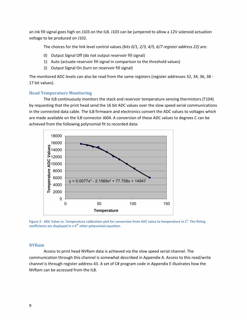
HeadTemperatureMonitoringThe ILB continuously monitors the stack and reservoir temperature sensing thermistors (T104)
by requesting that the print head send the 16 bit ADC values over the slow speed serial communications
in the connected data cable. The ILB firmware and electronics convert the ADC values to voltages which
are made available on the ILB connector J604. A conversion of these ADC values to degrees C can be
achieved from the following polynomial fit to recorded data:
Figure 2 ‐ ADC Value vs. Temperature calibration plot for conversion from ADC value to temperature in Co. The fitting coefficients are displayed in a 4th other polynomial equation.
NVRamAccess to print head NVRam data is achieved via the slow speed serial channel. The
communication through this channel is somewhat described in Appendix A. Access to this read/write
channel is through register address 43. A set of C# program code in Appendix E illustrates how the
NVRam can be accessed from the ILB.
y = 0.0077x3 - 2.1569x2 + 77.758x + 14947
0
2000
4000
6000
8000
10000
12000
14000
16000
18000
0 50 100 150
Tem
per
atu
re A
DC
Val
ues
Temperature

10
WaveformStorageWaveforms are defined by arrays of 16 bit values which give the ILB FPGA instructions for
voltage ramps, signal timing and the sending image data to the print head. The waveform data is written
to or read from FPGA local memory at address location starting point 256.
WaveformA detailed description of the waveform control data structure is supplied in Appendix D. The
waveform data provide information to the ILB for: 1) generation of voltage ramps, 2) the timing of
norming or calibration functions and 3) the transferring of ejection data intended for the next ejection
event. Due to the complexity and specific requirements needed for a fully functional waveform, the
Modify Waveform.exe program is included in order to create well‐formed waveform data in a form
which is readily downloadable to the ILB. Information concerning this program can be found in Appendix
C. Source code for creating a waveform from a formatted text .PRW file is included in Appendix G.
ImageDataImage data is stored in ILB SDDR Ram IC. The data is written to the ILB with the
QuickUSBWriteData function. This provides a high bandwidth method to write into ILB memory. In all
other cases where data is written to addresses in the ILB FPGA (see Register Definitions in Appendix B)
the QuickUSBWriteCommand method is used. The starting RAM address to write image data is set by
writing a 24 bit address value to register 18 (using the QuickUSBWriteCommand function). RAM can be
read back using the QuickUSBReadData function after setting the 24 bit beginning read address value in
register 20. When setting up to print, the beginning print from address is set with register 16.
The “gathered” image data consists of 4 or 5 bit words packed into 32 bit arrays (Maverick print
heads use 4 bit words). The 4 or 5 bits refer to shift register data for each of the 4 or 5 channels of a
print head, bit 0 representing channel 0, bit 1 representing channel 1, and so on. Upon the FPGA
accessing this memory during a print operation, it automatically forms the data in 3 bit packets as
described in appendix A according to the channel number mode bit (bit 16 register address 6).
EncoderPhaseLockLoopThe ILB FPGA firmware has the capability to generate various dot clock rates from motion
hardware encoder signals by a phase lock loop (PLL). The PLL function is controlled by set parameters in
the firmware:
Firmware Version up to 10.8 Firmware Version 11.0 and above
Register address 12 <7:0> Gain Multiplier <15:8> Gain Divisor <32:16> Frequency Range
Register address 12 <11:0> Gain Multiplier <23:12> Gain Divisor
Register address 46 <15:0> Frequency Range <29> Ignore Dead Band <30> Phase Lead <31> Phase Lag

11
The resulting dot clock spatial frequency in relation to the input encoder spatial frequency is
adjusted by a gain factor, gain=(Multiplier+1)/(Divisor+1). The stability of the PLL can be adjusted with
the Frequency Range value in relation to the Multiplier, where Stability = Frequency Range/ Multiplier.
In general the Frequency Range should be set to 4 X the Multiplier value. More information on the
operation and parameters for this is available in Appendix F.
DebugImagerSoftwareProgramThe operation of the imager board and settings can be explored with a LabView subroutine
called Debug Imager Board shown below in Figure 3. Upon starting the program it reads the state of all
the registers from the ILB and displays their hexadecimal value as well as parsing the values into their
functional parts and displaying them in readable and modifiable form. The routine also reads in the
current waveform in hex representation if a valid waveform is present in the ILB. The user can then
change the register settings by double clicking the Mode Bits selections and/or entering values into the
register values. The modified settings can then be sent to the ILB by clicking on the Write Values to
Board button and perhaps read them back by clicking the Read Values from Board button. The user can
then perform a Start Page command by clicking the Start Page button to begin the ejection sequence
and the stop it by selecting the Stop Page button.
Figure 3 ‐ Debug Imager Board LabView UI.
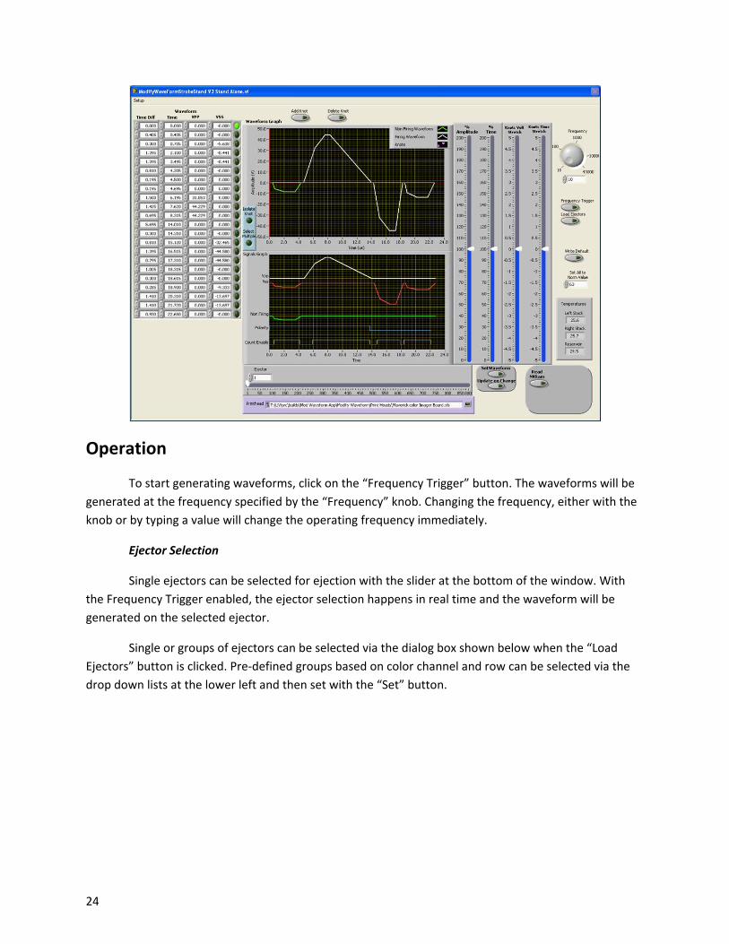
Perhaps a more complete user program tool for testing operation is the Modify Waveform
program which allows the user to design waveforms, address specific ejectors, read and display the print
head’s NVRAM and produce waveforms at selected frequencies. The Documentation for the program
can be found in Appendix C.
12
OperationalSettingExamplesBelow are sets of examples of register settings for various operational states of the imager
board displayed in the debugger program UI. Programming the operation of the print head for ejection
involves 1) setting the state of the operation through the registers, 2) loading a valid waveform and 3)
loading the ejector data. The latter may include norm and ejection data.
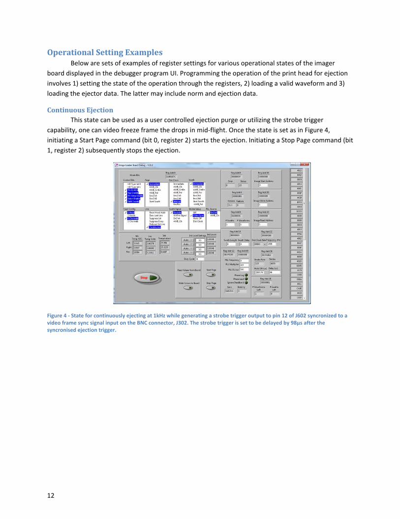
ContinuousEjectionThis state can be used as a user controlled ejection purge or utilizing the strobe trigger
capability, one can video freeze frame the drops in mid‐flight. Once the state is set as in Figure 4,
initiating a Start Page command (bit 0, register 2) starts the ejection. Initiating a Stop Page command (bit
1, register 2) subsequently stops the ejection.
Figure 4 ‐ State for continuously ejecting at 1kHz while generating a strobe trigger output to pin 12 of J602 syncronized to a video frame sync signal input on the BNC connector, J302. The strobe trigger is set to be delayed by 98µs after the syncronised ejection trigger.

13
DefinedNumberofEjectionsThe state depicted in Figure 5 is used to deposit a fixed number of ejected drops at the defined
frequency.
Figure 5 ‐ State for producing 100000 ejections at 30kHz

14
FlatBedPrintingFigure 6 shows a complex example intended primarily for flatbed printing. In this case an
encoder signal is fed into the encoder channel A connector which drives a phase lock loop (PLL) which
converts the encoder signal distance resolution into a different user controlled DPI. This is done by
adjusting the PLL Gain (gain = multiplier / divisor, PLL Multiplier and PLL Divisor, register 12) and the PLL
Frequency (register 46). The action of printing (Page setting in the Mode Bits below, register 6) is started
immediately upon a Start Page command. The ILB preloads the first ejector data into the print head then
waits until the Swath signal is detected (Swath setting, register 2), waits 200 encoder transitions (Swath
Delay, register 10) coming on encoder channel A and then begins ejecting 6000 ejection events (#
Waveforms in register 8). The ILB then waits until the next Swath signal to begin printing the second
pass. This is repeated until 4 passes (# Swaths, register 8) are completed. Upon completion the ILB clears
the ejector data in the print head.
Figure 6 ‐ State example for Flatbed Printing; 4 passes with 6000 ejections/pass, printing starts immediately from the Start Page command, Dot Clock from encoder PLL with the encoder signal connected to the encoder channel A. The start of printing is 200 encoder pulses from the start of each swath or pass. The Dot Clock is generated internally by the PLL with a gain of 0.85686 (600dpi with a 700dpi encoder). Preload 1st ejection data and clear the head ejection data upon completion.
15
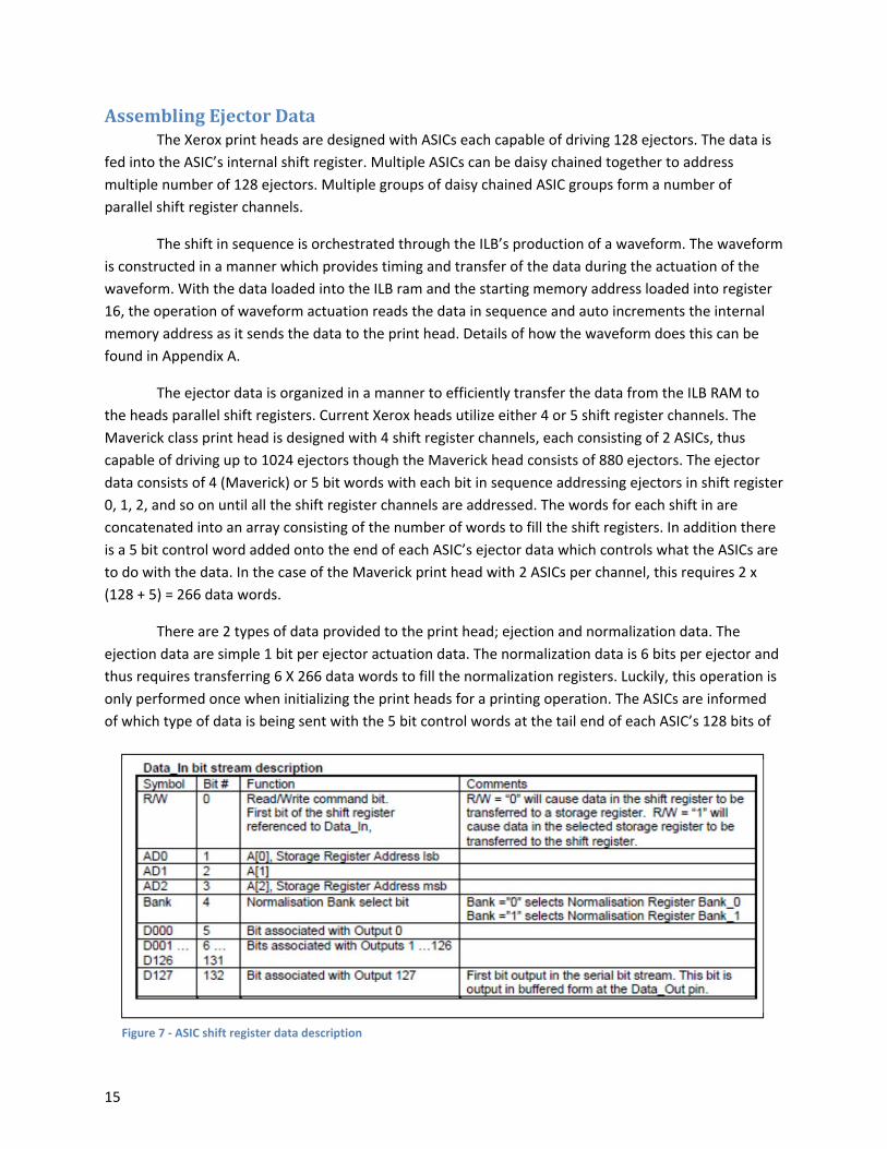
AssemblingEjectorDataThe Xerox print heads are designed with ASICs each capable of driving 128 ejectors. The data is
fed into the ASIC’s internal shift register. Multiple ASICs can be daisy chained together to address
multiple number of 128 ejectors. Multiple groups of daisy chained ASIC groups form a number of
parallel shift register channels.
The shift in sequence is orchestrated through the ILB’s production of a waveform. The waveform
is constructed in a manner which provides timing and transfer of the data during the actuation of the
waveform. With the data loaded into the ILB ram and the starting memory address loaded into register
16, the operation of waveform actuation reads the data in sequence and auto increments the internal
memory address as it sends the data to the print head. Details of how the waveform does this can be
found in Appendix A.
The ejector data is organized in a manner to efficiently transfer the data from the ILB RAM to
the heads parallel shift registers. Current Xerox heads utilize either 4 or 5 shift register channels. The
Maverick class print head is designed with 4 shift register channels, each consisting of 2 ASICs, thus
capable of driving up to 1024 ejectors though the Maverick head consists of 880 ejectors. The ejector
data consists of 4 (Maverick) or 5 bit words with each bit in sequence addressing ejectors in shift register
0, 1, 2, and so on until all the shift register channels are addressed. The words for each shift in are
concatenated into an array consisting of the number of words to fill the shift registers. In addition there
is a 5 bit control word added onto the end of each ASIC’s ejector data which controls what the ASICs are
to do with the data. In the case of the Maverick print head with 2 ASICs per channel, this requires 2 x
(128 + 5) = 266 data words.
There are 2 types of data provided to the print head; ejection and normalization data. The
ejection data are simple 1 bit per ejector actuation data. The normalization data is 6 bits per ejector and
thus requires transferring 6 X 266 data words to fill the normalization registers. Luckily, this operation is
only performed once when initializing the print heads for a printing operation. The ASICs are informed
of which type of data is being sent with the 5 bit control words at the tail end of each ASIC’s 128 bits of
Figure 7 ‐ ASIC shift register data description

16
data. Bit 0 of the 5 bit control word differentiates between ejection data and normalization data. Bits 1
through 3 define which bit of the 6 bit normalization data is being written. There are 2 banks of
normalization registers which are specified by bit 4. Figure 7 describes the ASIC’s data sequence and
control bits.
In the particular case of the Maverick print head, since not all of the shift register data connect
to ejectors and the unused registers are at the high end of the shift register chain, one only needs to
shift in 230 4 bit words.
17
AppendixA
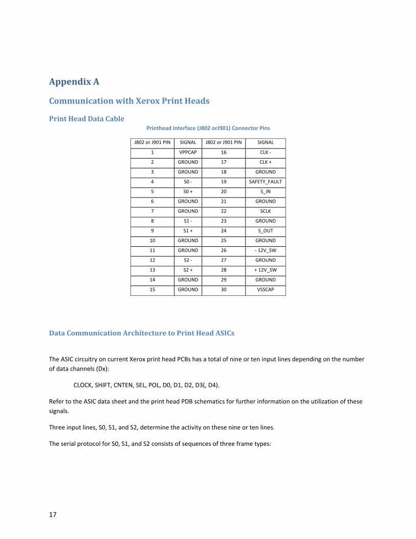
CommunicationwithXeroxPrintHeads
PrintHeadDataCablePrinthead Interface (J802 orJ901) Connector Pins
J802 or J901 PIN SIGNAL J802 or J901 PIN SIGNAL
1 VPPCAP 16 CLK ‐
2 GROUND 17 CLK +
3 GROUND 18 GROUND
4 S0 ‐ 19 SAFETY_FAULT
5 S0 + 20 S_IN
6 GROUND 21 GROUND
7 GROUND 22 SCLK
8 S1 ‐ 23 GROUND
9 S1 + 24 S_OUT
10 GROUND 25 GROUND
11 GROUND 26 ‐ 12V_SW
12 S2 ‐ 27 GROUND
13 S2 + 28 + 12V_SW
14 GROUND 29 GROUND
15 GROUND 30 VSSCAP
DataCommunicationArchitecturetoPrintHeadASICs
The ASIC circuitry on current Xerox print head PCBs has a total of nine or ten input lines depending on the number
of data channels (Dx):
CLOCK, SHIFT, CNTEN, SEL, POL, D0, D1, D2, D3(, D4).
Refer to the ASIC data sheet and the print head PDB schematics for further information on the utilization of these
signals.
Three input lines, S0, S1, and S2, determine the activity on these nine or ten lines.
The serial protocol for S0, S1, and S2 consists of sequences of three frame types:

18
Idle frame: S0 S1 S2
‐‐‐‐‐‐‐‐‐‐‐‐‐‐+‐‐‐‐‐‐‐‐+‐‐‐‐‐‐‐‐+‐‐‐‐‐‐‐‐+
| 0 | 0 | 0 |
+‐‐‐‐‐‐‐‐+‐‐‐‐‐‐‐‐+‐‐‐‐‐‐‐‐+
Control frame: S0 S1 S2
‐‐‐‐‐‐‐‐‐‐‐‐‐‐+‐‐‐‐‐‐‐‐‐+‐‐‐‐‐‐‐‐+‐‐‐‐‐‐‐‐‐‐‐‐+
| 0 | POL | SHIFT |
+‐‐‐‐‐‐‐‐‐+‐‐‐‐‐‐‐‐‐+‐‐‐‐‐‐‐‐‐‐‐‐+
| 0 | SEL | CNTEN‐ |
Data frame: S0 S1 S2
‐‐‐‐‐‐‐‐‐‐‐‐‐‐‐‐‐+‐‐‐‐‐‐‐‐+‐‐‐‐‐‐‐‐+‐‐‐‐‐‐‐‐+
| 1 | D1 | D3 |
+‐‐‐‐‐‐‐‐‐+‐‐‐‐‐‐‐‐+‐‐‐‐‐‐‐‐+
| D0‐ | D2 | D4 |
Each control frame must be immediately followed by a data frame. Each data frame generates a CLOCK pulse to
the HDA's to clock in the data. If a control frame precedes a data frame, then the same CLOCK pulse clocks in the
new control line states as well as the data.
Idle frames cause no activity on the HDA lines. As many idle frames as desired may be inserted between data
frames or between a data frame and the subsequent control frame. No idle frames are allowed between a control
frame and the following data frame.
The purpose of idle frames is to space out HDA CLOCK pulses. One data frame after another with nothing else in
between results in 32MHz HDA CLOCK frequency. One idle frame between data frames results in 21.33 MHz (three
64MHz serial clocks per HDA CLOCK). Two idle frames between each pair of data frames results in 16 MHz HDA
CLOCK (64MHz / 4). This is the same frequency as would result from inserting a control frame before each data
frame.
Between jet fire waveforms, no HDA CLOCK pulses are required. The serial bus will be continuous idle frames
(steady state low for S0, S1, and S2).
Two of the lines are inverted in the data stream: D0 and CNTEN. This is indicated by their listing as D0‐ and CNTEN‐
in the table above. CNTEN is inverted so that no control frame will have all zeros on S1 and S2. CNTEN never needs
to be high when SEL is low. Thus, CNTEN‐ will never be high when SEL is low. This leaves an unused control frame
case (all zeros), which is defined to be the idle frame.
D0 is inverted to reduce the number of edges on the S0 line when sending data frames at the full 33MHz rate.
Typical print data has more zeros than ones. Inverting D0 makes it more ones than zeros. This results in fewer
transitions on S0 during data frames.
DescriptionoftheASICFunctionsandMainParameters The Head Driver ASIC implements a low‐voltage serial to high‐voltage parallel converter for the purpose of driving
piezo‐electric transducers integral to a Ink Jet Print Head. It consists of a 133‐bit long 1‐bit wide shift register, a
128‐bit jet data latch, two banks of 128 * 6‐bit “normalization” data latches, a 6‐bit binary “normalization”
counter, a 128‐bit “normalization‐enable” data latch and 128 bi‐polar high voltage output drivers.

19
Data is loaded into and read from the Head Driver ASIC through a 133‐bit serial shift register. Serial Data_In, Serial
Data_Out, Shift, and Clock comprise the signalling elements of the serial data path to/from the ASIC. Serial data
order is data[127], as the first bit input by the ASIC, followed by data[126..0] and 5 control bits
(Norm_Bank_Select, Register_Address[2:0], and R/W – the last bit input). A Serial Data_Out pin (corresponding to
shift register bit 132 ‐ the first bit output from the ASIC) facilitates cascading multiple Head Driver ASICs in a data
chained application environment.
Data shifting into or out of the ASIC is synchronized on the positive edge of Clock and is qualified by Shift. Data
transfer to/from the addressed storage register occurs following negation of Shift. One of thirteen storage
registers is identified by the Norm_Bank_Select and register_Address[2:0] bits contained in the shift register. The
transaction type, read or write is defined by the R/W bit contained in the shift register. R/W = “1” defines a read of
a selected internal storage register, R/W = “0” defines a write to the selected internal storage register.

20
SerialCommunication:S3andSOUT(otherprintheadI/O):S3 and SOUT run at an 8 MHz bit rate (one bit every eight 64MHz clock cycles). This reduces EMI directly by lowering the number of edges (signal transitions), and allows for further reduction with low pass filtering. Low pass filtering may delay S3 by up to two 64MHz clock cycles. SOUT may also be delayed by up to two additional 64MHz clock cycles with low pass filtering for EMI reduction. S3 contains the following data bit sequence at 8 MHz:
0 Start_Bit // always 1
1 ADC_Clk_Enable // clocks thermal and ink level ADC's when set
2 Ink_Drive // state of conductive ink level sense reference
3 NVRAM_Clk // clock to NVRAM chip
4 NVRAM_Data // Open drain data line to NVRAM chip
5 Version_mode // Return PLD version on bits 9 through 13 when set.// (Instead of the ends of the HDA serial shift chains)
S3 is low (0) at all times except when sending the above sequence of six bits. This sequence is sent from the main board to the print head every 128 64MHz clocks (every 2 microseconds). Each bit of the six lasts for 8 64MHz clocks, or 48 clocks for the whole set. The Start_Bit on S3 also triggers the beginning of return data from the print head to the main board on SOUT. The first data bit on SOUT will be set on the third 64MHz clock cycle after S3 goes high at the beginning of each Start_Bit. Each bit will be held for a total of 8 64MHz clocks. Thus the second SOUT bit will be set on the eleventh 64MHz clock cycle after S3 goes high, the third bit on the nineteenth clock, etc.
The print head returns the following bit sequence on SOUT at an 8 MHz rate each time a new Start_Bit is received on S3: 0 Ink_0 // Channel 0 (left most) ink sense sigma delta ADC state
1 Ink_3 // Channel 3 (right most) ink sense sigma delta ADC state
2 Ink_2 // Channel 2 (inner right) ink sense sigma delta ADC state
3 Ink_1 // Channel 1 (inner left) ink sense sigma delta ADC state
4 Temp_JetL // Left jet stack thermister sigma delta ADC state
5 Temp_JetR // Right jet stack thermister sigma delta ADC state
6 Temp_Res // Reservoir thermister sigma delta ADC state
7 Dummy_Jet // Dummy jet and reference voltage sigma delta ADC state
8 NVRAM_Data // NVRAM serial data line state
9 HDA_Data_In0 // End of HDA serial shift chain 0 / PLD version bit 0
10 HDA_Data_In1 // End of HDA serial shift chain 1 / PLD version bit 1
11 HDA_Data_In2 // End of HDA serial shift chain 2 / PLD version bit 2
12 HDA_Data_In3 // End of HDA serial shift chain 3 / PLD version bit 3
13 HDA_Data_In4 // End of HDA serial shift chain 4 / PLD version bit 4
14 M12V_Present // High when ‐12v supply is OK and VPP and VSS are idle
15 Ink_Drive // Echo of Ink_Drive for serial link health check
This sequence of 16 bits (at 8 clocks per bit) fills up the entire 128 64MHz clocks between Start_Bits. So there is no idle time on SOUT. To provide re‐synchronization after a disturbance (static zap or whatever), the SOUT sequence will re‐start when a new Start_Bit is received if the Start_Bit comes when the sequence is at least half completed. If the sequence completes without seeing a new Start_Bit, it waits until the next Start_Bit before re‐starting.
The first eight SOUT bits are raw sigma delta ADC bits. They are accumulated into voltage readings inside the Titan chip on the main board. The next seven SOUT bits are available as raw bits to Saturn firmware. They are used for NVRAM access and head diagnostics. The final bit (Ink_Drive) is compared in Titan to check for serial link failure.

21
AppendixB
ImageLoaderRegisterDefinitionsRegister Address ↓
0 Error bits, status bits
2 Command bits
<0> Manual start page - This starts normal printing
<1> Manual single line – This outputs one line with waveform suppressed
<2> Manual stop page – This stops printing when the current waveform completes
<3> Manual immediate stop page – This stops immediately
<7> Reset errors – not used yet
4 Firmware version
<7:0> minor version
<15:8> major version
<23:16> {features - <1:0> clock type 3: dcm, 2: 66MHz split, 1: 48MHz} - (Unused)
<31:24> unused
6 Operational State
<6:0> wv
<6> shift enb
<5> select enb
<4> wa_en
<3> Vss enb
<2> Vpp enb
<1> Head Type - 1
<0> Head Type - 0=Fast Serial, 1=Slow Serial
<9:7> page select
0) immediate
1) AWB_CLK
2) AWB_CNTEN
3) AWB_POL
4) encoder_cha
5) encoder chb
6) start swath
<12:10> waveform select (Dot Clock)
0) immediate
1) AWB_CLK
2) AWB_CNTEN
3) AWB_POL
4) encoder_cha
5) encoder chb
6) internal dotclk
7) encoder PLL output
<15:13> swath select – pass select
0) immediate
1) AWB_CLK
2) AWB_CNTEN
3) AWB_POL
4) encoder_cha
5) encoder chb
6) start swath
7) -AWB_POL
<18:16> hd data width
<1> nbr heads 0) 1 heads, 1) 2 heads
<0> - width – 0) 4 bits, 1) 5 bits
<25:19> line_cnt_flags_reg
<5> continuous printing – This causes the system to keep printing pages until a manual stop page {Strobe Stand}
<4> output line zero – This causes an initial suppressed line sent before the bulk of the page. The wv amp is suppressed. {Printing}
<3> suppress_every_line – This causes the waveform to be suppressed on the first line of every page. {Strobe Stand}
<2> suppress first line – This causes the first waveform of the first page printed in a continuous group to be suppressed {Strobe Stand}
<1> zero_last line - This causes the data sent on the last line of the last swath to be 0 {Printing}
<0> reset head - Reset image start address every line {Weight Measure – in conjunction with # waveforms}
<27:26> swath length source
0) encoder PLL Out
1) start_waveform_sig
2) encoder_cha
3) AWB_CLK
<29:28> strobe select
0) off
1) video input
2) internal rep rate
3) always on
8 # Waveforms/Swaths
<23:0> number of waveforms
<31:24> number of swaths

22
10 Swath Length & Delay
<31:16> swath length (drum circumference in 150 dpi encoder pulses)
<15:0> swath delay (dot clks)
12 Encoder Gain PLL
<11:0> Gain Multiplier
<23:12> Gain Divider
14 Ink Level Monitor Control
<1:0> 0) Off, 1) Auto, 2) On
<3:2> 0) Off, 1) Auto, 2) On
<5:4> 0) Off, 1) Auto, 2) On
<7:6> 0) Off, 1) Auto, 2) On
<16:22> Duty Cycle Val (300)
16 image start addr
<24:0> The 4 lsbs should be 0
18 write start addr
<24:0> The 4 lsbs should be 0. It auto increments on data writes
20 read start addr
<24:0> The 4 lsbs should be 0
22 dotclk rate
<23:0> This is the internally generated dot clk in 66MHz
24 strobe timing
<15:0> pulse delay - Strobe pulse delay in 66Mhz
<31:16> pulse rate - Strobe pulse rate is in 2^10 * 66Mhz
26 read counts - These are the current position being reported. These numbers count down from total count. (config reg 1)
<23:0> waveform cnt
<31:24> swath cnt
28 Fifo data out
<15:0> This is the head memory at the location pointed at by write start addr
30 Mem Data Out
<15:0> This is the head memory at the location pointed at by write start addr
32 Ink 0 Level
<16:0> Read - Level, Write - Sense Level
34 Ink 1 Level
<16:0> Read - Level, Write - Sense Level
36 Ink 2 Level
<16:0> Read - Level, Write - Sense Level
38 Ink 3 Level
<16:0> Read - Level, Write - Sense Level
40 Ink Left Stack Temp
<15:0> Read Thermistor Temperature ADC Value
41 Ink Right Stack Temp
<15:0> Read Thermistor Temperature ADC Value
42 Ink Reservoir Temp
<15:0> Read Thermistor Temperature ADC Value
43 NVRam
Read
<0> Tx Clk
<1> Tx Data Write
<2> Read Data Value
<8:11> Head Frimware Version
Write
<0> Tx Clk
<1> Tx Data
46 PLL Frequency Range
<15:0> Frequency Range
<29> Ignore Dead Band
<30> Phase Lead
<31> Phase Lag
Notes:
The waveform is written to a specific register address in FPGA block memory. Firmware versions < 5.8 this address is 32 decimal. For versions 7 and above this address is 256 decimal. Waveform format is the binary 16 bit format
represented in text files as hex numbers. The format is detailed elsewhere. The maximum number of 16 bits values stored is 256.
Print data is written by first specifying the DDR2 memory address location via a Command Write to a Write Image Start Address register (18d). Subsequently one or more Write Data operations are performed to stream the data in
high speed mode in 32 bit words to DDR2 memory. The USB interface auto increments the memory address. An extra 8 words are needed at the end of the data stream to flush the fifos. Maximum amount of data in a single Write
Data operation cannot exceed 2^24 (16,777,216) bytes. Data amounts over this size need to be broken into multiple write operations. The gathered data has no breaks in the data stream from one ejection event or one printing
pass to the next. The amount of data downloaded to the head ASICs for an ejection event is controlled by the waveform through it specific number of head clocks embedded in the waveform.

23
AppendixC
ModifyWaveform
Introduction
This is a program initially developed to support the larger Xerox Ink Jet Strobe Stand test fixture
in order to provide a complete capability to easily modify test waveforms in real time so that the user
can visualize the effects on drop ejection. The version of the routine discussed here has been modified
to operate independent of the Strobe Stand code.
Installation and Startup
The current installation requires versions 10.2 or higher of the imager board firmware and the
QuickUSB driver software previously installed. The installation software installs the executable as well as
support files in directories located in the program directory. Before starting the software, be sure the
imager board is powered up and the imager board USB module is connected to the computer USB port.
Upon first starting the software, dialog boxes may appear asking the user to find and select from
waveform files and print head descriptor files. Sample waveforms for Jupitor and Mariner printers are
supplied in the Waveforms directory. Print head descriptor files for Taipan and various forms of
Maverick printheads are supplied. After these files are selected, a small window appears showing
progress of reading in the print head descriptor file and then the selected waveform is displayed.
Once the initialization is done and the program window is displayed as below, the imager board
is initialized and ready to generate waveforms on the print head. At this time it would be wise to click on
the “Write Default” button in order to save the waveform and print head selections for later restarting
of the program.
24
Operation
To start generating waveforms, click on the “Frequency Trigger” button. The waveforms will be
generated at the frequency specified by the “Frequency” knob. Changing the frequency, either with the
knob or by typing a value will change the operating frequency immediately.
Ejector Selection
Single ejectors can be selected for ejection with the slider at the bottom of the window. With
the Frequency Trigger enabled, the ejector selection happens in real time and the waveform will be
generated on the selected ejector.
Single or groups of ejectors can be selected via the dialog box shown below when the “Load
Ejectors” button is clicked. Pre‐defined groups based on color channel and row can be selected via the
drop down lists at the lower left and then set with the “Set” button.

25
The selected set of ejectors is indicated by the yellow dots. The ejector set can be modified in
many ways; 1) the user can mouse over ejector locations and click on the location to toggle the
particular ejector on/off. As you mouse over the ejector location, the ejector number is indicated in the
“At Mouse” number. Once a location is clicked,, a red crosshair is placed at the location and the ejector
number is displayed in the “At Cross Hair” location. You can also specify an ejector location by typing in
the ejector number at the “Set # Ejector” box which will toggle the ejector on/off as well as place the
crosshair at the ejector location. 2) You can limit the range of selected ejector numbers with the “Ejector
Range slider. 3) You can directly edit the list of ejectors in a dialog box which appears when the “Edit
Ejector List” button is clicked. 4) You can reset the selected ejectors to the original set with the “Reset”
button. 5) You can read/write ejector lists from/to ejector list files (ascii text files). 6) You can also select
ejectors with the “Min/Max Ejectors” and “Interval” sliders at the top of the window.
Then you can either click the OK button, which will load the selected ejectors into the print
head, or select “Cancel” which abandons any selections made.
Menu Selections
The Setup drop down menu provides means of selecting from (“Open”) or saving to (“Save”) a
waveform file. The user can save a waveform in three different formats; .prw, .wav and .txt. The .prw
format will save the waveform in a modified standard printer waveform format – modified in that the
volts column is split into separate Vpp and Vss columns. The .wav format is the ascii hex format which is
the data actually sent to the imager board. The .txt format is 3 columns of time, Vpp and Vss values.
The “Config” selection will bring up a configuration dialog box which allows the specifying of limits to
the possible waveforms as well as selecting the polarity of waveamp enable signal allowing for older
waveamp variations.

26
The “Stop” selection stops the program operation without quiting the program. One can then
restart the program by clicking on the arrow which appears in the upper left of the window. The “Exit”
selection quits the program.
The “Debug Imager Board” selection will bring up a parallel program window as shown below.
This routine allows a low level access to the imager board registers and a means of modifying settings. A
description of the operation of the imager board is beyond the scope of this document. Once opened, a
check mark is placed by the “Debug Imager Board” selection. To close the window, reselect the “Debug
Imager Board” selection.
Norm Value
The “Norm Value” box allows the user to set the operational norm value for the entire head.
Otherwise, the norm values for the ejectors are set by calibration values in the print head descriptor file.
Head Temperatures

27
The head temperature sensors readings are displayed in real time in the “Temperatures” box.
The raw thermistor readings are converted to Celsius via a calibration polynomial whose coefficients are
set in the print head descriptor file. The conversion is only meant to be approximate and may vary from
the real value by a degree or so.
Printhead Files
Print head descriptor files can be selected by clicking on the folder icon in the “Printhead” box at
the bottom of the screen. Once a valid file is selected, the file is read in, signified by an ejector number
progress window appearing.
The print head descriptor file is an Excel spread sheet providing print head specific data
including ejector addressing, ejector location relative to ejector number 1, color or ink supply channel,
norm calibration values, print head family name, temperature polynomial coefficients and ink level
setting values. This file allows the software to operate any Xerox print head if properly set.
Waveform Modifying

28
Using this program to modify waveforms is easy. Knowing just how to modify a waveform for
the desired result is hard. It is expected that the user knows the basics as well as being familiar with the
head ASIC’s capability and how they operate. Care has been put into the program to limit the user’s
ability to screw things up, but this is a complicated undertaking and would not be surprised at what an
untrained user can do with the current code.
Updating the Waveform
One can set the current waveform in the imager board by clicking on the “Set Waveform”
button. One can also set the program to update the waveform in real time to the imager board when
the waveform is changed by enabling “Update on Change”. In this way, the user can see the
modifications effect in close to real time.
Global Modifications
The 2 sliders to the right of the plots, “% Amplitude” and “% Time” can be used to expand and
shrink the entire waveform in volts or time.
Waveform Plot Windows
The two plot windows show different representations of the current waveform shape and
operation.
The top window shows the active ejection waveform in white and the non‐firing waveform in
green. In default mode, there is also a red crosshair with a small circle which snaps to the various knot
locations of the waveform. The crosshair can be moved by clicking and holding the mouse over the circle
and dragging the mouse to other knot locations. You can also move the crosshair by clicking on the one
of the radio buttons in the column to the left of the time/voltage values. As you mouse over the circle,
you will notice that the crosshair changes from red to green, signifying that it recognizes the potential to
move the crosshair. At that point, if the user holds down the middle mouse button, the green crosshair
changes to purple and can then drag the knot to a different time/volt location. If the knot is at zero
volts, the only change allowed is in the time direction. Attempts to drag a knot past allowable values will
cause a temporary notification to appear of the un‐allowed action.
By positioning the crosshair on a particular knot causes the slider scales for “Knots Volts Stretch”
and “Knots Time Stretch” to update. Sliding the “Knots Volt Stretch” causes the knots with values at or
greater, in absolute value time and volts, to change. Sliding the “Knots Time Stretch” causes the knots at
and greater time to change. By enabling the “Isolate Knot” radio button on the left hand of the plot,
isolated the slider action to the selected knot alone.
By enabling the “Select Multiple” radio button the left of the plot allows you to select multiple
knots with the radio button column to the right of the time/volt list. The selected knots are then
highlighted on the plot by purple dots. The sliders will then only operate on the selected knots.

29
The bottom plot window shows the waveform broken up into positive (Vpp) white and negative
(Vss) in red waveform portions as well as showing the non‐firing waveform in green. In addition, the
control signals, “Polarity” in blue and “Count Enable” in yellow are shown. The user can change these
two signals operation by clicking the appropriate signal plot in the particular lobe time they want to
change. The resulting change due to modification to the polarity signal will be shown in the wavefom
plots above.
One can add or delete knots with the “Add Knot” and “Delete Knot” buttons above the plot
areas. By positioning the crosshair to a selected position and clicking on “Add Knot” will result in putting
an additional knot half way between the selected knot and the next knot. The crosshair will be
automatically repositioned over the new knot.
One can also modify individual values in the time/volt data columns on the left of the screen.
One needs to be careful doing this as you can go outside allowable values easily.
NVRam
If the print head has data installed in its non volatile RAM (NVRam), this can be read in with the
“Read NVRam” button. Upon clicking the button a notice is displayed informing the user that the NVRam
reading is taking place. Depending on the amount of data and which print head is being read from, this
operation will take 15 to 60 seconds to complete. Upon completion, three more buttons appear:
“Display NVRam”, “Load NVRam Waveform” and “Load NVRam Norm”. If there is more than 1
waveform defined, a dialog box will pop up to give the opportunity to select which waveform/norm
values to potentially use.
“Display NVRam” button will bring up a window in which you are able to explore all the data
read in from NVRam. It may be that some of the values are not presented correctly, primarily due to lack
of information concerning the parameter’s data type. A drop down box in the window will bring up the
various categories of data.

30
The “Load NVRam Waveform” button will replace the current waveform in use with the
waveform from NVRam when toggled true. The old waveform will be installed again when the button is
toggled false.
Likewise, the “Load NVRam Norm” button will replace the current norm values in use with the
waveform from NVRam when toggled true. The original norm values will be installed again when the
button is toggled false.
Additional Notes
1) The decision to modify the waveform file format to separate the negative and positive going channels allows for the possibility to locate portions of the non‐firing waveform within the firing portion of the waveform. The reading in of waveforms can be done with files in the old format.
2) Great pains were taken to create algorithms for hex waveform generation and decoding to ensure a what‐you‐see‐is‐what‐you‐get operation. Certain hex generation “standards” had to be invoked to taken into scope to allow for smooth operation and most all waveform variations. While this may not produce the most compact form, it allows for more than less and reduces code complication. The basic code and philosophy was the result of modifications to Dave Knierim’s wavet.c code.
31
AppendixD
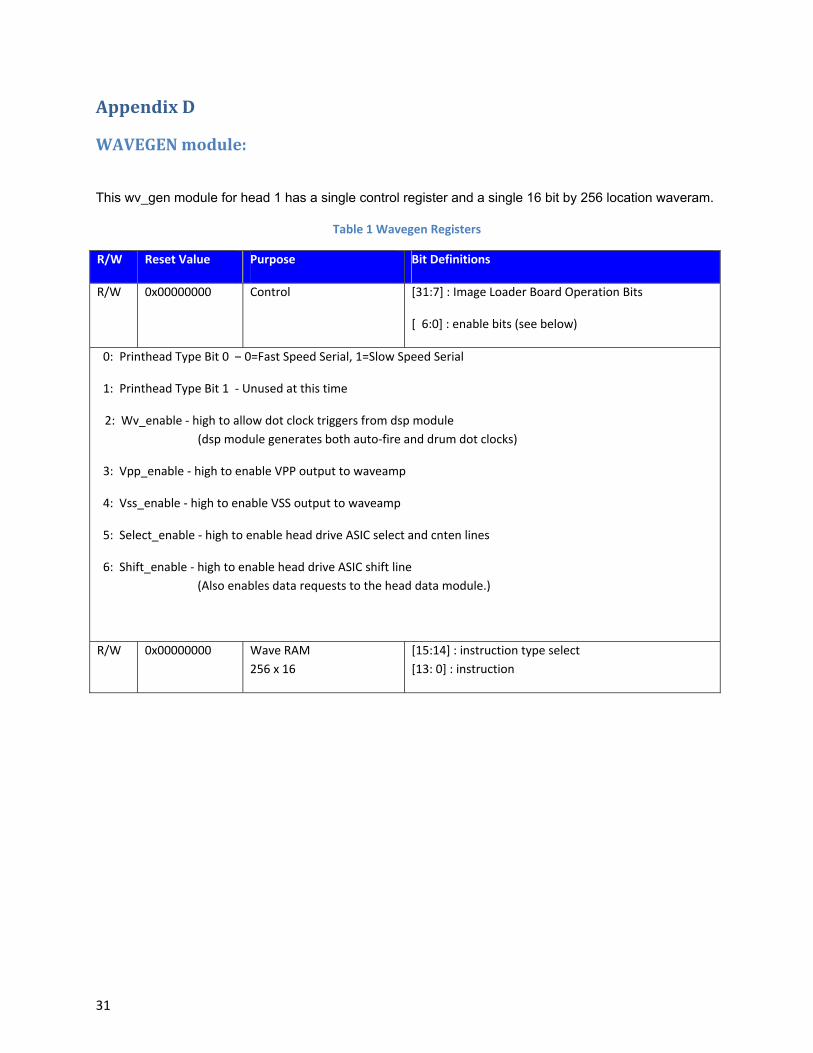
WAVEGENmodule:
This wv_gen module for head 1 has a single control register and a single 16 bit by 256 location waveram.
Table 1 Wavegen Registers
R/W Reset Value Purpose Bit Definitions
R/W 0x00000000 Control [31:7] : Image Loader Board Operation Bits
[ 6:0] : enable bits (see below)
0: Printhead Type Bit 0 – 0=Fast Speed Serial, 1=Slow Speed Serial
1: Printhead Type Bit 1 ‐ Unused at this time
2: Wv_enable ‐ high to allow dot clock triggers from dsp module
(dsp module generates both auto‐fire and drum dot clocks)
3: Vpp_enable ‐ high to enable VPP output to waveamp
4: Vss_enable ‐ high to enable VSS output to waveamp
5: Select_enable ‐ high to enable head drive ASIC select and cnten lines
6: Shift_enable ‐ high to enable head drive ASIC shift line
(Also enables data requests to the head data module.)
R/W 0x00000000 Wave RAM
256 x 16
[15:14] : instruction type select
[13: 0] : instruction

32
The waveram has four instruction types, selected by the top two bits:
00XX_XXXX_XXXX_XXXX: Set_control_bits:
Bit 0: head_polarity
Bit 1: head_select
Bit 2: head_count_enable
Bit 3: head_shift
Bit 13: end_waveform (stop instruction)
01XX_XXXX_XXXX_XXXX: Delay:
Bits 0 through 9: Delay count
Bits 10 through 13: Head clock divide
10XX_XXXX_XXXX_XXXX: Load_VPP_slope:
Bits 0 through 13: VPP slope
11XX_XXXX_XXXX_XXXX: Load_VSS_slope:
Bits 0 through 13: VSS slope
The control register will be cleared when the ADC module detects a waveamp fault (output short circuit) or a head_broken state (failed head slow serial link or ‐12 volt supply isn't up) for this print head.
All single shot firings should use the single_wave control register feature and not auto‐fire. Refer to DSP sections for information on generating auto‐fire and printing dot clocks.
Once a waveform is loaded into the waveram, it can be used for norm loading, priming the head drive ASIC data latches at the beginning of a drum revolution, for normal firing (with data loading), and for purge firing (no data loading).
For norm and data loading, enable shift only and fire a single waveform. Writing the control register with 0x61 accomplishes this.
For normal firing, enable everything (0x7C).
For purge firing, enable everything except shift (0x3C).
Waveform only firing shouldn't be needed any longer, but it can be accomplished by enabling VSS and VPP but not shift or select (0x1C).
All WAVERAM instructions take a single 66MHz clock to execute, except for delay instructions with a non-zero delay values. Delay instructions take the number of 66MHz clocks specified in the lower 10 bits, plus one extra. The head clock divide field of delay instructions takes effect immediately (at the end of the first clock cycle) without waiting for the delay time to expire.
33
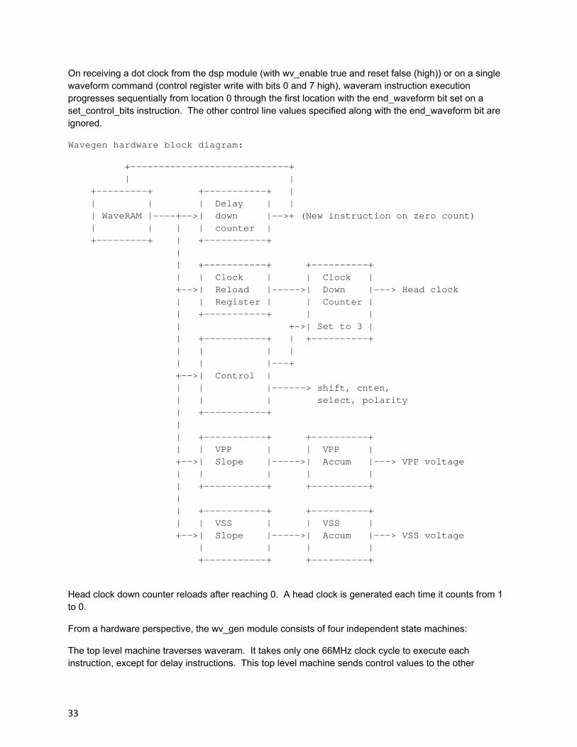
On receiving a dot clock from the dsp module (with wv_enable true and reset false (high)) or on a single waveform command (control register write with bits 0 and 7 high), waveram instruction execution progresses sequentially from location 0 through the first location with the end_waveform bit set on a set_control_bits instruction. The other control line values specified along with the end_waveform bit are ignored.
Wavegen hardware block diagram:
+----------------------------+ | | +---------+ +-----------+ | | | | Delay | | | WaveRAM |----+-->| down |-->+ (New instruction on zero count) | | | | counter | +---------+ | +-----------+ | | +-----------+ +----------+ | | Clock | | Clock | +-->| Reload |----->| Down |---> Head clock | | Register | | Counter | | +-----------+ | | | +->| Set to 3 | | +-----------+ | +----------+ | | | | | | |---+ +-->| Control | | | |------> shift, cnten, | | | select, polarity | +-----------+ | | +-----------+ +----------+ | | VPP | | VPP | +-->| Slope |----->| Accum |---> VPP voltage | | | | | | +-----------+ +----------+ | | +-----------+ +----------+ | | VSS | | VSS | +-->| Slope |----->| Accum |---> VSS voltage | | | | +-----------+ +----------+
Head clock down counter reloads after reaching 0. A head clock is generated each time it counts from 1 to 0.
From a hardware perspective, the wv_gen module consists of four independent state machines:
The top level machine traverses waveram. It takes only one 66MHz clock cycle to execute each instruction, except for delay instructions. This top level machine sends control values to the other
34
machines based on the data in the instructions. It does not wait for the other machines. It sends them data and continues on. The data it sends depends on the top two instruction bits:
00: Control bits (Shift, Cnten, Select, Polarity)
01: Head clock down counter reload value
10: VPP slope
11: VSS slope
On instruction 01, the delay counter is also loaded. If loaded to a non-zero value, then it prevents the waveram from executing the next instruction until the delay counter reaches 0. The head clock reload register is loaded immediately, not waiting for the delay count to expire.
The VPP state machine is very simple. It has only one input parameter, vpp_slope. Each clock cycle, it adds this slope value to the VPP voltage accumulator. The only exceptions are:
If the VPP voltage accumulator overflows, it limits to maximum.
If the VPP voltage accumulator underflows, it limits to zero.
If a waveform is not running or vpp is disabled, VPP voltage is set to zero.
Vpp_slope is set to zero when a waveform is not running. When a waveform is running, each time the top level state machine reaches a load_VPP_slope instruction in waveram, the slope value from that instruction is loaded into the vpp_slope register. The vpp_slope register contains a signed (two's compliment) 14 bit value. The VPP voltage accumulator contains an 18 bit unsigned value. The slope register is sign extended to 18 bits before being added to the VPP voltage accumulator. The top 8 bits of the VPP voltage accumulator drive the VPP DAC. Min (0) to max (2^^18 - 1) values in the VPP voltage accumulator generate roughly 0 to 50 volts VPP.
The VSS state machine is a copy of the VPP one.
CAUTION: Never run a waveform that leaves non-zero values in the VPP or
VSS voltage accumulators at the end of the waveform. The sudden
jump to zero volts when the waveform terminates could damage the
waveamp and/or head drive boards.
The final state machine manages the print head clocking and the serialization of data and control lines to the print head. This control state machine centers around a 4 bit down counter that reloads when it reaches count zero. The reload value comes from the head clock divide register, which comes from bits 13 through 10 of delay instructions. Head clock divide register values of 1 through 15 cause head clock frequencies of 66MHz/2 through 66MHz/16 respectively. A head clock divide value of 0 causes no head clocks. One head clock is generated each time the down counter counts from 1 down to 0. If shift is set, then one 4 bit (4 tap) data word is sent up to the head with each head clock.
A special case for the control state machine occurs when the top level state machine reaches a set_control_bits instruction in waveram. Set_control_bits instructions immediately set the down counter to 3 no matter where the counter had been or what value is in the head clock divide register. As the

35
counter counts down from 3 to 0, the new head control line values (polarity, select, cnten, and shift) are sent up to the print head. As usual, a head clock is generated as the count reaches 0. Also as usual, if shift was set then a 4 bit data word is sent with the clock.
When the top level state machine encounters a set_control_bits instruction, it does not wait for the down counter to count from 3 to 0. It continues with the next instruction. Set_control_bits instructions should be at least four 66MHz cycles apart (three cycles in between). If two set_control_bits instructions are closer than that, the first one will be aborted before it finishes. (The first one will not generate a head clock and will not transfer control or data to the head.)
A simple waveform might look like this:
(This waveform is to demonstrate the function of the instructions, and is not intended to be a reasonable waveform for any real print head.)
0: 0x000b // Set shift, select, and polarity 1: 0x4005 // Delay 6 ticks with no head clocks (HDA switching time). 2: 0x8333 // Start VPP ramp. 3: 0x403f // Delay to norm knee with no head clocks 4: 0x000f // Set count enable too. 5: 0x8111 // Lower VPP slope for norm ramp. 6: 0x485e // Delay for norm ramp. 22MHz head clock rate. 7: 0x8000 // Flat top - clear VPP slope a: 0x441f // Delay for flat top. 33MHz head clock rate. b: 0xbccc // Trailing edge VPP slope c: 0x405f // Delay for VPP trailing edge. 33MHz clock rate. d: 0x000a // Clear count_enable and polarity. e: 0x4004 // Delay to VSS start. No head clocks. f: 0xc333 // Start VSS ramp. 10: 0x443f // Delay to norm knee with 33MHz head clock rate. 11: 0x000e // Set count enable too. 12: 0xc111 // Lower VSS slope for norm ramp. 13: 0x5c5e // Delay for norm ramp. 8.25 MHz head clock rate. 14: 0xc000 // Flat top - clear VSS slope 15: 0x4017 // Delay for flat top. No head clocks. 16: 0xfccc // Trailing edge VSS slope 17: 0x4c5f // Delay for VSS trailing edge. 16.5 MHz head clock rate. 18: 0x0000 // Clear control lines. 19: 0x4406 // Wait until the 3rd head clock after shift ends. 1a: 0x2000 // End of waveform.
As a further example, below is a short waveform with the internal states shown for each 66MHz clock cycle. Note that the head clock count increments when the "Clk" count transitions from 1 to 0, but not when it stays at 0 or transitions from 1 to 3. This waveform has 9 clocks with shift true and 3 after shift goes false. It would be appropriate for a 9 bit long shift chain in the head drive ASIC's.
For simplicity, this table does not show the one clock pipeline delay common to all internal state values. Since this delay is common to everything (clocks, control, delay, VSS, and VPP), the net effect is irrelevant.

36
VSS VPP Adr RAM Time Slope Accum Slope Accum Dly ReLoad Clk Cntl Head_clks -------------------------------------------------------------------- 0 0x000b 0 0 0 0 0 0 0 3 1011 0 1 0x8005 1 0 0 5 0 0 0 2 1011 0 2 0x5003 2 0 0 5 5 3 4 1 1011 __ 0 3 0 0 5 10 2 4 0 1011 1 4 0 0 5 15 1 4 4 1011 1 5 0 0 5 20 0 4 3 1011 1 3 0x8002 6 0 0 2 25 0 4 2 1011 1 4 0x4805 7 0 0 2 27 5 2 1 1011 __ 1 8 0 0 2 29 4 2 0 1011 2 9 0 0 2 31 3 2 2 1011 2 10 0 0 2 33 2 2 1 1011 __ 2 11 0 0 2 35 1 2 0 1011 3 12 0 0 2 37 0 2 2 1011 3 5 0x000f 13 0 0 2 39 0 2 3 1111 3 6 0x4403 14 0 0 2 41 3 1 2 1111 3 15 0 0 2 43 2 1 1 1111 __ 3 16 0 0 2 45 1 1 0 1111 4 17 0 0 2 47 0 1 1 1111 __ 4 7 0x8000 18 0 0 0 49 0 1 0 1111 5 8 0x4003 19 0 0 0 49 3 0 1 1111 __ 5 20 0 0 0 49 2 0 0 1111 6 21 0 0 0 49 1 0 0 1111 6 22 0 0 0 49 0 0 0 1111 6 9 0xbff6 23 0 0 -10 49 0 0 0 1111 6 10 0x4c07 24 0 0 -10 39 7 3 0 1111 6 25 0 0 -10 29 6 3 3 1111 6 26 0 0 -10 19 5 3 2 1111 6 27 0 0 -10 9 4 3 1 1111 __ 6 28 0 0 -10 0 3 3 0 1111 7 29 0 0 -10 0 2 3 3 1111 7 30 0 0 -10 0 1 3 2 1111 7 31 0 0 -10 0 0 3 1 1111 7 11 0x000a 32 0 0 -10 0 0 3 3 1010 7 12 0x4404 33 0 0 -10 0 4 1 2 1010 7 34 0 0 -10 0 3 1 1 1010 __ 7 35 0 0 -10 0 2 1 0 1010 8 36 0 0 -10 0 1 1 1 1010 __ 8 37 0 0 -10 0 0 1 0 1010 9 13 0x0000 38 0 0 -10 0 0 1 3 0000 9 14 0x4406 39 0 0 -10 0 6 1 2 0000 9 40 0 0 -10 0 5 1 1 0000 __ 9 41 0 0 -10 0 4 1 0 0000 10 42 0 0 -10 0 3 1 1 0000 __10 43 0 0 -10 0 2 1 0 0000 11 44 0 0 -10 0 1 1 1 0000 __11 45 0 0 -10 0 0 1 0 0000 12 15 0x2000 46 0 0 -10 0 0 1 3 0000 12 stopped: 47+ 0 0 0 0 0 0 0 0000 12
This Callisto wv_gen module is intended to drive Maverick print heads containing AMI head drive ASIC's (PZTA or PZTC chips). The following are requirements for driving Maverick print heads:
37
Polarity, select, and cnten should be set to their desired state a minimum of 120ns before VPP or VSS reach 2 volts at the beginning of each pulse. This provides time for the high voltage outputs (jets) to connect to the appropriate rails (VPP or VSS) before the pulse starts.
Polarity and select may not change state during a VPP or VSS pulse until VPP and VSS have returned to less than 2 volts.
Cnten and shift may not go false during a VPP or VSS pulse until VPP and VSS have returned to less than 2 volts.
Polarity, select, and cnten may change state either simultaneously or with a minimum of 120ns separation. State changes closer than 120ns but greater than 0ns will not cause any harm, but may cause the high voltage outputs (jets) to take extra-long to reach their desired state. (For example, cnten is cleared at the end of the VPP pulse. If polarity was cleared 60ns before or after clearing cnten, then the outputs may take longer than 120ns to switch to the VSS state.)
The norm0 disconnect time is the second clock after setting cnten. (The control instruction generates one clock. The next head clock after that causes norm0 jets to disconnect.) Jets reconnect on the first clock after cnten is cleared.
New fire data is transferred on the second clock after shift is cleared. This transfer must be at the end of the waveform after VPP and VSS have returned to less than 2 volts from ground. (Shift may be set at the beginning of the waveform or at any point during the waveform. Of course, shift must be true for the same number of clocks as there are data and control bits in the shift chain.)
Three clocks are required after shift is cleared before a waveform ends. This includes the one generated by the control instruction plus two more. (Data is transferred on the second clock, but a third clock is required for the PZTA/C chip's internal state machine to finish.)
Cnten, select, and polarity should be left low at the end of waveforms. This leaves the PZTA/C chips in their normal idle state (all outputs connected to VPP). Since control line bits are ignored on the stop instruction, the previous control instruction should set all lines low.

38
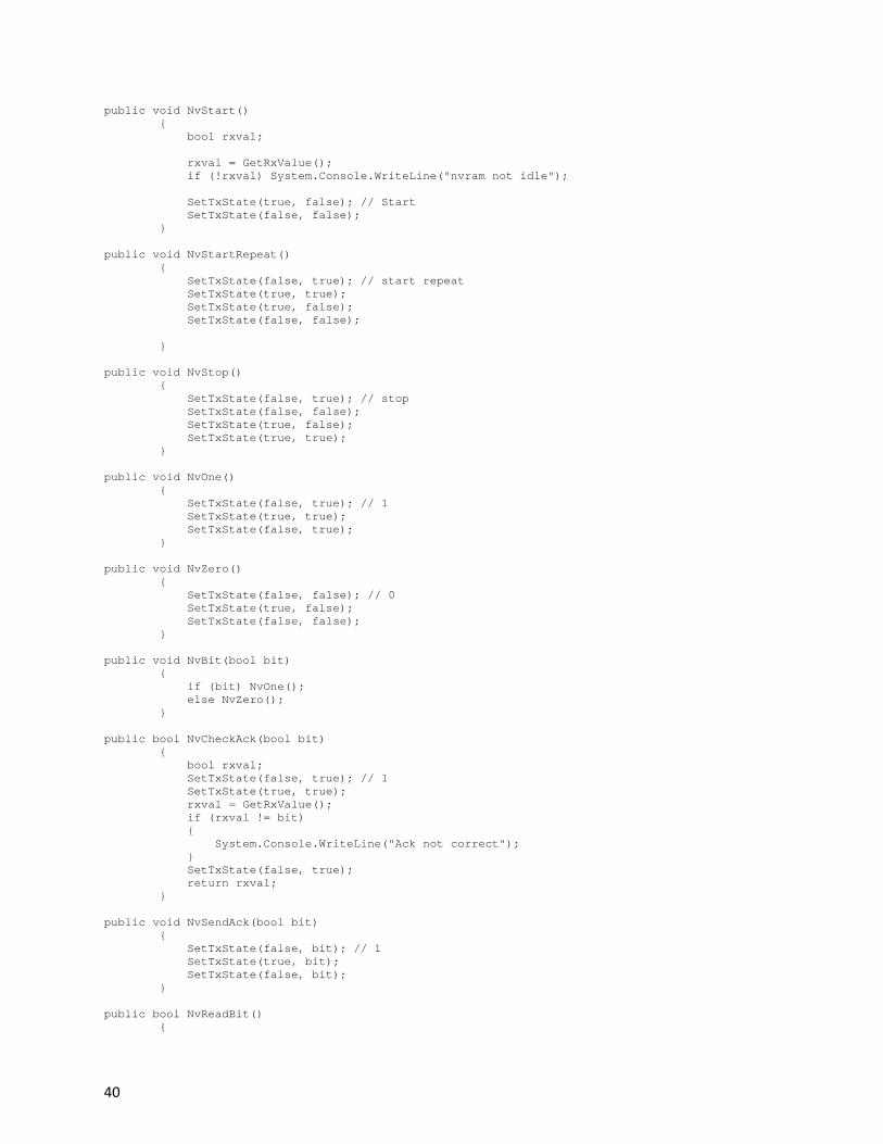
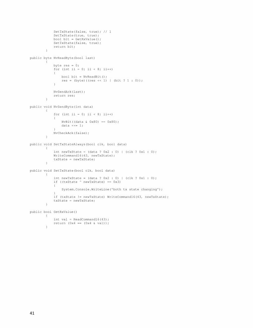
AppendixE
C#SourceCodeforReadingNVRam public byte [] ReadNvRam(int addr, int count) { openUsb(); byte res = 0; byte [] resarray = new byte[count]; SetTxStateAlways(true, true); // Idle NvStop(); if (!GetRxValue()) System.Console.WriteLine("nvram not idle"); NvStart(); NvSendByte(0xA0); NvSendByte(addr >> 8); NvSendByte(addr & 0xff); NvStartRepeat(); NvSendByte(0xA1); for (int jj = 0; jj < count; jj++) { res = NvReadByte((count-1) == jj); resarray[jj] = res; } NvStop(); closeUsb(); return resarray; } public void NvStart() { bool rxval; rxval = GetRxValue(); if (!rxval) System.Console.WriteLine("nvram not idle"); SetTxState(true, false); // Start SetTxState(false, false); } public void NvStartRepeat() { SetTxState(false, true); // start repeat SetTxState(true, true); SetTxState(true, false); SetTxState(false, false); } public void NvStop() { SetTxState(false, true); // stop SetTxState(false, false); SetTxState(true, false); SetTxState(true, true); } public void NvOne() { SetTxState(false, true); // 1 SetTxState(true, true);

39
SetTxState(false, true); } public void NvZero() { SetTxState(false, false); // 0 SetTxState(true, false); SetTxState(false, false); } public void NvBit(bool bit) { if (bit) NvOne(); else NvZero(); } public bool NvCheckAck(bool bit) { bool rxval; SetTxState(false, true); // 1 SetTxState(true, true); rxval = GetRxValue(); if (rxval != bit) { System.Console.WriteLine("Ack not correct"); } SetTxState(false, true); return rxval; } public void NvSendAck(bool bit) { SetTxState(false, bit); // 1 SetTxState(true, bit); SetTxState(false, bit); } public bool NvReadBit() { SetTxState(false, true); // 1 SetTxState(true, true); bool bit = GetRxValue(); SetTxState(false, true); return bit; } public byte NvReadByte(bool last) { byte res = 0; for (int ii = 0; ii < 8; ii++) { bool bit = NvReadBit(); res = (byte)((res << 1) | (bit ? 1 : 0)); } NvSendAck(last); return res; } public void NvSendByte(int data) { for (int ii = 0; ii < 8; ii++) { NvBit((data & 0x80) == 0x80); data <<= 1; } NvCheckAck(false); }
40
public void NvStart() { bool rxval; rxval = GetRxValue(); if (!rxval) System.Console.WriteLine("nvram not idle"); SetTxState(true, false); // Start SetTxState(false, false); } public void NvStartRepeat() { SetTxState(false, true); // start repeat SetTxState(true, true); SetTxState(true, false); SetTxState(false, false); } public void NvStop() { SetTxState(false, true); // stop SetTxState(false, false); SetTxState(true, false); SetTxState(true, true); } public void NvOne() { SetTxState(false, true); // 1 SetTxState(true, true); SetTxState(false, true); } public void NvZero() { SetTxState(false, false); // 0 SetTxState(true, false); SetTxState(false, false); } public void NvBit(bool bit) { if (bit) NvOne(); else NvZero(); } public bool NvCheckAck(bool bit) { bool rxval; SetTxState(false, true); // 1 SetTxState(true, true); rxval = GetRxValue(); if (rxval != bit) { System.Console.WriteLine("Ack not correct"); } SetTxState(false, true); return rxval; } public void NvSendAck(bool bit) { SetTxState(false, bit); // 1 SetTxState(true, bit); SetTxState(false, bit); } public bool NvReadBit() {
41
SetTxState(false, true); // 1 SetTxState(true, true); bool bit = GetRxValue(); SetTxState(false, true); return bit; } public byte NvReadByte(bool last) { byte res = 0; for (int ii = 0; ii < 8; ii++) { bool bit = NvReadBit(); res = (byte)((res << 1) | (bit ? 1 : 0)); } NvSendAck(last); return res; } public void NvSendByte(int data) { for (int ii = 0; ii < 8; ii++) { NvBit((data & 0x80) == 0x80); data <<= 1; } NvCheckAck(false); } public void SetTxStateAlways(bool clk, bool data) { int newTxState = (data ? 0x2 : 0) | (clk ? 0x1 : 0); WriteCommand16(43, newTxState); txState = newTxState; } public void SetTxState(bool clk, bool data) { int newTxState = (data ? 0x2 : 0) | (clk ? 0x1 : 0); if ((txState ^ newTxState) == 0x3) { System.Console.WriteLine("both tx state changing"); } if (txState != newTxState) WriteCommand16(43, newTxState); txState = newTxState; } public bool GetRxValue() { int val = ReadCommand16(43); return (0x4 == (0x4 & val)); }

42
AppendixF
FirmwareDocumentationfortheEncoderPLLDotClockGenerator// ============================================================================= // PLL Configuration and test // ============================================================================= // // The pll_gain_divisor is used to set the frequency multiplier which is dependent // on the printer drum encoder being used as an input and the drum speed. // The lower byte is used as the divisor for the feedback divider with its output // compared in phase with the encoder input using the phase comparator. // The upper byte is used as the divisor for the output divider with it output // used for the pll dot clock output. // // The vco multiplier (gain) is the ratio between the lower and upper bytes. // Currently setting values for a gain of 4x frequency multiplier with // the lower byte set to 255, 0xff, and the upper byte set to 63,0x3f. // The feedback divider (pll_fdbk_cntr) is loaded with the lower byte and the // output divider (pll_output_cntr) is loaded with upper byte. // The gain is lower(feedback divisor)/upper(output divisor). // The dot clock output rate is: encoder DPI * gain. // // parameter pll_gain_divisor_DEFAULT = 16'h3fff; // upper byte = 63, lower = 255 // // The pll_freq_range also controls the gain with the ratio of the pll_freq_range value // and the value in the output divisor. // *** Need to better understand this. Dave Knierim told me he did write-up for the // software people on how to set these variable for intended pll operation. // Currently setting pll_freq_range to 1024, 0x400, for a multiplier gain of 4x. // // parameter pll_freq_range_DEFAULT = 16'h0400; // vco period control // // The force_phase_lead and force_phase_lag test inputs are good for testing and // analyzing the design. The writable registers for loading the up_down counter // vco accumulator are left in the design but have never been used. // // The dead band control is used to stop the dot clock out during the dead band. // No dead band control was used for the image loader board but has been left in // the design. If dead band detection is needed it should be done by counting // the actural drum encoder pulses. Past design have reset the PLL during the // dead band to make sure everything starts up in phase for the next revolution.

43
AppendixG
Wavet.c
// // Image loader board waveform definition file to wave_gen conversion // This version takes printer (product) format waveform definition files // instead of strobe stand format files. // // Example input file (with extre "// " in front of each line: // // // # Time (us), Voltage, Drive, Connect, Scalable, Reference, NormRegion // # Only one reference segment is allowed per waveform // // WAVE_START // 1.30000 30.60162735 VPP VPP SCALE NOTREF NONORM // 3.20000 37.69999695 VPP VPP SCALE REFERENCE 0 // 6.50000 37.69999695 VPP VPP SCALE NOTREF 0 // 8.20000 0.00000000 VPP VPP SCALE NOTREF 0 // 8.50000 0.00000000 VSS VSS SCALE NOTREF NONORM // 9.80000 23.77254105 VSS VSS SCALE NOTREF NONORM // 11.70000 30.15999794 VSS VSS SCALE NOTREF 1 // 14.50000 30.15999794 VSS VSS SCALE NOTREF 1 // 15.20000 0.00000000 VSS VSS SCALE NOTREF 1 // 17.20000 0.00000000 VSS VSS SCALE NOTREF NONORM // 18.60000 32.04499817 VSS VSS SCALE NOTREF NONORM // 19.90000 32.04499817 VSS VSS SCALE NOTREF NONORM // 20.90000 0.00000000 VSS VSS SCALE NOTREF NONORM // // # Each row contains data for a norm region defined in the above waveform. // # The number of norm regions must equal the number of rows of delay data. // # Each row of delay contains 2 numbers that correspond to the hardware // # delay0 (in nanoseconds) and delays1-63 (in picoseconds) for each disconnect. // // DELAY_START // 120 30074 // 135 30074 // // // // // Waveamp and head defines - should be read from a file eventually: double vpp_scale = 1.000 * 255.0 * 1024.0 / 50.0; double vss_scale = 1.000 * -255.0 * 1024.0 / 50.0; double clock_freq = 66.5; // MHz double norm_clk_period = 0.0301; // Period of shift clock during norm disconnect (fine delays 2 through 64). int shift_clocks = 259; // Total bits in shift chain including control and dummy jet bits #define N 500 // Maximum number of knots, and maximum number of wave_ram entries #include <stdio.h> #include <stdlib.h> // #include <strings.h> #include <math.h> // // Global data structures: // struct { double t; // Total time since waveform start (sum of dt's) double v; // Voltage of this knot (positive for VPP, negative for VSS) int drive; // 1 if this knot defines a VPP voltage, 0 if VSS int connect; // 1 if active jets should be connected to VPP at this knot, 0 if VSS int norm; // Norm pulse number (0 through 9), or -1 if not part of a normed pulse } knot[N]; int knots; // Actual number of knots in this waveform int wave[N]; // Wave_ram entries int waves; // Actual number of wave_ram entries int time; // Time in units of clock periods int vpp; // VPP DAC value (0x3fc00 full scale) int vss; // VSS DAC value (0x3fc00 full scale) - this is positive even though VSS is negative int vpp_slope; int vss_slope; // Defines to convert integer wave_gen values into real (double precision floating point) times and voltages: #define TIME (((double)time) / clock_freq) #define VPP (((double)vpp) / vpp_scale) #define VSS (((double)vss) / vss_scale) // Read up to a specified string is found: void find_string(FILE *file, char *match_string) { int c, i;
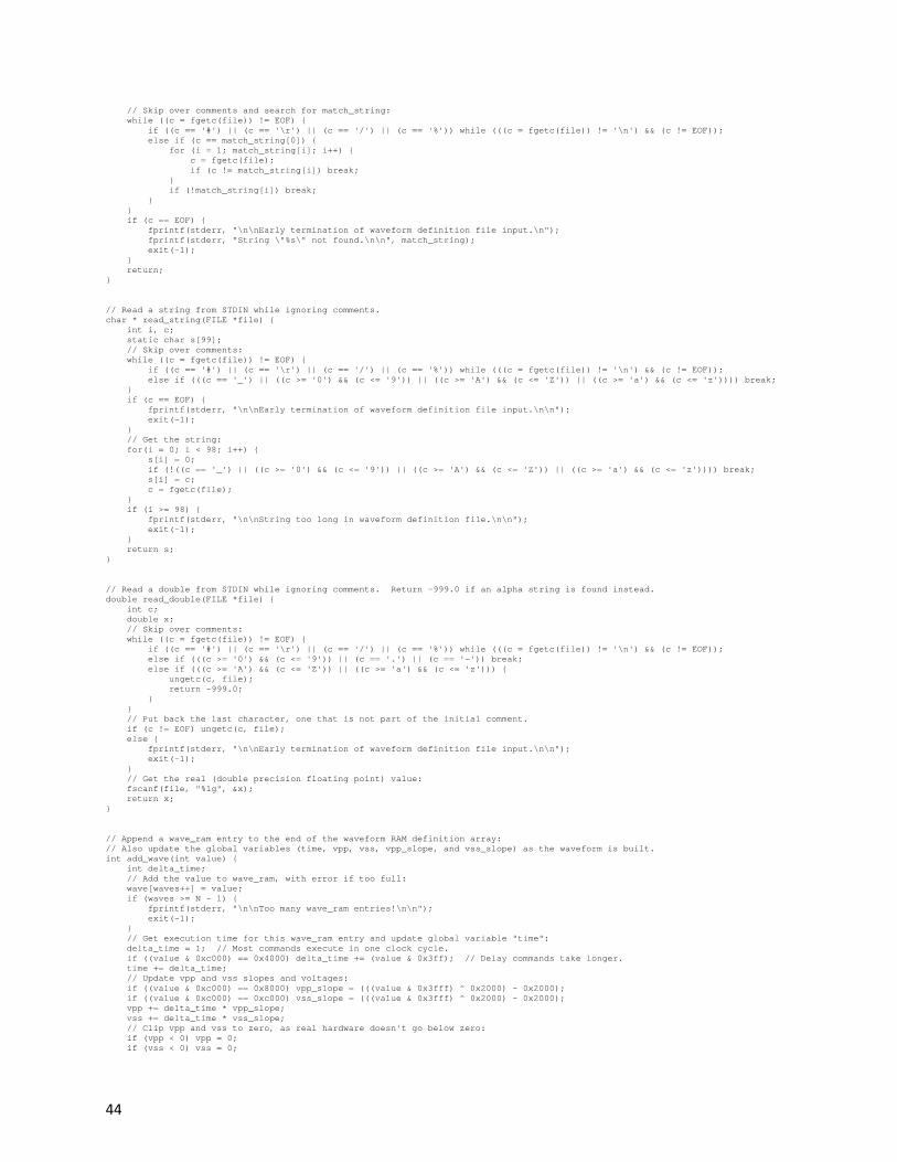
44
// Skip over comments and search for match_string: while ((c = fgetc(file)) != EOF) { if ((c == '#') || (c == '\r') || (c == '/') || (c == '%')) while (((c = fgetc(file)) != '\n') && (c != EOF)); else if (c == match_string[0]) { for (i = 1; match_string[i]; i++) { c = fgetc(file); if (c != match_string[i]) break; } if (!match_string[i]) break; } } if (c == EOF) { fprintf(stderr, "\n\nEarly termination of waveform definition file input.\n"); fprintf(stderr, "String \"%s\" not found.\n\n", match_string); exit(-1); } return; } // Read a string from STDIN while ignoring comments. char * read_string(FILE *file) { int i, c; static char s[99]; // Skip over comments: while ((c = fgetc(file)) != EOF) { if ((c == '#') || (c == '\r') || (c == '/') || (c == '%')) while (((c = fgetc(file)) != '\n') && (c != EOF)); else if (((c == '_') || ((c >= '0') && (c <= '9')) || ((c >= 'A') && (c <= 'Z')) || ((c >= 'a') && (c <= 'z')))) break; } if (c == EOF) { fprintf(stderr, "\n\nEarly termination of waveform definition file input.\n\n"); exit(-1); } // Get the string: for(i = 0; i < 98; i++) { s[i] = 0; if (!((c == '_') || ((c >= '0') && (c <= '9')) || ((c >= 'A') && (c <= 'Z')) || ((c >= 'a') && (c <= 'z')))) break; s[i] = c; c = fgetc(file); } if (i >= 98) { fprintf(stderr, "\n\nString too long in waveform definition file.\n\n"); exit(-1); } return s; } // Read a double from STDIN while ignoring comments. Return -999.0 if an alpha string is found instead. double read_double(FILE *file) { int c; double x; // Skip over comments: while ((c = fgetc(file)) != EOF) { if ((c == '#') || (c == '\r') || (c == '/') || (c == '%')) while (((c = fgetc(file)) != '\n') && (c != EOF)); else if (((c >= '0') && (c <= '9')) || (c == '.') || (c == '-')) break; else if (((c >= 'A') && (c <= 'Z')) || ((c >= 'a') && (c <= 'z'))) { ungetc(c, file); return -999.0; } } // Put back the last character, one that is not part of the initial comment. if (c != EOF) ungetc(c, file); else { fprintf(stderr, "\n\nEarly termination of waveform definition file input.\n\n"); exit(-1); } // Get the real (double precision floating point) value: fscanf(file, "%lg", &x); return x; } // Append a wave_ram entry to the end of the waveform RAM definition array: // Also update the global variables (time, vpp, vss, vpp_slope, and vss_slope) as the waveform is built. int add_wave(int value) { int delta_time; // Add the value to wave_ram, with error if too full: wave[waves++] = value; if (waves >= N - 1) { fprintf(stderr, "\n\nToo many wave_ram entries!\n\n"); exit(-1); } // Get execution time for this wave_ram entry and update global variable "time": delta_time = 1; // Most commands execute in one clock cycle. if ((value & 0xc000) == 0x4000) delta_time += (value & 0x3ff); // Delay commands take longer. time += delta_time; // Update vpp and vss slopes and voltages: if ((value & 0xc000) == 0x8000) vpp_slope = (((value & 0x3fff) ^ 0x2000) - 0x2000); if ((value & 0xc000) == 0xc000) vss_slope = (((value & 0x3fff) ^ 0x2000) - 0x2000); vpp += delta_time * vpp_slope; vss += delta_time * vss_slope; // Clip vpp and vss to zero, as real hardware doesn't go below zero: if (vpp < 0) vpp = 0; if (vss < 0) vss = 0;

45
// Clipping of vpp and vss to max value is not checked here, but is in "count_shift_clocks()" later. } // Count the number of shift clocks. Also print waveform debug information if "flag" is true. // This is a slight modification of the "read_wave()" function in "image_loader.c". int count_shift_clocks(int flag) { int a, time, stop, clock_count, shift_count, end_count; int delay, delay_value, clock_reload, clock_state, old_clock_state, clock_time; int hda_control, control; hda_control = control = 0; delay_value = delay = 0; vss = vss_slope = vpp = vpp_slope = 0; clock_state = old_clock_state = clock_time = 0; clock_reload = clock_count = shift_count = 0; end_count = -1; // Print header if (flag) { fprintf(stderr,"\n\nControl bits are: Shift Cnten Select Polarity.\n"); fprintf(stderr,"Clk_st is the value in the head clock divide counter.\n"); fprintf(stderr,"Re_ld is the value in the head clock divide reload register.\n\n"); fprintf(stderr,"Adr Data Time VSS VPP dly clk_st re_ld control Tot_cks Shft_cks\n"); } // For each system clock cycle (66.5 MHz): for (stop = time = a = 0; (a < N) && !stop; time++) { // Update clock state. Might be overridden by load_control instruction below. clock_state = clock_state ? (clock_state - 1) : clock_reload; // If not being delayed, read instruction: if (delay) delay--; else { // Check for control loading wave RAM instruction: if ((wave[a] & 0xc000) == 0x0000) { control = wave[a] & 15; stop = (wave[a] >> 13) & 1; // Force clock state to 3 for sending control lines to print head: clock_state = 3; } // Check for delay wave RAM instruction: // Note that delay_value is used only for print formatting, not for simulation. if ((wave[a] & 0xc000) == 0x4000) { delay_value = delay = wave[a] & 0x3ff; clock_reload = (wave[a] >> 10) & 15; } else delay_value = 0; // Check for vpp slope wave RAM instruction: // Sign extend the slope field to a full 32 bits. if ((wave[a] & 0xc000) == 0x8000) { vpp_slope = ((wave[a] & 0x3fff) ^ 0x2000) - 0x2000; } // Check for vss slope wave RAM instruction: // Sign extend the slope field to a full 32 bits. if ((wave[a] & 0xc000) == 0xc000) { vss_slope = ((wave[a] & 0x3fff) ^ 0x2000) - 0x2000; } // Increment wave RAM address a++; } // Update hda state when a head clock is generated. // A head clock is generated when the clock state transitions from 1 to 0. if (clock_state == 0 && old_clock_state == 1) { // Count head clocks: clock_count++; // Count head clocks that shift in new data (head clocks with shift true inside head drive ASIC's): if (hda_control & 8) shift_count++; // Count head clocks after shift goes false (-1 indicates that shift hasn't gone true yet): end_count = (control & 8) ? 0 : ((end_count >= 0) ? (end_count + 1) : -1); if (end_count == 2) fprintf(stderr,"Data transfer to hda output latches after shifting %d data bits.\n", shift_count); clock_time = time; // Check for select or polarity change, or for falling cnten or shift edge, when VPP or VSS is greater than 1 volt: if (flag & (((VPP > 2.0) || (VSS < -2.0)) && ((3 & (hda_control ^ control)) || (0xc & ~control & hda_control)))) fprintf(stderr,"\nWarning: HDA control line change while VPP or VSS is greater than 2 volts.\n\n"); // New control values are now clocked into the print head: hda_control = control; } old_clock_state = clock_state; // Print info on wave_ram words and for the first and last few delay counts of delay instructions: if (flag) { if (!delay_value || (delay_value == delay)) // First clock of an instruction:

46
fprintf(stderr,"%3d %05lx: %6.3f %6.2f %5.2f %4d %2d %2d %d %d %d %d %3d %3d\n", a - 1, wave[a - 1], TIME, VSS, VPP, delay, clock_state, clock_reload, (hda_control >> 3) & 1, (hda_control >> 2) & 1, (hda_control >> 1) & 1, (hda_control >> 0) & 1, clock_count, shift_count); else if ((delay < 2) || ((delay_value - delay) < 4)) // Next 3 clocks and last 2 clocks of delay instructions: fprintf(stderr, " %6.3f %6.2f %5.2f %4d %2d %2d %d %d %d %d %3d %3d\n", TIME, VSS, VPP, delay, clock_state, clock_reload, (hda_control >> 3) & 1, (hda_control >> 2) & 1, (hda_control >> 1) & 1, (hda_control >> 0) & 1, clock_count, shift_count); else if ((delay_value - delay) == 4) fprintf(stderr," . . . . . .\n"); } // Update VSS and VPP simulation states and check for overflow: vpp += vpp_slope; if (vpp < 0) vpp_slope = vpp = 0; if (vpp > 262143) { if (flag) fprintf(stderr,"\nWarning: Excess VPP voltage at time %6.3f.\n\n", TIME); vpp = 262143; vpp_slope = 0; } vss += vss_slope; if (vss < 0) vss_slope = vss = 0; if (vss > 262143) { if (flag) fprintf(stderr,"\nWarning: Excess VSS voltage at time %6.3f.\n\n", TIME); vss = 262143; vss_slope = 0; } if (flag && ((VPP - VSS) > 60.0)) { // VPP - VSS exceeds 60 volts! 60 volts is absolute maximum. fprintf(stderr,"\n\n*********** ERROR!!!! Excess VPP - VSS voltage at time %6.3f. ***********\n", TIME); fprintf(stderr,"\n*********** ERROR!!!! Damage to the print head is likely!!!!!! ***********\n\n"); exit(-1); } else if (flag && ((VPP - VSS) > 56.0)) { // VPP - VSS exceeds 56 volts! 60 volts is absolute maximum. fprintf(stderr,"\n********* WARNING!!!! Excess VPP - VSS voltage at time %6.3f. *********\n", TIME); fprintf(stderr,"\n********* WARNING!!!! Damage to the print head is possible!!!!!! *********\n\n"); } } if (flag) fprintf(stderr, "End of waveform with %d clocks after falling edge of shift.\n\n", end_count); return shift_count; } // // The waveform conversion routine // main(int argc, char *argv[]) { int c, i, j, k, n, w, clk_div, delta_time, delay, delay1, delay2, cnten, normed_pulses; char * strn; double slope; // **************************************************************************************************** // Read in shift clocks and norm disconnect clock period if provided: // **************************************************************************************************** j = 0; if (argc > ++j) sscanf(argv[j], "%d", &shift_clocks); fprintf(stderr, "\nProcessing waveform for %d shift clocks.\n\n", shift_clocks); // **************************************************************************************************** // Read in voltage/time knots: // **************************************************************************************************** // Find the "WAVE_START" line: strn = read_string(stdin); if (strcmp(strn, "WAVE_START")) { fprintf(stderr, "\n\nMissing or incorrect WAVE_START string: %s.\n\n", strn); exit(-1); } normed_pulses = 0; // Get knot values (time and voltage of this knot): knot[0].t = 0.0; knot[0].v = 0.0; for (knots = 1; knots < N; knots++) { // Read in knot time: knot[knots].t = read_double(stdin); // If no time found, then all knots have been read: if (knot[knots].t == -999.0) break; // Read in knot voltage: knot[knots].v = read_double(stdin); // Read in knot drive (VPP or VSS): strn = read_string(stdin); if (strcmp(strn, "VPP") && strcmp(strn, "VSS")) { fprintf(stderr, "\n\nMissing or incorrect VPP/VSS drive flag: %s.\n\n", strn); exit(-1); } knot[knots].drive = (strn[1] == 'P') ? 1 : 0; // Read in knot connect (VPP or VSS): strn = read_string(stdin); if (strcmp(strn, "VPP") && strcmp(strn, "VSS")) { fprintf(stderr, "\n\nMissing or incorrect VPP/VSS connect flag: %s.\n\n", strn); exit(-1); }
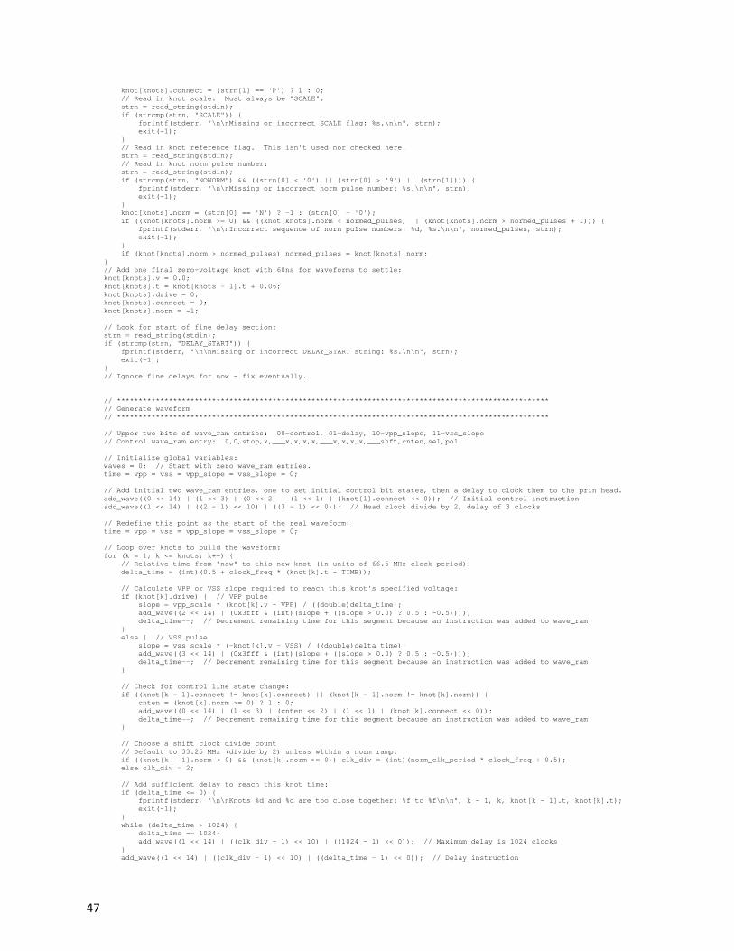
47
knot[knots].connect = (strn[1] == 'P') ? 1 : 0; // Read in knot scale. Must always be "SCALE". strn = read_string(stdin); if (strcmp(strn, "SCALE")) { fprintf(stderr, "\n\nMissing or incorrect SCALE flag: %s.\n\n", strn); exit(-1); } // Read in knot reference flag. This isn't used nor checked here. strn = read_string(stdin); // Read in knot norm pulse number: strn = read_string(stdin); if (strcmp(strn, "NONORM") && ((strn[0] < '0') || (strn[0] > '9') || (strn[1]))) { fprintf(stderr, "\n\nMissing or incorrect norm pulse number: %s.\n\n", strn); exit(-1); } knot[knots].norm = (strn[0] == 'N') ? -1 : (strn[0] - '0'); if ((knot[knots].norm >= 0) && ((knot[knots].norm < normed_pulses) || (knot[knots].norm > normed_pulses + 1))) { fprintf(stderr, "\n\nIncorrect sequence of norm pulse numbers: %d, %s.\n\n", normed_pulses, strn); exit(-1); } if (knot[knots].norm > normed_pulses) normed_pulses = knot[knots].norm; } // Add one final zero-voltage knot with 60ns for waveforms to settle: knot[knots].v = 0.0; knot[knots].t = knot[knots - 1].t + 0.06; knot[knots].drive = 0; knot[knots].connect = 0; knot[knots].norm = -1; // Look for start of fine delay section: strn = read_string(stdin); if (strcmp(strn, "DELAY_START")) { fprintf(stderr, "\n\nMissing or incorrect DELAY_START string: %s.\n\n", strn); exit(-1); } // Ignore fine delays for now - fix eventually. // **************************************************************************************************** // Generate waveform // **************************************************************************************************** // Upper two bits of wave_ram entries: 00=control, 01=delay, 10=vpp_slope, 11=vss_slope // Control wave_ram entry: 0,0,stop,x,___x,x,x,x,___x,x,x,x,___shft,cnten,sel,pol // Initialize global variables: waves = 0; // Start with zero wave_ram entries. time = vpp = vss = vpp_slope = vss_slope = 0; // Add initial two wave_ram entries, one to set initial control bit states, then a delay to clock them to the prin head. add_wave((0 << 14) | (1 << 3) | (0 << 2) | (1 << 1) | (knot[1].connect << 0)); // Initial control instruction add_wave((1 << 14) | ((2 - 1) << 10) | ((3 - 1) << 0)); // Head clock divide by 2, delay of 3 clocks // Redefine this point as the start of the real waveform: time = vpp = vss = vpp_slope = vss_slope = 0; // Loop over knots to build the waveform: for (k = 1; k <= knots; k++) { // Relative time from "now" to this new knot (in units of 66.5 MHz clock period): delta_time = (int)(0.5 + clock_freq * (knot[k].t - TIME)); // Calculate VPP or VSS slope required to reach this knot's specified voltage: if (knot[k].drive) { // VPP pulse slope = vpp_scale * (knot[k].v - VPP) / ((double)delta_time); add_wave((2 << 14) | (0x3fff & (int)(slope + ((slope > 0.0) ? 0.5 : -0.5)))); delta_time--; // Decrement remaining time for this segment because an instruction was added to wave_ram. } else { // VSS pulse slope = vss_scale * (-knot[k].v - VSS) / ((double)delta_time); add_wave((3 << 14) | (0x3fff & (int)(slope + ((slope > 0.0) ? 0.5 : -0.5)))); delta_time--; // Decrement remaining time for this segment because an instruction was added to wave_ram. } // Check for control line state change: if ((knot[k - 1].connect != knot[k].connect) || (knot[k - 1].norm != knot[k].norm)) { cnten = (knot[k].norm >= 0) ? 1 : 0; add_wave((0 << 14) | (1 << 3) | (cnten << 2) | (1 << 1) | (knot[k].connect << 0)); delta_time--; // Decrement remaining time for this segment because an instruction was added to wave_ram. } // Choose a shift clock divide count // Default to 33.25 MHz (divide by 2) unless within a norm ramp. if ((knot[k - 1].norm < 0) && (knot[k].norm >= 0)) clk_div = (int)(norm_clk_period * clock_freq + 0.5); else clk_div = 2; // Add sufficient delay to reach this knot time: if (delta_time <= 0) { fprintf(stderr, "\n\nKnots %d and %d are too close together: %f to %f\n\n", k - 1, k, knot[k - 1].t, knot[k].t); exit(-1); } while (delta_time > 1024) { delta_time -= 1024; add_wave((1 << 14) | ((clk_div - 1) << 10) | ((1024 - 1) << 0)); // Maximum delay is 1024 clocks } add_wave((1 << 14) | ((clk_div - 1) << 10) | ((delta_time - 1) << 0)); // Delay instruction
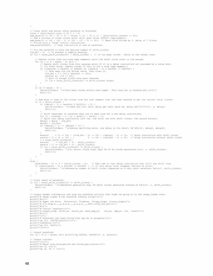
48
} // Clear shift and select after waveform is finished: cnten = (knot[knots].norm >= 0) ? 1 : 0; add_wave((0 << 14) | (0 << 3) | (cnten << 2) | (0 << 1) | (knot[knots].connect << 0)); // Add a minimum of three clocks after shift goes false (PZTA/C requirement): add_wave((1 << 14) | ((2 - 1) << 10) | ((7 - 1) << 0)); // Head clock divide by 2, delay of 7 clocks // Finish with a "stop" control instruction: add_wave(0x2000); // Stop instruction at end of waveform. // Fix the waveform to have the desired number of shift_clocks: clk_div = 0; // To prevent a compile warning. if ((c = count_shift_clocks(0)) > shift_clocks) { // If too many clocks - which is the normal case: // Remove clocks from non-norm-ramp segments until the shift clock count is low enough. for (w = 1; w < waves - 3; w++) { // Remove shift clocks from this waveram entry if it is a delay instruction not preceded by a cnten knot. // (In other words, remove clocks if this is not a norm ramp segment.) if (((wave[w] & 0xc000) == 0x4000) && ((wave[w - 1] & 0xc004) != 0x0004)) { // Save away old clk divide value, then clear it. clk_div = 1 + (15 & (wave[w] >> 10)); wave[w] &= ~(15 << 10); // Quit if enough clocks have been removed: if ((c = count_shift_clocks(0)) <= shift_clocks) break; } } if (w >= waves - 3) { fprintf(stderr, "\n\nToo many clocks within norm ramps - This case not is handled yet.\n\n"); exit(-1); } // Add back in some of the clocks from the last segment that had them removed to get the correct total clocks: if (c < shift_clocks) { if ((delay = (1 + (wave[w] & 0x3ff))) < 2) { fprintf(stderr, "\n\nHow did this short delay get here (wave %d, delay %d)?????\n\n", w, delay); exit(-1); } // Shift remainder of waveform down one to make room for a new delay instruction: for (i = ++waves; --i > w; ) wave[i] = wave[i - 1]; // Split this delay instruction into two, the first one with shift clocks, the second without. delay1 = delay - clk_div; delay2 = clk_div; if ((delay1 < 1) || (delay2 < 1)) { fprintf(stderr, "\n\nDelay splitting error, one delay is too short: %d %d\n\n", delay1, delay2); exit(-1); } wave[w] = (1 << 14) | ((clk_div - 1) << 10) | ((delay1 - 1) << 0); // Delay instruction with shift clocks wave[w + 1] = (1 << 14) | ( 0 << 10) | ((delay2 - 1) << 0); // Delay instruction without shift clocks c = count_shift_clocks(0); wave[w] -= clk_div * (c - shift_clocks); wave[w + 1] += clk_div * (c - shift_clocks); if ((c = count_shift_clocks(0)) != shift_clocks) { fprintf(stderr, "\n\n: Error: Clock count bug: %d of %d clocks generated.\n\n", c, shift_clocks); exit(-1); } } } else { wave[waves - 4] += 2 * (shift_clocks - c); // Add time to last delay instruction that still has shift true. if ((wave[waves - 4] & 0xfc00) != 0x4400) { // If this delay count wrapped, declare an error: fprintf(stderr, "\n\nExcessive number of shift clocks requested on a very short waveform: %d\n\n", shift_clocks); exit(-1); } } // Final check of waveform: if ((c = count_shift_clocks(1)) != shift_clocks) { fprintf(stderr, "\n\nWaveform generation bug: %d shift clocks generated instead of %d\n\n", c, shift_clocks); exit(-1); } // Output header information and stop any waveform activity that might be going on in the image_loader ecan: printf("# Image loader E-Can waveform loading script:\n"); printf("#\n"); printf("# Upper two bits: 00=control, 01=delay, 10=vpp_slope, 11=vss_slope\n"); printf("# 0,0,stop,x,___x,x,x,x,___x,x,x,x,___shft,cnten,sel,pol\n"); printf("#\n"); printf("# Control register:\n"); printf("# single_step, shift_en, select_en, wave_amp_en, vss_en, vpp_en, run, ~reset\n"); printf("#\n"); printf("\n"); printf("# Terminate any head firing that may be in progress:\n"); printf("wg 512, (0x7d&(rg(512)))\n"); printf("taskDelay 2\n"); printf("wg 512, 0x00\n"); printf("\n\n"); // Output waveform: for (w = 0; w < waves; w++) printf("wg 0x%03x, 0x%04x\n", w, wave[w]); // Output trailer: printf("\n\n"); printf("# Reset auto_fire_period and clocks_per_uCycle:\n"); printf("ww 33, 0\n"); printf("ww 32, 50 << 13\n");

49
printf("\n"); printf("# Reset next_fire_position to insure no imaging before armed:\n"); printf("ww 47, 1 << 31\n"); printf("\n"); printf("# Enable waveamp:\n"); printf("wg 512, 0x11\n"); printf("\n"); exit(0); }

POWER SWITCHING FOR PRINTHEADSI/O CONNECTIONS TO FPGA
13
PRINTHEAD CONNECTIONSTO FPGA
GENERAL I/O
(WA_FAULT)
OUTPUT SIGNALS AT 3.3V LEVEL
(S_OUT)
HD P17HD P18HD P19
HD P5
(SCLK)
(SAFETY_FAULT)
(CLK-)
(S1+)(S1-)
(S0-)
MAVERICK 2
HD P1
TAIPAN 2
(S1+)
(VPP)
MAVERICK 1TAIPAN 1
(S2-)
(S_IN)
(CLK+)
(S2+)
(SOUT+)
(SOUT+)
C 0
1
(S1-)(S1+)
(S3+)
(CLK-)(CLK+)
(WA_FAULT)
(S_OUT)
(SAFETY_FAULT)(S_IN)
(CLK+)(CLK-)
(SCLK)
(S2-)
(S0+)
(S1+)
(S2+)
(VSS)
(VPP)
HD P4HD P3HD P2
HD P6HD P5
HD P1
HD P7
HD P9HD P8
HD P20
HD P23
HD P25
HD P27HD P26
HD P21HD P22
HD P24
HD P18HD P19
HD P16HD P17
HD P10HD P11HD P12HD P13HD P14
HD P29HD P30
HD P28
HD P2HD P3
HD P6
HD P8HD P9
HD P4
HD P7
HD P13HD P12HD P11HD P10
(CLK-)(CLK+)
(S3+)
(S0+)
(S1-)
(S2-)(S2+)
(S0+)(S0-)
HD P16HD P15
HD P20
HD P25HD P24HD P23HD P22HD P21
HD P28
HD P26HD P27
HD P29HD P30
HD P14
(S1-)
HD P15
(S3-)
(VSS)
CHRIS GADKE/CURT KELLER
IMAGE LOADER BOARD86N-0661-XB
GO TO FPGA
PRINTHEAD CONNECTORS
(S0-)
OUTPUT SIGNALS AT 3.3V LEVEL
POWER SWITCHINGTO PRINTHEADS
FPGA LOGIC DISABLE
GENERAL I/O
ALL CONNECTIONS
(S0-)(S0+)
(S2-)(S2+)
(S3-)
LAST_MODIFIED=Wed Jul 09 09:36:34 2008
2
R841R842
MAV1_SDOMAV1_SCLKMAV1_SDI
BASICX<1..8>
C828
10.0K
1
12345678
3
5
BASICX-AD<1..5>
34
123456
789
101112
37
121314151617181920
22232425
2728
831-3147-00J903M50
494847
50
444546
4243
403938
3635
3233
313029
21
9876
3
5
2
26
1
HD1_S0_NHD1_S0_P
HD1_S1_N
Q701
PH_PWR
R787821-5421-00
1.00K
R7881.00K821-5421-00
1J709 M2
VDD
R781
4
NEG15V_SW
850-5024-00DS782LED1
821-5454-00
332R782
NEG15V
NEG12V
POS12V_SW
NEG12V_SW
POS12V
VDD VDD
VDD_SW
R637274
R636274
R638274
U638
5
61
AVQ252
U637
2
4
5
61
856-0221-00
AVQ252
AVQ252
856-0221-00
1 6
5
4
2
U636
274
821-5453-00R635 AVQ252
856-0221-00
1 6
5
4
2
U635
VDD
CON7X2
831-2401-00J602
6
234
1
5
HD2_S2_N
VDD
HD1_CLK_P
HD1_S3_N
HD1_S2_N
0.1UF
VPPCAP
HD1_S1_P
HD1_S2_P
VPPCAPM26MTG2
HD2_S0_P
HD2_S1_N
0
HD2_S1_P
0.1UF
FM30
831-7148-00
FM30831-7116-00
0
49.9 OHM
49.9 OHM
49.9 OHM
VSSCAP
VDD
HD2_S3_P
HD2_S2_P
HD2_S3_N
M26MTG2
TAI1_SDO
IL
831-7148-00
VSSCAP
HD1_S3_P
49.9 OHM821-5572-00
49.9 OHM
4.99K
10.0K821-5427-00
HD1_CLK_N
VDD
TAI2_SEN_N
4.99K
HD2_S0_N
HD2_CLK_NHD2_CLK_P
821-5427-00
MAV2_FAULT_NMAV2_SDIMAV2_SCLKMAV2_SDO
TAI2_SDO
49.9 OHM
TAI1_SEN_N
J802
1
10111213141516171819
2
20212223242526272829
3
30
456789
J801
1
10111213141516171819
2
20212223242526
3456789
J901
1
10111213141516171819
2
20212223242526272829
3
30
456789
J902
1
10111213141516171819
2
20212223242526
3456789
R846
1 2
R844
1 2
R845
1 2
R843
1 2
1 2
R838
1 2
1 2
R837
1
R869
1 2
R839
1 2
R840
1 2
R7131 2
C8021
2
1
2
R8491 2
R806
1 2 R805
1 2
R802
1 2
R803
1 22
R912
1 2
1 2
R901
1 2
1 2
R804
1 2
R829
1 2
R830
1 2
R828
1 2
R827
1 2
R831
1 2
R832
1 2
R833
1 2
R834
1 2
R835
1
R836
1 2
R870
2
1
R801
R856R853
IMAGE LOADER
1
883-5353-00
NEG15V_SW
NEG15V_SW
POS12V_SW
NEG12V_SW
NEG12V_SW
POS12V_SW
POS12V_SW
POS12V_SW
VDD_SW
883-5353-00
VDD_SW
VDD_SWVDD_SW
821-5572-00
VDD
831-7116-00
2
MAV1_FAULT_N
22
3
1
3SPDT S701
870-0006-00
856-0221-00
2
821-5421-001.00K
2
1831-1857-00
851-5001-00
NPNBEC
11
4
13
VDD
POS5V
41
7
6
5
4
3
2
1
2
10
4
AUX-LCD<1..7>
IO-CON2<1..6>
IIN-CON1<1..13>
RANK XEROX LTD./FUJI XEROX CO.LTD. BE REPRODUCED, COPIED OR USED FORWITHOUT THE PRIOR WRITTEN PERMISSION OF XEROX CORPORATION AND/OR
DATE:
CORPORATION AND/OR RANK XEROX LTD./FUJI XEROX CO. LTD.ANY PURPOSE WHATSOEVER, EXCEPT THE MANUFACTURE OF ARTICLES FOR XEROX
SIZE
SHEET
DESCRIPTION
TITLE
OF
ENGINEER
ABBREV
REV.
10
1 2 3 4 6 7 1098
8
H
G
F
E
B
C
A
97654321
A
F
E
G
H
D
C
B
D
ARE THE EXCLUSIVE PROPERTY OF XEROX CORPORATION AND/OR RANK XEROXLTD./FUJI XEROX CO.,LTD. ISSUED IN STRICT CONFIDENCE AND SHALL NOT,
THESE DRAWINGS AND SPECIFICATIONS,AND THE DATA CONTAINED THEREIN,
5
DRAWING
1113
9
57
13
1214
1086
24

(DATA1)(DATA2)(DATA3)(DATA4)
(DATA4)
(DATA3)
(POL)
(AWG_POL)
CURRENT WAVEAMP CONNECTOR SETUP
(VPPD)
(VPPTEMP)(VSSTEMP)
(VSSD)(VPPD)
WATLOW
(Y)(C)(M)(K)
TEST I/O
POWER INPUTS AND BYPASS CAPS
CURRENT SINGLE WAVE AMP INTERFACECURRENT STROBE STAND/MULE INTERFACEIMAGE LOADER BOARD
HEAD HEATERS
50V_SLEEP
(SEL)
(CLK)
(DATA1)
(SHIFT)
(CNTEN)
(POL)
0 CURT KELLERC
BNC INPUTS FROM AWG
(CLK)
(AWG_CE)
(VSSD)
(AWG_CLK)
(CNTEN)
(DATA2)
(DATA5)
(DATA6)
INPUTS AT 5V LEVEL
2
CLOSE JUMPERS TOSEND POWER TO
(DATA7)
(DATA8)
(DATA8)(DATA7)(DATA6)(DATA5)
TO FPGA
GROUND TEST PADS
STROBE STAND INPUTS
POWER IN
(SEL)
(SHIFT)
13
GENERAL I/O AND CONNECTOR
LAST_MODIFIED=Tue Jul 01 14:42:59 2008
1
.1UF2
POS5V
15
856-7332-00
POS15V_IN
5V_INNEG15V_IN
FM5GND2
831-0187-00J304
12345
76
814-5000-00
TP111MTP160CTESTPADTP112MTP160CTESTPADTP113MTP160CTESTPAD
14
9R202
1
25
TP200 TP700 TP950
TP2011
1817
TP208
TP206TP207
111213
18
74LVT245
WA_EN
R133R130
9
831-0113-00J105CON10X2
NEG15VPOS12V
0
821-5415-00
1
R204
VDD
6
21
2821-5572-0049.9R302
FD301FD901FD101
FD0301FD0901FD0101
1 1 1
111
MTMH800C430
2
1
C309
321
J306
3
4
2
1
U304
2
1
C312
1
MH406
2
1 C303
2
1
C304
5
6
4
1
2
U301
5
6
4
1
2
U206
98765432
10
1
J603
4321
J604
21
R301
21
R205
32
1
SW301
31
42
U303
23
1
U302
1
MH603
1
MH602
1
MH801
1
MH702
1
MH202
1
MH403
1
MH901
1
MH302
1
MH701
1
MH101
2
1
J104
1
1TP2021
TP2031TP2041
TP20511
1TP2091
TP210
1TP211
1TP213
21
R128
21
R119
2
1R120
21
R129
8
4
75
6
U102
21
R121
21
R132
21
2
1R131
8
4
13
2
U102
21
4321
J108
876543
20
2
19181716151413121110
1
1
9
8
7
5
4
39
38
37
36
35
34
33
32
31
30
3
29
28
27
26
24
23
22
202
19
18
17
16
15
14
13
12
11
10
J113
21R201
2
21
21R203
1TP212
2
1 R206
42
1
U203
42
1
U204
191
111213
1516
8765432
U201
42
1
U205
191
14
1617
98765432
U202
2
1 R3032
1
J303
2
1
J301
2
1
J302
2
1
C305 C301 2
1
C302
2
1
C313
2
1
C2012
1
C202 2
1
C909
21
DS301
2
1
C908 2
1 R306
2
1
C712 2
1
C104 2
1
C108
2
1
C107 2
1
C103 2
1
C711
654321
J305
2
1
J106
NEG12V
890-1365-00
120UF
890-1365-00
120UF
NEG15V
.1UF
LM2990S856-0226-00
.1UF .1UF .1UF .1UF
LED1850-5024-00
.1UF
LM3940HOR
.1UF
VDD
821-5454-00332 OHM
.1UF
.1UF
POS15V_IN
STB_SHIFT
856-0056-00
856-4666-00
LD1086D2T12
MTMH800C430
821-5572-00
VCC=VDD;GND=GND
MTMH800C430
MTMH800C430
MTMH800C430
MTMH800C430
MTMH800C430
821-5415-00O OHM
O OHM
831-2401-00
856-0056-00
NEG50V
POS50V
WA_GND_SENSE
VSSD
821-5422-00
2K
2K
TLE2082_PWR856-6988-01
POS50V
2K
821-5572-00 WA_FA_N
BNC2MTG
POS50V
831-0171-00
49.9
831-3379-00
49.9821-5572-00
AWG_POL
831-3379-00
BNC2MTG
D37GND2
SATURN INTERFACE SI
BNC2MTG
2K
831-3379-00
CON2X2
2K
2K
TLE2082_PWR
856-6988-01
49.9 OHM
2K
2K
BNC2MTG
831-3379-00
VPPDVPPD
POS50V
POS12V
NEG12V
VSSD
AWG_CNTEN
BNC2MTG
TP
NEG12V
POS12V
VDD
821-5422-00
814-5000-00
TP
STB_DATA8
STB_DATA1
STB_DATA6
STB_CLK
STB_SEL
814-5000-00
SN74LVC1G32
VCC=VDD;GND=GND
SN74LVC1G32VCC=VDD;GND=GND
STB_DATA7
STB_CNTEN
AWG_CLK
831-3379-00
MTMH800C430
NEG50V
STB_DATA5STB_DATA4STB_DATA3STB_DATA2
856-0056-00
SN74LVC1G32
STB_POL
M6
831-3272-00
SPDT
870-0006-00
821-0037-00
274NEG15VPOS5V
POS15V_INNEG15V_IN
POS5V
856-8833-00
VCC=VDD;GND=GND
TP
274
821-0037-00
AVQ252
856-0221-00
NEG15V_IN
AVQ252
856-0221-00
POS15V
CAP_POL890-1365-00
VCC=VDD;GND=GND
74LVT245
856-7332-00
.1UF.1UF.1UF
POS15V POS12V
MTMH800C430MTMH800C430MTMH800C430
890-1365-00CAP_POL
883-5353-00
.1UF
5V_IN
M10
831-6529-00
M4
831-3271-00
INK_3
INK_1INK_2
INK_0
VDDINK_REF
JET_RIGHT_TEMPJET_LEFT_TEMP
RES_TEMP
M3
831-4504-00
NEG50V
POS50V
DRAWING
RANK XEROX LTD./FUJI XEROX CO.LTD. BE REPRODUCED, COPIED OR USED FORWITHOUT THE PRIOR WRITTEN PERMISSION OF XEROX CORPORATION AND/OR
DATE:
CORPORATION AND/OR RANK XEROX LTD./FUJI XEROX CO. LTD.ANY PURPOSE WHATSOEVER, EXCEPT THE MANUFACTURE OF ARTICLES FOR XEROX
SIZE
SHEET
DESCRIPTION
TITLE
OF
ENGINEER
ABBREV
REV.
10
1 2 3 4 6 7 1098
8
H
G
F
E
B
C
A
97654321
A
F
E
G
H
D
C
B
D
ARE THE EXCLUSIVE PROPERTY OF XEROX CORPORATION AND/OR RANK XEROXLTD./FUJI XEROX CO.,LTD. ISSUED IN STRICT CONFIDENCE AND SHALL NOT,
THESE DRAWINGS AND SPECIFICATIONS,AND THE DATA CONTAINED THEREIN,
5
42
31
2018
1412
16
108
46
2
1719
1315
11
79
135
38
201
2
321
423
22
524
6
725
8
26
928
27
1029
11
1230
13
31
3214
3315
1634
1735
1836
3719
39
A4A5
A3A2A1
A6
DIROE
A7A8
B1B2B3B4B5B6B7B8
A4A5
A3A2A1
A6
DIROE
A7A8
B1B2B3B4B5B6B7B8
V_IN2
V_IN1 V_OUT
GND
GNDS
GNDOUTIN
OUT
GND
IN
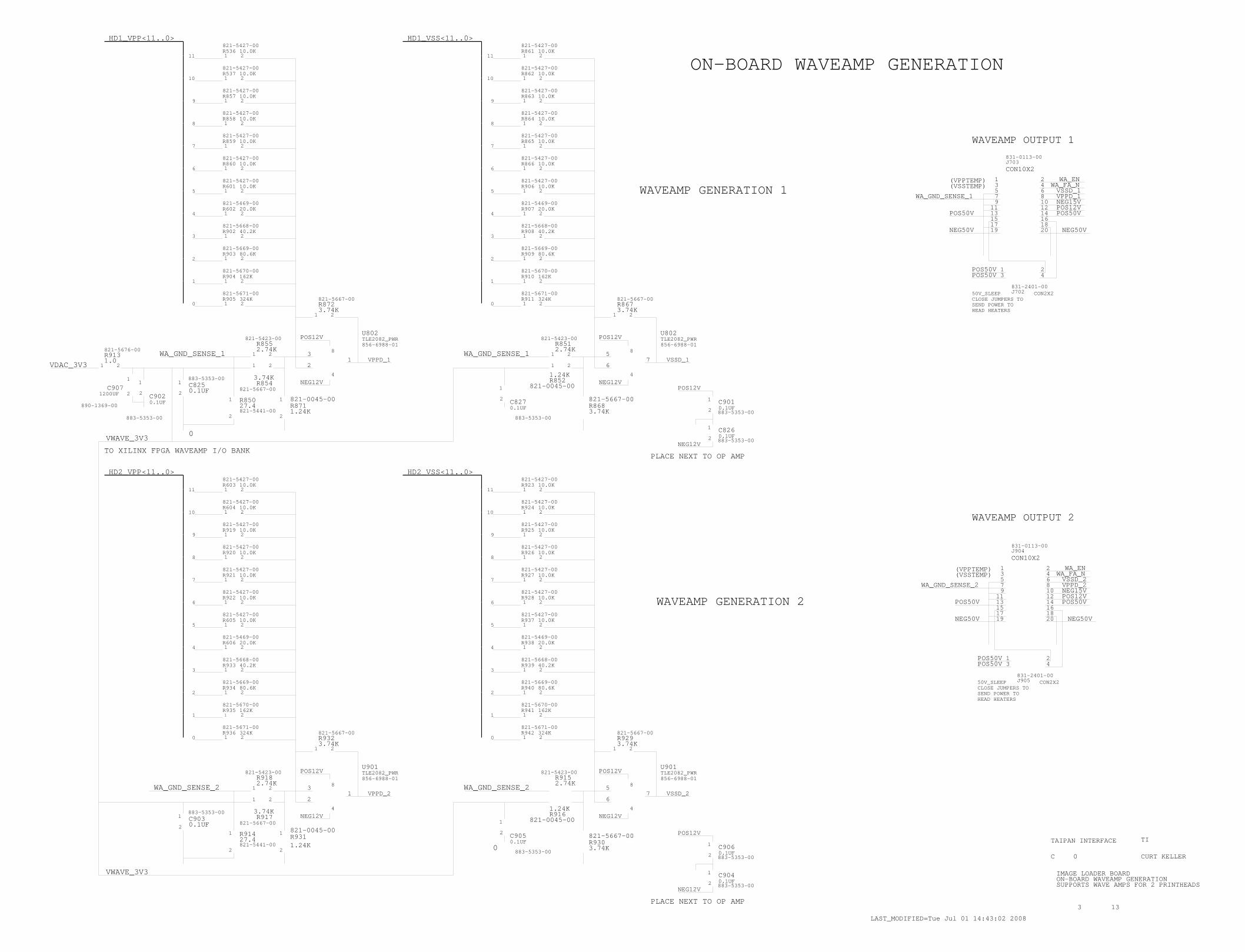
PLACE NEXT TO OP AMP
WAVEAMP GENERATION 1
C 0 CURT KELLER
PLACE NEXT TO OP AMP
50V_SLEEP
SEND POWER TOHEAD HEATERS
CLOSE JUMPERS TO
CLOSE JUMPERS TOSEND POWER TO
(VPPTEMP)(VSSTEMP)
50V_SLEEP
WAVEAMP OUTPUT 2
3
ON-BOARD WAVEAMP GENERATION
TO XILINX FPGA WAVEAMP I/O BANK
HEAD HEATERS
(VSSTEMP)(VPPTEMP)
WAVEAMP OUTPUT 1
WAVEAMP GENERATION 2
IMAGE LOADER BOARDON-BOARD WAVEAMP GENERATIONSUPPORTS WAVE AMPS FOR 2 PRINTHEADS
13
LAST_MODIFIED=Tue Jul 01 14:43:02 2008
821-5427-00
R923821-5427-00
R930
821-5670-00R9411
821-5671-00324K
821-5423-00R9152.74K
NEG12V
856-6988-01TLE2082_PWRU901
821-5667-00R9293.74K
821-5667-00
821-5669-00R9401
162K
WA_GND_SENSE_1
821-0045-00
R8683.74K
821-5667-00
4
7
856-6988-01TLE2082_PWRU802
TLE2082_PWR856-6988-01
R852
WA_EN
WA_EN
76 VSSD_1
WA_GND_SENSE_1
POS50V
NEG50V
R9241
R9422
80.6K
40.2K821-5668-00
20.0K821-5469-00
10.0K821-5427-00
10.0K821-5427-00
821-5427-00
821-5427-00
821-0045-00
2
1
R937
R927
883-5353-00
0.1UFC827
C907
VDAC_3V3
1200UF
890-1369-00
883-5353-00
2.74K
10.0K
10.0K
R858
R8711.24K
821-0045-00R9311.24K 3.74K
WA_GND_SENSE_2
R9161.24K
821-0045-00
2
1
1 2
1 2
1 2
1 2
2
1
1 2
1 2
R911
R910
R909
R908
R907
R906
R866
R865
R864
R863
R862
R861R536
R537
R857
R859
R860
R601
R602
R902
R903
R904
R905
R939
R938
R928
R926
R925
R603
R604
R919
R920
R921
R922
R605
R606
R933
R934
R9351
R936
R917821-5667-00
3.74K
R918821-5423-00
2.74K
U901
1.24K
821-5423-00R851
821-5667-00
3.74KR854
821-5423-00
2.74KR855
13.74K
0
WA_GND_SENSE_1
U802
883-5353-00
4
1
821-5427-00
821-5427-00
821-5427-00
821-5427-00
10.0K
4321
J905
9876543
20
2
19181716151413121110
1
J904
4321
J702
98
543
20
2
19181716151413121110
1
J703
2
1 C904
2
1 C906
2
1 C901
2
1 C826
2
1 C903
2
1 R914
8
4
13
2
2
21
21
21
R932
21
21
21
21
21
21
21
21
21
2
1
C905
1
2
2
2
21
21
21
21
21
21
2
21
8
4
75
6
21
21
R867
21
21
21
21
21
21
21
21
21
21
21
21
8
6
2
12
1 C8252
1
C902
4
13
2
2
1
21
R913
2
1 R850
2
2
21
21
21
21
21
21
21
21
21
21
21
VWAVE_3V3
VWAVE_3V3
0.1UF
HD2_VPP<11..0>
POS12V
10.0K8
9
821-5427-00HD1_VPP<11..0>
10.0K
821-5427-00
20.0K
821-5427-00
821-5676-00
1.0
821-5670-00821-5670-00162K
821-5671-00
831-0113-00
CON10X2
821-5469-00
TAIPAN INTERFACE
NEG12V
3.74K
821-5669-00
40.2K821-5668-00
821-5427-00
821-5427-00
883-5353-00
883-5353-00
VSSD_1VPPD_1
10.0K821-5427-00
10.0K821-5427-00
821-5427-00
10.0K
10.0K
10.0K
10.0K
20.0K
80.6K
162K
324K821-5671-00
324K
80.6K821-5669-00
40.2K821-5668-00
0
0.1UF
821-5469-00
27.4821-5441-00
10.0K
10.0K
821-5441-0027.4
821-5671-00
10.0K821-5427-00
10.0K
883-5353-00
0.1UF
HD2_VSS<11..0>
HD1_VSS<11..0>
11
10
9
8
7
6
4
5
3
1
0
0
1
2
3
5
6
7
10
11
11
10
9
8
7
4
5
3
2
1
11
10
9
8
7
6
4
5
3
1
0
TI
POS12V
NEG12V
POS12VTLE2082_PWR856-6988-01
162K821-5670-00
324K
80.6K821-5669-00
821-5667-00
3.74K
40.2K821-5668-00
821-5427-00
20.0K821-5469-00
10.0K
10.0K821-5427-00
10.0K
10.0K821-5427-00
821-5427-00
0.1UF
883-5353-00
10.0K
10.0K
10.0K
10.0K
VPPD_2 VSSD_2
6
0
821-5427-00
821-5427-00
821-5427-0010.0K
10.0K
2
0.1UF
0.1UF
POS12V
NEG12V
POS12V
883-5353-000.1UF
883-5353-000.1UF
821-5427-00
821-5427-00
10.0K
WA_GND_SENSE_2
831-2401-00CON2X2
VPPD_1
WA_FA_N
NEG15VPOS12VPOS50V
NEG50V
POS50VPOS50V
POS50VPOS50V
NEG50V
POS50V
NEG50V
POS50VPOS12VNEG15V
WA_FA_N
CON2X2831-2401-00
831-0113-00
CON10X2
VSSD_2VPPD_2WA_GND_SENSE_2
NEG12V
8
R872821-5667-00 821-5667-00
POS12V
5
NEG12V
DRAWING
RANK XEROX LTD./FUJI XEROX CO.LTD. BE REPRODUCED, COPIED OR USED FORWITHOUT THE PRIOR WRITTEN PERMISSION OF XEROX CORPORATION AND/OR
DATE:
CORPORATION AND/OR RANK XEROX LTD./FUJI XEROX CO. LTD.ANY PURPOSE WHATSOEVER, EXCEPT THE MANUFACTURE OF ARTICLES FOR XEROX
SIZE
SHEET
DESCRIPTION
TITLE
OF
ENGINEER
ABBREV
REV.
10
1 2 3 4 6 7 1098
8
H
G
F
E
B
C
A
97654321
A
F
E
G
H
D
C
B
D
ARE THE EXCLUSIVE PROPERTY OF XEROX CORPORATION AND/OR RANK XEROXLTD./FUJI XEROX CO.,LTD. ISSUED IN STRICT CONFIDENCE AND SHALL NOT,
THESE DRAWINGS AND SPECIFICATIONS,AND THE DATA CONTAINED THEREIN,
5
42
31
2018
1412
16
108
46
2
1719
1315
11
79
135
42
31
2018
1412
16
108
46
2
1719
1315
11
79
135

4
INK LEVEL SOLENOID DRIVE
CURT KELLERC 0
SOLENOID_INK_1
SOLENOID_INK_2
SOLENOID_INK_3
EXTRA DIAG LEDS
IMAGE LOADER BOARD
SOLENOID_INK_0
ALSO CONNECTS TO FPGA
(Y)
(C)
(M)
(K)
LEVEL SENSE LEDS
INK LEVEL SOLENOID DRIVEINK LEVEL INDICATOR LEDSEXTRA DIAG LEDS
13
LAST_MODIFIED=Tue Jul 01 14:43:05 2008
850-5024-00LED11
INK_LED_2
INK_LED_1
DIODEAAC
INK_LED_32
DS404
1 2 DS403
21 DS402
INK_LED_01 2 DS401
821-5454-00
NPNBCEC3
R114
851-5164-00
852-5047-00
831-6827-00J102M10
821-5093-00
87654321
J112
98765432
10
1
J103
2
1C412
2
1
R127
21
R116
21
R115
2
1
R126
3
42
1Q402
3
21
CR402
3
42
1Q401
2
1
R125
21
2
1
R124
3
21
CR401
42
1Q104
3
21
CR103
2
1 C403
2
1 C109
2
1 C402
21
R113
3
42
1Q103
3
21
CR102
2
1 C401
98765432
10
1 21
DS102
21
R134
21DS103
21DS104
21DS105
21DS106
21DS107
21DS108
21DS109
21
R136
21
R139
21
R143
21
R141
21
R144
21
R147
21
R146
DIAG_LED_4
DIAG_LED_3
850-5024-00
DIAG_LED_2
DIAG_LED_7
DIAG_LED_6
DIAG_LED_5
DIAG_LED_0
DIAG_LED_1M8
831-1857-00
821-5454-00
883-5353-00
852-5047-00
SOL_INK_1SOL_INK_0
SISATURN INTERFACE
883-5353-00
0.1UF
0
0.1 UF
883-5353-00
0.1 UF
200 OHM
821-5093-00
DIODEAAC
852-5047-00
200 OHM
120UF
890-1365-00
200 OHM
851-5164-00
NPNBCEC
200 OHM821-5093-00
DIODEAAC
200 OHM
821-5093-00
851-5164-00
NPNBCEC
200 OHM
821-5093-00
821-5093-00200 OHM
POS12V
332 OHM
LED1
332 OHM
VDD
852-5047-00
NPNBCEC
821-5093-00
821-5093-00
DIODEAAC
200 OHM
851-5164-00
831-2401-00CON5X2
SOL_INK_2SOL_INK_3POS5V
0.1 UF
883-5353-00
21
332 OHMR401
1 2
R402
21
R403
332 OHM
R404
1 2
VDD
DRAWING
RANK XEROX LTD./FUJI XEROX CO.LTD. BE REPRODUCED, COPIED OR USED FORWITHOUT THE PRIOR WRITTEN PERMISSION OF XEROX CORPORATION AND/OR
DATE:
CORPORATION AND/OR RANK XEROX LTD./FUJI XEROX CO. LTD.ANY PURPOSE WHATSOEVER, EXCEPT THE MANUFACTURE OF ARTICLES FOR XEROX
SIZE
SHEET
DESCRIPTION
TITLE
OF
ENGINEER
ABBREV
REV.
10
1 2 3 4 6 7 1098
8
H
G
F
E
B
C
A
97654321
A
F
E
G
H
D
C
B
D
ARE THE EXCLUSIVE PROPERTY OF XEROX CORPORATION AND/OR RANK XEROXLTD./FUJI XEROX CO.,LTD. ISSUED IN STRICT CONFIDENCE AND SHALL NOT,
THESE DRAWINGS AND SPECIFICATIONS,AND THE DATA CONTAINED THEREIN,
5
P10P8P6P4P2
P9P7P5P3P1
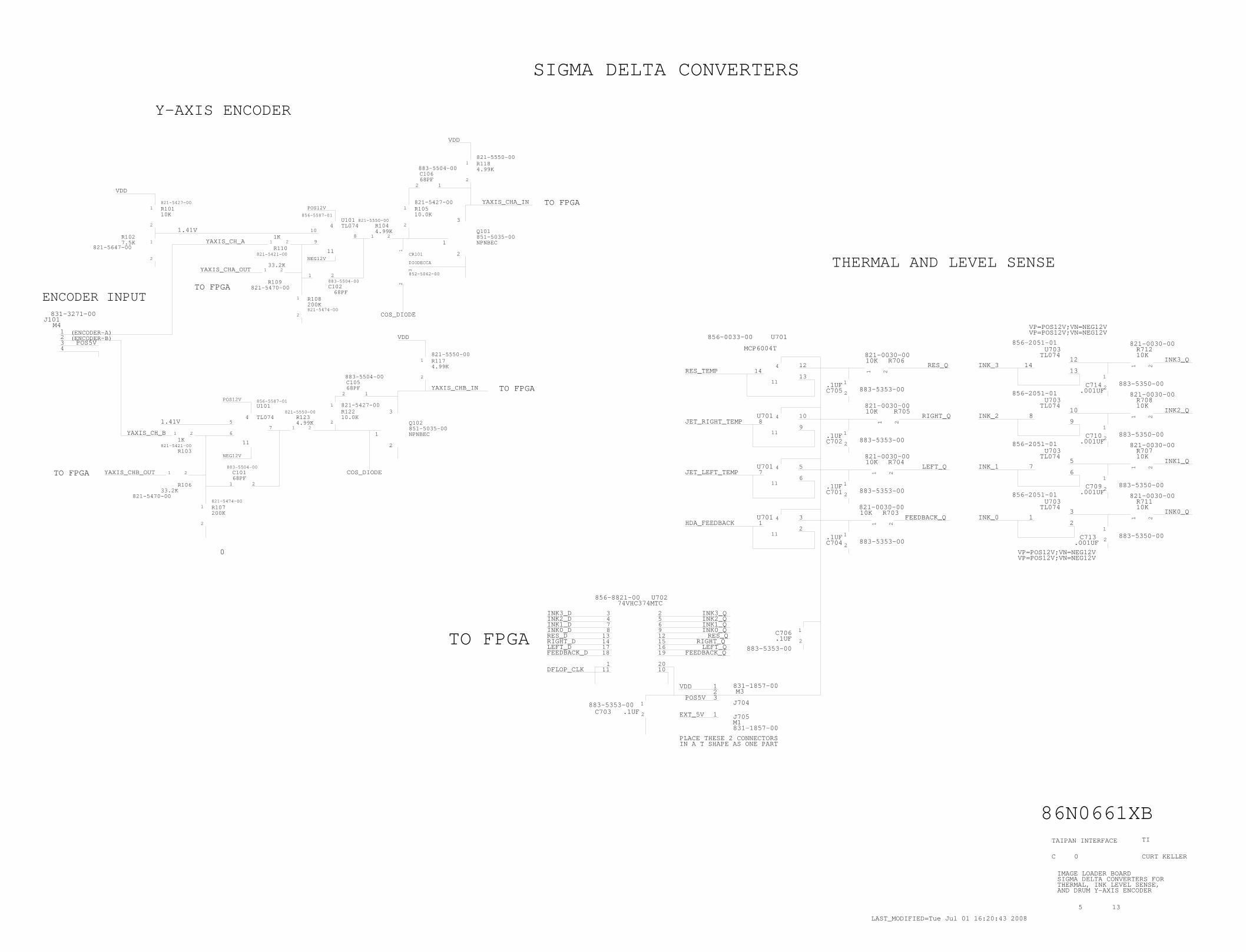
13
THERMAL, INK LEVEL SENSE,AND DRUM Y-AXIS ENCODER
TO FPGA
TO FPGA
5
SIGMA DELTA CONVERTERS FORIMAGE LOADER BOARD
SIGMA DELTA CONVERTERS
THERMAL AND LEVEL SENSE
0C CURT KELLER
PLACE THESE 2 CONNECTORSIN A T SHAPE AS ONE PART
(ENCODER-B)(ENCODER-A)
ENCODER INPUT
TO FPGA
TO FPGA
TO FPGA
Y-AXIS ENCODER
86N0661XB
LAST_MODIFIED=Tue Jul 01 16:20:43 2008
COS_DIODE
821-5427-00
883-5504-00
COS_DIODE
2
821-5550-00
TAIPAN INTERFACE
C706
0
10.0KR122
68PFC105
883-5504-00
POS12V
856-8821-00
3
10
4321
J101
2
1 R118
2 1
C106
2
3
1
Q1012
1 R105
1
R1044
11
89
U101
21
R110
2
1 R101
2
1R102
3
21
CR101
2
1 R117
21
C102
2
1 R108
2 1
2
3
1
Q1022
1
21
R123
21
R109
21
C101
4
11
57
6
U101
21
R103
21
R106
2
1 R107
1020
191615129652
1
18171413874
11
U702
2
1
C703 1 J705
321
J704
41
3
211
U701
47
5
611
U701
48
10
911
U701
2
1
2
1
C704
2
1
C701
21
R703
2
1
C702
21
R704
2
1
C713
31
2
U703
57
6
U703
2
1
C709
2
1
C710
21
R711
21
R707
108
9
U703
414
12
1311
U701
2
1
C705
21
R706
21
R705
1214
13
U703
2
1
C714
21
R708
21
R712
883-5353-00
POS5V
FEEDBACK_QLEFT_Q
RIGHT_Q
74VHC374MTC
821-0030-00
883-5353-00
883-5353-00
YAXIS_CH_B
1.41VTL074
4.99K
883-5353-00
LEFT_DRIGHT_D
INK0_DINK1_DINK2_DINK3_D
RES_QINK0_QINK1_Q
821-0030-00
INK_3
856-2051-01
INK_1
INK_2
LEFT_Q
.1UF
HDA_FEEDBACK
883-5353-00
FEEDBACK_Q
JET_RIGHT_TEMP
10K
821-5470-00
EXT_5VM1
TI
821-0030-00
10K
821-0030-00
10K
.001UF883-5350-00
VP=POS12V;VN=NEG12V
TL07410K
.1UF
VP=POS12V;VN=NEG12V
856-2051-01
TL074
821-0030-00
10K
883-5350-00.001UF
10K
821-0030-00.001UF883-5350-00
883-5350-00.001UF
VP=POS12V;VN=NEG12V
856-2051-01
TL074
856-2051-01
VP=POS12V;VN=NEG12V
TL074
10K
10K821-0030-00
.1UF
INK_0
INK3_Q
INK2_QRIGHT_Q
INK1_Q
INK0_Q
M3
.1UF
VDD 831-1857-00
831-1857-00
M4
POS5V
831-3271-00
POS12V
NEG12V
VDD
VDD
821-5647-007.5K
821-5421-00
1K
33.2K
821-5474-00200K
4.99K
DIODECCA
852-5062-00
10.0K
883-5504-00
68PF
NPNBEC851-5035-00
4.99K
851-5035-00NPNBEC
821-5550-00
1K821-5421-00
33.2K
200K
821-5474-00
68PF
883-5504-00
INK2_Q
821-5550-00
856-5587-01
821-5550-00
821-5427-00
DFLOP_CLK
FEEDBACK_D
RES_D
10K
VDD
1.41V
821-5427-00
68PF
TL074
856-5587-01
NEG12V
YAXIS_CH_A
821-5470-00
YAXIS_CHA_IN
YAXIS_CHA_OUT
YAXIS_CHB_IN
YAXIS_CHB_OUT JET_LEFT_TEMP
INK3_Q
.1UF
883-5353-00
4.99K
821-0030-00
.1UF
RES_TEMP
856-0033-00
MCP6004T
RES_Q
DRAWING
RANK XEROX LTD./FUJI XEROX CO.LTD. BE REPRODUCED, COPIED OR USED FORWITHOUT THE PRIOR WRITTEN PERMISSION OF XEROX CORPORATION AND/OR
DATE:
CORPORATION AND/OR RANK XEROX LTD./FUJI XEROX CO. LTD.ANY PURPOSE WHATSOEVER, EXCEPT THE MANUFACTURE OF ARTICLES FOR XEROX
SIZE
SHEET
DESCRIPTION
TITLE
OF
ENGINEER
ABBREV
REV.
10
1 2 3 4 6 7 1098
8
H
G
F
E
B
C
A
97654321
A
F
E
G
H
D
C
B
D
ARE THE EXCLUSIVE PROPERTY OF XEROX CORPORATION AND/OR RANK XEROXLTD./FUJI XEROX CO.,LTD. ISSUED IN STRICT CONFIDENCE AND SHALL NOT,
THESE DRAWINGS AND SPECIFICATIONS,AND THE DATA CONTAINED THEREIN,
5
1Q2Q3Q4Q5Q6Q
1D2D3D4D5D6D7D8D
OCCLK
7Q8Q
VDDVSS

QUICK USB MODULE +5V INPUT POWER
USB MODULE BOARDMOUNTING HOLES FOR QUICK
NVRAM
DEBUG PORT
TEST POINTS FOR QUICK USB
DO NOT STUFF
(QUSB_RS232_TXDO)
DO NOT STUFF
(QUSB_RS232_RXD0)
RS232 SERIAL DRIVER
LAST_MODIFIED=Tue Jul 01 14:42:46 2008
RS232/NVRAM
13
QUICK USB INTERFACE
C410
VAUX_P3V3
1
.01UC912
SER_RXD112
QUSB_RESET_N
0
QUSB_DATA<11>
QUSB_ADDR<3>
QUSB_DATA<2>
2
D92GND
C9141
0.1U
EEP1_CLK
EEP1_SDA
4.99KR611821-5550-00
1
2
3
QUSB_CMDAT_N
QUSB_IFCLK
QUSB_5V0
SER_TXD1
+5V0
QUSB_SCL
QUSB_ADDR<8..0>
QUSB_DATA<15..0>
QUSB_GPIO<7..0>
QUSB_SDA
QUSB_DATA<15> QUSB_ADDR<8>
QUSB_STATE3QUSB_STATE2QUSB_STATE1
QUSB_FULL_NQUSB_EMPTY_N
QUSB_OUTEN_NQUSB_WREN_NQUSB_RDEN_NQUSB_WRENQUSB_RDEN
QUSB_CLKOUT
QUSB_DATA<12>QUSB_DATA<13>QUSB_DATA<14>
QUSB_DATA<10>
QUSB_ADDR<1>QUSB_ADDR<2>
QUSB_ADDR<4>QUSB_ADDR<5>QUSB_ADDR<6>QUSB_ADDR<7>
QUSB_DATA<8>QUSB_DATA<9>
QUSB_DATA<0>QUSB_DATA<1>
QUSB_DATA<3>QUSB_DATA<4>QUSB_DATA<5>QUSB_DATA<6>QUSB_DATA<7>
QUSB_ADDR<0>
QUSB_GPIO<0>QUSB_GPIO<1>QUSB_GPIO<2>QUSB_GPIO<3>
QUSB_GPIO<5>QUSB_GPIO<4>
QUSB_GPIO<6>QUSB_GPIO<7>
15
CTL223
RXD0
PA71917
PA1
GND
SPR1SPT1+5V0PE0PE1
66
70
9
80
8
797877767574737271
7
696867
656463626160
6
59585756555453525150
5
4948474645444342414039383736353433323130
3
292827262524222120
2
1816151413121110
1
CTL4
PC0PC1PC2PC3PC4PC5PC6PC7GNDPD0PD1PD2PD3PD4PD5
TM0+5V0
PE3
PB1PB2
PE4
PB4PB3
PB0
PWRG
RDY4
GND
GNDTM1
CTL0
PE6
PA4PA5PA6
SDA
PD6PD7SCL
PB7GND
PB6
PA2PA3
PE7WUP*
PE5
PE2
RDY5
PA0
PB5
+5V0RST*CKOTIFCKINT4
TXD0TXD1RXD1+5V0
CTL1
CTL3
CTL5SPR0SPT0
RDY0
RDY2RDY3
RDY1
4
CON40X2J401831-0137-00
1314
12111098
765
7654
34
12
0
23
01
765
34
10
8
POS5V QUSB_5V0
QUSB_5V0
QUSB_5V0
10UC4111
2 10U1
2C708
2
1 C4070.1U
C4080.1U2
1
21
R405821-5005-00
100
10UC7071
2 10UC4041
2
883-0009-00
10UC4051
2
2
1 C4090.1U 2
1 C4060.1U 2
1883-5503-00
0.1U
1
MH402MTMH635C39878
1
MH401MTMH635C39878
1
MH405MTMH635C39878
1
MH404MTMH635C39878
EEP2_CLK
VDD VDD
EEP2_SDA7
5
6
U601856-0124-00
24LC256
VCC=VDD;GND=GND
2
883-5503-00
0.1U1 C604
2
1
2
1 C605883-5503-00
0.1U
VCC=VDD;GND=GND
24LC256
856-0124-00U904
1
2
3 6
5
7
821-5550-00
4.99KR9511
2
RS232_RXD2
RS232_TXD2
0.1UC9131
2 0.1UC9111
2
16 U905
856-0197-00
1345
15
1389
1410 7
26
11
ST4343E
2 2
0.1UC9101
2 0.1UC9151
2
21
R952
0
821-5415-00
21
R631
831-3925-00J906
QUSB_ADDR<7>
QUSB_ADDR<4>
QUSB_ADDR<2>
98765432
16151413121110
1
J403
98765432
16151413121110
1
J402
98765432
1413121110
1
J706
QUSB_WREN_NQUSB_OUTEN_NQUSB_EMPTY_NQUSB_FULL_N
QUSB_RDEN_NQUSB_CMDAT_N
QUSB_IFCLKQUSB_CLKOUTQUSB_RESET_NQUSB_SDA
CON7X2
IMAGE LOADER BOARD
CHRIS GADKE
6
IMAGE LOADER BRD IMAGE LOADER BRD
QUSB_ADDR<1>
QUSB_ADDR<5>QUSB_ADDR<6>
QUSB_ADDR<3>
QUSB_DATA<1>
QUSB_SCL
CON8X2
831-2401-00
QUSB_ADDR<0>
CON8X2
831-2401-00
QUSB_RDENQUSB_WREN
831-2401-00
QUSB_DATA<7>
QUSB_DATA<4>QUSB_DATA<3>
QUSB_DATA<8>QUSB_DATA<9>QUSB_DATA<10>QUSB_DATA<11>QUSB_DATA<12>QUSB_DATA<13>QUSB_DATA<14>QUSB_DATA<15>
QUSB_DATA<6>QUSB_DATA<5>
QUSB_DATA<0>
QUSB_DATA<2>
QUSB_ADDR<8>QUSB_GPIO<0>QUSB_GPIO<1>QUSB_GPIO<2>QUSB_GPIO<3>QUSB_GPIO<4>QUSB_GPIO<5>QUSB_GPIO<6>
QUSB_GPIO<7>
RANK XEROX LTD./FUJI XEROX CO.LTD. BE REPRODUCED, COPIED OR USED FORWITHOUT THE PRIOR WRITTEN PERMISSION OF XEROX CORPORATION AND/OR
DATE:
CORPORATION AND/OR RANK XEROX LTD./FUJI XEROX CO. LTD.ANY PURPOSE WHATSOEVER, EXCEPT THE MANUFACTURE OF ARTICLES FOR XEROX
SIZE
SHEET
DESCRIPTION
TITLE
OF
ENGINEER
ABBREV
REV.
10
1 2 3 4 6 7 1098
8
H
G
F
E
B
C
A
97654321
A
F
E
G
H
D
C
B
D
ARE THE EXCLUSIVE PROPERTY OF XEROX CORPORATION AND/OR RANK XEROXLTD./FUJI XEROX CO.,LTD. ISSUED IN STRICT CONFIDENCE AND SHALL NOT,
THESE DRAWINGS AND SPECIFICATIONS,AND THE DATA CONTAINED THEREIN,
5
DRAWING
R1INR2IN
V+
T1IN
R1OUT
T1OUTVCC
R2OUT
T2IN
C1+
GND V-
T2OUT
C2+C1-
C2-
P78P80
P74P76
P72P70P68
P64P66
P62P60P58P56P54P52P50P48P46P44P42P40P38P36P34P32P30P28P26P24P22P20P18P16P14P12P10P8P6
P2P4
P63P65P67P69P71
P75P73
P77P79
P61
P41P43P45P47P49
P55
P51P53
P57P59
P21P23P25P27P29P31P33P35P37P39
P1P3P5P7P9
P13P11
P15P17P19
16
27
38
49
5
SCL
WP
SDA
A2
A0
A1
SCL
WP
SDA
A2
A0
A1
57
1513119
31
1416
12
810
46
2
57
1513119
31
1416
12
810
46
2
1113
9
57
13
1214
1086
24

CONFIGURATION SERIAL/PARALLEL FLASH PROM
XILINX CONFIGURATION PROM XCF08PFSG48 POWER SUPPLY VOLTAGES
VCCINT: +1.8V SUPPLY. POSITIVE 1.8V SUPPLY VOLTAGE FOR INTERNAL LOGIC.
VCCO: +3.3V, 2.5V, 1.8V, OR 1.5V I/O SUPPLY. POSITIVE 3.3V, 2.5V,1.8V, OR 1.5V SUPPLY VOLTAGE CONNECTED TO THE OUTPUT VOLTAGEDRIVERS AND INPUT BUFFERS.
DO NOT STUFF THIS RESISTOR
JTAG INTERFACE CONNECTOR FOR PROGRAMING CONFIGURATION PROM
JTAG_TDI
AUXILLEY CLOCK LOCATION
TMS, AND TDI INPUT BUFFERS.
VCCJ: +3.3V OR 2.5V JTAG I/O SUPPLY. POSITIVE 3.3V OR 2.5V SUPPLY
FPGA CONFIGURATION BLOCK
FPGAFPGA_TDO
FPGA_TDI
JTAG_TMS
JTAG_TCK
FPGA CONFIGURATION MODE SELECTION
MASTER SERIAL MODE WHICH LOADS CONFIGURATION
VOLTAGE CONNECTED TO THE TDO OUTPUT VOLTAGE DRIVER AND TCK,
66MHZ SYSTEM CLOCK
TO FPGA GCLK4
TO FPGA GCLK2
MODE BITS M<2..0> = <000> SETS FPGA TO
SUSPEND MODE POWER MANAGEMENT NOTUSED, CONNECT INPUT TO GROUND.
CHIP SELECTS, CSI_B AND CSO_B NOT USEDFOR SINGLE-FPGA DESIGN. RDWR_N NOTUSED FOR MASTER SERIAL CONFIGURATION.
CONFIGURATION PROM NOTES------------------------XILINX 8-MBIT CONFIGURATION PROM IMPLEMENTED FOR SERIALMASTER MODE CONFIGURATION WITH MODE BITS ALL SET LOW.
SPARTAN3A XC3S1400A REQUIRES 4.73 MBITS FOR CONFIGURATIONSPARTAN3A XC3S700A REQUIRES 2.73 MBITS FOR CONFIGURATION
JTAG_TMSJTAG_TCK
FLASH
DASHED LINES ARE OPTIONAL CONNECTIONS WITHRESISTORS TO MODIFY THE JTAG CHAIN PATH
JTAG CHAIN
MODE BITS HAVE INTERNAL PULL-UPSFROM PLATFORM FLASH IN SERIAL MODE.
LAST_MODIFIED=Tue Jul 01 14:43:11 2008
13
IMAGE LOADER BOARDFPGA CONFIGURATIONAND POWER INTERFACE
2
100
R538
856-0198-00
D2OPEN FOR SINGLE PROM
821-5415-00VIO_P3V3
VIO_P3V3
A4
H4
1
NCE5
G5
VAUX_P1V8
49.9R847
821-5572-00
FPGA_PROG_N
JTAG_TDIJTAG_TCKJTAG_TMS
BUSY NOT SUPPORTED ON S3A
NCNCNCNC
NC
NC
OPEN WITH INTERNAL PULLUP
NC
NCNCNCNCNCNCNCNCNCNC
OPEN WITH INTERNAL PULLUP
U501
C1
B4
B3
C2H6H5
D5C5B5A5A6
C3C4D3D4E3E4F2F3F4G2
A1A2B6F1F5F6H1
A3
G4
H3G1
E6
E2
B1E1G6
H2B2
D6
831-1857-00
FPGA_INIT_NV13NCAA15
A2
JTAG_TMS
FPGA_TDOJTAG_TCK
FPGA_M0
AB14
CX506 CX504
2
1 CX5052
1 CX5032
1 CX507
21
R535
4 3
2 1
Y501
4 3
2
Y801
1C511
2
1 C824
2
1 R529
2
1 R525
2
1 R848
1 R520
2
1 R522
1
R533
2
1 R526
2
1 R527
2
1 R524
2
1 R523
987654321
J601
D4
E19F5
A21
U18
C4AB20
AA20
V9
W4
Y4
V6W5
Y19
U801
VIO_P3V3
0.01UF
883-5501-00
0.1U
FPGA_M1FPGA_M2
FPGA_CCLKFPGA_DONEFPGA_PROG_NFPGA_DIN
FPGA_M2FPGA_M1FPGA_M0
NC
856-0187-00
100
200 200
821-5663-00
200
10.0K10.0K
821-5425-00
4.75K4.75K4.75K0.1U
OSCSMD
DO NOT STUFF
OSCSMD
858-0010-00
TDO
TCK
M9
NC
NC
IMAGE LOADER BRD
CHRIS GADKE
VIO_P3V3VIO_P3V3 SYS_CLK66
VIO_P3V3 AUX_CLK
XC3S700AFG484
IMAGE LOADER BRD
7
FPGA_TDO
PWRGND
VDD
821-5690-00
0.1U
1.0U0.1U0.01UF
883-5503-00
883-5007-00
2FPGA_CCLK
FPGA_DONE
0
FPGA_INIT_N
858-0010-00
1
68.12
FPGA_DIN
NC
0
168.1
TMSKEYTDI
1 JTAG_TMS
21 JTAG_TCK
FPGA_TDI
FPGA_TDI
821-5417-00
2
JTAG_3V3
R532
JTAG_TDI2
2
68.1R534
68.1R531
68.1R539 OPEN WITH INTERNAL PULLUP
G3
C6
D1
FPGA_TDI
XCF08PFSG48
RANK XEROX LTD./FUJI XEROX CO.LTD. BE REPRODUCED, COPIED OR USED FORWITHOUT THE PRIOR WRITTEN PERMISSION OF XEROX CORPORATION AND/OR
DATE:
CORPORATION AND/OR RANK XEROX LTD./FUJI XEROX CO. LTD.ANY PURPOSE WHATSOEVER, EXCEPT THE MANUFACTURE OF ARTICLES FOR XEROX
SIZE
SHEET
DESCRIPTION
TITLE
OF
ENGINEER
ABBREV
REV.
10
1 2 3 4 6 7 1098
8
H
G
F
E
B
C
A
97654321
A
F
E
G
H
D
C
B
D
ARE THE EXCLUSIVE PROPERTY OF XEROX CORPORATION AND/OR RANK XEROXLTD./FUJI XEROX CO.,LTD. ISSUED IN STRICT CONFIDENCE AND SHALL NOT,
THESE DRAWINGS AND SPECIFICATIONS,AND THE DATA CONTAINED THEREIN,
5
DRAWING
VDD
GND NC(EN)
OUT
VDD
GND NC(EN)
OUT
REV_SEL1REV_SEL0EN_EXT_SEL*
OE_RESETCE*CF*
CLK
DNC[10]DNC[9]DNC[8]DNC[7]DNC[6]DNC[5]DNC[4]
DNC[2]DNC[3]
DNC[1]DNC[0]
GND[5]GND[4]
GND[6]
GND[3]GND[2]
VCCINT[2]GND[0]GND[1]
VCCINT[1]VCCINT[0]
VCCO[2]VCCO[3]
VCCO[1]
VCCJVCCO[0]D7
D6
D4D5
D3D2D1D0
TDOCLKOUT
CEO*
BUSYTDITCKTMS
PROG
SUSPEND
IO2L02P_M2IO2L01P_M1IO2L01N_M0
DONEPROG_B
IO2L36P_DO_DIN_MISOIO2L26P_INIT_B
IO2L36N_CCLK
IO2L24N_DOUT
TCKTDOTDITMSIO2L09P_RDWR_B
IO2L22N_MOSI_CSI_B
IO2L02N_CSO_B
IO0L36N_HSWAP
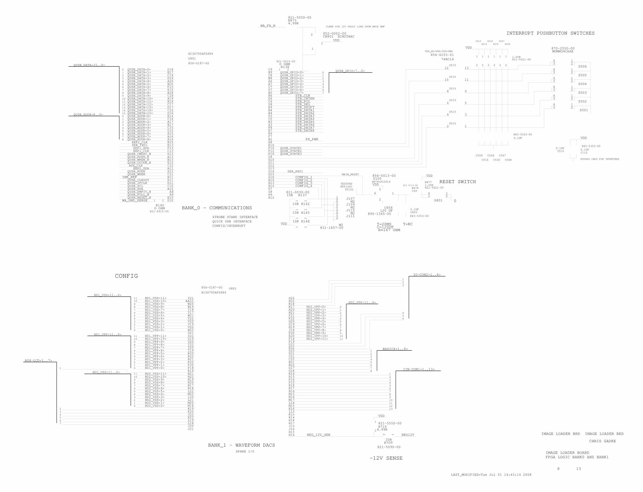
-12V SENSE
CONFIG
SPARE I/O
RESET SWITCH
T=20MS
R=167 OHM
T=RC
INTERRUPT PUSHBUTTON SWITCHES
C=120UF
BYPASS CAPS FOR INVERTERS
CLAMP FOR 12V FAULT LINE FROM WAVE AMP
STROBE STAND INTERFACE
CONFIG/INTERRUPTQUICK USB INTERFACE
LAST_MODIFIED=Tue Jul 01 14:43:14 2008
13
IMAGE LOADER BOARDFPGA LOGIC BANK0 AND BANK1
QUSB_GPIO<6>QUSB_GPIO<7>
QUSB_GPIO<5>QUSB_GPIO<4>QUSB_GPIO<3>QUSB_GPIO<2>QUSB_GPIO<1>
AUX-LCD<1..7>
765432
1
HD2_VSS<11..0>
HD2_VSS<2>HD2_VSS<1>HD2_VSS<0>
HD2_VSS<3>HD2_VSS<4>HD2_VSS<5>
HD2_VSS<7>HD2_VSS<6>
HD2_VSS<8>HD2_VSS<9>HD2_VSS<10>HD2_VSS<11>
HD1_VPP<1>HD1_VPP<0>
HD1_VPP<2>
HD1_VPP<4>HD1_VPP<3>
HD1_VPP<6>HD1_VPP<5>
HD1_VPP<7>
HD1_VPP<11..0>
HD1_VSS<11..0>
HD1_VPP<9>HD1_VPP<8>
HD1_VPP<10>HD1_VPP<11>
HD1_VSS<0>HD1_VSS<1>HD1_VSS<2>
HD1_VSS<4>HD1_VSS<3>
HD1_VSS<6>HD1_VSS<5>
HD1_VSS<7>
HD1_VSS<9>HD1_VSS<8>
HD1_VSS<11>HD1_VSS<10>
NEG_12V_SEN
HD2_VPP<11>HD2_VPP<10>HD2_VPP<9>HD2_VPP<8>HD2_VPP<7>HD2_VPP<6>HD2_VPP<5>HD2_VPP<4>HD2_VPP<3>HD2_VPP<2>HD2_VPP<1>HD2_VPP<0>
BASICX<1..8>
NEG12V
HD2_VPP<11..0>
VDD
IIN-CON1<1..13>
IO-CON2<1..6>
210
345
76
891011
10
2
43
65
7
98
1011
012
43
65
7
98
1110
V22
W21
H16H15J16J15H17H18K14K15
K16M15L16M17M16N15N16
P15P16R15
G17
B21C22C21D21D20
D22F19
G19G20F22
H21
K17
N20N19
U21
V20Y22
T17T18W19
Y21
F18E20
J18H19
J21
L15
F21
BANK_1 - WAVEFORM DACS
AA22
W22
U19U20
R18
T22T20
R20
R21P22P20
R19
N18L22M22
L21M20
K19K20J22
L19L18J20
E22
XC3S700AFG484
856-0187-00
G18
B22
F20
R16
H22K18
H20
G22
R17
U801
K22
M18
L20
N17
N22N21
P18
R22
T19
U22
V19
W20
5678
4321
11109876
45
3
12
0
2
1
R710821-5550-00
4.99K
2 1
R709821-5090-00
20K
13
10
1211
789
56
234
1
654
23
1
1
STB_DATA5
STB_DATA3
STB_SELSTB_POL
STB_CLK
2
821-5415-00
WA_FA_N
STB_CNTEN
STB_SHIFT
STB_DATA2
STB_DATA4
STB_DATA7
QUSB_STATE1
MAIN_RESET
6
0.1UF
C115
0.1UF VDD883-5353-00
F16
B9
6
1 1
R528
123
S503
4
123
4
S502
23
MOMNO4CASE
4
870-2550-00
421
3S505
12
S5063
INK_REFQUSB_WRENQUSB_RDEN
A11
F7
21
21
21
10K
10K
21
2M2
2
D7
QUSB_OUTEN_N
XC3S700AFG484
1
2
3
CR801
B8
G16
QUSB_GPIO<0>
R138
C5
A3
D5
F8
A13
QUSB_ADDR<7>
QUSB_ADDR<3>QUSB_ADDR<2>
1514
21
1
G12G11
F12
H12
B2
B3
A4
D6
A6
C8
C9
D10E10A9A8
A10C10D11E11B11C11A12
E12B13
D13
F13E13B15A14A16A15D15C15B17
C14E14D16C16D17C17B19A19C18A18E15F15B20A20D19C19E17D18
4
QUSB_DATA<3>QUSB_DATA<2>
76
2
QUSB_RESET_N
CHRIS GADKE
IMAGE LOADER BRD
6
3210
13
76543210
121110987
8
O OHM
QUSB_DATA<0>QUSB_DATA<1>
QUSB_DATA<4>
QUSB_EMPTY_N
WA_GND_SENSE
45
QUSB_DATA<6>QUSB_DATA<7>
QUSB_DATA<9>
QUSB_DATA<12>
QUSB_DATA<15>
AUX_CLK
01
3
5
QUSB_ADDR<0>
QUSB_DATA<14>QUSB_DATA<13>
QUSB_DATA<8>
QUSB_CLKOUTQUSB_IFCLKQUSB_SCLQUSB_SDA
EEP2_SDA
QUSB_DATA<10>
QUSB_ADDR<5>QUSB_ADDR<6>
QUSB_DATA<5>
QUSB_DATA<11>
QUSB_ADDR<1>
QUSB_FULL_N
A7
U801
856-0187-00 O OHM
4.99K
C559
CONFIG_3CONFIG_4
1M2
0.1UF883-5353-00
VDD
C515
B4
D8C6
B6A5
C7
STB_DATA1
U105
STB_DATA6 1E7
3
12
8
2
TP105 5
C530
3
C516
VDD
U515
883-5353-00
120 UF
U515
U515
U515
5
4
U515
R878
C855
S801
CONFIG_2
821-5415-00
VDD10K R148
2
821-0114-00
10K
R145
G8G7H14H13H10
G15
QUSB_GPIO<7..0>
74HC14856-6253-01
VDD_HC=VDD;VSS=GND
0.1UF
4
1
S504
R516
34
2S501
1
2
1
R568
13
U51510
2
1
R510
2 2
1
R567
2
11
1
2
R530
1.00K821-5421-00
QUSB_ADDR<8..0>
QUSB_WREN_N
C12
1
BANK_0 - COMMUNICATIONS
R137821-0030-00
G14G13
H9
E9
A17
QUSB_STATE2
G10
PH_PWR
IMAGE LOADER BRD
R140
QUSB_RDEN_NQUSB_CMDAT_N
EEP1_SDAEEP1_CLK
SER_RXD1
SER_TXD1
8 QUSB_ADDR<8>EEP2_CLK
1212
MTP160C
F10
E6STB_DATA8
856-0013-00
QUSB_DATA<15..0>
QUSB_ADDR<4>
C13
VDDSCHOTAAC
852-0002-00
R875821-5550-00
C858
SN74LVC2G14
J111
J110
TESTPAD
9
C568
C567C528
1
890-1365-00
M2J107
J109
CONFIG_1
G9
E8E16
QUSB_STATE3
VDD
169
2
831-1857-00M2
R142
4
821-5421-001.00KR877
0
RANK XEROX LTD./FUJI XEROX CO.LTD. BE REPRODUCED, COPIED OR USED FORWITHOUT THE PRIOR WRITTEN PERMISSION OF XEROX CORPORATION AND/OR
DATE:
CORPORATION AND/OR RANK XEROX LTD./FUJI XEROX CO. LTD.ANY PURPOSE WHATSOEVER, EXCEPT THE MANUFACTURE OF ARTICLES FOR XEROX
SIZE
SHEET
DESCRIPTION
TITLE
OF
ENGINEER
ABBREV
REV.
10
1 2 3 4 6 7 1098
8
H
G
F
E
B
C
A
97654321
A
F
E
G
H
D
C
B
D
ARE THE EXCLUSIVE PROPERTY OF XEROX CORPORATION AND/OR RANK XEROXLTD./FUJI XEROX CO.,LTD. ISSUED IN STRICT CONFIDENCE AND SHALL NOT,
THESE DRAWINGS AND SPECIFICATIONS,AND THE DATA CONTAINED THEREIN,
5
DRAWING
BANK1
IO1L29P_A12IO1L29N_A13
IO1L28NIO1L28P
IO1L26P_A10
IO1L25P_IRDY1_RHCLK6IO1L26N_A11
IO1L25N_RHCLK7IO1L24P_RHCLK4IO1L24N_RHCLK5
IO1L22N_TRDY1_RHCLK3IO1L22P_RHCLK2
IO1L21P_RHCLK0IO1L21N_RHCLK1IO1L20P_A8
IO1L19P_A6IO1L20N_A9
IO1L19N_A7IO1L18P_A4IO1L18N_A5
IO1L17N_A3IO1L17P_A2
IO1L15P
IO1L14PIO1L15N_VREF1
IO1L13PIO1L14N
IO1L13N
IO1L11NIO1L11P
IO1L10NIO1L10P
IO1L09P
IO1L07PIO1L09N
IO1L07NIO1L06PIO1L06N
IO1L05NIO1L05P
IO1L03P_A0IO1L03N_A1IO1L02P_LDC1IO1L02N_LDC0IO1L01P_HDCIO1L01N_LDC2
IP1L47P_VREF1IP1L47NIP1L43P
IP1L43N_VREF1IP1L39PIP1L39N
IP1L35P_VREF1IP1L35NIP1L31P
IP1L27P_VREF1IP1L31N
IP1L27NIP1L23PIP1L23NIP1L16P
IP1L16N_VREF1IP1L12P
IP1L12N_VREF1IP1L08PIP1L08NIP1L04P
IP1L04N_VREF1
IO1L46N_A25IO1L46P_A24
IO1L45P_A22IO1L45N_A23IO1L44P_A20IO1L44N_A21
IO1L42PIO1L42N
IO1L41NIO1L41P
IO1L40NIO1L40P
IO1L38PIO1L38NIO1L37PIO1L37NIO1L36PIO1L36N
IO1L34P_A18IO1L34N_A19IO1L33P_A16IO1L33N_A17
IO1L32P
IO1L30P_A14IO1L32N
IO1L30N_A15
BANK0
IO0L23PIO0L23NIO0L22P
IO0L21PIO0L21N
IO0L22N
IO0L20P_GCLK10IO0L20N_GCLK11IO0L19P_GCLK8IO0L19N_GCLK9IO0L18P_GCLK6
IO0L17P_GCLK4IO0L18N_GCLK7
IO0L17N_GCLK5IO0L16PIO0L16NIO0L15PIO0L15NIO0L14PIO0L14NIO0L13PIO0L13NIO0L12PIO0L12N_VREF0IO0L11PIO0L11NIO0L10PIO0L10NIO0L09PIO0L09NIO0L08PIO0L08NIO0L07PIO0L07N
IO0L06NIO0L06P_VREF0
IO0L05PIO0L05NIO0L04PIO0L04NIO0L03PIO0L03N
IO0L02NIO0L02P_VREF0
IO0L01PIO0L01N
IP19_VREF0IP20_VREF0
IP18_VREF0IP17_IREF
IP16
IP14IP15
IP13IP12IP11IP10IP9IP8IP7IP6IP5IP4IP3IP2IP1
IO0L35PIO0L36P_VREF0
IO0L35NIO0L34PIO0L34N
IO0L33NIO0L33P
IO0L32PIO0L32NIO0L31PIO0L31NIO0L30PIO0L30NIO0L29PIO0L29NIO0L28PIO0L28NIO0L27PIO0L27NIO0L26PIO0L26NIO0L25PIO0L25NIO0L24P
IO0L24N_VREF0
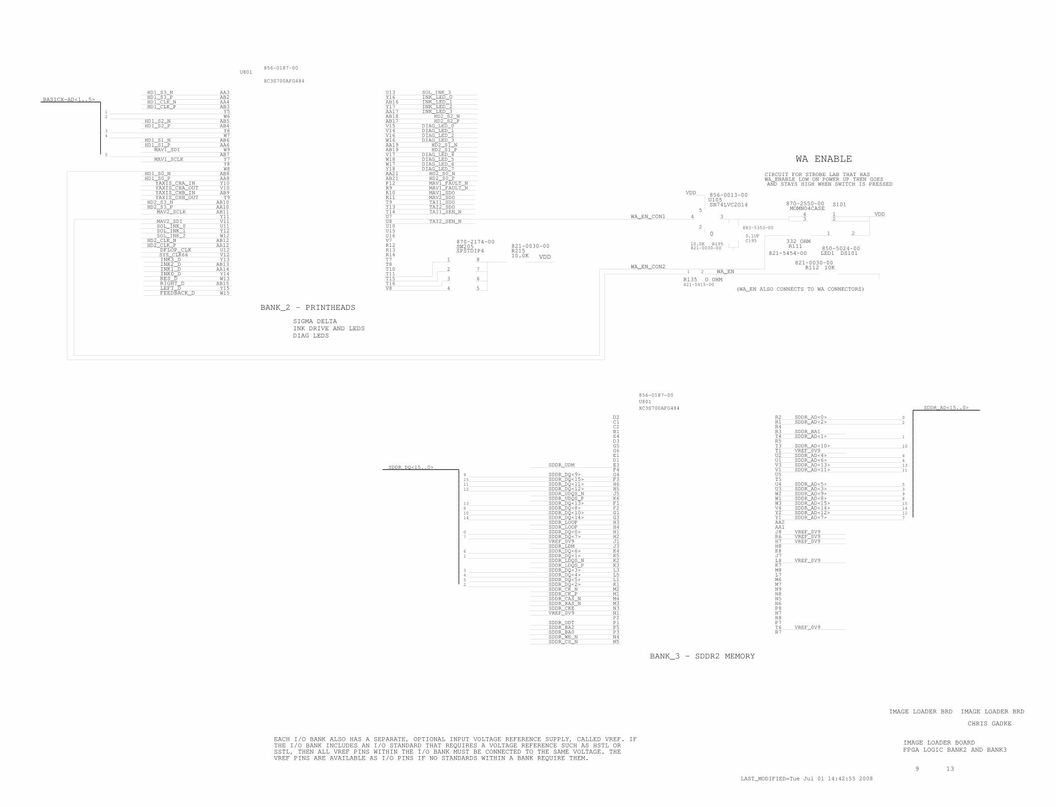
SIGMA DELTA
DIAG LEDS
THE I/O BANK INCLUDES AN I/O STANDARD THAT REQUIRES A VOLTAGE REFERENCE SUCH AS HSTL OR
(WA_EN ALSO CONNECTS TO WA CONNECTORS)
WA ENABLECIRCUIT FOR STROBE LAB THAT HASWA_ENABLE LOW ON POWER UP THEN GOESAND STAYS HIGH WHEN SWITCH IS PRESSED
INK DRIVE AND LEDS
EACH I/O BANK ALSO HAS A SEPARATE, OPTIONAL INPUT VOLTAGE REFERENCE SUPPLY, CALLED VREF. IF
SSTL, THEN ALL VREF PINS WITHIN THE I/O BANK MUST BE CONNECTED TO THE SAME VOLTAGE. THEVREF PINS ARE AVAILABLE AS I/O PINS IF NO STANDARDS WITHIN A BANK REQUIRE THEM.
LAST_MODIFIED=Tue Jul 01 14:42:55 2008
13
HD1_S3_N
AB4
W7AB6
XC3S700AFG484
10.0K
VDD
SW205
7
8
3
2
U16
T16T15T11T10T8
R14
AB19AA19W16
V14V15AB17AB18AA17Y17
Y16
W15Y15
AB15W13
AB13
V12U12
AA12AB12
Y12
Y8Y7
W9AA6
Y6
AA4
R8
N6N5N8N9M7M6L7M8K7L8J7K8H8H7R6J8AA1AA2Y1Y2V4W3W1W2U3U4T5U5V1V3U1U2T1T3R5T4R3R4R1R2
M5N4P3P5P1P2N1N3M3M4M1M2K1L1L5L3K3K2K5K4J3J1H2H1H4H3G3G1F2F1K6J5H5H6F3G4F4E3D1E1G6G5D3E4B1C2C1D2
U801
856-0187-00
INK_LED_2INK_LED_1INK_LED_0SOL_INK_3
9
FPGA LOGIC BANK2 AND BANK3
IMAGE LOADER BRD IMAGE LOADER BRD
CHRIS GADKE
IMAGE LOADER BOARD
RIGHT_D
INK3_DINK2_D
HD1_S0_N
HD2_CLK_P
02
1
10
46
1113
935
127
14158
XC3S700AFG484
856-0187-00
159
1381014
07
61
3
54
2
SDDR_AD<15..0>
SDDR_AD<0>SDDR_AD<2>
SDDR_BA1SDDR_AD<1>
SDDR_AD<10>
SDDR_AD<4>SDDR_AD<6>SDDR_AD<13>SDDR_AD<11>
SDDR_AD<5>SDDR_AD<3>SDDR_AD<9>SDDR_AD<8>SDDR_AD<15>SDDR_AD<14>SDDR_AD<12>SDDR_AD<7>
HD2_CLK_N
SOL_INK_0
SDDR_DQ<15..0>
1211
SDDR_CS_NSDDR_WE_NSDDR_BA0SDDR_BA2SDDR_ODT
SDDR_UDQS_N
SDDR_LOOPSDDR_LOOPSDDR_DQ<0>SDDR_DQ<7>
SDDR_DQ<5>
VREF_0V9SDDR_CKESDDR_RAS_N
SDDR_CK_PSDDR_CK_NSDDR_DQ<2>
SDDR_DQ<4>SDDR_DQ<3>SDDR_LDQS_PSDDR_LDQS_NSDDR_DQ<1>SDDR_DQ<6>
VREF_0V9SDDR_LDM
SDDR_CAS_N
VREF_0V9
VREF_0V9
VREF_0V9VREF_0V9VREF_0V9
VREF_0V9
R12SPSTDIP4
6
5V8
W12
MAV2_SDI
SOL_INK_1
870-2174-00
INK1_D
1
DIAG_LED_7
DIAG_LED_3V16
AA14Y14
SYS_CLK66DFLOP_CLK
SOL_INK_2
Y5AB3
AB5W6
MAV1_SCLK
MAV1_FAULT_NMAV1_FAULT_N
HD2_S0_PHD2_S0_N
YAXIS_CHB_IN
HD2_S3_P
U801
AB7
V11
AB2AA3
T9T13T14
U15
R11R10R9P12
Y18
W18W17
U11
AB10Y9
AB9
Y10AA8AB8W8
Y11
AB21AA21
DIAG_LED_6DIAG_LED_5DIAG_LED_4
HD2_S1_NHD2_S1_P
V17
1 2
LED1 DS101850-5024-00
3
S101870-2550-00MOMNO4CASE
12
4
R111332 OHM
821-5454-00
R112 10K821-0030-00
C1950.1UF
883-5353-00
R195821-0030-00
U105856-0013-00
5SN74LVC2G14
2
3
1
821-5415-00O OHMR135
2
VDD
VDD
WA_EN
WA_EN_CON1
WA_EN_CON2
4
5
43
2
HD1_S3_PHD1_CLK_N
HD1_S2_P
HD1_S1_NHD1_S1_P
YAXIS_CHB_OUT
AB11AA10
U7U8U10
R13
V7
TAI2_SEN_N
TAI1_SEN_NTAI2_SDOTAI1_SDO
MAV1_SDOMAV2_SDO
R21510.0K
821-0030-00
HD2_S2_PHD2_S2_N
AB16
T7Y13
MAV2_SCLK
HD2_S3_N
YAXIS_CHA_OUTYAXIS_CHA_IN
HD1_S0_P
BASICX-AD<1..5>
1
INK0_DRES_D
LEFT_DFEEDBACK_D
SDDR_UDM
SDDR_DQ<9>SDDR_DQ<15>SDDR_DQ<11>SDDR_DQ<12>
SDDR_UDQS_PSDDR_DQ<13>SDDR_DQ<8>SDDR_DQ<10>SDDR_DQ<14>
BANK_3 - SDDR2 MEMORY
R7T6P7
N7P8
U13
INK_LED_3
DIAG_LED_2DIAG_LED_1DIAG_LED_0
MAV1_SDI
BANK_2 - PRINTHEADS
V10
HD1_S2_N
HD1_CLK_P
4
0
DRAWING
RANK XEROX LTD./FUJI XEROX CO.LTD. BE REPRODUCED, COPIED OR USED FORWITHOUT THE PRIOR WRITTEN PERMISSION OF XEROX CORPORATION AND/OR
DATE:
CORPORATION AND/OR RANK XEROX LTD./FUJI XEROX CO. LTD.ANY PURPOSE WHATSOEVER, EXCEPT THE MANUFACTURE OF ARTICLES FOR XEROX
SIZE
SHEET
DESCRIPTION
TITLE
OF
ENGINEER
ABBREV
REV.
10
1 2 3 4 6 7 1098
8
H
G
F
E
B
C
A
97654321
A
F
E
G
H
D
C
B
D
ARE THE EXCLUSIVE PROPERTY OF XEROX CORPORATION AND/OR RANK XEROXLTD./FUJI XEROX CO.,LTD. ISSUED IN STRICT CONFIDENCE AND SHALL NOT,
THESE DRAWINGS AND SPECIFICATIONS,AND THE DATA CONTAINED THEREIN,
5
BANK2
IO2L25PIO2L25N
IO2L23NIO2L22P
IO2L23PIO2L24P_AWAKE
IO2L21P
IO2L20N_GCLK3IO2L19P_GCLK0
IO2L20P_GCLK2IO2L21N
IO2L19N_GCLK1IO2L18P_GCLK14
IO2L17P_GCLK12IO2L17N_GCLK13
IO2L18N_GCLK15
IO2L16P_D5IO2L16N_D4
IO2L15NIO2L14P_D7
IO2L15P
IO2L14N_D6
IO2L13N
IO2L11PIO2L12NIO2L12P
IO2L13P
IO2L10PIO2L10NIO2L09N_VS2IO2L08P
IO2L11N
IO2L07NIO2L06PIO2L06N
IO2L08NIO2L07P
IO2L04P
IO2L03PIO2L04N
IO2L05PIO2L05N
IO2L03N
IP21_VREF2
IP19_VREF2IP20_VREF2
IP23_VREF2IP22_VREF2
IP16_VREF2IP15_VREF2IP14_VREF2
IP17_VREF2IP18_VREF2_NC
IP2_13IP2_12_NC
IP2_9IP2_10IP2_11
IP2_8_NC
IP2_6IP2_5IP2_4
IP2_7
IP2_3
IP2_1
IO2L34PIO2L35NIO2L35P
IP2_2
IO2L33PIO2L33NIO2L32PIO2L32N
IO2L34N
IO2L30P
IO2L29PIO2L30N
IO2L31PIO2L31N
IO2L28N_D1
IO2L27NIO2L27P
IO2L28P_D2IO2L29N
IO2L26N_D3
BANK3
IO3L30PIO3L30NIO3L29PIO3L29NIO3L28PIO3L28NIO3L26P_VREF3IO3L26NIO3L25P_TRDY2_LHCLK6IO3L25N_LHCLK7IO3L24P_LHCLK4
IO3L22P_LHCLK2IO3L24N_LHCLK5
IO3L22N_IRDY2_LHCLK3IO3L21P_LHCLK0IO3L21N_LHCLK1IO3L20PIO3L20NIO3L18PIO3L18NIO3L17PIO3L17N_VREF3IO3L16PIO3L16NIO3L14PIO3L14NIO3L13PIO3L13NIO3L12PIO3L12NIO3L10PIO3L10N
IO3L09NIO3L09P
IO3L08PIO3L08NIO3L07PIO3L07NIO3L06P
IO3L05PIO3L06N
IO3L05N
IO3L03NIO3L03P
IO3L02PIO3L02NIO3L01PIO3L01N
IP3L46PIP3L46N_VREF3
IP3L39PIP3L39NIP3L35PIP3L35NIP3L31PIP3L31NIP3L27P
IP3L23PIP3L27N
IP3L23NIP3L19PIP3L19NIP3L15P
IP3L15N_VREF3IP3L11PIP3L11NIP3L04P
IP3L04N_VREF3IP2_VREF3IP1_VREF3
IO3L45PIO3L45NIO3L44PIO3L44NIO3L43PIO3L43NIO3L42PIO3L42NIO3L41PIO3L41NIO3L40PIO3L40NIO3L38PIO3L38NIO3L37PIO3L37N
IO3L36P_VREF3IO3L36NIO3L34PIO3L34NIO3L33P
IO3L32PIO3L33N
IO3L32N
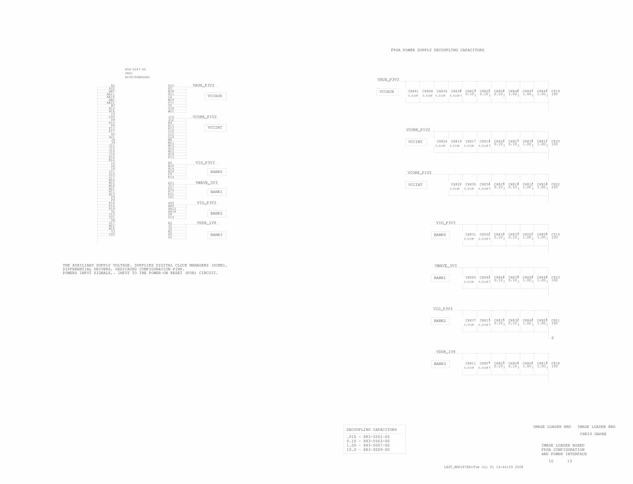
VCCAUX
BANK0
VCCINT
BANK1
BANK3
BANK2
BANK3
BANK1
BANK0
1.0U - 883-5007-000.1U - 883-5503-00
DECOUPLING CAPACITORS
POWERS INPUT SIGNALS,. INPUT TO THE POWER-ON RESET (POR) CIRCUIT.
THE AUXILIARY SUPPLY VOLTAGE. SUPPLIES DIGITAL CLOCK MANAGERS (DCMS),DIFFERENTIAL DRIVERS, DEDICATED CONFIGURATION PINS.
BANK2
FPGA POWER SUPPLY DECOUPLING CAPACITORS
VCCAUX
VCCINT
VCCINT
10.U - 883-0009-00
.01U - 883-5501-00
LAST_MODIFIED=Tue Jul 01 14:44:29 2008
0
CX8320.1U 1.0U
CX840
IMAGE LOADER BRD
13
IMAGE LOADER BOARDFPGA CONFIGURATIONAND POWER INTERFACE
1.0UCX811 CX807
2
1 CX8032
1 CX8042
1 CX8022
1 CX8102
1 C818
CX837 CX8132
1 CX8152
1
2
1
2
1 CX8252
1 C821
CX843 CX8422
1 CX8442
1 CX8392
1 CX8492
1 CX8462
1 C823
CX831 CX5022
1 CX8162
1 CX8332
1 CX5012
1 CX8052
1 C510
CX828 CX830 CX8342
1 CX8292
1 CX8182
1 CX8122
1 CX8242
1 C822
CX826 CX819 CX817 CX8142
1 CX8202
1 CX8272
1 CX8352
1 CX8212
1 C820
2
1 CX8482
1 CX806CX841 CX808 CX836 CX8382
1 CX8232
1 CX8222
1 CX8472
1 CX8452
1 C819
V2P6N2J6J2E2
U14U9AA18AA13AA9AA5
V21P21P17K21J17E21
F14F9B18B14B10B5
M9L14L12L10K13K11K9J12
P13N14N12N10M13M11
J10
V18V5P11M19L4H11E18E5
W11
D12
B12B7
AB22AB1
Y20Y3
W14W10
AA16
U17U6
T21T12T2
P19P14P10P9P4
AA11
N13N11M21M14M12M10L17L13L11L9
AA7
L6L2
K12K10J19J14J13J11J9J4
A22
G21G2
F17F11F6
D14D9
C20C3
B16
A1
U801
VWAVE_3V3
VWAVE_3V3
VIO_P3V3
VIO_P3V3
VAUX_P3V3
VCORE_P1V2
0.1U
0.1U
1.0U0.1U
10
VDDR_1V8
VIO_P3V3
VAUX_P3V3
VCORE_P1V2
IMAGE LOADER BRD
CHRIS GADKE
0.1U 1.0U 10U
0.1U 0.1U 1.0U 1.0U 10U
0.1U 0.1U 1.0U 1.0U 10U
0.1U 1.0U 1.0U 10U
0.1U 1.0U 1.0U 10U
1.0U0.1U0.1U 1.0U 10U
856-0187-00
XC3S700AFG484
0.1U 0.1U 1.0U 10U
VIO_P3V3
VDDR_1V8
VCORE_P1V2
0.01UF0.01UF0.01UF0.01UF
0.01UF 0.01UF 0.01UF 0.01UF
0.01UF 0.01UF 0.01UF
0.01UF 0.01UF
0.01UF 0.01UF
0.01UF 0.01UF
0.01UF 0.01UF
DRAWING
RANK XEROX LTD./FUJI XEROX CO.LTD. BE REPRODUCED, COPIED OR USED FORWITHOUT THE PRIOR WRITTEN PERMISSION OF XEROX CORPORATION AND/OR
DATE:
CORPORATION AND/OR RANK XEROX LTD./FUJI XEROX CO. LTD.ANY PURPOSE WHATSOEVER, EXCEPT THE MANUFACTURE OF ARTICLES FOR XEROX
SIZE
SHEET
DESCRIPTION
TITLE
OF
ENGINEER
ABBREV
REV.
10
1 2 3 4 6 7 1098
8
H
G
F
E
B
C
A
97654321
A
F
E
G
H
D
C
B
D
ARE THE EXCLUSIVE PROPERTY OF XEROX CORPORATION AND/OR RANK XEROXLTD./FUJI XEROX CO.,LTD. ISSUED IN STRICT CONFIDENCE AND SHALL NOT,
THESE DRAWINGS AND SPECIFICATIONS,AND THE DATA CONTAINED THEREIN,
5
POWER
VCCIO3_6VCCIO3_5
VCCIO3_3VCCIO3_4
VCCIO3_2VCCIO3_1
VCCIO2_6VCCIO2_5VCCIO2_4
VCCIO2_2VCCIO2_3
VCCIO1_6
VCCIO2_1
VCCIO1_4VCCIO1_5
VCCIO1_3VCCIO1_2VCCIO1_1
VCCIO0_6VCCIO0_5VCCIO0_4VCCIO0_3
VCCIO0_1VCCIO0_2
VCCINT14VCCINT15
VCCINT12VCCINT13
VCCINT11
VCCINT9VCCINT10
VCCINT7VCCINT8
VCCINT6
VCCINT4VCCINT5
VCCINT3VCCINT2VCCINT1
VCCAUX10VCCAUX9VCCAUX8VCCAUX7
VCCAUX4VCCAUX5VCCAUX6
VCCAUX2VCCAUX3
VCCAUX1
GND53GND52GND51GND50GND49GND48
GND45GND46GND47
GND44GND43
GND40GND41GND42
GND38GND39
GND37
GND35GND36
GND34GND33GND32
GND30GND31
GND27GND28GND29
GND26GND25
GND22GND23GND24
GND21GND20
GND17GND18GND19
GND16GND15GND14
GND12GND13
GND11GND10GND9
GND7GND8
GND6GND5GND4
GND2GND3
GND1

VIO +1.8V: DDR2 MEMORY SUPPLY VOLTAGE
DO NOT STUFF THESE 2 RES
AUX +1.8V: XILINX CONFIGURATION PROM
VIO +0.9V: DDR2 MEMORY TERMINATION VOLTAGE
VIO +3.3V: XILINX FPGA BANK0, BANK1, BANK2 I/OXILINX CONFIGURATION PROM I/O
VIO +3.3V: BOARD PULL-UPSST3232E RS232 DRIVER
POWER SUPPLIES FOR
POWER STATUS LEDS
FPGA CORE AND MEMORY
WAVEFORM DACS
DDR_VREF
XILINX CONFIGURATION PROM COREVIO +1.2: XILINX FPGA CORE SUPPLY
LAST_MODIFIED=Tue Jul 01 14:43:24 2008
13
TESTPAD
R957R956
821-5474-00R621200K
MTP160C
VCORE_P1V2
U903
3.6 1W
824-5014-00
3.6 1W
2
821-5415-00
VIO_P3V3
TP907MTP160CTESTPAD
821-5427-00
883-0009-00
10UFVIN2VIN1
10UFLDO12
883-0002-00
1.0UFLDO21.0UF
LDO11.0UFAVDD
1.0UF
CHRIS GADKE
IMAGE LOADER BRD
POS5V POS5V
IMAGE LOADER BRD
IMAGE LOADER BOARDFPGA POWER SUPPLIES
11
0.0
0.0
821-5474-00
200K10UF
883-0009-00
200K
883-0009-00
10UF
2.2UH
808-0053-00
2.2UH
808-0053-00
821-5474-00883-5467-00
0.47UF
0.47UF
883-5467-00
2.2UH
808-0053-00
0.0
0.0
0.0
821-5474-00883-0009-00
821-5474-00
200K
200K
2.2UH
808-0053-00
821-5663-00
200
0.47UF
883-5467-00
LP3906SQJXXI
821-5415-00
0.0
821-5691-00
1.0K
10.0K10.0K
821-5427-00
VIN210UF10UF
VIN1
856-0191-00
LP3906SQDJXI
821-5415-00
0.0
1.0UF
883-0002-00
LDO121.0UFLDO2LDO1
1.0UF
821-5691-00
1.0K
10.0K
821-5427-00
10.0K
821-5427-00
1.0UFAVDD
POS5V
POS5V
VAUX_P3V3
VREG1_SCL
VREG1_SDA
POS5V
POS5V
VAUX_P3V3
VREG2_SDA
VREG2_SCL
821-5415-00
821-5415-00
821-5415-00
821-5415-00
0.0
332821-5454-00
LED1850-5024-00
332821-5454-00
LED1
332
LED1850-5024-00
332821-5454-00
LED1850-5024-00
VDD
VDD
VDD
VDD
VDDR_1V8
VDD
VDD
856-6508-01TLC374
850-5024-00LED1
821-5454-00332
332821-5454-00
LED1850-5024-00
332821-5454-00
LED1850-5024-00
VDD
VDD
VDD
VDD
VDDR_1V8
332821-5454-00
LED1850-5024-00
VDD
VDD
200
821-5663-00
VDAC_3V3
VCORE_P1V2
200K
850-5024-00
821-5454-00
VDD
VDD
VDD
VDD
TLC374856-6508-01
VDDR_1V8
821-5415-00
200K10UF
VDDR_0V9
856-0190-00
883-0009-00
10UF
883-0009-00
821-5474-00883-5467-00
0.47UF
R6181 2
R6191 2
C6081
2
R6281 2
R6251 2
C6091
2
L602
1 2
L603
1 2
C3071
2C3101
2
C3111
2C6011
2C3061
2
C6121
2
R6131
2
R6271
2
U603
12
1015
16
22
24
11
21
417
5325
14
18
9
8
6
2
23
71
13
2019
C619 1
2
C6181
2
R6151
2
R6161
2
R6291
2
R6081
2
R6101
2
U602
12
1015
16
22
24
11
21
417
5325
14
18
9
8
6
2
23
71
13
2019
2
R3051
R6141
2
R6232
R3041
2
R6241
2
C6071
2
C3081
2
C6171
2
R6201 2
1
2C6161
2
L601
1 2
L301
1 2
C6141
2C6061
2
C6031
2
R6121
2
R6091
2
C6131
2C6021
2
C6151
2
R6071
2
R6221
2
R6261
2
R630
1 2
U903
124
52
3
DS908
1
2
R9501
2
R9491
2
DS907
1
2
U903
126
71
3
R9481
2
DS906
1
2
U903
128
9 3
R9471
2
DS905
1
2
1210
1113
3
R9461
2
DS904
1
2U902
124
52
3
R9451
2
DS903
1
2
R9441
2
DS902
1
2
U902
126
71
3
U902
128
914
3
R9431
2
DS901
1
2
U902
1210
1113
3
821-5474-00
VREF_0V9
0
821-5415-00
VCORE_P1V2R6170.0
1
MTP160CTP908TESTPAD
VAUX_P3V3821-5415-00
0.01
TP906MTP160CTESTPAD
TESTPAD TP905
TP904
TP903MTP160CTESTPAD
TP902MTP160C
TESTPADMTP160C
TP901
14
VDDR_1V8
TESTPAD
VDDR_0V9
MTP160C
VAUX_P1V8
RANK XEROX LTD./FUJI XEROX CO.LTD. BE REPRODUCED, COPIED OR USED FORWITHOUT THE PRIOR WRITTEN PERMISSION OF XEROX CORPORATION AND/OR
DATE:
CORPORATION AND/OR RANK XEROX LTD./FUJI XEROX CO. LTD.ANY PURPOSE WHATSOEVER, EXCEPT THE MANUFACTURE OF ARTICLES FOR XEROX
SIZE
SHEET
DESCRIPTION
TITLE
OF
ENGINEER
ABBREV
REV.
10
1 2 3 4 6 7 1098
8
H
G
F
E
B
C
A
97654321
A
F
E
G
H
D
C
B
D
ARE THE EXCLUSIVE PROPERTY OF XEROX CORPORATION AND/OR RANK XEROXLTD./FUJI XEROX CO.,LTD. ISSUED IN STRICT CONFIDENCE AND SHALL NOT,
THESE DRAWINGS AND SPECIFICATIONS,AND THE DATA CONTAINED THEREIN,
5
DRAWING
(3V3)LDO1
(1V8)LDO2
FB2(3V3)SW2
(1V2)SW1FB1
SYNC
AVDDVIN2VIN1
ENSW2
ENSW1
ENLDO2
VINLDO2
SCL
SDA
GND_CGND_L
GNDPADGND_SW2GND_SW1
VINLDO1
EN_T
VINLDO12
ENLDO1
(1V8)LDO2
FB2(1V8)SW2
FB1(0V9)SW1
SYNC
AVDD
VIN1VIN2
SCL
SDA
ENSW1
ENLDO2
VINLDO1VINLDO2VINLDO12
GND_SW2GND_SW1
(3V3)LDO1
ENSW2
EN_TENLDO1
GND_LGND_C
GNDPAD
-
+
-
+
-
+
-
+
-
+
-
+
-
+
-
+
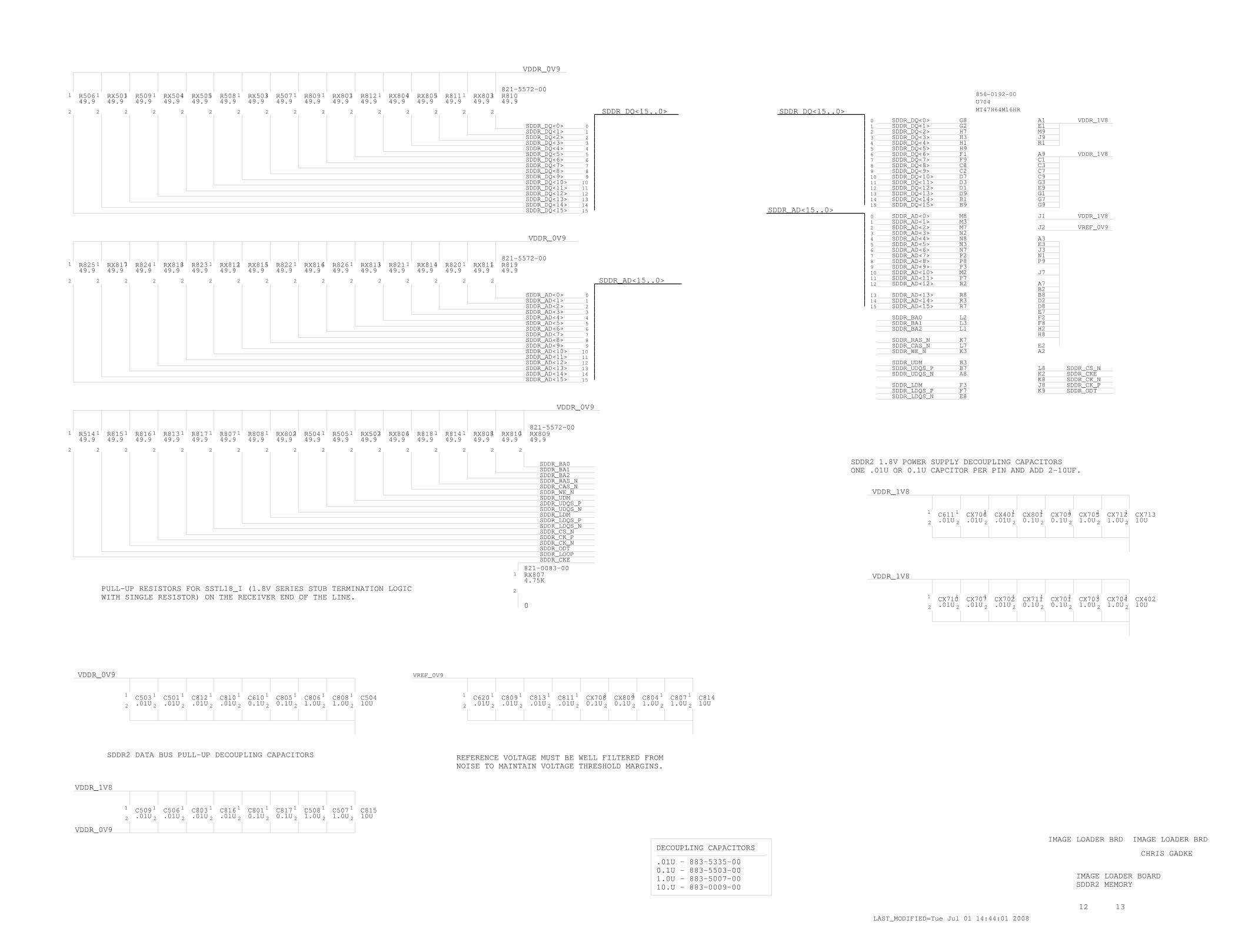
PULL-UP RESISTORS FOR SSTL18_I (1.8V SERIES STUB TERMINATION LOGICWITH SINGLE RESISTOR) ON THE RECEIVER END OF THE LINE.
SDDR2 DATA BUS PULL-UP DECOUPLING CAPACITORS
NOISE TO MAINTAIN VOLTAGE THRESHOLD MARGINS.REFERENCE VOLTAGE MUST BE WELL FILTERED FROM
SDDR2 1.8V POWER SUPPLY DECOUPLING CAPACITORSONE .01U OR 0.1U CAPCITOR PER PIN AND ADD 2-10UF.
DECOUPLING CAPACITORS
.01U - 883-5335-000.1U - 883-5503-001.0U - 883-5007-0010.U - 883-0009-00
LAST_MODIFIED=Tue Jul 01 14:44:01 2008
0
IMAGE LOADER BRD
IMAGE LOADER BOARDSDDR2 MEMORY
VDDR_1V8
SDDR_UDQS_NSDDR_UDQS_P
SDDR_CAS_N
5 SDDR_AD<5>
SDDR_RAS_NSDDR_CAS_NSDDR_WE_N
9
1213
11
1415
49.949.949.949.949.949.949.949.949.949.949.949.949.949.949.949.949.9
4.75K
821-0083-00
856-0192-00
MT47H64M16HR
01234
6789101112
131415
0.1U0.1U.01U.01U.01U.01U 1.0U 1.0U1.0U1.0U0.1U0.1U.01U.01U.01U.01U
1.0U0.1U0.1U.01U.01U.01U.01U
1.0U1.0U0.1U0.1U.01U.01U.01U
1.0U1.0U0.1U0.1U.01U.01U
0
10U
10U
10U
10U
10U
12
43
765
98
10
1211
1413
1515
49.9
821-5572-00
49.949.949.949.949.949.949.949.949.949.949.949.949.949.949.9
012
43
765
98
10
1211
1413
821-5572-00
49.949.949.949.949.949.949.949.949.949.949.949.949.949.949.949.9
210
3
54
76
8
10
IMAGE LOADER BRD
CHRIS GADKE
SDDR_LOOPSDDR_ODT
SDDR_LDM
SDDR_CS_N
SDDR_DQ<8>
SDDR_DQ<3>
SDDR_CS_NSDDR_CKE
SDDR_ODTSDDR_LDQS_N
SDDR_LDM
SDDR_UDQS_NSDDR_CK_N
SDDR_AD<6>
SDDR_AD<11>
SDDR_CK_PSDDR_AD<15>
SDDR_AD<7>
SDDR_AD<0>
SDDR_AD<10>
SDDR_AD<14>
SDDR_DQ<0>
SDDR_DQ<7>
SDDR_DQ<9>SDDR_DQ<10>SDDR_DQ<11>SDDR_DQ<12>
SDDR_DQ<15>
SDDR_DQ<6>SDDR_DQ<5>SDDR_DQ<4>
SDDR_DQ<1>
SDDR_DQ<13>SDDR_DQ<14>
SDDR_DQ<2>
SDDR_AD<13>SDDR_AD<12>SDDR_AD<11>
SDDR_AD<9>SDDR_AD<8>
SDDR_AD<6>SDDR_AD<5>SDDR_AD<4>SDDR_AD<3>SDDR_AD<2>SDDR_AD<1>
SDDR_AD<3>SDDR_AD<2>
SDDR_AD<0>
SDDR_DQ<14>
SDDR_DQ<12>SDDR_DQ<11>
SDDR_DQ<9>
SDDR_DQ<7>
SDDR_AD<7>SDDR_AD<8>SDDR_AD<9>
SDDR_AD<13>
SDDR_DQ<15..0>
SDDR_AD<15..0>
SDDR_AD<15..0>
SDDR_DQ<15..0>
SDDR_CKE
SDDR_BA0SDDR_BA1SDDR_BA2SDDR_RAS_N
SDDR_WE_NSDDR_UDM
.01U
SDDR_UDM
SDDR_BA2SDDR_BA1SDDR_BA0
SDDR_AD<15>SDDR_AD<14>
SDDR_AD<12>
SDDR_AD<10>
SDDR_AD<4>
SDDR_AD<1>
SDDR_DQ<15>
SDDR_DQ<13>
SDDR_DQ<10>
SDDR_DQ<8>
SDDR_DQ<5>SDDR_DQ<4>SDDR_DQ<3>SDDR_DQ<2>SDDR_DQ<1>SDDR_DQ<0>
SDDR_DQ<6>
VDDR_1V8
VDDR_1V8
VDDR_1V8
VDDR_0V9
VDDR_0V9
VDDR_0V9
VDDR_0V9
SDDR_LDQS_PSDDR_LDQS_N
SDDR_CK_PSDDR_CK_N
SDDR_UDQS_P
SDDR_LDQS_P
VREF_0V9
VREF_0V9
VDDR_0V9
VDDR_1V8
VDDR_1V8
1.0U
R8101
2
RX8031
2
R8111
2
RX8051
2
RX8041
2
1
2
RX8011
2
R8091
2
R5071
2
RX5031
2
R5081
2
RX5051
2
RX5041
2
R5091
2
RX5011
2
R5061
2
R8191
2
RX811
2
R8201
2
RX8141
2
R8211
2
RX8131
2
R8261
2
RX8161
2
R8221
2
RX8151
2
RX8121
2
R8231
2
RX8181
2
R8241
2
RX8171
2
R8251
2
RX8091
2
RX8101
2
RX8081
2
R8141
2
R8181
2
RX8061
2
RX5021
2
R5051
2
R5041
2
RX8021
2
R8081
2
R8071
2
R8171
2
R8131
2
R8161
2
R8151
2
R5141
2
RX8071
2
U704
M8M3
M2P7R2
M7N2N8N3N7P2P8P3
L2L3L1
L7
J8K8K2L8
G8G2
D7D3D1D9B1B9
H7H3H1H9F1F9C8C2
F3F7E8
A2E2
K9
K7
R8R3R7
B3B7A8
A1E1M9J9R1
J1
A9C1C3C7C9G3E9G1G7G9
J2
A3E3J3N1P9
J7
A7B2B8D2D8E7F2F8H2H8
K3
CX8091
2CX7081
2C8111
2C8131
2C8091
2C6201
2C8041
2C8071
2C8081
2C8061
2C8051
2C6101
2C8101
2C8121
2C5011
2C5031
2
C5071
2C5081
2C8171
2C8011
2C8161
2C8031
2C5061
2C5091
2
CX7121
2CX7051
2CX7091
2CX8011
2CX4011
2CX7061
2C6111
2
CX7041
2CX7031
2CX7011
2CX7111
2CX7021
2CX7071
2CX7101
2
CX7131
2
CX4021
2
C5041
2
C8151
2
C8141
2
R812
1
12 13
821-5572-00
DRAWING
RANK XEROX LTD./FUJI XEROX CO.LTD. BE REPRODUCED, COPIED OR USED FORWITHOUT THE PRIOR WRITTEN PERMISSION OF XEROX CORPORATION AND/OR
DATE:
CORPORATION AND/OR RANK XEROX LTD./FUJI XEROX CO. LTD.ANY PURPOSE WHATSOEVER, EXCEPT THE MANUFACTURE OF ARTICLES FOR XEROX
SIZE
SHEET
DESCRIPTION
TITLE
OF
ENGINEER
ABBREV
REV.
10
1 2 3 4 6 7 1098
8
H
G
F
E
B
C
A
97654321
A
F
E
G
H
D
C
B
D
ARE THE EXCLUSIVE PROPERTY OF XEROX CORPORATION AND/OR RANK XEROXLTD./FUJI XEROX CO.,LTD. ISSUED IN STRICT CONFIDENCE AND SHALL NOT,
THESE DRAWINGS AND SPECIFICATIONS,AND THE DATA CONTAINED THEREIN,
5
NC[0]NC[1]
VSSQ[9]VSSQ[8]
VSSQ[6]VSSQ[7]
VSSQ[4]VSSQ[5]
VSSQ[3]VSSQ[2]VSSQ[1]VSSQ[0]
VSSDL
VSS[4]
VSS[1]VSS[2]VSS[3]
VSS[0]
VREF
VDDL
VDDQ[8]VDDQ[9]
VDDQ[6]VDDQ[7]
VDDQ[5]VDDQ[4]VDDQ[3]VDDQ[2]VDDQ[1]VDDQ[0]
VDD[4]
VDD[2]VDD[1]
VDD[3]
VDD[0]
RFU3RFU2RFU1
LDQS*
LDMLDQS
UDQS*UDQSUDM
WE*CAS*RAS*
BA2BA1BA0
CS*CKECK*CK
ODT
DQ0DQ1DQ2DQ3DQ4DQ5DQ6DQ7DQ8
DQ10DQ9
DQ11DQ12DQ13DQ14DQ15
A0A1A2
A4A3
A5A6A7A8A9A10A11A12

(LCD_DB0)(LCD_E)(LCD_RW)
LCD MODULE CONN.
AUX LCD DRIVE ADAPTER
(BANK 0)(TO FPGA)
(TO FPGA)(BANK 2)
(SERIAL-TX)(SERIAL-RX)
(LCD_DB7)
(LCD_DB5)
(LCD_DB3)(LCD_DB4)
(LCD_DB2)(LCD_DB1)
(LCD_DB6)
BASICX COM PORT
BASICX MICROCONTROLLER
BASICX MICRO
C 0
IMAGE LOADER BOARD
CURT KELLER
86N0661XB
13 13
BASIC X MICROCONTROLLERTHERMAL AND LCD DRIVE CONTROL
(LCD_RS)
DO NOT STUFF
DO NOT STUFF
LAST_MODIFIED=Wed Jul 09 09:45:29 2008
C316
883-5353-0022
AUX-LCD<1..7>
11
2.00KR502821-5422-00
C505883-0009-0010UFC502
VCC=POS5V;GND=GND
2
C315
883-5353-00
BASICX-ATNBASICX-RX
821-5415-00
VCC=VDD;GND=GND
R36974LVT245U402856-7332-001
16
831-3271-00
VCC=POS5V;GND=GND
RES_SSRRIGHT_SSRLEFT_SSR
850-5024-00
4.99KR378
831-1857-00J605M6123456
RES_TEMP
JET_RIGHT_TEMP
JET_LEFT_TEMP
BASICX-AD<1..5>
1234
5
6
7
8
BASICX<1..8>
19
883-5353-00
13
1
2345
POS5V
U41424
1
821-5415-00R365 0
14
17
821-5415-00
205
23
10
78
R366R367
883-5503-00
821-5550-00
BASICX-TX
BASICX-RX
BASICX-ATN
59
8
6
4
2
1
D92GND
831-3925-00
73
0
TITAIPAN INTERFACE
R213475
DS203
R212475
DS202
475
821-5420-00R211
LED1DS201
R3774.99K
R376
M41
43
J200
2
C416
0.1UF
C418
0.1UF883-5503-00
45
3
1112
1516
9
1
218
6
0R368
C4190.1UF
821-5024-00
R4190
856-0266-00SN74LVC1G126
1
4 2U410
1
4 2U411
1
4 2U412
1
4U413
1.00KR209
821-5421-00
4
BASICX24U305
SKT
12
1819
15142
324
76
8
17
11
9
836-0751-00
156-VBASICX24
13
21
0.1UF
3
S201
21 4
0.1UF
J405831-1857-00M512345
POS5V
POS5V
POS5V
POS5V5VREF
VDD
POS5V
POS5V
POS12V
5VREF
POS5V
BASICX-TX
J907
4.99K
0R501
1 2
1
2
883-5335-00
2
1
0.01UF
4
23
7
56
1100
2
821-5417-00R503
2
1 2
R511
R513
1 22
R512
1
1 2
R517
1 2
R515
0
1 2
R518R519
1 2
821-5454-00
R521
1 2
332
1
831-1857-00
M16J501
10111213
1516
23456789
14
1
MTMH510C305MH301
MH601
1
MTMH510C305
MTMH510C305MH501
1
MTMH510C305MH201
1
POS5V
RANK XEROX LTD./FUJI XEROX CO.LTD. BE REPRODUCED, COPIED OR USED FORWITHOUT THE PRIOR WRITTEN PERMISSION OF XEROX CORPORATION AND/OR
DATE:
CORPORATION AND/OR RANK XEROX LTD./FUJI XEROX CO. LTD.ANY PURPOSE WHATSOEVER, EXCEPT THE MANUFACTURE OF ARTICLES FOR XEROX
SIZE
SHEET
DESCRIPTION
TITLE
OF
ENGINEER
ABBREV
REV.
10
1 2 3 4 6 7 1098
8
H
G
F
E
B
C
A
97654321
A
F
E
G
H
D
C
B
D
ARE THE EXCLUSIVE PROPERTY OF XEROX CORPORATION AND/OR RANK XEROXLTD./FUJI XEROX CO.,LTD. ISSUED IN STRICT CONFIDENCE AND SHALL NOT,
THESE DRAWINGS AND SPECIFICATIONS,AND THE DATA CONTAINED THEREIN,
5
DRAWING
16
27
38
49
5
COM1TRCOM1RATNVIN
VCCGNDGND1
PA0PA1PA2PA3PA4PA5PA6PA7
PC7
RES
PC0PC1PC2PC3PC4PC5PC6
A4A5
A3A2A1
A6
DIROE
A7A8
B1B2B3B4B5B6B7B8