immunity development system e 1 - langer emv … e1 user...1 description of the e1 immunity...
TRANSCRIPT

2016.08.15. E1 user manual
User manual
Immunity development system
E 1
How to make a DUT immune to interference
through measurement and modification at the development stage
Copyright (C) Dipl.- Ing. Gunter Langer Nöthnitzer Hang 31 01728 Bannewitz 10.04.2014

- 2 -
LANGER EMV-Technik
DE-01728 Bannewitz
www.langer-emv.de E1
Table of contents: Page
1 Description of the E1 immunity development system 3
2 Description of the E1 components 4
2.1 SGZ 21 pulse density counter / burst generator 5
2.1.1 SGZ 21 as a disturbance generator 5
2.1.2 SGZ 21 as a pulse density counter 6
2.1.3 Preparing the SGZ 21 as a disturbance generator 6
2.1.4 Preparing the SGZ 21 as a pulse density counter and for signal monitoring 7
2.2 Field sources 8
2.2.1 Field sources for magnetic fields 8
2.2.2 Field sources for electric fields 9
2.2.3 Measurement set-up with SGZ 21 to inject burst current with field sources 11
2.3 Sensor 11
2.3.1 Principal mode of operation of the sensor 12
2.4 Magnetic field probes 13
3 The pulse density method 14
4 Prerequisites for interference suppression in a device under test 17
5 Measurement strategies for interference suppression in a device under test 17
5.1 Analysis of the interference current paths 19
5.1.1 Basic principle of magnetic coupling – two-pole injection into the DUT 19
5.1.2 Basic principle of electric coupling – single-pole injection into the DUT 24
5.2 Localisation of weak points with field sources 26
5.2.1 Mechanism of action behind magnetic field coupling 27
5.2.2 Mechanism of action behind electric field coupling 28
5.2.3 Practical procedure for coupling with magnetic field sources 29
5.2.4 Practical procedure for coupling with electric field sources 34
5.3 Monitoring of logic signals from the device under test 39
5.3.1 Use of the pulse density method to evaluate immunity levels 40
5.3.2 Monitoring of logic signals from the device under test 41
5.4 Measurement of burst-related magnetic fields 42
6 Safety instructions 44
7 Warranty 44
8 Technical specifications 45
9 Scope of delivery 46
10 Optional components 47
10.1 S2 magnetic field probe set 47
10.2 Digital or analog optical signal transmission 48

- 3 -
LANGER EMV-Technik
DE-01728 Bannewitz
www.langer-emv.de E1
1 Description of the E1 immunity development system
The E1 immunity development system is an advanced tool for the electronics developer to examine the
immunity of modules to pulsed interference (burst/ESD) in experiments. The system allows him to analyse
the interference immunity in the confined space of a module. The selective injection of disturbance current
into individual sections (disturbance current paths) and application of pulsed electric (E fields) or magnetic
(H fields) fields to selected areas of the module's surface are decisive for the localisation of weak points.
While pulsed disturbances are applied to the device under test, the signals can be monitored
simultaneously via optical fibre without interaction.
The E1 immunity development system has been specially designed for the development process. It helps
the developer suppress interference in devices/modules or further harden them since it allows him to
clarify the immediate causes of immunity problems and test the effects of counter-measures directly.
The E1 immunity development system cannot be used for standard compliance tests. Testing a module's
immunity on the basis of the IEC 61000-4-4 and IEC 61000-4-2 standards, however, is an ideal starting point
for examining the device under test with the E1. The disturbances generated by the standard burst
generator in accordance with the standard are injected into the supply lines of the device under test and
flow back to the generator via ground. The paths on which the pulse-shaped disturbances flow through the
device module are not known. An unknown percentage of these disturbances encounters an unknown
victim in the device and generates a functional fault. This weak point can usually be pinpointed to a few
square centimetres of a module but can only be localised with difficulty in a standard compliance test. The
developer does not yet know if and where the disturbance current with its associated magnetic field
induces a voltage pulse in a conductor loop or couples electric field capacitively to sensitive lines.
Exact information about the fault pattern that has occurred is the decisive result of a failed compliance test.
But the fault pattern does not reveal precisely where the weak point of the device under test lies. A test in
accordance with the standard should thus initially be performed to determine the immunity of the device
under test so as to identify the fault pattern. The developer can then use the E1 at his workplace to analyse
the causes of the immunity problems, where the functional faults shown in the fault pattern provide a
certain orientation for interference suppression.
The immunity development system allows the developer to verify the effectiveness of EMC modifications
carried out in the interference suppression process immediately and thus to achieve a significant reduction
in the development time and development costs.

- 4 -
LANGER EMV-Technik
DE-01728 Bannewitz
www.langer-emv.de E1
2 Description of the E1 components
The E1 immunity development system comprises a SGZ 21 pulse density / burst generator, an S21 optical
sensor, an MS 02 magnetic field probe with optical fibre output, magnetic and electric field sources and
numerous accessories.
Figure 1: E1 hardware scope of delivery.

- 5 -
LANGER EMV-Technik
DE-01728 Bannewitz
www.langer-emv.de E1
2.1 SGZ 21 pulse density counter / burst generator
The SGZ 21 (Figure 2) is a burst generator with potential-free pulse generation on the one hand, and on the
other hand the SGZ°21 is also a pulse density counter to measure the disturbance pulses of the device
under test.
Figure 2: SGZ 21 pulse density counter / burst generator.
Generator ON/OFF: to switch the SGZ 21 on or off
Intensity: potentiometer to gradually adjust the intensity of the disturbance pulses
Pulse shape: toggle switch to change between steep and flat pulses
Counter display: six-digit counter to measure the pulse density
SIGNAL LED display: to indicate the received light signal
SPIKE LED display: to indicate the received light signal with pulse trap; the pulse is stretched to a visible
width of 50 ms
Burst output: symmetric output galvanically isolated from ground
Counter's optical fibre input: input socket for 2.2 mm plastic optical fibre
The power supply is located on the left side of the generator. A 12 V power supply unit is included in the
scope of delivery.
2.1.1 SGZ 21 as a disturbance generator
The SGZ 21 generates potential-free, pulse-shaped disturbances whose edges have a rise time of approx.
2 ns and a fall time of approx. 10 ns. In contrast, a standard generator generates pulse shapes of 5/50 ns.
The SGZ 21's smaller pulse width prevents the device under test from being destroyed. Furthermore,
working at a lower disturbance voltage level ensures greater safety for the engineer.
The SGZ 21 allows partial injection into structural parts, cables, shielding, earth connections and primarily
directly into the modules. The disturbance current of the SGZ 21 is generated via a differential output.
Consequently, the generated pulsed current does not relate to the generator housing potential.

- 6 -
LANGER EMV-Technik
DE-01728 Bannewitz
www.langer-emv.de E1
The path that the disturbance current takes through the device under test can be defined by contacting the
device under test accordingly. Disturbance current can thus be injected into defined sections of the module
without significantly influencing the environment.
The peak values of the disturbance pulses are between 0 and 1500 volt. They are constantly changed but
are stochastically evenly distributed.
- The SGZ 21 has a symmetric output that is galvanically isolated from ground. The disturbance pulses are
coupled out capacitively with alternating polarity.
- The pulse shape toggle switch of the SGZ 21 can be used to change over between steep and flat pulses
to adjust the disturbance effect.
2.1.2 SGZ 21 as a pulse density counter
A counter with an optical input (2.2 mm plastic optical fibre) is integrated in the SGZ 21 (Figure 2). A sensor
that is located in the device under test (Chapter 0) or a magnetic field probe transmits light pulses to the
SGZ 21 counter via an optical fibre and the optical input. The received light pulses are initially displayed by
the "Signal" and the "Spike" LEDs and then counted by the counter. The counter's peak time is 1 s.
Using the pulse density method (Chapter 3) allows a very fast assessment of the sensitivity of a device
under test.
The SGZ 21 can be operated standing perpendicular on its rear so that you can easily read the counter from
above – e.g. when working standing up.
2.1.3 Preparing the SGZ 21 as a disturbance generator
Generator cables and connecting terminals are needed to operate the SGZ 21 as a disturbance generator.
The generator cables are connected to the SGZ 21 output sockets via the 4 mm plug (banana plug). The
generator cables (Figure 3) end in two-pole 0.64 mm plug pins. Both pins are connected to the core of the
cable. Only one plug pin of each generator cable is used to connect the 250 mm long extension cable
(Figure 5).
The connection to the device under test is via alligator clips or micro-kleps (miniature clamp-type test
probes with rotating grip jaws) (Figure 4). The field sources contained in the E1 system can be connected
directly to the extension cables as required.
Figure 3: Generator cables (bottom); two extension cables (top).

- 7 -
LANGER EMV-Technik
DE-01728 Bannewitz
www.langer-emv.de E1
2.1.4 Preparing the SGZ 21 as a pulse density counter and for signal monitoring
The optical fibre has to be inserted into the input up to the limit stop and fastened with the knurled screw
(Figure 6).
Figure 4: Alligator clips on the left and micro-kleps on the right.
Figure 5: SGZ 21 with generator cables plus an alligator clip and a micro-klep.
Figure 6: Optical fibre connection on the SGZ 21.

- 8 -
LANGER EMV-Technik
DE-01728 Bannewitz
www.langer-emv.de E1
2.2 Field sources
The field sources are supplied with disturbance current from the SGZ 21 and generate either pulsed
magnetic or electric fields depending on the type of field source used. The field intensities of these pulsed
fields are comparable to those generated by burst currents on the surface of modules during standard
compliance tests. The field sources can be used to subject small areas of the device under test or individual
conductor runs to defined disturbances.
The field sources contained in the E1 system are optimised so that they generate either a magnetic field or
an electric field. Furthermore, the field sources are of different sizes, allowing the developer to apply the
pulsed field to differently dimensioned areas on the module. In addition, there are special field sources for
specific tasks such as magnetic field sources that couple to conductors via a specially shaped field.
Different types of probe heads are offered that are designed for certain measurement tasks. They allow the
developer to pinpoint weak points to the millimetre or to search for critical links and connections such as
components, conductor runs or IC pins on the defined interference path. The sensitivity of different IC pins
can be assessed. Following localisation, the sensitive areas can be treated in a specific way.
E-field-sensitive weak points cannot be identified with H-field sources. Special E-field probes have to be
used to localise these weak points. Apart from conductor run sections, high-resistance components such as
pull-up resistors or quartz generators may also prove critical in this respect.
2.2.1 Field sources for magnetic fields
The E1 contains four field sources which are able to generate magnetic fields. Thanks to the probe head's
various designs, two types of measurements can be performed:
a) Determination of an IC pin's / conductor's sensitivity irrespective of whether a layout-related disturbance
is conducted to the IC. This measurement provides the developer with an overview of which IC pins and/or
conductor runs are sensitive in general.
b) Localisation of weak points in the layout
The disturbance fields applied from outside during the standard compliance test couple to the module's
conductor runs at weak points in the layout. The disturbances are passed on to the IC via the conductor
runs. The disturbance process triggered by the standard compliance test on the module is generally due to
electric and magnetic field coupling. The E1 system contains field sources which have been custom-
developed to simulate these field coupling phenomena for fault localisation.
Field pattern Use Design
BS 02 is a field source to localise weak points in the layout. The
magnetic field source produces a B-field line bundle with a
diameter of > 5 cm. It is suitable for investigations on both
devices and modules. The size of the probe allows the developer
to apply the field to large areas of housing surfaces and inner
spaces, connecting elements and modules with conducting
structures as well as ICs to identify weak points that are sensitive
to magnetic fields.

- 9 -
LANGER EMV-Technik
DE-01728 Bannewitz
www.langer-emv.de E1
BS 04DB is a field source to localise weak points in the layout. It
generates a B-field line bundle in the millimetre range
(approx. 3 mm). The field beam emerging from the probe's face
can be used to scan the surface of circuit boards and resolve
magnetically sensitive weak points in small spaces of 3 mm in the
field of layout and packaging. The BS°04DB allows the localisation
of critical conductor run sections, components and component
connections.
BS 05D is a field source to localise weak points in the layout. The
magnetic field source generates a B-field line bundle with a
diameter of approx. 3 mm similar to the BS 04 DB. But the field
lines are at an angle of 90° to the probe shaft. The probe is thus
ideal to localise weak points between two printed circuit boards
or in hard-to-reach locations of modules between components,
for example. Before using the BS 05D field probe, the weak point
should be roughly narrowed down with the BS 02 or BS 04DB
probe.
BS 05DU is a field source that can be used to determine an
individual IC pin's/conductor's sensitivity. The magnetic field source
generates a circular magnetic field in the millimetre range. It can
also be used as a mini coupling clamp to couple disturbance current
into selected individual conductor runs, IC pins, SMD devices and
thin lines (ribbon cable). A module often has several insensitive and only a few sensitive
signal connections (conductor runs, IC pins). The field source is
the ideal tool to quickly identify the sensitive ones and carry out
appropriate layout modifications.
2.2.2 Field sources for electric fields
The E1 contains five field sources which are able to generate electric fields. Thanks to the probe head's
various designs, two types of measurements can be performed:
a) Determination of an IC pin's/conductor's sensitivity
b) Localisation of weak points in the layout
The size of the coupling electrode in the probe head is the field sources' distinguishing feature.
ES 08D is a probe tip that can be used to determine an
individual IC pin's/conductor's sensitivity. A galvanic isolating
point with capacitive coupling of approx. 1 pF is contained in
the probe tip which is ideal for very small structures. The
pin/conductor run is contacted with the probe tip and its
sensitivity determined by changing the intensity on the
SGZ 21 ("Intensity" controller) in the test. The field source has
to be connected via two poles. One conductor is connected to
the probe tip via a coupling capacitance of 1 pF. The second
conductor is connected to a counter-electrode, preventing
disturbance current from flowing through the device under
test unintentionally and thus affecting other areas.
Connection: two-pole

- 10 -
LANGER EMV-Technik
DE-01728 Bannewitz
www.langer-emv.de E1
ES 05D is a field source that can be used to determine the
sensitivity of an IC pin/conductor or individual components.
The E-field source has a narrow line-shaped coupling
electrode in its probe head. This design makes it ideal for
being placed on conductor runs and small components and
their connections, wires and individual SMD components such
as resistors and capacitors. Individual plug contacts or cores
of ribbon cables can also be examined. The probe is placed on
the component/conductor run to inject the E-field.
Connection: two-pole
ES 02 is a field source to localise weak points in the layout.
The size of the field source allows the developer to couple the
field to large areas of housing surfaces and inner spaces,
connecting elements and components with conducting
structures and ICs (e.g. bus systems, LCD displays). The tip of
the E-field source can be used to localise small weak points
that are sensitive to E-field (conductor runs, quartz crystal
oscillators, pull-up resistors, ICs).
Connection: two-pole
ES 01 is a field source to localise weak points in the layout.
The field source allows electric coupling to large areas. The
probe is ideal for applying an electric field to extensive or
line-shaped weak points with a size of 5 to 10 cm and ranks
between the ES 02 and ES 00 field sources (please refer to the
corresponding description). The ES 02 may be too small and
the ES 00 source too large for certain purposes. The ES 01 can
also be used to couple disturbance current to a module. The
intensity of the disturbance current can be controlled by the
distance between the probe and the module.
Connection: single-pole
ES 00 is a field source to localise weak points in the layout.
The field source allows electric coupling to large-area or line-
shaped structures (150 cm²). Electrically sensitive weak points
often extend over large areas from 10 to 15 cm of a module
(LCD display, bus systems). These weak points do not respond
to small field sources. Large-area field sources such as the
ES 00 are needed to identify this type of weak points. The
source can also be used for coupling to housings. The ES 00
can also be used to couple disturbance current to a module.
The intensity of the disturbance current can be controlled by
the distance between the probe and the module.
Connection: single-pole
Key to designations
Example: BS 04 DB
Type of field Size Attenuation Special field shape
BS Field source for magnetic
field
ES Field source for electric
field
00
01
02
D Common-mode
attenuation
B Bundled field lines
U Circular field

- 11 -
LANGER EMV-Technik
DE-01728 Bannewitz
www.langer-emv.de E1
2.2.3 Measurement set-up with SGZ 21 to inject burst current with field sources
The field sources are connected directly to the "Burst output" (Figure 2) of the SGZ 21 via the generator and
extension cables. Magnetic field sources are always connected via two poles (Figure 7).
Apart from the field sources themselves, the connecting cables also generate fields that may couple to the
device under test and affect the measurement result. Cables should thus always be kept away from the
device under test if possible.
2.3 Sensor
The S21 sensor (Figure 8) is a digital probe head to transmit binary signals from the device under test. The
sensor has a three-pin shrouded header (RM 2.5 mm). One pin of the shrouded header is the 3.5 V auxiliary
power supply. The second pin is the ground pin. The third pin is the input of the probe head. The sensor
input is connected internally to a digital IC input. This is connected to digital signals, VCC (</= 5 V) and
ground inside the device under test. The IC output supplies an optical transmitter. The transmitter is
connected to a 2 mm conical socket to accommodate a 2.2 mm plastic optical fibre (LWL). The light signals
from the sensor are transmitted to the "LWL" counter input of the SGZ 21 via an optical fibre.
The level changeover switch allows the signal to be negated.
The sensor can be used in two different ways:
a) to detect logic signals in the device under test
b) to detect disturbances in the device under test
to a) It is helpful if important signals (Reset, CE) of the device under test are monitored so as to find the
causes of problems in immunity investigations with the SGZ 21. When using a conventional oscilloscope
probe head, the disturbances are led to the oscilloscope via the probe head. The disturbances would affect
the oscilloscope. In addition, the probe head would change the disturbance current paths of the device
under test and thus falsify the measurement results. This is the reason why probe heads with an optical
fibre connection have to be used. The S21 sensor is such a probe head.
to b) The IC input of the S21 sensor has an immunity level that can be used to detect disturbances in the
device under test.
Figure 7: SGZ 21 with BS°04DB magnetic field source.
Depending on their type,
field sources for electric
fields are connected via one
pole or two poles (Figure 31).

- 12 -
LANGER EMV-Technik
DE-01728 Bannewitz
www.langer-emv.de E1
Figure 8: S21 Sensor
Pulse stretching
The S21 sensor of the E1 can detect fast transient disturbances. The pulse widths of these disturbances may
be in the nanosecond range. Due to the low limit frequency of the optical system (5 MHz), such short
disturbances cannot be transmitted. A pulse stretching circuit which stretches short pulses to 100 ns is
integrated in the sensor. The optical fibre is then able to transmit these pulses. Neither can the optical
system of the sensor transmit frequencies above 5 MHz. The same sensor circuit reduces frequencies >
5 MHz to 5 MHz.
Without this circuit, the optical system would not be able to transmit anything. It would assume a high or low state.
The circuit ensures that fault states are transmitted from the device under test.
2.3.1 Principal mode of operation of the sensor
The sensor is integrated in the device under test and connected to the line of interest. A three-pole socket
(included in the scope of delivery) is glued to the device under test with super glue in the immediate
vicinity of the interesting signal line, if possible at the input, and wired with a short CuL wire; the ground, 3-
5 V voltage and sensor input are also wired before the sensor is connected (Figure 9). The wiring should be
short and laid directly on the module's surface so as to prevent the formation of loops where magnetic or
electric fields could couple in.
The S21 sensor is supplied with a 3 to 5 volt voltage from the device under test. If this is not possible, a
battery module can be used (not included in the scope of delivery).
Figure 9: S21 sensor connected to an IC in the device under test, for example, via a three-pole socket.

- 13 -
LANGER EMV-Technik
DE-01728 Bannewitz
www.langer-emv.de E1
2.4 Magnetic field probes
The magnetic field probe is used to measure burst-related magnetic fields in the device under test.
The disturbance current i of the SGZ 21 generates a magnetic field B. The magnetic field which penetrates
the probe head induces a voltage in the probe head's induction coil. The voltage drives an optical
transmitter diode that is located in the MS 02 probe shaft (Figure 10).
Each disturbance pulse of the SGZ 21 causes a light pulse of the optical transmitter diode. The transmitter
diode has a 2.2 mm conical socket and is integrated in the MS 02 probe shaft. An optical fibre is guided
from the rear end of the MS 02 probe shaft through to the socket of the transmitter diode. The light pulse
is transmitted to the SGZ 21 in the same way as with the S21 sensor (Chapter 2.3). The measurement of the
magnetic field is based on the pulse density method (Chapter 3).
Figure 10: Measuring a magnetic field with the MS 02 probe.
Fields which penetrate the probe's induction coil in the orthogonal direction induce a voltage. Fields whose
direction coincides with the coil plane do not induce a voltage and are thus not detected. The maximum
voltage corresponds to the direction of the magnetic field (Figure 11). The MS 02 magnetic field probe is
used to determine the field distribution. The probe emits a light pulse for each magnetic field pulse which is
detected. The value shown on the SGZ 21 counter is proportional to the mean magnetic field strength
measured (Chapter 3, pulse density method). The field line configuration and field density are indicative of
the disturbance current distribution in the device under test.
The MS 02 is a passive probe and does not require any auxiliary power. The power needed to generate the
light pulses is taken from the burst-related magnetic field. The MS 02 is connected to the SGZ 21 counter
input via an optical fibre.
Figure 11: The MS 02 magnetic field probe can detect a magnetic field which is orthogonal to the probe
opening/probe shaft.

- 14 -
LANGER EMV-Technik
DE-01728 Bannewitz
www.langer-emv.de E1
3 The pulse density method
The pulse density method is a measuring method which can be used to determine the relative immunity of
a device under test. The effect of EMC modifications can be evaluated based on the relative immunity.
Furthermore, the pulse density method is the basis for measuring burst-related magnetic fields with MS 02
magnetic field probes and the optional S2 magnetic field measuring system (Chapter 10).
Figure 12: Ramp-like rise of the SGZ 21 disturbance pulses. The immunity level is exceeded n times at
different immunity level voltages u.
Figure 12 shows how the pulse density method functions in principal. The voltage u of the disturbance
pulses gradually rises from a minimum value to a maximum value up a ramp over the time T = 1 s. This
process is continuously repeated.
If the disturbance pulses encounter an immunity level u1 in the device under test, the disturbance pulses
which are greater than u1 will exceed the immunity level u1. This is n = 11 pulses in the example. If the
device under test has a higher immunity level, u3, for example, n = 3 pulses will exceed the immunity level.
The number of pulses which exceed the immunity level is inversely proportional to the value of the
immunity level.
This principle can be implemented with the E1 components, i.e. the SGZ 21 and the S21 sensor or the
MS 02 magnetic field probe.
The SGZ 21 generates disturbance pulses which are injected into the device under test. The S21 sensor is
used to create an immunity level in the device under test. If the immunity level of the S21 sensor is
exceeded, a light pulse is transmitted to the SGZ 21 counter via optical fibre. The counter counts how often
the immunity level is exceeded. Depending on the immunity level, the value in the aforementioned
example is: n = 3, n = 7, n = 11. These values are proportional to the immunity of the device under test
relative to the immunity level of the sensor.
This means: the immunity of the device under test is high at n = 3 and the immunity of the device under
test is low at n = 11.
The pulses that are counted in practice may be in the range between 0 and 3,000. A low value is indicative
of a high immunity while a higher value is indicative of a low immunity.
- 15 -
LANGER EMV-Technik
DE-01728 Bannewitz
www.langer-emv.de E1
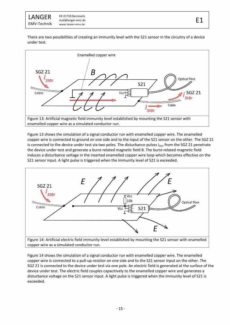
There are two possibilities of creating an immunity level with the S21 sensor in the circuitry of a device
under test.
Figure 13: Artificial magnetic field immunity level established by mounting the S21 sensor with
enamelled copper wire as a simulated conductor run.
Figure 13 shows the simulation of a signal conductor run with enamelled copper wire. The enamelled
copper wire is connected to ground on one side and to the input of the S21 sensor on the other. The SGZ 21
is connected to the device under test via two poles. The disturbance pulses iStör from the SGZ 21 penetrate
the device under test and generate a burst-related magnetic field B. The burst-related magnetic field
induces a disturbance voltage in the inserted enamelled copper wire loop which becomes effective on the
S21 sensor input. A light pulse is triggered when the immunity level of S21 is exceeded.
Figure 14: Artificial electric field immunity level established by mounting the S21 sensor with enamelled
copper wire as a simulated conductor run.
Figure 14 shows the simulation of a signal conductor run with enamelled copper wire. The enamelled
copper wire is connected to a pull-up resistor on one side and to the S21 sensor input on the other. The
SGZ 21 is connected to the device under test via one pole. An electric field is generated at the surface of the
device under test. The electric field couples capacitively to the enamelled copper wire and generates a
disturbance voltage on the S21 sensor input. A light pulse is triggered when the immunity level of S21 is
exceeded.

- 16 -
LANGER EMV-Technik
DE-01728 Bannewitz
www.langer-emv.de E1
Figure 15: Natural immunity level by placing the S21 sensor on a signal conductor run of the device
under test.
An original conductor run of the device under test is used for the same process in Figure 15. The pulse
density method can be used with the set-up shown in Figure 13 if high-frequency signal sequences pass
through this signal line.
In the SGZ 21, the pulse sequence is not ordered as a ramp according to the amplitude as shown in Figure
12; rather the amplitude u of the pulse sequence is distributed stochastically.
Figure 16: The SGZ 21 generates the pulses continuously in an unordered sequence.
The generator and counter do not have to be synchronised. The start time does not affect the result. The
number of pulses measured depends on both the device under test and the "Intensity" controller setting.
The system works at its optimum if the greatest number of pulses does not exceed the value 2,000. The
intensity should be reduced if necessary.

- 17 -
LANGER EMV-Technik
DE-01728 Bannewitz
www.langer-emv.de E1
4 Prerequisites for interference suppression in a device under
test
The immunity values and fault patterns which occurred when the device under test was subjected to
disturbances in a standard compliance test are a good basis for working with the E1. The E1 immunity
development system can now be used to clarify where exactly the weak points associated with these faults
are in the device under test. Appropriate counter-measures can be selectively integrated and their
effectiveness tested with the E1.
When working with the E1, the developer simulates the coupling paths from the standard compliance test
and runs a targeted search for the respective fault patterns from the test. Please note that the E1 can be
used for coupling at such high intensities that fault patterns become visible which did not occur in the
standard compliance test and which the developer should not try to trace at this time. The developer must
always compare the fault patterns triggered with the E1 to the fault patterns that occurred in the standard
compliance test to stay on track. Passing the standard compliance test is the key objective. In addition, the
developer can use the E1 to further harden the product.
The following issues should be clarified:
- Which malfunction occurs as of which voltage?
- Does the malfunction occur immediately or only after a certain time (statistics)?
- Is the fault exactly the same in each measurement or are there any differences?
- Which differences result from modifying the cable position, for example?
- Do other faults occur less frequently, for example, along with the known malfunctions?
After this initial analysis of malfunctions, the developer should try to find a logical explanation for how the
faults occur. This malfunction theory should run as a common thread through all subsequent work. The
developer should check and adjust this theory continuously during the entire measurement process.
The process aims at finding a relationship between a certain coupling path and the traced malfunction. The
developer should then narrow down the fault using the E1 measurement technology. The type of
malfunction caused and the required disturbance intensity are always the decisive criteria for a coupling
path's degree of relevance.
The key factor for successful measurements with the E1 is that the developer concentrates on following the
common thread of testing on the basis of fault patterns.
5 Measurement strategies for interference suppression in a
device under test
Disturbance currents flow through the modules of a device under test during a burst test (Figure 17). The
major share of the disturbance current flows via the low-impedance supply system.
There are two basic principles of interference:
1. Disturbances via magnetic field – two-pole connection to the device under test using the SGZ 21
(Figure 17)
If the disturbance current enters the device under test (printed circuit board) via a conductor during a burst
test and also leaves the device under test via a conductor, a disturbance current flows in a closed circuit
from the generator and back to this via the device under test (printed circuit board). The disturbance
current generates magnetic fields on the printed circuit board.

- 18 -
LANGER EMV-Technik
DE-01728 Bannewitz
www.langer-emv.de E1
These fields produce voltage differences in the ground system of the device under test (printed circuit
board) and/or induce voltages in signal line loops. Such voltages in signal line loops can be induced on the
circuit board or in connecting systems between the circuit boards.
2. Disturbances via electric field – single-pole connection to the device under test using the SGZ 21
If the disturbance current enters the device under test (printed circuit board) via a conductor during a burst
test and leaves it capacitively via an electric field, an electric disturbance field is generated on the surface of
the printed circuit board. An electric field is also generated at galvanic isolating points in the device under
test.
This process results in disturbance voltages between the modules and structural parts or relative to the
ground plane in the device under test. Due to the differential voltage between the module and the
surrounding metallic parts, electric fields are generated at the surface of the printed circuit board. These
fields couple to conductor runs, pins and components and may interfere with the connected ICs.
Figure 18: Single-pole injection of current ist into the device under test with the SGZ 21 generates an
electric field relative to the ground reference plane.
Figure 17: Disturbance current paths in the device under test during a burst test.

- 19 -
LANGER EMV-Technik
DE-01728 Bannewitz
www.langer-emv.de E1
The different tools included with the E1 allow four measurement strategies to clarify even the most
complex of EMC immunity faults.
5.1 - Analysis of the interference current paths; injection directly into the printed circuit board with
the SGZ 21 generator
5.2 - Localisation of weak points in the layout and components using field sources
5.3 - Monitoring of critical logic signals of the printed circuit board
5.4 - Measurement of the burst-related magnetic fields to trace the disturbance current
The faults are narrowed down in systematic steps. The first step is always the analysis of the interference
current paths and a reproduction of the fault patterns from the standard compliance test. Different
measurement strategies (5.2 to 5.4) can be applied depending on the behaviour of the device under test
and the developer's own theory about this behaviour.
5.1 Analysis of the interference current paths
The disturbance current i is injected via the mains connecting cable, for example, in the standard
compliance test. The disturbance current spreads across the modules and structural parts in the device.
Electric and magnetic disturbance fields are produced. These fields may encounter weak points at any place
and trigger malfunctions. But the exact location of the weak point cannot be identified (Figure 17).
The E1 can be used to inject disturbance current into individual paths at random (Figure 19). The
malfunction is triggered if an electric or magnetic field, which is generated by this, encounters the weak
point. Hence, the fault location is narrowed down. Fault localisation begins as soon as a malfunction is
triggered in the device under test. Individual sections of the device under test such as individual modules,
individual cable connections, small areas of a large module, etc. are initially investigated.
5.1.1 Basic principle of magnetic coupling – two-pole injection into the device under test
The objective of the first step is to reproduce the fault patterns from the standard compliance test. The first
test is thus performed with the device completely set up. The device under test is contacted with the
SGZ 21 in accessible places and a disturbance current is injected. This is demonstrated by way of an
example in Figure 19. One pole of the SGZ 21 is connected to the terminal of the auxiliary power supply.
The other pole is connected to the housing (PE). The interference current path closes to the housing via
supply conductor runs, discharge capacitors and discharge paths. The magnetic fields of the burst current
penetrate the upper printed circuit board and interfere with the processor system. A clever choice of
injection paths marked red in Figure 19 allows the developer to draw conclusions about the approximate
location of the actual interference and its mechanism of action.
If the disturbance current flows through the device under test via conductors or large capacitances (in the
nF range), it encounters a constantly low-resistance path in the area of the device under test. This requires
disturbance currents with a high intensity and corresponding strong magnetic fields. Only small electric
fields have to be expected in this case.
The occurrence of the sought-after malfunction in this situation suggests magnetic interference.
In the case of devices under test with several printed circuit boards or with large modules it is helpful to
guide the disturbance current through only individual printed circuit boards or sections of the module and
thus narrow down the sensitive area.

- 20 -
LANGER EMV-Technik
DE-01728 Bannewitz
www.langer-emv.de E1
This requires different variants of coupling disturbance current to the device under test, such as:
- Disturbance current can be fed through sections of the ground system if the two generator outputs are
galvanically connected to the ground system of the device under test.
- Disturbance current can be fed to ground and returned via VCC.
Disturbance current can be fed into the primary side of a transformer or opto-coupler and returned via the
secondary side. (Take appropriate protective measures when working with voltages of more than 42 V!)
Both generator outputs are connected to the device under test for two-pole coupling.
Figure 19: Two-pole injection into the device under test with the SGZ 21.
Figure 19 shows that not all of the coupling paths marked red are accessible in the device if set up
completely. The housing prevents the SGZ 21 from being connected to the printed circuit boards.
The SGZ 21 can only be connected to metal parts (PE bolt) of the housing and lines that lead to the outside
(Figure 20).
Figure 20: Complete device with housing and printed circuit boards.

- 21 -
LANGER EMV-Technik
DE-01728 Bannewitz
www.langer-emv.de E1
Since the SGZ 21 has to be connected directly to the printed circuit boards, the housing must be removed
as far as possible (Figure 21).
Figure 21: Device without housing; the printed circuit boards are connected and functional.
The areas between the printed circuit boards are hard to reach in the device under test. The printed circuit
boards may therefore have to be removed from the device and arranged with their original connections
alongside each other. The printed circuit boards can be unfolded directly and are then easily accessible if
they are flexibly connected in the device under test. If, however, they are firmly connected by pin shrouded
headers, for example, they can only be unfolded with additional adapters (Figure 22).
Figure 22: Variants for two-pole injection into a dismantled device comprising two printed circuit
boards.
The printed circuit boards of the device under test are now fully accessible and disturbance current can be
selectively coupled to them via a two-pole connection.

- 22 -
LANGER EMV-Technik
DE-01728 Bannewitz
www.langer-emv.de E1
Possiblities of injecting:
• via the incoming supply to printed circuit board 1
• via printed circuit board 1
• via the plug-in connector between printed circuit boards 1 and 2
• via printed circuit board 2
• via the incoming supplies to printed circuit board 2
The generator is switched directly to the lines of control and supply lines. The generator pole is connected
to the line shielding of data lines. The second pole closes the generator circuit to ground of the printed
circuit board (Figure 23).
If the disturbance current is injected via a printed circuit board, the generator poles are connected to the
board's ground at existing ground points such as terminals, component connections, etc. (Figure 24).
If the printed circuit board has a galvanic isolating point, this can be used for injection (Figure 24).
Figure 24: Injection of disturbance current into the device under test via a two-pole connection and a
galvanic isolating point.
Figure 23: The generator is connected directly to control and auxiliary power lines. With data lines, the
generator pole is connected to the line shielding or a capacitor coating.

- 23 -
LANGER EMV-Technik
DE-01728 Bannewitz
www.langer-emv.de E1
Figure 25: Injection of disturbance current into the
device under test via a two-pole galvanic connection
to ground.
Figure 26: Injection of disturbance current via a two-
pole connection and the connector of two modules.
Contact is made to ground of each of the modules.
Contact pins can be soldered to the printed circuit board if no suitable points are available in the device
under test to connect the generator (Figure 28).
Figure 27: Injection of disturbance current via a two-
pole connection and the connector of two modules
Contact is made to ground of each of the modules.
Connection of a PC's USB port to the device under
test. The lines leaving the device under test are
blocked with ferrites to prevent interference with the
PC.
Figure 28: Prepare the ground layer by spot-facing, solder the contact pin in place, connect the
generator cable to the contact pin with the micro-kleps and inject the disturbance current to ground via
the conductor.

- 24 -
LANGER EMV-Technik
DE-01728 Bannewitz
www.langer-emv.de E1
5.1.2 Basic principle of electric coupling – single-pole injection into the device under test
The disturbance current couples to the module via the cable and leaves the module by capacitive coupling
via the electric field in devices which have only one cable connection or where all of the connected cables
are joined in a cable bundle (e.g. within a cable duct).
Two-pole coupling stands for a closed disturbance current path and conductive coupling. In contrast, single-
pole coupling is not consistently conductive. The disturbance current path is closed by a displacement
current in this case.
In practice, there are two cases:
1. The electric field couples out to a wide area in the environment. The entire device is thereby
subjected to the electric field.
2. Metal parts (other modules, heat sinks, structural metal parts, etc.) are present in the vicinity of the
printed board. Due to their proximity to the printed circuit board, the electric field concentrates on
this discharge path. As a result, the field intensity rises substantially. The module is subjected to a
higher local load.
Test set-up for case 1:
The disturbance current from the generator enters the device under test by conductive coupling via the
connected cable and leaves it to the environment by capacitive coupling. The generator cable can be
connected directly to the device under test via the ground system of the circuit board, a cable shielding or,
if there is no cable shielding, via a capacitance coating made of copper foil.
In the example (Figure 29), the disturbance current is coupled from the generator to the ribbon cable via a
metallic capacitance coating. It flows through the device under test and returns to the generator's counter
pole by capacitive coupling. The capacitance coating is made of adhesive copper tape. It is wrapped around
a certain section of the ribbon cable. The disturbance current couples from the device under test to the
generator cable via an air gap of several centimeteres and returns to the SGZ 21. The electric field intensity
can be controlled by altering the distance of the generator cable, on the right in the figure, to the module.
Figure 29: Single-pole injection of the disturbance current with the SGZ 21 burst generator generates an
electric field to the generator's counter-pole.

- 25 -
LANGER EMV-Technik
DE-01728 Bannewitz
www.langer-emv.de E1
Example for case 1:
Structural metal parts, shielding, metal housings, etc. are located directly alongside the electronic module
in the device under test. Disturbance voltage differences may occur between the metal parts and the
ground system if these parts are not solidly connected to the ground system of the electronics (Figure 30).
The disturbance voltage differences generate electric fields which act on the surface of the module. High-
resistance networks with pull-up or pull-down resistors in the range of 1 – 10 kΩ are especially sensitive to
these electric fields. The connections of quartz crystal circuits, reset or all pull-up/pull-down arrangements
are some practical examples.
Test set-up for case 2:
Figure 30: Practical example of a module which is affected by the electric field of a neighbouring
structural part.
Figure 31: Injection with the ES 00 field source.
Attention: Moving your
hand or metallic objects
towards the measurement
set-up will influence the
measurement result!

- 26 -
LANGER EMV-Technik
DE-01728 Bannewitz
www.langer-emv.de E1
The E-field source (ES 00 to ES 02) connected to the SGZ 21 is used to simulate the neighbouring metal
system which generates the electric field (Figure 31). The size of the E-field source can be selected based on
the size of the real metal part.
The field source is connected to the second generator pole.
Two different coupling mechanisms are conceivable if these tests cause malfunctions:
1.) The electric field between the device under test and the probe triggers the malfunction directly or
2.) the displacement current of the electric field flows through the module and generates magnetic fields
there which in turn couple to signal line loops and cause a malfunction.
Proceed as follows to distinguish between these two coupling mechanisms:
A short, low-resistance connection is established between the ground system of the device under test and
neighbouring metal parts. The voltage difference between the two parts is thereby short-circuited and the
electric field no longer exists. If the known malfunction does not reappear, it was caused by the electric
field. If it still occurs or is even worse, magnetic interference caused by the displacement current on the
module is responsible for this malfunction. In addition, other malfunctions may occur under these
conditions.
5.2 Localisation of weak points with field sources
It is not the disturbance current or disturbance voltage that is directly responsible for interference but the
electric or magnetic fields caused by them. Magnetic fields are usually responsible for malfunctions that
occur under the influence of burst whereas electric fields are responsible for malfunctions that occur during
ESD coupling.
The results of the measurements carried out in "5.1 Analysis of the interference current paths" determine
which type of field source should be selected for localisation. The respective type of coupling, i.e. single-
pole or two-pole, is already indicative in terms of the differentiation between an electric and magnetic
field.
Depending on their type, field sources generate a small-scale magnetic or electric field. These fields are
systematically coupled to the module to pinpoint the place of interference.
The interference is due to magnetic fields if the malfunction occurs during two-pole injection into the
device under test. In this case, magnetic field sources have to be used in the subsequent localisation
process.
The interference will be due to electric fields if the malfunction occurs during single-pole injection into the
device under test. In this case, electric field sources have to be used in the subsequent localisation process.
This correlation should be used as an indication. Of course, combinations of both mechanisms can also
occur in practice. If so, both types of field sources have to be used one after the other.

- 27 -
LANGER EMV-Technik
DE-01728 Bannewitz
www.langer-emv.de E1
5.2.1 Mechanism of action behind magnetic field coupling
Magnetic disturbance fields couple to line networks outside the IC. Together with the IC pins, the networks
outside the IC form loops in which a voltage is induced. Interference with the IC is via the IC pins and
conductors.
uind = -dφ/dt
In the simplest and most frequent case, the loops close outside the IC via capacitors (Figure 32).
Figure 32: Principle of magnetic coupling to conductor loops.
The magnetic field H(t) generates the magnetic flux density B(t) or the magnetic flux φ(t). The flux φ(t)
induces voltage pulses in the conductor loops. The magnetic field enclosed by the conductor loop is
responsible for voltage induction. The values of voltages induced in practice are around 10 volt. The
impedance of a corresponding conductor loop is in the 1 ohm range. In the process of interference
suppression with field sources, the magnetic field is generated by the field source. In order to trigger
interference, the field source must be held so that the magnetic field penetrates the conductor loop.
(Figure 33). The IC starts malfunctioning if the induced voltage is high enough.
Figure 33: The magnetic field of the field source penetrates the conductor loop. and induces a voltage.

- 28 -
LANGER EMV-Technik
DE-01728 Bannewitz
www.langer-emv.de E1
5.2.2 Mechanism of action behind electric field coupling
Electric disturbance fields couple to line networks. The line networks form the coupling electrodes to which
the current pulse is capacitively coupled via the electric field. In the simplest and most frequent case, these
are conductor runs that have high-resistance current paths on the printed circuit board (Figure 34). Line
networks with high internal resistances are especially sensitive to electric disturbance fields. These may be
pull-up or pull-down circuits with resistances in the kΩ range.
Figure 34: Principle of electric coupling to conductor loops.
The coupling electrode formed by the conductor run has an outer capacitance per unit length which is the
total capacitance CP. This capacitance absorbs a displacement current i(t) from the electric field and feeds
this to the conductor run.
i(t) = CP � du/dt
Part of the displacement current is led to the IC. It flows into the IC via protection diodes.
The currents coupled in are around 1 A in practice.
The conductor run's capacitance per unit length adds up to the coupling capacitance CP. This capacitance is
around a few femtofarad in practice. The interference depends on du/dt of the generator voltage. The
steep leading edge of the generator voltage characteristic has the greatest effect.

- 29 -
LANGER EMV-Technik
DE-01728 Bannewitz
www.langer-emv.de E1
In the process of interference suppression with field sources, the electric field is generated by the field
source. The field source must be held so that its field acts on the sensitive conductor run/component. The
closer the field source is brought to the conductor/component, the more intensive is the interference.
5.2.3 Practical procedure for coupling with magnetic field sources
The field source is used to search for sensitive conductor loops which are responsible for a certain fault
pattern. A disturbance voltage can only be induced in a large conductor loop with field sources that can
generate a field beam of a similar size. The BS 02 field source, for example, can be used for conductor loops
in the 10 cm range (Figure 36) (2.2.1 Field sources for magnetic field).
Figure 36: BS 02 field source with a large field beam to apply a magnetic field to conductor loops of
around 10 cm.
Smaller magnetic field sources are required for smaller areas in the mm range. The BS 05DU magnetic field
source, for example, is used for IC pins (Figure 37).
Figure 35: The electric field of the field source couples to the conductor loop and feeds a current pulse
into this loop).

- 30 -
LANGER EMV-Technik
DE-01728 Bannewitz
www.langer-emv.de E1
Figure 37: The BS 05DU magnetic field source is ideal for applying a magnetic field to small conductor
loops.
The magnetic field source with its field beam is guided directly across the module's surface for magnetic
coupling (Figure 38). Only small surface areas are usually sensitive to magnetic fields. The field source has
to be swivelled and turned to find these sensitive conductor loops with the field beam. Malfunctions are
triggered as soon as a sensitive conductor loop has been found. Selected EMC measures can then be taken
at this spot.
Figure 38: The magnetic field source is guided across the module to apply the magnetic field directly to
conductor loops.

- 31 -
LANGER EMV-Technik
DE-01728 Bannewitz
www.langer-emv.de E1
BS 04DB magnetic field source Use
BS 04DB couples a magnetic field to the
supply line. The probe is placed directly to
the left of the supply line. The magnetic
field encircles the supply line in the circuit
board.
BS 04DB couples a magnetic field to signal
lines. It is used to find out whether one of
the affected signal lines is sensitive to
magnetic fields. The BS 05DU magnetic
field probe can then be used for a more
precise selection of individual lines.
BS 04DB couples a magnetic field to
ground between two signal lines. It is used
to find out whether one of the two lines is
sensitive to magnetic fields. The sensitivity
of the lines can only be determined if the
lines are sufficiently spaced as shown in
the figure.
BS 04DB couples a magnetic field between
a connector's shielding connection and
signal lines (pig tale) to find out whether
the signal input is sensitive to
disturbances.
- 32 -
LANGER EMV-Technik
DE-01728 Bannewitz
www.langer-emv.de E1
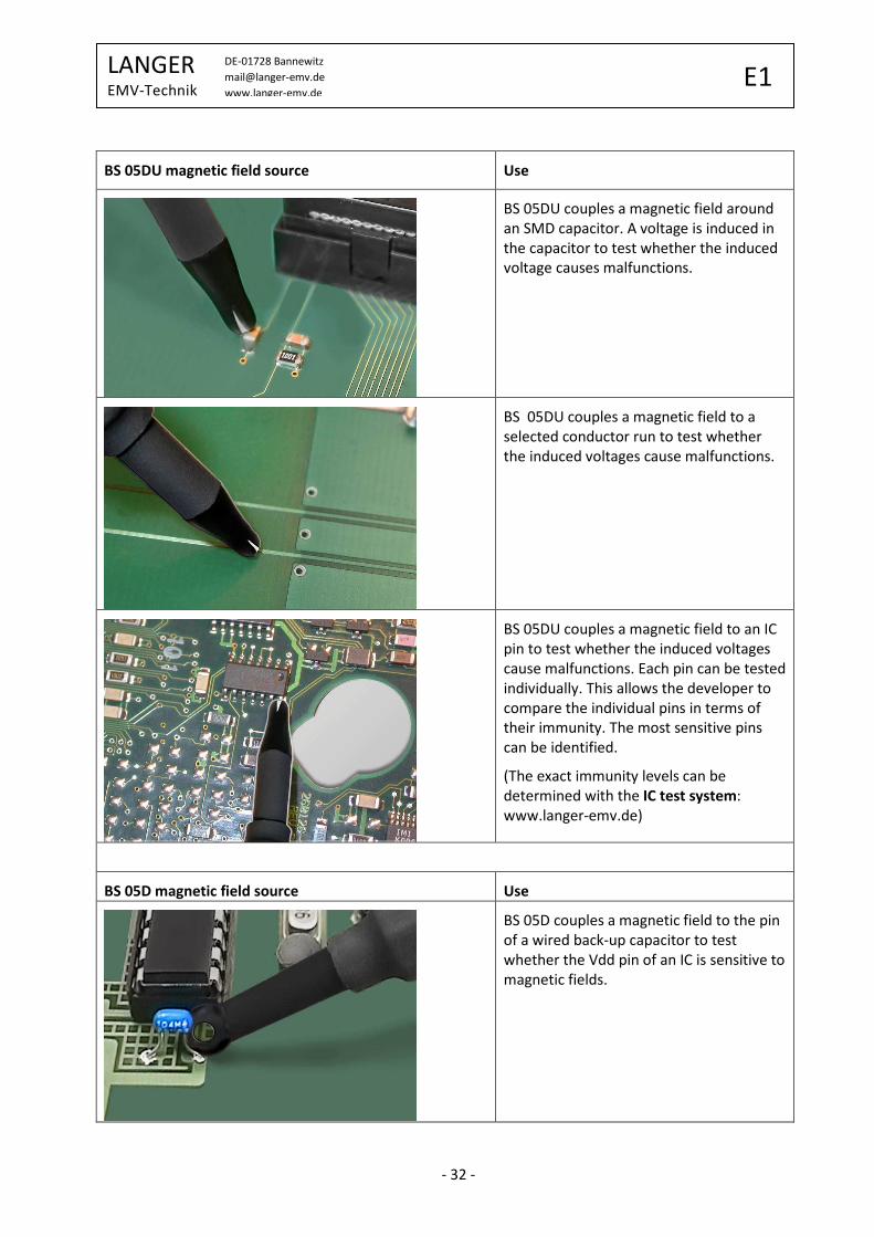
BS 05DU magnetic field source Use
BS 05DU couples a magnetic field around
an SMD capacitor. A voltage is induced in
the capacitor to test whether the induced
voltage causes malfunctions.
BS 05DU couples a magnetic field to a
selected conductor run to test whether
the induced voltages cause malfunctions.
BS 05DU couples a magnetic field to an IC
pin to test whether the induced voltages
cause malfunctions. Each pin can be tested
individually. This allows the developer to
compare the individual pins in terms of
their immunity. The most sensitive pins
can be identified.
(The exact immunity levels can be
determined with the IC test system:
www.langer-emv.de)
BS 05D magnetic field source Use
BS 05D couples a magnetic field to the pin
of a wired back-up capacitor to test
whether the Vdd pin of an IC is sensitive to
magnetic fields.

- 33 -
LANGER EMV-Technik
DE-01728 Bannewitz
www.langer-emv.de E1
BS 02 magnetic field source Use
BS 02 couples a magnetic field to large
areas of a module to test whether the
star-wired ground system has large-scale
weak points.
BS 02 couples a magnetic field to a U-
shaped ground system to test whether the
field affects lines located outside the
ground system.
BS 02 couples a magnetic field to a ribbon
cable to test whether individual lines are
sensitive to magnetic field.
BS 02 couples a magnetic field to a ribbon
cable to test whether individual lines are
sensitive to magnetic field.

- 34 -
LANGER EMV-Technik
DE-01728 Bannewitz
www.langer-emv.de E1
BS 02 magnetic field source Use
BS 02 couples a magnetic field between a
connector's shielding connection and
signal lines (pig tale) to find out whether
the signal input is sensitive to
disturbances.
Please refer to Chapter 2.2 for tips on how to select the individual probes.
The field intensity of a magnetic field source can be adjusted at the SGZ 21's "Intensity" controller (Figure
2). If the intensity is set very high, the magnetic field of the field source spreads over a larger area of the
module than if the intensity is set to a lower value. The measurement process has to be adjusted with the
"Intensity" controller to exactly pinpoint small sensitive weak points. Even very small sensitive points can
then be precisely localised. Should this adjustment prove insufficient, the PULSE SHAPE toggle switch
(Figure 2) can be changed over to "wide pulse" so as to attenuate the interference effect. The intensity may
then have to be slightly increased again if necessary.
5.2.4 Practical procedure for coupling with electric field sources
The field source is used to search for sensitive conductors or components which are responsible for a
certain fault pattern. Coupling to large line sections or line bundles is only possible with field sources which
generate fields of a similar size. The field sources ES 00 to ES 02 (Figure 39) (2.2.2 Field sources for electric
field), for example, can be used for lines in the 10 cm range. The field source is gradually moved towards
the device under test starting at a distance of approximately 10 cm until it rests on the device under test.
Figure 39: ES 00 - 02 field sources with a large field to apply an electric field to conductor loops of
around 10 cm.
- 35 -
LANGER EMV-Technik
DE-01728 Bannewitz
www.langer-emv.de E1
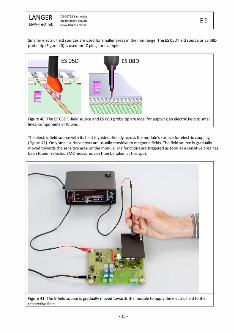
Smaller electric field sources are used for smaller areas in the mm range. The ES 05D field source or ES 08D
probe tip (Figure 40) is used for IC pins, for example.
Figure 40: The ES 05D E-field source and ES 08D probe tip are ideal for applying an electric field to small
lines, components or IC pins.
The electric field source with its field is guided directly across the module's surface for electric coupling
(Figure 41). Only small surface areas are usually sensitive to magnetic fields. The field source is gradually
moved towards the sensitive area on the module. Malfunctions are triggered as soon as a sensitive area has
been found. Selected EMC measures can then be taken at this spot.
Figure 41: The E-field source is gradually moved towards the module to apply the electric field to the
respective lines.

- 36 -
LANGER EMV-Technik
DE-01728 Bannewitz
www.langer-emv.de E1
ES 00 – 02 E-field sources Use
ES 00 couples an electric field to
signal lines of a printed circuit board
to test the sensitivity of components
or signal lines. The ES 05D E-field
source or ES 08D probe tip can then
be used to select individual lines or
components.
ES 01 couples an electric field to
signal lines of a ribbon cable to find
out whether one of the affected
signal lines is sensitive to electric
fields. The ES 05D electric field probe
is then used for a more precise
selection of the individual lines.
ES 02 couples an electric field to the
ground system of a printed circuit
board. A disturbance current is
coupled capacitively to the printed
circuit board. The disturbance
current may then affect weak points
that are sensitive to magnetic fields.
ES 02 couples an electric field to a
conductor run. Placing the probe
onto the conductor run on edge
facilitates the selection of an
individual conductor run. This
method is ideal for relatively
insensitive lines since the E-field
source has a longer edge (coupling
surface) than the ES 05D.

- 37 -
LANGER EMV-Technik
DE-01728 Bannewitz
www.langer-emv.de E1
ES 02 E-field sources Use
ES 02 couples an electric field to the
housing of an IC. The tip of the E-field
source is placed onto the IC housing
to examine individual areas.
This method can also be used for
other components (SMD resistors) or
conductor runs.
ES 05D E-field source Use
ES 05D couples an electric field to the
conductor runs of a printed circuit
board. If the conductor runs are very
close to each other in a bundle, it may
not be possible to find out exactly
which conductor run is the sensitive
one. The developer thus has to find a
point in the layout where the
conductor run is exposed or he has to
use the ES 08D probe tip.
ES 05D couples an electric field to a
quartz crystal oscillator housing to
test the sensitivity of the associated IC
connections. Depending on the IC
manufacturer, the quartz crystal
oscillator connections of ICs can be
very sensitive to electric field.
ES 05D couples an electric field to the
core of a ribbon cable to test its
sensitivity.

- 38 -
LANGER EMV-Technik
DE-01728 Bannewitz
www.langer-emv.de E1
ES 05D E-field sources Use
ES 05D couples an electric field to an
SMD resistor to test the sensitivity of
the associated line network and IC
inputs. Pull-up or pull-down resistors
usually pose a high risk and should
thus always be tested.
ES 05D couples an electric field to the
housing of an IC to test the IC's E-field
sensitivity. Depending on the
manufacturer, ICs may be very
sensitive to electric fields. The IC's
oscillator cells and PLL cells are usually
E-field sensitive.
ES 08D E-field sources Use
ES 08D couples an electric field to a
conductor run to investigate whether
a malfunction occurs in the associated
IC.
ES 08D injects a disturbance current
into individual IC pins. Thanks to the
needle-shaped tip the desired pin can
be exactly selected to test whether
the IC pin can be affected by
capacitive disturbance current. The
individual IC pins can be compared
and evaluated.
(The exact immunity levels can be
determined with the IC test system:
www.langer-emv.de)
Please refer to Chapter 2.2 for tips on how to select the individual probes.

- 39 -
LANGER EMV-Technik
DE-01728 Bannewitz
www.langer-emv.de E1
The field intensity of an electric field source can be adjusted at the SGZ 21's "Intensity" controller (Figure 2).
If the intensity is set very high, the electric field of the field source spreads over a larger area of the module
than if the intensity is set to a lower value. The measurement process has to be adjusted with the
"Intensity" controller to exactly pinpoint small sensitive weak points. Even very small sensitive points can
then be precisely localised. Should this adjustment prove insufficient, the PULSE SHAPE toggle switch
(Figure 2) can be changed over to "wide pulse" so as to attenuate the interference effect. The intensity may
then have to be slightly increased again if necessary.
5.3 Monitoring of logic signals from the device under test
The device under test usually provides information about malfunctions during a test. Malfunctions may not
be sufficient to assess internal interference processes. Characteristic logic signals from the module have to
be monitored to obtain more information about the device under test, such as reset, chip select, watchdog
or any other life signs. The E1 offers the possibility of indicating signal states on the SGZ 21 via the Spike
and Signal LEDs and counting them with a counter (Figure 2), using an optical probe head, the S21 sensor
(Chapter 0 Sensor) and optical fibre.
Furthermore, the pulse density method (Chapter 3) can be used to monitor whether immunity levels are
exceeded in the device under test.
Test set-up:
Figure 42: Test set-up to monitor logic signals from the device under test.
Figure 42 shows the test-set-up for monitoring logic signals of the device under test. The SGZ 21 generator
outputs are connected to the module. A single-pole or two-connection can be used for the set-up. The S21
sensor is connected to the signal that is to be monitored via an adapter socket and enamelled copper wire.
The sensor output is connected to the SGZ 21's "counter input" via an optical fibre (Figure 2).

- 40 -
LANGER EMV-Technik
DE-01728 Bannewitz
www.langer-emv.de E1
The adapter socket is stuck to a suitable location on the printed circuit board with super glue (Figure 43).
3 V to 5 V supply power, ground and signal are wired to the adapter socket connections in accordance with
the sensor assignment (Figure 8). Power can be tapped from a back-up capacitor. The S21 sensor may have
to be shielded if a sensitive signal has to be monitored.
Figure 43: A socket where the S21 sensor can be connected is stuck on the printed circuit board.
5.3.1 Use of the pulse density method to evaluate immunity levels
The S21 sensor input has a defined immunity level. The sensor is connected to a line in the device under
test. This creates an artificial device immunity level which, if exceeded, is signalled directly via an optical
fibre.
The line in the device under test may be an original conductor run or an artificial signal line made of wire
which has been inserted for this purpose (Chapter 3). If an original conductor run is used, no signal or a
signal with a constant frequency should be assigned to this conductor run. This is necessary so as to be able
to distinguish a signal caused by the immunity level overshoot from the useful signal.
The artificial immunity level allows the developer to evaluate EMC measures which have been taken on
filters, housings or the mechanical structure. Changing the discharge paths in the mechanical structure, for
example, enables the developer to determine the effect of this measure on the entire device's immunity.
- 41 -
LANGER EMV-Technik
DE-01728 Bannewitz
www.langer-emv.de E1
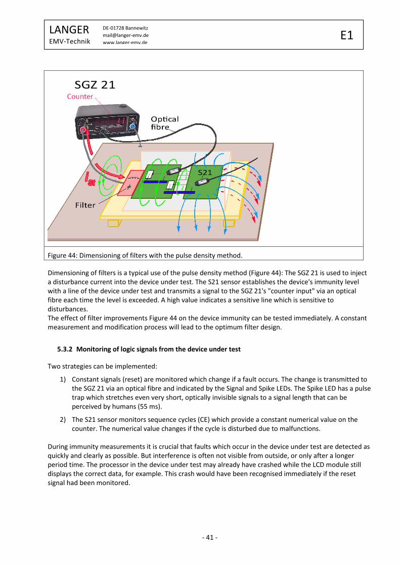
Dimensioning of filters is a typical use of the pulse density method (Figure 44): The SGZ 21 is used to inject
a disturbance current into the device under test. The S21 sensor establishes the device's immunity level
with a line of the device under test and transmits a signal to the SGZ 21's "counter input" via an optical
fibre each time the level is exceeded. A high value indicates a sensitive line which is sensitive to
disturbances.
The effect of filter improvements Figure 44 on the device immunity can be tested immediately. A constant
measurement and modification process will lead to the optimum filter design.
5.3.2 Monitoring of logic signals from the device under test
Two strategies can be implemented:
1) Constant signals (reset) are monitored which change if a fault occurs. The change is transmitted to
the SGZ 21 via an optical fibre and indicated by the Signal and Spike LEDs. The Spike LED has a pulse
trap which stretches even very short, optically invisible signals to a signal length that can be
perceived by humans (55 ms).
2) The S21 sensor monitors sequence cycles (CE) which provide a constant numerical value on the
counter. The numerical value changes if the cycle is disturbed due to malfunctions.
During immunity measurements it is crucial that faults which occur in the device under test are detected as
quickly and clearly as possible. But interference is often not visible from outside, or only after a longer
period time. The processor in the device under test may already have crashed while the LCD module still
displays the correct data, for example. This crash would have been recognised immediately if the reset
signal had been monitored.
Figure 44: Dimensioning of filters with the pulse density method.

- 42 -
LANGER EMV-Technik
DE-01728 Bannewitz
www.langer-emv.de E1
Data traffic on bus systems and/or at interfaces often provides information on the operating state of the
device under test. A precise analysis of the data with an oscilloscope or logic analyser is usually too time-
consuming and costly. A quick alternative is to monitor the data stream with the SGZ 21 counter. Of course,
due to changing data contents and a lack of synchronisation between the counter and data packages, a
constant numerical value cannot always be obtained on the counter. But certain numerical values are
usually assigned to certain operating states. The developer will thus recognise certain successive numerical
values when the system starts up after a RESET, for example, from which he can draw conclusions about
the respective current operating state of the device under test.
He can see whether interference is responsible for a system restart or the unusually frequent
retransmission of data, for example, during immunity measurements.
The optical OSE systems allow a more precise examination of the processes in the device under test during
burst measurements. The signals of the optical sensor are transmitted to an oscilloscope via an optical
fibre. The signals of the device under test can be traced exactly with the oscilloscope. An optical receiver of
the OSE system converts the light signals into electric signals (www.langer-emv.de).
5.4 Measurement of burst-related magnetic fields
It is good to know the distribution of burst-related magnetic fields so as to understand the interference
mechanisms in the device under test. The MS 02 magnetic field probe can be used to measure burst-
related magnetic fields in the device under test. The magnetic field probe is galvanically isolated by an
optical fibre to prevent interaction with the device under test. The optical fibre is connected to the SGZ 21's
counter. The signals of the magnetic field probe are evaluated on the basis of the pulse density method.
The counter displays a number which is proportional to the measured magnetic field.
The measurement of burst-related magnetic fields allows the developer to answer crucial questions such
as:
- Where do magnetic fields exist in the device under test?
- Which path does the disturbance current take in the device under test?
- Does disturbance current enter the IC via inputs and outputs?
- How effective are the integrated discharge capacitors and how big should they be?
- How does the length of a shield connection affect the discharged current?
- etc.
Measurements with the MS 02 magnetic field probe provide two results: the absolute value of the
magnetic field (pulse count) and the direction of the magnetic field (position of the probe head) (Figure 10
and Figure 11). This gives the developer a clear idea of the magnetic fields in the device under test and lets
him assess which structures are particularly at risk.
Test set-up:
Figure 45 shows the test-set-up for measuring burst-related magnetic fields in the device under test. The
SGZ 21 generator outputs are connected to the module. A single-pole or two-pole connection can be used
for the set-up. The optical fibre is connected to the rear of the magnetic field probe. Remember that the
optical fibre has to be inserted through to the conical socket of the transmitter diode. The transmitter
diode is close to the probe's front end. The other end of the optical fibre is connected to the SGZ 21's
counter input.

- 43 -
LANGER EMV-Technik
DE-01728 Bannewitz
www.langer-emv.de E1
Figure 45: Measurement set-up to measure magnetic fields with the MS 02 magnetic field probe.
The disturbance current which is fed into the module distributes according to the module's metallic system.
The ground system usually accounts for the largest share of the metallic system. This means that the
disturbance current will flow via the ground system and the respective magnetic field depends on the form
of the ground system. Figure 46 shows the current flow and the respective magnetic field.
If the ground system does not comprise a closed surface but is split by gaps, strong magnetic fields will be
generated in these gaps and will have a particularly negative effect on lines which are located there. The
MS 02 magnetic field probe can be used to search for these critical points.
.
Figure 46: Operational principle of the MS 02 magnetic field probe in connection with the SGZ 21.

- 44 -
LANGER EMV-Technik
DE-01728 Bannewitz
www.langer-emv.de E1
6 Safety instructions This product meets the requirements of the following directives of the European Union: 2004/108/EC (EMC
directive) and 2006/95/EC (low-voltage directive).
When using a product from LANGER EMV Technik, please observe the following safety instructions to
protect yourself from electric shock or the risk of injuries. Read and follow the operating instructions and
keep them in a safe place for later consultation. The device may only be used by personnel who are
qualified in the field of EMC and who are fit to work under the influence of disturbance voltages and
(electric and magnetic) burst fields.
• Never use any damaged or defective devices.
Carry out a visual check before using a measurement set-up with a Langer EMV-Technik GmbH product.
Replace any damaged connecting cables before starting the product.
• Never leave a Langer EMV-Technik GmbH product unattended whilst this is in operation.
• The Langer EMV-Technik GmbH product may only be used for its intended purpose. Any other use is
prohibited.
• Observe the operating and safety instructions for all devices used in the set-up.
• People with a pace-maker are not allowed to work with this device.
• The test set-up should always be operated via a filtered power supply.
• Attention! Functional near fields and interference emissions may occur when operating the SGZ 21 and
especially when using the test set-ups described in this manual. The user is responsible for taking
measures to prevent any interference to the correct function of products outside the operational EMC
environment (in particular through interference emissions).
This can be achieved by:
- observing an appropriate safety distance,
- use of shielded or shielding rooms.
• The disturbances that are injected into the modules can destroy the device under test (latch-up) if their
intensity is too high. Protect the device under test by:
- increasing the disturbance gradually and stopping when a functional fault occurs,
- interrupting the power supply to the device under test in the event of a latch-up.
Attention! Make sure that internal functional faults are visible from outside. The device under test may
be destroyed due to an increase in the injection intensity if the faults are not visible from outside. Take
the following measures as necessary:
• monitor representative signals in the device under test with optical sensors
• special test software
• visible reaction of the device under test to inputs (reaction test of the device under test).
We cannot assume any liability for the destruction of devices under test!
7 Warranty
Langer EMV-Technik GmbH will remedy any fault due to defective material or defective manufacture,
either by repair or by delivery of replacement, during the statutory warranty period.
This warranty is only granted on condition that:
- the information and instructions in the user manual have been observed.

- 45 -
LANGER EMV-Technik
DE-01728 Bannewitz
www.langer-emv.de E1
The warranty will be forfeited if:
- an unauthorized repair is performed on the product,
- the product is modified,
- the product is not used according to its intended purpose.
8 Technical specifications
SGZ 21 pulse density / burst generator:
- Dimensions WxDxH: (154x100x62) mm
- Pulse parameters Rise time: approx. 2 ns
Tail time: approx. 10 ns
Peak values: approx. 0…1500 V evenly distributed
Pulse interval: approx. 1 ms
Output: symmetric, galvanically isolated
- Contact gap mechanical spark gap
- Counter Display: 6-digit (1 MHz)
Peak time 1 s
- Optical input Max. frequency: 5 MHz
Minimum pulse width 100 ns
Optical fibre: 2.2 mm plastic
- Power supply unit 12 Volt; 200 mA;
- Standards used as a basis for CE mark test:
Emission: EN 50 081-1 /-2
Immunity: EN 50,082-1 /-2
Figure 47: E1 system case

- 46 -
LANGER EMV-Technik
DE-01728 Bannewitz
www.langer-emv.de E1
9 Scope of delivery
Item Designation Type Parameter Quantity
01 Pulse density / burst generator SGZ 21 1
02 Power supply unit 12 Volt, 200 mA 1
03 Generator cable GK 34 cm 2
04 Cable 250 mm 0.64 couplings 2
05 Alligator clips 2
06 Micro kleps 3
07 Optical fibre ∅ 2.2 mm 1 m 1
-------------------------------------------------------------------------------------------------------------------
08 Magnetic field source BS 02 1
09 Magnetic field source BS 04DB 1
10 Magnetic field source BS 05DU 1
11 Magnetic field source BS 05D 1
12 Electric field source ES 00 1
13 Electric field source ES 01 1
14 Electric field source ES 02 1
15 Electric field source ES 05D 1
16 Electric field source ES 08D 1
-------------------------------------------------------------------------------------------------------------------
17 Magnetic field probe MS 02 1
18 Sensor S21 1
19 Measurement lines, red 7 cm 2
20 Measurement lines, yellow 12 cm 2
23 Adapter socket, 3-pole 6
24 Enamelled copper wire Ø=0.2 mm Reel 1
-------------------------------------------------------------------------------------------------------------------
25 User manual 1
26 Laminated quick guide 1
27 E1 system case 1

- 47 -
LANGER EMV-Technik
DE-01728 Bannewitz
www.langer-emv.de E1
10 Optional components
10.1 S2 magnetic field probe set
The probes in the S2 set have a significantly higher resolution than the MS 02. The set also comprises three
different exchangeable probe heads which can be used for different tasks (Figure 49) such as measuring
pin-related magnetic fields and disturbance currents on ICs and on individual conductor runs (Figure 48).
Figure 48: Measurement of disturbance current on individual cores of a ribbon cable with probes from
the S2 set.
Figure 49: Magnetic field probe with exchangeable heads and an optical fibre from the S2 set.

- 48 -
LANGER EMV-Technik
DE-01728 Bannewitz
www.langer-emv.de E1
10.2 Digital or analog optical signal transmission
Analog and digital signals can be transmitted from the device under test to an oscilloscope with special
optical sensors. This transmission is without interaction. The benefit of these systems is that signals of the
device under test can be recorded with an oscilloscope under the influence of disturbances (Figure 50).
Figure 50: Test set-up with two-channel optical signal acquisition to produce an oscillogram of the
disturbed device under test.
This document may not be copied, reproduced or electronically processed, either in its entirety or in part, without
the prior written permission of Langer EMV-Technik GmbH. The management of Langer EMV-Technik GmbH assumes
no liability for damage that may arise from using this printed information.
LANGER Nöthnitzer Hang 31 Tel.: +49(0)351/430093-0
EMV-Technik-GmbH DE-01728 Bannewitz Fax: +49(0)351/430093-22
www.langer-emv.de [email protected]