impact of deep n-well implantation on substrate noise coupling … · 2002-09-02 · conclusions...
TRANSCRIPT

Rev0.8
Aug’01
Rev0.6
14Aug’01
Click to edit Master title style
CHARTERED TECHNOLOGY FORUM 2001
Impact of Deep N-well Implantation on Substrate Noise
Coupling and RF Transistor Performance for Systems-on-a-
Chip Integration
Authors : K. W. Chew, J. Zhang, K. Shao, W. B. Loh and S-. F. Chu
Presented by K. W. Chew

Outline
1. Introduction2.Deep Nwell Process Overview3.Substrate Coupling Test Structures4.S21 Isolation5.Effect on RF Transistor Performance6.Conclusions

Introduction
Source : IEEE Journal of Solid-State Circuits, Vol. 33, No. 3, pp. 314-323, Mar. 1998

Deep N-well Process Overview
STI formation
Deep n-well implant
P-well formation
N-well formation
Channel implants
Gate insulator and gate electrode
Pocket I/I + LDD I/I
Co salicidation
Sidewall spacer and S/D I/I
BEOL

Deep N-well Process Overview
Dop
ing
conc
entr
atio
n (c
m-3
)Deep N-well and P-well SIMS Profiles

CMOS with Deep N-well Technology
P-Well
N+ N+
Deep n-Well
N-Well
N+
N-Well
N+
p-substrate
STI STISTI STIP+P+STI STIP+ P+
P-Well
N+ N+
Deep n-Well
N-Well
N+
N-Well
N+
p-substrate
STI STISTISTI STIP+P+STISTI STISTIP+ P+
Transistor Cross-Sectional View

Deep N-well RF Isolation Test Structures
(a) Typical Layout*
N+
with DNW
P+P+P+ P+
(b) More Complex Layout*
* The authors would like to acknowledge Institute of Microelectronics (Singapore) VLSI department for the test structure layouts
N+
GR
DNW
P+P+P+ P+
N+
DNW
GR

Diode-Type Substrate Coupling Structure in Deep N-well
P+P+
P-Well
Deep n-Well
N-Well
N+
p-substrate
STISTISTI P+STIP+ P+N+ or P+
G P
N-Well
N+STI STI
N GRPNGR
STISTI
S
P+P+
P-Well
Deep n-Well
N-Well
N+
p-substrate
STISTISTI P+STIP+ P+N+ or P+
G P
N-Well
N+STI STI
N GRPNGR
STISTI
S

Effect of Different Body Biasing Techniques on RF Isolation for P+ Noise Generators
-95
-90
-85
-80
-75
-70
-65
-60
-55
-50
-45
-40
-35
-30
0.1 1 10
Frequency (GHz)
S21
Isol
atio
n (d
B)
without DNWwith DNW + unbiased P and N + no GRwith DNW + unbiased P and N + grounded GRwith DNW + unbiased P + grounded N and GRwith DNW + unbiased P + grounded N + no GRBackground noise
G to S spacing : 280µmDNW Implant : P1E13/900KeV

Effect of Different Body Biasing Techniques on RF Isolation for N+ Noise Generators
-80
-75
-70
-65
-60
-55
-50
-45
-40
-35
-30
0.1 1 10
Frequency (GHz)
S21
Isol
atio
n (d
B)
with DNW + P and N tied to Vdd + grounded GR
with DNW + grounded P + N tied to Vdd + no GR
with DNW + grounded P + unbiased N + grounded GR
G to S spacing : 280µmDNW Implant : P1E13/900KeV

Effect of Different Body Biasing Techniques on RF Isolation for N+ Noise Generators
-90
-80
-70
-60
-50
-40
-30
-20
-10
0.1 1 10
Frequency (GHz)
S21
Isol
atio
n (d
B)
without DNW (P+ to P+)without DNW (N+ to P+)with DNW + unbiased P and N + no GRwith DNW + unbiased P + N tied to Vdd + no GRwith DNW + unbiased P and N + grounded GRwith DNW + unbiased P + N tied to Vdd + grounded GR
G to S spacing : 50µmDNW Implant : P2E13/900KeV

Effect of Deep Nwell Dosage on RF Isolation for P+
Noise Generators
-70
-65
-60
-55
-50
-45
-40
-35
-30
0.1 1 10Frequency (GHz)
S21
Isol
atio
n (d
B)
with DNW P1E13/900KeV
with DNW P2E13/900KeV
with DNW P3E13/900KeV
without DNW
G to S spacing : 280µm

Thin-Gate Oxide MOSFETs in Deep N-well DC Characteristics
0.0E+00
1.0E-04
2.0E-04
3.0E-04
4.0E-04
5.0E-04
6.0E-04
-1.8 -1.3 -0.8 -0.3 0.2 0.7 1.2 1.7
Vds (V)
Ids (
A/um
)
N-std0V N-s td1.2V N-s td1.8VN-DW0V N-DW1.2V N-DW1.8VP-std0V P-std-1.2V P-std-1.8VP-DW0V P-DW-1.2V P-DW-1.8V
1.00E-13
1.00E-11
1.00E-09
1.00E-07
1.00E-05
-1.8 -1.2 -0.6 0 0.6 1.2 1.8
Vg (V)
Ids
(A/u
m)
P-std P-DWN-std N-DW

Thick-Gate Oxide MOSFETs in Deep N-well DC Characteristics
1.00E-14
1.00E-12
1.00E-10
1.00E-08
1.00E-06
1.00E-04
-3.5 -2.5 -1.5 -0.5 0.5 1.5 2.5 3.5
Vg (V)
Ids (A
/um)
P-std P-DWN-std N-DW
0.0E+00
1.0E-04
2.0E-04
3.0E-04
4.0E-04
5.0E-04
6.0E-04
-3.5 -2.5 -1.5 -0.5 0.5 1.5 2.5 3.5
Vds (V)
Ids (A
/um)
P-std0V P-s td-2.1V P-s td-3.5V
N-std0V N-std2.1V N-std3.5V
P-DW0V P-DW-2.1V P-DW-3.5V
N-DW0V N-DW2.1V N-DW3.5V
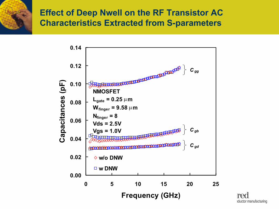
Effect of Deep Nwell on the RF Transistor AC Characteristics Extracted from S-parameters
0.00
0.02
0.04
0.06
0.08
0.10
0.12
0.14
0 5 10 15 20 25
Frequency (GHz)
Cap
acita
nces
(pF)
w/o DNW
w DNW
Cgd
C gg
C gb
NMOSFET Lgate = 0.25 µmWfinger = 9.58 µmNfinger = 8Vds = 2.5V Vgs = 1.0V

Effect of Deep Nwell on the RF Transistor AC Characteristics Extracted from CV Measurements
N+/P-well Junction CapacitanceArea : 225 µm2
Perimeter : 60 µmFrequency : 100 KHzDot: with Deep NwellLine: without Deep Nwell

Comparison of RF Transistor High Frequency Characteristics with and without Deep N-well
S11 S12Red : without Deep N-well Blue : with Deep N-well
S21
S22 H21 Unilateral Gain
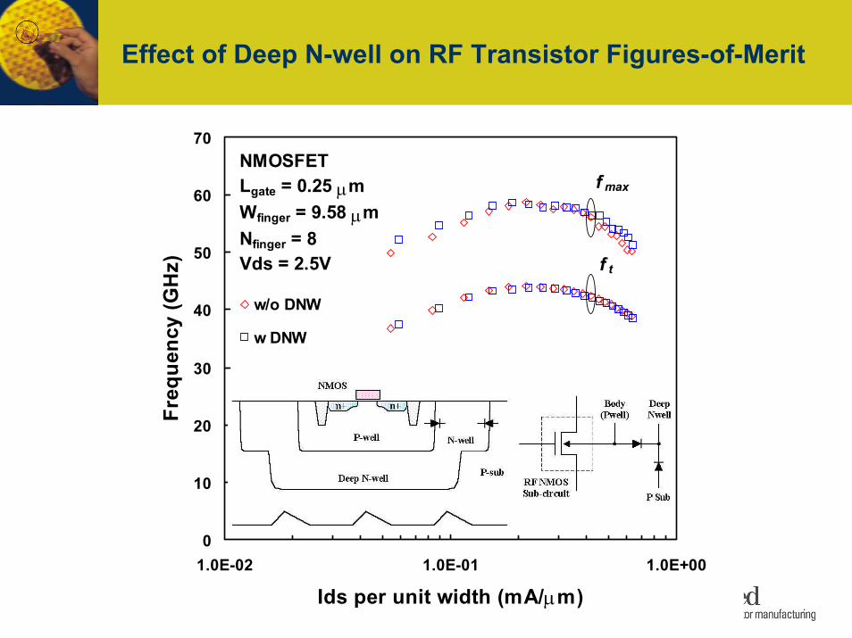
Effect of Deep N-well on RF Transistor Figures-of-Merit
0
10
20
30
40
50
60
70
1.0E-02 1.0E-01 1.0E+00
Ids per unit width (mA/µm)
Freq
uenc
y (G
Hz)
w/o DNW
w DNW
NMOSFET Lgate = 0.25 µmWfinger = 9.58 µmNfinger = 8Vds = 2.5V
f max
f t

Comparison of RF Transistor HF Noise Characteristics with and without Deep N-well
Red : without Deep N-well Blue : with Deep N-well
0.0
0.5
1.0
1.5
2.0
2.5
1.8 2.4 3.0 3.6 4.2 4.8 5.4 6.0
Frequency (GHz)
NFm
in (d
B)
w/o DNWw DNW
NMOS TransistorLf=0.18µmWf=5µmNf=16Vgs=1.2VVds=0.6V
Triode
0.0
0.5
1.0
1.5
2.0
2.5
1.8 2.4 3.0 3.6 4.2 4.8 5.4 6.0
Frequency (GHz)
NFm
in (d
B)
w/o DNWw DNW
NMOS TransistorLf=0.18µmWf=5µmNf=16Vgs=1.8VVds=1.8V
Saturation

Comparison of RF Transistor 1/f Noise Characteristics with and without Deep N-well
1.00E-17
1.00E-16
1.00E-15
1.00E-14
1.00E-13
1.00E-12
1 10 100 1000 10000
Frequency (Hz)
S Id (
A2 /Hz)
with DNWw/o DNW
NMOS TransistorsLgate = 0.18µmNfinger = 16Lfinger = 5µmVds = 0.7VVgs = 1.8V
Triode Saturation
1E-17
1E-16
1E-15
1E-14
1E-13
1E-12
1 10 100 1000 10000
Frequency (Hz)
S Id
(A2 /H
z)
with DNW
w/o DNW
NMOS TransistorsLgate = 0.18µmNfinger = 16Lfinger = 5µmVds = 1.8VVgs = 0.9V

Vertical NPN Bipolar from the 0.18 µm Deep N-well Technology
0
1
2
3
4
5
6
0 1 2 3 4 5
Vc (V)
Ic (m
A)
Ib=50uA Ib=100uAIb=150uA Ib=200uAIb=250uA Ib=300uA
N+
P+
N+
• VA = 22V
• BVCEO = 6V
• BVCBO = 17V
1.0E-131.0E-121.0E-111.0E-101.0E-091.0E-081.0E-071.0E-061.0E-051.0E-041.0E-031.0E-021.0E-011.0E+00
-2.0-1.5-1.0-0.50.0Veb (V)
Ib(1
) , Ic(2
) (A)
(2)
(1)
0
2
4
6
8
10
12
14
16
18
20
1.0E-12 1.0E-10 1.0E-08 1.0E-06 1.0E-04 1.0E-02 1.0E+00
Ic (A)
β
AE : 5X5 µm2

Conclusions
1.Deep n-well is effective in isolating substrate coupling for NMOSFET
2.Maximum of 35 dB isolation at 100 MHz obtained with deep n-well plus grounded nwelland p+ guard ring, using deep n-well dose and implant energy of P1E13 @ 900 KeV
3.Deep n-well process with optimum dosage and energy will not impact the dc, ac, rf, and noise performance
4.Vertical NPN bipolar with beta of 14 can be obtained from the deep n-well technology