implementation of space vector pwm...
TRANSCRIPT
1 | P a g e
IMPLEMENTATION OF SPACE VECTOR PWM
TECHNIQUE FOR A TWO LEVEL 3 PHASE BRIDGE
INVERTER USING DSP
Hemalatha J N1, Sunanda C
2
1Assistant Professor, Department of Electrical and Electronics Engineering,
RV College of Engineering, Bangalore, Karnataka, (India)
2 Assistant Professor, Department of Electrical and Electronics Engineering,
RV College of Engineering, Bangalore, Karnataka, (India)
ABSTRACT
Due to the revolution in the power electronics field and technology of processors various pulse-width-
modulation (PWM) techniques have been developed for many industrial applications. The drawbacks of basic
PWM techniques are higher harmonic content, poor DC bus utilization, higher switching losses, etc. reduces the
overall performance of the 3-phase inverter. The main objective of this paper is to overcome the above
mentioned limitations by implementing Space vector pulse width modulation (SVPWM) technique, an advanced
PWM technique. In this work an algorithm is developed for SVPWM technique and implemented it for a 3-phase
IGBT based inverter. The simulation model is developed using MATLAB/Simulink and hardware
implementation is carried out to validate the technique for the generation of gating pulses. The hardware
implementation is based on reduced computational method and is carried out using the digital processor
DSP2812. The processor produces gating signals for switching devices of an Intelligent Power Module (IPM)
consisting of 3-phase bridge inverter. The simulation study reveals that Space vector PWM gives THD of 5.06%
for phase voltage and 4.96% for line voltages. Whereas Sinusoidal PWM (SPWM) gives THD of 6.8% for phase
voltage and 5.2% for line voltage.
Keywords: Intelligent Power Module, Sinusoidal PWM, Space vector PWM, Total harmonic
distortion.
I. INTRODUCTION
In recent years for industrial drive applications three phase voltage-fed PWM inverters are more widely used.
The main reason for this popularity is developments in advanced PWM techniques. These developments result
in easy sharing of large voltage between the series devices and the improvement of the harmonic quality at the
output [1][2]. The main drawbacks of traditional inverters are the harmonic contents, dc bus utilization. The key
requirement of a drive system is to have low harmonic content. The AC output voltage of an inverter could be
fine-tuned at a fixed or variable frequency using PWM techniques [3][4]. There are several PWM techniques
(mainly with carrier without carrier) which differ in their methods of implementation. The key requirement is to

2 | P a g e
achieve a good quality output voltage of desired frequency and amplitude.[5] [6]. PWM switching strategies
provides output with less total harmonic distortion (THD), efficient dc bus utilization, reduced Electromagnetic
Interference (EMI) and switching losses [7].
Conventional methods of PWM techniques involve the modulation signals being compared with a carrier signal
to generate PWM signals. In SPWM technique a pure sinusoidal modulation signal is being compared with a
carrier signal. This is very basic and simple method which uses analog integrators and comparators to generate
carrier and switching states. But due to the changes in the sine wave reference values during a PWM period, the
cognation between reference values and the carrier wave is not fine-tuned. So the output voltage contains more
harmonics causing undesired low-frequency torque and speed fluctuations. The switching frequency is not fixed
and very narrow pulses may appear depending on the point of intersection between the carrier signal and the
reference signal. The switches may not operate at this instant hence results in more harmonics. Ordinary
machines do not perform smoothly due to substantial amount of %THD, which causes noise, vibration and
heating in machines. [8][9]. The DC bus utilization is only 78.5%, which is very less than that of the six-pulse
inverter (100%). So the current focus is to improve utilization rate of the DC bus voltage. In 1975, Buja
developed third-harmonic-injection pulse-width modulation (THIPWM) to overcome the limitation of SPWM.
This method improved DC utilization of dc bus voltage to 15.5% [10][11]. Another advanced method to
increase the output voltage is the space vector PWM (SVPWM) technique. This method was developed by Van
Der Broeck in 1988 [12]. Different SVPWM schemes have been developed and extensively proposed in the
literature. [13][14]. SVPWM gives an increase of 15.5% of maximum voltage compared with traditional
methods. The n objective of this paper is to implement Space vector pulse width modulation (SVPWM)
technique using DSP and compare the performance parameters.
The paper is organized in following sections II) Description of Space vector PWM III) Simulation
implementation IV) Hardware implementation V) Results and Conclusion
II . DESCRIPTION OF SPACE VECTOR PWM
SVPWM technique produces a sinusoidal waveform with high switching frequency which leads to a better
filtered output signal. The output voltage is changed by varying frequency and the amplitude of a reference
voltage.
The SVPWM technique involves in representing a sinusoidal signal in terms of a reference vector. It consists of
rotating reference vector around the state diagram, composed of six non-zero vector. A circle is inscribed inside
the state map and corresponds to sinusoidal operation as shown in Fig 1. The linear modulation region or under
modulation region is the area inside the inscribed circle. Nonlinear modulation region or over modulation region
is the area between the inside circle and outside circle of the hexagon. Inverter utilization capability depends on
the modulation index.
A set of three-phase voltages is represented by a space vector defined by

3 | P a g e
]
(1)
Fig. 1 Different modulation regions and 8 switching combinations
Where Va(t), Vb(t) and Vc(t) are phase voltages, reference vector rotates with frequency same as that of
sinusoidal signal.
The three phase inverter circuit of is as shown in Fig 2. The switching combinations generates three
independent pole voltages Vao, Vbo and Vco is the key factor of SVPWM.
Fig 2: Three phase Inverter
The pole voltages are either Vdc/2 or -Vdc/2. The (1,0,0) corresponds to switches S1, S6 and S2 are when closed,
the corresponding pole voltages are Vao =Vdc/2, Vbo = -Vdc/2, and Vco = -Vdc/2. The for space vector is as given
in (2)
(2)
In the same manner the eight states are transformed into respective eight space vectors that is given below in (3)
(3)
Reference vector Vref rotates in space at an angular velocity = 2πf, where f is the fundamental frequency.
Choosing a neutral load point n, the pole voltages are shown in (4)
(4)
The phase voltages are given in s (5)
4 | P a g e
(5)
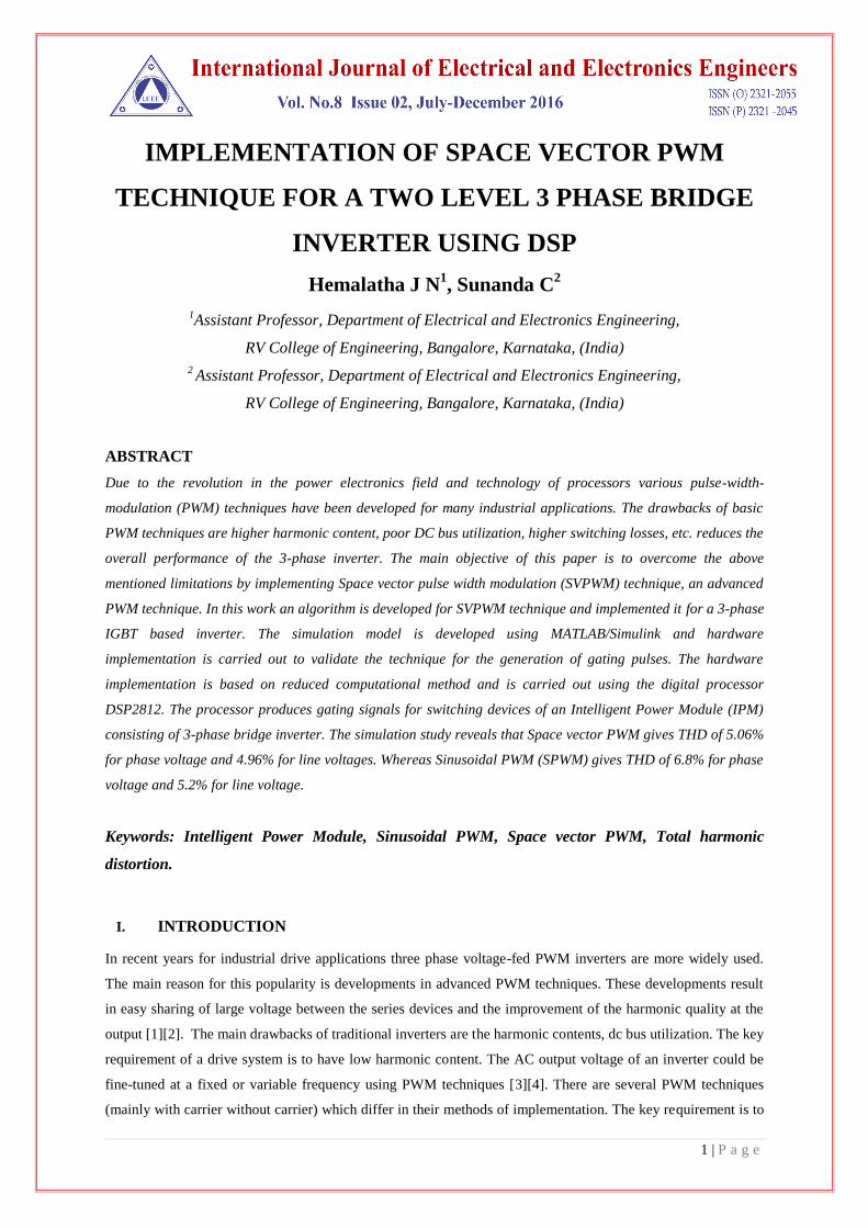
Table 1: Switching Vectors, Phase Voltages And Line Voltages
Voltage
vectors
Switching vectors Phase voltages Line voltages
A B C Van Vbn Vcn Vab Vbc Vca
V0 0 0 0 0 0 0 0 0 0
V1 1 0 0 Vdc - Vdc - Vdc Vdc 0 -Vdc
V2 1 1 0 Vdc Vdc - Vdc 0 Vdc -Vdc
V3 0 1 0 - Vdc Vdc - Vdc -Vdc Vdc 0
V4 0 1 1 - Vdc Vdc Vdc -Vdc 0 Vdc
V5 0 0 1 - Vdc - Vdc Vdc 0 -Vdc Vdc
V6 1 0 1 Vdc - Vdc Vdc Vdc -Vdc 0
V7 1 1 1 0 0 0 0 0 0
Table 1 gives the list of switching vectors, phase and line voltage along with the eight inverter voltage vectors.
The space vector is also represented in another reference frame with two orthogonal axes (α and β). Then the
three-phase voltage vector are transformed into a vector with αβ coordinates as shown in s below.
(6)
(7)
Equating real and imaginary parts, we get
(8)
(9)
III. IMPLEMENTATION OF SVPWM IN MATLAB
The SVPWM method is very complicated than the normal SPWM. It needs the finding of a sector, estimation of
vector segments, and modulation index and determination of switching times. The block diagram shown in Fig 3
depicts the procedure for developing a two-level space vector PWM

5 | P a g e
Fig 3: Block diagram for implementation
The mathematical calculations in the above procedure can be divided into three parts namely
(a)Angle and reference voltage vector
(b)Sector determination
(c)Calculation of switching time durations Ta, Tb and T0
a) Angle and Reference Voltage Vector
The switching states are combined to get the reference vector ref that rotates with angular speed in the
plane represents three sinusoidal waveforms at same frequency. Three sinusoidal and balanced voltages are
given by the relations shown in s
(10)
For any three-phase system with three wires and equal load impedances the vector sum is zero as in (11)
(11)
(12)
Where, a= . The magnitude of the reference vector is
(13)
The phase angle is evaluated from
(14)
Where, .
b) Sector Determination
In order to determine the switching time and sequence it is important to identify the sector in which the
reference vector lies. Depending on the reference voltages Vα and Vβ, the angle of the reference vector can be
used to determine the sector as per Table 2.

6 | P a g e
Table 2:sector determination
Sector Degrees
1 00 < θ ≤ 60
0
2 600 < θ ≤ 120
0
3 1200 < θ ≤ 180
0
4 1800 < θ ≤ 240
0
5 2400 < θ ≤ 300
0
6 3000 < θ ≤ 360
0
Ta, Tb, and T0 are the timings for which two active vectors and a zero vector is applied to switches of an inverter
in each sector respectively. Thus total time applied in each sector is sum of Ta, Tb, and T0 which is Ts.
C. CALCULATION OF SWITCHING TIME DURATIONS TA, TB AND T0.
(15)
(16)
(17)
(18)
Where, n = 1 through 6 ,0 ≤ ≤ 600
The first step to generate SVPWM is to get reference voltage magnitude and the position of the reference
voltage in axis. To generate reference voltage (Vref) three sinusoidal waves displaced by 1200
to each other
are required. The 3-phase reference voltages are converted to 2-phase voltages given by,
(19)
(20)
Where Va, Vb and Vc are three reference waves. The and are corresponding to 2- phase quantities.
The first block in Fig.4 is used to generate three-phase sinusoidal input voltages with variable frequency and
amplitude. The three signals are delayed by 1200 from each other. The three-phase abc voltages are then
converted to two-phase voltages given in the block diagram shown in Fig.3.
The detailed view of block 2 is shown in Fig. 5. To determine the switching time, it is necessary to know in
which sector the reference vector lies.

7 | P a g e
Fig 4: Block diagram to transform abc to αβ
The reference voltages and are utilized to determine the sector of the vectors from 1 to 6. The value of
and are converted to polar co-ordinates (magnitude and angle form) is used to identify the sector of the
reference voltage .
The triangular generator is used to produce a unit triangular waveform at the PWM switching frequency as
shown in Fig 4. First the reference waves are sampled using sample and hold block. The sample are taken at
each 10-5
seconds.
Fig 5: Triangular generator
The sampled signals from the 3rd
block are compared with the triangular wave from triangular generator as
shown in fig 6. Gating time of each switch is calculated using,
(21)
(22)
(23)
Each time the sector is divided as timing for active vectors and zero vectors as in Fig.6
8 | P a g e
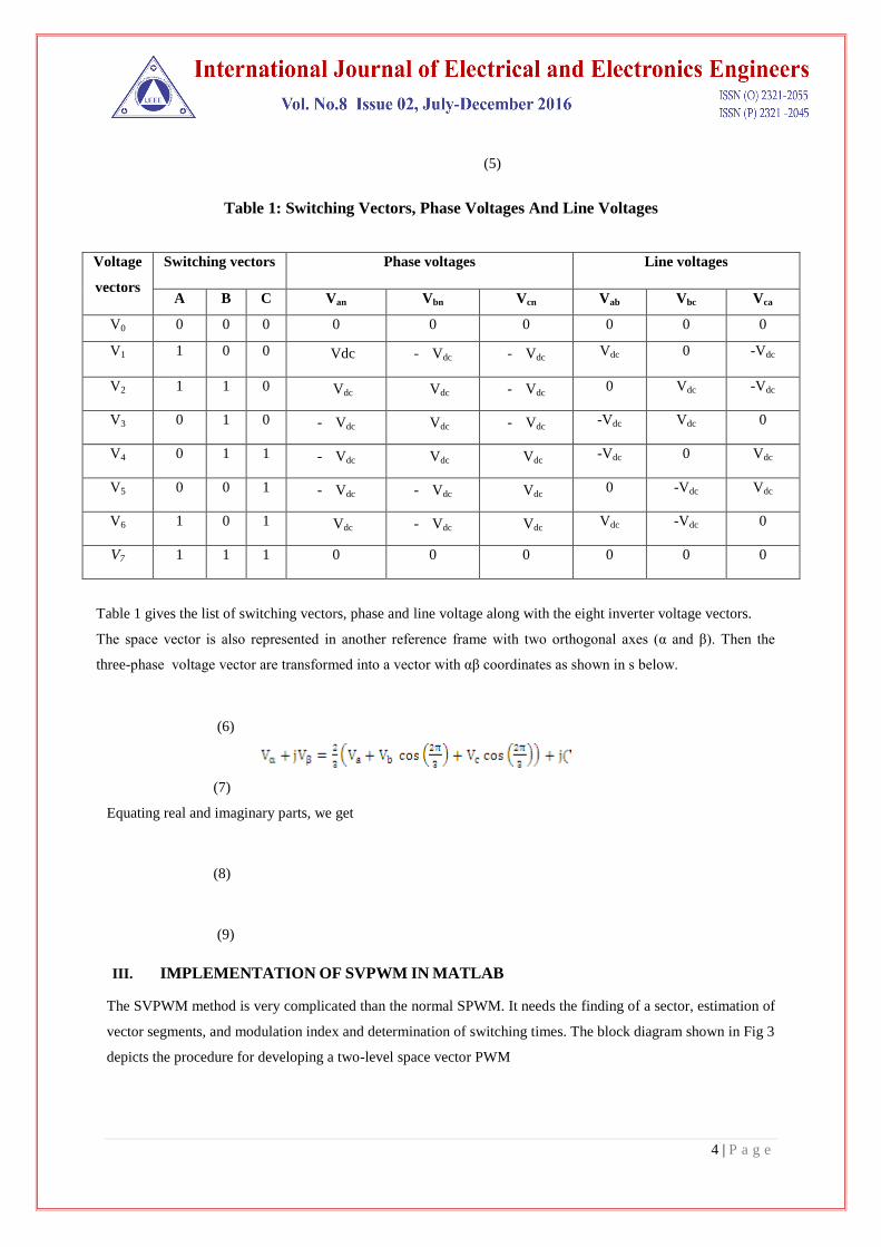
Fig. 6 Timing calculation block for each vector Fig 7: Determination of state vector
According to the gating time signal, each sector is selected and corresponding active vector is determined
according to the position of active vector, switching condition of the switches are selected. Since in sector active
vectors have different switching condition have to determine the switching condition at every position. It is done
in block 5 of Fig.4 and detailed view is given in Fig.7 and Fig 8.
Since MATLAB multiport switch operates from 1 and the gating signals are represented in 0 and 1,to select the
port, constant 1 is added. Now 0 is changed to 1 and 1 is changed to 2. From the block 5,switch conditions of
upper leg of the inverter are obtained. If [1 0 0] is the output of block 5 in Fig.3,then switch 1 ,switch 6 and
switch 2 should be on and switch 4,switch 3 and switch 5 should be off. By adding constant 1, switching matrix
becomes [2 1 1]. Thus in 3 port selectors, first portselects second switch and the other two ports select first
switch. Hence corresponding switching signals are sent to gating of MOSFET switches shown in fig 7
Fig 8: switching vector generation
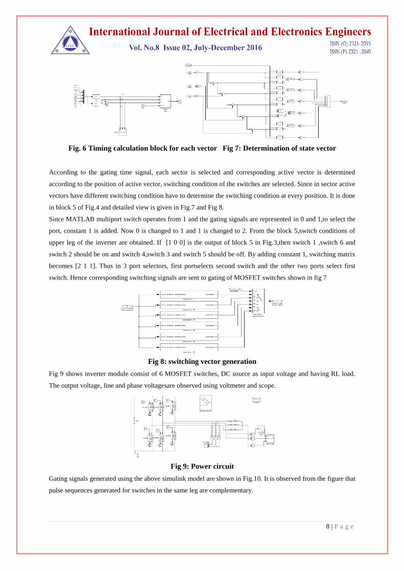
Fig 9 shows inverter module consist of 6 MOSFET switches, DC source as input voltage and having RL load.
The output voltage, line and phase voltagesare observed using voltmeter and scope.
Fig 9: Power circuit
Gating signals generated using the above simulink model are shown in Fig.10. It is observed from the figure that
pulse sequences generated for switches in the same leg are complementary.

9 | P a g e
Fig 10: Gating signals for the switches Fig 11: Line voltages
From the Fig.11 it is seen that line voltage has two levels i.e. +12V and -12V. Also the three line voltages are
phase shifted by 1200.FFT analysis of output phase and line voltage is carried out after the introduction of filter.
It is observed that THD is reduced to 5.07% in case of phase voltage and is shown in table 3
Table 3: THD comparison
Modulation
Index(m)
% THD(Phase
voltage)
(with filter)
% THD (line
voltage)
(with filter)
SVPWM SPWM SVPWM SPWM
0.86 5.06% 6.8% 4.96% 5.2%
0.80 5.06% 6.85% 4.97% 5.3%
0.60 5.07% 6.85% 4.97% 5.9%
0.40 5.08% 6.9% 4.98% 5.91%
0.2 5.08% 6.91% 4.98% 6.02%
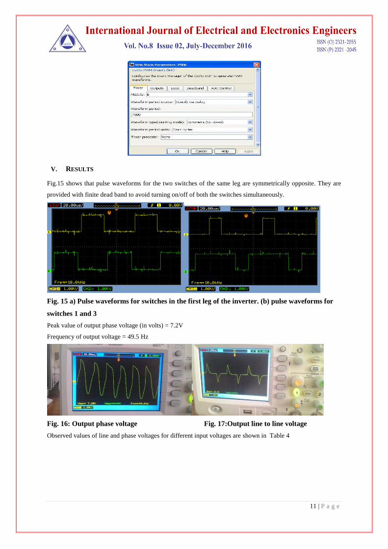
IV.HARDWARE IMPLEMENTATION
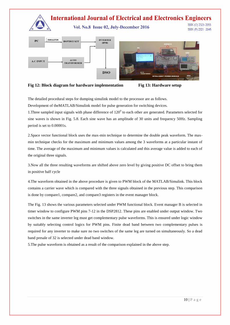
The hardware implementation of SVPWM is carried out using DSP2812 kit. The block diagram shown in Fig12
explains the sequential flow of the hardware implementation of SVPWM. A Simulink model is built to generate
pulses for switching devices of a 3-phase inverter and the model is dumped into DSP2812 processor and inverter
module is connected to the processor to obtain the pulses. The hardware prototype implementation is as shown
in Fig 11.
10 | P a g e
Fig 12: Block diagram for hardware implementation Fig 13: Hardware setup
The detailed procedural steps for dumping simulink model to the processor are as follows.
Development of theMATLAB/Simulink model for pulse generation for switching devices.
1.Three sampled input signals with phase difference of 1200 to each other are generated. Parameters selected for
sine waves is shown in Fig. 5.8. Each sine wave has an amplitude of 30 units and frequency 50Hz. Sampling
period is set to 0.00001s.
2.Space vector functional block uses the max-min technique to determine the double peak waveform. The max-
min technique checks for the maximum and minimum values among the 3 waveforms at a particular instant of
time. The average of the maximum and minimum values is calculated and this average value is added to each of
the original three signals.
3.Now all the three resulting waveforms are shifted above zero level by giving positive DC offset to bring them
in positive half cycle
4.The waveform obtained in the above procedure is given to PWM block of the MATLAB/Simulink. This block
contains a carrier wave which is compared with the three signals obtained in the previous step. This comparison
is done by compare1, compare2, and compare3 registers in the event manager block.
The Fig. 13 shows the various parameters selected under PWM functional block. Event manager B is selected in
timer window to configure PWM pins 7-12 in the DSP2812. These pins are enabled under output window. Two
switches in the same inverter leg must get complementary pulse waveforms. This is ensured under logic window
by suitably selecting control logics for PWM pins. Finite dead band between two complementary pulses is
required for any inverter to make sure no two switches of the same leg are turned on simultaneously. So a dead
band presale of 32 is selected under dead band window.
5.The pulse waveform is obtained as a result of the comparison explained in the above step.
11 | P a g e
V. RESULTS
Fig.15 shows that pulse waveforms for the two switches of the same leg are symmetrically opposite. They are
provided with finite dead band to avoid turning on/off of both the switches simultaneously.
Fig. 15 a) Pulse waveforms for switches in the first leg of the inverter. (b) pulse waveforms for
switches 1 and 3
Peak value of output phase voltage (in volts) = 7.2V
Frequency of output voltage = 49.5 Hz
Fig. 16: Output phase voltage Fig. 17:Output line to line voltage
Observed values of line and phase voltages for different input voltages are shown in Table 4

12 | P a g e
Table 4: Percentage error between theoretical and actual values of line and phase voltages.
Sl.No
.
Input to
IPM
(Vrms)
Input to
inverter, Vdc
(Theoretical)
Input to
inverter,
Vdc
(Actual)
Output line
voltage
(Theoretical
)
Output line
voltage (actual)
% Error
in line
voltage
1 10 9.5 8.9 9.5 8.9 6.31
2 16 14.2 13.9 14.2 13.9 2.11
3 20 18 17.8 18 17.8 1.11
4 25 22.5 22 22.5 22 2.22
5 30 27 26.2 27 26.2 2.96
VI. CONCLUSION
This work concludes that SVPWM is the best among all the PWM techniques and it gives better output voltage
waveforms. The entire work is summarized as follows:
The implementation of SVPWM algorithm for inverter switching control scheme using
MATLAB/Simulink and DSP board TMS320f2812 is performed. And the hardware results obtained
are closely matching the results obtained using MATLAB/Simulink.
The gating pulses generated from the TMS320F2812 are given to the IPM module and they are verified
by observing output voltage. For an input DC voltage of 12V, output line voltage is 12V and phase
voltage obtained is 6.93V.
Simulation results show that THD in output line voltage is 4.96% (with filter) and that of phase voltage
is 5.06% (with filter). Hence output voltage with maximum fundamental component and minimum
harmonics is obtained.
REFERNCES
[1] Rohit Baranwal, Kaushik Basu, and Ned Mohan,“Carrier-Based Implementation of SVPWM for Dual
Two-Level VSI and Dual Matrix Converter with Zero Common-Mode Voltage,”IEEE Trans. on Power
electronics, vol. 30, no. 3, pp. 1474-1487, Mar. 2015.
[2] Shuangxia Niu, S. L. Ho, and W. N. Fu, “A Novel Stator and Rotor Dual PM Vernier Motor with Space
Vector Pulse Width Modulation,” IEEE Trans. on magnetics, vol. 50, no. 2, pp. 3001–3011, Feb. 2014.
13 | P a g e
[3] R.K. Pongiannan, S. Paramasivam, and N. Yadaiah, “Dynamically reconfigurable PWM controller for
three phase voltage source inverters,” IEEE Trans. on Power Electronics, vol. 26, no. 3, pp. 1790-1798,
Jun. 2011.
[4] Lu. B., and Sharma, S.K, “A literature review of IGBT fault-diagnostic and protection methods for power
inverters,”IEEE Trans. on power electronics. vol. 45, no.1, pp. 1770–1777, Apr. 2012.
[5] Vas, P., „Electrical Machines and Drives a Space-Vector Theory Approach,‟ Oxford University
Press, 3rd
edition,1992.
[6] N. P. Van Der Duijn Schouten, C. Y. Leong, P. D. Malliband, and R.A. McMahon, “Implementation and
calorimetric verification of modelsfor IGBT-based inverters for small drives,” Proc. IEEE Conf. Ind.
Appl. SOC., vol. 3, pp. 1786–1793,Oct. 12–16, 2003.
[7] J.Y. Lee, and Y.Y. Sun, “A New SPWM Inverter with Minimum Filter Requirement,” International
Journal of Electronics, vol. 64, no. 5, pp. 815-826, 1988.
[8] H. Quan, Z.Gang, C. Jie, Z. Wu, and Z. Liu, “Study of A Novel Over-modulation Technique Based on
Space-Vector PWM,” IEEE Computer Distributed Control and Intelligent Environmental Monitoring
(CDCIEM), vol. 4 ,no. 4, pp.295-298, 2011.
[9] M. M. Prats, L. G. Franquelo, J. I. Leon, R. Portillo, E. Galvan, andJ. M. Carrasco, “A 3-D space vector
modulation generalized algorithmfor multilevel converters,” IEEE Power Electronics Letters, vol. 1, no.
4,pp. 110–114, Dec. 2003
[10] H. R. Pouya and H. Mokhtari, “Control of Parallel Three-phase Inverters Using Optimal Control and
SVPWM Technique,” IEEE International Conference on Industrial Electronics ISIE, Seoul, Korea, July
2009.
[11] Uddin, M. N., Radwan, T. S., George, G. H., and Rahman M. A., “Performance of Current Controllers for
VSI-Fed IPMSM Drive,” IEEE Trans. Ind. Appl.,vol.36, no. 6, pp. 1531- 1538, Nov./Dec. 2000.
[12] K.V. Kumar, P.A. Michael, J.P. John and S.S. Kumar, “Simulation and Comparison of SPWM and
SVPWM control for Three Phase Inverter,” Asian Research Publishing Network,vol. 5, no. 7, pp. 61-74,
Jul. 2010.
[13] K. Zhou and D. Wang, “Relationship between Space-Vector Modulation and Three- Phase Carrier-Based
PWM: A Comprehensive Analysis,” IEEE Transactions on Industrial Electronics, vol. 49, no. 1, pp. 186-
196, Feb. 2002.
[14] R.K. Pongiannan, and N. Yadaiah, “FPGA Based Three Phase Sinusoidal PWM VVVF Controller,”
IEEE ICEES (International Conference on Electrical Energy Systems), Bijing,China, vol. 1, no.5, pp. 34-
39, 2011.