implementation of space vector-pwm for · pdf fileimplementation of space vector-pwm for...
TRANSCRIPT
Journal of Engineering Sciences, Assiut University, Vol. 39, No. 4, pp.871-884, July 2011.
871
IMPLEMENTATION OF SPACE VECTOR-PWM FOR DRIVING TWO LEVEL VOLTAGE SOURCE INVERTERS
Mahmoud Gaballah, Mohammed El-Bardini, Soliman Sharaf and Mohammed Mabrouk Dept. of industrial electronics & control engineering Faculty of Electronic Engineering, Minufiya University, 32852, Egypt
(Received June 11, 2011 Accepted June 25, 2011)
This paper presents an implementation of space vector pulse width modulation signal generation for driving three phase voltage source inverter. The SVPWM technique gets the PWM switching times for the inverter legs directly from the sampled amplitudes of the reference phase voltages. The SVPWM switching strategy is based on the right aligned sequence. This method is much simpler and more executable than conventional means without look-up tables or complex logical judgments. The SVPWM scheme is modeled/simulated using MATLAB SIMULINK software package, and experimentally implemented / verified on the low cost microchip 8 bit microcontroller PIC16F747 platform. The experimental results are presented for three phase two-level inverter followed by three phase output LC filter.
I. INTRODUCTION
Voltage source inverter is nowadays commonly used to synthesize AC output voltage and frequency from a constant DC voltage via Pulse width modulation control technique. Nowadays many industries are based on voltage source inverters such as motor drives, Uninterruptible power supplies (UPS’s), Frequency converters, AC-AC PWM mode static voltage stabilizer, and active filters [1- 2]. Pulse-width modulation (PWM) techniques have been studied extensively during the last few decades. A large variety of methods different in concept and performance have been developed to achieve the following aims: wide linear modulation range, less switching losses, less harmonic distortion (THD), easy implementation, and less computation time [3- 4].
Several modulation strategies differing in concept and performance have been developed. Space vector modulation techniques have been increasingly used in last decade to generate the inverter output voltage(s) because they allow reducing commutation losses and/or the harmonic content of output voltage, and to obtain higher amplitude modulation indexes if compared with conventional Sinusoidal PWM techniques. Moreover, space vector modulation techniques can be easily implemented in digital processors. In SVPWM scheme the reference voltage space phasor is realized by switching between the nearest three inverter voltage space phasors which form the sector in which the reference vector resides. Each of the combined inverter voltage space phasor is realized by switching a combination of the individual inverter voltage space vectors [5].

Mahmoud Gaballah, Mohammed El-Bardini, Soliman Sharaf ,. 872
A large variety of methods have been developed to implement the SVPWM for voltage source inverters. In general the SVPWM implementation involves the following steps: (a) sector identification in which the instantaneous reference space vector lies (b) mapping this sector to an appropriate sector in the inner hexagon through coordinate transformations (c) determination of the inverter vector switching times (d) selecting appropriate individual vectors using switching sequence tables [6-7]. The sector identification can be done by coordinate transformation [8- 9- 10] or by repeated comparison of the three phase reference voltages [6- 11]. The lookup tables can be used for determining the switching vectors in optimum switching sequence [12]. The calculation of the duration of the switching vectors can be simplified by mapping the sector of the multilevel inverter to a corresponding sector of the two-level inverter [13- 14]. Another SVPWM method using the principle of equivalence with SPWM can generate the SVPWM signals directly from the instantaneous reference phase voltages for multilevel inverters without using lookup tables [15- 16]. The inverter leg switching times are directly obtained from the instantaneous sampled reference phase voltages and the inverter switching vectors are automatically generated.
This paper aims to presents a low cost implementation of space vector-PWM signal generation technique in which the PWM switching times for the inverter legs are directly derived from the sampled amplitudes of the reference phase voltages. The SVPWM switching strategy is based on the right aligned sequence .The switching vectors for the inverter is derived using a simple digital logic which does not involve any complex computations and hence the implementation time is reduced. The space vector PWM scheme is modeled / simulated using MATLAB SIMULINK software package, and experimentally implemented / verified on the low cost microchip PIC microcontroller PIC16F747 platform. The experimental results are presented for three phase two-level inverter followed by three phase LC filter.
II. THREE-PHASE INVERTER
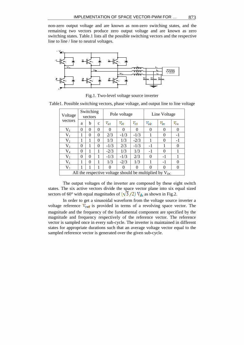
Voltage source inverter (VSI) is the most widely utilized device with power ratings ranging from fractions of a kilowatt to megawatt level and basically used within motor drives, Uninterruptable power supplies and active filters. The VSI consists of six power semiconductor switches with anti-parallel feedback diodes. It converts a DC voltage to three phase AC voltages with controllable frequency and magnitude. In the widely utilized Pulse Width Modulation (PWM) methods, the inverter output voltage approximates the reference value through high frequency switching for the six power semiconductor switches. The circuit model of a typical two-level inverter is shown in Fig.1.
S1 to S6 are the six power switches that shape the output, which are controlled by the variables a, à, b, b̀ , c, and c̀ . It is assumed that S1 and S2, S3, and S4 as well as S5, and S6 are switched in a complementary way. Thus, there are only eight possible switching vectors. Therefore, the ON and OFF states of upper switches S1, S3, and S5 can be used to determine the output voltage. There are only eight possible switching vectors. Six out of these eight vectors produce a
IMPLEMENTATION OF SPACE VECTOR-PWM FOR …
873
non-zero output voltage and are known as non-zero switching states, and the remaining two vectors produce zero output voltage and are known as zero switching states. Table.1 lists all the possible switching vectors and the respective line to line / line to neutral voltages.
Fig.1. Two-level voltage source inverter
Table1. Possible switching vectors, phase voltage, and output line to line voltage
Voltage vectors
Switching vectors
Pole voltage Line Voltage
a b c V0 0 0 0 0 0 0 0 0 0 V1 1 0 0 2/3 -1/3 -1/3 1 0 -1 V2 1 1 0 1/3 1/3 -2/3 1 0 -1 V3 0 1 0 -1/3 2/3 -1/3 -1 1 0 V4 0 1 1 -2/3 1/3 1/3 -1 0 1 V5 0 0 1 -1/3 -1/3 2/3 0 -1 1 V6 1 0 1 1/3 -2/3 1/3 1 -1 0 V7 1 1 1 0 0 0 0 0 0
All the respective voltage should be multiplied by VDC
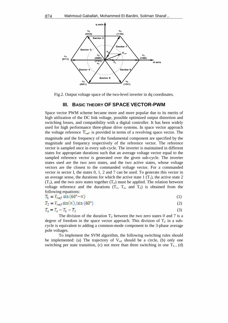
The output voltages of the inverter are composed by these eight switch states. The six active vectors divide the space vector plane into six equal sized sectors of 60° with equal magnitudes of as shown in Fig.2.
In order to get a sinusoidal waveform from the voltage source inverter a voltage reference is provided in terms of a revolving space vector. The
magnitude and the frequency of the fundamental component are specified by the magnitude and frequency respectively of the reference vector. The reference vector is sampled once in every sub-cycle. The inverter is maintained in different states for appropriate durations such that an average voltage vector equal to the sampled reference vector is generated over the given sub-cycle.
Mahmoud Gaballah, Mohammed El-Bardini, Soliman Sharaf ,. 874
Fig.2. Output voltage space of the two-level inverter in dq coordinates.
III. BASIC THEORY OF SPACE VECTOR-PWM
Space vector PWM scheme became more and more popular due to its merits of high utilization of the DC link voltage, possible optimized output distortion and switching losses, and compatibility with a digital controller. It has been widely used for high performance three-phase drive systems. In space vector approach the voltage reference is provided in terms of a revolving space vector. The
magnitude and the frequency of the fundamental component are specified by the magnitude and frequency respectively of the reference vector. The reference vector is sampled once in every sub-cycle. The inverter is maintained in different states for appropriate durations such that an average voltage vector equal to the sampled reference vector is generated over the given sub-cycle. The inverter states used are the two zero states, and the two active states, whose voltage vectors are the closest to the commanded voltage vector. For a commanded vector in sector I, the states 0, 1, 2 and 7 can be used. To generate this vector in an average sense, the durations for which the active state 1 (T1), the active state 2 (T2), and the two zero states together (TZ) must be applied. The relation between voltage reference and the durations (T1, T2, and TZ) is obtained from the following equations:
(1)
(2)
(3)
The division of the duration TZ between the two zero states 0 and 7 is a degree of freedom in the space vector approach. This division of TZ in a sub-cycle is equivalent to adding a common-mode component to the 3-phase average pole voltages.
To implement the SVM algorithm, the following switching rules should be implemented: (a) The trajectory of Vref should be a circle, (b) only one switching per state transition, (c) not more than three switching in one TS , (d)
IMPLEMENTATION OF SPACE VECTOR-PWM FOR …
875
The final state of one sample must be the initial state of the next sample. These rules help in limiting the number of switching actions and hence, there is a reduction in the switching losses. Also, they maintain symmetry in switching waveforms at the VSI output to achieve the lower THD. The SVM algorithm implementation using these switching rules is called Conventional SVM.
In general the Conventional SVPWM implementation involves the following four steps: (a) sector identification in which the instantaneous reference space vector lies, (b) mapping this sector to an appropriate sector in the inner hexagon through coordinate transformations, (c) determination of the inverter vector switching times, (d) selecting appropriate individual vectors using switching sequence tables [6-7].
The main advantage of the SVM algorithm when compared to the Sine PWM algorithm is that it is possible to get line to line voltage amplitude as high as VDC using the SVM algorithm in the linear operating range for this reason the Sine PWM generates sinusoidal phase voltages waveforms with 120° phase shift between them, the resultant line to line voltage is approximately 86.6% of VDC But, the SVM generates phase voltages have a third harmonic component superimposed on the fundamental component “ the addition of this harmonic component is due to the effective usage of inactive states which is not possible in the Sine PWM ” with 120° phase shift between them, the third harmonic component is cancelled out in the resultant line to line voltage in such a way that the resultant line to line voltage is boosted to VDC (100%). Thus, SVM generates line to line voltage with higher amplitude.
IV. SVPWM SIGNAL GENERATION USING ONLY THE
INSTANTANEOUS REFERENCE PHASE AMPLITUDES
In the sinusoidal PWM scheme for two-level inverter each reference phase amplitudes. In the sinusoidal PWM scheme for two-level inverter each reference phase voltage is compared with the triangular carrier and the individual pole voltages are generated independent of each other [3]. To obtain the maximum possible peak amplitude of the fundamental phase voltage in linear modulation a common mode voltage is added to the reference phase voltages [17, 18],
where the magnitude of is given by the following equation:
(4)
In equation (4) Vmax is the maximum magnitude of the three sampled reference phase voltages, while is the minimum magnitude of the three sampled reference phase voltages. In a sampling interval the addition of the common mode voltage Voffset1 results in the active inverter switching vectors being centered in a sampling interval, making the SPWM technique equivalent to the SVPWM technique [3]. Equation (4) is based on the fact that in a sampling interval the reference phase which has lowest magnitude (termed the min-phase) crosses the triangular carrier first and causes the first transition in the inverter switching state. While the reference phase which has the maximum magnitude (termed the max-phase) crosses the carrier last and causes the last switching

Mahmoud Gaballah, Mohammed El-Bardini, Soliman Sharaf ,. 876
transition in the inverter switching states in a two-level SVPWM scheme [17,18]. Thus the switching periods of the active vectors can be determined from the (max-phase and min-phase) sampled reference phase voltage amplitudes in a two-level inverter scheme [19]. The SVPWM technique using only the instantaneous reference phase amplitudes presents a simple way to determine the time instants at which the three reference phases cross the triangular carriers using only the instantaneous reference phase amplitudes. These time instants are sorted to find the offset voltage to be added to the reference phase voltages for SVPWM generation for the entire linear modulation range, so that the middle inverter switching vectors are centered (during a sampling interval), as in the case of the conventional two-level SPWM scheme [20]. The implementation of the Space Vector Pulse Width Modulation (SVPWM) using only the instantaneous reference phase amplitudes for the two-level inverter scheme involves the following steps: A: Read the sampled amplitudes of VAN, VBN, and VCN for the present sampling interval and then calculate the time equivalents of phase voltages, i.e. ,
and as:
(5)
(6)
(7)
Where is the sampling time period.
B: Find as:
(8)
Where , are the maximum and minimum of , and
respectively. C: Find , and as:
(9)
(10)
(11)
Where and are the gating signals during which the top switches in a
leg is turned on. Equations (5) to (11) show that in this method the centering of the
middle inverter switching vectors of the SVPWM is achieved by the addition of an offset time signal to the inverter gating signals derived from the sampled amplitudes of the reference phase voltages. This SVPWM scheme covers the entire modulation range including the over modulation region, also it does not need any sector identification as is required in conventional SVPWM schemes. Complicated calculations for inverter switching vector times and look-up tables for selecting the inverter switching vectors are also avoided in this scheme. This reduces the computation time required to determine the switching times for inverter legs, making the algorithm suitable for real-time implementation.

IMPLEMENTATION OF SPACE VECTOR-PWM FOR …
877
V. SIMULATION RESULTS
The algorithm in section IV is modeled / simulated using MATLAB SIMULINK software package. The MATLAB SIMULINK model is shown in Fig.4. The simulation is performed under the following conditions: input voltage = 220 VAC, VDC = 620 V, Output voltage fundamental harmonic f = 50Hz, Switching frequency fsw = 20 KHZ, and variable modulation index “0.1, 0.85 and 1.15”, also the output of the system is connected to 1.5 KVA load with Power factor = 0.7 Inductive. The Simulation results are presented in Fig.5 to Fig.7.
Fig.4. MATLAB SIMULINK model for the system
Fig.5 shows the simulation results at modulation index = 0.1. A: Output pole Voltage waveforms, B: Line voltage / current waveforms across load terminals
B A

Mahmoud Gaballah, Mohammed El-Bardini, Soliman Sharaf ,. 878
Fig.6 shows the simulation results at modulation index = 0.85. A: Output pole Voltage waveforms, B: Line voltage / current waveforms across load terminals
Fig.7 shows the simulation results at modulation index = 1.15. A: Output pole Voltage waveforms, B: Line voltage / current waveform s across load terminals
From these simulation results we can say that the SV-PWM signal generation using algorithm in section IV can work in the under-modulation region with some small harmonics in pole and line voltages as shown in Fig.5, also it can work in the over-modulation region with some small distortions in the output line voltage at the largest modulation index of SV-PWM as shown in Fig.7
VI. EXPERIMENTAL RESULTS
The algorithm in section IV is implemented on microchip PIC16F747 microcontroller platform and the experimental results are presented for two-level inverter with output LC filter as shown in Fig.1. The overall block diagram of the experiment is shown in Fig.8, The single phase AC input 220v is rectified to ±320 VDC, then synthesized to three phase programmable amplitude and
A B
A B
IMPLEMENTATION OF SPACE VECTOR-PWM FOR …
879
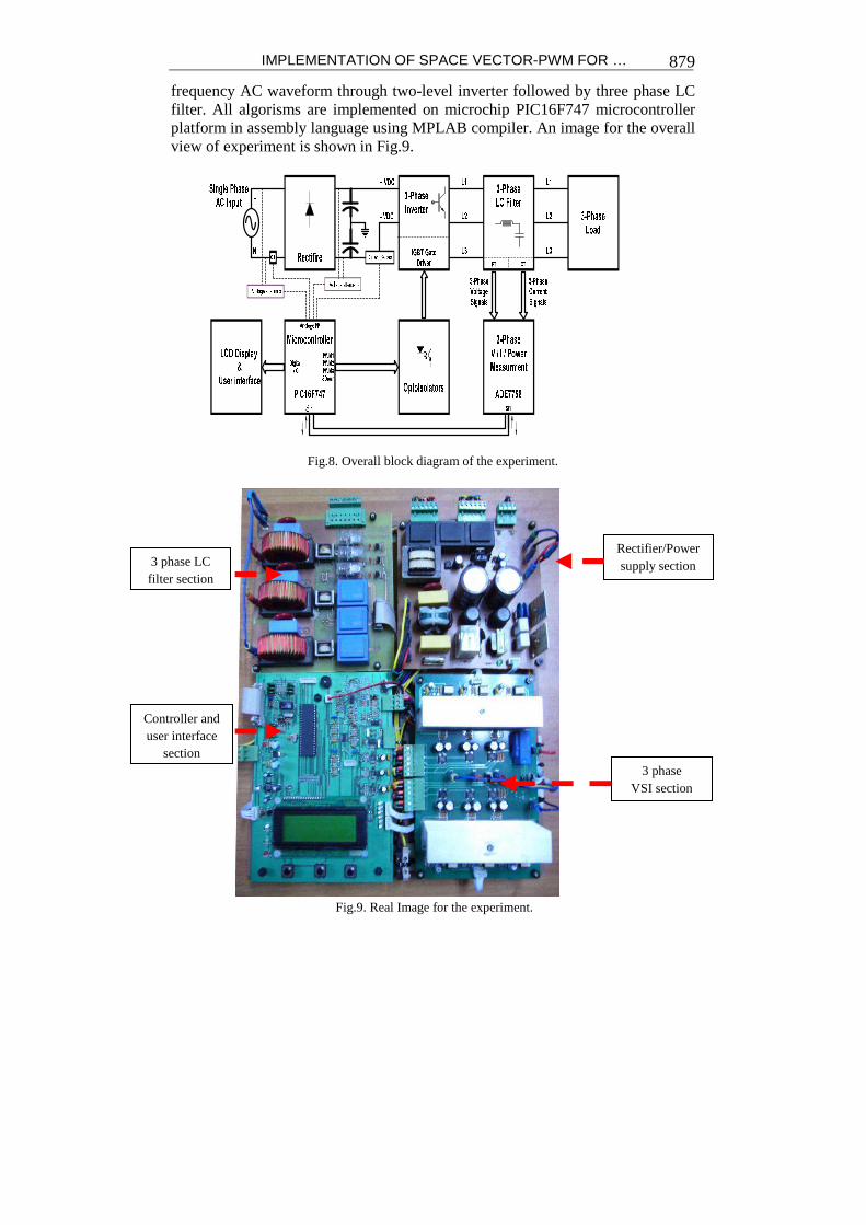
frequency AC waveform through two-level inverter followed by three phase LC filter. All algorisms are implemented on microchip PIC16F747 microcontroller platform in assembly language using MPLAB compiler. An image for the overall view of experiment is shown in Fig.9.
Fig.8. Overall block diagram of the experiment.
Fig.9. Real Image for the experiment.
3 phase VSI section
Controller and user interface
section
3 phase LC filter section
Rectifier/Power supply section

Mahmoud Gaballah, Mohammed El-Bardini, Soliman Sharaf ,. 880
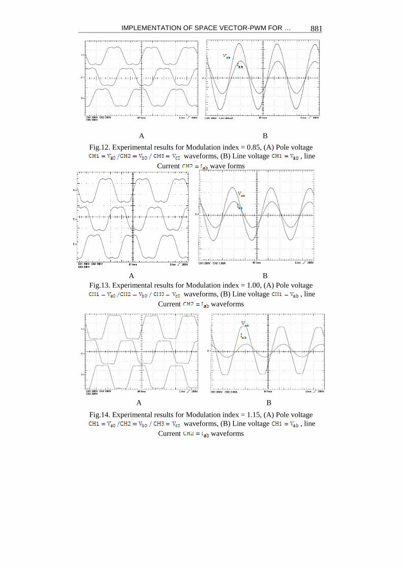
The modulation index is varied from a low modulation index to the over modulation region. The experiment is done under the following conditions: DC link = 400V is used for the inverter, Output voltage fundamental harmonic f = 50Hz, Switching frequency , and three phase 1.5 KVA /0.7 power
factor load. The experimental results are presented in Figs. 10–14. Figure 10 shows the generated SV-PWM signal used to drive the inverter switches a, b and c respectively. The SVPWM strategy is based on the right aligned sequence. Figure 11-14 shows pole voltage / line voltage / line current waveforms at modulation index 0.1, 0.85, 1.00, and 1.15 respectively.
Fig.10. shows the experimental SV-PWM gating signals. CH1= , CH2= ,
and the CH3= , X axis 400usec/div, Y axis 5volt/div
Fig.11. Experimental results for Modulation index = 0.1, (A) Pole voltage waveforms, (B) Line voltage ,
line Current waveforms
A B
IMPLEMENTATION OF SPACE VECTOR-PWM FOR …
881
Fig.12. Experimental results for Modulation index = 0.85, (A) Pole voltage waveforms, (B) Line voltage , line
Current wave forms
Fig.13. Experimental results for Modulation index = 1.00, (A) Pole voltage waveforms, (B) Line voltage , line
Current waveforms
Fig.14. Experimental results for Modulation index = 1.15, (A) Pole voltage waveforms, (B) Line voltage , line
Current waveforms
A B
B A
A B
Mahmoud Gaballah, Mohammed El-Bardini, Soliman Sharaf ,. 882
The experimental results for the under modulation region with a modulation index 0.1 is shown in Fig.11.(A) Shows the pole voltage of three phases,(B) shows the line voltage and line current for phase A. it may be noted that the harmonics appear in voltage waveforms is due to low modulation index. The experimental results for the modulation region with a modulation index 0.85, and 1.00 is shown in Fig.12-13. The line voltage and line current signals seem to be good with low harmonic and no distortion. Finally The experimental results for the over modulation region with a modulation index 1.15 is shown in Fig.14. (A)Shows the pole voltage of three phases it may be noted that this waveforms tends to be square wave due to over-modulation. Fig.14 (B) shows the line voltage and line current for phase A. the small distortion within line voltage is due to large modulation index.
The simulation and experimental waveforms are exactly identical. It demonstrates that the simplified implementation of SVPWM is feasible and effectual in driving three phase two level inverter, and it is much simpler and more executable than conventional means without look-up tables or complex logical judgments.
VI. CONCLUSIONS
A simple and low cost implementation of space vector pulse width modulation technique was presented. The presented SVPWM technique driving the inverter gating signals from the sampled amplitudes of the reference phase voltages The SVPWM strategy is based on the right aligned sequence. The switching vectors for the inverter are derived using a simple digital logic which does not involve any complex computations and hence reduces the implementation time. This scheme can be used for any multilevel inverter configuration and can also work in the over-modulation region. A MATLAB SIMULINK model, and simulation results for different modulation indexes were presented .The space vector PWM scheme is implemented on microchip PIC microcontroller 16F747 platform, and the experimental results were presented for two-level inverter with output LC filter.
REFERENCES
1 P.Channegowda, V.john“Filter optimization for grid interactive voltage source inverter”, IEEE Trans.Ind.Electr. v. 157, pp. 4106-4114, Dec. 2010.
2 S.Yang, Q.Lei, F.Z.Peng and Z.Qian “Robust control scheme for grid interactive voltage source inverter”, IEEE Trans. Ind.Electr. v. 158, pp. 202-212, Jan. 2011.
3 J. Holtz “Pulse-width-modulation–Asurvey”, IEEETrans. Ind. Electr.,v. 39,pp.410-419,Dec.1992.
4 S.R.Bowesand, Y.S.Lai, “The relationship between space-vector modulation and regular-sampled PWM”,IEEE.Trans.Ind.Electr.,v. 44,pp.670-679,Oct.1997.
5 H. W Van Der Broeck, H- C skudenly, and G.V Stanke “Analysis and realization of a pulse width modulator based on voltage space vector”

IMPLEMENTATION OF SPACE VECTOR-PWM FOR …
883
IEEETrans. Ind. Electr.,v. 24,pp.142-150,Jan.1988. 6 N. Celanovic and D. Boroyevich, “A fast space-vector modulation
algorithm for multilevel three-phase converters,” IEEE Trans. Ind.Appl., vol. 37, no. 2, pp. 637–641, Mar./Apr. 2001.
7 N. Tekwani, S. Kanchan, and K. Gopakumar, “A dual five-level induction motor drive with common-mode voltage elimination and DC-link capacitor voltage balancing using only the switching-state redundancy—Part I,” IEEE Trans. Ind. Electron., vol. 54, no. 5, pp. 2600–2608, Oct. 2007.
8 P. F. Seixas, M. A. Severo Mendes, P. Donoso Garcia, and A. M. N. Lima, “A space-vector PWM method for three-level voltage source inverters,” in Proc. IEEE APEC, 2000, vol. 1, pp. 549–555.
9 W. Yao, H. Hu, and Z. Lu, “Comparisons of space-vector modulation and carrier-based modulation of multilevel inverter,” IEEE Transpower Electron., vol. 23, no. 1, pp. 45–51, Jan. 2008.
10 V. T. Somasekhar, K. Gopakumar, M. R. Baiju, K. K. Mohapatra, and L. Umanand, “A multilevel inverter system for an induction motor with open-end windings,” IEEE Trans. Ind. Electron., vol. 52, no. 3, pp. 824–836, Jun. 2005.
11 E. G. Shivakumar, K. Gopakumar, S. K. Sinha, A. Pittet, and V. T. Ranganathan, “Space-vector PWM control of dual inverter fed open-end-winding induction motor drive,” in Proc. IEEE APEC, 2001, pp. 399–405.
12 V. T. Somasekhar, S. Srinivas, and K. K. Kumar, “Effect of zero-vector placement in a dual-inverter fed open-end-winding induction motor drive with a decoupled space-vector PWM strategy,” IEEE Trans. Ind. Electron., vol. 55, no. 6, pp. 2497–2505, Jun. 2008.
13 E. G. Shivakumar, K. Gopakumar, S. K. Sinha, A. Pittet, and V. T. Ranganathan, “Space-vector PWM control of dual inverter fed open-end-winding induction motor drive,” in Proc. IEEE APEC, 2001, pp. 399–405.
14 A. Gopinath, A. Mohamed A. S., and M. R. Baiju, “Fractal based space vector PWM for multilevel inverters—A novel approach,” IEEE Trans. Ind. Electron., vol. 56, no. 4, pp. 1230–1237, Apr. 2009.
15 M. R. Baiju, K. Gopakumar, V. T. Somasekhar, K. K. Mohapatra, and L. Umanand, “A space-vector-based PWM method using only the instantaneous amplitudes of reference phase voltages for three-level inverters,” EPE J., vol. 13, no. 2, pp. 35–45, 2003.
16 R. S. Kanchan, M. R. Baiju, K. K. Mohapatra, P. P. Ouseph, and K. Gopakumar, “Space-vector PWM signal generation for multilevel inverters using only the sampled amplitudes of reference phase voltages,” Proc. Inst. Elect. Eng.—Elect. Power Appl., vol. 152, no. 2, pp. 297–309, Mar. 2005.
17 Holmes, D.G.: ‘The general relationship between regular sampled pulse width modulation and space vector modulation for hard switched converters’. Conf. Rec. IEEE Industry Applications Society (IAS) Annual Meeting, 1992, pp. 1002–1009
18 Baiju, M.R., Mohapatra, K.K., Somasekhar, V.T., Gopakumar, K., and Umanand, L.: ‘A five-level inverter voltage space phasor generation for an open-end winding induction motor drives’, IEE Proc. Electr. Power Appl., 2003, 150, (5), pp. 531–538

Mahmoud Gaballah, Mohammed El-Bardini, Soliman Sharaf ,. 884
19 Kim, J., and Sul, S.: ‘A novel voltage modulation technique of the Space Vector PWM’. Proc. Int. Power Electronics Conf., Yokohama, Japan, 1995, pp. 742–747
20 Zhou, K., and Wang, D.: ‘Relationship between space-vector modulation and three-phase carrier-based PWM: A comprehensive analysis’, IEEE Trans. Ind. Electron., 2002, 49, (1), pp. 186–196
تطبيق طريقة التحكم باستخدام تعديل المتجه الفراغى لعرض النبضة
اكس مصدر جهد ثنائى المستوىلتشغيل ع
تيار -تيار مستمر" فى هذا البحث تم تنفيذ طريقة لتوليد النبضات الالزمة لتشغيل عاكس مصدر جهد
.ثالثى األوجه ثنائى المستوى باستخدام طريقة جديدة لتعديل المتجه الفراغى لعرض النبضة" متردد
“Space vector-PWM” مكنها توليد النبضات الالزمة لتشغيل العاكس الطريقة المستخدمة فى البحث ي
أخوذة من الموجة االساسية وتعتبر هذه الطريقة أفضل وأقل تعقيدا من مباشرة من القيم اللحظية للعينات الم
الطرق التقليدية لتعديل المتجه الفراغى لعرض النبضة وذلك النها ال تستخدم أنظمة الجدولة للحصول
.على قيم تعديل عرض النبضة وال تحتاج الى عمليات منطقية معقدة
اتة من خالل برنامج الماتالب عند نسب تعديل مختلفة وقد تم عمل نموذج رياضى للنظام ككل ومحاك
وبأحمال مختلفة وعليه فقد اثبتت النتائج النظرية أن هذه الطريقة صالحة لتشغيل عاكس مصدر الجهد
.ثالثى األوجه
وقد تم بناء النظام السابق محاكاته عمليا وتم تطبيق الطريقة المستخدمة فى البحث على متحكم دقيق
تيار "وقدمت النتائج العملية على عاكس جهد " PIC16f747"لر رخيص الثمن من النوع ميكروكنترو
وقد وجد " LC"ثنائى المستوى ثالثى األوجه يتبعه مرشح ثالثى األوجه من النوع " تيار متردد -مستمر
الجهد بطريقة تطابق النتائج العملية مع النتائج المحاكاتية مما يثبت صالحية هذه الطريقة لتشغيل عاكس مصدر
.مبسطه وسهلة التنفيذ