implementation of thermal inkjet printing of 2d materials ... · pdf filethe thermal inkjet...
TRANSCRIPT

Implementation of Thermal Inkjet Printing of 2D Materials into 3D
Printers
Henry E. Crosby III REU program, College of William and MaryDr. Russell ”Buzz” Wincheski NASA Langley, Nondestructive Evaluation Sciences Branch
August 8, 2016
Abstract
Inks of conductive materials are currently being developed for methods of direct-write addi-tive manufacturing of thin circuits onto materials and structures. Beyond standard direct-writeprinting methods, one can instead implement the use of thermal inkjet printing of such circuits.In particular, the printing of strain gauge sensors can be utilized for non-destruction evaluat-ing techniques. Printing both silver-nanoparticle inks and graphene oxide inks, these circuitstrain gauges were printed and further investigated for quality of prints. The investigation ofthese printed sensors onto materials such as standard printer paper, polyethylene terephthalate(PET), polymide films, and additive manufacturing thermoplastics. Using the techniques ofthermal inkjet printing on 3D printers opens up a variety of possibilities in printing such inksonto printed parts.
Supported by NSF REU grant PHY-1359364
1 Introduction
1.1 Nondestructive evaluating strain sensors
Strain gauge sensors are of the most basic form of non-destructive evaluating devices that offera simple way to monitor the strain that a material experiences. Manufacturing said sensors varygreatly and have seen many changes over time in design, material, and construction. One suchmethod for creating such an electronic device is by using a 3D printed direct writing utilizingtraces of metallic inks that can be annealed and form a circuit. Similarly one could print thesemetallic inks using an inkjet printer instead. Thermal inkjet printers are an very effective methodbecause they can relatively cheap to replace, they can print traces of inks of up to micron-scale linewidth prints, and already exist as a commercial standard in inkjet printing so they’re very familiarin their effectiveness.
1.2 Thermal Inkjet Printing
The interest in implementing the printing of such conductive inks is twofold. On one hand thereis the practicality of printing using thermal inkjet printers in that they’re the industry standard inprinting industry. In this regard they’re very interesting because they are very familiar and can beeasily much more easily accessible. On the other hand they are also cheaper and this makes them
1

much more disposable. This is important because inkjet printer, in general, do have a tendency tojam and with metallic inks it can become difficult to clean once jammed. So in this respect, it ismore appealing to work with these inkjet printheads, first, to understand the printing process andthe potential resolutions of inkjet printing.
1.3 Additive manufactoring
Since the early 80s, additive manufacturing has continued to see improvements up to the modern3D printer that is now a standard tool in the creation of structures for many industries. Fuseddeposition modeling (FDM) or fused filament fabrication (FFF). Many of the popular 3D printerused in industry are open-sourced and this makes it very easy to modify things like extruder mountsto implement the thermal inkjet to supplement in printing these conductive inks directly onto a 3Dprinted structure.
1.4 2D materials
In 2010, Andre Geim and Konstantin Novoselov received the Nobel Prize in Physics for the discoverygraphene for their experiment in 2004. Graphene ever since has been fascinating to many for itsmany appealing properties. It is a mono-layer crystalline sheet of carbon atoms in hexagonal shape.Graphene has the best thermal and electrical conductivity known to date. Being able to implementthese ”2D materials” with similar features of graphene would be of great interest.
2 Experimental
2.1 Optimizing ink for printing
Figure 1: Image of the four Novacentrix silver nano particle inks and Graphenea graphene oxideink.1,2
Four Novacentrix silver nano-particle inks dispersed ethylene glycol solutions of varying viscosi-ties and concentrations were investigated for the optimal printed silver traces. These inks werelabeled JS-B25P, JS-A101, JS-B30G, and JS-B40G. Each was to be studied and investigated in
2
order to determine which ink gave the best print possible and which was easiest to clean. The sec-ond kind of ink was a graphene oxide ink. This was an ink developed by Graphenea and containedflakes of exfoliated graphene oxide dispersed in a water solution.
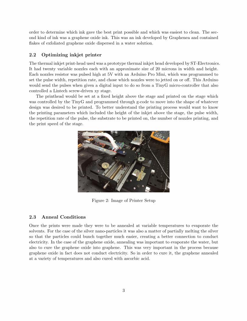
2.2 Optimizing inkjet printer
The thermal inkjet print-head used was a prototype thermal inkjet head developed by ST-Electronics.It had twenty variable nozzles each with an approximate size of 20 microns in width and height.Each nozzles resistor was pulsed high at 5V with an Arduino Pro Mini, which was programmed toset the pulse width, repetition rate, and chose which nozzles were to jetted on or off. This Arduinowould send the pulses when given a digital input to do so from a TinyG micro-controller that alsocontrolled a Lintech screw-driven xy stage.
The printhead would be set at a fixed height above the stage and printed on the stage whichwas controlled by the TinyG and programmed through g-code to move into the shape of whateverdesign was desired to be printed. To better understand the printing process would want to knowthe printing parameters which included the height of the inkjet above the stage, the pulse width,the repetition rate of the pulse, the substrate to be printed on, the number of nozzles printing, andthe print speed of the stage.
Figure 2: Image of Printer Setup
2.3 Anneal Conditions
Once the prints were made they were to be annealed at variable temperatures to evaporate thesolvents. For the case of the silver nano-particles it was also a matter of partially melting the silverso that the particles could bunch together much easier, creating a better connection to conductelectricity. In the case of the graphene oxide, annealing was important to evaporate the water, butalso to cure the graphene oxide into graphene. This was very important in the process becausegraphene oxide in fact does not conduct electricity. So in order to cure it, the graphene annealedat a variety of temperatures and also cured with ascorbic acid.
3
2.4 Print characterization
Once the prints were made and being that they are continuous one wants to know the conductivityof the prints. To measure the dimensions of a print one would measure the print height and linewidth using an optical profilometer. For every print, three arbitrary points were picked along theentire print and then measured three times giving a total of nine data points for both a measurementin height and width. The length of the print was measure using a ruler as this was of larger scale.Lastly, the resistance of the prints was measured using an ohmmeter where they were measuredfrom end to end.
2.5 Mechanical characterization
Load tests were conducted to determine the gauge factor (GF) of the printed strain gauges. Thefollowing equation is for the gauge factor of a strain sensor, it describes the sensitivity of the gaugefactors by displaying the amount percent change of a resistance divided by the percent change instrain:
GF =
∆RR0
ε(1)
Where the amount of strain (ε) the substrate experiences is simply:
ε =∆L
L0(2)
This was done by putting a silver epoxy on both pads and then connecting them to an ACcurrent bridge that would measure the resistance of the sensor. The ends of the substrate thegauges were printed on were placed taught into a load cell where the length that the load cellwould pull the substrate was measured along with the changes of resistance in the sensor and theamount of load that the substrate was experiencing.
2.6 Material characterization
For the case of the graphene oxide prints. One was not only interested in the electrical function-ality of the printed ink, but also how well one could actually cure the graphene oxide into puregraphene. As previously mentioned, the graphene was annealed to better cure the graphene oxideinto graphene. This quality of this cure was measured using Raman spectroscopy. Comparing thisshift in what was called the Raman shift and the intensity of the shift, one could compare themto the spectrum response of a sheet of pure graphene to get a feel for how pure of graphene thereduced graphene oxide was annealed to.
4

3 Results and Discussion
3.1 Optimizing ink for printing
Figure 3: Silver nano-particle inkbefore (top) and after (bottom) be-ing filtered.
The thermal inkjet print-head had a a reported target ink vis-cosity of around 2 cP at 20C. The inks labeled as JS-B30Gand JS-B40G were far too viscous for the recommended, withviscosities of 9.0 and 7.8 cP at 18C. The first ink tested forprinting was the JS-B25P ink which had a reported viscosityof 3.3 cP at 20C. The JS-A100 silver nano-particle ink wasalso tested, but was not given a reported viscosity value, itappeared to be less viscous in comparison to the JS-B40P andJs-B30P so it was not even attempted. After printing the sil-ver inks JS-B25P and JS-A100, it became quite apparent thatthey were presenting themselves as problematic for the inkjetprint-heads as they had a tendency to clog them. Imaging theink with a scanning electron microscope (SEM) it became clearthat the silver nano-particles in the ink will clump together asseen in Figure 3.
Further test prints indicated that the JS-B25P ink wasthe most optimal for the printing process as it was the lessercommon to jam the ink just printer after shorter periods oftime. To better remedy the issue of jamming, the ink was fil-tered with a 0.2 micron filter and diluted in a 1:1 ratio withmethanol. The dilution and filter helped to lessen the viscosity,making it even more optimal to print.
The graphene oxide ink did not experience quite the sameamount of optimizing rigor. The ink would run for a substan-tial amount of more prints in comparison to the silver nano-particle ink. For the sake of testing and trying to preventfuture prints from jamming the inkjet print-heads, the graphene oxide ink was further diluted 1:1,with 2.5 mL of graphene oxide ink and 2.5 mL of water.
3.2 Optimizing inkjet printer
To better understand the printing parameters, we varied certain parameters while keeping othersconstant. For instance varying the substrates while keeping the rest of the printing conditionsthe same to compare the water adhesion. There were four different substrates printed on. Moreimportantly though were differences in parameters and their effect on the actual dimensions ofthe print qualities. Due to the high amount of jamming it was hard to really consider an optimalprinting height above the substrate.
5

Figure 4: Image of inkjet nozzles jamming and the cleaning process
3.3 Anneal conditions
The silver nano particle inks were to be annealed to both evaporate the solvent they were dis-persed in and to partially melt and better connect the silver nano particles to try and increase theconductivity of the printed sensors. The anneal temperatures and durations varied for the silverprints, but most importantly it depended on the substrate to which they were printed on. Thetwo thermoplastics, could withstand higher temperatures and only needed to be annealed for shortdurations of up to an hour at temperatures ranging between 200C to 300C. There was minisculedifferences in the anneal temperatures and even more in anneal durations for these anneals becauseonce the process of evaporating the solvent was complete, it did not change much in regard tothe actual quality of the conductivities of the silver ink prints. Annealing the silve rink onto thePET plastic and printer paper were another story, due to the fact that they were more susceptibleto burning or scarring at such temperatures. As a result an optimal 175C anneal time over thecourse of approximately 24 hours seemed to work best. Too much higher temperature and scarringwould become extreme and if the duration lasted much longer it wouldnt change the print much atall since the solvent at this point would have evaporated. The anneals were varied between a hotplate versus an oven. Where for the shorter anneals, they were conducted on a hot plate, while thelonger anneals were done in the oven.
Annealing the graphene oxide ink was a similar process. The only issue with annealing thegraphene is that it is much more important in the curing process because one is annealing thegraphene oxide ink in order to reduce the graphene oxide flakes into flakes of graphene to conductelectricity. In fact the same exact anneal conditions applied to the graphene oxide as to that of thesilver, in particular, it mattered most what the graphene oxide was printed on. Instead of annealingat the higher 200-300C range for the thermoplastics, the graphene oxide was instead exclusivelyannealed in the oven at 175C for at a minimum of 24 hours. Another added caviat to reducing thegraphene oxide is that a pre-anneal step was made to further reduce the graphene oxide by soakingit in ascorbic acid at 90for up to 30 minutes. Very noticeable change to the quality of the graphenesensors was made when annealing in the process from start to finish. Further understanding of thequality of the graphene prints and the anneal conditions were analyzed using Raman spectroscopy.
6

3.4 Print characterization
The dimensions of the printed silver depended heavily upon the substrate and the number of nozzlebeing printed. On average however, the On average, the silver nano particle had a conductivityof 3.38x10⁶(Ωm)−1. Compared to the accepted value of bulk silver, 6.29 x 10⁷(Ωm)−1, this is 5percent of the accepted value. This fairly reasonable because it is an incredibly smaller scale andthere is going to be an expected, even significant, drop in conductivity because of the fact that itis a bunch of silver nano particles group together and not solid silver.
For the reduced graphene oxide prints, the most difficult measurement to make was the actualheight of the traces. Because graphene is so small and the flakes, may be relatively think withrespect to a monolayer of graphene, it is still incredibly small. Somewhere in the nanometer scale,and at this scale it becomes relatively hard to make a definitely measurement. Even using anatomic force microscope (AFM) the height was indefinite and appeared to be within the actualplane of the substrate that it was printed on. The other dimensions were just the same howeveras the silver ink. The resistances of the reduced graphene oxide prints were still very high as well,averaging in the mega-ohm range. On average the conductivites of the reduced graphene printswere around 12.8 (Ωm)−1.
3.5 Mechanical characterization
Figure 5: Image of Printer Setup
Only the silver nano-particle ink printed sensors gave resistances that were low enough tomake a quality load test with initial resistances in the tens of ohms. An average gauge factor ofapproximately 11.3, the standard deviation here is almost the size of the average. This makes thenumber much more inconclusive, but it is important to take note of the fact that some of the silversensors were cracked or were missing parts, that would lower their sensitivity to the strain of thematerial. The large standard deviation is mainly do to the large differences in the gauge factorvalues with only five load tests successfully completed. To get a better understanding for a moreprecise estimate of a typical gauge factor of silver one would want to do more tests.
7

3.6 Material characterization
Figure 6: Picture of Raman Spectroscopic analysis of various graphene and reduced graphene oxidestructures
Lastly, one would want to better characterize the graphene oxide anneal process. The grapheneoxide flakes In the graph above, Figure 6, one can see that the reduced graphene oxide (the toptwo lines) is not very close to the shape of a pure sheet of graphene (the bottom line). One canalso see that in using Raman spectroscopy the issues of how substrate being printed on can skewthe actual spectra. Here it appears that the green line may have the graphene spike, but in factit is not the same exact shift and is a product of the PET substrate it was printed on. There isactually some response for a typical graphene response in the printed reduced graphene oxide, butit isn’t strong enough to fully confirm. One way of fixing this and getting better results would beto print over the same trace a few times to pick up a stronger response and cloud the backgroundsubstrate response.
4 Conclusions and Future Work
Thermal inkjet printing indeed has it its own set of pros and cons that come with it. On one hand itis a commercial standard, it can printed up to relatively high resolutions, and it is fairly inexpensiveto replace. On the other hand it does have a tendency to jam up and problems are more likelyto arise when printing a lot of sensors or a very large sized one. To remedy these problems withprinting one simply needs to do more research on both the printing process and cleaning the ink-jetprint heads. Another idea would be to try and either implement a thermal inkjet print heads witha lot more nozzles or even try a piezoelectric printer head that flushes inks our of the ink chamberutilizing the piezoelectric effect from certain crystals.
Another step in the step of this research is to further the understanding of the quality of theprints that are being made when printing from the inkjet print head, as well as actually printingwith the inkjet printer head mounted to a 3D printer. Additionally, one could look into prinitng notjust strain gauges, but things like photovoltaic cells and see how well the graphene, in particular,might be susceptible to storing energy from light. Also, further work does need to go into, especiallythe Raman Spectra analysis, to see how one could develop better quality prints of graphene.
Ultimately this project is not a niche concept. It has a vast spectrum of application in which
8

one may desire to incorporate conductive inks into 3D printed structures and in particular, imple-menting the printing of 2D materials like graphene into these structures. So, in the end, it is notsomething that is specific even for nondestructive testing, but would have many applications as onewould now be able to even easier embed said 2 material sensors onto 3D printed objects.
9

Bibliography
10