implementing digital processing for automotive radar using ... · page 2 pulse-doppler method for...
TRANSCRIPT
December 2013 Altera Corporation
WP-01183-1.3
© 2013 Altera Corporation. AlNIOS, QUARTUS and STRATTrademark Office and in othetheir respective holders as desproducts to current specificatioproducts and services at any tiof any information, product, oadvised to obtain the latest verfor products or services.
101 Innovation DriveSan Jose, CA 95134www.altera.com
Implementing Digital Processing forAutomotive Radar Using SoCs
White Paper
This white paper shows the feasibility of implementing the digital processing portion of a representative radar system using Altera® low-cost Cyclone® V SoCs. Advantages of this approach compared to a custom ASIC are reduced time to market, field upgradability, the ability to rapidly and easily implement in floating-point, dual pre-integrated ARM® Cortex™-A9 microprocessor systems, and available automotive-grade devices.
IntroductionRadar has long been used in military and commercial applications. Recently, radar has begun to appear on high-end automobiles for parking assistance and lane departure warning. Next-generation automotive radars must be more sophisticated, as radar will play a key role in active collision avoidance and adaptive cruise control. Once the radar is integrated into a system that actively controls the vehicle, as opposed to merely providing warning signals, the system reliability requirements become much more stringent, with an associated liability potential for vehicle collisions.
This white paper describes how an automotive radar system was built using digital processing segments with Altera’s rapid prototyping and development tool flow for digital signal processing (DSP) design, known as DSP Builder Advanced. The results provide actual circuit size and performance metrics for the digital portion of the radar processing. This digital processing incorporates a new breed of programmable logic, known as SoCs, which embed powerful dual 925 MHz ARM Cortex-A9 processors in a low-cost FPGA fabric. Automotive-grade versions of these devices are also available and capable of 700 MHz CPU clock rates. SoCs provide a flexible, scalable platform for applications from radar to light detection and ranging (LIDAR) to infrared and visible cameras. Moreover, both the FPGA hardware and ARM software implementations use floating-point processing, which provides superior performance in radar applications compared to traditional fixed-point implementations in FPGAs or ASICs. These low-cost SoC devices support volume applications, while providing much faster time to market compared to alternate ASIC solutions.
The SoC approach provides the ability for production line or even field firmware updates of both software and hardware, which can be important as automotive radar systems continue to increase in complexity. SoCs are also ideal for integrating video processing using cameras. Video analytics processing can be used in conjunction with the radar detection information in a process called sensor fusion, where multiple sensing systems combine to generate the most reliable data on which to base decisions.
l rights reserved. ALTERA, ARRIA, CYCLONE, ENPIRION, HARDCOPY, MAX, MEGACORE, IX words and logos are trademarks of Altera Corporation and registered in the U.S. Patent and r countries. All other words and logos identified as trademarks or service marks are the property of cribed at www.altera.com/common/legal.html. Altera warrants performance of its semiconductor ns in accordance with Altera's standard warranty, but reserves the right to make changes to any
me without notice. Altera assumes no responsibility or liability arising out of the application or use r service described herein except as expressly agreed to in writing by Altera. Altera customers are sion of device specifications before relying on any published information and before placing orders
Feedback Subscribe
ISO 9001:2008 Registered
Page 2 Pulse-Doppler Method for Automotive Radar
Pulse-Doppler Method for Automotive Radar Many radar systems employ pulse-Doppler methods, in which the transmitter operates for a short duration, then the system switches to receive mode until the next transmit pulse. The pulse-Doppler radar sends successive pulses at specific intervals or a pulse repetition interval (PRI). As the radar returns, the reflections are processed coherently to extract range and relative motion of detected objects. More sophisticated processing methods, such as space time adaptive radar (STAP) further process radar returns and extract target data even when heavily obscured by ground clutter or background returns surrounding the object(s) of interest.
f For further information on radar basics, pulse-Doppler radar, STAP radar, and SAR radar, refer to EETimes’ tutorial on “Radar Basics.”
In automotive radar, the range can be as short as a few meters to as much as a few hundred meters. For a range of 2 m, the round-trip transit time of the radar pulse is 13 ns. This short range requires that the transmitter and receiver operate simultaneously, which requires separate antennas. The pulse-Doppler radar sends a pulse periodically, and the ratio of the time the transmitter is active to the total time elapsed is the duty cycle. Since duty cycles are typically small, this ratio limits the total transmit power. The power, in turn limits the range of detection. Achieving a 1- to 2 m range resolution also requires a sample rate on the order of 100 MSPS or more, and the ability to digitally process the data in both range and Doppler dimensions. This high sample rate can increase the cost of the radar system.
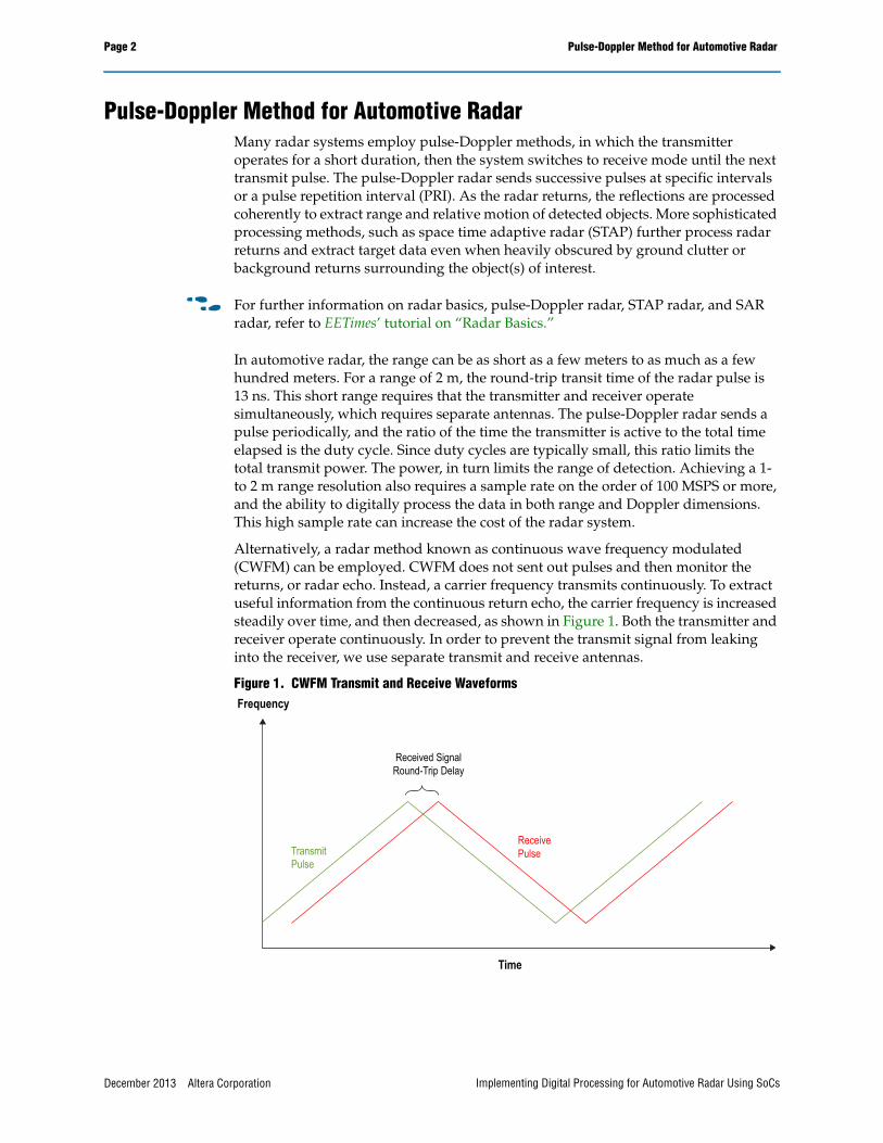
Alternatively, a radar method known as continuous wave frequency modulated (CWFM) can be employed. CWFM does not sent out pulses and then monitor the returns, or radar echo. Instead, a carrier frequency transmits continuously. To extract useful information from the continuous return echo, the carrier frequency is increased steadily over time, and then decreased, as shown in Figure 1. Both the transmitter and receiver operate continuously. In order to prevent the transmit signal from leaking into the receiver, we use separate transmit and receive antennas.
Figure 1. CWFM Transmit and Receive WaveformsFrequency
Time
TransmitPulse
ReceivePulse
Received SignalRound-Trip Delay
December 2013 Altera Corporation Implementing Digital Processing for Automotive Radar Using SoCs
Pulse-Doppler Method for Automotive Radar Page 3
The radar must determine the range of objects detected. In CWFM, the range is accomplished by measuring the instantaneous receive frequency difference, or delta, from the transmit frequency. During the positive frequency ramp portion of the transmit cycle, the receive frequency will be somewhat less than the transmit frequency, depending upon the time delay. During the negative frequency ramp portion of the transmit cycle, the receive frequency will be greater than the transmit frequency, again depending upon the time delay. These frequency differences, or offsets, will be proportional to the round-trip delay time, which provides a means to measure the range. The greater the range, the more time delay there is from the transmitter to the receiver. Since the transmit frequency is constantly changing, the difference between transmit and receive frequencies at any given instant will be proportional to the elapsed time for the transmit signal to travel from the radar to the target and back.
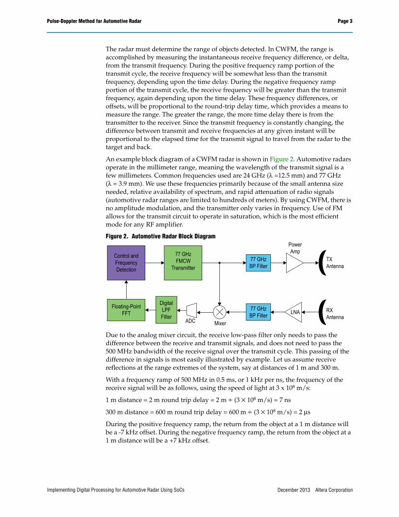
An example block diagram of a CWFM radar is shown in Figure 2. Automotive radars operate in the millimeter range, meaning the wavelength of the transmit signal is a few millimeters. Common frequencies used are 24 GHz (λ =12.5 mm) and 77 GHz (λ = 3.9 mm). We use these frequencies primarily because of the small antenna size needed, relative availability of spectrum, and rapid attenuation of radio signals (automotive radar ranges are limited to hundreds of meters). By using CWFM, there is no amplitude modulation, and the transmitter only varies in frequency. Use of FM allows for the transmit circuit to operate in saturation, which is the most efficient mode for any RF amplifier.
Figure 2. Automotive Radar Block Diagram
Due to the analog mixer circuit, the receive low-pass filter only needs to pass the difference between the receive and transmit signals, and does not need to pass the 500 MHz bandwidth of the receive signal over the transmit cycle. This passing of the difference in signals is most easily illustrated by example. Let us assume receive reflections at the range extremes of the system, say at distances of 1 m and 300 m.
With a frequency ramp of 500 MHz in 0.5 ms, or 1 kHz per ns, the frequency of the receive signal will be as follows, using the speed of light at 3 x 10⁸ m/s:
1 m distance = 2 m round trip delay = 2 m ÷ (3 × 10⁸ m/s) = 7 ns
300 m distance = 600 m round trip delay = 600 m ÷ (3 × 10⁸ m/s) = 2 μs
During the positive frequency ramp, the return from the object at a 1 m distance will be a -7 kHz offset. During the negative frequency ramp, the return from the object at a 1 m distance will be a +7 kHz offset.
Control andFrequencyDetection
77 GHzFMCW
Transmitter
Floating-PointFFT
DigitalLPFFIlter
ADC
77 GHzBP Filter
LNA RXAntenna
77 GHzBP Filter
PowerAmp
TXAntenna
Mixer
December 2013 Altera CorporationImplementing Digital Processing for Automotive Radar Using SoCs
Page 4 Pulse-Doppler Method for Automotive Radar
During the positive frequency ramp, the return from the object at a 300 m distance will be a -2 MHz offset. During the negative frequency ramp, the return from the object at a 1 m distance will be +2 MHz offset.
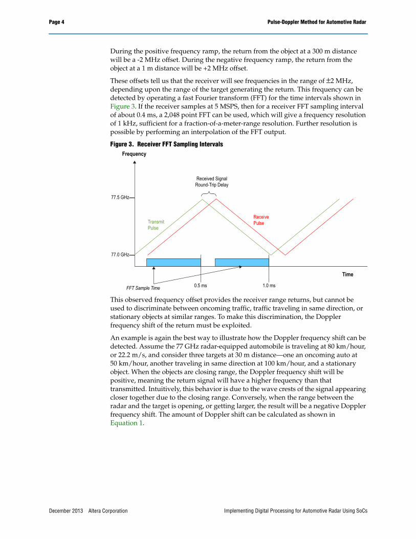
These offsets tell us that the receiver will see frequencies in the range of ±2 MHz, depending upon the range of the target generating the return. This frequency can be detected by operating a fast Fourier transform (FFT) for the time intervals shown in Figure 3. If the receiver samples at 5 MSPS, then for a receiver FFT sampling interval of about 0.4 ms, a 2,048 point FFT can be used, which will give a frequency resolution of 1 kHz, sufficient for a fraction-of-a-meter-range resolution. Further resolution is possible by performing an interpolation of the FFT output.
Figure 3. Receiver FFT Sampling Intervals
This observed frequency offset provides the receiver range returns, but cannot be used to discriminate between oncoming traffic, traffic traveling in same direction, or stationary objects at similar ranges. To make this discrimination, the Doppler frequency shift of the return must be exploited.
An example is again the best way to illustrate how the Doppler frequency shift can be detected. Assume the 77 GHz radar-equipped automobile is traveling at 80 km/hour, or 22.2 m/s, and consider three targets at 30 m distance—one an oncoming auto at 50 km/hour, another traveling in same direction at 100 km/hour, and a stationary object. When the objects are closing range, the Doppler frequency shift will be positive, meaning the return signal will have a higher frequency than that transmitted. Intuitively, this behavior is due to the wave crests of the signal appearing closer together due to the closing range. Conversely, when the range between the radar and the target is opening, or getting larger, the result will be a negative Doppler frequency shift. The amount of Doppler shift can be calculated as shown in Equation 1.
Frequency
Time
TransmitPulse
ReceivePulse
Received SignalRound-Trip Delay
77.5 GHz
77.0 GHz
FFT Sample Time0.5 ms 1.0 ms
December 2013 Altera Corporation Implementing Digital Processing for Automotive Radar Using SoCs
Pulse-Doppler Method for Automotive Radar Page 5
Equation 1. Doppler Shift
Doppler frequency shift = (2 × velocity difference) ÷ wavelength
Oncoming auto at 50 km/hour, radar auto at 80 km/hour, closing rate of 130 km/hour or 36.1 m/s
Doppler frequency shift = 2 (36.1 m/s) ÷ (.0039 m) = 18.5 kHz
Stationary object, radar auto at 80 km/hour, closing rate of 80 km/hour or 22.2 m/s
Doppler frequency shift = 2 (22.2 m/s) ÷ (.0039 m) = 11.4 kHz
Auto ahead at 100 km/hour, radar auto at 80 km/hour, opening rate of 20 km/hour or 5.56 m/s
Doppler frequency shift = -2 (5.56 m/s) ÷ (.0039 m) = -2.8 kHz
These Doppler shifts will offset the detected frequency differences on both the positive and negative frequency ramps. When there is no relative motion, and no Doppler shift, the difference in the receive frequency will be equal, but of opposite sign, in the positive and negative frequency ramps. So the Doppler shift can be found by comparing the receive frequency offsets during the positive and negative portions of the frequency ramp of the transmit signal. The relationship is described in Equation 2, where the range and the relative velocity can be determined by the output of the FFT using the results both during both positive and negative frequency ramps of the transmitter.
Equation 2. Relative Velocity
Relative velocity (target to radar) = (wavelength ÷ 2) × (positive ramp detected frequency – negative ramp detected frequency) ÷ 2
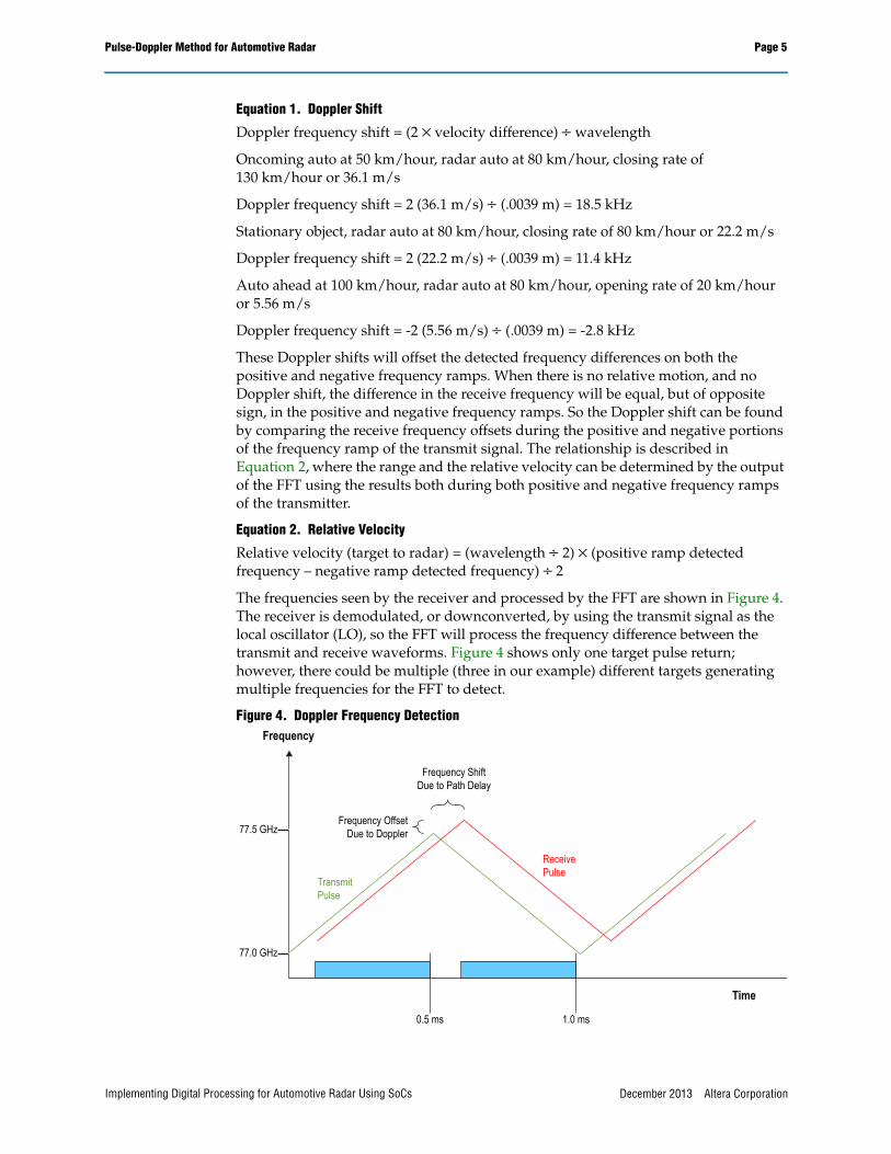
The frequencies seen by the receiver and processed by the FFT are shown in Figure 4. The receiver is demodulated, or downconverted, by using the transmit signal as the local oscillator (LO), so the FFT will process the frequency difference between the transmit and receive waveforms. Figure 4 shows only one target pulse return; however, there could be multiple (three in our example) different targets generating multiple frequencies for the FFT to detect.
Figure 4. Doppler Frequency DetectionFrequency
Time
TransmitPulse
ReceivePulse
Frequency ShiftDue to Path Delay
Frequency OffsetDue to Doppler77.5 GHz
77.0 GHz
0.5 ms 1.0 ms
December 2013 Altera CorporationImplementing Digital Processing for Automotive Radar Using SoCs
Page 6 Pulse-Doppler Method for Automotive Radar
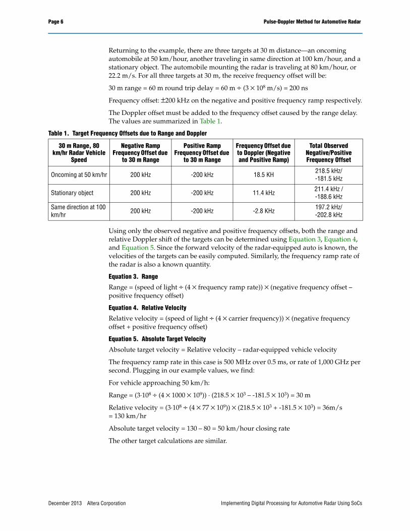
Returning to the example, there are three targets at 30 m distance—an oncoming automobile at 50 km/hour, another traveling in same direction at 100 km/hour, and a stationary object. The automobile mounting the radar is traveling at 80 km/hour, or 22.2 m/s. For all three targets at 30 m, the receive frequency offset will be:
30 m range = 60 m round trip delay = 60 m ÷ (3 × 10⁸ m/s) = 200 ns
Frequency offset: ±200 kHz on the negative and positive frequency ramp respectively.
The Doppler offset must be added to the frequency offset caused by the range delay. The values are summarized in Table 1.
Using only the observed negative and positive frequency offsets, both the range and relative Doppler shift of the targets can be determined using Equation 3, Equation 4, and Equation 5. Since the forward velocity of the radar-equipped auto is known, the velocities of the targets can be easily computed. Similarly, the frequency ramp rate of the radar is also a known quantity.
Equation 3. Range
Range = (speed of light ÷ (4 × frequency ramp rate)) × (negative frequency offset – positive frequency offset)
Equation 4. Relative Velocity
Relative velocity = (speed of light ÷ (4 × carrier frequency)) × (negative frequency offset + positive frequency offset)
Equation 5. Absolute Target Velocity
Absolute target velocity = Relative velocity – radar-equipped vehicle velocity
The frequency ramp rate in this case is 500 MHz over 0.5 ms, or rate of 1,000 GHz per second. Plugging in our example values, we find:
For vehicle approaching 50 km/h:
Range = (3·108 ÷ (4 × 1000 × 109)) · (218.5 × 10³ – -181.5 × 10³) = 30 m
Relative velocity = (3·108 ÷ (4 × 77 × 109)) × (218.5 × 10³ + -181.5 × 10³) = 36m/s = 130 km/hr
Absolute target velocity = 130 – 80 = 50 km/hour closing rate
The other target calculations are similar.
Table 1. Target Frequency Offsets due to Range and Doppler
30 m Range, 80 km/hr Radar Vehicle
Speed
Negative Ramp Frequency Offset due
to 30 m Range
Positive Ramp Frequency Offset due
to 30 m Range
Frequency Offset due to Doppler (Negative and Positive Ramp)
Total Observed Negative/Positive Frequency Offset
Oncoming at 50 km/hr 200 kHz -200 kHz 18.5 KH 218.5 kHz/-181.5 kHz
Stationary object 200 kHz -200 kHz 11.4 kHz 211.4 kHz /-188.6 kHz
Same direction at 100 km/hr 200 kHz -200 kHz -2.8 KHz 197.2 kHz/
-202.8 kHz
December 2013 Altera Corporation Implementing Digital Processing for Automotive Radar Using SoCs
Radar Link Budget Page 7
A critical aspect to be considered is in the presence of multiple targets, it may not be easily apparent how to pair up the frequencies in the negative and positive ramp period. This problem is known as ambiguities in radar jargon, and special techniques are needed to deal with it, as it is a more complicated issue in CWFM radar than in pulse-Doppler radar.
One approach to the problem is varying the duration and frequency of the ramps and evaluating how the detected frequencies move in the spectrum with different steepness of frequency ramps. This variation can allow accurate pairing of the negative and positive frequency identification of each target. As the ramp can be varied roughly once per ms, hundreds of these variations can be analyzed in a fraction of a second. It is normally the job of the control processor, implemented in one of the ARM Cortex-A9 processors of the SoC, to control the settings of the frequency ramps and durations, and determine the target range and Doppler from the FFT output frequencies detected in the negative and positive frequency ramps.
Using alternate sensing techniques can also help. Cameras can help discriminate between stronger returns from vehicles compared to weaker returns from people, and what sort of Doppler offset to expect. If stereo cameras are used, then imaging analysis techniques can be employed to help estimate range as well.
Another option is a multimode radar, using CWFM to find targets at longer range on the open highway, and using a short range pulse-Doppler radar for urban areas, where more target returns are present at closer ranges. The pulse-Doppler radar will have less ambiguity detection issues in a crowded target environment.
Radar Link BudgetRadar performance is governed by the link budget equations, which determine what level of receive signal are available for detection. A simplified version of the radar link budget is expressed in Equation 6.
Equation 6. Radar Link Budget
Prcv = Ptrx × G2 × σ × λ2 × τ ÷ ((4π)3 × R4)
Where:
Ptrx is the peak transmit power
G is the transmit and receive antenna gain
σ is the radar cross section or area of the target
λ is the radar wavelength
τ is the duty cycle of transmitter
R is the range to the target
Often, parameters are specified on a logarithmic scale, using decibels (dB), or dBm (dB referenced to 1 mW). This scale will be used in this case, but figures in Watts will also be given. We must make a few assumptions. With an achievable receiver noise figure of 5 dB, the receiver sensitivity should be about -120 dBm (10-15 W). Assuming about 20 dB signal-to-noise ratio (SNR) to achieve reasonable frequency detection, results in a requirement that Prcv should be at least 100 dBm (10-13 W) under worst-case circumstances.
December 2013 Altera CorporationImplementing Digital Processing for Automotive Radar Using SoCs
Page 8 Implementation Considerations
We will use an antenna gain of 30 dB, or 1000. For a parabolic antenna, the gain in the direction of the boresight of the antenna can be calculated as shown in Equation 7.
Equation 7. Antenna Boresight Gain
G = 4πAeff ÷ λ
Working backward, we find the area required for the antenna at 77 GHz is .0012 m2, which works out to a diameter of 0.04 m, or 4 cm, which is a very reasonable size to mount on the front of a vehicle. (Note, we need at least one transmit and one receiver antenna.)
The duty cycle τ in CWFM is 100%, or 1. If we assume a transmit power of 0.1 W (20 dBm), a maximum range of 300 m, and a target vehicle reflecting area of 1 m2, we can find the worst-case receive power under reasonable circumstances.
Prcv = (0.1 × 1,0002 × 1 × .00392 × 1) ÷ ((4π)3 × 3004) = 9.4 × 10⁻¹⁴ W or -100 dBm
Using a very close range, say 2 m, and same cross sectional area of 10 m2 (the back of a tractor trailer), we can calculate the maximum Prcv we can expect under reasonable circumstances.
Prcv = (0.1 × 1,0002 × 1 × .00392 × 10) ÷ ((4π)3 × 24) = 4.8 × 10⁻⁴ W or -3.2 dBm
These calculations tell us that our system requires a very high-dynamic-range receiver, on the order of 120 dB. The high dynamic range imposes a severe requirement upon linearity of the receiver and the analog-to-digital converter (ADC). However, a large target only 2 m away will obscure the radar line of sight for other targets. Therefore, an analog automatic gain control (AGC) loop can be used to reduce the dynamic range of the receiver and ADC by desensitizing the receiver with attenuation in the presence of extremely large returns.
Full sensitivity could be desired in a slightly less demanding situation, such as a 1 m2 target at 4 m distance, and still used to detect other targets at much longer range. In this case, the large return will have a receive power:
Prcv = (0.1 × 1,0002 × 1 × .00392 × 1) ÷ ((4π)3 × 44) = 3.0 × 10⁻⁶ W or -25 dBm
The use of AGC reduces the dynamic range requirement to about 95 dBm, achievable using a 16 bit ADC. To give some margin, the ADC could be operated with 32x oversampling (beyond Nyquist requirements) to achieve another effective 3 bits, or reducing the quantization noise floor a further18 dB. Alternatively, an 18 bit ADC could be used, but would likely be much more costly.
Implementation ConsiderationsThe advantage of the CWFM radar architecture is simplicity in both the analog and digital implementation. On the analog side, the transmitter can be implemented using a direct digital synthesizer (DDS) with a standard reference crystal. The DDS generates an analog frequency ramp reference for the phased-locked loop (PLL) to generate the desired transmit frequency modulation. For example, if the PLL has a divider of 1000, then in our example, the reference would be centered at 77 MHz, with a 5 MHz frequency ramp. This analog ramp signal drives the reference of a PLL, which disciplines a 77 GHz oscillator. The oscillator output of the circuit is amplified and produces the continuous wave (CW) signal ramping up and down over 500 MHz with a center frequency of 77 GHz. Filtering and matching circuits at 77 GHz can be
December 2013 Altera Corporation Implementing Digital Processing for Automotive Radar Using SoCs

Implementation Considerations Page 9
accomplished using passive components etched into high-epsilon R dielectric circuit cards, minimizing the components required. Figure 5 illustrates an analog circuit block diagram.
Figure 5. Analog Circuit Block Diagram
In the receiver, the front end requires filtering and a low-noise amplifier (LNA), followed by an analog mixer. The mixer downconverts the 77 GHz receive signal with the ramping transmit signal, outputting a baseband signal that contains the difference between the transit and receive waveforms at any given instant. The ramping is cancelled out, as we see fixed frequencies depending upon the range and Doppler shift of the target returns. Again, the high-frequency filtering at 77 GHz can be implemented using etched passive components. The output of the mixer will be at low frequency, up to ±2 MHz at maximum range. Therefore, traditional passive components and operational amplifiers can be used to provide anti-aliasing low-pass filtering prior to the ADC. Alternately, an intermediate frequency (IF) architecture could be used, but would require an offset receive LO generation circuit.
Note that complex downconversion is not required. The baseband signal is composed of frequencies, either all positive (during negative frequency ramp) or all negative (during positive frequency ramp), so a mixer followed by a single low-pass filter and ADC is sufficient.
The ADC for baseband input must operate at a minimum of 5 MSPS to meet the Nyquist criterion. If, instead, an 8x sampling frequency of 40 MSPS is used, followed by an 8:1 digital decimation filter, then approximately 3 bits of additional resolution can be achieved. This decimation allows a 16 bit ADC to effectively operate in the range of 18 to19 bits, achieving well over 100 dB of dynamic range.
The digital filter can operate at a 160 MHz rate using 16 bit input samples, outputting samples at 5 MHz, but rounded to 24 bits. The next step of signal processing is to perform frequency discrimination using an FFT, followed by an interpolation circuit. The nature of FFTs is to have growth in the data precision as it proceeds through the processing stages. For our case, we will assume a 2,048 point FFT, which can potentially require up to 10 additional bits of precision to avoid any loss of data. However, this bit growth can be avoided by implementing the FFT in single-precision floating-point processing. The full 24 bit mantissa precision (23 bits plus sign) can be preserved through the FFT, and will easily accommodate the 100+ dB dynamic range of the target returns. Distant and weak target returns will not be obscured by nearby, strong returns, therefore avoiding the radar system being “blinded” by strong, nearby
LPFilter
ADC
77 GHzBP Filter
LNA RXAntenna
77 GHzBP Filter
PowerAmp
TXAntenna
Mixer
77 GHzVCO
RampReference
LoopFilterPLL
DDS
TransmitControl
FrequencyReference
Baseband Data
December 2013 Altera CorporationImplementing Digital Processing for Automotive Radar Using SoCs
Page 10 Implementation Considerations
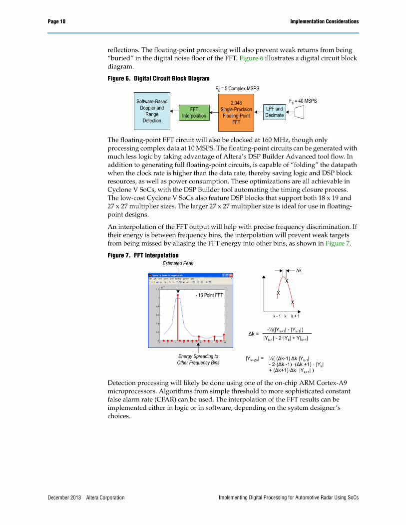
reflections. The floating-point processing will also prevent weak returns from being “buried” in the digital noise floor of the FFT. Figure 6 illustrates a digital circuit block diagram.
Figure 6. Digital Circuit Block Diagram
The floating-point FFT circuit will also be clocked at 160 MHz, though only processing complex data at 10 MSPS. The floating-point circuits can be generated with much less logic by taking advantage of Altera’s DSP Builder Advanced tool flow. In addition to generating full floating-point circuits, is capable of “folding” the datapath when the clock rate is higher than the data rate, thereby saving logic and DSP block resources, as well as power consumption. These optimizations are all achievable in Cyclone V SoCs, with the DSP Builder tool automating the timing closure process. The low-cost Cyclone V SoCs also feature DSP blocks that support both 18 x 19 and 27 x 27 multiplier sizes. The larger 27 x 27 multiplier size is ideal for use in floating-point designs.
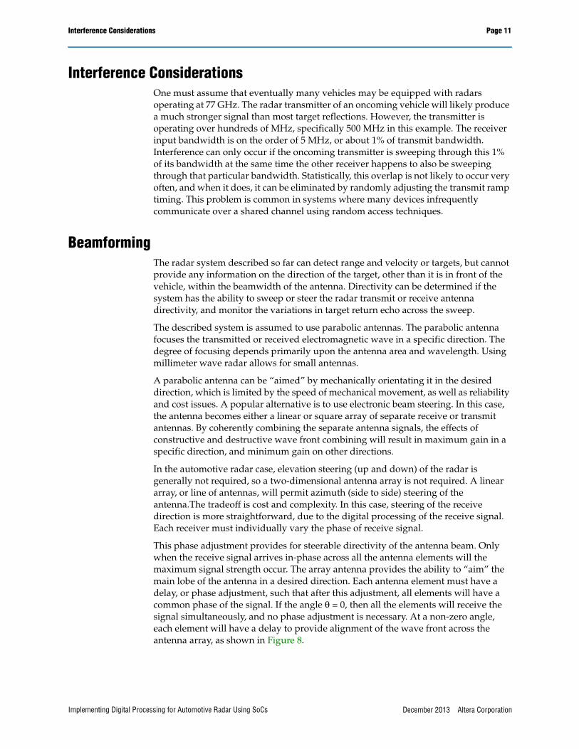
An interpolation of the FFT output will help with precise frequency discrimination. If their energy is between frequency bins, the interpolation will prevent weak targets from being missed by aliasing the FFT energy into other bins, as shown in Figure 7.
Figure 7. FFT Interpolation
Detection processing will likely be done using one of the on-chip ARM Cortex-A9 microprocessors. Algorithms from simple threshold to more sophisticated constant false alarm rate (CFAR) can be used. The interpolation of the FFT results can be implemented either in logic or in software, depending on the system designer’s choices.
FS = 5 Complex MSPS
FS = 40 MSPSFFT
Interpolation
2,048Single-PrecisionFloating-Point
FFT
LPF andDecimate
Software-BasedDoppler and
RangeDetection
- 16 Point FFT
Estimated Peak
Energy Spreading to
Other Frequency Bins
X
X
X
k - 1 k k + 1
- (|Yk+1| - |Yk-1|)
|Yk-1| - 2 |Yk| + Y|k+1| k =
|Yk+ k| = ( ( k-1) k |Yk-1| - 2 ( k -1) ( k +1) |Yk| + ( k+1) k |Yk+1| )
December 2013 Altera Corporation Implementing Digital Processing for Automotive Radar Using SoCs
Interference Considerations Page 11
Interference ConsiderationsOne must assume that eventually many vehicles may be equipped with radars operating at 77 GHz. The radar transmitter of an oncoming vehicle will likely produce a much stronger signal than most target reflections. However, the transmitter is operating over hundreds of MHz, specifically 500 MHz in this example. The receiver input bandwidth is on the order of 5 MHz, or about 1% of transmit bandwidth. Interference can only occur if the oncoming transmitter is sweeping through this 1% of its bandwidth at the same time the other receiver happens to also be sweeping through that particular bandwidth. Statistically, this overlap is not likely to occur very often, and when it does, it can be eliminated by randomly adjusting the transmit ramp timing. This problem is common in systems where many devices infrequently communicate over a shared channel using random access techniques.
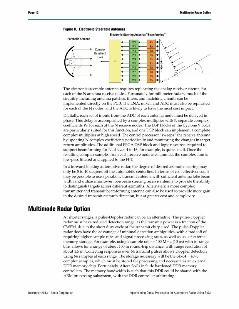
BeamformingThe radar system described so far can detect range and velocity or targets, but cannot provide any information on the direction of the target, other than it is in front of the vehicle, within the beamwidth of the antenna. Directivity can be determined if the system has the ability to sweep or steer the radar transmit or receive antenna directivity, and monitor the variations in target return echo across the sweep.
The described system is assumed to use parabolic antennas. The parabolic antenna focuses the transmitted or received electromagnetic wave in a specific direction. The degree of focusing depends primarily upon the antenna area and wavelength. Using millimeter wave radar allows for small antennas.
A parabolic antenna can be “aimed” by mechanically orientating it in the desired direction, which is limited by the speed of mechanical movement, as well as reliability and cost issues. A popular alternative is to use electronic beam steering. In this case, the antenna becomes either a linear or square array of separate receive or transmit antennas. By coherently combining the separate antenna signals, the effects of constructive and destructive wave front combining will result in maximum gain in a specific direction, and minimum gain on other directions.
In the automotive radar case, elevation steering (up and down) of the radar is generally not required, so a two-dimensional antenna array is not required. A linear array, or line of antennas, will permit azimuth (side to side) steering of the antenna.The tradeoff is cost and complexity. In this case, steering of the receive direction is more straightforward, due to the digital processing of the receive signal. Each receiver must individually vary the phase of receive signal.
This phase adjustment provides for steerable directivity of the antenna beam. Only when the receive signal arrives in-phase across all the antenna elements will the maximum signal strength occur. The array antenna provides the ability to “aim” the main lobe of the antenna in a desired direction. Each antenna element must have a delay, or phase adjustment, such that after this adjustment, all elements will have a common phase of the signal. If the angle θ = 0, then all the elements will receive the signal simultaneously, and no phase adjustment is necessary. At a non-zero angle, each element will have a delay to provide alignment of the wave front across the antenna array, as shown in Figure 8.
December 2013 Altera CorporationImplementing Digital Processing for Automotive Radar Using SoCs
Page 12 Multimode Radar Option
Figure 8. Electronic Steerable Antennas
The electronic steerable antenna requires replicating the analog receiver circuits for each of the N antenna receive nodes. Fortunately for millimeter radars, much of the circuitry, including antenna patches, filters, and matching circuits can be implemented directly on the PCB. The LNA, mixer, and ADC must also be replicated for each of the N nodes, and the ADC is likely to have the most cost impact.
Digitally, each set of inputs from the ADC of each antenna node must be delayed in phase. This delay is accomplished by a complex multiplier with N separate complex coefficients Wi for each of the N receive nodes. The DSP blocks of the Cyclone V SoCs are particularly suited for this function, and one DSP block can implement a complete complex multiplier at high speed. The control processor “sweeps” the receive antenna by updating N complex coefficients periodically and monitoring the changes in target return amplitudes. The additional FPGA DSP block and logic resources required to support beamforming for N of sizes 4 to 16, for example, is quite small. Once the resulting complex samples from each receive node are summed, the complex sum is low-pass filtered and applied to the FFT.
In a forward-looking automotive radar, the degree of desired azimuth steering may only be 5 to 10 degrees off the automobile centerline. In terms of cost effectiveness, it may be possible to use a parabolic transmit antenna with sufficient antenna lobe beam width and utilize a narrower lobe beam steering receive antenna to provide the ability to distinguish targets across different azimuths. Alternately, a more complex transmitter and transmit beamforming antenna can also be used to provide more gain in the desired transmit azimuth direction, but at greater cost and complexity.
Multimode Radar OptionAt shorter ranges, a pulse-Doppler radar can be an alternative. The pulse-Doppler radar must have reduced detection range, as the transmit power is a fraction of the CWFM, due to the short duty cycle of the transmit chirp used. The pulse-Doppler radar does have the advantage of minimal detection ambiguities, with a tradeoff of requiring higher sample rates and signal processing rates, as well as use of external memory storage. For example, using a sample rate of 100 MHz (10 ns) with 64 range bins allows for a range of about 100 m round-trip distance, with range resolution of about 1.5 m. Collecting responses over 64 transmit pulses allows Doppler detection using 64 samples at each range. The storage necessary will be the 64x64 = 4096 complex samples, which must be stored for processing and necessitates an external DDR memory chip. Fortunately, Altera SoCs include hardened DDR memory controllers. The memory bandwidth is such that this DDR could be shared with the ARM processing subsystem, with the DDR controller arbitrating.
W0W1W2W3W4W5W6W7W8W9
RxRxRxRxRxRxRxRxRxRx
Σ
d
λ
Θ
Parabolic AntennaElectronic Steering Antenna (”Beamforming”)
ComplexBaseband
Data
December 2013 Altera Corporation Implementing Digital Processing for Automotive Radar Using SoCs
FPGA Resources Estimations Page 13
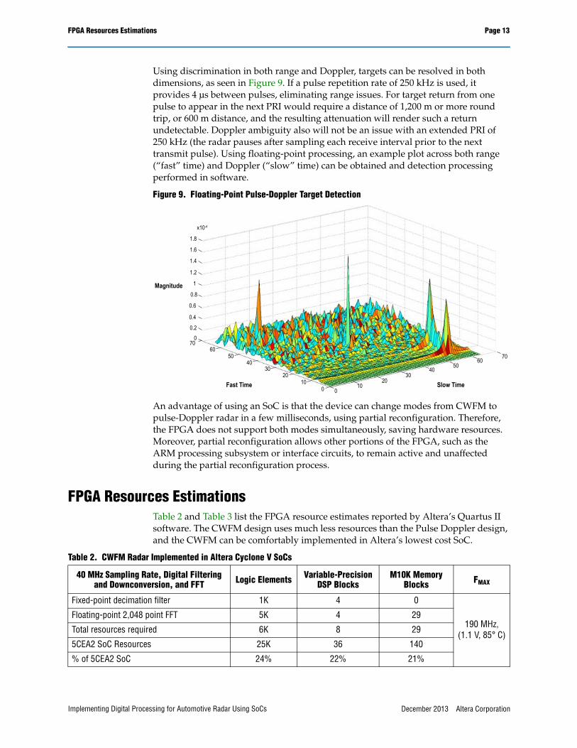
Using discrimination in both range and Doppler, targets can be resolved in both dimensions, as seen in Figure 9. If a pulse repetition rate of 250 kHz is used, it provides 4 µs between pulses, eliminating range issues. For target return from one pulse to appear in the next PRI would require a distance of 1,200 m or more round trip, or 600 m distance, and the resulting attenuation will render such a return undetectable. Doppler ambiguity also will not be an issue with an extended PRI of 250 kHz (the radar pauses after sampling each receive interval prior to the next transmit pulse). Using floating-point processing, an example plot across both range (“fast” time) and Doppler (“slow” time) can be obtained and detection processing performed in software.
Figure 9. Floating-Point Pulse-Doppler Target Detection
An advantage of using an SoC is that the device can change modes from CWFM to pulse-Doppler radar in a few milliseconds, using partial reconfiguration. Therefore, the FPGA does not support both modes simultaneously, saving hardware resources. Moreover, partial reconfiguration allows other portions of the FPGA, such as the ARM processing subsystem or interface circuits, to remain active and unaffected during the partial reconfiguration process.
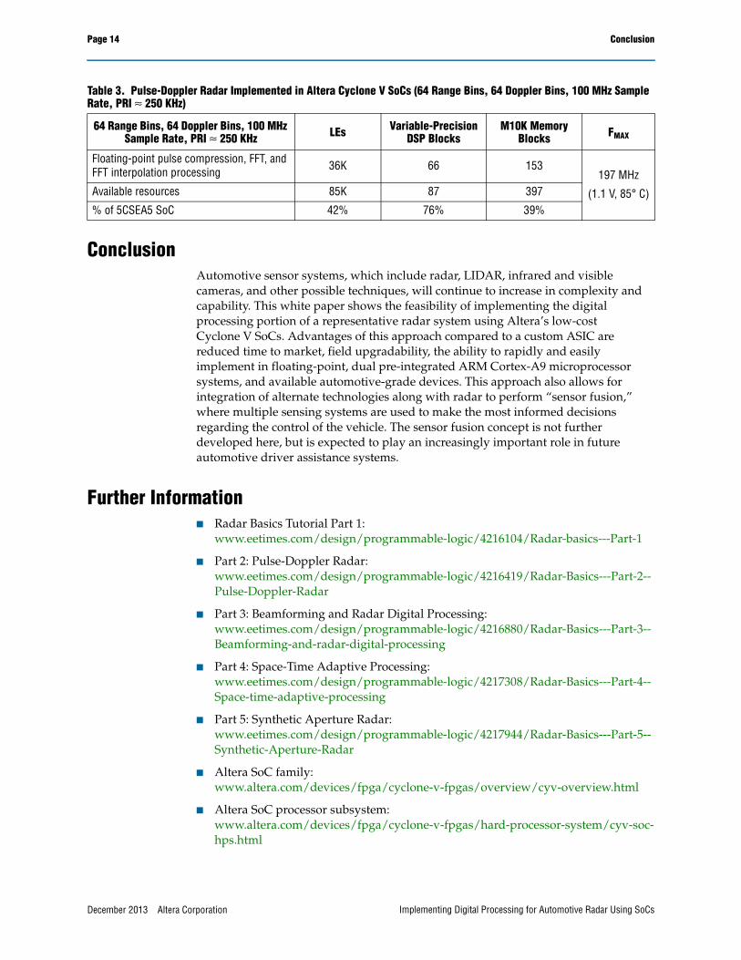
FPGA Resources EstimationsTable 2 and Table 3 list the FPGA resource estimates reported by Altera’s Quartus II software. The CWFM design uses much less resources than the Pulse Doppler design, and the CWFM can be comfortably implemented in Altera’s lowest cost SoC.
1.8
1.6
1.4
1.2
1
0.8
0.6
0.4
00.2
Magnitude
7060
5040
3020
100
7060
5040
3020
100
Slow TimeFast Time
x10-4
Table 2. CWFM Radar Implemented in Altera Cyclone V SoCs
40 MHz Sampling Rate, Digital Filtering and Downconversion, and FFT Logic Elements Variable-Precision
DSP BlocksM10K Memory
Blocks FMAX
Fixed-point decimation filter 1K 4 0
190 MHz, (1.1 V, 85° C)
Floating-point 2,048 point FFT 5K 4 29
Total resources required 6K 8 29
5CEA2 SoC Resources 25K 36 140
% of 5CEA2 SoC 24% 22% 21%
December 2013 Altera CorporationImplementing Digital Processing for Automotive Radar Using SoCs
Page 14 Conclusion
ConclusionAutomotive sensor systems, which include radar, LIDAR, infrared and visible cameras, and other possible techniques, will continue to increase in complexity and capability. This white paper shows the feasibility of implementing the digital processing portion of a representative radar system using Altera’s low-cost Cyclone V SoCs. Advantages of this approach compared to a custom ASIC are reduced time to market, field upgradability, the ability to rapidly and easily implement in floating-point, dual pre-integrated ARM Cortex-A9 microprocessor systems, and available automotive-grade devices. This approach also allows for integration of alternate technologies along with radar to perform “sensor fusion,” where multiple sensing systems are used to make the most informed decisions regarding the control of the vehicle. The sensor fusion concept is not further developed here, but is expected to play an increasingly important role in future automotive driver assistance systems.
Further Information■ Radar Basics Tutorial Part 1:
www.eetimes.com/design/programmable-logic/4216104/Radar-basics---Part-1
■ Part 2: Pulse-Doppler Radar:www.eetimes.com/design/programmable-logic/4216419/Radar-Basics---Part-2--Pulse-Doppler-Radar
■ Part 3: Beamforming and Radar Digital Processing: www.eetimes.com/design/programmable-logic/4216880/Radar-Basics---Part-3--Beamforming-and-radar-digital-processing
■ Part 4: Space-Time Adaptive Processing: www.eetimes.com/design/programmable-logic/4217308/Radar-Basics---Part-4--Space-time-adaptive-processing
■ Part 5: Synthetic Aperture Radar:www.eetimes.com/design/programmable-logic/4217944/Radar-Basics---Part-5--Synthetic-Aperture-Radar
■ Altera SoC family:www.altera.com/devices/fpga/cyclone-v-fpgas/overview/cyv-overview.html
■ Altera SoC processor subsystem:www.altera.com/devices/fpga/cyclone-v-fpgas/hard-processor-system/cyv-soc-hps.html
Table 3. Pulse-Doppler Radar Implemented in Altera Cyclone V SoCs (64 Range Bins, 64 Doppler Bins, 100 MHz Sample Rate, PRI ≈ 250 KHz)
64 Range Bins, 64 Doppler Bins, 100 MHz Sample Rate, PRI ≈ 250 KHz LEs Variable-Precision
DSP BlocksM10K Memory
Blocks FMAX
Floating-point pulse compression, FFT, and FFT interpolation processing 36K 66 153
197 MHz
(1.1 V, 85° C)Available resources 85K 87 397
% of 5CSEA5 SoC 42% 76% 39%
December 2013 Altera Corporation Implementing Digital Processing for Automotive Radar Using SoCs
Acknowledgements Page 15
Acknowledgements■ Michael Parker, DSP Planning Architect, Altera Corporation
Document Revision HistoryTable 4 lists the revision history for this document.
Table 4. Document Revision History
Date Version Changes
December 2013 1.3 Updates to “Introduction” on page 1.
January 2013 1.2 Updates to Figure 2, “Implementation Considerations”, Figure 5, Figure 6, “Beamforming”, and Figure 8.
September 2012 1.1 Minor text edits.
September 2012 1.0 Initial release.
December 2013 Altera CorporationImplementing Digital Processing for Automotive Radar Using SoCs

Page 16 Document Revision History
December 2013 Altera Corporation Implementing Digital Processing for Automotive Radar Using SoCs