implicating the contributions of surface and bulk states
TRANSCRIPT

Marquette Universitye-Publications@Marquette
Chemistry Faculty Research and Publications Chemistry, Department of
2-7-2017
Implicating the Contributions of Surface and BulkStates on Carrier Trapping and PhotocurrentPerformance of BiVO4 PhotoanodesBrian PattengaleMarquette University
Jier HuangMarquette University, [email protected]
Accepted version. Physical Chemistry Chemical Physics, Vol. 19, No. 9 (2017): 6831-6837. DOI. ©2017 The Royal Society of Chemistry. Used with permission.
Marquette University
e-Publications@Marquette
Chemistry Faculty Research and Publications/College of Arts and Sciences
This paper is NOT THE PUBLISHED VERSION; but the author’s final, peer-reviewed manuscript. The published version may be accessed by following the link in the citation below.
Physical Chemistry Chemical Physics, Vol. 19 (2005): 6831-6837. DOI. This article is © Royal Society of Chemistry and permission has been granted for this version to appear in e-Publications@Marquette. Royal Society of Chemistry does not grant permission for this article to be further copied/distributed or hosted elsewhere without the express permission from Royal Society of Chemistry.
Implicating the Contributions of Surface and Bulk States on Carrier Trapping and Photocurrent Performance of Bivo4 Photoanodes
B. Pattengale Marquette University, Milwaukee WI J. Huang Marquette University, Milwaukee WI
Abstract Monoclinic-scheelite BiVO4 has been widely studied as a promising oxygen evolution reaction (OER) catalyst in artificial photosynthesis. Though significant progress to improve or augment its catalysis performance has been made, fundamental understanding of its relatively poor performance as a bare material is lacking. In this paper, we report the correlation of the surface structure and trap states with charge separation efficiency and OER performance of bare BiVO4 photoanodes via varying the sample

thickness. Using X-ray absorption spectroscopy (XAS), we observed a more compacted, symmetric Bi center in the surface state. Using transient absorption (TA) spectroscopy, we show that the structural properties of the surface lead to shallow and deep hole trap states and electron trapping that occurs at the surface of the material. Despite more severe carrier trapping on the surface, our OER measurements demonstrate that a significant bulk structure is required for light absorption but is only beneficial until the carrier mobility becomes the limiting factor in photoelectrochemical cell studies.
Introduction Photoelectrochemical (PEC) water splitting to produce H2 has been recognized as a viable approach for superseding fossil fuel energy sources and combating their deleterious environmental effects.1–5 The major barrier to performing this process is the kinetically and thermodynamically challenging oxygen evolution reaction (OER), the oxidative half reaction that splits water into protons and oxygen gas. The thermodynamics requirement together with the associated overpotential necessary to drive the OER has driven the development of a variety of n-type semiconductor metal oxides that are relatively stable and show significant visible light absorption.1,6–9
Of these materials, monoclinic scheelite bismuth vanadate (BiVO4) has received special attention owing to its narrow bandgap (∼2.4 eV) and appropriate valence band edge with respect to the OER.10–12 Despite its potential as a photoanode material, the OER performance of a bare BiVO4 photoanode is modest and limited by poor charge separation, low photogenerated carrier mobility (reported to be 4 × 10⁻² cm2 V−1 s−1)13 and slow OER kinetics. Further development of these materials for the OER would certainly demand a thorough understanding of the mechanistic origin of the modest performance of bare BiVO4, which, however, is a persisting challenge.10 An important distinction needs to be made between the bulk states that play a dominant role in photogenerated carrier transport and light absorption and the surface states that perform the actual redox chemistry during the OER.
Due to termination of the crystalline structure at the surface, semiconducting materials develop trap states due to structural and coordination differences from the bulk crystalline structure, or defect states.14,15 As a result, photogenerated charge carriers can be trapped in surface defect states, typically on a femtosecond to picosecond timescale,16–20 before either performing their respective redox chemistries or recombining. Before implicating the bulk or surface states in the modest performance of BiVO4, there is a need to uncover the properties of each state without altering the crystal structure of the material (i.e. utilizing standard synthetic techniques).
In this work, we report the molecular level understanding of the electronic structure of bulk and surface states by evaluating the correlation of the bulk and local electronic structure, carrier dynamics, and PEC performance of the bare BiVO4 film. BiVO4 thin films with different thicknesses were synthesized to alter the ratio of the bulk material to the surface material. Using the combination of multiple spectroscopic methods, we observed surface electron and hole trap states that, in correlation to PEC performance, require a significant bulk layer to decompensate the trap-mediated recombination in BiVO4 thin films. These findings indicate a critical thickness for BiVO4 photoanodes due to the carrier mobility and the necessity to modulate the carrier trapping processes in order to develop the optimal next generation of BiVO4 photoanode materials.
Experimental
Materials Vanadyl-(IV) acetylacetonate (C10H14O5V) was purchased from Acros Organics (Geel, Belgium) and bismuth(III) nitrate (Bi(NO3)3·5H2O) and sodium sulfate (Na2SO4) were purchased from Ward’s Science (Rochester, NY). Acetylacetone (>99.0%) was purchased from TCI America (Portland, OR) and acetic acid (>99.7%) was purchased from Sigma Aldrich (Milwaukee, WI). Fluorine-doped tin oxide (FTO) glass was acquired from Solaronix (Aubonne, Switzerland). Piranha glass-etching solution was prepared from nitric acid (Sigma Aldrich, Milwaukee, WI) and hydrogen peroxide (30%, J.T. Baker, Avantor Materials, Center Valley PA).
BiVO4 synthesis Following a solution-based method,21 bismuth nitrate and vanadyl acetylacetonate were dissolved in acetic acid and acetylacetone, respectively. These solutions were sonicated individually to dissolve and then mixed and sonicated to give a 0.08 M BiVO4 solution with a 1 : 4 acetic acid to acetylacetone volume ratio and a 1 : 1 Bi : V mole ratio. The stock solution was then either used directly or diluted with acetylacetone to 0.04, 0.02, and 0.01 M concentrations. For transient absorption, UV-visible, X-ray diffraction, and X-ray absorption measurements, a 1.25 × 2.50 cm quartz substrate was etched with piranha solution (3 : 1 H2SO4 : H2O2 mixture) for 3 hours, rinsed with water, and then 25 μL of the BiVO4 precursor was drop-coated onto the substrate and allowed to dry under ambient conditions. For PEC measurements, FTO electrodes with the same sample area dimensions were prepared under the same conditions. The dried films were then calcined in air at 450 °C for 90 minutes to form BiVO4 films from the amorphous precursor films.
Characterization UV-visible absorption spectra were collected on an HP Agilent 8453 spectrometer. For X-ray diffraction (XRD), film samples were prepared and patterns were collected on a Rigaku Miniflex II diffractometer (Cu-Kα radiation). Cross-sectional SEM was performed using a JEOL JSM-6510LV in secondary electron mode with an ≈20 nm thick AuPd sputter-coated layer.
Transient absorption spectroscopy (TA) A regenerative amplified Ti-Sapphire laser (Solstice, 800 nm, 3.5 mJ per pulse, <100 fs fwhm, 1 kHz repetition) was used to generate pump and probe pulses for TA spectroscopy. The output of the laser is split to give 75% of output to TOPAS to generate tunable pump pulses (235–1150 nm) chopped at 500 Hz and the other 25% is directed to a Helios ultrafast spectrometer (Ultrafast Systems LLC), where a translated CaF2 window is used to generate UV-visible (320–720 nm) probe pulses. The time delay between pump and probe pulses was controlled with a delay stage in the Helios ultrafast spectrometer. The pump pulse energy for the experiments performed was 0.35 μJ at 315 nm and the samples were continuously translated to avoid sample heating and degradation.
Photoelectrochemical cell (PEC) PEC measurements were performed in a custom 3-electrode cell with a flat quartz window. Through this window, >400 nm long-pass filtered and extensively IR filtered (1 foot water bath and IR filter) 300 W Xenon lamp output was focused onto the photoanode BiVO4–FTO sample. The Pt wire counter electrode and the Ag/AgCl (3 M NaCl) reference electrode were used with the BiVO4 working electrode
in the stirred PEC cell with N2 purged 0.1 M Na2SO4 electrolyte. Linear sweep voltammetry (25 mV s−1) was used to generate JV curves with either rear or front-side illumination of the working electrode.
X-ray absorption spectroscopy (XAS) Beamline 12BM of the Advanced Photon Source at Argonne National Laboratory was used to perform the steady-state XAS experiments. The samples were oriented at a standard 45° incident angle to give equal X-ray footprint and penetration depth at each sample thickness for fluorescence mode detection using a 13-element germanium solid-state detector. Three ion chambers were configured to detect incident X-ray flux, transmission through the sample, and then transmission through a Pt or V reference foil for energy calibration.
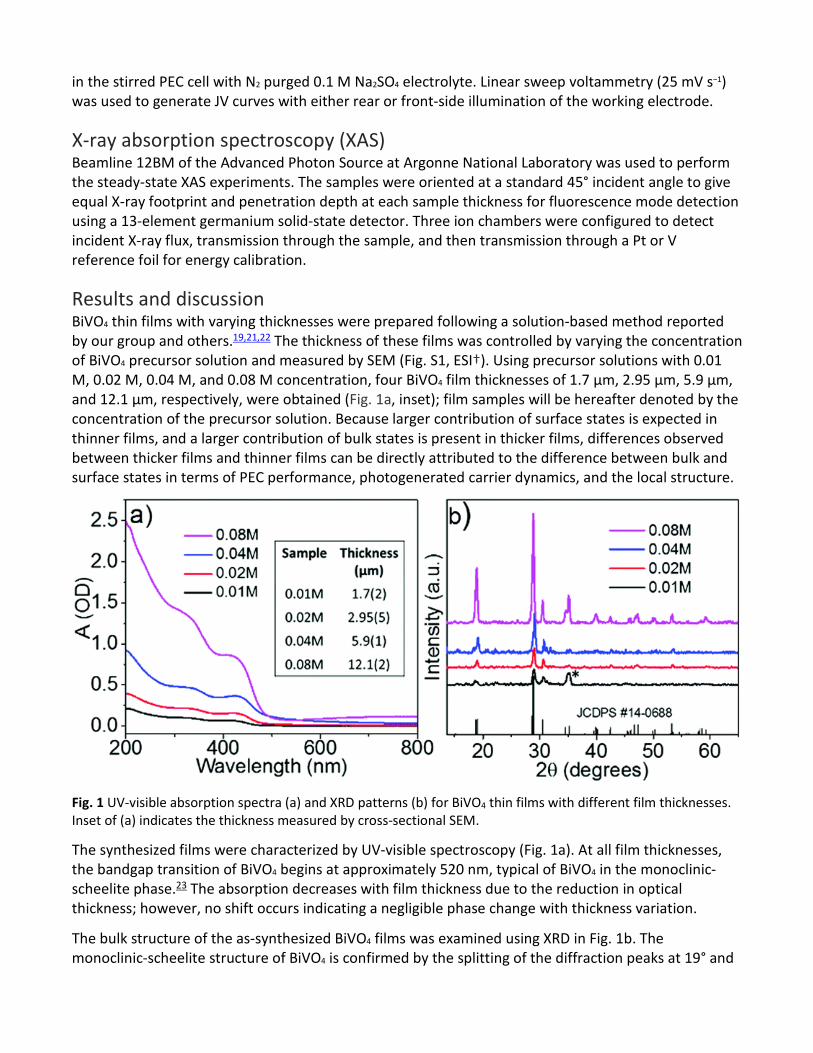
Results and discussion BiVO4 thin films with varying thicknesses were prepared following a solution-based method reported by our group and others.19,21,22 The thickness of these films was controlled by varying the concentration of BiVO4 precursor solution and measured by SEM (Fig. S1, ESI†). Using precursor solutions with 0.01 M, 0.02 M, 0.04 M, and 0.08 M concentration, four BiVO4 film thicknesses of 1.7 μm, 2.95 μm, 5.9 μm, and 12.1 μm, respectively, were obtained (Fig. 1a, inset); film samples will be hereafter denoted by the concentration of the precursor solution. Because larger contribution of surface states is expected in thinner films, and a larger contribution of bulk states is present in thicker films, differences observed between thicker films and thinner films can be directly attributed to the difference between bulk and surface states in terms of PEC performance, photogenerated carrier dynamics, and the local structure.
Fig. 1 UV-visible absorption spectra (a) and XRD patterns (b) for BiVO4 thin films with different film thicknesses. Inset of (a) indicates the thickness measured by cross-sectional SEM.
The synthesized films were characterized by UV-visible spectroscopy (Fig. 1a). At all film thicknesses, the bandgap transition of BiVO4 begins at approximately 520 nm, typical of BiVO4 in the monoclinic-scheelite phase.23 The absorption decreases with film thickness due to the reduction in optical thickness; however, no shift occurs indicating a negligible phase change with thickness variation.
The bulk structure of the as-synthesized BiVO4 films was examined using XRD in Fig. 1b. The monoclinic-scheelite structure of BiVO4 is confirmed by the splitting of the diffraction peaks at 19° and
35° 2θ,24 in agreement with the JCDPS standard (card # 14-0688). It is worth noting that macrostructural strain was observed for BiVO4 thin films in comparison to bulk BiVO4 synthesized by the same method (Fig. S2, ESI†) as shown by a slight shift in the position of the peaks to a higher degree 2θ.25 However, there is no shift observed between film samples at different thicknesses in Fig. 1b, indicating that the strain is not thickness-dependent. There is additionally a significant change in the relative intensity of the split 35° peaks (marked with an asterisk in Fig. 1b) corresponding to the (2 0 0) and (0 2 0) facets, which increases relative to the other peaks for the 0.01 M film. This difference is assigned to a preferred orientation near the BiVO4-substrate interface or at the surface of the material, revealed by the relative decrease in the amount of bulk material.
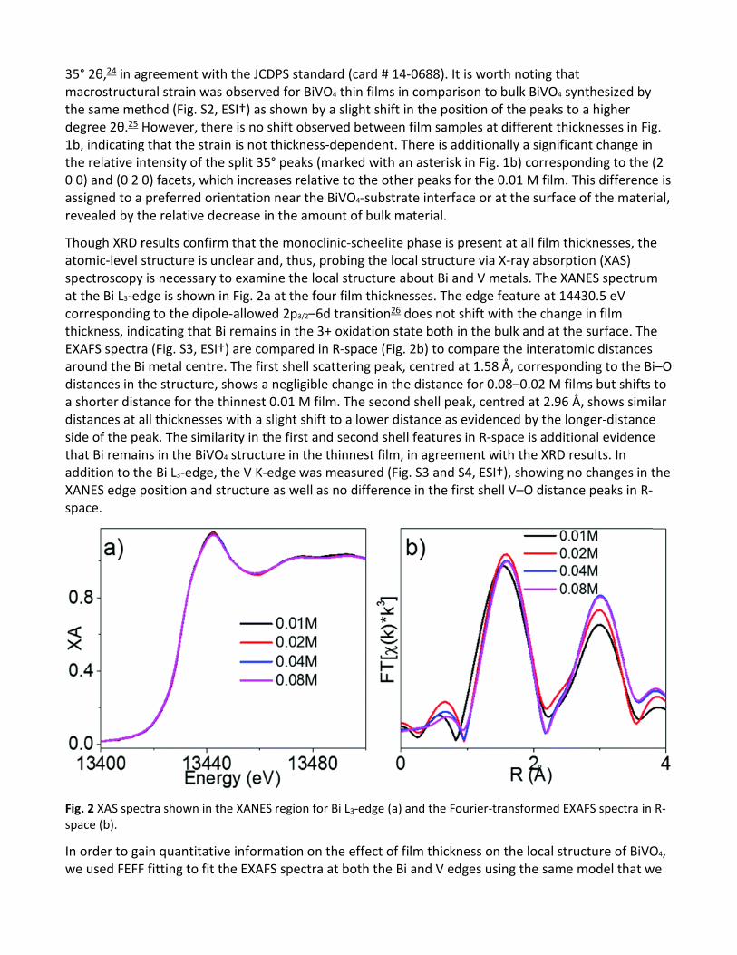
Though XRD results confirm that the monoclinic-scheelite phase is present at all film thicknesses, the atomic-level structure is unclear and, thus, probing the local structure via X-ray absorption (XAS) spectroscopy is necessary to examine the local structure about Bi and V metals. The XANES spectrum at the Bi L3-edge is shown in Fig. 2a at the four film thicknesses. The edge feature at 14430.5 eV corresponding to the dipole-allowed 2p3/2–6d transition26 does not shift with the change in film thickness, indicating that Bi remains in the 3+ oxidation state both in the bulk and at the surface. The EXAFS spectra (Fig. S3, ESI†) are compared in R-space (Fig. 2b) to compare the interatomic distances around the Bi metal centre. The first shell scattering peak, centred at 1.58 Å, corresponding to the Bi–O distances in the structure, shows a negligible change in the distance for 0.08–0.02 M films but shifts to a shorter distance for the thinnest 0.01 M film. The second shell peak, centred at 2.96 Å, shows similar distances at all thicknesses with a slight shift to a lower distance as evidenced by the longer-distance side of the peak. The similarity in the first and second shell features in R-space is additional evidence that Bi remains in the BiVO4 structure in the thinnest film, in agreement with the XRD results. In addition to the Bi L3-edge, the V K-edge was measured (Fig. S3 and S4, ESI†), showing no changes in the XANES edge position and structure as well as no difference in the first shell V–O distance peaks in R-space.
Fig. 2 XAS spectra shown in the XANES region for Bi L3-edge (a) and the Fourier-transformed EXAFS spectra in R-space (b).
In order to gain quantitative information on the effect of film thickness on the local structure of BiVO4, we used FEFF fitting to fit the EXAFS spectra at both the Bi and V edges using the same model that we
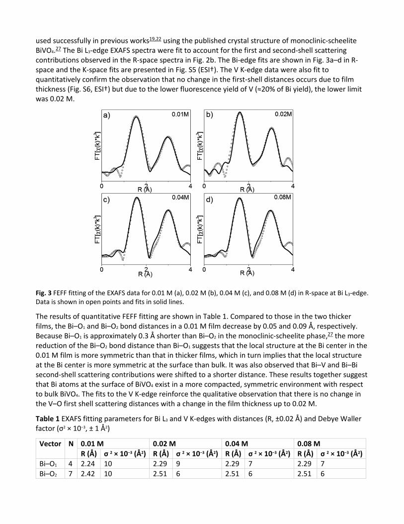
used successfully in previous works19,22 using the published crystal structure of monoclinic-scheelite BiVO4.27 The Bi L3-edge EXAFS spectra were fit to account for the first and second-shell scattering contributions observed in the R-space spectra in Fig. 2b. The Bi-edge fits are shown in Fig. 3a–d in R-space and the K-space fits are presented in Fig. S5 (ESI†). The V K-edge data were also fit to quantitatively confirm the observation that no change in the first-shell distances occurs due to film thickness (Fig. S6, ESI†) but due to the lower fluorescence yield of V (≈20% of Bi yield), the lower limit was 0.02 M.
Fig. 3 FEFF fitting of the EXAFS data for 0.01 M (a), 0.02 M (b), 0.04 M (c), and 0.08 M (d) in R-space at Bi L3-edge. Data is shown in open points and fits in solid lines.
The results of quantitative FEFF fitting are shown in Table 1. Compared to those in the two thicker films, the Bi–O1 and Bi–O2 bond distances in a 0.01 M film decrease by 0.05 and 0.09 Å, respectively. Because Bi–O1 is approximately 0.3 Å shorter than Bi–O2 in the monoclinic-scheelite phase,27 the more reduction of the Bi–O2 bond distance than Bi–O1 suggests that the local structure at the Bi center in the 0.01 M film is more symmetric than that in thicker films, which in turn implies that the local structure at the Bi center is more symmetric at the surface than bulk. It was also observed that Bi–V and Bi–Bi second-shell scattering contributions were shifted to a shorter distance. These results together suggest that Bi atoms at the surface of BiVO4 exist in a more compacted, symmetric environment with respect to bulk BiVO4. The fits to the V K-edge reinforce the qualitative observation that there is no change in the V–O first shell scattering distances with a change in the film thickness up to 0.02 M.
Table 1 EXAFS fitting parameters for Bi L3 and V K-edges with distances (R, ±0.02 Å) and Debye Waller factor (σ2 × 10⁻³, ± 1 Å2)
Vector N 0.01 M 0.02 M 0.04 M 0.08 M R (Å) σ 2 × 10⁻³ (Å2) R (Å) σ 2 × 10⁻³ (Å2) R (Å) σ 2 × 10⁻³ (Å2) R (Å) σ 2 × 10⁻³ (Å2)
Bi–O1 4 2.24 10 2.29 9 2.29 7 2.29 7 Bi–O2 7 2.42 10 2.51 6 2.51 6 2.51 6

Bi–O2 2 2.53 15 2.62 22 2.62 18 2.62 22 Bi–V 2 5.56 7 3.58 7 3.58 4 3.58 4 Bi–V 2 3.69 7 3.72 7 3.72 4 3.72 4 Bi–Bi 2 3.42 20 3.62 12 3.62 18 3.62 17 V–O1 2 — — 1.68 0.7 1.68 2 1.68 6 V–O2 2 — — 1.75 0.7 1.75 1 1.75 1
With the understanding of the bulk and local structure of BiVO4 at the surface, we proceeded to examine the effect of film thickness on light harvesting and carrier dynamics of the BiVO4 photoanode. Fig. 4 shows the femtosecond transient absorption spectra (TA) of BiVO4 films with varying thicknesses upon 315 nm excitation. All TA spectra show four main spectral features, including three positive and one negative feature; the spectra at different film thicknesses are compared in Fig. S7 (ESI†). As in our previous publication19 and on the basis of other works,18,28,29 we assign three positive features, i.e. the positive bands centred at 370 nm and 465 nm, and the broad feature >600 nm, to hole absorption, and the negative feature at 430 nm to ground state bleach (GSB) resulting from the occupation of the conduction band by the photoexcited electron, which reduces the oscillator strength of the bandgap transition.
Fig. 4 TA spectra for 0.01 M (a), 0.02 M (b), 0.04 M (c), and 0.08 M (d) BiVO4 excited at 315 nm.
The evolution of these features as a function of time can be clearly seen from their kinetic traces presented in Fig. 5. Some trends can be observed in the spectral and kinetic data for the positive features as a function of film thickness, namely the slower initial growth on a short timescale and then faster decay on a longer timescale of 370 nm hole trap feature, the loss of growth on the short timescale and faster decay on long timescale for the 465 nm feature, and the faster decay of 620 nm feature. The negative GSB showed a weaker trend as a function of film thickness; however there was generally faster decay for thinner films at all timescales with a clearer trend at shorter timescale. These
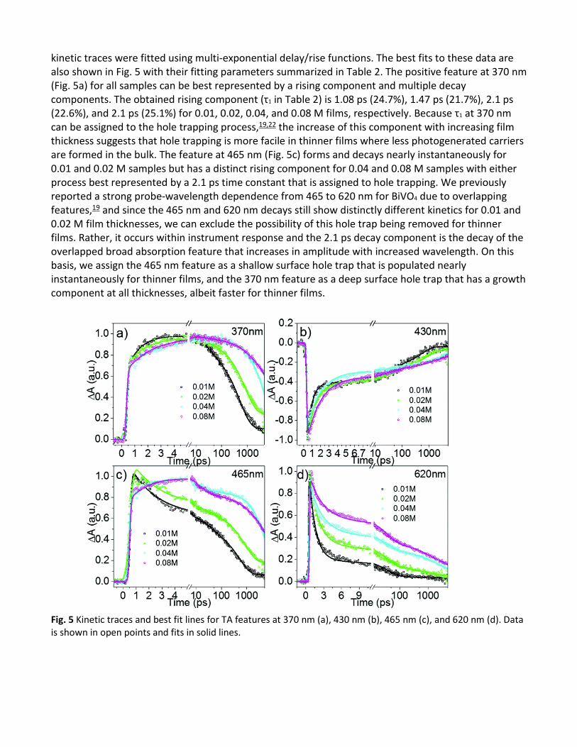
kinetic traces were fitted using multi-exponential delay/rise functions. The best fits to these data are also shown in Fig. 5 with their fitting parameters summarized in Table 2. The positive feature at 370 nm (Fig. 5a) for all samples can be best represented by a rising component and multiple decay components. The obtained rising component (τ1 in Table 2) is 1.08 ps (24.7%), 1.47 ps (21.7%), 2.1 ps (22.6%), and 2.1 ps (25.1%) for 0.01, 0.02, 0.04, and 0.08 M films, respectively. Because τ1 at 370 nm can be assigned to the hole trapping process,19,22 the increase of this component with increasing film thickness suggests that hole trapping is more facile in thinner films where less photogenerated carriers are formed in the bulk. The feature at 465 nm (Fig. 5c) forms and decays nearly instantaneously for 0.01 and 0.02 M samples but has a distinct rising component for 0.04 and 0.08 M samples with either process best represented by a 2.1 ps time constant that is assigned to hole trapping. We previously reported a strong probe-wavelength dependence from 465 to 620 nm for BiVO4 due to overlapping features,19 and since the 465 nm and 620 nm decays still show distinctly different kinetics for 0.01 and 0.02 M film thicknesses, we can exclude the possibility of this hole trap being removed for thinner films. Rather, it occurs within instrument response and the 2.1 ps decay component is the decay of the overlapped broad absorption feature that increases in amplitude with increased wavelength. On this basis, we assign the 465 nm feature as a shallow surface hole trap that is populated nearly instantaneously for thinner films, and the 370 nm feature as a deep surface hole trap that has a growth component at all thicknesses, albeit faster for thinner films.
Fig. 5 Kinetic traces and best fit lines for TA features at 370 nm (a), 430 nm (b), 465 nm (c), and 620 nm (d). Data is shown in open points and fits in solid lines.
Table 2 Fitting parameters for OTA results
Sample (M) Probe τ 1, ps (A1, %) τ 2, ps (A2, %) τ 3, ps (A3, %) τ 4, ns (A4, %) 0.01 370 1.08 (24.7)c 36.6 (13.6) 511 (54.0) ≫5 (7.6) 430 0.53 (62.1) (15.8) (18.7) (3.3) 462 2.1 (40.4) (14.9) (38.6) (6.0) 620 1.08 (80.3) (15.3) (1.25) (3.2) 0.02 370 1.47 (21.7)c 36.6 (5.5) 835 (5.4) (19.2) 430 0.96 (61.0) (14.5) (17.6) (6.9) 465 2.1 (37.2) (8.2) (38.7) (15.9) 620 1.47 (66.0) (2.1) (7.2) (5.6) 0.04a 370 2.1 (22.6)c 36.6 (0.4) 835 (1.0) (76.0) 430 1.6 (66.5) (60.2) (5.6) (21.9) 465 2.1 (28.3)c (2.9) (1.7) (44.8) 620 2.1 (51.6) (18.3) (8.9) (21.1) 0.08b 370 2.1 (25.1)c 36.6 (2.3) 835 (9.5) (82.7) 430 1.6 (64.5) (9.3) (7.9) (18.3) 465 2.1 (23.8)c (5.5) (6.6) (48.1) 620 2.1 (38.3) (26.1) (12.4) (23.1)
a Fifth time constants of 3.75 ps (22.0%). b Fifth time constants of 7.13 ps (15.9%). c Rising component.
The decay of the broad positive absorption feature at 620 nm (Fig. 5d) with τ1 identical to the 370 nm feature is additionally affected by film thickness, where the amplitude decreases in the order of 80.3, 66.0, 51.6, and 38.3% with increasing film thickness. Time constants τ2, τ3, and τ4 are all assigned to recombination between the electron and trapped holes and in exception of 0.01 M with τ3 of 511 ps, recombination processes were fit with the same time constants for all wavelengths and samples. Thinner films fit with an amplitude-weight toward faster decay processes whereas thicker films have longer lifetimes (following 620 nm A4 from 3.2, 5.6, 21.1, and 23.1% with increasing thickness) in the collected timescale, indicating that trap-mediated recombination plays a major role at the surface of BiVO4 materials.
The 430 nm feature (Fig. 5b) is assigned to GSB and has τ1 of 0.53, 0.96, and 1.6 ps for 0.01, 0.02, and 0.04–0.08 M, respectively, with a similar amplitude at all thicknesses. Assigned to electron trapping on the basis of its decay being faster than the decay of any hole features, it is again evident that trapping is accentuated for samples with a less bulk material. Thus, it is assigned to a surface electron trap state.
To evaluate the effect of film thickness on the photocatalytic performance for the OER, electrodes were fabricated on FTO glass at each thickness. Linear sweep voltammetry, performed in triplicate samples, was used to scan toward anodic potentials with the BiVO4 working electrode under rear-side and front-side (Fig. 6a and b) illumination with a long-pass (>400 nm) filtered 300 W Xenon lamp. The stability of the BiVO4 photoanode during the measurements was confirmed by XRD and UV-visible absorption spectroscopy before and after measurement (Fig. S8, ESI†). Under rear-side illumination (Fig. 6a), the observed current density increases significantly with sample thickness for the first three thicknesses due to the enhanced light absorption and thereby the density of the photogenerated carriers available for photocatalysis. The 0.08 M film, however, that absorbs significantly more visible light than the 0.04 M film displays reduced current density that becomes significantly lower than 0.04 M photocurrent at high (>1.2 V) overpotential. The front-side illumination (Fig. 6b) shows a similar trend from 0.01 to 0.08 M at lower overpotentials, where the photocurrent density increases with film

thickness up to 0.04 M and then decreases for the 0.08 M sample. However, the 0.04 M photocurrent density is significantly higher than that of 0.08 M at potentials higher than the photocurrent onset (≈0.6 V). As the applied potential increases, the photocurrent density for 0.08 M increases more slowly than the other thicknesses, indicating that the extraction of photogenerated charges is hindered at this thickness. These observations were further investigated by comparing the front- and rear-side illumination current density for each thickness under the same linear-sweep voltammetry conditions (Fig. 7). For the thinnest sample (0.01 M), the photocurrent is not significantly different between rear and front illumination. However, at the other thicknesses (0.02–0.08 M), the rear-illuminated photocurrent is always significantly higher over the entire potential range. This effect is attributed to the low photogenerated carrier mobility of BiVO4, which was reported to be approximately 4 × 10⁻² cm2 V−1 s−1 by the van de Krol group;13 when illuminated from the rear, the photogeneration of carriers occurs close to the electrode back-contact whereas when illuminated from the front, carriers are generated primarily at the surface and electrons must travel through the film to reach the back contact. Therefore, as the film thickness increases, the low carrier mobility decompensates the enhanced light absorption after a critical thickness (0.04 M) is reached.
Fig. 6 Linear-sweep voltammetry (25 mV s−1) of BiVO4 photoanodes under rear-side (a) and front-side (b) visible light illumination (>400 nm) with potential vs. Ag/AgCl.
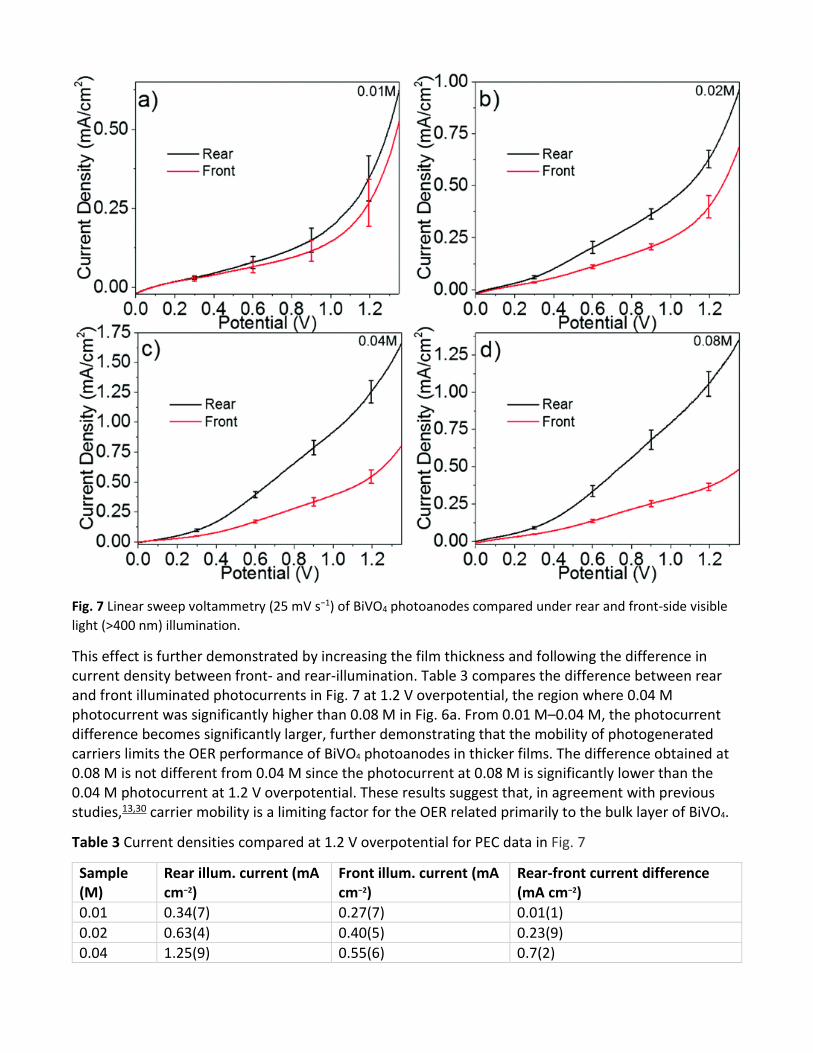
Fig. 7 Linear sweep voltammetry (25 mV s−1) of BiVO4 photoanodes compared under rear and front-side visible light (>400 nm) illumination.
This effect is further demonstrated by increasing the film thickness and following the difference in current density between front- and rear-illumination. Table 3 compares the difference between rear and front illuminated photocurrents in Fig. 7 at 1.2 V overpotential, the region where 0.04 M photocurrent was significantly higher than 0.08 M in Fig. 6a. From 0.01 M–0.04 M, the photocurrent difference becomes significantly larger, further demonstrating that the mobility of photogenerated carriers limits the OER performance of BiVO4 photoanodes in thicker films. The difference obtained at 0.08 M is not different from 0.04 M since the photocurrent at 0.08 M is significantly lower than the 0.04 M photocurrent at 1.2 V overpotential. These results suggest that, in agreement with previous studies,13,30 carrier mobility is a limiting factor for the OER related primarily to the bulk layer of BiVO4.
Table 3 Current densities compared at 1.2 V overpotential for PEC data in Fig. 7
Sample (M)
Rear illum. current (mA cm−2)
Front illum. current (mA cm−2)
Rear-front current difference (mA cm−2)
0.01 0.34(7) 0.27(7) 0.01(1) 0.02 0.63(4) 0.40(5) 0.23(9) 0.04 1.25(9) 0.55(6) 0.7(2)
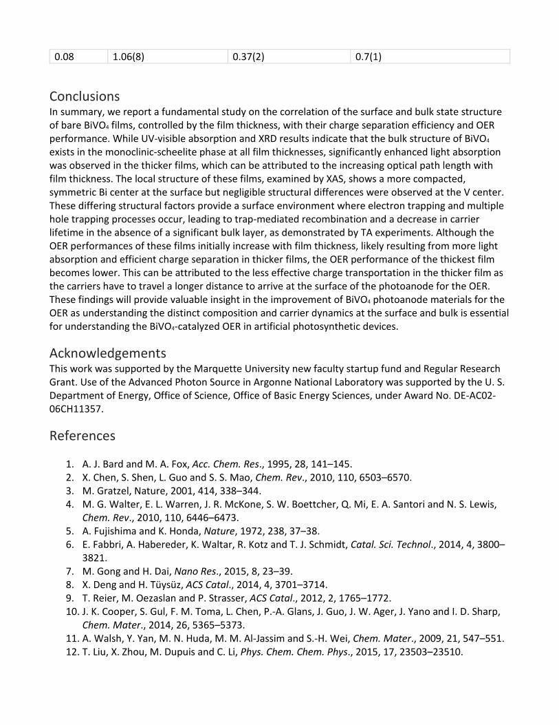
0.08 1.06(8) 0.37(2) 0.7(1)
Conclusions In summary, we report a fundamental study on the correlation of the surface and bulk state structure of bare BiVO4 films, controlled by the film thickness, with their charge separation efficiency and OER performance. While UV-visible absorption and XRD results indicate that the bulk structure of BiVO4 exists in the monoclinic-scheelite phase at all film thicknesses, significantly enhanced light absorption was observed in the thicker films, which can be attributed to the increasing optical path length with film thickness. The local structure of these films, examined by XAS, shows a more compacted, symmetric Bi center at the surface but negligible structural differences were observed at the V center. These differing structural factors provide a surface environment where electron trapping and multiple hole trapping processes occur, leading to trap-mediated recombination and a decrease in carrier lifetime in the absence of a significant bulk layer, as demonstrated by TA experiments. Although the OER performances of these films initially increase with film thickness, likely resulting from more light absorption and efficient charge separation in thicker films, the OER performance of the thickest film becomes lower. This can be attributed to the less effective charge transportation in the thicker film as the carriers have to travel a longer distance to arrive at the surface of the photoanode for the OER. These findings will provide valuable insight in the improvement of BiVO4 photoanode materials for the OER as understanding the distinct composition and carrier dynamics at the surface and bulk is essential for understanding the BiVO4-catalyzed OER in artificial photosynthetic devices.
Acknowledgements This work was supported by the Marquette University new faculty startup fund and Regular Research Grant. Use of the Advanced Photon Source in Argonne National Laboratory was supported by the U. S. Department of Energy, Office of Science, Office of Basic Energy Sciences, under Award No. DE-AC02-06CH11357.
References
1. A. J. Bard and M. A. Fox, Acc. Chem. Res., 1995, 28, 141–145. 2. X. Chen, S. Shen, L. Guo and S. S. Mao, Chem. Rev., 2010, 110, 6503–6570. 3. M. Gratzel, Nature, 2001, 414, 338–344. 4. M. G. Walter, E. L. Warren, J. R. McKone, S. W. Boettcher, Q. Mi, E. A. Santori and N. S. Lewis,
Chem. Rev., 2010, 110, 6446–6473. 5. A. Fujishima and K. Honda, Nature, 1972, 238, 37–38. 6. E. Fabbri, A. Habereder, K. Waltar, R. Kotz and T. J. Schmidt, Catal. Sci. Technol., 2014, 4, 3800–
3821. 7. M. Gong and H. Dai, Nano Res., 2015, 8, 23–39. 8. X. Deng and H. Tüysüz, ACS Catal., 2014, 4, 3701–3714. 9. T. Reier, M. Oezaslan and P. Strasser, ACS Catal., 2012, 2, 1765–1772. 10. J. K. Cooper, S. Gul, F. M. Toma, L. Chen, P.-A. Glans, J. Guo, J. W. Ager, J. Yano and I. D. Sharp,
Chem. Mater., 2014, 26, 5365–5373. 11. A. Walsh, Y. Yan, M. N. Huda, M. M. Al-Jassim and S.-H. Wei, Chem. Mater., 2009, 21, 547–551. 12. T. Liu, X. Zhou, M. Dupuis and C. Li, Phys. Chem. Chem. Phys., 2015, 17, 23503–23510.
13. F. F. Abdi, T. J. Savenije, M. M. May, B. Dam and R. van de Krol, J. Phys. Chem. Lett., 2013, 4, 2752–2757.
14. K. P. McKenna and A. L. Shluger, Proc. R. Soc. A, 2011, 467, 2043–2053. 15. F. Greuter and G. Blatter, Semicond. Sci. Technol., 1990, 5, 111. 16. Y. Tamaki, A. Furube, R. Katoh, M. Murai, K. Hara, H. Arakawa and M. Tachiya, C. R. Chim., 2006,
9, 268–274. 17. J. Ludwig, L. An, B. Pattengale, Q. Kong, X. Zhang, P. Xi and J. Huang, J. Phys. Chem. Lett., 2015,
6, 2671–2675. 18. J. Ravensbergen, F. F. Abdi, J. H. van Santen, R. N. Frese, B. Dam, R. van de Krol and J. T. M.
Kennis, J. Phys. Chem. C, 2014, 118, 27793–27800. 19. B. Pattengale, J. Ludwig and J. Huang, J. Phys. Chem. C, 2016, 120, 1421–1427. 20. F. G. Santomauro, A. Lübcke, J. Rittmann, E. Baldini, A. Ferrer, M. Silatani, P. Zimmermann, S.
Grübel, J. A. Johnson, S. O. Mariager, P. Beaud, D. Grolimund, C. Borca, G. Ingold, S. L. Johnson and M. Chergui, Sci. Rep., 2015, 5, 14834.
21. W. Luo, Z. Yang, Z. Li, J. Zhang, J. Liu, Z. Zhao, Z. Wang, S. Yan, T. Yu and Z. Zou, Energy Environ. Sci., 2011, 4, 4046–4051.
22. B. Pattengale and J. Huang, Phys. Chem. Chem. Phys., 2016, 18, 32820–32825. 23. S. M. Thalluri, S. Hernández, S. Bensaid, G. Saracco and N. Russo, Appl. Catal., B, 2016, 180,
630–636. 24. S. Tokunaga, H. Kato and A. Kudo, Chem. Mater., 2001, 13, 4624–4628. 25. A. Le Bail, I. Madsen, L. M. D. Cranswick, J. K. Cockcroft, P. Norby, A. D. Zuev, A. Fitch, J.
Rodriguez-Carvajal, C. Giacovazzo, R. B. Von Dreele, P. Scardi, N. C. Popa, R. Allmann, L. A. Solovyov, B. Hinrichsen, U. Schwarz, A. Altomare, A. Moliterni, R. Caliandro, R. Rizzi, N. V. Y. Scarlett, M. Jansen, R. E. Dinnebier and S. J. L. Billinge, Powder Diffraction: Theory and Practice, Royal Society of Chemistry, 2008.
26. S. M. Heald, D. DiMarzio, M. Croft, M. S. Hegde, S. Li and M. Greenblatt, Phys. Rev. B: Condens. Matter Mater. Phys., 1989, 40, 8828–8833.
27. A. W. Sleight, H. Chen, Y. A. Ferretti and D. E. Cox, Mater. Res. Bull., 1979, 14, 1571–1581. 28. Y. Ma, S. R. Pendlebury, A. Reynal, F. Le Formal and J. R. Durrant, Chem. Sci., 2014, 5, 2964–
2973. 29. I. Grigioni, K. G. Stamplecoskie, E. Selli and P. V. Kamat, J. Phys. Chem. C, 2015, 119, 20792–
20800. 30. A. J. E. Rettie, H. C. Lee, L. G. Marshall, J.-F. Lin, C. Capan, J. Lindemuth, J. S. McCloy, J. Zhou, A.
J. Bard and C. B. Mullins, J. Am. Chem. Soc., 2013, 135, 11389–11396.
Footnote † Electronic supplementary information (ESI) available. See DOI: 10.1039/c6cp08564d