ims4-p-fx2 -xxx modular quad output synthesizer overview and basic... · ims4-p-fx2 -xxx modular...
TRANSCRIPT

Issue 1.4.0: 2017-04-11
1
ISOMET
iMS4-P-Fx2 -xxx Modular Quad Output Synthesizer With Integral Frequency Doubler
Overview and Basic Operation
Models - Options –xxx, combinations possible
ISOMET CORP, 5263 Port Royal Rd, Springfield, VA 22151, USA.
Tel: (703) 321 8301, Fax: (703) 321 8546, e-mail: [email protected]
www.ISOMET.com ISOMET (UK) Ltd, 18 Llantarnam Park, Cwmbran, Torfaen, NP44 3AX, UK.
Tel: +44 1633-872721, Fax: +44 1633 874678, e-mail: [email protected]
Model Outputs Feature Freq RF Output
Range (MHz) Power
iMS4-P 4 Standard model 12.5 – 200MHz 1.2mW
iMS4-P-Fx2 4 Integrated Frequency doubling stage 150 - 400MHz 40mW
iMS4-P-ERC 4 External reference clock input 12.5 – 200MHz 1.2mW
Issue 1.4.0: 2017-04-11
2
ISOMET
Contents 1. Hardware Overview and Key features. ............................................................................................... 3
2. Single (Set Calibration) Tone. ............................................................................................................... 5
3. Local Tone Buffer. ................................................................................................................................. 5
4. Image Mode. ......................................................................................................................................... 5
5. Look-up-table (LUT). ............................................................................................................................. 6
6. RF power Level and Modulation. ......................................................................................................... 6
7. Technical Specifications. ...................................................................................................................... 8
8. Hardware Connection. ....................................................................................................................... 10
9. LED Indicators. .................................................................................................................................... 12
10. Connector pin-outs. ........................................................................................................................ 13
11. Software. ........................................................................................................................................ 17
a. Visual Studio Notes ........................................................................................................................ 18
b. Folder locations. ............................................................................................................................. 18
c. Importing C++ example flies into the project ................................................................................ 19
d. Installing the 3rd party Excel Spreadsheet Import Export function .............................................. 20
12. Direct programming of the DDS Synthesizer Chip. ....................................................................... 23

Issue 1.4.0: 2017-04-11
3
ISOMET
1. Hardware Overview and Key features. The diagram below illustrates a schematic of the iMS4-P connected with a generic Power Amplifier Before operating the IMS4-P, it will be necessary to load the USB Window drivers. (See section 10). The IMS4-P operates from DC power and requires a 15V-24Vdc supply (0.7Aat 24Vdc) The iMS4-e synthesizer incorporates a frequency doubler. A bandpass filter limits the lowest output frequency to around 150MHz. The upper frequency is 400MHz. The units operate in two basic modes: Local Tone Buffer (LTB) or Single Tone Mode. This mode is useful for setting the AO Bragg Angle or switching rapidly between 16 (256 with paging) preassigned points. The DDS synthesizer generates a single tone output at the specified Frequency, Amplitude and Phase or F/A/P triad. Key features:
Up to 95 KHz update rate between locations within a given buffer page.
The required output tone may be selected via software control or from hardwired inputs.
Option to Bypass the LUT modifier (see LUT description below)
DDS
F/A/C file
A/P comp' file
Single ToneGPIO
F/A/P
TRIGGERCLOCK-GATE
LUT
IMGSequences
RF1
RF2
RF3
RF4
DIR
EC
TIN
ST
RU
CT
ION
FIL
E T
RA
NS
FE
R
DDSPowerLevel
WIPER_1 WIPER_2
EnableRFChannels
EnableAmplifier
Interlock/Monitor
External inputs (x4)0-10V modulation(independent)
RF
MO
D1
RF
MO
D2
RF
MO
D3
RF
MO
D4
(Wipers commonto all RF channels)
AmplitudeControlSource select
(Off)
F/A/P/C = Frequency / Amplitude / Phase / Sync Control
iMS4-e-P
Power Amplifier
GP IO
-GA
TE
*
-IN
T *
BIA
S *
( * not all models)
BUFFER
4Select
500MbyteDDR3
Sync IO
J1
J2
J3
J4
Fx2
Fx2
Fx2
Fx2
Freq Doubler

Issue 1.4.0: 2017-04-11
4
ISOMET
IMAGE mode or Sequence mode. This mode is useful for generating larger more complex scan patterns. An Image file (IMG) containing the desired frequency scan pattern is downloaded into memory space within the iMS4. Output play back is under the control of user defined Image Trigger and Image Clock. Key features:
Update rate up to 1200 KHz, all four channels.
Any frequency pattern may be generated e.g. random, linear, step, saw tooth.
Multiple frequency images can be uploaded in multiple play sequences.
Simultaneous upload and play of image files
Very large image size, in excess of 10million frequency points. LUT and Image files can be generated on Excel Spread sheets and imported into the C++ project. Look-up-table (LUT) A calibration or compensation look-up-table (LUT) contains frequency specific phase and amplitude data. Its purpose is to compensate for non-linearity and non-uniformities in the wider system. E.g. create efficient uniform intensity scan lines in an AOD base laser scanning system. Initial values for the LUT are calculated and loaded into the IMS prior to running the Local Tone Buffer or Image modes. Subsequently, LUT values may be modified with real world measured data or integrated within a feedback mechanism. Amplitude and Power Level control Each frequency point is assigned a unique 10-bit amplitude value ranging from 0 -100% of the maximum RF power setting. This is a relative value and is dynamic i.e. able to change from output point to output point. The maximum RF output power setting is defined by the iMS AmplitudeControl and DDSPowerLevel digital potentiometers. These are 8-bit static controls and together define the absolute RF power level of the IMS4-P (and any connected power amplifier module). Auxiliary Digital and Analog I-O signals The iMS-P also features: Signal Description Ident 12 bit Synchronous output register, updated with the each new image point, SDOR[0…11] 10 bit Asynchronous output, GP Out[1…10] 8 bit Asynchronous input, GP In[1…8] 1 bit 24V PLC compatible opto relay output, Laser bit 2x Synchronous analog outputs, 0 -5V full scale AOUT_Frq …Amp 1x Asynchronous analog output, 0 -10V full scale AOUT_DAC 2x Asynchronous analog inputs, 0 -10V full scale Aux_ADC1 … 2

Issue 1.4.0: 2017-04-11
5
ISOMET
Main operating modes and functions. Please refer to the application program interface (API) documentation with the software development kit (SDK) available as a download. 2. Single (Set Calibration) Tone. Simplest mode. Direct programming of the DDS frequency, amplitude and phase values. Bypasses LUT compensation. 3. Local Tone Buffer. The Local tone buffer (LTB) area contains 256 locations arranged in 16 pages. Within each page, the 16 F/A/P Tones may be rapidly addressed using 4x external LTB address lines. Two additional signals are employed in a handshaking routine to select the active page. The same four LTB address lines are used to select the page.
Page Control
LTB ext’l address, J8 (P3 ... P0)
Function Update rate
GPI 1, input level 0 0 h ... F h Select Tone address within page 6usec
GPI 1, input level 1 0 h … F h Define new page address.
GP0 1, output flag 1 X New page latched and acknowledged (Ok to return GPI 1 Low)
~300usec
4. Image Mode. An Image contains multiple F/A/P data points pre-arranged to give the desired frequency or scan pattern. Image playback is initiated with the Image Trigger. The output update rate is determined by the Image Clock. The Image trigger and clock may be software generated or applied from an external source. At each clock edge, the next location in the Image Memory area is addressed. The frequency and amplitude data point is read and modified by the LUT data (see below). The resultant F/A/P triad is routed to the DDS registers. An update clock is then issued to the DDS and all 4x RF outputs are simultaneously updated with a new Frequency, Amplitude and Phase value. Any Synchronous control data will also be updated on the appropriate I/O port. Multiple images can be grouped together into a play sequence. Each image within a sequence can have unique properties such as clock rate and post image delay. Likewise multiple sequences can be defined and queued. These are uploaded into the iMS DDR memory and played in FIFO order. Memory is dynamically allocated to permit flexibility in the size and number of both the images and sequences, and to allow simultaneous upload and output of data. The total number of images (excluding repeats) is 4096. The size of a single image is in excess of a 1million F/A/P points.
Issue 1.4.0: 2017-04-11
6
ISOMET
5. Look-up-table (LUT). The LUT is frequency-addressed look-up-table for applying amplitude and phase compensation to the RF signal output. The tables are indexed by the nearest programmed LUT frequency to the demanded output frequency. Table entries are linearly spaced in frequency from the lowest to highest supported. The number of entries in the table is hardware specific. At a minimum, the LUT must contain amplitude compensation data over the desired frequency range of interest. LUT Size: 2047 entries equally spaced from 12.5 – 200MHz (25 – 400MHz after frequency doubling). Primary features: Compensation Data
•Amplitude: a value between 0 and 100% for modifying the output amplitude according to frequency. Used for compensating for AOD efficiency as well as filter attenuation and DDS roll-off. •Phase: 0 - 360 degrees. Represents the per-channel phase difference applied to enable beam steered (= phased array) applications. Value represents the phase offset between adjacent channels Channel 1 is the reference and unmodified. Channel 4 will exhibit the largest phase differential relative to Channel 1.
Secondary features: Synchronous output data
•Sync Analog: A value between 0.0 and 1.0 that can be output on one of the synchronous DAC outputs (updated in step with the RF image point data). •Sync Digital: A binary value that can be output on the synchronous digital outputs (updated in step with the RF image point data).
6. RF power Level and Modulation. The output RF power at each frequency is determined by the combination of static controls and point specific amplitude data values.
Static Controls. Applies to all operating modes. Purpose: To set the maximum safe operating RF power level.
1: DDS Power Level. 8-bit non-volatile digital pot. Always programmed. Sets the DDS chip output level using a dedicated digital pot. Common to all outputs. Typical values 70 – 90%
<< and >>

Issue 1.4.0: 2017-04-11
7
ISOMET
2: Amplitude Control Source for the RF mixers, 4 options. Must select and apply one. 00: OFF. Common to all outputs 01: EXTERNAL signal(s)*, per RF channel, output proportional to applied control voltage. 10: WIPER_1, internal 8-bit non-volatile digital pot setting. Common to all outputs 11: WIPER_2, alternative to Wiper_1 The value written and stored to Wiper_1 (or Wiper_2) sets the RF mixer drive level. Typical values 70 – 90%
The above controls should be set in combination so that the AO device is operated at optimum efficiency without saturating the connected power amplifiers and/or applying excessive RF power to the AO device. Starting values will be provided on the appropriate test data sheets (* Can be wired together to combine multiple channels onto a common control input. 0-10V, 600-ohm / channel. May also used for fast asynchronous amplitude modulation).
Dynamic Control. Purpose: To set or modulate the RF power at a specific output frequency. (I.e. the AO diffracted laser power at a specific scan angle)
3: Tone Buffer mode The 10-bit amplitude data value associated with a specific frequency value. This is multiplied by the LUT amplitude calibration factor for that frequency point. The LUT can be bypassed if required. The LUT is applied by default.
<< or >> 4: Image mode The 10-bit amplitude data value associated with a specific frequency value. This is multiplied by the LUT amplitude compensation factor for that frequency point. For a typical AO scanning application, the Image amplitude data is a simple “On” or ”Off” value. The LUT is programmed with the variable amplitude compensation data that creates the desired weighting for the scan intensity profile.

Issue 1.4.0: 2017-04-11
8
ISOMET
7. Technical Specifications. Image Mode
Timing Value Condition
Frequency Settling Time < 40nsec Step change in Image data value (Phase accumulator set to clear at each DDS update)
Output Delay - Image Clock edge 1.6 usec *
Minimum Trigger to Clock edge TBD nsec
Maximum Image Clock rate 1200KHz *
Maximum Image Clock rate 0 Hz
GATE, TRIGGER, CLOCK inputs. J9, J10,J11 Value Condition
Absolute Maximum Input Voltage 5.5V Per input.
Recommended Input Voltage > 3V, <5V For logic High
Minimum Input Voltage 0V
* Pre–optimization. Please contact Isomet if faster rate is required Local Tone Buffer Mode
Timing Value Condition
Frequency Settling Time < 40nsec For tone – tone selection within a LTB page. (Phase accumulator set to clear at each DDS update)
Output Delay - LTB address change 6.5 usec
Maximum LTB address rate 95KHz
Maximum Image Clock rate 0 Hz
LTB address, input Voltages, J8 Value Condition
Absolute Maximum Input Voltage 5.5V Per input.
Recommended Input Voltage, > 3V, < 5V For Logic High
Minimum Input Voltage 0V
Opto-isolated, signal source sink current 16mA All inputs
Issue 1.4.0: 2017-04-11
9
ISOMET
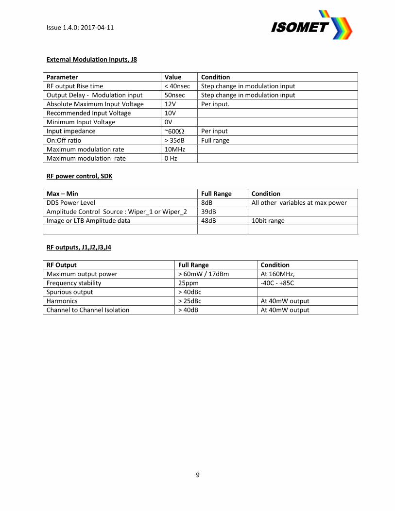
External Modulation Inputs, J8
Parameter Value Condition
RF output Rise time < 40nsec Step change in modulation input
Output Delay - Modulation input 50nsec Step change in modulation input
Absolute Maximum Input Voltage 12V Per input.
Recommended Input Voltage 10V
Minimum Input Voltage 0V
Input impedance ~600 Per input
On:Off ratio > 35dB Full range
Maximum modulation rate 10MHz
Maximum modulation rate 0 Hz
RF power control, SDK
Max – Min Full Range Condition
DDS Power Level 8dB All other variables at max power
Amplitude Control Source : Wiper_1 or Wiper_2 39dB
Image or LTB Amplitude data 48dB 10bit range
RF outputs, J1,J2,J3,J4
RF Output Full Range Condition
Maximum output power > 60mW / 17dBm At 160MHz,
Frequency stability 25ppm -40C - +85C
Spurious output > 40dBc
Harmonics > 25dBc At 40mW output
Channel to Channel Isolation > 40dB At 40mW output
Issue 1.4.0: 2017-04-11
10
ISOMET
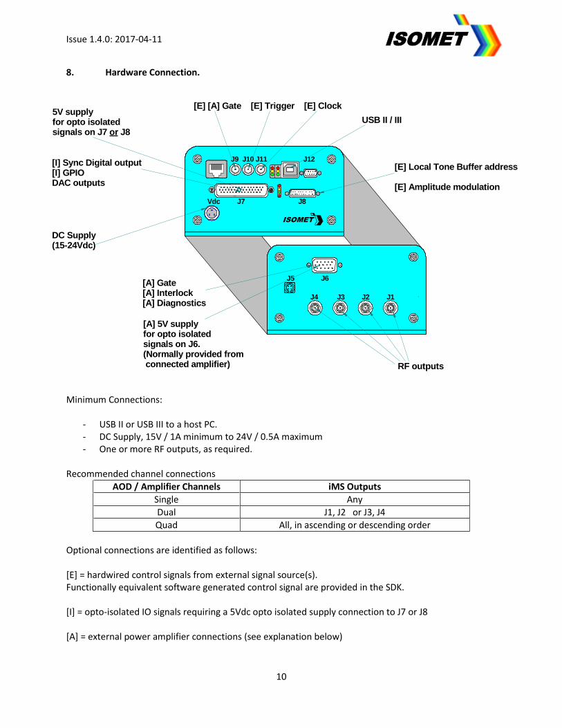
8. Hardware Connection.
Minimum Connections:
- USB II or USB III to a host PC. - DC Supply, 15V / 1A minimum to 24V / 0.5A maximum - One or more RF outputs, as required.
Recommended channel connections
AOD / Amplifier Channels iMS Outputs
Single Any
Dual J1, J2 or J3, J4
Quad All, in ascending or descending order
Optional connections are identified as follows: [E] = hardwired control signals from external signal source(s). Functionally equivalent software generated control signal are provided in the SDK. [I] = opto-isolated IO signals requiring a 5Vdc opto isolated supply connection to J7 or J8 [A] = external power amplifier connections (see explanation below)
J5 J6
J4 J3 J2 J1
ISOMET
Vdc J7 J8
J9 J10 J11 J12
[E] [A] Gate [E] Trigger [E] Clock5V supplyfor opto isolatedsignals on J7 or J8
[A] 5V supplyfor opto isolatedsignals on J6.(Normally provided from connected amplifier)
[E] Local Tone Buffer address
[E] Amplitude modulation
[A] Gate[A] Interlock[A] Diagnostics
[I] Sync Digital output[I] GPIODAC outputs
USB II / III
RF outputs
DC Supply(15-24Vdc)

Issue 1.4.0: 2017-04-11
11
ISOMET
The iMS4-P features external power amplifier diagnostic and control signals. These are available on J6. A limited sub-set is wired to J5 if J6 is not fitted. J6 will require 5V opto isolator dc feed (5V_RFA) from the connected RF amplifier. J5, does not. (The internal iMS 5V and 5V_RFA are commoned when J5 is used.) An appropriate interface card must exist within the power amplifier. Basic amplifier control With few exceptions, most Isomet existing power amplifier modules require an active low Gate or Enable signal to operate and will output a normally closed over-temperature thermal interlock signal. Diagnostics Certain amplifier models include diagnostic outputs indicating: - Forward and reflected RF power (between the PA outputs and connected AO device/load). - Temperature of the PA - DC current - Temperature of the AO device These are communicated via I2C bus on J6
Model Channels Power/ch Frequency Range Enable/Gate Control Diagnostics
500C series 1 2,4,or 7W Model dependent NA NA
iMPA-4-1W 4 1 – 1.8W 20-200 J5 NA
RFA200-2H 2 100W 35 – 65 J6 NA
RFA1170-4 4 80W 48-92 J6 J6
NA= not applicable

Issue 1.4.0: 2017-04-11
12
ISOMET
9. LED Indicators. Top Stack, Controller PCB
Ident LED Mode iMS4-P
A RED (top left) If illuminated Not Downloading File
B Yellow If illuminated Downloading File
C Green Pulsing Controller OK
D RED (top right) If illuminated Image output stopped
E Yellow If illuminated Waiting on Trigger
F Green If illuminated Image playing / output active
Lower stack. Synthesizer PCB
Ident LED Mode Stand Alone iMS4-
In combination with PA and J6 (or J5) is connected
G RED (top) Constant on DC power On Thermal Interlock Open (= fault)
H Yellow Constant on NA PA is enabled. Thermal Interlock OK
I Green Pulsing Synthesizer OK Synthesizer OK
J Red Not used
DC power applied, USB communication problem If the 6x LED’s (A,B,C,D,E,F) are constantly illuminated, then USB communication has not been established. In this case: a: Ensure USB driver is loaded (see section 10) b: Cycle DC power and /or c: Disconnect then reconnect USB
ABC
DEF
GH IJ

Issue 1.4.0: 2017-04-11
13
ISOMET
115
16
30
3144
1 13
14 25
J8 (female)J7 (female)
Front panel view
10. Connector pin-outs.
D-type pin idents looking into connector Pin-out decryptions as follows: Circuit details for opto-isolated inputs / outputs on J7 and J8 connector Recommended drive circuit for opto-isolated logic inputs
(GbE) GATE TRG CLK USB (RS422)
J5 J6
J4 J3 J2 J1
ISOMET
Vdc J7 J8
J9 J10 J11 J12
5V_iso
5V_iso
220
.
.
.
. .
0V_iso
Any open collector TTL or open drain CMOS gate
iMS4-
IsolatedInput

Issue 1.4.0: 2017-04-11
14
ISOMET
Opto-isolated logic output schematic
J8, 25way micro-D connector Main connection for external control signals (Micro-D to full size D-type converter cable available).
Connector Type 25way micro-D Ident J8
Signal Signal Type Description Alternate use Pin
Designation RFmod4 In Analog, 0-10V External amplitude control for RF4
13
A_Rtn
Analog Analog return
25
RFmod3 In Analog, 0-10V External amplitude control for RF3
12
A_Rtn
Analog Analog return
24
RFmod2 In Analog, 0-10V External amplitude control for RF2
11
A_Rtn
Analog Analog return
23
RFmod1 In Analog, 0-10V External amplitude control for RF1
10
A_Rtn
Analog Analog return
22
No Connect Out Logic RS232. RXD (Factory test)
9
No Connect In Logic RS232. TXD (Factory test)
8
GP In1 In Opto isolated logic Async general purpose input LTB select page addressing 4
GP Out1 Out Opto isolated logic Async general purpose output LTB new page acknowledge 16
GP In2 IN Opto isolated logic Async general purpose input
7
GP Out2 Out Opto isolated logic Async general purpose output
20
D_Rtn DC
isolated 0V / signal return input 0V 15
P0 In Opto isolated logic Profile select, bit0 LTB location/address, bit0 3
P1 In Opto isolated logic Profile select, bit1 LTB location/address, bit1 6
P2 In Opto isolated logic Profile select, bit2 LTB location/address, bit2 18
P3 In Opto isolated logic Profile select, bit3 LTB location/address, bit3 5
D_Rtn DC
isolated 0V / signal return input 0V 1
RST In Opto isolated logic Reset
14
-GATE In Opto isolated logic Enable connected Power Amps
2
5V_iso DC
Isolated 5V DC supply input 5V output, 10mA 19
5V_iso DC
Isolated 5V DC supply input 5V output, 10mA 21
D_Rtn DC
isolated 0V / signal return input 0V 17
Notes:
Key:
Type Logic = TTL or 5V CMOS GP = General Purpose
Drive inputs with open collector or open drain gate, 16mA sink LTB = Local Tone Buffer
Open collector outputs with internal 1Kohm pull-up to 5V_iso
5V_iso
1K
. .
0V_iso
iMS4-
IsolatedOutput

Issue 1.4.0: 2017-04-11
15
ISOMET
J7, 44way high density-D connector Connection for auxiliary I-O signals
Connector Type 44way HD-D Ident J7
Signal Signal Type Description Alternate use Pin
Designation SDOR0 Out Opto isolated logic Synchronous-Digital Output bit0
1
SDOR1 Out Opto isolated logic Sync-Digital Output bit1
2
SDOR2 Out Opto isolated logic Sync-Digital Output bit2
33
SDOR3 Out Opto isolated logic Sync-Digital Output bit3
34
SDOR4 Out Opto isolated logic Sync-Digital Output bit4
38
SDOR5 Out Opto isolated logic Sync-Digital Output bit5
39
SDOR6 Out Opto isolated logic Sync-Digital Output bit6
40
SDOR7 Out Opto isolated logic Sync-Digital Output bit7
41
SDOR8 Out Opto isolated logic Sync-Digital Output bit8
35
SDOR9 Out Opto isolated logic Sync-Digital Output bit9
5
SDOR10 Out Opto isolated logic Sync-Digital Output bit10
21
SDOR11 Out Opto isolated logic Sync-Digital Output bit11
36
D_Rtn Out
isolated 0V / signal return input 0V 26
GP In3 In Opto isolated logic Asynchronous GP logic input
9
GP In4 In Opto isolated logic Async GP input
8
GP In5 In Opto isolated logic Async GP input
37
GP In6 In Opto isolated logic Async GP input
6
GP In7 In Opto isolated logic Async GP input
3
GP In8 In Opto isolated logic Async GP input
17
GP In9 In Opto isolated logic Async GP input
31
GP In10 In Opto isolated logic Async GP input
32
D_Rtn In
isolated 0V / signal return input 0V 16
GP Out3 Out Opto isolated logic Async GP logic output
10
GP Out4 Out Opto isolated logic Async GP output
25
GP Out5 Out Opto isolated logic Async GP output
23
GP Out6 Out Opto isolated logic Async GP output
7
GP Out7 Out Opto isolated logic Async GP output
4
GP Out8 Out Opto isolated logic Async GP output
19
D_Rtn Out
isolated 0V / signal return input
18
24V_laser In PLC Laser Opto-Supply
42
Laser_Bit Out PLC Laser Opto relay bit Tr/Tf < 50usec)
43
Gnd_laser In PLC Laser Opto-Gnd
44
AOUT_Frq Out Analog 8-bit analog representation of Image freq
13
AOUT_Amp Out Analog 8-bit analog equivalent of Image amplitude
28
A_Rtn Out Analog Analog return
29
AOUT_DAC Out Analog GP 12-bit DAC analog output.
27
A_Rtn Out Analog Analog return
30
Aux_ADC1 In Analog GP Analog input to a 12-bit ADC (0 to +10V).
15
A_Rtn In Analog Analog return
12
Aux_ADC2 In Analog GP Analog input to a 12-bit ADC (0 to +10V).
14
A_Rtn In Analog Analog return
11
5V_iso DC
Isolated 5V DC supply input 5V output, 10mA 20
5V_iso DC
Isolated 5V DC supply input 5V output, 10mA 22
D_Rtn DC
isolated 0V / signal return input 0V 24
Notes:
Key: Type Logic = TTL or 5V CMOS
GP + General Purpose
Drive inputs with open collector or open drain gate, 16mA sink Open collector outputs with internal 1Kohm pull-up to 5V_iso

Issue 1.4.0: 2017-04-11
16
ISOMET
Other Connectors
Connector Type see table
Ident see table
Signal Signal Type Description Alternate use Connector Ident Pin
Designation
Communication
Ethernet In/Out Logic TBA
USB Serial In/Out Logic USB II / USBIII
B-type -
RX-P In Logic RS422 receive+
9-way D J12 2
RX-N In Logic RS422 receive-
9-way D J12 1
TX-P Out Logic RS422 transmit+
9-way D J12 7
TX-N Out Logic RS422 transmit-
9-way D J12 6
Rtn Gnd
Sig Rtn
9-way D J12 5
DC Supply
Vdc DC DC-In Supply 15V -24V dc, <0.4A
3w TINI-Q
1
0V DC-In
3w TINI-Q
2
SMA Coax Connections
Gate In Logic Connected power amplifier, Enable SMA coaxial J9
Centre
Rtn Gnd Sig Rtn Outer
Trigger In Logic O/P Image Data, Trigger SMA coaxial J10 Centre
Rtn Gnd Sig Rtn Outer
Clock In Logic O/P Image Data, Clock (< 310KHz) SMA coaxial J11
Centre
Rtn Gnd Sig Rtn Outer
Ch0 Analog RF RF1 frequency output, 50
SMA coaxial J1 Centre
Rtn Gnd
Sig Rtn
Outer
Ch1 Analog RF RF2 frequency output, 50
SMA coaxial J2 Centre
Rtn Gnd
Sig Rtn
Outer
Ch2 Analog RF RF3 frequency output, 50
SMA coaxial J3 Centre
Rtn Gnd
Sig Rtn
Outer
Ch3 Analog RF RF4 frequency output, 50
SMA coaxial J4 Centre
Rtn Gnd
Sig Rtn
Outer
(J5 Alternate PA Control *)
No Connect
Logic In use only if J6 not fitted INT_Mon RTN 4w-Binder 719 J5 1
No Connect
Logic In use only if J6 not fitted INT_Mon 4w-Binder 719 J5 2
No Connect
Logic In use only if J6 not fitted -GATE 4w-Binder 719 J5 3
No Connect
Logic In use only if J6 not fitted Gate RTN 4w-Binder 719 J5 4
J6 Power Amp Control *
5V_RFA In
Opto supply from connected PA 5V, 20mA output 15w-HD D J6 1
5V_RFA In
Opto supply from connected PA 5V, 20mA output 15w-HD D J6 10
0V_RFA In
Opto 0V from connected PA 0V 15w-HD D J6 4
0V_RFA In
Opto 0V from connected PA 0V 15w-HD D J6 7
SCL_RFA_TX IO Opto isolated logic I2C Clock_TX
15w-HD D J6 2
SCL_RFA_RX
Opto isolated logic I2C Clock_RX
15w-HD D J6 3
SDA_RFA_TY IO Opto isolated logic I2C Data_TY
15w-HD D J6 5
SDA_RFA_RY
Opto isolated logic I2C Data_RY
15w-HD D J6 6
EXT-CONVST Out Opto isolated logic Start ADC conversion
15w-HD D J6 8
-EXT_GATE Out Opto isolated logic Enable connected amplifier
15w-HD D J6 9
EXT-BSY In Opto isolated logic ADC conversion busy
15w-HD D J6 11
EXT-INT_MON In Opto isolated logic Interlocks valid monitor
15w-HD D J6 12
* Applies only when signals supported by connected PA
Issue 1.4.0: 2017-04-11
17
ISOMET
11. Software.
The core of the Software Development Kit is the C++ iMS library and API. All interaction with iMS hardware ultimately passes through this API. However we have also provided a number of other software utilities and wrappers that allow you to use the iMS System at a higher level of abstraction. Included in the SDK are:
•The core iMSLibrary binaries for a number of different platforms and toolsets. •Accompanying C++ header files for application interface. •iMSNET An experimental .NET assembly written in C# that wraps the core library and permits
user application development in any .NET language targetting the .NET Framework •ims_hw_server is a command line daemon type process that can handle all communication with
an iMS system, decoupling it from user application business logic. A gRPC streaming interface connects the server to application software, either on the same host or across a network.
•iMS Studio is a full featured GUI front end application that can be used to create Images, Tone
Buffers and Compensation Functions and play them on an iMS system. This is often a good starting point for users wishing to explore the capabilities of an iMS before starting development of custom software. The iMS software is available for download from http://www.isomet.com/software.html Depending on your computer select and run one of the followimg :
Isomet iMS SDK v 1.30 Win7 32-bit Setup.exe
Isomet iMS SDK v 1.30 Win7 64-bit Setup.exe
Isomet iMS SDK v 1.30 Win10 32-bit Setup.exe
Isomet iMS SDK v 1.30 Win10 64-bit Setup.exe
The software download also includes documentation and tutorials for setting up a project and connecting to the iMS. Note: these Tutorials are NOT specific to any practical AO device. Please refer to Quick Start Guide: Isomet iMS Studio for instructions on the Isomet Windows GUI The iMS software library and API has been written purely in native ANSI-C++ with some use of features introduced in C++11 (ISO/IEC 14882:2011), including the C++ Standard Library. There is no use of features associated with the updated C++14 specification. Isomet will provide example projects applicable to the customer hardware configuration. The Software Development Kits are regularly updated. Please check for Isomet website for updates.

Issue 1.4.0: 2017-04-11
18
ISOMET
a. Visual Studio Notes
b. Folder locations. For ease of transferring files between PC’s, the example projects are referenced to a Visual Studio 2013 folder placed directly in the C: drive of the PC. Consequently the Isomet SDK folder is installed in the Projects folder; C:\Visual Studio 2013\Projects\iMS_SDK If you choose to do the same, then after installing Visual Studios 2013 make the following directory location changes. Use the drop down menu and expand the relevant headings (click on arrow).
1: > Tools > Options > Environment > Import and Export Settings (Changed locations shown)
2: > Tools > Options > Program and Solutions > General (Changed locations shown)

Issue 1.4.0: 2017-04-11
19
ISOMET
c. Importing C++ example flies into the project
Refer to Isomet SDK documentation > Tutorial 1(a): Setting up a project and connecting to an iMS Follow the project set-up as directed up to Step 4.
Right Click on Source Files. This will offer several options including:
Select Add -> Existing Item. Use to import (say) one of the example *.cpp files. Point to the desired *.cpp file location. (Typically this should be copied into your project folder)
Select Add - > New Item. Use to set up a new blank source file (as directed in the SDK Tutorial). To remove an existing Source file and change to a different file, right click on the *.cpp file name, Select Remove (Not Delete, unless you intend to permanently discard). Then, Select Add -> Existing Item. The example C++ projects generally all follow a similar format as listed below. See comment fields within the Source code for specific details.
1. Find a valid iMS connection on the USB port 2. Display the FPGA Firmware Version numbers 3. Declare and assign variables for the AO deflector/Power amplifier supplied with the iMS4-x 4. Generate or import a default LUT (if required). 5. Set the DDS power Level 6. Select and Set the Amplitude control source and Level ( e.g. Wiper_1)
7. ……….example code * ……………..
8. Enable power amplifier BIAS (if applicable) 9. Enable RF amplifier outputs 10. Request key hit to finish output 11. Set the Amplitude control source “Output (OFF)” 12. Disable any connected RF amplifiers 13. Disconnect
* Typical examples: SingleTone_FX2.cpp: Single frequency programming of iMS LocalTone Buffer_FX2.cpp: Load table of 16 frequency points. Select point for output ImageMode_FX2_XLS_Single.cpp: Import LUT and Image data from Excel and run in Image mode ImageMode_FX2_XLS_Sequence.cpp: as above, 2 image sequence.

Issue 1.4.0: 2017-04-11
20
ISOMET
d. Installing the 3rd party Excel Spreadsheet Import Export function Generating LUT and Image files in Excel can be convenient. Several routines exist to import data into C++. One such is from libxl.com A licence key is required and it is free to use. Add the following code prior to calling the LibXL functions. // call LibXL licence key libxl::Book* ExcelBook = xlCreateBook(); ExcelBook->setKey(L"Michael Hillier", L"windows-222329040ec5ec046fb46767a7h1gej6"); To add this feature to your project
Copy the Excel spreadsheet ‘include_excel’ directory into the existing SDK project folder
Add the above additional include files to the project using the Solution Explorer. (See tutorial 1A, Step 3 for method)

Issue 1.4.0: 2017-04-11
21
ISOMET
Add ‘include_excel’ to the above Additional Include Directory under C++ > General.
(See Tutorial 1A, Step 6 for method)
Copy libxl.dll to the project folder you created. It should be in the same folder as the source file *.cpp. (See tutorial 1A, Step 8 for method)

Issue 1.4.0: 2017-04-11
22
ISOMET
Add the folder containing libxl.lib to the Additional Library Dependencies under Linker > General. (See Tutorial 1A, Step 7 for method)
Add libxl.lib to the Additional Dependencies under Linker > Input
(See Tutorial 1A, Step 7 for method)
Example files include GP_LUT_Amp80.xls: LUT data with phase and amplitude calculation GP_IMG_Swp.xls: IMAGE data , Linear sweep with constant amplitude
Issue 1.4.0: 2017-04-11
23
ISOMET
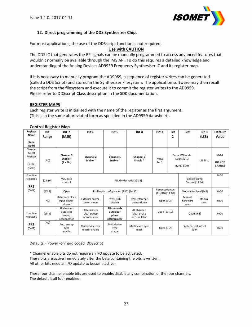
12. Direct programming of the DDS Synthesizer Chip. For most applications, the use of the DDSscript function is not required.
Use with CAUTION The DDS IC that generates the RF signals can be manually programmed to access advanced features that wouldn't normally be available through the iMS API. To do this requires a detailed knowledge and understanding of the Analog Devices AD9959 Frequency Synthesiser IC and its register map. If it is necessary to manually program the AD9959, a sequence of register writes can be generated (called a DDS Script) and stored in the Synthesiser Filesystem. The application software may then recall the script from the filesystem and execute it to commit the register writes to the AD9959. Please refer to DDSscript Class description in the SDK documentation. REGISTER MAPS Each register write is initialised with the name of the register as the first argument. (This is in the same abbreviated form as specified in the AD9959 datasheet). Control Register Map
Register Name
(Serial Addr)
Bit Range
Bit 7 (MSB)
Bit 6
Bit 5
Bit 4
Bit 3
Bit 2
Bit1 Bit 0 (LSB)
Default Value
Channel Select
Register
(CSR) (0x00)
[7:0]
Channel 3 Enable * (1 = On)
Channel 2 Enable *
Channel 1 Enable *
Channel 0 Enable *
Must be 0
Serial I/O mode Select [2:1]
B2=1, B1=0
LSB first
0xF4
DO NOT CHANGE
Function Register 1
(FR1) (0x01)
[23:16] VCO gain control
PLL divider ratio[22:18] Charge pump
Control [17:16]
0xD0
[15:8] Open Profile pin configuration (PPC) [14:12] Ramp-up/down (RU/RD) [11:10]
Modulation level [9:8] 0x00
[7:0] Reference clock
input power-down
External power- down mode
SYNC_CLK disable
DAC reference power-down
Open [3:2] Manual
hardware sync
Manual sync
0x00
Function Register 2
(FR2) (0x02)
[15:8]
All channels autoclear
sweep accumulator
All channels clear sweep accumulator
All channels autoclear
phase accumulator
All channels clear phase accumulator
Open [11:10]
Open [9:8] 0x20
[7:0]
Auto sweep sync
enable
Multidevice sync master enable
Multidevice sync
status
Multidevice sync mask
Open [3:2] System clock offset
[1:0] 0x00
Defaults = Power -on hard coded DDSScript * Channel enable bits do not require an I/O update to be activated. These bits are active immediately after the byte containing the bits is written. All other bits need an I/O update to become active. These four channel enable bits are used to enable/disable any combination of the four channels. The default is all four enabled.

Issue 1.4.0: 2017-04-11
24
ISOMET
Channel Register Map Register
Name (Serial Addr)
Bit Range
Bit 7 (MSB)
Bit 6
Bit 5
Bit 4
Bit 3
Bit 2
Bit1 Bit 0 (LSB)
Default Value
* Channel Function Register
(CFR) (0x03)
[23:16
Amplitude freq. phase (AFP) select [23:22]
Open [21:16] 0x00
[15:8]
Linear sweep no-dwell
Linear sweep enable
Load SRR at I/O_UPDATE
Open [12:11] Must be 0 DAC full-scale
current 0x03
[7:0]
Digital power- down
DAC power- down
Matched pipe delays
active
Autoclear sweep
accumulator
Clear sweep accumulator
Autoclear phase
accumulator
Clear phase
Accumulator **
Sine wave
output enable
0x00
* Channel Frequency
Tuning Word 0
(CFTW0)
(0x04)
[31:24] Frequency Tuning Word 0 [31:24]
0x00
N/A
N/A
N/A
[23:16]
Frequency Tuning Word 0 [23:16]
[15:8]
Frequency Tuning Word 0 [15:8]
[7:0]
Frequency Tuning Word 0 [7:0]
* Channel Phase Offset
Word 0 (CPOW0)
(0x05)
[15:8] Open [15:14] Phase Offset Word 0 [13:8]
0x00
[7:0] Phase Offset Word 0 [7:0] 0x00
Amplitude Control Register
(ACR) (0x06)
[23:16] Amplitude ramp rate [23:16]
N/A
[15:8] Increment/decrement step
size [15:14] Open
Amplitude multiplier
enable
Ramp-up/ down
enable
Load ARR at I/O_UPDATE
Amplitude scale Factor [9:8]
0x13
[7:0] Amplitude scale factor [7:0]
0xFF
* Linear Sweep Ramp Rate
(LSRR) (0x07)
[15:8] Falling sweep ramp rate (FSRR) [15:8]
N/A
[7:0]
Rising sweep ramp rate (RSRR) [7:0] N/A
* LSR Rising Delta Word
(RDW) (0x08)
[31:24] Rising delta word [31:24]
N/A
[23:16]
Rising delta word [23:16] N/A
[15:8]
Rising delta word [15:8] N/A
[7:0]
Rising delta word [7:0] N/A
* LSR Falling Delta Word
(FDW) (0x09)
[31:24] Falling delta word [31:24]
N/A
[23:16]
Falling delta word [23:16] N/A
[15:8]
Falling delta word [15:8] N/A
[7:0]
Falling delta word [7:0] N/A
**
The clear phase accumulator bit is set to Logic 1 after a master reset. It self-clears or is set to Logic 0 when an I/O update is asserted. * There are four sets of channel registers and profile registers, one per channel. The addresses of all channel registers and profile registers are the same for each channel. The channel enable bits (Control Register 0, CSR [7:4]) determine if the channel registers and/or profile registers of each channel are written to or not.

Issue 1.4.0: 2017-04-11
25
ISOMET
Profile Register Map For clarity, only the MSB byte is shown for each Channel Word register.
Register Name
Bit Range
Bit 7 (MSB)
Bit 6
Bit 5
Bit 4
Bit 3
Bit 2
Bit1 Bit 0 (LSB)
Default Value
Channel Word 1 (CW1) (0x0A)
[31:0] Frequency tuning word [31:0] or Phase word [31:18] or Amplitude word [31:22] N/A
Channel Word 2 (CW2) (0x0B)
[31:0] Frequency tuning word [31:0] or Phase word [31:18] or Amplitude word [31:22] N/A
Channel Word 3 (CW3) (0x0C)
[31:0] Frequency tuning word [31:0] or Phase word [31:18] or Amplitude word [31:22] N/A
Channel Word 4 (CW4) (0x0D)
[31:0] Frequency tuning word [31:0] or Phase word [31:18] or Amplitude word [31:22] N/A
Channel Word 5 (CW5) (0x0E)
[31:0] Frequency tuning word [31:0] or Phase word [31:18] or Amplitude word [31:22] N/A
Channel Word 6 (CW6) (0x0F)
[31:0] Frequency tuning word [31:0] or Phase word [31:18] or Amplitude word [31:22] N/A
Channel Word 7 (CW7) (0x10)
[31:0] Frequency tuning word [31:0] or Phase word [31:18] or Amplitude word [31:22] N/A
Channel Word 8 (CW8) (0x11)
[31:0] Frequency tuning word [31:0] or Phase word [31:18] or Amplitude word [31:22] N/A
Channel Word 9 (CW9) (0x12)
[31:0] Frequency tuning word [31:0] or Phase word [31:18] or Amplitude word [31:22] N/A
Channel Word 10 (CW10) (0x13)
[31:0] Frequency tuning word [31:0] or Phase word [31:18] or Amplitude word [31:22] N/A
Channel Word 11 (CW11) (0x14)
[31:0] Frequency tuning word [31:0] or Phase word [31:18] or Amplitude word [31:22] N/A
Channel Word 12 (CW12) (0x15)
[31:0] Frequency tuning word [31:0] or Phase word [31:18] or Amplitude word [31:22] N/A
Channel Word 13 (CW13) (0x16)
[31:0] Frequency tuning word [31:0] or Phase word [31:18] or Amplitude word [31:22] N/A
Channel Word 14 (CW14) (0x17)
[31:0] Frequency tuning word [31:0] or Phase word [31:18] or Amplitude word [31:22] N/A
Channel Word 15 (CW15) (0x18)
[31:0] Frequency tuning word [31:0] or Phase word [31:18] or Amplitude word [31:22] N/A
Each channel word register has a capacity of 32 bits (only 8 shown above). If phase or amplitude is stored in the channel word registers, it must be first MSB aligned per the bit range. File System Once created, DDSScripts can be downloaded to the filesystem on the Synthesiser (they can only be committed to the AD9959 from the file system, they cannot be executed directly. Create a DDSScriptDownload object initialised from the DDSScript and the attached iMS, then call the .Program() function to transfer the contents. The function parameters assign a file name (max 8 chars) to the script stored in the Filesystem, and indicate whether it should be executed at power-up (DEFAULT) or not (NON_DEFAULT). This second argument is optional, if not given, it will be set to NON_DEFAULT. Note that only one script in the Filesystem can be set to DEFAULT.