in-circuit serial programming guide - uvajesman/bigseti/ftp/microcontroladores... · 2000 microchip...
TRANSCRIPT
2000 Microchip Technology Inc. May 2000 DS30277C
In-Circuit Serial Programming™(ICSP™) Guide

DS30277C - page ii 2000 Microchip Technology Inc.
All rights reserved. Copyright 2000, Microchip TechnologyIncorporated, USA. Information contained in this publication regardingdevice applications and the like is intended through suggestion only andmay be superseded by updates. No representation or warranty is givenand no liability is assumed by Microchip Technology Incorporated withrespect to the accuracy or use of such information, or infringement ofpatents arising from such use or otherwise. Use of Microchip’s productsas critical components in life support systems is not authorized exceptwith express written approval by Microchip. No licenses are conveyed,implicitly or otherwise, under any intellectual property rights.”
The Microchip name and logo, PIC, PICmicro, PRO MATE, PICSTART,MPLAB, and The Embedded Control Solutions Company are registeredtrademarks of Microchip Technology Inc. in the U.S.A. and other coun-tries.
In-Circuit Serial Programming and ICSP are trademarks and SQTP is aservice mark of Microchip Technology Inc.
All other trademarks mentioned herein are property of their respectivecompanies.
2000 Microchip Technology Inc. DS30277C-page iii
PAGESECTION 1 INTRODUCTION
In-Circuit Serial Programming™ (ICSP™) Guide ............................................................................................. 1-1
SECTION 2 TECHNICAL BRIEFS
How to Implement ICSP™ Using PIC12C5XX OTP MCUs ............................................................................. 2-1How to Implement ICSP™ Using PIC16CXXX OTP MCUs ............................................................................. 2-9How to Implement ICSP™ Using PIC17CXXX OTP MCUs ........................................................................... 2-15How to Implement ICSP™ Using PIC16F8X FLASH MCUs .......................................................................... 2-21
SECTION 3 PROGRAMMING SPECIFICATIONS
In-Circuit Serial Programming for PIC12C5XX OTP MCUs ............................................................................. 3-1In-Circuit Serial Programming for PIC12C67X and PIC12CE67X OTP MCUs .............................................. 3-15In-Circuit Serial Programming for PIC14000 OTP MCUs ............................................................................... 3-27In-Circuit Serial Programming for PIC16C55X OTP MCUs ............................................................................ 3-39In-Circuit Serial Programming for PIC16C6XX/7XX/9XX OTP MCUs ............................................................ 3-51In-Circuit Serial Programming for PIC17C7XX OTP MCUs ........................................................................... 3-71In-Circuit Serial Programming for PIC18CXXX OTP MCUs ........................................................................... 3-97In-Circuit Serial Programming for PIC16F62X FLASH MCUs ...................................................................... 3-135In-Circuit Serial Programming for PIC16F8X FLASH MCUs ........................................................................ 3-149In-Circuit Serial Programming for PIC16F8XX FLASH MCUs ..................................................................... 3-165
SECTION 4 APPLICATION NOTES
In-Circuit Serial Programming™ (ICSP™) of Calibration Parameters Using a PICmicro® Microcontroller ...... 4-1
Table of Contents

DS30277C-page iv © 2000 Microchip Technology Inc.
SECTION 1INTRODUCTION
IN-CIRCUIT SERIAL PROGRAMMING™ (ICSP™) GUIDE ...................................................................1-1
2000 Microchip Technology Inc. DS30277C-page 1-i

DS30277C-page 1-ii 2000 Microchip Technology Inc.

INTRODUCTIONIn-Circuit Serial Programming™ (ICSP™) Guide
WHAT IS IN-CIRCUIT SERIAL PROGRAMMING (ICSP)?
In-System Programming (ISP) is a technique where aprogrammable device is programmed after the deviceis placed in a circuit board.
In-Circuit Serial Programming (ICSP) is an enhancedISP technique implemented in Microchip’s PICmicro®
One-Time-Programmable (OTP) and FLASH RISCmicrocontrollers (MCU). Use of only two I/O pins toserially input and output data makes ICSP easy to useand less intrusive on the normal operation of the MCU.
Because they can accommodate rapid code changesin a manufacturing line, PICmicro OTP and FLASHMCUs offer tremendous flexibility, reduce developmenttime and manufacturing cycles, and improve time tomarket.
In-Circuit Serial Programming enhances the flexibilityof the PICmicro even further.
This In-Circuit Serial Programming Guide is designedto show you how you can use ICSP to get an edge overyour competition. Microchip has helped its customersimplement ICSP using PICmicro MCUs since 1992.Contact your local Microchip sales representative todayfor more information on implementing ICSP in yourproduct.
PICmicro MCUs MAKE IN-CIRCUIT SERIAL PROGRAMMING A CINCH
Unlike many other MCUs, most PICmicro MCUs offer asimple serial programming interface using only two I/Opins (plus power, ground and VPP). Following very sim-ple guidelines, these pins can be fully utilized as I/Opins during normal operation and programming pinsduring ICSP.
ICSP can be activated through a simple 5-pin connec-tor and a standard PICmicro programmer supportingserial programming mode such as Microchip’sPRO MATE® II.
No other MCU has a simpler and less intrusive SerialProgramming Mode to facilitate your ICSP needs.
WHAT CAN I DO WITH IN-CIRCUIT SERIAL PROGRAMMING?
ICSP is truly an enabling technology that can be usedin a variety of ways including:
• Reduce Cost of Field Upgrades
The cost of upgrading a system’s code can bedramatically reduced using ICSP. With very littleeffort and planning, a PICmicro OTP- or FLASH-based system can be designed to have code updatesin the field.
For PICmicro FLASH devices, the entire codememory can be rewritten with new code. In PICmicroOTP devices, new code segments and parametertables can be easily added in program memory areasleft blank for update purpose. Often, only a portion ofthe code (such as a key algorithm) requires update.
• Reduce Time to Market
In instances where one product is programmed withdifferent customer codes, generic systems can bebuilt and inventoried ahead of time. Based on actualmix of customer orders, the PICmicro MCU can beprogrammed using ICSP, then tested and shipped.The lead-time reduction and simplification of finishedgoods inventory are key benefits.
• Calibrate Your System During Manufacturing
Many systems require calibration in the final stagesof manufacturing and testing. Typically, calibrationparameters are stored in Serial EEPROM devices.Using PICmicro MCUs, it is possible to save the addi-tional system cost by programming the calibrationparameters directly into the program memory.
• Add Unique ID Code to Your System During Manufacturing
Many products require a unique ID number or aserial number. An example application would be aremote keyless entry device. Each transmitter has aunique “binary key” that makes it very easy to pro-gram in the access code at the very end of the man-ufacturing process and prior to final test.
Serial number, revision code, date code, manufac-turer ID and a variety of other useful information canalso be added to any product for traceability. UsingICSP, you can eliminate the need for DIP switches orjumpers.
In-Circuit Serial Programming and ICSP are trademarks of Microchip Technology Inc. SQTP is a service mark of Microchip Technology Inc.
2000 Microchip Technology Inc. DS30277C-page 1-1

Introduction
In fact, this capability is so important to many of ourcustomers that Microchip offers a factory program-ming service called Serialized Quick Turn Program-ming (SQTPSM), where each PICmicro MCU device iscoded with up to 16 bytes of unique code.
• Calibrate Your System in the Field
Calibration need not be done only in the factory.During installation of a system, ICSP can be used tofurther calibrate the system to actual operatingenvironment.
In fact, recalibration can be easily done duringperiodic servicing and maintenance. In OTP parts,newer calibration data can be written to blankmemory locations reserved for such use.
• Customize and Configure Your System in the Field
Like calibration, customization need not done in thefactory only. In many situations, customizing aproduct at installation time is very useful. A goodexample is home or car security systems where IDcode, access code and other such information canbe burned in after the actual configuration is deter-mined. Additionally, you can save the cost of DIPswitches and jumpers, which are traditionally used.
• Program Dice When Using Chip-On-Board (COB)
If you are using COB, Microchip offers a comprehen-sive die program. You can get dice that arepreprogrammed, or you may want to program the dieonce the circuit board is assembled. Programmingand testing in one single step in the manufacturingprocess is simpler and more cost effective.
PROGRAMMING TIME CONSIDERATIONS
Programming time can be significantly differentbetween OTP and FLASH MCUs. OTP (EPROM) bytestypically program with pulses in the order of severalhundred microseconds. FLASH, on the other hand,require several milliseconds or more per byte (or word)to program.
Figure 1 and Figure 2 below illustrate the programmingtime differences between OTP and FLASH MCUs.Figure 1 shows programming time in an ideal program-mer or tester, where the only time spent is actually pro-gramming the device. This is only important to illustratethe minimum time required to program such devices,where the programmer or the tester is fully optimized.
Figure 2 is a more realistic programming time compar-ison, where the “overhead” time for programmer or atester is built in. The programmer often requires 3 to 5times the “theoretically” minimum programming time.
FIGURE 1: PROGRAMMING TIME FOR FLASH AND OTP MCUS (THEORETICAL MINIMUM TIMES)
0
5
10
15
20
25
30
35
40
45
0 1K 2K 4K 8K 16K
TypicalFlash MCU
MicrochipOTP MCU
Pro
gra
mm
ing
Tim
e (S
eco
nd
s)
Note 1: The programming times shown here only include the total programming time for all memory. Typically, aprogrammer will have quite a bit of overhead over this “theoretical minimum” programming time.
2: In the PIC16CXX MCU (used here for comparison) each word is 14 bits wide. For the sake of simplicity,each word is viewed as “two bytes”.
Memory Size (in bytes)
Typical FLASH MCU
MicrochipOTP MCU
DS30277C-page 1-2 2000 Microchip Technology Inc.

Introduction
FIGURE 2: PROGRAMMING TIME FOR FLASH AND OTP MCUS (TYPICAL PROGRAMMING TIMES ON A PROGRAMMER)
Ramifications
The programming time differences between FLASHand OTP MCUs are not particular material for prototyp-ing quantities. However, its impact can be significant inlarge volume production.
MICROCHIP PROVIDES A COMPLETE SOLUTION FOR ICSP
Products
Microchip offers the broadest line of ICSP-capableMCUs:
• PIC12C5XX OTP, 8-pin Family• PIC12C67X OTP, 8-pin Family
• PIC12CE67X OTP, 8-pin Family• PIC16C6XX OTP, Mid-Range Family• PIC17C7XX OTP High-End Family
• PIC18CXXX OTP, High-End Family• PIC16F62X FLASH, Mid-Range Family• PIC16F8X FLASH, Mid-Range Family
• PIC6F8XX FLASH, Mid-Range Family
All together, Microchip currently offers over 40 MCUscapable of ICSP.
Development Tools
Microchip offers a comprehensive set of developmenttools for ICSP that allow system engineers to quicklyprototype, make code changes and get designs out thedoor faster than ever before.
PRO MATE II Production Programmer – a productionquality programmer designed to support the SerialProgramming Mode in MCUs up to midvolume produc-tion. PRO MATE II runs under DOS in a Command LineMode, Microsoft® Windows® 3.1, Windows® 95/98,and Windows NT®. PRO MATE II is also capable ofSerialized Quick Turn ProgrammingSM (SQTPSM),where each device can be programmed with up to 16bytes of unique code.
Microchip offers an ICSP kit that can be used with theUniversal Microchip Device Programmer,PRO MATE II. Together these two tools allow you toimplement ICSP with minimal effort and use the ICSPcapability of Microchip’s PICmicro MCUs.
Technical support
Microchip has been delivering ICSP capable MCUssince 1992. Many of our customers are using ICSPcapability in full production. Our field and factory appli-cation engineers can help you implement ICSP in yourproduct.
Pro
gra
mm
ing
Tim
e (S
eco
nd
s)
Memory Size (in bytes)
Note 1: The programming times shown are actual programming times on vendor supplied programmers.
2: Microchip OTP programming times are based on PRO MATE II programmer.
0
20
40
60
80
100
120
140
160
180
200
220
240
260
280
0 1K 2K 4K 8K 16K
TypicalFlash MCU
MicrochipOTP MCU
Typical FLASH MCU
MicrochipOTP MCU
2000 Microchip Technology Inc. DS30277C-page 1-3

Introduction
NOTES:
DS30277C-page 1-4 2000 Microchip Technology Inc.

SECTION 2TECHNICAL BRIEFS
HOW TO IMPLEMENT ICSP™ USING PIC12C5XX OTP MCUS ...........................................................2-1
HOW TO IMPLEMENT ICSP™ USING PIC16CXXX OTP MCUS ..........................................................2-9
HOW TO IMPLEMENT ICSP™ USING PIC17CXXX OTP MCUS ........................................................2-15
HOW TO IMPLEMENT ICSP™ USING PIC16F8X FLASH MCUS .......................................................2-21
2000 Microchip Technology Inc. DS30277C-page 2-i

DS30277C-page 2-ii 2000 Microchip Technology Inc.

TB017How to Implement ICSP™ Using PIC12C5XX OTP MCUs
INTRODUCTION
The technical brief describes how to implement in-cir-cuit serial programming™ (ICSP) using thePIC12C5XX OTP PICmicro® MCU.
ICSP is a simple way to manufacture your board withan unprogrammed PICmicro MCU and program thedevice just before shipping the product. Programmingthe PIC12C5XX MCU in-circuit has many advantagesfor developing and manufacturing your product.
• Reduces inventory of products with old firmware. With ICSP, the user can manufacture product without programming the PICmicro MCU. The PICmicro MCU will be programmed just before the product is shipped.
• ICSP in production. New software revisions or additional software modules can be programmed during production into the PIC12C5XX MCU.
• ICSP in the field. Even after your product has been sold, a service man can update your program with new program modules.
• One hardware with different software. ICSP allows the user to have one hardware, whereas the PIC12C5XX MCU can be programmed with different types of software.
• Last minute programming. Last minute pro-gramming can also facilitate quick turnarounds on custom orders for your products.
IN-CIRCUIT SERIAL PROGRAMMING
To implement ICSP into an application, the user needsto consider three main components of an ICSP system:Application Circuit, Programmer and ProgrammingEnvironment.
Application Circuit
During the initial design phase of the application circuit,certain considerations have to be taken into account.Figure 1 shows and typical circuit that addresses thedetails to be considered during design. In order toimplement ICSP on your application board you have toput the following issues into consideration:
1. Isolation of the GP3/MCLR/VPP pin from the restof the circuit.
2. Isolation of pins GP1 and GP0 from the rest ofthe circuit.
3. Capacitance on each of the VDD, GP3/MCLR/VPP, GP1, and GP0 pins.
4. Interface to the programmer.5. Minimum and maximum operating voltage for
VDD.
FIGURE 1: TYPICAL APPLICATION CIRCUIT
Author: Thomas SchmidtMicrochip Technology Inc.
Application PCBPIC12C5XX
GP3/MCLR/VPP
VDD
VSS
GP0GP1
VDD VDD
To application circuit
Isolation circuits
ICSP Connector
PICmicro, PRO MATE and PICSTART are registered trademarks of Microchip Technology Inc.In-Circuit Serial Programming and ICSP are trademarks of Microchip Technology Inc.
2000 Microchip Technology Inc. Preliminary DS91017B-page 2-1
TB017
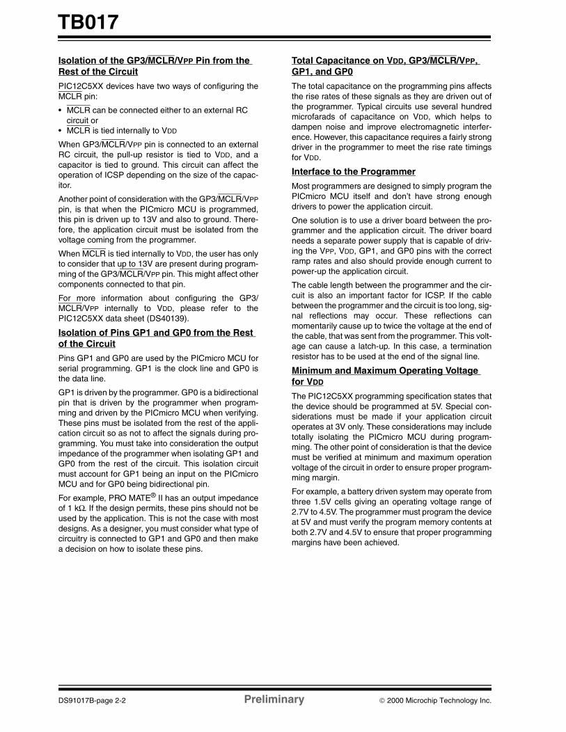
Isolation of the GP3/MCLR/VPP Pin from the Rest of the Circuit
PIC12C5XX devices have two ways of configuring theMCLR pin:
• MCLR can be connected either to an external RC circuit or
• MCLR is tied internally to VDD
When GP3/MCLR/VPP pin is connected to an externalRC circuit, the pull-up resistor is tied to VDD, and acapacitor is tied to ground. This circuit can affect theoperation of ICSP depending on the size of the capac-itor.
Another point of consideration with the GP3/MCLR/VPP
pin, is that when the PICmicro MCU is programmed,this pin is driven up to 13V and also to ground. There-fore, the application circuit must be isolated from thevoltage coming from the programmer.
When MCLR is tied internally to VDD, the user has onlyto consider that up to 13V are present during program-ming of the GP3/MCLR/VPP pin. This might affect othercomponents connected to that pin.
For more information about configuring the GP3/MCLR/VPP internally to VDD, please refer to thePIC12C5XX data sheet (DS40139).
Isolation of Pins GP1 and GP0 from the Rest of the Circuit
Pins GP1 and GP0 are used by the PICmicro MCU forserial programming. GP1 is the clock line and GP0 isthe data line.
GP1 is driven by the programmer. GP0 is a bidirectionalpin that is driven by the programmer when program-ming and driven by the PICmicro MCU when verifying.These pins must be isolated from the rest of the appli-cation circuit so as not to affect the signals during pro-gramming. You must take into consideration the outputimpedance of the programmer when isolating GP1 andGP0 from the rest of the circuit. This isolation circuitmust account for GP1 being an input on the PICmicroMCU and for GP0 being bidirectional pin.
For example, PRO MATE® II has an output impedanceof 1 kΩ. If the design permits, these pins should not beused by the application. This is not the case with mostdesigns. As a designer, you must consider what type ofcircuitry is connected to GP1 and GP0 and then makea decision on how to isolate these pins.
Total Capacitance on VDD, GP3/MCLR/VPP, GP1, and GP0
The total capacitance on the programming pins affectsthe rise rates of these signals as they are driven out ofthe programmer. Typical circuits use several hundredmicrofarads of capacitance on VDD, which helps todampen noise and improve electromagnetic interfer-ence. However, this capacitance requires a fairly strongdriver in the programmer to meet the rise rate timingsfor VDD.
Interface to the Programmer
Most programmers are designed to simply program thePICmicro MCU itself and don’t have strong enoughdrivers to power the application circuit.
One solution is to use a driver board between the pro-grammer and the application circuit. The driver boardneeds a separate power supply that is capable of driv-ing the VPP, VDD, GP1, and GP0 pins with the correctramp rates and also should provide enough current topower-up the application circuit.
The cable length between the programmer and the cir-cuit is also an important factor for ICSP. If the cablebetween the programmer and the circuit is too long, sig-nal reflections may occur. These reflections canmomentarily cause up to twice the voltage at the end ofthe cable, that was sent from the programmer. This volt-age can cause a latch-up. In this case, a terminationresistor has to be used at the end of the signal line.
Minimum and Maximum Operating Voltage for VDD
The PIC12C5XX programming specification states thatthe device should be programmed at 5V. Special con-siderations must be made if your application circuitoperates at 3V only. These considerations may includetotally isolating the PICmicro MCU during program-ming. The other point of consideration is that the devicemust be verified at minimum and maximum operationvoltage of the circuit in order to ensure proper program-ming margin.
For example, a battery driven system may operate fromthree 1.5V cells giving an operating voltage range of2.7V to 4.5V. The programmer must program the deviceat 5V and must verify the program memory contents atboth 2.7V and 4.5V to ensure that proper programmingmargins have been achieved.
DS91017B-page 2-2 Preliminary 2000 Microchip Technology Inc.

TB017
THE PROGRAMMER
PIC12C5XX MCUs only use serial programming and,therefore, all programmers supporting these deviceswill support the ICSP. One issue with the programmeris the drive capability. As discussed before, it must beable to provide the specified rise rates on the ICSP sig-nals and also provide enough current to power theapplication circuit. It is recommended that you bufferthe programming signals.
Another point of consideration for the programmer iswhat VDD levels are used to verify the memory contentsof the PICmicro MCU. For instance, the PRO MATE IIverifies program memory at the minimum and maxi-mum VDD levels for the specified device and is there-fore considered a production quality programmer. Onthe other hand, the PICSTART® Plus only verifies at 5Vand is for prototyping use only. The PIC12C5XX pro-gramming specifications state that the program mem-ory contents should be verified at both the minimumand maximum VDD levels that the application circuit willbe operating. This implies that the application circuitmust be able to handle the varying VDD voltages.
There are also several third-party programmers thatare available. You should select a programmer basedon the features it has and how it fits into your program-ming environment. The Microchip Development Sys-tems Ordering Guide (DS30177) provides detailedinformation on all our development tools. The MicrochipThird Party Guide (DS00104) provides information onall of our third party development tool developers.Please consult these two references when selecting aprogrammer. Many options exist including serial or par-allel PC host connection, stand-alone operation, andsingle or gang programmers.
PROGRAMMING ENVIRONMENT
The programming environment will affect the type ofprogrammer used, the programmer cable length, andthe application circuit interface. Some programmersare well suited for a manual assembly line while othersare desirable for an automated assembly line. A gangprogrammer should be chosen for programming multi-ple MCUs at one time. The physical distance betweenthe programmer and the application circuit affects theload capacitance on each of the programming signals.This will directly affect the drive strength needed to pro-vide the correct signal rise rates and current. Finally,the application circuit interface to the programmerdepends on the size constraints of the application cir-cuit itself and the assembly line. A simple header canbe used to interface the application circuit to the pro-grammer. This might be more desirable for a manualassembly line where a technician plugs theprogrammer cable into the board.
A different method is the uses spring loaded test pins(often referred as pogo-pins). The application circuithas pads on the board for each of the programming sig-nals. Then there is a movable fixture that has pogo pins
in the same configuration as the pads on the board.The application circuit is moved into position and thefixture is moved such that the spring loaded test pinscome into contact with the board. This method might bemore suitable for an automated assembly line.
After taking into consideration the issues with theapplication circuit, the programmer, and the program-ming environment, anyone can build a high quality,reliable manufacturing line based on ICSP.
OTHER BENEFITS
ICSP provides several other benefits such as calibra-tion and serialization. If program memory permits, itwould be cheaper and more reliable to store calibrationconstants in program memory instead of using anexternal serial EEPROM.
Field Programming of PICmicro OTP MCUs
An OTP device is not normally capable of being repro-grammed, but the PICmicro MCU architecture givesyou this flexibility provided the size of your firmware isless than half that of the desired device.
This method involves using jump tables for the resetand interrupt vectors. Example 1 shows the location ofa main routine and the reset vector for the first time adevice with 0.5K-words of program memory is pro-grammed. Example 2 shows the location of a secondmain routine and its reset vector for the second time thesame device is programmed. You will notice that theGOTO Main that was previously at location 0x0002 isreplaced with an NOP. An NOP is a program memorylocation with all the bits programmed as 0s. When thereset vector is executed, it will execute an NOP andthen a GOTO Main1 instruction to the new code.
2000 Microchip Technology Inc. Preliminary DS91017B-page 2-3

TB017
EXAMPLE 1: LOCATION OF THE FIRST MAIN ROUTINE AND ITS INTERRUPT VECTOR
MOVLW XX
MOVWF OSCAL
PROGRAM MEMORY
0X000
0X1FF
GOTO MAIN10X001
MAIN10X040
0X080
CALIBRATION VALUE
RESET VECTOR
MAIN1 ROUTINE
UNPROGRAMMED
UNPROGRAMMED
LEGEND: XX = CALIBRATION VALUE
DS91017B-page 2-4 Preliminary 2000 Microchip Technology Inc.

TB017
EXAMPLE 2: LOCATION OF THE SECOND MAIN ROUTINE AND IT INTERRUPT VECTOR (AFTER SECOND PROGRAMMING)
MOVLW XX
MOVWF OSCAL
PROGRAM MEMORY
0X000
0X1FF
NOP0X001
MAIN10X040
0X080
CALIBRATION VALUE
RESET VECTOR
MAIN1 ROUTINE
GOTO MAIN2
MAIN2
MAIN2 ROUTINE
0X10E
0X136
UNPROGRAMMED
UNPROGRAMMED
0X002
LEGEND: XX = CALIBRATION VALUE
2000 Microchip Technology Inc. Preliminary DS91017B-page 2-5

TB017
Since the program memory of the PIC12C5XX devicesis organized in 256 x 12 word pages, placement of suchinformation as look-up tables and CALL instructionsmust be taken into account. For further information,please refer to application note AN581, ImplementingLong Calls and application note AN556, Implementinga Table Read.
CONCLUSION
Microchip Technology Inc. is committed to supportingyour ICSP needs by providing you with our many yearsof experience and expertise in developing in-circuit sys-tem programming solutions. Anyone can create a reli-able in-circuit system programming station by couplingour background with some forethought to the circuitdesign and programmer selection issues previouslymentioned. Your local Microchip representative is avail-able to answer any questions you have about therequirements for ICSP.
DS91017B-page 2-6 Preliminary 2000 Microchip Technology Inc.

TB017
APPENDIX A: SAMPLE DRIVER BOARD SCHEMATIC
R6
1V
PP_O
UT
TO
CIR
CU
IT
3 2 1
41U
1A
TL
E21
44A
R9
100
R9
100
VC
CQ1
2N39
06
R10
100
R2
33k
5 6 7
U1B
TL
E21
44A
VC
C
VC
C
15V
EX
TE
RN
AL
PO
WE
R S
UP
PL
Y R12
100k
VP
P_I
N
FR
OM
PR
OG
RA
MM
ER
C1
1NF
D1
12.7
V
Q2
2N22
22
R13
5k
Q3
2N39
06
C3
0.1µ
F
VD
D_O
UT
R15
1T
O C
IRC
UIT
C6
0.1µ
F
10
9 8
U1C
TL
E21
44A
VC
CR
18
100
R17
100
Q4
2N22
22
R22
5k
R19
100
C4
1NF
D2
6.2V
VD
D_I
N
12
13
14U
1D
TL
E21
44A
R4
10k
R21
100k
FR
OM
PR
OG
RA
MM
ER
GP
1_IN
GN
D_I
NG
ND
_OU
T
FR
OM
PR
OG
RA
MM
ER
FR
OM
PR
OG
RA
MM
ER
TO
CIR
CU
IT
GP
1_O
UT
GP
0_IN
FR
OM
PR
OG
RA
MM
ER
TO
CIR
CU
IT
GP
0_O
UT
TO
CIR
CU
IT
No
te:
The
driv
er b
oard
des
ign
MU
ST
be
test
ed in
the
use
r’sap
plic
atio
n to
det
erm
ine
the
effe
cts
of th
e ap
plic
atio
nsci
rcui
t on
the
pro
gram
min
g si
gnal
s tim
ing.
Cha
nges
may
be
requ
ired
if th
e ap
plic
atio
n pl
aces
a s
igni
fican
tlo
ad o
n V
DD
, VP
P, G
P0
or G
P1.
*see
text
in te
chni
cal b
rief.
*see
text
in te
chni
cal b
rief.
2000 Microchip Technology Inc. Preliminary DS91017B-page 2-7

TB017
NOTES:
DS91017B-page 2-8 Preliminary 2000 Microchip Technology Inc.

TB013How to Implement ICSP™ Using PIC16CXXX OTP MCUs
INTRODUCTION
In-Circuit Serial Programming™ (ICSP) is a great wayto reduce your inventory overhead and time-to-marketfor your product. By assembling your product with ablank Microchip microcontroller (MCU), you can stockone design. When an order has been placed, theseunits can be programmed with the latest revision offirmware, tested, and shipped in a very short time. Thismethod also reduces scrapped inventory due to oldfirmware revisions. This type of manufacturing systemcan also facilitate quick turnarounds on custom ordersfor your product.
Most people would think to use ICSP with PICmicro®
OTP MCUs only on an assembly line where the deviceis programmed once. However, there is a method bywhich an OTP device can be programmed severaltimes depending on the size of the firmware. Thismethod, explained later, provides a way to fieldupgrade your firmware in a way similar to EEPROM- orFlash-based devices.
HOW DOES ICSP WORK?
Now that ICSP appeals to you, what steps do you taketo implement it in your application? There are threemain components of an ICSP system: ApplicationCircuit, Programmer and Programming Environment.
Application Circuit
The application circuit must be designed to allow all theprogramming signals to be directly connected to thePICmicro MCU. Figure 1 shows a typical circuit that isa starting point for when designing with ICSP. Theapplication must compensate for the following issues:
1. Isolation of the MCLR/VPP pin from the rest ofthe circuit.
2. Isolation of pins RB6 and RB7 from the rest ofthe circuit.
3. Capacitance on each of the VDD, MCLR/VPP,RB6, and RB7 pins.
4. Minimum and maximum operating voltage forVDD.
5. PICmicro Oscillator.6. Interface to the programmer.
The MCLR/VPP pin is normally connected to an RC cir-cuit. The pull-up resistor is tied to VDD and a capacitoris tied to ground. This circuit can affect the operation ofICSP depending on the size of the capacitor. It is, there-fore, recommended that the circuit in Figure 1 be usedwhen an RC is connected to MCLR/VPP. The diodeshould be a Schottky-type device. Another issue withMCLR/VPP is that when the PICmicro MCU device isprogrammed, this pin is driven to approximately 13Vand also to ground. Therefore, the application circuitmust be isolated from this voltage provided by theprogrammer.
FIGURE 1: TYPICAL APPLICATION CIRCUIT
Author: Rodger RicheyMicrochip Technology Inc.
Application PCBPIC16CXXX
MCLR/Vpp
VddVssRB7RB6
Vdd Vdd
To application circuit
Isolation circuits
ICSP Connector
2000 Microchip Technology Inc. Preliminary DS91013B-page 2-9

TB013
Pins RB6 and RB7 are used by the PICmicro MCU forserial programming. RB6 is the clock line and RB7 isthe data line. RB6 is driven by the programmer. RB7 isa bidirectional pin that is driven by the programmerwhen programming, and driven by the PICmicro MCUwhen verifying. These pins must be isolated from therest of the application circuit so as not to affect the sig-nals during programming. You must take into consider-ation the output impedance of the programmer whenisolating RB6 and RB7 from the rest of the circuit. Thisisolation circuit must account for RB6 being an input onthe PICmicro MCU, and for RB7 being bidirectional(can be driven by both the PICmicro MCU and the pro-grammer). For instance, PRO MATE® II has an outputimpedance of 1k¾. If the design permits, these pinsshould not be used by the application. This is not thecase with most applications so it is recommended thatthe designer evaluate whether these signals need to bebuffered. As a designer, you must consider what type ofcircuitry is connected to RB6 and RB7 and then makea decision on how to isolate these pins. Figure 1 doesnot show any circuitry to isolate RB6 and RB7 on theapplication circuit because this is very applicationdependent.
The total capacitance on the programming pins affectsthe rise rates of these signals as they are driven out ofthe programmer. Typical circuits use several hundredmicrofarads of capacitance on VDD which helps todampen noise and ripple. However, this capacitancerequires a fairly strong driver in the programmer tomeet the rise rate timings for VDD. Most programmersare designed to simply program the PICmicro MCUitself and don’t have strong enough drivers to power theapplication circuit. One solution is to use a driver boardbetween the programmer and the application circuit.The driver board requires a separate power supply thatis capable of driving the VPP and VDD pins with thecorrect rise rates and should also provide enough cur-rent to power the application circuit. RB6 and RB7 arenot buffered on this schematic but may require buffer-ing depending upon the application. A sample driverboard schematic is shown in Appendix A.
The Microchip programming specification states thatthe device should be programmed at 5V. Special con-siderations must be made if your application circuitoperates at 3V only. These considerations may includetotally isolating the PICmicro MCU during program-ming. The other issue is that the device must be verifiedat the minimum and maximum voltages at which theapplication circuit will be operating. For instance, a bat-tery operated system may operate from three 1.5Vcells giving an operating voltage range of 2.7V to 4.5V.
The programmer must program the device at 5V andmust verify the program memory contents at both 2.7Vand 4.5V to ensure that proper programming marginshave been achieved. This ensures the PICmicro MCUoption over the voltage range of the system.
This final issue deals with the oscillator circuit on theapplication board. The voltage on MCLR/VPP must riseto the specified program mode entry voltage before thedevice executes any code. The crystal modes availableon the PICmicro MCU are not affected by this issuebecause the Oscillator Start-up Timer waits for 1024oscillations before any code is executed. However, RCoscillators do not require any startup time and, there-fore, the Oscillator Startup Timer is not used. The pro-grammer must drive MCLR/VPP to the program modeentry voltage before the RC oscillator toggles fourtimes. If the RC oscillator toggles four or more times,the program counter will be incremented to some valueX. Now when the device enters programming mode,the program counter will not be zero and the program-mer will start programming your code at an offset of X.There are several alternatives that can compensate fora slow rise rate on MCLR/VPP. The first method wouldbe to not populate the R, program the device, and theninsert the R. The other method would be to have theprogramming interface drive the OSC1 pin of thePICmicro MCU to ground while programming. This willprevent any oscillations from occurring during program-ming.
Now all that is left is how to connect the application cir-cuit to the programmer. This depends a lot on theprogramming environment and will be discussed in thatsection.
Programmer
The second consideration is the programmer.PIC16CXXX MCUs only use serial programming andtherefore all programmers supporting these deviceswill support ICSP. One issue with the programmer is thedrive capability. As discussed before, it must be able toprovide the specified rise rates on the ICSP signals andalso provide enough current to power the applicationcircuit. Appendix A shows an example driver board.This driver schematic does not show any buffer circuitryfor RB6 and RB7. It is recommended that an evaluationbe performed to determine if buffering is required.Another issue with the programmer is what VDD levelsare used to verify the memory contents of the PICmicroMCU. For instance, the PRO MATE II verifies programmemory at the minimum and maximum VDD levels forthe specified device and is therefore considered a pro-duction quality programmer. On the other hand, thePICSTART® Plus only verifies at 5V and is for prototyp-ing use only. The Microchip programming specifica-tions state that the program memory contents shouldbe verified at both the minimum and maximum VDD lev-els that the application circuit will be operating. Thisimplies that the application circuit must be able to han-dle the varying VDD voltages.
Note: The driver board design MUST be testedin the user’s application to determine theeffects of the application circuit on theprogramming signals timing. Changesmay be required if the application placesa significant load on VDD, VPP, RB6 OR
RB7.
DS91013B-page 2-10 Preliminary 2000 Microchip Technology Inc.

TB013
There are also several third party programmers that areavailable. You should select a programmer based onthe features it has and how it fits into your programmingenvironment. The Microchip Development SystemsOrdering Guide (DS30177) provides detailed informa-tion on all our development tools. The Microchip ThirdParty Guide (DS00104) provides information on all ofour third party tool developers. Please consult thesetwo references when selecting a programmer. Manyoptions exist including serial or parallel PC host con-nection, stand-alone operation, and single or gang pro-grammers. Some of the third party developers includeAdvanced Transdata Corporation, BP Microsystems,Data I/O, Emulation Technology and Logical Devices.
Programming Environment
The programming environment will affect the type ofprogrammer used, the programmer cable length, andthe application circuit interface. Some programmersare well suited for a manual assembly line while othersare desirable for an automated assembly line. You maywant to choose a gang programmer to program multiplesystems at a time.
The physical distance between the programmer andthe application circuit affects the load capacitance oneach of the programming signals. This will directlyaffect the drive strength needed to provide the correctsignal rise rates and current. This programming cablemust also be as short as possible and properlyterminated and shielded, or the programming signalsmay be corrupted by ringing or noise.
Finally, the application circuit interface to the program-mer depends on the size constraints of the applicationcircuit itself and the assembly line. A simple header canbe used to interface the application circuit to the pro-grammer. This might be more desirable for a manualassembly line where a technician plugs theprogrammer cable into the board. A different method isthe use of spring loaded test pins (commonly referredto as pogo pins). The application circuit has pads onthe board for each of the programming signals. Thenthere is a fixture that has pogo pins in the same config-uration as the pads on the board. The application circuitor fixture is moved into position such that the pogo pinscome into contact with the board. This method might bemore suitable for an automated assembly line.
After taking into consideration the issues with the appli-cation circuit, the programmer, and the programmingenvironment, anyone can build a high quality, reliablemanufacturing line based on ICSP.
Other Benefits
ICSP provides other benefits, such as calibration andserialization. If program memory permits, it would becheaper and more reliable to store calibration con-stants in program memory instead of using an externalserial EEPROM. For example, your system has a ther-mistor which can vary from one system to another.Storing some calibration information in a table formatallows the microcontroller to compensate in softwarefor external component tolerances. System cost can bereduced without affecting the required performance ofthe system by using software calibration techniques.But how does this relate to ICSP? The PICmicro MCUhas already been programmed with firmware that per-forms a calibration cycle. The calibration data is trans-ferred to a calibration fixture. When all calibration datahas been transferred, the fixture places the PICmicroMCU in programming mode and programs thePICmicro MCU with the calibration data. Applicationnote AN656, In-Circuit Serial Programming of Calibra-tion Parameters Using a PICmicro Microcontroller,shows exactly how to implement this type of calibrationdata programming.
The other benefit of ICSP is serialization. Each individ-ual system can be programmed with a unique or ran-dom serial number. One such application of a uniqueserial number would be for security systems. A typicalsystem might use DIP switches to set the serial num-ber. Instead, this number can be burned into programmemory, thus reducing the overall system cost and low-ering the risk of tampering.
Field Programming of PICmicro OTP MCUs
An OTP device is not normally capable of beingreprogrammed, but the PICmicro MCU architecturegives you this flexibility provided the size of your firm-ware is at least half that of the desired device and thedevice is not code protected. If your target device doesnot have enough program memory, Microchip providesa wide spectrum of devices from 0.5K to 8K programmemory with the same set of peripheral features thatwill help meet the criteria.
The PIC16CXXX microcontrollers have two vectors,reset and interrupt, at locations 0x0000 and 0x0004.When the PICmicro MCU encounters a reset or inter-rupt condition, the code located at one of these twolocations in program memory is executed. The first list-ing of Example 1 shows the code that is first pro-grammed into the PICmicro MCU. The second listing ofExample 1 shows the code that is programmed into thePICmicro MCU for the second time.
2000 Microchip Technology Inc. Preliminary DS91013B-page 2-11

TB013
EXAMPLE 1: PROGRAMMING CYCLE LISTING FILESFirst Program Cycle Second Program Cycle
_________________________________________________________________________________________Prog Opcode Assembly |Prog Opcode AssemblyMem Instruction |Mem Instruction-----------------------------------------------------------------------------------------0000 2808 goto Main ;Main loop |0000 0000 nop0001 3FFF <blank> ;at 0x0008 |0001 2860 goto Main ;Main now0002 3FFF <blank> |0002 3FFF <blank> ;at 0x00600003 3FFF <blank> |0003 3FFF <blank>0004 2848 goto ISR ;ISR at |0004 0000 nop0005 3FFF <blank> ;0x0048 |0005 28A8 goto ISR ;ISR now at0006 3FFF <blank> |0006 3FFF <blank> ;0x00A80007 3FFF <blank> |0007 3FFF <blank>0008 1683 bsf STATUS,RP0 | 0008 1683 bsf STATUS,RP00009 3007 movlw 0x07 |0009 3007 movlw 0x07000A 009F movwf ADCON1 |000A 009F movwf ADCON1 . | . . | . . | .0048 1C0C btfss PIR1,RBIF | 0048 1C0C btfss PIR1,RBIF0049 284E goto EndISR |0049 284E goto EndISR004A 1806 btfsc PORTB,0 |004A 1806 btfsc PORTB,0 . | . . | . . | .0060 3FFF <blank> |0060 1683 bsf STATUS,RP00061 3FFF <blank> |0061 3005 movlw 0x050062 3FFF <blank> |0062 009F movwf ADCON1 . | . . | . . | .00A8 3FFF <blank> |00A8 1C0C btfss PIR1,RBIF00A9 3FFF <blank> |00A9 28AE goto EndISR00AA 3FFF <blank> |00AA 1806 btfsc PORTB,0 . | . . | . . | .-----------------------------------------------------------------------------------------
DS91013B-page 2-12 Preliminary 2000 Microchip Technology Inc.

TB013
The example shows that to program the PICmicro MCUa second time the memory location 0x0000, originallygoto Main (0x2808), is reprogrammed to all 0’s whichhappens to be a nop instruction. This location cannotbe reprogrammed to the new opcode (0x2860)because the bits that are 0’s cannot be reprogrammedto 1’s, only bits that are 1’s can be reprogrammed to0’s. The next memory location 0x0001 was originallyblank (all 1’s) and now becomes a goto Main(0x2860). When a reset condition occurs, the PICmicroMCU executes the instruction at location 0x0000 whichis the nop, a completely benign instruction, and thenexecutes the goto Main to start the execution of code.The example also shows that all program memory loca-tions after 0x005A are blank in the original program sothat the second time the PICmicro MCU is pro-grammed, the revised code can be programmed atthese locations. The same descriptions can be givenfor the interrupt vector at location 0x0004.
This method changes slightly for PICmicro MCUs with>2K words of program memory. Each of the gotoMain and goto ISR instructions are replaced by thefollowing code segments due to paging on devices with>2K words of program memory.
movlw <page> movlw <page>movwf PCLATH movwf PCLATHgoto Main goto ISR
Now your one time programmable PICmicro MCU isexhibiting more EEPROM- or Flash-like qualities.
CONCLUSION
Microchip Technology Inc. is committed to supportingyour ICSP needs by providing you with our many yearsof experience and expertise in developing ICSPsolutions. Anyone can create a reliable ICSP program-ming station by coupling our background with someforethought to the circuit design and programmerselection issues previously mentioned. Your localMicrochip representative is available to answer anyquestions you have about the requirements for ICSP.
2000 Microchip Technology Inc. Preliminary DS91013B-page 2-13

TB013
APPENDIX A: SAMPLE DRIVER BOARD SCHEMATIC
R6
1V
PP_O
UT
TO
CIR
CU
IT
3 2 1
41U
1A
TL
E21
44A
R9
100
R9
100
VC
CQ1
2N39
06
R10
100
R2
33k
5 6 7
U1B
TL
E21
44A
VC
C
VC
C
15V
EX
TE
RN
AL
PO
WE
R S
UP
PL
Y R12
100k
VP
P_I
N
FR
OM
PR
OG
RA
MM
ER
C1
1NF
D1
12.7
V
Q2
2N22
22
R13
5k
Q3
2N39
06
C3
0.1µ
F
VD
D_O
UT
R15
1T
O C
IRC
UIT
C6
0.1µ
F
10
9 8
U1C
TL
E21
44A
VC
CR
18
100
R17
100
Q4
2N22
22
R22
5k
R19
100
C4
1NF
D2
6.2V
VD
D_I
N
12
13
14U
1D
TL
E21
44A
R4
10k
R21
100k
FR
OM
PR
OG
RA
MM
ER
RB
6_IN
GN
D_I
NG
ND
_OU
T
FR
OM
PR
OG
RA
MM
ER
FR
OM
PR
OG
RA
MM
ER
TO
CIR
CU
IT
RB
6_O
UT
RB
7_IN
FR
OM
PR
OG
RA
MM
ER
TO
CIR
CU
IT
RB
7_O
UT
TO
CIR
CU
IT
No
te:
The
driv
er b
oard
des
ign
MU
ST
be
test
ed in
the
use
r’sap
plic
atio
n to
det
erm
ine
the
effe
cts
of t
he a
pplic
atio
nci
rcui
t on
the
pro
gram
min
g si
gnal
s tim
ing.
Cha
nges
may
be
requ
ired
if th
e ap
plic
atio
n pl
aces
a s
igni
fican
tlo
ad o
n V
dd, V
pp, R
B6
or R
B7.
*see
text
in te
chni
cal b
rief.
*see
text
in te
chni
cal b
rief.
DS91013B-page 2-14 Preliminary 2000 Microchip Technology Inc.

TB015How to Implement ICSP™ Using PIC17CXXX OTP MCUs
INTRODUCTION
PIC17CXXX microcontroller (MCU) devices can beserially programmed using an RS-232 or equivalentserial interface. As shown in Figure 2, using just threepins, the PIC17CXXX can be connected to an externalinterface and programmed. In-Circuit Serial Program-ming (ICSP™) allows for a greater flexibility in an appli-cation as well as a faster time to market for the user'sproduct.
This technical brief will demonstrate the practicalaspects associated with ICSP using the PIC17CXXX. Itwill also demonstrate some key capabilities of OTPdevices when used in conjunction with ICSP.
Implementation
The PIC17CXXX devices have special instructions,which enables the user to program and read thePIC17CXXX's program memory. The instructions areTABLWT and TLWT which implement the program mem-ory write operation and TABLRD and TLRD which per-form the program memory read operation. For moredetails, please check the In-Circuit Serial Programmingfor PIC17CXXX OTP Microcontrollers Specification(DS30273), PIC17C4X data sheet (DS30412) andPIC17C75X data sheet (DS30264).
When doing ICSP, the PIC17CXXX runs a boot code,which configures the USART port and receives dataserially through the RX line. This data is then pro-grammed at the address specified in the serial datastring. A high voltage (about 13V) is required for theEPROM cell to get programmed, and this is usuallysupplied by the programming header as shown inFigure 2 and Figure 3. The PIC17CXXX's boot codeenables and disables the high voltage line using a ded-icated I/O line.
FIGURE 2: PIC17CXXX IN-CIRCUIT SERIAL PROGRAMMING USING TABLE WRITE INSTRUCTIONS
Author: Stan D’SouzaMicrochip Technology Inc.
PIC17CXXX
DataMemory
ProgramMemory
Data LData H
BootCode
USART Level Converter
In-CircuitProgramming
Connector
I/O13V Enable
SYSTEM BOARD
VPP
13V
RX
TX
Data H:Data L
2000 Microchip Technology Inc. Preliminary DS91015A-page 2-15
TB015
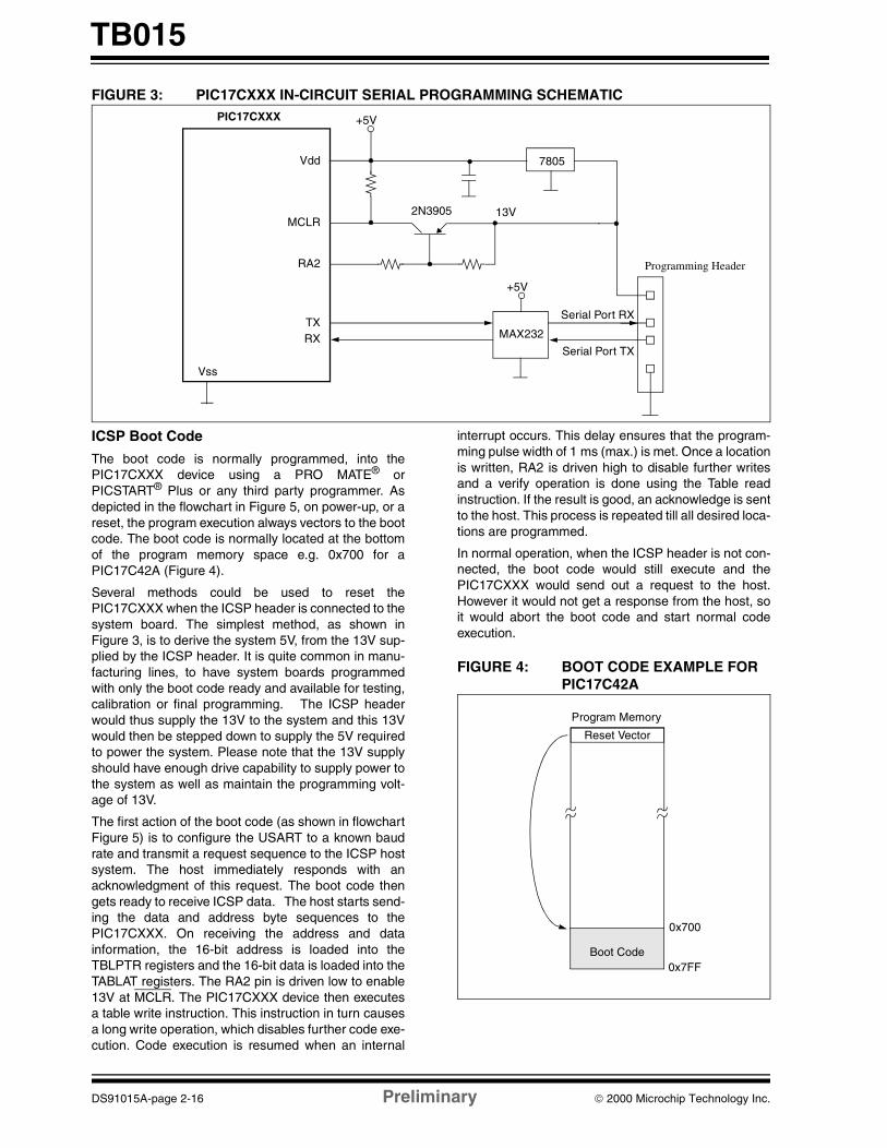
FIGURE 3: PIC17CXXX IN-CIRCUIT SERIAL PROGRAMMING SCHEMATIC
ICSP Boot Code
The boot code is normally programmed, into thePIC17CXXX device using a PRO MATE® orPICSTART® Plus or any third party programmer. Asdepicted in the flowchart in Figure 5, on power-up, or areset, the program execution always vectors to the bootcode. The boot code is normally located at the bottomof the program memory space e.g. 0x700 for aPIC17C42A (Figure 4).
Several methods could be used to reset thePIC17CXXX when the ICSP header is connected to thesystem board. The simplest method, as shown inFigure 3, is to derive the system 5V, from the 13V sup-plied by the ICSP header. It is quite common in manu-facturing lines, to have system boards programmedwith only the boot code ready and available for testing,calibration or final programming. The ICSP headerwould thus supply the 13V to the system and this 13Vwould then be stepped down to supply the 5V requiredto power the system. Please note that the 13V supplyshould have enough drive capability to supply power tothe system as well as maintain the programming volt-age of 13V.
The first action of the boot code (as shown in flowchartFigure 5) is to configure the USART to a known baudrate and transmit a request sequence to the ICSP hostsystem. The host immediately responds with anacknowledgment of this request. The boot code thengets ready to receive ICSP data. The host starts send-ing the data and address byte sequences to thePIC17CXXX. On receiving the address and datainformation, the 16-bit address is loaded into theTBLPTR registers and the 16-bit data is loaded into theTABLAT registers. The RA2 pin is driven low to enable13V at MCLR. The PIC17CXXX device then executesa table write instruction. This instruction in turn causesa long write operation, which disables further code exe-cution. Code execution is resumed when an internal
interrupt occurs. This delay ensures that the program-ming pulse width of 1 ms (max.) is met. Once a locationis written, RA2 is driven high to disable further writesand a verify operation is done using the Table readinstruction. If the result is good, an acknowledge is sentto the host. This process is repeated till all desired loca-tions are programmed.
In normal operation, when the ICSP header is not con-nected, the boot code would still execute and thePIC17CXXX would send out a request to the host.However it would not get a response from the host, soit would abort the boot code and start normal codeexecution.
FIGURE 4: BOOT CODE EXAMPLE FOR PIC17C42A
PIC17CXXX
Vdd
MCLR
RA2
RX
Vss
+5V
MAX232
2N3905 13V
+5V
Serial Port TX
Serial Port RXTX
7805
Programming Header
Reset Vector
Boot Code
Program Memory
0x700
0x7FF
DS91015A-page 2-16 Preliminary 2000 Microchip Technology Inc.

TB015
FIGURE 5: FLOWCHART FOR ICSP BOOT CODE
Start
Received Host’s
Configure USARTand send request
Goto Boot Code
Prepare to receiveICSP data
Do Table Writeoperation
Received Addressand Data info?
Last Data/Address
Signal ProgrammingError
END
sequence?
ACK?Time-out complete?
Start CodeExecution
Interrupt?
Read ProgramLocation
Program locationverified correctly?
No
Yes
No
Yes
No
Yes
No
Yes
Yes
No
YesNo
2000 Microchip Technology Inc. Preliminary DS91015A-page 2-17
TB015
USING THE ICSP FEATURE ON PIC17CXXX OTP DEVICES
The ICSP feature is a very powerful tool when used inconjunction with OTP devices.
Saving Calibration Information Using ICSP
One key use of ICSP is to store calibration constants orparameters in program memory. It is quite common tointerface a PIC17CXXX device to a sensor. Accurate,pre-calibrated sensors can be used, but they are moreexpensive and have long lead times. Uncalibrated sen-sors on the other hand are inexpensive and readilyavailable. The only caveat is that these sensors have tobe calibrated in the application. Once the calibrationconstants have been determined, they would be uniqueto a given system, so they have to be saved in programmemory. These calibration parameters/constants canthen be retrieved later during program execution andused to improve the accuracy of low cost un-calibratedsensors. ICSP thus offers a cost reduction path for theend user in the application.
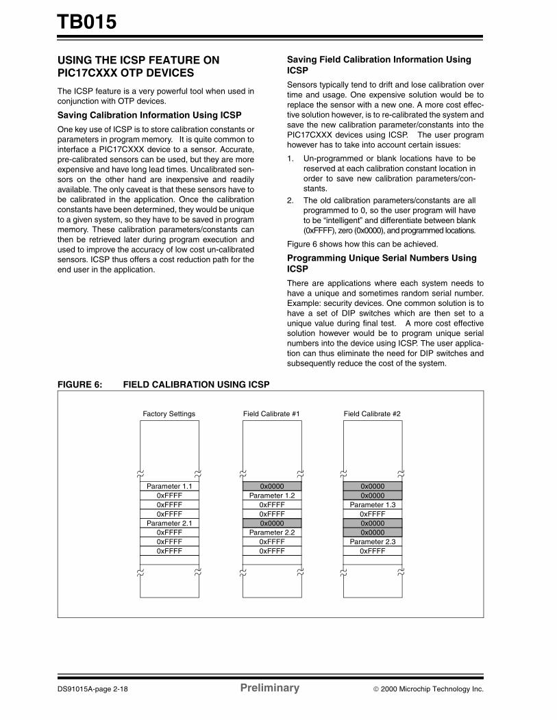
Saving Field Calibration Information Using ICSP
Sensors typically tend to drift and lose calibration overtime and usage. One expensive solution would be toreplace the sensor with a new one. A more cost effec-tive solution however, is to re-calibrated the system andsave the new calibration parameter/constants into thePIC17CXXX devices using ICSP. The user programhowever has to take into account certain issues:
1. Un-programmed or blank locations have to bereserved at each calibration constant location inorder to save new calibration parameters/con-stants.
2. The old calibration parameters/constants are allprogrammed to 0, so the user program will haveto be “intelligent” and differentiate between blank(0xFFFF), zero (0x0000), and programmed locations.
Figure 6 shows how this can be achieved.
Programming Unique Serial Numbers Using ICSP
There are applications where each system needs tohave a unique and sometimes random serial number.Example: security devices. One common solution is tohave a set of DIP switches which are then set to aunique value during final test. A more cost effectivesolution however would be to program unique serialnumbers into the device using ICSP. The user applica-tion can thus eliminate the need for DIP switches andsubsequently reduce the cost of the system.
FIGURE 6: FIELD CALIBRATION USING ICSP
Parameter 1.10xFFFF0xFFFF0xFFFF
Parameter 2.10xFFFF0xFFFF0xFFFF
Factory Settings
0x0000Parameter 1.2
0xFFFF0xFFFF0x0000
Parameter 2.20xFFFF0xFFFF
Field Calibrate #1
0x00000x0000
Parameter 1.30xFFFF0x00000x0000
Parameter 2.30xFFFF
Field Calibrate #2
DS91015A-page 2-18 Preliminary 2000 Microchip Technology Inc.

TB015
Code Updates in the Field Using ICSP
With fast time to market it is not uncommon to seeapplication programs which need to be updated or cor-rected for either enhancements or minor errors/bugs. IfROM parts were used, updates would be impossibleand the product would either become outdated orrecalled from the field. A more cost effective solutionis to use OTP devices with ICSP and program them inthe field with the new updates. Figure 7 shows anexample where the user has allowed for one fieldupdate to his program.
Here are some of the issues which need to beaddressed:
1. The user has to reserve sufficient blank memoryto fit his updated code.
2. At least one blank location needs to be saved atthe reset vector as well as for all the interrupts.
3. Program all the old “goto” locations (located atthe reset vector and the interrupts vectors) to 0so that these instructions execute as NOPs.
4. Program new “goto” locations (at the reset vec-tor and the interrupt vectors) just below the old“goto” locations.
5. Finally, program the new updated code in theblank memory space.
CONCLUSION
ICSP is a very powerful feature available on thePIC17CXXX devices. It offers tremendous design flex-ibility to the end user in terms of saving calibration con-stants and updating code in final production as well asin the field, thus helping the user design a low-cost andfast time-to-market product.
FIGURE 7: CODE UPDATES USING ICSP
Goto Boot
Goto Main10xFFFF0xFFFF
Production Program
0x0000
Main1
Main
Boot
Goto Main
Goto Boot
0x0000Goto Main2
0xFFFF
Code Update #1
Main1
Main
Boot
Goto Main
Main2
0x0000
2000 Microchip Technology Inc. Preliminary DS91015A-page 2-19

TB015
NOTES:
DS91015A-page 2-20 Preliminary 2000 Microchip Technology Inc.

TB016How to Implement ICSP™ Using PIC16F8X FLASH MCUs
INTRODUCTION
In-Circuit Serial Programming™ (ICSP) withPICmicro® FLASH microcontrollers (MCU) is not only agreat way to reduce your inventory overhead and time-to-market for your product, but also to easily providefield upgrades of firmware. By assembling your productwith a Microchip FLASH-based MCU, you can stock theshelf with one system. When an order has been placed,these units can be programmed with the latest revisionof firmware, tested, and shipped in a very short time.This type of manufacturing system can also facilitatequick turnarounds on custom orders for your product.You don’t have to worry about scrapped inventorybecause of the FLASH-based program memory. Thisgives you the advantage of upgrading the firmware atany time to fix those “features” that pop up from time totime.
HOW DOES ICSP WORK?
Now that ICSP appeals to you, what steps do you taketo implement it in your application? There are threemain components of an ICSP system.
These are the: Application Circuit, Programmer andProgramming Environment.
Application Circuit
The application circuit must be designed to allow all theprogramming signals to be directly connected to thePICmicro MCUs. Figure 1 shows a typical circuit that isa starting point for when designing with ICSP. Theapplication must compensate for the following issues:
1. Isolation of the MCLR/VPP pin from the rest ofthe circuit.
2. Isolation of pins RB6 and RB7 from the rest ofthe circuit.
3. Capacitance on each of the VDD, MCLR/VPP,RB6, and RB7 pins.
4. Minimum and maximum operating voltage forVDD.
5. PICmicro Oscillator.6. Interface to the programmer.
The MCLR/VPP pin is normally connected to an RC cir-cuit. The pull-up resistor is tied to VDD and a capacitoris tied to ground. This circuit can affect the operation ofICSP depending on the size of the capacitor. It is, there-fore, recommended that the circuit in Figure 1 be usedwhen an RC is connected to MCLR/VPP. The diodeshould be a Schottky-type device. Another issue withMCLR/VPP is that when the PICmicro MCU device isprogrammed, this pin is driven to approximately 13Vand also to ground. Therefore, the application circuitmust be isolated from this voltage provided by theprogrammer.
FIGURE 1: TYPICAL APPLICATION CIRCUIT
Author: Rodger RicheyMicrochip Technology Inc.
Application PCBPIC16F8X
MCLR/VPP
VddVssRB7RB6
Vdd Vdd
To application circuit
Isolation circuits
ICSP Connector
PICmicro, PRO MATE, and PICSTART are registered trademarks of Microchip Technology Inc.In-Circuit Serial Programming and ICSP are trademarks of Microchip Technology Inc.
2000 Microchip Technology Inc. DS91016B-page 2-21

TB016
Pins RB6 and RB7 are used by the PICmicro MCU forserial programming. RB6 is the clock line and RB7 isthe data line. RB6 is driven by the programmer. RB7 isa bidirectional pin that is driven by the programmerwhen programming, and driven by the PICmicro MCUwhen verifying. These pins must be isolated from therest of the application circuit so as not to affect the sig-nals during programming. You must take into consider-ation the output impedance of the programmer whenisolating RB6 and RB7 from the rest of the circuit. Thisisolation circuit must account for RB6 being an input onthe PICmicro MCU and for RB7 being bidirectional (canbe driven by both the PICmicro MCU and the program-mer). For instance, PRO MATE® II has an outputimpedance of 1k¾. If the design permits, these pinsshould not be used by the application. This is not thecase with most applications so it is recommended thatthe designer evaluate whether these signals need to bebuffered. As a designer, you must consider what type ofcircuitry is connected to RB6 and RB7 and then makea decision on how to isolate these pins. Figure 1 doesnot show any circuitry to isolate RB6 and RB7 on theapplication circuit because this is very applicationdependent.
The total capacitance on the programming pins affectsthe rise rates of these signals as they are driven out ofthe programmer. Typical circuits use several hundredmicrofarads of capacitance on VDD which helps todampen noise and ripple. However, this capacitancerequires a fairly strong driver in the programmer tomeet the rise rate timings for VDD. Most programmersare designed to simply program the PICmicro MCUitself and don’t have strong enough drivers to power theapplication circuit. One solution is to use a driver boardbetween the programmer and the application circuit.The driver board requires a separate power supply thatis capable of driving the VPP and VDD pins with the cor-rect rise rates and should also provide enough currentto power the application circuit. RB6 and RB7 are notbuffered on this schematic but may require bufferingdepending upon the application. A sample driver boardschematic is shown in Appendix A.
The Microchip programming specification states thatthe device should be programmed at 5V. Special con-siderations must be made if your application circuitoperates at 3V only. These considerations may includetotally isolating the PICmicro MCU during program-ming. The other issue is that the device must be verifiedat the minimum and maximum voltages at which theapplication circuit will be operating. For instance, a bat-tery operated system may operate from three 1.5V
cells giving an operating voltage range of 2.7V to 4.5V.The programmer must program the device at 5V andmust verify the program memory contents at both 2.7Vand 4.5V to ensure that proper programming marginshave been achieved. This ensures the PICmicro MCUoption over the voltage range of the system.
This final issue deals with the oscillator circuit on theapplication board. The voltage on MCLR/VPP must riseto the specified program mode entry voltage before thedevice executes any code. The crystal modes availableon the PICmicro MCU are not affected by this issuebecause the Oscillator Start-up Timer waits for 1024oscillations before any code is executed. However, RCoscillators do not require any startup time and, there-fore, the Oscillator Startup Timer is not used. The pro-grammer must drive MCLR/VPP to the program modeentry voltage before the RC oscillator toggles fourtimes. If the RC oscillator toggles four or more times,the program counter will be incremented to some valueX. Now when the device enters programming mode,the program counter will not be zero and the program-mer will start programming your code at an offset of X.There are several alternatives that can compensate fora slow rise rate on MCLR/VPP. The first method wouldbe to not populate the R, program the device, and theninsert the R. The other method would be to have theprogramming interface drive the OSC1 pin of thePICmicro MCU to ground while programming. This willprevent any oscillations from occurring during program-ming.
Now all that is left is how to connect the application cir-cuit to the programmer. This depends a lot on theprogramming environment and will be discussed in thatsection.
Programmer
The second consideration is the programmer.PIC16F8X MCUs only use serial programming andtherefore all programmers supporting these deviceswill support ICSP. One issue with the programmer is thedrive capability. As discussed before, it must be able toprovide the specified rise rates on the ICSP signals andalso provide enough current to power the applicationcircuit. Appendix A shows an example driver board.This driver schematic does not show any buffer circuitryfor RB6 and RB7. It is recommended that an evalua-tion be performed to determine if buffering is required.Another issue with the programmer is what VDD levelsare used to verify the memory contents of the PICmicroMCU. For instance, the PRO MATE II verifies programmemory at the minimum and maximum VDD levels forthe specified device and is therefore considered a pro-duction quality programmer. On the other hand, thePICSTART® Plus only verifies at 5V and is for prototyp-ing use only. The Microchip programming specifica-tions state that the program memory contents shouldbe verified at both the minimum and maximum VDD lev-els that the application circuit will be operating. Thisimplies that the application circuit must be able to han-dle the varying VDD voltages.
Note: The driver board design MUST be testedin the user’s application to determine theeffects of the application circuit on theprogramming signals timing. Changesmay be required if the application placesa significant load on Vdd, VPP, RB6 orRB7.
DS91016B-page 2-22 2000 Microchip Technology Inc.

TB016
There are also several third party programmers that areavailable. You should select a programmer based onthe features it has and how it fits into your programmingenvironment. The Microchip Development SystemsOrdering Guide (DS30177) provides detailed informa-tion on all our development tools. The Microchip ThirdParty Guide (DS00104) provides information on all ofour third party tool developers. Please consult thesetwo references when selecting a programmer. Manyoptions exist including serial or parallel PC host con-nection, stand-alone operation, and single or gang pro-grammers. Some of the third party developers includeAdvanced Transdata Corporation, BP Microsystems,Data I/O, Emulation Technology and Logical Devices.
Programming Environment
The programming environment will affect the type ofprogrammer used, the programmer cable length, andthe application circuit interface. Some programmersare well suited for a manual assembly line while othersare desirable for an automated assembly line. You maywant to choose a gang programmer to program multiplesystems at a time.
The physical distance between the programmer andthe application circuit affects the load capacitance oneach of the programming signals. This will directlyaffect the drive strength needed to provide the correctsignal rise rates and current. This programming cablemust also be as short as possible and properly termi-nated and shielded or the programming signals may becorrupted by ringing or noise.
Finally, the application circuit interface to the program-mer depends on the size constraints of the applicationcircuit itself and the assembly line. A simple header canbe used to interface the application circuit to the pro-grammer. This might be more desirable for a manualassembly line where a technician plugs theprogrammer cable into the board. A different method isthe use of spring loaded test pins (commonly referredto as pogo pins). The application circuit has pads onthe board for each of the programming signals. Thenthere is a fixture that has pogo pins in the same config-uration as the pads on the board. The application circuitor fixture is moved into position such that the pogo pinscome into contact with the board. This method might bemore suitable for an automated assembly line.
After taking into consideration the issues with the appli-cation circuit, the programmer, and the programmingenvironment, anyone can build a high quality, reliablemanufacturing line based on ICSP.
Other Benefits
ICSP provides other benefits, such as calibration andserialization. If program memory permits, it would becheaper and more reliable to store calibration con-stants in program memory instead of using an externalserial EEPROM. For example, your system has a ther-mistor which can vary from one system to another.Storing some calibration information in a table formatallows the microcontroller to compensate in softwarefor external component tolerances. System cost can bereduced without affecting the required performance ofthe system by using software calibration techniques.But how does this relate to ICSP? The PICmicro MCUhas already been programmed with firmware that per-forms a calibration cycle. The calibration data is trans-ferred to a calibration fixture. When all calibration datahas been transferred, the fixture places the PICmicroMCU in programming mode and programs thePICmicro MCU with the calibration data. Applicationnote AN656, In-Circuit Serial Programming of Calibra-tion Parameters Using a PICmicro Microcontroller,shows exactly how to implement this type of calibrationdata programming.
The other benefit of ICSP is serialization. Each individ-ual system can be programmed with a unique or ran-dom serial number. One such application of a uniqueserial number would be for security systems. A typicalsystem might use DIP switches to set the serial num-ber. Instead, this number can be burned into programmemory thus reducing the overall system cost and low-ering the risk of tampering.
Field Programming of FLASH PICmicro MCUs
With the ISP interface circuitry already in place, theseFLASH-based PICmicro MCUs can be easily repro-grammed in the field. These FLASH devices allow youto reprogram them even if they are code protected. Aportable ISP programming station might consist of alaptop computer and programmer. The technicianplugs the ISP interface cable into the application circuitand downloads the new firmware into the PICmicroMCU. The next thing you know the system is up andrunning without those annoying “bugs”. Anotherinstance would be that you want to add an additionalfeature to your system. All of your current inventory canbe converted to the new firmware and field upgradescan be performed to bring your installed base of sys-tems up to the latest revision of firmware.
CONCLUSION
Microchip Technology Inc. is committed to supportingyour ICSP needs by providing you with our many yearsof experience and expertise in developing ICSPsolutions. Anyone can create a reliable ICSP program-ming station by coupling our background with someforethought to the circuit design and programmerselection issues previously mentioned. Your localMicrochip representative is available to answer anyquestions you have about the requirements for ICSP.
2000 Microchip Technology Inc. DS91016B-page 2-23

TB016
APPENDIX A: SAMPLE DRIVER BOARD SCHEMATIC
R6
1V
PP_O
UT
TO C
IRC
UIT
3 2 1
41U
1A
TLE
2144
A
R9
100
R9
100
Vcc
Q1
2N39
06
R10
100
R2
33k
5 6 7
U1B
TLE
2144
A
Vcc
Vcc
15V
EX
TE
RN
AL
PO
WE
R S
UP
PLY R12
100k
VP
P_I
N
FR
OM
PR
OG
RA
MM
ER
C1
1NF
D1
12.7
V
Q2
2N22
22
R13
5k
Q3
2N39
06
C3
0.1m
F
VD
D_O
UT
R15
1TO
CIR
CU
IT
C6
0.1m
F
10
9 8
U1C
TLE
2144
A
Vcc
R18
100
R17
100
Q4
2N22
22
R22
5k
R19
100
C4
1NF
D2
6.2V
Vdd
_IN
12
13
14U
1D
TLE
2144
A
R4
10k
R21
100k
FR
OM
PR
OG
RA
MM
ER
RB
6_IN
GN
D_I
NG
ND
_OU
T
FR
OM
PR
OG
RA
MM
ER
FR
OM
PR
OG
RA
MM
ER
TO C
IRC
UIT
RB
6_O
UT
RB
7_IN
from
prog
ram
mer
TO C
IRC
UIT
RB
7_O
UT
To C
ircui
t
No
te:
The
driv
er b
oard
des
ign
MU
ST
be
test
ed in
the
use
r’sap
plic
atio
n to
det
erm
ine
the
effe
cts
of t
he a
pplic
atio
nci
rcui
t on
the
pro
gram
min
g si
gnal
s tim
ing.
Cha
nges
may
be
requ
ired
if th
e ap
plic
atio
n pl
aces
a s
igni
fican
tlo
ad o
n V
dd, V
PP, R
B6
or R
B7.
*see
text
in te
chni
cal b
rief.
*see
text
in te
chni
cal b
rief.
DS91016B-page 2-24 2000 Microchip Technology Inc.

2000 Microchip Technology Inc. DS30277C-page 3-i
IN-CIRCUIT SERIAL PROGRAMMING FOR PIC12C5XX OTP MCUs ..................................................3-1
IN-CIRCUIT SERIAL PROGRAMMING FOR PIC12C67X AND PIC12CE67X OTP MCUs .................3-15
IN-CIRCUIT SERIAL PROGRAMMING FOR PIC14000 OTP MCUs ...................................................3-27
IN-CIRCUIT SERIAL PROGRAMMING FOR PIC16C55X OTP MCUs ................................................3-39
IN-CIRCUIT SERIAL PROGRAMMING FOR PIC16C6XX/7XX/9XX OTP MCUsS ..............................3-51
IN-CIRCUIT SERIAL PROGRAMMING FOR PIC17C7XX OTP MCUs ................................................3-71
IN-CIRCUIT SERIAL PROGRAMMING FOR PIC18CXXX OTP MCUs ................................................3-97
IN-CIRCUIT SERIAL PROGRAMMING FOR PIC16F62X FLASH MCUs ..........................................3-135
IN-CIRCUIT SERIAL PROGRAMMING FOR PIC16F8X FLASH MCUs ............................................3-149
IN-CIRCUIT SERIAL PROGRAMMING FOR PIC16F8XX FLASH MCUs ..........................................3-165
SECTION 3 PROGRAMMING SPECIFICATIONS

DS30277C-page 3-ii 2000 Microchip Technology Inc.

PIC12C5XXIn-Circuit Serial Programming for PIC12C5XX OTP MCUs
This document includes the programming specifications for the following devices:
1.0 PROGRAMMING THE PIC12C5XX
The PIC12C5XX can be programmed using a serialmethod. Due to this serial programming, thePIC12C5XX can be programmed while in the user’ssystem increasing design flexibility. This programmingspecification applies to PIC12C5XX devices in all pack-ages.
1.1 Hardware Requirements
The PIC12C5XX requires two programmable powersupplies, one for VDD (2.0V to 6.5V recommended) andone for VPP (12V to 14V). Both supplies should have aminimum resolution of 0.25V.
1.2 Programming Mode
The programming mode for the PIC12C5XX allowsprogramming of user program memory, special loca-tions used for ID, and the configuration word for thePIC12C5XX.
Pin Diagram
• PIC12C508 • PIC12C508A • PIC12CE518• PIC12C509 • PIC12C509A • PIC12CE519
PDIP, SOIC, JW
8
7
6
5
1
2
3
4
VDD
GP5/OSC1/CLKIN
GP4/OSC2/CLKOUT
GP3/MCLR/Vpp
VSS
GP0
GP1
GP2/T0CKI
PIC
12C5X
XP
IC12C
5XX
AP
IC12C
E5X
XA
2000 Microchip Technology Inc. DS30557E-page 3-1

PIC12C5XX
2.0 PROGRAM MODE ENTRYThe program/verify test mode is entered by holdingpins DB0 and DB1 low while raising MCLR pin from VIL
to VIHH. Once in this test mode the user program mem-ory and the test program memory can be accessed andprogrammed in a serial fashion. The first selectedmemory location is the fuses. GP0 and GP1 areSchmitt trigger inputs in this mode.
Incrementing the PC once (using the incrementaddress command) selects location 0x000 of the regu-lar program memory. Afterwards all other memory loca-tions from 0x001-01FF (PIC12C508/CE518), 0x001-03FF (PIC12C509/CE519) can be addressed by incre-menting the PC.
If the program counter has reached the last user pro-gram location and is incremented again, the on-chipspecial EPROM area will be addressed. (SeeFigure 2-2 to determine where the special EPROMarea is located for the various PIC12C5XX devices).
2.1 Programming Method
The programming technique is described in the follow-ing section. It is designed to guarantee good program-ming margins. It does, however, require a variablepower supply for VCC.
2.1.1 PROGRAMMING METHOD DETAILS
Essentially, this technique includes the following steps:
1. Perform blank check at VDD = VDDmin. Reportfailure. The device may not be properly erased.
2. Program location with pulses and verify aftereach pulse at VDD = VDDP: where VDDP = VDD range required during pro-gramming (4.5V - 5.5V).
a) Programming condition:
VPP = 13.0V to 13.25V
VDD = VDDP = 4.5V to 5.5V
VPP must be ≥ VDD + 7.25V to keep “programmingmode” active.
b) Verify condition:
VDD = VDDP
VPP ≥ VDD + 7.5V but not to exceed 13.25V
If location fails to program after “N” pulses, (sug-gested maximum program pulses of 8) then reporterror as a programming failure.
3. Once location passes “Step 2", apply 11X overprogramming, i.e., apply 11 times the number ofpulses that were required to program the loca-tion. This will guarantee a solid programmingmargin. The over programming should be made“software programmable” for easy updates.
4. Program all locations.
5. Verify all locations (using speed verify mode) atVDD = VDDmin
6. Verify all locations at VDD = VDDmax
VDDmin is the minimum operating voltage spec. forthe part. VDDmax is the maximum operating volt-age spec. for the part.
2.1.2 SYSTEM REQUIREMENTS
Clearly, to implement this technique, the most stringentrequirements will be that of the power supplies:
VPP: VPP can be a fixed 13.0V to 13.25V supply. Itmust not exceed 14.0V to avoid damage to the pin andshould be current limited to approximately 100mA.
VDD: 2.0V to 6.5V with 0.25V granularity. Since thismethod calls for verification at different VDD values, aprogrammable VDD power supply is needed.
Current Requirement: 40mA maximum
Microchip may release devices in the future with differ-ent VDD ranges which make it necessary to have a pro-grammable VDD.
It is important to verify an EPROM at the voltagesspecified in this method to remain consistent withMic roch ip 's tes t screen ing . For example, aPIC12C5XX specified for 4.5V to 5.5V should betested for proper programming from 4.5V to 5.5V.
2.1.3 SOFTWARE REQUIREMENTS
Certain parameters should be programmable (andtherefore easily modified) for easy upgrade.
a) Pulse widthb) Maximum number of pulses, present limit 8.
c) Number of over-programming pulses: should be= (A • N) + B, where N = number of pulsesrequired in regular programming. In our currentalgorithm A = 11, B = 0.
2.2 Programming Pulse Width
Program Memory Cells: When programming oneword of EPROM, a programming pulse width (TPW) of100µs is recommended.
The maximum number of programming attemptsshould be limited to 8 per word.
After the first successful verify, the same locationshould be over-programmed with 11X over-program-ming.
Configuration Word: The configuration word for oscil-lator selection, WDT (watchdog timer) disable andcode protection, and MCLR enable, requires a pro-gramming pulse width (TPWF) of 10ms. A series of100µs pulses is preferred over a single 10ms pulse.
Note: Device must be verified at minimum andmaximum specified operating voltages asspecified in the data sheet.
Note: Any programmer not meeting the programma-ble VDD requirement and the verify at VDDmaxand VDDmin requirement may only be classi-fied as “prototype” or “development” program-mer but not a production programmer.
DS30557E-page 3-2 2000 Microchip Technology Inc.

PIC12C5XX
FIGURE 2-1: PROGRAMMING METHOD FLOWCHART
N > 8?
Start
Blank Check@ VDD = VDDmin
Pass?
Report Possible Erase FailureContinue Programming
at user’s option
Program 1 Location@ VPP = 13.0V to 13.25V
VDD = VDDP
N = N + 1(N = # of program pulses)
Report Programming Failure
Increment PC to point tonext location, N = 0
Apply 11N additionalprogram pulses
Pass?
Alllocations
done?
Verify all locations@ VDD = VDDmin
Pass? Report verify failure@ VDDmin
VDD = VDD max.Verify all locations @ VDD = VDDmax
Pass? Report verify failure@ VDDmax
Done
Yes
No
Yes
No
No
Yes
No
Yes
Yes
Yes
No
No
Now programConfiguration Word
Verify Configuration Word@ VDDmax & VDDmin
2000 Microchip Technology Inc. DS30557E-page 3-3

PIC12C5XX
FIGURE 2-2: PIC12C5XX SERIES PROGRAM MEMORY MAP IN PROGRAM/VERIFY MODEAddress(Hex) 000
Bit Number11 0
NNN
TTT
TTT + 1
TTT + 2
TTT + 3
TTT + 3F
(FFF)
For Customer Use(4 x 4 bit usable)
For Factory Use
Configuration Word 5 bits
0 0 ID0
0 0 ID1
0 0 ID2
0 0 ID3
User Program Memory(NNN + 1) x 12 bit
NNN Highest normal EPROM memory address. NNN = 0x1FF for PIC12C508/CE518.NNN = 0x3FF for PIC12C509/CE519.
TTT Start address of special EPROM area and ID locations.Note that some versions will have an oscillator calibration value programmed at NNN
DS30557E-page 3-4 2000 Microchip Technology Inc.

PIC12C5XX
2.3 Special Memory Locations
The highest address of program memory space isreserved for the internal RC oscillator calibration value.This location should not be overwritten except whenthis location is blank, and it should be verified, whenprogrammed, that it is a MOVLW XX instruction.
The ID Locations area is only enabled if the device is inprogramming/verify mode. Thus, in normal operationmode only the memory location 0x000 to 0xNNN will beaccessed and the Program Counter will just roll overfrom address 0xNNN to 0x000 when incremented.
The configuration word can only be accessed immedi-ately after MCLR going from VIL to VHH. The ProgramCounter will be set to all ’1’s upon MCLR = VIL. Thus,it has the value “0xFFF” when accessing the configura-tion EPROM. Incrementing the Program Counter oncecauses the Program Counter to roll over to all '0's.Incrementing the Program Counter 4K times after reset(MCLR = VIL) does not allow access to the configura-tion EPROM.
2.3.1 CUSTOMER ID CODE LOCATIONS
Per definition, the first four words (address TTT to TTT+ 3) are reserved for customer use. It is recommendedthat the customer use only the four lower order bits (bits0 through 3) of each word and filling the eight higherorder bits with '0's.
A user may want to store an identification code (ID) inthe ID locations and still be able to read this code afterthe code protection bit was programmed.
EXAMPLE 2-1: CUSTOMER CODE 0xD1E2
The Customer ID code “0xD1E2” should be stored inthe ID locations 0x200-0x203 like this (PIC12C508/508A/CE518):
200: 0000 0000 1101201: 0000 0000 0001202: 0000 0000 1110203: 0000 0000 0010
Reading these four memory locations, even with thecode protection bit programmed would still output onGP0 the bit sequence “1101”, “0001”, “1110”, “0010”which is “0xD1E2”.
2.4 Program/Verify Mode
The program/verify mode is entered by holding pinsGP1 and GP0 low while raising MCLR pin from VIL toVIHH (high voltage). Once in this mode the user pro-gram memory and the configuration memory can beaccessed and programmed in serial fashion. The modeof operation is serial. GP0 and GP1 are Schmitt Triggerinputs in this mode.
The sequence that enters the device into the program-ming/verify mode places all other logic into the resetstate (the MCLR pin was initially at VIL). This meansthat all I/O are in the reset state (High impedanceinputs).
Note: All other locations in PICmicro® MCU con-figuration memory are reserved andshould not be programmed.
Note: The MCLR pin should be raised from VIL toVIHH within 9 ms of VDD rise. This is toensure that the device does not have thePC incremented while in valid operationrange.
2000 Microchip Technology Inc. DS30557E-page 3-5

PIC12C5XX
2.4.1 PROGRAM/VERIFY OPERATION
The GP1 pin is used as a clock input pin, and the GP0pin is used for entering command bits and data input/output during serial operation. To input a command, theclock pin (GP1) is cycled six times. Each command bitis latched on the falling edge of the clock with the leastsignificant bit (LSB) of the command being input first.The data on pin GP0 is required to have a minimumsetup and hold time (see AC/DC specs) with respect tothe falling edge of the clock. Commands that have dataassociated with them (read and load) are specified tohave a minimum delay of 1 µs between the commandand the data. After this delay the clock pin is cycled 16times with the first cycle being a start bit and the lastcycle being a stop bit. Data is also input and output LSBfirst. Therefore, during a read operation the LSB will betransmitted onto pin GP0 on the rising edge of the sec-ond cycle, and during a load operation the LSB will belatched on the falling edge of the second cycle. A min-imum 1 µs delay is also specified between consecutivecommands.
All commands are transmitted LSB first. Data wordsare also transmitted LSB first. The data is transmittedon the rising edge and latched on the falling edge of theclock. To allow for decoding of commands and reversalof data pin configuration, a time separation of at least 1µs is required between a command and a data word (oranother command).
The commands that are available are listed in Table .
TABLE 2-1: COMMAND MAPPING
Command Mapping (MSB ... LSB) Data
Load Data 0 0 0 0 1 0 0, data(14), 0
Read Data 0 0 0 1 0 0 0, data(14), 0
Increment Address 0 0 0 1 1 0
Begin programming 0 0 1 0 0 0
End Programming 0 0 1 1 1 0
Note: The clock must be disabled during in-circuit programming.
DS30557E-page 3-6 2000 Microchip Technology Inc.

PIC12C5XX
2.4.1.1 LOAD DATA
After receiving this command, the chip will load in a14-bit “data word” when 16 cycles are applied, asdescribed previously. Because this is a 12 bit core, thetwo msb’s of the data word are ignored. A timing dia-gram for the load data command is shown inFigure 5-1.
2.4.1.2 READ DATA
After receiving this command, the chip will transmitdata bits out of the memory currently accessed startingwith the second rising edge of the clock input. The GP0pin will go into output mode on the second rising clockedge, and it will revert back to input mode (hi-imped-ance) after the 16th rising edge. Because this is a 12-bit core, the two MSB’s of the data are unused and readas ’0’. A timing diagram of this command is shown inFigure 5-2.
2.4.1.3 INCREMENT ADDRESS
The PC is incremented when this command isreceived. A timing diagram of this command is shownin Figure 5-3.
2.4.1.4 BEGIN PROGRAMMING
A load data command must be given before everybegin programming command. Programming of theappropriate memory (test program memory or userprogram memory) will begin after this command isreceived and decoded. Programming should be per-formed with a series of 100µs programming pulses. Aprogramming pulse is defined as the time between thebegin programming command and the end program-ming command.
2.4.1.5 END PROGRAMMING
After receiving this command, the chip stops program-ming the memory (configuration program memory oruser program memory) that it was programming at thetime.
2.5 Programming Algorithm Requires Variable VDD
The PIC12C5XX uses an intelligent algorithm. Thealgorithm calls for program verification at VDDmin aswell as VDDmax. Verification at VDDmin guaranteesgood “erase margin”. Verification at VDDmax guaran-tees good “program margin”.
The actual programming must be done with VDD in theVDDP range (4.75 - 5.25V).
VDDP = VCC range required during programming.
VDD min. = minimum operating VDD spec for the part.
VDDmax = maximum operating VDD spec for the part.
Programmers must verify the PIC12C5XX at its speci-fied VDDmax and VDDmin levels. Since Microchip mayintroduce future versions of the PIC12C5XX with abroader VDD range, it is best that these levels are userselectable (defaults are ok).
Note: Any programmer not meeting theserequirements may only be classified as“prototype” or “development” programmerbut not a “production” quality programmer.
2000 Microchip Technology Inc. DS30557E-page 3-7

PIC12C5XX
3.0 CONFIGURATION WORDThe PIC12C5XX family members have several config-uration bits. These bits can be programmed (reads ’0’)or left unprogrammed (reads ’1’) to select variousdevice configurations. Figure 3-1 provides an overviewof configuration bits.
FIGURE 3-1: CONFIGURATION WORD BIT MAP
Bit Number: 11 10 9 8 7 6 5 4 3 2 1 0PIC12C5XX — — — — — — — MCLRE CP WDTE FOSC1 FOSC0
bit 11-5:Reserved, '–' write as '0' for PIC12C5XX
bit 4: MCLRE, Master Clear pin Enable Bit 0 = MCLR internally connected to Vdd 1 = MCLR pin enabled
bit 3: CP, Code Protect Enable Bit1 = Code Memory Unprotected0 = Code Memory Protected
bit 2: WDTE, WDT Enable Bit1 = WDT enabled0 = WDT disabled
bit 1-0: FOSC<1:0>, Oscillator Selection Bit11: ExtRC oscillator10: IntRC oscillator01: XT oscillator00: LP oscillator
DS30557E-page 3-8 2000 Microchip Technology Inc.
PIC12C5XX
4.0 CODE PROTECTIONThe program code written into the EPROM can be pro-tected by writing to the CP bit of the configuration word.
In PIC12C5XX, it is still possible to program and readlocations 0x000 through 0x03F, after code protection.Once code protection is enabled, all protected seg-ments read '0's (or “garbage values”) and are pre-vented from further programming. All unprotected
segments, including ID locations and configurationword, read normally. These locations can be pro-grammed.
Once code protection is enabled, all code protectedlocations read 0’s. All unprotected segments, includingthe internal oscillator calibration value, ID, and configu-ration word read as normal.
4.1 Embedding Configuration Word and ID Information in the Hex File
TABLE 4-1: CODE PROTECTION
PIC12C508To code protect:
• (CP enable pattern: XXXXXXXX0XXX)
PIC12C508ATo code protect:
• (CP enable pattern: XXXXXXXX0XXX)
PIC12C509To code protect:
• (CP enable pattern: XXXXXXXX0XXX))
To allow portability of code, the programmer is required to read the configuration word and ID locations from the hexfile when loading the hex file. If configuration word information was not present in the hex file then a simple warningmessage may be issued. Similarly, while saving a hex file, configuration word and ID information must be included.An option to not include this information may be provided.
Microchip Technology Inc. feels strongly that this feature is important for the benefit of the end customer.
Program Memory Segment R/W in Protected Mode R/W in Unprotected Mode
Configuration Word (0xFFF) Read Enabled, Write Enabled Read Enabled, Write Enabled
[0x00:0x3F] Read Enabled, Write Enabled Read Enabled, Write Enabled
[0x40:0x1FF] Read Disabled (all 0’s), Write Disabled Read Enabled, Write Enabled
ID Locations (0x200 : 0x203) Read Enabled, Write Enabled Read Enabled, Write Enabled
Program Memory Segment R/W in Protected Mode R/W in Unprotected Mode
Configuration Word (0xFFF) Read enabled, Write Enabled Read enabled, Write Enabled
[0x00:0x3F] Read enabled, Write Enabled Read enabled, Write Enabled
[0x40:0x1FE] Read disabled (all 0’s), Write Disabled Read enabled, Write Enabled
0x1FF Oscillator Calibration Value Read enabled, Write Enabled Read enabled, Write Enabled
ID Locations (0x200 : 0x203) Read enabled, Write Enabled Read enabled, Write Enabled
Program Memory Segment R/W in Protected Mode R/W in Unprotected Mode
Configuration Word (0xFFF) Read enabled, Write Enabled Read enabled, Write Enabled
[0x00:0x3F] Read enabled, Write Enabled Read enabled, Write Enabled
[0x40:0x3FF] Read disabled (all 0’s), Write Disabled Read enabled, Write Enabled
ID Locations (0x400 : 0x403) Read enabled, Write Enabled Read enabled, Write Enabled
2000 Microchip Technology Inc. DS30557E-page 3-9

PIC12C5XX
PIC12C509ATo code protect:
• (CP enable pattern: XXXXXXXX0XXX))
PIC12CE518To code protect:
• (CP enable pattern: XXXXXXXX0XXX)
PIC12CE519To code protect:
• (CP enable pattern: XXXXXXXX0XXX))
Program Memory Segment R/W in Protected Mode R/W in Unprotected Mode
Configuration Word (0xFFF) Read enabled, Write Enabled Read enabled, Write Enabled
[0x00:0x3F] Read enabled, Write Enabled Read enabled, Write Enabled
[0x40:0x3FE] Read disabled (all 0’s), Write Disabled Read enabled, Write Enabled
0x3FF Oscillator Calibration Value Read enabled, Write Enabled Read enabled, Write Enabled
ID Locations (0x400 : 0x403) Read enabled, Write Enabled Read enabled, Write Enabled
Program Memory Segment R/W in Protected Mode R/W in Unprotected Mode
Configuration Word (0xFFF) Read enabled, Write Enabled Read enabled, Write Enabled
[0x00:0x3F] Read enabled, Write Enabled Read enabled, Write Enabled
[0x40:0x1FE] Read disabled (all 0’s), Write Disabled Read enabled, Write Enabled
0x1FF Oscillator Calibration Value Read enabled, Write Enabled Read enabled, Write Enabled
ID Locations (0x200 : 0x203) Read enabled, Write Enabled Read enabled, Write Enabled
Program Memory Segment R/W in Protected Mode R/W in Unprotected Mode
Configuration Word (0xFFF) Read enabled, Write Enabled Read enabled, Write Enabled
[0x00:0x3F] Read enabled, Write Enabled Read enabled, Write Enabled
[0x40:0x3FF] Read disabled (all 0’s), Write Disabled Read enabled, Write Enabled
ID Locations (0x400 : 0x403) Read enabled, Write Enabled Read enabled, Write Enabled
DS30557E-page 3-10 2000 Microchip Technology Inc.
PIC12C5XX
4.2 Checksum
4.2.1 CHECKSUM CALCULATIONS
Checksum is calculated by reading the contents of thePIC12C5XX memory locations and adding up theopcodes up to the maximum user addressable location,(not including the last location which is reserved for theoscillator calibration value) e.g., 0x1FE for thePIC12C508/CE518. Any carry bits exceeding 16-bitsare neglected. Finally, the configuration word (appropri-ately masked) is added to the checksum. Checksumcomputation for each member of the PIC12C5XX fam-ily is shown in Table 4-2.
The checksum is calculated by summing the following:
• The contents of all program memory locations
• The configuration word, appropriately masked• Masked ID locations (when applicable)
The least significant 16 bits of this sum is the check-sum.
The following table describes how to calculate thechecksum for each device. Note that the checksum cal-culation differs depending on the code protect setting.Since the program memory locations read out differ-ently depending on the code protect setting, the tabledescribes how to manipulate the actual program mem-ory values to simulate the values that would be readfrom a protected device. When calculating a checksumby reading a device, the entire program memory cansimply be read and summed. The configuration wordand ID locations can always be read.
The oscillator calibration value location is not used inthe above checksums.
TABLE 4-2: CHECKSUM COMPUTATION
DeviceCode
ProtectChecksum*
BlankValue
0x723 at0 and maxaddress
PIC12C508 OFFON
SUM[0x000:0x1FE] + CFGW & 0x01FSUM[0x000:0x03F] + CFGW & 0x01F + SUM(IDS)
EE20EDF7
DC68D363
PIC12C508A OFFON
SUM[0x000:0x1FE] + CFGW & 0x01FSUM[0x000:0x03F] + CFGW & 0x01F + SUM(IDS)
EE20EDF7
DC68D363
PIC12C509 OFFON
SUM[0x000:0x3FE] + CFGW & 0x01FSUM[0x000:0x03F] + CFGW & 0x01F + SUM(IDS)
EC20EBF7
DA68D163
PIC12C509A OFFON
SUM[0x000:0x3FE] + CFGW & 0x01FSUM[0x000:0x03F] + CFGW & 0x01F + SUM(IDS)
EC20EBF7
DA68D163
PIC12CE518 OFFON
SUM[0x000:0x1FE] + CFGW & 0x01FSUM[0x000:0x03F] + CFGW & 0x01F + SUM(IDS)
EE20EDF7
DC68D363
PIC12CE519 OFFON
SUM[0x000:0x3FE] + CFGW & 0x01FSUM[0x000:0x03F] + CFGW & 0x01F + SUM(IDS)
EC20EBF7
DA68D163
Legend: CFGW = Configuration WordSUM[a:b] = [Sum of locations a through b inclusive]SUM_ID = ID locations masked by 0xF then made into a 16-bit value with ID0 as the most significant nibble. For example, ID0 = 0x12, ID1 = 0x37, ID2 = 0x4, ID3 = 0x26, then SUM_ID = 0x2746.*Checksum = [Sum of all the individual expressions] MODULO [0xFFFF]+ = Addition& = Bitwise AND
2000 Microchip Technology Inc. DS30557E-page 3-11

PIC12C5XX
5.0 PROGRAM/VERIFY MODE ELECTRICAL CHARACTERISTICS
TABLE 5-1: AC/DC CHARACTERISTICSTIMING REQUIREMENTS FOR PROGRAM/VERIFY MODE
Standard Operating ConditionsOperating Temperature: +10°C ≤ TA ≤ +40°C, unless otherwise stated, (20°C recommended)Operating Voltage: 4.5V ≤ VDD ≤ 5.5V, unless otherwise stated.
ParameterNo.
Sym. Characteristic Min. Typ. Max. Units Conditions
General
PD1 VDDP Supply voltage during programming 4.75 5.0 5.25 V
PD2 IDDP Supply current (from VDD)during programming
20 mA
PD3 VDDV Supply voltage during verify VDDmin VDDmax V Note 1
PD4 VIHH1 Voltage on MCLR/VPP during programming
12.75 13.25 V Note 2
PD5 VIHH2 Voltage on MCLR/VPP during verify VDD + 4.0 13.5
PD6 IPP Programming supply current (from VPP)
50 mA
PD9 VIH1 (GP1, GP0) input high level 0.8 VDD V Schmitt Trigger input
PD8 VIL1 (GP1, GP0) input low level 0.2 VDD V Schmitt Trigger input
Serial Program Verify
P1 TR MCLR/VPP rise time (VSS to VHH) 8.0 µs
P2 Tf MCLR Fall time 8.0 µs
P3 Tset1 Data in setup time before clock ↓ 100 ns
P4 Thld1 Data in hold time after clock ↓ 100 ns
P5 Tdly1 Data input not driven to next clock input (delay required between com-mand/data or command/command)
1.0 µs
P6 Tdly2 Delay between clock ↓ to clock ↑ of next command or data
1.0 µs
P7 Tdly3 Clock ↑ to date out valid (during read data)
200 ns
P8 Thld0 Hold time after MCLR ↑ 2 µs
Note 1: Program must be verified at the minimum and maximum VDD limits for the part.2: VIHH must be greater than VDD + 4.5V to stay in programming/verify mode.
DS30557E-page 3-12 2000 Microchip Technology Inc.

PIC12C5XX
FIGURE 5-1: LOAD DATA COMMAND (PROGRAM/VERIFY)
FIGURE 5-2: READ DATA COMMAND (PROGRAM/VERIFY)
FIGURE 5-3: INCREMENT ADDRESS COMMAND (PROGRAM/VERIFY)
100nsmin.
P4P3
000
1ms min.
P5
1ms min.
P6
0
155432165
Program/Verify Mode
0
43
0
100ns
P4
1
100nsmin.
P3
Reset
21
100nsP8
VIHH
GP1(CLOCK)
GP0(DATA) 0
MCLR/VPP
00
1ms min.
P5
1ms min.
P6
155432165
Program/Verify Mode
0
43
0100ns
P4
1
100nsmin.
P3
Reset
21
100nsP8
VIHH
GP1(CLOCK)
GP0(DATA)
0
MCLR/VPP
GP0 = outputGP0input
P7
000 0 0 01 1
1 2 3 4 5 6 1 2
100nsmin
P3 P4
P6
1ms min.Next Command
P5
1ms min.
VIHHMCLR/VPP
GP1(CLOCK)
(DATA)GP0
ResetProgram/Verify Mode
2000 Microchip Technology Inc. DS30557E-page 3-13

PIC12C5XX
DS30557E-page 3-14 2000 Microchip Technology Inc.

PIC12C67X AND PIC12CE67XIn-Circuit Serial Programming for PIC12C67X and PIC12CE67X OTP MCUs
This document includes the programming specifications for the following devices:
1.0 PROGRAMMING THE PIC12C67X AND PIC12CE67X
The PIC12C67X and PIC12CE67X can be pro-grammed using a serial method. In serial mode thePIC12C67X and PIC12CE67X can be programmedwhile in the users system. This allows for increaseddesign flexibility.
1.1 Hardware Requirements
The PIC12C67X and PIC12CE67X requires two pro-grammable power supplies, one for VDD (2.0V to 6.0Vrecommended) and one for VPP (12V to 14V). Bothsupplies should have a minimum resolution of 0.25V.
1.2 Programming Mode
The programming mode for the PIC12C67X andPIC12CE67X allows programming of user programmemory, special locations used for ID, and the configu-ration word for the PIC12C67X and PIC12CE67X.
Pin Diagram:
• PIC12C671• PIC12C672• PIC12CE673• PIC12CE674
PDIP, SOIC, JW
8
7
6
5
1
2
3
4
PIC
12C67X
GP5/OSC1/CLKINGP4/OSC2/AN3/
GP3/MCLR/VPP
VDD VSS
GP0/AN0
GP1/AN1/VREF
GP2/T0CKI/AN2/INT
CLKOUT
PDIP, JW
8
7
6
5
1
2
3
4
GP5/OSC1/CLKINGP4/OSC2/AN3/
GP3/MCLR/VPP
VDD VSS
GP0/AN0
GP1/AN1/VREF
GP2/T0CKI/AN2/INT
CLKOUT
PIC
12CE
67X
2000 Microchip Technology Inc. DS40175B-page 3-15

PIC12C67X and PIC12CE67X
2.0 PROGRAM MODE ENTRY
2.1 User Program Memory Map
The user memory space extends from 0x0000 to0x1FFF (8K). Table 2-1 shows actual implementationof program memory in the PIC12C67X family.
When the PC reaches the last location of the imple-mented program memory, it will wrap around andaddress a location within the physically implementedmemory (see Figure 2-1).
In programming mode the program memory spaceextends from 0x0000 to 0x3FFF, with the first half(0x0000-0x1FFF) being user program memory and thesecond half (0x2000-0x3FFF) being configurationmemory. The PC will increment from 0x0000 to 0x1FFFand wrap to 0x000 or 0x2000 to 0x3FFF and wraparound to 0x2000 (not to 0x0000). Once in configura-tion memory, the highest bit of the PC stays a ’1’, thusalways pointing to the configuration memory. The onlyway to point to user program memory is to reset thepart and reenter program/verify mode, as described inSection 2.2.
The last location of the program memory space holdsthe factory programmed oscillator calibration value.This location should not be programmed except whenblank (a non-blank value should not cause the device tofail a blank check). If blank, the programmer should pro-gram it to a RETLW XX statement where “XX” is thecalibration value.
In the configuration memory space, 0x2000-0x20FFare utilized. When in configuration memory, as in theuser memory, the 0x2000-0x2XFF segment is repeat-edly accessed as the PC exceeds 0x2XFF (seeFigure 2-1).
A user may store identification information (ID) in fourID locations. The ID locations are mapped in [0x2000:0x2003].
Note 1: All other locations in PICmicro® MCU con-figuration memory are reserved and shouldnot be programmed.
2: Due to the secure nature of the on-boardEEPROM memory in the PIC12CE673/674,it can be accessed only by the user pro-gram.
TABLE 2-1: IMPLEMENTATION OF PROGRAM MEMORY IN THE PIC12C67X
Device Program Memory Size
PIC12C671/PIC12CE673
0x000 - 0x3FF (1K)
PIC12C672/PIC12CE674
0x000 - 0x7FF (2K)
DS40175B-page 3-16 2000 Microchip Technology Inc.

PIC12C67X and PIC12CE67X
FIGURE 2-1: PROGRAM MEMORY MAPPING
0
3FF
4007FF800
BFFC00
FFF1000
1FFF
2000
2008
2100
3FFF
ID Location
ID Location
ID Location
ID Location
Reserved
Reserved
Reserved
Configuration Word
2000
2001
2002
2003
2004
2005
2006
2007
1FF1KW 2KW
Implemented Implemented
Implemented
Reserved
Reserved
Reserved Reserved
Reserved Reserved
2000 Microchip Technology Inc. DS40175B-page 3-17
PIC12C67X and PIC12CE67X
2.2 Program/Verify Mode
The program/verify mode is entered by holding pinsGP1 and GP0 low while raising MCLR pin from VIL toVIHH (high voltage). VDD is then raised from VIL toVIH.Once in this mode the user program memory andthe configuration memory can be accessed and pro-grammed in serial fashion. The mode of operation isserial, and the memory that is accessed is the user pro-gram memory. GP1 is a Schmitt Trigger input in thismode.
The sequence that enters the device into the program-ming/verify mode places all other logic into the resetstate (the MCLR pin was initially at VIL). This meansthat all I/O are in the reset state (High impedanceinputs).
2.2.1 PROGRAM/VERIFY OPERATION
The GP1 pin is used as a clock input pin, and the GP0pin is used for entering command bits and data input/output during serial operation. To input a command, theclock pin (GP1) is cycled six times. Each command bitis latched on the falling edge of the clock with the leastsignificant bit (LSB) of the command being input first.The data on pin GP0 is required to have a minimumsetup and hold time (see AC/DC specs) with respect tothe falling edge of the clock. Commands that have dataassociated with them (read and load) are specified tohave a minimum delay of 1µs between the commandand the data. After this delay the clock pin is cycled 16times with the first cycle being a start bit and the lastcycle being a stop bit. Data is also input and output LSBfirst. Therefore, during a read operation the LSB will betransmitted onto pin GP0 on the rising edge of the sec-ond cycle, and during a load operation the LSB will belatched on the falling edge of the second cycle. A min-imum 1µs delay is also specified between consecutivecommands.
All commands are transmitted LSB first. Data wordsare also transmitted LSB first. The data is transmittedon the rising edge and latched on the falling edge of theclock. To allow for decoding of commands and reversalof data pin configuration, a time separation of at least1µs is required between a command and a data word(or another command).
The commands that are available are listed in Table .
2.2.1.1 LOAD CONFIGURATION
After receiving this command, the program counter(PC) will be set to 0x2000. By then applying 16 cyclesto the clock pin, the chip will load 14-bits a “data word”as described above, to be programmed into the config-uration memory. A description of the memory mappingschemes for normal operation and configuration modeoperation is shown in Figure 2-1. After the configura-tion memory is entered, the only way to get back to theuser program memory is to exit the program/verify testmode by taking MCLR low (VIL).
Note 1:The MCLR pin must be raised from VIL
to VIHH before VDD is applied. This is toensure that the device does not have thePC incremented while in valid operationrange.
Note 2:Do not power GP2, GP4 or GP5before VDD is applied.
TABLE 1-1: COMMAND MAPPING
Command Mapping (MSB ... LSB) Data
Load Configuration 0 0 0 0 0 0 0, data(14), 0
Load Data 0 0 0 0 1 0 0, data(14), 0
Read Data 0 0 0 1 0 0 0, data(14), 0
Increment Address 0 0 0 1 1 0
Begin programming 0 0 1 0 0 0
End Programming 0 0 1 1 1 0
DS40175B-page 3-18 2000 Microchip Technology Inc.

PIC12C67X and PIC12CE67X
FIGURE 2-2: PROGRAM FLOW CHART - PIC12C67X AND PIC12CE67X PROGRAM MEMORY
Start
Set VDD = VDDP•
N = N + 1
Load DataCommand
Increment AddressCommand
Report Verify@ VDD MAX Error
End ProgrammingCommand
Begin ProgrammingCommand
Apply 3N AdditionalProgram Cycles
Read DataCommand
Program Cycle
Program Cycle N > 25
Data Correct?
Done
No
Yes
Yes
No
No
Yes
Set VPP = VIHH1
N = 0
All Locations Done?
Verify all Locations @ VDD MIN.• VPP = VIHH2
Data Correct?
Yes
Verify all Locations @ VDD MAX.
VPP = VIHH2
Data Correct?
Yes
Report ProgrammingFailure
Wait 100 µs
Report Verify@ VDD MIN. Error
No
No
• VDDP = VDD range for programming (typically 4.75V - 5.25V).VDD MIN. = Minimum VDD for device operation.VDD MAX. = Maximum VDD for device operation.
N = # of Program Cycles
2000 Microchip Technology Inc. DS40175B-page 3-19

PIC12C67X and PIC12CE67X
FIGURE 2-3: PROGRAM FLOW CHART - PIC12C67X AND PIC12CE67X CONFIGURATION WORD & ID LOCATIONS
VDDmin
VDDmax
Start
Load ConfigurationCommand
Increment AddressCommand N = N + 1
N = # of Program
ID/ConfigurationError
Increment AddressCommand
Increment AddressCommand
Increment AddressCommand
Program Cycle100 Cycles
Read DataCommand
Apply 3NProgram Cycles
Read DataCommand
Report ProgramID/Config. Error
Set VDD = VDDmax
Program Cycle
N = 0
Data Correct?
Data Correct?
Data Correct?
Data Correct?
N > 25 Address = 2004
Program ID Loc?
Done
Yes
No
No
YesNo
Yes
Yes
Yes
No
Yes
No
No
No Yes
Read Data CommandSet VPP = VIHH2
Set VDD = VDDminRead Data Command
Set VPP = VIHH2
Cycles
Set VPP = VIHH1
DS40175B-page 3-20 2000 Microchip Technology Inc.
PIC12C67X and PIC12CE67X
2.2.1.2 LOAD DATA
After receiving this command, the chip will load in a14-bit “data word” when 16 cycles are applied, asdescribed previously. A timing diagram for the load datacommand is shown in Figure 5-1.
2.2.1.3 READ DATA
After receiving this command, the chip will transmitdata bits out of the memory currently accessed startingwith the second rising edge of the clock input. The GP0pin will go into output mode on the second rising clockedge, and it will revert back to input mode (hi-imped-ance) after the 16th rising edge. A timing diagram ofthis command is shown in Figure 5-2.
2.2.1.4 INCREMENT ADDRESS
The PC is incremented when this command isreceived. A timing diagram of this command is shownin Figure 5-3.
2.2.1.5 BEGIN PROGRAMMING
A load command (load configuration or load data)must be given before every begin programmingcommand. Programming of the appropriate memory(test program memory or user program memory) willbegin after this command is received and decoded.Programming should be performed with a series of100µs programming pulses. A programming pulse isdefined as the time between the begin programmingcommand and the end programming command.
2.2.1.6 END PROGRAMMING
After receiving this command, the chip stops program-ming the memory (configuration program memory oruser program memory) that it was programming at thetime.
2.3 Programming Algorithm Requires Variable VDD
The PIC12C67X and PIC12CE67X uses an intelligentalgorithm. The algorithm calls for program verificationat VDDmin as well as VDDmax. Verification at VDDminguarantees good “erase margin”. Verification atVDDmax guarantees good “program margin”.
The actual programming must be done with VDD in theVDDP range (4.75 - 5.25V).
VDDP = VCC range required during programming.
VDD min. = minimum operating VDD spec for the part.
VDD max.= maximum operating VDD spec for the part.
Programmers must verify the PIC12C67X andPIC12CE67X at its specified VDDmax and VDDmin lev-els. Since Microchip may introduce future versions ofthe PIC12C67X and PIC12CE67X with a broader VDD
range, it is best that these levels are user selectable(defaults are ok).
Note: Any programmer not meeting theserequirements may only be classified as“prototype” or “development” programmerbut not a “production” quality programmer.
2000 Microchip Technology Inc. DS40175B-page 3-21

PIC12C67X and PIC12CE67X
3.0 CONFIGURATION WORDThe PIC12C67X and PIC12CE67X family membershave several configuration bits. These bits can be pro-grammed (reads ’0’) or left unprogrammed (reads ’1’) to
select various device configurations. Figure 3-1 pro-vides an overview of configuration bits.
FIGURE 3-1: CONFIGURATION WORD
Bit Number:
11 10 9 8 7 6 5 4 3 2
FOSC2
1
FOSC1
0
FOSC0WDTE
bit 13-8, 6-5: CP1:CP0: Code Protection bits (1) (2)
11 = Code protection off10 = 0400h-07FFh code protected; 01 = 0200h-07FFh code protected; 00 = 0000h-07FFh code protected;
bit 7: MCLRE: GP3/MCLR pin function select
1 = GP3/MCLR pin function is MCLR0 = GP3/MCLR pin function is digital I/O, MCLR internally tied to Vdd
bit 4: PWRTE: Power-up Timer Enable bit (1)
1 = PWRT disabled0 = PWRT enabled
bit 3: WDTE: Watchdog Timer Enable bit
1 = WDT enabled0 = WDT disabled
bit 2-0: FOSC2:FOSC0: Oscillator Selection bits
111 = EXTRC oscillator / CLKOUT function on GP4/OSC2/CLKOUT pin110 = EXTRC oscillator / GP4 function on GP4/OSC2/CLKOUT pin101 = INTRC oscillator / CLKOUT function on GP4/OSC2/CLKOUT pin100 = INTRC oscillator / GP4 function on GP4/OSC2/CLKOUT pin011 = invalid selection010 = HS oscillator001 = XT oscillator000 = LP oscillator
3: All of the CP1:CP0 pairs have to be given the same value to enable the code protection scheme listed.
4: 07FFh is always uncode protected on the 12C672 and 03FFh is always uncode protected on the 12C671. This locationcontains the RETLW xx calibration instruction for the INTRC.
13 12
CP0MCLRE CP1CP0CP1 CP0CP1 CP0CP1 PWRTERegister: CONFIGAddress 2007h
DS40175B-page 3-22 2000 Microchip Technology Inc.
PIC12C67X and PIC12CE67X
4.0 CODE PROTECTIONThe program code written into the EPROM can be pro-tected by writing to the CP0 & CP1 bits of the configu-ration word.
For PIC12C67X and PIC12CE67X devices, once codeprotection is enabled, all protected segments read ’0’s(or “garbage values”) and are prevented from furtherprogramming. All unprotected segments, including IDand configuration word locations, and calibration wordlocation read normally and can be programmed.
4.1 Embedding Configuration Word and ID Information in the Hex File
TABLE 1-2: CONFIGURATION WORD
PIC12C671, PIC12CE673
To code protect:• Protect all memory 00 0000 X00X XXXX• Protect 0200h-07FFh 01 0101 X01X XXXX• No code protection 11 1111 X11X XXXX
PIC12C672, PIC12CE674
To code protect:• Protect all memory 00 0000 X00X XXXX
• Protect 0200h-07FFh 01 0101 X01X XXXX
• Protect 0400h-07FFh 10 1010 X10X XXXX
• No code protection 11 1111 X11X XXXX
To allow portability of code, the programmer is required to read the configuration word and ID locations from the hexfile when loading the hex file. If configuration word information was not present in the hex file then a simple warningmessage may be issued. Similarly, while saving a hex file, configuration word and ID information must be included.An option to not include this information may be provided.
Microchip Technology Inc. feels strongly that this feature is important for the benefit of the end customer.
Program Memory Segment R/W in Protected Mode R/W in Unprotected Mode
Configuration Word (0x2007) Read Unscrambled, Write Enabled Read Unscrambled, Write Enabled
Unprotected memory segment Read Unscrambled, Write Enabled Read Unscrambled, Write Enabled
Protected memory segment Read All 0’s, Write Disabled Read Unscrambled, Write Enabled
ID Locations (0x2000 : 0x2003) Read Unscrambled, Write Enabled Read Unscrambled, Write Enabled
INTRC Calibration Word (0X3FF) Read Unscrambled, Write Enabled Read Unscrambled, Write Enabled
Program Memory Segment R/W in Protected Mode R/W in Unprotected Mode
Configuration Word (0x2007) Read Unscrambled, Write Enabled Read Unscrambled, Write Enabled
Unprotected memory segment Read Unscrambled, Write Enabled Read Unscrambled, Write Enabled
Protected memory segment Read All 0’s, Write Disabled Read Unscrambled, Write Enabled
ID Locations (0x2000 : 0x2003) Read Unscrambled, Write Enabled Read Unscrambled, Write Enabled
INTRC Calibration Word (0X7FF) Read Unscrambled, Write Enabled Read Unscrambled, Write Enabled
2000 Microchip Technology Inc. DS40175B-page 3-23

PIC12C67X and PIC12CE67X
4.2 Checksum
4.2.1 CHECKSUM CALCULATIONS
Checksum is calculated by reading the contents of thePIC12C67X and PIC12CE67X memory locations andadding the opcodes up to the maximum user address-able location, excluding the oscillator calibration loca-tion in the last address, e.g., 0x3FE for the PIC12C671/CE673. Any carry bits exceeding 16-bits are neglected.Finally, the configuration word (appropriately masked)is added to the checksum. Checksum computation foreach member of the PIC12C67X and PIC12CE67Xdevices is shown in Table 4-1.
The checksum is calculated by summing the following:
• The contents of all program memory locations• The configuration word, appropriately masked
• Masked ID locations (when applicable)
The least significant 16 bits of this sum is the check-sum.
The following table describes how to calculate thechecksum for each device. Note that the checksum cal-culation differs depending on the code protect setting.Since the program memory locations read out differ-ently depending on the code protect setting, the tabledescribes how to manipulate the actual program mem-ory values to simulate the values that would be readfrom a protected device. When calculating a checksumby reading a device, the entire program memory cansimply be read and summed. The configuration wordand ID locations can always be read.
Note that some older devices have an additional valueadded in the checksum. This is to maintain compatibil-ity with older device programmer checksums.
TABLE 4-1: CHECKSUM COMPUTATION
Legend: CFGW = Configuration WordSUM[a:b] = [Sum of locations a through b inclusive]SUM_ID = ID locations masked by 0xF then made into a 16-bit value with ID0 as the most significant nibble.For example,
ID0 = 0x12, ID1 = 0x37, ID2 = 0x4, ID3 = 0x26, then SUM_ID = 0x2746.*Checksum = [Sum of all the individual expressions] MODULO [0xFFFF]+ = Addition& = Bitwise AND
DeviceCode
ProtectChecksum*
BlankValue
Ox25E6 at0 and maxaddress
PIC12C671PIC12CE673
OFF1/2ALL
SUM[0x000:0x3FE] + CFGW & 0x3FFFSUM[0x000:0x1FF] + CFGW & 0x3FFF + SUM_ID
CFGW & 0x3FFF + SUM_ID
3B3F4E5E3B4E
070D0013071C
PIC12C672PIC12CE674
OFF1/23/4ALL
SUM[0x000:0x7FE] + CFGW & 0x3FFFSUM[0x000:0x3FF] + CFGW & 0x3FFF + SUM_IDSUM[0x000:0x1FF] + CFGW & 0x3FFF + SUM_ID
CFGW & 0x3FFF + SUM_ID
373F5D6E4A5E374E
030D0F23FC13031C
DS40175B-page 3-24 2000 Microchip Technology Inc.

PIC12C67X and PIC12CE67X
5.0 PROGRAM/VERIFY MODE ELECTRICAL CHARACTERISTICS
TABLE 1-3: AC/DC CHARACTERISTICSTIMING REQUIREMENTS FOR PROGRAM/VERIFY TEST MODE
Standard Operating ConditionsOperating Temperature: +10°C ≤ TA ≤ +40°C, unless otherwise stated, (25°C is recommended)Operating Voltage: 4.5V ≤ VDD ≤ 5.5V, unless otherwise stated.
ParameterNo.
Sym. Characteristic Min. Typ. Max. Units Conditions
General
PD1 VDDP Supply voltage during programming 4.75 5.0 5.25 V
PD2 IDDP Supply current (from VDD)during programming
20 mA
PD3 VDDV Supply voltage during verify VDDmin VDDmax V Note 1
PD4 VIHH1 Voltage on MCLR/VPP during programming
12.75 13.25 V Note 2
PD5 VIHH2 Voltage on MCLR/VPP during verify VDD + 4.0 13.5
PD6 IPP Programming supply current (from VPP)
50 mA
PD9 VIH1 (GP0, GP1) input high level 0.8 VDD V Schmitt Trigger input
PD8 VIL1 (GP0, GP1) input low level 0.2 VDD V Schmitt Trigger input
Serial Program Verify
P1 TR MCLR/VPP rise time (VSS to VIHH) for test mode entry
8.0 µs
P2 Tf MCLR Fall time 8.0 µs
P3 Tset1 Data in setup time before clock ↓ 100 ns
P4 Thld1 Data in hold time after clock ↓ 100 ns
P5 Tdly1 Data input not driven to next clock input (delay required between com-mand/data or command/command)
1.0 µs
P6 Tdly2 Delay between clock ↓ to clock ↑ of next command or data
1.0 µs
P7 Tdly3 Clock ↑ to data out valid (during read data)
200 ns
P8 Thld0 Hold time after VDD↑ 2 µs
P9 TPPDP Hold time after VPP↑ 5 µs
Note 1: Program must be verified at the minimum and maximum VDD limits for the part.2: VIHH must be greater than VDD + 4.5V to stay in programming/verify mode.
2000 Microchip Technology Inc. DS40175B-page 3-25

PIC12C67X and PIC12CE67X
FIGURE 5-1: LOAD DATA COMMAND (PROGRAM/VERIFY)
FIGURE 5-2: READ DATA COMMAND (PROGRAM/VERIFY)
FIGURE 5-3: INCREMENT ADDRESS COMMAND (PROGRAM/VERIFY)
100nsmin.
P4P3
000
1µs min.
P5
1µs min.
P6
0
155432165
Program/Verify Mode
0
43
0
100ns
P4
1
100nsmin.
P3
Reset
21
100nsP8
VIHH
GP1(CLOCK)
GP0(DATA) 0
MCLR/VPP
VDD
P9
00
1µs min.
P5
1µs min.
P6
155432165
Program/Verify Mode
0
43
0100ns
P4
1
100nsmin.
P3
Reset
21
100nsP8
VIHH
GP1(CLOCK)
GP0(DATA)
0
MCLR/VPP
RB7 = outputRB7input
P7
VDDP9
000 0 0 01 1
1 2 3 4 5 6 1 2
100nsmin
P3 P4
P6
1µs min.Next Command
P5
1µs min.
VIHHMCLR/VPP
GP1(CLOCK)
(DATA)GP0
ResetProgram/Verify Mode
VDDP9
DS40175B-page 3-26 2000 Microchip Technology Inc.

PIC14000In-Circuit Serial Programming for PIC14000 OTP MCUs
This document includes the programming specifications for the following devices:
1.0 PROGRAMMING THE PIC14000The PIC14000 can be programmed using a serialmethod. In serial mode the PIC14000 can be pro-grammed while in the users system. This allows forincreased design flexibility. This programming specifi-cation applies to PIC14000 devices in all packages.
1.1 Hardware Requirements
The PIC14000 requires two programmable power sup-plies, one for VDD (2.0V to 6.5V recommended) andone for VPP (12V to 14V).
1.2 Programming Mode
The programming mode for the PIC14000 allows pro-gramming of user program memory, configurationword, and calibration memory.
PIN DIAGRAM
• PIC14000 PDIP, SOIC, SSOP, Windowed CERDIP
28
27
26
25
24
23
22
21
20
19
18
17
16
15
RA2/AN2
RA3/AN3
RD4/AN4
RD5/AN5
RD6/AN6
RD7/AN7
CDAC
SUM
VSS
RC0/REFA
RC1/CMPA
RC2
RC3/T0CKI
RC4
PIC
14000
• 1
2
3
4
5
6
7
8
9
10
11
12
13
14
RA1/AN1
RA0/AN0
RD3/REFB
RD2/CMPB
RD1/SDAB
RD0/SCLB
OSC2/CLKOUT
OSC1/PBTN
VDD
VREG
RC7/SDAA
RC6/SCLA
RC5
MCLR/VPP
2000 Microchip Technology Inc. DS30555B-page 3-27

PIC14000
2.0 PROGRAM MODE ENTRY
2.1 User Program Memory Map
The program and calibration memory space extendsfrom 0x000 to 0xFFF (4096 words). Table 2-1 showsactual implementation of program memory in thePIC14000.
TABLE 2-1: IMPLEMENTATION OF PROGRAM AND CALIBRATION MEMORY IN THE PIC14000P
When the PC reaches address 0xFFF, it will wraparound and address a location within the physicallyimplemented memory (see Figure 2-1).
In programming mode the program memory spaceextends from 0x0000 to 0x3FFF, with the first half(0x0000-0x1FFF) being user program memory and thesecond half (0x2000-0x3FFF) being configurationmemory. The PC will increment from 0x0000 to 0x1FFFand wrap to 0x0000, or 0x2000 to 0x3FFF and wraparound to 0x2000 (not to 0x0000). Once in configura-tion memory, the highest bit of the PC stays a ’1’, thusalways pointing to the configuration memory. The onlyway to point to user program memory is to reset thepart and reenter program/verify mode, as described inSection 2.2.
In the configuration memory space, 0x2000-0x20FFare utilized. When in configuration memory, as in theuser memory, the 0x2000-0x2XFF segment is repeat-edly accessed as PC exceeds 0x2XFF (Figure 2-1).
A user may store identification information (ID) in fourID locations. The ID locations are mapped in [0x2000:0x2003]. All other locations are reserved and shouldnot be programmed.
The ID locations read out normally, even after code pro-tection. To understand how the devices behave, refer toTable 4-1.
To understand the scrambling mechanism after codeprotection, refer to Section 4.1.
Area Memory SpaceAccess toMemory
Program 0x000-0xFBF PC<12:0>Calibration 0xFC0 -0xFFF PC<12:0>
DS30555B-page 3-28 2000 Microchip Technology Inc.

PIC14000
FIGURE 2-1: PROGRAM MEMORY MAPPING
0
0FC0
0FFF
1FFF
20FF
3FFF
ID Location
ID Location
ID Location
ID Location
Reserved
Reserved
Reserved
Configuration Word
2000
2001
2002
2003
2004
2005
2006
2007
0FBF
2000
Program
Reserved
Calibration
Test
Reserved
2000 Microchip Technology Inc. DS30555B-page 3-29

PIC14000
2.2 Program/Verify Mode
The program/verify mode is entered by holding pinsRC6 and RC7 low while raising MCLR pin from VIL toVIHH (high voltage). Once in this mode the user pro-gram memory and the configuration memory can beaccessed and programmed in serial fashion. The modeof operation is serial, and the memory that is accessedis the user program memory. RC6 and RC7 are bothSchmitt Trigger inputs in this mode.
The sequence that enters the device into the program-ming/verify mode places all other logic into the resetstate (the MCLR pin was initially at VIL). This meansthat all I/O are in the reset state (High impedanceinputs).
2.2.1 PROGRAM/VERIFY OPERATION
The RB6 pin is used as a clock input pin, and the RB7pin is used for entering command bits and data input/output during serial operation. To input a command, theclock pin (RC6) is cycled six times. Each command bitis latched on the falling edge of the clock with the leastsignificant bit (LSB) of the command being input first.The data on pin RC7 is required to have a minimumsetup and hold time (see AC/DC specs) with respect tothe falling edge of the clock. Commands that have dataassociated with them (read and load) are specified to
have a minimum delay of 1µs between the commandand the data. After this delay the clock pin is cycled 16times with the first cycle being a start bit and the lastcycle being a stop bit. Data is also input and output LSBfirst. Therefore, during a read operation the LSB will betransmitted onto pin RC7 on the rising edge of the sec-ond cycle, and during a load operation the LSB will belatched on the falling edge of the second cycle. A min-imum 1µs delay is also specified between consecutivecommands.
All commands are transmitted LSB first. Data wordsare also transmitted LSB first. The data is transmittedon the rising edge and latched on the falling edge of theclock. To allow for decoding of commands and reversalof data pin configuration, a time separation of at least1µs is required between a command and a data word(or another command).
The commands that are available are listed in Table .
2.2.1.1 LOAD CONFIGURATION
After receiving this command, the program counter(PC) will be set to 0x2000. By then applying 16 cyclesto the clock pin, the chip will load 14-bits a “data word”as described above, to be programmed into the config-uration memory. A description of the memory mappingschemes for normal operation and configuration modeoperation is shown in Figure 2-1. After the configura-tion memory is entered, the only way to get back to theuser program memory is to exit the program/verify testmode by taking MCLR low (VIL).
Note: The MCLR pin should be raised as quicklyas possible from VIL to VIHH. This is toensure that the device does not have thePC incremented while in valid operationrange.
TABLE 2-1: COMMAND MAPPING
Command Mapping (MSB ... LSB) Data
Load Configuration 0 0 0 0 0 0 0, data(14), 0
Load Data 0 0 0 0 1 0 0, data(14), 0
Read Data 0 0 0 1 0 0 0, data(14), 0
Increment Address 0 0 0 1 1 0
Begin programming 0 0 1 0 0 0
End Programming 0 0 1 1 1 0
Note: The CPU clock must be disabled during in-circuit programming (to avoid incrementing the PC).
DS30555B-page 3-30 2000 Microchip Technology Inc.
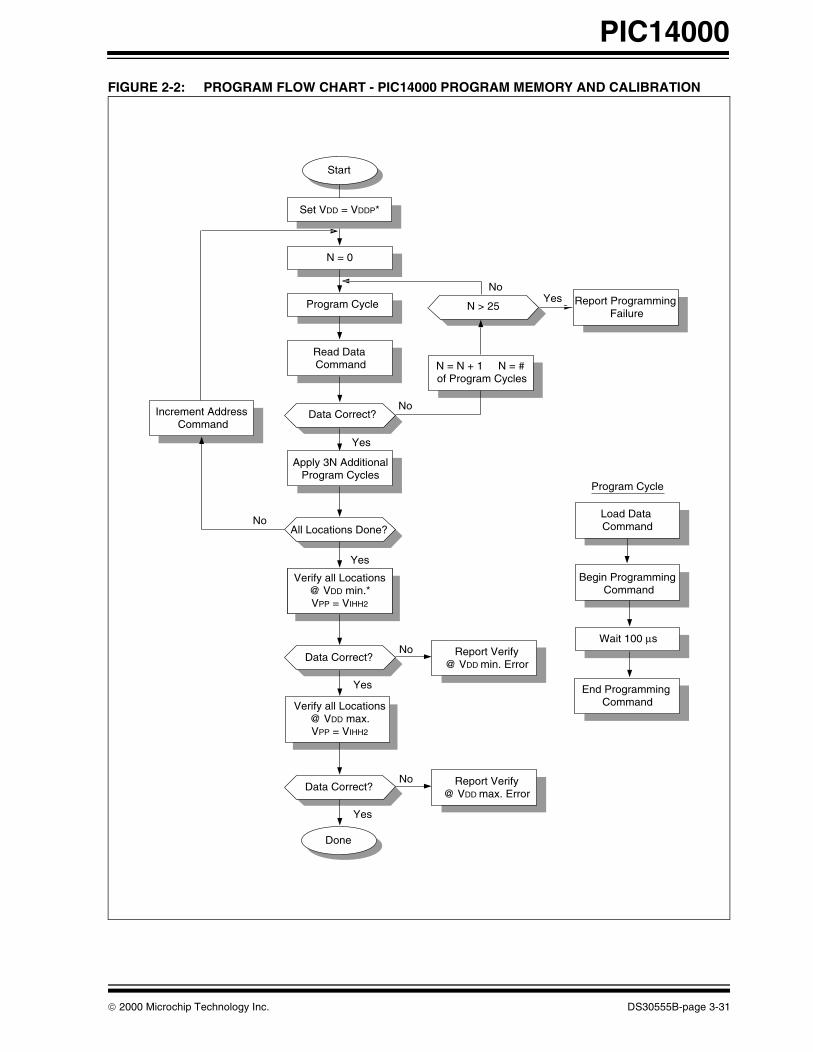
PIC14000
FIGURE 2-2: PROGRAM FLOW CHART - PIC14000 PROGRAM MEMORY AND CALIBRATION
* VDDP = VDD range for programming (typically 4.75V - 5.25V).VDDmin = Minimum VDD for device operation.VDDmax = Maximum VDD for device operation.
Start
No
Yes
Yes
Yes
Done
No
No
No
Data Correct?
Program Cycle
Read Data Command N = N + 1 N = #
of Program Cycles
N > 25 Report Programming Failure
Increment Address Command
Apply 3N AdditionalProgram Cycles
All Locations Done?
Data Correct? Report Verify@ VDD min. Error
Program Cycle
Load Data Command
Begin Programming Command
Wait 100 µs
End Programming Command
No
Yes
Data Correct? Report Verify@ VDD max. Error
N = 0
Yes
Set VDD = VDDP*
Verify all Locations@ VDD min.*VPP = VIHH2
Verify all Locations@ VDD max.VPP = VIHH2
2000 Microchip Technology Inc. DS30555B-page 3-31

PIC14000
FIGURE 2-3: PROGRAM FLOW CHART - PIC14000 CONFIGURATION WORD & ID LOCATIONS
VDDmin
VDDmax
Start
Load ConfigurationCommand
Increment AddressCommand N = N + 1 N = #
of Program Cycles
Report IDConfiguration Error
Increment AddressCommand
Increment AddressCommand
Increment AddressCommand
Program Cycle100 Cycles
Read DataCommand
Apply 3NProgram Cycles
Read DataCommand
Report ProgramID/Config. Error
Set VDD = VDDmax
Program Cycle
N = 0
Data Correct?
Data Correct?
Data Correct?
Data Correct?
N > 25 Address = 2004
Program ID Loc?
Done
Yes
No
No
YesNo
Yes
Yes
Yes
No
Yes
No
No
No Yes
Read Data CommandSet VPP = VIHH2
Set VDD = VDDminRead Data Command
Set VPP = VIHH2
DS30555B-page 3-32 2000 Microchip Technology Inc.
PIC14000
2.2.1.2 LOAD DATA
After receiving this command, the chip will load in a14-bit “data word” when 16 cycles are applied, asdescribed previously. A timing diagram for the load datacommand is shown in Figure 5-1.
2.2.1.3 READ DATA
After receiving this command, the chip will transmitdata bits out of the memory currently accessed startingwith the second rising edge of the clock input. The RC7pin will go into output mode on the second rising clockedge, and it will revert back to input mode (hi-imped-ance) after the 16th rising edge. A timing diagram ofthis command is shown in Figure 5-2.
2.2.1.4 INCREMENT ADDRESS
The PC is incremented when this command isreceived. A timing diagram of this command is shownin Figure 5-3.
2.2.1.5 BEGIN PROGRAMMING
A load command (load configuration or load data)must be given before every begin programmingcommand. Programming of the appropriate memory(test program memory or user program memory) willbegin after this command is received and decoded.Programming should be performed with a series of100µs programming pulses. A programming pulse isdefined as the time between the begin programmingcommand and the end programming command.
2.2.1.6 END PROGRAMMING
After receiving this command, the chip stops program-ming the memory (configuration program memory oruser program memory) that it was programming at thetime.
2.3 Programming Algorithm Requires Variable VDD
The PIC14000 uses an intelligent algorithm. The algo-rithm calls for program verification at VDDmin as well asVDDmax. Verification at VDDmin guarantees good“erase margin”. Verification at VDDmax guaranteesgood “program margin”.
The actual programming must be done with VDD in theVDDP range (4.75 - 5.25V).
VDDP = VCC range required during programming.
VDDmin = minimum operating VDD spec for the part.
VDDmax = maximum operating VDD spec for the part.
Programmers must verify the PIC14000 at its specifiedVDDmax and VDDmin levels. Since Microchip mayintroduce future versions of the PIC14000 with abroader VDD range, it is best that these levels are userselectable (defaults are ok).
Note: Any programmer not meeting theserequirements may only be classified as“prototype” or “development” programmerbut not a “production” quality programmer.
2000 Microchip Technology Inc. DS30555B-page 3-33
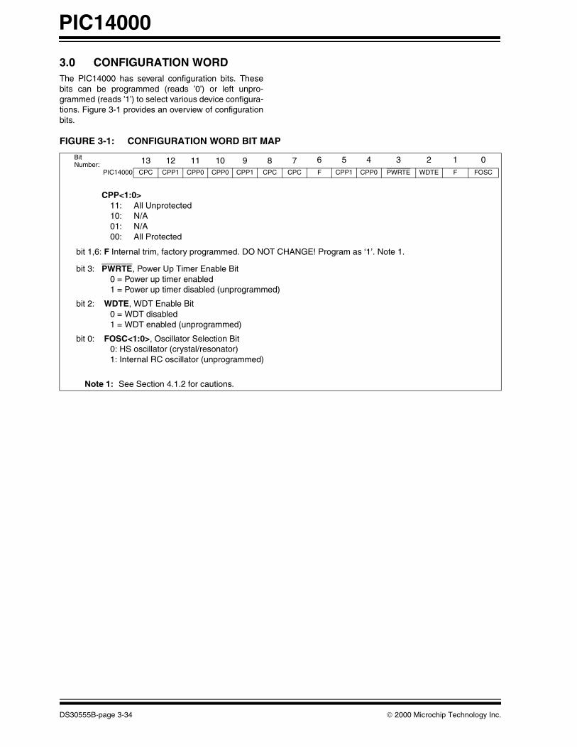
PIC14000
3.0 CONFIGURATION WORDThe PIC14000 has several configuration bits. Thesebits can be programmed (reads ’0’) or left unpro-grammed (reads ’1’) to select various device configura-tions. Figure 3-1 provides an overview of configurationbits.
FIGURE 3-1: CONFIGURATION WORD BIT MAP
Bit Number: 13 12 11 10 9 8 7 6 5 4 3 2 1 0
PIC14000 CPC CPP1 CPP0 CPP0 CPP1 CPC CPC F CPP1 CPP0 PWRTE WDTE F FOSC
CPP<1:0>11: All Unprotected10: N/A01: N/A00: All Protected
bit 1,6: F Internal trim, factory programmed. DO NOT CHANGE! Program as ‘1’. Note 1.
bit 3: PWRTE, Power Up Timer Enable Bit0 = Power up timer enabled 1 = Power up timer disabled (unprogrammed)
bit 2: WDTE, WDT Enable Bit0 = WDT disabled1 = WDT enabled (unprogrammed)
bit 0: FOSC<1:0>, Oscillator Selection Bit0: HS oscillator (crystal/resonator)1: Internal RC oscillator (unprogrammed)
Note 1: See Section 4.1.2 for cautions.
DS30555B-page 3-34 2000 Microchip Technology Inc.
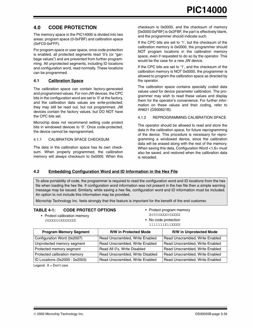
PIC14000
4.0 CODE PROTECTIONThe memory space in the PIC14000 is divided into twoareas: program space (0-0xFBF) and calibration space(0xFC0-0xFFF).
For program space or user space, once code protectionis enabled, all protected segments read ‘0’s (or “gar-bage values”) and are prevented from further program-ming. All unprotected segments, including ID locationsand configuration word, read normally. These locationscan be programmed.
4.1 Calibration Space
The calibration space can contain factory-generatedand programmed values. For non-JW devices, the CPCbits in the configuration word are set to ‘0’ at the factory,and the calibration data values are write-protected;they may still be read out, but not programmed. JWdevices contain the factory values, but DO NOT havethe CPC bits set.
Microchip does not recommend setting code protectbits in windowed devices to ‘0’. Once code-protected,the device cannot be reprogrammed.
4.1.1 CALIBRATION SPACE CHECKSUM
The data in the calibration space has its own check-sum. When properly programmed, the calibrationmemory will always checksum to 0x0000. When this
checksum is 0x0000, and the checksum of memory[0x0000:0xFBF] is 0x2FBF, the part is effectively blank,and the programmer should indicate such.
If the CPC bits are set to ‘1’, but the checksum of thecalibration memory is 0x0000, the programmer shouldNOT program locations in the calibration memoryspace, even if requested to do so by the operator. Thiswould be the case for a new JW device.
If the CPC bits are set to ‘1’, and the checksum of thecalibration memory is NOT 0x0000, the programmer isallowed to program the calibration space as directed bythe operator.
The calibration space contains specially coded datavalues used for device parameter calibration. The pro-grammer may wish to read these values and displaythem for the operator’s convenience. For further infor-mation on these values and their coding, refer toAN621 (DS00621B).
4.1.2 REPROGRAMMING CALIBRATION SPACE
The operator should be allowed to read and store thedata in the calibration space, for future reprogrammingof the device. This procedure is necessary for repro-gramming a windowed device, since the calibrationdata will be erased along with the rest of the memory.When saving this data, Configuration Word <1,6> mustalso be saved, and restored when the calibration datais reloaded.
4.2 Embedding Configuration Word and ID Information in the Hex File
TABLE 4-1: CODE PROTECT OPTIONS• Protect calibration memory0XXXX00XXXXXXX
• Protect program memoryX0000XXX00XXXX
• No code protection1111111X11XXXX
Legend: X = Don’t care
To allow portability of code, the programmer is required to read the configuration word and ID locations from the hexfile when loading the hex file. If configuration word information was not present in the hex file then a simple warningmessage may be issued. Similarly, while saving a hex file, configuration word and ID information must be included.An option to not include this information may be provided.
Microchip Technology Inc. feels strongly that this feature is important for the benefit of the end customer.
Program Memory Segment R/W in Protected Mode R/W in Unprotected Mode
Configuration Word (0x2007) Read Unscrambled, Write Enabled Read Unscrambled, Write EnabledUnprotected memory segment Read Unscrambled, Write Enabled Read Unscrambled, Write Enabled
Protected memory segment Read All 0’s, Write Disabled Read Unscrambled, Write EnabledProtected calibration memory Read Unscrambled, Write Disabled Read Unscrambled, Write EnabledID Locations (0x2000 : 0x2003) Read Unscrambled, Write Enabled Read Unscrambled, Write Enabled
2000 Microchip Technology Inc. DS30555B-page 3-35

PIC14000
4.3 Checksum
4.3.1 CHECKSUM CALCULATIONS
Checksum is calculated by reading the contents of thePIC14000 memory locations and adding up theopcodes up to the maximum user addressable location,0xFBF. Any carry bits exceeding 16-bits are neglected.Finally, the configuration word (appropriately masked)is added to the checksum. Checksum computation forthe PIC14000 device is shown in Table 4-2:
The checksum is calculated by summing the following:
• The contents of all program memory locations• The configuration word, appropriately masked
• Masked ID locations (when applicable)
The least significant 16 bits of this sum is the check-sum.
The following table describes how to calculate thechecksum for each device. Note that the checksum cal-culation differs depending on the code protect setting.Since the program memory locations read out differ-ently depending on the code protect setting, the tabledescribes how to manipulate the actual program mem-ory values to simulate the values that would be readfrom a protected device. When calculating a checksumby reading a device, the entire program memory cansimply be read and summed. The configuration wordand ID locations can always be read.
Note that some older devices have an additional valueadded in the checksum. This is to maintain compatibil-ity with older device programmer checksums.
TABLE 4-2: CHECKSUM COMPUTATION
CodeProtect
Checksum*BlankValue
0x25E6 at0 and maxaddress
OFFOFF OTP ON
SUM[0000:0FBF] + CFGW & 0x3FBDSUM[0000:0FBF] + CFGW & 0x3FBDCFGW & 0x3FBD + SUM(IDs)
0x2FFD0x0E7D0x300A
0xFBCB0xDA4B0xFBD8
Legend: CFGW = Configuration WordSUM[A:B] = [Sum of locations a through b inclusive]SUM(ID) = ID locations masked by 0x7F then made into a 28-bit value with ID0 as the most significant byte *Checksum = [Sum of all the individual expressions] MODULO [0xFFFF]+ = Addition& = Bitwise AND
DS30555B-page 3-36 2000 Microchip Technology Inc.

PIC14000
5.0 PROGRAM/VERIFY MODE ELECTRICAL CHARACTERISTICS
TABLE 5-1: AC/DC CHARACTERISTICSAC/DC TIMING REQUIREMENTS FOR PROGRAM/VERIFY MODE
Standard Operating ConditionsOperating Temperature: +10°C ≤ TA ≤ +40°C, unless otherwise stated, (25°C recommended)Operating Voltage: 4.5V ≤ VDD ≤ 5.5V, unless otherwise stated.
ParameterNo.
Sym. Characteristic Min. Typ. Max. Units Conditions
General
PD1 VDDP Supply voltage during programming 4.75 5.0 5.25 V
PD2 IDDP Supply current (from VDD)during programming
– – 20 mA
PD3 VDDV Supply voltage during verify VDDmin VDDmax V Note 1
PD4 VIHH1 Voltage on MCLR/VPP during programming
12.75 – 13.25 V Note 2
PD5 VIHH2 Voltage on MCLR/VPP during verify VDD + 4.0 13.5
PD6 IPP Programming supply current (from VPP)
– – 50 mA
PD9 VIH1 (RC6, RC7) input high level 0.8 VDD – – V Schmitt Trigger input
PD8 VIL1 (RC6, RC7) input low level 0.2 VDD – – V Schmitt Trigger input
Serial Program Verify
P1 TR MCLR/VPP rise time (VSS to VHH) for test mode entry
– – 8.0 µs
P2 Tf MCLR Fall time – – 8.0 µs
P3 Tset1 Data in setup time before clock ↓ 100 – – ns
P4 Thld1 Data in hold time after clock ↓ 100 – – ns
P5 Tdly1 Data input not driven to next clock input (delay required between com-mand/data or command/command)
1.0 – – µs
P6 Tdly2 Delay between clock ↓ to clock ↑ of next command or data
1.0 – – µs
P7 Tdly3 Clock ↑ to date out valid (during read data)
200 – – ns
P8 Thld0 Hold time after MCLR ↑ 2 – – µs
Note 1: Program must be verified at the minimum and maximum VDD limits for the part.Note 2: VIHH must be greater than VDD + 4.5V to stay in programming/verify mode.
2000 Microchip Technology Inc. DS30555B-page 3-37
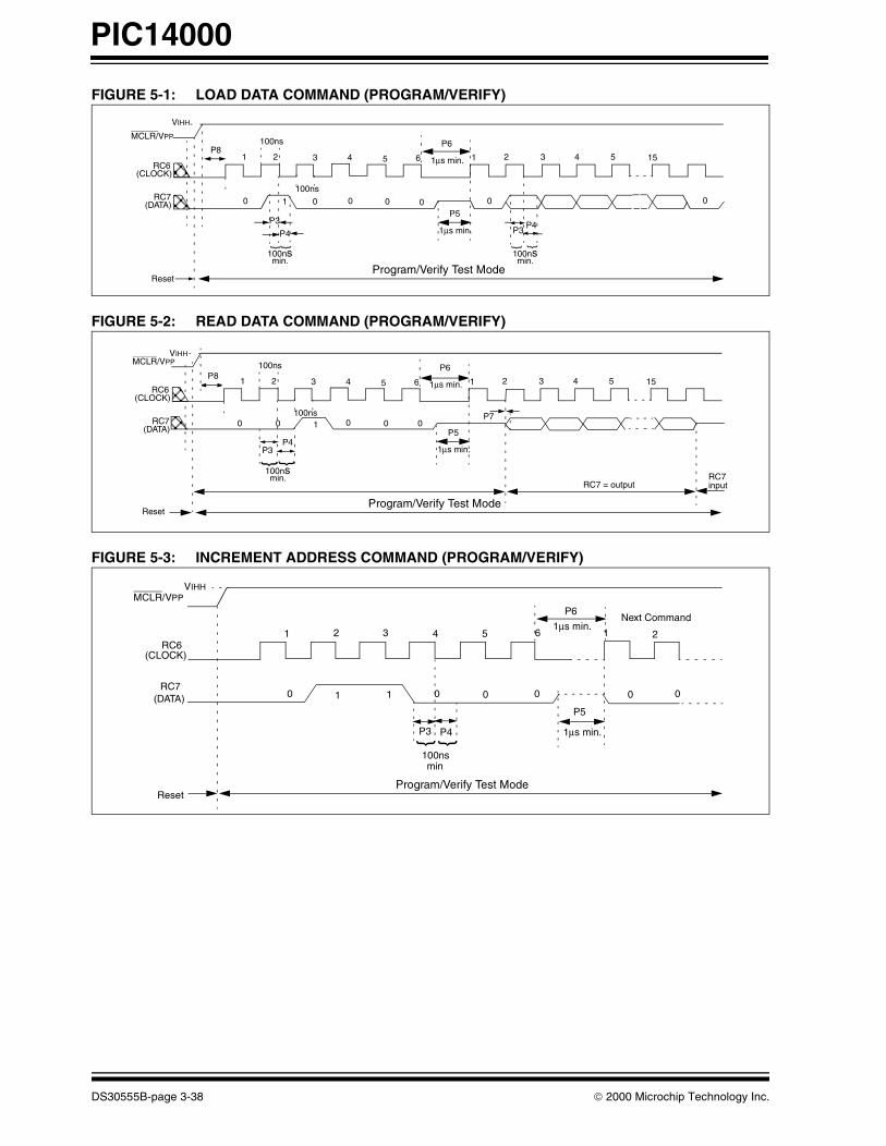
PIC14000
FIGURE 5-1: LOAD DATA COMMAND (PROGRAM/VERIFY)
FIGURE 5-2: READ DATA COMMAND (PROGRAM/VERIFY)
FIGURE 5-3: INCREMENT ADDRESS COMMAND (PROGRAM/VERIFY)
100nsmin.
P4P3
000
1µs min.
P5
1µs min.
P6
0
155432165
Program/Verify Test Mode
0
43
0
100ns
P4
1
100nsmin.
P3
Reset
21
100nsP8
VIHH
RC6(CLOCK)
RC7(DATA) 0
MCLR/VPP
00
1µs min.
P5
1µs min.
P6
155432165
Program/Verify Test Mode
0
43
0100ns
P4
1
100nsmin.
P3
Reset
21
100nsP8
VIHH
RC6(CLOCK)
RC7(DATA)
0
MCLR/VPP
RC7 = outputRC7input
P7
000 0 0 01 1
1 2 3 4 5 6 1 2
100nsmin
P3 P4
P6
1µs min.Next Command
P5
1µs min.
VIHHMCLR/VPP
RC6(CLOCK)
(DATA)RC7
ResetProgram/Verify Test Mode
DS30555B-page 3-38 2000 Microchip Technology Inc.

PIC16C55XIn-Circuit Serial Programming for PIC16C55X OTP MCUs
30261C.fm Page 39 Wednesday, May 3, 2000 12:18 PM
This document includes the programming specifications for the following devices:
1.0 PROGRAMMING THE PIC16C55X
The PIC16C55X can be programmed using a serialmethod. In serial mode the PIC16C55X can be pro-grammed while in the users system. This allows forincreased design flexibility.
1.1 Hardware Requirements
The PIC16C55X requires two programmable powersupplies, one for VDD (2.0V to 6.5V recommended) andone for VPP (12V to 14V). Both supplies should have aminimum resolution of 0.25V.
1.2 Programming Mode
The programming mode for the PIC16C55X allows pro-gramming of user program memory, special locationsused for ID, and the configuration word for thePIC16C55X.
PIN Diagrams
• PIC16C554• PIC16C556• PIC16C558
RA1RA0
OSC2/CLKOUTVDDRB7RB6RB5RB4
OSC1/CLKIN
RA2RA3
MCLRVSS
RB0/INTRB1RB2RB3
RA4/T0CKI
PIC
16C55X
RA1RA0
OSC2/CLKOUTVDD
RB7RB6RB5RB4
OSC1/CLKIN
RA2RA3
MCLRVSSVSS
RB0/INTRB1RB2
RA4/T0CKI
PIC
16C55X
RB3RB3
VDD
PDIP, SOIC, Windowed CERDIP
SSOP
2 3 4 5 6 7 8 910
•1
2 3 4 5 6 7 8 9
•1
1918
161514131211
17
1817
151413121110
16
20
2000 Microchip Technology Inc. DS30261C-page 3-39

PIC16C55X
30261C.fm Page 40 Wednesday, May 3, 2000 12:18 PM
2.0 PROGRAM MODE ENTRY
2.1 User Program Memory Map
The user memory space extends from 0x0000 to0x1FFF (8K). Table 2-1 shows actual implementationof program memory in the PIC16C55X family.
TABLE 2-1: IMPLEMENTATION OF PROGRAM MEMORY IN THE PIC16C55X
When the PC reaches the last location of the imple-mented program memory, it will wrap around andaddress a location within the physically implementedmemory (see Figure 2-1).
In programming mode the program memory spaceextends from 0x0000 to 0x3FFF, with the first half(0x0000-0x1FFF) being user program memory and thesecond half (0x2000-0x3FFF) being configurationmemory. The PC will increment from 0x0000 to 0x1FFFand wrap to 0x000 or 0x2000 to 0x3FFF and wraparound to 0x2000 (not to 0x0000). Once in configura-tion memory, the highest bit of the PC stays a ’1’, thusalways pointing to the configuration memory. The onlyway to point to user program memory is to reset thepart and reenter program/verify mode, as described inSection 2.2.
In the configuration memory space, 0x2000-0x20FFare utilized. When in a configuration memory, as in theuser memory, the 0x2000-0x2XFF segment is repeat-edly accessed as the PC exceeds 0x2XFF (seeFigure 2-1).
A user may store identification information (ID) in fourID locations. The ID locations are mapped in [0x2000:0x2003]. It is recommended that the user use only thefour least significant bits of each ID location. In somedevices, the ID locations read-out in a scrambled fash-ion after code protection is enabled. For these devices,it is recommended that ID location is written as “111111 1000 bbbb” where 'bbbb' is ID information.
Note: All other locations are reserved and shouldnot be programmed.
In other devices, the ID locations read out normally,even after code protection. To understand how thedevices behave, refer to Table 4-1.
To understand the scrambling mechanism after codeprotection, refer to Section 4.1.
Device Program Memory SizeAccess to Program Memory
PIC16C554 0x000 - 0x1FF (0.5K) PC<8:0>
PIC16C556 0x000 - 0x3FF (1K) PC<9:0>
PIC16C558 0x000 - 0x7FF (2K) PC<10:0>
DS30261C-page 3-40 2000 Microchip Technology Inc.

PIC16C55X
30261C.fm Page 41 Wednesday, May 3, 2000 12:18 PM
FIGURE 2-1: PROGRAM MEMORY MAPPING
0.5KW 1KW 2KW
Implemented Implemented
Implemented
Reserved
Reserved Reserved Reserved
Reserved Reserved Reserved
0
3FF400
7FF800
BFFC00
FFF1000
1FFF20002008
2100
3FFF
ID Location
ID Location
ID Location
ID Location
Reserved
Reserved
Reserved
Configuration Word
2000
2001
2002
2003
2004
2005
2006
2007
1FF
Reserved
Reserved
Implemented
Reserved Reserved
2000 Microchip Technology Inc. DS30261C-page 3-41

PIC16C55X
30261C.fm Page 42 Wednesday, May 3, 2000 12:18 PM
2.2 Program/Verify Mode
The program/verify mode is entered by holding pinsRB6 and RB7 low while raising MCLR pin from VIL toVIHH (high voltage). Once in this mode the user pro-gram memory and the configuration memory can beaccessed and programmed in serial fashion. The modeof operation is serial, and the memory that is accessedis the user program and configuration memory. RB6 isa Schmitt Trigger input in this mode.
The sequence that enters the device into the program-ming/verify mode places all other logic into the resetstate (the MCLR pin was initially at VIL). This meansthat all I/O are in the reset state (High impedanceinputs).
2.2.1 PROGRAM/VERIFY OPERATION
The RB6 pin is used as a clock input pin, and the RB7pin is used for entering command bits and data input/output during serial operation. To input a command, theclock pin (RB6) is cycled six times. Each command bitis latched on the falling edge of the clock with the leastsignificant bit (LSB) of the command being input first.The data on pin RB7 is required to have a minimum
setup and hold time (see AC/DC specs) with respect tothe falling edge of the clock. Commands that have dataassociated with them (read and load) are specified tohave a minimum delay of 1µs between the commandand the data. After this delay the clock pin is cycled 16times with the first cycle being a start bit and the lastcycle being a stop bit. Data is also input and output LSBfirst. Therefore, during a read operation the LSB will betransmitted onto pin RB7 on the rising edge of the sec-ond cycle, and during a load operation the LSB will belatched on the falling edge of the second cycle. A min-imum 1µs delay is also specified between consecutivecommands.
The commands that are available are listedin Table 2-1.
2.2.1.1 LOAD CONFIGURATION
After receiving this command, the program counter(PC) will be set to 0x2000. By then applying 16 cyclesto the clock pin, the chip will load 14-bits a “data word”as described above, to be programmed into the config-uration memory. A description of the memory mappingschemes for normal operation and configuration modeoperation is shown in Figure 2-1. After the configura-tion memory is entered, the only way to get back to theuser program memory is to exit the program/verify testmode by taking MCLR low (VIL).
Note: The MCLR pin should be raised as quicklyas possible from VIL to VIHH. this is toensure that the device does not have thePC incremented while in valid operationrange.
TABLE 2-1: COMMAND MAPPING
Command Mapping (MSB ... LSB) Data
Load Configuration 0 0 0 0 0 0 0, data(14), 0
Load Data 0 0 0 0 1 0 0, data(14), 0
Read Data 0 0 0 1 0 0 0, data(14), 0
Increment Address 0 0 0 1 1 0
Begin programming 0 0 1 0 0 0
End Programming 0 0 1 1 1 0
Note: The CPU clock must be disabled during in-circuit programming.
DS30261C-page3-42 2000 Microchip Technology Inc.

PIC16C55X
30261C.fm Page 43 Wednesday, May 3, 2000 12:18 PM
FIGURE 2-2: PROGRAM FLOW CHART - PIC16C55X PROGRAM MEMORY
* VDDP = VDD range for programming (typically 4.75V - 5.25V).VDDmin = Minimum VDD for device operation.VDDmax = Maximum VDD for device operation.
Start
No
Yes
Yes
Yes
Done
No
No
No
Data Correct?
Program Cycle
Read Data Command N = N + 1 N = #
of Program Cycles
N > 25 Report Programming Failure
Increment Address Command
Apply 3N AdditionalProgram Cycles
All Locations Done?
Data Correct? Report Verify@ VDD min. Error
Program Cycle
Load Data Command
Begin Programming Command
Wait 100 µs
End Programming Command
No
Yes
Data Correct? Report Verify@ VDD max. Error
N = 0
Yes
Set VDD = VDDP*
Verify all Locations@ VDD min.*VPP = VIHH2
Verify all Locations@ VDD max.VPP = VIHH2
2000 Microchip Technology Inc. DS30261C-page 3-43

PIC16C55X
30261C.fm Page 44 Wednesday, May 3, 2000 12:18 PM
FIGURE 2-3: PROGRAM FLOW CHART - PIC16C55X CONFIGURATION WORD & ID LOCATIONS
VDDmin
VDDmax
Start
Load ConfigurationCommand
Increment AddressCommand N = N + 1 N = #
of Program Cycles
ID/ConfigurationError
Increment AddressCommand
Increment AddressCommand
Increment AddressCommand
Program Cycle100 Cycles
Read DataCommand
Apply 3NProgram Cycles
Read DataCommand
Report ProgramID/Config. Error
Set VDD = VDDmax
Program Cycle
N = 0
Data Correct?
Data Correct?
Data Correct?
Data Correct?
N > 25 Address = 2004
Program ID Loc?
Done
Yes
No
No
YesNo
Yes
Yes
Yes
No
Yes
No
No
No Yes
Read Data CommandSet VPP = VIHH2
Set VDD = VDDminRead Data Command
Set VPP = VIHH2
DS30261C-page 3-44 2000 Microchip Technology Inc.

PIC16C55X
30261C.fm Page 45 Wednesday, May 3, 2000 12:18 PM
2.2.1.2 LOAD DATA
After receiving this command, the chip will load in a14-bit “data word” when 16 cycles are applied, asdescribed previously. A timing diagram for the load datacommand is shown in Figure 5-1.
2.2.1.3 READ DATA
After receiving this command, the chip will transmitdata bits out of the memory currently accessed startingwith the second rising edge of the clock input. The RB7pin will go into output mode on the second rising clockedge, and it will revert back to input mode (hi-imped-ance) after the 16th rising edge. A timing diagram ofthis command is shown in Figure 5-2.
2.2.1.4 INCREMENT ADDRESS
The PC is incremented when this command isreceived. A timing diagram of this command is shownin Figure 5-3.
2.2.1.5 BEGIN PROGRAMMING
A load command (load configuration or load data)must be given before every begin programmingcommand. Programming of the appropriate memory(test program memory or user program memory) willbegin after this command is received and decoded.Programming should be performed with a series of100µs programming pulses. A programming pulse isdefined as the time between the begin programmingcommand and the end programming command.
2.2.1.6 END PROGRAMMING
After receiving this command, the chip stops program-ming the memory (configuration program memory oruser program memory) that it was programming at thetime.
2.3 Programming Algorithm Requires Variable VDD
The PIC16C55X uses an intelligent algorithm. Thealgorithm calls for program verification at VDDmin aswell as VDDmax. Verification at VDDmin guaranteesgood “erase margin”. Verification at VDDmax guaran-tees good “program margin”.
The actual programming must be done with VDD in theVDDP range (4.75 - 5.25V).
VDDP = VCC range required during programming.
VDD min. = minimum operating VDD spec for the part.
VDD max.= maximum operating VDD spec for the part.
Programmers must verify the PIC16C55X at its speci-fied VDDmax and VDDmin levels. Since Microchip mayintroduce future versions of the PIC16C55X with abroader VDD range, it is best that these levels are userselectable (defaults are ok).
Note: Any programmer not meeting theserequirements may only be classified as“prototype” or “development” programmerbut not a “production” quality programmer.
2000 Microchip Technology Inc. DS30261C-page 3-45

PIC16C55X
30261C.fm Page 46 Wednesday, May 3, 2000 12:18 PM
3.0 CONFIGURATION WORDThe PIC16C55X family members have several configu-ration bits. These bits can be programmed (reads ’0’) orleft unprogrammed (reads ’1’) to select various deviceconfigurations. Figure 3-1 provides an overview of con-figuration bits.
FIGURE 3-1: CONFIGURATION WORD BIT MAP
Bit Number: 13 12 11 10 9 8 7 6 5 4 3 2 1 0
PIC16C554/556/558 CP1 CP0 CP1 CP0 CP1 CP0 — 0 CP1 CP0 PWRTE WDTE FOSC1 FOSC0
bit 7: Reserved for future usebit 6: Set to 0
bit 5-4: CP1:CP0, Code Protect
bit 8-13
bit 3: PWRTE, Power Up Timer Enable BitPIC16C554/556/558: 0 = Power up timer enabled 1 = Power up timer disabled
bit 2: WDTE, WDT Enable Bit1 = WDT enabled0 = WDT disabled
bit 1-0:FOSC<1:0>, Oscillator Selection Bit11: RC oscillator10: HS oscillator01: XT oscillator00: LP oscillator
Device CP1 CP0 Code Protection
PIC16C554 All memory protectedDo not use
Do not use
Code protection off
0 00 1
1 0
1 1
PIC16C556 All memory protectedUpper 1/2 memory protectedDo not use
Code protection off
0 00 1
1 01 1
PIC16C558 All memory protectedUpper 3/4 memory protected
Upper 1/2 memory protected
Code protection off
0 00 1
1 01 1
DS30261C-page 3-46 2000 Microchip Technology Inc.

PIC16C55X
30261C.fm Page 47 Wednesday, May 3, 2000 12:18 PM
4.0 CODE PROTECTIONThe program code written into the EPROM can be pro-tected by writing to the CP0 & CP1 bits of the configu-ration word.
4.1 Programming Locations 0x0000 to 0x03F after Code Protection
For PIC16C55X devices, once code protection isenabled, all protected segments read '0's (or “garbagevalues”) and are prevented from further programming.All unprotected segments, including ID locations andconfiguration word, read normally. These locations canbe programmed.
4.2 Embedding Configuration Word and ID Information in the Hex File
TABLE 4-1: CONFIGURATION WORD
PIC16C554
To code protect:• Protect all memory 0000001000XXXX
• No code protection 1111111011XXXX
PIC16C556
To code protect:• Protect all memory 0000001000XXXX• Protect upper 1/2 memory 0101011001XXXX• No code protection 1111111011XXXX
PIC16C558
To code protect:• Protect all memory 0000001000XXXX
• Protect upper 3/4 memory 0101011001XXXX
• Protect upper 1/2 memory 1010101010XXXX
• No code protection 1111111011XXXX
To allow portability of code, the programmer is required to read the configuration word and ID locations from the hexfile when loading the hex file. If configuration word information was not present in the hex file then a simple warningmessage may be issued. Similarly, while saving a hex file, configuration word and ID information must be included.An option to not include this information may be provided.
Microchip Technology Inc. feels strongly that this feature is important for the benefit of the end customer.
Program Memory Segment R/W in Protected Mode R/W in Unprotected Mode
Configuration Word (0x2007) Read Unscrambled, Write Enabled Read Unscrambled, Write Enabled
Protected memory segment Read All 0’s, Write Disabled Read Unscrambled, Write Enabled
ID Locations (0x2000 : 0x2003) Read Unscrambled, Write Enabled Read Unscrambled, Write Enabled
2000 Microchip Technology Inc. DS30261C-page 3-47
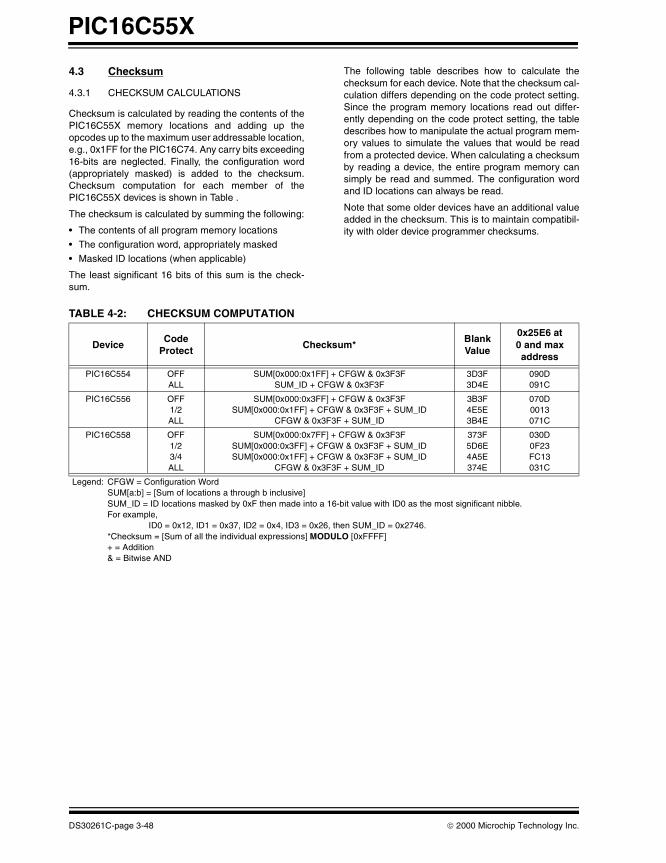
PIC16C55X
30261C.fm Page 48 Wednesday, May 3, 2000 12:18 PM
4.3 Checksum
4.3.1 CHECKSUM CALCULATIONS
Checksum is calculated by reading the contents of thePIC16C55X memory locations and adding up theopcodes up to the maximum user addressable location,e.g., 0x1FF for the PIC16C74. Any carry bits exceeding16-bits are neglected. Finally, the configuration word(appropriately masked) is added to the checksum.Checksum computation for each member of thePIC16C55X devices is shown in Table .
The checksum is calculated by summing the following:
• The contents of all program memory locations
• The configuration word, appropriately masked
• Masked ID locations (when applicable)
The least significant 16 bits of this sum is the check-sum.
The following table describes how to calculate thechecksum for each device. Note that the checksum cal-culation differs depending on the code protect setting.Since the program memory locations read out differ-ently depending on the code protect setting, the tabledescribes how to manipulate the actual program mem-ory values to simulate the values that would be readfrom a protected device. When calculating a checksumby reading a device, the entire program memory cansimply be read and summed. The configuration wordand ID locations can always be read.
Note that some older devices have an additional valueadded in the checksum. This is to maintain compatibil-ity with older device programmer checksums.
TABLE 4-2: CHECKSUM COMPUTATION
DeviceCode
ProtectChecksum*
BlankValue
0x25E6 at0 and maxaddress
PIC16C554 OFFALL
SUM[0x000:0x1FF] + CFGW & 0x3F3FSUM_ID + CFGW & 0x3F3F
3D3F3D4E
090D091C
PIC16C556 OFF1/2ALL
SUM[0x000:0x3FF] + CFGW & 0x3F3FSUM[0x000:0x1FF] + CFGW & 0x3F3F + SUM_ID
CFGW & 0x3F3F + SUM_ID
3B3F4E5E3B4E
070D0013071C
PIC16C558 OFF1/23/4ALL
SUM[0x000:0x7FF] + CFGW & 0x3F3FSUM[0x000:0x3FF] + CFGW & 0x3F3F + SUM_IDSUM[0x000:0x1FF] + CFGW & 0x3F3F + SUM_ID
CFGW & 0x3F3F + SUM_ID
373F5D6E4A5E374E
030D0F23FC13031C
Legend: CFGW = Configuration WordSUM[a:b] = [Sum of locations a through b inclusive]SUM_ID = ID locations masked by 0xF then made into a 16-bit value with ID0 as the most significant nibble.For example, ID0 = 0x12, ID1 = 0x37, ID2 = 0x4, ID3 = 0x26, then SUM_ID = 0x2746.*Checksum = [Sum of all the individual expressions] MODULO [0xFFFF]+ = Addition& = Bitwise AND
DS30261C-page 3-48 2000 Microchip Technology Inc.

PIC16C55X
30261C.fm Page 49 Wednesday, May 3, 2000 12:18 PM
5.0 PROGRAM/VERIFY MODE ELECTRICAL CHARACTERISTICS
TABLE 5-1: AC/DC CHARACTERISTICSTIMING REQUIREMENTS FOR PROGRAM/VERIFY TEST MODE
Standard Operating ConditionsOperating Temperature: +10°C ≤ TA ≤ +40°C, unless otherwise stated, (25°C is recommended)Operating Voltage: 4.5V ≤ VDD ≤ 5.5V, unless otherwise stated.
ParameterNo.
Sym. Characteristic Min. Typ. Max. Units Conditions
General
PD1 VDDP Supply voltage during programming 4.75 5.0 5.25 V
PD2 IDDP Supply current (from VDD)during programming
- - 20 mA
PD3 VDDV Supply voltage during verify VDDmin - VDDmax V Note 1
PD4 VIHH1 Voltage on MCLR/VPP during programming
12.75 - 13.25 V Note 2
PD5 VIHH2 Voltage on MCLR/VPP during verify VDD + 4.0 - 13.5 -
PD6 IPP Programming supply current (from VPP)
- - 50 mA
PD9 VIH1 (RB6, RB7) input high level 0.8 VDD - - V Schmitt Trigger input
PD8 VIL1 (RB6, RB7) input low level 0.2 VDD - - V Schmitt Trigger input
Serial Program Verify
P1 TR MCLR/VPP rise time (VSS to VHH) for test mode entry
- - 8.0 µs
P2 Tf MCLR Fall time - - 8.0 µs
P3 Tset1 Data in setup time before clock ↓ 100 - - ns
P4 Thld1 Data in hold time after clock ↓ 100 - - ns
P5 Tdly1 Data input not driven to next clock input (delay required between com-mand/data or command/command)
1.0 - - µs
P6 Tdly2 Delay between clock ↓ to clock ↑ of next command or data
1.0 - - µs
P7 Tdly3 Clock ↑ to date out valid (during read data)
200 - - ns
P8 Thld0 Hold time after MCLR ↑ 2 - - µs
- Tpw Programming Pulse Width 10 100 1000 µs
Note 1: Program must be verified at the minimum and maximum VDD limits for the part.2: VIHH must be greater than VDD + 4.5V to stay in programming/verify mode.
2000 Microchip Technology Inc. DS30261C-page 3-49
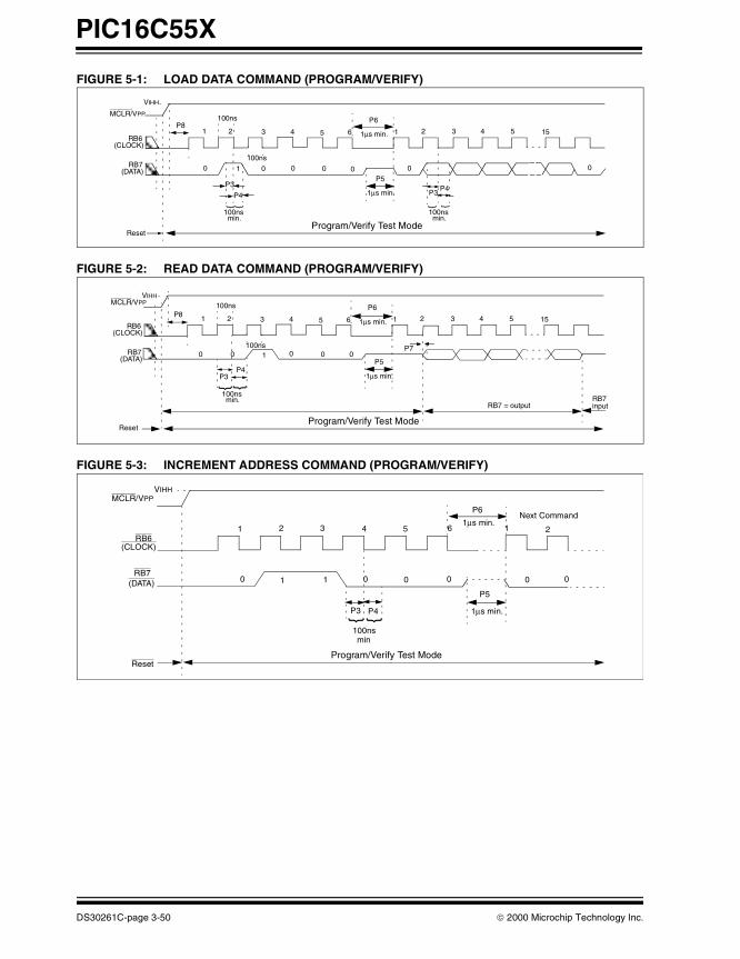
PIC16C55X
30261C.fm Page 50 Wednesday, May 3, 2000 12:18 PM
FIGURE 5-1: LOAD DATA COMMAND (PROGRAM/VERIFY)
FIGURE 5-2: READ DATA COMMAND (PROGRAM/VERIFY)
FIGURE 5-3: INCREMENT ADDRESS COMMAND (PROGRAM/VERIFY)
100nsmin.
P4P3
000
1µs min.
P5
1µs min.
P6
0
155432165
Program/Verify Test Mode
0
43
0
100ns
P4
1
100nsmin.
P3
Reset
21
100nsP8
VIHH
RB6(CLOCK)
RB7(DATA) 0
MCLR/VPP
00
1µs min.
P5
1µs min.
P6
155432165
Program/Verify Test Mode
0
43
0100ns
P4
1
100nsmin.
P3
Reset
21
100nsP8
VIHH
RB6(CLOCK)
RB7(DATA)
0
MCLR/VPP
RB7 = outputRB7input
P7
000 0 0 01 1
1 2 3 4 5 6 1 2
100nsmin
P3 P4
P6
1µs min.Next Command
P5
1µs min.
VIHHMCLR/VPP
RB6(CLOCK)
(DATA)RB7
ResetProgram/Verify Test Mode
DS30261C-page 3-50 2000 Microchip Technology Inc.
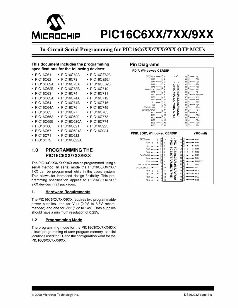
2000 Microchip Technology Inc. DS30228J-page 3-51
PIC16C6XX/7XX/9XX
This document includes the programming specifications for the following devices:
1.0 PROGRAMMING THE PIC16C6XX/7XX/9XX
The PIC16C6XX/7XX/9XX can be programmed using aserial method. In serial mode the PIC16C6XX/7XX/9XX can be programmed while in the users system.This allows for increased design flexibility. This pro-gramming specification applies to PIC16C6XX/7XX/9XX devices in all packages.
1.1 Hardware Requirements
The PIC16C6XX/7XX/9XX requires two programmablepower supplies, one for VDD (2.0V to 6.5V recom-mended) and one for VPP (12V to 14V). Both suppliesshould have a minimum resolution of 0.25V.
1.2 Programming Mode
The programming mode for the PIC16C6XX/7XX/9XXallows programming of user program memory, speciallocations used for ID, and the configuration word for thePIC16C6XX/7XX/9XX.
Pin Diagrams
• PIC16C61 • PIC16C72A • PIC16CE623• PIC16C62 • PIC16C73 • PIC16CE624• PIC16C62A • PIC16C73A • PIC16CE625• PIC16C62B • PIC16C73B • PIC16C710• PIC16C63 • PIC16C74 • PIC16C711• PIC16C63A • PIC16C74A • PIC16C712• PIC16C64 • PIC16C74B • PIC16C716• PIC16C64A • PIC16C76 • PIC16C745• PIC16C65 • PIC16C77 • PIC16C765• PIC16C65A • PIC16C620 • PIC16C773• PIC16C65B • PIC16C620A • PIC16C774• PIC16C66 • PIC16C621 • PIC16C923• PIC16C67 • PIC16C621A • PIC16C924• PIC16C71 • PIC16C622• PIC16C72 • PIC16C622A P
IC16C
62/62A/63/66/72/72A
PIC
16C73/73A
/73B/76/745
RB7RB6RB5RB4RB3RB2RB1RB0/INTVDD
VSS
RD7RD6RD5RD4RC7RC6RC5RC4RD3RD2
MCLR/VPP
RA0RA1RA2RA3
RA4/T0CKIRA5RE0RE1RE2VDD
VSS
OSC1/CLKINOSC2/CLKOUT
RC0RC1RC2RC3RD0RD1
1234567891011121314151617181920
4039383736353433323130292827262524232221
PDIP, Windowed CERDIP
PDIP, SOIC, Windowed CERDIP (300 mil)
28
27
26
25
24
23
22
21
20
19
18
17
16
15
RB7
RB6
RB5
RB4
RB3
RB2
RB1
RB0/INT
VDD
VSS
RC7
RC6
RC5
RC4
• 1
2
3
4
5
6
7
8
9
10
11
12
13
14
MCLR/VPP
RA0
RA1
RA2
RA3
RA4/T0CKI
RA5
VSS
OSC1/CLKIN
OSC2/CLKOUT
RC0
RC1
RC2
RC3
PIC
16C64/64A
/65/65A/67
PIC
16C74/74A
/74B/77/765
In-Circuit Serial Programming for PIC16C6XX/7XX/9XX OTP MCUs

PIC16C6XX/7XX/9XX
DS30228J-page 3-52 2000 Microchip Technology Inc.
Pin Diagrams (Con’t)
1011121314151617181920212223242526
6059585756555453525150494847464544
9 8 7 6 5 4 3 2 16
86
76
66
56
46
36
26
1
27 28 29 30 31 32 33 34 35 36 37 38 39 40 41 42 43
PIC16C924
RD5/SEG29/COM3RG6/SEG26RG5/SEG25RG4/SEG24RG3/SEG23RG2/SEG22RG1/SEG21RG0/SEG20RG7/SEG28RF7/SEG19RF6/SEG18RF5/SEG17RF4/SEG16RF3/SEG15RF2/SEG14RF1/SEG13RF0/SEG12
RA4/T0CKIRA5/AN4/SS
RB1RB0/INT
RC3/SCK/SCLRC4/SDI/SDA
RC5/SDO
VLCD2VLCD3AVDDVDD
VSS
C1C2
OSC1/CLKINOSC2/CLKOUT
RC0/T1OSO/T1CKI
RA
3/A
N3
/VR
EF
RA
2/A
N2
VS
SR
A1/
AN
1R
A0/
AN
0R
B2
RB
3M
CLR
/VP
PN
/CR
B4
RB
5R
B7
RB
6V
DD
CO
M0
RD
7/S
EG
31/C
OM
1R
D6/
SE
G30
/CO
M2
RC
1/T
1OS
IR
C2/
CC
P1
VLC
D1
VLC
DA
DJ
RD
0/S
EG
00R
D1/
SE
G01
RD
2/S
EG
02R
D3/
SE
G03
RD
4/S
EG
04R
E7/
SE
G27
RE
0/S
EG
05R
E1/
SE
G06
RE
2/S
EG
07R
E3/
SE
G08
RE
4/S
EG
09
RE
6/S
EG
11R
E5/
SE
G10
PLCC
PDIP, SOIC, Windowed CERDIP
18
17
16
15
14
13
12
11
10
• 1
2
3
4
5
6
7
8
9
RA2
RA3
RA4/T0CKI
MCLR/VPP
VSS
RB0/INT
RB1
RB2
RB3
RA1
RA0
OSC1/CLKIN
OSC2/CLKOUT
VDD
RB7
RB6
RB5
RB4
PIC
16C61/71
PIC
16C62X
PIC
16C710/711
PIC16C923
MCLR/VPP
RA0/AN0
RA1/AN1
RA2/AN2/VREF-/VRL
RA3/AN3/VREF+/VRH
RA4/T0CKI
AVDD
AVSS
OSC1/CLKIN
OSC2/CLKOUT
RC0/T1OSO/T1CKI
RC1/T1OSI/CCP2
RC2/CCP1
RC3/SCK/SCL
RB7
RB6
RB5
RB4
RB3/AN9/LVDIN
RB2/AN8
RB1/SS
RB0/INT
VDD
VSS
RC7/RX/DT
RC6/TX/CK
RC5/SDO
RC4/SDI/SDA
• 1
2
3
4
5
6
7
8
9
10
11
12
13
14
28
27
26
25
24
23
22
21
20
19
18
17
16
15
300 mil. SDIP, SOIC, Windowed CERDIP, SSOP
PIC
16C773
PIC
16C712
RA2/AN2
RA4/T0CKI
RB0/INTRB1/T1OSO/T1CKI
RA0/AN0
OSC1/CLKIN
RB7RB6
• 1
2
3
4
5
6
7
18
17
16
15
14
13
12
8
9
11
10
18 pin PDIP, SOIC, Windowed CERDIP
MCLR/VPP
RA3/AN3/VREF
RB2/T1OSIRB3/CCP1 RB4
RB5
RA1/AN1
VDD
OSC2/CLKOUT
VSS
PIC
16C716
PIC
16C712
RA2/AN2
RA4/T0CKI
RB0/INTRB1/T1OSO/T1CKI
RA0/AN0
OSC1/CLKIN
RB7RB6
• 1
2
3
4
5
6
7
20
19
18
17
16
15
14
8
9
13
12
20 pin SSOP
MCLR/VPP
RA3/AN3/VREF
RB2/T1OSIRB3/CCP1 RB4
RB5
RA1/AN1
VDD
OSC2/CLKOUT
VSS
PIC
16C716
10
VSS VDD
11
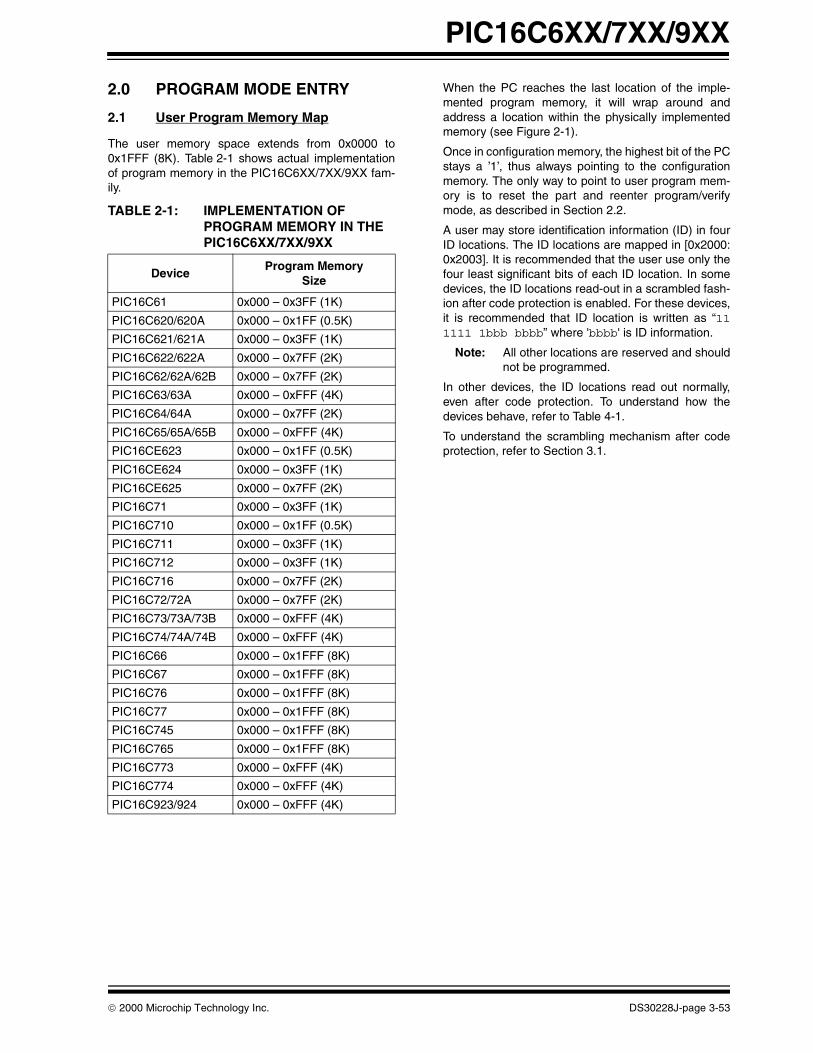
2000 Microchip Technology Inc. DS30228J-page 3-53
PIC16C6XX/7XX/9XX
2.0 PROGRAM MODE ENTRY
2.1 User Program Memory Map
The user memory space extends from 0x0000 to0x1FFF (8K). Table 2-1 shows actual implementationof program memory in the PIC16C6XX/7XX/9XX fam-ily.
TABLE 2-1: IMPLEMENTATION OF PROGRAM MEMORY IN THE PIC16C6XX/7XX/9XX
When the PC reaches the last location of the imple-mented program memory, it will wrap around andaddress a location within the physically implementedmemory (see Figure 2-1).
Once in configuration memory, the highest bit of the PCstays a ’1’, thus always pointing to the configurationmemory. The only way to point to user program mem-ory is to reset the part and reenter program/verifymode, as described in Section 2.2.
A user may store identification information (ID) in fourID locations. The ID locations are mapped in [0x2000:0x2003]. It is recommended that the user use only thefour least significant bits of each ID location. In somedevices, the ID locations read-out in a scrambled fash-ion after code protection is enabled. For these devices,it is recommended that ID location is written as “111111 1bbb bbbb” where 'bbbb' is ID information.
Note: All other locations are reserved and shouldnot be programmed.
In other devices, the ID locations read out normally,even after code protection. To understand how thedevices behave, refer to Table 4-1.
To understand the scrambling mechanism after codeprotection, refer to Section 3.1.
DeviceProgram Memory
Size
PIC16C61 0x000 – 0x3FF (1K)
PIC16C620/620A 0x000 – 0x1FF (0.5K)
PIC16C621/621A 0x000 – 0x3FF (1K)
PIC16C622/622A 0x000 – 0x7FF (2K)
PIC16C62/62A/62B 0x000 – 0x7FF (2K)
PIC16C63/63A 0x000 – 0xFFF (4K)
PIC16C64/64A 0x000 – 0x7FF (2K)
PIC16C65/65A/65B 0x000 – 0xFFF (4K)
PIC16CE623 0x000 – 0x1FF (0.5K)
PIC16CE624 0x000 – 0x3FF (1K)
PIC16CE625 0x000 – 0x7FF (2K)
PIC16C71 0x000 – 0x3FF (1K)
PIC16C710 0x000 – 0x1FF (0.5K)
PIC16C711 0x000 – 0x3FF (1K)
PIC16C712 0x000 – 0x3FF (1K)
PIC16C716 0x000 – 0x7FF (2K)
PIC16C72/72A 0x000 – 0x7FF (2K)
PIC16C73/73A/73B 0x000 – 0xFFF (4K)
PIC16C74/74A/74B 0x000 – 0xFFF (4K)
PIC16C66 0x000 – 0x1FFF (8K)
PIC16C67 0x000 – 0x1FFF (8K)
PIC16C76 0x000 – 0x1FFF (8K)
PIC16C77 0x000 – 0x1FFF (8K)
PIC16C745 0x000 – 0x1FFF (8K)
PIC16C765 0x000 – 0x1FFF (8K)
PIC16C773 0x000 – 0xFFF (4K)
PIC16C774 0x000 – 0xFFF (4K)
PIC16C923/924 0x000 – 0xFFF (4K)

PIC16C6XX/7XX/9XX
DS30228J-page 3-54 2000 Microchip Technology Inc.
FIGURE 2-1: PROGRAM MEMORY MAPPING
0.5Kwords
1Kwords
2Kwords
4Kwords
8Kwords
ImplementedImplemented Implemented Implemented Implemented
Implemented Implemented Implemented
Reserved Implemented Implemented
Reserved Implemented Implemented
Reserved Implemented
Reserved Implemented
Implemented
Implemented
Reserved Reserved Reserved Reserved Reserved
Reserved Reserved Reserved Reserved Reserved
ID Location
ID Location
ID Location
ID Location
Reserved
Reserved
Reserved
Configuration Word
2000h
2001h
2002h
2003h
2004h
2005h
2006h
2007h
0h
1FFh
3FFh
400h
7FFh
800h
BFFh
C00h
FFFh
1000h
1FFFh
2008h
2100h
3FFFh

2000 Microchip Technology Inc. DS30228J-page 3-55
PIC16C6XX/7XX/9XX
2.2 Program/Verify Mode
The program/verify mode is entered by holding pinsRB6 and RB7 low while raising MCLR pin from VSS tothe appropriate VIHH (high voltage). Once in this modethe user program memory and the configuration mem-ory can be accessed and programmed in serial fash-ion. The mode of operation is serial, and the memorythat is accessed is the user program memory. RB6 is aSchmitt Trigger input in this mode.
The sequence that enters the device into the program-ming/verify mode places all other logic into the resetstate (the MCLR pin was initially at VSS). This meansthat all I/O are in the reset state (High impedanceinputs).
2.2.1 PROGRAM/VERIFY OPERATION
The RB6 pin is used as a clock input pin, and the RB7pin is used for entering command bits and data input/output during serial operation. To input a command, theclock pin (RB6) is cycled six times. Each command bitis latched on the falling edge of the clock with the leastsignificant bit (LSb) of the command being input first.The data on pin RB7 is required to have a minimumsetup and hold time (see AC/DC specs) with respect tothe falling edge of the clock. Commands that have dataassociated with them (read and load) are specified to
have a minimum delay of 1 µs between the commandand the data. After this delay the clock pin is cycled 16times with the first cycle being a start bit and the lastcycle being a stop bit. Data is also input and output LSbfirst. Therefore, during a read operation the LSb will betransmitted onto pin RB7 on the rising edge of the sec-ond cycle, and during a load operation the LSb will belatched on the falling edge of the second cycle. A min-imum 1 µs delay is also specified between consecutivecommands.
All commands are transmitted LSb first. Data words arealso transmitted LSb first. The data is transmitted onthe rising edge and latched on the falling edge of theclock. To allow for decoding of commands and reversalof data pin configuration, a time separation of at least1 µs is required between a command and a data word(or another command).
The commands that are available are listedin Table 2-2.
2.2.1.1 LOAD CONFIGURATION
After receiving this command, the program counter(PC) will be set to 0x2000. By then applying 16 cyclesto the clock pin, the chip will load 14-bits a “data word”as described above, to be programmed into the config-uration memory. A description of the memory mappingschemes for normal operation and configuration modeoperation is shown in Figure 2-1. After the configura-tion memory is entered, the only way to get back to theuser program memory is to exit the program/verify testmode by taking MCLR low (VIL).
TABLE 2-2: COMMAND MAPPING
Note 1: The MCLR pin should be raised as quicklyas possible from VIL to VIHH. this is toensure that the device does not have thePC incremented while in valid operationrange.
2: Do not power any pin before VDD isapplied.
Command Mapping (MSb... LSb) Data
Load Configuration 0 0 0 0 0 0 0, data(14), 0
Load Data 0 0 0 0 1 0 0, data(14), 0
Read Data 0 0 0 1 0 0 0, data(14), 0
Increment Address 0 0 0 1 1 0
Begin programming 0 0 1 0 0 0
End Programming 0 0 1 1 1 0
Note: The clock must be disabled during In-Circuit Serial Programming.
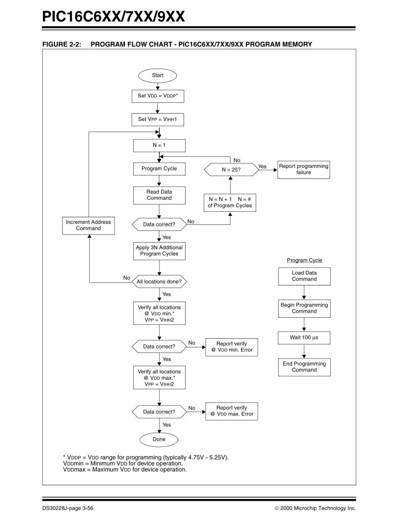
PIC16C6XX/7XX/9XX
DS30228J-page 3-56 2000 Microchip Technology Inc.
FIGURE 2-2: PROGRAM FLOW CHART - PIC16C6XX/7XX/9XX PROGRAM MEMORY
* VDDP = VDD range for programming (typically 4.75V - 5.25V).VDDmin = Minimum VDD for device operation.VDDmax = Maximum VDD for device operation.
Start
N = 1
Set VDD = VDDP*
Program Cycle
Read DataCommand
Data correct?
Apply 3N AdditionalProgram Cycles
All locations done?
Verify all locations@ VDD min.*VPP = VIHH2
Data correct?
Verify all locations@ VDD max.*VPP = VIHH2
Data correct?
Done
N > 25?Report programming
failure
N = N + 1 N = #of Program Cycles
Increment AddressCommand
Report verify@ VDD min. Error
Report verify@ VDD max. Error
Load DataCommand
Begin ProgrammingCommand
End ProgrammingCommand
Wait 100 µs
Program Cycle
Yes
No
NoYes
No
Yes
No
No
Yes
Yes
Set VPP = VIHH1

2000 Microchip Technology Inc. DS30228J-page 3-57
PIC16C6XX/7XX/9XX
FIGURE 2-3: PROGRAM FLOW CHART - PIC16C6XX/7XX/9XX CONFIGURATION WORD & ID LOCATIONS
VDDmin
VDDmax
Start
Load ConfigurationCommand
Increment AddressCommand N = N + 1 N = #
of Program Cycles
Report IDConfiguration Error
Increment AddressCommand
Increment AddressCommand
Increment AddressCommand
Program Cycle100 Cycles
Read DataCommand
Apply 3NProgram Cycles
Read DataCommand
Report ProgramID/Config. Error
Set VDD = VDDmax
Program Cycle
N = 1
Data Correct?
Data Correct?
Data Correct?
Data Correct?
N > 25 Address = 2004
Program ID Loc?
Done
Yes
No
No
YesNo
Yes
Yes
Yes
No
Yes
No
No
No Yes
Read Data CommandSet VPP = VIHH2
Set VDD = VDDminRead Data Command
Set VPP = VIHH2
Set VDD = VDDP*
Set VPP = VIHH1
VDDP = VDD Range for programming (Typically 4.25V – 5.25V)VDDMIN = minimum VDD for device operationVDDMAX = maximum VDD for device operation
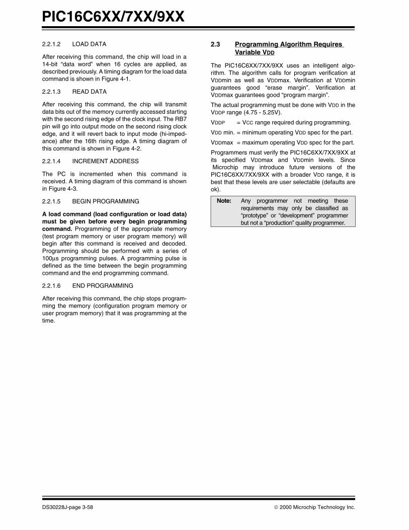
PIC16C6XX/7XX/9XX
DS30228J-page 3-58 2000 Microchip Technology Inc.
2.2.1.2 LOAD DATA
After receiving this command, the chip will load in a14-bit “data word” when 16 cycles are applied, asdescribed previously. A timing diagram for the load datacommand is shown in Figure 4-1.
2.2.1.3 READ DATA
After receiving this command, the chip will transmitdata bits out of the memory currently accessed startingwith the second rising edge of the clock input. The RB7pin will go into output mode on the second rising clockedge, and it will revert back to input mode (hi-imped-ance) after the 16th rising edge. A timing diagram ofthis command is shown in Figure 4-2.
2.2.1.4 INCREMENT ADDRESS
The PC is incremented when this command isreceived. A timing diagram of this command is shownin Figure 4-3.
2.2.1.5 BEGIN PROGRAMMING
A load command (load configuration or load data)must be given before every begin programmingcommand. Programming of the appropriate memory(test program memory or user program memory) willbegin after this command is received and decoded.Programming should be performed with a series of100µs programming pulses. A programming pulse isdefined as the time between the begin programmingcommand and the end programming command.
2.2.1.6 END PROGRAMMING
After receiving this command, the chip stops program-ming the memory (configuration program memory oruser program memory) that it was programming at thetime.
2.3 Programming Algorithm Requires Variable VDD
The PIC16C6XX/7XX/9XX uses an intelligent algo-rithm. The algorithm calls for program verification atVDDmin as well as VDDmax. Verification at VDDminguarantees good “erase margin”. Verification atVDDmax guarantees good “program margin”.
The actual programming must be done with VDD in theVDDP range (4.75 - 5.25V).
VDDP = VCC range required during programming.
VDD min. = minimum operating VDD spec for the part.
VDDmax = maximum operating VDD spec for the part.
Programmers must verify the PIC16C6XX/7XX/9XX atits specified VDDmax and VDDmin levels. SinceMicrochip may introduce future versions of the
PIC16C6XX/7XX/9XX with a broader VDD range, it isbest that these levels are user selectable (defaults areok).
Note: Any programmer not meeting theserequirements may only be classified as“prototype” or “development” programmerbut not a “production” quality programmer.

2000 Microchip Technology Inc. DS30228J-page 3-59
PIC16C6XX/7XX/9XX
3.0 CONFIGURATION WORDThe PIC16C6XX/7XX/9XX family members have sev-eral configuration bits. These bits can be programmed(reads ’0’) or left unprogrammed (reads ’1’) to selectvarious device configurations. Figure 3-1 andFigure 3-2 provides an overview of configuration bits.

PIC16C6XX/7XX/9XX
DS30228J-page 3-60 2000 Microchip Technology Inc.
FIGURE 3-1: CONFIGURATION WORD BIT MAP
Bit Number: 13 12 11 10 9 8 7 6 5 4 3 2 1 0
PIC16C61/71 — — — — — — — — — CP0 PWRTE WDTE FOSC1 FOSC0PIC16C62/64/65/73/74 — — — — — — — 0 CP1 CP0 PWRTE WDTE FOSC1 FOSC0
PIC16C62A/62B/63A/CR62/63/
64A/CR64/65A/65B/66/67/72/72A/73A/73B/74A/74B/76/
77/620/620A/621/621A/622/622A/
712/716 CP1 CP0 CP1 CP0 CP1 CP0 — BODEN CP1 CP0 PWRTE WDTE FOSC1 FOSC0
PIC16C9XX/745/765 CP1 CP0 CP1 CP0 CP1 CP0 — — CP1 CP0 PWRTE WDTE FOSC1 FOSC0
Reserved, '–' write as '1' for PIC16C6XX/7XX/9XX
CP <1:0>, Code Protect
bit 6: BODEN, Brown Out Enable Bit1 = Enabled2 = Disable
bit 4: PWRTE/PWRTE, Power Up Timer Enable BitPIC16C61/62/64/65/71/73/74: 1 = Power up timer enabled 0 = Power up timer disabledPIC16C620/620A/621/621A/622/622A/62A/63/63A/65A/65B/66/67/72/72A/73A/73B/74A/74B/76/77/710/711/923/924/745/765: 0 = Power up timer enabled 1 = Power up timer disabled
bit 3-2: WDTE, WDT Enable Bit1 = WDT enabled0 = WDT disabled
bit 1-0: FOSC<1:0>, Oscillator Selection Bit11: RC oscillator10: HS oscillator01: XT oscillator00: LP oscillator
bit 1-0: FOSC<1:0>, PIC16C745/76511: E external clock with 4k PLL 10: H HS oscillator with 4k PL enabled01: EC external clock, clkout on osc200: HS
Note 1: Enabling Brown-out Reset automatically enables the Power-up Timer (PWRT) regardless of the value of bit PWRTE. Ensure the Power-up Timer is enabled anytime Brown-out Reset is enabled.
Device CP1 CP0 Code ProtectionPIC16C622/622APIC16C62/62A/62B 0 0 All memory protected
PIC16C63/63APIC16C64/64A/712/716
0 1 Upper 3/4 memory protected
PIC16C65/65A/65BPIC16C66/67/72/72A
1 0 Upper 1/2 memory protected
PIC16C73/73A/73BPIC16C74/74A/74B/76/77PIC16C745/765PIC16C9XX
1 1 Code protection off
PIC16C61/71PIC16C710/711
— 0 All memory protected— 1 Off
PIC16C620 0 0 All memory protected0 1 Do not use1 0 Do not use1 1 Code protection off
PIC16C621 0 0 All memory protected1 0 Upper 1/2 memory protected1 1 Code protection off

2000 Microchip Technology Inc. DS30228J-page 3-61
PIC16C6XX/7XX/9XX
FIGURE 3-2: CONFIGURATION WORD FOR PIC16C773/774 DEVICE
CP1 CP0 BORV1 BORV0 CP1 CP0 - BODEN CP1 CP0 PWRTE WDTE FOSC1 FOSC0 Register: CONFIGAddress 2007h
bit13 12 11 10 9 8 7 6 5 4 3 2 1 bit0
CP <1:0> Code Protection bits (2)
bit 11-10: BORV <1:0>: Brown-out Reset Voltage bits11 = VBOR set to 2.5V10 = VBOR set to 2.7V01 = VBOR set to 4.2V00 = VBOR set to 4.5V
bit 7: Unimplemented, Read as ’1’
bit 6: BODEN: Brown-out Reset Enable bit (1)
1 = Brown-out Reset enabled0 = Brown-out Reset disabled
bit 3: PWRTE: Power-up Timer Enable bit (1)
1 = PWRT disabled0 = PWRT enabled
bit 2: WDTE: Watchdog Timer Enable bit1 = WDT enabled0 = WDT disabled
bit 1-0: FOSC <1:0>: Oscillator Selection bits11 = RC oscillator10 = HS oscillator01 = XT oscillator00 = LP oscillator
Note 1: Enabling Brown-out Reset automatically enables the Power-up Timer (PWRT) regardless of the value of bit PWRTE. Ensure the Power-up Timer is enabled anytime Brown-out Reset is enabled.
2: All of the CP <1:0> pairs have to be given the same value to enable the code protection scheme listed.
Device CP1 CP0 Code Protection
PIC16C773/774 0 0 All memory protected
0 1 Upper 3/4 memory protected
1 0 Upper 1/2 memory protected1
1 1 Code protection off
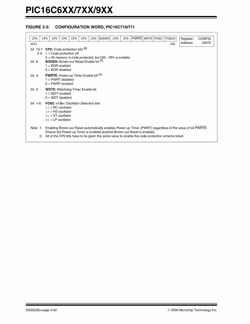
PIC16C6XX/7XX/9XX
DS30228J-page 3-62 2000 Microchip Technology Inc.
FIGURE 3-3: CONFIGURATION WORD, PIC16C710/711
CP0 CP0 CP0 CP0 CP0 CP0 CP0 BODEN CP0 CP0 PWRTE WDTE FOSC1 FOSC0 Register: CONFIGAddress 2007hbit13 bit0
bit 13-7 CP0: Code protection bits (2)
5-4: 1 = Code protection off0 = All memory is code protected, but 00h - 3Fh is writable
bit 6: BODEN: Brown-out Reset Enable bit (1)
1 = BOR enabled0 = BOR disabled
bit 3: PWRTE: Power-up Timer Enable bit (1)
1 = PWRT disabled0 = PWRT enabled
bit 2: WDTE: Watchdog Timer Enable bit1 = WDT enabled0 = WDT disabled
bit 1-0: FOSC <1:0>: Oscillator Selection bits11 = RC oscillator10 = HS oscillator01 = XT oscillator00 = LP oscillator
Note 1: Enabling Brown-out Reset automatically enables Power-up Timer (PWRT) regardless of the value of bit PWRTE. Ensure the Power-up Timer is enabled anytime Brown-out Reset is enabled.
2: All of the CP0 bits have to be given the same value to enable the code protection scheme listed.
2000 Microchip Technology Inc. DS30228J-page 3-63
PIC16C6XX/7XX/9XX
3.1 Embedding Configuration Word and ID Information in the Hex File.
To allow portability of code, the programmer is required to read the configuration word and ID locations from the hexfile when loading the hex file. If configuration word information was not present in the hex file then a simple warningmessage may be issued. Similarly, while saving a hex file, configuration word and ID information must be included.An option to not include this information may be provided.
Microchip Technology Inc. feels strongly that this feature is beneficial to the end customer.

PIC16C6XX/7XX/9XX
DS30228J-page 3-64 2000 Microchip Technology Inc.
3.2 Checksum
3.2.1 CHECKSUM CALCULATIONS
Checksum is calculated by reading the contents of thePIC16C6XX/7XX/9XX memory locations and addingup the opcodes up to the maximum user addressablelocation, e.g., 0x1FF for the PIC16C74. Any carry bitsexceeding 16-bits are neglected. Finally, the configura-tion word (appropriately masked) is added to the check-sum. Checksum computation for each member of thePIC16C6XX/7XX/9XX devices is shown in Table 3-1.
The checksum is calculated by summing the following:
• The contents of all program memory locations• The configuration word, appropriately masked• Masked ID locations (when applicable)
The least significant 16 bits of this sum is the check-sum.
The following table describes how to calculate thechecksum for each device. Note that the checksum cal-culation differs depending on the code protect setting.Since the program memory locations read out differ-ently depending on the code protect setting, the tabledescribes how to manipulate the actual program mem-ory values to simulate the values that would be readfrom a protected device. When calculating a checksumby reading a device, the entire program memory cansimply be read and summed. The configuration wordand ID locations can always be read.
Note that some older devices have an additional valueadded in the checksum. This is to maintain compatibil-ity with older device programmer checksums.
TABLE 3-1: CHECKSUM COMPUTATION
DeviceCode
ProtectChecksum*
BlankValue
0x25E6 at0 and maxaddress
PIC16C61 OFFON
SUM[0x000:0x3FF] + CFGW & 0x001F + 0x3FE0SUM_XNOR7[0x000:0x3FF] + (CFGW & 0x001F | 0x0060)
0x3BFF0xFC6F
0x07CD0xFC15
PIC16C620 OFFON
SUM[0x000:0x1FF] + CFGW & 0x3F7FSUM_ID + CFGW & 0x3F7F
0x3D7F0x3DCE
0x094D0x099C
PIC16C620A OFFON
SUM[0x000:0x1FF] + CFGW & 0x3F7FSUM_ID + CFGW & 0x3F7F
0x3D7F0x3DCE
0x094D0x099C
PIC16C621 OFF1/2ALL
SUM[0x000:0x3FF] + CFGW & 0x3F7FSUM[0x000:0x1FF] + CFGW & 0x3F7F + SUM_IDCFGW & 0x3F7F + SUM_ID
0x3B7F0x4EDE0x3BCE
0x074D0x00930x079C
PIC16C621A OFF1/2ALL
SUM[0x000:0x3FF] + CFGW & 0x3F7FSUM[0x000:0x1FF] + CFGW & 0x3F7F + SUM_IDCFGW & 0x3F7F + SUM_ID
0x3B7F0x4EDE0x3BCE
0x074D0x00930x079C
PIC16C622 OFF1/23/4ALL
SUM[0x000:0x7FF] + CFGW & 0x3F7FSUM[0x000:0x3FF] + CFGW & 0x3F7F + SUM_IDSUM[0x000:0x1FF] + CFGW & 0x3F7F + SUM_IDCFGW & 0x3F7F + SUM_ID
0x377F0x5DEE0x4ADE0x37CE
0x034D0x0FA30xFC930x039C
PIC16C622A OFF1/23/4ALL
SUM[0x000:0x7FF] + CFGW & 0x3F7FSUM[0x000:0x3FF] + CFGW & 0x3F7F + SUM_IDSUM[0x000:0x1FF] + CFGW & 0x3F7F + SUM_IDCFGW & 0x3F7F + SUM_ID
0x377F0x5DEE0x4ADE0x37CE
0x034D0x0FA30xFC930x039C
PIC16CE623 OFFON
SUM[0x000:0x1FF] + CFGW & 0x3F7FSUM_ID + CFGW & 0x3F7F
0x3D7F0x3DCE
0x094D0x099C
Legend: CFGW = Configuration WordSUM[a:b] = [Sum of locations a through b inclusive]SUM_XNOR7[a:b] = XNOR of the seven high order bits of memory location with the seven low order bits summed over locations a through b inclusive. For example, XNOR(0x3C31)=0x78 XNOR 0c31 = 0x0036.SUM_ID = ID locations masked by 0xF then made into a 16-bit value with ID0 as the most significant nibble. For example, ID0 = 0x12, ID1 = 0x37, ID2 = 0x4, ID3 = 0x26, then SUM_ID = 0x2746.*Checksum = [Sum of all the individual expressions] MODULO [0xFFFF]+ = Addition& = Bitwise AND| = Bitwise OR
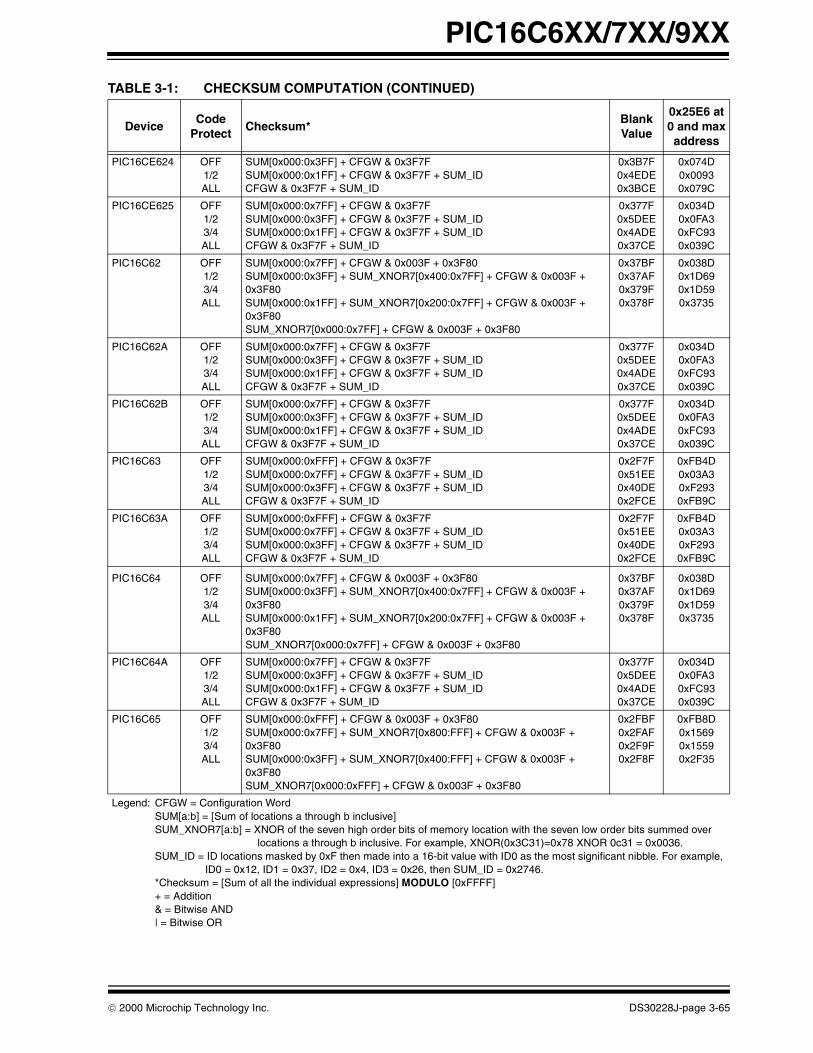
2000 Microchip Technology Inc. DS30228J-page 3-65
PIC16C6XX/7XX/9XX
PIC16CE624 OFF1/2ALL
SUM[0x000:0x3FF] + CFGW & 0x3F7FSUM[0x000:0x1FF] + CFGW & 0x3F7F + SUM_IDCFGW & 0x3F7F + SUM_ID
0x3B7F0x4EDE0x3BCE
0x074D0x00930x079C
PIC16CE625 OFF1/23/4ALL
SUM[0x000:0x7FF] + CFGW & 0x3F7FSUM[0x000:0x3FF] + CFGW & 0x3F7F + SUM_IDSUM[0x000:0x1FF] + CFGW & 0x3F7F + SUM_IDCFGW & 0x3F7F + SUM_ID
0x377F0x5DEE0x4ADE0x37CE
0x034D0x0FA30xFC930x039C
PIC16C62 OFF1/23/4ALL
SUM[0x000:0x7FF] + CFGW & 0x003F + 0x3F80SUM[0x000:0x3FF] + SUM_XNOR7[0x400:0x7FF] + CFGW & 0x003F + 0x3F80SUM[0x000:0x1FF] + SUM_XNOR7[0x200:0x7FF] + CFGW & 0x003F + 0x3F80SUM_XNOR7[0x000:0x7FF] + CFGW & 0x003F + 0x3F80
0x37BF0x37AF0x379F0x378F
0x038D0x1D690x1D590x3735
PIC16C62A OFF1/23/4ALL
SUM[0x000:0x7FF] + CFGW & 0x3F7FSUM[0x000:0x3FF] + CFGW & 0x3F7F + SUM_IDSUM[0x000:0x1FF] + CFGW & 0x3F7F + SUM_IDCFGW & 0x3F7F + SUM_ID
0x377F0x5DEE0x4ADE0x37CE
0x034D0x0FA30xFC930x039C
PIC16C62B OFF1/23/4ALL
SUM[0x000:0x7FF] + CFGW & 0x3F7FSUM[0x000:0x3FF] + CFGW & 0x3F7F + SUM_IDSUM[0x000:0x1FF] + CFGW & 0x3F7F + SUM_IDCFGW & 0x3F7F + SUM_ID
0x377F0x5DEE0x4ADE0x37CE
0x034D0x0FA30xFC930x039C
PIC16C63 OFF1/23/4ALL
SUM[0x000:0xFFF] + CFGW & 0x3F7FSUM[0x000:0x7FF] + CFGW & 0x3F7F + SUM_IDSUM[0x000:0x3FF] + CFGW & 0x3F7F + SUM_IDCFGW & 0x3F7F + SUM_ID
0x2F7F0x51EE0x40DE0x2FCE
0xFB4D0x03A30xF2930xFB9C
PIC16C63A OFF1/23/4ALL
SUM[0x000:0xFFF] + CFGW & 0x3F7FSUM[0x000:0x7FF] + CFGW & 0x3F7F + SUM_IDSUM[0x000:0x3FF] + CFGW & 0x3F7F + SUM_IDCFGW & 0x3F7F + SUM_ID
0x2F7F0x51EE0x40DE0x2FCE
0xFB4D0x03A30xF2930xFB9C
PIC16C64 OFF1/23/4ALL
SUM[0x000:0x7FF] + CFGW & 0x003F + 0x3F80SUM[0x000:0x3FF] + SUM_XNOR7[0x400:0x7FF] + CFGW & 0x003F + 0x3F80SUM[0x000:0x1FF] + SUM_XNOR7[0x200:0x7FF] + CFGW & 0x003F + 0x3F80SUM_XNOR7[0x000:0x7FF] + CFGW & 0x003F + 0x3F80
0x37BF0x37AF0x379F0x378F
0x038D0x1D690x1D590x3735
PIC16C64A OFF1/23/4ALL
SUM[0x000:0x7FF] + CFGW & 0x3F7FSUM[0x000:0x3FF] + CFGW & 0x3F7F + SUM_IDSUM[0x000:0x1FF] + CFGW & 0x3F7F + SUM_IDCFGW & 0x3F7F + SUM_ID
0x377F0x5DEE0x4ADE0x37CE
0x034D0x0FA30xFC930x039C
PIC16C65 OFF1/23/4ALL
SUM[0x000:0xFFF] + CFGW & 0x003F + 0x3F80SUM[0x000:0x7FF] + SUM_XNOR7[0x800:FFF] + CFGW & 0x003F + 0x3F80SUM[0x000:0x3FF] + SUM_XNOR7[0x400:FFF] + CFGW & 0x003F + 0x3F80SUM_XNOR7[0x000:0xFFF] + CFGW & 0x003F + 0x3F80
0x2FBF0x2FAF0x2F9F0x2F8F
0xFB8D0x15690x15590x2F35
TABLE 3-1: CHECKSUM COMPUTATION (CONTINUED)
DeviceCode
ProtectChecksum*
BlankValue
0x25E6 at0 and maxaddress
Legend: CFGW = Configuration WordSUM[a:b] = [Sum of locations a through b inclusive]SUM_XNOR7[a:b] = XNOR of the seven high order bits of memory location with the seven low order bits summed over locations a through b inclusive. For example, XNOR(0x3C31)=0x78 XNOR 0c31 = 0x0036.SUM_ID = ID locations masked by 0xF then made into a 16-bit value with ID0 as the most significant nibble. For example, ID0 = 0x12, ID1 = 0x37, ID2 = 0x4, ID3 = 0x26, then SUM_ID = 0x2746.*Checksum = [Sum of all the individual expressions] MODULO [0xFFFF]+ = Addition& = Bitwise AND| = Bitwise OR

PIC16C6XX/7XX/9XX
DS30228J-page 3-66 2000 Microchip Technology Inc.
PIC16C65A OFF1/23/4ALL
SUM[0x000:0xFFF] + CFGW & 0x3F7FSUM[0x000:0x7FF] + CFGW & 0x3F7F + SUM_IDSUM[0x000:0x3FF] + CFGW & 0x3F7F + SUM_IDCFGW & 0x3F7F + SUM_ID
0x2F7F0x51EE0x40DE0x2FCE
0xFB4D0x03A30xF2930xFB9C
PIC16C65B OFF1/23/4ALL
SUM[0x000:0xFFF] + CFGW & 0x3F7FSUM[0x000:0x7FF] + CFGW & 0x3F7F + SUM_IDSUM[0x000:0x3FF] + CFGW & 0x3F7F + SUM_IDCFGW & 0x3F7F + SUM_ID
0x2F7F0x51EE0x40DE0x2FCE
0xFB4D0x03A30xF2930xFB9C
PIC16C66 OFF1/23/4ALL
SUM[0x000:0x1FFF] + CFGW & 0x3F7FSUM[0x000:0xFFF] + CFGW & 0x3F7F + SUM_IDSUM[0x000:0x7FF] + CFGW & 0x3F7F + SUM_IDCFGW & 0x3F7F + SUM_ID
0x1F7F0x39EE0x2CDE0x1FCE
0xEB4D0xEBA30xDE930xEB9C
PIC16C67 OFF1/23/4ALL
SUM[0x000:0x1FFF] + CFGW & 0x3F7FSUM[0x000:0xFFF] + CFGW & 0x3F7F + SUM_IDSUM[0x000:0x7FF] + CFGW & 0x3F7F + SUM_IDCFGW & 0x3F7F + SUM_ID
0x1F7F0x39EE0x2CDE0x1FCE
0xEB4D0xEBA30xDE930xEB9C
PIC16C710 OFFON
SUM[0x000:0x1FF] + CFGW & 0x3FFFSUM[0x00:0x3F] + CFGW & 0x3FFF + SUM_ID
0x3DFF0x3E0E
0x09CD0xEFC3
PIC16C71 OFFON
SUM[0x000:0x3FF] + CFGW & 0x001F + 0x3FE0SUM_XNOR7[0x000:0x3FF] + (CFGW & 0x001F | 0x0060)
0x3BFF0xFC6F
0x07CD0xFC15
PIC16C711 OFFON
SUM[0x000:0x03FF] + CFGW & 0x3FFFSUM[0x00:0x3FF] + CFGW & 0x3FFF + SUM_ID
0x3BFF0x3C0E
0x07CD0xEDC3
PIC16C712 OFF1/2ALL
SUM[0x000:0x07FF] + CFGW & 0x3F7FSUM[0x000:0x03FF] + CFGW & 3F7F + SUM_IDCFGW & 0x3F7F + SUM_ID
0x377F0x5DEE0x37CE
0x034D0xF58A0x039C
PIC16C716 OFF1/23/4ALL
SUM[0x000:0x07FF] + CFGW & 0x3F7FSUM[0x000:0x03FF] + CFGW & 0x3F7F + SUM_IDSUM]0x000:0x01FF] + CFGW & 0x3F7F + SUM_IDCFGW & 0x3F7F + SUM_ID
0x377F0x5DEE0x4ADE0x37CE
0x034D0x0FA30xFC930x039C
PIC16C72 OFF1/23/4ALL
SUM[0x000:0x7FF] + CFGW & 0x3F7FSUM[0x000:0x3FF] + CFGW & 0x3F7F + SUM_IDSUM[0x000:0x1FF] + CFGW & 0x3F7F + SUM_IDCFGW & 0x3F7F + SUM_ID
0x377F0x5DEE0x4ADE0x37CE
0x034D0x0FA30xFC930x039C
PIC16C72A OFF1/23/4ALL
SUM[0x000:0x7FF] + CFGW & 0x3F7FSUM[0x000:0x3FF] + CFGW & 0x3F7F + SUM_IDSUM[0x000:0x1FF] + CFGW & 0x3F7F + SUM_IDCFGW & 0x3F7F + SUM_ID
0x377F0x5DEE0x4ADE0x37CE
0x034D0x0FA30xFC930x039C
PIC16C73 OFF1/23/4ALL
SUM[0x000:0xFFF] + CFGW & 0x003F + 0x3F80SUM[0x000:0x7FF] + SUM_XNOR7[0x800:FFF] + CFGW & 0x003F + 0x3F80SUM[0x000:0x3FF] + SUM_XNOR7[0x400:FFF] + CFGW & 0x003F + 0x3F80SUM_XNOR7[0x000:0xFFF] + CFGW & 0x003F + 0x3F80
0x2FBF0x2FAF0x2F9F0x2F8F
0xFB8D0x15690x15590x2F35
PIC16C73A OFF1/23/4ALL
SUM[0x000:0xFFF] + CFGW & 0x3F7FSUM[0x000:0x7FF] + CFGW & 0x3F7F + SUM_IDSUM[0x000:0x3FF] + CFGW & 0x3F7F + SUM_IDCFGW & 0x3F7F + SUM_ID
0x2F7F0x51EE0x40DE0x2FCE
0xFB4D0x03A30xF2930xFB9C
TABLE 3-1: CHECKSUM COMPUTATION (CONTINUED)
DeviceCode
ProtectChecksum*
BlankValue
0x25E6 at0 and maxaddress
Legend: CFGW = Configuration WordSUM[a:b] = [Sum of locations a through b inclusive]SUM_XNOR7[a:b] = XNOR of the seven high order bits of memory location with the seven low order bits summed over locations a through b inclusive. For example, XNOR(0x3C31)=0x78 XNOR 0c31 = 0x0036.SUM_ID = ID locations masked by 0xF then made into a 16-bit value with ID0 as the most significant nibble. For example, ID0 = 0x12, ID1 = 0x37, ID2 = 0x4, ID3 = 0x26, then SUM_ID = 0x2746.*Checksum = [Sum of all the individual expressions] MODULO [0xFFFF]+ = Addition& = Bitwise AND| = Bitwise OR

2000 Microchip Technology Inc. DS30228J-page 3-67
PIC16C6XX/7XX/9XX
PIC16C73B OFF1/23/4ALL
SUM[0x000:0xFFF] + CFGW & 0x3F7FSUM[0x000:0x7FF] + CFGW & 0x3F7F + SUM_IDSUM[0x000:0x3FF] + CFGW & 0x3F7F + SUM_IDCFGW & 0x3F7F + SUM_ID
0x2F7F0x51EE0x40DE0x2FCE
0xFB4D0x03A30xF2930xFB9C
PIC16C74 OFF1/23/4ALL
SUM[0x000:0xFFF] + CFGW & 0x003F + 0x3F80SUM[0x000:0x7FF] + SUM_XNOR7[0x800:FFF] + CFGW & 0x003F + 0x3F80SUM[0x000:0x3FF] + SUM_XNOR7[0x400:FFF] + CFGW & 0x003F + 0x3F80SUM_XNOR7[0x000:0xFFF] + CFGW & 0x003F + 0x3F80
0x2FBF0x2FAF0x2F9F0x2F8F
0xFB8D0x15690x15590x2F35
PIC16C74A OFF1/23/4ALL
SUM[0x000:0xFFF] + CFGW & 0x3F7FSUM[0x000:0x7FF] + CFGW & 0x3F7F + SUM_IDSUM[0x000:0x3FF] + CFGW & 0x3F7F + SUM_IDCFGW & 0x3F7F + SUM_ID
0x2F7F0x51EE0x40DE0x2FCE
0xFB4D0x03A30xF2930xFB9C
PIC16C74B OFF1/23/4ALL
SUM[0x000:0xFFF] + CFGW & 0x3F7FSUM[0x000:0x7FF] + CFGW & 0x3F7F + SUM_IDSUM[0x000:0x3FF] + CFGW & 0x3F7F + SUM_IDCFGW & 0x3F7F + SUM_ID
0x2F7F0x51EE0x40DE0x2FCE
0xFB4D0x03A30xF2930xFB9C
PIC16C76 OFF1/23/4ALL
SUM[0x000:0x1FFF] + CFGW & 0x3F7FSUM[0x000:0xFFF] + CFGW & 0x3F7F + SUM_IDSUM[0x000:0x7FF] + CFGW & 0x3F7F + SUM_IDCFGW & 0x3F7F + SUM_ID
0x1F7F0x39EE0x2CDE0x1FCE
0xEB4D0xEBA30xDE930xEB9C
PIC16C77 OFF1/23/4ALL
SUM[0x000:0x1FFF] + CFGW & 0x3F7FSUM[0x000:0xFFF] + CFGW & 0x3F7F + SUM_IDSUM[0x000:0x7FF] + CFGW & 0x3F7F + SUM_IDCFGW & 0x3F7F + SUM_ID
0x1F7F0x39EE0x2CDE0x1FCE
0xEB4D0xEBA30xDE930xEB9C
PIC16C773 OFF1/23/4ALL
SUM[0x000:0x0FFF] + CFGW & 0x3F7FSUM[0x000:07FF] + CFGW & 0x3F7F + SUM_IDSUM[0x000:03FF] + CFGW & 0x3F7F + SUM_IDCFGW & 0x3F7F + SUM_ID
0x2F7F0x55EE0x48DE0x3BCE
0xFB4D0x07A30xFA930x079C
PIC16C774 OFF1/23/4ALL
SU:M[0x000:0FFF] + CFGW & 0x3F7FSUM[0x000:07FF] + CFGW & 0x3F7F + SUM_IDSUM[0x000:03FF] + CFGW & 0x3F7F + SUM_IDCFGW & 0x3F7F + SUM_ID
0x2F7F0X55EE0X48DE0x3BCE
0xFB4D0x07A30xFA930X079C
PIC16C923 OFF1/23/4ALL
SUM[0x000:0xFFF] + CFGW & 0x3F3FSUM[0x000:0x7FF] + CFGW & 0x3F3F + SUM_IDSUM[0x000:0x3FF] + CFGW & 0x3F3F + SUM_IDCFGW & 0x3F3F + SUM_ID
0x2F3F0x516E0x405E0x2F4E
0xFB0D0x03230xF2130xFB1C
PIC16C924 OFF1/23/4ALL
SUM[0x000:0xFFF] + CFGW & 0x3F3FSUM[0x000:0x7FF] + CFGW & 0x3F3F + SUM_IDSUM[0x000:0x3FF] + CFGW & 0x3F3F + SUM_IDCFGW & 0x3F3F + SUM_ID
0x2F3F0x516E0x405E0x2F4E
0xFB0D0x03230xF2130xFB1C
PIC16C745 OFF1000:1FFF800:1FFF
ALL
SUM(0000:1FFF) + CFGW & 0x3F3FSUM(0000:0FFF) + CFGW & 0x3F3F+SUM_IDSUM(0000:07FF) + CFGW & 0x3F3F + SUM_IDCFGW * 0x3F3F + SUM_ID
1F3F396E2C5E1F4E
EB0DEB23DE13EB1C
TABLE 3-1: CHECKSUM COMPUTATION (CONTINUED)
DeviceCode
ProtectChecksum*
BlankValue
0x25E6 at0 and maxaddress
Legend: CFGW = Configuration WordSUM[a:b] = [Sum of locations a through b inclusive]SUM_XNOR7[a:b] = XNOR of the seven high order bits of memory location with the seven low order bits summed over locations a through b inclusive. For example, XNOR(0x3C31)=0x78 XNOR 0c31 = 0x0036.SUM_ID = ID locations masked by 0xF then made into a 16-bit value with ID0 as the most significant nibble. For example, ID0 = 0x12, ID1 = 0x37, ID2 = 0x4, ID3 = 0x26, then SUM_ID = 0x2746.*Checksum = [Sum of all the individual expressions] MODULO [0xFFFF]+ = Addition& = Bitwise AND| = Bitwise OR
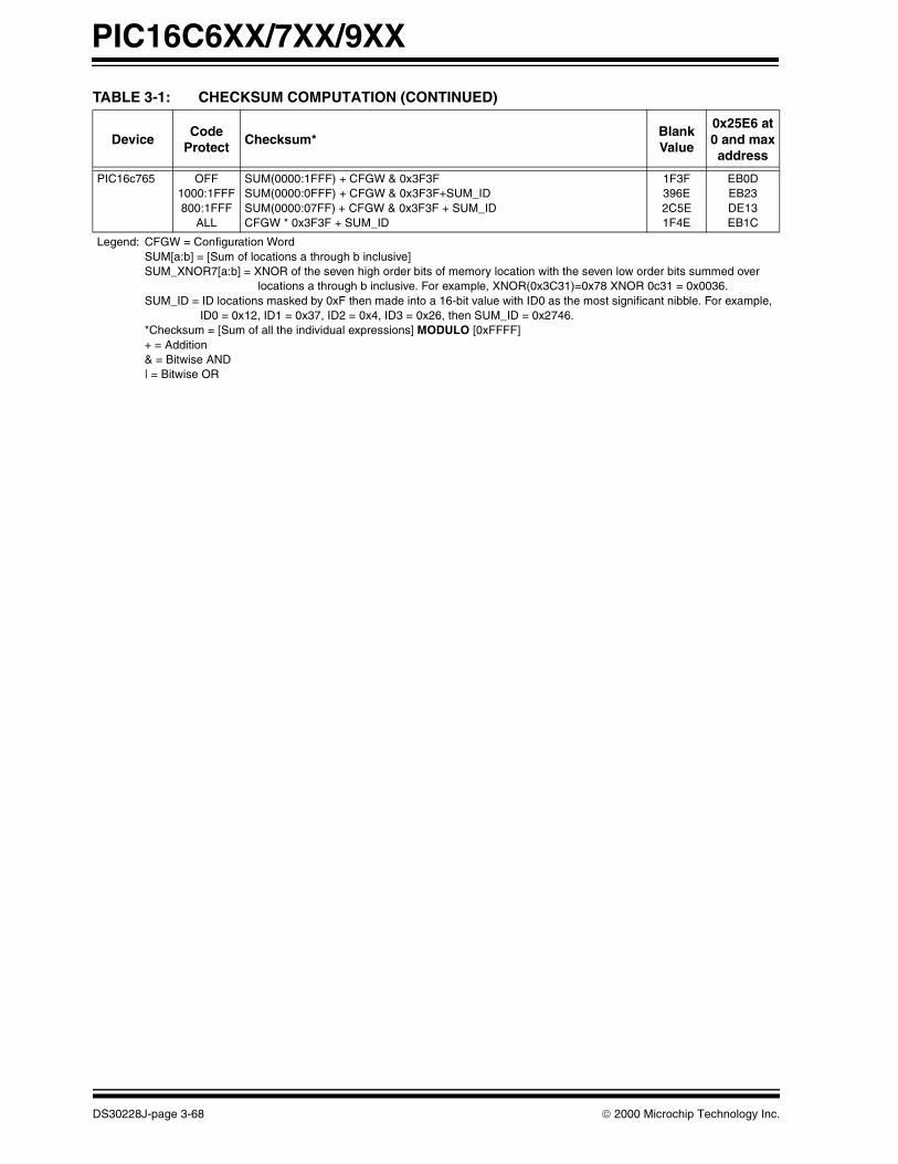
PIC16C6XX/7XX/9XX
DS30228J-page 3-68 2000 Microchip Technology Inc.
PIC16c765 OFF1000:1FFF800:1FFF
ALL
SUM(0000:1FFF) + CFGW & 0x3F3FSUM(0000:0FFF) + CFGW & 0x3F3F+SUM_IDSUM(0000:07FF) + CFGW & 0x3F3F + SUM_IDCFGW * 0x3F3F + SUM_ID
1F3F396E2C5E1F4E
EB0DEB23DE13EB1C
TABLE 3-1: CHECKSUM COMPUTATION (CONTINUED)
DeviceCode
ProtectChecksum*
BlankValue
0x25E6 at0 and maxaddress
Legend: CFGW = Configuration WordSUM[a:b] = [Sum of locations a through b inclusive]SUM_XNOR7[a:b] = XNOR of the seven high order bits of memory location with the seven low order bits summed over locations a through b inclusive. For example, XNOR(0x3C31)=0x78 XNOR 0c31 = 0x0036.SUM_ID = ID locations masked by 0xF then made into a 16-bit value with ID0 as the most significant nibble. For example, ID0 = 0x12, ID1 = 0x37, ID2 = 0x4, ID3 = 0x26, then SUM_ID = 0x2746.*Checksum = [Sum of all the individual expressions] MODULO [0xFFFF]+ = Addition& = Bitwise AND| = Bitwise OR
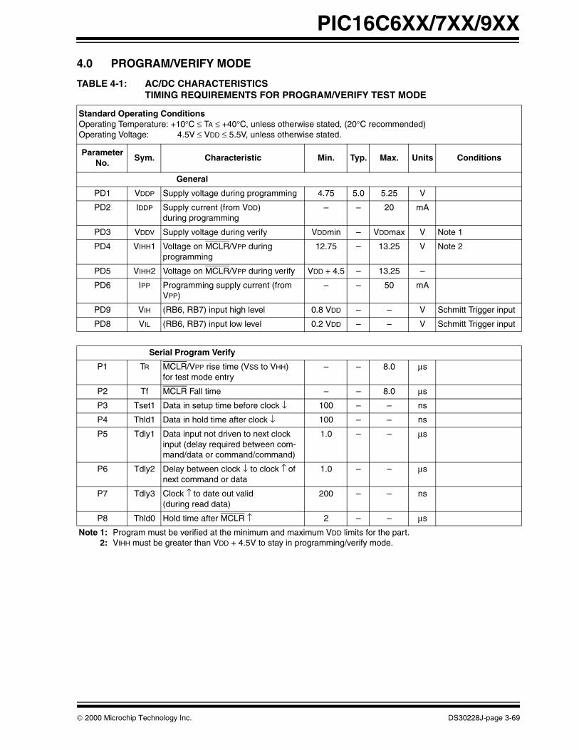
2000 Microchip Technology Inc. DS30228J-page 3-69
PIC16C6XX/7XX/9XX
4.0 PROGRAM/VERIFY MODE
TABLE 4-1: AC/DC CHARACTERISTICSTIMING REQUIREMENTS FOR PROGRAM/VERIFY TEST MODE
Standard Operating ConditionsOperating Temperature: +10°C ≤ TA ≤ +40°C, unless otherwise stated, (20°C recommended)Operating Voltage: 4.5V ≤ VDD ≤ 5.5V, unless otherwise stated.
ParameterNo.
Sym. Characteristic Min. Typ. Max. Units Conditions
General
PD1 VDDP Supply voltage during programming 4.75 5.0 5.25 V
PD2 IDDP Supply current (from VDD)during programming
– – 20 mA
PD3 VDDV Supply voltage during verify VDDmin – VDDmax V Note 1
PD4 VIHH1 Voltage on MCLR/VPP during programming
12.75 – 13.25 V Note 2
PD5 VIHH2 Voltage on MCLR/VPP during verify VDD + 4.5 – 13.25 –
PD6 IPP Programming supply current (from VPP)
– – 50 mA
PD9 VIH (RB6, RB7) input high level 0.8 VDD – – V Schmitt Trigger input
PD8 VIL (RB6, RB7) input low level 0.2 VDD – – V Schmitt Trigger input
Serial Program Verify
P1 TR MCLR/VPP rise time (VSS to VHH) for test mode entry
– – 8.0 µs
P2 Tf MCLR Fall time – – 8.0 µs
P3 Tset1 Data in setup time before clock ↓ 100 – – ns
P4 Thld1 Data in hold time after clock ↓ 100 – – ns
P5 Tdly1 Data input not driven to next clock input (delay required between com-mand/data or command/command)
1.0 – – µs
P6 Tdly2 Delay between clock ↓ to clock ↑ of next command or data
1.0 – – µs
P7 Tdly3 Clock ↑ to date out valid (during read data)
200 – – ns
P8 Thld0 Hold time after MCLR ↑ 2 – – µs
Note 1: Program must be verified at the minimum and maximum VDD limits for the part.2: VIHH must be greater than VDD + 4.5V to stay in programming/verify mode.

PIC16C6XX/7XX/9XX
DS30228J-page 3-70 2000 Microchip Technology Inc.
FIGURE 4-1: LOAD DATA COMMAND (PROGRAM/VERIFY)
FIGURE 4-2: READ DATA COMMAND (PROGRAM/VERIFY)
FIGURE 4-3: INCREMENT ADDRESS COMMAND (PROGRAM/VERIFY)
000
1µs min.
P5
1µs min.
P6
0
155432165
Program/Verify Test Mode
0
43
0
100ns
P4
1
100nsmin.
P3
Reset
21
100nsP8
VIHH
RB6(CLOCK)
RB7(DATA) 0
MCLR/VPP
P4
100nsmin.
P3
00
1µs min.
P5
1µs min.
P6
155432165
Program/Verify Test Mode
0
43
0100ns
P4
1
100nsmin.
P3
Reset
21
100nsP8
VIHH
RB6(CLOCK)
RB7(DATA)
0
MCLR/VPP
RB7 = outputRB7input
P7
000 0 0 01 1
1 2 3 4 5 6 1 2
100nsmin
P3 P4
P6
1µs min.Next Command
P5
1µs min.
VIHHMCLR/VPP
RB6(CLOCK)
(DATA)RB7
ResetProgram/Verify Test Mode

2000 Microchip Technology Inc. DS30274B-page 3-71
PIC17C7XX
This document includes the programming specifications for the following devices:
• PIC17C752
• PIC17C756• PIC17C756A• PIC17C762
• PIC17C766
1.0 PROGRAMMING THE PIC17C7XX
The PIC17C7XX is programmed using the TABLWTinstruction. The table pointer points to the internalEPROM location start. Therefore, a user can programan EPROM location while executing code (even frominternal EPROM). This programming specificationapplies to PIC17C7XX devices in all packages.
For the convenience of a programmer developer, a“program & verify” routine is provided in the on-chip testprogram memory space. The program resides in ROMand not EPROM, therefore, it is not erasable. The “pro-gram/verify” routine allows the user to load anyaddress, program a location, verify a location or incre-ment to the next location. It allows variable program-ming pulse width.
The PIC17C7XX group of the High End Family hasadded a feature that allows the serial programming ofthe device. This is very useful in applications where it isdesirable to program the device after it has been man-ufactured into the users system (In-circuit Serial Pro-gramming (ISP)). This allows the product to be shippedwith the most current version of the firmware, since themicrocontroller can be programmed just before finaltest as opposed to before board manufacture. Devicesmay be serialized to make the product unique, “special”variants of the product may be offered, and codeupdates are possible. This allows for increased designflexibility.
1.1 Hardware Requirements
Since the PIC17C7XX under programming is actuallyexecuting code from “boot ROM,” a clock must be pro-vided to the part. Furthermore, the PIC17C7XX underprogramming may have any oscillator configuration(EC, XT, LF or RC). Therefore, the external clock drivermust be able to overdrive pulldown in RC mode. CMOSdrivers are required since the OSC1 input has aSchmitt trigger input with levels (typically) of 0.2 VDD
and 0.8 VDD. See the PIC17C7XX data sheet(DS30289) for exact specifications.
The PIC17C7XX requires two programmable powersupplies, one for VDD (3.0V to 5.5V recommended) andone for VPP (13 ± 0.25V). Both supplies should have aminimum resolution of 0.25V.
The PIC17C7XX uses an intelligent algorithm. Thealgorithm calls for program verification at VDDmin aswell as VDDmax. Verification at VDDmin guaranteesgood “erase margin”. Verification at VDDmax guaran-tees good “program margin.” Three times (3X)additional pulses will increase program margin beyondVDDmax and insure safe operation in user system.
The actual programming must be done with VDD in theVDDP range (Parameter PD1).
VDDP = VDD range required during programming.
VDDmin. = minimum operating VDD spec. for the part.
VDDmax. = maximum operating VCC spec for the part.
Programmers must verify the PIC17C7XX at its speci-fied VDDmax and VDDmin levels. Since Microchip mayintroduce future versions of the PIC17C7XX with abroader VDD range, it is best that these levels are userselectable (defaults are ok). Blank checks should beperformed at VDDMIN.
Note: Any programmer not meeting theserequirements may only be classified as“prototype” or “development” programmerbut not a “production” quality programmer.
In-Circuit Serial Programming for PIC17C7XX OTP MCUs

PIC17C7XX
DS30274B-page 3-72 2000 Microchip Technology Inc.
FIGURE 1-1: PIC17C752/756/756A/762/766 LCC
TABLE 1-1: PIN DESCRIPTIONS (DURING PROGRAMMING IN PARALLEL MODE): PIC17C7XX
Pin Name
During Programming
Pin Name Pin Type Pin Description
RA4:RA0 RA4:RA0 I Necessary in programming modeTEST TEST I Must be set to “high” to enter programming mode
PORTB<7:0> DAD15:DAD8 I/O Address & data: high bytePORTC<7:0> DAD7:DAD0 I/O Address & data: low byte
MCLR/VPP VPP P Programming Power
VDD VDD P Power SupplyVSS VSS P Ground
Legend: I = Input, O = Output, P = Power
1011121314151617181920212223242526
6059
585756555453525150494847464544
9 8 7 6 5 4 3 2 1 68 67 66 65 64 63 62 61
2728 29 30 3132 33 34 35 36 37 38 39 40 41 42 43
Top View
RA0/INTRB0/CAP1RB1/CAP2RB3/PWM2RB4/TCLK12RB5/TCLK3RB2/PWM1VSS
NCOSC2/CLKOUTOSC1/CLKINVDD
RB7/SDO
RA3/SDI/SDARA2/SS/SCLRA1/T0CKI
RD1/AD9RD0/AD8RE0/ALERE1/OERE2/WR
RE3/CAP4MCLR/VPP
TEST
VSS
VDD
RF7/AN11RF6/AN10RF5/AN9RF4/AN8RF3/AN7RF2/AN6
RD
2/A
D10
RD
3/A
D11
RD
4/A
D12
RD
5/A
D13
RD
6/A
D14
RD
7/A
D15
RC
0/A
D0
VD
D
NC
VS
S
RC
1/A
D1
RC
2/A
D2
RC
3/A
D3
RC
4/A
D4
RC
5/A
D5
RC
6/A
D6
RC
7/A
D7
RF
1/A
N5
RF
0/A
N4
AV
DD
AV
SS
RG
3/A
N0/
VR
EF+
RG
2/A
N1
/VR
EF-
RG
1/A
N2
RG
0/A
N3
NC
VS
S
VD
D
RG
4/C
AP
3R
G5/
PW
M3
RG
7/T
X2/
CK
2R
G6
/RX
2/D
T2
RA
4/R
X1/
DT
1R
A5/
TX
1/C
K1
NC
RB6/SCK
RF
1/A
N5
RF
0/A
N4
AV
DD
AV
SS
RG
3/A
N0/
VR
EF+
RG
2/A
N1/
VR
EF-
RG
1/A
N2
RG
0/A
N3
NC
VS
S
VD
D
RG
4/C
AP
3R
G5/
PW
M3
RG
7/T
X2/
CK
2R
G6
/RX
2/D
T2
RA
4/R
X1/
DT
1R
A5/
TX
1/C
K1
RJ0
RJ1
RH
6/A
N14
RH
7/A
N15
RD1/AD9RD0/AD8RE0/ALERE1/OERE2/WR
RE3/CAP4MCLR/VPP
TEST
VSS
VDDRF7/AN11RF6/AN10RF5/AN9RF4/AN8RF3/AN7RF2/AN6
NC
RH2RH3
RH4/AN12RH5/AN13
1011121314151617181920212223242526 60
595857565554
53525150494847464544
9 8 7 6 5 4 3 2 1
272829303132
3334353637383940414243
Top View
RA0/INTRB0/CAP1RB1/CAP2RB3/PWM2RB4/TCLK12RB5/TCLK3RB2/PWM1VSS
NCOSC2/CLKOUTOSC1/CLKINVDD
RB7/SDO
RA3/SDI/SDARA2/SS/SCLRA1/T0CKI
RD
2/A
D10
RD
3/A
D11
RD
4/A
D12
RD
5/A
D13
RD
6/A
D14
RD
7/A
D15
RC
0/A
D0
VD
D
NC
VS
S
RC
1/A
D1
RC
2/A
D2
RC
3/A
D3
RC
4/A
D4
RC
5/A
D5
RC
6/A
D6
RC
7/A
D7
RB6/SCK
RJ5RJ4
RJ7
RJ6
RJ3RJ2
RH
1R
H0
67666564636261
68
7473727170
767978778083828184 75
69
PIC17C762/766
PIC17C752/756/756A

2000 Microchip Technology Inc. DS30274B-page 3-73
PIC17C7XX
2.0 PARALLEL MODE PROGRAM ENTRY
To execute the programming routine, the user must holdTEST pin high, RA2, RA3 must be low and RA4 mustbe high (after power-up) while keeping MCLR low andthen raise MCLR pin from VIL to VDD or VPP. This willforce FFE0h in the program counter and execution willbegin at that location (the beginning of the boot code)following reset.
All unused pins during programming are in hi-imped-ance state.
PORTB (RB pins) has internal weak pull-ups which areactive during the programming mode. When the TESTpin is high, the Power-up timer (PWRT) and OscillatorStart-up Timers (OST) are disabled.
2.1 Program/Verify Mode
The program/verify mode is intended for full-featureprogrammers. This mode offers the following capabili-ties:
a) Load any arbitrary 16-bit address to start pro-gram and/or verify at that location.
b) Increment address to program/verify the nextlocation.
c) Allows arbitrary length programming pulse width.
d) Following a “verify” allows option to program thesame location or increment and verify the nextlocation.
e) Following a “program” allows options to programthe same location again, verify the same loca-tion or to increment and verify the next location.
FIGURE 2-1: PROGRAMMING/VERIFY STATE DIAGRAM
Note: The Oscillator must not have 72 OSCclocks while the device MCLR is betweenVIL and VIHH.
ResetJump toProgramRoutine
LoadAddress
Reset
PulseRA1
PulseRA1
Pulse RA1(Raise RA1after RA0↓)
RA0↑
ProgramRaise RA1before RA0↓
Pulse RA0(RA0 pulsewidth isprogramming time)
IncrementAddress
PulseRA1

PIC17C7XX
DS30274B-page 3-74 2000 Microchip Technology Inc.
2.1.1 LOADING NEW ADDRESS
The program allows new address to be loaded right outof reset. A 16-bit address is presented on ports B (highbyte) and C (low byte) and the RA1 is pulsed (0 → 1,then 1 → 0). The address is latched on the rising edgeof RA1. See timing diagrams for details. After loadingan address, the program automatically goes into a “ver-ify cycle.” To load a new address at any time, thePIC17C7XX must be reset and the programming modere-entered.
2.1.2 VERIFY (OR READ) MODE
“Verify mode” can be entered from “Load address”mode, “program mode” or “verify mode.” In verify modepulsing RA1 will turn on PORTB and PORTC outputdrivers and output the 16-bit value from the currentlocation. Pulsing RA1 again will increment locationcount and be ready for the next verify cycle. PulsingRA0 will begin a program cycle.
2.1.3 PROGRAM CYCLE
“Program cycle” is entered from “verify cycle” or pro-gram cycle” itself. After a verify, pulsing RA0 will begina program cycle. 16-bit data must be presented onPORTB (high byte) and PORTC (low byte) before RA0is raised.
The data is sampled 3 TCY cycles after the rising edgeof RA0. Programming continues for the duration of RA0pulse.
At the end of programming, the user can choose one ofthree different routes. If RA1 is kept low and RA0 ispulsed again, the same location will be programmedagain. This is useful for applying over programmingpulses. If RA1 is raised before RA0 falling edge, then averify cycle is started without address increment. Rais-ing RA1 after RA0 goes low will increment address andbegin verify cycle on the next address.
FIGURE 2-2: PIC17C7XX PROGRAM MEMORY MAP
FOSC0
FOSC1
WDTPS0
WDTPS1
PM0
PM1
PM2
Reserved
Reserved
Reserved
FE00h
FE01h
FE02h
FE03h
FE04h
FE05h
FE06h
FE07h
FE08h
FE09h
FE0Fh
Reserved
BODENFE0Eh
On-chipProgramEPROM
ConfigurationWord
0000h
1FFFh
FE00hFE0Fh
FFFFh
On-chipProgramEPROM
ConfigurationWord
On-chipProgramEPROM
ConfigurationWord
On-chipProgramEPROM
ConfigurationWord
PIC17C752 PIC17C756/756A PIC17C762 PIC17C766
3FFFh

2000 Microchip Technology Inc. DS30274B-page 3-75
PIC17C7XX
3.0 PARALLEL MODE PROGRAMMING SPECIFICATIONS
FIGURE 3-1: PROGRAMMING ROUTINE FLOWCHART
RESET
RA2 = 0RA3 = 0RA4 = 1
MCLR = 1Bport = 0xE1(hold for 10 TCY)
Present address on ports RB, RChold TCY afterRA1 changesto 1
RA1 = 0
RA1 = 1
Stop driving address on ports
RA1 = 0
RA1 = 1
B port = MSB of Data
C port = LSB of Data
Read MSB of datafrom portB.
Read LSB of datafrom portC
Enable RA0 to endprogram cycle
Program16-bitdata
RA0 = 0
RA1 = 0
Bport = xxx
Bport = xxx
RA1 = 0
RA1 = 1
RA1 = 0
B and Cports not
driven by part
If programming is desiredforce portB = MSB of dataforce portC = LSB of data(hold 10 Tcy after RA0is raised)
RA0 = 1
RA1 = 1
IncrementAddress
YES
YES
YES
YES
NO
NO
NO
NO
YES
YES
YES
NO
NO
NO
NO
NO
RA0 = 1
RA1 = 1
NO
NO
YESYES
YES
YES
YES
NO
NO
- B port is forced by the part
- B port tristate, should be forced by user
Min RA + high or low = 10 TCY
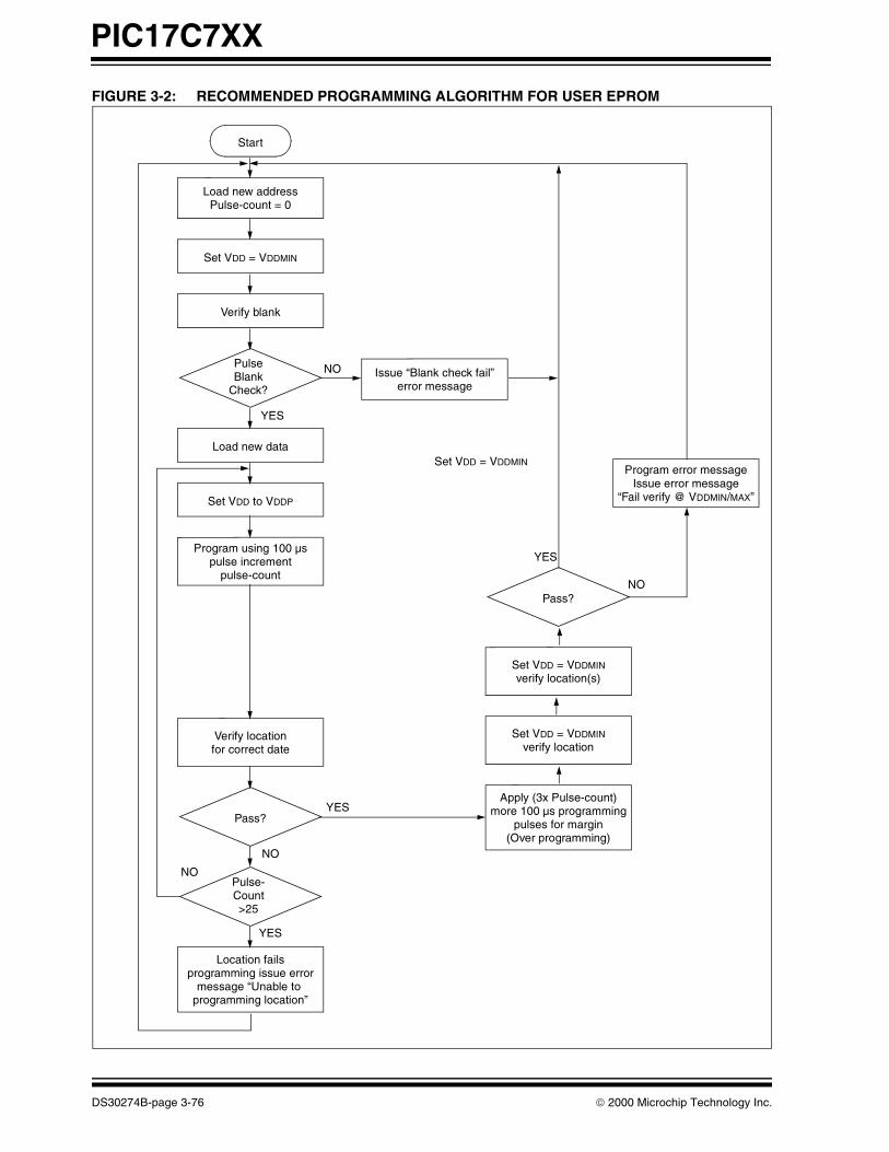
PIC17C7XX
DS30274B-page 3-76 2000 Microchip Technology Inc.
FIGURE 3-2: RECOMMENDED PROGRAMMING ALGORITHM FOR USER EPROM
Apply (3x Pulse-count)more 100 µs programming
pulses for margin(Over programming)
Start
Load new addressPulse-count = 0
Set VDD = VDDMIN
Verify blank
PulseBlank
Check?
Load new data
Set VDD to VDDP
Program using 100 µspulse increment
pulse-count
Verify locationfor correct date
Pass?
Pulse-Count>25
Location failsprogramming issue error
message “Unable to programming location”
Issue “Blank check fail”error message
Pass?
Set VDD = VDDMIN
verify location
Set VDD = VDDMIN
verify location(s)
Program error messageIssue error message
“Fail verify @ VDDMIN/MAX”
Set VDD = VDDMIN
YES
NO
NO
YES
YES
NO
NO
YES

2000 Microchip Technology Inc. DS30274B-page 3-77
PIC17C7XX
FIGURE 3-3: RECOMMENDED PROGRAMMING ALGORITHM FOR CONFIGURATION WORDS
Load new addressPulse-count = 0
Set VDD = VDDmin
Verify blank
Issue “blank check fail”
Load new data
Set VDD = VDDP
Set VDD = VDDmax
Set VDD = VDDmin Verify location for
Program using 100 µs
Location fails
Programming error:
NO
YES
NO
NO
YES
YES
Start
PassBlank
check?
pulse incrementpulse-count
Pass?
Issue error message“Fail verify @ VDDmin/max”
Verify location(s)
Pass?
NO
YES Pulsecount<100
programming, issue errormessage “Unable to
program location”
correct data
error message
Set VDD = VDDMIN
Set VDD = VDDminVerify location

PIC17C7XX
DS30274B-page 3-78 2000 Microchip Technology Inc.
4.0 SERIAL MODE PROGRAM ENTRY
4.1 Hardware Requirements
Certain design criteria must be taken into account forISP. Seven pins are required for the interface. Theseare shown in Table 4-1.
4.2 Serial Program Mode Entry
To place the device into the serial programming testmode, two pins will need to be placed at VIHH. Theseare the TEST pin and the MCLR/VPP pins. Also, the fol-lowing sequence of events must occur:
1. The TEST pin is placed at VIHH. 2. The MCLR/VPP pin is placed at VIHH.
There is a setup time between step 1 and step 2 thatmust be meet (See “Electrical Specifications for SerialProgramming Mode” on page 93.)
After this sequence the Program Counter is pointing toProgram Memory Address 0xFF60. This location is inthe Boot ROM. The code initializes the USART/SCI sothat it can receive commands. For this the device mustbe clocked. The device clock source in this mode is theRA1/T0CKI pin. Once the USART/SCI has been initial-ized, commands may be received. The flow is show inthese 3 steps:
1. The device clock source starts.2. Wait 80 device clocks for Boot ROM code
to configure the USART/SCI.3. Commands may be sent now.
TABLE 4-1: ISP Interface PinsDuring Programming
Name Function Type Description
RA4/RX/DT DT I/O Serial Data
RA5/TX/CK CK I Serial Clock
RA1/T0CKI OSCI I Device Clock Source
TEST TEST I Test mode selection control input. Force to VIHH,
MCLR/VPP MCLR/VPP P Programming Power
VDD VDD P Power Supply
VSS VSS P Ground

2000 Microchip Technology Inc. DS30274B-page 3-79
PIC17C7XX
4.3 Software Commands
This feature is similar to that of the PIC16CXXX mid-range family, but the programming commands havebeen implemented in the device Boot ROM. The BootROM is located in the program memory from 0xFF60 to0xFFFF. The ISP mode is entered when the TEST pinhas a VIHH voltage applied. Once in ISP mode, theUSART/SCI module is configured as a synchronousslave receiver, and the device waits for a command tobe received. The ISP firmware recognizes eight com-mands. These are shown in Table 4-2.
TABLE 4-2: ISP COMMANDS
4.3.1 RESET PROGRAM MEMORY POINTER
This is used to clear the address pointer to the ProgramMemory. This ensures that the pointer is at a knownstate as well as pointing to the first location in programmemory.
4.3.2 INCREMENT ADDRESS
This is used to increment the address pointer to theProgram Memory. This is used after the current locationhas been programmed (or read).
FIGURE 4-1: RESET ADDRESS POINTER COMMAND (PROGRAM/VERIFY)
FIGURE 4-2: INCREMENT ADDRESS COMMAND (PROGRAM/VERIFY)
Command Value
RESET PROGRAMMEMORY POINTER
0000 0000
LOAD DATA 0000 0010
READ DATA 0000 0100
INCREMENT ADDRSS 0000 0110
BEGIN PROGRAMMING 0000 1000
LOAD ADDRESS 0000 1010
READ ADDRESS 0000 1100
END PROGRAMMING 0000 1110
MCLR/VPPVIHH
RA1/T0CKI
Test
RA5 (Clock)
RA4 (Data)
1 2 3 4 5 6 7 8 1 2
0 0 0 0 0 0 0 0
PS2
Reset
RA4 = Input
Program/Verify Test Mode
PS6
VIHH
PS3
PS4PS5
PS1
(NEXT COMMAND)
MCLR/VPPVIHH
RA1/T0CKI
Test
RA5 (Clock)
RA4 (Data)
1 2 3 4 5 6 7 8 1 2
0 1 1 0 0 0 0 0
PS2
Reset
RA4 = Input
Program/Verify Test Mode
PS6
VIHH
PS3
PS4PS5
PS1
(NEXT COMMAND)

PIC17C7XX
DS30274B-page 3-80 2000 Microchip Technology Inc.
4.3.3 LOAD ADDRESS
This is used to load the address pointer to the ProgramMemory with a specific 16-bit value. This is useful whena specific range of locations are to be accessed.
4.3.4 READ ADDRESS
This is used so that the current address in the ProgramMemory pointer can be determined. This can be usedto increase the robustness of the ISP programming(ensure that the Program Memory pointers are still insync).
FIGURE 4-3: LOAD ADDRESS COMMAND
FIGURE 4-4: READ ADDRESS COMMAND
MCLR/VPPVIHH
RA1/T0CKI
Test
RA5 (Clock)
RA4 (Data)
1 2 3 4 5 6 7 8 1 2 3 15 16 1
0 1 0 1 0 0 0 0
PS2
Reset
RA4 = Input
Program/Verify Test Mode
PS7
VIHH
PS3
PS4PS5
PS1
PS6
(NEXT COMMAND)
MCLR/VPPVIHH
RA1/T0CKI
Test
RA5 (Clock)
RA4 (Data)
1 2 3 4 5 6 7 8 1 2 3 15 16 1
0 0 1 1 0 0 0 0
PS2
Reset
RA4 = Input
Program/Verify Test Mode
PS8
VIHH
PS3
PS4PS5
RA4 = Output
PS6
PS1
PS9
(NEXT COMMAND)
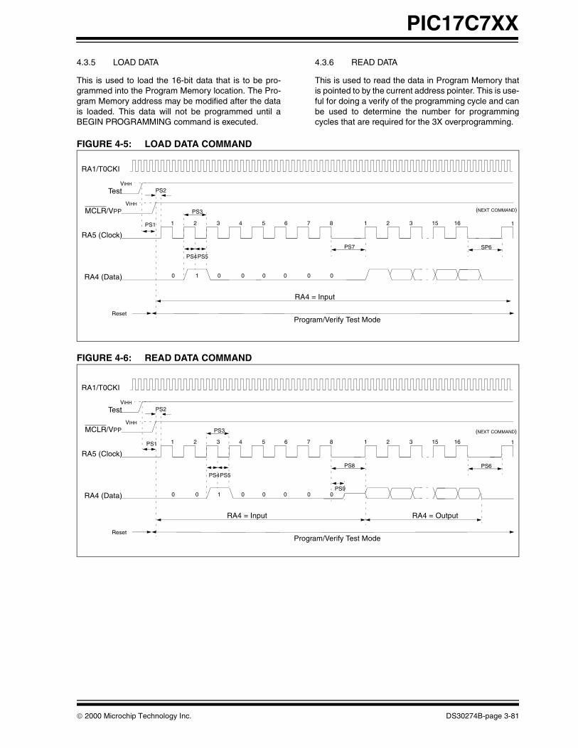
2000 Microchip Technology Inc. DS30274B-page 3-81
PIC17C7XX
4.3.5 LOAD DATA
This is used to load the 16-bit data that is to be pro-grammed into the Program Memory location. The Pro-gram Memory address may be modified after the datais loaded. This data will not be programmed until aBEGIN PROGRAMMING command is executed.
4.3.6 READ DATA
This is used to read the data in Program Memory thatis pointed to by the current address pointer. This is use-ful for doing a verify of the programming cycle and canbe used to determine the number for programmingcycles that are required for the 3X overprogramming.
FIGURE 4-5: LOAD DATA COMMAND
FIGURE 4-6: READ DATA COMMAND
MCLR/VPPVIHH
RA1/T0CKI
Test
RA5 (Clock)
RA4 (Data)
1 2 3 4 5 6 7 8 1 2 3 15 16 1
0 1 0 0 0 0 0 0
PS2
Reset
RA4 = Input
Program/Verify Test Mode
PS7
VIHH
PS3
PS4PS5
PS1
SP6
(NEXT COMMAND)
MCLR/VPPVIHH
RA1/T0CKI
Test
RA5 (Clock)
RA4 (Data)
1 2 3 4 5 6 7 8 1 2 3 15 16 1
0 0 1 0 0 0 0 0
PS2
Reset
RA4 = Input
Program/Verify Test Mode
PS8
VIHH
PS3
PS4PS5
RA4 = Output
PS6
PS1
PS9
(NEXT COMMAND)

PIC17C7XX
DS30274B-page 3-82 2000 Microchip Technology Inc.
4.3.7 BEGIN PROGRAMMING
This is used to program the current 16-bit data (lastdata sent with LOAD DATA Command) into the Pro-gram Memory at the address specified by the currentaddress pointer. The programming cycle time is speci-fied by specification P10. After this time has elapsed,any command must be sent, which wakes the proces-sor from the Long Write cycle. This command will bethe next executed command.
4.3.8 3X OVERPROGRAMMING
Once a location has been both programmed and veri-fied over a range of voltages, 3X overprogrammingshould be applied. In other words, apply three times thenumber of programming pulses that were required toprogram a location in memory, to ensure a solid pro-gramming margin.
This means that every location will be programmed aminimum of 4 times (1 + 3X overprogramming).
FIGURE 4-7: BEGIN PROGRAMMING COMMAND (PROGRAM)
MCLR/VPPVIHH
RA1/T0CKI
Test
RA5 (Clock)
RA4 (Data)
1 2 3 4 5 6 7 8 1 2
0 0 0 1 0 0 0 0
PS2
Reset
RA4 = Input
Program/Verify Test Mode
PS10
VIHH
PS3
PS4PS5
PS1
(NEXT COMMAND)
7 8

2000 Microchip Technology Inc. DS30274B-page 3-83
PIC17C7XX
FIGURE 4-8: RECOMMENDED PROGRAMMING FLOWCHART
ISP CommandINCREMENT ADDRESS
orLOAD ADDRESS
START
TEST = Vihh
MCLR = Vihh
N = 1
ISP Command RESET ADDRESS
ISP Command LOAD DATA
ISP CommandBEGIN PROGRAMMING
Wait approx 100 ms
ISP CommandREAD DATA
Data Correct? N = N + 1
N > 25?Report
ProgrammingFailure
ISP CommandBEGIN PROGRAMMING
Wait approx 100 ms
N = N - 1
N = 0?
Programmed allrequired locations?
4.75V < VDD < 5.25V
Start Device Clock (on RA0),
TEST = MCLR = RA4 = RA5 = Vss
YesNo
Wait 80 Device Clocks
N = 3N
Verify all Locations @ Vddmin
Data Correct?
Report
@ Vddmin
Verify all Locations @ Vddmax
DONE
Data Correct?VerifyError
Report
@ Vddmax
VerifyError
No
Yes
No
No
Yes
Yes
No
Yes
YesNo

PIC17C7XX
DS30274B-page 3-84 2000 Microchip Technology Inc.
5.0 CONFIGURATION WORDConfiguration bits are mapped into program memory.Each bit is assigned one memory location. In erasedcondition, a bit will read as ‘1’. To program a bit, theuser needs to write to the memory address. The data isimmaterial; the very act of writing will program the bit.The configuration word locations are shown inTable 5-3. The programmer should not program thereserved locations to avoid unpredictable resultsand to be compatible with future variations of thePIC17C7XX. It is also mandatory that configurationlocations are programmed in the strict order start-ing from the first location (0xFE00) and ending withthe last (0xFE0F). Unpredictable results may occurif the sequence is violated.
5.1 Reading Configuration Word
The PIC17C7XX has seven configuration locations(Table 5-1). These locations can be programmed (readas ‘0’) or left unprogrammed (read as ‘1’) to select var-ious device configurations. Any write to a configurationlocation, regardless of the data, will program that con-figuration bit. Reading any configuration locationbetween 0xFE00 and 0xFE07 will place the low byte ofthe configuration word (Table 5-2) into DAD<7:0>(PORTC). DAD<15:8> (PORTD) will be set to 0xFF.Reading a configuration location between 0xFE08 and0xFE0F will place the high byte of the configurationword into DAD<7:0> (PORTC). DAD<15:8> (PORTD)will be set to 0xFF.
TABLE 5-1: CONFIGURATION BIT PROGRAMMING LOCATIONS
TABLE 5-2: READ MAPPING OF CONFIGURATION BITS
Bit Address
FOSC0 0xFE00
FOSC1 0xFE01
WDTPS0 0xFE02
WDTPS1 0xFE03
PM0 0xFE04
PM1 0xFE06
BODEN 0xFE0E
PM2 0xFE0F
—=UnusedPM<2:0>, Processor Mode Select bits
111 = Microprocessor mode110 = Microcontroller mode101 = Extended Microcontroller mode000 = Code protected microcontroller mode
BODEN, Brown-out Detect Enable1 = Brown-out Detect Circuitry enabled0 = Brown-out Detect Circuitry disabled
WDTPS1:WDTPS0, WDT Prescaler Select bits.11 = WDT enabled, postscaler = 110 = WDT enabled, postscaler = 25601 = WDT enabled, postscaler = 6400 = WDT disabled, 16-bit overflow timerFOSC1:FOSC0, Oscillator Select bits
11 = EC oscillator10 = XT oscillator01 = RC oscillator00 = LF oscillator
WDTPS1 FOSC1 FOSC0WDTPS0PM0PM1 ——
PM2
11111111
11111111 BODEN PM2 PM2
89101112131415 01234567
PM2 PM2PM289101112131415 01234567
PM2

2000 Microchip Technology Inc. DS30274B-page 3-85
PIC17C7XX
5.2 Embedding Configuration Word Information in the Hex File
5.3 Reading From and Writing To a Code Protected Device
When a device is code-protected, writing to programmemory is disabled. If program memory is read, thevalue returned is the XNOR8 result of the actual pro-gram memory word. The XNOR8 result is the uppereight bits of the program memory word XNOR’d withthe lower eight bits of the same word. This 8-bit resultis then duplicated into both the upper and lower 8-bitsof the read value. The configuration word can alwaysbe read and written.
To allow portability of code, a PIC17C7XX programmer is required to read the configuration word locations from thehex file when loading the hex file. If the configuration word information was not present in the hex file, then a simplewarning message may be issued. Similarly, while saving a hex file, all configuration word information must be included.An option to not include the configuration word information may be provided. When embedding configuration wordinformation in the hex file, it should be to address FE00h.
Microchip Technology Inc. feels strongly that this feature is important for the benefit of the end customer.
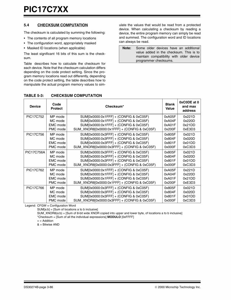
PIC17C7XX
DS30274B-page 3-86 2000 Microchip Technology Inc.
5.4 CHECKSUM COMPUTATION
The checksum is calculated by summing the following:
• The contents of all program memory locations• The configuration word, appropriately masked• Masked ID locations (when applicable)
The least significant 16 bits of this sum is the check-sum.
Table describes how to calculate the checksum foreach device. Note that the checksum calculation differsdepending on the code protect setting. Since the pro-gram memory locations read out differently, dependingon the code protect setting, the table describes how tomanipulate the actual program memory values to sim-
ulate the values that would be read from a protecteddevice. When calculating a checksum by reading adevice, the entire program memory can simply be readand summed. The configuration word and ID locationscan always be read.
Note: Some older devices have an additionalvalue added in the checksum. This is tomaintain compatibility with older deviceprogrammer checksums.
TABLE 5-3: CHECKSUM COMPUTATION
DeviceCode
ProtectChecksum*
BlankValue
0xC0DE at 0and maxaddress
PIC17C752 MP modeMC mode
EMC modePMC mode
SUM[0x0000:0x1FFF] + (CONFIG & 0xC05F)SUM[0x0000:0x1FFF] + (CONFIG & 0xC05F)SUM[0x0000:0x1FFF] + (CONFIG & 0xC05F)
SUM_XNOR8[0x0000:0x1FFF] + (CONFIG & 0xC05F)
0xA05F0xA04F0xA01F0x200F
0x221D0x220D0x21DD0xE3D3
PIC17C756 MP modeMC mode
EMC modePMC mode
SUM[0x0000:0x3FFF] + (CONFIG & 0xC05F)SUM[0x0000:0x3FFF] + (CONFIG & 0xC05F)SUM[0x0000:0x3FFF] + (CONFIG & 0xC05F)
SUM_XNOR8[0x0000:0x3FFF] + (CONFIG & 0xC05F)
0x805F0x804F0x801F0x000F
0x021D0x020D0x01DD0xC3D3
PIC17C756A MP modeMC mode
EMC modePMC mode
SUM[0x0000:0x3FFF] + (CONFIG & 0xC05F)SUM[0x0000:0x3FFF] + (CONFIG & 0xC05F)SUM[0x0000:0x3FFF] + (CONFIG & 0xC05F)
SUM_XNOR8[0x0000:0x3FFF] + (CONFIG & 0xC05F)
0x805F0x804F0x801F0x000F
0x021D0x020D0x01DD0xC3D3
PIC17C762 MP modeMC mode
EMC modePMC mode
SUM[0x0000:0x1FFF] + (CONFIG & 0xC05F)SUM[0x0000:0x1FFF] + (CONFIG & 0xC05F)SUM[0x0000:0x1FFF] + (CONFIG & 0xC05F)
SUM_XNOR8[0x0000:0x1FFF] + (CONFIG & 0xC05F)
0xA05F0xA04F0xA01F0x200F
0x221D0x220D0x21DD0xE3D3
PIC17C766 MP modeMC mode
EMC modePMC mode
SUM[0x0000:0x3FFF] + (CONFIG & 0xC05F)SUM[0x0000:0x3FFF] + (CONFIG & 0xC05F)SUM[0x0000:0x3FFF] + (CONFIG & 0xC05F)
SUM_XNOR8[0x0000:0x3FFF] + (CONFIG & 0xC05F)
0x805F0x804F0x801F0x000F
0x021D0x020D0x01DD0xC3D3
Legend: CFGW = Configuration WordSUM[a:b] = [Sum of locations a to b inclusive]SUM_XNOR8(a:b) = [Sum of 8-bit wide XNOR copied into upper and lower byte, of locations a to b inclusive]*Checksum = [Sum of all the individual expressions] MODULO [0xFFFF]+ = Addition& = Bitwise AND
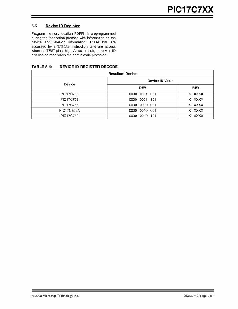
2000 Microchip Technology Inc. DS30274B-page 3-87
PIC17C7XX
5.5 Device ID Register
Program memory location FDFFh is preprogrammedduring the fabrication process with information on thedevice and revision information. These bits areaccessed by a TABLR0 instruction, and are accesswhen the TEST pin is high. As as a result, the device IDbits can be read when the part is code protected.
TABLE 5-4: DEVICE ID REGISTER DECODE
Resultant Device
DeviceDevice ID Value
DEV REV
PIC17C766 0000 0001 001 X XXXX
PIC17C762 0000 0001 101 X XXXX
PIC17C756 0000 0000 001 X XXXX
PIC17C756A 0000 0010 001 X XXXX
PIC17C752 0000 0010 101 X XXXX

PIC17C7XX
DS30274B-page 3-88 2000 Microchip Technology Inc.
6.0 PARALLEL MODE AC/DC CHARACTERISTICS AND TIMING REQUIREMENTS FOR PROGRAM/VERIFY TEST MODE
Standard Operating Conditions
Operating Temperature: +10°C ≤ TA ≤ +70°C, unless otherwise stated, (25°C is recommended)Operating Voltage: 4.5V ≤ VDD ≤ 5.25V, unless otherwise stated.
ParameterNo.
Sym. Characteristic Min. Typ. Max. Units Conditions/Comments
PD1 VDDP Supply voltage during pro-gramming
4.75 5.0 5.25 V
PD2 IDDP Supply current during pro-gramming
— — 50 mA Freq = 10MHz, VDD = 5.5V
PD3 VDDV Supply voltage during verify VDD min.
— VDD max.
V Note 2
PD4 VPP Voltage on VPP/MCLR pin during programming
12.75 — 13.25 V Note 1
PD6 IPP Programming current on VPP/MCLR pin
— 25 50 mA
P1 FOSCP Osc/clockin frequency dur-ing programming
4 — 10 MHz
P2 TCY Instruction cycle 1 — 0.4 µs TCY = 4/FOSCP
P3 TIRV2TSH RA0, RA1, RA2, RA3, RA4 setup before TEST↑
1 — — µs
P4 TTSH2MCH TEST↑ to MCLR↑ 1 — — µsP5 TBCV2IRH RC7:RC0, RB7:RB0 valid to
RA1 or RA0↑:Address/Data input setup time
0 — — µs
P6 TIRH2BCL RA1 or RA0↑ to RB7:RB0, RC7:RC0 invalid; Address
data hold time;
10 TCY — — µs
P7 T0CKIL2RBCZ RT↓ to RB7:RB0, RC7:RC0 hi-impedance
— — 8TCY
P8 T0CKIH2BCV RA1↑ to data out valid — — 10 TCY
P9 TPROG Programming pulse width 100 1000 µsP10 TIRH2IRL RA0, RA1 high pulse width 10 TCY — — µsP11 TIRL2IRH RA0, RA1 low pulse width 10 TCY — — µsP12 T0CKIV2INL RA1↑ before INT↓ (to go
from prog cycle to verify w/o increment)
0 — — µs
P13 TINL2RTL RA1 valid after RA0 (to select increment or no
increment going from pro-gram to verify cycle
10 TCY — — µs
P14 TVPPS VPP setup time before RA0↑ 100 — — µs Note 1 P15 TVPPH VPP hold time after INT↓ 0 — — µs Note 1 P16 TVDV2TSH VDD stable to TEST↑ 10 — — msP17 TRBV2MCH RB input (E1h) valid to VPP/
MCLR↑ 0 — — µs
P18 TMCH2RBI RB input (E1h) hold after VPP/MCLR↑
10TCY — — ns
P19 TVPL2VDL VDD power down after VPP power down
10 — — ms
Note 1: VPP/MCLR pin must only be equal to or greater than VDD at times other than programming. 2: Program must be verified at the minimum and maximum VDD limits for the part.

2000 Microchip Technology Inc. DS30274B-page 3-89
PIC17C7XX
FIGURE 6-1: PARALLEL MODE PROGRAMMING AND VERIFY TIMINGS I
Test
MC
LR
RA
1
RA
0
RB
<7:
0>
RC
<7:
0>
P4
P5
P18
INC
AD
DR
E1H
AD
DR
_HI
DAT
A_H
I OU
TD
ATA
_HI O
UT
DD
ATA
_HI O
UT
AD
DR
_LO
DAT
A_L
O O
UT
DAT
A_L
O O
UT
DAT
A_L
O O
UT
DAT
A_L
O O
UT
DAT
A_H
I OU
T
13V
5V
P14
P9
P15
P10
P11
P9
P7
P5
P6
Jum
p A
ddre
ssIn
put
Pro
gram
min
g
Mod
e E
ntry
Load
Add
ress
X
Ver
ify lo
catio
n X
Incr
emen
t Add
ress
to X
+ 1
by p
ulsi
ng R
A1
Ver
ify lo
catio
n X
+ 1
Pro
gram
loca
tion
X +
!
Do
not i
ncre
men
t PC
by r
aisi
ng R
A1
befo
re
RA
0
Ver
ify lo
catio
n X
+ 1
No
te:
RA
2 =
0R
A3
= 0
RA
4 =
1

PIC17C7XX
DS30274B-page 3-90 2000 Microchip Technology Inc.
FIGURE 6-2: PARALLEL MODE PROGRAMMING AND VERIFY TIMINGS II
Test
13V
5V
VP
P/M
CLR
RA
1
RA
0
RB
<7:
0>
RC
<7:
0>
E1H
AD
DR
_HI
DAT
A_H
I OU
TD
ATA
_HI_
IND
ATA
_HI_
IND
ATA
_HI_
IND
ATA
_HI O
UT
AD
DR
_LO
DAT
A_L
O O
UT
DAT
A_L
O O
UT
DAT
A_L
O_I
ND
ATA
_LO
_IN
DAT
A_L
O_I
N
P15
P9
P9
P9
Jum
p A
ddre
ssIn
put
Pro
gram
min
gm
ode
entr
yLo
ad a
ddre
ss X
Ver
ify lo
catio
n X
Pro
gram
loca
tion
X
Pro
gram
loca
tion
XM
ove
to v
erify
cyc
leP
reve
nt in
crem
ent o
fP
C b
y ra
isin
g R
A1
befo
re R
A0
Ver
ify lo
catio
n X
No
te:
RA
2 =
0R
A3
= 0
RA
4 =
1
P14

2000 Microchip Technology Inc. DS30274B-page 3-91
PIC17C7XX
FIGURE 6-3: PARALLEL MODE PROGRAMMING AND VERIFY TIMINGS III
P13
P13
P12
DAT
A_H
IOU
TD
ATA
_HI I
ND
ATA
_HI O
UT
DAT
A_H
I IN
DAT
A_H
I OU
TD
ATA
_HI I
N
DAT
A_LO
OU
TD
ATA
_LO
IND
ATA
_LO
OU
TD
ATA
_LO
IND
ATA
_LO
OU
TD
ATA
_LO
IN
Ver
ify lo
catio
n X
Pro
gram
loca
tion
XD
o no
t inc
rem
ent
PC
Rai
se R
A1
befo
reR
A0
to d
o th
is
Ver
ify lo
catio
n X
Pro
gram
loca
tion
XR
aise
RA
1 af
ter
RA
0to
incr
emen
t loc
atio
n X
+ 1
Ver
ify lo
catio
n X
+ 1
Pul
se R
A1
to in
crem
ent
addr
ess
to X
+ 2
Ver
ify lo
catio
n X
+ 2
RA
1
RA
0
RB
<7:
0>
RC
<7:
0>
INC
PC No
te:
Dev
ice
in P
GM
mod
eTe
st =
+6
VP
P/M
CLR
= V
PP
RA
2 =
0R
A3
= 0
RA
4 =
1
INC
PC
INC
PC

PIC17C7XX
DS30274B-page 3-92 2000 Microchip Technology Inc.
FIGURE 6-4: POWER-UP/DOWN SEQUENCE FOR PROGRAMMING
P16
P19
P3
P17
P18
E1H
VDD
VPP/MCLR
Test
RA4
RA2
RA3
RA0
RB<7:0>

2000 Microchip Technology Inc. DS30274B-page 3-93
PIC17C7XX
7.0 ELECTRICAL SPECIFICATIONS FOR SERIAL PROGRAMMING MODE
All parameters apply across the specified operating ranges unless otherwise noted.
Vcc = 2.5V to 5.5VCommercial (C): Tamb = 0° to +70°CIndustrial (I): Tamb = -40°C to +85°C
Parameter No.
Sym Characteristic Min Typ† Max Units Conditions
VIHH Programming Voltage on VPP/MCLR pin and TEST pin.
12.75 — 13.75 V
IPP Programming current on MCLR pin — 25 50 mA
FOSC Input OSC frequency on RA1 — — 8 MHz
TCY Instruction Cycle Time — 4/FOSC —
PS1 TVH2VH Setup time between TEST = VIHH and MCLR = VIHH
1 — — µs
PS2 TSER Serial setup time 20 — — TCY
PS3 TSCLK Serial Clock period 1 — — TCY
PS4 TSET1 Input Data Setup Time to serial clock ↓
15 — — ns
PS5 THLD1 Input Data Hold Time from serial clock ↓
15 — — ns
PS6 TDLY1 Delay between last clock ↓ to first clock ↑ of next command
20 — — TCY
PS7 TDLY2 Delay between last clock ↓ of com-mand byte to first clock ↑ of read of
data word
20 — — TCY
PS8 TDLY3 Delay between last clock ↓ of com-mand byte to first clock ↑ of write of
data word
30 — — TCY
PS9 TDLY4 Data input not driven to next clock input
1 — — TCY
PS10 TDLY5 Delay between last begin program-ming clock ↓ to last clock ↓ of next command (minimum programming
time)
100 — — µs
* These parameters are characterized but not tested.† Data in “Typ” column is at 5V, 25°C unless otherwise stated. These parameters are for design guidance only and are not
tested.

PIC17C7XX
DS30274B-page 3-94 2000 Microchip Technology Inc.
FIGURE 7-1: RESET ADDRESS POINTER COMMAND (PROGRAM/VERIFY)
FIGURE 7-2: INCREMENT ADDRESS COMMAND (PROGRAM/VERIFY)
MCLR/VPPVIHH
RA1/T0CKI
Test
RA5 (Clock)
RA4 (Data)
1 2 3 4 5 6 7 8 1 2
0 0 0 0 0 0 0 0
PS2
Reset
RA4 = Input
Program/Verify Test Mode
PS6
VIHH
PS3
PS4PS5
PS1
(NEXT COMMAND)
MCLR/VPPVIHH
RA1/T0CKI
Test
RA5 (Clock)
RA4 (Data)
1 2 3 4 5 6 7 8 1 2
0 1 1 0 0 0 0 0
PS2
Reset
RA4 = Input
Program/Verify Test Mode
PS6
VIHH
PS3
PS4PS5
PS1
(NEXT COMMAND)

2000 Microchip Technology Inc. DS30274B-page 3-95
PIC17C7XX
FIGURE 7-3: LOAD ADDRESS COMMAND
FIGURE 7-4: READ ADDRESS COMMAND
MCLR/VPPVIHH
RA1/T0CKI
Test
RA5 (Clock)
RA4 (Data)
1 2 3 4 5 6 7 8 1 2 3 15 16 1
0 1 0 1 0 0 0 0
PS2
Reset
RA4 = Input
Program/Verify Test Mode
PS7
VIHH
PS3
PS4PS5
PS1
PS6
(NEXT COMMAND)
MCLR/VPPVIHH
RA1/T0CKI
Test
RA5 (Clock)
RA4 (Data)
1 2 3 4 5 6 7 8 1 2 3 15 16 1
0 0 1 1 0 0 0 0
PS2
Reset
RA4 = Input
Program/Verify Test Mode
PS8
VIHH
PS3
PS4PS5
RA4 = Output
PS6
PS1
PS9
(NEXT COMMAND)
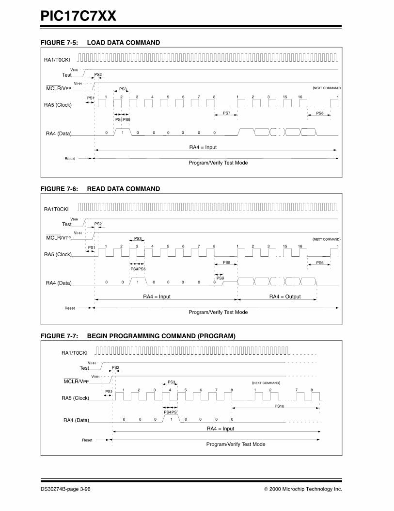
PIC17C7XX
DS30274B-page 3-96 2000 Microchip Technology Inc.
FIGURE 7-5: LOAD DATA COMMAND
FIGURE 7-6: READ DATA COMMAND
FIGURE 7-7: BEGIN PROGRAMMING COMMAND (PROGRAM)
MCLR/VPPVIHH
RA1/T0CKI
Test
RA5 (Clock)
RA4 (Data)
1 2 3 4 5 6 7 8 1 2 3 15 16 1
0 1 0 0 0 0 0 0
PS2
Reset
RA4 = Input
Program/Verify Test Mode
PS7
VIHH
PS3
PS4PS5
PS1
PS6
(NEXT COMMAND)
MCLR/VPPVIHH
RA1T0CKI
Test
RA5 (Clock)
RA4 (Data)
1 2 3 4 5 6 7 8 1 2 3 15 16 1
0 0 1 0 0 0 0 0
PS2
Reset
RA4 = Input
Program/Verify Test Mode
PS8
VIHH
PS3
PS4PS5
RA4 = Output
PS6
PS1
PS9
(NEXT COMMAND)
MCLR/VPPVIHH
RA1/T0CKI
Test
RA5 (Clock)
RA4 (Data)
1 2 3 4 5 6 7 8 1 2
0 0 0 1 0 0 0 0
PS2
Reset
RA4 = Input
Program/Verify Test Mode
PS10
VIHH
PS3
PS4PS
PS1
(NEXT COMMAND)
7 8

PIC18CXXXIn-Circuit Serial Programming for PIC18CXXX OTP MCUs
This document includes the programming specifications for the following devices:
1.0 PROGRAMMING THE PIC18CXXX
The PIC18CXXX can be programmed using a serialmethod. while in the users system. This allows forincreased design flexibility. This programming specifi-cation applies to PIC18CXXX devices in all packagetypes.
1.1 Hardware Requirements
The PIC18CXXX requires two programmable powersupplies, one for VDD (2.0V to 5.5V recommended) andone for VPP (12V to 14V). Both supplies should have aminimum resolution of 0.25V.
1.2 Programming Mode
The programming mode for the PIC18CXXX allowsprogramming of user program memory, special loca-tions used for ID, and the configuration word for thePIC18CXXX.
Pin Diagram
• PIC18C452• PIC18C252
• PIC18C242• PIC18C442
PIC
18C2X
X
RB7RB6RB5RB4RB3RB2RB1RB0/INTVDD
VSS
RD7RD6RD5RD4RC7RC6RC5RC4RD3RD2
MCLR/VPP
RA0RA1RA2RA3
RA4/T0CKIRA5RE0RE1RE2VDD
VSS
OSC1/CLKINOSC2/CLKOUT
RC0RC1RC2RC3RD0RD1
1234567891011121314151617181920
4039383736353433323130292827262524232221
PDIP, Windowed CERDIP
PDIP, SOIC, Windowed CERDIP (300 mil)
28
27
26
25
24
23
22
21
20
19
18
17
16
15
RB7
RB6
RB5
RB4
RB3
RB2
RB1
RB0/INT
VDD
VSS
RC7
RC6
RC5
RC4
• 1
2
3
4
5
6
7
8
9
10
11
12
13
14
MCLR/VPP
RA0
RA1
RA2
RA3
RA4/T0CKI
RA5
VSS
OSC1/CLKIN
OSC2/CLKOUT
RC0
RC1
RC2
RC3
PIC
18C4X
X
TABLE 1-1: PIN DESCRIPTIONS (DURING PROGRAMMING): PIC18C242/252/442/452
Pin NameDuring Programming
Pin Name Pin Type Pin Description
MCLR/VPP VPP P Programming Power
VDD VDD P Power Supply
Vss VSS P Ground
RB6 RB6 I Serial Clock
RB7 RB7 I/O Serial Data
Legend: I = Input, O = Output, P = Power
2000 Microchip Technology Inc. DS39028A-page 3-97

PIC18CXXX
2.0 IN-CIRCUIT SERIAL PROGRAMMING MODE (ICSP)
2.1 Introduction
Serial programming mode is entered by assertingMCLR/VPP = VIHH and RB6, RB7 = 0.
Instructions are fed into the CPU serially on RB7, andare shifted in on the rising edge of the serial clock pre-sented on RB6. Programming and verification are per-formed by executing TBLRD and TBLWT instructions.The address pointer to the program memory is simplythe table pointer. The address pointer can be incre-mented and decremented by executing table reads andwrites with auto-decrement and auto-increment.
2.2 ICSP OPERATION
In ICSP mode, instruction execution takes placethrough a serial interface using RB6 and RB7. RB7 isused to shift in instructions and shift out data from theTABLAT register. RB6 is used as the serial shift clockand the CPU execution clock. Instructions and dataare shifted in LSb first.
In this mode all instructions are shifted serially, thenloaded into the instruction register, and executed. Noprogram fetching occurs from internal or external pro-gram memory. 8-bit data bytes are read from theTABLAT register via the same serial interface.
2.2.1 4-BIT SERIAL INSTRUCTIONS
A set of 4-bit instructions are provided for ICSP mode,so that the most common instructions used for ICSPcan be fetched quickly, and thus reduce the amount oftime required to program a device. The 4-bit opcode isshifted in while the previous instruction fetched exe-cutes. The 4-bit instruction contains the lower 4-bits ofan instruction opcode. The upper 12-bits default as all0’s. Instructions with all 0’s in the upper byte of theinstruction word, are by default considered specialinstructions. The serial instructions are decoded asshown in Table 2-1:
TABLE 2-1: SPECIAL INSTRUCTIONS FOR SERIAL INSTRUCTION EXECUTION AND ICSP
Mnemonic,Operands
Description Cycles 4-Bit OpcodeStatus
Affected
NOP No Operation (Shift in16-bit instruction) 1 0000 None
TBLRD * Table Read (no change to TBLPTR) 2 1000 None
TBLRD *+ Table Read (post-increment TBLPTR) 2 1001 None
TBLRD *- Table Read (post-decrement TBLPTR) 2 1010 None
TBLRD +* Table Read (pre-increment TBLPTR) 2 1011 None
TBLWT * Table Write (no change to TBLPTR) 2 1100 None
TBLWT *+ Table Write (post-increment TBLPTR) 2 1101 None
TBLWT *- Table Write (post-decrement TBLPTR) 2 1110 None
TBLWT +* Table Write (pre-increment TBLPTR) 2 1111 None
Legend: Refer to the PIC18CXXX Data Sheet (DS39026) for opcode field descriptions.Note: All special instructions not included in this table are decoded as NOP’s
In-Circuit Serial Programming™ (ICSP) is a trademark of Microchip Technology Inc.
DS39028A-page 3-98 2000 Microchip Technology Inc.

PIC18CXXX
2.2.2 INITIAL SERIAL INSTRUCTION OPERATION
Upon ICSP mode entry, the CPU is idle. The executionof the CPU is governed by a state machine. The CPUclock source comes from RB6 which also acts as theserial shift clock. The first clock transition on RB6 isabsorbed after RESET. While the first instruction isbeing clocked in, a forced NOP is executed.
Following the FNOP instruction execution and the nextshifting in of the next instruction, the serial statemachine will do one of three things depending uponthe 4-bit instruction that was fetched:
1. If the instruction fetched was a NOP, the statemachine will suspend the CPU awaiting a 16-bitwide instruction to be shifted in.
2. If the instruction is a TBLWT, the state machinesuspends the CPU from execution while sixteenbits of data are shifted in as data for the TBLWTinstruction.
3. If the instruction is a TBLRD, then execution ofthe TBLRD instruction begins immediately foreight clock cycles, followed by eight clock cycleswhere the contents of the TABLAT register isshifted out onto RB7.
Once sixteen clock cycles have elapsed, the next 4-bitinstruction is fetched while the current instruction isexecuted. Each instruction type is described in latersections.
FIGURE 2-1: SERIAL INSTRUCTION TIMING AFTER RESET
Q1Q Cycles
P2
Q2 Q3 Q4 Q1 Q2 Q3 Q4
RB7 = Input or Output depending upon instruction
ICSP Mode
16-bit Instruction Load or Execute Instruction,Execute FNOPFetch 4-bit Instruction Fetch Next 4-bit
Q4Q1
MCLR/VPP
VIHH
P1
Reset
16-bit data Fetch orPerform TABLRD followed by shift data out Instruction
1 2 3 4 1 2 15 16 1 2 3 4
RB6 (Clock)P5 P5
3 4 65 7 8 9 10 12 13 1411
P4P3
P9
RB7 (Data) 1 1 0 11 1 0 1
(TBLWT **)
2000 Microchip Technology Inc. DS39028A-page 3-99

PIC18CXXX
2.2.3 NOP SERIAL INSTRUCTION EXECUTION
The NOP serial instruction is used to allow execution ofall other instructions not included in Table 2-1. Whenthe NOP instruction is fetched, the serial executionstate machine suspends the CPU for 16 clock cycles.During these 16 clock cycles, all 16-bits of an instruc-tion are fed into the CPU and the NOP instruction isdiscarded. Once all 16 bits have been shifted in thestate machine will allow the instruction to be executedfor the next 4 clock cycles.
2.2.4 ONE CYCLE 16-BIT INSTRUCTIONS
If the instruction fetched is a one cycle instruction,then the instruction operation will be completed in the4 clock cycles following the instruction fetched. Duringinstruction execution, the next 4-bit serial instruction isfetched (See Figure 2-2).
FIGURE 2-2: SERIAL INSTRUCTION TIMING FOR 1 CYCLE 16-BIT INSTRUCTIONS
Note: 16-bit TBLWT and TBLRD instructions arenot permitted. They will cause timing prob-lems with the serial state machine. If theuser wishes to perform a TBLWT or TBLRDinstruction, it must be performed as a 4-bitinstruction.
MCLR/VPP = VIHH
P5P3P4
Q1Q Cycles
2 3 1 2 3 15 16 1 2 3 4
P2
RB6 (Clock)
P5
Q2 Q3 Q4 Q1 Q2 Q3 Q4
RB7 = Input
ICSP Mode
16-bit Instruction Fetch Execute 16-bit Instruction,Execute PC-2,
1 4
Fetch NOP to enable16-bit Instruction fetch
Fetch Next Serial
4 5 6 7 8 9 10 11 12 13 14
Q4
4-bit Instruction
RB7 (Data) 1 1 0 10 0 0 0
DS39028A-page 3-100 2000 Microchip Technology Inc.

PIC18CXXX
FIGURE 2-3: 16-BIT 1 CYCLE SERIAL INSTRUCTION FLOW AFTER RESET
Start
Num_Clk = 1,
ClockTransition
RB6?
Yes
No
MCLR = VIHH
MCLR = VSS,RB6, RB7 = 0
Num_Clk = 1,
Execute 16-bit Instruction,
ClockTransition
RB6?
Yes
No
End
Shift(R) RB7Num_Clk = Num_Clk + 1
Num_Clk = 16?
ClockTransition
RB6?
Yes
Yes
No
No
Shift in 1st4-bit instruction,
Shift(R) RB7Num_Clk = Num_Clk + 1
and shift in next4-bit instruction,
Shift(R) RB7Num_Clk = Num_Clk + 1
4-bit instruction = NOP,Shift in 16-bit instruction,
Num_Clk = 1
2000 Microchip Technology Inc. DS39028A-page 3-101

PIC18CXXX
FIGURE 2-4: 16-BIT 1 CYCLE SERIAL INSTRUCTION FLOW
Start
Num_Clk = 1,
ClockTransition
RB6?
Yes
No
execute (PC - 2),
Num_Clk = 1,
execute 16-bit Instruction,
ClockTransition
RB6?
Yes
No
End
Shift(R) RB7Num_Clk = Num_Clk + 1
Num_Clk = 16?
ClockTransition
RB6?
Yes
Yes
No
No
and shift in next4-bit instruction,
Shift(R) RB7into ROMLAT<15>,
Num_Clk = Num_Clk + 1
and shift in next4-bit instruction,
Shift(R) RB7Num_Clk = Num_Clk + 1
4-bit instruction = NOP,Shift in 16-bit instruction,
Num_Clk = 1
DS39028A-page 3-102 2000 Microchip Technology Inc.

PIC18CXXX
2.3 Serial Instruction Execution For Two Cycle, One Word Instructions
When a NOP instruction is fetched, the serial executionstate machine suspends the CPU for 16 clock cycles.During these 16 clock cycles, all 16-bits of an instruc-tion are fed in and the NOP instruction is discarded.
If the instruction fetched is a two cycle, one wordinstruction, then the instruction operation will require asecond “dummy fetch” to be performed before theinstruction execution can be completed. The first cycleof the instruction will be executed in the 4 clock cyclesfollowing the instruction fetched. During the first cycleof instruction execution, the next 4-bit serial instructionis fetched. In order to perform the second half of thetwo cycle instruction, this 4-bit instruction loaded inmust be a NOP, so that state machine will remain idlefor the second half of the instruction. Following thefetch of the second NOP, the state machine will shift16-bits of data that will be discarded. After the 16-bitsof data is shifted in, the state machine will release theCPU, and allow it to perform the second half of the twocycle instruction. During the second half of the twocycle instruction execution, the next 4-bit instruction isloaded (See Figure 2-5).
FIGURE 2-5: 2 CYCLE 1 WORD 16-BIT INSTRUCTION SEQUENCE
Q Cycles
1 2 3 4 1 2 15 16
P5 P5
1 2 3 4
Q1 Q2 Q3 Q4
MCLR/VPP
RB7 = Input
ICSP Mode
P3P4
Execute PC-2 Fetch 16-bit Instruction
P2
RB6 (Clock)
Q1 Q2 Q3 Q4
Fetch 2nd 16-bit Execute 1st Cycle
P5
1 2 15 16
P5
1 2 3 4
Q1 Q2 Q3 Q4
Fetch 4-bit NOPExecute 2nd Cycle,Fetch 4-bit NOP,Fetch Next 4-bit InstructionOperand Word (discarded)
of 16-bit Instruction
RB7 (Data) 1 1 0 10 0 0 0
2000 Microchip Technology Inc. DS39028A-page 3-103
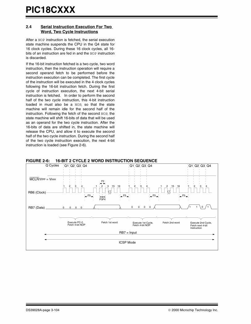
PIC18CXXX
2.4 Serial Instruction Execution For Two Word, Two Cycle Instructions
After a NOP instruction is fetched, the serial executionstate machine suspends the CPU in the Q4 state for16 clock cycles. During these 16 clock cycles, all 16-bits of an instruction are fed in and the NOP instructionis discarded.
If the 16-bit instruction fetched is a two cycle, two wordinstruction, then the instruction operation will require asecond operand fetch to be performed before theinstruction execution can be completed. The first cycleof the instruction will be executed in the 4 clock cyclesfollowing the 16-bit instruction fetch. During the firstcycle of instruction execution, the next 4-bit serialinstruction is fetched. In order to perform the secondhalf of the two cycle instruction, this 4-bit instructionloaded in must also be a NOP, so that the statemachine will remain idle for the second half of theinstruction. Following the fetch of the second NOP, thestate machine will shift 16-bits of data that will be usedas an operand for the two cycle instruction. After the16-bits of data are shifted in, the state machine willrelease the CPU, and allow it to execute the secondhalf of the two cycle instruction. During the second halfof the two cycle instruction execution, the next 4-bitinstruction is loaded (see Figure 2-6).
FIGURE 2-6: 16-BIT 2 CYCLE 2 WORD INSTRUCTION SEQUENCE
MCLR/VPP = VIHH
P5
P3P4
Q1Q Cycles
2 3 1 2 3 15 16 1 2 3 4 1 2 15 16 1 2 3 4
P2
RB6 (Clock)P5 P5 P5
Q2 Q3 Q4 Q1 Q2 Q3 Q4 Q1 Q2 Q3 Q4
RB7 = Input
ICSP Mode
Execute 1st Cycle,Execute PC-2, Execute 2nd Cycle,
1 4
Fetch 2nd wordFetch 1st wordFetch next 4-bit Fetch 4-bit NOP Fetch 4-bit NOPInstruction
RB7 (Data) 1 1 0 10 0 0 0 0 0 0 0
DS39028A-page 3-104 2000 Microchip Technology Inc.

PIC18CXXX
FIGURE 2-7: 16-BIT 2 CYCLE 2 WORD SERIAL INSTRUCTION FLOW AFTER RESET
Start
MCLR = VPP,RB6, RB7 = 0
Num_Clk = 1,
4-bit instruction = NOP,
Num_Clk = 1
Num_Clk = 16?
ClockTransition
RB6?
ClockTransition
RB6?
Yes
No
Yes
Yes
No
No
execute FNOP and shift in
Shift in 16-bit instruction,Num_Clk = 1
Num_Clk = 16?
ClockTransition
RB6?
Yes
Yes
No
No
Enable CPU,
Num_Clk = 1,
execute 1st cycle of 16-bit
ClockTransition
RB6?
Yes
No
execute 2nd cycle of 16-bit
End
MCLR = VIHH
Shift in 2nd 16-bit operand,
ClockTransition
RB6?
Yes
No
Shift(R) RB7,Num_Clk = Num_Clk + 1
instruction, and shift in next4-bit instruction,
4-bit instruction = NOP,
1st 4-bit instruction,
Shift(R) RB7,Num_Clk = Num_Clk + 1
Shift(R) RB7,Num_Clk = Num_Clk + 1
instruction, and shift innext 4-bit instruction
Num_Clk = 1
Shift(R) RB7,Num_Clk = Num_Clk + 1
Shift(R) RB7,Num_Clk = Num_Clk + 1
2000 Microchip Technology Inc. DS39028A-page 3-105

PIC18CXXX
FIGURE 2-8: 16-BIT 2 CYCLE 2 WORD SERIAL INSTRUCTION FLOW
Start
Num_Clk = 1,
Num_Clk = 16?
ClockTransition
RB6?
ClockTransition
RB6?
Yes
No
Yes
Yes
No
No
execute (PC-2)and shift in
Shift in 16-bit instruction,Num_Clk = 1
Num_Clk = 16?
ClockTransition
RB6?
Yes
Yes
No
No
Num_Clk = 1,
execute 1st cycle of 16-bit
ClockTransition
RB6?
Yes
No
execute 2nd cycle of 16-bit
End
ClockTransition
RB6?
Yes
No
Shift(R) RB7,Num_Clk = Num_Clk + 1
instruction, and shift in next4-bit instruction,
4-bit instruction = NOP,
4-bit instruction,
Shift(R) RB7,Num_Clk = Num_Clk + 1
Shift(R) RB7,Num_Clk = Num_Clk + 1
instruction, and shift innext 4-bit instruction
Num_Clk = 1
Shift(R) RB7,Num_Clk = Num_Clk + 1
Shift(R) RB7,Num_Clk = Num_Clk + 1
4-bit instruction = NOP,
Num_Clk = 1Shift in 2nd 16-bit operand,
DS39028A-page 3-106 2000 Microchip Technology Inc.

PIC18CXXX
2.5 TBLWT Instruction
The TBLWT instruction is a unique two cycle instruc-tion.
All forms of TBLWT instructions (post/pre-increment,post decrement, etc.) are encoded as 4-bit specialinstructions. This is useful as TBLWT instructions areused repeatedly in ICSP mode. A 4-bit instruction willminimize the total number of clock cycles required toperform programming algorithms.
The TBLWT instruction sequence operates as follows:
1. The 4-bit TBLWT instruction is read in by thestate machine on RB7 during the 4 clock cycleexecution of the instruction fetched previous tothe TBLWT (which is an FNOP if the TBLWT isexecuted following a reset).
2. Once the state machine recognizes that theinstruction fetched is a TBLWT, the statemachine proceeds to fetch in the 16-bits of datathat will be written into the program memorylocation pointed to by the TBLPTR.
3. The serial state machine releases the CPU toexecute the first cycle of the TBLWT instructionwhile the first 4 bits of the 16-bit data word areshifted in. After the first cycle of TBLWT instruc-tion has completed the state machine shifts inthe remaining 12 of the sixteen bits of data. Thedata word will not be used until the second cycleof the instruction.
4. After all 16-bits of data are shifted in and the firstcycle of the TBLWT is performed, the CPU isallowed to execute the second cycle of theTBLWT operation, programming the currentmemory location with the 16-bit value. The nextinstruction following the TBLWT instruction isshifted in during the execution of the secondcycle (See Figure 2-9).
The TBLWT instruction is used in ICSP mode to pro-gram the EPROM array. When writing a 16-bit valueto the EPROM, ID locations, or configuration locations,the device, RB6, must be held high for the appropriateprogramming time during the TBLWT instruction asspecified by parameter P9.
When RB6 is asserted low the device will cease pro-gramming the specified location.
After RB6 is asserted low, RB6 is held low for the timespecified by parameter P10, to allow high voltage dis-charge of the program memory array.
FIGURE 2-9: TBLWT INSTRUCTION SEQUENCE
MCLR/VPP = VIHH
Q Cycles
1 2 3 4 1 2 15 16 1 2 3 4
RB6 (Clock)P5 P5
Q1 Q2 Q3 Q4 Q1 Q2 Q3 Q4
RB7 = Input
ICSP Mode
Execute PC-2 Execute 2nd Cycle TBLWT
Load TBLWT Data
Fetch TBLWT
3 4 65 7 8 9 10 12 13 1411
Execute 1stCycle TBLWT
P2
P4P3
P9
and fetch next 4-bit
Q1 Q2 Q3 Q4
instruction
P10
RB7 (Data) 1 1 0 10 0 0 0 0 01 1
2000 Microchip Technology Inc. DS39028A-page 3-107

PIC18CXXX
FIGURE 2-10: TBLWT SERIAL INSTRUCTION FLOW AFTER RESET
Start
Num_Clk = 1,
4-bit instruction = TBLWT,
Begin Shifting in TBLWT data,Num_Clk = 1
ClockTransition
RB6?
Yes
No
Execute FNOP,
MCLR = VIHH
MCLR = VSS,RB6, RB7 = 0
Num_Clk = 1,
Num_Clk = 12?
ClockTransition
RB6?
Yes
Yes
No
No
End
Shift(R) RB7Num_Clk = Num_Clk + 1
Execute 1st cycle of TBLWT,
Num_Clk = 4?
ClockTransition
RB6?
Yes
Yes
No
No
and shift in 4-bitTBLWT instruction,
Shift(R) RB7Num_Clk = Num_Clk + 1
shift in last 12 bitsof TBLWT data,
Shift(R) RB7Num_Clk = Num_Clk + 1
Num_Clk = 1,
Execute 2nd cycle of TBLWT
ClockTransition
RB6?
Yes
No
instruction and shift in next4-bit instruction,
Shift(R) RB7Num_Clk = Num_Clk + 1
DS39028A-page 3-108 2000 Microchip Technology Inc.

PIC18CXXX
FIGURE 2-11: TBLWT SERIAL INSTRUCTION FLOW
Start
Num_Clk = 1,
4-bit instruction = TBLWT,
Begin Shifting in TBLWT data,Num_Clk = 1
ClockTransition
RB6?
Yes
No
Execute (PC-2),
Num_Clk = 1,
Num_Clk = 12?
ClockTransition
RB6?
Yes
Yes
No
No
End
Shift(R) RB7Num_Clk = Num_Clk + 1
Execute 1st cycle of TBLWT,
Num_Clk = 4?
ClockTransition
RB6?
Yes
Yes
No
No
and shift in 4-bitTBLWT instruction,
Shift(R) RB7Num_Clk = Num_Clk + 1
Shift in last 12 bitsof TBLWT data,
Shift(R) RB7Num_Clk = Num_Clk + 1
Num_Clk = 1,
Execute 2nd cycle of TBLWT
ClockTransition
RB6?
Yes
No
instruction and shift in next4-bit instruction,
Shift(R) RB7Num_Clk = Num_Clk + 1
2000 Microchip Technology Inc. DS39028A-page 3-109

PIC18CXXX
2.6 TBLRD Instruction
The TBLRD instruction is another unique two cycleinstruction.
All forms of TBLRD instructions (post/pre-increment,post decrement, etc.) are encoded as 4-bit specialinstructions. This is useful as TBLRD instructions areused repeatedly in ICSP mode. A 4-bit instruction willminimize the total number of clock cycles required toperform programming algorithms.
The TBLRD instruction sequence operates as follows:
1. The 4-bit TBLRD instruction is read in by thestate machine on RB7 during the 4 clock cycleexecution of the instruction fetched previous tothe TBLRD (which is an FNOP if the TBLRD isexecuted following a reset).
2. Once the state machine recognizes that theinstruction fetched is a TBLRD, the statemachine releases the CPU and allows execu-tion of the first and second cycles of the TBLRDinstruction for eight clock cycles. When theTBLRD is performed, the contents of the pro-gram memory byte pointed to by the TBLPTR isloaded into the TABLAT register.
3. After eight clock cycles have transitioned onRB6, and the TBLRD instruction has completed,the state machine will suspend the CPU for eightclock cycles. During these eight clock cycles,the state machine configures RB7 as an output,and will shift out the contents of the TABLAT reg-ister onto RB7 LSb first.
4. When the state machine has shifted out all eightbits of data, the state machine suspends theCPU to allow an instruction pre-fetch. Four (4)clock cycles are required on RB6 to shift in thenext 4-bit instruction.
FIGURE 2-12: TBLRD INSTRUCTION SEQUENCE
MCLR/VPP = VIHH
Q Cycles
1 2 3 4 1 2 3 4
RB6 (Clock)
P5
Q1 Q2 Q3 Q4 Q1 Q2 Q3 Q4
RB7 (Data)
RB7 = Input
ICSP Mode
Execute PC-2 Execute Cycle 2Execute Cycle 1 Shift Data Out From TABLAT
P6
RB7 = Output
1 2 3 4
Q1 Q2 Q3 Q4
1 2 3 4
P5
Fetch TBLRD
1 2 3 5 7 864
TBLRD TBLRDNo Execution takes place,Fetch Next 4-bit instruction
1 0 0 1 1 0 0 1
RB7 = Input
LSb MSb1 2 3 4 5 6
DS39028A-page 3-110 2000 Microchip Technology Inc.

PIC18CXXX
FIGURE 2-13: TBLRD SERIAL INSTRUCTION FLOW AFTER RESET
Start
Num_Clk = 1,
Enable CPU,
cycle TBLRD instruction
ClockTransition
RB6?
Yes
No
Execute FNOP,
MCLR = VIHH
MCLR = VSS,RB6, RB7 = 0
Shift out 8-bits
End
Shift(R) RB7Num_Clk = Num_Clk + 1
execute 1st and 2nd
Num_Clk = 8?
ClockTransition
RB6?
Yes
Yes
No
No
and shift in 4-bitTBLRD instruction,
TBLRD instruction execution
Num_Clk = Num_Clk + 1
of data to RB7
Num_Clk = 8?
ClockTransition
RB6?
Yes
Yes
No
No
Shift(R) TABLAT<0>out onto RB7
Num_Clk = Num_Clk + 1
4-bit instructionShift in next
Num_Clk = 4?
ClockTransition
RB6?
Yes
Yes
No
No
Shift(R) RB7Num_Clk = Num_Clk + 1
takes place here
2000 Microchip Technology Inc. DS39028A-page 3-111
PIC18CXXX
FIGURE 2-14: TBLRD SERIAL INSTRUCTION FLOW
Start
Num_Clk = 1,
cycle TBLRD instruction
ClockTransition
RB6?
Yes
No
Execute (PC-2),
Shift out 8-bits
End
Shift(R) RB7Num_Clk = Num_Clk + 1
Execute 1st and 2nd
Num_Clk = 8?
ClockTransition
RB6?
Yes
Yes
No
No
and shift in 4-bitTBLRD instruction,
of data to RB7
Num_Clk = 8?
ClockTransition
RB6?
Yes
Yes
No
No
4-bit instructionShift in next
Num_Clk = 4?
ClockTransition
RB6?
Yes
Yes
No
No
Shift(R) RB7Num_Clk = Num_Clk + 1
Shift(R) TABLAT<0>out onto RB7
Num_Clk = Num_Clk + 1
TBLRD instruction execution
Num_Clk = Num_Clk + 1takes place here
DS39028A-page 3-112 2000 Microchip Technology Inc.

PIC18CXXX
2.6.1 SOFTWARE COMMANDS
ICSP commands of the PICmicro® MCU are supportedin the PIC18CXXX family by simply combining CPUinstructions. Once in In-Circuit Serial Programming(ICSP) mode, the instructions are loaded into a shiftregister, and the device waits for a command to bereceived. The ICSP commands for the PIC16CXXXfamily are now “pseudo-commands” and are shown inTable 2-2. The following sections are a description ofhow the pseudo-commands can be implemented usingCPU instructions.
TABLE 2-2: ICSP PSEUDO COMMAND MAPPING
ICSP Command Golden Gate Instructions
Load Configuration MOVLW#Address1
MOVWFTBLPTRL
MOVLW#Address2
MOVWFTBLPTRH
MOVLW#Address3
MOVWFTBLPTRU
Load Data Not needed. Data encoded in 4-bit TBLWT instruction sequence.
Read Data TBLRD instruction
Increment Address Not needed. Use TBLWT with increment/decrement (TBLWT *+/*-).
Load Address MOVLW#Addr_low
MOVWFTBLPTRL
MOVLW#Addr_high
MOVWFTBLPTRH
MOVLW#Addr_upper
MOVWFTBLPTRU
Reset Address MOVLW#Data
MOVWFTBLPTRH
MOVWFTBLPTRL
MOVWFTBLPTRU
Begin programming TBLWT
End Programming Not needed. Programming will cease at the end of TBLWT execution.
2000 Microchip Technology Inc. DS39028A-page 3-113

PIC18CXXX
2.6.2 RESET ADDRESS
A reset of the program memory pointer is a write to theupper, high, and low bytes of the TBLPTR. To reset theprogram memory pointer, the following instructionsequence is used.
NOP ;(4-BIT INSTRUCTION)MOVLW 00hNOP ;(4-BIT INSTRUCTION)MOVWF TBLPTRU, 0NOP ;(4-BIT INSTRUCTION)MOVWF TBLPTRH, 0NOP ;(4-BIT INSTRUCTION)MOVWF TBLPTRL, 0
DS39028A-page 3-114 2000 Microchip Technology Inc.

PIC18CXXX
FIGURE 2-15: RESET ADDRESS SERIAL INSTRUCTION SEQUENCE
Start
Num_Clk = 4?
Yes
No
execute (PC - 2),
End
Shift(R) RB7into Shift Reg<3>,
Num_Clk = Num_Clk + 1
Num_Clk = 16?
Yes
No
shift in next 4-bit instruction, Shift in 16-bit MOVWF instruction,Num_Clk = 1
4-bit instruction = NOP,
Num_Clk = 1,
Num_Clk = 4?
Yes
No
Num_Clk = 16?
Yes
No
Num_Clk = 1,
Execute MOVLW Instruction,shift in 4-bit NOP instruction,
Num_Clk = 1,
execute MOVWF Instruction,shift in 4-bit NOP instruction,
On rising edge RB6
Shift(R) RB7into Shift Reg<15>,
Num_Clk = Num_Clk + 1
On rising edge RB6
Shift(R) RB7into Shift Reg<3>,
Num_Clk = Num_Clk + 1
On rising edge RB6
Shift(R) RB7into Shift Reg<15>,
Num_Clk = Num_Clk + 1
On rising edge RB6
Shift in 16-bit MOVWF instruction,Num_Clk = 1
4-bit instruction = NOP,
Num_Clk = 16?
Yes
No
Shift(R) RB7into Shift Reg<15>,
Num_Clk = Num_Clk + 1
On rising edge RB6
Num_Clk = 1,
Execute MOVWF Instruction,shift in next 4-bit instruction,
Num_Clk = 4?
Yes
No
Shift(R) RB7into Shift Reg<3>,
Num_Clk = Num_Clk + 1
On rising edge RB6
(NOP)
(NOP)
(NOP)
(NOP)
(NOP)
MOVLW 00h
MOVWF TBLPTRM,0
MOVWF TBLPTRM,0
(NOP)
4-bit instruction = NOP,
Num-Clk = 1Shift in 16-bit MOVLW instruction,
2000 Microchip Technology Inc. DS39028A-page 3-115

PIC18CXXX
2.6.3 LOAD ADDRESS
This is used to load the address pointer to the ProgramMemory with a specific 22-bit value. This is useful whena specific range of locations are to be accessed. Toload the address into the table pointer, the followingcommands must be used:
NOP ; 4-bit instructionMOVLW Low_AddressNOP ; 4-bit instructionMOVWF TBLPTRL, 0NOP ; 4-bit instructionMOVLW High_AddressNOP ; 4-bit instructionMOVWF TBLPTRH, 0NOP ; 4-bit instructionMOVLW Upper_AddressNOP ; 4-bit instructionMOVWF TBLPTRU, 0
DS39028A-page 3-116 2000 Microchip Technology Inc.
PIC18CXXX
FIGURE 2-16: LOAD ADDRESS SERIAL INSTRUCTION SEQUENCE
Start
Num_Clk = 4?
Shift in 16-bit MOVLW instruction,Num_Clk = 1
Yes
No
execute (PC - 2),
End
Shift(R) RB7into Shift Reg<3>,
Num_Clk = Num_Clk + 1
4-bit instruction = NOP,
Num_Clk = 16?
Yes
No
shift in next 4-bit instruction, Shift in 16-bit MOVWF instruction,Num_Clk = 1
4-bit instruction = NOP,
Num_Clk = 1,
Num_Clk = 4?
Yes
No
Num_Clk = 16?
Yes
No
Num_Clk = 1,
execute MOVLW Instruction,shift in 4-bit NOP instruction,
Num_Clk = 1,
execute MOVWF Instruction,shift in 4-bit NOP instruction,
On rising edge RB6
Shift(R) RB7into Shift Reg<15>,
Num_Clk = Num_Clk + 1
On rising edge RB6
Shift(R) RB7into Shift Reg<3>,
Num_Clk = Num_Clk + 1
On rising edge RB6
Shift(R) RB7into Shift Reg<15>,
Num_Clk = Num_Clk + 1
On rising edge RB6
Shift in 16-bit MOVWF instruction,Num_Clk = 1
4-bit instruction = NOP,
Num_Clk = 16?
Yes
No
Shift(R) RB7into Shift Reg<15>,
Num_Clk = Num_Clk + 1
On rising edge RB6
Num_Clk = 1,
execute MOVWF Instruction,shift in next 4-bit instruction,
Num_Clk = 4?
Yes
No
Shift(R) RB7into Shift Reg<3>,
Num_Clk = Num_Clk + 1
On rising edge RB6
(NOP)
(NOP)
MOVLWLOW_Address
MOVWFTBLPTRL,0
MOVLWHIGH_Address
(NOP)
2000 Microchip Technology Inc. DS39028A-page 3-117

PIC18CXXX
2.6.4 ICSP BEGIN PROGRAMMING
Programming is performed by executing a TBLWTinstruction. In ICSP mode the TBLWT instructionsequence will include 16-bits of data that are shiftedinto a data buffer, and then written to the word locationthat is addressed by the TBLPTR. Although theTBLPTR addresses the program memory on a bytewide boundary, all 16-bits of data that are shifted in dur-ing the TBLWT sequence are written at once. The16-bits are shifted into the TABLAT and buffer registers.The TBLPTR points to the word that will be pro-grammed; it can point to either the high or the low byte.(See Figure 2-17).
The sequence for programming a location could occuras follows:
1. Setup the TLBPTR with the first ok address tobe programmed (even or odd byte).
2. Shift in a 4 bit TBLWT instruction.3. 16-bits of data are then shifted in for program-
ming both high and low byte of the first pro-grammed location.
4. Execute TBLWT instruction to program location.5. Verify high byte (odd address) by executing
TLBRD *- (post-decrement). (If TBLPTR point-ing at odd address.)
6. Verify low byte (even address) by executingTLBRD *+ (post-increment). TBLPTR is point-ing to odd address again.
7. If location doesn’t verify, go back to step 4.
8. If location does verify, begin 3x overprogram-ming.
The TBLWT instruction offers flexibility with multipleaddressing modes: pre-increment, post-increment,post decrement, and no change of the TBLPTR. Thesemodes eliminate the need for the increment addresscommand sequence.
FIGURE 2-17: DATA BUFFERING SCHEME FOR ICSP
Buffer Register
Program Memorybank 0(Even Address)
Program Memorybank 1(Odd Address)
TBLWTOdd or Even
TBLWTOdd or Even
TBLRD
TABLAT Register
addressaddress
EvenOddTBLRD
RB7
Data shifted intoTABLAT andBuffer registers
DS39028A-page 3-118 2000 Microchip Technology Inc.

PIC18CXXX
2.6.5 PROGRAMMING INSTRUCTION SEQUENCE
The series of instructions needed to execute a pro-gramming sequence is as follows. Many of the instruc-tion sequences used in the following example are alsoshown in previous sections.
NOP ; 4-bit instruction; Set up low byte ; of program address
MOVLW Low_Byte_Address ; = 00NOP ; 4-bit instructionMOVWF TBLPTRL, 0NOP ; 4-bit instruction
; Set up high byte ; of program; address
MOVLW High_Byte_Address ; = 00NOP ; 4-bit instructionMOVWF TBLPTRH, 0NOP ; 4-bit instruction
; Set up upper byte; of program ; address
MOVLW Upper_Byte_Address; = 00NOP ; 4-bit instructionMOVWF TBLPTRU, 0 ; Program data byte
; included in TBLWT; instruction; sequence
TBLWT+* ; TBLPTR = 000000h
A write of a program memory location with an odd or aneven address causes a long write cycle in ICSP mode.The 16-bit data is encoded in the TBLWT sequence andis loaded into the temporary buffer register for wordwide writes.
The user must wait 100 µs for the long write to com-plete before the next instruction is executed.
2.6.6 VERIFY SEQUENCE
The table pointer = 000001h in the last example. ATBLRD will then read the odd address byte of the cur-rent program word address location first. The verifysequence will be as follows:
; Read/verify high byte firstTBLRD*-
; TBLPTR = 0000 post-dec; Read/verify low byte
TBLRD*
The first TBLRD decrements the table pointer to point tothe even address byte of the current program word.After the first and second cycle of the TBLRD are per-formed, all 8-bits of data are shifted out on RB7. Thefetch of the second TBLRD occurs on the next 4 clockcycles. The second TBLRD does not modify the tablepointer address. This allows another programmingcycle (TBLWT+*) to take place if the verify doesn’tmatch the program data without having to update thetable pointer.
If the contents of the verify do not match the intendedprogram data word, then the TBLWT instruction must berepeated with the correct contents of the current pro-gram word. Therefore, only one instruction needs to beperformed to repeat the programming cycle:
TBLWT+*
2.6.7 3X OVER PROGRAMMING
Once a location has been both programmed and veri-fied over a range of voltages, 3x over programmingshould be applied. In other words, apply three times thenumber of programming pulses that were required toprogram a location in memory, to ensure a solid pro-gramming margin.
This means that every location will be programmed aminimum of 4 times (1 + 3x over programming).
2000 Microchip Technology Inc. DS39028A-page 3-119

PIC18CXXX
FIGURE 2-18: DETAILED PROGRAMMING FLOW CHART – PROGRAM MEMORY
Start
Execute MOVLW for 4 clock cycles
MCLR = VPP,RB6, RB7 = 0
Execute FNOPfor four clock cycles
Shift in last 12-bits of datafor 12 clock cycles
Hold CPU,Shift in TBLRD *for 4 clock cycles
Execute 1st cycle TBLWT +*, and shift in
Wait 100 µsec toensure programming
A
Execute 2nd cycle TBLWT +* for 4 clock cycles
Shift in TBLRD *-for 4 clock cycles
N = 0
Execute 1st and 2nd cycle TBLRD *- for 8 clock cycles
Shift Data Outfor 8 clock cycles
Verify?
No
Yes
N = N + 1
N > 25?Yes
NoReport
ProgrammingFailure
shift in 4-bit NOP
Shift in 16-bit MOVLW Low_Addrinstruction for 16 clock cycles
4-bit instruction = NOP,
and shift in 4-bit NOP
Shift in 16-bit MOVLW High_Addrinstruction for 16 clock cycles
4-bit instruction = NOP,
Execute MOVLW for 4 clock cycles
and shift in 4-bit NOP
Execute MOVWFfor 4 clock cycles
Shift in 16-bit MOVWF TBLPTRLinstruction for 16 clock cycles
4-bit instruction = NOP,
and shift in 4-bit NOP
Shift in 16-bit MOVWF TBLPTRHinstruction for 16 clock cycles
4-bit instruction = NOP,
first 4-bits of datafor 4 clock cycles
Execute 1st and 2nd cycle TBLRD * for 8 clock cycles
Shift Data Outfor 8 clock cycles
B
Shift in 16-bit MOVLW Upper_Addrinstruction for 16 clock cycles
4-bit instruction = NOP,
Execute MOVLW for 4 clock cycles
and shift in 4-bit NOP
Execute MOVWFfor 4 clock cycles
and shift in 4-bit NOP
Shift in 16-bit MOVWF TBLPTRUinstruction for 16 clock cycles
4-bit instruction = NOP,
Execute current instruction for 4 clock cycles, andshift in 4-bit TBLWT+*
Hold RB6Clock high
Clock Lowfor Discharge
Hold RB6Clock high (P10)
DS39028A-page 3-120 2000 Microchip Technology Inc.

PIC18CXXX
FIGURE 2-19: DETAILED PROGRAMMING FLOW CHART – PROGRAM MEMORY (CONTINUED)
A
Execute current instruction,Shift in TBLWT *+for 4 clock cycles
N = 1?
Yes
No
N = 3 * N
All locations
No
Yesprogrammed?
To B
Wait 100 µsec toensure programming
Report
@ VDDMIN
VerifyError
Report
@ VDDMAX
VerifyError
No
No
Yes
Yes
End
Verify all Locations @ VDDMIN
Data Correct?
Verify all Locations @ VDDMAX
Data Correct?
N = N - 1
Execute 1st cycle TBLWT *+ or *, and shift in
first 4-bits of datafor 4 clock cycles
Shift in last 12-bits of datafor 12 clock cycles
Execute 2nd cycle TBLWT * for 4 clock cycles
Shift in TBLWT *for 4 clock cycles
Execute 2nd cycle TBLWT * for 4 clock cycles
Shift in TBLWT *+for 4 clock cycles
Shift in last 12-bits of datafor 12 clock cycles
Execute current instruction for 4 clock cycles, andshift in 4-bit TBLRD+*
Hold RB6 high
Wait 100 µS
Hold RB6 high
Clock Lowfor Discharge
2000 Microchip Technology Inc. DS39028A-page 3-121

PIC18CXXX
2.6.8 LOAD CONFIGURATION
The Configuration registers are located in ok memory,and are only addressable when the high address bit ofthe TBLPTR (bit 21) is set. Test program memory con-tains test memory, configuration registers, calibrationregisters, and ID locations. The desired address mustbe loaded into all three bytes of the table pointer to pro-gram specific ID locations or the configuration bits. Toprogram the configuration registers, the followingsequence must be followed:
NOP ; 4-bit instruction ; shift in 16-bit ; MOVLW instruction
MOVLW 03hNOP ; 4-bit instruction
; shift in 16-bit ; MOVWF instruction ; Enable Test memory
MOVWF TBLPTRU, 0NOP ; 4-bit instruction
; shift in 16-bit ; MOVLW instruction
MOVLW Low_Config_AddressNOP ; 4-bit instruction
; shift in 16-bit ; MOVWF instruction
MOVWF TBLPTRL, 0NOP ; 4-bit instruction
; shift in 16-bit ; MOVLW instruction
MOVLW ; High_Config_AddressNOP ; 4-bit instruction
; shift in 16-bit ; MOVWF instruction
MOVWF TBLPTRH, 0NOP ; 4-bit instruction
; shift in 16-bit ; MOVLW instruction
TBLWT *+; 16-bits of data are; shifted in for write; of config1L and ; config1H TBLWT is a; 4-bit special ; instruction Wait ; 100 µsec for programming
2.6.9 END PROGRAMMING
When programming occurs, 16 bits of data are pro-grammed into memory. The 16-bits of data are shiftedin during the TBLWT sequence. After the programmingcommand (TBLWT) has been executed, the user mustwait for 100 µs until programming is complete, beforeanother command can be executed by the CPU. Thereis no command to end programming.
RB6 must remain high for as long as programming isdesired. When RB6 is lowered programming will cease.
After the falling edge occurs on RB6, RB6 must be heldlow for a period of time so that a high voltage dischargecan be performed to ensure that the program array isn’tstressed at high voltage during execution of the nextinstruction. The high voltage discharge will occur whileRB6 is low following the programming time.
DS39028A-page 3-122 2000 Microchip Technology Inc.

PIC18CXXX
FIGURE 2-20: SYMBOLIC PROGRAMMING FLOW CHART – CONFIG WORD / ID LOCATION
ICSP CommandINCREMENT ADDRESS
START
MCLR = VIHH
N = 0
ICSP Command LOAD CONFIGURATION
Program ID Loc?
Report Programming
Failure
ICSP CommandBEGIN PROGRAMMING
Wait approx 100 µs
N = N - 1
4.75V < VDD < 5.25VMCLR = VSS
No
N = 3N
No
Yes
No
Address = 300000h
N > 25?
ICSP Command LOAD DATA
Address = 300000h?
ICSP CommandLOAD ADDRESS
Address = 300000h
ICSP CommandBEGIN PROGRAMMING
Wait approx 100 µs
ICSP CommandREAD DATA
Data Correct?
Yes
ICSP Command LOAD DATA
ICSP CommandBEGIN PROGRAMMING
Wait approx 100 µs
N = N - 1
N = 0?
N = 100
No
Data Correct? Report
ProgrammingFailure
Yes
ICSP CommandREAD DATA
Verify all Locations @ VDDMIN
Data Correct?
Verify all Locations @ VDDMAX
Data Correct?
DONE
Report
@ VDDMIN
VerifyError
Report
@ VDDMAX
VerifyError
No
No
Yes
Yes
Yes
N = 0
N = 0?
2000 Microchip Technology Inc. DS39028A-page 3-123

PIC18CXXX
FIGURE 2-21: DETAILED PROGRAMMING FLOW CHART – CONFIG WORD
START
MCLR = VIHH
4.75V < VDD < 5.25VMCLR = VSS
N = 99
Wait 100 µsec toensure programming
N = N - 1
Execute FNOPfor four clock cycles
shift in 4-bit NOP
Shift in 16-bit MOVLW 00instruction for 16 clock cycles
4-bit instruction = NOP,
Execute MOVLW for 4 clock cycles
and shift in 4-bit NOP
Shift in 16-bit MOVWF TBLPTRHinstruction for 16 clock cycles
4-bit instruction = NOP,
Execute MOVWF for 4 clock cycles
and shift in 4-bit NOP
Shift in 16-bit MOVLW 00instruction for 16 clock cycles
4-bit instruction = NOP,
Execute MOVLW for 4 clock cycles
and shift in 4-bit NOP
Shift in 16-bit MOVWF TBPLTRLinstruction for 16 clock cycles
4-bit instruction = NOP,
Execute last fetched inst.for 4 clock cycles
and shift in 4-bit TBLWT+*
TBPLTR = 0x300000h
Shift in last 12-bits of datafor 12 clock cycles
Execute 1st cycle TBLWT, and shift in
Execute 2nd cycle TBLWT for 4 clock cycles
Shift in TBLWT *for 4 clock cycles
first 4-bits of config. reg.for 4 clock cycles
CONFIG1L and CONFIG1H
N = 1?
Execute 2nd cycle TBLWT* for 4 clock cycles
Shift in TBLWT *-for 4 clock cycles
Shift in 16-bit MOVLW 30instruction for 16 clock cycles
4-bit instruction = NOP,
Execute MOVLW for 4 clock cycles
and shift in 4-bit NOP
Shift in 16-bit MOVWF TBLPTRUinstruction for 16 clock cycles
4-bit instruction = NOP,
Execute MOVWF for 4 clock cycles
and shift in 4-bit NOP
A
B
Yes
No
Wait 100 µsec toensure programming
Clock Lowfor Discharge
RB6 High
DS39028A-page 3-124 2000 Microchip Technology Inc.
PIC18CXXX
FIGURE 2-22: DETAILED PROGRAMMING FLOW CHART – CONFIG WORD
Shift in TBLRD*+for 4 clock cycles
Execute 1st and 2nd cycle TBLRD*+ for 8 clock cycles
Shift Data Outfor 8 clock cycles
Execute 1st and 2nd cycle TBLRD*+ for 8 clock cycles
Shift Data Outfor 8 clock cycles
Verify?
Yes
Report
@ VDDMIN
VerifyError
Report
@ VDDMAX
VerifyError
Yes
Yes
Verify all ID_Locations @ VDDMIN
Verify all Locations @ VDDMAX
Alllocations
ReportVerifyError
No
Data Correct? No
Data Correct?
programmed?
Wait 100 µsec toensure programming
Execute 2nd cycle TBLWT *- for 4 clock cycles
Shift in TBLRD*+for 4 clock cycles
Shift in last 12-bits of datafor 12 clock cycles
Execute 1st cycle TBLWT*-, and shift infirst 4-bits of config. reg.
for 4 clock cycles
B
A
DONE
No
No
Yes
2000 Microchip Technology Inc. DS39028A-page 3-125

PIC18CXXX
FIGURE 2-23: DETAILED PROGRAMMING FLOW CHART – ID LOCATION
Start
Execute MOVLW for 4 clock cycles
MCLR = VPP,RB6, RB7 = 0
Execute FNOPfor four clock cycles
Shift in last 12-bits of datafor 12 clock cycles
Shift in TBLRD *for 4 clock cycles
Execute 1st cycle TBLWT +*, and shift in
Wait 100 µsec toensure programming
A
Execute 2nd cycle TBLWT +* for 4 clock cycles
Shift in TBLRD *-for 4 clock cycles
N = 0
Execute 1st and 2nd cycle TBLRD *- for 8 clock cycles
Shift Data Outfor 8 clock cycles
Verify?
No
Yes
N = N + 1
N > 25?Yes
NoReport
ProgrammingFailure
shift in 4-bit NOP
Shift in 16-bit MOVLW Low_Addrinstruction for 16 clock cycles
4-bit instruction = NOP,
and shift in 4-bit NOP
Shift in 16-bit MOVLW High_Addrinstruction for 16 clock cycles
4-bit instruction = NOP,
Execute MOVLW for 4 clock cycles
and shift in 4-bit NOP
Execute MOVWFfor 4 clock cycles
Shift in 16-bit MOVWF TBLPTRLinstruction for 16 clock cycles
4-bit instruction = NOP,
and shift in 4-bit NOP
Shift in 16-bit MOVWF TBLPTRHinstruction for 16 clock cycles
4-bit instruction = NOP,
first 4-bits of datafor 4 clock cycles
Execute 1st and 2nd cycle TBLRD * for 8 clock cycles
Shift Data Outfor 8 clock cycles
B
Shift in 16-bit MOVLW Upper_Addrinstruction for 16 clock cycles
4-bit instruction = NOP,
Execute MOVLW for 4 clock cycles
and shift in 4-bit NOP
Execute MOVWFfor 4 clock cycles
and shift in 4-bit NOP
Shift in 16-bit MOVWF TBLPTRUinstruction for 16 clock cycles
4-bit instruction = NOP,
Execute current instruction for 4 clock cycles, andshift in 4-bit TBLWT+*
DS39028A-page 3-126 2000 Microchip Technology Inc.

PIC18CXXX
FIGURE 2-24: DETAILED PROGRAMMING FLOW CHART – ID LOCATIONS (CONTINUED)
A
Execute current instruction,Shift in TBLWT *+for 4 clock cycles
N = 1?
Yes
No
N = 3 * N
All locations
No
Yesprogrammed?
B
Wait 100 µsec toensure programming
Report
@ VDDMIN
VerifyError
Report
@ VDDMAX
VerifyError
No
No
Yes
Yes
End
Verify all Locations @ VDDMIN
Data Correct?
Verify all Locations @ VDDMAX
Data Correct?
N = N - 1
Wait 100 µsec toensure programming
Execute 1st cycle TBLWT *+ or *, and shift in
first 4-bits of datafor 4 clock cycles
Shift in last 12-bits of datafor 12 clock cycles
Execute 2nd cycle TBLWT * for 4 clock cycles
Shift in TBLWT *for 4 clock cycles
Execute 2nd cycle TBLWT * for 4 clock cycles
Shift in TBLWT *+for 4 clock cycles
Execute 1st cycle TBLWT *+, and shift in
first 4-bits of datafor 4 clock cycles
Shift in last 12-bits of datafor 12 clock cycles
Execute 2nd cycle TBLWT *+for 4 clock cycles, andshift in 4-bit TBLWT +*
2000 Microchip Technology Inc. DS39028A-page 3-127

PIC18CXXX
3.0 CONFIGURATION WORD The configuration bits can be programmed (read as ’0’)or left unprogrammed (read as ’1’) to select variousdevice configurations. These bits are mapped startingat program memory location 300000h.
The user will note that address 300000h is beyond theuser program memory space. In fact, it belongs to theconfiguration memory space (300000h – 3FFFFFh).
TABLE 3-1: CONFIGURATION BITS AND DEVICE IDS
Filename Bit 7 Bit 6 Bit 5 Bit 4 Bit 3 Bit 2 Bit 1 Bit 0Default /
unprogrammedvalue
300000h CONFIG1L CP CP CP CP CP CP CP CP 1111 1111
300001h CONFIG1H RES1 RES1 OSCSEN — — FOSC2 FOSC1 FOSC0 111- -111
300002h CONFIG2L — — — — BORV1 BORV0 BODEN PWRTEN ---- 1111
300003h CONFIG2H — — — — WDTPS2 WDTPS1 WDTPS0 WDTEN ---- 1111
300005h CONFIG3H — — — — — — — CCP2MX ---- ---1
300006h CONFIG4L — — — — — — RES1 STVREN ---- --11
3FFFFEh DEVID1 DEV2 DEV1 DEV0 REV4 REV3 REV2 REV1 REV0 ---- ----
3FFFFFh DEVID2 DEV10 DEV9 DEV8 DEV7 DEV6 DEV5 DEV4 DEV3 ---- ----
Legend: x = unknown, u = unchanged, - = unimplemented, q = value depends on condition, grayed cells are unimplemented read as 0
Note 1: Resvered – Read as 1.
DS39028A-page 3-128 2000 Microchip Technology Inc.
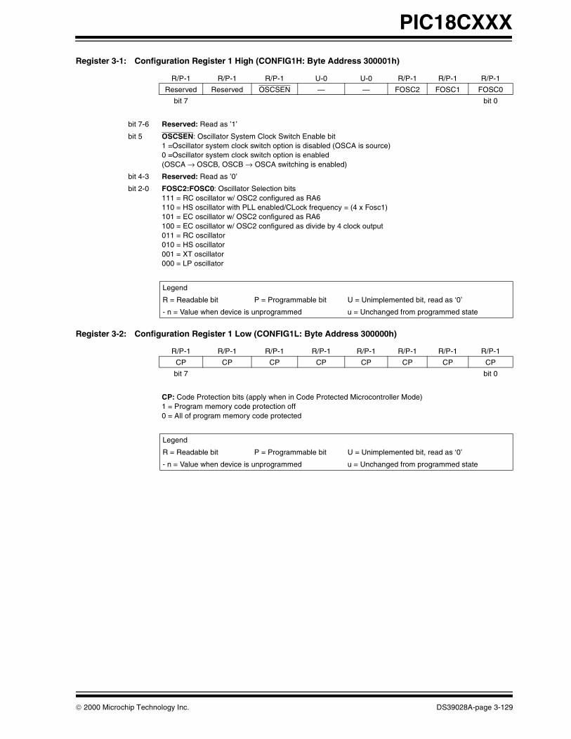
PIC18CXXX
Register 3-1: Configuration Register 1 High (CONFIG1H: Byte Address 300001h)
Register 3-2: Configuration Register 1 Low (CONFIG1L: Byte Address 300000h)
R/P-1 R/P-1 R/P-1 U-0 U-0 R/P-1 R/P-1 R/P-1
Reserved Reserved OSCSEN — — FOSC2 FOSC1 FOSC0
bit 7 bit 0
bit 7-6 Reserved: Read as ’1’
bit 5 OSCSEN: Oscillator System Clock Switch Enable bit1 =Oscillator system clock switch option is disabled (OSCA is source)0 =Oscillator system clock switch option is enabled (OSCA → OSCB, OSCB → OSCA switching is enabled)
bit 4-3 Reserved: Read as ’0’
bit 2-0 FOSC2:FOSC0: Oscillator Selection bits111 = RC oscillator w/ OSC2 configured as RA6 110 = HS oscillator with PLL enabled/CLock frequency = (4 x Fosc1) 101 = EC oscillator w/ OSC2 configured as RA6 100 = EC oscillator w/ OSC2 configured as divide by 4 clock output 011 = RC oscillator 010 = HS oscillator 001 = XT oscillator 000 = LP oscillator
Legend
R = Readable bit P = Programmable bit U = Unimplemented bit, read as ‘0’
- n = Value when device is unprogrammed u = Unchanged from programmed state
R/P-1 R/P-1 R/P-1 R/P-1 R/P-1 R/P-1 R/P-1 R/P-1
CP CP CP CP CP CP CP CP
bit 7 bit 0
CP: Code Protection bits (apply when in Code Protected Microcontroller Mode) 1 = Program memory code protection off 0 = All of program memory code protected
Legend
R = Readable bit P = Programmable bit U = Unimplemented bit, read as ‘0’
- n = Value when device is unprogrammed u = Unchanged from programmed state
2000 Microchip Technology Inc. DS39028A-page 3-129

PIC18CXXX
Register 3-3: Configuration Register 2 High (CONFIG2H: Byte Address 300003h)
Register 3-4: Configuration Register 2 Low (CONFIG2L: Byte Address 300002h)
U-0 U-0 U-0 U-0 R/P-1 R/P-1 R/P-1 R/P-1
— — — — WDTPS2 WDTPS1 WDTPS0 WDTEN
bit 7 bit 0
bit 7-4 Reserved: Read as ’0’
bit 3-1 WDTPS2:WDTPS0: Watchdog Timer Postscale Select bits111 = 1:128 110 = 1:64 101 = 1:32 100 = 1:16 011 = 1:8 010 = 1:4 001 = 1:2 000 = 1:1
bit 0 WDTEN: Watchdog Timer Enable bit1 = WDT enabled 0 = WDT disabled (control is placed on the SWDTE bit)
Legend
R = Readable bit P = Programmable bit U = Unimplemented bit, read as ‘0’
- n = Value when device is unprogrammed u = Unchanged from programmed state
U-0 U-0 U-0 U-0 R/P-1 R/P-1 R/P-1 R/P-1
— — — — BORV1 BORV0 BOREN PWRTEN
bit 7 bit 0
bit 7-4 Reserved: Read as ’0’
bit 3-2 BORV1:BORV0: Brown-out Reset Voltage bits11 = VBOR set to 2.5V 10 = VBOR set to 2.7V 01 = VBOR set to 4.2V 00 = VBOR set to 4.5V
bit 1 BOREN: Brown-out Reset Enable bit (1)
1 = Brown-out Reset enabled 0 = Brown-out Reset disabled Enabling Brown-out Reset automatically enables the Power-up Timer (PWRT) regardless of the value of bit PWRTEN. Ensure the Power-up Timer is enabled anytime Brown-out Reset is enabled.
bit 0 PWRTEN: Power-up Timer Enable bit (1)
1 = PWRT disabled 0 = PWRT enabled Enabling Brown-out Reset automatically enables the Power-up Timer (PWRT) regardless of the value of bit PWRTEN. Ensure the Power-up Timer is enabled anytime Brown-out Reset is enabled.
Legend
R = Readable bit P = Programmable bit U = Unimplemented bit, read as ‘0’
- n = Value when device is unprogrammed u = Unchanged from programmed state
DS39028A-page 3-130 2000 Microchip Technology Inc.
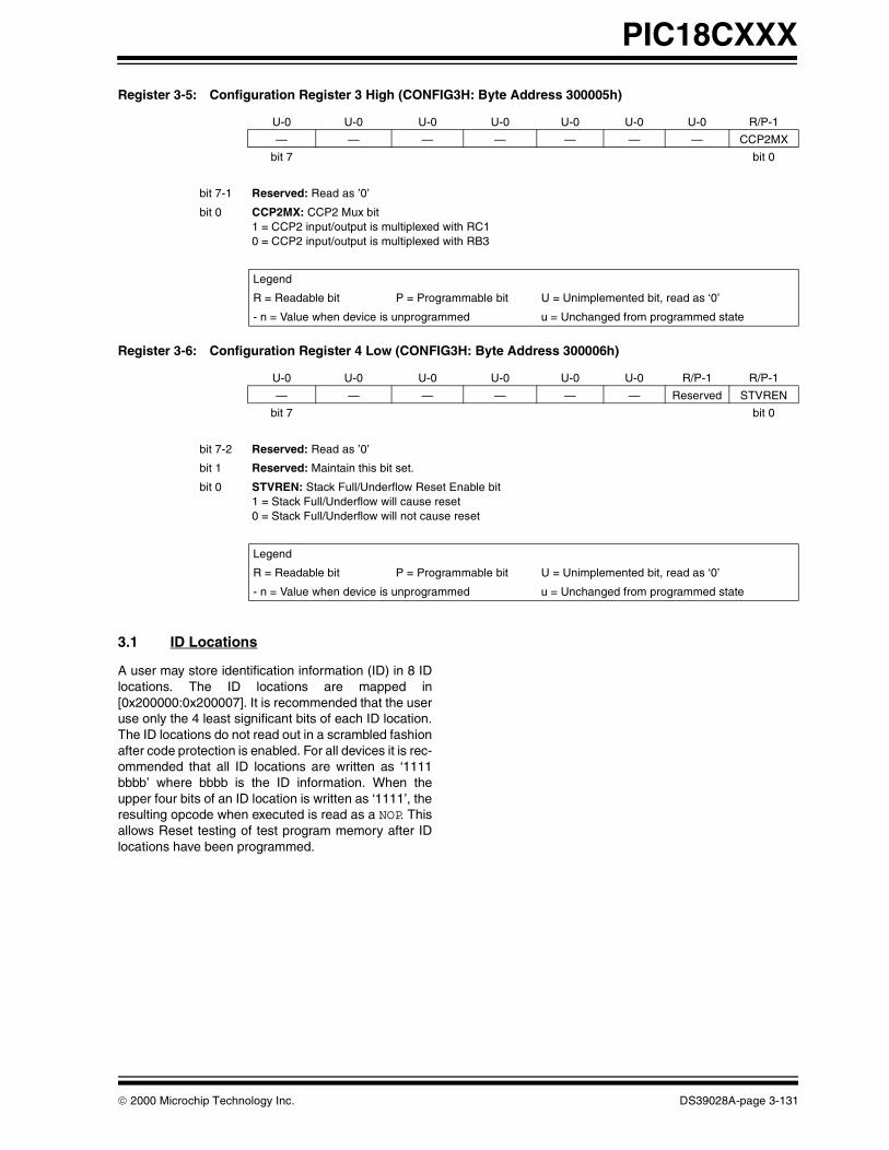
PIC18CXXX
Register 3-5: Configuration Register 3 High (CONFIG3H: Byte Address 300005h)
Register 3-6: Configuration Register 4 Low (CONFIG3H: Byte Address 300006h)
3.1 ID Locations
A user may store identification information (ID) in 8 IDlocations. The ID locations are mapped in[0x200000:0x200007]. It is recommended that the useruse only the 4 least significant bits of each ID location.The ID locations do not read out in a scrambled fashionafter code protection is enabled. For all devices it is rec-ommended that all ID locations are written as ‘1111bbbb’ where bbbb is the ID information. When theupper four bits of an ID location is written as ‘1111’, theresulting opcode when executed is read as a NOP. Thisallows Reset testing of test program memory after IDlocations have been programmed.
U-0 U-0 U-0 U-0 U-0 U-0 U-0 R/P-1
— — — — — — — CCP2MX
bit 7 bit 0
bit 7-1 Reserved: Read as ’0’
bit 0 CCP2MX: CCP2 Mux bit1 = CCP2 input/output is multiplexed with RC1 0 = CCP2 input/output is multiplexed with RB3
Legend
R = Readable bit P = Programmable bit U = Unimplemented bit, read as ‘0’
- n = Value when device is unprogrammed u = Unchanged from programmed state
U-0 U-0 U-0 U-0 U-0 U-0 R/P-1 R/P-1
— — — — — — Reserved STVREN
bit 7 bit 0
bit 7-2 Reserved: Read as ’0’
bit 1 Reserved: Maintain this bit set.
bit 0 STVREN: Stack Full/Underflow Reset Enable bit1 = Stack Full/Underflow will cause reset 0 = Stack Full/Underflow will not cause reset
Legend
R = Readable bit P = Programmable bit U = Unimplemented bit, read as ‘0’
- n = Value when device is unprogrammed u = Unchanged from programmed state
2000 Microchip Technology Inc. DS39028A-page 3-131

PIC18CXXX
3.2 Embedding Configuration Word Information in the Hex File
3.3 CHECKSUM COMPUTATION
The checksum is calculated by summing the following:
• The contents of all program memory locations• The configuration word, appropriately masked• Masked ID locations (when applicable)
The least significant 16 bits of this sum is the check-sum.
The following table describes how to calculate thechecksum for each device. Note that the checksum cal-culation differs depending on the code protect setting.Since the program memory locations read out differ-
ently depending on the code protect setting, the tabledescribes how to manipulate the actual program mem-ory values to simulate the values that would be readfrom a protected device. When calculating a checksumby reading a device, the entire program memory cansimply be read and summed. The configuration wordand ID locations can always be read.
Note that some older devices have an additional valueadded in the checksum. This is to maintain compatibil-ity with older device programmer checksums.
To allow portability of code, a PIC18C4X programmer is required to read the configuration word locations from the hexfile when loading the hex file. If configuration word information was not present in the hex file then a simple warningmessage may be issued. Similarly, while saving a hex file, all configuration word information must be included. Anoption to not include the configuration word information may be provided. When embedding configuration word infor-mation in the hex file, it should be to address FE00h.
Microchip Technology Inc. feels strongly that this feature is important for the benefit of the end customer.
TABLE 3-2: CHECKSUM COMPUTATION
DeviceCode
ProtectChecksum*
BlankValue
0xAA at 0and maxaddress
PIC18C452
Disable SUM[0C000:0x7FFF] + CFGW0 & 0xFF + CFGW1 & 0x27 + CFGW2 & 0x0F + CFGW3 & 0x0F + CFGW4 & 0x00 + CFGW5 & 0x01 +
CFGW6 & 0x03 + CFGW7 & 0x00
0x8148 0x809E
Enabled CFGW0 & 0xFF + CFGW1 & 0x27 + CFGW2 & 0xF + CFGW3 & 0x0F + CFGW4 & 0x00 + CFGW5 & 0x01 + CFGW6 & 0x03 + CFGW7 &
0x00 + SUM_ID
0x005E 0x0068
PIC18C442
Disable SUM[0x000:0x3FFF] + CFGW0 & 0xFF + CFGW1 & 0x27 + CFGW2 & 0x0F + CFGW3 & 0x0F + CFGW4 & 0x00 + CFGW5 & 0x01 +
CFGW6 & 0x03 + CFGW7 & 0x00
0xC148 0xC09E
Enabled CFGW0 & 0xFF + CFGW1 & 0x27 + CFGW2 & 0x0F + CFGW3 & 0x0F + CFGW4 & 0x00 + CFGW5 & 0x01 + CFGW6 & 0x03 +
CFGW7 & 0x00 + SUM_ID
0x0062 0x006C
PIC18C252
Disable SUM[0x000:0x7FFF] + CFGW0 & 0xFF + CFGW1 & 0x27 + CFGW2 & 0x0F + CFGW3 & 0x0F + CFGW4 & 0x00 + CFGW5 & 0x01 +
CFGW6 & 0x03 + CFGW7 & 0x00
0x8148 0x809E
Enabled CFGW0 & 0xFF + CFGW1 & 0x27 + CFGW2 & 0x0F + CFGW3 & 0x0F + CFGW4 & 0x00 + CFGW5 & 0x01 + CFGW6 & 0x03 +
CFGW7 & 0x00 + SUM_ID
0x005E 0x0068
PIC18C242
Disable SUM[0x000:0x3FFF] + CFGW0 & 0xFF + CFGW1 & 0x27 + CFGW2 & 0x0F + CFGW3 & 0x0F + CFGW4 & 0x00 + CFGW5 & 0x01 +
CFGW6 & 0x03 + CFGW7 & 0x00
0xC148 0xC09E
Enabled CFGW0 & 0xFF + CFGW1 & 0x27 + CFGW2 & 0x0F + CFGW3 & 0x0F + CFGW4 & 0x00 + CFGW5 & 0x01 + CFGW6 & 0x03 +
CFGW7 & 0x00 + SUM_ID
0x0062 0x006C
Legend: CFGW = Configuration WordSUM[a:b] = [Sum of locations a to b inclusive]SUM_ID = Byte-wise sum of lower four bits of all ID locations+ = Addition& = Bitwise AND
DS39028A-page 3-132 2000 Microchip Technology Inc.

PIC18CXXX
4.0 AC/DC CHARACTERISTICSTIMING REQUIREMENTS FOR PROGRAM/VERIFY TEST MODE
Standard Operating Conditions
Operating Temperature: +10°C ≤ TA ≤ +70°C, unless otherwise stated, (25°C is recommended)
Operating Voltage: 4.5V ≤ VDD ≤ 5.25V, unless otherwise stated.
Parameter No.
Sym Characteristic Min Typ† Max Units Conditions
VIHH Programming Voltage on VPP/MCLR pin and TEST pin.
VDD + 4.0 — 13.25 V
IPP Programming current on MCLR pin 25 50 mA
P1 TSER Serial setup time 20 — — ns
P2 TSCLK Serial Clock period 100 — — ns
P3 TSET1 Input Data Setup Time to serial clock ↓
15 — — ns
P4 THLD1 Input Data Hold Time from serial clock ↓
15 — — ns
P5 TDLY1 Delay between last clock ↓ to first clock ↑ of next command
20 — — ns
P6 TDLY2 Delay between last clock ↓ of com-mand byte to first clock ↑ of read of data word
20 — — ns
P8 TDLY4 Data input not driven to next clock input
1 — — ns
P9 TDLY5 RB6 high time (minimum program-ming time)
100 — — µs
P10 TDLY6 RB6 low time after programming (high voltage discharge time)
100 — — ns
* These parameters are characterized but not tested.† Data in “Typ” column is at 5V, 25×C unless otherwise stated. These parameters are for design guidance only and are not
tested.
2000 Microchip Technology Inc. DS39028A-page 3-133

PIC18CXXX
NOTES:
DS39028A-page 3-134 2000 Microchip Technology Inc.

PIC16F62XIn-Circuit Serial Programming for PIC16F62X FLASH MCUs
This document includes the programming specifications for the following devices:
• PIC16F627
• PIC16F628• PIC16LF627• PIC16LF628
1.0 PROGRAMMING THE PIC16F62X
The PIC16F62X is programmed using a serial method.The serial mode will allow the PIC16F62X to be pro-grammed while in the users system. This allows forincreased design flexibility. This programming specifi-cation applies to PIC16F62X devices in all packages.
PIC16F62X devices may be programmed using a sin-gle +5 volt supply (low voltage programming mode).
1.1 Hardware Requirements
The PIC16F62X requires one programmable powersupply for VDD (4.5V to 5.5V) and a VPP of 12V to 14Vor VPP of (4.5V to 5.5V) when using low voltage. Bothsupplies should have a minimum resolution of 0.25V.
1.2 Programming Mode
The programming mode for the PIC16F62X allows pro-gramming of user program memory, data memory, spe-cial locations used for ID, and the configuration word.
PIN Diagram
PDIP, SOIC
RA2/AN2/VREF
RA3/AN3/CMP1
RA4/T0CKI/CMP2
RA5/MCLR/THV
VSS
RB0/INT
RB1/RX/DT
RB2/TX/CK
RB3/CCP1
RA1/AN1
RA0/AN0
RA7/OSC1/CLKIN
RA6/OSC2/CLKOUT
VDD
RB7/T1OSI
RB6/T1OSO/T1CKI
RB5
RB4/PGM
• 1
2
3
4
5
7
8
9
18
17
16
15
14
12
11
10
PIC
16F62X6 13
RA2/AN2/VREF
RA3/AN3/CMP1
RA4/T0CKI/CMP2
RA5/MCLR/THV
VSS
RB0/INT
RB1/RX/DT
RB2/TX/CK
RB3/CCP1
RA1/AN1
RA0/AN0
RA7/OSC1/CLKIN
RA6/OSC2/CLKOUT
VDD
RB7/T1OSI
RB6/T1OSO/T1CKI
RB5
RB4/PGM
• 1
2
3
4
5
7
8
9
18
17
16
15
14
12
1110
PIC
16F62X6
13
VDDVSS
19
20
PIN DESCRIPTIONS (DURING PROGRAMMING): PIC16F62X
Pin Name
During Programming
Function Pin Type Pin Description
RB4 PGM I Low voltage programming input if configuration bit equals 1
RB6 CLOCK I Clock input
RB7 DATA I/O Data input/output
MCLR VTEST MODE P* Program Mode Select
VDD VDD P Power Supply
VSS VSS P Ground
Legend: I = Input, O = Output, P = Power
*In the PIC16F62X, the programming high voltage is internally generated. To activate the programming mode, high voltage needsto be applied to MCLR input. Since the MCLR is used for a level source, this means that MCLR does not draw any significant current.
2000 Microchip Technology Inc. Preliminary DS30034A-page 3-135

PIC16F62X
2.0 PROGRAM MODE ENTRY
2.1 User Program Memory Map
The user memory space extends from 0x0000 to0x7FFF. In programming mode the program memoryspace extends from 0x0000 to 0x3FFF, with the firsthalf (0x0000-0x7FFF) being user program memory andthe second half (0x2000-0x3FFF) being configurationmemory. The PC will increment from 0x0000 to 0x7FFFand wrap to 0x000, 0x2000 to 0x3FFF and wraparound to 0x2000 (not to 0x0000). Once in configura-tion memory, the highest bit of the PC stays a ‘1’, thusalways pointing to the configuration memory. The onlyway to point to user program memory is to reset thepart and reenter program/verify mode as described inSection 2.3.
In the configuration memory space, 0x2000-0x200Fare physically implemented. However, only locations0x2000 through 0x2007 are available. Other locationsare reserved. Locations beyond 0x200F will physicallyaccess user memory. (See Figure 2-1).
2.2 ID Locations
A user may store identification information (ID) in fourID locations. The ID locations are mapped in [0x2000 :0x2003]. It is recommended that the user use only thefour least significant bits of each ID location. In somedevices, the ID locations read-out in an unscrambledfashion after code protection is enabled. For thesedevices, it is recommended that ID location is written as“11 1111 1000 bbbb” where ‘bbbb’ is ID information.
In other devices, the ID locations read out normally,even after code protection. To understand how thedevices behave, refer to Table 4-1.
To understand the scrambling mechanism after codeprotection, refer to Section 3-1.
FIGURE 2-1: PROGRAM MEMORY MAPPING
1FFF
2000ID Location
ID Location
ID Location
ID Location
Reserved
Reserved
Reserved
Configuration Word
2000
2001
2002
2003
2005
2006
2007
2008
3FFF
0x1FF
Not Implemented
Implemented
1 KW
Implemented
2004
Implemented
2 KW
Implemented
DS30034A-page 3-136 Preliminary 2000 Microchip Technology Inc.

PIC16F62X
2.3 Program/Verify Mode
The program/verify mode is entered by holding pinsRB6 and RB7 low while raising MCLR pin from VIL toVIHH (high voltage) or by applying VDD to MCLR andraising RB3 from VIL to VDD. Once in this mode the userprogram memory and the configuration memory can beaccessed and programmed in serial fashion. The modeof operation is serial, and the memory that is accessedis the user program memory. RB6 and RB7 are SchmittTrigger Inputs in this mode.
The sequence that enters the device into the program-ming/verify mode places all other logic into the resetstate (the MCLR pin was initially at VIL). This meansthat all I/O are in the reset state (High impedanceinputs).
The normal sequence for programming is to use theload data command to set a value to be written at theselected address. Issue the begin programming com-mand followed by read data command to verify, andthen increment the address.
A device reset will clear the PC and set the address to0. The “increment address” command will incrementthe PC. The “load configuration” command will se thePC to 0x2000. The available commands are shown inTable 2-1.
2.3.1 LOW-VOLTAGE PROGRAMMING MODE
When LVP bit is set to ‘1’, the low-voltage programmingentry is enabled. Since the LVP configuration bit allowslow voltage programming entry in its erased state, anerased device will have the LVP bit enabled at the fac-tory. While LVP is ‘1’, RB4 is dedicated to low voltageprogramming. Bring MCLR to VDD and then RB4 toVDD to enter programming mode. All other specifica-tions for high-voltage ICSP™ apply.
To disable low voltage mode, the LVP bit must be pro-grammed to ‘0’. This must be done while entered withhigh voltage entry mode (LVP bit= 1). RB4 is now ageneral purpose I/O pin.
2.3.2 SERIAL PROGRAM/VERIFY OPERATION
The RB6 pin is used as a clock input pin, and the RB7pin is used for entering command bits and data input/output during serial operation. To input a command, theclock pin (RB6) is cycled six times. Each command bitis latched on the falling edge of the clock with the leastsignificant bit (LSB) of the command being input first.The data on pin RB7 is required to have a minimumsetup and hold time (see AC/DC specifications) withrespect to the falling edge of the clock. Commands thathave data associated with them (read and load) arespecified to have a minimum delay of 1 µs between thecommand and the data. After this delay, the clock pin iscycled 16 times with the first cycle being a start bit andthe last cycle being a stop bit. Data is also input andoutput LSB first.
Therefore, during a read operation the LSB will betransmitted onto pin RB7 on the rising edge of the sec-ond cycle, and during a load operation the LSB will belatched on the falling edge of the second cycle. A min-imum 1µs delay is also specified between consecutivecommands.
All commands are transmitted LSB first. Data wordsare also transmitted LSB first. The data is transmittedon the rising edge and latched on the falling edge ofthe clock. To allow for decoding of commands andreversal of data pin configuration, a time separation ofat least 1 µs is required between a command and adata word (or another command).
The commands that are available are:
2.3.2.1 LOAD CONFIGURATION
After receiving this command, the program counter(PC) will be set to 0x2000. By then applying 16 cyclesto the clock pin, the chip will load 14-bits in a “dataword,” as described above, to be programmed into theconfiguration memory. A description of the memorymapping schemes of the program memory for normaloperation and configuration mode operation is shownin Figure 2-1. After the configuration memory isentered, the only way to get back to the user programmemory is to exit the program/verify test mode by tak-ing MCLR low (VIL).
Note: The OSC must not have 72 osc clockswhile the device MCLR is between VIL andVIHH.
2000 Microchip Technology Inc. Preliminary DS30034A-page 3-137

PIC16F62X
2.3.2.2 LOAD DATA FOR PROGRAM MEMORY
After receiving this command, the chip will load in a14-bit “data word” when 16 cycles are applied, asdescribed previously. A timing diagram for the load datacommand is shown in Figure 5-1.
TABLE 2-1: COMMAND MAPPING FOR PIC16F627/PIC16F628
Command Mapping (MSB … LSB) Data
Load Configuration X X 0 0 0 0 0, data (14), 0
Load Data for Program Memory X X 0 0 1 0 0, data (14), 0
Read Data from Program Memory X X 0 1 0 0 0, data (14), 0
Increment Address X X 0 1 1 0
Begin Erase Programming Cycle 0 0 1 0 0 0
Begin Programming Only Cycle 0 1 1 0 0 0
Load Data for Data Memory X X 0 0 1 1 0, data (14), 0
Read Data from Data Memory X X 0 1 0 1 0, data (14), 0
Bulk Erase Program Memory X X 1 0 0 1
Bulk Erase Data Memory X X 1 0 1 1
DS30034A-page 3-138 Preliminary 2000 Microchip Technology Inc.

PIC16F62X
FIGURE 2-2: PROGRAM FLOW CHART - PIC16F62X PROGRAM MEMORY
Start
Set VDD = VDDP
Program Cycle
Read Data Command
Data Correct?Report
ProgrammingFailure
All LocationsDone?
Verify allLocations @
VDDMIN
Data Correct?
Verify allLocations @
VDDMAX
Data Correct?
Done
IncrementAddress
Command
Report VerifyError @VDDMIN
Report VerifyError @VDDMAX
Load DataCommand
BeginProgramming
Command
Wait 2 ms
PROGRAM CYCLE
No
No
No
No
2000 Microchip Technology Inc. Preliminary DS30034A-page 3-139

PIC16F62X
FIGURE 2-3: PROGRAM FLOW CHART - PIC16F62X CONFIGURATION MEMORY
Program ID
Start
LoadConfiguration
Data
Location? Program CycleRead Data Command
Data Correct?Report
ProgrammingFailure
IncrementAddress
Command
Address = 0x2004?
IncrementAddress
Command
IncrementAddress
Command
IncrementAddress
Command
ProgramCycle
(Config. Word)
Set VDD = VDDMAX
Read Data CommandData Correct?
Set VDD = VDDMAX
Read Data CommandData Correct?
Report ProgramConfigurationWord Error
Done
Yes
No
No
Yes
YesNo
No
Yes
Yes
No
DS30034A-page 3-140 Preliminary 2000 Microchip Technology Inc.

PIC16F62X
2.3.2.3 LOAD DATA FOR DATA MEMORY
After receiving this command, the chip will load in a 14-bit “data word” when 16 cycles are applied. However,the data memory is only 8-bits wide, and thus only thefirst 8-bits of data after the start bit will be programmedinto the data memory. It is still necessary to cycle theclock the full 16 cycles in order to allow the internal cir-cuitry to reset properly. The data memory contains 64words. Only the lower 8-bits of the PC are decoded bythe data memory, and therefore if the PC is greater than0x3F, it will wrap around and address a location withinthe physically implemented memory. If the device iscode protected, the data is read as all zeros.
2.3.2.4 READ DATA FROM PROGRAM MEMORY
After receiving this command, the chip will transmitdata bits out of the program memory (user or configu-ration) currently accessed starting with the second ris-ing edge of the clock input. The RB7 pin will go intooutput mode on the second rising clock edge, and it willrevert back to input mode (hi-impedance) after the 16thrising edge. A timing diagram of this command isshown in Figure 5-2.
2.3.2.5 READ DATA FROM DATA MEMORY
After receiving this command, the chip will transmitdata bits out of the data memory starting with the sec-ond rising edge of the clock input. The RB7 pin will gointo output mode on the second rising edge, and it willrevert back to input mode (hi-impedance) after the 16thrising edge. As previously stated, the data memory is 8-bits wide, and therefore, only the first 8-bits that are out-put are actual data.
2.3.2.6 INCREMENT ADDRESS
The PC is incremented when this command isreceived. A timing diagram of this command is shownin Figure 5-3.
2.3.2.7 BEGIN ERASE/PROGRAM CYCLE
A load command must be given before every beginprogramming command. Programming of the appro-priate memory (test program memory, user programmemory or data memory) will begin after this commandis received and decoded. An internal timing mechanismexecutes an erase before write. The user must allow forboth erase and programming cycle times for program-ming to complete. No “end programming” command isrequired.
2.3.2.8 BEGIN PROGRAMMING
A load command must be given before every beginprogramming command. Programming of the appro-priate memory (test program memory, user programmemory or data memory) will begin after this commandis received and decoded. An internal timing mechanismexecutes a write. The user must allow for program cycletime for programming to complete. No “end program-ming” command is required.
This command is similar to the ERASE/PROGRAMCYCLE command, except that a word erase is notdone. It is recommended that a bulk erase be per-formed before starting a series of programming onlycycles.
2.3.2.9 BULK ERASE PROGRAM MEMORY
After this command is performed, the next programcommand will erase the entire program memory.
To perform a bulk erase of the program memory, the fol-lowing sequence must be performed.
1. Do a “Load Data All 1’s” command.2. Do a “Bulk Erase User Memory” command.
3. Do a “Begin Programming” command.4. Wait 10 ms to complete bulk erase.
If the address is pointing to the test program memory(0x2000 - 0x200F), then both the user memory and thetest memory will be erased. The configuration word willnot be erased, even if the address is pointing to location0x2007.
2.3.2.10 BULK ERASE DATA MEMORY
To perform a bulk erase of the data memory, the follow-ing sequence must be performed.
1. Do a “Load Data All 1’s” command.
2. Do a “Bulk Erase Data Memory” command.3. Do a “Begin Programming” command.4. Wait 10 ms to complete bulk erase.
Note: If the device is code-protected, the BULKERASE command will not work.
Note: All BULK ERASE operations must takeplace at 4.5 to 5.5 VDD range.
2000 Microchip Technology Inc. Preliminary DS30034A-page 3-141

PIC16F62X
2.4 Programming Algorithm Requires Variable VDD
The PIC16F62X uses an intelligent algorithm. Thealgorithm calls for program verification at VDDmin. aswell as VDDmax. Verification at VDDmin. guaranteesgood “erase margin”. Verification at VDDmax guaran-tees good “program margin”.
The actual programming must be done with VDD in theVDDP range (See Table 5-1).
VDDP = VCC range required during programming.
VDDmin. = minimum operating VDD spec for the part.
VDDmax.= maximum operating VDD spec for the part.
Programmers must verify the PIC16F62X at its speci-fied VDD max. and VDDmin levels. Since Microchip mayintroduce future versions of the PIC16F62X with abroader VDD range, it is best that these levels are userselectable (defaults are ok).
Note: Any programmer not meeting theserequirements may only be classified as“prototype” or “development” programmerbut not a “production” quality programmer.
DS30034A-page 3-142 Preliminary 2000 Microchip Technology Inc.

PIC16F62X
3.0 CONFIGURATION WORDThe PIC16F62X has several configuration bits. Thesebits can be set (reads ‘0’) or left unchanged (reads ‘1’)to select various device configurations.
3.1 Device ID Word
The device ID word for the PIC16F62X is located at2006h.
FIGURE 3-1: CONFIGURATION WORD FOR PIC16F877/876/873
TABLE 3-1:
DeviceDevice ID Value
Dev Rev
PIC16F627 00 0111 111 x xxxxPIC16F628 00 0111 001 x xxxx
CP1 CP0 CP1 CP0 - CPD LVP BODEN MCLRE FOSC2 PWRTE WDTE F0SC1 F0SC0 Register: CONFIGAddress 2007h
bit13 bit0
bit 13-10: CP1:CP0: Code Protection bits (2)
Code protection for 2K program memory11 = Program memory code protection off10 = 0400h-07FFh code protected01 = 0200h-07FFh code protected00 = 0000h-07FFhcode protectedCode protection for 1K program memory11 = Program memory code protection off10 = Program memory code protection off01 = 0200h-03FFh code protected00 = 0000h-03FFh code protected
bit 8: CPD: Data Code Protection bit(3)
1 = Data memory code protection off0 = Data memory code protected
bit 7: LVP: Low Voltage Programming Enable1 = RB4/PGM pin has PGM function, low voltage programming enabled0 = RB4/PGM is digital I/O, HV on MCLR must be used for programming
bit 6: BODEN: Brown-out Detect Reset Enable bit (1)
1 = BOD reset enabled0 = BOD reset disabled
bit 5: MCLRE: RA5/MCLR pin function select1 = RA5/MCLR pin function is MCLR 0 = RA5/MCLR pin function is digital I/O, MCLR internally tied to VDD
bit 3: PWRTE: Power-up Timer Enable bit (1)
1 = PWRT disabled0 = PWRT enabled
bit 2: WDTE: Watchdog Timer Enable bit1 = WDT enabled0 = WDT disabled
bit 4,1-0: FOSC2:FOSC0: Oscillator Selection bits(4)
111 = ER oscillator: CLKOUT function on RA6/OSC2/CLKOUT pin, Resistor on RA7/OSC1/CLKIN110 = ER oscillator: I/O function on RA6/OSC2/CLKOUT pin, Resistor on RA7/OSC1/CLKIN101 = INTRC oscillator: CLKOUT function on RA6/OSC2/CLKOUT pin, I/O function on RA7/OSC1/CLKIN100 = INTRC oscillator: I/O function on RA6/OSC2/CLKOUT pin, I/O function on RA7/OSC1/CLKIN011 = EXTCLK: I/O function on RA6/OSC2/CLKOUT pin, CLKIN on RA7/OSC1/CLKIN010 = HS oscillator: High speed crystal/resonator on RA6/OSC2/CLKOUT and RA7/OSC1/CLKIN001 = XT oscillator: Crystal/resonator on RA6/OSC2/CLKOUT and RA7/OSC1/CLKIN000 = LP oscillator: Low power crystal on RA6/OSC2/CLKOUT and RA7/OSC1/CLKIN
Note 1: Enabling Brown-out Reset automatically enables Power-up Timer (PWRT) regardless of the value of bit PWRTE. Ensure the Power-up Timer is enabled anytime Brown-out Reset is enabled.
2: All of the CP1:CP0 pairs have to be given the same value to enable the code protection scheme listed. The entire pro-gram EEPROM will be erased if the code protection is reduced.
3: The entire data EEPROM will be erased when the code protection is turned off. The calibration space in the test memory is not erased.
4: When MCLR is asserted in INTRC or ER mode, the internal clock oscillator is disabled.
2000 Microchip Technology Inc. Preliminary DS30034A-page 3-143

PIC16F62X
4.0 CODE PROTECTIONFor PIC16F62X devices, once code protection isenabled, all program memory locations read all 0’s.The ID locations and the configuration word read out inan unscrambled fashion. Further programming is dis-abled for the entire program memory as well as datamemory. It is possible to program the ID locations andthe configuration word.
4.1 Disabling Code-Protection
It is recommended that the following procedure be per-formed before any other programming is attempted. Itis also possible to turn code protection off (code protectbit = 1) using this procedure; however, all data withinthe program memory and the data memory will beerased when this procedure is executed, and thus,the security of the data or code is not compro-mised.
Procedure to disable code protect:
a) Execute load configuration (with a ‘1’ in bit 4, code protect).
b) Increment to configuration word location(0x2007)
c) Execute command (000001)d) Execute command (000111)
e) Execute ‘Begin Programming’ (001000)f) Wait 10 msg) Execute command (000001)
h) Execute command (000111)
4.2 Embedding Configuration Word and ID Information in the Hex File
To allow portability of code, the programmer is required to read the configuration word and ID locations from the hexfile when loading the hex file. If configuration word information was not present in the hex file then a simple warningmessage may be issued. Similarly, while saving a hex file, configuration word and ID information must be included.An option to not include this information may be provided.
Specifically for the PIC16F62X, the EEPROM data memory should also be embedded in the hex file (seeSection 5.1).
Microchip Technology Inc. feels strongly that this feature is important for the benefit of the end customer.
DS30034A-page 3-144 Preliminary 2000 Microchip Technology Inc.

PIC16F62X
4.3 CHECKSUM COMPUTATION
4.3.1 CHECKSUM
Checksum is calculated by reading the contents of thePIC16F62X memory locations and adding up theopcodes up to the maximum user addressable location,e.g., 0x1FF for the PIC16F62X. Any carry bits exceed-ing 16-bits are neglected. Finally, the configurationword (appropriately masked) is added to the check-sum. Checksum computation for each member of thePIC16F62X devices is shown in Table 4-1.
The checksum is calculated by summing the following:
• The contents of all program memory locations• The configuration word, appropriately masked
• Masked ID locations (when applicable)
The least significant 16 bits of this sum is the check-sum.
The following table describes how to calculate thechecksum for each device. Note that the checksum cal-culation differs depending on the code protect setting.Since the program memory locations read out differ-ently depending on the code protect setting, the tabledescribes how to manipulate the actual program mem-ory values to simulate the values that would be readfrom a protected device. When calculating a checksumby reading a device, the entire program memory cansimply be read and summed. The configuration wordand ID locations can always be read.
Note that some older devices have an additional valueadded in the checksum. This is to maintain compatibil-ity with older device programmer checksums.
TABLE 4-1: CHECKSUM COMPUTATION
DeviceCode
ProtectChecksum*
BlankValue
0x25E6 at 0and maxaddress
PIC16F627 OFF SUM[0x0000:0x3FFF] + CFGW & 0x3DFF 0x39FF 0x05CD
0x200 : 0x3FF SUM[0x0000:0x01FF] + CFGW & 0x3DFF + SUM_ID 0x4DFE 0xFFB3
ALL 0x3BFE 0x07CC
PIC16F628 OFF SUM[0x0000:0x07FF] + CFGW & 0x3DFF 0x35FF 0x01CD
0x400 : 0xFFF SUM[0x0000:0x03FF] + CFGW & 0x3DFF +SUM_ID 0x5BFE 0x0DB3
0x200 : 0x7FF SUM[0x0000:0x01FF] + CFGW & 0x3DFF + SUM_ID 0x49FE 0xFBB3
ALL CFGW & 0x3DFF + SUM_ID 0x37FE 0x03CC
Legend: CFGW = Configuration WordSUM[a:b] = [Sum of locations a to b inclusive]SUM_ID = ID locations masked by 0xF then made into a 16-bit value with ID0 as the most significant nibble. For example, ID0 = 0x1, ID1 = 0x2, ID3 = 0x3, ID4 = 0x4, then SUM_ID = 0x1234*Checksum = [Sum of all the individual expressions] MODULO [0xFFFF]+ = Addition& = Bitwise AND
2000 Microchip Technology Inc. Preliminary DS30034A-page 3-145

PIC16F62X
5.0 PROGRAM/VERIFY MODE ELECTRICAL CHARACTERISTICS
5.1 Embedding Data EEPROM Contents in Hex File
The programmer should be able to read data EEPROM information from a hex file and conversely (as an option) writedata EEPROM contents to a hex file along with program memory information and fuse information.
The 64 data memory locations are logically mapped starting at address 0x2100. The format for data memory storageis one data byte per address location, LSB aligned.
TABLE 5-1: AC/DC CHARACTERISTICSTIMING REQUIREMENTS FOR PROGRAM/VERIFY MODE
Standard Operating Conditions (unless otherwise stated)Operating Temperature: 0°C ≤ TA ≤ +70°COperating Voltage: 4.5V ≤ VDD ≤ 5.5V
Characteristics Sym Min Typ Max Units Conditions/Comments
General
VDD level for word operations, program memory VDD 2.0 5.5 V
VDD level for word operations, data mem-ory VDD 2.0 5.5 V
VDD level for bulk erase/write operations, program and data memory VDD 4.5 5.5 V
High voltage on MCLR and RA4/T0CKI for test-mode entry VIHH VDD + 3.5 13.5 V
MCLR rise time (VSS to VHH) for testmode entry
tVHHR 1.0 µs
(RB6, RB7) input high level VIH1 0.8VDD V Schmitt Trigger input
(RB6, RB7) input low level VIL1 0.2VDD V Schmitt Trigger input
RB<7:4> setup time before MCLR↑ (test mode selection pattern setup time)
tset0 100 ns
RB<7:4> hold time after MCLR↑ (test mode selection pattern setup time)
thld0 5 µs
Serial Program/Verify
Data in setup time before clock↓ tset1 100 ns
Data in hold time after clock↓ thld1 100 ns
Data input not driven to next clock input (delay required between command/data or command/command)
tdly1 1.0 µs
Delay between clock↓ to clock↑ of next command or data
tdly2 1.0 µs
Clock↑ to data out valid (during read data) tdly3 80 ns
Parallel Program/Verify
Data in setup time before clock↓ tset0 1.0 µs
Data in hold time after clock↓ thld0 1.0 µs
RB6 and RB7 setup time before clock↓ tset1 1.0 µs
RB6 and RB7 hold time after clock↓ thld1 1.0 µs
RA4/T0CKI (clock)↓ to (clock)↑ tdly4 2.0 µs
RB7 (data/command select input) setup before RA4/T0CKI (clock)↑
tset2 1.0 µs
RB7 (data/command select input) hold time after RA4/T0CKI (clock)↓
thld2 1.0 µs
RA4/T0CKI (clock)↑ to data out valid tdly5 1.0 µs
RB6 (hi/lo select) valid to data out valid tdly6 1.0 µs
Erase cycle time tera 2 5 ms
Programming cycle time tprog 2 5 ms
Time delay from program to compare (HV discharge time)
tdis 0.5 µs
DS30034A-page 3-146 Preliminary 2000 Microchip Technology Inc.

PIC16F62X
FIGURE 5-1: LOAD DATA COMMAND (PROGRAM/VERIFY)
FIGURE 5-2: READ DATA COMMAND (PROGRAM/VERIFY)
FIGURE 5-3: INCREMENT ADDRESS COMMAND (PROGRAM/VERIFY)
MCLRVIHH
tset0
RB6(CLOCK)
RB7(DATA)
Reset
tset1
thld1tdly1
1µs min.
Program/Verify Test Mode
tset1
thld1
100ns min.
1µs min.
tdly21 2 3 4 5 6
0 1 0 0 X X
1 2 3 4 5 15 16
strt_bit stp_bit
100ns min.
thld0
MCLRVIHH
tset0
RB6(CLOCK)
RB7(DATA)
Reset
tdly1
1µs min.
Program/Verify Test Mode
tset1
thld1
1µs min.
tdly2
1 2 3 4 5 6
1 0 1 0 X X
1 2 3 4 5 15 16
100ns min.
tdly3
RB7 = input RB7 = outputRB7
input
thld0
strt_bit stp_bit
MCLRVIHH
RB6(CLOCK)
RB7(DATA)
Reset
tdly1
1µs min.
Program/Verify Test Mode
tset1
thld1
1µs min.
tdly2
1 2 3 4 5 6
0 1 1 X X
1 2
100ns min.
X 00
Next Command
2000 Microchip Technology Inc. Preliminary DS30034A-page 3-147

PIC16F62X
NOTES:
DS30034A-page 3-148 Preliminary 2000 Microchip Technology Inc.

PIC16F8XIn-Circuit Serial Programming for PIC16F8X FLASH MCUs
This document includes the programming specifications for the following devices:
• PIC16F83
• PIC16CR83• PIC16F84• PIC16CR84
• PIC16F84A• PIC16F877
1.0 PROGRAMMING THE PIC16F8XThe PIC16F8X is programmed using a serial method.The serial mode will allow the PIC16F8X to be pro-grammed while in the users system. This allows forincreased design flexibility. This programming specifi-cation applies to PIC16F8X devices in all packages.
1.1 Hardware Requirements
The PIC16F8X requires one programmable power sup-ply for VDD (4.5V to 5.5V) and a VPP of 12V to 14V. Bothsupplies should have a minimum resolution of 0.25V.
1.2 Programming Mode
The programming mode for the PIC16F8X allows pro-gramming of user program memory, data memory, spe-cial locations used for ID, and the configuration word.
Pin Diagram
RA1RA0OSC1/CLKINOSC2/CLKOUTVDDRB7RB6RB5RB4
RA2RA3
RA4/T0CKIMCLR
VSSRB0/INT
RB1RB2RB3
•123456789
181716151413121110
PIC
16F8X
PDIP, SOIC
RB7RB6
RB5
RB4RB3
RB2
RB1
RB0/INT
VDD
VSS
RD7/PSP7
RD6/PSP6RD5/PSP5
RD4/PSP4
RC7/RX/DT
RC6/TX/CK
RC5/SDO
RC4/SDI/SDARD3/PSP3
RD2/PSP2
MCLR/VPP
RA0/AN0
RA1/AN1RA2/AN2/VREF
RA3/AN3/VREF
RA4/T0CKI
RA5/AN4/SS
RE0/RD/AN5
RE1/WR/AN6
RE2/CS/AN7VDD
VSS
OSC1/CLKIN
OSC2/CLKOUT
RC0/T1OSO/T1CKI
RC1/T1OSI/CCP2
RC2/CCP1
RC3/SCK/SCLRD0/PSP0
RD1/PSP1
1
2
3
4
5
6
7
8
910
11
12
13
14
15
16
17
18
1920
40
39
38
37
36
35
34
33
3231
30
2928
27
26
25
24
23
2221
PIC
16F877
PIN DESCRIPTIONS (DURING PROGRAMMING): PIC16F8X
Pin Name
During Programming
Function Pin Type Pin Description
RB6 CLOCK I Clock input
RB7 DATA I/O Data input/output
MCLR VTEST MODE P* Program Mode Select
VDD VDD P Power Supply
VSS VSS P Ground
Legend: I = Input, O = Output, P = Power
*In the PIC16F8X, the programming high voltage is internally generated. To activate the programming mode, high voltage needs tobe applied to MCLR input. Since the MCLR is used for a level source, this means that MCLR does not draw any significant current.
2000 Microchip Technology Inc. DS30262C-page 3-149
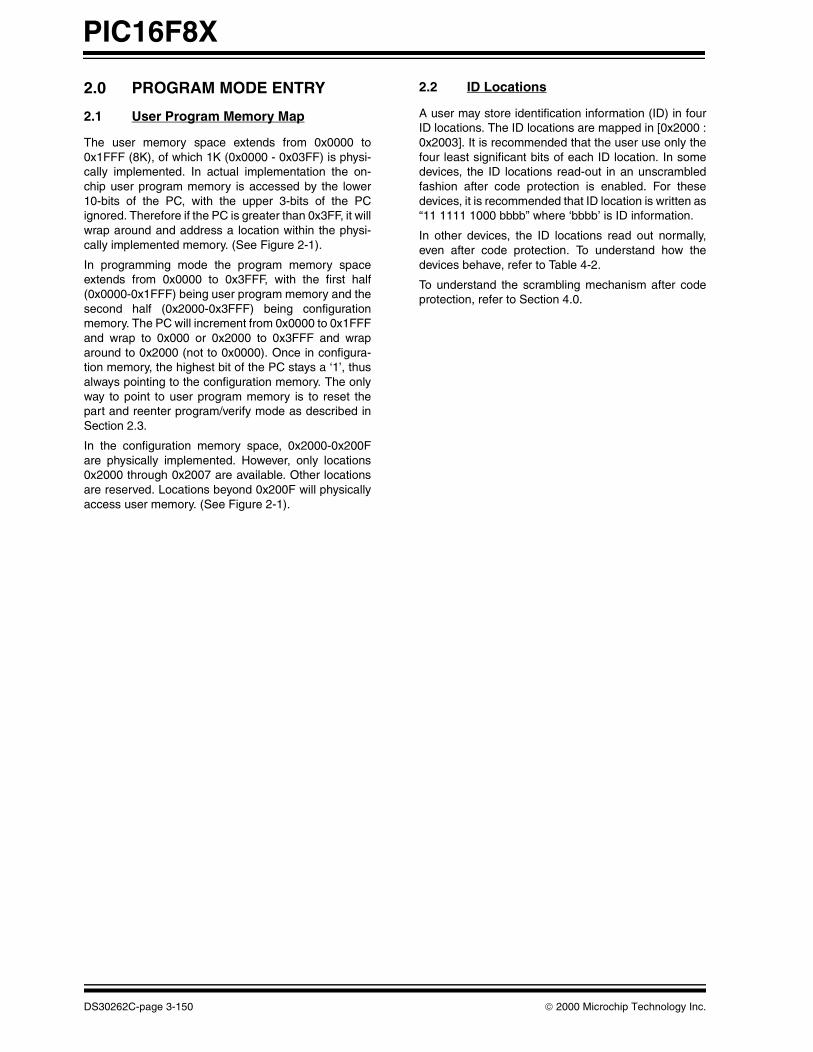
PIC16F8X
2.0 PROGRAM MODE ENTRY
2.1 User Program Memory Map
The user memory space extends from 0x0000 to0x1FFF (8K), of which 1K (0x0000 - 0x03FF) is physi-cally implemented. In actual implementation the on-chip user program memory is accessed by the lower10-bits of the PC, with the upper 3-bits of the PCignored. Therefore if the PC is greater than 0x3FF, it willwrap around and address a location within the physi-cally implemented memory. (See Figure 2-1).
In programming mode the program memory spaceextends from 0x0000 to 0x3FFF, with the first half(0x0000-0x1FFF) being user program memory and thesecond half (0x2000-0x3FFF) being configurationmemory. The PC will increment from 0x0000 to 0x1FFFand wrap to 0x000 or 0x2000 to 0x3FFF and wraparound to 0x2000 (not to 0x0000). Once in configura-tion memory, the highest bit of the PC stays a ‘1’, thusalways pointing to the configuration memory. The onlyway to point to user program memory is to reset thepart and reenter program/verify mode as described inSection 2.3.
In the configuration memory space, 0x2000-0x200Fare physically implemented. However, only locations0x2000 through 0x2007 are available. Other locationsare reserved. Locations beyond 0x200F will physicallyaccess user memory. (See Figure 2-1).
2.2 ID Locations
A user may store identification information (ID) in fourID locations. The ID locations are mapped in [0x2000 :0x2003]. It is recommended that the user use only thefour least significant bits of each ID location. In somedevices, the ID locations read-out in an unscrambledfashion after code protection is enabled. For thesedevices, it is recommended that ID location is written as“11 1111 1000 bbbb” where ‘bbbb’ is ID information.
In other devices, the ID locations read out normally,even after code protection. To understand how thedevices behave, refer to Table 4-2.
To understand the scrambling mechanism after codeprotection, refer to Section 4.0.
DS30262C-page 3-150 2000 Microchip Technology Inc.

PIC16F8X
FIGURE 2-1: PROGRAM MEMORY MAPPING
0
3FF400
1FFF
2000
ID Location
ID Location
ID Location
ID Location
Reserved
Reserved
Reserved
Configuration Word
2000
2001
2002
2003
2004
2005
2006
2007
2008
3FFF
Not Implemented
Not Implemented
Implemented
Implemented1FF
Not Implemented
Not Implemented
Implemented
Implemented
0.5 KW 1 KW
Not Implemented
Implemented
8 KW
Implemented
2000 Microchip Technology Inc. DS30262C-page 3-151

PIC16F8X
2.3 Program/Verify Mode
The program/verify mode is entered by holding pinsRB6 and RB7 low while raising MCLR pin from VIL toVIHH (high voltage). Once in this mode the user pro-gram memory and the configuration memory can beaccessed and programmed in serial fashion. The modeof operation is serial, and the memory that is accessedis the user program memory. RB6 and RB7 are SchmittTrigger Inputs in this mode.
The sequence that enters the device into the program-ming/verify mode places all other logic into the resetstate (the MCLR pin was initially at VIL). This meansthat all I/O are in the reset state (High impedanceinputs).
The normal sequence for programming is to use theload data command to set a value to be written at theselected address. Issue the begin programming com-mand followed by read data command to verify, andthen increment the address.
2.3.1 SERIAL PROGRAM/VERIFY OPERATION
The RB6 pin is used as a clock input pin, and the RB7pin is used for entering command bits and data input/output during serial operation. To input a command, theclock pin (RB6) is cycled six times. Each command bitis latched on the falling edge of the clock with the leastsignificant bit (LSB) of the command being input first.The data on pin RB7 is required to have a minimumsetup and hold time (see AC/DC specifications) withrespect to the falling edge of the clock. Commands thathave data associated with them (read and load) arespecified to have a minimum delay of 1 µs between thecommand and the data. After this delay, the clock pin iscycled 16 times with the first cycle being a start bit andthe last cycle being a stop bit. Data is also input andoutput LSB first.
Therefore, during a read operation the LSB will betransmitted onto pin RB7 on the rising edge of the sec-ond cycle, and during a load operation the LSB will belatched on the falling edge of the second cycle. A min-imum 1µs delay is also specified between consecutivecommands.
All commands are transmitted LSB first. Data wordsare also transmitted LSB first. The data is transmittedon the rising edge and latched on the falling edge ofthe clock. To allow for decoding of commands andreversal of data pin configuration, a time separation ofat least 1 µs is required between a command and adata word (or another command).
The commands that are available are:
2.3.1.1 LOAD CONFIGURATION
After receiving this command, the program counter(PC) will be set to 0x2000. By then applying 16 cyclesto the clock pin, the chip will load 14-bits in a “dataword,” as described above, to be programmed into theconfiguration memory. A description of the memorymapping schemes of the program memory for normaloperation and configuration mode operation is shownin Figure 2-1. After the configuration memory isentered, the only way to get back to the user programmemory is to exit the program/verify test mode by tak-ing MCLR low (VIL).
Note: The OSC must not have 72 osc clockswhile the device MCLR is between VIL andVIHH.
DS30262C-page 3-152 2000 Microchip Technology Inc.

PIC16F8X
2.3.1.2 LOAD DATA FOR PROGRAM MEMORY
After receiving this command, the chip will load in a14-bit “data word” when 16 cycles are applied, asdescribed previously. A timing diagram for the load datacommand is shown in Figure 5-1.
TABLE 2-1: COMMAND MAPPING FOR PIC16F83/CR83/F84/CR84
Command Mapping (MSB … LSB) Data
Load Configuration 0 0 0 0 0 0 0, data (14), 0
Load Data for Program Memory 0 0 0 0 1 0 0, data (14), 0
Read Data from Program Memory 0 0 0 1 0 0 0, data (14), 0
Increment Address 0 0 0 1 1 0
Begin Programming 0 0 1 0 0 0
Load Data for Data Memory 0 0 0 0 1 1 0, data (14), 0
Read Data from Data Memory 0 0 0 1 0 1 0, data (14), 0
Bulk Erase Program Memory 0 0 1 0 0 1
Bulk Erase Data Memory 0 0 1 0 1 1
TABLE 2-2: COMMAND MAPPING FOR PIC16F84A/PIC16F877
Command Mapping (MSB … LSB) Data
Load Configuration X X 0 0 0 0 0, data (14), 0
Load Data for Program Memory X X 0 0 1 0 0, data (14), 0
Read Data from Program Memory X X 0 1 0 0 0, data (14), 0
Increment Address X X 0 1 1 0
Begin Erase Programming Cycle 0 0 1 0 0 0
Begin Programming Only Cycle 0 1 1 0 0 0
Load Data for Data Memory X X 0 0 1 1 0, data (14), 0
Read Data from Data Memory X X 0 1 0 1 0, data (14), 0
Bulk Erase Program Memory X X 1 0 0 1
Bulk Erase Data Memory X X 1 0 1 1
2000 Microchip Technology Inc. DS30262C-page 3-153

PIC16F8X
FIGURE 2-2: PROGRAM FLOW CHART - PIC16F8X PROGRAM MEMORY
Start
Set VDD = VDDP
Program Cycle
Read Data Command
Data Correct?Report
ProgrammingFailure
All LocationsDone?
Verify allLocations @
VDDMIN
Data Correct?
Verify allLocations @
VDDMAX
Data Correct?
Done
IncrementAddress
Command
Report VerifyError @VDDMIN
Report VerifyError @VDDMAX
Load DataCommand
BeginProgramming
Command
Wait 10 ms
PROGRAM CYCLE
No
No
No
No
DS30262C-page 3-154 2000 Microchip Technology Inc.

PIC16F8X
FIGURE 2-3: PROGRAM FLOW CHART - PIC16F8X CONFIGURATION MEMORY
Program ID
Start
LoadConfiguration
Data
Location? Program CycleRead Data Command
Data Correct?Report
ProgrammingFailure
IncrementAddress
Command
Address = 0x2004?
IncrementAddress
Command
IncrementAddress
Command
IncrementAddress
Command
ProgramCycle
(Config. Word)
Set VDD = VDDMAX
Read Data CommandData Correct?
Set VDD = VDDMAX
Read Data CommandData Correct?
Report ProgramConfigurationWord Error
Done
Yes
No
No
Yes
YesNo
No
Yes
Yes
No
2000 Microchip Technology Inc. DS30262C-page 3-155

PIC16F8X
2.3.1.3 LOAD DATA FOR DATA MEMORY
After receiving this command, the chip will load in a 14-bit “data word” when 16 cycles are applied. However,the data memory is only 8-bits wide, and thus only thefirst 8-bits of data after the start bit will be programmedinto the data memory. It is still necessary to cycle theclock the full 16 cycles in order to allow the internal cir-cuitry to reset properly. The data memory contains 64words. Only the lower 8-bits of the PC are decoded bythe data memory, and therefore if the PC is greater than0x3F, it will wrap around and address a location withinthe physically implemented memory.
2.3.1.4 READ DATA FROM PROGRAM MEMORY
After receiving this command, the chip will transmitdata bits out of the program memory (user or configu-ration) currently accessed starting with the second ris-ing edge of the clock input. The RB7 pin will go intooutput mode on the second rising clock edge, and it willrevert back to input mode (hi-impedance) after the 16thrising edge. A timing diagram of this command isshown in Figure 5-2.
2.3.1.5 READ DATA FROM DATA MEMORY
After receiving this command, the chip will transmitdata bits out of the data memory starting with the sec-ond rising edge of the clock input. The RB7 pin will gointo output mode on the second rising edge, and it willrevert back to input mode (hi-impedance) after the 16thrising edge. As previously stated, the data memory is 8-bits wide, and therefore, only the first 8-bits that are out-put are actual data.
2.3.1.6 INCREMENT ADDRESS
The PC is incremented when this command isreceived. A timing diagram of this command is shownin Figure 5-3.
2.3.1.7 BEGIN ERASE/PROGRAM CYCLE
A load command must be given before every beginprogramming command. Programming of the appro-priate memory (test program memory, user programmemory or data memory) will begin after this commandis received and decoded. An internal timing mechanismexecutes an erase before write. The user must allow forboth erase and programming cycle times for program-ming to complete. No “end programming” command isrequired.
2.3.1.8 BEGIN PROGRAMMING
A load command must be given before every beginprogramming command. Programming of the appro-priate memory (test program memory, user programmemory or data memory) will begin after this commandis received and decoded. An internal timing mechanismexecutes a write. The user must allow for program cycletime for programming to complete. No “end program-ming” command is required.
This command is similar to the ERASE/PROGRAMCYCLE command, except that a word erase is notdone. It is recommended that a bulk erase be per-formed before starting a series of programming onlycycles.
2.3.1.9 BULK ERASE PROGRAM MEMORY
After this command is performed, the next programcommand will erase the entire program memory.
To perform a bulk erase of the program memory, the fol-lowing sequence must be performed.
1. Do a “Load Data All 1’s” command.2. Do a “Bulk Erase User Memory” command.3. Do a “Begin Programming” command.
4. Wait 10 ms to complete bulk erase.
If the address is pointing to the test program memory(0x2000 - 0x200F), then both the user memory and thetest memory will be erased. The configuration word willnot be erased, even if the address is pointing to location0x2007
For PIC16F84 perform the following commands:
1. Issue Command 2 (write program memory).
2. Send out 3FFFH data.3. Issue Command 1 (toggle select even rows).4. Issue Command 7 (toggle select even rows).
5. Issue Command 8 (begin programming)6. Delay 10 ms7. Issue Command 1 (toggle select even rows).
8. Issue Command 7 (toggle select even rows).
Note: If the device is code-protected(PIC16F84A), the BULK ERASE com-mand will not work.
DS30262C-page 3-156 2000 Microchip Technology Inc.
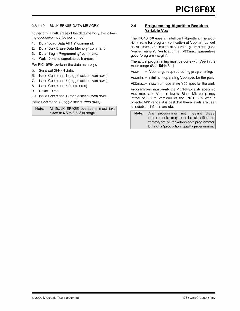
PIC16F8X
2.3.1.10 BULK ERASE DATA MEMORY
To perform a bulk erase of the data memory, the follow-ing sequence must be performed.
1. Do a “Load Data All 1’s” command.
2. Do a “Bulk Erase Data Memory” command.3. Do a “Begin Programming” command.4. Wait 10 ms to complete bulk erase.
For PIC16F84 perform the data memory).
5. Send out 3FFFH data.
6. Issue Command 1 (toggle select even rows).7. Issue Command 7 (toggle select even rows).8. Issue Command 8 (begin data)
9. Delay 10 ms10. Issue Command 1 (toggle select even rows).
Issue Command 7 (toggle select even rows).
2.4 Programming Algorithm Requires Variable VDD
The PIC16F8X uses an intelligent algorithm. The algo-rithm calls for program verification at VDDmin. as wellas VDDmax. Verification at VDDmin. guarantees good“erase margin”. Verification at VDDmax guaranteesgood “program margin”.
The actual programming must be done with VDD in theVDDP range (See Table 5-1).
VDDP = VCC range required during programming.
VDDmin. = minimum operating VDD spec for the part.
VDDmax.= maximum operating VDD spec for the part.
Programmers must verify the PIC16F8X at its specifiedVDD max. and VDDmin levels. Since Microchip mayintroduce future versions of the PIC16F8X with abroader VDD range, it is best that these levels are userselectable (defaults are ok). Note: All BULK ERASE operations must take
place at 4.5 to 5.5 VDD range. Note: Any programmer not meeting theserequirements may only be classified as“prototype” or “development” programmerbut not a “production” quality programmer.
2000 Microchip Technology Inc. DS30262C-page 3-157

PIC16F8X
3.0 CONFIGURATION WORDThe PIC16F8X has five configuration bits. These bitscan be set (reads ‘0’) or left unchanged (reads ‘1’) toselect various device configurations.
3.1 Device ID Word
The device ID word for the PIC16F8XX is located at2006h.
FIGURE 3-1: CONFIGURATION WORD BIT MAP FOR PIC16F83/CR83/F84/CR84/F84A
TABLE 3-1:
DeviceDevice ID Value
Dev Rev
PIC16F84A 00 0101 010 0 0000
PIC16F877 00 1001 101 0 0000
Bit Number: 13 12 11 10 9 8 7 6 5 4 3 2 1 0
PIC16F83/F84/F84A
CP CP CP CP CP CP CP CP CP CP PWRTE WDTE FOSC1 FOSC0
PIC16CR83/CR84
CP CP CP CP CP CP DP CP CP CP PWRTE WDTE FOSC1 FOSC0
bit 4-13: CP, Code Protection Configuration Bits1 = code protection off0 = code protection on
bit 7: PIC16CR83/CR84 onlyDP, Data Memory Code Protection Bit1 = code protection off0 = data memory is code protected
bit 3: PWRTE, Power Up Timer Enable Configuration Bit1 = Power up timer disabled0 = Power up timer enabled
bit 2: WDTE, WDT Enable Configuration Bits1 = WDT enabled0 = WDT disabled
bit 1-0 FOSC<1:0>, Oscillator Selection Configuration Bits11: RC oscillator10: HS oscillator01: XT oscillator00: LP oscillator
DS30262C-page 3-158 2000 Microchip Technology Inc.

PIC16F8X
FIGURE 3-2: CONFIGURATION WORD FOR PIC16F877
CP1 CP0 BKBUG - WRT CPD LVP BODEN CP1 CP0 PWRTE WDTE F0SC1 F0SC0 Register: CONFIGAddress 2007hbit13 bit0
bit 13-12:bit 11: BKBUG: Background Debugger Mode (This bit documented as reserved in data sheet) 1 = Background debugger functions not enabled
0 = Background debugger functional.bit 5-4: CP1:CP0: Flash Program Memory Code Protection bits (2)
11 = Code protection off10 = 1F00h to 1FFFh code protected 01 = 1000h to 1FFFh code protected 00 = 0000h to 1FFFh code protected
bit 11: Reserved: Set to ‘1’ for normal operation bit 10: Unimplemented: Read as ‘1’bit 9: WRT: Flash Program Memory Write Enable 1 = Unprotected program memory may be written to by EECON control
0 = Unprotected program memory may not be written to by EECON controlbit 8: CPD: Data EE Memory Code Protection 1 = Code protection off
0 = Data EE memory code protected
bit 7: LVP: Low voltage programming Enable bit1 = RB3/PGM pin has PGM function, low voltage programming enabled0 = RB3 is digital I/O, HV on MCLR must be used for programming
bit 6: BODEN: Brown-out Reset Enable bit (1)
1 = BOR enabled0 = BOR disabled
bit 3: PWRTE: Power-up Timer Enable bit (1)
1 = PWRT disabled0 = PWRT enabled
bit 2: WDTE: Watchdog Timer Enable bit1 = WDT enabled0 = WDT disabled
bit 1-0: FOSC1:FOSC0: Oscillator Selection bits11 = RC oscillator10 = HS oscillator01 = XT oscillator00 = LP oscillator
Note 1: Enabling Brown-out Reset automatically enables Power-up Timer (PWRT) regardless of the value of bit PWRTE. Ensure the Power-up Timer is enabled anytime Brown-out Reset is enabled.
2: All of the CP1:CP0 pairs have to be given the same value to enable the code protection scheme listed.
2000 Microchip Technology Inc. DS30262C-page 3-159

PIC16F8X
4.0 CODE PROTECTIONFor PIC16F8X devices, once code protection isenabled, all program memory locations read all 0’s.The ID locations and the configuration word read out inan unscrambled fashion. Further programming is dis-abled for the entire program memory as well as datamemory. It is possible to program the ID locations andthe configuration word.
4.1 Disabling Code-Protection
It is recommended that the following procedure be per-formed before any other programming is attempted. Itis also possible to turn code protection off (code protectbit = 1) using this procedure; however, all data withinthe program memory and the data memory will beerased when this procedure is executed, and thus,the security of the data or code is not compro-mised.
Procedure to disable code protect:
a) Execute load configuration (with a ‘1’ in bit 4, code protect).
b) Increment to configuration word location(0x2007)
c) Execute command (000001)d) Execute command (000111)
e) Execute ‘Begin Programming’ (001000)f) Wait 10 msg) Execute command (000001)
h) Execute command (000111)
4.2 Embedding Configuration Word and ID Information in the Hex File
TABLE 4-1: CONFIGURATION WORD
PIC16F83
To code protect: 0000000000XXXX
PIC16CR83
To code protect: 0000000000XXXX
To allow portability of code, the programmer is required to read the configuration word and ID locations from the hexfile when loading the hex file. If configuration word information was not present in the hex file then a simple warningmessage may be issued. Similarly, while saving a hex file, configuration word and ID information must be included.An option to not include this information may be provided.
Specifically for the PIC16F8X, the EEPROM data memory should also be embedded in the hex file (see Section 5.1).
Microchip Technology Inc. feels strongly that this feature is important for the benefit of the end customer.
Program Memory Segment R/W in Protected Mode R/W in Unprotected Mode
Configuration Word (0x2007) Read Unscrambled, Write Enabled Read Unscrambled, Write Enabled
All memory Read All 0’s, Write Disabled Read Unscrambled, Write Enabled
ID Locations [0x2000 : 0x2003] Read Unscrambled, Write Enabled Read Unscrambled, Write Enabled
Program Memory Segment R/W in Protected Mode R/W in Unprotected Mode
Configuration Word (0x2007) Read Unscrambled Read Unscrambled
All memory Read All 0’s for Program Memory,Read All 1’s for Data Memory -Write Disabled
Read Unscrambled, Data Memory - Write Enabled
ID Locations [0x2000 : 0x2003] Read Unscrambled Read Unscrambled
DS30262C-page 3-160 2000 Microchip Technology Inc.

PIC16F8X
PIC16CR84
To code protect: 0000000000XXXX
PIC16F84
To code protect: 0000000000XXXX
PIC16F84A
To code protect: 0000000000XXXX
PIC16F8XX
To code protect: 00X1XXXX00XXXX
Legend: X = Don’t care
Program Memory Segment R/W in Protected Mode R/W in Unprotected Mode
Configuration Word (0x2007) Read Unscrambled Read UnscrambledAll memory Read All 0’s for Program Memory,
Read All 1’s for Data Memory -Write Disabled
Read Unscrambled, Data Memory - Write Enabled
ID Locations [0x2000 : 0x2003] Read Unscrambled Read Unscrambled
Program Memory Segment R/W in Protected Mode R/W in Unprotected Mode
Configuration Word (0x2007) Read Unscrambled, Write Enabled Read Unscrambled, Write EnabledAll memory Read All 0’s, Write Disabled Read Unscrambled, Write EnabledID Locations [0x2000 : 0x2003] Read Unscrambled, Write Enabled Read Unscrambled, Write Enabled
Program Memory Segment R/W in Protected Mode R/W in Unprotected Mode
Configuration Word (0x2007) Read Unscrambled, Write Enabled Read Unscrambled, Write EnabledAll memory Read All 0’s, Write Disabled Read Unscrambled, Write Enabled
ID Locations [0x2000 : 0x2003] Read Unscrambled, Write Enabled Read Unscrambled, Write Enabled
Program Memory Segment R/W in Protected Mode R/W in Unprotected Mode
Configuration Word (0x2007) Read Unscrambled, Write Enabled Read Unscrambled, Write Enabled
All memory Read All 0’s, Write Disabled Read Unscrambled, Write EnabledID Locations [0x2000 : 0x2003] Read Unscrambled, Write Enabled Read Unscrambled, Write Enabled
2000 Microchip Technology Inc. DS30262C-page 3-161

PIC16F8X
4.3 CHECKSUM COMPUTATION
4.3.1 CHECKSUM
Checksum is calculated by reading the contents of thePIC16F8X memory locations and adding up theopcodes up to the maximum user addressable location,e.g., 0x1FF for the PIC16F8X. Any carry bits exceeding16-bits are neglected. Finally, the configuration word(appropriately masked) is added to the checksum.Checksum computation for each member of thePIC16F8X devices is shown in Table 4-2.
The checksum is calculated by summing the following:
• The contents of all program memory locations• The configuration word, appropriately masked• Masked ID locations (when applicable)
The least significant 16 bits of this sum is the check-sum.
The following table describes how to calculate thechecksum for each device. Note that the checksum cal-culation differs depending on the code protect setting.Since the program memory locations read out differ-ently depending on the code protect setting, the tabledescribes how to manipulate the actual program mem-ory values to simulate the values that would be readfrom a protected device. When calculating a checksumby reading a device, the entire program memory cansimply be read and summed. The configuration wordand ID locations can always be read.
Note that some older devices have an additional valueadded in the checksum. This is to maintain compatibil-ity with older device programmer checksums.
TABLE 4-2: CHECKSUM COMPUTATION
DeviceCode
ProtectChecksum*
BlankValue
0x25E6 at 0and maxaddress
PIC16F83 OFFON
SUM[0x000:0x1FF] + CFGW & 0x3FFFCFGW & 0x3FFF + SUM_ID
0x3DFF0x3E0E
0x09CD0x09DC
PIC16CR83 OFFON
SUM[0x000:0x1FF] + CFGW & 0x3FFFCFGW & 0x3FFF + SUM_ID
0x3DFF0x3E0E
0x09CD0x09DC
PIC16F84 OFFON
SUM[0x000:0x3FF] + CFGW & 0x3FFFCFGW & 0x3FFF + SUM_ID
0x3BFF0x3C0E
0x07CD0x07DC
PIC16CR84 OFFON
SUM[0x000:0x3FF] + CFGW & 0x3FFFCFGW & 0x3FFF + SUM_ID
0x3BFF0x3C0E
0x07CD0x07DC
PIC16F84A OFFON
SUM[0x000:0x3FF] + CFGW & 0x3FFFCFGW & 0x3FFF + SUM_ID
0x3BFF0x3C0E
0x07CD0x07DC
PIC16F877 OFF SUM[0x0000:0x1FFF] + CFGW & 0x3BFF 0x1BFF 0xE7CD
0X1F00 –
0X1FFF
SUM[0x0000:0x1EFF] + CFGW & 0x3BFF +SUM_ID 0x28EE 0xDAA3
0x1000–
0x1FFF
SUM[0x0000:0x0FFF] + CFGW & 0x3BFF + SUM_ID 0x27DE 0xD993
ALL CFGW & 0x3BFF + SUM_ID 0x27CE 0xF39C
Legend: CFGW = Configuration WordSUM[a:b] = [Sum of locations a to b inclusive]SUM_ID = ID locations masked by 0xF then made into a 16-bit value with ID0 as the most significant nibble. For example, ID0 = 0x1, ID1 = 0x2, ID3 = 0x3, ID4 = 0x4, then SUM_ID = 0x1234*Checksum = [Sum of all the individual expressions] MODULO [0xFFFF]+ = Addition& = Bitwise AND
DS30262C-page 3-162 2000 Microchip Technology Inc.
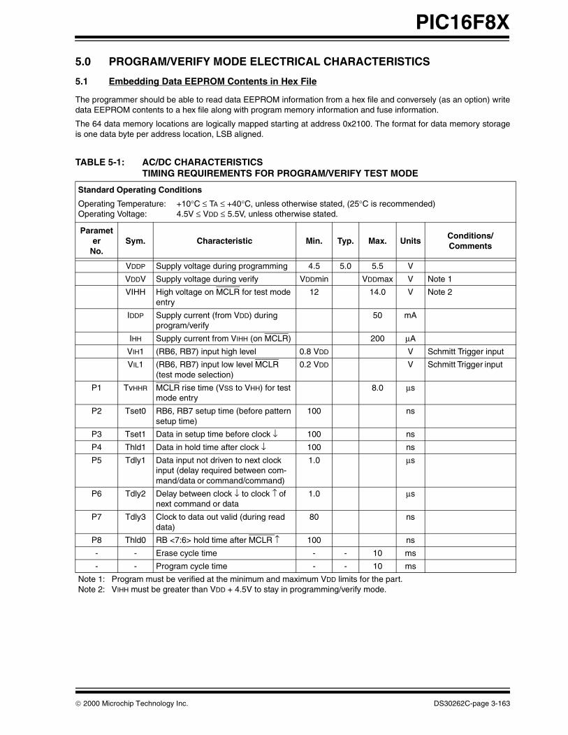
PIC16F8X
5.0 PROGRAM/VERIFY MODE ELECTRICAL CHARACTERISTICS
5.1 Embedding Data EEPROM Contents in Hex File
The programmer should be able to read data EEPROM information from a hex file and conversely (as an option) writedata EEPROM contents to a hex file along with program memory information and fuse information.
The 64 data memory locations are logically mapped starting at address 0x2100. The format for data memory storageis one data byte per address location, LSB aligned.
TABLE 5-1: AC/DC CHARACTERISTICSTIMING REQUIREMENTS FOR PROGRAM/VERIFY TEST MODE
Standard Operating Conditions
Operating Temperature: +10°C ≤ TA ≤ +40°C, unless otherwise stated, (25°C is recommended)Operating Voltage: 4.5V ≤ VDD ≤ 5.5V, unless otherwise stated.
Parameter
No.Sym. Characteristic Min. Typ. Max. Units
Conditions/Comments
VDDP Supply voltage during programming 4.5 5.0 5.5 V
VDDV Supply voltage during verify VDDmin VDDmax V Note 1
VIHH High voltage on MCLR for test mode entry
12 14.0 V Note 2
IDDP Supply current (from VDD) during program/verify
50 mA
IHH Supply current from VIHH (on MCLR) 200 µA
VIH1 (RB6, RB7) input high level 0.8 VDD V Schmitt Trigger input
VIL1 (RB6, RB7) input low level MCLR (test mode selection)
0.2 VDD V Schmitt Trigger input
P1 TvHHR MCLR rise time (VSS to VHH) for test mode entry
8.0 µs
P2 Tset0 RB6, RB7 setup time (before pattern setup time)
100 ns
P3 Tset1 Data in setup time before clock ↓ 100 ns
P4 Thld1 Data in hold time after clock ↓ 100 ns
P5 Tdly1 Data input not driven to next clock input (delay required between com-mand/data or command/command)
1.0 µs
P6 Tdly2 Delay between clock ↓ to clock ↑ of next command or data
1.0 µs
P7 Tdly3 Clock to data out valid (during read data)
80 ns
P8 Thld0 RB <7:6> hold time after MCLR ↑ 100 ns
- - Erase cycle time - - 10 ms
- - Program cycle time - - 10 ms
Note 1: Program must be verified at the minimum and maximum VDD limits for the part.Note 2: VIHH must be greater than VDD + 4.5V to stay in programming/verify mode.
2000 Microchip Technology Inc. DS30262C-page 3-163
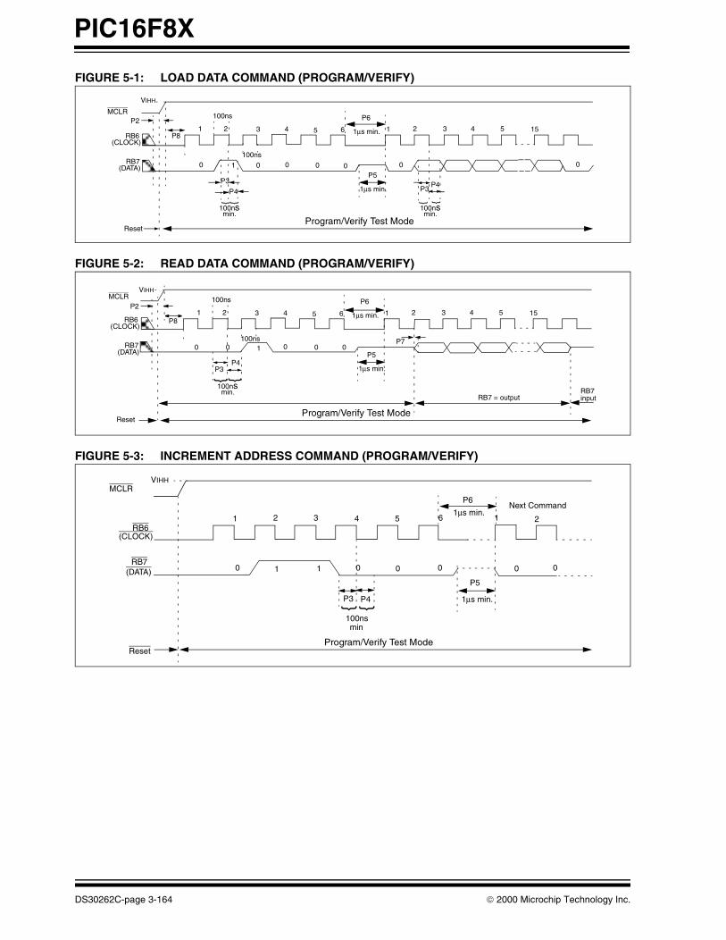
PIC16F8X
FIGURE 5-1: LOAD DATA COMMAND (PROGRAM/VERIFY)
FIGURE 5-2: READ DATA COMMAND (PROGRAM/VERIFY)
FIGURE 5-3: INCREMENT ADDRESS COMMAND (PROGRAM/VERIFY)
100nsmin.
P4P3
000
1µs min.
P5
1µs min.
P6
0
155432165
Program/Verify Test Mode
0
43
0
100ns
P4
1
100nsmin.
P3
Reset
21
100ns
P8
VIHH
RB6(CLOCK)
RB7(DATA) 0
MCLRP2
00
1µs min.
P5
1µs min.
P6
155432165
Program/Verify Test Mode
0
43
0100ns
P4
1
100nsmin.
P3
Reset
21
100ns
P8
VIHH
RB6(CLOCK)
RB7(DATA)
0
MCLR
RB7 = outputRB7input
P7
P2
000 0 0 01 1
1 2 3 4 5 6 1 2
100nsmin
P3 P4
P6
1µs min.Next Command
P5
1µs min.
VIHHMCLR
RB6(CLOCK)
(DATA)RB7
ResetProgram/Verify Test Mode
DS30262C-page 3-164 2000 Microchip Technology Inc.

PIC16F8XXIn-Circuit Serial Programming for PIC16F8XX FLASH MCUs
This document includes the programming specifications for the following devices:
1.0 PROGRAMMING THE PIC16F8XX
The PIC16F8XX is programmed using a serial method.The serial mode will allow the PIC16F8XX to be pro-grammed while in the users system. This allows forincreased design flexibility. This programming specifi-cation applies to PIC16F8XX devices in all packages.
PIC16F8XX devices may be programmed using a sin-gle +5 volt supply (low voltage programming mode).
1.1 Hardware Requirements
The PIC16F8XX requires one programmable powersupply for VDD (4.5V to 5.5V) and a VPP of 12V to 14Vor VPP of (4.5V to 5.5V) when using low voltage In-Cir-cuit Serial Programming™ (ICSP™). Both suppliesshould have a minimum resolution of 0.25V.
1.2 Programming Mode
The programming mode for the PIC16F8XX allows pro-gramming of user program memory, data memory, spe-cial locations used for ID, and the configuration word.
Pin Diagram
• PIC16F870 • PIC16F874
• PIC16F871 • PIC16F876
• PIC16F872 • PIC16F877
• PIC16F873
PDIP, SOIC
RB7RB6
RB5
RB4RB3
RB2
RB1
RB0/INT
VDD
VSS
RD7/PSP7
RD6/PSP6RD5/PSP5
RD4/PSP4
RC7/RX/DT
RC6/TX/CK
RC5/SDO
RC4/SDI/SDARD3/PSP3
RD2/PSP2
MCLR/VPP
RA0/AN0
RA1/AN1RA2/AN2/VREF
RA3/AN3/VREF
RA4/T0CKI
RA5/AN4/SS
RE0/RD/AN5
RE1/WR/AN6
RE2/CS/AN7VDD
VSS
OSC1/CLKIN
OSC2/CLKOUT
RC0/T1OSO/T1CKI
RC1/T1OSI/CCP2
RC2/CCP1
RC3/SCK/SCLRD0/PSP0
RD1/PSP1
1
2
3
4
5
6
7
8
9
10
11
12
13
14
15
16
17
18
19
20
40
39
38
37
36
35
34
33
32
31
30
2928
27
26
25
24
23
22
21
PIC
16F877/874/871
PIC
16F876/873/872/870
1011
23456
1
87
9
121314 15
1617181920
232425
262728
2221
MCLR/VPP
RA0/AN0RA1/AN1
RA2/AN2/VREF
RA3/AN3/VREF
RA4/T0CKIRA5/AN4/SS
VSS
OSC1/CLKINOSC2/CLKOUT
RC0/T1OSO/T1CKIRC1/T1OSI/CCP2
RC2/CCP1RC3/SCK/SCL
RB7RB6RB5RB4RB3RB2RB1RB0/INTVDD
VSS
RC7/RX/DTRC6/TX/CKRC5/SDORC4/SDI/SDA
PIN DESCRIPTIONS (DURING PROGRAMMING): PIC16F8XX
Pin NameDuring Programming
Function Pin Type Pin Description
RB3 PGM I Low voltage ICSP programming input if configuration bit equals 1
RB6 CLOCK I Clock input
RB7 DATA I/O Data input/output
MCLR VTEST MODE P* Program Mode Select
VDD VDD P Power Supply
VSS VSS P Ground
Legend: I = Input, O = Output, P = Power
*In the PIC16F8XX, the programming high voltage is internally generated. To activate the programming mode, high voltage needsto be applied to MCLR input. Since the MCLR is used for a level source, this means that MCLR does not draw any significant current.
2000 Microchip Technology Inc. DS39025D-page 3-165
In-circuit Serial Programming (ICSP) is a trademark of Microchip Technology Inc.

PIC16F8XX
2.0 PROGRAM MODE ENTRY
2.1 User Program Memory Map
The user memory space extends from 0x0000 to0x1FFF (8K). In programming mode the program mem-ory space extends from 0x0000 to 0x3FFF, with the firsthalf (0x0000-0x1FFF) being user program memory andthe second half (0x2000-0x3FFF) being configurationmemory. The PC will increment from 0x0000 to 0x1FFFand wrap to 0x000, 0x2000 to 0x3FFF and wraparound to 0x2000 (not to 0x0000). Once in configura-tion memory, the highest bit of the PC stays a ‘1’, thusalways pointing to the configuration memory. The onlyway to point to user program memory is to reset thepart and reenter program/verify mode as described inSection 2.3.
In the configuration memory space, 0x2000-0x200Fare physically implemented. However, only locations0x2000 through 0x2007 are available. Other locationsare reserved. Locations beyond 0x200F will physicallyaccess user memory. (See Figure 2-1).
2.2 ID Locations
A user may store identification information (ID) in fourID locations. The ID locations are mapped in [0x2000 :0x2003]. It is recommended that the user use only thefour least significant bits of each ID location. In somedevices, the ID locations read-out in an unscrambledfashion after code protection is enabled. For thesedevices, it is recommended that ID location is written as“11 1111 1000 bbbb” where ‘bbbb’ is ID information.
In other devices, the ID locations read out normally,even after code protection. To understand how thedevices behave, refer to Table 4-1.
To understand the scrambling mechanism after codeprotection, refer to Section 4.0.
DS39025D-page 3-166 2000 Microchip Technology Inc.

PIC16F8XX
FIGURE 2-1: PROGRAM MEMORY MAPPING
2Kwords
4Kwords
8Kwords
Implemented Implemented Implemented
Implemented Implemented Implemented
Implemented Implemented
Implemented Implemented
Reserved Implemented
Reserved Implemented
Implemented
Implemented
Reserved Reserved Reserved
Reserved Reserved Reserved
ID Location
ID Location
ID Location
ID Location
Reserved
Reserved
Device ID
Configuration Word
2000h
2001h
2002h
2003h
2004h
2005h
2006h
2007h
0h
1FFh
3FFh
400h
7FFh
800h
BFFh
C00h
FFFh
1000h
1FFFh
2008h
2100h
3FFFh
2000 Microchip Technology Inc. DS39025D-page 3-167

PIC16F8XX
2.3 Program/Verify Mode
The program/verify mode is entered by holding pinsRB6 and RB7 low while raising MCLR pin from VIL toVIHH (high voltage). In this mode, the state of the RB3pin does not effect programming. Low-voltage ICSPprogramming mode is entered by applying VDD toMCLR and raising RB3 from VIL to VDD. Once in thismode the user program memory and the configurationmemory can be accessed and programmed in serialfashion. The mode of operation is serial, and the mem-ory that is accessed is the user program memory. RB6and RB7 are Schmitt Trigger Inputs in this mode.
The sequence that enters the device into the program-ming/verify mode places all other logic into the resetstate (the MCLR pin was initially at VIL). This meansthat all I/O are in the reset state (High impedanceinputs).
The normal sequence for programming is to use theload data command to set a value to be written at theselected address. Issue the begin programming com-mand followed by read data command to verify, andthen increment the address.
A device reset will clear the PC and set the address to0. The “increment address” command will incrementthe PC. The “load configuration” command will se thePC to 0x2000. The available commands are shown inTable 2-1.
2.3.1 LOW-VOLTAGE ICSP PROGRAMMING MODE
When LVP bit is set to ‘1’, the low-voltage ICSP pro-gramming entry is enabled. Since the LVP configura-tion bit allows low voltage ICSP programming entry inits erased state, an erased device will have the LVP bitenabled at the factory. While LVP is ‘1’, RB3 is dedi-cated to low voltage ICSP programming. Bring MCLRto VDD and then RB3 to VDD to enter programmingmode. All other specifications for high-voltage ICSP™apply.
To disable low voltage ICSP mode, the LVP bit must beprogrammed to ‘0’. This must be done while enteredwith high voltage entry mode (LVP bit= 1). RB3 is nowa general purpose I/O pin.
2.3.2 SERIAL PROGRAM/VERIFY OPERATION
The RB6 pin is used as a clock input pin, and the RB7pin is used for entering command bits and data input/output during serial operation. To input a command, theclock pin (RB6) is cycled six times. Each command bitis latched on the falling edge of the clock with the leastsignificant bit (LSB) of the command being input first.The data on pin RB7 is required to have a minimumsetup and hold time (see AC/DC specifications) withrespect to the falling edge of the clock. Commands thathave data associated with them (read and load) arespecified to have a minimum delay of 1 µs between thecommand and the data. After this delay, the clock pin iscycled 16 times with the first cycle being a start bit andthe last cycle being a stop bit. Data is also input andoutput LSB first.
Therefore, during a read operation the LSB will betransmitted onto pin RB7 on the rising edge of the sec-ond cycle, and during a load operation the LSB will belatched on the falling edge of the second cycle. A min-imum 1µs delay is also specified between consecutivecommands.
All commands are transmitted LSB first. Data wordsare also transmitted LSB first. The data is transmittedon the rising edge and latched on the falling edge ofthe clock. To allow for decoding of commands andreversal of data pin configuration, a time separation ofat least 1 µs is required between a command and adata word (or another command).
The commands that are available are:
2.3.2.1 LOAD CONFIGURATION
After receiving this command, the program counter(PC) will be set to 0x2000. By then applying 16 cyclesto the clock pin, the chip will load 14-bits in a “dataword,” as described above, to be programmed into theconfiguration memory. A description of the memorymapping schemes of the program memory for normaloperation and configuration mode operation is shownin Figure 2-1. After the configuration memory isentered, the only way to get back to the user programmemory is to exit the program/verify test mode by tak-ing MCLR low (VIL).
Note: The OSC must not have 72 osc clockswhile the device MCLR is between VIL andVIHH.
DS39025D-page 3-168 2000 Microchip Technology Inc.

PIC16F8XX
2.3.2.2 LOAD DATA FOR PROGRAM MEMORY
After receiving this command, the chip will load in a14-bit “data word” when 16 cycles are applied, asdescribed previously. A timing diagram for the load datacommand is shown in Figure 5-1.
TABLE 2-1: COMMAND MAPPING FOR PIC16F84A/PIC16F877
Command Mapping (MSB … LSB) Data
Load Configuration X X 0 0 0 0 0, data (14), 0
Load Data for Program Memory X X 0 0 1 0 0, data (14), 0
Read Data from Program Memory X X 0 1 0 0 0, data (14), 0
Increment Address X X 0 1 1 0
Begin Erase Programming Cycle 0 0 1 0 0 0
Begin Programming Only Cycle 0 1 1 0 0 0
Load Data for Data Memory X X 0 0 1 1 0, data (14), 0
Read Data from Data Memory X X 0 1 0 1 0, data (14), 0
Bulk Erase Program Memory X X 1 0 0 1
Bulk Erase Data Memory X X 1 0 1 1
2000 Microchip Technology Inc. DS39025D-page 3-169

PIC16F8XX
FIGURE 2-2: PROGRAM FLOW CHART - PIC16F8XX PROGRAM MEMORY
Start
Set VDD = VDDP
Program Cycle
Read Data Command
Data Correct?Report
ProgrammingFailure
All LocationsDone?
Verify allLocations @
VDDMIN
Data Correct?
Verify allLocations @
VDDMAX
Data Correct?
Done
IncrementAddress
Command
Report VerifyError @VDDMIN
Report VerifyError @VDDMAX
Load DataCommand
BeginProgramming
Command
Wait tprog
PROGRAM CYCLE
No
No
No
No
DS39025D-page 3-170 2000 Microchip Technology Inc.

PIC16F8XX
FIGURE 2-3: PROGRAM FLOW CHART - PIC16F8XX CONFIGURATION MEMORY
Program ID
Start
LoadConfiguration
Data
Location? Program CycleRead Data Command
Data Correct?Report
ProgrammingFailure
IncrementAddress
Command
Address = 0x2004?
IncrementAddress
Command
IncrementAddress
Command
IncrementAddress
Command
ProgramCycle
(Config. Word)
Set VDD = VDDMAX
Read Data CommandData Correct?
Set VDD = VDDMAX
Read Data CommandData Correct?
Report ProgramConfigutationWord Error
Done
Yes
No
No
Yes
YesNo
No
Yes
Yes
No
2000 Microchip Technology Inc. DS39025D-page 3-171

PIC16F8XX
2.3.2.3 LOAD DATA FOR DATA MEMORY
After receiving this command, the chip will load in a 14-bit “data word” when 16 cycles are applied. However,the data memory is only 8-bits wide, and thus only thefirst 8-bits of data after the start bit will be programmedinto the data memory. It is still necessary to cycle theclock the full 16 cycles in order to allow the internal cir-cuitry to reset properly. The data memory contains 64words. Only the lower 8-bits of the PC are decoded bythe data memory, and therefore if the PC is greater than0x3F, it will wrap around and address a location withinthe physically implemented memory. If the device iscode protected, the data is read as all zeros.
2.3.2.4 READ DATA FROM PROGRAM MEMORY
After receiving this command, the chip will transmitdata bits out of the program memory (user or configu-ration) currently accessed starting with the second ris-ing edge of the clock input. The RB7 pin will go intooutput mode on the second rising clock edge, and it willrevert back to input mode (hi-impedance) after the 16thrising edge. A timing diagram of this command isshown in Figure 5-2.
2.3.2.5 READ DATA FROM DATA MEMORY
After receiving this command, the chip will transmitdata bits out of the data memory starting with the sec-ond rising edge of the clock input. The RB7 pin will gointo output mode on the second rising edge, and it willrevert back to input mode (hi-impedance) after the 16thrising edge. As previously stated, the data memory is 8-bits wide, and therefore, only the first 8-bits that are out-put are actual data.
2.3.2.6 INCREMENT ADDRESS
The PC is incremented when this command isreceived. A timing diagram of this command is shownin Figure 5-3.
2.3.2.7 BEGIN ERASE/PROGRAM CYCLE
A load command must be given before every beginprogramming command. Programming of the appro-priate memory (test program memory, user programmemory or data memory) will begin after this commandis received and decoded. An internal timing mechanismexecutes an erase before write. The user must allow forboth erase and programming cycle times for program-ming to complete. No “end programming” command isrequired.
2.3.2.8 BEGIN PROGRAMMING
A load command must be given before every beginprogramming command. Programming of the appro-priate memory (test program memory, user programmemory or data memory) will begin after this commandis received and decoded. An internal timing mechanismexecutes a write. The user must allow for program cycletime for programming to complete. No “end program-ming” command is required.
This command is similar to the ERASE/PROGRAMCYCLE command, except that a word erase is notdone. It is recommended that a bulk erase be per-formed before starting a series of programming onlycycles.
2.3.2.9 BULK ERASE PROGRAM MEMORY
After this command is performed, the next programcommand will erase the entire program memory.
To perform a bulk erase of the program memory, the fol-lowing sequence must be performed.
1. Do a “Load Data All 1’s” command.2. Do a “Bulk Erase Program Memory” command.3. Do a “Begin Programming” command.
4. Wait 10 ms to complete bulk erase.
If the address is pointing to the test program memory(0x2000 - 0x200F), then both the user memory and thetest memory will be erased. The configuration word willnot be erased, even if the address is pointing to location0x2007.
2.3.2.10 BULK ERASE DATA MEMORY
To perform a bulk erase of the data memory, the follow-ing sequence must be performed.
1. Do a “Load Data All 1’s” command.2. Do a “Bulk Erase Data Memory” command.
3. Do a “Begin Programming” command.4. Wait 10 ms to complete bulk erase.
Note: If the device is code-protected, the BULKERASE command will not work.
Note: All BULK ERASE operations must takeplace at 4.5 to 5.5 VDD range.
DS39025D-page 3-172 2000 Microchip Technology Inc.

PIC16F8XX
2.4 Programming Algorithm Requires Variable VDD
The PIC16F8XX uses an intelligent algorithm. Thealgorithm calls for program verification at VDDmin. aswell as VDDmax. Verification at VDDmin. guaranteesgood “erase margin”. Verification at VDDmax guaran-tees good “program margin”.
The actual programming must be done with VDD in theVDDP range (See Table 5-1).
VDDP = VCC range required during programming.
VDDmin. = minimum operating VDD spec for the part.
VDDmax.= maximum operating VDD spec for the part.
Programmers must verify the PIC16F8XX at its speci-fied VDD max. and VDDmin levels. Since Microchip mayintroduce future versions of the PIC16F8XX with abroader VDD range, it is best that these levels are userselectable (defaults are ok).
Note: Any programmer not meeting theserequirements may only be classified as“prototype” or “development” programmerbut not a “production” quality programmer.
2000 Microchip Technology Inc. DS39025D-page 3-173

PIC16F8XX
3.0 CONFIGURATION WORDThe PIC16F8XX has several configuration bits. Thesebits can be set (reads ‘0’) or left unchanged (reads ‘1’)to select various device configurations.
3.1 Device ID Word
The device ID word for the PIC16F8XX is located at2006h.
FIGURE 3-1: CONFIGURATION WORD FOR PIC16F873/874/876/877
TABLE 3-1: DEVICE ID VALUE
DeviceDevice ID Value
Dev Rev
PIC16F870 00 1101 000 x xxxx
PIC16F871 00 1101 001 x xxxx
PIC16F872 00 1000 111 x xxxx
PIC16F873 00 1001 011 x xxxx
PIC16F874 00 1001 001 x xxxx
PIC16F876 00 1001 111 x xxxx
PIC16F877 00 1001 101 x xxxx
CP1 CP0 RESV - WRT CPD LVP BODEN CP1 CP0 PWRTE WDTE F0SC1 F0SC0 Register: CONFIGAddress 2007hbit13 bit0
bit 13-12:bit 11: Reserved: Set to ‘1’ for normal operationbit 5-4: CP1:CP0: Flash Program Memory Code Protection bits (2)
4K Devices:11 = Code protection off10 = not supported01 = not supported00 = 0000h to 0FFFh code protected
8K Devices:11 = Code protection off10 = 1F00h to 1FFFh code protected 01 = 1000h to 1FFFh code protected 00 = 0000h to 1FFFh code protected
bit 11: Reserved: Set to ‘1’ for normal operation bit 10: Unimplemented: Read as ‘1’bit 9: WRT: Flash Program Memory Write Enable 1 = Unprotected program memory may be written to by EECON control
0 = Unprotected program memory may not be written to by EECON controlbit 8: CPD: Data EE Memory Code Protection 1 = Code protection off
0 = Data EE memory code protected
bit 7: LVP: Low voltage programming Enable bit1 = RB3/PGM pin has PGM function, low voltage programming enabled0 = RB3 is digital I/O, HV on MCLR must be used for programming
bit 6: BODEN: Brown-out Reset Enable bit (1)
1 = BOR enabled0 = BOR disabled
bit 3: PWRTE: Power-up Timer Enable bit (1)
1 = PWRT disabled0 = PWRT enabled
bit 2: WDTE: Watchdog Timer Enable bit1 = WDT enabled0 = WDT disabled
bit 1-0: FOSC1:FOSC0: Oscillator Selection bits11 = RC oscillator10 = HS oscillator01 = XT oscillator00 = LP oscillator
Note 1: Enabling Brown-out Reset automatically enables Power-up Timer (PWRT) regardless of the value of bit PWRTE. Ensure the Power-up Timer is enabled anytime Brown-out Reset is enabled.
2: All of the CP1:CP0 pairs have to be given the same value to enable the code protection scheme listed.
DS39025D-page 3-174 2000 Microchip Technology Inc.

PIC16F8XX
FIGURE 3-2: CONFIGURATION WORD FOR PIC16F870/871/872
CP1 CP0 RESV - WRT CPD LVP BODEN CP1 CP0 PWRTE WDTE F0SC1 F0SC0 Register: CONFIGAddress 2007hbit13 bit0
bit 13-12:bit 5-4: CP1:CP0: Flash Program Memory Code Protection bits (2)
11 = Code protection off10 = not supported01 = not supported00 = 0000h to 07FFh code protected
bit 11: Reserved: Set to ‘1’ for normal operation bit 10: Unimplemented: Read as ‘1’bit 9: WRT: Flash Program Memory Write Enable 1 = Unprotected program memory may be written to by EECON control
0 = Unprotected program memory may not be written to by EECON controlbit 8: CPD: Data EE Memory Code Protection 1 = Code protection off
0 = Data EE memory code protected
bit 7: LVP: Low voltage programming Enable bit1 = RB3/PGM pin has PGM function, low voltage programming enabled0 = RB3 is digital I/O, HV on MCLR must be used for programming
bit 6: BODEN: Brown-out Reset Enable bit (1)
1 = BOR enabled0 = BOR disabled
bit 3: PWRTE: Power-up Timer Enable bit (1)
1 = PWRT disabled0 = PWRT enabled
bit 2: WDTE: Watchdog Timer Enable bit1 = WDT enabled0 = WDT disabled
bit 1-0: FOSC1:FOSC0: Oscillator Selection bits11 = RC oscillator10 = HS oscillator01 = XT oscillator00 = LP oscillator
Note 1: Enabling Brown-out Reset automatically enables Power-up Timer (PWRT) regardless of the value of bit PWRTE. Ensure the Power-up Timer is enabled anytime Brown-out Reset is enabled.
2: All of the CP1:CP0 pairs have to be given the same value to enable the code protection scheme listed.
2000 Microchip Technology Inc. DS39025D-page 3-175

PIC16F8XX
4.0 CODE PROTECTIONFor PIC16F8XX devices, once code protection isenabled, all program memory locations read all 0’s.The ID locations and the configuration word read out inan unscrambled fashion. Further programming is dis-abled for the entire program memory as well as datamemory. It is possible to program the ID locations andthe configuration word.
4.1 Disabling Code-Protection
It is recommended that the following procedure be per-formed before any other programming is attempted. Itis also possible to turn code protection off (code protectbit = 1) using this procedure; however, all data withinthe program memory and the data memory will beerased when this procedure is executed, and thus,the security of the data or code is not compro-mised.
Procedure to disable code protect:
a) Execute load configuration (with a ‘1’ in bit 13-4,code protect).
b) Increment to configuration word location(0x2007)
c) Execute command (000001)d) Execute command (000111)
e) Execute ‘Begin Programming’ (001000)f) Wait 12 msg) Execute command (000001)
h) Execute command (000111)
4.2 Embedding Configuration Word and ID Information in the Hex File
To allow portability of code, the programmer is required to read the configuration word and ID locations from the hexfile when loading the hex file. If configuration word information was not present in the hex file then a simple warningmessage may be issued. Similarly, while saving a hex file, configuration word and ID information must be included.An option to not include this information may be provided.
Specifically for the PIC16F8XX, the EEPROM data memory should also be embedded in the hex file (seeSection 5.1).
Microchip Technology Inc. feels strongly that this feature is important for the benefit of the end customer.
DS39025D-page 3-176 2000 Microchip Technology Inc.
PIC16F8XX
4.3 CHECKSUM COMPUTATION
4.3.1 CHECKSUM
Checksum is calculated by reading the contents of thePIC16F8XX memory locations and adding up theopcodes up to the maximum user addressable location,e.g., 0x1FF for the PIC16F8XX. Any carry bits exceed-ing 16-bits are neglected. Finally, the configurationword (appropriately masked) is added to the check-sum. Checksum computation for each member of thePIC16F8XX devices is shown in Table 4-1.
The checksum is calculated by summing the following:
• The contents of all program memory locations• The configuration word, appropriately masked
• Masked ID locations (when applicable)
The least significant 16 bits of this sum is the check-sum.
The following table describes how to calculate thechecksum for each device. Note that the checksum cal-culation differs depending on the code protect setting.Since the program memory locations read out differ-ently depending on the code protect setting, the tabledescribes how to manipulate the actual program mem-ory values to simulate the values that would be readfrom a protected device. When calculating a checksumby reading a device, the entire program memory cansimply be read and summed. The configuration wordand ID locations can always be read.
Note that some older devices have an additional valueadded in the checksum. This is to maintain compatibil-ity with older device programmer checksums.
2000 Microchip Technology Inc. DS39025D-page 3-177

PIC16F8XX
TABLE 4-1: CHECKSUM COMPUTATION
DeviceCode
ProtectChecksum*
Blank”Value
0x25E6 at 0and maxaddress
PIC16F870 OFF SUM[0x0000:0x07FFF] + CFGW & 0x3BFF 0x33FF 0xFFCD
ALL CFGW & 0x3BFF + SUM_ID 0x3FCE 0x0B9C
PIC16F871 OFF SUM[0x0000:0x07FFF] + CFGW & 0x3BFF 0x33FF 0xFFCD
ALL CFGW & 0x3BFF + SUM_ID 0x3FCE 0x0B9C
PIC16F872 OFF SUM[0x0000:0x07FFF] + CFGW & 0x3BFF 0x33FF 0xFFCD
ALL CFGW & 0x3BFF + SUM_ID 0x3FCE 0x0B9C
PIC16F873 OFF SUM[0x0000:0x0FFF] + CFGW & 0x3BFF 0x2BFF 0xF7CD
0x0F00 : 0xFFF SUM[0x0000:0x0EFF] + CFGW & 0x3BFF +SUM_ID 0x48EE 0xFAA3
0x0800 : 0xFFF SUM[0x0000:0x07FF] + CFGW & 0x3BFF + SUM_ID 0x3FDE 0xF193
ALL CFGW & 0x3BFF + SUM_ID 0x37CE 0x039C
PIC16F874 OFF SUM[0x0000:0x0FFF] + CFGW & 0x3BFF 0x2BFF 0xF7CD
0x0F00 : 0xFFF SUM[0x0000:0x0EFF] + CFGW & 0x3BFF +SUM_ID 0x48EE 0xFAA3
0x0800 : 0xFFF SUM[0x0000:0x07FF] + CFGW & 0x3BFF + SUM_ID 0x3FDE 0xF193
ALL CFGW & 0x3BFF + SUM_ID 0x37CE 0x039C
PIC16F876 OFF SUM[0x0000:0x1FFF] + CFGW & 0x3BFF 0x1BFF 0xE7CD
0x1F00 : 0x1FFF SUM[0x0000:0x1EFF] + CFGW & 0x3BFF +SUM_ID 0x28EE 0xDAA3
0x1000 : 0x1FFF SUM[0x0000:0x0FFF] + CFGW & 0x3BFF + SUM_ID 0x27DE 0xD993
ALL CFGW & 0x3BFF + SUM_ID 0x27CE 0xF39C
PIC16F877 OFF SUM[0x0000:0x1FFF] + CFGW & 0x3BFF 0x1BFF 0xE7CD
0x1F00 : 0x1FFF SUM[0x0000:0x1EFF] + CFGW & 0x3BFF +SUM_ID 0x28EE 0xDAA3
0x1000 : 0x1FFF SUM[0x0000:0x0FFF] + CFGW & 0x3BFF + SUM_ID 0x27DE 0xD993
ALL CFGW & 0x3BFF + SUM_ID 0x27CE 0xF39C
Legend: CFGW = Configuration WordSUM[a:b] = [Sum of locations a to b inclusive]SUM_ID = ID locations masked by 0xF then made into a 16-bit value with ID0 as the most significant nibble. For example, ID0 = 0x1, ID1 = 0x2, ID3 = 0x3, ID4 = 0x4, then SUM_ID = 0x1234*Checksum = [Sum of all the individual expressions] MODULO [0xFFFF]+ = Addition& = Bitwise AND
DS39025D-page 3-178 2000 Microchip Technology Inc.

PIC16F8XX
5.0 PROGRAM/VERIFY MODE ELECTRICAL CHARACTERISTICS
5.1 Embedding Data EEPROM Contents in Hex File
The programmer should be able to read data EEPROM information from a hex file and conversely (as an option) writedata EEPROM contents to a hex file along with program memory information and fuse information.
The 256 data memory locations are logically mapped starting at address 0x2100. The format for data memory storageis one data byte per address location, LSB aligned.
TABLE 5-1: AC/DC CHARACTERISTICSTIMING REQUIREMENTS FOR PROGRAM/VERIFY MODE
Standard Operating Conditions (unless otherwise stated)Operating Temperature: 0°C ≤ TA ≤ +70°COperating Voltage: 4.5V ≤ VDD ≤ 5.5V
Characteristics Sym Min Typ Max Units Conditions/Comments
General
VDD level for word operations, program memory VDD 2.0 5.5 V
VDD level for word operations, data mem-ory VDD 2.0 5.5 V
VDD level for bulk erase/write operations, program and data memory VDD 4.5 5.5 V
High voltage on MCLR for high-voltage programming entry VIHH VDD + 3.5 13.5 V
Voltage on MCLR for low-voltage programming entry
VIH 4.5 5.5 V
MCLR rise time (VSS to VHH) for testmode entry
tVHHR 1.0 µs
(RB6, RB7) input high level VIH1 0.8VDD V Schmitt Trigger input
(RB6, RB7) input low level VIL1 0.2VDD V Schmitt Trigger input
RB<7:4> setup time before MCLR↑ (test mode selection pattern setup time)
tset0 100 ns
RB<7:4> hold time after MCLR↑ (test mode selection pattern setup time)
thld0 5 µs
Serial Program/Verify
Data in setup time before clock↓ tset1 100 ns
Data in hold time after clock↓ thld1 100 ns
Data input not driven to next clock input (delay required between command/data or command/command)
tdly1 1.0 µs
Delay between clock↓ to clock↑ of next command or data
tdly2 1.0 µs
Clock↑ to data out valid (during read data) tdly3 80 ns
Erase cycle time tera 2 5 ms
Programming cycle time tprog 2 5 ms
2000 Microchip Technology Inc. DS39025D-page 3-179

PIC16F8XX
FIGURE 5-1: LOAD DATA COMMAND HIGH-VOLTAGE MODE (PROGRAM/VERIFY)
FIGURE 5-2: READ DATA COMMAND HIGH-VOLTAGE MODE (PROGRAM/VERIFY)
FIGURE 5-3: INCREMENT ADDRESS COMMAND HIGH-VOLTAGE MODE (PROGRAM/VERIFY)
MCLRVIHH
tset0
RB6(CLOCK)
RB7(DATA)
Reset
tset1
thld1tdly1
1µs min.
Program/Verify Test Mode
tset1
thld1
100ns min.
1µs min.
tdly21 2 3 4 5 6
0 1 0 0 X X
1 2 3 4 5 15 16
strt_bit stp_bit
100ns min.
thld0
MCLRVIHH
tset0
RB6(CLOCK)
RB7(DATA)
Reset
tdly1
1µs min.
Program/Verify Test Mode
tset1
thld1
1µs min.
tdly2
1 2 3 4 5 6
0 0 1 0 X X
1 2 3 4 5 15 16
100ns min.
tdly3
RB7 = input RB7 = outputRB7
input
thld0
strt_bit stp_bit
MCLRVIHH
RB6(CLOCK)
RB7(DATA)
Reset
tdly1
1µs min.
Program/Verify Test Mode
tset1
thld1
1µs min.
tdly2
1 2 3 4 5 6
0 1 1 X X
1 2
100ns min.
X 00
Next Command
DS39025D-page 3-180 2000 Microchip Technology Inc.

PIC16F8XX
FIGURE 5-4: LOAD DATA COMMAND LOW-VOLTAGE MODE (PROGRAM/VERIFY)
FIGURE 5-5: READ DATA COMMAND LOW-VOLTAGE MODE (PROGRAM/VERIFY)
FIGURE 5-6: INCREMENT ADDRESS COMMAND LOW-VOLTAGE MODE (PROGRAM/VERIFY)
MCLRVIH
tset0
RB6(CLOCK)
RB7(DATA)
Reset
tset1
thld1tdly1
1µs min.
Program/Verify Test Mode
tset1
thld1
100ns min.
1µs min.
tdly21 2 3 4 5 6
0 1 0 0 X X
1 2 3 4 5 15 16
strt_bit stp_bit
100ns min.
thld0
RB3
MCLRVIH
tset0
RB6(CLOCK)
RB7(DATA)
Reset
tdly1
1µs min.
Program/Verify Test Mode
tset1
thld1
1µs min.
tdly2
1 2 3 4 5 6
0 0 1 0 X X
1 2 3 4 5 15 16
100ns min.
tdly3
RB7 = input RB7 = outputRB7
input
thld0
strt_bit stp_bit
RB3
MCLRVIH
RB6(CLOCK)
RB7(DATA)
Reset
tdly1
1µs min.
Program/Verify Test Mode
tset1
thld1
1µs min.
tdly2
1 2 3 4 5 6
0 1 1 X X
1 2
100ns min.
X 00
Next Command
RB3
2000 Microchip Technology Inc. DS39025D-page 3-181

PIC16F8XX
NOTES:
DS39025D-page 3-182 2000 Microchip Technology Inc.
SECTION 4APPLICATION NOTES
IN-CIRCUIT SERIAL PROGRAMMING™ (ICSP™) OF CALIBRATION PARAMETERS USING A PICmicro® MICROCONTROLLER .........................................................................................4-1
2000 Microchip Technology Inc. DS30277C-page 4-i

DS30277C-page 4-ii 2000 Microchip Technology Inc.

AN656In-Circuit Serial Programming™ (ICSP™) of Calibration Parameters
Using a PICmicro® Microcontroller
INTRODUCTION
Many embedded control applications, where sensoroffsets, slopes and configuration information are mea-sured and stored, require a calibration step. Tradition-ally, potentiometers or Serial EEPROM devices areused to set up and store this calibration information.This application note will show how to construct a pro-gramming jig that will receive calibration parametersfrom the application mid-range PICmicro® microcon-trollers (MCU) and program this information into theapplication baseline PICmicro MCU using the In-CircuitSerial Programming (ICSP) protocol. This method usesthe PIC16CXXX In-Circuit Serial Programming algo-rithm of the 14-bit core microcontrollers.
PROGRAMMING FIXTURE
A programming fixture is needed to assist with the selfprogramming operation. This is typically a small re-usable module that plugs into the application PCBbeing calibrated. Only five pin connections are neededand this programming fixture can draw its power fromthe application PCB to simplify the connections.
FIGURE 1:
Author: John DayMicrochip Technology Inc.
PIC16CXXXSensor(s)
Application I/O
To Application Input(s)
RAX
RBX
MCLR/VPP
VDD
VSS
RB7
RB6
+5V
10k
Customer Application PCB
VPP
VDD
VSS
RB7
RB6
Calibration Programming Jig
+13V VPPGenerator
PIC16C58
+5V +5V
VDD
GND_ONVPP_ON VSS
MCLR
RB7RB6RB5RB4 RB3
RB2
RB1RC osc
Optional PC Connection
1k
Wait
Done
2000 Microchip Technology Inc. DS00656B-page 4-1
AN656
Electrical Interface
There are a total of five electrical connections neededbetween the application PIC16CXXX microcontrollerand the programming jig:
• MCLR/VPP - High voltage pin used to place appli-cation PIC16CXXX into programming mode
• VDD - +5 volt power supply connection to the application PIC16CXXX
• VSS - Ground power supply connection to the application PIC16CXXX
• RB6 - PORTB, bit6 connection to application PIC16CXXX used to clock programming data
• RB7 - PORTB, bit7 connection to application PIC16CXXX used to send programming data
This programming jig is intended to grab power fromthe application power supply through the VDD connec-tion. The programming jig will require 100 mA of peakcurrent during programming. The application will needto set RB6 and RB7 as inputs, which means externaldevices cannot drive these lines. The calibration datawill be sent to the programming jig by the applicationPIC16CXXX through RB6 and RB7. The programmingjig will later use these lines to clock the calibration datainto the application PIC16CXXX.
Programming Issues
The PIC16CXXX programming specification suggestsverification of program memory at both Maximum andMinimum VDD for each device. This is done to ensureproper programming margins and to detect (and reject)any improperly programmed devices. All productionquality programmers vary VDD from VDDmin to VDDmaxafter programming and verify the device under each ofthese conditions.
Since both the application voltage and it’s tolerancesare known, it is not necessary to verify the PIC16CXXXcalibration parameters at the device VDDmax andVDDmin. It is only necessary to verify at the applicationpower supply Max and Min voltages. This applicationnote shows the nominal (+5V) verification routine andhardware. If the power supply is a regulated +5V, thisis adequate and no additional hardware or software isneeded. If the application power supply is not regulated(such as a battery powered or poorly regulated system)it is important to complete a VDDmin and VDDmax veri-fication cycle following the +5V verification cycle. Seeprogramming specifications for more details on VDD
verification procedures.
• PIC16C5X Programming Specifications - DS30190
• PIC16C55X Programming Specifications - DS30261
• PIC16C6X/7X/9XX Programming Specifications - DS30228
• PIC16C84 Programming Specifications - DS30189
The calibration programming and initial verificationMUST occur at +5V. If the application is intended to runat lower (or higher voltages), a second verification passmust be added where those voltages are applied toVDD and the device is verified.
Note: The designer must consider environmentalconditions, voltage ranges, and agingissues when determining VDD min/maxverification levels. Please refer to the pro-gramming specification for the applicationdevice.
DS00656B-page 4-2 2000 Microchip Technology Inc.

AN656
Communication Format (Application Microcontroller to Programming Jig)
Unused program memory, in the applicationPIC16CXXX, is left unprogrammed as all 1s; thereforethe unprogrammed program memory for the calibrationlook-up table would contain 3FFF (hex). This is inter-preted as an “ADDLW FF”. The application microcon-troller simply needs one “RETLW FF” instruction at theend of the space allocated in program memory for thecalibration parameter look-up table. When the applica-tion microcontroller is powered up, it will receive a “FFh”for each calibration parameter that is looked up; there-fore, it can detect that it is uncalibrated and jump to thecalibration code.
Once the calibration constants are calculated by theapplication PICmicro MCU, they need to be communi-cated to the (PIC16C58A based) programming jig. This
is accomplished through the RB6 and RB7 lines. Theformat is a simple synchronous clock and data formatas shown in Figure 2.
A pull-down on the clock line is used to hold it low. Theapplication microcontroller needs to send the high andlow bytes of the target start address of the calibrationconstants to the calibration jig. Next, the data bytes aresent followed by a checksum of the entire data transferas shown in Figure 1.
Once the data transfer is complete, the checksum isverified by the programming jig and the data printed at9600 baud, 8-bits, no parity, 1 stop bit through RB3. Aconnection to this pin is optional. Next the programmingjig applies +13V, programs and verifies the applicationPIC16CXXX calibration parameters.
FIGURE 2:
FIGURE 1:
RB6
RB7 CALbit7 CALbit6 CALbit5 CALbit4 CALbit3 CALbit2 CALbit1 CALbit0
AddrH AddrL Data 0 Data 1 Data N CKSUM
2000 Microchip Technology Inc. DS00656B-page 4-3

AN656
LED Operation
When the programming jig is waiting for communicationfrom the application PICmicro MCU, both LEDs areOFF. Once a valid data stream is received (with at leastone calibration byte and a correct checksum) theWORK LED is lit while the calibration parameters areprinted through the optional RB3 port. Next, the DONELED is lit to indicate that these parameters are beingprogrammed and verified by the programming jig. Oncethe programming is finished, the WORK LED is extin-guished and the DONE LED remains lit. If any param-eters fail programming, the DONE LED is extinguished;therefore both LEDs would remain off.
FIGURE 3: ISP CALIBRATION JIG PROGRAMMER SCHEMATIC
T0CKI
VSS VDD
VCC VCC
VPP
VCC
VCC
VCC
VPP
VIN
VREF
VCC
VCC VCC
DS00656B-page 4-4 2000 Microchip Technology Inc.
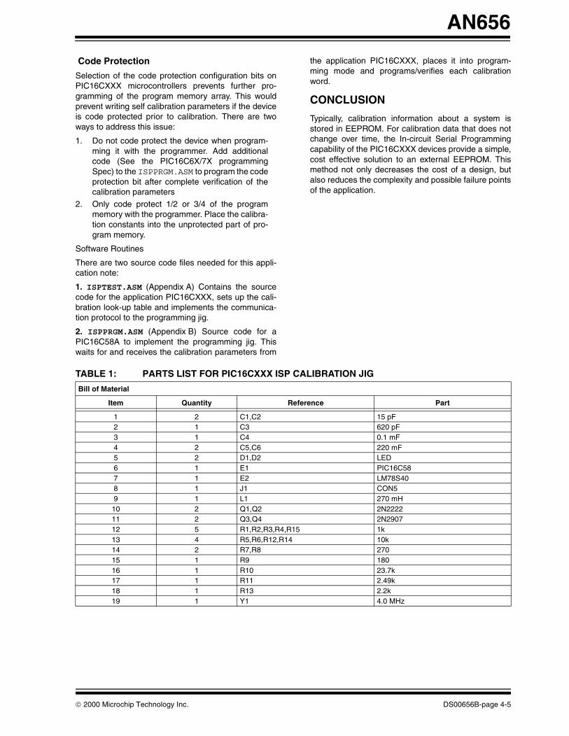
AN656
Code Protection
Selection of the code protection configuration bits onPIC16CXXX microcontrollers prevents further pro-gramming of the program memory array. This wouldprevent writing self calibration parameters if the deviceis code protected prior to calibration. There are twoways to address this issue:
1. Do not code protect the device when program-ming it with the programmer. Add additionalcode (See the PIC16C6X/7X programmingSpec) to the ISPPRGM.ASM to program the codeprotection bit after complete verification of thecalibration parameters
2. Only code protect 1/2 or 3/4 of the programmemory with the programmer. Place the calibra-tion constants into the unprotected part of pro-gram memory.
Software Routines
There are two source code files needed for this appli-cation note:
1. ISPTEST.ASM (Appendix A) Contains the sourcecode for the application PIC16CXXX, sets up the cali-bration look-up table and implements the communica-tion protocol to the programming jig.
2. ISPPRGM.ASM (Appendix B) Source code for aPIC16C58A to implement the programming jig. Thiswaits for and receives the calibration parameters from
the application PIC16CXXX, places it into program-ming mode and programs/verifies each calibrationword.
CONCLUSION
Typically, calibration information about a system isstored in EEPROM. For calibration data that does notchange over time, the In-circuit Serial Programmingcapability of the PIC16CXXX devices provide a simple,cost effective solution to an external EEPROM. Thismethod not only decreases the cost of a design, butalso reduces the complexity and possible failure pointsof the application.
TABLE 1: PARTS LIST FOR PIC16CXXX ISP CALIBRATION JIG
Bill of Material
Item Quantity Reference Part
1 2 C1,C2 15 pF2 1 C3 620 pF3 1 C4 0.1 mF4 2 C5,C6 220 mF5 2 D1,D2 LED6 1 E1 PIC16C587 1 E2 LM78S408 1 J1 CON59 1 L1 270 mH10 2 Q1,Q2 2N222211 2 Q3,Q4 2N290712 5 R1,R2,R3,R4,R15 1k13 4 R5,R6,R12,R14 10k14 2 R7,R8 27015 1 R9 18016 1 R10 23.7k17 1 R11 2.49k18 1 R13 2.2k19 1 Y1 4.0 MHz
2000 Microchip Technology Inc. DS00656B-page 4-5

AN656
APPENDIX A:MPASM 01.40.01 Intermediate ISPPRGM.ASM 3-31-1997 10:57:03 PAGE 1
LOC OBJECT CODE LINE SOURCE TEXT VALUE
00001 ; Filename: ISPPRGM.ASM 00002 ; ********************************************** 00003 ; * Author: John Day * 00004 ; * Sr. Field Applications Engineer * 00005 ; * Microchip Technology * 00006 ; * Revision: 1.0 * 00007 ; * Date August 25, 1995 * 00008 ; * Part: PIC16C58 * 00009 ; * Compiled using MPASM V1.40 * 00010 ; ********************************************** 00011 ; * Include files: * 00012 ; * P16C5X.ASM * 00013 ; ********************************************** 00014 ; * Fuses: OSC: XT (4.0 Mhz xtal) * 00015 ; * WDT: OFF * 00016 ; * CP: OFF * 00017 ;********************************************************************************* 00018 ; This program is intended to be used as a self programmer 00019 ; to store calibration constants into a lookup table 00020 ; within the main system processor. A 4 Mhz crystal 00021 ; is needed and an optional 9600 baud seiral port will 00022 ; display the parameters to be programmed. 00023 ; ;********************************************************************************* 00024 ; * Program Memory: * 00025 ; * Words - communication with test jig * 00026 ; * 17 Words - calibration look-up table (16 bytes of data) * 00027 ; * 13 Words - Test Code to generate Calibration Constants * 00028 ; * RAM memory: * 00029 ; * 64 Bytes - Store up to 64 bytes of calibration constant * 00030 ; * 9 Bytes - Store 9 bytes of temp variables (reused) * 00031 ; ;**************************************************************************** 00032 00033 list p=16C58A 00034 include <p16C5x.inc> 00001 LIST 00002 ; P16C5X.INC Standard Hdr File, Version 3.30 Microchip Technology, Inc. 00224 LIST0FFF 0FF9 00035 __CONFIG _CP_OFF&_WDT_OFF&_XT_OSC 00036 00037 ; ************************************ 00038 ; * Port A (RA0-RA4) bit definitions * 00039 ; ************************************ 00040 ; No PORT A pins are used in this design 00041 00042 ; ************************************ 00043 ; * Port B (RB0-RB7) bit definitions * 00044 ; ************************************ 00000006 00045 ISPCLOCK EQU 6 ; Clock line for ISP and parameter comm 00000007 00046 ISPDATA EQU 7 ; Data line for ISP and parameter comm 00000005 00047 VPPON EQU 5 ; Apply +13V VPP voltage to MCLR (test mode) 00000004 00048 GNDON EQU 4 ; Apply +0V (gnd) voltage to MCLR (reset) 00000003 00049 SEROUT EQU 3 ; Optional RS-232 TX output (needs 12V driver) 00000002 00050 DONELED EQU 2 ; Turns on LED when done sucessfully program 00000001 00051 WORKLED EQU 1 ; On during programming, off when done 00052 ; RB0 is not used in this design 00053
DS00656B-page 4-6 2000 Microchip Technology Inc.

AN656
00054 ; ************************************************* 00055 ; * RAM register definition: * 00056 ; * 07h - 0Fh - used for internal counters, vars * 00057 ; * 10h - 7Fh - 64 bytes for cal param storage * 00058 ; ************************************************* 00059 ; *** 00060 ; *** The following VARS are used during ISP programming: 00061 ; *** 00000007 00062 HIADDR EQU 07h ; High address of CAL params to be stored 00000008 00063 LOADDR EQU 08h ; Low address of CAL params to be stored 00000007 00064 HIDATA EQU 07h ; High byte of data to be sent via ISP 00000008 00065 LODATA EQU 08h ; Low byte of data to be sent via ISP 00000009 00066 HIBYTE EQU 09h ; High byte of data received via ISP 0000000A 00067 LOBYTE EQU 0Ah ; Low byte of data received via ISP 0000000B 00068 PULSECNT EQU 0Bh ; Number of times PIC has been pulse programmed 0000000C 00069 TEMPCOUNT EQU 0Ch ; TEMP var used in counters 0000000D 00070 TEMP EQU 0Dh ; TEMP var used throughout program 00071 ; *** 00072 ; *** The following VARS are used to receive and store CAL params: 00073 ; *** 00000007 00074 COUNT EQU 07h ; Counter var used to receive cal params 00000008 00075 TEMP1 EQU 08h ; TEMP var used for RS-232 comm 00000009 00076 DATAREG EQU 09h ; Data register used for RS-232 comm 0000000A 00077 CSUMTOTAL EQU 0Ah ; Running total of checksum (addr + data) 0000000B 00078 TIMEHIGH EQU 0Bh ; Count how long CLOCK line is high 0000000C 00079 TIMELOW EQU 0Ch ; Count how long CLOCK line is low 0000000E 00080 ADDRPTR EQU 0Eh ; Pointer to next byte of CAL storage 0000000F 00081 BYTECOUNT EQU 0Fh ; Number of CAL bytes received 00082 00083 ; ************************************* 00084 ; * Various constants used in program * 00085 ; ************************************* 00000001 00086 DATISPOUT EQU b’00000001’ ; tris settings for ISP data out 00000081 00087 DATISPIN EQU b’10000001’ ; tris settings for ISP data in 00000006 00088 CMDISPCNT EQU 6 ; Number of bits for ISP command 00000010 00089 STARTCALBYTE EQU 10h ; Address in RAM where CAL byte data stored 00000007 00090 VFYYES EQU PA2 ; Flag bit enables verification (STATUS) 00000006 00091 CMDISPINCRADDR EQU b’00000110’ ; ISP Pattern to increment address 00000008 00092 CMDISPPGMSTART EQU b’00001000’ ; ISP Pattern to start programming 0000000E 00093 CMDISPPGMEND EQU b’00001110’ ; ISP Pattern to end programming 00000002 00094 CMDISPLOAD EQU b’00000010’ ; ISP Pattern to load data for program 00000004 00095 CMDISPREAD EQU b’00000100’ ; ISP Pattern to read data for verify 00000034 00096 UPPER6BITS EQU 034h ; Upper 6 bits for retlw instruction 00097 00098 ; ************************************* 00099 ; * delaybit macro * 00100 ; * Delays for 104 uS (at 4 Mhz clock)* 00101 ; * for 9600 baud communications * 00102 ; * RAM used: COUNT * 00103 ; ************************************* 00104 delaybit macro 00105 local dlylabels 00106 ; 9600 baud, 8 bit, no parity, 104 us per bit, 52 uS per half bit 00107 ; (8) shift/usage + (2) setup + (1) nop + (3 * 31) literal = (104) 4Mhz 00108 movlw .31 ; place 31 decimal literal into count 00109 movwf COUNT ; Initialize COUNT with loop count 00110 nop ; Add one cycle delay 00111 dlylabels 00112 decfsz COUNT,F ; Decrement count until done 00113 goto dlylabels ; Not done delaying - go back! 00114 ENDM ; Done with Macro 00115 00116 ; ************************************************ 00117 ; * addrtofsr macro * 00118 ; * Converts logical, continuous address 10h-4Fh * 00119 ; * to FSR address as follows for access to (4) *
2000 Microchip Technology Inc. DS00656B-page 4-7

AN656
00120 ; * banks of file registers in PIC16C58: * 00121 ; * Logical Address FSR Value * 00122 ; * 10h-1Fh 10h-1Fh * 00123 ; * 20h-2Fh 30h-3Fh * 00124 ; * 30h-3Fh 50h-5Fh * 00125 ; * 40h-4Fh 70h-7Fh * 00126 ; * Variable Passed: Logical Address * 00127 ; * RAM used: FSR * 00128 ; * W * 00129 ; ************************************************ 00130 addrtofsr macro TESTADDR 00131 movlw STARTCALBYTE ; Place base address into W 00132 subwf TESTADDR,w ; Offset by STARTCALBYTE 00133 movwf FSR ; Place into FSR 00134 btfsc FSR,5 ; Shift bits 4,5 to 5,6 00135 bsf FSR,6 00136 bcf FSR,5 00137 btfsc FSR,4 00138 bsf FSR,5 00139 bsf FSR,4 00140 endm 00141 00142 00143 ; ************************************** 00144 ; * The PC starts at the END of memory * 00145 ; **************************************07FF 00146 ORG 7FFhMessage[306]: Crossing page boundary -- ensure page bits are set.07FF 0A00 00147 goto start 00148 00149 ; ************************************** 00150 ; * Start of CAL param read routine * 00151 ; **************************************0000 00152 ORG 0h0000 00153 start0000 0C0A 00154 movlw b’00001010’ ; Serial OFF, LEDS OFF, VPP OFF0001 0026 00155 movwf PORTB ; Place “0” into port b latch register0002 0CC1 00156 movlw b’11000001’ ; RB7;:RB6, RB0 set to inputs0003 0006 00157 tris PORTB ; Move to tris registers0004 0040 00158 clrw ; Place 0 into W0005 0065 00159 clrf PORTA ; Place all ZERO into latch0006 0005 00160 tris PORTA ; Make all pins outputs to be safe..0007 0586 00161 bsf PORTB,GNDON ; TEST ONLY-RESET PIC-NOT NEEDED IN REAL DESIGN!0008 00162 clearram0008 0C10 00163 movlw 010h ; Place start of buffer into W0009 0027 00164 movwf COUNT ; Use count for RAM pointer000A 00165 loopclrram 00166 addrtofsr COUNT ; Set up FSR000A 0C10 M movlw STARTCALBYTE ; Place base address into W000B 0087 M subwf COUNT,w ; Offset by STARTCALBYTE000C 0024 M movwf FSR ; Place into FSR000D 06A4 M btfsc FSR,5 ; Shift bits 4,5 to 5,6000E 05C4 M bsf FSR,6000F 04A4 M bcf FSR,50010 0684 M btfsc FSR,40011 05A4 M bsf FSR,50012 0584 M bsf FSR,40013 0060 00167 clrf INDF ; Clear buffer value0014 02A7 00168 incf COUNT,F ; Move to next reg0015 0C50 00169 movlw 050h ; Move end of buffer addr to W0016 0087 00170 subwf COUNT,W ; Check if at last MEM0017 0743 00171 btfss STATUS,Z ; Skip when at end of counter0018 0A0A 00172 goto loopclrram ; go back to next location0019 0486 00173 bcf PORTB,GNDON ; TEST ONLY-LET IT GO-NOT NEEDED IN REAL DESIGN!001A 00174 calget001A 006A 00175 clrf CSUMTOTAL ; Clear checksum total byte
DS00656B-page 4-8 2000 Microchip Technology Inc.

AN656
001B 0069 00176 clrf DATAREG ; Clear out data receive register001C 0C10 00177 movlw STARTCALBYTE ; Place RAM start address of first cal byte001D 002E 00178 movwf ADDRPTR ; Place this into ADDRPTR001E 00179 waitclockpulse001E 07C6 00180 btfss PORTB,ISPCLOCK ; Wait for CLOCK high pulse - skip when high001F 0A1E 00181 goto waitclockpulse ; CLOCK is low - go back and wait!0020 00182 loopcal0020 0C08 00183 movlw .8 ; Place 8 into W (8 bits/byte)0021 0027 00184 movwf COUNT ; set up counter register to count bits0022 00185 loopsendcal 0022 006B 00186 clrf TIMEHIGH ; Clear timeout counter for high pulse0023 006C 00187 clrf TIMELOW ; Clear timeout counter for low pulse0024 00188 waitclkhi0024 06C6 00189 btfsc PORTB,ISPCLOCK ; Wait for CLOCK high - skip if it is low0025 0A29 00190 goto waitclklo ; Jump to wait for CLOCK low state0026 02EB 00191 decfsz TIMEHIGH,F ; Decrement counter - skip if timeout0027 0A24 00192 goto waitclkhi ; Jump back and wait for CLOCK high again0028 0A47 00193 goto timeout ; Timed out waiting for high - check data!0029 00194 waitclklo0029 07C6 00195 btfss PORTB,ISPCLOCK ; Wait for CLOCK low - skip if it is high002A 0A2E 00196 goto clockok ; Got a high to low pulse - jump to clockok002B 02EC 00197 decfsz TIMELOW,F ; Decrement counter - skip if timeout002C 0A29 00198 goto waitclklo ; Jump back and wait for CLOCK low again002D 0A47 00199 goto timeout ; Timed out waiting for low - check data!002E 00200 clockok002E 0C08 00201 movlw .8 ; Place initial count value into W002F 0087 00202 subwf COUNT,W ; Subtract from count, place into W0030 0743 00203 btfss STATUS,Z ; Skip if we are at count 8 (first value)0031 0A34 00204 goto skipcsumadd ; Skip checksum add if any other count value0032 0209 00205 movf DATAREG,W ; Place last byte received into W0033 01EA 00206 addwf CSUMTOTAL,F ; Add to checksum0034 00207 skipcsumadd0034 0503 00208 bsf STATUS,C ; Assume data bit is high0035 07E6 00209 btfss PORTB,ISPDATA ; Skip if the data bit was high0036 0403 00210 bcf STATUS,C ; Set data bit to low0037 0369 00211 rlf DATAREG,F ; Rotate next bit into DATAREG0038 02E7 00212 decfsz COUNT,F ; Skip after 8 bits0039 0A22 00213 goto loopsendcal ; Jump back and send next bit 00214 addrtofsr ADDRPTR ; Convert pointer address to FSR003A 0C10 M movlw STARTCALBYTE ; Place base address into W003B 008E M subwf ADDRPTR,w ; Offset by STARTCALBYTE003C 0024 M movwf FSR ; Place into FSR003D 06A4 M btfsc FSR,5 ; Shift bits 4,5 to 5,6003E 05C4 M bsf FSR,6003F 04A4 M bcf FSR,50040 0684 M btfsc FSR,40041 05A4 M bsf FSR,50042 0584 M bsf FSR,40043 0209 00215 movf DATAREG,W ; Place received byte into W0044 0020 00216 movwf INDF ; Move recv’d byte into CAL buffer location0045 02AE 00217 incf ADDRPTR,F ; Move to the next cal byte0046 0A20 00218 goto loopcal ; Go back for next byte0047 00219 timeout0047 0C14 00220 movlw STARTCALBYTE+4 ; check if we received (4) params0048 008E 00221 subwf ADDRPTR,W ; Move current address pointer to W0049 0703 00222 btfss STATUS,C ; Skip if we have at least (4)004A 0A93 00223 goto sendnoise ; not enough params - print and RESET!004B 0200 00224 movf INDF,W ; Move received checksum into W004C 00AA 00225 subwf CSUMTOTAL,F ; Subtract received Checksum from calc’d checksum004D 0743 00226 btfss STATUS,Z ; Skip if CSUM OK004E 0A9F 00227 goto sendcsumbad ; Checksum bad - print and RESET!004F 00228 csumok004F 0426 00229 bcf PORTB,WORKLED ; Turn on WORK LED 0050 0C10 00230 movlw STARTCALBYTE ; Place start pointer into W0051 008E 00231 subwf ADDRPTR,W ; Subtract from current address0052 002F 00232 movwf BYTECOUNT ; Place into number of bytes into BYTECOUNT
2000 Microchip Technology Inc. DS00656B-page 4-9

AN656
0053 002B 00233 movwf TIMEHIGH ; TEMP store into timehigh reg0054 0C10 00234 movlw STARTCALBYTE ; Place start address into W0055 002E 00235 movwf ADDRPTR ; Set up address pointer0056 00236 loopprintnums 00237 addrtofsr ADDRPTR ; Set up FSR0056 0C10 M movlw STARTCALBYTE ; Place base address into W0057 008E M subwf ADDRPTR,w ; Offset by STARTCALBYTE0058 0024 M movwf FSR ; Place into FSR0059 06A4 M btfsc FSR,5 ; Shift bits 4,5 to 5,6005A 05C4 M bsf FSR,6005B 04A4 M bcf FSR,5005C 0684 M btfsc FSR,4005D 05A4 M bsf FSR,5005E 0584 M bsf FSR,4005F 0380 00238 swapf INDF,W ; Place received char into W0060 0E0F 00239 andlw 0Fh ; Strip off upper digits0061 002D 00240 movwf TEMP ; Place into TEMP0062 0C0A 00241 movlw .10 ; Place .10 into W0063 00AD 00242 subwf TEMP,F ; Subtract 10 from TEMP0064 0603 00243 btfsc STATUS,C ; Skip if TEMP is less than 90065 0A6D 00244 goto printhiletter ; Greater than 9 - print letter instead0066 00245 printhinumber0066 0380 00246 swapf INDF,W ; Place received char into W0067 0E0F 00247 andlw 0Fh ; Strip off upper digits0068 002D 00248 movwf TEMP ; Place into TEMP0069 0C30 00249 movlw ‘0’ ; Place ASCII ‘0’ into W006A 01CD 00250 addwf TEMP,w ; Add to TEMP, place into W006B 09AE 00251 call putchar ; Send out char006C 0A73 00252 goto printlo ; Jump to print next char006D 00253 printhiletter006D 0380 00254 swapf INDF,W ; Place received char into W006E 0E0F 00255 andlw 0Fh ; Strip off upper digits006F 002D 00256 movwf TEMP ; Place into TEMP0070 0C37 00257 movlw ‘A’-.10 ; Place ASCII ‘A’ into W0071 01CD 00258 addwf TEMP,w ; Add to TEMP, place into W0072 09AE 00259 call putchar ; send out char0073 00260 printlo0073 0200 00261 movf INDF,W ; Place received char into W0074 0E0F 00262 andlw 0Fh ; Strip off upper digits0075 002D 00263 movwf TEMP ; Place into TEMP0076 0C0A 00264 movlw .10 ; Place .10 into W0077 00AD 00265 subwf TEMP,F ; Subtract 10 from TEMP0078 0603 00266 btfsc STATUS,C ; Skip if TEMP is less than 90079 0A81 00267 goto printloletter ; Greater than 9 - print letter instead007A 00268 printlonumber007A 0200 00269 movf INDF,W ; Place received char into W007B 0E0F 00270 andlw 0Fh ; Strip off upper digits007C 002D 00271 movwf TEMP ; Place into TEMP007D 0C30 00272 movlw ‘0’ ; Place ASCII ‘0’ into W007E 01CD 00273 addwf TEMP,w ; Add to TEMP, place into W007F 09AE 00274 call putchar ; send out char0080 0A87 00275 goto printnext ; jump to print next char0081 00276 printloletter0081 0200 00277 movf INDF,W ; Place received char into W0082 0E0F 00278 andlw 0Fh ; Strip off upper digits0083 002D 00279 movwf TEMP ; Place into TEMP0084 0C37 00280 movlw ‘A’-.10 ; Place ASCII ‘A’ into W0085 01CD 00281 addwf TEMP,w ; Add to TEMP, place into W0086 09AE 00282 call putchar ; send out char0087 00283 printnext0087 0C7C 00284 movlw ‘|’ ; Place ASCII ‘|’ into W0088 09AE 00285 call putchar ; Send out character0089 028E 00286 incf ADDRPTR,W ; Go to next buffer value008A 0E0F 00287 andlw 0Fh ; And with F
008B 0643 00288 btfsc STATUS,Z ; Skip if this is NOT multiple of 16
DS00656B-page 4-10 2000 Microchip Technology Inc.

AN656
008C 09A9 00289 call printcrlf ; Print CR and LF every 16 chars008D 02AE 00290 incf ADDRPTR,F ; go to next address008E 02EF 00291 decfsz BYTECOUNT,F ; Skip after last byte008F 0A56 00292 goto loopprintnums ; Go back and print next char0090 09A9 00293 call printcrlf ; Print CR and LF 0091 05A3 00294 bsf STATUS,PA0 ; Set page bit to page 1Message[306]: Crossing page boundary -- ensure page bits are set.0092 0A6B 00295 goto programpartisp ; Go to program part through ISP0093 00296 sendnoise0093 0C4E 00297 movlw ‘N’ ; Place ‘N’ into W0094 09AE 00298 call putchar ; Send char in W to terminal0095 0C4F 00299 movlw ‘O’ ; Place ‘O’ into W0096 09AE 00300 call putchar ; Send char in W to terminal0097 0C49 00301 movlw ‘I’ ; Place ‘I’ into W0098 09AE 00302 call putchar ; Send char in W to terminal0099 0C53 00303 movlw ‘S’ ; Place ‘S’ into W009A 09AE 00304 call putchar ; Send char in W to terminal009B 0C45 00305 movlw ‘E’ ; Place ‘E’ into W009C 09AE 00306 call putchar ; Send char in W to terminal009D 09A9 00307 call printcrlf ; Print CR and LF009E 0A1A 00308 goto calget ; RESET! 009F 00309 sendcsumbad009F 0C43 00310 movlw ‘C’ ; Place ‘C’ into W00A0 09AE 00311 call putchar ; Send char in W to terminal00A1 0C53 00312 movlw ‘S’ ; Place ‘S’ into W00A2 09AE 00313 call putchar ; Send char in W to terminal00A3 0C55 00314 movlw ‘U’ ; Place ‘U’ into W00A4 09AE 00315 call putchar ; Send char in W to terminal00A5 0C4D 00316 movlw ‘M’ ; Place ‘M’ into W00A6 09AE 00317 call putchar ; Send char in W to terminal00A7 09A9 00318 call printcrlf ; Print CR and LF00A8 0A1A 00319 goto calget ; RESET! 00320 00321 ; ****************************************** 00322 ; * printcrlf * 00323 ; * Sends char .13 (Carrage Return) and * 00324 ; * char .10 (Line Feed) to RS-232 port * 00325 ; * by calling putchar. * 00326 ; * RAM used: W * 00327 ; ******************************************00A9 00328 printcrlf00A9 0C0D 00329 movlw .13 ; Value for CR placed into W00AA 09AE 00330 call putchar ; Send char in W to terminal00AB 0C0A 00331 movlw .10 ; Value for LF placed into W00AC 09AE 00332 call putchar ; Send char in W to terminal00AD 0800 00333 retlw 0 ; Done - return! 00334 00335 ; ****************************************** 00336 ; * putchar * 00337 ; * Print out the character stored in W * 00338 ; * by toggling the data to the RS-232 * 00339 ; * output pin in software. * 00340 ; * RAM used: W,DATAREG,TEMP1 * 00341 ; ******************************************00AE 00342 putchar 00AE 0029 00343 movwf DATAREG ; Place character into DATAREG00AF 0C09 00344 movlw 09h ; Place total number of bits into W 00B0 0028 00345 movwf TEMP1 ; Init TEMP1 for bit counter00B1 0403 00346 bcf STATUS,C ; Set carry to send start bit00B2 0AB4 00347 goto putloop1 ; Send out start bit00B3 00348 putloop 00B3 0329 00349 rrf DATAREG,F ; Place next bit into carry00B4 00350 putloop1 00B4 0703 00351 btfss STATUS,C ; Skip if carry was set 00B5 0466 00352 bcf PORTB,SEROUT ; Clear RS-232 serial output bit00B6 0603 00353 btfsc STATUS,C ; Skip if carry was clear
2000 Microchip Technology Inc. DS00656B-page 4-11

AN656
00B7 0566 00354 bsf PORTB,SEROUT ; Set RS-232 serial output bit 00355 delaybit ; Delay for one bit time 0000 M local dlylabels M ; 9600 baud, 8 bit, no parity, 104 us per bit, 52 uS per half bit M ; (8) shift/usage + (2) setup + (1) nop + (3 * 31) literal = (104) 4Mhz 00B8 0C1F M movlw .31 ; place 31 decimal literal into count 00B9 0027 M movwf COUNT ; Initialize COUNT with loop count00BA 0000 M nop ; Add one cycle delay00BB M dlylabels00BB 02E7 M decfsz COUNT,F ; Decrement count until done00BC 0ABB M goto dlylabels ; Not done delaying - go back!00BD 02E8 00356 decfsz TEMP1,F ; Decrement bit counter, skip when done!00BE 0AB3 00357 goto putloop ; Jump back and send next bit00BF 0566 00358 bsf PORTB,SEROUT ; Send out stop bit 00359 delaybit ; delay for stop bit 0000 M local dlylabels M ; 9600 baud, 8 bit, no parity, 104 us per bit, 52 uS per half bit M ; (8) shift/usage + (2) setup + (1) nop + (3 * 31) literal = (104) 4Mhz 00C0 0C1F M movlw .31 ; place 31 decimal literal into count 00C1 0027 M movwf COUNT ; Initialize COUNT with loop count00C2 0000 M nop ; Add one cycle delay00C3 M dlylabels00C3 02E7 M decfsz COUNT,F ; Decrement count until done00C4 0AC3 M goto dlylabels ; Not done delaying - go back!00C5 0800 00360 retlw 0 ; Done - RETURN 00361 00362 ; ******************************************************************* 00363 ; * ISP routines from PICSTART-16C * 00364 ; * Converted from PIC17C42 to PIC16C5X code by John Day * 00365 ; * Originially written by Jim Pepping * 00366 ; *******************************************************************0200 00367 ORG 200 ; ISP routines stored on page 1 00368 00369 ; ******************************************************************* 00370 ; * poweroffisp * 00371 ; * Power off application PIC - turn off VPP and reset device after * 00372 ; * programming pass is complete * 00373 ; *******************************************************************0200 00374 poweroffisp0200 04A6 00375 bcf PORTB,VPPON ; Turn off VPP 13 volts0201 0586 00376 bsf PORTB,GNDON ; Apply 0 V to MCLR to reset PIC0202 0CC1 00377 movlw b’11000001’ ; RB6,7 set to inputs0203 0006 00378 tris PORTB ; Move to tris registers0204 0486 00379 bcf PORTB,GNDON ; Allow MCLR to go back to 5 volts, deassert reset0205 0526 00380 bsf PORTB,WORKLED ; Turn off WORK LED0206 0800 00381 retlw 0 ; Done so return! 00382 00383 ; ******************************************************************* 00384 ; * testmodeisp * 00385 ; * Apply VPP voltage to place application PIC into test mode. * 00386 ; * this enables ISP programming to proceed * 00387 ; * RAM used: TEMP * 00388 ; *******************************************************************0207 00389 testmodeisp0207 0C08 00390 movlw b’00001000’ ; Serial OFF, LEDS OFF, VPP OFF0208 0026 00391 movwf PORTB ; Place “0” into port b latch register0209 04A6 00392 bcf PORTB,VPPON ; Turn off VPP just in case!020A 0586 00393 bsf PORTB,GNDON ; Apply 0 volts to MCLR020B 0C01 00394 movlw b’00000001’ ; RB6,7 set to outputs020C 0006 00395 tris PORTB ; Move to tris registers020D 0206 00396 movf PORTB,W ; Place PORT B state into W020E 002D 00397 movwf TEMP ; Move state to TEMP020F 048D 00398 bcf TEMP,4 ; Turn off MCLR GND0210 05AD 00399 bsf TEMP,5 ; Turn on VPP voltage0211 020D 00400 movf TEMP,W ; Place TEMP into W0212 0026 00401 movwf PORTB ; Turn OFF GND and ON VPP
DS00656B-page 4-12 2000 Microchip Technology Inc.

AN656
0213 0546 00402 bsf PORTB,DONELED ; Turn ON GREEN LED0214 0800 00403 retlw 0 ; Done so return! 00404 00405 ; ******************************************************************* 00406 ; * p16cispout * 00407 ; * Send 14-bit data word to application PIC for writing this data * 00408 ; * to it’s program memory. The data to be sent is stored in both * 00409 ; * HIBYTE (6 MSBs only) and LOBYTE. * 00410 ; * RAM used: TEMP, W, HIBYTE (inputs), LOBYTE (inputs) * 00411 ; *******************************************************************0215 00412 P16cispout0215 0C0E 00413 movlw .14 ; Place 14 into W for bit counter0216 002D 00414 movwf TEMP ; Use TEMP as bit counter0217 04C6 00415 bcf PORTB,ISPCLOCK ; Clear CLOCK line0218 04E6 00416 bcf PORTB,ISPDATA ; Clear DATA line0219 0C01 00417 movlw DATISPOUT ; Place tris value for data output021A 0006 00418 tris PORTB ; Set tris latch as data output021B 04E6 00419 bcf PORTB,ISPDATA ; Send a start bit (0)021C 05C6 00420 bsf PORTB,ISPCLOCK ; Set CLOCK output021D 04C6 00421 bcf PORTB,ISPCLOCK ; Clear CLOCK output (clock start bit)021E 00422 P16cispoutloop021E 0403 00423 bcf STATUS,C ; Clear carry bit to start clean021F 04E6 00424 bcf PORTB,ISPDATA ; Clear DATA bit to start (assume 0)0220 0329 00425 rrf HIBYTE,F ; Rotate HIBYTE output0221 032A 00426 rrf LOBYTE,F ; Rotate LOBYTE output0222 0603 00427 btfsc STATUS,C ; Skip if data bit is zero0223 05E6 00428 bsf PORTB,ISPDATA ; Set DATA line to send a one0224 05C6 00429 bsf PORTB,ISPCLOCK ; Set CLOCK output0225 04C6 00430 bcf PORTB,ISPCLOCK ; Clear CLOCK output (clock bit)0226 02ED 00431 decfsz TEMP,F ; Decrement bit counter, skip when done0227 0A1E 00432 goto P16cispoutloop ; Jump back and send next bit0228 04E6 00433 bcf PORTB,ISPDATA ; Send a stop bit (0)0229 05C6 00434 bsf PORTB,ISPCLOCK ; Set CLOCK output022A 04C6 00435 bcf PORTB,ISPCLOCK ; Clear CLOCK output (clock stop bit)022B 0800 00436 retlw 0 ; Done so return! 00437 00438 ; ******************************************************************* 00439 ; * p16cispin * 00440 ; * Receive 14-bit data word from application PIC for reading this * 00441 ; * data from it’s program memory. The data received is stored in * 00442 ; * both HIBYTE (6 MSBs only) and LOBYTE. * 00443 ; * RAM used: TEMP, W, HIBYTE (output), LOBYTE (output) * 00444 ; *******************************************************************022C 00445 P16cispin022C 0C0E 00446 movlw .14 ; Place 14 data bit count value into W022D 002D 00447 movwf TEMP ; Init TEMP and use for bit counter022E 0069 00448 clrf HIBYTE ; Clear recieved HIBYTE register022F 006A 00449 clrf LOBYTE ; Clear recieved LOBYTE register0230 0403 00450 bcf STATUS,C ; Clear carry bit to start clean0231 04C6 00451 bcf PORTB,ISPCLOCK ; Clear CLOCK output0232 04E6 00452 bcf PORTB,ISPDATA ; Clear DATA output0233 0C81 00453 movlw DATISPIN ; Place tris value for data input into W0234 0006 00454 tris PORTB ; Set up tris latch for data input0235 05C6 00455 bsf PORTB,ISPCLOCK ; Send a single clock to start things going0236 04C6 00456 bcf PORTB,ISPCLOCK ; Clear CLOCK to start receive0237 00457 P16cispinloop0237 05C6 00458 bsf PORTB,ISPCLOCK ; Set CLOCK bit0238 0000 00459 nop ; Wait one cycle0239 0403 00460 bcf STATUS,C ; Clear carry bit, assume 0 read023A 06E6 00461 btfsc PORTB,ISPDATA ; Check the data, skip if it was zero023B 0503 00462 bsf STATUS,C ; Set carry bit if data was one023C 0329 00463 rrf HIBYTE,F ; Move recevied bit into HIBYTE023D 032A 00464 rrf LOBYTE,F ; Update LOBYTE023E 04C6 00465 bcf PORTB,ISPCLOCK ; Clear CLOCK line023F 0000 00466 nop ; Wait one cycle0240 0000 00467 nop ; Wait one cycle
2000 Microchip Technology Inc. DS00656B-page 4-13
AN656
0241 02ED 00468 decfsz TEMP,F ; Decrement bit counter, skip when zero0242 0A37 00469 goto P16cispinloop ; Jump back and receive next bit0243 05C6 00470 bsf PORTB,ISPCLOCK ; Clock a stop bit (0)0244 0000 00471 nop ; Wait one cycle0245 04C6 00472 bcf PORTB,ISPCLOCK ; Clear CLOCK to send bit0246 0000 00473 nop ; Wait one cycle0247 0403 00474 bcf STATUS,C ; Clear carry bit0248 0329 00475 rrf HIBYTE,F ; Update HIBYTE with the data0249 032A 00476 rrf LOBYTE,F ; Update LOBYTE024A 0403 00477 bcf STATUS,C ; Clear carry bit024B 0329 00478 rrf HIBYTE,F ; Update HIBYTE with the data024C 032A 00479 rrf LOBYTE,F ; Update LOBYTE with the data024D 04C6 00480 bcf PORTB,ISPCLOCK ; Clear CLOCK line024E 04E6 00481 bcf PORTB,ISPDATA ; Clear DATA line024F 0C01 00482 movlw DATISPOUT ; Place tris value for data output into W0250 0006 00483 tris PORTB ; Set tris to data output0251 0800 00484 retlw 0 ; Done so RETURN! 00485 00486 ; ******************************************************************* 00487 ; * commandisp * 00488 ; * Send 6-bit ISP command to application PIC. The command is sent * 00489 ; * in the W register and later stored in LOBYTE for shifting. * 00490 ; * RAM used: LOBYTE, W, TEMP * 00491 ; *******************************************************************0252 00492 commandisp0252 002A 00493 movwf LOBYTE ; Place command into LOBYTE 0253 0C06 00494 movlw CMDISPCNT ; Place number of command bits into W0254 002D 00495 movwf TEMP ; Use TEMP as command bit counter0255 04E6 00496 bcf PORTB,ISPDATA ; Clear DATA line0256 04C6 00497 bcf PORTB,ISPCLOCK ; Clear CLOCK line0257 0C01 00498 movlw DATISPOUT ; Place tris value for data output into W0258 0006 00499 tris PORTB ; Set tris to data output0259 00500 P16cispcmmdoutloop0259 0403 00501 bcf STATUS,C ; Clear carry bit to start clean025A 04E6 00502 bcf PORTB,ISPDATA ; Clear the DATA line to start025B 032A 00503 rrf LOBYTE,F ; Update carry with next CMD bit to send025C 0603 00504 btfsc STATUS,C ; Skip if bit is supposed to be 0025D 05E6 00505 bsf PORTB,ISPDATA ; Command bit was a one - set DATA to one025E 05C6 00506 bsf PORTB,ISPCLOCK ; Set CLOCK line to clock the data025F 0000 00507 nop ; Wait one cycle0260 04C6 00508 bcf PORTB,ISPCLOCK ; Clear CLOCK line to clock data0261 02ED 00509 decfsz TEMP,F ; Decement bit counter TEMP, skip when done0262 0A59 00510 goto P16cispcmmdoutloop ; Jump back and send next cmd bit0263 0000 00511 nop ; Wait one cycle0264 04E6 00512 bcf PORTB,ISPDATA ; Clear DATA line0265 04C6 00513 bcf PORTB,ISPCLOCK ; Clear CLOCK line0266 0C81 00514 movlw DATISPIN ; Place tris value for data input into W0267 0006 00515 tris PORTB ; set as input to avoid any contention0268 0000 00516 nop ; Wait one cycle0269 0000 00517 nop ; Wait one cycle026A 0800 00518 retlw 0 ; Done - return! 00519 00520 ; ******************************************************************** 00521 ; * programpartisp * 00522 ; * Main ISP programming loop. Reads data starting at STARTCALBYTE * 00523 ; * and calls programming subroutines to program and verify this * 00524 ; * data into the application PIC. * 00525 ; * RAM used: LOADDR, HIADDR, LODATA, HIDATA, FSR, LOBYTE, HIBYTE* 00526 ; ********************************************************************026B 00527 programpartisp026B 0907 00528 call testmodeisp ; Place PIC into test/program mode026C 0064 00529 clrf FSR ; Point to bank 0026D 0210 00530 movf STARTCALBYTE,W ; Upper order address of data to be stored into W026E 0027 00531 movwf HIADDR ; place into counter026F 0211 00532 movf STARTCALBYTE+1,W ; Lower order address byte of data to be stored0270 0028 00533 movwf LOADDR ; place into counter
DS00656B-page 4-14 2000 Microchip Technology Inc.

AN656
0271 00E8 00534 decf LOADDR,F ; Subtract one from loop constant0272 02A7 00535 incf HIADDR,F ; Add one for loop constant0273 00536 programsetptr0273 0C06 00537 movlw CMDISPINCRADDR ; Increment address command load into W0274 0952 00538 call commandisp ; Send command to PIC0275 02E8 00539 decfsz LOADDR,F ; Decrement lower address0276 0A73 00540 goto programsetptr ; Go back again0277 02E7 00541 decfsz HIADDR,F ; Decrement high address0278 0A73 00542 goto programsetptr ; Go back again0279 0C03 00543 movlw .3 ; Place start pointer into W, offset address027A 008B 00544 subwf TIMEHIGH,W ; Restore byte count into W027B 002F 00545 movwf BYTECOUNT ; Place into byte counter027C 0C12 00546 movlw STARTCALBYTE+2 ; Place start of REAL DATA address into W027D 002E 00547 movwf ADDRPTR ; Update pointer027E 00548 programisploop027E 0C34 00549 movlw UPPER6BITS ; retlw instruction opcode placed into W027F 0027 00550 movwf HIDATA ; Set up upper bits of program word 00551 addrtofsr ADDRPTR ; Set up FSR to point to next value0280 0C10 M movlw STARTCALBYTE ; Place base address into W0281 008E M subwf ADDRPTR,w ; Offset by STARTCALBYTE0282 0024 M movwf FSR ; Place into FSR0283 06A4 M btfsc FSR,5 ; Shift bits 4,5 to 5,60284 05C4 M bsf FSR,60285 04A4 M bcf FSR,50286 0684 M btfsc FSR,40287 05A4 M bsf FSR,50288 0584 M bsf FSR,40289 0200 00552 movf INDF,W ; Place next cal param into W028A 0028 00553 movwf LODATA ; Move it out to LODATA028B 0208 00554 movf LODATA,W ; Place LODATA into LOBYTE028C 002A 00555 movwf LOBYTE ;028D 0207 00556 movf HIDATA,W ; Place HIDATA into HIBYTE028E 0029 00557 movwf HIBYTE ;028F 006B 00558 clrf PULSECNT ; Clear pulse counter0290 00559 pgmispcntloop0290 05E3 00560 bsf STATUS,VFYYES ; Set verify flag0291 09B1 00561 call pgmvfyisp ; Program and verify this byte0292 02AB 00562 incf PULSECNT,F ; Increment pulse counter0293 0C19 00563 movlw .25 ; Place 25 count into W0294 008B 00564 subwf PULSECNT,w ; Subtract pulse count from 250295 0643 00565 btfsc STATUS,Z ; Skip if NOT 25 pulse counts0296 0AA9 00566 goto pgmispfail ; Jump to program failed - only try 25 times0297 0209 00567 movf HIBYTE,w ; Subtract programmed and read data0298 0087 00568 subwf HIDATA,w0299 0743 00569 btfss STATUS,Z ; Skip if programmed is OK029A 0A90 00570 goto pgmispcntloop ; Miscompare - program it again!029B 020A 00571 movf LOBYTE,w ; Subtract programmed and read data029C 0088 00572 subwf LODATA,w029D 0743 00573 btfss STATUS,Z ; Skip if programmed is OK029E 0A90 00574 goto pgmispcntloop ; Miscompare - program it again!029F 0040 00575 clrw ; Clear W reg02A0 01CB 00576 addwf PULSECNT,W ; now do 3 times overprogramming pulses02A1 01CB 00577 addwf PULSECNT,W02A2 01CB 00578 addwf PULSECNT,W02A3 002B 00579 movwf PULSECNT ; Add 3X pulsecount to pulsecount02A4 00580 pgmisp3X02A4 04E3 00581 bcf STATUS,VFYYES ; Clear verify flag02A5 09B1 00582 call pgmvfyisp ; Program this byte02A6 02EB 00583 decfsz PULSECNT,F ; Decrement pulse counter, skip when done02A7 0AA4 00584 goto pgmisp3X ; Loop back and program again!02A8 0AAA 00585 goto prgnextbyte ; Done - jump to program next byte!02A9 00586 pgmispfail02A9 0446 00587 bcf PORTB,DONELED ; Failure - clear green LED!02AA 00588 prgnextbyte02AA 0C06 00589 movlw CMDISPINCRADDR ; Increiment address command load into W02AB 0952 00590 call commandisp ; Send command to PIC
2000 Microchip Technology Inc. DS00656B-page 4-15

AN656
02AC 02AE 00591 incf ADDRPTR,F ; Increment pointer to next address02AD 02EF 00592 decfsz BYTECOUNT,F ; See if we sent last byte02AE 0A7E 00593 goto programisploop ; Jump back and send next byte02AF 0900 00594 call poweroffisp ; Done - power off PIC and reset it!02B0 00595 self02B0 0AB0 00596 goto self ; Done with programming - wait here! 00597 00598 00599 00600 ; ******************************************************************* 00601 ; * pgmvfyisp * 00602 ; * Program and/or Veryify a word in program memory on the * 00603 ; * application PIC. The data to be programmed is in HIDATA and * 00604 ; * LODATA. * 00605 ; * RAM used: HIBYTE, LOBYTE, HIDATA, LODATA, TEMP * 00606 ; *******************************************************************02B1 00607 pgmvfyisp02B1 00608 loadcisp02B1 0C02 00609 movlw CMDISPLOAD ; Place load data command into W02B2 0952 00610 call commandisp ; Send load data command to PIC02B3 0000 00611 nop ; Wait one cycle02B4 0000 00612 nop ; Wait one cycle02B5 0000 00613 nop ; Wait one cycle02B6 0208 00614 movf LODATA,w ; Place LODATA byte into W02B7 002A 00615 movwf LOBYTE ; Move it to LOBYTE reg02B8 0207 00616 movf HIDATA,w ; Place HIDATA byte into W02B9 0029 00617 movwf HIBYTE ; Move it to HIBYTE reg02BA 0915 00618 call P16cispout ; Send data to PIC02BB 0C08 00619 movlw CMDISPPGMSTART ; Place start programming command into W02BC 0952 00620 call commandisp ; Send start programming command to PIC02BD 00621 delay100us02BD 0C20 00622 movlw .32 ; Place 32 into W02BE 0000 00623 nop ; Wait one cycle02BF 002D 00624 movwf TEMP ; Move it to TEMP for delay counter02C0 00625 loopprgm02C0 02ED 00626 decfsz TEMP,F ; Decrement TEMP, skip when delay done02C1 0AC0 00627 goto loopprgm ; Jump back and loop delay02C2 0C0E 00628 movlw CMDISPPGMEND ; Place stop programming command into W02C3 0952 00629 call commandisp ; Send end programming command to PIC02C4 07E3 00630 btfss STATUS,VFYYES ; Skip if we are supposed to verify this time02C5 0800 00631 retlw 0 ; Done - return!02C6 0000 00632 nop ; Wait one cycle02C7 00633 readcisp02C7 0C04 00634 movlw CMDISPREAD ; Place read data command into W02C8 0952 00635 call commandisp ; Send read data command to PIC02C9 092C 00636 call P16cispin ; Read programmed data 02CA 0800 00637 retlw 0 ; Done - return! 00638 END
DS00656B-page 4-16 2000 Microchip Technology Inc.

AN656
MEMORY USAGE MAP (‘X’ = Used, ‘-’ = Unused)
0000 : XXXXXXXXXXXXXXXX XXXXXXXXXXXXXXXX XXXXXXXXXXXXXXXX XXXXXXXXXXXXXXXX0040 : XXXXXXXXXXXXXXXX XXXXXXXXXXXXXXXX XXXXXXXXXXXXXXXX XXXXXXXXXXXXXXXX0080 : XXXXXXXXXXXXXXXX XXXXXXXXXXXXXXXX XXXXXXXXXXXXXXXX XXXXXXXXXXXXXXXX00C0 : XXXXXX---------- ---------------- ---------------- ----------------0200 : XXXXXXXXXXXXXXXX XXXXXXXXXXXXXXXX XXXXXXXXXXXXXXXX XXXXXXXXXXXXXXXX0240 : XXXXXXXXXXXXXXXX XXXXXXXXXXXXXXXX XXXXXXXXXXXXXXXX XXXXXXXXXXXXXXXX0280 : XXXXXXXXXXXXXXXX XXXXXXXXXXXXXXXX XXXXXXXXXXXXXXXX XXXXXXXXXXXXXXXX02C0 : XXXXXXXXXXX----- ---------------- ---------------- ----------------07C0 : ---------------- ---------------- ---------------- ---------------X0FC0 : ---------------- ---------------- ---------------- ---------------X
All other memory blocks unused.
Program Memory Words Used: 402Program Memory Words Free: 1646
Errors : 0Warnings : 0 reported, 0 suppressedMessages : 2 reported, 0 suppressed
2000 Microchip Technology Inc. DS00656B-page 4-17
AN656
APPENDIX B:MPASM 01.40.01 Intermediate ISPTEST.ASM 3-31-1997 10:55:57 PAGE 1
LOC OBJECT CODE LINE SOURCE TEXT VALUE
00001 ; Filename: ISPTEST.ASM 00002 ; ********************************************** 00003 ; * Author: John Day * 00004 ; * Sr. Field Applications Engineer * 00005 ; * Microchip Technology * 00006 ; * Revision: 1.0 * 00007 ; * Date August 25, 1995 * 00008 ; * Part: PIC16CXX * 00009 ; * Compiled using MPASM V1.40 * 00010 ; ********************************************** 00011 ; * Include files: * 00012 ; * P16CXX.ASM * 00013 ; ********************************************** 00014 ; * Fuses: OSC: XT (4.0 Mhz xtal) * 00015 ; * WDT: OFF * 00016 ; * CP: OFF * 00017 ; * PWRTE: OFF * 00018 ; ************************************************************************** 00019 ; * This program is intended to be used as a code example to * 00020 ; * show how to comunicate with a manufacturing test jig that * 00021 ; * allows this PIC16CXX device to self program. The RB6 and RB7 * 00022 ; * lines of this PIC16CXX device are used to clock the data from * 00023 ; * this device to the test jig (running ISPPRGM.ASM). Once the * 00024 ; * PIC16C58 running ISPPRGM in the test jig receives the data, * 00025 ; * it places this device in test mode and programs these parameters. * 00026 ; * The code with comments “TEST -“ is used to create some fakecalibration * 00027 ; * parameters that are first written to addresses STARTCALBYTE through * 00028 ; * ENDCALBYTE and later used to call the self-programming algorithm. * 00029 ; * Replace this code with your parameter calculation procedure, * 00030 ; * placing each parameter into the STARTCALBYTE to ENDCALBYTE * 00031 ; * file register addresses (16 are used in this example). The address * 00032 ; * “lookuptable” is used by the main code later on for the final lookup * 00033 ; * table of calibration constants. 16 words are reserved for this lookup * 00034 ; * table. * 00035 ; ************************************************************************** 00036 ; * Program Memory: * 00037 ; * 49 Words - communication with test jig * 00038 ; * 17 Words - calibration look-up table (16 bytes of data) * 00039 ; * 13 Words - Test Code to generate Calibration Constants * 00040 ; * RAM Memory: * 00041 ; * 16 Bytes -Temporary- Store 16 bytes of calibration constant* 00042 ; * 4 Bytes -Temporary- Store 4 bytes of temp variables * 00043 ; ************************************************************************** 00044 Warning[217]: Hex file format specified on command line. 00045 list p=16C71,f=inhx8m 00046 include <p16C71.inc> 00001 LIST 00002 ; P16C71.INC Standard Header File, Version 1.00 Microchip Technology, Inc. 00142 LIST2007 3FF1 00047 __CONFIG _CP_OFF&_WDT_OFF&_XT_OSC&_PWRTE_OFF 00048 00049 ; ************************************ 00050 ; * Port A (RA0-RA4) bit definitions * 00051 ; ************************************ 00052 ; Port A is not used in this test program 00053 00054 ; ************************************
DS00656B-page 4-18 2000 Microchip Technology Inc.
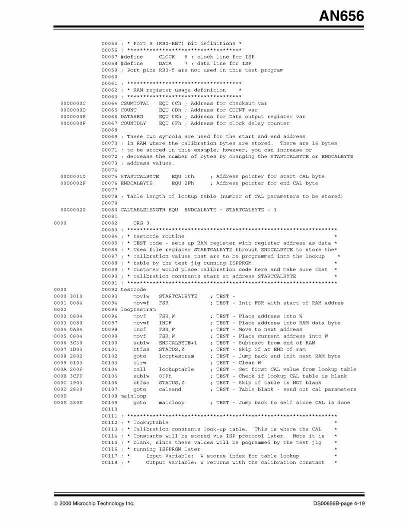
AN656
00055 ; * Port B (RB0-RB7) bit definitions * 00056 ; ************************************ 00057 #define CLOCK 6 ; clock line for ISP 00058 #define DATA 7 ; data line for ISP 00059 ; Port pins RB0-5 are not used in this test program 00060 00061 ; ************************************ 00062 ; * RAM register usage definition * 00063 ; ************************************ 0000000C 00064 CSUMTOTAL EQU 0Ch ; Address for checksum var 0000000D 00065 COUNT EQU 0Dh ; Address for COUNT var 0000000E 00066 DATAREG EQU 0Eh ; Address for Data output register var 0000000F 00067 COUNTDLY EQU 0Fh ; Address for clock delay counter 00068 00069 ; These two symbols are used for the start and end address 00070 ; in RAM where the calibration bytes are stored. There are 16 bytes 00071 ; to be stored in this example; however, you can increase or 00072 ; decrease the number of bytes by changing the STARTCALBYTE or ENDCALBYTE 00073 ; address values. 00074 00000010 00075 STARTCALBYTE EQU 10h ; Address pointer for start CAL byte 0000002F 00076 ENDCALBYTE EQU 2Fh ; Address pointer for end CAL byte 00077 00078 ; Table length of lookup table (number of CAL parameters to be stored) 00079 00000020 00080 CALTABLELENGTH EQU ENDCALBYTE - STARTCALBYTE + 1 00081 0000 00082 ORG 0 00083 ; ****************************************************************** 00084 ; * testcode routine * 00085 ; * TEST code - sets up RAM register with register address as data * 00086 ; * Uses file register STARTCALBYTE through ENDCALBYTE to store the* 00087 ; * calibration values that are to be programmed into the lookup * 00088 ; * table by the test jig running ISPPRGM. * 00089 ; * Customer would place calibration code here and make sure that * 00090 ; * calibration constants start at address STARTCALBYTE * 00091 ; ******************************************************************0000 00092 testcode0000 3010 00093 movlw STARTCALBYTE ; TEST - 0001 0084 00094 movwf FSR ; TEST - Init FSR with start of RAM addres0002 00095 looptestram0002 0804 00096 movf FSR,W ; TEST - Place address into W0003 0080 00097 movwf INDF ; TEST - Place address into RAM data byte0004 0A84 00098 incf FSR,F ; TEST - Move to next address0005 0804 00099 movf FSR,W ; TEST - Place current address into W0006 3C30 00100 sublw ENDCALBYTE+1 ; TEST - Subtract from end of RAM0007 1D03 00101 btfss STATUS,Z ; TEST - Skip if at END of ram0008 2802 00102 goto looptestram ; TEST - Jump back and init next RAM byte0009 0103 00103 clrw ; TEST - Clear W000A 200F 00104 call lookuptable ; TEST - Get first CAL value from lookup table000B 3CFF 00105 sublw 0FFh ; TEST - Check if lookup CAL table is blank000C 1903 00106 btfsc STATUS,Z ; TEST - Skip if table is NOT blank000D 2830 00107 goto calsend ; TEST - Table blank - send out cal parameters000E 00108 mainloop000E 280E 00109 goto mainloop ; TEST - Jump back to self since CAL is done 00110 00111 ; ****************************************************************** 00112 ; * lookuptable * 00113 ; * Calibration constants look-up table. This is where the CAL * 00114 ; * Constants will be stored via ISP protocol later. Note it is * 00115 ; * blank, since these values will be pogrammed by the test jig * 00116 ; * running ISPPRGM later. * 00117 ; * Input Variable: W stores index for table lookup * 00118 ; * Output Variable: W returns with the calibration constant *
2000 Microchip Technology Inc. DS00656B-page 4-19

AN656
00119 ; * NOTE: Blank table when programmed reads “FF” for all locations * 00120 ; ******************************************************************000F 00121 lookuptable000F 0782 00122 addwf PCL,F ; Place the calibration constant table here! 00123 002F 00124 ORG lookuptable + CALTABLELENGTH 002F 34FF 00125 retlw 0FFh ; Return FF at last location for a blank table 00126 00127 ; ****************************************************************** 00128 ; * calsend subroutine * 00129 ; * Send the calibration data stored in locations STARTCALBYTE * 00130 ; * through ENDCALBYTE in RAM to the programming jig using a serial* 00131 ; * clock and data protocol * 00132 ; * Input Variables: STARTCALBYTE through ENDCALBYTE * 00133 ; ******************************************************************0030 00134 calsend 0030 018C 00135 clrf CSUMTOTAL ; Clear CSUMTOTAL reg for delay counter0031 018D 00136 clrf COUNT ; Clear COUNT reg to delay counter0032 00137 delayloop ; Delay for 100 mS to wait for prog jig wakeup0032 0B8D 00138 decfsz COUNT,F ; Decrement COUNT and skip when zero0033 2832 00139 goto delayloop ; Go back and delay again0034 0B8C 00140 decfsz CSUMTOTAL,F ; Decrement CSUMTOTAL and skip when zero0035 2832 00141 goto delayloop ; Go back and delay again0036 0186 00142 clrf PORTB ; Place “0” into port b latch register0037 1683 00143 bsf STATUS,RP0 ; Switch to bank 10038 303F 00144 movlw b’00111111’ ; RB6,7 set to outputsMessage[302]: Register in operand not in bank 0. Ensure that bank bits are correct.0039 0086 00145 movwf TRISB ; Move to TRIS registers003A 1283 00146 bcf STATUS,RP0 ; Switch to bank 0003B 018C 00147 clrf CSUMTOTAL ; Clear checksum total byte003C 3001 00148 movlw high lookuptable+1 ; place MSB of first addr of cal table into W003D 204D 00149 call sendcalbyte ; Send the high address out003E 3010 00150 movlw low lookuptable+1 ; place LSB of first addr of cal table into W003F 204D 00151 call sendcalbyte ; Send low address out0040 3010 00152 movlw STARTCALBYTE ; Place RAM start address of first cal byte0041 0084 00153 movwf FSR ; Place this into FSR0042 00154 loopcal0042 0800 00155 movf INDF,W ; Place data into W0043 204D 00156 call sendcalbyte ; Send the byte out0044 0A84 00157 incf FSR,F ; Move to the next cal byte0045 0804 00158 movf FSR,W ; Place byte address into W0046 3C30 00159 sublw ENDCALBYTE+1 ; Set Z bit if we are at the end of CAL data0047 1D03 00160 btfss STATUS,Z ; Skip if we are done0048 2842 00161 goto loopcal ; Go back for next byte0049 080C 00162 movf CSUMTOTAL,W ; place checksum total into W004A 204D 00163 call sendcalbyte ; Send the checksum out004B 0186 00164 clrf PORTB ; clear out port pins004C 00165 calsenddone004C 284C 00166 goto calsenddone ; We are done - go home! 00167 00168 ; ****************************************************************** 00169 ; * sendcalbyte subroutine * 00170 ; * Send one byte of calibration data to the programming jig * 00171 ; * Input Variable: W contains the byte to be sent * 00172 ; ******************************************************************004D 00173 sendcalbyte004D 008E 00174 movwf DATAREG ; Place send byte into data register004E 078C 00175 addwf CSUMTOTAL,F ; Update checksum total004F 3008 00176 movlw .8 ; Place 8 into W0050 008D 00177 movwf COUNT ; set up counter register0051 00178 loopsendcal 0051 1706 00179 bsf PORTB,CLOCK ; Set clock line high0052 205C 00180 call delaysend ; Wait for test jig to synch up0053 0D8E 00181 rlf DATAREG,F ; Rotate to next bit0054 1786 00182 bsf PORTB,DATA ; Assume data bit is high0055 1C03 00183 btfss STATUS,C ; Skip if the data bit was high
DS00656B-page 4-20 2000 Microchip Technology Inc.

AN656
0056 1386 00184 bcf PORTB,DATA ; Set data bit to low0057 1306 00185 bcf PORTB,CLOCK ; Clear clock bit to clock data out0058 205C 00186 call delaysend ; Wait for test jig to synch up0059 0B8D 00187 decfsz COUNT,F ; Skip after 8 bits005A 2851 00188 goto loopsendcal ; Jump back and send next bit005B 0008 00189 return ; We are done with this byte so return! 00190 00191 ; ****************************************************************** 00192 ; * delaysend subroutine * 00193 ; * Delay for 50 ms to wait for the programming jig to synch up * 00194 ; ******************************************************************005C 00195 delaysend005C 3010 00196 movlw 10h ; Delay for 16 loops005D 008F 00197 movwf COUNTDLY ; Use COUNTDLY as delay count variable005E 00198 loopdelaysend005E 0B8F 00199 decfsz COUNTDLY,F ; Decrement COUNTDLY and skip when done005F 285E 00200 goto loopdelaysend ; Jump back for more delay0060 0008 00201 return 00202 END
MEMORY USAGE MAP (‘X’ = Used, ‘-’ = Unused)
0000 : XXXXXXXXXXXXXXXX ---------------- ---------------X XXXXXXXXXXXXXXXX0040 : XXXXXXXXXXXXXXXX XXXXXXXXXXXXXXXX X--------------- ----------------2000 : -------X-------- ---------------- ---------------- ----------------
All other memory blocks unused.
Program Memory Words Used: 66Program Memory Words Free: 958
Errors : 0Warnings : 1 reported, 0 suppressedMessages : 1 reported, 0 suppressed
2000 Microchip Technology Inc. DS00656B-page 4-21

Information contained in this publication regarding device applications and the like is intended through suggestion only and may be superseded by updates.It is your responsibility to ensure that your application meets with your specifications. No representation or warranty is given and no liability is assumed byMicrochip Technology Incorporated with respect to the accuracy or use of such information, or infringement of patents or other intellectual property rightsarising from such use or otherwise. Use of Microchip’s products as critical components in life support systems is not authorized except with express writtenapproval by Microchip. No licenses are conveyed, implicitly or otherwise, except as maybe explicitly expressed herein, under any intellectual propertyrights. The Microchip logo and name are registered trademarks of Microchip Technology Inc. in the U.S.A. and other countries. All rights reserved. All othertrademarks mentioned herein are the property of their respective companies.
DS30277C-page 4-22 2000 Microchip Technology Inc.
All rights reserved. © 2000 Microchip Technology Incorporated. Printed in the USA. 5/00 Printed on recycled paper.
AMERICASCorporate OfficeMicrochip Technology Inc.2355 West Chandler Blvd.Chandler, AZ 85224-6199Tel: 480-786-7200 Fax: 480-786-7277Technical Support: 480-786-7627Web Address: http://www.microchip.com
AtlantaMicrochip Technology Inc.500 Sugar Mill Road, Suite 200BAtlanta, GA 30350Tel: 770-640-0034 Fax: 770-640-0307BostonMicrochip Technology Inc.5 Mount Royal AvenueMarlborough, MA 01752Tel: 508-480-9990 Fax: 508-480-8575ChicagoMicrochip Technology Inc.333 Pierce Road, Suite 180Itasca, IL 60143Tel: 630-285-0071 Fax: 630-285-0075DallasMicrochip Technology Inc.4570 Westgrove Drive, Suite 160Addison, TX 75248Tel: 972-818-7423 Fax: 972-818-2924DaytonMicrochip Technology Inc.Two Prestige Place, Suite 150Miamisburg, OH 45342Tel: 937-291-1654 Fax: 937-291-9175DetroitMicrochip Technology Inc.Tri-Atria Office Building 32255 Northwestern Highway, Suite 190Farmington Hills, MI 48334Tel: 248-538-2250 Fax: 248-538-2260Los AngelesMicrochip Technology Inc.18201 Von Karman, Suite 1090Irvine, CA 92612Tel: 949-263-1888 Fax: 949-263-1338New YorkMicrochip Technology Inc.150 Motor Parkway, Suite 202Hauppauge, NY 11788Tel: 631-273-5305 Fax: 631-273-5335San JoseMicrochip Technology Inc.2107 North First Street, Suite 590San Jose, CA 95131Tel: 408-436-7950 Fax: 408-436-7955
AMERICAS (continued)TorontoMicrochip Technology Inc.5925 Airport Road, Suite 200Mississauga, Ontario L4V 1W1, Canada Tel: 905-405-6279 Fax: 905-405-6253
ASIA/PACIFICChina - BeijingMicrochip Technology, Beijing Unit 915, 6 Chaoyangmen Bei Dajie Dong Erhuan Road, Dongcheng District New China Hong Kong Manhattan BuildingBeijing, 100027, P.R.C. Tel: 86-10-85282100 Fax: 86-10-85282104China - ShanghaiMicrochip Technology Unit B701, Far East International Plaza,No. 317, Xianxia RoadShanghai, 200051, P.R.C.Tel: 86-21-6275-5700 Fax: 86-21-6275-5060Hong KongMicrochip Asia PacificUnit 2101, Tower 2Metroplaza223 Hing Fong RoadKwai Fong, N.T., Hong KongTel: 852-2-401-1200 Fax: 852-2-401-3431IndiaMicrochip Technology Inc.India Liaison OfficeNo. 6, Legacy, Convent RoadBangalore, 560 025, IndiaTel: 91-80-229-0061 Fax: 91-80-229-0062JapanMicrochip Technology Intl. Inc.Benex S-1 6F3-18-20, ShinyokohamaKohoku-Ku, Yokohama-shiKanagawa, 222-0033, JapanTel: 81-45-471- 6166 Fax: 81-45-471-6122KoreaMicrochip Technology Korea168-1, Youngbo Bldg. 3 FloorSamsung-Dong, Kangnam-KuSeoul, KoreaTel: 82-2-554-7200 Fax: 82-2-558-5934
ASIA/PACIFIC (continued)SingaporeMicrochip Technology Singapore Pte Ltd.200 Middle Road#07-02 Prime CentreSingapore, 188980Tel: 65-334-8870 Fax: 65-334-8850TaiwanMicrochip Technology Taiwan10F-1C 207Tung Hua North RoadTaipei, TaiwanTel: 886-2-2717-7175 Fax: 886-2-2545-0139
EUROPEDenmarkMicrochip Technology Denmark ApSRegus Business CentreLautrup hoj 1-3Ballerup DK-2750 DenmarkTel: 45 4420 9895 Fax: 45 4420 9910FranceArizona Microchip Technology SARLParc d’Activite du Moulin de Massy43 Rue du Saule TrapuBatiment A - ler Etage91300 Massy, FranceTel: 33-1-69-53-63-20 Fax: 33-1-69-30-90-79GermanyArizona Microchip Technology GmbHGustav-Heinemann-Ring 125D-81739 München, GermanyTel: 49-89-627-144 0 Fax: 49-89-627-144-44ItalyArizona Microchip Technology SRLCentro Direzionale Colleoni Palazzo Taurus 1 V. Le Colleoni 120041 Agrate BrianzaMilan, Italy Tel: 39-039-65791-1 Fax: 39-039-6899883United KingdomArizona Microchip Technology Ltd.505 Eskdale RoadWinnersh TriangleWokingham Berkshire, England RG41 5TUTel: 44 118 921 5858 Fax: 44-118 921-5835
03/23/00
WORLDWIDE SALES AND SERVICE
Microchip received QS-9000 quality system certification for its worldwide headquarters, design and wafer fabrication facilities in Chandler and Tempe, Arizona in July 1999. The Company’s quality system processes and procedures are QS-9000 compliant for its PICmicro® 8-bit MCUs, KEELOQ® code hopping devices, Serial EEPROMs and microperipheral products. In addition, Microchip’s quality system for the design and manufacture of development systems is ISO 9001 certified.