ina188 datasheet - texas instruments · a 2 + a 3 rfi filter inputs rfi filtered inputs rfi...
TRANSCRIPT
+A2
+A3
RFI Filter Inputs
RFI Filtered Inputs
RFI Filtered Inputs
RFI Filtered Inputs
RG
VIN-
VIN+
V-
V+
VOUT
REF
25 k
25 k
20 k
20 k 20 k
20 k
G
50 kG 1
R:
OUT IN IN REFV V V G V u
+ A1
Product
Folder
Sample &Buy
Technical
Documents
Tools &
Software
Support &Community
An IMPORTANT NOTICE at the end of this data sheet addresses availability, warranty, changes, use in safety-critical applications,intellectual property matters and other important disclaimers. UNLESS OTHERWISE NOTED, this document contains PRODUCTIONDATA.
INA188SBOS632 –SEPTEMBER 2015
INA188Precision, Zero-Drift, Rail-to-Rail Out, High-Voltage Instrumentation Amplifier
1
1 Features1• Excellent DC Performance:
– Low Input Offset Voltage: 55 μV (max)– Low Input Offset Drift: 0.2 μV/°C (max)– High CMRR: 104 dB, G ≥ 10 (min)
• Low Input Noise:– 12 nV/√Hz at 1 kHz– 0.25 μVPP (0.1 Hz to 10 Hz)
• Wide Supply Range:– Single Supply: 4 V to 36 V– Dual Supply: ±2 V to ±18 V
• Gain Set with a Single External Resistor:– Gain Equation: G = 1 + (50 kΩ / RG)– Gain Error: 0.007%, G = 1– Gain Drift: 5 ppm/°C (max) G = 1
• Input Voltage: (V–) + 0.1 V to (V+) – 1.5 V• RFI-Filtered Inputs• Rail-to-Rail Output• Low Quiescent Current: 1.4 mA• Operating Temperature: –55°C to +150°C• SOIC-8 and DFN-8 Packages
2 Applications• Bridge Amplifiers• ECG Amplifiers• Pressure Sensors• Medical Instrumentation• Portable Instrumentation• Weigh Scales• Thermocouple Amplifiers• RTD Sensor Amplifiers• Data Acquisition
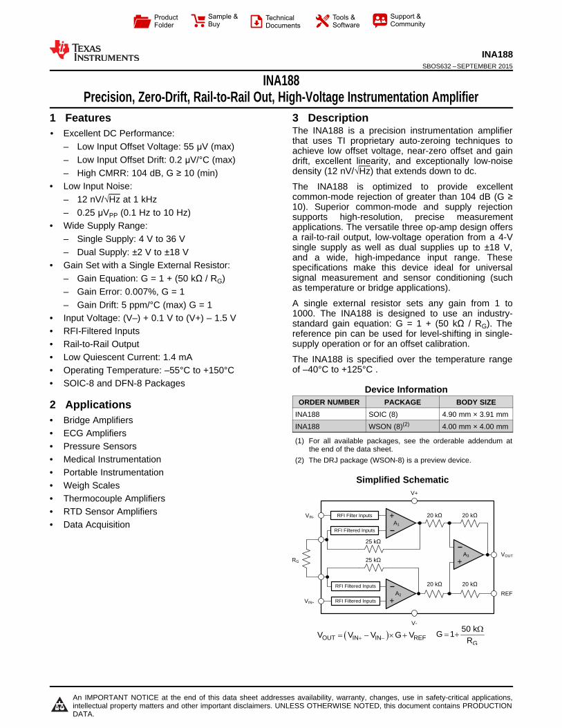
3 DescriptionThe INA188 is a precision instrumentation amplifierthat uses TI proprietary auto-zeroing techniques toachieve low offset voltage, near-zero offset and gaindrift, excellent linearity, and exceptionally low-noisedensity (12 nV/√Hz) that extends down to dc.
The INA188 is optimized to provide excellentcommon-mode rejection of greater than 104 dB (G ≥10). Superior common-mode and supply rejectionsupports high-resolution, precise measurementapplications. The versatile three op-amp design offersa rail-to-rail output, low-voltage operation from a 4-Vsingle supply as well as dual supplies up to ±18 V,and a wide, high-impedance input range. Thesespecifications make this device ideal for universalsignal measurement and sensor conditioning (suchas temperature or bridge applications).
A single external resistor sets any gain from 1 to1000. The INA188 is designed to use an industry-standard gain equation: G = 1 + (50 kΩ / RG). Thereference pin can be used for level-shifting in single-supply operation or for an offset calibration.
The INA188 is specified over the temperature rangeof –40°C to +125°C .
Device InformationORDER NUMBER PACKAGE BODY SIZE
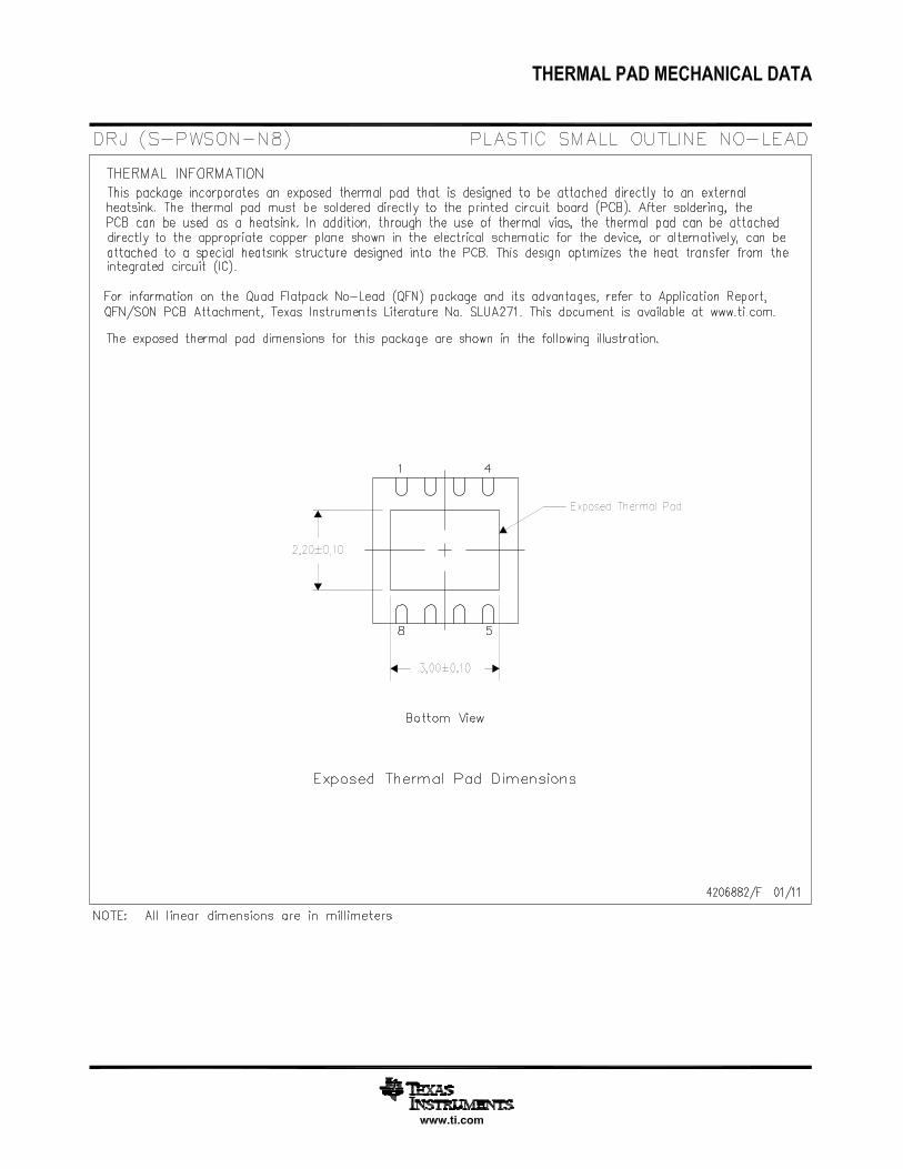
INA188 SOIC (8) 4.90 mm × 3.91 mmINA188 WSON (8)(2) 4.00 mm × 4.00 mm
(1) For all available packages, see the orderable addendum atthe end of the data sheet.
(2) The DRJ package (WSON-8) is a preview device.
Simplified Schematic
2
INA188SBOS632 –SEPTEMBER 2015 www.ti.com
Product Folder Links: INA188
Submit Documentation Feedback Copyright © 2015, Texas Instruments Incorporated
Table of Contents1 Features .................................................................. 12 Applications ........................................................... 13 Description ............................................................. 14 Revision History..................................................... 25 Pin Configuration and Functions ......................... 36 Specifications......................................................... 4
6.1 Absolute Maximum Ratings ...................................... 46.2 ESD Ratings.............................................................. 46.3 Recommended Operating Conditions....................... 46.4 Thermal Information .................................................. 46.5 Electrical Characteristics: VS = ±4 V to ±18 V (VS =
8 V to 36 V)................................................................ 56.6 Electrical Characteristics: VS = ±2 V to < ±4 V (VS =
4 V to < 8 V)............................................................... 76.7 Typical Characteristics .............................................. 9
7 Detailed Description ............................................ 177.1 Overview ................................................................. 177.2 Functional Block Diagram ....................................... 17
7.3 Feature Description................................................. 187.4 Device Functional Modes........................................ 21
8 Application and Implementation ........................ 278.1 Application Information............................................ 278.2 Typical Application .................................................. 27
9 Power Supply Recommendations ...................... 2910 Layout................................................................... 29
10.1 Layout Guidelines ................................................. 2910.2 Layout Example .................................................... 30
11 Device and Documentation Support ................. 3111.1 Device Support .................................................... 3111.2 Documentation Support ........................................ 3111.3 Community Resources.......................................... 3111.4 Trademarks ........................................................... 3111.5 Electrostatic Discharge Caution............................ 3111.6 Glossary ................................................................ 31
12 Mechanical, Packaging, and OrderableInformation ........................................................... 32
4 Revision History
DATE REVISION NOTESSeptember 2015 * Initial release.
RG
VIN-
VIN+
V-
RG
V+
VOUT
REF
8
7
6
5
2
3
4
1
Exposed Thermal
Die Pad on Underside
RG
2
3
4
8
7
6
5
VIN-
VIN+
V-
RG
V+
VOUT
REF
1
3
INA188www.ti.com SBOS632 –SEPTEMBER 2015
Product Folder Links: INA188
Submit Documentation FeedbackCopyright © 2015, Texas Instruments Incorporated
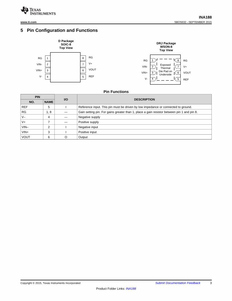
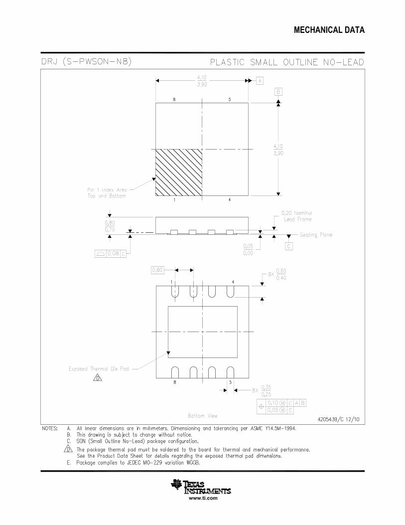
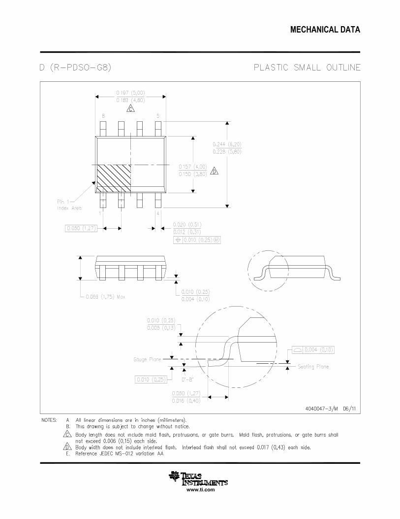
5 Pin Configuration and Functions
D PackageSOIC-8
Top ViewDRJ Package
WSON-8Top View
Pin FunctionsPIN
I/O DESCRIPTIONNO. NAME
REF 5 I Reference input. This pin must be driven by low impedance or connected to ground.RG 1, 8 — Gain setting pin. For gains greater than 1, place a gain resistor between pin 1 and pin 8.V– 4 — Negative supplyV+ 7 — Positive supplyVIN– 2 I Negative inputVIN+ 3 I Positive inputVOUT 6 O Output
4
INA188SBOS632 –SEPTEMBER 2015 www.ti.com
Product Folder Links: INA188
Submit Documentation Feedback Copyright © 2015, Texas Instruments Incorporated
(1) Stresses beyond those listed under Absolute Maximum Ratings may cause permanent damage to the device. These are stress ratingsonly, which do not imply functional operation of the device at these or any other conditions beyond those indicated under RecommendedOperating Conditions. Exposure to absolute-maximum-rated conditions for extended periods may affect device reliability.
(2) Input pins are diode-clamped to the power-supply rails. Input signals that can swing more than 0.3 V beyond the supply rails must becurrent limited to 10 mA or less.
(3) Short-circuit to ground.
6 Specifications
6.1 Absolute Maximum Ratingsover operating free-air temperature range (unless otherwise noted) (1)
MIN MAX UNIT
VoltageSupply
±20V
40 (single supply)Current ±10 mAAnalog input range (2) (V–) – 0.5 (V+) + 0.5 V
Output short-circuit (3) Continuous
TemperatureOperating range, TA –55 150
°CJunction, TJ 150Storage temperature, Tstg –65 150
(1) JEDEC document JEP155 states that 500-V HBM allows safe manufacturing with a standard ESD control process.(2) JEDEC document JEP157 states that 250-V CDM allows safe manufacturing with a standard ESD control process.
6.2 ESD RatingsVALUE UNIT
V(ESD) Electrostatic dischargeHuman-body model (HBM), per ANSI/ESDA/JEDEC JS-001 (1) ±2500
VCharged-device model (CDM), per JEDEC specification JESD22-C101 (2) ±1000
6.3 Recommended Operating Conditionsover operating free-air temperature range (unless otherwise noted)
MIN NOM MAX UNITVS Supply voltage 4 (±2) 36 (±18) V
Specified temperature -40 125 °C
(1) For more information about traditional and new thermal metrics, see the IC Package Thermal Metrics application report, SPRA953.
6.4 Thermal Information
THERMAL METRIC (1)INA188
UNITD (SOIC) DRG (WSON)8 PINS 8 PINS
RθJA Junction-to-ambient thermal resistance 125 145 °C/WRθJC(top) Junction-to-case (top) thermal resistance 80 75 °C/WRθJB Junction-to-board thermal resistance 68 39 °C/WψJT Junction-to-top characterization parameter 32 14 °C/WψJB Junction-to-board characterization parameter 68 105 °C/WRθJC(bot) Junction-to-case (bottom) thermal resistance N/A N/A °C/W
5
INA188www.ti.com SBOS632 –SEPTEMBER 2015
Product Folder Links: INA188
Submit Documentation FeedbackCopyright © 2015, Texas Instruments Incorporated
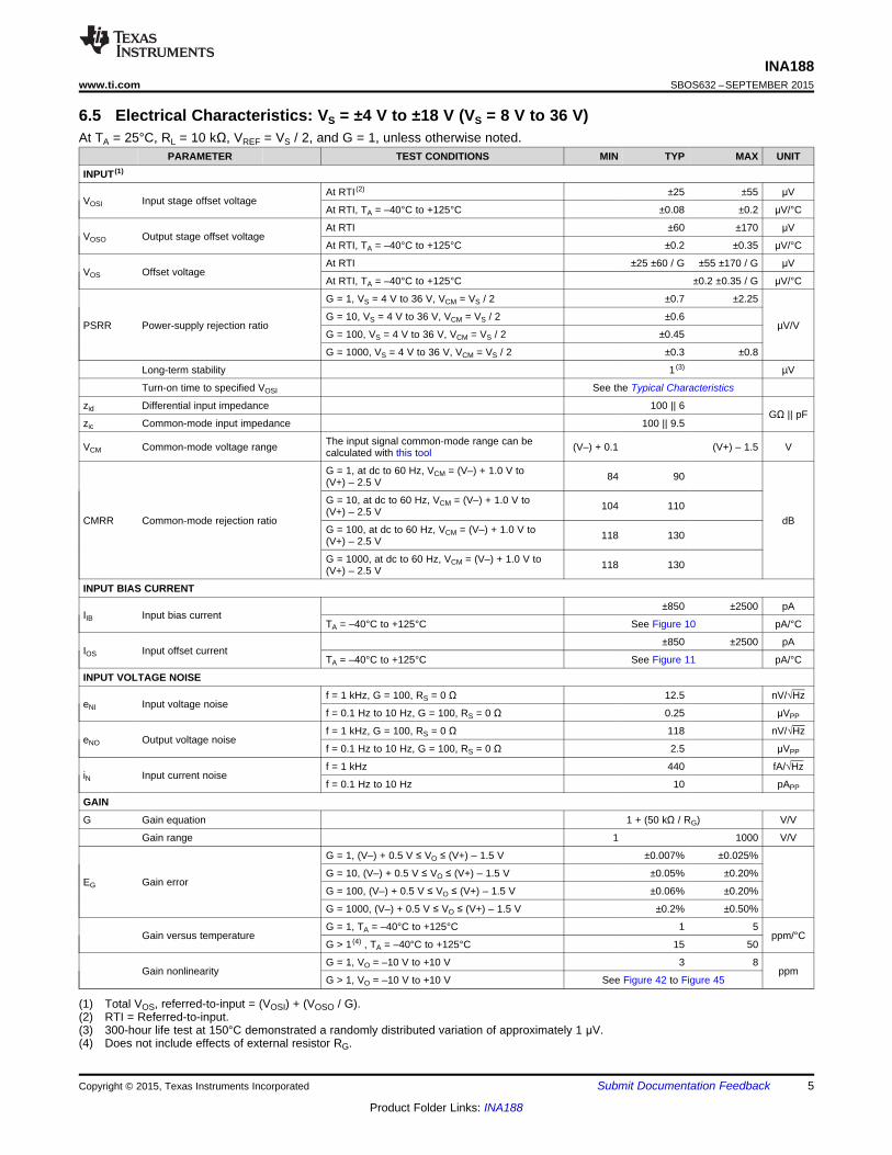
(1) Total VOS, referred-to-input = (VOSI) + (VOSO / G).(2) RTI = Referred-to-input.(3) 300-hour life test at 150°C demonstrated a randomly distributed variation of approximately 1 μV.(4) Does not include effects of external resistor RG.
6.5 Electrical Characteristics: VS = ±4 V to ±18 V (VS = 8 V to 36 V)At TA = 25°C, RL = 10 kΩ, VREF = VS / 2, and G = 1, unless otherwise noted.
PARAMETER TEST CONDITIONS MIN TYP MAX UNIT
INPUT (1)
VOSI Input stage offset voltageAt RTI (2) ±25 ±55 μV
At RTI, TA = –40°C to +125°C ±0.08 ±0.2 μV/°C
VOSO Output stage offset voltageAt RTI ±60 ±170 μV
At RTI, TA = –40°C to +125°C ±0.2 ±0.35 μV/°C
VOS Offset voltageAt RTI ±25 ±60 / G ±55 ±170 / G μV
At RTI, TA = –40°C to +125°C ±0.2 ±0.35 / G μV/°C
PSRR Power-supply rejection ratio
G = 1, VS = 4 V to 36 V, VCM = VS / 2 ±0.7 ±2.25
µV/VG = 10, VS = 4 V to 36 V, VCM = VS / 2 ±0.6
G = 100, VS = 4 V to 36 V, VCM = VS / 2 ±0.45
G = 1000, VS = 4 V to 36 V, VCM = VS / 2 ±0.3 ±0.8
Long-term stability 1 (3) µV
Turn-on time to specified VOSI See the Typical Characteristics
zid Differential input impedance 100 || 6GΩ || pF
zic Common-mode input impedance 100 || 9.5
VCM Common-mode voltage range The input signal common-mode range can becalculated with this tool (V–) + 0.1 (V+) – 1.5 V
CMRR Common-mode rejection ratio
G = 1, at dc to 60 Hz, VCM = (V–) + 1.0 V to(V+) – 2.5 V 84 90
dB
G = 10, at dc to 60 Hz, VCM = (V–) + 1.0 V to(V+) – 2.5 V 104 110
G = 100, at dc to 60 Hz, VCM = (V–) + 1.0 V to(V+) – 2.5 V 118 130
G = 1000, at dc to 60 Hz, VCM = (V–) + 1.0 V to(V+) – 2.5 V 118 130
INPUT BIAS CURRENT
IIB Input bias current±850 ±2500 pA
TA = –40°C to +125°C See Figure 10 pA/°C
IOS Input offset current±850 ±2500 pA
TA = –40°C to +125°C See Figure 11 pA/°C
INPUT VOLTAGE NOISE
eNI Input voltage noisef = 1 kHz, G = 100, RS = 0 Ω 12.5 nV/√Hz
f = 0.1 Hz to 10 Hz, G = 100, RS = 0 Ω 0.25 μVPP
eNO Output voltage noisef = 1 kHz, G = 100, RS = 0 Ω 118 nV/√Hz
f = 0.1 Hz to 10 Hz, G = 100, RS = 0 Ω 2.5 μVPP
iN Input current noisef = 1 kHz 440 fA/√Hz
f = 0.1 Hz to 10 Hz 10 pAPP
GAIN
G Gain equation 1 + (50 kΩ / RG) V/V
Gain range 1 1000 V/V
EG Gain error
G = 1, (V–) + 0.5 V ≤ VO ≤ (V+) – 1.5 V ±0.007% ±0.025%
G = 10, (V–) + 0.5 V ≤ VO ≤ (V+) – 1.5 V ±0.05% ±0.20%
G = 100, (V–) + 0.5 V ≤ VO ≤ (V+) – 1.5 V ±0.06% ±0.20%
G = 1000, (V–) + 0.5 V ≤ VO ≤ (V+) – 1.5 V ±0.2% ±0.50%
Gain versus temperatureG = 1, TA = –40°C to +125°C 1 5
ppm/°CG > 1 (4) , TA = –40°C to +125°C 15 50
Gain nonlinearityG = 1, VO = –10 V to +10 V 3 8
ppmG > 1, VO = –10 V to +10 V See Figure 42 to Figure 45
6
INA188SBOS632 –SEPTEMBER 2015 www.ti.com
Product Folder Links: INA188
Submit Documentation Feedback Copyright © 2015, Texas Instruments Incorporated
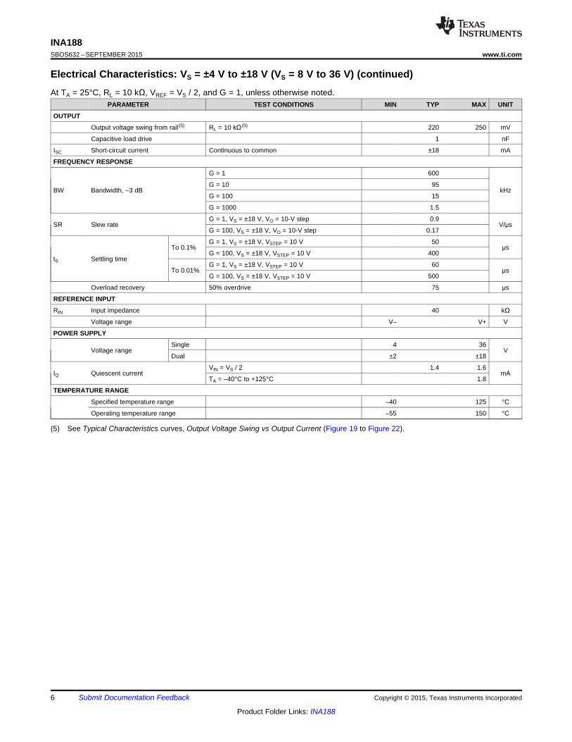
Electrical Characteristics: VS = ±4 V to ±18 V (VS = 8 V to 36 V) (continued)At TA = 25°C, RL = 10 kΩ, VREF = VS / 2, and G = 1, unless otherwise noted.
PARAMETER TEST CONDITIONS MIN TYP MAX UNIT
(5) See Typical Characteristics curves, Output Voltage Swing vs Output Current (Figure 19 to Figure 22).
OUTPUT
Output voltage swing from rail (5) RL = 10 kΩ (5) 220 250 mV
Capacitive load drive 1 nF
ISC Short-circuit current Continuous to common ±18 mA
FREQUENCY RESPONSE
BW Bandwidth, –3 dB
G = 1 600
kHzG = 10 95
G = 100 15
G = 1000 1.5
SR Slew rateG = 1, VS = ±18 V, VO = 10-V step 0.9
V/μsG = 100, VS = ±18 V, VO = 10-V step 0.17
tS Settling time
To 0.1%G = 1, VS = ±18 V, VSTEP = 10 V 50
μsG = 100, VS = ±18 V, VSTEP = 10 V 400
To 0.01%G = 1, VS = ±18 V, VSTEP = 10 V 60
μsG = 100, VS = ±18 V, VSTEP = 10 V 500
Overload recovery 50% overdrive 75 μs
REFERENCE INPUT
RIN Input impedance 40 kΩ
Voltage range V– V+ V
POWER SUPPLY
Voltage rangeSingle 4 36
VDual ±2 ±18
IQ Quiescent currentVIN = VS / 2 1.4 1.6
mATA = –40°C to +125°C 1.8
TEMPERATURE RANGE
Specified temperature range –40 125 °C
Operating temperature range –55 150 °C
7
INA188www.ti.com SBOS632 –SEPTEMBER 2015
Product Folder Links: INA188
Submit Documentation FeedbackCopyright © 2015, Texas Instruments Incorporated
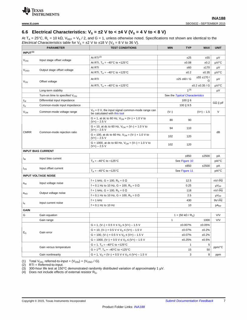
(1) Total VOS, referred-to-input = (VOSI) + (VOSO / G).(2) RTI = Referred-to-input.(3) 300-hour life test at 150°C demonstrated randomly distributed variation of approximately 1 μV.(4) Does not include effects of external resistor RG.
6.6 Electrical Characteristics: VS = ±2 V to < ±4 V (VS = 4 V to < 8 V)At TA = 25°C, RL = 10 kΩ, VREF = VS / 2, and G = 1, unless otherwise noted. Specifications not shown are identical to theElectrical Characteristics table for VS = ±2 V to ±18 V (VS = 8 V to 36 V).
PARAMETER TEST CONDITIONS MIN TYP MAX UNIT
INPUT (1)
VOSI Input stage offset voltageAt RTI (2) ±25 ±55 μV
At RTI, TA = –40°C to +125°C ±0.08 ±0.2 μV/°C
VOSO Output stage offset voltageAt RTI ±60 ±170 μV
At RTI, TA = –40°C to +125°C ±0.2 ±0.35 μV/°C
VOS Offset voltageAt RTI ±25 ±60 / G ±55 ±170 /
G μV
At RTI, TA = –40°C to +125°C ±0.2 ±0.35 / G μV/°C
Long-term stability 1 (3) µV
Turn-on time to specified VOSI See the Typical Characteristics
zid Differential input impedance 100 || 6GΩ || pF
zic Common-mode input impedance 100 || 9.5
VCM Common-mode voltage range VO = 0 V, the input signal common-mode range canbe calculated with this tool (V–) (V+) – 1.5 V
CMRR Common-mode rejection ratio
G = 1, at dc to 60 Hz, VCM = (V–) + 1.0 V to(V+) – 2.5 V 80 90
dB
G = 10, at dc to 60 Hz, VCM = (V–) + 1.0 V to(V+) – 2.5 V 94 110
G = 100, at dc to 60 Hz, VCM = (V–) + 1.0 V to(V+) – 2.5 V 102 120
G = 1000, at dc to 60 Hz, VCM = (V–) + 1.0 V to(V+) – 2.5 V 102 120
INPUT BIAS CURRENT
IIB Input bias current±850 ±2500 pA
TA = –40°C to +125°C See Figure 10 pA/°C
IOS Input offset current±850 ±2500 pA
TA = –40°C to +125°C See Figure 11 pA/°C
INPUT VOLTAGE NOISE
eNI Input voltage noisef = 1 kHz, G = 100, RS = 0 Ω 12.5 nV/√Hz
f = 0.1 Hz to 10 Hz, G = 100, RS = 0 Ω 0.25 μVPP
eNO Output voltage noisef = 1 kHz, G = 100, RS = 0 Ω 118 nV/√Hz
f = 0.1 Hz to 10 Hz, G = 100, RS = 0 Ω 2.5 μVPP
iN Input current noisef = 1 kHz 430 fA/√Hz
f = 0.1 Hz to 10 Hz 10 pAPP
GAIN
G Gain equation 1 + (50 kΩ / RG) V/V
Gain range 1 1000 V/V
EG Gain error
G = 1, (V–) + 0.5 V ≤ VO ≤ (V+) – 1.5 V ±0.007% ±0.05%
G = 10, (V–) + 0.5 V ≤ VO ≤ (V+) – 1.5 V ±0.07% ±0.2%
G = 100, (V–) + 0.5 V ≤ VO ≤ (V+) – 1.5 V ±0.07% ±0.2%
G = 1000, (V–) + 0.5 V ≤ VO ≤ (V+) – 1.5 V ±0.25% ±0.5%
Gain versus temperatureG = 1, TA = –40°C to +125°C 1 5
ppm/°CG > 1 (4), TA = –40°C to +125°C 15 50
Gain nonlinearity G = 1, VO = (V–) + 0.5 V ≤ VO ≤ (V+) – 1.5 V 3 8 ppm
8
INA188SBOS632 –SEPTEMBER 2015 www.ti.com
Product Folder Links: INA188
Submit Documentation Feedback Copyright © 2015, Texas Instruments Incorporated
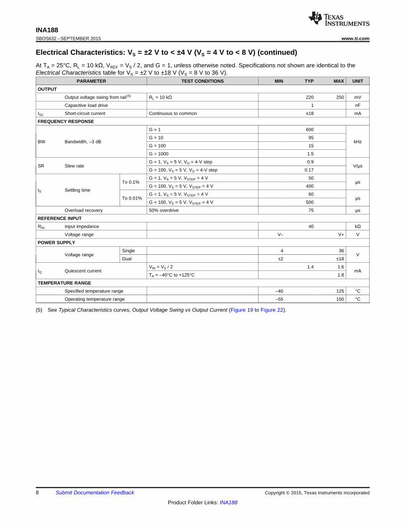
Electrical Characteristics: VS = ±2 V to < ±4 V (VS = 4 V to < 8 V) (continued)At TA = 25°C, RL = 10 kΩ, VREF = VS / 2, and G = 1, unless otherwise noted. Specifications not shown are identical to theElectrical Characteristics table for VS = ±2 V to ±18 V (VS = 8 V to 36 V).
PARAMETER TEST CONDITIONS MIN TYP MAX UNIT
(5) See Typical Characteristics curves, Output Voltage Swing vs Output Current (Figure 19 to Figure 22).
OUTPUT
Output voltage swing from rail (5) RL = 10 kΩ 220 250 mV
Capacitive load drive 1 nF
ISC Short-circuit current Continuous to common ±18 mA
FREQUENCY RESPONSE
BW Bandwidth, –3 dB
G = 1 600
kHzG = 10 95
G = 100 15
G = 1000 1.5
SR Slew rateG = 1, VS = 5 V, VO = 4-V step 0.9
V/μsG = 100, VS = 5 V, VO = 4-V step 0.17
tS Settling time
To 0.1%G = 1, VS = 5 V, VSTEP = 4 V 50
μsG = 100, VS = 5 V, VSTEP = 4 V 400
To 0.01%G = 1, VS = 5 V, VSTEP = 4 V 60
μsG = 100, VS = 5 V, VSTEP = 4 V 500
Overload recovery 50% overdrive 75 μs
REFERENCE INPUT
RIN Input impedance 40 kΩ
Voltage range V– V+ V
POWER SUPPLY
Voltage rangeSingle 4 36
VDual ±2 ±18
IQ Quiescent currentVIN = VS / 2 1.4 1.6
mATA = –40°C to +125°C 1.8
TEMPERATURE RANGE
Specified temperature range –40 125 °C
Operating temperature range –55 150 °C
Pop
ulat
ion
(%)
0
2
4
6
8
10
12
14
16
18
-1.7
-1.5
3-1
.36
-1.1
9-1
.02
-0.8
5-0
.68
-0.5
1-0
.34
-0.1
7 00.
170.
340.
510.
680.
851.
021.
191.
361.
53 1.7
IOS (nA)
Pop
ulat
ion
(%)
0
2
4
6
8
10
12
14
16
18
20
-1.4
-1.2
6
-1.1
2
-0.9
8
-0.8
4
-0.7
-0.5
6
-0.4
2
-0.2
8
-0.1
4 0
0.14
0.28
0.42
0.56 0.7
0.84
0.98
Input Bias Current (nA)
Pop
ulat
ion
(%)
0
5
10
15
20
25
30
35
40
45
0
0.04
25
0.08
5
0.12
75
0.17
0.21
25
0.25
5
0.29
75
0.34
0.38
25
VOSO (µV/°C)
Cou
nt
0
100
200
300
400
500
600
700
800
900
1000
-100 -80
-60
-40
-20 0 20 40 60 80 100
D001VOSO (µV)
Pop
ulat
ion
(%)
0123456789
101112131415
0
0.00
75
0.01
5
0.02
25
0.03
0.03
75
0.04
5
0.05
25
0.06
0.06
75
0.07
5
0.08
25
0.09
0.09
75
0.10
5
Input Voltage Offset Drift (µV/°C)
Cou
nt
0
50
100
150
200
250
300
350
400
450
500
550
600-3
0
-25
-20
-15
-10 -5 0 5 10 15 20 25 30
D001VOSI (µV)
9
INA188www.ti.com SBOS632 –SEPTEMBER 2015
Product Folder Links: INA188
Submit Documentation FeedbackCopyright © 2015, Texas Instruments Incorporated
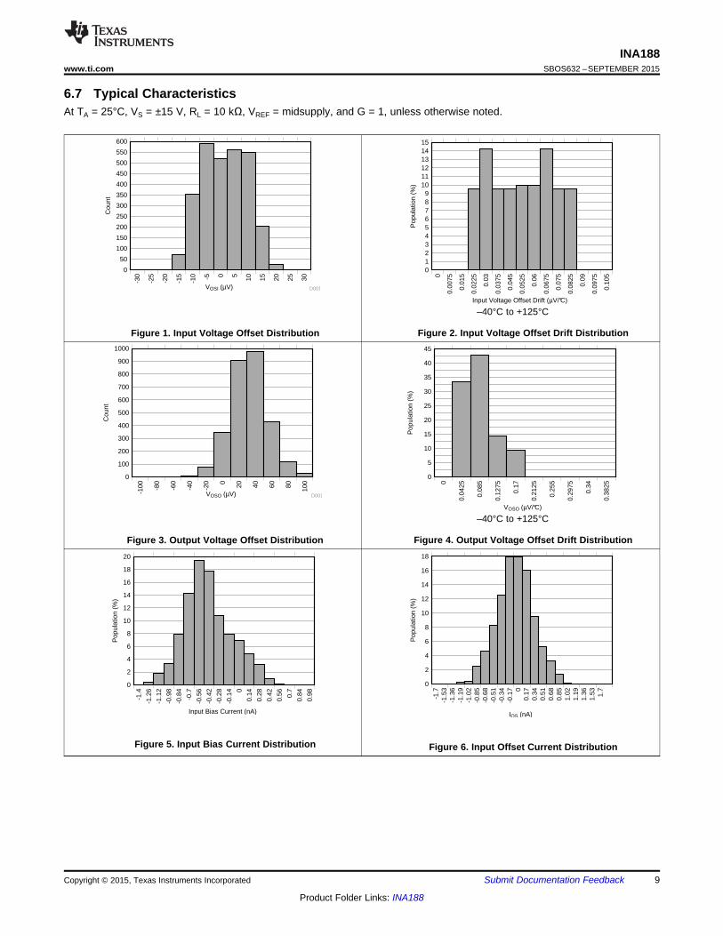
6.7 Typical CharacteristicsAt TA = 25°C, VS = ±15 V, RL = 10 kΩ, VREF = midsupply, and G = 1, unless otherwise noted.
Figure 1. Input Voltage Offset Distribution
–40°C to +125°C
Figure 2. Input Voltage Offset Drift Distribution
Figure 3. Output Voltage Offset Distribution
–40°C to +125°C
Figure 4. Output Voltage Offset Drift Distribution
Figure 5. Input Bias Current Distribution Figure 6. Input Offset Current Distribution
Temperature (°C)
Inpu
t Offs
et C
urre
nt (
pA)
-75 -50 -25 0 25 50 75 100 125 150 175300
350
400
450
500
550
600
650
700
D001Time (s)
Cha
nge
in In
put O
ffset
Vol
tage
(µ
V)
0 10 20 30 40 50 60 70 80 90 100-6
-4
-2
0
2
4
6
D001
Temperature (°C)
Inpu
t Bia
s C
urre
nt (
nA)
-75 -50 -25 0 25 50 75 100 125 150 175-2000
0
2000
4000
6000
8000
10000
12000
14000
16000
18000
D001Common-Mode Voltage (V)
Inpu
t Bia
s C
urre
nt (
nA)
-15 -12 -9 -6 -3 0 3 6 9 12 150.3
0.35
0.4
0.45
0.5
0.55
0.6
0.65
0.7
0.75
0.8
0.85
0.9
0.95
IIB ±2 VIIB ±15 V
Pop
ulat
ion
(%)
0
2.5
5
7.5
10
12.5
15
17.5
20
22.5
25
27.5-5
0-4
5-4
0-3
5-3
0-2
5-2
0-1
5-1
0 -5 0 5 10 15 20 25 30 35 40 45 50Common-Mode Rejection (µV/V)
Pop
ulat
ion
(%)
0
5
10
15
20
25
30
35
40
45
-1-0
.9-0
.8-0
.7-0
.6-0
.5-0
.4-0
.3-0
.2-0
.1 -0 0.1
0.2
0.3
0.4
0.5
0.6
0.7
0.8
0.9 1
Common-Mode Rejection (µV/V)
10
INA188SBOS632 –SEPTEMBER 2015 www.ti.com
Product Folder Links: INA188
Submit Documentation Feedback Copyright © 2015, Texas Instruments Incorporated
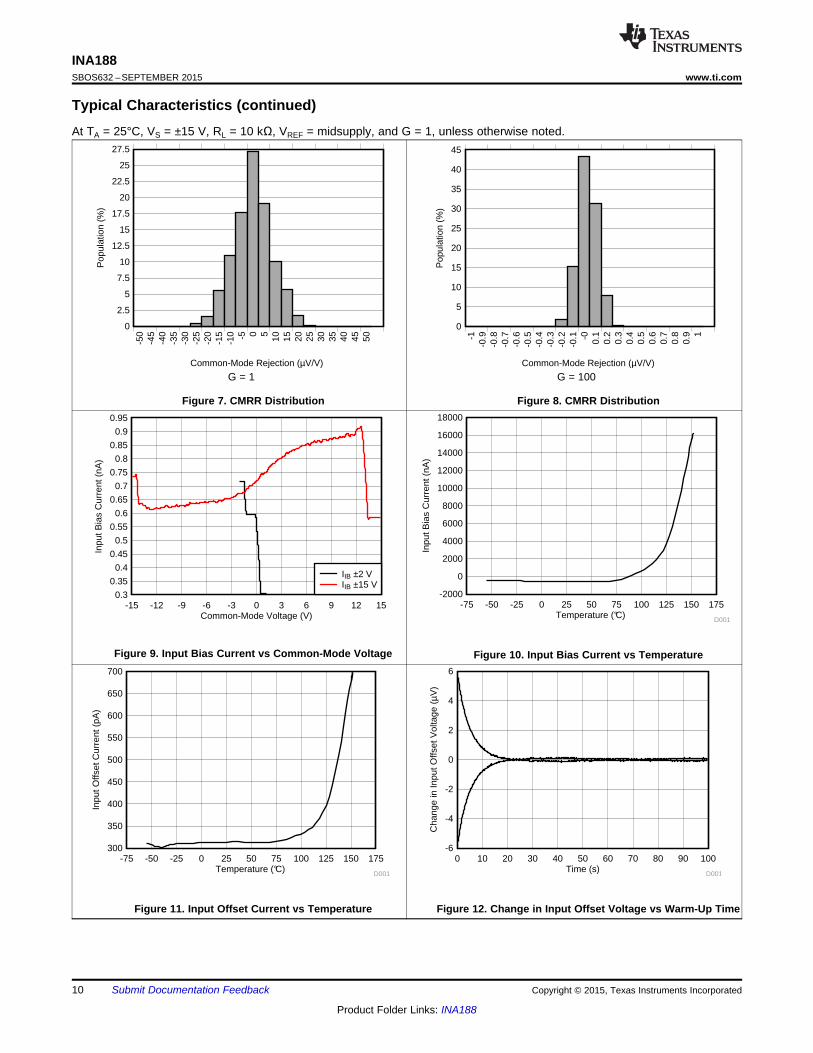
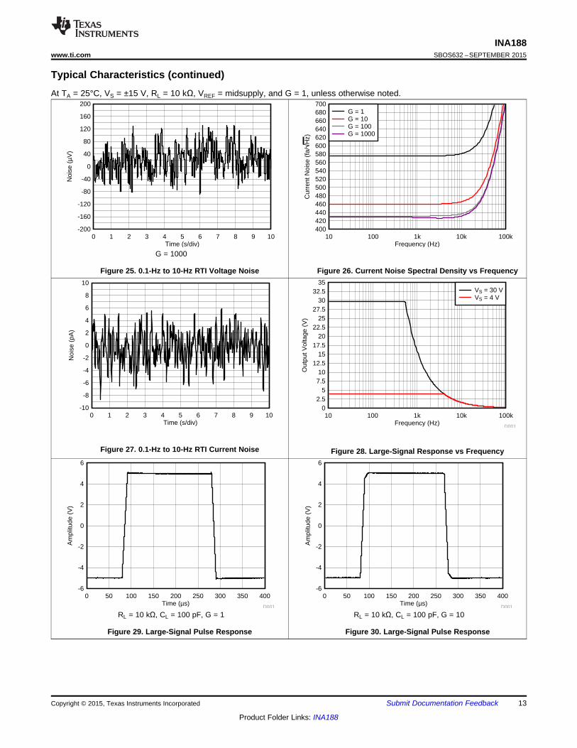
Typical Characteristics (continued)At TA = 25°C, VS = ±15 V, RL = 10 kΩ, VREF = midsupply, and G = 1, unless otherwise noted.
G = 1
Figure 7. CMRR Distribution
G = 100
Figure 8. CMRR Distribution
Figure 9. Input Bias Current vs Common-Mode Voltage Figure 10. Input Bias Current vs Temperature
Figure 11. Input Offset Current vs Temperature Figure 12. Change in Input Offset Voltage vs Warm-Up Time
Frequency (Hz)
Com
mon
-Mod
e R
ejec
tion
Rat
io (
dB)
0102030405060708090
100110120130140150160
10 100 1k 10k 100k
D001
G=1G=10G=100G=1000
Temperature (ºC)
Com
mon
-Mod
e R
ejec
tion
Rat
io (
dB)
-75 -45 -15 15 45 75 105 135-50
-40
-30
-20
-10
0
10
20
30
40
50
D001
G = 1G > 1
Frequency (Hz)
Gai
n (d
B)
-10-505
10152025303540455055606570
10 100 1k 10k 100k 1M 10M
D001
G=1G=10G=100G=1000
Frequency (Hz)
Com
mon
-Mod
e R
ejec
tion
Rat
io (
dB)
0102030405060708090
100110120130140150160
10 100 1k 10k 100k
D001
G=1G=10G=100G=1000
Frequency (Hz)
Pos
itive
Pow
er-S
uppl
y R
ejec
tion
Rat
io (
dB)
-10
10
30
50
70
90
110
130
150
10 100 1k 10k 100k 1M
G = 1G = 10G = 100G = 1000
Frequency (Hz)
Neg
ativ
e P
ower
-Sup
ply
Rej
ectio
n R
atio
(dB
)
-10
10
30
50
70
90
110
130
150
10 100 1k 10k 100k 1M
G = 1G = 10G = 100G = 1000
11
INA188www.ti.com SBOS632 –SEPTEMBER 2015
Product Folder Links: INA188
Submit Documentation FeedbackCopyright © 2015, Texas Instruments Incorporated
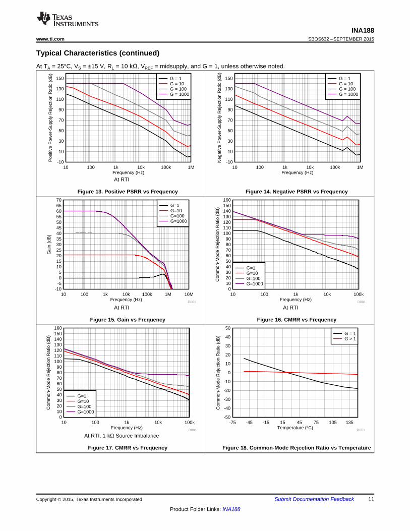
Typical Characteristics (continued)At TA = 25°C, VS = ±15 V, RL = 10 kΩ, VREF = midsupply, and G = 1, unless otherwise noted.
At RTI
Figure 13. Positive PSRR vs Frequency Figure 14. Negative PSRR vs Frequency
At RTI
Figure 15. Gain vs Frequency
At RTI
Figure 16. CMRR vs Frequency
At RTI, 1-kΩ Source Imbalance
Figure 17. CMRR vs Frequency Figure 18. Common-Mode Rejection Ratio vs Temperature
Frequency (Hz)
Vol
tage
Noi
se (
nV/
Hz)
0.02
0.05
0.1
0.2
0.5
1
2
5
10
20
50
100
1 10 100 1k 10k 100k
G = 1G = 10G = 100G = 1000
Time (s/div)
Noi
se (
µV
)
0 1 2 3 4 5 6 7 8 9 10-2
-1.6
-1.2
-0.8
-0.4
0
0.4
0.8
1.2
1.6
2
Output Current (mA)
Out
put V
olta
ge (
V)
0 2 4 6 8 10 12 14 16 18 200
0.2
0.4
0.6
0.8
1
1.2
1.4
1.6
1.8
2
D001
-40°C125°C25°C
Output Current (mA)
Out
put V
olta
ge (
V)
0 2.5 5 7.5 10 12.5 15 17.5 20 22.5-2
-1.8
-1.6
-1.4
-1.2
-1
-0.8
-0.6
-0.4
-0.2
0
D001
-40°C125°C25°C
Output Current (mA)
Out
put V
olta
ge (
V)
0 2.5 5 7.5 10 12.5 15 17.5 20 22.5 25-2
0
2
4
6
8
10
12
14
16
18
D001
-40°C125°C25°C
Output Current (mA)
Out
put V
olta
ge (
V)
0 3 6 9 12 15 18 21 24 27 30-18
-16
-14
-12
-10
-8
-6
-4
-2
0
D001
-40°C125°C25°C
12
INA188SBOS632 –SEPTEMBER 2015 www.ti.com
Product Folder Links: INA188
Submit Documentation Feedback Copyright © 2015, Texas Instruments Incorporated
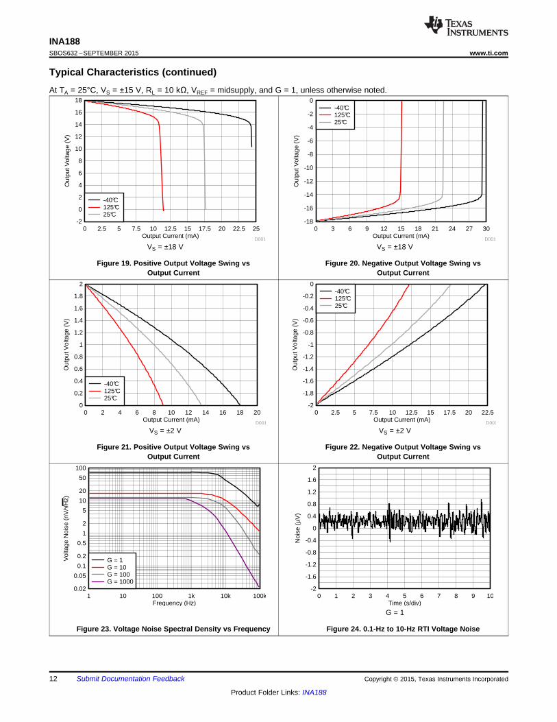
Typical Characteristics (continued)At TA = 25°C, VS = ±15 V, RL = 10 kΩ, VREF = midsupply, and G = 1, unless otherwise noted.
VS = ±18 V
Figure 19. Positive Output Voltage Swing vsOutput Current
VS = ±18 V
Figure 20. Negative Output Voltage Swing vsOutput Current
VS = ±2 V
Figure 21. Positive Output Voltage Swing vsOutput Current
VS = ±2 V
Figure 22. Negative Output Voltage Swing vsOutput Current
Figure 23. Voltage Noise Spectral Density vs Frequency
G = 1
Figure 24. 0.1-Hz to 10-Hz RTI Voltage Noise
Time (µs)
Am
plitu
de (
V)
0 50 100 150 200 250 300 350 400-6
-4
-2
0
2
4
6
D001Time (µs)
Am
plitu
de (
V)
0 50 100 150 200 250 300 350 400-6
-4
-2
0
2
4
6
D001
Frequency (Hz)
Out
put V
olta
ge (
V)
02.5
57.510
12.515
17.520
22.525
27.530
32.535
10 100 1k 10k 100k
D001
VS = 30 VVS = 4 V
Time (s/div)
Noi
se (
pA)
0 1 2 3 4 5 6 7 8 9 10-10
-8
-6
-4
-2
0
2
4
6
8
10
Time (s/div)
Noi
se (
µV
)
0 1 2 3 4 5 6 7 8 9 10-200
-160
-120
-80
-40
0
40
80
120
160
200
Frequency (Hz)
Cur
rent
Noi
se (
fa/
Hz)
400420440460480500520540560580600620640660680700
10 100 1k 10k 100k
G = 1G = 10G = 100G = 1000
13
INA188www.ti.com SBOS632 –SEPTEMBER 2015
Product Folder Links: INA188
Submit Documentation FeedbackCopyright © 2015, Texas Instruments Incorporated
Typical Characteristics (continued)At TA = 25°C, VS = ±15 V, RL = 10 kΩ, VREF = midsupply, and G = 1, unless otherwise noted.
G = 1000
Figure 25. 0.1-Hz to 10-Hz RTI Voltage Noise Figure 26. Current Noise Spectral Density vs Frequency
Figure 27. 0.1-Hz to 10-Hz RTI Current Noise Figure 28. Large-Signal Response vs Frequency
RL = 10 kΩ, CL = 100 pF, G = 1
Figure 29. Large-Signal Pulse Response
RL = 10 kΩ, CL = 100 pF, G = 10
Figure 30. Large-Signal Pulse Response
Time (µs)
Am
plitu
de (
mV
)
0 50 100 150 200 250 300 350 400-60
-40
-20
0
20
40
60
D001Time (µs)
Am
plitu
de (
mV
)
0 0.5 1 1.5 2 2.5 3 3.5 4-60
-40
-20
0
20
40
60
D001
Time (µs)
Am
plitu
de (
mV
)
0 50 100 150 200 250 300 350 400-100
-75
-50
-25
0
25
50
75
100
D001Time (µs)
Am
plitu
de (
mV
)
0 50 100 150 200 250 300 350 400-60
-40
-20
0
20
40
60
D001
Time (µs)
Am
plitu
de (
V)
0 50 100 150 200 250 300 350 400-6
-4
-2
0
2
4
6
D001Time (µs)
Am
plitu
de (
V)
0 0.5 1 1.5 2 2.5 3 3.5 4-6
-4
-2
0
2
4
6
D001
14
INA188SBOS632 –SEPTEMBER 2015 www.ti.com
Product Folder Links: INA188
Submit Documentation Feedback Copyright © 2015, Texas Instruments Incorporated
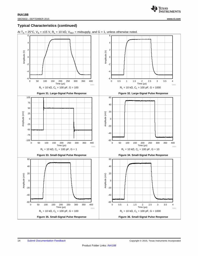
Typical Characteristics (continued)At TA = 25°C, VS = ±15 V, RL = 10 kΩ, VREF = midsupply, and G = 1, unless otherwise noted.
RL = 10 kΩ, CL = 100 pF, G = 100
Figure 31. Large-Signal Pulse Response
RL = 10 kΩ, CL = 100 pF, G = 1000
Figure 32. Large-Signal Pulse Response
RL = 10 kΩ, CL = 100 pF, G = 1
Figure 33. Small-Signal Pulse Response
RL = 10 kΩ, CL = 100 pF, G = 10
Figure 34. Small-Signal Pulse Response
RL = 10 kΩ, CL = 100 pF, G = 100
Figure 35. Small-Signal Pulse Response
RL = 10 kΩ, CL = 100 pF, G = 1000
Figure 36. Small-Signal Pulse Response
Output Voltage (V)
Non
linea
rity
(ppm
)
-10 -8 -6 -4 -2 0 2 4 6 8 10-4
-3.2
-2.4
-1.6
-0.8
0
0.8
1.6
2.4
3.2
4
D001
10k
1k
100
10
1
0.1
Z(
)W
O
1 10 100 1k 10k 10M
Frequency (Hz)
100k 1M
Temperature (°C)
Sup
ply
Cur
rent
(m
A)
-75 -50 -25 0 25 50 75 100 125 1501.1
1.15
1.2
1.25
1.3
1.35
1.4
1.45
1.5
D001Supply Voltage (V)
Sup
ply
Cur
rent
(m
A)
0 5 10 15 20 25 30 35 40 451.2
1.22
1.24
1.26
1.28
1.3
1.32
1.34
1.36
1.38
D001
Time (µs)
Am
plitu
de (
mV
)
0 20 40 60 80 100 120-100
-50
0
50
100
1500 pF100 pF220 pF500 pF1000 pF
Frequency (Hz)
Tot
al H
arm
onic
Dis
tort
ion
+ N
oise
(%
)
0.001
0.0020.0030.005
0.01
0.020.030.05
0.1
0.20.30.5
1
100 1k 10k
G = 1, 1-Vrms out, 2-k: loadG = 10, 1-Vrms out, 2-k: load
15
INA188www.ti.com SBOS632 –SEPTEMBER 2015
Product Folder Links: INA188
Submit Documentation FeedbackCopyright © 2015, Texas Instruments Incorporated
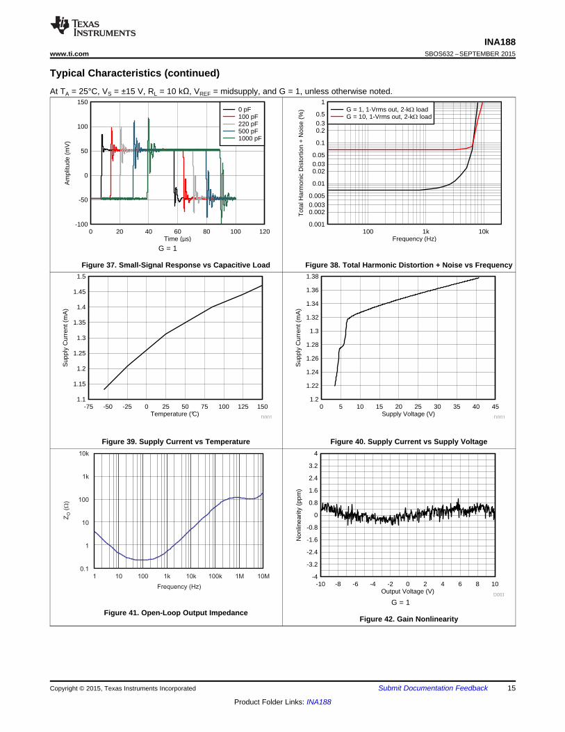
Typical Characteristics (continued)At TA = 25°C, VS = ±15 V, RL = 10 kΩ, VREF = midsupply, and G = 1, unless otherwise noted.
G = 1
Figure 37. Small-Signal Response vs Capacitive Load Figure 38. Total Harmonic Distortion + Noise vs Frequency
Figure 39. Supply Current vs Temperature Figure 40. Supply Current vs Supply Voltage
Figure 41. Open-Loop Output ImpedanceG = 1
Figure 42. Gain Nonlinearity
Output Voltage (V)
Non
linea
rity
(ppm
)
-10 -8 -6 -4 -2 0 2 4 6 8 10-10
-8
-6
-4
-2
0
2
4
6
8
10
D001Frequency (Hz)
EM
I Rej
ectio
n-R
atio
(dB
)
0
20
40
60
80
100
120
140
160
180
10M 100M 1G 10G
D001
Single-Ended InputCommon-Mode Input
Output Voltage (V)
Non
linea
rity
(ppm
)
-10 -8 -6 -4 -2 0 2 4 6 8 10-4
-3.2
-2.4
-1.6
-0.8
0
0.8
1.6
2.4
3.2
4
D001Output Voltage (V)
Non
linea
rity
(ppm
)
-10 -8 -6 -4 -2 0 2 4 6 8 10-15
-12
-9
-6
-3
0
3
6
9
12
15
D001
16
INA188SBOS632 –SEPTEMBER 2015 www.ti.com
Product Folder Links: INA188
Submit Documentation Feedback Copyright © 2015, Texas Instruments Incorporated
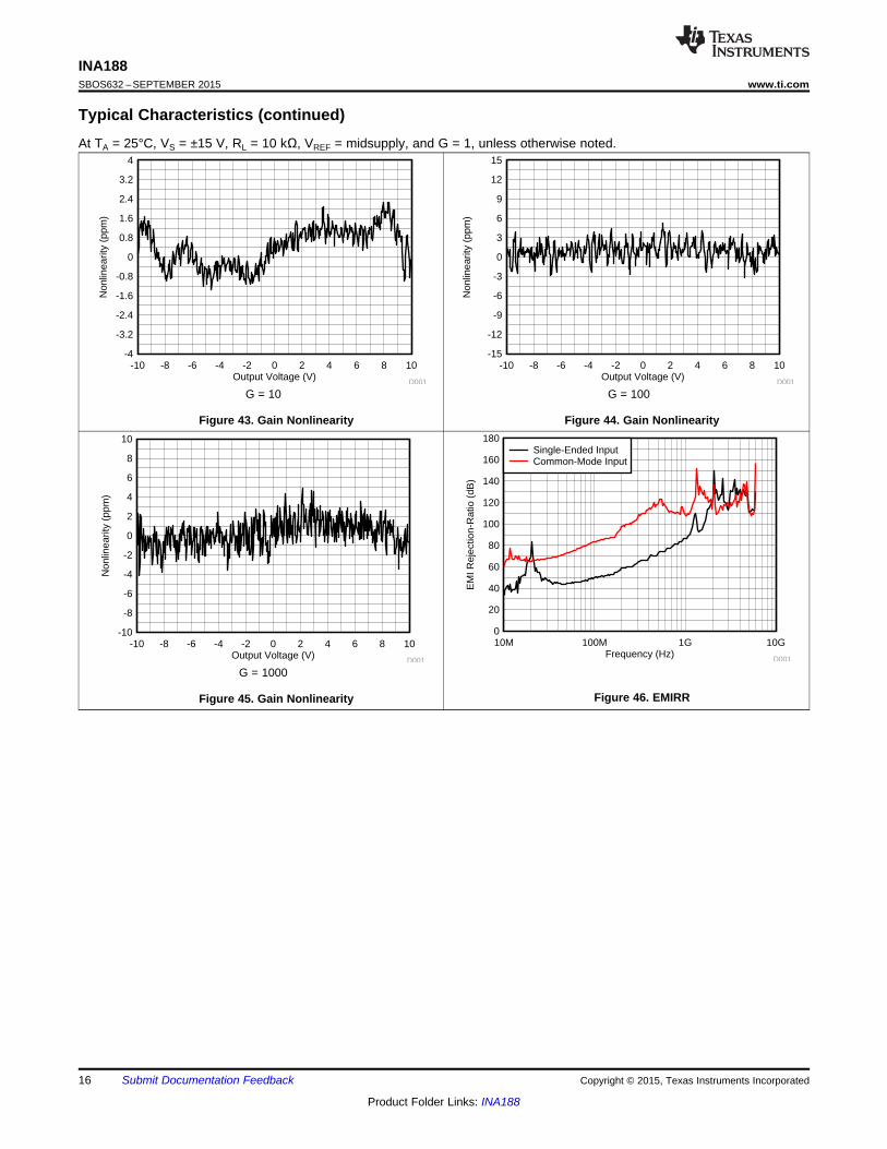
Typical Characteristics (continued)At TA = 25°C, VS = ±15 V, RL = 10 kΩ, VREF = midsupply, and G = 1, unless otherwise noted.
G = 10
Figure 43. Gain Nonlinearity
G = 100
Figure 44. Gain Nonlinearity
G = 1000
Figure 45. Gain Nonlinearity Figure 46. EMIRR
-
+
+
-
-
+
V+
V-
V+
V-
V+
V-
V+
V-
V+
V-
V+
V-
RFI Filter
RFI Filter
VIN-
VIN+
RG
25 k
25 k
20 k
20 k
20 k
20 k
VOUT
REF
A2
Zero-Drift Amp
A3
Zero-Drift Amp
A1
Zero-Drift Amp
RFI Filter
RFI Filter
V+
V-
V1 = VCM ± G1 (VDIFF / 2)
V2 = VCM + G1 (VDIFF / 2)
G1 = 1 + 2RF / RG G2 = R2 / R1
+
±
+±
VDIFF / 2
VCM
+ ±
VIN- = VCM ± VDIFF / 2
VIN+ = VCM + VDIFF / 2
VDIFF / 2
INA188RG
VIN-
VIN+ +
VOUT
REF
Simplified Form
+
VO = G1 x G2 (VIN+ - VIN-)
-
RLOAD
17
INA188www.ti.com SBOS632 –SEPTEMBER 2015
Product Folder Links: INA188
Submit Documentation FeedbackCopyright © 2015, Texas Instruments Incorporated
7 Detailed Description
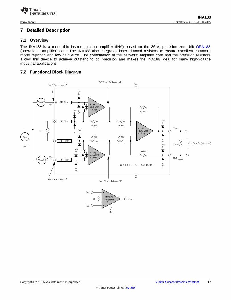
7.1 OverviewThe INA188 is a monolithic instrumentation amplifier (INA) based on the 36-V, precision zero-drift OPA188(operational amplifier) core. The INA188 also integrates laser-trimmed resistors to ensure excellent common-mode rejection and low gain error. The combination of the zero-drift amplifier core and the precision resistorsallows this device to achieve outstanding dc precision and makes the INA188 ideal for many high-voltageindustrial applications.
7.2 Functional Block Diagram
G
50 kG 1
R:
INA188RG
VIN-
VIN+ +
VOUT
REF
Simplified Form
18
INA188SBOS632 –SEPTEMBER 2015 www.ti.com
Product Folder Links: INA188
Submit Documentation Feedback Copyright © 2015, Texas Instruments Incorporated
(1) NC denotes no connection. When using the SPICE model, the simulation does not converge unless a resistor is connected to the RGpins; use a very large resistor value.
7.3 Feature Description
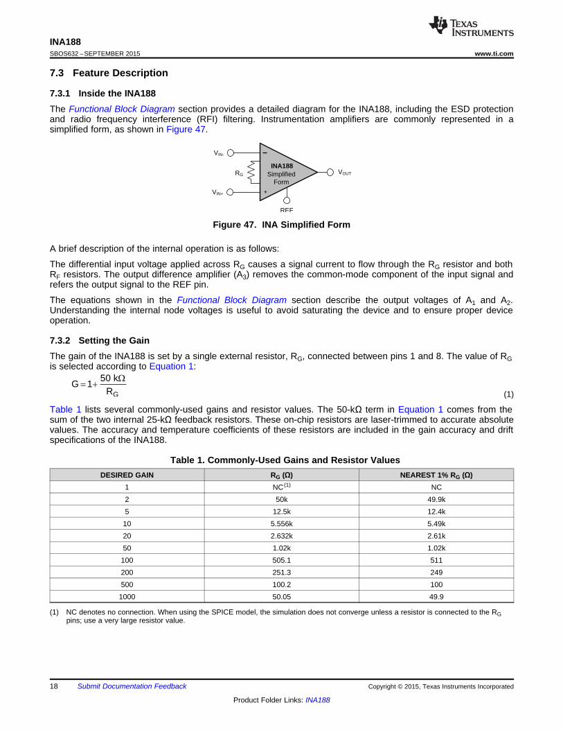
7.3.1 Inside the INA188The Functional Block Diagram section provides a detailed diagram for the INA188, including the ESD protectionand radio frequency interference (RFI) filtering. Instrumentation amplifiers are commonly represented in asimplified form, as shown in Figure 47.
Figure 47. INA Simplified Form
A brief description of the internal operation is as follows:
The differential input voltage applied across RG causes a signal current to flow through the RG resistor and bothRF resistors. The output difference amplifier (A3) removes the common-mode component of the input signal andrefers the output signal to the REF pin.
The equations shown in the Functional Block Diagram section describe the output voltages of A1 and A2.Understanding the internal node voltages is useful to avoid saturating the device and to ensure proper deviceoperation.
7.3.2 Setting the GainThe gain of the INA188 is set by a single external resistor, RG, connected between pins 1 and 8. The value of RGis selected according to Equation 1:
(1)
Table 1 lists several commonly-used gains and resistor values. The 50-kΩ term in Equation 1 comes from thesum of the two internal 25-kΩ feedback resistors. These on-chip resistors are laser-trimmed to accurate absolutevalues. The accuracy and temperature coefficients of these resistors are included in the gain accuracy and driftspecifications of the INA188.
Table 1. Commonly-Used Gains and Resistor ValuesDESIRED GAIN RG (Ω) NEAREST 1% RG (Ω)
1 NC (1) NC2 50k 49.9k5 12.5k 12.4k10 5.556k 5.49k20 2.632k 2.61k50 1.02k 1.02k100 505.1 511200 251.3 249500 100.2 1001000 50.05 49.9
GM1
+IN
-IN
CHOP1 CHOP2NotchFilter
GM_FF
GM2 GM3
C2
C1
OUT
Zero-Drift Amplifier Inside the INA188
19
INA188www.ti.com SBOS632 –SEPTEMBER 2015
Product Folder Links: INA188
Submit Documentation FeedbackCopyright © 2015, Texas Instruments Incorporated
7.3.2.1 Gain DriftThe stability and temperature drift of the external gain setting resistor, RG, also affects gain. The contribution ofRG to gain accuracy and drift can be determined from Equation 1.
The best gain drift of 5 ppm/ can be achieved when the INA188 uses G = 1 without RG connected. In this case,gain drift is limited only by the slight mismatch of the temperature coefficient of the integrated 20-kΩ resistors inthe differential amplifier (A3). At gains greater than 1, gain drift increases as a result of the individual drift of the25-kΩ resistors in the feedback of A1 and A2, relative to the drift of the external gain resistor RG. The lowtemperature coefficient of the internal feedback resistors significantly improves the overall temperature stability ofapplications using gains greater than 1 V/V over competing alternate solutions.
Low resistor values required for high gain can make wiring resistance important. Sockets add to the wiringresistance and contribute additional gain error (such as a possible unstable gain error) at gains of approximately100 or greater. To ensure stability, avoid parasitic capacitance of more than a few picofarads at RG connections.Careful matching of any parasitics on both RG pins maintains optimal CMRR over frequency; see TypicalCharacteristics curve, Figure 17.
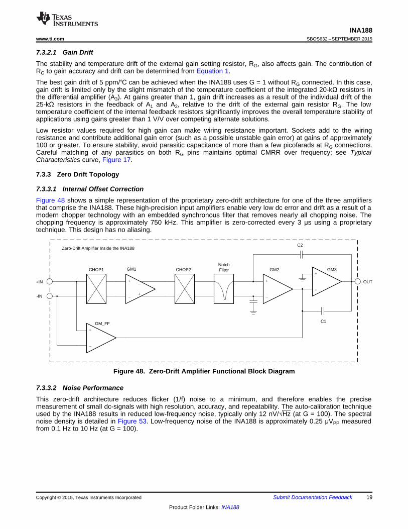
7.3.3 Zero Drift Topology
7.3.3.1 Internal Offset CorrectionFigure 48 shows a simple representation of the proprietary zero-drift architecture for one of the three amplifiersthat comprise the INA188. These high-precision input amplifiers enable very low dc error and drift as a result of amodern chopper technology with an embedded synchronous filter that removes nearly all chopping noise. Thechopping frequency is approximately 750 kHz. This amplifier is zero-corrected every 3 μs using a proprietarytechnique. This design has no aliasing.
Figure 48. Zero-Drift Amplifier Functional Block Diagram
7.3.3.2 Noise PerformanceThis zero-drift architecture reduces flicker (1/f) noise to a minimum, and therefore enables the precisemeasurement of small dc-signals with high resolution, accuracy, and repeatability. The auto-calibration techniqueused by the INA188 results in reduced low-frequency noise, typically only 12 nV/√Hz (at G = 100). The spectralnoise density is detailed in Figure 53. Low-frequency noise of the INA188 is approximately 0.25 μVPP measuredfrom 0.1 Hz to 10 Hz (at G = 100).
0
20
40
60
80
100
120
140
160
180
10M 100M 1G 10G
EM
IRR
(dB
)
Frequency (Hz) C035
0
20
40
60
80
100
120
140
160
10M 100M 1G 10G
EM
IRR
(dB
)
Frequency (Hz) C036
20
INA188SBOS632 –SEPTEMBER 2015 www.ti.com
Product Folder Links: INA188
Submit Documentation Feedback Copyright © 2015, Texas Instruments Incorporated
7.3.3.3 Input Bias Current Clock FeedthroughZero-drift amplifiers, such as the INA188, use switching on their inputs to correct for the intrinsic offset and drift ofthe amplifier. Charge injection from the integrated switches on the inputs can introduce very short transients inthe input bias current of the amplifier. The extremely short duration of these pulses prevents them from beingamplified; however, the pulses can be coupled to the output of the amplifier through the feedback network. Themost effective method to prevent transients in the input bias current from producing additional noise at theamplifier output is to use a low-pass filter (such as an RC network).
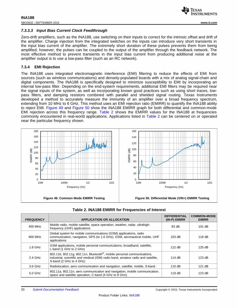
7.3.4 EMI RejectionThe INA188 uses integrated electromagnetic interference (EMI) filtering to reduce the effects of EMI fromsources (such as wireless communications) and densely-populated boards with a mix of analog signal-chain anddigital components. The INA188 is specifically designed to minimize susceptibility to EMI by incorporating aninternal low-pass filter. Depending on the end-system requirements, additional EMI filters may be required nearthe signal inputs of the system, as well as incorporating known good practices such as using short traces, low-pass filters, and damping resistors combined with parallel and shielded signal routing. Texas Instrumentsdeveloped a method to accurately measure the immunity of an amplifier over a broad frequency spectrum,extending from 10 MHz to 6 GHz. This method uses an EMI rejection ratio (EMIRR) to quantify the INA188 abilityto reject EMI. Figure 49 and Figure 50 show the INA188 EMIRR graph for both differential and common-modeEMI rejection across this frequency range. Table 2 shows the EMIRR values for the INA188 at frequenciescommonly encountered in real-world applications. Applications listed in Table 2 can be centered on or operatednear the particular frequency shown.
Figure 49. Common Mode EMIRR Testing Figure 50. Differential Mode (VIN+) EMIRR Testing
Table 2. INA188 EMIRR for Frequencies of Interest
FREQUENCY APPLICATION OR ALLOCATIONDIFFERENTIAL(IN-P) EMIRR
COMMON-MODEEMIRR
400 MHz Mobile radio, mobile satellite, space operation, weather, radar, ultrahigh-frequency (UHF) applications 83 dB 101 dB
900 MHzGlobal system for mobile communications (GSM) applications, radiocommunication, navigation, GPS (to 1.6 GHz), GSM, aeronautical mobile, UHFapplications
103 dB 118 dB
1.8 GHz GSM applications, mobile personal communications, broadband, satellite,L-band (1 GHz to 2 GHz) 112 dB 125 dB
2.4 GHz802.11b, 802.11g, 802.11n, Bluetooth®, mobile personal communications,industrial, scientific and medical (ISM) radio band, amateur radio and satellite,S-band (2 GHz to 4 GHz)
114 dB 123 dB
3.6 GHz Radiolocation, aero communication and navigation, satellite, mobile, S-band 110 dB 121 dB
5.0 GHz 802.11a, 802.11n, aero communication and navigation, mobile communication,space and satellite operation, C-band (4 GHz to 8 GHz) 119 dB 123 dB
21
INA188www.ti.com SBOS632 –SEPTEMBER 2015
Product Folder Links: INA188
Submit Documentation FeedbackCopyright © 2015, Texas Instruments Incorporated
7.3.5 Input Protection and Electrical OverstressDesigners often ask questions about the capability of an amplifier to withstand electrical overstress. Thesequestions tend to focus on the device inputs, but can involve the supply voltage pins or even the output pin. Eachof these different pin functions have electrical stress limits determined by the voltage breakdown characteristicsof the particular semiconductor fabrication process and specific circuits connected to the pin. Additionally, internalESD protection is built into these circuits to protect them from accidental ESD events both before and duringproduct assembly.
Having a good understanding of this basic ESD circuitry and its relevance to an electrical overstress event ishelpful. The Functional Block Diagram section illustrates the ESD circuits contained in the INA188. The ESDprotection circuitry involves several current-steering diodes connected from the input and output pins and routedback to the internal power-supply lines. This protection circuitry is intended to remain inactive during normalcircuit operation.
The input pins of the INA188 are protected with internal diodes connected to the power-supply rails. Thesediodes clamp the applied signal to prevent the input circuitry from being damaged. If the input signal voltage canexceed the power supplies by more than 0.3 V, limit the input signal current to less than 10 mA to protect theinternal clamp diodes. This current limiting can generally be done with a series input resistor. Some signalsources are inherently current-limited and do not require limiting resistors.
7.3.6 Input Common-Mode RangeThe linear input voltage range of the INA188 input circuitry extends from 100 mV inside the negative supplyvoltage to 1.5 V below the positive supply, and maintains 84-dB (minimum) common-mode rejection throughoutthis range. The common-mode range for most common operating conditions is best calculated using the INAcommon-mode range calculating tool. The INA188 can operate over a wide range of power supplies and VREFconfigurations, thus providing a comprehensive guide to common-mode range limits for all possible conditions isimpractical.
The most commonly overlooked overload condition occurs when a circuit exceeds the output swing of A1 and A2,which are internal circuit nodes that cannot be measured. Calculating the expected voltages at the output of A1and A2 (see the Functional Block Diagram section) provides a check for the most common overload conditions.The designs of A1 and A2 are identical and the outputs can swing to within approximately 250 mV of the power-supply rails. For example, when the A2 output is saturated, A1 can continue to be in linear operation, respondingto changes in the noninverting input voltage. This difference can give the appearance of linear operation but theoutput voltage is invalid.
7.4 Device Functional Modes
7.4.1 Single-Supply OperationThe INA188 can be used on single power supplies of 4 V to 36 V. Use the output REF pin to level shift theinternal output voltage into a linear operating condition. Ideally, connecting the REF pin to a potential that is mid-supply avoids saturating the output of the input amplifiers (A1 and A2). Actual output voltage swing is limited to250 mV above ground when the load is referred to ground. The typical characteristic curves, Output VoltageSwing vs Output Current (Figure 19 to Figure 22) illustrates how the output voltage swing varies with outputcurrent. See the Driving the Reference Pin section for information on how to adequately drive the reference pin.
With single-supply operation, VIN+ and VIN– must both be 0.1 V above ground for linear operation. For instance,the inverting input cannot be connected to ground to measure a voltage connected to the noninverting input.
RG
-
+
INA188
+
VIN-
VIN+
±10 mV Adjustment Range
V+
V-
OPA333
100 µA½ REF200
100 µA½ REF200
100
100
10 k
REF
22
INA188SBOS632 –SEPTEMBER 2015 www.ti.com
Product Folder Links: INA188
Submit Documentation Feedback Copyright © 2015, Texas Instruments Incorporated
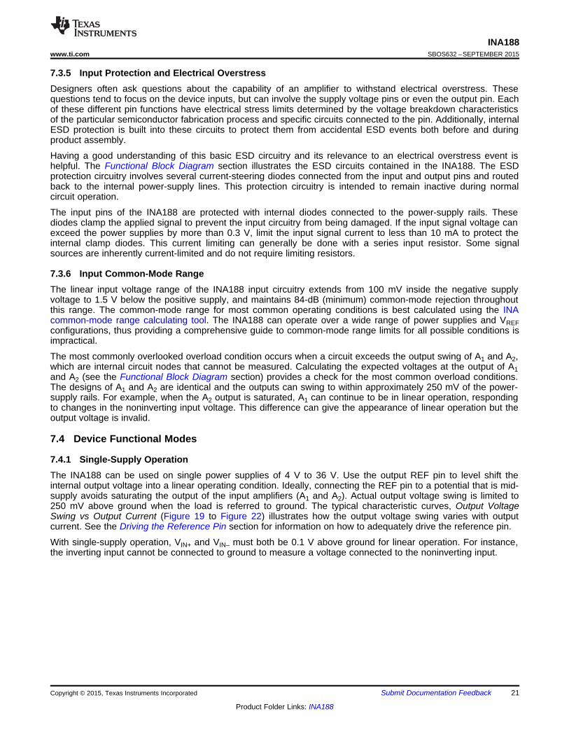
Device Functional Modes (continued)7.4.2 Offset TrimmingMost applications require no external offset adjustment; however, if necessary, adjustments can be made byapplying a voltage to the REF pin. Figure 51 shows an optional circuit for trimming the output offset voltage. Thevoltage applied to the REF pin is summed at the output. The op amp buffer provides low impedance at the REFpin to preserve good common-mode rejection.
Figure 51. Optional Trimming of the Output Offset Voltage
47 k 47 k
RG
Microphone, hydrophone, and so forth.
-
+
INA188
10 k
RGThermocouple
-
+
INA188
RG
Center tap provides bias current return.
-
+
INA188
23
INA188www.ti.com SBOS632 –SEPTEMBER 2015
Product Folder Links: INA188
Submit Documentation FeedbackCopyright © 2015, Texas Instruments Incorporated
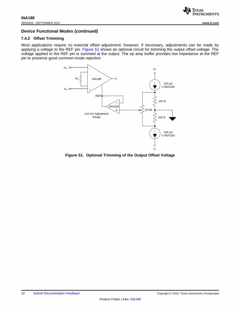
Device Functional Modes (continued)7.4.3 Input Bias Current Return PathThe input impedance of the INA188 is extremely high—approximately 20 GΩ. However, a path must be providedfor the input bias current of both inputs. This input bias current is typically 750 pA. High input impedance meansthat this input bias current changes very little with varying input voltage.
Input circuitry must provide a path for this input bias current for proper operation. Figure 52 shows variousprovisions for an input bias current path. Without a bias current path, the inputs float to a potential that exceedsthe common-mode range of the INA188, and the input amplifiers saturate. If the differential source resistance islow, the bias current return path can be connected to one input (as shown in the thermocouple example inFigure 52). With a higher source impedance, using two equal resistors provides a balanced input with possibleadvantages of a lower input offset voltage as a result of bias current and better high-frequency common-moderejection.
Figure 52. Providing an Input Common-Mode Current Path
INA188RG
VIN-
VIN+ +
VOUT
REF
5 V
+
5 V5 V
INA188RG
VIN-
VIN+ +
VOUT
REF
5 V
REF32252.5 V
a) Level shifting using the OPA330 as a low-impedance buffer. b) Level shifting using the low-impedance output of the REF3225.
24
INA188SBOS632 –SEPTEMBER 2015 www.ti.com
Product Folder Links: INA188
Submit Documentation Feedback Copyright © 2015, Texas Instruments Incorporated
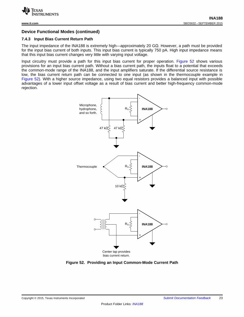
Device Functional Modes (continued)7.4.4 Driving the Reference PinThe output voltage of the INA188 is developed with respect to the voltage on the reference pin. Often, thereference pin (pin 5) is connected to the low-impedance system ground in dual-supply operation. In single-supplyoperation, offsetting the output signal to a precise mid-supply level (for example, 2.5 V in a 5-V supplyenvironment) can be useful. To accomplish this, a voltage source can be tied to the REF pin to level-shift theoutput so that the INA188 can drive a single-supply analog-to-digital converter (ADC).
For best performance, keep the source impedance to the REF pin below 5 Ω. As illustrated in the FunctionalBlock Diagram section, the reference pin is internally connected to a 20-kΩ resistor. Additional impedance at theREF pin adds to this 20-kΩ resistor. The imbalance in the resistor ratios results in degraded common-moderejection ratio (CMRR).
Figure 53 shows two different methods of driving the reference pin with low impedance. The OPA330 is a low-power, chopper-stabilized amplifier, and therefore offers excellent stability over temperature. The OPA330 isavailable in a space-saving SC70 and an even smaller chip-scale package. The REF3225 is a precisionreference in a small SOT23-6 package.
Figure 53. Options for Low-Impedance Level Shifting
RG 5.49 k
-
+
INA188
+
VDIFF = 1 V
-
VCM = 10 V
10 k
10 k
15 V
-15 V
Signal Bandwidth = 5 kHz
REF
VOUT
25
INA188www.ti.com SBOS632 –SEPTEMBER 2015
Product Folder Links: INA188
Submit Documentation FeedbackCopyright © 2015, Texas Instruments Incorporated
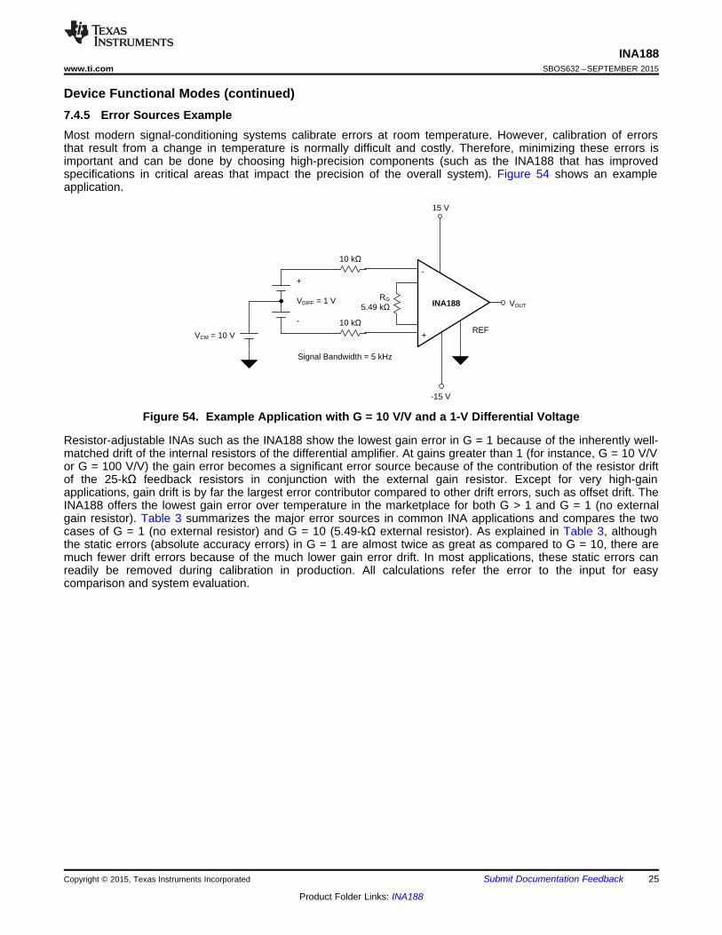
Device Functional Modes (continued)7.4.5 Error Sources ExampleMost modern signal-conditioning systems calibrate errors at room temperature. However, calibration of errorsthat result from a change in temperature is normally difficult and costly. Therefore, minimizing these errors isimportant and can be done by choosing high-precision components (such as the INA188 that has improvedspecifications in critical areas that impact the precision of the overall system). Figure 54 shows an exampleapplication.
Figure 54. Example Application with G = 10 V/V and a 1-V Differential Voltage
Resistor-adjustable INAs such as the INA188 show the lowest gain error in G = 1 because of the inherently well-matched drift of the internal resistors of the differential amplifier. At gains greater than 1 (for instance, G = 10 V/Vor G = 100 V/V) the gain error becomes a significant error source because of the contribution of the resistor driftof the 25-kΩ feedback resistors in conjunction with the external gain resistor. Except for very high-gainapplications, gain drift is by far the largest error contributor compared to other drift errors, such as offset drift. TheINA188 offers the lowest gain error over temperature in the marketplace for both G > 1 and G = 1 (no externalgain resistor). Table 3 summarizes the major error sources in common INA applications and compares the twocases of G = 1 (no external resistor) and G = 10 (5.49-kΩ external resistor). As explained in Table 3, althoughthe static errors (absolute accuracy errors) in G = 1 are almost twice as great as compared to G = 10, there aremuch fewer drift errors because of the much lower gain error drift. In most applications, these static errors canreadily be removed during calibration in production. All calculations refer the error to the input for easycomparison and system evaluation.
(e +NI2
´
eNO
2
G´
6
VDIFF
BW
26
INA188SBOS632 –SEPTEMBER 2015 www.ti.com
Product Folder Links: INA188
Submit Documentation Feedback Copyright © 2015, Texas Instruments Incorporated
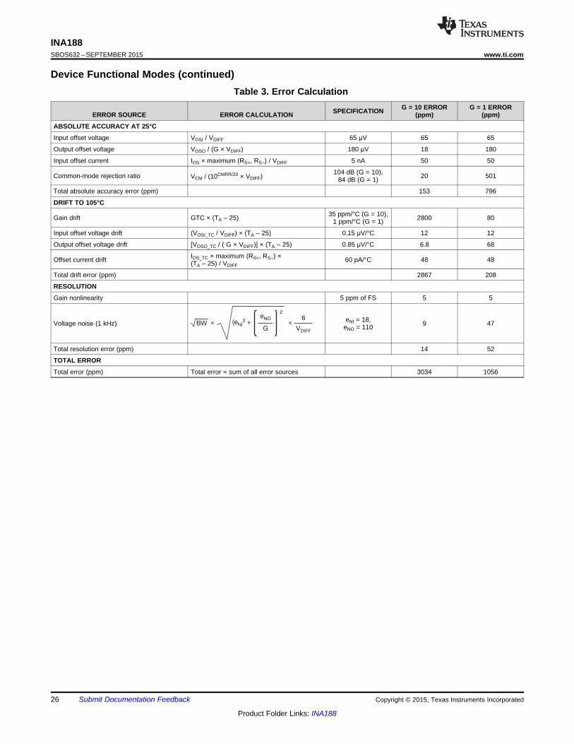
Device Functional Modes (continued)Table 3. Error Calculation
ERROR SOURCE ERROR CALCULATION SPECIFICATION G = 10 ERROR(ppm)
G = 1 ERROR(ppm)
ABSOLUTE ACCURACY AT 25°C
Input offset voltage VOSI / VDIFF 65 μV 65 65
Output offset voltage VOSO / (G × VDIFF) 180 μV 18 180
Input offset current IOS × maximum (RS+, RS–) / VDIFF 5 nA 50 50
Common-mode rejection ratio VCM / (10CMRR/20 × VDIFF) 104 dB (G = 10),84 dB (G = 1) 20 501
Total absolute accuracy error (ppm) 153 796
DRIFT TO 105°C
Gain drift GTC × (TA – 25) 35 ppm/°C (G = 10),1 ppm/°C (G = 1) 2800 80
Input offset voltage drift (VOSI_TC / VDIFF) × (TA – 25) 0.15 μV/°C 12 12
Output offset voltage drift [VOSO_TC / ( G × VDIFF)] × (TA – 25) 0.85 μV/°C 6.8 68
Offset current drift IOS_TC × maximum (RS+, RS–) ×(TA – 25) / VDIFF
60 pA/°C 48 48
Total drift error (ppm) 2867 208
RESOLUTION
Gain nonlinearity 5 ppm of FS 5 5
Voltage noise (1 kHz) eNI = 18,eNO = 110 9 47
Total resolution error (ppm) 14 52
TOTAL ERROR
Total error (ppm) Total error = sum of all error sources 3034 1056
RG 12.4 k
-
+
INA188
15 V
15 V
REF
VOUT = 2.5 V ± 2.3 V
REF3225 5 V
100 k
4.87 k
20
±10 V
4 mA to 20 mA±20 mA
2.5 V
10 F
27
INA188www.ti.com SBOS632 –SEPTEMBER 2015
Product Folder Links: INA188
Submit Documentation FeedbackCopyright © 2015, Texas Instruments Incorporated
8 Application and Implementation
NOTEInformation in the following applications sections is not part of the TI componentspecification, and TI does not warrant its accuracy or completeness. TI’s customers areresponsible for determining suitability of components for their purposes. Customers shouldvalidate and test their design implementation to confirm system functionality.
8.1 Application InformationThe INA188 measures a small differential voltage with a high common-mode voltage developed between thenoninverting and inverting input. The low offset drift in conjunction with no 1/f noise makes the INA188 suitablefor a wide range of applications. The ability to set the reference pin to adjust the functionality of the output signaloffers additional flexibility that is practical for multiple configurations.
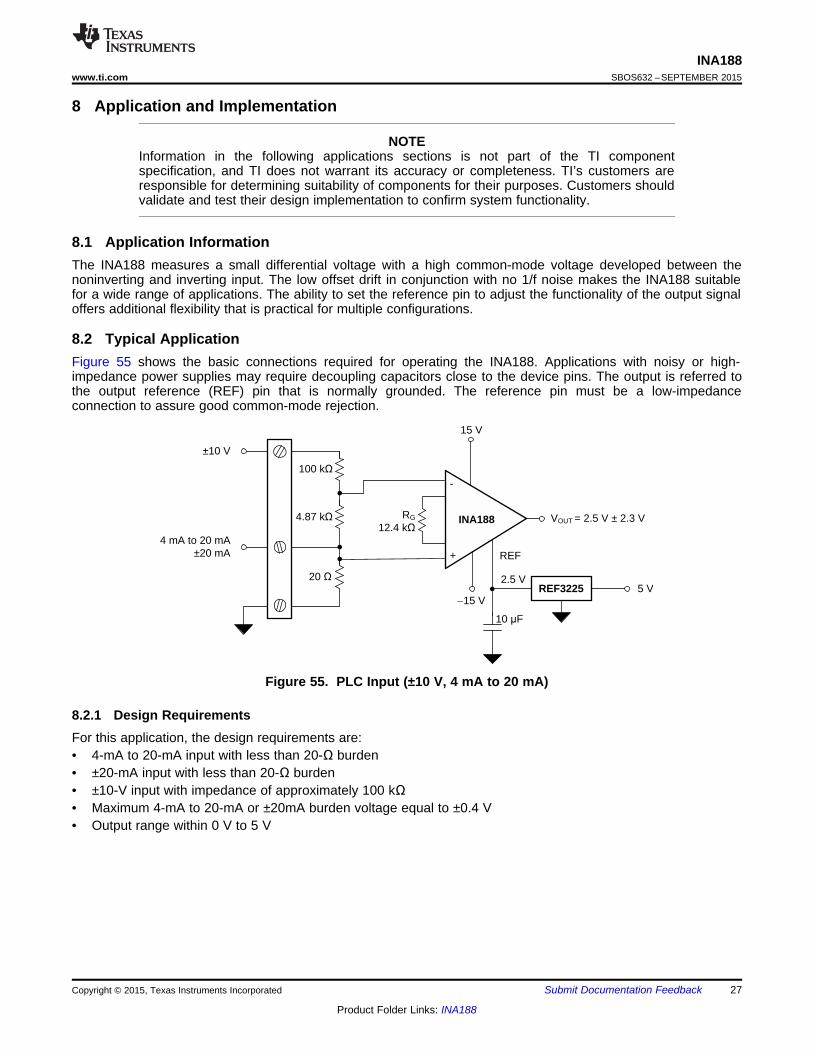
8.2 Typical ApplicationFigure 55 shows the basic connections required for operating the INA188. Applications with noisy or high-impedance power supplies may require decoupling capacitors close to the device pins. The output is referred tothe output reference (REF) pin that is normally grounded. The reference pin must be a low-impedanceconnection to assure good common-mode rejection.
Figure 55. PLC Input (±10 V, 4 mA to 20 mA)
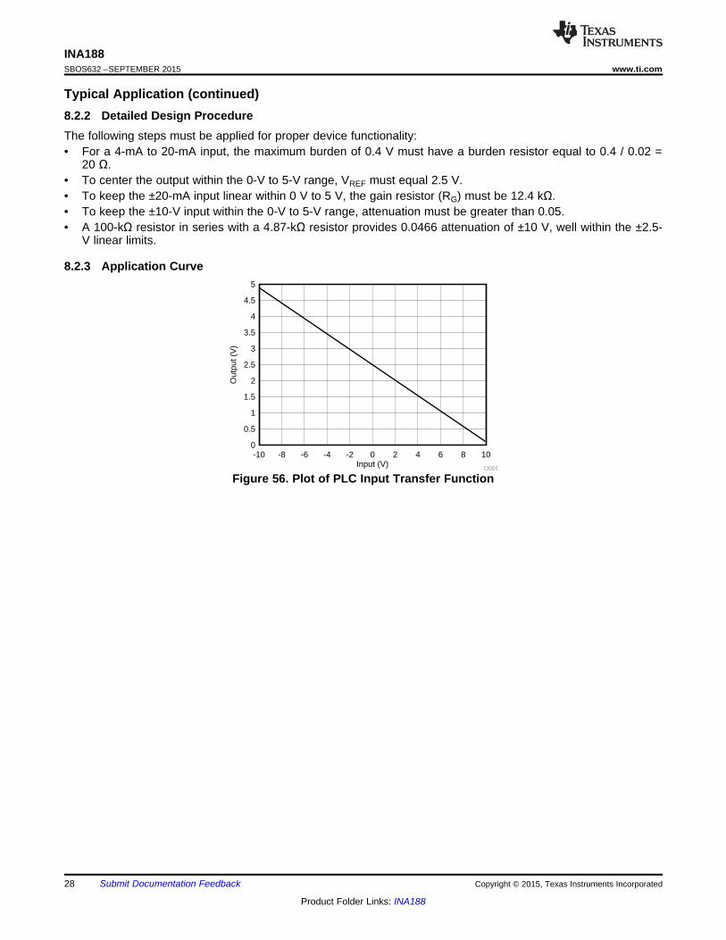
8.2.1 Design RequirementsFor this application, the design requirements are:• 4-mA to 20-mA input with less than 20-Ω burden• ±20-mA input with less than 20-Ω burden• ±10-V input with impedance of approximately 100 kΩ• Maximum 4-mA to 20-mA or ±20mA burden voltage equal to ±0.4 V• Output range within 0 V to 5 V
Input (V)
Out
put (
V)
-10 -8 -6 -4 -2 0 2 4 6 8 100
0.5
1
1.5
2
2.5
3
3.5
4
4.5
5
D001
28
INA188SBOS632 –SEPTEMBER 2015 www.ti.com
Product Folder Links: INA188
Submit Documentation Feedback Copyright © 2015, Texas Instruments Incorporated
Typical Application (continued)8.2.2 Detailed Design ProcedureThe following steps must be applied for proper device functionality:• For a 4-mA to 20-mA input, the maximum burden of 0.4 V must have a burden resistor equal to 0.4 / 0.02 =
20 Ω.• To center the output within the 0-V to 5-V range, VREF must equal 2.5 V.• To keep the ±20-mA input linear within 0 V to 5 V, the gain resistor (RG) must be 12.4 kΩ.• To keep the ±10-V input within the 0-V to 5-V range, attenuation must be greater than 0.05.• A 100-kΩ resistor in series with a 4.87-kΩ resistor provides 0.0466 attenuation of ±10 V, well within the ±2.5-
V linear limits.
8.2.3 Application Curve
Figure 56. Plot of PLC Input Transfer Function
29
INA188www.ti.com SBOS632 –SEPTEMBER 2015
Product Folder Links: INA188
Submit Documentation FeedbackCopyright © 2015, Texas Instruments Incorporated
9 Power Supply RecommendationsThe minimum power-supply voltage for the INA188 is ±2 V and the maximum power-supply voltage is ±18 V.This minimum and maximum range covers a wide range of power supplies. However, for optimum performance,±15 V is recommended. A 0.1-µF bypass capacitor is recommended to be added at the input to compensate forthe layout and power-supply source impedance.
10 Layout
10.1 Layout GuidelinesAttention to good layout practices is always recommended. For best operational performance of the device, usegood printed circuit board (PCB) layout practices, including:• Care must be taken to ensure that both input paths are well-matched for source impedance and capacitance
to avoid converting common-mode signals into differential signals. In addition, parasitic capacitance at thegain-setting pins can also affect CMRR over frequency. For example, in applications that implement gainswitching using switches or PhotoMOS® relays to change the value of RG, select the component so that theswitch capacitance is as small as possible.
• Noise can propagate into analog circuitry through the power pins of the circuit as a whole and of the deviceitself. Bypass capacitors are used to reduce the coupled noise by providing low-impedance power sourceslocal to the analog circuitry.– Connect low-ESR, 0.1-μF ceramic bypass capacitors between each supply pin and ground, placed as
close to the device as possible. A single bypass capacitor from V+ to ground is applicable for single-supply applications.
• Separate grounding for analog and digital portions of the circuitry is one of the simplest and most effectivemethods of noise suppression. One or more layers on multilayer PCBs are usually devoted to ground planes.A ground plane helps distribute heat and reduces EMI noise pickup. Make sure to physically separate digitaland analog grounds, paying attention to the flow of the ground current. For more detailed information, seeSLOA089, Circuit Board Layout Techniques.
• In order to reduce parasitic coupling, run the input traces as far away from the supply or output traces aspossible. If these traces cannot be kept separate, crossing the sensitive trace perpendicular is much betterthan in parallel with the noisy trace.
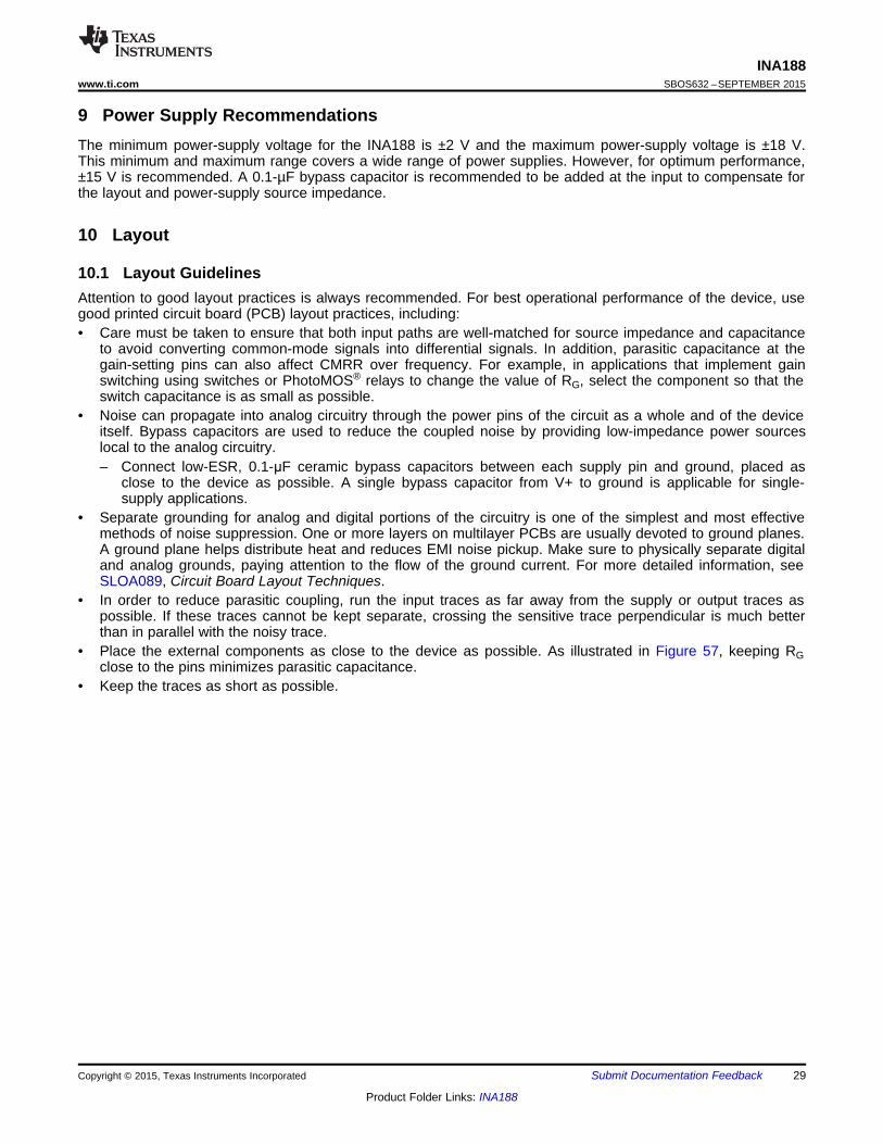
• Place the external components as close to the device as possible. As illustrated in Figure 57, keeping RGclose to the pins minimizes parasitic capacitance.
• Keep the traces as short as possible.
BypassCapacitor
BypassCapacitor
Gain Resistor
R6
V–IH
V+IH
V–
R6
V+
VO
REF
–
+
V+
VOUT
GND
VIN
VIN
GNDV–
30
INA188SBOS632 –SEPTEMBER 2015 www.ti.com
Product Folder Links: INA188
Submit Documentation Feedback Copyright © 2015, Texas Instruments Incorporated
10.2 Layout Example
Figure 57. PCB Layout Example
31
INA188www.ti.com SBOS632 –SEPTEMBER 2015
Product Folder Links: INA188
Submit Documentation FeedbackCopyright © 2015, Texas Instruments Incorporated
11 Device and Documentation Support
11.1 Device Support
11.1.1 Development Support
Table 4. Table 1. Design Kits and Evaluation ModulesNAME PART NUMBER TYPE
DIP Adapter Evaluation Module DIP-ADAPTER-EVM Evaluation Module and BoardsUniversal Instrumentation Amplifier Evaluation Module INAEVM Evaluation Module and Boards
Table 5. Table 2. Development ToolsNAME PART NUMBER TYPE
Calculate Input Common-Mode Range of Instrumentation Amplifiers INA-CMV-CALC Calculation ToolsSPICE-Based Analog Simulation Program TINA-TI Circuit Design and Simulation
11.2 Documentation Support
11.2.1 Related DocumentationOPA188 Data Sheet, SBOS642
OPA330 Data Sheet, SBOS432
REF3225 Data Sheet, SBVS058
Circuit Board Layout Techniques, SLOA089
11.3 Community ResourcesThe following links connect to TI community resources. Linked contents are provided "AS IS" by the respectivecontributors. They do not constitute TI specifications and do not necessarily reflect TI's views; see TI's Terms ofUse.
TI E2E™ Online Community TI's Engineer-to-Engineer (E2E) Community. Created to foster collaborationamong engineers. At e2e.ti.com, you can ask questions, share knowledge, explore ideas and helpsolve problems with fellow engineers.
Design Support TI's Design Support Quickly find helpful E2E forums along with design support tools andcontact information for technical support.
11.4 TrademarksE2E is a trademark of Texas Instruments.Bluetooth is a registered trademark of Bluetooth SIG, Inc.PhotoMOS is a registered trademark of Panasonic Electric Works Europe AG.All other trademarks are the property of their respective owners.
11.5 Electrostatic Discharge CautionThese devices have limited built-in ESD protection. The leads should be shorted together or the device placed in conductive foamduring storage or handling to prevent electrostatic damage to the MOS gates.
11.6 GlossarySLYZ022 — TI Glossary.
This glossary lists and explains terms, acronyms, and definitions.

32
INA188SBOS632 –SEPTEMBER 2015 www.ti.com
Product Folder Links: INA188
Submit Documentation Feedback Copyright © 2015, Texas Instruments Incorporated
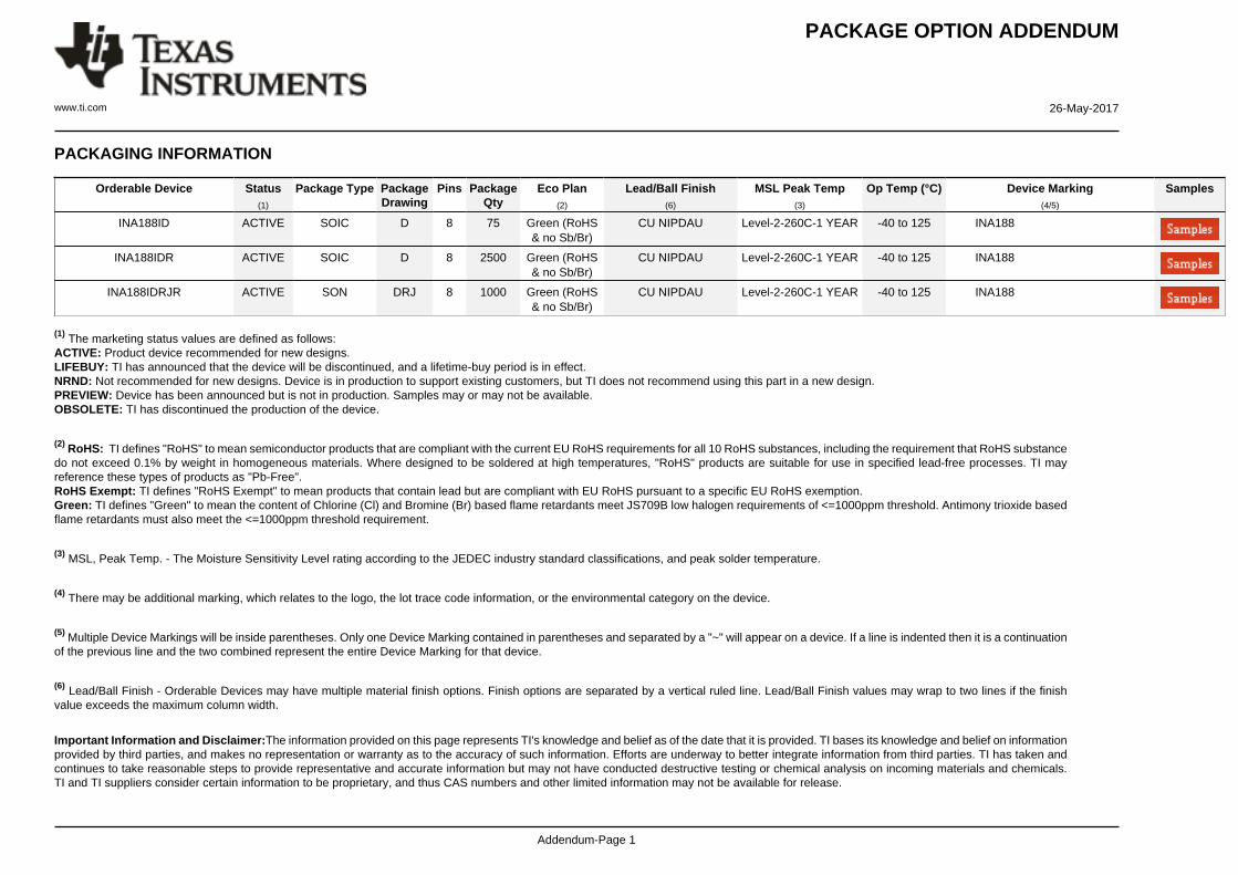
12 Mechanical, Packaging, and Orderable InformationThe following pages include mechanical, packaging, and orderable information. This information is the mostcurrent data available for the designated devices. This data is subject to change without notice and revision ofthis document. For browser-based versions of this data sheet, refer to the left-hand navigation.
PACKAGE OPTION ADDENDUM
www.ti.com 26-May-2017
Addendum-Page 1
PACKAGING INFORMATION
Orderable Device Status(1)
Package Type PackageDrawing
Pins PackageQty
Eco Plan(2)
Lead/Ball Finish(6)
MSL Peak Temp(3)
Op Temp (°C) Device Marking(4/5)
Samples
INA188ID ACTIVE SOIC D 8 75 Green (RoHS& no Sb/Br)
CU NIPDAU Level-2-260C-1 YEAR -40 to 125 INA188
INA188IDR ACTIVE SOIC D 8 2500 Green (RoHS& no Sb/Br)
CU NIPDAU Level-2-260C-1 YEAR -40 to 125 INA188
INA188IDRJR ACTIVE SON DRJ 8 1000 Green (RoHS& no Sb/Br)
CU NIPDAU Level-2-260C-1 YEAR -40 to 125 INA188
(1) The marketing status values are defined as follows:ACTIVE: Product device recommended for new designs.LIFEBUY: TI has announced that the device will be discontinued, and a lifetime-buy period is in effect.NRND: Not recommended for new designs. Device is in production to support existing customers, but TI does not recommend using this part in a new design.PREVIEW: Device has been announced but is not in production. Samples may or may not be available.OBSOLETE: TI has discontinued the production of the device.
(2) RoHS: TI defines "RoHS" to mean semiconductor products that are compliant with the current EU RoHS requirements for all 10 RoHS substances, including the requirement that RoHS substancedo not exceed 0.1% by weight in homogeneous materials. Where designed to be soldered at high temperatures, "RoHS" products are suitable for use in specified lead-free processes. TI mayreference these types of products as "Pb-Free".RoHS Exempt: TI defines "RoHS Exempt" to mean products that contain lead but are compliant with EU RoHS pursuant to a specific EU RoHS exemption.Green: TI defines "Green" to mean the content of Chlorine (Cl) and Bromine (Br) based flame retardants meet JS709B low halogen requirements of <=1000ppm threshold. Antimony trioxide basedflame retardants must also meet the <=1000ppm threshold requirement.
(3) MSL, Peak Temp. - The Moisture Sensitivity Level rating according to the JEDEC industry standard classifications, and peak solder temperature.
(4) There may be additional marking, which relates to the logo, the lot trace code information, or the environmental category on the device.
(5) Multiple Device Markings will be inside parentheses. Only one Device Marking contained in parentheses and separated by a "~" will appear on a device. If a line is indented then it is a continuationof the previous line and the two combined represent the entire Device Marking for that device.
(6) Lead/Ball Finish - Orderable Devices may have multiple material finish options. Finish options are separated by a vertical ruled line. Lead/Ball Finish values may wrap to two lines if the finishvalue exceeds the maximum column width.
Important Information and Disclaimer:The information provided on this page represents TI's knowledge and belief as of the date that it is provided. TI bases its knowledge and belief on informationprovided by third parties, and makes no representation or warranty as to the accuracy of such information. Efforts are underway to better integrate information from third parties. TI has taken andcontinues to take reasonable steps to provide representative and accurate information but may not have conducted destructive testing or chemical analysis on incoming materials and chemicals.TI and TI suppliers consider certain information to be proprietary, and thus CAS numbers and other limited information may not be available for release.
PACKAGE OPTION ADDENDUM
www.ti.com 26-May-2017
Addendum-Page 2
In no event shall TI's liability arising out of such information exceed the total purchase price of the TI part(s) at issue in this document sold by TI to Customer on an annual basis.
IMPORTANT NOTICE
Texas Instruments Incorporated (TI) reserves the right to make corrections, enhancements, improvements and other changes to itssemiconductor products and services per JESD46, latest issue, and to discontinue any product or service per JESD48, latest issue. Buyersshould obtain the latest relevant information before placing orders and should verify that such information is current and complete.TI’s published terms of sale for semiconductor products (http://www.ti.com/sc/docs/stdterms.htm) apply to the sale of packaged integratedcircuit products that TI has qualified and released to market. Additional terms may apply to the use or sale of other types of TI products andservices.Reproduction of significant portions of TI information in TI data sheets is permissible only if reproduction is without alteration and isaccompanied by all associated warranties, conditions, limitations, and notices. TI is not responsible or liable for such reproduceddocumentation. Information of third parties may be subject to additional restrictions. Resale of TI products or services with statementsdifferent from or beyond the parameters stated by TI for that product or service voids all express and any implied warranties for theassociated TI product or service and is an unfair and deceptive business practice. TI is not responsible or liable for any such statements.Buyers and others who are developing systems that incorporate TI products (collectively, “Designers”) understand and agree that Designersremain responsible for using their independent analysis, evaluation and judgment in designing their applications and that Designers havefull and exclusive responsibility to assure the safety of Designers' applications and compliance of their applications (and of all TI productsused in or for Designers’ applications) with all applicable regulations, laws and other applicable requirements. Designer represents that, withrespect to their applications, Designer has all the necessary expertise to create and implement safeguards that (1) anticipate dangerousconsequences of failures, (2) monitor failures and their consequences, and (3) lessen the likelihood of failures that might cause harm andtake appropriate actions. Designer agrees that prior to using or distributing any applications that include TI products, Designer willthoroughly test such applications and the functionality of such TI products as used in such applications.TI’s provision of technical, application or other design advice, quality characterization, reliability data or other services or information,including, but not limited to, reference designs and materials relating to evaluation modules, (collectively, “TI Resources”) are intended toassist designers who are developing applications that incorporate TI products; by downloading, accessing or using TI Resources in anyway, Designer (individually or, if Designer is acting on behalf of a company, Designer’s company) agrees to use any particular TI Resourcesolely for this purpose and subject to the terms of this Notice.TI’s provision of TI Resources does not expand or otherwise alter TI’s applicable published warranties or warranty disclaimers for TIproducts, and no additional obligations or liabilities arise from TI providing such TI Resources. TI reserves the right to make corrections,enhancements, improvements and other changes to its TI Resources. TI has not conducted any testing other than that specificallydescribed in the published documentation for a particular TI Resource.Designer is authorized to use, copy and modify any individual TI Resource only in connection with the development of applications thatinclude the TI product(s) identified in such TI Resource. NO OTHER LICENSE, EXPRESS OR IMPLIED, BY ESTOPPEL OR OTHERWISETO ANY OTHER TI INTELLECTUAL PROPERTY RIGHT, AND NO LICENSE TO ANY TECHNOLOGY OR INTELLECTUAL PROPERTYRIGHT OF TI OR ANY THIRD PARTY IS GRANTED HEREIN, including but not limited to any patent right, copyright, mask work right, orother intellectual property right relating to any combination, machine, or process in which TI products or services are used. Informationregarding or referencing third-party products or services does not constitute a license to use such products or services, or a warranty orendorsement thereof. Use of TI Resources may require a license from a third party under the patents or other intellectual property of thethird party, or a license from TI under the patents or other intellectual property of TI.TI RESOURCES ARE PROVIDED “AS IS” AND WITH ALL FAULTS. TI DISCLAIMS ALL OTHER WARRANTIES ORREPRESENTATIONS, EXPRESS OR IMPLIED, REGARDING RESOURCES OR USE THEREOF, INCLUDING BUT NOT LIMITED TOACCURACY OR COMPLETENESS, TITLE, ANY EPIDEMIC FAILURE WARRANTY AND ANY IMPLIED WARRANTIES OFMERCHANTABILITY, FITNESS FOR A PARTICULAR PURPOSE, AND NON-INFRINGEMENT OF ANY THIRD PARTY INTELLECTUALPROPERTY RIGHTS. TI SHALL NOT BE LIABLE FOR AND SHALL NOT DEFEND OR INDEMNIFY DESIGNER AGAINST ANY CLAIM,INCLUDING BUT NOT LIMITED TO ANY INFRINGEMENT CLAIM THAT RELATES TO OR IS BASED ON ANY COMBINATION OFPRODUCTS EVEN IF DESCRIBED IN TI RESOURCES OR OTHERWISE. IN NO EVENT SHALL TI BE LIABLE FOR ANY ACTUAL,DIRECT, SPECIAL, COLLATERAL, INDIRECT, PUNITIVE, INCIDENTAL, CONSEQUENTIAL OR EXEMPLARY DAMAGES INCONNECTION WITH OR ARISING OUT OF TI RESOURCES OR USE THEREOF, AND REGARDLESS OF WHETHER TI HAS BEENADVISED OF THE POSSIBILITY OF SUCH DAMAGES.Unless TI has explicitly designated an individual product as meeting the requirements of a particular industry standard (e.g., ISO/TS 16949and ISO 26262), TI is not responsible for any failure to meet such industry standard requirements.Where TI specifically promotes products as facilitating functional safety or as compliant with industry functional safety standards, suchproducts are intended to help enable customers to design and create their own applications that meet applicable functional safety standardsand requirements. Using products in an application does not by itself establish any safety features in the application. Designers mustensure compliance with safety-related requirements and standards applicable to their applications. Designer may not use any TI products inlife-critical medical equipment unless authorized officers of the parties have executed a special contract specifically governing such use.Life-critical medical equipment is medical equipment where failure of such equipment would cause serious bodily injury or death (e.g., lifesupport, pacemakers, defibrillators, heart pumps, neurostimulators, and implantables). Such equipment includes, without limitation, allmedical devices identified by the U.S. Food and Drug Administration as Class III devices and equivalent classifications outside the U.S.TI may expressly designate certain products as completing a particular qualification (e.g., Q100, Military Grade, or Enhanced Product).Designers agree that it has the necessary expertise to select the product with the appropriate qualification designation for their applicationsand that proper product selection is at Designers’ own risk. Designers are solely responsible for compliance with all legal and regulatoryrequirements in connection with such selection.Designer will fully indemnify TI and its representatives against any damages, costs, losses, and/or liabilities arising out of Designer’s non-compliance with the terms and provisions of this Notice.
Mailing Address: Texas Instruments, Post Office Box 655303, Dallas, Texas 75265Copyright © 2017, Texas Instruments Incorporated