inclined nanoimprinting lithography-based 3d …mems.seas.upenn.edu/publications/2011/inclined...
TRANSCRIPT

Inclined nanoimprinting lithography-based 3D nanofabrication
This article has been downloaded from IOPscience. Please scroll down to see the full text article.
2011 J. Micromech. Microeng. 21 065036
(http://iopscience.iop.org/0960-1317/21/6/065036)
Download details:
IP Address: 130.207.50.192
The article was downloaded on 17/06/2011 at 21:37
Please note that terms and conditions apply.
View the table of contents for this issue, or go to the journal homepage for more
Home Search Collections Journals About Contact us My IOPscience

IOP PUBLISHING JOURNAL OF MICROMECHANICS AND MICROENGINEERING
J. Micromech. Microeng. 21 (2011) 065036 (11pp) doi:10.1088/0960-1317/21/6/065036
Inclined nanoimprintinglithography-based 3D nanofabricationZhan Liu1,3, David G Bucknall1 and Mark G Allen2
1 School of Materials Science and Engineering, Georgia Institute of Technology, Atlanta, GA 30332,USA2 School of Electrical and Computer Engineering, Georgia Institute of Technology, Atlanta, GA 30332,USA
E-mail: [email protected]
Received 22 February 2011, in final form 28 March 2011Published 18 May 2011Online at stacks.iop.org/JMM/21/065036
AbstractWe report a ‘top–down’ 3D nanofabrication approach combining non-conventional inclinednanoimprint lithography (INIL) with reactive ion etching (RIE), contact molding and 3D metalnanotransfer printing (nTP). This integration of processes enables the production andconformal transfer of 3D polymer nanostructures of varying heights to a variety of othermaterials including a silicon-based substrate, a silicone stamp and a metal gold (Au) thin film.The process demonstrates the potential of reduced fabrication cost and complexity comparedto existing methods. Various 3D nanostructures in technologically useful materials have beenfabricated, including symmetric and asymmetric nanolines, nanocircles and nanosquares.Such 3D nanostructures have potential applications such as angle-resolved photonic crystals,plasmonic crystals and biomimicking anisotropic surfaces. This integrated INIL-basedstrategy shows great promise for 3D nanofabrication in the fields of photonics, plasmonics andsurface tribology.
(Some figures in this article are in colour only in the electronic version)
1. Introduction
Fabrication of various well-defined 3D nanostructureswith controlled feature sizes is a significant technicaldriver for a number of applications in differentfields including photonics, plasmonics, nanotribology andnanoelectromechanical systems (NEMS). For example,3D nanophotonic crystals exploit periodic 3D nano-sizeddielectric structures to dramatically influence light throughthem [1–3]. However, it is much more challenging to fabricatehigh-quality 3D nanophotonic crystals and properly integratethem in optical devices compared to 1D/2D nanophotoniccrystals. Some ‘top–down’ nanolithographic techniqueshave shown their fabrication potentials including electronbeam lithography (EBL) [4, 5], laser direct writing [2, 6],nanoimprinting lithography (NIL) and photolithography usingphase masks [7]. However, process speed (e.g. for EBLand laser direct writing), increased process complexity (e.g.
3 Author to whom any correspondence should be addressed.
multiple alignments between layers) as well as potential highcost are practical barriers inhibiting their application to fieldssuch as photonics.
The emerging field of plasmonic crystals is anotherexample of increasing research activity requiring highlydefined micro/nanostructures. Plasmonic crystals havemetallic nanostructures, where confined electrons are forcedto oscillate by an incident light or electromagnetic wave. Suchelectron oscillation can exhibit strong local-field enhancementat a particular wavelength known as localized surface plasmonresonances (LSPRs). This electron–photon coupled resonanceis essential to increase nearly all light–matter interactionsincluding surface-enhanced Raman scattering (SERS) andsurface-enhanced fluorescence for applications including bio-diagnostics, imaging and sensing [8–14]. The plasmonresonance frequency is largely determined by the metalnanostructure itself [13]. Therefore, there is a surge ofinterest in exploring proper nanofabrication approaches thatcan control the shape, size and spacing of metal structures atmicro/nano scales, e.g. in three dimensions.
0960-1317/11/065036+11$33.00 1 © 2011 IOP Publishing Ltd Printed in the UK & the USA
J. Micromech. Microeng. 21 (2011) 065036 Z Liu et al
(a)
(b)
(c)
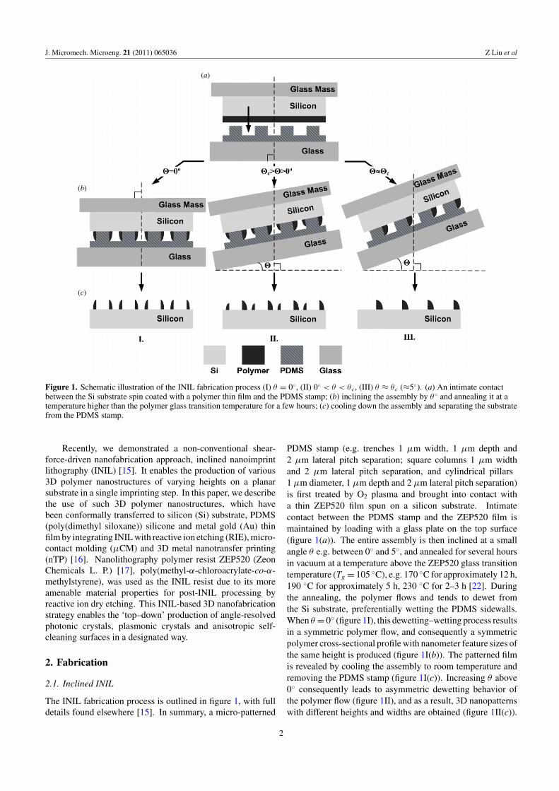
Figure 1. Schematic illustration of the INIL fabrication process (I) θ = 0◦, (II) 0◦ < θ < θc, (III) θ ≈ θc (≈5◦). (a) An intimate contactbetween the Si substrate spin coated with a polymer thin film and the PDMS stamp; (b) inclining the assembly by θ◦ and annealing it at atemperature higher than the polymer glass transition temperature for a few hours; (c) cooling down the assembly and separating the substratefrom the PDMS stamp.
Recently, we demonstrated a non-conventional shear-force-driven nanofabrication approach, inclined nanoimprintlithography (INIL) [15]. It enables the production of various3D polymer nanostructures of varying heights on a planarsubstrate in a single imprinting step. In this paper, we describethe use of such 3D polymer nanostructures, which havebeen conformally transferred to silicon (Si) substrate, PDMS(poly(dimethyl siloxane)) silicone and metal gold (Au) thinfilm by integrating INIL with reactive ion etching (RIE), micro-contact molding (μCM) and 3D metal nanotransfer printing(nTP) [16]. Nanolithography polymer resist ZEP520 (ZeonChemicals L. P.) [17], poly(methyl-α-chloroacrylate-co-α-methylstyrene), was used as the INIL resist due to its moreamenable material properties for post-INIL processing byreactive ion dry etching. This INIL-based 3D nanofabricationstrategy enables the ‘top–down’ production of angle-resolvedphotonic crystals, plasmonic crystals and anisotropic self-cleaning surfaces in a designated way.
2. Fabrication
2.1. Inclined INIL
The INIL fabrication process is outlined in figure 1, with fulldetails found elsewhere [15]. In summary, a micro-patterned
PDMS stamp (e.g. trenches 1 μm width, 1 μm depth and2 μm lateral pitch separation; square columns 1 μm widthand 2 μm lateral pitch separation, and cylindrical pillars1 μm diameter, 1 μm depth and 2 μm lateral pitch separation)is first treated by O2 plasma and brought into contact witha thin ZEP520 film spun on a silicon substrate. Intimatecontact between the PDMS stamp and the ZEP520 film ismaintained by loading with a glass plate on the top surface(figure 1(a)). The entire assembly is then inclined at a smallangle θ e.g. between 0◦ and 5◦, and annealed for several hoursin vacuum at a temperature above the ZEP520 glass transitiontemperature (Tg = 105 ◦C), e.g. 170 ◦C for approximately 12 h,190 ◦C for approximately 5 h, 230 ◦C for 2–3 h [22]. Duringthe annealing, the polymer flows and tends to dewet fromthe Si substrate, preferentially wetting the PDMS sidewalls.When θ = 0◦ (figure 1I), this dewetting–wetting process resultsin a symmetric polymer flow, and consequently a symmetricpolymer cross-sectional profile with nanometer feature sizes ofthe same height is produced (figure 1I(b)). The patterned filmis revealed by cooling the assembly to room temperature andremoving the PDMS stamp (figure 1I(c)). Increasing θ above0◦ consequently leads to asymmetric dewetting behavior ofthe polymer flow (figure 1II), and as a result, 3D nanopatternswith different heights and widths are obtained (figure 1II(c)).
2

J. Micromech. Microeng. 21 (2011) 065036 Z Liu et al
(a) (b) (a) (b)
(c) (d) (c) (d)
(e) (f ) (e) (f )
(g) (g)
Figure 2. Schematic illustration of the INIL-based fabrication process. (a) 3D polymer nanostructures produced by INIL; (b) reactive ionetching (RIE) for pattern transfer to the Si substrate; (c) casting and curing PDMS prepolymer against Si master template; (d) de-molding toobtain the PDMS silicon stamp; (e) sputtering Au/Ti thin film on the PDMS stamp surface; (f ) 3D metal nanotransfer printing (nTP) totransfer 3D freestanding Au nanostructures on an adhesive polymer substrate; (g) stamp separation.
When θ is increased close to or beyond a threshold angleθc, which is approximately equal to 5◦, wetting only occurson one face of the PDMS (figure 1III(b)); consequently,extremely asymmetric 3D nanopatterns can be obtained(figure 1III(c)).
2.2. 3D nanofabrication based on INIL
Figure 2 schematically illustrates the INIL-based fabricationprocess for 3D nanopattern transfer. The process exploitsthe 3D polymer nanostructures (figure 2(a)) produced byINIL, described above. A plasma dry etching (CHF3/H2)process is applied to transfer the polymer nanopattern tothe underlying Si substrate, followed by removal of thepolymer residue using either plasma dry etching (CHF3/O2)or solution cleaning (98% H2SO4 and 30% H2O2 in volumeratio of 3:1 at 120 ◦C for 10 min) (figure 2(b)). Theresulting Si nanostructure is used as a master template forsubsequent PDMS contact molding to transfer the oppositeSi 3D nanostructures to a PDMS silicone stamp. In thisprocess, PDMS prepolymer (Sylgard 184, Dow Corning) iscast onto the Si template surface, followed by curing at 60 ◦Cfor 24 h (figure 2(c)). The PDMS stamp with recessed 3Dnanostructures is revealed by de-molding from the Si template
(figure 2(d)). To achieve this, an anti-adhesion agent (3,3,3-trifluoropropyl dimethylchlorosilane) was used to treat the Sitemplate surface prior to applying the PDMS prepolymer inorder to prevent adhesion between the Si master templateand the cured PDMS, hence improving mold separation. Atypical operation for such a surface treatment is to soak the Sitemplate in a liquid anti-adhesion agent for 2–3 min followedby drying the template by N2 gas. The resulting nanopatternedPDMS stamp is then mounted onto a glass substrate and thesurface is coated with a uniform thin metal film by sputtering(figure 2(e)), e.g. 40 nm gold (Au)/5 nm titanium (Ti) wherethe Ti functions as an adhesion layer in the subsequent 3Dmetal nTP process. In the nTP process (figure 2(f )) the 3DAu thin film can be thought of as a nanostructured metal sheet.It is able to be transferred to an adhesive polymer substrate(e.g. Kapton tape backed by a glass substrate or photocurablepolyurethane (PU) spin coated onto a glass substrate) due tothe higher surface energy of the adhesive polymer. Typically,immediately after metal coating the PDMS stamp it is broughtinto contact with the polymer substrate and a slight pressureis applied. Once contact has been established, the metal layeron the stamp becomes strongly adhered and is transferredto the high surface energy polymer substrate. After stampseparation, freestanding Au nanostructures of varying heights
3

J. Micromech. Microeng. 21 (2011) 065036 Z Liu et al
(a) (b)
(c) (d)
(e) (f)
Figure 3. AFM images (3D views) of resulting 3D polymer nanostructures produced by INIL. (a) Symmetric nanolines; (b) asymmetricnanolines; (c) symmetric nanocircles; (d) asymmetric nanocircles; (e) symmetric nanosquares; (f ) asymmetric nanosquares.
that replicate 3D nanostructures of the Si master template areobtained (figure 2(g)).
3. Results and discussion
3.1. 3D polymer nanostructures
Figure 3 shows AFM images of resulting polymer 3Dnanopatterns of varying heights produced by INIL at differentinclination angles. The patterns produced include symmetricand asymmetric nanolines, nanocircles and nanosquares. Theheight of resulting symmetric nanolines (figure 3(a)) producedfrom a ZEP520 film (30 nm thick) is 100 nm, and the fullwidth half maximum (FWHM) of the lines is 300 nm. Theinner diameter of resulting symmetric nanocircles producedfrom a ZEP520 film (50 nm thick) is 1 μm, the circle heightis approximately 200 nm (figure 3(c)) and the FWHM of thecircles is 250 nm. The inner side length of resulting symmetricnanosquares produced from a ZEP520 film (70 nm thick) is1 μm, the square height is 125 nm and the FWHM of thesquares is 400 nm (figure 3(e)). Comparison of the volume ofthe polymer film patterns before and after INIL indicates thatthe entire polymer mass is properly conserved without any loss
in the INIL process. For asymmetric nanolines (figure 3(b)),the height and width are varied according to the inclinationangle θ , similarly for asymmetric nanocircles (figure 3(d)) andnanosquares (figure 3(f )), but the total volume of the polymeris still conserved. The actual feature height variation of theresulting asymmetric nanopatterns can be adjusted by tuningthe process parameters including the degree of the inclinationangle and the initial film thickness. The inclination angle is anessential factor influencing the resulting structure and featureheight difference [22]. In this work, the resultant asymmetricnanopattern height difference (e.g. nanolines) ranged from 30to 200 nm by adjusting the degree of the inclination angleand the initial film thickness for a PDMS mold with a patterndesign consisting of trenches 1 μm in width, 1 μm in depthand 2 μm in a lateral pitch separation. In fact, it is alsoobserved that the FWHM of the resulting nanopatterns andthe corresponding ratio of height to FWHM are also affectedand varied by the inclination angle. Although further studywould be needed to understand this behavior quantitatively,we believe it is possible to manipulate the ratio of the heightto FWHM of the resultant nanopatterns produced in INIL bycarefully manipulating the process factors according to theINIL mechanism.
4

J. Micromech. Microeng. 21 (2011) 065036 Z Liu et al
(a) (b)
(c) (d )
(e) (f )
Figure 4. SEM images of resulting 3D Si nanostructures. (a) Symmetric nanolines; (b) asymmetric nanolines; (c) symmetric nanocircles;(d) asymmetric nanocircles; (e) symmetric nanosquares; (f ) asymmetric nanosquares.
In addition, it can be observed that the corners ofthe resulting nanosquares are slightly rounded. This isprimarily attributed to the PDMS mold, in particular theslight deformation of the mold corners induced by therelaxation of the elastomeric mold material (PDMS, Sylgard184, Dow Corning). Relaxation occurs after separating themolded PDMS stamp from the Si master in the PDMS moldpreparation. Material relaxation is caused by the surfacetension, which can deform the molded sharp corners into asmooth equilibrium rounded shape with a radius of curvature(Rc) on the order of γ s (surface energy)/E (modulus), andthus γ s/E represents a lower limit for Rc of the corners. Fora PDMS elastomer Rc is on the order of 50 nm [18]. Onepossible solution to address the edge rounding issue is the useof a mold material that has a larger modulus (E) such as PDMScomposite material [19]. A larger modulus (E) would lead to
smaller Rc, and thus conformal sharp corners may be retainedby the stamp.
While this work mainly focuses on micron or sub-micronnanopattern separation distance, it is theoretically feasibleto fabricate 3D nanopatterns with sub-100 nm separationdistances by using a sub-100 nm patterned PDMS stamp[19] (d � 100 nm) and also reducing the initial polymerfilm thickness to 5–10 nm. Smaller film thicknesses wouldallow polymer dewetting at smaller length scales. Meanwhile,strategies to ensure intimate contact between the stamp andthe substrate without deforming the fine features of the PDMSstamp and reduce the adhesion issue at the stamp–substrateseparation step also need to be addressed.
Moreover, although uniformity was not quantitativelyassessed, visual inspection by SEM indicated no significantuniformity variation over the entire pattern dimension(100 μm × 1 mm to 500 μm × 3 mm for nanolines, and
5

J. Micromech. Microeng. 21 (2011) 065036 Z Liu et al
Figure 5. AFM images of resulting 3D Si nanostructures in top (left) and 3D (right) views. (a-1, a-2) Asymmetric nanolines; ((b-1, b-2) and(c-1, c-2)) symmetric and asymmetric nanocircles; ((d-1, d-2) and (e-1, e-2)) symmetric and asymmetric nanosquares.
6

J. Micromech. Microeng. 21 (2011) 065036 Z Liu et al
Figure 6. AFM images of 3D PDMS nanostructures in top (left) and 3D (right) views. (a-1, a-2) Asymmetric nanolines; (b-1, b-2)asymmetric nanocircles; (c-1, c-2) symmetric nanosquares; (d-1, d-2) asymmetric nanosquares.
100 μm × 100 μm to 500 μm × 500 μm for both nanocirclesand nanosquares). Also, the resulting nanopatterns (bothsymmetric and asymmetric) are smooth with little profilevariation (<5 nm) in the x–y directions. Uniformity of verylarge pattern areas such as over the extent of a 4 inch wafer andlittle edge roughness variation in resulting nanopatterns shouldbe possible by ensuring uniform application of a sufficientand suitable force or pressure over the overall pattern area
without deforming the PDMS stamp, requiring a properlydesigned INIL setup.
3.2. 3D Si nanostructures
Figures 4 and 5 show representative SEM and AFM imagesof resulting 3D Si nanostructures produced by RIE patterntransfer. The width of the resulting Si symmetric nanolines
7
J. Micromech. Microeng. 21 (2011) 065036 Z Liu et al
(a) (b)
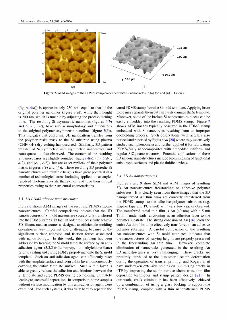
Figure 7. AFM images of the PDMS stamp embedded with Si nanocircles in (a) top and (b) 3D views.
(figure 4(a)) is approximately 250 nm, equal to that of theoriginal polymer nanolines (figure 3(a)), while their heightis 200 nm, which is tunable by adjusting the process etchingtime. The resulting Si asymmetric nanolines (figures 4(b)and 5(a-1, a-2)) have similar morphology and dimensionsto the original polymer asymmetric nanolines (figure 3(b)).This indicates that conformal 3D nanopattern transfer fromthe polymer resist mask to the Si substrate using plasma(CHF3/H2) dry etching has occurred. Similarly, 3D patterntransfer of Si symmetric and asymmetric nanocircles andnanosquares is also observed. The corners of the resultingSi nanosquares are slightly rounded (figures 4(e), (f ), 5(d-1,d-2), and (e-1, e-2)), but are exact replicas of their polymermasks (figures 3(e) and (f )). These resulting 3D periodic Sinanostructures with multiple heights have great potential in anumber of technological areas including application as angle-resolved photonic crystals that exploit and tune their opticalproperties owing to their structural characteristics.
3.3. 3D PDMS silicone nanostructures
Figure 6 shows AFM images of the resulting PDMS siliconenanostructures. Careful comparisons indicate that the 3Dnanostructures of Si mold masters are successfully transferredinto the PDMS stamps. In fact, in order to successfully achieve3D silicone nanostructures as designed an efficient de-moldingoperation is very important and challenging because of thesignificant surface adhesion and friction forces associatedwith nanotribology. In this work, this problem has beenaddressed by treating the Si mold template surface by an anti-adhesion agent (3,3,3-trifluoropropyl dimethylchlorosilane)prior to casting and curing PDMS prepolymer onto the Si moldtemplate. Such an anti-adhesion agent can efficiently reactwith the template surface and form a thin layer homogenouslycovering the entire template surface. Such a thin layer isable to greatly reduce the adhesion and frictions between theSi template and cured PDMS during de-molding, ultimatelyleading to successful separation. In comparison, some sampleswithout surface modification by this anti-adhesion agent wereexamined. For such systems, it was very hard to separate the
cured PDMS stamp from the Si mold template. Applying bruteforce may separate them but can easily damage the Si template.Moreover, some of the broken Si nanostructure pieces can beeasily embedded into the resulting PDMS stamp. Figure 7shows AFM images typically observed in the PDMS stampembedded with Si nanocircles resulting from an improperde-molding process. Such observations were actually alsonoticed and reported by Fujita et al [20] where they extensivelystudied such phenomena and further applied it for fabricatingPDMS/SiO2 nanocomposites with embedded uniform andregular SiO2 nanostructures. Potential applications of these3D silicone nanostructures include biomimicking of functionalanisotropic surfaces and plastic fluidic devices.
3.4. 3D Au nanostructures
Figures 8 and 9 show SEM and AFM images of resulting3D Au nanostructures freestanding on adhesive polymersubstrates. It is clearly seen from these images that the 3Dnanopatterned Au thin films are correctly transferred fromthe PDMS stamps to the adhesive polymer substrates (e.g.Kapton tape and PU sheet) with very few cracks observed.The transferred metal thin film is Au (40 nm) with a 5 nmTi film underneath functioning as an adhesion layer to thepolymer substrate. The strong cohesion of Au [16] leads theentire Au thin film to be effectively transferred to an adhesivepolymer substrate. A careful comparison of the resultingAu nanostructures with Si mold templates indicates thatthe nanostructures of varying heights are properly preservedin the freestanding Au thin film. However, completeelimination of nanocracks generated in the resulting Au3D nanostructures is very challenging. These cracks areprimarily attributed to the elastomeric stamp deformationduring the operation of transfer printing, and Rogers et alhave undertaken extensive studies on minimizing cracks innTP by improving the stamp surface chemistries, thin filmdeposition techniques and stamp pattern design [21]. Inour work, crack elimination has been effectively achievedby a combination of using a glass backing to support thePDMS stamp, coupled with a thin nanopatterned PDMS
8

J. Micromech. Microeng. 21 (2011) 065036 Z Liu et al
(a) (b)
(c) (d )
(e) (f )
(g) (h)
Figure 8. SEM images of 3D Au nanostructures freestanding on an adhesive glass substrate. (a), (b) Asymmetric nanolines; (c), (d)symmetric nanosquares; (e), (f ) asymmetric nanosquares; (g), (h) asymmetric nanocircles.
stamp (approximately 0.5 mm thick), in addition to a gentleforce. The demonstrated 3D Au nanostructures with multipleheights could be potentially utilized as plasmonic crystalsthat produce incident angle-dependent optical properties dueto their asymmetric nanostructures, and consequently havewide applicability for sensing and imaging applications.
Further, 3D anisotropic or chiral nanostructures could bepotentially assembled layer-by-layer from the demonstratednanopatterned Au film with multiple feature heights. Suchstacked 3D anisotropic structures would be of great interestsince they may bring interesting and novel properties rangingfrom condensed matter physics to optics for various potential
9

J. Micromech. Microeng. 21 (2011) 065036 Z Liu et al
Figure 9. AFM images of 3D Au nanostructures in top (left) and 3D views (right). (a-1, a-2) Asymmetric nanolines; (b-1, b-2) and(c-1, c-2) symmetric and asymmetric nanosquares; (d-1, d-2) and (e-1, e-2) asymmetric nanocircles with different degrees of asymmetry.
10

J. Micromech. Microeng. 21 (2011) 065036 Z Liu et al
applications. The INIL-based process demonstrated in thiswork could serve as a significant technical driver for suchexploration.
4. Conclusion
In this paper, an integrated ‘top–down’ 3D nanofabricationstrategy has been demonstrated by combining inclinednanoimprinting lithography (INIL) with reactive ion etching(RIE), micro-contact molding and metal nanotransfer printing(nTP). It enables the pattern transfer of various 3Dnanostructures with varying heights from a polymer resistlayer to other material media including an Si-based substrate,a PDMS silicone stamp and a metal Au thin film in acontrolled way, with reduced fabrication cost and complexity.Various 3D nanostructures can be designed, produced andproperly preserved in a variety of target materials by usingsuch an integrated process. Applications of these 3Dnanostructures could be angle-resolved photonic crystals,plasmonic crystals and bio-mimicking anisotropic self-cleaning surfaces. Therefore, the reported INIL-based 3Dnanofabrication shows great application potential in photonics,plasmonics, nanotribology and NEMS.
References
[1] Ishizaki K and Noda S 2009 Nature 460 367–70[2] Freymann G, Ledermann A, Thiel M, Staude I, Essig S,
Busch K and Wegener M 2010 Adv. Funct. Mater.20 1038–52
[3] Toader O and John S 2001 Science 292 1133–5[4] Qi M, Lidorikis E, Rakich P, Johnson S, Joannopoulos J,
Ippen E and Smith H 2004 Nature 429 538–42[5] Subramania G, Lee Y-J, Brener I, Luk T S and Clem P G 2007
Opt. Express 15 12049–57
[6] Sun Q, Juodkazis S, Murazawa N, Mizeikis V and Misawa H2010 J. Micromech. Microeng. 20 035004
[7] Jeon S et al 2007 Opt. Express 15 6358–66[8] Baumberg J, Kelf T, Sugawara Y, Cintra S,
Abdelsalam M, Bartlett P and Russell A 2005 Nano Lett.5 2262–7
[9] Baca A, Truong T, Cambrea L, Montgomery J, Gray S,Abdula D, Banks T, Yao J, Nuzzo R and Rogers J 2009Appl. Phys. Lett. 94 243109
[10] Heo C, Kim S, Jang S, Lee S and Yang S 2009 Adv. Mater.21 1726–31
[11] Stewart M, Mack N, Malyarchuk V, Soares J, Lee T, Gray S,Nuzzo R and Rogers J 2006 Proc. Natl Acad. Sci.103 17143–8
[12] Kinkhabwala A, Yu Z, Fan S, Avlasevich Y, Mullen Kand Moerner W 2009 Nature Photonics 3 654–7
[13] Prodan E, Radloff C, Halas N and Nordlander P 2003 Science302 419–22
[14] Kan T, Matsumoto K and Shimoyama I 2010 J. Micromech.Microeng. 20 085032
[15] Liu Z, Bucknall D G and Allen M G 2007 Proc. Transducers2007 & Eurosensors XXI Dig. Techn. Papers1–2 U819–20
[16] Zaumseil J, Meitl M, Hsu J, Acharya B, Baldwin K, Loo Yand Rogers J 2003 Nano Lett. 3 1223–7
[17] Medeiros D R, Aviram A, Guarnieri C R, Huang W S,Kwong R, Magg C K, Mahorowala A P, Moreau W M,Petrillo K E and Angelopoulos M 2001 IBM J. Res. Dev.45 639–50
[18] Hui C Y, Jagota A, Lin Y Y and Kramer E J 2002 Langmuir18 1394–407
[19] Odom T W, Love J C, Wolfe D B, Paul K E and Whitesides G2002 Langmuir 18 5314–20
[20] Jalabert L, Bottier C, Kumemura M and Fujita H 2009 J. Vac.Sci. Technol. B 27 3055–8
[21] Menard E, Bilhaut L, Zaumseil J and Rogers J 2004 Langmuir20 6871–8
[22] Liu Z, Bucknall D G and Allen M G 2011 Nanotechnology22 225302
11