incorporating altera fpga demo boards in computer ... · pdf fileincorporating altera fpga...
TRANSCRIPT
Incorporating Altera FPGA Demo boards in Computer Engineering Labs
Waleed K. Al-Assadi, Mandar V. Joshi, Sagar R. Gosavi, and Daryl Beetner Department of Electrical and Computer Engineering
University of Missouri-Rolla Rolla, MO 65401
{waleed, mvjvx8, srggz3, daryl} @ umr.edu Abstract
Field Programmable Gate Arrays (FPGAs) are widely used as teaching tools in university computer engineering laboratories. Numerous computationally intensive applications such as IP cores, ASICs and microcontrollers are prototyped on FPGAs to reduce the number of cycles and the time to market. This paper presents our experience in incorporating Altera DE-2 FPGA board equipped with Altera Cyclone-II FPGA demo boards into variety of computer engineering courses at the University of Missouri-Rolla. The paper details application of Altera DE-2 board into sophomore and senior courses. The sophomore course, the digital systems design, incorporates embedded systems using the 8051 microcontroller, and in senior courses such as VLSI design and computer architecture, where designs utilizing multiple-components (system-level design) can be prototyped and verified. The paper presents the benefits of introducing industrial-standard design tools to our students so that students will focus on whether they have designed their circuits correctly. 1. Introduction
FPGA boards are widely used for digital design laboratories in universities [1],[2]. Basically, an FPGA board consists of an FPGA chip, input/output (I/O) devices, and supporting logic for downloading a bit-stream into the FPGA. Commonly seen input devices include push-button switches, output devices are seven-segment, bar-graph light-emitting device (LED) displays, and dual-in-line package (DIP). Altera Development and Educational (DE-2) FPGA board is a useful learning tool for courses in computer engineering. The board features Altera Cyclone-II 672 pin FPGA along with other supporting hardware such as expansion IO slots, seven-segment displays, toggle switches etc. It is used with Altera’s powerful design and automation software “Quartus-II” that is ideally suited for student design projects in the coursework. Students can create their designs using schematic capture or HDL synthesis and download them to the FPGA for real time hardware verification. The complexity of the designs can vary from simple gate-level combinational circuits (that the students create in “introduction to computer engineering” course) to highly structured microcontroller based embedded applications.
This paper addresses the issues of design considerations for efficient resource allocation for FPGA demo-board based digital design laboratories. The paper is organized as follows; section 2 introduces the hardware and software interface features of Altera DE-2 board. Section 3 gives details of incorporating Altera DE-2 into several computer engineering courses, and section 4 gives conclusion of the paper.
Proceedings of 2007 Midwest Section Conference of American Society for Engineering Education
2
2. Features of DE-2 Board
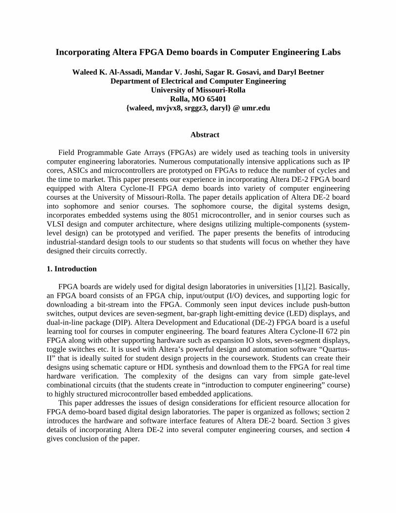
DE-2 board is equipped with 16x2 LCD display, eight seven segment displays and LEDs (18 Red and 9 Green) that can be typically used to observe the outputs from the various output pins in the design. Available 18 toggle switches and four debounced switches can be used to provide external inputs, along with 50 MHz and 27 MHz on-board clocks. It also has an external SMA clock input. Figure 1 shows a complete schematic of Altera DE-2 board [5]. The expansion headers are used to hook-up the outputs to an external device, such as an oscillator for timing analysis. All these features have encouraged the migration of laboratory experiments, initially carried out using Xilinx XS-40 FPGA board that offered considerably limited functionality as compared with Altera DE-2 board. Before using Altera DE-2 board, students created their designs in Mentor Graphics (UNIX) environment. It involved the use of Design Architect tool for schematic capture and QuickSim Pro for simulation. After a successful simulation, the students followed a Xilinx-specific design flow to create a “bit” file that could be downloaded onto Xilinx FPGA in Windows environment. Since the XS-40 board had an on-board 8031 microcontroller, they could directly download it using serial communication with PC. Since 8031 does not contain on-chip ROM, the code had to be written onto on-chip RAM.
Fig. 1: Altera DE-2 board schematic [3]
Altera’s design and automation software “Quartus-II” offers all the tools necessary for
implementation of design experiments in computer engineering courses and labs [4]. This eliminates the need for the students to shift the OS environment every now and then. It has a Schematic-Capture module, a basic tool that enables the students to build custom digital circuits using a component library available with Quartus-II. In addition, it can synthesize HDL designs (created using VHDL, Verilog or System Verilog) and it can also be used to integrate those with the designs created using schematic capture. Since DE-2 board does not have an on-chip microcontroller, we need to prototype one using its VHDL code. This can conveniently be done using Quartus-II that enables the user to create a schematic symbol for 8051 microcontroller, which can be used as many number of times as needed. The HEX code is usually written inside
Proceedings of 2007 Midwest Section Conference of American Society for Engineering Education
3
ROM module in VHDL/Verilog and can be changed as per application. It can also be saved as a symbol and interfaced with the 8051 microcontroller using schematic capture.
Quartus-II comes with a simulation tool that is used for functional verification of designs made using the above techniques. The use of this feature will be explained in the sections to follow. There are many other tools associated with Quartus-II which include Timing Quest timing analyzer, System on a Programmable Chip (SOPC) builder etc. which are not currently being used for any courses at this time.
The post-synthesis VHDL model is used to create all the necessary complex symbols to be given to the students by the Teaching Assistants. These symbols are given to them in the form of an EDIF (acronym for Electronic Design Interchange Format) File. This format is technology-specific and the one used here is Altera Cyclone –II EP2C35F672C6. EDIF can be read by Quartus-II and it can readily generate the symbol for the corresponding code. Students build the glue logic using various tools in Quartus-II for prototyping in using Cyclone-II FPGA. 3. Incorporation of DE-2 Board in Computer Engineering Courses This section details our experience in incorporating Altera DE-2 board in several computer engineering courses. 3.1 DE-2 Board in Digital Engineering Lab
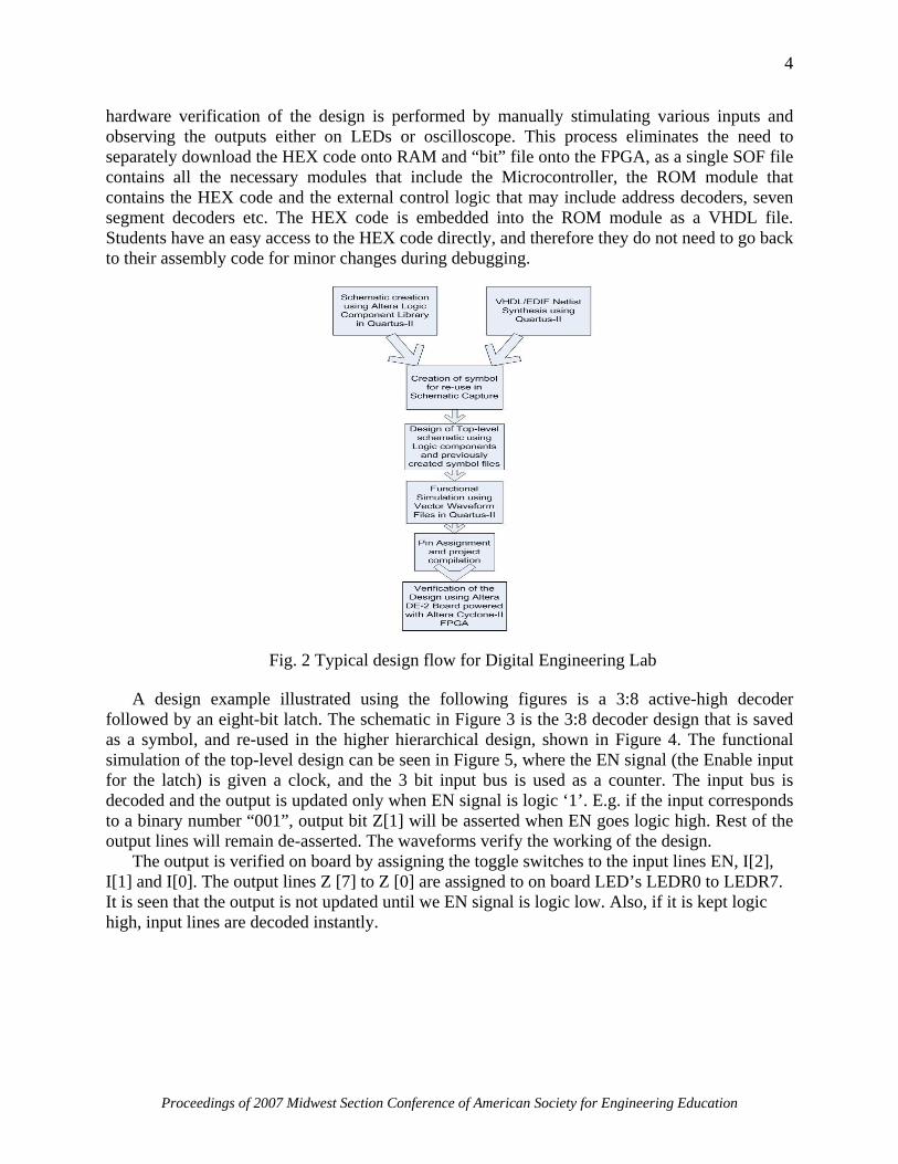
Recently, laboratories involving the design of hardware and software for Intel 8051 family microcontroller were migrated to DE-2 board. Previously, students created their schematic-level designs in Mentor Graphics Design Architect tool, created software using the Keil 8051 development software, then downloaded their software and hardware to an XESS XS40 board that included a Xilinx FPGA and a stand-alone 8051 microcontroller. After migration to the Altera DE-2 board, the students only need to use a single tool (Quartus-II) for all their design needs. Hierarchical schematic capture helps use previously made designs to be invoked as “symbols” and re-used to create more complicated designs. A synthesizable 8051 microcontroller VHDL code has also been obtained that will enable the students to build both the microcontroller and the external logic (developed using schematic capture) inside the FPGA, eliminating the need to program the microcontroller and hardware separately. The external logic typically includes LCD drivers, seven segment decoders, address decoders, ROM modules etc. Following is a general design flow that the students are expected to follow for typical schematic capture based designs. It is illustrated in Figure 2.
Students create the gate level/block level design on paper based on the specifications given by the instructor. On instructor’s approval, they create the schematics (.bdf files) using Quartus-II and associate those schematics with the project files for the corresponding lab experiment. For hierarchical designs, they save all their previously created designs as logic symbols (.bsf files), and reuse them for top-level designs. For the experiments involving creation of symbols from an HDL source, the corresponding BSF files are provided to them by the instructors. After successful compilation and synthesis of the top-level schematic, the students verify the functionality by using the simulation tool in Quartus-II and create a Vector Waveform File (.vwf) that contains all the necessary traces. On a successful logic simulation, the students assign the I/O pins to various physical I/O’s available on DE-2 board such as toggle switches, LEDs etc. and recompile with pin assignments. This creates a downloadable bit file (.sof) for Altera Cyclone-II FPGA. Now the design is ready to be downloaded onto the FPGA and then the
Proceedings of 2007 Midwest Section Conference of American Society for Engineering Education
4
hardware verification of the design is performed by manually stimulating various inputs and observing the outputs either on LEDs or oscilloscope. This process eliminates the need to separately download the HEX code onto RAM and “bit” file onto the FPGA, as a single SOF file contains all the necessary modules that include the Microcontroller, the ROM module that contains the HEX code and the external control logic that may include address decoders, seven segment decoders etc. The HEX code is embedded into the ROM module as a VHDL file. Students have an easy access to the HEX code directly, and therefore they do not need to go back to their assembly code for minor changes during debugging.
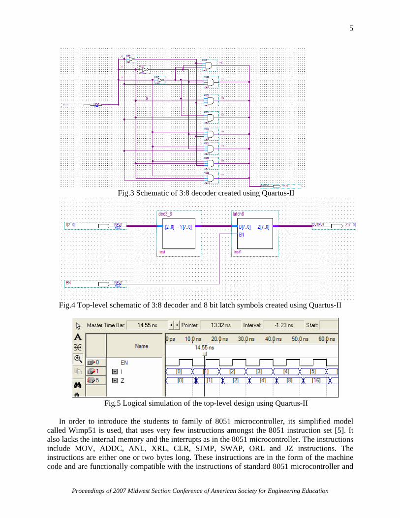
Fig. 2 Typical design flow for Digital Engineering Lab A design example illustrated using the following figures is a 3:8 active-high decoder
followed by an eight-bit latch. The schematic in Figure 3 is the 3:8 decoder design that is saved as a symbol, and re-used in the higher hierarchical design, shown in Figure 4. The functional simulation of the top-level design can be seen in Figure 5, where the EN signal (the Enable input for the latch) is given a clock, and the 3 bit input bus is used as a counter. The input bus is decoded and the output is updated only when EN signal is logic ‘1’. E.g. if the input corresponds to a binary number “001”, output bit Z[1] will be asserted when EN goes logic high. Rest of the output lines will remain de-asserted. The waveforms verify the working of the design.
The output is verified on board by assigning the toggle switches to the input lines EN, I[2], I[1] and I[0]. The output lines Z [7] to Z [0] are assigned to on board LED’s LEDR0 to LEDR7. It is seen that the output is not updated until we EN signal is logic low. Also, if it is kept logic high, input lines are decoded instantly.
Proceedings of 2007 Midwest Section Conference of American Society for Engineering Education
5
Fig.3 Schematic of 3:8 decoder created using Quartus-II
Fig.4 Top-level schematic of 3:8 decoder and 8 bit latch symbols created using Quartus-II
Fig.5 Logical simulation of the top-level design using Quartus-II
In order to introduce the students to family of 8051 microcontroller, its simplified model
called Wimp51 is used, that uses very few instructions amongst the 8051 instruction set [5]. It also lacks the internal memory and the interrupts as in the 8051 microcontroller. The instructions include MOV, ADDC, ANL, XRL, CLR, SJMP, SWAP, ORL and JZ instructions. The instructions are either one or two bytes long. These instructions are in the form of the machine code and are functionally compatible with the instructions of standard 8051 microcontroller and

Proceedings of 2007 Midwest Section Conference of American Society for Engineering Education
6
thus enabling the use of standard compilers to simulate the code for the Wimp51 module. The simulator used for this purpose is the simulator of the Quartus –II software which is compatible to the ALTERA DE-II board. The basic operation of the Wimp51 processor is completed in 3 cycles, fetch, decode and execute. Thus it takes 3 clock cycles for the entire process to take place. Students are also provided with an editable ROM module that contains the instructions (codes) for Wimp51.They interface this ROM module with Wimp51 and various signals such as 8 bit address, data output of ROM, PSEN, and Accumulator contents are observed on the DE-2 board using the seven-segment displays using the schematic capture capability of the software. The clock is given manually using a debounced switch. But a preventive measure to be taken here is that the clock needs to be given only to the Wimp51 module as the ROM does not require any clock. If a clock is also assigned to the ROM then there is a conflict between the timing issues of the two modules (the Wimp51 and the ROM) and the functionality of the system changes abruptly. Thus after incorporating the various signals to be observed on FPGA, the functionality of the Wimp51 module can be verified. This gives the students the “feel” of how a microcontroller actually works in hardware at every clock tick. Simple integer multiplication code is used as an example for the experiment. The Wimp51 processor is also used as an introduction to hardware-software co-design. This method is particularly useful for early detection of hardware bugs. The students are provided with a Wimp51 model with a fault (e.g. Zero flag inverted) and they are required to find the bug using software simulation and FPGA verification. After they find the bug, they need to modify their code, a solution that is a work-around for the hardware fault. Figure 6 shows the Wimp51 module interfaced with the ROM module in a schematic capture tool of the Quartus-II software. An external ROM was used as the Wimp51 lacks any internal memory to store the instructions. The signals to be observed are then fed to the seven segment decoder to display the output on the seven segment display.
Fig.6 A Design example with Wimp51 processor and ROM module
Proceedings of 2007 Midwest Section Conference of American Society for Engineering Education
7
The above schematic shows a design with Wimp51 and ROM modules. PSEN signal is
connected directly to the RD signal of ROM. Both the signals are active low. The data corresponding to the ROM address is read and is made available on the data bus only when RD signal is logic low. The data is decoded using seven segment decoder modules. The outputs of these decoders are assigned to the corresponding segments in the displays so that the data is visible to the user, and further debugging, if needed, is facilitated. Even the address and contents of various other registers can also be decoded in the same way. 3.2 DE-2 Board for prototyping of miscellaneous designs 3.2.1 RISC Processor Design
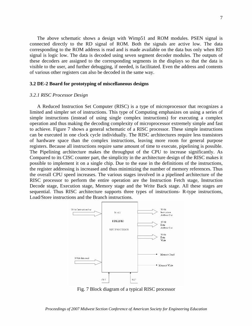
A Reduced Instruction Set Computer (RISC) is a type of microprocessor that recognizes a limited and simpler set of instructions. This type of Computing emphasizes on using a series of simple instructions (instead of using single complex instructions) for executing a complex operation and thus making the decoding complexity of microprocessor extremely simple and fast to achieve. Figure 7 shows a general schematic of a RISC processor. These simple instructions can be executed in one clock cycle individually. The RISC architectures require less transistors of hardware space than the complex instructions, leaving more room for general purpose registers. Because all instructions require same amount of time to execute, pipelining is possible. The Pipelining architecture makes the throughput of the CPU to increase significantly. As Compared to its CISC counter part, the simplicity in the architecture design of the RISC makes it possible to implement it on a single chip. Due to the ease in the definitions of the instructions, the register addressing is increased and thus minimizing the number of memory references. Thus the overall CPU speed increases. The various stages involved in a pipelined architecture of the RISC processor to perform the entire operation are the Instruction Fetch stage, Instruction Decode stage, Execution stage, Memory stage and the Write Back stage. All these stages are sequential. Thus RISC architecture supports three types of instructions- R-type instructions, Load/Store instructions and the Branch instructions.
Fig. 7 Block diagram of a typical RISC processor

Proceedings of 2007 Midwest Section Conference of American Society for Engineering Education
8
After having developed the high level code for the RISC processor either in VHDL or Verilog, the various RISC modules are then integrated and simulated to analyze the functioning of the system and can be cross examined for any types of bugs. Once the design entities are simulated successfully and results desired being achieved, the system as a whole is analyzed on the hardware (ASIC). But having known the capabilities of the powerful Altera DE-II FPGA board, it is possible to analyze the system on the FPGA prior to moving onto the chip implementation to ensure that the system is free of any bugs and there exists no errors in the design that can cause failure of the system when designed onto the chip. It is also possible to synthesize and simulate the entire design on the supporting Quartus-II software that enables us to verify the functionality of the design. Once the entire design modules are synthesized and simulated in Quartus-II, the design is ready to be implemented on FPGA Board. Using the schematic capture capability in the software it is also possible to display the corresponding results onto the 7 segment display or on the LCD panels provided we have to develop different module incorporating this capability in the system. With the schematic capture capability it is also possible to view the contents of each register, also the accumulator and other various components which enables us to view the results and also enables us to trace the functioning of the entire system as a whole. The address of the instructions is stored in the ROM, the corresponding instructions are executed in the CPU (RISC module) and the data corresponding to these instructions is stored in the RAM module as is shown in the Figure 8. The example here illustrates the working of a 16-bit RISC processor. The Simulation Waveforms that are obtained from the timing analyzer tool included in the software itself helps to prove the functionality of the system while the implementation of the design on the FPGA (Altera DE-II board) verifies it. Thus it signifies the ability of the Altera board to emulate a microprocessor on it.
Fig.8 Schematic RISC processor interfaced with external RAM and ROM created using Quartus-II

Proceedings of 2007 Midwest Section Conference of American Society for Engineering Education
9
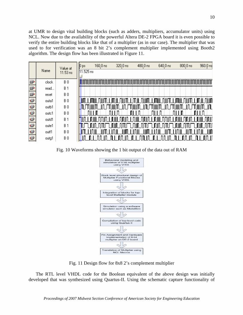
The flowchart in Figure 9 shows the various stages that are involved during the migration of the RISC modules onto an FPGA. It shows the sequence of events to be followed in order for the verification of the design entities. It is very important that each module in the RISC design be simulated individually for its functional verification. Only when all the modules are tested in this way, they are integrated together to get the top-level entity of the RISC processor. In the current design we have a module for every stage in the pipeline. The Waveforms corresponding to one bit of the data output from RAM which is being displayed on the seven-segment display is shown in Figure 10.
Fig. 9 A typical design flow for implementing the RISC processor
3.2.2 8 Bit Booth2 Multiplier for Null Convention Logic Design
Null Convention Logic (NCL) is an area of active research at the University of Missouri-Rolla. It is an asynchronous digital logic design paradigm that is known to have significant advantages over conventional Boolean synchronous digital design. Asynchronous circuits require less power, generate less noise, produce less electromagnetic interference and allow for easier reuse of components compared to their synchronous counterpart, without compromising for performance. Due to these advantages the industry is now looking upon the asynchronous logic to implement the various circuits to increase performance of the system as a whole. To cope up with the ever growing need of the market which can be partially accomplished by using the asynchronous circuits, it is important to make students acquainted with the various circuits to be implemented by asynchronous logic and in order to do so various projects have been carried out
Proceedings of 2007 Midwest Section Conference of American Society for Engineering Education
10
at UMR to design vital building blocks (such as adders, multipliers, accumulator units) using NCL. Now due to the availability of the powerful Altera DE-2 FPGA board it is even possible to verify the entire building blocks like that of a multiplier (as in our case). The multiplier that was used to for verification was an 8 bit 2’s complement multiplier implemented using Booth2 algorithm. The design flow has been illustrated in Figure 11.
Fig. 10 Waveforms showing the 1 bit output of the data out of RAM
Fig. 11 Design flow for 8x8 2’s complement multiplier
The RTL level VHDL code for the Boolean equivalent of the above design was initially developed that was synthesized using Quartus-II. Using the schematic capture functionality of
Proceedings of 2007 Midwest Section Conference of American Society for Engineering Education
11
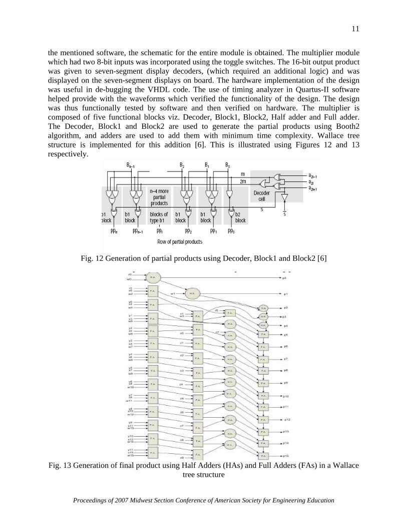
the mentioned software, the schematic for the entire module is obtained. The multiplier module which had two 8-bit inputs was incorporated using the toggle switches. The 16-bit output product was given to seven-segment display decoders, (which required an additional logic) and was displayed on the seven-segment displays on board. The hardware implementation of the design was useful in de-bugging the VHDL code. The use of timing analyzer in Quartus-II software helped provide with the waveforms which verified the functionality of the design. The design was thus functionally tested by software and then verified on hardware. The multiplier is composed of five functional blocks viz. Decoder, Block1, Block2, Half adder and Full adder. The Decoder, Block1 and Block2 are used to generate the partial products using Booth2 algorithm, and adders are used to add them with minimum time complexity. Wallace tree structure is implemented for this addition [6]. This is illustrated using Figures 12 and 13 respectively.
Fig. 12 Generation of partial products using Decoder, Block1 and Block2 [6]
Fig. 13 Generation of final product using Half Adders (HAs) and Full Adders (FAs) in a Wallace
tree structure
Proceedings of 2007 Midwest Section Conference of American Society for Engineering Education
12
The successful functional verification of the multiplier helped the design team to translate the entire design into NCL based macros. Thus it can be inferred from this implementation of design that not only synchronous logic circuits but also the asynchronous logic circuits can be successfully verified on the Altera DE- II FPGA boards. 4. Conclusion
The functionality offered by Altera DE-2 FPGA board was successfully utilized by the students through various design projects and lab experiments in digital design courses. It helped the students to gain the knowledge of a typical design flow in digital logic design. Students can learn to use the tools contained in Quartus-II design and automation software suite such as schematic capture, VHDL synthesis, timing simulation and place & route. They can design, simulate and debug their designs with ease, after the FPGA prototyping of their design. We have successfully incorporated DE-2 boards in senior design courses such VLSI design and computer architecture. The overall conclusion is that both students and instructors have benefited from incorporation DE-2 FPGA boards in our computer engineering courses.
Acknowledgment We appreciate the generous hardware and software donations from Altera Corporation. References [1] I. A. Hack and J. Haberly, “ Low cost FPGA Development Systems for Teaching Advanced Digital Circuits ,” ASEE Conference, session 0047, 2001 [2] R. Backnak, D. Kar, and H. Shaalan, “Digital Systems Laboratory for Teaching and Research, “ASEE Conference, session 1520, 2004. [3] Altera DE-2 FPGA board Manual at www.altera.com/education/univ/materials/boards/DE2_UserManual.pdf [4] Altera Quartus-II Manual at www.altera.com/literature/manual/intro_to_quartus2.pdf [5] D. Sullins, H. Pottinger, D. Beetner, "The WIMP51: A Simple Processor and Visualization Tool to Introduce Undergraduates to Computer Organization," Computers in Education Journal, vol. 13, pp 17-23, Jan. 2003 [6] M Nicolaidis, R Duarte, “Fault Secure Parity Prediction Booth Multipliers”, IEEE Design & Test of Computers, pages 90-101, 1999