industry-standard dual operational amplifiers datasheet
TRANSCRIPT

Industry-Standard Dual Operational Amplifiers
1 Features• Wide supply range of 3 V to 36 V (B version)• Quiescent current: 300 µA per amplifier (B version,
typical)• Unity-gain bandwidth of 1.2 MHz (B version)• Common-mode input voltage range includes
ground, enabling direct sensing near ground• Low input offset voltage of 3 mV at 25°C (A and B
versions, maximum)• Internal RF and EMI filter (B version)• On products compliant to MIL-PRF-38535, all
parameters are tested unless otherwise noted. On all other products, production processing does not necessarily include testing of all parameters.
2 Applications• Merchant network and server power supply units• Multi-function printers• Power supplies and mobile chargers• Motor control: AC induction, brushed DC,
brushless DC, high-voltage, low-voltage, permanent magnet, and stepper motor
• Desktop PC and motherboard• Indoor and outdoor air conditioners• Washers, dryers, and refrigerators• AC inverters, string inverters, central inverters, and
voltage frequency drives• Uninterruptible power supplies• Programmable logic controllers• Electronic point-of-sale systems
RG RF
R1
C1
VIN
VOUT
= 1 +V
VOUT
IN
R
RF
G
1
1 + sR C1 1( (( (
1
2pR C1 1
f =-3 dB
Single-Pole, Low-Pass Filter
3 DescriptionThe LM358B and LM2904B devices are the next-generation versions of the industry-standard operational amplifiers (op amps) LM358 and LM2904, which include two high-voltage (36 V) op amps. These devices provide outstanding value for cost-sensitive applications, with features including low offset (300 µV, typical), common-mode input range to ground, and high differential input voltage capability.
The LM358B and LM2904B op amps simplify circuit design with enhanced features such as unity-gain stability, lower offset voltage of 3 mV (maximum at room temperature), and lower quiescent current of 300 µA per amplifier (typical). High ESD (2 kV, HBM) and integrated EMI and RF filters enable the LM358B and LM2904B devices to be used in the most rugged, environmentally challenging applications.
The LM358B and LM2904B amplifiers are available in micro-sized packaging, such as the SOT23-8, as well as industry standard packages including SOIC, TSSOP, and VSSOP.
Device InformationPART NUMBER(1) PACKAGE BODY SIZE (NOM)
LM358B, LM2904B, LM358, LM358A, LM2904, LM2904V, LM258, LM258A
SOIC (8) 4.90 mm × 3.90 mm
LM358B, LM2904B, LM358, LM358A, LM2904, LM2490V
TSSOP (8) 3.00 mm × 4.40 mm
LM358B, LM2904B, LM358, LM358A, LM2904, LM2904V, LM258, LM258A
VSSOP (8) 3.00 mm × 3.00 mm
LM358B, LM2904B SOT-23 (8) 2.90 mm × 1.60 mm
LM358, LM2904 SO (8) 5.20 mm × 5.30 mm
LM358, LM2904, LM358A, LM258, LM258A PDIP (8) 9.81 mm × 6.35 mm
LM158, LM158A CDIP (8) 9.60 mm × 6.67 mm
LM158, LM158A LCCC (20) 8.89 mm × 8.89 mm
(1) For all available packages, see the orderable addendum at the end of the data sheet.
LM158, LM158A, LM258, LM258ALM2904, LM2904B, LM2904BA, LM2904V
LM358, LM358A, LM358B, LM358BASLOS068Z – JUNE 1976 – REVISED JULY 2021
An IMPORTANT NOTICE at the end of this data sheet addresses availability, warranty, changes, use in safety-critical applications, intellectual property matters and other important disclaimers. PRODUCTION DATA.

Table of Contents1 Features............................................................................12 Applications..................................................................... 13 Description.......................................................................14 Revision History.............................................................. 25 Device Comparison Table...............................................46 Pin Configuration and Functions...................................57 Specifications.................................................................. 6
7.1 Absolute Maximum Ratings........................................ 67.2 ESD Ratings............................................................... 67.3 Recommended Operating Conditions.........................77.4 Thermal Information....................................................77.5 Electrical Characteristics: LM358B and LM358BA..... 87.6 Electrical Characteristics: LM2904B and
LM2904BA...................................................................107.7 Electrical Characteristics: LM358, LM358A.............. 127.8 Electrical Characteristics: LM2904, LM2904V.......... 137.9 Electrical Characteristics: LM158, LM158A.............. 147.10 Electrical Characteristics: LM258, LM258A............ 167.11 Typical Characteristics: LM358B and LM2904B..... 177.12 Typical Characteristics: LM158, LM158A,
LM258, LM258A, LM358, LM358A, LM2904, and LM2904V.....................................................................24
8 Parameter Measurement Information.......................... 269 Detailed Description......................................................27
9.1 Overview................................................................... 279.2 Functional Block Diagram: LM358B, LM358BA,
LM2904B, LM2904BA................................................. 279.3 Feature Description...................................................289.4 Device Functional Modes..........................................28
10 Application and Implementation................................ 2910.1 Application Information........................................... 2910.2 Typical Application.................................................. 29
11 Power Supply Recommendations..............................3012 Layout...........................................................................30
12.1 Layout Guidelines................................................... 3012.2 Layout Examples.................................................... 31
13 Device and Documentation Support..........................3213.1 Receiving Notification of Documentation Updates..3213.2 Support Resources................................................. 3213.3 Trademarks.............................................................3213.4 Electrostatic Discharge Caution..............................3213.5 Glossary..................................................................32
14 Mechanical, Packaging, and Orderable Information.................................................................... 33
4 Revision HistoryNOTE: Page numbers for previous revisions may differ from page numbers in the current version.
Changes from Revision Y (February 2021) to Revision Z (July 2021) Page• Deleted preview tag from LM358B and LM2904B SOT-23 (8) package in Device Information table................. 1• Updated DDF (SOT-23) package thermal information in the Thermal Information table....................................7• Deleted Related Links from the Device and Documentation Support section.................................................. 32
Changes from Revision X (June 2020) to Revision Y (February 2021) Page• Updated the numbering format for tables, figures, and cross-references throughout the document..................1• Added SOT23-8 (DDF) package information throughout data sheet..................................................................1• Deleted preview tag from LM358B and LM2904B VSSOP (8) package in Device Information table................. 1• Added SOT23-8 (DDF) package information to Device Comparison Table .......................................................4• Added SOT23-8 (DDF) package information to the Pin Configuration and Functions section........................... 5• Added DDF (SOT-23) package to the Thermal Information table.......................................................................7
Changes from Revision W (October 2019) to Revision X (June 2020) Page• Added application links to Applications section.................................................................................................. 1• Deleted preview tag from LM358B and LM2904B TSSOP (8) package in Device Information table ................ 1
Changes from Revision V (September 2018) to Revision W (October 2019) Page• Added specification in the Device Comparison Table ........................................................................................4• Changed CDM ESD rating for LM358B and LM2904B in ESD Ratings ............................................................ 6• Changed VS to V+ in Recommended Operating Conditions ..............................................................................7• Changed Thermal Information for the LM158FK and LM158JG devices........................................................... 7• Added Typical Characteristics section for the LM358B and LM2490B op amps.............................................. 17
LM158, LM158A, LM258, LM258ALM2904, LM2904B, LM2904BA, LM2904VLM358, LM358A, LM358B, LM358BASLOS068Z – JUNE 1976 – REVISED JULY 2021 www.ti.com
2 Submit Document Feedback Copyright © 2021 Texas Instruments Incorporated
Product Folder Links: LM158 LM158A LM258 LM258A LM2904 LM2904B LM2904BA LM2904V LM358 LM358A LM358B LM358BA
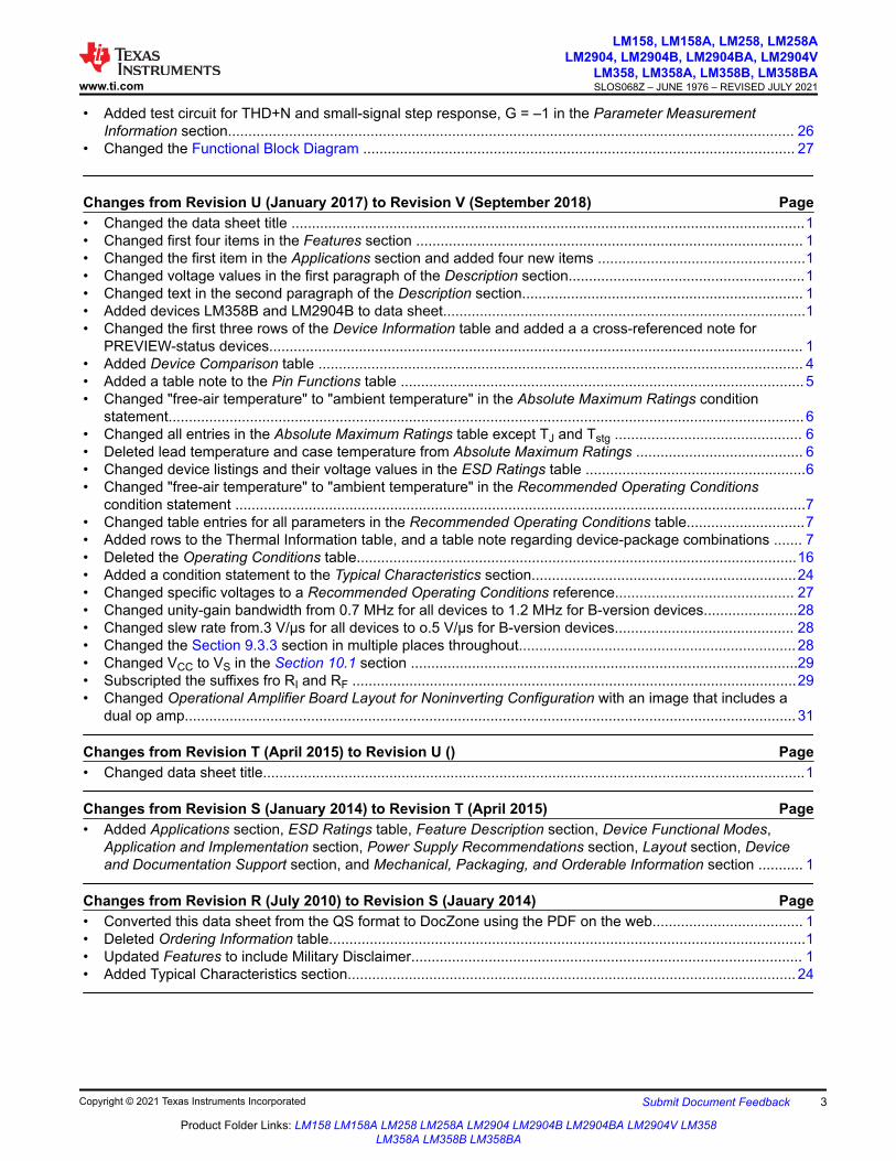
• Added test circuit for THD+N and small-signal step response, G = –1 in the Parameter Measurement Information section........................................................................................................................................... 26
• Changed the Functional Block Diagram .......................................................................................................... 27
Changes from Revision U (January 2017) to Revision V (September 2018) Page• Changed the data sheet title ..............................................................................................................................1• Changed first four items in the Features section ............................................................................................... 1• Changed the first item in the Applications section and added four new items ...................................................1• Changed voltage values in the first paragraph of the Description section..........................................................1• Changed text in the second paragraph of the Description section..................................................................... 1• Added devices LM358B and LM2904B to data sheet.........................................................................................1• Changed the first three rows of the Device Information table and added a a cross-referenced note for
PREVIEW-status devices................................................................................................................................... 1• Added Device Comparison table ....................................................................................................................... 4• Added a table note to the Pin Functions table ................................................................................................... 5• Changed "free-air temperature" to "ambient temperature" in the Absolute Maximum Ratings condition
statement............................................................................................................................................................ 6• Changed all entries in the Absolute Maximum Ratings table except TJ and Tstg .............................................. 6• Deleted lead temperature and case temperature from Absolute Maximum Ratings ......................................... 6• Changed device listings and their voltage values in the ESD Ratings table ......................................................6• Changed "free-air temperature" to "ambient temperature" in the Recommended Operating Conditions
condition statement ............................................................................................................................................7• Changed table entries for all parameters in the Recommended Operating Conditions table.............................7• Added rows to the Thermal Information table, and a table note regarding device-package combinations ....... 7• Deleted the Operating Conditions table............................................................................................................16• Added a condition statement to the Typical Characteristics section.................................................................24• Changed specific voltages to a Recommended Operating Conditions reference............................................ 27• Changed unity-gain bandwidth from 0.7 MHz for all devices to 1.2 MHz for B-version devices.......................28• Changed slew rate from.3 V/µs for all devices to o.5 V/µs for B-version devices............................................ 28• Changed the Section 9.3.3 section in multiple places throughout.................................................................... 28• Changed VCC to VS in the Section 10.1 section ...............................................................................................29• Subscripted the suffixes fro RI and RF .............................................................................................................29• Changed Operational Amplifier Board Layout for Noninverting Configuration with an image that includes a
dual op amp...................................................................................................................................................... 31
Changes from Revision T (April 2015) to Revision U () Page• Changed data sheet title.....................................................................................................................................1
Changes from Revision S (January 2014) to Revision T (April 2015) Page• Added Applications section, ESD Ratings table, Feature Description section, Device Functional Modes,
Application and Implementation section, Power Supply Recommendations section, Layout section, Device and Documentation Support section, and Mechanical, Packaging, and Orderable Information section ........... 1
Changes from Revision R (July 2010) to Revision S (Jauary 2014) Page• Converted this data sheet from the QS format to DocZone using the PDF on the web..................................... 1• Deleted Ordering Information table.....................................................................................................................1• Updated Features to include Military Disclaimer................................................................................................ 1• Added Typical Characteristics section.............................................................................................................. 24
www.ti.com
LM158, LM158A, LM258, LM258ALM2904, LM2904B, LM2904BA, LM2904V
LM358, LM358A, LM358B, LM358BASLOS068Z – JUNE 1976 – REVISED JULY 2021
Copyright © 2021 Texas Instruments Incorporated Submit Document Feedback 3
Product Folder Links: LM158 LM158A LM258 LM258A LM2904 LM2904B LM2904BA LM2904V LM358 LM358A LM358B LM358BA

5 Device Comparison TablePART NUMBER SUPPLY
VOLTAGETEMPERATURE
RANGEVOS (MAXIMUM
AT 25°C)IQ / CH (TYPICAL AT
25°C)INTEGRATED EMI
FILTER PACKAGE
LM358B 3 V–36 V –40°C to 85°C 3 mV 300 µA Yes D, DDF, DGK, PW
LM2904B 3 V–36 V –40°C to 125°C 3 mV 300 µA Yes D, DDF, DGK, PW
LM358 3 V–32 V 0°C to 70°C 7 mV 350 µA No D, PW, DGK, P, PS
LM2904 3 V–26 V –40°C to 125°C 7 mV 350 µA No D, PW, DGK, P, PS
LM358A 3 V–32 V 0°C to 70°C 3 mV 350 µA No D, PW, DGK, P
LM2904V 3 V–32 V –40°C to 125°C 7 mV 350 µA No D, PW
LM158 3 V–32 V –55°C to 125°C 5 mV 350 µA No JG, FK
LM158A 3 V–32 V –55°C to 125°C 3 mV 350 µA No JG, FK
LM258 3 V–32 V –25°C to 85°C 5 mV 350 µA No D, DGK, P
LM258A 3 V–32 V –25°C to 85°C 3 mV 350 µA No D, DGK, P
LM158, LM158A, LM258, LM258ALM2904, LM2904B, LM2904BA, LM2904VLM358, LM358A, LM358B, LM358BASLOS068Z – JUNE 1976 – REVISED JULY 2021 www.ti.com
4 Submit Document Feedback Copyright © 2021 Texas Instruments Incorporated
Product Folder Links: LM158 LM158A LM258 LM258A LM2904 LM2904B LM2904BA LM2904V LM358 LM358A LM358B LM358BA

6 Pin Configuration and Functions
1OUT1 8 V+
2IN1± 7 OUT2
3IN1+ 6 IN2±
4V± 5 IN2+
Not to scale
Figure 6-1. D, DDF, DGK, P, PS, PW, and JG Package
8-Pin SOIC, SOT23-8, VSSOP, PDIP, SO, TSSOP, and CDIPTop View
4NC
5IN1±
6NC
7IN1+
8NC
9N
C
10
V±
11
NC
12
IN2
+
13
NC
14 NC
15 IN2±
16 NC
17 OUT2
18 NC
19
NC
20
V+
1N
C
2O
UT
1
3N
C
Not to scale
NC - No internal connectionFigure 6-2. FK Package
20-Pin LCCCTop View
Table 6-1. Pin FunctionsPIN
I/O DESCRIPTIONNAME LCCC(1) SOIC, SOT23-8, VSSOP, CDIP,
PDIP, SO, TSSOP, CFP(1)
IN1– 5 2 I Negative input
IN1+ 7 3 I Positive input
IN2– 15 6 I Negative input
IN2+ 12 5 I Positive input
OUT1 2 1 O Output
OUT2 17 7 O Output
V– 10 4 — Negative (lowest) supply or ground (for single-supply operation)
NC 1, 3, 4, 6, 8, 9, 11, 13, 14, 16, 18, 19 — — No internal connection
V+ 20 8 — Positive (highest) supply
(1) For a listing of which devices are available in what packages, see Section 5.
www.ti.com
LM158, LM158A, LM258, LM258ALM2904, LM2904B, LM2904BA, LM2904V
LM358, LM358A, LM358B, LM358BASLOS068Z – JUNE 1976 – REVISED JULY 2021
Copyright © 2021 Texas Instruments Incorporated Submit Document Feedback 5
Product Folder Links: LM158 LM158A LM258 LM258A LM2904 LM2904B LM2904BA LM2904V LM358 LM358A LM358B LM358BA

7 Specifications7.1 Absolute Maximum Ratingsover operating ambient temperature range (unless otherwise noted)(1)
MIN MAX UNIT
Supply voltage, VS = ([V+] – [V–])
LM358B, LM358BA, LM2904B, LM2904BA ±20 or 40
VLM158, LM258, LM358, LM158A, LM258A, LM358A, LM2904V
±16 or 32
LM2904 ±13 or 26
Differential input voltage, VID (2)
LM358B, LM358BA, LM2904B, LM2904BA,LM158, LM258, LM358, LM158A, LM258A, LM358A, LM2904V
–32 32V
LM2904 –26 26
Input voltage, VI Either input
LM358B, LM358BA, LM2904B, LM2904BA –0.3 40
VLM158, LM258, LM358, LM158A, LM258A, LM358A, LM2904V
–0.3 32
LM2904 –0.3 26
Duration of output short circuit (one amplifier) to ground at (or below) TA = 25°C,VS ≤ 15 V(3) Unlimited s
Operating ambient temperature, TA
LM158, LM158A –55 125
°C
LM258, LM258A –25 85
LM358B, LM358BA –40 85
LM358, LM358A 0 70
LM2904B, LM2904BA, LM2904, LM2904V –40 125
Operating virtual-junction temperature, TJ 150 °C
Storage temperature, Tstg –65 150 °C
(1) Stresses beyond those listed under Absolute Maximum Ratings may cause permanent damage to the device. These are stress ratings only, and do not imply functional operation of the device at these or any other conditions beyond those indicated under Recommended Operating Conditions. Exposure to absolute-maximum-rated conditions for extended periods may affect device reliability.
(2) Differential voltages are at IN+, with respect to IN−.(3) Short circuits from outputs to VS can cause excessive heating and eventual destruction.
7.2 ESD RatingsVALUE UNIT
LM358B, LM358BA, LM2904B, AND LM2904BA
V(ESD) Electrostatic dischargeHuman-body model (HBM), per ANSI/ESDA/JEDEC JS-001(1) ±2000
VCharged-device model (CDM), per JEDEC specification JESD22-C101(2) ±1000
LM158, LM258, LM358, LM158, LM258A, LM358A, LM2904, AND LM2904V
V(ESD) Electrostatic dischargeHuman-body model (HBM), per ANSI/ESDA/JEDEC JS-001(1) ±500
VCharged-device model (CDM), per JEDEC specification JESD22-C101(2) ±1000
(1) JEDEC document JEP155 states that 500-V HBM allows safe manufacturing with a standard ESD control process.(2) JEDEC document JEP157 states that 250-V CDM allows safe manufacturing with a standard ESD control process.
LM158, LM158A, LM258, LM258ALM2904, LM2904B, LM2904BA, LM2904VLM358, LM358A, LM358B, LM358BASLOS068Z – JUNE 1976 – REVISED JULY 2021 www.ti.com
6 Submit Document Feedback Copyright © 2021 Texas Instruments Incorporated
Product Folder Links: LM158 LM158A LM258 LM258A LM2904 LM2904B LM2904BA LM2904V LM358 LM358A LM358B LM358BA

7.3 Recommended Operating Conditionsover operating ambient temperature range (unless otherwise noted)
MIN MAX UNIT
VS Supply voltage, VS= ([V+] – [V–])
LM358B, LM358BA, LM2904B, LM2904BA 3 36
VLM158, LM258, LM358, LM158A, LM258A, LM358A, LM2904V 3 30
LM2904 3 26
VCM Common-mode voltage V– V+ – 2 V
TA Operating ambient temperature
LM358B, LM358BA –40 85
°C
LM2904B, LM2904BA, LM2904, LM2904V –40 125
LM358, LM358A 0 70
LM258, LM258A –20 85
LM158, LM158A –55 125
7.4 Thermal Information
THERMAL METRIC(1)
LM258, LM258A, LM358, LM358A, LM358B, LM358BA, LM2904, LM2904B, LM2904BA, LM2904V(2) LM158, LM158A
UNITD(SOIC)
DGK(VSSOP)
P(PDIP)
PS(SO)
PW(TSSOP)
DDF(SOT-23)
FK(LCCC)
JG(CDIP)
8 PINS 8 PINS 8 PINS 8 PINS 8 PINS 8PINS 20 PINS 8 PINS
RθJAJunction-to-ambient thermal resistance 124.7 181.4 80.9 116.9 171.7 164.3 84.0 112.4 °C/W
RθJC(top)Junction-to-case (top) thermal resistance 66.9 69.4 70.4 62.5 68.8 98.1 56.9 63.6 °C/W
RθJBJunction-to-board thermal resistance 67.9 102.9 57.4 68.6 99.2 82.1 57.5 100.3 °C/W
ψJT
Junction-to-top characterization parameter
19.2 11.8 40 21.9 11.5 11.4 51.7 35.7 °C/W
ψJB
Junction-to-board characterization parameter
67.2 101.2 56.9 67.6 97.9 81.7 57.1 93.3 °C/W
RθJC(bot)Junction-to-case (bottom) thermal resistance — — — — — — 10.6 22.3 °C/W
(1) For more information about traditional and new thermal metrics, see Semiconductor and IC Package Thermal Metrics.(2) For a listing of which devices are available in what packages, see Section 5.
www.ti.com
LM158, LM158A, LM258, LM258ALM2904, LM2904B, LM2904BA, LM2904V
LM358, LM358A, LM358B, LM358BASLOS068Z – JUNE 1976 – REVISED JULY 2021
Copyright © 2021 Texas Instruments Incorporated Submit Document Feedback 7
Product Folder Links: LM158 LM158A LM258 LM258A LM2904 LM2904B LM2904BA LM2904V LM358 LM358A LM358B LM358BA

7.5 Electrical Characteristics: LM358B and LM358BAVS = (V+) – (V–) = 5 V – 36 V (±2.5 V – ±18 V), TA = 25°C, VCM = VOUT = VS / 2, RL = 10k connected to VS / 2(unless otherwise noted)
PARAMETER TEST CONDITIONS MIN TYP MAX UNIT
OFFSET VOLTAGE
VOS Input offset voltage
LM358B±0.3 ±3.0 mV
TA = –40°C to +85°C ±4 mV
LM358BA±2.0 mV
TA = –40°C to +85°C ±2.5 mV
dVOS/dT Input offset voltage drift TA = -40°C to +85°C(1) ±3.5 11 µV/°C
PSRR Power supply rejection ratio ±2 15 µV/V
Channel separation, dc f = 1 kHz to 20 kHz ±1 µV/V
INPUT VOLTAGE RANGE
VCM Common-mode voltage rangeVS = 3 V to 36 V (V–) (V+) – 1.5 V
VS = 5 V to 36 V TA = –40°C to +85°C (V–) (V+) – 2 V
CMRR Common-mode rejection ratio(V–) ≤ VCM ≤ (V+) – 1.5 V VS = 3 V to 36 V 20 100
µV/V(V–) ≤ VCM ≤ (V+) – 2.0 V VS = 5 V to 36 V TA = –40°C to +85°C 25 316
INPUT BIAS CURRENT
IB Input bias current±10 ±35 nA
TA = –40°C to +85°C(1) ±50 nA
IOS Input offset current0.5 4 nA
TA = –40°C to +85°C(1) 5 nA
dIOS/dT Input offset current drift TA = –40°C to +85°C 10 pA/
NOISE
En Input voltage noise f = 0.1 to 10 Hz 3 µVPP
en Input voltage noise density f = 1 kHz 40 nV/√/Hz
INPUT IMPEDANCE
ZID Differential 10 || 0.1 MΩ|| pF
ZIC Common-mode 4 || 1.5 GΩ|| pF
OPEN-LOOP GAIN
AOL Open-loop voltage gain VS = 15 V; VO = 1 V to 11 V; RL ≥ 10 kΩ, connected to (V–)70 140 V/mV
TA = –40°C to +85°C 35 V/mV
FREQUENCY RESPONSE
GBW Gain bandwidth product 1.2 MHz
SR Slew rate G = + 1 0.5 V/µs
Θm Phase margin G = + 1, RL = 10kΩ, CL = 20 pF 56 °
tOR Overload recovery time VIN × gain > VS 10 µs
ts Settling time To 0.1%, VS = 5 V, 2-V step , G = +1, CL = 100 pF 4 µs
THD+N Total harmonic distortion + noise G = + 1, f = 1 kHz, VO = 3.53 VRMS, VS = 36 V, RL = 100k, IOUT ≤ ±50 µA, BW = 80 kHz 0.001 %
OUTPUT
VO Voltage output swing from rail
Positive rail (V+)
IOUT = 50 µA 1.35 1.42 V
IOUT = 1 mA 1.4 1.48 V
IOUT = 5 mA(1) 1.5 1.61 V
Negative rail (V–)
IOUT = 50 µA 100 150 mV
IOUT = 1 mA 0.75 1 V
VS = 5 V, RL ≤ 10 kΩ connected to (V–) TA = –40°C to +85°C 5 20 mV
IO Output current
VS = 15 V; VO = V–;VID = 1 V Source(1)
-20 -30
mATA = –40°C to +85°C -10
VS = 15 V; VO = V+;VID = –1 V Sink(1)
10 20
TA = –40°C to +85°C 5
VID = –1 V; VO = (V–) + 200 mV 60 100 μA
ISC Short-circuit current VS = 20 V, (V+) = 10 V, (V–) = –10 V, VO = 0 V ±40 ±60 mA
CLOAD Capacitive load drive 100 pF
RO Open-loop output resistance f = 1 MHz, IO = 0 A 300 Ω
LM158, LM158A, LM258, LM258ALM2904, LM2904B, LM2904BA, LM2904VLM358, LM358A, LM358B, LM358BASLOS068Z – JUNE 1976 – REVISED JULY 2021 www.ti.com
8 Submit Document Feedback Copyright © 2021 Texas Instruments Incorporated
Product Folder Links: LM158 LM158A LM258 LM258A LM2904 LM2904B LM2904BA LM2904V LM358 LM358A LM358B LM358BA

7.5 Electrical Characteristics: LM358B and LM358BA (continued)VS = (V+) – (V–) = 5 V – 36 V (±2.5 V – ±18 V), TA = 25°C, VCM = VOUT = VS / 2, RL = 10k connected to VS / 2(unless otherwise noted)
PARAMETER TEST CONDITIONS MIN TYP MAX UNIT
POWER SUPPLY
IQ Quiescent current per amplifier VS = 5 V; IO = 0 ATA = –40°C to +85°C
300 460 µA
IQ Quiescent current per amplifier VS = 36 V; IO = 0 A 800 µA
(1) Specified by characterization only.
www.ti.com
LM158, LM158A, LM258, LM258ALM2904, LM2904B, LM2904BA, LM2904V
LM358, LM358A, LM358B, LM358BASLOS068Z – JUNE 1976 – REVISED JULY 2021
Copyright © 2021 Texas Instruments Incorporated Submit Document Feedback 9
Product Folder Links: LM158 LM158A LM258 LM258A LM2904 LM2904B LM2904BA LM2904V LM358 LM358A LM358B LM358BA

7.6 Electrical Characteristics: LM2904B and LM2904BAVS = (V+) – (V–) = 5 V – 36 V (±2.5 V – ±18 V), TA = 25°C, VCM = VOUT = VS / 2, RL = 10k connected to VS / 2(unless otherwise noted)
PARAMETER TEST CONDITIONS MIN TYP MAX UNIT
OFFSET VOLTAGE
VOS Input offset voltage
LM2904B±0.3 ±3.0 mV
TA = –40°C to +125°C ±4 mV
LM2904BA±2.0 mV
TA = –40°C to +125°C ±2.5 mV
dVOS/dT Input offset voltage drift TA = –40°C to +125°C(1) ±3.5 12 µV/°C
PSRR Power supply rejection ratio ±2 15 µV/V
Channel separation, dc f = 1 kHz to 20 kHz ±1 µV/V
INPUT VOLTAGE RANGE
VCM Common-mode voltage rangeVS = 3 V to 36 V (V–) (V+) – 1.5 V
VS = 5 V to 36 V TA = –40°C to +125°C (V–) (V+) – 2 V
CMRR Common-mode rejection ratio(V–) ≤ VCM ≤ (V+) – 1.5 V VS = 3 V to 36 V 20 100
µV/V(V–) ≤ VCM ≤ (V+) – 2.0 V VS = 5 V to 36 V TA = –40°C to +125°C 25 316
INPUT BIAS CURRENT
IB Input bias current±10 ±35 nA
TA = –40°C to +125°C(1) ±50 nA
IOS Input offset current0.5 4 nA
TA = –40°C to +125°C(1) 5 nA
dIOS/dT Input offset current drift TA = –40°C to +125°C 10 pA/
NOISE
En Input voltage noise f = 0.1 to 10 Hz 3 µVPP
en Input voltage noise density f = 1 kHz 40 nV/√/Hz
INPUT IMPEDANCE
ZID Differential 10 || 0.1 MΩ|| pF
ZIC Common-mode 4 || 1.5 GΩ|| pF
OPEN-LOOP GAIN
AOL Open-loop voltage gain VS = 15 V; VO = 1 V to 11 V; RL ≥ 10 kΩ, connected to (V–)70 140 V/mV
TA = –40°C to +125°C 35 V/mV
FREQUENCY RESPONSE
GBW Gain bandwidth product 1.2 MHz
SR Slew rate G = + 1 0.5 V/µs
Θm Phase margin G = + 1, RL = 10kΩ, CL = 20 pF 56 °
tOR Overload recovery time VIN × gain > VS 10 µs
ts Settling time To 0.1%, VS = 5 V, 2-V Step , G = +1, CL = 100 pF 4 µs
THD+N Total harmonic distortion + noise G = + 1, f = 1 kHz, VO = 3.53 VRMS, VS = 36 V, RL = 100k, IOUT ≤ ±50 µA, BW = 80 kHz 0.001 %
OUTPUT
VO Voltage output swing from rail
Positive rail (V+)
IOUT = 50 µA 1.35 1.42 V
IOUT = 1 mA 1.4 1.48 V
IOUT = 5 mA(1) 1.5 1.61 V
Negative rail (V–)
IOUT = 50 µA 100 150 mV
IOUT = 1 mA 0.75 1 V
VS = 5 V, RL ≤ 10 kΩ connected to (V–) TA = –40°C to +125°C 5 20 mV
IO Output current
VS = 15 V; VO = V–; VID = 1 V Source(1)
–20 –30
mATA = –40°C to +125°C –10
VS = 15 V; VO = V+; VID = –1 V Sink(1)
10 20
TA = –40°C to +125°C 5
VID = –1 V; VO = (V–) + 200 mV 60 100 μA
ISC Short-circuit current VS = 20 V, (V+) = 10 V, (V–) = –10 V, VO = 0 V ±40 ±60 mA
CLOAD Capacitive load drive 100 pF
RO Open-loop output resistance f = 1 MHz, IO = 0 A 300 Ω
LM158, LM158A, LM258, LM258ALM2904, LM2904B, LM2904BA, LM2904VLM358, LM358A, LM358B, LM358BASLOS068Z – JUNE 1976 – REVISED JULY 2021 www.ti.com
10 Submit Document Feedback Copyright © 2021 Texas Instruments Incorporated
Product Folder Links: LM158 LM158A LM258 LM258A LM2904 LM2904B LM2904BA LM2904V LM358 LM358A LM358B LM358BA

7.6 Electrical Characteristics: LM2904B and LM2904BA (continued)VS = (V+) – (V–) = 5 V – 36 V (±2.5 V – ±18 V), TA = 25°C, VCM = VOUT = VS / 2, RL = 10k connected to VS / 2(unless otherwise noted)
PARAMETER TEST CONDITIONS MIN TYP MAX UNIT
POWER SUPPLY
IQ Quiescent current per amplifier VS = 5 V; IO = 0 ATA = –40°C to +125°C
300 460 µA
IQ Quiescent current per amplifier VS = 36 V; IO = 0 A 800 µA
(1) Specified by characterization only.
www.ti.com
LM158, LM158A, LM258, LM258ALM2904, LM2904B, LM2904BA, LM2904V
LM358, LM358A, LM358B, LM358BASLOS068Z – JUNE 1976 – REVISED JULY 2021
Copyright © 2021 Texas Instruments Incorporated Submit Document Feedback 11
Product Folder Links: LM158 LM158A LM258 LM258A LM2904 LM2904B LM2904BA LM2904V LM358 LM358A LM358B LM358BA

7.7 Electrical Characteristics: LM358, LM358AFor VS = (V+) – (V–) = 5 V, TA = 25°C (unless otherwise noted)
PARAMETER TEST CONDITIONS(1) MIN TYP(2) MAX UNIT
OFFSET VOLTAGE
VOS Input offset voltage VS = 5 V to 30 V; VC M = 0 V; VO = 1.4 V
LM3583 7
mVTA = 0°C to 70°C 9
LM358A 2 3
TA = 0°C to 70°C 5
dVOS/dT Input offset voltage driftLM358 TA = 0°C to 70°C 7
µV/°CLM358A TA = 0°C to 70°C 7 20
PSRR Input offset voltage vs power supply (ΔVIO/ΔVS) VS = 5 V to 30 V 65 100 dB
VO1/ VO2 Channel separation f = 1 kHz to 20 kHz 120 dB
INPUT VOLTAGE RANGE
VCM Common-mode voltage range
VS = 5 V to 30 V LM358(V–) (V+) – 1.5
VVS = 30 V LM358A
VS = 5 V to 30 V LM358TA = 0°C to 70°C (V–) (V+) – 2
VS = 30 V LM358A
CMRR Common-mode rejection ratio VS = 5 V to 30 V; VCM = 0 V 65 80 dB
INPUT BIAS CURRENT
IB Input bias current VO = 1.4 V
LM358–20 –250
nATA = 0°C to 70°C –500
LM358A–15 –100
TA = 0°C to 70°C –200
IOS Input offset current VO = 1.4 V
LM3582 50
nATA = 0°C to 70°C 150
LM358A2 30
TA = 0°C to 70°C 75
dIOS/dT Input offset current drift10
pA/°CLM358A TA = 0°C to 70°C 300
NOISE
en Input voltage noise density f = 1 kHz 40 nV/√ Hz
OPEN-LOOP GAIN
AOL Open-loop voltage gain VS = 15 V; VO = 1 V to 11 V; RL ≥ 2 kΩ25 100
V/mVTA = 0°C to 70°C 15
FREQUENCY RESPONSE
GBW Gain bandwidth product 0.7 MHz
SR Slew rate G = +1 0.3 V/µs
OUTPUT
VO Voltage output swing from railPositive rail
VS = 30 V; RL = 2 kΩ TA = 0°C to 70°C 4
VVS = 30 V; RL ≥ 10 kΩ 2 3
VS = 5 V; RL ≥ 2 kΩ 1.5
Negative rail VS = 5 V; RL ≤ 10 kΩ TA = 0°C to 70°C 5 20 mV
IO Output current
VS = 15 V; VO = 0 V; VID = 1 V Source
–20 –30
mA
LM358A –60
TA = 0°C to 70°C –10
VS = 15 V; VO = 15 V; VID = –1 V Sink
10 20
TA = 0°C to 70°C 5
VID = –1 V; VO = 200 mV 12 30 µA
ISC Short-circuit current VS = 10 V; VO = VS / 2 ±40 ±60 mA
POWER SUPPLY
IQ Quiescent current per amplifierVO = 2.5 V; IO = 0 A
TA = 0°C to 70°C350 600
µAVS = 30 V; VO = 15 V; IO = 0 A 500 1000
(1) All characteristics are measured under open-loop conditions, with zero common-mode input voltage, unless otherwise specified. Maximum VS for testing purposes is 30 V for LM358 and LM358A.
(2) All typical values are TA = 25°C.
LM158, LM158A, LM258, LM258ALM2904, LM2904B, LM2904BA, LM2904VLM358, LM358A, LM358B, LM358BASLOS068Z – JUNE 1976 – REVISED JULY 2021 www.ti.com
12 Submit Document Feedback Copyright © 2021 Texas Instruments Incorporated
Product Folder Links: LM158 LM158A LM258 LM258A LM2904 LM2904B LM2904BA LM2904V LM358 LM358A LM358B LM358BA

7.8 Electrical Characteristics: LM2904, LM2904VFor VS = (V+) – (V–) = 5 V, TA = 25°C (unless otherwise noted)
PARAMETER TEST CONDITIONS(1) MIN TYP(2) MAX UNIT
OFFSET VOLTAGE
VOS Input offset voltage VS = 5 V to maximum; VC M = 0 V; VO = 1.4 V
Non-A suffix devices
3 7
mVTA = –40°C to 125°C 10
A-suffix devices
1 2
TA = –40°C to 125°C 4
dVOS/dT Input offset voltage drift TA = –40°C to 125°C 7 µV/°C
PSRR Input offset voltage vs power supply (ΔVIO/ΔVS) VS = 5 V to 30 V 65 100 dB
VO1/ VO2 Channel separation f = 1 kHz to 20 kHz 120 dB
INPUT VOLTAGE RANGE
VCM Common-mode voltage range VS = 5 V to maximum(V–) (V+) – 1.5
VTA = –40°C to 125°C (V–) (V+) – 2
CMRR Common-mode rejection ratio VS = 5 V to maximum; VCM = 0 V 65 80 dB
INPUT BIAS CURRENT
IB Input bias current VO = 1.4 V–20 –250
nATA = –40°C to 125°C –500
IOS Input offset current VO = 1.4 V
Non-V suffix device
2 50
nATA = –40°C to 125°C 300
V-suffix device
2 50
TA = –40°C to 125°C 150
dIOS/dT Input offset current drift TA = –40°C to 125°C 10 pA/°C
NOISE
en Input voltage noise density f = 1 kHz 40 nV/√ Hz
OPEN-LOOP GAIN
AOL Open-loop voltage gain VS = 15 V; VO = 1 V to 11 V; RL ≥ 2 kΩ25 100
V/mVTA = –40°C to 125°C 15
FREQUENCY RESPONSE
GBW Gain bandwidth product 0.7 MHz
SR Slew rate G = +1 0.3 V/µs
OUTPUT
VO Voltage output swing from railPositive rail
RL ≥ 10 kΩ VS – 1.5
V
Non-V suffix device
VS = maximum; RL = 2 kΩ
TA = –40°C to 125°C
4
VS = maximum; RL ≥ 10 kΩ 2 3
V-suffix device
VS = maximum; RL = 2 kΩ 6
VS = maximum; RL ≥ 10 kΩ 4 5
Negative rail VS = 5 V; RL ≤ 10 kΩ TA = –40°C to 125°C 5 20 mV
IO Output current
VS = 15 V; VO = 0 V; VID = 1 V Source–20 –30
mATA = –40°C to 125°C –10
VS = 15 V; VO = 15 V; VID = –1 V Sink10 20
TA = –40°C to 125°C 5
VID = -1 V; VO = 200 mVNon-V suffix device 30
µAV-suffix device 12 40
ISC Short-circuit current VS = 10 V; VO = VS / 2 ±40 ±60 mA
POWER SUPPLY
IQ Quiescent current per amplifierVO = 2.5 V; IO = 0 A
TA = –40°C to 125°C350 600
µAVS = maximum; VO = maximum / 2; IO = 0 A 500 1000
(1) All characteristics are measured under open-loop conditions, with zero common-mode input voltage, unless otherwise specified. Maximum VS for testing purposes is 26 V for LM2904 and 32 V for LM2904V.
(2) All typical values are TA = 25°C.
www.ti.com
LM158, LM158A, LM258, LM258ALM2904, LM2904B, LM2904BA, LM2904V
LM358, LM358A, LM358B, LM358BASLOS068Z – JUNE 1976 – REVISED JULY 2021
Copyright © 2021 Texas Instruments Incorporated Submit Document Feedback 13
Product Folder Links: LM158 LM158A LM258 LM258A LM2904 LM2904B LM2904BA LM2904V LM358 LM358A LM358B LM358BA

7.9 Electrical Characteristics: LM158, LM158AFor VS = (V+) – (V–) = 5 V, TA = 25°C (unless otherwise noted)
PARAMETER TEST CONDITIONS(1) MIN TYP(2) MAX UNIT
OFFSET VOLTAGE
VOS Input offset voltage VS = 5 V to 30 V; VC M = 0 V; VO = 1.4 V
LM1583 5
mVTA = –55°C to 125°C 7
LM158A2
TA = –55°C to 125°C 4
dVOS/dT Input offset voltage driftLM158 TA = –55°C to 125°C 7
µV/°CLM158A TA = –55°C to 125°C 7 15(3)
PSRR Input offset voltage vs power supply (ΔVIO/ΔVS) VS = 5 V to 30 V 65 100 dB
VO1/ VO2 Channel separation f = 1 kHz to 20 kHz 120 dB
INPUT VOLTAGE RANGE
VCM Common-mode voltage range
VS = 5 V to 30 V LM158(V–) (V+) – 1.5
VVS = 30 V LM158A
VS = 5 V to 30 V LM158TA = –55°C to 125°C (V–) (V+) – 2
VS = 30 V LM158A
CMRR Common-mode rejection ratio VS = 5 V to 30 V; VCM = 0 V 70 80 dB
INPUT BIAS CURRENT
IB Input bias current VO = 1.4 V
LM158–20 –150
nATA = –55°C to 125°C –300
LM158A–15 –50
TA = –55°C to 125°C –100
IOS Input offset current VO = 1.4 V
LM1582 30
nATA = –55°C to 125°C 100
LM158A2 10
TA = –55°C to 125°C 30
dIOS/dT Input offset current drift10
pA/°CLM158A TA = –55°C to 125°C 200
NOISE
en Input voltage noise density f = 1 kHz 40 nV/√ Hz
OPEN-LOOP GAIN
AOL Open-loop voltage gain VS = 15 V; VO = 1 V to 11 V; RL ≥ 2 kΩ50 100
V/mVTA = –55°C to 125°C 25
FREQUENCY RESPONSE
GBW Gain bandwidth product 0.7 MHz
SR Slew rate G = +1 0.3 V/µs
OUTPUT
VO Voltage output swing from railPositive rail
VS = 30 V; RL = 2 kΩ TA = –55°C to 125°C 4
VVS = 30 V; RL ≥ 10 kΩ 2 3
VS = 5 V; RL ≥ 2 kΩ 1.5
Negative rail VS = 5 V; RL ≤ 10 kΩ TA = –55°C to 125°C 5 20 mV
IO Output current
VS = 15 V; VO = 0 V; VID = 1 V Source
–20 –30
mA
LM158A –60
TA = –55°C to 125°C –10
VS = 15 V; VO = 15 V; VID = –1 V Sink
10 20
TA = –55°C to 125°C 5
VID = –1 V; VO = 200 mV 12 30 µA
ISC Short-circuit current VS = 10 V; VO = VS / 2 ±40 ±60 mA
LM158, LM158A, LM258, LM258ALM2904, LM2904B, LM2904BA, LM2904VLM358, LM358A, LM358B, LM358BASLOS068Z – JUNE 1976 – REVISED JULY 2021 www.ti.com
14 Submit Document Feedback Copyright © 2021 Texas Instruments Incorporated
Product Folder Links: LM158 LM158A LM258 LM258A LM2904 LM2904B LM2904BA LM2904V LM358 LM358A LM358B LM358BA

7.9 Electrical Characteristics: LM158, LM158A (continued)For VS = (V+) – (V–) = 5 V, TA = 25°C (unless otherwise noted)
PARAMETER TEST CONDITIONS(1) MIN TYP(2) MAX UNIT
POWER SUPPLY
IQ Quiescent current per amplifierVO = 2.5 V; IO = 0 A
TA = –55°C to 125°C350 600
µAVS = 30 V; VO = 15 V; IO = 0 A 500 1000
(1) All characteristics are measured under open-loop conditions, with zero common-mode input voltage, unless otherwise specified. Maximum VS for testing purposes is 30 V for LM158 and LM158A.
(2) All typical values are TA = 25°C.(3) On products compliant to MIL-PRF-38535, this parameter is not production tested.
www.ti.com
LM158, LM158A, LM258, LM258ALM2904, LM2904B, LM2904BA, LM2904V
LM358, LM358A, LM358B, LM358BASLOS068Z – JUNE 1976 – REVISED JULY 2021
Copyright © 2021 Texas Instruments Incorporated Submit Document Feedback 15
Product Folder Links: LM158 LM158A LM258 LM258A LM2904 LM2904B LM2904BA LM2904V LM358 LM358A LM358B LM358BA

7.10 Electrical Characteristics: LM258, LM258AFor VS = (V+) – (V–) = 5 V, TA = 25°C (unless otherwise noted)
PARAMETER TEST CONDITIONS(1) MIN TYP(2) MAX UNIT
OFFSET VOLTAGE
VOS Input offset voltage VS = 5 V to 30 V; VC M = 0 V; VO = 1.4 V
LM2583 5
mVTA = –25°C to 85°C 7
LM258A2 3
TA = –25°C to 85°C 4
dVOS/dT Input offset voltage driftLM258
TA = –25°C to 85°C7
µV/°CLM258A 7 15
PSRR Input offset voltage vs power supply (ΔVIO/ΔVS) VS = 5 V to 30 V 65 100 dB
VO1/ VO2 Channel separation f = 1 kHz to 20 kHz 120 dB
INPUT VOLTAGE RANGE
VCM Common-mode voltage range
VS = 5 V to 30 V LM258(V–) (V+) – 1.5
VVS = 30 V LM258A
VS = 5 V to 30 V LM258TA = –25°C to 85°C (V–) (V+) – 2
VS = 30 V LM258A
CMRR Common-mode rejection ratio VS = 5 V to 30 V; VCM = 0 V 70 80 dB
INPUT BIAS CURRENT
IB Input bias current VO = 1.4 V
LM258–20 –150
nATA = –25°C to 85°C –300
LM258A–15 –80
TA = –25°C to 85°C –100
IOS Input offset current VO = 1.4 V
LM2582 30
nATA = –25°C to 85°C 100
LM258A2 15
TA = –25°C to 85°C 30
dIOS/dT Input offset current drift10
pA/°CLM258A TA = –25°C to 85°C 200
NOISE
en Input voltage noise density f = 1 kHz 40 nV/√ Hz
OPEN-LOOP GAIN
AOL Open-loop voltage gain VS = 15 V; VO = 1 V to 11 V; RL ≥ 2 kΩ50 100
V/mVTA = –25°C to 85°C 25
FREQUENCY RESPONSE
GBW Gain bandwidth product 0.7 MHz
SR Slew rate G = +1 0.3 V/µs
OUTPUT
VO Voltage output swing from railPositive rail
VS = 30 V; RL = 2 kΩ TA = –25°C to 85°C 4
VVS = 30 V; RL ≥ 10 kΩ 2 3
VS = 5 V; RL ≥ 2 kΩ 1.5
Negative rail VS = 5 V; RL ≤ 10 kΩ TA = –25°C to 85°C 5 20 mV
IO Output current
VS = 15 V; VO = 0 V; VID = 1 V Source
–20 –30
mA
LM258A –60
TA = –25°C to 85°C –10
VS = 15 V; VO = 15 V; VID = –1 V Sink
10 20
TA = –25°C to 85°C 5
VID = –1 V; VO = 200 mV 12 30 µA
ISC Short-circuit current VS = 10 V; VO = VS / 2 ±40 ±60 mA
POWER SUPPLY
IQ Quiescent current per amplifierVO = 2.5 V; IO = 0 A
TA = –25°C to 85°C350 600
µAVS = 30 V; VO = 15 V; IO = 0 A 500 1000
(1) All characteristics are measured under open-loop conditions, with zero common-mode input voltage, unless otherwise specified. Maximum VS for testing purposes is 30 V for LM258 and LM258A.
(2) All typical values are TA = 25°C.
LM158, LM158A, LM258, LM258ALM2904, LM2904B, LM2904BA, LM2904VLM358, LM358A, LM358B, LM358BASLOS068Z – JUNE 1976 – REVISED JULY 2021 www.ti.com
16 Submit Document Feedback Copyright © 2021 Texas Instruments Incorporated
Product Folder Links: LM158 LM158A LM258 LM258A LM2904 LM2904B LM2904BA LM2904V LM358 LM358A LM358B LM358BA

7.11 Typical Characteristics: LM358B and LM2904BThis typical characteristics section is applicable for LM358B and LM2904B. Typical characteristics data in this section was taken with TA = 25°C, VS = 36 V (±18 V), VCM = VS / 2, RLOAD = 10 kΩ connected to VS / 2 (unless otherwise noted).
Offset Voltage (µV)
Am
plif
iers
(%
)
-1800 -1200 -600 0 600 1200 18000
2
4
6
8
10
12
14
16
18
20
DC11
Figure 7-1. Offset Voltage Production DistributionOffset Voltage Drift (µV/°C)
Am
plif
iers
(%
)
0 0.25 0.5 0.75 1 1.25 1.5 1.75 2 2.25 2.5 2.750
3
6
9
12
15
18
21
24
27
30
DC12
Figure 7-2. Offset Voltage Drift Distribution
Temperature (°C)
Offse
t V
olta
ge
(µ
V)
-40 -20 0 20 40 60 80 100 120-750
-450
-150
150
450
750
DC10
Figure 7-3. Offset Voltage vs TemperatureCommon-Mode Voltage (V)
Offse
t V
olta
ge
(µ
V)
-18 -12 -6 0 6 12 17-500
-300
-100
100
300
500
DC10
Figure 7-4. Offset Voltage vs Common-Mode Voltage
Frequency (Hz)
Open L
oop V
oltage G
ain
(dB
)
Pha
se ()
-20 -10
-10 0
0 10
10 20
20 30
30 40
40 50
50 60
60 70
70 80
80 90
90 100
1k 10k 100k 1M
D012
Gain (dB)Phase (°)
Figure 7-5. Open-Loop Gain and Phase vs FrequencyFrequency (Hz)
Clo
sed L
opp V
oltage G
ain
(dB
)
-30
-20
-10
0
10
20
30
40
50
60
70
1k 10k 100k 1M
D017
G = 1G = 10G = 100G = 1000G = –1
Figure 7-6. Closed-Loop Gain vs Frequency
www.ti.com
LM158, LM158A, LM258, LM258ALM2904, LM2904B, LM2904BA, LM2904V
LM358, LM358A, LM358B, LM358BASLOS068Z – JUNE 1976 – REVISED JULY 2021
Copyright © 2021 Texas Instruments Incorporated Submit Document Feedback 17
Product Folder Links: LM158 LM158A LM258 LM258A LM2904 LM2904B LM2904BA LM2904V LM358 LM358A LM358B LM358BA

7.11 Typical Characteristics: LM358B and LM2904B (continued)This typical characteristics section is applicable for LM358B and LM2904B. Typical characteristics data in this section was taken with TA = 25°C, VS = 36 V (±18 V), VCM = VS / 2, RLOAD = 10 kΩ connected to VS / 2 (unless otherwise noted).
Common-Mode Voltage (V)
Input B
ias C
urr
ent (n
A)
-20 -15 -10 -5 0 5 10 15 20-15
-12.5
-10
-7.5
-5
DC3I
IB+
IB–
Figure 7-7. Input Bias Current vs Common-Mode VoltageCommon-Mode Voltage (V)
Input O
ffset
Curr
ent
(pA
)
-20 -15 -10 -5 0 5 10 15 20-40
-20
0
20
40
60
80
100
120
DC3I
Figure 7-8. Input Offset Current vs Common-Mode Voltage
Temperature (°C)
Input B
ias C
urr
ent (n
A)
-40 -10 20 50 80 110 130-12
-11
-10
-9
-8
-7
-6
DCIB
IB+IB–
Figure 7-9. Input Bias Current vs Temperature
Temperature (°C)
Input O
ffset C
urr
ent (n
A)
-40 -10 20 50 80 110 130-0.03
-0.015
0
0.015
0.03
0.045
0.06
DCIO
Figure 7-10. Input Offset Current vs Temperature
Output Current (mA)
Outp
ut
Voltage (
V)
0 10 20 30 40 50
V+
(V+) – 3 V
(V+) – 6 V
(V+) – 9 V
(V+) – 12 V
DC13
–40C25C125C
Figure 7-11. Output Voltage Swing vs Output Current (Sourcing)
Output Current (mA)
Outp
ut V
oltage (
V)
0 5 10 15 20 25 30 35 40V–
(V–) + 3 V
(V–) + 6 V
(V–) + 9 V
(V–) + 12 V
(V–) + 15 V
(V–) + 18 V
DC1-
–40C25C125C
Figure 7-12. Output Voltage Swing vs Output Current (Sinking)
LM158, LM158A, LM258, LM258ALM2904, LM2904B, LM2904BA, LM2904VLM358, LM358A, LM358B, LM358BASLOS068Z – JUNE 1976 – REVISED JULY 2021 www.ti.com
18 Submit Document Feedback Copyright © 2021 Texas Instruments Incorporated
Product Folder Links: LM158 LM158A LM258 LM258A LM2904 LM2904B LM2904BA LM2904V LM358 LM358A LM358B LM358BA

7.11 Typical Characteristics: LM358B and LM2904B (continued)This typical characteristics section is applicable for LM358B and LM2904B. Typical characteristics data in this section was taken with TA = 25°C, VS = 36 V (±18 V), VCM = VS / 2, RLOAD = 10 kΩ connected to VS / 2 (unless otherwise noted).
Frequency (Hz)
PS
RR
and C
MR
R (
dB
)
0
10
20
30
40
50
60
70
80
90
100
1k 10k 100k 1M
D001
PSRR+PSRR-CMRR
Figure 7-13. CMRR and PSRR vs FrequencyTemperature (°C)
Com
mon-M
ode R
eje
ction R
atio (
dB
)
-40 -10 20 50 80 110 13085
90
95
100
105
110
115
120
DC2_
VS = 36VVS = 5V
Figure 7-14. Common-Mode Rejection Ratio vsTemperature (dB)
Temperature (°C)
Pow
er
Supply
Reje
ction R
atio
(dB
)
-40 -20 0 20 40 60 80 100 120 140-123
-122
-121
-120
-119
-118
DC8_
VS = 5 V to 36 V
Figure 7-15. Power Supply Rejection Ratio vs Temperature (dB)
Time (s)
Voltage (
µV
)
0 1 2 3 4 5 6 7 8 9 10-2
-1.6
-1.2
-0.8
-0.4
0
0.4
0.8
1.2
1.6
D011
Figure 7-16. 0.1-Hz to 10-Hz Noise
Frequency (Hz)
Voltage N
ois
e S
pectr
al D
ensity (
nV
/H
z)
0
10
20
30
40
50
60
70
80
90
100
10 100 1k 10k 100k
D010
Figure 7-17. Input Voltage Noise Spectral Density vs Frequency
Frequency (Hz)
TH
D+
N (
dB
)
-112
-104
-96
-88
-80
-72
-64
-56
-48
-40
-32
100 1k 10k
D013
10 k2 k
G = 1, f = 1 kHz, BW = 80 kHz,VOUT = 10 VPP, RL connected to V–
Figure 7-18. THD+N Ratio vs Frequency, G = 1
www.ti.com
LM158, LM158A, LM258, LM258ALM2904, LM2904B, LM2904BA, LM2904V
LM358, LM358A, LM358B, LM358BASLOS068Z – JUNE 1976 – REVISED JULY 2021
Copyright © 2021 Texas Instruments Incorporated Submit Document Feedback 19
Product Folder Links: LM158 LM158A LM258 LM258A LM2904 LM2904B LM2904BA LM2904V LM358 LM358A LM358B LM358BA

7.11 Typical Characteristics: LM358B and LM2904B (continued)This typical characteristics section is applicable for LM358B and LM2904B. Typical characteristics data in this section was taken with TA = 25°C, VS = 36 V (±18 V), VCM = VS / 2, RLOAD = 10 kΩ connected to VS / 2 (unless otherwise noted).
Frequency (Hz)
TH
D+
N (
dB
)
-104
-96
-88
-80
-72
-64
-56
-48
-40
-32
100 1k 10k
D014
10 k2 k
G = –1, f = 1 kHz, BW = 80 kHz,VOUT = 10 VPP, RL connected to V–
See Figure 8-3
Figure 7-19. THD+N Ratio vs Frequency, G = –1
Amplitude (VPP)
TH
D+
N (
dB
)
0.001 0.01 0.1 1 10 2020-120
-110
-100
-90
-80
-70
-60
-50
-40
-30
D015
10 k2 k
G = 1, f = 1 kHz, BW = 80 kHz,RL connected to V–
Figure 7-20. THD+N vs Output Amplitude, G = 1
Amplitude (VPP)
TH
D+
N (
dB
)
0.001 0.01 0.1 1 10 2020-110
-95
-80
-65
-50
-35
-20
D016
10 k2 k
G = –1, f = 1 kHz, BW = 80 kHz,RL connected to V–
See Figure 8-3
Figure 7-21. THD+N vs Output Amplitude, G = –1
Supply Voltage (V)
Quie
scent C
urr
ent (µ
A)
3 9 15 21 27 33 36280
310
340
370
400
430
460
DC_S
Figure 7-22. Quiescent Current vs Supply Voltage
Temperature (°C)
Quie
scent C
urr
ent per
Am
plif
ier
(µA
)
-40 -20 0 20 40 60 80 100 120240
300
360
420
480
540
600
DC4_
VS = 36VVS = 5V
Figure 7-23. Quiescent Current vs Temperature
Frequency (Hz)
Open L
oop O
utp
ut Im
pedance (
)
100
200
300
400
500
1k 10k 100k 1M
D006
Figure 7-24. Open-Loop Output Impedance vs Frequency
LM158, LM158A, LM258, LM258ALM2904, LM2904B, LM2904BA, LM2904VLM358, LM358A, LM358B, LM358BASLOS068Z – JUNE 1976 – REVISED JULY 2021 www.ti.com
20 Submit Document Feedback Copyright © 2021 Texas Instruments Incorporated
Product Folder Links: LM158 LM158A LM258 LM258A LM2904 LM2904B LM2904BA LM2904V LM358 LM358A LM358B LM358BA

7.11 Typical Characteristics: LM358B and LM2904B (continued)This typical characteristics section is applicable for LM358B and LM2904B. Typical characteristics data in this section was taken with TA = 25°C, VS = 36 V (±18 V), VCM = VS / 2, RLOAD = 10 kΩ connected to VS / 2 (unless otherwise noted).
Capacitance load (pF)
Overs
hoot (%
)
0 40 80 120 160 200 240 280 320 3608
12
16
20
24
28
32
36
40
44
D019
Overshoot (+)Overshoot (-)
G = 1, 100-mV output step, RL = open
Figure 7-25. Small-Signal Overshoot vs Capacitive Load
Capacitance load (pF)
Overs
hoot
(%)
40 80 120 160 200 240 280 320 3600
2
4
6
8
10
12
14
16
18
D020
Overshoot (+)Overshoot (–)
G = –1, 100-mV output step, RL = open
Figure 7-26. Small-Signal Overshoot vs Capacitive Load
Capacitance Load (pF)
Phase M
arg
in (
°)
0 40 80 120 160 200 240 280 320 36030
33
36
39
42
45
48
51
54
57
60
D018
Figure 7-27. Phase Margin vs Capacitive Load
Time (s)
Voltage (
V)
0 200 400 600 800 1000-20
-10
0
10
20
D021
InputOutput
G = –10
Figure 7-28. Overload Recovery
Time (s)
Voltage (
mV
)
0 20 40 60 80 100-10
-7.5
-5
-2.5
0
2.5
5
7.5
10
D022
InputOutput
G = 1, RL = open
Figure 7-29. Small-Signal Step Response, G = 1
Time (s)
Voltage (
mV
)
0 20 40 60 80 100-10
-7.5
-5
-2.5
0
2.5
5
7.5
10
D023
InputOutput
G = –1, RL = open, RFB = 10KSee Figure 8-3
Figure 7-30. Small-Signal Step Response, G = –1
www.ti.com
LM158, LM158A, LM258, LM258ALM2904, LM2904B, LM2904BA, LM2904V
LM358, LM358A, LM358B, LM358BASLOS068Z – JUNE 1976 – REVISED JULY 2021
Copyright © 2021 Texas Instruments Incorporated Submit Document Feedback 21
Product Folder Links: LM158 LM158A LM258 LM258A LM2904 LM2904B LM2904BA LM2904V LM358 LM358A LM358B LM358BA

7.11 Typical Characteristics: LM358B and LM2904B (continued)This typical characteristics section is applicable for LM358B and LM2904B. Typical characteristics data in this section was taken with TA = 25°C, VS = 36 V (±18 V), VCM = VS / 2, RLOAD = 10 kΩ connected to VS / 2 (unless otherwise noted).
Time (s)
Outp
ut D
elta fro
m F
inal V
alu
e (
mV
)
0 0.5 1 1.5 2 2.5 3 3.5 4 4.5 5-20
-16
-12
-8
-4
0
4
8
12
16
20
D003
G = 1, RL = open
Figure 7-31. Large-Signal Step Response (Rising)
Time (s)
Outp
ut D
elta fro
m F
inal V
alu
e (
mV
)
0 0.5 1 1.5 2 2.5 3 3.5 4 4.5 5-40
-32
-24
-16
-8
0
8
16
24
32
40
D004
G = 1, RL = open
Figure 7-32. Large-Signal Step Response (Falling)
Time (µs)
Votlage
(V)
0 20 40 60 80 100-2.5
-2
-1.5
-1
-0.5
0
0.5
1
1.5
2
2.5
AC_S
OutputInput
G = 1, RL = open
Figure 7-33. Large-Signal Step Response
Temp(C)
Sle
w R
ate
(V/
s)
-40 -25 -10 5 20 35 50 65 80 95 110 1250.425
0.475
0.525
0.575
0.625
0.675
D009
PositiveNegative
Figure 7-34. Slew Rate vs Temperature
Temperature (°C)
Short
-Circuit C
urr
ent (m
A)
-40 -25 -10 5 20 35 50 65 80 95 110 125-60
-40
-20
0
20
40
60
DC7_
SinkingSourcing
Figure 7-35. Short-Circuit Current vs Temperature
Frequency (Hz)
Maxim
um
Outp
ut V
oltage (
VP
P)
0
1
2
3
4
5
6
7
8
9
10
11
12
13
14
15
1k 10k 100k 1M
D005
VS = 15 V
Figure 7-36. Maximum Output Voltage vs Frequency
LM158, LM158A, LM258, LM258ALM2904, LM2904B, LM2904BA, LM2904VLM358, LM358A, LM358B, LM358BASLOS068Z – JUNE 1976 – REVISED JULY 2021 www.ti.com
22 Submit Document Feedback Copyright © 2021 Texas Instruments Incorporated
Product Folder Links: LM158 LM158A LM258 LM258A LM2904 LM2904B LM2904BA LM2904V LM358 LM358A LM358B LM358BA

7.11 Typical Characteristics: LM358B and LM2904B (continued)This typical characteristics section is applicable for LM358B and LM2904B. Typical characteristics data in this section was taken with TA = 25°C, VS = 36 V (±18 V), VCM = VS / 2, RLOAD = 10 kΩ connected to VS / 2 (unless otherwise noted).
Frequency (Hz)
Channel S
epara
tion (
dB
)
-135
-125
-115
-105
-95
-85
-75
1k 10k 100k 1M
D008
Figure 7-37. Channel Separation vs FrequencyFrequency (Hz)
EM
IRR
(dB
)
24
30
36
42
48
54
60
66
72
78
84
90
1M 10M 100M 1G
D007
Figure 7-38. EMIRR (Electromagnetic Interference Rejection Ratio) vs Frequency
www.ti.com
LM158, LM158A, LM258, LM258ALM2904, LM2904B, LM2904BA, LM2904V
LM358, LM358A, LM358B, LM358BASLOS068Z – JUNE 1976 – REVISED JULY 2021
Copyright © 2021 Texas Instruments Incorporated Submit Document Feedback 23
Product Folder Links: LM158 LM158A LM258 LM258A LM2904 LM2904B LM2904BA LM2904V LM358 LM358A LM358B LM358BA

7.12 Typical Characteristics: LM158, LM158A, LM258, LM258A, LM358, LM358A, LM2904, and LM2904VTypical characteristics section is applicable for LM158, LM158A, LM258, LM258A, LM358, LM358A, LM2904, and LM2904V.
0
2
4
6
8
10
12
14
16
18
20
–55 –35 –15 5 25 45 65 85 105 125
InputC
urr
ent
(nA
dc)
Temperature (°C)
5Vdc
15Vdc
30Vdc
Figure 7-39. Input Current vs Temperature
0.2
0.22
0.24
0.26
0.28
0.3
0.32
0.34
0.36
0 5 10 15 20 25 30
Su
pp
lyC
urr
en
t (m
A)
Supply Voltage (Vdc)
–55C
0C
125C
Figure 7-40. Supply Current vs Supply Voltage
0
20
40
60
80
100
120
140
160
0 5 10 15 20 25 30 35 40
Avo
lV
olta
ge
Gain
(dB
)
V+ Supply Voltage (Vdc)
RL=20K
RL=2K
Figure 7-41. Voltage Gain vs Supply Voltage
0
10
20
30
40
50
60
70
80
90
100
0.1 1 10 100 1000
CM
RR
(dB
)
Frequency (kHz)
CMRR
C001
Figure 7-42. Common-Mode Rejection Ratio vs Frequency
0.0
0.5
1.0
1.5
2.0
2.5
3.0
3.5
0 4 8 12 16 20 24 28 32 36 40
Voltage (
V)
Time (s)
VOUT
C001
Figure 7-43. Voltage Follower Large Signal Response (50 pF)
0.20
0.25
0.30
0.35
0.40
0.45
0.50
0 2 4 6 8 10
Voltage (
V)
Time (s)
VOUT
C001
Figure 7-44. Voltage Follower Small Signal Response (50 pF)
LM158, LM158A, LM258, LM258ALM2904, LM2904B, LM2904BA, LM2904VLM358, LM358A, LM358B, LM358BASLOS068Z – JUNE 1976 – REVISED JULY 2021 www.ti.com
24 Submit Document Feedback Copyright © 2021 Texas Instruments Incorporated
Product Folder Links: LM158 LM158A LM258 LM258A LM2904 LM2904B LM2904BA LM2904V LM358 LM358A LM358B LM358BA

7.12 Typical Characteristics: LM158, LM158A, LM258, LM258A, LM358, LM358A, LM2904, and LM2904V (continued)Typical characteristics section is applicable for LM158, LM158A, LM258, LM258A, LM358, LM358A, LM2904, and LM2904V.
0
2.5
5
7.5
10
12.5
15
17.5
20
1 10 100 1k
Outp
ut
Sw
ing
(Vp
-p)
Frequency (kHz)
Figure 7-45. Maximum Output Swing vs Frequency (VCC = 15 V)
1
2
3
4
5
6
7
8
0.001 0.01 0.1 1 10 100
Outp
ut
Voltage
(Vdc)
rela
tive
toV
cc
Output Sink Current (mAdc)
Figure 7-46. Output Sourcing Characteristics
0.01
0.1
1
10
0.001 0.01 0.1 1 10 100
Ou
tpu
t V
olta
ge
(Vd
c)
Output Sink Current (mAdc)
5Vdc
15Vdc
30Vdc
Figure 7-47. Output Sinking Characteristics
0
10
20
30
40
50
60
70
80
90
–55 –35 –15 5 25 45 65 85 105 125
Ou
tpu
tC
urr
en
t(m
Ad
c)
Temperature (°C)
Figure 7-48. Source Current Limiting
www.ti.com
LM158, LM158A, LM258, LM258ALM2904, LM2904B, LM2904BA, LM2904V
LM358, LM358A, LM358B, LM358BASLOS068Z – JUNE 1976 – REVISED JULY 2021
Copyright © 2021 Texas Instruments Incorporated Submit Document Feedback 25
Product Folder Links: LM158 LM158A LM258 LM258A LM2904 LM2904B LM2904BA LM2904V LM358 LM358A LM358B LM358BA
8 Parameter Measurement Information
VO
−
+
RLCL
VI
VCC+
VCC−
Figure 8-1. Unity-Gain Amplifier
VO
−
+
100 Ω
VCC+
VCC−
RS
900 Ω
VI = 0 V
Figure 8-2. Noise-Test Circuit
10 k
+18V
-18V
–
+
GNDGND
RL
VIN
Figure 8-3. Test Circuit, G = –1, for THD+N and Small-Signal Step Response
LM158, LM158A, LM258, LM258ALM2904, LM2904B, LM2904BA, LM2904VLM358, LM358A, LM358B, LM358BASLOS068Z – JUNE 1976 – REVISED JULY 2021 www.ti.com
26 Submit Document Feedback Copyright © 2021 Texas Instruments Incorporated
Product Folder Links: LM158 LM158A LM258 LM258A LM2904 LM2904B LM2904BA LM2904V LM358 LM358A LM358B LM358BA

9 Detailed Description9.1 OverviewThese devices consist of two independent, high-gain frequency-compensated operational amplifiers designed to operate from a single supply over a wide range of voltages. Operation from split supplies also is possible if the difference between the two supplies is within the supply voltage range specified in Section 7.3 and VS is at least 1.5 V more positive than the input common-mode voltage. The low supply-current drain is independent of the magnitude of the supply voltage.
Applications include transducer amplifiers, dc amplification blocks, and all the conventional operational amplifier circuits that now can be implemented more easily in single-supply-voltage systems. For example, these devices can be operated directly from the standard 5-V supply used in digital systems and easily can provide the required interface electronics without additional ±5-V supplies.
9.2 Functional Block Diagram: LM358B, LM358BA, LM2904B, LM2904BAVCC+
~100 µA
Current
Regula tor
~6 µA
Current
Regula tor
IN-
IN+
OUT
~6 µA
Current
Regulator
~120 µA
Current
Regulator
www.ti.com
LM158, LM158A, LM258, LM258ALM2904, LM2904B, LM2904BA, LM2904V
LM358, LM358A, LM358B, LM358BASLOS068Z – JUNE 1976 – REVISED JULY 2021
Copyright © 2021 Texas Instruments Incorporated Submit Document Feedback 27
Product Folder Links: LM158 LM158A LM258 LM258A LM2904 LM2904B LM2904BA LM2904V LM358 LM358A LM358B LM358BA

9.3 Feature Description9.3.1 Unity-Gain Bandwidth
The unity-gain bandwidth is the frequency up to which an amplifier with a unity gain may be operated without greatly distorting the signal. These devices have a 1.2-MHz unity-gain bandwidth (B Version).
9.3.2 Slew Rate
The slew rate is the rate at which an operational amplifier can change its output when there is a change on the input. These devices have a 0.5-V/µs slew rate (B Version).
9.3.3 Input Common Mode Range
The valid common mode range is from device ground to VS – 1.5 V (VS – 2 V across temperature). Inputs may exceed VS up to the maximum VS without device damage. At least one input must be in the valid input common-mode range for the output to be the correct phase. If both inputs exceed the valid range, then the output phase is undefined. If either input more than 0.3 V below V– then input current should be limited to 1 mA and the output phase is undefined.
9.4 Device Functional ModesThese devices are powered on when the supply is connected. This device can be operated as a single-supply operational amplifier or dual-supply amplifier, depending on the application.
LM158, LM158A, LM258, LM258ALM2904, LM2904B, LM2904BA, LM2904VLM358, LM358A, LM358B, LM358BASLOS068Z – JUNE 1976 – REVISED JULY 2021 www.ti.com
28 Submit Document Feedback Copyright © 2021 Texas Instruments Incorporated
Product Folder Links: LM158 LM158A LM258 LM258A LM2904 LM2904B LM2904BA LM2904V LM358 LM358A LM358B LM358BA

10 Application and ImplementationNote
Information in the following applications sections is not part of the TI component specification, and TI does not warrant its accuracy or completeness. TI’s customers are responsible for determining suitability of components for their purposes. Customers should validate and test their design implementation to confirm system functionality.
10.1 Application InformationThe LMx58 and LM2904 operational amplifiers are useful in a wide range of signal conditioning applications. Inputs can be powered before VSfor flexibility in multiple supply circuits.
10.2 Typical ApplicationA typical application for an operational amplifier is an inverting amplifier. This amplifier takes a positive voltage on the input, and makes it a negative voltage of the same magnitude. In the same manner, it also makes negative voltages positive.
Vsup+
+VOUT
RF
VIN
RI
Vsup-
Figure 10-1. Application Schematic
10.2.1 Design Requirements
The supply voltage must be chosen such that it is larger than the input voltage range and output range. For instance, this application scales a signal of ±0.5 V to ±1.8 V. Setting the supply at ±12 V is sufficient to accommodate this application.
10.2.2 Detailed Design Procedure
Determine the gain required by the inverting amplifier using Equation 1 and Equation 2:
V
VOUTA
VIN
(1)
V
1.8A 3.6
0.5
(2)
Once the desired gain is determined, choose a value for RI or RF. [Subscripts should be fixed in the accompanying figures and equations also.] Choosing a value in the kilohm range is desirable because the amplifier circuit uses currents in the milliampere range. This ensures the part does not draw too much current. This example uses 10 kΩ for RI which means 36 kΩ is used for RF. This was determined by Equation 3.
V
RFA
RI
(3)
www.ti.com
LM158, LM158A, LM258, LM258ALM2904, LM2904B, LM2904BA, LM2904V
LM358, LM358A, LM358B, LM358BASLOS068Z – JUNE 1976 – REVISED JULY 2021
Copyright © 2021 Texas Instruments Incorporated Submit Document Feedback 29
Product Folder Links: LM158 LM158A LM258 LM258A LM2904 LM2904B LM2904BA LM2904V LM358 LM358A LM358B LM358BA

10.2.3 Application Curve
-2
-1.5
-1
-0.5
0
0.5
1
1.5
2
0 0.5 1 1.5 2V
olt
sTime (ms)
VIN
VOUT
Figure 10-2. Input and Output Voltages of the Inverting Amplifier
11 Power Supply Recommendations
CAUTION
Supply voltages larger than specified in the recommended operating region can permanently damage the device (see Section 7.1).
Place 0.1-µF bypass capacitors close to the power-supply pins to reduce errors coupling in from noisy or high-impedance power supplies. For more detailed information on bypass capacitor placement, see Section 12.
12 Layout12.1 Layout GuidelinesFor best operational performance of the device, use good PCB layout practices, including:
• Noise can propagate into analog circuitry through the power pins of the circuit as a whole, as well as the operational amplifier. Bypass capacitors are used to reduce the coupled noise by providing low-impedance power sources local to the analog circuitry.– Connect low-ESR, 0.1-µF ceramic bypass capacitors between each supply pin and ground, placed as
close to the device as possible. A single bypass capacitor from V+ to ground is applicable for single-supply applications.
• Separate grounding for analog and digital portions of circuitry is one of the simplest and most-effective methods of noise suppression. One or more layers on multilayer PCBs are usually devoted to ground planes. A ground plane helps distribute heat and reduces EMI noise pickup. Make sure to physically separate digital and analog grounds, paying attention to the flow of the ground current.
• To reduce parasitic coupling, run the input traces as far away from the supply or output traces as possible. If it is not possible to keep them separate, it is much better to cross the sensitive trace perpendicular as opposed to in parallel with the noisy trace.
• Place the external components as close to the device as possible. Keeping RF and RG close to the inverting input minimizes parasitic capacitance, as shown in Section 12.2.
• Keep the length of input traces as short as possible. Always remember that the input traces are the most sensitive part of the circuit.
• Consider a driven, low-impedance guard ring around the critical traces. A guard ring can significantly reduce leakage currents from nearby traces that are at different potentials.
LM158, LM158A, LM258, LM258ALM2904, LM2904B, LM2904BA, LM2904VLM358, LM358A, LM358B, LM358BASLOS068Z – JUNE 1976 – REVISED JULY 2021 www.ti.com
30 Submit Document Feedback Copyright © 2021 Texas Instruments Incorporated
Product Folder Links: LM158 LM158A LM258 LM258A LM2904 LM2904B LM2904BA LM2904V LM358 LM358A LM358B LM358BA

12.2 Layout Examples
OUT1
OUT2IN1í
IN1+
Ví
V+
IN2í
IN2+
RG
RIN
RF
GND
VIN
VSíGND
VS+
GND
Run the input traces as far
away from the supply lines
as possible
Only needed for
dual-supply
operation
Place components close to
device and to each other to
reduce parasitic errors
Use low-ESR, ceramic
bypass capacitor
(or GND for single supply) Ground (GND) plane on another layer
Figure 12-1. Operational Amplifier Board Layout for Noninverting Configuration
+RIN
RGRF
VOUTVIN
Figure 12-2. Operational Amplifier Schematic for Noninverting Configuration
www.ti.com
LM158, LM158A, LM258, LM258ALM2904, LM2904B, LM2904BA, LM2904V
LM358, LM358A, LM358B, LM358BASLOS068Z – JUNE 1976 – REVISED JULY 2021
Copyright © 2021 Texas Instruments Incorporated Submit Document Feedback 31
Product Folder Links: LM158 LM158A LM258 LM258A LM2904 LM2904B LM2904BA LM2904V LM358 LM358A LM358B LM358BA

13 Device and Documentation Support13.1 Receiving Notification of Documentation UpdatesTo receive notification of documentation updates, navigate to the device product folder on ti.com. Click on Subscribe to updates to register and receive a weekly digest of any product information that has changed. For change details, review the revision history included in any revised document.
13.2 Support ResourcesTI E2E™ support forums are an engineer's go-to source for fast, verified answers and design help — straight from the experts. Search existing answers or ask your own question to get the quick design help you need.
Linked content is provided "AS IS" by the respective contributors. They do not constitute TI specifications and do not necessarily reflect TI's views; see TI's Terms of Use.
13.3 TrademarksTI E2E™ is a trademark of Texas Instruments.All trademarks are the property of their respective owners.13.4 Electrostatic Discharge Caution
This integrated circuit can be damaged by ESD. Texas Instruments recommends that all integrated circuits be handled with appropriate precautions. Failure to observe proper handling and installation procedures can cause damage.ESD damage can range from subtle performance degradation to complete device failure. Precision integrated circuits may be more susceptible to damage because very small parametric changes could cause the device not to meet its published specifications.
13.5 GlossaryTI Glossary This glossary lists and explains terms, acronyms, and definitions.
LM158, LM158A, LM258, LM258ALM2904, LM2904B, LM2904BA, LM2904VLM358, LM358A, LM358B, LM358BASLOS068Z – JUNE 1976 – REVISED JULY 2021 www.ti.com
32 Submit Document Feedback Copyright © 2021 Texas Instruments Incorporated
Product Folder Links: LM158 LM158A LM258 LM258A LM2904 LM2904B LM2904BA LM2904V LM358 LM358A LM358B LM358BA

14 Mechanical, Packaging, and Orderable InformationThe following pages include mechanical packaging and orderable information. This information is the most-current data available for the designated devices. This data is subject to change without notice and without revision of this document. For browser based versions of this data sheet, see the left-hand navigation pane.
www.ti.com
LM158, LM158A, LM258, LM258ALM2904, LM2904B, LM2904BA, LM2904V
LM358, LM358A, LM358B, LM358BASLOS068Z – JUNE 1976 – REVISED JULY 2021
Copyright © 2021 Texas Instruments Incorporated Submit Document Feedback 33
Product Folder Links: LM158 LM158A LM258 LM258A LM2904 LM2904B LM2904BA LM2904V LM358 LM358A LM358B LM358BA

PACKAGE OPTION ADDENDUM
www.ti.com 7-Feb-2022
Addendum-Page 1
PACKAGING INFORMATION
Orderable Device Status(1)
Package Type PackageDrawing
Pins PackageQty
Eco Plan(2)
Lead finish/Ball material
(6)
MSL Peak Temp(3)
Op Temp (°C) Device Marking(4/5)
Samples
5962-87710012A ACTIVE LCCC FK 20 1 Non-RoHS& Green
SNPB N / A for Pkg Type -55 to 125 5962-87710012ALM158FKB
5962-8771001PA ACTIVE CDIP JG 8 1 Non-RoHS& Green
SNPB N / A for Pkg Type -55 to 125 8771001PALM158
5962-87710022A ACTIVE LCCC FK 20 1 Non-RoHS& Green
SNPB N / A for Pkg Type -55 to 125 5962-87710022ALM158AFKB
5962-8771002PA ACTIVE CDIP JG 8 1 Non-RoHS& Green
SNPB N / A for Pkg Type -55 to 125 8771002PALM158A
LM158 MW8 ACTIVE WAFERSALE YS 0 1 RoHS & Green Call TI Level-1-NA-UNLIM -55 to 125
LM158AFKB ACTIVE LCCC FK 20 1 Non-RoHS& Green
SNPB N / A for Pkg Type -55 to 125 5962-87710022ALM158AFKB
LM158AJG ACTIVE CDIP JG 8 1 Non-RoHS& Green
SNPB N / A for Pkg Type -55 to 125 LM158AJG
LM158AJGB ACTIVE CDIP JG 8 1 Non-RoHS& Green
SNPB N / A for Pkg Type -55 to 125 8771002PALM158A
LM158FKB ACTIVE LCCC FK 20 1 Non-RoHS& Green
SNPB N / A for Pkg Type -55 to 125 5962-87710012ALM158FKB
LM158JG ACTIVE CDIP JG 8 1 Non-RoHS& Green
SNPB N / A for Pkg Type -55 to 125 LM158JG
LM158JGB ACTIVE CDIP JG 8 1 Non-RoHS& Green
SNPB N / A for Pkg Type -55 to 125 8771001PALM158
LM258AD LIFEBUY SOIC D 8 75 RoHS & Green NIPDAU Level-1-260C-UNLIM -25 to 85 LM258A
LM258ADGKR ACTIVE VSSOP DGK 8 2500 RoHS & Green NIPDAU | SN| NIPDAUAG
Level-1-260C-UNLIM -25 to 85 (M3L, M3P, M3S, M3 U)
LM258ADR ACTIVE SOIC D 8 2500 RoHS & Green NIPDAU | SN Level-1-260C-UNLIM -25 to 85 LM258A
LM258ADRE4 ACTIVE SOIC D 8 2500 RoHS & Green NIPDAU Level-1-260C-UNLIM -25 to 85 LM258A
LM258ADRG4 ACTIVE SOIC D 8 2500 RoHS & Green NIPDAU Level-1-260C-UNLIM -25 to 85 LM258A

PACKAGE OPTION ADDENDUM
www.ti.com 7-Feb-2022
Addendum-Page 2
Orderable Device Status(1)
Package Type PackageDrawing
Pins PackageQty
Eco Plan(2)
Lead finish/Ball material
(6)
MSL Peak Temp(3)
Op Temp (°C) Device Marking(4/5)
Samples
LM258AP ACTIVE PDIP P 8 50 RoHS & Green NIPDAU | SN N / A for Pkg Type -25 to 85 LM258AP
LM258APE4 ACTIVE PDIP P 8 50 RoHS & Green NIPDAU N / A for Pkg Type -25 to 85 LM258AP
LM258D LIFEBUY SOIC D 8 75 RoHS & Green NIPDAU Level-1-260C-UNLIM -25 to 85 LM258
LM258DG4 LIFEBUY SOIC D 8 75 RoHS & Green NIPDAU Level-1-260C-UNLIM -25 to 85 LM258
LM258DGKR ACTIVE VSSOP DGK 8 2500 RoHS & Green NIPDAU | SN| NIPDAUAG
Level-1-260C-UNLIM -25 to 85 (M2L, M2P, M2S, M2 U)
LM258DGKRG4 LIFEBUY VSSOP DGK 8 2500 RoHS & Green SN Level-1-260C-UNLIM -25 to 85 (M2L, M2P, M2S, M2 U)
LM258DR ACTIVE SOIC D 8 2500 RoHS & Green NIPDAU | SN Level-1-260C-UNLIM -25 to 85 LM258
LM258DRG3 ACTIVE SOIC D 8 2500 RoHS & Green SN Level-1-260C-UNLIM -25 to 85 LM258
LM258DRG4 ACTIVE SOIC D 8 2500 RoHS & Green NIPDAU Level-1-260C-UNLIM -25 to 85 LM258
LM258P ACTIVE PDIP P 8 50 RoHS & Green NIPDAU | SN N / A for Pkg Type -25 to 85 LM258P
LM258PE4 ACTIVE PDIP P 8 50 RoHS & Green NIPDAU N / A for Pkg Type -25 to 85 LM258P
LM2904AVQDR ACTIVE SOIC D 8 2500 RoHS & Green NIPDAU Level-1-260C-UNLIM -40 to 125 L2904AV
LM2904AVQDRG4 ACTIVE SOIC D 8 2500 RoHS & Green NIPDAU Level-1-260C-UNLIM -40 to 125 L2904AV
LM2904AVQPWR ACTIVE TSSOP PW 8 2000 RoHS & Green NIPDAU Level-1-260C-UNLIM -40 to 125 L2904AV
LM2904AVQPWRG4 ACTIVE TSSOP PW 8 2000 RoHS & Green NIPDAU Level-1-260C-UNLIM -40 to 125 L2904AV
LM2904BAIDR ACTIVE SOIC D 8 2500 RoHS & Green NIPDAU Level-1-260C-UNLIM -40 to 125 2904BA
LM2904BIDDFR ACTIVE SOT-23-THIN DDF 8 3000 RoHS & Green NIPDAU Level-1-260C-UNLIM -40 to 125 L2904
LM2904BIDGKR ACTIVE VSSOP DGK 8 2500 RoHS & Green SN Level-1-260C-UNLIM -40 to 125 28BB
LM2904BIDR ACTIVE SOIC D 8 2500 RoHS & Green NIPDAU Level-1-260C-UNLIM -40 to 125 L2904B
LM2904BIPWR ACTIVE TSSOP PW 8 2000 RoHS & Green NIPDAU Level-1-260C-UNLIM -40 to 125 L2904B
LM2904D LIFEBUY SOIC D 8 75 RoHS & Green NIPDAU Level-1-260C-UNLIM -40 to 125 LM2904
LM2904DE4 LIFEBUY SOIC D 8 75 RoHS & Green NIPDAU Level-1-260C-UNLIM -40 to 125 LM2904

PACKAGE OPTION ADDENDUM
www.ti.com 7-Feb-2022
Addendum-Page 3
Orderable Device Status(1)
Package Type PackageDrawing
Pins PackageQty
Eco Plan(2)
Lead finish/Ball material
(6)
MSL Peak Temp(3)
Op Temp (°C) Device Marking(4/5)
Samples
LM2904DG4 LIFEBUY SOIC D 8 75 RoHS & Green NIPDAU Level-1-260C-UNLIM -40 to 125 LM2904
LM2904DGKR ACTIVE VSSOP DGK 8 2500 RoHS & Green NIPDAU | SN| NIPDAUAG
Level-1-260C-UNLIM -40 to 125 (MBL, MBP, MBS, MB U)
LM2904DGKRG4 LIFEBUY VSSOP DGK 8 2500 RoHS & Green SN Level-1-260C-UNLIM -40 to 125 (MBL, MBP, MBS, MB U)
LM2904DR ACTIVE SOIC D 8 2500 RoHS & Green NIPDAU | SN Level-1-260C-UNLIM -40 to 125 LM2904
LM2904DRE4 ACTIVE SOIC D 8 2500 RoHS & Green NIPDAU Level-1-260C-UNLIM -40 to 125 LM2904
LM2904DRG3 ACTIVE SOIC D 8 2500 RoHS & Green SN Level-1-260C-UNLIM -40 to 125 LM2904
LM2904DRG4 ACTIVE SOIC D 8 2500 RoHS & Green NIPDAU Level-1-260C-UNLIM -40 to 125 LM2904
LM2904P ACTIVE PDIP P 8 50 RoHS & Green NIPDAU | SN N / A for Pkg Type -40 to 125 LM2904P
LM2904PE4 ACTIVE PDIP P 8 50 RoHS & Green NIPDAU N / A for Pkg Type -40 to 125 LM2904P
LM2904PSR ACTIVE SO PS 8 2000 RoHS & Green NIPDAU Level-1-260C-UNLIM -40 to 125 L2904
LM2904PW ACTIVE TSSOP PW 8 150 RoHS & Green NIPDAU Level-1-260C-UNLIM -40 to 125 L2904
LM2904PWR ACTIVE TSSOP PW 8 2000 RoHS & Green NIPDAU | SN Level-1-260C-UNLIM -40 to 125 L2904
LM2904PWRG3 ACTIVE TSSOP PW 8 2000 RoHS & Green SN Level-1-260C-UNLIM -40 to 125 L2904
LM2904PWRG4 ACTIVE TSSOP PW 8 2000 RoHS & Green NIPDAU Level-1-260C-UNLIM -40 to 125 L2904
LM2904PWRG4-JF ACTIVE TSSOP PW 8 2000 RoHS & Green NIPDAU Level-1-260C-UNLIM -40 to 125 L2904
LM2904QDR ACTIVE SOIC D 8 2500 RoHS & Green NIPDAU Level-1-260C-UNLIM -40 to 125 2904Q1
LM2904QDRG4 ACTIVE SOIC D 8 2500 RoHS & Green NIPDAU Level-1-260C-UNLIM -40 to 125 2904Q1
LM2904VQDR ACTIVE SOIC D 8 2500 RoHS & Green NIPDAU Level-1-260C-UNLIM -40 to 125 L2904V
LM2904VQDRG4 ACTIVE SOIC D 8 2500 RoHS & Green NIPDAU Level-1-260C-UNLIM -40 to 125 L2904V
LM2904VQPWR ACTIVE TSSOP PW 8 2000 RoHS & Green NIPDAU Level-1-260C-UNLIM -40 to 125 L2904V
LM2904VQPWRG4 ACTIVE TSSOP PW 8 2000 RoHS & Green NIPDAU Level-1-260C-UNLIM -40 to 125 L2904V

PACKAGE OPTION ADDENDUM
www.ti.com 7-Feb-2022
Addendum-Page 4
Orderable Device Status(1)
Package Type PackageDrawing
Pins PackageQty
Eco Plan(2)
Lead finish/Ball material
(6)
MSL Peak Temp(3)
Op Temp (°C) Device Marking(4/5)
Samples
LM358AD LIFEBUY SOIC D 8 75 RoHS & Green NIPDAU Level-1-260C-UNLIM 0 to 70 LM358A
LM358ADE4 LIFEBUY SOIC D 8 75 RoHS & Green NIPDAU Level-1-260C-UNLIM 0 to 70 LM358A
LM358ADG4 LIFEBUY SOIC D 8 75 RoHS & Green NIPDAU Level-1-260C-UNLIM 0 to 70 LM358A
LM358ADGKR ACTIVE VSSOP DGK 8 2500 RoHS & Green NIPDAU | SN| NIPDAUAG
Level-1-260C-UNLIM 0 to 70 (M6L, M6P, M6S, M6 U)
LM358ADGKRG4 LIFEBUY VSSOP DGK 8 2500 RoHS & Green SN Level-1-260C-UNLIM 0 to 70 (M6L, M6P, M6S, M6 U)
LM358ADR ACTIVE SOIC D 8 2500 RoHS & Green NIPDAU | SN Level-1-260C-UNLIM 0 to 70 LM358A
LM358ADRE4 ACTIVE SOIC D 8 2500 RoHS & Green NIPDAU Level-1-260C-UNLIM 0 to 70 LM358A
LM358ADRG4 ACTIVE SOIC D 8 2500 RoHS & Green NIPDAU Level-1-260C-UNLIM 0 to 70 LM358A
LM358AP ACTIVE PDIP P 8 50 RoHS & Green NIPDAU | SN N / A for Pkg Type 0 to 70 LM358AP
LM358APE4 ACTIVE PDIP P 8 50 RoHS & Green NIPDAU N / A for Pkg Type 0 to 70 LM358AP
LM358APW ACTIVE TSSOP PW 8 150 RoHS & Green NIPDAU Level-1-260C-UNLIM 0 to 70 L358A
LM358APWR ACTIVE TSSOP PW 8 2000 RoHS & Green NIPDAU | SN Level-1-260C-UNLIM 0 to 70 L358A
LM358APWRG4 ACTIVE TSSOP PW 8 2000 RoHS & Green NIPDAU Level-1-260C-UNLIM 0 to 70 L358A
LM358BAIDR ACTIVE SOIC D 8 2500 RoHS & Green NIPDAU Level-1-260C-UNLIM -40 to 85 L358BA
LM358BIDDFR ACTIVE SOT-23-THIN DDF 8 3000 RoHS & Green NIPDAU Level-1-260C-UNLIM -40 to 85 LM358
LM358BIDGKR ACTIVE VSSOP DGK 8 2500 RoHS & Green SN Level-1-260C-UNLIM -40 to 85 358B
LM358BIDR ACTIVE SOIC D 8 2500 RoHS & Green NIPDAU Level-1-260C-UNLIM -40 to 85 LM358B
LM358BIPWR ACTIVE TSSOP PW 8 2000 RoHS & Green NIPDAU Level-1-260C-UNLIM -40 to 85 LM358B
LM358D LIFEBUY SOIC D 8 75 RoHS & Green NIPDAU Level-1-260C-UNLIM 0 to 70 LM358
LM358D-JF LIFEBUY SOIC D 8 75 RoHS & Green NIPDAU Level-1-260C-UNLIM 0 to 70 LM358
LM358DG4 LIFEBUY SOIC D 8 75 RoHS & Green NIPDAU Level-1-260C-UNLIM 0 to 70 LM358
LM358DGKR ACTIVE VSSOP DGK 8 2500 RoHS & Green NIPDAU | SN| NIPDAUAG
Level-1-260C-UNLIM 0 to 70 (M5L, M5P, M5S, M5 U)
LM358DGKRG4 LIFEBUY VSSOP DGK 8 2500 RoHS & Green SN Level-1-260C-UNLIM 0 to 70 (M5L, M5P, M5S, M5

PACKAGE OPTION ADDENDUM
www.ti.com 7-Feb-2022
Addendum-Page 5
Orderable Device Status(1)
Package Type PackageDrawing
Pins PackageQty
Eco Plan(2)
Lead finish/Ball material
(6)
MSL Peak Temp(3)
Op Temp (°C) Device Marking(4/5)
Samples
U)
LM358DR ACTIVE SOIC D 8 2500 RoHS & Green NIPDAU | SN Level-1-260C-UNLIM 0 to 70 LM358
LM358DRE4 ACTIVE SOIC D 8 2500 RoHS & Green NIPDAU Level-1-260C-UNLIM 0 to 70 LM358
LM358DRG3 ACTIVE SOIC D 8 2500 RoHS & Green SN Level-1-260C-UNLIM 0 to 70 LM358
LM358DRG4 ACTIVE SOIC D 8 2500 RoHS & Green NIPDAU Level-1-260C-UNLIM 0 to 70 LM358
LM358P ACTIVE PDIP P 8 50 RoHS & Green NIPDAU | SN N / A for Pkg Type 0 to 70 LM358P
LM358PE3 ACTIVE PDIP P 8 50 RoHS &Non-Green
SN N / A for Pkg Type 0 to 70 LM358P
LM358PE4 ACTIVE PDIP P 8 50 RoHS & Green NIPDAU N / A for Pkg Type 0 to 70 LM358P
LM358PSR ACTIVE SO PS 8 2000 RoHS & Green NIPDAU Level-1-260C-UNLIM 0 to 70 L358
LM358PW ACTIVE TSSOP PW 8 150 RoHS & Green NIPDAU Level-1-260C-UNLIM 0 to 70 L358
LM358PWR ACTIVE TSSOP PW 8 2000 RoHS & Green NIPDAU | SN Level-1-260C-UNLIM 0 to 70 L358
LM358PWRG3 ACTIVE TSSOP PW 8 2000 RoHS & Green SN Level-1-260C-UNLIM 0 to 70 L358
LM358PWRG4 ACTIVE TSSOP PW 8 2000 RoHS & Green NIPDAU Level-1-260C-UNLIM 0 to 70 L358
LM358PWRG4-JF ACTIVE TSSOP PW 8 2000 RoHS & Green NIPDAU Level-1-260C-UNLIM 0 to 70 L358
(1) The marketing status values are defined as follows:ACTIVE: Product device recommended for new designs.LIFEBUY: TI has announced that the device will be discontinued, and a lifetime-buy period is in effect.NRND: Not recommended for new designs. Device is in production to support existing customers, but TI does not recommend using this part in a new design.PREVIEW: Device has been announced but is not in production. Samples may or may not be available.OBSOLETE: TI has discontinued the production of the device.
(2) RoHS: TI defines "RoHS" to mean semiconductor products that are compliant with the current EU RoHS requirements for all 10 RoHS substances, including the requirement that RoHS substancedo not exceed 0.1% by weight in homogeneous materials. Where designed to be soldered at high temperatures, "RoHS" products are suitable for use in specified lead-free processes. TI mayreference these types of products as "Pb-Free".RoHS Exempt: TI defines "RoHS Exempt" to mean products that contain lead but are compliant with EU RoHS pursuant to a specific EU RoHS exemption.Green: TI defines "Green" to mean the content of Chlorine (Cl) and Bromine (Br) based flame retardants meet JS709B low halogen requirements of <=1000ppm threshold. Antimony trioxide basedflame retardants must also meet the <=1000ppm threshold requirement.
PACKAGE OPTION ADDENDUM
www.ti.com 7-Feb-2022
Addendum-Page 6
(3) MSL, Peak Temp. - The Moisture Sensitivity Level rating according to the JEDEC industry standard classifications, and peak solder temperature.
(4) There may be additional marking, which relates to the logo, the lot trace code information, or the environmental category on the device.
(5) Multiple Device Markings will be inside parentheses. Only one Device Marking contained in parentheses and separated by a "~" will appear on a device. If a line is indented then it is a continuationof the previous line and the two combined represent the entire Device Marking for that device.
(6) Lead finish/Ball material - Orderable Devices may have multiple material finish options. Finish options are separated by a vertical ruled line. Lead finish/Ball material values may wrap to twolines if the finish value exceeds the maximum column width.
Important Information and Disclaimer:The information provided on this page represents TI's knowledge and belief as of the date that it is provided. TI bases its knowledge and belief on informationprovided by third parties, and makes no representation or warranty as to the accuracy of such information. Efforts are underway to better integrate information from third parties. TI has taken andcontinues to take reasonable steps to provide representative and accurate information but may not have conducted destructive testing or chemical analysis on incoming materials and chemicals.TI and TI suppliers consider certain information to be proprietary, and thus CAS numbers and other limited information may not be available for release.
In no event shall TI's liability arising out of such information exceed the total purchase price of the TI part(s) at issue in this document sold by TI to Customer on an annual basis.
OTHER QUALIFIED VERSIONS OF LM258A, LM2904, LM2904B :
• Automotive : LM2904-Q1, LM2904B-Q1
• Enhanced Product : LM258A-EP, LM2904-EP
NOTE: Qualified Version Definitions:
• Automotive - Q100 devices qualified for high-reliability automotive applications targeting zero defects
• Enhanced Product - Supports Defense, Aerospace and Medical Applications

TAPE AND REEL INFORMATION
*All dimensions are nominal
Device PackageType
PackageDrawing
Pins SPQ ReelDiameter
(mm)
ReelWidth
W1 (mm)
A0(mm)
B0(mm)
K0(mm)
P1(mm)
W(mm)
Pin1Quadrant
LM258ADGKR VSSOP DGK 8 2500 330.0 12.4 5.3 3.4 1.4 8.0 12.0 Q1
LM258ADGKR VSSOP DGK 8 2500 330.0 12.4 5.3 3.4 1.4 8.0 12.0 Q1
LM258ADR SOIC D 8 2500 330.0 12.4 6.4 5.2 2.1 8.0 12.0 Q1
LM258ADR SOIC D 8 2500 330.0 12.8 6.4 5.2 2.1 8.0 12.0 Q1
LM258ADR SOIC D 8 2500 330.0 12.4 6.4 5.2 2.1 8.0 12.0 Q1
LM258ADR SOIC D 8 2500 330.0 12.4 6.4 5.2 2.1 8.0 12.0 Q1
LM258ADR SOIC D 8 2500 330.0 12.4 6.4 5.2 2.1 8.0 12.0 Q1
LM258ADRG4 SOIC D 8 2500 330.0 12.4 6.4 5.2 2.1 8.0 12.0 Q1
LM258ADRG4 SOIC D 8 2500 330.0 12.4 6.4 5.2 2.1 8.0 12.0 Q1
LM258ADRG4 SOIC D 8 2500 330.0 12.4 6.4 5.2 2.1 8.0 12.0 Q1
LM258ADRG4 SOIC D 8 2500 330.0 12.4 6.4 5.2 2.1 8.0 12.0 Q1
LM258DGKR VSSOP DGK 8 2500 330.0 12.4 5.3 3.4 1.4 8.0 12.0 Q1
LM258DGKR VSSOP DGK 8 2500 330.0 12.4 5.3 3.4 1.4 8.0 12.0 Q1
LM258DR SOIC D 8 2500 330.0 12.4 6.4 5.2 2.1 8.0 12.0 Q1
LM258DR SOIC D 8 2500 330.0 12.4 6.4 5.2 2.1 8.0 12.0 Q1
LM258DR SOIC D 8 2500 330.0 12.4 6.4 5.2 2.1 8.0 12.0 Q1
LM258DR SOIC D 8 2500 330.0 12.4 6.4 5.2 2.1 8.0 12.0 Q1
LM258DR SOIC D 8 2500 330.0 12.8 6.4 5.2 2.1 8.0 12.0 Q1
PACKAGE MATERIALS INFORMATION
www.ti.com 4-Jan-2022
Pack Materials-Page 1

Device PackageType
PackageDrawing
Pins SPQ ReelDiameter
(mm)
ReelWidth
W1 (mm)
A0(mm)
B0(mm)
K0(mm)
P1(mm)
W(mm)
Pin1Quadrant
LM258DRG3 SOIC D 8 2500 330.0 12.8 6.4 5.2 2.1 8.0 12.0 Q1
LM258DRG3 SOIC D 8 2500 330.0 15.4 6.4 5.2 2.1 8.0 12.0 Q1
LM258DRG4 SOIC D 8 2500 330.0 12.4 6.4 5.2 2.1 8.0 12.0 Q1
LM258DRG4 SOIC D 8 2500 330.0 12.4 6.4 5.2 2.1 8.0 12.0 Q1
LM258DRG4 SOIC D 8 2500 330.0 12.4 6.4 5.2 2.1 8.0 12.0 Q1
LM258DRG4 SOIC D 8 2500 330.0 12.4 6.4 5.2 2.1 8.0 12.0 Q1
LM2904AVQDR SOIC D 8 2500 330.0 12.5 6.4 5.2 2.1 8.0 12.0 Q1
LM2904AVQDRG4 SOIC D 8 2500 330.0 12.5 6.4 5.2 2.1 8.0 12.0 Q1
LM2904AVQPWR TSSOP PW 8 2000 330.0 12.4 7.0 3.6 1.6 8.0 12.0 Q1
LM2904AVQPWRG4 TSSOP PW 8 2000 330.0 12.4 7.0 3.6 1.6 8.0 12.0 Q1
LM2904BAIDR SOIC D 8 2500 330.0 12.4 6.4 5.2 2.1 8.0 12.0 Q1
LM2904BIDDFR SOT-23-THIN
DDF 8 3000 180.0 8.4 3.2 3.2 1.4 4.0 8.0 Q3
LM2904BIDGKR VSSOP DGK 8 2500 330.0 12.4 5.3 3.4 1.4 8.0 12.0 Q1
LM2904BIDR SOIC D 8 2500 330.0 12.4 6.4 5.2 2.1 8.0 12.0 Q1
LM2904BIPWR TSSOP PW 8 2000 330.0 12.4 7.0 3.6 1.6 8.0 12.0 Q1
LM2904DGKR VSSOP DGK 8 2500 330.0 12.4 5.3 3.4 1.4 8.0 12.0 Q1
LM2904DGKR VSSOP DGK 8 2500 330.0 12.4 5.3 3.4 1.4 8.0 12.0 Q1
LM2904DGKR VSSOP DGK 8 2500 330.0 12.4 5.3 3.4 1.4 8.0 12.0 Q1
LM2904DR SOIC D 8 2500 330.0 12.4 6.4 5.2 2.1 8.0 12.0 Q1
LM2904DR SOIC D 8 2500 330.0 12.4 6.4 5.2 2.1 8.0 12.0 Q1
LM2904DR SOIC D 8 2500 330.0 12.4 6.4 5.2 2.1 8.0 12.0 Q1
LM2904DR SOIC D 8 2500 330.0 12.8 6.4 5.2 2.1 8.0 12.0 Q1
LM2904DR SOIC D 8 2500 330.0 12.4 6.4 5.2 2.1 8.0 12.0 Q1
LM2904DRG3 SOIC D 8 2500 330.0 15.4 6.4 5.2 2.1 8.0 12.0 Q1
LM2904DRG3 SOIC D 8 2500 330.0 12.8 6.4 5.2 2.1 8.0 12.0 Q1
LM2904DRG4 SOIC D 8 2500 330.0 12.4 6.4 5.2 2.1 8.0 12.0 Q1
LM2904DRG4 SOIC D 8 2500 330.0 12.4 6.4 5.2 2.1 8.0 12.0 Q1
LM2904DRG4 SOIC D 8 2500 330.0 12.4 6.4 5.2 2.1 8.0 12.0 Q1
LM2904DRG4 SOIC D 8 2500 330.0 12.4 6.4 5.2 2.1 8.0 12.0 Q1
LM2904PSR SO PS 8 2000 330.0 16.4 8.35 6.6 2.4 12.0 16.0 Q1
LM2904PWR TSSOP PW 8 2000 330.0 12.4 7.0 3.6 1.6 8.0 12.0 Q1
LM2904PWR TSSOP PW 8 2000 330.0 12.4 7.0 3.6 1.6 8.0 12.0 Q1
LM2904PWRG3 TSSOP PW 8 2000 330.0 12.4 7.0 3.6 1.6 8.0 12.0 Q1
LM2904PWRG4 TSSOP PW 8 2000 330.0 12.4 7.0 3.6 1.6 8.0 12.0 Q1
LM2904PWRG4-JF TSSOP PW 8 2000 330.0 12.4 7.0 3.6 1.6 8.0 12.0 Q1
LM2904QDR SOIC D 8 2500 330.0 12.4 6.4 5.2 2.1 8.0 12.0 Q1
LM2904VQDR SOIC D 8 2500 330.0 12.5 6.4 5.2 2.1 8.0 12.0 Q1
LM2904VQPWR TSSOP PW 8 2000 330.0 12.4 7.0 3.6 1.6 8.0 12.0 Q1
LM2904VQPWRG4 TSSOP PW 8 2000 330.0 12.4 7.0 3.6 1.6 8.0 12.0 Q1
LM358ADGKR VSSOP DGK 8 2500 330.0 12.4 5.3 3.4 1.4 8.0 12.0 Q1
LM358ADGKR VSSOP DGK 8 2500 330.0 12.4 5.3 3.4 1.4 8.0 12.0 Q1
LM358ADR SOIC D 8 2500 330.0 12.4 6.4 5.2 2.1 8.0 12.0 Q1
PACKAGE MATERIALS INFORMATION
www.ti.com 4-Jan-2022
Pack Materials-Page 2
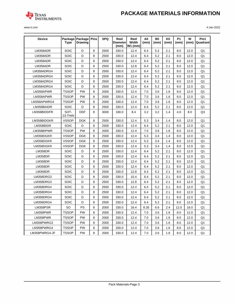
Device PackageType
PackageDrawing
Pins SPQ ReelDiameter
(mm)
ReelWidth
W1 (mm)
A0(mm)
B0(mm)
K0(mm)
P1(mm)
W(mm)
Pin1Quadrant
LM358ADR SOIC D 8 2500 330.0 12.4 6.4 5.2 2.1 8.0 12.0 Q1
LM358ADR SOIC D 8 2500 330.0 12.4 6.4 5.2 2.1 8.0 12.0 Q1
LM358ADR SOIC D 8 2500 330.0 12.4 6.4 5.2 2.1 8.0 12.0 Q1
LM358ADR SOIC D 8 2500 330.0 12.8 6.4 5.2 2.1 8.0 12.0 Q1
LM358ADRG4 SOIC D 8 2500 330.0 12.4 6.4 5.2 2.1 8.0 12.0 Q1
LM358ADRG4 SOIC D 8 2500 330.0 12.4 6.4 5.2 2.1 8.0 12.0 Q1
LM358ADRG4 SOIC D 8 2500 330.0 12.4 6.4 5.2 2.1 8.0 12.0 Q1
LM358ADRG4 SOIC D 8 2500 330.0 12.4 6.4 5.2 2.1 8.0 12.0 Q1
LM358APWR TSSOP PW 8 2000 330.0 12.4 7.0 3.6 1.6 8.0 12.0 Q1
LM358APWR TSSOP PW 8 2000 330.0 12.4 7.0 3.6 1.6 8.0 12.0 Q1
LM358APWRG4 TSSOP PW 8 2000 330.0 12.4 7.0 3.6 1.6 8.0 12.0 Q1
LM358BAIDR SOIC D 8 2500 330.0 12.4 6.4 5.2 2.1 8.0 12.0 Q1
LM358BIDDFR SOT-23-THIN
DDF 8 3000 180.0 8.4 3.2 3.2 1.4 4.0 8.0 Q3
LM358BIDGKR VSSOP DGK 8 2500 330.0 12.4 5.3 3.4 1.4 8.0 12.0 Q1
LM358BIDR SOIC D 8 2500 330.0 12.4 6.4 5.2 2.1 8.0 12.0 Q1
LM358BIPWR TSSOP PW 8 2000 330.0 12.4 7.0 3.6 1.6 8.0 12.0 Q1
LM358DGKR VSSOP DGK 8 2500 330.0 12.4 5.3 3.4 1.4 8.0 12.0 Q1
LM358DGKR VSSOP DGK 8 2500 330.0 12.4 5.3 3.4 1.4 8.0 12.0 Q1
LM358DGKR VSSOP DGK 8 2500 330.0 12.4 5.3 3.4 1.4 8.0 12.0 Q1
LM358DR SOIC D 8 2500 330.0 12.4 6.4 5.2 2.1 8.0 12.0 Q1
LM358DR SOIC D 8 2500 330.0 12.4 6.4 5.2 2.1 8.0 12.0 Q1
LM358DR SOIC D 8 2500 330.0 12.4 6.4 5.2 2.1 8.0 12.0 Q1
LM358DR SOIC D 8 2500 330.0 12.4 6.4 5.2 2.1 8.0 12.0 Q1
LM358DR SOIC D 8 2500 330.0 12.8 6.4 5.2 2.1 8.0 12.0 Q1
LM358DRG3 SOIC D 8 2500 330.0 15.4 6.4 5.2 2.1 8.0 12.0 Q1
LM358DRG3 SOIC D 8 2500 330.0 12.8 6.4 5.2 2.1 8.0 12.0 Q1
LM358DRG4 SOIC D 8 2500 330.0 12.4 6.4 5.2 2.1 8.0 12.0 Q1
LM358DRG4 SOIC D 8 2500 330.0 12.4 6.4 5.2 2.1 8.0 12.0 Q1
LM358DRG4 SOIC D 8 2500 330.0 12.4 6.4 5.2 2.1 8.0 12.0 Q1
LM358DRG4 SOIC D 8 2500 330.0 12.4 6.4 5.2 2.1 8.0 12.0 Q1
LM358PSR SO PS 8 2000 330.0 16.4 8.35 6.6 2.4 12.0 16.0 Q1
LM358PWR TSSOP PW 8 2000 330.0 12.4 7.0 3.6 1.6 8.0 12.0 Q1
LM358PWR TSSOP PW 8 2000 330.0 12.4 7.0 3.6 1.6 8.0 12.0 Q1
LM358PWRG3 TSSOP PW 8 2000 330.0 12.4 7.0 3.6 1.6 8.0 12.0 Q1
LM358PWRG4 TSSOP PW 8 2000 330.0 12.4 7.0 3.6 1.6 8.0 12.0 Q1
LM358PWRG4-JF TSSOP PW 8 2000 330.0 12.4 7.0 3.6 1.6 8.0 12.0 Q1
PACKAGE MATERIALS INFORMATION
www.ti.com 4-Jan-2022
Pack Materials-Page 3

*All dimensions are nominal
Device Package Type Package Drawing Pins SPQ Length (mm) Width (mm) Height (mm)
LM258ADGKR VSSOP DGK 8 2500 366.0 364.0 50.0
LM258ADGKR VSSOP DGK 8 2500 364.0 364.0 27.0
LM258ADR SOIC D 8 2500 853.0 449.0 35.0
LM258ADR SOIC D 8 2500 364.0 364.0 27.0
LM258ADR SOIC D 8 2500 340.5 336.1 25.0
LM258ADR SOIC D 8 2500 853.0 449.0 35.0
LM258ADR SOIC D 8 2500 340.5 336.1 25.0
LM258ADRG4 SOIC D 8 2500 340.5 336.1 25.0
LM258ADRG4 SOIC D 8 2500 853.0 449.0 35.0
LM258ADRG4 SOIC D 8 2500 853.0 449.0 35.0
LM258ADRG4 SOIC D 8 2500 340.5 336.1 25.0
LM258DGKR VSSOP DGK 8 2500 366.0 364.0 50.0
LM258DGKR VSSOP DGK 8 2500 364.0 364.0 27.0
LM258DR SOIC D 8 2500 340.5 336.1 25.0
LM258DR SOIC D 8 2500 340.5 336.1 25.0
LM258DR SOIC D 8 2500 853.0 449.0 35.0
LM258DR SOIC D 8 2500 853.0 449.0 35.0
LM258DR SOIC D 8 2500 364.0 364.0 27.0
LM258DRG3 SOIC D 8 2500 364.0 364.0 27.0
LM258DRG3 SOIC D 8 2500 333.2 345.9 28.6
PACKAGE MATERIALS INFORMATION
www.ti.com 4-Jan-2022
Pack Materials-Page 4

Device Package Type Package Drawing Pins SPQ Length (mm) Width (mm) Height (mm)
LM258DRG4 SOIC D 8 2500 853.0 449.0 35.0
LM258DRG4 SOIC D 8 2500 853.0 449.0 35.0
LM258DRG4 SOIC D 8 2500 340.5 336.1 25.0
LM258DRG4 SOIC D 8 2500 340.5 336.1 25.0
LM2904AVQDR SOIC D 8 2500 340.5 336.1 25.0
LM2904AVQDRG4 SOIC D 8 2500 340.5 336.1 25.0
LM2904AVQPWR TSSOP PW 8 2000 853.0 449.0 35.0
LM2904AVQPWRG4 TSSOP PW 8 2000 853.0 449.0 35.0
LM2904BAIDR SOIC D 8 2500 340.5 336.1 25.0
LM2904BIDDFR SOT-23-THIN DDF 8 3000 210.0 185.0 35.0
LM2904BIDGKR VSSOP DGK 8 2500 366.0 364.0 50.0
LM2904BIDR SOIC D 8 2500 340.5 336.1 25.0
LM2904BIPWR TSSOP PW 8 2000 853.0 449.0 35.0
LM2904DGKR VSSOP DGK 8 2500 358.0 335.0 35.0
LM2904DGKR VSSOP DGK 8 2500 366.0 364.0 50.0
LM2904DGKR VSSOP DGK 8 2500 364.0 364.0 27.0
LM2904DR SOIC D 8 2500 340.5 336.1 25.0
LM2904DR SOIC D 8 2500 853.0 449.0 35.0
LM2904DR SOIC D 8 2500 340.5 336.1 25.0
LM2904DR SOIC D 8 2500 364.0 364.0 27.0
LM2904DR SOIC D 8 2500 853.0 449.0 35.0
LM2904DRG3 SOIC D 8 2500 333.2 345.9 28.6
LM2904DRG3 SOIC D 8 2500 364.0 364.0 27.0
LM2904DRG4 SOIC D 8 2500 853.0 449.0 35.0
LM2904DRG4 SOIC D 8 2500 853.0 449.0 35.0
LM2904DRG4 SOIC D 8 2500 340.5 336.1 25.0
LM2904DRG4 SOIC D 8 2500 340.5 336.1 25.0
LM2904PSR SO PS 8 2000 853.0 449.0 35.0
LM2904PWR TSSOP PW 8 2000 853.0 449.0 35.0
LM2904PWR TSSOP PW 8 2000 364.0 364.0 27.0
LM2904PWRG3 TSSOP PW 8 2000 364.0 364.0 27.0
LM2904PWRG4 TSSOP PW 8 2000 853.0 449.0 35.0
LM2904PWRG4-JF TSSOP PW 8 2000 853.0 449.0 35.0
LM2904QDR SOIC D 8 2500 350.0 350.0 43.0
LM2904VQDR SOIC D 8 2500 340.5 336.1 25.0
LM2904VQPWR TSSOP PW 8 2000 853.0 449.0 35.0
LM2904VQPWRG4 TSSOP PW 8 2000 853.0 449.0 35.0
LM358ADGKR VSSOP DGK 8 2500 364.0 364.0 27.0
LM358ADGKR VSSOP DGK 8 2500 366.0 364.0 50.0
LM358ADR SOIC D 8 2500 853.0 449.0 35.0
LM358ADR SOIC D 8 2500 340.5 336.1 25.0
LM358ADR SOIC D 8 2500 853.0 449.0 35.0
LM358ADR SOIC D 8 2500 340.5 336.1 25.0
LM358ADR SOIC D 8 2500 364.0 364.0 27.0
PACKAGE MATERIALS INFORMATION
www.ti.com 4-Jan-2022
Pack Materials-Page 5
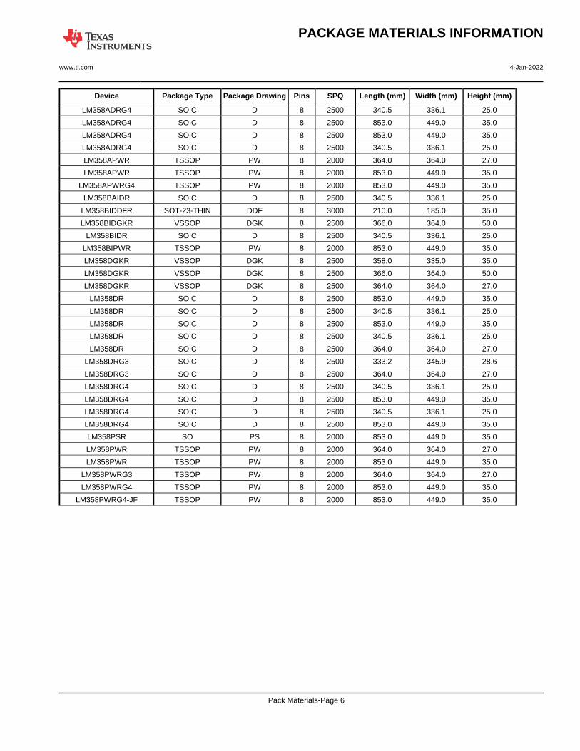
Device Package Type Package Drawing Pins SPQ Length (mm) Width (mm) Height (mm)
LM358ADRG4 SOIC D 8 2500 340.5 336.1 25.0
LM358ADRG4 SOIC D 8 2500 853.0 449.0 35.0
LM358ADRG4 SOIC D 8 2500 853.0 449.0 35.0
LM358ADRG4 SOIC D 8 2500 340.5 336.1 25.0
LM358APWR TSSOP PW 8 2000 364.0 364.0 27.0
LM358APWR TSSOP PW 8 2000 853.0 449.0 35.0
LM358APWRG4 TSSOP PW 8 2000 853.0 449.0 35.0
LM358BAIDR SOIC D 8 2500 340.5 336.1 25.0
LM358BIDDFR SOT-23-THIN DDF 8 3000 210.0 185.0 35.0
LM358BIDGKR VSSOP DGK 8 2500 366.0 364.0 50.0
LM358BIDR SOIC D 8 2500 340.5 336.1 25.0
LM358BIPWR TSSOP PW 8 2000 853.0 449.0 35.0
LM358DGKR VSSOP DGK 8 2500 358.0 335.0 35.0
LM358DGKR VSSOP DGK 8 2500 366.0 364.0 50.0
LM358DGKR VSSOP DGK 8 2500 364.0 364.0 27.0
LM358DR SOIC D 8 2500 853.0 449.0 35.0
LM358DR SOIC D 8 2500 340.5 336.1 25.0
LM358DR SOIC D 8 2500 853.0 449.0 35.0
LM358DR SOIC D 8 2500 340.5 336.1 25.0
LM358DR SOIC D 8 2500 364.0 364.0 27.0
LM358DRG3 SOIC D 8 2500 333.2 345.9 28.6
LM358DRG3 SOIC D 8 2500 364.0 364.0 27.0
LM358DRG4 SOIC D 8 2500 340.5 336.1 25.0
LM358DRG4 SOIC D 8 2500 853.0 449.0 35.0
LM358DRG4 SOIC D 8 2500 340.5 336.1 25.0
LM358DRG4 SOIC D 8 2500 853.0 449.0 35.0
LM358PSR SO PS 8 2000 853.0 449.0 35.0
LM358PWR TSSOP PW 8 2000 364.0 364.0 27.0
LM358PWR TSSOP PW 8 2000 853.0 449.0 35.0
LM358PWRG3 TSSOP PW 8 2000 364.0 364.0 27.0
LM358PWRG4 TSSOP PW 8 2000 853.0 449.0 35.0
LM358PWRG4-JF TSSOP PW 8 2000 853.0 449.0 35.0
PACKAGE MATERIALS INFORMATION
www.ti.com 4-Jan-2022
Pack Materials-Page 6

TUBE
*All dimensions are nominal
Device Package Name Package Type Pins SPQ L (mm) W (mm) T (µm) B (mm)
5962-87710012A FK LCCC 20 1 506.98 12.06 2030 NA
5962-87710022A FK LCCC 20 1 506.98 12.06 2030 NA
LM158AFKB FK LCCC 20 1 506.98 12.06 2030 NA
LM158FKB FK LCCC 20 1 506.98 12.06 2030 NA
LM258AD D SOIC 8 75 506.6 8 3940 4.32
LM258AD D SOIC 8 75 507 8 3940 4.32
LM258AP P PDIP 8 50 506.1 9 600 5.4
LM258AP P PDIP 8 50 506 13.97 11230 4.32
LM258APE4 P PDIP 8 50 506 13.97 11230 4.32
LM258D D SOIC 8 75 506.6 8 3940 4.32
LM258D D SOIC 8 75 507 8 3940 4.32
LM258DG4 D SOIC 8 75 507 8 3940 4.32
LM258DG4 D SOIC 8 75 506.6 8 3940 4.32
LM258P P PDIP 8 50 506 13.97 11230 4.32
LM258P P PDIP 8 50 506.1 9 600 5.4
LM258PE4 P PDIP 8 50 506 13.97 11230 4.32
LM2904D D SOIC 8 75 507 8 3940 4.32
LM2904D D SOIC 8 75 506.6 8 3940 4.32
LM2904DE4 D SOIC 8 75 506.6 8 3940 4.32
LM2904DE4 D SOIC 8 75 507 8 3940 4.32
LM2904DG4 D SOIC 8 75 507 8 3940 4.32
LM2904DG4 D SOIC 8 75 506.6 8 3940 4.32
LM2904P P PDIP 8 50 506.1 9 600 5.4
LM2904P P PDIP 8 50 506 13.97 11230 4.32
LM2904PE4 P PDIP 8 50 506 13.97 11230 4.32
LM2904PW PW TSSOP 8 150 530 10.2 3600 3.5
LM358AD D SOIC 8 75 507 8 3940 4.32
LM358AD D SOIC 8 75 506.6 8 3940 4.32
PACKAGE MATERIALS INFORMATION
www.ti.com 4-Jan-2022
Pack Materials-Page 7
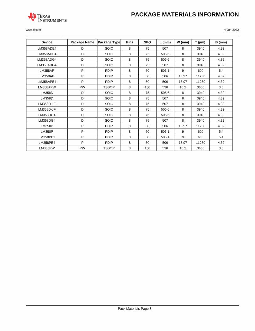
Device Package Name Package Type Pins SPQ L (mm) W (mm) T (µm) B (mm)
LM358ADE4 D SOIC 8 75 507 8 3940 4.32
LM358ADE4 D SOIC 8 75 506.6 8 3940 4.32
LM358ADG4 D SOIC 8 75 506.6 8 3940 4.32
LM358ADG4 D SOIC 8 75 507 8 3940 4.32
LM358AP P PDIP 8 50 506.1 9 600 5.4
LM358AP P PDIP 8 50 506 13.97 11230 4.32
LM358APE4 P PDIP 8 50 506 13.97 11230 4.32
LM358APW PW TSSOP 8 150 530 10.2 3600 3.5
LM358D D SOIC 8 75 506.6 8 3940 4.32
LM358D D SOIC 8 75 507 8 3940 4.32
LM358D-JF D SOIC 8 75 507 8 3940 4.32
LM358D-JF D SOIC 8 75 506.6 8 3940 4.32
LM358DG4 D SOIC 8 75 506.6 8 3940 4.32
LM358DG4 D SOIC 8 75 507 8 3940 4.32
LM358P P PDIP 8 50 506 13.97 11230 4.32
LM358P P PDIP 8 50 506.1 9 600 5.4
LM358PE3 P PDIP 8 50 506.1 9 600 5.4
LM358PE4 P PDIP 8 50 506 13.97 11230 4.32
LM358PW PW TSSOP 8 150 530 10.2 3600 3.5
PACKAGE MATERIALS INFORMATION
www.ti.com 4-Jan-2022
Pack Materials-Page 8


www.ti.com
PACKAGE OUTLINE
C
.228-.244 TYP[5.80-6.19]
.069 MAX[1.75]
6X .050[1.27]
8X .012-.020 [0.31-0.51]
2X.150[3.81]
.005-.010 TYP[0.13-0.25]
0 - 8 .004-.010[0.11-0.25]
.010[0.25]
.016-.050[0.41-1.27]
4X (0 -15 )
A
.189-.197[4.81-5.00]
NOTE 3
B .150-.157[3.81-3.98]
NOTE 4
4X (0 -15 )
(.041)[1.04]
SOIC - 1.75 mm max heightD0008ASMALL OUTLINE INTEGRATED CIRCUIT
4214825/C 02/2019
NOTES: 1. Linear dimensions are in inches [millimeters]. Dimensions in parenthesis are for reference only. Controlling dimensions are in inches. Dimensioning and tolerancing per ASME Y14.5M. 2. This drawing is subject to change without notice. 3. This dimension does not include mold flash, protrusions, or gate burrs. Mold flash, protrusions, or gate burrs shall not exceed .006 [0.15] per side. 4. This dimension does not include interlead flash.5. Reference JEDEC registration MS-012, variation AA.
18
.010 [0.25] C A B
54
PIN 1 ID AREA
SEATING PLANE
.004 [0.1] C
SEE DETAIL A
DETAIL ATYPICAL
SCALE 2.800

www.ti.com
EXAMPLE BOARD LAYOUT
.0028 MAX[0.07]ALL AROUND
.0028 MIN[0.07]ALL AROUND
(.213)[5.4]
6X (.050 )[1.27]
8X (.061 )[1.55]
8X (.024)[0.6]
(R.002 ) TYP[0.05]
SOIC - 1.75 mm max heightD0008ASMALL OUTLINE INTEGRATED CIRCUIT
4214825/C 02/2019
NOTES: (continued) 6. Publication IPC-7351 may have alternate designs. 7. Solder mask tolerances between and around signal pads can vary based on board fabrication site.
METALSOLDER MASKOPENING
NON SOLDER MASKDEFINED
SOLDER MASK DETAILS
EXPOSEDMETAL
OPENINGSOLDER MASK METAL UNDER
SOLDER MASK
SOLDER MASKDEFINED
EXPOSEDMETAL
LAND PATTERN EXAMPLEEXPOSED METAL SHOWN
SCALE:8X
SYMM
1
45
8
SEEDETAILS
SYMM

www.ti.com
EXAMPLE STENCIL DESIGN
8X (.061 )[1.55]
8X (.024)[0.6]
6X (.050 )[1.27]
(.213)[5.4]
(R.002 ) TYP[0.05]
SOIC - 1.75 mm max heightD0008ASMALL OUTLINE INTEGRATED CIRCUIT
4214825/C 02/2019
NOTES: (continued) 8. Laser cutting apertures with trapezoidal walls and rounded corners may offer better paste release. IPC-7525 may have alternate design recommendations. 9. Board assembly site may have different recommendations for stencil design.
SOLDER PASTE EXAMPLEBASED ON .005 INCH [0.125 MM] THICK STENCIL
SCALE:8X
SYMM
SYMM
1
45
8


MECHANICAL DATA
MCER001A – JANUARY 1995 – REVISED JANUARY 1997
POST OFFICE BOX 655303 • DALLAS, TEXAS 75265
JG (R-GDIP-T8) CERAMIC DUAL-IN-LINE
0.310 (7,87)0.290 (7,37)
0.014 (0,36)0.008 (0,20)
Seating Plane
4040107/C 08/96
5
40.065 (1,65)0.045 (1,14)
8
1
0.020 (0,51) MIN
0.400 (10,16)0.355 (9,00)
0.015 (0,38)0.023 (0,58)
0.063 (1,60)0.015 (0,38)
0.200 (5,08) MAX
0.130 (3,30) MIN
0.245 (6,22)0.280 (7,11)
0.100 (2,54)
0°–15°
NOTES: A. All linear dimensions are in inches (millimeters).B. This drawing is subject to change without notice.C. This package can be hermetically sealed with a ceramic lid using glass frit.D. Index point is provided on cap for terminal identification.E. Falls within MIL STD 1835 GDIP1-T8


www.ti.com
PACKAGE OUTLINE
C
TYP6.66.2
1.2 MAX
6X 0.65
8X 0.300.19
2X1.95
0.150.05
(0.15) TYP
0 - 8
0.25GAGE PLANE
0.750.50
A
NOTE 3
3.12.9
BNOTE 4
4.54.3
4221848/A 02/2015
TSSOP - 1.2 mm max heightPW0008ASMALL OUTLINE PACKAGE
NOTES: 1. All linear dimensions are in millimeters. Any dimensions in parenthesis are for reference only. Dimensioning and tolerancing per ASME Y14.5M. 2. This drawing is subject to change without notice. 3. This dimension does not include mold flash, protrusions, or gate burrs. Mold flash, protrusions, or gate burrs shall not exceed 0.15 mm per side. 4. This dimension does not include interlead flash. Interlead flash shall not exceed 0.25 mm per side.5. Reference JEDEC registration MO-153, variation AA.
18
0.1 C A B
54
PIN 1 IDAREA
SEATING PLANE
0.1 C
SEE DETAIL A
DETAIL ATYPICAL
SCALE 2.800

www.ti.com
EXAMPLE BOARD LAYOUT
(5.8)
0.05 MAXALL AROUND
0.05 MINALL AROUND
8X (1.5)8X (0.45)
6X (0.65)
(R )TYP
0.05
4221848/A 02/2015
TSSOP - 1.2 mm max heightPW0008ASMALL OUTLINE PACKAGE
SYMM
SYMM
LAND PATTERN EXAMPLESCALE:10X
1
45
8
NOTES: (continued) 6. Publication IPC-7351 may have alternate designs. 7. Solder mask tolerances between and around signal pads can vary based on board fabrication site.
METALSOLDER MASKOPENING
NON SOLDER MASKDEFINED
SOLDER MASK DETAILSNOT TO SCALE
SOLDER MASKOPENING
METAL UNDERSOLDER MASK
SOLDER MASKDEFINED
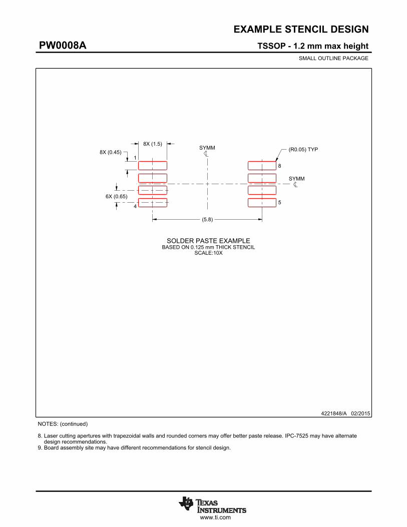
www.ti.com
EXAMPLE STENCIL DESIGN
(5.8)
6X (0.65)
8X (0.45)8X (1.5)
(R ) TYP0.05
4221848/A 02/2015
TSSOP - 1.2 mm max heightPW0008ASMALL OUTLINE PACKAGE
NOTES: (continued) 8. Laser cutting apertures with trapezoidal walls and rounded corners may offer better paste release. IPC-7525 may have alternate design recommendations. 9. Board assembly site may have different recommendations for stencil design.
SYMM
SYMM
1
45
8
SOLDER PASTE EXAMPLEBASED ON 0.125 mm THICK STENCIL
SCALE:10X

www.ti.com
PACKAGE OUTLINE
C
TYP2.952.65
1.1 MAX
6X 0.65
8X 0.40.2
2X1.95
TYP0.200.08
0 - 80.10.0
0.25GAGE PLANE
0.60.3
A
NOTE 3
2.952.85
B 1.651.55
4222047/B 11/2015
SOT-23 - 1.1 mm max heightDDF0008APLASTIC SMALL OUTLINE
NOTES: 1. All linear dimensions are in millimeters. Any dimensions in parenthesis are for reference only. Dimensioning and tolerancing per ASME Y14.5M. 2. This drawing is subject to change without notice. 3. This dimension does not include mold flash, protrusions, or gate burrs. Mold flash, protrusions, or gate burrs shall not exceed 0.15 mm per side.
18
0.1 C A B
5
4
PIN 1 IDAREA
SEATING PLANE
0.1 C
SEE DETAIL A
DETAIL ATYPICAL
SCALE 4.000

www.ti.com
EXAMPLE BOARD LAYOUT
(2.6)
8X (1.05)
8X (0.45)
6X (0.65)
(R )TYP
0.05
4222047/B 11/2015
SOT-23 - 1.1 mm max heightDDF0008APLASTIC SMALL OUTLINE
SYMM
SYMM
LAND PATTERN EXAMPLESCALE:15X
1
45
8
NOTES: (continued) 4. Publication IPC-7351 may have alternate designs. 5. Solder mask tolerances between and around signal pads can vary based on board fabrication site.
METALSOLDER MASKOPENING
NON SOLDER MASKDEFINED
SOLDER MASK DETAILS
SOLDER MASKOPENING
METAL UNDERSOLDER MASK
SOLDER MASKDEFINED

www.ti.com
EXAMPLE STENCIL DESIGN
(2.6)
6X (0.65)
8X (0.45)
8X (1.05)(R ) TYP0.05
4222047/B 11/2015
SOT-23 - 1.1 mm max heightDDF0008APLASTIC SMALL OUTLINE
NOTES: (continued) 6. Laser cutting apertures with trapezoidal walls and rounded corners may offer better paste release. IPC-7525 may have alternate design recommendations. 7. Board assembly site may have different recommendations for stencil design.
SYMM
SYMM
1
4 5
8
SOLDER PASTE EXAMPLEBASED ON 0.125 mm THICK STENCIL
SCALE:15X

IMPORTANT NOTICE AND DISCLAIMERTI PROVIDES TECHNICAL AND RELIABILITY DATA (INCLUDING DATA SHEETS), DESIGN RESOURCES (INCLUDING REFERENCE DESIGNS), APPLICATION OR OTHER DESIGN ADVICE, WEB TOOLS, SAFETY INFORMATION, AND OTHER RESOURCES “AS IS” AND WITH ALL FAULTS, AND DISCLAIMS ALL WARRANTIES, EXPRESS AND IMPLIED, INCLUDING WITHOUT LIMITATION ANY IMPLIED WARRANTIES OF MERCHANTABILITY, FITNESS FOR A PARTICULAR PURPOSE OR NON-INFRINGEMENT OF THIRD PARTY INTELLECTUAL PROPERTY RIGHTS.These resources are intended for skilled developers designing with TI products. You are solely responsible for (1) selecting the appropriate TI products for your application, (2) designing, validating and testing your application, and (3) ensuring your application meets applicable standards, and any other safety, security, regulatory or other requirements.These resources are subject to change without notice. TI grants you permission to use these resources only for development of an application that uses the TI products described in the resource. Other reproduction and display of these resources is prohibited. No license is granted to any other TI intellectual property right or to any third party intellectual property right. TI disclaims responsibility for, and you will fully indemnify TI and its representatives against, any claims, damages, costs, losses, and liabilities arising out of your use of these resources.TI’s products are provided subject to TI’s Terms of Sale or other applicable terms available either on ti.com or provided in conjunction with such TI products. TI’s provision of these resources does not expand or otherwise alter TI’s applicable warranties or warranty disclaimers for TI products.TI objects to and rejects any additional or different terms you may have proposed. IMPORTANT NOTICE
Mailing Address: Texas Instruments, Post Office Box 655303, Dallas, Texas 75265Copyright © 2022, Texas Instruments Incorporated