infineon c167cr user's manual - keil
TRANSCRIPT

N e v e r s t o p t h i n k i n g .
Microcontrol lers
User ’s Manual , V 3.1, Mar . 2000
C167CR Derivat ives16-Bi t S ingle-Chip Microcontro l ler

Edition 2000-03
Published by Infineon Technologies AG,St.-Martin-Strasse 53,D-81541 München, Germany
© Infineon Technologies AG 2000.All Rights Reserved.
Attention please!
The information herein is given to describe certain components and shall not be considered as warranted characteristics.Terms of delivery and rights to technical change reserved.We hereby disclaim any and all warranties, including but not limited to warranties of non-infringement, regarding circuits, descriptions and charts stated herein.Infineon Technologies is an approved CECC manufacturer.
Information
For further information on technology, delivery terms and conditions and prices please contact your nearest Infineon Technologies Office in Germany or our Infineon Technologies Representatives worldwide (see address list).
Warnings
Due to technical requirements components may contain dangerous substances. For information on the types in question please contact your nearest Infineon Technologies Office.Infineon Technologies Components may only be used in life-support devices or systems with the express written approval of Infineon Technologies, if a failure of such components can reasonably be expected to cause the failure of that life-support device or system, or to affect the safety or effectiveness of that device or system. Life support devices or systems are intended to be implanted in the human body, or to support and/or maintain and sustain and/or protect human life. If they fail, it is reasonable to assume that the health of the user or other persons may be endangered.

Microcontrol lers
User ’s Manual , V 3.1, Mar . 2000
N e v e r s t o p t h i n k i n g .
C167CR Der ivat ives16-Bit S ingle-Chip Microcontro l ler
Controller Area Network (CAN): License of Robert Bosch GmbH
C167CR Revision History: V 3.1, 2000-03
Previous Version: Version 3.0, 2000-02 (intermediate version)Version 2.1, 1999-03Version 2.0, 03.96Version 1.0, 08.94Preliminary User’s Manual Revision 1.0, 07.92
Page Subjects (major changes since last revision)
all Converted to new company layout
all Figures have been redrawn (compared to V3.0)
1-1 List of derivatives reworked
2-2, 4-1 Figure corrected
6-1 RTC hints removed
9-29 … 34 Description of bus arbitration improved
9-35 … 37 Description of XBUS interface improved
10-6, 10-27 Timer frequency tables improved
10-16 Figure 10-11 corrected (compared to V3.0)
10-30 Description of T5M corrected (compared to V3.0)
10-33 Figure 10-21 corrected (compared to V3.0)
11-12 … 14 Baudrate tables improved
12-5 Description of transmission timing improved
12-13 Baudrate tables improved
13-5 Time range table improved
13-6 Reset indication table improved
14-7 Baudrate table added
15-3 Port connection table corrected
15-7 Input frequency table improved
17-3 Bitfield ADSTC added
18-33 Separate section for Busoff Recovery Sequence
19-5 … 8 Status after reset regrouped
19-9 … 19 Description of initialization routine improved
19-13 … 20 Better structure for section “Startup Configuration”
We Listen to Your CommentsAny information within this document that you feel is wrong, unclear or missing at all?Your feedback will help us to continuously improve the quality of this document.Please send your proposal (including a reference to this document) to:[email protected]

C167CRDerivatives
Table of Contents Page
1 Introduction . . . . . . . . . . . . . . . . . . . . . . . . . . . . . . . . . . . . . . . . . . . . . . 1-11.1 The Members of the 16-bit Microcontroller Family . . . . . . . . . . . . . . . . . 1-21.2 Summary of Basic Features . . . . . . . . . . . . . . . . . . . . . . . . . . . . . . . . . . 1-41.3 Abbreviations . . . . . . . . . . . . . . . . . . . . . . . . . . . . . . . . . . . . . . . . . . . . . . 1-7
2 Architectural Overview . . . . . . . . . . . . . . . . . . . . . . . . . . . . . . . . . . . . . 2-12.1 Basic CPU Concepts and Optimizations . . . . . . . . . . . . . . . . . . . . . . . . . 2-22.1.1 High Instruction Bandwidth/Fast Execution . . . . . . . . . . . . . . . . . . . . . 2-32.1.2 Programmable Multiple Priority Interrupt System . . . . . . . . . . . . . . . . 2-72.2 The On-chip System Resources . . . . . . . . . . . . . . . . . . . . . . . . . . . . . . . 2-82.3 The On-chip Peripheral Blocks . . . . . . . . . . . . . . . . . . . . . . . . . . . . . . . 2-112.4 Protected Bits . . . . . . . . . . . . . . . . . . . . . . . . . . . . . . . . . . . . . . . . . . . . 2-18
3 Memory Organization . . . . . . . . . . . . . . . . . . . . . . . . . . . . . . . . . . . . . . 3-13.1 Internal ROM Area . . . . . . . . . . . . . . . . . . . . . . . . . . . . . . . . . . . . . . . . . . 3-33.2 Internal RAM and SFR Area . . . . . . . . . . . . . . . . . . . . . . . . . . . . . . . . . . 3-43.3 The On-Chip XRAM . . . . . . . . . . . . . . . . . . . . . . . . . . . . . . . . . . . . . . . . . 3-93.4 External Memory Space . . . . . . . . . . . . . . . . . . . . . . . . . . . . . . . . . . . . 3-113.5 Crossing Memory Boundaries . . . . . . . . . . . . . . . . . . . . . . . . . . . . . . . . 3-123.6 Protection of the On-chip Mask ROM . . . . . . . . . . . . . . . . . . . . . . . . . . 3-13
4 The Central Processing Unit (CPU) . . . . . . . . . . . . . . . . . . . . . . . . . . . 4-14.1 Instruction Pipelining . . . . . . . . . . . . . . . . . . . . . . . . . . . . . . . . . . . . . . . . 4-34.2 Particular Pipeline Effects . . . . . . . . . . . . . . . . . . . . . . . . . . . . . . . . . . . . 4-64.3 Bit-Handling and Bit-Protection . . . . . . . . . . . . . . . . . . . . . . . . . . . . . . . 4-104.4 Instruction State Times . . . . . . . . . . . . . . . . . . . . . . . . . . . . . . . . . . . . . 4-114.5 CPU Special Function Registers . . . . . . . . . . . . . . . . . . . . . . . . . . . . . . 4-12
5 Interrupt and Trap Functions . . . . . . . . . . . . . . . . . . . . . . . . . . . . . . . . 5-15.1 Interrupt System Structure . . . . . . . . . . . . . . . . . . . . . . . . . . . . . . . . . . . . 5-25.1.1 Interrupt Control Registers . . . . . . . . . . . . . . . . . . . . . . . . . . . . . . . . . . 5-65.2 Operation of the PEC Channels . . . . . . . . . . . . . . . . . . . . . . . . . . . . . . 5-125.3 Prioritization of Interrupt and PEC Service Requests . . . . . . . . . . . . . . 5-165.4 Saving the Status During Interrupt Service . . . . . . . . . . . . . . . . . . . . . . 5-185.5 Interrupt Response Times . . . . . . . . . . . . . . . . . . . . . . . . . . . . . . . . . . . 5-205.6 PEC Response Times . . . . . . . . . . . . . . . . . . . . . . . . . . . . . . . . . . . . . . 5-235.7 External Interrupts . . . . . . . . . . . . . . . . . . . . . . . . . . . . . . . . . . . . . . . . . 5-255.8 Trap Functions . . . . . . . . . . . . . . . . . . . . . . . . . . . . . . . . . . . . . . . . . . . . 5-28
6 Clock Generation . . . . . . . . . . . . . . . . . . . . . . . . . . . . . . . . . . . . . . . . . . 6-16.1 Oscillator . . . . . . . . . . . . . . . . . . . . . . . . . . . . . . . . . . . . . . . . . . . . . . . . . 6-26.2 Frequency Control . . . . . . . . . . . . . . . . . . . . . . . . . . . . . . . . . . . . . . . . . . 6-46.3 Oscillator Watchdog . . . . . . . . . . . . . . . . . . . . . . . . . . . . . . . . . . . . . . . . . 6-86.4 Clock Drivers . . . . . . . . . . . . . . . . . . . . . . . . . . . . . . . . . . . . . . . . . . . . . . 6-9
User’s Manual I-1 V3.1, 2000-03
C167CRDerivatives
Table of Contents Page
7 Parallel Ports . . . . . . . . . . . . . . . . . . . . . . . . . . . . . . . . . . . . . . . . . . . . . 7-17.1 Input Threshold Control . . . . . . . . . . . . . . . . . . . . . . . . . . . . . . . . . . . . . . 7-27.2 Output Driver Control . . . . . . . . . . . . . . . . . . . . . . . . . . . . . . . . . . . . . . . . 7-47.3 Alternate Port Functions . . . . . . . . . . . . . . . . . . . . . . . . . . . . . . . . . . . . . 7-77.4 PORT0 . . . . . . . . . . . . . . . . . . . . . . . . . . . . . . . . . . . . . . . . . . . . . . . . . . . 7-97.5 PORT1 . . . . . . . . . . . . . . . . . . . . . . . . . . . . . . . . . . . . . . . . . . . . . . . . . . 7-137.6 Port 2 . . . . . . . . . . . . . . . . . . . . . . . . . . . . . . . . . . . . . . . . . . . . . . . . . . . 7-187.7 Port 3 . . . . . . . . . . . . . . . . . . . . . . . . . . . . . . . . . . . . . . . . . . . . . . . . . . . 7-237.8 Port 4 . . . . . . . . . . . . . . . . . . . . . . . . . . . . . . . . . . . . . . . . . . . . . . . . . . . 7-287.9 Port 5 . . . . . . . . . . . . . . . . . . . . . . . . . . . . . . . . . . . . . . . . . . . . . . . . . . . 7-327.10 Port 6 . . . . . . . . . . . . . . . . . . . . . . . . . . . . . . . . . . . . . . . . . . . . . . . . . . . 7-367.11 Port 7 . . . . . . . . . . . . . . . . . . . . . . . . . . . . . . . . . . . . . . . . . . . . . . . . . . . 7-427.12 Port 8 . . . . . . . . . . . . . . . . . . . . . . . . . . . . . . . . . . . . . . . . . . . . . . . . . . . 7-47
8 Dedicated Pins . . . . . . . . . . . . . . . . . . . . . . . . . . . . . . . . . . . . . . . . . . . . 8-1
9 The External Bus Interface . . . . . . . . . . . . . . . . . . . . . . . . . . . . . . . . . . 9-19.1 Single Chip Mode . . . . . . . . . . . . . . . . . . . . . . . . . . . . . . . . . . . . . . . . . . 9-29.2 External Bus Modes . . . . . . . . . . . . . . . . . . . . . . . . . . . . . . . . . . . . . . . . . 9-39.3 Programmable Bus Characteristics . . . . . . . . . . . . . . . . . . . . . . . . . . . . 9-129.4 READY Controlled Bus Cycles . . . . . . . . . . . . . . . . . . . . . . . . . . . . . . . 9-179.5 Controlling the External Bus Controller . . . . . . . . . . . . . . . . . . . . . . . . . 9-199.6 EBC Idle State . . . . . . . . . . . . . . . . . . . . . . . . . . . . . . . . . . . . . . . . . . . . 9-289.7 External Bus Arbitration . . . . . . . . . . . . . . . . . . . . . . . . . . . . . . . . . . . . . 9-299.8 The XBUS Interface . . . . . . . . . . . . . . . . . . . . . . . . . . . . . . . . . . . . . . . . 9-359.8.1 Accessing the On-chip XBUS Peripherals . . . . . . . . . . . . . . . . . . . . . 9-369.8.2 External Accesses to XBUS Peripherals . . . . . . . . . . . . . . . . . . . . . . 9-37
10 The General Purpose Timer Units . . . . . . . . . . . . . . . . . . . . . . . . . . . 10-110.1 Timer Block GPT1 . . . . . . . . . . . . . . . . . . . . . . . . . . . . . . . . . . . . . . . . . 10-110.1.1 GPT1 Core Timer T3 . . . . . . . . . . . . . . . . . . . . . . . . . . . . . . . . . . . . . 10-310.1.2 GPT1 Auxiliary Timers T2 and T4 . . . . . . . . . . . . . . . . . . . . . . . . . . 10-1210.1.3 Interrupt Control for GPT1 Timers . . . . . . . . . . . . . . . . . . . . . . . . . . 10-2110.2 Timer Block GPT2 . . . . . . . . . . . . . . . . . . . . . . . . . . . . . . . . . . . . . . . . 10-2210.2.1 GPT2 Core Timer T6 . . . . . . . . . . . . . . . . . . . . . . . . . . . . . . . . . . . . 10-2410.2.2 GPT2 Auxiliary Timer T5 . . . . . . . . . . . . . . . . . . . . . . . . . . . . . . . . . 10-3010.2.3 Interrupt Control for GPT2 Timers and CAPREL . . . . . . . . . . . . . . . 10-38
11 The Asynchronous/Synchronous Serial Interface . . . . . . . . . . . . . . 11-111.1 Asynchronous Operation . . . . . . . . . . . . . . . . . . . . . . . . . . . . . . . . . . . . 11-511.2 Synchronous Operation . . . . . . . . . . . . . . . . . . . . . . . . . . . . . . . . . . . . . 11-811.3 Hardware Error Detection Capabilities . . . . . . . . . . . . . . . . . . . . . . . . 11-1011.4 ASC0 Baud Rate Generation . . . . . . . . . . . . . . . . . . . . . . . . . . . . . . . . 11-1111.5 ASC0 Interrupt Control . . . . . . . . . . . . . . . . . . . . . . . . . . . . . . . . . . . . 11-15
User’s Manual I-2 V3.1, 2000-03

C167CRDerivatives
Table of Contents Page
12 The High-speed Synchronous Serial Interface . . . . . . . . . . . . . . . . . 12-112.1 Full-duplex Operation . . . . . . . . . . . . . . . . . . . . . . . . . . . . . . . . . . . . . . 12-712.2 Half-duplex Operation . . . . . . . . . . . . . . . . . . . . . . . . . . . . . . . . . . . . . 12-1012.3 Continuous Transfers . . . . . . . . . . . . . . . . . . . . . . . . . . . . . . . . . . . . . 12-1112.4 Port Control . . . . . . . . . . . . . . . . . . . . . . . . . . . . . . . . . . . . . . . . . . . . . 12-1212.5 Baud Rate Generation . . . . . . . . . . . . . . . . . . . . . . . . . . . . . . . . . . . . . 12-1312.6 Error Detection Mechanisms . . . . . . . . . . . . . . . . . . . . . . . . . . . . . . . . 12-1512.7 SSC Interrupt Control . . . . . . . . . . . . . . . . . . . . . . . . . . . . . . . . . . . . . 12-17
13 The Watchdog Timer (WDT) . . . . . . . . . . . . . . . . . . . . . . . . . . . . . . . . 13-113.1 Operation of the Watchdog Timer . . . . . . . . . . . . . . . . . . . . . . . . . . . . . 13-313.2 Reset Source Indication . . . . . . . . . . . . . . . . . . . . . . . . . . . . . . . . . . . . . 13-6
14 The Bootstrap Loader . . . . . . . . . . . . . . . . . . . . . . . . . . . . . . . . . . . . . 14-1
15 The Capture/Compare Units . . . . . . . . . . . . . . . . . . . . . . . . . . . . . . . . 15-115.1 The CAPCOM Timers . . . . . . . . . . . . . . . . . . . . . . . . . . . . . . . . . . . . . . 15-415.2 CAPCOM Unit Timer Interrupts . . . . . . . . . . . . . . . . . . . . . . . . . . . . . . . 15-915.3 Capture/Compare Registers . . . . . . . . . . . . . . . . . . . . . . . . . . . . . . . . 15-1015.4 Capture Mode . . . . . . . . . . . . . . . . . . . . . . . . . . . . . . . . . . . . . . . . . . . 15-1315.5 Compare Modes . . . . . . . . . . . . . . . . . . . . . . . . . . . . . . . . . . . . . . . . . 15-1415.6 Capture/Compare Interrupts . . . . . . . . . . . . . . . . . . . . . . . . . . . . . . . . 15-22
16 The Pulse Width Modulation Module . . . . . . . . . . . . . . . . . . . . . . . . . 16-116.1 Operating Modes . . . . . . . . . . . . . . . . . . . . . . . . . . . . . . . . . . . . . . . . . . 16-216.2 PWM Module Registers . . . . . . . . . . . . . . . . . . . . . . . . . . . . . . . . . . . . 16-1016.3 Interrupt Request Generation . . . . . . . . . . . . . . . . . . . . . . . . . . . . . . . 16-1416.4 PWM Output Signals . . . . . . . . . . . . . . . . . . . . . . . . . . . . . . . . . . . . . . 16-15
17 The Analog/Digital Converter . . . . . . . . . . . . . . . . . . . . . . . . . . . . . . . 17-117.1 Mode Selection and Operation . . . . . . . . . . . . . . . . . . . . . . . . . . . . . . . 17-217.2 Conversion Timing Control . . . . . . . . . . . . . . . . . . . . . . . . . . . . . . . . . 17-1217.3 A/D Converter Interrupt Control . . . . . . . . . . . . . . . . . . . . . . . . . . . . . . 17-14
18 The On-chip CAN Interface . . . . . . . . . . . . . . . . . . . . . . . . . . . . . . . . . 18-118.1 Functional Blocks of the CAN Module . . . . . . . . . . . . . . . . . . . . . . . . . . 18-218.2 General Functional Description . . . . . . . . . . . . . . . . . . . . . . . . . . . . . . . 18-718.3 The Message Object . . . . . . . . . . . . . . . . . . . . . . . . . . . . . . . . . . . . . . 18-1818.4 Controlling the CAN Module . . . . . . . . . . . . . . . . . . . . . . . . . . . . . . . . 18-3018.5 Configuration Examples for Message Objects . . . . . . . . . . . . . . . . . . . 18-3418.6 The CAN Application Interface . . . . . . . . . . . . . . . . . . . . . . . . . . . . . . 18-36
19 System Reset . . . . . . . . . . . . . . . . . . . . . . . . . . . . . . . . . . . . . . . . . . . . 19-119.1 Reset Sources . . . . . . . . . . . . . . . . . . . . . . . . . . . . . . . . . . . . . . . . . . . . 19-219.2 Status After Reset . . . . . . . . . . . . . . . . . . . . . . . . . . . . . . . . . . . . . . . . . 19-5
User’s Manual I-3 V3.1, 2000-03
C167CRDerivatives
Table of Contents Page
19.3 Application-specific Initialization Routine . . . . . . . . . . . . . . . . . . . . . . . . 19-919.4 System Startup Configuration . . . . . . . . . . . . . . . . . . . . . . . . . . . . . . . 19-1219.4.1 System Startup Configuration upon an External Reset . . . . . . . . . . 19-1319.4.2 System Startup Configuration upon a Single-chip Mode Reset . . . . 19-20
20 Power Management . . . . . . . . . . . . . . . . . . . . . . . . . . . . . . . . . . . . . . . 20-120.1 Idle Mode . . . . . . . . . . . . . . . . . . . . . . . . . . . . . . . . . . . . . . . . . . . . . . . . 20-220.2 Power Down Mode . . . . . . . . . . . . . . . . . . . . . . . . . . . . . . . . . . . . . . . . 20-420.2.1 Status of Output Pins During Power Reduction Modes . . . . . . . . . . . 20-5
21 System Programming . . . . . . . . . . . . . . . . . . . . . . . . . . . . . . . . . . . . . 21-121.1 Stack Operations . . . . . . . . . . . . . . . . . . . . . . . . . . . . . . . . . . . . . . . . . . 21-421.2 Register Banking . . . . . . . . . . . . . . . . . . . . . . . . . . . . . . . . . . . . . . . . . . 21-921.3 Procedure Call Entry and Exit . . . . . . . . . . . . . . . . . . . . . . . . . . . . . . . . 21-921.4 Table Searching . . . . . . . . . . . . . . . . . . . . . . . . . . . . . . . . . . . . . . . . . . 21-1221.5 Floating Point Support . . . . . . . . . . . . . . . . . . . . . . . . . . . . . . . . . . . . . 21-1221.6 Peripheral Control and Interface . . . . . . . . . . . . . . . . . . . . . . . . . . . . . 21-1321.7 Trap/Interrupt Entry and Exit . . . . . . . . . . . . . . . . . . . . . . . . . . . . . . . . 21-1321.8 Unseparable Instruction Sequences . . . . . . . . . . . . . . . . . . . . . . . . . . 21-1421.9 Overriding the DPP Addressing Mechanism . . . . . . . . . . . . . . . . . . . . 21-1421.10 Handling the Internal Code Memory . . . . . . . . . . . . . . . . . . . . . . . . . . 21-1621.11 Pits, Traps and Mines . . . . . . . . . . . . . . . . . . . . . . . . . . . . . . . . . . . . . 21-18
22 The Register Set . . . . . . . . . . . . . . . . . . . . . . . . . . . . . . . . . . . . . . . . . 22-122.1 Register Description Format . . . . . . . . . . . . . . . . . . . . . . . . . . . . . . . . . 22-122.2 CPU General Purpose Registers (GPRs) . . . . . . . . . . . . . . . . . . . . . . . 22-222.3 Special Function Registers Ordered by Name . . . . . . . . . . . . . . . . . . . 22-422.4 Special Function Registers Ordered by Address . . . . . . . . . . . . . . . . . 22-1222.5 Special Notes . . . . . . . . . . . . . . . . . . . . . . . . . . . . . . . . . . . . . . . . . . . . 22-20
23 Instruction Set Summary . . . . . . . . . . . . . . . . . . . . . . . . . . . . . . . . . . 23-1
24 Device Specification . . . . . . . . . . . . . . . . . . . . . . . . . . . . . . . . . . . . . . 24-1
25 Keyword Index . . . . . . . . . . . . . . . . . . . . . . . . . . . . . . . . . . . . . . . . . . . 25-1
User’s Manual I-4 V3.1, 2000-03
C167CRDerivatives
Introduction
1 IntroductionThe rapidly growing area of embedded control applications is representing one of themost time-critical operating environments for today’s microcontrollers. Complex controlalgorithms have to be processed based on a large number of digital as well as analoginput signals, and the appropriate output signals must be generated within a definedmaximum response time. Embedded control applications also are often sensitive toboard space, power consumption, and overall system cost.
Embedded control applications therefore require microcontrollers, which:
• offer a high level of system integration• eliminate the need for additional peripheral devices and the associated software overhead• provide system security and fail-safe mechanisms• provide effective means to control (and reduce) the device’s power consumption.
With the increasing complexity of embedded control applications, a significant increasein CPU performance and peripheral functionality over conventional 8-bit controllers isrequired from microcontrollers for high-end embedded control systems. In order toachieve this high performance goal Infineon has decided to develop its family of 16-bitCMOS microcontrollers without the constraints of backward compatibility.
Of course the architecture of the 16-bit microcontroller family pursues successfulhardware and software concepts, which have been established in Infineons popular 8-bit controller families.
About this Manual
This manual describes the functionality of a number of 16-bit microcontrollers of theInfineon C166 Family, the C167-class.
As these microcontrollers provide a great extent of identical functionality it makes senseto describe a superset of the provided features. For this reason some sections of thismanual do not refer to all the C167 derivatives that are offered (e.g. devices without aCAN interface). These sections contain respective notes wherever possible.
The descriptions in this manual refer to the following derivatives of the C167-class:
• C167CR-LM Version with PLL, 2 KByte XRAM, CAN module• C167CR-4RM Version with PLL, 2 KByte XRAM, 32 KByte ROM, CAN module• C167CR-16RM Version with PLL, 2 KByte XRAM, 128 KByte ROM, CAN module• C167SR-LM Version with PLL, 2 KByte XRAM
This manual is valid for the versions with on-chip ROM or Flash memory of thementioned derivatives as well as for the ROMless versions. Of course it refers to alldevices of the different available temperature ranges and packages.
For simplicity all these various versions are referred to by the term C167CR throughoutthis manual. The complete pro-electron conforming designations are listed in therespective data sheets.
User’s Manual 1-1 V3.1, 2000-03
C167CRDerivatives
Introduction
1.1 The Members of the 16-bit Microcontroller Family
The microcontrollers of the Infineon 16-bit family have been designed to meet the highperformance requirements of real-time embedded control applications. The architectureof this family has been optimized for high instruction throughput and minimum responsetime to external stimuli (interrupts). Intelligent peripheral subsystems have beenintegrated to reduce the need for CPU intervention to a minimum extent. This alsominimizes the need for communication via the external bus interface. The high flexibilityof this architecture allows to serve the diverse and varying needs of different applicationareas such as automotive, industrial control, or data communications.
The core of the 16-bit family has been developed with a modular family concept in mind.All family members execute an efficient control-optimized instruction set (additionalinstructions for members of the second generation). This allows an easy and quickimplementation of new family members with different internal memory sizes andtechnologies, different sets of on-chip peripherals and/or different numbers of IO pins.
The XBUS concept opens a straight forward path for the integration of applicationspecific peripheral modules in addition to the standard on-chip peripherals in order tobuild application specific derivatives.
As programs for embedded control applications become larger, high level languages arefavored by programmers, because high level language programs are easier to write, todebug and to maintain.
The 80C166-type microcontrollers were the first generation of the 16-bit controllerfamily. These devices have established the C166 architecture.
The C165-type and C167-type devices are members of the second generation of thisfamily. This second generation is even more powerful due to additional instructions forHLL support, an increased address space, increased internal RAM and highly efficientmanagement of various resources on the external bus.
Enhanced derivatives of this second generation provide additional features likeadditional internal high-speed RAM, an integrated CAN-Module, an on-chip PLL, etc.
Utilizing integration to design efficient systems may require the integration of applicationspecific peripherals to boost system performance, while minimizing the part count.These efforts are supported by the so-called XBUS, defined for the Infineon 16-bitmicrocontrollers (second generation). This XBUS is an internal representation of theexternal bus interface that opens and simplifies the integration of peripherals bystandardizing the required interface. One representative taking advantage of thistechnology is the integrated CAN module.
The C165-type devices are reduced versions of the C167 which provide a smallerpackage and reduced power consumption at the expense of the A/D converter, theCAPCOM units and the PWM module.
User’s Manual 1-2 V3.1, 2000-03
C167CRDerivatives
Introduction
The C164-type devices and some of the C161-type devices are further enhanced by aflexible power management and form the third generation of the 16-bit controller family.This power management mechanism provides effective means to control the power thatis consumed in a certain state of the controller and thus allows the minimization of theoverall power consumption with respect to a given application.
A variety of different versions is provided which offer various kinds of on-chip programmemory:
• Mask-programmable ROM• Flash memory• OTP memory• ROMless with no non-volatile memory at all.
Also there are devices with specific functional units.
The devices may be offered in different packages, temperature ranges and speedclasses.
More standard and application-specific derivatives are planned and in development.
Note: Not all derivatives will be offered in any temperature range, speed class, packageor program memory variation.
Information about specific versions and derivatives will be made available with thedevices themselves. Contact your Infineon representative for up-to-date material.
Note: As the architecture and the basic features (i.e. CPU core and built in peripherals)are identical for most of the currently offered versions of the C167CR, thedescriptions within this manual that refer to the “C167CR” also apply to the othervariations, unless otherwise noted.
User’s Manual 1-3 V3.1, 2000-03
C167CRDerivatives
Introduction
1.2 Summary of Basic Features
The C167CR is an improved representative of the Infineon family of full featured 16-bitsingle-chip CMOS microcontrollers. It combines high CPU performance (up to 12.5/16.5million instructions per second) with high peripheral functionality and means for powerreduction.Several key features contribute to the high performance of the C167CR (the indicatedtimings refer to a CPU clock of 25/33 MHz).
High Performance 16-bit CPU with Four-Stage Pipeline
• 80/60 ns minimum instruction cycle time, with most instructions executed in 1 cycle• 400/300 ns multiplication (16-bit × 16-bit), 800/600 ns division (32-bit/16-bit)• Multiple high bandwidth internal data buses• Register based design with multiple variable register banks• Single cycle context switching support• 16 MBytes linear address space for code and data (Von Neumann architecture)• System stack cache support with automatic stack overflow/underflow detection
Control Oriented Instruction Set with High Efficiency
• Bit, byte, and word data types• Flexible and efficient addressing modes for high code density• Enhanced boolean bit manipulation with direct addressability of 6 Kbits
for peripheral control and user defined flags• Hardware traps to identify exception conditions during runtime• HLL support for semaphore operations and efficient data access
Integrated On-chip Memory
• 2 KByte internal RAM for variables, register banks, system stack and code• 2 KByte on-chip high-speed XRAM for variables, user stack and code (not on all
derivatives)• 128 KByte or 32 KByte on-chip ROM (not for ROMless devices)
External Bus Interface
• Multiplexed or demultiplexed bus configurations• Segmentation capability and chip select signal generation• 8-bit or 16-bit data bus• Bus cycle characteristics selectable for five programmable address areas
User’s Manual 1-4 V3.1, 2000-03
C167CRDerivatives
Introduction
16-Priority-Level Interrupt System
• 56 interrupt nodes with separate interrupt vectors• 240/180 ns typical interrupt latency (400/300 ns maximum)
in case of internal program execution• Fast external interrupts
8-Channel Peripheral Event Controller (PEC)
• Interrupt driven single cycle data transfer• Transfer count option (std. CPU interrupt after programmable number of PEC transfers)• Eliminates overhead of saving and restoring system state for interrupt requests
Intelligent On-chip Peripheral Subsystems
• 16-channel 10-bit A/D Converter with programmable conversion time(7.76 µs minimum), auto scan modes, channel injection mode
• Two 16-channel Capture/Compare Units with 2 independent time bases each,very flexible PWM unit/event recording unit with different operating modes,includes four 16-bit timers/counters, maximum resolution fCPU/8
• 4-channel PWM unit• Two Multifunctional General Purpose Timer Units
GPT1: Three 16-bit timers/counters, maximum resolution fCPU/8GPT2: Two 16-bit timers/counters, maximum resolution fCPU/4
• Asynchronous/Synchronous Serial Channels (USART)with baud rate generator, parity, framing, and overrun error detection
• High Speed Synchronous Serial Channelprogrammable data length and shift direction
• On-chip CAN Bus Module, Rev. 2.0B active (not on all derivatives)• Watchdog Timer with programmable time intervals• Bootstrap Loader for flexible system initialization
111 IO Lines with Individual Bit Addressability
• Tri-stated in input mode• Selectable input thresholds (not on all pins)• Push/pull or open drain output mode• Programmable port driver control (fast/reduced edge)
Different Temperature Ranges
• 0 to + 70 °C, – 40 to + 85 °C, – 40 to + 125 °C
User’s Manual 1-5 V3.1, 2000-03
C167CRDerivatives
Introduction
Infineon CMOS Process
• Low power CMOS technology including power saving Idle and Power Down modes.
144-pin Plastic Metric Quad Flat Pack (MQFP) Package
• P-MQFP, 28 × 28 mm body, 0.65 mm (25.6 mil) lead spacing,surface mount technology
Complete Development Support
For the development tool support of its microcontrollers, Infineon follows a clear thirdparty concept. Currently around 120 tool suppliers world-wide, ranging from local nichemanufacturers to multinational companies with broad product portfolios, offer powerfuldevelopment tools for the Infineon C500 and C166 microcontroller families,guaranteeing a remarkable variety of price-performance classes as well as earlyavailability of high quality key tools such as compilers, assemblers, simulators,debuggers or in-circuit emulators.
Infineon incorporates its strategic tool partners very early into the product developmentprocess, making sure embedded system developers get reliable, well-tuned toolsolutions, which help them unleash the power of Infineon microcontrollers in the mosteffective way and with the shortest possible learning curve.
The tool environment for the Infineon 16-bit microcontrollers includes the following tools:
• Compilers (C, MODULA2, FORTH)• Macro-assemblers, linkers, locators, library managers, format-converters• Architectural simulators• HLL debuggers• Real-time operating systems• VHDL chip models• In-circuit emulators (based on bondout or standard chips)• Plug-in emulators• Emulation and clip-over adapters, production sockets• Logic analyzer disassemblers• Starter kits• Evaluation boards with monitor programs• Industrial boards (also for CAN, FUZZY, PROFIBUS, FORTH applications)• Network driver software (CAN, PROFIBUS)
User’s Manual 1-6 V3.1, 2000-03
C167CRDerivatives
Introduction
1.3 Abbreviations
The following acronyms and terms are used within this document:
ADC Analog Digital Converter
ALE Address Latch Enable
ALU Arithmetic and Logic Unit
ASC Asynchronous/synchronous Serial Controller
CAN Controller Area Network (License Bosch)
CAPCOM CAPture and COMpare unit
CISC Complex Instruction Set Computing
CMOS Complementary Metal Oxide Silicon
CPU Central Processing Unit
EBC External Bus Controller
ESFR Extended Special Function Register
Flash Non-volatile memory that may be electrically erased
GPR General Purpose Register
GPT General Purpose Timer unit
HLL High Level Language
IO Input/Output
OTP One Time Programmable memory
PEC Peripheral Event Controller
PLA Programmable Logic Array
PLL Phase Locked Loop
PWM Pulse Width Modulation
RAM Random Access Memory
RISC Reduced Instruction Set Computing
ROM Read Only Memory
SFR Special Function Register
SSC Synchronous Serial Controller
XBUS Internal representation of the External Bus
XRAM On-chip extension RAM
User’s Manual 1-7 V3.1, 2000-03

C167CRDerivatives
Architectural Overview
2 Architectural OverviewThe architecture of the C167CR combines the advantages of both RISC and CISCprocessors in a very well-balanced way. The sum of the features which are combinedresult in a high performance microcontroller, which is the right choice not only for today’sapplications, but also for future engineering challenges. The C167CR not only integratesa powerful CPU core and a set of peripheral units into one chip, but also connects theunits in a very efficient way. One of the four buses used concurrently on the C167CR isthe XBUS, an internal representation of the external bus interface. This bus provides astandardized method of integrating application-specific peripherals to producederivatives of the standard C167CR.
Figure 2-1 C167CR Functional Block Diagram
C166-Core
CPU
Por
t 2
Interrupt Bus
XTALOsc / PLL
WDT
32
16
Interrupt Controller 16-LevelPriority
PECExternal Instr. / Data
GPTT2
T3
T4
T5
T6
SSC
BRGen
(SPI)ASC0
BRGen
(USART)ADC10-Bit
16Channels
PWM CCOM1T0
T1
CCOM2T7
T8EBCXBUS ControlExternal Bus
Control
Dua
l Por
t IRAMInternal
RAM2 KByte
ProgMem
ROM128/32KByte
Data
Data
16
16
16
CANRev 2.0B active
Instr. / Data
Port 0
XRAM2 KByte
Por
t 6
8
8
Port 1
16 1616
Port 5 Port 3
15
Port 7
8
Port 8
8
Por
t 4
16
On-
Chi
p X
BU
S (
16-B
it D
emux
)
Peripheral Data Bus
16
User’s Manual 2-1 V3.1, 2000-03
C167CRDerivatives
Architectural Overview
2.1 Basic CPU Concepts and Optimizations
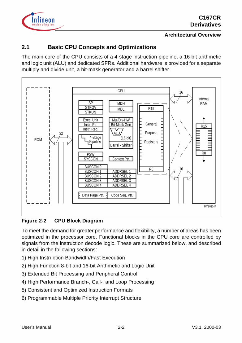
The main core of the CPU consists of a 4-stage instruction pipeline, a 16-bit arithmeticand logic unit (ALU) and dedicated SFRs. Additional hardware is provided for a separatemultiply and divide unit, a bit-mask generator and a barrel shifter.
Figure 2-2 CPU Block Diagram
To meet the demand for greater performance and flexibility, a number of areas has beenoptimized in the processor core. Functional blocks in the CPU core are controlled bysignals from the instruction decode logic. These are summarized below, and describedin detail in the following sections:
1) High Instruction Bandwidth/Fast Execution
2) High Function 8-bit and 16-bit Arithmetic and Logic Unit
3) Extended Bit Processing and Peripheral Control
4) High Performance Branch-, Call-, and Loop Processing
5) Consistent and Optimized Instruction Formats
6) Programmable Multiple Priority Interrupt Structure
MCB02147
CPU
SPSTKOVSTKUN
Instr. Reg.Instr. Ptr.
Exec. Unit
4-StagePipeline
MDHMDL
PSWSYSCON Context Ptr.
Mul/Div-HW
R15
R0
General
Purpose
Registers
Bit-Mask Gen
Barrel - Shifter
ALU(16-bit)
Data Page Ptr. Code Seg. Ptr.
InternalRAM
R15
R0
ROM
16
16
32
BUSCON 0BUSCON 1BUSCON 2BUSCON 3BUSCON 4 ADDRSEL 4
ADDRSEL 3ADDRSEL 2ADDRSEL 1
User’s Manual 2-2 V3.1, 2000-03

C167CRDerivatives
Architectural Overview
2.1.1 High Instruction Bandwidth/Fast Execution
Based on the hardware provisions, most of the C167CR’s instructions can be executedin just one machine cycle, which requires 2 CPU clock cycles (2 × 1 / fCPU = 4 TCL). Forexample, shift and rotate instructions are always processed within one machine cycle,independent of the number of bits to be shifted.
Branch-, multiply- and divide instructions normally take more than one machine cycle.These instructions, however, have also been optimized. For example, branchinstructions only require an additional machine cycle, when a branch is taken, and mostbranches taken in loops require no additional machine cycles at all, due to the so-called‘Jump Cache’.A 32-bit/16-bit division takes 20 CPU clock cycles, a 16-bit × 16-bit multiplication takes10 CPU clock cycles.
The instruction cycle time has been dramatically reduced through the use of instructionpipelining. This technique allows the core CPU to process portions of multiple sequentialinstruction stages in parallel. The following four stage pipeline provides the optimumbalancing for the CPU core:
FETCH: In this stage, an instruction is fetched from the internal ROM or RAM or from theexternal memory, based on the current IP value.
DECODE: In this stage, the previously fetched instruction is decoded and the requiredoperands are fetched.
EXECUTE: In this stage, the specified operation is performed on the previously fetchedoperands.
WRITE BACK: In this stage, the result is written to the specified location.
If this technique were not used, each instruction would require four machine cycles. Thisincreased performance allows a greater number of tasks and interrupts to be processed.
Instruction Decoder
Instruction decoding is primarily generated from PLA outputs based on the selectedopcode. No microcode is used and each pipeline stage receives control signals stagedin control registers from the decode stage PLAs. Pipeline holds are primarily caused bywait states for external memory accesses and cause the holding of signals in the controlregisters. Multiple-cycle instructions are performed through instruction injection andsimple internal state machines which modify required control signals.
User’s Manual 2-3 V3.1, 2000-03
C167CRDerivatives
Architectural Overview
High Function 8-bit and 16-bit Arithmetic and Logic Unit
All standard arithmetic and logical operations are performed in a 16-bit ALU. In addition,for byte operations, signals are provided from bits six and seven of the ALU result tocorrectly set the condition flags. Multiple precision arithmetic is provided through a‘CARRY-IN’ signal to the ALU from previously calculated portions of the desired operation.
Most internal execution blocks have been optimized to perform operations on either 8-bitor 16-bit quantities. Once the pipeline has been filled, one instruction is completed permachine cycle, except for multiply and divide. An advanced Booth algorithm has beenincorporated to allow four bits to be multiplied and two bits to be divided per machinecycle. Thus, these operations use two coupled 16-bit registers, MDL and MDH, andrequire four and nine machine cycles, respectively, to perform a 16-bit by 16-bit (or 32-bitby 16-bit) calculation plus one machine cycle to setup and adjust the operands and theresult. Even these longer multiply and divide instructions can be interrupted during theirexecution to allow for very fast interrupt response. Instructions have also been providedto allow byte packing in memory while providing sign extension of bytes for word widearithmetic operations. The internal bus structure also allows transfers of bytes or wordsto or from peripherals based on the peripheral requirements.
A set of consistent flags is automatically updated in the PSW after each arithmetic,logical, shift, or movement operation. These flags allow branching on specific conditions.Support for both signed and unsigned arithmetic is provided through user-specifiablebranch tests. These flags are also preserved automatically by the CPU upon entry intoan interrupt or trap routine.All targets for branch calculations are also computed in the central ALU.
A 16-bit barrel shifter provides multiple bit shifts in a single cycle. Rotates and arithmeticshifts are also supported.
Extended Bit Processing and Peripheral Control
A large number of instructions has been dedicated to bit processing. These instructionsprovide efficient control and testing of peripherals while enhancing data manipulation.Unlike other microcontrollers, these instructions provide direct access to two operandsin the bit-addressable space without requiring to move them into temporary flags.
The same logical instructions available for words and bytes are also supported for bits.This allows the user to compare and modify a control bit for a peripheral in oneinstruction. Multiple bit shift instructions have been included to avoid long instructionstreams of single bit shift operations. These are also performed in a single machinecycle.
In addition, bit field instructions have been provided, which allow the modification ofmultiple bits from one operand in a single instruction.
User’s Manual 2-4 V3.1, 2000-03
C167CRDerivatives
Architectural Overview
High Performance Branch-, Call-, and Loop Processing
Due to the high percentage of branching in controller applications, branch instructionshave been optimized to require one extra machine cycle only when a branch is taken.This is implemented by precalculating the target address while decoding the instruction.To decrease loop execution overhead, three enhancements have been provided:
• The first solution provides single cycle branch execution after the first iteration of aloop. Thus, only one machine cycle is lost during the execution of the entire loop. Inloops which fall through upon completion, no machine cycles are lost when exiting theloop. No special instructions are required to perform loops, and loops areautomatically detected during execution of branch instructions.
• The second loop enhancement allows the detection of the end of a table and avoidsthe use of two compare instructions embedded in loops. One simply places the lowestnegative number at the end of the specific table, and specifies branching if neither thisvalue nor the compared value have been found. Otherwise the loop is terminated ifeither condition has been met. The terminating condition can then be tested.
• The third loop enhancement provides a more flexible solution than the Decrement andSkip on Zero instruction which is found in other microcontrollers. Through the use ofCompare and Increment or Decrement instructions, the user can make comparisonsto any value. This allows loop counters to cover any range. This is particularlyadvantageous in table searching.
Saving of system state is automatically performed on the internal system stack avoidingthe use of instructions to preserve state upon entry and exit of interrupt or trap routines.Call instructions push the value of the IP on the system stack, and require the sameexecution time as branch instructions.
Instructions have also been provided to support indirect branch and call instructions.This supports implementation of multiple CASE statement branching in assemblermacros and high level languages.
User’s Manual 2-5 V3.1, 2000-03
C167CRDerivatives
Architectural Overview
Consistent and Optimized Instruction Formats
To obtain optimum performance in a pipelined design, an instruction set has beendesigned which incorporates concepts from Reduced Instruction Set Computing (RISC).These concepts primarily allow fast decoding of the instructions and operands whilereducing pipeline holds. These concepts, however, do not preclude the use of complexinstructions, which are required by microcontroller users. The following goals were usedto design the instruction set:
1. Provide powerful instructions to perform operations which currently requiresequences of instructions and are frequently used. Avoid transfer into and out oftemporary registers such as accumulators and carry bits. Perform tasks in parallelsuch as saving state upon entry into interrupt routines or subroutines.
2. Avoid complex encoding schemes by placing operands in consistent fields for eachinstruction. Also avoid complex addressing modes which are not frequently used. Thisdecreases the instruction decode time while also simplifying the development ofcompilers and assemblers.
3. Provide most frequently used instructions with one-word instruction formats. All otherinstructions are placed into two-word formats. This allows all instructions to be placedon word boundaries, which alleviates the need for complex alignment hardware. Italso has the benefit of increasing the range for relative branching instructions.
The high performance offered by the hardware implementation of the CPU can efficientlybe utilized by a programmer via the highly functional C167CR instruction set whichincludes the following instruction classes:
• Arithmetic Instructions• Logical Instructions• Boolean Bit Manipulation Instructions• Compare and Loop Control Instructions• Shift and Rotate Instructions• Prioritize Instruction• Data Movement Instructions• System Stack Instructions• Jump and Call Instructions• Return Instructions• System Control Instructions• Miscellaneous Instructions
Possible operand types are bits, bytes and words. Specific instruction support theconversion (extension) of bytes to words. A variety of direct, indirect or immediateaddressing modes are provided to specify the required operands.
User’s Manual 2-6 V3.1, 2000-03

C167CRDerivatives
Architectural Overview
2.1.2 Programmable Multiple Priority Interrupt System
The following enhancements have been included to allow processing of a large numberof interrupt sources:
1. Peripheral Event Controller (PEC): This processor is used to off-load many interruptrequests from the CPU. It avoids the overhead of entering and exiting interrupt or traproutines by performing single-cycle interrupt-driven byte or word data transfersbetween any two locations in segment 0 with an optional increment of either the PECsource or the destination pointer. Just one cycle is ‘stolen’ from the current CPUactivity to perform a PEC service.
2. Multiple Priority Interrupt Controller: This controller allows all interrupts to be placed atany specified priority. Interrupts may also be grouped, which provides the user withthe ability to prevent similar priority tasks from interrupting each other. For each of thepossible interrupt sources there is a separate control register, which contains aninterrupt request flag, an interrupt enable flag and an interrupt priority bitfield. Oncehaving been accepted by the CPU, an interrupt service can only be interrupted by ahigher prioritized service request. For standard interrupt processing, each of thepossible interrupt sources has a dedicated vector location.
3. Multiple Register Banks: This feature allows the user to specify up to sixteen generalpurpose registers located anywhere in the internal RAM. A single one-machine-cycleinstruction allows to switch register banks from one task to another.
4. Interruptable Multiple Cycle Instructions: Reduced interrupt latency is provided byallowing multiple-cycle instructions (multiply, divide) to be interruptable.
With an interrupt response time within a range from just 5 to 10 CPU clock cycles (in caseof internal program execution), the C167CR is capable of reacting very fast on non-deterministic events.
Its fast external interrupt inputs are sampled every CPU clock cycle and allow torecognize even very short external signals.
The C167CR also provides an excellent mechanism to identify and to processexceptions or error conditions that arise during run-time, so called ‘Hardware Traps’.Hardware traps cause an immediate non-maskable system reaction which is similar to astandard interrupt service (branching to a dedicated vector table location). Theoccurrence of a hardware trap is additionally signified by an individual bit in the trap flagregister (TFR). Except for another higher prioritized trap service being in progress, ahardware trap will interrupt any current program execution. In turn, hardware trapservices can normally not be interrupted by standard or PEC interrupts.
Software interrupts are supported by means of the ‘TRAP’ instruction in combination withan individual trap (interrupt) number.
User’s Manual 2-7 V3.1, 2000-03
C167CRDerivatives
Architectural Overview
2.2 The On-chip System Resources
The C167CR controllers provide a number of powerful system resources designedaround the CPU. The combination of CPU and these resources results in the highperformance of the members of this controller family.
Peripheral Event Controller (PEC) and Interrupt Control
The Peripheral Event Controller allows to respond to an interrupt request with a singledata transfer (word or byte) which only consumes one instruction cycle and does notrequire to save and restore the machine status. Each interrupt source is prioritized everymachine cycle in the interrupt control block. If PEC service is selected, a PEC transfer isstarted. If CPU interrupt service is requested, the current CPU priority level stored in thePSW register is tested to determine whether a higher priority interrupt is currently beingserviced. When an interrupt is acknowledged, the current state of the machine is savedon the internal system stack and the CPU branches to the system specific vector for theperipheral.
The PEC contains a set of SFRs which store the count value and control bits for eightdata transfer channels. In addition, the PEC uses a dedicated area of RAM whichcontains the source and destination addresses. The PEC is controlled similar to anyother peripheral through SFRs containing the desired configuration of each channel.
An individual PEC transfer counter is implicitly decremented for each PEC serviceexcept forming in the continuous transfer mode. When this counter reaches zero, astandard interrupt is performed to the vector location related to the correspondingsource. PEC services are very well suited, for example, to move register contents to/froma memory table. The C167CR has 8 PEC channels each of which offers such fastinterrupt-driven data transfer capabilities.
Memory Areas
The memory space of the C167CR is configured in a Von Neumann architecture whichmeans that code memory, data memory, registers and IO ports are organized within thesame linear address space which covers up to 16 MBytes. The entire memory space canbe accessed bytewise or wordwise. Particular portions of the on-chip memory haveadditionally been made directly bit addressable.
A 2 KByte 16-bit wide internal RAM (IRAM) provides fast access to General PurposeRegisters (GPRs), user data (variables) and system stack. The internal RAM may alsobe used for code. A unique decoding scheme provides flexible user register banks in theinternal memory while optimizing the remaining RAM for user data.
User’s Manual 2-8 V3.1, 2000-03
C167CRDerivatives
Architectural Overview
The CPU has an actual register context consisting of up to 16 wordwide and/or bytewideGPRs at its disposal, which are physically located within the on-chip RAM area. AContext Pointer (CP) register determines the base address of the active register bank tobe accessed by the CPU at a time. The number of register banks is only restricted by theavailable internal RAM space. For easy parameter passing, a register bank may overlapothers.
A system stack of up to 1024 words is provided as a storage for temporary data. Thesystem stack is also located within the on-chip RAM area, and it is accessed by the CPUvia the stack pointer (SP) register. Two separate SFRs, STKOV and STKUN, areimplicitly compared against the stack pointer value upon each stack access for thedetection of a stack overflow or underflow.
Hardware detection of the selected memory space is placed at the internal memorydecoders and allows the user to specify any address directly or indirectly and obtain thedesired data without using temporary registers or special instructions.
A 2 KByte 16-bit wide on-chip XRAM provides fast access to user data (variables),user stacks and code. The on-chip XRAM is realized as an X-Peripheral and appears tothe software as an external RAM. Therefore it cannot store register banks and is notbitaddressable. The XRAM allows 16-bit accesses with maximum speed.
For Special Function Registers 1024 Bytes of the address space are reserved. Thestandard Special Function Register area (SFR) uses 512 Bytes, while the ExtendedSpecial Function Register area (ESFR) uses the other 512 Bytes. (E)SFRs are wordwideregisters which are used for controlling and monitoring functions of the different on-chipunits. Unused (E)SFR addresses are reserved for future members of the C166 Familywith enhanced functionality.
An optional internal ROM provides for both code and constant data storage. Thismemory area is connected to the CPU via a 32-bit-wide bus. Thus, an entire double-wordinstruction can be fetched in just one machine cycle.Program execution from on-chip program memory is the fastest of all possiblealternatives.
The size of the on-chip ROM depends on the chosen derivative.
User’s Manual 2-9 V3.1, 2000-03
C167CRDerivatives
Architectural Overview
External Bus Interface
In order to meet the needs of designs where more memory is required than is providedon chip, up to 16 MBytes of external RAM and/or ROM can be connected to themicrocontroller via its external bus interface. The integrated External Bus Controller(EBC) allows to access external memory and/or peripheral resources in a very flexibleway. For up to five address areas the bus mode (multiplexed/demultiplexed), the databus width (8-bit/16-bit) and even the length of a bus cycle (waitstates, signal delays) canbe selected independently. This allows to access a variety of memory and peripheralcomponents directly and with maximum efficiency. If the device does not run in SingleChip Mode, where no external memory is required, the EBC can control externalaccesses in one of the following external access modes:
• 16-/18-/20-/24-bit Addresses, 16-bit Data, Demultiplexed• 16-/18-/20-/24-bit Addresses, 8-bit Data, Demultiplexed• 16-/18-/20-/24-bit Addresses, 16-bit Data, Multiplexed• 16-/18-/20-/24-bit Addresses, 8-bit Data, Multiplexed
The demultiplexed bus modes use PORT1 for addresses and PORT0 for data input/output. The multiplexed bus modes use PORT0 for both addresses and data input/output. Port 4 is used for the upper address lines (A16 …) if selected.
Important timing characteristics of the external bus interface (waitstates, ALE length andRead/Write Delay) have been made programmable to allow the user the adaption of awide range of different types of memories and/or peripherals. Access to very slowmemories or peripherals is supported via a particular ‘Ready’ function.
For applications which require less than 64 KBytes of address space, a non-segmentedmemory model can be selected, where all locations can be addressed by 16-bits, andthus Port 4 is not needed as an output for the upper address bits (Axx … A16), as is thecase when using the segmented memory model.
The on-chip XBUS is an internal representation of the external bus and allows to accessintegrated application-specific peripherals/modules in the same way as externalcomponents. It provides a defined interface for these customized peripherals.
The on-chip XRAM and the on-chip CAN-Module are examples for these X-Peripherals.
User’s Manual 2-10 V3.1, 2000-03
C167CRDerivatives
Architectural Overview
2.3 The On-chip Peripheral Blocks
The C166 Family clearly separates peripherals from the core. This structure permits themaximum number of operations to be performed in parallel and allows peripherals to beadded or deleted from family members without modifications to the core. Each functionalblock processes data independently and communicates information over commonbuses. Peripherals are controlled by data written to the respective Special FunctionRegisters (SFRs). These SFRs are located either within the standard SFR area(00’FE00H … 00’FFFFH) or within the extended ESFR area (00’F000H … 00’F1FFH).
These built in peripherals either allow the CPU to interface with the external world, orprovide functions on-chip that otherwise were to be added externally in the respectivesystem.
The C167CR generic peripherals are:
• Two General Purpose Timer Blocks (GPT1 and GPT2)• Two Serial Interfaces (ASC0 and SSC)• A Watchdog Timer• Two 16-channel Capture/Compare units (CAPCOM1 and CAPCOM2)• A 4-channel Pulse Width Modulation unit• A 10-bit Analog/Digital Converter• Nine IO ports with a total of 111 IO lines
Each peripheral also contains a set of Special Function Registers (SFRs), which controlthe functionality of the peripheral and temporarily store intermediate data results. Eachperipheral has an associated set of status flags. Individually selected clock signals aregenerated for each peripheral from binary multiples of the CPU clock.
Peripheral Interfaces
The on-chip peripherals generally have two different types of interfaces, an interface tothe CPU and an interface to external hardware. Communication between CPU andperipherals is performed through Special Function Registers (SFRs) and interrupts. TheSFRs serve as control/status and data registers for the peripherals. Interrupt requestsare generated by the peripherals based on specific events which occur during theiroperation (e.g. operation complete, error, etc.).
For interfacing with external hardware, specific pins of the parallel ports are used, whenan input or output function has been selected for a peripheral. During this time, the portpins are controlled by the peripheral (when used as outputs) or by the external hardwarewhich controls the peripheral (when used as inputs). This is called the ‘alternate (inputor output) function’ of a port pin, in contrast to its function as a general purpose IO pin.
User’s Manual 2-11 V3.1, 2000-03

C167CRDerivatives
Architectural Overview
Peripheral Timing
Internal operation of CPU and peripherals is based on the CPU clock (fCPU). The on-chiposcillator derives the CPU clock from the crystal or from the external clock signal. Theclock signal which is gated to the peripherals is independent from the clock signal whichfeeds the CPU. During Idle mode the CPU’s clock is stopped while the peripheralscontinue their operation. Peripheral SFRs may be accessed by the CPU once per state.When an SFR is written to by software in the same state where it is also to be modifiedby the peripheral, the software write operation has priority. Further details on peripheraltiming are included in the specific sections about each peripheral.
Programming Hints
Access to SFRsAll SFRs reside in data page 3 of the memory space. The following addressingmechanisms allow to access the SFRs:
• Indirect or direct addressing with 16-bit (mem) addresses must guarantee that theused data page pointer (DPP0 … DPP3) selects data page 3.
• Accesses via the Peripheral Event Controller (PEC) use the SRCPx and DSTPxpointers instead of the data page pointers.
• Short 8-bit (reg) addresses to the standard SFR area do not use the data pagepointers but directly access the registers within this 512 Byte area.
• Short 8-bit (reg) addresses to the extended ESFR area require switching to the512 Byte extended SFR area. This is done via the EXTension instructions EXTR,EXTP(R), EXTS(R).
Byte write operations to word wide SFRs via indirect or direct 16-bit (mem) addressingor byte transfers via the PEC force zeros in the non-addressed byte. Byte writeoperations via short 8-bit (reg) addressing can only access the low byte of an SFR andforce zeros in the high byte. It is therefore recommended, to use the bit field instructions(BFLDL and BFLDH) to write to any number of bits in either byte of an SFR withoutdisturbing the non-addressed byte and the unselected bits.
Reserved BitsSome of the bits which are contained in the C167CR’s SFRs are marked as ‘Reserved’.User software should never write ‘1’s to reserved bits. These bits are currently notimplemented and may be used in future products to invoke new functions. In this case,the active state for these functions will be ‘1’, and the inactive state will be ‘0’. Thereforewriting only ‘0’s to reserved locations provides portability of the current software to futuredevices. After read accesses reserved bits should be ignored or masked out.
User’s Manual 2-12 V3.1, 2000-03
C167CRDerivatives
Architectural Overview
Serial Channels
Serial communication with other microcontrollers, processors, terminals or externalperipheral components is provided by two serial interfaces with different functionality, anAsynchronous/Synchronous Serial Channel (ASC0) and a High-Speed SynchronousSerial Channel (SSC).
The ASC0 is upward compatible with the serial ports of the Infineon 8-bit microcontrollerfamilies. It supports full-duplex asynchronous communication at up to 780/1030 KBaudand half-duplex synchronous communication at up to 3.1/4.1 MBaud @ 25/33 MHz CPUclock.A dedicated baud rate generator allows to set up all standard baud rates withoutoscillator tuning. For transmission, reception and error handling 4 separate interruptvectors are provided. In asynchronous mode, 8- or 9-bit data frames are transmitted orreceived, preceded by a start bit and terminated by one or two stop bits. Formultiprocessor communication, a mechanism to distinguish address from data bytes hasbeen included (8-bit data plus wake up bit mode).In synchronous mode, the ASC0 transmits or receives bytes (8 bits) synchronously to ashift clock which is generated by the ASC0. The ASC0 always shifts the LSB first. A loopback option is available for testing purposes.A number of optional hardware error detection capabilities has been included to increasethe reliability of data transfers. A parity bit can automatically be generated ontransmission or be checked on reception. Framing error detection allows to recognizedata frames with missing stop bits. An overrun error will be generated, if the lastcharacter received has not been read out of the receive buffer register at the time thereception of a new character is complete.
The SSC supports full-duplex synchronous communication at up to 6.25/8.25 Mbaud @25/33 MHz CPU clock. It may be configured so it interfaces with serially linked peripheralcomponents. A dedicated baud rate generator allows to set up all standard baud rateswithout oscillator tuning. For transmission, reception and error handling 3 separateinterrupt vectors are provided. The SSC transmits or receives characters of 2 … 16-bits length synchronously to a shiftclock which can be generated by the SSC (master mode) or by an external master (slavemode). The SSC can start shifting with the LSB or with the MSB and allows the selectionof shifting and latching clock edges as well as the clock polarity.A number of optional hardware error detection capabilities has been included to increasethe reliability of data transfers. Transmit and receive error supervise the correct handlingof the data buffer. Phase and baudrate error detect incorrect serial data.
User’s Manual 2-13 V3.1, 2000-03
C167CRDerivatives
Architectural Overview
The On-chip CAN Module
The integrated CAN Module handles the completely autonomous transmission andreception of CAN frames in accordance with the CAN specification V2.0 part B (active),i.e. the on-chip CAN Module can receive and transmit standard frames with 11-bitidentifiers as well as extended frames with 29-bit identifiers.
The module provides Full CAN functionality on up to 15 message objects. Messageobject 15 may be configured for Basic CAN functionality. Both modes provide separatemasks for acceptance filtering which allows to accept a number of identifiers in Full CANmode and also allows to disregard a number of identifiers in Basic CAN mode. Allmessage objects can be updated independent from the other objects and are equippedfor the maximum message length of 8 Bytes.
The bit timing is derived from the XCLK and is programmable up to a data rate of1 MBaud. The CAN Module uses two pins to interface to a bus transceiver.
Note: The CAN Module is not part of all C167 derivatives. This description, of course,refers to those devices only which incorporate a CAN Module.
Parallel Ports
The C167CR provides up to 111 IO lines which are organized into eight input/outputports and one input port. All port lines are bit-addressable, and all input/output lines areindividually (bit-wise) programmable as inputs or outputs via direction registers. The IOports are true bidirectional ports which are switched to high impedance state whenconfigured as inputs. The output drivers of five IO ports can be configured (pin by pin)for push/pull operation or open-drain operation via control registers. During the internalreset, all port pins are configured as inputs.
All port lines have programmable alternate input or output functions associated withthem. PORT0 and PORT1 may be used as address and data lines when accessingexternal memory, while Port 4 outputs the additional segment address bits A23/19/17 …A16 in systems where segmentation is used to access more than 64 KBytes of memory.Port 6 provides the optional bus arbitration signals (BREQ, HLDA, HOLD) and the chipselect signals CS4 … CS0. Port 2 accepts the fast external interrupt inputs and providesinputs/outputs for the CAPCOM1 unit. Port 3 includes alternate functions of timers, serialinterfaces, the optional bus control signal BHE and the system clock output (CLKOUT).Port 5 is used for timer control signals and for the analog inputs to the A/D Converter.Port 7 provides the output signals from the PWM unit and inputs/outputs for theCAPCOM2 unit (more on P1H). Port 8 provides inputs/outputs for the CAPCOM2 unit.Four pins of PORT1 may also be used as inputs for the CAPCOM2 unit. All port linesthat are not used for these alternate functions may be used as general purpose IO lines.
User’s Manual 2-14 V3.1, 2000-03

C167CRDerivatives
Architectural Overview
A/D Converter
For analog signal measurement, a 10-bit A/D converter with 16 multiplexed inputchannels and a sample and hold circuit has been integrated on-chip. It uses the methodof successive approximation. The sample time (for loading the capacitors) and theconversion time is programmable and can so be adjusted to the external circuitry.
Overrun error detection/protection is provided for the conversion result register(ADDAT): either an interrupt request will be generated when the result of a previousconversion has not been read from the result register at the time the next conversion iscomplete, or the next conversion is suspended in such a case until the previous resulthas been read.
For applications which require less analog input channels, the remaining channel inputscan be used as digital input port pins.
The A/D converter of the C167CR supports four different conversion modes. In thestandard Single Channel conversion mode, the analog level on a specified channel issampled once and converted to a digital result. In the Single Channel Continuous mode,the analog level on a specified channel is repeatedly sampled and converted withoutsoftware intervention. In the Auto Scan mode, the analog levels on a prespecifiednumber of channels are sequentially sampled and converted. In the Auto ScanContinuous mode, the number of prespecified channels is repeatedly sampled andconverted. In addition, the conversion of a specific channel can be inserted (injected) intoa running sequence without disturbing this sequence. This is called Channel InjectionMode.
The Peripheral Event Controller (PEC) may be used to automatically store theconversion results into a table in memory for later evaluation, without requiring theoverhead of entering and exiting interrupt routines for each data transfer.
User’s Manual 2-15 V3.1, 2000-03
C167CRDerivatives
Architectural Overview
General Purpose Timer (GPT) Unit
The GPT units represent a very flexible multifunctional timer/counter structure whichmay be used for many different time related tasks such as event timing and counting,pulse width and duty cycle measurements, pulse generation, or pulse multiplication.
The five 16-bit timers are organized in two separate modules, GPT1 and GPT2. Eachtimer in each module may operate independently in a number of different modes, or maybe concatenated with another timer of the same module.
Each timer can be configured individually for one of four basic modes of operation, whichare Timer, Gated Timer, Counter Mode and Incremental Interface Mode (GPT1 timers).In Timer Mode the input clock for a timer is derived from the internal CPU clock dividedby a programmable prescaler, while Counter Mode allows a timer to be clocked inreference to external events (via TxIN).Pulse width or duty cycle measurement is supported in Gated Timer Mode where theoperation of a timer is controlled by the ‘gate’ level on its external input pin TxIN.In Incremental Interface Mode the GPT1 timers can be directly connected to theincremental position sensor signals A and B via the respective inputs TxIN and TxEUD.Direction and count signals are internally derived from these two input signals, so thecontents of timer Tx corresponds to the sensor position. The third position sensor signalTOP0 can be connected to an interrupt input.
The count direction (up/down) for each timer is programmable by software or mayadditionally be altered dynamically by an external signal (TxEUD) to facilitate e.g.position tracking.
The core timers T3 and T6 have output toggle latches (TxOTL) which change their stateon each timer over-flow/underflow. The state of these latches may be output on port pins(TxOUT) or may be used internally to concatenate the core timers with the respectiveauxiliary timers resulting in 32/33-bit timers/counters for measuring long time periodswith high resolution.
Various reload or capture functions can be selected to reload timers or capture a timer’scontents triggered by an external signal or a selectable transition of toggle latch TxOTL.
The maximum resolution of the timers in module GPT1 is 8 CPU clock cycles (= 16 TCL).With their maximum resolution of 4 CPU clock cycles (= 8 TCL) the GPT2 timers provideprecise event control and time measurement.
User’s Manual 2-16 V3.1, 2000-03

C167CRDerivatives
Architectural Overview
Capture/Compare (CAPCOM) Units
The two CAPCOM units support generation and control of timing sequences on up to 32channels with a maximum resolution of 8 CPU clock cycles. The CAPCOM units aretypically used to handle high speed IO tasks such as pulse and waveform generation,pulse width modulation (PWM), Digital to Analog (D/A) conversion, software timing, ortime recording relative to external events.
Four 16-bit timers (T0/T1, T7/T8) with reload registers provide two independent timebases for the capture/compare register array.
The input clock for the timers is programmable to several prescaled values of the internalCPU clock, or may be derived from an overflow/underflow of timer T6 in module GPT2.This provides a wide range of variation for the timer period and resolution and allowsprecise adjustments to the application specific requirements. In addition, external countinputs for CAPCOM timers T0 and T7 allow event scheduling for the capture/compareregisters relative to external events.
Both of the two capture/compare register arrays contain 16 dual purpose capture/compare registers, each of which may be individually allocated to either CAPCOM timerT0 or T1 (T7 or T8, respectively), and programmed for capture or compare function.Each register has one port pin associated with it which serves as an input pin fortriggering the capture function, or as an output pin (except for CC24 … CC27) to indicatethe occurrence of a compare event.
When a capture/compare register has been selected for capture mode, the currentcontents of the allocated timer will be latched (captured) into the capture/compareregister in response to an external event at the port pin which is associated with thisregister. In addition, a specific interrupt request for this capture/compare register isgenerated. Either a positive, a negative, or both a positive and a negative external signaltransition at the pin can be selected as the triggering event. The contents of all registerswhich have been selected for one of the five compare modes are continuously comparedwith the contents of the allocated timers. When a match occurs between the timer valueand the value in a capture/compare register, specific actions will be taken based on theselected compare mode.
User’s Manual 2-17 V3.1, 2000-03

C167CRDerivatives
Architectural Overview
Pulse Width Modulation Unit
The PWM Unit supports the generation of up to four independent high-speed PWMsignals. It allows to generate standard (edge aligned) PWM signals as well assymmetrical (center aligned) PWM signals. In Burst Mode two channels may becombined with their output signals ANDed, where one channel gates the output signal ofthe other channel. Single Shot Mode allows to generate single output pulses(retriggerable) under software control. Each PWM channel is controlled by an up/downcounter with associated reload and compare registers. The polarity of the PWM outputsignals may be controlled via the respective port output latch (combination via EXOR).
Watchdog Timer
The Watchdog Timer represents one of the fail-safe mechanisms which have beenimplemented to prevent the controller from malfunctioning for longer periods of time.
The Watchdog Timer is always enabled after a reset of the chip, and can only bedisabled in the time interval until the EINIT (end of initialization) instruction has beenexecuted. Thus, the chip’s start-up procedure is always monitored. The software has tobe designed to service the Watchdog Timer before it overflows. If, due to hardware orsoftware related failures, the software fails to do so, the Watchdog Timer overflows andgenerates an internal hardware reset and pulls the RSTOUT pin low in order to allowexternal hardware components to reset.
The Watchdog Timer is a 16-bit timer, clocked with the CPU clock divided either by 2 or by128. The high byte of the Watchdog Timer register can be set to a prespecified reloadvalue (stored in WDTREL) in order to allow further variation of the monitored time interval.Each time it is serviced by the application software, the high byte of the Watchdog Timeris reloaded. Thus, time intervals between 21 ms and 335 ms can be monitored @25 MHz (16 ms and 254 ms @ 33 MHz). The default Watchdog Timer interval after resetis 5.2/4.0 ms (@ 25/33 MHz).
2.4 Protected Bits
The C167CR provides a special mechanism to protect bits which can be modified by theon-chip hardware from being changed unintentionally by software accesses to relatedbits (see also Chapter 4).
User’s Manual 2-18 V3.1, 2000-03

C167CRDerivatives
Architectural Overview
The following bits are protected
Σ = 133 protected bits.
Table 2-1 C167CR Protected Bits
Register Bit Name Notes
T2IC, T3IC, T4IC T2IR, T3IR, T4IR GPT1 timer interrupt request flags
T5IC, T6IC T5IR, T6IR GPT2 timer interrupt request flags
CRIC CRIR GPT2 CAPREL interrupt request flag
T3CON, T6CON T3OTL, T6OTL GPTx timer output toggle latches
T0IC, T1IC T0IR, T1IR CAPCOM1 timer interrupt request flags
T7IC, T8IC T7IR, T8IR CAPCOM2 timer interrupt request flags
S0TIC, S0TBIC S0TIR, S0TBIR ASC0 transmit(buffer) interrupt request flags
S0RIC, S0EIC S0RIR, S0EIR ASC0 receive/error interrupt request flags
S0CON S0REN ASC0 receiver enable flag
SSCTIC, SSCRIC SSCTIR, SSCRIR SSC transmit/receive interrupt request flags
SSCEIC SSCEIR SSC error interrupt request flag
SSCCON SSCBSY SSC busy flag
SSCCON SSCBE, SSCPE SSC error flags
SSCCON SSCRE, SSCTE SSC error flags
ADCIC, ADEIC ADCIR, ADEIR ADC end-of-conv./overrun intr. request flag
ADCON ADST, ADCRQ ADC start flag/injection request flag
CC31IC … CC16IC CC31IR … CC16IR CAPCOM2 interrupt request flags
CC15IC … CC0IC CC15IR … CC0IR CAPCOM1 interrupt request flags
PWMIC PWMIR PWM module interrupt request flag
PWMCON0 PIR3 … PTR0 All bits of PWMCON0
PWMCON1 PS3 … PEN0 All bits of PWMCON1
TFR TFR.15,14,13 Class A trap flags
TFR TFR.7,3,2,1,0 Class B trap flags
P2 P2.15 … P2.0 All bits of Port 2
P7 P7.7 … P7.0 All bits of Port 7
P8 P8.7 … P8.0 All bits of Port 8
XP3IC … XP0IC XP3IR … XP0IC X-Peripheral interrupt request flags
User’s Manual 2-19 V3.1, 2000-03
C167CRDerivatives
Memory Organization
3 Memory OrganizationThe memory space of the C167CR is configured in a “Von Neumann” architecture. Thismeans that code and data are accessed within the same linear address space. All of thephysically separated memory areas, including internal ROM/Flash/OTP (whereintegrated), internal RAM, the internal Special Function Register Areas (SFRs andESFRs), the address areas for integrated XBUS peripherals and external memory aremapped into one common address space.
The C167CR provides a total addressable memory space of 16 MBytes. This addressspace is arranged as 256 segments of 64 KBytes each, and each segment is againsubdivided into four data pages of 16 KBytes each (see Figure 3-1).
Figure 3-1 Address Space Overview
MCA04325
Begin ofProg. Memoryabove 32 KB
255
128
254...129
127
126...65
64
63
62...12
11
10
9
8
7
6
5
4
3
2
1
0
InternalROMArea
00’0000H
01’FFFFH
0A’FFFFH
40’0000H
80’0000H
FF’FFFFH
Data Page 2
Data Page 3
AlternateROMArea
255...2
02’FFFFH
08’0000H
00’0000H
01’0000H
01’8000H
01’FFFFHS
egm
ent 0
Seg
men
t 1
16 M
Byt
eE
xter
nal A
ddre
ssin
g C
apab
ility
Total Address Space16 MByte, Segments 255...0
Segments 1 and 064 + 64 Kbyte
User’s Manual 3-1 V3.1, 2000-03
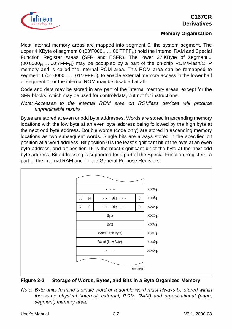
C167CRDerivatives
Memory Organization
Most internal memory areas are mapped into segment 0, the system segment. Theupper 4 KByte of segment 0 (00’F000H … 00’FFFFH) hold the Internal RAM and SpecialFunction Register Areas (SFR and ESFR). The lower 32 KByte of segment 0(00’0000H … 00’7FFFH) may be occupied by a part of the on-chip ROM/Flash/OTPmemory and is called the Internal ROM area. This ROM area can be remapped tosegment 1 (01’0000H … 01’7FFFH), to enable external memory access in the lower halfof segment 0, or the internal ROM may be disabled at all.
Code and data may be stored in any part of the internal memory areas, except for theSFR blocks, which may be used for control/data, but not for instructions.
Note: Accesses to the internal ROM area on ROMless devices will produceunpredictable results.
Bytes are stored at even or odd byte addresses. Words are stored in ascending memorylocations with the low byte at an even byte address being followed by the high byte atthe next odd byte address. Double words (code only) are stored in ascending memorylocations as two subsequent words. Single bits are always stored in the specified bitposition at a word address. Bit position 0 is the least significant bit of the byte at an evenbyte address, and bit position 15 is the most significant bit of the byte at the next oddbyte address. Bit addressing is supported for a part of the Special Function Registers, apart of the internal RAM and for the General Purpose Registers.
Figure 3-2 Storage of Words, Bytes, and Bits in a Byte Organized Memory
Note: Byte units forming a single word or a double word must always be stored withinthe same physical (internal, external, ROM, RAM) and organizational (page,segment) memory area.
MCD01996
15 14 8
067
Hxxxx6
Bits
Bits
Byte
Byte
Word (High Byte)
Word (Low Byte)
xxxx5H
xxxx4 H
xxxx3 H
xxxx2H
xxxx1 H
xxxx0H
xxxxF H
User’s Manual 3-2 V3.1, 2000-03
C167CRDerivatives
Memory Organization
3.1 Internal ROM Area
The C167CR may reserve an address area of variable size (depending on the version)for on-chip mask-programmable ROM/Flash/OTP memory (organized as X × 32). Thelower 32 KByte of this on-chip memory block are referred to as “Internal ROM Area”.Internal ROM accesses are globally enabled or disabled via bit ROMEN in registerSYSCON. This bit is set during reset according to the level on pin EA, or may be alteredvia software. If enabled, the internal ROM area occupies the lower 32 KByte of eithersegment 0 or segment 1 (alternate ROM area). This mapping is controlled by bit ROMS1in register SYSCON.
Note: The size of the internal ROM area is independent of the size of the actualimplemented Program Memory. Also devices with less than 32 KByte of ProgramMemory or with no Program Memory at all will have this 32 KByte area occupied,if the Program Memory is enabled. Devices with a larger Program Memory providethe mapping option only for the internal ROM area.
Devices with a Program Memory size above 32 KByte expand the ROM area from themiddle of segment 1, i.e. starting at address 01’8000H.
The internal Program Memory can be used for both code (instructions) and data(constants, tables, etc.) storage.
Code fetches are always made on even byte addresses. The highest possible codestorage location in the internal Program Memory is either xx’xxFEH for single wordinstructions, or xx’xxFCH for double word instructions. The respective location must containa branch instruction (unconditional), because sequential boundary crossing from internalProgram Memory to external memory is not supported and causes erroneous results.
Any word and byte data read accesses may use the indirect or long 16-bit addressingmodes. There is no short addressing mode for internal ROM operands. Any word dataaccess is made to an even byte address. The highest possible word data storagelocation in the internal ROM is xx’xxFEH. For PEC data transfers the internal ProgramMemory can be accessed independent of the contents of the DPP registers via the PECsource and destination pointers.
The internal Program Memory is not provided for single bit storage, and therefore it is notbit addressable.
Note: The ‘x’ in the locations above depend on the available Program Memory and onthe mapping.
The internal ROM may be enabled, disabled or mapped into segment 0 or segment 1under software control. Chapter 21 shows how to do this and reminds of the precautionsthat must be taken in order to prevent the system from crashing.
User’s Manual 3-3 V3.1, 2000-03

C167CRDerivatives
Memory Organization
3.2 Internal RAM and SFR Area
The RAM/SFR area is located within data page 3 and provides access to the internalRAM (IRAM, organized as X × 16) and to two 512 Byte blocks of Special FunctionRegisters (SFRs).The C167CR provides 2 KByte of IRAM.
Figure 3-3 System Memory Map
MCA04326
XRAM
00’8000H 00’E000H
Reserved
CAN1
ESFR Area
Reserved
IRAM
Ext. Memory
XRAM
X-Peripherals
IRAM/SFR SFR Area
00’E7FFH
00’EF00H
00’F000H
00’F200H
00’F600H
00’FFFFH00’FFFFH
00’F000H
00’C000H
Dat
a P
age
3D
ata
Pag
e 2
Note: New XBUS peripherals will be preferably placed into the shaded areas,which now access external memory (bus cycles executed).
User’s Manual 3-4 V3.1, 2000-03
C167CRDerivatives
Memory Organization
Note: The upper 256 Bytes of SFR area, ESFR area and internal RAM are bit-addressable (see shaded blocks in Figure 3-3).
Code accesses are always made on even byte addresses. The highest possible codestorage location in the internal RAM is either 00’FDFEH for single word instructions or00’FDFCH for double word instructions. The respective location must contain a branchinstruction (unconditional), because sequential boundary crossing from internal RAM tothe SFR area is not supported and causes erroneous results.
Any word and byte data in the internal RAM can be accessed via indirect or long 16-bitaddressing modes, if the selected DPP register points to data page 3. Any word dataaccess is made on an even byte address. The highest possible word data storagelocation in the internal RAM is 00’FDFEH. For PEC data transfers, the internal RAM canbe accessed independent of the contents of the DPP registers via the PEC source anddestination pointers.
The upper 256 Byte of the internal RAM (00’FD00H through 00’FDFFH) and the GPRs ofthe current bank are provided for single bit storage, and thus they are bitaddressable.
System Stack
The system stack may be defined within the internal RAM. The size of the system stackis controlled by bitfield STKSZ in register SYSCON (see Table 3-1).
For all system stack operations the on-chip RAM is accessed via the Stack Pointer (SP)register. The stack grows downward from higher towards lower RAM address locations.Only word accesses are supported to the system stack. A stack overflow (STKOV) anda stack underflow (STKUN) register are provided to control the lower and upper limits ofthe selected stack area. These two stack boundary registers can be used not only forprotection against data destruction, but also allow to implement a circular stack withhardware supported system stack flushing and filling (except for option ‘111’). Thetechnique of implementing this circular stack is described in Chapter 21.
Table 3-1 System Stack Size Encoding
<STKSZ> Stack Size (words) Internal RAM Addresses (words)
0 0 0 B 256 00’FBFEH … 00’FA00H (Default after Reset)
0 0 1 B 128 00’FBFEH … 00’FB00H
0 1 0 B 64 00’FBFEH … 00’FB80H
0 1 1 B 32 00’FBFEH … 00’FBC0H
1 0 0 B 512 00’FBFEH … 00’F800H
1 0 1 B – Reserved. Do not use this combination.
1 1 0 B – Reserved. Do not use this combination.
1 1 1 B 1024 00’FDFEH … 00’F600H (Note: No circular stack)
User’s Manual 3-5 V3.1, 2000-03

C167CRDerivatives
Memory Organization
General Purpose Registers
The General Purpose Registers (GPRs) use a block of 16 consecutive words within theinternal RAM. The Context Pointer (CP) register determines the base address of thecurrently active register bank. This register bank may consist of up to 16 Word-GPRs(R0, R1, … R15) and/or of up to 16 Byte-GPRs (RL0, RH0, … RL7, RH7). The sixteenByte-GPRs are mapped onto the first eight Word-GPRs (see Table 3-2).
In contrast to the system stack, a register bank grows from lower towards higher addresslocations and occupies a maximum space of 32 Byte. The GPRs are accessed via short2-, 4-, or 8-bit addressing modes using the Context Pointer (CP) register as baseaddress (independent of the current DPP register contents). Additionally, each bit in thecurrently active register bank can be accessed individually.
The C167CR supports fast register bank (context) switching. Multiple register banks canphysically exist within the internal RAM at the same time. Only the register bank selectedby the Context Pointer register (CP) is active at a given time, however. Selecting a newactive register bank is simply done by updating the CP register. A particular SwitchContext (SCXT) instruction performs register bank switching and an automatic saving of
Table 3-2 Mapping of General Purpose Registers to RAM Addresses
Internal RAM Address Byte Registers Word Register
<CP> + 1EH – R15
<CP> + 1CH – R14
<CP> + 1AH – R13
<CP> + 18H – R12
<CP> + 16H – R11
<CP> + 14H – R10
<CP> + 12H – R9
<CP> + 10H – R8
<CP> + 0EH RH7 RL7 R7
<CP> + 0CH RH6 RL6 R6
<CP> + 0AH RH5 RL5 R5
<CP> + 08H RH4 RL4 R4
<CP> + 06H RH3 RL3 R3
<CP> + 04H RH2 RL2 R2
<CP> + 02H RH1 RL1 R1
<CP> + 00H RH0 RL0 R0
User’s Manual 3-6 V3.1, 2000-03

C167CRDerivatives
Memory Organization
the previous context. The number of implemented register banks (arbitrary sizes) is onlylimited by the size of the available internal RAM.Details on using, switching and overlapping register banks are described in Chapter 21.
PEC Source and Destination Pointers
The 16 word locations in the internal RAM from 00’FCE0H to 00’FCFEH (just below thebit-addressable section) are provided as source and destination address pointers fordata transfers on the eight PEC channels. Each channel uses a pair of pointers storedin two subsequent word locations with the source pointer (SRCPx) on the lower and thedestination pointer (DSTPx) on the higher word address (x = 7 … 0).
Figure 3-4 Location of the PEC Pointers
Whenever a PEC data transfer is performed, the pair of source and destination pointers,which is selected by the specified PEC channel number, is accessed independent of thecurrent DPP register contents and also the locations referred to by these pointers areaccessed independent of the current DPP register contents. If a PEC channel is notused, the corresponding pointer locations area available and can be used for word orbyte data storage.For more details about the use of the source and destination pointers for PEC datatransfers see Section 5.
00’FCE2
00’FCE0 H
H
SRCP0
DSTP0
00’F5FE
00’F600
MCD03903
H
H
Destination
00’FCFC
Pointers
and
H
PECSource
SRCP7
00’FCFE H DSTP7
Internal
00’FCE0
00’FCDE
RAM
H
H
00’FCFE
00’FD00
H
H
User’s Manual 3-7 V3.1, 2000-03
C167CRDerivatives
Memory Organization
Special Function Registers
The functions of the CPU, the bus interface, the IO ports and the on-chip peripherals ofthe C167CR are controlled via a number of so-called Special Function Registers (SFRs).These SFRs are arranged within two areas of 512 Byte size each. The first register block,the SFR area, is located in the 512 Bytes above the internal RAM (00’FFFFH …00’FE00H), the second register block, the Extended SFR (ESFR) area, is located in the512 Bytes below the internal RAM (00’F1FFH … 00’F000H).
Special function registers can be addressed via indirect and long 16-bit addressingmodes. Using an 8-bit offset together with an implicit base address allows to addressword SFRs and their respective low bytes. However, this does not work for therespective high bytes!
Note: Writing to any byte of an SFR causes the non-addressed complementary byte tobe cleared!
The upper half of each register block is bit-addressable, so the respective control/statusbits can directly be modified or checked using bit addressing.
When accessing registers in the ESFR area using 8-bit addresses or direct bitaddressing, an Extend Register (EXTR) instruction is required before, to switch the shortaddressing mechanism from the standard SFR area to the Extended SFR area. This isnot required for 16-bit and indirect addresses. The GPRs R15 … R0 are duplicated, i.e.they are accessible within both register blocks via short 2-, 4- or 8-bit addresses withoutswitching.
ESFR_SWITCH_EXAMPLE:EXTR #4 ;Switch to ESFR area for next 4 instr.MOV ODP2, #data16 ;ODP2 uses 8-bit reg addressingBFLDL DP6, #mask, #data8 ;Bit addressing for bit fieldsBSET DP1H.7 ;Bit addressing for single bitsMOV T8REL, R1 ;T8REL uses 16-bit mem address,
;R1 is duplicated into the ESFR space;(EXTR is not required for this access)
;---- ;----------------- ;The scope of the EXTR #4 instruction … ; … ends here!
MOV T8REL, R1 ;T8REL uses 16-bit mem address,;R1 is accessed via the SFR space
In order to minimize the use of the EXTR instructions the ESFR area mostly holdsregisters which are mainly required for initialization and mode selection. Registers thatneed to be accessed frequently are allocated to the standard SFR area, whereverpossible.
Note: The tools are equipped to monitor accesses to the ESFR area and willautomatically insert EXTR instructions, or issue a warning in case of missing orexcessive EXTR instructions.
User’s Manual 3-8 V3.1, 2000-03
C167CRDerivatives
Memory Organization
3.3 The On-Chip XRAM
The C167CR provides access to 2 KByte of on-chip extension RAM. The XRAM islocated within data page 3 (organized as 1 K × 16). As the XRAM is connected to theinternal XBUS it is accessed like external memory, however, no external bus cycles areexecuted for these accesses. XRAM accesses are globally enabled or disabled via bitXPEN in register SYSCON. This bit is cleared after reset and may be set via softwareduring the initialization to allow accesses to the on-chip XRAM. When the XRAM isdisabled (default after reset) all accesses to the XRAM area are mapped to externallocations. The XRAM may be used for both code (instructions) and data (variables, userstack, tables, etc.) storage.
Code fetches are always made on even byte addresses. The highest possible codestorage location in the XRAM is either 00’E7FEH for single word instructions, or00’E7FCH for double word instructions. The respective location must contain a branchinstruction (unconditional), because sequential boundary crossing from XRAM toexternal memory is not supported and causes erroneous results.
Any word and byte data read accesses may use the indirect or long 16-bit addressingmodes. There is no short addressing mode for XRAM operands. Any word data accessis made to an even byte address. The highest possible word data storage location in theXRAM is 00’E7FEH. For PEC data transfers the XRAM can be accessed independent ofthe contents of the DPP registers via the PEC source and destination pointers.
Note: As the XRAM appears like external memory it cannot be used for the C167CR’ssystem stack or register banks. The XRAM is not provided for single bit storageand therefore is not bitaddressable.
The on-chip XRAM is accessed with the following bus cycles:
• Normal ALE• No cycle time waitstates (no READY control)• No tristate time waitstate• No Read/Write delay• 16-bit demultiplexed bus cycles (4 TCL)
Even if the XRAM is used like external memory it does not occupy BUSCONx/ADDRSELx registers but rather is selected via additional dedicated XBCON/XADRSregisters. These registers are mask-programmed and are not user accessible. Withthese registers the address area 00’E000H to 00’E7FFH is reserved for XRAM accesses.
User’s Manual 3-9 V3.1, 2000-03
C167CRDerivatives
Memory Organization
XRAM Access via External Masters
In X-Peripheral Share mode (bit XPER-SHARE in register SYSCON is set) the on-chipXRAM of the C167CR can be accessed by an external master during hold mode via theC167CR’s bus interface. These external accesses must use the same configuration asinternally programmed (see above). No waitstates are required. In X-Peripheral Sharemode the C167CR bus interface reverses its direction, i.e. address lines (PORT1,Port 4), control signals (RD, WR), and BHE must be driven by the external master.
Note: The configuration in register SYSCON cannot be changed after the execution ofthe EINIT instruction.
User’s Manual 3-10 V3.1, 2000-03

C167CRDerivatives
Memory Organization
3.4 External Memory Space
The C167CR is capable of using an address space of up to 16 MByte. Only parts of thisaddress space are occupied by internal memory areas. All addresses which are not usedfor on-chip memory (ROM/Flash/OTP or RAM) or for registers may reference externalmemory locations. This external memory is accessed via the C167CR’s external businterface.
Four memory bank sizes are supported:
• Non-segmented mode: 64 KByte with A15 … A0 on PORT0 or PORT1• 2-bit segmented mode: 256 KByte with A17 … A16 on Port 4
and A15 … A0 on PORT0 or PORT1• 4-bit segmented mode: 1 MByte with A19 … A16 on Port 4
and A15 … A0 on PORT0 or PORT1• 8-bit segmented mode: 16 MByte with A22 … A16 on Port 4
and A15 … A0 on PORT0 or PORT1
Each bank can be directly addressed via the address bus, while the programmable chipselect signals can be used to select various memory banks.
The C167CR also supports four different bus types:
• Multiplexed 16-bit Bus with address and data on PORT0 (Default after Reset)• Multiplexed 8-bit Bus with address and data on PORT0/P0L• Demultiplexed 16-bit Bus with address on PORT1 and data on PORT0• Demultiplexed 8-bit Bus with address on PORT1 and data on P0L
Memory model and bus mode are selected during reset by pin EA and PORT0 pins. Forfurther details about the external bus configuration and control please refer to Chapter 9.
External word and byte data can only be accessed via indirect or long 16-bit addressingmodes using one of the four DPP registers. There is no short addressing mode forexternal operands. Any word data access is made to an even byte address.
For PEC data transfers the external memory in segment 0 can be accessed independentof the contents of the DPP registers via the PEC source and destination pointers.
The external memory is not provided for single bit storage and therefore it is notbitaddressable.
User’s Manual 3-11 V3.1, 2000-03
C167CRDerivatives
Memory Organization
3.5 Crossing Memory Boundaries
The address space of the C167CR is implicitly divided into equally sized blocks ofdifferent granularity and into logical memory areas. Crossing the boundaries betweenthese blocks (code or data) or areas requires special attention to ensure that thecontroller executes the desired operations.
Memory Areas are partitions of the address space that represent different kinds ofmemory (if provided at all). These memory areas are the internal RAM/SFR area, theinternal ROM/Flash/OTP (if available), the on-chip X-Peripherals (if integrated) and theexternal memory.
Accessing subsequent data locations that belong to different memory areas is noproblem. However, when executing code, the different memory areas must be switchedexplicitly via branch instructions. Sequential boundary crossing is not supported andleads to erroneous results.
Note: Changing from the external memory area to the internal RAM/SFR area takesplace within segment 0.
Segments are contiguous blocks of 64 KByte each. They are referenced via the codesegment pointer CSP for code fetches and via an explicit segment number for dataaccesses overriding the standard DPP scheme.During code fetching segments are not changed automatically, but rather must beswitched explicitly. The instructions JMPS, CALLS and RETS will do this.
In larger sequential programs make sure that the highest used code location of asegment contains an unconditional branch instruction to the respective followingsegment, to prevent the prefetcher from trying to leave the current segment.
Data Pages are contiguous blocks of 16 KByte each. They are referenced via the datapage pointers DPP3 … 0 and via an explicit data page number for data accessesoverriding the standard DPP scheme. Each DPP register can select one of the possible1024 data pages. The DPP register that is used for the current access is selected via thetwo upper bits of the 16-bit data address. Subsequent 16-bit data addresses that crossthe 16 KByte data page boundaries therefore will use different data page pointers, whilethe physical locations need not be subsequent within memory.
User’s Manual 3-12 V3.1, 2000-03
C167CRDerivatives
Memory Organization
3.6 Protection of the On-chip Mask ROM
The on-chip mask ROM of the C167CR can be protected against read accesses of bothcode and data. ROM protection is established during the production process of thedevice (a ROM mask can be ordered with a ROM protection or without it). No softwarecontrol is possible, i.e. the ROM protection cannot be disabled or enabled by software.
When a device has been produced with ROM protection active, the ROM contents areprotected against unauthorized access by the following measures:
• No data read accesses to the internal ROM by any instruction which is executed fromany location outside the on-chip mask ROM (including IRAM, XRAM, and externalmemory). A program cannot read any data out of the protected ROM from outside. The read data will be replaced by the default value 009BH for any read access to anylocation.
• No codes fetches from the internal ROM by any instruction which is executed fromany location outside the on-chip mask ROM (including IRAM, XRAM, and externalmemory). A program cannot branch to a location within the protected ROM from outside. Thisapplies to JUMPs as well as to RETurns, i.e. a called routine within RAM or externalmemory can never return to the protected ROM.The fetched code will be replaced by the default value 009BH for any access to anylocation. This default value will be decoded as the instruction “TRAP #00” which willrestart program execution at location 00’0000H.
Note: ROM protection may be used for applications where the complete software fits intothe on-chip ROM, or where the on-chip ROM holds an initialization software whichis then replaced by an external (e.g.) application software. In the latter case nodata (constants, tables, etc.) can be stored within the ROM. The ROM itself shouldbe mapped to segment 1 before branching outside, so an interrupt vector tablecan established in external memory.
User’s Manual 3-13 V3.1, 2000-03

C167CRDerivatives
The Central Processing Unit (CPU)
4 The Central Processing Unit (CPU)Basic tasks of the CPU are to fetch and decode instructions, to supply operands for thearithmetic and logic unit (ALU), to perform operations on these operands in the ALU, andto store the previously calculated results. As the CPU is the main engine of the C167CRcontroller, it is also affected by certain actions of the peripheral subsystem.
Since a four stage pipeline is implemented in the C167CR, up to four instructions can beprocessed in parallel. Most instructions of the C167CR are executed in one machinecycle (2 CPU clock periods) due to this parallelism.
This chapter describes how the pipeline works for sequential and branch instructions ingeneral, and which hardware provisions have been made to speed the execution of jumpinstructions in particular. The general instruction timing is described including standardand exceptional timing.
While internal memory accesses are normally performed by the CPU itself, externalperipheral or memory accesses are performed by a particular on-chip External BusController (EBC), which is automatically invoked by the CPU whenever a code or dataaddress refers to the external address space.
Figure 4-1 CPU Block Diagram
MCB02147
CPU
SPSTKOVSTKUN
Instr. Reg.Instr. Ptr.
Exec. Unit
4-StagePipeline
MDHMDL
PSWSYSCON Context Ptr.
Mul/Div-HW
R15
R0
General
Purpose
Registers
Bit-Mask Gen
Barrel - Shifter
ALU(16-bit)
Data Page Ptr. Code Seg. Ptr.
InternalRAM
R15
R0
ROM
16
16
32
BUSCON 0BUSCON 1BUSCON 2BUSCON 3BUSCON 4 ADDRSEL 4
ADDRSEL 3ADDRSEL 2ADDRSEL 1
User’s Manual 4-1 V3.1, 2000-03
C167CRDerivatives
The Central Processing Unit (CPU)
If possible, the CPU continues operating while an external memory access is inprogress. If external data are required but are not yet available, or if a new externalmemory access is requested by the CPU, before a previous access has been completed,the CPU will be held by the EBC until the request can be satisfied. The EBC is describedin a dedicated chapter.
The on-chip peripheral units of the C167CR work nearly independent of the CPU with aseparate clock generator. Data and control information is interchanged between theCPU and these peripherals via Special Function Registers (SFRs).
Whenever peripherals need a non-deterministic CPU action, an on-chip InterruptController compares all pending peripheral service requests against each other andprioritizes one of them. If the priority of the current CPU operation is lower than thepriority of the selected peripheral request, an interrupt will occur.
Basically, there are two types of interrupt processing:
• Standard interrupt processing forces the CPU to save the current program statusand the return address on the stack before branching to the interrupt vector jumptable.
• PEC interrupt processing steals just one machine cycle from the current CPUactivity to perform a single data transfer via the on-chip Peripheral Event Controller(PEC).
System errors detected during program execution (so-called hardware traps) or anexternal non-maskable interrupt are also processed as standard interrupts with a veryhigh priority.
In contrast to other on-chip peripherals, there is a closer conjunction between thewatchdog timer and the CPU. If enabled, the watchdog timer expects to be serviced bythe CPU within a programmable period of time, otherwise it will reset the chip. Thus, thewatchdog timer is able to prevent the CPU from going totally astray when executingerroneous code. After reset, the watchdog timer starts counting automatically, but it canbe disabled via software, if desired.
Beside its normal operation there are the following particular CPU states:
• Reset state: Any reset (hardware, software, watchdog) forces the CPU into apredefined active state.
• IDLE state: The clock signal to the CPU itself is switched off, while the clocks for theon-chip peripherals keep running.
• POWER DOWN state: All of the on-chip clocks are switched off (RTC clock selectable),all inputs are disregarded.
A transition into an active CPU state is forced by an interrupt (if being in IDLE) or by areset (if being in POWER DOWN mode).The IDLE, POWER DOWN, and RESET states can be entered by particular C167CRsystem control instructions.
User’s Manual 4-2 V3.1, 2000-03

C167CRDerivatives
The Central Processing Unit (CPU)
A set of Special Function Registers is dedicated to the functions of the CPU core:
• General System Configuration: SYSCON (RP0H)• CPU Status Indication and Control: PSW• Code Access Control: IP, CSP• Data Paging Control: DPP0, DPP1, DPP2, DPP3• GPRs Access Control: CP• System Stack Access Control: SP, STKUN, STKOV• Multiply and Divide Support: MDL, MDH, MDC• ALU Constants Support: ZEROS, ONES
4.1 Instruction Pipelining
The instruction pipeline of the C167CR partitiones instruction processing into four stagesof which each one has its individual task:
1st → FETCH: In this stage the instruction selected by the Instruction Pointer (IP) andthe Code Segment Pointer (CSP) is fetched from either the internal ROM, internal RAM,or external memory.
2nd → DECODE: In this stage the instructions are decoded and, if required, the operandaddresses are calculated and the respective operands are fetched. For all instructions,which implicitly access the system stack, the SP register is either decremented orincremented, as specified. For branch instructions the Instruction Pointer and the CodeSegment Pointer are updated with the desired branch target address (provided that thebranch is taken).
3rd → EXECUTE: In this stage an operation is performed on the previously fetchedoperands in the ALU. Additionally, the condition flags in the PSW register are updatedas specified by the instruction. All explicit writes to the SFR memory space and all auto-increment or auto-decrement writes to GPRs used as indirect address pointers areperformed during the execute stage of an instruction, too.
4th → WRITE BACK: In this stage all external operands and the remaining operandswithin the internal RAM space are written back.
A particularity of the C167CR are the so-called injected instructions. These injectedinstructions are generated internally by the machine to provide the time needed toprocess instructions, which cannot be processed within one machine cycle. They areautomatically injected into the decode stage of the pipeline, and then they pass throughthe remaining stages like every standard instruction. Program interrupts are performedby means of injected instructions, too. Although these internally injected instructions willnot be noticed in reality, they are introduced here to ease the explanation of the pipelinein the following.
User’s Manual 4-3 V3.1, 2000-03

C167CRDerivatives
The Central Processing Unit (CPU)
Sequential Instruction Processing
Each single instruction has to pass through each of the four pipeline stages regardlessof whether all possible stage operations are really performed or not. Since passingthrough one pipeline stage takes at least one machine cycle, any isolated instructiontakes at least four machine cycles to be completed. Pipelining, however, allows parallel(i.e. simultaneous) processing of up to four instructions. Thus, most of the instructionsseem to be processed during one machine cycle as soon as the pipeline has been filledonce after reset (see Figure 4-2).
Instruction pipelining increases the average instruction throughput considered over acertain period of time. In the following, any execution time specification of an instructionalways refers to the average execution time due to pipelined parallel instructionprocessing.
Figure 4-2 Sequential Instruction Pipelining
Standard Branch Instruction Processing
Instruction pipelining helps to speed sequential program processing. In the case that abranch is taken, the instruction which has already been fetched providently is mostly notthe instruction which must be decoded next. Thus, at least one additional machine cycleis normally required to fetch the branch target instruction. This extra machine cycle isprovided by means of an injected instruction (see Figure 4-3).
Figure 4-3 Standard Branch Instruction Pipelining
MCT04327
FETCH
DECODE
EXECUTE
WRITEBACK
I1 I2
I1
I3
I2
I1
I4
I3
I2
I1
I5
I4
I3
I2
I6
I5
I4
I3
1 Machine Cycle
Time
MCT04328
FETCH
DECODE
EXECUTE
WRITEBACK
BRANCH In+2 ITARGET
(IINJECT)
1 Machine Cycle
Time
BRANCH
BRANCH
BRANCH
In
In
In
...
... ...
ITARGET+1
ITARGET
(IINJECT)
ITARGET+2
ITARGET+1
(IINJECT)
ITARGET
ITARGET+2
ITARGET+1
ITARGET
ITARGET+3
Injection
User’s Manual 4-4 V3.1, 2000-03
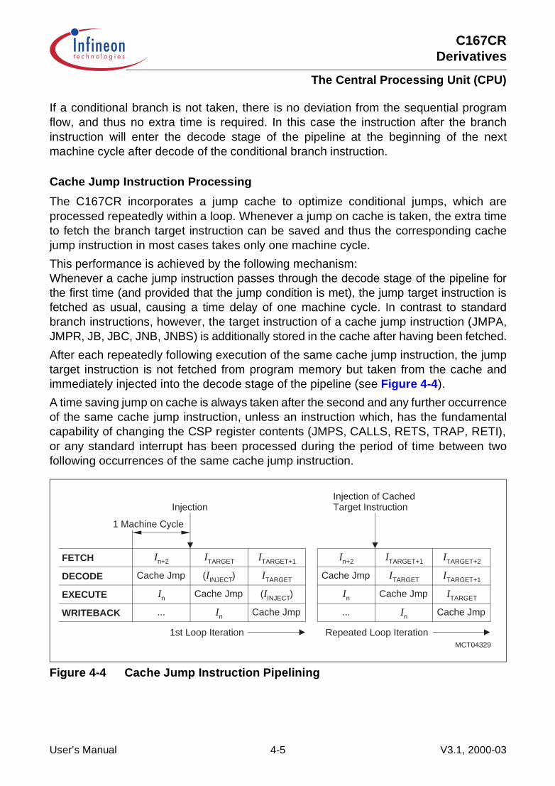
C167CRDerivatives
The Central Processing Unit (CPU)
If a conditional branch is not taken, there is no deviation from the sequential programflow, and thus no extra time is required. In this case the instruction after the branchinstruction will enter the decode stage of the pipeline at the beginning of the nextmachine cycle after decode of the conditional branch instruction.
Cache Jump Instruction Processing
The C167CR incorporates a jump cache to optimize conditional jumps, which areprocessed repeatedly within a loop. Whenever a jump on cache is taken, the extra timeto fetch the branch target instruction can be saved and thus the corresponding cachejump instruction in most cases takes only one machine cycle.
This performance is achieved by the following mechanism:Whenever a cache jump instruction passes through the decode stage of the pipeline forthe first time (and provided that the jump condition is met), the jump target instruction isfetched as usual, causing a time delay of one machine cycle. In contrast to standardbranch instructions, however, the target instruction of a cache jump instruction (JMPA,JMPR, JB, JBC, JNB, JNBS) is additionally stored in the cache after having been fetched.
After each repeatedly following execution of the same cache jump instruction, the jumptarget instruction is not fetched from program memory but taken from the cache andimmediately injected into the decode stage of the pipeline (see Figure 4-4).
A time saving jump on cache is always taken after the second and any further occurrenceof the same cache jump instruction, unless an instruction which, has the fundamentalcapability of changing the CSP register contents (JMPS, CALLS, RETS, TRAP, RETI),or any standard interrupt has been processed during the period of time between twofollowing occurrences of the same cache jump instruction.
Figure 4-4 Cache Jump Instruction Pipelining
MCT04329
FETCH
DECODE
EXECUTE
WRITEBACK
In+2 ITARGET
(IINJECT)
1 Machine Cycle
1st Loop Iteration
Cache JmpIn
...
ITARGET+1
ITARGET
Injection
(IINJECT)
Cache Jmp
Cache Jmp
In+2 ITARGET+1
Repeated Loop Iteration
Cache JmpIn
...
ITARGET+2
ITARGET+1
Injection of CachedTarget Instruction
Cache Jmp
Cache Jmp
ITARGET
In
ITARGET
In
User’s Manual 4-5 V3.1, 2000-03
C167CRDerivatives
The Central Processing Unit (CPU)
4.2 Particular Pipeline Effects
Since up to four different instructions are processed simultaneously, additional hardwarehas been spent in the C167CR to consider all causal dependencies which may exist oninstructions in different pipeline stages without a loss of performance. This extrahardware (i.e. for ‘forwarding’ operand read and write values) resolves most of thepossible conflicts (e.g. multiple usage of buses) in a time optimized way and thus avoidsthat the pipeline becomes noticeable for the user in most cases. However, there aresome very rare cases, where the circumstance that the C167CR is a pipelined machinerequires attention by the programmer. In these cases the delays caused by pipelineconflicts can be used for other instructions in order to optimize performance.
Context Pointer Updating
An instruction, which calculates a physical GPR operand address via the CP register, ismostly not capable of using a new CP value, which is to be updated by an immediatelypreceding instruction. Thus, to make sure that the new CP value is used, at least oneinstruction must be inserted between a CP-changing and a subsequent GPR-usinginstruction, as shown in the following example:
In :SCXT CP,#0FC00h ;select a new contextIn + 1: … ;must not be an instruction using a GPRIn + 2:MOV R0,#dataX ;write to GPR 0 in the new context
Data Page Pointer Updating
An instruction, which calculates a physical operand address via a particular DPPn(n = 0 to 3) register, is mostly not capable of using a new DPPn register value, which isto be updated by an immediately preceding instruction. Thus, to make sure that the newDPPn register value is used, at least one instruction must be inserted between a DPPn-changing instruction and a subsequent instruction which implicitly uses DPPn via a longor indirect addressing mode, as shown in the following example:
In :MOV DPP0,#4 ;select data page 4 via DPP0In + 1:… ;must not be an instruction using DPP0In + 2:MOV DPP0:0000H,R1;move contents of R1 to address location01’0000 H
;(in data page 4) supposed segment. isenabled
User’s Manual 4-6 V3.1, 2000-03

C167CRDerivatives
The Central Processing Unit (CPU)
Explicit Stack Pointer Updating
None of the RET, RETI, RETS, RETP or POP instructions is capable of correctly usinga new SP register value, which is to be updated by an immediately preceding instruction.Thus, in order to use the new SP register value without erroneously performed stackaccesses, at least one instruction must be inserted between an explicitly SP-writing andany subsequent of the just mentioned implicitly SP-using instructions, as shown in thefollowing example:
In :MOV SP,#0FA40H ;select a new top of stackIn + 1:… ;must not be an instruction popping operands
;from the system stackIn + 2:POP R0 ;pop word value from new top of stack intoR0
Note: Conflicts with instructions writing to the stack (PUSH, CALL, SCXT) are solvedinternally by the CPU logic.
Controlling Interrupts
Software modifications (implicit or explicit) of the PSW are done in the execute phase ofthe respective instructions. In order to maintain fast interrupt responses, however, thecurrent interrupt prioritization round does not consider these changes, i.e. an interruptrequest may be acknowledged after the instruction that disables interrupts via IEN orILVL or after the following instructions. Timecritical instruction sequences thereforeshould not begin directly after the instruction disabling interrupts, as shown in thefollowing examples:
INTERRUPTS_OFF:BCLR IEN ;globally disable interrupts<Instr non-crit> ;non-critical instruction<Instr 1st-crit> ;begin of uninterruptable critical sequence…<Instr last-crit> ;end of uninterruptable critical sequenceINTERRUPTS_ON:BSET IEN ;globally re-enable interruptsCRITICAL_SEQUENCE:ATOMIC #3 ;immediately block interruptsBCLR IEN ;globally disable interrupts… ;here is the uninterruptable sequenceBSET IEN ;globally re-enable interrupts
Note: The described delay of 1 instruction also applies for enabling the interrupts systemi.e. no interrupt requests are acknowledged until the instruction following theenabling instruction.
User’s Manual 4-7 V3.1, 2000-03
C167CRDerivatives
The Central Processing Unit (CPU)
External Memory Access Sequences
The effect described here will only become noticeable, when watching the externalmemory access sequences on the external bus (e.g. by means of a Logic Analyzer).Different pipeline stages can simultaneously put a request on the External Bus Controller(EBC). The sequence of instructions processed by the CPU may diverge from thesequence of the corresponding external memory accesses performed by the EBC, dueto the predefined priority of external memory accesses:
1st Write Data2nd Fetch Code3rd Read Data.
Initialization of Port Pins
Modifications of the direction of port pins (input or output) become effective only after theinstruction following the modifying instruction. As bit instructions (BSET, BCLR) useinternal read-modify-write sequences accessing the whole port, instructions modifyingthe port direction should be followed by an instruction that does not access the same port(see example below).
PORT_INIT_WRONG:BSET DP3.13 ;change direction of P3.13 to outputBSET P3.9 ;P3.13 is still input,
;rd-mod-wr reads pin P3.13PORT_INIT_RIGHT:BSET DP3.13 ;change direction of P3.13 to outputNOP ;any instruction not accessing port 3BSET P3.9 ;P3.13 is now output,
;rd-mod-wr reads P3.13’s output latch
Note: Special attention must be paid to interrupt service routines that modify the sameport as the software they have interrupted.
Changing the System Configuration
The instruction following an instruction that changes the system configuration via registerSYSCON (e.g. the mapping of the internal ROM, segmentation, stack size) cannot usethe new resources (e.g. ROM or stack). In these cases an instruction that does notaccess these resources should be inserted. Code accesses to the new ROM area areonly possible after an absolute branch to this area.
Note: As a rule, instructions that change ROM mapping should be executed frominternal RAM or external memory.
User’s Manual 4-8 V3.1, 2000-03

C167CRDerivatives
The Central Processing Unit (CPU)
BUSCON/ADDRSEL
The instruction following an instruction that changes the properties of an externaladdress area cannot access operands within the new area. In these cases an instructionthat does not access this address area should be inserted. Code accesses to the newaddress area should be made after an absolute branch to this area.
Note: As a rule, instructions that change external bus properties should not be executedfrom the respective external memory area.
Timing
Instruction pipelining reduces the average instruction processing time in a wide scale(from four to one machine cycles, mostly). However, there are some rare cases, wherea particular pipeline situation causes the processing time for a single instruction to beextended either by a half or by one machine cycle. Although this additional timerepresents only a tiny part of the total program execution time, it might be of interest toavoid these pipeline-caused time delays in time critical program modules.
Besides a general execution time description, Section 4.3 provides some hints on howto optimize time-critical program parts with regard to such pipeline-caused timingparticularities.
User’s Manual 4-9 V3.1, 2000-03
C167CRDerivatives
The Central Processing Unit (CPU)
4.3 Bit-Handling and Bit-Protection
The C167CR provides several mechanisms to manipulate bits. These mechanismseither manipulate software flags within the internal RAM, control on-chip peripherals viacontrol bits in their respective SFRs or control IO functions via port pins.
The instructions BSET, BCLR, BAND, BOR, BXOR, BMOV, BMOVN explicitly set orclear specific bits. The instructions BFLDL and BFLDH allow to manipulate up to 8 bitsof a specific byte at one time. The instructions JBC and JNBS implicitly clear or set thespecified bit when the jump is taken. The instructions JB and JNB (also conditional jumpinstructions that refer to flags) evaluate the specified bit to determine if the jump is to betaken.
Note: Bit operations on undefined bit locations will always read a bit value of ‘0’, whilethe write access will not effect the respective bit location.
All instructions that manipulate single bits or bit groups internally use a read-modify-writesequence that accesses the whole word, which contains the specified bit(s).
This method has several consequences:
• Bits can only be modified within the internal address areas, i.e. internal RAM andSFRs. External locations cannot be used with bit instructions.
The upper 256 Bytes of the SFR area, the ESFR area and the internal RAM are bit-addressable (see Chapter 3), i.e. those register bits located within the respectivesections can be directly manipulated using bit instructions. The other SFRs must beaccessed byte/word wise.
Note: All GPRs are bit-addressable independent of the allocation of the register bank viathe context pointer CP. Even GPRs which are allocated to not bit-addressableRAM locations provide this feature.
• The read-modify-write approach may be critical with hardware-effected bits. In thesecases the hardware may change specific bits while the read-modify-write operation isin progress, where the writeback would overwrite the new bit value generated by thehardware. The solution is either the implemented hardware protection (see below) orrealized through special programming (see Chapter 4.2).
Protected bits are not changed during the read-modify-write sequence, i.e. whenhardware sets e.g. an interrupt request flag between the read and the write of the read-modify-write sequence. The hardware protection logic guarantees that only the intendedbit(s) is/are effected by the write-back operation.
Note: If a conflict occurs between a bit manipulation generated by hardware and anintended software access the software access has priority and determines thefinal value of the respective bit.
A summary of the protected bits implemented in the C167CR can be found at the end ofChapter 2.
User’s Manual 4-10 V3.1, 2000-03

C167CRDerivatives
The Central Processing Unit (CPU)
4.4 Instruction State Times
Basically, the time to execute an instruction depends on where the instruction is fetchedfrom, and where possible operands are read from or written to. The fastest processingmode of the C167CR is to execute a program fetched from the internal code memory. Inthat case most of the instructions can be processed within just one machine cycle, whichis also the general minimum execution time.
All external memory accesses are performed by the C167CR’s on-chip External BusController (EBC), which works in parallel with the CPU.
This section summarizes the execution times in a very condensed way. A detaileddescription of the execution times for the various instructions and the specific exceptionscan be found in the “C166 Family Instruction Set Manual” .
Table 4-1 shows the minimum execution times required to process a C167CRinstruction fetched from the internal code memory, the internal RAM or from externalmemory. These execution times apply to most of the C167CR instructions - except someof the branches, the multiplication, the division and a special move instruction. In caseof internal ROM program execution there is no execution time dependency on theinstruction length except for some special branch situations. The numbers in the tableare in units of CPU clock cycles and assume no waitstates.
Execution from the internal RAM provides flexibility in terms of loadable and modifyablecode on the account of execution time.Execution from external memory strongly depends on the selected bus mode and theprogramming of the bus cycles (waitstates).
Table 4-1 Minimum Execution Times
Instruction Fetch Word Operand Access
Memory Area Word Instruction
Doubleword Instruction
Read from Write to
Internal code memory 2 2 2 –
Internal RAM 6 8 0/1 0
16-bit Demux Bus 2 4 2 2
16-bit Mux Bus 3 6 3 3
8-bit Demux Bus 4 8 4 4
8-bit Mux Bus 6 12 6 6
User’s Manual 4-11 V3.1, 2000-03

C167CRDerivatives
The Central Processing Unit (CPU)
The operand and instruction accesses listed below can extend the execution time of aninstruction:
• Internal code memory operand reads (same for byte and word operand reads)• Internal RAM operand reads via indirect addressing modes• Internal SFR operand reads immediately after writing• External operand reads• External operand writes• Jumps to non-aligned double word instructions in the internal ROM space• Testing Branch Conditions immediately after PSW writes
4.5 CPU Special Function Registers
The core CPU requires a set of Special Function Registers (SFRs) to maintain thesystem state information, to supply the ALU with register-addressable constants and tocontrol system and bus configuration, multiply and divide ALU operations, code memorysegmentation, data memory paging, and accesses to the General Purpose Registersand the System Stack.
The access mechanism for these SFRs in the CPU core is identical to the accessmechanism for any other SFR. Since all SFRs can simply be controlled by means of anyinstruction, which is capable of addressing the SFR memory space, a lot of flexibility hasbeen gained, without the need to create a set of system-specific instructions.
Note, however, that there are user access restrictions for some of the CPU core SFRsto ensure proper processor operations. The instruction pointer IP and code segmentpointer CSP cannot be accessed directly at all. They can only be changed indirectly viabranch instructions.
The PSW, SP, and MDC registers can be modified not only explicitly by the programmer,but also implicitly by the CPU during normal instruction processing. Note that any explicitwrite request (via software) to an SFR supersedes a simultaneous modification byhardware of the same register.
Note: Any write operation to a single byte of an SFR clears the non-addressedcomplementary byte within the specified SFR.Non-implemented (reserved) SFR bits cannot be modified, and will always supplya read value of ‘0’.
User’s Manual 4-12 V3.1, 2000-03
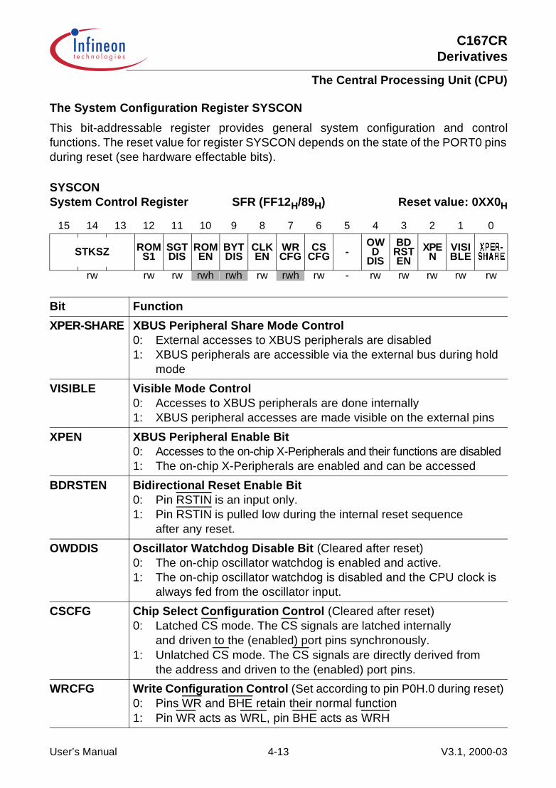
C167CRDerivatives
The Central Processing Unit (CPU)
The System Configuration Register SYSCON
This bit-addressable register provides general system configuration and controlfunctions. The reset value for register SYSCON depends on the state of the PORT0 pinsduring reset (see hardware effectable bits).
SYSCONSystem Control Register SFR (FF12H/89H) Reset value: 0XX0H
15 14 13 12 11 10 9 8 7 6 5 4 3 2 1 0
STKSZ ROM S1
SGT DIS
ROM EN
BYT DIS
CLK EN
WR CFG
CS CFG -
OWD
DIS
BDRSTEN
XPEN
VISIBLE
<4)67,%6)
rw rw rw rwh rwh rw rwh rw - rw rw rw rw rw
Bit Function
XPER-SHARE XBUS Peripheral Share Mode Control0: External accesses to XBUS peripherals are disabled1: XBUS peripherals are accessible via the external bus during hold
mode
VISIBLE Visible Mode Control0: Accesses to XBUS peripherals are done internally1: XBUS peripheral accesses are made visible on the external pins
XPEN XBUS Peripheral Enable Bit0: Accesses to the on-chip X-Peripherals and their functions are disabled1: The on-chip X-Peripherals are enabled and can be accessed
BDRSTEN Bidirectional Reset Enable Bit0: Pin RSTIN is an input only.1: Pin RSTIN is pulled low during the internal reset sequence
after any reset.
OWDDIS Oscillator Watchdog Disable Bit (Cleared after reset)0: The on-chip oscillator watchdog is enabled and active.1: The on-chip oscillator watchdog is disabled and the CPU clock is
always fed from the oscillator input.
CSCFG Chip Select Configuration Control (Cleared after reset)0: Latched CS mode. The CS signals are latched internally
and driven to the (enabled) port pins synchronously.1: Unlatched CS mode. The CS signals are directly derived from
the address and driven to the (enabled) port pins.
WRCFG Write Configuration Control (Set according to pin P0H.0 during reset)0: Pins WR and BHE retain their normal function1: Pin WR acts as WRL, pin BHE acts as WRH
User’s Manual 4-13 V3.1, 2000-03

C167CRDerivatives
The Central Processing Unit (CPU)
Note: Register SYSCON cannot be changed after execution of the EINIT instruction.The function of bits XPER-SHARE, VISIBLE, WRCFG, BYTDIS, ROMEN andROMS1 is described in more detail in Chapter 9.
CLKEN System Clock Output Enable (CLKOUT, cleared after reset)0: CLKOUT disabled: pin may be used for general purpose IO1: CLKOUT enabled: pin outputs the system clock signal
BYTDIS Disable/Enable Control for Pin BHE (Set according to data bus width)0: Pin BHE enabled1: Pin BHE disabled, pin may be used for general purpose IO
ROMEN Internal ROM Enable (Set according to pin EA during reset)0: Internal program memory disabled, accesses to the ROM area use
the external bus1: Internal program memory enabled
SGTDIS Segmentation Disable/Enable Control (Cleared after reset)0: Segmentation enabled
(CSP is saved/restored during interrupt entry/exit)1: Segmentation disabled (Only IP is saved/restored)
ROMS1 Internal ROM Mapping0: Internal ROM area mapped to segment 0 (00’0000H … 00’7FFFH)1: Internal ROM area mapped to segment 1 (01’0000H … 01’7FFFH)
STKSZ System Stack SizeSelects the size of the system stack (in the internal RAM)from 32 to 512 words
Bit Function
User’s Manual 4-14 V3.1, 2000-03
C167CRDerivatives
The Central Processing Unit (CPU)
System Clock Output Enable (CLKEN)
The system clock output function is enabled by setting bit CLKEN in register SYSCONto ‘1’. If enabled, port pin P3.15 takes on its alternate function as CLKOUT output pin.The clock output is a 50% duty cycle clock (except for direct drive operation whereCLKOUT reflects the clock input signal, and for slowdown operation where CLKOUTmirrors the CPU clock signal) whose frequency equals the CPU operating frequency(fOUT = fCPU).
Note: The output driver of port pin P3.15 is switched on automatically, when theCLKOUT function is enabled. The port direction bit is disregarded.After reset, the clock output function is disabled (CLKEN = ‘0’).In emulation mode the CLKOUT function is enabled automatically.
Segmentation Disable/Enable Control (SGTDIS)
Bit SGTDIS allows to select either the segmented or non-segmented memory mode.In non-segmented memory mode (SGTDIS = ‘1’) it is assumed that the code addressspace is restricted to 64 KBytes (segment 0) and thus 16 bits are sufficient to representall code addresses. For implicit stack operations (CALL or RET) the CSP register istotally ignored and only the IP is saved to and restored from the stack.In segmented memory mode (SGTDIS = ‘0’) it is assumed that the whole addressspace is available for instructions. For implicit stack operations (CALL or RET) the CSPregister and the IP are saved to and restored from the stack. After reset the segmentedmemory mode is selected.
Note: Bit SGTDIS controls if the CSP register is pushed onto the system stack in additionto the IP register before an interrupt service routine is entered, and it is repoppedwhen the interrupt service routine is left again.
System Stack Size (STKSZ)
This bitfield defines the size of the physical system stack, which is located in the internalRAM of the C167CR. An area of 32 … 512 words or all of the internal RAM may bededicated to the system stack. A so-called “circular stack” mechanism allows to use abigger virtual stack than this dedicated RAM area.
These techniques as well as the encoding of bitfield STKSZ are described in more detailin Chapter 21.
User’s Manual 4-15 V3.1, 2000-03
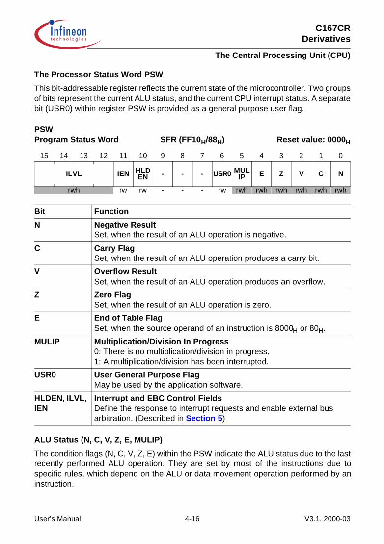
C167CRDerivatives
The Central Processing Unit (CPU)
The Processor Status Word PSW
This bit-addressable register reflects the current state of the microcontroller. Two groupsof bits represent the current ALU status, and the current CPU interrupt status. A separatebit (USR0) within register PSW is provided as a general purpose user flag.
ALU Status (N, C, V, Z, E, MULIP)
The condition flags (N, C, V, Z, E) within the PSW indicate the ALU status due to the lastrecently performed ALU operation. They are set by most of the instructions due tospecific rules, which depend on the ALU or data movement operation performed by aninstruction.
PSWProgram Status Word SFR (FF10H/88H) Reset value: 0000H
15 14 13 12 11 10 9 8 7 6 5 4 3 2 1 0
ILVL IEN HLDEN - - - USR0 MUL
IP E Z V C N
rwh rw rw - - - rw rwh rwh rwh rwh rwh rwh
Bit Function
N Negative ResultSet, when the result of an ALU operation is negative.
C Carry FlagSet, when the result of an ALU operation produces a carry bit.
V Overflow ResultSet, when the result of an ALU operation produces an overflow.
Z Zero FlagSet, when the result of an ALU operation is zero.
E End of Table FlagSet, when the source operand of an instruction is 8000H or 80H.
MULIP Multiplication/Division In Progress0: There is no multiplication/division in progress.1: A multiplication/division has been interrupted.
USR0 User General Purpose FlagMay be used by the application software.
HLDEN, ILVL, IEN
Interrupt and EBC Control FieldsDefine the response to interrupt requests and enable external bus arbitration. (Described in Section 5)
User’s Manual 4-16 V3.1, 2000-03

C167CRDerivatives
The Central Processing Unit (CPU)
After execution of an instruction which explicitly updates the PSW register, the conditionflags cannot be interpreted as described in the following, because any explicit write tothe PSW register supersedes the condition flag values, which are implicitly generated bythe CPU. Explicitly reading the PSW register supplies a read value which represents thestate of the PSW register after execution of the immediately preceding instruction.
Note: After reset, all of the ALU status bits are cleared.
N-Flag: For most of the ALU operations, the N-flag is set to ‘1’, if the most significant bitof the result contains a ‘1’, otherwise it is cleared. In the case of integer operations theN-flag can be interpreted as the sign bit of the result (negative: N = ‘1’, positive: N = ‘0’).Negative numbers are always represented as the 2’s complement of the correspondingpositive number. The range of signed numbers extends from ‘– 8000H’ to ‘+ 7FFFH’ forthe word data type, or from ‘– 80H’ to ‘+ 7FH’ for the byte data type.For Boolean bitoperations with only one operand the N-flag represents the previous state of thespecified bit. For Boolean bit operations with two operands the N-flag represents thelogical XORing of the two specified bits.
C-Flag: After an addition the C-flag indicates that a carry from the most significant bit ofthe specified word or byte data type has been generated. After a subtraction or acomparison the C-flag indicates a borrow, which represents the logical negation of acarry for the addition.This means that the C-flag is set to ‘1’, if no carry from the most significant bit of thespecified word or byte data type has been generated during a subtraction, which isperformed internally by the ALU as a 2’s complement addition, and the C-flag is clearedwhen this complement addition caused a carry.The C-flag is always cleared for logical, multiply and divide ALU operations, becausethese operations cannot cause a carry anyhow.For shift and rotate operations the C-flag represents the value of the bit shifted out last.If a shift count of zero is specified, the C-flag will be cleared. The C-flag is also clearedfor a prioritize ALU operation, because a ‘1’ is never shifted out of the MSB during thenormalization of an operand.For Boolean bit operations with only one operand the C-flag is always cleared. ForBoolean bit operations with two operands the C-flag represents the logical ANDing of thetwo specified bits.
V-Flag: For addition, subtraction and 2’s complementation the V-flag is always set to ‘1’,if the result overflows the maximum range of signed numbers, which are representableby either 16 bits for word operations (‘– 8000H’ to ‘+ 7FFFH’), or by 8 bits for byteoperations (‘– 80H’ to ‘+ 7FH’), otherwise the V-flag is cleared. Note that the result of aninteger addition, integer subtraction, or 2’s complement is not valid, if the V-flag indicatesan arithmetic overflow.For multiplication and division the V-flag is set to ‘1’, if the result cannot be representedin a word data type, otherwise it is cleared. Note that a division by zero will always causean overflow. In contrast to the result of a division, the result of a multiplication is valid
User’s Manual 4-17 V3.1, 2000-03

C167CRDerivatives
The Central Processing Unit (CPU)
regardless of whether the V-flag is set to ‘1’ or not.Since logical ALU operations cannot produce an invalid result, the V-flag is cleared bythese operations.
The V-flag is also used as ‘Sticky Bit’ for rotate right and shift right operations. With onlyusing the C-flag, a rounding error caused by a shift right operation can be estimated upto a quantity of one half of the LSB of the result. In conjunction with the V-flag, the C-flagallows evaluating the rounding error with a finer resolution (see Table 4-2).For Boolean bit operations with only one operand the V-flag is always cleared. ForBoolean bit operations with two operands the V-flag represents the logical ORing of thetwo specified bits.
Z-Flag: The Z-flag is normally set to ‘1’, if the result of an ALU operation equals zero,otherwise it is cleared.For the addition and subtraction with carry the Z-flag is only set to ‘1’, if the Z-flag alreadycontains a ‘1’ and the result of the current ALU operation additionally equals zero. Thismechanism is provided for the support of multiple precision calculations.For Boolean bit operations with only one operand the Z-flag represents the logicalnegation of the previous state of the specified bit. For Boolean bit operations with twooperands the Z-flag represents the logical NORing of the two specified bits. For theprioritize ALU operation the Z-flag indicates, if the second operand was zero or not.
E-Flag: The E-flag can be altered by instructions, which perform ALU or data movementoperations. The E-flag is cleared by those instructions which cannot be reasonably usedfor table search operations. In all other cases the E-flag is set depending on the value ofthe source operand to signify whether the end of a search table is reached or not. If thevalue of the source operand of an instruction equals the lowest negative number, whichis representable by the data format of the corresponding instruction (‘8000H’ for the worddata type, or ‘80H’ for the byte data type), the E-flag is set to ‘1’, otherwise it is cleared.
MULIP-Flag: The MULIP-flag will be set to ‘1’ by hardware upon the entrance into aninterrupt service routine, when a multiply or divide ALU operation was interrupted beforecompletion. Depending on the state of the MULIP bit, the hardware decides whether amultiplication or division must be continued or not after the end of an interrupt service.The MULIP bit is overwritten with the contents of the stacked MULIP-flag when thereturn-from-interrupt-instruction (RETI) is executed. This normally means that theMULIP-flag is cleared again after that.
Table 4-2 Shift Right Rounding Error Evaluation
C-flag V-flag Rounding Error Quantity
0011
0101
– No rounding error – 0 < Rounding error < 1/2 LSB
Rounding error = 1/2 LSBRounding error > 1/2 LSB
User’s Manual 4-18 V3.1, 2000-03
C167CRDerivatives
The Central Processing Unit (CPU)
Note: The MULIP flag is a part of the task environment! When the interrupting serviceroutine does not return to the interrupted multiply/divide instruction (i.e. in case ofa task scheduler that switches between independent tasks), the MULIP flag mustbe saved as part of the task environment and must be updated accordingly for thenew task before this task is entered.
CPU Interrupt Status (IEN, ILVL)
The Interrupt Enable bit allows to globally enable (IEN = ‘1’) or disable (IEN = ‘0’)interrupts. The four-bit Interrupt Level field (ILVL) specifies the priority of the current CPUactivity. The interrupt level is updated by hardware upon entry into an interrupt serviceroutine, but it can also be modified via software to prevent other interrupts from beingacknowledged. In case an interrupt level ‘15’ has been assigned to the CPU, it has thehighest possible priority, and thus the current CPU operation cannot be interruptedexcept by hardware traps or external non-maskable interrupts. For details please referto Chapter 5.
After reset all interrupts are globally disabled, and the lowest priority (ILVL = 0) isassigned to the initial CPU activity.
The Instruction Pointer IP
This register determines the 16-bit intra-segment address of the currently fetchedinstruction within the code segment selected by the CSP register. The IP register is notmapped into the C167CR’s address space, and thus it is not directly accessable by theprogrammer. The IP can, however, be modified indirectly via the stack by means of areturn instruction.
The IP register is implicitly updated by the CPU for branch instructions and afterinstruction fetch operations.
IPInstruction Pointer - - - (- - - -/- -) Reset value: 0000H
15 14 13 12 11 10 9 8 7 6 5 4 3 2 1 0
ip
(r)(w)h
Bit Function
ip Specifies the intra segment offset, from where the current instruction is to be fetched. IP refers to the current segment <SEGNR>.
User’s Manual 4-19 V3.1, 2000-03
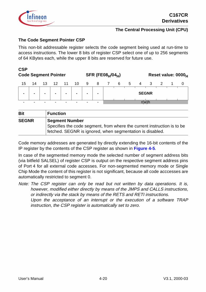
C167CRDerivatives
The Central Processing Unit (CPU)
The Code Segment Pointer CSP
This non-bit addressable register selects the code segment being used at run-time toaccess instructions. The lower 8 bits of register CSP select one of up to 256 segmentsof 64 KBytes each, while the upper 8 bits are reserved for future use.
Code memory addresses are generated by directly extending the 16-bit contents of theIP register by the contents of the CSP register as shown in Figure 4-5.
In case of the segmented memory mode the selected number of segment address bits(via bitfield SALSEL) of register CSP is output on the respective segment address pinsof Port 4 for all external code accesses. For non-segmented memory mode or SingleChip Mode the content of this register is not significant, because all code acccesses areautomatically restricted to segment 0.
Note: The CSP register can only be read but not written by data operations. It is,however, modified either directly by means of the JMPS and CALLS instructions,or indirectly via the stack by means of the RETS and RETI instructions.Upon the acceptance of an interrupt or the execution of a software TRAPinstruction, the CSP register is automatically set to zero.
CSPCode Segment Pointer SFR (FE08H/04H) Reset value: 0000H
15 14 13 12 11 10 9 8 7 6 5 4 3 2 1 0
- - - - - - - - SEGNR
- - - - - - - - r(w)h
Bit Function
SEGNR Segment NumberSpecifies the code segment, from where the current instruction is to be fetched. SEGNR is ignored, when segmentation is disabled.
User’s Manual 4-20 V3.1, 2000-03
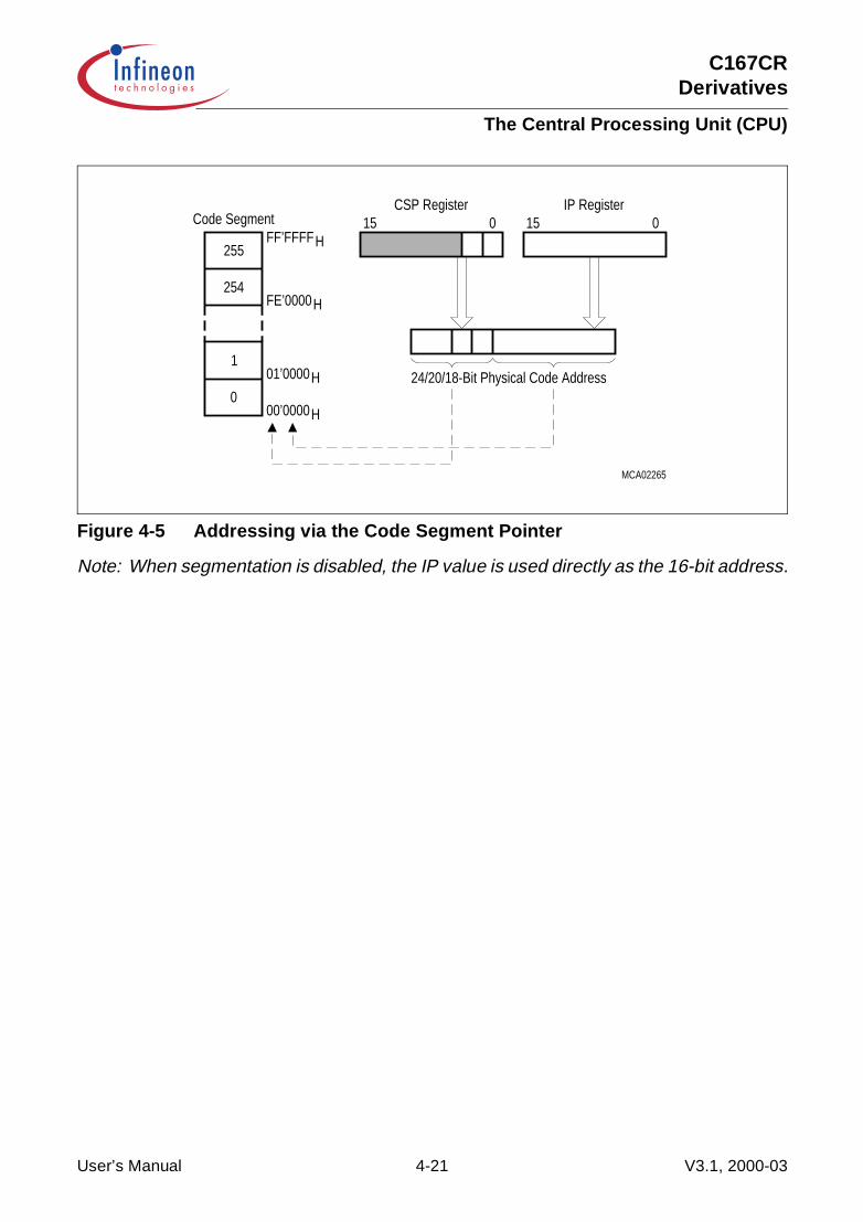
C167CRDerivatives
The Central Processing Unit (CPU)
Figure 4-5 Addressing via the Code Segment Pointer
Note: When segmentation is disabled, the IP value is used directly as the 16-bit address.
MCA02265
255
1
15 0IP Register
254
0
Code SegmentFF’FFFFH
FE’0000H
01’0000H
00’0000H
CSP Register15 0
24/20/18-Bit Physical Code Address
User’s Manual 4-21 V3.1, 2000-03

C167CRDerivatives
The Central Processing Unit (CPU)
The Data Page Pointers DPP0, DPP1, DPP2, DPP3
These four non-bit addressable registers select up to four different data pages beingactive simultaneously at run-time. The lower 10 bits of each DPP register select one ofthe 1024 possible 16-KByte data pages while the upper 6 bits are reserved for future use.The DPP registers allow to access the entire memory space in pages of 16 KBytes each.
DPP0Data Page Pointer 0 SFR (FE00H/00H) Reset value: 0000H
15 14 13 12 11 10 9 8 7 6 5 4 3 2 1 0
- - - - - - DPP0PN
- - - - - - rw
DPP1Data Page Pointer 1 SFR (FE02H/01H) Reset value: 0001H
15 14 13 12 11 10 9 8 7 6 5 4 3 2 1 0
- - - - - - DPP1PN
- - - - - - rw
DPP2Data Page Pointer 2 SFR (FE04H/02H) Reset value: 0002H
15 14 13 12 11 10 9 8 7 6 5 4 3 2 1 0
- - - - - - DPP2PN
- - - - - - rw
DPP3Data Page Pointer 3 SFR (FE06H/03H) Reset value: 0003H
15 14 13 12 11 10 9 8 7 6 5 4 3 2 1 0
- - - - - - DPP3PN
- - - - - - rw
User’s Manual 4-22 V3.1, 2000-03
C167CRDerivatives
The Central Processing Unit (CPU)
The DPP registers are implicitly used, whenever data accesses to any memory locationare made via indirect or direct long 16-bit addressing modes (except for overrideaccesses via EXTended instructions and PEC data transfers). After reset, the Data PagePointers are initialized in a way that all indirect or direct long 16-bit addresses result inidentical 18-bit addresses. This allows to access data pages 3 … 0 within segment 0 asshown in Figure 4-6. If the user does not want to use any data paging, no further actionis required.
Data paging is performed by concatenating the lower 14 bits of an indirect or direct long16-bit address with the contents of the DPP register selected by the upper two bits of the16-bit address. The contents of the selected DPP register specify one of the1024 possible data pages. This data page base address together with the 14-bit pageoffset forms the physical 24-bit address (selectable part is driven to the address pins).
In case of non-segmented memory mode, only the two least significant bits of theimplicitly selected DPP register are used to generate the physical address. Thus,extreme care should be taken when changing the content of a DPP register, if a non-segmented memory model is selected, because otherwise unexpected results couldoccur.
In case of the segmented memory mode the selected number of segment address bits(via bitfield SALSEL) of the respective DPP register is output on the respective segmentaddress pins of Port 4 for all external data accesses.
A DPP register can be updated via any instruction, which is capable of modifying an SFR.
Note: Due to the internal instruction pipeline, a new DPP value is not yet usable for theoperand address calculation of the instruction immediately following theinstruction updating the DPP register.
Bit Function
DPPxPN Data Page Number of DPPxSpecifies the data page selected via DPPx. Only the least significant two bits of DPPx are significant, when segmentation is disabled.
User’s Manual 4-23 V3.1, 2000-03

C167CRDerivatives
The Central Processing Unit (CPU)
Figure 4-6 Addressing via the Data Page Pointers
MCA02264
1023
1022
1021
3
2
1
0
DPP Registers
DPP3-11
DPP2-10
DPP1-01
DPP0-00
15 14 016-Bit Data Address
14-BitIntra-Page Address(concatenated withcontent of DPPx).
Affer reset or with segmentation disabled the DPP registers select data pages 3...0.All of the internal memory is accessible in these cases.
User’s Manual 4-24 V3.1, 2000-03
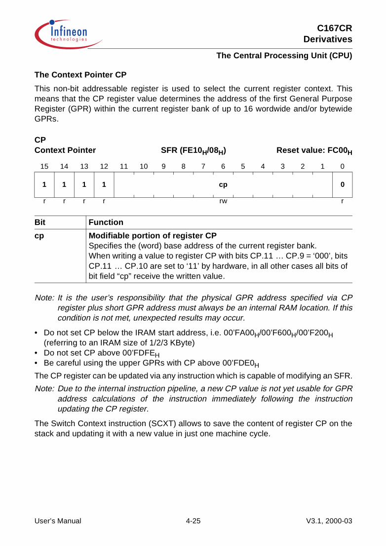
C167CRDerivatives
The Central Processing Unit (CPU)
The Context Pointer CP
This non-bit addressable register is used to select the current register context. Thismeans that the CP register value determines the address of the first General PurposeRegister (GPR) within the current register bank of up to 16 wordwide and/or bytewideGPRs.
Note: It is the user’s responsibility that the physical GPR address specified via CPregister plus short GPR address must always be an internal RAM location. If thiscondition is not met, unexpected results may occur.
• Do not set CP below the IRAM start address, i.e. 00’FA00H/00’F600H/00’F200H(referring to an IRAM size of 1/2/3 KByte)
• Do not set CP above 00’FDFEH• Be careful using the upper GPRs with CP above 00’FDE0H
The CP register can be updated via any instruction which is capable of modifying an SFR.
Note: Due to the internal instruction pipeline, a new CP value is not yet usable for GPRaddress calculations of the instruction immediately following the instructionupdating the CP register.
The Switch Context instruction (SCXT) allows to save the content of register CP on thestack and updating it with a new value in just one machine cycle.
CPContext Pointer SFR (FE10H/08H) Reset value: FC00H
15 14 13 12 11 10 9 8 7 6 5 4 3 2 1 0
1 1 1 1 cp 0
r r r r rw r
Bit Function
cp Modifiable portion of register CPSpecifies the (word) base address of the current register bank.When writing a value to register CP with bits CP.11 … CP.9 = ‘000’, bits CP.11 … CP.10 are set to ‘11’ by hardware, in all other cases all bits of bit field “cp” receive the written value.
User’s Manual 4-25 V3.1, 2000-03
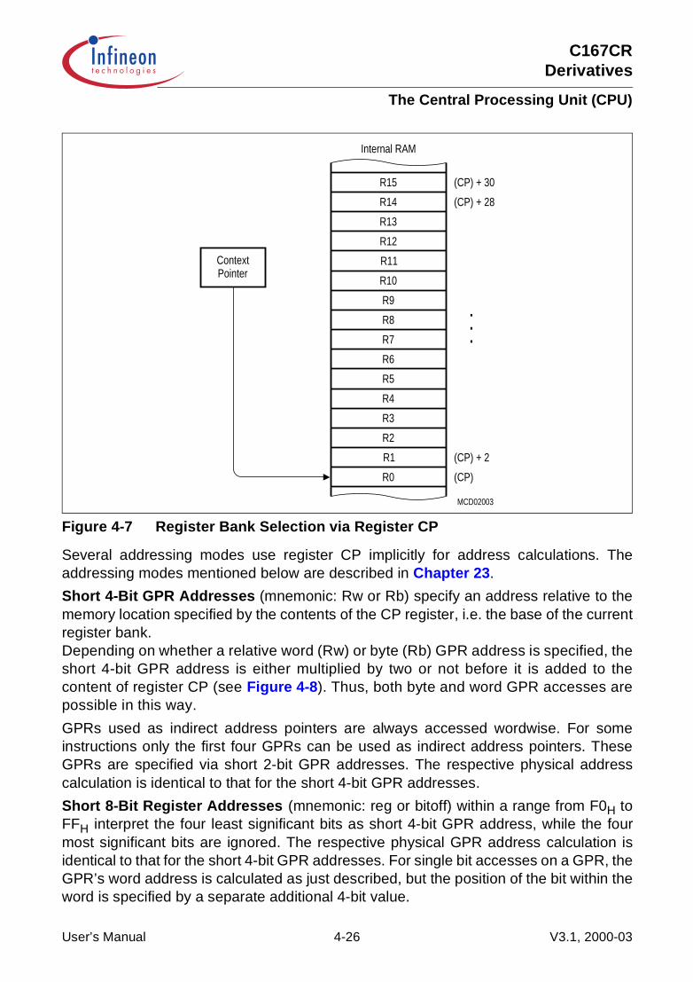
C167CRDerivatives
The Central Processing Unit (CPU)
Figure 4-7 Register Bank Selection via Register CP
Several addressing modes use register CP implicitly for address calculations. Theaddressing modes mentioned below are described in Chapter 23.
Short 4-Bit GPR Addresses (mnemonic: Rw or Rb) specify an address relative to thememory location specified by the contents of the CP register, i.e. the base of the currentregister bank.Depending on whether a relative word (Rw) or byte (Rb) GPR address is specified, theshort 4-bit GPR address is either multiplied by two or not before it is added to thecontent of register CP (see Figure 4-8). Thus, both byte and word GPR accesses arepossible in this way.
GPRs used as indirect address pointers are always accessed wordwise. For someinstructions only the first four GPRs can be used as indirect address pointers. TheseGPRs are specified via short 2-bit GPR addresses. The respective physical addresscalculation is identical to that for the short 4-bit GPR addresses.
Short 8-Bit Register Addresses (mnemonic: reg or bitoff) within a range from F0H toFFH interpret the four least significant bits as short 4-bit GPR address, while the fourmost significant bits are ignored. The respective physical GPR address calculation isidentical to that for the short 4-bit GPR addresses. For single bit accesses on a GPR, theGPR’s word address is calculated as just described, but the position of the bit within theword is specified by a separate additional 4-bit value.
MCD02003
R0
R1
R2
R3
R4
R5
R6
R7
R8
R9
R10
R11
R12
R13
R14
R15
ContextPointer
(CP) + 30
(CP) + 28
(CP) + 2
(CP)
Internal RAM
...
User’s Manual 4-26 V3.1, 2000-03
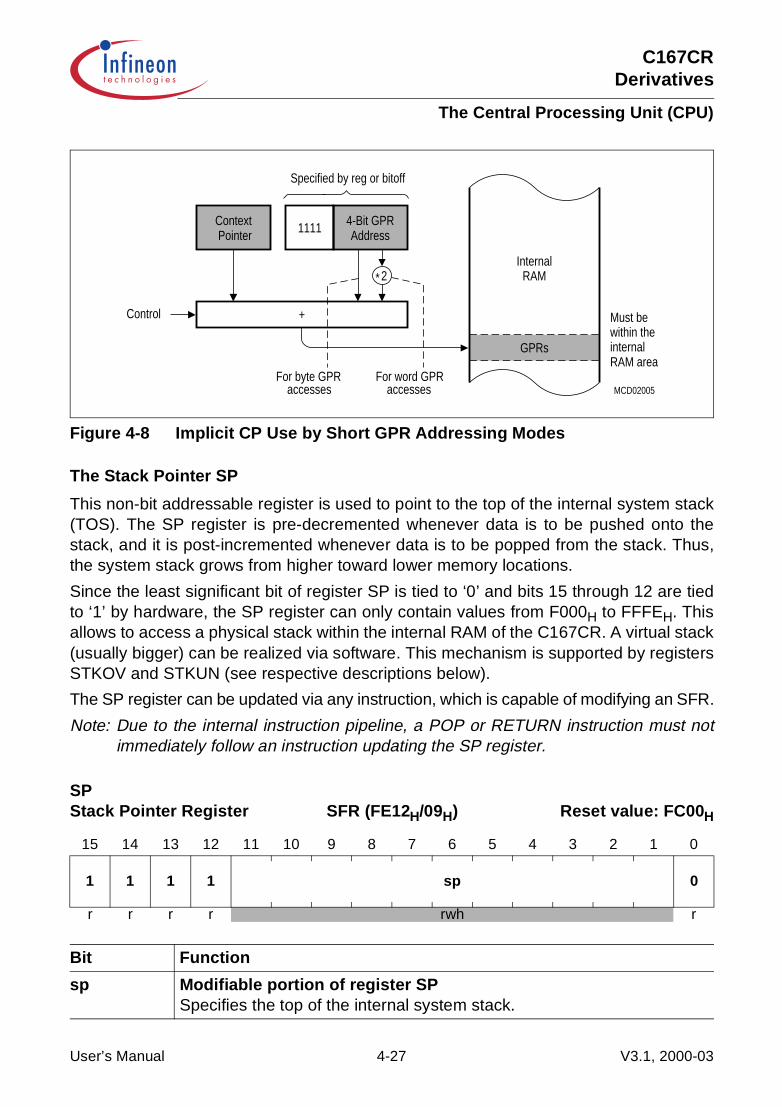
C167CRDerivatives
The Central Processing Unit (CPU)
Figure 4-8 Implicit CP Use by Short GPR Addressing Modes
The Stack Pointer SP
This non-bit addressable register is used to point to the top of the internal system stack(TOS). The SP register is pre-decremented whenever data is to be pushed onto thestack, and it is post-incremented whenever data is to be popped from the stack. Thus,the system stack grows from higher toward lower memory locations.
Since the least significant bit of register SP is tied to ‘0’ and bits 15 through 12 are tiedto ‘1’ by hardware, the SP register can only contain values from F000H to FFFEH. Thisallows to access a physical stack within the internal RAM of the C167CR. A virtual stack(usually bigger) can be realized via software. This mechanism is supported by registersSTKOV and STKUN (see respective descriptions below).
The SP register can be updated via any instruction, which is capable of modifying an SFR.
Note: Due to the internal instruction pipeline, a POP or RETURN instruction must notimmediately follow an instruction updating the SP register.
SPStack Pointer Register SFR (FE12H/09H) Reset value: FC00H
15 14 13 12 11 10 9 8 7 6 5 4 3 2 1 0
1 1 1 1 sp 0
r r r r rwh r
Bit Function
sp Modifiable portion of register SPSpecifies the top of the internal system stack.
For word GPRaccessesaccesses
For byte GPR
Control
1111
Specified by reg or bitoff
ContextPointer
+
4-Bit GPRAddress
2*
MCD02005
Internal
GPRs
RAM
Must bewithin the
RAM areainternal
User’s Manual 4-27 V3.1, 2000-03

C167CRDerivatives
The Central Processing Unit (CPU)
The Stack Overflow Pointer STKOV
This non-bit addressable register is compared against the SP register after eachoperation, which pushes data onto the system stack (e.g. PUSH and CALL instructionsor interrupts) and after each subtraction from the SP register. If the content of the SPregister is less than the content of the STKOV register, a stack overflow hardware trapwill occur.
Since the least significant bit of register STKOV is tied to ‘0’ and bits 15 through 12 aretied to ‘1’ by hardware, the STKOV register can only contain values from F000H toFFFEH.
The Stack Overflow Trap (entered when (SP) < (STKOV)) may be used in two differentways:
• Fatal error indication treats the stack overflow as a system error through theassociated trap service routine. Under these circumstances data in the bottom of thestack may have been overwritten by the status information stacked upon servicing thestack overflow trap.
• Automatic system stack flushing allows to use the system stack as a ‘Stack Cache’for a bigger external user stack. In this case register STKOV should be initialized to avalue, which represents the desired lowest Top of Stack address plus 12 according tothe selected maximum stack size. This considers the worst case that will occur, whena stack overflow condition is detected just during entry into an interrupt service routine.Then, six additional stack word locations are required to push IP, PSW, and CSP forboth the interrupt service routine and the hardware trap service routine.
More details about the stack overflow trap service routine and virtual stack managementare given in Chapter 21.
STKOVStack Overflow Reg. SFR (FE14H/0AH) Reset value:FA00H
15 14 13 12 11 10 9 8 7 6 5 4 3 2 1 0
1 1 1 1 stkov 0
r r r r rw
Bit Function
stkov Modifiable portion of register STKOVSpecifies the lower limit of the internal system stack.
User’s Manual 4-28 V3.1, 2000-03

C167CRDerivatives
The Central Processing Unit (CPU)
The Stack Underflow Pointer STKUN
This non-bit addressable register is compared against the SP register after eachoperation, which pops data from the system stack (e.g. POP and RET instructions) andafter each addition to the SP register. If the content of the SP register is greater than thecontent of the STKUN register, a stack underflow hardware trap will occur.
Since the least significant bit of register STKUN is tied to ‘0’ and bits 15 through 12 aretied to ‘1’ by hardware, the STKUN register can only contain values from F000H toFFFEH.
The Stack Underflow Trap (entered when (SP) > (STKUN)) may be used in two differentways:
• Fatal error indication treats the stack underflow as a system error through theassociated trap service routine.
• Automatic system stack refilling allows to use the system stack as a ‘Stack Cache’for a bigger external user stack. In this case register STKUN should be initialized to avalue, which represents the desired highest Bottom of Stack address.
More details about the stack underflow trap service routine and virtual stackmanagement are given in Chapter 21.
Scope of Stack Limit Control
The stack limit control realized by the register pair STKOV and STKUN detects caseswhere the stack pointer SP is moved outside the defined stack area either by ADD orSUB instructions or by PUSH or POP operations (explicit or implicit, i.e. CALL or RETinstructions).
This control mechanism is not triggered, i.e. no stack trap is generated, when
• the stack pointer SP is directly updated via MOV instructions• the limits of the stack area (STKOV, STKUN) are changed, so that SP is outside of the
new limits.
STKUNStack Underflow Reg. SFR (FE16H/0BH) Reset value: FC00H
15 14 13 12 11 10 9 8 7 6 5 4 3 2 1 0
1 1 1 1 stkun 0
r r r r rw r
Bit Function
stkun Modifiable portion of register STKUNSpecifies the upper limit of the internal system stack.
User’s Manual 4-29 V3.1, 2000-03

C167CRDerivatives
The Central Processing Unit (CPU)
The Multiply/Divide High Register MDH
This register is a part of the 32-bit multiply/divide register, which is implicitly used by theCPU, when it performs a multiplication or a division. After a multiplication, this non-bitaddressable register represents the high order 16 bits of the 32-bit result. For longdivisions, the MDH register must be loaded with the high order 16 bits of the 32-bitdividend before the division is started. After any division, register MDH represents the16-bit remainder.
Whenever this register is updated via software, the Multiply/Divide Register In Use(MDRIU) flag in the Multiply/Divide Control register (MDC) is set to ‘1’.
When a multiplication or division is interrupted before its completion and when a newmultiply or divide operation is to be performed within the interrupt service routine, registerMDH must be saved along with registers MDL and MDC to avoid erroneous results.
A detailed description of how to use the MDH register for programming multiply anddivide algorithms can be found in Chapter 21.
MDHMultiply/Divide High Reg. SFR (FE0CH/06H) Reset value: 0000H
15 14 13 12 11 10 9 8 7 6 5 4 3 2 1 0
mdh
rwh
Bit Function
mdh Specifies the high order 16 bits of the 32-bit multiply and divide reg. MD.
User’s Manual 4-30 V3.1, 2000-03
C167CRDerivatives
The Central Processing Unit (CPU)
The Multiply/Divide Low Register MDL
This register is a part of the 32-bit multiply/divide register, which is implicitly used by theCPU, when it performs a multiplication or a division. After a multiplication, this non-bitaddressable register represents the low order 16 bits of the 32-bit result. For longdivisions, the MDL register must be loaded with the low order 16 bits of the 32-bitdividend before the division is started. After any division, register MDL represents the 16-bit quotient.
Whenever this register is updated via software, the Multiply/Divide Register In Use(MDRIU) flag in the Multiply/Divide Control register (MDC) is set to ‘1’. The MDRIU flagis cleared, whenever the MDL register is read via software.
When a multiplication or division is interrupted before its completion and when a newmultiply or divide operation is to be performed within the interrupt service routine, registerMDL must be saved along with registers MDH and MDC to avoid erroneous results.
A detailed description of how to use the MDL register for programming multiply anddivide algorithms can be found in Chapter 21.
MDLMultiply/Divide Low Reg. SFR (FE0EH/07H) Reset value: 0000H
15 14 13 12 11 10 9 8 7 6 5 4 3 2 1 0
mdl
rwh
Bit Function
mdl Specifies the low order 16 bits of the 32-bit multiply and divide reg. MD.
User’s Manual 4-31 V3.1, 2000-03

C167CRDerivatives
The Central Processing Unit (CPU)
The Multiply/Divide Control Register MDC
This bit addressable 16-bit register is implicitly used by the CPU, when it performs amultiplication or a division. It is used to store the required control information for thecorresponding multiply or divide operation. Register MDC is updated by hardware duringeach single cycle of a multiply or divide instruction.
When a division or multiplication was interrupted before its completion and the multiply/divide unit is required, the MDC register must first be saved along with registers MDHand MDL (to be able to restart the interrupted operation later), and then it must becleared prepare it for the new calculation. After completion of the new division ormultiplication, the state of the interrupted multiply or divide operation must be restored.
The MDRIU flag is the only portion of the MDC register which might be of interest for theuser. The remaining portions of the MDC register are reserved for dedicated use by thehardware, and should never be modified by the user in another way than describedabove. Otherwise, a correct continuation of an interrupted multiply or divide operationcannot be guaranteed.
A detailed description of how to use the MDC register for programming multiply anddivide algorithms can be found in Chapter 21.
MDCMultiply/Divide Control Reg. SFR (FF0EH/87H) Reset value: 0000H
15 14 13 12 11 10 9 8 7 6 5 4 3 2 1 0
- - - - - - - - ! ! ! ! ! ! MDRIU ! ! ! ! ! ! ! !
- - - - - - - - r(w)h r(w)h r(w)h r(w)h r(w)h r(w)h r(w)h r(w)h
Bit Function
MDRIU Multiply/Divide Register In Use0: Cleared, when register MDL is read via software.1: Set when register MDL or MDH is written via software, or when
a multiply or divide instruction is executed.
!! Internal Machine StatusThe multiply/divide unit uses these bits to control internal operations.Never modify these bits without saving and restoring register MDC.
User’s Manual 4-32 V3.1, 2000-03
C167CRDerivatives
The Central Processing Unit (CPU)
The Constant Zeros Register ZEROS
All bits of this bit-addressable register are fixed to ‘0’ by hardware. This register can beread only. Register ZEROS can be used as a register-addressable constant of all zeros,i.e. for bit manipulation or mask generation. It can be accessed via any instruction, whichis capable of addressing an SFR.
The Constant Ones Register ONES
All bits of this bit-addressable register are fixed to ‘1’ by hardware. This register can beread only. Register ONES can be used as a register-addressable constant of all ones,i.e. for bit manipulation or mask generation. It can be accessed via any instruction, whichis capable of addressing an SFR.
ZEROSZeros Register SFR (FF1CH/8EH) Reset value: 0000H
15 14 13 12 11 10 9 8 7 6 5 4 3 2 1 0
0 0 0 0 0 0 0 0 0 0 0 0 0 0 0 0
r r r r r r r r r r r r r r r r
ONESOnes Register SFR (FF1EH/8FH) Reset Value: FFFFH
15 14 13 12 11 10 9 8 7 6 5 4 3 2 1 0
1 1 1 1 1 1 1 1 1 1 1 1 1 1 1 1
r r r r r r r r r r r r r r r r
User’s Manual 4-33 V3.1, 2000-03
C167CRDerivatives
Interrupt and Trap Functions
5 Interrupt and Trap FunctionsThe architecture of the C167CR supports several mechanisms for fast and flexibleresponse to service requests that can be generated from various sources internal orexternal to the microcontroller.
These mechanisms include:
Normal Interrupt Processing
The CPU temporarily suspends the current program execution and branches to aninterrupt service routine in order to service an interrupt requesting device. The currentprogram status (IP, PSW, in segmentation mode also CSP) is saved on the internalsystem stack. A prioritization scheme with 16 priority levels allows the user to specify theorder in which multiple interrupt requests are to be handled.
Interrupt Processing via the Peripheral Event Controller (PEC)
A faster alternative to normal software controlled interrupt processing is servicing aninterrupt requesting device with the C167CR’s integrated Peripheral Event Controller(PEC). Triggered by an interrupt request, the PEC performs a single word or byte datatransfer between any two locations in segment 0 (data pages 0 through 3) through oneof eight programmable PEC Service Channels. During a PEC transfer the normalprogram execution of the CPU is halted for just 1 instruction cycle. No internal programstatus information needs to be saved. The same prioritization scheme is used for PECservice as for normal interrupt processing. PEC transfers share the 2 highest prioritylevels.
Trap Functions
Trap functions are activated in response to special conditions that occur during theexecution of instructions. A trap can also be caused externally by the Non-MaskableInterrupt pin NMI. Several hardware trap functions are provided for handling erroneousconditions and exceptions that arise during the execution of an instruction. Hardwaretraps always have highest priority and cause immediate system reaction. The softwaretrap function is invoked by the TRAP instruction, which generates a software interrupt fora specified interrupt vector. For all types of traps the current program status is saved onthe system stack.
External Interrupt Processing
Although the C167CR does not provide dedicated interrupt pins, it allows to connectexternal interrupt sources and provides several mechanisms to react on external events,including standard inputs, non-maskable interrupts and fast external interrupts. Theseinterrupt functions are alternate port functions, except for the non-maskable interrupt andthe reset input.
User’s Manual 5-1 V3.1, 2000-03
C167CRDerivatives
Interrupt and Trap Functions
5.1 Interrupt System Structure
The C167CR provides 56 separate interrupt nodes that may be assigned to 16 prioritylevels. In order to support modular and consistent software design techniques, mostsources of an interrupt or PEC request are supplied with a separate interrupt controlregister and interrupt vector. The control register contains the interrupt request flag, theinterrupt enable bit, and the interrupt priority of the associated source. Each sourcerequest is then activated by one specific event, depending on the selected operatingmode of the respective device. For efficient usage of the resources also multi-sourceinterrupt nodes are incorporated. These nodes can be activated by several sourcerequests, e.g. as different kinds of errors in the serial interfaces. However, specific statusflags which identify the type of error are implemented in the serial channels’ controlregisters.
The C167CR provides a vectored interrupt system. In this system specific vectorlocations in the memory space are reserved for the reset, trap, and interrupt servicefunctions. Whenever a request occurs, the CPU branches to the location that isassociated with the respective interrupt source. This allows direct identification of thesource that caused the request. The only exceptions are the class B hardware traps,which all share the same interrupt vector. The status flags in the Trap Flag Register(TFR) can then be used to determine which exception caused the trap. For the specialsoftware TRAP instruction, the vector address is specified by the operand field of theinstruction, which is a seven bit trap number.
The reserved vector locations build a jump table in the low end of the C167CR’s addressspace (segment 0). The jump table is made up of the appropriate jump instructions thattransfer control to the interrupt or trap service routines, which may be located anywherewithin the address space. The entries of the jump table are located at the lowestaddresses in code segment 0 of the address space. Each entry occupies 2 words,except for the reset vector and the hardware trap vectors, which occupy 4 or 8 words.Table 5-1 lists all sources that are capable of requesting interrupt or PEC service in theC167CR, the associated interrupt vectors, their locations and the associated trapnumbers. It also lists the mnemonics of the affected Interrupt Request flags and theircorresponding Interrupt Enable flags. The mnemonics are composed of a part thatspecifies the respective source, followed by a part that specifies their function(IR = Interrupt Request flag, IE = Interrupt Enable flag).
Note: Each entry of the interrupt vector table provides room for two word instructions orone doubleword instruction. The respective vector location results from multiplyingthe trap number by 4 (4 Bytes per entry).All interrupt nodes that are currently not used by their associated modules or arenot connected to a module in the actual derivative may be used to generatesoftware controlled interrupt requests by setting the respective IR flag.
User’s Manual 5-2 V3.1, 2000-03
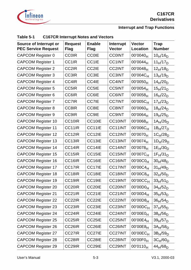
C167CRDerivatives
Interrupt and Trap Functions
Table 5-1 C167CR Interrupt Notes and Vectors
Source of Interrupt or PEC Service Request
RequestFlag
EnableFlag
InterruptVector
VectorLocation
TrapNumber
CAPCOM Register 0 CC0IR CC0IE CC0INT 00’0040H 10H/16D
CAPCOM Register 1 CC1IR CC1IE CC1INT 00’0044H 11H/17D
CAPCOM Register 2 CC2IR CC2IE CC2INT 00’0048H 12H/18D
CAPCOM Register 3 CC3IR CC3IE CC3INT 00’004CH 13H/19D
CAPCOM Register 4 CC4IR CC4IE CC4INT 00’0050H 14H/20D
CAPCOM Register 5 CC5IR CC5IE CC5INT 00’0054H 15H/21D
CAPCOM Register 6 CC6IR CC6IE CC6INT 00’0058H 16H/22D
CAPCOM Register 7 CC7IR CC7IE CC7INT 00’005CH 17H/23D
CAPCOM Register 8 CC8IR CC8IE CC8INT 00’0060H 18H/24D
CAPCOM Register 9 CC9IR CC9IE CC9INT 00’0064H 19H/25D
CAPCOM Register 10 CC10IR CC10IE CC10INT 00’0068H 1AH/26D
CAPCOM Register 11 CC11IR CC11IE CC11INT 00’006CH 1BH/27D
CAPCOM Register 12 CC12IR CC12IE CC12INT 00’0070H 1CH/28D
CAPCOM Register 13 CC13IR CC13IE CC13INT 00’0074H 1DH/29D
CAPCOM Register 14 CC14IR CC14IE CC14INT 00’0078H 1EH/30D
CAPCOM Register 15 CC15IR CC15IE CC15INT 00’007CH 1FH/31D
CAPCOM Register 16 CC16IR CC16IE CC16INT 00’00C0H 30H/48D
CAPCOM Register 17 CC17IR CC17IE CC17INT 00’00C4H 31H/49D
CAPCOM Register 18 CC18IR CC18IE CC18INT 00’00C8H 32H/50D
CAPCOM Register 19 CC19IR CC19IE CC19INT 00’00CCH 33H/51D
CAPCOM Register 20 CC20IR CC20IE CC20INT 00’00D0H 34H/52D
CAPCOM Register 21 CC21IR CC21IE CC21INT 00’00D4H 35H/53D
CAPCOM Register 22 CC22IR CC22IE CC22INT 00’00D8H 36H/54D
CAPCOM Register 23 CC23IR CC23IE CC23INT 00’00DCH 37H/55D
CAPCOM Register 24 CC24IR CC24IE CC24INT 00’00E0H 38H/56D
CAPCOM Register 25 CC25IR CC25IE CC25INT 00’00E4H 39H/57D
CAPCOM Register 26 CC26IR CC26IE CC26INT 00’00E8H 3AH/58D
CAPCOM Register 27 CC27IR CC27IE CC27INT 00’00ECH 3BH/59D
CAPCOM Register 28 CC28IR CC28IE CC28INT 00’00F0H 3CH/60D
CAPCOM Register 29 CC29IR CC29IE CC29INT 00’0110H 44H/68D
User’s Manual 5-3 V3.1, 2000-03
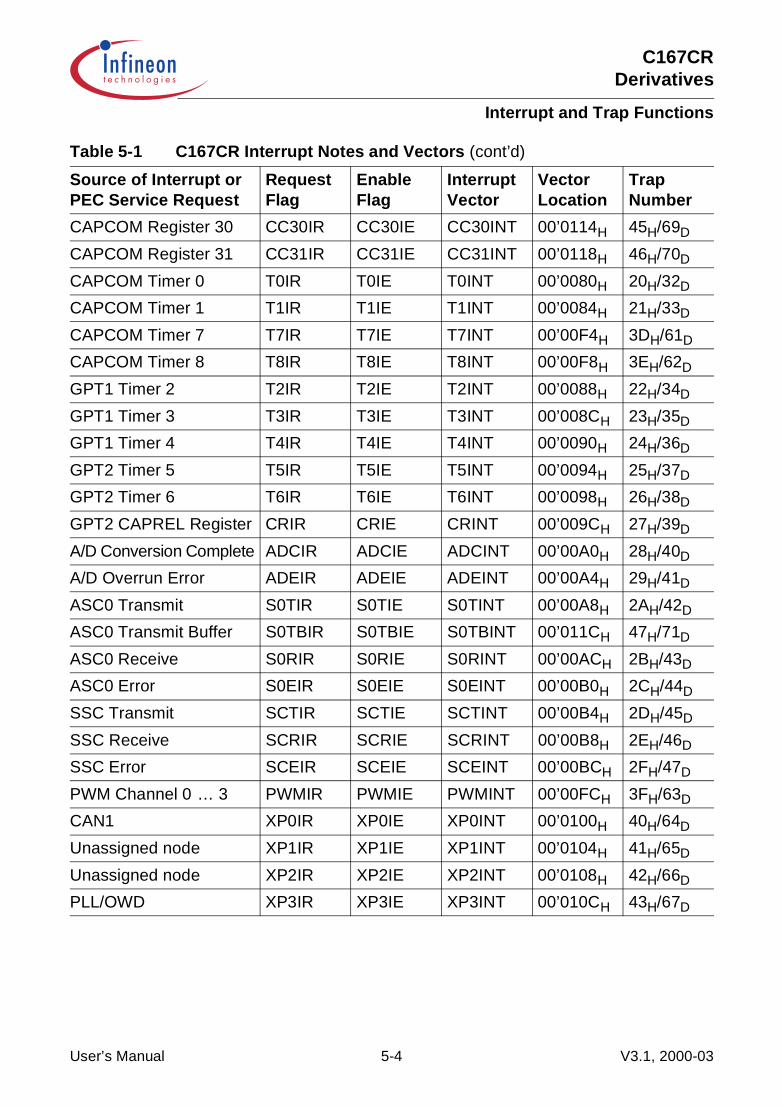
C167CRDerivatives
Interrupt and Trap Functions
CAPCOM Register 30 CC30IR CC30IE CC30INT 00’0114H 45H/69D
CAPCOM Register 31 CC31IR CC31IE CC31INT 00’0118H 46H/70D
CAPCOM Timer 0 T0IR T0IE T0INT 00’0080H 20H/32D
CAPCOM Timer 1 T1IR T1IE T1INT 00’0084H 21H/33D
CAPCOM Timer 7 T7IR T7IE T7INT 00’00F4H 3DH/61D
CAPCOM Timer 8 T8IR T8IE T8INT 00’00F8H 3EH/62D
GPT1 Timer 2 T2IR T2IE T2INT 00’0088H 22H/34D
GPT1 Timer 3 T3IR T3IE T3INT 00’008CH 23H/35D
GPT1 Timer 4 T4IR T4IE T4INT 00’0090H 24H/36D
GPT2 Timer 5 T5IR T5IE T5INT 00’0094H 25H/37D
GPT2 Timer 6 T6IR T6IE T6INT 00’0098H 26H/38D
GPT2 CAPREL Register CRIR CRIE CRINT 00’009CH 27H/39D
A/D Conversion Complete ADCIR ADCIE ADCINT 00’00A0H 28H/40D
A/D Overrun Error ADEIR ADEIE ADEINT 00’00A4H 29H/41D
ASC0 Transmit S0TIR S0TIE S0TINT 00’00A8H 2AH/42D
ASC0 Transmit Buffer S0TBIR S0TBIE S0TBINT 00’011CH 47H/71D
ASC0 Receive S0RIR S0RIE S0RINT 00’00ACH 2BH/43D
ASC0 Error S0EIR S0EIE S0EINT 00’00B0H 2CH/44D
SSC Transmit SCTIR SCTIE SCTINT 00’00B4H 2DH/45D
SSC Receive SCRIR SCRIE SCRINT 00’00B8H 2EH/46D
SSC Error SCEIR SCEIE SCEINT 00’00BCH 2FH/47D
PWM Channel 0 … 3 PWMIR PWMIE PWMINT 00’00FCH 3FH/63D
CAN1 XP0IR XP0IE XP0INT 00’0100H 40H/64D
Unassigned node XP1IR XP1IE XP1INT 00’0104H 41H/65D
Unassigned node XP2IR XP2IE XP2INT 00’0108H 42H/66D
PLL/OWD XP3IR XP3IE XP3INT 00’010CH 43H/67D
Table 5-1 C167CR Interrupt Notes and Vectors (cont’d)
Source of Interrupt or PEC Service Request
RequestFlag
EnableFlag
InterruptVector
VectorLocation
TrapNumber
User’s Manual 5-4 V3.1, 2000-03
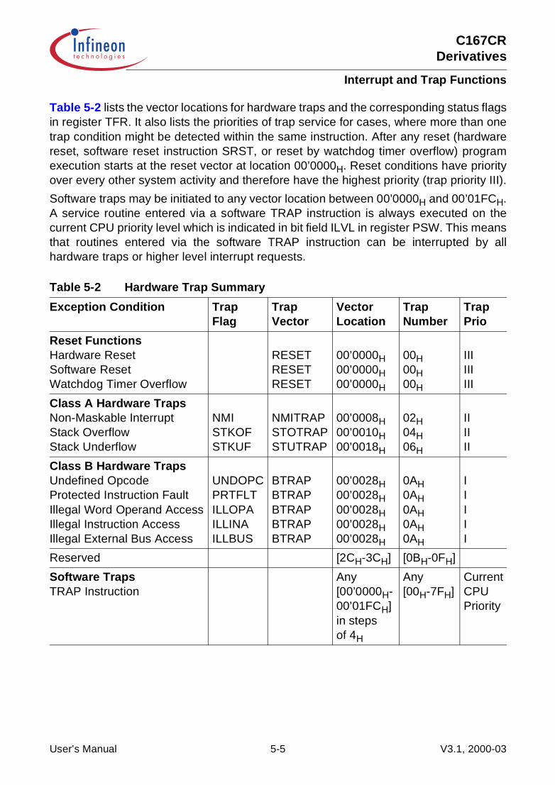
C167CRDerivatives
Interrupt and Trap Functions
Table 5-2 lists the vector locations for hardware traps and the corresponding status flagsin register TFR. It also lists the priorities of trap service for cases, where more than onetrap condition might be detected within the same instruction. After any reset (hardwarereset, software reset instruction SRST, or reset by watchdog timer overflow) programexecution starts at the reset vector at location 00’0000H. Reset conditions have priorityover every other system activity and therefore have the highest priority (trap priority III).
Software traps may be initiated to any vector location between 00’0000H and 00’01FCH.A service routine entered via a software TRAP instruction is always executed on thecurrent CPU priority level which is indicated in bit field ILVL in register PSW. This meansthat routines entered via the software TRAP instruction can be interrupted by allhardware traps or higher level interrupt requests.
Table 5-2 Hardware Trap Summary
Exception Condition TrapFlag
TrapVector
VectorLocation
TrapNumber
TrapPrio
Reset FunctionsHardware ResetSoftware ResetWatchdog Timer Overflow
RESETRESETRESET
00’0000H00’0000H00’0000H
00H00H00H
IIIIIIIII
Class A Hardware TrapsNon-Maskable InterruptStack OverflowStack Underflow
NMISTKOFSTKUF
NMITRAPSTOTRAPSTUTRAP
00’0008H00’0010H00’0018H
02H04H06H
IIIIII
Class B Hardware TrapsUndefined OpcodeProtected Instruction FaultIllegal Word Operand AccessIllegal Instruction AccessIllegal External Bus Access
UNDOPCPRTFLTILLOPAILLINAILLBUS
BTRAPBTRAPBTRAPBTRAPBTRAP
00’0028H00’0028H00’0028H00’0028H00’0028H
0AH0AH0AH0AH0AH
IIIII
Reserved [2CH-3CH] [0BH-0FH]
Software TrapsTRAP Instruction
Any[00’0000H-00’01FCH]in stepsof 4H
Any[00H-7FH]
CurrentCPU Priority
User’s Manual 5-5 V3.1, 2000-03

C167CRDerivatives
Interrupt and Trap Functions
Normal Interrupt Processing and PEC Service
During each instruction cycle one out of all sources which require PEC or interruptprocessing is selected according to its interrupt priority. This priority of interrupts andPEC requests is programmable in two levels. Each requesting source can be assignedto a specific priority. A second level (called “group priority”) allows to specify an internalorder for simultaneous requests from a group of different sources on the same prioritylevel. At the end of each instruction cycle the one source request with the highest currentpriority will be determined by the interrupt system. This request will then be serviced, ifits priority is higher than the current CPU priority in register PSW.
Interrupt System Register Description
Interrupt processing is controlled globally by register PSW through a general interruptenable bit (IEN) and the CPU priority field (ILVL). Additionally the different interruptsources are controlled individually by their specific interrupt control registers (… IC).Thus, the acceptance of requests by the CPU is determined by both the individualinterrupt control registers and the PSW. PEC services are controlled by the respectivePECCx register and the source and destination pointers, which specify the task of therespective PEC service channel.
5.1.1 Interrupt Control Registers
All interrupt control registers are organized identically. The lower 8 bits of an interruptcontrol register contain the complete interrupt status information of the associatedsource, which is required during one round of prioritization, the upper 8 bits of therespective register are reserved. All interrupt control registers are bit-addressable and allbits can be read or written via software. This allows each interrupt source to beprogrammed or modified with just one instruction. When accessing interrupt controlregisters through instructions which operate on word data types, their upper 8 bits(15 … 8) will return zeros, when read, and will discard written data.
The layout of the Interrupt Control registers shown below applies to each xxIC register,where xx stands for the mnemonic for the respective source.
User’s Manual 5-6 V3.1, 2000-03
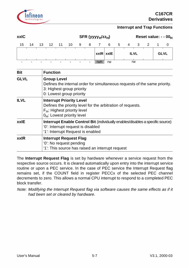
C167CRDerivatives
Interrupt and Trap Functions
The Interrupt Request Flag is set by hardware whenever a service request from therespective source occurs. It is cleared automatically upon entry into the interrupt serviceroutine or upon a PEC service. In the case of PEC service the Interrupt Request flagremains set, if the COUNT field in register PECCx of the selected PEC channeldecrements to zero. This allows a normal CPU interrupt to respond to a completed PECblock transfer.
Note: Modifying the Interrupt Request flag via software causes the same effects as if ithad been set or cleared by hardware.
xxIC SFR (yyyyH/zzH) Reset value: - - 00H
15 14 13 12 11 10 9 8 7 6 5 4 3 2 1 0
xxIR xxIE ILVL GLVL
- - - - - - - - rwh rw rw
Bit Function
GLVL Group LevelDefines the internal order for simultaneous requests of the same priority.3: Highest group priority0: Lowest group priority
ILVL Interrupt Priority LevelDefines the priority level for the arbitration of requests.FH: Highest priority level0H: Lowest priority level
xxIE Interrupt Enable Control Bit (individually enables/disables a specific source)‘0’: Interrupt request is disabled‘1’: Interrupt Request is enabled
xxIR Interrupt Request Flag‘0’: No request pending‘1’: This source has raised an interrupt request
User’s Manual 5-7 V3.1, 2000-03
C167CRDerivatives
Interrupt and Trap Functions
Interrupt Priority Level and Group Level
The four bits of bit field ILVL specify the priority level of a service request for thearbitration of simultaneous requests. The priority increases with the numerical value ofILVL, so 0000B is the lowest and 1111B is the highest priority level.
When more than one interrupt request on a specific level gets active at the same time,the values in the respective bit fields GLVL are used for second level arbitration to selectone request for being serviced. Again the group priority increases with the numericalvalue of GLVL, so 00B is the lowest and 11B is the highest group priority.
Note: All interrupt request sources that are enabled and programmed to the samepriority level must always be programmed to different group priorities. Otherwisean incorrect interrupt vector will be generated.
Upon entry into the interrupt service routine, the priority level of the source that won thearbitration and who’s priority level is higher than the current CPU level, is copied into bitfield ILVL of register PSW after pushing the old PSW contents on the stack.
The interrupt system of the C167CR allows nesting of up to 15 interrupt service routinesof different priority levels (level 0 cannot be arbitrated).
Interrupt requests that are programmed to priority levels 15 or 14 (i.e. ILVL = 111XB) willbe serviced by the PEC, unless the COUNT field of the associated PECC registercontains zero. In this case the request will instead be serviced by normal interruptprocessing. Interrupt requests that are programmed to priority levels 13 through 1 willalways be serviced by normal interrupt processing.
Note: Priority level 0000B is the default level of the CPU. Therefore a request on level 0will never be serviced, because it can never interrupt the CPU. However, anenabled interrupt request on level 0000B will terminate the C167CR’s Idle modeand reactivate the CPU.
For interrupt requests which are to be serviced by the PEC, the associated PEC channelnumber is derived from the respective ILVL (LSB) and GLVL (see Figure 5-1). Soprogramming a source to priority level 15 (ILVL = 1111B) selects the PEC channel group7 … 4, programming a source to priority level 14 (ILVL = 1110B) selects the PEC channelgroup 3 … 0. The actual PEC channel number is then determined by the group priorityfield GLVL.
Simultaneous requests for PEC channels are prioritized according to the PEC channelnumber, where channel 0 has lowest and channel 8 has highest priority.
Note: All sources that request PEC service must be programmed to different PECchannels. Otherwise an incorrect PEC channel may be activated.
User’s Manual 5-8 V3.1, 2000-03
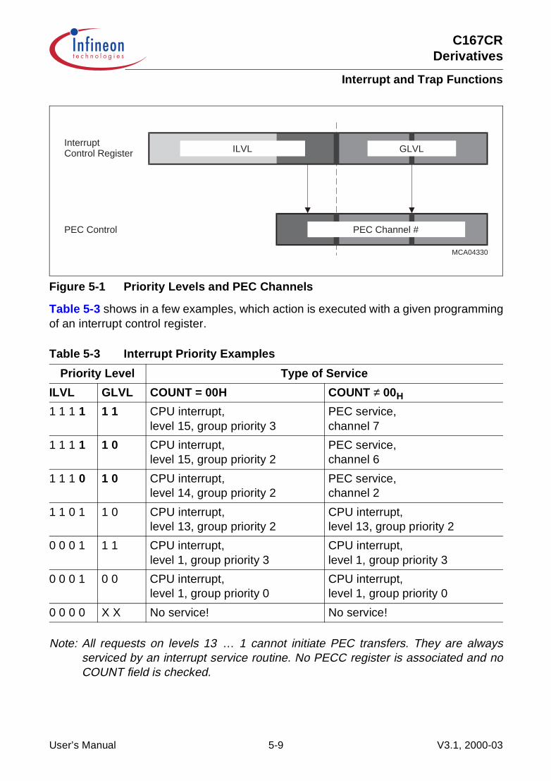
C167CRDerivatives
Interrupt and Trap Functions
Figure 5-1 Priority Levels and PEC Channels
Table 5-3 shows in a few examples, which action is executed with a given programmingof an interrupt control register.
Note: All requests on levels 13 … 1 cannot initiate PEC transfers. They are alwaysserviced by an interrupt service routine. No PECC register is associated and noCOUNT field is checked.
Table 5-3 Interrupt Priority Examples
Priority Level Type of Service
ILVL GLVL COUNT = 00H COUNT ≠ 00H
1 1 1 1 1 1 CPU interrupt,level 15, group priority 3
PEC service,channel 7
1 1 1 1 1 0 CPU interrupt,level 15, group priority 2
PEC service,channel 6
1 1 1 0 1 0 CPU interrupt,level 14, group priority 2
PEC service,channel 2
1 1 0 1 1 0 CPU interrupt,level 13, group priority 2
CPU interrupt,level 13, group priority 2
0 0 0 1 1 1 CPU interrupt,level 1, group priority 3
CPU interrupt,level 1, group priority 3
0 0 0 1 0 0 CPU interrupt,level 1, group priority 0
CPU interrupt,level 1, group priority 0
0 0 0 0 X X No service! No service!
MCA04330
ILVL GLVL
PEC Channel #
InterruptControl Register
PEC Control
User’s Manual 5-9 V3.1, 2000-03
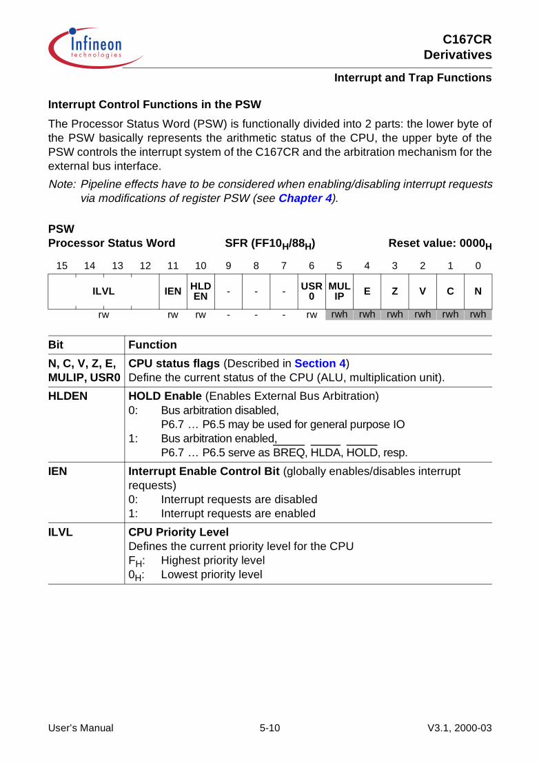
C167CRDerivatives
Interrupt and Trap Functions
Interrupt Control Functions in the PSW
The Processor Status Word (PSW) is functionally divided into 2 parts: the lower byte ofthe PSW basically represents the arithmetic status of the CPU, the upper byte of thePSW controls the interrupt system of the C167CR and the arbitration mechanism for theexternal bus interface.
Note: Pipeline effects have to be considered when enabling/disabling interrupt requestsvia modifications of register PSW (see Chapter 4).
PSWProcessor Status Word SFR (FF10H/88H) Reset value: 0000H
15 14 13 12 11 10 9 8 7 6 5 4 3 2 1 0
ILVL IEN HLD EN - - - USR
0MUL
IP E Z V C N
rw rw rw - - - rw rwh rwh rwh rwh rwh rwh
Bit Function
N, C, V, Z, E, MULIP, USR0
CPU status flags (Described in Section 4)Define the current status of the CPU (ALU, multiplication unit).
HLDEN HOLD Enable (Enables External Bus Arbitration)0: Bus arbitration disabled,
P6.7 … P6.5 may be used for general purpose IO1: Bus arbitration enabled,
P6.7 … P6.5 serve as BREQ, HLDA, HOLD, resp.
IEN Interrupt Enable Control Bit (globally enables/disables interrupt requests)0: Interrupt requests are disabled1: Interrupt requests are enabled
ILVL CPU Priority LevelDefines the current priority level for the CPUFH: Highest priority level0H: Lowest priority level
User’s Manual 5-10 V3.1, 2000-03

C167CRDerivatives
Interrupt and Trap Functions
CPU priority ILVL defines the current level for the operation of the CPU. This bit fieldreflects the priority level of the routine that is currently executed. Upon the entry into aninterrupt service routine this bit field is updated with the priority level of the request thatis being serviced. The PSW is saved on the system stack before. The CPU leveldetermines the minimum interrupt priority level that will be serviced. Any request on thesame or a lower level will not be acknowledged.The current CPU priority level may be adjusted via software to control which interruptrequest sources will be acknowledged.
PEC transfers do not really interrupt the CPU, but rather “steal” a single cycle, so PECservices do not influence the ILVL field in the PSW.
Hardware traps switch the CPU level to maximum priority (i.e. 15) so no interrupt or PECrequests will be acknowledged while an exception trap service routine is executed.
Note: The TRAP instruction does not change the CPU level, so software invoked trapservice routines may be interrupted by higher requests.
Interrupt Enable bit IEN globally enables or disables PEC operation and theacceptance of interrupts by the CPU. When IEN is cleared, no new interrupt requests areaccepted by the CPU. Requests that already have entered the pipeline at that time willprocess, however. When IEN is set to ‘1’, all interrupt sources, which have beenindividually enabled by the interrupt enable bits in their associated control registers, areglobally enabled.
Note: Traps are non-maskable and are therefore not affected by the IEN bit.
User’s Manual 5-11 V3.1, 2000-03

C167CRDerivatives
Interrupt and Trap Functions
5.2 Operation of the PEC Channels
The C167CR’s Peripheral Event Controller (PEC) provides 8 PEC service channels,which move a single byte or word between two locations in segment 0 (data pages3 … 0). This is the fastest possible interrupt response and in many cases is sufficient toservice the respective peripheral request (e.g. serial channels, etc.). Each channel iscontrolled by a dedicated PEC Channel Counter/Control register (PECCx) and a pair ofpointers for source (SRCPx) and destination (DSTPx) of the data transfer.
The PECC registers control the action that is performed by the respective PEC channel.
PECCxPEC Control Reg. SFR (FECyH/6zH, see Table 5-4) Reset value: 0000H
15 14 13 12 11 10 9 8 7 6 5 4 3 2 1 0
INC BWT COUNT
- - - - - rw rw rw
Bit Function
COUNT PEC Transfer CountCounts PEC transfers and influences the channel’s action (see Table 5-5)
BWT Byte/Word Transfer Selection0: Transfer a Word1: Transfer a Byte
INC Increment Control (Modification of SRCPx or DSTPx)0 0: Pointers are not modified0 1: Increment DSTPx by 1 or 2 (BWT)1 0: Increment SRCPx by 1 or 2 (BWT)1 1: Reserved. Do not use this combination.
(changed to ‘10’ by hardware)
Table 5-4 PEC Control Register Addresses
Register Address Reg. Space Register Address Reg. Space
PECC0 FEC0H/60H SFR PECC4 FEC8H/64H SFR
PECC1 FEC2H/61H SFR PECC5 FECAH/65H SFR
PECC2 FEC4H/62H SFR PECC6 FECCH/66H SFR
PECC3 FEC6H/63H SFR PECC7 FECEH/67H SFR
User’s Manual 5-12 V3.1, 2000-03
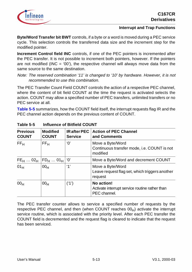
C167CRDerivatives
Interrupt and Trap Functions
Byte/Word Transfer bit BWT controls, if a byte or a word is moved during a PEC servicecycle. This selection controls the transferred data size and the increment step for themodified pointer.
Increment Control field INC controls, if one of the PEC pointers is incremented afterthe PEC transfer. It is not possible to increment both pointers, however. If the pointersare not modified (INC = ‘00’), the respective channel will always move data from thesame source to the same destination.
Note: The reserved combination ‘11’ is changed to ‘10’ by hardware. However, it is notrecommended to use this combination.
The PEC Transfer Count Field COUNT controls the action of a respective PEC channel,where the content of bit field COUNT at the time the request is activated selects theaction. COUNT may allow a specified number of PEC transfers, unlimited transfers or noPEC service at all.
Table 5-5 summarizes, how the COUNT field itself, the interrupt requests flag IR and thePEC channel action depends on the previous content of COUNT.
The PEC transfer counter allows to service a specified number of requests by therespective PEC channel, and then (when COUNT reaches 00H) activate the interruptservice routine, which is associated with the priority level. After each PEC transfer theCOUNT field is decremented and the request flag is cleared to indicate that the requesthas been serviced.
Table 5-5 Influence of Bitfield COUNT
Previous COUNT
Modified COUNT
IR after PEC Service
Action of PEC Channeland Comments
FFH FFH ‘0’ Move a Byte/WordContinuous transfer mode, i.e. COUNT is not modified
FEH … 02H FDH … 01H ‘0’ Move a Byte/Word and decrement COUNT
01H 00H ‘1’ Move a Byte/WordLeave request flag set, which triggers another request
00H 00H (‘1’) No action!Activate interrupt service routine rather than PEC channel.
User’s Manual 5-13 V3.1, 2000-03
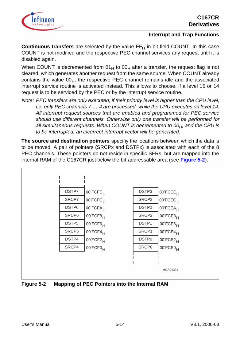
C167CRDerivatives
Interrupt and Trap Functions
Continuous transfers are selected by the value FFH in bit field COUNT. In this caseCOUNT is not modified and the respective PEC channel services any request until it isdisabled again.
When COUNT is decremented from 01H to 00H after a transfer, the request flag is notcleared, which generates another request from the same source. When COUNT alreadycontains the value 00H, the respective PEC channel remains idle and the associatedinterrupt service routine is activated instead. This allows to choose, if a level 15 or 14request is to be serviced by the PEC or by the interrupt service routine.
Note: PEC transfers are only executed, if their priority level is higher than the CPU level,i.e. only PEC channels 7 … 4 are processed, while the CPU executes on level 14.All interrupt request sources that are enabled and programmed for PEC serviceshould use different channels. Otherwise only one transfer will be performed forall simultaneous requests. When COUNT is decremented to 00H, and the CPU isto be interrupted, an incorrect interrupt vector will be generated.
The source and destination pointers specifiy the locations between which the data isto be moved. A pair of pointers (SRCPx and DSTPx) is associated with each of the 8PEC channels. These pointers do not reside in specific SFRs, but are mapped into theinternal RAM of the C167CR just below the bit-addressable area (see Figure 5-2).
Figure 5-2 Mapping of PEC Pointers into the Internal RAM
MCA04331
DSTP7
SRCP7
DSTP6
SRCP6
DSTP5
SRCP5
DSTP4
SRCP4
00’FCFEH00’FCFCH00’FCFAH00’FCF8H00’FCF6H00’FCF4H00’FCF2H00’FCF0H
DSTP3
SRCP3
DSTP2
SRCP2
DSTP1
SRCP1
DSTP0
SRCP0
00’FCEEH00’FCECH00’FCEAH00’FCE8H00’FCE6H00’FCE4H00’FCE2H00’FCE0H
User’s Manual 5-14 V3.1, 2000-03

C167CRDerivatives
Interrupt and Trap Functions
PEC data transfers do not use the data page pointers DPP3 … DPP0. The PEC sourceand destination pointers are used as 16-bit intra-segment addresses within segment 0,so data can be transferred between any two locations within the first four data pages3 … 0.
The pointer locations for inactive PEC channels may be used for general data storage.Only the required pointers occupy RAM locations.
Note: If word data transfer is selected for a specific PEC channel (i.e. BWT = ‘0’), therespective source and destination pointers must both contain a valid word addresswhich points to an even byte boundary. Otherwise the Illegal Word Access trap willbe invoked, when this channel is used.
User’s Manual 5-15 V3.1, 2000-03
C167CRDerivatives
Interrupt and Trap Functions
5.3 Prioritization of Interrupt and PEC Service Requests
Interrupt and PEC service requests from all sources can be enabled, so they arearbitrated and serviced (if they win), or they may be disabled, so their requests aredisregarded and not serviced.
Enabling and disabling interrupt requests may be done via three mechanisms:
Control bits allow to switch each individual source “ON” or “OFF”, so it may generate arequest or not. The control bits (xxIE) are located in the respective interrupt controlregisters. All interrupt requests may be enabled or disabled generally via bit IEN inregister PSW. This control bit is the “main switch” that selects, if requests from anysource are accepted or not.For a specific request to be arbitrated the respective source’s enable bit and the globalenable bit must both be set.
The priority level automatically selects a certain group of interrupt requests that will beacknowledged, disclosing all other requests. The priority level of the source that won thearbitration is compared against the CPU’s current level and the source is only serviced,if its level is higher than the current CPU level. Changing the CPU level to a specific valuevia software blocks all requests on the same or a lower level. An interrupt source that isassigned to level 0 will be disabled and never be serviced.
The ATOMIC and EXTend instructions automatically disable all interrupt requests forthe duration of the following 1 … 4 instructions. This is useful e.g. for semaphorehandling and does not require to re-enable the interrupt system after the unseparableinstruction sequence (see Chapter 21).
Interrupt Class Management
An interrupt class covers a set of interrupt sources with the same importance, i.e. thesame priority from the system’s viewpoint. Interrupts of the same class must not interrupteach other. The C167CR supports this function with two features:
Classes with up to 4 members can be established by using the same interrupt priority(ILVL) and assigning a dedicated group level (GLVL) to each member. This functionalityis built-in and handled automatically by the interrupt controller.
Classes with more than 4 members can be established by using a number of adjacentinterrupt priorities (ILVL) and the respective group levels (4 per ILVL). Each interruptservice routine within this class sets the CPU level to the highest interrupt priority withinthe class. All requests from the same or any lower level are blocked now, i.e. no requestof this class will be accepted.
User’s Manual 5-16 V3.1, 2000-03

C167CRDerivatives
Interrupt and Trap Functions
The example below establishes 3 interrupt classes which cover 2 or 3 interrupt priorities,depending on the number of members in a class. A level 6 interrupt disables all othersources in class 2 by changing the current CPU level to 8, which is the highest priority(ILVL) in class 2. Class 1 requests or PEC requests are still serviced in this case.
The 24 interrupt sources (excluding PEC requests) are so assigned to 3 classes ofpriority rather than to 7 different levels, as the hardware support would do.
Table 5-6 Software Controlled Interrupt Classes (Example)
ILVL(Priority)
GLVL Interpretation
3 2 1 0
15 PEC service on up to 8 channels
14
13
12 X X X X Interrupt Class 15 sources on 2 levels11 X
10
9
8 X X X X Interrupt Class 29 sources on 3 levels7 X X X X
6 X
5 X X X X Interrupt Class 35 sources on 2 levels4 X
3
2
1
0 No service!
User’s Manual 5-17 V3.1, 2000-03

C167CRDerivatives
Interrupt and Trap Functions
5.4 Saving the Status During Interrupt Service
Before an interrupt request that has been arbitrated is actually serviced, the status of thecurrent task is automatically saved on the system stack. The CPU status (PSW) is savedalong with the location, where the execution of the interrupted task is to be resumed afterreturning from the service routine. This return location is specified through the InstructionPointer (IP) and, in case of a segmented memory model, the Code Segment Pointer(CSP). Bit SGTDIS in register SYSCON controls, how the return location is stored.
The system stack receives the PSW first, followed by the IP (unsegmented) or followedby CSP and then IP (segmented mode). This optimizes the usage of the system stack,if segmentation is disabled.
The CPU priority field (ILVL in PSW) is updated with the priority of the interrupt requestthat is to be serviced, so the CPU now executes on the new level. If a multiplication ordivision was in progress at the time the interrupt request was acknowledged, bit MULIPin register PSW is set to ‘1’. In this case the return location that is saved on the stack isnot the next instruction in the instruction flow, but rather the multiply or divide instructionitself, as this instruction has been interrupted and will be completed after returning fromthe service routine.
Figure 5-3 Task Status saved on the System Stack
The interrupt request flag of the source that is being serviced is cleared. The IP is loadedwith the vector associated with the requesting source (the CSP is cleared in case ofsegmentation) and the first instruction of the service routine is fetched from therespective vector location, which is expected to branch to the service routine itself. Thedata page pointers and the context pointer are not affected.
When the interrupt service routine is left (RETI is executed), the status information ispopped from the system stack in the reverse order, taking into account the value of bitSGTDIS.
(Unsegmented)
PSW
System Stack afterInterrupt EntryInterrupt Entry
System Stack beforea) b)
SP
HighAddresses
LowAddresses
--
--
--
SP IP
--
MCD02226
b)Interrupt EntrySystem Stack after
(Segmented)
TaskInterruptedStatus of
CSP
PSW
IP SP
User’s Manual 5-18 V3.1, 2000-03
C167CRDerivatives
Interrupt and Trap Functions
Context Switching
An interrupt service routine usually saves all the registers it uses on the stack, andrestores them before returning. The more registers a routine uses, the more time iswasted with saving and restoring. The C167CR allows to switch the complete bank ofCPU registers (GPRs) with a single instruction, so the service routine executes within itsown, separate context.
The instruction “SCXT CP, #New_Bank” pushes the content of the context pointer (CP)on the system stack and loads CP with the immediate value “New_Bank”, which selectsa new register bank. The service routine may now use its “own registers”. This registerbank is preserved, when the service routine terminates, i.e. its contents are available onthe next call.Before returning (RETI) the previous CP is simply POPped from the system stack, whichreturns the registers to the original bank.
Note: The first instruction following the SCXT instruction must not use a GPR.
Resources that are used by the interrupting program must eventually be saved andrestored, e.g. the DPPs and the registers of the MUL/DIV unit.
User’s Manual 5-19 V3.1, 2000-03

C167CRDerivatives
Interrupt and Trap Functions
5.5 Interrupt Response Times
The interrupt response time defines the time from an interrupt request flag of an enabledinterrupt source being set until the first instruction (I1) being fetched from the interruptvector location. The basic interrupt response time for the C167CR is 3 instruction cycles.
Figure 5-4 Pipeline Diagram for Interrupt Response Time
All instructions in the pipeline including instruction N (during which the interrupt requestflag is set) are completed before entering the service routine. The actual execution timefor these instructions (e.g. waitstates) therefore influences the interrupt response time.
In Figure 5-4 the respective interrupt request flag is set in cycle 1 (fetching of instructionN). The indicated source wins the prioritization round (during cycle 2). In cycle 3 a TRAPinstruction is injected into the decode stage of the pipeline, replacing instruction N + 1and clearing the source’s interrupt request flag to ‘0’. Cycle 4 completes the injectedTRAP instruction (save PSW, IP and CSP, if segmented mode) and fetches the firstinstruction (I1) from the respective vector location.
All instructions that entered the pipeline after setting of the interrupt request flag (N + 1,N + 2) will be executed after returning from the interrupt service routine.
The minimum interrupt response time is 5 states (10 TCL). This requires programexecution from the internal code memory, no external operand read requests and settingthe interrupt request flag during the last state of an instruction cycle. When the interruptrequest flag is set during the first state of an instruction cycle, the minimum interruptresponse time under these conditions is 6 state times (12 TCL).
The interrupt response time is increased by all delays of the instructions in the pipelinethat are executed before entering the service routine (including N).
MCT04332
Pipeline Stage
FETCH
DECODE
EXECUTE
WRITEBACK
Cycle 1
N
N - 1
N - 2
N - 3
Cycle 2
N + 1
N
N - 1
N - 2
Cycle 3
N + 2
TRAP (1)
N
N - 1
Cycle 4
I1
TRAP (2)
TRAP
N
0
1IR-Flag
Interrupt Response Time
User’s Manual 5-20 V3.1, 2000-03

C167CRDerivatives
Interrupt and Trap Functions
• When internal hold conditions between instruction pairs N – 2/N – 1 or N – 1/N occur,or instruction N explicitly writes to the PSW or the SP, the minimum interrupt responsetime may be extended by 1 state time for each of these conditions.
• When instruction N reads an operand from the internal code memory, or when N is acall, return, trap, or MOV Rn, [Rm+ #data16] instruction, the minimum interruptresponse time may additionally be extended by 2 state times during internal codememory program execution.
• In case instruction N reads the PSW and instruction N – 1 has an effect on thecondition flags, the interrupt response time may additionally be extended by 2 statetimes.
The worst case interrupt response time during internal code memory program executionadds to 12 state times (24 TCL).
Any reference to external locations increases the interrupt response time due to pipelinerelated access priorities. The following conditions have to be considered:
• Instruction fetch from an external location• Operand read from an external location• Result write-back to an external location
Depending on where the instructions, source and destination operands are located,there are a number of combinations. Note, however, that only access conflicts contributeto the delay.
A few examples illustrate these delays:
• The worst case interrupt response time including external accesses will occur, wheninstructions N, N + 1 and N + 2 are executed out of external memory, instructions N – 1and N require external operand read accesses, instructions N – 3 through N writeback external operands, and the interrupt vector also points to an external location. Inthis case the interrupt response time is the time to perform 9 word bus accesses,because instruction I1 cannot be fetched via the external bus until all write, fetch andread requests of preceding instructions in the pipeline are terminated.
• When the above example has the interrupt vector pointing into the internal codememory, the interrupt response time is 7 word bus accesses plus 2 states, becausefetching of instruction I1 from internal code memory can start earlier.
• When instructions N, N + 1 and N + 2 are executed out of external memory and theinterrupt vector also points to an external location, but all operands for instructions N – 3through N are in internal memory, then the interrupt response time is the time toperform 3 word bus accesses.
• When the above example has the interrupt vector pointing into the internal codememory, the interrupt response time is 1 word bus access plus 4 states.
User’s Manual 5-21 V3.1, 2000-03
C167CRDerivatives
Interrupt and Trap Functions
After an interrupt service routine has been terminated by executing the RETI instruction,and if further interrupts are pending, the next interrupt service routine will not be entereduntil at least two instruction cycles have been executed of the program that wasinterrupted. In most cases two instructions will be executed during this time. Only oneinstruction will typically be executed, if the first instruction following the RETI instructionis a branch instruction (without cache hit), or if it reads an operand from internal codememory, or if it is executed out of the internal RAM.
Note: A bus access in this context includes all delays which can occur during an externalbus cycle.
User’s Manual 5-22 V3.1, 2000-03

C167CRDerivatives
Interrupt and Trap Functions
5.6 PEC Response Times
The PEC response time defines the time from an interrupt request flag of an enabledinterrupt source being set until the PEC data transfer being started. The basic PECresponse time for the C167CR is 2 instruction cycles.
Figure 5-5 Pipeline Diagram for PEC Response Time
In Figure 5-5 above the respective interrupt request flag is set in cycle 1 (fetching ofinstruction N). The indicated source wins the prioritization round (during cycle 2). Incycle 3 a PEC transfer “instruction” is injected into the decode stage of the pipeline,suspending instruction N + 1 and clearing the source’s interrupt request flag to ‘0’.Cycle 4 completes the injected PEC transfer and resumes the execution of instructionN + 1.
All instructions that entered the pipeline after setting of the interrupt request flag (N + 1,N + 2) will be executed after the PEC data transfer.
Note: When instruction N reads any of the PEC control registers PECC7 … PECC0,while a PEC request wins the current round of prioritization, this round is repeatedand the PEC data transfer is started one cycle later.
The minimum PEC response time is 3 states (6 TCL). This requires program executionfrom the internal code memory, no external operand read requests and setting theinterrupt request flag during the last state of an instruction cycle. When the interruptrequest flag is set during the first state of an instruction cycle, the minimum PECresponse time under these conditions is 4 state times (8 TCL).
The PEC response time is increased by all delays of the instructions in the pipeline thatare executed before starting the data transfer (including N).
MCT04333
Pipeline Stage
FETCH
DECODE
EXECUTE
WRITEBACK
Cycle 1
N
N - 1
N - 2
N - 3
Cycle 2
N + 1
N
N - 1
N - 2
Cycle 3
N + 2
PEC
N
N - 1
Cycle 4
N + 2
N + 1
PEC
N
0
1IR-Flag
PEC Response Time
User’s Manual 5-23 V3.1, 2000-03
C167CRDerivatives
Interrupt and Trap Functions
• When internal hold conditions between instruction pairs N – 2/N– 1 or N – 1/N occur,the minimum PEC response time may be extended by 1 state time for each of theseconditions.
• When instruction N reads an operand from the internal code memory, or when N is acall, return, trap, or MOV Rn, [Rm+ #data16] instruction, the minimum PEC responsetime may additionally be extended by 2 state times during internal code memoryprogram execution.
• In case instruction N reads the PSW and instruction N – 1 has an effect on thecondition flags, the PEC response time may additionally be extended by 2 state times.
The worst case PEC response time during internal code memory program executionadds to 9 state times (18 TCL).
Any reference to external locations increases the PEC response time due to pipelinerelated access priorities. The following conditions have to be considered:
• Instruction fetch from an external location• Operand read from an external location• Result write-back to an external location
Depending on where the instructions, source and destination operands are located,there are a number of combinations. Note, however, that only access conflicts contributeto the delay.
A few examples illustrate these delays:
• The worst case interrupt response time including external accesses will occur, wheninstructions N and N + 1 are executed out of external memory, instructions N – 1 andN require external operand read accesses and instructions N – 3, N – 2 and N – 1write back external operands. In this case the PEC response time is the time toperform 7 word bus accesses.
• When instructions N and N + 1 are executed out of external memory, but all operandsfor instructions N – 3 through N – 1 are in internal memory, then the PEC responsetime is the time to perform 1 word bus access plus 2 state times.
Once a request for PEC service has been acknowledged by the CPU, the execution ofthe next instruction is delayed by 2 state times plus the additional time it might take tofetch the source operand from internal code memory or external memory and to write thedestination operand over the external bus in an external program environment.
Note: A bus access in this context includes all delays which can occur during an externalbus cycle.
User’s Manual 5-24 V3.1, 2000-03

C167CRDerivatives
Interrupt and Trap Functions
5.7 External Interrupts
Although the C167CR has no dedicated INTR input pins, it provides many possibilitiesto react on external asynchronous events by using a number of IO lines for interruptinput. The interrupt function may either be combined with the pin’s main function or maybe used instead of it, i.e. if the main pin function is not required.
Interrupt signals may be connected to:
• CC31IO … CC16IO, the capture input/compare output lines of the CAPCOM2 unit,• CC15IO … CC0IO, the capture input/compare output lines of the CAPCOM1 unit,• T4IN, T2IN, the timer input pins,• CAPIN, the capture input of GPT2
For each of these pins either a positive, a negative, or both a positive and a negativeexternal transition can be selected to cause an interrupt or PEC service request. Theedge selection is performed in the control register of the peripheral device associatedwith the respective port pin. The peripheral must be programmed to a specific operatingmode to allow generation of an interrupt by the external signal. The priority of theinterrupt request is determined by the interrupt control register of the respectiveperipheral interrupt source, and the interrupt vector of this source will be used to servicethe external interrupt request.
Note: In order to use any of the listed pins as external interrupt input, it must be switchedto input mode via its direction control bit DPx.y in the respective port directioncontrol register DPx.
When port pins CCxIO are to be used as external interrupt input pins, bit field CCMODxin the control register of the corresponding capture/compare register CCx must selectcapture mode. When CCMODx is programmed to 001B, the interrupt request flag CCxIRin register CCxIC will be set on a positive external transition at pin CCxIO. WhenCCMODx is programmed to 010B, a negative external transition will set the interruptrequest flag. When CCMODx = 011B, both a positive and a negative transition will set
Table 5-7 Pins to be Used as External Interrupt Inputs
Port Pin Original Function Control Register
P7.7-4/CC31-28IO CAPCOM register 31-28 capture input CC31-CC28
P1H.7-4/CC27-24IO CAPCOM register 27-24 capture input CC27-CC24
P8.7-0/CC23-16IO CAPCOM register 23-16 capture input CC23-CC16
P2.15-0/CC15-0IO CAPCOM register 15-0 capture input CC15-CC0
P3.7/T2IN Auxiliary timer T2 input pin T2CON
P3.5/T4IN Auxiliary timer T4 input pin T4CON
P3.2/CAPIN GPT2 capture input pin T5CON
User’s Manual 5-25 V3.1, 2000-03

C167CRDerivatives
Interrupt and Trap Functions
the request flag. In all three cases, the contents of the allocated CAPCOM timer will belatched into capture register CCx, independent whether the timer is running or not. Whenthe interrupt enable bit CCxIE is set, a PEC request or an interrupt request for vectorCCxINT will be generated.
Pins T2IN or T4IN can be used as external interrupt input pins when the associatedauxiliary timer T2 or T4 in block GPT1 is configured for capture mode. This mode isselected by programming the mode control fields T2M or T4M in control registersT2CON or T4CON to 101B. The active edge of the external input signal is determined bybit fields T2I or T4I. When these fields are programmed to X01B, interrupt request flagsT2IR or T4IR in registers T2IC or T4IC will be set on a positive external transition at pinsT2IN or T4IN, respectively. When T2I or T4I are programmed to X10B, then a negativeexternal transition will set the corresponding request flag. When T2I or T4I areprogrammed to X11B, both a positive and a negative transition will set the request flag.In all three cases, the contents of the core timer T3 will be captured into the auxiliarytimer registers T2 or T4 based on the transition at pins T2IN or T4IN. When the interruptenable bits T2IE or T4IE are set, a PEC request or an interrupt request for vector T2INTor T4INT will be generated.
Pin CAPIN differs slightly from the timer input pins as it can be used as external interruptinput pin without affecting peripheral functions. When the capture mode enable bit T5SCin register T5CON is cleared to ‘0’, signal transitions on pin CAPIN will only set theinterrupt request flag CRIR in register CRIC, and the capture function of registerCAPREL is not activated.
So register CAPREL can still be used as reload register for GPT2 timer T5, while pinCAPIN serves as external interrupt input. Bit field CI in register T5CON selects theeffective transition of the external interrupt input signal. When CI is programmed to 01B,a positive external transition will set the interrupt request flag. CI = 10B selects a negativetransition to set the interrupt request flag, and with CI = 11B, both a positive and anegative transition will set the request flag. When the interrupt enable bit CRIE is set, aninterrupt request for vector CRINT or a PEC request will be generated.
Note: The non-maskable interrupt input pin NMI and the reset input RSTIN provideanother possibility for the CPU to react on an external input signal. NMI and RSTINare dedicated input pins, which cause hardware traps.
User’s Manual 5-26 V3.1, 2000-03
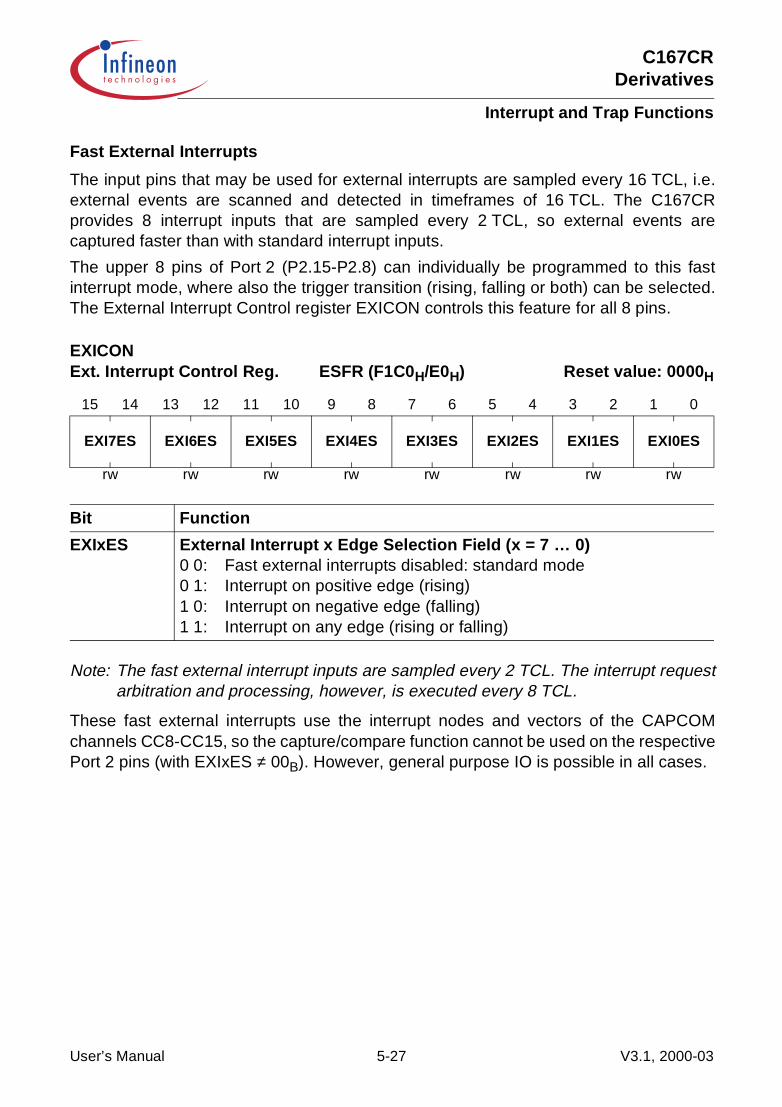
C167CRDerivatives
Interrupt and Trap Functions
Fast External Interrupts
The input pins that may be used for external interrupts are sampled every 16 TCL, i.e.external events are scanned and detected in timeframes of 16 TCL. The C167CRprovides 8 interrupt inputs that are sampled every 2 TCL, so external events arecaptured faster than with standard interrupt inputs.
The upper 8 pins of Port 2 (P2.15-P2.8) can individually be programmed to this fastinterrupt mode, where also the trigger transition (rising, falling or both) can be selected.The External Interrupt Control register EXICON controls this feature for all 8 pins.
Note: The fast external interrupt inputs are sampled every 2 TCL. The interrupt requestarbitration and processing, however, is executed every 8 TCL.
These fast external interrupts use the interrupt nodes and vectors of the CAPCOMchannels CC8-CC15, so the capture/compare function cannot be used on the respectivePort 2 pins (with EXIxES ≠ 00B). However, general purpose IO is possible in all cases.
EXICONExt. Interrupt Control Reg. ESFR (F1C0H/E0H) Reset value: 0000H
15 14 13 12 11 10 9 8 7 6 5 4 3 2 1 0
EXI7ES EXI6ES EXI5ES EXI4ES EXI3ES EXI2ES EXI1ES EXI0ES
rw rw rw rw rw rw rw rw
Bit Function
EXIxES External Interrupt x Edge Selection Field (x = 7 … 0)0 0: Fast external interrupts disabled: standard mode0 1: Interrupt on positive edge (rising)1 0: Interrupt on negative edge (falling)1 1: Interrupt on any edge (rising or falling)
User’s Manual 5-27 V3.1, 2000-03

C167CRDerivatives
Interrupt and Trap Functions
5.8 Trap Functions
Traps interrupt the current execution similar to standard interrupts. However, trapfunctions offer the possibility to bypass the interrupt system’s prioritization process incases where immediate system reaction is required. Trap functions are not maskableand always have priority over interrupt requests on any priority level.
The C167CR provides two different kinds of trapping mechanisms. Hardware traps aretriggered by events that occur during program execution (e.g. illegal access or undefinedopcode), software traps are initiated via an instruction within the current execution flow.
Software Traps
The TRAP instruction is used to cause a software call to an interrupt service routine. Thetrap number that is specified in the operand field of the trap instruction determines whichvector location in the address range from 00’0000H through 00’01FCH will be branched to.
Executing a TRAP instruction causes a similar effect as if an interrupt at the same vectorhad occurred. PSW, CSP (in segmentation mode), and IP are pushed on the internalsystem stack and a jump is taken to the specified vector location. When segmentation isenabled and a trap is executed, the CSP for the trap service routine is set to codesegment 0. No Interrupt Request flags are affected by the TRAP instruction. Theinterrupt service routine called by a TRAP instruction must be terminated with a RETI(return from interrupt) instruction to ensure correct operation.
Note: The CPU level in register PSW is not modified by the TRAP instruction, so theservice routine is executed on the same priority level from which it was invoked.Therefore, the service routine entered by the TRAP instruction can be interruptedby other traps or higher priority interrupts, other than when triggered by ahardware trap.
Hardware Traps
Hardware traps are issued by faults or specific system states that occur during runtimeof a program (not identified at assembly time). A hardware trap may also be triggeredintentionally, e.g. to emulate additional instructions by generating an Illegal Opcode trap.The C167CR distinguishes eight different hardware trap functions. When a hardwaretrap condition has been detected, the CPU branches to the trap vector location for therespective trap condition. Depending on the trap condition, the instruction which causedthe trap is either completed or cancelled (i.e. it has no effect on the system state) beforethe trap handling routine is entered.
Hardware traps are non-maskable and always have priority over every other CPU activity.If several hardware trap conditions are detected within the same instruction cycle, thehighest priority trap is serviced (see Table 5-2).
User’s Manual 5-28 V3.1, 2000-03

C167CRDerivatives
Interrupt and Trap Functions
PSW, CSP (in segmentation mode), and IP are pushed on the internal system stack andthe CPU level in register PSW is set to the highest possible priority level (i.e. level 15),disabling all interrupts. The CSP is set to code segment zero, if segmentation is enabled.A trap service routine must be terminated with the RETI instruction.
The eight hardware trap functions of the C167CR are divided into two classes:
Class A traps are• external Non-Maskable Interrupt (NMI)• Stack Overflow• Stack Underflow TrapThese traps share the same trap priority, but have an individual vector address.
Class B traps are• Undefined Opcode• Protection Fault• Illegal Word Operand Access• Illegal Instruction Access• Illegal External Bus Access TrapThese traps share the same trap priority, and the same vector address.
The bit-addressable Trap Flag Register (TFR) allows a trap service routine to identify thekind of trap which caused the exception. Each trap function is indicated by a separaterequest flag. When a hardware trap occurs, the corresponding request flag in registerTFR is set to ‘1’.
The reset functions (hardware, software, watchdog) may be regarded as a type of trap.Reset functions have the highest system priority (trap priority III).
Class A traps have the second highest priority (trap priority II), on the 3rd rank are classB traps, so a class A trap can interrupt a class B trap. If more than one class A trap occurat a time, they are prioritized internally, with the NMI trap on the highest and the stackunderflow trap on the lowest priority.
All class B traps have the same trap priority (trap priority I). When several class B trapsget active at a time, the corresponding flags in the TFR register are set and the trapservice routine is entered. Since all class B traps have the same vector, the priority ofservice of simultaneously occurring class B traps is determined by software in the trapservice routine.
A class A trap occurring during the execution of a class B trap service routine will beserviced immediately. During the execution of a class A trap service routine, however,any class B trap occurring will not be serviced until the class A trap service routine isexited with a RETI instruction. In this case, the occurrence of the class B trap conditionis stored in the TFR register, but the IP value of the instruction which caused this trap islost.
User’s Manual 5-29 V3.1, 2000-03
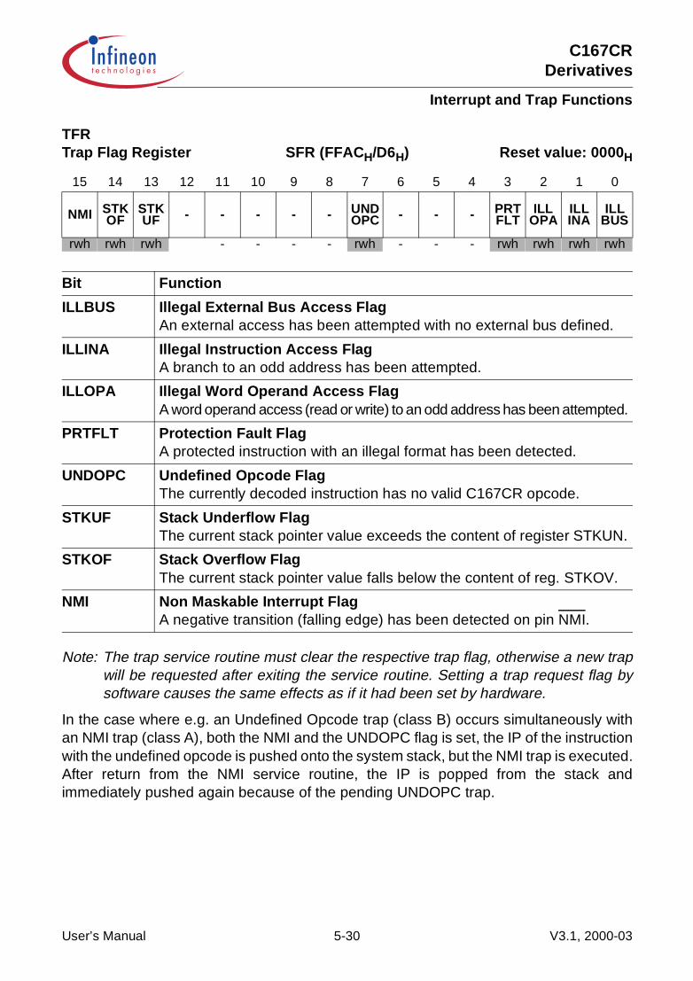
C167CRDerivatives
Interrupt and Trap Functions
Note: The trap service routine must clear the respective trap flag, otherwise a new trapwill be requested after exiting the service routine. Setting a trap request flag bysoftware causes the same effects as if it had been set by hardware.
In the case where e.g. an Undefined Opcode trap (class B) occurs simultaneously withan NMI trap (class A), both the NMI and the UNDOPC flag is set, the IP of the instructionwith the undefined opcode is pushed onto the system stack, but the NMI trap is executed.After return from the NMI service routine, the IP is popped from the stack andimmediately pushed again because of the pending UNDOPC trap.
TFRTrap Flag Register SFR (FFACH/D6H) Reset value: 0000H
15 14 13 12 11 10 9 8 7 6 5 4 3 2 1 0
NMI STK OF
STK UF - - - - - UND
OPC - - - PRT FLT
ILL OPA
ILL INA
ILL BUS
rwh rwh rwh - - - - rwh - - - rwh rwh rwh rwh
Bit Function
ILLBUS Illegal External Bus Access FlagAn external access has been attempted with no external bus defined.
ILLINA Illegal Instruction Access FlagA branch to an odd address has been attempted.
ILLOPA Illegal Word Operand Access FlagA word operand access (read or write) to an odd address has been attempted.
PRTFLT Protection Fault FlagA protected instruction with an illegal format has been detected.
UNDOPC Undefined Opcode FlagThe currently decoded instruction has no valid C167CR opcode.
STKUF Stack Underflow FlagThe current stack pointer value exceeds the content of register STKUN.
STKOF Stack Overflow FlagThe current stack pointer value falls below the content of reg. STKOV.
NMI Non Maskable Interrupt FlagA negative transition (falling edge) has been detected on pin NMI.
User’s Manual 5-30 V3.1, 2000-03

C167CRDerivatives
Interrupt and Trap Functions
External NMI Trap
Whenever a high to low transition on the dedicated external NMI pin (Non-MaskableInterrupt) is detected, the NMI flag in register TFR is set and the CPU will enter the NMItrap routine. The IP value pushed on the system stack is the address of the instructionfollowing the one after which normal processing was interrupted by the NMI trap.
Note: The NMI pin is sampled with every CPU clock cycle to detect transitions.
Stack Overflow Trap
Whenever the stack pointer is decremented to a value which is less than the value in thestack overflow register STKOV, the STKOF flag in register TFR is set and the CPU willenter the stack overflow trap routine. Which IP value will be pushed onto the systemstack depends on which operation caused the decrement of the SP. When an implicitdecrement of the SP is made through a PUSH or CALL instruction, or upon interrupt ortrap entry, the IP value pushed is the address of the following instruction. When the SPis decremented by a subtract instruction, the IP value pushed represents the address ofthe instruction after the instruction following the subtract instruction.
For recovery from stack overflow it must be ensured that there is enough excess spaceon the stack for saving the current system state (PSW, IP, in segmented mode also CSP)twice. Otherwise, a system reset should be generated.
Stack Underflow Trap
Whenever the stack pointer is incremented to a value which is greater than the value inthe stack underflow register STKUN, the STKUF flag is set in register TFR and the CPUwill enter the stack underflow trap routine. Again, which IP value will be pushed onto thesystem stack depends on which operation caused the increment of the SP. When animplicit increment of the SP is made through a POP or return instruction, the IP valuepushed is the address of the following instruction. When the SP is incremented by anadd instruction, the pushed IP value represents the address of the instruction after theinstruction following the add instruction.
Undefined Opcode Trap
When the instruction currently decoded by the CPU does not contain a valid C167CRopcode, the UNDOPC flag is set in register TFR and the CPU enters the undefinedopcode trap routine. The IP value pushed onto the system stack is the address of theinstruction that caused the trap.
This can be used to emulate unimplemented instructions. The trap service routine canexamine the faulting instruction to decode operands for unimplemented opcodes basedon the stacked IP. In order to resume processing, the stacked IP value must beincremented by the size of the undefined instruction, which is determined by the user,before a RETI instruction is executed.
User’s Manual 5-31 V3.1, 2000-03

C167CRDerivatives
Interrupt and Trap Functions
Protection Fault Trap
Whenever one of the special protected instructions is executed where the opcode of thatinstruction is not repeated twice in the second word of the instruction and the bytefollowing the opcode is not the complement of the opcode, the PRTFLT flag in registerTFR is set and the CPU enters the protection fault trap routine. The protectedinstructions include DISWDT, EINIT, IDLE, PWRDN, SRST, and SRVWDT. The IP valuepushed onto the system stack for the protection fault trap is the address of the instructionthat caused the trap.
Illegal Word Operand Access Trap
Whenever a word operand read or write access is attempted to an odd byte address, theILLOPA flag in register TFR is set and the CPU enters the illegal word operand accesstrap routine. The IP value pushed onto the system stack is the address of the instructionfollowing the one which caused the trap.
Illegal Instruction Access Trap
Whenever a branch is made to an odd byte address, the ILLINA flag in register TFR isset and the CPU enters the illegal instruction access trap routine. The IP value pushedonto the system stack is the illegal odd target address of the branch instruction.
Illegal External Bus Access Trap
Whenever the CPU requests an external instruction fetch, data read or data write, andno external bus configuration has been specified, the ILLBUS flag in register TFR is setand the CPU enters the illegal bus access trap routine. The IP value pushed onto thesystem stack is the address of the instruction following the one which caused the trap.
User’s Manual 5-32 V3.1, 2000-03

C167CRDerivatives
Clock Generation
6 Clock GenerationAll activities of the C167CR’s controller hardware and its on-chip peripherals arecontrolled via the system clock signal fCPU.This reference clock is generated in three stages (see also Figure 6-1):
Oscillator
The on-chip Pierce oscillator can either run with an external crystal and appropriateoscillator circuitry or it can be driven by an external oscillator.
Frequency Control
The input clock signal feeds the controller hardware:
• directly, providing phase coupled operation on not too high input frequency• divided by 2 in order to get 50% duty cycle clock signal• via an on-chip phase locked loop (PLL) providing max. performance on low input
frequency
The resulting internal clock signal is referred to as “CPU clock” fCPU.
Clock Drivers
The CPU clock is distributed via separate clock drivers which feed the CPU itself and twogroups of peripheral modules.
Figure 6-1 CPU Clock Generation Stages
MCS04334
OSC
CCD
PCD
PrescalerPLL
CPU
Idle Mode
Peripherals,Ports, Intr. Ctrl.Interfaces
Power Down
Oscillator Frequency Control Clock Drivers
User’s Manual 6-1 V3.1, 2000-03

C167CRDerivatives
Clock Generation
6.1 Oscillator
The main oscillator of the C167CR is a power optimized Pierce oscillator providing aninverter and a feedback element. Pins XTAL1 and XTAL2 connect the inverter to theexternal crystal. The standard external oscillator circuitry (see Figure 6-2) comprises thecrystal, two low end capacitors and series resistor (Rx2) to limit the current through thecrystal. The additional LC combination is only required for 3rd overtone crystals tosuppress oscillation in the fundamental mode. A test resistor (RQ) may be temporarilyinserted to measure the oscillation allowance of the oscillator circuitry.
Figure 6-2 External Oscillator Circuitry
The on-chip oscillator is optimized for an input frequency range of 4 to 40 MHz.
An external clock signal (e.g. from an external oscillator or from a master device) maybe fed to the input XTAL1. The Pierce oscillator then is not required to support theoscillation itself but is rather driven by the input signal. In this case the input frequencyrange may be 0 to 50 MHz (please note that the maximum applicable input frequency islimited by the device’s maximum CPU frequency).
MCS04335
XTAL1 XTAL2
Rx2RQ
User’s Manual 6-2 V3.1, 2000-03
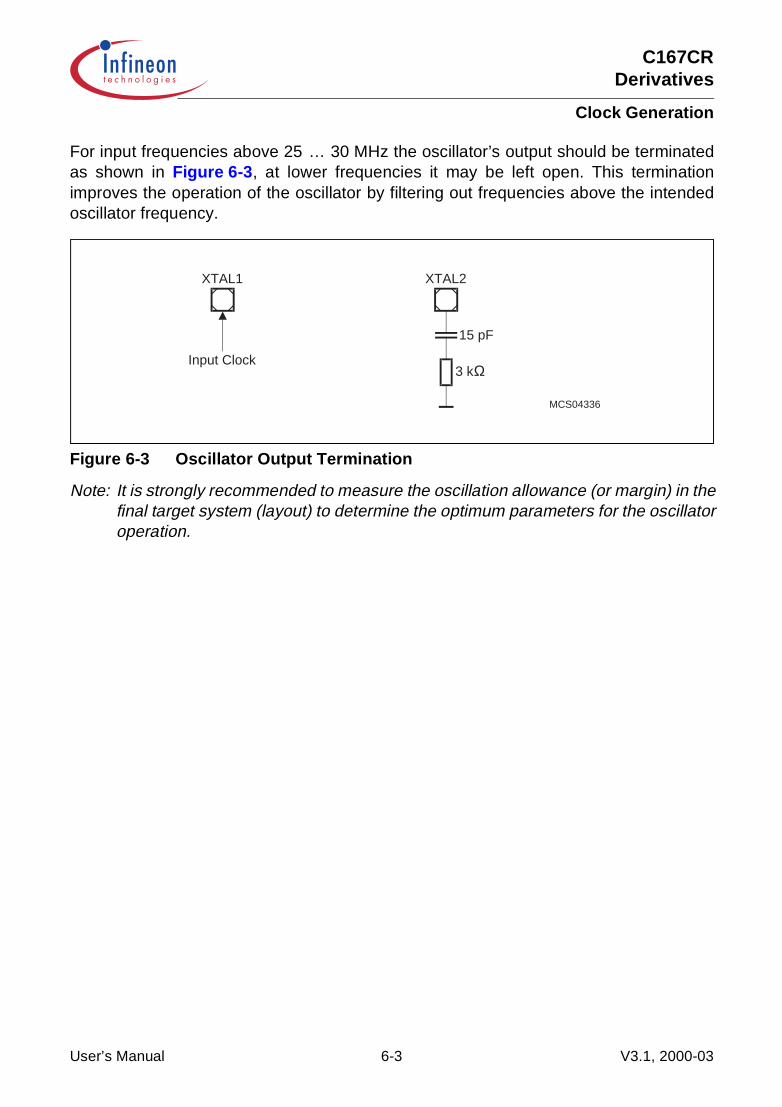
C167CRDerivatives
Clock Generation
For input frequencies above 25 … 30 MHz the oscillator’s output should be terminatedas shown in Figure 6-3, at lower frequencies it may be left open. This terminationimproves the operation of the oscillator by filtering out frequencies above the intendedoscillator frequency.
Figure 6-3 Oscillator Output Termination
Note: It is strongly recommended to measure the oscillation allowance (or margin) in thefinal target system (layout) to determine the optimum parameters for the oscillatoroperation.
MCS04336
XTAL1
Input Clock
XTAL2
15 pF
3 kΩ
User’s Manual 6-3 V3.1, 2000-03
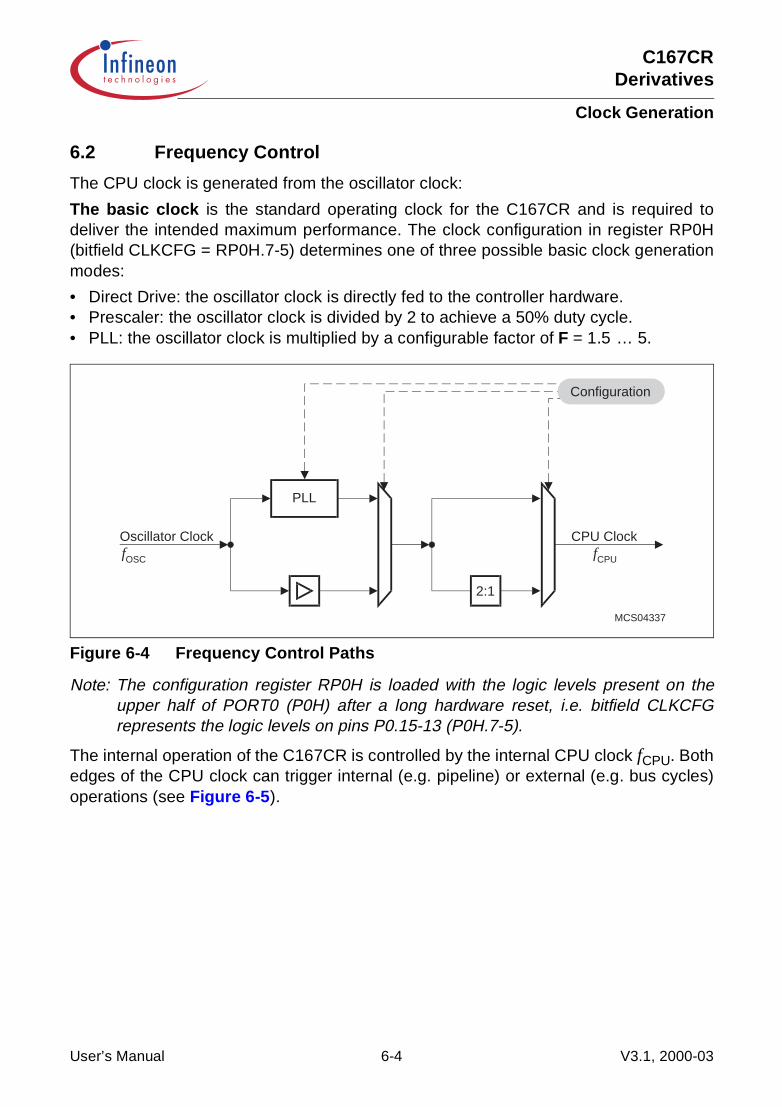
C167CRDerivatives
Clock Generation
6.2 Frequency Control
The CPU clock is generated from the oscillator clock:
The basic clock is the standard operating clock for the C167CR and is required todeliver the intended maximum performance. The clock configuration in register RP0H(bitfield CLKCFG = RP0H.7-5) determines one of three possible basic clock generationmodes:
• Direct Drive: the oscillator clock is directly fed to the controller hardware.• Prescaler: the oscillator clock is divided by 2 to achieve a 50% duty cycle.• PLL: the oscillator clock is multiplied by a configurable factor of F = 1.5 … 5.
Figure 6-4 Frequency Control Paths
Note: The configuration register RP0H is loaded with the logic levels present on theupper half of PORT0 (P0H) after a long hardware reset, i.e. bitfield CLKCFGrepresents the logic levels on pins P0.15-13 (P0H.7-5).
The internal operation of the C167CR is controlled by the internal CPU clock fCPU. Bothedges of the CPU clock can trigger internal (e.g. pipeline) or external (e.g. bus cycles)operations (see Figure 6-5).
MCS04337
PLL
Oscillator ClockfOSC
2:1
CPU ClockfCPU
Configuration
User’s Manual 6-4 V3.1, 2000-03

C167CRDerivatives
Clock Generation
Figure 6-5 Generation Mechanisms for the CPU Clock
Direct Drive
When direct drive is configured (CLKCFG = 011B) the C167CR’s clock system is directlyfed from the external clock input, i.e. fCPU = fOSC. This allows operation of the C167CRwith a reasonably small fundamental mode crystal. The specified minimum values for theCPU clock phases (TCLs) must be respected. Therefore the maximum input clockfrequency depends on the clock signal’s duty cycle.
Prescaler Operation
When prescaler operation is configured (CLKCFG = 001B) the C167CR’s input clock isdivided by 2 to generate then CPU clock signal, i.e. fCPU = fOSC / 2. This requires theoscillator (or input clock) to run on 2 times the intended operating frequency butguarantees a 50% duty cycle for the internal clock system independent of the input clocksignal’s waveform.
MCT04338
fOSC
fCPU
Phase Locked Loop Operation
TCL
fOSC
fCPU
Direct Clock Drive
fOSC
fCPU
Prescaler OperationTCL
TCL
TCL
TCL
TCL
User’s Manual 6-5 V3.1, 2000-03

C167CRDerivatives
Clock Generation
PLL Operation
When PLL operation is configured (via CLKCFG) the C167CR’s input clock is fed to theon-chip phase locked loop circuit which multiplies its frequency by a factor of F = 1.5 … 5(selectable via CLKCFG, see Table 6-1) and generates a CPU clock signal with 50%duty cycle, i.e. fCPU = fOSC × F.
The on-chip PLL circuit allows operation of the C167CR on a low frequency externalclock while still providing maximum performance. The PLL also provides fail safemechanisms which allow the detection of frequency deviations and the execution ofemergency actions in case of an external clock failure.
When the PLL detects a missing input clock signal it generates an interrupt request. Thiswarning interrupt indicates that the PLL frequency is no more locked, i.e. no more stable.This occurs when the input clock is unstable and especially when the input clock failscompletely, e.g. due to a broken crystal. In this case the synchronization mechanism willreduce the PLL output frequency down to the PLL’s base frequency (2 … 5 MHz). Thebase frequency is still generated and allows the CPU to execute emergency actions incase of a loss of the external clock.
On power-up the PLL provides a stable clock signal within ca. 1 ms after VDD hasreached the specified valid range, even if there is no external clock signal (in this casethe PLL will run on its base frequency of 2 … 5 MHz). The PLL starts synchronizing withthe external clock signal as soon as it is available. Within ca. 1 ms after stableoscillations of the external clock within the specified frequency range the PLL will besynchronous with this clock at a frequency of F × fOSC, i.e. the PLL locks to the externalclock.
When PLL operation is selected the CPU clock is a selectable multiple of the oscillatorfrequency, i.e. the input frequency.
Table 6-1 lists the possible selections.
User’s Manual 6-6 V3.1, 2000-03
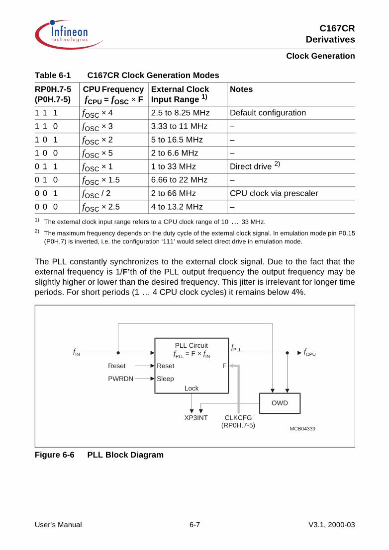
C167CRDerivatives
Clock Generation
The PLL constantly synchronizes to the external clock signal. Due to the fact that theexternal frequency is 1/F’th of the PLL output frequency the output frequency may beslightly higher or lower than the desired frequency. This jitter is irrelevant for longer timeperiods. For short periods (1 … 4 CPU clock cycles) it remains below 4%.
Figure 6-6 PLL Block Diagram
Table 6-1 C167CR Clock Generation Modes
RP0H.7-5(P0H.7-5)
CPU Frequency fCPU = fOSC × F
External Clock Input Range 1)
Notes
1 1 1 fOSC × 4 2.5 to 8.25 MHz Default configuration
1 1 0 fOSC × 3 3.33 to 11 MHz –
1 0 1 fOSC × 2 5 to 16.5 MHz –
1 0 0 fOSC × 5 2 to 6.6 MHz –
0 1 1 fOSC × 1 1 to 33 MHz Direct drive 2)
0 1 0 fOSC × 1.5 6.66 to 22 MHz –
0 0 1 fOSC / 2 2 to 66 MHz CPU clock via prescaler
0 0 0 fOSC × 2.5 4 to 13.2 MHz –1) The external clock input range refers to a CPU clock range of 10 … 33 MHz.2) The maximum frequency depends on the duty cycle of the external clock signal. In emulation mode pin P0.15
(P0H.7) is inverted, i.e. the configuration ‘111’ would select direct drive in emulation mode.
MCB04339
fINPLL CircuitfPLL = F × fIN
Reset
PWRDN
fPLL fCPU
OWD
Reset
SleepLock
XP3INT CLKCFG(RP0H.7-5)
F
User’s Manual 6-7 V3.1, 2000-03
C167CRDerivatives
Clock Generation
6.3 Oscillator Watchdog
The C167CR provides an Oscillator Watchdog (OWD) which monitors the clock signalfed to input XTAL1 of the on-chip oscillator (either with a crystal or via external clockdrive) in prescaler or direct drive mode (not if the PLL provides the basic clock). For thisoperation the PLL provides a clock signal (base frequency) which is used to supervisetransitions on the oscillator clock. This PLL clock is independent from the XTAL1 clock.When the expected oscillator clock transitions are missing the OWD activates the PLLUnlock/OWD interrupt node and supplies the CPU with the PLL clock signal instead ofthe selected oscillator clock. Under these circumstances the PLL will oscillate with itsbase frequency.
In direct drive mode the PLL base frequency is used directly (fCPU = 2 … 5 MHz).In prescaler mode the PLL base frequency is divided by 2 (fCPU = 1 … 2.5 MHz).
If the oscillator clock fails while the PLL provides the basic clock the system will besupplied with the PLL base frequency anyway.
With this PLL clock signal the CPU can either execute a controlled shutdown sequencebringing the system into a defined and safe idle state, or it can provide an emergencyoperation of the system with reduced performance based on this (normally slower)emergency clock.
Note: The CPU clock source is only switched back to the oscillator clock after ahardware reset.
The oscillator watchdog can be disabled by setting bit OWDDIS in register SYSCON.In this case the PLL remains idle and provides no clock signal, while the CPU clocksignal is derived directly from the oscillator clock or via prescaler. Also no interruptrequest will be generated in case of a missing oscillator clock.
Note: The oscillator watchdog may also be disabled via hardware by (externally) pullingthe OWE line low. However, this is mainly provided for testing purposes and notrecommended for application systems.
User’s Manual 6-8 V3.1, 2000-03
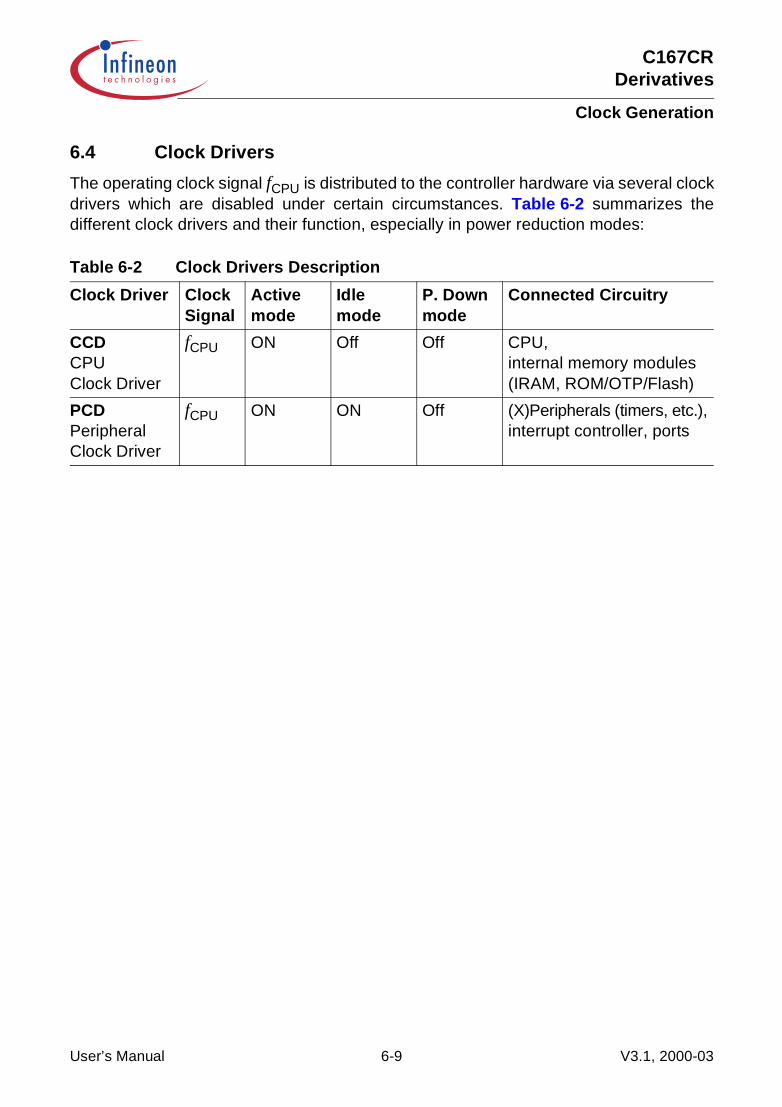
C167CRDerivatives
Clock Generation
6.4 Clock Drivers
The operating clock signal fCPU is distributed to the controller hardware via several clockdrivers which are disabled under certain circumstances. Table 6-2 summarizes thedifferent clock drivers and their function, especially in power reduction modes:
Table 6-2 Clock Drivers Description
Clock Driver Clock Signal
Activemode
Idlemode
P. Downmode
Connected Circuitry
CCDCPUClock Driver
fCPU ON Off Off CPU,internal memory modules (IRAM, ROM/OTP/Flash)
PCDPeripheralClock Driver
fCPU ON ON Off (X)Peripherals (timers, etc.),interrupt controller, ports
User’s Manual 6-9 V3.1, 2000-03

C167CRDerivatives
Parallel Ports
7 Parallel PortsIn order to accept or generate single external control signals or parallel data, theC167CR provides up to 111 parallel IO lines organized into one 16-bit IO port (Port 2),eight 8-bit IO ports (PORT0 made of P0H and P0L, PORT1 made of P1H and P1L,Port 4, Port 6, Port 7, Port 8), one 15-bit IO port (Port 3), and one 16-bit input port(Port 5).
These port lines may be used for general purpose Input/Output controlled via softwareor may be used implicitly by the C167CR’s integrated peripherals or the External BusController.
All port lines are bit addressable, and all input/output lines are individually (bit-wise)programmable as inputs or outputs via direction registers (except Port 5, of course). TheIO ports are true bidirectional ports which are switched to high impedance state whenconfigured as inputs. The output drivers of five IO ports (2, 3, 6, 7, 8) can be configured(pin by pin) for push/pull operation or open-drain operation via control registers.
The logic level of a pin is clocked into the input latch once per state time, regardlesswhether the port is configured for input or output.
Figure 7-1 SFRs and Pins associated with the Parallel Ports
MCA04340
P0L
P0H
P1L
DP0H
PDCR PICON
Data Input / OutputRegisters
Direction ControlRegisters
Port Driver ControlRegister
Diverse Control Registers
P1H
E
P2
P3
P4
P5
P6
P7
P8
DP0L E
DP1L E
DP1H E
DP2
DP3
DP4
DP6
DP7
DP8
E E
ODP3
ODP2 E
E
ODP6
ODP7
ODP8
E
E
E
User’s Manual 7-1 V3.1, 2000-03
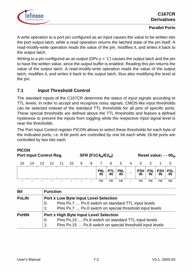
C167CRDerivatives
Parallel Ports
A write operation to a port pin configured as an input causes the value to be written intothe port output latch, while a read operation returns the latched state of the pin itself. Aread-modify-write operation reads the value of the pin, modifies it, and writes it back tothe output latch.
Writing to a pin configured as an output (DPx.y = ‘1’) causes the output latch and the pinto have the written value, since the output buffer is enabled. Reading this pin returns thevalue of the output latch. A read-modify-write operation reads the value of the outputlatch, modifies it, and writes it back to the output latch, thus also modifying the level atthe pin.
7.1 Input Threshold Control
The standard inputs of the C167CR determine the status of input signals according toTTL levels. In order to accept and recognize noisy signals, CMOS-like input thresholdscan be selected instead of the standard TTL thresholds for all pins of specific ports.These special thresholds are defined above the TTL thresholds and feature a definedhysteresis to prevent the inputs from toggling while the respective input signal level isnear the thresholds.
The Port Input Control register PICON allows to select these thresholds for each byte ofthe indicated ports, i.e. 8-bit ports are controlled by one bit each while 16-bit ports arecontrolled by two bits each.
PICONPort Input Control Reg. SFR (F1C4H/E2H) Reset value: - - 00H
15 14 13 12 11 10 9 8 7 6 5 4 3 2 1 0
P8LIN
P7LIN
P6LIN - P3H
INP3LIN
P2HIN
P2LIN
- - - - - - - - rw rw rw - rw rw rw rw
Bit Function
PxLIN Port x Low Byte Input Level Selection0: Pins Px.7 … Px.0 switch on standard TTL input levels1: Pins Px.7 … Px.0 switch on special threshold input levels
PxHIN Port x High Byte Input Level Selection0: Pins Px.15 … Px.8 switch on standard TTL input levels1: Pins Px.15 … Px.8 switch on special threshold input levels
User’s Manual 7-2 V3.1, 2000-03
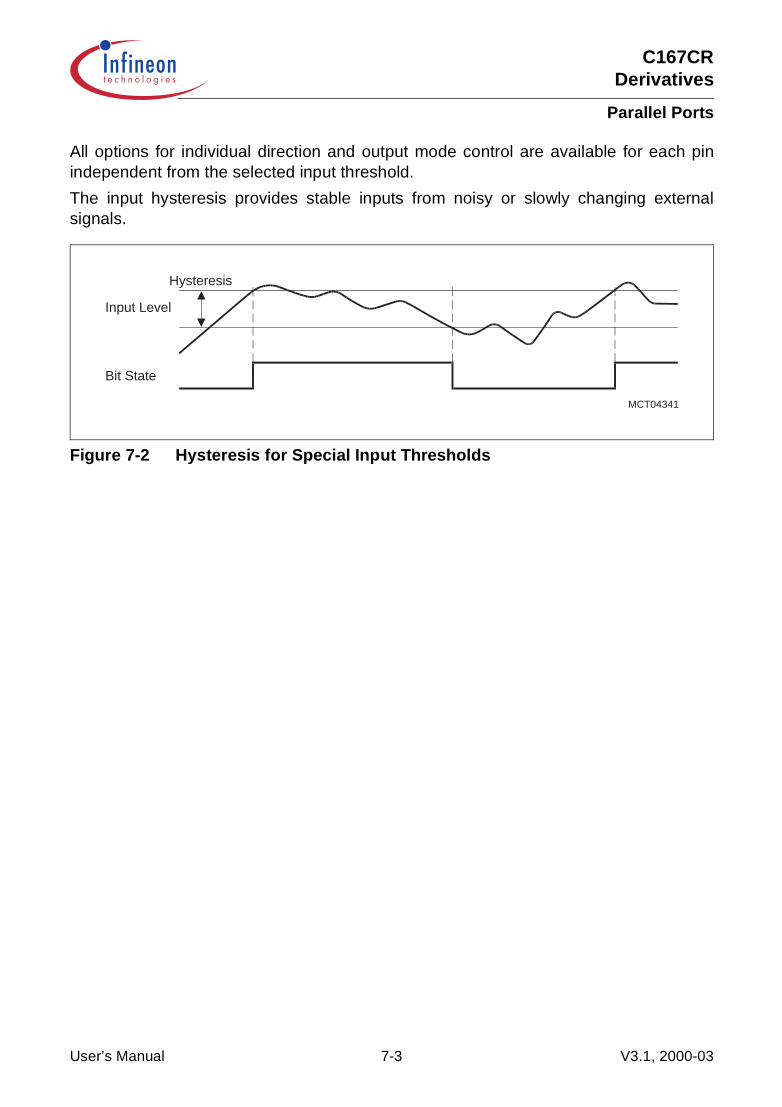
C167CRDerivatives
Parallel Ports
All options for individual direction and output mode control are available for each pinindependent from the selected input threshold.
The input hysteresis provides stable inputs from noisy or slowly changing externalsignals.
Figure 7-2 Hysteresis for Special Input Thresholds
MCT04341
Bit State
Input Level
Hysteresis
User’s Manual 7-3 V3.1, 2000-03
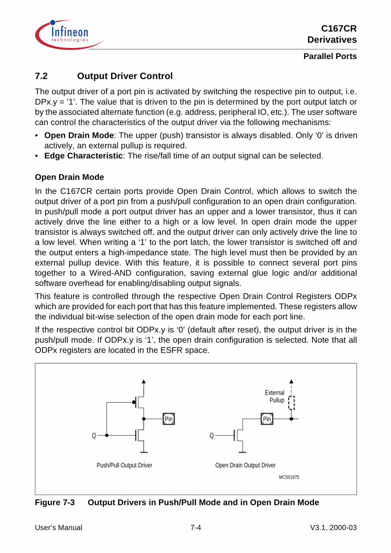
C167CRDerivatives
Parallel Ports
7.2 Output Driver Control
The output driver of a port pin is activated by switching the respective pin to output, i.e.DPx.y = ’1’. The value that is driven to the pin is determined by the port output latch orby the associated alternate function (e.g. address, peripheral IO, etc.). The user softwarecan control the characteristics of the output driver via the following mechanisms:
• Open Drain Mode: The upper (push) transistor is always disabled. Only ‘0’ is drivenactively, an external pullup is required.
• Edge Characteristic: The rise/fall time of an output signal can be selected.
Open Drain Mode
In the C167CR certain ports provide Open Drain Control, which allows to switch theoutput driver of a port pin from a push/pull configuration to an open drain configuration.In push/pull mode a port output driver has an upper and a lower transistor, thus it canactively drive the line either to a high or a low level. In open drain mode the uppertransistor is always switched off, and the output driver can only actively drive the line toa low level. When writing a ‘1’ to the port latch, the lower transistor is switched off andthe output enters a high-impedance state. The high level must then be provided by anexternal pullup device. With this feature, it is possible to connect several port pinstogether to a Wired-AND configuration, saving external glue logic and/or additionalsoftware overhead for enabling/disabling output signals.
This feature is controlled through the respective Open Drain Control Registers ODPxwhich are provided for each port that has this feature implemented. These registers allowthe individual bit-wise selection of the open drain mode for each port line.
If the respective control bit ODPx.y is ‘0’ (default after reset), the output driver is in thepush/pull mode. If ODPx.y is ‘1’, the open drain configuration is selected. Note that allODPx registers are located in the ESFR space.
Figure 7-3 Output Drivers in Push/Pull Mode and in Open Drain Mode
MCS01975
Open Drain Output Driver
ExternalPullup
Q
Push/Pull Output Driver
Q
Pin Pin
User’s Manual 7-4 V3.1, 2000-03

C167CRDerivatives
Parallel Ports
Edge Characteristic
This defines the rise/fall time for the respective output, i.e. the output transition time.Slow edges reduce the peak currents that are drawn when changing the voltage level ofan external capacitive load. For a bus interface, however, fast edges may still berequired. Edge characteristic effects the pre-driver which controls the final output driverstage.
Figure 7-4 Structure of Output Driver with Edge Control
MCS04342
Data Signal
Push
Pull
Edge Control
Open Drain Control
Control Signals Driver Control Logic Driver Stage
Pin
User’s Manual 7-5 V3.1, 2000-03
C167CRDerivatives
Parallel Ports
The Port Driver Control Register PDCR provides the corresponding control bits. Aseparate control bit is provided for bus pins as well as for non-bus pins.
Figure 7-5 summarizes the effects of the driver characteristics:
Edge characteristic generally influences the output signal’s shape.
Figure 7-5 General Output Signal Waveforms
PDCRPort Driver Control Reg. ESFR (F0AAH/55H) Reset value: 0000H
15 14 13 12 11 10 9 8 7 6 5 4 3 2 1 0
- - - - - - - - - - - NBP EC - - - BIP
EC
- - - - - - - - - - - rw - - - rw
Bit Function
BIPEC Bus Interface Pins Edge Characteristic (Defines the outp. rise/fall time tRF)0: Fast edge mode, rise/fall times depend on the driver’s dimensioning.1: Reduced edge mode.BIPEC controls: PORT0, PORT1, Port 4, Port 6, RD, WR, ALE, CLKOUT, BHE/WRH, READY (emulation mode only).
NBPEC Non-Bus Pins Edge Characteristic (Defines the output rise/fall time tRF)0: Fast edge mode, rise/fall times depend on the driver’s dimensioning.1: Reduced edge mode.NBPEC controls: Port 2, Port 3, Port 7, Port 8, RSTOUT, RSTIN (bidirectional reset mode only).
MCD04343Fast Edge Slow Edge
User’s Manual 7-6 V3.1, 2000-03

C167CRDerivatives
Parallel Ports
7.3 Alternate Port Functions
In order to provide a maximum of flexibility for different applications and their specific IOrequirements port lines have programmable alternate input or output functionsassociated with them.
If an alternate output function of a pin is to be used, the direction of this pin must beprogrammed for output (DPx.y = ‘1’), except for some signals that are used directly afterreset and are configured automatically. Otherwise the pin remains in the high-impedancestate and is not effected by the alternate output function. The respective port latch shouldhold a ‘1’, because its output is combined with the alternate output data.X-Peripherals (peripherals connected to the on-chip XBUS) control their associated IOpins directly via separate control lines.
Table 7-1 Summary of Alternate Port Functions
Port Alternate Function(s) Alternate Signal(s)
PORT0 Address and data lines when accessing external resources (e.g. memory)
AD15 … AD0
PORT1 Address lines when accessing ext. resourcesCapture inputs of the CAPCOM units
A15 … A0,CC27IO … CC24IO
Port 2 Capture inputs or compare outputs of the CAPCOM units, CAPCOM timer inputFast external interrupt inputs
CC15IO … CC0IO,T7IN,EX7IN … EX0IN
Port 3 System clock outputOptional bus control signalInput/output functions of serial interfaces, timers
CLKOUT, BHE/WRH,RxD0, TxD0, MTSR, MRST, SCLK, T2IN, T3IN, T4IN, T3EUD, T3OUT, CAPIN, T6OUT, T0IN
Port 4 Selected segment address lines in systems with more than 64 KBytes of external resourcesCAN interface (where implemented)
A23 … A16,
CAN1_TxD, CAN1_RxD
Port 5 Analog input channels to the A/D converterTimer control signal inputs
AN15 … AN0,T2EUD, T4EUD, T5IN, T6IN
Port 6 Bus arbitration signals,Chip select output signals
BREQ, HLDA, HOLD,CS4 … CS0
Port_7 Capture inputs or compare outputs of the CAPCOM unitsPWM output signals
CC31IO … CC28IO,
POUT3 … POUT0
Port 8 Capture inputs or compare outputs of the CAPCOM units
CC23IO … CC16IO
User’s Manual 7-7 V3.1, 2000-03

C167CRDerivatives
Parallel Ports
If an alternate input function of a pin is used, the direction of the pin must beprogrammed for input (DPx.y = ‘0’) if an external device is driving the pin. The inputdirection is the default after reset. If no external device is connected to the pin, however,one can also set the direction for this pin to output. In this case, the pin reflects the stateof the port output latch. Thus, the alternate input function reads the value stored in theport output latch. This can be used for testing purposes to allow a software trigger of analternate input function by writing to the port output latch.
On most of the port lines, the user software is responsible for setting the proper directionwhen using an alternate input or output function of a pin. This is done by setting orclearing the direction control bit DPx.y of the pin before enabling the alternate function.There are port lines, however, where the direction of the port line is switchedautomatically. For instance, in the multiplexed external bus modes of PORT0, thedirection must be switched several times for an instruction fetch in order to output theaddresses and to input the data. Obviously, this cannot be done through instructions. Inthese cases, the direction of the port line is switched automatically by hardware if thealternate function of such a pin is enabled.To determine the appropriate level of the port output latches check how the alternatedata output is combined with the respective port latch output.
There is one basic structure for all port lines with only an alternate input function. Portlines with only an alternate output function, however, have different structures due to theway the direction of the pin is switched and depending on whether the pin is accessibleby the user software or not in the alternate function mode.
All port lines that are not used for these alternate functions may be used as generalpurpose IO lines. When using port pins for general purpose output, the initial outputvalue should be written to the port latch prior to enabling the output drivers, in order toavoid undesired transitions on the output pins. This applies to single pins as well as topin groups (see examples below).
OUTPUT_ENABLE_SINGLE_PIN:BSET P4.0 ;Initial output level is ‘high’BSET DP4.0 ;Switch on the output driverOUTPUT_ENABLE_PIN_GROUP:BFLDL P4, #05H, #05H ;Initial output level is ‘high’BFLDL DP4, #05H, #05H ;Switch on the output drivers
Note: When using several BSET pairs to control more pins of one port, these pairs mustbe separated by instructions, which do not reference the respective port (seeChapter 4.2).
Each of these ports and the alternate input and output functions are described in detailin the following subsections.
User’s Manual 7-8 V3.1, 2000-03

C167CRDerivatives
Parallel Ports
7.4 PORT0
The two 8-bit ports P0H and P0L represent the higher and lower part of PORT0,respectively. Both halfs of PORT0 can be written (e.g. via a PEC transfer) withouteffecting the other half.If this port is used for general purpose IO, the direction of each line can be configuredvia the corresponding direction registers DP0H and DP0L.
P0LPORT0 Low Register SFR (FF00H/80H) Reset value: - - 00H
15 14 13 12 11 10 9 8 7 6 5 4 3 2 1 0
P0L .7
P0L .6
P0L .5
P0L .4
P0L .3
P0L .2
P0L .1
P0L .0
- - - - - - - - rw rw rw rw rw rw rw rw
P0HPORT0 High Register SFR (FF02H/81H) Reset value: - - 00H
15 14 13 12 11 10 9 8 7 6 5 4 3 2 1 0
P0H .7
P0H .6
P0H .5
P0H .4
P0H .3
P0H .2
P0H .1
P0H .0
- - - - - - - - rw rw rw rw rw rw rw rw
Bit Function
P0X.y Port data register P0H or P0L bit y
User’s Manual 7-9 V3.1, 2000-03
C167CRDerivatives
Parallel Ports
Alternate Functions of PORT0
When an external bus is enabled, PORT0 is used as data bus or address/data bus.Note that an external 8-bit demultiplexed bus only uses P0L, while P0H is free for IO(provided that no other bus mode is enabled).
PORT0 is also used to select the system startup configuration. During reset, PORT0 isconfigured to input, and each line is held high through an internal pullup device. Eachline can now be individually pulled to a low level (see DC-level specifications in therespective Data Sheets) through an external pulldown device. A default configuration isselected when the respective PORT0 lines are at a high level. Through pulling individuallines to a low level, this default can be changed according to the needs of theapplications.The internal pullup devices are designed such that an external pulldown resistors (seeData Sheet specification) can be used to apply a correct low level. These externalpulldown resistors can remain connected to the PORT0 pins also during normaloperation, however, care has to be taken such that they do not disturb the normalfunction of PORT0 (this might be the case, for example, if the external resistor is toostrong).With the end of reset, the selected bus configuration will be written to the BUSCON0register. The configuration of the high byte of PORT0 will be copied into the specialregister RP0H. This read-only register holds the selection for the number of chip selects
DP0LP0L Direction Ctrl. Register ESFR (F100H/80H) Reset value: - - 00H
15 14 13 12 11 10 9 8 7 6 5 4 3 2 1 0
DP0L .7
DP0L .6
DP0L .5
DP0L .4
DP0L .3
DP0L .2
DP0L .1
DP0L .0
- - - - - - - - rw rw rw rw rw rw rw rw
DP0HP0H Direction Ctrl. Register ESFR (F102H/81H) Reset Value: - - 00H
15 14 13 12 11 10 9 8 7 6 5 4 3 2 1 0
DP0H .7
DP0H .6
DP0H .5
DP0H .4
DP0H .3
DP0H .2
DP0H .1
DP0H .0
- - - - - - - - rw rw rw rw rw rw rw rw
Bit Function
DP0X.y Port direction register DP0H or DP0L bit yDP0X.y = 0: Port line P0X.y is an input (high-impedance)DP0X.y = 1: Port line P0X.y is an output
User’s Manual 7-10 V3.1, 2000-03

C167CRDerivatives
Parallel Ports
and segment addresses. Software can read this register in order to react according tothe selected configuration, if required.When the reset is terminated, the internal pullup devices are switched off, and PORT0will be switched to the appropriate operating mode.
During external accesses in multiplexed bus modes PORT0 first outputs the 16-bitintra-segment address as an alternate output function. PORT0 is then switched tohigh-impedance input mode to read the incoming instruction or data. In 8-bit data busmode, two memory cycles are required for word accesses, the first for the low byte andthe second for the high byte of the word. During write cycles PORT0 outputs the databyte or word after outputting the address.During external accesses in demultiplexed bus modes PORT0 reads the incominginstruction or data word or outputs the data byte or word.
Figure 7-6 PORT0 IO and Alternate Functions
When an external bus mode is enabled, the direction of the port pin and the loading ofdata into the port output latch are controlled by the bus controller hardware. The input ofthe port output latch is disconnected from the internal bus and is switched to the linelabeled “Alternate Data Output” via a multiplexer. The alternate data can be the 16-bitintrasegment address or the 8/16-bit data information. The incoming data on PORT0 isread on the line “Alternate Data Input”. While an external bus mode is enabled, the usersoftware should not write to the port output latch, otherwise unpredictable results mayoccur. When the external bus modes are disabled, the contents of the direction registerlast written by the user becomes active.
Figure 7-7 shows the structure of a PORT0 pin.
MCA04344
P0H.7P0H.6P0H.5P0H.4P0H.3P0H.2P0H.1P0H.0P0L.7P0L.6P0L.5P0L.4P0L.3P0L.2P0L.1P0L.0
Port 0
P0H
P0L
Alternate Function
General PurposeInput/Output
D7D6D5D4D3D2D1D0
8-BitDemux Bus
a) b)
16-BitDemux Bus
D0D1D2D3D4D5D6D7D8D9D10D11D12D13D14D15 A15
A14A13A12A11A10A9A8AD7AD6AD5AD4AD3AD2AD1AD0
8-BitMUX Bus
c) d)
AD15AD14AD13AD12AD11AD10AD9AD8AD7AD6AD5AD4AD3AD2AD1AD0
16-BitMUX Bus
User’s Manual 7-11 V3.1, 2000-03

C167CRDerivatives
Parallel Ports
Figure 7-7 Block Diagram of a PORT0 Pin
MCB04345
Internal Bus
Rea
d
Writ
e
Port OutputLatch
Rea
d
Writ
e
DirectionLatch
01
1 0
01
Driver
Pin
InputLatch
Clock
AltDataOut
AltEN
AltDir
AltDataIN
P0H.7-0, P0L.7-0
User’s Manual 7-12 V3.1, 2000-03

C167CRDerivatives
Parallel Ports
7.5 PORT1
The two 8-bit ports P1H and P1L represent the higher and lower part of PORT1,respectively. Both halfs of PORT1 can be written (e.g. via a PEC transfer) withouteffecting the other half.If this port is used for general purpose IO, the direction of each line can be configuredvia the corresponding direction registers DP1H and DP1L.
P1LPORT1 Low Register SFR (FF04H/82H) Reset Value: - - 00H
15 14 13 12 11 10 9 8 7 6 5 4 3 2 1 0
P1L .7
P1L 6
P1L .5
P1L .4
P1L .3
P1L .2
P1L .1
P1L .0
- - - - - - - - rw rw rw rw rw rw rw rw
P1HPORT1 High Register SFR (FF06H/83H) Reset Value: - - 00H
15 14 13 12 11 10 9 8 7 6 5 4 3 2 1 0
P1H .7
P1H .6
P1H .5
P1H .4
P1H .3
P1H .2
P1H .1
P1H .0
- - - - - - - - rw rw rw rw rw rw rw rw
Bit Function
P1X.y Port data register P1H or P1L bit y
User’s Manual 7-13 V3.1, 2000-03
C167CRDerivatives
Parallel Ports
Alternate Functions of PORT1
When a demultiplexed external bus is enabled, PORT1 is used as address bus.Note that demultiplexed bus modes use PORT1 as a 16-bit port. Otherwise all 16 portlines can be used for general purpose IO.
The upper four pins of PORT1 (P1H.7 … P1H.4) also serve as capture inputs(CC27IO … CC24IO) for the CAPCOM2 unit.
The usage of the port lines by the CAPCOM unit, its accessibility via software, and theprecautions are the same as described for the Port 2 lines.
As all other capture inputs, the capture input function of pins P1H.7 … P1H.4 can alsobe used as external interrupt inputs (sample rate 16 TCL).
As a side effect, the capture input capability of these lines can also be used in theaddress bus mode. Hereby changes of the upper address lines could be detected andtrigger an interrupt request in order to perform some special service routines. Externalcapture signals can only be applied if no address output is selected for PORT1.
DP1LP1L Direction Ctrl. Register ESFR (F104H/82H) Reset Value: - - 00H
15 14 13 12 11 10 9 8 7 6 5 4 3 2 1 0
DP1L.7
DP1L.6
DP1L.5
DP1L.4
DP1L.3
DP1L.2
DP1L.1
DP1L.0
- - - - - - - - rw rw rw rw rw rw rw rw
DP1HP1H Direction Ctrl. Register ESFR (F106H/83H) Reset Value: - - 00H
15 14 13 12 11 10 9 8 7 6 5 4 3 2 1 0
DP1H.7
DP1H.6
DP1H.5
DP1H.4
DP1H.3
DP1H.2
DP1H.1
DP1H.0
- - - - - - - - rw rw rw rw rw rw rw rw
Bit Function
DP1X.y Port direction register DP1H or DP1L bit yDP1X.y = 0: Port line P1X.y is an input (high-impedance)DP1X.y = 1: Port line P1X.y is an output
User’s Manual 7-14 V3.1, 2000-03

C167CRDerivatives
Parallel Ports
Figure 7-8 PORT1 IO and Alternate Functions
During external accesses in demultiplexed bus modes PORT1 outputs the 16-bitintra-segment address as an alternate output function.
During external accesses in multiplexed bus modes, when no BUSCON register selectsa demultiplexed bus mode, PORT1 is not used and is available for general purpose IO.
When an external bus mode is enabled, the direction of the port pin and the loading ofdata into the port output latch are controlled by the bus controller hardware. The input ofthe port output latch is disconnected from the internal bus and is switched to the linelabeled “Alternate Data Output” via a multiplexer. The alternate data is the 16-bitintrasegment address. While an external bus mode is enabled, the user software shouldnot write to the port output latch, otherwise unpredictable results may occur. When theexternal bus modes are disabled, the contents of the direction register last written by theuser becomes active.
Figure 7-9 show the structure of PORT1 pins. The upper 4 pins of PORT1 combineinternal bus data and alternate data output before the port latch input.
MCA04346
P1H.7P1H.6P1H.5P1H.4P1H.3P1H.2P1H.1P1H.0P1L.7P1L.6P1L.5P1L.4P1L.3P1L.2P1L.1P1L.0
Port 1
P1H
P1L
Alternate Function
General PurposeInput/Output
A7A6A5A4A3A2A1A0
8/16-BitDemux Bus
a) b)
CAPCOM2Capture Inputs
CC24IOCC25IOCC26IOCC27IOA15
A14A13A12A11A10A9A8
User’s Manual 7-15 V3.1, 2000-03
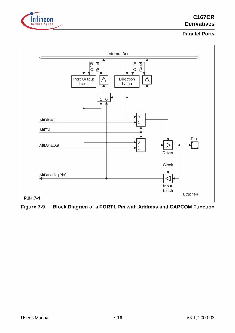
C167CRDerivatives
Parallel Ports
Figure 7-9 Block Diagram of a PORT1 Pin with Address and CAPCOM Function
MCB04347
Internal Bus
Rea
d
Writ
e
Port OutputLatch
Rea
d
Writ
e
DirectionLatch
01
1 0
01
Driver
Pin
InputLatch
Clock
AltDataOut
AltEN
AltDir = '1'
AltDataIN (Pin)
P1H.7-4
User’s Manual 7-16 V3.1, 2000-03
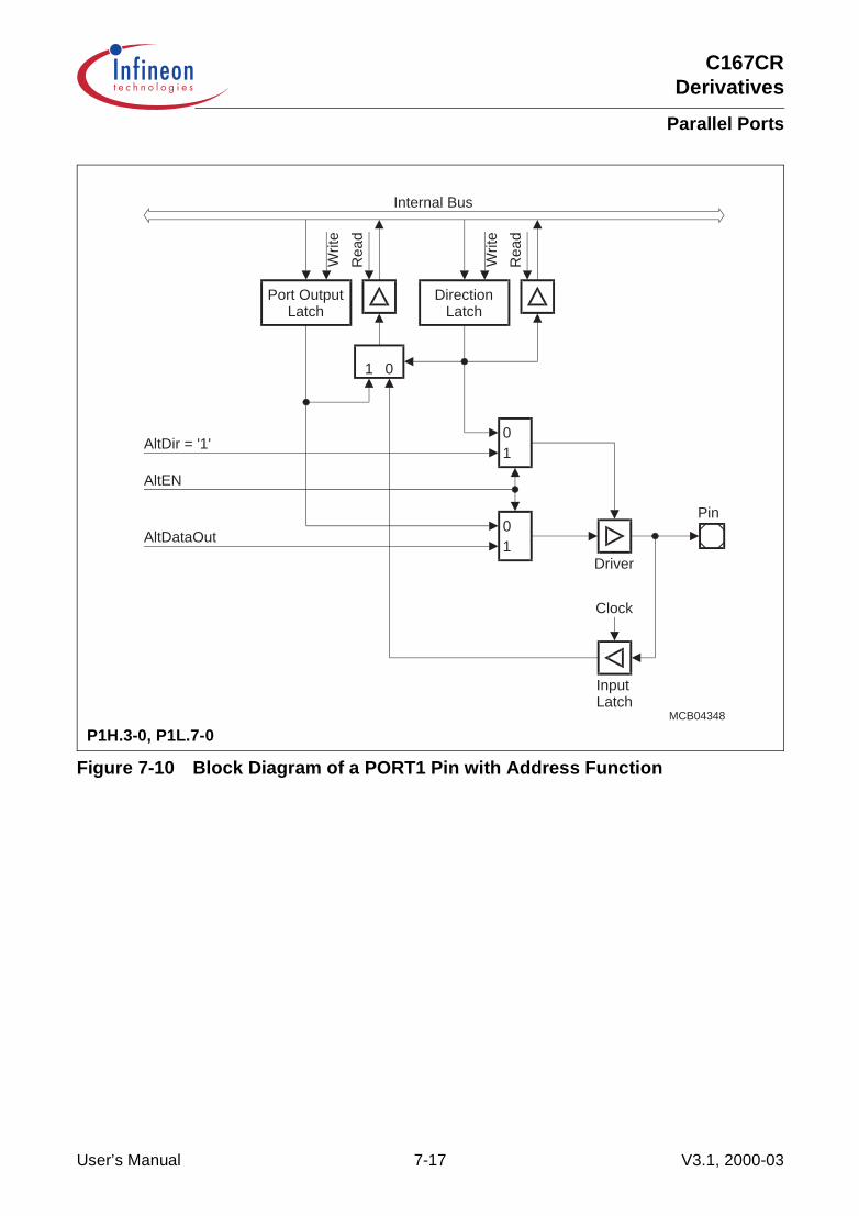
C167CRDerivatives
Parallel Ports
Figure 7-10 Block Diagram of a PORT1 Pin with Address Function
P1H.3-0, P1L.7-0MCB04348
Internal Bus
Rea
d
Writ
e
Port OutputLatch
Rea
d
Writ
e
DirectionLatch
01
1 0
01
Driver
Pin
InputLatch
Clock
AltDataOut
AltEN
AltDir = '1'
User’s Manual 7-17 V3.1, 2000-03

C167CRDerivatives
Parallel Ports
7.6 Port 2
If this 16-bit port is used for general purpose IO, the direction of each line can beconfigured via the corresponding direction register DP2. Each port line can be switchedinto push/pull or open drain mode via the open drain control register ODP2.
P2 Port 2 Data Register SFR (FFC0H/E0H) Reset value: 0000H
15 14 13 12 11 10 9 8 7 6 5 4 3 2 1 0
P2 .15
P2 .14
P2 .13
P2 .12
P2 .11
P2 .10 P2.9 P2.8 P2.7 P2.6 P2.5 P2.4 P2.3 P2.2 P2.1 P2.0
rw rw rw rw rw rw rw rw rw rw rw rw rw rw rw rw
Bit Function
P2.y Port data register P2 bit y
DP2 P2 Direction Ctrl. Register SFR (FFC2H/E1H) Reset value: 0000H
15 14 13 12 11 10 9 8 7 6 5 4 3 2 1 0
DP2 .15
DP2 .14
DP2 .13
DP2 .12
DP2 .11
DP2 .10
DP2 .9
DP2 .8
DP2 .7
DP2 .6
DP2 .5
DP2 .4
DP2 .3
DP2 .2
DP2 .1
DP2 .0
rw rw rw rw rw rw rw rw rw rw rw rw rw rw rw rw
Bit Function
DP2.y Port direction register DP2 bit yDP2.y = 0: Port line P2.y is an input (high-impedance)DP2.y = 1: Port line P2.y is an output
User’s Manual 7-18 V3.1, 2000-03
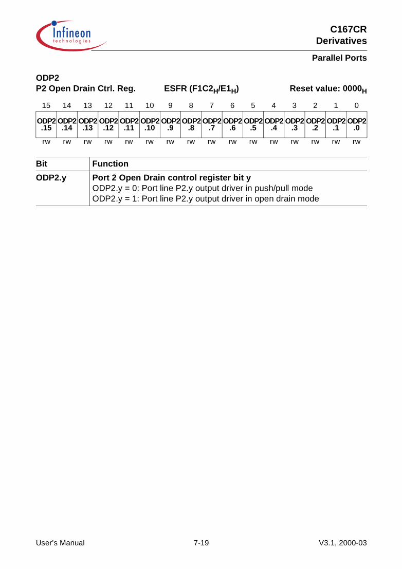
C167CRDerivatives
Parallel Ports
ODP2 P2 Open Drain Ctrl. Reg. ESFR (F1C2H/E1H) Reset value: 0000H
15 14 13 12 11 10 9 8 7 6 5 4 3 2 1 0
ODP2 .15
ODP2 .14
ODP2 .13
ODP2 .12
ODP2 .11
ODP2 .10
ODP2 .9
ODP2 .8
ODP2 .7
ODP2 .6
ODP2 .5
ODP2 .4
ODP2 .3
ODP2 .2
ODP2 .1
ODP2 .0
rw rw rw rw rw rw rw rw rw rw rw rw rw rw rw rw
Bit Function
ODP2.y Port 2 Open Drain control register bit yODP2.y = 0: Port line P2.y output driver in push/pull modeODP2.y = 1: Port line P2.y output driver in open drain mode
User’s Manual 7-19 V3.1, 2000-03

C167CRDerivatives
Parallel Ports
Alternate Functions of Port 2
All Port 2 lines (P2.15 … P2.0) serve as capture inputs or compare outputs(CC15IO … CC0IO) for the CAPCOM1 unit. The upper eight Port 2 lines (P2.15 … P2.8)also serve as external interrupt inputs EX7IN … EX0IN (16 TCL sample rate).
When a Port 2 line is used as a capture input, the state of the input latch, whichrepresents the state of the port pin, is directed to the CAPCOM unit via the line “AlternatePin Data Input”. If an external capture trigger signal is used, the direction of therespective pin must be set to input. If the direction is set to output, the state of the portoutput latch will be read since the pin represents the state of the output latch. This canbe used to trigger a capture event through software by setting or clearing the port latch.Note that in the output configuration, no external device may drive the pin, otherwiseconflicts would occur.
When a Port 2 line is used as a compare output (compare modes 1 and 3), the compareevent (or the timer overflow in compare mode 3) directly effects the port output latch. Incompare mode 1, when a valid compare match occurs, the state of the port output latchis read by the CAPCOM control hardware via the line “Alternate Latch Data Input”,inverted, and written back to the latch via the line “Alternate Data Output”. The portoutput latch is clocked by the signal “Compare Trigger” which is generated by theCAPCOM unit. In compare mode 3, when a match occurs, the value ‘1’ is written to theport output latch via the line “Alternate Data Output”. When an overflow of thecorresponding timer occurs, a ‘0’ is written to the port output latch. In both cases, theoutput latch is clocked by the signal “Compare Trigger”. The direction of the pin shouldbe set to output by the user, otherwise the pin will be in the high-impedance state andwill not reflect the state of the output latch.
As can be seen from the port structure below, the user software always has free accessto the port pin even when it is used as a compare output. This is useful for setting up theinitial level of the pin when using compare mode 1 or the double-register mode. In thesemodes, unlike in compare mode 3, the pin is not set to a specific value when a comparematch occurs, but is toggled instead.
When the user wants to write to the port pin at the same time a compare trigger tries toclock the output latch, the write operation of the user software has priority. Each time aCPU write access to the port output latch occurs, the input multiplexer of the port outputlatch is switched to the line connected to the internal bus. The port output latch willreceive the value from the internal bus and the hardware triggered change will be lost.
As all other capture inputs, the capture input function of pins P2.15 … P2.0 can also beused as external interrupt inputs (sample rate 16 TCL) or as Fast External Interruptinputs (sample rate 2 TCL).
P2.15 in addition serves as input for CAPCOM2 timer T7 (T7IN).
Table 7-2 summarizes the alternate functions of Port 2.
User’s Manual 7-20 V3.1, 2000-03
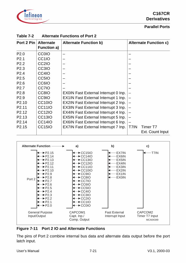
C167CRDerivatives
Parallel Ports
Figure 7-11 Port 2 IO and Alternate Functions
The pins of Port 2 combine internal bus data and alternate data output before the portlatch input.
Table 7-2 Alternate Functions of Port 2
Port 2 Pin Alternate Function a)
Alternate Function b) Alternate Function c)
P2.0P2.1P2.2P2.3P2.4P2.5P2.6P2.7P2.8P2.9P2.10P2.11P2.12P2.13P2.14P2.15
CC0IOCC1IOCC2IOCC3IOCC4IOCC5IOCC6IOCC7IOCC8IOCC9IOCC10IOCC11IOCC12IOCC13IOCC14IOCC15IO
––––––––EX0IN Fast External Interrupt 0 Inp.EX1IN Fast External Interrupt 1 Inp.EX2IN Fast External Interrupt 2 Inp.EX3IN Fast External Interrupt 3 Inp.EX4IN Fast External Interrupt 4 Inp.EX5IN Fast External Interrupt 5 Inp.EX6IN Fast External Interrupt 6 Inp.EX7IN Fast External Interrupt 7 Inp.
–––––––––––––––T7IN Timer T7
Ext. Count Input
MCA04349
P2.15P2.14P2.13P2.12P2.11P2.10P2.9P2.8P2.7P2.6P2.5P2.4P2.3P2.2P2.1P2.0
Port 2
Alternate Function
General PurposeInput/Output
CC7IOCC6IOCC5IOCC4IOCC3IOCC2IOCC1IOCC0IO
CAPCOM1Capt. Inp./Comp. Output
a)
CC15IOCC14IOCC13IOCC12IOCC11IOCC10IOCC9IOCC8IO EX0IN
EX1INEX2INEX3INEX4INEX5INEX6INEX7IN
b)
Fast ExternalInterrupt Input
c)
CAPCOM2Timer T7 Input
T7IN
User’s Manual 7-21 V3.1, 2000-03

C167CRDerivatives
Parallel Ports
Figure 7-12 Block Diagram of a Port 2 Pin
Note: Fast external interrupt inputs only on the upper eight pins of Port2.
P2.15-0, x = 15-0, z = 7-0
MCB04350
Internal Bus
Rea
d
Port OutputLatch
Rea
d
Writ
e
DirectionLatch
Rea
d
Writ
e
Open DrainLatch
1 0
Driver
Pin
InputLatch
Clock
AltDataIn (Pin)
0 1
CCx
Writ
e
AltDataIn (Latch)
EXzIN
User’s Manual 7-22 V3.1, 2000-03

C167CRDerivatives
Parallel Ports
7.7 Port 3
If this 15-bit port is used for general purpose IO, the direction of each line can beconfigured via the corresponding direction register DP3. Most port lines can be switchedinto push/pull or open drain mode via the open drain control register ODP3 (pins P3.15and P3.12 do not support open drain mode!).
P3 Port 3 Data Register SFR (FFC4H/E2H) Reset value: 0000H
15 14 13 12 11 10 9 8 7 6 5 4 3 2 1 0
P3 .15 - P3
.13P3.12
P3.11
P3.10
P3.9
P3.8 P3.7 P3.6 P3.5 P3.4 P3.3 P3.2 P3.1 P3.0
rw - rw rw rw rw rw rw rw rw rw rw rw rw rw rw
Bit Function
P3.y Port data register P3 bit y
DP3 P3 Direction Ctrl. Register SFR (FFC6H/E3H) Reset value: 0000H
15 14 13 12 11 10 9 8 7 6 5 4 3 2 1 0
DP3.15 - DP3
.13DP3.12
DP3.11
DP3.10
DP3.9
DP3.8
DP3.7
DP3.6
DP3.5
DP3 .4
DP3.3
DP3.2
DP3.1
DP3.0
rw - rw rw rw rw rw rw rw rw rw rw rw rw rw rw
Bit Function
DP3.y Port direction register DP3 bit yDP3.y = 0: Port line P3.y is an input (high-impedance)DP3.y = 1: Port line P3.y is an output
User’s Manual 7-23 V3.1, 2000-03

C167CRDerivatives
Parallel Ports
Note: Due to pin limitations register bit P3.14 is not connected to an IO pin.Pins P3.15 and P3.12 do not support open drain mode.
Alternate Functions of Port 3
The pins of Port 3 serve for various functions which include external timer control lines,the two serial interfaces, and the control lines BHE/WRH and clock output.
Table 7-3 summarizes the alternate functions of Port 3.
ODP3 P3 Open Drain Ctrl. Reg. ESFR (F1C6H/E3H) Reset value: 0000H
15 14 13 12 11 10 9 8 7 6 5 4 3 2 1 0
- - ODP3.13 - ODP
3.11ODP3.10
ODP3.9
ODP3.8
ODP3.7
ODP3.6
ODP3.5
ODP3.4
ODP3.3
ODP3.2
ODP3.1
ODP3.0
- - rw - rw rw rw rw rw rw rw rw rw rw rw rw
Bit Function
ODP3.y Port 3 Open Drain control register bit yODP3.y = 0: Port line P3.y output driver in push/pull modeODP3.y = 1: Port line P3.y output driver in open drain mode
Table 7-3 Alternate Functions of Port 3
Port 3 Pin Alternate Function
P3.0P3.1P3.2P3.3P3.4P3.5P3.6P3.7P3.8P3.9P3.10P3.11P3.12P3.13–P3.15
T0IN CAPCOM1 Timer T0 Count InputT6OUT GPT2 Timer T6 Toggle Latch OutputCAPIN GPT2 Capture InputT3OUT GPT1 Timer T3 Toggle Latch OutputT3EUD GPT1 Timer T3 External Up/Down InputT4IN GPT1 Timer T4 Count InputT3IN GPT1 Timer T3 Count InputT2IN GPT1 Timer T2 Count InputMRST SSC Master Receive/Slave TransmitMTSR SSC Master Transmit/Slave ReceiveTxD0 ASC0 Transmit Data OutputRxD0 ASC0 Receive Data InputBHE/WRH Byte High Enable/Write High OutputSCLK SSC Shift Clock Input/Output–CLKOUT System Clock Output
User’s Manual 7-24 V3.1, 2000-03
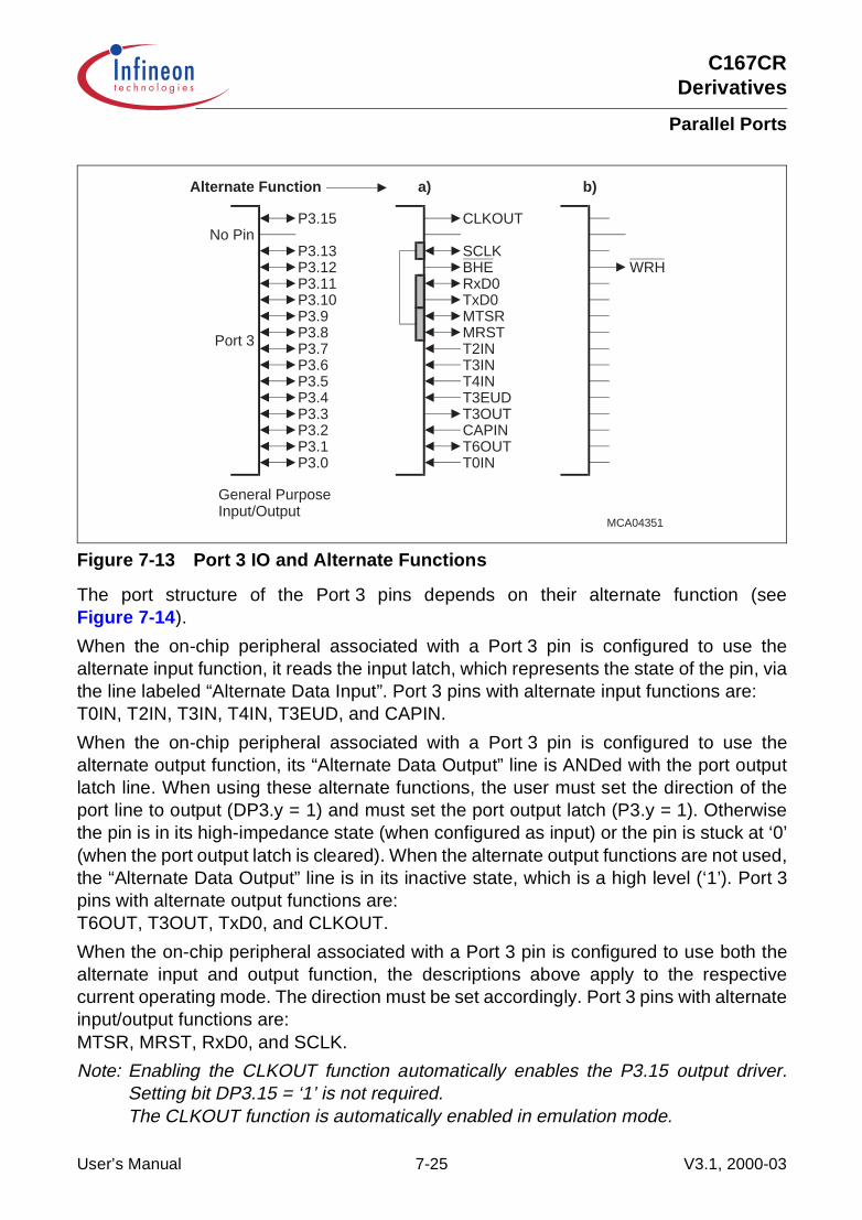
C167CRDerivatives
Parallel Ports
Figure 7-13 Port 3 IO and Alternate Functions
The port structure of the Port 3 pins depends on their alternate function (seeFigure 7-14).
When the on-chip peripheral associated with a Port 3 pin is configured to use thealternate input function, it reads the input latch, which represents the state of the pin, viathe line labeled “Alternate Data Input”. Port 3 pins with alternate input functions are:T0IN, T2IN, T3IN, T4IN, T3EUD, and CAPIN.
When the on-chip peripheral associated with a Port 3 pin is configured to use thealternate output function, its “Alternate Data Output” line is ANDed with the port outputlatch line. When using these alternate functions, the user must set the direction of theport line to output (DP3.y = 1) and must set the port output latch (P3.y = 1). Otherwisethe pin is in its high-impedance state (when configured as input) or the pin is stuck at ‘0’(when the port output latch is cleared). When the alternate output functions are not used,the “Alternate Data Output” line is in its inactive state, which is a high level (‘1’). Port 3pins with alternate output functions are:T6OUT, T3OUT, TxD0, and CLKOUT.
When the on-chip peripheral associated with a Port 3 pin is configured to use both thealternate input and output function, the descriptions above apply to the respectivecurrent operating mode. The direction must be set accordingly. Port 3 pins with alternateinput/output functions are:MTSR, MRST, RxD0, and SCLK.
Note: Enabling the CLKOUT function automatically enables the P3.15 output driver.Setting bit DP3.15 = ‘1’ is not required.The CLKOUT function is automatically enabled in emulation mode.
MCA04351
P3.15
P3.13P3.12P3.11P3.10P3.9P3.8P3.7P3.6P3.5P3.4P3.3P3.2P3.1P3.0
Port 3
No Pin
Alternate Function
General PurposeInput/Output
T2INT3INT4INT3EUDT3OUTCAPINT6OUTT0IN
a) b)
CLKOUT
SCLKBHERxD0TxD0MTSRMRST
WRH
User’s Manual 7-25 V3.1, 2000-03

C167CRDerivatives
Parallel Ports
Figure 7-14 Block Diagram of a Port 3 Pin with Alternate Input or Alternate Output Function
Pin P3.12 (BHE/WRH) is one more pin with an alternate output function. However, itsstructure is slightly different (see Figure 7-15), because after reset the BHE or WRHfunction must be used depending on the system startup configuration. In these casesthere is no possibility to program any port latches before. Thus the appropriate alternatefunction is selected automatically. If BHE/WRH is not used in the system, this pin can beused for general purpose IO by disabling the alternate function (BYTDIS = ‘1’/WRCFG = ‘0’).
P3.13, P3.11-0
MCB04352
Internal Bus
Rea
dPort Output
Latch
Rea
d
Writ
e
DirectionLatch
Rea
d
Writ
e
Open DrainLatch
1 0
Driver
Pin
InputLatch
Clock
AltDataIn
Writ
e
AltDataOut&
User’s Manual 7-26 V3.1, 2000-03

C167CRDerivatives
Parallel Ports
Figure 7-15 Block Diagram of Pins P3.15 (CLKOUT) and P3.12 (BHE/WRH)
Note: Enabling the BHE or WRH function automatically enables the P3.12 output driver.Setting bit DP3.12 = ‘1’ is not required.During bus hold pin P3.12 is switched back to its standard function and is thencontrolled by DP3.12 and P3.12. Keep DP3.12 = ‘0’ in this case to ensure floatingin hold mode.Enabling the CLKOUT function automatically enables the P3.15 output driver.Setting bit DP3.15 = ‘1’ is not required.
MCB04353
Internal Bus
Rea
d
Writ
e
Port OutputLatch
Rea
d
Writ
e
DirectionLatch
01
1 0
01
Driver
Pin
InputLatch
Clock
AltDataOut
AltEN
AltDir = '1'
P3.15, P3.12
User’s Manual 7-27 V3.1, 2000-03
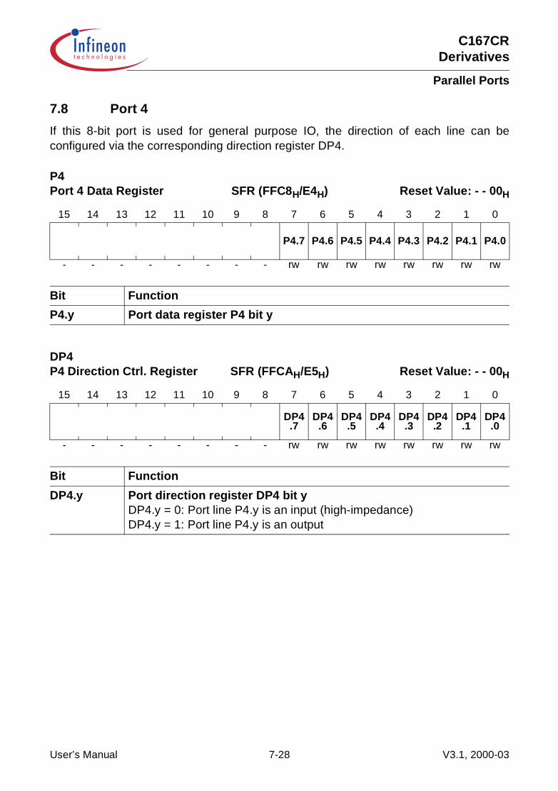
C167CRDerivatives
Parallel Ports
7.8 Port 4
If this 8-bit port is used for general purpose IO, the direction of each line can beconfigured via the corresponding direction register DP4.
P4 Port 4 Data Register SFR (FFC8H/E4H) Reset Value: - - 00H
15 14 13 12 11 10 9 8 7 6 5 4 3 2 1 0
P4.7 P4.6 P4.5 P4.4 P4.3 P4.2 P4.1 P4.0
- - - - - - - - rw rw rw rw rw rw rw rw
Bit Function
P4.y Port data register P4 bit y
DP4 P4 Direction Ctrl. Register SFR (FFCAH/E5H) Reset Value: - - 00H
15 14 13 12 11 10 9 8 7 6 5 4 3 2 1 0
DP4.7
DP4.6
DP4.5
DP4.4
DP4.3
DP4.2
DP4.1
DP4.0
- - - - - - - - rw rw rw rw rw rw rw rw
Bit Function
DP4.y Port direction register DP4 bit yDP4.y = 0: Port line P4.y is an input (high-impedance)DP4.y = 1: Port line P4.y is an output
User’s Manual 7-28 V3.1, 2000-03

C167CRDerivatives
Parallel Ports
Alternate Functions of Port 4
During external bus cycles that use segmentation (i.e. an address space above64 KByte) a number of Port 4 pins may output the segment address lines. The numberof pins that is used for segment address output determines the external address spacewhich is directly accessible. The other pins of Port 4 (if any) may be used for generalpurpose IO or for the CAN interface.If segment address lines are selected, the alternate function of Port 4 may be necessaryto access e.g. external memory directly after reset. For this reason Port 4 will beswitched to this alternate function automatically.
The number of segment address lines is selected via PORT0 during reset. The selectedvalue can be read from bitfield SALSEL in register RP0H (read only) e.g. in order tocheck the configuration during run time.
Devices with CAN interface use 2 pins of Port 4 to interface the CAN module to anexternal CAN transceiver. In this case the number of possible segment address lines isreduced.
Table 7-4 summarizes the alternate functions of Port 4 depending on the number ofselected segment address lines (coded via bitfield SALSEL).
Note: Port 4 pins that are neither used for segment address output nor for the CANinterface may be used for general purpose IO.If more than one function is selected for a Port 4 pin, the segment address takespreference over the CAN interface lines.
Table 7-4 Alternate Functions of Port 4
Port 4Pin
Std. FunctionSALSEL = 0164 KB
Altern. FunctionSALSEL = 11256KB
Altern. FunctionSALSEL = 001 MB
Altern. FunctionSALSEL = 1016 MB
P4.0P4.1P4.2P4.3P4.4P4.5P4.6P4.7
Gen. purpose IOGen. purpose IOGen. purpose IOGen. purpose IOGen. purpose IOGen. p. IO or CANGen. p. IO or CANGen. purpose IO
Seg. Address A16Seg. Address A17Gen. purpose IOGen. purpose IOGen. purpose IOGen. p. IO or CANGen. p. IO or CANGen. purpose IO
Seg. Address A16Seg. Address A17Seg. Address A18Seg. Address A19Gen. purpose IOGen. p. IO or CANGen. p. IO or CANGen. purpose IO
Seg. Address A16Seg. Address A17Seg. Address A18Seg. Address A19Seg. Address A20Seg. Address A21Seg. Address A22Seg. Address A23
User’s Manual 7-29 V3.1, 2000-03

C167CRDerivatives
Parallel Ports
Figure 7-16 Port 4 IO and Alternate Functions
MCA04354
--------P4.7P4.6P4.5P4.4P4.3P4.2P4.1P4.0
Port 4
Alternate Function
General PurposeInput/Output
A23A22A21A20A19A18A17A16
Full SegmentAddress (16 MB)
a)
-------
- -
-------
b)
CAN Interface
A16A17A18A19P4.4CAN_RxDCAN_TxDP4.7
User’s Manual 7-30 V3.1, 2000-03
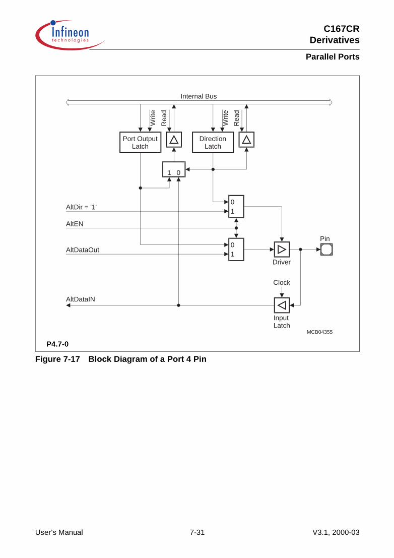
C167CRDerivatives
Parallel Ports
Figure 7-17 Block Diagram of a Port 4 Pin
P4.7-0
MCB04355
Internal Bus
Rea
d
Writ
e
Port OutputLatch
Rea
d
Writ
e
DirectionLatch
01
1 0
01
Driver
Pin
InputLatch
Clock
AltDataOut
AltEN
AltDir = '1'
AltDataIN
User’s Manual 7-31 V3.1, 2000-03
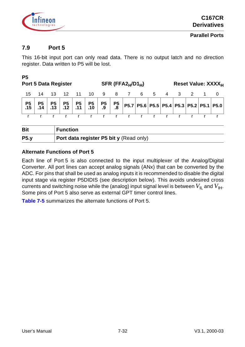
C167CRDerivatives
Parallel Ports
7.9 Port 5
This 16-bit input port can only read data. There is no output latch and no directionregister. Data written to P5 will be lost.
Alternate Functions of Port 5
Each line of Port 5 is also connected to the input multiplexer of the Analog/DigitalConverter. All port lines can accept analog signals (ANx) that can be converted by theADC. For pins that shall be used as analog inputs it is recommended to disable the digitalinput stage via register P5DIDIS (see description below). This avoids undesired crosscurrents and switching noise while the (analog) input signal level is between VIL and VIH.Some pins of Port 5 also serve as external GPT timer control lines.
Table 7-5 summarizes the alternate functions of Port 5.
P5 Port 5 Data Register SFR (FFA2H/D1H) Reset Value: XXXXH
15 14 13 12 11 10 9 8 7 6 5 4 3 2 1 0
P5.15
P5.14
P5.13
P5.12
P5.11
P5.10
P5.9
P5.8 P5.7 P5.6 P5.5 P5.4 P5.3 P5.2 P5.1 P5.0
r r r r r r r r r r r r r r r r
Bit Function
P5.y Port data register P5 bit y (Read only)
User’s Manual 7-32 V3.1, 2000-03

C167CRDerivatives
Parallel Ports
Figure 7-18 Port 5 IO and Alternate Functions
Table 7-5 Alternate Functions of Port 5
Port 5 Pin Alternate Function a) Alternate Function b)
P5.0P5.1P5.2P5.3P5.4P5.5P5.6P5.7P5.8P5.7P5.10P5.11P5.12P5.13P5.14P5.15
Analog Input AN0Analog Input AN1Analog Input AN2Analog Input AN3Analog Input AN4Analog Input AN5Analog Input AN6Analog Input AN7Analog Input AN8Analog Input AN9Analog Input AN10Analog Input AN11Analog Input AN12Analog Input AN13Analog Input AN14Analog Input AN15
––––––––––T6EUD Timer 6 ext. Up/Down InputT5EUD Timer 5 ext. Up/Down InputT6IN Timer 6 Count InputT5IN Timer 5 Count InputT4EUD Timer 4 ext. Up/Down InputT2EUD Timer 2 ext. Up/Down Input
MCA04356
P5.15P5.14P5.13P5.12P5.11P5.10P5.9P5.8P5.7P5.6P5.5P5.4P5.3P5.2P5.1P5.0
Port 5
Alternate Function
General PurposeInput
AN7AN6AN5AN4AN3AN2AN1AN0
A/D ConverterInput
a)
AN15AN14AN13AN12AN11AN10AN9AN8
T6EUDT5EUDT6INT5INT4EUDT2EUD
b)
Timer ControlInput
User’s Manual 7-33 V3.1, 2000-03
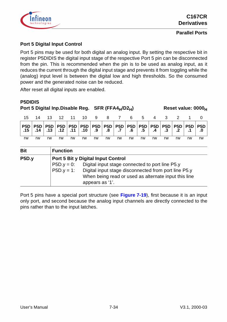
C167CRDerivatives
Parallel Ports
Port 5 Digital Input Control
Port 5 pins may be used for both digital an analog input. By setting the respective bit inregister P5DIDIS the digital input stage of the respective Port 5 pin can be disconnectedfrom the pin. This is recommended when the pin is to be used as analog input, as itreduces the current through the digital input stage and prevents it from toggling while the(analog) input level is between the digital low and high thresholds. So the consumedpower and the generated noise can be reduced.
After reset all digital inputs are enabled.
Port 5 pins have a special port structure (see Figure 7-19), first because it is an inputonly port, and second because the analog input channels are directly connected to thepins rather than to the input latches.
P5DIDISPort 5 Digital Inp.Disable Reg. SFR (FFA4H/D2H) Reset value: 0000H
15 14 13 12 11 10 9 8 7 6 5 4 3 2 1 0
P5D.15
P5D.14
P5D.13
P5D.12
P5D.11
P5D.10
P5D.9
P5D.8
P5D.7
P5D.6
P5D.5
P5D.4
P5D.3
P5D.2
P5D.1
P5D.0
rw rw rw rw rw rw rw rw rw rw rw rw rw rw rw rw
Bit Function
P5D.y Port 5 Bit y Digital Input ControlP5D.y = 0: Digital input stage connected to port line P5.yP5D.y = 1: Digital input stage disconnected from port line P5.y
When being read or used as alternate input this lineappears as ‘1’.
User’s Manual 7-34 V3.1, 2000-03

C167CRDerivatives
Parallel Ports
Figure 7-19 Block Diagram of a Port 5 Pin
Note: The “AltDataIn” line does not exist on all Port 5 inputs.
P5.15-0MCB04357
Internal Bus
Rea
d
Pin
AnalogInput
InputLatch
Clock
AltDataIn
ChannelSelect
DigInputEN
User’s Manual 7-35 V3.1, 2000-03

C167CRDerivatives
Parallel Ports
7.10 Port 6
If this 8-bit port is used for general purpose IO, the direction of each line can beconfigured via the corresponding direction register DP6. Each port line can be switchedinto push/pull or open drain mode via the open drain control register ODP6.
P6 Port 6 Data Register SFR (FFCCH/E6H) Reset Value: - - 00H
15 14 13 12 11 10 9 8 7 6 5 4 3 2 1 0
P6.7 P6.6 P6.5 P6.4 P6.3 P6.2 P6.1 P6.0
- - - - - - - - rw rw rw rw rw rw rw rw
Bit Function
P6.y Port data register P6 bit y
DP6 P6 Direction Ctrl. Register SFR (FFCEH/E7H) Reset Value: - - 00H
15 14 13 12 11 10 9 8 7 6 5 4 3 2 1 0
DP6.7
DP6.6
DP6.5
DP6.4
DP6.3
DP6.2
DP6.1
DP6.0
- - - - - - - - rw rw rw rw rw rw rw rw
Bit Function
DP6.y Port direction register DP6 bit yDP6.y = 0: Port line P6.y is an input (high-impedance)DP6.y = 1: Port line P6.y is an output
User’s Manual 7-36 V3.1, 2000-03
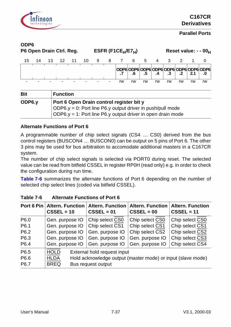
C167CRDerivatives
Parallel Ports
Alternate Functions of Port 6
A programmable number of chip select signals (CS4 … CS0) derived from the buscontrol registers (BUSCON4 … BUSCON0) can be output on 5 pins of Port 6. The other3 pins may be used for bus arbitration to accomodate additional masters in a C167CRsystem.The number of chip select signals is selected via PORT0 during reset. The selectedvalue can be read from bitfield CSSEL in register RP0H (read only) e.g. in order to checkthe configuration during run time.
Table 7-6 summarizes the alternate functions of Port 6 depending on the number ofselected chip select lines (coded via bitfield CSSEL).
ODP6 P6 Open Drain Ctrl. Reg. ESFR (F1CEH/E7H) Reset value: - - 00H
15 14 13 12 11 10 9 8 7 6 5 4 3 2 1 0
ODP6.7
ODP6.6
ODP6.5
ODP6.4
ODP6.3
ODP6.2
ODP62.1
ODP6.0
- - - - - - - - rw rw rw rw rw rw rw rw
Bit Function
ODP6.y Port 6 Open Drain control register bit yODP6.y = 0: Port line P6.y output driver in push/pull modeODP6.y = 1: Port line P6.y output driver in open drain mode
Table 7-6 Alternate Functions of Port 6
Port 6 Pin Altern. FunctionCSSEL = 10
Altern. FunctionCSSEL = 01
Altern. FunctionCSSEL = 00
Altern. FunctionCSSEL = 11
P6.0P6.1P6.2P6.3P6.4
Gen. purpose IOGen. purpose IOGen. purpose IOGen. purpose IOGen. purpose IO
Chip select CS0Chip select CS1Gen. purpose IOGen. purpose IOGen. purpose IO
Chip select CS0Chip select CS1Chip select CS2Gen. purpose IOGen. purpose IO
Chip select CS0Chip select CS1Chip select CS2Chip select CS3Chip select CS4
P6.5P6.6P6.7
HOLD External hold request inputHLDA Hold acknowledge output (master mode) or input (slave mode)BREQ Bus request output
User’s Manual 7-37 V3.1, 2000-03

C167CRDerivatives
Parallel Ports
Figure 7-20 Port 6 IO and Alternate Functions
The chip select lines of Port 6 additionally have an internal weak pullup device. Thisdevice is switched on under the following conditions:
• always during reset for all potential CS output pins• if the Port 6 line is used as a chip select output,
and the C167CR is in Hold mode (invoked through HOLD),and the respective pin driver is in push/pull mode (ODP6.x = ‘0’).
This feature is implemented to drive the chip select lines high during reset in order toavoid multiple chip selection, and to allow another master to access the external memoryvia the same chip select lines (Wired-AND), while the C167CR is in Hold mode.With ODP6.x = ‘1’ (open drain output selected), the internal pullup device will not beactive during Hold mode; external pullup devices must be used in this case.When entering Hold mode the CS lines are actively driven high for one clock phase, thenthe output level is controlled by the pullup devices (if activated).
After reset the CS function must be used, if selected so. In this case there is no possibilityto program any port latches before. Thus the alternate function (CS) is selectedautomatically in this case.
Note: The open drain output option can only be selected via software earliest during theinitialization routine; the configured chip select lines (via CSSEL) will be in push/pull output driver mode directly after reset.
MCA04358
--------P6.7P6.6P6.5P6.4P6.3P6.2P6.1P6.0
Port 6
Alternate Function
General PurposeInput/Output
BREQHLDAHOLDCS4CS3CS2CS1CS0
a)
-------
-
User’s Manual 7-38 V3.1, 2000-03

C167CRDerivatives
Parallel Ports
Figure 7-21 Block Diagram of Port 6 Pins with an Alternate Output Function
P6.7, P6.4-0
MCB04359
Internal Bus
Rea
d
Writ
ePort Output
Latch
Rea
d
Writ
e
DirectionLatch
Rea
d
Writ
e
Open DrainLatch
01
1 0
01
Driver
Pin
InputLatch
Clock
AltDataOut
AltEN
AltDir = '1'
User’s Manual 7-39 V3.1, 2000-03
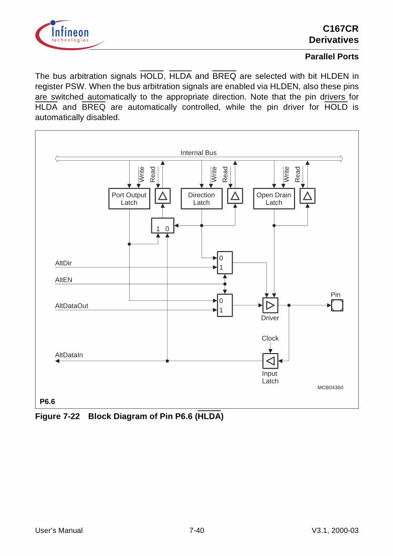
C167CRDerivatives
Parallel Ports
The bus arbitration signals HOLD, HLDA and BREQ are selected with bit HLDEN inregister PSW. When the bus arbitration signals are enabled via HLDEN, also these pinsare switched automatically to the appropriate direction. Note that the pin drivers forHLDA and BREQ are automatically controlled, while the pin driver for HOLD isautomatically disabled.
Figure 7-22 Block Diagram of Pin P6.6 (HLDA)
P6.6
MCB04360
Internal BusR
ead
Writ
e
Port OutputLatch
Rea
d
Writ
e
DirectionLatch
Rea
d
Writ
e
Open DrainLatch
01
1 0
01
Driver
Pin
InputLatch
Clock
AltDataOut
AltEN
AltDir
AltDataIn
User’s Manual 7-40 V3.1, 2000-03
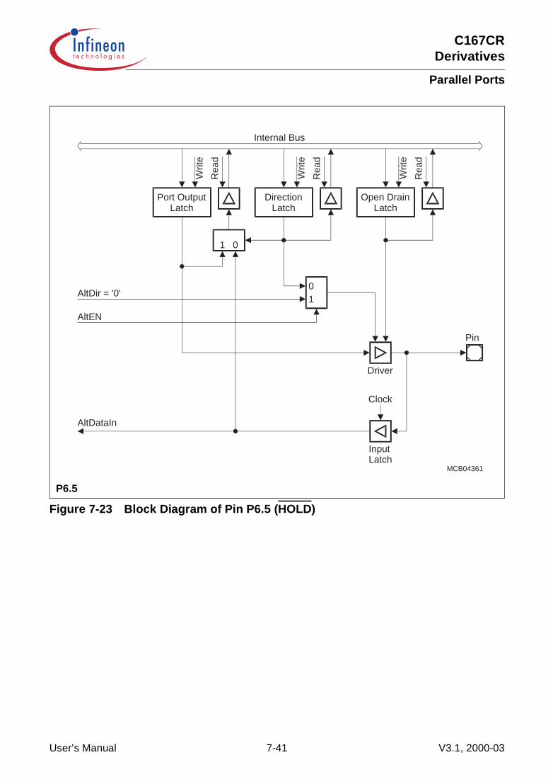
C167CRDerivatives
Parallel Ports
Figure 7-23 Block Diagram of Pin P6.5 (HOLD)
P6.5
MCB04361
Internal Bus
Rea
d
Writ
ePort Output
Latch
Rea
d
Writ
e
DirectionLatch
Rea
d
Writ
e
Open DrainLatch
01
1 0
Driver
Pin
InputLatch
Clock
AltEN
AltDir = '0'
AltDataIn
User’s Manual 7-41 V3.1, 2000-03

C167CRDerivatives
Parallel Ports
7.11 Port 7
If this 8-bit port is used for general purpose IO, the direction of each line can beconfigured via the corresponding direction register DP7. Each port line can be switchedinto push/pull or open drain mode via the open drain control register ODP7.
P7 Port 7 Data Register SFR (FFD0H/E8H) Reset Value: - - 00H
15 14 13 12 11 10 9 8 7 6 5 4 3 2 1 0
P7.7 P7.6 P7.5 P7.4 P7.3 P7.2 P7.1 P7.0
- - - - - - - - rw rw rw rw rw rw rw rw
Bit Function
P7.y Port data register P7 bit y
DP7 P7 Direction Ctrl. Register SFR (FFD2H/E9H) Reset Value: - - 00H
15 14 13 12 11 10 9 8 7 6 5 4 3 2 1 0
DP7.7
DP7.6
DP7.5
DP7.4
DP7.3
DP7.2
DP7.1
DP7.0
- - - - - - - - rw rw rw rw rw rw rw rw
Bit Function
DP7.y Port direction register DP7 bit yDP7.y = 0: Port line P7.y is an input (high-impedance)DP7.y = 1: Port line P7.y is an output
User’s Manual 7-42 V3.1, 2000-03
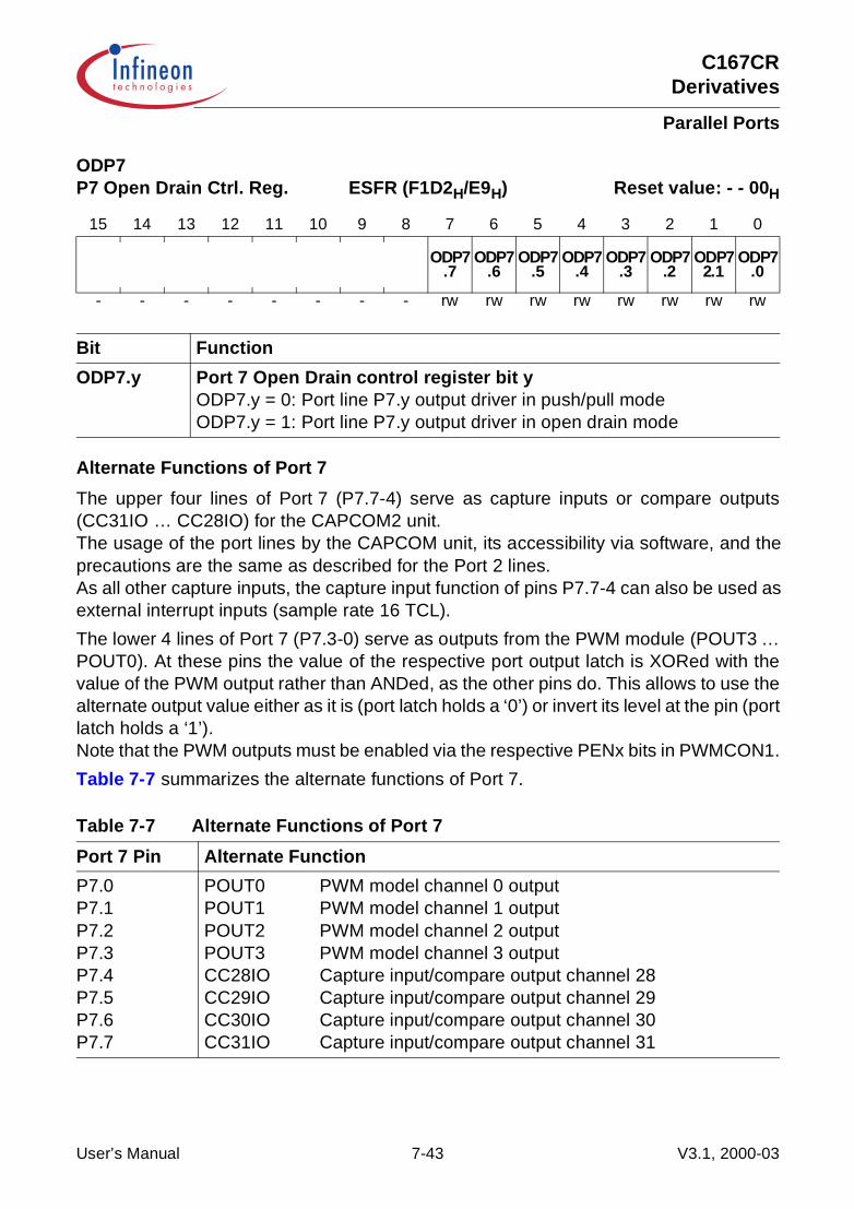
C167CRDerivatives
Parallel Ports
Alternate Functions of Port 7
The upper four lines of Port 7 (P7.7-4) serve as capture inputs or compare outputs(CC31IO … CC28IO) for the CAPCOM2 unit.The usage of the port lines by the CAPCOM unit, its accessibility via software, and theprecautions are the same as described for the Port 2 lines.As all other capture inputs, the capture input function of pins P7.7-4 can also be used asexternal interrupt inputs (sample rate 16 TCL).
The lower 4 lines of Port 7 (P7.3-0) serve as outputs from the PWM module (POUT3 …POUT0). At these pins the value of the respective port output latch is XORed with thevalue of the PWM output rather than ANDed, as the other pins do. This allows to use thealternate output value either as it is (port latch holds a ‘0’) or invert its level at the pin (portlatch holds a ‘1’).Note that the PWM outputs must be enabled via the respective PENx bits in PWMCON1.
Table 7-7 summarizes the alternate functions of Port 7.
ODP7 P7 Open Drain Ctrl. Reg. ESFR (F1D2H/E9H) Reset value: - - 00H
15 14 13 12 11 10 9 8 7 6 5 4 3 2 1 0
ODP7.7
ODP7.6
ODP7.5
ODP7.4
ODP7.3
ODP7.2
ODP72.1
ODP7.0
- - - - - - - - rw rw rw rw rw rw rw rw
Bit Function
ODP7.y Port 7 Open Drain control register bit yODP7.y = 0: Port line P7.y output driver in push/pull modeODP7.y = 1: Port line P7.y output driver in open drain mode
Table 7-7 Alternate Functions of Port 7
Port 7 Pin Alternate Function
P7.0P7.1P7.2P7.3P7.4P7.5P7.6P7.7
POUT0 PWM model channel 0 outputPOUT1 PWM model channel 1 outputPOUT2 PWM model channel 2 outputPOUT3 PWM model channel 3 outputCC28IO Capture input/compare output channel 28CC29IO Capture input/compare output channel 29CC30IO Capture input/compare output channel 30CC31IO Capture input/compare output channel 31
User’s Manual 7-43 V3.1, 2000-03

C167CRDerivatives
Parallel Ports
Figure 7-24 Port 7 IO and Alternate Functions
The port structures of Port 7 differ in the way the output latches are connected to theinternal bus and to the pin driver (see Figure 7-25 and Figure 7-26).
Pins P7.3-0 (POUT3 … POUT0) of Port 7 XOR the alternate data output with the portlatch output, which allows to use the alternate data directly or inverted at the pin driver.
MCA04362
--------P7.7P7.6P7.5P7.4P7.3P7.2P7.1P7.0
Port 7
Alternate FunctionGeneral PurposeInput/Output
-------
-CC31IOCC30IOCC29IOCC28IOPOUT3POUT2POUT1POUT0
User’s Manual 7-44 V3.1, 2000-03
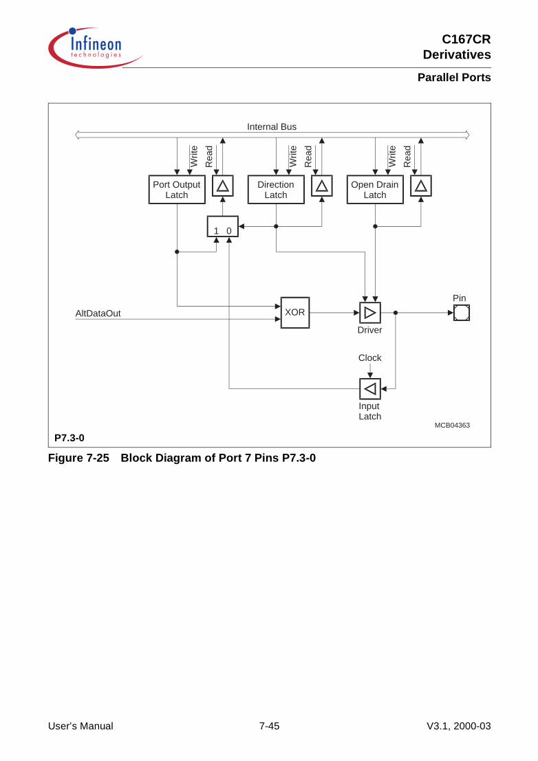
C167CRDerivatives
Parallel Ports
Figure 7-25 Block Diagram of Port 7 Pins P7.3-0
MCB04363
Internal Bus
Rea
d
Writ
ePort Output
Latch
Rea
d
Writ
e
DirectionLatch
Rea
d
Writ
e
Open DrainLatch
1 0
XOR
Driver
Pin
InputLatch
Clock
AltDataOut
P7.3-0
User’s Manual 7-45 V3.1, 2000-03
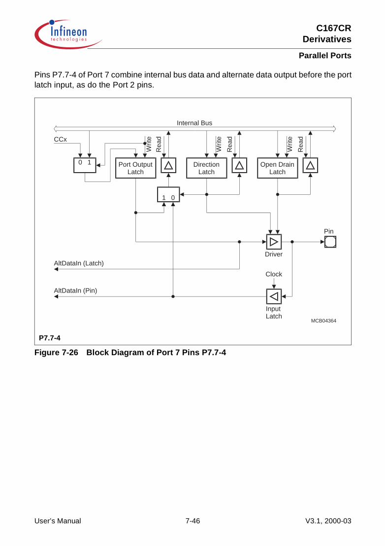
C167CRDerivatives
Parallel Ports
Pins P7.7-4 of Port 7 combine internal bus data and alternate data output before the portlatch input, as do the Port 2 pins.
Figure 7-26 Block Diagram of Port 7 Pins P7.7-4
P7.7-4
MCB04364
Internal Bus
Rea
dPort Output
Latch
Rea
d
Writ
e
DirectionLatch
Rea
d
Writ
e
Open DrainLatch
1 0
Driver
Pin
InputLatch
Clock
AltDataIn (Pin)
0 1
CCxW
rite
AltDataIn (Latch)
User’s Manual 7-46 V3.1, 2000-03
C167CRDerivatives
Parallel Ports
7.12 Port 8
If this 8-bit port is used for general purpose IO, the direction of each line can beconfigured via the corresponding direction register DP8. Each port line can be switchedinto push/pull or open drain mode via the open drain control register ODP8.
P8 Port 8 Data Register SFR (FFD4H/EAH) Reset Value: - - 00H
15 14 13 12 11 10 9 8 7 6 5 4 3 2 1 0
P8.7 P8.6 P8.5 P8.4 P8.3 P8.2 P8.1 P8.0
- - - - - - - - rwh rwh rwh rwh rwh rwh rwh rwh
Bit Function
P8.y Port data register P8 bit y
DP8 P8 Direction Ctrl. Register SFR (FFD6H/EBH) Reset Value: - - 00H
15 14 13 12 11 10 9 8 7 6 5 4 3 2 1 0
DP8.7
DP8.6
DP8.5
DP8.4
DP8.3
DP8.2
DP8.1
DP8.0
- - - - - - - - rw rw rw rw rw rw rw rw
Bit Function
DP8.y Port direction register DP8 bit yDP8.y = 0: Port line P8.y is an input (high-impedance)DP8.y = 1: Port line P8.y is an output
User’s Manual 7-47 V3.1, 2000-03
C167CRDerivatives
Parallel Ports
Alternate Functions of Port 8
All Port 8 lines (P8.7-0) serve as capture inputs or compare outputs (CC23IO …CC16IO) for the CAPCOM2 unit (see Table 7-8).
The usage of the port lines by the CAPCOM unit, its accessibility via software and theprecautions are the same as described for the Port 2 lines.
As all other capture inputs, the capture input function of pins P8.7-0 can also be used asexternal interrupt inputs (sample rate 16 TCL).
ODP8 P8 Open Drain Ctrl. Reg. ESFR (F1D6H/EBH) Reset Value: - - 00H
15 14 13 12 11 10 9 8 7 6 5 4 3 2 1 0
ODP8.7
ODP8.6
ODP8.5
ODP8.4
ODP8.3
ODP8.2
ODP8.1
ODP8.0
- - - - - - - - rw rw rw rw rw rw rw rw
Bit Function
ODP8.y Port 8 Open Drain control register bit yODP8.y = 0: Port line P8.y output driver in push/pull modeODP8.y = 1: Port line P8.y output driver in open drain mode
Table 7-8 Alternate Functions of Port 8
Port 8 Pin Alternate Function
P8.0P8.1P8.2P8.3P8.4P8.5P8.6P8.7
CC16IO Capture input/compare output channel 16CC17IO Capture input/compare output channel 17CC18IO Capture input/compare output channel 18CC19IO Capture input/compare output channel 19CC20IO Capture input/compare output channel 20CC21IO Capture input/compare output channel 21CC22IO Capture input/compare output channel 22CC23IO Capture input/compare output channel 23
User’s Manual 7-48 V3.1, 2000-03

C167CRDerivatives
Parallel Ports
Figure 7-27 Port 8 IO and Alternate Functions
The pins of Port 8 combine internal bus data and alternate data output before the portlatch input, as do the Port 2 pins.
MCA04365
--------P8.7P8.6P8.5P8.4P8.3P8.2P8.1P8.0
Port 8
Alternate Function
General PurposeInput/Output
a)
-------
-CC23IOCC22IOCC21IOCC20IOCC19IOCC18IOCC17IOCC16IO
User’s Manual 7-49 V3.1, 2000-03
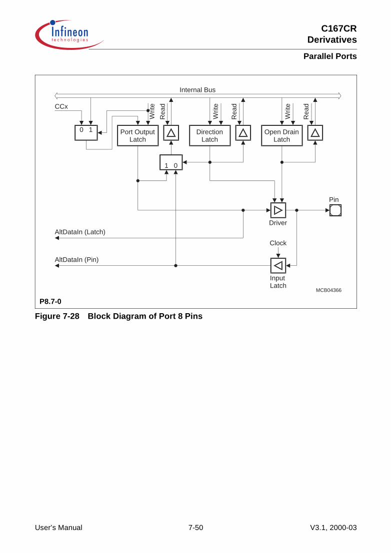
C167CRDerivatives
Parallel Ports
Figure 7-28 Block Diagram of Port 8 Pins
MCB04366
Internal Bus
Rea
d
Port OutputLatch
Rea
d
Writ
e
DirectionLatch
Rea
d
Writ
e
Open DrainLatch
1 0
Driver
Pin
InputLatch
Clock
AltDataIn (Pin)
0 1
CCx
Writ
e
AltDataIn (Latch)
P8.7-0
User’s Manual 7-50 V3.1, 2000-03

C167CRDerivatives
Dedicated Pins
8 Dedicated PinsMost of the input/output or control signals of the functional the C167CR are realized asalternate functions of pins of the parallel ports. There is, however, a number of signalsthat use separate pins, including the oscillator, special control signals and, of course, thepower supply.
Table 8-1 summarizes the 33 dedicated pins of the C167CR.
The Address Latch Enable signal ALE controls external address latches that providea stable address in multiplexed bus modes.ALE is activated for every external bus cycle independent of the selected bus mode,i.e. it is also activated for bus cycles with a demultiplexed address bus. When an externalbus is enabled (one or more of the BUSACT bits set) also X-Peripheral accesses willgenerate an active ALE signal.ALE is not activated for internal accesses, i.e. accesses to ROM/OTP/Flash (if provided),the internal RAM and the special function registers. In single chip mode, i.e. when noexternal bus is enabled (no BUSACT bit set), ALE will also remain inactive forX-Peripheral accesses.During reset an internal pulldown ensures an inactive (low) level on the ALE output.
Table 8-1 C167CR Dedicated Pins
Pin(s) Function
ALE Address Latch Enable
RD External Read Strobe
WR/WRL External Write/Write Low Strobe
READY Ready Input
EA External Access Enable
NMI Non-Maskable Interrupt Input
XTAL1, XTAL2 Oscillator Input/Output
RSTIN Reset Input
RSTOUT Reset Output
VAREF, VAGND Power Supply for Analog/Digital Converter
VDD Digital Power Supply (10 pins)
VSS Digital Reference Ground (10 pins)
OWE Oscillator Watchdog Enable
User’s Manual 8-1 V3.1, 2000-03
C167CRDerivatives
Dedicated Pins
The External Read Strobe RD controls the output drivers of external memory orperipherals when the C167CR reads data from these external devices. During accessesto on-chip X-Peripherals RD remains inactive (high).During reset an internal pullup ensures an inactive (high) level on the RD output.
The External Write Strobe WR/WRL controls the data transfer from the C167CR to anexternal memory or peripheral device. This pin may either provide an general WR signalactivated for both byte and word write accesses, or specifically control the low byte of anexternal 16-bit device (WRL) together with the signal WRH (alternate function of P3.12/BHE). During accesses to on-chip X-Peripherals WR/WRL remains inactive (high).During reset an internal pullup ensures an inactive (high) level on the WR/WRL output.
The Ready Input READY receives a control signal from an external memory orperipheral device that is used to terminate an external bus cycle, provided that thisfunction is enabled for the current bus cycle. READY may be used as synchronousREADY or may be evaluated asynchronously. When waitstates are defined for a READYcontrolled address window the READY input is not evaluated during these waitstates.An internal pullup ensures an inactive (high) level on the READY input.
The External Access Enable Pin EA determines if the C167CR after reset startsfetching code from the internal ROM area (EA = ‘1’) or via the external bus interface(EA = ‘0’). Be sure to hold this input low for ROMless devices. At the end of the internalreset sequence the EA signal is latched together with the PORT0 configuration.
The Non-Maskable Interrupt Input NMI allows to trigger a high priority trap via anexternal signal (e.g. a power-fail signal). It also serves to validate the PWRDN instructionthat switches the C167CR into Power-Down mode. The NMI pin is sampled with everyCPU clock cycle to detect transitions.
The Oscillator Input XTAL1 and Output XTAL2 connect the internal Main Oscillatorto the external crystal. The oscillator provides an inverter and a feedback element. Thestandard external oscillator circuitry (see Chapter 6) comprises the crystal, two low endcapacitors and series resistor to limit the current through the crystal. The main oscillatoris intended for the generation of the basic operating clock signal of the C167CR.
An external clock signal may be fed to the input XTAL1, leaving XTAL2 open orterminating it for higher input frequencies.
User’s Manual 8-2 V3.1, 2000-03
C167CRDerivatives
Dedicated Pins
The Reset Input RSTIN allows to put the C167CR into the well defined reset conditioneither at power-up or external events like a hardware failure or manual reset. The inputvoltage threshold of the RSTIN pin is raised compared to the standard pins in order tominimize the noise sensitivity of the reset input.
In bidirectional reset mode the C167CR’s line RSTIN may be driven active by the chiplogic e.g. in order to support external equipment which is required for startup (e.g. flashmemory).
Bidirectional reset reflects internal reset sources (software, watchdog) also to the RSTINpin and converts short hardware reset pulses to a minimum duration of the internal resetsequence. Bidirectional reset is enabled by setting bit BDRSTEN in register SYSCONand changes RSTIN from a pure input to an open drain IO line. When an internal resetis triggered by the SRST instruction or by a watchdog timer overflow or a low level isapplied to the RSTIN line, an internal driver pulls it low for the duration of the internalreset sequence. After that it is released and is then controlled by the external circuitryalone.
The bidirectional reset function is useful in applications where external devices requirea defined reset signal but cannot be connected to the C167CR’s RSTOUT signal, e.g.an external flash memory which must come out of reset and deliver code well beforeRSTOUT can be deactivated via EINIT.
The following behavior differences must be observed when using the bidirectional resetfeature in an application:
• Bit BDRSTEN in register SYSCON cannot be changed after EINIT and is clearedautomatically after a reset.
• The reset indication flags always indicate a long hardware reset.• The PORT0 configuration is treated like on a hardware reset. Especially the bootstrap
loader may be activated when P0L.4 is low.• Pin RSTIN may only be connected to external reset devices with an open drain output driver.• A short hardware reset is extended to the duration of the internal reset sequence.
The Reset Output RSTOUT provides a special reset signal for external circuitry.RSTOUT is activated at the beginning of the reset sequence, triggered via RSTIN, awatchdog timer overflow or by the SRST instruction. RSTOUT remains active (low) untilthe EINIT instruction is executed. This allows to initialize the controller before theexternal circuitry is activated.
Note: During emulation mode pin RSTOUT is used as an input and therefore must bedriven by the external circuitry.
User’s Manual 8-3 V3.1, 2000-03

C167CRDerivatives
Dedicated Pins
The Power Supply pins for the Analog/Digital Converter VAREF and VAGNDprovide a separate power supply (reference voltage) for the on-chip ADC. This reducesthe noise that is coupled to the analog input signals from the digital logic sections and soimproves the stability of the conversion results, when VAREF and VAGND are properlydiscoupled from VDD and VSS.
The Power Supply pins VDD and VSS provide the power supply for the digital logic ofthe C167CR. The respective VDD/VSS pairs should be decoupled as close to the pinsas possible. For best results it is recommended to implement two-level decoupling, e.g.(the widely used) 100 nF in parallel with 30 … 40 pF capacitors which deliver the peakcurrents.
Note: All VDD pins and all VSS pins must be connected to the power supply and ground,respectively.
The Oscillator Watchdog Enable input OWE enables the oscillator watchdog, whendriven high or disables it, when driven low e.g. for testing purposes. An internal pullupdevice holds this input high if nothing is driving it.
For normal operation pin OWE should be high or not connected. The oscillator watchdogcan be disabled via software by setting bit OWDDIS in register SYSCON.
User’s Manual 8-4 V3.1, 2000-03
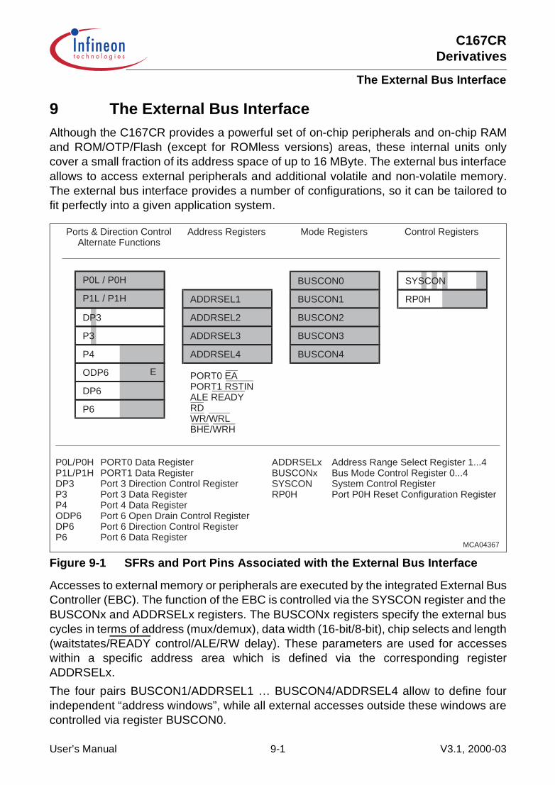
C167CRDerivatives
The External Bus Interface
9 The External Bus InterfaceAlthough the C167CR provides a powerful set of on-chip peripherals and on-chip RAMand ROM/OTP/Flash (except for ROMless versions) areas, these internal units onlycover a small fraction of its address space of up to 16 MByte. The external bus interfaceallows to access external peripherals and additional volatile and non-volatile memory.The external bus interface provides a number of configurations, so it can be tailored tofit perfectly into a given application system.
Figure 9-1 SFRs and Port Pins Associated with the External Bus Interface
Accesses to external memory or peripherals are executed by the integrated External BusController (EBC). The function of the EBC is controlled via the SYSCON register and theBUSCONx and ADDRSELx registers. The BUSCONx registers specify the external buscycles in terms of address (mux/demux), data width (16-bit/8-bit), chip selects and length(waitstates/READY control/ALE/RW delay). These parameters are used for accesseswithin a specific address area which is defined via the corresponding registerADDRSELx.
The four pairs BUSCON1/ADDRSEL1 … BUSCON4/ADDRSEL4 allow to define fourindependent “address windows”, while all external accesses outside these windows arecontrolled via register BUSCON0.
MCA04367
P0L / P0H
P1L / P1H
DP3
ADDRSEL1
ADDRSEL2
ADDRSEL3
BUSCON0 SYSCON
Ports & Direction ControlAlternate Functions
Address Registers Mode Registers Control Registers
P0L/P0H PORT0 Data RegisterP1L/P1H PORT1 Data RegisterDP3 Port 3 Direction Control RegisterP3 Port 3 Data RegisterP4 Port 4 Data RegisterODP6 Port 6 Open Drain Control RegisterDP6 Port 6 Direction Control RegisterP6 Port 6 Data Register
ADDRSELx Address Range Select Register 1...4BUSCONx Bus Mode Control Register 0...4SYSCON System Control RegisterRP0H Port P0H Reset Configuration Register
RP0H
PORT0 EAPORT1 RSTINALE READYRDWR/WRLBHE/WRH
P3
BUSCON1
BUSCON3
BUSCON2
E
P4
ODP6
DP6
P6
ADDRSEL4 BUSCON4
User’s Manual 9-1 V3.1, 2000-03

C167CRDerivatives
The External Bus Interface
9.1 Single Chip Mode
Single chip mode is entered, when pin EA is high during reset. In this case registerBUSCON0 is initialized with 0000H, which also resets bit BUSACT0, so no external busis enabled.
In single chip mode the C167CR operates only with and out of internal resources. Noexternal bus is configured and no external peripherals and/or memory can be accessed.Also no port lines are occupied for the bus interface. When running in single chip mode,however, external access may be enabled by configuring an external bus under softwarecontrol. Single chip mode allows the C167CR to start execution out of the internalprogram memory (Mask-ROM, OTP or Flash memory).
Note: Any attempt to access a location in the external memory space in single chip moderesults in the hardware trap ILLBUS if no external bus has been explicitly enabledby software.
User’s Manual 9-2 V3.1, 2000-03
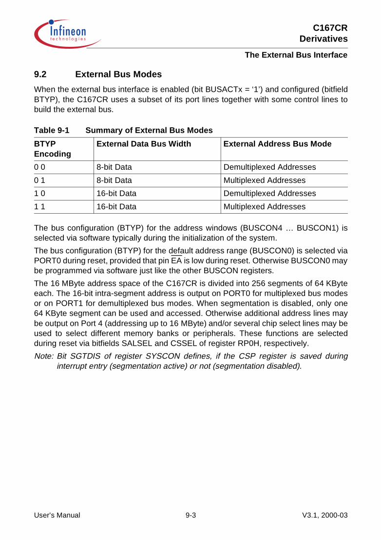
C167CRDerivatives
The External Bus Interface
9.2 External Bus Modes
When the external bus interface is enabled (bit BUSACTx = ‘1’) and configured (bitfieldBTYP), the C167CR uses a subset of its port lines together with some control lines tobuild the external bus.
The bus configuration (BTYP) for the address windows (BUSCON4 … BUSCON1) isselected via software typically during the initialization of the system.
The bus configuration (BTYP) for the default address range (BUSCON0) is selected viaPORT0 during reset, provided that pin EA is low during reset. Otherwise BUSCON0 maybe programmed via software just like the other BUSCON registers.
The 16 MByte address space of the C167CR is divided into 256 segments of 64 KByteeach. The 16-bit intra-segment address is output on PORT0 for multiplexed bus modesor on PORT1 for demultiplexed bus modes. When segmentation is disabled, only one64 KByte segment can be used and accessed. Otherwise additional address lines maybe output on Port 4 (addressing up to 16 MByte) and/or several chip select lines may beused to select different memory banks or peripherals. These functions are selectedduring reset via bitfields SALSEL and CSSEL of register RP0H, respectively.
Note: Bit SGTDIS of register SYSCON defines, if the CSP register is saved duringinterrupt entry (segmentation active) or not (segmentation disabled).
Table 9-1 Summary of External Bus Modes
BTYP Encoding
External Data Bus Width External Address Bus Mode
0 0 8-bit Data Demultiplexed Addresses
0 1 8-bit Data Multiplexed Addresses
1 0 16-bit Data Demultiplexed Addresses
1 1 16-bit Data Multiplexed Addresses
User’s Manual 9-3 V3.1, 2000-03
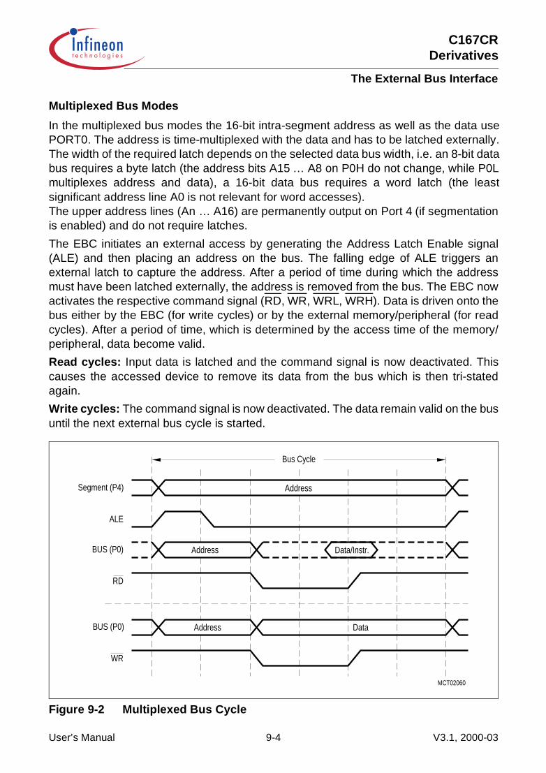
C167CRDerivatives
The External Bus Interface
Multiplexed Bus Modes
In the multiplexed bus modes the 16-bit intra-segment address as well as the data usePORT0. The address is time-multiplexed with the data and has to be latched externally.The width of the required latch depends on the selected data bus width, i.e. an 8-bit databus requires a byte latch (the address bits A15 … A8 on P0H do not change, while P0Lmultiplexes address and data), a 16-bit data bus requires a word latch (the leastsignificant address line A0 is not relevant for word accesses).The upper address lines (An … A16) are permanently output on Port 4 (if segmentationis enabled) and do not require latches.
The EBC initiates an external access by generating the Address Latch Enable signal(ALE) and then placing an address on the bus. The falling edge of ALE triggers anexternal latch to capture the address. After a period of time during which the addressmust have been latched externally, the address is removed from the bus. The EBC nowactivates the respective command signal (RD, WR, WRL, WRH). Data is driven onto thebus either by the EBC (for write cycles) or by the external memory/peripheral (for readcycles). After a period of time, which is determined by the access time of the memory/peripheral, data become valid.
Read cycles: Input data is latched and the command signal is now deactivated. Thiscauses the accessed device to remove its data from the bus which is then tri-statedagain.
Write cycles: The command signal is now deactivated. The data remain valid on the busuntil the next external bus cycle is started.
Figure 9-2 Multiplexed Bus Cycle
MCT02060
AddressSegment (P4)
ALE
BUS (P0) Data/Instr.Address
RD
Address DataBUS (P0)
WR
Bus Cycle
User’s Manual 9-4 V3.1, 2000-03
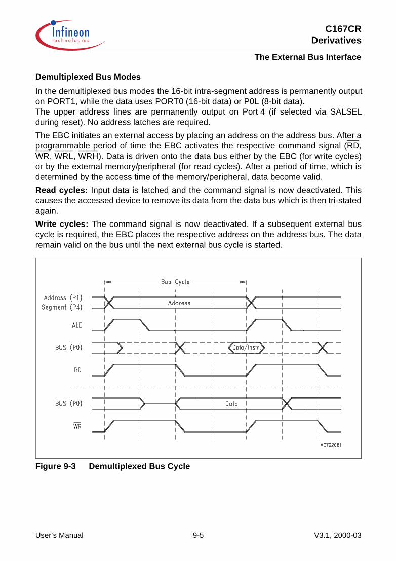
C167CRDerivatives
The External Bus Interface
Demultiplexed Bus Modes
In the demultiplexed bus modes the 16-bit intra-segment address is permanently outputon PORT1, while the data uses PORT0 (16-bit data) or P0L (8-bit data).The upper address lines are permanently output on Port 4 (if selected via SALSELduring reset). No address latches are required.
The EBC initiates an external access by placing an address on the address bus. After aprogrammable period of time the EBC activates the respective command signal (RD,WR, WRL, WRH). Data is driven onto the data bus either by the EBC (for write cycles)or by the external memory/peripheral (for read cycles). After a period of time, which isdetermined by the access time of the memory/peripheral, data become valid.
Read cycles: Input data is latched and the command signal is now deactivated. Thiscauses the accessed device to remove its data from the data bus which is then tri-statedagain.
Write cycles: The command signal is now deactivated. If a subsequent external buscycle is required, the EBC places the respective address on the address bus. The dataremain valid on the bus until the next external bus cycle is started.
Figure 9-3 Demultiplexed Bus Cycle
User’s Manual 9-5 V3.1, 2000-03

C167CRDerivatives
The External Bus Interface
Switching Between the Bus Modes
The EBC allows to switch between different bus modes dynamically, i.e. subsequentexternal bus cycles may be executed in different ways. Certain address areas may usemultiplexed or demultiplexed buses or use READY control or predefined waitstates.
A change of the external bus characteristics can be initiated in two different ways:
Reprogramming the BUSCON and/or ADDRSEL registers allows to either changethe bus mode for a given address window, or change the size of an address window thatuses a certain bus mode. Reprogramming allows to use a great number of differentaddress windows (more than BUSCONs are available) on the expense of the overheadfor changing the registers and keeping appropriate tables.
Switching between predefined address windows automatically selects the bus modethat is associated with the respective window. Predefined address windows allow to usedifferent bus modes without any overhead, but restrict their number to the number ofBUSCONs. However, as BUSCON0 controls all address areas, which are not coveredby the other BUSCONs, this allows to have gaps between these windows, which use thebus mode of BUSCON0.
PORT1 will output the intra-segment address, when any of the BUSCON registersselects a demultiplexed bus mode, even if the current bus cycle uses a multiplexed busmode. This allows to have an external address decoder connected to PORT1 only, whileusing it for all kinds of bus cycles.
Note: Never change the configuration for an address area that currently supplies theinstruction stream. Due to the internal pipelining it is very difficult to determine thefirst instruction fetch that will use the new configuration. Only change theconfiguration for address areas that are not currently accessed. This applies toBUSCON registers as well as to ADDRSEL registers.
The usage of the BUSCON/ADDRSEL registers is controlled via the issued addresses.When an access (code fetch or data) is initiated, the respective generated physicaladdress defines, if the access is made internally, uses one of the address windowsdefined by ADDRSEL4 … 1, or uses the default configuration in BUSCON0. Afterinitializing the active registers, they are selected and evaluated automatically byinterpreting the physical address. No additional switching or selecting is necessaryduring run time, except when more than the four address windows plus the default is tobe used.
Switching from demultiplexed to multiplexed bus mode represents a special case.The bus cycle is started by activating ALE and driving the address to Port 4 and PORT1as usual, if another BUSCON register selects a demultiplexed bus. However, in themultiplexed bus modes the address is also required on PORT0. In this special case theaddress on PORT0 is delayed by one CPU clock cycle, which delays the complete(multiplexed) bus cycle and extends the corresponding ALE signal (see Figure 9-4).
User’s Manual 9-6 V3.1, 2000-03
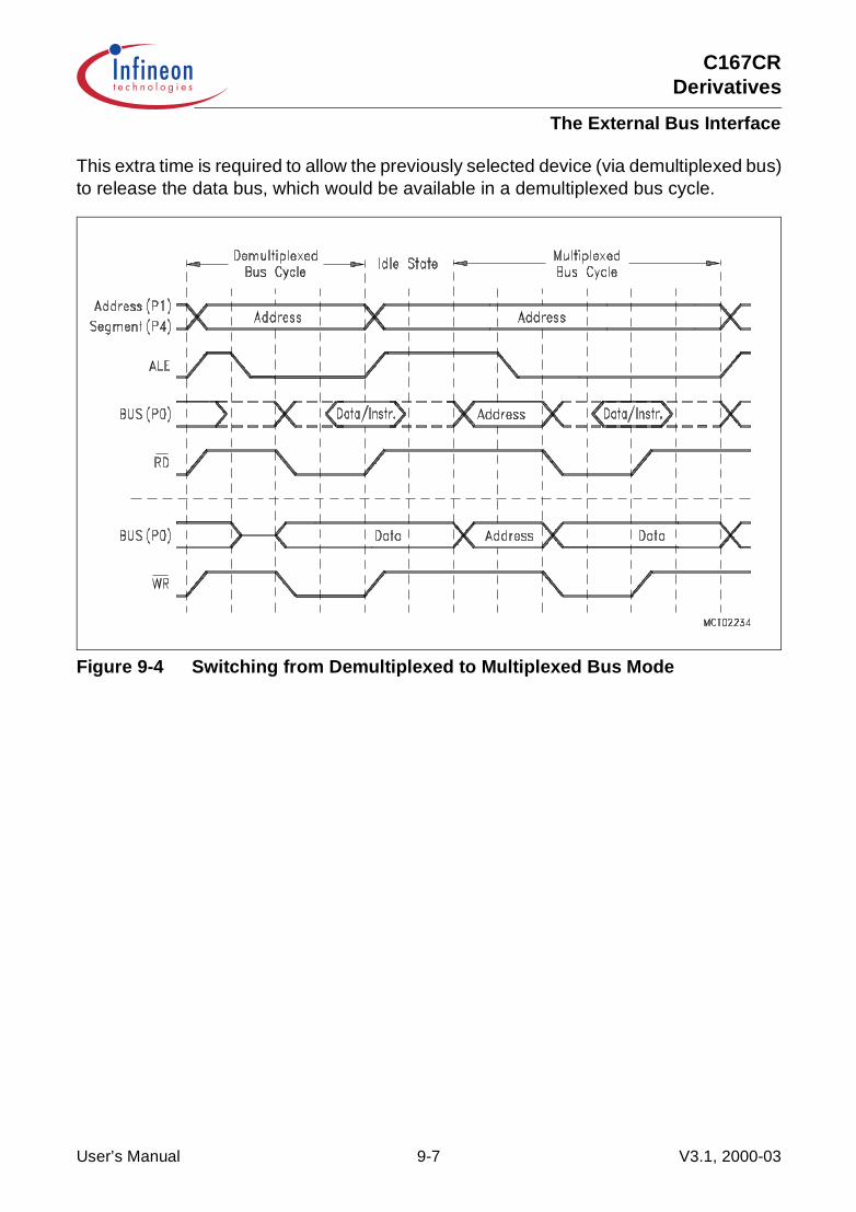
C167CRDerivatives
The External Bus Interface
This extra time is required to allow the previously selected device (via demultiplexed bus)to release the data bus, which would be available in a demultiplexed bus cycle.
Figure 9-4 Switching from Demultiplexed to Multiplexed Bus Mode
User’s Manual 9-7 V3.1, 2000-03

C167CRDerivatives
The External Bus Interface
External Data Bus Width
The EBC can operate on 8-bit or 16-bit wide external memory/peripherals. A 16-bit databus uses PORT0, while an 8-bit data bus only uses P0L, the lower byte of PORT0. Thissaves on address latches, bus transceivers, bus routing and memory cost on theexpense of transfer time. The EBC can control word accesses on an 8-bit data bus aswell as byte accesses on a 16-bit data bus.
Word accesses on an 8-bit data bus are automatically split into two subsequent byteaccesses, where the low byte is accessed first, then the high byte. The assembly of bytesto words and the disassembly of words into bytes is handled by the EBC and istransparent to the CPU and the programmer.
Byte accesses on a 16-bit data bus require that the upper and lower half of the memorycan be accessed individually. In this case the upper byte is selected with the BHE signal,while the lower byte is selected with the A0 signal. So the two bytes of the memory canbe enabled independent from each other, or together when accessing words.
When writing bytes to an external 16-bit device, which has a single CS input, but two WRenable inputs (for the two bytes), the EBC can directly generate these two write controlsignals. This saves the external combination of the WR signal with A0 or BHE. In thiscase pin WR serves as WRL (write low byte) and pin BHE serves as WRH (write highbyte). Bit WRCFG in register SYSCON selects the operating mode for pins WR andBHE. The respective byte will be written on both data bus halfs.
When reading bytes from an external 16-bit device, whole words may be read and theC167CR automatically selects the byte to be input and discards the other. However, caremust be taken when reading devices that change state when being read, like FIFOs,interrupt status registers, etc. In this case individual bytes should be selected using BHEand A0.
Note: PORT1 becomes available for general purpose IO, when none of the BUSCONregisters selects a demultiplexed bus mode.
Disable/Enable Control for Pin BHE (BYTDIS) Bit BYTDIS is provided for controlling the active low Byte High Enable (BHE) pin. The
Table 9-2 Bus Mode versus Performance
Bus Mode Transfer Rate(Speed factor for byte/word/dword access)
System Requirements Free IO Lines
8-bit Multiplexed Very low (1.5/3/6) Low (8-bit latch, byte bus) P1H, P1L
8-bit Demultipl. Low (1/2/4) Very low (no latch, byte bus) P0H
16-bit Multiplexed High (1.5/1.5/3) High (16-bit latch, word bus) P1H, P1L
16-bit Demultipl. Very high (1/1/2) Low (no latch, word bus) –
User’s Manual 9-8 V3.1, 2000-03
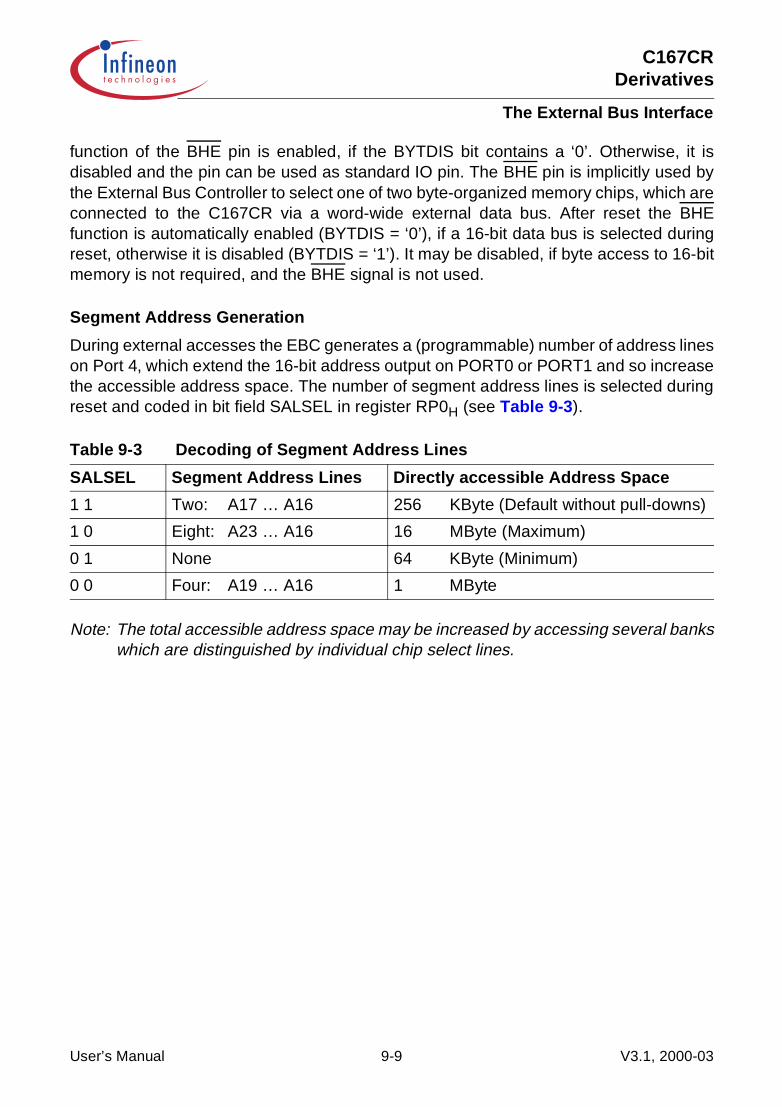
C167CRDerivatives
The External Bus Interface
function of the BHE pin is enabled, if the BYTDIS bit contains a ‘0’. Otherwise, it isdisabled and the pin can be used as standard IO pin. The BHE pin is implicitly used bythe External Bus Controller to select one of two byte-organized memory chips, which areconnected to the C167CR via a word-wide external data bus. After reset the BHEfunction is automatically enabled (BYTDIS = ‘0’), if a 16-bit data bus is selected duringreset, otherwise it is disabled (BYTDIS = ‘1’). It may be disabled, if byte access to 16-bitmemory is not required, and the BHE signal is not used.
Segment Address Generation
During external accesses the EBC generates a (programmable) number of address lineson Port 4, which extend the 16-bit address output on PORT0 or PORT1 and so increasethe accessible address space. The number of segment address lines is selected duringreset and coded in bit field SALSEL in register RP0H (see Table 9-3).
Note: The total accessible address space may be increased by accessing several bankswhich are distinguished by individual chip select lines.
Table 9-3 Decoding of Segment Address Lines
SALSEL Segment Address Lines Directly accessible Address Space
1 1 Two: A17 … A16 256 KByte (Default without pull-downs)
1 0 Eight: A23 … A16 16 MByte (Maximum)
0 1 None 64 KByte (Minimum)
0 0 Four: A19 … A16 1 MByte
User’s Manual 9-9 V3.1, 2000-03

C167CRDerivatives
The External Bus Interface
CS Signal Generation
During external accesses the EBC can generate a (programmable) number of CS lineson Port 6, which allow to directly select external peripherals or memory banks withoutrequiring an external decoder. The number of CS lines is selected during reset andcoded in bit field CSSEL in register RP0H (see Table 9-4).
The CSx outputs are associated with the BUSCONx registers and are driven active (low)for any access within the address area defined for the respective BUSCON register. Forany access outside this defined address area the respective CSx signal will go inactive(high). At the beginning of each external bus cycle the corresponding valid CS signal isdetermined and activated. All other CS lines are deactivated (driven high) at the sametime.
Note: The CSx signals will not be updated for an access to any internal address area(i.e. when no external bus cycle is started), even if this area is covered by therespective ADDRSELx register. An access to an on-chip X-Peripheral deactivatesall external CS signals.Upon accesses to address windows without a selected CS line all selected CSlines are deactivated.
The chip select signals allow to be operated in four different modes (see Table 9-5)which are selected via bits CSWENx and CSRENx in the respective BUSCONx register.
Table 9-4 Decoding of Chip Select Lines
CSSEL Chip Select Lines Note
1 1 Five: CS4 … CS0 Default without pull-downs
1 0 None Port 6 pins free for IO
0 1 Two: CS1 … CS0
0 0 Three: CS2 … CS0
Table 9-5 Chip Select Generation Modes
CSWENx CSRENx Chip Select Mode
0 0 Address Chip Select (Default after Reset)
0 1 Read Chip Select
1 0 Write Chip Select
1 1 Read/Write Chip Select
User’s Manual 9-10 V3.1, 2000-03
C167CRDerivatives
The External Bus Interface
Read or Write Chip Select signals remain active only as long as the associated controlsignal (RD or WR) is active. This also includes the programmable read/write delay. Readchip select is only activated for read cycles, write chip select is only activated for writecycles, read/write chip select is activated for both read and write cycles (write cycles areassumed, if any of the signals WRH or WRL gets active). These modes save externalglue logic, when accessing external devices like latches or drivers that only provide asingle enable input.
Address Chip Select signals remain active during the complete bus cycle. For addresschip select signals two generation modes can be selected via bit CSCFG in registerSYSCON:
• A latched address chip select signal (CSCFG = ‘0’) becomes active with the fallingedge of ALE and becomes inactive at the beginning of an external bus cycle thataccesses a different address window. No spikes will be generated on the chip selectlines and no changes occur as long as locations within the same address window orwithin internal memory (excluding X-Peripherals and XRAM) are accessed.
• An early address chip select signal (CSCFG = ‘1’) becomes active together with theaddress and BHE (if enabled) and remains active until the end of the current bus cycle.Early address chip select signals are not latched internally and may toggleintermediately while the address is changing.
Note: CS0 provides a latched address chip select directly after reset (except for singlechip mode) when the first instruction is fetched.
Internal pullup devices hold all CS lines high during reset. After the end of a resetsequence the pullup devices are switched off and the pin drivers control the pin levelson the selected CS lines. Not selected CS lines will enter the high-impedance state andare available for general purpose IO.
The pullup devices are also active during bus hold on the selected CS lines, while HLDAis active and the respective pin is switched to push/pull mode. Open drain outputs willfloat during bus hold. In this case external pullup devices are required or the new busmaster is responsible for driving appropriate levels on the CS lines.
Segment Address versus Chip Select
The external bus interface of the C167CR supports many configurations for the externalmemory. By increasing the number of segment address lines the C167CR can addressa linear address space of 256 KByte, 1 MByte or 16 MByte. This allows to implement alarge sequential memory area, and also allows to access a great number of externaldevices, using an external decoder. By increasing the number of CS lines the C167CRcan access memory banks or peripherals without external glue logic. These two featuresmay be combined to optimize the overall system performance.
Note: Bit SGTDIS of register SYSCON defines, if the CSP register is saved duringinterrupt entry (segmentation active) or not (segmentation disabled).
User’s Manual 9-11 V3.1, 2000-03

C167CRDerivatives
The External Bus Interface
9.3 Programmable Bus Characteristics
Important timing characteristics of the external bus interface have been made userprogrammable to allow to adapt it to a wide range of different external bus and memoryconfigurations with different types of memories and/or peripherals.
The following parameters of an external bus cycle are programmable:
• ALE Control defines the ALE signal length and the address hold time after its fallingedge
• Memory Cycle Time (extendable with 1 … 15 waitstates) defines the allowableaccess time
• Memory Tri-State Time (extendable with 1 waitstate) defines the time for a datadriver to float
• Read/Write Delay Time defines when a command is activated after the falling edgeof ALE
• READY Control defines, if a bus cycle is terminated internally or externally
Note: Internal accesses are executed with maximum speed and therefore are notprogrammable.External accesses use the slowest possible bus cycle after reset. The bus cycletiming may then be optimized by the initialization software.
Figure 9-5 Programmable External Bus Cycle
RD/WR
DATA
ADDR
ALE
ALECTL
DATA
RD/WR
ADDR
ALE
MTTCMCTC MCD02225
User’s Manual 9-12 V3.1, 2000-03

C167CRDerivatives
The External Bus Interface
ALE Length Control
The length of the ALE signal and the address hold time after its falling edge arecontrolled by the ALECTLx bits in the BUSCON registers. When bit ALECTL is set to ‘1’,external bus cycles accessing the respective address window will have their ALE signalprolonged by half a CPU clock (1 TCL). Also the address hold time after the falling edgeof ALE (on a multiplexed bus) will be prolonged by half a CPU clock, so the data transferwithin a bus cycle refers to the same CLKOUT edges as usual (i.e. the data transfer isdelayed by one CPU clock). This allows more time for the address to be latched.
Note: ALECTL0 is ‘1’ after reset to select the slowest possible bus cycle, the otherALECTLx are ‘0’ after reset.
Figure 9-6 ALE Length Control
User’s Manual 9-13 V3.1, 2000-03

C167CRDerivatives
The External Bus Interface
Programmable Memory Cycle Time
The C167CR allows the user to adjust the controller’s external bus cycles to the accesstime of the respective memory or peripheral. This access time is the total time requiredto move the data to the destination. It represents the period of time during which thecontroller’s signals do not change.
Figure 9-7 Memory Cycle Time
The external bus cycles of the C167CR can be extended for a memory or peripheral,which cannot keep pace with the controller’s maximum speed, by introducing wait statesduring the access (see Figure 9-7). During these memory cycle time wait states, theCPU is idle, if this access is required for the execution of the current instruction.
The memory cycle time wait states can be programmed in increments of one CPU clock(2 TCL) within a range from 0 to 15 (default after reset) via the MCTC fields of theBUSCON registers. 15 – <MCTC> waitstates will be inserted.
MCT02063
AddressSegment
ALE
BUS (P0) Address
RD
Address DataBUS (P0)
WR
MCTC Wait States (1...15)
Bus Cycle
Data/Instr.
User’s Manual 9-14 V3.1, 2000-03

C167CRDerivatives
The External Bus Interface
Programmable Memory Tri-state Time
The C167CR allows the user to adjust the time between two subsequent externalaccesses to account for the tri-state time of the external device. The tri-state time defines,when the external device has released the bus after deactivation of the read command(RD).
Figure 9-8 Memory Tri-state Time
The output of the next address on the external bus can be delayed for a memory orperipheral, which needs more time to switch off its bus drivers, by introducing a wait stateafter the previous bus cycle (see Figure 9-8). During this memory tri-state time waitstate, the CPU is not idle, so CPU operations will only be slowed down if a subsequentexternal instruction or data fetch operation is required during the next instruction cycle.
The memory tri-state time waitstate requires one CPU clock (2 TCL) and is controlled viathe MTTCx bits of the BUSCON registers. A waitstate will be inserted, if bit MTTCx is ‘0’(default after reset).
Note: External bus cycles in multiplexed bus modes implicitly add one tri-state timewaitstate in addition to the programmable MTTC waitstate.
MCT02065
Segment
ALE
BUS (P0) Address
RD
MTTC Wait State
Address
Bus Cycle
Data/Instr.
User’s Manual 9-15 V3.1, 2000-03
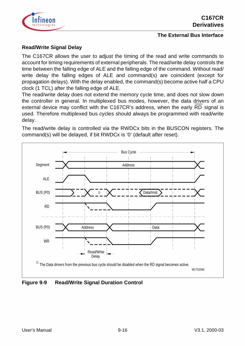
C167CRDerivatives
The External Bus Interface
Read/Write Signal Delay
The C167CR allows the user to adjust the timing of the read and write commands toaccount for timing requirements of external peripherals. The read/write delay controls thetime between the falling edge of ALE and the falling edge of the command. Without read/write delay the falling edges of ALE and command(s) are coincident (except forpropagation delays). With the delay enabled, the command(s) become active half a CPUclock (1 TCL) after the falling edge of ALE.The read/write delay does not extend the memory cycle time, and does not slow downthe controller in general. In multiplexed bus modes, however, the data drivers of anexternal device may conflict with the C167CR’s address, when the early RD signal isused. Therefore multiplexed bus cycles should always be programmed with read/writedelay.
The read/write delay is controlled via the RWDCx bits in the BUSCON registers. Thecommand(s) will be delayed, if bit RWDCx is ‘0’ (default after reset).
Figure 9-9 Read/Write Signal Duration Control
MCT02066
AddressSegment
ALE
BUS (P0) 1)
RD
Address DataBUS (P0)
WR
Read/WriteDelay
Bus Cycle
Data/Instr.
The Data drivers from the previous bus cycle should be disabled when the RD signal becomes active.1)
User’s Manual 9-16 V3.1, 2000-03
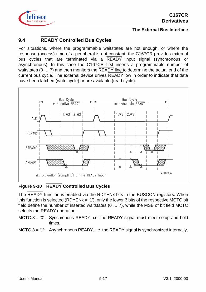
C167CRDerivatives
The External Bus Interface
9.4 READY Controlled Bus Cycles
For situations, where the programmable waitstates are not enough, or where theresponse (access) time of a peripheral is not constant, the C167CR provides externalbus cycles that are terminated via a READY input signal (synchronous orasynchronous). In this case the C167CR first inserts a programmable number ofwaitstates (0 … 7) and then monitors the READY line to determine the actual end of thecurrent bus cycle. The external device drives READY low in order to indicate that datahave been latched (write cycle) or are available (read cycle).
Figure 9-10 READY Controlled Bus Cycles
The READY function is enabled via the RDYENx bits in the BUSCON registers. Whenthis function is selected (RDYENx = ‘1’), only the lower 3 bits of the respective MCTC bitfield define the number of inserted waitstates (0 … 7), while the MSB of bit field MCTCselects the READY operation:
MCTC.3 = ‘0’: Synchronous READY, i.e. the READY signal must meet setup and holdtimes.
MCTC.3 = ‘1’: Asynchronous READY, i.e. the READY signal is synchronized internally.
User’s Manual 9-17 V3.1, 2000-03

C167CRDerivatives
The External Bus Interface
The Synchronous READY provides the fastest bus cycles, but requires setup and holdtimes to be met. The CLKOUT signal should be enabled and may be used by theperipheral logic to control the READY timing in this case.
The Asynchronous READY is less restrictive, but requires additional waitstates causedby the internal synchronization. As the asynchronous READY is sampled earlier (seeFigure 9-10) programmed waitstates may be necessary to provide proper bus cycles(see also notes on “normally-ready” peripherals below).
A READY signal (especially asynchronous READY) that has been activated by anexternal device may be deactivated in response to the trailing (rising) edge of therespective command (RD or WR).
Note: When the READY function is enabled for a specific address window, each buscycle within this window must be terminated with an active READY signal.Otherwise the controller hangs until the next reset. A timeout function is onlyprovided by the watchdog timer.
Combining the READY function with predefined waitstates is advantageous in twocases:
Memory components with a fixed access time and peripherals operating with READYmay be grouped into the same address window. The (external) waitstate control logic inthis case would activate READY either upon the memory’s chip select or with theperipheral’s READY output. After the predefined number of waitstates the C167CR willcheck its READY line to determine the end of the bus cycle. For a memory access it willbe low already (see example a) in Figure 9-10), for a peripheral access it may bedelayed (see example b) in Figure 9-10). As memories tend to be faster thanperipherals, there should be no impact on system performance.
When using the READY function with so-called “normally-ready” peripherals, it may leadto erroneous bus cycles, if the READY line is sampled too early. These peripherals pulltheir READY output low, while they are idle. When they are accessed, they deactivateREADY until the bus cycle is complete, then drive it low again. If, however, the peripheraldeactivates READY after the first sample point of the C167CR, the controller samplesan active READY and terminates the current bus cycle, which, of course, is too early. Byinserting predefined waitstates the first READY sample point can be shifted to a time,where the peripheral has safely controlled the READY line (e.g. after 2 waitstates inFigure 9-10).
User’s Manual 9-18 V3.1, 2000-03

C167CRDerivatives
The External Bus Interface
9.5 Controlling the External Bus Controller
A set of registers controls the functions of the EBC. General features like the usage ofinterface pins (WR, BHE), segmentation and internal ROM mapping are controlled viaregister SYSCON. The properties of a bus cycle like chip select mode, usage of READY,length of ALE, external bus mode, read/write delay and waitstates are controlled viaregisters BUSCON4 … BUSCON0. Four of these registers (BUSCON4 … BUSCON1)have an address select register (ADDRSEL4 … ADDRSEL1) associated with them,which allows to specify up to four address areas and the individual bus characteristicswithin these areas. All accesses that are not covered by these four areas are thencontrolled via BUSCON0. This allows to use memory components or peripherals withdifferent interfaces within the same system, while optimizing accesses to each of them.
SYSCONSystem Control Register SFR (FF12H/89H) Reset value: 0XX0H
15 14 13 12 11 10 9 8 7 6 5 4 3 2 1 0
STKSZ ROM S1
SGT DIS
ROM EN
BYT DIS
CLK EN
WR CFG
CS CFG - 3;(
(-7BD
RSTEN
<4)2 VISI-BLE
<4)67,%6)
rw rw rw rwh rwh rw rwh rw - V[ rw V[ rw rw
Bit Function
XPER-SHARE XBUS Peripheral Share Mode Control0: External accesses to XBUS peripherals are disabled1: XBUS peripherals are accessible via the ext. bus during hold mode
VISIBLE Visible Mode Control0: Accesses to XBUS peripherals are done internally1: XBUS peripheral accesses are made visible on the external pins
XPEN XBUS Peripheral Enable Bit0: Accesses to the on-chip X-Peripherals and their functions are disabled1: The on-chip X-Peripherals are enabled and can be accessed
BDRSTEN Bidirectional Reset Enable Bit0: Pin RSTIN is an input only.1: Pin RSTIN is pulled low during the internal reset sequence
after any reset.
OWDDIS Oscillator Watchdog Disable Bit (Cleared after reset)0: The on-chip oscillator watchdog is enabled and active.1: The on-chip oscillator watchdog is disabled and the CPU clock is
always fed from the oscillator input.
User’s Manual 9-19 V3.1, 2000-03

C167CRDerivatives
The External Bus Interface
Note: Register SYSCON cannot be changed after execution of the EINIT instruction.Bit SGTDIS controls the correct stack operation (push/pop of CSP or not) duringtraps and interrupts.
The layout of the BUSCON registers and ADDRSEL registers is identical (respectively).
Registers BUSCON4 … BUSCON1, which control the selected address windows, arecompletely under software control, while register BUSCON0, which e.g. is also used forthe very first code access after reset, is partly controlled by hardware, i.e. it is initializedvia PORT0 during the reset sequence. This hardware control allows to define anappropriate external bus for systems, where no internal program memory is provided.
CSCFG Chip Select Configuration Control (Cleared after reset)0: Latched CS mode. The CS signals are latched internally
and driven to the (enabled) port pins synchronously.1: Unlatched CS mode. The CS signals are directly derived from
the address and driven to the (enabled) port pins.
WRCFG Write Configuration Control (Set according to pin P0H.0 during reset)0: Pins WR and BHE retain their normal function1: Pin WR acts as WRL, pin BHE acts as WRH
CLKEN System Clock Output Enable (CLKOUT, cleared after reset)0: CLKOUT disabled: pin may be used for general purpose IO1: CLKOUT enabled: pin outputs the system clock signal
BYTDIS Disable/Enable Control for Pin BHE (Set according to data bus width)0: Pin BHE enabled1: Pin BHE disabled, pin may be used for general purpose IO
ROMEN Internal ROM Enable (Set according to pin EA during reset)0: Internal program memory disabled,
accesses to the ROM area use the external bus1: Internal program memory enabled
SGTDIS Segmentation Disable/Enable Control (Cleared after reset)0: Segmentation enabled
(CSP is saved/restored during interrupt entry/exit)1: Segmentation disabled (Only IP is saved/restored)
ROMS1 Internal ROM Mapping0: Internal ROM area mapped to segment 0 (00’0000H … 00’7FFFH)1: Internal ROM area mapped to segment 1 (01’0000H … 01’7FFFH)
STKSZ System Stack SizeSelects the size of the system stack (in the internal RAM)from 32 to 512 words
Bit Function
User’s Manual 9-20 V3.1, 2000-03
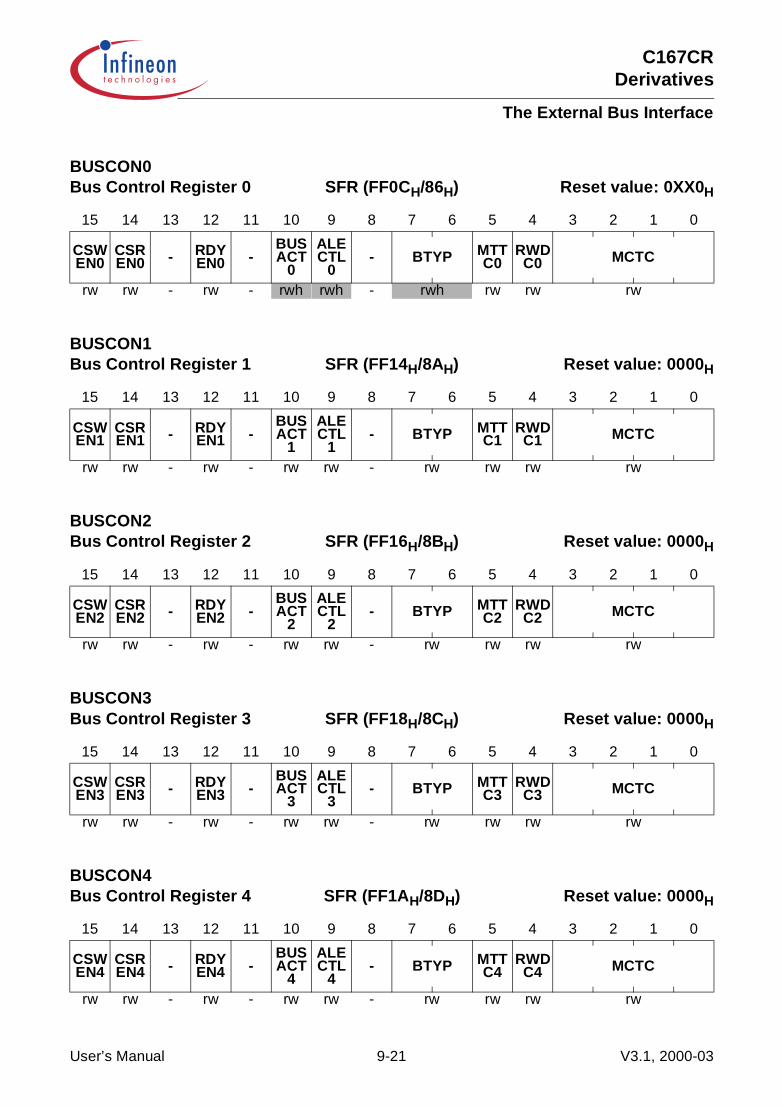
C167CRDerivatives
The External Bus Interface
BUSCON0Bus Control Register 0 SFR (FF0CH/86H) Reset value: 0XX0H
15 14 13 12 11 10 9 8 7 6 5 4 3 2 1 0
CSW EN0
CSR EN0 - RDY
EN0 -BUS ACT
0
ALE CTL
0- BTYP MTT
C0RWDC0 MCTC
rw rw - rw - rwh rwh - rwh rw rw rw
BUSCON1Bus Control Register 1 SFR (FF14H/8AH) Reset value: 0000H
15 14 13 12 11 10 9 8 7 6 5 4 3 2 1 0
CSW EN1
CSR EN1 - RDY
EN1 -BUS ACT
1
ALE CTL
1- BTYP MTT
C1RWDC1 MCTC
rw rw - rw - rw rw - rw rw rw rw
BUSCON2Bus Control Register 2 SFR (FF16H/8BH) Reset value: 0000H
15 14 13 12 11 10 9 8 7 6 5 4 3 2 1 0
CSW EN2
CSR EN2 - RDY
EN2 -BUS ACT
2
ALE CTL
2- BTYP MTT
C2RWDC2 MCTC
rw rw - rw - rw rw - rw rw rw rw
BUSCON3Bus Control Register 3 SFR (FF18H/8CH) Reset value: 0000H
15 14 13 12 11 10 9 8 7 6 5 4 3 2 1 0
CSW EN3
CSR EN3 - RDY
EN3 -BUS ACT
3
ALE CTL
3- BTYP MTT
C3RWDC3 MCTC
rw rw - rw - rw rw - rw rw rw rw
BUSCON4Bus Control Register 4 SFR (FF1AH/8DH) Reset value: 0000H
15 14 13 12 11 10 9 8 7 6 5 4 3 2 1 0
CSW EN4
CSR EN4 - RDY
EN4 -BUS ACT
4
ALE CTL
4- BTYP MTT
C4RWDC4 MCTC
rw rw - rw - rw rw - rw rw rw rw
User’s Manual 9-21 V3.1, 2000-03
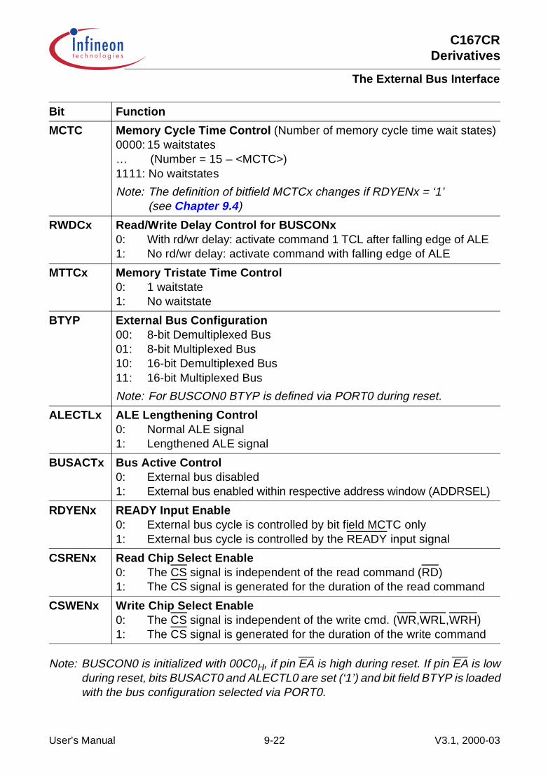
C167CRDerivatives
The External Bus Interface
Note: BUSCON0 is initialized with 00C0H, if pin EA is high during reset. If pin EA is lowduring reset, bits BUSACT0 and ALECTL0 are set (‘1’) and bit field BTYP is loadedwith the bus configuration selected via PORT0.
Bit Function
MCTC Memory Cycle Time Control (Number of memory cycle time wait states)0000: 15 waitstates… (Number = 15 – <MCTC>)1111: No waitstates
Note: The definition of bitfield MCTCx changes if RDYENx = ‘1’ (see Chapter 9.4)
RWDCx Read/Write Delay Control for BUSCONx0: With rd/wr delay: activate command 1 TCL after falling edge of ALE1: No rd/wr delay: activate command with falling edge of ALE
MTTCx Memory Tristate Time Control0: 1 waitstate1: No waitstate
BTYP External Bus Configuration00: 8-bit Demultiplexed Bus01: 8-bit Multiplexed Bus10: 16-bit Demultiplexed Bus11: 16-bit Multiplexed Bus
Note: For BUSCON0 BTYP is defined via PORT0 during reset.
ALECTLx ALE Lengthening Control0: Normal ALE signal1: Lengthened ALE signal
BUSACTx Bus Active Control0: External bus disabled1: External bus enabled within respective address window (ADDRSEL)
RDYENx READY Input Enable0: External bus cycle is controlled by bit field MCTC only1: External bus cycle is controlled by the READY input signal
CSRENx Read Chip Select Enable0: The CS signal is independent of the read command (RD)1: The CS signal is generated for the duration of the read command
CSWENx Write Chip Select Enable0: The CS signal is independent of the write cmd. (WR,WRL,WRH)1: The CS signal is generated for the duration of the write command
User’s Manual 9-22 V3.1, 2000-03
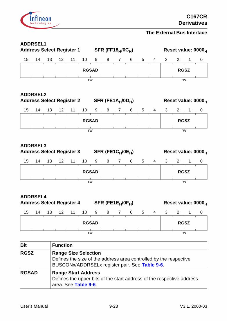
C167CRDerivatives
The External Bus Interface
ADDRSEL1Address Select Register 1 SFR (FF18H/0CH) Reset value: 0000H
15 14 13 12 11 10 9 8 7 6 5 4 3 2 1 0
RGSAD RGSZ
rw rw
ADDRSEL2Address Select Register 2 SFR (FE1AH/0DH) Reset value: 0000H
15 14 13 12 11 10 9 8 7 6 5 4 3 2 1 0
RGSAD RGSZ
rw rw
ADDRSEL3Address Select Register 3 SFR (FE1CH/0EH) Reset value: 0000H
15 14 13 12 11 10 9 8 7 6 5 4 3 2 1 0
RGSAD RGSZ
rw rw
ADDRSEL4Address Select Register 4 SFR (FE1EH/0FH) Reset value: 0000H
15 14 13 12 11 10 9 8 7 6 5 4 3 2 1 0
RGSAD RGSZ
rw rw
Bit Function
RGSZ Range Size SelectionDefines the size of the address area controlled by the respective BUSCONx/ADDRSELx register pair. See Table 9-6.
RGSAD Range Start AddressDefines the upper bits of the start address of the respective address area. See Table 9-6.
User’s Manual 9-23 V3.1, 2000-03

C167CRDerivatives
The External Bus Interface
Note: There is no register ADDRSEL0, as register BUSCON0 controls all externalaccesses outside the four address windows of BUSCON4 … BUSCON1 within thecomplete address space.
Definition of Address Areas
The four register pairs BUSCON4/ADDRSEL4 … BUSCON1/ADDRSEL1 allow to define4 separate address areas within the address space of the C167CR. Within each of theseaddress areas external accesses can be controlled by one of the four different busmodes, independent of each other and of the bus mode specified in register BUSCON0.Each ADDRSELx register in a way cuts out an address window, within which theparameters in register BUSCONx are used to control external accesses. The range startaddress of such a window defines the upper address bits, which are not used within theaddress window of the specified size (see Table 9-6). For a given window size onlythose upper address bits of the start address are used (marked “R”), which are notimplicitly used for addresses inside the window. The lower bits of the start address(marked “x”) are disregarded.
Table 9-6 Address Window Definition
Bit field RGSZ Resulting Window Size Relevant Bits (R) of Start Addr. (A12 …)
0 0 0 00 0 0 10 0 1 00 0 1 1 0 1 0 00 1 0 10 1 1 00 1 1 11 0 0 01 0 0 11 0 1 01 0 1 11 1 x x
4 KByte8 KByte16 KByte32 KByte64 KByte128 KByte256 KByte512 KByte1 MByte2 MByte4 MByte8 MByteReserved.
R R R R R R R R R R R RR R R R R R R R R R R xR R R R R R R R R R x xR R R R R R R R R x x xR R R R R R R R x x x xR R R R R R R x x x x xR R R R R R x x x x x xR R R R R x x x x x x xR R R R x x x x x x x xR R R x x x x x x x x xR R x x x x x x x x x xR x x x x x x x x x x x
User’s Manual 9-24 V3.1, 2000-03
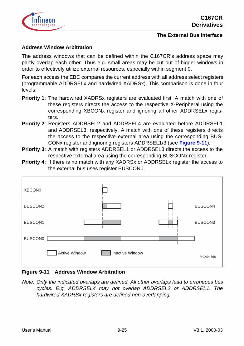
C167CRDerivatives
The External Bus Interface
Address Window Arbitration
The address windows that can be defined within the C167CR’s address space maypartly overlap each other. Thus e.g. small areas may be cut out of bigger windows inorder to effectively utilize external resources, especially within segment 0.
For each access the EBC compares the current address with all address select registers(programmable ADDRSELx and hardwired XADRSx). This comparison is done in fourlevels.
Priority 1: The hardwired XADRSx registers are evaluated first. A match with one ofthese registers directs the access to the respective X-Peripheral using thecorresponding XBCONx register and ignoring all other ADDRSELx regis-ters.
Priority 2: Registers ADDRSEL2 and ADDRSEL4 are evaluated before ADDRSEL1and ADDRSEL3, respectively. A match with one of these registers directsthe access to the respective external area using the corresponding BUS-CONx register and ignoring registers ADDRSEL1/3 (see Figure 9-11).
Priority 3: A match with registers ADDRSEL1 or ADDRSEL3 directs the access to therespective external area using the corresponding BUSCONx register.
Priority 4: If there is no match with any XADRSx or ADDRSELx register the access tothe external bus uses register BUSCON0.
Figure 9-11 Address Window Arbitration
Note: Only the indicated overlaps are defined. All other overlaps lead to erroneous buscycles. E.g. ADDRSEL4 may not overlap ADDRSEL2 or ADDRSEL1. Thehardwired XADRSx registers are defined non-overlapping.
MCA04368
XBCON0
BUSCON2
BUSCON1
BUSCON0
BUSCON4
BUSCON3
Active Window Inactive Window
User’s Manual 9-25 V3.1, 2000-03
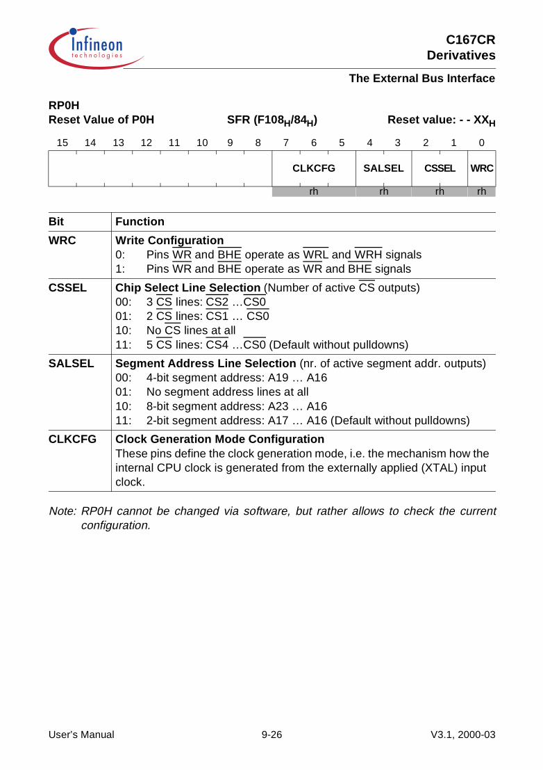
C167CRDerivatives
The External Bus Interface
Note: RP0H cannot be changed via software, but rather allows to check the currentconfiguration.
RP0HReset Value of P0H SFR (F108H/84H) Reset value: - - XXH
15 14 13 12 11 10 9 8 7 6 5 4 3 2 1 0
CLKCFG SALSEL CSSEL WRC
rh rh rh rh
Bit Function
WRC Write Configuration0: Pins WR and BHE operate as WRL and WRH signals1: Pins WR and BHE operate as WR and BHE signals
CSSEL Chip Select Line Selection (Number of active CS outputs)00: 3 CS lines: CS2 …CS001: 2 CS lines: CS1 … CS010: No CS lines at all11: 5 CS lines: CS4 …CS0 (Default without pulldowns)
SALSEL Segment Address Line Selection (nr. of active segment addr. outputs)00: 4-bit segment address: A19 … A1601: No segment address lines at all10: 8-bit segment address: A23 … A1611: 2-bit segment address: A17 … A16 (Default without pulldowns)
CLKCFG Clock Generation Mode ConfigurationThese pins define the clock generation mode, i.e. the mechanism how the internal CPU clock is generated from the externally applied (XTAL) input clock.
User’s Manual 9-26 V3.1, 2000-03

C167CRDerivatives
The External Bus Interface
Precautions and Hints
• The ext. bus interface is enabled as long as at least one of the BUSCON registers hasits BUSACT bit set.
• PORT1 will output the intra-segment addr. as long as at least one of the BUSCONregisters selects a demultiplexed external bus, even for multiplexed bus cycles.
• Not all addr. windows defined via registers ADDRSELx may overlap each other. Theoperation of the EBC will be unpredictable in such a case. See “Address WindowArbitration” on Page 9-25 .
• The addr. windows defined via registers ADDRSELx may overlap internal addr. areas.Internal accesses will be executed in this case.
• For any access to an internal addr. area the EBC will remain inactive (see EBC IdleState).
User’s Manual 9-27 V3.1, 2000-03

C167CRDerivatives
The External Bus Interface
9.6 EBC Idle State
When the external bus interface is enabled, but no external access is currently executed,the EBC is idle. As long as only internal resources (from an architecture point of view)like IRAM, GPRs or SFRs, etc. are used the external bus interface does not change (seeTable 9-7).
Accesses to on-chip X-Peripherals are also controlled by the EBC. However, eventhough an X-Peripheral appears like an external peripheral to the controller, therespective accesses do not generate valid external bus cycles.
Due to timing constraints address and write data of an XBUS cycle are reflected on theexternal bus interface (see Table 9-7). The “address” mentioned above includesPORT1, Port 4, BHE and ALE which also pulses for an XBUS cycle. The external CSsignals on Port 6 are driven inactive (high) because the EBC switches to an internal XCSsignal.
The external control signals (RD and WR or WRL/WRH if enabled) remain inactive (high).
Table 9-7 Status of the External Bus Interface During EBC Idle State
Pins Internal accesses only XBUS accesses
PORT0 Tristated (floating) Tristated (floating) for read accessesXBUS write data for write accesses
PORT1 Last used external address(if used for the bus interface)
Last used XBUS address(if used for the bus interface)1)
1) Used and driven in visible mode.
Port 4 Last used external segment address(on selected pins)
Last used XBUS segment address(on selected pins)
Port 6 Active external CS signal corresponding to last used address
Inactive (high) for selected CS signals
BHE Level corresponding to last external access
Level corresponding to last XBUS access
ALE Inactive (low) Pulses as defined for X-Peripheral
RD Inactive (high) Inactive (high)1)
WR/WRL Inactive (high) Inactive (high)1)
WRH Inactive (high) Inactive (high)1)
User’s Manual 9-28 V3.1, 2000-03
C167CRDerivatives
The External Bus Interface
9.7 External Bus Arbitration
In embedded systems it may be efficient to share external resources like memory banksor peripheral devices among more than one microcontroller or processor. The C167CRsupports this approach with the possibility to arbitrate the access to its external bus, i.e.to the external resources. Several bus masters can therefore use the same set ofresources, resulting in compact, though powerful systems.
Note: Sharing external resources is useful if these resources are used to a limitedamount only. The performance of a bus master which relies on these externalresources to a great extent (e.g. external code) will be reduced by the bandwidthused by the other masters.
Bus arbitration uses three control signals (HOLD, HLDA/BGR, BREQ) and can beenabled and disabled via software (PSW.HLDEN), e.g. in order to protect time-criticalcode sections from being suspended by other bus masters. A bus arbiter logic can bedesigned to determine which of the bus masters controls the external system at a giventime.
Using the specific master and slave modes for bus arbitration saves external glue logic(bus arbiter) when connecting two devices of the C166 Family.
Note: Bus arbitration does not work if there is no clock signal for the EBC, i.e. during Idlemode and Powerdown mode.
Signals and Control
The upper three pins of Port 6 are used for the bus arbitration interface. Table 9-8summarizes the functions of these interface lines.
The external bus arbitration is enabled by setting bit HLDEN in register PSW to ‘1’. Inthis case the three bus arbitration pins HOLD, HLDA and BREQ are automaticallycontrolled by the EBC independent of their IO configuration.
Bit HLDEN may be cleared during the execution of program sequences, where theexternal resources are required but cannot be shared with other bus masters, or duringsequences which need to access on-chip XBUS resources but which shall not beinterrupted by hold states. In this case the C167CR will not answer to HOLD requestsfrom other external masters. If HLDEN is cleared while the C167CR is in Hold State(code execution from internal RAM/ROM) this Hold State is left only after HOLD hasbeen deactivated again. I.e. in this case the current Hold State continues and only thenext HOLD request is not answered.
Note: The pins HOLD, HLDA and BREQ keep their alternate function (bus arbitration)even after the arbitration mechanism has been switched off by clearing HLDEN.All three pins are used for bus arbitration after bit HLDEN was set once.
User’s Manual 9-29 V3.1, 2000-03
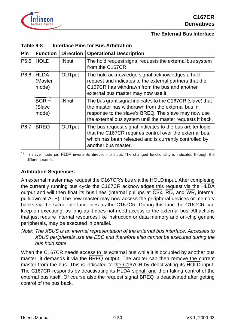
C167CRDerivatives
The External Bus Interface
Arbitration Sequences
An external master may request the C167CR’s bus via the HOLD input. After completingthe currently running bus cycle the C167CR acknowledges this request via the HLDAoutput and will then float its bus lines (internal pullups at CSx, RD, and WR, internalpulldown at ALE). The new master may now access the peripheral devices or memorybanks via the same interface lines as the C167CR. During this time the C167CR cankeep on executing, as long as it does not need access to the external bus. All actionsthat just require internal resources like instruction or data memory and on-chip genericperipherals, may be executed in parallel.
Note: The XBUS is an internal representation of the external bus interface. Accesses toXBUS peripherals use the EBC and therefore also cannot be executed during thebus hold state.
When the C167CR needs access to its external bus while it is occupied by another busmaster, it demands it via the BREQ output. The arbiter can then remove the currentmaster from the bus. This is indicated to the C167CR by deactivating its HOLD input.The C167CR responds by deactivating its HLDA signal, and then taking control of theexternal bus itself. Of course also the request signal BREQ is deactivated after gettingcontrol of the bus back.
Table 9-8 Interface Pins for Bus Arbitration
Pin Function Direction Operational Description
P6.5 HOLD INput The hold request signal requests the external bus system from the C167CR.
P6.6 HLDA(Master mode)
OUTput The hold acknowledge signal acknowledges a hold request and indicates to the external partners that the C167CR has withdrawn from the bus and another external bus master may now use it.
BGR 1)
(Slave mode)
INput The bus grant signal indicates to the C167CR (slave) that the master has withdrawn from the external bus in response to the slave’s BREQ. The slave may now use the external bus system until the master requests it back.
P6.7 BREQ OUTput The bus request signal indicates to the bus arbiter logic that the C167CR requires control over the external bus, which has been released and is currently controlled by another bus master.
1) In slave mode pin HLDA inverts its direction to input. The changed functionality is indicated through thedifferent name.
User’s Manual 9-30 V3.1, 2000-03
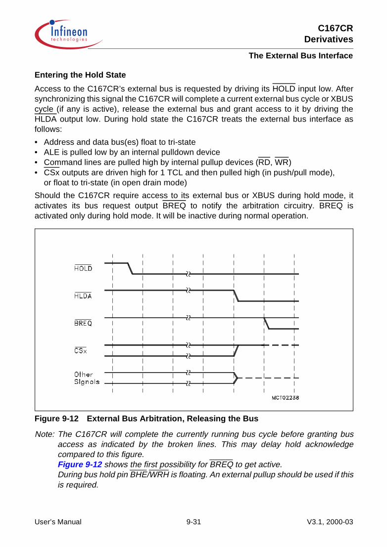
C167CRDerivatives
The External Bus Interface
Entering the Hold State
Access to the C167CR’s external bus is requested by driving its HOLD input low. Aftersynchronizing this signal the C167CR will complete a current external bus cycle or XBUScycle (if any is active), release the external bus and grant access to it by driving theHLDA output low. During hold state the C167CR treats the external bus interface asfollows:
• Address and data bus(es) float to tri-state• ALE is pulled low by an internal pulldown device• Command lines are pulled high by internal pullup devices (RD, WR)• CSx outputs are driven high for 1 TCL and then pulled high (in push/pull mode),
or float to tri-state (in open drain mode)
Should the C167CR require access to its external bus or XBUS during hold mode, itactivates its bus request output BREQ to notify the arbitration circuitry. BREQ isactivated only during hold mode. It will be inactive during normal operation.
Figure 9-12 External Bus Arbitration, Releasing the Bus
Note: The C167CR will complete the currently running bus cycle before granting busaccess as indicated by the broken lines. This may delay hold acknowledgecompared to this figure.Figure 9-12 shows the first possibility for BREQ to get active.During bus hold pin BHE/WRH is floating. An external pullup should be used if thisis required.
User’s Manual 9-31 V3.1, 2000-03

C167CRDerivatives
The External Bus Interface
Exiting the Hold State
The external bus master returns the access rights to the C167CR by driving the HOLDinput high. After synchronizing this signal the C167CR will drive the HLDA output high,actively drive the control signals and resume executing external bus cycles if required.
Depending on the arbitration logic, the external bus can be returned to the C167CRunder two circumstances:
• The external master does no more require access to the shared resources and givesup its own access rights, or
• The C167CR needs access to the shared resources and demands this by activatingits BREQ output. The arbitration logic may then activate the other master’s HOLD andso free the external bus for the C167CR, depending on the priority of the differentmasters.
Note: The Hold State is not terminated by clearing bit HLDEN.
Figure 9-13 External Bus Arbitration, Regaining the Bus
Note: The falling BREQ edge shows the last chance for BREQ to trigger the indicatedregain-sequence. Even if BREQ is activated earlier the regain-sequence isinitiated by HOLD going high. BREQ and HOLD are connected via an externalarbitration circuitry. Please note that HOLD may also be deactivated without theC167CR requesting the bus.
MCD02236
OtherSignals
CSx
BREQ
HLDA
HOLD
User’s Manual 9-32 V3.1, 2000-03
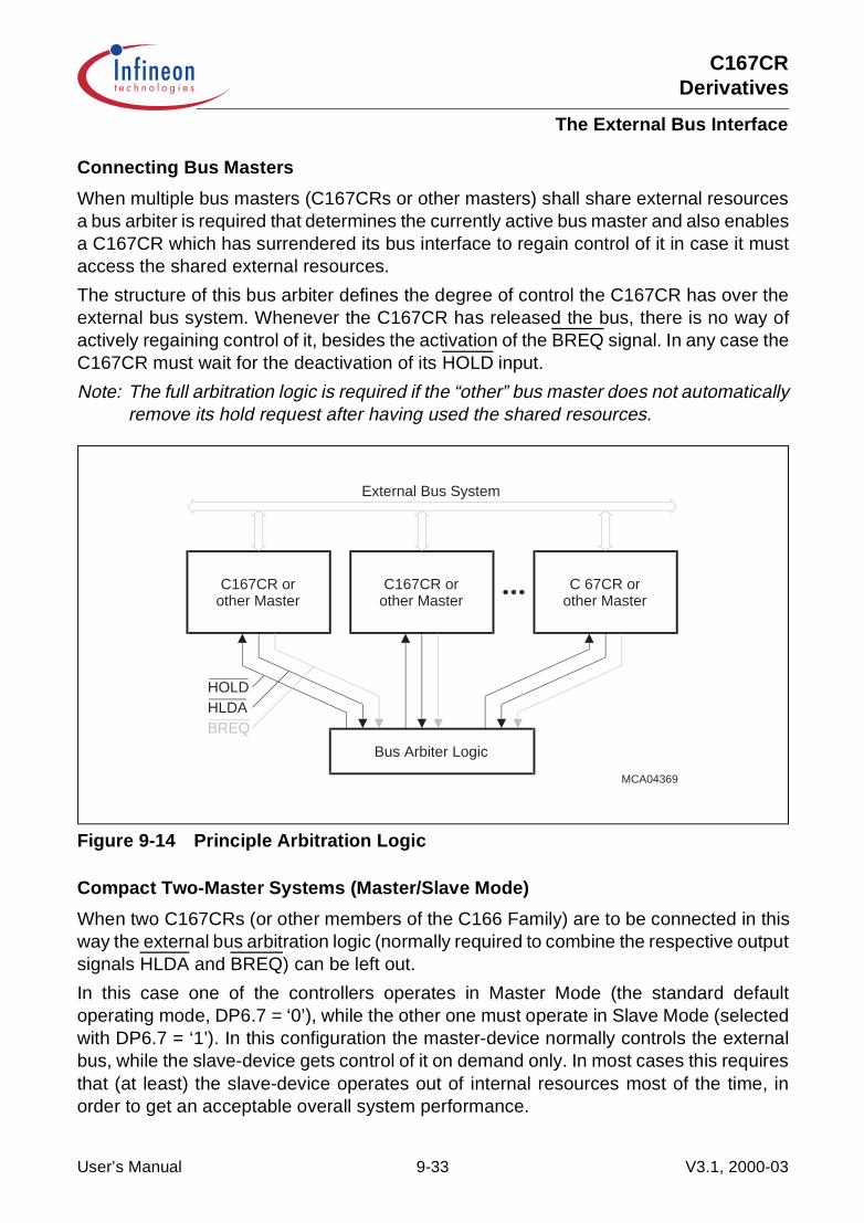
C167CRDerivatives
The External Bus Interface
Connecting Bus Masters
When multiple bus masters (C167CRs or other masters) shall share external resourcesa bus arbiter is required that determines the currently active bus master and also enablesa C167CR which has surrendered its bus interface to regain control of it in case it mustaccess the shared external resources.
The structure of this bus arbiter defines the degree of control the C167CR has over theexternal bus system. Whenever the C167CR has released the bus, there is no way ofactively regaining control of it, besides the activation of the BREQ signal. In any case theC167CR must wait for the deactivation of its HOLD input.
Note: The full arbitration logic is required if the “other” bus master does not automaticallyremove its hold request after having used the shared resources.
Figure 9-14 Principle Arbitration Logic
Compact Two-Master Systems (Master/Slave Mode)
When two C167CRs (or other members of the C166 Family) are to be connected in thisway the external bus arbitration logic (normally required to combine the respective outputsignals HLDA and BREQ) can be left out.
In this case one of the controllers operates in Master Mode (the standard defaultoperating mode, DP6.7 = ‘0’), while the other one must operate in Slave Mode (selectedwith DP6.7 = ‘1’). In this configuration the master-device normally controls the externalbus, while the slave-device gets control of it on demand only. In most cases this requiresthat (at least) the slave-device operates out of internal resources most of the time, inorder to get an acceptable overall system performance.
MCA04369
Bus Arbiter Logic
C167CR orother Master
C167CR orother Master
C 67CR orother Master
HOLDHLDABREQ
External Bus System
User’s Manual 9-33 V3.1, 2000-03
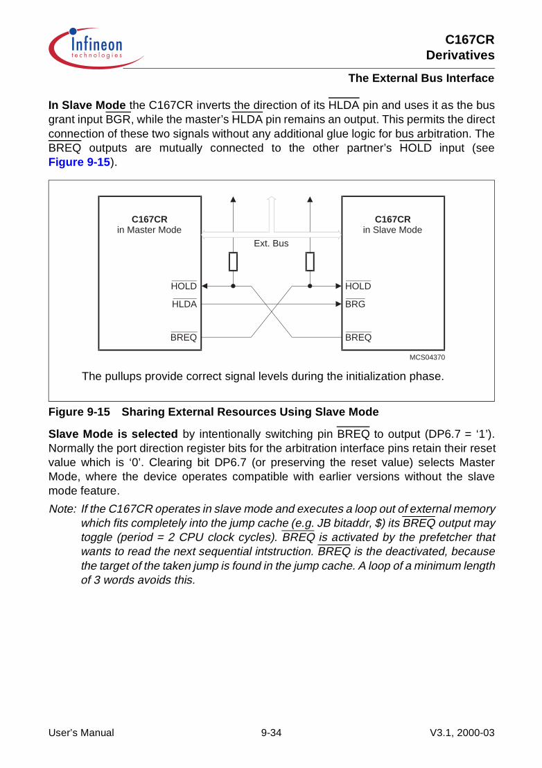
C167CRDerivatives
The External Bus Interface
In Slave Mode the C167CR inverts the direction of its HLDA pin and uses it as the busgrant input BGR, while the master’s HLDA pin remains an output. This permits the directconnection of these two signals without any additional glue logic for bus arbitration. TheBREQ outputs are mutually connected to the other partner’s HOLD input (seeFigure 9-15).
Figure 9-15 Sharing External Resources Using Slave Mode
Slave Mode is selected by intentionally switching pin BREQ to output (DP6.7 = ‘1’).Normally the port direction register bits for the arbitration interface pins retain their resetvalue which is ‘0’. Clearing bit DP6.7 (or preserving the reset value) selects MasterMode, where the device operates compatible with earlier versions without the slavemode feature.
Note: If the C167CR operates in slave mode and executes a loop out of external memorywhich fits completely into the jump cache (e.g. JB bitaddr, $) its BREQ output maytoggle (period = 2 CPU clock cycles). BREQ is activated by the prefetcher thatwants to read the next sequential intstruction. BREQ is the deactivated, becausethe target of the taken jump is found in the jump cache. A loop of a minimum lengthof 3 words avoids this.
MCS04370
C167CRin Master Mode
C167CRin Slave Mode
Ext. Bus
HOLD
HLDA
BREQ
HOLD
BRG
BREQ
The pullups provide correct signal levels during the initialization phase.
User’s Manual 9-34 V3.1, 2000-03
C167CRDerivatives
The External Bus Interface
9.8 The XBUS Interface
The C167CR provides an on-chip interface (the XBUS interface), via which integratedcustomer/application specific peripherals can be connected to the standard controllercore. The XBUS is an internal representation of the external bus interface, i.e. it isoperated in the same way.
For each peripheral on the XBUS (X-Peripheral) there is a separate address windowcontrolled by a register pair XBCONx/XADRSx (similar to registers BUSCONx andADDRSELx). As an interface to a peripheral in many cases is represented by just a fewregisters, the XADRSx registers partly select smaller address windows than the standardADDRSEL registers. As the XBCONx/XADRSx register pairs control integratedperipherals rather than externally connected ones, they are fixed by mask programmingrather than being user programmable.
X-Peripheral accesses provide the same choices as external accesses, so theseperipherals may be bytewide or wordwide. Because the on-chip connection can berealized very efficient and for performance reasons X-Peripherals are only implementedwith a separate address bus, i.e. in demultiplexed bus mode. Interrupt nodes areprovided for X-Peripherals to be integrated.
Note: If you plan to develop a peripheral of your own to be integrated into a C167CRdevice to create a customer specific version, please ask for the specification of theXBUS interface and for further support.
User’s Manual 9-35 V3.1, 2000-03

C167CRDerivatives
The External Bus Interface
9.8.1 Accessing the On-chip XBUS Peripherals
Enabling of XBUS Peripherals
After reset all on-chip XBUS peripherals are disabled. In order to be usable an XBUSperipheral must be enabled via the global enable bit XPEN in register SYSCON.
Table 9-9 summarizes the XBUS peripherals and also the number of waitstates whichare used when accessing the respective peripheral.
Visible Mode
The C167CR can mirror on-chip access cycles to its XBUS peripherals so theseaccesses can be observed or recorded by the external system. This function is enabledvia bit VISIBLE in register SYSCON.
Accesses to XBUS peripherals also use the EBC. Due to timing constraints the addressbus will change for all accesses using the EBC.
Note: As XBUS peripherals use demultiplexed bus cycles, the respective address isdriven on PORT1 in visible mode, even if the external system uses MUX busesonly.
If visible mode is activated, accesses to on-chip XBUS peripherals (including controlsignals RD, WR, and BHE) are mirrored to the bus interface. Accesses to internalresources (program memory, IRAM, GPRs) do not use the EBC and cannot be mirroredto outside.
If visible mode is deactivated, however, no control signals (RD, WR) will be activated,i.e. there will be no valid external bus cycles.
Note: Visible mode can only work if the external bus is enabled at all.
Table 9-9 XBUS Peripherals in the C167CR
Associated XBUS Peripheral Waitstates
CAN 2
XRAM 2 KByte 0
User’s Manual 9-36 V3.1, 2000-03
C167CRDerivatives
The External Bus Interface
9.8.2 External Accesses to XBUS Peripherals
The on-chip XBUS peripherals of the C167CR can be accessed from outside via theexternal bus interface under certain circumstances. In emulation mode the XBUSperipherals are controlled by the bondout-chip. During normal operation this externalaccess is accomplished selecting the XPER-Share mode.
XPER-Share Mode
The C167CR can share its on-chip XBUS peripherals with other (external) bus masters,i.e. it can allow them to access its X-Peripherals while it is in hold mode. This externalaccess is enabled via bit XPERSHARE in register SYSCON and is only possible whilethe host controller is in hold mode.
During XPER-Share mode the C167CR’s bus interface inverts its direction so theexternal master can drive address, control, and data signals to the respective peripheral.This can be used e.g. to install a mailbox memory in a multi-processor system.
Note: When XPER-Share mode is disabled no accesses to on-chip XBUS peripheralscan be executed from outside.
User’s Manual 9-37 V3.1, 2000-03
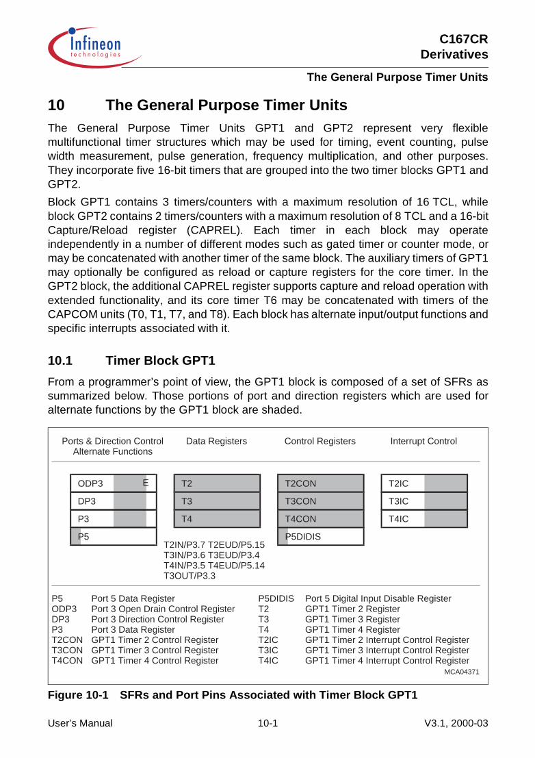
C167CRDerivatives
The General Purpose Timer Units
10 The General Purpose Timer UnitsThe General Purpose Timer Units GPT1 and GPT2 represent very flexiblemultifunctional timer structures which may be used for timing, event counting, pulsewidth measurement, pulse generation, frequency multiplication, and other purposes.They incorporate five 16-bit timers that are grouped into the two timer blocks GPT1 andGPT2.
Block GPT1 contains 3 timers/counters with a maximum resolution of 16 TCL, whileblock GPT2 contains 2 timers/counters with a maximum resolution of 8 TCL and a 16-bitCapture/Reload register (CAPREL). Each timer in each block may operateindependently in a number of different modes such as gated timer or counter mode, ormay be concatenated with another timer of the same block. The auxiliary timers of GPT1may optionally be configured as reload or capture registers for the core timer. In theGPT2 block, the additional CAPREL register supports capture and reload operation withextended functionality, and its core timer T6 may be concatenated with timers of theCAPCOM units (T0, T1, T7, and T8). Each block has alternate input/output functions andspecific interrupts associated with it.
10.1 Timer Block GPT1
From a programmer’s point of view, the GPT1 block is composed of a set of SFRs assummarized below. Those portions of port and direction registers which are used foralternate functions by the GPT1 block are shaded.
Figure 10-1 SFRs and Port Pins Associated with Timer Block GPT1
E
MCA04371
ODP3
DP3
P3
T2
T3
T4
T2CON T2IC
T4IC
Ports & Direction ControlAlternate Functions
Data Registers Control Registers Interrupt Control
P5 Port 5 Data RegisterODP3 Port 3 Open Drain Control RegisterDP3 Port 3 Direction Control RegisterP3 Port 3 Data RegisterT2CON GPT1 Timer 2 Control RegisterT3CON GPT1 Timer 3 Control RegisterT4CON GPT1 Timer 4 Control Register
P5DIDIS Port 5 Digital Input Disable RegisterT2 GPT1 Timer 2 RegisterT3 GPT1 Timer 3 RegisterT4 GPT1 Timer 4 RegisterT2IC GPT1 Timer 2 Interrupt Control RegisterT3IC GPT1 Timer 3 Interrupt Control RegisterT4IC GPT1 Timer 4 Interrupt Control Register
T3IC
T2IN/P3.7 T2EUD/P5.15T3IN/P3.6 T3EUD/P3.4T4IN/P3.5 T4EUD/P5.14T3OUT/P3.3
P5
T3CON
P5DIDIS
T4CON
User’s Manual 10-1 V3.1, 2000-03
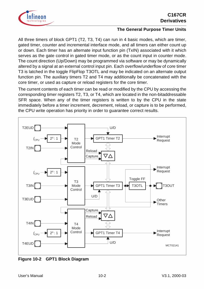
C167CRDerivatives
The General Purpose Timer Units
All three timers of block GPT1 (T2, T3, T4) can run in 4 basic modes, which are timer,gated timer, counter and incremental interface mode, and all timers can either count upor down. Each timer has an alternate input function pin (TxIN) associated with it whichserves as the gate control in gated timer mode, or as the count input in counter mode.The count direction (Up/Down) may be programmed via software or may be dynamicallyaltered by a signal at an external control input pin. Each overflow/underflow of core timerT3 is latched in the toggle FlipFlop T3OTL and may be indicated on an alternate outputfunction pin. The auxiliary timers T2 and T4 may additionally be concatenated with thecore timer, or used as capture or reload registers for the core timer.
The current contents of each timer can be read or modified by the CPU by accessing thecorresponding timer registers T2, T3, or T4, which are located in the non-bitaddressableSFR space. When any of the timer registers is written to by the CPU in the stateimmediately before a timer increment, decrement, reload, or capture is to be performed,the CPU write operation has priority in order to guarantee correct results.
Figure 10-2 GPT1 Block Diagram
T3Mode
Control
2n : 1fCPU
2n : 1fCPU T2Mode
Control
GPT1 Timer T2
Reload
Capture
2n : 1fCPU
T4Mode
Control GPT1 Timer T4
Reload
Capture
GPT1 Timer T3 T3OTL
U/D
T2EUD
T2IN
T3IN
T3EUD
T4IN
T4EUD
T3OUT
Toggle FF
U/D
U/D
InterruptRequest
InterruptRequest
InterruptRequest
OtherTimers
MCT02141
User’s Manual 10-2 V3.1, 2000-03
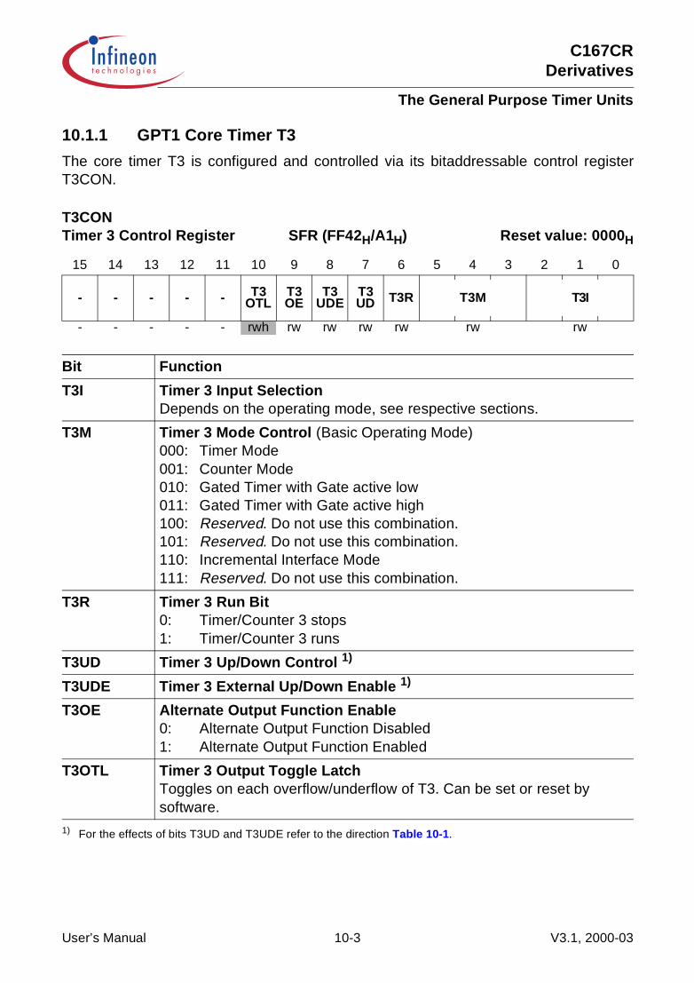
C167CRDerivatives
The General Purpose Timer Units
10.1.1 GPT1 Core Timer T3
The core timer T3 is configured and controlled via its bitaddressable control registerT3CON.
T3CONTimer 3 Control Register SFR (FF42H/A1H) Reset value: 0000H
15 14 13 12 11 10 9 8 7 6 5 4 3 2 1 0
- - - - - T3OTL
T3OE
T3UDE
T3UD T3R T3M T3I
- - - - - rwh rw rw rw rw rw rw
Bit Function
T3I Timer 3 Input SelectionDepends on the operating mode, see respective sections.
T3M Timer 3 Mode Control (Basic Operating Mode)000: Timer Mode001: Counter Mode010: Gated Timer with Gate active low011: Gated Timer with Gate active high100: Reserved. Do not use this combination.101: Reserved. Do not use this combination.110: Incremental Interface Mode111: Reserved. Do not use this combination.
T3R Timer 3 Run Bit0: Timer/Counter 3 stops1: Timer/Counter 3 runs
T3UD Timer 3 Up/Down Control 1)
1) For the effects of bits T3UD and T3UDE refer to the direction Table 10-1.
T3UDE Timer 3 External Up/Down Enable 1)
T3OE Alternate Output Function Enable0: Alternate Output Function Disabled1: Alternate Output Function Enabled
T3OTL Timer 3 Output Toggle LatchToggles on each overflow/underflow of T3. Can be set or reset by software.
User’s Manual 10-3 V3.1, 2000-03
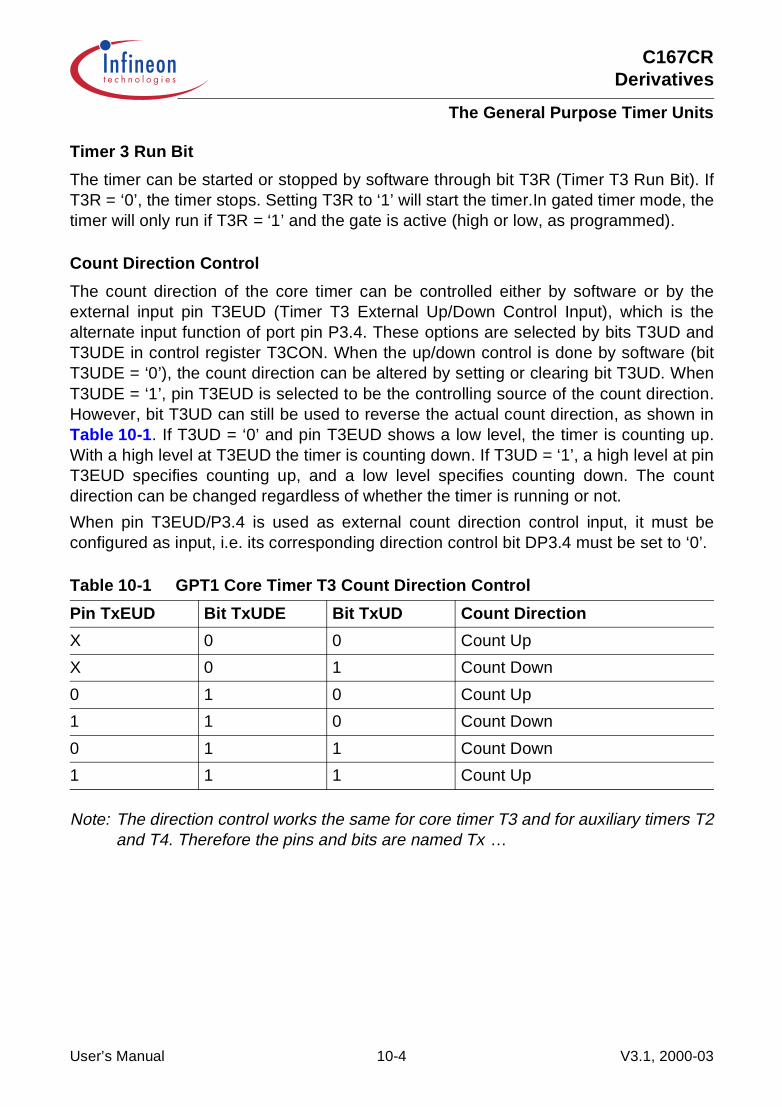
C167CRDerivatives
The General Purpose Timer Units
Timer 3 Run Bit
The timer can be started or stopped by software through bit T3R (Timer T3 Run Bit). IfT3R = ‘0’, the timer stops. Setting T3R to ‘1’ will start the timer.In gated timer mode, thetimer will only run if T3R = ‘1’ and the gate is active (high or low, as programmed).
Count Direction Control
The count direction of the core timer can be controlled either by software or by theexternal input pin T3EUD (Timer T3 External Up/Down Control Input), which is thealternate input function of port pin P3.4. These options are selected by bits T3UD andT3UDE in control register T3CON. When the up/down control is done by software (bitT3UDE = ‘0’), the count direction can be altered by setting or clearing bit T3UD. WhenT3UDE = ‘1’, pin T3EUD is selected to be the controlling source of the count direction.However, bit T3UD can still be used to reverse the actual count direction, as shown inTable 10-1. If T3UD = ‘0’ and pin T3EUD shows a low level, the timer is counting up.With a high level at T3EUD the timer is counting down. If T3UD = ‘1’, a high level at pinT3EUD specifies counting up, and a low level specifies counting down. The countdirection can be changed regardless of whether the timer is running or not.
When pin T3EUD/P3.4 is used as external count direction control input, it must beconfigured as input, i.e. its corresponding direction control bit DP3.4 must be set to ‘0’.
Note: The direction control works the same for core timer T3 and for auxiliary timers T2and T4. Therefore the pins and bits are named Tx …
Table 10-1 GPT1 Core Timer T3 Count Direction Control
Pin TxEUD Bit TxUDE Bit TxUD Count Direction
X 0 0 Count Up
X 0 1 Count Down
0 1 0 Count Up
1 1 0 Count Down
0 1 1 Count Down
1 1 1 Count Up
User’s Manual 10-4 V3.1, 2000-03
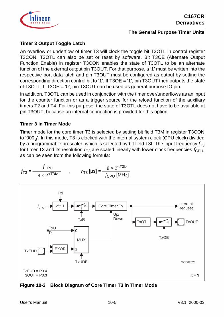
C167CRDerivatives
The General Purpose Timer Units
Timer 3 Output Toggle Latch
An overflow or underflow of timer T3 will clock the toggle bit T3OTL in control registerT3CON. T3OTL can also be set or reset by software. Bit T3OE (Alternate OutputFunction Enable) in register T3CON enables the state of T3OTL to be an alternatefunction of the external output pin T3OUT. For that purpose, a ‘1’ must be written into therespective port data latch and pin T3OUT must be configured as output by setting thecorresponding direction control bit to ‘1’. If T3OE = ‘1’, pin T3OUT then outputs the stateof T3OTL. If T3OE = ‘0’, pin T3OUT can be used as general purpose IO pin.
In addition, T3OTL can be used in conjunction with the timer over/underflows as an inputfor the counter function or as a trigger source for the reload function of the auxiliarytimers T2 and T4. For this purpose, the state of T3OTL does not have to be available atpin T3OUT, because an internal connection is provided for this option.
Timer 3 in Timer Mode
Timer mode for the core timer T3 is selected by setting bit field T3M in register T3CONto ‘000B’. In this mode, T3 is clocked with the internal system clock (CPU clock) dividedby a programmable prescaler, which is selected by bit field T3I. The input frequency fT3for timer T3 and its resolution rT3 are scaled linearly with lower clock frequencies fCPU,as can be seen from the following formula:
Figure 10-3 Block Diagram of Core Timer T3 in Timer Mode
fT3 =fCPU
8 × 2<T3I>rT3 [µs] =
fCPU [MHz]8 × 2<T3I>
,
Core Timer Tx
TxOTL
InterruptRequest
TxOE
TxOUTTxR
2n : 1
Txl
EXOR
0
MUX
1TxEUD
TxUDE MCB02028
TxUD
fCPU
Up/Down
T3EUD = P3.4T3OUT = P3.3 x = 3
User’s Manual 10-5 V3.1, 2000-03

C167CRDerivatives
The General Purpose Timer Units
The timer input frequencies, resolution and periods which result from the selectedprescaler option are listed in Table 10-2. This table also applies to the Gated TimerMode of T3 and to the auxiliary timers T2 and T4 in timer and gated timer mode. Notethat some numbers may be rounded to 3 significant digits.
Table 10-2 GPT1 Timer Input Frequencies, Resolution and Periods @ 20 MHz
fCPU = 20 MHz Timer Input Selection T2I/T3I/T4I
000B 001B 010B 011B 100B 101B 110B 111B
Prescaler factor 8 16 32 64 128 256 512 1024
Input Frequency
2.5MHz
1.25MHz
625kHz
312.5kHz
156.25kHz
78.125kHz
39.06kHz
19.53kHz
Resolution 400 ns 800 ns 1.6 µs 3.2 µs 6.4 µs 12.8 µs 25.6 µs 51.2 µs
Period 26.2 ms 52.5 ms 105 ms 210 ms 420 ms 840 ms 1.68 s 3.36 s
Table 10-3 GPT1 Timer Input Frequencies, Resolution and Periods @ 25 MHz
fCPU = 25 MHz Timer Input Selection T2I/T3I/T4I
000B 001B 010B 011B 100B 101B 110B 111B
Prescaler factor 8 16 32 64 128 256 512 1024
Input Frequency
3.125MHz
1.56MHz
781.25kHz
390.62kHz
195.3kHz
97.65kHz
48.83kHz
24.42kHz
Resolution 320 ns 640 ns 1.28 µs 2.56 µs 5.12 µs 10.2 µs 20.5 µs 41.0 µs
Period 21.0 ms 41.9 ms 83.9 ms 168 ms 336 ms 671 ms 1.34 s 2.68 s
Table 10-4 GPT1 Timer Input Frequencies, Resolution and Periods @ 33 MHz
fCPU = 33 MHz Timer Input Selection T2I/T3I/T4I
000B 001B 010B 011B 100B 101B 110B 111B
Prescaler factor 8 16 32 64 128 256 512 1024
Input Frequency
4.125MHz
2.0625MHz
1.031MHz
515.62kHz
257.81kHz
128.91kHz
64.45kHz
32.23kHz
Resolution 242 ns 485 ns 970 ns 1.94 µs 3.88 µs 7.76 µs 15.5 µs 31.0 µs
Period 15.9 ms 31.8 ms 63.6 ms 127 ms 254 ms 508 ms 1.02 s 2.03 s
User’s Manual 10-6 V3.1, 2000-03

C167CRDerivatives
The General Purpose Timer Units
Timer 3 in Gated Timer Mode
Gated timer mode for the core timer T3 is selected by setting bit field T3M in registerT3CON to ‘010B’ or ‘011B’. Bit T3M.0 (T3CON.3) selects the active level of the gateinput. In gated timer mode the same options for the input frequency as for the timer modeare available. However, the input clock to the timer in this mode is gated by the externalinput pin T3IN (Timer T3 External Input).To enable this operation pin T3IN must be configured as input, i.e. the correspondingdirection control bit must contain ‘0’.
Figure 10-4 Block Diagram of Core Timer T3 in Gated Timer Mode
If T3M.0 = ‘0’, the timer is enabled when T3IN shows a low level. A high level at this pinstops the timer. If T3M.0 = ‘1’, pin T3IN must have a high level in order to enable thetimer. In addition, the timer can be turned on or off by software using bit T3R. The timerwill only run, if T3R = ‘1’ and the gate is active. It will stop, if either T3R = ‘0’ or the gateis inactive.
Note: A transition of the gate signal at pin T3IN does not cause an interrupt request.
MUX Core Timer Tx TxOTL
InterruptRequest
TxOE
TxOUT
TxR
XOR
0
MUX
1
Up/Down
TxEUD
TxUDE MCB02029
TxUD
2n : 1
TxI
fCPU
TxM
TxIN
T3IN = P3.6T3EUD = P3.4T3OUT = P3.3 x = 3
User’s Manual 10-7 V3.1, 2000-03

C167CRDerivatives
The General Purpose Timer Units
Timer 3 in Counter Mode
Counter mode for the core timer T3 is selected by setting bit field T3M in register T3CONto ‘001B’. In counter mode timer T3 is clocked by a transition at the external input pinT3IN. The event causing an increment or decrement of the timer can be a positive, anegative, or both a positive and a negative transition at this pin. Bit field T3I in controlregister T3CON selects the triggering transition (see Table 10-5).
Figure 10-5 Block Diagram of Core Timer T3 in Counter Mode
For counter operation, pin T3IN must be configured as input, i.e. the respective directioncontrol bit DPx.y must be ‘0’. The maximum input frequency which is allowed in countermode is fCPU/16. To ensure that a transition of the count input signal which is applied toT3IN is correctly recognized, its level should be held high or low for at least 8 fCPU cyclesbefore it changes.
Table 10-5 GPT1 Core Timer T3 (Counter Mode) Input Edge Selection
T3I Triggering Edge for Counter Increment/Decrement
0 0 0 None. Counter T3 is disabled
0 0 1 Positive transition (rising edge) on T3IN
0 1 0 Negative transition (falling edge) on T3IN
0 1 1 Any transition (rising or falling edge) on T3IN
1 X X Reserved. Do not use this combination
Core Timer Tx
TxR
XOR
0
MUX
1
Up/Down
TxEUD
TxUDE MCB02030
TxUD
Txl
TxIN
EdgeSelect
TxOTL
TxOE
TxOUT
InterruptRequest
T3IN = P3.6T3EUD = P3.4T3OUT = P3.3 x = 3
User’s Manual 10-8 V3.1, 2000-03
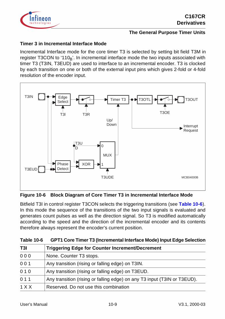
C167CRDerivatives
The General Purpose Timer Units
Timer 3 in Incremental Interface Mode
Incremental Interface mode for the core timer T3 is selected by setting bit field T3M inregister T3CON to ‘110B’. In incremental interface mode the two inputs associated withtimer T3 (T3IN, T3EUD) are used to interface to an incremental encoder. T3 is clockedby each transition on one or both of the external input pins which gives 2-fold or 4-foldresolution of the encoder input.
Figure 10-6 Block Diagram of Core Timer T3 in Incremental Interface Mode
Bitfield T3I in control register T3CON selects the triggering transitions (see Table 10-6).In this mode the sequence of the transitions of the two input signals is evaluated andgenerates count pulses as well as the direction signal. So T3 is modified automaticallyaccording to the speed and the direction of the incremental encoder and its contentstherefore always represent the encoder’s current position.
Table 10-6 GPT1 Core Timer T3 (Incremental Interface Mode) Input Edge Selection
T3I Triggering Edge for Counter Increment/Decrement
0 0 0 None. Counter T3 stops.
0 0 1 Any transition (rising or falling edge) on T3IN.
0 1 0 Any transition (rising or falling edge) on T3EUD.
0 1 1 Any transition (rising or falling edge) on any T3 input (T3IN or T3EUD).
1 X X Reserved. Do not use this combination
EdgeSelect Timer T3
XOR
0
MUX
1T3EUD
T3UDE MCB04000B
T3UD
T3l
T3INT3OTL
InterruptRequest
T3OUT
PhaseDetect
T3OET3R
Up/Down
User’s Manual 10-9 V3.1, 2000-03
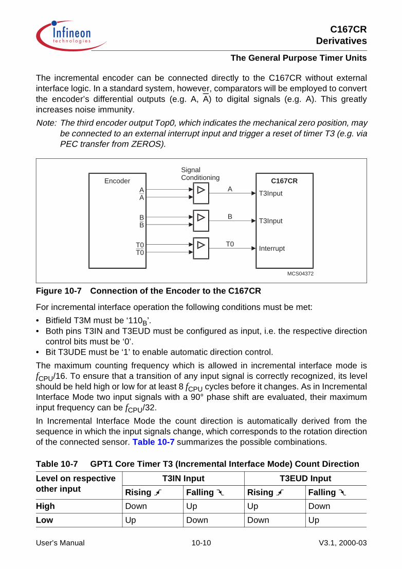
C167CRDerivatives
The General Purpose Timer Units
The incremental encoder can be connected directly to the C167CR without externalinterface logic. In a standard system, however, comparators will be employed to convertthe encoder’s differential outputs (e.g. A, A) to digital signals (e.g. A). This greatlyincreases noise immunity.
Note: The third encoder output Top0, which indicates the mechanical zero position, maybe connected to an external interrupt input and trigger a reset of timer T3 (e.g. viaPEC transfer from ZEROS).
Figure 10-7 Connection of the Encoder to the C167CR
For incremental interface operation the following conditions must be met:
• Bitfield T3M must be ‘110B’.• Both pins T3IN and T3EUD must be configured as input, i.e. the respective direction
control bits must be ‘0’.• Bit T3UDE must be ‘1’ to enable automatic direction control.
The maximum counting frequency which is allowed in incremental interface mode isfCPU/16. To ensure that a transition of any input signal is correctly recognized, its levelshould be held high or low for at least 8 fCPU cycles before it changes. As in IncrementalInterface Mode two input signals with a 90° phase shift are evaluated, their maximuminput frequency can be fCPU/32.
In Incremental Interface Mode the count direction is automatically derived from thesequence in which the input signals change, which corresponds to the rotation directionof the connected sensor. Table 10-7 summarizes the possible combinations.
Table 10-7 GPT1 Core Timer T3 (Incremental Interface Mode) Count Direction
Level on respective other input
T3IN Input T3EUD Input
Rising Falling Rising Falling
High Down Up Up Down
Low Up Down Down Up
MCS04372
Encoder C167CRA
B
T0
T3Input
T3Input
Interrupt
A
BB
T0T0
A
SignalConditioning
User’s Manual 10-10 V3.1, 2000-03

C167CRDerivatives
The General Purpose Timer Units
Figure 10-8 and Figure 10-9 give examples of T3’s operation, visualizing count signalgeneration and direction control. It also shows how input jitter is compensated whichmight occur if the sensor rests near to one of its switching points.
Figure 10-8 Evaluation of the Incremental Encoder Signals
Figure 10-9 Evaluation of the Incremental Encoder Signals
Note: Timer T3 operating in incremental interface mode automatically providesinformation on the sensor’s current position. Dynamic information (speed,acceleration, deceleration) may be obtained by measuring the incoming signalperiods. This is facilitated by an additional special capture mode for timer T5.
MCT04373
Forward Jitter Backward Jitter Forward
T3IN
T3EUD
Contentsof T3
Up Down Up
Note: This example shows the timer behaviour assuming that T3 counts upon any transition on input, i.e. T3I = '011 B'.
MCT04374
Forward Jitter Backward Jitter Forward
T3IN
Up Down Up
T3EUD
Contentsof T3
Note: This example shows the timer behaviour assuming that T3 counts upon any transition on input T3IN, i.e. T3I = '001 B'.
User’s Manual 10-11 V3.1, 2000-03
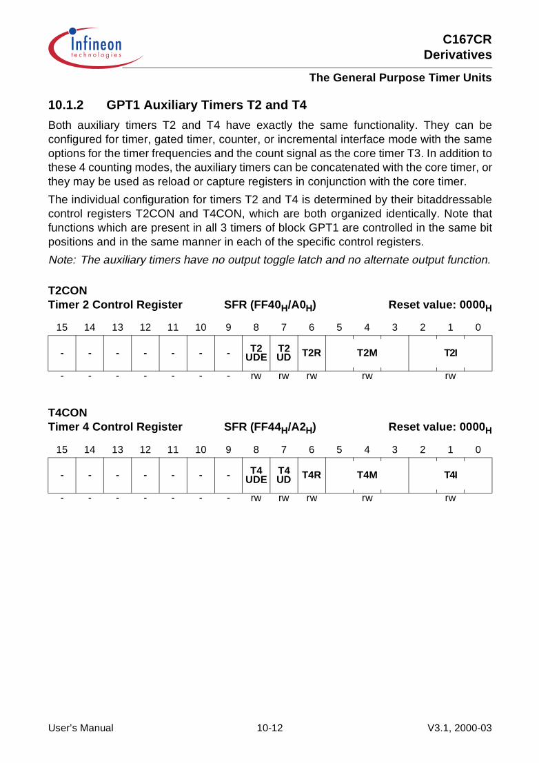
C167CRDerivatives
The General Purpose Timer Units
10.1.2 GPT1 Auxiliary Timers T2 and T4
Both auxiliary timers T2 and T4 have exactly the same functionality. They can beconfigured for timer, gated timer, counter, or incremental interface mode with the sameoptions for the timer frequencies and the count signal as the core timer T3. In addition tothese 4 counting modes, the auxiliary timers can be concatenated with the core timer, orthey may be used as reload or capture registers in conjunction with the core timer.
The individual configuration for timers T2 and T4 is determined by their bitaddressablecontrol registers T2CON and T4CON, which are both organized identically. Note thatfunctions which are present in all 3 timers of block GPT1 are controlled in the same bitpositions and in the same manner in each of the specific control registers.
Note: The auxiliary timers have no output toggle latch and no alternate output function.
T2CONTimer 2 Control Register SFR (FF40H/A0H) Reset value: 0000H
15 14 13 12 11 10 9 8 7 6 5 4 3 2 1 0
- - - - - - - T2UDE
T2UD T2R T2M T2I
- - - - - - - rw rw rw rw rw
T4CONTimer 4 Control Register SFR (FF44H/A2H) Reset value: 0000H
15 14 13 12 11 10 9 8 7 6 5 4 3 2 1 0
- - - - - - - T4UDE
T4UD T4R T4M T4I
- - - - - - - rw rw rw rw rw
User’s Manual 10-12 V3.1, 2000-03

C167CRDerivatives
The General Purpose Timer Units
Count Direction Control for Auxiliary Timers
The count direction of the auxiliary timers can be controlled in the same way as for thecore timer T3. The description and the table apply accordingly.
Timers T2 and T4 in Timer Mode or Gated Timer Mode
When the auxiliary timers T2 and T4 are programmed to timer mode or gated timermode, their operation is the same as described for the core timer T3. The descriptions,figures and tables apply accordingly with one exception:
• There is no output toggle latch for T2 and T4.
Timers T2 and T4 in Incremental Interface Mode
When the auxiliary timers T2 and T4 are programmed to incremental interface mode,their operation is the same as described for the core timer T3. The descriptions, figuresand tables apply accordingly.
Bit Function
TxI Timer x Input SelectionDepends on the Operating Mode, see respective sections.
TxM Timer x Mode Control (Basic Operating Mode)000: Timer Mode001: Counter Mode010: Gated Timer with Gate active low011: Gated Timer with Gate active high100: Reload Mode101: Capture Mode110: Incremental Interface Mode111: Reserved. Do not use this combination.
TxR Timer x Run Bit0: Timer/Counter x stops1: Timer/Counter x runs
TxUD Timer x Up/Down Control1)
TxUDE Timer x External Up/Down Enable1) 1) For the effects of bits TxUD and TxUDE refer to Table 10-1 (see T3 section).
User’s Manual 10-13 V3.1, 2000-03
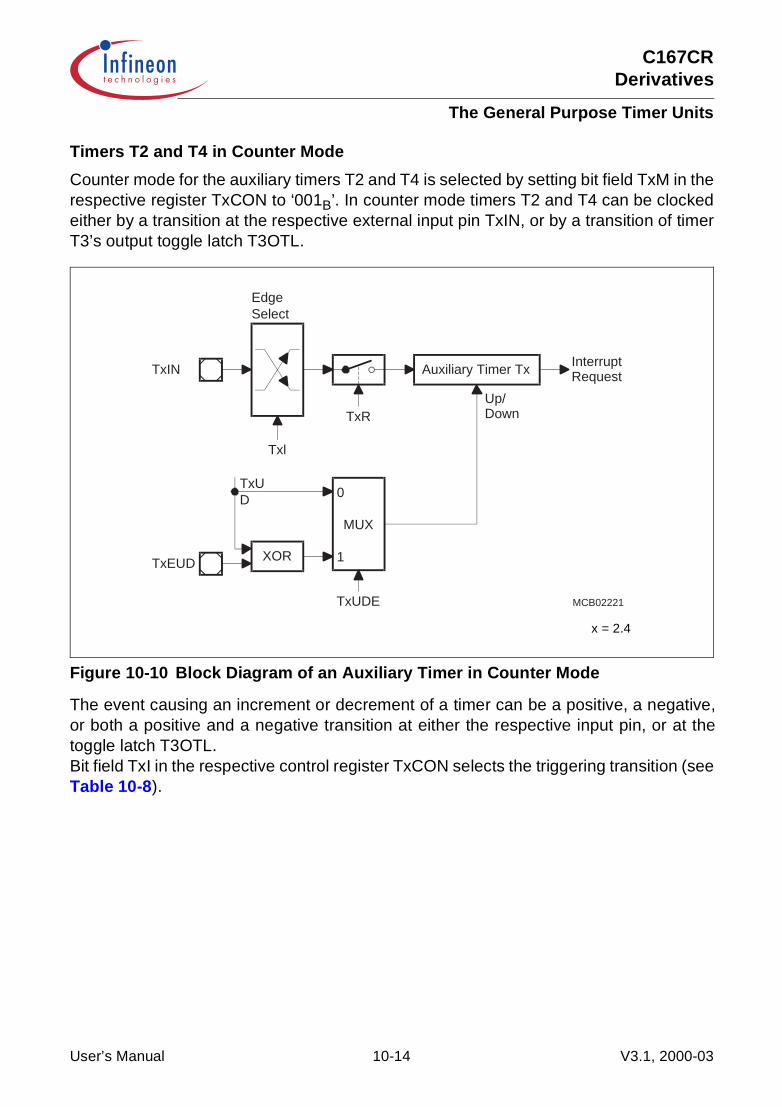
C167CRDerivatives
The General Purpose Timer Units
Timers T2 and T4 in Counter Mode
Counter mode for the auxiliary timers T2 and T4 is selected by setting bit field TxM in therespective register TxCON to ‘001B’. In counter mode timers T2 and T4 can be clockedeither by a transition at the respective external input pin TxIN, or by a transition of timerT3’s output toggle latch T3OTL.
Figure 10-10 Block Diagram of an Auxiliary Timer in Counter Mode
The event causing an increment or decrement of a timer can be a positive, a negative,or both a positive and a negative transition at either the respective input pin, or at thetoggle latch T3OTL.Bit field TxI in the respective control register TxCON selects the triggering transition (seeTable 10-8).
Auxiliary Timer TxInterruptRequest
TxR
XOR
0
MUX
1TxEUD
TxUDE MCB02221
TxUD
Txl
TxIN
EdgeSelect
Up/Down
x = 2.4
User’s Manual 10-14 V3.1, 2000-03

C167CRDerivatives
The General Purpose Timer Units
Note: Only state transitions of T3OTL which are caused by the overflows/underflows ofT3 will trigger the counter function of T2/T4. Modifications of T3OTL via softwarewill NOT trigger the counter function of T2/T4.
For counter operation, pin TxIN must be configured as input, i.e. the respective directioncontrol bit must be ‘0’. The maximum input frequency which is allowed in counter modeis fCPU/16. To ensure that a transition of the count input signal which is applied to TxINis correctly recognized, its level should be held for at least 8 fCPU cycles before itchanges.
Table 10-8 GPT1 Auxiliary Timer (Counter Mode) Input Edge Selection
T2I/T4I Triggering Edge for Counter Increment/Decrement
X 0 0 None. Counter Tx is disabled
0 0 1 Positive transition (rising edge) on TxIN
0 1 0 Negative transition (falling edge) on TxIN
0 1 1 Any transition (rising or falling edge) on TxIN
1 0 1 Positive transition (rising edge) of output toggle latch T3OTL
1 1 0 Negative transition (falling edge) of output toggle latch T3OTL
1 1 1 Any transition (rising or falling edge) of output toggle latch T3OTL
User’s Manual 10-15 V3.1, 2000-03

C167CRDerivatives
The General Purpose Timer Units
Timer Concatenation
Using the toggle bit T3OTL as a clock source for an auxiliary timer in counter modeconcatenates the core timer T3 with the respective auxiliary timer. Depending on whichtransition of T3OTL is selected to clock the auxiliary timer, this concatenation forms a 32-bit or a 33-bit timer/counter.
• 32-bit Timer/Counter: If both a positive and a negative transition of T3OTL is used toclock the auxiliary timer, this timer is clocked on every overflow/underflow of the coretimer T3. Thus, the two timers form a 32-bit timer.
• 33-bit Timer/Counter: If either a positive or a negative transition of T3OTL is selectedto clock the auxiliary timer, this timer is clocked on every second overflow/underflowof the core timer T3. This configuration forms a 33-bit timer (16-bit core timer + T3OTL+ 16-bit auxiliary timer).
The count directions of the two concatenated timers are not required to be the same.This offers a wide variety of different configurations.T3 can operate in timer, gated timer or counter mode in this case.
Figure 10-11 Concatenation of Core Timer T3 and an Auxiliary Timer
Core Timer Ty TyOTL
InterruptRequest
TyOE
TyOUT
TyR
2n : 1
Tyl
MCB02034
fCPU
Up/Down
Auxiliary Timer Tx
TxR
Txl
EdgeSelect
TxIRInterruptRequest
*)
*) Note: Line only affected by over/underflows of T3, but NOT by software modifications of T3OTL.
T3OUT = P3.3 x = 2.4, y = 3
User’s Manual 10-16 V3.1, 2000-03
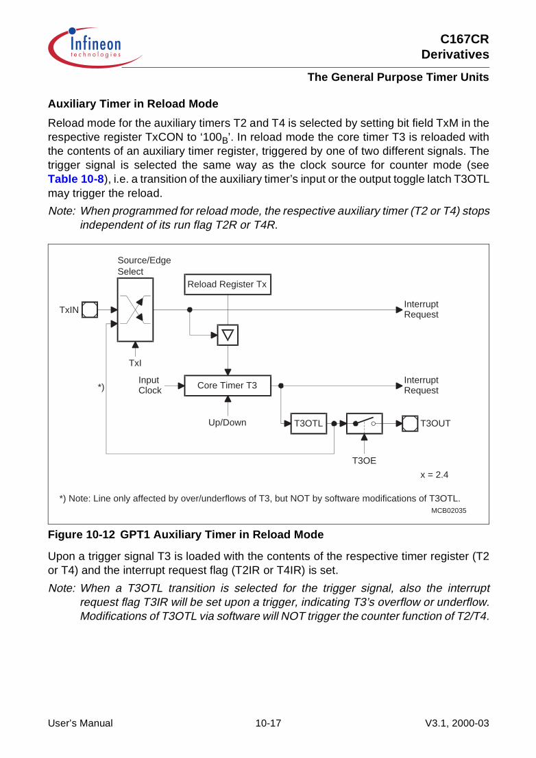
C167CRDerivatives
The General Purpose Timer Units
Auxiliary Timer in Reload Mode
Reload mode for the auxiliary timers T2 and T4 is selected by setting bit field TxM in therespective register TxCON to ‘100B’. In reload mode the core timer T3 is reloaded withthe contents of an auxiliary timer register, triggered by one of two different signals. Thetrigger signal is selected the same way as the clock source for counter mode (seeTable 10-8), i.e. a transition of the auxiliary timer’s input or the output toggle latch T3OTLmay trigger the reload.
Note: When programmed for reload mode, the respective auxiliary timer (T2 or T4) stopsindependent of its run flag T2R or T4R.
Figure 10-12 GPT1 Auxiliary Timer in Reload Mode
Upon a trigger signal T3 is loaded with the contents of the respective timer register (T2or T4) and the interrupt request flag (T2IR or T4IR) is set.
Note: When a T3OTL transition is selected for the trigger signal, also the interruptrequest flag T3IR will be set upon a trigger, indicating T3’s overflow or underflow.Modifications of T3OTL via software will NOT trigger the counter function of T2/T4.
Reload Register Tx
Core Timer T3
Up/Down
Source/EdgeSelect
T3OTL
InterruptRequest
T3OE
T3OUT
TxIN
InputClock
TxI
InterruptRequest
MCB02035
*) Note: Line only affected by over/underflows of T3, but NOT by software modifications of T3OTL.
x = 2.4
*)
User’s Manual 10-17 V3.1, 2000-03
C167CRDerivatives
The General Purpose Timer Units
The reload mode triggered by T3OTL can be used in a number of differentconfigurations. Depending on the selected active transition the following functions canbe performed:
• If both a positive and a negative transition of T3OTL is selected to trigger a reload, thecore timer will be reloaded with the contents of the auxiliary timer each time itoverflows or underflows. This is the standard reload mode (reload on overflow/underflow).
• If either a positive or a negative transition of T3OTL is selected to trigger a reload, thecore timer will be reloaded with the contents of the auxiliary timer on every secondoverflow or underflow.
• Using this “single-transition” mode for both auxiliary timers allows to perform veryflexible pulse width modulation (PWM). One of the auxiliary timers is programmed toreload the core timer on a positive transition of T3OTL, the other is programmed for areload on a negative transition of T3OTL. With this combination the core timer isalternately reloaded from the two auxiliary timers.
Figure 10-13 shows an example for the generation of a PWM signal using the alternatereload mechanism. T2 defines the high time of the PWM signal (reloaded on positivetransitions) and T4 defines the low time of the PWM signal (reloaded on negativetransitions). The PWM signal can be output on T3OUT with T3OE = ‘1’, port latch = ‘1’and direction bit = ‘1’. With this method the high and low time of the PWM signal can bevaried in a wide range.
Note: The output toggle latch T3OTL is accessible via software and may be changed, ifrequired, to modify the PWM signal.However, this will NOT trigger the reloading of T3.
User’s Manual 10-18 V3.1, 2000-03
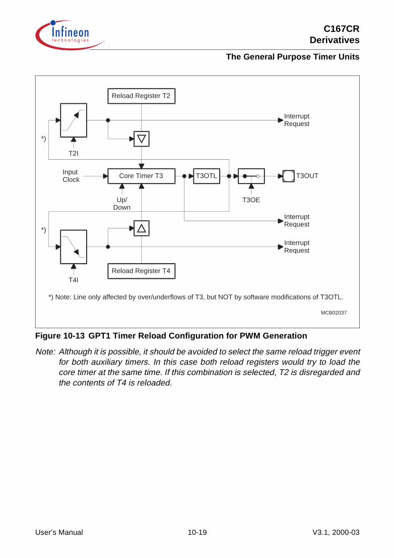
C167CRDerivatives
The General Purpose Timer Units
Figure 10-13 GPT1 Timer Reload Configuration for PWM Generation
Note: Although it is possible, it should be avoided to select the same reload trigger eventfor both auxiliary timers. In this case both reload registers would try to load thecore timer at the same time. If this combination is selected, T2 is disregarded andthe contents of T4 is reloaded.
Core Timer T3
Up/Down
T3OTL
InterruptRequest
T3OE
T3OUT
InterruptRequest
Reload Register T2
InterruptRequest
Reload Register T4
T2I
T4I
InputClock
MCB02037
*) Note: Line only affected by over/underflows of T3, but NOT by software modifications of T3OTL.
*)
*)
User’s Manual 10-19 V3.1, 2000-03
C167CRDerivatives
The General Purpose Timer Units
Auxiliary Timer in Capture Mode
Capture mode for the auxiliary timers T2 and T4 is selected by setting bit field TxM in therespective register TxCON to ‘101B’. In capture mode the contents of the core timer arelatched into an auxiliary timer register in response to a signal transition at the respectiveauxiliary timer’s external input pin TxIN. The capture trigger signal can be a positive, anegative, or both a positive and a negative transition.
The two least significant bits of bit field TxI are used to select the active transition (seeTable 10-8), while the most significant bit TxI.2 is irrelevant for capture mode. It isrecommended to keep this bit cleared (TxI.2 = ‘0’).
Note: When programmed for capture mode, the respective auxiliary timer (T2 or T4)stops independent of its run flag T2R or T4R.
Figure 10-14 GPT1 Auxiliary Timer in Capture Mode
Upon a trigger (selected transition) at the corresponding input pin TxIN the contents ofthe core timer are loaded into the auxiliary timer register and the associated interruptrequest flag TxIR will be set.
Note: The direction control bits for T2IN and T4IN must be set to ‘0’, and the level of thecapture trigger signal should be held high or low for at least 8 fCPU cycles beforeit changes to ensure correct edge detection.
Capture Register Tx
Core Timer T3
Up/Down
EdgeSelect
T3OTL
InterruptRequest
T3OE
T3OUT
TxIN
InputClock
InterruptRequest
MCB02038
TxI
x = 2.4
User’s Manual 10-20 V3.1, 2000-03

C167CRDerivatives
The General Purpose Timer Units
10.1.3 Interrupt Control for GPT1 Timers
When a timer overflows from FFFFH to 0000H (when counting up), or when it underflowsfrom 0000H to FFFFH (when counting down), its interrupt request flag (T2IR, T3IR orT4IR) in register TxIC will be set. This will cause an interrupt to the respective timerinterrupt vector (T2INT, T3INT or T4INT) or trigger a PEC service, if the respectiveinterrupt enable bit (T2IE, T3IE or T4IE in register TxIC) is set. There is an interruptcontrol register for each of the three timers.
Note: Please refer to the general Interrupt Control Register description for anexplanation of the control fields.
T2ICTimer 2 Intr. Ctrl. Reg. SFR (FF60H/B0H) Reset value: - - 00H
15 14 13 12 11 10 9 8 7 6 5 4 3 2 1 0
- T2IR T2IE ILVL GLVL
- - - - - - - - rwh rw rw rw
T3ICTimer 3 Intr. Ctrl. Reg. SFR (FF62H/B1H) Reset value: - - 00H
15 14 13 12 11 10 9 8 7 6 5 4 3 2 1 0
- T3IR T3IE ILVL GLVL
- - - - - - - - rwh rw rw rw
T4ICTimer 4 Intr. Ctrl. Reg. SFR (FF64H/B2H) Reset value: - - 00H
15 14 13 12 11 10 9 8 7 6 5 4 3 2 1 0
- T4IR T4IE ILVL GLVL
- - - - - - - - rwh rw rw rw
User’s Manual 10-21 V3.1, 2000-03

C167CRDerivatives
The General Purpose Timer Units
10.2 Timer Block GPT2
From a programmer’s point of view, the GPT2 block is represented by a set of SFRs assummarized below. Those portions of port and direction registers which are used foralternate functions by the GPT2 block are shaded.
Figure 10-15 SFRs and Port Pins Associated with Timer Block GPT2
Timer block GPT2 supports high precision event control with a maximum resolution of8 TCL. It includes the two timers T5 and T6, and the 16-bit capture/reload registerCAPREL. Timer T6 is referred to as the core timer, and T5 is referred to as the auxiliarytimer of GPT2.
Each timer has an alternate input function pin associated with it which serves as the gatecontrol in gated timer mode, or as the count input in counter mode. The count direction(Up/Down) may be programmed via software. An overflow/underflow of T6 is indicatedby the output toggle bit T6OTL whose state may be output on an alternate function portpin (T6OUT). In addition, T6 may be reloaded with the contents of CAPREL.
The toggle bit also supports the concatenation of T6 with auxiliary timer T5, whileconcatenation of T6 with the timers of the CAPCOM units is provided through a directconnection. Triggered by an external signal, the contents of T5 can be captured intoregister CAPREL, and T5 may optionally be cleared. Both timer T6 and T5 can count upor down, and the current timer value can be read or modified by the CPU in the non-bitaddressable SFRs T5 and T6.
E
MCA04375
ODP3
DP3
P3
T5
T6
CAPREL
T5CON T5IC
CRIC
Ports & Direction ControlAlternate Functions
Data Registers Control Registers Interrupt Control
ODP3 Port 3 Open Drain Control RegisterDP3 Port 3 Direction Control RegisterP3 Port 3 Data RegisterP5 Port 5 Data RegisterP5DIDIS Port 5 Digital Input Disable RegisterT5CONGPT2 Timer 5 Control RegisterT6CONGPT2 Timer 6 Control Register
T5 GPT2 Timer 5 RegisterT6 GPT2 Timer 6 RegisterCAPRELGPT2 Capture/Reload RegisterT5ICGPT2 Timer 5 Interrupt Control RegisterT6ICGPT2 Timer 6 Interrupt Control RegisterCRICGPT2 CAPREL Interrupt Control Register
T6IC
T5IN/P5.13 T5EUD/P5.11T6IN/P5.12 T6EUD/P5.10CAPIN/P3.2 T6OUT/P3.1
P5
T6CON
P5DIDIS
User’s Manual 10-22 V3.1, 2000-03

C167CRDerivatives
The General Purpose Timer Units
Figure 10-16 GPT2 Block Diagram
MUX
2n : 1fCPU T5Mode
Control
2n : 1fCPU
T6Mode
Control
T6OTL
T5EUD
T5IN
T3
CAPIN
T6IN
T6EUD
T6OUT
U/D
U/D
InterruptRequest
InterruptRequest
InterruptRequest
OtherTimers
Clear
Capture
CT3
MCB03999
GPT2 Timer T5
GPT2 CAPREL
GPT2 Timer T6
User’s Manual 10-23 V3.1, 2000-03
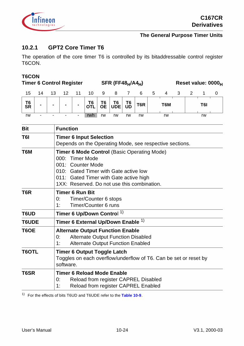
C167CRDerivatives
The General Purpose Timer Units
10.2.1 GPT2 Core Timer T6
The operation of the core timer T6 is controlled by its bitaddressable control registerT6CON.
T6CONTimer 6 Control Register SFR (FF48H/A4H) Reset value: 0000H
15 14 13 12 11 10 9 8 7 6 5 4 3 2 1 0
T6 SR - - - - T6
OTLT6 OE
T6 UDE
T6 UD T6R T6M T6I
rw - - - - rwh rw rw rw rw rw rw
Bit Function
T6I Timer 6 Input SelectionDepends on the Operating Mode, see respective sections.
T6M Timer 6 Mode Control (Basic Operating Mode)000: Timer Mode001: Counter Mode010: Gated Timer with Gate active low011: Gated Timer with Gate active high1XX: Reserved. Do not use this combination.
T6R Timer 6 Run Bit0: Timer/Counter 6 stops1: Timer/Counter 6 runs
T6UD Timer 6 Up/Down Control 1)
1) For the effects of bits T6UD and T6UDE refer to the Table 10-9.
T6UDE Timer 6 External Up/Down Enable 1)
T6OE Alternate Output Function Enable0: Alternate Output Function Disabled1: Alternate Output Function Enabled
T6OTL Timer 6 Output Toggle LatchToggles on each overflow/underflow of T6. Can be set or reset by software.
T6SR Timer 6 Reload Mode Enable0: Reload from register CAPREL Disabled1: Reload from register CAPREL Enabled
User’s Manual 10-24 V3.1, 2000-03
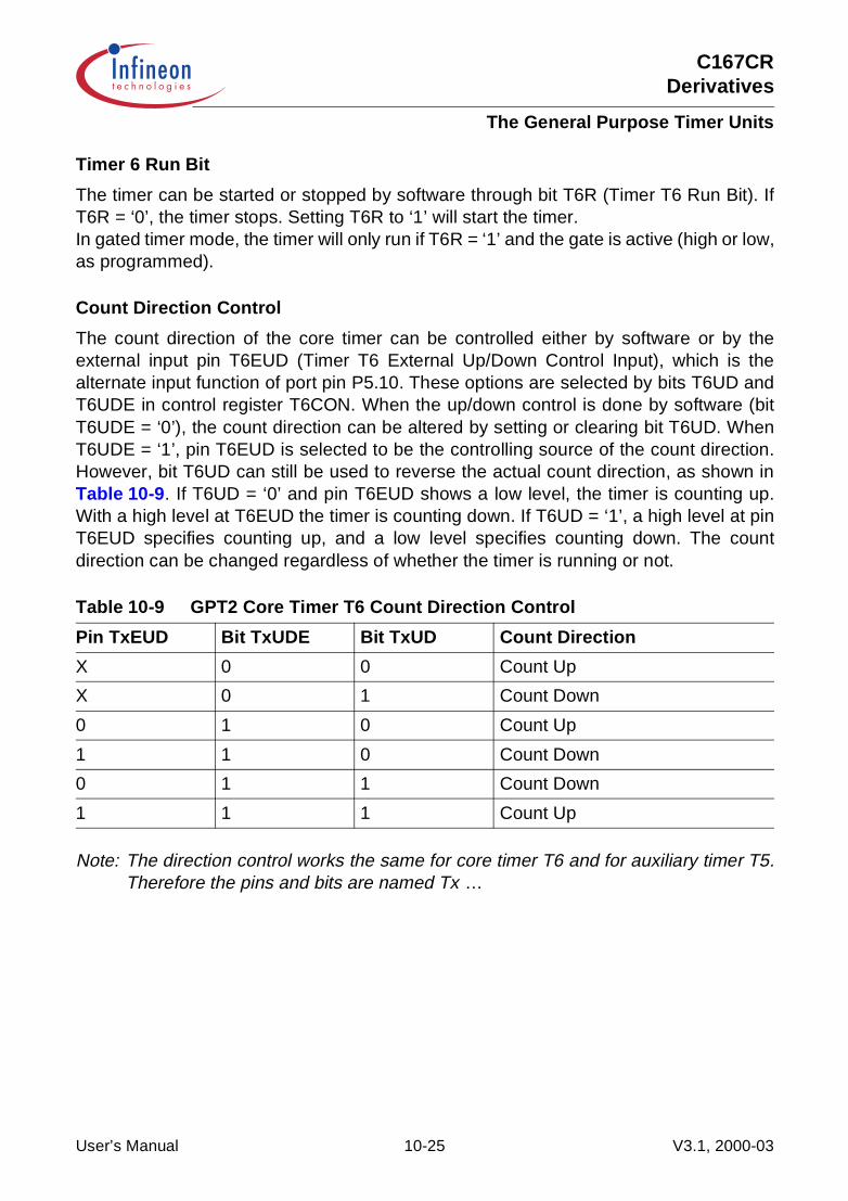
C167CRDerivatives
The General Purpose Timer Units
Timer 6 Run Bit
The timer can be started or stopped by software through bit T6R (Timer T6 Run Bit). IfT6R = ‘0’, the timer stops. Setting T6R to ‘1’ will start the timer.In gated timer mode, the timer will only run if T6R = ‘1’ and the gate is active (high or low,as programmed).
Count Direction Control
The count direction of the core timer can be controlled either by software or by theexternal input pin T6EUD (Timer T6 External Up/Down Control Input), which is thealternate input function of port pin P5.10. These options are selected by bits T6UD andT6UDE in control register T6CON. When the up/down control is done by software (bitT6UDE = ‘0’), the count direction can be altered by setting or clearing bit T6UD. WhenT6UDE = ‘1’, pin T6EUD is selected to be the controlling source of the count direction.However, bit T6UD can still be used to reverse the actual count direction, as shown inTable 10-9. If T6UD = ‘0’ and pin T6EUD shows a low level, the timer is counting up.With a high level at T6EUD the timer is counting down. If T6UD = ‘1’, a high level at pinT6EUD specifies counting up, and a low level specifies counting down. The countdirection can be changed regardless of whether the timer is running or not.
Note: The direction control works the same for core timer T6 and for auxiliary timer T5.Therefore the pins and bits are named Tx …
Table 10-9 GPT2 Core Timer T6 Count Direction Control
Pin TxEUD Bit TxUDE Bit TxUD Count Direction
X 0 0 Count Up
X 0 1 Count Down
0 1 0 Count Up
1 1 0 Count Down
0 1 1 Count Down
1 1 1 Count Up
User’s Manual 10-25 V3.1, 2000-03

C167CRDerivatives
The General Purpose Timer Units
Timer 6 Output Toggle Latch
An overflow or underflow of timer T6 will clock the toggle bit T6OTL in control registerT6CON. T6OTL can also be set or reset by software. Bit T6OE (Alternate OutputFunction Enable) in register T6CON enables the state of T6OTL to be an alternatefunction of the external output pin T6OUT. For that purpose, a ‘1’ must be written into therespective port data latch and pin T6OUT must be configured as output by setting therespective direction control bit to ‘1’. If T6OE = ‘1’, pin T6OUT then outputs the state ofT6OTL. If T6OE = ‘0’ pin T6OUT can be used as general purpose IO pin.
In addition, T6OTL can be used in conjunction with the timer over/underflows as an inputfor the counter function of the auxiliary timer T5. For this purpose, the state of T6OTLdoes not have to be available at pin T6OUT, because an internal connection is providedfor this option.An overflow or underflow of timer T6 can also be used to clock the timers in the CAPCOMunits. For this purpose, there is a direct internal connection between timer T6 and theCAPCOM timers.
Timer 6 in Timer Mode
Timer mode for the core timer T6 is selected by setting bitfield T6M in register T6CONto ‘000B’. In this mode, T6 is clocked with the internal system clock divided by aprogrammable prescaler, which is selected by bit field T6I. The input frequency fT6 fortimer T6 and its resolution rT6 are scaled linearly with lower clock frequencies fCPU, ascan be seen from the following formula:
Figure 10-17 Block Diagram of Core Timer T6 in Timer Mode
fT6 =fCPU
4 × 2<T6I>rT6 [µs] =
fCPU [MHz]4 × 2<T6I>
,
Core Timer Tx
TxOTL
InterruptRequest
TxOE
TxOUTTxR
2n : 1
Txl
EXOR
0
MUX
1TxEUD
TxUDE MCB02028
TxUD
fCPU
Up/Down
T6EUD = P5.10T6OUT = P3.1 x = 6
User’s Manual 10-26 V3.1, 2000-03
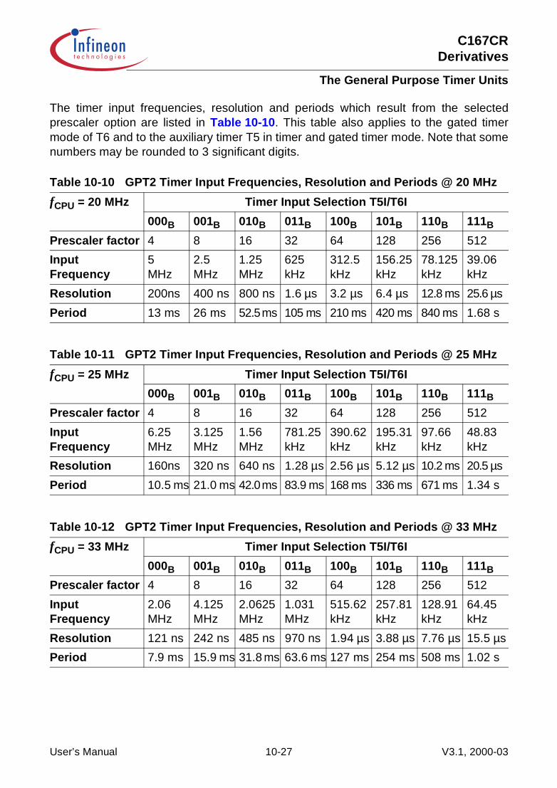
C167CRDerivatives
The General Purpose Timer Units
The timer input frequencies, resolution and periods which result from the selectedprescaler option are listed in Table 10-10. This table also applies to the gated timermode of T6 and to the auxiliary timer T5 in timer and gated timer mode. Note that somenumbers may be rounded to 3 significant digits.
Table 10-10 GPT2 Timer Input Frequencies, Resolution and Periods @ 20 MHz
fCPU = 20 MHz Timer Input Selection T5I/T6I
000B 001B 010B 011B 100B 101B 110B 111B
Prescaler factor 4 8 16 32 64 128 256 512
Input Frequency
5MHz
2.5MHz
1.25MHz
625kHz
312.5kHz
156.25kHz
78.125kHz
39.06kHz
Resolution 200ns 400 ns 800 ns 1.6 µs 3.2 µs 6.4 µs 12.8 ms 25.6 µs
Period 13 ms 26 ms 52.5 ms 105 ms 210 ms 420 ms 840 ms 1.68 s
Table 10-11 GPT2 Timer Input Frequencies, Resolution and Periods @ 25 MHz
fCPU = 25 MHz Timer Input Selection T5I/T6I
000B 001B 010B 011B 100B 101B 110B 111B
Prescaler factor 4 8 16 32 64 128 256 512
Input Frequency
6.25MHz
3.125MHz
1.56MHz
781.25kHz
390.62kHz
195.31kHz
97.66kHz
48.83kHz
Resolution 160ns 320 ns 640 ns 1.28 µs 2.56 µs 5.12 µs 10.2 ms 20.5 µs
Period 10.5 ms 21.0 ms 42.0 ms 83.9 ms 168 ms 336 ms 671 ms 1.34 s
Table 10-12 GPT2 Timer Input Frequencies, Resolution and Periods @ 33 MHz
fCPU = 33 MHz Timer Input Selection T5I/T6I
000B 001B 010B 011B 100B 101B 110B 111B
Prescaler factor 4 8 16 32 64 128 256 512
Input Frequency
2.06MHz
4.125MHz
2.0625MHz
1.031MHz
515.62kHz
257.81kHz
128.91kHz
64.45kHz
Resolution 121 ns 242 ns 485 ns 970 ns 1.94 µs 3.88 µs 7.76 µs 15.5 µs
Period 7.9 ms 15.9 ms 31.8 ms 63.6 ms 127 ms 254 ms 508 ms 1.02 s
User’s Manual 10-27 V3.1, 2000-03
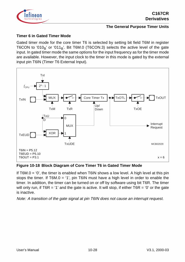
C167CRDerivatives
The General Purpose Timer Units
Timer 6 in Gated Timer Mode
Gated timer mode for the core timer T6 is selected by setting bit field T6M in registerT6CON to ‘010B’ or ‘011B’. Bit T6M.0 (T6CON.3) selects the active level of the gateinput. In gated timer mode the same options for the input frequency as for the timer modeare available. However, the input clock to the timer in this mode is gated by the externalinput pin T6IN (Timer T6 External Input).
Figure 10-18 Block Diagram of Core Timer T6 in Gated Timer Mode
If T6M.0 = ‘0’, the timer is enabled when T6IN shows a low level. A high level at this pinstops the timer. If T6M.0 = ‘1’, pin T6IN must have a high level in order to enable thetimer. In addition, the timer can be turned on or off by software using bit T6R. The timerwill only run, if T6R = ‘1’ and the gate is active. It will stop, if either T6R = ‘0’ or the gateis inactive.
Note: A transition of the gate signal at pin T6IN does not cause an interrupt request.
MUX Core Timer Tx TxOTL
InterruptRequest
TxOE
TxOUT
TxR
XOR
0
MUX
1
Up/Down
TxEUD
TxUDE MCB02029
TxUD
2n : 1
TxI
fCPU
TxM
TxIN
T6IN = P5.12T6EUD = P5.10T6OUT = P3.1 x = 6
User’s Manual 10-28 V3.1, 2000-03
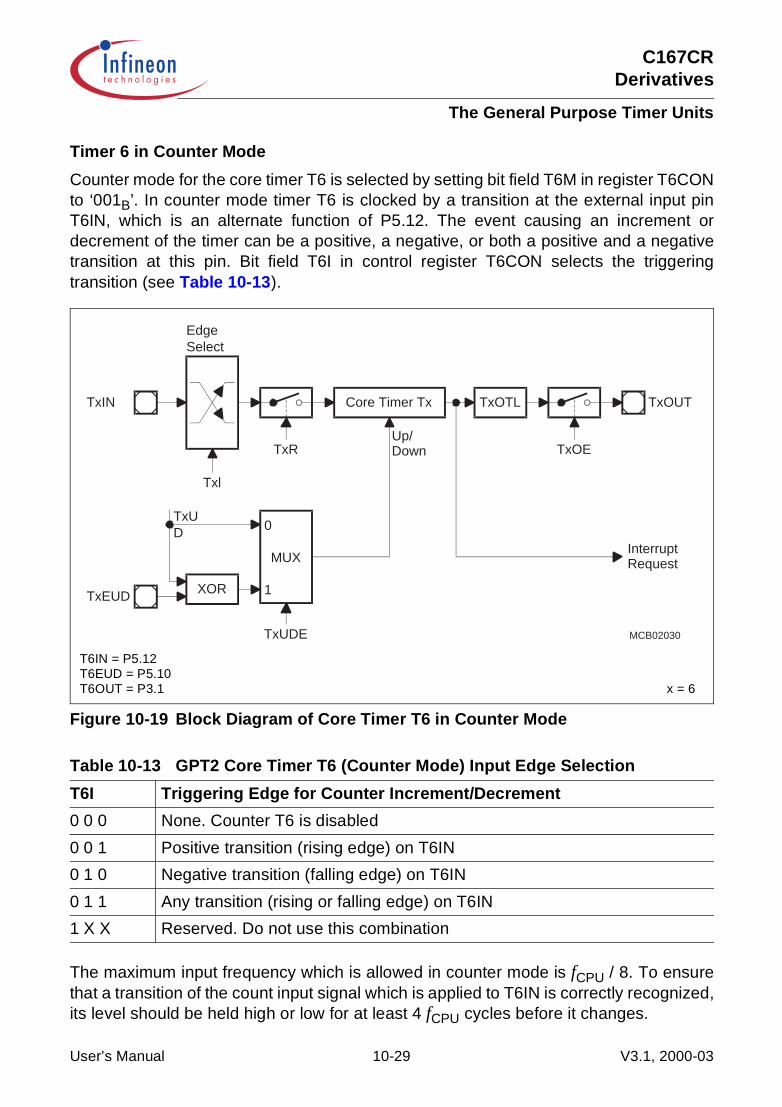
C167CRDerivatives
The General Purpose Timer Units
Timer 6 in Counter Mode
Counter mode for the core timer T6 is selected by setting bit field T6M in register T6CONto ‘001B’. In counter mode timer T6 is clocked by a transition at the external input pinT6IN, which is an alternate function of P5.12. The event causing an increment ordecrement of the timer can be a positive, a negative, or both a positive and a negativetransition at this pin. Bit field T6I in control register T6CON selects the triggeringtransition (see Table 10-13).
Figure 10-19 Block Diagram of Core Timer T6 in Counter Mode
The maximum input frequency which is allowed in counter mode is fCPU / 8. To ensurethat a transition of the count input signal which is applied to T6IN is correctly recognized,its level should be held high or low for at least 4 fCPU cycles before it changes.
Table 10-13 GPT2 Core Timer T6 (Counter Mode) Input Edge Selection
T6I Triggering Edge for Counter Increment/Decrement
0 0 0 None. Counter T6 is disabled
0 0 1 Positive transition (rising edge) on T6IN
0 1 0 Negative transition (falling edge) on T6IN
0 1 1 Any transition (rising or falling edge) on T6IN
1 X X Reserved. Do not use this combination
Core Timer Tx
TxR
XOR
0
MUX
1
Up/Down
TxEUD
TxUDE MCB02030
TxUD
Txl
TxIN
EdgeSelect
TxOTL
TxOE
TxOUT
InterruptRequest
T6IN = P5.12T6EUD = P5.10T6OUT = P3.1 x = 6
User’s Manual 10-29 V3.1, 2000-03

C167CRDerivatives
The General Purpose Timer Units
10.2.2 GPT2 Auxiliary Timer T5
The auxiliary timer T5 can be configured for timer, gated timer or counter mode with thesame options for the timer frequencies and the count signal as the core timer T6. Inaddition the auxiliary timer can be concatenated with the core timer (operation in countermode). Its contents may be captured to register CAPREL upon a selectable trigger.
The individual configuration for timer T5 is determined by its bitaddressable controlregister T5CON. Note that functions which are present in both timers of block GPT2 arecontrolled in the same bit positions and in the same manner in each of the specific controlregisters.
Note: The auxiliary timer has no output toggle latch and no alternate output function.
T5CON Timer 5 Control Register SFR (FF46H/A3H) Reset value: 0000H
15 14 13 12 11 10 9 8 7 6 5 4 3 2 1 0
T5 SC
T5 CLR CI - CT3 - T5
UDET5 UD T5R T5M T5I
rw rw rw - rw - rw rw rw rw rw
Bit Function
T5I Timer 5 Input SelectionDepends on the Operating Mode, see respective sections.
T5M Timer 5 Mode Control (Basic Operating Mode)000: Timer Mode001: Counter Mode010: Gated Timer with Gate active low011: Gated Timer with Gate active high1XX: Reserved. Do not use this combination.
T5R Timer 5 Run Bit0: Timer / Counter 5 stops1: Timer / Counter 5 runs
T5UD Timer 5 Up / Down Control *)
T5UDE Timer 5 External Up/Down Enable *)
CT3 Timer 3 Capture Trigger Enable0: Capture trigger from pin CAPIN1: Capture trigger from T3 input pins
User’s Manual 10-30 V3.1, 2000-03

C167CRDerivatives
The General Purpose Timer Units
*) For the effects of bits T5UD and T5UDE refer to the direction table (see T6 section).
Count Direction Control for Auxiliary Timer
The count direction of the auxiliary timer can be controlled in the same way as for thecore timer T6. The description and the table apply accordingly.
Timer T5 in Timer Mode or Gated Timer Mode
When the auxiliary timer T5 is programmed to timer mode or gated timer mode, itsoperation is the same as described for the core timer T6. The descriptions, figures andtables apply accordingly with one exception:
• There is no output toggle latch for T5.
Timer T5 in Counter Mode
Counter mode for the auxiliary timer T5 is selected by setting bit field T5M in registerT5CON to ‘001B’. In counter mode timer T5 can be clocked either by a transition at theexternal input pin T5IN, or by a transition of timer T6’s output toggle latch T6OTL (i.e.timer concatenation).
CI Register CAPREL Capture Trigger Selection (depending on bit CT3)00: Capture disabled01: Positive transition (rising edge) on CAPIN or
any transition on T3IN10: Negative transition (falling edge) on CAPIN or
any transition on T3EUD11: Any transition (rising or falling edge) on CAPIN or
any transition on T3IN or T3EUD
T5CLR Timer 5 Clear Bit0: Timer 5 not cleared on a capture1: Timer 5 is cleared on a capture
T5SC Timer 5 Capture Mode Enable0: Capture into register CAPREL disabled1: Capture into register CAPREL enabled
Bit Function
User’s Manual 10-31 V3.1, 2000-03

C167CRDerivatives
The General Purpose Timer Units
Figure 10-20 Block Diagram of Auxiliary Timer T5 in Counter Mode
The event causing an increment or decrement of the timer can be a positive, a negative,or both a positive and a negative transition at either the input pin, or at the toggle latchT6OTL.Bitfield T5I in control register T5CON selects the triggering transition (see Table 10-14).
Note: Only state transitions of T6OTL which are caused by the overflows/underflows ofT6 will trigger the counter function of T5. Modifications of T6OTL via software willNOT trigger the counter function of T5.
The maximum input frequency which is allowed in counter mode is fCPU / 8. To ensurethat a transition of the count input signal which is applied to T5IN is correctly recognized,its level should be held high or low for at least 4 fCPU cycles before it changes.
Table 10-14 GPT2 Auxiliary Timer (Counter Mode) Input Edge Selection
T5I Triggering Edge for Counter Increment/Decrement
X 0 0 None. Counter T5 is disabled
0 0 1 Positive transition (rising edge) on T5IN
0 1 0 Negative transition (falling edge) on T5IN
0 1 1 Any transition (rising or falling edge) on T5IN
1 0 1 Positive transition (rising edge) of output toggle latch T6OTL
1 1 0 Negative transition (falling edge) of output toggle latch T6OTL
1 1 1 Any transition (rising or falling edge) of output toggle latch T6OTL
Auxiliary Timer TxInterruptRequest
TxR
XOR
0
MUX
1TxEUD
TxUDE MCB02221
TxUD
Txl
TxIN
EdgeSelect
Up/Down
x = 5
User’s Manual 10-32 V3.1, 2000-03

C167CRDerivatives
The General Purpose Timer Units
Timer Concatenation
Using the toggle bit T6OTL as a clock source for the auxiliary timer in counter modeconcatenates the core timer T6 with the auxiliary timer. Depending on which transition ofT6OTL is selected to clock the auxiliary timer, this concatenation forms a 32-bit or a 33-bit timer/counter.
• 32-bit Timer/Counter: If both a positive and a negative transition of T6OTL is used toclock the auxiliary timer, this timer is clocked on every overflow/underflow of the coretimer T6. Thus, the two timers form a 32-bit timer.
• 33-bit Timer/Counter: If either a positive or a negative transition of T6OTL is selectedto clock the auxiliary timer, this timer is clocked on every second overflow/underflowof the core timer T6. This configuration forms a 33-bit timer (16-bit core timer + T6OTL+ 16-bit auxiliary timer).
The count directions of the two concatenated timers are not required to be the same.This offers a wide variety of different configurations.T6 can operate in timer, gated timer or counter mode in this case.
Figure 10-21 Concatenation of Core Timer T6 and Auxiliary Timer T5
Core Timer Ty TyOTL
InterruptRequest
TyOE
TyOUT
TyR
2n : 1
Tyl
MCB02034
fCPU
Up/Down
Auxiliary Timer Tx
TxR
Txl
EdgeSelect
TxIRInterruptRequest
*)
*) Note: Line only affected by over/underflows of T3, but NOT by software modifications of T3OTL.
T6OUT = P3.1 x = 5, y = 6
User’s Manual 10-33 V3.1, 2000-03

C167CRDerivatives
The General Purpose Timer Units
GPT2 Capture/Reload Register CAPREL in Capture Mode
This 16-bit register can be used as a capture register for the auxiliary timer T5. Thismode is selected by setting bit T5SC = ‘1’ in control register T5CON. Bit CT3 selects theexternal input pin CAPIN or the input pins of timer T3 as the source for a capture trigger.Either a positive, a negative, or both a positive and a negative transition at pin CAPINcan be selected to trigger the capture function, or transitions on input T3IN or inputT3EUD or both inputs T3IN and T3EUD. The active edge is controlled by bit field CI inregister T5CON. The same coding is used as in the two least significant bits of bit fieldT5I (see Table 10-14).
The maximum input frequency for the capture trigger signal at CAPIN is fCPU / 8. Toensure that a transition of the capture trigger signal is correctly recognized, its levelshould be held for at least 4 fCPU cycles before it changes.
Figure 10-22 GPT2 Register CAPREL in Capture Mode
When the timer T3 capture trigger is enabled (CT3 = ‘1’) register CAPREL captures thecontents of T5 upon transitions of the selected input(s). These values can be used tomeasure T3’s input signals. This is useful e.g. when T3 operates in incremental interfacemode, in order to derive dynamic information (speed acceleration) from the input signals.
Auxiliary Timer T5
EdgeSelect
MCB02044B
InterruptRequest
CAPIN
CI
T5SC
T5CLR
InputClock
Up/Down
InterruptRequest
CAPREL Register
User’s Manual 10-34 V3.1, 2000-03

C167CRDerivatives
The General Purpose Timer Units
When a selected transition at the selected input pin(s) (CAPIN, T3IN, T3EUD) isdetected, the contents of the auxiliary timer T5 are latched into register CAPREL, andinterrupt request flag CRIR is set. With the same event, timer T5 can be cleared to0000H. This option is controlled by bit T5CLR in register T5CON. If T5CLR = ‘0’, thecontents of timer T5 are not affected by a capture. If T5CLR = ‘1’, timer T5 is cleared afterthe current timer value has been latched into register CAPREL.
Note: Bit T5SC only controls whether a capture is performed or not. If T5SC = ‘0’, theselected trigger event can still be used to clear timer T5 or to generate an interruptrequest. This interrupt is controlled by the CAPREL interrupt control register CRIC.
GPT2 Capture/Reload Register CAPREL in Reload Mode
This 16-bit register can be used as a reload register for the core timer T6. This mode isselected by setting bit T6SR = ‘1’ in register T6CON. The event causing a reload in thismode is an overflow or underflow of the core timer T6.
When timer T6 overflows from FFFFH to 0000H (when counting up) or when it underflowsfrom 0000H to FFFFH (when counting down), the value stored in register CAPREL isloaded into timer T6. This will not set the interrupt request flag CRIR associated with theCAPREL register. However, interrupt request flag T6IR will be set indicating theoverflow/underflow of T6.
Figure 10-23 GPT2 Register CAPREL in Reload Mode
Core Timer T6
Up/Down
InterruptRequest
T6OE
T6OUT
InputClock
MCB02045
T6OTL
T6SR
CAPREL Register
User’s Manual 10-35 V3.1, 2000-03

C167CRDerivatives
The General Purpose Timer Units
GPT2 Capture/Reload Register CAPREL in Capture-And-Reload Mode
Since the reload function and the capture function of register CAPREL can be enabledindividually by bits T5SC and T6SR, the two functions can be enabled simultaneously bysetting both bits. This feature can be used to generate an output frequency that is amultiple of the input frequency.
Figure 10-24 GPT2 Register CAPREL in Capture-And-Reload Mode
This combined mode can be used to detect consecutive external events which mayoccur aperiodically, but where a finer resolution, that means, more ‘ticks’ within the timebetween two external events is required.
Auxiliary Timer T5
EdgeSelect
MCB02046B
InterruptRequest
CAPIN
CI
T5SC
T5CLR
InputClock
Up/Down
InterruptRequest
CAPREL Register
T6OTL
T6OE
T6OUT
Core Timer T6InterruptRequest
InputClock
T6SR
Up/Down
User’s Manual 10-36 V3.1, 2000-03
C167CRDerivatives
The General Purpose Timer Units
For this purpose, the time between the external events is measured using timer T5 andthe CAPREL register. Timer T5 runs in timer mode counting up with a frequency of e.g.fCPU/32. The external events are applied to pin CAPIN. When an external event occurs,the timer T5 contents are latched into register CAPREL, and timer T5 is cleared(T5CLR = ‘1’). Thus, register CAPREL always contains the correct time between twoevents, measured in timer T5 increments. Timer T6, which runs in timer mode countingdown with a frequency of e.g. fCPU / 4, uses the value in register CAPREL to perform areload on underflow. This means, the value in register CAPREL represents the timebetween two underflows of timer T6, now measured in timer T6 increments. Since timerT6 runs 8 times faster than timer T5, it will underflow 8 times within the time between twoexternal events. Thus, the underflow signal of timer T6 generates 8 ‘ticks’. Upon eachunderflow, the interrupt request flag T6IR will be set and bit T6OTL will be toggled. Thestate of T6OTL may be output on pin T6OUT. This signal has 8 times more transitionsthan the signal which is applied to pin CAPIN.
The underflow signal of timer T6 can furthermore be used to clock one or more of thetimers of the CAPCOM units, which gives the user the possibility to set compare eventsbased on a finer resolution than that of the external events.
User’s Manual 10-37 V3.1, 2000-03

C167CRDerivatives
The General Purpose Timer Units
10.2.3 Interrupt Control for GPT2 Timers and CAPREL
When a timer overflows from FFFFH to 0000H (when counting up), or when it underflowsfrom 0000H to FFFFH (when counting down), its interrupt request flag (T5IR or T6IR) inregister TxIC will be set. Whenever a transition according to the selection in bit field CIis detected at pin CAPIN, interrupt request flag CRIR in register CRIC is set. Setting anyrequest flag will cause an interrupt to the respective timer or CAPREL interrupt vector(T5INT, T6INT or CRINT) or trigger a PEC service, if the respective interrupt enable bit(T5IE or T6IE in register TxIC, CRIE in register CRIC) is set. There is an interrupt controlregister for each of the two timers and for the CAPREL register.
Note: Please refer to the general Interrupt Control Register description for anexplanation of the control fields.
T5ICTimer 5 Intr. Ctrl. Reg. SFR (FF66H/B3H) Reset value: - - 00H
15 14 13 12 11 10 9 8 7 6 5 4 3 2 1 0
- T5IR T5IE ILVL GLVL
- - - - - - - - rwh rw rw RW
T6ICTimer 6 Intr. Ctrl. Reg. SFR (FF68H/B4H) Reset value: - - 00H
15 14 13 12 11 10 9 8 7 6 5 4 3 2 1 0
- T6IR T6IE ILVL GLVL
- - - - - - - - rwh rw rw RW
CRICCAPREL Intr. Ctrl. Reg. SFR (FF6AH/B5H) Reset value: - - 00H
15 14 13 12 11 10 9 8 7 6 5 4 3 2 1 0
- CRIR CRIE ILVL GLVL
- - - - - - - - rwh rw rw RW
User’s Manual 10-38 V3.1, 2000-03

C167CRDerivatives
The Asynchronous/Synchronous Serial Interface
11 The Asynchronous/Synchronous Serial InterfaceThe Asynchronous/Synchronous Serial Interface ASC0 provides serial communicationbetween the C167CR and other microcontrollers, microprocessors or externalperipherals.
The ASC0 supports full-duplex asynchronous communication up to 781 KBaud/1.03 MBaud and half-duplex synchronous communication up to 3.1/4.1 MBaud (@ 25/33 MHz CPU clock). In synchronous mode, data are transmitted or receivedsynchronous to a shift clock which is generated by the C167CR. In asynchronous mode,8- or 9-bit data transfer, parity generation, and the number of stop bits can be selected.Parity, framing, and overrun error detection is provided to increase the reliability of datatransfers. Transmission and reception of data is double-buffered. For multiprocessorcommunication, a mechanism to distinguish address from data bytes is included. Testingis supported by a loop-back option. A 13-bit baud rate generator provides the ASC0 witha separate serial clock signal.
Figure 11-1 SFRs and Port Pins Associated with ASC0
E
MCA04376
ODP3
DP3
P3
S0BG
S0TBUF
S0RBUF
S0CON S0TIC
S0EIC
Ports & Direction ControlAlternate Functions
Data Registers Control Registers Interrupt Control
ODP3 Port 3 Open Drain Control RegisterDP3 Port 3 Direction Control RegisterS0BG ASC0 Baud Rate Generator/Reload Reg.S0TBUF ASC0 Transmit Buffer RegisterS0TIC ASC0 Transmit Interrupt Control RegisterS0TBIC ASC0 Transmit Buffer Interrupt Ctrl. Reg.
P3 Port 3 Data RegisterS0CON ASC0 Control RegisterS0RBUF ASC0 Receive Buffer Register (read
only)S0RIC ASC0 Receive Interrupt Control
RegisterS0EIC ASC0 Error Interrupt Control Register
S0RIC
RXD0/P3.11TXD0/P3.10
S0TBIC E
User’s Manual 11-1 V3.1, 2000-03

C167CRDerivatives
The Asynchronous/Synchronous Serial Interface
The operating mode of the serial channel ASC0 is controlled by its bitaddressable controlregister S0CON. This register contains control bits for mode and error check selection,and status flags for error identification.
S0CONASC0 Control Register SFR (FFB0H/D8H) Reset value: 0000H
15 14 13 12 11 10 9 8 7 6 5 4 3 2 1 0
S0R S0 LB
S0 BRS
S0 ODD - S0
OES0 FE
S0 PE
S0 OEN
S0 FEN PEN S0
RENS0
STP S0M
rw rw rw rw - rwh rwh rwh rw rw rw rwh rw rw
Bit Function
S0M ASC0 Mode Control000: 8-bit data synchronous operation001: 8-bit data async. operation010: Reserved. Do not use this combination!011: 7-bit data + parity async. operation100: 9-bit data async. operation101: 8-bit data + wake up bit async. operation110: Reserved. Do not use this combination!111: 8-bit data + parity async. operation
S0STP Number of Stop Bits Selection async. operation0: One stop bit1: Two stop bits
S0REN Receiver Enable Bit0: Receiver disabled1: Receiver enabled(Reset by hardware after reception of byte in synchronous mode)
S0PEN Parity Check Enable Bit async. operation0: Ignore parity1: Check parity
S0FEN Framing Check Enable Bit async. operation0: Ignore framing errors1: Check framing errors
S0OEN Overrun Check Enable Bit0: Ignore overrun errors1: Check overrun errors
User’s Manual 11-2 V3.1, 2000-03

C167CRDerivatives
The Asynchronous/Synchronous Serial Interface
A transmission is started by writing to the Transmit Buffer register S0TBUF (via aninstruction or a PEC data transfer). Only the number of data bits which is determined bythe selected operating mode will actually be transmitted, i.e. bits written to positions 9through 15 of register S0TBUF are always insignificant. After a transmission has beencompleted, the transmit buffer register is cleared to 0000H.
Data transmission is double-buffered, so a new character may be written to the transmitbuffer register, before the transmission of the previous character is complete. This allowsthe transmission of characters back-to-back without gaps.
Data reception is enabled by the Receiver Enable Bit S0REN. After reception of acharacter has been completed, the received data and, if provided by the selectedoperating mode, the received parity bit can be read from the (read-only) Receive Bufferregister S0RBUF. Bits in the upper half of S0RBUF which are not valid in the selectedoperating mode will be read as zeros.
Data reception is double-buffered, so that reception of a second character may alreadybegin before the previously received character has been read out of the receive bufferregister. In all modes, receive buffer overrun error detection can be selected through bit
S0PE Parity Error FlagSet by hardware on a parity error (S0PEN = ‘1’). Must be reset by software.
S0FE Framing Error FlagSet by hardware on a framing error (S0FEN = ‘1’). Must be reset by software.
S0OE Overrun Error FlagSet by hardware on an overrun error (S0OEN = ‘1’). Must be reset by software.
S0ODD Parity Selection Bit0: Even parity (parity bit set on odd number of ‘1’s in data)1: Odd parity (parity bit set on even number of ‘1’s in data)
S0BRS Baudrate Selection Bit0: Divide clock by reload-value + constant (depending on mode)1: Additionally reduce serial clock to 2/3rd
S0LB LoopBack Mode Enable Bit0: Standard transmit/receive mode1: Loopback mode enabled
S0R Baudrate Generator Run Bit0: Baudrate generator disabled (ASC0 inactive)1: Baudrate generator enabled
Bit Function
User’s Manual 11-3 V3.1, 2000-03
C167CRDerivatives
The Asynchronous/Synchronous Serial Interface
S0OEN. When enabled, the overrun error status flag S0OE and the error interruptrequest flag S0EIR will be set when the receive buffer register has not been read by thetime reception of a second character is complete. The previously received character inthe receive buffer is overwritten.
The Loop-Back option (selected by bit S0LB) allows the data currently beingtransmitted to be received simultaneously in the receive buffer. This may be used to testserial communication routines at an early stage without having to provide an externalnetwork. In loop-back mode the alternate input/output functions of the Port 3 pins are notnecessary.
Note: Serial data transmission or reception is only possible when the Baud RateGenerator Run Bit S0R is set to ‘1’. Otherwise the serial interface is idle.Do not program the mode control field S0M in register S0CON to one of thereserved combinations to avoid unpredictable behavior of the serial interface.
User’s Manual 11-4 V3.1, 2000-03
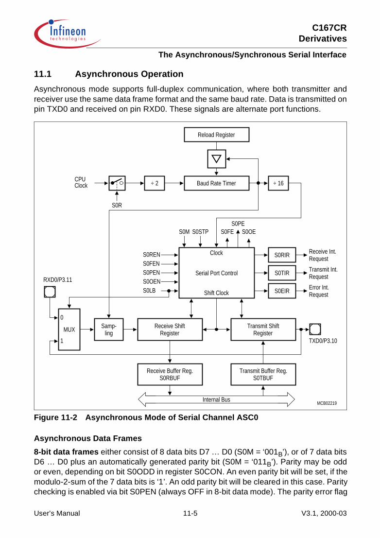
C167CRDerivatives
The Asynchronous/Synchronous Serial Interface
11.1 Asynchronous Operation
Asynchronous mode supports full-duplex communication, where both transmitter andreceiver use the same data frame format and the same baud rate. Data is transmitted onpin TXD0 and received on pin RXD0. These signals are alternate port functions.
Figure 11-2 Asynchronous Mode of Serial Channel ASC0
Asynchronous Data Frames
8-bit data frames either consist of 8 data bits D7 … D0 (S0M = ‘001B’), or of 7 data bitsD6 … D0 plus an automatically generated parity bit (S0M = ‘011B’). Parity may be oddor even, depending on bit S0ODD in register S0CON. An even parity bit will be set, if themodulo-2-sum of the 7 data bits is ‘1’. An odd parity bit will be cleared in this case. Paritychecking is enabled via bit S0PEN (always OFF in 8-bit data mode). The parity error flag
MCB02219
Reload Register
Baud Rate Timer
Receive Int.Request
CPU
MUX
÷ 2Clock
S0R
÷ 16
S0RIR
S0TIR
S0EIR
Clock
Serial Port Control
Shift Clock
Receive ShiftRegister Register
Transmit Shift
S0RBUFReceive Buffer Reg.
lingSamp-
RXD0/P3.11
TXD0/P3.10
Internal Bus
0
1
Transmit Int.Request
Error Int.Request
S0OES0FES0PE
S0STPS0M
S0RENS0FENS0PENS0OENS0LB
Transmit Buffer Reg.S0TBUF
User’s Manual 11-5 V3.1, 2000-03

C167CRDerivatives
The Asynchronous/Synchronous Serial Interface
S0PE will be set along with the error interrupt request flag, if a wrong parity bit isreceived. The parity bit itself will be stored in bit S0RBUF.7.
Figure 11-3 Asynchronous 8-bit Data Frames
9-bit data frames either consist of 9 data bits D8 … D0 (S0M = ‘100B’), of 8 data bitsD7 … D0 plus an automatically generated parity bit (S0M = ‘111B’) or of 8 data bitsD7 … D0 plus wake-up bit (S0M = ‘101B’). Parity may be odd or even, depending on bitS0ODD in register S0CON. An even parity bit will be set, if the modulo-2-sum of the 8data bits is ‘1’. An odd parity bit will be cleared in this case. Parity checking is enabledvia bit S0PEN (always OFF in 9-bit data and wake-up mode). The parity error flag S0PEwill be set along with the error interrupt request flag, if a wrong parity bit is received. Theparity bit itself will be stored in bit S0RBUF.8.
In wake-up mode received frames are only transferred to the receive buffer register, ifthe 9th bit (the wake-up bit) is ‘1’. If this bit is ‘0’, no receive interrupt request will beactivated and no data will be transferred.
This feature may be used to control communication in multi-processor system:When the master processor wants to transmit a block of data to one of several slaves, itfirst sends out an address byte which identifies the target slave. An address byte differsfrom a data byte in that the additional 9th bit is a ‘1’ for an address byte and a ‘0’ for adata byte, so no slave will be interrupted by a data ‘byte’. An address ‘byte’ will interruptall slaves (operating in 8-bit data + wake-up bit mode), so each slave can examine the 8LSBs of the received character (the address). The addressed slave will switch to 9-bitdata mode (e.g. by clearing bit S0M.0), which enables it to also receive the data bytesthat will be coming (having the wake-up bit cleared). The slaves that were not beingaddressed remain in 8-bit data + wake-up bit mode, ignoring the following data bytes.
Figure 11-4 Asynchronous 9-bit Data Frames
D7 /Parity
MCT04377
D0(LSB)
StartBit D1 D2 D3 D4 D5 D6
(1st)StopBit
2ndStopBit
D7
MCT04378
D0(LSB)
StartBit D1 D2 D3 D4 D5 D6
(1st)StopBit
2ndStopBit
9thBit
Data Bit D8ParityWake-up Bit
User’s Manual 11-6 V3.1, 2000-03
C167CRDerivatives
The Asynchronous/Synchronous Serial Interface
Asynchronous transmission begins at the next overflow of the divide-by-16 counter(see Figure 11-4), provided that S0R is set and data has been loaded into S0TBUF. Thetransmitted data frame consists of three basic elements:
• the start bit• the data field (8 or 9 bits, LSB first, including a parity bit, if selected)• the delimiter (1 or 2 stop bits)
Data transmission is double buffered. When the transmitter is idle, the transmit dataloaded into S0TBUF is immediately moved to the transmit shift register thus freeingS0TBUF for the next data to be sent. This is indicated by the transmit buffer interruptrequest flag S0TBIR being set. S0TBUF may now be loaded with the next data, whiletransmission of the previous one is still going on.
The transmit interrupt request flag S0TIR will be set before the last bit of a frame istransmitted, i.e. before the first or the second stop bit is shifted out of the transmit shiftregister.The transmitter output pin TXD0 must be configured for alternate data output, i.e. therespective port output latch and the direction latch must be ‘1’.
Asynchronous reception is initiated by a falling edge (1-to-0 transition) on pin RXD0,provided that bits S0R and S0REN are set. The receive data input pin RXD0 is sampledat 16 times the rate of the selected baud rate. A majority decision of the 7th, 8th and 9thsample determines the effective bit value. This avoids erroneous results that may becaused by noise.
If the detected value is not a ‘0’ when the start bit is sampled, the receive circuit is resetand waits for the next 1-to-0 transition at pin RXD0. If the start bit proves valid, thereceive circuit continues sampling and shifts the incoming data frame into the receiveshift register.
When the last stop bit has been received, the content of the receive shift register istransferred to the receive data buffer register S0RBUF. Simultaneously, the receiveinterrupt request flag S0RIR is set after the 9th sample in the last stop bit time slot (asprogrammed), regardless whether valid stop bits have been received or not. The receivecircuit then waits for the next start bit (1-to-0 transition) at the receive data input pin.
The receiver input pin RXD0 must be configured for input, i.e. the respective directionlatch must be ‘0’.
Asynchronous reception is stopped by clearing bit S0REN. A currently received frame iscompleted including the generation of the receive interrupt request and an error interruptrequest, if appropriate. Start bits that follow this frame will not be recognized.
Note: In wake-up mode received frames are only transferred to the receive bufferregister, if the 9th bit (the wake-up bit) is ‘1’. If this bit is ‘0’, no receive interruptrequest will be activated and no data will be transferred.
User’s Manual 11-7 V3.1, 2000-03

C167CRDerivatives
The Asynchronous/Synchronous Serial Interface
11.2 Synchronous Operation
Synchronous mode supports half-duplex communication, basically for simple IOexpansion via shift registers. Data is transmitted and received via pin RXD0, while pinTXD0 outputs the shift clock. These signals are alternate port functions. Synchronousmode is selected with S0M = ‘000B’.
8 data bits are transmitted or received synchronous to a shift clock generated by theinternal baud rate generator. The shift clock is only active as long as data bits aretransmitted or received.
Figure 11-5 Synchronous Mode of Serial Channel ASC0
MCB02220
Reload Register
Baud Rate Timer
Receive Int.Request
MUX
÷ 2Clock
Clock
Serial Port Control
Shift Clock
Receive ShiftRegister
Receive Buffer Reg.
TXD0/P3.10
Internal Bus
0
1
Transmit Int.Request
Error Int.Request
S0OES0M = 000B
S0REN
S0OEN
S0LB
÷ 4
RXD0/P3.11
Receive
Transmit
CPU
S0R
S0RIR
S0TIR
S0EIR
Transmit ShiftRegister
Transmit Buffer Reg.S0TBUFS0RBUF
User’s Manual 11-8 V3.1, 2000-03

C167CRDerivatives
The Asynchronous/Synchronous Serial Interface
Synchronous transmission begins within 4 state times after data has been loaded intoS0TBUF, provided that S0R is set and S0REN = ‘0’ (half-duplex, no reception). Datatransmission is double buffered. When the transmitter is idle, the transmit data loadedinto S0TBUF is immediately moved to the transmit shift register thus freeing S0TBUF forthe next data to be sent. This is indicated by the transmit buffer interrupt request flagS0TBIR being set. S0TBUF may now be loaded with the next data, while transmissionof the previous one is still going on. The data bits are transmitted synchronous with theshift clock. After the bit time for the 8th data bit, both pins TXD0 and RXD0 will go high,the transmit interrupt request flag S0TIR is set, and serial data transmission stops.
Pin TXD0 must be configured for alternate data output, i.e. the respective port outputlatch and the direction latch must be ‘1’, in order to provide the shift clock. Pin RXD0 mustalso be configured for output (output/direction latch = ‘1’) during transmission.
Synchronous reception is initiated by setting bit S0REN = ‘1’. If bit S0R = ‘1’, the dataapplied at pin RXD0 are clocked into the receive shift register synchronous to the clockwhich is output at pin TXD0. After the 8th bit has been shifted in, the content of thereceive shift register is transferred to the receive data buffer S0RBUF, the receiveinterrupt request flag S0RIR is set, the receiver enable bit S0REN is reset, and serialdata reception stops.
Pin TXD0 must be configured for alternate data output, i.e. the respective port outputlatch and the direction latch must be ‘1’, in order to provide the shift clock. Pin RXD0 mustbe configured as alternate data input, i.e. the respective direction latch must be ‘0’.
Synchronous reception is stopped by clearing bit S0REN. A currently received byte iscompleted including the generation of the receive interrupt request and an error interruptrequest, if appropriate. Writing to the transmit buffer register while a reception is inprogress has no effect on reception and will not start a transmission.
If a previously received byte has not been read out of the receive buffer register at thetime the reception of the next byte is complete, both the error interrupt request flagS0EIR and the overrun error status flag S0OE will be set, provided the overrun checkhas been enabled by bit S0OEN.
User’s Manual 11-9 V3.1, 2000-03
C167CRDerivatives
The Asynchronous/Synchronous Serial Interface
11.3 Hardware Error Detection Capabilities
To improve the safety of serial data exchange, the serial channel ASC0 provides an errorinterrupt request flag, which indicates the presence of an error, and three (selectable)error status flags in register S0CON, which indicate which error has been detectedduring reception. Upon completion of a reception, the error interrupt request flag S0EIRwill be set simultaneously with the receive interrupt request flag S0RIR, if one or more ofthe following conditions are met:
• If the framing error detection enable bit S0FEN is set and any of the expected stop bitsis not high, the framing error flag S0FE is set, indicating that the error interrupt requestis due to a framing error (Asynchronous mode only).
• If the parity error detection enable bit S0PEN is set in the modes where a parity bit isreceived, and the parity check on the received data bits proves false, the parity errorflag S0PE is set, indicating that the error interrupt request is due to a parity error(Asynchronous mode only).
• If the overrun error detection enable bit S0OEN is set and the last character receivedwas not read out of the receive buffer by software or PEC transfer at the time thereception of a new frame is complete, the overrun error flag S0OE is set indicating thatthe error interrupt request is due to an overrun error (Asynchronous and synchronousmode).
User’s Manual 11-10 V3.1, 2000-03
C167CRDerivatives
The Asynchronous/Synchronous Serial Interface
11.4 ASC0 Baud Rate Generation
The serial channel ASC0 has its own dedicated 13-bit baud rate generator with 13-bitreload capability, allowing baud rate generation independent of the GPT timers.
The baud rate generator is clocked with the CPU clock divided by 2 (fCPU/2). The timeris counting downwards and can be started or stopped through the Baud Rate GeneratorRun Bit S0R in register S0CON. Each underflow of the timer provides one clock pulse tothe serial channel. The timer is reloaded with the value stored in its 13-bit reload registereach time it underflows. The resulting clock is again divided according to the operatingmode and controlled by the Baudrate Selection Bit S0BRS. If S0BRS = ‘1’, the clocksignal is additionally divided to 2/3rd of its frequency (see formulas and table). So thebaud rate of ASC0 is determined by the CPU clock, the reload value, the value of S0BRSand the operating mode (asynchronous or synchronous).
Register S0BG is the dual-function Baud Rate Generator/Reload register. ReadingS0BG returns the content of the timer (bits 15 … 13 return zero), while writing to S0BGalways updates the reload register (bits 15 … 13 are insiginificant).
An auto-reload of the timer with the content of the reload register is performed each timeS0BG is written to. However, if S0R = ‘0’ at the time the write operation to S0BG isperformed, the timer will not be reloaded until the first instruction cycle after S0R = ‘1’.
Asynchronous Mode Baud Rates
For asynchronous operation, the baud rate generator provides a clock with 16 times therate of the established baud rate. Every received bit is sampled at the 7th, 8th and 9thcycle of this clock. The baud rate for asynchronous operation of serial channel ASC0 andthe required reload value for a given baudrate can be determined by the followingformulas:
<S0BRL> represents the content of the reload register, taken as unsigned 13-bit integer,<S0BRS> represents the value of bit S0BRS (i.e. ‘0’ or ‘1’), taken as integer.
The tables below list various commonly used baud rates together with the requiredreload values and the deviation errors compared to the intended baudrate for a numberof CPU frequencies.
Note: The deviation errors given in the tables below are rounded. Using a baudratecrystal (e.g. 18.432 MHz) will provide correct baudrates without deviation errors.
BAsync =fCPU
16 × (2 + <S0BRS>) × (<S0BRL> + 1)
S0BRL = (fCPU
16 × (2 + <S0BRS>) × BAsync) – 1
User’s Manual 11-11 V3.1, 2000-03

C167CRDerivatives
The Asynchronous/Synchronous Serial Interface
Table 11-1 ASC0 Asynchronous Baudrate Generation for fCPU = 16 MHz
Baud Rate S0BRS = ‘0’ S0BRS = ‘1’
Deviation Error Reload Value Deviation Error Reload Value
500 KBaud ± 0.0% 0000H – –
19.2 KBaud + 0.2%/ – 3.5% 0019H/001AH + 2.1%/ – 3.5% 0010H/0011H
9600 Baud + 0.2%/ – 1.7% 0033H/0034H + 2.1%/ – 0.8% 0021H/0022H
4800 Baud + 0.2%/ – 0.8% 0067H/0068H + 0.6%/ – 0.8% 0044H/0045H
2400 Baud + 0.2%/ – 0.3% 00CFH/00D0H + 0.6%/ – 0.1% 0089H/008AH
1200 Baud + 0.4%/ – 0.1% 019FH/01A0H + 0.3%/ – 0.1% 0114H/0115H
600 Baud + 0.0%/ – 0.1% 0340H/0341H + 0.1%/ – 0.1% 022AH/022BH
61 Baud + 0.1% 1FFFH + 0.0%/ – 0.0% 115BH/115CH
40 Baud – – + 1.7% 1FFFH
Table 11-2 ASC0 Asynchronous Baudrate Generation for fCPU = 20 MHz
Baud Rate S0BRS = ‘0’ S0BRS = ‘1’
Deviation Error Reload Value Deviation Error Reload Value
625 KBaud ± 0.0% 0000H – –
19.2 KBaud + 1.7%/ – 1.4% 001FH/0020H + 3.3%/ – 1.4% 0014H/0015H
9600 Baud + 0.2%/ – 1.4% 0040H/0041H + 1.0%/ – 1.4% 002AH/002BH
4800 Baud + 0.2%/ – 0.6% 0081H/0082H + 1.0%/ – 0.2% 0055H/0056H
2400 Baud + 0.2%/ – 0.2% 0103H/0104H + 0.4%/ – 0.2% 00ACH/00ADH
1200 Baud + 0.2%/ – 0.4% 0207H/0208H + 0.1%/ – 0.2% 015AH/015BH
600 Baud + 0.1%/ – 0.0% 0410H/0411H + 0.1%/ – 0.1% 02B5H/02B6H
75 Baud + 1.7% 1FFFH + 0.0%/ – 0.0% 15B2H/15B3H
50 Baud – – + 1.7% 1FFFH
User’s Manual 11-12 V3.1, 2000-03

C167CRDerivatives
The Asynchronous/Synchronous Serial Interface
Table 11-3 ASC0 Asynchronous Baudrate Generation for fCPU = 25 MHz
Baud Rate S0BRS = ‘0’ S0BRS = ‘1’
Deviation Error Reload Value Deviation Error Reload Value
781 KBaud + 0.2% 0000H – –
19.2 KBaud + 1.7%/ – 0.8% 0027H/0028H + 0.5%/ – 3.1% 001AH/001BH
9600 Baud + 0.5%/ – 0.8% 0050H/0051H + 0.5%/ – 1.4% 0035H/0036H
4800 Baud + 0.5%/ – 0.2% 00A1H/00A2H + 0.5%/ – 0.5% 006BH/006CH
2400 Baud + 0.2%/ – 0.2% 0145H/0146H + 0.0%/ – 0.5% 00D8H/00D9H
1200 Baud + 0.0%/ – 0.2% 028AH/028BH + 0.0%/ – 0.2% 01B1H/01B2H
600 Baud + 0.0%/ – 0.1% 0515H/0516H + 0.0%/ – 0.1% 0363H/0364H
95 Baud + 0.4% 1FFFH + 0.0%/ – 0.0% 1569H/156AH
63 Baud – – + 1.0% 1FFFH
Table 11-4 ASC0 Asynchronous Baudrate Generation for fCPU = 33 MHz
Baud Rate S0BRS = ‘0’ S0BRS = ‘1’
Deviation Error Reload Value Deviation Error Reload Value
1.031 MBaud ± 0.0% 0000H – –
19.2 KBaud + 1.3%/ – 0.5% 0034H/0035H + 2.3%/ – 0.5% 0022H/0023H
9600 Baud + 0.4%/ – 0.5% 006AH/006BH + 0.9%/ – 0.5% 0046H/0047H
4800 Baud + 0.4%/ – 0.1% 00D5H/00D6H + 0.2%/ – 0.5% 008EH/008FH
2400 Baud + 0.2%/ – 0.1% 01ACH/01ADH + 0.2%/ – 0.2% 011DH/011EH
1200 Baud + 0.0%/ – 0.1% 035AH/035BH + 0.2%/ – 0.0% 023BH/023CH
600 Baud + 0.0%/ – 0.0% 06B5H/06B6H + 0.1%/ – 0.0% 0478H/0479H
125 Baud + 7.1% 1FFFH ± 0.0% 157CH
84 Baud – – – 0.9% 1FFFH
User’s Manual 11-13 V3.1, 2000-03
C167CRDerivatives
The Asynchronous/Synchronous Serial Interface
Synchronous Mode Baud Rates
For synchronous operation, the baud rate generator provides a clock with 4 times therate of the established baud rate. The baud rate for synchronous operation of serialchannel ASC0 can be determined by the following formula:
<S0BRL> represents the content of the reload register, taken as unsigned 13-bit integers,<S0BRS> represents the value of bit S0BRS (i.e. ‘0’ or ‘1’), taken as integer.
Table 11-5 gives the limit baudrates depending on the CPU clock frequency and bitS0BRS.
Table 11-5 ASC0 Synchronous Baudrate Generation
CPU clockfCPU
S0BRS = ‘0’ S0BRS = ‘1’
Min. Baudrate Max. Baudrate Min. Baudrate Max. Baudrate
16 MHz 244 Baud 2.000 MBaud 162 Baud 1.333 MBaud
20 MHz 305 Baud 2.500 MBaud 203 Baud 1.666 MBaud
25 MHz 381 Baud 3.125 MBaud 254 Baud 2.083 MBaud
33 MHz 504 Baud 4.125 MBaud 336 Baud 2.750 MBaud
BSync =
S0BRL = (4 × (2 + <S0BRS>) × BSync
fCPU
fCPU ) – 1
4 × (2 + <S0BRS>) × (<S0BRL> + 1)
User’s Manual 11-14 V3.1, 2000-03

C167CRDerivatives
The Asynchronous/Synchronous Serial Interface
11.5 ASC0 Interrupt Control
Four bit addressable interrupt control registers are provided for serial channel ASC0.Register S0TIC controls the transmit interrupt, S0TBIC controls the transmit bufferinterrupt, S0RIC controls the receive interrupt and S0EIC controls the error interrupt ofserial channel ASC0. Each interrupt source also has its own dedicated interrupt vector.S0TINT is the transmit interrupt vector, S0TBINT is the transmit buffer interrupt vector,S0RINT is the receive interrupt vector, and S0EINT is the error interrupt vector.
The cause of an error interrupt request (framing, parity, overrun error) can be identifiedby the error status flags in control register S0CON.
Note: In contrast to the error interrupt request flag S0EIR, the error status flags S0FE/S0PE/S0OE are not reset automatically upon entry into the error interrupt serviceroutine, but must be cleared by software.
S0TICASC0 Tx Intr. Ctrl. Reg. SFR (FF6CH/B6H) Reset value: - - 00H
15 14 13 12 11 10 9 8 7 6 5 4 3 2 1 0
- S0 TIR
S0 TIE ILVL GLVL
- - - - - - - - rwh rw rw rw
S0TBICASC0 Tx Buf. Intr. Ctrl. Reg. SFR (FF9CH/CEH) Reset value: - - 00H
15 14 13 12 11 10 9 8 7 6 5 4 3 2 1 0
- S0 TBIR
S0 TBIE ILVL GLVL
- - - - - - - - rwh rw rw rw
S0RICASC0 Rx Intr. Ctrl. Reg. SFR (FF6EH/B7H) Reset value: - - 00H
15 14 13 12 11 10 9 8 7 6 5 4 3 2 1 0
- S0 RIR
S0 RIE ILVL GLVL
- - - - - - - - rwh rw rw rw
User’s Manual 11-15 V3.1, 2000-03

C167CRDerivatives
The Asynchronous/Synchronous Serial Interface
Note: Please refer to the general Interrupt Control Register description for anexplanation of the control fields.
Using the ASC0 Interrupts
For normal operation (i.e. besides the error interrupt) the ASC0 provides three interruptrequests to control data exchange via this serial channel:
• S0TBIR is activated when data is moved from S0TBUF to the transmit shift register.• S0TIR is activated before the last bit of an asynchronous frame is transmitted,
or after the last bit of a synchronous frame has been transmitted.• S0RIR is activated when the received frame is moved to S0RBUF.
While the task of the receive interrupt handler is quite clear, the transmitter is servicedby two interrupt handlers. This provides advantages for the servicing software.
For single transfers is sufficient to use the transmitter interrupt (S0TIR), which indicatesthat the previously loaded data has been transmitted, except for the last bit of anasynchronous frame.
For multiple back-to-back transfers it is necessary to load the following piece of dataat last until the time the last bit of the previous frame has been transmitted. Inasynchronous mode this leaves just one bit-time for the handler to respond to thetransmitter interrupt request, in synchronous mode it is impossible at all.Using the transmit buffer interrupt (S0TBIR) to reload transmit data gives the time totransmit a complete frame for the service routine, as S0TBUF may be reloaded while theprevious data is still being transmitted.
S0EICASC0 Error Intr. Ctrl. Reg. SFR (FF70H/B8H) Reset value: - - 00H
15 14 13 12 11 10 9 8 7 6 5 4 3 2 1 0
- S0 EIR
S0 EIE ILVL GLVL
- - - - - - - - rwh rw rw rw
User’s Manual 11-16 V3.1, 2000-03
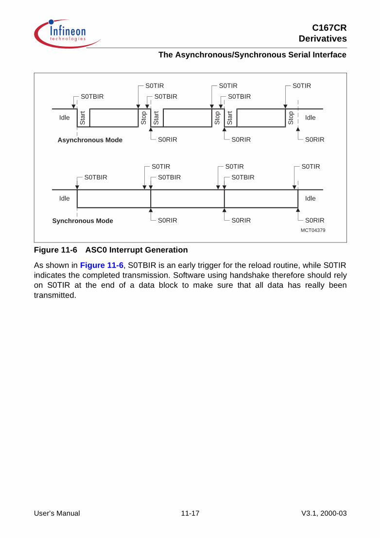
C167CRDerivatives
The Asynchronous/Synchronous Serial Interface
Figure 11-6 ASC0 Interrupt Generation
As shown in Figure 11-6, S0TBIR is an early trigger for the reload routine, while S0TIRindicates the completed transmission. Software using handshake therefore should relyon S0TIR at the end of a data block to make sure that all data has really beentransmitted.
MCT04379
Sta
rt
Sto
p
Sta
rt
Sto
p
Sta
rt
Sto
p
Idle Idle
S0RIR
S0TBIR
S0TIR
S0TBIR
S0TIR
S0TBIR
S0RIRS0RIRAsynchronous Mode
Idle Idle
S0RIR
S0TBIR
S0TIR
S0TBIR
S0TIR
S0TBIR
S0RIRS0RIRSynchronous Mode
S0TIR
S0TIR
User’s Manual 11-17 V3.1, 2000-03
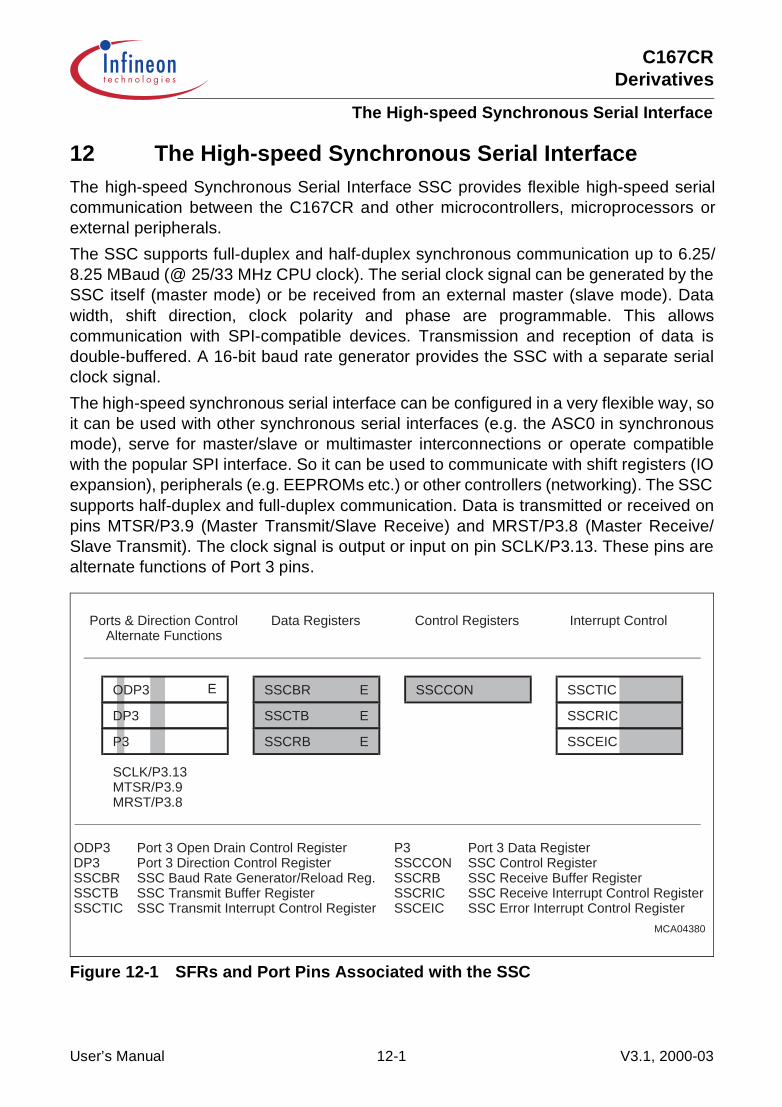
C167CRDerivatives
The High-speed Synchronous Serial Interface
12 The High-speed Synchronous Serial InterfaceThe high-speed Synchronous Serial Interface SSC provides flexible high-speed serialcommunication between the C167CR and other microcontrollers, microprocessors orexternal peripherals.
The SSC supports full-duplex and half-duplex synchronous communication up to 6.25/8.25 MBaud (@ 25/33 MHz CPU clock). The serial clock signal can be generated by theSSC itself (master mode) or be received from an external master (slave mode). Datawidth, shift direction, clock polarity and phase are programmable. This allowscommunication with SPI-compatible devices. Transmission and reception of data isdouble-buffered. A 16-bit baud rate generator provides the SSC with a separate serialclock signal.
The high-speed synchronous serial interface can be configured in a very flexible way, soit can be used with other synchronous serial interfaces (e.g. the ASC0 in synchronousmode), serve for master/slave or multimaster interconnections or operate compatiblewith the popular SPI interface. So it can be used to communicate with shift registers (IOexpansion), peripherals (e.g. EEPROMs etc.) or other controllers (networking). The SSCsupports half-duplex and full-duplex communication. Data is transmitted or received onpins MTSR/P3.9 (Master Transmit/Slave Receive) and MRST/P3.8 (Master Receive/Slave Transmit). The clock signal is output or input on pin SCLK/P3.13. These pins arealternate functions of Port 3 pins.
Figure 12-1 SFRs and Port Pins Associated with the SSC
E
MCA04380
ODP3
DP3
P3
SSCBR
SSCTB
SSCRB
SSCCON SSCTIC
SSCEIC
Ports & Direction ControlAlternate Functions
Data Registers Control Registers Interrupt Control
ODP3 Port 3 Open Drain Control RegisterDP3 Port 3 Direction Control RegisterSSCBR SSC Baud Rate Generator/Reload Reg.SSCTB SSC Transmit Buffer RegisterSSCTIC SSC Transmit Interrupt Control Register
P3 Port 3 Data RegisterSSCCON SSC Control RegisterSSCRB SSC Receive Buffer RegisterSSCRIC SSC Receive Interrupt Control RegisterSSCEIC SSC Error Interrupt Control Register
SSCRIC
SCLK/P3.13MTSR/P3.9MRST/P3.8
E
E
E
User’s Manual 12-1 V3.1, 2000-03
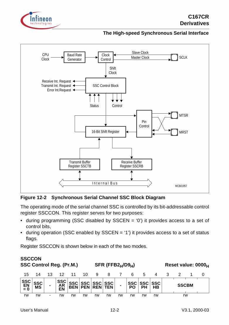
C167CRDerivatives
The High-speed Synchronous Serial Interface
Figure 12-2 Synchronous Serial Channel SSC Block Diagram
The operating mode of the serial channel SSC is controlled by its bit-addressable controlregister SSCCON. This register serves for two purposes:
• during programming (SSC disabled by SSCEN = ‘0’) it provides access to a set ofcontrol bits,
• during operation (SSC enabled by SSCEN = ‘1’) it provides access to a set of statusflags.
Register SSCCON is shown below in each of the two modes.
SSCCONSSC Control Reg. (Pr.M.) SFR (FFB2H/D9H) Reset value: 0000H
15 14 13 12 11 10 9 8 7 6 5 4 3 2 1 0
SSCEN= 0
SSC MS -
SSC AR EN
SSCBEN
SSCPEN
SSCREN
SSCTEN - SSC
POSSCPH
SSCHB SSCBM
rw rw - rw rw rw rw rw rw rw rw rw rw
MCB01957
Receive Int. RequestTransmit Int. Request
Error Int.RequestSSC Control Block
16-Bit Shift Register
Transmit BufferRegister SSCTB Register SSCRB
Receive Buffer
PinControl
Status Control
ShiftClock
GeneratorBaud Rate Clock
Control
Slave ClockMaster Clock
CPUClock
I n t e r n a l B u s
MTSR
MRST
SCLK
User’s Manual 12-2 V3.1, 2000-03
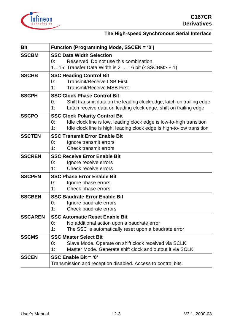
C167CRDerivatives
The High-speed Synchronous Serial Interface
Bit Function (Programming Mode, SSCEN = ‘0’)
SSCBM SSC Data Width Selection0: Reserved. Do not use this combination.1…15: Transfer Data Width is 2 … 16 bit (<SSCBM> + 1)
SSCHB SSC Heading Control Bit0: Transmit/Receive LSB First1: Transmit/Receive MSB First
SSCPH SSC Clock Phase Control Bit0: Shift transmit data on the leading clock edge, latch on trailing edge1: Latch receive data on leading clock edge, shift on trailing edge
SSCPO SSC Clock Polarity Control Bit0: Idle clock line is low, leading clock edge is low-to-high transition1: Idle clock line is high, leading clock edge is high-to-low transition
SSCTEN SSC Transmit Error Enable Bit0: Ignore transmit errors1: Check transmit errors
SSCREN SSC Receive Error Enable Bit0: Ignore receive errors1: Check receive errors
SSCPEN SSC Phase Error Enable Bit0: Ignore phase errors1: Check phase errors
SSCBEN SSC Baudrate Error Enable Bit0: Ignore baudrate errors1: Check baudrate errors
SSCAREN SSC Automatic Reset Enable Bit0: No additional action upon a baudrate error1: The SSC is automatically reset upon a baudrate error
SSCMS SSC Master Select Bit0: Slave Mode. Operate on shift clock received via SCLK.1: Master Mode. Generate shift clock and output it via SCLK.
SSCEN SSC Enable Bit = ‘0’Transmission and reception disabled. Access to control bits.
User’s Manual 12-3 V3.1, 2000-03

C167CRDerivatives
The High-speed Synchronous Serial Interface
Note: The target of an access to SSCCON (control bits or flags) is determined by thestate of SSCEN prior to the access, i.e. writing C057H to SSCCON inprogramming mode (SSCEN = ‘0’) will initialize the SSC (SSCEN was ‘0’) and thenturn it on (SSCEN = ‘1’).When writing to SSCCON, make sure that reserved locations receive zeros.
SSCCONSSC Control Reg. (Op.M.) SFR (FFB2H/D9H) Reset value: 0000H
15 14 13 12 11 10 9 8 7 6 5 4 3 2 1 0
SSCEN= 1
SSC MS - SSC
BSYSSC BE
SSC PE
SSC RE
SSC TE - - - - SSCBC
rw rw - rw rw rw rw rw - - - - r
Bit Function (Operating Mode, SSCEN = ‘1’)
SSCBC SSC Bit Count FieldShift counter is updated with every shifted bit. Do not write to!!!
SSCTE SSC Transmit Error Flag1: Transfer starts with the slave’s transmit buffer not being updated
SSCRE SSC Receive Error Flag1: Reception completed before the receive buffer was read
SSCPE SSC Phase Error Flag1: Received data changes around sampling clock edge
SSCBE SSC Baudrate Error Flag1: More than factor 2 or less than factor 0.5 between Slave’s actual
and expected baudrate
SSCBSY SSC Busy FlagSet while a transfer is in progress. Do not write to!!!
SSCMS SSC Master Select Bit0: Slave Mode. Operate on shift clock received via SCLK.1: Master Mode. Generate shift clock and output it via SCLK.
SSCEN SSC Enable Bit = ‘1’Transmission and reception enabled. Access to status flags and M/S control.
User’s Manual 12-4 V3.1, 2000-03

C167CRDerivatives
The High-speed Synchronous Serial Interface
The shift register of the SSC is connected to both the transmit pin and the receive pin viathe pin control logic (see block diagram). Transmission and reception of serial data issynchronized and takes place at the same time, i.e. the number of transmitted bits is alsoreceived.
The major steps of the state machine of the SSC are controlled by the shift clock signal(see Figure 12-3).In master mode (SSCMS = ‘1’) two clocks per bit-time are generated, each upon anunderflow of the baudrate counter.In slave mode (SSCMS = ‘0’) one clock per bit-time is generated, when the latchingedge of the external SCLK signal has been detected.
Transmit data is written into the transmit buffer SSCTB. When the contents of the bufferare moved to the shift register (immediately if no transfer is currently active) a transmitinterrupt request (SSCTIR) is generated indicating that SSCTB may be reloaded again.
The busy flag SSCBSY is set when the transfer starts (with the next following shift clockin master mode, immediately in slave mode).
Note: If no data is written to SSCTB prior to a slave transfer, this transfer starts after thefirst latching edge of the external SCLK signal is detected. No transmit interrupt isgenerated in this case.
When the contents of the shift register are moved to the receive buffer SSCRB after theprogrammed number of bits (2 … 16) have been transferred, i.e. after the last latchingedge of the current transfer, a receive interrupt request (SSCRIR) is generated.
The busy flag SSCBSY is cleared at the end of the current transfer (with the nextfollowing shift clock in master mode, immediately in slave mode).
When the transmit buffer is not empty at that time (in the case of continuous transfers)the busy flag is not cleared and the transfer goes on after moving data from the buffer tothe shift register.
Software should not modify SSCBSY, as this flag is hardware controlled.
Note: Only one SSC (etc.) can be master at a given time.
The transfer of serial data bits can be programmed in many respects:
• the data width can be chosen from 2 bits to 16 bits• transfer may start with the LSB or the MSB• the shift clock may be idle low or idle high• data bits may be shifted with the leading or trailing edge of the clock signal• the baudrate may be set within a wide range (see baudrate generation)• the shift clock can be generated (master) or received (slave)
This allows the adaptation of the SSC to a wide range of applications, where serial datatransfer is required.
User’s Manual 12-5 V3.1, 2000-03

C167CRDerivatives
The High-speed Synchronous Serial Interface
The Data Width Selection supports the transfer of frames of any length, from 2-bit“characters” up to 16-bit “characters”. Starting with the LSB (SSCHB = ‘0’) allowscommunication e.g. with ASC0 devices in synchronous mode (C166 Family) or 8051 likeserial interfaces. Starting with the MSB (SSCHB = ‘1’) allows operation compatible withthe SPI interface.Regardless which data width is selected and whether the MSB or the LSB is transmittedfirst, the transfer data is always right aligned in registers SSCTB and SSCRB, with theLSB of the transfer data in bit 0 of these registers. The data bits are rearranged fortransfer by the internal shift register logic. The unselected bits of SSCTB are ignored, theunselected bits of SSCRB will be not valid and should be ignored by the receiver serviceroutine.
The Clock Control allows the adaptation of transmit and receive behavior of the SSC toa variety of serial interfaces. A specific clock edge (rising or falling) is used to shift outtransmit data, while the other clock edge is used to latch in receive data. Bit SSCPHselects the leading edge or the trailing edge for each function. Bit SSCPO selects thelevel of the clock line in the idle state. So for an idle-high clock the leading edge is afalling one, a 1-to-0 transition. Figure 12-3 is a summary.
Figure 12-3 Serial Clock Phase and Polarity Options
User’s Manual 12-6 V3.1, 2000-03

C167CRDerivatives
The High-speed Synchronous Serial Interface
12.1 Full-duplex Operation
The different devices are connected through three lines. The definition of these lines isalways determined by the master: The line connected to the master’s data output pinMTSR is the transmit line, the receive line is connected to its data input line MRST, andthe clock line is connected to pin SCLK. Only the device selected for master operationgenerates and outputs the serial clock on pin SCLK. All slaves receive this clock, so theirpin SCLK must be switched to input mode (DP3.13 = ‘0’). The output of the master’s shiftregister is connected to the external transmit line, which in turn is connected to theslaves’ shift register input. The output of the slaves’ shift register is connected to theexternal receive line in order to enable the master to receive the data shifted out of theslave. The external connections are hard-wired, the function and direction of these pinsis determined by the master or slave operation of the individual device.
Note: The shift direction shown in Figure 12-4 applies for MSB-first operation as well asfor LSB-first operation.
When initializing the devices in this configuration, select one device for master operation(SSCMS = ‘1’), all others must be programmed for slave operation (SSCMS = ‘0’).Initialization includes the operating mode of the device’s SSC and also the function ofthe respective port lines (see “Port Control”).
Figure 12-4 SSC Full-duplex Configuration
MCS01963
MRST
SCLK
Device #2 Slave
Clock
Shift Register
MTSR
Clock
Master
Receive
Transmit
Device #1
Clock
MTSR
MRST
SCLK
Shift Register
MTSR
Shift Register
Clock
Slave
SCLK
MRST
Device #3
User’s Manual 12-7 V3.1, 2000-03
C167CRDerivatives
The High-speed Synchronous Serial Interface
The data output pins MRST of all slave devices are connected together onto the onereceive line in this configuration. During a transfer each slave shifts out data from its shiftregister. There are two ways to avoid collisions on the receive line due to different slavedata:
Only one slave drives the line, i.e. enables the driver of its MRST pin. All the otherslaves have to program their MRST pins to input. So only one slave can put its data ontothe master’s receive line. Only receiving of data from the master is possible. The masterselects the slave device from which it expects data either by separate select lines, or bysending a special command to this slave. The selected slave then switches its MRST lineto output, until it gets a deselection signal or command.
The slaves use open drain output on MRST. This forms a Wired-AND connection. Thereceive line needs an external pullup in this case. Corruption of the data on the receiveline sent by the selected slave is avoided, when all slaves which are not selected fortransmission to the master only send ones (‘1’). Since this high level is not actively drivenonto the line, but only held through the pullup device, the selected slave can pull this lineactively to a low level when transmitting a zero bit. The master selects the slave devicefrom which it expects data either by separate select lines, or by sending a specialcommand to this slave.
After performing all necessary initializations of the SSC, the serial interfaces can beenabled. For a master device, the alternate clock line will now go to its programmedpolarity. The alternate data line will go to either ‘0’ or ‘1’, until the first transfer will start.
When the serial interfaces are enabled, the master device can initiate the first datatransfer by writing the transmit data into register SSCTB. This value is copied into theshift register (which is assumed to be empty at this time), and the selected first bit of thetransmit data will be placed onto the MTSR line on the next clock from the baudrategenerator (transmission only starts, if SSCEN = ‘1’). Depending on the selected clockphase, also a clock pulse will be generated on the SCLK line. With the opposite clockedge the master at the same time latches and shifts in the data detected at its input lineMRST. This “exchanges” the transmit data with the receive data. Since the clock line isconnected to all slaves, their shift registers will be shifted synchronously with themaster’s shift register, shifting out the data contained in the registers, and shifting in thedata detected at the input line. After the preprogrammed number of clock pulses (via thedata width selection) the data transmitted by the master is contained in all slaves’ shiftregisters, while the master’s shift register holds the data of the selected slave. In themaster and all slaves the content of the shift register is copied into the receive bufferSSCRB and the receive interrupt flag SSCRIR is set.
A slave device will immediately output the selected first bit (MSB or LSB of the transferdata) at pin MRST, when the content of the transmit buffer is copied into the slave’s shiftregister. It will not wait for the next clock from the baudrate generator, as the masterdoes. The reason for this is that, depending on the selected clock phase, the first clock
User’s Manual 12-8 V3.1, 2000-03

C167CRDerivatives
The High-speed Synchronous Serial Interface
edge generated by the master may be already used to clock in the first data bit. So theslave’s first data bit must already be valid at this time.
Note: On the SSC always a transmission and a reception takes place at the same time,regardless whether valid data has been transmitted or received. This is differente.g. from asynchronous reception on ASC0.
The initialization of the SCLK pin on the master requires some attention in order toavoid undesired clock transitions, which may disturb the other receivers. The state of theinternal alternate output lines is ‘1’ as long as the SSC is disabled. This alternate outputsignal is ANDed with the respective port line output latch. Enabling the SSC with an idle-low clock (SSCPO = ‘0’) will drive the alternate data output and (via the AND) the portpin SCLK immediately low. To avoid this, use the following sequence:
• select the clock idle level (SSCPO = ‘x’)• load the port output latch with the desired clock idle level (P3.13 = ‘x’)• switch the pin to output (DP3.13 = ‘1’)• enable the SSC (SSCEN = ‘1’)• if SSCPO = ‘0’: enable alternate data output (P3.13 = ‘1’)
The same mechanism as for selecting a slave for transmission (separate select lines orspecial commands) may also be used to move the role of the master to another devicein the network. In this case the previous master and the future master (previous slave)will have to toggle their operating mode (SSCMS) and the direction of their port pins (seedescription above).
User’s Manual 12-9 V3.1, 2000-03
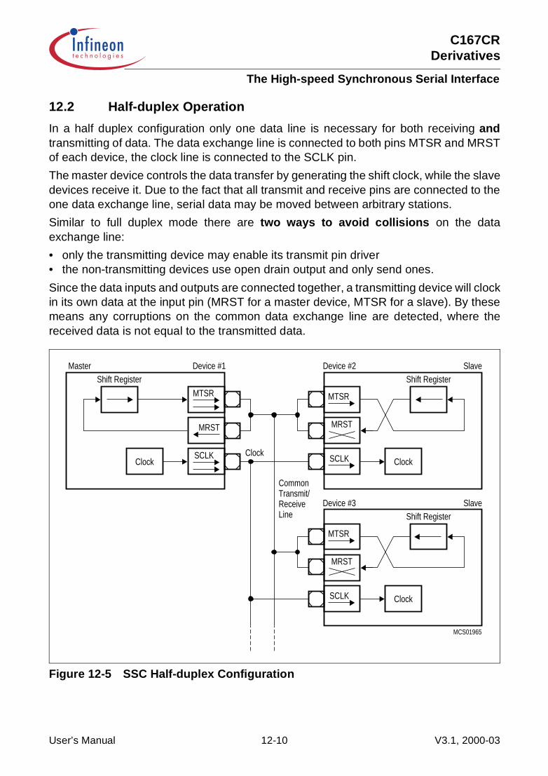
C167CRDerivatives
The High-speed Synchronous Serial Interface
12.2 Half-duplex Operation
In a half duplex configuration only one data line is necessary for both receiving andtransmitting of data. The data exchange line is connected to both pins MTSR and MRSTof each device, the clock line is connected to the SCLK pin.
The master device controls the data transfer by generating the shift clock, while the slavedevices receive it. Due to the fact that all transmit and receive pins are connected to theone data exchange line, serial data may be moved between arbitrary stations.
Similar to full duplex mode there are two ways to avoid collisions on the dataexchange line:
• only the transmitting device may enable its transmit pin driver• the non-transmitting devices use open drain output and only send ones.
Since the data inputs and outputs are connected together, a transmitting device will clockin its own data at the input pin (MRST for a master device, MTSR for a slave). By thesemeans any corruptions on the common data exchange line are detected, where thereceived data is not equal to the transmitted data.
Figure 12-5 SSC Half-duplex Configuration
MCS01965
CommonTransmit/ReceiveLine
MRST
SCLK
Device #2 Slave
Clock
Shift Register
MTSR
Clock
Master Device #1
Clock
MTSR
MRST
SCLK
Shift Register
Shift Register
Clock
SlaveDevice #3
SCLK
MTSR
MRST
User’s Manual 12-10 V3.1, 2000-03

C167CRDerivatives
The High-speed Synchronous Serial Interface
12.3 Continuous Transfers
When the transmit interrupt request flag is set, it indicates that the transmit buffer SSCTBis empty and ready to be loaded with the next transmit data. If SSCTB has been reloadedby the time the current transmission is finished, the data is immediately transferred to theshift register and the next transmission will start without any additional delay. On the dataline there is no gap between the two successive frames. E.g. two byte transfers wouldlook the same as one word transfer. This feature can be used to interface with deviceswhich can operate with or require more than 16 data bits per transfer. It is just a matterof software, how long a total data frame length can be. This option can also be used e.g.to interface to byte-wide and word-wide devices on the same serial bus.
Note: Of course, this can only happen in multiples of the selected basic data width, sinceit would require disabling/enabling of the SSC to reprogram the basic data widthon-the-fly.
User’s Manual 12-11 V3.1, 2000-03

C167CRDerivatives
The High-speed Synchronous Serial Interface
12.4 Port Control
The SSC uses three pins of Port 3 to communicate with the external world. Pin P3.13/SCLK serves as the clock line, while pins P3.8/MRST (Master Receive/Slave Transmit)and P3.9/MTSR (Master Transmit/Slave Receive) serve as the serial data input/outputlines.The operation of these pins depends on the selected operating mode (master orslave). In order to enable the alternate output functions of these pins instead of thegeneral purpose IO operation, the respective port latches have to be set to ‘1’, since theport latch outputs and the alternate output lines are ANDed. When an alternate dataoutput line is not used (function disabled), it is held at a high level, allowing IO operationsvia the port latch. The direction of the port lines depends on the operating mode. TheSSC will automatically use the correct alternate input or output line of the ports whenswitching modes. The direction of the pins, however, must be programmed by the user,as shown in the tables. Using the open drain output feature helps to avoid bus contentionproblems and reduces the need for hardwired hand-shaking or slave select lines. In thiscase it is not always necessary to switch the direction of a port pin. Table 12-1summarizes the required values for the different modes and pins.
Note: In Table 12-1, an ‘x’ means that the actual value is irrelevant in the respectivemode, however, it is recommended to set these bits to ‘1’, so they are already inthe correct state when switching between master and slave mode.
Table 12-1 SSC Port Control
Pin Master Mode Slave Mode
Function Port Latch Direction Function Port Latch Direction
SCLK Serial Clock Output
P3.13 = ‘1’ DP3.13 = ‘1’ Serial Clock Input
P3.13 = ‘x’ DP3.13 = ‘0’
MTSR Serial Data Output
P3.9 = ‘1’ DP3.9 = ‘1’ Serial Data Input
P3.9 = ‘x’ DP3.9 = ‘0’
MRST Serial Data Input
P3.8 = ‘x’ DP3.8 = ‘0’ Serial Data Output
P3.8 = ‘1’ DP3.8 = ‘1’
User’s Manual 12-12 V3.1, 2000-03
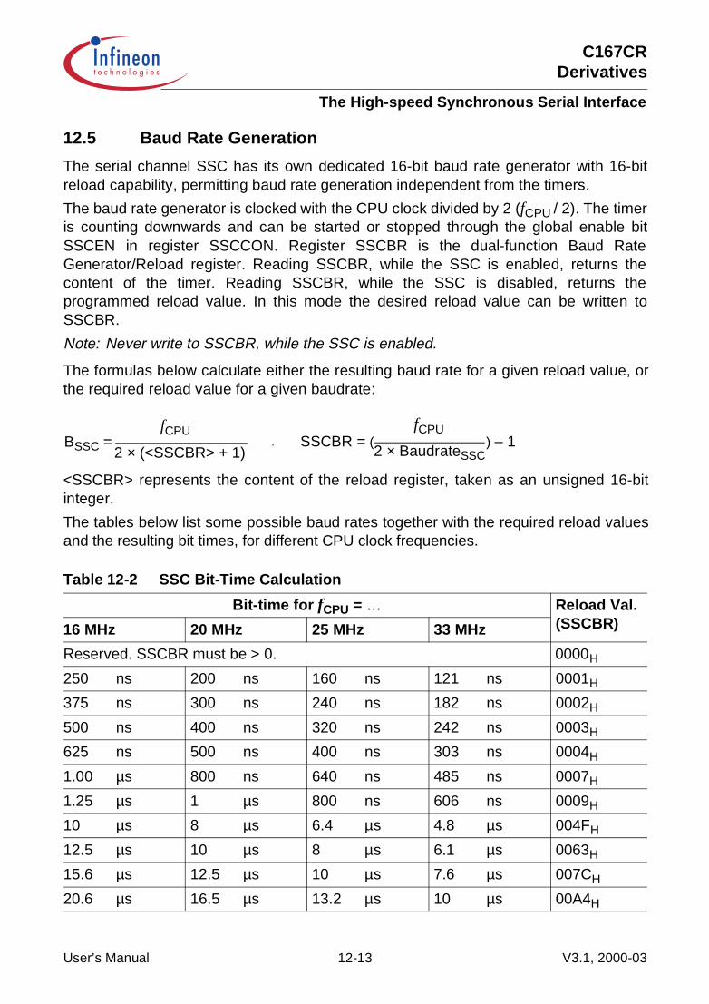
C167CRDerivatives
The High-speed Synchronous Serial Interface
12.5 Baud Rate Generation
The serial channel SSC has its own dedicated 16-bit baud rate generator with 16-bitreload capability, permitting baud rate generation independent from the timers.
The baud rate generator is clocked with the CPU clock divided by 2 (fCPU / 2). The timeris counting downwards and can be started or stopped through the global enable bitSSCEN in register SSCCON. Register SSCBR is the dual-function Baud RateGenerator/Reload register. Reading SSCBR, while the SSC is enabled, returns thecontent of the timer. Reading SSCBR, while the SSC is disabled, returns theprogrammed reload value. In this mode the desired reload value can be written toSSCBR.
Note: Never write to SSCBR, while the SSC is enabled.
The formulas below calculate either the resulting baud rate for a given reload value, orthe required reload value for a given baudrate:
<SSCBR> represents the content of the reload register, taken as an unsigned 16-bitinteger.
The tables below list some possible baud rates together with the required reload valuesand the resulting bit times, for different CPU clock frequencies.
Table 12-2 SSC Bit-Time Calculation
Bit-time for fCPU = … Reload Val.(SSCBR)16 MHz 20 MHz 25 MHz 33 MHz
Reserved. SSCBR must be > 0. 0000H
250 ns 200 ns 160 ns 121 ns 0001H
375 ns 300 ns 240 ns 182 ns 0002H
500 ns 400 ns 320 ns 242 ns 0003H
625 ns 500 ns 400 ns 303 ns 0004H
1.00 µs 800 ns 640 ns 485 ns 0007H
1.25 µs 1 µs 800 ns 606 ns 0009H
10 µs 8 µs 6.4 µs 4.8 µs 004FH
12.5 µs 10 µs 8 µs 6.1 µs 0063H
15.6 µs 12.5 µs 10 µs 7.6 µs 007CH
20.6 µs 16.5 µs 13.2 µs 10 µs 00A4H
BSSC =fCPU
2 × (<SSCBR> + 1)SSCBR = (
fCPU
2 × BaudrateSSC) – 1,
User’s Manual 12-13 V3.1, 2000-03

C167CRDerivatives
The High-speed Synchronous Serial Interface
1 ms 800 µs 640 µs 485 µs 1F3FH
1.25 ms 1 ms 800 µs 606 µs 270FH
1.56 ms 1.25 ms 1 ms 758 µs 30D3H
8.2 ms 6.6 ms 5.2 ms 4.0 ms FFFFH
Table 12-3 SSC Baudrate Calculation
Baud Rate for fCPU = … Reload Val.(SSCBR)16 MHz 20 MHz 25 MHz 33 MHz
Reserved. SSCBR must be > 0. 0000H
4.00 MBaud 5.00 MBaud 6.25 MBaud 8.25 MBaud 0001H
2.67 MBaud 3.33 MBaud 4.17 MBaud 5.50 MBaud 0002H
2.00 MBaud 2.50 MBaud 3.13 MBaud 4.13 MBaud 0003H
1.60 MBaud 2.00 MBaud 2.50 MBaud 3.30 MBaud 0004H
1.00 MBaud 1.25 MBaud 1.56 MBaud 2.06 MBaud 0007H
800 KBaud 1.0 MBaud 1.25 MBaud 1.65 MBaud 0009H
100 KBaud 125 KBaud 156 KBaud 206 KBaud 004FH
80 KBaud 100 KBaud 125 KBaud 165 KBaud 0063H
64 KBaud 80 KBaud 100 KBaud 132 KBaud 007CH
48.5 KBaud 60.6 KBaud 75.8 KBaud 100 KBaud 00A4H
1.0 KBaud 1.25 KBaud 1.56 KBaud 2.06 KBaud 1F3FH
800 Baud 1.0 KBaud 1.25 KBaud 1.65 KBaud 270FH
640 Baud 800 Baud 1.0 KBaud 1.32 KBaud 30D3H
122.1 Baud 152.6 Baud 190.7 Baud 251.7 Baud FFFFH
Table 12-2 SSC Bit-Time Calculation (cont’d)
Bit-time for fCPU = … Reload Val.(SSCBR)16 MHz 20 MHz 25 MHz 33 MHz
User’s Manual 12-14 V3.1, 2000-03
C167CRDerivatives
The High-speed Synchronous Serial Interface
12.6 Error Detection Mechanisms
The SSC is able to detect four different error conditions. Receive Error and Phase Errorare detected in all modes, while Transmit Error and Baudrate Error only apply to slavemode. When an error is detected, the respective error flag is set. When thecorresponding Error Enable Bit is set, also an error interrupt request will be generatedby setting SSCEIR (see Figure 12-6). The error interrupt handler may then check theerror flags to determine the cause of the error interrupt. The error flags are not resetautomatically (like SSCEIR), but rather must be cleared by software after servicing. Thisallows servicing of some error conditions via interrupt, while the others may be polled bysoftware.
Note: The error interrupt handler must clear the associated (enabled) errorflag(s) toprevent repeated interrupt requests.
A Receive Error (Master or Slave mode) is detected, when a new data frame iscompletely received, but the previous data was not read out of the receive buffer registerSSCRB. This condition sets the error flag SSCRE and, when enabled via SSCREN, theerror interrupt request flag SSCEIR. The old data in the receive buffer SSCRB will beoverwritten with the new value and is unretrievably lost.
A Phase Error (Master or Slave mode) is detected, when the incoming data at pin MRST(master mode) or MTSR (slave mode), sampled with the same frequency as the CPUclock, changes between one sample before and two samples after the latching edge ofthe clock signal (see “Clock Control”). This condition sets the error flag SSCPE and,when enabled via SSCPEN, the error interrupt request flag SSCEIR.
A Baud Rate Error (Slave mode) is detected, when the incoming clock signal deviatesfrom the programmed baud rate by more than 100%, i.e. it either is more than double orless than half the expected baud rate. This condition sets the error flag SSCBE and,when enabled via SSCBEN, the error interrupt request flag SSCEIR. Using this errordetection capability requires that the slave’s baud rate generator is programmed to thesame baud rate as the master device. This feature detects false additional, or missingpulses on the clock line (within a certain frame).
Note: If this error condition occurs and bit SSCAREN = ‘1’, an automatic reset of the SSCwill be performed in case of this error. This is done to reinitialize the SSC, if toofew or too many clock pulses have been detected.
User’s Manual 12-15 V3.1, 2000-03
C167CRDerivatives
The High-speed Synchronous Serial Interface
A Transmit Error (Slave mode) is detected, when a transfer was initiated by the master(shift clock gets active), but the transmit buffer SSCTB of the slave was not updatedsince the last transfer. This condition sets the error flag SSCTE and, when enabled viaSSCTEN, the error interrupt request flag SSCEIR. If a transfer starts while the transmitbuffer is not updated, the slave will shift out the ‘old’ contents of the shift register, whichnormally is the data received during the last transfer.This may lead to the corruption of the data on the transmit/receive line in half-duplexmode (open drain configuration), if this slave is not selected for transmission. This moderequires that slaves not selected for transmission only shift out ones, i.e. their transmitbuffers must be loaded with ‘FFFFH’ prior to any transfer.
Note: A slave with push/pull output drivers, which is not selected for transmission, willnormally have its output drivers switched. However, in order to avoid possibleconflicts or misinterpretations, it is recommended to always load the slave’stransmit buffer prior to any transfer.
Figure 12-6 SSC Error Interrupt Control
&SSCTEN
SSCTETransmitError
Register SSCCON
&SSCREN
SSCREReceiveError
&SSCPEN
SSCPEPhaseError
&SSCBEN
SSCBEBaudrateError
1
&SSCEIE
SSCEIR
ErrorInterruptSSCEINT
Register SSCEIC
MCA01968
User’s Manual 12-16 V3.1, 2000-03
C167CRDerivatives
The High-speed Synchronous Serial Interface
12.7 SSC Interrupt Control
Three bit addressable interrupt control registers are provided for serial channel SSC.Register SSCTIC controls the transmit interrupt, SSCRIC controls the receive interruptand SSCEIC controls the error interrupt of serial channel SSC. Each interrupt sourcealso has its own dedicated interrupt vector. SCTINT is the transmit interrupt vector,SCRINT is the receive interrupt vector, and SCEINT is the error interrupt vector.
The cause of an error interrupt request (receive, phase, baudrate, transmit error) can beidentified by the error status flags in control register SSCCON.
Note: In contrary to the error interrupt request flag SSCEIR, the error status flags SSCxEare not reset automatically upon entry into the error interrupt service routine, butmust be cleared by software.
Note: Please refer to the general Interrupt Control Register description for anexplanation of the control fields.
SSCTICSSC Transmit Intr. Ctrl. Reg. SFR (FF72H/B9H) Reset value: - - 00H
15 14 13 12 11 10 9 8 7 6 5 4 3 2 1 0
SSC TIR
SSC TIE ILVL GLVL
- - - - - - - - rw rw rw rw
SSCRICSSC Receive Intr. Ctrl. Reg. SFR (FF74H/BAH) Reset value: - - 00H
15 14 13 12 11 10 9 8 7 6 5 4 3 2 1 0
SSC RIR
SSC RIE ILVL GLVL
- - - - - - - - rw rw rw rw
SSCEICSSC Error Intr. Ctrl. Reg. SFR (FF76H/BBH) Reset value: - - 00H
15 14 13 12 11 10 9 8 7 6 5 4 3 2 1 0
SSC EIR
SSC EIE ILVL GLVL
- - - - - - - - rw rw rw rw
User’s Manual 12-17 V3.1, 2000-03

C167CRDerivatives
The Watchdog Timer (WDT)
13 The Watchdog Timer (WDT)To allow recovery from software or hardware failure, the C167CR provides a WatchdogTimer. If the software fails to service this timer before an overflow occurs, an internalreset sequence will be initiated. This internal reset will also pull the RSTOUT pin low,which also resets the peripheral hardware which might be the cause for the malfunction.When the watchdog timer is enabled and the software has been designed to service itregularly before it overflows, the watchdog timer will supervise the program execution asit only will overflow if the program does not progress properly. The watchdog timer willalso time out if a software error was due to hardware related failures. This prevents thecontroller from malfunctioning for longer than a user-specified time.
Note: When the bidirectional reset is enabled also pin RSTIN will be pulled low for theduration of the internal reset sequence upon a software reset or a watchdog timerreset.
The watchdog timer provides two registers:
• a read-only timer register that contains the current count, and• a control register for initialization and reset source detection.
Figure 13-1 SFRs and Port Pins Associated with the Watchdog Timer
The watchdog timer is a 16-bit up counter which is clocked with the prescaled CPU clock(fCPU). The prescaler divides the CPU clock:
• by 2 (WDTIN = ‘0’), or• by 128 (WDTIN = ‘1’).
MCA04381
WDT WDTCON
Reset Indication Pins Data Registers Control Registers
RSTOUT(deactivated by EINIT)
RSTIN(bidirectional reset only)
User’s Manual 13-1 V3.1, 2000-03
C167CRDerivatives
The Watchdog Timer (WDT)
The 16-bit watchdog timer is realized as two concatenated 8-bit timers (seeFigure 13-2). The upper 8 bits of the watchdog timer can be preset to auser-programmable value via a watchdog service access in order to vary the watchdogexpire time. The lower 8 bits are reset upon each service access.
Figure 13-2 Watchdog Timer Block Diagram
MCB02052
WDT High Byte WDTRMUX
÷ 2
RSTOUT
WDTIN
WDT Low Byte
WDTRELControlWDT
÷ 128
f CPU
Reset
Clear
User’s Manual 13-2 V3.1, 2000-03

C167CRDerivatives
The Watchdog Timer (WDT)
13.1 Operation of the Watchdog Timer
The current count value of the Watchdog Timer is contained in the Watchdog TimerRegister WDT which is a non-bitaddressable read-only register. The operation of theWatchdog Timer is controlled by its bitaddressable Watchdog Timer Control RegisterWDTCON. This register specifies the reload value for the high byte of the timer, selectsthe input clock prescaling factor and also provides flags that indicate the source of areset.
After any reset (except see note) the watchdog timer is enabled and starts counting upfrom 0000H with the default frequency fWDT = fCPU / 2. The default input frequency maybe changed to another frequency (fWDT = fCPU / 128) by programming the prescaler (bitWDTIN).
The watchdog timer can be disabled by executing the instruction DISWDT (DisableWatchdog Timer). Instruction DISWDT is a protected 32-bit instruction which will ONLYbe executed during the time between a reset and execution of either the EINIT (End ofInitialization) or the SRVWDT (Service Watchdog Timer) instruction. Either one of theseinstructions disables the execution of DISWDT.
Note: After a hardware reset that activates the Bootstrap Loader the watchdog timer willbe disabled. The software reset that terminates the BSL mode will then enable theWDT.
When the watchdog timer is not disabled via instruction DISWDT it will continue countingup, even during Idle Mode. If it is not serviced via the instruction SRVWDT by the timethe count reaches FFFFH the watchdog timer will overflow and cause an internal reset.This reset will pull the external reset indication pin RSTOUT low. The Watchdog TimerReset Indication Flag (WDTR) in register WDTCON will be set in this case.In bidirectional reset mode also pin RSTIN will be pulled low for the duration of theinternal reset sequence and a long hardware reset will be indicated instead.
A watchdog reset will also complete a running external bus cycle before starting theinternal reset sequence if this bus cycle does not use READY or samples READY active(low) after the programmed waitstates. Otherwise the external bus cycle will be aborted.
To prevent the watchdog timer from overflowing it must be serviced periodically by theuser software. The watchdog timer is serviced with the instruction SRVWDT which is aprotected 32-bit instruction. Servicing the watchdog timer clears the low byte and reloadsthe high byte of the watchdog timer register WDT with the preset value from bitfieldWDTREL which is the high byte of register WDTCON. Servicing the watchdog timer willalso reset bit WDTR. After being serviced the watchdog timer continues counting up fromthe value (<WDTREL> × 28).
User’s Manual 13-3 V3.1, 2000-03
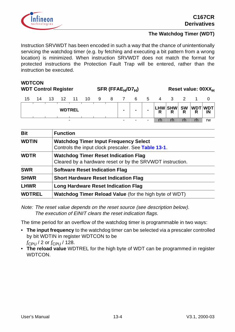
C167CRDerivatives
The Watchdog Timer (WDT)
Instruction SRVWDT has been encoded in such a way that the chance of unintentionallyservicing the watchdog timer (e.g. by fetching and executing a bit pattern from a wronglocation) is minimized. When instruction SRVWDT does not match the format forprotected instructions the Protection Fault Trap will be entered, rather than theinstruction be executed.
Note: The reset value depends on the reset source (see description below).The execution of EINIT clears the reset indication flags.
The time period for an overflow of the watchdog timer is programmable in two ways:
• The input frequency to the watchdog timer can be selected via a prescaler controlledby bit WDTIN in register WDTCON to befCPU / 2 or fCPU / 128.
• The reload value WDTREL for the high byte of WDT can be programmed in registerWDTCON.
WDTCONWDT Control Register SFR (FFAEH/D7H) Reset value: 00XXH
15 14 13 12 11 10 9 8 7 6 5 4 3 2 1 0
WDTREL - - - LHW R
SHW R
SW R
WDT R
WDT IN
- - - - rh rh rh rh rw
Bit Function
WDTIN Watchdog Timer Input Frequency SelectControls the input clock prescaler. See Table 13-1.
WDTR Watchdog Timer Reset Indication FlagCleared by a hardware reset or by the SRVWDT instruction.
SWR Software Reset Indication Flag
SHWR Short Hardware Reset Indication Flag
LHWR Long Hardware Reset Indication Flag
WDTREL Watchdog Timer Reload Value (for the high byte of WDT)
User’s Manual 13-4 V3.1, 2000-03
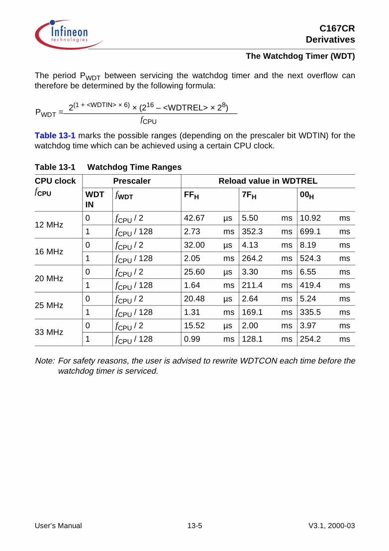
C167CRDerivatives
The Watchdog Timer (WDT)
The period PWDT between servicing the watchdog timer and the next overflow cantherefore be determined by the following formula:
Table 13-1 marks the possible ranges (depending on the prescaler bit WDTIN) for thewatchdog time which can be achieved using a certain CPU clock.
Note: For safety reasons, the user is advised to rewrite WDTCON each time before thewatchdog timer is serviced.
Table 13-1 Watchdog Time Ranges
CPU clock fCPU
Prescaler Reload value in WDTREL
WDTIN
fWDT FFH 7FH 00H
12 MHz0 fCPU / 2 42.67 µs 5.50 ms 10.92 ms
1 fCPU / 128 2.73 ms 352.3 ms 699.1 ms
16 MHz0 fCPU / 2 32.00 µs 4.13 ms 8.19 ms
1 fCPU / 128 2.05 ms 264.2 ms 524.3 ms
20 MHz0 fCPU / 2 25.60 µs 3.30 ms 6.55 ms
1 fCPU / 128 1.64 ms 211.4 ms 419.4 ms
25 MHz0 fCPU / 2 20.48 µs 2.64 ms 5.24 ms
1 fCPU / 128 1.31 ms 169.1 ms 335.5 ms
33 MHz0 fCPU / 2 15.52 µs 2.00 ms 3.97 ms
1 fCPU / 128 0.99 ms 128.1 ms 254.2 ms
PWDT =fCPU
2(1 + <WDTIN> × 6) × (216 – <WDTREL> × 28)
User’s Manual 13-5 V3.1, 2000-03

C167CRDerivatives
The Watchdog Timer (WDT)
13.2 Reset Source Indication
The reset indication flags in register WDTCON provide information on the source for thelast reset. As the C167CR starts executing from location 00’0000H after any possiblereset event the initialization software may check these flags in order to determine if therecent reset event was triggered by an external hardware signal (via RSTIN), by softwareitself or by an overflow of the watchdog timer. The initialization (and also the furtheroperation) of the microcontroller system can thus be adapted to the respectivecircumstances, e.g. a special routine may verify the software integrity after a watchdogtimer reset.
The reset indication flags are not mutually exclusive, i.e. more than one flag may be setafter reset depending on its source. Table 13-2 summarizes the possible combinations:
Long Hardware Reset is indicated when the RSTIN input is still sampled low (active) atthe end of a hardware triggered internal reset sequence.
Short Hardware Reset is indicated when the RSTIN input is sampled high (inactive) atthe end of a hardware triggered internal reset sequence.
Software Reset is indicated after a reset triggered by the excution of instruction SRST.
Watchdog Timer Reset is indicated after a reset triggered by an overflow of thewatchdog timer.
Note: When bidirectional reset is enabled the RSTIN pin is pulled low for the duration ofthe internal reset sequence upon any sort of reset.Therefore always a long hardware reset (LHWR) will be recognized in any case.
Table 13-2 Reset Indication Flag Combinations
Event Reset Indication Flags1)
1) Description of table entries:‘1’ = flag is set, ‘0’ = flag is cleared, ‘–’ = flag is not affected,‘∗’ = flag is set in bidirectional reset mode, not affected otherwise.
LHWR SHWR SWR WDTR
Long Hardware Reset 1 1 1 0
Short Hardware Reset ∗ 1 1 0
Software Reset ∗ ∗ 1 –
Watchdog Timer Reset ∗ ∗ 1 1
EINIT instruction 0 0 0 –
SRVWDT instruction – – – 0
User’s Manual 13-6 V3.1, 2000-03
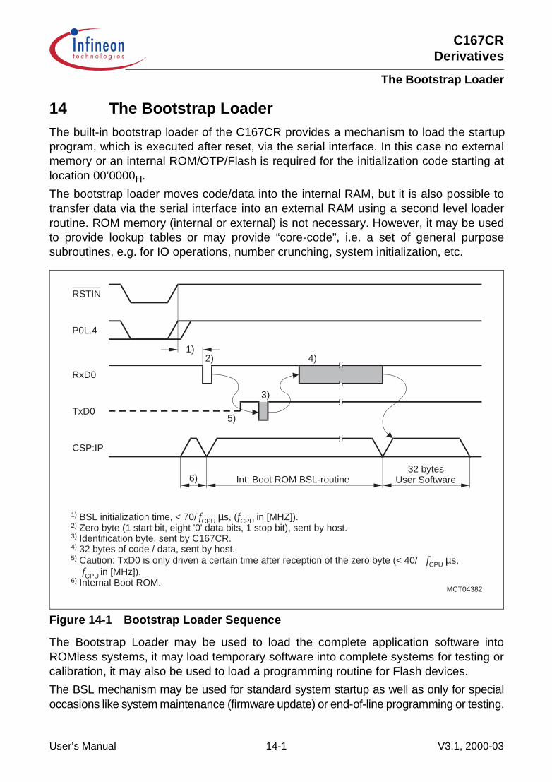
C167CRDerivatives
The Bootstrap Loader
14 The Bootstrap LoaderThe built-in bootstrap loader of the C167CR provides a mechanism to load the startupprogram, which is executed after reset, via the serial interface. In this case no externalmemory or an internal ROM/OTP/Flash is required for the initialization code starting atlocation 00’0000H.
The bootstrap loader moves code/data into the internal RAM, but it is also possible totransfer data via the serial interface into an external RAM using a second level loaderroutine. ROM memory (internal or external) is not necessary. However, it may be usedto provide lookup tables or may provide “core-code”, i.e. a set of general purposesubroutines, e.g. for IO operations, number crunching, system initialization, etc.
Figure 14-1 Bootstrap Loader Sequence
The Bootstrap Loader may be used to load the complete application software intoROMless systems, it may load temporary software into complete systems for testing orcalibration, it may also be used to load a programming routine for Flash devices.
The BSL mechanism may be used for standard system startup as well as only for specialoccasions like system maintenance (firmware update) or end-of-line programming or testing.
MCT04382
RSTIN
P0L.4
RxD0
TxD0
CSP:IP
1)2) 4)
3)
5)
32 bytesUser Software6) Int. Boot ROM BSL-routine
1) BSL initialization time, < 70/ fCPU µs, (fCPU in [MHZ]).2) Zero byte (1 start bit, eight '0' data bits, 1 stop bit), sent by host.3) Identification byte, sent by C167CR.4) 32 bytes of code / data, sent by host.5) Caution: TxD0 is only driven a certain time after reception of the zero byte (< 40/ fCPU µs,
fCPU in [MHz]).6) Internal Boot ROM.
User’s Manual 14-1 V3.1, 2000-03

C167CRDerivatives
The Bootstrap Loader
Entering the Bootstrap Loader
The C167CR enters BSL mode if pin P0L.4 is sampled low at the end of a hardwarereset. In this case the built-in bootstrap loader is activated independent of the selectedbus mode. The bootstrap loader code is stored in a special Boot-ROM, no part of thestandard mask ROM, OTP or Flash memory area is required for this.
After entering BSL mode and the respective initialization1) the C167CR scans the RXD0line to receive a zero byte, i.e. one start bit, eight ‘0’ data bits and one stop bit. From theduration of this zero byte it calculates the corresponding baudrate factor with respect tothe current CPU clock, initializes the serial interface ASC0 accordingly and switches pinTxD0 to output. Using this baudrate, an identification byte is returned to the host thatprovides the loaded data.
This identification byte identifies the device to be booted. The following codes aredefined:
55H: 8xC166.A5H: Previous versions of the C167 (obsolete).B5H: Previous versions of the C165.C5H: C167 derivatives.D5H: All devices equipped with identification registers.
Note: The identification byte D5H does not directly identify a specific derivative. Thisinformation can in this case be obtained from the identification registers.
When the C167CR has entered BSL mode, the following configuration is automaticallyset (values that deviate from the normal reset values, are marked):
Watchdog Timer: Disabled Register STKUN: FA40HContext Pointer CP: FA00H Register STKOV: FA0CH 0<–>CStack Pointer SP: FA40H Register BUSCON0: acc. to startup config.Register S0CON: 8011H P3.10/TXD0: ‘1’Register S0BG: acc. to ‘00’ byte DP3.10: ‘1’
Other than after a normal reset the watchdog timer is disabled, so the bootstrap loadingsequence is not time limited. Pin TXD0 is configured as output, so the C167CR canreturn the identification byte.
Note: Even if the internal ROM/OTP/Flash is enabled, no code can be executed out of it.
The hardware that activates the BSL during reset may be a simple pull-down resistor onP0L.4 for systems that use this feature upon every hardware reset. You may want to usea switchable solution (via jumper or an external signal) for systems that only temporarilyuse the bootstrap loader.
1) The external host should not send the zero byte before the end of the BSL initialization time (see Figure 14-1)to make sure that it is correctly received.
User’s Manual 14-2 V3.1, 2000-03

C167CRDerivatives
The Bootstrap Loader
Figure 14-2 Hardware Provisions to Activate the BSL
After sending the identification byte the ASC0 receiver is enabled and is ready to receivethe initial 32 Bytes from the host. A half duplex connection is therefore sufficient to feedthe BSL.
Note: In order to properly enter BSL mode it is not only required to pull P0L.4 low, butalso pins P0L.2, P0L.3, P0L.5 must receive defined levels.This is described in Chapter 19.
MCA02261
P0L.4Ω
Circuit_1
P0L.4
R8 k
P0L.4
External Signal
R
BSL
8 kP0L.4Ω
Normal Boot
Circuit_2
User’s Manual 14-3 V3.1, 2000-03

C167CRDerivatives
The Bootstrap Loader
Memory Configuration after Reset
The configuration (i.e. the accessibility) of the C167CR’s memory areas after reset inBootstrap-loader mode differs from the standard case. Pin EA is not evaluated whenBSL mode is selected, and accesses to the internal code memory are partly redirected,while the C167CR is in BSL mode (see Table 14-1). All code fetches are made from thespecial Boot-ROM, while data accesses read from the internal code memory. Dataaccesses will return undefined values on ROMless devices.
Note: The code in the Boot-ROM is not an invariant feature of the C167CR. Usersoftware should not try to execute code from the internal ROM area while the BSLmode is still active, as these fetches will be redirected to the Boot-ROM.The Boot-ROM will also “move” to segment 1, when the internal ROM area ismapped to segment 1.
Table 14-1 BSL Memory Configurations
BSL mode active Yes (P0L.4 = ‘0’) Yes (P0L.4 = ‘0’) No (P0L.4 = ‘1’)
EA pin high low acc. to application
Code fetch from internal ROM area
Boot-ROM access Boot-ROM access User ROM access
Data fetch from internal ROM area
User ROM access User ROM access User ROM access
MCA04383
255
1
Int.RAM
0
Use
r R
OM
Boo
t-R
OM
Access toint. ROMenabled
Access toexternalbusdisabled
16 MBytes
MCA04384
255
1
Int.RAM
0
Use
r R
OM
Boo
t-R
OM
Access toint. ROMenabled
Access toexternalbusenabled
16 MBytes
MCA04385
255
1
Int.RAM
0
Use
r R
OM
Dependson resetconfig.
Dependson resetconfig.(EA, P0)
16 MBytes
User’s Manual 14-4 V3.1, 2000-03
C167CRDerivatives
The Bootstrap Loader
Loading the Startup Code
After sending the identification byte the BSL enters a loop to receive 32 Bytes via ASC0.These bytes are stored sequentially into locations 00’FA40H through 00’FA5FH of theinternal RAM. So up to 16 instructions may be placed into the RAM area. To execute theloaded code the BSL then jumps to location 00’FA40H, i.e. the first loaded instruction.The bootstrap loading sequence is now terminated, the C167CR remains in BSL mode,however. Most probably the initially loaded routine will load additional code or data, asan average application is likely to require substantially more than 16 instructions. Thissecond receive loop may directly use the pre-initialized interface ASC0 to receive dataand store it to arbitrary user-defined locations.
This second level of loaded code may be the final application code. It may also beanother, more sophisticated, loader routine that adds a transmission protocol to enhancethe integrity of the loaded code or data. It may also contain a code sequence to changethe system configuration and enable the bus interface to store the received data intoexternal memory.
This process may go through several iterations or may directly execute the finalapplication. In all cases the C167CR will still run in BSL mode, i.e. with the watchdogtimer disabled and limited access to the internal code memory. All code fetches from theinternal ROM area (00’0000H … 00’7FFFH or 01’0000H … 01’7FFFH, if mapped tosegment 1) are redirected to the special Boot-ROM. Data fetches access will access theinternal code memory of the C167CR, if any is available, but will return undefined dataon ROMless devices.
Exiting Bootstrap Loader Mode
In order to execute a program in normal mode, the BSL mode must be terminated first.The C167CR exits BSL mode upon a software reset (ignores the level on P0L.4) or ahardware reset (P0L.4 must be high then!). After a reset the C167CR will start executingfrom location 00’0000H of the internal ROM or the external memory, as programmed viapin EA.
User’s Manual 14-5 V3.1, 2000-03

C167CRDerivatives
The Bootstrap Loader
Choosing the Baudrate for the BSL
The calculation of the serial baudrate for ASC0 from the length of the first zero byte thatis received, allows the operation of the bootstrap loader of the C167CR with a wide rangeof baudrates. However, the upper and lower limits have to be kept, in order to insureproper data transfer.
The C167CR uses timer T6 to measure the length of the initial zero byte. Thequantization uncertainty of this measurement implies the first deviation from the realbaudrate, the next deviation is implied by the computation of the S0BRL reload valuefrom the timer contents. The formula below shows the association:
For a correct data transfer from the host to the C167CR the maximum deviation betweenthe internal initialized baudrate for ASC0 and the real baudrate of the host should bebelow 2.5%. The deviation (FB, in percent) between host baudrate and C167CRbaudrate can be calculated via the formula below:
Note: Function (FB) does not consider the tolerances of oscillators and other devicessupporting the serial communication.
This baudrate deviation is a nonlinear function depending on the CPU clock and thebaudrate of the host. The maxima of the function (FB) increase with the host baudratedue to the smaller baudrate prescaler factors and the implied higher quantization error(see Figure 14-3).
fCPU
32 S0BRL 1+( )⋅----------------------------------------------BC167CR =
S0BRL T6 36–72
--------------------= T6 94---
fCPU
BHost--------------⋅=,
FBBContr BHost–
BContr------------------------------------- 100%⋅= FB 2,5%≤,
User’s Manual 14-6 V3.1, 2000-03

C167CRDerivatives
The Bootstrap Loader
Figure 14-3 Baudrate Deviation between Host and C167CR
The minimum baudrate (BLow in Figure 14-3) is determined by the maximum countcapacity of timer T6, when measuring the zero byte, i.e. it depends on the CPU clock.The minimum baudrate is obtained by using the maximum T6 count 216 in the baudrateformula. Baudrates below BLow would cause T6 to overflow. In this case ASC0 cannotbe initialized properly and the communication with the external host is likely to fail.
The maximum baudrate (BHigh in Figure 14-3) is the highest baudrate where thedeviation still does not exceed the limit, i.e. all baudrates between BLow and BHigh arebelow the deviation limit. BHigh marks the baudrate up to which communication with theexternal host will work properly without additional tests or investigations.
Higher baudrates, however, may be used as long as the actual deviation does notexceed the indicated limit. A certain baudrate (marked I) in Figure 14-3) may e.g. violatethe deviation limit, while an even higher baudrate (marked II) in Figure 14-3) stays verywell below it. Any baudrate can be used for the bootstrap loader provided that thefollowing three prerequisites are fulfilled:
• the baudrate is within the specified operating range for the ASC0• the external host is able to use this baudrate• the computed deviation error is below the limit.
Table 14-2 Bootstrap Loader Baudrate Ranges
fCPU [MHz] 10 12 16 20 25 33
BMAX 312,500 375,000 500,000 625,000 781,250 1,031,250
BHigh 9,600 19,200 19,200 19,200 38,400 38,400
BSTDmin 600 600 600 1,200 1,200 1,200
BLow 344 412 550 687 859 1,133
MCA02260
BF
2.5%
LowB BHigh
Ι
ΙΙ
BHost
User’s Manual 14-7 V3.1, 2000-03

C167CRDerivatives
The Capture/Compare Units
15 The Capture/Compare UnitsThe C167CR provides two almost identical Capture/Compare (CAPCOM) units whichonly differ in the way they are connected to the C167CR’s IO pins. They provide32 channels which interact with 4 timers. The CAPCOM units can capture the contentsof a timer on specific internal or external events, or they can compare a timer’s contentwith given values and modify output signals in case of a match. With this mechanismthey support generation and control of timing sequences on up to 16 channels per unitwith a minimum of software intervention.
Figure 15-1 SFRs and Port Pins Associated with the CAPCOM Units
E
MCA04386
DP1H
P1H
ODP2 E
DP2
P2
ODP3 E
DP3
P3
EODP7
DP7
P7
ODP8 E
DP8
P8
T0
T0REL
T1
T1REL
T7 E
T7REL E
T8 E
T8REL E
CC0-3
CC4-7
CC8-11
CC12-15
CC16-19
CC20-23
CC24-27
CC28-31
T01CON
T78CON
CCM0
CCM1
CCM2
CCM3
CCM4
CCM5
CCM6
CCM7
T0IC
T1IC
T7IC E
T8IC E
CC0IC-3IC
CC4IC-7IC
CC8IC-11IC
CC12IC-15IC
CC16IC-19IC
CC20IC-23IC
CC24IC-27IC
CC28IC-31IC
Ports & Direction ControlAlternate Functions
Data Registers Control Registers Interrupt Control
CC0IO/P2.0..CC15IO/P2.15CC16IO/P8.0..CC23IO/P8.7CC28IO/P7.4..CC31IO/P7.7CC24IO/P1H.4..CC27IO/P1H.7
ODPx Port x Open Drain Control RegisterDPx Port x Direction Control RegisterPx Port x Data RegisterT01CON CAPCOM1 Timers T0/T1 Control RegisterT78CON CAPCOM2 Timers T7/T8 Control RegisterT0IC/T1IC CAPCOM1 Timer 0/1 Interrupt Ctrl. Reg.T7IC/T8IC CAPCOM2 Timer 7/8 Interrupt Ctrl. Reg.TxREL CAPCOM Timer x Reload Register
E
E
E
E
Tx CAPCOM Timer x RegisterCC0..15 CAPCOM1 Register 0..15CC16..31 CAPCOM2 Register 16..31CCM0..3 CAPCOM1 Mode Control Register 0..3CCM4..7 CAPCOM2 Mode Control Register 4..7CC0..15IC CAPCOM1 Interrupt Ctrl. Reg. 0..15CC16..31IC CAPCOM2 Interrupt Ctrl. Reg. 16..31
User’s Manual 15-1 V3.1, 2000-03

C167CRDerivatives
The Capture/Compare Units
From the programmer’s point of view, the term ‘CAPCOM unit’ refers to a set of SFRswhich are associated with this peripheral, including the port pins which may be used foralternate input/output functions including their direction control bits.
A CAPCOM unit is typically used to handle high speed IO tasks such as pulse andwaveform generation, pulse width modulation, or recording of the time at which specificevents occur. It also allows the implementation of up to 16 software timers. Themaximum resolution of the CAPCOM units is 8 CPU clock cycles (=16 TCL).
Each CAPCOM unit consists of two 16-bit timers (T0/T1 in CAPCOM1, T7/T8 inCAPCOM2), each with its own reload register (TxREL), and a bank of sixteen dualpurpose 16-bit capture/compare registers (CC0 through CC15 in CAPCOM1, CC16through CC31 in CAPCOM2).
The input clock for the CAPCOM timers is programmable to several prescaled values ofthe CPU clock, or it can be derived from an overflow/underflow of timer T6 in block GPT2.T0 and T7 may also operate in counter mode (from an external input) where they can beclocked by external events.
Each capture/compare register may be programmed individually for capture or comparefunction, and each register may be allocated to either timer of the associated unit. Allcapture/compare registers of each module have one port pin associated with it,respectively, which serves as an input pin for the capture function or as an output pin forthe compare function. The capture function causes the current timer contents to belatched into the respective capture/compare register triggered by an event (transition) onits associated port pin. The compare function may cause an output signal transition onthat port pin whose associated capture/compare register matches the current timercontents. Specific interrupt requests are generated upon each capture/compare event orupon timer overflow.
Figure 15-2 shows the basic structure of the two CAPCOM units.
User’s Manual 15-2 V3.1, 2000-03

C167CRDerivatives
The Capture/Compare Units
Figure 15-2 CAPCOM Unit Block Diagram
Table 15-1 CAPCOM Channel Port Connections
Unit Channel Port Capture Compare
CAPCOM1 CC0IO … CC15IO P2.0 … P2.15 Input Output
CAPCOM2 CC16IO … CC23IO P8.0 … P8.7 Input Output
CC24IO … CC27IO P1H.4 … P1H.7 Input –
CC28IO … CC31IO P7.4 … P7.7 Input Output
Σ = 32 Σ = 32 Σ = 32 Σ = 28
MCB02143B
ModeControl
(Captureor
Compare)
2n : 1fCPU
TxInput
ControlCAPCOM Timer Tx
TyInput
Control
TxIN
InterruptRequest
GPT2 Timer T6Over/Underflow
2n : 1fCPU
GPT2 Timer T6Over/Underflow
CCxIO
CCxIO
16 Capture Inputs16 Compare Outputs
Reload Reg. TxREL
CAPCOM Timer Ty
Reload Reg. TyREL
InterruptRequest
16 Capture/CompareInterrupt Request
16-BitCapture/CompareRegisters
User’s Manual 15-3 V3.1, 2000-03

C167CRDerivatives
The Capture/Compare Units
15.1 The CAPCOM Timers
The primary use of the timers T0/T1 and T7/T8 is to provide two independent time bases(16 TCL maximum resolution) for the capture/compare registers of each unit, but theymay also be used independent of the capture/compare registers.The basic structure of the four timers is identical, while the selection of input signals isdifferent for timers T0/T7 and timers T1/T8 (see figures below).
Figure 15-3 Block Diagram of CAPCOM Timers T0 and T7
Figure 15-4 Block Diagram of CAPCOM Timers T1 and T8
Note: When an external input signal is connected to the input lines of both T0 and T7,these timers count the input signal synchronously. Thus the two timers can beregarded as one timer whose contents can be compared with 32 capture registers.
MCB02013
CAPCOM Timer Tx InterruptRequest
2n : 1
Txl
TxIN
TxI
fCPU
MUX
TxR
TxI TxM
GPT2 Timer T6Over/Underflow
Reload Reg. TxREL
InputControl
EdgeSelect
x = 0, 7
MCB02014
CAPCOM Timer Tx InterruptRequest
2n : 1
Txl
fCPU
MUX
TxR
TxM
GPT2 Timer T6Over/Underflow
Reload Reg. TxREL
x = 1, 8
User’s Manual 15-4 V3.1, 2000-03
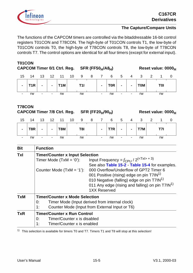
C167CRDerivatives
The Capture/Compare Units
The functions of the CAPCOM timers are controlled via the bitaddressable 16-bit controlregisters T01CON and T78CON. The high-byte of T01CON controls T1, the low-byte ofT01CON controls T0, the high-byte of T78CON controls T8, the low-byte of T78CONcontrols T7. The control options are identical for all four timers (except for external input).
T01CONCAPCOM Timer 0/1 Ctrl. Reg. SFR (FF50H/A8H) Reset value: 0000H
15 14 13 12 11 10 9 8 7 6 5 4 3 2 1 0
- T1R - - T1M T1I - T0R - - T0M T0I
- rw - - rw rw - rw - - rw rw
T78CONCAPCOM Timer 7/8 Ctrl. Reg. SFR (FF20H/90H) Reset value: 0000H
15 14 13 12 11 10 9 8 7 6 5 4 3 2 1 0
- T8R - - T8M T8I - T7R - - T7M T7I
- rw - - rw rw - rw - - rw rw
Bit Function
TxI Timer/Counter x Input SelectionTimer Mode (TxM = ‘0’): Input Frequency = fCPU / 2(<TxI> + 3)
See also Table 15-2 - Table 15-4 for examples.Counter Mode (TxM = ‘1’): 000 Overflow/Underflow of GPT2 Timer 6
001 Positive (rising) edge on pin T7IN1)
010 Negative (falling) edge on pin T7IN1) 011 Any edge (rising and falling) on pin T7IN1)
1XX Reserved
1) This selection is available for timers T0 and T7. Timers T1 and T8 will stop at this selection!
TxM Timer/Counter x Mode Selection0: Timer Mode (Input derived from internal clock)1: Counter Mode (Input from External Input or T6)
TxR Timer/Counter x Run Control0: Timer/Counter x is disabled1: Timer/Counter x is enabled
User’s Manual 15-5 V3.1, 2000-03
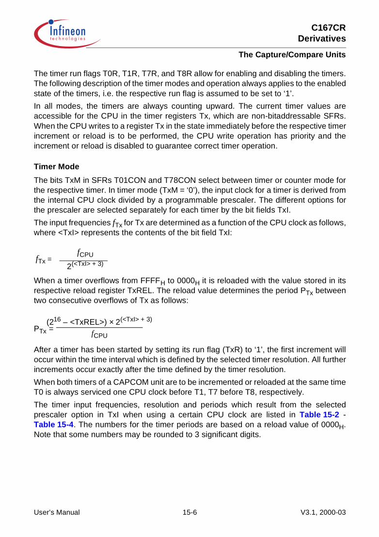
C167CRDerivatives
The Capture/Compare Units
The timer run flags T0R, T1R, T7R, and T8R allow for enabling and disabling the timers.The following description of the timer modes and operation always applies to the enabledstate of the timers, i.e. the respective run flag is assumed to be set to ‘1’.
In all modes, the timers are always counting upward. The current timer values areaccessible for the CPU in the timer registers Tx, which are non-bitaddressable SFRs.When the CPU writes to a register Tx in the state immediately before the respective timerincrement or reload is to be performed, the CPU write operation has priority and theincrement or reload is disabled to guarantee correct timer operation.
Timer Mode
The bits TxM in SFRs T01CON and T78CON select between timer or counter mode forthe respective timer. In timer mode (TxM = ‘0’), the input clock for a timer is derived fromthe internal CPU clock divided by a programmable prescaler. The different options forthe prescaler are selected separately for each timer by the bit fields TxI.
The input frequencies fTx for Tx are determined as a function of the CPU clock as follows,where <TxI> represents the contents of the bit field TxI:
When a timer overflows from FFFFH to 0000H it is reloaded with the value stored in itsrespective reload register TxREL. The reload value determines the period PTx betweentwo consecutive overflows of Tx as follows:
After a timer has been started by setting its run flag (TxR) to ‘1’, the first increment willoccur within the time interval which is defined by the selected timer resolution. All furtherincrements occur exactly after the time defined by the timer resolution.
When both timers of a CAPCOM unit are to be incremented or reloaded at the same timeT0 is always serviced one CPU clock before T1, T7 before T8, respectively.
The timer input frequencies, resolution and periods which result from the selectedprescaler option in TxI when using a certain CPU clock are listed in Table 15-2 -Table 15-4. The numbers for the timer periods are based on a reload value of 0000H.Note that some numbers may be rounded to 3 significant digits.
fTx =fCPU
2(<TxI> + 3)
PTx =fCPU
(216 – <TxREL>) × 2(<TxI> + 3)
User’s Manual 15-6 V3.1, 2000-03
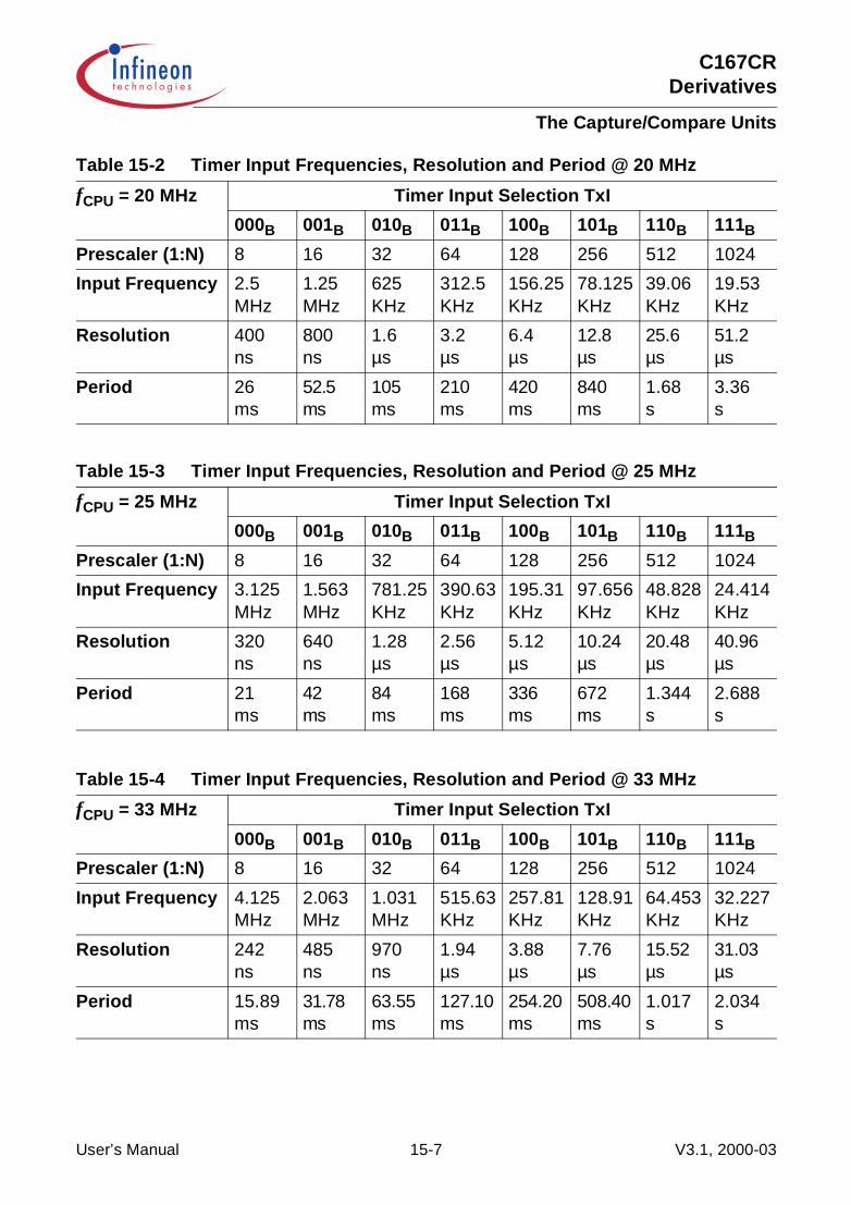
C167CRDerivatives
The Capture/Compare Units
Table 15-2 Timer Input Frequencies, Resolution and Period @ 20 MHz
fCPU = 20 MHz Timer Input Selection TxI
000B 001B 010B 011B 100B 101B 110B 111B
Prescaler (1:N) 8 16 32 64 128 256 512 1024
Input Frequency 2.5MHz
1.25MHz
625KHz
312.5KHz
156.25KHz
78.125KHz
39.06KHz
19.53KHz
Resolution 400ns
800ns
1.6µs
3.2µs
6.4µs
12.8µs
25.6µs
51.2µs
Period 26ms
52.5 ms
105ms
210ms
420ms
840ms
1.68s
3.36s
Table 15-3 Timer Input Frequencies, Resolution and Period @ 25 MHz
fCPU = 25 MHz Timer Input Selection TxI
000B 001B 010B 011B 100B 101B 110B 111B
Prescaler (1:N) 8 16 32 64 128 256 512 1024
Input Frequency 3.125MHz
1.563MHz
781.25KHz
390.63KHz
195.31KHz
97.656KHz
48.828KHz
24.414KHz
Resolution 320ns
640ns
1.28µs
2.56µs
5.12µs
10.24µs
20.48µs
40.96µs
Period 21ms
42ms
84ms
168ms
336ms
672ms
1.344s
2.688s
Table 15-4 Timer Input Frequencies, Resolution and Period @ 33 MHz
fCPU = 33 MHz Timer Input Selection TxI
000B 001B 010B 011B 100B 101B 110B 111B
Prescaler (1:N) 8 16 32 64 128 256 512 1024
Input Frequency 4.125MHz
2.063MHz
1.031MHz
515.63KHz
257.81KHz
128.91KHz
64.453KHz
32.227KHz
Resolution 242ns
485ns
970ns
1.94µs
3.88µs
7.76µs
15.52µs
31.03µs
Period 15.89ms
31.78ms
63.55ms
127.10ms
254.20ms
508.40ms
1.017s
2.034s
User’s Manual 15-7 V3.1, 2000-03

C167CRDerivatives
The Capture/Compare Units
Counter Mode
The bits TxM in SFRs T01CON and T78CON select between timer or counter mode forthe respective timer. In Counter mode (TxM = ‘1’) the input clock for a timer can bederived from the overflows/underflows of timer T6 in block GPT2. In addition, timers T0and T7 can be clocked by external events. Either a positive, a negative, or both a positiveand a negative transition at pin T0IN or T7IN (alternate port input function), respectively,can be selected to cause an increment of T0/T7.
When T1 or T8 is programmed to run in counter mode, bit field TxI is used to enable theoverflows/underflows of timer T6 as the count source. This is the only option for thesetimers and it is selected by the combination TxI = 000B. When bit field TxI is programmedto any other valid combination, the respective timer will stop.
When T0 or T7 is programmed to run in counter mode, bit field TxI is used to select thecount source and transition (if the source is the input pin) which should cause a counttrigger (see description of TxyCON for the possible selections).
Note: In order to use pin T0IN or T7IN as external count input pin, the respective port pinmust be configured as input, i.e. the corresponding direction control bit must becleared (DPx.y = ‘0’).If the respective port pin is configured as output, the associated timer may beclocked by modifying the port output latches Px.y via software, e.g. for testingpurposes.
The maximum external input frequency to T0 or T7 in counter mode is fCPU/16. Toensure that a signal transition is properly recognized at the timer input, an external countinput signal should be held for at least 8 CPU clock cycles before it changes its levelagain. The incremented count value appears in SFR T0/T7 within 8 CPU clock cyclesafter the signal transition at pin TxIN.
Reload
A reload of a timer with the 16-bit value stored in its associated reload register in bothmodes is performed each time a timer would overflow from FFFFH to 0000H. In this casethe timer does not wrap around to 0000H, but rather is reloaded with the contents of therespective reload register TxREL. The timer then resumes incrementing starting from thereloaded value.
The reload registers TxREL are not bitaddressable.
User’s Manual 15-8 V3.1, 2000-03

C167CRDerivatives
The Capture/Compare Units
15.2 CAPCOM Unit Timer Interrupts
Upon a timer overflow the corresponding timer interrupt request flag TxIR for therespective timer will be set. This flag can be used to generate an interrupt or trigger aPEC service request, when enabled by the respective interrupt enable bit TxIE.
Each timer has its own bitaddressable interrupt control register (TxIC) and its owninterrupt vector (TxINT). The organization of the interrupt control registers TxIC isidentical with the other interrupt control registers.
Note: Please refer to the general Interrupt Control Register description for anexplanation of the control fields.
T0ICCAPCOM T0 Intr. Ctrl. Reg. SFR (FF9CH/CEH) Reset value: - - 00H
15 14 13 12 11 10 9 8 7 6 5 4 3 2 1 0
T0IR T0IE ILVL GLVL
- - - - - - - - rwh rw rw rw
T1ICCAPCOM T1 Intr. Ctrl. Reg. SFR (FF9EH/CFH) Reset value: - - 00H
15 14 13 12 11 10 9 8 7 6 5 4 3 2 1 0
T1IR T1IE ILVL GLVL
- - - - - - - - rwh rw rw rw
T7ICCAPCOM T7 Intr. Ctrl. Reg. ESFR (F17AH/BEH) Reset value: - - 00H
15 14 13 12 11 10 9 8 7 6 5 4 3 2 1 0
T7IR T7IE ILVL GLVL
- - - - - - - - rwh rw rw rw
T8ICCAPCOM T8 Intr. Ctrl. Reg. ESFR (F17CH/BFH) Reset value: - - 00H
15 14 13 12 11 10 9 8 7 6 5 4 3 2 1 0
T8IR T8IE ILVL GLVL
- - - - - - - - rwh rw rw rw
User’s Manual 15-9 V3.1, 2000-03
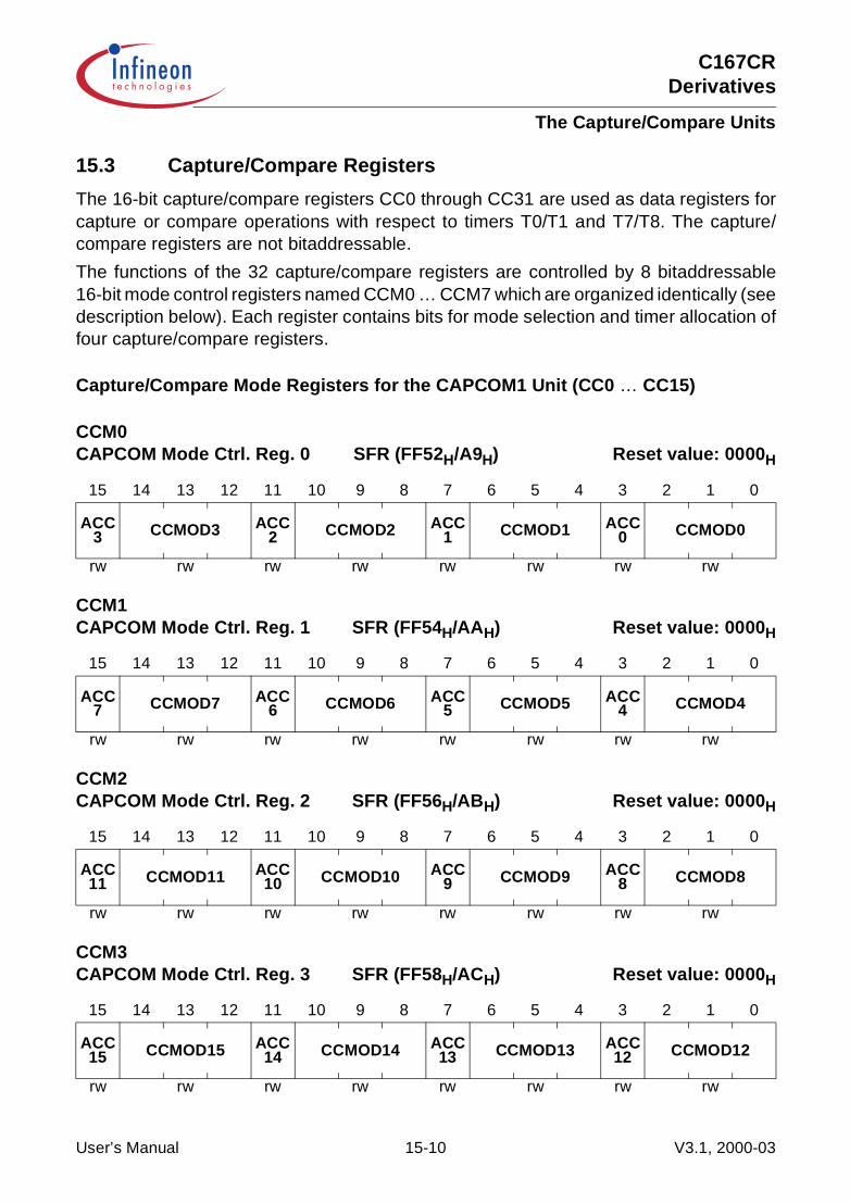
C167CRDerivatives
The Capture/Compare Units
15.3 Capture/Compare Registers
The 16-bit capture/compare registers CC0 through CC31 are used as data registers forcapture or compare operations with respect to timers T0/T1 and T7/T8. The capture/compare registers are not bitaddressable.
The functions of the 32 capture/compare registers are controlled by 8 bitaddressable16-bit mode control registers named CCM0 … CCM7 which are organized identically (seedescription below). Each register contains bits for mode selection and timer allocation offour capture/compare registers.
Capture/Compare Mode Registers for the CAPCOM1 Unit (CC0 … CC15)
CCM0CAPCOM Mode Ctrl. Reg. 0 SFR (FF52H/A9H) Reset value: 0000H
15 14 13 12 11 10 9 8 7 6 5 4 3 2 1 0
ACC3 CCMOD3 ACC
2 CCMOD2 ACC1 CCMOD1 ACC
0 CCMOD0
rw rw rw rw rw rw rw rw
CCM1CAPCOM Mode Ctrl. Reg. 1 SFR (FF54H/AAH) Reset value: 0000H
15 14 13 12 11 10 9 8 7 6 5 4 3 2 1 0
ACC7 CCMOD7 ACC
6 CCMOD6 ACC5 CCMOD5 ACC
4 CCMOD4
rw rw rw rw rw rw rw rw
CCM2CAPCOM Mode Ctrl. Reg. 2 SFR (FF56H/ABH) Reset value: 0000H
15 14 13 12 11 10 9 8 7 6 5 4 3 2 1 0
ACC11 CCMOD11 ACC
10 CCMOD10 ACC9 CCMOD9 ACC
8 CCMOD8
rw rw rw rw rw rw rw rw
CCM3CAPCOM Mode Ctrl. Reg. 3 SFR (FF58H/ACH) Reset value: 0000H
15 14 13 12 11 10 9 8 7 6 5 4 3 2 1 0
ACC15 CCMOD15 ACC
14 CCMOD14 ACC13 CCMOD13 ACC
12 CCMOD12
rw rw rw rw rw rw rw rw
User’s Manual 15-10 V3.1, 2000-03
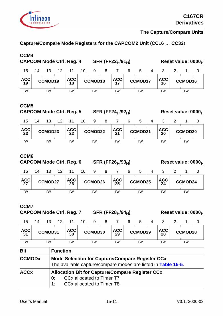
C167CRDerivatives
The Capture/Compare Units
Capture/Compare Mode Registers for the CAPCOM2 Unit (CC16 … CC32)
CCM4CAPCOM Mode Ctrl. Reg. 4 SFR (FF22H/91H) Reset value: 0000H
15 14 13 12 11 10 9 8 7 6 5 4 3 2 1 0
ACC19 CCMOD19 ACC
18 CCMOD18 ACC17 CCMOD17 ACC
16 CCMOD16
rw rw rw rw rw rw rw rw
CCM5CAPCOM Mode Ctrl. Reg. 5 SFR (FF24H/92H) Reset value: 0000H
15 14 13 12 11 10 9 8 7 6 5 4 3 2 1 0
ACC23 CCMOD23 ACC
22 CCMOD22 ACC21 CCMOD21 ACC
20 CCMOD20
rw rw rw rw rw rw rw rw
CCM6CAPCOM Mode Ctrl. Reg. 6 SFR (FF26H/93H) Reset value: 0000H
15 14 13 12 11 10 9 8 7 6 5 4 3 2 1 0
ACC27 CCMOD27 ACC
26 CCMOD26 ACC25 CCMOD25 ACC
24 CCMOD24
rw rw rw rw rw rw rw rw
CCM7CAPCOM Mode Ctrl. Reg. 7 SFR (FF28H/94H) Reset value: 0000H
15 14 13 12 11 10 9 8 7 6 5 4 3 2 1 0
ACC31 CCMOD31 ACC
30 CCMOD30 ACC29 CCMOD29 ACC
28 CCMOD28
rw rw rw rw rw rw rw rw
Bit Function
CCMODx Mode Selection for Capture/Compare Register CCxThe available capture/compare modes are listed in Table 15-5.
ACCx Allocation Bit for Capture/Compare Register CCx0: CCx allocated to Timer T71: CCx allocated to Timer T8
User’s Manual 15-11 V3.1, 2000-03
C167CRDerivatives
The Capture/Compare Units
Each of the registers CCx may be individually programmed for capture mode or one of4 different compare modes (no output signal for CC24 … CC27), and may be allocatedindividually to one of the two timers of the respective CAPCOM unit (T0 or T1, and T7 orT8, respectively). A special combination of compare modes additionally allows theimplementation of a ‘double-register’ compare mode. When capture or compareoperation is disabled for one of the CCx registers, it may be used for general purposevariable storage.
The detailed discussion of the capture and compare modes is valid for all the capture/compare channels, so registers, bits and pins are only referenced by the placeholder ‘x’.
Note: Capture/compare channels 27 … 24 generate an interrupt request but do notprovide an output signal. The resulting exceptions are indicated in the followingsubsections.A capture or compare event on channel 31 may be used to trigger a channelinjection on the C167CR’s A/D converter if enabled.
Table 15-5 Selection of Capture Modes and Compare Modes
CCMODx Selected Operating Mode
0 0 0 Disable Capture and Compare ModesThe respective CAPCOM register may be used for general variable storage.
0 0 1 Capture on Positive Transition (Rising Edge) at Pin CCxIO
0 1 0 Capture on Negative Transition (Falling Edge) at Pin CCxIO
0 1 1 Capture on Positive and Negative Transition (Both Edges) at Pin CCxIO
1 0 0 Compare Mode 0: Interrupt OnlySeveral interrupts per timer period; Enables double-register compare mode for registers CC8 … CC15 and CC24 … CC31.
1 0 1 Compare Mode 1: Toggle Output Pin on each MatchSeveral compare events per timer period; This mode is required for double-register compare mode for registers CC0 … CC7 and CC16 … CC23.
1 1 0 Compare Mode 2: Interrupt OnlyOnly one interrupt per timer period.
1 1 1 Compare Mode 3: Set Output Pin on each MatchReset output pin on each timer overflow; Only one interrupt per timer period.
User’s Manual 15-12 V3.1, 2000-03

C167CRDerivatives
The Capture/Compare Units
15.4 Capture Mode
In response to an external event the content of the associated timer (T0/T1 or T7/T8,depending on the used CAPCOM unit and the state of the allocation control bit ACCx) islatched into the respective capture register CCx. The external event causing a capturecan be programmed to be either a positive, a negative, or both a positive or a negativetransition at the respective external input pin CCxIO.
The triggering transition is selected by the mode bits CCMODx in the respectiveCAPCOM mode control register. In any case, the event causing a capture will also setthe respective interrupt request flag CCxIR, which can cause an interrupt or a PECservice request, when enabled.
Figure 15-5 Capture Mode Block Diagram
In order to use the respective port pin as external capture input pin CCxIO for captureregister CCx, this port pin must be configured as input, i.e. the corresponding directioncontrol bit must be set to ‘0’. To ensure that a signal transition is properly recognized, anexternal capture input signal should be held for at least 8 CPU clock cycles before itchanges its level.
During these 8 CPU clock cycles the capture input signals are scanned sequentially.When a timer is modified or incremented during this process, the new timer contents willalready be captured for the remaining capture registers within the current scanningsequence.
Note: When the timer modification can generate an overflow the capture interrupt routineshould check if the timer overflow was serviced during these 8 CPU clock cycles.
If pin CCxIO is configured as output, the capture function may be triggered by modifyingthe corresponding port output latch via software, e.g. for testing purposes.
EdgeSelect
MCB02015
Capture Reg. CCx
CAPCOM Timer Ty InterruptRequest
CCxIO
InputClock
CCMODx
InterruptRequest
x = 31...0y = 0, 1, 7, 8
User’s Manual 15-13 V3.1, 2000-03

C167CRDerivatives
The Capture/Compare Units
15.5 Compare Modes
The compare modes allow triggering of events (interrupts and/or output signaltransitions) with minimum software overhead. In all compare modes, the 16-bit valuestored in compare register CCx (in the following also referred to as ‘compare value’) iscontinuously compared with the contents of the allocated timer (T0/T1 or T7/T8). If thecurrent timer contents match the compare value, an appropriate output signal, which isbased on the selected compare mode, can be generated at the corresponding output pinCCxIO (except for CC27IO … CC24IO) and the associated interrupt request flag CCxIRis set, which can generate an interrupt request (if enabled).
As for capture mode, the compare registers are also processed sequentially duringcompare mode. When any two compare registers are programmed to the same comparevalue, their corresponding interrupt request flags will be set to ‘1’ and the selected outputsignals will be generated within 8 CPU clock cycles after the allocated timer isincremented to the compare value. Further compare events on the same compare valueare disabled until the timer is incremented again or written to by software. After a reset,compare events for register CCx will only become enabled, if the allocated timer hasbeen incremented or written to by software and one of the compare modes described inthe following has been selected for this register.
The different compare modes which can be programmed for a given compare registerCCx are selected by the mode control field CCMODx in the associated capture/comparemode control register. In the following, each of the compare modes, including the special‘double-register’ mode, is discussed in detail.
Compare Mode 0
This is an interrupt-only mode which can be used for software timing purposes. Comparemode 0 is selected for a given compare register CCx by setting bit field CCMODx of thecorresponding mode control register to ‘100B’.
In this mode, the interrupt request flag CCxIR is set each time a match is detectedbetween the content of compare register CCx and the allocated timer. Several of thesecompare events are possible within a single timer period, when the compare value inregister CCx is updated during the timer period. The corresponding port pin CCxIO is notaffected by compare events in this mode and can be used as general purpose IO pin.
If compare mode 0 is programmed for one of the registers CC8 … CC15 orCC24 … CC31, the double-register compare mode becomes enabled for this register ifthe corresponding bank 1 register is programmed to compare mode 1 (see “Double-register Compare Mode” on Page 15-19 ).
User’s Manual 15-14 V3.1, 2000-03
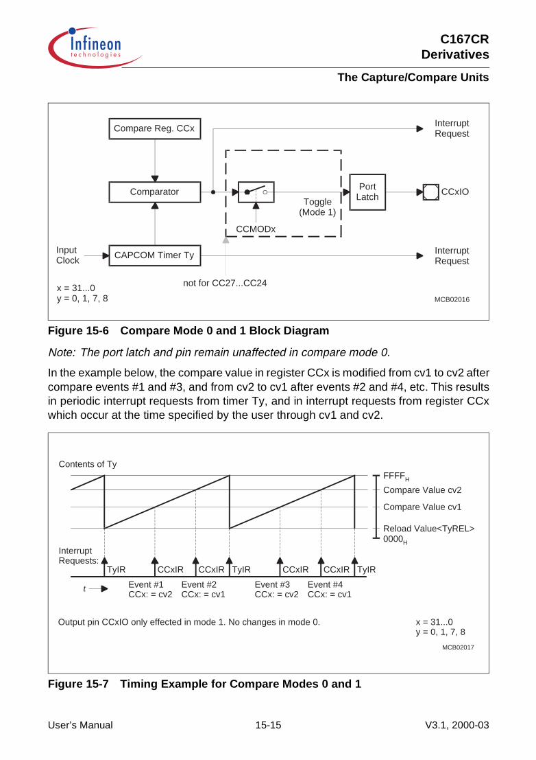
C167CRDerivatives
The Capture/Compare Units
Figure 15-6 Compare Mode 0 and 1 Block Diagram
Note: The port latch and pin remain unaffected in compare mode 0.
In the example below, the compare value in register CCx is modified from cv1 to cv2 aftercompare events #1 and #3, and from cv2 to cv1 after events #2 and #4, etc. This resultsin periodic interrupt requests from timer Ty, and in interrupt requests from register CCxwhich occur at the time specified by the user through cv1 and cv2.
Figure 15-7 Timing Example for Compare Modes 0 and 1
MCB02016
Compare Reg. CCx
Comparator
CAPCOM Timer Ty
CCMODx
PortLatchToggle
(Mode 1)
CCxIO
InterruptRequest
InterruptRequest
InputClock
x = 31...0y = 0, 1, 7, 8
not for CC27...CC24
MCB02017
Contents of Ty
TyIRCCxIRCCxIRTyIRCCxIRCCxIRTyIR
InterruptRequests:
t Event #1CCx: = cv2
Event #2CCx: = cv1
Event #3CCx: = cv2
Event #4CCx: = cv1
x = 31...0y = 0, 1, 7, 8
Output pin CCxIO only effected in mode 1. No changes in mode 0.
0000H
Reload Value<TyREL>
Compare Value cv1
Compare Value cv2
FFFFH
User’s Manual 15-15 V3.1, 2000-03

C167CRDerivatives
The Capture/Compare Units
Compare Mode 1
Compare mode 1 is selected for register CCx by setting bit field CCMODx of thecorresponding mode control register to ‘101B’.
When a match between the content of the allocated timer and the compare value inregister CCx is detected in this mode, interrupt request flag CCxIR is set to ‘1’, and inaddition the corresponding output pin CCxIO (alternate port output function) is toggled.For this purpose, the state of the respective port output latch (not the pin) is read,inverted, and then written back to the output latch.
Compare mode 1 allows several compare events within a single timer period. Anoverflow of the allocated timer has no effect on the output pin, nor does it disable orenable further compare events.
In order to use the respective port pin as compare signal output pin CCxIO for compareregister CCx in compare mode 1, this port pin must be configured as output, i.e. thecorresponding direction control bit must be set to ‘1’. With this configuration, the initialstate of the output signal can be programmed or its state can be modified at any time bywriting to the port output latch.
In compare mode 1 the port latch is toggled upon each compare event (see TimingExample above).
If compare mode 1 is programmed for one of the registers CC0 … CC7 or CC16 … CC23the double-register compare mode becomes enabled for this register if thecorresponding bank 2 register is programmed to compare mode 0 (see “Double-register Compare Mode” on Page 15-19 ).
Note: If the port output latch is written to by software at the same time it would be alteredby a compare event, the software write will have priority. In this case the hardware-triggered change will not become effective.On channels 27 … 24 compare mode 1 will generate an interrupt request but nooutput function is provided.
Compare Mode 2
Compare mode 2 is an interrupt-only mode similar to compare mode 0, but only oneinterrupt request per timer period will be generated. Compare mode 2 is selected forregister CCx by setting bit field CCMODx of the corresponding mode control register to‘110B’.
When a match is detected in compare mode 2 for the first time within a timer period, theinterrupt request flag CCxIR is set to ‘1’. The corresponding port pin is not affected andcan be used for general purpose IO. However, after the first match has been detected inthis mode, all further compare events within the same timer period are disabled forcompare register CCx until the allocated timer overflows. This means, that after the firstmatch, even when the compare register is reloaded with a value higher than the currenttimer value, no compare event will occur until the next timer period.
User’s Manual 15-16 V3.1, 2000-03
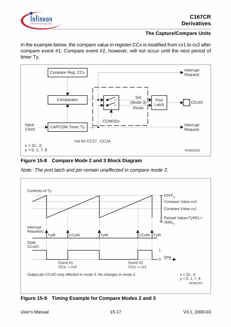
C167CRDerivatives
The Capture/Compare Units
In the example below, the compare value in register CCx is modified from cv1 to cv2 aftercompare event #1. Compare event #2, however, will not occur until the next period oftimer Ty.
Figure 15-8 Compare Mode 2 and 3 Block Diagram
Note: The port latch and pin remain unaffected in compare mode 2.
Figure 15-9 Timing Example for Compare Modes 2 and 3
MCB02019
Compare Reg. CCx
Comparator
CAPCOM Timer TyCCMODx
PortLatch(Mode 3) CCxIO
InterruptRequest
InterruptRequest
InputClock
Set
Reset
not for CC27...CC24x = 31...0y = 0, 1, 7, 8
MCB02021
0000H
FFFFH
Contents of Ty
TyIRCCxIRTyIRCCxIRTyIR
InterruptRequests:
time
Event #1CCx: = cv2
Event #2CCx: = cv1
0
1
StateCCxIO:
x = 31...0y = 0, 1, 7, 8
Output pin CCxIO only effected in mode 3. No changes in mode 2.
Reload Value<TyREL>
Compare Value cv1
Compare Value cv2
User’s Manual 15-17 V3.1, 2000-03
C167CRDerivatives
The Capture/Compare Units
Compare Mode 3
Compare mode 3 is selected for register CCx by setting bit field CCMODx of thecorresponding mode control register to ‘111B’. In compare mode 3 only one compareevent will be generated per timer period.
When the first match within the timer period is detected the interrupt request flag CCxIRis set to ‘1’ and also the output pin CCxIO (alternate port function) will be set to ‘1’. Thepin will be reset to ‘0’, when the allocated timer overflows.
If a match was found for register CCx in this mode, all further compare events during thecurrent timer period are disabled for CCx until the corresponding timer overflows. If, aftera match was detected, the compare register is reloaded with a new value, this value willnot become effective until the next timer period.
In order to use the respective port pin as compare signal output pin CCxIO for compareregister CCx in compare mode 3 this port pin must be configured as output, i.e. thecorresponding direction control bit must be set to ‘1’. With this configuration, the initialstate of the output signal can be programmed or its state can be modified at any time bywriting to the port output latch.
In compare mode 3 the port latch is set upon a compare event and cleared upon a timeroverflow (see Timing Example above).
However, when compare value and reload value for a channel are equal the respectiveinterrupt requests will be generated, only the output signal is not changed (set and clearwould coincide in this case).
Note: If the port output latch is written to by software at the same time it would be alteredby a compare event, the software write will have priority. In this case the hardware-triggered change will not become effective.On channels 27 … 24 compare mode 3 will generate an interrupt request but nooutput function is provided.
User’s Manual 15-18 V3.1, 2000-03

C167CRDerivatives
The Capture/Compare Units
Double-register Compare Mode
In double-register compare mode two compare registers work together to control oneoutput pin. This mode is selected by a special combination of modes for these tworegisters.
For double-register mode the 16 capture/compare registers of each CAPCOM unit areregarded as two banks of 8 registers each. Registers CC0 … CC7 and CC16 … CC23form bank 1 while registers CC8 … CC15 and CC24 … CC31 form bank 2 (respectively).For double-register mode a bank 1 register and a bank 2 register form a register pair.Both registers of this register pair operate on the pin associated with the bank 1 register(pins CC0IO … CC7IO and CC16IO … CC23IO).
The relationship between the bank 1 and bank 2 register of a pair and the effected outputpins for double-register compare mode is listed in Table 15-6.
The double-register compare mode can be programmed individually for each registerpair. In order to enable double-register mode the respective bank 1 register (seeTable 15-6) must be programmed to compare mode 1 and the corresponding bank 2register (see Table 15-6) must be programmed to compare mode 0.If the respective bank 1 compare register is disabled or programmed for a mode otherthan mode 1 the corresponding bank 2 register will operate in compare mode 0(interrupt-only mode).
In the following, a bank 2 register (programmed to compare mode 0) will be referred toas CCz while the corresponding bank 1 register (programmed to compare mode 1) willbe referred to as CCx.
Table 15-6 Register Pairs for Double-register Compare Mode
CAPCOM1 Unit CAPCOM2 Unit
Register Pair Associated Output Pin
Register Pair Associated Output PinBank 1 Bank 2 Bank 1 Bank 2
CC0 CC8 CC0IO CC16 CC24 CC16IO
CC1 CC9 CC1IO CC17 CC25 CC17IO
CC2 CC10 CC2IO CC18 CC26 CC18IO
CC3 CC11 CC3IO CC19 CC27 CC19IO
CC4 CC12 CC4IO CC20 CC28 CC20IO
CC5 CC13 CC5IO CC21 CC29 CC21IO
CC6 CC14 CC6IO CC22 CC30 CC22IO
CC7 CC15 CC7IO CC23 CC31 CC23IO
User’s Manual 15-19 V3.1, 2000-03

C167CRDerivatives
The Capture/Compare Units
When a match is detected for one of the two registers in a register pair (CCx or CCz) theassociated interrupt request flag (CCxIR or CCzIR) is set to ‘1’ and pin CCxIOcorresponding to bank 1 register CCx is toggled. The generated interrupt alwayscorresponds to the register that caused the match.
Note: If a match occurs simultaneously for both register CCx and register CCz of theregister pair pin CCxIO will be toggled only once but two separate compareinterrupt requests will be generated, one for vector CCxINT and one for vectorCCzINT.
In order to use the respective port pin as compare signal output pin CCxIO for compareregister CCx in double-register compare mode, this port pin must be configured asoutput, i.e. the corresponding direction control bit must be set to ‘1’. With thisconfiguration, the output pin has the same characteristics as in compare mode 1.
Figure 15-10 Double-Register Compare Mode Block Diagram
MCB02022
Comparator
CAPCOM Timer Ty
Mode 0 (CCMODz)
PortLatchToggle
CCxIO
InterruptRequest
InputClock
Compare Reg. CCz
Comparator
Compare Reg. CCxMode 1 (CCMODx)
1
InterruptRequest
x = 23...16, 7...0y = 0, 1, 7, 8z = 31...24, 15...8
User’s Manual 15-20 V3.1, 2000-03
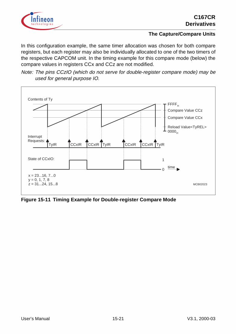
C167CRDerivatives
The Capture/Compare Units
In this configuration example, the same timer allocation was chosen for both compareregisters, but each register may also be individually allocated to one of the two timers ofthe respective CAPCOM unit. In the timing example for this compare mode (below) thecompare values in registers CCx and CCz are not modified.
Note: The pins CCzIO (which do not serve for double-register compare mode) may beused for general purpose IO.
Figure 15-11 Timing Example for Double-register Compare Mode
MCB02023
0000H
FFFFH
Contents of Ty
TyIRCCxIRTyIRCCxIRTyIR
InterruptRequests:
time0
1State of CCxIO:
CCxIR CCxIR
x = 23...16, 7...0y = 0, 1, 7, 8z = 31...24, 15...8
Reload Value<TyREL>
Compare Value CCx
Compare Value CCz
User’s Manual 15-21 V3.1, 2000-03
C167CRDerivatives
The Capture/Compare Units
15.6 Capture/Compare Interrupts
Upon a capture or compare event, the interrupt request flag CCxIR for the respectivecapture/compare register CCx is set to ‘1’. This flag can be used to generate an interruptor trigger a PEC service request when enabled by the interrupt enable bit CCxIE.
Capture interrupts can be regarded as external interrupt requests with the additionalfeature of recording the time at which the triggering event occurred (see alsoSection 5.7).
Each of the 32 capture/compare registers has its own bitaddressable interrupt controlregister (CC0IC … CC31IC) and its own interrupt vector (CC0INT … CC31INT). Theseregisters are organized the same way as all other interrupt control registers. The basicregister layout is shown below, Table 15-7 lists the associated addresses.
Note: Please refer to the general Interrupt Control Register description for anexplanation of the control fields.
CCxICCAPCOM Intr. Ctrl. Reg. (E)SFR (See Table 15-7) Reset value: - - 00H
15 14 13 12 11 10 9 8 7 6 5 4 3 2 1 0
CCxIR
CCxIE ILVL GLVL
- - - - - - - - rwh rw rw rw
User’s Manual 15-22 V3.1, 2000-03
C167CRDerivatives
The Capture/Compare Units
Table 15-7 Register Pairs for Double-Register Compare Mode
CAPCOM1 Unit CAPCOM2 Unit
Register Address Reg. Space Register Address Reg. Space
CC0IC FF78H/BCH SFR CC16IC F160H/B0H ESFR
CC1IC FF7AH/BDH SFR CC17IC F162H/B1H ESFR
CC2IC FF7CH/BEH SFR CC18IC F164H/B2H ESFR
CC3IC FF7EH/BFH SFR CC19IC F166H/B3H ESFR
CC4IC FF80H/C0H SFR CC20IC F168H/B4H ESFR
CC5IC FF82H/C1H SFR CC21IC F16AH/B5H ESFR
CC6IC FF84H/C2H SFR CC22IC F16CH/B6H ESFR
CC7IC FF86H/C3H SFR CC23IC F16EH/B7H ESFR
CC8IC FF88H/C4H SFR CC24IC F170H/B8H ESFR
CC9IC FF8AH/C5H SFR CC25IC F172H/B9H ESFR
CC10IC FF8CH/C6H SFR CC26IC F174H/BAH ESFR
CC11IC FF8EH/C7H SFR CC27IC F176H/BBH ESFR
CC12IC FF90H/C8H SFR CC28IC F178H/BCH ESFR
CC13IC FF92H/C9H SFR CC29IC F184H/C2H ESFR
CC14IC FF94H/CAH SFR CC30IC F18CH/C6H ESFR
CC15IC FF96H/CBH SFR CC31IC F194H/CAH ESFR
User’s Manual 15-23 V3.1, 2000-03

C167CRDerivatives
The Pulse Width Modulation Module
16 The Pulse Width Modulation ModuleThe Pulse Width Modulation (PWM) Module of the C167CR allows the generation of upto 4 independent PWM signals. These PWM signals can be generated within a widerange of output frequencies, which depends on:• the CPU clock frequency fCPU• the selected counter resolution (fCPU / 1 or fCPU / 64)• the operating mode (edge/center aligned)• the required PWM resolution (1-bit … 16-bit)
The maximum PWM output frequency in a real application is primarily determined by thePWM resolution which is required for that application.
Figure 16-1 SFRs and Port Pins Associated with the PWM Module
The Pulse Width Modulation Module consists of 4 independent PWM channels. Eachchannel has a 16-bit up/down counter PTx, a 16-bit period register PPx with a shadowlatch, a 16-bit pulse width register PWx with a shadow latch, two comparators, and thenecessary control logic.
The operation of all four channels is controlled by two common control registers,PWMCON0 and PWMCON1, and the interrupt control and status is handled by oneinterrupt control register PWMIC, which is also common for all channels.
E
MCA04387
ODP7
DP7
P7
PP0
PW0
PP1
PW1
PP2 E
PW2
PP3 E
PW3
PT0
PT1
PWMCON0
PWMIC
Ports & Direction ControlAlternate Functions
Data Registers Control Registers Control Registers andInterrupt Control
ODP7 Port 7 Open Drain Control RegisterDP7 Port 7 Direction Control RegisterP7 Port 7 Data RegisterPWMIC PWM Interrupt Control Register
PPx PWM Period Register xPWx PWM Pulse Width Register xPTx PWM Counter Register xPWMCONx PWM Control Register 0/1
PWMCON1
PT2
PT3
POUT0/P7.0POUT1/P7.1POUT2/P7.2POUT3/P7.3
E
E
E
E
E
E
E
User’s Manual 16-1 V3.1, 2000-03

C167CRDerivatives
The Pulse Width Modulation Module
Figure 16-2 PWM Channel Block Diagram
16.1 Operating Modes
The PWM module provides four different operating modes:
• Standard PWM generation (edge aligned PWM) available on all four channels• Symmetrical PWM generation (center aligned PWM) available on all four channels• Burst mode combines channels 0 and 1• Single shot mode available on channels 2 and 3
Note: The output signals of the PWM module are XORed with the outputs of therespective port output latches. After reset these latches are cleared, so the PWMsignals are directly driven to the port pins. By setting the respective port outputlatch to ‘1’ the PWM signal may be inverted (XORed with ‘1’) before being drivento the port pin. The descriptions below refer to the standard case after reset, i.e.direct driving.
WriteControl
OutputControl
Up/Down/Clear
Control
WriteControl
Match
Match
POUTx
InputControl
User Read-& Writeable
PPx Period Register
Shadow Register
Comparator
PTx16-Bit Up/Down
Counter
Comparator
Shadow Register
PWx Pulse Width Reg.
fCPURun
Enable
MCB01948
User’s Manual 16-2 V3.1, 2000-03

C167CRDerivatives
The Pulse Width Modulation Module
Mode 0: Standard PWM Generation (Edge Aligned PWM)
Mode 0 is selected by clearing the respective bit PMx in register PWMCON1 to ‘0’. In thismode the timer PTx of the respective PWM channel is always counting up until it reachesthe value in the associated period shadow register. Upon the next count pulse the timeris reset to 0000H and continues counting up with subsequent count pulses. The PWMoutput signal is switched to high level when the timer contents are equal to or greaterthan the contents of the pulse width shadow register. The signal is switched back to lowlevel when the respective timer is reset to 0000H, i.e. below the pulse width shadowregister. The period of the resulting PWM signal is determined by the value of therespective PPx shadow register plus 1, counted in units of the timer resolution.
PWM_PeriodMode0 = [PPx] + 1
The duty cycle of the PWM output signal is controlled by the value in the respective pulsewidth shadow register. This mechanism allows the selection of duty cycles from 0% to100% including the boundaries. For a value of 0000H the output will remain at a highlevel, representing a duty cycle of 100%. For a value higher than the value in the periodregister the output will remain at a low level, which corresponds to a duty cycle of 0%.
Figure 16-3 illustrates the operation and output waveforms of a PWM channel in mode0 for different values in the pulse width register. This mode is referred to as Edge AlignedPWM, because the value in the pulse width (shadow) register only effects the positiveedge of the output signal. The negative edge is always fixed and related to the clearingof the timer.
User’s Manual 16-3 V3.1, 2000-03
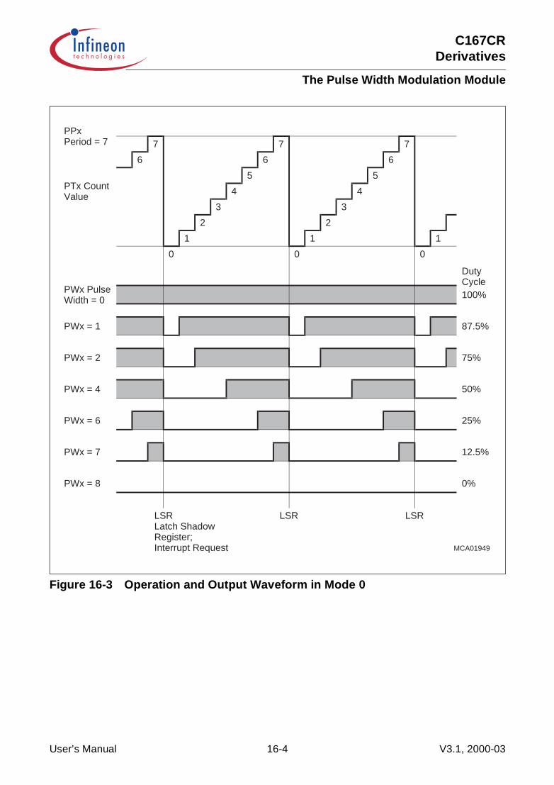
C167CRDerivatives
The Pulse Width Modulation Module
Figure 16-3 Operation and Output Waveform in Mode 0
MCA01949
PPxPeriod = 7
PTx CountValue
6
7
0
1
2
3
4
5
6
7
0
1
2
3
4
5
6
7
0
1
PWx PulseWidth = 0
PWx = 1
PWx = 2
PWx = 4
PWx = 6
PWx = 7
PWx = 8
LSRLatch ShadowRegister;Interrupt Request
LSR LSR
DutyCycle100%
87.5%
75%
50%
25%
12.5%
0%
User’s Manual 16-4 V3.1, 2000-03
C167CRDerivatives
The Pulse Width Modulation Module
Mode 1: Symmetrical PWM Generation (Center Aligned PWM)
Mode 1 is selected by setting the respective bit PMx in register PWMCON1 to ‘1’. In thismode the timer PTx of the respective PWM channel is counting up until it reaches thevalue in the associated period shadow register. Upon the next count pulse the countdirection is reversed and the timer starts counting down now with subsequent countpulses until it reaches the value 0000H. Upon the next count pulse the count direction isreversed again and the count cycle is repeated with the following count pulses.
The PWM output signal is switched to a high level when the timer contents are equal toor greater than the contents of the pulse width shadow register while the timer is countingup. The signal is switched back to a low level when the respective timer has counteddown to a value below the contents of the pulse width shadow register. So in mode 1 thisPWM value controls both edges of the output signal.
Note that in mode 1 the period of the PWM signal is twice the period of the timer:
PWM_PeriodMode1 = 2 × ([PPx] + 1)
Figure 16-4 illustrates the operation and output waveforms of a PWM channel in mode 1for different values in the pulse width register. This mode is referred to as Center AlignedPWM, because the value in the pulse width (shadow) register effects both edges of theoutput signal symmetrically.
User’s Manual 16-5 V3.1, 2000-03

C167CRDerivatives
The Pulse Width Modulation Module
Figure 16-4 Operation and Output Waveform in Mode 1
MCA01950
PPxPeriod = 7
PTx CountValue
0
1
2
3
4
5
6
7
0
1
2
3
4
5
6
7
0
1
PWx PulseWidth = 0
PWx = 1
PWx = 2
PWx = 4
PWx = 6
PWx = 7
PWx = 8
LSRLatch ShadowRegister;Interrupt Request
Change CountDirection
LSR
DutyCycle
100%
87.5%
75%
50%
25%
12.5%
0%
0
1
User’s Manual 16-6 V3.1, 2000-03

C167CRDerivatives
The Pulse Width Modulation Module
Burst Mode
Burst mode is selected by setting bit PB01 in register PWMCON1 to ‘1’. This modecombines the signals from PWM channels 0 and 1 onto the port pin of channel 0. Theoutput of channel 0 is replaced with the logical AND of channels 0 and 1. The output ofchannel 1 can still be used at its associated output pin (if enabled).Each of the two channels can either operate in mode 0 or 1.
Note: It is guaranteed by design, that no spurious spikes will occur at the output pin ofchannel 0 in this mode. The output of the AND gate will be transferred to the outputpin synchronously to internal clocks.XORing of the PWM signal and the port output latch value is done after theANDing of channel 0 and 1.
Figure 16-5 Operation and Output Waveform in Burst Mode
MCA01951
PP0PeriodValue
PT0CountValue
Channel 0
PP1PT1Count
Channel 1
ResultingOutputPOUT0
User’s Manual 16-7 V3.1, 2000-03
C167CRDerivatives
The Pulse Width Modulation Module
Single Shot Mode
Single shot mode is selected by setting the respective bit PSx in register PWMCON1 to‘1’. This mode is available for PWM channels 2 and 3.
In this mode the timer PTx of the respective PWM channel is started via software and iscounting up until it reaches the value in the associated period shadow register. Upon thenext count pulse the timer is cleared to 0000H and stopped via hardware, i.e. therespective PTRx bit is cleared. The PWM output signal is switched to high level when thetimer contents are equal to or greater than the contents of the pulse width shadowregister. The signal is switched back to low level when the respective timer is cleared,i.e. is below the pulse width shadow register. Thus starting a PWM timer in single shotmode produces one single pulse on the respective port pin, provided that the pulse widthvalue is between 0000H and the period value. In order to generate a further pulse, thetimer has to be started again via software by setting bit PTRx.
After starting the timer (i.e. PTRx = ‘1’) the output pulse may be modified via software.Writing to timer PTx changes the positive and/or negative edge of the output signal,depending on whether the pulse has already started (i.e. the output is high) or not (i.e.the output is still low). This (multiple) retriggering is always possible while the timer isrunning, i.e. after the pulse has started and before the timer is stopped.
Loading counter PTx directly with the value in the respective PPx shadow register willabort the current PWM pulse upon the next clock pulse (counter is cleared and stoppedby hardware).
By setting the period (PPx), the timer start value (PTx) and the pulse width value (PWx)appropriately, the pulse width (tw) and the optional pulse delay (td) may be varied in awide range.
User’s Manual 16-8 V3.1, 2000-03

C167CRDerivatives
The Pulse Width Modulation Module
Figure 16-6 Operation and Output Waveform in Single Shot Mode
MCA01952
PPxPeriod = 7
PTx CountValue
0
1
2
3
4
5
6
7
PWx PulseWidth = 4
LSR;PTRx Reset byHardwarePTx stopped
LSR
1
2
3
4
5
6
7
Set PTRx bySoftware
Set PTRx bySoftware forNext Pulse
PPxPeriod = 7
PTx CountValue
0
1
2
3
4
5
6
PWx PulseWidth = 4
Trigger before Pulse hasstarted: Write PWx valueto PTx;Shortens Delay Time tD
4
5
6
7
Retrigger after Pulsehas started: Write PWxvalue to PTx
4
5
6
7
0
1
tDtD
User’s Manual 16-9 V3.1, 2000-03
C167CRDerivatives
The Pulse Width Modulation Module
16.2 PWM Module Registers
The PWM module is controlled via two sets of registers. The waveforms are selected bythe channel specific registers PTx (timer), PPx (period) and PWx (pulse width). Threecommon registers control the operating modes and the general functions (PWMCON0and PWMCON1) of the PWM module as well as the interrupt behavior (PWMIC).
Up/Down Counters PTx
Each counter PTx of a PWM channel is clocked either directly with fCPU or with fCPU/64.Bit PTIx in register PWMCON0 selects the respective clock source. A PWM countercounts up or down (controlled by hardware), while its respective run control bit PTRx isset. A timer is started (PTRx = ‘1’) via software and is stopped (PTRx = ‘0’) either viahardware or software, depending on its operating mode. Control bit PTRx enables ordisables the clock input of counter PTx rather than controlling the PWM output signal.
Note: For the register locations please refer to Table 16-2 further below.
Table 16-1 summarizes the PWM frequencies that result from various combinations ofoperating mode, counter resolution (input clock) and pulse width resolution.
Table 16-1 PWM Output Frequency and Resolution
Inp.Clk. (fCPU/x)(Counter resol.)
PWM Mode
8-bit PWM Resolution
10-bit PWM Resolution
12-bit PWM Resolution
14-bit PWM Resolution
16-bit PWM Resolution
16 MHz/1(62.5 ns)
01
62.50 KHz31.25 KHz
15.63 KHz7.81 KHz
3.91 KHz1.95 KHz
976.6 Hz488.3 Hz
244.1 Hz122.1 Hz
16 MHz/64(4.0 µs)
01
976.6 Hz488.3 Hz
244.1 Hz122.1 Hz
61.04 Hz30.52 Hz
15.29 Hz7.63 Hz
3.81 Hz1.91 Hz
20 MHz/1(50 ns)
01
78.13 KHz39.06 KHz
19.53 KHz9.77 KHz
4.88 KHz2.44 KHz
1.22 KHz610.4 Hz
305.2 Hz152.6 Hz
20 MHz/64(3.2 µs)
01
1.22 KHz610.4 Hz
305.2 Hz152.6 Hz
76.29 Hz38.15 Hz
19.07 Hz9.54 Hz
4.77 Hz2.38 Hz
25 MHz/1(40 ns)
01
97.66 KHz48.83 KHz
24.41 KHz12.21 KHz
6.10 KHz3.05 KHz
1.53 KHz762.9 Hz
381.5 Hz190.7 Hz
25 MHz/64(2.56 µs)
01
1.53 KHz762.9 Hz
381.5 Hz190.7 Hz
95.37 Hz47.68 Hz
23.84 Hz11.92 Hz
5.96 Hz2.98 Hz
33 MHz/1(30.3 ns)
01
128.9 KHz64.45 KHz
32.23 KHz16.11 KHz
8.06 KHz4.03 KHz
2.01 KHz1.01 KHz
503.5 Hz251.8 Hz
33 MHz/64(1.94 µs)
01
2.01 KHz1.01 KHz
503.5 Hz251.8 Hz
125.9 Hz62.94 Hz
31.47 Hz15.74 Hz
7.87 Hz3.93 Hz
User’s Manual 16-10 V3.1, 2000-03
C167CRDerivatives
The Pulse Width Modulation Module
Period Registers PPx
The 16-bit period register PPx (see Table 16-2 for locations) of a PWM channeldetermines the period of a PWM cycle, i.e. the frequency of the PWM signal. Thisregister is buffered with a shadow register. The shadow register is loaded from therespective PPx register at the beginning of every new PWM cycle, or upon a write accessto PPx, while the timer is stopped. The CPU accesses the PPx register while thehardware compares the contents of the shadow register with the contents of theassociated counter PTx. When a match is found between counter and PPx shadowregister, the counter is either reset to 0000H, or the count direction is switched fromcounting up to counting down, depending on the selected operating mode of that PWMchannel.
Pulse Width Registers PWx
The 16-bit pulse width register PWx (see Table 16-2 for locations) of a PWM channelholds the actual PWM pulse width value which corresponds to the duty cycle of the PWMsignal. This register is buffered with a shadow register. The CPU accesses the PWxregister while the hardware compares the contents of the shadow register with thecontents of the associated counter PTx. The shadow register is loaded from therespective PWx register at the beginning of every new PWM cycle, or upon a writeaccess to PWx, while the timer is stopped.
When the counter value is greater than or equal to the shadow register value, the PWMsignal is set, otherwise it is reset. The output of the comparators may be described bythe boolean formula:
PWM output signal = [PTx] ≥ [PWx shadow latch].
This type of comparison allows a flexible control of the PWM signal.
Table 16-2 PWM Module Channel Specific Register Addresses
Register Address Register Space Register Address Register Space
PW0 FE30H/18H SFR PT0 F030H/18H ESFR
PW1 FE32H/19H SFR PT1 F032H/19H ESFR
PW2 FE34H/1AH SFR PT2 F034H/1AH ESFR
PW3 FE36H/1BH SFR PT3 F036H/1BH ESFR
Note: These registers are notbitaddressable.
PP0 F038H/1CH ESFR
PP1 F03AH/1DH ESFR
PP2 F03CH/1EH ESFR
PP3 F03EH/1FH ESFR
User’s Manual 16-11 V3.1, 2000-03

C167CRDerivatives
The Pulse Width Modulation Module
PWM Control Register PWMCON0
Register PWMCON0 controls the function of the timers of the four PWM channels andthe channel specific interrupts. Having the control bits organized in functional groupsallows e.g. to start or stop all 4 PWM timers simultaneously with one bitfield instruction.
PWMCON0 PWM Control Register 0 SFR (FF30H/98H) Reset value: 0000H
15 14 13 12 11 10 9 8 7 6 5 4 3 2 1 0
PIR3
PIR2
PIR1
PIR0
PIE3
PIE2
PIE1
PIE0
PTI3
PTI2
PTI1
PTI0
PTR3
PTR2
PTR1
PTR0
rwh rwh rwh rwh rw rw rw rw rw rw rw rw rwh rwh rw rw
Bit Function
PTRx PWM Timer x Run Control Bit0: Timer PTx is disconnected from its input clock1: Timer PTx is running
PTIx PWM Timer x Input Clock Selection0: Timer PTx clocked with CLKCPU1: Timer PTx clocked with CLKCPU/64
PIEx PWM Channel x Interrupt Enable Flag0: Interrupt from channel x disabled1: Interrupt from channel x enabled
PIRx PWM Channel x Interrupt Request Flag0: No interrupt request from channel x1: Channel x interrupt pending (must be reset via software)
User’s Manual 16-12 V3.1, 2000-03

C167CRDerivatives
The Pulse Width Modulation Module
PWM Control Register PWMCON1
Register PWMCON1 controls the operating modes and the outputs of the four PWMchannels. The basic operating mode for each channel (standard = edge aligned, orsymmetrical = center aligned PWM mode) is selected by the mode bits PMx. Burst mode(channels 0 and 1) and single shot mode (channel 2 or 3) are selected by separatecontrol bits. The output signal of each PWM channel is individually enabled by bit PENx.If the output is not enabled the respective pin can be used for general purpose IO andthe PWM channel can only be used to generate an interrupt request.
PWMCON1 PWM Control Register 1 SFR (FF32H/99H) Reset value: 0000H
15 14 13 12 11 10 9 8 7 6 5 4 3 2 1 0
PS3 PS2 - PB01 - - - - PM3 PM2 PM1 PM0 PEN
3PEN
2PEN
1PEN
0
rw rw - rw - - - - rw rw rw rw rw rw rw rw
Bit Function
PENx PWM Channel x Output Enable Bit0: Channel x output signal disabled, generate interrupt only1: Channel x output signal enabled
PMx PWM Channel x Mode Control Bit0: Channel x operates in mode 0, i.e. edge aligned PWM1: Channel x operates in mode 1, i.e. center aligned PWM
PB01 PWM Channel 0/1 Burst Mode Control Bit0: Channel 0 and channel 1 work independently in their respective
standard mode1: Outputs of channels 0 and 1 are ANDed to POUT0 in burst mode
PSx PWM Channel x Single Shot Mode Control Bit0: Channel x works in respective standard mode1: Channel x operates in single shot mode
User’s Manual 16-13 V3.1, 2000-03

C167CRDerivatives
The Pulse Width Modulation Module
16.3 Interrupt Request Generation
Each of the four channels of the PWM module can generate an individual interruptrequest. Each of these “channel interrupts” can activate the common “module interrupt”,which actually interrupts the CPU. This common module interrupt is controlled by thePWM Module Interrupt Control register PWMIC. The interrupt service routine candetermine the active channel interrupt(s) from the channel specific interrupt request flagsPIRx in register PWMCON0. The interrupt request flag PIRx of a channel is set at thebeginning of a new PWM cycle, i.e. upon latching the shadow registers (LSR). Thisindicates that registers PPx and PWx are now ready to receive a new value. If a channelinterrupt is enabled via its respective PIEx bit, also the common interrupt request flagPWMIR in register PWMIC is set, provided that it is enabled via the common interruptenable bit PWMIE.
Note: The channel interrupt request flags (PIRx in register PWMCON0) are notautomatically cleared by hardware upon entry into the interrupt service routine, sothey must be cleared via software. The module interrupt request flag PWMIR iscleared by hardware upon entry into the service routine, regardless of how manychannel interrupts were active. However, it will be set again if during execution ofthe service routine a new channel interrupt request is generated.
Note: Please refer to the general Interrupt Control Register description for anexplanation of the control fields.
PWMICPWM Intr. Ctrl. Reg. ESFR (F17EH/BFH) Reset value: - - 00H
15 14 13 12 11 10 9 8 7 6 5 4 3 2 1 0
PWM IR
PWM IE ILVL GLVL
- - - - - - - - rwh rw rw rw
User’s Manual 16-14 V3.1, 2000-03

C167CRDerivatives
The Pulse Width Modulation Module
16.4 PWM Output Signals
The output signals of the four PWM channels (POUT3 … POUT0) are alternate outputfunctions on Port 7 (P7.3 … P7.0). The output signal of each PWM channel is individuallyenabled by control bit PENx in register PWMCON1.
The PWM signals are XORed with the respective port latch outputs before being drivento the port pins. This allows driving the PWM signal directly to the port pin (P7.x = ‘0’) ordrive the inverted PWM signal (P7.x = ‘1’).
Figure 16-7 PWM Output Signal Generation
Note: Using the open drain mode on Port 7 allows the combination of two or more PWMoutputs through a Wired-AND configuration, using an external pullup device. Thisprovides sort of a burst mode for any PWM channel.
MCA02277
Pin P7.3XORLatch P7.3PWM 3
Pin P7.2PWM 2
XORLatch P7.2
Pin P7.1PWM 1
XORLatch P7.1&
PWM 0 Pin P7.0XORLatch P7.0PENx PB 01
User’s Manual 16-15 V3.1, 2000-03
C167CRDerivatives
The Pulse Width Modulation Module
Software Control of the PWM Outputs
In an application the PWM output signals are generally controlled by the PWM module.However, it may be necessary to influence the level of the PWM output pins via softwareeither to initialize the system or to react on some extraordinary condition, e.g. a systemfault or an emergency.
Clearing the timer run bit PTRx stops the associated counter and leaves the respectiveoutput at its current level.
The individual PWM channel outputs are controlled by comparators according to theformula:
PWM output signal = [PTx] ≥ [PWx shadow latch].
So whenever software changes registers PTx, the respective output will reflect thecondition after the change. Loading timer PTx with a value greater than or equal to thevalue in PWx immediately sets the respective output, a PTx value below the PWx valueclears the respective output.
By clearing or setting the respective Port 7 output latch the PWM channel signal is drivendirectly or inverted to the port pin.
Clearing the enable bit PENx disconnects the PWM channel and switches the respectiveport pin to the value in the port output latch.
Note: To prevent further PWM pulses from occurring after such a software interventionthe respective counter must be stopped first.
User’s Manual 16-16 V3.1, 2000-03
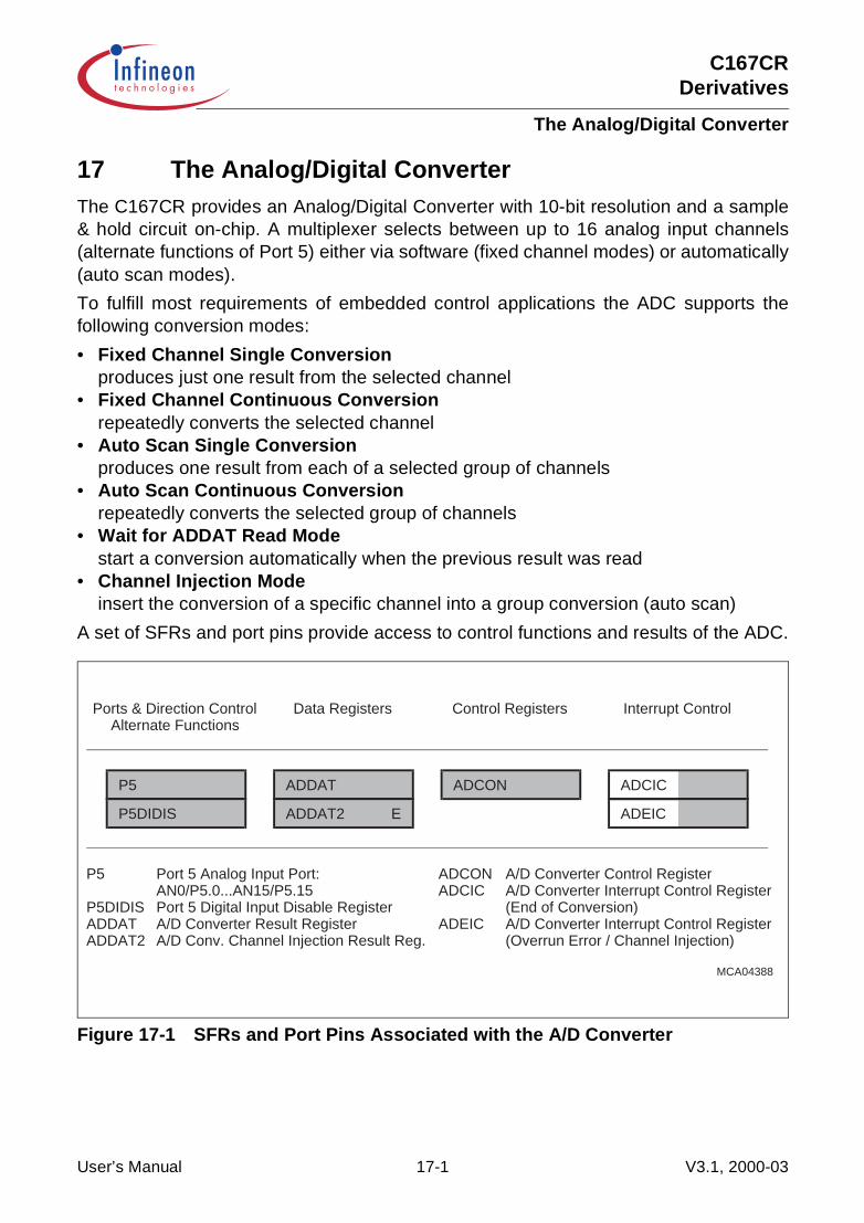
C167CRDerivatives
The Analog/Digital Converter
17 The Analog/Digital ConverterThe C167CR provides an Analog/Digital Converter with 10-bit resolution and a sample& hold circuit on-chip. A multiplexer selects between up to 16 analog input channels(alternate functions of Port 5) either via software (fixed channel modes) or automatically(auto scan modes).
To fulfill most requirements of embedded control applications the ADC supports thefollowing conversion modes:
• Fixed Channel Single Conversionproduces just one result from the selected channel
• Fixed Channel Continuous Conversionrepeatedly converts the selected channel
• Auto Scan Single Conversionproduces one result from each of a selected group of channels
• Auto Scan Continuous Conversionrepeatedly converts the selected group of channels
• Wait for ADDAT Read Modestart a conversion automatically when the previous result was read
• Channel Injection Modeinsert the conversion of a specific channel into a group conversion (auto scan)
A set of SFRs and port pins provide access to control functions and results of the ADC.
Figure 17-1 SFRs and Port Pins Associated with the A/D Converter
MCA04388
P5 ADDAT
ADDAT2
ADCON ADCIC
Ports & Direction ControlAlternate Functions
Data Registers Control Registers Interrupt Control
P5 Port 5 Analog Input Port:AN0/P5.0...AN15/P5.15
P5DIDIS Port 5 Digital Input Disable RegisterADDAT A/D Converter Result RegisterADDAT2 A/D Conv. Channel Injection Result Reg.
ADCON A/D Converter Control RegisterADCIC A/D Converter Interrupt Control Register
(End of Conversion)ADEIC A/D Converter Interrupt Control Register
(Overrun Error / Channel Injection)
EP5DIDIS ADEIC
User’s Manual 17-1 V3.1, 2000-03

C167CRDerivatives
The Analog/Digital Converter
The external analog reference voltages VAREF and VAGND are fixed. The separatesupply for the ADC reduces the interference with other digital signals.
The sample time as well as the conversion time is programmable, so the ADC can beadjusted to the internal resistances of the analog sources and/or the analog referencevoltage supply.
Figure 17-2 Analog/Digital Converter Block Diagram
17.1 Mode Selection and Operation
The analog input channels AN15 … AN0 are alternate functions of Port 5 which is aninput-only port. The Port 5 lines may either be used as analog or digital inputs. For pinsthat shall be used as analog inputs it is recommended to disable the digital input stagevia register P5DIDIS. This avoids undesired cross currents and switching noise while the(analog) input signal level is between VIL and VIH.
The functions of the A/D converter are controlled by the bit-addressable A/D ConverterControl Register ADCON. Its bitfields specify the analog channel to be acted upon, theconversion mode, and also reflect the status of the converter.
MCB04389
10-BitConverter
ConversionControl
ADCON
VAGNDVAREF
S + HMUX
AN0
AN15
.
.
.
ADCIR
ADEIR
Result Reg. ADDAT
Result Reg. ADDAT2
InerruptRequests
User’s Manual 17-2 V3.1, 2000-03
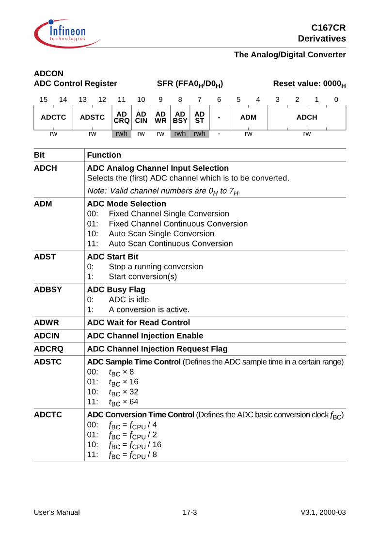
C167CRDerivatives
The Analog/Digital Converter
ADCONADC Control Register SFR (FFA0H/D0H) Reset value: 0000H
15 14 13 12 11 10 9 8 7 6 5 4 3 2 1 0
ADCTC ADSTC AD CRQ
AD CIN
AD WR
AD BSY
AD ST - ADM ADCH
rw rw rwh rw rw rwh rwh - rw rw
Bit Function
ADCH ADC Analog Channel Input SelectionSelects the (first) ADC channel which is to be converted.
Note: Valid channel numbers are 0H to 7H.
ADM ADC Mode Selection00: Fixed Channel Single Conversion01: Fixed Channel Continuous Conversion10: Auto Scan Single Conversion11: Auto Scan Continuous Conversion
ADST ADC Start Bit0: Stop a running conversion1: Start conversion(s)
ADBSY ADC Busy Flag0: ADC is idle1: A conversion is active.
ADWR ADC Wait for Read Control
ADCIN ADC Channel Injection Enable
ADCRQ ADC Channel Injection Request Flag
ADSTC ADC Sample Time Control (Defines the ADC sample time in a certain range)00: tBC × 801: tBC × 1610: tBC × 3211: tBC × 64
ADCTC ADC Conversion Time Control (Defines the ADC basic conversion clock fBC)00: fBC = fCPU / 401: fBC = fCPU / 210: fBC = fCPU / 1611: fBC = fCPU / 8
User’s Manual 17-3 V3.1, 2000-03

C167CRDerivatives
The Analog/Digital Converter
Bitfield ADCH specifies the analog input channel which is to be converted (first channelof a conversion sequence in auto scan modes). Bitfield ADM selects the operating modeof the A/D converter. A conversion (or a sequence) is then started by setting bit ADST.Clearing ADST stops the A/D converter after a certain operation which depends on theselected operating mode.
The busy flag (read-only) ADBSY is set, as long as a conversion is in progress.
The result of a conversion is stored in the result register ADDAT, or in register ADDAT2for an injected conversion.
Note: Bitfield CHNR of register ADDAT is loaded by the ADC to indicate, which channelthe result refers to.Bitfield CHNR of register ADDAT2 is loaded by the CPU to select the analogchannel, which is to be injected.
ADDATADC Result Register SFR (FEA0H/50H) Reset value: 0000H
15 14 13 12 11 10 9 8 7 6 5 4 3 2 1 0
CHNR - - ADRES
rwh - - rwh
ADDAT2ADC Chan. Inj. Result Reg. ESFR (F0A0H/50H) Reset value: 0000H
15 14 13 12 11 10 9 8 7 6 5 4 3 2 1 0
CHNR - - ADRES
rw - - rwh
Bit Function
ADRES A/D Conversion ResultThe 10-bit digital result of the most recent conversion.
CHNR Channel Number (identifies the converted analog channel)
Note: Valid channel numbers are FH to 0H.
User’s Manual 17-4 V3.1, 2000-03
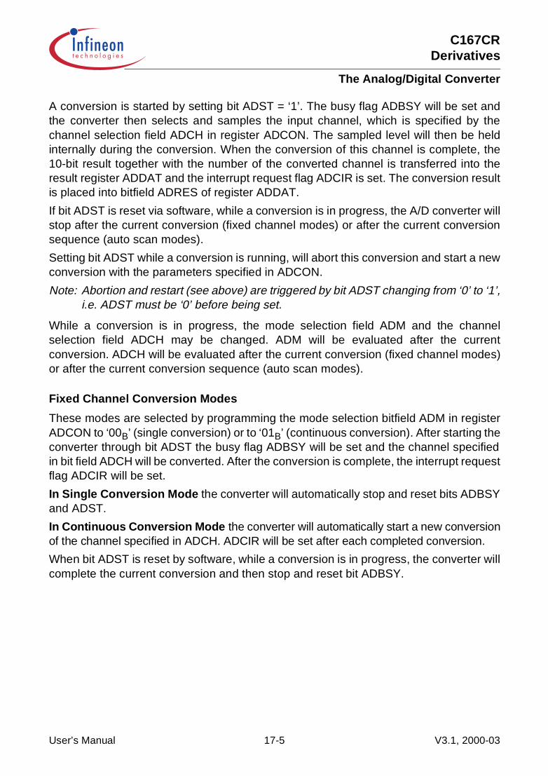
C167CRDerivatives
The Analog/Digital Converter
A conversion is started by setting bit ADST = ‘1’. The busy flag ADBSY will be set andthe converter then selects and samples the input channel, which is specified by thechannel selection field ADCH in register ADCON. The sampled level will then be heldinternally during the conversion. When the conversion of this channel is complete, the10-bit result together with the number of the converted channel is transferred into theresult register ADDAT and the interrupt request flag ADCIR is set. The conversion resultis placed into bitfield ADRES of register ADDAT.
If bit ADST is reset via software, while a conversion is in progress, the A/D converter willstop after the current conversion (fixed channel modes) or after the current conversionsequence (auto scan modes).
Setting bit ADST while a conversion is running, will abort this conversion and start a newconversion with the parameters specified in ADCON.
Note: Abortion and restart (see above) are triggered by bit ADST changing from ‘0’ to ‘1’,i.e. ADST must be ‘0’ before being set.
While a conversion is in progress, the mode selection field ADM and the channelselection field ADCH may be changed. ADM will be evaluated after the currentconversion. ADCH will be evaluated after the current conversion (fixed channel modes)or after the current conversion sequence (auto scan modes).
Fixed Channel Conversion Modes
These modes are selected by programming the mode selection bitfield ADM in registerADCON to ‘00B’ (single conversion) or to ‘01B’ (continuous conversion). After starting theconverter through bit ADST the busy flag ADBSY will be set and the channel specifiedin bit field ADCH will be converted. After the conversion is complete, the interrupt requestflag ADCIR will be set.
In Single Conversion Mode the converter will automatically stop and reset bits ADBSYand ADST.
In Continuous Conversion Mode the converter will automatically start a new conversionof the channel specified in ADCH. ADCIR will be set after each completed conversion.
When bit ADST is reset by software, while a conversion is in progress, the converter willcomplete the current conversion and then stop and reset bit ADBSY.
User’s Manual 17-5 V3.1, 2000-03

C167CRDerivatives
The Analog/Digital Converter
Auto Scan Conversion Modes
These modes are selected by programming the mode selection field ADM in registerADCON to ‘10B’ (single conversion) or to ‘11B’ (continuous conversion). Auto Scanmodes automatically convert a sequence of analog channels, beginning with the channelspecified in bit field ADCH and ending with channel 0, without requiring software tochange the channel number.After starting the converter through bit ADST, the busy flag ADBSY will be set and thechannel specified in bit field ADCH will be converted. After the conversion is complete,the interrupt request flag ADCIR will be set and the converter will automatically start anew conversion of the next lower channel. ADCIR will be set after each completedconversion. After conversion of channel 0 the current sequence is complete.
In Single Conversion Mode the converter will automatically stop and reset bitsADBSY and ADST.
In Continuous Conversion Mode the converter will automatically start a new sequencebeginning with the conversion of the channel specified in ADCH.
When bit ADST is reset by software, while a conversion is in progress, the converter willcomplete the current sequence (including conversion of channel 0) and then stop andreset bit ADBSY.
Figure 17-3 Auto Scan Conversion Mode Example
# 2
Result of Channel: # x # 3
Write ADDATADDAT Full
Conversionof Channel..
Read of ADDAT;
Generate InterruptRequest
# x
# 3
# 3
# 2
Interrupt RequestOverrun Error
# 2 # 1 Result Lost
MCA02241
# 3
# 1
# 1 # 0
ADDAT Full;Channnel 0
# 0 # 3
# 3 # 2
User’s Manual 17-6 V3.1, 2000-03
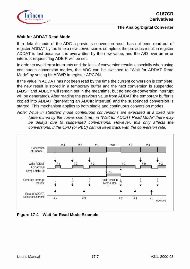
C167CRDerivatives
The Analog/Digital Converter
Wait for ADDAT Read Mode
If in default mode of the ADC a previous conversion result has not been read out ofregister ADDAT by the time a new conversion is complete, the previous result in registerADDAT is lost because it is overwritten by the new value, and the A/D overrun errorinterrupt request flag ADEIR will be set.
In order to avoid error interrupts and the loss of conversion results especially when usingcontinuous conversion modes, the ADC can be switched to “Wait for ADDAT ReadMode” by setting bit ADWR in register ADCON.
If the value in ADDAT has not been read by the time the current conversion is complete,the new result is stored in a temporary buffer and the next conversion is suspended(ADST and ADBSY will remain set in the meantime, but no end-of-conversion interruptwill be generated). After reading the previous value from ADDAT the temporary buffer iscopied into ADDAT (generating an ADCIR interrupt) and the suspended conversion isstarted. This mechanism applies to both single and continuous conversion modes.
Note: While in standard mode continuous conversions are executed at a fixed rate(determined by the conversion time), in “Wait for ADDAT Read Mode” there maybe delays due to suspended conversions. However, this only affects theconversions, if the CPU (or PEC) cannot keep track with the conversion rate.
Figure 17-4 Wait for Read Mode Example
Result of Channel:Read of ADDAT;
# x # 2# 3 # 1MCA01970
# 0
RequestGenerate Interrupt
Temp-Latch FullADDAT Full
Write ADDAT # x
of Channel..Conversion
# 3
# 2# 3
Temp-LatchHold Result in
1
# 2 # 1 wait
# 1 # 0 # 3
# 3# 0
User’s Manual 17-7 V3.1, 2000-03
C167CRDerivatives
The Analog/Digital Converter
Channel Injection Mode
Channel Injection Mode allows the conversion of a specific analog channel (also whilethe ADC is running in a continuous or auto scan mode) without changing the currentoperating mode. After the conversion of this specific channel the ADC continues with theoriginal operating mode.
Channel Injection mode is enabled by setting bit ADCIN in register ADCON and requiresthe Wait for ADDAT Read Mode (ADWR = ‘1’). The channel to be converted in this modeis specified in bitfield CHNR of register ADDAT2.
Note: Bitfield CHNR in ADDAT2 is not modified by the A/D converter, but only theADRES bit field. Since the channel number for an injected conversion is notbuffered, bitfield CHNR of ADDAT2 must never be modified during the samplephase of an injected conversion, otherwise the input multiplexer will switch to thenew channel. It is recommended to only change the channel number with noinjected conversion running.
Figure 17-5 Channel Injection Example
# x-2
Write ADDAT2
Int. Request
Conversionof Channel # y
ADDAT2 Full
Read ADDAT2
Request
Conversion
Write ADDAT;
Injected
Read ADDAT
ADDAT Full
of Channel..
Channel Injection
# x-1
# x+1
# x+1
# x
# x
# x
# x-1
# x-1
# x-2
MCA01971
ADEINT
# ...
# x-4
# y
# x-2
# x-3
# x-3
# x-3 # x-4
# x-4
User’s Manual 17-8 V3.1, 2000-03
C167CRDerivatives
The Analog/Digital Converter
A channel injection can be triggered in two ways:
• setting of the Channel Injection Request bit ADCRQ via software• a compare or a capture event of Capture/Compare register CC31 of the CAPCOM2
unit, which also sets bit ADCRQ.
The second method triggers a channel injection at a specific time, on the occurrence ofa predefined count value of the CAPCOM timers or on a capture event of register CC31.This can be either the positive, the negative, or both the positive and the negative edgeof an external signal. In addition, this option allows recording the time of occurrence ofthis signal.
Note: The channel injection request bit ADCRQ will be set on any interrupt request ofCAPCOM2 channel CC31, regardless whether the channel injection mode isenabled or not. It is recommended to always clear bit ADCRQ before enabling thechannel injection mode.
After the completion of the current conversion (if any is in progress) the converter willstart (inject) the conversion of the specified channel. When the conversion of thischannel is complete, the result will be placed into the alternate result registerADDAT2, and a Channel Injection Complete Interrupt request will be generated,which uses the interrupt request flag ADEIR (for this reason the Wait for ADDATRead Mode is required).
Note: If the temporary data register used in Wait for ADDAT Read Mode is full, therespective next conversion (standard or injected) will be suspended. Thetemporary register can hold data for ADDAT (from a standard conversion) or forADDAT2 (from an injected conversion).
User’s Manual 17-9 V3.1, 2000-03

C167CRDerivatives
The Analog/Digital Converter
Figure 17-6 Channel Injection Example with Wait for Read
# y
Int.
Int. RequestADEINT
ADDAT2 isWait until
Read ADDAT2
ADDAT2 Full
Temp-LatchFull
Write ADDATADDAT Full
Read ADDAT
Conversionof Channel..
# x-1
Channel Injection
# x+1
# x+1
# x
# x
Wait untilADDAT2 is
read
# x-1
# x
FullTemp-Latch
ADDAT2 Full
of Channel yConversion
Injected
Read ADDAT2
of Channel..Conversion
Read ADDAT
ADDAT FullWrite ADDAT
# x+1
Channel Injection
# x+1
# x
# x
# z
# x-1
# x-1
# x-1# x
MCA01972
# y
# x-2
Write ADDAT2
# x-2
# x-1
# x-3
# x-2
# x-3
# x-3
# ...
# ...
# x-3
Write ADDAT2
# y
ADEINTRequest
# z
read
# y
# x-2
# x-2 # x-3
# x-2 # x-3
Request
Request
User’s Manual 17-10 V3.1, 2000-03
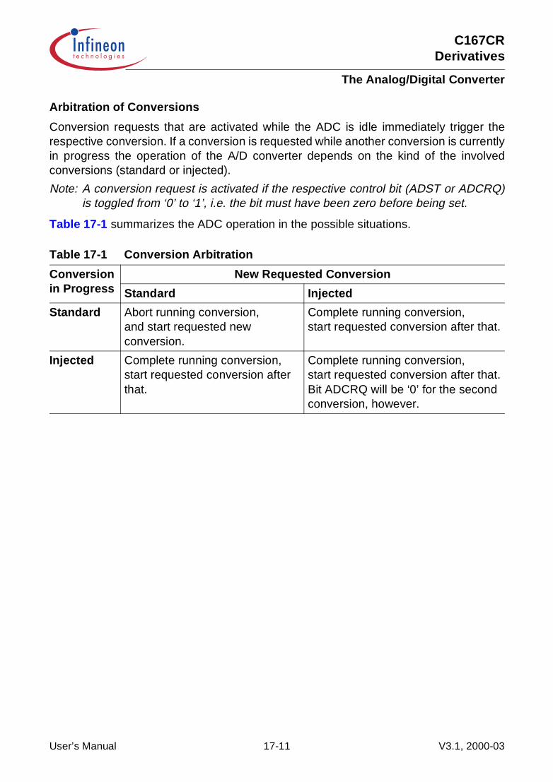
C167CRDerivatives
The Analog/Digital Converter
Arbitration of Conversions
Conversion requests that are activated while the ADC is idle immediately trigger therespective conversion. If a conversion is requested while another conversion is currentlyin progress the operation of the A/D converter depends on the kind of the involvedconversions (standard or injected).
Note: A conversion request is activated if the respective control bit (ADST or ADCRQ)is toggled from ‘0’ to ‘1’, i.e. the bit must have been zero before being set.
Table 17-1 summarizes the ADC operation in the possible situations.
Table 17-1 Conversion Arbitration
Conversion in Progress
New Requested Conversion
Standard Injected
Standard Abort running conversion,and start requested new conversion.
Complete running conversion,start requested conversion after that.
Injected Complete running conversion,start requested conversion after that.
Complete running conversion,start requested conversion after that.Bit ADCRQ will be ‘0’ for the second conversion, however.
User’s Manual 17-11 V3.1, 2000-03

C167CRDerivatives
The Analog/Digital Converter
17.2 Conversion Timing Control
When a conversion is started, first the capacitances of the converter are loaded via therespective analog input pin to the current analog input voltage. The time to load thecapacitances is referred to as sample time. Next the sampled voltage is converted to adigital value in successive steps, which correspond to the resolution of the ADC. Duringthese phases (except for the sample time) the internal capacitances are repeatedlycharged and discharged via pins VAREF and VAGND.
The current that has to be drawn from the sources for sampling and changing chargesdepends on the time that each respective step takes, because the capacitors must reachtheir final voltage level within the given time, at least with a certain approximation. Themaximum current, however, that a source can deliver, depends on its internal resistance.
The time that the two different actions during conversion take (sampling, and converting)can be programmed within a certain range in the C167CR relative to the CPU clock. Theabsolute time that is consumed by the different conversion steps therefore isindependent from the general speed of the controller. This allows adjusting the A/Dconverter of the C167CR to the properties of the system:
Fast Conversion can be achieved by programming the respective times to theirabsolute possible minimum. This is preferable for scanning high frequency signals. Theinternal resistance of analog source and analog supply must be sufficiently low,however.
High Internal Resistance can be achieved by programming the respective times to ahigher value, or the possible maximum. This is preferable when using analog sourcesand supply with a high internal resistance in order to keep the current as low as possible.The conversion rate in this case may be considerably lower, however.
The conversion time is programmed via the upper two bits of register ADCON. BitfieldADCTC (conversion time control) selects the basic conversion clock (fBC), used for theoperation of the A/D converter. The sample time is derived from this conversion clock.Table 17-2 lists the possible combinations. The timings refer to CPU clock cycles, wheretCPU = 1 / fCPU.
The limit values for fBC (see data sheet) must not be exceeded when selecting ADCTCand fCPU.
Table 17-2 ADC Conversion Timing Control
ADCON.15|14(ADCTC)
A/D ConverterBasic Clock fBC
ADCON.13|12(ADSTC)
Sample Time tS
00 fCPU / 4 00 tBC × 8
01 fCPU / 2 01 tBC × 16
10 fCPU / 16 10 tBC × 32
11 fCPU / 8 11 tBC × 64
User’s Manual 17-12 V3.1, 2000-03
C167CRDerivatives
The Analog/Digital Converter
The time for a complete conversion includes the sample time tS, the conversion itself andthe time required to transfer the digital value to the result register (2 tCPU) as shown inthe example below.
Note: The non-linear decoding of bit field ADCTC provides compatibility with 80C166designs for the default value (‘00’ after reset).
Converter Timing Example
Assumptions: fCPU = 25 MHz (i.e. tCPU = 40 ns), ADCTC = ‘00’, ADSTC = ‘00’.
Basic clock fBC = fCPU / 4 = 6.25 MHz, i.e. tBC = 160 ns.Sample time tS = tBC × 8 = 1280 ns.Conversion time tC = tS + 40 tBC + 2 tCPU = (1280 + 6400 + 80) ns = 7.76 µs.
Note: For the exact specification please refer to the data sheet of the selected derivative.
User’s Manual 17-13 V3.1, 2000-03

C167CRDerivatives
The Analog/Digital Converter
17.3 A/D Converter Interrupt Control
At the end of each conversion, interrupt request flag ADCIR in interrupt control registerADCIC is set. This end-of-conversion interrupt request may cause an interrupt to vectorADCINT, or it may trigger a PEC data transfer which reads the conversion result fromregister ADDAT e.g. to store it into a table in the internal RAM for later evaluation.
The interrupt request flag ADEIR in register ADEIC will be set either, if a conversionresult overwrites a previous value in register ADDAT (error interrupt in standard mode),or if the result of an injected conversion has been stored into ADDAT2 (end-of-injected-conversion interrupt). This interrupt request may be used to cause an interrupt to vectorADEINT, or it may trigger a PEC data transfer.
Note: Please refer to the general Interrupt Control Register description for anexplanation of the control fields.
ADCICADC Conversion Intr.Ctrl.Reg. SFR (FF98H/CCH) Reset value: - - 00H
15 14 13 12 11 10 9 8 7 6 5 4 3 2 1 0
- ADC IR
ADC IE ILVL GLVL
- - - - - - - - rwh rw rw rw
ADEICADC Error Intr.Ctrl.Reg. SFR (FF9AH/CDH) Reset value: - - 00H
15 14 13 12 11 10 9 8 7 6 5 4 3 2 1 0
- ADE IR
ADE IE ILVL GLVL
- - - - - - - - rwh rw rw rw
User’s Manual 17-14 V3.1, 2000-03
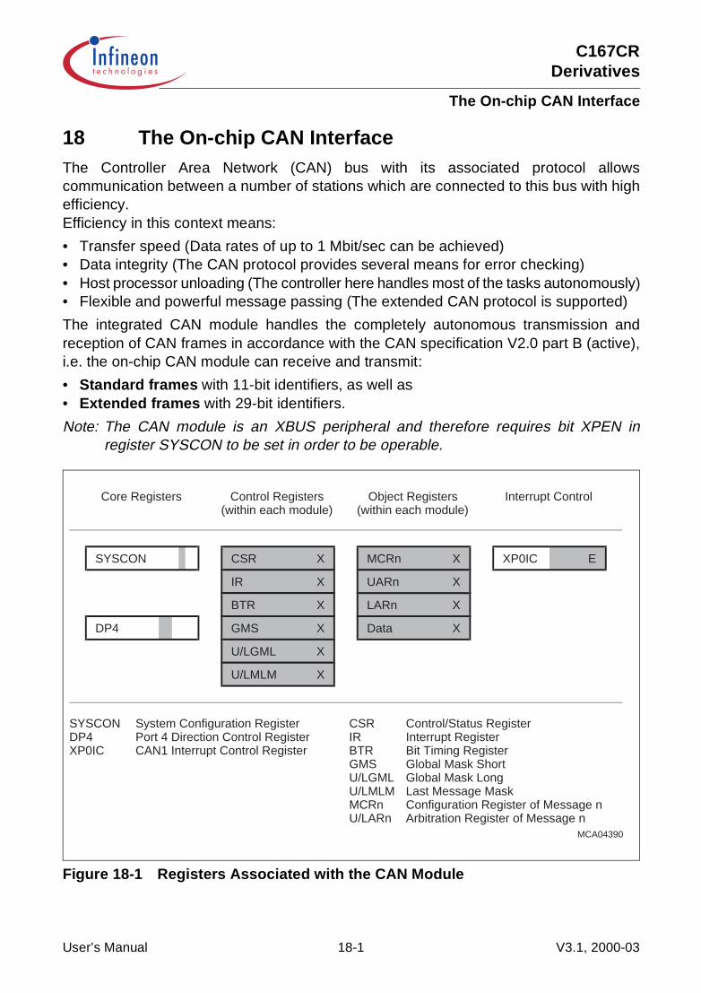
C167CRDerivatives
The On-chip CAN Interface
18 The On-chip CAN InterfaceThe Controller Area Network (CAN) bus with its associated protocol allowscommunication between a number of stations which are connected to this bus with highefficiency.Efficiency in this context means:
• Transfer speed (Data rates of up to 1 Mbit/sec can be achieved)• Data integrity (The CAN protocol provides several means for error checking)• Host processor unloading (The controller here handles most of the tasks autonomously)• Flexible and powerful message passing (The extended CAN protocol is supported)
The integrated CAN module handles the completely autonomous transmission andreception of CAN frames in accordance with the CAN specification V2.0 part B (active),i.e. the on-chip CAN module can receive and transmit:
• Standard frames with 11-bit identifiers, as well as• Extended frames with 29-bit identifiers.
Note: The CAN module is an XBUS peripheral and therefore requires bit XPEN inregister SYSCON to be set in order to be operable.
Figure 18-1 Registers Associated with the CAN Module
MCA04390
SYSCON
DP4
CSR
IR
BTR
GMS
U/LGML X
U/LMLM X
MCRn
Data
XP0IC
Core Registers Control Registers(within each module)
Object Registers(within each module)
Interrupt Control
SYSCON System Configuration RegisterDP4 Port 4 Direction Control RegisterXP0IC CAN1 Interrupt Control Register
CSR Control/Status RegisterIR Interrupt RegisterBTR Bit Timing RegisterGMS Global Mask ShortU/LGML Global Mask LongU/LMLM Last Message MaskMCRn Configuration Register of Message nU/LARn Arbitration Register of Message n
X
X
X
X
LARn
UARn
X
X
X
X
E
User’s Manual 18-1 V3.1, 2000-03

C167CRDerivatives
The On-chip CAN Interface
The bit timing is derived from the XCLK and is programmable up to a data rate of1 MBaud. The minimum CPU clock frequency to achieve 1 MBaud is fCPU ≥ 8/16 MHz,depending on the activation of the CAN module’s clock prescaler.
The CAN module uses two pins of Port 4 to interface to a bus transceiver.
It provides Full CAN functionality on up to 15 full-sized message objects (8 data byteseach). Message object 15 may be configured for Basic CAN functionality with a double-buffered receive object.
Both modes provide separate masks for acceptance filtering which allows theacceptance of a number of identifiers in Full CAN mode and also allows disregarding anumber of identifiers in Basic CAN mode.
All message objects can be updated independent from the other objects during operationof the module and are equipped with buffers for the maximum message length of 8Bytes.
18.1 Functional Blocks of the CAN Module
The CAN module combines several functional blocks (see Figure 18-2) that work inparallel and contribute to the controller’s performance. These units and the functionsthey provide are described below.
Each of the message objects has a unique identifier and its own set of control and statusbits. Each object can be configured with its direction as either transmit or receive, exceptthe last message which is only a double receive buffer with a special mask register.
An object with its direction set as transmit can be configured to be automatically sentwhenever a remote frame with a matching identifier (taking into account the respectiveglobal mask register) is received over the CAN bus. By requesting the transmission of amessage with the direction set as receive, a remote frame can be sent to request thatthe appropriate object be sent by some other node. Each object has separate transmitand receive interrupts and status bits, giving the CPU full flexibility in detecting when aremote/data frame has been sent or received.
For general purpose two masks for acceptance filtering can be programmed, one foridentifiers of 11 bits and one for identifiers of 29 bits. However the CPU must configurebit XTD (Normal or Extended Frame Identifier) for each valid message to determinewhether a standard or extended frame will be accepted.
The last message object has its own programmable mask for acceptance filtering,allowing a large number of infrequent objects to be handled by the system.
The object layer architecture of the CAN controller is designed to be as regular andorthogonal as possible. This makes it easy to use.
User’s Manual 18-2 V3.1, 2000-03
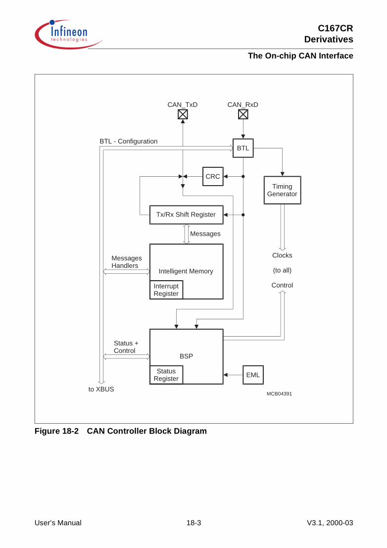
C167CRDerivatives
The On-chip CAN Interface
Figure 18-2 CAN Controller Block Diagram
MCB04391
StatusRegister
InterruptRegister
Tx/Rx Shift Register
Messages
MessagesHandlers
Status +Control
EML
CRC
BTL
TimingGenerator
Clocks
(to all)
Control
BTL - Configuration
CAN_RxDCAN_TxD
to XBUS
Intelligent Memory
BSP
User’s Manual 18-3 V3.1, 2000-03
C167CRDerivatives
The On-chip CAN Interface
Tx/Rx Shift Register
The Transmit/Receive Shift Register holds the destuffed bit stream from the bus line toallow the parallel access to the whole data or remote frame for the acceptance matchtest and the parallel transfer of the frame to and from the Intelligent Memory.
Bit Stream Processor
The Bit Stream Processor (BSP) is a sequencer controlling the sequential data streambetween the Tx/Rx Shift Register, the CRC Register, and the bus line. The BSP alsocontrols the EML and the parallel data stream between the Tx/Rx Shift Register and theIntelligent Memory such that the processes of reception, arbitration, transmission, anderror signalling are performed according to the CAN protocol. Note that the automaticretransmission of messages which have been corrupted by noise or other external errorconditions on the bus line is handled by the BSP.
Cyclic Redundancy Check Register
This register generates the Cyclic Redundancy Check (CRC) code to be transmittedafter the data bytes and checks the CRC code of incoming messages. This is done bydividing the data stream by the code generator polynomial.
Error Management Logic
The Error Management Logic (EML) is responsible for the fault confinement of the CANdevice. Its counters, the Receive Error Counter and the Transmit Error Counter, areincremented and decremented by commands from the Bit Stream Processor. Accordingto the values of the error counters, the CAN controller is set into the states error active,error passive and busoff.
The CAN controller is error active, if both error counters are below the error passive limit of 128.
It is error passive, if at least one of the error counters equals or exceeds 128.
It goes busoff, if the Transmit Error Counter equals or exceeds the busoff limit of 256.The device remains in this state, until the busoff recovery sequence is finished.
Additionally, there is the bit EWRN in the Status Register, which is set, if at least one ofthe error counters equals or exceeds the error warning limit of 96. EWRN is reset, if botherror counters are less than the error warning limit.
User’s Manual 18-4 V3.1, 2000-03

C167CRDerivatives
The On-chip CAN Interface
Bit Timing Logic
This block (BTL) monitors the busline input CAN_RXD and handles the busline relatedbit timing according to the CAN protocol.
The BTL synchronizes on a recessive to dominant busline transition at Start of Frame(hard synchronization) and on any further recessive to dominant busline transition, if theCAN controller itself does not transmit a dominant bit (resynchronization).
The BTL also provides programmable time segments to compensate for the propagationdelay time and for phase shifts and to define the position of the Sample Point in the bittime. The programming of the BTL depends on the baudrate and on external physicaldelay times.
Intelligent Memory
The Intelligent Memory (CAM/RAM Array) provides storage for up to 15 message objectsof maximum 8 data bytes length. Each of these objects has a unique identifier and itsown set of control and status bits. After the initial configuration, the Intelligent Memorycan handle the reception and transmission of data without further CPU actions.
Organization of Registers and Message Objects
All registers and message objects of the CAN controller are located in the special CANaddress area of 256 Bytes, which is mapped into segment 0 and uses addresses00’EF00H through 00’EFFFH. All registers are organized as 16-bit registers, located onword addresses. However, all registers may be accessed bytewise in order to selectspecial actions without effecting other mechanisms.
Register Naming reflects the specific name of a register as well as a general moduleindicator. This results in unique register names.
Example: module indicator is C1 (CAN module 1), specific name is Control/StatusRegister (CSR), unique register name is C1CSR.
Note: The address map shown below lists the registers which are part of the CANcontroller. There are also C167CR specific registers that are associated with theCAN module.
User’s Manual 18-5 V3.1, 2000-03
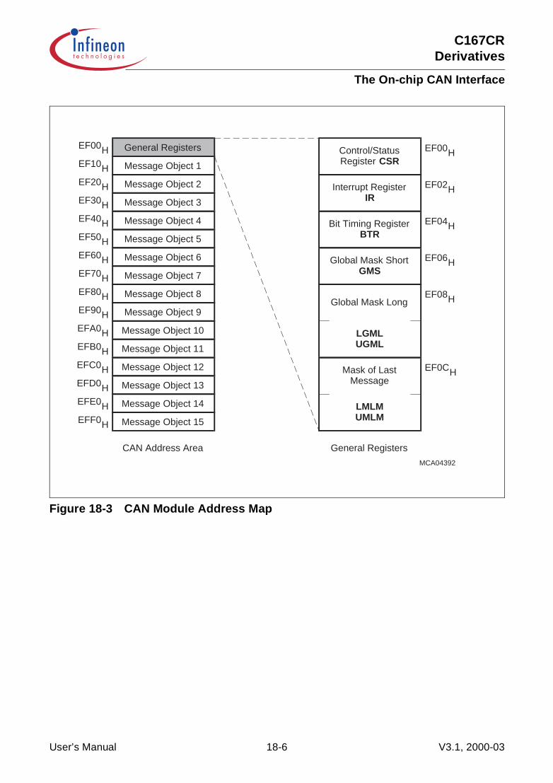
C167CRDerivatives
The On-chip CAN Interface
Figure 18-3 CAN Module Address Map
EFF0H
EF0CH
Message Object 15
Message Object 14EFE0H
EFD0H Message Object 13
Message Object 12EFC0H
EFB0H Message Object 11
Message Object 10EFA0H
EF90H Message Object 9
Message Object 8EF80H
EF70H Message Object 7
Message Object 6EF60H
EF50H Message Object 5
Message Object 4EF40H
EF30H Message Object 3
Message Object 2EF20H
EF10H Message Object 1
General RegistersEF00H
Mask of LastMessage
LMLMUMLM
LGMLUGML
Global Mask LongEF08H
EF06HGlobal Mask ShortGMS
Bit Timing RegisterBTR
EF04H
Interrupt RegisterIR
EF02H
Control/StatusRegister CSR
EF00H
CAN Address Area General Registers
MCA04392
User’s Manual 18-6 V3.1, 2000-03
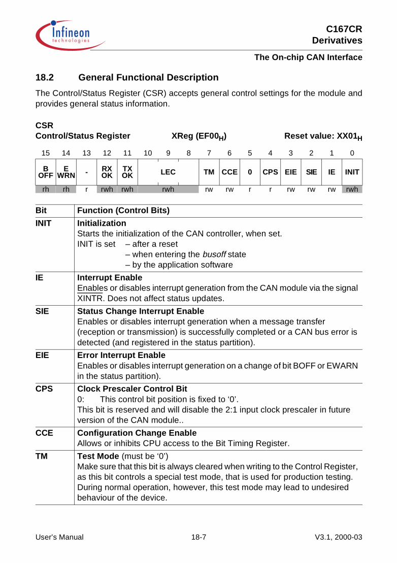
C167CRDerivatives
The On-chip CAN Interface
18.2 General Functional Description
The Control/Status Register (CSR) accepts general control settings for the module andprovides general status information.
CSRControl/Status Register XReg (EF00H) Reset value: XX01H
15 14 13 12 11 10 9 8 7 6 5 4 3 2 1 0
BOFF
EWRN - RX
OKTX OK LEC TM CCE 0 CPS EIE SIE IE INIT
rh rh r rwh rwh rwh rw rw r r rw rw rw rwh
Bit Function (Control Bits)
INIT InitializationStarts the initialization of the CAN controller, when set.INIT is set – after a reset
– when entering the busoff state– by the application software
IE Interrupt EnableEnables or disables interrupt generation from the CAN module via the signal XINTR. Does not affect status updates.
SIE Status Change Interrupt EnableEnables or disables interrupt generation when a message transfer (reception or transmission) is successfully completed or a CAN bus error is detected (and registered in the status partition).
EIE Error Interrupt EnableEnables or disables interrupt generation on a change of bit BOFF or EWARN in the status partition).
CPS Clock Prescaler Control Bit0: This control bit position is fixed to ‘0’.This bit is reserved and will disable the 2:1 input clock prescaler in future version of the CAN module..
CCE Configuration Change EnableAllows or inhibits CPU access to the Bit Timing Register.
TM Test Mode (must be ‘0’)Make sure that this bit is always cleared when writing to the Control Register, as this bit controls a special test mode, that is used for production testing. During normal operation, however, this test mode may lead to undesired behaviour of the device.
User’s Manual 18-7 V3.1, 2000-03

C167CRDerivatives
The On-chip CAN Interface
Note: Reading the upper half of the Control Register (status partition) will clear theStatus Change Interrupt value in the Interrupt Register, if it is pending. Use byteaccesses to the lower half to avoid this.
LEC Last Error CodeThis field holds a code which indicates the type of the last error occurred on the CAN bus. If a message has been transferred (reception or transmission) without error, this field will be cleared.0 No Error1 Stuff Error: More than 5 equal bits in a sequence have occurred in a
part of a received message where this is not allowed.2 Form Error: Wrong format in fixed format part of a received frame.3 AckError: The message this CAN controller transmitted was not
acknowledged by another node.4 Bit1Error: During the transmission of a message (with the exception
of the arbitration field), the device wanted to send a recessive level (“1”), but the monitored bus value was dominant.
5 Bit0Error: During the transmission of a message (or acknowledge bit, active error flag, or overload flag), the device wanted to send a dominant level (“0”), but the monitored bus value was recessive.During busoff recovery this status is set each time a sequence of 11 recessive bits has been monitored. This enables the CPU to monitor the proceeding of the busoff recovery sequence (indicates that the bus is not stuck at dominant or continously disturbed).
6 CRCError: The received CRC check sum was incorrect.7 Unused code: may be written by the CPU to check for updates.
TXOK Transmitted Message SuccessfullyIndicates that a message has been transmitted successfully (error free and acknowledged by at least one other node), since this bit was last reset by the CPU (the CAN controller does not reset this bit!).
RXOK Received Message SuccessfullyThis bit is set each time a message has been received successfully, since this bit was last reset by the CPU (the CAN controller does not reset this bit!).RXOK is also set when a message is received that is not accepted (i.e. stored).
EWRN Error Warning StatusIndicates that at least one of the error counters in the EML has reached the error warning limit of 96.
BOFF Busoff StatusIndicates when the CAN controller is in busoff state (see EML).
Bit Function (Control Bits)
User’s Manual 18-8 V3.1, 2000-03

C167CRDerivatives
The On-chip CAN Interface
CAN Interrupt Handling
The on-chip CAN module has one interrupt output, which is connected (through asynchronization stage) to a standard interrupt node in the C167CR in the same manneras all other interrupts of the standard on-chip peripherals. With this configuration, theuser has all control options available for this interrupt, such as enabling/disabling, leveland group priority, and interrupt or PEC service (see note below). The on-chip CANmodule is connected to an XBUS interrupt control register.As for all other interrupts, the node interrupt request flag is cleared automatically byhardware when this interrupt is serviced (either by standard interrupt or PEC service).
Note: As a rule, CAN interrupt requests can be serviced by a PEC channel. However,because PEC channels only can execute single predefined data transfers (thereare no conditional PEC transfers), PEC service can only be used, if the respectiverequest is known to be generated by one specific source, and that no otherinterrupt request will be generated in between. In practice this seems to be a rarecase.
Since an interrupt request of the CAN module can be generated due to differentconditions, the appropriate CAN interrupt status register must be read in the serviceroutine to determine the cause of the interrupt request. The interrupt identifier INTID (anumber) in the Port Control/Interrupt Register (PCIR) indicates the cause of an interrupt.When no interrupt is pending, the identifier will have the value 00H.
If the value in INTID is not 00H, then there is an interrupt pending. If bit IE in the control/status register is set also the interrupt signal to the CPU is activated. The interrupt signal(to the interrupt node) remains active until INTID gets 00H (i.e. all interrupt requests havebeen serviced) or until interrupt generation is disabled (CSR.IE = ‘0’).
Note: The interrupt node is activated only upon a 0 → 1 transition of the CAN interruptsignal. The CAN interrupt service routine should only be left after INTID has beenverified to be 00H.
The interrupt with the lowest number has the highest priority. If a higher priority interrupt(lower number) occurs before the current interrupt is processed, INTID is updated andthe new interrupt overrides the last one.
INTID is also updated when the respective source request has been processed. This isindicated by clearing the INTPND flag in the respective object’s message control register(MCRn) or by reading the status partition of register CSR (in case of a status changeinterrupt). The updating of INTID is done by the CAN state machine and takes up to 6CAN clock cycles (1 CAN clock cycle = 1 or 2 CPU clock cycles, detrmined by theprescaler bit CPS), depending on current state of the state machine.
Note: A worst case condition can occur when BRP = 00H AND the CAN controller is storinga just received message AND the CPU is executing consecutive accesses to the CANmodule. In this rare case the maximum delay may be 26 CAN clock cycles.The impact of this delay can be minimized by clearing bit INTPND at an early stage
User’s Manual 18-9 V3.1, 2000-03
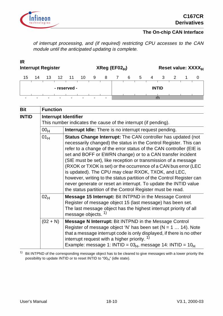
C167CRDerivatives
The On-chip CAN Interface
of interrupt processing, and (if required) restricting CPU accesses to the CANmodule until the anticipated updating is complete.
IRInterrupt Register XReg (EF02H) Reset value: XXXXH
15 14 13 12 11 10 9 8 7 6 5 4 3 2 1 0
- reserved - INTID
- - - - - - - - rh
Bit Function
INTID Interrupt IdentifierThis number indicates the cause of the interrupt (if pending).
00H Interrupt Idle: There is no interrupt request pending.
01H Status Change Interrupt: The CAN controller has updated (not necessarily changed) the status in the Control Register. This can refer to a change of the error status of the CAN controller (EIE is set and BOFF or EWRN change) or to a CAN transfer incident (SIE must be set), like reception or transmission of a message (RXOK or TXOK is set) or the occurrence of a CAN bus error (LEC is updated). The CPU may clear RXOK, TXOK, and LEC, however, writing to the status partition of the Control Register can never generate or reset an interrupt. To update the INTID value the status partition of the Control Register must be read.
02H Message 15 Interrupt: Bit INTPND in the Message Control Register of message object 15 (last message) has been set.The last message object has the highest interrupt priority of all message objects. 1)
1) Bit INTPND of the corresponding message object has to be cleared to give messages with a lower priority thepossibility to update INTID or to reset INTID to “00H” (idle state).
(02 + N) Message N Interrupt: Bit INTPND in the Message Control Register of message object ‘N’ has been set (N = 1 … 14). Note that a message interrupt code is only displayed, if there is no other interrupt request with a higher priority. 1)
Example: message 1: INTID = 03H, message 14: INTID = 10H
User’s Manual 18-10 V3.1, 2000-03
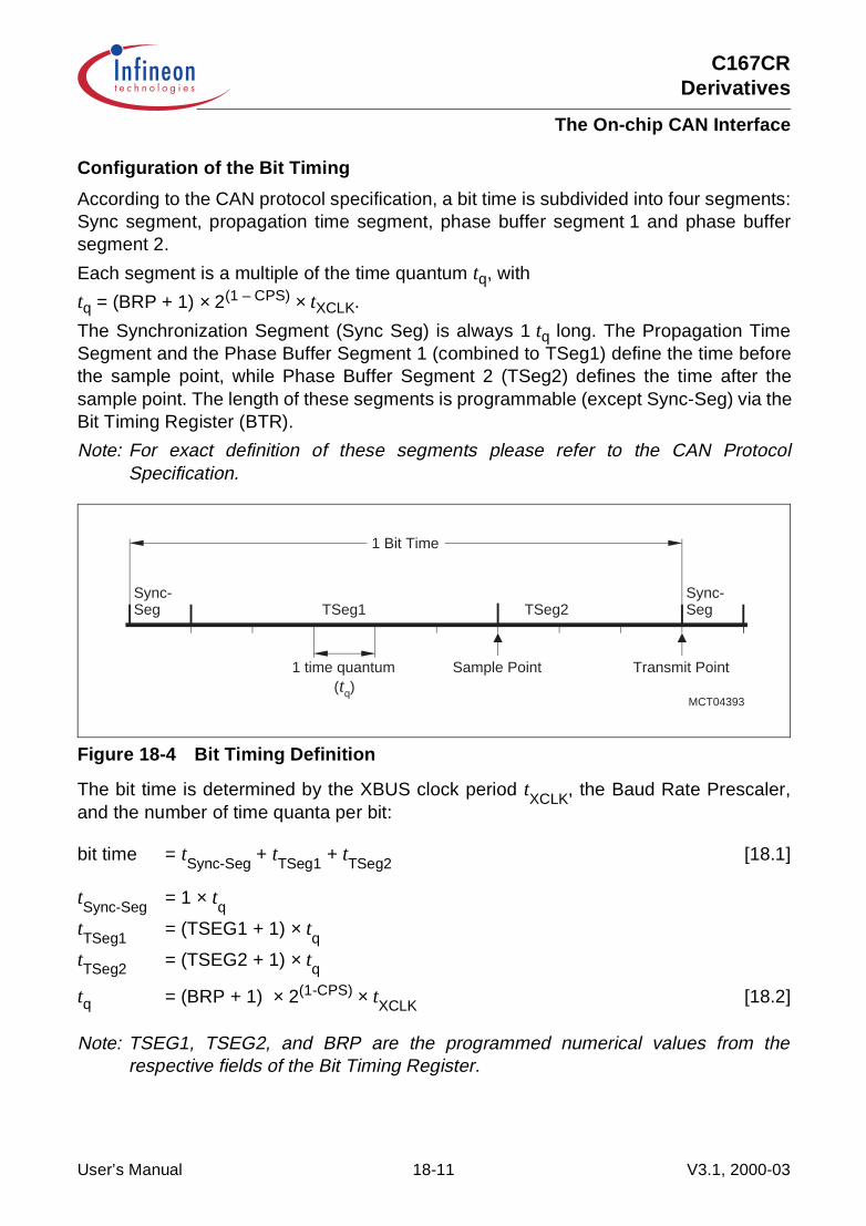
C167CRDerivatives
The On-chip CAN Interface
Configuration of the Bit Timing
According to the CAN protocol specification, a bit time is subdivided into four segments:Sync segment, propagation time segment, phase buffer segment 1 and phase buffersegment 2.
Each segment is a multiple of the time quantum tq, with
tq = (BRP + 1) × 2(1 – CPS) × tXCLK.
The Synchronization Segment (Sync Seg) is always 1 tq long. The Propagation TimeSegment and the Phase Buffer Segment 1 (combined to TSeg1) define the time beforethe sample point, while Phase Buffer Segment 2 (TSeg2) defines the time after thesample point. The length of these segments is programmable (except Sync-Seg) via theBit Timing Register (BTR).
Note: For exact definition of these segments please refer to the CAN ProtocolSpecification.
Figure 18-4 Bit Timing Definition
The bit time is determined by the XBUS clock period tXCLK, the Baud Rate Prescaler,and the number of time quanta per bit:
bit time = tSync-Seg + tTSeg1 + tTSeg2 [18.1]
tSync-Seg = 1 × tqtTSeg1 = (TSEG1 + 1) × tqtTSeg2 = (TSEG2 + 1) × tq
tq = (BRP + 1)
× 2(1-CPS) × tXCLK [18.2]
Note: TSEG1, TSEG2, and BRP are the programmed numerical values from therespective fields of the Bit Timing Register.
MCT04393
Sync-Seg
1 time quantum(tq)
TSeg1
Sample Point
Sync-SegTSeg2
Transmit Point
1 Bit Time
User’s Manual 18-11 V3.1, 2000-03
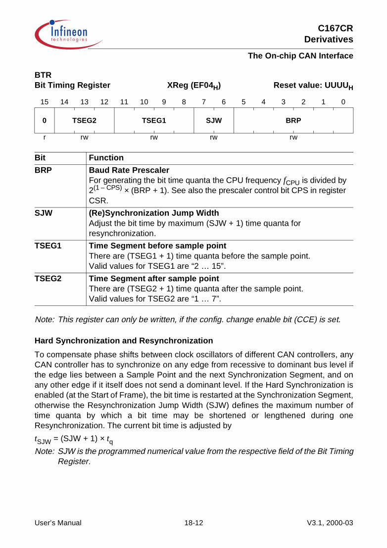
C167CRDerivatives
The On-chip CAN Interface
Note: This register can only be written, if the config. change enable bit (CCE) is set.
Hard Synchronization and Resynchronization
To compensate phase shifts between clock oscillators of different CAN controllers, anyCAN controller has to synchronize on any edge from recessive to dominant bus level ifthe edge lies between a Sample Point and the next Synchronization Segment, and onany other edge if it itself does not send a dominant level. If the Hard Synchronization isenabled (at the Start of Frame), the bit time is restarted at the Synchronization Segment,otherwise the Resynchronization Jump Width (SJW) defines the maximum number oftime quanta by which a bit time may be shortened or lengthened during oneResynchronization. The current bit time is adjusted by
tSJW = (SJW + 1) × tqNote: SJW is the programmed numerical value from the respective field of the Bit Timing
Register.
BTRBit Timing Register XReg (EF04H) Reset value: UUUUH
15 14 13 12 11 10 9 8 7 6 5 4 3 2 1 0
0 TSEG2 TSEG1 SJW BRP
r rw rw rw rw
Bit Function
BRP Baud Rate PrescalerFor generating the bit time quanta the CPU frequency fCPU is divided by2(1 – CPS) × (BRP + 1). See also the prescaler control bit CPS in register CSR.
SJW (Re)Synchronization Jump WidthAdjust the bit time by maximum (SJW + 1) time quanta for resynchronization.
TSEG1 Time Segment before sample pointThere are (TSEG1 + 1) time quanta before the sample point.Valid values for TSEG1 are “2 … 15”.
TSEG2 Time Segment after sample pointThere are (TSEG2 + 1) time quanta after the sample point.Valid values for TSEG2 are “1 … 7”.
User’s Manual 18-12 V3.1, 2000-03
C167CRDerivatives
The On-chip CAN Interface
Calculation of the Bit Time
The programming of the bit time according to the CAN Specification depends on thedesired baudrate, the XCLK frequency, and on the external physical delay times of thebus driver, of the bus line and of the input comparator. These delay times aresummarized in the Propagation Time Segment tProp, where
tProp is two times the maximum of the sum of physical bus delay, the input comparator
delay, and the output driver delay rounded up to the nearest multiple of tq.
To fulfill the requirements of the CAN specification, the following conditions must be met:
tTSeg2 ≥ 2 × tq = Information Processing Time
tTSeg2 ≥ tSJW
tTSeg1 ≥ 3 × tqtTSeg1 ≥ tSJW + tProp
Note: In order to achieve correct operation according to the CAN protocol the total bittime should be at least 8 tq, i.e. TSEG1 + TSEG2 ≥ 5.So, to operate with a baudrate of 1 MBit/sec, the XCLK frequency has to be atleast 8/16 MHz (depending on the prescaler control bit CPS in register CSR).
The maximum tolerance df for XCLK depends on the Phase Buffer Segment 1 (PB1),the Phase Buffer Segment 2 (PB2), and the Resynchronization Jump Width (SJW):
df ≤
AND
df ≤
The examples below show how the bit timing is to be calculated under specificcircumstances.
min PB1 PB2,( )2 13 bit time PB2–×( )×----------------------------------------------------------------
tSJW
20 bit time×--------------------------------
User’s Manual 18-13 V3.1, 2000-03

C167CRDerivatives
The On-chip CAN Interface
Bit Timing Example for High Baudrate
This example makes the following assumptions:
• XCLK frequency = 20 MHz• BRP = 00, CPS = 0• Baudrate = 1 Mbit/sec
tq 100 ns = 2 × tXCLKbus driver delay 50 nsreceiver circuit delay 30 nsbus line (40 m) delay 220 nstProp 600 ns = 6 × tqtSJW 100 ns = 1 × tqtTSeg1 700 ns = tProp + tSJWtTSeg2 200 ns = Information Processing TimetSync 100 ns = 1 × tqtBit 1000 ns = tSync + tTSeg1 + tTSeg2
tolerance for tXCLK 0.39% =
=
Bit Timing Example for Low Baudrate
This example makes the following assumptions:
• XCLK frequency = 4 MHz• BRP = 01, CPS = 0• Baudrate = 100 kbit/sec
tq 1 µs = 4 × tXCLKbus driver delay 200 nsreceiver circuit delay 80 nsbus line (40 m) delay 220 nstProp 1 µs = 1 × tqtSJW 4 µs = 4 × tqtTSeg1 5 µs = tProp + tSJWtTSeg2 4 µs = Information Processing Time + 2 × tqtSync 1 µs = 1 × tqtBit 10 µs = tSync + tTSeg1 + tTSeg2
tolerance for fXCLK 1.58% =
=
min PB1 PB2,( )2 13 bit time PB2–×( )×----------------------------------------------------------------
0,1µs2 13 1µs 0,2µs–×( )×-----------------------------------------------------------
min PB1 PB2,( )2 13 bit time PB2–×( )×----------------------------------------------------------------
4µs2 13 10µs 4µs–×( )×---------------------------------------------------------
User’s Manual 18-14 V3.1, 2000-03

C167CRDerivatives
The On-chip CAN Interface
Mask Registers
Messages can use standard or extended identifiers. Incoming frames are masked withtheir appropriate global masks. Bit IDE of the incoming message determines, if thestandard 11-bit mask in Global Mask Short (GMS) is to be used, or the 29-bit extendedmask in Global Mask Long (UGML&LGML). Bits holding a “0” mean “don’t care”, i.e. donot compare the message’s identifier in the respective bit position.
The last message object (15) has an additional individually programmable acceptancemask (Mask of Last Message, UMLM&LMLM) for the complete arbitration field. Thisallows classes of messages to be received in this object by masking some bits of theidentifier.
Note: The Mask of Last Message is ANDed with the Global Mask that corresponds tothe incoming message.
GMSGlobal Mask Short XReg (EF06H) Reset value: UFUUH
15 14 13 12 11 10 9 8 7 6 5 4 3 2 1 0
ID20 … 18 1 1 1 1 1 ID28 … 21
rw r r r r r rw
Bit Function
ID28 … 18 Identifier (11-bit)Mask to filter incoming messages with standard identifier.
User’s Manual 18-15 V3.1, 2000-03

C167CRDerivatives
The On-chip CAN Interface
UGMLUpper Global Mask Long XReg (EF08H) Reset value: UUUUH
15 14 13 12 11 10 9 8 7 6 5 4 3 2 1 0
ID20 … 13 ID28 … 21
rw rw
LGMLLower Global Mask Long XReg (EF0AH) Reset value: UUUUH
15 14 13 12 11 10 9 8 7 6 5 4 3 2 1 0
ID4 … 0 0 0 0 ID12 … 5
rw r r r rw
Bit Function
ID28 … 0 Identifier (29-bit)Mask to filter incoming messages with extended identifier.
User’s Manual 18-16 V3.1, 2000-03
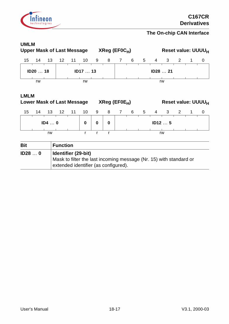
C167CRDerivatives
The On-chip CAN Interface
UMLMUpper Mask of Last Message XReg (EF0CH) Reset value: UUUUH
15 14 13 12 11 10 9 8 7 6 5 4 3 2 1 0
ID20 … 18 ID17 … 13 ID28 … 21
rw rw rw
LMLMLower Mask of Last Message XReg (EF0EH) Reset value: UUUUH
15 14 13 12 11 10 9 8 7 6 5 4 3 2 1 0
ID4 … 0 0 0 0 ID12 … 5
rw r r r rw
Bit Function
ID28 … 0 Identifier (29-bit)Mask to filter the last incoming message (Nr. 15) with standard or extended identifier (as configured).
User’s Manual 18-17 V3.1, 2000-03

C167CRDerivatives
The On-chip CAN Interface
18.3 The Message Object
The message object is the primary means of communication between CPU and CANcontroller. Each of the 15 message objects uses 15 consecutive bytes (see map below)and starts at an address that is a multiple of 16.
Note: All message objects must be initialized by the CPU, even those which are notgoing to be used, before clearing the INIT bit.
Figure 18-5 Message Object Address Map
The general properties of a message object are defined via the Message ControlRegister (MCR). There is a dedicated register MCRn for each message object n.
Each element of the Message Control Register is made of two complementary bits.Thisspecial mechanism allows the selective setting or resetting of specific elements (leavingothers unchanged) without requiring read-modify-write cycles. None of these elementswill be affected by reset.Table 18-1 shows how to use and interpret these 2-bit fields.
Table 18-1 MCR Bitfield Encoding
Value Function on Write Meaning on Read
0 0 – reserved – – reserved –
0 1 Reset element Element is reset
1 0 Set element Element is set
1 1 Leave element unchanged – reserved –
MCA04394
Msg. Config. (MCFG)Data0
Arbitration (UAR&LAR )
Message Control ( MCR)
Data1Data2
Data3Data4
Data5Data6
Data7Reserved
+0
+2
+4
+6
+8
+10
+12
+14
Offset
Object Start Address (EFn0 H)
Message Object 1: EF10 HMessage Object 2: EF20 H...
Message Object 14: EFE0 HMessage Object 15: EFF0 H
User’s Manual 18-18 V3.1, 2000-03

C167CRDerivatives
The On-chip CAN Interface
MCRnMessage Control Register XReg (EFn0H) Reset value: UUUUH
15 14 13 12 11 10 9 8 7 6 5 4 3 2 1 0
RMTPND TXRQ MSGLSTCPUUPD NEWDAT MSGVAL TXIE RXIE INTPND
rw rw rw rw rw rw rw rw
Bit Function
INTPND Interrupt PendingIndicates, if this message object has generated an interrupt request (see TXIE and RXIE), since this bit was last reset by the CPU, or not.
RXIE Receive Interrupt EnableDefines, if bit INTPND is set after successful reception of a frame.
TXIE Transmit Interrupt EnableDefines, if bit INTPND is set after successful transmission of a frame.1)
MSGVAL Message ValidIndicates, if the corresponding message object is valid or not. The CAN controller only operates on valid objects. Message objects can be tagged invalid, while they are changed, or if they are not used at all.
NEWDAT New DataIndicates, if new data has been written into the data portion of this message object by CPU (transmit-objects) or CAN controller (receive-objects) since this bit was last reset, or not.2)
MSGLST Message Lost (This bit applies to receive-objects only!)Indicates that the CAN controller has stored a new message into this object, while NEWDAT was still set, i.e. the previously stored message is lost.
CPUUPD CPU Update (This bit applies to transmit-objects only!)Indicates that the corresponding message object may not be transmitted now. The CPU sets this bit in order to inhibit the transmission of a message that is currently updated, or to control the automatic response to remote requests.
TXRQ Transmit RequestIndicates that the transmission of this message object is requested by the CPU or via a remote frame and is not yet done. TXRQ can be disabled by CPUUPD.1) 3)
User’s Manual 18-19 V3.1, 2000-03
C167CRDerivatives
The On-chip CAN Interface
1) In message object 15 (last message) these bits are hardwired to “0” (inactive) in order to prevent transmissionof message 15.
2) When the CAN controller writes new data into the message object, unused message bytes will be overwrittenby non specified values. Usually the CPU will clear this bit before working on the data, and verify that the bit isstill cleared once it has finished working to ensure that it has worked on a consistent set of data and not partof an old message and part of the new message.For transmit-objects the CPU will set this bit along with clearing bit CPUUPD. This will ensure that, if themessage is actually being transmitted during the time the message was being updated by the CPU, the CANcontroller will not reset bit TXRQ. In this way bit TXRQ is only reset once the actual data has been transferred.
3) When the CPU requests the transmission of a receive-object, a remote frame will be sent instead of a dataframe to request a remote node to send the corresponding data frame. This bit will be cleared by the CANcontroller along with bit RMTPND when the message has been successfully transmitted, if bit NEWDAT hasnot been set.If there are several valid message objects with pending transmission request, the message with the lowestmessage number is transmitted first. This arbitration is done when several objects are requested fortransmission by the CPU, or when operation is resumed after an error frame or after arbitration has been lost.
Arbitration Registers
The Arbitration Registers (UARn&LARn) are used for acceptance filtering of incomingmessages and to define the identifier of outgoing messages. A received message witha matching identifier is accepted as a data frame (matching object has DIR = ‘0’) or as aremote frame (matching object has DIR = ‘1’). For matching, the corresponding GlobalMask has to be considered (in case of message object 15 also the Mask of LastMessage). Extended frames (using Global Mask Long) can be stored only in messageobjects with XTD = ‘1’, standard frames (using Global Mask Short) only in messageobjects with XTD = ‘0’.
Message objects should have unique identifiers, i.e. if some bits are masked out by theGlobal Mask Registers (i.e. “don’t care”), then the identifiers of the valid message objectsshould differ in the remaining bits which are used for acceptance filtering.
If a received message (data frame or remote frame) matches with more than one validmessage object, it is associated with the object with the lowest message number. I.e. areceived data frame is stored in the “lowest” object, or the “lowest” object is sent inresponse to a remote frame. The Global Mask is used for matching here.
RMTPND Remote Pending (Used for transmit-objects)Indicates that the transmission of this message object has been requested by a remote node, but the data has not yet been transmitted. When RMTPND is set, the CAN controller also sets TXRQ. RMTPND and TXRQ are cleared, when the message object has been successfully transmitted.
Bit Function
User’s Manual 18-20 V3.1, 2000-03
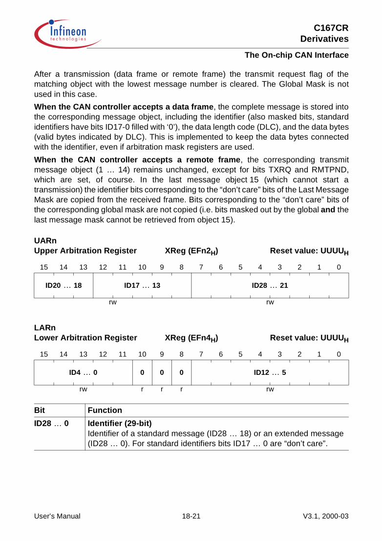
C167CRDerivatives
The On-chip CAN Interface
After a transmission (data frame or remote frame) the transmit request flag of thematching object with the lowest message number is cleared. The Global Mask is notused in this case.
When the CAN controller accepts a data frame, the complete message is stored intothe corresponding message object, including the identifier (also masked bits, standardidentifiers have bits ID17-0 filled with ‘0’), the data length code (DLC), and the data bytes(valid bytes indicated by DLC). This is implemented to keep the data bytes connectedwith the identifier, even if arbitration mask registers are used.
When the CAN controller accepts a remote frame, the corresponding transmitmessage object (1 … 14) remains unchanged, except for bits TXRQ and RMTPND,which are set, of course. In the last message object 15 (which cannot start atransmission) the identifier bits corresponding to the “don’t care” bits of the Last MessageMask are copied from the received frame. Bits corresponding to the “don’t care” bits ofthe corresponding global mask are not copied (i.e. bits masked out by the global and thelast message mask cannot be retrieved from object 15).
UARnUpper Arbitration Register XReg (EFn2H) Reset value: UUUUH
15 14 13 12 11 10 9 8 7 6 5 4 3 2 1 0
ID20 … 18 ID17 … 13 ID28 … 21
rw rw
LARnLower Arbitration Register XReg (EFn4H) Reset value: UUUUH
15 14 13 12 11 10 9 8 7 6 5 4 3 2 1 0
ID4 … 0 0 0 0 ID12 … 5
rw r r r rw
Bit Function
ID28 … 0 Identifier (29-bit)Identifier of a standard message (ID28 … 18) or an extended message (ID28 … 0). For standard identifiers bits ID17 … 0 are “don’t care”.
User’s Manual 18-21 V3.1, 2000-03

C167CRDerivatives
The On-chip CAN Interface
Message Configuration
The Message Configuration Register (low byte of MCFGn) holds a description of themessage within this object.
Note: There is no “don’t care” option for bits XTD and DIR. So incoming frames can onlymatch with corresponding message objects, either standard (XTD = 0) orextended (XTD = 1). Data frames only match with receive-objects, remote framesonly match with transmit-objects.When the CAN controller stores a data frame, it will write all the eight data bytesinto a message object. If the data length code was less than 8, the remaining bytesof the message object will be overwritten by non specified values.
Note: The first data byte occupies the upper half of the message configuration register.
MCFGnMessage Configuration Reg. XReg (EFn6H) Reset value: - - UUH
15 14 13 12 11 10 9 8 7 6 5 4 3 2 1 0
Data Byte 0 DLC DIR XTD 0 0
rw rw rw rw r r
Bit Function
XTD Extended Identifier0: Standard
This message object uses a standard 11-bit identifier.1: Extended
This message object uses an extended 29-bit identifier.
DIR Message Direction0: Receive object.
On TXRQ, a remote frame with the identifier of this message object is transmitted.On reception of a data frame with matching identifier, that message is stored in this message object.
1: Transmit object.On TXRQ, the respective message object is transmitted.On reception of a remote frame with matching identifier, the TXRQ and RMTPND bits of this message object are set.
DLC Data Length CodeDefines the number of valid data bytes within the data area.Valid values for the data length are 0 … 8.
User’s Manual 18-22 V3.1, 2000-03

C167CRDerivatives
The On-chip CAN Interface
Data Area
The data area occupies 8 successive byte positions after the Message ConfigurationRegister, i.e. the data area of message object n covers locations 00’EFn7H through00’EFnEH.Location 00’EFnFH is reserved.
Message data for message object 15 (last message) will be written into a two-message-alternating buffer to avoid the loss of a message, if a second message has beenreceived, before the CPU has read the first one.
Handling of Message Objects
The following diagrams summarize the actions that have to be taken in order to transmitand receive messages over the CAN bus. The actions taken by the CAN controller aredescribed as well as the actions that have to be taken by the CPU (i.e. the servicingprogram).
The diagrams show:
• CAN controller handling of transmit objects• CAN controller handling of receive objects• CPU handling of transmit objects• CPU handling of receive objects• CPU handling of last message object• Handling of the last message’s alternating buffer
User’s Manual 18-23 V3.1, 2000-03
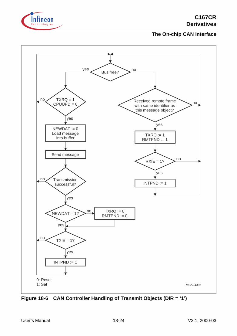
C167CRDerivatives
The On-chip CAN Interface
Figure 18-6 CAN Controller Handling of Transmit Objects (DIR = ‘1’)
MCA04395
Received remote framewith same identifier asthis message object?
TXRQ = 1CPUUPD = 0
Transmissionsuccessful?
Bus free?
yes
NEWDAT := 0Load message
into buffer
Send message
yes
TXIE = 1?
yes
INTPND := 1
nono
yes
RXIE = 1?
yes
INTPND := 1
no
TXRQ := 1RMTPND := 1
no
no
0: Reset1: Set
yes no
NEWDAT = 1? TXRQ := 0RMTPND := 0
no
yes
User’s Manual 18-24 V3.1, 2000-03

C167CRDerivatives
The On-chip CAN Interface
Figure 18-7 CAN Controller Handling of Receive Objects (DIR = ‘0’)
MCA04396
Received frame withsame identifier as this
message object?
TXRQ = 1?CPUUPD = 0?
Transmissionsuccessful?
Bus idle?
yes
NEWDAT := 0Load identifier andcontrol into buffer
Send remote frame
yes
TXRQ := 0RMTPND := 0
TXIE = 1?
yes
INTPND := 1
nono
yes
NEWDAT = 1
no
RXIE = 1?
yes
INTPND := 1
no
Store messageNEWDAT := 1
TXRQ := 0RMTPND := 0
yes
MSGLST := 1
no
no
0: Reset1: Set
yes no
User’s Manual 18-25 V3.1, 2000-03

C167CRDerivatives
The On-chip CAN Interface
Figure 18-8 CPU Handling of Transmit Objects (DIR = ‘1’)
MCA04397
Updatemessage?
Want to send?
no
yes
TXRQ := 1
no yes
CPUUPD := 0
Write / calculate message contents
CPUUPD := 1NEWDAT := 1
TXIE := (application cpecific)RXIE := (application cpecific)
INTPND := 0RMTPND := 0
TXRQ := 0CPUUPD := 1
Identifier := (application cpecific)NEWDAT := 0
Direction := transmitDLC := (application cpecific)
MSGVAL := 1XTD := (application cpecific)
(all bits undefined)
Update
Update: Start
Update: End
Initialization
Power Up
0: Reset1: Set
User’s Manual 18-26 V3.1, 2000-03

C167CRDerivatives
The On-chip CAN Interface
Figure 18-9 CPU Handling of Receive Objects (DIR = ‘0’)
MCA04398
RequestUpdate?
NEWDAT = 1?
no
yes
no
Process message contents
NEWDAT := 0
TXIE := (application cpecific)RXIE := (application cpecific)
INTPNDd := 0RMTPND := 0
TXRQ := 0MSGLST := 0
Identifier := (application cpecific)NEWDAT := 0
Direction := receiveDLC := (value of DLC in transmitter)
MSGVAL := 1XTD := (application cpecific)
(all bits undefined)
Process
Process: Start
Process: End
Initialization
Power Up
0: Reset1: Set
yes
TXRQ := 1
Restart process
User’s Manual 18-27 V3.1, 2000-03

C167CRDerivatives
The On-chip CAN Interface
Figure 18-10 CPU Handling of the Last Message Object
MCA04399
NEWDAT = 1?
no
yes
NEWDAT := 0
Process message contents
RXIE := (application cpecific)INTPND := 0
RMTPND := 0MSGLST := 0
Identifier := (application cpecific)NEWDAT := 0
Direction := receiveDLC := (value of DLC in transmitter)
MSGVAL := 1XTD := (application cpecific)
(all bits undefined)
Process
Process: Start
Process: End
Initialization
Power Up
0: Reset1: Set
Restart process
User’s Manual 18-28 V3.1, 2000-03
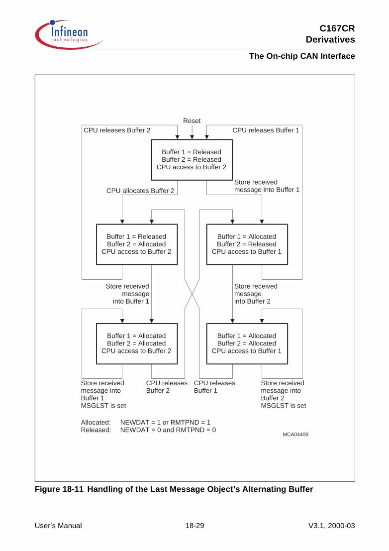
C167CRDerivatives
The On-chip CAN Interface
Figure 18-11 Handling of the Last Message Object’s Alternating Buffer
MCA04400
Buffer 1 = ReleasedBuffer 2 = Released
CPU access to Buffer 2
Reset
Buffer 1 = ReleasedBuffer 2 = Allocated
CPU access to Buffer 2
CPU allocates Buffer 2
Buffer 1 = AllocatedBuffer 2 = Released
CPU access to Buffer 1
Buffer 1 = AllocatedBuffer 2 = Allocated
CPU access to Buffer 2
Buffer 1 = AllocatedBuffer 2 = Allocated
CPU access to Buffer 1
Store receivedmessage
into Buffer 1
Store receivedmessageinto Buffer 2
CPU releases Buffer 2 CPU releases Buffer 1
Store receivedmessage intoBuffer 1MSGLST is set
CPU releasesBuffer 2
CPU releasesBuffer 1
Store receivedmessage intoBuffer 2MSGLST is set
Allocated: NEWDAT = 1 or RMTPND = 1Released: NEWDAT = 0 and RMTPND = 0
Store receivedmessage into Buffer 1
User’s Manual 18-29 V3.1, 2000-03
C167CRDerivatives
The On-chip CAN Interface
18.4 Controlling the CAN Module
The CAN module is controlled by the C167CR via hardware signals (e.g. reset) and viaregister accesses executed by software.
Accessing the On-chip CAN Module
The CAN module is implemented as an X-Peripheral and is therefore accessed like anexternal memory or peripheral. That means that the registers of the CAN module can beread and written using 16-bit or 8-bit direct or indirect MEM addressing modes. Also bithandling is not supported via the XBUS. Since the XBUS, to which the CAN module isconnected, also represents the external bus, CAN accesses follow the same rules andprocedures as accesses to the external bus. CAN accesses cannot be executed inparallel to external instruction fetches or data read/writes, but are arbitrated and insertedinto the external bus access stream.
Accesses to the CAN module use demultiplexed addresses, a 16-bit data bus (byteaccesses possible), two waitstates and no tristate waitstate.
The CAN address area starts at 00’EF00H and covers 256 Bytes. This area is decodedinternally, so none of the programmable address windows must be sacrificed in order toaccess the on-chip CAN module.
The advantage of locating the CAN address area in segment 0 is that the CAN moduleis accessible via data page 3, which is the ‘system’ data page, accessed usually throughthe ‘system’ data page pointer DPP3. In this way, the internal addresses, such like SFRs,internal RAM, and the CAN registers, are all located within the same data page and forma contiguous address space.
Power Down Mode
If the C167CR enters Power Down mode, the XCLK signal will be turned off which willstop the operation of the CAN module. Any message transfer is interrupted. In order toensure that the CAN controller is not stopped while sending a dominant level (‘0’) on theCAN bus, the CPU should set bit INIT in the Control Register prior to entering PowerDown mode. The CPU can check if a transmission is in progress by reading bits TXRQand NEWDAT in the message objects and bit TXOK in the Control Register. Afterreturning from Power Down mode via hardware reset, the CAN module has to bereconfigured.
User’s Manual 18-30 V3.1, 2000-03

C167CRDerivatives
The On-chip CAN Interface
CAN Module Reset
The on-chip CAN module is connected to the XBUS Reset signal. This signal isactivated, when the C167CR’s reset input is activated, when a software reset isexecuted, and in case of a watchdog reset. Activating the CAN module’s reset linetriggers a hardware reset.
This hardware reset:
• disconnects the CAN_TXD output from the port logic• clears the error counters• resets the busoff state• switches the Control Register’s low byte to 01H• leaves the Control Register’s high byte and the Interrupt Register undefined• does not change the other registers including the message objects (notified as UUUU)
Note: The first hardware reset after power-on leaves the unchanged registers in anundefined state, of course.The value 01H in the Control Register’s low byte prepares for the moduleinitialization.
CAN Module Activation
After a reset the CAN module is disabled. Before it can be used to receive or transmitmessages the application software must activate the CAN module.
Two actions are required for this purpose:
• General Module Enable globally activates the CAN module. This is done by settingbit XPEN in register SYSCON.
• Module Initialization determines the functionality of the CAN module (baudrate,active objects, etc.). This is the major part of the activation and is described in thefollowing.
User’s Manual 18-31 V3.1, 2000-03
C167CRDerivatives
The On-chip CAN Interface
Module Initialization
The module initialization is enabled by setting bit INIT in the control register CSR. Thiscan be done by the CPU via software, or automatically by the CAN controller on ahardware reset, or if the EML switches to busoff state.
While INIT is set:
• all message transfer from and to the CAN bus is stopped• the CAN transmit line CAN_TXD is “1” (recessive)• the control bits NEWDAT and RMTPND of the last message object are reset• the counters of the EML are left unchanged.
Setting bit CCE in addition, permits changing the configuration in the Bit Timing Register.
To initialize the CAN Controller, the following actions are required:
• configure the Bit Timing Register (CCE required)• set the Global Mask Registers• initialize each message object.
If a message object is not needed, it is sufficient to clear its message valid bit (MSGVAL),i.e. to define it as not valid. Otherwise, the whole message object has to be initialized.
After the initialization sequence has been completed, the CPU clears bit INIT.
Now the BSP synchronizes itself to the data transfer on the CAN bus by waiting for theoccurrence of a sequence of 11 consecutive recessive bits (i.e. Bus Idle) before it cantake part in bus activities and start message transfers.
The initialization of the message objects is independent of the state of bit INIT and canbe done on the fly. The message objects should all be configured to particular identifiersor set to “not valid” before the BSP starts the message transfer, however.
To change the configuration of a message object during normal operation, the CPU firstclears bit MSGVAL, which defines it as not valid. When the configuration is completed,MSGVAL is set again.
User’s Manual 18-32 V3.1, 2000-03

C167CRDerivatives
The On-chip CAN Interface
Busoff Recovery Sequence
If the device goes busoff, it will set bit BOFF and also set bit INIT of its own accord,stopping all bus activities. To have the CAN module take part in the CAN bus activitiesagain, the bus-off recovery sequence must be started by clearing the bit INIT (viasoftware). Once INIT has been cleared, the module will then wait for 129 occurrences ofBus idle before resuming normal operation.
At the end of the busoff recovery sequence the Error Management Counters will bereset. This will automatically clear bits BOFF and EWRN.
During the waiting time after the resetting of INIT each time a sequence of 11 recessivebits has been monitored, a Bit0Error code is written to the Control Register, enablingthe CPU to check up whether the CAN bus is stuck at dominant or continously disturbedand to monitor the proceeding of the busoff recovery sequence.
Note: An interrupt can be generated when entering the busoff state if bits IE and EIE areset. The corresponding interrupt code in bitfield INTID is 01H.The busoff recovery sequence cannot be shortened by setting or resetting INIT.
User’s Manual 18-33 V3.1, 2000-03
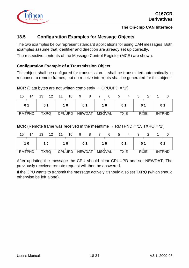
C167CRDerivatives
The On-chip CAN Interface
18.5 Configuration Examples for Message Objects
The two examples below represent standard applications for using CAN messages. Bothexamples assume that identifier and direction are already set up correctly.
The respective contents of the Message Control Register (MCR) are shown.
Configuration Example of a Transmission Object
This object shall be configured for transmission. It shall be transmitted automatically inresponse to remote frames, but no receive interrupts shall be generated for this object.
After updating the message the CPU should clear CPUUPD and set NEWDAT. Thepreviously received remote request will then be answered.
If the CPU wants to transmit the message actively it should also set TXRQ (which shouldotherwise be left alone).
MCR (Data bytes are not written completely → CPUUPD = ‘1’)
15 14 13 12 11 10 9 8 7 6 5 4 3 2 1 0
0 1 0 1 1 0 0 1 1 0 0 1 0 1 0 1
RMTPND TXRQ CPUUPD NEWDAT MSGVAL TXIE RXIE INTPND
MCR (Remote frame was received in the meantime → RMTPND = ‘1’, TXRQ = ‘1’)
15 14 13 12 11 10 9 8 7 6 5 4 3 2 1 0
1 0 1 0 1 0 0 1 1 0 0 1 0 1 0 1
RMTPND TXRQ CPUUPD NEWDAT MSGVAL TXIE RXIE INTPND
User’s Manual 18-34 V3.1, 2000-03
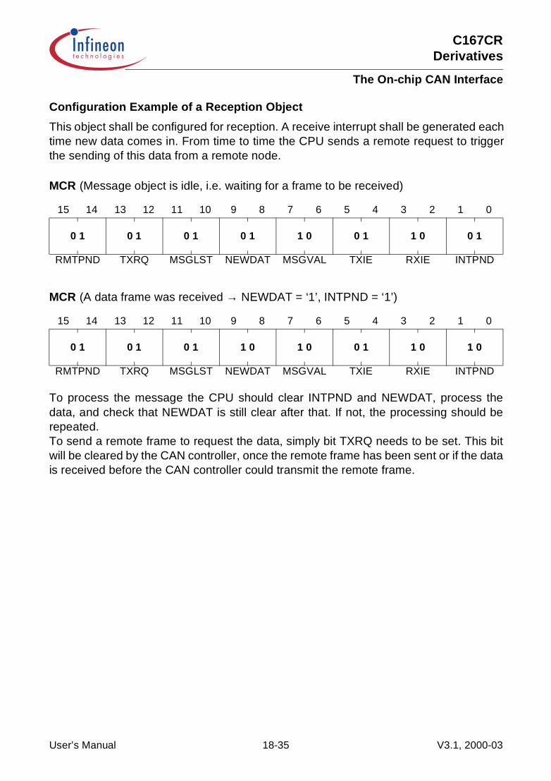
C167CRDerivatives
The On-chip CAN Interface
Configuration Example of a Reception Object
This object shall be configured for reception. A receive interrupt shall be generated eachtime new data comes in. From time to time the CPU sends a remote request to triggerthe sending of this data from a remote node.
.
To process the message the CPU should clear INTPND and NEWDAT, process thedata, and check that NEWDAT is still clear after that. If not, the processing should berepeated.To send a remote frame to request the data, simply bit TXRQ needs to be set. This bitwill be cleared by the CAN controller, once the remote frame has been sent or if the datais received before the CAN controller could transmit the remote frame.
MCR (Message object is idle, i.e. waiting for a frame to be received)
15 14 13 12 11 10 9 8 7 6 5 4 3 2 1 0
0 1 0 1 0 1 0 1 1 0 0 1 1 0 0 1
RMTPND TXRQ MSGLST NEWDAT MSGVAL TXIE RXIE INTPND
MCR (A data frame was received → NEWDAT = ‘1’, INTPND = ‘1’)
15 14 13 12 11 10 9 8 7 6 5 4 3 2 1 0
0 1 0 1 0 1 1 0 1 0 0 1 1 0 1 0
RMTPND TXRQ MSGLST NEWDAT MSGVAL TXIE RXIE INTPND
User’s Manual 18-35 V3.1, 2000-03

C167CRDerivatives
The On-chip CAN Interface
18.6 The CAN Application Interface
The on-chip CAN module of the C167CR is connected to the (external) physical layer(i.e. the CAN bus) via two signals:
A logic low level (‘0’) is interpreted as the dominant CAN bus level, a logic high level (‘1’)is interpreted as the recessive CAN bus level.
Connection to an External Transceiver
The CAN module of the C167CR can be connected to an external CAN bus via a CANtransceiver.
Note: Basically it is also possible to connect several CAN modules directly (on-board)without using CAN transceivers.
Figure 18-12 Connection to a Single CAN Bus
Table 18-2 CAN Interface Signals
CAN Signal Port Pin Function
CAN_RXD P4.5 Receive data from the physical layer of the CAN bus.
CAN_TXD P4.6 Transmit data to the physical layer of the CAN bus.
MCS04401
CAN 1
CANTransceiver
PhysicalLayer
C167CR
CAN_RxD
CAN_TxD CA
N B
us
User’s Manual 18-36 V3.1, 2000-03

C167CRDerivatives
The On-chip CAN Interface
Port Control
The receive data line and the transmit data line of the CAN module are alternate portfunctions. Make sure that the respective port pin for the receive line is switched to inputin order to enable proper reception. The respective port driver for the transmit willautomatically be switched ON.
This provides a standard pin configuration without additional software control and alsoworks in emulation mode where the port direction registers cannot be controlled.
Note: The CAN interface signals are only available on Port 4 if the respective pins arenot programmed to output segment address lines (alternate function of Port 4).Select 0, 2, or 4 segment address lines if the CAN interface is to be used.
User’s Manual 18-37 V3.1, 2000-03
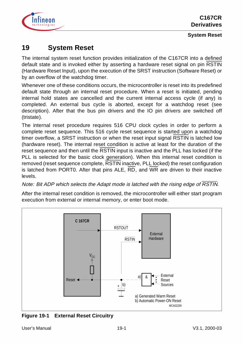
C167CRDerivatives
System Reset
19 System ResetThe internal system reset function provides initialization of the C167CR into a defineddefault state and is invoked either by asserting a hardware reset signal on pin RSTIN(Hardware Reset Input), upon the execution of the SRST instruction (Software Reset) orby an overflow of the watchdog timer.
Whenever one of these conditions occurs, the microcontroller is reset into its predefineddefault state through an internal reset procedure. When a reset is initiated, pendinginternal hold states are cancelled and the current internal access cycle (if any) iscompleted. An external bus cycle is aborted, except for a watchdog reset (seedescription). After that the bus pin drivers and the IO pin drivers are switched off(tristate).
The internal reset procedure requires 516 CPU clock cycles in order to perform acomplete reset sequence. This 516 cycle reset sequence is started upon a watchdogtimer overflow, a SRST instruction or when the reset input signal RSTIN is latched low(hardware reset). The internal reset condition is active at least for the duration of thereset sequence and then until the RSTIN input is inactive and the PLL has locked (if thePLL is selected for the basic clock generation). When this internal reset condition isremoved (reset sequence complete, RSTIN inactive, PLL locked) the reset configurationis latched from PORT0. After that pins ALE, RD, and WR are driven to their inactivelevels.
Note: Bit ADP which selects the Adapt mode is latched with the rising edge of RSTIN.
After the internal reset condition is removed, the microcontroller will either start programexecution from external or internal memory, or enter boot mode.
Figure 19-1 External Reset Circuitry
Reset
+
a) Generated Warm Resetb) Automatic Power-ON Reset
&
MCA02259
RSTOUT
C 167CR
ExternalHardware
a)
b)
ExternalResetSources
CCV
RSTIN
User’s Manual 19-1 V3.1, 2000-03
C167CRDerivatives
System Reset
19.1 Reset Sources
Several sources (external or internal) can generate a reset for the C167CR. Softwarecan identify the respective reset source via the reset source indication flags in registerWDTCON. Generally any reset causes the same actions on the C167CR’s modules. Thedifferences are described in the following sections.
Hardware Reset
A hardware reset is triggered when the reset input signal RSTIN is latched low. To ensurethe recognition of the RSTIN signal (latching), it must be held low for at least 100 ns plus2 CPU clock cycles (input filter plus synchronization). Also shorter RSTIN pulses maytrigger a hardware reset, if they coincide with the latch’s sample point. The actualminimum duration for a reset pulse depends on the current CPU clock generation mode.The worstcase is generating the CPU clock via the prescaler (fCPU = fOSC / 2 in this case).
After the reset sequence has been completed, the RSTIN input is sampled again. Whenthe reset input signal is inactive at that time, the internal reset condition is terminated(indicated as short hardware reset, SHWR). When the reset input signal is still active atthat time, the internal reset condition is prolonged until RSTIN gets inactive (indicated aslong hardware reset, LHWR).
During a hardware reset the inputs for the reset configuration (PORT0) need some timeto settle on the required levels, especially if the hardware reset aborts a read operationfrom an external peripheral. During this settling time the configuration may intermittentlybe wrong. For the duration of one internal reset sequence after a reset has beenrecognized the configuration latches are not transparent, i.e. the (new) configurationbecomes valid earliest after the completion of one reset sequence. This usually coversthe required settling time.
When the basic clock is generated by the PLL the internal reset condition should beextended until the on-chip PLL has locked (longer RSTIN signal).
The input RSTIN provides an internal pullup device equalling a resistor of 50 kΩ to250 kΩ (the minimum reset time must be determined by the lowest value). Simplyconnecting an external capacitor is sufficient for an automatic power-on reset (see b) inFigure 19-1). RSTIN may also be connected to the output of other logic gates (see a) inFigure 19-1). See also “Bidirectional Reset” on Page 19-4 in this case.
Note: A power-on reset requires an active time of two reset sequences (1036 CPU clockcycles) after a stable clock signal is available (about 10 … 50 ms, depending onthe oscillator frequency, to allow the on-chip oscillator to stabilize).
User’s Manual 19-2 V3.1, 2000-03

C167CRDerivatives
System Reset
Software Reset
The reset sequence can be triggered at any time via the protected instruction SRST(Software Reset). This instruction can be executed deliberately within a program, e.g. toleave bootstrap loader mode, or upon a hardware trap that reveals a system failure.
Note: A software reset only latches the configuration of the bus interface (SALSEL,CSSEL, WRC, BUSTYP) from PORT0. If bidirectional reset is enabled, a software reset is executed like a long hardwarereset.
Watchdog Timer Reset
When the watchdog timer is not disabled during the initialization or serviced regularlyduring program execution it will overflow and trigger the reset sequence. Other thanhardware and software reset the watchdog reset completes a running external bus cycleif this bus cycle either does not use READY at all, or if READY is sampled active (low)after the programmed waitstates. When READY is sampled inactive (high) after theprogrammed waitstates the running external bus cycle is aborted. Then the internal resetsequence is started.
Note: A watchdog reset only latches the configuration of the bus interface (SALSEL,CSSEL, WRC, BUSTYP) from PORT0.If bidirectional reset is enabled a watchdog timer reset is executed like a longhardware reset.The watchdog reset cannot occur while the C167CR is in bootstrap loader mode!
User’s Manual 19-3 V3.1, 2000-03
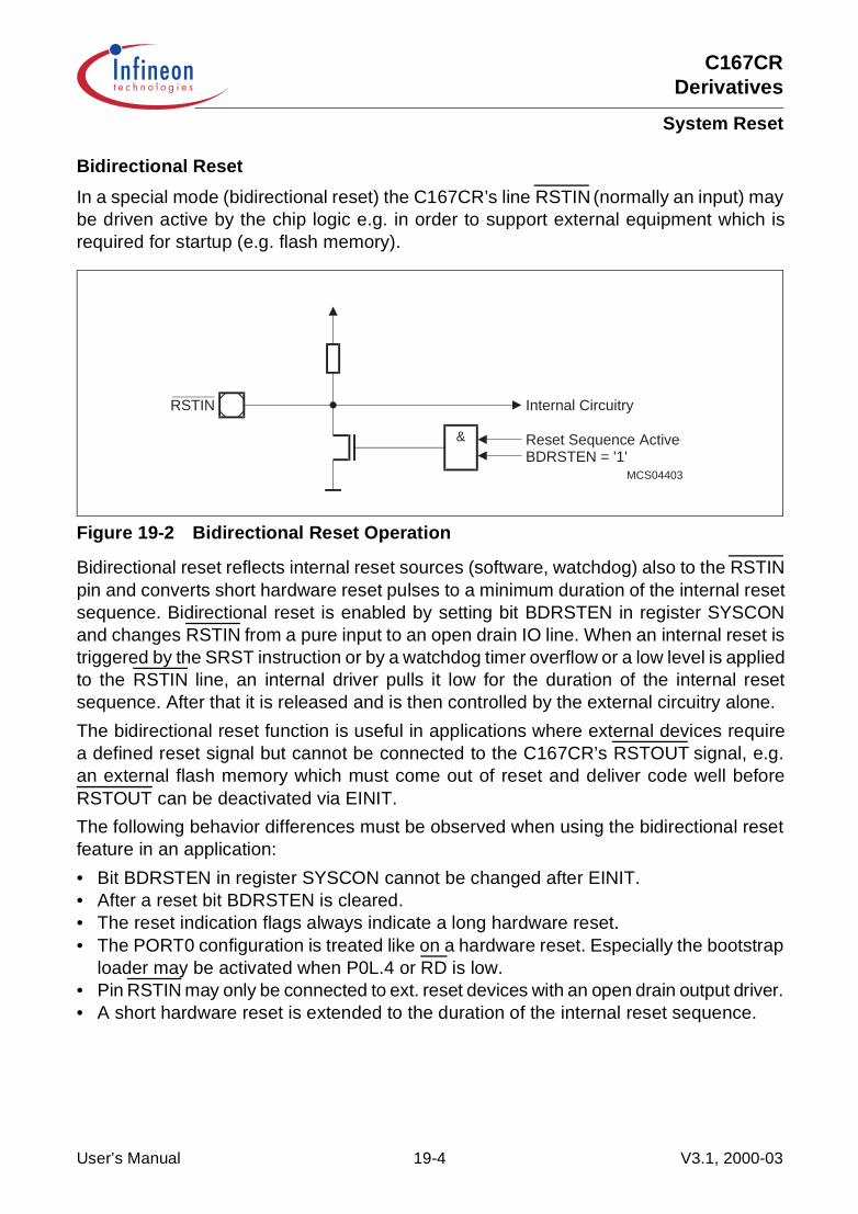
C167CRDerivatives
System Reset
Bidirectional Reset
In a special mode (bidirectional reset) the C167CR’s line RSTIN (normally an input) maybe driven active by the chip logic e.g. in order to support external equipment which isrequired for startup (e.g. flash memory).
Figure 19-2 Bidirectional Reset Operation
Bidirectional reset reflects internal reset sources (software, watchdog) also to the RSTINpin and converts short hardware reset pulses to a minimum duration of the internal resetsequence. Bidirectional reset is enabled by setting bit BDRSTEN in register SYSCONand changes RSTIN from a pure input to an open drain IO line. When an internal reset istriggered by the SRST instruction or by a watchdog timer overflow or a low level is appliedto the RSTIN line, an internal driver pulls it low for the duration of the internal resetsequence. After that it is released and is then controlled by the external circuitry alone.
The bidirectional reset function is useful in applications where external devices requirea defined reset signal but cannot be connected to the C167CR’s RSTOUT signal, e.g.an external flash memory which must come out of reset and deliver code well beforeRSTOUT can be deactivated via EINIT.
The following behavior differences must be observed when using the bidirectional resetfeature in an application:
• Bit BDRSTEN in register SYSCON cannot be changed after EINIT.• After a reset bit BDRSTEN is cleared.• The reset indication flags always indicate a long hardware reset.• The PORT0 configuration is treated like on a hardware reset. Especially the bootstrap
loader may be activated when P0L.4 or RD is low.• Pin RSTIN may only be connected to ext. reset devices with an open drain output driver.• A short hardware reset is extended to the duration of the internal reset sequence.
MCS04403
RSTIN
&
Internal Circuitry
Reset Sequence ActiveBDRSTEN = '1'
User’s Manual 19-4 V3.1, 2000-03

C167CRDerivatives
System Reset
19.2 Status After Reset
After a reset is completed most units of the C167CR enter a well-defined default status.This ensures repeatable start conditions and avoids spurious activities after reset.
Watchdog Timer Operation after Reset
The watchdog timer starts running after the internal reset has completed. It will beclocked with the internal system clock divided by 2 (fCPU / 2), and its default reload valueis 00H, so a watchdog timer overflow will occur 131,072 CPU clock cycles (2 × 216) aftercompletion of the internal reset, unless it is disabled, serviced or reprogrammedmeanwhile. When the system reset was caused by a watchdog timer overflow, theWDTR (Watchdog Timer Reset Indication) flag in register WDTCON will be set to ‘1’.This indicates the cause of the internal reset to the software initialization routine. WDTRis reset to ‘0’ by an external hardware reset, by servicing the watchdog timer or afterEINIT. After the internal reset has completed, the operation of the watchdog timer canbe disabled by the DISWDT (Disable Watchdog Timer) instruction. This instruction hasbeen implemented as a protected instruction. For further security, its execution is onlyenabled in the time period after a reset until either the SRVWDT (Service WatchdogTimer) or the EINIT instruction has been executed. Thereafter the DISWDT instructionwill have no effect.
Reset Values for the C167CR Registers
During the reset sequence the registers of the C167CR are preset with a default value.Most SFRs, including system registers and peripheral control and data registers, arecleared to zero, so all peripherals and the interrupt system are off or idle after reset. Afew exceptions to this rule provide a first pre-initialization, which is either fixed orcontrolled by input pins.
DPP1: 0001H (points to data page 1)DPP2: 0002H (points to data page 2)DPP3: 0003H (points to data page 3)CP: FC00HSTKUN: FC00HSTKOV: FA00HSP: FC00HWDTCON: 00XXH (value depends on the reset source)S0RBUF: XXH (undefined)SSCRB: XXXXH (undefined)SYSCON: 0XX0H (set according to reset configuration)BUSCON0: 0XX0H (set according to reset configuration)RP0H: XXH (reset levels of P0H)ONES: FFFFH (fixed value)
User’s Manual 19-5 V3.1, 2000-03

C167CRDerivatives
System Reset
The C167CR’s Pins after Reset
After the reset sequence the different groups of pins of the C167CR are activated indifferent ways depending on their function. Bus and control signals are activatedimmediately after the reset sequence according to the configuration latched fromPORT0, so either external accesses can takes place or the external control signals areinactive. The general purpose IO pins remain in input mode (high impedance) untilreprogrammed via software (see Figure 19-3 ). The RSTOUT pin remains active (low)until the end of the initialization routine (see description).
Figure 19-3 Reset Input and Output Signals
delayed until the end of the internal reset condition.
Current bus cycle is completed or aborted.
Activation of the IO pins is controlled by software.Execution of the EINIT instruction.
When the internal reset condition is extended by RSTIN, the activation of the output signals is
Switches asinchronously with RSTIN, sinchronously upon software or watchdog reset.The reset condition ends here. The C 167CR starts program execution.
The shaded area designates the internal reset sequence, which starts after synchronization of RSTIN.
RSTIN
Internal Reset Condition
6)
Initialization
3)
MCS02258
RD, WR
RSTOUT
IO
ALE
Bus
RSTIN
Internal Reset Condition
6)
1)
2)
2)
Initialization
3) 5)
4)
8)
7)
A short hardware reset is extended until the end of the reset sequence in Bidirectional reset mode.A software or WDT reset activates the RSTIN line in Bidirectional reset mode.8)
7)
6)
3)
2)
5)
4)
1)
User’s Manual 19-6 V3.1, 2000-03

C167CRDerivatives
System Reset
Ports and External Bus Configuration during Reset
During the internal reset sequence all of the C167CR’s port pins are configured as inputsby clearing the associated direction registers, and their pin drivers are switched to thehigh impedance state. This ensures that the C167CR and external devices will not try todrive the same pin to different levels. Pin ALE is held low through an internal pulldown,and pins RD, WR and READY are held high through internal pullups. Also the pins thatcan be configured for CS output will be pulled high.
The registers SYSCON and BUSCON0 are initialized according to the configurationselected via PORT0.
When an external start is selected (pin EA = ‘0’):
• the Bus Type field (BTYP) in register BUSCON0 is initialized according toP0L.7 and P0L.6
• bit BUSACT0 in register BUSCON0 is set to ‘1’• bit ALECTL0 in register BUSCON0 is set to ‘1’• bit ROMEN in register SYSCON will be cleared to ‘0’• bit BYTDIS in register SYSCON is set according to the data bus width (set if 8-bit)• bit WRCFG in register SYSCON is set according to pin P0H.0 (WRC)
When an internal start is selected (pin EA = ‘1’):
• register BUSCON0 is cleared to 0000H• bit ROMEN in register SYSCON will be set to ‘1’• bit BYTDIS in register SYSCON is set, i.e. BHE/WRH is disabled• bit WRCFG in register SYSCON is set according to pin P0H.0 (WRC)
The other bits of register BUSCON0, and the other BUSCON registers are cleared.This default initialization selects the slowest possible external accesses using theconfigured bus type.
When the internal reset has completed, the configuration of PORT0, PORT1, Port 4,Port 6, and of the BHE signal (High Byte Enable, alternate function of P3.12) dependson the bus type which was selected during reset. When any of the external bus modeswas selected during reset, PORT0 will operate in the selected bus mode. Port 4 willoutput the selected number of segment address lines (all zero after reset). Port 6 willdrive the selected number of CS lines (CS0 will be ‘0’, while the other active CS lineswill be ‘1’). When no memory accesses above 64 K are to be performed, segmentationmay be disabled.
When the on-chip bootstrap loader was activated during reset, pin TxD0 (alternate portfunction) will be switched to output mode after the reception of the zero byte.
All other pins remain in the high-impedance state until they are changed by software orperipheral operation.
User’s Manual 19-7 V3.1, 2000-03

C167CRDerivatives
System Reset
Reset Output Pin
The RSTOUT pin is dedicated to generate a reset signal for the system componentsbesides the controller itself. RSTOUT will be driven active (low) at the begin of any resetsequence (triggered by hardware, the SRST instruction or a watchdog timer overflow).RSTOUT stays active (low) beyond the end of the internal reset sequence until theprotected EINIT (End of Initialization) instruction is executed (see Figure 19-3). Thisallows the complete configuration of the controller including its on-chip peripheral unitsbefore releasing the reset signal for the external peripherals of the system.
Note: RSTOUT will float during emulation mode or adapt mode.
The Internal RAM after Reset
The contents of the internal RAM are not affected by a system reset. However, after apower-on reset, the contents of the internal RAM are undefined. This implies that theGPRs (R15 … R0) and the PEC source and destination pointers (SRCP7 … SRCP0,DSTP7 … DSTP0) which are mapped into the internal RAM are also unchanged after awarm reset, software reset or watchdog reset, but are undefined after a power-on reset.
The Extension RAM (XRAM) after Reset
The contents of the on-chip extension RAM are not affected by a system reset. However,after a power-on reset, the contents of the XRAM are undefined.
Operation after Reset
After the internal reset condition is removed the C167CR fetches the first instruction fromthe program memory (location 00’0000H for a standard start). As a rule, this first locationholds a branch instruction to the actual initialization routine that may be locatedanywhere in the address space.
Note: When the Bootstrap Loader Mode was activated during a hardware reset theC167CR does not fetch instructions from the program memory.The standard bootstrap loader expects data via serial interface ASC0.
User’s Manual 19-8 V3.1, 2000-03
C167CRDerivatives
System Reset
19.3 Application-specific Initialization Routine
After a reset the modules of the C167CR must be initialized to enable their operation ona given application. This initialization depends on the task the C167CR is to fulfill in thatapplication and on some system properties like operating frequency, connected externalcircuitry, etc.
The following initializations should typically be done, before the C167CR is prepared torun the actual application software:
Memory Areas
The external bus interface can be reconfigured after an external reset because registerBUSCON0 is initialized to the slowest possible bus cycle configuration. Theprogrammable address windows can be enabled in order to adapt the bus cyclecharacteristics to different memory areas or peripherals. Also after a single-chip modereset the external bus interface can be enabled and configured.
The internal program memory (if available) can be enabled and mapped after anexternal reset in order to use the on-chip resources. After a single-chip mode reset theinternal program memory can be remapped or disabled at all in order to utilize externalmemory (partly or completely).
Programmable program memory can be programmed, e.g. with data received over aserial link.
Note: Initial Flash or OTP programming will rather be done in bootstrap loader mode.
System Stack
The default setup for the system stack (size, stackpointer, upper and lower limitregisters) can be adjusted to application-specific values. After reset, registers SP andSTKUN contain the same reset value 00’FC00H, while register STKOV contains00’FA00H. With the default reset initialization, 256 words of system stack are available,where the system stack selected by the SP grows downwards from 00’FBFEH.
Note: The interrupt system, which is disabled upon completion of the internal reset,should remain disabled until the SP is initialized.Traps (incl. NMI) may occur, even though the interrupt system is still disabled.
Register Bank
The location of a register bank is defined by the context pointer (CP) and can be adjustedto an application-specific bank before the general purpose registers (GPRs) are used.After reset, register CP contains the value 00’FC00H, i.e. the register bank selected bythe CP grows upwards from 00’FC00H.
User’s Manual 19-9 V3.1, 2000-03
C167CRDerivatives
System Reset
On-chip RAM
Based on the application, the user may wish to initialize portions of the internal writablememory (IRAM/XRAM) before normal program operation. Once the register bank hasbeen selected by programming the CP register, the desired portions of the internalmemory can easily be initialized via indirect addressing.
Interrupt System
After reset the individual interrupt nodes and the global interrupt system are disabled. Inorder to enable interrupt requests the nodes must be assigned to their respectiveinterrupt priority levels and be enabled. The vector locations must receive pointers to therespective exception handlers. The interrupt system must globally be enabled by settingbit IEN in register PSW. Care must be taken not to enable the interrupt system beforethe initialization is complete in order to avoid e.g. the corruption of internal memorylocations by stack operations using an uninitialized stack pointer.
Watchdog Timer
After reset the watchdog timer is active and is counting its default period. If the watchdogtimer shall remain active the desired period should be programmed by selecting theappropriate prescaler value and reload value. Otherwise the watchdog timer must bedisabled before EINIT.
Ports
Generally all ports of the C167CR are switched to input after reset. Some pins may beautomatically controlled, e.g. bus interface pins for an external start, TxD in Boot mode,etc. Pins that shall be used for general purpose IO must be initialized via software. Therequired mode (input/output, open drain/push pull, input threshold, etc.) depends on theintended function for a given pin.
Peripherals
After reset the C167CR’s on-chip peripheral modules enter a defined default state (seerespective peripheral description) where it is disabled from operation. In order to use acertain peripheral it must be initialized according to its intended operation in the application.
This includes selecting the operating mode (e.g. counter/timer), operating parameters(e.g. baudrate), enabling interface pins (if required), assigning interrupt nodes to therespective priority levels, etc.
After these standard initialization also application-specific actions may be required likeasserting certain levels to output pins, sending codes via interfaces, latching input levels, etc.
User’s Manual 19-10 V3.1, 2000-03
C167CRDerivatives
System Reset
Termination of Initialization
The software initialization routine should be terminated with the EINIT instruction. Thisinstruction has been implemented as a protected instruction.
The execution of the EINIT instruction:
• disables the action of the DISWDT instruction,• disables write accesses to reg. SYSCON (all configurations regarding reg. SYSCON
(enable CLKOUT, stacksize, etc.) must be selected before the execution of EINIT),• clears the reset source detection bits in register WDTCON,• causes the RSTOUT pin to go high
(this signal can be used to indicate the end of the initialization routine and the properoperation of the microcontroller to external hardware).
User’s Manual 19-11 V3.1, 2000-03

C167CRDerivatives
System Reset
19.4 System Startup Configuration
Although most of the programmable features of the C167CR are selected by softwareeither during the initialization phase or repeatedly during program execution, there aresome features that must be selected earlier, because they are used for the first accessof the program execution (e.g. internal or external start selected via EA).
These configurations are accomplished by latching the logic levels at a number of pinsat the end of the internal reset sequence. During reset internal pullup/pulldown devicesare active on those lines. They ensure inactive/default levels at pins which are not drivenexternally. External pulldown/pullup devices may override the default levels in order toselect a specific configuration. Many configurations can therefore be coded with aminimum of external circuitry.
Note: The load on those pins that shall be latched for configuration must be smallenough for the internal pullup/pulldown device to sustain the default level, orexternal pullup/pulldown devices must ensure this level.Those pins whose default level shall be overridden must be pulled low/highexternally.Make sure that the valid target levels are reached until the end of the resetsequence.There is a specific application note to illustrate this.
User’s Manual 19-12 V3.1, 2000-03

C167CRDerivatives
System Reset
19.4.1 System Startup Configuration upon an External Reset
For an external reset (EA = ‘0’) the startup configuration uses the pins of PORT0. Thevalue on the upper byte of PORT0 (P0H) is latched into register RP0H upon reset, thevalue on the lower byte (P0L) directly influences the BUSCON0 register (bus mode) orthe internal control logic of the C167CR.
Figure 19-4 PORT0 Configuration during Reset
The pins that control the operation of the internal control logic, the clock configuration,and the reserved pins are evaluated only during a hardware triggered reset sequence.The pins that influence the configuration of the C167CR are evaluated during any resetsequence, i.e. also during software and watchdog timer triggered resets.
The configuration via P0H is latched in register RP0H for subsequent evaluation bysoftware. Register RP0H is described in Chapter 9.
The following describes the different selections that are offered for reset configuration.The default modes refer to pins at high level, i.e. without external pulldown devicesconnected.Please also consider the note above.
MCA04405
EMUADPSMODBUSTYPWRCCALSELCLKCFG CSSEL
ClockGenerator
Port 4Logic
Port 6Logic
Internal Control Logic(only on Hardware Reset)
L.0L.1L.2L.3L.4L.5L.6L.7H.0H.1H.2H.3H.4H.5H.6H.7
SYSCON BUSCON0
PR
0H
User’s Manual 19-13 V3.1, 2000-03
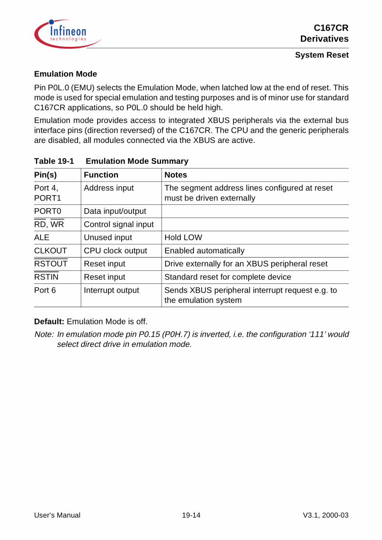
C167CRDerivatives
System Reset
Emulation Mode
Pin P0L.0 (EMU) selects the Emulation Mode, when latched low at the end of reset. Thismode is used for special emulation and testing purposes and is of minor use for standardC167CR applications, so P0L.0 should be held high.
Emulation mode provides access to integrated XBUS peripherals via the external businterface pins (direction reversed) of the C167CR. The CPU and the generic peripheralsare disabled, all modules connected via the XBUS are active.
Default: Emulation Mode is off.
Note: In emulation mode pin P0.15 (P0H.7) is inverted, i.e. the configuration ‘111’ wouldselect direct drive in emulation mode.
Table 19-1 Emulation Mode Summary
Pin(s) Function Notes
Port 4, PORT1
Address input The segment address lines configured at reset must be driven externally
PORT0 Data input/output
RD, WR Control signal input
ALE Unused input Hold LOW
CLKOUT CPU clock output Enabled automatically
RSTOUT Reset input Drive externally for an XBUS peripheral reset
RSTIN Reset input Standard reset for complete device
Port 6 Interrupt output Sends XBUS peripheral interrupt request e.g. to the emulation system
User’s Manual 19-14 V3.1, 2000-03

C167CRDerivatives
System Reset
Adapt Mode
Pin P0L.1 (ADP) selects the Adapt Mode, when latched low at the end of reset. In thismode the C167CR goes into a passive state, which is similar to its state during reset.The pins of the C167CR float to tristate or are deactivated via internal pullup/pulldowndevices, as described for the reset state. In addition also the RSTOUT pin floats totristate rather than be driven low. The on-chip oscillator is disabled.
This mode allows switching a C167CR that is mounted to a board virtually off, so anemulator may control the board’s circuitry, even though the original C167CR remains inits place. The original C167CR also may resume to control the board after a resetsequence with P0L.1 high. Please note that adapt mode overrides any otherconfiguration via PORT0.
Default: Adapt Mode is off.
Note: When XTAL1 is fed by an external clock generator (while XTAL2 is left open), thisclock signal may also be used to drive the emulator device.However, if a crystal is used, the emulator device’s oscillator can use this crystalonly, if at least XTAL2 of the original device is disconnected from the circuitry (theoutput XTAL2 will be driven high in Adapt Mode).
User’s Manual 19-15 V3.1, 2000-03
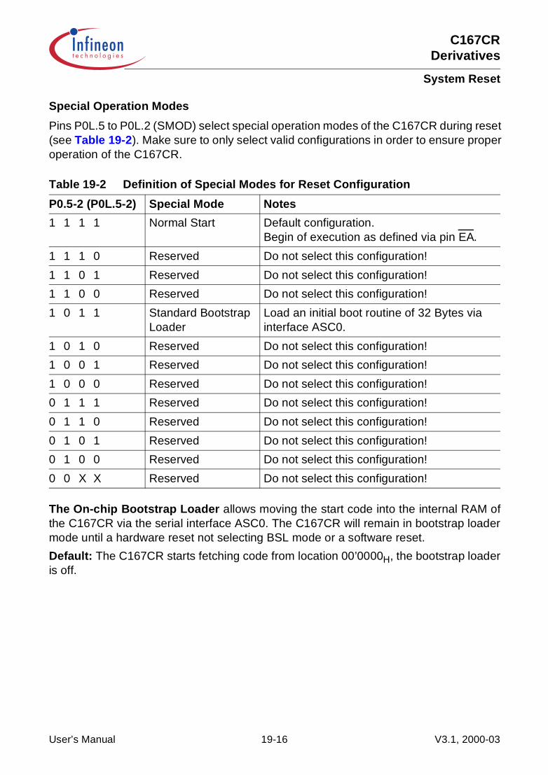
C167CRDerivatives
System Reset
Special Operation Modes
Pins P0L.5 to P0L.2 (SMOD) select special operation modes of the C167CR during reset(see Table 19-2). Make sure to only select valid configurations in order to ensure properoperation of the C167CR.
The On-chip Bootstrap Loader allows moving the start code into the internal RAM ofthe C167CR via the serial interface ASC0. The C167CR will remain in bootstrap loadermode until a hardware reset not selecting BSL mode or a software reset.
Default: The C167CR starts fetching code from location 00’0000H, the bootstrap loaderis off.
Table 19-2 Definition of Special Modes for Reset Configuration
P0.5-2 (P0L.5-2) Special Mode Notes
1 1 1 1 Normal Start Default configuration.Begin of execution as defined via pin EA.
1 1 1 0 Reserved Do not select this configuration!
1 1 0 1 Reserved Do not select this configuration!
1 1 0 0 Reserved Do not select this configuration!
1 0 1 1 Standard Bootstrap Loader
Load an initial boot routine of 32 Bytes via interface ASC0.
1 0 1 0 Reserved Do not select this configuration!
1 0 0 1 Reserved Do not select this configuration!
1 0 0 0 Reserved Do not select this configuration!
0 1 1 1 Reserved Do not select this configuration!
0 1 1 0 Reserved Do not select this configuration!
0 1 0 1 Reserved Do not select this configuration!
0 1 0 0 Reserved Do not select this configuration!
0 0 X X Reserved Do not select this configuration!
User’s Manual 19-16 V3.1, 2000-03

C167CRDerivatives
System Reset
External Bus Type
Pins P0L.7 and P0L.6 (BUSTYP) select the external bus type during reset, if an externalstart is selected via pin EA. This allows the configuration of the external bus interface ofthe C167CR even for the first code fetch after reset. The two bits are copied into bit fieldBTYP of register BUSCON0. P0L.7 controls the data bus width, while P0L.6 controls theaddress output (multiplexed or demultiplexed). This bit field may be changed viasoftware after reset, if required.
PORT0 and PORT1 are automatically switched to the selected bus mode. In multiplexedbus modes PORT0 drives both the 16-bit intra-segment address and the output data,while PORT1 remains in high impedance state as long as no demultiplexed bus isselected via one of the BUSCON registers. In demultiplexed bus modes PORT1 drivesthe 16-bit intra-segment address, while PORT0 or P0L (according to the selected databus width) drives the output data.For a 16-bit data bus BHE is automatically enabled, for an 8-bit data bus BHE is disabledvia bit BYTDIS in register SYSCON.
Default: 16-bit data bus with multiplexed addresses.
Note: If an internal start is selected via pin EA, these two pins are disregarded and bitfield BTYP of register BUSCON0 is cleared.
Write Configuration
Pin P0H.0 (WRC) selects the initial operation of the control pins WR and BHE duringreset. When high, this pin selects the standard function, i.e. WR control and BHE. Whenlow, it selects the alternate configuration, i.e. WRH and WRL. Thus even the first accessafter a reset can go to a memory controlled via WRH and WRL. This bit is latched inregister RP0H and its inverted value is copied into bit WRCFG in register SYSCON.
Default: Standard function (WR control and BHE).
Table 19-3 Configuration of External Bus Type
P0L.7-6 (BTYP) Encoding
External Data Bus Width External Address Bus Mode
0 0 8-bit Data Demultiplexed Addresses
0 1 8-bit Data Multiplexed Addresses
1 0 16-bit Data Demultiplexed Addresses
1 1 16-bit Data Multiplexed Addresses
User’s Manual 19-17 V3.1, 2000-03

C167CRDerivatives
System Reset
Chip Select Lines
Pins P0H.2 and P0H.1 (CSSEL) define the number of active chip select signals duringreset. This allows the selection which pins of Port 6 drive external CS signals and whichare used for general purpose IO. The two bits are latched in register RP0H.
Default: All 5 chip select lines active (CS4 … CS0).
Note: The selected number of CS signals cannot be changed via software after reset.
Segment Address Lines
Pins P0H.4 and P0H.3 (SALSEL) define the number of active segment address linesduring reset. This allows the selection which pins of Port 4 drive address lines and whichare used for general purpose IO. The two bits are latched in register RP0H. Dependingon the system architecture the required address space is chosen and accessible rightfrom the start, so the initialization routine can directly access all locations without priorprogramming. The required pins of Port 4 are automatically switched to address outputmode.
Even if not all segment address lines are enabled on Port 4, the C167CR internally usesits complete 24-bit addressing mechanism. This allows the restriction of the width of theeffective address bus, while still deriving CS signals from the complete addresses.
Default: 2-bit segment address (A17 … A16) allowing access to 256 KByte.
Note: The selected number of segment address lines cannot be changed via softwareafter reset.
Table 19-4 Configuration of Chip Select Lines
P0H.2-1 (CSSEL) Chip Select Lines Note
1 1 Five: CS4 … CS0 Default without pull-downs
1 0 None
0 1 Two: CS1 … CS0
0 0 Three:CS2 … CS0
Table 19-5 Configuration of Segment Address Lines
P0H.4-3 (SALSEL) Segment Address Lines Directly accessible A. Space
1 1 Two: A17 … A16 256 KByte (Default without pull-downs)
1 0 Eight: A23 … A16 16 MByte (Maximum)
0 1 None 64 KByte (Minimum)
0 0 Four: A19 … A16 1 MByte
User’s Manual 19-18 V3.1, 2000-03
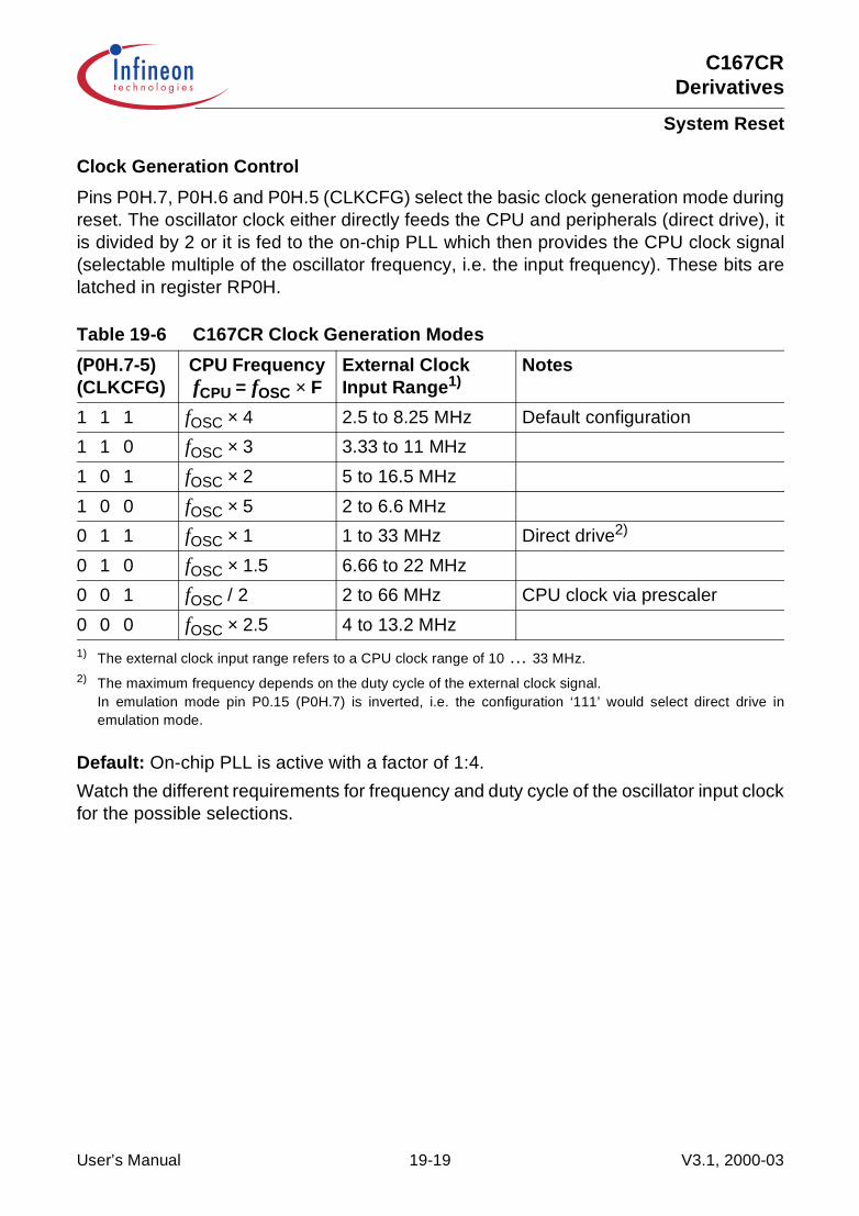
C167CRDerivatives
System Reset
Clock Generation Control
Pins P0H.7, P0H.6 and P0H.5 (CLKCFG) select the basic clock generation mode duringreset. The oscillator clock either directly feeds the CPU and peripherals (direct drive), itis divided by 2 or it is fed to the on-chip PLL which then provides the CPU clock signal(selectable multiple of the oscillator frequency, i.e. the input frequency). These bits arelatched in register RP0H.
Default: On-chip PLL is active with a factor of 1:4.
Watch the different requirements for frequency and duty cycle of the oscillator input clockfor the possible selections.
Table 19-6 C167CR Clock Generation Modes
(P0H.7-5) (CLKCFG)
CPU Frequency fCPU = fOSC × F
External Clock Input Range1)
1) The external clock input range refers to a CPU clock range of 10 … 33 MHz.
Notes
1 1 1 fOSC × 4 2.5 to 8.25 MHz Default configuration
1 1 0 fOSC × 3 3.33 to 11 MHz
1 0 1 fOSC × 2 5 to 16.5 MHz
1 0 0 fOSC × 5 2 to 6.6 MHz
0 1 1 fOSC × 1 1 to 33 MHz Direct drive2)
2) The maximum frequency depends on the duty cycle of the external clock signal.In emulation mode pin P0.15 (P0H.7) is inverted, i.e. the configuration ‘111’ would select direct drive inemulation mode.
0 1 0 fOSC × 1.5 6.66 to 22 MHz
0 0 1 fOSC / 2 2 to 66 MHz CPU clock via prescaler
0 0 0 fOSC × 2.5 4 to 13.2 MHz
User’s Manual 19-19 V3.1, 2000-03
C167CRDerivatives
System Reset
19.4.2 System Startup Configuration upon a Single-chip Mode Reset
For a single-chip mode reset (indicated by EA = ‘1’) the configuration via PORT0 is onlypartly evaluated.
No bus type is stored into BUSCON0. The external bus interface remains inactive(PORT0, PORT1, Port 4, Port 6).
The first instruction is fetched from internal program memory.
Note: Single-chip mode reset cannot be selected on ROMless devices. The attempt toread the first instruction after reset will fail in such a case.
User’s Manual 19-20 V3.1, 2000-03

C167CRDerivatives
Power Management
20 Power ManagementFor an increasing number of microcontroller based systems it is an important objectiveto reduce the power consumption of the system as much as possible. A contradictoryobjective is, however, to reach a certain level of system performance. Besidesoptimization of design and technology a microcontroller’s power consumption cangenerally be reduced by lowering its operating frequency and/or by reducing the circuitrythat is clocked. The architecture of the C167CR provides two operating modes to reduceits power consumption (see Figure 20-1) under software control:
• In Idle mode the CPU is stopped, while the peripherals continue their operation. Idlemode can be terminated by any reset or interrupt request
• In Power Down mode both the CPU and the peripherals are stopped. Power Downmode can only be terminated by a hardware reset.
Note: All external bus actions are completed before Idle or Power Down mode isentered. However, Idle or Power Down mode is not entered if READY is enabled,but has not been activated (driven low) during the last bus access.
Intermittent operation (i.e. alternating phases of high performance and power saving) issupported by cyclic interrupt generation of a timer.
Figure 20-1 Power Reduction Possibilities
MCA04406
Active
Idle
Power DownfCPU
Power
User’s Manual 20-1 V3.1, 2000-03
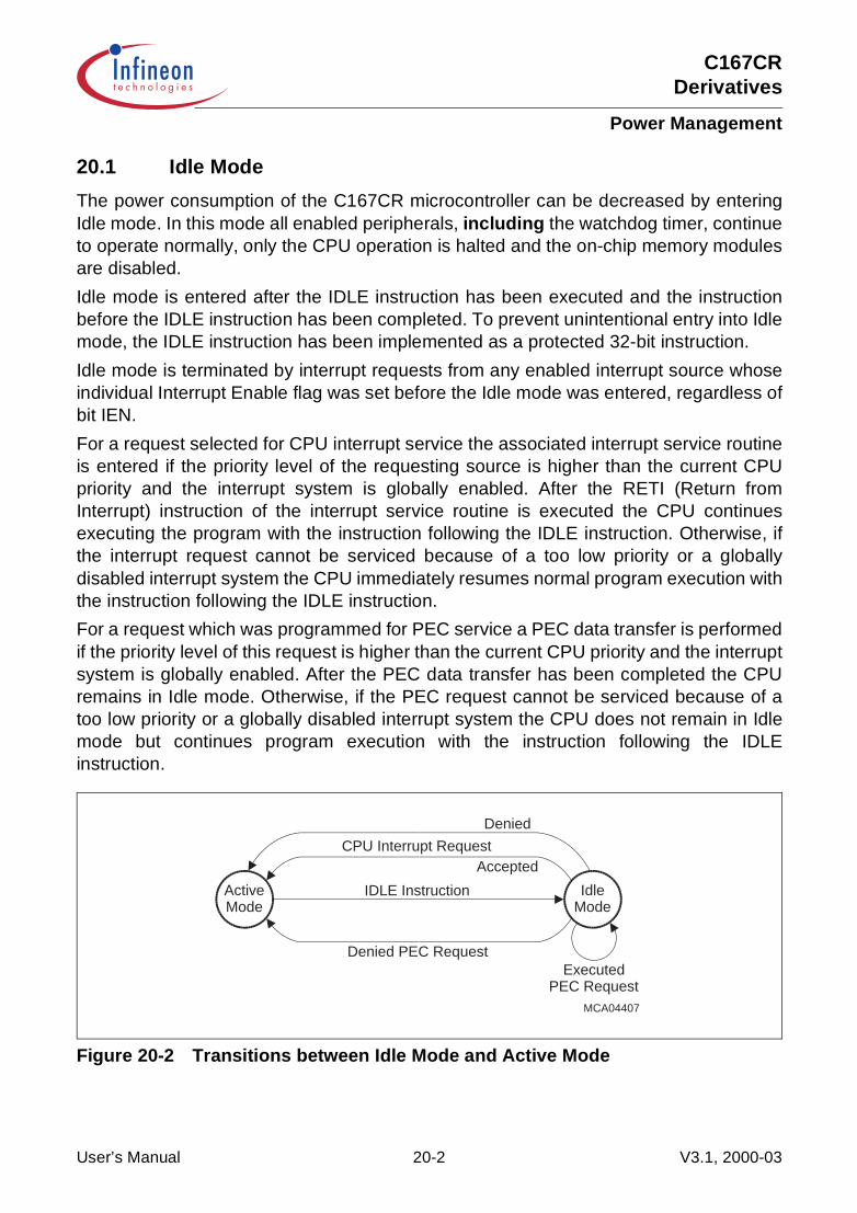
C167CRDerivatives
Power Management
20.1 Idle Mode
The power consumption of the C167CR microcontroller can be decreased by enteringIdle mode. In this mode all enabled peripherals, including the watchdog timer, continueto operate normally, only the CPU operation is halted and the on-chip memory modulesare disabled.
Idle mode is entered after the IDLE instruction has been executed and the instructionbefore the IDLE instruction has been completed. To prevent unintentional entry into Idlemode, the IDLE instruction has been implemented as a protected 32-bit instruction.
Idle mode is terminated by interrupt requests from any enabled interrupt source whoseindividual Interrupt Enable flag was set before the Idle mode was entered, regardless ofbit IEN.
For a request selected for CPU interrupt service the associated interrupt service routineis entered if the priority level of the requesting source is higher than the current CPUpriority and the interrupt system is globally enabled. After the RETI (Return fromInterrupt) instruction of the interrupt service routine is executed the CPU continuesexecuting the program with the instruction following the IDLE instruction. Otherwise, ifthe interrupt request cannot be serviced because of a too low priority or a globallydisabled interrupt system the CPU immediately resumes normal program execution withthe instruction following the IDLE instruction.
For a request which was programmed for PEC service a PEC data transfer is performedif the priority level of this request is higher than the current CPU priority and the interruptsystem is globally enabled. After the PEC data transfer has been completed the CPUremains in Idle mode. Otherwise, if the PEC request cannot be serviced because of atoo low priority or a globally disabled interrupt system the CPU does not remain in Idlemode but continues program execution with the instruction following the IDLEinstruction.
Figure 20-2 Transitions between Idle Mode and Active Mode
MCA04407
IdleMode
ActiveMode
Denied
AcceptedCPU Interrupt Request
IDLE Instruction
Denied PEC RequestExecuted
PEC Request
User’s Manual 20-2 V3.1, 2000-03

C167CRDerivatives
Power Management
Idle mode can also be terminated by a Non-Maskable Interrupt, i.e. a high to lowtransition on the NMI pin. After Idle mode has been terminated by an interrupt or NMIrequest, the interrupt system performs a round of prioritization to determine the highestpriority request. In the case of an NMI request, the NMI trap will always be entered.
Any interrupt request whose individual Interrupt Enable flag was set before Idle modewas entered will terminate Idle mode regardless of the current CPU priority. The CPUwill not go back into Idle mode when a CPU interrupt request is detected, even when theinterrupt was not serviced because of a higher CPU priority or a globally disabledinterrupt system (IEN = ‘0’). The CPU will only go back into Idle mode when the interruptsystem is globally enabled (IEN = ‘1’) and a PEC service on a priority level higher thanthe current CPU level is requested and executed.
Note: An interrupt request which is individually enabled and assigned to priority level 0will terminate Idle mode. The associated interrupt vector will not be accessed,however.
The watchdog timer may be used to monitor the Idle mode: an internal reset will begenerated if no interrupt or NMI request occurs before the watchdog timer overflows. Toprevent the watchdog timer from overflowing during Idle mode it must be programmedto a reasonable time interval before Idle mode is entered.
User’s Manual 20-3 V3.1, 2000-03

C167CRDerivatives
Power Management
20.2 Power Down Mode
The microcontroller can be switched to Power Down mode which reduces the powerconsumption to a minimum. Clocking of all internal blocks is stopped, the contents of theinternal RAM, however, are preserved through the voltage supplied via the VDD pins.The watchdog timer is stopped in Power Down mode. This mode can only be terminatedby an external hardware reset, i.e. by asserting a low level on the RSTIN pin. This resetwill initialize all SFRs and ports to their default state, but will not change the contents ofthe internal RAM.
There are two levels of protection against unintentionally entering Power Down mode.First, the PWRDN (Power Down) instruction which is used to enter this mode has beenimplemented as a protected 32-bit instruction. Second, this instruction is effective onlyif the NMI (Non Maskable Interrupt) pin is externally pulled low while the PWRDNinstruction is executed. The microcontroller will enter Power Down mode after thePWRDN instruction has completed.
This feature can be used in conjunction with an external power failure signal which pullsthe NMI pin low when a power failure is imminent. The microcontroller will enter the NMItrap routine which can save the internal state into RAM. After the internal state has beensaved, the trap routine may then execute the PWRDN instruction. If the NMI pin is stilllow at this time, Power Down mode will be entered, otherwise program executioncontinues.
The initialization routine (executed upon reset) can check the reset identification flags inregister WDTCON to determine whether the controller was initially switched on, orwhether it was properly restarted from Power Down mode.
During power down the voltage at the VDD pins can be lowered to 2.5 V while thecontents of the internal RAM will still be preserved.
The total power consumption in Power Down mode depends on the current that flowsthrough the port drivers. To minimize the consumed current the pin drivers can bedisabled (pins switched to tristate) simply by configuring them for input.
The bus interface pins can be separately disabled by releasing the external bus (disableall address windows by clearing the BUSACT bits) and switching the ports to input (ifnecessary). Of course the required software in this case must be executed from internalmemory.
User’s Manual 20-4 V3.1, 2000-03

C167CRDerivatives
Power Management
20.2.1 Status of Output Pins During Power Reduction Modes
During Idle mode the CPU clocks are turned off, while all peripherals continue theiroperation in the normal way. Therefore all ports pins, which are configured as generalpurpose output pins, output the last data value which was written to their port outputlatches. If the alternate output function of a port pin is used by a peripheral, the state ofthe pin is determined by the operation of the peripheral.
Port pins which are used for bus control functions go into that state which represents theinactive state of the respective function (e.g. WR), or to a defined state which is basedon the last bus access (e.g. BHE). Port pins which are used as external address/databus hold the address/data which was output during the last external memory accessbefore entry into Idle mode under the following conditions:
P0H outputs the high byte of the last address if a multiplexed bus mode with 8-bit databus is used, otherwise P0H is floating. P0L is always floating in Idle mode.
PORT1 outputs the lower 16 bits of the last address if a demultiplexed bus mode is used,otherwise the output pins of PORT1 represent the port latch data.
Port 4 outputs the segment address for the last access on those pins that were selectedduring reset, otherwise the output pins of Port 4 represent the port latch data.
During power down mode the oscillator and the clocks to the CPU and to theperipherals are turned off. Like in Idle mode, all port pins which are configured as generalpurpose output pins output the last data value which was written to their port outputlatches.
When the alternate output function of a port pin is used by a peripheral the state of thispin is determined by the last action of the peripheral before the clocks were switched off.
Note: When the supply voltage is lowered in Power Down mode the high voltage ofoutput pins will decrease accordingly.
User’s Manual 20-5 V3.1, 2000-03
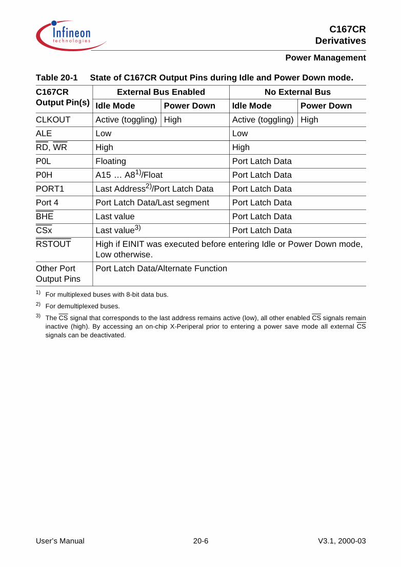
C167CRDerivatives
Power Management
Table 20-1 State of C167CR Output Pins during Idle and Power Down mode.
C167CROutput Pin(s)
External Bus Enabled No External Bus
Idle Mode Power Down Idle Mode Power Down
CLKOUT Active (toggling) High Active (toggling) High
ALE Low Low
RD, WR High High
P0L Floating Port Latch Data
P0H A15 … A81)/Float Port Latch Data
PORT1 Last Address2)/Port Latch Data Port Latch Data
Port 4 Port Latch Data/Last segment Port Latch Data
BHE Last value Port Latch Data
CSx Last value3) Port Latch Data
RSTOUT High if EINIT was executed before entering Idle or Power Down mode,Low otherwise.
Other Port Output Pins
Port Latch Data/Alternate Function
1) For multiplexed buses with 8-bit data bus.2) For demultiplexed buses.3) The CS signal that corresponds to the last address remains active (low), all other enabled CS signals remain
inactive (high). By accessing an on-chip X-Periperal prior to entering a power save mode all external CSsignals can be deactivated.
User’s Manual 20-6 V3.1, 2000-03
C167CRDerivatives
System Programming
21 System ProgrammingTo aid in software development, a number of features has been incorporated into theinstruction set of the C167CR, including constructs for modularity, loops, and contextswitching. In many cases commonly used instruction sequences have been simplifiedwhile providing greater flexibility. The following programming features help to fully utilizethis instruction set.
Instructions Provided as Subsets of Instructions
In many cases, instructions found in other microcontrollers are provided as subsets ofmore powerful instructions in the C167CR. This allows the same functionality to beprovided while decreasing the hardware required and decreasing decode complexity. Inorder to aid assembly programming, these instructions, familiar from othermicrocontrollers, can be built in macros, thus providing the same names.
Directly Substitutable Instructions are instructions known from other microcontrollersthat can be replaced by the following instructions of the C167CR:
Modification of System Flags is performed using bit set or bit clear instructions (BSET, BCLR). All bit and word instructions can access the PSW register, so noinstructions like CLEAR CARRY or ENABLE INTERRUPTS are required.
External Memory Data Access does not require special instructions to load datapointers or explicitly load and store external data. The C167CR provides a VonNeumann memory architecture and its on-chip hardware automatically detects accessesto internal RAM, GPRs, and SFRs.
Multiplication and Division
Multiplication and division of words and double words is provided through multiple cycleinstructions implementing a Booth algorithm. Each instruction implicitly uses the 32-bitregister MD (MDL = lower 16 bits, MDH = upper 16 bits). The MDRIU flag (Multiply orDivide Register In Use) in register MDC is set whenever either half of this register iswritten to or when a multiply/divide instruction is started. It is cleared whenever the MDL
Table 21-1 Substitution of Instructions
Substituted Instruction C167CR Instruction Function
CLR Rn AND Rn, #0H Clear register
CPLB Bit BMOVN Bit, Bit Complement bit
DEC Rn SUB Rn, #1H Decrement register
INC Rn ADD Rn, #1H Increment register
SWAPB Rn ROR Rn, #8H Swap bytes within word
User’s Manual 21-1 V3.1, 2000-03

C167CRDerivatives
System Programming
register is read. Because an interrupt can be acknowledged before the contents ofregister MD are saved, this flag is required to alert interrupt routines, which require theuse of the multiply/divide hardware, so they can preserve register MD. This register,however, only needs to be saved when an interrupt routine requires use of the MDregister and a previous task has not saved the current result. This flag is easily tested bythe Jump-on-bit instructions.
Multiplication or division is simply performed by specifying the correct (signed orunsigned) version of the multiply or divide instruction. The result is then stored in registerMD. The overflow flag (V) is set if the result from a multiply or divide instruction is greaterthan 16 bits. This flag can be used to determine whether both word halfs must betransferred from register MD. The high portion of register MD (MDH) must be moved intothe register file or memory first, in order to ensure that the MDRIU flag reflects the correctstate.
The following instruction sequence performs an unsigned 16 by 16-bit multiplication:
SAVE:JNB MDRIU, START;Test if MD was in use.SCXT MDC, #0010H ;Save and clear control register,
;leaving MDRIU set;(only required for interrupted;multiply/divide instructions)
BSET SAVED ;Indicate the save operationPUSH MDH ;Save previous MD contents … PUSH MDL ;… on system stackSTART:MULU R1, R2 ;Multiply 16·16 unsigned, Sets MDRIUJMPR cc_NV, COPYL;Test for only 16-bit resultMOV R3, MDH ;Move high portion of MDCOPYL:MOV R4, MDL ;Move low portion of MD, Clears MDRIURESTORE:JNB SAVED, DONE ;Test if MD registers were savedPOP MDL ;Restore registersPOP MDHPOP MDCBCLR SAVED ;Multiplication is completed,
;program continuesDONE: …
User’s Manual 21-2 V3.1, 2000-03

C167CRDerivatives
System Programming
The above save sequence and the restore sequence after COPYL are only required ifthe current routine could have interrupted a previous routine which contained a MUL orDIV instruction. Register MDC is also saved because it is possible that a previousroutine’s Multiply or Divide instruction was interrupted while in progress. In this case theinformation about how to restart the instruction is contained in this register. RegisterMDC must be cleared to be correctly initialized for a subsequent multiplication ordivision. The old MDC contents must be popped from the stack before the RETIinstruction is executed.
For a division the user must first move the dividend into the MD register. If a 16/16-bitdivision is specified, only the low portion of register MD must be loaded. The result is alsostored into register MD. The low portion (MDL) contains the integer result of the division,while the high portion (MDH) contains the remainder.
The following instruction sequence performs a 32 by 16-bit division:
MOV MDH, R1 ;Move dividend to MD register. Sets MDRIUMOV MDL, R2 ;Move low portion to MDDIV R3 ;Divide 32/16 signed, R3 holds divisorJMPR cc_V, ERROR ;Test for divide overflowMOV R3, MDH ;Move remainder to R3MOV R4, MDL ;Move integer result to R4. Clears MDRIU
Whenever a multiply or divide instruction is interrupted while in progress, the address ofthe interrupted instruction is pushed onto the stack and the MULIP flag in the PSW of theinterrupting routine is set. When the interrupt routine is exited with the RETI instruction,this bit is implicitly tested before the old PSW is popped from the stack. If MULIP = ‘1’the multiply/divide instruction is re-read from the location popped from the stack (returnaddress) and will be completed after the RETI instruction has been executed.
Note: The MULIP flag is part of the context of the interrupted task. When theinterrupting routine does not return to the interrupted task (e.g. scheduler switchesto another task) the MULIP flag must be set or cleared according to the context ofthe task that is switched to.
BCD Calculations
No direct support for BCD calculations is provided in the C167CR. BCD calculations areperformed by converting BCD data to binary data, performing the desired calculationsusing standard data types, and converting the result back to BCD data. Due to theenhanced performance of division instructions binary data is quickly converted to BCDdata through division by 10D. Conversion from BCD data to binary data is enhanced bymultiple bit shift instructions. This provides similar performance compared to instructionsdirectly supporting BCD data types, while no additional hardware is required.
User’s Manual 21-3 V3.1, 2000-03
C167CRDerivatives
System Programming
21.1 Stack Operations
The C167CR supports two types of stacks. The system stack is used implicitly by thecontroller and is located in the internal RAM. The user stack provides stack access to theuser in either the internal or external memory. Both stack types grow from high memoryaddresses to low memory addresses.
Internal System Stack
A system stack is provided to store return vectors, segment pointers, and processorstatus for procedures and interrupt routines. A system register, SP, points to the top ofthe stack. This pointer is decremented when data is pushed onto the stack, andincremented when data is popped.
The internal system stack can also be used to temporarily store data or pass it betweensubroutines or tasks. Instructions are provided to push or pop registers on/from thesystem stack. However, in most cases the register banking scheme provides the bestperformance for passing data between multiple tasks.
Note: The system stack allows the storage of words only. Bytes must either beconverted to words or the respective other byte must be disregarded.Register SP can only be loaded with even byte addresses (The LSB of SP isalways ‘0’).
Detection of stack overflow/underflow is supported by two registers, STKOV (StackOverflow Pointer) and STKUN (Stack Underflow Pointer). Specific system traps (StackOverflow trap, Stack Underflow trap) will be entered whenever the SP reaches eitherboundary specified in these registers.
The contents of the stack pointer are compared to the contents of the overflow register,whenever the SP is DECREMENTED either by a CALL, PUSH or SUB instruction. Anoverflow trap will be entered, when the SP value is less than the value in the stackoverflow register.
The contents of the stack pointer are compared to the contents of the underflow register,whenever the SP is INCREMENTED either by a RET, POP or ADD instruction. Anunderflow trap will be entered, when the SP value is greater than the value in the stackunderflow register.
Note: When a value is MOVED into the stack pointer, NO check against the overflow/underflow registers is performed.
In many cases the user will place a software reset instruction (SRST) into the stackunderflow and overflow trap service routines. This is an easy approach, which does notrequire special programming. However, this approach assumes that the defined internalstack is sufficient for the current software and that exceeding its upper or lower boundaryrepresents a fatal error.
User’s Manual 21-4 V3.1, 2000-03

C167CRDerivatives
System Programming
It is also possible to use the stack underflow and stack overflow traps to cache portionsof a larger external stack. Only the portion of the system stack currently being used isplaced into the internal memory, thus allowing a greater portion of the internal RAM tobe used for program, data or register banking. This approach assumes no error butrequires a set of control routines (see below).
Circular (Virtual) Stack
This basic technique allows pushing until the overflow boundary of the internal stack isreached. At this point a portion of the stacked data must be saved into external memoryto create space for further stack pushes. This is called “stack flushing”. When executinga number of return or pop instructions, the upper boundary (since the stack emptiesupward to higher memory locations) is reached. The entries that have been previouslysaved in external memory must now be restored. This is called “stack filling”. Becauseprocedure call instructions do not continue to nest infinitely and call and returninstructions alternate, flushing and filling normally occurs very infrequently. If this is nottrue for a given program environment, this technique should not be used because of theoverhead of flushing and filling.
The basic mechanism is the transformation of the addresses of a virtual stack area,controlled via registers SP, STKOV and STKUN, to a defined physical stack area withinthe internal RAM via hardware. This virtual stack area covers all possible locations thatSP can point to, i.e. 00’F000H through 00’FFFEH. STKOV and STKUN accept the same4 KByte address range.The size of the physical stack area within the internal RAM that effectively is used forstandard stack operations is defined via bitfield STKSZ in register SYSCON (see below).
Table 21-2 Circular Stack Address Transformation
STKSZ Stack Size(Words)
Internal RAM Addresses (Words)of Physical Stack
Significant Bits of Stack Ptr. SP
0 0 0B 256 00’FBFEH … 00’FA00H (Default after Reset) SP.8 … SP.0
0 0 1B 128 00’FBFEH … 00’FB00H SP.7 … SP.0
0 1 0B 64 00’FBFEH … 00’FB80H SP.6 … SP.0
0 1 1B 32 00’FBFEH … 00’FBC0H SP.5 … SP.0
1 0 0B 512 00’FBFEH … 00’F800H (not for 1KByte IRAM) SP.9 … SP.0
1 0 1B – Reserved. Do not use this combination. –
1 1 0 B – Reserved. Do not use this combination. –
1 1 1 B 1024 00’FDFEH … 00’FX00H (Note: No circular stack)00’FX00H represents the lower IRAM limit, i.e.1 KB: 00’FA00H, 2 KB: 00’F600H,3 KB: 00’F200H
SP.11 … SP.0
User’s Manual 21-5 V3.1, 2000-03

C167CRDerivatives
System Programming
The virtual stack addresses are transformed to physical stack addresses byconcatenating the significant bits of the stack pointer register SP (see Table 21-2) withthe complementary most significant bits of the upper limit of the physical stack area(00’FBFEH). This transformation is done via hardware (see Figure 21-1).
The reset values (STKOV = FA00H, STKUN = FC00H, SP = FC00H, STKSZ = 000B)map the virtual stack area directly to the physical stack area and allow using the internalsystem stack without any changes, provided that the 256 word area is not exceeded.
Figure 21-1 Physical Stack Address Generation
The following example demonstrates the circular stack mechanism which is also aneffect of this virtual stack mapping: First, register R1 is pushed onto the lowest physicalstack location according to the selected maximum stack size. With the followinginstruction, register R2 will be pushed onto the highest physical stack location althoughthe SP is decremented by 2 as for the previous push operation.
MOV SP, #0F802H ;Set SP before last entry … ;… of physical stack of 256 words
… ;(SP)= F802H: Physical stack addr.= FA02HPUSH R1 ;(SP)= F800H: Physical stack addr.= FA00HPUSH R2 ;(SP)= F7FEH: Physical stack addr.= FBFEH
MCA04408
1 1 1 1 1 0 1 1 1 1 1 1 1 1 1 0FBFEH 1 1 1 1 1 0 1 1 1 1 1 1 1 1 1 0FBFEH
FB80H 0000000111011111 Phys.A.
<SP>1 1 1 1 1 0 1 1 1 0 0 0 0 0 0 0FB80H
FA00H 0000000001011111
F800H 0000000000011111
1 1 1 1 1 0 1 1 1 1 1 1 1 1 1 0FBFEH 1 1 1 1 1 0 1 1 1 1 1 1 1 1 1 0FBFEH
FBFEH 0111111111011111 Phys.A.
<SP>1 1 1 1 1 0 1 1 0 1 1 1 1 1 1 0FB7EH
FBFEH 0111111111011111
F7FEH 0111111111101111
After PUSH After PUSH
64 words 256 wordsStack Size
User’s Manual 21-6 V3.1, 2000-03

C167CRDerivatives
System Programming
The effect of the address transformation is that the physical stack addresses wraparound from the end of the defined area to its beginning. When flushing and filling theinternal stack, this circular stack mechanism only requires to move that portion of stackdata which is really to be re-used (i.e. the upper part of the defined stack area) insteadof the whole stack area. Stack data that remain in the lower part of the internal stackneed not be moved by the distance of the space being flushed or filled, as the stackpointer automatically wraps around to the beginning of the freed part of the stack area.
Note: This circular stack technique is applicable for stack sizes of 32 to 512 words(STKSZ = ‘000B’ to ‘100B’), it does not work with option STKSZ = ‘111B’, whichuses the complete internal RAM for system stack.In the latter case the address transformation mechanism is deactivated.
When a boundary is reached, the stack underflow or overflow trap is entered, where theuser moves a predetermined portion of the internal stack to or from the external stack.The amount of data transferred is determined by the average stack space required byroutines and the frequency of calls, traps, interrupts and returns. In most cases this willbe approximately one quarter to one tenth the size of the internal stack. Once the transferis complete, the boundary pointers are updated to reflect the newly allocated space onthe internal stack. Thus, the user is free to write code without concern for the internalstack limits. Only the execution time required by the trap routines affects user programs.
The following procedure initializes the controller for usage of the circular stackmechanism:
• Specify the size of the physical system stack area within the internal RAM (bitfieldSTKSZ in register SYSCON).
• Define two pointers, which specify the upper and lower boundary of the external stack.These values are then tested in the stack underflow and overflow trap routines whenmoving data.
• Set the stack overflow pointer (STKOV) to the limit of the defined internal stack areaplus six words (for the reserved space to store two interrupt entries).
The internal stack will now fill until the overflow pointer is reached. After entry into theoverflow trap procedure, the top of the stack will be copied to the external memory. Theinternal pointers will then be modified to reflect the newly allocated space. After exitingfrom the trap procedure, the internal stack will wrap around to the top of the internalstack, and continue to grow until the new value of the stack overflow pointer is reached.
When the underflow pointer is reached while the stack is meptied the bottom of stack isreloaded from the external memory and the internal pointers are adjusted accordingly.
User’s Manual 21-7 V3.1, 2000-03

C167CRDerivatives
System Programming
Linear Stack
The C167CR also offers a linear stack option (STKSZ = ‘111B’), where the system stackmay use the complete internal RAM area. This provides a large system stack withoutrequiring procedures to handle data transfers for a circular stack. However, this methodalso leaves less RAM space for variables or code. The RAM area that may effectively beconsumed by the system stack is defined via the STKUN and STKOV pointers. Theunderflow and overflow traps in this case serve for fatal error detection only.
For the linear stack option all modifiable bits of register SP are used to access thephysical stack. Although the stack pointer may cover addresses from 00’F000H up to00’FFFEH the (physical) system stack must be located within the internal RAM andtherefore may only use the address range 00’F600H to 00’FDFEH. It is the user’sresponsibility to restrict the system stack to the internal RAM range.
Note: Avoid stack accesses below the IRAM area (ESFR space and reserved area) andwithin address range 00’FE00H and 00’FFFEH (SFR space).Otherwise unpredictable results will occur.
User Stacks
User stacks provide the ability to create task specific data stacks and to off-load datafrom the system stack. The user may push both bytes and words onto a user stack, butis responsible for using the appropriate instructions when popping data from the specificuser stack. No hardware detection of overflow or underflow of a user stack is provided.The following addressing modes allow implementation of user stacks:
[–Rw], Rb or [–Rw], Rw : Pre-decrement Indirect Addressing.Used to push one byte or word onto a user stack. This mode is only available for MOVinstructions and can specify any GPR as the user stack pointer.
Rb, [Rw i+] or Rw, [Rw i+]: Post-increment Index Register Indirect Addressing.Used to pop one byte or word from a user stack. This mode is available to mostinstructions, but only GPRs R0-R3 can be specified as the user stack pointer.
Rb, [Rw+] or Rw, [Rw+] : Post-increment Indirect Addressing.Used to pop one byte or word from a user stack. This mode is only available for MOVinstructions and can specify any GPR as the user stack pointer.
User’s Manual 21-8 V3.1, 2000-03

C167CRDerivatives
System Programming
21.2 Register Banking
Register banking provides the user with an extremely fast method to switch user context.A single machine cycle instruction saves the old bank and enters a new register bank.Each register bank may assign up to 16 registers. Each register bank should beallocated during coding based on the needs of each task. Once the internal memory hasbeen partitioned into a register bank space, internal stack space and a global internalmemory area, each bank pointer is then assigned. Thus, upon entry into a new task, theappropriate bank pointer is used as the operand for the SCXT (switch context)instruction. Upon exit from a task a simple POP instruction to the context pointer (CP)restores the previous task’s register bank.
21.3 Procedure Call Entry and Exit
To support modular programming a procedure mechanism is provided to allow coding offrequently used portions of code into subroutines. The CALL and RET instructions storeand restore the value of the instruction pointer (IP) on the system stack before and aftera subroutine is executed.
Procedures may be called conditionally with instructions CALLA or CALLI, or be calledunconditionally using instructions CALLR or CALLS.
Note: Any data pushed onto the system stack during execution of the subroutine mustbe popped before the RET instruction is executed.
Passing Parameters on the System Stack
Parameters may be passed via the system stack through PUSH instructions before thesubroutine is called, and POP instructions during execution of the subroutine. Base plusoffset indirect addressing also permits access to parameters without popping theseparameters from the stack during execution of the subroutine. Indirect addressingprovides a mechanism of accessing data referenced by data pointers, which are passedto the subroutine.
In addition, two instructions have been implemented to allow one parameter to bepassed on the system stack without additional software overhead.
The PCALL (push and call) instruction first pushes the ‘reg’ operand and the IP contentsonto the system stack and then passes control to the subroutine specified by the ‘caddr’operand.
When exiting from the subroutine, the RETP (return and pop) instruction first pops the IPand then the ‘reg’ operand from the system stack and returns to the calling program.
User’s Manual 21-9 V3.1, 2000-03
C167CRDerivatives
System Programming
Cross Segment Subroutine Calls
Calls to subroutines in different segments require the use of the CALLS (call inter-segment subroutine) instruction. This instruction preserves both the CSP (code segmentpointer) and IP on the system stack.
Upon return from the subroutine, a RETS (return from inter-segment subroutine)instruction must be used to restore both the CSP and IP. This ensures that the nextinstruction after the CALLS instruction is fetched from the correct segment.
Note: It is possible to use CALLS within the same segment, but still two words of thestack are used to store both the IP and CSP.
Providing Local Registers for Subroutines
For subroutines which require local storage, the following methods are provided:
Alternate Bank of Registers: Upon entry into a subroutine, it is possible to specify anew set of local registers by executing the SCXT (switch context) instruction. Thismechanism does not provide a method to recursively call a subroutine.
Saving and Restoring of Registers: To provide local registers, the contents of theregisters which are required for use by the subroutine can be pushed onto the stack andthe previous values be popped before returning to the calling routine. This is the mostcommon technique used today and it does provide a mechanism to support recursiveprocedures. This method, however, requires two machine cycles per register stored onthe system stack (one cycle to PUSH the register, and one to POP the register).
Use of the System Stack for Local Registers: It is possible to use the SP and CP toset up local subroutine register frames. This enables subroutines to dynamically allocatelocal variables as needed within two machine cycles. A local frame is allocated by simplysubtracting the number of required local registers from the SP, and then moving thevalue of the new SP to the CP.
This operation is supported through the SCXT (switch context) instruction with theaddressing mode ‘reg, mem’. Using this instruction saves the old contents of the CP onthe system stack and moves the value of the SP into CP (see example below). Each localregister is then accessed as if it was a normal register. Upon exit from the subroutine,first the old CP must be restored by popping it from the stack and then the number ofused local registers must be added to the SP to restore the allocated local space backto the system stack.
Note: The system stack is growing downwards, while the register bank is growingupwards.
User’s Manual 21-10 V3.1, 2000-03

C167CRDerivatives
System Programming
Figure 21-2 Local Registers
The software to provide the local register bank for the example above is very compact:
After entering the subroutine:
SUB SP, #10D ;Free 5 words in the current system stackSCXT CP, SP ;Set the new register bank pointer
Before exiting the subroutine:
POP CP ;Restore the old register bankADD SP, #10D ;Release the 5 words …
;… of the current system stack
R3
R4
R2
R1
R0
MCA04409
Old CPContents
NewStackArea
NewlyAllocatedRegisterBank
OldStackArea
Old SP
New CP
New SP
User’s Manual 21-11 V3.1, 2000-03
C167CRDerivatives
System Programming
21.4 Table Searching
A number of features have been included to decrease the execution time required tosearch tables. First, branch delays are eliminated by the branch target cache after thefirst iteration of the loop. Second, in non-sequentially searched tables, the enhancedperformance of the ALU allows more complicated hash algorithms to be processed toobtain better table distribution. For sequentially searched tables, the auto-incrementindirect addressing mode and the E (end of table) flag stored in the PSW decrease thenumber of overhead instructions executed in the loop.
The two examples below illustrate searching ordered tables and non-ordered tables,respectively:
MOV R0, #BASE ;Move table base into R0LOOP:CMP R1, [R0+] ;Compare target to table entryJMPR cc_SGT, LOOP;Test whether target has not been found
Note: The last entry in the table must be greater than the largest possible target.
MOV R0, #BASE ;Move table base into R0LOOP:CMP R1, [R0+] ;Compare target to table entryJMPR cc_NET, LOOP;Test whether target is not found AND …
;…the end of table has not been reached.
Note: The last entry in the table must be equal to the lowest signed integer (8000H).
21.5 Floating Point Support
All floating point operations are performed using software. Standard multiple precisioninstructions are used to perform calculations on data types that exceed the size of theALU. Multiple bit rotate and logic instructions allow easy masking and extracting ofportions of floating point numbers.
To decrease the time required to perform floating point operations, two hardwarefeatures have been implemented in the CPU core. First, the PRIOR instruction aids innormalizing floating point numbers by indicating the position of the first set bit in a GPR.This result can the be used to rotate the floating point result accordingly. The secondfeature aids in properly rounding the result of normalized floating point numbers throughthe overflow (V) flag in the PSW. This flag is set when a one is shifted out of the carry bitduring shift right operations. The overflow flag and the carry flag are then used to roundthe floating point result based on the desired rounding algorithm.
User’s Manual 21-12 V3.1, 2000-03
C167CRDerivatives
System Programming
21.6 Peripheral Control and Interface
All communication between peripherals and the CPU is performed either by PECtransfers to and from internal memory, or by explicitly addressing the SFRs associatedwith the specific peripherals. After resetting the C167CR all peripherals (except thewatchdog timer) are disabled and initialized to default values. A desired configuration ofa specific peripheral is programmed using MOV instructions of either constants ormemory values to specific SFRs. Specific control flags may also be altered via bitinstructions.
Once in operation, the peripheral operates autonomously until an end condition isreached at which time it requests a PEC transfer or requests CPU servicing through aninterrupt routine. Information may also be polled from peripherals through read accessesto SFRs or bit operations including branch tests on specific control bits in SFRs. Toensure proper allocation of peripherals among multiple tasks, a portion of the internalmemory has been made bit addressable to allow user semaphores. Instructions havealso been provided to lock out tasks via software by setting or clearing user specific bitsand conditionally branching based on these specific bits.
It is recommended that bit fields in control SFRs are updated using the BFLDH andBFLDL instructions or a MOV instruction to avoid undesired intermediate modes ofoperation which can occur, when BCLR/BSET or AND/OR instruction sequences areused.
21.7 Trap/Interrupt Entry and Exit
Interrupt routines are entered when a requesting interrupt has a priority higher than thecurrent CPU priority level. Traps are entered regardless of the current CPU priority.When either a trap or interrupt routine is entered, the state of the machine is preservedon the system stack and a branch to the appropriate trap/interrupt vector is made.
All trap and interrupt routines require the use of the RETI (return from interrupt)instruction to exit from the called routine. This instruction restores the system state fromthe system stack and then branches back to the location where the trap or interruptoccurred.
User’s Manual 21-13 V3.1, 2000-03
C167CRDerivatives
System Programming
21.8 Unseparable Instruction Sequences
The instructions of the C167CR are very efficient (most instructions execute in onemachine cycle) and even the multiplication and division are interruptable in order tominimize the response latency to interrupt requests (internal and external). In manymicrocontroller applications this is vital.
Some special occasions, however, require certain code sequences (e.g. semaphorehandling) to be uninterruptable to function properly. This can be provided by inhibitinginterrupts during the respective code sequence by disabling and enabling them beforeand after the sequence. The necessary overhead may be reduced by means of theATOMIC instruction which allows locking 1 … 4 instructions to an unseparable codesequence, during which the interrupt system (standard interrupts and PEC requests)and Class A Traps (NMI, stack overflow/underflow) are disabled. A Class B Trap(illegal opcode, illegal bus access, etc.), however, will interrupt the atomic sequence,since it indicates a severe hardware problem.
The interrupt inhibit caused by an ATOMIC instruction gets active immediately, i.e. noother instruction will enter the pipeline except the one that follows the ATOMICinstruction, and no interrupt request will be serviced in between. All instructions requiringmultiple cycles or hold states are regarded as one instruction in this sense (e.g. MUL isone instruction). Any instruction type can be used within an unseparable code sequence.
ATOMIC #3 ;The next 3 instr. are locked (No NOP requ.)MOV R0, #1234H ;Instr. 1 (no other instr. enters pipeline!)MOV R1, #5678H ;Instr. 2MUL R0, R1 ;Instr. 3: MUL regarded as one instructionMOV R2, MDL ;This instruction is out of the scope …
;… of the ATOMIC instruction sequence
Note: As long as any Class B trap is pending (any of the class B trap flags in registerTFR is set) the ATOMIC instruction will not work. Clear the respective B trap flagat the beginning of a B trap routine if ATOMIC shall be used within the routine.
21.9 Overriding the DPP Addressing Mechanism
The standard mechanism to access data locations uses one of the four data pagepointers (DPPx), which selects a 16-KByte data page, and a 14-bit offset within this datapage. The four DPPs allow immediate access to up to 64 KByte of data. In applicationswith big data arrays, especially in HLL applications using large memory models, this mayrequire frequent reloading of the DPPs, even for single accesses.
User’s Manual 21-14 V3.1, 2000-03

C167CRDerivatives
System Programming
The EXTP (extend page) instruction allows switching to an arbitrary data page for1 … 4 instructions without having to change the current DPPs.
EXTP R15, #1 ;The override page number is stored in R15MOV R0, [R14] ;The (14-bit) page offset is stored in R14MOV R1, [R13] ;This instruction uses the std. DPP scheme!
The EXTS (extend segment) instruction allows switching to a 64 KByte segmentoriented data access scheme for 1 … 4 instructions without having to change the currentDPPs. In this case all 16 bits of the operand address are used as segment offset, withthe segment taken from the EXTS instruction. This greatly simplifies address calculationwith continuous data like huge arrays in “C”.
EXTS #15, #1 ;The override seg. is 15 (0F’0000H..0F’FFFFH)MOV R0, [R14] ;The (16-bit) segment offset is stored in R14MOV R1, [R13] ;This instruction uses the std. DPP scheme!
Note: Instructions EXTP and EXTS inhibit interrupts the same way as ATOMIC.As long as any Class B trap is pending (any of the class B trap flags in registerTFR is set) the EXTend instructions will not work. Clear the respective B trap flagat the beginning of a B trap routine if EXT* shall be used within the routine.
Short Addressing in the Extended SFR (ESFR) Space
The short addressing modes of the C167CR (REG or BITOFF) implicitly access the SFRspace. The additional ESFR space would have to be accessed via long addressingmodes (MEM or [Rw]). The EXTR (extend register) instruction redirects accesses inshort addressing modes to the ESFR space for 1 … 4 instructions, so the additionalregisters can be accessed this way, too.
The EXTPR and EXTSR instructions combine the DPP override mechanism with theredirection to the ESFR space using a single instruction.
Note: Instructions EXTR, EXTPR and EXTSR inhibit interrupts the same way as ATOMIC.The switching to the ESFR area and data page overriding is checked by thedevelopment tools or handled automatically.
Nested Locked Sequences
Each of the described extension instruction and the ATOMIC instruction starts aninternal “extension counter” counting the effected instructions. When another extensionor ATOMIC instruction is contained in the current locked sequence this counter isrestarted with the value of the new instruction. This allows the construction of lockedsequences longer than 4 instructions.
Note: Interrupt latencies may be increased when using locked code sequences.PEC requests are not serviced during idle mode, if the IDLE instruction is part of a locked sequence.
User’s Manual 21-15 V3.1, 2000-03

C167CRDerivatives
System Programming
21.10 Handling the Internal Code Memory
The Mask-ROM/OTP/Flash versions of the C167CR provide on-chip code memory thatmay store code as well as data. The lower 32 KByte of this code memory are referred toas the „internal ROM area“. Access to this internal ROM area is controlled during thereset configuration and via software. The ROM area may be mapped to segment 0, tosegment 1 or the code memory may be disabled at all.
Note: The internal ROM area always occupies an address area of 32 KByte, even if theimplemented mask ROM/OTP/Flash memory is smaller than that (e.g. 8 KByte).Of course the total implemented memory may exceed 32 KBytes.
Code Memory Configuration During Reset
The control input pin EA (External Access) enables the user to define the address areafrom which the first instructions after reset are fetched. When EA is low (‘0’) during reset,the internal code memory is disabled and the first instructions are fetched from externalmemory. When EA is high (‘1’) during reset, the internal code memory is globally enabledand the first instructions are fetched from the internal memory.
Note: Be sure not to select internal memory access after reset on ROMless devices.
Mapping the Internal ROM Area
After reset the internal ROM area is mapped into segment 0, the “system segment”(00’0000H … 00’7FFFH) as a default. This is necessary to allow the first instructions tobe fetched from locations 00’0000H ff. The ROM area may be mapped to segment 1(01’0000H … 01’7FFFH) by setting bit ROMS1 in register SYSCON. The internal ROMarea may now be accessed through the lower half of segment 1, while accesses tosegment 0 will now be made to external memory. This adds flexibility to the systemsoftware. The interrupt/trap vector table, which uses locations 00’0000H through00’01FFH, is now part of the external memory and may therefore be modified, i.e. thesystem software may now change interrupt/trap handlers according to the currentcondition of the system. The internal code memory can still be used for fixed softwareroutines like IO drivers, math libraries, application specific invariant routines, tables, etc.This combines the advantage of an integrated non-volatile memory with the advantageof a flexible, adaptable software system.
User’s Manual 21-16 V3.1, 2000-03

C167CRDerivatives
System Programming
Enabling and Disabling the Internal Code Memory After Reset
If the internal code memory does not contain an appropriate startup code, the systemmay be booted from external memory, while the internal memory is enabled afterwardsto provide access to library routines, tables, etc.
If the internal code memory only contains the startup code and/or test software, thesystem may be booted from internal memory, which may then be disabled, after thesoftware has switched to executing from (e.g.) external memory, in order to free theaddress space occupied by the internal code memory, which is now unnecessary.
User’s Manual 21-17 V3.1, 2000-03

C167CRDerivatives
System Programming
21.11 Pits, Traps and Mines
Although handling the internal code memory provides powerful means to enhance theoverall performance and flexibility of a system, extreme care must be taken in order toavoid a system crash. Instruction memory is the most crucial resource for the C167CRand it must be made sure that it never runs out of it. The following precautions help totake advantage of the methods mentioned above without jeopardizing system security.
Internal code memory access after reset: When the first instructions are to be fetchedfrom internal memory (EA = ‘1’), the device must contain code memory, and this mustcontain a valid reset vector and valid code at its destination.
Mapping the internal ROM area to segment 1: Due to instruction pipelining, any newROM mapping will at the earliest become valid for the second instruction after theinstruction which has changed the ROM mapping. To enable accesses to the ROM areaafter mapping a branch to the newly selected ROM area (JMPS) and reloading of all datapage pointers is required.This also applies to re-mapping the internal ROM area to segment 0.
Enabling the internal code memory after reset: When enabling the internal codememory after having booted the system from external memory, note that the C167CRwill then access the internal memory using the current segment offset, rather thanaccessing external memory.
Disabling the internal code memory after reset: When disabling the internal codememory after having booted the system from there, note that the C167CR will not accessexternal memory before a jump to segment 0 (in this case) is executed.
General Rules
When mapping the code memory no instruction or data accesses should be made to theinternal memory, otherwise unpredictable results may occur.
To avoid these problems, the instructions that configure the internal code memoryshould be executed from external memory or from the on-chip RAM.
Whenever the internal code memory is disabled, enabled or remapped the DPPs mustbe explicitly (re)loaded to enable correct data accesses to the internal and/or externalmemory.
User’s Manual 21-18 V3.1, 2000-03
C167CRDerivatives
The Register Set
22 The Register SetThis section summarizes all registers, which are implemented in the C167CR andexplains the description format which is used in the chapters describing the function andlayout of the SFRs.For easy reference the registers are ordered according to two different keys (except for GPRs):
• Ordered by address, to check which register a given address references,• Ordered by register name, to find the location of a specific register.
22.1 Register Description Format
In the respective chapters the function and the layout of the SFRs is described in aspecific format which provides a number of details about the described special functionregister. The example below shows how to interpret these details.
Elements
REG_NAME Short name of this registerA16/A8 Long 16-bit address/Short 8-bit addressSFR/ESFR/XReg Register space (SFR, ESFR or External/XBUS Register)(**) ** Register contents after reset
0/1: defined value, ‘X’: undefined, ‘U’: unchanged (undefined (‘X’) after power up)
r/w Access modes: can be read and/or writeBits that are set/cleared by hardware are marked witha shaded access box and an ‘h’ in it.
REG_NAMEName of Register E/SFR (A16H/A8H) Reset value: ****H
15 14 13 12 11 10 9 8 7 6 5 4 3 2 1 0
<empty for byte registers> std hwread/ write
bitread bit
write bit bitfield
- - - - - - - - rw rwh rw r w rw
Bit Function
bit(field)name Explanation of bit(field)nameDescription of the functions controlled by the different possible values of this bit(field).
×h
User’s Manual 22-1 V3.1, 2000-03
C167CRDerivatives
The Register Set
22.2 CPU General Purpose Registers (GPRs)
The GPRs form the register bank that the CPU works with. This register bank may belocated anywhere within the internal RAM via the Context Pointer (CP). Due to theaddressing mechanism, GPR banks can only reside within the internal RAM. All GPRsare bit-addressable.
Table 22-1 General Purpose Word Registers
Name PhysicalAddress
8-bitAddress
Description ResetValue
R0 (CP) + 0 F0H CPU General Purpose (Word) Reg. R0 UUUUH
R1 (CP) + 2 F1H CPU General Purpose (Word) Reg. R1 UUUUH
R2 (CP) + 4 F2H CPU General Purpose (Word) Reg. R2 UUUUH
R3 (CP) + 6 F3H CPU General Purpose (Word) Reg. R3 UUUUH
R4 (CP) + 8 F4H CPU General Purpose (Word) Reg. R4 UUUUH
R5 (CP) + 10 F5H CPU General Purpose (Word) Reg. R5 UUUUH
R6 (CP) + 12 F6H CPU General Purpose (Word) Reg. R6 UUUUH
R7 (CP) + 14 F7H CPU General Purpose (Word) Reg. R7 UUUUH
R8 (CP) + 16 F8H CPU General Purpose (Word) Reg. R8 UUUUH
R9 (CP) + 18 F9H CPU General Purpose (Word) Reg. R9 UUUUH
R10 (CP) + 20 FAH CPU General Purpose (Word) Reg. R10 UUUUH
R11 (CP) + 22 FBH CPU General Purpose (Word) Reg. R11 UUUUH
R12 (CP) + 24 FCH CPU General Purpose (Word) Reg. R12 UUUUH
R13 (CP) + 26 FDH CPU General Purpose (Word) Reg. R13 UUUUH
R14 (CP) + 28 FEH CPU General Purpose (Word) Reg. R14 UUUUH
R15 (CP) + 30 FFH CPU General Purpose (Word) Reg. R15 UUUUH
User’s Manual 22-2 V3.1, 2000-03
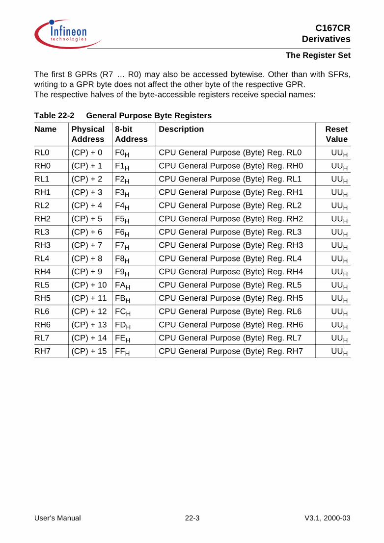
C167CRDerivatives
The Register Set
The first 8 GPRs (R7 … R0) may also be accessed bytewise. Other than with SFRs,writing to a GPR byte does not affect the other byte of the respective GPR.The respective halves of the byte-accessible registers receive special names:
Table 22-2 General Purpose Byte Registers
Name PhysicalAddress
8-bitAddress
Description ResetValue
RL0 (CP) + 0 F0H CPU General Purpose (Byte) Reg. RL0 UUH
RH0 (CP) + 1 F1H CPU General Purpose (Byte) Reg. RH0 UUH
RL1 (CP) + 2 F2H CPU General Purpose (Byte) Reg. RL1 UUH
RH1 (CP) + 3 F3H CPU General Purpose (Byte) Reg. RH1 UUH
RL2 (CP) + 4 F4H CPU General Purpose (Byte) Reg. RL2 UUH
RH2 (CP) + 5 F5H CPU General Purpose (Byte) Reg. RH2 UUH
RL3 (CP) + 6 F6H CPU General Purpose (Byte) Reg. RL3 UUH
RH3 (CP) + 7 F7H CPU General Purpose (Byte) Reg. RH3 UUH
RL4 (CP) + 8 F8H CPU General Purpose (Byte) Reg. RL4 UUH
RH4 (CP) + 9 F9H CPU General Purpose (Byte) Reg. RH4 UUH
RL5 (CP) + 10 FAH CPU General Purpose (Byte) Reg. RL5 UUH
RH5 (CP) + 11 FBH CPU General Purpose (Byte) Reg. RH5 UUH
RL6 (CP) + 12 FCH CPU General Purpose (Byte) Reg. RL6 UUH
RH6 (CP) + 13 FDH CPU General Purpose (Byte) Reg. RH6 UUH
RL7 (CP) + 14 FEH CPU General Purpose (Byte) Reg. RL7 UUH
RH7 (CP) + 15 FFH CPU General Purpose (Byte) Reg. RH7 UUH
User’s Manual 22-3 V3.1, 2000-03

C167CRDerivatives
The Register Set
22.3 Special Function Registers Ordered by Name
Table 22-3 lists all SFRs which are implemented in the C167CR in alphabetical order.Bit-addressable SFRs are marked with the letter “b” in column “Name”.SFRs within the extended SFR-space (ESFRs) are marked with the letter “E” in column“Physical Address”. Registers within on-chip X-Peripherals are marked with the letter “X”in column “Physical Address”.
Table 22-3 C167CR Registers, Ordered by Name
Name PhysicalAddress
8-bitAddr.
Description ResetValue
ADCIC b FF98H CCH A/D Converter End of Conversion Interrupt Control Register
0000H
ADCON b FFA0H D0H A/D Converter Control Register 0000H
ADDAT FEA0H 50H A/D Converter Result Register 0000H
ADDAT2 F0A0H E 50H A/D Converter 2 Result Register 0000H
ADDRSEL1 FE18H 0CH Address Select Register 1 0000H
ADDRSEL2 FE1AH 0DH Address Select Register 2 0000H
ADDRSEL3 FE1CH 0EH Address Select Register 3 0000H
ADDRSEL4 FE1EH 0FH Address Select Register 4 0000H
ADEIC b FF9AH CDH A/D Converter Overrun Error Interrupt Control Register
0000H
BUSCON0 b FF0CH 86H Bus Configuration Register 0 0000H
BUSCON1 b FF14H 8AH Bus Configuration Register 1 0000H
BUSCON2 b FF16H 8BH Bus Configuration Register 2 0000H
BUSCON3 b FF18H 8CH Bus Configuration Register 3 0000H
BUSCON4 b FF1AH 8DH Bus Configuration Register 4 0000H
C1BTR EF04H X – CAN1 Bit Timing Register UUUUH
C1CSR EF00H X – CAN1 Control/Status Register XX01H
C1GMS EF06H X – CAN1 Global Mask Short UFUUH
C1IR EF02H X – CAN1 Interrupt Register XXH
C1LARn EFn4H X – CAN1 Lower Arbitration Register (msg. n) UUUUH
C1LGML EF0AH X – CAN1 Lower Global Mask Long UUUUH
C1LMLM EF0EH X – CAN1 Lower Mask of Last Message UUUUH
C1MCFGn EFn6H X – CAN1 Message Configuration Register (msg. n)
UUH
User’s Manual 22-4 V3.1, 2000-03
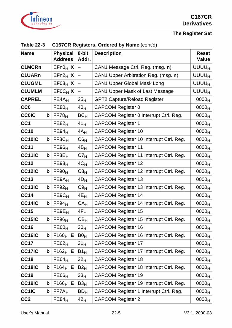
C167CRDerivatives
The Register Set
C1MCRn EFn0H X – CAN1 Message Ctrl. Reg. (msg. n) UUUUH
C1UARn EFn2H X – CAN1 Upper Arbitration Reg. (msg. n) UUUUH
C1UGML EF08H X – CAN1 Upper Global Mask Long UUUUH
C1UMLM EF0CH X – CAN1 Upper Mask of Last Message UUUUH
CAPREL FE4AH 25H GPT2 Capture/Reload Register 0000H
CC0 FE80H 40H CAPCOM Register 0 0000H
CC0IC b FF78H BCH CAPCOM Register 0 Interrupt Ctrl. Reg. 0000H
CC1 FE82H 41H CAPCOM Register 1 0000H
CC10 FE94H 4AH CAPCOM Register 10 0000H
CC10IC b FF8CH C6H CAPCOM Register 10 Interrupt Ctrl. Reg. 0000H
CC11 FE96H 4BH CAPCOM Register 11 0000H
CC11IC b FF8EH C7H CAPCOM Register 11 Interrupt Ctrl. Reg. 0000H
CC12 FE98H 4CH CAPCOM Register 12 0000H
CC12IC b FF90H C8H CAPCOM Register 12 Interrupt Ctrl. Reg. 0000H
CC13 FE9AH 4DH CAPCOM Register 13 0000H
CC13IC b FF92H C9H CAPCOM Register 13 Interrupt Ctrl. Reg. 0000H
CC14 FE9CH 4EH CAPCOM Register 14 0000H
CC14IC b FF94H CAH CAPCOM Register 14 Interrupt Ctrl. Reg. 0000H
CC15 FE9EH 4FH CAPCOM Register 15 0000H
CC15IC b FF96H CBH CAPCOM Register 15 Interrupt Ctrl. Reg. 0000H
CC16 FE60H 30H CAPCOM Register 16 0000H
CC16IC b F160H E B0H CAPCOM Register 16 Interrupt Ctrl. Reg. 0000H
CC17 FE62H 31H CAPCOM Register 17 0000H
CC17IC b F162H E B1H CAPCOM Register 17 Interrupt Ctrl. Reg. 0000H
CC18 FE64H 32H CAPCOM Register 18 0000H
CC18IC b F164H E B2H CAPCOM Register 18 Interrupt Ctrl. Reg. 0000H
CC19 FE66H 33H CAPCOM Register 19 0000H
CC19IC b F166H E B3H CAPCOM Register 19 Interrupt Ctrl. Reg. 0000H
CC1IC b FF7AH BDH CAPCOM Register 1 Interrupt Ctrl. Reg. 0000H
CC2 FE84H 42H CAPCOM Register 2 0000H
Table 22-3 C167CR Registers, Ordered by Name (cont’d)
Name PhysicalAddress
8-bitAddr.
Description ResetValue
User’s Manual 22-5 V3.1, 2000-03

C167CRDerivatives
The Register Set
CC20 FE68H 34H CAPCOM Register 20 0000H
CC20IC b F168H E B4H CAPCOM Register 20 Interrupt Ctrl. Reg. 0000H
CC21 FE6AH 35H CAPCOM Register 21 0000H
CC21IC b F16AH E B5H CAPCOM Register 21 Interrupt Ctrl. Reg. 0000H
CC22 FE6CH 36H CAPCOM Register 22 0000H
CC22IC b F16CH E B6H CAPCOM Register 22 Interrupt Ctrl. Reg. 0000H
CC23 FE6EH 37H CAPCOM Register 23 0000H
CC23IC b F16EH E B7H CAPCOM Register 23 Interrupt Ctrl. Reg. 0000H
CC24 FE70H 38H CAPCOM Register 24 0000H
CC24IC b F170H E B8H CAPCOM Register 24 Interrupt Ctrl. Reg. 0000H
CC25 FE72H 39H CAPCOM Register 25 0000H
CC25IC b F172H E B9H CAPCOM Register 25 Interrupt Ctrl. Reg. 0000H
CC26 FE74H 3AH CAPCOM Register 26 0000H
CC26IC b F174H E BAH CAPCOM Register 26 Interrupt Ctrl. Reg. 0000H
CC27 FE76H 3BH CAPCOM Register 27 0000H
CC27IC b F176H E BBH CAPCOM Register 27 Interrupt Ctrl. Reg. 0000H
CC28 FE78H 3CH CAPCOM Register 28 0000H
CC28IC b F178H E BCH CAPCOM Register 28 Interrupt Ctrl. Reg. 0000H
CC29 FE7AH 3DH CAPCOM Register 29 0000H
CC29IC b F184H E C2H CAPCOM Register 29 Interrupt Ctrl. Reg. 0000H
CC2IC b FF7CH BEH CAPCOM Register 2 Interrupt Ctrl. Reg. 0000H
CC3 FE86H 43H CAPCOM Register 3 0000H
CC30 FE7CH 3EH CAPCOM Register 30 0000H
CC30IC b F18CH E C6H CAPCOM Register 30 Interrupt Ctrl. Reg. 0000H
CC31 FE7EH 3FH CAPCOM Register 31 0000H
CC31IC b F194H E CAH CAPCOM Register 31 Interrupt Ctrl. Reg. 0000H
CC3IC b FF7EH BFH CAPCOM Register 3 Interrupt Ctrl. Reg. 0000H
CC4 FE88H 44H CAPCOM Register 4 0000H
CC4IC b FF80H C0H CAPCOM Register 4 Interrupt Ctrl. Reg. 0000H
CC5 FE8AH 45H CAPCOM Register 5 0000H
Table 22-3 C167CR Registers, Ordered by Name (cont’d)
Name PhysicalAddress
8-bitAddr.
Description ResetValue
User’s Manual 22-6 V3.1, 2000-03

C167CRDerivatives
The Register Set
CC5IC b FF82H C1H CAPCOM Register 5 Interrupt Ctrl. Reg. 0000H
CC6 FE8CH 46H CAPCOM Register 6 0000H
CC6IC b FF84H C2H CAPCOM Register 6 Interrupt Ctrl. Reg. 0000H
CC7 FE8EH 47H CAPCOM Register 7 0000H
CC7IC b FF86H C3H CAPCOM Register 7 Interrupt Ctrl. Reg. 0000H
CC8 FE90H 48H CAPCOM Register 8 0000H
CC8IC b FF88H C4H CAPCOM Register 8 Interrupt Ctrl. Reg. 0000H
CC9 FE92H 49H CAPCOM Register 9 0000H
CC9IC b FF8AH C5H CAPCOM Register 9 Interrupt Ctrl. Reg. 0000H
CCM0 b FF52H A9H CAPCOM Mode Control Register 0 0000H
CCM1 b FF54H AAH CAPCOM Mode Control Register 1 0000H
CCM2 b FF56H ABH CAPCOM Mode Control Register 2 0000H
CCM3 b FF58H ACH CAPCOM Mode Control Register 3 0000H
CCM4 b FF22H 91H CAPCOM Mode Control Register 4 0000H
CCM5 b FF24H 92H CAPCOM Mode Control Register 5 0000H
CCM6 b FF26H 93H CAPCOM Mode Control Register 6 0000H
CCM7 b FF28H 94H CAPCOM Mode Control Register 7 0000H
CP FE10H 08H CPU Context Pointer Register FC00H
CRIC b FF6AH B5H GPT2 CAPREL Interrupt Control Register 0000H
CSP FE08H 04H CPU Code Segment Pointer Register(8 bits, not directly writeable)
0000H
DP0H b F102H E 81H P0H Direction Control Register 00H
DP0L b F100H E 80H P0L Direction Control Register 00H
DP1H b F106H E 83H P1H Direction Control Register 00H
DP1L b F104H E 82H P1L Direction Control Register 00H
DP2 b FFC2H E1H Port 2 Direction Control Register 0000H
DP3 b FFC6H E3H Port 3 Direction Control Register 0000H
DP4 b FFCAH E5H Port 4 Direction Control Register 00H
DP6 b FFCEH E7H Port 6 Direction Control Register 00H
DP7 b FFD2H E9H Port 7 Direction Control Register 00H
Table 22-3 C167CR Registers, Ordered by Name (cont’d)
Name PhysicalAddress
8-bitAddr.
Description ResetValue
User’s Manual 22-7 V3.1, 2000-03

C167CRDerivatives
The Register Set
DP8 b FFD6H EBH Port 8 Direction Control Register 00H
DPP0 FE00H 00H CPU Data Page Pointer 0 Register (10 bits) 0000H
DPP1 FE02H 01H CPU Data Page Pointer 1 Register (10 bits) 0001H
DPP2 FE04H 02H CPU Data Page Pointer 2 Register (10 bits) 0002H
DPP3 FE06H 03H CPU Data Page Pointer 3 Register (10 bits) 0003H
EXICON b F1C0H E E0H External Interrupt Control Register 0000H
MDC b FF0EH 87H CPU Multiply Divide Control Register 0000H
MDH FE0CH 06H CPU Multiply Divide Register – High Word 0000H
MDL FE0EH 07H CPU Multiply Divide Register – Low Word 0000H
ODP2 b F1C2H E E1H Port 2 Open Drain Control Register 0000H
ODP3 b F1C6H E E3H Port 3 Open Drain Control Register 0000H
ODP6 b F1CEH E E7H Port 6 Open Drain Control Register 00H
ODP7 b F1D2H E E9H Port 7 Open Drain Control Register 00H
ODP8 b F1D6H E EBH Port 8 Open Drain Control Register 00H
ONES b FF1EH 8FH Constant Value 1’s Register (read only) FFFFH
P0H b FF02H 81H Port 0 High Register (Upper half of PORT0) 00H
P0L b FF00H 80H Port 0 Low Register (Lower half of PORT0) 00H
P1H b FF06H 83H Port 1 High Register (Upper half of PORT1) 00H
P1L b FF04H 82H Port 1 Low Register (Lower half of PORT1) 00H
P2 b FFC0H E0H Port 2 Register 0000H
P3 b FFC4H E2H Port 3 Register 0000H
P4 b FFC8H E4H Port 4 Register (7 bits) 00H
P5 b FFA2H D1H Port 5 Register (read only) XXXXH
P5DIDIS b FFA4H D2H Port 5 Digital Input Disable Register 0000H
P6 b FFCCH E6H Port 6 Register (8 bits) 00H
P7 b FFD0H E8H Port 7 Register (8 bits) 00H
P8 b FFD4H EAH Port 8 Register (8 bits) 00H
PDCR F0AAH E 55H Port Driver Control Register 0000H
PECC0 FEC0H 60H PEC Channel 0 Control Register 0000H
PECC1 FEC2H 61H PEC Channel 1 Control Register 0000H
Table 22-3 C167CR Registers, Ordered by Name (cont’d)
Name PhysicalAddress
8-bitAddr.
Description ResetValue
User’s Manual 22-8 V3.1, 2000-03

C167CRDerivatives
The Register Set
PECC2 FEC4H 62H PEC Channel 2 Control Register 0000H
PECC3 FEC6H 63H PEC Channel 3 Control Register 0000H
PECC4 FEC8H 64H PEC Channel 4 Control Register 0000H
PECC5 FECAH 65H PEC Channel 5 Control Register 0000H
PECC6 FECCH 66H PEC Channel 6 Control Register 0000H
PECC7 FECEH 67H PEC Channel 7 Control Register 0000H
PICON F1C4H E E2H Port Input Threshold Control Register 0000H
PP0 F038H E 1CH PWM Module Period Register 0 0000H
PP1 F03AH E 1DH PWM Module Period Register 1 0000H
PP2 F03CH E 1EH PWM Module Period Register 2 0000H
PP3 F03EH E 1FH PWM Module Period Register 3 0000H
PSW b FF10H 88H CPU Program Status Word 0000H
PT0 F030H E 18H PWM Module Up/Down Counter 0 0000H
PT1 F032H E 19H PWM Module Up/Down Counter 1 0000H
PT2 F034H E 1AH PWM Module Up/Down Counter 2 0000H
PT3 F036H E 1BH PWM Module Up/Down Counter 3 0000H
PW0 FE30H 18H PWM Module Pulse Width Register 0 0000H
PW1 FE32H 19H PWM Module Pulse Width Register 1 0000H
PW2 FE34H 1AH PWM Module Pulse Width Register 2 0000H
PW3 FE36H 1BH PWM Module Pulse Width Register 3 0000H
PWMCON0b FF30H 98H PWM Module Control Register 0 0000H
PWMCON1b FF32H 99H PWM Module Control Register 1 0000H
PWMIC b F17EH E BFH PWM Module Interrupt Control Register 0000H
RP0H b F108H E 84H System Startup Configuration Register (read only)
XXH
S0BG FEB4H 5AH Serial Channel 0 Baud Rate Generator Reload Register
0000H
S0CON b FFB0H D8H Serial Channel 0 Control Register 0000H
S0EIC b FF70H B8H Serial Channel 0 Error Interrupt Control Register
0000H
Table 22-3 C167CR Registers, Ordered by Name (cont’d)
Name PhysicalAddress
8-bitAddr.
Description ResetValue
User’s Manual 22-9 V3.1, 2000-03

C167CRDerivatives
The Register Set
S0RBUF FEB2H 59H Serial Channel 0 Receive Buffer Register(read only)
XXXXH
S0RIC b FF6EH B7H Serial Channel 0 Receive Interrupt Control Register
0000H
S0TBIC b F19CH E CEH Serial Channel 0 Transmit Buffer Interrupt Control Register
0000H
S0TBUF FEB0H 58H Serial Channel 0 Transmit Buffer Register 0000H
S0TIC b FF6CH B6H Serial Channel 0 Transmit Interrupt Control Register
0000H
SP FE12H 09H CPU System Stack Pointer Register FC00H
SSCBR F0B4H E 5AH SSC Baudrate Register 0000H
SSCCON b FFB2H D9H SSC Control Register 0000H
SSCEIC b FF76H BBH SSC Error Interrupt Control Register 0000H
SSCRB F0B2H E 59H SSC Receive Buffer XXXXH
SSCRIC b FF74H BAH SSC Receive Interrupt Control Register 0000H
SSCTB F0B0H E 58H SSC Transmit Buffer 0000H
SSCTIC b FF72H B9H SSC Transmit Interrupt Control Register 0000H
STKOV FE14H 0AH CPU Stack Overflow Pointer Register FA00H
STKUN FE16H 0BH CPU Stack Underflow Pointer Register FC00H
SYSCON b FF12H 89H CPU System Configuration Register 1)0xx0H
T0 FE50H 28H CAPCOM Timer 0 Register 0000H
T01CON b FF50H A8H CAPCOM Timer 0 and Timer 1 Ctrl. Reg. 0000H
T0IC b FF9CH CEH CAPCOM Timer 0 Interrupt Ctrl. Reg. 0000H
T0REL FE54H 2AH CAPCOM Timer 0 Reload Register 0000H
T1 FE52H 29H CAPCOM Timer 1 Register 0000H
T1IC b FF9EH CFH CAPCOM Timer 1 Interrupt Ctrl. Reg. 0000H
T1REL FE56H 2BH CAPCOM Timer 1 Reload Register 0000H
T2 FE40H 20H GPT1 Timer 2 Register 0000H
T2CON b FF40H A0H GPT1 Timer 2 Control Register 0000H
T2IC b FF60H B0H GPT1 Timer 2 Interrupt Control Register 0000H
T3 FE42H 21H GPT1 Timer 3 Register 0000H
Table 22-3 C167CR Registers, Ordered by Name (cont’d)
Name PhysicalAddress
8-bitAddr.
Description ResetValue
User’s Manual 22-10 V3.1, 2000-03

C167CRDerivatives
The Register Set
T3CON b FF42H A1H GPT1 Timer 3 Control Register 0000H
T3IC b FF62H B1H GPT1 Timer 3 Interrupt Control Register 0000H
T4 FE44H 22H GPT1 Timer 4 Register 0000H
T4CON b FF44H A2H GPT1 Timer 4 Control Register 0000H
T4IC b FF64H B2H GPT1 Timer 4 Interrupt Control Register 0000H
T5 FE46H 23H GPT2 Timer 5 Register 0000H
T5CON b FF46H A3H GPT2 Timer 5 Control Register 0000H
T5IC b FF66H B3H GPT2 Timer 5 Interrupt Control Register 0000H
T6 FE48H 24H GPT2 Timer 6 Register 0000H
T6CON b FF48H A4H GPT2 Timer 6 Control Register 0000H
T6IC b FF68H B4H GPT2 Timer 6 Interrupt Control Register 0000H
T7 F050H E 28H CAPCOM Timer 7 Register 0000H
T78CON b FF20H 90H CAPCOM Timer 7 and 8 Control Register 0000H
T7IC b F17AH E BDH CAPCOM Timer 7 Interrupt Ctrl. Reg. 0000H
T7REL F054H E 2AH CAPCOM Timer 7 Reload Register 0000H
T8 F052H E 29H CAPCOM Timer 8 Register 0000H
T8IC b F17CH E BEH CAPCOM Timer 8 Interrupt Ctrl. Reg. 0000H
T8REL F056H E 2BH CAPCOM Timer 8 Reload Register 0000H
TFR b FFACH D6H Trap Flag Register 0000H
WDT FEAEH 57H Watchdog Timer Register (read only) 0000H
WDTCON b FFAEH D7H Watchdog Timer Control Register 2)00xxH
XP0IC b F186H E C3H CAN1 Interrupt Control Register 0000H
XP1IC b F18EH E C7H Unassigned Interrupt Control Register 0000H
XP2IC b F196H E CBH Unassigned Interrupt Control Register 0000H
XP3IC b F19EH E CFH PLL/OWD Interrupt Control Register 0000H
ZEROS b FF1CH 8EH Constant Value 0’s Register (read only) 0000H
1) The system configuration is selected during reset.2) The reset value depends on the indicated reset source.
Table 22-3 C167CR Registers, Ordered by Name (cont’d)
Name PhysicalAddress
8-bitAddr.
Description ResetValue
User’s Manual 22-11 V3.1, 2000-03

C167CRDerivatives
The Register Set
22.4 Special Function Registers Ordered by Address
Table 22-4 lists all SFRs which are implemented in the C167CR ordered by theirphysical address. Bit-addressable SFRs are marked with the letter “b” in column“Name”.SFRs within the extended SFR-space (ESFRs) are marked with the letter “E” in column“Physical Address”. Registers within on-chip X-Peripherals are marked with the letter “X”in column “Physical Address”.
Table 22-4 C167CR Registers, Ordered by Address
Name PhysicalAddress
8-bitAddr.
Description ResetValue
C1CSR EF00H X – CAN1 Control/Status Register XX01H
C1IR EF02H X – CAN1 Interrupt Register XXH
C1BTR EF04H X – CAN1 Bit Timing Register UUUUH
C1GMS EF06H X – CAN1 Global Mask Short UFUUH
C1UGML EF08H X – CAN1 Upper Global Mask Long UUUUH
C1LGML EF0AH X – CAN1 Lower Global Mask Long UUUUH
C1UMLM EF0CH X – CAN1 Upper Mask of Last Message UUUUH
C1LMLM EF0EH X – CAN1 Lower Mask of Last Message UUUUH
C1MCRn EFn0H X – CAN1 Message Ctrl. Reg. (msg. n) UUUUH
C1UARn EFn2H X – CAN1 Upper Arbitration Reg. (msg. n) UUUUH
C1LARn EFn4H X – CAN1 Lower Arbitration Reg. (msg. n) UUUUH
C1MCFGn EFn6H X – CAN1 Message Configuration Register (msg. n)
UUH
PT0 F030H E 18H PWM Module Up/Down Counter 0 0000H
PT1 F032H E 19H PWM Module Up/Down Counter 1 0000H
PT2 F034H E 1AH PWM Module Up/Down Counter 2 0000H
PT3 F036H E 1BH PWM Module Up/Down Counter 3 0000H
PP0 F038H E 1CH PWM Module Period Register 0 0000H
PP1 F03AH E 1DH PWM Module Period Register 1 0000H
PP2 F03CH E 1EH PWM Module Period Register 2 0000H
PP3 F03EH E 1FH PWM Module Period Register 3 0000H
T7 F050H E 28H CAPCOM Timer 7 Register 0000H
T8 F052H E 29H CAPCOM Timer 8 Register 0000H
User’s Manual 22-12 V3.1, 2000-03
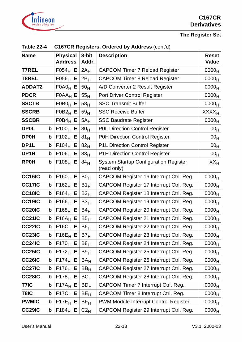
C167CRDerivatives
The Register Set
T7REL F054H E 2AH CAPCOM Timer 7 Reload Register 0000H
T8REL F056H E 2BH CAPCOM Timer 8 Reload Register 0000H
ADDAT2 F0A0H E 50H A/D Converter 2 Result Register 0000H
PDCR F0AAH E 55H Port Driver Control Register 0000H
SSCTB F0B0H E 58H SSC Transmit Buffer 0000H
SSCRB F0B2H E 59H SSC Receive Buffer XXXXH
SSCBR F0B4H E 5AH SSC Baudrate Register 0000H
DP0L b F100H E 80H P0L Direction Control Register 00H
DP0H b F102H E 81H P0H Direction Control Register 00H
DP1L b F104H E 82H P1L Direction Control Register 00H
DP1H b F106H E 83H P1H Direction Control Register 00H
RP0H b F108H E 84H System Startup Configuration Register (read only)
XXH
CC16IC b F160H E B0H CAPCOM Register 16 Interrupt Ctrl. Reg. 0000H
CC17IC b F162H E B1H CAPCOM Register 17 Interrupt Ctrl. Reg. 0000H
CC18IC b F164H E B2H CAPCOM Register 18 Interrupt Ctrl. Reg. 0000H
CC19IC b F166H E B3H CAPCOM Register 19 Interrupt Ctrl. Reg. 0000H
CC20IC b F168H E B4H CAPCOM Register 20 Interrupt Ctrl. Reg. 0000H
CC21IC b F16AH E B5H CAPCOM Register 21 Interrupt Ctrl. Reg. 0000H
CC22IC b F16CH E B6H CAPCOM Register 22 Interrupt Ctrl. Reg. 0000H
CC23IC b F16EH E B7H CAPCOM Register 23 Interrupt Ctrl. Reg. 0000H
CC24IC b F170H E B8H CAPCOM Register 24 Interrupt Ctrl. Reg. 0000H
CC25IC b F172H E B9H CAPCOM Register 25 Interrupt Ctrl. Reg. 0000H
CC26IC b F174H E BAH CAPCOM Register 26 Interrupt Ctrl. Reg. 0000H
CC27IC b F176H E BBH CAPCOM Register 27 Interrupt Ctrl. Reg. 0000H
CC28IC b F178H E BCH CAPCOM Register 28 Interrupt Ctrl. Reg. 0000H
T7IC b F17AH E BDH CAPCOM Timer 7 Interrupt Ctrl. Reg. 0000H
T8IC b F17CH E BEH CAPCOM Timer 8 Interrupt Ctrl. Reg. 0000H
PWMIC b F17EH E BFH PWM Module Interrupt Control Register 0000H
CC29IC b F184H E C2H CAPCOM Register 29 Interrupt Ctrl. Reg. 0000H
Table 22-4 C167CR Registers, Ordered by Address (cont’d)
Name PhysicalAddress
8-bitAddr.
Description ResetValue
User’s Manual 22-13 V3.1, 2000-03
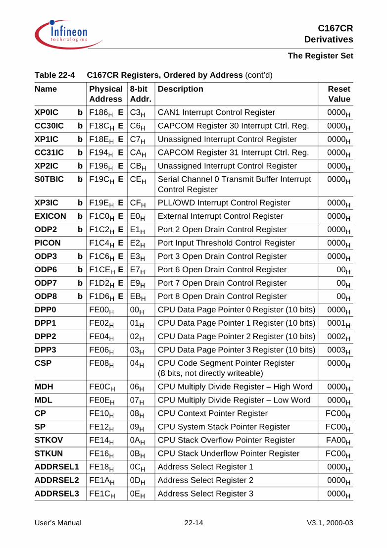
C167CRDerivatives
The Register Set
XP0IC b F186H E C3H CAN1 Interrupt Control Register 0000H
CC30IC b F18CH E C6H CAPCOM Register 30 Interrupt Ctrl. Reg. 0000H
XP1IC b F18EH E C7H Unassigned Interrupt Control Register 0000H
CC31IC b F194H E CAH CAPCOM Register 31 Interrupt Ctrl. Reg. 0000H
XP2IC b F196H E CBH Unassigned Interrupt Control Register 0000H
S0TBIC b F19CH E CEH Serial Channel 0 Transmit Buffer Interrupt Control Register
0000H
XP3IC b F19EH E CFH PLL/OWD Interrupt Control Register 0000H
EXICON b F1C0H E E0H External Interrupt Control Register 0000H
ODP2 b F1C2H E E1H Port 2 Open Drain Control Register 0000H
PICON F1C4H E E2H Port Input Threshold Control Register 0000H
ODP3 b F1C6H E E3H Port 3 Open Drain Control Register 0000H
ODP6 b F1CEH E E7H Port 6 Open Drain Control Register 00H
ODP7 b F1D2H E E9H Port 7 Open Drain Control Register 00H
ODP8 b F1D6H E EBH Port 8 Open Drain Control Register 00H
DPP0 FE00H 00H CPU Data Page Pointer 0 Register (10 bits) 0000H
DPP1 FE02H 01H CPU Data Page Pointer 1 Register (10 bits) 0001H
DPP2 FE04H 02H CPU Data Page Pointer 2 Register (10 bits) 0002H
DPP3 FE06H 03H CPU Data Page Pointer 3 Register (10 bits) 0003H
CSP FE08H 04H CPU Code Segment Pointer Register(8 bits, not directly writeable)
0000H
MDH FE0CH 06H CPU Multiply Divide Register – High Word 0000H
MDL FE0EH 07H CPU Multiply Divide Register – Low Word 0000H
CP FE10H 08H CPU Context Pointer Register FC00H
SP FE12H 09H CPU System Stack Pointer Register FC00H
STKOV FE14H 0AH CPU Stack Overflow Pointer Register FA00H
STKUN FE16H 0BH CPU Stack Underflow Pointer Register FC00H
ADDRSEL1 FE18H 0CH Address Select Register 1 0000H
ADDRSEL2 FE1AH 0DH Address Select Register 2 0000H
ADDRSEL3 FE1CH 0EH Address Select Register 3 0000H
Table 22-4 C167CR Registers, Ordered by Address (cont’d)
Name PhysicalAddress
8-bitAddr.
Description ResetValue
User’s Manual 22-14 V3.1, 2000-03

C167CRDerivatives
The Register Set
ADDRSEL4 FE1EH 0FH Address Select Register 4 0000H
PW0 FE30H 18H PWM Module Pulse Width Register 0 0000H
PW1 FE32H 19H PWM Module Pulse Width Register 1 0000H
PW2 FE34H 1AH PWM Module Pulse Width Register 2 0000H
PW3 FE36H 1BH PWM Module Pulse Width Register 3 0000H
T2 FE40H 20H GPT1 Timer 2 Register 0000H
T3 FE42H 21H GPT1 Timer 3 Register 0000H
T4 FE44H 22H GPT1 Timer 4 Register 0000H
T5 FE46H 23H GPT2 Timer 5 Register 0000H
T6 FE48H 24H GPT2 Timer 6 Register 0000H
CAPREL FE4AH 25H GPT2 Capture/Reload Register 0000H
T0 FE50H 28H CAPCOM Timer 0 Register 0000H
T1 FE52H 29H CAPCOM Timer 1 Register 0000H
T0REL FE54H 2AH CAPCOM Timer 0 Reload Register 0000H
T1REL FE56H 2BH CAPCOM Timer 1 Reload Register 0000H
CC16 FE60H 30H CAPCOM Register 16 0000H
CC17 FE62H 31H CAPCOM Register 17 0000H
CC18 FE64H 32H CAPCOM Register 18 0000H
CC19 FE66H 33H CAPCOM Register 19 0000H
CC20 FE68H 34H CAPCOM Register 20 0000H
CC21 FE6AH 35H CAPCOM Register 21 0000H
CC22 FE6CH 36H CAPCOM Register 22 0000H
CC23 FE6EH 37H CAPCOM Register 23 0000H
CC24 FE70H 38H CAPCOM Register 24 0000H
CC25 FE72H 39H CAPCOM Register 25 0000H
CC26 FE74H 3AH CAPCOM Register 26 0000H
CC27 FE76H 3BH CAPCOM Register 27 0000H
CC28 FE78H 3CH CAPCOM Register 28 0000H
CC29 FE7AH 3DH CAPCOM Register 29 0000H
CC30 FE7CH 3EH CAPCOM Register 30 0000H
Table 22-4 C167CR Registers, Ordered by Address (cont’d)
Name PhysicalAddress
8-bitAddr.
Description ResetValue
User’s Manual 22-15 V3.1, 2000-03

C167CRDerivatives
The Register Set
CC31 FE7EH 3FH CAPCOM Register 31 0000H
CC0 FE80H 40H CAPCOM Register 0 0000H
CC1 FE82H 41H CAPCOM Register 1 0000H
CC2 FE84H 42H CAPCOM Register 2 0000H
CC3 FE86H 43H CAPCOM Register 3 0000H
CC4 FE88H 44H CAPCOM Register 4 0000H
CC5 FE8AH 45H CAPCOM Register 5 0000H
CC6 FE8CH 46H CAPCOM Register 6 0000H
CC7 FE8EH 47H CAPCOM Register 7 0000H
CC8 FE90H 48H CAPCOM Register 8 0000H
CC9 FE92H 49H CAPCOM Register 9 0000H
CC10 FE94H 4AH CAPCOM Register 10 0000H
CC11 FE96H 4BH CAPCOM Register 11 0000H
CC12 FE98H 4CH CAPCOM Register 12 0000H
CC13 FE9AH 4DH CAPCOM Register 13 0000H
CC14 FE9CH 4EH CAPCOM Register 14 0000H
CC15 FE9EH 4FH CAPCOM Register 15 0000H
ADDAT FEA0H 50H A/D Converter Result Register 0000H
WDT FEAEH 57H Watchdog Timer Register (read only) 0000H
S0TBUF FEB0H 58H Serial Channel 0 Transmit Buffer Register 0000H
S0RBUF FEB2H 59H Serial Channel 0 Receive Buffer Register(read only)
XXXXH
S0BG FEB4H 5AH Serial Channel 0 Baud Rate Generator Reload Register
0000H
PECC0 FEC0H 60H PEC Channel 0 Control Register 0000H
PECC1 FEC2H 61H PEC Channel 1 Control Register 0000H
PECC2 FEC4H 62H PEC Channel 2 Control Register 0000H
PECC3 FEC6H 63H PEC Channel 3 Control Register 0000H
PECC4 FEC8H 64H PEC Channel 4 Control Register 0000H
PECC5 FECAH 65H PEC Channel 5 Control Register 0000H
Table 22-4 C167CR Registers, Ordered by Address (cont’d)
Name PhysicalAddress
8-bitAddr.
Description ResetValue
User’s Manual 22-16 V3.1, 2000-03
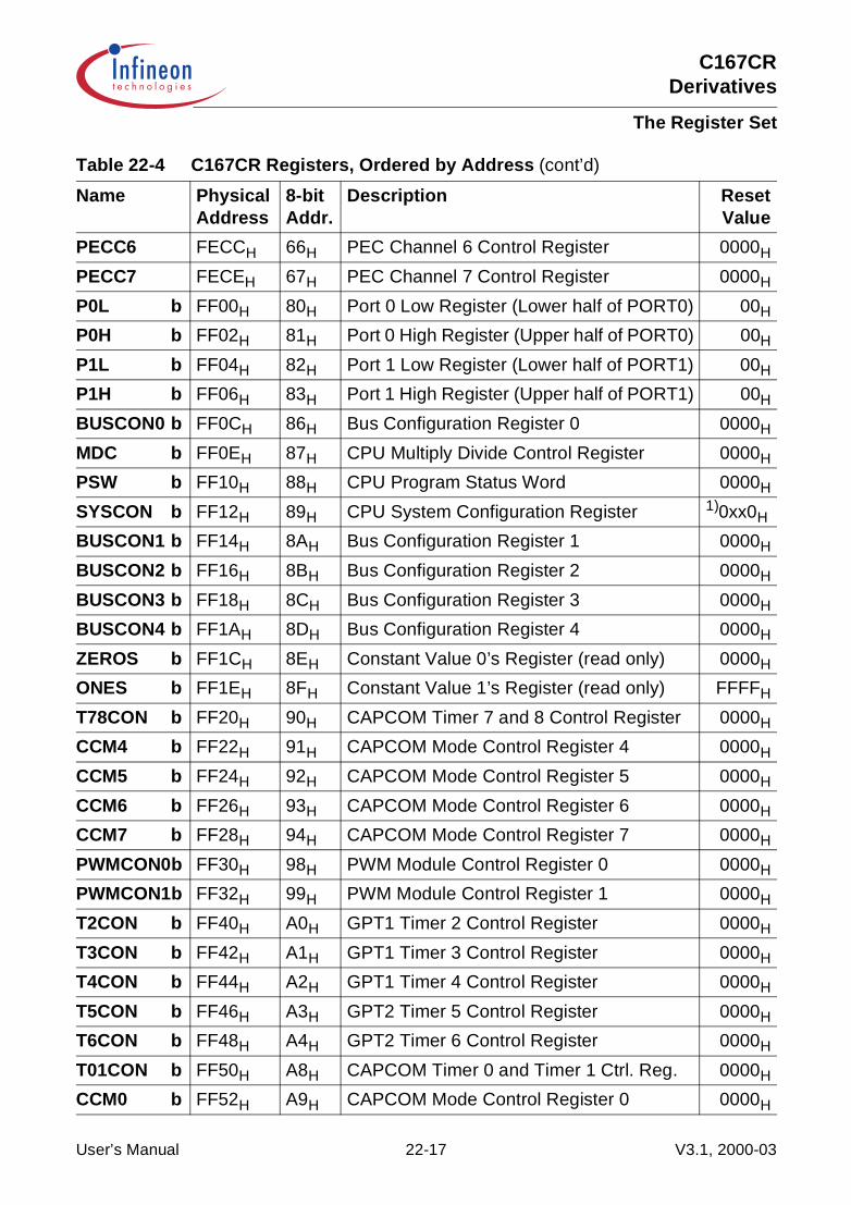
C167CRDerivatives
The Register Set
PECC6 FECCH 66H PEC Channel 6 Control Register 0000H
PECC7 FECEH 67H PEC Channel 7 Control Register 0000H
P0L b FF00H 80H Port 0 Low Register (Lower half of PORT0) 00H
P0H b FF02H 81H Port 0 High Register (Upper half of PORT0) 00H
P1L b FF04H 82H Port 1 Low Register (Lower half of PORT1) 00H
P1H b FF06H 83H Port 1 High Register (Upper half of PORT1) 00H
BUSCON0 b FF0CH 86H Bus Configuration Register 0 0000H
MDC b FF0EH 87H CPU Multiply Divide Control Register 0000H
PSW b FF10H 88H CPU Program Status Word 0000H
SYSCON b FF12H 89H CPU System Configuration Register 1)0xx0H
BUSCON1 b FF14H 8AH Bus Configuration Register 1 0000H
BUSCON2 b FF16H 8BH Bus Configuration Register 2 0000H
BUSCON3 b FF18H 8CH Bus Configuration Register 3 0000H
BUSCON4 b FF1AH 8DH Bus Configuration Register 4 0000H
ZEROS b FF1CH 8EH Constant Value 0’s Register (read only) 0000H
ONES b FF1EH 8FH Constant Value 1’s Register (read only) FFFFH
T78CON b FF20H 90H CAPCOM Timer 7 and 8 Control Register 0000H
CCM4 b FF22H 91H CAPCOM Mode Control Register 4 0000H
CCM5 b FF24H 92H CAPCOM Mode Control Register 5 0000H
CCM6 b FF26H 93H CAPCOM Mode Control Register 6 0000H
CCM7 b FF28H 94H CAPCOM Mode Control Register 7 0000H
PWMCON0b FF30H 98H PWM Module Control Register 0 0000H
PWMCON1b FF32H 99H PWM Module Control Register 1 0000H
T2CON b FF40H A0H GPT1 Timer 2 Control Register 0000H
T3CON b FF42H A1H GPT1 Timer 3 Control Register 0000H
T4CON b FF44H A2H GPT1 Timer 4 Control Register 0000H
T5CON b FF46H A3H GPT2 Timer 5 Control Register 0000H
T6CON b FF48H A4H GPT2 Timer 6 Control Register 0000H
T01CON b FF50H A8H CAPCOM Timer 0 and Timer 1 Ctrl. Reg. 0000H
CCM0 b FF52H A9H CAPCOM Mode Control Register 0 0000H
Table 22-4 C167CR Registers, Ordered by Address (cont’d)
Name PhysicalAddress
8-bitAddr.
Description ResetValue
User’s Manual 22-17 V3.1, 2000-03
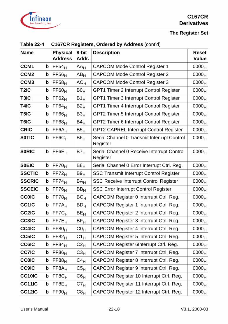
C167CRDerivatives
The Register Set
CCM1 b FF54H AAH CAPCOM Mode Control Register 1 0000H
CCM2 b FF56H ABH CAPCOM Mode Control Register 2 0000H
CCM3 b FF58H ACH CAPCOM Mode Control Register 3 0000H
T2IC b FF60H B0H GPT1 Timer 2 Interrupt Control Register 0000H
T3IC b FF62H B1H GPT1 Timer 3 Interrupt Control Register 0000H
T4IC b FF64H B2H GPT1 Timer 4 Interrupt Control Register 0000H
T5IC b FF66H B3H GPT2 Timer 5 Interrupt Control Register 0000H
T6IC b FF68H B4H GPT2 Timer 6 Interrupt Control Register 0000H
CRIC b FF6AH B5H GPT2 CAPREL Interrupt Control Register 0000H
S0TIC b FF6CH B6H Serial Channel 0 Transmit Interrupt Control Register
0000H
S0RIC b FF6EH B7H Serial Channel 0 Receive Interrupt Control Register
0000H
S0EIC b FF70H B8H Serial Channel 0 Error Interrupt Ctrl. Reg. 0000H
SSCTIC b FF72H B9H SSC Transmit Interrupt Control Register 0000H
SSCRIC b FF74H BAH SSC Receive Interrupt Control Register 0000H
SSCEIC b FF76H BBH SSC Error Interrupt Control Register 0000H
CC0IC b FF78H BCH CAPCOM Register 0 Interrupt Ctrl. Reg. 0000H
CC1IC b FF7AH BDH CAPCOM Register 1 Interrupt Ctrl. Reg. 0000H
CC2IC b FF7CH BEH CAPCOM Register 2 Interrupt Ctrl. Reg. 0000H
CC3IC b FF7EH BFH CAPCOM Register 3 Interrupt Ctrl. Reg. 0000H
CC4IC b FF80H C0H CAPCOM Register 4 Interrupt Ctrl. Reg. 0000H
CC5IC b FF82H C1H CAPCOM Register 5 Interrupt Ctrl. Reg. 0000H
CC6IC b FF84H C2H CAPCOM Register 6Interrupt Ctrl. Reg. 0000H
CC7IC b FF86H C3H CAPCOM Register 7 Interrupt Ctrl. Reg. 0000H
CC8IC b FF88H C4H CAPCOM Register 8 Interrupt Ctrl. Reg. 0000H
CC9IC b FF8AH C5H CAPCOM Register 9 Interrupt Ctrl. Reg. 0000H
CC10IC b FF8CH C6H CAPCOM Register 10 Interrupt Ctrl. Reg. 0000H
CC11IC b FF8EH C7H CAPCOM Register 11 Interrupt Ctrl. Reg. 0000H
CC12IC b FF90H C8H CAPCOM Register 12 Interrupt Ctrl. Reg. 0000H
Table 22-4 C167CR Registers, Ordered by Address (cont’d)
Name PhysicalAddress
8-bitAddr.
Description ResetValue
User’s Manual 22-18 V3.1, 2000-03
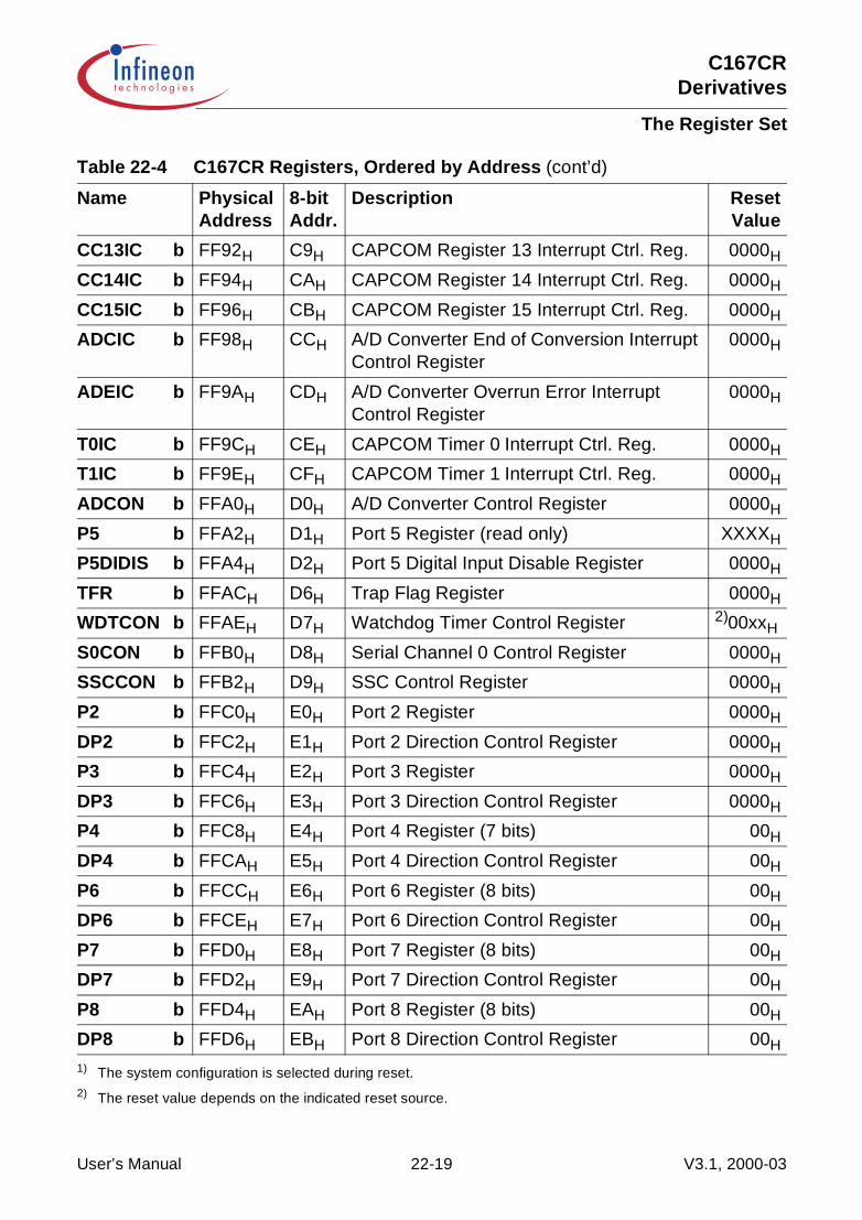
C167CRDerivatives
The Register Set
CC13IC b FF92H C9H CAPCOM Register 13 Interrupt Ctrl. Reg. 0000H
CC14IC b FF94H CAH CAPCOM Register 14 Interrupt Ctrl. Reg. 0000H
CC15IC b FF96H CBH CAPCOM Register 15 Interrupt Ctrl. Reg. 0000H
ADCIC b FF98H CCH A/D Converter End of Conversion Interrupt Control Register
0000H
ADEIC b FF9AH CDH A/D Converter Overrun Error Interrupt Control Register
0000H
T0IC b FF9CH CEH CAPCOM Timer 0 Interrupt Ctrl. Reg. 0000H
T1IC b FF9EH CFH CAPCOM Timer 1 Interrupt Ctrl. Reg. 0000H
ADCON b FFA0H D0H A/D Converter Control Register 0000H
P5 b FFA2H D1H Port 5 Register (read only) XXXXH
P5DIDIS b FFA4H D2H Port 5 Digital Input Disable Register 0000H
TFR b FFACH D6H Trap Flag Register 0000H
WDTCON b FFAEH D7H Watchdog Timer Control Register 2)00xxH
S0CON b FFB0H D8H Serial Channel 0 Control Register 0000H
SSCCON b FFB2H D9H SSC Control Register 0000H
P2 b FFC0H E0H Port 2 Register 0000H
DP2 b FFC2H E1H Port 2 Direction Control Register 0000H
P3 b FFC4H E2H Port 3 Register 0000H
DP3 b FFC6H E3H Port 3 Direction Control Register 0000H
P4 b FFC8H E4H Port 4 Register (7 bits) 00H
DP4 b FFCAH E5H Port 4 Direction Control Register 00H
P6 b FFCCH E6H Port 6 Register (8 bits) 00H
DP6 b FFCEH E7H Port 6 Direction Control Register 00H
P7 b FFD0H E8H Port 7 Register (8 bits) 00H
DP7 b FFD2H E9H Port 7 Direction Control Register 00H
P8 b FFD4H EAH Port 8 Register (8 bits) 00H
DP8 b FFD6H EBH Port 8 Direction Control Register 00H
1) The system configuration is selected during reset.2) The reset value depends on the indicated reset source.
Table 22-4 C167CR Registers, Ordered by Address (cont’d)
Name PhysicalAddress
8-bitAddr.
Description ResetValue
User’s Manual 22-19 V3.1, 2000-03

C167CRDerivatives
The Register Set
22.5 Special Notes
PEC Pointer Registers
The source and destination pointers for the peripheral event controller are mapped to aspecial area within the internal RAM. Pointers that are not occupied by the PEC maytherefore be used like normal RAM. During Power Down mode or any warm reset thePEC pointers are preserved.
The PEC and its registers are described in Chapter 5.
GPR Access in the ESFR Area
The locations 00’F000H … 00’F01EH within the ESFR area are reserved and allow toaccess the current register bank via short register addressing modes. The GPRs aremirrored to the ESFR area which allows access to the current register bank even afterswitching register spaces (see example below).
MOV R5, DP3 ;GPR access via SFR areaEXTR #1MOV R5, ODP3 ;GPR access via ESFR area
Writing Bytes to SFRs
All special function registers may be accessed wordwise or bytewise (some of them evenbitwise). Reading bytes from word SFRs is a non-critical operation. However, whenwriting bytes to word SFRs the complementary byte of the respective SFR is cleared withthe write operation.
User’s Manual 22-20 V3.1, 2000-03
C167CRDerivatives
Instruction Set Summary
23 Instruction Set SummaryThis chapter briefly summarizes the C167CR’s instructions ordered by instructionclasses. This provides a basic understanding of the C167CR’s instruction set, the powerand versatility of the instructions and their general usage.
A detailed description of each single instruction, including its operand data type,condition flag settings, addressing modes, length (number of bytes) and object codeformat is provided in the “Instruction Set Manual” for the C166 Family. This manualalso provides tables ordering the instructions according to various criteria, to allow quickreferences.
Summary of Instruction Classes
Grouping the various instruction into classes aids in identifying similar instructions (e.g.SHR, ROR) and variations of certain instructions (e.g. ADD, ADDB). This provides aneasy access to the possibilities and the power of the instructions of the C167CR.
Note: The used mnemonics refer to the detailed description.
Arithmetic Instructions
• Addition of two words or bytes: ADD ADDB• Addition with Carry of two words or bytes: ADDC ADDCB• Subtraction of two words or bytes: SUB SUBB• Subtraction with Carry of two words or bytes: SUBC SUBCB• 16 ×16 bit signed or unsigned multiplication: MUL MULU• 16 / 16 bit signed or unsigned division: DIV DIVU• 32 / 16 bit signed or unsigned division: DIVL DIVLU• 1’s complement of a word or byte: CPL CPLB• 2’s complement (negation) of a word or byte: NEG NEGB
Logical Instructions
• Bitwise ANDing of two words or bytes: AND ANDB• Bitwise ORing of two words or bytes: OR ORB• Bitwise XORing of two words or bytes: XOR XORB
Compare and Loop Control Instructions
• Comparison of two words or bytes: CMP CMPB• Comparison of two words with post-increment
by either 1 or 2: CMPI1 CMPI2• Comparison of two words with post-decrement
by either 1 or 2: CMPD1 CMPD2
User’s Manual 23-1 V3.1, 2000-03

C167CRDerivatives
Instruction Set Summary
Boolean Bit Manipulation Instructions
• Manipulation of a maskable bit fieldin either the high or the low byte of a word: BFLDH BFLDL
• Setting a single bit (to ‘1’): BSET• Clearing a single bit (to ‘0’): BCLR• Movement of a single bit: BMOV• Movement of a negated bit: BMOVN• ANDing of two bits: BAND• ORing of two bits: BOR• XORing of two bits: BXOR• Comparison of two bits: BCMP
Shift and Rotate Instructions
• Shifting right of a word: SHR• Shifting left of a word: SHL• Rotating right of a word: ROR• Rotating left of a word: ROL• Arithmetic shifting right of a word (sign bit shifting): ASHR
Prioritize Instruction
• Determination of the number of shift cycles requiredto normalize a word operand (floating point support): PRIOR
Data Movement Instructions
• Standard data movement of a word or byte: MOV MOVB• Data movement of a byte to a word location
with either sign or zero byte extension: MOVBS MOVBZ
Note: The data movement instructions can be used with a big number of differentaddressing modes including indirect addressing and automatic pointer in-/decrementing.
System Stack Instructions
• Pushing of a word onto the system stack: PUSH• Popping of a word from the system stack: POP• Saving of a word on the system stack,
and then updating the old word with a new value(provided for register bank switching): SCXT
User’s Manual 23-2 V3.1, 2000-03
C167CRDerivatives
Instruction Set Summary
Jump Instructions
• Conditional jumping to an either absolutely,indirectly, or relatively addressed target instructionwithin the current code segment: JMPA JMPI JMPR
• Unconditional jumping to an absolutely addressedtarget instruction within any code segment: JMPS
• Conditional jumping to a relatively addressedtarget instruction within the current code segmentdepending on the state of a selectable bit: JB JNB
• Conditional jumping to a relatively addressedtarget instruction within the current code segmentdepending on the state of a selectable bitwith a post-inversion of the tested bitin case of jump taken (semaphore support): JBC JNBS
Call Instructions
• Conditional calling of an either absolutelyor indirectly addressed subroutine within the currentcode segment: CALLA CALLI
• Unconditional calling of a relatively addressedsubroutine within the current code segment: CALLR
• Unconditional calling of an absolutely addressedsubroutine within any code segment: CALLS
• Unconditional calling of an absolutely addressedsubroutine within the current code segment plusan additional pushing of a selectable register ontothe system stack: PCALL
• Unconditional branching to the interrupt ortrap vector jump table in code segment 0: TRAP
Return Instructions
• Returning from a subroutinewithin the current code segment: RET
• Returning from a subroutinewithin any code segment: RETS
• Returning from a subroutine within the currentcode segment plus an additional popping of aselectable register from the system stack: RETP
• Returning from an interrupt service routine: RETI
User’s Manual 23-3 V3.1, 2000-03

C167CRDerivatives
Instruction Set Summary
System Control Instructions
• Resetting the C167CR via software: SRST• Entering the Idle mode: IDLE• Entering the Power Down mode: PWRDN• Servicing the Watchdog Timer: SRVWDT• Disabling the Watchdog Timer: DISWDT• Signifying the end of the initialization routine
(pulls pin RSTOUT high, and disables the effect ofany later execution of a DISWDT instruction): EINIT
Miscellaneous
• Null operation which requires 2 Bytes ofstorage and the minimum time for execution: NOP
• Definition of an unseparable instruction sequence: ATOMIC• Switch ‘reg’, ‘bitoff’ and ‘bitaddr’ addressing modes
to the Extended SFR space: EXTR• Override the DPP addressing scheme
using a specific data page instead of the DPPs,and optionally switch to ESFR space: EXTP EXTPR
• Override the DPP addressing schemeusing a specific segment instead of the DPPs,and optionally switch to ESFR space: EXTS EXTSR
Note: The ATOMIC and EXT* instructions provide support for uninterruptable codesequences e.g. for semaphore operations. They also support data addressingbeyond the limits of the current DPPs (except ATOMIC), which is advantageousfor bigger memory models in high level languages. Refer to Chapter 21 forexamples.
Protected Instructions
Some instructions of the C167CR which are critical for the functionality of the controllerare implemented as so-called Protected Instructions. These protected instructions usethe maximum instruction format of 32 bits for decoding, while the regular instructionsonly use a part of it (e.g. the lower 8 bits) with the other bits providing additionalinformation like involved registers. Decoding all 32 bits of a protected doublewordinstruction increases the security in cases of data distortion during instruction fetching.Critical operations like a software reset are therefore only executed if the completeinstruction is decoded without an error. This enhances the safety and reliability of amicrocontroller system.
User’s Manual 23-4 V3.1, 2000-03

C167CRDerivatives
Device Specification
24 Device SpecificationThe device specification describes the electrical parameters of the device. It lists DCcharacteristics like input, output or supply voltages or currents, and AC characteristicslike timing characteristics and requirements.
Other than the architecture, the instruction set or the basic functions of the C167CR coreand its peripherals, these DC and AC characteristics are subject to changes due todevice improvements or specific derivatives of the standard device.
Therefore these characteristics are not contained in this manual, but rather provided ina separate Data Sheet, which can be updated more frequently.
Please refer to the current version of the Data Sheet of the respective device for allelectrical parameters.
Note: In any case the specific characteristics of a device should be verified, before a newdesign is started. This ensures that the used information is up to date.
Figure 24-1 shows the pin diagram of the C167CR. It shows the location of the differentsupply and IO pins. A detailed description of all the pins is also found in the Data Sheet.
Note: Not all alternate functions shown in the figure below are supported by allderivatives.Please refer to the corresponding descriptions in the data sheets.
User’s Manual 24-1 V3.1, 2000-03

C167CRDerivatives
Device Specification
Figure 24-1 Pin Configuration P-MQFP-144 Package (top view)
Note: Signals CAN1_TxD and CAN1_RxD are not available in all derivatives of theC167CR.
123456789101112131415161718192021222324252627282930313233343536
37 38 39 40 41 42 43 44 45 46 47 48 49 50 51 52 53 54 55 56 57 58 59 60 61 62 63 64 65 66 67 68 69 70 71 72
144
143
142
141
140
139
138
137
136
135
134
133
132
131
130
129
128
127
126
125
124
123
122
121
120
119
118
117
116
115
114
113
112
111
110
109
108107106105104103102101100999897969594939291908988878685848382818079787776757473
VA
RE
F
VA
GN
DP
5.10
/AN
10/T
6EU
DP
5.11
/AN
11/T
5EU
DP
5.12
/AN
12/T
6IN
P5.
13/A
N13
/T5I
NP
5.14
/AN
14/T
4EU
DP
5.15
/AN
15/T
2EU
DV
SS
VD
DP
2.0/
CC
0IO
P2.
1/C
C1I
OP
2.2/
CC
2IO
P2.
3/C
C3I
OP
2.4/
CC
4IO
P2.
5/C
C5I
OP
2.6/
CC
6IO
P2.
7/C
C7I
OV
SS
VD
DP
2.8/
CC
8IO
/EX
0IN
P2.
9/C
C9I
O/E
X1I
NP
2.10
/CC
10IO
/EX
2IN
P2.
11/C
C11
IO/E
X3I
NP
2.12
/CC
12IO
/EX
4IN
P2.
13/C
C13
IO/E
X5I
NP
2.14
/CC
14IO
/EX
6IN
P2.
15/C
C15
IO/E
X7I
N/T
7IN
P3.
0/T
0IN
P3.
1/T
6OU
TP
3.2/
CA
PIN
P3.
3/T
3OU
TP
3.4/
T3E
UD
P3.
5/T
4IN
VS
S
VD
D
VD
D
VS
SN
MI
RS
TO
UT
RS
TIN
VS
SX
TA
L1X
TA
L2V
DD
P1H
.7/A
15/C
C27
IOP
1H.6
/A14
/CC
26IO
P1H
.5/A
13/C
C25
IOP
1H.4
/A12
/CC
24IO
P1H
.3/A
11P
1H.2
/A10
P1H
.1/A
9P
1H.0
/A8
VS
S
VD
D
P1L
.7/A
7P
1L.6
/A6
P1L
.5/A
5P
1L.4
/A4
P1L
.3/A
3P
1L.2
/A2
P1L
.1/A
1P
1L.0
/A0
P0H
.7/A
D15
P0H
.6/A
D14
P0H
.5/A
D13
P0H
.4/A
D12
P0H
.3/A
D11
P0H
.2/A
D10
P0H
.1/A
D9
VS
S
VD
D
P0L.0/AD8P0L.7/AD7P0L.6/AD6P0L.5/AD5P0L.4/AD4P0L.3/AD3P0L.2/AD2P0L.1/AD1P0L.0/AD0EAALEREADYWR/WRLRDVSS
VDD
P4.7/A23P4.6/A22/CAN1_TxDP4.5/A21/CAN1_RxDP4.4/A20P4.3/A19P4.2/A18P4.1/A17P4.0/A16OWEVSS
VDD
P3.15/CLKOUTP3.13/SCLKP3.12/BHE/WRHP3.111/RxD0P3.10/TxD0P3.9/MTSRP3.8/MRSTP3.7/T2INP3.6/T3IN
P6.0/CS0P6.1/CS1P6.2/CS2P6.3/CS3P6.4/CS4
P6.5/HOLDP6.6/HLDAP6.7/BREQ
P8.0/CC16IOP8.1/CC17IOP8.2/CC18IOP8.3/CC19IOP8.4/CC20IOP8.5/CC21IOP8.6/CC22IOP8.7/CC23IO
VDD
VSSP7.0/POUT0P7.1/POUT1P7.2/POUT2P7.3/POUT3P7.4/CC28IOP7.5/CC29IOP7.6/CC30IOP7.7/CC31IO
P5.0/AN0P5.1/AN1P5.2/AN2P5.3/AN3P5.4/AN4P5.5/AN5P5.6/AN6P5.7/AN7P5.8/AN8P5.9/AN9
C 167CR
MCP04410
User’s Manual 24-2 V3.1, 2000-03
C167CRDerivatives
Keyword Index
25 Keyword IndexThis section lists a number of keywords which refer to specific details of the C167CR interms of its architecture, its functional units or functions. This helps to quickly find theanswer to specific questions about the C167CR.
AAccess to X-Peripherals 9-37Acronyms 1-7Adapt Mode 19-15ADC 2-15, 17-1ADCIC, ADEIC 17-14ADCON 17-3ADDAT, ADDAT2 17-5Address
Arbitration 9-25Area Definition 9-24Boundaries 3-12Segment 9-9, 19-18
ADDRSELx 9-23, 9-25ALE length 9-13Alternate signals 7-7ALU 4-16Analog/Digital Converter 2-15, 17-1Arbitration
Address 9-25External Bus 9-29Master/Slave mode 9-33Signals 9-30
ASC0 11-1Asynchronous mode 11-5Baudrate 11-11Error Detection 11-10Interrupts 11-15Synchronous mode 11-8
Asynchronous Serial Interface (->ASC0)11-1
Auto Scan conversion 17-6
BBaudrate
ASC0 11-11Bootstrap Loader 14-6SSC 12-13
BHE 7-26, 9-9Bidirectional reset 19-4Bit
addressable memory 3-4Handling 4-10Manipulation Instructions 23-2protected 2-18, 4-10reserved 2-12
Bootstrap Loader 14-1, 19-16Boundaries 3-12BTR 18-12Burst mode (PWM) 16-7Bus
Arbitration 9-29CAN 2-14, 18-1, 18-36Demultiplexed 9-5Idle State 9-28Mode Configuration 9-3, 19-17Multiplexed 9-4
BUSCONx 9-21, 9-25
CCAN Interface 2-14, 18-1
activation 18-31port control 18-37
CAPCOM 2-17interrupt 15-22timer 15-4unit 15-1
Capture ModeCAPCOM 15-13GPT1 10-20GPT2 (CAPREL) 10-34
User’s Manual 25-1 V3.1, 2000-03

C167CRDerivatives
Keyword Index
Capture/Compare unit 15-1CCM0, CCM1, CCM2, CCM3 15-10CCM4, CCM5, CCM6, CCM7 15-11CCxIC 15-22Center aligned PWM 16-5Chip Select
Configuration 9-10, 19-18Latched/Early 9-11
Clockdistribution 6-1generator modes 6-7, 19-19
Code memory handling 21-16Compare modes 15-14
double register 15-19Concatenation of Timers 10-16, 10-33Configuration
Address 9-9, 19-18Bus Mode 9-3, 19-17Chip Select 9-10, 19-18PLL 6-7, 19-19Reset 19-7, 19-12special modes 19-16Write Control 19-17
ContextPointer 4-25
Context Switching 5-19Conversion
analog/digital 17-1Auto Scan 17-6timing control 17-12
Count direction 10-4, 10-25Counter 10-8, 10-14, 10-29, 10-31, 16-10CP 4-25CPU 2-2, 4-1CRIC 10-38CSP 4-20CSR 18-7
DData Page 4-22, 21-14
boundaries 3-12Delay
Read/Write 9-16
Demultiplexed Bus 9-5Development Support 1-6Direct Drive 6-5Direction
count 10-4, 10-25Disable
Interrupt 5-16Segmentation 4-15
Division 4-30, 21-1Double-Register compare 15-19DP0L, DP0H 7-10DP1L, DP1H 7-14DP2 7-18DP3 7-23DP4 7-28, 7-36, 7-42DP8 7-47DPP 4-22, 21-14
EEarly chip select 9-11Edge aligned PWM 16-3Edge characteristic (ports) 7-5Emulation Mode 19-14Enable
Interrupt 5-16Segmentation 4-15XBUS peripherals 9-36
Error DetectionASC0 11-10CAN 18-4SSC 12-15
EXICON 5-27External
Bus 2-10Bus Characteristics 9-12–9-18Bus Idle State 9-28Bus Modes 9-3–9-8Fast interrupts 5-27Interrupts 5-25startup configuration 19-13
FFast external interrupts 5-27
User’s Manual 25-2 V3.1, 2000-03

C167CRDerivatives
Keyword Index
Flags 4-16–4-19Full Duplex 12-7
GGMS 18-15GPR 3-6, 4-25, 22-2GPT 2-16GPT1 10-1GPT2 10-22
HHalf Duplex 12-10Hardware
Reset 19-2Traps 5-28
Hold StateEntry 9-31Exit 9-32
IIdle
Mode 20-2State (Bus) 9-28
Incremental Interface 10-9Indication of reset source 13-6Input threshold 7-2Instruction 21-1, 23-1
Bit Manipulation 23-2Branch 4-4Pipeline 4-3protected 23-4Timing 4-11unseparable 21-14
InterfaceCAN 2-14, 18-1External Bus 9-1serial async. (->ASC0) 11-1serial sync. (->SSC) 12-1
Internal RAM 3-4Interrupt
CAPCOM 15-22Enable/Disable 5-16External 5-25
Fast external 5-27Handling CAN 18-9Priority 5-8Processing 5-1, 5-6Response Times 5-20Sources 5-2System 2-7, 5-2Vectors 5-2
IP 4-19IRAM 3-4
status after reset 19-8
LLARn 18-21Latched chip select 9-11LGML 18-16LMLM 18-17
MManagement
Power 20-1Master mode
External bus 9-33MCFGn 18-22MCRn 18-19MDC 4-32MDH 4-30MDL 4-31Memory 2-8
bit-addressable 3-4Code memory handling 21-16External 3-11RAM/SFR 3-4ROM area 3-3Tri-state time 9-15XRAM 3-9
Memory Cycle Time 9-14Multiplexed Bus 9-4Multiplication 4-30, 21-1
NNMI 5-1, 5-31
User’s Manual 25-3 V3.1, 2000-03

C167CRDerivatives
Keyword Index
OODP2 7-19, 7-37, 7-43ODP3 7-24ODP8 7-48ONES 4-33Open Drain Mode 7-4Oscillator
circuitry 6-2Watchdog 6-8
PP0L, P0H 7-9P1L, P1H 7-13P2 7-18P3 7-23P4 7-28, 7-36, 7-42P5 7-32P5DIDIS 7-34P8 7-47PCIR 18-10PDCR 7-6PEC 2-8, 3-7, 5-12
Response Times 5-23PECCx 5-12Peripheral
enable on XBUS 9-36Summary 2-11
Phase Locked Loop (->PLL) 6-1PICON 7-2Pins 8-1, 24-2
in Idle and Power Down mode20-6
Pipeline 4-3Effects 4-6
PLL 6-1, 19-19Port 2-14
edge characteristic 7-5input threshold 7-2
Power Down Mode 20-4Power Management 20-1Prescaler 6-5Protected
Bits 2-18, 4-10instruction 23-4
PSW 4-16, 5-10Pulse Width Modulation 2-18PWM 2-18PWM Module 16-1PWMCON0 16-12PWMCON1 16-13PWMIC 16-14
RRAM
extension 3-9internal 3-4
Read/Write Delay 9-16READY 9-17Registers 22-1
sorted by address 22-12sorted by name 22-4
Reserved bits 2-12Reset 19-1
Bidirectional 19-4Configuration 19-7, 19-12Hardware 19-2Output 19-8Software 19-3Source indication 13-6Values 19-5Watchdog Timer 19-3
SS0BG 11-11S0CON 11-2S0EIC, S0RIC, S0TIC, S0TBIC 11-15S0RBUF 11-7, 11-9S0TBUF 11-7, 11-9Segment
Address 9-9, 19-18boundaries 3-12
Segmentation 4-20Enable/Disable 4-15
Serial Interface 2-13, 11-1Asynchronous 11-5
User’s Manual 25-4 V3.1, 2000-03

C167CRDerivatives
Keyword Index
CAN 2-14, 18-1Synchronous 11-8, 12-1
SFR 3-8, 22-4, 22-12Sharing X-Peripherals 9-37Single Chip Mode 9-2
startup configuration 19-20Single shot mode (PWM) 16-8Slave mode
External bus 9-33Software
Reset 19-3Traps 5-28
SourceInterrupt 5-2Reset 13-6
SP 4-27Special operation modes (config.) 19-16SSC 12-1
Baudrate generation 12-13Error Detection 12-15Full Duplex 12-7Half Duplex 12-10
SSCBR 12-13SSCCON 12-2, 12-4SSCEIC, SSCRIC, SSCTIC 12-17SSCRB, SSCTB 12-8Stack 3-5, 4-27, 21-4Startup Configuration 19-7, 19-12
external reset 19-13single-chip 19-20
STKOV 4-28STKUN 4-29Subroutine 21-10Synchronous Serial Interface (->SSC)
12-1SYSCON 4-13, 9-19
TT01CON 15-5T2CON 10-12T2IC, T3IC, T4IC 10-21T3CON 10-3T4CON 10-12
T5CON 10-30T5IC, T6IC 10-38T6CON 10-24T78CON 15-5T7IC 15-9T8IC 15-9TFR 5-30Threshold 7-2Timer 2-16, 10-1, 10-22
Auxiliary Timer 10-12, 10-30CAPCOM 15-4Concatenation 10-16, 10-33Core Timer 10-3, 10-24
Tools 1-6Traps 5-28Tri-State Time 9-15
UUARn 18-21UGML 18-16UMLM 18-17Unseparable instructions 21-14
VVisible mode 9-36
WWaitstate
Memory Cycle 9-14Tri-State 9-15XBUS peripheral 9-36
Watchdog 2-18, 13-1after reset 19-5Oscillator 6-8Reset 19-3
WDT 13-2WDTCON 13-4
XXBUS 2-10, 9-35
enable peripherals 9-36external access 9-37waitstates 9-36
User’s Manual 25-5 V3.1, 2000-03

C167CRDerivatives
Keyword Index
XPER-Share mode 9-37XRAM
on-chip 3-9status after reset 19-8
xxIC 5-7
ZZEROS 4-33
User’s Manual 25-6 V3.1, 2000-03

h t t p : / / w w w . i n f i n e o n . c o m
Published by Infineon Technologies AG
Infineon goes for Business Excellence
“Business excellence means intelligent approaches and clearly defined processes, which are both constantly under review and ultimately lead to good operating results.Better operating results and business excellence mean less idleness and wastefulness for all of us, more professional success, more accurate information, a better overview and, thereby, less frustration and more satisfaction.”
Dr. Ulrich Schumacher