influence of concentration on the structural, optical and ... · influence of concentration on the...
TRANSCRIPT

IOSR Journal of Applied Physics (IOSR-JAP)
e-ISSN: 2278-4861.Volume 7, Issue 6 Ver. II (Nov. - Dec. 2015), PP 14-21
www.iosrjournals
DOI: 10.9790/4861-07621421 www.iosrjournals.org 14 | Page
Influence of concentration on the structural, optical and electrical
properties of TiO2: CuO thin film Fabricate by PLD
Sabah N. Mazhir *1, Noha. H. Harb*
2
*University of Baghdad, Department of Physics, collage of Science for Women
Abstract: In this work, Titanium oxide thin films doped with different concentration of CuO (0,5,10, 15,20)
%wt were prepared by pulse laser deposition(PLD) technique on glass substrates at room temperature with
constant deposition parameter such as : pulse (Nd:YAG), laser with λ=1064 nm, constant energy 800 mJ ,
repetition rate 6 Hz and No. of pulse (500). The structure , optical and electrical properties were studied . The
results of X-ray diffraction( XRD) confirmed that the film grown by this technique have good crystalline
tetragonal mixed anatase and rutile phase structure, The preferred orientation was along (110) direction for
Rutile phase. The optical properties of the films were studied by UV-VIS spectrum in the range of (360-1100)
nm. The optical transmission results show that the maximum transmission over than ~ 48% for pure TiO2 films
and decreases to ~ 30% with increasing the CuO content to 20%wt .The optical energy for pure TiO2 film was
about 3.212eV and decreases to 3.13eVwith increasing of concentration. The results of PL emission at RT
shows that there are two peaks positioned around 386 nm and 396 nm for predominated peak and795 nm and
810 for the small peaks. DC measurements show that as the increasing of film concentration lead to increase
the conductivity , while the values of activation energy (Ea1,Ea2) decrease. Hall effect measurements show that
all films have n- type charge carriers and the carriers concentration increases while the mobility decreases with
increasing the CuO content.
Keywords: Titanium oxide, pulse laser deposition technique, optostructural propertied, electrical properties.
I. Introduction: After the invention of the first ruby laser, We appreciate that the use of pulsed lasers as a directed
energy source for evaporative film growth (now termed PLD).
Smith and Turner utilized a pulsed ruby laser to deposit the first vacuum deposited thin films in 1965
for the preparation of semiconductors [1]. shares some process characteristics common with molecular beam
epitaxy and some with sputter deposition[2]. A typical set-up for PLD is schematically shown in Figure(1a) , It
consists of a target holder and a substrate holder housed in a vacuum chamber, The idea of (PLD) is simple. A
pulsed laser beam is focused onto the surface of a solid target. The strong absorption of the electromagnetic
radiation by the solid surface leads to rapid evaporation of the target materials. The evaporated materials consist
of highly excited and ionized species. They presented themselves as a glowing plasma plume immediately in
front of the target surface if the ablation is carried out in vacuum[3]. The pulsed laser deposition (PLD)
technique is probably the most versatile method for the fabrication of oxide thin films because of its unique
features a high pulse deposition rate and the controllable kinetic energy of the deposited particles. one of the
metal oxides, which is Titanium dioxide (TiO2) that has a white solid inorganic substance and which thermally
stable, a cheap, non-flammable, poorly soluble, and not classified as hazardous, also TiO2 occurs naturally in
several kinds of rock and mineral sands. Titanium is the ninth most common element in the earth’s crust [4].
Crystalline (TiO2) occurs in three different structures: rutile (tetragonal), anatase (tetragonal) and brookite
(orthorhombic) [5,6]. Copper (II) oxide or cupric oxide (CuO) is the higher oxide of copper. As a mineral, it is
known as tenorite. It is a black solid with an ionic structure, which melts above 1200 °C with some loss of
oxygen. Copper forms two well-known stable oxides, which are cupric oxide (CuO) and cuprous oxide (Cu2O)
,These two oxides have different physical properties, colors, crystal structures and optical properties [7]. Copper
(II) oxide has application as a p-and n-type semiconductor, because it has a narrow band gap of 1.2 eV [8]. It is
an abrasive used to polish optical equipment, produce dry cell batteries, wet cell batteries as the cathode, etc.
[9].
II. Experimental 2.1TiO2:CuO nanoparticles growth
Thin films of approximately (5,10,15,20) at. % CuO-TiO2 thin films, were deposit on glass substrate by
pulsed laser deposition (PLD) technique using Nd:YAG laser operating at 1064 nm and constant parameter such
as : constant energy 800 mJ, repetition rate 6 Hz and No. of pulse (500) on glass .The set up of our PLD system
was illustrated in Fig.(1a) . The doped TiO2 with CuO target was prepared from high purity TiO2 (99.999%)-and
CuO(99.999%).The powders were mixed together for 1 hour using agate mortar then press into disk with

Influence of concentration on the structural, optical and electrical properties of TiO2: CuO thin…
DOI: 10.9790/4861-07621421 www.iosrjournals.org 15 | Page
(1.5)cm in diameter and(3)cm thick using hydraulic type (SPE CAC) as shown in Fig (1 b) under pressure of 5
Ton. Finally the pellets were sintered in air at Temperature (873) K for 1 hour .The glass slides substrate of 3
x 2 cm2 area were cleaned with dilated water using ultrasonic process for 15 minute to deposit the films. Also ,a
mask was prepared from a piece of aluminum foil having width: 2mm and distance between electrodes 2mm)
with the same size of the substrate. These masks are put on glass substrates to deposit the electrodes of
aluminum using Tungsten (W) boat material using vacuum thermal evaporation technique of type (Balzers-
BAE370) under pressure (10-5
mbar).
2.2Characterization
The crystalline structure of TiO2 thin films was determined by using > θ−2θ scans were recorded using
Cu Kα radiation of wavelength of 1.5405 Å from 20o to 60
o with a step size of 0.05.the optical properties were
measured using UV-VIS spectrometer in the range (200-1100 )nm .Photoluminescence emission spectra were
recorded on a type fluorescence spectrophotometer over a wavelength range of 3600–900 nm.
The DC conductivity was measured over the range of temperature from 293k to 473k using sensitive
digital electrometer type keithley (616). The Hall coefficient (RH) is determined using four probe technique.
(a) (b)
Fig (1) (a) Schematic of PLD [10],(b) palette of TiO2:CuO
III. Results and discussion
Fig(2) shows the X-ray diffraction patterns of TiO2:CuO thin film prepared at RT with different
concentration of CuO ( 0,5,10,15and 20)%. It is clear from this figure that the preferred orientation was along
(110) direction for Rutile phase. The XRD data of thin films coincides with that of the known tetragonal. Also,
it was noticed that the peaks intensities increase with increasing of the doping ratio from 5 to 20%.
The value of crystallite size and the experiment and the standard peaks from International Centre for
Diffraction Data(ICDD) for anatase and Rutile TiO2 was listed in table (1). The average crystallite size D
measured in direction perpendicular to the surface of the specimen is calculated using the Debye- Scherer
formula [11].
…………………………………………………… (1)
Where D is the mean crystallite size, λ is the X-ray wavelength in nanometer (nm), θ is the degree of
the diffraction peak, and β is the peak width of the diffraction peak profile at half maximum height resulting
from small crystallite size in radians and K is a constant related to crystallite shape, normally taken as 0.9.
It is cleared from the tables (1) that dhkl and grain size increases with increasing of CuO content This
implies that Cu partially substituted for Ti in TiO2 structure. However, copper may exist in the sample with a
quantity so low that the x-ray shoulder around 800 nm in the case of the sample doped by Cu with a
concentration of 5 at% that attributed to the absorption concerned with the transitions between states created by
doping Cu in TiO2,This result is in agreement with the result of N. Tai Ly, et al. [12].

Influence of concentration on the structural, optical and electrical properties of TiO2: CuO thin…
DOI: 10.9790/4861-07621421 www.iosrjournals.org 16 | Page
Fig. (2 ) X-ray diffraction patterns of as deposited TiO2 films at 423K with different CuO
doping ratio ( 0, 5, 10, 15 and20) % wt
Table (4-1) The obtained result of the XRD for TiO2:CuO at RT
Cu % 2θ (Deg.) FWHM
(Deg.) dhkl Exp.(Å)
G.S
(nm) dhkl Std. (Å) Hkl Phase card No.
0 27.7255 1.0673 3.2150 7.7 3.2483 (110) Rutile 96-900-9084
36.3659 0.9657 2.4685 8.7 2.4871 (101) Rutile 96-900-9084
5
25.3367 0.9149 3.5124 8.9 3.5372 (011) Anatase 96-900-8217
27.5222 0.7624 3.2383 10.7 3.2483 (110) Rutile 96-900-9084
36.3151 0.8207 2.4718 10.2 2.4871 (101) Rutile 96-900-9084
10
25.4892 0.7116 3.4918 11.4 3.5372 (011) Anatase 96-900-8217
27.7255 0.6607 3.2150 12.4 3.2483 (110) Rutile 96-900-9084
36.3659 0.7116 2.4685 11.8 2.4871 (101) Rutile 96-900-9084
15
25.5400 0.5591 3.4849 14.6 3.5372 (011) Anatase 96-900-8217
27.7764 0.5743 3.2092 14.2 3.2483 (110) Rutile 96-900-9084
36.3659 0.6607 2.4685 12.7 2.4871 (101) Rutile 96-900-9084
20
25.3875 0.5091 3.5055 16.0 3.5372 (011) Anatase 96-900-8217
27.6239 0.5191 3.2266 15.8 3.2483 (110) Rutile 96-900-9084
36.4168 0.5285 2.4652 15.8 2.4871 (101) Rutile 96-900-9084
Figures (3) shows the optical transmission spectrum for pure and doped TiO2 with different
concentration of CuO (5,10,15 and 20)wt% prepared at RT. It is clear from this figure that the transmission
decreases with increasing of CuO content and this is may be due to the increased in the absorption value due to
Cu has substituted Ti inTiO2 structure and/or incorporated in the form of CuxO with TiO2. Figure (3) shows the
variation of (α) as a function of wavelength . From this Figures, it can be seen that the absorption coefficient (α)
decreases with increasing of wavelength. One can see from these figures that the absorption coefficient of the
TiO2:CuO films is characterized by strong absorption at the shorter wavelength region between 300nm -600nm
with sharp edge on the long wavelength side from 600nm–1100nm. The absorption coefficient exhibits high
values of α (α >104) which means that there is a large probability of the allowed direct transition . In general, it
can be observed from these figures that the absorption coefficient increases with increasing of CuO content and
annealing temperatures.. This can be linked with increase in grain size and it may be attributed to the light
scattering effect for its high surface roughness, or also corresponds to the density of absorbing centers such as
impurities absorption, excitation transition, and other defects in the crystal lattice dependent on the conditions of
sample preparation. From figure (4) It can be observed that the energy gap decreased with increasing of CuO
content. This result confirmed an incorporation of TiO2 with CuxO and the overlapping of their energy bands.

Influence of concentration on the structural, optical and electrical properties of TiO2: CuO thin…
DOI: 10.9790/4861-07621421 www.iosrjournals.org 17 | Page
The experimental evidence proved again that Cu has substituted Ti in TiO2 structure, also annealing process lead
to increase levels of localized near valence band and conduction band and these levels ready to receive
electrons and generate tails in the optical energy gap and tails is working toward reducing the energy gap, or can
be attributed decrease energy gap to the increased size of particles in the films and such variation in the optical
band gap has been observed earlier with the results of other workers N. Tai Ly, et al [ 12].
Figure(3) The variation of transmittance with wavelength for TiO2:CuO films at RT with different
concentration of CuO ( 0, 5, 10, 15 and20) % wt.
Figure(4) The variation of with absorption coefficient wavelength Figure(5) The variation of (αhν)2 versus photon energy of (hν)
for Tio2:Cuo thin films at RT with at different of CuO for Tio2:Cuo thin films at RT with at different of CuO
(0,5,10,15,20) % wt . (0,5,10,15,20) % wt .
Figure (6) presents the PL measurements for TiO2:CuO deposited at room temperature It can be seen
that the samples have a stronger emission peak positioned are around 386 nm and 396 nm for peak 1 and a
weaker emission peak at around 795 nm and 810 nm for peak 2. From Figure 6, it is clear that the relative
intensity of the emission spectra of TiO2 has the greatest relative intensity, which means that electrons and
holes of TiO2 are easy to recombine .The intensity of these two peaks 1 and 2 increases with increasing of
concentration of Cuo ,due to the large exaction bending energy of TiO2. Usually for semiconductor Nano
crystals, two emission peaks can be observed, the exaction and the trapped luminescence .The exaction emission
peak is sharp while the trapped emission peak is broad. The emission bands shown in the spectra can be
attributed to band gap emission; the strong band gap emission demonstrates the high crystalline nature of the as-

Influence of concentration on the structural, optical and electrical properties of TiO2: CuO thin…
DOI: 10.9790/4861-07621421 www.iosrjournals.org 18 | Page
synthesized particles[13]. That there were shifts between the peaks of all concentration which may be attributed
to the difference between band gaps for the content. Table (2) shows the peak values and the intensity of the
luminescence spectrum of all samples
Fig (6): Room temperature photoluminescence spectra of the TiO2:CuOthin film at different concentration of
CuO
Table (2) The obtained result of the Photoluminescence for TiO2:Cuo thin films Cu% Wavelength (1)
(nm)
Energy (1)
(eV)
Wavelength (2)
(nm)
Energy (2)
(eV)
pure 386 3.212 795 1.560
5 388 3.196 798 1.554
10 390 3.179 800 1.550
15 392 3.163 805 1.540
20 396 3.131 810 1.531
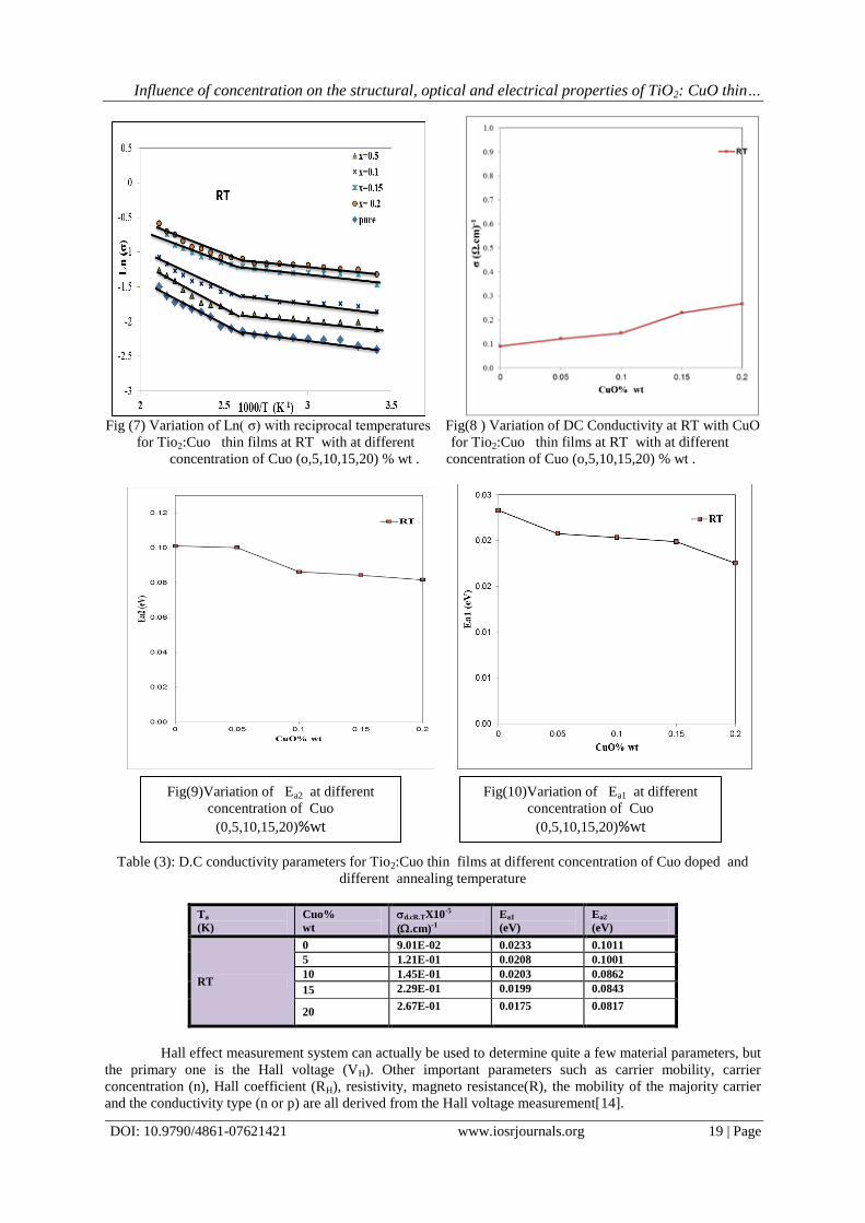
Figure (7) shows the variation of d.c. conductivity for pure and doped TiO2 films with differeny
concentration of CuO. There are two stages of mechanism d.c conductivity throughout the temperature range
(293-473K).The first activation energy (Ea1) occurs at higher temperature (373-473)K due to conduction of the
carrier excited into the extended states beyond the mobility edge and the second activation energy( Ea2) occurs
at low temperature (293-373)K due to the carriers transport to localized states near the valence and conduction
bands. From d.c measurement we can see that the conductivity increases with increasing of CuO content, as
show in Figure(8) and Figure (9and 10) shows the variation of (Ea1,Ea2) as a function of CuO content .Table
(3) demonstrates that as the film concentration increases leads to increase in the conductivity while decreases
in the values of activation energy(Ea1,Ea2). We conclude that the excess CuO will act as the donor impurities
may occupy shallow donor levels in the film, resulting in the reduction of conduction activation energy .Also
,This increasing in the conductivity can be attributed to the increase in the carrier concentration in the layers .
Influence of concentration on the structural, optical and electrical properties of TiO2: CuO thin…
DOI: 10.9790/4861-07621421 www.iosrjournals.org 19 | Page
Fig (7) Variation of Ln( σ) with reciprocal temperatures Fig(8 ) Variation of DC Conductivity at RT with CuO
for Tio2:Cuo thin films at RT with at different for Tio2:Cuo thin films at RT with at different
concentration of Cuo (o,5,10,15,20) % wt . concentration of Cuo (o,5,10,15,20) % wt .
Table (3): D.C conductivity parameters for Tio2:Cuo thin films at different concentration of Cuo doped and
different annealing temperature
Ta
(K)
Cuo%
wt
d.cR.TX10-5
(.cm)-1
Ea1
(eV)
Ea2
(eV)
RT
0 9.01E-02 0.0233 0.1011
5 1.21E-01 0.0208 0.1001
10 1.45E-01 0.0203 0.0862
15 2.29E-01 0.0199 0.0843
20 2.67E-01 0.0175 0.0817
Hall effect measurement system can actually be used to determine quite a few material parameters, but
the primary one is the Hall voltage (VH). Other important parameters such as carrier mobility, carrier
concentration (n), Hall coefficient (RH), resistivity, magneto resistance(R), the mobility of the majority carrier
and the conductivity type (n or p) are all derived from the Hall voltage measurement[14].
Fig(9)Variation of Ea2 at different
concentration of Cuo
(0,5,10,15,20)%wt
Fig(10)Variation of Ea1 at different
concentration of Cuo
(0,5,10,15,20)%wt

Influence of concentration on the structural, optical and electrical properties of TiO2: CuO thin…
DOI: 10.9790/4861-07621421 www.iosrjournals.org 20 | Page
The Hall coefficient (RH) is determined by measuring the Hall voltage generated by the Hall field across the
sample of thickness (t), given by[15]:
B
t
I
VR H
H . ……………………………………………………(2 )
where I : is the current in a passing through the sample, t: is the thickness of the film in cm and B :is
the magnetic field
Carriers concentration can be determined by using the relation[16]
H
HqR
1n
………………………………………..…. for electrons (3)
Hall's mobility (H) measured with (cm2/V.s) can be written in the form[17]
Hn.q
…………………………………………………...(4)
where q is the charge of electron.
From the Hall Effect measurements, the resistivity (ρ), charge carrier concentration (NH) and carrier
Hall mobility (μH) values were calculated and is given in table (3) and figure(10 and 11). The results obtained
from the Hall effect indicated that the pure doped TiO2 thin films with CuO have negative Hall coefficient (n-
type) conductivity i.e Hall voltage decreases with increasing of the current . It is seen from these figures that the carries concentration increases with increasing of CuO content
such behavior is expected as a result of the substitution doping of CuO creating one extra free carrier in the
process .As the doping level is increased, more dopant atoms occupy lattice sites of Ti atoms resulting in more
charge carriers. Thus, the conductivity increases with increasing of CuO content. In contrast with the Hall
mobility, it is decreased sharply with increasing of concentration of CuO The decreasing of mobility is come
from the inverse relation between μH and nH This is typical of many polycrystalline thin films and is due to
the existence of potential barriers in the grain boundaries.
Figurer(10)Variation of carrier concentration(nH) Figurer(11)Variation of mobility (μH )
with different concentration of CuO with different concentration of CuO
(0,5,10,15,20) % wt. (0,5,10,15,20) % wt
Tabel(3) Hall measurement of TiO2:CuO thin films prepared at different concentration of CuO .
Ta (K)
Cuo% ρ (Ω.cm)*10-6 nH
(cm-3)*1010 μH
(cm2 .V-1 .s-1) *103 RH *109
type
RT
0 1.496 0.115 5.956 5.601 n
5 1.660 0.2423 4.454 2.579 n
10 2.320 0.468 3.851 1.335 n
15 2.428 0.4792 2.839 1.304 n
20 3.431 0.5346 1.377 1.169 n

Influence of concentration on the structural, optical and electrical properties of TiO2: CuO thin…
DOI: 10.9790/4861-07621421 www.iosrjournals.org 21 | Page
IV. Conclusion Nanoparticles of TiO2:CuO were grown by PLD technique from the synthesize palate at different
concentration of CuO at RT. XRD results Increasing in dhkl and grain size with increasing of CuO content can
be attributed that Cu partially substituted for Ti in TiO2 structure. This work presents a simple and a general
strategy to improve the growth of TiO2 doped Cuo at different concentration of Cuo with a wide optical band
gap directly on glass substrates, providing an opportunity to integrate them in optoelectronic devices, e.g. for
UV light detection or solar cell applications. The electrical conductivity and Hall effect were measured for films
with average thickness (250) nm. The analysis of the d.c. conductivity There are two stages of d.c conductivity
mechanism throughout the temperature range (293-473K) decreases while conductivity increases with
concentration of Cuo . also from Hall Effect measurements show that all films have n- type charge carriers and
the concentration increases carriers concentration while the mobility decreases .
References [1] H. M. Smith and A. F. Turner, ―Vacuum Deposited Thin Films Using a Ruby Laser,‖ Appl. Opt. 4(1), 147 ,1965.
[2] R. Eason,Plused laser deposition of thin films, A JOHN WILEY & SONS, INC., PUBLICATION (2007).
[3] D. B. Chrisey and G. K. Hubler (editors), ―Pulsed Laser Deposition of Thin Films‖, John Wiley & Sons Inc., New York, 1994. [4] P. Boffetta, V. Gaborieau, L. Nadon, M-E Parent, E. Weiderpass, J. Siemiatycki, Exposure to titanium dioxide and risk of lung
cancer in a population-based study from Montreal , Scand J Work Environ Health 2001;27(4):227—232 [5] C. Garzella, E. Comini, E. Tempesti, C. Frigeri, and G. Sberveglieri, [TiO2 thin films by a novel sol-gel processing for gas sensor
applications], Sensors and Actuators B: Chemical 68 ,189-196,2000.
[6] K. R. Al-Rawi, S. Kh. Taha, The Effect of nano particles of TiO2-Al2O3 on the Mechanical properties of epoxy Hybrid
nanocomposites, Baghdad Science Journal Vol.12(3),2015. [7] Yoon K H, Choi W J and Kang D H. Photo electrochemical properties of copper oxide thin films coated on an n-Si substrate, Thin
Solid Films 372: 250,2000.
[8] Jayatissa,A. K. Guo, A. Jayasuriya, Fabrication of cuprous and cupric oxide thin films by heat treatment, 2009, Applied Surface Science 255, 9474–9479.
[9] Dhanasekaran,V. T. Mahalingam, V. Ganesan, SEM and AFM Studies of Dip-Coated CuO Nanofilms, MICROSCOPY
RESEARCH AND TECHNIQUE 76:58–65,2013. [10] P Balling1 and J Schou2 Femtosecond-laser ablation dynamics of dielectrics: basics and applications for thin films © 2013 IOP
Publishing Ltd
[11] X.S. Peng, A.C. Chen, Large-scale synthesis and characterization of TiO2-based nanostructures on Ti substrates, Adv. Funct. Mater. 16 ,1355–1362,2006.
[12] N. Tai Ly, T. Van Hoang, T. Hong Le Ngo1, et al. TiO2 nanocrystal incorporated with CuO and its optical propertiesAdv. Nat. Sci.:
Nanosci. Nanotechnol. 3,2012, 045009 (5pp) [13] G. Dagan, M. Tomkiewics, Titanium dioxide aerogels for photocatalytic decontamination of aquatic environments, J. Phys. Chem.
97 ,12651–12655,1993. [14] R. Green(Hall Effect Measurements in Materials Characterization) Senior Market Development Manager Keithley Instruments, Inc.
[15] D. A. Neamen, "Semiconductor Physics and Devices", University of New Mexico, printed by R. R. Donnlley & Sons company,
(1992). [16] C. R. Iordanescu, D. Tenciu, I. D. Feraru, A. Kiss, M. Bercu, D. Savastru, R. Notonier, and C. E. A. Grigorescu, Digest Journal of
Nanomaterials and Biostructures, 6 ,2011, 863.
[17] C. Kittel, John Introduction to Solid State Physics 5th edition, Wiley and Sons, 1976, Chapter 2.