innovation - cea serie leti... · which technological innovation ... 1000 transistor circuit...
TRANSCRIPT

www.cea.fr / www.leti-cea.fr
Extract from issue May 2017
of LetiInnovation
50years
The magazine of research and its applications

boxes, high-tech medical appliances and ever more in our day-to-day objects!
What markets are you currently targeting?We target changing markets, in which technological innovation may make the difference at French companies. This is the case of the Internet of Things (IoT) and 5G communication technologies as well as the car with its intelligent sensors, data fusion algorithms, GaN power components and secure hardware solutions. Or again, the connected healthcare market, in which we can draw advantage from sensor and data processing technologies for personalizing care. Finally, data centers and high-performance computing with an approach combining photonics, 3D integration and new calculation and memorization architectures.
data fusion and many others. This melting pot that is Leti is unique in the world. In conjunction with our partners, it allows us to develop a project’s entire value chain right up to pre-production stage. For example, in power electronics, our know-how extends from a single chip to the entire vehicle!Similarly, we do not satisfy ourselves with the status quo: we seek differentiating, industrializable solutions in conjunction with our partners. Each year, Leti launches between 5 and 6 start-up projects: the technologies industrialized by these companies are innovative gems for many markets. Aledia (LEDs), Wavelens (variable focus optical lenses on silicon) or Avalun (portable biological analyzer) are perhaps tomorrow’s global benchmarks! Today, we can say that there’s a little bit of Leti in all our cellphones,
How would you define Leti, the CEA Tech institute you direct since 2015?“Initiatives are indisciplined actions that have succeeded!” This statement of Michel Cordelle, Leti’s first director in 1967, clearly illustrates our story. At the time, a handful of electronics specialists working for CEA researchers insisted that electronics be given its own laboratory. They had fully understood that innovation is synonymous with change in relation to industry and employment. The framework was established. In 1972, Leti director Jacques Lacour identified MOS (Metal Oxide Semiconductor) technology in the USA. In 1977, he founded the EFCIS startup to produce this type of integrated circuit in France. This initiative, which later led to the founding of STMicroelectronics,
kick-started a real dynamic: skills in infrared detection prompting establishment of Sofradir, today’s international leader; accelerometers equipping our cellphones; FDSOI technology (see following article) revolutionizing microelectronics; tomorrow, 3D Coolcube™ integration technology.Leti research teams know how to make small, intelligent, communicating, safe, low energy consuming objects.
What accounts for these successes?In addition to this seminal pioneering spirit, our strength is that we concentrate and consolidate a wide range of technologies: CMOS, sensors, communication systems, packaging and 3D integration, power electronics, imagery, integrated circuits, specific architectures,
MARIE-NOELLE SEMERIA,Director of Leti, a CEA Tech institute
Jewels of innovation for multiple markets
© B
runo
Ra
ma
in
1967Leti founded, previously CEA Grenoble’s Electronics Department
19721000 transistor circuit produced (5 micron technology)
1979X-ray scanner technology transferred to Thomson CGR
Les défis du CEA May 2017 Les défis du CEA May 2017
02 50 Years of Leti Innovation
Moreover, just like CEA Tech institutes List and Liten with which we cooperate closely, we accompany both high-tech and conventional SMEs and companies in full mutation, thereby enabling them to differentiate and gain in competitiveness.
What will be Leti’s new R&D areas?I’ll quote six that are vehicles of change and take advantage of a multidisciplinary approach: artificial intelligence with its new neuromorphic and quantic calculation technologies; augmented and virtual reality implementing new imagery and screen concepts; development of new medical protocols through Leti’s medical system platform and Clinatech; complex, intelligent and safe cyber physical systems; cybersecurity from a physical attack standpoint; materials engineering, in which new functions originate.
How is innovation nourished? Innovation takes root in a cultural environment and its driving force is encountered in perpetual confrontation with the outside world because, to innovate, we must distinguish ourselves and understand what forms the value of this distinction: the 40% energy saving of FDSOI circuits and their compatibility with communication functions; the 10,000-fold gain in GaN screen brilliance; our capacity to control microelectronics techniques on 300 mm diameter wafers, etc.Grenoble’s cultural environment is fertile with Minatec, Giant, French
1 900 RESEARCHERS AND 250 THESIS AND POST-DOCTORAL STUDENTS
330 INDUSTRIAL PARTNERS
2 760 PATENTS INCLUDING 310 LODGED IN 2016
60 STARTUPS FORMED
Tech startups, the Minalogic hub, etc. We’re also active in innovation ecosystems, such as the Consumer Electronics Show in Las Vegas, which allow us to compare our innovations with others across the world. For 50 years, Leti’s research teams have known how to reinvent themselves by capitalizing on their knowledge and know-how and by recruiting new profiles to remain at the forefront. Cooperation with our academic partners is essential, as is the work of our thesis and post-doctoral students, who explore new avenues with us. This is vital, as are our equipment investment capacity forming the basis of our white room facilities. Interview by Aude Ganier
1991SOI Smart Cut™ patent granted
19852000 m2 of white rooms inaugurated by President of France
Les défis du CEA May 2017 Les défis du CEA May 2017
03 50 Years of Leti Innovation
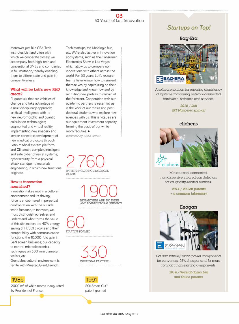
Startups on Top!Bag-Era
A software solution for ensuring consistency of systems comprising network-connected
hardware, software and services.
2016 / Leti IRT Nanoelec spin-off
elichens
Miniaturized, connected, non-dispersive infrared gas detectors
for air quality-related services.
2014 / 20 Leti patents + a common laboratory
Exagan
Gallium nitride/Silicon power components for converters: 25% cheaper and 3x more
compact than existing components.
2014 / Several dozen Leti and Soitec patents.
© C
oolm
an
© F
otol
ia©
Ma
rtia
l Gue
bey
/CEA

1994Aeronautical pressure sensor technology transferred to Thales
1996First uncooled infrared bolometer image
1992Gamma camera technology transferred to Sopha Medical Vision
Les défis du CEA May 2017 Les défis du CEA May 2017
04 50 Years of Leti Innovation
Iconic FDSOIFDSOI technology seemed to foretoken a major change
in the chip industry almost 40 years ago at Leti. A few years later, this view was supplemented by the
conviction of a handful of engineers. Then came the gamble taken by a few manufacturers... A revolutionary
patent… Establishment of a full technological and industrial ecosystem… International partnerships…
Today, FDSOI technology is integrated into millions of consoles and smartphones and it’s now becoming a
standard across the nomadic electronics, automotive engineering and the Internet of Things sectors.
by Mathieu Grousson
I n real terms, Fully Depleted Silicon on Insulator is a tech-nology involving the small-est calculation unit in every processor: the transistor. The
driving idea was to fashion transis-tors in an ultra-thin silicon film/wafer on an insulating silicon-oxide layer, rather than in a block of solid sili-con. This presence of oxygen ions within the silicon strengthens the
electronics’ resistance to radiation; this is why Leti focused on imple-menting FDSOI for the CEA’s mil-itary applications beginning in the 1980s. Moreover, thin-film-based components offer advantageous
performance characteristics: They are intrinsically immunized against current leakage when placed on an insulating layer. However, wafer qual-ity was not up to this in the technolo-gy’s early years and, more important, solid silicon was achieving wonders in the microelectronics industry. For example, according to Moore’s Law, voiced by a co-founder Intel in 1965, transistor surface area was halving every two years!
Ultrathin silicon or solid silicon? Leti’s SmartCutTM processIn 1991, this situation led to Leti’s Michel Bruel proposing a revolu-tionary process for cutting out and bonding, at the atomic level, ultra-thin silicon films oxidized on the surface: the SmartCut™ process. Implemented today by Soitec, which Leti launched in 1992, this process produces very high quality layers of silicon and silicon oxide at controlled thicknesses between a
few nanometers and a few microns, bonded to a silicon wafer. “Furthermore, SmartCut™ is com-patible with standard microelec-tronics standards, allowing rapid production of very high qual-ity wafers,” explains Leti engi-neer Olivier Faynot. “This is the real starting point for thin-film electronics.”Leti and Thomson joined forces to establish an SOI subsidiary for military applications. Thereafter, from the early 2000s onward, AMD and IBM have produced SOI microprocessors especially for computer, smart phone, tablet and video-game manufacturers, for which the excellent current-leak-age characteristics of thin-film transistors provide a favorable trade off between processing speed and energy consumption. But in the early years of SOI tech-nology, “All that remained highly confidential, most often at the R&D stage conducted at Leti,” recalls Leti researcher François Andrieu. It’s a fact that this tech-nology was not especially popular in the small world of microelec-tronics. The specialist recalls that, “Technology bricks were clearly missing.” How could one effec-tively challenge the conventional, solid silicon-based MOS technol-ogies, for which the clean rooms of the founding manufacturers had been designed? “Up to a certain point, there was an insufficient gain in performance for even our tra-ditional partners to take the leap into large-scale production of SOI devices,” Faynot admits.
This is the real starting point
for thin-film electronics.
Olivier Faynot, Leti engineer
1996First uncooled infrared bolometer image
1997First biochip circuit in cooperation with CisBio
2000Delivery of RMN magnetic resonance magnetometer flight models for CHAMP satellite
Les défis du CEA May 2017 Les défis du CEA May 2017
05 50 Years of Leti Innovation
Intel’s FinFET and Leti’s FDSOI revolutionsA bridge was crossed in the mid-2000s, when transistor size decreased to a few tens of nano-meters. The specialists started to observe significant current leak-age at the transistor grid. The con-sequence was that the electrical characteristics of these components started to deviate dangerously, mak-ing their control increasingly diffi-cult at the industrial level. In simple terms, if compliance with Moore’s Law was to continue, the microelec-tronics universe would need to start a revolution by inventing new tran-sistor architectures. In 2011, Intel proposed FinFET tech-nology, a true paradigm change in microelectronics. In a traditional transistor, the electrical charges cir-culate in a planar channel deposited on a wafer; conversely, in a FinFET transistor, this channel comprises a silicon fin a few nanometers thick, surrounded by the transistor grid, thereby immunizing it against leaks. Success was immediate since this type of transistor offered very high performance characteristics in terms of speed. Was there still room for an alternative? Faynot explains: “With regard to thin-film-electronics performance, improved wafer quality and the ever-better reproducibility of our results, we replied: yes”. Moreover, with its 3D architecture, the FinFET is difficult to build, while the “con-ventional” planar structure of FDSOI makes fabrication easier. Above all, the promoters of FDSOI knew they had a major advantage up their
sleeve, a property that only thin-film transistors have: the so-called “rear face” electrical polarization of the insulating layer beneath the sil-icon film makes it possible to mod-ulate the processing speed/energy consumption tradeoff as required. This means the circuit’s energy consumption can be most finely
adjusted for the operations to be performed. “This flexibility is clearly the spear-head of FDSOI”, notes Andrieu. Still, confronted by Intel’s firepower, Leti’s microelectronics experts and their partners appeared very much alone in believing in FDSOI’s chances. “At conferences, we were told that we were on the wrong track! But we had an insight!” Faynot recalls.
Foundation stones of an industry: from the UTSOI model to the Xiaomi smart watchIt remained to materialize FDSOI physically! Where and how to pro-duce thin films in industrial quan-tities? Would suitable production performance be achieved? What degree of reliability? In short, there was no other solution than
At conferences, we were told that we were on the wrong track! But we had an insight! Olivier Faynot, Leti engineer
Startups on Top!Fluoptics
Fluobeam® imaging system and fluorescent tracers for guiding
surgery integrated into cheap, portable systems.
2009 / A dozen Leti patents and annual cooperation contracts
Illumina
100 cm2, 50 gr chip laboratory for analyzing 300 nl and larger droplets and DNA preparation operations for external
sequencing stages.
2014 / Common patent applications after acquiring Advanced Liquid Logic
Iprasense
Lensless imagery technology that enhances tenfold the visual field
compared with a microscope and video capture solutions for monitoring growth
of cell cultures without marking.
2013 / 10 Leti patents + a common laboratory.
© F
otol
ia©
iSto
ck

Higher speed/energy consumption ratio
The FDSOI transistor
PRINCIPLELeti-designed FDSOI technology is based around adding a film of insulating silicon oxide to conventional transistor architecture. This innovation ensures efficient, energy saving transistor operation, while responding to the challenge of miniaturization.
The quest for the infinitely smallThere’s a transistor at the heart of every micro-processor. It is composed of three elements sup-ported by a doped, generally solid silicon wafer: the grid (or gate), the source and the sink.When an electrical voltage is applied to the grid, an electron current flows between the source and the sink via the silicon. Thus, by applying or not applying a voltage, a transistor works like
a switch in an open or closed position, thereby producing the 0 and 1 composing binary data. To increase speed and lower energy consump-tion of transistors, the microelectronics indus-try has continually reduced their size down to around 20 nanometers, at which current leaks appear, causing a deterioration in transistor performance.
Grid
Channel Channel
Doped silicon wafer
Current leaks Undoped silicon wafer
Double grid
Second grid for “rear face polarization”
Insulating silicon oxide film
Source
Drain
Bulk transistor FDSOI transistor
28 mm 24 mm
Les défis du CEA May 2017 Les défis du CEA May 2017
06 50 Years of Leti Innovation
Credit: Mathieu Grousson, Aude Ganier / Fabrice Mathé (Computer graphics),in collaboration with Olivier Faynot and François Andrieu of Leti, CEA Tech Institute
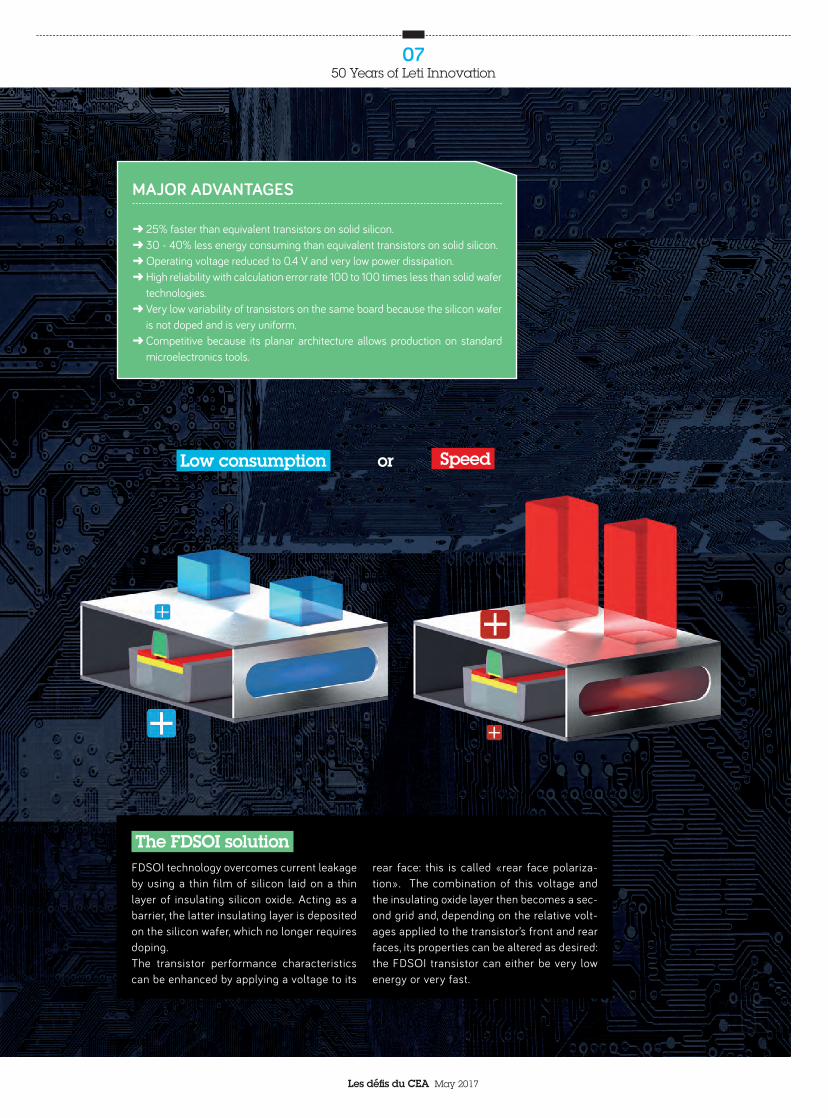
➜ 25% faster than equivalent transistors on solid silicon.➜ 30 - 40% less energy consuming than equivalent transistors on solid silicon.➜ Operating voltage reduced to 0.4 V and very low power dissipation.➜ High reliability with calculation error rate 100 to 100 times less than solid wafer
technologies.➜ Very low variability of transistors on the same board because the silicon wafer
is not doped and is very uniform.➜ Competitive because its planar architecture allows production on standard
microelectronics tools.
MAJOR ADVANTAGES
The FDSOI solutionFDSOI technology overcomes current leakage by using a thin film of silicon laid on a thin layer of insulating silicon oxide. Acting as a barrier, the latter insulating layer is deposited on the silicon wafer, which no longer requires doping. The transistor performance characteristics can be enhanced by applying a voltage to its
rear face: this is called «rear face polariza-tion». The combination of this voltage and the insulating oxide layer then becomes a sec-ond grid and, depending on the relative volt-ages applied to the transistor’s front and rear faces, its properties can be altered as desired: the FDSOI transistor can either be very low energy or very fast.
Low consumption Speedor
Les défis du CEA May 2017 Les défis du CEA May 2017
07 50 Years of Leti Innovation
© G
lob
alF
ound
erie
s
2001Ideas Laboratory® established
2002First 200 mm MEMS wafer (accelerometer for Freescale Semiconductor)
2004Spintronic technology (CEA/CNRS/UJF) transferred to startup Crocus Technology
Les défis du CEA May 2017 Les défis du CEA May 2017
08 50 Years of Leti Innovation
to build the entire technologi-cal and industrial environment for designing and manufacturing FDSOI components on a large scale. Leti and STMicroelectronics worked hand in hand to achieve this. The manufacturer, which wanted to develop its business in the “low-power” direction (low consumption applications such as telephony), decided to con-vert its 28-nm node platform to FDSOI. The goal? Components, whose speed-related performance characteristics can be boosted as required and when necessary (e.g. during a telephone call), but
which are also capable of going on standby or sleeping between two peaks of activity. Ten to 15 Leti engineers were therefore dispatched to ST’s site in Crolles, where 300 employees were developing the platform, sup-ported by 50 more Leti employ-ees in Grenoble. “A technological change like that and the leap into the dark that accompanies it only happen once every ten years or so in the life of a manufacturer,” Andrieu notes. In concrete terms, the Leti and ST teams developed all the components (more than 20) required for producing an FDSOI-based circuit and, in particular, the voltage generators located on the components for ensur-ing “rear-face polarization”. They redesigned all the logic gates and cells obtained by connecting dif-ferent transistors, in order to adapt them to a broad operating range. Furthermore, they imagined global control methods for dynamically
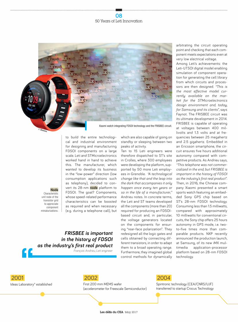
arbitrating the circuit operating point and checking that each com-ponent meets expectations even at very low electrical voltage. Among Leti’s achievements: the Leti-UTSOI digital model enabling simulation of component opera-tion for generating the cell library from which circuits and proces-sors are then designed. “This is the most effective model cur-rently available on the mar-ket for the STMicroelectronics design environment and, today, for Samsung and its clients”, says Faynot. The FRISBEE circuit was its ultimate development in 2014. FRISBEE is capable of operating at voltages between 400 mil-livolts and 1.3 volts and at fre-quencies between 25 megahertz and 2.5 gigahertz. Embedded in an Ericsson smartphone, the cir-cuit ensures five hours additional autonomy compared with com-petitive products. As Andrieu says, “This telephone was not commer-cialized in the end, but FRISBEE is important in the history of FDSOI as the industry’s first real product”. Then, in 2016, the Chinese com-pany Xiaomi presented a smart sports watch featuring an embed-ded Sony GPS chip based on ST’s 28-nm FDSOI technology. Consuming less than 1.5 milliwatts, compared with approximately 10 milliwatts for conventional cir-cuits, the Sony chip offers 25 hours autonomy in GPS mode, i.e. two-to-five times more than com-parable products. NXP recently announced the production launch, at Samsung, of its new iMX mul-timedia application-processor platform based on 28-nm FDSOI technology.
FRISBEE is important in the history of FDSOI
as the industry’s first real product François Andrieu, Leti engineer
NodeCharacteristic
unit node of the transistor grid to appreciate
component miniaturizations.
Xiaomi watch integrating FDSOI technology and the FRISBEE circuit.© Xiaomi

2007Alliance with Caltech (California Institute of Technology) on NEMS
20093-party alliance with IBM and STMicroelectronics (FDSOI technology)
Les défis du CEA May 2017 Les défis du CEA May 2017
09 50 Years of Leti Innovation
Ever-smaller nodes for ever-larger marketsThe markets targeted by FDSOI tech-nology are clearly those embracing mobile electronics: smartphones, tab-lets… objects for which the energy consumption issue is now crucial. “For these applications, FinFET processors, while performing better strictly from the processing speed standpoint, face serious challenges on the issue of energy consumption,” Faynot says. Taking this a step further, FDSOI will probably become required in con-nected cars, in which processors will be required to combine data pro-cessing power with low energy con-sumption. Another targeted sector is the Internet of Things, an emerging market in which objects will be “con-scious” of their environment in rela-tion to exchanging information and performing functions in response to that information. The healthcare mar-ket also represents a vast outlet for FDSOI technology. The microelec-tronics giants were absolutely right: in its 28-nm version, FDSOI is now firmly established in the STMicroelectronics and Samsung catalogues. Yet, this is only a start! In cooperation with ST, Leti’s idea is to develop new functionalities for the 28-nm node: radiofrequency, embed-ded memory for chips, microcontrol-lers, etc. “The 28-nm node will have a long service life since it is very cost competitive and will meet the require-ments of all the applications of the manufacturer’s customers,” predicts Andrieu. In parallel, this also involves demonstrating that FDSOI is compati-ble with transistor miniaturization. Leti, ST and IBM therefore started to focus on the 22-nm node from the end of the 2000s onwards. The outcome was that the technology was transferred to
Iit is completely possible that this technology will end up capturing significant market share.François Andrieu, Leti engineer
GLOBALFOUNDRIES, the second-larg-est foundry company worldwide, in 2016. Leti’s Grenoble lab dispatched a dozen personnel to the company’s Dresden site to set up the correspond-ing platform. Moreover, last September, GLOBALFOUNDRIES announced an extension of its FDSOI platform to the 12-nm node. Its level of integration is unmatched. The objective is to produce the first circuits in Dresden in 2019. Is it enough to make FDSOI the new king of microelectronics technology? “It’s not a question of overturning FinFET,” Andrieu explains. “We’re an alternative because even though Intel’s technology remains unbeatable for high-performance computing appli-cations, FDSOI is the solution for opti-
mizing the processing speed/energy consumption tradeoff on demand. FDSOI is in the challenger’s position with respect to FinFET. But, from the market-development standpoint, it is completely possible that this technol-ogy will end up capturing significant market share.” As proof, GLOBALFOUNDRIES has not opted for one technology to the detri-ment of the other, but now offers both to its customers. In other words, FDSOI now appears to be essential and this is more than a turn of events. It is the long-term outlook!
Startups on Top!iskn
Solutions for enriching and facilitating interaction of physical objects
and the digital world using a learning tablet, for example.
2014 / 11 Leti patents and multiannual cooperation contract
MirSense
Quantic cascade, solid-state laser technology and unique silicon-based,
medium infrared system for rapid, reliable identification of organic molecules.
2015 / Leti patents
Morphosense
Solution for processing signals and merging data that are transmitted
by MEMS sensors to monitor deformations and vibrations in critical systems.
2016 / Leti patents
© P
ierr
e Ja
yet/
CEA
© P
ierr
e Ja
yet/
CEA
© F
otol
ia
2013First clinical test at Clinatech
2010First 3D stacked transistors: Coolcube™
2011Construction of 240 m long white room link between Leti and Minatec
Les défis du CEA May 2017 Les défis du CEA May 2017
10 50 Years of Leti Innovation
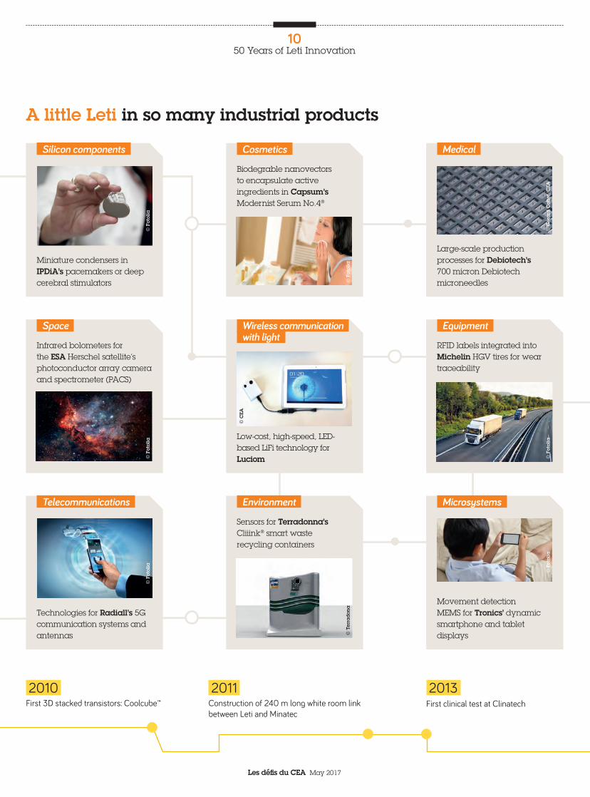
Silicon components
Miniature condensers in IPDiA’s pacemakers or deep cerebral stimulators
Medical
Large-scale production processes for Debiotech’s 700 micron Debiotech microneedles
Telecommunications
Technologies for Radiall’s 5G communication systems and antennas
Microsystems
Movement detection MEMS for Tronics’ dynamic smartphone and tablet displays
Wireless communication with light
Low-cost, high-speed, LED-based LiFi technology for Luciom
Space
Infrared bolometers for the ESA Herschel satellite’s photoconductor array camera and spectrometer (PACS)
Equipment
RFID labels integrated into Michelin HGV tires for wear traceability
Cosmetics
Biodegrable nanovectors to encapsulate active ingredients in Capsum’s Modernist Serum No.4®
Environment
Sensors for Terradonna’s Cliiink® smart waste recycling containers
A little Leti in so many industrial products©
Fot
olia
© G
éra
rd C
otte
t/C
EA
© F
otol
ia
© F
otol
ia©
Fot
olia
© C
EA
© T
erra
don
a
© F
otol
ia©
Fot
olia

2016• Joins Stanford SystemX Alliance• Internet of Things cooperation
agreement with Intel
2013First clinical test at Clinatech
2014First Earth-Moon high-speed laser communication lin cooperation with ESA and NASA
2015First STT-type MRAM in cooperation with Spintec
Les défis du CEA May 2017 Les défis du CEA May 2017
11 50 Years of Leti Innovation
Arts-Sciences
Fresque #1, Digital “Aura”
When a microphone is too near to a loudspeaker, we’re subjected to an ear-splitting whistle: the dreaded Larsen effect! Similarly, image pixels go hysterical when a camera is brought close to a screen. Fresque#1 is this type of Larsen effect “video”, a visual that Lionel Palun “painted” with the artist’s brush of today: networks, real-time computation and data flow. “I intervene between the camera and the screen by playing on the physical characteristics of image acquisition and by adding my own partition in the form of masks, grids and other filters. Above all, I invite the spectator to intrude upon this purely digital relationship by capturing his or her silhouette or face, furtively revealing a digital aura”, explains the artist.
Illusion of network ubiquityFresque #1 plays out the illusion of ubiquity offered by networks. It gives resonance to two distant geographical and cultural spaces: in November 2017, the work will be
simultaneously exhibited in two public spaces in Japan and France. “These two locations will be interconnected through a Larsen effect video, which reflects ad infinitum the images of personal captures in these distant places. Lionel’s visual partition, derived from real-time data, will ensure a sensitive restitution of these places and persons”, explains William Guicquero, a Leti researcher involved in producing the work of art.Fresque#1 falls within the H2020 “Festival” research program, which brings together French, European and Japanese partners around coordinator Leti. Festival is dedicated to the Internet of Things and proposes new services capable of exploiting heterogeneous data. To achieve this, the researchers are developing an Internet platform, which makes available data collected in connected urban spaces (in partner cities), experimentation infrastructures and open data.The work is backed by Arts-Sciences, a workshop founded in 2007 by the Ideas Laboratory, a Leti creation, in conjunction with Hexagone Scène Nationale Arts Sciences – Meylan. Once again, Leti has been a pioneer in this area by initiating this first research laboratory common to artists and scientists in France.
Fresque#1 on YouTubelionelpalun.com
www.fesivalproject.eu/www.atelier-arts-sciences.eu/
www
© F
resq
ue#1
© F
resq
ue#1
© A
ntoi
ne C
onja
rd
While Larsen effects can hurt our ears, those depicted in
Fresque#1 captivate the eye and unleash the imagination
to better query the digital data flows that now shape our
day-to-day. by Aude Ganier

Publisher French alternative energies and atomic energy commission, R. C. S. Paris B77568019 | Publication director Xavier Clément | Editor in chief Aude Ganier | Contributor Mathieu Grousson | Editorial Board Camille Giroud and Isabelle Dellis | Design and layout www.grouperougevif.fr | N°ISSN 1163-619X | All rights reserved.
of LetiInnovation
50