innovations for high performance microelectronics leibniz
TRANSCRIPT

IHPIm Technologiepark 2515236 Frankfurt (Oder)
Germany
IHP Im Technologiepark 25 15236 Frankfurt (Oder) Germany www.ihp-microelectronics.com © 2009 - All rights
reserved
IHPInnovations for High Performance Microelectronics
Leibniz-Institut für innovative Mikroelektronik
Wolfgang Kissinger
April 03, 2009
IHP Im Technologiepark 25 15236 Frankfurt (Oder) Germany www.ihp-microelectronics.com © 2009 - All rights
reserved
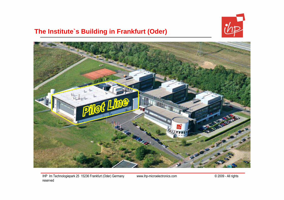
The Institute`s Building in Frankfurt (Oder)
IHP Im Technologiepark 25 15236 Frankfurt (Oder) Germany www.ihp-microelectronics.com © 2009 - All rights
reserved
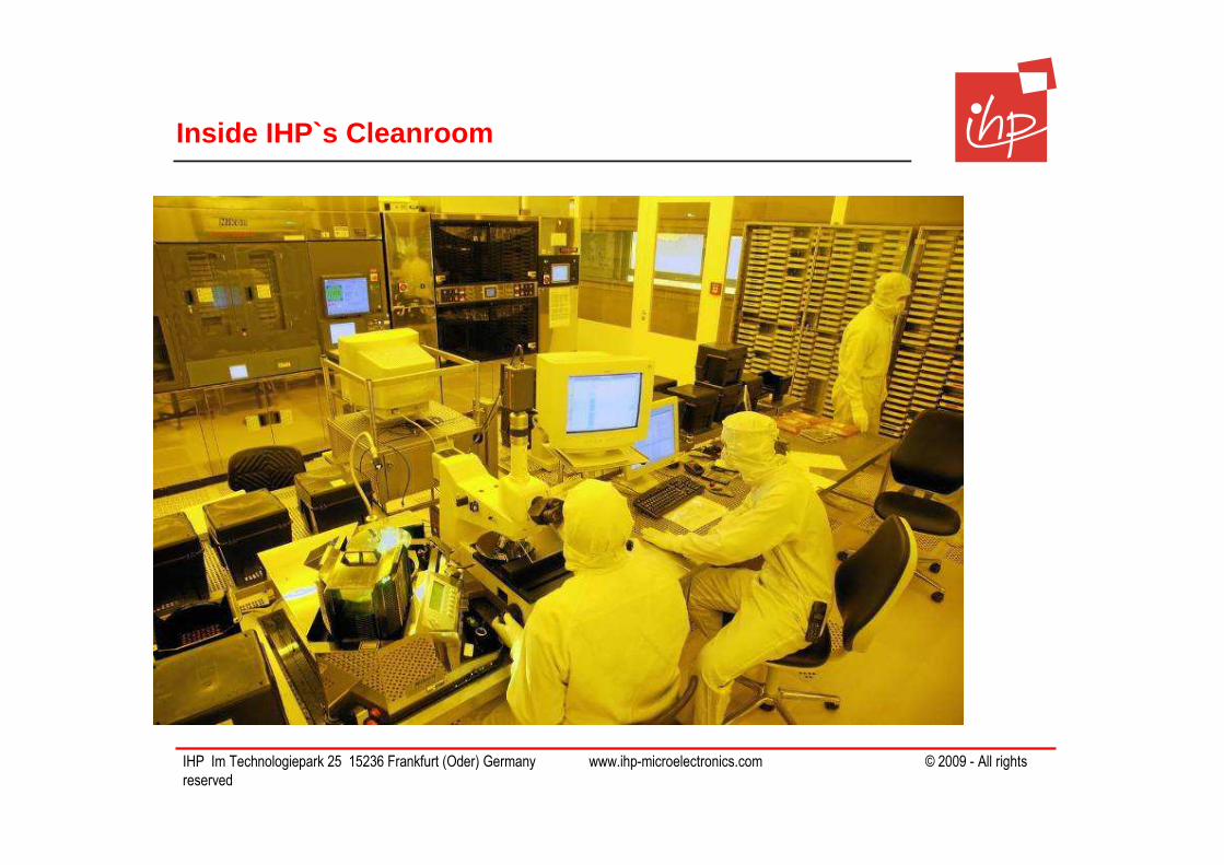
Inside IHP`s Cleanroom

IHP Im Technologiepark 25 15236 Frankfurt (Oder) Germany www.ihp-microelectronics.com © 2009 - All rights
reserved
IHP in a Nutshell
• Institute of the Leibniz AssociationOwned by the State of Brandenburg; limited liability com pany since 1991
• Founded in 1983 Long term experience in silicon technology & materials research
• Silicon based high-frequency technologies, circuits an d systemsfor the wireless and broadband communication
• 250 people from 20 countriesAmong them 110 scientists
• Certified DIN EN ISO 9001:2000
• Funding 2008Institutional funds: € 16 millionThird-party funds: € 12.3 millionERDF funds: € 7.4 million

IHP Im Technologiepark 25 15236 Frankfurt (Oder) Germany www.ihp-microelectronics.com © 2009 - All rights
reserved
The Organisation Chart November 2008
IHP – Organization Chart
Supervisory Board Chair: K. Pistor
Deputy Chair: RD Dr. V. Dietz
Directors Scientific Administra tive Prof. W. Mehr M. Stöcker
Scientific Advisory Council
Chair: Prof. H. Grimmeiss
Scientific & Techn ical Council
Chair: Dr. Ch. Wenger
System Design Head: Prof. R. Kraemer
Circuit Design Head: Dr. Ch. Scheytt
Materials Research Acting Head: Prof. H.-J. Müssig
Technology Head: Prof. B. Tillack
Marketing & Strategy Head: Dr. W. Kissinger
Finance & Accounting Head: U. George
Personnel Head: Dr. Ch. Quick
Works Council Chair: S. Jätzlau
Scientific & Technical Service
Head: L. Hartmann
Quality Management Representative
G. Zaumseil
Joint Lab IHP /BTU Head: Prof. M. Kittler
Shareholder MdF
Finan cial Adv isory Council
Chair: V. Düppe

IHP Im Technologiepark 25 15236 Frankfurt (Oder) Germany www.ihp-microelectronics.com © 2009 - All rights
reserved
I H P
System Design
Circuit Design
Technology
Materials Research
Pilot Line
Basic
Research
Settlements &Spin-Offs
JointProjects
Contract Research
Academia Industry
Joint Labs
MPW &Prototyping
JointResearchProjects
Education
IHP bridging the gap between Academia & Industry
IHP Im Technologiepark 25 15236 Frankfurt (Oder) Germany www.ihp-microelectronics.com © 2009 - All rights
reserved
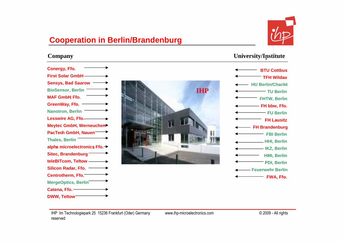
Cooperation in Berlin/Brandenburg
Company University/Institute-
Conergy, Ffo.
First Solar GmbH
Sensys, Bad Saarow
BioSensor, Berlin
MAF GmbH, Ffo.
GreenWay, Ffo.
Nanotron, Berlin
Lesswire AG, Ffo.
Meytec GmbH, Werneuchen
PacTech GmbH, Nauen
Thales, Berlin
alpha microelectronics, Ffo.
Sitec, Brandenburg
teleBITcom, Teltow
Silicon Radar, Ffo.
Centrotherm, Ffo.
MergeOptics, Berlin
Catena, Ffo.
DWW, Teltow
IHP
BTU Cottbus
TFH Wildau
HU Berlin/Charité
TU Berlin
FHTW, Berlin
FH bbw, Ffo.
FU Berlin
FH Lausitz
FH Brandenburg
FBI Berlin
HHI, Berlin
IKZ, Berlin
HMI, Berlin
PDI, Berlin
Feuerwehr Berlin
FWA, Ffo.
IHP

IHP Im Technologiepark 25 15236 Frankfurt (Oder) Germany www.ihp-microelectronics.com © 2009 - All rights
reserved
0,0
2,0
4,0
6,0
8,0
10,0
12,0
14,0
1 2 3 4 5 6 7
Mio
. €
Development of Third-party Funding
2002 2003* 2004 2005 2006 2007 2008*Adjusted for CST 180 FTE 216 FTE ~240 FTE
3,23,3
4,8
5,9
7,6
8,1
12,3
MPW MPW
Ind.
Ind.
Ind.
Ind.
Ind.

IHP Im Technologiepark 25 15236 Frankfurt (Oder) Germany www.ihp-microelectronics.com © 2009 - All rights
reserved
IHP`s Departments and Research Programs
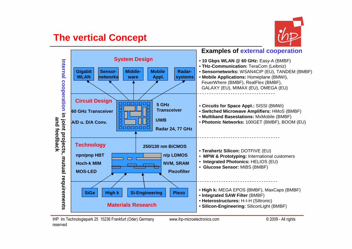
• System Design - Wireless Systems and Applications High-performance systems (WLAN 1…100 Gbit/s) Low power wireless sensor networks and applications
• Circuit Design - RF Circuit Designmm-wave circuits at 5…200 GHz; Broadband mixed sign al circuits, Analog/Digital-converters up to 30 GSps, UWB circui ts Radiation hard circuits for aerospace
• Technology - Extension of standard CMOS technologies0.25/0.13 µm SiGe BiCMOS, 300 GHz HBTsAdditional functionalitiesInternational MPW- und Prototyping Service
• Materials Research - New materials for microelectronics New high-k materials; New concepts & materials for THz devices; Integrated silicon LEDs for optical on-chip data tra nsmission; Efficiency engineering for solar cells
IHP Im Technologiepark 25 15236 Frankfurt (Oder) Germany www.ihp-microelectronics.com © 2009 - All rights
reserved
• 10 Gbps WLAN @ 60 GHz: Easy-A (BMBF)• THz-Communication: TeraCom (Leibniz)• Sensornetworks: WSAN4CIP (EU), TANDEM (BMBF)• Mobile Applications: Homeplane (BMWi), FeuerWhere (BMBF), RealFlex (BMBF),GALAXY (EU), MIMAX (EU), OMEGA (EU)
• High k: MEGA EPOS (BMBF), MaxCaps (BMBF)• Integrated SAW Filter (BMBF)• Heterostructures: H-I-H (Siltronic)• Silicon-Engineering: SiliconLight (BMBF)
• Terahertz Silicon: DOTFIVE (EU)• MPW & Prototyping: International customers• Integrated Photonics: HELIOS (EU)• Glucose Sensor: MIBS (BMBF)
• Circuits for Space Appl.: SISSI (BMWi)• Switched Microwave Amplifiers: HMoS (BMBF)• Multiband Basestations: MxMobile (BMBF)• Photonic Networks: 100GET (BMBF), BOOM (EU)
Examples of external cooperation
Internalcooperationin jointprojects, m
utualrequirements
and feedback
SiGe High k Si-Engineering Piezo
GigabitWLAN
Middle-ware
MobileAppl.
Radar-systems
Sensor-networks
System Design
Circuit Design
Technology
Materials Research
UWB
Radar 24, 77 GHz
60 GHz Transceiver
A/D u. D/A Conv.
npn/pnp HBT
Hoch-k MIM
MOS-LED
n/p LDMOS
NVM, SRAM
Piezofilter
5 GHz Transceiver
250/130 nm BiCMOS
The vertical Concept
IHP Im Technologiepark 25 15236 Frankfurt (Oder) Germany www.ihp-microelectronics.com © 2009 - All rights
reserved
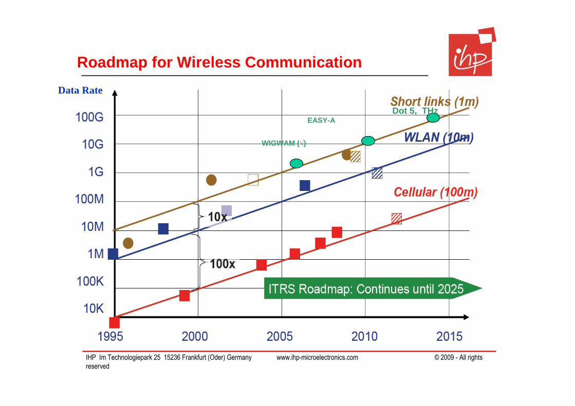
Roadmap for Wireless Communication
WIGWAM (√)
EASY-ADot 5, THz
Data Rate
IHP Im Technologiepark 25 15236 Frankfurt (Oder) Germany www.ihp-microelectronics.com © 2009 - All rights
reserved
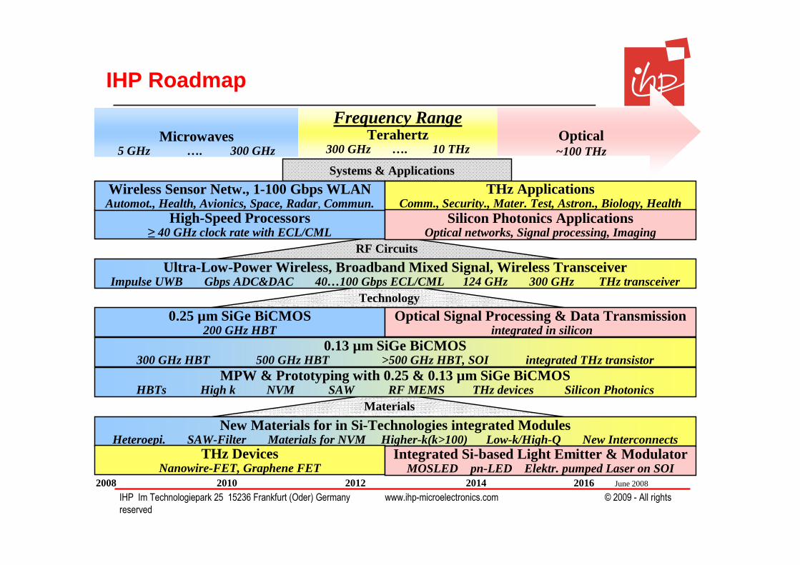
Technology
Materials
0.25 µm SiGe BiCMOS200 GHz HBT
Ultra-Low-Power Wireless, Broadband Mixed Signal, Wireless TransceiverImpulse UWB Gbps ADC&DAC 40…100 Gbps ECL/CML 124 GHz 300 GHz THz transceiver
0.13 µm SiGe BiCMOS300 GHz HBT 500 GHz HBT >500 GHz HBT, SOI integrated THz transistor
New Materials for in Si-Technologies integrated ModulesHeteroepi. SAW-Filter Materials for NVM Higher-k(k>100) Low-k/High-Q New Interconnects
THz DevicesNanowire-FET, Graphene FET
MPW & Prototyping with 0.25 & 0.13 µm SiGe BiCMOSHBTs High k NVM SAW RF MEMS THz devices Silicon Photonics
2008 2010 2012 2014 2016 June 2008
Integrated Si-based Light Emitter & ModulatorMOSLED pn-LED Elektr. pumped Laser on SOI
Optical Signal Processing & Data Transmissionintegrated in silicon
Microwaves5 GHz …. 300 GHz
Frequency RangeTerahertz
300 GHz …. 10 THz
Systems & Applications
High-Speed Processors≥ 40 GHz clock rate with ECL/CML
Wireless Sensor Netw., 1-100 Gbps WLAN Automot., Health, Avionics, Space, Radar, Commun.
THz ApplicationsComm., Security., Mater. Test, Astron., Biology, Health
Silicon Photonics ApplicationsOptical networks, Signal processing, Imaging
Optical~100 THz
IHP Roadmap
RF Circuits
IHP Im Technologiepark 25 15236 Frankfurt (Oder) Germany www.ihp-microelectronics.com © 2009 - All rights
reserved
Thank you for your Attention !

IHP Im Technologiepark 25 15236 Frankfurt (Oder) Germany www.ihp-microelectronics.com © 2009 - All rights
reserved
Systems and RF Circuits

IHP Im Technologiepark 25 15236 Frankfurt (Oder) Germany www.ihp-microelectronics.com © 2009 - All rights
reserved
IHP - 60 GHz Demonstration
60 GHz TX60 GHz RX
5 GHz TX
5 GHz RX
IHP Im Technologiepark 25 15236 Frankfurt (Oder) Germany www.ihp-microelectronics.com © 2009 - All rights
reserved
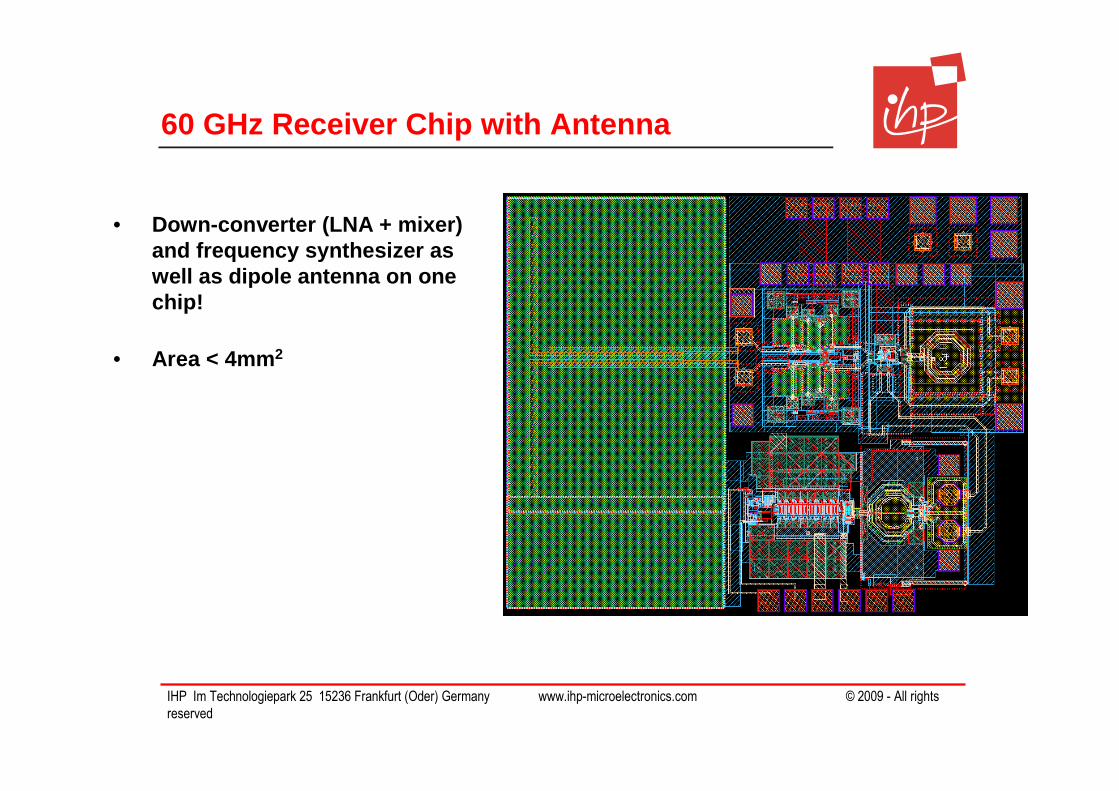
60 GHz Receiver Chip with Antenna
• Down-converter (LNA + mixer) and frequency synthesizer as well as dipole antenna on one chip!
• Area < 4mm 2
IHP Im Technologiepark 25 15236 Frankfurt (Oder) Germany www.ihp-microelectronics.com © 2009 - All rights
reserved
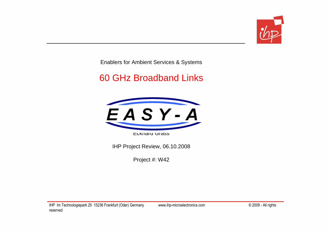
Enablers for Ambient Services & Systems
60 GHz Broadband Links
- Project Outline –
Eckhard Grass
IHP Project Review, 06.10.2008
Project #: W42
IHP Im Technologiepark 25 15236 Frankfurt (Oder) Germany www.ihp-microelectronics.com © 2009 - All rights
reserved
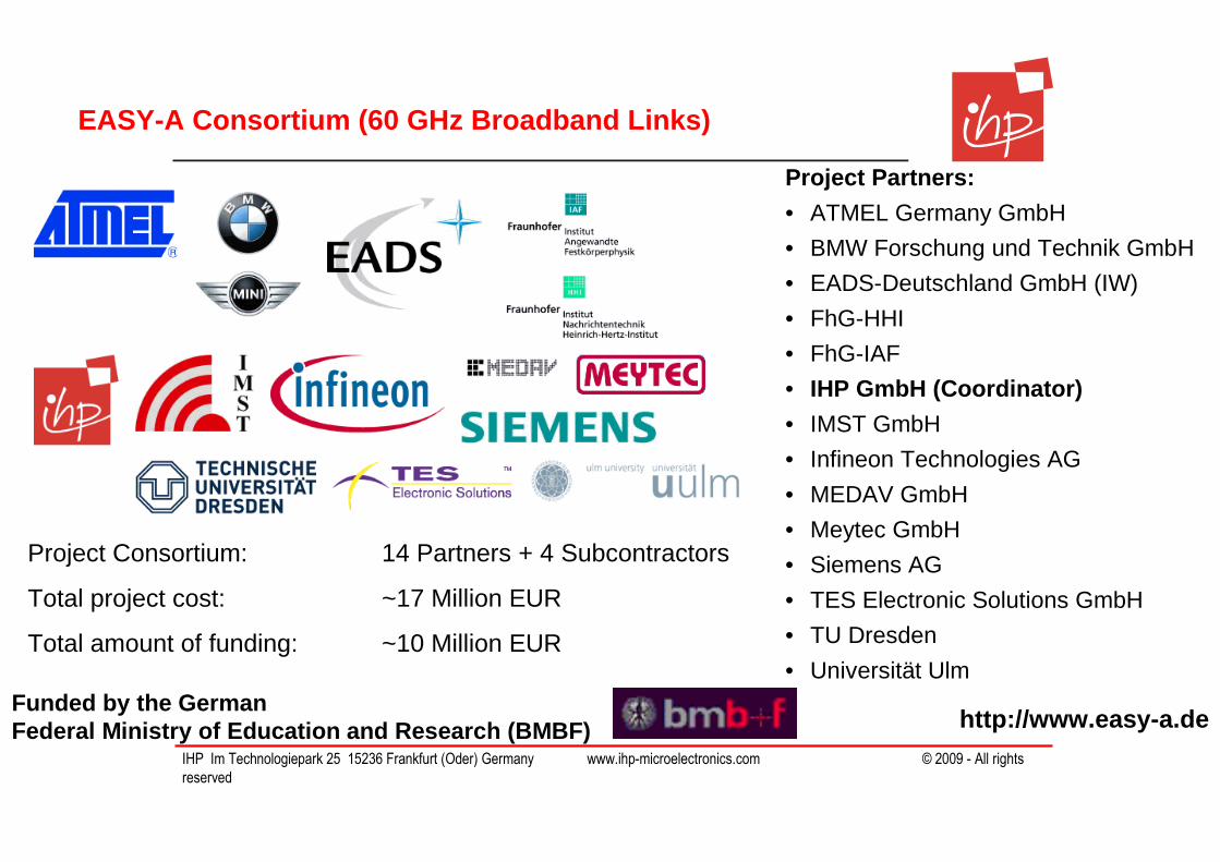
EASY-A Consortium (60 GHz Broadband Links)
Funded by the German Federal Ministry of Education and Research (BMBF) http://www.easy-a.de
Project Partners:
• ATMEL Germany GmbH
• BMW Forschung und Technik GmbH
• EADS-Deutschland GmbH (IW)
• FhG-HHI
• FhG-IAF
• IHP GmbH (Coordinator)
• IMST GmbH
• Infineon Technologies AG
• MEDAV GmbH
• Meytec GmbH
• Siemens AG
• TES Electronic Solutions GmbH
• TU Dresden
• Universität Ulm
Project Consortium: 14 Partners + 4 Subcontractors
Total project cost: ~17 Million EUR
Total amount of funding: ~10 Million EUR

IHP Im Technologiepark 25 15236 Frankfurt (Oder) Germany www.ihp-microelectronics.com © 2009 - All rights
reserved
60 GHz Applications
Fast sync
VeryHigh Rate – Extended Range (VHR-E) Ultra High Rate – Cordless (UHR-C)In-Flight Entertainment (IFE)
Wireless Home Entertainment
Fast Download
Fast Synchronisation of HD to Mobile
WIGWAM: 1 Gbit/s
EASY-A: 10 Gbit/s

IHP Im Technologiepark 25 15236 Frankfurt (Oder) Germany www.ihp-microelectronics.com © 2009 - All rights
reserved
Application of 60 GHz Technology
Wireless business communication and media streaming in cars (Source: BMW, EDAG Report)
Forward Looking Radar used to detect distance to leading vehicle; 60 GHz technology used for car-to-car (C2C) and car to roadside (C2X) communication
IHP Im Technologiepark 25 15236 Frankfurt (Oder) Germany www.ihp-microelectronics.com © 2009 - All rights
reserved
Project Goals
• Develop a multi-mode RF chip set for Gigabit/s communication in the 60 GHz band
• In cooperation with other project partners, develop cost efficient modules for different application scenarios
• Develop complete demonstrator for 60 GHz communication (RF, Baseband, MAC)
• Contribute to the standardization process
• Coordinate the project activities and provide efficient communication platform

IHP Im Technologiepark 25 15236 Frankfurt (Oder) Germany www.ihp-microelectronics.com © 2009 - All rights
reserved
CD Results – 79GHz Radar Frontend
Integrated 79 GHz Automotive Radar Frontend
• Combines previously developedcomponents from KOKON project(finished May 2007) on single chip
• Presented on IEEE BCTM, Boston 2007 1
• Good overall figures besides VCO (tuning range, output power)
• VCO successfully redesigned (77 – 81 GHz,16 dBm) but not yet included in frontend
Oscillator Mixer LNA
AmplifierIF signal
Power amplifier Transmitantenna
Receiveantenna
LNA MixerVCO
RF IN
IF OUT
+ -
Vcc
0.85 WPower Dissipation
14.5 dBmOutput Power
10.2 dBOverall NF (simulated)
-35 dBmInput P1dB
26 dBWhole receiver gain
79.1 GHz to 82.7GHzVCO_frequency
20 dB Gain_LNA
IHP Im Technologiepark 25 15236 Frankfurt (Oder) Germany www.ihp-microelectronics.com © 2009 - All rights
reserved
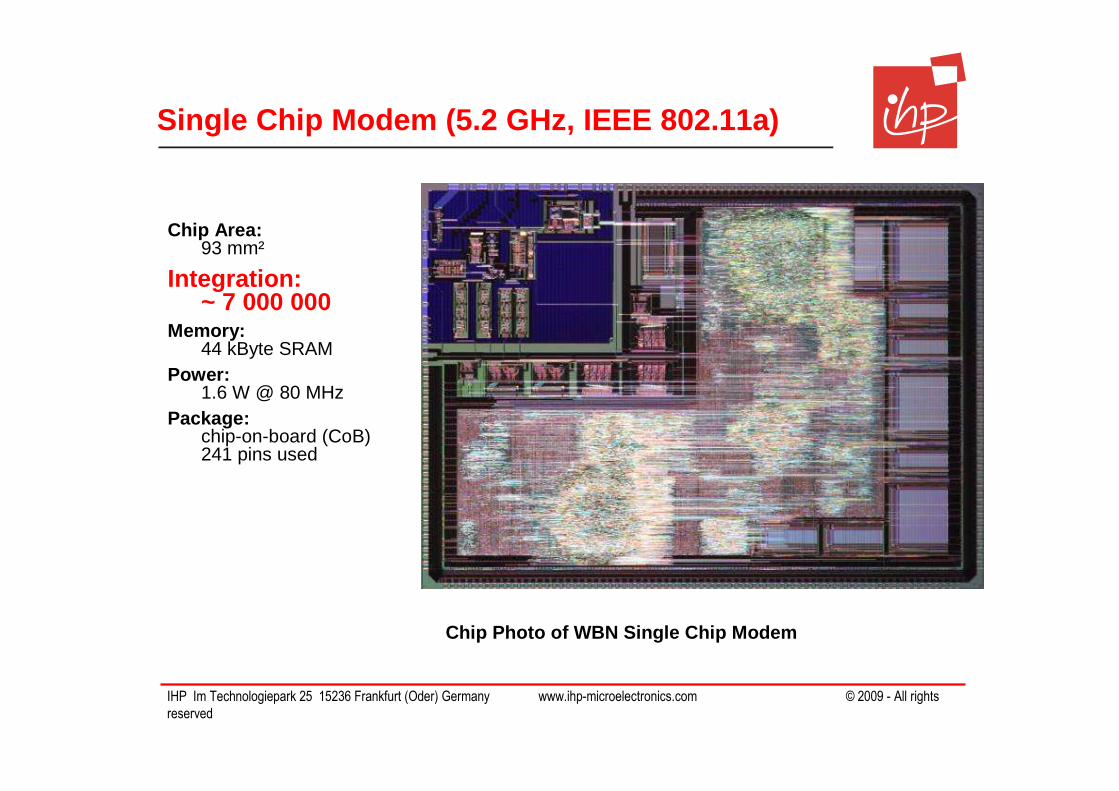
Single Chip Modem (5.2 GHz, IEEE 802.11a)
Chip Photo of WBN Single Chip Modem
Chip Area: 93 mm²
Integration: ~ 7 000 000
Memory: 44 kByte SRAM
Power: 1.6 W @ 80 MHz
Package: chip-on-board (CoB)241 pins used
IHP Im Technologiepark 25 15236 Frankfurt (Oder) Germany www.ihp-microelectronics.com © 2009 - All rights
reserved
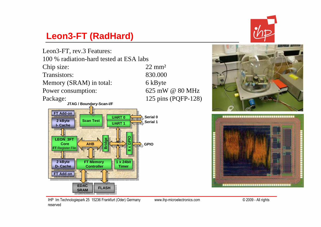
Leon3-FT (RadHard)
LEON_3FTCore
FT Register File
LEON_3FTCore
FT Register File
FT MemoryController
FT MemoryController
8 x
GP
IO8
x G
PIO
GPIO
2 kByteI- Cache
2 kByteI- Cache
2 kByteD- Cache
2 kByteD- Cache
AHBAPB
1 x 24bitTimer
1 x 24bitTimer
UART 0UART 0
EDAC SRAM
EDAC SRAM FLASHFLASH
Serial 0 Serial 1
UART 1UART 1
Brid
geB
ridge
Scan TestScan TestFT Add-onFT Add-on
FT Add-onFT Add-on
JTAG / Boundary-Scan-I/F
Leon3-FT, rev.3 Features:100 % radiation-hard tested at ESA labs Chip size: 22 mm²Transistors: 830.000Memory (SRAM) in total: 6 kBytePower consumption: 625 mW @ 80 MHzPackage: 125 pins (PQFP-128)
IHP Im Technologiepark 25 15236 Frankfurt (Oder) Germany www.ihp-microelectronics.com © 2009 - All rights
reserved
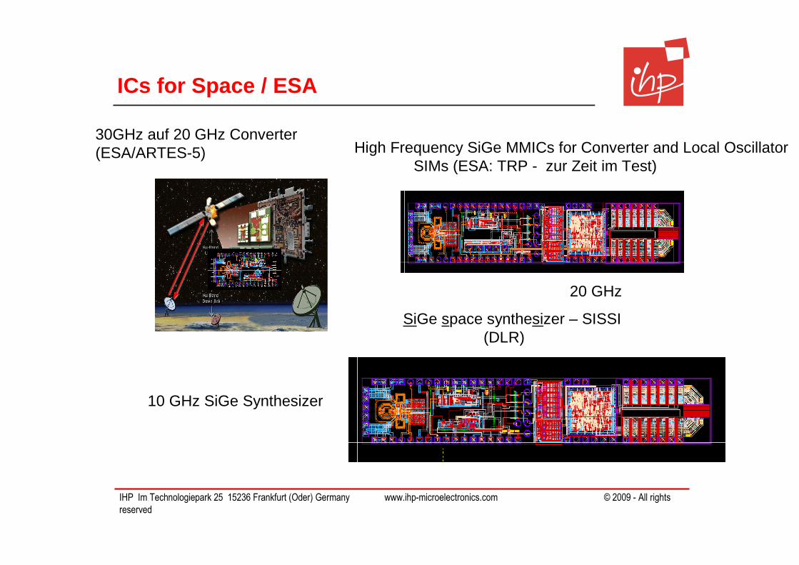
ICs for Space / ESA
30GHz auf 20 GHz Converter(ESA/ARTES-5)
10 GHz SiGe Synthesizer
High Frequency SiGe MMICs for Converter and Local OscillatorSIMs (ESA: TRP - zur Zeit im Test)
SiGe space synthesizer – SISSI(DLR)
20 GHz

IHP Im Technologiepark 25 15236 Frankfurt (Oder) Germany www.ihp-microelectronics.com © 2009 - All rights
reserved
CD Results - DAC
Ultra-Fast DAC• 30 GS/s, 4 bit, output bandwidth 3.85 GHz• Second fastest DAC in the world
with good Figure of Merit (0.95 pJ) [FOM=Power/ 2 N • Conversion Rate]
• Presented on IEEE BCTM 2007• Future plan: 20 GS/s 8 bit DAC
with 4 bit DAC as core component
0.25µm SG25H1
0.954553.5430This work
0.12µmSi/ 2102.75660340W. Cheng, et al, TelASICComm., CA, ISSCC 2004
0.13µm SiGe/150
0.721014622P. Schvan, et al, Nortel Network, CA ISSCC 2005
0.18µm SiGe0.283601.8620D. Baranauskas, et al. Pulse~Link, CA, ISSCC 20061
Process/FtFOM (pJ)Pdiss(mW)
Supply(V)
Reso-lution(Bits)
Fc(GHz)
Reference

IHP Im Technologiepark 25 15236 Frankfurt (Oder) Germany www.ihp-microelectronics.com © 2009 - All rights
reserved
Crypto Core Results
• Tested in different ASICs• Standalone crypto chip
(Dcrypt) • Hardware accelerator (e.g. in
TCP Chip)• Published:
• 4 paper • 2 journal paper
• Patents: • 2 patents for ECC• 4 patents to prevent side
channel attacks
IHP Im Technologiepark 25 15236 Frankfurt (Oder) Germany www.ihp-microelectronics.com © 2009 - All rights
reserved
Technology

IHP Im Technologiepark 25 15236 Frankfurt (Oder) Germany www.ihp-microelectronics.com © 2009 - All rights
reserved
IHP‘s Technology Focus: More than Moore
Source: ITRS Roadmap
SoC
THz Electronics
IHP
Scaling Down:• E-Beam (Mix-Match)• CMOS CooperationLETI, IMEC and/or Companies
Si Photonics

IHP Im Technologiepark 25 15236 Frankfurt (Oder) Germany www.ihp-microelectronics.com © 2009 - All rights
reserved
Generations of IHP’s High-Speed HBTs
World record gate delay of 2.5 ps (2008 !!!!!!!!!!)Fastest circuit speed achieved in any Si IC technol ogy

IHP Im Technologiepark 25 15236 Frankfurt (Oder) Germany www.ihp-microelectronics.com © 2009 - All rights
reserved
The Pilot Line
• 1000 m2 cleanroom class 1, 200 mm Wafer
• Equipped for 0.25 µm and 0.13 µm technology levels
• Running 24 h / 7 days
• Complete SiGe:C BiCMOS Technologies with highest perf ormance
0,25 µm (0,13µm) CMOS Basis-Technologie
SiGe:C HBT LDMOS Flash SpeicherPassive
Bauelemente
THz BauelementeHBTs? MEMS Integration
Optische Funktionen„Si Photonics”
0,25 µm (0,13µm) CMOS Basis-Technologie
SiGe:C HBT LDMOS Flash SpeicherPassive
Bauelemente
THz BauelementeHBTs? MEMS Integration
Optische Funktionen„Si Photonics”

IHP Im Technologiepark 25 15236 Frankfurt (Oder) Germany www.ihp-microelectronics.com © 2009 - All rights
reserved
SiGe BiCMOS Technology Offers
• IHP`s Technologies are offered worldwide for research and development ofPrototypes – Today there are about 50 active user
• IHP holds the world record with 2.5 ps gate delay !
• 0.25 µm BiCMOS with additional functions such as compl . LDMOS, • Space evaluation; fastest HBTs up to 300 GHz• Parameter of the latest 0.13 µm technologies since 2008 :
IHP Im Technologiepark 25 15236 Frankfurt (Oder) Germany www.ihp-microelectronics.com © 2009 - All rights
reserved
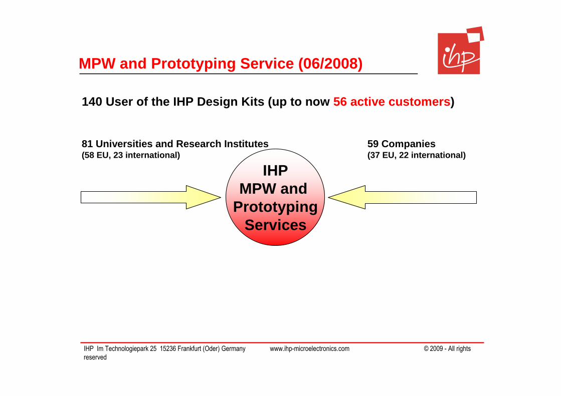
MPW and Prototyping Service (06/2008)
IHPMPW and
PrototypingServices
81 Universities and Research Institutes (58 EU, 23 international)
59 Companies(37 EU, 22 international)
140 User of the IHP Design Kits (up to now 56 active customers )

IHP Im Technologiepark 25 15236 Frankfurt (Oder) Germany www.ihp-microelectronics.com © 2009 - All rights
reserved
C 4 C 4
C 1 C 2 C 3 C 1
MPW Offering
C 7 C 8C 9
C 5
C 6
C 10
C 12C 11C 13
C 14
C 16C 15
C 17
C 18
C 19
IHP Im Technologiepark 25 15236 Frankfurt (Oder) Germany www.ihp-microelectronics.com © 2009 - All rights
reserved
Materials Research

IHP Im Technologiepark 25 15236 Frankfurt (Oder) Germany www.ihp-microelectronics.com © 2009 - All rights
reserved
Source Drain
Gate Oxide
Gate
THz-FET (Graphene)
“Only” 2 main problems:• layer deposition• Integration of
Graphene layers into CMOS process
Channel
SOI Wafer
Source Drain

IHPIm Technologiepark 2515236 Frankfurt (Oder)
Germany
IHP Im Technologiepark 25 15236 Frankfurt (Oder) Germany www.ihp-microelectronics.com © 2009 - All rights
reserved
Si Substrate
Buffer
Buffer:Lattice Window by
Mixed Rare Earth Oxides
Semiconductor Functional Semiconductors:suitable for a number ofIV-IV, III-V, II-VI materials
Heteroepitaxy –Ge / GaAs / InP / GaN on CMOS forPhotonic and THz application
via local epitaxy - SoS
Composition x [ % ]Si1-xGex
(Y2O3)1-x(Pr2O3)xComposition x [ % ]
LatticeP
arameter [A
]
Latti
ceP
aram
eter
[A]
0.0 0.2 0.4 0.6 0.8 1.010.5
10.6
10.7
10.8
10.9
11.0
11.1
11.2
11.3
Mixed OxideLatticeParameter [ A ]
10.5
10.6
10.7
10.8
10.9
11.0
11.1
11.2
11.30.0 0.2 0.4 0.6 0.8 1.0
Si Ge1-x x
Example
Ge
Si
Y2O3Pr2O3
IHPIm Technologiepark 2515236 Frankfurt (Oder)
Germany
IHP Im Technologiepark 25 15236 Frankfurt (Oder) Germany www.ihp-microelectronics.com © 2009 - All rights
reserved
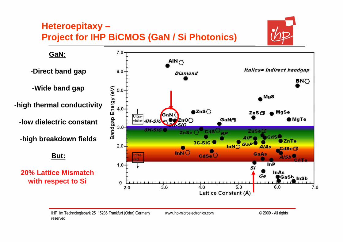
Heteroepitaxy –Project for IHP BiCMOS (GaN / Si Photonics)
GaN:
-Direct band gap
-Wide band gap
-high thermal conductivity
-low dielectric constant
-high breakdown fields
But:
20% Lattice Mismatchwith respect to Si
IHP Im Technologiepark 25 15236 Frankfurt (Oder) Germany www.ihp-microelectronics.com © 2009 - All rights
reserved
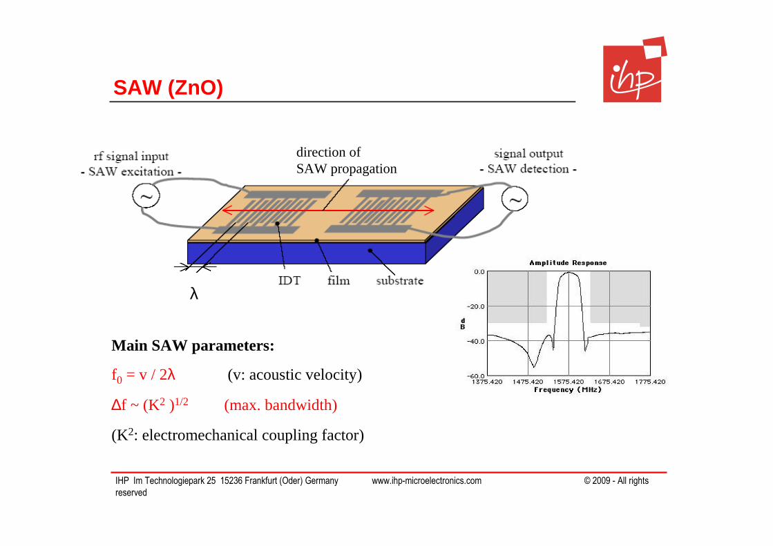
SAW (ZnO)
λ
direction ofSAW propagation
Main SAW parameters:
f0 = v / 2λ (v: acoustic velocity)
∆f ~ (K2 )1/2 (max. bandwidth)
(K2: electromechanical coupling factor)

IHP Im Technologiepark 25 15236 Frankfurt (Oder) Germany www.ihp-microelectronics.com © 2009 - All rights
reserved
0,8 0,9 1,0 1,1 1,2
140000
160000
180000
200000
220000
240000
EL
inte
nsity
, a.u
.
Energy, eV
MOS Si LED @ 1.5µm (D-band emission)
Forward biased devices show strong D1 luminescenceEfficiency > 0.15%
D1 @ 1.5 µm BB
Dislocation networkM. Kittler, IHP

IHP Im Technologiepark 25 15236 Frankfurt (Oder) Germany www.ihp-microelectronics.com © 2009 - All rights
reserved
Photovoltaics

IHP Im Technologiepark 25 15236 Frankfurt (Oder) Germany www.ihp-microelectronics.com © 2009 - All rights
reserved
Photovoltaic Activities of the IHP
• IHP has long term experience in silicon materials resear ch,especially in defect engineeringMajor competence for increasing efficiency
• The Joint Lab IHP/TU Cottbus is working in the project “ Solarfocus“
• IHP is working in projects for 3rd generation solar cell sHigher efficiency by using quantum effects
• IHP founded a Photovoltaic network with regional compan iesRegular meetings, organized by the Transferzentrum Ostb randenburg
• IHP has excellent equipment for measurement and analyti cs

IHP Im Technologiepark 25 15236 Frankfurt (Oder) Germany www.ihp-microelectronics.com © 2009 - All rights
reserved
3rd Generation
IHP Im Technologiepark 25 15236 Frankfurt (Oder) Germany www.ihp-microelectronics.com © 2009 - All rights
reserved
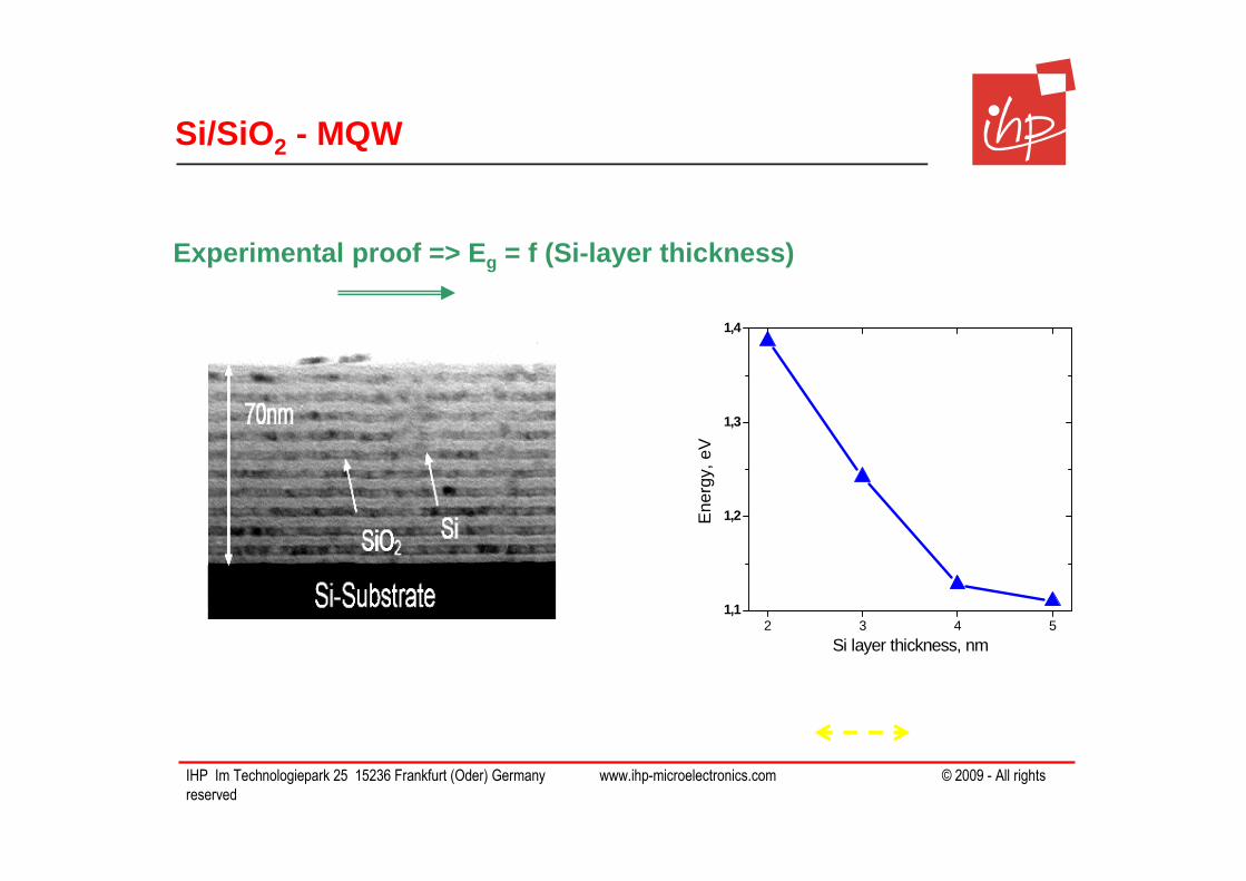
Si/SiO 2 - MQW
2 3 4 51,1
1,2
1,3
1,4
Si layer thickness, nm
Ene
rgy,
eV
Experimental proof => E g = f (Si-layer thickness)