instrumentation for ac four-probe measurements of large
TRANSCRIPT
ELSEVIER Journal of Electroanalytical Chemistry 430 (! 997) 269-278
JOURNAL OF
Instrumentation for ac four-probe measurements of large impedances
G. F a f i l e k *, M . W . B r e i t e r
institut fiir Technische Elektrochemie, TU Wien, Getreidemarkt 9, A-I060 Vienna, Austria
Received 4 April 1997; revis*,d 28 April 1997; accepted 29 April 1997
Abstract
An ac four-probe set-up was constructed to measure impedance spectra between 1 Hz and 100 kHz on solid electrolytes up to impedance values of 10 GO. The influence of the system on the measurement was analysed for the previous and the new set-up. A solution to minimise the source of errors by pre-amplifiers for current and voltage signals is presented. A new sample holder was constructed for best results in conjunction with the new pre-amplifiers. The holder is designed for measurements on solid electrolytes over a wide temperature range. The performance of the improved set-up and the residual error sources are discussed. Measurements of impedance spectra on YSZ and BICUVOX.10 in a four-probe arrangement are given as an example. © 1997 Elsevier Science S.A.
Keywords: Four-probe; High impedance; Conductivity; Solid electrolytes
1. Introduction
Impedance spectroscopy on symmetric cells by two- probe techniques is widely used for the measurement of bulk impedances in solid state ionics. The disadvantage is the necessary separation of the bulk impedance from the interfacial impedance bulklelectrode. This is sometimes difficult. On the other hand, the impedance spectra allow a distinction to be made between different bulk processes, such as intragranular and intergranular conduction in poly- crystalline material [1]. The four-probe technique avoids the difficulties of the separation of interfacial impedances because only the voltage drop across the bulk impedance between the two voltage probes is measured [2]. Since current and voltage probes are separated and, in theory, current does not pass through the voltage electrodes, the voltage drop across the part of the electrolyte between the voltage probes should be measured without contribution of the impedance of the bulk lelectrode interface.
Usually de or fixed frequency systems are used as standard methods [3]. However, only the total resistivity can be determined by these methods. Although impedance spectra can be taken, their interpretation is very difficult in many cases. Correct results are only obtained for systems with low resistance (less than approximately 1 M/ / ) . The
* Corresponding author. Fax: 0043 [email protected].
1 5861560. E-mail:
0022-0728/97/$17.00 © 1997 Elsevier Science S.A. All rights reserved. PII S0022-0728(97)00263-5
measurement is restricted to a relatively small frequency range (less than 1 kHz) [4,5]. Systems with very high impedance cannot be measured by standard methods be- cause of the influence of the set-up. Even though interfa- cial pro,~erties should not contribute to the measurement, in practice there is a voltage drop at the interfacial impedance of the voltage probes. Bias currents to the amplifier inputs, the cable capacity and the input impedance of the amplifier, are loads for the probes and form current paths across that part of the bulk impedance where the voltage drop is measured. The size of the voltage probes is one of the parameters which determines the value of the interfacial impedance. Therefore the area cannot be too small but, on the other hand, large probes disturb the uniformity of the current distribution.
In this paper we describe the reasons for these errors and discuss the possibilities for reducing these problems.
2. Equivalent circuit of the ac four-probe set-up
In a four-probe set-up, stray capacities have more influ- ence on the measurements than in a two-probe set-up. A schematic diagram of a traditional four-probe set-up is shown in Fig. 1. For this arrangement the ac response of the system can be evaluated by equivalent circuits. A complicated equivalent circuit, which is shown in Fig. 2, results because the impedance of the sample outside of the voltage probes cannot be neglected. This model may be

270 G. Fafilek, M. W. Breiter / Jou rnal of Electroanalytical Chemist~ 430 ( 1997) 269-2 78
t - - ~ ' 7 I' .,.
,"It ' : - - z ' - , . . . . . . . . . . . !1 ,11 Rs I . . . . I__,
r - - -
II . . . . . . . 33 I : : : , - - -
sample holder i L --_ nt
Fig. 1. Schematic diagram of the set-up for conventional measurement of voltage and current. Both ate measured with the same type of instrumen- tation amplifier.
too simple to simulate the real behaviour of the set-up because the values of the different parameters are not known exactly. However, this circuit can show qualJta- 6vely why it is so difficult to get correct results for the impedance to be measured. The stray capacity across a large standard resistor for the current measurement leads to a decreased bandwidth in the voltage drop technique. Stray capacities of the voltage leads and the input impedance of the voltmeter also produce a bypass to the unknown impedance and contribute to the measured current. In
addition the frequency response of the amplifiers has to be considered. It is therefore necessary to modify the measur- ing circuits used commonly for ac four-probe measure- ments of high impedance systems.
In ac two-probe measurements, the use of a current-to- voltage converter instead of the measurement of the volt- age drop across a standard resistor is a common method to avoid stray capacities. With that arrangement the ac perfor- mance of the current measurement depends mainly on the performance of the amplifier and very large impedances can be measured [6]. A similar technique can be used in the four-probe set-up. The schematic diagram of the new set-up is shown in Fig. 3a. A current to voltage converter instead of a standard resistor in series with the sample and a voltage amplifier which allows the use of driven shields [7] was implemented. The equivalent circuit in Fig. 3b is simpler than that in Fig. 2. The capacity, Cg, and the impedance, Z~n, formed by the cable and the amplifier input do not influence the measurement because of the virtually grounded input of the current-to-voltage ampli- fier. The cable capacity, Cg, to the ground of the voltage leads, and the stray capacity, C s, between the voltage signal leads, can be eliminated by the active shielding. It is necessary to extend the active shield as close as possible to the sample even at high temperatures. The current leads
Rs [sample[
_ "x Z, I ±
Cs
Cs//Zin ~/Vx
Cs
l _ _ _
c ,z,n 7-c 7-C -
"-x ix "~- Zbx ....
Zin t impedance of the bulklelectrode interface Z b impedance of the bulk Zbx impedance to be measured C s stray capacity between signal lines Zin inp~t impedance of amplifier Cg capacity between signal line and grounded shield Z i standard r e s i s t o r
V× measured voltage drop "~ I x measured current }~ tdifferent from real values i[ Z x measured impedance J
Fig. 2. Equivalent circuit of the set-up shown in Fig. 1.
-Cg n

G. Fafilek, M. W. Breiter / Journal of Electroanalytical Chemistry 430 (1997) 269-278 271
should have grounded shields up to the current probes of the sample. Therefore a stray capacity cannot be formed from these lines to other signal lines. The cable capacity Cg of the high current input lead, which still exists, will not influence the measured impedance. Only the input impedance of the instrumentation amplifier in parallel to the sample remains. This would be the ideal behaviour of the circuit. The value of the input capacity, which is usually between 1 and 2 pF, can be taken into account in the calculation of the real bulk impedance, Z bx, from the measured impedance, Z x:
V x Z i n Z b x ,, . _ .
ZX -- I X Zin + Zbx + 2Zin t ( 1 )
In Eq. (1), derived from the circuit in Fig. 3b, the interfa- cial impedance of the voltage electrodes has to be in- eluded. That is the reason why in the four-probe measure- ment, even when it is made by a carefully designed set-up, the interfacial impedance contributes to the total impedance. One has to make a compromise between geo- metric effects due to the non-uniform current distribution
for large voltage probes and interfacial effects for small electrodes.
3. Description of the set-up
A previously described set-up for computer controlled four-probe measurements [2] was modified to allow the measurement of larger impedances in a wider frequency range. Amplifiers and sample holder were newly con- structed for that purpose.
3.1. Voltage amplifier
An instrumentation amplifier can measure voltage dif- ferences floating to the ground, which is required for the measurement of the potential drop across the voltage probes. The amplifier inputs have to be connected to the sample through shielded cables. The capacitive coupling between noise sources, mostly from the power line, and the signal line, introduces noise [8]. The noise current
(a) Rs
I J
' I" . . . . : . . . . . . . . . . . . i I: / act, ve sh,elds ,, . . . . ' ' I -----'---'-'2--I' ' ,,
. . . . . . . . . . . . . . . . . . . . . . . . . . i + _ ~ v lta e , v, .... 2 " 'l_-----_-= o g
Vout I l a . . . . . . . . . . ] v ' 2 ' . . . . . . . ' - T - - i I
sample holder , i i I , , l , . . . . -,.---._-7"_.
m - - m
current
( b )
Rs
I
Vout
/_J~Ix - : Cg+Cs
- - virtual ground - -
Fig. 3. (a) Schematic diagram of the four-probe set-up with special current and voltage amplifier. (b) Resulting equivalent circuit.
272 G. Fafilek, M.W. Breiter / Journal of Electroanalytical Chemisto' 430 (1997) 269-278
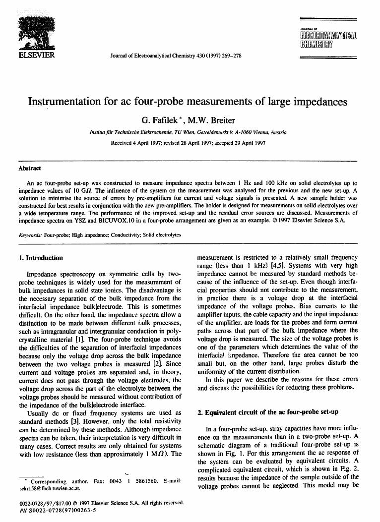
flows through the shield, not through the signal line with a grounded metal shield. However, the cable capacity Cg and the leakage resistance Rg from the signal line to the grounded shield are loads for signal sources with large source impedance. To avoid this influence, active shielding is necessary. The active shield is held at the same signal level as the signal line itself by means of a buffer ampli- fier. In principle, active shielding (guarding) rejects the capacitive current even when the cable capacity still exists. The performance of the guarding depends on the perfor- mance of the buffer amplifier. The frequency dependence of the open loop voltage gain has a single pole behaviour. Therefore the voltage difference between signal line and guard becomes larger at higher frequencies. Also, the output resistance of the buffer anlplifier has some influ- ence on the efficiency of the guarding. The output resis- tance is normally approximately 100 O and forms a low-pass with the capacity between active and grounded
shield in a TRIAX cable. The time constant of this low-pass is very small and the influence on the bandwidth of the whole circuit can be neglected.
3.1.1. The voltage amplifier circuit (Fig. 4a) An INA 110 instrumentation amplifier from Burr Brown
was used for amplification of the voltage signal. This amplifier provides a flat voltage gain-frequency response up to 100 kHz with a gain of 1 or 100. Buffer amplifiers for both inputs, built by the OPA 128 from Burr Brown, ensure the very low bias current of 75 fA, which is necessary to avoid dc-offset on the voltage electrodes [9]. A careful arrangement is necessary to avoid the degrading of the very good performance of this amplifier. Therefore the noninverting inputs of the OPA 128 were directly attached to the TRIAX connectors mounted on the case. The outputs of these buffers also supply the driven shields of the TRIAX cables which are connected to the TRIAX
a)
+ INPUT
._r
INAII0
L.J xiuu ~ o o,
- J 4341 [BURR I BROWN
AC-OUTPUT
$ DC-OUTPUT
$
Voltage amplifier 4-probe
10M
|NPU
I OPAl28
all switches shown in off position 200 open circles -- off f i l l ed c i rc les -- on -$3
~ain[VIA] -S ! -52 -$3 IO s 0 0 0
10 4 0 0 •
IO s • 0 0
10 6 • 0 •
10 7 • • O
lO s • • •
OPA602
I BURR l
AC-OUTPUT
$ D~-OUTPUT
$
Current amplifier 4-probe
Fig. 4. Electronic circuits for (a) voltage and (b) current amplifier. Power supply and offset compensation of the amplifiers are not drawn.
G. Fafilek, M.W. Breiter / Journal of Electroanalyticai Chemist~. 430 (1997) 269-278 273
connectors on the sample holder. An additional noninvert- ing amplifier stage (OPA 602, Burr Brown) provides gains of 1 and 10. Together with the INA 110, the gains 1, 10, 100 and 1000 can be set by two relays. A true RMS converter (4341 from Burr Brown) gives additional infor- mation about de-offset, or saturation of the voltage inputs in case of high interfacial impedance or blocking be- haviour of the electrodes. The ac output can be used to supply a regular FRA or, in our case, the HP gain-phase meter 3575A was used.
3.2. Current to voltage converter
The same amplifier which is used as a buffer in the voltage amplifier is located in the currc=z-to-voltage con- verter. The single pole transfer functioa of the amplifier, together with the low pass, formed by t~ie feedback resistor and the capacity of the input cable of the current amplifier, leads to a two-pole behaviour and introduces gain peaking followed by a - 4 0 dB/dcc slope [10]. To avoid gain peaking and oscillation a parallel capacitor across the feedback resistor is required sometimes, reducing the bandwidth.
The voltage applied to the sample is more or less constant, except for impedances smaller than 100 /2. Therefore the dynamic range of the voltage to be mea- sured, compared to the current, is much smaller. In order to cover a wide range of impedance values it is necessary to have several ranges for the current measurement. Unfor- tunately, ordinary switching of the ranges in the current to voltage amplifier introduces additional stray capacities in the high gain ranges and therefore additional limitations of the bandwidth. For that purpose a circuit was developed which avoids this influence of the switches on the mea- surement.
3.2.1. The current amplifier circuit (Fig. 4b) The OPA 128 was used as a current-to-voltage con-
verter. The switching of the ranges is a difficult problem because of the stray shunting capacities across the feed- back resistor. A 10 M/2 feedback resistor was connected directly from the input to the output in such a way that a minimum shunt capacity results. The resistors for the additional ranges were added afterwards~ Only a shunt capacity across the feedback resistor will reduce the band- width. Stray capacities from the output of the amplifier to ground or from the input (which is practically on virtual ground if the frequency is not too high) to ground have no influence on the bandwidth. If the feedback resistor with low resistance is connected to the output and switched to ground when a higher gain is necessary, only a very small additional stray capacity (compared to the cable capacity) from the input to ground is inserted. The output of the amplifier is loaded by that part of the feedback resistor which is connected to ground. It is about 1000 ~ in the worst case when -S 1 and -$2 are switched on. The output
J I alumina steel
silver layer
~ ~ _ ~ } current active shield
U' ~.;, active shield current
sample / platinum
leads
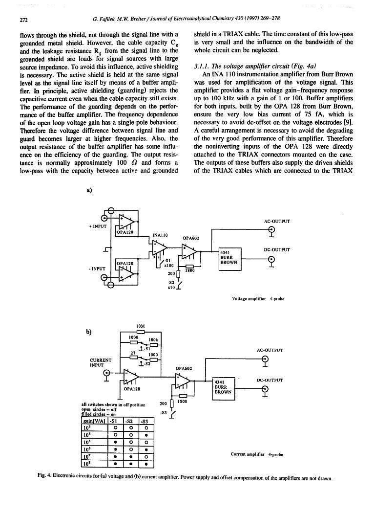
Fig. 5. Sample holder for measurements at high temperatures with point electrodes as voltage probes and active shielding up to the sample.
resistance of 100/2 and the maximum output current of 5 mA of the OPA 128 have to be considered for accuracy and large signal fi,~quency response characteristics. The second stage ct,f the current amplifier, as well as the true RMS converte,', is tl~e same as that in the voltage ampli- fier.
3.3. Sample holder
The sample holder for measurements at high tempera- tures (Fig. 5), consists of alumina and steel tubes and platinum leads. The voltage leads had to be actively shielded separately by their own signal potential and were therefore arranged in a triaxial configuration. Both voltage signal leads are isolated by alumina tubes, which are covered by silver paste on the o~,tside. This silver layer is used as an active shield for the high temperature part of the holder. Additional alumina tubes isolate the active shields against the grounded steel tubes. The outer and the inner alumina tubes are glued together and can move inside the steel tubes. On the end where the sample is placed, tip electrodes are welded onto the signal leads. Springs, located outside of the hot area, put pressure on these alumina tubes, so that the point electrodes are pressed onto the top of the sample. The two point electrodes are used as voltage electrodes. Two platinum wires on the side make the connections to the current electrodes. The sample is placed on an alumina plate which is mounted on four outer steel tubes. All steel tubes are brazed together to form a rigid and electrically grounded construction which is attached to a brass head. A thermocouple for the mea- surement of the sample temperature is placed in one of the steel tubes. The brass head holds the BNC- and TRIAX- jacks as well as the inlet and outlet for the gas. A quaztz tube, closed at one end, is fitted with an o-ring to the head
I Vx i ix
Fig. 6. Example of the arrangement of the calibration ce)~. consisting of SMD components.
274 ( 7 , Fafilek, M. IN. Breiter / Journal of Electroana(Wical Chemistry 430 (1997) 269-278
of the holder. The holder is inserted into an electric furnace supplied by a dc power supply.
4. Calibration measurements and test of the perfor- mance
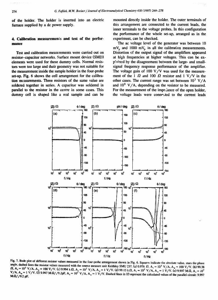
Test and calibration meast~rements were carded out on resistor-capacitor networks. Surface mount device (SMD) elements were used for these dummy cells. Normal resis- tors were too large and their geometry was not suitable for the measurement inside the sample holder in the four-probe set-up. Fig. 6 shows the cell arrangement for the calibra- tion measurements. Three resistors of the same value are soldered together in series. A capacitor was soldered in parallel to the resistor in the centre in some cases. This dummy cell is shaped like a real sample and can be
mounted directly inside the holder. The outer terminals of this arrangement are connected to the current leads, the inner terminals to the voltage probes. In this configuration the performance of the whole set-up, arranged as in the experiment, can be checked.
The ac voltage level of the generator was between 10 mVp and 1000 mV r in all the calibration measurements. Distortion cf the output signal of the amplifiers appeared at high frequencies at higher voltages. This can be ex- plained by the disagreement between the large- and small- signal frequency response performance of the amplifier. The voltage gain of 100 V / V was used for the measure- ment of the ! /2 and 100 O resistor and 1 V / V in the other cases. The current range was set between 10 3 V / A and l0 s V / A , depending on the resistor to be measured. For the measurement of the impe'ance of the open holder, the voltage leads were conna;ted to the current leads
IZl/f~ ~/deg IZI/~ phi
}iai,,..t ....... ,,.--~.~. ~,,.~-.-.,..,~ 18o 135 1 (bi''"~ ....... ' ...... '~ ....... "
100
, , , . , , , , l . . . . . . . d , , . , , , J . . . . . . , i
10' 10 = 1# 10 4 10 s
deg IZl/t~ ~/deg I ....... , . . . . . . . , ....... , . . . . . . ] 18o
150 (C) "i 135 |
100 I ~ 9 0
0 ~ - ' ~ ' ~ 0
-100 "90
. . . . . . . . . . . . . . . . . . . . . . . . . . . . . t:12 10 1 102 10 a 10 4 102 1¢ 10 2 102 1¢ 102
f iHz f/Hz f/Hz
lZi/n ~/deg IZl/~ ~/deg IZl/~ ~/deg
10e I('di""t I ~ ' 1 1 . . . . . . . . . . . . . . . . '] 180 108 1 igi'"'l 'l t ~ f ....... ...... "!! ''''''1 180 108 I" i'''''l ' • .11! ~ ....... ........ i " "ll'"~l 180:135
lo' ................. lo' t . . . . . . . . . . . . lo'
"i .1.:" '° I 10 ~ ' ...... ~ ....... ., ...... J ...... J .18010~ i ............. ., ...... .J 1# 1# 10' 1# 10 s 101 ...... " ~aJ10 ............................... -180 102 1# 10 4 102 10 1 102 10 a 10 4 10 s
f lHz flHz f lHz
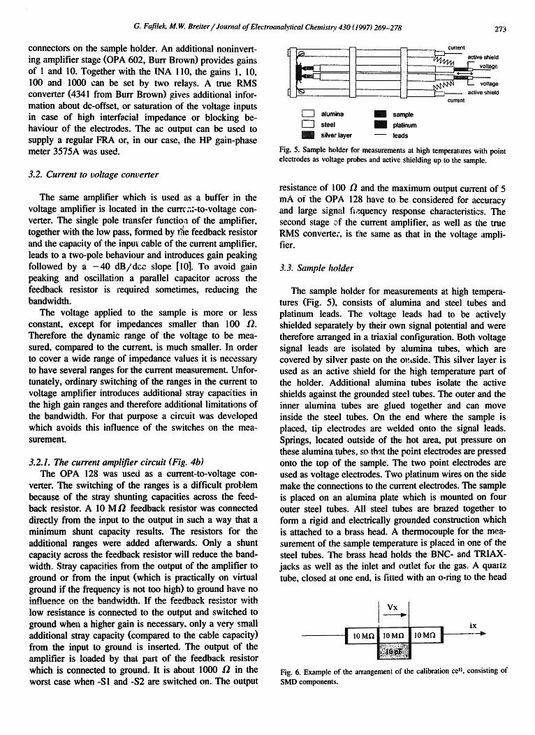
Fig. 7. Bode plot of different resistor values measured in the four-probe arrangement shown in Fig. 6. Squar~.s indicate the absolute value, stars the phase angle, dashed lines the resistor values measured with the source measure, unit Keithley SMU 237. (a) 0.976 D,, A i = 103 V/A, A u = 100 V/V. (b) 99.38 [ ] . A i = 10 3 V / A . A, = 100 V/V. (c) 9.994 kO, A i = 10 3 V/A, A, = 1 V/V. (d) 99.13 kO, A i = 105 V/A, A u = 1 V/V. (e) 9.997 M/2, A i = 10 7
V/A, A, = 1 V/V. (f) 9.997 Mn//9.2pF, A i -~ 10 7 V / A . A , = 1 V/V. Dashed lines in (0 represent the calculated values of the parallel circuit: 9.997 M/~//9.2 pF.

G. Fafilek, M.W. Breiter / Journal of Electroanalytical Chemistry 430 (1997) 269-278 275
IZl/t~ 10" !-;, ..... ~ ........ , . . . . . . "~ . . . . . . .
" , , l i m i t e d
lO '0 ~ n ~
1°'1 ~ o l d -4s
lo' ~ -131
10 a , , ' " " . . . . . . . ' . . . . . . "~ . . . . . .181 lo' lO' lo = lo' lo ~ f l H z
~/deg Cp/pF 180 - 1.0
135
"0.8 90
45 .0.6
-0.4
0 . 2
'0.0
Fig. 8. Open holder, current and voltage dectrodes directly connected. A i = 10 s V/A, Aa = 1 V/V. Solid line represents the calculated capac- ity of the open holder Ci, = 0.12 pF.
directly. Therefore, the current through the voltage ampli- fier plus that through the geometric capacity was measured by the current amplifier. The results of the calibration measurements are presented in Figs. 7 and 8.
The measurements of the 1 /2 and the 100 /2 resistor show the sum of the frequency responses of the voltage amplifier with gain 100 V / V plus that of the current amplifier at a gain of 103 A/V. With the l0 kO resistor the voltage amplifier has a gain of" 1 V / V and its widest bandwidth. Therefore, the frequency response characteris- tic of the current amplifier, at the gain 10 3 V / / A , deter- mines the measured values. At higher current gain (A i= IO s for R~ = 100 k O) the bandwidth of the current to voltage converter becomes smaller. Gain peaking with a
peak frequency at approximately 100 kHz determines the upper frequency limit. With an amplification of 10 7 A / V the peak frequency is shifted down to approximately 10 kHz. This is in full agreement with the proposed origin of the peaking effect. The characteristic frequency of the low pass, fRc, formed by the feedback resistor and the input cable capacitor in the current range of 10 7 A//V is one hundred times smaller than in the range 105 A/V. To- gether with the unity gain frequency, f, , of the amplifier (1-2 MHz for the OPAl28) the peak frequency can be calculated as the geometric mean of the unity gain fre- quency and the characteristic frequency of the low pass: fp = ( f , *fRc) -1/2 [10].
In the measurement of the open holder, the low fre- quency limit of about 200 Hz was determined by the signal to noise ratio of the current signal. Noise sources are the resistance noise and the voltage noise of the amplifier but there is no noise pickup from the power line because of the careful shielding. For an absolute value of the impedance higher than 10 :° 12 and a current gain of 108 V /A at a generator signal amplitude of 100 mVp, the current signal is only I mVp. This signal level is usually too small, compared to the noise level, for measurements without special treatment, such as long integration time. The maxi- mum absolute value of the impedance which can be mea- sured is therefore approximately 10 GO. The high fre- quency limit appears at 2 kHz because of the gain peaking of the current amplifier and the following - 4 0 dB/dec slope in its gain-frequency depende::,,ce. Therefore, in the Bode plot of the measured impedance, a minimum at 10 kHz and an increasing part afterwards with a slope of + 20 dB/dec can be seen. At frequencies higher than approxi- mately 50 kHz the low pass behaviour of the voltage amplifier starts to have an influence and the slope of the measured itapedance becomes slightly smaller. The calcu-
IZl / ~ $ I deg 6x~O'[ ia i " " ....... ' ........ ' ........ , . , ,.. 15
L
k v 1 . . . . . . ' . . . . . . . . . . . . . . . . . . . . ' . . . . . . .
l O o 101 10 a 10 3 10 4 10 s
-ImlMQ I !
( b )
,•N N O "1"
__N ~ O
I , I
2 4 Re(Z) I M n
t t
f l Hz
Fig. 9. Four.probe impedance of YSZ measured in air at 300°C. The total bulk resistance R b
stars = phase angle. (b) Nyquist plot.
--4.32 M•. (a) Bode plot, squares = absolute value;

276 G. Fafilek. M. W. Breiter / Journal of Electroanalytical Chemistry 430 (1997) 269-278
T I ° C
800 600 400 200 i 1 i
t
o
-1
.u
& 4
-6 - 7 o o
i , , I . . . . I , , , , I , i i ° l
1,0 1,5 2,0 2,5 3,0
1 0 0 0 . r r I K "1
Fig. 10. A r r h e n i u s plot of the total conductivity of YSZ. Solid line = linear regression. The activation energy was calculated to be E~ = 0.97 eV. Deviations at 100°C and 50°C from the straight line are caused by the noise limit of the measurement.
lated total input capacity Ci,, which is the sum of input capacity of the amplifier and the geometric capacity, is only 0.12 pF.
A correction of the measured impedances, for the fre- quency response characteristics of the amplifiers is only reasonable for samples with low impedance. In high impedance systems, unpredictable errors from the 'outside' bulk impedance and interfacial impedance of the current electrode, as well as the impedance of the interface bulklvoltage electrode, together with the impedance of the voltage leads, will affect the impedance, Z x, to be mea- sured (see Fig. 2). Although the frequency and impedance range is extended because of the measuring principle, a correction will fail in many cases.
5. Measurements on YSZ
Ac four-probe impedance spectra were taken on poly- crystalline yttria stabilised zirconia (YSZ) samples with 8 mol% yttria content (Degussit FZY from Trentini). The total bulk conductivity of YSZ strongly depends upon temperature, with an activation energy of about 1 eV. Therefore, the resistance of the sample at room tempera- ture has values comparable to that of insulators.
Experiments were performed on rectangular cells with the size of 0.92 × 0.475 × 0.12 cm in air. The samples were polished using SiC paper up to grade 1200. The current electrodes were gold films painted on the two opposite small sides. Voltage electrodes were applied in the same way on one large side of the sample with a distance of 0.5 cm from each other and a width of less than 0. I cm. The use of point electrodes for the voltage probes is not feasible because of their high interfacial impedance. The electrodes were sintered in air at approximately 800°C. Spectra were taken every 50°C between room temperature and 750°C during heating and in the cooling cycle. Fre- quencies between 10 Hz and 100 kHz with a signal amplitude between 100mV and 1000 mV were set by a signal generator. The use of a more modem Frequency Response Analyser for the current and voltage signals would extend the lower frequency limit. A Bode and a Nyquist plot are shown in Fig. 9 as an example. The positive imaginary part at high frequencies results from the inadequate frequency response of the current amplifier above the bandwidth limit (see also Fig. 7). The conductiv- ity of the sample was determined from the spectra by graphical extrapolation.
Reproducible straight lines were obtained in the Arrhe- nius plot between 150°C and 750°C (Fig. I0). A deviation
IZl / n ~ i deg . . . . . . . ,, ........ , . . . . . . . . ,, ........ ~ ... . . . 2 0
= ~ ' * * a) 1 0
o
-10 10
I -~,~e ~ -20
-30
-40"
-50
10 ' . . . . . . J . . . . . . . . . . . . . . . ~ ........ ' ' - 6 0
~o ° lO' lo ' lO = lo ' lO ~
-Im(Z) ! M ~
O f f ' I ~ I ~ / 0 2 0 4 0 6O
Re(Z) ! M~
f / H z
Fig. 11. Four-probe impedance of BICUVOX. I0 measured in air at 48'.2°C. (a) Bode plot, squares = absolute value; stars = phase angle. (b) Nyquist plot.

G. Fafilek, M. W. Breiter / Journal of Electroanalytical Chemistry. 430 (1997) 269-278 277
from this straight line can be seen at lower temperatures. The impedance measured at this temperature was larger than 10 GO and therefore in the signal to noise ratio limit. At room temperature, the voltage amplifier ran into satura- tion because of the blocking behaviour of the voltage electrodes. This marks the absolute limit for all four-probe measurements even at fixed low frequencies or with de methods.
6. M e a s u r e m e n t s o n B I C U V O X . 1 0
BICUVOX.10 is the designation of the oxygen ion conductor Bi 2Vo.9Cu 0.105.35 [ 11 ]. A polycrystalline sample of BICUVOX.10 was cut into a rectangular piece and polished with SiC paper up to grade 1200. The size of the sample was 0.8 × 0.475 × 0.18 cm. A thin film was painted with gold paste on the two opposite small sides for the current electrodes. The electrodes were sintered in air at 700°(2. The platinum tip electrodes of the holder were attached directly to the sample in the first experiment. The distance between the point contacts was 0.23 cm. Impedance spectra were taken every 25°C from room temperature to 725°C and back. Frequencies between 1 Hz and 100 kHz with signal levels between 100 mV and 2000mV were applied.
In a second experiment the sample holder was placed in a Dewar bottle filled with liquid nitrogen. A heating coil allowed the control of the sample temperature between - 150 and + 200°C. In the first run below room tempera- ture we saw that the voltage electrodes became blocking very early. Therefore voltage electrodes were applied with platinum paste and sintered in air at 700°C. The distance between the voltage electrodes was 0.23 cm and their width was less than 0.05 cm. The measurement could be extended to - 15°C with that type of electrode before the interfaeial impedance became too large. The measurements
2
1
¢/J - 1
I - - - 2
o'J o -3
-4
-5
T I "C 800 600 400 200 100
• • • • i
i
1 2 3
lO00fr I K"
Fig. 12. Arrbenius plot of the total conductivity of BICUVOX.10, high temperature measurement. & = heating cycle; ~' = cooling cycle; solid line = linear regression.
l l "C 150 100 50 0 -20
-2 - " " " ' ! ' ' m' ' ! . . . . ! ' ! -3
- 7 .
2,5 3 , 0 3 , 5 4 , 0
1 oooK / K"
Fig. 13. Arrhenius plot of the conductivity of BICUVOX. 10, low temper- ature measurement. [] = grain boundary; B = grain interior; stars = total conductivity of the high temperature measurement; solid line = linear regression.
were performed from room temperature to 150°C and back with steps of 10°C. A cooling cycle with 5°(3 steps down to -30°(3 and again a heating/cooling cycle with a maximum temperature of 150°(3 followed. The Nyquist plot (Fig. 1 lb) shows two well separated semi-circles in a ve~ restricted temperature range from 25°(3 to 100°C, because of our relatively small frequency window of 1 Hz to about 100 kHz. The interceptions with the real axis at high and low frequencies were interpreted as grain interior resistance, R g, and the total bu'~k resistance, which is the sum of Rg and the grain boundary resistance, Rg b, respec- tively. Above 200°C the frequency dependence of the impedance displays pure Ohmic behaviour up to the high frequency limit of our instrument. This value corresponds to the total bulk resistance. The bulk conductivity is shown in an Arrhenius plot for the high temperature experiment (Fig. 12). The temperature dependence of the grain interior and grain boundary conductivity is plotted in Fig. 13 for the low temperature experiment. The bulk conductivity of the first experiment is also shown for the overlapping temperature range in that diagram. The agreement of the activation energies and conductivity values with previous results from two-probe impedance measurements [12] is good (Table 1). The limit of the instrument was achieved at -15°(2 by the saturation of the inputs of the voltage amplifier.
Table 1 Comparison of activation energies of BICUVOX.iO obtained by four- probe and two-probe impedance spectroscopy
Temperature range E a (eV)
(K) This work [12]
Total bulk conductivity > 750 0.476 0.481 Total bulk conductivity < 730 0.681 0.682 Grain interior 0.68 0.643 Grain boundary 0.751 0.75

278 G. Fafilek, M. W Breiter / Journal of Electroanalytwal Chemistry 430 (1997) 269-278
References
[1] W.I. Archer, R.D. Armstrong, Specialist Per. Report, The Chemistry Society London, Electrochemistry I (1980) 157.
[2] P. Linhardt, M. Maly-Schreiber, M.W. Breiter, in: F.W. Poulsen, N. Hessel Henderson, K. Clausen, S. Skaarup, O. Toft Sorensen (Eds.), Proc. 6th Int. Syrup. on Metallurgy and Materials Science, RISO National Laboratory, Roskilde, 1985, p. 475.
[3] S.ES. Badwal, FT. Ciacchi, D.V. Ho, J. Appi. Electrochem. 21 (1991) 721.
[4] J.J. Bentzen, N.H. Andersen, F.W. Poulsen, O.T. Sorensen. R. Schram, Solid State Ionics 28-30 (1988) 550.
[5] C. Gabrielli, Schlumberger Technologies, technicfil report, 1990. [6] J.R. Dygas, M.W. Breiter, Electrochim. Acta 41 (1996) 993. [7] J.A. Chroboczek, J. Link, J. Phys. E Sci. Instrum. 18 (1985) 568. [8] Keithley, Low Level Measurements, 1992. [9] Burr Brown, IC Data Book, Linear Products, 1994.
[10] Burr Brown, Applications Handbook, 1994, pp. 172-206. [1 I] F. Abraham, J.C. Boivin, G. Mairesse, G. Novogrocki, Soli0 State
lonics 40/41 (1990) 934. [12] J.R. Dygas, F. Krok, W. Bogusz, P. Kurek, K. Reiselhuber, M.W.
Breiter, Solid State Ionics 70/71 (1994) 239.