integrated circuit immunity modelling beyond 1 ghz
TRANSCRIPT

Integrated circuit immunity modelling beyond 1 GHz
Sjoerd Op ’T Land
To cite this version:
Sjoerd Op ’T Land. Integrated circuit immunity modelling beyond 1 GHz. Electromagnetism.INSA de Rennes, 2014. English. <NNT : 2014ISAR0029>. <tel-01165061>
HAL Id: tel-01165061
https://tel.archives-ouvertes.fr/tel-01165061
Submitted on 18 Jun 2015
HAL is a multi-disciplinary open accessarchive for the deposit and dissemination of sci-entific research documents, whether they are pub-lished or not. The documents may come fromteaching and research institutions in France orabroad, or from public or private research centers.
L’archive ouverte pluridisciplinaire HAL, estdestinee au depot et a la diffusion de documentsscientifiques de niveau recherche, publies ou non,emanant des etablissements d’enseignement et derecherche francais ou etrangers, des laboratoirespublics ou prives.

La modélisation de l’immunité des circuits
intégrés au-delà de 1 GHz
Thèse soutenue le 20.06.2014 devant le jury composé de :
Frank Leferink
Professeur Université de Twente, Pays-Bas / président Etienne Sicard
Professeur – INSA de Toulouse / rapporteur
Geneviève Duchamp
Professeure – Université de Bordeaux 1 / rapporteur Jean-Luc Levant
Expert CEM – Atmel Nantes / examinateur Richard Perdriau
Enseignant Chercheur HDR – ESEO Angers / Co-encadrant de thèse Mohamed Ramdani
Enseignant Chercheur HDR – ESEO Angers / Co-directeur de thèse
M’hamed Drissi Professeur – IETR INSA de Rennes / Directeur de thèse
THESE INSA Rennes sous le sceau de l’Université européenne de Bretagne
pour obtenir le titre de
DOCTEUR DE L’INSA DE RENNES
Spécialité : Électronique et télécommunications
Thèse Confidentielle jusqu’au 1er Juin 2015
présentée par
Sjoerd OP ‘T LAND ECOLE DOCTORALE : MATISSE
LABORATOIRE : IETR INSA de Rennes - ESEO-EMC


La modélisation de l’immunité des circuits intégrés au-delà de 1 GHz
Integrated Circuit Immunity Modelling
Beyond 1 GHz
Sjoerd OP ‘T LAND
En partenariat avec
Document protégé par les droits d’auteur

[sumus] quasi nanos, gigantium humeris insidentes,ut possimus plura eis et remotiora videre,
non utique proprii visus acumine, aut eminentia corporis,sed quia in altum subvenimur et extollimur magnitudine gigantea
[we are] like dwarfs on the shoulders of giants,so that we can see more than they, and things at a greater distance,not by virtue of any sharpness of sight on our part, or any physical
distinction,but because we are carried high and raised up by their giant size
[nous sommes] des nains assis sur des épaules de géants,nous voyons plus de choses et plus lointaines qu’eux,
ce n’est pas à cause de la perspicacité de notre vue, ni de notregrandeur,
c’est parce que nous sommes élevés par eux.
als dwergen [zijn wij], gezeten op de schouders van reuzen,opdat we méér zien dan zij, en verder,
niet door onze eigen scherpe blik of uitmuntend lichaam,maar omdat we, hoog opgetild, boven hen uit torenen
Bernard of Chartres (12th century)

Résumé
La compatibilité électromagnétique (CEM) est l’aptitude des produits électroniques àcoexister au niveau électromagnétique. Dans la pratique, c’est une tâche très complexeque de concevoir des produits compatibles. L’arme permettant de concevoir des pro-duits bon-du-premier-coup est la modélisation. Cette thèse étudie l’utilité et la faisabilitéde la modélisation de l’immunité des circuits intégrés (CI) au-delà de 1 GHz.
Si les pistes des circuits imprimés déterminent l’immunité rayonnée de ces circuits,il serait pertinent de pouvoir prévoir l’efficacité de couplage et de comprendre commentelle découle du routage des pistes. Les solveurs full-wave sont lents et ne contribuentpas à la compréhension. En conséquence, un modèle existant (la cellule de Taylor)est modifié de manière à ce que son temps de calcul soit divisé par 100. De plus, cemodèle modifié est capable de fournir une explication de la limite supérieure pourle couplage d’une onde plane, rasante et polarisée verticalement vers une piste deplusieurs segments, électriquement longue et avec des terminaisons arbitraires. Lesrésultats jusqu’à 20 GHz corrèlent avec des simulations full-wave à une erreur absoluemoyenne de 2,6 dB près et avec des mesures en cellule GTEM (Gigahertz TransversaleElectromagnétique) à une erreur absolue moyenne de 4,0 dB près.
Si l’immunité conduite des CI est intéressante au-delà de 1 GHz, il faut une méthodede mesure, valable au-delà de 1 GHz. Actuellement, il n’y a pas de méthode normalisée,car la fréquence élevée fausse les observations faites avec la manipulation normali-sée. Il est difficile de modéliser et de compenser le comportement de la manipulationnormalisée. Par conséquent, une manipulation simplifiée et sa méthode d’extractioncorrespondante sont proposées, ainsi qu’une démonstration du principe de générationautomatique de la carte d’essai utilisée dans la manipulation simplifiée. Pour illus-trer la méthode simplifiée, l’immunité conduite d’un régulateur de tension LM7805 estmesurée jusqu’à 4,2 GHz.
À part la tendance générale des fréquences qui montent, il y a peu de preuveconcrète qui étaye la pertinence de la modélisation de l’immunité conduite des CI au-delà de 1 GHz. Une simulation full-wave suggère que jusqu’à 10 GHz, la plus grandepartie de l’énergie rentre dans la puce à travers la piste. Par concaténation des modèlesdéveloppés ci-dessus, l’immunité rayonnée d’une piste micro-ruban et d’un régulateurde tension LM7805 est prédite. Bien que ce modèle néglige l’immunité rayonnée du CI
i

ii Résumé
lui-même, la prédiction corrèle avec des mesures en cellule GTEM à une erreur absoluede 2,1 dB en moyenne.
Ces expériences suggèrent que la plus grande partie du rayonnement entre dans uncircuit imprimé à travers ses pistes, bien au-delà de 1 GHz. Dans ce cas, la modélisationde l’immunité conduite au-delà de 1 GHz serait utile. Par conséquent, l’extension jus-qu’à 10 GHz de la méthode de mesure CEI 62132-4 devrait être considérée. De plus, lavitesse et la transparence du modèle de Taylor modifié pour le couplage champ-à-lignepermettent des innovations dans la conception assistée par l’ordinateur. La générationsemi-automatique des cartes d’essais dites maigres pourrait faciliter l’extraction desmodèles. Certaines questions critiques et importantes demeurent ouvertes.
Mots clefs : EMC, IC, immunité, couplage champ-à-piste, cellule de Taylor, DPI, ICIM-CI,mesure, modélisation, simulation, GHz

Summary
ElectroMagnetic Compatibility (EMC) is the faculty of working devices to co-exist elec-tromagnetically. In practice, it turns out to be very complex to create electromagneticallycompatible devices. The weapon to succeed the complex challenge of creating First-Time-Right (FTR) compatible devices is modelling. This thesis investigates whetherit makes sense to model the conducted immunity of Integrated Circuits (ICs) beyond1 GHz and how to do that.
If the Printed Circuit Board (PCB) traces determine a PCB’s radiated immunity, it isinteresting to predict their coupling efficiency and to understand how that depends onthe trace routing. Because full-wave solvers are slow and do not yield understanding,the existing Taylor cell model is modified to yield another 100× speedup and an insight-ful upper bound, for vertically polarised, grazing-incident plane wave illumination ofelectrically long, multi-segment traces with arbitrary terminal loads. The results up to20 GHz match with full-wave simulations to within 2.6 dB average absolute error andwith Gigahertz Transverse Electromagnetic-cell (GTEM-cell) measurements to within4.0 dB average absolute error.
If the conducted immunity of ICs is interesting above 1 GHz, a measurement methodis needed that is valid beyond 1 GHz. There is no standardised method yet, becausewith rising frequency, the common measurement set-up increasingly obscures the IC’simmunity. An attempt to model and remove the set-up’s impact on the measurementresult proved difficult. Therefore, a simplified set-up and extraction method is proposedand a proof-of-concept of the automatic generation of the set-up’s PCB is given. Theconducted immunity of an LM7805 voltage regulator is measured up to 4.2 GHz todemonstrate the method.
Except for a general trend of rising frequencies, there is only little concrete prooffor the relevance of IC immunity modelling beyond 1 GHz. A full-wave simulationsuggests that up to 10 GHz, most energy enters the die via the trace. Similarly, theradiated immunity of a microstrip trace and an LM7805 voltage regulator is predicted byconcatenating the models developed above. Although this model neglects the radiatedimmunity of the IC itself, the prediction corresponds with GTEM-cell measurement towithin 2.1 dB average absolute error.
These experiments suggest the most radiation enters a PCB via its traces, well beyond1 GHz, hence it is useful to model the conducted immunity of ICs beyond 1 GHz. There-
iii

iv Summary
fore, the extension of IEC 62132-4 to 10 GHz should be seriously considered. Moreover,the speed and transparency of the modified Taylor model for field-to-trace couplingopen up new possibilities for computer-aided design. The semi-automatic generationof lean extraction PCB could facilitate model extraction. There are also critical remain-ing questions, remaining to be answered.
Keywords: EMC, IC, immunity, field-to-trace coupling, Taylor cell, DPI, ICIM-CI, mea-surement, modelling, simulation, GHz

Contents
Résumé i
Summary iii
Contents v
Conventions vii
1 Introduction 1
1.1 EMC . . . . . . . . . . . . . . . . . . . . . . . . . . . . . . . . . . . . . . . 11.2 Complexity . . . . . . . . . . . . . . . . . . . . . . . . . . . . . . . . . . . . 21.3 Industrial need . . . . . . . . . . . . . . . . . . . . . . . . . . . . . . . . . 71.4 Research context . . . . . . . . . . . . . . . . . . . . . . . . . . . . . . . . . 91.5 This thesis . . . . . . . . . . . . . . . . . . . . . . . . . . . . . . . . . . . . 9
2 Field-to-trace Coupling 13
2.1 Introduction . . . . . . . . . . . . . . . . . . . . . . . . . . . . . . . . . . . 132.2 State of the Art . . . . . . . . . . . . . . . . . . . . . . . . . . . . . . . . . . 142.3 Meshed Taylor Model . . . . . . . . . . . . . . . . . . . . . . . . . . . . . 182.4 Modified Taylor Model . . . . . . . . . . . . . . . . . . . . . . . . . . . . . 332.5 Full-wave simulation . . . . . . . . . . . . . . . . . . . . . . . . . . . . . . 542.6 Measurement . . . . . . . . . . . . . . . . . . . . . . . . . . . . . . . . . . 602.7 Conclusions . . . . . . . . . . . . . . . . . . . . . . . . . . . . . . . . . . . 85
3 IC Conducted Immunity 89
3.1 Introduction . . . . . . . . . . . . . . . . . . . . . . . . . . . . . . . . . . . 893.2 State of the Art . . . . . . . . . . . . . . . . . . . . . . . . . . . . . . . . . . 903.3 Modelling passive components . . . . . . . . . . . . . . . . . . . . . . . . 963.4 Lean Method . . . . . . . . . . . . . . . . . . . . . . . . . . . . . . . . . . . 1093.5 Specialisation: SOIC8 Extraction PCB . . . . . . . . . . . . . . . . . . . . 1203.6 Case study: LM7805 . . . . . . . . . . . . . . . . . . . . . . . . . . . . . . 1313.7 Conclusions . . . . . . . . . . . . . . . . . . . . . . . . . . . . . . . . . . . 140
v

vi CONTENTS
4 PCB Radiated Immunity 143
4.1 Introduction . . . . . . . . . . . . . . . . . . . . . . . . . . . . . . . . . . . 1434.2 State of the Art . . . . . . . . . . . . . . . . . . . . . . . . . . . . . . . . . . 1444.3 Explorative Simulation . . . . . . . . . . . . . . . . . . . . . . . . . . . . . 1454.4 Cascading Trace and IC Models . . . . . . . . . . . . . . . . . . . . . . . . 1484.5 Conclusions . . . . . . . . . . . . . . . . . . . . . . . . . . . . . . . . . . . 161
5 Conclusion and Perspectives 163
5.1 Introduction . . . . . . . . . . . . . . . . . . . . . . . . . . . . . . . . . . . 1635.2 Modified Taylor Model for Field-to-trace Coupling . . . . . . . . . . . . . 1635.3 Lean GDPI Method . . . . . . . . . . . . . . . . . . . . . . . . . . . . . . . 1675.4 ICIM-CI Beyond 1 GHz Considered Possible and Useful . . . . . . . . . 169
Bibliography 173
A Scientific Production 183
Acknowledgments 185
Abbreviations 189
Definitions 195

Conventions
Units. Système Internationale (SI) units, as opposed to Gaussian and imperial units, areemployed, unless otherwise noted.
All decibel values, dimensional or dimensionless, are prefixed with their sign, so allexcess pluses or minuses are operators [1].
Passivity. The passive sign convention is used as shown in Figure 1.
Responsibility. When reading about the responsibility of anything but a person, thisshould of course be understood as a metaphor; it facilitates the explanation of causeand effect. In the end, only something with freedom of choice can be accountable. Ifanyone, these are human beings [2, p. 165ff.].
+
–
v ip
Figure 1: Passive sign convention for voltage and current: a positive product vi meansthat net power p is dissipated in the element.
vii

viii Conventions
Symbols.
B magnetic field in TH magnetic field in Am−1
E electric field in Vm−1
ε The permittivity ε relates the displacement of charges D in a linear and homo-geneous material with the electric field E as follows:
Dejωt ≡ ε0εrEejωt, (1)
where the relative permittivity εr is a second rank tensor in general, which re-duces to a scalar for isotropic materials. Conventionally, the real and imaginaryparts are denoted as follows:
εr = ε′r − jε′′r . (2)
Under above sign conventions, ε′r quantifies the energy storage in the materialand ε′′r quantifies the loss.
∓ minus for the near end and plus for the far endc
per unit length (pul) capacitance in Fm−1
l pul inductance in Hm−1
g pul conductanse in Sm−1
r pul resistance in Ωm−1
ℓ total trace length in mℓu length of uth trace segment in mc0 the speed of light in m/s, supposedly a constantp position parallel to the (first) trace segment in mt position transversal to the (first) trace segment in mn position normal to the (first) trace segment in mφ azimuthθ elevationZc characteristic impedance

CHAPTER 1Introduction
Abstract. ElectroMagnetic Compatibility (EMC) is the faculty of working devices toco-exist electromagnetically. In practice, it turns out to be very complex to createelectromagnetically compatible devices. The weapon to succeed the complex challengeof creating First-Time-Right (FTR) compatible devices is modelling. In the context ofworldwide Gigahertz Direct Power Injection (GDPI) research and the French SEISMEproject, this thesis investigates whether it makes sense to model the conducted immunityof ICs beyond 1 GHz and how to do that.
1.1 EMC
Problems due to electromagnetic interaction between devices range from funny to lethal.For example, a rusty microwave oven could trigger Mazda, Mitsubishi and Toyoto caralarms. For another example, a New Jersey TV transmitter set off baby monitors atnearby intensive care. Annoyed by the many false alarms, the nurses started to ignorethe alarms, killing an estimated 6 babies [3].
For public health and safety, governments require devices to be compliant withEMC standards. For example, the Federal Communications Commission (FCC) essen-tially requires that ‘no harmful interference is caused and that interference must beaccepted (. . .)’ by devices on the US market [4]. In Europe, manufacturers are trustedto distinguish and perform relevant EMC testing before labeling their products with aCE-marking.
Manufacturers may also be intrinsically motivated to deliver compatible products.Negatively, the fear for reputation damage pushes internal standards. Positively, man-ufacturers that strive for excellence will also take EMC into account.
1

2 CHAPTER 1. INTRODUCTION
Very often, EMC problems can be understood in terms of this directed graph of electro-magnetic energy propagation:
aggressor −→ coupling path −→ victim. (1.1)
For example, the New Jersey TV transmitter could be considered the aggressor, the babymonitor cabling the coupling path and the nurse’s control panel the victim.
In this view, the problem could for example be solved by (1) reducing the TVtransmitter power, by (2) shielding the cable, by (3) applying an input filter at thecontrol panel or a combination of solutions.
The graph can be simplified by merging the coupling path into the victim:
aggressor −→ victim, (1.2)
and we can say “the aggressor’s emissions and the victim’s susceptibility cause a problem”.In this view, proposed solution (1) is called a reduction of emissions, whereas solu-
tion (2) and (3) is called a reduction of susceptibility (or an increase of immunity). Noticethat there are also cases where the system boundaries are less obvious.
Sometimes the electromagnetic energy is completely guided along the coupling path,for example from an IC power supply pin, along a PCB trace to an analog input pin ofanother IC. This problem is entirely conducted: the conducted emission of the first ICand the conducted susceptibility of the second IC cause a problem.
In all other cases, the coupling path contains free space propagation, for example inthe mentioned New Jersey case. The unshielded cable acts as an antenna and convertsradiated electromagnetic waves to conducted voltage/current waves. This way, theradiated emission of the TV transmitter and the conducted immunity of the controlpanel cause a problem.
In this paradigm, the EMC of any device can be quantified by its radiated emissionand immunity. Devices that have interfaces along which guided electromagnetic energycan leave and enter, also have conducted emission and immunity. The EMC of ICs, forinstance, can be quantified on all four aspects, as they have metallic pins.
Notice that the boundary between guided and free space energy is not always clear.For example, the Bulk Current Injection (BCI) method induces (guided) currents by amagnetic field (in free space). Therefore, it has been considered both a conducted anda radiated test method.
1.2 Complexity
Designing a device that is electromagnetically compatible or modifying a device tobecome so is engineering. That is, solving a problem, given a number of degrees of free-dom: the design parameters (e.g. resistor value, trace length or circuit topology). Thesedesign parameters span the design space D, which contains every possible design. The

1.2. COMPLEXITY 3
D
P
designparameter2
designparameter1design
parameter3
performancemetric2
C performancemetric1
p = reality(d)
Figure 1.1: Reality maps design space into performance space. One successful designand one unsuccessful design are shown.
problem is solved when the performance of the design complies with the requirements,expressed in terms of performance metrics (e.g. immunity, speed, bandwidth, cost ordevelopment time). These performance metrics span the performance space P, of whichcompliance C is a subspace (e.g. immunity meets or exceeds DO-160F and developmenttime is shorter than one month). Reality determines the performance of each designcandidate, reality : D → P. To successfully design is to find a design d, of which theperformance p is compliant with the requirements: any d ∈ D, such that reality(d) ∈ C,as shown in Figure 1.1.
We believe the relevant reality to depend on a small number of deterministic physicallaws: those of Newton1, Maxwell2 and that of thermodynamics, for example. They canbe summed up like so
U = (F−ma)2 + (∇ ·D− ρ)2 + . . .+ (TdS− PdV − dE)2 (1.3)
and the behaviour of all matter can be described by this universal equation3
U = 0. (1.4)
The next step is to apply the universal equation to the design parameters and to solvefor the performance metrics in order to obtain the reality function. Finally, the realityfunction needs to be inverted to find a compliant design d from a performance p ∈ C.
Except for the proverbial ‘spherical cow in vacuum’ [5], this is unfortunately neverpossible. The dimension of design space is generally high and reality is too hard tounderstand, let alone analytically invertible.
One practical alternative is physical simulation. For a given design d, a (multi-)physics simulator can calculate the performance p. Using trial-and-error, the design
1Sir Isaac Newton (1643-1727)2James Clerc Maxwell (1831-1879)3I stole this idea of a useless universal equation from an author that I forgot.

4 CHAPTER 1. INTRODUCTION
parameters d can be tuned to make the design compliant. The advantage of physicalsimulation is that it is relatively easy to set-up. The downside is that it is generally time-consuming and it yields little insight. Moreover, the physical simulation of industrialproducts is often impossible, because the exact constitution of components is secret.Even if these details were available, simulation time would explode: a car of 100 mconsisting of ICs with 10−7 m details would require a hexahedral mesh in the orderof 107×7×7 cells. Even when applying multi-scale meshing techniques to reduce thenumber of mesh cells, the simulation will remain time-consuming.
Another practical alternative is experimentation. The advantage with respect tosimulation is that results may be obtained rather quickly, once the set-up is made.However, creating prototypes, setting up measurements and using rare instruments,like an anechoic chamber, is not free. Similarly to simulation, no fundamental insightis obtained by experimenting with complex systems.
It can be concluded that analysis and simulation of the physical laws, as well asexperimentation on complex systems do not yield fundamental insight in the relationbetween design parameters and performance.
Therefore, simplified views on reality are always applied: models. Modeling is design-oriented approximation: reality is approximated to become easily invertible. For exam-ple, the resistive voltage divider of Figure 1.2 is required to have a voltage transferH = 1/3, when loaded by an unknown load RL > 10 kΩ. The real relation betweendesign parameters (R1 and R2) and the performance metric (H) is given by
H =R1//RL
R1//RL + R2=
R1RL
R1R2 + R1RL + R2RL. (1.5)
Suppose that RL and R1 (R2) would be given, it is not obvious to find R2 (R1). Theequation is true, but one cannot ‘see through’ it, the relation is opaque.4
Conversely, when R1 is chosen much smaller than RL, the transfer becomes approx-imately:
H ≈ R1
R1 + R2→ R2
R1≈ 1
H− 1, (1.6)
and R2 follows naturally. Moreover, one sees directly that only the ratio between R1
and R2 is fixed by H. Hence, the relation is considered transparent.To summarize, the relation between design parameters and performance metrics can
become more transparent by approximation. The price paid is reduction in accuracyand in validity domain (above approximation only holds for R1 ≪ RL).
Note that transparency is subjective: experienced engineers will also see through(1.5). However, even these subjects will consider (1.6) more transparent than (1.5).Therefore, relative transparency is objective.
4Dr. Middlebrook calls this an high-entropy equation, useless in Design-Oriented Analysis (D-OA).

1.2. COMPLEXITY 5
+
–
vin
+
–
vout
R2
R1 R
L
H =vout
vin
Figure 1.2: Resistive voltage divider with resistive load.
There are general modeling techniques, that are not specific to EMC (although EMCexamples will be given).
One modeling technique is hierarchical segmentation: a system topology is chosen,for which the system performance is known as function of the performances of itsconstituants (e.g. a cascade of blocks has a gain that amounts to the product of the gainsof the blocks). Next, a successful set of sub-system performances is chosen (e.g. a linkbudget is distributed). Now, for each sub-system, the requirements are known, and theengineer can try to design them one by one, and simplify again if necessary.
A related technique is the weak coupling assumption. That is, although all interactionsare really bilateral, only a one-way interaction is taken into account. In the New Jerseyexample cited on page 1, a TV transmitter induces a cable current, which in turn will re-radiate and be received by the TV transmitter, which will slightly modify its operatingpoint, which will in turn. . . , and so forth. Fortunately, the cable’s re-radiation receivedby the TV transmitter is so weak, that it can be neglected. Only the action of the TVtransmitter on the cable needs to be considered to explain the harmful interference.Indeed, when speaking about emission and immunity, weak coupling is implicitlyassumed.
Another simplification is to only look at the worst case. For example, if decreasingthe distance between aggressor and victim makes everything worse, it suffices to provethat there is no harmful interference at the smallest required distance. Instead of havingto prove EMC for all distances, we only need to prove it for one particular distance (theworst case). A variant is to consider the typical case and base conclusions on a statisticor probabilistic mean.
Intelligent use of phenomenological, descriptive or black-box models enables the con-struction of transparent models. For example, to design a circuit, it might suffice toknow the constant ratio between the voltage across the terminals of a resistor and cur-rent through it (its resistance). That way, the resistor’s material and dimensions donot clutter the circuit model. However, with rising frequency, a parallel capacitancedepending on the pad distance becomes necessary to sufficiently model the resistor’s

6 CHAPTER 1. INTRODUCTION
behaviour. Notice that this pad-distance-dependent resistor model is grey-box: it offersone more level of explanation, and then resorts to description again. Models with morethan one level of explanation are called white-box model. Intelligence is needed to discernwhether or not the validity domain of the black-box model matches its application.
There are also modelling techniques specific to electromagnetics or to EMC.
If structures are small with respect to the wavelength of propagating waves, elec-tromagnetic waves can be supposed to propagate infinitely fast. That is, although thefield is changing with time (not temporally uniform), fields (hence, voltages and cur-rents) can be considered spatially uniform. Electro- and magnetostatic analysis maybe applied to obtain lumped-element capacitances and inductances. This is called thequasi-static approximation.
If guided waves need to be considered, and the waveguide is homogeneous, uni-form and has an infinitely small cross-section with respect to the wavelength, only thefundamental Transversal ElectroMagnetic (TEM) mode needs to be considered. As fewreal waveguides are homogeneous, no real waveguide is uniform (that would requireinfinite length) and all real waveguides have finite cross-section, a Quasi-TEM (QTEM)wave is said to propagate on them.
Finally, emission and susceptibility are often characterised in terms of the far fieldmagnitude. In general, an aggressor can generate any spatiotemporal field that satisfiesthe Maxwell equations. Hence, it needs to be described as ~E(~r, t) or ~H(~r, t). At somedistance from the aggressor, however, the field tends to a plane wave with the waveimpedance of the vacuum. Assuming susceptibility to be independent of the relativephase of the field’s spectral components, it can be described with the magnitude vectorof its Fourier transform: |~E(~r, ω)|. Assuming a linearly polarised wave, the field onlydecays with the distance~r. Now, the vector |~E(ω)| at a rough distance suffices to describethe emissivity of a system. Reciprocally, the susceptibility of a system can be describedin terms of a maximum allowed electric field magnitude vector.
Using these and other modelling techniques, the reality function can become invertible:the engineer then knows what knob (design parameter) to turn in which direction toimprove performance.
Modelling is an art: if a model is too complicated, it does not yield the wantedinsight or it is too expensive to use (tools, training, measurement and simulation time).If a model is too simple, it does not sufficiently describe the reality, so it does not yieldthe needed insight either. Breedveld calls a model that strikes the right balance for agiven problem a competent model. Another way to put it: the Return On ModellingEffort (ROME) should be maximum.

1.3. INDUSTRIAL NEED 7
time
det
ail
defin
ition
test
& in
teg
rati
on
implemen-tation
product
atomic design
start
end
Figure 1.3: V-model for systems engineering.
1.3 Industrial need
For an industrial product, EMC is only one of the performance metrics. Moreover, thetotal engineering task is distributed over multiple persons. One way of distributing thetask is by the hierarchical segmentation mentioned on page 5. A classical way to map thismethod on time is by means of the V-model sketched in Figure 1.3 [6]. In this paradigm,EMC needs to be taken into account in each phase: definition, implementation and test.
In the definition phase, the product requirements are propagated down the producthierarchy. For example, law may require an electric car to meet the CISPR 12 limitson radiated emissions. Knowing that these emissions will mainly emanate from theelectric motor and from the back-to-front cable, requirements can then be imposed onthe motor and on the cabling. That way, the cabling designers and motor designerscan both be given requirements, with confidence that the combination cable-motor willperform sufficiently when integrated. Generally, more understanding is needed on howsubsystem EMC performance ‘adds up’ to system EMC performance.
In the implementation phase, the subsystem requirements should lead to produce-able subsystems. There, the influence of detailed design decisions on subsystem per-formance is needed. For example, is this filter capacitor needed to pass the BCI test,imposed as subsystem requirement? Or: this IC seems to perform better in DPI, butit is e 0.02 more expensive than another. Does the former IC cost outweigh the riskof not passing the BCI test? Generally and again, more understanding is needed as

8 CHAPTER 1. INTRODUCTION
time
flexibility
cost
of c
hange
start end
Figure 1.4: Flexibility and consequent cost of change along product design time.
to how component EMC performance ‘adds up’ to subsystem (PCB, assembly) EMCperformance.
In the test and integration phase, the subsystems are assembled, performing thepredefined tests at each hierarchical level. For example, after checking that the cableand the motor each do not radiate more than required, the combination battery-cable-motor is tested. If the latter test passes, too, the combination is mounted in an emptychassis to verify that the vehicle does not radiate more than required because of thecable and motor. Finally, the complete car prototype’s radiated emissions are measuredto make sure that the car is road legal. Standardised tests exist at all detail levels, butthe main challenge remains to understand why a test failed in order to remove the rootcause.
While the complete, feasible product crystallises along all these phases, there is lessand less flexibility in the design. Consequently, the cost of a hypothetical change ishigh, as illustrated in Figure 1.4. For example, the car radio and Global PositioningSystem (GPS) receiver are discovered to interfere in a very late integration test. Itwould have been easy to place them apart early on, but now that the injection molds arealready made, the only solution is to shield the GPS receiver stage. Therefore, althoughfew details are available in the early design, the earlier tools can orient the design, thebetter.
The masterpiece of EMC engineering is to produce a product prototype that is First-Time-Right (FTR). This is currently only a dream, because commonly, multiple productprototypes are needed before reaching compliance.

1.4. RESEARCH CONTEXT 9
1.4 Research context
Around the world, thousands of people are trying to advance EMC in various ways:on different hierarchical levels (from vehicle to transistor), with different beneficiaries(from a company to the general public) and with different modelling techniques (asoutlined before). The topic, beneficiaries and methodology of this thesis are partlydetermined by the context in which it was prepared: on the crossroads of the Frenchproject SEISME and the worldwide GDPI research, in the ESEO-EMC laboratory.
Simulation de l’Emission et de l’Immunité des Systèmes et des Modules Electroniques(SEISME) or Simulation of Emission and Immunity of Electronic Systems and Modulesis a project labeled by Aerospace Valley, performed from 2010 to 2014 for the FrenchMinistry of Defence. It financially federates research to lower the cost of EMC, byenabling virtual prototyping of new and modified electronic systems [7]. Indeed, themodification of systems is a recurring problem in aerospace industry, because of theobsolescence of components occurring before that of long-lived airplanes. For example,replacing just one IC by its successor in an airplane necessitates another qualification ofthe entire airplane. Instead, it would be a great cost saving to be able to reliably simulatethe effect of replacing the IC on the EMC performance of the airplane. To that end, theSEISME project comprises work at all hierarchical levels (IC, PCB, rack and vehicle).This thesis is co-financed by the fifth SEISME work package: ‘Modelling MethodologyDevelopment for EMC’. As a result, the beneficiary of this thesis is the general public.
Simultaneously, worldwide research on the EMC of ICs is going on. In 2009, Ram-dani et al. predicted that measurement methods for conducted immunity of ICs in the3 − 10 GHz range would be in industrial use around 2010, and modelling techniquesaround 2015 [8]. An informal collaboration on the measurement method was led byEtienne Sicard, with participants in France (ESEO, INSA Toulouse), in Spain (Univer-sitat Polytècnica de Catalunya (UPC)) and in Taiwan (Bureau of Standards, Metrology &Inspection (BSMI)). Formerly called eXtended DPI (X-DPI), it was later given a moreontological name: Gigahertz Direct Power Injection (GDPI).
The author performed the research in the ESEO-EMC laboratory (formerly GRACE),part of Institut d’Électronique et de Télécommunications de Rennes (IETR), Mixed ResearchUnit (UMR) National Centre for Scientific Research (CNRS) 6164. Since 2000, EcoleSuperieure d’Electronique de l’Ouest (ESEO) performs research on EMC in collaborationwith industrial partners, as outlined in Figure 1.5. ESEO-EMC has experience in black-,gray- and white-box IC modelling for EMC, but is only autonomous in black-boxmodelling. For gray- and white-box modelling, close collaboration with semiconductorfoundries is needed. This context favoured black-box modelling.
1.5 This thesis
Formulated as falsifiable main hypothesis, this thesis states that

10 CHAPTER 1. INTRODUCTION
2004 2006 2008 2010 2012 2020
IB µC ICEM-CEVHDL-AMS
Immunity
NFSI/E Mixity
ICIM-CI
Lightning/ESD
EMC Europe 2017
Emissions
20022000
Figure 1.5: Research topics, partnerships and events of ESEO-EMC.
it is useful and possible to model the conducted immunity of ICs beyond 1 GHz.
In Popper’s5 tradition of falsification and the more recent Test Driven Development(TDD), the goal of this thesis is to render the main hypothesis falsifiable by making ourunderpinning repeatable for anyone with an electronic or microwave background.
Modeling the IC’s conducted immunity is useful if it is necessary for a competentmodel of the system’s radiated immunity. This thesis will consider the common systemof a microstrip PCB trace leading to an IC, as shown in Figure 1.6a. A weakly-coupledmodel of the system’s immunity is given in Figure 1.6b: the incoming radiation illumi-nates both trace and IC, and electromagnetic energy is also conducted from the traceto the IC. If the IC suffers much more from the radiation picked up by the trace, thanfrom the radiation picked up by the IC itself, the radiated immunity of the IC can beneglected. This is the dominant-conduction hypothesis:
in a typical trace-IC system, the IC is predominantly disturbed by the radiation gathered by thetrace and conducted into the IC until above 1 GHz.
If the dominant-conduction hypothesis is true, modeling the conducted immunity ofICs beyond 1 GHz is useful.
Modeling the IC’s conducted immunity beyond 1 GHz can be proved possible bydoing it once.
This thesis is structured as shown in Figure 1.7. In Chapter 2, a model for field-to-tracecoupling will be developed that remains transparent for high frequencies. In Chapter 3,a method for black-box-modeling of the conducted immunity of an IC beyond 1 GHz
5Sir Karl Raimund Popper (1902–1996)

1.5. THIS THESIS 11
Ei
ω
c0Hi
(a) Perspective on the system.
trace
radiation
IC
radiation
conduction
!!
(b) Weakly-coupled model of the system.
Figure 1.6: Illumination of the system: a trace connected to an IC.
will be developed, which proves that it is possible. These two models will then becascaded and compared to measurement in Chapter 4. If the latter cascade (whichneglects the IC’s radiated immunity) correlates well with measurement, this underpinsthe dominant-conduction hypothesis, i.e. that the exercise is useful. Overall conclusionsand perspectives on future research will be given in Chapter 5. In each chapter, previouswork on that topic will be reviewed.

12 CHAPTER 1. INTRODUCTION
trace
radiation
conduction
f
coupling
(a) Chapter 2 models and measures field-to-trace coupling.
ICconduction
f
immunity
(b) Chapter 3 models IC conducted immunity from measurement.
trace
radiation
ICconduction
f
immunity–couplingradiation
!!
?
(c) Chapter 4 models and measures PCB radiated immunity by concatenating Chapter 2and 3.
Figure 1.7: Structure of this thesis.

CHAPTER 2Field-to-trace Coupling
Abstract. If the PCB traces determine a PCB’s radiated immunity, it is interesting topredict their coupling efficiency and to understand how that depends on the tracerouting. Because full-wave solvers are slow and do not yield understanding, a faster,existing circuit model is employed. This model is modified to yield another 100×speedup and an insightful upper bound, for vertically polarised, grazing-incident planewave illumination of electrically long, multi-segment traces with arbitrary terminalloads. The results up to 20 GHz match with full-wave simulations to within 2.6 dBaverage absolute error and with GTEM-cell measurements to within 4.0 dB averageabsolute error.
2.1 Introduction
How much radiated electromagnetic energy is captured by typical PCB traces? Whattrace illumination induces the worst case? What are the design parameters that havesignificant effect on the worst-case coupling?
In practice, radiated electromagnetic energy can arrive in all sort of forms on a PCBtrace. It can come from nearby aggressors, like neighbouring traces (crosstalk) or cabling.In that case, the full structure of the electric or magnetic field needs to be taken intoaccount. Moreover, as the aggressor is close, the weak-coupling assumption might nothold. On the other hand, the disturbing energy can come from far-away aggressors, likea TV transmitter or Intentional ElectroMagnetic Interference (IEMI). In that case, thefar-field and weak-coupling assumptions may be applied, as explained in section 1.2.In the sequel, a far-field, weakly coupled and linearly polarised source will be assumed.
As illustrated in Figure 2.1, typical PCB traces meander with 90˚ and 45˚ bends.Width changes and none-chamfered bends occur, introducing impedance discontinu-ities. On typical 2-layer PCBs, traces can be considered as MicroStrip (MS) lines above
13

14 CHAPTER 2. FIELD-TO-TRACE COUPLING
coplanar
waveguide
microstrip
45º bend
90º bend
width
changecopper flood
Figure 2.1: Example copper artwork of a typical PCB. Geometrical features that mightneed modelling are indicated.
a ground plane. On multi-layer PCBs, copper floods to the left and right of a tracemake for a CoPlanar Waveguide (CPW) or Grounded CoPlanar Wave-guide (GCPW) ifa ground plane is present. In the sequel, meandered MS traces of constant characteristicimpedance will be considered, unless mentioned otherwise.
As most circuits are designed to function with node voltages and mesh currents(as opposed to travelling waves), we are interested in trace terminal voltages or cur-rents. Knowing the terminal impedances, the terminal voltage can be converted intothe terminal current and vice versa. Because of the author’s taste for node analysis, theterminal voltages will be sought, but this really is an arbitrary choice. To simplify, onlythe case of a trace with exactly two terminals will be considered, unless stated otherwise.
The state of the art will be reviewed in section 2.2. One existing model (Taylor’s) willbe applied with novel meshing in section 2.3. Although fast, this model is opaque,and therefore, a transparent model will be developed in section 2.4. To challenge bothmodels, full-wave simulations will be performed in section 2.5 and measurements insection 2.6. A concluding overview of the developed models will be given in section 2.7.
2.2 State of the Art
The quest for field-induced voltages at the terminals of general lines is not new. Thepublished models until 2014 will be reviewed, going from physical but opaque to trans-parent but simplistic.
A versatile solution is to enter the entire aggressor and victim into a full-wave multi-physics solver with circuit co-simulation (e.g. CST Design Studio or COMSOL Mul-

2.2. STATE OF THE ART 15
tiphysics), thus including both geometry and electronics. The advantage is that quitemany physical effects can be taken into account. Take for example a PCB that heatsup, expands, thereby creating a resonating slit in its shielding enclosure, of which theemissions are captured by another PCB’s trace and finally rectified to an interferingfrequency by an ESD protection network. When all of the geometry and the circuit isprecisely entered into the simulation, it is possible to predict this kind of phenomena.
However, it takes a lot of time to precisely enter the geometry and circuit into asimulation. Competent models of electronics are not free, if they are available at all. Ontop of that, very detailed multi-domain simulations necessitate significant calculationtime. In the above example, the simulation must run for a sufficient time to reveal thethermally induced deformation with electromagnetic and then electronic consequences.
Moreover, this method yields little insight. For example, in practice, the aggressorPCB is not always installed in the same position in its enclosure. Does this matter?Did our simulation give the worst case result? Is it worth the extra cost to improvethe mechanical fixation of the aggressor in its enclosure? Does it help to reduce thevictim trace length? These kind of questions can only be answered by time-consumingparameter sweeps. Even then, sweeping the entire design space is impossible, sococktail-effects (results of a particular mix of causes) might never be detected.
Over and above that, this approach yields very specific results. For example, theEMC of the victim PCB can be demonstrated for one specific aggressor, but in practicethere is an infinity of potential aggressors. What can be generally concluded about thevictim’s immunity? Therefore, the first step towards genericity is splitting aggressorand victim, which requires the weak coupling assumption to hold.
Under the weak coupling assumption, immutable electromagnetic energy impinges onPCB traces and causes induced terminal voltages – and the analysis stops there. Acommon means to understand the behaviour of PCB traces is transmission line theory:the supposition that there be only a differential transverse electromagnetic mode (TEM).
The common mode is negligible, because the ground planes of modern PCBs sup-press it and because the common mode response across the terminals is generally small[9, 10]. A typical microstrip line gradually becomes multimodal above this cut-offfrequency [11]:
fMS,TEM =21.3× 10⁶
(w + 2t)√εr + 1
=21.3× 10⁶
(1.0× 10⁻³ + 2 · 1.6× 10−3)√
4.6 + 1= 2.3 GHz, (2.1)
where trace width w and substrate thickness t represent a relatively large trace on a two-layer FR4 substrate (permittivity εr = 4.6), employing Système Internationale (SI) units.With PCBs that have an increasing number of layers (decreasing t) and an increasingtrace density (decreasing w), this cut-off frequency is only increasing (a 50 Ω microstripon a four-layer substrate becomes multimodal from about 8.7 GHz upwards). It can beconcluded that, while checking these validity limitations, PCB traces can be consideredas transmission lines up to several GHz.

16 CHAPTER 2. FIELD-TO-TRACE COUPLING
For example, using coupled transmission lines, Mandic predicted the coupling be-tween a Transversal ElectroMagnetic (TEM) cell septum and PCB traces [12] with theMethod of Lines (MoL) and a circuit simulator. His model is not transparent, because ituses a circuit simulator. Neither is it intrinsically generic, because the TEM cell geome-try is entered in detail, whereas it is supposed to represent a general aggressor. Finally,Mandic’ model is not weakly coupled, because it also predicts the effect of the trace onthe TEM cell.
There are three weakly coupled transmission line based models [9, 13]: that of Tayloret al. [14], Agrawal et al. [15] and that of Rachidi [16]. They all model a transmissionline as a cascade of cells. Each cell models a line slice that experiences a uniform fieldalong its length dp. A bifilar (two-wire) transmission line and its one-cell models aredepicted in Figure 2.2 for the case of uniform field between both wires (along t). As canbe seen, the passive slice of transmission line dp is enriched with one or two distributedsources representing the field induction. In the case of Agrawal’s and Rachidi’s model,additional sources are needed at both terminals. As the wavelength along the linedecreases, the line needs to be considered as a cascade of short enough cells, such thatthe field is uniform enough along each cell. From two cells upward, the terminal voltageexpressions are no longer transparent.
Paul extended Agrawal’s model to multi-conductor transmission lines [17, §12.2].He showed that the coupling distributed on the line can be lumped into a voltage and acurrent source at only one terminal by means of convolution. Moreover, he elaboratedthe case of a lossless multi-conductor transmission line in a homogeneous medium,illuminated by a plane wave.
However, in the case of a PCB trace, the medium is non-homogeneous. Bernardi andCichetti studied the case of arbitrary incident plane wave illumination of a microstripwith arbitrary loads [18]. Unfortunately, their result is opaque and only allows fornumerical simulation.1
Leone, on the contrary, found transparent expressions for the same case, usingAgrawal’s model, the Baum-Liu-Tesche (BLT) equation [20] and Snell’s law of refraction[19]. He then simplifies by assuming that both loads be matched, which he showedto be a reasonable approximation for moderately mismatched loads. Secondly, thetransient excitation should be essentially low-frequency, which is reasonable for NuclearElectroMagnetic Pulse (NEMP) testing. From his model, he concludes that end-fire(parallel with the line), vertically-polarised illumination induced the worst case voltageat the near-end terminal.
Indeed, a simple expression for the worst case incidence and trace are useful for test-ing and design, respectively. Lagos built a numerical algorithm around Leone’s modelto find the worst case incidence with known load impedances [21]. Although this algo-rithm could serve to falsify analytical models, it does not prove anything general, nor isit transparent. Magdowski derived analytical expressions from Agrawal’s formulation
1Or, as Leone puts it, “general, but very lengthy equations” [19].

2.2. STATE OF THE ART 17
Rne
Rfe
h
Hn
Et
`
kp
(a) Bifilar line geometry. p, n and t denote the Cartesian coordinates parallel, normaland transversal to the line. The ‘ne’ and ‘fe’ indices denote near-end and far-end,respectively.
+–
Rfe
Rne
+
–
Vne
+
–
Vfe
dpjωµ0Hn hdp
jωcEt hdp
(b) One-cell electrical model of Taylor et al.
+–
Rfe
Rne
+
– Vne
+
–Vfe
jωEp dp
hEt hEt
+
–
+
–
dp
(c) One-cell electrical model of Agrawal et al.
Rfe
Rne
Vne
Vfe
+
–
+
–
dp
1lµ0Hnh
1lµ0Hnh
1lµ0@Hp
@nh
(d) One-cell electrical model of Rachidi.
Figure 2.2: Three equivalent weakly coupled field-to-line coupling models.

18 CHAPTER 2. FIELD-TO-TRACE COUPLING
for the typical case, that is: for random incidence [22]. However, as it was derivedusing computer algebra tools, it does not necessarily contribute to the understandingof the coupling mechanism, nor does it simply reveal what trace geometry constitutesthe worst case.
A last, extreme simplification is the quasi-static approximation. It lets waves propa-gate infinitely fast: c0 → ∞, which is representative for structures that are sufficientlysmall with respect to the wavelength. With susceptibility tests up to 18 GHz, free-spacewavelength descends to 1.7 cm, while PCB traces may be tens of centimetres in length.Therefore, this approximation is too simplistic for high-frequency predictions. How-ever, it may be useful to obtain a low-frequency limit.
To summarise, physical simulation is too costly and yields little insight on field-to-trace coupling. The transmission line approximation seems reasonable and yieldsinsight on field-to-trace coupling (notably through the work of Leone), although not forhigh frequencies and/or extremely mismatched loads. The quasi-static approximationis too simplistic for practical traces, but yields insight and provides a low-frequencylimit.
2.3 Meshed Taylor Model
The most obvious application of Taylor’s model for a non-uniform incident field, is tomesh (slice) the line in short enough cells, in order for the field to become approximatelyuniform to each cell.
To demonstrate the Taylor model, a simple microstrip case study will first be drawnup. Then, it will be translated to a bifilar equivalent to match with the Taylor cell ofFigure 2.2b. That way, it will be possible to mesh it manually under ADS, which willturn out to be time-consuming and error-prone. Therefore, it will be meshed usingKron’s formalism, first on paper and then automatically. Finally, frequency-adaptivemeshing will be tried out, which is novel for 1D circuit simulation.
Case study
A rather simple case study will now be defined to evaluate the various models bysimulation and measurement. However, more realistic PCB traces should be kept inmind when concluding on their performance.
Microstrips, i.e. traces above a ground plane are widely used. Moreover, withrespect to CPWs and striplines, they are good antennas and therefore prone to createimmunity problems. Hence, a microstrip will be taken as case study.
Operational and harmonic frequencies of electronics keep rising, so the wavelengthskeep falling. For example, the Wireless Home Digital Interface (WHDI) uses a 5 GHz

2.3. MESHED TAYLOR MODEL 19
Ei
ω
c0Hi
5 cm 360 µmFR4
Cu
Cu 18 µm
FR4
ground
signal0.67 mm
Figure 2.3: Microstrip of 5 cm length, illuminated by a grazing-incident, verticallypolarised, end-fire excitation.
carrier, or a 3 cm wavelength in typical substrate. Back-up radars may use ultra-wideband signals up to 24 GHz, or down to 1.25 cm. PCBs still have sizes in that orderof magnitude, so long-line effects can be expected. Therefore, a 5 cm trace, illuminatedwith a frequency up to 20 GHz is chosen.
In practice, traces are never characteristically terminated, because the terminatingICs and passives have frequency dependent impedances. Neither are real-world tracesuniform, because of width changes and unmitered (unchamfered) bends. Existing mi-crowave theory could be employed to incorporate these non-idealities in simulation,whereas we would like to focus on modelling of field-to-trace coupling. Therefore, auniform trace that is characteristically terminated will be studied. To facilitate measure-ment, the characteristic impedance is chosen to be 50 Ω. A common substrate is chosen:FR4, which has a relative permittivity εr of about 4.6 . For an outer layer microstrip on atypical four-layer stack-up, the substrate is 360µm thick [23]. Typical traces are mostlycovered by solder mask, hence only consist of unplated 18µm copper [23].
Finally, an illumination must be chosen. For low frequencies, the worst case (end-fireexcitation) is grazing-incident [19]. Moreover, Gigahertz Transverse ElectroMagnetic(GTEM) cell measurements emulate a grazing-incident plane wave, by integrating a PCBin the waveguide wall. Finally, grazing-incident illumination will turn out to be easy toanalyse. Therefore, a grazing incident, vertically polarised plane wave illumination ischosen. This case study is summarised in Figure 2.3. The remainder of this thesis willbe restricted to grazing incidence, which is a considerable limitation.
The field strength Ei will be chosen to be representative of that generated by astandard GTEM cell, in order to allow for comparison with measurement. Because oflinearity, this choice induces no loss of generality.
Bifilar Microstrip Equivalent
The essential difference between a bifilar line and a microstrip is the presence of aground plane and a substrate.

20 CHAPTER 2. FIELD-TO-TRACE COUPLING
The ground plane doubles the field strength Ei. This can be understood from the caseof a Hertzian dipole, placed just above the np-plane, infinitely far from the origin, in anotherwise empty universe, such that the field Et is 1 V/m at the origin. If a ground planeis now placed at the np-plane, there will be no field anymore under the np-plane andthe field above it will have doubled. In the special case of a GTEM-cell, this free spacefield 2Ei equals 23.7 V/m for 1 V at the GTEM input. That way, the induced voltagescan be numerically interpreted as voltage transfers. More details about the GTEM-cell’selectromagnetic field and the measurement set-up will be given in section 2.6.
As for the dielectric substrate, the plane wave just above it is imposed. Since thefield in the substrate must follow with a constant phase lag, the wavenumber k in thedielectric is equal to that in free space. Moreover, the material is not magnetic, hencethe magnetic field H in the substrate is 2Hi. Considering the substrate as part of aninfinitely broad parallel-plate voltage divider, the electric field E in the substrate turnsout to be 2Ei/εr.
In summary, the bifilar-equivalent grazing-incident illumination of a microstripcauses the following plane wave in the substrate:
H = 2Hi (2.2)
E = 2Ei/εr (2.3)
k =ω
c0, (2.4)
as illustrated in Figure 2.4.
Manual meshing
Now that the bifilar equivalent of the illuminated microstrip is known, the field-inducedterminal voltages can be predicted using discrete Taylor’s cell and a circuit simulator.Recall that a discrete Taylor’s cell consists of a slice of passive transmission line ∆p,enriched with sources representing the effect of an incident electromagnetic field (cf.Figure 2.2b).
The slice of passive transmission line ∆p can be modeled with a telegrapher’s cell, whichlumps the distributed or per unit length (pul) resistance, conductance, inductance andcapacitance into discrete elements r∆p, g∆p, l∆p and c∆p, respectively. The copper anddielectric losses are represented by the dissipative elements r∆p and g∆p, respectively.A line can be modeled as lossless or lossy by omitting or including these dissipativeelements. For example, a lossless model of a line of length ℓ meshed in three cells isdepicted in Figure 2.5.
Practically, the 50-mm case study was entered in Agilent’s Advanced Design System(ADS). To that end, a mesh size should be decided upon. As the case study goesup to 20 GHz, the free-space wavelength descends to 15 mm. Supposing a velocityfactor of 2/3, the wavelength in substrate thus descends to 10 mm. Without further

2.3. MESHED TAYLOR MODEL 21
µ0, "0
µ0, "0"r
2Hi2Ei/"r ω
c0
Ei
ω
c0
Ei
ω
c0
Hi
Hi
2Hiω
c0
2Ei
np
t
Coordinates:
Figure 2.4: The far-away plane wave source (top left) is reflected by the microstrip’sground plane (image source at the bottom left). This results in the fields shown at theright.
understanding of a problem, the line should be meshed to a small fraction of thewavelength. To be safe, λ/20 was chosen, or 0.5 mm. To avoid placing 100 ADS cells, a10mm_line cell is defined, that contains 20 0.5-mm Taylor cells. The 50-mm line is thenmodeled by placing 5 10mm_line cells, as shown in Figure 2.6.
In order to simulate the passive, 50-mm microstrip, values need to be entered forc, l, g and r. To that end, ADS LineCalc was used, which is based on the models ofHammerstad and Jensen [24], Wheeler [25] and Kirschning and Jansen [26]. From thecase study definition, the length ℓ = 50 mm, the characteristic impedance Zc = 50 Ω,the substrate height h = 360µm, the copper thickness t = 18µm, copper conductivityσ = 5.96 × 10⁻⁷ S/m and the relative permittivity εr = 4.6 were entered. A typical losstangent of tan δ = 0.025 at 1 GHz [27, Table 3.3] and a typical copper roughness forouter layer copper of 1.6µmrms [28] were supposed. LineCalc calculated the width w ofthis line to be 0.67 mm and the effective permittivity εr,eff = 3.34 and produced an MSUBtwo-port, allowing to simulate the microstrip behaviour.
From LineCalc’s effective permittivity, the pul capacitance c was calculated:
Zc =1cv
=
√εr,eff
cc0=⇒ c =
√εr,eff
Zcc0=
√3.34
50 · 3× 108≈ 122 pF/m, (2.5)
where v is the phase speed in substrate. From this result the pul inductance l was

22 CHAPTER 2. FIELD-TO-TRACE COUPLING
+–
Rfe
Rne
jωcE
t (0 )h∆
p
+
–
Vne
Vfe
+
–
jωµ
0H
n (0 )h∆
p
jωµ
0H
n(2∆
p)
h∆
p
jωµ
0H
n(∆
p)
h∆
p
jωcE
t(∆
p)
h∆
p
jωcE
t(2∆
p)
h∆
p
c∆p
l∆p +–
c∆p
l∆p
+–
c∆p
l∆p
Figure 2.5: Transmission line meshed in three cells (∆p = 13ℓ). The passive transmission
line is modeled as lossless, with l and c being the per-unit-length inductance andcapacitance, respectively.
calculated:
Zc =
√
lc=⇒ l = Z2
c · c = 502 · 122× 10−12 ≈ 305 nH/m. (2.6)
According to the simplest model, the pul conductance g is linearly dependent on fre-quency, supposing a frequency-independent loss tangent tan δ [27]:
g = ωc tan δ, (2.7)
which is plotted in Figure 2.7a. Finally, the pul resistivity r is simply the resistance ofthe effective cross-section Aeff :
r =1σAeff
, (2.8)
where the effective cross-section is the apparent trace cross-section for low frequencies,but limited by the skin depth δs for increasing frequency [10]:
Aeff = min (wt, 2δs (w + t)) (2.9)
δs =1
√
π fµ0σ. (2.10)

2.3. MESHED TAYLOR MODEL 23
P2
P1lossy_receiving_line_segment
lossy_receiving_line_segment
lossy_receiving_line_segment
lossy_receiving_line_segment
lossy_receiving_line_segment
lossy_receiving_line_segment
lossy_receiving_line_segment
lossy_receiving_line_segment
lossy_receiving_line_segment
lossy_receiving_line_segment
lossy_receiving_line_segment
lossy_receiving_line_segment
lossy_receiving_line_segment
lossy_receiving_line_segment
lossy_receiving_line_segment
lossy_receiving_line_segment
lossy_receiving_line_segment
lossy_receiving_line_segment
lossy_receiving_line_segmen
lossy_receiving_line_segment
Num=2
Num=1X29
X31
X32
X33
X38
X37
X39
X40
X41
X42
X43
X44
X45
X46
X47
X48
X49
X50
X51
X30
position=position+0
length=0.5 mm
position=position+1 mm
length=0.5 mm
position=position+1.5 mm
length=0.5 mm
position=position+2 mm
length=0.5 mm
position=position+2.5 mm
length=0.5 mm
position=position+3 mm
length=0.5 mm
position=position+3.5 mm
length=0.5 mm
position=position+4 mm
length=0.5 mm
position=position+4.5 mm
length=0.5 mm
position=position+5 mm
length=0.5 mm
position=position+5.5 mm
length=0.5 mm
position=position+6 mm
length=0.5 mm
position=position+6.5 mm
length=0.5 mm
position=position+7 mm
length=0.5 mm
position=position+7.5 mm
length=0.5 mm
position=position+8 mm
length=0.5 mm
position=position+8.5 mm
length=0.5 mm
position=position+9 mm
length=0.5 mm
position=position+9.5 mm
length=0.5 mmposition=position+0.5 mm
length=0.5 mm
Figure 2.6: Implementation of the meshed transmission line under ADS as a chain ofparametrised cells. The 50-mm line is meshed into 100 cells of 0.5 mm.

24 CHAPTER 2. FIELD-TO-TRACE COUPLING
The resulting r is plotted in Figure 2.7b. Notice how these c, l, g and r pul parametersare implemented in the passive VAR block in the ADS cell at the bottom of Figure 2.6.
In order to gauge the accuracy of this simple clgr model, the S-parameter simula-tion of Figure 2.6 was run and compared to the S-parameters of ADS behavioural MSUBmodel. The either-end return loss −S11 and −S22 of the clgr model (not plotted) wasvery high for low frequencies and never descended under 20 dB up to 20 GHz, whichindicates good matching. The transfer phase ∠S21 of the clgr and the MSUB model cor-respond to within 2˚ (not plotted). The line’s transfer magnitude |S21| according to theclgr and the MSUB correspond very well, as can be seen in Figure 2.7c.
Now that the passive clgr elements are checked to constitute a competent model of apassive transmission line, the active elements representing the field-to-trace couplingcan be added: voltage and current sources representing magnetic and electric induction,respectively.
Contrary to the clgr elements, their values depend on the relative position to theplane wave origin. To that end, each cell takes a position parameter and calculates thelocal field accordingly. This is done in the ADS cell at the bottom of Figure 2.6, in theVAR illumination block of equations.
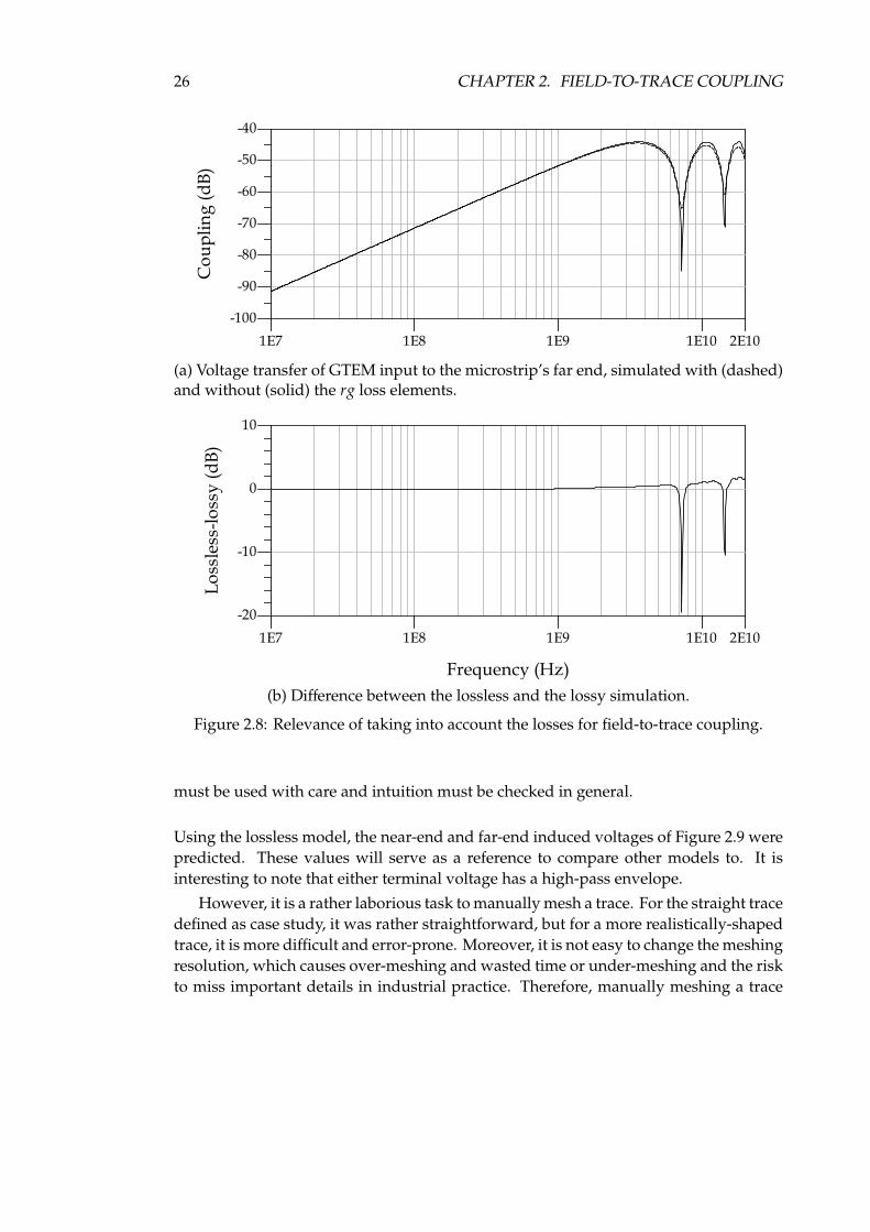
Now, an AC simulation can be run. In contrast to the S-parameter simulation, thedistributed sources will be activated and thus simulate the effect of the illuminationdefined in the case study. The simulation was run for the far end, with and without therg elements modeling the line’s losses. The results are presented in Figure 2.8.
The plateau and null frequencies look like resonances, but this transmission line isnot in resonance: both ends are characteristically terminated. Therefore, the relationbetween the ‘resonance’ frequencies and the geometrical dimensions is not simple. Anattempt to explain the phenomenon will be made in section 2.4.
As can be seen from Figure 2.8b, the lossless model slightly overestimates the cou-pling when the coupling is high, as could be expected. The lossless model underesti-mates the coupling, however, when it’s low. Because EMC problems are most likely tooccur when the coupling is high, the lossless model could here safely have been usedfor design purposes. Therefore and unless otherwise noted, lossless models will bestudied in the sequel of this thesis.
It be noted that either-end loads are matched to the trace in this case study, whichnever occurs in industrial practice. Intuitively, it may be expected that a lossless modelalso overestimates the field-to-trace coupling in a mismatched case. If that is the case,this lossless model may safely be used in an industrial case. It can also be expected thatthe bigger the mismatch, the larger the error induced by using a lossless model.2 Alarge, pessimistic error will result in expensive over-designing. At any rate, as can beseen above, a lossless model sometimes underestimates coupling, so the lossless model
2Consider the case of a lossless trace either-end terminated in an open circuit. A lossless model willthen predict infinite terminal voltages, although in reality they will be finite because of the trace’s losses.

2.3. MESHED TAYLOR MODEL 25
(a) The ωc tan δ dielectric conductance (notice the unitary slope).
(b) The copper resistance, dominated by the ∝√
f skin loss above 55 MHz.
(c) Comparison of the rg loss model (curve with markers) with ADS’ MSUB model(plain curve) for the 5-cm case study microstrip.
Figure 2.7: Modeling of the frequency dependent transmission line losses by g and r.
26 CHAPTER 2. FIELD-TO-TRACE COUPLING
(a) Voltage transfer of GTEM input to the microstrip’s far end, simulated with (dashed)and without (solid) the rg loss elements.
(b) Difference between the lossless and the lossy simulation.
Figure 2.8: Relevance of taking into account the losses for field-to-trace coupling.
must be used with care and intuition must be checked in general.
Using the lossless model, the near-end and far-end induced voltages of Figure 2.9 werepredicted. These values will serve as a reference to compare other models to. It isinteresting to note that either terminal voltage has a high-pass envelope.
However, it is a rather laborious task to manually mesh a trace. For the straight tracedefined as case study, it was rather straightforward, but for a more realistically-shapedtrace, it is more difficult and error-prone. Moreover, it is not easy to change the meshingresolution, which causes over-meshing and wasted time or under-meshing and the riskto miss important details in industrial practice. Therefore, manually meshing a trace

2.3. MESHED TAYLOR MODEL 27
Figure 2.9: ADS simulation result for voltage transfer of the GTEM input to the near-end(dashed trace) and far-end (solid trace) of a 5-cm lossless microstrip trace.
and entering the meshes as discrete elements in a standard circuit simulator does notseem a promising direction for practical use.
Meshing under Kron’s formalism
To facilitate meshing of realistically-shaped traces and to promote experimentation withthe meshing resolution, the meshing will be automated. As it is not straightforward toimplement this inside existing circuit simulators with a Graphical User Interface (GUI),like ADS or OrCAD, it will be done in a custom circuit simulator.
First, this problem will be analyzed in terms of Gabriel Kron’s formalism [29], be-cause of its promise to handle complex electromagnetic systems [30]. Next, the analysiswill be translated into a computer programme. Finally, the result will be compared tothe result from manual meshing under ADS.
Generally, solving a problem in Kron’s formalism consists of eight steps: stating theproblem, drawing the associated graph, defining the topological base, entering thesources, transforming, solving in mesh space, deducing the differences of potentialsand deducing other required quantities [31].
The problem was already stated in Figure 2.5 and now need to be converted to agraph. In this graph, nodes (or junctions) and meshes (or loops) need to be identified.Meshes consist of at least two branches (or vertices) that each connect two nodes. Sim-plified Kirchhoff branches will now be used, which generally consist of an impedanceZ and a voltage source e as defined in Figure 2.10. One possible graph is depicted inFigure 2.11.

28 CHAPTER 2. FIELD-TO-TRACE COUPLING
+ –v
Z
– +
ei
Figure 2.10: Simplified Kirchhoff branch. The difference of potential v across the branchand the current i through the branch are defined such, that when iv is positive, netpower is dissipated in the branch (passive sign convention).
1 2 3 4
1
2 4 6
83 5 7
Vne
Vfe
+
–
+
–
Figure 2.11: Graph representation of a three-cell transmission line model. Please verifythat there are 4 meshes (dashed loops, numbered), 8 branches (with arrows, numbered)and 5 nodes (dots, not numbered).
Let i, v and e be column vectors in the branch space, that is: containing the currentsand voltages of every branch. The (arbitrary) branch numbers of Figure 2.11 definewhich vector component represents which voltage and current: it is the definition of atopological base. Kirchoff’s mesh rule and Ohm’s law then hold as in e + v = Zi. In thiscase, the impedance matrix Z only has entries on its main diagonal:
Z =
Rne
jωl∆p1
jωc∆p
jωl∆p1
jωc∆p
jωl∆p1
jωc∆p
Rfe
(2.11)
To incorporate the current sources in the simplified Kirchhoff branch, their Théveninequivalents Eth are used. The source vector e stemming from the illumination electro-

2.3. MESHED TAYLOR MODEL 29
magnetic field thus becomes:
e =
0 0Hn(0) 00 Et(0)Hn(∆p) 00 Et(∆p)Hn(2∆p) 00 Et(2∆p)0 0
[
jωµ0 h∆ph
]
. (2.12)
To solve for the mesh currents, the equations need to be transformed to anothertopological base: that of the mesh space. Simultaneously and inevitably, the branchesare connected together. This is done by means of the connectivity matrix L, which linksthe branches (rows) with the meshes (columns). In this case,
L =
1 0 0 01 0 0 01 −1 0 00 1 0 00 1 −1 00 0 1 00 0 1 −10 0 0 1
. (2.13)
Note that a minus sign signifies a branch going against the mesh direction. Tensors inmesh space will be denoted with a hat, e.g.:
e = L−1e i = Lı Z = L−1ZL v = L−1v ≡ 0,
where the last vector (voltage around every mesh) is zero according to Kirchhoff’s meshlaw. The connectivity matrix L is Hadamard-like, of which the inverse can be foundby its transpose [31]. Kirchoff’s mesh rule and Ohm’s law can be transformed to meshspace as follows:
L−1v + L−1e = L−1Zi = L−1ZL ı (2.14)
e = Z ı. (2.15)
Notice that by transforming to the lower-dimensional mesh space, the branches wereconnected together.
To solve the system, the pseudoinverse (denoted +) can be used:
ı = Z+e, (2.16)
because the sources e and impedances Z are given, and the mesh currents ı are sought.

30 CHAPTER 2. FIELD-TO-TRACE COUPLING
The quantities of interest are the near-end and far-end voltages, which can now befound by means of the terminal impedances:
Vne = −ı1Rne (2.17)
Vfe = ı8Rfe. (2.18)
As the frequency-domain response is sought, these expressions need to be evaluated asfunction of the frequency ω.
In order to automatically mesh a microstrip and solve for its terminal voltages, theabove analysis need to be generalised for an arbitrary number of cells and implementedas a computer programme.
To promote reproducible computational research [32], a free-to-use programminglanguage is preferred. Python was selected, because it is, like its predecessor ABC, aprogramming language for intelligent computer users, which need not be computerprogrammers [33]. The numpy and matplotlib packages provide sufficient means formatrix algebra and visualisation of results, respectively.
It is rather straightforward to generalize (2.11) and (2.12), and functions were writtenthat generate these for an arbitrary number of cells. To generalise (2.13), the cases of 2and 3 cells were manually elaborated and first formulated as a unit test [34]. Next, animplementation satisfying both unit tests was written.
To evaluate (2.16), numpy’s Moore-Penrose pseudoinverse was called upon, whichuses Singular Value Decomposition (SVD). All code was then incorporated in thefield2line framework, written for this thesis and allowing for easy comparison ofdifferent field-to-trace coupling models and measurements [35].
To be sure to over-mesh the structure, a meshing resolution of 50 cells per free-space-wavelength for the highest frequency of interest was chosen: 167 cells in total forthe 5-cm case-study. With 661 logarithmically-spaced frequency points from 10 MHz to20 GHz, the calculation took 54 s on an Intel 2.53 GHz Core 2 Duo processor. The far-endresult is plotted and compared with the formerly obtained ADS result in Figure 2.12.The log frequency-weighted average difference between manual ADS meshing andautomatic Kron meshing is −0.03 dB, the average absolute difference being 0.1 dB.
Frequency-adaptive Meshing
In order to accelerate the calculation, the Kron-based simulation was profiled. Abouthalf of the total execution time was found to be spent on the pseudoinverse of (2.16).This and other matrix manipulations depend heavily on the size of the matrix, whichis drawn up for every frequency point. As the required number of cells is much lowerfor low frequencies, it makes sense to mesh the line for each frequency in the requirednumber of cells. Note that the speedup will be most pronounced for a logarithmicfrequency sampling. This was done with 50 cells per free-space-wavelength for each

2.3. MESHED TAYLOR MODEL 31
107 108 109 1010
Frequency (Hz)
−100
−90
−80
−70
−60
−50
−40|V
fe|
(dB
V)
Manual ADS
Automatic Kron
Figure 2.12: Comparison between manually meshed (ADS) and automatically meshed(Kron) simulation of the far-end induced voltage.
frequency, reducing the execution time to 4 s on the same platform. Fixed and frequency-adaptive meshing are compared in Figure 2.13. An average difference between fixedand adaptive meshing of −0.1 dB and an average absolute difference of 0.2 dB wereobtained.
Now that the simulation runs rather quickly, the sensitivity to the meshing resolutioncan be easily studied. The number of cells per wavelength of the frequency adaptivesimulation was swept from 1 to 50, and the error was calculated with respect to thesimulation result for a fixed meshing of 50 cells per wavelength. The result is plotted inFigure 2.14. As can be seen, both error metrics become very reasonable (below ±1 dB)from 20 cells per wavelength upward, at least in this case study.
Conclusion
The simple case study of the far-end induced voltage on a 5-cm, characteristicallyterminated microstrip, illuminated by a vertically polarised plane wave, was studiedby meshing the trace into many Taylor cells. This was first done manually, using ADS,carefully taking into account dielectric and copper losses. This led to the conclusion thatthe trace losses could be neglected to obtain only slightly pessimistic results. Then, themeshing was automated under Kron’s formalism, yielding the same results as underADS. The latter implementation also allowed for frequency-adaptive meshing, whichachieved a speedup of an order of magnitude. In this case study, 20 cells per wavelengthsufficed to obtain precise results.
Note that the automatic meshing could easily have been applied to multi-segment,arbitrarily-shaped traces with arbitrary loads. In spite of that and for simplicity, it wasnot done.

32 CHAPTER 2. FIELD-TO-TRACE COUPLING
107 108 109 1010−1800−1440−1080−720−360
0
6V
fe(°
) Fixed meshing
Adaptive meshing
107 108 109 1010−100−90−80−70−60−50−40
|Vfe|
(dB
V)
cells (a) Simulation result in amplitude and phase.
107 108 109 1010
Frequency (Hz)
100
101
102
103
Nu
mbe
rof
mes
hce
lls
(b) Number of cells used for the simulation.
Figure 2.13: Comparison of fixed and frequency-adaptive automatic meshing in Kron-based simulation.

2.4. MODIFIED TAYLOR MODEL 33
10 20 30 40 50Number of cells per wavelength
−3
−2
−1
0
1
2
3
4
Err
or(d
B)
Average error
Average absolute error
Figure 2.14: Sensitivity of adaptively-meshed simulation to the meshing resolution. Anon-adaptively-meshed simulation with 50 cells per wavelength served as reference tocalculate the error metrics.
2.4 Modified Taylor Model
As shown in the previous section, the coupling of an incident wave to a PCB tracecan be predicted by meshing the trace in electrically short Taylor cells, and solvingthe resulting circuit. Although the solution is found relatively quickly (4 s for a 5-cmmicrostrip), it does not yield insight. Indeed, the underlying model is completelyopaque: imagine the system of equations of a two-cell mesh. Little understanding isobtained, and important engineering questions remain unanswered, like “What designparameters have significant impact on the field-to-trace coupling?” or “What is theworst-case illumination (to test devices)?”
To answer these important questions, a transparent model will be constructedbottom-up. In each step, the model will be generalised, while keeping transparency bydetermining the worst case. The starting point is a single Taylor cell, valid for grazing-incident, vertically polarised plane wave incident on a single electrically short tracesegment with matched loads. Then, the model will be generalised to an electricallylong trace segment. Next, the model will be extended to multiple segments. Finally,the model will be generalised to comprise arbitrary loads. To conclude, this modifiedTaylor cell will be compared to above meshed Taylor simulations in terms of speed andinsight.
Short Trace
The starting point for the generalisation is one electrically short microstrip segment,illuminated by a vertically polarised, grazing-incident plane wave.
Electrically short means very small with respect to the exciting wavelength. Con-versely, the exciting wavelength is very large with respect to the trace length, so thephase shift of the incident field along the line tends to zero and the field can be con-

34 CHAPTER 2. FIELD-TO-TRACE COUPLING
+–
Zc
Zc
+
–
Vne
+
–
jωµ0Hn h`
j!cEt h` Vfe
Figure 2.15: An electrically short bifilar transmission line with characteristic loadsmodeled as a single Taylor cell.
sidered spatially uniform. Consequently, the line can be lumped as a single Taylor cell∆p = ℓ. Because the line is electrically short, the phase lag βℓ is negligible so the passiveline segment ℓ can be neglected. The resulting model of a short line with characteristicloads (Rne = Rfe = Zc) is shown in Figure 2.15. The low-frequency either-end terminalvoltages can be found by inspection [10]:
VLF = −12
j! cEtZc hℓ ∓ 12
j! µ0Hn hℓ, (2.19)
where c is the pul capacitance of the line. Unless otherwise noted, the near-end andfar-end results are presented simultaneously throughout this thesis; ∓means minus forthe near end and plus for the far end.
To evaluate this expression for grazing incidence, the substrate fields Et and Hn firstneed to be determined. Let the incidence azimuth φ be defined as in Figure 2.16a.Similarly to the end-fire case developed on p. 19, the incident field doubles in thesubstrate, the electric field is diminished by the permittivity and the phase speed remainsunchanged, as shown in Figure 2.16b.
Using the constitutive relations
Zc =1
cvline=
√εr,eff
c c0; Ei = Hi
√
µ0
ε0; c0 =
1√µ0ε0
,
the low-frequency terminal voltage under grazing incidence can now be expressed interms of Ei and φ:
VLF =12
j!(
−Zcc2Ei
εr∓ µ02Hi cos(φ)
)
hℓ
= j!Ei
(
−√εr,eff
c0εr∓ √µ0ε0 cos(φ)
)
hℓ
= jkiEi
(
−√εr,eff
εr∓ cos(φ)
)
hℓ,
(2.20)

2.4. MODIFIED TAYLOR MODEL 35
Ei
φ
!
c0
Hi
h`
(a) Perspective on the grazing incident wave: the incident electric field is perpendicularto the substrate and the wave vector makes an angle φwith the transmission line axis.
µ0, "0
µ0, "0"r
Zc
Zc
2Hi cosφ2Ei/"r !
c0cosφ
Ei
!
c0cosφ
Ei
!
c0cosφ
Hi cosφ
Hi cosφ
h
`
(b) Cross section of the transmission line. The incident and reflected plane wave sourcesproduce the shown substrate field.
Figure 2.16: Approximation of the substrate field strength for grazing incidence.
where the effective permittivity εr,eff is the field-weighted average permittivity that themicrostrip mode encounters: consequently, it is somewhere between the εr of the sub-strate and unity of the air.
By inspecting (2.20), the influence of the different design parameters can be gauged.The induced voltage is linearly dependent of the loop surface hℓ, of which the tracelength ℓ is easy to change in a late design stage, whereas the substrate thickness h isharder to change. The substrate’s permittivity εr is only of little influence, as it occursboth in denominator and (indirectly) in the enumerator.
The worst case illumination can also be found by inspection: the highest near-end(far-end) induced voltage magnitude occurs for φ = 0 (φ = π), that is, at the end wherethe incident wave is coming from. Note that this result is consistent with [19].
Long Trace
The next generalisation towards real-life traces is to include electrically long traces.

36 CHAPTER 2. FIELD-TO-TRACE COUPLING
First, a thought experiment will be performed to intuitively understand the longline effect. Alternatively, analytic reasoning will be used to quantify this long line effect,which will result in a single modified Taylor cell, which is also valid for high frequen-cies. This will be numerically checked against the meshed simulation results obtainedabove. Finally, the single modified Taylor cell will be used to obtain a transparent worstcase.
Consider the illumination of Figure 2.16a; now that the trace is generally long withrespect to the wavelength, the field becomes of a function of the position p along theline:
Ei(p) = Ei(0) · i(p), (2.21)
where i denotes the normalised amplitude of the illuminating field, which is just a phaselag:
i(p) = e−jkpp; kp =!
c0cosφ. (2.22)
The near-end (far-end) induced voltage can be thought of as the effect of a travelingwave on the line: the backward (forward) eigenwave [36]. Its normalised amplitude w isalso a phase lag:
w(p) = e±jβp; β =!
v, (2.23)
where v is the phase speed of a wave on the transmission line.Now imagine the illumination and the forward eigenwave at such a low frequency,
that a single Taylor cell is a competent model because the error it introduces is negli-gible. Along Figure 2.17(a-d), we will imagine what happens for rising frequency andconsequently, what the error introduced by a single Taylor cell would be.
Figure 2.17a shows the case for low frequencies, where the incident field remainsuniform along the line and the guided wave propagates quasi-instantly on the line, somodeling the line as one Taylor cell is legitimate.
As shown in Figure 2.17b, with increasing frequency, the wavelength decreases.When the wavelength gets in the order of the line length, a propagating wave appears,both in free space and in the transmission line. Yet, this does not immediately invalidatethe model. Indeed, the field is no longer uniform along the line, but the forwardeigenwave of the line and the free space plane wave travel in the same direction.That means that, for every line slice, the free space wave and the eigenwave still haveapproximately the same phase. Therefore, it is still legitimate to model the line as onecell.
As frequency increases further, like in Figure 2.17c, the phase difference between theforward eigenwave and the incident plane wave becomes significant; in the exampleshown, the phase difference goes from 0 at p = 0 to π at p = ℓ. On average, both wavesare still cross-correlated, but less so than for low frequencies.
In the extreme case of Figure 2.17d, the phase difference goes all the way from 0 atp = 0 to 2π at p = ℓ. On average, the two waves are no longer cross-correlated and

2.4. MODIFIED TAYLOR MODEL 37
–π
0
–2π
0 `p
\ (rad)
(a) Low frequency. . .
0
0
–π
–2π
\ (rad)
`p
(b) . . .
0
0
–π
–2π
\ (rad)
`p
π
(c) . . .
0
0
–π
–2π
\ (rad)
`p
2π
(d) . . . high frequency.
Figure 2.17: Phase along the transmission line of the line’s eigenwave ∠w (solid line)and illuminating plane wave ∠i (dashed line), for increasing frequency.
coupling is not expected any longer. For even higher frequencies (not depicted), therewill be some net correlation again, but never as much as for low frequencies.
To summarize, a single Taylor cell correctly predicts coupling for low frequencies.However, it overestimates the coupling at increasing frequencies, because the decreas-ing length-average similitude of the illuminating- and the eigenwave. Put differently,the high-frequency solution should equal the low-frequency solution of (2.20), correctedby some unitless measure K of similitude. This K should be unity for low frequencies,in order not to modify the low frequency coupling. K should amount to zero when thephase difference along the line goes all the way from 0 to 2π.
Armed with this intuitive expectation, an analytical approach can be safely taken. Nowthat the field is not generally uniform anymore, the integral over infinitely many cells dpalong the line’s length must be taken. Now that the propagation delay on the line is notnegligible anymore, the passive lossless transmission line must be taken into accountas well. This integral corresponds to a sliding cell dp with transmission lines at its leftand its right with lengths p and ℓ − p respectively, as shown in Figure 2.18.
Both sources of the infinitesimal cell directly see a characteristic load, so (2.20) givesthe backward- and forward traveling voltages. The near-end voltage contribution of

38 CHAPTER 2. FIELD-TO-TRACE COUPLING
+–
Zc
Zc
+
–
Vne
Vfe
+
–
j!µ0Hn(p) hdp
j!cEt(p) hdp
e−jβp e−jβ(`−p)
Figure 2.18: Modelling an electrically long, lossless bifilar transmission line with char-acteristic loads as the continuous integral of infinitesimal cells of length dp.
the infinitesimal cell is then delayed by the left half p of the lossless transmission line:
dVne =(
−12
Zc j!cEt(p) hdp − 12
j!µ0Hn(p) hdp)
e−jβp
= jkiEi(0)(
−√εr,eff
εr− cos(φ)
)
e−jkppe−jβp hdp(2.24)
Vne = jkiEi(0)(
−√εr,eff
εr− cos(φ)
)
h∫ ℓ
0e−jkppe−jβp dp. (2.25)
Similarly, the far-end voltage contribution is delayed by the right half (ℓ − p) of thetransmission line:
Vfe = jkiEi(0)(
−√εr,eff
εr+ cos(φ)
)
h∫ ℓ
0e−jkppe+jβp dp e−jβℓ. (2.26)
Let us now try to interpret the result as an equivalent circuit in order to developintuition. By slightly rewriting (2.25) and (2.26), we can recognise the low-frequencyinduced voltage of (2.20), multiplied by a factor K:
Vne = jkiEi(0)(
−√εr,eff
εr− cos(φ)
)
hℓ
︸ ︷︷ ︸
VLF,ne
1ℓ
∫ ℓ
0e−jkppe−jβp dp
︸ ︷︷ ︸
Kne
(2.27)
Vfe = jkiEi(0)(
−√εr,eff
εr+ cos(φ)
)
hℓ
︸ ︷︷ ︸
VLF,fe
1ℓ
∫ ℓ
0e−jkppe+jβp dp
︸ ︷︷ ︸
Kfe
e−jβℓ︸︷︷︸
delay
, (2.28)
where K is the length-averaged cross-correlation between the illumination- and eigen-wave amplitudes:
K =1ℓ
∫ ℓ
0i(p) ·w∗(p) dp =
1ℓ
∫ ℓ
0e−jkppe∓jβp dp =
1j(−kp ∓ β)ℓ
(
ej(−kp∓β)ℓ − 1)
, (2.29)

2.4. MODIFIED TAYLOR MODEL 39
+–
Zc
Zc
+
–
Vne
Vfe
+
–
e−jβ`j!µ0Hn(0)h` K
j!cEt(0)h` K
Figure 2.19: The modified Taylor cell; the correction factor K takes into account the longline effect.
which indeed is a measure for similitude. This result is visualised in Figure 2.19: asingle Taylor-like cell, also valid for high frequencies. One passive transmission line oflength ℓ accounts for the delay of (2.28). Note that for calculating the near-end or thefar-end induced voltage, Kne or Kfe need to be used, respectively.
To better understand the meaning of K, consider the non-physical case where theexcitation wave travels with the same phase speed along the line as a wave on the line:kp ≡ β. With Figure 2.17 in mind, it can be intuitively understood that both waves aresimilar for any frequency or wavelength. Analytically, this can be shown by calculatingthe far-end correlation Kfe for a wave number difference −kp + β tending to zero and afinite line length ℓ:
Kfe = lim−kp+β→0
1j(−kp + β)ℓ
(
ej(−kp+β)ℓ − 1)
= lim−kp+β→0
cos
(
(−kp + β)ℓ)
+ j sin(
(−kp + β)ℓ)
− 1
j(−kp + β)ℓ= 1.
(2.30)
Apparently, the non-uniformity of the excitation field does not suffice to invalidate asingle-cell Taylor model. It is rather the discrepancy between β and kp that makes Kdeviate from unity.
To gauge the correctness of (2.28) and the numerical speed-up of having only a single(modified) cell, the modified Taylor cell was implemented in the field2line frameworkmentioned before. This allowed for easy comparison between the simulation results ofdifferent models.
For example, the modified Taylor cell has an average error of −0.1 dB and a 0.2 dBaverage absolute error with respect to the first, manual ADS simulation (not shown).For another example, the modified Taylor cell was compared to the adaptively meshedTaylor cell in Figure 2.20. Phase comparisons proved a useful tool in debugging theimplementation. As can be seen, the modified and the meshed Taylor cell correlaterather well; +0.1 dB average error, 0.3 dB average absolute error.

40 CHAPTER 2. FIELD-TO-TRACE COUPLING
107 108 109 1010
−1440
−1080
−720
−360
0
6V
fe(°
)
Adaptively meshed
Modified
107 108 109 1010−100−90−80−70−60−50−40
|Vfe|
(dB
V)
(a) Simulation result in amplitude and phase.
107 108 109 1010
Frequency (Hz)
100
101
102
103
Nu
mbe
rof
mes
hce
lls
(b) Number of cells used for the simulation.
Figure 2.20: Comparison of modified Taylor with frequency-adaptive meshing (cf.Figure 2.13).
The simulation with the single modified Taylor cell took 0.4 s, which is about anotherorder of magnitude speedup with respect to the adaptively meshed Taylor cell.
Does the worst-case conclusion for an electrically short line also hold for an electricallylong line? Looking at (2.28), it can be seen that the line delay only introduces a phaseshift, so it can be ignored when reasoning about voltage magnitude. Both near-end andfar-end voltage magnitudes are the product of the low-frequency terminal voltage VLF
and the correction factor K. If the worst-case |K| coincides with the worst-case |VLF|,the worst-case product is the product of worst cases. Let us explore this hypothesis byfinding the worst-case |K|.
Let us interpret K geometrically on the complex plane. Recall that the integrandiw∗(p) yields the similarity of the excitation plane wave and the line’s eigenwave at any

2.4. MODIFIED TAYLOR MODEL 41
Im
K
iw∗(0)
iw∗(`)
Re
(a) On the complex plane: K is the centre of gravity of the arc iw∗(p). The trajectory ofK is dashed for 0 ≤ iw∗(ℓ) ≤ 4π.
β
k
kpβ − kp
φ
(b) In Carthesian space: wave vector alignment with the transmission line.
Figure 2.21: Geometric interpretations of K’s constituents.
position p on the transmission line. At the beginning of the line, both waves have thesame phase. As i and w are normalised amplitudes, the integrand amounts to one. Dueto the different propagation speeds of the excitation wave and the line’s eigenwave, thephase difference grows along the line. The arc described by the integrand in the case ofa forward propagating wave is shown in Figure 2.21.
The integral divided by its length yields the arc’s centre of gravity K. By inspectingFigure 2.21a, it can be seen that |K| ≤ 1. Moreover, the greater the phase difference atthe end of the line, the longer the arc, the smaller |K|. Conversely, the smaller the phasedifference at the end of the line, the greater |K|. The phase difference at the end of theline is (β− kp)ℓ. Hence, for a given ℓ, the worst case occurs when kp and β are closest.
To see when β and kp are closest, picture the line’s wavenumber β as a vector pointingin the line direction. The excitation wave vector parallel to the line kp then is the

42 CHAPTER 2. FIELD-TO-TRACE COUPLING
projection of k on the first vector. Moreover, as the excitation wave always propagatesfaster than a wave on the line, k is always shorter than β, as is the case in Figure 2.21b.By inspection, it can be concluded that β − kp is minimal when the excitation wavevector k is parallel with the line. Therefore, |Kfe| is maximum when exciting from thenear-end side, parallel to the line: end-fire excitation. Analogously, |Kne| is maximumwhen exiting from the far-end side, parallel to the line. Put differently, |K| is maximumat the end where the incident wave is going to.
So, both for |K| and |VLF|, the worst case occurs for end-fire excitation, but not fromthe same end, unfortunately. Indeed, Leone’s case study suggests that the worst-caseend be frequency dependent [19]. All the same, the upper bound mentioned before canbe evaluated:
max |V| ≤ max |VLF| ·max |K| = max |VLF|, (2.31)
which is true but not very useful, because |VLF| increases without bound as function offrequency.
Therefore, the product VLFK will be first evaluated for a given Ei, h, ℓ, εr and εr,eff ,and then the worst-case φwill be sought.
K =1
j(−ki cos(φ) ∓ β)ℓ(
ej(−ki cos(φ)∓β)ℓ − 1)
, (2.32)
|V| = |VLF||K| = Eih
∣∣∣∣∣∣∣∣
−√εr,eff
εr∓ cos(φ)
− cos(φ) ∓ √εr,eff
∣∣∣∣∣∣∣∣
∣∣∣∣∣ej!(− cos(φ)∓√εr,eff) ℓc0 − 1
∣∣∣∣∣. (2.33)
The rightmost term determines the worst case frequency, then amounting to 2. The restis frequency- and length- (!) independent.
Knowing that√εr,eff > 1 and for given Ei, h, εr and εr,eff ,
max!ℓ|V| = 2Eih
∣∣∣∣−√εr,eff
εr∓ cos(φ)
∣∣∣∣
√εr,eff ± cos(φ)
. (2.34)
In order to find the maximum with respect to φ, we would like to differentiate andequate to zero to find the critical points. However, for φ where the enumerator signflips over, the fraction is not differentiable. Fortunately, these φ constitute the minima,whereas we search the maxima. We may ignore the absolute operator because criticalpoints stay critical under the absolute operator:
∂
∂φmax!ℓ|V| = 2Eih
∓√εr,eff
(
1− 1εr
)
sin(φ)(√εr,eff ± cos(φ)
)2. (2.35)
The denominator is never zero, so the derivative only equals zero for φ = 0, π: we onlyneed to consider end-fire illumination.

2.4. MODIFIED TAYLOR MODEL 43
Let us compare φ = 0 (left hand side) and φ = π (right hand side) for the near-endcase of (2.34) (recall that
√εr,eff < εr,eff < εr):
2Eih1 +
√εr,eff
εr√εr,eff + 1
≶ 2Eih1−
√εr,eff
εr√εr,eff − 1
(2.36)
(
1 +√εr,eff
εr
)(√εr,eff − 1
)
≶
(
1−√εr,eff
εr
)(√εr,eff + 1
)
(2.37)
√εr,eff +
εr,eff
εr− 1−
√εr,eff
εr≶
√εr,eff + 1−
εr,eff
εr−
√εr,eff
εr, (2.38)
so, φ = π constitutes the worst case for the near-end. Conversely, φ = 0 constitutes theworst case for the far-end.
By plugging these worst-case φ into (2.34), we conclude:
max!ℓ,φ|V| = 2Eih
1−√εr,eff
εr√εr,eff − 1
, (2.39)
which is the high-frequency, worst-case, either-end induced voltage in a characteristi-cally terminated microstrip illuminated under grazing incidence.
Now that the high-frequency worst case of (2.39) and the low-frequency worst caseof (2.20) are found, they can be joined to obtain a broadband worst case:
max |V| = Eih ·min
8
>
>
>
<
>
>
>
:
!
c0`
(
1 +p"r,eff
"r
!
, 21 −
p"r,eff
"rp"r,eff − 1
9
>
>
>
=
>
>
>
;
,
magnetic
electric
low-frequency high-frequency
(2.40)
that is, the envelope formed by the low-frequency near-end voltage for φ = 0 and thehigh-frequency voltage for φ = π, as illustrated in Figure 2.22 and Figure 2.23.
This broadband worst case envelope can be physically interpreted as follows: forlow frequencies, the worst case occurs when the magnetic and the electric contributionsadd up constructively. The wavelength is great with respect to the line length, so theline does not feel the difference between a forward or a backward travelling wave:Kfe = Kne = 1. For high frequencies, the worst case occurs when the illuminating waveis aligned with the wave propagating towards the terminal. The magnetic and electriccontributions cancel somewhat, but the alignment (K→ 1) has a bigger effect.
Multiple Segments
To study multi-segment traces a simple case study was drawn up. To facilitate foranalytical and numerical debugging, a small number of segments was chosen: three.

44 CHAPTER 2. FIELD-TO-TRACE COUPLING
W Pfe
φ = 0
12π
π
32πhigh frequency
low frequency
Figure 2.22: Qualitative antenna pattern of the far end. The radial axis has no particularunit: the low-frequency gain of (2.20) is linear in !, the high-frequency gain of (2.34) isnormalised to coincide with the low-frequency gain at φ = π. Notice the broadband
null at cos(φ) = ∓√εr,eff
εr.
107 108 109 1010
Frequency (Hz)
−130−120−110−100−90−80−70−60−50−40
|Vfe|
(dB
V)
West
East
|V| =!
c0Ei
(
1 +
p εr,eff
εr
!
h`
|V| = 2Eih1 −
p"r,eff
"rp"r,eff − 1
Figure 2.23: Coupling to one end of a rotated trace: the eastern orientation (φ = 0,actual far-end coupling) and western orientation (φ = π, rather near-end coupling) arehighlighted. The orientation of the trace was swept from 0 to 2π in 100 steps. Thebroadband envelope of (2.40) is plotted in red.

2.4. MODIFIED TAYLOR MODEL 45
Ei
ω
c0
Hi360 µm
near endfar end
1
2
3
`2 = 1.7cm
`1 = 2.5cm `3 = 2.5cm
Figure 2.24: Case study on three-segment trace with mitred bends.
The lengths were chosen to have the trace significantly differ from one straight segment,as can be seen in Figure 2.24. Similarly to the above analyses, the terminal voltages underend-fire illumination will be sought.
To simplify the analysis, the transitions between the segments will be considerednegligible. That way, the entire trace will behave like a uniform transmission line, like itdid in the analysis of a single microstrip segment. In practice, this will require optimallymitred bends, because straight corners introduce excess capacitance [37].
The coupling to multiple straight line segments can be found by superposition, becausethe segments are matched. In the three-segment case study, the contributions of thestraight line segments ℓ1, ℓ2 and ℓ3 must be summed:
Vne =(
K1neV1
LF,ne + K2neV2
LF,ne + K3neV3
LF,ne
)
(2.41)
Vfe =(
K1feV1
LF,fe + K2feV2
LF,fe + K3feV3
LF,fe
)
e−jβℓ (2.42)
where Kufe is the far-end correction factor of the uth line segment. Vu
LF,fe (VuLF,ne) denotes
the low-frequency far-end (near-end) voltage of the uth segment according to (2.19). ℓis a shorthand for the line’s total length ℓ1 + ℓ2 + ℓ3. In general:
Vne =n
∑
u=1
KuneVu
LF,ne (2.43)
Vfe =n
∑
u=1
KufeVu
LF,fee−jβℓ, (2.44)
where n denotes the number of segments. The correction factors Ku are found by inte-grating iw∗ along the particular segment. Now that the segment is no longer necessarilyparallel with p anymore, let s denote the path length along the entire trace. For example,
K2 =1ℓ2
∫ ℓ1+ℓ2
ℓ1
i(s)w∗(s) ds =1ℓ2
∫ ℓ1+ℓ2
ℓ1
e−jkpℓ1e∓jβs ds, (2.45)
because the incident field is uniform along segment 2. In general, it can be shown that
Ku =1
j(−ks ∓ β)ℓu
(
ej(−kppend∓βsend) − ej(−kppbegin∓βsbegin))
, (2.46)

46 CHAPTER 2. FIELD-TO-TRACE COUPLING
where ks is the incident wave vector along the line segment and kp is the incident wavenumber. The distance from the field origin at the beginning (end) of the segment isdenoted by pbegin (pend). The path length along the trace at the beginning (end) of thesegment is denoted by sbegin (send).
Likewise, for the low-frequency contributions VuLF, the field orientation with respect
to the line segment must be taken into account. For example,
V2LF = −j!c
Ei
εrZchℓ2 = −j
!
c0Eihℓ2
√εr,eff
εr, (2.47)
because the incident magnetic field is parallel to line segment 2, hence it does not con-tribute to the terminal voltage.
In order to find a transparent worst case for multi-segment traces, recall the single-segment worst case of (2.40). The multi-segment induced voltage is the sum of thesegment’s contributions. There is no simple (transparent) way to know whether thecontributions add up constructively or destructively. Therefore, a loose upper boundon the sum of the contributions is the sum of the upper bound of the contributions:
max |V| = Eih ·min
!
c0ℓ
(
1 +√εr,eff
εr
)
, 2n1−
√εr,eff
εr√εr,eff − 1
, (2.48)
where ℓ is the total path length of the multi-segment trace and n denotes the numberof segments. This upper bound is calculated for the case study and compared to anazimuthal sweep (φ ∈ [0, 2π)) of (2.44) in Figure 2.25.
Notice that even for low frequencies, no curve actually touches the upper bound(contrary to Figure 2.23). This can be understood by recognising that the low-frequencyupper bound holds for a straight trace of the same total length ℓ. Only for this straighttrace, the electric and magnetic contribution entirely add up at the near end. For anytrace deviating from a straight trace, with the same length, the contributions will notadd up to that maximum.
Notice also that the high frequencies, the asymptote is rather tight: 2.6 dB higherthan the sweep maximum in this particular case study. However, imagine consideringa straight trace as many short traces in series. Contrary to the low frequency asymptote,the high frequency asymptote will grow without bound, while the trace remains thesame. Therefore, there must also be cases where the high frequency upper bound is notat all tight.
Arbitrary Loads
Basic transmission line theory will now be applied to obtain the either-end inducedvoltages for arbitrary (generally mismatched) loads.

2.4. MODIFIED TAYLOR MODEL 47
10 10 10 10
107 108 109 1010
Frequency (Hz)
−140
−120
−100
−80
−60
−40
−20|V
fe|
(dB
V)
West
East
Ei h`!
c0
(
1 +
p"r,eff
"r
!
Ei hn 21 −
p"r,eff
"rp"r,eff − 1
Figure 2.25: Coupling to one end of a rotated, multi-segment (n = 3) trace: the easternorientation (actual far-end coupling) and western orientation (rather near-end coupling)are highlighted. The orientation of the trace was swept from 0 to 2π in 100 steps. Thebroadband envelope of (2.48) is plotted in red.
From the foregoing, the terminal voltages Vne and Vfe on characteristic loads areknown, which can be considered voltage waves coming out of a transmission line ofcharacteristic impedance Zc. These voltage waves will then generally be reflected by theeither-end terminal impedances Zee according to their voltage reflection coefficients:
Γee =Zee −Zc
Zee + Zc. (2.49)
As illustrated in Figure 2.26, the far-end induced voltage wave Vfe will be reflected bythe far-end terminal impedance, then delayed by the transmission line. Together withthe near-end induced voltage Vne, it can be considered a voltage wave Vinc,ne incidenton the near-end terminal impedance:
Vinc,ne = Vne + ΓfeVfee−jβℓ. (2.50)
If the near-end would be characteristically terminated (Zne = Zc), this is exactly thefinal near-end voltage [38].
In general, however, a near-end reflection will occur:
Vrefl,ne = ΓneVinc,ne =Zne −Zc
Zne + ZcVinc,ne, (2.51)
that is, the near-end reflected wave would induce a voltage Vrefl,ne on a characteristicload. With this knowledge, the reflected wave can also be represented as an equivalentnear-end voltage source as shown in Figure 2.27a:
Vrefl,ne,equiv = Vrefl,neZc + Zne
Zc= Vinc,ne
Zne −Zc
Zne + Zc
Zc + Zne
Zc(2.52)

48 CHAPTER 2. FIELD-TO-TRACE COUPLING
Vfe
ΓfeVfe
Γne
(
Vne +ΓfeVfee−jβ`)
| z
Vinc,ne
Vne
ZfeZne
Zc
ΓfeVfee−jβ`
Figure 2.26: From top to bottom: the either-end induced voltage waves, the far-endreflection and the near-end reflection.
To avoid having to consider infinite reflections going up and down the line, the far-endterminal impedance is translated to the near end:
Γfe@ne = e−2jβℓΓfe (2.53)
Zfe@ne = ZcΓfe@ne + 1Γfe@ne − 1
, (2.54)
where ‘@ne’ denotes ‘as seen at the near end’. Now, the final near-end reflected voltagecan be calculated using the voltage divider of Figure 2.27b:
Vrefl,ne,final = Vrefl,ne,equivZfe@ne
Zne + Zfe@ne. (2.55)
The total near-end voltage is the sum of the incident and the final reflected voltage:
Vne,final = Vinc,ne + Vrefl,ne,final
=(
Vne + ΓfeVfee−jβℓ)
(
1 +Zc −Zne
Zc
Zfe@ne
Zne + Zfe@ne
)
,(2.56)
which also holds, mutatis mutandis, for the total far-end voltage. Note that this solutionis, albeit lengthy, closed-form.
The conclusion of (2.56), especially when expanded, is very opaque. In order to gaininsight, a design-oriented worst case will now be sought.
Particularly, an EMC-aware PCB designer will try to achieve sufficient immunity,having some influence on routing and terminal impedances. Sufficient immunity equalsworst-case (maximum) voltages at the trace terminals, depending on the immunity ofthe connected components. Routing influence may consist in reducing trace length orchanging trace width within the practical possibilities. Terminal impedances may alsobe tuned, by introducing frequency-dependent parallel or series impedances.

2.4. MODIFIED TAYLOR MODEL 49
Zne
Vrefl,neZc +Zne
Zc
+
–
Zc
+
–
Vrefl,ne
(a) First step: find the near-end voltage source equivalent to the reflected voltage wave,using a characteristic load.
Zne
Vrefl,neZc +Zne
Zc
Zfe@ne
+
–
(b) Second step: find the final near-end reflected voltage, using the actual far-endterminal impedance, translated to the near end.
Figure 2.27: Calculating the final effect of the near-end reflection.
Especially for low-frequency circuits (e.g. a logical output and a logical input), bothterminal impedances are expected to be rather mismatched (i.e. some Ω connectedto some kΩ). Furthermore, the engineer will be interested in the worst-case voltagemagnitude over angle of incidence and frequency.
To deal with the complexity of (2.56), its terms and factors will be separately in-spected to find an upper bound to them. The sum and product of these upper boundswill then also constitute an upper bound.
Although the near- and far-end voltages Vne and Vfe will never simultaneously amountto the upper bound of (2.48), it is safe to assume so. Moreover, the phasor e−jβℓ rotateswith frequency, so for some frequencies, the near- and far-end induced voltages willadd up in phase. Therefore, the first factor of (2.56) can be safely approximated like so:
max∣
∣
∣Vne + ΓfeVfee−jβℓ∣
∣
∣ ≤ max |Vee| (1 + ρfe) , (2.57)
where ρfe is the magnitude of the far-end reflection coefficient Γfe. This reasoning step
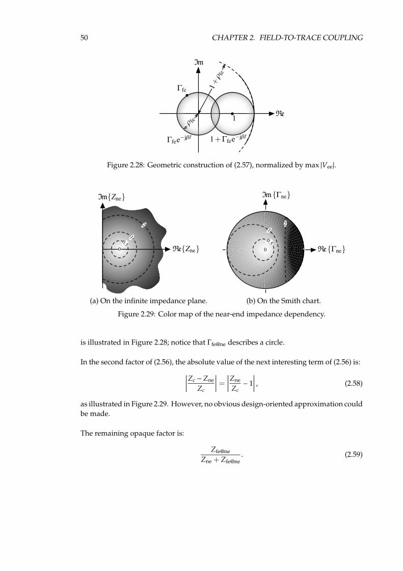
50 CHAPTER 2. FIELD-TO-TRACE COUPLING
Γfe
Re
Im
1
1+Γfee−jβ`Γfee−jβ`
ρ fe
1+ρ
fe
Figure 2.28: Geometric construction of (2.57), normalized by max |Vee|.
ReZne
ImZne
0.5
1
2
0
(a) On the infinite impedance plane.
0.5
1
2
0 ReΓne
ImΓne
(b) On the Smith chart.
Figure 2.29: Color map of the near-end impedance dependency.
is illustrated in Figure 2.28; notice that Γfe@ne describes a circle.
In the second factor of (2.56), the absolute value of the next interesting term of (2.56) is:∣
∣
∣
∣
∣
Zc −Zne
Zc
∣
∣
∣
∣
∣
=
∣
∣
∣
∣
∣
Zne
Zc− 1
∣
∣
∣
∣
∣
, (2.58)
as illustrated in Figure 2.29. However, no obvious design-oriented approximation couldbe made.
The remaining opaque factor is:
Zfe@ne
Zne + Zfe@ne. (2.59)

2.4. MODIFIED TAYLOR MODEL 51
Let us therefore find its maximum magnitude while e−jβℓ describes the unit circle (i.e.the product βℓ takes all possible values). To that end, the fraction will be rearrangedto obtain a difference, which has an obvious geometric interpretation on the complexplane: a distance.
maxβℓ
∣
∣
∣
∣
∣
Zfe@ne
Zfe@ne + Zne
∣
∣
∣
∣
∣
= maxβℓ
1∣
∣
∣
∣
1 + ZneZfe@ne
∣
∣
∣
∣
=1
|Zne|minβℓ
∣
∣
∣
∣
1Zne
+ 1Zfe@ne
∣
∣
∣
∣
=1
|Zne|minβℓ
∣
∣
∣
∣
− 1Zne− 1
Zfe@ne
∣
∣
∣
∣
.(2.60)
Put geometrically: the worst case occurs when the mirrored near-end admittance −Yne
and the far-end admittance seen at the near end Yfe@ne are closest. Now what doesYfe@ne look like, on the complex admittance plane?
Recall that admittance and reflection coefficient are related by:
Y =1
Zc
1− Γ
1 + Γ(2.61)
which is a Möbius transformation, so generalized circles in Γ correspond with gener-alized circles in Y. Therefore, Yfe@ne must be a circle. Moreover, this transformation ismirror symmetric about the real axis. As the Γfe@ne itself is mirror symmetric about thereal axis, its transform Yfe@ne must be mirror symmetric about the real axis too. Hence,the transform Yfe@ne must be a circle with a real centre.
Now it suffices to find two transformed points to entirely define the transformedcircle. Let us take the rightmost and the leftmost value of Γfe@ne, that is ±ρfe. Theiradmittance counterparts are
Yfe@ne =1
Zc
1∓ ρfe
1± ρfe. (2.62)
As these points lie on a circle with a real centre, the centre and radius can be found bytaking half the sum and half the difference:
Yfe@ne,radius =12
1Zc
(
1 + ρfe
1− ρfe−
1− ρfe
1 + ρfe
)
=1
Zc
2ρfe
1− ρ2fe
(2.63)
Yfe@ne,centre =12
1Zc
(
1 + ρfe
1− ρfe+
1− ρfe
1 + ρfe
)
=1
Zc
1 + ρ2fe
1− ρ2fe
(2.64)
The sought minimum is constructed in Figure 2.30: Yfe@ne describes a circle and −1/Zne
always lies in the left half plane. The minimum distance between a circle and a pointis the distance from the circle’s centre to the point minus the circle’s radius. For arather mismatched far-end load (a circle close to the imaginary axis), a reasonableapproximation can be found by inspection of Figure 2.30:
minβℓ
∣∣∣∣∣− 1
Zne− 1
Zfe@ne
∣∣∣∣∣≥ Re
1Zne
. (2.65)

52 CHAPTER 2. FIELD-TO-TRACE COUPLING
ReY
ImY
1
Zne
−1
Zne
Yfe@ne,centerYfe@ne,radius
Re
1
Zne
min…
Figure 2.30: Geometric construction of (2.65). Yne accidentally lies inside the Yfe@necircle.
Note that this approximation is also true for rather matched far-end loads, but it willresult in a looser upper bound. Other approximations are possible, but for the sake oftransparency and in view of the typical application, this candidate was retained.
Plugging this result into (2.60) yields
maxβℓ
∣
∣
∣
∣
∣
Zfe@ne
Zfe@ne + Zne
∣
∣
∣
∣
∣
≤ 1
|Zne| 1ReZne
=1
|Zne| ReZne|Zne|2
=1
cos ∠Zne, (2.66)
which is barely transparent.
Plugging the worst case terms and factors found above in (2.56), this upper bound isobtained:
Vne,final ≤ max |Vee| (1 + ρfe)(
1 +∣
∣
∣
∣
∣
Zne
Zc− 1
∣
∣
∣
∣
∣
1cos ∠Zne
)
, (2.67)
mutatis mutandis for the far end.Note that this upper bound is particularly pessimistic for rather matched far-end
loads. Tighter upper bounds exist and were found, but turned out to be opaque.One obvious design-oriented conclusion may be drawn from this result: matching
helps. This can be seen from (2.67), because the smaller ρfe and the closer Zne to Zc,the smaller the upper bound. Note that this matching can be achieved by changingthe terminal impedances or by changing the line’s characteristic impedance (by tuningthe trace width, typically). The last factor shows that a purely capacitive (inductive)near-end load is particularly bad, and adding a small resistance in series (parallel) maydramatically reduce resonances.
To demonstrate the applicability, the upper bound of (2.67) is calculated for thethree-segment trace with typical mismatched loads. It is compared with the azimuthallyswept solution of (2.56) in Figure 2.31. Notice that for some frequencies, neither theeastern nor the western orientation constitute the worst case.

2.4. MODIFIED TAYLOR MODEL 53
10 10 10 10
107 108 109 1010
Frequency (Hz)
−140−120−100−80−60−40−20
0
|Vfe|
(dB
V)
West
East
(1 + ρfe)(
1 +∣
∣
∣
∣
∣
Zne
Zc− 1∣
∣
∣
∣
∣
1cos \Zne
)
×Ei hn 21 −
p"r,eff
"rp"r,eff − 1Ei h`
!
c0
(
1 +
p"r,eff
"r
!
× (1 + ρfe)(
1 +
∣
∣
∣
∣
∣
Zne
Zc− 1∣
∣
∣
∣
∣
1
cos \Zne
)
9 dB10 dB
Figure 2.31: Coupling to one end of a rotated, multi-segment trace with mismatchedloads: 1 Ω at the near end, 1 kΩ at the far end. The eastern orientation (actual far-end coupling) and western orientation (rather near-end coupling) are highlighted. Theorientation of the trace was swept from 0 to 2π in 100 steps. The broadband envelopeof (2.67) is plotted in red.
Conclusion
A lightweight model for field-to-trace coupling was constructed by generalising step-by-step. The model consists of a single Taylor cell, corrected for high frequencies withthe cross-correlation K between the incident- and eigenwaves. By superposition of onesuch cell for each segment, the model also applies to multi-segment traces. By anothercorrection factor, the effect of either-end mismatched loads can be taken into account.The model thus predicts the coupling of a grazing incident, vertically polarised planewave to a multi-segment, uniform microstrip trace with arbitrary terminal loads.
Because the model is closed-form, it outperforms the meshed solution. For instance,it executes ten times as fast as the adaptively meshed model of section 2.3, while corre-lating to within 0.3 dB average absolute error.
The transparent formulation of Figure 2.31 also has practical design implications. Forexample, matching the trace impedance and its terminal impedances reduces resonancepeaks. The substrate permittivity has only little influence on the coupling. For lowfrequencies, the coupling is proportional to the total trace length and the substratethickness. For high frequencies, the coupling is loosely proportional to the number oftrace segments, but not to the trace length.
The are also practical (pre-compliance) testing implications. For example, the worst-

54 CHAPTER 2. FIELD-TO-TRACE COUPLING
case induced voltage on a straight microstrip trace occurs at the near end for low fre-quencies and the far end for high frequencies. The trace also has a blind azimuthal spotat cos(φ) = ∓√εr,eff/εr.
The modified Taylor model has a limited validity domain, in comparison with industrialelectronics. Therefore, industry-related research should indicate to what extent itslimitations form a problem. If so, the model might need improvement.
For instance, no trace width (i.e. impedance) changes or branches can be modelled.
Furthermore, the mismatched loads were supposed to have a frequency-constantcomplex impedance. This is not the case for IC terminals or passive loads.
Moreover, trace losses were not taken into account. Especially with very reflectiveterminal loads, this may seriously overestimate the induced voltages. The above anal-ysis should be repeated with a complex β to represent losses, to transparently representthem in the upper bound.
Finally, the presented upper bound is not very tight. A practical case should revealwhether or not this induces costly overengineering. Moreover, as we only started toenjoy Möbius transformations, stricter yet transparent upper bounds may have beenoverlooked.
2.5 Full-wave simulation
The Taylor cell applied in section 2.3 and simplified in section 2.4 is based on someunchecked assumptions. Firstly, a meandered trace is modelled as a TEM transmissionline: uniform, homogeneous and monomodal. Secondly, the substrate field is supposedto be a fraction of the illumination (cf. Figure 2.4). Finally, the bifilar line model isapplied to a microstrip trace. Do these modelling decisions significantly degrade itspredictions?
To check these assumptions, two case studies will be simulated with a full-wavesolver. The case studies are designed to be comparable both with the modified Taylorcell and with measurements. The full-wave solver allows for a perfect illumination of aperfectly-defined geometry and known lossless dielectric with lumped-element loads,without applying the idealisations mentioned above. Comparing its results with thoseof the modified Taylor cell will therefore gauge the impact of the assumptions.
First, the case studies will be drawn up. These will be entered and then simulatedunder CST Studio. The simulation results will then be compared to the correspondingpredictions of the modified Taylor cell. Consequently, conclusions will be drawn on thevalidity of the Taylor model’s assumptions.

2.5. FULL-WAVE SIMULATION 55
Case Study
The three-segment microstrip studied before is chosen again, for simplicity’s sake.In measurement, the PCB will need coaxial connectors to give access to both traceterminals. The entire path from connector to connector needs to be matched to theVNA characteristic impedance of 50 Ω. At the near end, a short calibration standard isconnected, inevitably including an electrical delay τd, as shown in Figure 2.32. For thefar end, two different configurations will be considered.
The first configuration called ‘matched’, the far end of the trace sees a 50 Ω load.In measurement, this simply corresponds to connecting the VNA to the far-end SMAconnector. In this case, the induced near-end voltage will be reflected once by the shortcircuit and there will be no more transmission line reflections after that.
Therefore, a second configuration called ‘probed’ is defined. To have a mismatchedload at both ends, but still be able to measure with a VNA, a 220 Ω probe resistanceis installed in series with the trace at the far end. When the VNA is connected, thetrace will see a far-end load of 270 Ω. The actual far-end voltage will be sampled by the50/270 resistive divider. To be precise, the 220 Ω resistor used in measurement, wasmeasured and found to have a 44 fF parasitic parallel capacitance. This will need to betaken into account both in simulation and using the modified Taylor model.
Simulation Set-up
The trace was entered in CST Microwave Studio as an infinitely-thin, Perfect ElectricalConductor (PEC). The ground plane was a 75 × 75 mm PEC beneath the trace. Thesubstrate was a lossless dielectric layer with εr = 4.6, covering the ground plane. Thetrace was terminated in 50 Ω discrete face ports. The geometry was meshed using a
Ei
ω
c0
Hi
360 µm
near end far end
1
2
3
`2 = 1.7cm
`1 = 2.5cm `3 = 2.5cm
50 Ω
τd
Figure 2.32: Perspective on the case study PCB: a three-segment, 50 Ω microstrip traceover a ground plane, illuminated by a horizontally polarised plane wave. The near end’scoaxial connector is shorted, the far end’s connector is terminated in a characteristic load(the VNA’s input).

56 CHAPTER 2. FIELD-TO-TRACE COUPLING
hexahedral λ/20 mesh for 20 GHz, except near the microstrip: one mesh cell acrossthe dielectric thickness and at least two mesh cells across the trace width. The PerfectBoundary Approximation (PBA) compensates for the staircase meshing of the miteredtrace corners.
All boundary conditions were set to ‘open and add space’: that is, λ/8 extra spacewas added, terminated by 4 Perfectly Matched Layers (PMLs). This geometry wasthen illuminated with a vertically polarised plane wave excitation, as illustrated inFigure 2.33a. The plane wave electric field strength was 1/d, where d is the averageGTEM-cell septum distance 42.2 mm.
In order to take the terminal impedances into account, a geometry-circuit co-simulation was chosen, also because of its scaleability to many and non-linear loads.Hence, the above-mentioned geometry with plane wave excitation was entered as oneschematic block in the co-simulation. At the near end, a lossless transmission line wasconnected, representing the coaxial connection with a 80-ps delay τd up to the shortstandard, followed by a perfect short circuit.
At the far end, for the ‘matched’ configuration, a perfect load was connected, mon-itored by a voltage probe. As the structure is illuminated with the field caused by 1 Vat the septum, the output voltage in volts predicts the measurable S21 transfer fromseptum to far end. The resulting schematic is depicted in Figure 2.33b.
For the ‘probed’ configuration, the same co-simulation schematic was used, butwith the series probe resistance inserted, as shown in Figure 2.33c. Because this proberesistance will consume 2.5 mm trace length, the third segment ℓ3 was modified to22.5 mm.
Results
The inherent causality of co-simulation requires a time-domain solver and a FiniteIntegration Technique (FIT)-based solver [39] was chosen. The ‘matched’ co-simulationwas run with a −80 dB accuracy criterion. In order to allow for phase comparison, thephase reference of the plane wave was moved from the simulation boundary to the nearend. The result is compared with the modified Taylor prediction in Figure 2.34.
The log-frequency average difference between simulation and the extended Taylorprediction, a measure for bias, was −0.36 dB over the 50 MHz to 20 GHz range. Theaverage absolute error was 0.94 dB. The comparison was repeated with different mesh-ing resolutions and accuracy criteria, as shown in Table 2.1. With the lowest accuracysettings, the required simulation time is reasonable: 35 s on a 2× 2.5 GHz Intel R© E5 with16 GB RAM and an NVIDIA R© Tesla
TM20 Graphics Processing Unit (GPU). As can be
seen, increasing the accuracy criterion has little influence, but decreasing the mesh sizehas. Moreover, the more precise the simulation, the lower the average absolute error.
Then the simulation was run for the ‘probed’ configuration. The simulation seemedto converge (decreasing residual energy), but started diverging again. This problemmay be caused by the long-lasting reflections going up and down on the lossless line

2.5. FULL-WAVE SIMULATION 57
1
2
E
H
(a) Geometry (figure not to scale, in order to see the substrate) as entered into CSTMicrowave Studio. The dielectric substrate is shown translucent. Note the polarisationof the incident plane wave from the left.
(b) Co-simulation schematic as entered into CST Design Studio for the ‘matched’ con-figuration. The first block is a lossless transmission line defined by its delay τd, thesecond block is the geometry with excitation of Figure 2.33a.
(c) Co-simulation schematic as entered into CST Design Studio for the ‘probed’ config-uration, identical to Figure 2.33b, except for the far-end termination.
Figure 2.33: Overview of the CST Studio full-wave simulation.

58 CHAPTER 2. FIELD-TO-TRACE COUPLING
108 109 1010
−3240−2880−2520−2160−1800−1440−1080−720−360
06
Vfe
(°)
CST
Taylor
108 109 1010
Frequency (Hz)
−80
−70
−60
−50
−40
−30
|Vfe|
(dB
V)
Figure 2.34: Field-to-trace coupling of the meandered trace as simulated (λ/20, −80 dB)and calculated with the extended Taylor model. The near-end is terminated in a delayedshort circuit.
Table 2.1: Sensitivity of CST results for meshing and stop criterionon ‘shorted’ configuration. Averages are log-frequency weightedfrom 50 MHz to 20 GHz.
simulation error Taylor–CSTmeshing accuracy criterion average average absolute ↓λ/10 −60 dB −0.78 dB 1.42 dBλ/10 −80 dB −0.81 dB 1.39 dBλ/20 −60 dB −0.36 dB 0.94 dBλ/20 −80 dB −0.36 dB 0.94 dB

2.5. FULL-WAVE SIMULATION 59
10 10 10
108 109 1010−80
−70
−60
−50
−40
−30
−20|V
fe|
(dB
V)
CST
Taylor
(a) End-fire plane wave incidence from the shorted terminal side.10 10 10
108 109 1010
Frequency (Hz)
−90−80−70−60−50−40−30−20
|Vfe|
(dB
V)
CST
Taylor
(b) Broadside incidence from the probed terminal side.
Figure 2.35: Comparison between full-wave simulation and modified Taylor results fora three-segment trace, shorted on one end and equipped with a 220 Ω probe at the otherside.
and a numerical imprecision. At any rate, it never reached the accuracy criterion. Towork around this problem, the criterion was set to −55 dB. Therefore, the simulationstopped relatively early, which could cause the low-frequency simulation results to beinaccurate. The result is plotted in Figure 2.35a.
To further challenge the validity of the Taylor model, the simulation was repeated byilluminating the geometry from all four cardinal directions. For example, the broadsideillumination from the probed terminal side is depicted in Figure 2.35b. The comparisonwith the model was performed for all four directions as tabulated in Table 2.2. Theaverage absolute error over all this campaign was 2.51 dB.
As can be visually appreciated from Figure 2.35, this is mainly due to a broad-band frequency shift; it seems that the CST resonances occur slightly earlier, whichcorresponds with an additional trace length of about 1 mm. This might be due to thenon-zero length of the discrete face ports, which is not accounted for in the modifiedTaylor model. This hypothesis was not further investigated, however.

60 CHAPTER 2. FIELD-TO-TRACE COUPLING
Table 2.2: Error of the CST ‘probed’ simulation under the fourcardinal incidence directions.
error Taylor–CSTincidence average average absoluteend-fire from short side −0.29 dB 2.58 dBend-fire from probe side −0.32 dB 2.37 dBbroadside from short side −0.38 dB 2.55 dBbroadside from probe side −0.29 dB 2.55 dBaverage −0.32 dB 2.51 dB
Conclusions
The correlation between full-wave CST simulations and the modified Taylor model wasstudied on a tree-segment microstrip. It was first configured with a short at the near endand a match at the far end, yielding 0.9 dB average absolute error. Moreover, increasingthe full-wave precision decreased the error. Although no extensive sensitivity study wasconducted, this suggests that the model is rather truthful. In second configuration witha short and a mismatched resistive load, a 1.5 dB average absolute error was obtained,averaged over the four cardinal azimuthal orientations.
Recall that CST does not rely on a transmission line model of the trace, a simplesubstrate field formulation nor on the bifilar equivalent of the microstrip. Yet, abovelow errors and the good visual agreement are observed. Hence, these assumptions maybe considered acceptable.
2.6 Measurement
Both the modified Taylor model of section 2.4 and the full-wave simulations of sec-tion 2.5 are based on idealisations of reality. For instance, real substrates are lossy anddispersive. Moreover, the illumination performed with a GTEM cell may not exactly bea single plane wave. A field-to-trace coupling set-up will contain non-ideal waveguidetransitions that might not be negligible. Finally, spatially extensive discrete componentswill be used, which might not be competently modelled by lumped elements.
What is the effect of these various idealisations? What non-idealities need to betaken into account to competently model field-to-trace coupling? What accuracy can beattained in the prediction of field-to-trace coupling? Does the transparent upper boundderived from the modified Taylor model work in practice?
To answer these questions, the field-to-trace coupling of a simple case will first be pre-dicted and measured. To try and improve accuracy, the frequency-dependent substrate

2.6. MEASUREMENT 61
permittivity will be measured and taken into account. In another improvement attempt,the non-ideality of the GTEM cell will be characterised, modelled and taken into ac-count. Then, field-to-trace coupling will be measured of increasingly complex cases: athree-segment trace with characteristic and non-characteristic loads, as well as a seven-segment trace. Finally and to the extent that the results correlate, the idealisations willbe considered valid.
Single-Segment Microstrip
The simplest case study thus far consisted of an end-fire illuminated, single-segment5 cm microstrip trace with characteristic loads.
As illumination, the GTEM cell was chosen as the plane wave source. The GTEMcell can be considered a characteristically terminated 50 Ω waveguide with a coaxialinput connector. The centre conductor is a strip, called the septum. At the top andbottom centre, this mode emulates a vertically polarised plane wave. Commonly, thebottom ‘usable volume’ is employed for testing equipment. In this thesis, the top fieldis employed, because the used Schaeffner 250A-SAE GTEM cell has a 10 × 10 cm topopening for illuminating PCBs. The air field between the PCB and the septum can beapproximated by dividing the septum voltage Vseptum by the septum distance d [40].The septum distance d was measured to be 42.2 mm on average under the 10 × 10 cmPCB aperture, so for 1 V on the septum, the air field amounts to
2Ei =Vseptum
d=
142.2× 10⁻³
≈ 23.7 V/m. (2.68)
To measure the broadband transfer from the GTEM cell input to any trace terminal, aVNA is employed as shown in Figure 2.36. Port 1 of the VNA is connected to the GTEMcell input, port 2 is connected to the terminal of interest of the illuminated trace. Ifthe trace is matched to the VNA characteristic impedance, the measured S21 parameterequals the voltage transfer between GTEM septum and a 50 Ω trace terminal. Putdifferently, the terminal voltage caused by 1 V at the septum in dBV will numericallyequal the S21 parameter in dB.
To keep the entire path matched, the PCB needs to provide coaxial connectors togive access to both trace terminals. In order to fabricate the case study with smalland known mechanical uncertainties, the PCB was made in a four-layer industrial FR4process, traces matched to 50 Ω and connector-to-board transitions optimised, as canbe seen in Figure 2.37. To limit the influence of the screws, M2 nylon screws wereused. The PCB’s ground contact was matched to the shape of the GTEM-cell apertureto smooth the transition from the ground plane to the GTEM-cell wall. The resultingPCB is shown in Figure 2.38. In order to express the layout as an objective function offabrication and experiment constraints, it was described in code, using the library thatwill be developed on page 123ff.
The measurement result was first predicted using the modified Taylor model. Thesubstrate’s relative permittivity εr was taken to be 4.6. Using ADS LineCalc, the filling

62 CHAPTER 2. FIELD-TO-TRACE COUPLING
Figure 2.36: Measurement set-up overview with the relevant parts highlighted: VNAand GTEM cell with the 10× 10 cm PCB mounted.
µstripground
groundground
43
21
2Ei
2Hi ki
1.55
7.67
(a) Lateral cross-section.
µstripground
groundground
43
21
2Ei
2Hi
ki
0.36
(b) Frontal cross-section.
Figure 2.37: SMA-to-microstrip transition: a Molex SD-73251-185 SMA jack, screwedonto a footprint, optimised using CST to minimize reflections (drawing not to scale,dimensions in mm).

2.6. MEASUREMENT 63
S
3-seg.trace
1-segment trace
E-sensor
H-sensor
(a) Top side (layer 1).
E-sensor
H-sensor
1-segment trace
ground: 1
ground: 1,2,3
ground: 1,2,3,4
S
N
W E
3-seg.trace
(b) Bottom side (layer 4).
Figure 2.38: GTEM 10× 10 cm PCB.
factor of the microstrip was calculated to be 0.67 on average over the frequency rangeof interest. With this approximation, the microstrip’s effective relative permittivity εr,eff
was calculated to be 3.4. The substrate thickness was taken to be 362µm. The incidentfield strength of (2.68) was entered and the model was run.
The coupling to the single-segment was then measured with an Agilent N5247AVNA. First a calibration was performed to the 3.5 mm reference plane, that wouldthen connect to the GTEM cell input and the SMA connector on the PCB outside. Thefrequency was logarithmically swept from 20 MHz to 20 GHz. The measurement iscompared to the modified Taylor model prediction in Figure 2.39.
As a measure for systematic bias, the log-frequency average error Taylor – measure-ment was calculated: −2.1 dB. The average absolute error was 2.27 dB. To get a morerobust metric of the accuracy, the measurement was repeated by turning the PCB in allfour cardinal directions. Over all four measurements, the average error was −1.81 dBand the average absolute error was 2.63 dB.
Permittivity Modelling
In a first attempt to improve the prediction, the substrate’s permittivity was takeninto account. Because the supplier guarantees nothing with regard to the substratepermittivity, we would like to measure it ourselves. From the industrial perspective,a measurement method is sought that requires few measurement-specific investments.However, typical EMC laboratory equipment like a VNA will be supposed available.From the modified Taylor model, the permittivity is known to have medium influence

64 CHAPTER 2. FIELD-TO-TRACE COUPLING
108 109 1010
−1440
−1080
−720
−360
06
Vfe
(°)
Measurement
Taylor
108 109 1010
Frequency (Hz)
−100
−90
−80
−70
−60
−50
−40
|Vfe|
(dB
V)/
S 21
(dB
)
Figure 2.39: Measured and predicted field-to-trace coupling for a 5 cm microstrip seg-ment.
on the field-to-trace coupling. Therefore, a moderate measurement accuracy of 10% istargeted.
Our case study is the Eurocircuits 4-layer standard stack-up used for the field-to-trace measurement, shown in Figure 2.40. The prepreg (core) consists of 2 (probably 4)sheets of Technolam NP-155F [41]. The prepreg and core are both composite materialsconsisting of fibre glass fabric (εr ∼ 5) in epoxy resin (εr ≈ 3.2) [42]. The fabric consists ofstraight warp yarns in length direction, with weft yarns going up and down in the cross-(transversal) direction. We do not know if this PCB was rotated during panelisation,that is, x and y might be swapped. Most probably, the laminate sheets are rectangular,so the warp yarns in all sheets will be parallel.
First, a short overview of existing permittivity measurement methods will be given.From these methods, a practical method will be chosen and compared to reference mea-surement performed by a research acquaintance.
A complete overview of all existing measurement methods is outside the scope of this

2.6. MEASUREMENT 65
yx
z
Cu 18µm
Prepreg 7628 180µm
Cu 35µmLayer 2
Core 710µm
Cu 35µmLayer 3
Prepreg 7628 180µm
Prepreg 7628 180µm
Cu 18µm
Ni/Au 3.5µm
Ni/Au 3.5µmLayer 4
Layer 1
Figure 2.40: Eurocircuits standard 4-layer stackup with material directions: weft- orx-direction, warp- or y-direction, and depth- or z-direction.
thesis. Moreover, as these measurement methods are inventions, there is no overviewof all possible measurement methods. Furtunately, some classifications can be made andgeneral properties can be attributed to these classes.
All measurement methods can be classified as resonant or non-resonant. Reso-nant methods work for a finite number of frequencies and accurately measure evensmall losses (ε′′r ). Non-resonant methods are broadband and only measure high lossesaccurately. [43]
Examples of resonant methods are the resonant cavity, the Fabry-Perot resonator, theopen (or Courtney) resonator, Full Sheet Resonance (FSR) [44], planar resonators pressedagainst or between samples [45]. Examples of non-resonant methods are the coaxialprobe, the parallel-plate set-up, transmission line (planar [46], coaxial or rectangular[47, 48]) and free-space measurement. These methods all require a fixture: somethingthat couples guided waves to a known geometry containing the Material Under Test(MUT). A recurring problem is the presence of air gaps between fixture and MUT [49,43].
The choice of a measurement technique depends on the frequency range of interest,the expected values of real permittivity and loss, the required measurement accuracy,the temperature range to be characterized, the size and shape of the material and thenecessity of non-destructive or non-contacting measurements.
We choose a planar ring resonator [50, 51, 52, 53] to evaluate the possibility tomeasure accurately without special (i.e. expensive) fixtures. It is a destructive method:the ring is etched on the substrate, which cannot be reused afterwards. It is a resonantmethod, so only a few frequency samples of the permittivity will be available.
To evaluate this rather experimental method, a reference measurement is needed.

66 CHAPTER 2. FIELD-TO-TRACE COUPLING
1
2
Figure 2.41: Microstrip ring resonator excited with 5λ = 2πr. The clockwise- andcounterclockwise wave amplitudes are superimposed on the artwork.
As the Rectangular Dielectric WaveGuide (RDWG) is an established method, masteredby our research acquaintance Olga Tereshchenko at the University of Twente [48], it waschosen as the reference measurement. It is a destructive, banded method: samples ofdifferent sizes need to be cut out for insertion in waveguides of different bandwidths.
The planar ring resonator is illustrated in Figure 2.41. It consists of a microstrip ring,which supports a clockwise- and a counterclockwise propagating wave. Two microstripfeeds, spaced 90 apart, are capacitively coupled to the ring. Imagine that power comingfrom port 1 equally splits into a clockwise- and a counterclockwise propagating wave.If the circumference 2πr equals an odd multiple of the wavelength λ (like in the figure),both waves interfere destructively at the feed point of port 2, therefore S21 is minimum.If the circumference equals an even multiple of the wavelength, there is constructiveinterference, hence S21 is maximum.
By measuring the resonance frequencies (the local maxima of S21) the phase velocityv and the real effective permittivity εr,eff can be calculated:
v = λ f =2πr
kf k = 2, 4, 6, . . . (2.69)
εr,eff =(c0
v
)2, (2.70)
where k is the harmonic index and r is the effective radius of the ring. From this εr,eff
and the trace cross-sectional geometry, the real substrate permittivity ε′r can then becalculated using a microstrip model.
Note that the imaginary permittivity can also be measured using this method, bymeasuring the quality factor Q, which represents the total resonator loss. However, to beaccurate, radiation and conductor losses must also be known and subtracted to isolate

2.6. MEASUREMENT 67
the dielectric loss [54]. Furthermore, there is no simple analytical relation between fewgeometrical parameters, observed Q and the imaginary permittivity; all geometricalparameters play a role and thereby complicate the metrological analysis.
A typical approach is to simulate a completely known ring resonator without MUT,either by means of closed-form relations [52] or by a finite-element solver [55]. Thenthe complex permittivity of a hypothetical MUT is varied and some interpolant is fittedto the results. Finally, the measurements are mapped back to the complex permittivityby the inverse interpolant. For simplicity, and because the modified Taylor model doesnot take losses into account anyway, this will not be done.This method for measuring the permittivity has several metrological advantages. Firstand foremost, the microstrip is infinite along its propagation direction, so the uniformitycriterion of transmission line is fully met. Put differently, there are no fringing fields atthe ends that need to be taken into account.
Secondly, only few quantities need to be known precisely (cf. (2.69)). If the ring issufficiently large with respect to the trace width (r/w > 7), which is our case, the wavetravels the centreline of the annular ring [56]. Therefore, even under- or overetching ofthe PCB will not affect r, only photolithographical scaling errors, which are generallyknown and small. Trace width has almost no influence on the filling factor (FF) whichrelates εr and εr,eff. The uncertainty of the resonance frequency f , when measured witha VNA is also known and small.
Thirdly, the orientation of the microstrip turns along the ring’s circumference withrespect to the FR4 fabric orientation. As a result, the average εr is found and thealignment with the fabric is non-critical. Notice that the field is mostly perpendicular tothe substrate, so we find εr,zz, which is the interesting tensor component for field-to-tracecoupling under grazing incidence.
Lastly, under certain conditions, the feed construction is non-critical. As long as thefeeds are short with respect to the ring circumference, resonance modes in the feeds onlyappear beyond the interesting bandwidth of the resonator. As long as the coupling gapg is sufficiently large with respect to the trace width w (g > 0.4w, [53]), the resonancefrequencies of the ring can be considered untouched by the feeds. As long as the feedis reasonably matched to the VNA, the ring resonances will dominate the S21 readoutand there is no need for de-embedding.
Two resonator rings were put on the test panel of Figure 2.42 with 1.91 cm and 8.38 cmrespective diameters, targeting overlapping resonance frequencies on a reasonable PCBsurface. The microstrip was placed on outer layer 1, with a ground plane on layer 2(cf. Figure 2.40). Surface mount SMA connectors were soldered onto the resonator feedsusing reflow soldering. No solder mask was present on the substrate samples as wellas on the rings. Consequently, the rings have a gold finish.
The S21 parameter of both rings was measured using an Agilent N5247A networkanalyser, after calibration up to the SMA connectors. As the coupling is very weak,a 10 Hz intermediate frequency (IF) bandwidth was used to lower the noise floor. A200 ps electrical delay was subtracted to flatten the phase response somewhat. The

68 CHAPTER 2. FIELD-TO-TRACE COUPLING
resonator ring
SMA footprint & feed
(no soldermask)
S-bandy
C-bandy
C-b
an
dx
X x
X y
(no copper)
zx
y
Figure 2.42: Panel containing both the resonator rings and substrate samples for theRDWG measurement method.
result is shown in Figure 2.43. The frequency was swept from 10 MHz to 12 GHz on thelarge ring, from 2 GHz to 26 GHz on the small ring, both with 801 points.
The resonances were manually identified and the frequency (on the 801-point scale)of the local maxima are tabulated in Table 2.3 for both rings. Notice that from the 12thharmonic upward, another mechanism seems to obscure the ring resonances. On thesmall ring, a similar effect appeared after the 4th harmonic, but left the 6th and 8thdistinguishable. The QTEM cut-off frequency of this particular microstrip is [11]:
fMS,TEM ≈21.3× 10⁶
(w + 2h)√εr + 1
≈ 6.4 GHz, (2.71)
so resonances above that frequency should be interpreted with caution.Using ADS LineCalc, we reverse-calculated the substrate ε′r for a measured εr,eff at
a given frequency. The resulting permittivities are added to Table 2.3 as the εr,zz column.
The reference RDWG method consists of measuring the scattering parameters of anrectangular waveguide with and without the MUT sample, cf. Figure 2.44. A softwarealgorithm then solves for the complex permittivity εr.
We fabricated samples for the available rectangular waveguide sections. As can beseen in Figure 2.44a, the wave only ‘feels’ the vertical component of the permittivitytensor εr,yy, mainly in the middle of the sample. To also measure the horizontal com-ponent εr,xx, we fabricated rotated samples from the same substrate. Notice, because ofthe field profile, that air gaps at the left and right end of the sample hardly impact themeasurement result.
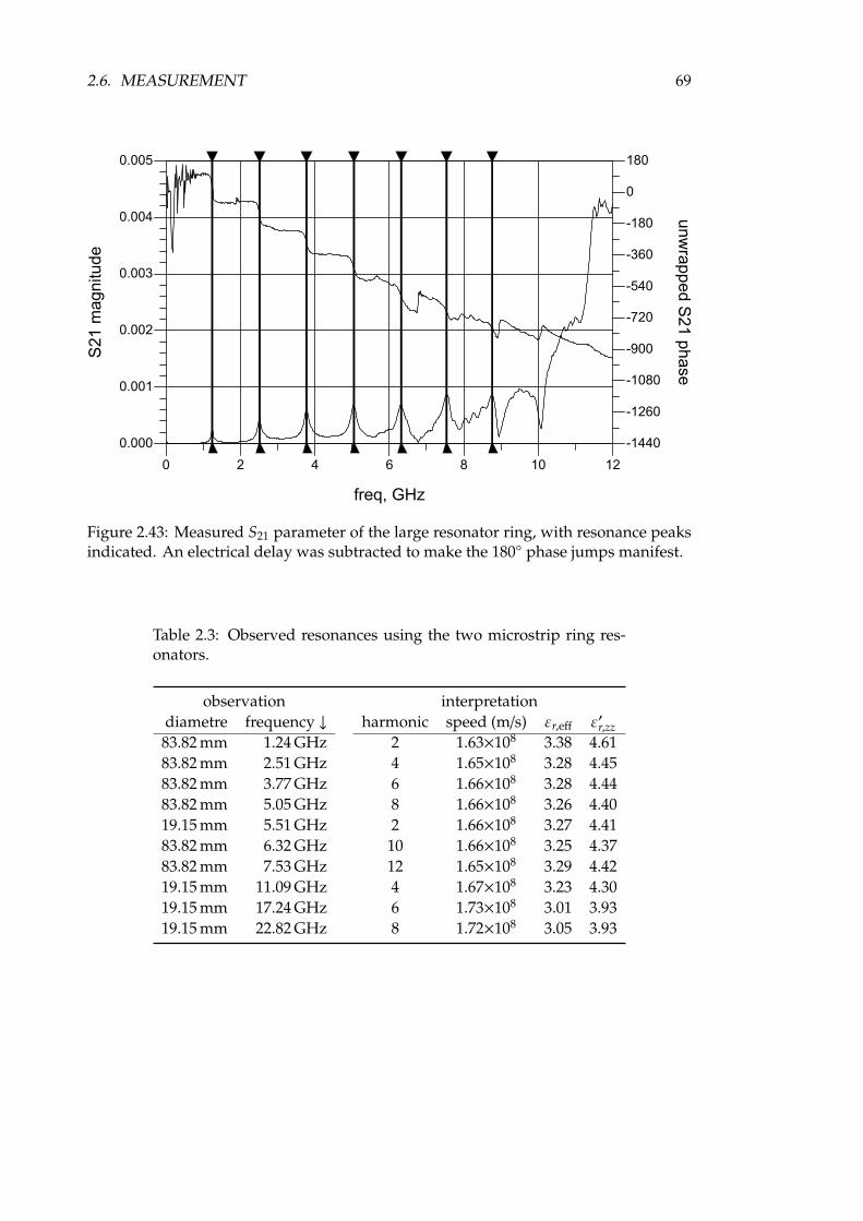
2.6. MEASUREMENT 69
2 4 6 8 100 12
0.001
0.002
0.003
0.004
0.000
0.005
-1260
-1080
-900
-720
-540
-360
-180
0
-1440
180
freq, GHz
S21 m
agnitude
unw
rapped S
21 p
hase
Figure 2.43: Measured S21 parameter of the large resonator ring, with resonance peaksindicated. An electrical delay was subtracted to make the 180 phase jumps manifest.
Table 2.3: Observed resonances using the two microstrip ring res-onators.
observation interpretationdiametre frequency ↓ harmonic speed (m/s) εr,eff ε′r,zz83.82 mm 1.24 GHz 2 1.63×10⁸ 3.38 4.6183.82 mm 2.51 GHz 4 1.65×10⁸ 3.28 4.4583.82 mm 3.77 GHz 6 1.66×10⁸ 3.28 4.4483.82 mm 5.05 GHz 8 1.66×10⁸ 3.26 4.4019.15 mm 5.51 GHz 2 1.66×10⁸ 3.27 4.4183.82 mm 6.32 GHz 10 1.66×10⁸ 3.25 4.3783.82 mm 7.53 GHz 12 1.65×10⁸ 3.29 4.4219.15 mm 11.09 GHz 4 1.67×10⁸ 3.23 4.3019.15 mm 17.24 GHz 6 1.73×10⁸ 3.01 3.9319.15 mm 22.82 GHz 8 1.72×10⁸ 3.05 3.93

70 CHAPTER 2. FIELD-TO-TRACE COUPLING
zx
yE(x)
(a) Photo of MUT sample in waveguide, with superimposed E-field profile.
(b) Set-up overview photo.
Figure 2.44: The RDWG measurement.

2.6. MEASUREMENT 71
Table 2.4: Material property calculation algorithms available in the Agilent 85071Esoftware programme
Method Calculates Best for. . . Particularities1. Nicolson- Ross εr & µr magnetic, short or
lossy MUTsFast, but has disconti-nuities.
2. Reflection/Trans-mission EpsilonPrecision Model
εr (µr ≡ 1) non-magnetic ma-terials, long, low-loss MUTs
Accurate, no disconti-nuities.
3. Transmission Ep-silon Fast Model
εr (µr ≡ 1) non-magnetic ma-terials, long, low-loss MUTs
Similar to precisionbut faster and betterfor lossy MUTs.
Next, Tereshchenko measured the S-parameters with an HP 8510C VNA at 21 and30% relative humidity. She repeated the measurement for all three bands, using rotatedsamples if available: 5 measurements in total (cf. Figure 2.44b).
Finally, the complex permittivity needed to be extracted from this measurementdata. Three algorithms in the Agilent 85071E software are available as outlined in Ta-ble 2.4. As the Flame Retardant 4 (FR4) samples are non-magnetic, short, and havemedium loss, Table 2.4 shows that none of the three available methods is an obviousmatch. Therefore, Tereshenko tried all three, and chose model 2, because it gave physi-cally plausible results for all bands (cf. Figure 2.45) and because of its robustness againstpositioning errors.
To summarise, the real permittivity perpendicular to the substrate (ε′r,zz) of the prepregbetween layer 1 and 2 was measured using a microstrip ring resonator. For reference,the complex permittivity in the plane of the substrate (εr,xx and εr,yy) of the entire stackupwas measured by Tereshchenko using the RDWG method. The results are compared inFigure 2.46.
The obtained values vary with frequency between 4.3 and 4.8. Supposing materialisotropy (ε ≡ εxx ≡ εyy ≡ εzz) and homogeneity between the layers, the permittivitiesmeasured with both methods should be equal. Under that condition only, the differencebetween permittivities obtained with both methods equals the relative measurementerror between the two methods. In the X-band, both methods correspond to within 12%,which is slightly worse than our objective. In the C-band, both methods correspond towithin 5%, which was our initial objective.
To take the dispersive real permittivity of the used substrate into account, thismeasurement can be used. Instead of plugging a constant scalar εr = 4.6 into themodified Taylor model, a frequency-dependent vector needs to be entered. Lacking aphysical model, a frequency-linear interpolation of the samples of Table 2.3 was entered.

72 CHAPTER 2. FIELD-TO-TRACE COUPLING
3.8
4.0
4.2
4.4
4.6
4.8
2 4 6 8 10 12
1. Nicolson-Ross2. R/T Epsilon Precision3. T Epsilon Fast
.....
Frequency (GHz)
Rea
l p
erm
itti
vty 1
32
132
3
2
(a) The real part of the permittivity.
-0.2
-0.0
0.2
0.4
0.6
0.8
1.0
1.2
2 4 6 8 10 12
1. Nicolson-Ross2. R/T Epsilon Precision3. T Epsilon Fast
.....
Imag
inar
y p
erm
itti
vty
Frequency (GHz)
3
2
31,2
31,2
(b) The imaginary part of the permittivity, representing the losses.
Figure 2.45: The complex permittivity of the y-direction samples, calculated with thedifferent methods.

2.6. MEASUREMENT 73
4,0
4,2
4,4
4,6
4,8
5,0
0 2 4 6 8 10 12 14 16 18
Rea
l per
mit
tivit
y
Frequency (GHz)
+5%
–5%
S C X-band5.0
4.8
4.6
4.4
4.2
4.0
Frequency (GHz)
Waveguide, y-sampleWaveguide, x-sample
Large ringSmall ring
(
ε0
r,xx
)
(
ε0
r,yy
)
(
ε0
r,zz
)
(
ε0
r,zz
)
Figure 2.46: Comparison of permittivity measured using waveguide and resonatormethods.
The field-to-trace coupling was calculated again and is compared with measurementin Figure 2.47. The average error over all cardinal directions was −1.52 dB average and2.79 dB average absolute.
In this example, the systematic bias was improved with 0.29 dB by taking into ac-count the measured permittivity. However, the average absolute error worsened by0.16 dB. Moreover, as can be seen from Figure 2.47, the prediction clearly worsened be-yond 3 GHz. This may be explained by the Quasi-TEM (QTEM) assumption breakingdown differently in the planar resonator and in the illuminated trace. Because measur-ing and taking into account the substrate permittivity takes considerable effort, withoutyielding clear improvement, the simple model of εr = 4.6 will be used from here on out.
GTEM Cell Modelling
In another attempt to improve the predictions, the GTEM cell’s illumination is criticallyexamined.
Ideally, the GTEM cell emulates a vertically polarised plane wave, as will be ex-plained. This model will be challenged by field-strength sensors and a Voltage StandingWave Ratio (VSWR) measurement. Consequently, a first-order model describing thecell’s non-ideality will be proposed.
A GTEM cell can be considered a rectangular, paraxial, tapered 50 Ω waveguide. Thenarrow end of the taper is equipped with a coaxial connector and the wide end isterminated in a hybrid resistive/absorber 50 Ω load, as shown in Figure 2.48a. As the

74 CHAPTER 2. FIELD-TO-TRACE COUPLING
10 10 10
108 109 1010−100
−90
−80
−70
−60
−50
−40
|Vfe|
(dB
V)/
S 21
(dB
)
Measurement
Taylor
(a) Typical values: εr = 4.6 and εr,eff = 3.4, yielding −1.81 dB average error and 2.63 dBaverage absolute error over all cardinal directions. (Repetition of Figure 2.39.)
10 10 10
108 109 1010
Frequency (Hz)
−100
−90
−80
−70
−60
−50
−40
|Vfe|
(dB
V)/
S 21
(dB
)
(b) As measured with the ring resonator, yielding −1.52 dB average error and 2.79 dBaverage absolute error over all cardinal directions.
Figure 2.47: Measurement and prediction of the field-to-trace coupling using differentsubstrate permittivity models.
medium is homogeneous (air) and the line is approximately uniform (taper, matching),the fundamental mode is TEM, as shown in Figure 2.49. By placing a PCB, the groundplane of the PCB becomes part of the metallic wall. This seemingly infinite ground planecorresponds well with the earlier analysis of the substrate field strength, summarisedin Figure 2.4.
To get a rough idea of the field uniformity under the 10×10 cm opening of the GTEM cell,the field uniformity was measured. To do so, E-field and H-field sensors were integratedin one corner of the PCB (cf. Figure 2.38). The H-field sensor consists of two vias anda trace that form a loop tangential to the septum, as short as technologically possiblefor the field to be uniform in the loop (1.23 mm), as high as technologically possibleto increase its surface (1.50 mm). To measure the E-field, a disk of 3 mm diameter was

2.6. MEASUREMENT 75
VNA
1 2
(a) Lateral cross section.
ΓloadV i
V i
Zload
50 Ω
1 2
(b) First-order model of the GTEM cell, including the absorber reflections.
Figure 2.48: Modelling the measurement set-up to illuminate PCBs.
d
Figure 2.49: Frontal cross section and the fundamental mode: solid electrical field linesand dashed magnetic field lines.

76 CHAPTER 2. FIELD-TO-TRACE COUPLING
used, in order to stay under λ/10 at 10 GHz and to have sufficient coupling surface tomeasure strong enough a signal.
The transfer from GTEM cell septum to the E-field sensor was measured at fourdifferent PCB orientations by rotating the PCB. Up to 5 GHz, the log-frequency averageddifference between the maximum and minimum transfer was 1.4 dB, and 5.8 dB between5-20 GHz. As far as the H-field sensor is concerned, it only has two valid positions. Theaverage difference in transfer between both positions was 1.5 dB up to 5 GHz, and 3.9 dBbetween 5-20 GHz. In absolute terms, a CST simulation of the H-field sensor yielded onaverage 1 dB more than the measured transfer up to 10 GHz, after which the discrepancywent up to 5 dB.
These numbers suggest that the field non-uniformity is in the order of a few dB.However, the shape of its non-uniformity is not known, so the predictions cannot beadjusted accordingly. A simple model for the field non-uniformity is therefore needed.
Recall the conception of a GTEM cell as a perfect waveguide. If it actually were, anincoming voltage wave Vi would travel along the septum once and be perfectly absorbedat the wide end. As a consequence, the S11 observed at the GTEM cell input shouldbe −∞dB, or rather the noise floor of the VNA. However, it is not: the manufacturerpromises −19 dB maximum and we even measured incidental excesses up to −10 dB inthe DC-18 GHz range.
A first-order model to explain this observation is to suppose the GTEM waveguideto be perfectly matched and lossless, but the wide-end load to be slightly mismatched,as illustrated in Figure 2.48b. In this model, there will be the incident wave Ei and onereflected wave ΓloadEi, where Γload is the electric field reflection coefficient of the load.The value of Γload can be easily extracted from an S11 measurement, the reference planeshould just be phase offset from the GTEM input to the centre of the illuminated trace.
Using this model, the GTEM-field-to-trace coupling can be predicted more accu-rately. First, the induced voltage by the forward-going wave Ei that illuminates thetrace should be calculated. Then, the induced voltage by the backward-going waveΓloadEi that illuminates the trace should be added. This prediction was tested on thesame simple case of a 5-cm microstrip. The S11 parameter of the GTEM cell was firstmeasured, phase-shifted by 53 cm, the equivalent distance from the GTEM-cell inputto the middle of the trace. The resulting prediction (dashed) is compared with mea-surement (blue) in Figure 2.50a. The average error is now −1.75 dB (was −1.81 dB) andthe average absolute error is now 2.60 dB (was 2.63 dB). More importantly, a strikingsimilitude is visually observed in the 0.1–2 GHz range.
If the position of the trace is not well-known with respect to the GTEM cell input,the phase of Γload must be considered unknown. In that case, the voltage inducedby the backward-going wave may add to or subtract from the voltage induced by theforward-going wave. That way, the gray uncertainty band in Figure 2.50a could becalculated, only based on |S11|. Without measuring anything, the manufacturer-given

2.6. MEASUREMENT 77
108 109 1010
−1800
−1440
−1080
−720
−360
0S
21
phas
e(d
egre
es)
Measurement
Extended Taylor
108 109 1010
−80
−70
−60
−50
−40
S21
mag
nit
ude
(dB
)
108 109 1010
Frequency (Hz)
−40−30−20−10
|S11|
(dB
)
(a) Model using the measured S11 (dashed curve) or |S11| (gray band).
108 109 1010
Frequency (Hz)
−100
−90
−80
−70
−60
−50
−40
S21
mag
nit
ude
(dB
)
Measurement
Extended Taylor
(b) Model using the manufacturer-specified VSWR ≤ 1.25 (or |S11| < −19 dB).
Figure 2.50: Measurement and modeling of the coupling to the far end of a 5 cm,characteristically terminated microstrip, taking into account the first reflection of theilluminating GTEM cell.
maximum voltage standing wave ratio (VSWR) 1.25 (|S11| = −19 dB) can be used toobtain the uncertainty band of Figure 2.50b. These uncertainty bands do not improvethe accuracy, but inform about the measurement uncertainty that is inherent to the set-up.

78 CHAPTER 2. FIELD-TO-TRACE COUPLING
To summarise, measuring the S11 parameter of the GTEM cell and taking it into accountis relatively easy. The prediction of the field-to-trace coupling improved by 0.1 dB on(absolute) average. The striking resemblance in the 0.1–2 GHz range suggests that thehybrid load reflections actually cause the oscillations. Even if only the scalar VSWR isknown, the measurement uncertainty due to absorber reflections can be quantified. Forthese reasons, the GTEM model will be taken into account from here on out.
Beyond 2 GHz, another non-ideality seems to take over, which might be explainedas multi-moding. Notice also that the systematic bias remains about −2 dB. Becausethis is observed in measurement, but not in full-wave simulation with plane waveillumination, we hypothesize that this is due to a yet unidentified non-ideality of theGTEM cell.
More Complex Cases
To further challenge the modified Taylor model, measurements will now be performedon more complex traces and non-characteristic loads. For each case, a comparison willbe made with the deterministic prediction and the transparent upper bound of themodified Taylor model.
The first complex case is the three-segment trace with characteristic loads of Figure 2.24.Similarly to the first measurement, the trace is a 50 Ω microstrip with mitred bends, ascan be seen in Figure 2.38.
The S21 parameter was measured to one end of the trace, while terminating theother end in 50 Ω. The square PCB was rotated in order to illuminate the trace fromall four cardinal directions. Judging from the frequency-average error, the best- andworst matching directions are compared to the modified Taylor model in Figure 2.51aand 2.51b, respectively. Averaged over all four directions, an average error of −1.53 dBis found, and an average absolute error of 2.85 dB.
The measurements are also compared to the transparent upper bound in Figure 2.51c.The upper bound seems to envelope all measurements, as expected. However, even thewestern illuminated trace should be about 2 dB below the low-frequency asymptote, aspredicted in Figure 2.25 and by full-wave simulations not incorporated in this thesis. Itseems that the GTEM field strength is about 2 dB higher than predicted by Vseptum/d,for a yet unknown reason. Despite that, the upper bound is rather tight, even whentaking into account this error.
Next, the same trace is shorted at the near end by an Agilent 85052D-60006 short circuit.From the near end of the illuminated trace to the short circuit, the signal traversesthe PCB, the SMA connector and the short standard. The PCB has a thickness t of1.55 mm. Modeling this path as a homogeneous waveguide, the delay
√εr · t/c0 should
approximate 11.1 ps. The SMA connector has a Teflon dielectric (εr = 2.1) of 7.67 mmfrom board to reference plane. Similarly, this should account for 37.1 ps. The short
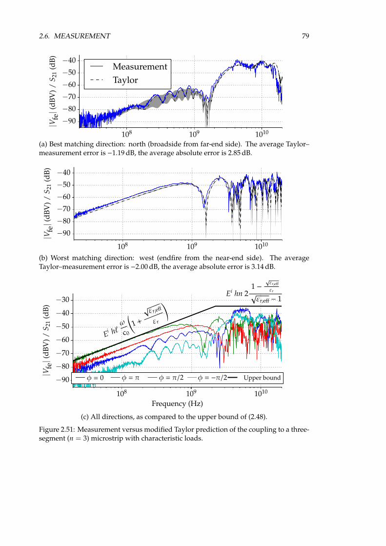
2.6. MEASUREMENT 79
108 109 1010
−90
−80
−70
−60
−50
−40|V
fe|
(dB
V)/
S 21
(dB
)
Measurement
Taylor
(a) Best matching direction: north (broadside from far-end side). The average Taylor–measurement error is −1.19 dB, the average absolute error is 2.85 dB.
108 109 1010
−90
−80
−70
−60
−50
−40
|Vfe|
(dB
V)/
S 21
(dB
)
(b) Worst matching direction: west (endfire from the near-end side). The averageTaylor–measurement error is −2.00 dB, the average absolute error is 3.14 dB.
108 109 1010
Frequency (Hz)
−90
−80
−70
−60
−50
−40
−30
|Vfe|
(dB
V)/
S 21
(dB
)
East West South North Upper bound
Ei h`!
c0
(
1 +
p "r,eff
"r
!
Ei hn 21 −
p"r,eff
"rp"r,eff − 1
φ = 0 φ = π φ = π/2 φ = −π/2
(c) All directions, as compared to the upper bound of (2.48).
Figure 2.51: Measurement versus modified Taylor prediction of the coupling to a three-segment (n = 3) microstrip with characteristic loads.

80 CHAPTER 2. FIELD-TO-TRACE COUPLING
108 109 1010
−3240−2880−2520−2160−1800−1440−1080−720−360
0
6V
fe(°
)
Measurement
Taylor
−20
(dB
) (a) Phase.
10 10 10
108 109 1010
Frequency (Hz)
−80
−70
−60
−50
−40
−30
−20
|Vfe|
(dB
V)/
S 21
(dB
)
(1 + ρfe)(
1 +∣
∣
∣
∣
∣
Zne
Zc− 1∣
∣
∣
∣
∣
1cos \Zne
)
×Ei hn 21 −
p"r,eff
"rp"r,eff − 1
Ei h`!
c0
(
1 +
p "r,eff
"r
!
× (1 + ρfe)(
1 +
∣
∣
∣
∣
∣
Zne
Zc
− 1
∣
∣
∣
∣
∣
1
cos \Zne
)
(b) Magnitude and upper bound.
Figure 2.52: Measurement versus modified Taylor prediction of the coupling to a three-segment microstrip, shorted at the near end, matched at the far end. Port 1 is the GTEMcell input, port 2 is the trace’s far end.
standard is specified to have a 31.78 ps delay, totaling to a delay of 79.95 ps. The near-end load is thus modeled by a short circuit with a lossless, 79.95-ps delay. The far endof the illuminated trace is directly connected to the VNA like in the former experiment.
The measurement was performed and compared against the extended Taylor model.The average difference with the modified Taylor model was −0.22 dB with an averageabsolute error of 2.13 dB.
To consider either-end reflections, a far-end mismatch allowing for measurements wasneeded. For that purpose, the trace was cut open at the far end and a 0603 surface

2.6. MEASUREMENT 81
220Ω
50Ω VNA
50Ω
80ps
44fF
Zne Zfe
Figure 2.53: Model of the near-end short standard and the far-end resistive probe,leading to the VNA input.
mount 220 Ω resistor was soldered in series. This modification shortened the third linesegment ℓ3 to 22.5 mm. Just before, this resistor was measured up to 20 GHz with thelow-budget fixture that will be described in section 3.3. The measured impedance couldbe satisfactorily modelled by a 44 fF parasitic capacitance. As the VNA, connector andtransition are matched to 50 Ω, they can be modeled as a simple 50 Ω load. The resultingmodel of the terminal loads is shown in Figure 2.53.
The measurement was then performed and the S21 readout of the VNA was dividedby the voltage transfer of the resistive voltage divider to estimate the actual far-endvoltage. The Taylor–measurement error, averaged over all four cardinal directions andover log-frequency is−1.75 dB, the average absolute error is 4.02 dB. The directions withthe best and the worst average error are shown in Figure 2.54a and 2.54b, respectively.
The rather high error might be explained by the fact that the 220 Ω probe resistor isilluminated itself, too. With rather reflective loads, many reflections travel up and downthe line, making its losses less negligible. These two non-idealities are neither taken intoaccount by the full-wave simulation nor by the extended Taylor model. Therefore, theymight explain the discrepanciy between measurement and the modified Taylor model.
As demonstrated in Figure 2.54c, the coupling remains under the transparent upperbound for all cardinal directions. For this particular trace and these four directions ofillumination, the proposed upper bound is 7 dB too pessimistic for the low frequencyasymptote, and 13 dB too pessimistic for the high frequency asymptote.
To assess the validity of the modified Taylor model for traces with more complex routing,another trace is needed. Our research acquaintance Tvrtko Mandic provided us withmeasurements that he performed on such a trace.
Mandic realised a 50 Ω microstrip trace on a 1-mm FR4 substrate (εr = 4.5), henceof 1.75 width (εr,eff = 3.6). His trace consisted of 7 segments of 14.5, 10.75, 19.5, 21.75, 6,

82 CHAPTER 2. FIELD-TO-TRACE COUPLING
10 10 10
108 109 1010−80
−70
−60
−50
−40
−30
−20
|Vfe|
(dB
V)
Meas.
Taylor
(a) Best correlation: west (endfire illumination from the far-end side). The averageTaylor–measurement error was −0.86 dB, the average absolute error 3.08 dB.
10 10 10
108 109 1010
Frequency (Hz)
−80
−70
−60
−50
−40
−30
−20
|Vfe|
(dB
V)
(b) Worst correlation: east (endfire illumination from the near-end side). The averageTaylor–measurement error was −3.58 dB, the average, absolute error 5.51 dB.
108 109 1010
Frequency (Hz)
−80
−70
−60
−50
−40
−30
−20
−10
|Vfe|
(dB
V)
East West South North Upper bound
(1 + ρfe)(
1 +∣
∣
∣
∣
∣
Zne
Zc− 1∣
∣
∣
∣
∣
1cos \Zne
)
×Ei hn 21 −
p"r,eff
"rp"r,eff − 1
Ei h`!
c0
(
1 +
p "r,eff
"r
!
× (1 + ρfe)(
1 +
∣
∣
∣
∣
∣
Zne
Zc
− 1
∣
∣
∣
∣
∣
1
cos \Zne
)
13 dB
7 dB
(c) All directions, compared to the transparent upper bound of (2.67). The high-frequency limit is not flat, because of the parasitic capacitance in the near-end load.
Figure 2.54: Induced voltage in the near end of the multi-segment trace, as measured(port 1 on the GTEM cell input, port 2 is the trace’s far end equipped with a seriesresistive probe, the near end being shorted using a calibration standard).

2.6. MEASUREMENT 83
17
2
34
5
61
2
3
4
5
7
6
Figure 2.55: Mandic’s 7-segment microstrip trace.
3 and 14 mm length, as enumerated in Figure 2.55. The 90˚ bends are not mitred. Thetrace is fabricated on a 10 × 10 cm PCB. The trace terminals are equipped with 3-pinthrough-hole SMA connectors.
The field-to-trace coupling was measured by Mandic using a TEM cell. Analogouslyto a GTEM cell, the TEM cell is a rectangular, coaxial 50 Ω waveguide. A top openingof 10 × 10 cm allows illuminating PCBs with an air field 2Ei of Vseptum/d. The septumdistance d is constant over the opening: 45 mm. The TEM cell has coaxial input andoutput connectors. Similarly to the GTEM measurements, the coupling measurementsare performed by connecting one port of the VNA to the TEM cell input, and the otherport to one end of the transmission line. The second TEM cell port, as well as the secondtransmission line port are terminated in 50 Ω.
The result is compared to the modified Taylor model for the near-end and the far-end coupling in Figure 2.56a and 2.56b, respectively. Mandic showed that the sharppeaks measured above 1 GHz are due to TEM cell resonances [57]. The log-frequencyaveraged Taylor–measurement error over both terminal voltages is −0.05 dB and theaverage absolute error is 2.07 dB.
It be noted that there is little systematic bias, both numerically and visually. Thiscorroborates with the hypothesis that the 2 dB systematic offset observed in GTEMmeasurements is really due to a non-ideality of the GTEM cell. Moreover, the lowaverage absolute error suggest that even these seven traces with mutual interactionscan be competently modelled by the modified Taylor model.
To assess the validity of the upper bound, the far-end and near-end coupling wasmeasured in all four cardinal directions. Because of the high number of segments n, thehigh-frequency upper bound is out of sight, as can be seen in Figure 2.56c. Nonetheless,the low-frequency upper bound is respected and about 4 dB too pessimistic.

84 CHAPTER 2. FIELD-TO-TRACE COUPLING
10 10 10 10
106 107 108 109−120
−100
−80
−60
−40
−20
|Vne
|(d
BV
)/S 2
1(d
B)
(a) Near-end coupling (0.73 dB average error, 1.15 dB average absolute error).10 10 10 10
106 107 108 109−120
−100
−80
−60
−40
−20
|Vfe|
(dB
V)/
S 21
(dB
)
Measurement
Taylor
(b) Far-end coupling (−0.83 dB average error, 2.98 dB average absolute error).
106 107 108 109
Frequency (Hz)
−100−90−80−70−60−50−40−30−20
|Vfe|
(dB
V)/
S 21
(dB
)
Ei h`!
c0
(
1 +
p "r,eff
"r
!
(c) All ends, all directions and the worst-case asymptote.
Figure 2.56: Comparison between measurement and both models.

2.7. CONCLUSIONS 85
Conclusions
The field-to-trace coupling of increasingly complex cases was measured and comparedwith the modified Taylor prediction, as summarised in Table 2.5. The coupling toa single 5 cm trace was measured and predicted by supposing an ideal plane waveillumination and a constant substrate permittivity εr = 4.6.
Using a microstrip resonator, the substrate permittivity was then measured andtaken into account. The prediction did not unambiguously improve and above 10 GHz,it visually deteriorated. This might be explained by the gradual breakdown of theQTEM assumption at these frequencies. Because of the considerable effort withoutclear improvement, this permittivity model was not retained.
In another attempt to explain the discrepancy between measurement and prediction,the first reflection of the GTEM cell hybrid load was measured and taken into account.This yielded a slight numerical, but a clear visual improvement of the predictions.Moreover, it yields a quick indicator of the measurement uncertainty due to this GTEMcell non-ideality. Because of this improvement at the price of a simple measurement,this GTEM cell reflection model was retained.
Then, with the same GTEM cell, the coupling to a three-segment trace with matchedand unmatched loads was measured and predicted. The average Taylor–measurementerror over all GTEM cell measured cases is −1.3 dB, which indicates a systematic nega-tive bias. The average absolute error was 2.9 dB, although that might not be that goodan accuracy metric; often, the match is better appreciated visually.
Lastly, measurements performed by Mandic on a seven-segment trace in a TEM cellup to 2 GHz were predicted. The small error suggests that the modified Taylor modelalso holds for traces with closely-spaced segments with mutual interactions. Althoughthe TEM cell was supposed ideal, almost no systematic bias was observed: −0.05 dB.Therefore, the systematic bias observed in the precedent GTEM cell measurements isprobably due to a non-ideality that is proper to the GTEM cell.
The transparent upper bound was not exceeded throughout these measurements.The tightness of the upper bound varied: margins ranging from 0 dB to 13 dB wereobserved.
2.7 Conclusions
The coupling of incident electromagnetic waves to PCB traces was found to be studied bymany authors, yet with few transparent results. Only Leone derived a transparent low-frequency upper bound for the coupling of an arbitrary-incident, arbitrarily polarisedplane wave to a single microstrip trace segment with moderately mismatched terminalloads.
To explore the problem and obtain a reference, a 5 cm microstrip segment wasmanually meshed into λ/20 Taylor cells. A comparison of the coupling to a line withmatched loads suggested that neglecting the microstrip losses only introduce a slight,

86 CHAPTER 2. FIELD-TO-TRACE COUPLING
Table 2.5: Measurement and modelling of non-idealities in section 2.6.
modelled errormeasurement non-ideality average avg. abs. visual1-segment – −1.81 dB 2.63 dB
permittivity −1.52 dB 2.79 dB problems > 10 GHzGTEM refl. −1.75 dB 2.60 dB good match oscillations
3-segment GTEM refl. −1.53 dB 2.85 dB3-segm. shorted GTEM refl. −0.22 dB 2.13 dB3-segm. probed GTEM refl. −1.75 dB 4.02 dB7-segment – −0.05 dB 2.07 dB
pessimistic error. Therefore, and to simplify, trace losses are neglected from there onout. To promote experimentation and to enable practical application, the meshingwas successfully automated and the terminal voltages were predicted using Kron’sformalism. By frequency-adaptive meshing of the trace, an order of a magnitudespeedup was achieved. A sensitivity study suggest that meshing finer than λ/20 is awaste of time. All the same, these numerical solutions do not provide understanding.
Therefore, the single Taylor cell was modified to remain valid for high frequencies,at least for grazing-incident, vertically polarised plane wave incident on a microstriptrace segment with matched loads. This modified Taylor cell consists of Taylor’s cell,which predicts the low-frequency coupling, and the cross-correlation K between theincident wave and the line’s eigenwave. More importantly than another order of amagnitude speedup, this model yields understanding. From the modified Taylor cell,it can be understood that for low frequencies, the electric and magnetic coupling addup constructively at the trace’s near end under end-fire illumination. Consistent withLeone, the latter illumination constitutes the worst case. In this case, trace length andsubstrate thickness are the design parameters that proportionally determine the low-frequency coupling. For high frequencies, the worst case occurs at the far end, becausethe incident- and the eigenwave are aligned, yielding a maximum K. In that case, onlythe substrate thickness determines the worst-case coupling, and not the trace length.
By superposing one modified Taylor cell per segment, the coupling to multi-segmenttraces can be predicted. By applying transmission line theory, predictions for arbitraryloads can be calculated analytically. The worst case was also studied as function of theterminal loads and a loose upper bound was found. Not surprisingly, the better bothterminal impedances are matched to the trace, the smaller the either-end voltages are.It be noted that the trace impedance may also be tuned for given terminal impedances.
Full-wave simulation of the case studies used above correspond very well to thepredictions obtained with the modified Taylor cell. Apparently, the transmission line

2.7. CONCLUSIONS 87
assumption inherent to the (modified) Taylor cell holds, even for segmented traces.Also, the approximation of the substrate field seems to work.
In comparison with GTEM cell measurements, it turned out redundant to mea-sure and take into account the substrate permittivity. It was useful, however, to takeinto account the first GTEM cell’s reflection. Even then, about 1.3 dB more couplingis observed with the GTEM cell than with the modified Taylor cell or with full-wavesimulation. Therefore, it is supposedly due to a non-ideality of the GTEM cell that isnot taken into account by either model. Averaged over the different case studies, anaverage absolute error of 2.7 dB was found. The transparent upper bound found fromthe modified Taylor model was respected.
With the obtained transparent model, EMC-aware PCB designers can make informeddesign decisions. For example, for a weak analog signal, the maximum trace lengthand substrate thickness can be calculated early in the design process, just from thefield strength that the PCB must be compliant with. For another example, the designerknows that at high frequencies, it may be a waste of time to shorten the trace to improvethe PCB radiated immunity. As a last example, the trace width of a sensitive signalmay be tuned to be in between both terminal impedances in order to reduce EMC risks.The latter is a ‘free’ EMI countermeasure. Because the modified Taylor model is closed-form, field-to-trace coupling of a given trace can be predicted in the order of tens ofmilliseconds.
The transparent models are also of use for testing. For example, in pre-compliancetesting of a prototype with a sensitive trace, the engineer can immediately perform end-fire illumination at either end, instead of having to rotate the Device Under Test (DUT).
In future research, the illumination should be generalised to arbitrarily-polarised,arbitrarily-incident plane waves, because in reality, perturbing electromagnetic fieldsare unknown. Considering the worst case and taking loose upper bounds may help tokeep the expressions transparent.


CHAPTER 3IC Conducted Immunity
Abstract. If the conducted immunity of ICs is interesting above 1 GHz, a measurementmethod is needed that is valid beyond 1 GHz. There is no standardised method yet,because with rising frequency, the common measurement set-up increasingly obscuresthe IC’s immunity. An attempt to model and remove the set-up’s impact on the mea-surement result proved difficult. Therefore, a simplified set-up and extraction methodis proposed and a proof-of-concept of the automatic generation of the set-up’s PCB isgiven. The conducted immunity of an LM7805 voltage regulator is measured up to4.2 GHz to demonstrate the method.
3.1 Introduction
What is the conducted immunity of ICs beyond 1 GHz? How to obtain models for ICconducted immunity that are valid beyond 1 GHz? Can this be done efficiently in anindustrial context?
Because of the prototyping cost and delay, PCB designers strive for First-Time-Right (FTR) EMC compliance. PCB-level designers decide on placing and routing of ICsand various electronic and electromechanical components. The designer understandsthe routed traces that connect the components, so the transparent model for field-to-trace-coupling developed in Chapter 2 might be of use to them. The ICs, however, areblack boxes to the PCB designer, which just fulfil certain functions. Therefore, opaquemodels of the involved ICs suffice for PCB-level design and simulation.
If conduction remains the dominant perturbation mechanism beyond 1 GHz, mod-els are needed that are descriptive of the conducted immunity of ICs beyond 1 GHz. Tounderpin this thesis’ main hypothesis (cf. p. 9), a possible technique should be demon-strated to obtain these models. The modelling technique should be applicable in anindustrial context, valid for a wide range of ICs and produce models that allow for
89

90 CHAPTER 3. IC CONDUCTED IMMUNITY
PCB-level simulations.
To that end, the existing models and modelling techniques for conducted IC immunitywill be reviewed in section 3.2, to conclude that no standardised method beyond 1 GHzcurrently exists. A first attempt to extend the current state of the art in black-boxmodelling beyond 1 GHz consists in modelling the passive components used in itsmeasurement technique beyond 1 GHz, as will be documented in section 3.3. It willturn out that its passive components are not always needed, and that there are othereffects that need to be taken into account. Therefore, a ‘lean extraction PCB’ approachwill be elaborated from the ground up in section 3.4. This approach will be applied togeneral SOIC8-packaged ICs by semi-automatically generating an extraction board insection 3.5. Using this board, one IC will be modelled in section 3.6: the LM7805 voltageregulator. Conclusions will be drawn in section 3.7.
3.2 State of the Art
With the keywords of the goal mentioned above in mind, published IC conductedimmunity models were inspected with the following questions:
1 ‘wide range of ICs’: What range of ICs are modelled? From a single transistor toan A/D-converter, a CPU or a television SoC?
2 ‘black box’: What kind of model is used and why?3 ‘modelling technique’: What measurement and simulation techniques are used to
obtain these models?4 ‘competent models’: What prediction is accurate enough? Should the output of
the model be boolean (pass/fail) or continuous (DC offset voltage, RF disturbancepropagation)?
5 ‘beyond 1 GHz bandwidth’: What bandwidth is modelled for and why?
The results are enumerated in Table 3.1. If the publication mentions the initial modellinggoal (to aid the IC, PCB- or equipment designer), it is marked in the table.
As for the range of modelled components, the least complex component was found tobe a single transistor, ranging up to A/D converters and the I/O buffers of a microcon-troller. In view of the complexity of contemporary SoCs, this range is rather modest.Few examples were found of the integration of these models in a greater whole.
Often, authors do not document their choice for a black, white or grey box. However,the modelling goal is briefly mentioned in most publications. Not surprisingly, themodelling goal correlates with the modelling depth (black-, white- or grey box). That is,research targeting IC designers creates white-box models, which explain the integratedcircuit’s susceptibility root cause. Research targeting PCB or equipment designers, on

3.2. STATE OF THE ART 91
Tabl
e3.
1:L
iter
atu
rest
ud
yre
sult
sfo
rIC
cond
uct
edim
mu
nity
mod
els.
pu
blic
atio
nm
odel
ant
mod
elye
arre
f.co
mp
onen
tba
ndw
idth
goal↓
colo
ur
outp
ut
tech
niqu
e20
10[5
8]cu
rren
tmir
ror
0–10
GH
zIC
whi
tevo
ltag
esi
mu
lati
on20
10[5
8]L
INd
rive
r0.
05–1
2M
Hz
ICw
hite
pas
s/fa
ilsi
mu
lati
on20
10[5
8]ri
ngos
cilla
tor
1–7.
7G
Hz
ICw
hite
jitte
rsi
mu
lati
on20
10[5
8]4-
bita
dd
er40
MH
zIC
whi
tep
ass/
fail
sim
ula
tion
2009
[59]
AD
C1
kHz–
1G
Hz
ICw
hite
pas
s/fa
ilsi
mu
lati
on,I
CIM
-CI
2002
[60]
op-a
mp
0–1
GH
zIC
?w
hite
volt
age
anal
ysis
-mea
sure
men
t20
02[6
1]C
MO
Sop
-am
p0–
2G
Hz
IC?
whi
tevo
ltag
ean
alys
is-m
easu
rem
ent
2010
[62]
AD
C0.
1–10
MH
zIC
?gr
eyp
ass/
fail
DP
I20
09[6
3]µ
Cw
ith
AD
C0–
0.6
GH
zIC/P
CB
grey
EFT
shap
eV
NA
2007
[64]
µC
inp
utb
uff
er0.
01–2
GH
zIC/P
CB
grey
pas
s/fa
ilsi
m.,
mea
sure
men
t,D
PI
2010
[65]
op-a
mp
5–10
0M
Hz
PC
Bgr
eyvo
ltag
ean
alys
is,D
DP
I,V
NA
2010
[66]
Flex
Ray
tran
ceiv
er1–
200
MH
zP
CB
grey
pas
s/fa
ilD
PI,
BC
I20
13[6
7]74
LS
inve
rter
0–1
GH
z?
grey
pas
s/fa
ilD
PI,
VN
A,I
CIM
-CI
2013
[68]
EE
PR
OM
mem
orie
s1
MH
z–1
GH
zP
CB
?bl
ack
pas
s/fa
ilD
PI,
VN
A,I
CIM
-CI
2009
[69]
vari
ous
1M
Hz–
1G
Hz
PC
Bbl
ack
pas
s/fa
ilD
PI,
VN
A,I
CIM
-CI
2008
[70]
CM
OS
inve
rter
0.05
–1G
Hz
PC
Bbl
ack
volt
age
DP
I,N
Ns
1978
[71]
74xx
,op
amp
,780
50.
01–1
0G
Hz
equ
ipm
ent
blac
kp/f
,vol
tage
DP
I20
00[7
2]"
""
""
2013
[73]
LD
O1–
18G
Hz
PC
B?
blac
kp
ass/
fail
DP
I
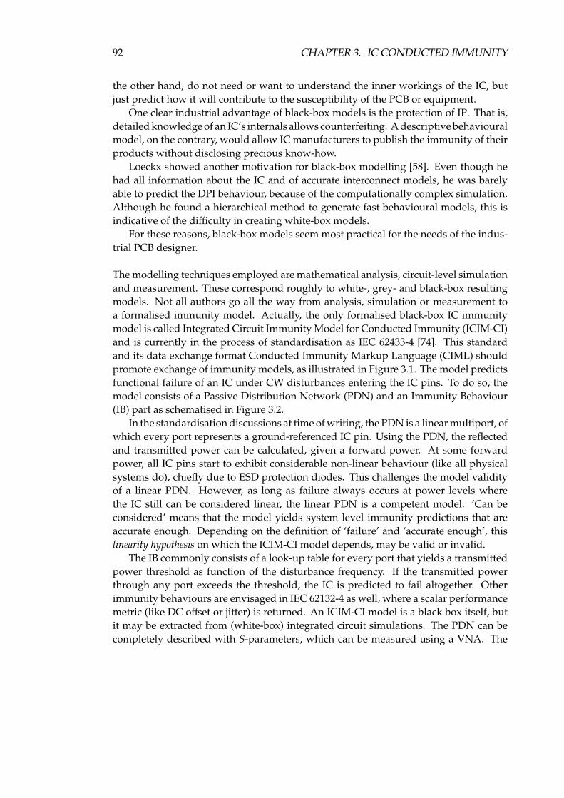
92 CHAPTER 3. IC CONDUCTED IMMUNITY
the other hand, do not need or want to understand the inner workings of the IC, butjust predict how it will contribute to the susceptibility of the PCB or equipment.
One clear industrial advantage of black-box models is the protection of IP. That is,detailed knowledge of an IC’s internals allows counterfeiting. A descriptive behaviouralmodel, on the contrary, would allow IC manufacturers to publish the immunity of theirproducts without disclosing precious know-how.
Loeckx showed another motivation for black-box modelling [58]. Even though hehad all information about the IC and of accurate interconnect models, he was barelyable to predict the DPI behaviour, because of the computationally complex simulation.Although he found a hierarchical method to generate fast behavioural models, this isindicative of the difficulty in creating white-box models.
For these reasons, black-box models seem most practical for the needs of the indus-trial PCB designer.
The modelling techniques employed are mathematical analysis, circuit-level simulationand measurement. These correspond roughly to white-, grey- and black-box resultingmodels. Not all authors go all the way from analysis, simulation or measurement toa formalised immunity model. Actually, the only formalised black-box IC immunitymodel is called Integrated Circuit Immunity Model for Conducted Immunity (ICIM-CI)and is currently in the process of standardisation as IEC 62433-4 [74]. This standardand its data exchange format Conducted Immunity Markup Language (CIML) shouldpromote exchange of immunity models, as illustrated in Figure 3.1. The model predictsfunctional failure of an IC under CW disturbances entering the IC pins. To do so, themodel consists of a Passive Distribution Network (PDN) and an Immunity Behaviour(IB) part as schematised in Figure 3.2.
In the standardisation discussions at time of writing, the PDN is a linear multiport, ofwhich every port represents a ground-referenced IC pin. Using the PDN, the reflectedand transmitted power can be calculated, given a forward power. At some forwardpower, all IC pins start to exhibit considerable non-linear behaviour (like all physicalsystems do), chiefly due to ESD protection diodes. This challenges the model validityof a linear PDN. However, as long as failure always occurs at power levels wherethe IC still can be considered linear, the linear PDN is a competent model. ‘Can beconsidered’ means that the model yields system level immunity predictions that areaccurate enough. Depending on the definition of ‘failure’ and ‘accurate enough’, thislinearity hypothesis on which the ICIM-CI model depends, may be valid or invalid.
The IB commonly consists of a look-up table for every port that yields a transmittedpower threshold as function of the disturbance frequency. If the transmitted powerthrough any port exceeds the threshold, the IC is predicted to fail altogether. Otherimmunity behaviours are envisaged in IEC 62132-4 as well, where a scalar performancemetric (like DC offset or jitter) is returned. An ICIM-CI model is a black box itself, butit may be extracted from (white-box) integrated circuit simulations. The PDN can becompletely described with S-parameters, which can be measured using a VNA. The

3.2. STATE OF THE ART 93
compiler builder
model author model user
CIML
• Comma separated value
Measurement/simulation
results
IB
• Touchstone• SPICE subcircuit
PDN
• Excel sheet• Post-processing macros
Exploitable simulation ingredients
• Touchstone• SPICE subcircuit
IB
PDN
ICIM-CI
Figure 3.1: Schematic use case of a single-file ICIM-CI standard.
PDN
Pinc,1Prefl,1
Pinc,2Prefl,2
Pinc,nPrefl,n
…
IB
f Ptrans,1,threshold
f Ptrans,2,threshold
f Ptrans,n,threshold
Ptrans,1
Ptrans,2
Ptrans,n
…
pass/fail
Figure 3.2: Symbolic representation of the ICIM-CI of IEC 62433-4. In this case, the IBjust returns a boolean pass/fail signal, based on transmitted power threshold lookuptables.

94 CHAPTER 3. IC CONDUCTED IMMUNITY
Directional CouplerAmplifier
RF Source
Fixture PCB
DC Signal
Trace
Choke
CouplingCapacitor
DUTW W
PincidentPreflected
Bias Tee
Figure 3.3: RF injection path of the DPI set-up proposed in IEC 62132-4.
difficulty lies in moving the reference plane to the IC pins.The IB’s transmitted power threshold can be extracted from measurement using the
DPI set-up described in IEC 62132-4. Its goal is to characterise the susceptibility of an ICto conducted disturbances, while reducing the influence of the particular test set-up onthe measurement results. The set-up proposed by IEC 62132-4 [75] is shown in Figure 3.3:it consists of a PCB with the Device Under Test (DUT) and some peripherals, and adirectional coupler that allows for measuring the incident and reflected power. That is,for every frequency, the forward power is increased until the IC fails according. Thedefinition of failure needs to be given elsewhere, and a suitable technique for observingfailure needs to be applied. At the point of failure, the difference Pfwd − Prefl = Ptrans istaken to be the power really dissipated by the IC.
The most difficult part is injecting a known RF disturbance power into the IC pinunder test. Mathematically, the differential power measurement yields the net powerleaving the directional coupler output. Although it is not common terminology in DPI,this is the transmitted power at the reference plane of the coupler output. Recall that theICIM-CI reference plane should lie at the Pin Under Test (PUT) boundary. Therefore,recording the differential power measurement as the IB is legitimate to the extent thatthe cabling and on-PCB loss is negligible. For that reason, the standard requires theinsertion loss not to exceed 3 dB [75, §7.4]. That way, the coupler output and PUTreference planes are numerically close.
The great advantage of this approach is that it is simple: one can design a PCBwith all necessary periphery, measure incident and reflected power when the DUT failsand register the difference as being Ptrans,threshold. However, two critical remarks onthe accuracy of the method can be made. First of all, when the PUT is very reflective,Pfwd ≈ Prefl and the wattmetre errors dominate the Ptrans reading [71, p. 112]. In practicalcases, in the 1 − 3 GHz range, the difference between the true and the measured Ptrans
can go down to −10 dB [76].

3.2. STATE OF THE ART 95
(a) Component- and RF perturbation side. (b) Peripheral- and functional side.
Figure 3.4: Generic SOIC14 extraction PCB as developed at Valeo’s (image courtesyFrédéric Lafon).
Therefore, an improvement upon both inaccuracies was proposed earlier by Lafon[69]. The measurement set-up can be the same as in Figure 3.3, in this proposal, how-ever, only the forward power Pfwd at failure will be recorded. To obtain the transmittedpower Ptrans, all of the set-up is modelled in SPICE, then simulated with the recordedforward power Pfwd,threshold, and the transmitted power Ptrans,threshold is calculated. Putdifferently, the reference plane is moved from generator output to DUT pin by simula-tion.
Practically, the used extraction PCB is generic for a particular package (SOIC14, inthe example of Figure 3.4), and has almost the same and well-known layout for eachpin. The layout allows to solder bias tees and other peripheral circuitry for every pin.Passive components that make up the bias tees are separately measured, modelled andentered in the simulation. The DUT is modelled by measuring its S-parameters witha VNA, after calibrating using a custom Short-Open-Load (SOL) calibration PCB thatmoves the reference plane up to the DUT pins for the S-parameter measurement. Finallythe S-parameters are converted to a SPICE model with IdEM [77].
The bandwidth of most models is limited to 2 GHz. There are exceptions: Chang etal. measured at 18 GHz, but they do not explicitly define the RF reference plane [73].Judging from their extraction PCB layout, the reference plane not very representative.Similarly, the McDonnell Company measured up to 10 GHz at the SMA reference planeof connectorised bias tees, relying on striplines and Zero Insertion Force (ZIF) sockets tohave negligible insertion loss, it seems [71]. Lafon measures up to 3 GHz and remarksthat with rising frequency, the mutual inductance of DPI capacitors becomes non-negligible and needs to be modeled [27].
96 CHAPTER 3. IC CONDUCTED IMMUNITY
Maybe it is for these practical difficulties that there is no standardised measurementmethod beyond 1 GHz; IEC 62132-4 is defined up to 1 GHz. The different attempts,however, show a popular trend towards higher frequencies [8].
To summarise, since the 1980’s, people have tried to construct some more or less stan-dardised descriptive models of conducted IC immunity up to 10 GHz. Depending onthe modelling goal (e.g. predict system immunity or improve IC immunity) the modelswere more or less explanatory (e.g. black-box or white-box). The most standardisedmodel to date is ICIM-CI, which can be extracted by VNA and DPI measurements onICs. The DPI exhibits accuracy problems for rising frequency, something for which La-fon proposed an alternative. However, this alternative still requires careful modellingof the set-up. In general, authors and committees are unclear about the definition ofreference planes. For these and other reasons, we consider there is no standardisedblack-box modeling technique beyond 1 GHz.
3.3 Modelling passive components
The hardware set-up prescribed in IEC 62132-4 comprises on-PCB decoupling networks,that is, DC-blocks and bias tees [75]. We would like to assess the feasibility of a similarset-up for frequencies beyond 1 GHz. These decoupling networks consist of discretecomponents like capacitors, inductors and resistors and PCB traces. Models of tracesare readily available and can be simulated with tools like ADS. Discrete componentmodels can be bought from specialists like Modelithics, Inc., and sometimes they aresupplied by the component manufacturer.
In the latter case, however, it is not always clear whether and how the modelsinclude the PCB layout [78] and how element values vary as result of productiontolerances [79]. To verify the manufacturer’s models, we would like to model thecomponents ourselves by means of measurement. Commercial SMD test fixtures likeAgilent’s 16196 allow measuring SMDs up to 3 GHz, for about 5 ke [80]. Furthermore,one needs an impedance analyser that can measure up to 3 GHz.
Attempting to find a cheaper solution, while gaining experience with PCB designfor 10 GHz, we decided to design a test fixture ourselves. This attempt to find a cheapand simple solution also suggests to use standard measurement equipment. That is,instead of a somewhat special impedance analyser, we would like to use a networkanalyser, which is present in virtually any EMC laboratory. Nonetheless, the analyser’sfrequency range should encompass at least the resonance frequency of the DUT. Weuse the HP 8720C VNA at hand, which has a frequency range of 50 MHz–20.05 GHz.
Therefore, a typical case study that is useful for the DPI set-up will be defined. For thatcase, a measurement fixture will be designed. The case study will then be measured withthe fixture, yielding raw impedance data. Different ways of compensating these data for

3.3. MODELLING PASSIVE COMPONENTS 97
Table 3.2: Frequency-dependent behaviour of AVX 1 pF U-series NP0 chip capacitors, copied and extrapolated from[81].
package behaviourJEDEC metric resonance ESR @ resonance
0402 1.0× 0.5 mm 8.3 GHz 0.15 Ω
0603 1.6× 0.8 mm 7.9 GHz 0.2 Ω
0805 2.0× 1.25 mm 7.2 GHz 0.3 Ω
1210 3.2× 2.5 mm 6.3 GHz 0.2 Ω
the fixture influence will then be compared. Consequently, a preferred compensationmethod will be concluded upon, as well as the fixture performance.
Case Study
To assess the test fixture, we chose a capacitor that is candidate for Gigahertz DirectPower Injection (GDPI) set-ups: a 1 pF microwave capacitor from AVX. This capacitoris available in JEDEC 0402, 0603, 0805 and 1210 packages. We chose the 0603, tryingto strike the balance between a high resonance frequency and the mechanical repro-ducibility of the measurements. The 0603-packaged capacitor allegedly resonates at8 GHz with an Equivalent Series Resistance (ESR) of 0.2 Ω at resonance (cf. Table 3.2).No tolerance nor reference planes are specified, however.
Design
The two-terminal (one-port) DUT needs to be connected somehow to a two-port VNA.Hence, there is essentially only one measurement configuration when using one VNAport, cf. Figure 3.5a. With two ports, there are essentially two possible configurations,1
shunt and series, cf. Figure 3.5b-c. From symmetry, we deduce that S11 = S22 andS21 = S12, so there are two interesting S-parameters per configuration. This gives usfive quantities that can be measured with a VNA: the (one-port) reflection coefficient,the series S11, the series S21, the shunt S11 and the shunt S21. Due to the measurementprinciple of the VNA, the impedance thus measured is more or less precise. The 10%uncertainty of impedance magnitude is shown in Figure 3.6.
The most interesting impedance region of measurement will be around the res-onance. One frequency decade under its nominal resonant frequency of 8 GHz, the
1In bond graph terminology, one can prove that there are only two junctions that do not dissipate norstore energy: the 0-junction and the 1-junction. The former corresponds with a parallel circuit, the latterwith a series circuit.

98 CHAPTER 3. IC CONDUCTED IMMUNITY
+
–
1 DUT
+
–
1 DUT
+
–
2
+
–
1
DUT+
–
2
Figure 3.5: All possible ways to connect a DUT to one and two ports: (a) reflection,(b) shunt and (c) series.
106
107
108
109
1010
10-1
100
101
102
103
104
105
1 GHz 10 GHz100 MHz10 MHz1 MHz
Frequency (Hz)
|Z
| (Ω
)
Ref
lect
ion
Ser
ie S
21
Sh
un
t S
21
Ser
ie S
11
Sh
un
t S
11
Figure 3.6: Theoretical impedance magnitude of the nominal AVX U-series 10 pF ca-pacitor. The impedance intervals of 10% uncertainty are given for a best-of-class VNA[82].
impedance of 1 pF is as high as 199 jΩ. At resonance, the impedance is the nominal ESRof 0.2 Ω. This 200 mΩ–200 Ω range pleads for a S21 shunt configuration. However, forease of measurement and calibration, we would like to try the ‘reflection’ configuration,which should allow us to at least estimate the equivalent C and L of the DUT. We acceptbeforehand that we will not be able to accurately measure the ESR.
The fixture should allow for a reproducible and compact connection between the con-nector and the DUT up to about 10 GHz. For robustness, an SMA connector wasselected.
Commonly, board-edge end-launch SMA connectors are used for experimental set-ups, their advantage over thru-hole connectors being a straight waveguide transitionwithout stubs. For example, the Emerson Johnson R© 26.5 GHz end-launch SMA con-

3.3. MODELLING PASSIVE COMPONENTS 99
Figure 3.7: Bottom and perspective view of the Molex SD-73251-185 27 GHz SMAconnector. Dimensions are in mm/inch. [84]
nector [83], which is slid on the PCB edge and soldered to a microstrip or GroundedCoPlanar Wave-guide (GCPW) waveguide. A disadvantage of this connector may be,that the DUT will be mounted at about 6 mm from the board edge, to allow the groundlugs of the connector to be properly soldered and not generate too much parasitic ca-pacitance. Furthermore, the connector is dimensioned for GCPWs on high-frequencysubstrates, which makes the necessary PCB more expensive and difficult to order.
Therefore, Molex Incorporated advised us to use their SD-73251-185 SMA connec-tor (cf. Figure 3.7). This 27 GHz SMA connector is screwed onto the PCB, instead ofsoldered [84]. A ring of ‘bolt’ vias and one central via emulate a coaxial connectionthrough the board. Allegedly, low insertion losses can be achieved with well-designedtransitions [85]. As the wave only traverses the thickness of the lossy board (1.5 mm,typically), an Flame Retardant 4 (FR4) substrate might suffice. If so, the board becomescheaper and easier to order with respect to an RF substrate.
On the other side of the board, the DUT will be clamped between the central viaand the bolt vias, thus creating a non-coaxial fixture [86], i.e. the fixture is not point-symmetric around the connector’s axis. Like in commercial fixtures, the DUT will not besoldered, but contacted using a spring. This avoids measuring the unknown parasiticsintroduced by the solder joint. Furthermore, a PCB will wear by repeated solderingand desoldering. To increase life time, gold plated pads are used. The total assembly isillustrated in Figure 3.9.
The DUT footprint was chosen such, that the case study capacitor and a precision50 Ω resistor [87] fit. The rectangular soldermask gap on top of the PCB helps the

100 CHAPTER 3. IC CONDUCTED IMMUNITY
FR 4
mask mask
1.0
Vishay 50 Ω
Cu
AVX 1 pF
1.77
(a) Choice of total path length. Longest capacitor and resistor, according to their speci-fied production tolerances, with the largest wraparound electrodes.
AVX 1 pF
Vishay 50 Ω
Cu Cu
0.36
1.03
FR 4
mask mask
1.0
(b) Choice of gap width. Shortest capacitor and resistor, according to their specifiedproduction tolerances, with the smallest wraparound electrodes.
Figure 3.8: Lengthwise design of the DUT footprint. All dimensions in mm.
operator to align the DUT. By taking the minima and maxima of both DUT mechanicaltolerances, the footprint was designed, as illustrated in Figure 3.8.
To optimise the transition from SMA connector to footprint, the Molex-supplied 3Dmodel of the SMA connector was entered into CST. A small PCB was on put on top,based on the SMA’s nominal footprint [84], Molex’ example design [85] (8 bolt vias of12 mil) and the standard Eurocircuits 2-layer build-up [23]. For the SMD, we used the

3.3. MODELLING PASSIVE COMPONENTS 101
DUT soldermaskcopper
substrate
copper
SMA connector
(a) Cross section, not to scale. (b) Central conductor and pads are highlighted.
Figure 3.9: Overview of the fixture.
(a) DUT side of the PCB. (b) SMA side of the PCB.
Figure 3.10: Optimised PCB layout of the fixture (grid size 1 mm). The arrows indicatethe degrees of freedom.
footprint designed above.The performance was evaluated by the fixture’s S-parameters. That is, an ideal
fixture only introduces an electrical delay and no losses: |S11| = −∞dB and |S21| = 0 dB.The remaining degrees of freedom in PCB layout were the outer and inner diameter ofthe ground contact and the ground plane clearance of the SMD footprint. These threedesign parameters were swept within the limitations of manufacturability in orderto obtain a low and smooth S11 and a high and smooth S21. The resulting layout ispresented in Figure 3.10.

102 CHAPTER 3. IC CONDUCTED IMMUNITY
After this optimisation, two other uncertain parameters were identified: DUT place-ment and substrate permittivity. The sensitivity for DUT placement was studied bytranslating and rotating the nominal DUT within the solder mask gap. The effect of thesubstrate permittivity was studied by sweeping the permittivity εr between 3.9 and 4.9for the nominal DUT placement. As can be seen in Figure 3.11, the fixture performanceremains rather stable.
The fixture was fabricated in the standard 2-layer Eurocircuits process. The PCB wascleaned with 70% IPA and the SMA connector was screwed-on hand-tight, in lack ofa 0.09 Nm torque limited screwdriver. A stainless-steel bow with a nylon M3 screwwas mounted to keep the DUT in place. Two white LEDs were added to mitigate theshadow cast by the bow. Using a jeweler’s magnifying glass, the alignment can now beproperly inspected.
The SMA connector was connected to the first port of an HP 8720C VNA (50 MHz–20 GHz) with a semi-rigid SMA 90 bend. The resulting set-up is depicted in Figure 3.12.
Compensation
Raw measurements taken with this fixture now need to be compensated for the fixture’spresence. Three compensation methods will now be explained and applied.
The simplest compensation consists in subtracting an electrical delay from the measure-ment results.
That is, the fixture is considered a lossless, characteristic transmission line (Z0 =
50 Ω), just described by a propagation delay τd. To apply this compensation, we proceedas follows. First, a SOL calibration with an Agilent 85052D 3.5 mm calibration kit isperformed on the VNA to shift the reference plane to the end of the SMA elbow. TheS11 parameter of the fixture without DUT is then measured and an open stub is fittedto the result.
The Agilent 85052D 3.5 mm calibration kit is valid up to 26.5 GHz [88], but thefixture-without-DUT will be capacitive. Therefore, we manually fitted the τd more tothe low than to the high frequencies and obtained 53 ps, as can be seen in Figure 3.13.
A slightly more advanced compensation consist in using the CST-simulated S-parametersof the fixture to de-embed the DUT from the fixture.
Apply this compensation, the VNA was again calibrated up to the SMA referenceplane. We then de-embed the DUT from the fixture in Agilent’s Advanced DesignSystem (ADS), as shown in Figure 3.14. However, the compensated 1 pF case studythus obtained stays capacitive until 20.05 GHz, as if the compensated fixture is tooshort. When we de-embed an ‘open’ measurement in the same way, we need to add8 ps electrical delay to obtain ∠S11 = 0 ± 4 up to 8 GHz.

3.3. MODELLING PASSIVE COMPONENTS 103
-1.50
-1.25
-1.00
-0.75
-0.50
-0.25
0.00
0 5 10 15 20
Frequency (GHz)
| S2
1| (d
B)
-30
-25
-20
-15
-10
-5
0
|S
11 | (d
B)
S 21
S 11
(a) Sensitivity to DUT placement offset. Solid curve shows the response at the nominalDUT position. Non-solid curves show the response for ∆x = +0.1 mm, ∆y = ±0.2 mmand ∆θ = +10.
-1.50
-1.25
-1.00
-0.75
-0.50
-0.25
0.00
0 5 10 15 20
Frequency (GHz)
| S2
1| (d
B)
-30
-25
-20
-15
-10
-5
0
|S
11 | (d
B)
3.9 4.3 4.9S 21
S 11
S
S
(b) Sensitivity to substrate permittivity.
Figure 3.11: Sensitivity study in simulation of the fixture’s S-parameters. The linearfrequency scale reveals GHz issues. The solid line consequently represents the nominalcase.

104 CHAPTER 3. IC CONDUCTED IMMUNITY
Figure 3.12: Measurement set-up. (a) Overview: PCB with HP 8720C VNA. (b) Detail:spring-loaded nylon bolt keeps the DUT in place.
0 5 10 15 20Frequency (GHz)
−720
−630
−540
−450
−360
−270
−180
−90
0
Unw
rapp
ed6
S 11
()
Measured open
Fitted 53.0 ps
τd
Figure 3.13: Open measurement with fitted stub

3.3. MODELLING PASSIVE COMPONENTS 105
!"#$%&"'(
)*+,
-./"012.%3/45"'-.6537"#589:975;2(:1
(,
<"=
)#+474%
)+,
)59:0(>;>?@ABC
)54750?>@DBC
)E+F<FD$G$<)
G"7%
G"7%,
H0?>@IJ%
),+
)*+(
-./"01"K9L?M4/#N#,:-M;2,:1
,
<"=
Figure 3.14: The de-embedding network under ADS.
Without understanding this 8 ps or 1.6 mm (at 2/3c) shortcoming of the CST simula-tion, we will use the de-embedding anyhow in the comparison, and systematically add8 ps.
Finally, a SOL calibration can be used, based on standard measurements and their short-open- and load ideals.
As short standard, we measure a polished 1.52 × 0.75 × 0.5 mm brick of 750% Auto mimic the nominal size of the 0603 load used. Because of the gold contacts, itsmain imperfection is supposed to be its non-zero inductance. The ideal model shouldtherefore at least model this inductance.
Inductance is the capability of electric current flowing in a closed loop to generate amagnetic flux. Regarding this capability as linear, inductance is measured in H ≡WbA.The value of this self-inductance thus depends on our choice of the subspace over whichwe integrate the magnetic flux density caused by 1 A of current. It is not obvious overwhat subspace to integrate the self-inductance of our short-circuit. Furthermore, thecurrent density will not be uniform over our brick volume, and not even over its faces,due to the combination of the skin effect and Joule2 heating. In gold, the crossoverfrequency where the equivalent radius 0.25 mm is twice the skin depth equals 0.36 MHz[10]. Therefore, the current density in the brick will be considered zero, as will be themagnetic flux density.
Rosa calculates the self-inductance of a bar with a rectangular cross-section byintegrating the magnetic flux density between the planes touching the bar’s end faces
2After James Prescott Joule (1818–1889).

106 CHAPTER 3. IC CONDUCTED IMMUNITY
0.9
0.5
0.75
0.8 0.9
1.52
0.9
1.16
Figure 3.15: Rectangular bar model of the golden brick. The bar is a little shorter toincorporate the current that will enter the brick halfway the brick-pad overlap.
[89]. He seems to suppose a uniform current distribution [90] and finds:
Ltot ≈µ0
2πℓ
[
ln( 2ℓw + h
)
+12+ 0.2235
w + hℓ
]
, (3.1)
where ℓ, w and h are the length, width and height of the bar, respectively. To get ridof the internal inductance, we subtract the radius independent, 0.05-nHmm−1 internalinductance of a round wire [10]:
Lext ≈µ0
2πℓ
[
ln( 2ℓw + h
)
+12+ 0.2235
w + hℓ−µ
4
]
. (3.2)
We assume that the current effectively enters the brick halfway the pad-brick overlap,cf. Figure 3.15. The brick will therefore have an effective length of 0.8+ (1.52− 0.8)/2 =
1.16 mm. We plug the values into (3.2) and obtain:
Lext ≈4π× 10−7
2π1.16× 10⁻³
[
ln( 2 · 1.160.76 + 0.5
)
+12+ 0.2235
0.76 + 0.51.16
− 14
]
≈ 0.26 nH.
(3.3)As for the open circuit, it should approximate a DUT of infinite impedance (∞Ω), so
we just do not place any DUT. This way, only dust or grease in the 0.8 mm gap betweenthe patches could provide an ohmic path. Normally, this will be in the order of MΩs.
Of course there will be stray capacitance between the conductor pad and the groundplane around. Insofar as this stray capacitance will also be there with a DUT in place,this is good, because the open circuit calibration will allow the VNA to compensatethe stray capacitance. The stray capacitance at the place of the DUT however, willbe replaced by the DUT, so it should not be compensated. Therefore, it should beconsidered part of the standard.
Let us estimate the stray capacitance through the air that will be replaced by the DUT.We suppose all charge will be on the surface of the contacts, which will be particularly

3.3. MODELLING PASSIVE COMPONENTS 107
0.9
0.8 0.90.9
Figure 3.16: Approximation of stray capacitance in the air above the contacts by meansof parallel round wires (drawing not to scale nor in correct perspective).
adequate for high frequencies, due to the skin effect. The charge on the inner rims ofthe contacts will generate an electric field through the substrate (εr = 4.3) and a smallerelectric field through the air above. To estimate the capacitance in the air above thecontacts, we take half the capacitance created by two parallel round wires suspended inair, both with a diameter equal to the contact thickness (35µm), cf. Figure 3.16. Basedon the per-unit-length capacitance of two parallel wires according to [10], we find:
C =ℓ
2· πε
ln(s/r)=
0.8× 10⁻³
2· π8.85× 10⁻¹²
ln(0.8× 10⁻³/0.175× 10−3)= 7.32 fF, (3.4)
where ℓ and r are the length and diameter of the two wires, respectively, s is theseparation between the two and ε is the permittivity of the medium.
As load standard, we measure a Vishay 50 Ω thin-film microwave resistor in a wrap-around 0603 package (reference CH0603-50RJNT). Allegedly, these resistors remainresistive up to 50 GHz [87]. Vishay’s lumped-element model of a correctly mountedresistor in this package is depicted in Figure 3.17.
The lumped-element ideal models for the three standards were entered in ADS andplotted in Figure 3.18. To compensate a measurement, offline calibration was needed,because the used VNA does not allow entering the LCRLC load ideal.
The AVX 1 pF case study capacitor was measured and compensated using the threeaforementioned methods. Recall that the nominal resonance frequency of this capacitoris 8 GHz. The results are plotted in Figure 3.19.
Looking at the impedance magnitude in Figure 3.19a, and assuming that the capaci-tor behaves as an RLC-series until 20 GHz, the impedance magnitude compensated bothby an electrical delay and the SOL calibration look plausible up to about 12 GHz. Abovethat frequency, probably, either an RLC-series model is inadequate, or the calibration iswrong, or both. The CST-based compensated impedance magnitude deviates from theother compensations from 4 GHz and upwards, so we do not trust this compensationmethod. Furthermore, the 8 ps shortage of the CST model is not explained, which chal-lenges the correctness of the compensation. We therefore discard the CST-de-embeddedresults.

108 CHAPTER 3. IC CONDUCTED IMMUNITY
LcCg
Z0
C
L R
Z
Z0
Lc
50 Ω0.15 nH
0.05 pF
0.3 nH0.05 pF 0.3 nH 0.05 pF
resistor
connectioninductance
ground capacitance
connectioninductance
ground capacitance
(a) Lumped element model [79]. The elements in the dashed rectangle represent theresistor, while the other elements represent the parasitics of the PCB pads after andbefore the transition to a characteristic transmission line.
1⋅107
1⋅108
1⋅109
1⋅1010
1⋅1011
50
100
frequency (Hz)
imp
edan
ce m
agn
itu
de
(Ω)
(b) Calculated impedance magnitude of the resistor itself (dashed) and the resistorincluding connection and ground parasitics (solid).
Figure 3.17: Model of the Vishay CH0603-50RJNT resistor.
Looking at the impedance phase in Figure 3.19b, we note that an RLC-series modelpredicts a neat transition of the impedance phase from −90 to +90 at the resonancefrequency. The resonance frequency, judging from the phase plot, is 6.9 GHz accordingto the SOL calibration or 6.5 GHz according to the electrical delay compensation.
Conclusions
We designed, realised and tested a solderless test fixture on FR4 substrate that allowsmeasuring the impedance of 0603 SMD components using an appropriate VNA. Thefixture was optimised for measurements around 50 Ω, which allows to measure theresonant frequency of typical DPI coupling capacitors, but prohibits measuring the ESRvery precisely.
The fixture was tested by measuring an microwave capacitor of 1 pF nominal value.
3.4. LEAN METHOD 109
freq (50.00MHz to 20.05GHz)
Load
)
Short
impedance = 94.0 + j78.7
Openimpedance = 10.9p - j1.08k
freq=impedance = 0.0000 + j32.75
20.05GHz
Figure 3.18: S11 parameter of the lumped element-models of the three standards. Com-plex impedances at 20.05 GHz are shown at the end of each curve.
We compared three different methods to compensate the fixture: subtracting an electri-cal delay, an SOL calibration and de-embedding using a CST simulation of the fixture.The former two methods seem to work well up to 12 GHz and give similar results.The latter method has a yet unexplained problem and does not look trustworthy above4 GHz.
Using the fixture requires operator skills to manually align the SMD correctly. Fur-thermore, no metrological rigour was exercised to be able to define the measurementaccuracy, so measurements taken with this fixture should be used as indication.
3.4 Lean Method
Recall Lafon’s modelling method, which consists in moving the DPI reference planeto the PUTs by simulating the extraction PCB [69]. Now that the behaviour of SMDpassives can be characterised well beyond 1 GHz, an extraction PCB can be bettermodelled. Lafon showed that de-embedding DPI measurements this way improves

110 CHAPTER 3. IC CONDUCTED IMMUNITY
108 109 1010
Frequency (Hz)
101
102
103
104
|Z|
(Ω)
Electrical delay
SOL calibration
CST de-embedded + 8.0 ps
(a) Impedance magnitude.
108 109 1010
Frequency (Hz)
−90
0
90
6Z
()
Electrical delay
SOL calibration
CST de-embedded + 8.0 ps
(b) Impedance phase
Figure 3.19: Measurement results of a 1 pF AVX capacitor, compensated using threedifferent compensation techniques (electrical delay, SOL calibration and de-embeddingusing CST simulation results).

3.4. LEAN METHOD 111
accuracy by about 10 dB [76]. Furthermore, his generic extraction PCB allows forchanging peripheral passives while experimenting. Of course, the PCB model used forde-embedding must be changed accordingly. For instance, competent models of theused passives must be available.
This modelling obligation is also a disadvantage. For example, neighbouring biastee capacitors have a mutual inductance that cannot be neglected from 1 GHz upwards[27]. Also, the complex, dispersive permittivity of the PCB substrate must be knownto incorporate the dielectric losses. The conductor losses are mainly determined bythe skin effect, and with rising frequency, the skin thickness approaches the surfaceroughness. Therefore, the surface roughness becomes important to correctly modelthe conductor losses. Furthermore, it is hard to route a generic extraction PCB that hasexactly the same layout for each pin, while still providing footprints to solder peripheralcircuitry. Particularly, the fan-out of the traces will quickly impose corners that havedifferent angles for each pin, as can be seen in Figure 3.4. With rising frequency, theserouting differences have increasing influence and complicate the competent modellingof the extraction PCB.
Recognising that above problems arise from a dense and integrated extraction PCB,one may ask: is it really necessary to place all periphery that close to the DUT? Therefore,the idea of a ‘lean’ (minimalist) extraction PCB, which modularises and decouples theperiphery will be investigated. To that end, the question will first be asked what theessential requirements on an ICIM-CI extraction set-up are. Then, a case will be studiedusing these requirements, to find that a lean PCB is possible. Consequently, an extractionmethod suitable for high frequencies, using a lean extraction PCB will be developed.
ICIM-CI Measurement Requirements
For the extraction of an ICIM-CI from measurements, the DUT’s PDN and IB must bequantified. To measure the PDN, the DUT’s RF impedances must be measured at thePUT reference plane, while its electronics are in a representative operating point. Tomeasure the IB, the DUT failure must be measured, while it is performing a typical orworst-case task under a known RF perturbation at its PUTs.
For both purposes, the DUT must be put at the same time in a functional and aperturbation environment. The functional environment must be representative of thetypical application of the DUT and allow for failure monitoring. The perturbation en-vironment must allow to inject a sufficient, well-known amount of RF perturbation inthe DUT’s pins [91].
The particular functional environment will, of course, depend on the DUT’s function.Generally speaking, ICs need one or more stable voltage supplies. That is, a DC
voltage on one or more pins with respect to the ground. Depending on the IC’s operatingfrequency, this voltage supply must present a more or less broadband low impedance.

112 CHAPTER 3. IC CONDUCTED IMMUNITY
Extraction PCB
S
Feed
DUT
1
2
Figure 3.20: Definition of feed (described by its S-parameters). The connector- andPUT reference planes are dashed and correspond to respective port 1 and 2 of theS-parameters.
In standardised test set-ups, this requirement is often fulfilled with LISNs and/or biastees.
Analog ICs will need supply and monitoring of analog signals with impedancestypical of the application. For DC or low-frequency applications, this can be realisedwith programmable voltage or current supplies meters, connected through bias tees tothe PUTs.
Logic ICs will need toggling input signals, representative of the application, whilemonitoring the (quality) of the output data. Typically, arbitrary waveform generatorsand oscilloscopes with mask testing are used to that end.
For applications where the functional signals overlap the perturbation signals, ad-vanced multiplexing techniques are needed [70, 67].
The RF environment may be quite generic, for its purpose is to deliver a known RFperturbation power to the PUTs. If the RF forward power, incident on the extractionPCB’s connectors is known, still PCB losses and crosstalk may misreport the actualpower incident on the DUT’s pins.
To limit the distortion caused by losses, IEC 62132-4 requires the extraction PCBlosses to be smaller than 3 dB [75, ¶7.4]. This can be checked by installing a connectorat the PUT reference plane and measuring the insertion loss of the feed, as defined inFigure 3.20.
IEC 62132-4 imposes no requirements on crosstalk. However, when power is leakedto a neighbouring pin, one will observe the joint susceptibility of the PUT and itsneighbouring pin. This leakage is called far-end crosstalk: the forward propagatingpower leaked from one feed to forward propagating power in a neighbouring feed. Inreality, there is always some crosstalk, so the question is: what crosstalk is acceptable?
Let us assume that the immunity of an entire IC is the minimum of the individualimmunities of its pins; we thereby neglect complex interactions between multiple dis-

3.4. LEAN METHOD 113
6
7
Susceptibilitythresholds:
–10 dBm
+9 dBm
+5 dBm
–15 dB
FAIL
PASS
Figure 3.21: Thought experiment: an ATA6662 with its “true”, unknowable, suscepti-bility thresholds. The crosstalk between feeds obscures the susceptible pin.
turbing signals. Under this assumption, the worst acceptable crosstalk is the largestpossible difference between the immunity of any two neighbouring pins.
For example, supposing all pins to be matched to the feeds: the immunity level ofpin 6 of a ATA6662 LIN transceiver at 10 MHz reportedly was −10 dBm of transmittedpower, while the neighbouring pin 7 has an immunity level of +9 dBm of transmittedpower [92], as illustrated in Figure 3.21. Suppose that the extraction PCB has −15 dBof far-end crosstalk between the traces of pin 6 and pin 7. When injecting on pin 7,one will observe an immunity level of +5 dBm, caused by the susceptibility of pin 6,instead of +9 dBm, proper to pin 7. To unambiguously characterise the immunity ofthe pins of this IC, an extraction PCB with better than −20 dB far-end crosstalk wouldbe preferable.
Lacking more available immunity data of neighbouring pins, a far-end crosstalkbetter than −20 dB is targeted. More important than having little crosstalk, though, is toknow the crosstalk; this way one is warned for misinterpretations of DPI measurements.
To summarise, a lean extraction PCB consists of connectorised traces leading to theDUT’s pins with less than 3 dB loss and less than −20 dB crosstalk, well beyond 1 GHz.
Case Study: Lean extraction PCB for LM7805
The lean extraction PCB by itself meets the perturbation requirements stated above.However, the functional requirements must also be met in the extraction set-up.
To study the suitability of a lean extraction PCB, above requirements will thereforebe elaborated for the simple case of an LM7805, a 5-V linear voltage regulator. Forinstance, it has one input and one output and requires no peripheral components. Onlythe voltage regulator’s input will be studied in this case study. Although this case studyis simple with respect to industrial cases, it will reveal the possibilities and limitations

114 CHAPTER 3. IC CONDUCTED IMMUNITY
of a lean extraction PCB.
To specify the functional environment for the LM7805, data sheets from its variousmanufacturers were consulted. Most data sheets specify the nominal performance ofthe LM7805 voltage regulator for an input voltage Vin of 10 V, a load current of 40 mA,an input filter capacitor Cin of 330 nF and an output filter capacitor of Cout of 100 nF.Some data sheets mention that the capacitors need to be of the solid tantalum type [93].These functional environment specifications are summarised in Figure 3.22a.
Often, only non-quantitative placement requirements are given, like: “the capacitorsneed to be placed as close as possible to the LM7805”. Because we are going to challengeprecisely this requirement, we need to guess the essential quantitative requirementbehind the statement. The specification of tantalum capacitors [93] corresponds toan equivalent series inductance (ESL) in the order of 2 nH [94], hence to resonancefrequencies of tens of MHz. Furthermore, the ESR of these solid tantalum capacitors isin the order of ohms [94].
The input filter capacitor supposedly serves to feed the regulator by low enoughan impedance magnitude, so we require |Zsupply| < 5 Ω (the ESR) up to 6 MHz (theexpected resonance frequency of the input filter capacitor). The output filter capacitor,however, may be an essential part of the regulator’s feedback loop, so we requireIm Zload < 1/(!100 × 10−9) up to 11 MHz (the expected resonance frequency of theoutput filter capacitor). In order to draw the typical load current,Re Zload ≈ 125 Ω. Wesuppose the regulator correctly regulates the output voltage up to about this frequency.Let us call therefore call 0− 10 MHz the functional frequency range of the regulator.
Although most data sheets guarantee an output voltage deviation of 250 mVDC,an output voltage offset in excess of ±100µVDC in a 1 kΩ load will be considered afailure. This extremely severe criterion was chosen in order to observe susceptibilitywith the available radiated field strength in the 20 MHz-4.2 GHz range, as we will seein Chapter 4.
To gauge the compatibility of these functional requirements and the lean extractionPCB, the impedance of the source and load networks specified above were entered intoan ADS simulation (cf. Figure 3.22b). To represent the feeds of the lean extractionPCB, 5 cm of 50 Ω coplanar grounded waveguide was added in series (cf. Figure 3.22c).The resulting impedance shift can be appreciated in Figure 3.23. The 70 mΩ increase inseries resistance is barely visible. Only above resonance of the capacitors, the impedancerises with frequency and then, transmission line resonances appear. In this case, theimpedance shift due to the added feeds is negligible in the functional frequency range,so the requirements stated above are met.
This principle is expected to hold true in general, at least for ICs with moderatefunctional frequency ranges (up to tens of MHz). Therefore, a lean extraction PCB withoff-board source and load networks is considered valid for ICIM-CI extraction.

3.4. LEAN METHOD 115
330 nFtantalum
unspecified
LM7805
in out
100 nFtantalum
10V load
+
–
5V
40 mA
(a) Specification from datasheet.
Zload
Zsupply
5 Ω
LM7805
in out
2 nH
ESL
5 Ω
ESR
100 nF
125 Ω
2 nH
ESL
5 Ω
ESR
330 nF
(b) Circuit for the simulation of the specified supply and load impedances, as seen bythe LM7805.
Zload
Zsupply
25 mm
GCPW LM7805
in out
25 mm
GCPW
2 nH
ESL
5 Ω
ESR
100 nF
125 Ω5 Ω
2 nH
ESL
5 Ω
ESR
330 nF
(c) Circuit for the simulation of the impact of trace insertion.
Figure 3.22: Analysis of the functional environment of the LM7805.

116 CHAPTER 3. IC CONDUCTED IMMUNITY
10
0.0
1.0
00
k
10
.00
k
10
0.0
k
1.0
00
M
10
.00
M
10
0.0
M
1.0
00
G
10
.00
G
10
.00
20
.00
G100
10
400
freq, Hz
ma
g(s
toz
(S(1
,1),
50
))m
ag
(sto
z(S
(2,2
),5
0))
ma
g(s
toz
(S(3
,3),
50
))m
ag
(sto
z(S
(4,4
),5
0))
frequency (Hz)
imp
edan
ce m
agn
itu
de
(Ω) Zload
Zsupply
without trace
with trace
Figure 3.23: Impedance of specified source and load (thick curves) and the sameimpedances in series with 5 cm of 50 Ω trace (thin curves).
Lean ICIM-CI Method
With peripheral circuitry placed off-board, the lean extraction PCB only fans out theDUT pins to connectors. Hence, the peripheral circuitry necessary for a functionalenvironment must be connectorised as peripheral modules, like a bias tee, a filter capacitor,a load emulator or a DC block. Refer to Figure 3.24 to see how a DUT, mounted on anextraction PCB may connect to its peripheral modules. The peripheral modules maybe custom PCBs for a particular DUT, or Commercial Off-The-Shelf (COTS) modules,which may be reused between DPI set-ups.
With a lean extraction PCB and the necessary peripheral modules in hand, how topractically extract an ICIM-CI from measurement? How to easily move the referenceplane of PDN and IB to the IC pins?
For the extraction of the PDN, Lafon already employed a calibration kit. That is, hereproduced the feed several times, with known impedances instead of the PUT. Forinstance, his calibration kit was fabricated in the same PCB panel as the extraction PCB,in order to have the same permittivity and substrate thickness. The feed was reproducedwith open, short, load, thru or line standards to allow a Short-Open-Load-Thru (SOLT)or Thru-Reflect-Line (TRL) calibration. Any VNA can calibrate on these standards inorder to translate the S-parameters measured at the extraction PCB’s connector plane

3.4. LEAN METHOD 117
Fixture PCB
DUT
Filter Capacitor
Bias Tee
Load Emulator
DC Block
Figure 3.24: DUT on extraction PCB with example periphery. Signal generator anddirectional coupler not shown.
to the PUT plane.However, he also needed to faithfully reproduce relevant on-board peripherals on
the calibration kit. For example, the on-board capacitor or even the bias tee had to bereproduced. Because this bias tee consists of SMDs, it is critical that the soldering isconsistent between standards and feed, particularly for rising frequencies. Moreover, ifthe bias tee was modified on the extraction board, it should equally be modified on thecalibration kit.
With the lean extraction PCB and peripheral modules, on the contrary, the samecalibration kit can be used for any peripheral module. That is, to measure the impedanceof a PUT, the calibration can be performed on the calibration kit, seen through theperipheral module. That way, the reference plane is moved from the input of theperipheral module to the PUT, rather than from the extraction PCB connector plane tothe PUT.
A practical advantage is that the peripheral circuitry need not be reproduced. Evena sloppily-soldered peripheral module will be compensated for, because the identicalmodule is used during calibration and measurement. The only thing that remains crit-ical is the similitude of the feeds on calibration kit and the extraction PCB. Because lesssoldering is involved, this becomes easier with the lean extraction PCB.
As for the extraction of the IB, this is also a matter of reference planes. That is, thestandardised DPI, the transmitted threshold power at the output of the directionalcoupler is measured. The standard requires that the insertion loss of feed is less than3 dB. If the cable between directional coupler and extraction PCB has negligible loss,too, the standard implicitly considers the error negligible.

118 CHAPTER 3. IC CONDUCTED IMMUNITY
load
open
short
thru
line
Figure 3.25: A calibration kit, allowing to move the reference plane from the extractionPCB connector plane to the PUT plane.
Alternatively, Lafon proposes to record the generator’s forward power [69]. Bycareful modelling of the entire following RF chain (amplifier, cabling, on-board bias tee),the transmitted power at the PUT reference plane is calculated by circuit simulation.
Using the lean extraction PCB, the reference plane of the DPI result can be moved tothe PUT as illustrated in Figure 3.26. The first step is to calibrate the VNA to a suitablecoaxial reference plane. The second step is to measure and save the S-parameters ofthe calibration standards on the calibration kit, as seen through the peripheral modules.In the case of a reflection-only (SOL) calibration, only the reflection parameter of eachstandard is measured. Let the injection path be described by S (port 1 is the connector,port 2 is the PUT reference plane) and the reflection coefficient of the standard by Γ.The measured apparent reflection coefficient Γ is then:
Γ = S11 +S21S12Γ
1− S22Γ, (3.5)
of which the verification with a flow graph and Mason’s rule is left as an exercise to theteacher. From the three measured reflection coefficients Γ of the open, short and loadstandards Γ = +1,−1, 0, one can numerically solve for three unknowns, typically thedirectivity S11, the source match S22 and the reflection tracking product S21S12 [95]. Asthe injection path is passive and behaves linearly for all reasonable voltages, we knowthem to be reciprocal: S21 = S12. Except for a π-phase ambiguity, the insertion loss cantherefore be determined from the reflection tracking product: |S21| =
∣
∣
∣
√S21S12
∣
∣
∣
3 These3Because of measurement errors and numerical imprecision, the square root will have a small imaginary

3.4. LEAN METHOD 119
load
open
Load Emulator
DC Block
Calibration KitPeripheral modules
VNA
VNA calibration
offline calibration
Figure 3.26: Translation of the reference plane from the peripheral modules’ input tothe PUT by two-step calibration.
calculations typically need to be performed as an offline calibration, on a PC.Alternatively, the peripheral modules can be omitted during the two-step calibra-
tion. That way, the offline calibration yields a model of the feed only (connectorand trace). Because the peripheral modules are equipped with connectors, their S-parameters can be measured separately. By concatenating both models on a PC, amodel of the entire injection path can be obtained.
By subtracting the insertion loss |S21| of the injection path, the DPI measurementresult can be moved from the peripheral module’s input to the PUT. That is, to theextent that the source match of the injection path is negligible, the insertion loss cansimply be subtracted from the DPI result. For example, if the DUT first fails with+25 dBm forward power at the input of the peripheral module, and the insertion loss ofthe injection path is 2 dB, that means a +23-dBm forward power threshold at the PUT.If the source match is not negligible, the forward power at the PUT can be analyticallycalculated using the PUT’s reflection coefficient (not elaborated in this thesis).
To summarise, a lean extraction PCB only consists of connectors and traces leading tothe DUT. This requires functional peripheral circuitry to be placed on connectorisedperipheral modules. By calibrating a VNA first to the input of the peripheral modulesand then to the PUT using a calibration kit, the insertion loss of the entire injection pathcan be calculated. Using this insertion loss, the DPI result can be corrected to obtainthe threshold power at the PUT. The same calibration can be used to measure the PDNusing a VNA.
The advantage of this approach with respect to Lafon’s method is that the peripheralcircuitry no longer needs to be modelled. Even unknown, bought or self-built peripheral
part. Either the absolute or the real value could be used to estimate |S21|.

120 CHAPTER 3. IC CONDUCTED IMMUNITY
circuitry can just be measured. In case of doubt, or in order to improve the set-up, eachmodule can be separately verified against analytical equations or SPICE simulations.Furthermore, if the same peripheral modules are used during PDN and IB measurement,the model becomes more consistent.
The disadvantage may be the necessity of software to perform offline calibration.Also, lab personnel needs to understand the two-step calibration procedure. Morefundamentally, placing the peripheral circuitry on connectorised modules modifies theirimpedance as seen by the DUT. ICs stringent impedance masks, for example becauseof a high working frequency, may require shorter traces than practically feasible.
3.5 Specialisation: SOIC8 Extraction PCB
To study the feasibility of a lean extraction PCB without specialising too much, a genericSOIC8 extraction PCB is designed. SOIC8 was chosen in collaboration with Bureau ofStandards, Metrology & Inspection (BSMI) because it is a common IC package, andwidely used in the automotive industry because of its reliability.
Recall the goal of the lean extraction PCB: to connectorise the IC pins and provide awell-known perturbation injection path. From an industrial point of view, the solutionshould be economical in fabrication and in use. Moreover, the ease of extension to otherpackages should be known.
The design of a generic SOIC8 lean extraction PCB will first be underpinned. Thisdesign will prove impractical to draw with ordinary PCB design tools, so a libraryto programmatically generate PCB layouts will be developed. The generic extractionPCB will then be generated using this library and fabricated in an industrial process. Togauge the quality of this perturbation environment, the loss and crosstalk of the PCB willthen be measured. Finally, conclusions will be drawn and practical recommendationsfor future revisions will be given, as well as perspectives because of the automatic layoutgeneration.
PCB Design
The generic lean extraction PCB should allow for DPIs on any SOIC8-packaged IC.Because the PUT can be any pin, access should be provided to all pins. To avoid wastingprecious centimetre-wave power, the feeds should have low loss and low crosstalk. Forthe feeds to be practically well-known, the feeds need to be electrically equivalent. Thatway, the feed calibration only needs to be performed once, and can then be applied forall PUTs.
Secondarily, to promote experimentation, we would like the fixture to be low-cost.To freely compare many DUTs, we choose not to solder but to clamp the DUT.

3.5. SPECIALISATION: SOIC8 EXTRACTION PCB 121
1,52 mm
0,6 mm
5,52 mm
1,27 mm
pin reference planes
length
padwidth
pitch
Figure 3.27: Definition of the SOIC8 footprint for GDPI purposes, as agreed upon withBSMI.
Recommended footprints for the SOIC8 package vary and also depend on the indus-trial soldering technique used. Recommended pad widths vary between 0.56 mm and0.72 mm. We chose to take a typical maximum pin width 0.5 mm and add 0.1 mm tofacilitate DUT placement, without introducing too much coupling uncertainty. The padlength is rather tight with respect to different recommendations: 1.52 mm. The resultingfootprint agreed upon with BSMI is shown in Figure 3.27.
To avoid losing power on a trace-pad discontinuity, we decide to use a waveguidewith the same width as the pad. To keep the fixture low-cost, we choose a standard Euro-circuits 4-layer FR4 stack-up [23]. To distribute a ground reference with low impedance,we opt for a ground plane. As the trace will end up on the outer layer, we have thechoice between a microstrip and a GCPW. A 0.6 mm microstrip on outer layer 1 withinner layer 2 as a ground plane was calculated to have a characteristic impedance of56.7 Ω, using ADS LineCalc and supposing a permittivity εr = 4.1 (the manufacturerspecification we had at the time). If we want the GCPW to continue until the IC pads,there needs to be a trace of ground in between the pads, which has a minimum widthof 0.15 mm in standard Eurocircuits technology. This implies a maximum lateral gap of0.26 mm, which corresponds to a 49.8 Ω GCPW, when using layer 2 as a ground plane.For this particular trace width and substrate thickness, the characteristic impedance ofa GCPW approaches 50 Ω the closest.
Another advantage of a GCPW is that it has less capacitive crosstalk between neigh-bouring traces; the ground in between serves as a shield. Furthermore, budget board-

122 CHAPTER 3. IC CONDUCTED IMMUNITY
edge SMA connectors are available that launch a GCPW wave with a SWR (standingwave ratio) below 1.5 for 18− 26.5 GHz [83]. For these reasons, we chose to use a GCPW.
One extraction PCB and a calibration kit are estimated to fit on a 10× 5 cm panel. Withthe stack-up mentioned above, a 50 cm2 PCB costs about e 80. An SOLT calibrationkit requires 5 connectors, and a fully equipped extraction PCB 7 more connectors,supposing one ground pin. With connectors ranging from e 0.50 to e 50, the connectoris relatively important for the total cost.
Trying to strike the right balance between quality and price, a conventional boardedge connector from Emerson was selected. From their example recommendations, itseems 0.21 mm ground lug clearance is needed at the left and right of a GCPW, includingboth lateral gaps. For the GCPW designed above, a good distance between ground lugswould thus be
w + 2g + 2 · a = (0.6 + 2 · 0.26 + 2 · 0.21) × 10−3 = 1.54 mm, (3.6)
where w denotes the trace width, g the bilateral gap, a the clearance between the groundplane and the ground lugs.
In the Johnson connector series for this board thickness, a ground lug distance of1.27 mm and 1.70 mm is available. For safety, the latter of the two was chosen: theEmerson 142-0771-831, e 7.33 at Digi-key.
For a generic PCB all IC pins need feeds to connectors. In this case of SOIC8, thereare four pins at both sides, with a 1.27 mm pitch. The Johnson connectors practicallyneed 1 cm of board edge. Consequently, the traces from the pads to the connectorshave to fan out. However, to keep losses low and to limit the distortion of peripheralimpedance, the feeds must be kept short. Therefore, an efficient fan-out taper is needed.The optimum taper is a circle segment, so we use arc-shaped traces. To keep the feedselectrically equivalent, the effective length of the arcs must be equal. As an empiricalrule, the effective length of a microstrip arc is wθ/2 shorter than its centreline length,where w is the trace width and θ is the arc’s angle [37].
However, when using arcs of equivalent length, while fanning out, the bend radiiwill be different and the trace ends will not generally line up. Because the connectorsat the trace ends need to be mounted on the PCB edge, the PCB will not be rectangular.
To render the feeds knowable, a calibration kit is needed that faithfully reproducesthe feeds with short, open, load, thru and line standards. The load was chosen to bea 50 GHz 0402 flip-chip 50 Ω resistor: the Vishay CH0402-50RGFPT [87], in order tomatch the trace width. Line standards are effective for a phase shift between 20 and160, and are provided for 1 − 8 GHz (9.98 mm) and 2.5 − 20 GHz (4.04 mm). A thrustandard is provided for all bend radii, to be able to check that the feeds are indeedelectrically equivalent.

3.5. SPECIALISATION: SOIC8 EXTRACTION PCB 123
PyPCB
Drawing bent traces is possible in some layout tools, such as Altium or ADS, but drawingthe corresponding non-rectangular board outline and placing equidistant stitching viascan only be done manually. This laborious task is error-prone and needs to be done overif any elementary parameter changes (trace length, trace radius) or when an extractionPCB for another package would need to be designed.
More fundamentally, (PCB) design is a many-dimensional puzzle. Solving this puz-zle consists in the iterative propagation of the requirements. The advantage of classicalPCB design tools is that the designer can interactively solve this puzzle. However, thepropagation of requirements takes place in the head of the designer, implicitly. Conse-quently, when any of the requirements changes or constraints are added, the designerhas to propagate the new requirements, which is error-prone. For example, connectorJ1 should be flush with the PCB border, then connected by a 50 Ω trace to connector J2,that should be flush with the opposing PCB border. When changing the PCB outline,he must manually move the connectors to remain flush with the PCB border.
This way of working is annoying while playing around with design alternatives,and error-prone for a multitude of more complex design constraints. To make PCBdesign more enjoyable and less error-prone, it would be great to have a language toexpress the design constraints. An automat could then propagate these constraints tofind a solution that meets all requirements.
Knowing the immense complexity of modern-day PCBs, it would be too ambitiousto create this automat for any PCB. However, a solution that works for the layout of anSOIC8-generic lean extraction PCB seems reasonable. This solution could then becomethe starting point of a community-driven generalisation. Because of the (open) commu-nity perspective and the rapidity of development, Python was chosen as interpreter. Toexpress the final goal, the project was titled PyPCB.
The design flow then becomes as illustrated in Figure 3.28. PyPCB would translatethe explicit design in industrially feasible layout description. Using existing tools, theselayouts can then be previewed. Once satisfactory, the layout description can be sent outfor fabrication.
To allow for this flow, unit tests were defined on simple layout elements and thenimplemented. This Test Driven Development (TDD) was facilitated by the nose testingframework.
Firstly, the geometry.py allows describing planar geometry. On top of axiomslike Location, Angle and Segment, basic geometric concepts are built, like Square(subclass of Rectangle), Arc and Circle. From these, PCB-oriented planar geometriesare modelled with classes like Pad, Trace and MiteredBend. Using these, multi-layerentities are described, such as Via, CoplanarTrace (subclass of Trace) and Sma.
It turned out useful to introduce the notion of an Arrow, that is, a Direction vectorwith a Location origin. The concept was inspired by the planar ports that ADS uses to

124 CHAPTER 3. IC CONDUCTED IMMUNITY
drillFile = HoleFile()topFile = GerberFile('Signal 1 Top',physicalLayer=1)
def soic8pcb(soicLocation): dutFootprint = Soic8(soicLocation,padClearance=traceGap) padTraces = dutFootprint.padTraces() drillFile.addHole(Hole(soicLocation+Vector(0.,+10. drillFile.addHole(Hole(soicLocation+Vector(0.,-10.
class StrokedOutline(RotatableList): def addPointsBefore(self,newPoints,verticalStep= for point in newPoints: self.insert(0,point) def addPointsAfter(self,newPoints): for point in newPoints[::-1]: self.append(point) @property def strokes(self):
G04 ===== Begin FILE IDENTIFICATION =====*G04 File Format: Gerber RS274X*G04 ===== End FILE IDENTIFICATION =====*%FSLAX55Y55*%%MOMM*%%SFA1.0B1.0*%%OFA0.0B0.0*%G04 Image metadata*%INSOLDERMASK TOP*%%IPPOS*%%ADD10R,3.42000X2.50000*%%ADD11R,0.35000X0.90000*%%ADD12R,3.42000X2.50000*%%ADD13R,0.35000X0.90000*%%ADD14R,3.42000X2.50000*%%ADD15R,0.35000X0.90000*%
fabrication
PyPCB
preview
Figure 3.28: PyPCB design flow: from essential code, Gerber and Excellon files aregenerated, that can be visualised and fabricated.

3.5. SPECIALISATION: SOIC8 EXTRACTION PCB 125
automatically layout microwave circuits. Indeed, these Arrows often bear the meaningof a reference plane (or line, strictly speaking).DrawGroups allow to hierarchically construct a layout. For example, top-aligning of
two groups drawGroupA left of drawGroupB, can be done like so:
drawGroupA.topRight = drawGroupB.topLeft
Using stroketext.py, text can be drawn using the stroke font courteously providedby Altium Limited.
The description of stackups and their fabrication constraints is done in stack.py.For example, EuroCircuits6C (sub-subclass of Classification contains knowledgeabout the minimum via stitching pitch. That way, CoplanarTrace can remain agnosticof technology constraints. If one day another manufacturer is chosen, their classificationcan be entered and the stitching via pitch of GCPWs will automatically change.
A Stack consists of inner and outer Faces (commonly called layers), as well as cross-layer information like cutting contours, plated- and non-plated holes. The faces consistof one or more GerberFiles defined in rs274x.py. The holes are ultimately describedin an Excellon object, as defined in excellon.py. The entire Stack can be shipped outas a ZIP archive that is conform with the Eurocircuits specifications.
The entire PyPCB module consists of 2473 Single Line Of Code (SLOC), of which607 SLOC of tests. For example, a Sierpinski carpet was generated using PyPCB. ASierpinski carpet is a fractal that also has applications in antenna design [96]. Thefollowing code was used:
from pypcb import *
copper = GerberFile(’Sierpinski’)
def sierpinski(centre=Location(0,0),width=10.,recursions=1):
for x in [-1,0,1]:
for y in [-1,0,1]:
if not(x == 0 and y == 0):
subcentre = Location(x,y)*width/3+centre
if recursions == 0:
Square(subcentre ,width/3).draw(copper[0])
else:
sierpinski(subcentre ,width/3,recursions -1)
sierpinski(recursions=3)
copper.writeOut()
The resulting Sierpinski.gbr can be visualised using a free Gerber viewer like Penta-Logix’ ViewMate. The result is shown in Figure 3.29.
Using PyPCB, the extraction PCB designed above was explicitly described. That is, anSOIC8 footprint is defined as the starting point. Based on the Arrows of its pads, GCPWsof the same equivalent length but with different bend radii were constructed. Vias that

126 CHAPTER 3. IC CONDUCTED IMMUNITY
Figure 3.29: Sierpinski carpet as generated with PyPCB.
were too close to manufacture, were automatically merged. At the end of these traces,an SMA footprint was placed. The cutting contour of the board was then constructedby linking the SMA footprint edges. The bend radii and the trace length were tweakedmanually to avoid overlap of the SMA footprints.
The calibration kit was defined by repeating the identical feed. For the line andthru standards, the identical feeds were followed by a straight trace segment, and thenby another identical feed. The straight trace segments automatically wrote their actuallength in the silkscreen. Next, the SOL standards were placed. Finally, the cuttingcontour was constructed by linking the SMA footprint edges together using orthogonalsegments. The total panel was constructed by putting three extraction PCBs above thecalibration kit.
The code was run and the resulting archive of Gerber and Excellon files was sent toEurocircuits. The fabrication result is shown in Figure 3.30.
The Python module PyPCB was developed to generate PCB layouts based on explicitdesign decisions. That is, layout elements need to be geometrically constructed insteadof drawn at fixed coordinates. The code was used to generate the layout for the leanextraction PCB and the corresponding calibration kit.
To propagate the design constraints, lazy evaluation was tried. That is, whilecreating the objects, only relative coordinates between objects were stored. Only at theend of the programme, all coordinates were evaluated to become absolute in a singlecoordinate system. This proved too difficult to implement, so absolute coordinates areevaluated from the beginning. Aligning entities then immediately move objects in this
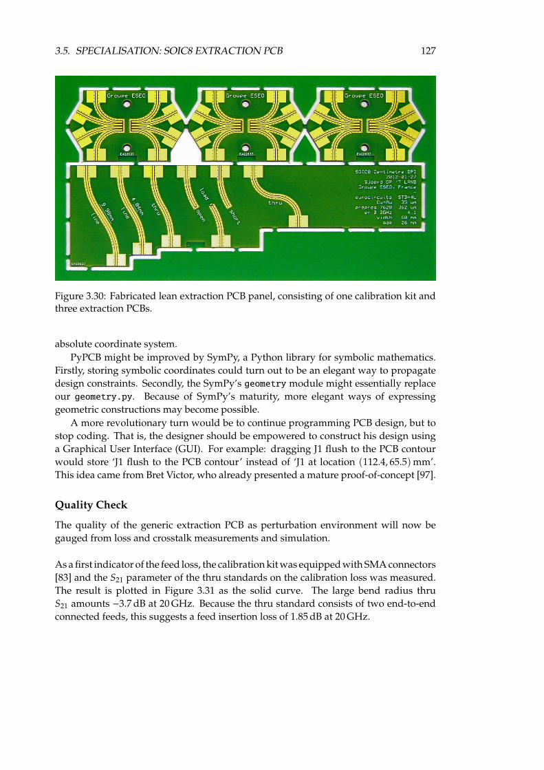
3.5. SPECIALISATION: SOIC8 EXTRACTION PCB 127
Figure 3.30: Fabricated lean extraction PCB panel, consisting of one calibration kit andthree extraction PCBs.
absolute coordinate system.PyPCB might be improved by SymPy, a Python library for symbolic mathematics.
Firstly, storing symbolic coordinates could turn out to be an elegant way to propagatedesign constraints. Secondly, the SymPy’s geometry module might essentially replaceour geometry.py. Because of SymPy’s maturity, more elegant ways of expressinggeometric constructions may become possible.
A more revolutionary turn would be to continue programming PCB design, but tostop coding. That is, the designer should be empowered to construct his design usinga Graphical User Interface (GUI). For example: dragging J1 flush to the PCB contourwould store ‘J1 flush to the PCB contour’ instead of ‘J1 at location (112.4, 65.5)mm’.This idea came from Bret Victor, who already presented a mature proof-of-concept [97].
Quality Check
The quality of the generic extraction PCB as perturbation environment will now begauged from loss and crosstalk measurements and simulation.
As a first indicator of the feed loss, the calibration kit was equipped with SMA connectors[83] and the S21 parameter of the thru standards on the calibration loss was measured.The result is plotted in Figure 3.31 as the solid curve. The large bend radius thruS21 amounts −3.7 dB at 20 GHz. Because the thru standard consists of two end-to-endconnected feeds, this suggests a feed insertion loss of 1.85 dB at 20 GHz.

128 CHAPTER 3. IC CONDUCTED IMMUNITY
S21 (
dB
)
Figure 3.31: Measurement of the S21 parameter of the large radius thru (solid line).Circuit simulation of thru by connecting two feed models back-to-back, where the feedmodels are obtained by measuring SOLT (), TRL 1− 8 GHz (+) and TRL 2.5− 20 GHz(×) and performing offline calibration.
To check the electrical equivalence of the small and large bend radii, the S21 ofthe small radius thru was measured too (not plotted). The difference with the largebend radius is maximally ±0.3 dB and +3 ps from the large radius thru. At a phasespeed of c0/2, this corresponds with a 1 mm effective length difference per feed. The0.2-mm Eurocircuits milling uncertainty does not suffice to explain this difference. Theempirical rule used to compensate the centreline length of the feeds might not haveheld for these GCPWs.
To characterise the feed in another way, we measure the short, open, load, thruand line standards, and extract a feed model by offline calibration (cf. section 3.4).We then cascade two feed models back-to-back in ADS and simulate the end-to-endtransfer; if the feed model is good, this transfer should correspond to the measured thrutransfer above. The simulation results are added to Figure 3.31. The feed model basedon SOLT measurements results in a transfer that deviates maximally ±0.5 dB over all0.05− 20 GHz frequency range. Similarly, models are extracted from TRL standards forthe short and the long line. Around 19 GHz, the short line phase shift surpasses 150,and the resulting prediction starts to deviate heavily. Apparently, line standards shouldnot be used beyond about 150, whereas we designed for up to 160.
In order to understand the ±0.5-dB deviations between prediction and measure-

3.5. SPECIALISATION: SOIC8 EXTRACTION PCB 129
0
25
50
75
100
-50 0 50 100 150 200 250 300 350 400
time (ps)
resi
stan
ce (!
)
–
load
open
short
Figure 3.32: Time domain reflectometry of the short, open and load standards (rise timeof 35 ps). The image of the open standard is warped according to ADS LineCalc delaydata, t = 0 ps corresponds with the SMA reference plane.
ment, we check the step response of the SOL standards with a Time Domain Reflec-tometre (TDR). As we know the propagation velocity, we can map the round-trip-timeto a physical position along the line, which is done in Figure 3.32. It can be noticedthat the standards differ about 5 Ω just after the board edge at 70 ps. Supposedly, thesoldering and/or the connector alignment is not consistent from standard to standard.
The DUT-side crosstalk cannot be measured physically, because there is no room fortwo SMA connectors next to each other at the place of the DUT. Therefore, we asked ourresearch acquaintance Ignacio Gil of the Universitat Polytècnica de Catalunya (UPC) toperform an electromagnetic simulation of the PCB with Agilent Momentum. Accordingto the simulation results, the layout exhibits a worst-case crosstalk of −19 dB at 14 GHzbetween neighbouring large radius and small radius feeds.
To appreciate the reliability of the simulation, the following measurement was de-vised. The extraction PCB was cut in half and the IC pads were shorted with copper tapeat the PUT reference plane. The transfer from one SMA connector to the neighbouringconnector was measured. The same set-up was simulated, by shorting the ports of thesimulated neighbouring traces. The simulation results are compared to measurementin Figure 3.33. On average, the simulation is 5 dB too optimistic. This suggests that thereal PUT crosstalk of the extraction PCB is also higher than simulated, towards −14 dB.

130 CHAPTER 3. IC CONDUCTED IMMUNITY
Figure 3.33: Measurement () and Agilent Momentum electromagnetic simulation (solidline) of the SMA-end crosstalk between a neighbouring large radius and small radiusfeed, with all PUT-ends shorted to ground.
To summarise, the extraction PCB has a feed loss of 1.9 dB at 20 GHz. In light of the3 dB requirement formulated in IEC 62132-4, this is perfectly acceptable. The ±0.5-dBreproducibility of the feed seems to be limited by the consistency of the connector-PCB alignment and soldering. The worst case far-end crosstalk between neighbouringtraces is estimated to be about −14 dB. With respect to the −20 dB requirement derivedin section 3.4, this is marginal. However, the crosstalk is more or less known, so DPImeasurements can be intelligently interpreted.
The extraction PCB could mainly be improved on the reproducibility of the con-nector mounting. Soldering angled connectors under pressure proved difficult, so afuture fan-out should end in straight angles. As revealed by TDR-measurements thatare difficult to reproduce, the centre conductor is subject to mechanical play, causinginvisible solder cracks. Soldering with a more elastic silver solution might prove morerobust to mechanical stress. A solder mask dash could limit excess solder flowing downthe trace. Only if these measures do not improve reliability, more expensive connectorsshould be tried.

3.6. CASE STUDY: LM7805 131
Conclusions
To prove the feasibility of a lean extraction PCB, a generic PCB for SOIC8-packagedICs was developed. To employ bent GCPWs, it proved useful to develop the PyPCBlibrary to programmatically generate PCB layouts. Measurements and simulations onthe resulting calibration kit show that the feeds have acceptable loss up to 20 GHz.
The extraction PCB is fitted with budget SMA connectors on a standard FR4 sub-strate to reduce fabrication cost: depending on the number of feeds fitted with SMAconnectors, one extraction PCB and calibration kit cost around e 200. Moreover, thespring-loaded extraction PCB does not require soldering the DUT, thereby reducingutilisation cost.
One important aspect remaining to be understood, is the perturbation mode incidentupon the PUTs because of the trace fan-out. Firstly, the GCPW conducts three modes:a microstrip mode, a coplanar common mode and a coplanar differential mode.
Secondly, the calibration standards represent a single GCPW feed, but at the DUT,many traces come together and there is no place for stitching vias along some 8 mm.Therefore, the mode may radically change nearby the DUT, without this effect appearingon calibration traces. A future study could be performed on a thru standard withoutstitching vias, and with nearby neighbouring traces: the lean extraction PCB withoutDUT footprint. If the mode conversion proves problematic, a generic extraction PCBmight be invalid for high frequencies. In that case, extraction PCBs need to be designedfor each specific DUT or even PUT.
Apart from that, the PyPCB library may prove very interesting for generalising themethod to other ICs and -packages. Although the library still requires manual tweakingof layouts, the automatic generation of an extraction PCB based on a pinout should befeasible. For example, a graphical application could allow users to choose a package,indicate the pins that need to be injected on, as well as power and ground pins, and pinsfor which no feed is needed. The application then optimises the layout for that particularcase, creates the corresponding calibration kit, and sends the order to Eurocircuits.
3.6 Case study: LM7805
Now that a generic extraction PCB is available, the lean extraction method developedin section 3.4 can be applied to a real DUT. The same case study that was used toprove the validity of the lean extraction method will be used: in particular, a NationalSemiconductor LM78L05ACM.
Knowing that the ICIM-CI model will be used in a radiated PCB immunity testin Chapter 4 directs the model validity domain as follows. Because of the significantfield-to-trace attenuation, little power will be available at the PUT to provoke failure.Therefore, amplifiers will be needed in order to observe susceptibility, which in our

132 CHAPTER 3. IC CONDUCTED IMMUNITY
Figure 3.34: LM7805 on generic SOIC8 extraction PCB.
laboratory dictated the upper frequency bound: 4.2 GHz. Another trick to observesusceptibility, is to define a very stringent functional criterion.
Recall that the ICIM-CI model consists of a PDN and an IB. The PDN will first beextracted from VNA measurements. Next, the IB will be extracted from DPI measure-ments, corrected using the feed model.
PDN Extraction by VNA Measurement
To obtain the PDN, the S-parameters were measured using an Agilent 8753E VNA. Tothat end, the LM7805 was put on the generic SOIC8 extraction PCB. All unused andground pins of the IC (2 up and until 7) were shorted to ground using a CircuitWorks2200MTP conductive coating dispenser. The input (pin 8) and the output (pin 1) of theextraction PCB were equipped with SMA connectors, as shown in Figure 3.34.
To get the LM7805 IC into its operating point, 10 V was applied to the input throughthe VNA’s bias tee. To check the solderless connections at DC, the output voltagewas verified to be 5 V through the VNA’s other bias tee. The measurement set-up isschematised in Figure 3.35.
To move the reference plane to the IC pins, the two-step calibration developed insection 3.4 was employed. First, the reference plane was moved to the extraction PCB’sSMA connectors. That is, 3.5-mm standards from the Agilent 85052D 3.5 mm economycalibration kit were connected instead of the extraction PCB. Then, the VNA’s built-incalibration with the corresponding ideal definitions was run.
Next, the short- open- and load standards on the extraction PCB calibration kit weremeasured and saved to a PC. Using scikit-rf, an offline calibration was performed,

3.6. CASE STUDY: LM7805 133
Fixture PCB
LM7805
Vector Network Analyzer
Calibration Kit
load
open
short
out in
2 1
10VV 1kΩ
Figure 3.35: Measurement set-up for PDN extraction of the LM7805 IC.
assuming ideal standards (i.e. reflection coefficients −1, +1 and 0, respectively). Thiscalibration thus moves the reference plane from the SMA connector to the PUT. Thecalculated calibration coefficients can be visualised using scikit-rf and are plotted inFigure 3.36.
Finally, the LM7805 input impedance is measured at the SMA reference plane, usingthe extraction PCB. The measurement is saved and compensated on the PC, usingcalibration coefficients obtained above. The resulting impedance at the PUT referenceplane is plotted in Figure 3.37. The oscillations in the 120− 210 MHz range are presentboth on the SMA and the PUT reference planes. This phenomenon may be explained bythe marginal stability of the LM7805 without external capacitors. The VNA’s stimulusmay lead the active LM7805 to ring, leading to false reflection readings. Indeed, turningoff the 10 V power supply removes the ringing (measurement not plotted). However,the impedance profile also changes shape by turning off the power supply. Therefore,and because the impedance profile of Figure 3.37b only exhibits small oscillations, the10-V powered measurements are used for the remainder of this thesis.
Although a CRL-like behaviour can be recognized in the impedance profile, we havechosen not to fit a grey-box model to the data, because it does not help falsifying themain hypothesis. Instead, it would degrade the realism of the descriptive, black-boxmodel.

134 CHAPTER 3. IC CONDUCTED IMMUNITY
108 109−0.45−0.40−0.35−0.30−0.25−0.20−0.15−0.10−0.05
0.00
|S21|
(dB
)
(a) Feed loss√
S12S21, estimated from the reflection tracking product.
108 109
Frequency (Hz)
−70−60−50−40−30−20−10
0
Refl
ecti
on(d
B) S22
S11
(b) Either-end feed reflection, equal to the source match (S22) and the directivity (S11).
Figure 3.36: Calibration coefficients describing the feed between SMA reference plane(port 1) and PUT (port 2).

3.6. CASE STUDY: LM7805 135
108 109−5.0−4.5−4.0−3.5−3.0−2.5−2.0−1.5−1.0
PU
Tre
flec
tion
(dB
)
(a) In terms of the reflection coefficient ΓPUT
108 109
Frequency (Hz)
101
102
103
Imp
edan
cem
agni
tud
e(Ω
)
(b) In terms of the impedance ZPUT
Figure 3.37: Linear port behaviour of the LM7805 input (operating point Vin = 10 V), atthe PUT reference plane.
IB Extraction by DPI Measurement
The DPI set-up of Figure 3.38 was made, consisting of a functional and perturbationenvironment.
Functionally, the voltage regulator IC was powered with 10 V from an Agilent N6700Bpower supply via the Picosecond 5545 input bias tee. This bias tee was then connected tothe extraction PCB, leading to the DUT input. The DUT output voltage was connectedto an Agilent 4411A voltmeter via a Mini-Circuits ZX85-12G-S+ bias tee. To decrease thesettling time of the output voltage and to put the LM7805 in typical working conditions,it was DC-loaded with 1 kΩ. In order to observe a high susceptibility, the functionalcriterion was defined less than two orders of magnitude higher than the voltmeter noise

136 CHAPTER 3. IC CONDUCTED IMMUNITY
W W
DPI forward power
50 Ω
1 kΩV10 V
±100
µV0.02–1 GHz
1–4.2 GHz
(a) Schematic.
DC supply
1 kΩ load
voltmeter
DPI forward power
50Ω
(b) Photo.
Figure 3.38: DPI set-up with lean extraction PCB. The dashed line indicates the initialreference plane of the forward power measurement.

3.6. CASE STUDY: LM7805 137
floor: ±100µVDC output offset. Because of this severe criterion, the non-disturbed volt-age drift during the DPI measurement could not be neglected. Therefore, before everyfrequency-power point, the RF disturbance was turned off, the nominal output voltagewas measured again and the voltmeter thresholds were recalculated.
As for the perturbation, two different RF amplifiers were used to obtain the necessarypower: the Prâna AP32-DT120 for the 20 − 1000 MHz range and the Milmega AS0104-3030 for the 1− 4.2 GHz range. The amplifiers were routed through an Agilent L4490Aswitching platform to the DUT input bias tee, which has a 20 GHz bandwidth. TheDUT output bias tee has a 12 GHz bandwidth and is loaded with a 6-GHz 50-Ω load.
The DPI measurement was performed as follows. For each frequency in the logarithmicrange from 20 MHz to 4.2 GHz, the failure threshold RF power was sought. To speed upthe DPI measurement, successive approximation is used: failure is sought by steppingup the generator power in steps of 5, 1, 0.5 and 0.25 dB [62]. After each refinement, thepower was lowered to encounter failure while stepping up, in order to avoid hysteresisuncertainty. This way, the forward power threshold at the IC pin was measured with0.25 dB resolution.
Once the failure was reached, an image of the forward power was obtained fromthe amplifier’s integrated directional couplers. The latter were connected to an Agi-lent E4419B wattmeter through the L4490A switching platform. To deduce the exactpower incident on the input bias tee’s RF input, the directional couplers were calibratedon the bias tee input reference plane (the dashed line in Figure 3.38). That is, one probeof the wattmeter was connected through a Mini-circuits BW-N30W50+ 30 dB precisionattenuator to the cable, that otherwise led to the input bias tee. The other probe ofthe wattmeter was connected as usual, measuring the forward power image from thedirection couplers. At constant generator power, the frequency was swept and readingsof both wattmeters were registered. The attenuation of the precision attenuator wasfirst measured with a VNA and then added to the reading of the first wattmeter probeto obtain the real forward power at the bias tee. Then the difference with the secondwattmeter probe was recorded as correction.
To move the reference plane from the bias tee input to the PUT, a model of the injec-tion path between the two reference planes was made. The bias tee S-parameters weremeasured with the VNA between its input and output SMA reference planes. Then, thefeed network of Figure 3.36 was appended using scikit-rf. The S-parameters of theresulting network are plotted in Figure 3.39. As can be seen, the PUT-side mismatchis relatively small: S22 remains below −18 dB for most frequencies. Therefore, onlythe injection path loss needs to be taken into account. That is, the injection path |S21|was added to the recorded forward power threshold. This way, the forward thresholdpower Pfwd,th at the PUT was obtained.
Finally, the transmitted power threshold Ptrans,th can be calculated from the forward

138 CHAPTER 3. IC CONDUCTED IMMUNITY
108 109−1.2−1.1−1.0−0.9−0.8−0.7−0.6−0.5−0.4
|S21|
(dB
)
(a) Injection path loss.
108 109
Frequency (Hz)
−32−30−28−26−24−22−20−18−16
Refl
ecti
on(d
B) S22
S11
(b) Either-end injection path reflections.
Figure 3.39: Model of the injection path between the input bias tee’s RF input (port 1)and PUT (port 2).

3.6. CASE STUDY: LM7805 139
108 109−40
−35
−30
−25
−20
−15
−10
−5
Tran
smit
ted
pow
er(d
Bm
)
(a) In terms of the transmitted power to the PUT.
108 109
Frequency (Hz)
−35−30−25−20−15−10−5
0
Forw
ard
pow
er(d
Bm
)
(b) In terms of the forward power at the PUT.
Figure 3.40: CW immunity of a LM7805 voltage regulator input for a±100µVDC outputcriterion.
power threshold and the PUT reflection coefficient Γ, which was measured above:
Ptrans,th = Pfwd,th ·(
1− |S11|2)
. (3.7)
Both thresholds are plotted in Figure 3.40.
Conclusions
An ICIM-CI of the National Semiconductor LM78L05ACM voltage regulator was ex-tracted from measurements according to the lean method of section 3.4. That is, atwo-step calibration allowed to measure the PUT impedance and to characterise thefeed (connector and trace leading to the PUT). The latter model is then combined withthe measured S-parameters of a bias tee used during DPI, to correctly move the forward

140 CHAPTER 3. IC CONDUCTED IMMUNITY
power threshold reference plane to the PUT, too. Finally, the two models are used tocalculate the transmitted power threshold. No significant difficulties were encounteredin the extraction process.
To explore the validity domain of the conducted immunity model thus created, theinput voltage and complex load could be swept. Aiming to manage IC obsolescence, itwould be useful to create ICIM-CIs of equivalent ICs from different suppliers and studythe model differences and similitudes.
3.7 Conclusions
In an industrial context, it makes sense to extract ICIM-CI models from measurement.The common IEC 62132-4 DPI test to measure IC immunity is only standardised up to1 GHz. With increasing frequency, DPI yields uncertain transmitted power thresholds.Therefore, Lafon already proposed an alternative method to determine the transmittedpower, by careful modelling and simulation of the used extraction PCB.
Following this approach, a fixture was created to measure and model the SMDpassive components that constitute extraction PCBs up to about 12 GHz. Still, the correctmodelling of extraction PCBs was foreseen to remain time-consuming and error-prone.Therefore, an alternative method was proposed around a lean extraction PCB, designedto be easy to model. The peripheral circuitry consequently needs to be implementedoff-board, on peripheral modules with coaxial connectors. The S-parameters of theentire injection path (peripheral modules and the feed on the extraction PCB) can thenbe found by measuring SOLT standards through eventual peripheral modules. If theinjection path has a good source match, only its insertion loss needs to be taken intoaccount. The forward threshold power at the PUT can then be found by subtracting thisinsertion loss from the threshold found by DPI at the input of the peripheral modules.
To demonstrate this approach, a lean extraction PCB was designed, generic forSOIC8-packaged ICs. In order not to put the peripheral circuitry (on the peripheral mod-ules) too far away, the on-board feeds needed to be short. This suggested bent GCPWs,which is not easy to draw with conventional PCB Computer Aided Design (CAD) tools.Therefore, the PyPCB library was developed, which allows to programmatically gener-ate complex layouts by explicitly propagating constraints. Moreover, this library opensthe way for industrialising the method to other packages. Using this library, the PCBlayout was described and then generated. The PCB fabricated in a standard FR4 pro-cess and equipped with budget SMA connectors. Its feeds exhibited an insertion lossof 1.9 dB at 20 GHz. The worst case far-end crosstalk between neighbouring traces wasestimated to be about −14 dB. The reproducibility of the feed was ±0.3 dB, probablybecause of the inconsistency of the connector-PCB soldering.
Specialising even further, the conducted immunity of a very simple, analog IC wasmodelled: the LM7805 linear voltage regulator.

3.7. CONCLUSIONS 141
Perspectives
The design of the lean extraction PCB necessitated a clear definition of the modelboundaries. A two-dimensional definition of reference lines was agreed upon withBSMI (cf. Figure 3.27).
However, as the common name suggests, reference planes should be defined, thusenclosing the DUT, substrate and ground plane. Indeed, the implicit choice of a sub-strate and feed waveguides may impact the ICIM-CI. For example, the GCPW guidesthe superposition of a microstrip and coplanar modes. With increasing frequency, theimmunity to incident electromagnetic power may depend on the mode. Further re-search should indicate whether this is an important issue. Consequently, IEC 62433-4and IEC 62132-4 will probably need amendment.
Using the findings of this thesis, the IEC 62132-4 standard could already be improvedas follows.
The standard states in section 4.1 that “it has been observed that many ICs aremost susceptible to the disturbances at quite high reflections,” while McDonnel alreadyshowed that high reflections cause high measurement uncertainty of the transmittedpower [71]. Therefore, Lafon’s alternative method of deducing the transmitted powershould at least permitted by the standard and might even be required [76]. The offlinecalibration method proposed in this chapter could also be added as informative ap-pendix. At any rate, it would be a smart step forward to require DPI test reports to statethe measurement uncertainty.
The standard is ambiguous as to the physical placement of the bias tee or blockingcapacitor in the injection path. For example, section 7.2 states “[Are] placed directly onthe testboard: (. . . ) the connection from the end of the transmission line (RF injectionport) via the DC block to the DUT [and] DC biasing networks connected to the pinunder test.” Section 7.3 requires the DC blocking capacitor to be electrically close tothe PUT: “The end of the transmission line to the pin of the DUT should be as short aspossible. A trace length equal to 1/20 of the shortest wavelength applied is a reasonabletarget. Shorter trace lengths are advantageous.” The formulation is somewhat unclear,but Figure 4 suggest that the output of the blocking capacitor should be close to thePUT. No proof is given as to why that would be ‘advantageous’. On the other hand,section 7.5 remarks: “The DC biasing network may also be connected to the injectionpath offside the printed circuit board.”
The latter seems most reasonable: the operator might find it practical to integratebias tees on the extraction PCB, but he might also consider the modelling difficulty aswe did in this chapter. Therefore, the choice should be left to the operator. However,this freedom should consistently be propagated throughout the standard. For example,when presenting the schematics with on-board DC blocks, it should be mentioned that

142 CHAPTER 3. IC CONDUCTED IMMUNITY
this is one possible way of implementing bias tees. For another example, section 7.2should be less categoric about what components should go on the extraction PCB andwhat may be placed off-board.
On the construction of the bias-tee, the enigmatic remark of section 7.5 “To min-imise the effect of mismatching in both cases, the connection from the high impedancedecoupling DC-biasing network to the injection path shall be shorter than λ/20 of thehighest frequency in the test (e.g. less than 15 mm for 1 GHz).” could be clarified likeso: “As the high frequency impedance of the inductance of the biasing network is high,the trace between the inductance and the matched injection path forms a stub. To keepthe effect of this stub negligible, it shall be shorter than λ/20 of the highest frequency inthe test (e.g. less than 15 mm for 1 GHz).” An illustration of placement and constructionof a bias tee could clarify what dimensions are critical and what dimensions are not.More in general, clear definitions of components and reference planes could make thestandard more comprehensible.
To characterise the set-up, section 7.4 requires the attenuation between the coaxialinjection port and the PUT reference plane to be measured less than 3 dB. As thetransmitted power is measured at the output of the directional coupler, the systematicerror could be reduced by including the cabling and eventual off-board bias tees inthis measurement. Moreover, the higher the frequency is, the harder it is to solder aconnector to the PUT reference plane. Therefore, section 7.4 might also allow offlinecalibration of the feed, leading to its calculated |S21|.
Finally, section 4.2 mentions ‘test selectivity’ as an important goal of the DPI. Itwould be good to elaborate this requirement as an upper bound to the far-end crosstalk,for example −10 dB. To measure the far-end crosstalk, the method used in section 3.5of this thesis could be proposed. At any rate, the test report should comment on thedifference between the immunity of neighbouring pins and state whether the PCB’scrosstalk could play a role in the observations.

CHAPTER 4PCB Radiated Immunity
Abstract. Except for a general trend of rising frequencies, there is only little concreteproof for the relevance of IC conducted immunity modelling beyond 1 GHz. Therefore,the cascade of a Grounded CoPlanar Wave-guide (GCPW) trace and an SOIC8 leadframe is studied with full-wave simulation, to find out that up to 10 GHz, most energyenters the die via the trace. Similarly, the immunity of a microstrip trace and an LM7805voltage regulator is predicted up to 4.2 GHz by concatenating the models developedin the former chapters. Although this model neglects the radiated immunity of theIC itself, the prediction corresponds with GTEM-cell measurement to within 2.1 dBaverage error. These experiments suggest the dominant-conduction hypothesis to holdtrue well beyond 1 GHz.
4.1 Introduction
Now that modeling IC conducted immunity beyond 1 GHz proved possible, is it alsouseful? That is, in a realistic system that contains the IC, do perturbations predomi-nantly perturb the IC by conduction or rather by radiation? How does this depend onfrequency?
The little literature that directly or indirectly treats the question will be reviewed insection 4.2. For little is published on the matter, a qualitative exploration by full-wavesimulation will be performed in section 4.3. Alternatively, the radiated immunity of asimple PCB will be predicted in section 4.4, while neglecting the radiated immunity ofthe IC. If nonetheless, this prediction correlates well with measurement, this suggestsdominant conduction. Conclusions will be drawn in section 4.5.
143

144 CHAPTER 4. PCB RADIATED IMMUNITY
4.2 State of the Art
Little explicit conclusions are published on the dominant coupling mechanism of real-life perturbations into ICs. Lagos and Fiori explain why they believe the dominant-conduction hypothesis to hold up to several GHz: “radiated EM fields also couple withthe wiring interconnects (leadframe and bonding wires) of integrated circuits, but in-duced voltages are usually negligible as long as package interconnects are significantlyshorter than the interference minimum wavelength. Given that the maximum size ofmass-production IC packages is usually smaller than a few centimeters, the disturbancecollected by the package interconnects can be neglected up to several gigahertz, hence(. . . ) the direct coupling of external EM fields to IC interconnects (at package and chiplevel) will be neglected.” [21] With similar reasoning, Lafon et al. state that the directcoupling to the IC can be neglected up to at least 4 GHz [76].
There is some indirect proof, however, for dominant conduction beyond 1 GHz.Ramdani et al. describe and explain industrial trends in the EMC of ICs. Because
of the steady miniaturisation, ICs can be sped up, which in turn increases power con-sumption. To counter the latter effect, the supply voltage is steadily lowered, whichinherently lowers the noise margin for digital circuitry, hence lowering IC immunity.Simultaneously, the potential aggressors increase because of the spectacular digitalisa-tion of our society. Also within products, the threat of aggressors increases becauseof the accelerating communication buses and switching noise on supply rails. Conse-quently, IC customers push for increasing immunity. This might explain their expectedextension of the frequency range of conducted immunity modelling and measurementtechniques [8].
Indeed, the publication of research on DPI extension up to 2 GHz in 2012 [91] and upto 18 GHz in 2013 [73], implies that IC conducted immunity beyond 1 GHz is industriallyinteresting. For example, the latter authors show a +20-dBm forward power thresholdobserved around 17 GHz on an Low DropOut voltage regulator (LDO). Maurice andPigneret reports the conducted susceptibility threshold of a simple digital circuit to be+20 dBm of transmitted power in the 2− 4 GHz band [98]. The current mirror studiedby Loeckx starts to offset around 5 GHz with less than +10 dBm forward power [58].McConaghy shows increased conducted susceptibility of a 1990 logic circuit above10 GHz [99]. However, none of the authors prove that these conducted perturbationscould correspond with real-life situations.
Reciprocally, the absence of standards on IC radiated immunity models is alsointeresting. The IEC 62433-4 Integrated Circuit Immunity Model for Conducted Immu-nity (ICIM-CI) was recently approved as New Proposal (NP). No such proposal for ICradiated immunity was made yet. This could be partially due to little actual, industrialimportance.
Finally, the IC interconnects are sometimes believed to strongly attenuate incom-ing perturbations above some GHz. However, Chun, Pham, Laskar, and Hutchison

4.3. EXPLORATIVE SIMULATION 145
measured the −3-dB bandwidth of SOIC8-packaged thru-lines to be 12 GHz [100]. Thepseudo-physical model does not include inductive coupling between neighbouringbondwires and as such, it cannot be trusted to predict the physical path of the power:maybe the power is not really conducted to the die, but capacitively coupled to all pinsat the same time, for example. Nonetheless, this measurement is an indication thatsignificant power can couple on and off the die, well beyond 1 GHz.
On the other hand, there is also indirect evidence for dominant radiation beyond 1 GHz.For example, the bondwire plus leadframe inductance of wire-bonded packaging is
in the order of some nH. For flip-chip packages, the ‘lead’ inductance is lower, but stillin the same order of magnitude [101]. 2 nH, for instance, equals 251 jΩ at 20 GHz. Inother words, the die starts to electrically float. Put differently, with rising frequency,it becomes harder for conducted functional signals and perturbations to arrive at thedie. This might explain the popularity of Antenna on Chip (AoC) solutions for 60 GHz[102], but also Antenna in Package (AiP) for 2.4 GHz [103]. This suggests significantdirect coupling of (functional) radiation to chip-size structures.
Although there are no standardised IC radiated immunity models, there are variousmeasurement methods, like the IEC 62132-6 Local Injection Horn Antenna (LIHA), upto 10 GHz, the IEC 62132-9 Near Field Scan of Immunity (NFSI) and the IEC 62132-8IC stripline, up to 6 GHz. This suggests that IC radiated immunity is an interestingquantity.
Perdriau, Maurice, Dubois, Ramdani, and Sicard estimate the radiated immunitythreshold of a particular digital circuit to be as low as −5 dBm transmitted power at20 GHz [104].
In summary, there is no hard proof for nor against the real-life relevance of IC conductedimmunity measurement beyond 1 GHz. However, below a certain frequency, radiatedperturbations can be expected to mainly couple to the trace and then be conducted tothe die. Above a certain frequency, perturbations can be expected to be mainly coupleddirectly to the die. In between these frequencies, there must be a conducted-radiatedtransition frequency, which will depend on the trace and IC geometry and materials.
Therefore, the question is: what is the conducted-radiated transition frequency?
4.3 Explorative Simulation
To quickly get a qualitative idea about the dominant coupling mechanism as functionof frequency, a full-wave solver was employed as follows. The conducted-radiatedtransition frequency will be determined for a modern trace-IC configuration that hasa low expected transition frequency. That way, if even that configuration exhibits atransition frequency above 1 GHz, all other modern cases may be expected to have atransition frequency above 1 GHz.

146 CHAPTER 4. PCB RADIATED IMMUNITY
In modern electronics, traces with or without ground planes are applied, with copla-nar ground planes and/or ground planes beneath the trace. From all these configura-tions, a Grounded CoPlanar Wave-guide (GCPW) is expected to be the worst antennabecause of the nearby ground planes. Consequently, little radiated perturbation will becaptured with respect to the IC, hence a low transition frequency.
As for the IC, the bigger the package, the more coupling can be expected. This pleadsfor packages with a big lead frame, like a 40-pin Dual Inline Package (DIP). However,mainstream electronics are moving towards smaller Surface Mount Technology (SMT)packages like Quad Flat package No leads (QFN) and Ball Grid Array (BGA). To strikea realistic balance, popular in automotive because of its reliability, an SOIC packagewas chosen.
The trace was modelled under CST as a 0.6 mm, 50 Ω coplanar trace. Again, to minimisethe antenna efficiency of the trace, it was terminated in a discrete characteristic (50 Ω)load at the near end.
To obtain a realistic IC model, the SOIC8 package of a National LM7805 was opened(Figure 4.1a) and conscientiously reproduced under CST (Figure 4.1b). The lead framewas modelled as Perfect Electrical Conductor (PEC). A bondwire was though up,and a 50 Ω discrete port was installed between the end of the bondwire and the IC’sinternal ground plane. The package was modelled as epoxy resin. The structure was il-luminated by a 1 V/m endfire plane wave. The power arriving on the die was monitored.
By a parametric sweep of the trace length, the coupling via the trace could be qualita-tively identified.
Not to our surprise, a longer trace caused more coupling at low frequencies (Fig-ure 4.2). At about 20 GHz, the trace length does not seem to change the couplinganymore, which suggests that all power couples directly to the package and the bond-wire. For particular lengths and frequencies, destructive interference seems to occur.The transition frequency seems to be between 10 GHz and 19 GHz, but clearly above1 GHz.
It be noted that side fire illumination could have coupled much less to the trace,and thus have revealed a much lower transition frequency. However, as all incidenceangles may occur in practice, it can still be concluded that for some angles, conductionis dominant. At least for these cases conducted immunity IC models are required.
To summarise, a qualitative study of the dominant coupling mechanism was performedon a modern trace and IC. Despite the GCPW, the lossy substrate and the matched load,the coupling seems to be predominantly conducted, at least up to 10 GHz.
However, we have no analytical reference to validate the simulation against and wehave no insight in the influence of all geometric parameters. Therefore, more proof isneeded.

4.3. EXPLORATIVE SIMULATION 147
1 Vout
2 gnd
3 gnd
4 NC
Vin 8
gnd 7
gnd 6
NC 5
3.9 mm nom.
4.9
mm
no
m.
0.35 mm nominal
(a) Macroscopic photo of a mechanically opened National SemiconductorLM78L05ACM voltage regulator. Nominal dimensions are taken from the productdata sheet.
1 V/m
trace_length
(b) Simulation of reproduced leadframe, GCPW and plane wave as entered under CST.
Figure 4.1: Simulation set-up to study the contribution of PCB trace, package andbondwire to the field-to-die coupling.

148 CHAPTER 4. PCB RADIATED IMMUNITY
on
-die
rec
eiv
ed p
ow
er (
dB
W)
frequency (GHz)
mm
longer traces, more coupling
only on-die coupling?
?
longer traces λ/2?
Figure 4.2: Simulation result: on-die received power as function of frequency and tracelength for 1 V/m far-field illumination.
4.4 Cascading Trace and IC Models
The dominant coupling mechanism will now be studied using the overarching approachof this thesis, as follows. The radiated immunity of the cascade of a trace and an ICwill be predicted by cascading the models developed in Chapter 2 and 3. That way,the radiated immunity of the IC is neglected, as illustrated in Figure 4.3b. Next, thisprediction will be compared to measurement, where both trace and IC are exposed tothe radiated perturbation. To the extent that the prediction corresponds well with themeasurement, the radiated immunity of the IC is negligible.
To allow for measurement, a demonstrator PCB with the LM7805 voltage regulatorwill first be developed. Knowing the demonstrator, two measurement configurationswill be decided upon. For each configuration, the field-to-trace coupling will then becalculated. By slightly adapting the IC conducted immunity, as measured in Chapter 3,the radiated immunity of the whole will be predicted for both configurations. Finally,these predictions will be compared to measurements.
Demonstrator Design
As must conducted immunity tests, any radiated immunity test must provide a per-turbation and a functional environment. The perturbation environment allows for awell-defined supply of radiated perturbation. The functional environment puts the

4.4. CASCADING TRACE AND IC MODELS 149
Ei
!
c0Hi
(a) Perspective on the system.
trace
radiation
IC
radiation
conduction
!!
(b) Weakly-coupled model of the system.
Figure 4.3: Illumination of the system: a trace connected to an IC (repetition of Fig-ure 1.6).
Device Under Test (DUT) in a typical or worst case application and allows for failuresurveillance. In this particular case, the demonstrator geometry was chosen such, thatthe field-to-trace coupling model and the ICIM-CI developed in this thesis could modelthe entire demonstrator.
As for the perturbation environment, the trace could be any multi-segment mi-crostrip, given the model developed in Chapter 2. However, at the time of fabricatingthe demonstrator, the modified Taylor cell was not yet proven by measurement. There-fore, to reduce the number of uncertainties, a single microstrip segment of 5 cm waschosen. Similarly to the field-to-trace measurements, the trace was put on a 10× 10 cmPCB for illumination in a Gigahertz Transverse ElectroMagnetic (GTEM) cell.
The IC was chosen to be the LM7805 linear voltage regulator, of which the input’simmunity was modelled in section 3.6. The footprint was chosen to be similar tothat used on the extraction PCB. Also, the substrate was chosen to be the same ason the extraction PCB: 360µm Flame Retardant 4 (FR4). However, to challenge theindependence of the model to the waveguide design, another ground plane was defined.The trace leading to the regulator’s input is a microstrip, so no coplanar ground is usedin the demonstrator. Also, no ground plane is put on the outer PCB layer, just beneaththe IC package, contrary to the extraction PCB. To provide a low-impedance ground,all ground pads were equipped with two in-pad vias.
As for the functional environment, the regulator should be supplied with a DCsupply voltage. Therefore, the other end of the illuminated trace is equipped with aprecision Molex SMA connector, allowing to connect a bias tee for DC supply. As theconnectorised bias tee can be measured with a VNA, the RF charge impedance can alsobe well-known. Because the ICIM-CI describes the immunity of the IC input, the traceleads to the IC input. To monitor failure, the regulator output DC voltage should bemeasured. To avoid coupling of the radiated perturbation to the IC’s output, which isnot modelled, an in-pad via directly brings the signal to the outside of the GTEM cell. It

150 CHAPTER 4. PCB RADIATED IMMUNITY
(a) Bottom side (illuminated by the GTEM cell).
(b) Top side (outside of the GTEM cell).
Figure 4.4: Eurocircuit pre-production visualisation of the trace-IC demonstrator. Darkgrey signifies gold-plated outside copper.
might prove necessary to supply an output capacitor for stability, so a suitable footprintwas provided. The trace being at the outside of the GTEM cell, a precision Molex SMAcan no longer be used, so a budget SMD SMA connector was used. Similarly, a bias teewith a 50 Ω load can be applied to correspond with the model extraction environment.The DC output of the bias tee allows for monitoring of the voltage offset.
The resulting demonstrator PCB is shown in Figure 4.4. The footprint of the precisionMolex SMA connector was optimised using CST to provide a good transition frommicrostrip to coax. A cross-section of the PCB is shown in Figure 4.5. Notice how themodels for field-to-trace coupling and IC immunity describe touching regions. Noticealso that the microstrip-to-SMA transition, the SMA connector and the input bias teeare not modelled by either model. Therefore, they should be represented as the chargeimpedance connected to the left end of the field-to-trace coupling model.
Measurement Configurations
Given this demonstrator PCB, equipped with an LM7805 voltage regulator, there aretwo remaining degrees of freedom. Firstly, the RF charge impedance connected to theinput bias tee. Because this charge is connected to the RF SMA connector of the inputbias tee, it is easy to experiment with this variable. Secondly, the 10 × 10 cm (square)PCB can be easily rotated by quarters of a turn.
To start with a simple case, the PCB is placed such, that the trace is end-fire illumi-nated with the IC at the far end, as shown in Figure 4.6a. As this configuration wasshown before to induce the worst case terminal voltage for high frequencies, the highest

4.4. CASCADING TRACE AND IC MODELS 151
43
21
2Ei
2Hi ki
field-to-trace model ICIM-CI
100 µV criterion
|
voltmeter
|
bias-T
|short/load
|
bias-T
|
Figure 4.5: Longitudinal cross-section of the trace-IC demonstrator (not to scale). Modelboundaries are dashed.
Ei
!
c0Hi
50 Ω
(a) ‘Matched’
Ei
!
c0
Hi
(b) ‘Shorted’
Figure 4.6: Measurement configurations.

152 CHAPTER 4. PCB RADIATED IMMUNITY
susceptibility can be expected. To exclude modelling problems with the near-end chargeimpedance, the bias-tee was terminated in a broadband 50 Ω load. This configuration(near end: 50 Ω charge, far end: LM7805 Pin Under Test (PUT)) will be referred to as‘matched’.
To challenge the modelling of a non-characteristic charge impedance, a short cali-bration standard is connected to the input bias tee, as shown in Figure 4.6b. Becausereflections are now expected, the lower high-frequency coupling to the near end maystill suffice to observe susceptibility. Therefore, the card is rotated by 180˚; the trace isstill end-fire illuminated, but the IC is now located at the near end. This configuration(near end: LM7805 PUT, far end: short standard) will be referred to as ‘shorted’.
Field-to-trace Coupling Calculation
Using the field-to-trace coupling model developed in Chapter 2, the trace terminalvoltage induced by a given field on given terminal impedances can be calculated.
The trace is well-known: a 5 cm, end-fire illuminated microstrip on a 360µm FR4substrate. The field will be the field strength, that would be generated by 1 V on theGTEM cell septum.
To determine the terminal impedances as seen by the illuminated trace, the geometryof Figure 4.5 must be carefully inspected. At the right side (at the PUT), the field-to-tracemodel is flush with the ICIM-CI. That is, the right-end impedance coincides with thereference plane of the Passive Distribution Network (PDN) extracted from measurementin section 3.6. Therefore, the ICIM-CI’s S11 only needs to be converted to Z11.
At the left side, however, the trace is connected to an SMA connector through amicrostrip-to-coaxial transition. As both were designed to resemble a 50 Ω waveguide,they may be modelled as electrical delays. As calculated in Chapter 2, the connector hasa 37 ps delay and the transition about 11 ps. To exclude non-idealities of the used 50 Ω
standard or the short, the impedance of both will be measured with a VNA throughthe bias tee. The resulting model is shown in Figure 4.7. Both charges are measured atthe bias tee’s ‘RF+DC’ output with a VNA, then retarded by 37 + 11 ps. The resultingimpedances are plotted in Figure 4.8.
Alternatively, simplified charge models can be used. For the matched configuration,if the standard is perfect and the bias tee a 50 Ω waveguide, the simplified model shownat the top of Figure 4.7 may be used. As can be seen from Figure 4.8a, this seems areasonable approximation. For the shorted configuration, the nominal delays of theshort standard and the bias tee can be used to retard a perfect short circuit.
Again, the field2line framework developed in Chapter 2 was used to numericallycalculate the induced voltage VPUT at the IC’s PUT.

4.4. CASCADING TRACE AND IC MODELS 153
50Ω
SMA +
PCB
illuminated trace ICload
standard
50Ω
ZPUT
measured
measured
Zload
Zne Zfe
(a) ‘Matched’
50Ω
37+11 ps
ZPUT
measured
50Ω
195 ps
50Ω
bias tee
32 ps
50Ω
short standard
measuredZshort
short
ZneZfe
(b) ‘Shorted’
Figure 4.7: Model of the illuminated trace leading to the PUT of the IC. At the left, theimpedance of any charge measured at its SMA reference plane can be used. Alterna-tively, simplified models of the load and short standards can be used.

154 CHAPTER 4. PCB RADIATED IMMUNITY
108 109
Frequency (Hz)
100
101
102
103
Mag
nitu
de
(Ω) Zc
Z11
(a) Measured impedance of the Picosecond 5545 bias tee ‘AC+DC’ port (the ‘AC’ portwas connected to the other port of the VNA), delayed by 37 + 11 ps.
108 109
Frequency (Hz)
100
101
102
103
Mag
nitu
de
(Ω) Zc
Z11
(b) Measured Agilent 85052D-60006 male short, seen through the Picosecond 5545 biastee, delayed by 37 + 11 ps.
Figure 4.8: Charge impedances Zcharge, which will be entered at one end into theilluminated trace model.

4.4. CASCADING TRACE AND IC MODELS 155
+
–
Zc
Zc
Vint
source load
+
–
V
P =V2
R=
(
12 Vint
)2
Zc
Vint = 2p
PZc
P
(a) First step: find the internal source voltage for a given forward power using a matchedload.
+
–
Zc
source load
+
–
VZPUT2
p
PZc V = 2p
PZcZPUT
ZPUT + Zc
(b) Second step: use this internal voltage to find the load voltage for an arbitrary load.
Figure 4.9: Conversion of forward power to voltage.
Radiated Immunity Calculation
To calculate the forward power immunity threshold at the GTEM cell input, the abovemodels will now be concatenated.
The first step is to interface the field-to-trace model and the ICIM-CI. The formeryields a voltage VPUT (for 1 V at the septum), while the latter yields a threshold net powertransmitted to the PUT. The choice was made to adapt the ICIM-CI, by converting thetransmitted power threshold to a threshold voltage (cf. Figure 4.9):
Vth = 2√
Pfwd,thZcZPUT
ZPUT + Zc, (4.1)
where Pfwd,th is the forward threshold power at the PUT reference plane, as observed inDPI, Zc is the characteristic impedance of the DPI set-up and ZPUT is the IC’s impedanceas measured with a VNA. This calculation is graphically performed in Figure 4.10.
The next step is to calculate the septum threshold voltage:
Vth,septum =Vth
H, (4.2)
where H is the voltage transfer from septum to PUT, as given by the field-to-tracecoupling model. It be noted that H may be a random variable, because of the phase

156 CHAPTER 4. PCB RADIATED IMMUNITY
108 109101
102
103
Imp
edan
cem
agni
tud
e(Ω
)
(a) IC impedance ZPUT as measured with the VNA for Vin = 10 V on the SOIC8 extractionPCB, calibrated using the calibration kit (repetition of Figure 3.37b).
108 109−35
−30
−25
−20
−15
−10
−5
0
Forw
ard
pow
er(d
Bm
)
(b) IC immunity measured with DPI (100µVDC criterion), corrected for the SOIC8extraction PCB using the calibration kit (repetition of Figure 3.40b).
108 109
Frequency (Hz)
10−3
10−2
10−1
100
Vol
tage
(V)
(c) IC immunity in terms of threshold voltage.
Figure 4.10: Calculation of the IC immunity in terms of threshold voltage, calculatedaccording to (4.1).

4.4. CASCADING TRACE AND IC MODELS 157
uncertainty of the GTEM cell reflection. Consequently, Vth,septum may be stochastic, too.This calculation is performed graphically in Figure 4.11.
Finally, this septum threshold must be converted to a forward threshold powerincident on the GTEM cell input:
Pfwd,GTEM,th =V2
th,septum
Zc,GTEM=
(Vth/H)2
50.0. (4.3)
This calculation graphically simply corresponds to a vertical shift and scale on a loga-rithmic axis.
Comparison with Measurement
Now that a quantitative prediction is calculated, the measurement can be performed.The measurement set-up and procedure will be described and the measurement resultswill be compared to the prediction.
The demonstrator PCB was fabricated and assembled as can be seen in Figure 4.12a.Then, the PCB was placed on the GTEM cell opening as shown in Figure 4.12b. Similarlyto the DPI measurement conditions, the voltage regulator IC was powered with an Ag-ilent N6700B power supply via the Picosecond 5545 input bias tee. The output voltagewas coupled out via a Mini-Circuits ZX85-12G-S+ bias tee, loaded with 1 kΩ and thenconnected to an Agilent 4411A voltmeter. The RF perturbation coming from variousamplifiers was connected to the GTEM cell input. In the ‘matched’ configuration, the‘RF’ terminal of both bias tees was terminated in 50 Ω. For the ‘shorted’ configuration,an Agilent 85052D-60006 short standard was connected the ‘RF’ terminal of the inputbias tee.
The radiated immunity in the GTEM cell was measured similarly to the DPI. That is,with successive approximation and a final 0.25 dB forward power resolution. Becauseof the subtle failure criterion of ±100µVDC, the output voltage drift made the mea-surement time-variant. To counter this effect, the nominal output voltage had to bemeasured again before each point, like during DPI.
Again, similarly to the DPI measurement, the Prâna and the Milmega amplifierswere used to cover the 20 MHz to 4.2 GHz frequency range. The forward power at thedirectional couplers was compensated with a calibration to obtain the forward powerat the input of the GTEM cell.
The immunity measurement result is compared with the prediction for both configura-tions in Figure 4.13.
The peak in the measurement at 290 MHz occurred intermittently, both in DPIand GTEM measurements. Probably, the voltage regulator without external outputcapacitor is marginally stable around this frequency, and the disturbance may excite

158 CHAPTER 4. PCB RADIATED IMMUNITY
108 10910−3
10−2
10−1
100
PU
TV
olta
ge(V
)
(a) PUT failure threshold (repetition of Figure 4.10c)
108 109−80
−70
−60
−50
−40
−30
−20
Vol
tage
tran
sfer
(dB
)
(b) Voltage transfer from GTEM septum to PUT.
108 109
Frequency (Hz)
100
101
102
Sep
tum
volt
age
(V)
(c) Consequent septum failure threshold.
Figure 4.11: Calculation of the radiated immunity for the shorted configuration (differ-ence on above scales).

4.4. CASCADING TRACE AND IC MODELS 159
SM
A in
5 c
m
trace
LM
7805
SM
A o
ut
(a) Illuminated side of the demonstrator PCB, consisting of trace and IC.
DC supply
bias T
bias T
1 kΩ load
voltmeter
GTEM cell
50Ω load 50Ω
load
RF
Pfwd reference plane
(b) Demonstrator PCB placed on the GTEM cell and connected to peripherals.
Figure 4.12: Measurement of the radiated immunity of the demonstrator PCB in the‘matched’ configuration.
this oscillation. Notice also how the GTEM measurement flattens around the alleged+46 dBm (40 W) at low frequencies. The Prâna amplifier used in this range has an output3 dB compression point at 25 W, so significant harmonic distortion can be expected. Ascan be seen from the prediction, higher harmonics encounter lower immunity, so theobserved failure could be caused by harmonics. This might explain the low-frequencyflattening.
The comparison with prediction was repeated for simplified charge models, toinvestigate the importance of accurate charge models. Instead of the VNA-measuredimpedance, the idealised models of Figure 4.7 were used. To check the method, anoversimplified charge model was applied in the ‘shorted’ case: a 0 Ω without a 32 +
195 ps delay. This charge model is expected to predict resonances that are significantlyfrequency-shifted.
The results are numerically compared in Table 4.1. Notice that the averages arecalculated along the log-sampled frequency range from 20 MHz to 4.2 GHz, whereverfailure could be observed.

160 CHAPTER 4. PCB RADIATED IMMUNITY
108 109152025303540455055
GT
EM
inp
utp
ower
(dB
m)
DPI-Taylor
GTEM102
103
Fieldstrength
(V/
m)
(a) ‘Matched’ configuration (near end: matched load, far end: LM7805 input).
108 109
Frequency (Hz)
152025303540455055
GT
EM
inp
utp
ower
(dB
m)
DPI-Taylor
GTEM
102
103
Fieldstrength
(V/
m)
(b) ‘Shorted’ configuration (near end: LM7805 input, far end: short standard).
Figure 4.13: Prediction and measurement of the radiated immunity of a 5 cm trace andan LM7805 voltage regulator. The shaded area represents the uncertainty introducedby the reflection phase of the GTEM absorbers. Gaps in the black curve signify that nosusceptibility could be observed with the available RF power.
For the ‘matched’ configuration, the average absolute error is 2.01 dB (as plottedin Figure 4.13a). Using the ideal charge model improves this number slightly, but thevisual match is about as good (not plotted).
For the ‘shorted’ configuration, the average absolute error is 2.19 dB (as plotted inFigure 4.13b). This number only slightly deteriorates when using the idealised chargemodel of a delayed short. When using a simple short, the curve visually deteriorates(not plotted), as can be seen from the increased average absolute error 4.36 dB.
In summary, the radiated immunity of a trace and an IC can be predicted to within2.1 dB average absolute error by correctly concatenating the modified Taylor model andthe ICIM-CI. On average, using a measured charge model is not necessary, at least up

4.5. CONCLUSIONS 161
Table 4.1: PCB immunity prediction – measurement error as function of terminalmodel quality.
errorconfig. charge model average avg. abs. maximum minimummatched delayed meas. −1.91 dB 2.01 dB +2.30 dB −6.80 dB
(delayed) 50 Ω −1.53 dB 1.87 dB +2.79 dB −6.70 dBshorted delayed meas. +1.14 dB 2.19 dB +7.68 dB −14.29 dB
delayed 0 Ω +0.97 dB 2.22 dB +4.71 dB −17.73 dB0 Ω +1.12 dB 4.36 dB +14.40 dB −13.75 dB
to 4.2 GHz.
4.5 Conclusions
Because of the small size of IC leadframe and bonding wires with respect to the wave-length, the direct coupling of radiated interference with IC is generally supposed to benegligible up to several GHz. On the other hand, Antenna in Package (AiP) solutionsfor 2.4 GHz suggest the contrary. In order to understand the coupling mechanism and,consequently, the relevance of IC immunity tests beyond 1 GHz, two experiments wereconducted.
Firstly, a full-wave simulation was performed on a trace and a SOIC8 interconnect.The coupling of an incident plane wave to the die was found to be dependent on the tracelength up to 10 GHz. This experiment suggests that the dominant coupling mechanismfor a modern IC is conducted, well beyond 1 GHz.
Secondly, the field-to-trace model and the ICIM-CI obtained in Chapter 2 and 3are concatenated, to predict the radiated immunity of the whole up to 4.2 GHz. Al-though this model does not take the direct radiated immunity of the IC into account,it corresponds with measurement to within 2.1 dB average absolute error. In anotherway, this experiment suggests that the perturbation predominantly perturbs the IC byconduction, well beyond 1 GHz.
Both experiments were conducted on modern packages, while electronics are con-tinuously expected to shrink, hence reduce direct coupling. Therefore, the dominant-conduction conclusion may be expected to remain valid over time and for increasingfrequencies. Consequently, IC immunity modelling beyond 1 GHz seems useful.
In this particular concatenation of systems at the hierarchical PCB level, the radiatedperturbation seems to mainly couple to the trace and then be conducted to the IC. Thissubsystem generally is comprised in a much larger system, for example in a rack, in a

162 CHAPTER 4. PCB RADIATED IMMUNITY
shielded enclosure, connected with cable bundles in a vehicle. It would be interestingto prove that the dominant-conduction hypothesis also holds true in that case. Atopological approach like the Power Balance technique developed by Junqua et al.could be a good starting point [105].

CHAPTER 5Conclusion and Perspectives
Abstract. From the observations described in this thesis, it can be concluded that it isuseful and possible to model the conducted immunity of ICs beyond 1 GHz. Therefore,the extension of IEC 62132-4 to 10 GHz should be seriously considered. Moreover, thespeed and transparency of the model for field-to-trace coupling open up new possibili-ties for computer-aided design. The semi-automatic generation of lean extraction PCBscould facilitate model extraction. There are also critical remaining questions, remainingto be answered.
5.1 Introduction
What have we seen throughout this thesis? How could all of this be put into practicetoday? What can not yet be concluded? Where should we, therefore, go tomorrow?
The first building block of this thesis is the transparent model for field-to-trace coupling;section 5.2 will review the results and draw up a research agenda for this model alone.The second building block is the lean Gigahertz Direct Power Injection (GDPI) method,comprising semi-automatic PCB layout generation, which will be reviewed and ofwhich the future possibilities will be sketched in section 5.3. Finally, section 5.4 willconclude upon the thesis’ main hypothesis.
5.2 Modified Taylor Model for Field-to-trace Coupling
Literature offered little understanding on how PCB traces determine the coupling ofincident RF radiation to conducted voltages or currents. That is, models allowing fornumerical simulation existed, notably the weakly coupled Taylor cell or its equivalents.When applying this model to electrically short, bifilar lines in vacuum, the effect of
163

164 CHAPTER 5. CONCLUSION AND PERSPECTIVES
+–
Zc
Zc
+
–
Vne
Vfe
+
–
e−jβ`j!µ0Hn(0)h` K
j!cEt(0)h` K
Figure 5.1: The modified Taylor cell; the correction factor K takes into account the longline effect. (Repetition of Figure 2.19.)
line dimensions and orientation can be understood [10]. However, when applying thismodels to PCB traces, the result becomes hard to understand because of the substrate.Only Leone gave a transparent worst case for a single microstrip segment with mod-erately mismatched loads, for low frequencies. Nonetheless, for high frequencies, thetrace becomes electrically long, meshing is required and understanding is lost.
Yet, to acquire a numeric reference, a meshed model was implemented for the caseof a grazing incident, vertically polarised plane wave on a single microstrip with ar-bitrary loads. The Taylor-telegrapher’s cell was applied under Kron’s formalism. Byfrequency-adaptive meshing of the trace, a 10× speedup was achieved. Of course, noprofound understanding was obtained.
Therefore, the single Taylor cell was modified to remain valid for high frequencies.Thereby, meshing is no longer needed and understanding could be hoped for. Themodification is a correction factor K, which quantifies the similitude between the il-lumination and the trace’s eigenwave, which would spontaneously propagate on theline:
K =1ℓ
∫ ℓ
0i(p) ·w∗(p) dp, (5.1)
where i and w are the normalised amplitude phasors of the illumination and the eigen-wave, ℓ is the trace length and p is the coordinate along the trace segment. Indeed,this is the length-averaged cross-correlation between illumination and eigenwave. Theresulting modified Taylor cell is repeated in Figure 5.1. Note that for calculating thenear-end or the far-end induced voltage, the backward- or the forward-going eigen-wave needs to be used. By superposition and basic transmission line theory, the modelwas extended to hold for vertically polarised, grazing-incident plane wave illumina-tion of uniform multi-segment traces with arbitrary loads. Because of the single cell,closed-form solution, another 10× speedup was achieved.
Predictions from this model were compared to full-wave simulation, yielding verygood correlation. Because the full-wave solver does not rely on transmission line theoryor our approximation of the substrate field, both approximations seem legitimate.

5.2. MODIFIED TAYLOR MODEL FOR FIELD-TO-TRACE COUPLING 165
108 109 1010
−90
−80
−70
−60
−50
−40|V
fe|
(dB
V)/
S 21
(dB
)
Measurement
Taylor
Figure 5.2: Prediction and measurement of coupling to a three-segment microstrip withcharacteristic loads. Without taking into account GTEM cell reflections, the predictionwould be midway the grey zone. (Repetition of Figure 2.51a.)
The modified Taylor predictions were also compared to Gigahertz Transverse Elec-troMagnetic (GTEM) cell measurements, taking into account substrate permittivity andGTEM cell reflections.
To take into account the frequency-dependent real substrate permittivity, a planarresonator was employed to measure the used substrate. In comparison to Rectangu-lar Dielectric WaveGuide (RDWG) measurements on the same substrate, this methodseemed to work. However, taking into account the measured permittivity did not yieldsignificant improvement of the field-to-line coupling prediction up to 3 GHz, and wors-ened it above. Because of this low Return On Modelling Effort (ROME), the permittivitymeasurements were not used anymore and a simple εr = 4.6 was retained.
To take into account the non-ideality of the GTEM cell hybrid load, the S11 of theGTEM cell was measured and translated to the position of the illuminated trace. Theforward wave and its first reflection by the hybrid load was then fed to the modifiedTaylor model. As can be seen in the striking example of Figure 5.2, this predicts theoscillations in the 0.1 − 2 GHz range. Because of the good ROME, this correction wasretained.
Based on this model formulation, the transparent upper bound shown in Figure 5.3could be found. Several practical consequences could be drawn from this formulation.Not surprisingly, matching helps. Practically, this can be done by adding passivecomponents at the trace terminals, or just by adjusting the trace width, which is ‘free’.Furthermore, decreasing the substrate thickness h (not so easy) or the trace length ℓ(easier) helps for low frequencies. At high frequencies, shortening the trace does nothelp, although the crossover frequency between ‘low’ and ‘high’ frequencies increases.Finally, changing the substrate permittivity εr does not significantly decrease couplingat any frequency, because εr,eff will change accordingly.
For a single microstrip segment with matched loads, this worst case occurs for end-fire excitation at the near-end side for low frequencies and at the far-end side for high

166 CHAPTER 5. CONCLUSION AND PERSPECTIVES
. . . × Ei hn 21 −
p"r,eff
"rp"r,eff − 1
. . . ×Ei h`
!
c0
(
1 +
p "r,eff
"r
!
(1 + ρfe)(
1 +∣
∣
∣
∣
∣
Zne
Zc− 1∣
∣
∣
∣
∣
1cos \Zne
)
. . .
108 109 1010
Frequency (Hz)
80
70
60
50
40
30
20
10
Vfe
(dBV)
East West South North Upper bound
mismatchpenalty
matchedcoupling
Figure 5.3: Upper bound versus measurement of an either-end mismatched (0− 270 Ω),three-segment trace, after Figure 2.54c.
frequencies. Consequently, it is most interesting to illuminate a sensitive trace fromeither end in pre-compliance testing.
The upper bound was not proven for arbitrarily-polarised, arbitrarily-incident planewaves. As any electromagnetic fields can perturb a PCB in real life, the analysis shouldbe extended to all polarisations and all angles of incidence. Considering the worst caseand taking loose upper bounds may help to keep the expressions transparent.
A deterministic approach was taken in this thesis to allow for understanding, de-bugging and selection of test scenarios. However, as perturbing fields are random inreal life, it might be useful to take a stochastic approach [22]. The challenge will remainto keep the solution transparent.
The +1.3-dB systematic bias of the GTEM measurements with respect to the Taylormodel predictions remains enigmatic. Full-wave simulation of the GTEM cell for thetop opening might yield new insights.
Throughout the modelling process, errors were mainly quantified by the average ab-solute error in dB. However, the match was often better appreciated visually. Therefore,techniques like Feature Selective Validation (FSV) should rather be applied [106].
Finally, the presented upper bound is rather loose. For one case study, the upperbound was as much as 13 dB too high in the high-frequency range. This might bedue to the pessimistic assumptions behind the upper bound: there are no trace lossesand all segments will interfere constructively for some frequency. Moreover, rather

5.3. LEAN GDPI METHOD 167
rough approximations were used in the consideration of arbitrary terminal impedances.Therefore, a sensitive trace from industrial reality should be studied to see how loose theupper bound is in practice. If it turns out to be too pessimistic and that it would causecostly over-engineering, the assumptions and approximations should be revisited.
5.3 Lean GDPI Method
Now that the conducted perturbation induced by an incident electromagnetic field be-yond 1 GHz is known, the conducted immunity of ICs is also interesting beyond 1 GHz.The IEC 62433-4 Integrated Circuit Immunity Model for Conducted Immunity (ICIM-CI)is a mature model to describe IC’s immunity, which consists of a Passive DistributionNetwork (PDN) and an Immunity Behaviour (IB) part. From the PCB designer’s per-spective, it is generally impossible to obtain such models from IC manufacturers, so amethod is needed to extract these models from measurement.
The IEC 62132-4 DPI already allows for extracting the IB and is standardised up to1 GHz. The transmitted power threshold is deduced from a directional coupler powerreading. The reference plane of this measurement is at the output of the directionalcoupler, instead of at the Pin Under Test (PUT). Moreover, the directional couplerpower measurement has a high uncertainty. To solve both problems, Lafon proposedthe following method. First, the PDN is measured at the PUT reference plane bycalibrating the VNA with a calibration kit that mimics the DPI feed. Then, the entireDPI set-up is carefully modelled, including peripheral circuitry present during DPI.That way, the transfer from forward power at the generator to transmitted power to thePUT can be simulated. The DPI is then performed and corrected using this transfer.
A practical problem of this method is the required modelling of the peripheral cir-cuitry on the DPI extraction PCB. With increasing frequency, this becomes increasinglydifficult.
Therefore, this thesis proposed to move the peripheral circuitry away from the PCB, toobtain a lean extraction PCB. A lean extraction PCB only consists of feeds (i.e. connectorsand traces) leading to PUTs. The extraction PCB thereby becomes easier to design andto characterise beyond 1 GHz. Necessary peripherals can be placed on connectorisedperipheral modules. That way, they can be characterised by VNA measurements.
The feeds can also be characterised by VNA measurement, in two steps. That is, theVNA is calibrated to the connector reference plane. Standards on feed calibration kitare then measured and transferred to a PC. There, a second calibration is performed toobtain the correction factors that describe the feed.
These black-box models of the measurement set-up can then be used to move thereference plane of both VNA and DPI measurements to the PUT.

168 CHAPTER 5. CONCLUSION AND PERSPECTIVES
drillFile = HoleFile()topFile = GerberFile('Signal 1 Top',physicalLayer=1)
def soic8pcb(soicLocation): dutFootprint = Soic8(soicLocation,padClearance=traceGap) padTraces = dutFootprint.padTraces() drillFile.addHole(Hole(soicLocation+Vector(0.,+10. drillFile.addHole(Hole(soicLocation+Vector(0.,-10.
class StrokedOutline(RotatableList): def addPointsBefore(self,newPoints,verticalStep= for point in newPoints: self.insert(0,point) def addPointsAfter(self,newPoints): for point in newPoints[::-1]: self.append(point) @property def strokes(self):
PyPCB
Figure 5.4: The lean extraction PCB is code-generated with PyPCB, after Figure 3.28.
To demonstrate this method, a generic SOIC8 lean extraction PCB was developed. Inview of the industrialisation of the method, the PCB design was partly automated. Thatis, the PyPCB module was developed to generate the PCB layout in code.
The feed loss of the resulting fixture was measured to be 0.1 dB/GHz and the worst-case crosstalk was estimated at−14 dB. The fixture was then used to extract the ICIM-CIof an LM7805 voltage regulator up to 4.2 GHz.
Based on this proposition, the IEC 62132-4 DPI could be improved by requiring adocumented measurement uncertainty. This in turn, would logically allow Lafon’stransmitted power deduction method. The placement of peripheral circuitry is actuallyoverconstrained and ambiguous, which should be solved. The lean extraction proposedin this thesis could be informatively added as one possible method. Also, a requirementto the crosstalk between feeds might be added.
The tooling for model extraction could also be improved. For example, by creatingmeasurement software that records observations together with the measurement un-certainty. This software should then propagate the uncertainty through all calculationsleading to an ICIM-CI, for example with the Python uncertainties package.
Many questions remain, however. For example, how does this method extrapolate toICs that require more and closer-by peripherals? Could the method also be appliedto ICs with more compact packages? Can PyPCB be used in an industrial context togenerate extraction PCBs for complex ICs?
More fundamentally, the physical meaning of the DPI results beyond should beinvestigated. For example, when multi-modal waveguides like the Grounded CoPlanarWave-guide (GCPW) are used, what does a transmitted power threshold mean? Is thepower distribution over modes important? If so, IEC 62433-4 should also define thereference planes of its waveguide ports.
A good check to gauge the objectivity of the standard would be to let two parties

5.4. ICIM-CI BEYOND 1 GHZ CONSIDERED POSSIBLE AND USEFUL 169
independently extract models from the same Device Under Test (DUT) and comparethe resulting ICIM-CI.
5.4 ICIM-CI Beyond 1 GHz Considered Possible and Useful
There is general consensus that below 1 GHz, real-life radiated perturbations mainlycouple to cabling and PCB traces. It also seems intuitive that for rising frequencies, thewavelength approaches the size of the IC and direct coupling becomes important. Atsome frequency, the radiated immunity of the IC is even expected to become dominant.
However, there is little experimental data to determine the conducted-radiated tran-sition frequency. No theoretical deduction of this transition frequency from trace andpackage geometry was found either.
Therefore, the modified Taylor model for field-to-trace coupling and an ICIM-CI modelwere concatenated to predict the radiated immunity of a 5 cm PCB trace and an SOIC8-packaged voltage regulator IC. This experiment connects the building blocks of thisthesis, as illustrated in Figure 5.5.
Although the radiated immunity of the IC itself was thus neglected, good correlationbetween measurement and prediction was observed up to 4.2 GHz. Therefore, thisobservation did not falsify the dominant-conduction hypothesis. Moreover, becausepackages shrink and have decreasing parasitic inductance, the dominant-conductionhypothesis can be expected to hold true in the future. For the present, modeling theconducted immunity of ICs beyond 1 GHz will therefore be considered useful.
As this thesis also showed that it is possible to model the conducted immunity of ICsbeyond 1 GHz, the main hypothesis
it is useful and possible to model the conducted immunity of ICs beyond 1 GHz
was not falsified.
Supposing that conduction indeed remains the dominant interference mechanism forintegrated circuits above 1 GHz, GDPI measurements are useful. IEC 62132-4, ¶ 4.1currently reads: “For a frequency range below 1 GHz, this leadframe, as well as thestructures on-chip, are not regarded as efficient antennas for the reception of unwantedRF energy.” Based on this thesis’ observations, ‘below 1 GHz’ may safely be changed to‘up to several GHz’, at least in some cases. Moreover, the standard should be amendedas described in section 3.7 to prescribe and propose measurement set-ups that are validbeyond 1 GHz.
In this thesis, it turned out practical to express the immunity threshold of an IC interms of voltage, instead of transmitted power. This might be an argument to favor thevoltage formulation, permitted in the last IEC 62433-4 Conducted Immunity MarkupLanguage (CIML) proposal.

170 CHAPTER 5. CONCLUSION AND PERSPECTIVES
trace
radiation
conduction
108 10990
80
70
60
50
40Modified Taylor
trace
(a) Chapter 2 modeled and measured field-to-trace coupling.
ICICconduction
108 1093
2
1
100GDPI
(b) Chapter 3 modeled IC conducted immunity from measurement.
A in
5 c
m
race
trace
radiation
ICconduction
108 109152025303540455055
DPI-Taylor
GTEM
GDPI - Modified Taylorradiation
!!
!
(c) Chapter 4 modeled PCB radiated immunity by subtracting (a) from (b), and checkedwith GTEM measurements.
Figure 5.5: Structured results of this thesis, after Figure 1.7.

5.4. ICIM-CI BEYOND 1 GHZ CONSIDERED POSSIBLE AND USEFUL 171
Finally, the speed of the closed-form immunity prediction of trace and IC should bemade accessible to PCB designers. That way, they can estimate PCB immunity quicklyand early in the design process.
For example, a designer could click on a PCB trace or net and be almost immediatelyprovided with immunity curves. An entire PCB could also be analysed and based onICIM-CI models of the ICs, sensitive traces could be marked in red. A wizard couldthen be provided to optimise the trace width to match the terminal impedances at themost problematic frequency.
If the modified Taylor model turns out to be reciprocal, it can be used to quicklypredict emissions. For example, PCB design tools could quickly estimate the far-fieldemissions of a PCB by chaining Integrated Circuit Emission Model for Conducted Emis-sion (ICEM-CE) and a trace-to-field coupling model together.
The main conclusion might be challenged by studying a borderline geometry: forexample a 2-cm trace, leading to a large package that contains 2-cm leads. Will themajority of the radiated energy still couple to the trace? And how does the answer onthat question depend on the frequency?
Another critical question that should be asked is: are there real IC susceptibilityissues beyond 1 GHz? For instance, we needed the ridiculous functional criterion of100µVDC to be able to observe ‘susceptibility’ of the LM7805 voltage regulator. InSketoe’s 1999 DPI campaign, no susceptibility could be observed anymore beyond2 GHz, contrary to 1978 ICs. Maybe present-day ICs have become robust enough andno immunity modelling (radiated nor conducted) is needed anymore.
Again, the verdict should come from real-life examples. An industrial EMC problemcaused by Continuous Wave (CW) perturbation beyond 1 GHz should be analysed tosee whether it can be understood as rooted in an IC. If so, this thesis’ modelling methodshould be applied to try and falsify the main hypothesis.


Bibliography
[1] Sjoerd T. Op ’t Land. Dimensional Decibel Calculation Rule. Sept. 2011. url: http:/ / eseo - emc . fr / people / sjoerd - op - t - land / dimensional - decibel -
calculation-rule/.
[2] Alvin C. Plantinga. The Nature of Necessity. Clarendon Press, Oxford, 1974. isbn:9780198244141. doi: 10.1093/0198244142.001.0001.
[3] Keith Armstrong and Alan E. Hutley. The First Five Hundred Banana Skins. Nut-wood UK Ltd., Oct. 2007. url: http://www.compliance- club.com/pdf/banana%20skins.pdf.
[4] Federal Communications Commission Subchapter A Part 15. Oct. 2010. url: http://www.gpo.gov/fdsys/pkg/CFR- 2013- title47- vol1/xml/CFR- 2013-
title47-vol1-sec15-5.xml.
[5] T.W. Kirkman. Spherical Cow: a Simple Model. 1996. url: http://www.physics.csbsju.edu/stats/WAPP2_cow.html.
[6] V-Modell XT. Tech. rep. IABG, Bundesrepublik Deutschland, June 2012. url:http://v- modell.iabg.de/index.php?option=com_docman&task=doc_
details&gid=48&Itemid=30.
[7] Etienne Sicard. Projet SEISME. url: http://intranet-gei.insa-toulouse.fr/~sicard/seisme/.
[8] Mohamed Ramdani, Etienne Sicard, Alexandre Boyer, Sonia Ben Dhia, James J.Whalen, Todd H. Hubing, Mart Coenen, and Osami Wada. “The Electromag-netic Compatibility of Integrated Circuits — Past, Present, and Future.” In: IEEETransactions on Electromagnetic Compatibility 51.1 (Feb. 2009), pp. 78–100. issn:0018-9375. doi: 10.1109/TEMC.2008.2008907.
[9] Carlo A. Nucci, Farhad Rachidi, and Marcos Rubinstein. “An overview of field-to-transmission line interaction.” In: Applied Computational Electromagnetics Soci-ety Newsletter 22.1 (2007), pp. 9–27.
[10] Clayton R. Paul. Introduction to Electromagnetic Compatibility. Hoboken, New Jer-sey: Wiley, 2006.
173
174 BIBLIOGRAPHY
[11] Reinmut K. Hoffmann. Handbook of microwave integrated circuits. Vol. 1. Norwood,MA, Artech House, Inc., 1987.
[12] Tvrtko Mandic, Renaud Gillon, Bart Nauwelaers, and Adrijan Baric. “Character-izing the TEM Cell Electric and Magnetic Field Coupling to PCB TransmissionLines.” In: Electromagnetic Compatibility, IEEE Transactions on 54.5 (Oct. 2012),pp. 976–985. issn: 0018-9375. doi: 10.1109/TEMC.2012.2193888.
[13] Farhad Rachidi. “A Review of Field-to-Transmission Line Coupling Models WithSpecial Emphasis to Lightning-Induced Voltages on Overhead Lines.” In: Elec-tromagnetic Compatibility, IEEE Transactions on 54.4 (Aug. 2012), pp. 898–911. issn:0018-9375. doi: 10.1109/TEMC.2011.2181519.
[14] Clayborne D. Taylor, R.S. Satterwhite, and Charles W. Harrison Jr. “The responseof a terminated two-wire transmission line excited by a nonuniform electromag-netic field.” In: Antennas and Propagation, IEEE Transactions on 13.6 (Nov. 1965),pp. 987–989. issn: 0018-926X. doi: 10.1109/TAP.1965.1138574.
[15] Ashok K. Agrawal, Harold J. Price, and Shyam H. Gurbaxani. “Transient Re-sponse of Multiconductor Transmission Lines Excited by a Nonuniform Electro-magnetic Field.” In: Electromagnetic Compatibility, IEEE Transactions on EMC-22.2(May 1980), pp. 119–129. issn: 0018-9375. doi: 10.1109/TEMC.1980.303824.
[16] Farhad Rachidi. “Formulation of the field-to-transmission line coupling equa-tions in terms of magnetic excitation field.” In: Electromagnetic Compatibility, IEEETransactions on 35.3 (Aug. 1993), pp. 404–407. issn: 0018-9375. doi: 10.1109/15.277316.
[17] Clayton R. Paul. Analysis of multiconductor transmission lines. Wiley-Interscience,2007.
[18] P. Bernardi and R. Cicchetti. “Response of a planar microstrip line excited byan external electromagnetic field.” In: Electromagnetic Compatibility, IEEE Trans-actions on 32.2 (1990), pp. 98–105. issn: 0018-9375. doi: 10.1109/15.52405.
[19] Marco Leone and Hermann L. Singer. “On the coupling of an external elec-tromagnetic field to a printed circuit board trace.” In: Electromagnetic Compat-ibility, IEEE Transactions on 41.4 (Nov. 1999), pp. 418–424. issn: 0018-9375. doi:10.1109/15.809842.
[20] C.E. Baum, T.K. Liu, and F.M. Tesche. “On the analysis of general multiconductortransmission-line networks.” In: Interaction Note 350 (1978), pp. 467–547.
[21] Jorge L. Lagos and Franco L. Fiori. “Worst-Case Induced Disturbances in Dig-ital and Analog Interchip Interconnects by an External Electromagnetic PlaneWave – Part I: Modeling and Algorithm.” In: Electromagnetic Compatibility, IEEETransactions on 53.1 (Feb. 2011), pp. 178–184. issn: 0018-9375. doi: 10.1109/TEMC.2010.2085005.

BIBLIOGRAPHY 175
[22] Mathias Magdowski and Ralf Vick. “Closed-Form Formulas for the StochasticElectromagnetic Field Coupling to a Transmission Line With Arbitrary Loads.”In: Electromagnetic Compatibility, IEEE Transactions on 54.5 (Oct. 2012), pp. 1147–1152. issn: 0018-9375. doi: 10.1109/TEMC.2012.2193130.
[23] Eurocircuits. Standard board build up 0-8 layers. url: http://www.eurocircuits.com/index.php/technology-guidelines/pcb-multilayer-build-ups.
[24] E. Hammerstad and O. Jensen. “Accurate Models for Microstrip Computer-Aided Design.” In: Microwave symposium Digest, 1980 IEEE MTT-S International.May 1980, pp. 407–409. doi: 10.1109/MWSYM.1980.1124303.
[25] H.A. Wheeler. “Formulas for the Skin Effect.” In: Proceedings of the IRE 30.9 (Sept.1942), pp. 412–424. issn: 0096-8390. doi: 10.1109/JRPROC.1942.232015.
[26] M. Kirschning and R.H. Jansen. “Accurate model for effective dielectric constantof microstrip with validity up to millimetre-wave frequencies.” In: ElectronicsLetters 18.6 (Mar. 1982), pp. 272–273. issn: 0013-5194. doi: 10.1049/el:19820186.
[27] Frédéric Lafon. “Techniques and methodologies development to take into ac-count EMC constraints in automotive equipment design.” PhD thesis. INSARennes, Jan. 2011.url:https://docs.google.com/open?id=0B8yEyqRrFcmcWnMxZTRLdnRRNmc.
[28] Surface roughness effect on PCB trace attenuation/loss. Tech. rep. AP8155. PolarInstruments. url: http://www.polarinstruments.com/support/si/AP8155.html.
[29] Gabriel Kron. Tensor Analysis of Networks. John Wiley and Sons, Inc., 1939.
[30] Olivier Maurice. Theoretical Application of the Tensorial Analysis of Network forEMC at the System Level. Tech. rep. PSA Peugeot-Citroen, 2007. url: http://hal.archives-ouvertes.fr/hal-00166215.
[31] O. Maurice. “xTan par la pratique.”url:http://olivier.maurice.pagesperso-orange.fr/topologieAppliquee/ExTAN_for_Students_bat.pdf.
[32] Victoria Stodden. The Reproducible Research Standard. Presentation. June 2009.url:http://www.stanford.edu/~vcs/talks/VictoriaStoddenCommuniaJune2009-
2.pdf.
[33] Bill Venners. “The Making of Python: A Conversation with Guido van Rossum,Part I.” In: Artima Developer (Jan. 2003). url: http://www.artima.com/intv/pythonP.html.
[34] Scott Wambler. Introduction to Test Driven Development. Tech. rep. Ambysoft Inc.,2014. url: http://www.agiledata.org/essays/tdd.html.
[35] Field-to-line coupling models and measurement data. url: https://github.com/eseo-emc/field2line.

176 BIBLIOGRAPHY
[36] Mathias Magdowski, Sergey V. Tkachenko, and Ralf Vick. “Coupling of Stochas-tic Electromagnetic Fields to a Transmission Line in a Reverberation Chamber.”In: Electromagnetic Compatibility, IEEE Transactions on 53.2 (May 2011), pp. 308–317. issn: 0018-9375. doi: 10.1109/TEMC.2010.2097267.
[37] Bends in transmission lines. Microwaves101 Online Encyclopedia. Nov. 2011. url:http://www.microwaves101.com/encyclopedia/mitered_bends.cfm.
[39] Thomas Weiland. “A discretization model for the solution of Maxwell’s equa-tions for six-component fields.” In: Archiv Elektronik und Übertragungstechnik 31(1977), pp. 116–120.
[40] IEC 62132-2 Integrated circuits – Measurement of electromagnetic immunity 150 kHzto 1 GHz – Part 2: Measurement of radiated immunity – TEM-cell method. July 2004.
[41] Datasheet NP-155F. Technolam. 2011. url: http://technolam.de/cms/upload/datenblaetter_en/Datasheets_NP-155F_E-4-2011.pdf.
[42] Scott McMorrow and Chris Heard. “The Impact of PCB Laminate Weave on theElectrical Performance of Differential Signaling at Multi-Gigabit Data Rates.” In:DesignCon. 2005. url: http://www.teraspeed.com/papers/The%20Impact%20of%20PCB%20Laminate%20Weave%20paper.pdf.
[43] Jerzy Krupka. “Frequency domain complex permittivity measurements at mi-crowave frequencies.” In: Measurement Science and Technology 17.6 (2006), R55.url: http://stacks.iop.org/0957-0233/17/i=6/a=R01.
[44] Non-destructive Full Sheet Resonance Test for Permittivity of Clad Laminates. May1989. url: http://www.ipc.org/4.0_Knowledge/4.1_Standards/test/2.5.5.6.pdf.
[45] David L. Wynants. DK or Dielectric Constant or Relative Permittivity or εr: What isit, why is it important and how does Taconic test for it? Tech. rep. Taconic ADD, 2011.url: http://www.taconic-add.com/pdf/technicaltopics--dielectric_constant.pdf.
[46] A. Rakov, M. Koledintseva, J. Drewniak, and S. Hinaga. “Major error and sensi-tivity analysis for characterization of laminate dielectrics on PCB striplines.” In:IEEE Symp. Electromag. Compat., Denver, CO. Aug. 2013.
[47] Z. Abbas, Roger D. Pollard, and R.W. Kelsall. “A rectangular dielectric waveg-uide technique for determination of permittivity of materials at W-band.” In:Microwave Theory and Techniques, IEEE Transactions on 46.12 (1998), pp. 2011–2015. issn: 0018-9480. doi: 10.1109/22.739275.
[48] Olga V. Tereshchenko, Frits J.K. Buesink, and Frank B.J. Leferink. “Measurementof complex permittivity of composite materials using waveguide method.” In:EMC Europe 2011 York. Sept. 2011, pp. 52–56.

BIBLIOGRAPHY 177
[49] Basics of Measuring the Dielectric Properties of Materials. Tech. rep. Agilent, Apr.2013. url: http://cp.literature.agilent.com/litweb/pdf/5989-2589EN.pdf.
[50] Victor F.M.B. Melo, Adaildo G. D’Assunção Jr., Alfredo Gomes Neto, R.C.S.Freire, and Glauco Fontgalland. “The new configuration of measure PCB electricpermittivity using de ring resonator.” In: XIX IMEKO World Congress on Funda-mental and Applied Metrology. Sept. 2009. url: http://www.imeko2009.it.pt/Papers/FP_497.pdf.
[51] J. Vorlicek, J. Rusz, L. Oppl, and J. Vrba. “Complex Permittivity Measurement ofSubstrates Using Ring Resonator.” In: Technical Computing Bratislava. 2010. url:http://phobos.vscht.cz/konference_matlab/MATLAB10/full_text/107_
Vorlicek.pdf.
[52] Isaac Waldron. “Ring Resonator Method for Dielectric Permittivity Measurementof Foams.” MA thesis. Worcester Polytechnic Institute, May 2006.
[53] Cheng-Cheh Yu and Kai Chang. “Transmission-line analysis of a capacitivelycoupled microstrip-ring resonator.” In: Microwave Theory and Techniques, IEEETransactions on 45.11 (Nov. 1997), pp. 2018–2024. issn: 0018-9480. doi: 10.1109/22.644224.
[54] M. Xu and Todd H. Hubing. “Application of the cavity model to lossy power re-turn plane structures in printed circuit boards.” In: IEEE Transactions on AdvancedPackaging 26.1 (Feb. 2003), pp. 73–80.
[55] Marlize Schoeman. “Interpolation-Based Modelling of Microwave Ring Res-onators.” PhD thesis. University of Stellenbosch, 2006.
[56] Iulian Rosu. Microstrip, Stripline, and CPW Design. Tech. rep. Apr. 2012.url: http://www.qsl.net/va3iul/Microstrip_Stripline_CPW_Design/Microstrip_
Stripline_and_CPW_Design.pdf.
[58] Johan Loeckx. “Methods for simulating and analysing the effects of EMC onIntegrated Circuits.” PhD thesis. Katholieke Universiteit Leuven, May 2010. url:ftp://ingenius.be/Procopia/phd-procopia.pdf.
[59] Jean-Baptiste Gros, Geneviève Duchamp, Alain Meresse, Jean-Luc Levant, andChristian Marot. “An Analog to Digital Converter ICIM-CI Model Based onDesign.” In: EMC Compo 09, 7th International Workshop on Electromagnetic Com-patibility of Integrated Circuits. 24. Toulouse, France: INSA Toulouse, Nov. 2009.
[60] Franco L. Fiori and Paulo S. Crovetti. “Nonlinear effects of radio-frequency inter-ference in operational amplifiers.” In: IEEE Transactions on Circuits and Systems I:Fundamental Theory and Applications 49.3 (Mar. 2002), pp. 367–372. issn: 1057-7122.doi: 10.1109/81.989173.

178 BIBLIOGRAPHY
[61] Franco L. Fiori. “A new nonlinear model of EMI-induced distortion phenomenain feedback CMOS operational amplifiers.” In: IEEE Transactions on Electromag-netic Compatibility 44.4 (Nov. 2002), pp. 495–502. issn: 0018-9375. doi: 10.1109/TEMC.2002.804766.
[62] Jean-Baptiste Gros, Geneviève Duchamp, and Jean-Luc Levant. “A ImmunityMeasurement Bench Dedicated to Analog To Digital Converter.” In: EMC Europe2010, 9th International Symposium on EMC and 20th International Wroclaw Sym-posium on Electromagnetic Compatibility. Wroclaw, Poland: Oficyna WydawniczaPolitechniki Wroclawskiej, Sept. 2010, pp. 685–690.
[63] Jayong Koo, Lijun Han, Scott Herrin, Richard Moseley, Ross Carlton, Daryl G.Beetner, and David Pommerenke. “A Nonlinear Microcontroller Power Dis-tribution Network Model for the Characterization of Immunity to ElectricalFast Transients.” In: IEEE Transactions on Electromagnetic Compatibility 51.3 (Aug.2009), pp. 611–619. issn: 0018-9375. doi: 10.1109/TEMC.2009.2023670.
[64] Alexandre Boyer, Sonia Ben Dhia, and Etienne Sicard. “Modelling of a DirectPower Injection Aggression on a 16-bit Microcontroller Buffer.” In: Electromag-netic Compatibility of Integrated Circuits (EMC Compo), 2007, Workshop on. 2007.
[65] Sjoerd T. Op ’t Land, Frédéric Lafon, François de Daran, Frank Leferink, M’hamedDrissi, and Mohamed Ramdani. “Immunity modeling of the LM2902 operationalamplifier.” In: EMC Europe 2010, 9th International Symposium on EMC and 20th In-ternational Wroclaw Symposium on Electromagnetic Compatibility. Wroclaw, Poland:Oficyna Wydawnicza Politechniki Wroclawskiej, Sept. 2010, pp. 680–684. url:http://doc.utwente.nl/73237/.
[66] Ulf Hilger, Sergey Miropolsky, and Stephan Frei. “Modeling of Automotive BusTransceivers and ESD Protection Circuits for Immunity Simulations of ExtendedNetworks.” In: EMC Europe 2010, 9th International Symposium on EMC and 20th In-ternational Wroclaw Symposium on Electromagnetic Compatibility. Wroclaw, Poland:Oficyna Wydawnicza Politechniki Wroclawskiej, Sept. 2010, pp. 209–214.
[67] G. Coru, F. Duval, N. Benjelloun, and M. Kadi. “Fast versatile EMC immunitymodel for digital IOs.” In: Electromagnetic Compatibility (EMC EUROPE), 2013International Symposium on. Sept. 2013, pp. 920–925.
[68] M. Amellal, M. Ramdani, R. Perdriau, M. Medina, M. Drissi, and A. Ahaitouf.“The conducted immunity of SPI EEPROM memories.” In: Electromagnetic Com-patibility (EMC EUROPE), 2013 International Symposium on. Sept. 2013, pp. 926–930.
[69] Frédéric Lafon, Mohamed Ramdani, Richard Perdriau, M’hamed Drissi, andFrançois de Daran. “An Industry-Compliant Immunity Modeling Technique forIntegrated Circuits.” In: 2009 Kyoto International Symposium on EMC. July 2009.

BIBLIOGRAPHY 179
[70] I. Chahine, M. Kadi, E. Gaboriaud, A. Louis, and B. Mazari. “Characterizationand Modeling of the Susceptibility of Integrated Circuits to Conducted Elec-tromagnetic Disturbances Up to 1 GHz.” In: Electromagnetic Compatibility, IEEETransactions on 50.2 (2008), pp. 285–293. issn: 0018-9375. doi: 10.1109/TEMC.2008.918983.
[71] Integrated Circuit Electromagnetic Susceptibility Handbook. Tech. rep. McDonnellDouglas Astronautics Company St. Louis, Aug. 1978.
[72] J.G. Sketoe. Integrated Circuit Electromagnetic Immunity Handbook. Tech. rep. Boe-ing Information, Space and Defense Systems, Seattle, WA, Aug. 2000.
[73] Yin-Cheng Chang, S.S.H. Hsu, Yen-Tang Chang, Chiu-Kuo Chen, Hsu-ChenCheng, and Da-Chiang Chang. “The direct RF power injection method up to18 GHz for investigating IC’s susceptibility.” In: Electromagnetic Compatibility ofIntegrated Circuits (EMC Compo), 2013 9th Intl Workshop on. Dec. 2013, pp. 167–170. doi: 10.1109/EMCCompo.2013.6735194.
[74] Future IEC 62433-4: EMC IC modelling - part 4: Models of Integrated Circuits for EMIbehavioural simulation - Conducted Immunity Modelling (ICIM-CI). IEC, 2014.
[75] IEC 62132-4 Integrated circuits - Measurement of electromagnetic immunity 150 kHzto 1 GHz - Part 4: Direct RF power injection method. IEC, Sept. 2005.
[76] Frédéric Lafon, Mohamed Ramdani, Richard Perdriau, François de Daran, andM’hamed Drissi. “Extending the Frequency Range of the Direct Power InjectionTest: Uncertainty Considerations and Modeling Approach.” In: EMC Compo 2009.Nov. 2009.
[77] IdEM R2010. url: http://www.idemworks.com/.
[78] Shawn Carpenter. High Frequency Planar Electromagnetic Simulation with SurfaceMount Devices. Presentation. July 2008. url: http://www.modelithics.com/paper/799.pdf.
[79] Dominique Vignolo. Re: Request for 0603 wraparound (N) resistor model. Email.Aug. 29, 2011.
[80] Agilent 16196A/B/C/D Parallel Electrode SMD Test Fixture. 4th edition. Agilent Tech-nologies. June 2005. url: http://cp.literature.agilent.com/litweb/pdf/16196-90040.pdf.
[81] Ultra Low ESR, “U” Series, C0G (NP0) Chip Capacitors. AVX. url: http://www.avx.com/docs/Catalogs/useriesrf.pdf.
[82] Advanced impedance measurement capability of the RF I-V method compared to thenetwork analysis method. Tech. rep. 5988-0728. Agilent, 2001. url: http://cp.literature.agilent.com/litweb/pdf/5988-0728EN.pdf.

180 BIBLIOGRAPHY
[83] Johnson High Frequency End Launch Connectors. Catalogue. June 2005. url: https://emersonconnectivity.com/OA_MEDIA/catalog/pdf_endlaunchBROCHUREFINAL.
pdf.
[84] Molex SD-73251-185 SMA jack, 2H flange with 0-80 thread, 50 ohm, 27 GHz. Techni-cal Drawing. Molex Incorporated, June 2010. url: http://www.molex.com/pdm_docs/sd/732511850_sd.pdf.
[85] Dave Dunham. High Speed SMA Interface Design. Tech. rep. CPD Connector Di-vision, Molex, June 2004.
[86] Impedance Measurement Handbook. 4th edition. 5950-3000. Agilent, June 2009. url:http://cp.literature.agilent.com/litweb/pdf/5950-3000.pdf.
[87] Thin Film Microwave Resistors. Vishay Sfernice. url: http://www.vishay.com/docs/53014/ch.pdf.
[88] Agilent 85052D 3.5 mm Economy Calibration Kit Operating and Service Manual.Agilent Technologies. Aug. 2010. url: http://cp.literature.agilent.com/litweb/pdf/85052-90079.pdf.
[89] E.B. Rosa. The self and mutual inductances of linear conductors. Ed. by United StatesNational Bureau of Standards. Vol. 4. 2. US Dept. of Commerce and Labor, Bureauof Standards, 1908.
[90] M. A. Bueno and A. K. T. Assis. “A new method for inductance calculations.”In: Journal of Physics D: Applied Physics 28.9 (1995), p. 1802. doi: 10.1088/0022-3727/28/9/007. url: http://stacks.iop.org/0022-3727/28/i=9/a=007.
[91] H. Pues and D. Pissoort. “Design of IEC 62132-4 compliant DPI test Boardsthat work up to 2 GHz.” In: Electromagnetic Compatibility (EMC EUROPE), 2012International Symposium on. Sept. 2012, pp. 1–4. doi: 10.1109/EMCEurope.2012.6396661.
[92] F. Lafon, F. de Daran, M. Ramdani, R. Perdriau, and M. Drissi. “Immunity Mod-eling of Integrated Circuits: an Industrial Case.” In: IEICE Transactions on Com-munications. Vol. E93-B. 7. July 2010, pp. 1723–1730.
[93] LM78LXX Series 3-Terminal Positive Regulators. Texas Instruments. Jan. 2012. url:http://www.ti.com/lit/ds/symlink/lm78l05.pdf.
[94] General Performance Info. Nemco. url: http : / / www . nemcocaps . com / PDF /performance_info.pdf.
[95] Doug Rytting. Network Analyzer Error Models and Calibration Methods. Presenta-tion. Apr. 2002. url: http://www-ee.uta.edu/online/adavis/ee5349/NA_Error_Models_and_Cal_Methods.pdf.
[96] Fractal Antennas. url: http : / / classes . yale . edu / fractals / panorama /ManuFractals/FractalAntennas/FractalAntennas.html.

BIBLIOGRAPHY 181
[97] Bret Victor. Drawing Dynamic Visualizations: Direct-manipulation data graphics. Lec-ture. Feb. 2013. url: https://vimeo.com/66085662.
[98] Olivier Maurice and Jacques Pigneret. “Digital circuit susceptibility characteri-zation to RF and microwave disturbances.” In: Radiation and Its Effects on Com-ponents and Systems, 1997. RADECS 97. Fourth European Conference on. Sept. 1997,pp. 178–181. doi: 10.1109/RADECS.1997.698884.
[99] C. McConaghy. Microwave component susceptibility, FY86: Final report. Tech. rep.UCID-20923. Lawrence Livermore National Lab., CA (USA), Nov. 1986. url:http://www.osti.gov/energycitations/product.biblio.jsp?osti_id=
6760696.
[100] C. Chun, A. Pham, J. Laskar, and B. Hutchison. “Development of microwavepackage models utilizing on-wafer characterization techniques.” In: MicrowaveTheory and Techniques, IEEE Transactions on 45.10 (Oct. 1997), pp. 1948–1954. issn:0018-9480. doi: 10.1109/22.641800.
[101] Fujitsu. Flip-Chip Ball Grid Arrays. url: http://www.fujitsu.com/downloads/MICRO/fma/pdf/fcbga.pdf.
[102] Y.P. Zhang and Duixian Liu. “Antenna-on-Chip and Antenna-in-Package So-lutions to Highly Integrated Millimeter-Wave Devices for Wireless Communi-cations.” In: Antennas and Propagation, IEEE Transactions on 57.10 (Oct. 2009),pp. 2830–2841. issn: 0018-926X. doi: 10.1109/TAP.2009.2029295.
[103] Antenna in Package Design Methodology. 2010. url: http://www.insightsip.com/images/stories/download/technical_documentation/aip_methodology_
whitepaper_isip.pdf.
[104] R. Perdriau, O. Maurice, S. Dubois, M. Ramdani, and E. Sicard. “Explorationof radiated electromagnetic immunity of integrated circuits up to 40 GHz.” In:Electronics Letters 47.10 (Dec. 2011), pp. 589–590. issn: 0013-5194. doi: 10.1049/el.2011.0333.
[105] Isabelle Junqua, Jean-Philippe Parmantier, and François Issac. “A Network For-mulation of the Power Balance Method for High-Frequency Coupling.” In: Elec-tromagnetics 25.7-8 (2005), pp. 603–622.doi:10.1080/02726340500214845. eprint:http://dx.doi.org/10.1080/02726340500214845. url: http://dx.doi.org/10.1080/02726340500214845.
[106] A.P. Duffy, A.J.M. Martin, A. Orlandi, G. Antonini, T.M. Benson, and Malcolm S.Woolfson. “Feature selective validation (FSV) for validation of computationalelectromagnetics (CEM). part I-the FSV method.” In: Electromagnetic Compatibil-ity, IEEE Transactions on 48.3 (2006), pp. 449–459. issn: 0018-9375. doi: 10.1109/TEMC.2006.879358.
[115] S. Bradner. Key words for use in RFCs to Indicate Requirement Levels. Mar. 1997. url:http://www.ietf.org/rfc/rfc2119.txt.


APPENDIX AScientific Production
This PhD-thesis is related to earlier and future publications, as follows:1 The measurement and simulation on the seven-segment trace on p. 81ff. were
taken from Sjoerd T. Op ’t Land, Tvrtko Mandic, Mohamed Ramdani, AdrijanBaric, Richard Perdriau, and Bart Nauwelaers. “Comparison of field-to-line cou-pling models: Coupled transmission lines model versus single-cell corrected Tay-lor model.” In: Electromagnetic Compatibility (EMC EUROPE), 2013 InternationalSymposium on. Sept. 2013, pp. 276–281. The Method of Lines (MoL) approachpresented in the article was not incorporated in this thesis, as it is original workof Tvrtko Mandic.
2 The measurement of PCB substrate permittivity presented on p. 63ff. is a slightadaptation of Sjoerd T. Op ’t Land, Olga V. Tereshchenko, Mohamed Ramdani,Frank B.J. Leferink, and Richard Perdriau. “Printed Circuit Board PermittivityMeasurement Using Waveguide and Resonator Rings.” In: Proceedings of EMC’14Tokyo. The article contains a justification for metrological requirements on permit-tivity measurements, which is not included in this thesis.
3 The analytical derivation of the modified Taylor model presented in section 2.4appeared earlier in Sjoerd T. Op ’t Land, Mohamed Ramdani, Richard Perdriau,Marco Leone, and M’hamed Drissi. “Simple, Taylor-based worst-case model forfield-to-line coupling.” In: JPIER 140 (June 2013), pp. 297–311. doi: 10.2528/PIER13041207.
4 The intuitive explanation of the modified Taylor model first appeared in Sjoerd T.Op ’t Land, Richard Perdriau, Mohamed Ramdani, Olivier Maurice, and M’hamedDrissi. “Kron Simulation of Field-to-line Coupling using a Meshed and a ModifiedTaylor Cell.” In: Electromagnetic Compatibility of Integrated Circuits (EMC Compo2013), Proceedings of the 9th International Workshop on. Nara, Japan, Dec. 2013.
5 The measurement on a one-side non-characteristic load presented on p. 78ff. willappear shortly in Sjoerd T. Op ’t Land, Mohamed Ramdani, Richard Perdriau,
183

184 APPENDIX A. SCIENTIFIC PRODUCTION
Yannis Braux, and M’hamed Drissi. “Using a Modified Taylor Cell to ValidateSimulation and Measurement of Field-to-Shorted-Trace Coupling.” In: IEEETransactions on Electromagnetic Compatibility 56.4 (870 2014), p. 864. issn: 0018-9375. doi: 10.1109/TEMC.2014.2313231.
6 The extension of the modified Taylor model to arbitrary either-end loads presentedon p. 46ff. and the GTEM cell modelling on p. 73ff. should appear in Sjoerd T. Op ’tLand, Mohamed Ramdani, Richard Perdriau, Jean Sudolski, M’hamed Drissi, andFrank B.J. Leferink. “Field-to-Long-Segmented-Trace Coupling with ArbitraryLoads and a Transparent Upper Bound Using a Single Modified Taylor Cell.” In:IEEE Transactions on Electromagnetic Compatibility (). In preparation.
7 The design of an extraction PCB for SMD passives presented in section 3.3 ap-peared earlier in Sjoerd T. Op ’t Land, Richard Perdriau, and Mohamed Ram-dani. “Low-cost 0603 SMD Impedance Measurement Fixture.” In: MediterraneanTelecommunication Journal 3.1 (Feb. 2013). Presented earlier on Congrès Mediter-ranéen des Télécommunications et Exposition, 22 to 24 March 2012, Fez, Marocco,pp. 40–43.
8 The design of a lean extraction method and PCB presented in Chapter 3 appearedearlier in Sjoerd T. Op ’t Land, Richard Perdriau, and Mohamed Ramdani. “Designof a 20 GHz DPI method for SOIC8.” In: Electromagnetic Compatibility (EMCEUROPE), 2012 International Symposium on. Sept. 2012, pp. 1–6. doi: 10.1109/EMCEurope.2012.6396691.
9 The merger of the modified Taylor field-to-line coupling and a conducted im-munity IC model presented in Chapter 4 should appear in Sjoerd T. Op ’t Land,Mohamed Ramdani, Richard Perdriau, and M’hamed Drissi. “Modeling the far-field radiated immunity of integrated circuits using conducted immunity andfield-to-line coupling.” In: IEEE Transactions on Electromagnetic Compatibility (). Inpreparation.
10 A proof of concept for the measurement of non-linear behaviour of ICs was notincorporated in this thesis, but published as Sjoerd T. Op ’t Land, Richard Perdriau,Mohamed Ramdani, and Frédéric Lafon. “Towards nonlinearity measurementand simulation using common EMC equipment.” In: Electromagnetic Compatibilityof Integrated Circuits (EMC Compo), 2011 8th Workshop on. Nov. 2011, pp. 125–130.

Acknowledgments
I consider myself privileged to have had Mohamed Ramdani as supervisor. Thank youfor your good intuition, razor-blade leadership and trust in me. Richard Perdriau, itwas a pleasure to have your rich thoughts, polyglot vocabulary, -idiom, -humour andencyclopædic knowledge around every day.
Etienne Sicard, your vision, leadership, worldwide network, humility and construc-tive attitude have enabled this piece of research. Thank you Geneviève Duchamp foryour seemingly pitiless critique: you raised the scientific bar! Thank you, M’hamedDrissi, for your availability and eloquence. Jean-Luc Levant, thanks for your con-siderable effort for normalisation and conciliatory tone. Thanks, Frank Leferink forintroducing me to the intriguing universe of EMC in the first place.
Thanks again, Frédéric Lafon for giving me the taste of modelling, simulation andmeasurement. Ala Ayed, I am grateful for your careful proofreading, finding bothspelling- and conceptual errors.
This research could not have been done without the financial and organisationalsupport of Simulation de l’Emission et de l’Immunité des Systèmes et des Modules Elec-troniques (SEISME); thanks Christian Marot and André Durier for your coordination,humour and scientific relevance.
Thanks, Marianne de Wolf at Eurocircuits, for patiently teaching me about photolitho-graphical fabrication constraints. Christof Vercouter at Eurocircuits, for providing uswith precious manufacturing information. Alex Arsenovic of the University of Virginia,USA for your quick support on the Python scikit-rf package. Yen-Tang Chang c.s.of BSMI, Taiwan for sharing their SOIC8 footprint rationale. Ignacio Gil of UniversitatPolytècnica de Catalunya (UPC) for your simulation efforts and high-quality reporting.Olga Tereshchenko, for our meaningful discussions and your measurement work. DirkGlaser from Altium Customer Support for granting us the license to use the stroke font.Jon Wiener and David Graham of Molex Incorporated for their advise on the connectorchoice. Richard Cousin of CST AG for his advise on the fixture simulations. DominiqueVignolo of Vishay S.A. for supplying lumped element models of their 50 Ω resistors.
Thanks, Benoît Lecomte, Damien Guitton, Fabien Tessier and Sylvain Perpoil ofESEO’s technical support for your precious time, without which my measurementcould not have been performed. Philippe Delahaye, for your most humane welcome.
185

186 Acknowledgments
Jérôme Delatour and Olivier Beaudoux for their precious time and thoughts on howto structure the great many EMC Testbench classes and how to save and recall XML,respectively. Bilel Ben Boubaker, your enthusiasm and hospitality helped me throughthe lonely beginning. Alain Le Duff, for the enthusiasm and speed with which you sharebeautiful science and culture. Romain Feron, brother, for being quick of understanding,aiming for the best and daring to hope. Guy Plantier, for your self-mockery, love forscience and concern for your people. Frédéric Jouault, for being a good geek, and eagerto share your enthusiasm. Sébastien Aubin, for opening your house, for your humbleand mild goodness. Simon Lenain, for your most sincere search for truth and meaning,and for the privilege of being friends.
Olivier Maurice, you gave me confidence that fundamental and applied research arenot mutually exclusive. Antoine Le Jardinier made me aware of my western mindset,problematic to detect cocktail effects. Thanks, Jacques Nussbaumer, for pointing outthat all of my thesis is built upon implicit values (e.g.: faster and cheaper is better). I willtry to explicitly address this in my HDR-manuscript, s.c.J. The gentle, enthusiastic andhumble suggestions of Jan Sudolski were very inspiring and crucial to find an upperbound for the case of non-characteristic terminations. Alice Olive, thank you for yourexample of including outsiders.
Esthelladi Ramanandraibe, for your serious working attitude and Madagascar laugh-ter. Filip Fikejz, for your unpretentious attitude, your journalist- and research curiosity.Stefan Daraban, for your most essential humour, whilst working hard. Hemant Singh,for your jokes, trust and sincerity. Yu-Lun Wu, for teaching me friendship, commu-nion and contemplation. Hedi Raggad, for your caring, random and always relevantquestions. Florentin Bourge, for including me in the Blue Moon adventure. MohamedAmellal, I have appreciated to work and travel through this adventure together. Za-her Sayegh, thank you for your humble example of hospitality and kindness. PatrickChawah and Alfiya Bakhtieva, for welcoming me into your lives. Ladji Adiaviakoye,for my privilege to work alongside a persevering warrior and a man of values.
Father Matthieu Lefrançois, for your absurd humour, dedication and faith. Geof-frey Cawston, for your British humour, your loving interest for people and prayerfulfaith. Grégoire Noirot-Nerin, for your exemplary take-charge attitude and zeal. CamilleDe Poulpiquet, for your optimism and care. René Pann, for faithfully building a friend-ship. Anthony and Sitraka Guyot, for your opening up your house, taking many initia-tives. Stéphane and Véro Hurpe, for inviting me to laugh and enjoy life. Sam Boukorras,for being an all-round example, serving leader and loving father. Sara Boukorras, fornot taking life too seriously, steadfast laughter and sharing. Nathan Boukorras, foryour attention and solemness. Elise Boukorras, for your vivacity. Theo Boukorras, forbeing to-the-point, a young leader and a well-timed comfort. Cyril Kerimian, for yourincessant corrections, sharing your life and general folly. Mathias Peleszko, for yourcalmness and brotherhood.
Rob Reilink, thank you for being a friend, a great and inspiring engineer, and foryour idea of programmatically generated Gerber files. Sjors Hettinga, for your faithful

Acknowledgments 187
phone calls. Octo Halsema, for sharing your adventurous and passionate life with me.Kees Verhaar, for our relaxed and evolving friendship. Stefan Halsema, for your con-tagious honesty, wit and loyalty. Annelies Borgmeier, for your provoking humour andrefreshing taste. Anne Eringa, for your well-versed and passionately defended pointsof view. Lies Marijs, for your strength, daily surprise, jokes and tangible faith. SytseBisschop, for your understanding of friendship, adventure and scripture.
Norbert Op ’t Land, thank you for your enthusiasm, entrepreneurship and care. SifraBaayen - Op ’t Land, for your original thoughts, play, perseverance and courageous faith.Thijs-Willem Baayen, for your pragmatism, knowledge, implicit goodness and practicalfaith. Wil Doornenbal, for your loyalty, dedication, ripe perspectives and prayer. CobiWattez, for giving your life for us, having me taught to check my hypotheses, topersevere in searching, to pronounce my feelings and for your convincing discipleship.Martin Op ’t Land, for being present as a father, knowing me, loving me careless aboutwhat people may think, forgetting about yourself, teaching me analytical rigour andencouraging me to ask frankly.
Finally, I am grateful for nature’s consistency; predicting its behaviour proved nei-ther easy nor impossible. I would like to thank my heavenly father for repeatedlygrabbing my hand de profundis: You know human life, first-hand.


Abbreviations
AC Alternating Current, often used informally to indicate variations on the DCoperating point, or any frequency > 0 Hz.
ADC Analog to Digital Converter
ADS Agilent’s Advanced Design System
AiP Antenna in Package
AoC Antenna on Chip
BCI Bulk Current Injection
BGA Ball Grid Array
BLT Baum-Liu-Tesche
BSMI Bureau of Standards, Metrology & Inspection, Taiwan
CAD Computer Aided Design
CE Communauté Européenne, European Community
CIML Conducted Immunity Markup Language
CISPR Comité International Spécial des Perturbations Radioélectriques, InternationalSpecial Committee for Radio Electric Disturbances
CMOS Complementary Metal Oxide Semiconductor, the ubiquitous IC technology.
CNRS National Centre for Scientific Research, Centre National de la RechercheScientifique
COTS Commercial Off-The-Shelf
CPW CoPlanar Waveguide
CPU Central Processing Unit
189

190 ABBREVIATIONS
CST Computer Simulation Technology AG, develops and markets high performancesoftware for the simulation of electromagnetic fields in all frequency bands.
CW Continuous Wave
DC Direct Current, often used informally to indicate 0 Hz.
DDPI Differential DPI
DIP Dual Inline Package
DPI Direct Power Injection, an immunity test method defined in IEC 62132-4. [75]
DUT Device Under Test
EFT Electrical Fast Transient
EMC ElectroMagnetic Compatibility
EMI ElectroMagnetic Interference
ESD ElectroStatic Discharge
ESR Equivalent Series Resistance
ESEO Ecole Superieure d’Electronique de l’Ouest
FCC Federal Communications Commission
FIT Finite Integration Technique
FR4 Flame Retardant 4, a class of common, low-cost PCB substrates.
FSV Feature Selective Validation
FTR First-Time-Right, bon du premier coup
GCPW Grounded CoPlanar Wave-guide
GDPI Gigahertz Direct Power Injection
GPS Global Positioning System
GPU Graphics Processing Unit
GRACE Groupe de Recherche en Architecture des Composants Electroniques, ResearchGroup on Electronic Component Architecture
GTEM Gigahertz Transverse ElectroMagnetic, a broadband test mode of IEC 62132-2.[40]

191
GUI Graphical User Interface
HDR Habilitation à Diriger des Recherches
IB Immunity Behaviour
ICEM-CE Integrated Circuit Emission Model for Conducted Emission
ICIM-CI Integrated Circuit Immunity Model for Conducted Immunity
IC Integrated Circuit
IEMI Intentional ElectroMagnetic Interference, interference intended to hinder anenemy.
IETR Institut d’Électronique et de Télécommunications de Rennes, Rennes Institute forElectronics and Telecommunications
INSA Institut National de Sciences Appliquées, National Institute of Applied Sciences
IPA IsoPropyl Alcohol
IP Intellectual Property
JEDEC Joint Electron Devices Engineering Council, the former name of the JEDECSolid State Technology Association
LDO Low DropOut voltage regulator
LED Light Emitting Diode
LIHA Local Injection Horn Antenna
LIN Local Interconnect Network, a digital bus for automotive communication.
LISN Line Impedance Stabilisation Network, a device that, when placed in serieswith a power supply, guarantees a broadband, known, source impedance(often 50 Ω).
MoL Method of Lines
MS MicroStrip
NEMP Nuclear ElectroMagnetic Pulse
NFSI Near Field Scan of Immunity
NN Neural Network
NP New Proposal

192 ABBREVIATIONS
PBA Perfect Boundary Approximation
PC Personal Computer
PCB Printed Circuit Board
PDN Passive Distribution Network
PEC Perfect Electrical Conductor
PML Perfectly Matched Layer
pul per unit length
PUT Pin Under Test
QFN Quad Flat package No leads
QTEM Quasi-TEM
RAM Random Access Memory
RDWG Rectangular Dielectric WaveGuide
RF Radio Frequency
ROME Return On Modelling Effort
s.c.J. sub conditione Jacobi, under James’ condition.
SEISME Simulation de l’Emission et de l’Immunité des Systèmes et des ModulesElectroniques, Simulation of Emissions and Immunity of Electronic Systems andModules
SI Système Internationale, International System of units
SLOC Single Line Of Code
SMA SubMiniature version A, a screw-type coaxial connector for DC-18 GHz.
SMD Surface Mount Devices are mounted at the surface of a PCB, as opposed tothrough-hole components. SMD is the modern device form of choice, becauseof compactness and speed of assembly. Through-hole components may be usedfor mechanical strength or if heat considerations oblige so.
SMT Surface Mount Technology, see SMD
SoC System on a Chip
SOIC Small Outline IC, an SMD IC package with leads on two opposite sides.

193
SOL Short-Open-Load
SOLT Short-Open-Load-Thru
SPICE Simulation Program with Integrated Circuit Emphasis, a general-purposeopen source analog electronic circuit simulator.
SVD Singular Value Decomposition
TDD Test Driven Development
TDR Time Domain Reflectometre
TEM Transversal ElectroMagnetic, a mode that has neither electric nor magneticfieldlines tangential to the propagation direction.
TRL Thru-Reflect-Line
UMR Mixed Research Unit, Unité Mixte de Recherche
UPC Universitat Polytècnica de Catalunya, Polytechnical University of Catalonia
US United States
VNA Vector Network Analyser
VSWR Voltage Standing Wave Ratio
WHDI Wireless Home Digital Interface
XML eXtended Markup Language
X-DPI eXtended DPI
ZIF Zero Insertion Force


Definitions
Below, the definitions as used in this report are enumerated.
jitter Deviation of a time reference t with respect to the real time t.
phase shift Signal a = cos(!t+ α) is said to have a phase shift φab = α− βwith respectto signal b = cos(!t + β).(A positive phase shift is called lead, a negative phase shift lag.)
emulation System X is said to emulate another system Y when the behaviour of Xmimics the behaviour of Y by means of a mechanism analogous to the mechanismof Y.
simulation System X is said to simulate another system Y when the behaviour of Xmimics the behaviour of Y by means of a (mathematical) model of the behaviourof Y.
modelling Process of defining a model.
model Simplified view on physical reality.(A model of a system can often be thought separated in a structure (e.g. circuittopology) on the one hand, and parameters (e.g. element values) on the otherhand.)
transparent Revealing the injection from design parameters to performance.
opaque Opposite of transparent.
functional criterion Requirement on behaviour.(Examples: “vout deviates less than ±100 ns and ±1 V from vout without distur-bance”)
element Part of a model.(Example: a capacitance.)
electrical criterion Requirement on (a function of) one ore more electrical quantities.(Examples: “the voltage at node ‘+’ with respect to the ground is larger than100 mVpp”, or “the power transmitted to port ‘–’ is less than 1 mW”.)
195

196 DEFINITIONS
emission The caused electromagnetic field.
susceptibility The sensitivity of a function to an electromagnetic field.
immunity Inverse susceptibility.
conducted Completely guiding the electromagnetic energy.
radiated Not conducted.
device System with a (subjective) function.
must This word, or the terms required or shall, mean that the definition is an absoluterequirement of the specification. [115]
must not This phrase, or the phrase shall not, mean that the definition is an absoluteprohibition of the specification. [115]
should This word, or the adjective recommmended, mean that there may exist validreasons in particular circumstances to ignore a particular item, but the full im-plications must be understood and carefully weighed before choosing a differentcourse. [115]
should not This phrase, or the phrase not recommended mean that there may existvalid reasons in particular circumstances when the particular behavior is accept-able or even useful, but the full implications should be understood and the casecarefully weighed before implementing any behavior described with this label.[115]
may This word, or the adjective optional, mean that an item is truly optional. Onevendor may choose to include the item because a particular marketplace requiresit or because the vendor feels that it enhances the product while another vendormay omit the same item. An implementation which does not include a particularoption must be prepared to interoperate with another implementation whichdoes include the option, though perhaps with reduced functionality. In the samevein an implementation which does include a particular option must be preparedto interoperate with another implementation which does not include the option(except, of course, for the feature the option provides.) [115]
competent model Model, exactly extensive enough to answer a certain question.
black-box model Model that only describes behaviour.
grey-box model Model that offers one layer of explanation, before employing black-boxmodels.

197
white-box model Model that offers two or more layers of explanation, before employ-ing black-box models.
component Part of a system.(For example: a capacitor.)
system Physical whole.
reproducibility The inverse amount of systematic errors. [46]That is, when we are measuring the exact same quantity, we should observe thesame value. All variation is thus caused by the measurement method and we callthem systematic
repeatability The inverse amount of manufacturing variability. [46]For example, when we are measuring the same attribute of different instances ofthe same type (e.g. substrates or ICs), we would like to observe the same value.All observed variation is the effect of finite repeatability and finite reproducibility.


Résumé
La compatibilité électromagnétique (CEM) est l'aptitude des produits électroniques à coexister au niveau électromagnétique. Dans la pratique, c'est une tâche très complexe que de concevoir des produits compatibles. L'arme permettant de concevoir des produits bon-du-premier-coup est la modélisation. Cette thèse étudie l'utilité et la faisabilité de la modélisation de l'immunité des circuits intégrés (CI) au-delà de 1 GHz. Si les pistes des circuits imprimés déterminent l'immunité rayonnée de ces circuits, il serait pertinent de pouvoir prévoir l'efficacité de couplage et de comprendre comment elle découle du routage des pistes. Les solveurs full-wave sont lents et ne contribuent pas à la compréhension. En conséquence, un modèle existant (la cellule de Taylor) est modifié de manière à ce que son temps de calcul soit divisé par 100. De plus, ce modèle modifié est capable de fournir une explication de la limite supérieure pour le couplage d'une onde plane, rasante et polarisée verticalement vers une piste de plusieurs segments, électriquement longue et avec des terminaisons arbitraires. Les résultats jusqu'à 20 GHz corrèlent avec des simulations full-wave à une erreur absolue moyenne de 2,6 dB près et avec des mesures en cellule GTEM (Gigahertz Transversale Electromagnétique) à une erreur absolue moyenne de 4,0 dB près. Si l'immunité conduite des CI est intéressante au-delà de 1 GHz, il faut une méthode de mesure, valable au-delà de 1 GHz. Actuellement, il n'y a pas de méthode normalisée, car la fréquence élevée fausse les observations faites avec la manipulation normalisée. Il est difficile de modéliser et de compenser le comportement de la manipulation normalisée. Par conséquent, une manipulation simplifiée et sa méthode d'extraction correspondante sont proposées, ainsi qu'une démonstration du principe de génération automatique de la carte d'essai utilisée dans la manipulation simplifiée. Pour illustrer la méthode simplifiée, l'immunité conduite d'un régulateur de tension LM7805 est mesurée jusqu'à 4,2 GHz. À part la tendance générale des fréquences qui montent, il y a peu de preuve concrète qui étaye la pertinence de la modélisation de l'immunité conduite des CI au-delà de 1 GHz. Une simulation full-wave suggère que jusqu'à 10 GHz, la plus grande partie de l'énergie rentre dans la puce à travers la piste. Par concaténation des modèles développés ci-dessus, l'immunité rayonnée d'une piste micro-ruban et d'un régulateur de tension LM7805 est prédite. Bien que ce modèle néglige l'immunité rayonnée du CI lui-même, la prédiction corrèle avec des mesures en cellule GTEM à une erreur absolue de 2,1 dB en moyenne. Ces expériences suggèrent que la plus grande partie du rayonnement entre dans un circuit imprimé à travers ses pistes, bien au-delà de 1 GHz. Dans ce cas, la modélisation de l'immunité conduite au-delà de 1 GHz serait utile. Par conséquent, l'extension jusqu'à 10 GHz de la méthode de mesure CEI 62132-4 devrait être considérée. De plus, la vitesse et la transparence du modèle de Taylor modifié pour le couplage champ-à-ligne permettent des innovations dans la conception assistée par l'ordinateur. La génération semi-automatique des cartes d'essais dites maigres pourrait faciliter l'extraction des modèles. Certaines questions critiques et importantes demeurent ouvertes. Mots clefs : EMC, IC, immunité, couplage champ-à-piste, cellule de Taylor, DPI, ICIM-CI, mesure, modélisation, simulation, GHz
N° d’ordre : 14ISAR 19 / D14 - 19
Abstract
Electromagnetic Compatibility (EMC) is the faculty of working devices to co-exist electromagnetically. In practice, it turns out to be very complex to create electromagnetically compatible devices. The weapon to succeed the complex challenge of creating First-Time-Right (FTR) compatible devices is modelling. This thesis investigates whether it makes sense to model the conducted immunity of Integrated Circuits (ICs) beyond 1 GHz and how to do that. If the Printed Circuit Board (PCB) traces determine a PCB's radiated immunity, it is interesting to predict their coupling efficiency and to understand how that depends on the trace routing. Because full-wave solvers are slow and do not yield understanding, the existing Taylor cell model is modified to yield another 100 times speedup and an insightful upper bound, for vertically polarised, grazing-incident plane wave illumination of electrically long, multi-segment traces with arbitrary terminal loads. The results up to 20 GHz match with full-wave simulations to within 2.6 dB average absolute error and with Gigahertz Transverse Electromagnetic-cell (GTEM-cell) measurements to within 4.0 dB average absolute error. If the conducted immunity of ICs is interesting above 1 GHz, a measurement method is needed that is valid beyond 1 GHz. There is no standardised method yet, because with rising frequency, the common measurement set-up increasingly obscures the IC's immunity. An attempt to model and remove the set-up's impact on the measurement result proved difficult. Therefore, a simplified set-up and extraction method is proposed and a proof-of-concept of the automatic generation of the set-up's PCB is given. The conducted immunity of an LM7805 voltage regulator is measured up to 4.2 GHz to demonstrate the method. Except for a general trend of rising frequencies, there is only little concrete proof for the relevance of IC immunity modelling beyond 1 GHz. A full-wave simulation suggests that up to 10 GHz, most energy enters the die via the trace. Similarly, the radiated immunity of a microstrip trace and an LM7805 voltage regulator is predicted by concatenating the models developed above. Although this model neglects the radiated immunity of the IC itself, the prediction corresponds with GTEM-cell measurement to within 2.1 dB average absolute error. These experiments suggest the most radiation enters a PCB via its traces, well beyond 1 GHz, hence it is useful to model the conducted immunity of IC beyond 1 GHz. Therefore, the extension of IEC 62132-4 to 10 GHz should be seriously considered. Moreover, the speed and transparency of the modified Taylor model for field-to-trace coupling open up new possibilities for computer-aided design. The semi-automatic generation of lean extraction PCB could facilitate model extraction. There are also critical remaining questions, remaining to be answered. Keywords: EMC, IC, immunity, field-to-trace coupling, Taylor cell, DPI, ICIM-CI, measurement, modeling, simulation, GHz