integrated multi-mode oscillators and filters for …
TRANSCRIPT

INTEGRATED MULTI-MODE OSCILLATORS AND FILTERS
FOR MULTI-BAND RADIOS USING LIQUID CRYSTALLINE
POLYMER BASED PACKAGING TECHNOLOGY
A Thesis Presented to
The Academic Faculty
By
Amit Bavisi
In Partial Fulfillment of the Requirements for the Degree
Doctor of Philosophy in the School of Electrical and Computer Engineering
Georgia Institute of Technology May 2006

ii
INTEGRATED MULTI-MODE OSCILLATORS AND FILTERS
FOR MULTI-BAND RADIOS USING LIQUID CRYSTALLINE
POLYMER BASED PACKAGING TECHNOLOGY
Approved by:
Dr. Madhavan Swaminathan, Advisor
Professor, Department of ECE
Georgia Institute of Technology
Dr. John D. Cressler, Co-advisor
Professor, Department of ECE
Georgia Institute of Technology
Dr. J. Stevenson Kenney
Associate Professor, Department of ECE
Georgia Institute of Technology
Dr. Andrew F. Peterson
Professor, Department of ECE
Georgia Institute of Technology
Dr. Gregory D. Durgin
Asst. Professor, Department of ECE
Georgia Institute of Technology
Dr. Suresh K. Sitaraman
Professor, Department of ME
Georgia Institute of Technology
Data Approved: 03/17/06

iii
To my parents, sister, grandmother and grandfather, and the Bavisi, Kamdar, Jhonsa,
and Shah Families for their Love, Support, Encouragement, and Friendship

iv
ACKNOWLEDGEMENTS
The past five years at Georgia Tech has been like a roller coaster ride for me.
There are a lot of wonderful people I would like to acknowledge who have made my
experience at Georgia Tech a unique and memorable one. I was fortunate to enjoy the
guidance, assistance, support and friendship of many without whom this work would not
have taken shape. Here, I hope to express my gratitude to most of them.
First of all, I would like to thank my academic advisor, Professor Madhavan
Swaminathan, for his continuous insight, enthusiasm and encouragement. I am forever
grateful to him for letting me pursue the research topic of my choice and being a
continuous source of inspiration. Like an advisor, he has helped me in difficult times of
my graduate student career and as a friend, in my personal life. He has been a great
advisor and friend. I would also like to thank Professor John D. Cressler who has served
as my co-advisor and helped me get a well-rounded thesis. His professional attitude,
continuous support, management skills, and efficiency need special acknowledgement.
He has helped me learn the virtue of simplifying things. I am indebted to all my reading
and oral committee members, Professor Steve Kenney, Professor Andrew F. Peterson,
Professor Gregory D. Durgin, and Professor Suresh K. Sitaraman, for sitting through my
extensive number of presentation slides and giving me excellent technical feedback and
insights.
Many people at Georgia Tech have contributed to this work. Special thanks to my
friends and colleagues, especially Venky Sundaram, Dr. Sidharth Dalmia, Charlie
Russell, and Dr. George White, for fabricating my boards and helping with the
manufacturing aspects. I am also thankful to Dr. Manos Tentzeris at Georgia Tech for
his assistance and continued friendship.

v
Over the years I enjoyed the friendship and association of many brilliant people.
Firstly, I want to thank all the members of the Epsilon group at Georgia Tech. Thanks go
to: Souvik Mukherjee, Subramaniam N. Lalgudi, Bhyrav Mutnury, Rohan Mandrekar,
Wansuk Yun, Prathap Muthana, Vinu Govind, Jifeng Mao, Krishna Bharath, Tae Hong
Kim, and Krishna Srinivasan. They have been a great source for inspiration and great
friends in good and bad times. John Cressler’s group members deserve special mention:
Jon Comeau and Joel Andrews for helping me with the SiGe process and simulations. I
would also like to thank the following people for their assistance in different stages of my
Ph.D.: Vishwa, Raj, Ash, Rajarshi, and Ganesh. Finally, I would like to thank all my
friends who have selflessly inspired me and with whom I share great memories, Vandan,
Kunal, Deepti, Ekta, Preeti, Vinit, Chirag, Ulupi, Anish, Souvik, Mahesh, Vishal, Aditya,
Prachi, Aarti, Tanveer, and Saong.
Finally, it’s time to mention the people whom I care about the most: my parents,
Mrs. Kashmira and Mr. Dharmendra Bavisi, and my loving kid sister, Hemali, who have
done a lot for me: inspired me, educated me, loved me, supported me and sacrificed
immensely. Sincerest thanks to Bipin kaka for being a guiding star in my life and always
believing in me. This thesis would not have been complete without the support and
unconditional love of my beloved grandmother and grandfather. Special thanks to my
Ritesh, Boski, Vaishu, and Amit for their love, and ever cheerful and inspiring
conversations. Finally, I wish to thank the Bavisi, Kamdar, Maniar, Shah, Jhonsa,
Domadia and Sanghavi families for always supporting me.
Lastly, I wish to thank my fiancé, Atura, for accepting me to be a part of her life
and sacrificing a lot so that I can finish my thesis. Thank you for waiting for years for
which I shall be forever grateful.
This thesis is dedicated to my parents and God. Jai Jinendra.

vi
TABLE OF CONTENTS
ACKNOWLEDGEMENTS............................................................................................ IV LIST OF TABLES ........................................................................................................ IX LIST OF FIGURES....................................................................................................... XI SUMMARY.................................................................................................................. XX
CHAPTER 1................................................................................................................................ 1
1.1 Trend in Wireless Communication.............................................................1 1.2 Multi-Band Radios .....................................................................................4 1.2.1. Multi-Band Receiver Architectures ............................................................5 1.3 Multi-Mode Radios.....................................................................................9 1.3.1. Multi-Mode Receiver Architectures..........................................................11 1.4 System on Chip vs. System on Package.................................................14 1.4.1. SOC .........................................................................................................14 1.4.2. SOP .........................................................................................................16 1.5 Fabrication Technologies in SOP ............................................................19 1.5.1. Low-Temperature Co-Fired Ceramic (LTCC) ..........................................20 1.5.2. Organic Technology.................................................................................24 1.6 LCP-based Substrates.............................................................................27 1.7 Focus of This Thesis................................................................................29 1.8 Original Contributions ..............................................................................33 1.9 Organization ............................................................................................33
CHAPTER 2.............................................................................................................................. 36
DUAL-BAND FILTERS................................................................................................36 2.1 Review of Existing Dual-band Filters .......................................................39 2.2 Lumped-Element Dual-Band Filters.........................................................45 2.2.1. Dual-Band Filter at 0.9/2.45 GHz.............................................................46 2.2.2. Dual-Band Filter at 2.45/5 GHz................................................................57 2.3 Summary .................................................................................................67
CHAPTER 3.............................................................................................................................. 70
OSCILLATOR THEORY..............................................................................................70 3.1 Review of Frequency Instability in Oscillators .........................................71 3.1.1. Leeson’s LTI Phase Noise Model ............................................................75 3.1.2. Lee-Hajimiri’s LTV Model.........................................................................78 3.2 LO Requirements for Multi-Band and Multi-Mode Systems.....................83 3.2.1. Review of On-chip and On-package LO Design......................................86 3.3 Summary .................................................................................................89

vii
CHAPTER 4.............................................................................................................................. 91
DESIGN OF INTEGRATED OSCILLATORS IN LCP SUBSTRATE...........................91 4.1 Design of Negative Resistance VCO in LCP Substrate...........................92 4.1.1. Process Details........................................................................................97 4.1.2. Passive Component Modeling .................................................................98 4.1.3. Experimental Results.............................................................................101 4.1.4. Design Techniques for Low Power Operation .......................................105 4.2 Design of Colpitt’s Oscillator in LCP Substrate......................................114 4.3 Summary ...............................................................................................120
CHAPTER 5............................................................................................................................ 123
IMPROVED CIRCUIT TECHNIQUES FOR VCO DESIGN IN MULTI-BAND RADIOS...................................................................................................................................123
5.1 Modified-Colpitt’s Oscillator - Analysis and Design ...............................125 5.1.1. Circuit Operation....................................................................................126 5.1.2. Circuit Optimization................................................................................129 5.1.3. Plastic-Packaged Integrated LCP Process............................................134 5.1.4. Experimental Results.............................................................................136 5.1.5. Frequency Scalability of the Modified-Colpitt’s VCO .............................141 5.1.6. Temperature Characterization of the Modified-Colpitt’s VCO................148 5.2 Transformer Feedback Oscillator (TVCO) .............................................159 5.2.1. Design Validation...................................................................................163 5.2.2. Component to Component Coupling in TVCOs.....................................167 5.3 Summary ...............................................................................................176
CHAPTER 6............................................................................................................................ 179
CONCURRENT OSCILLATORS...............................................................................179 6.1 Techniques for Multiple Signal Generation............................................183 6.2 Dual Frequency Oscillator (DFO) ..........................................................186 6.2.1. Design of DFOs .....................................................................................187 6.2.2. Experimental Results.............................................................................194 6.2.3. Tuning of DFO .......................................................................................200 6.2.4. Circuit Optimization................................................................................208 6.2.5. Frequency Pulling Characteristics .........................................................211 6.2.6. Frequency Scalability.............................................................................214 6.2.7. Colpitt’s-Hartley’s DFO ..........................................................................216 6.3 Frequency Divider-based Multiple Frequency Generators ....................219 6.3.1. Design of 8 GHz SiGe HBT TVCO ........................................................220 6.4 Comparison between DFOs and Frequency Divider-based Concurrent
Signal Generation Schemes..................................................................................226 6.5 Summary ...............................................................................................231
CHAPTER 7............................................................................................................................ 232
CONCLUSION AND FUTURE WORK ......................................................................232 7.1 Conclusions ...........................................................................................233 7.2 Recommendations for Future Work.......................................................234

viii
7.3 Publications and Inventions Generated .................................................236
APPENDIX A.......................................................................................................................... 240
MANUFACTURING PROCESS STEPS FOR LTCC.................................................240
APPENDIX B.......................................................................................................................... 242
TUNING ISSUES IN NEGATIVE RESISTANCE VCOS............................................242
APPENDIX C.......................................................................................................................... 246
THEORY ON DUAL FREQUENCY OSCILLATIONS................................................246
APPENDIX D.......................................................................................................................... 255
FREQUENCY DIVIDERS...........................................................................................255 REFERENCES...........................................................................................................260

ix
LIST OF TABLES
Table 1.1 2.5G and 3G current and proposed future cellular frequency bands and regions of deployment. ..............................................................................2
Table 2.1 Component values of the designed 2.4 GHz single-band filter................47
Table 2.2 Component values of the designed 0.9 GHz single-band filter................47
Table 2.3 Component values used in the design of the dual-band filter..................50
Table 2.4 Summary of measured results of the 0.9/2.4 GHz dual-band filter..........57
Table 2.5 Component values used in the design of the dual-band filter..................61
Table 2.6 Measured performance of the 2.45/5.5 GHz dual-band filter...................65
Table 2.7 Measured performance of the reduced bandwidth 2.45/5.5 GHz dual-band filter. ................................................................................................66
Table 2.8 Performance comparisons of the lumped-element dual-band filter with other works on high Q packaging technologies .......................................68
Table 3.1 Phase noise specifications of various communication standards. ............85
Table 3.2 Survey of CMOS-based VCOs at 2 GHz. ................................................87
Table 3.3 Performance summary of a LTCC-based VCO by Alps Inc.....................88
Table 4.1 Designed components on LCP substrate for the 1.9 GHz VCO. ...........100
Table 4.2 Comparison of VCO FOM over different technologies. .........................121
Table 5.1 Components parameters used in the design of the 700 MHz VCO.......143
Table 5.2 Model-to-hardware correlation of the 700 MHz VCO.............................147
Table 5.3 Comparisons of the VCO performance characteristics..........................178
Table 6.1 Component characteristics used in the base resonator.........................191
Table 6.2 Component parameter for the design of the 0.9/2.7 GHz DFO. ............214
Table 6.3 Performance comparisons.....................................................................225

x
Table 6.4 Summary of the two investigated architectures as concurrent signal generators..............................................................................................230
Table D.1 Performance summary of different DFDs over technology generations and frequency. .......................................................................................259

xi
LIST OF FIGURES
Figure 1.1 Spectrum utilization by different communication standards.......................5
Figure 1.2 Photograph of the O2 Xda Exec PDA illustrating radical change in cellular handset integration with multi-functional capability [8]............................6
Figure 1.3 Traditional multi-band receiver architecture [10]........................................8
Figure 1.4 Internal photograph of a dual-band 900/1900 MHz commercial handset. .8
Figure 1.5 Pictorial representation of converting a dual-band receiver into a concurrent dual-mode receiver [10]. .....................................................12
Figure 1.6 Conceptual representation of SOP-based microsystem [27]...................17
Figure 1.7 Block diagram and photograph of an Epcos front-end module used in Nokia 7210 phone. The model was introduced in the year 2002..........22
Figure 1.8 Cross-section photograph of a LTCC substrate from Epcos Inc [30]. .....23
Figure 2.1 Block schematic of a front-end module for a WLAN system....................38
Figure 2.2 Schematic of parallel connected filters for obtaining dual-band characteristics.......................................................................................39
Figure 2.3 (a) Basic structure of a Dual behavior resonator (DBR). (b) Dual-band filter schematic......................................................................................41
Figure 2.4 Maximum bandwidth ratio vs. frequency ratio in dual-band filters [61]. ...44
Figure 2.5 Circuit schematic of a single-band capacitively-coupled Chebychev filter...............................................................................................................45
Figure 2.6 Simulated S21 and S11 response of a 2.4 GHz single-band filter...........47
Figure 2.7 Pictorial representation of the obtaining dual passband characteristics by combining the two single-band filters. (a) Shows the two single-band filters with their responses, (b) Shows the entire dual-band filter. ........48
Figure 2.8 ADS simulation results of the dual-band filter using lumped components...............................................................................................................50
Figure 2.9 Simulated return loss at port 1 illustrating the physical mechanism for rejection of various frequencies. ...........................................................51
Figure 2.10 ADS simulation of a 0.9/2.4 GHz filter with reduced passband ripple. .52

xii
Figure 2.11 Cross-section of the balanced LCP process technology. .....................53
Figure 2.12 3-D view of the filter layout. ..................................................................54
Figure 2.13 Current density plot of the design 0.9/2.4 GHz filter in Sonnet. (a) @ 0.5 GHz, (b) @ 1.66 GHz. ..........................................................................55
Figure 2.14 Summary of measured and simulated results. Solid data: Measured results. Triangle marker: Sonnet simulation results. sampled line: ADS simulation results. .................................................................................57
Figure 2.15 Schematic of a 2.45/5 GHz dual-band filter with transmission zeros....58
Figure 2.16 Effect of varying Lf and hence the admittance of the inverter on the insertion and return loss at 5.1 GHz. ....................................................60
Figure 2.17 Effect of varying Lc on the insertion and return loss at 2.5 GHz. ..........61
Figure 2.18 Simulated current flow at transmission zeros in the 2.45/5.5 GHz dual-band filter. (a) at 1.5 GHz the current flows into the resonator presenting a short. (b) At 3 GHz showing the current flows into the Lc-Cc dissipated partially as loss and partly through the resonator. (c) Out of phase current flowing through two paths canceling at port 2 at 6.2 GHz. .......63
Figure 2.19 Layout of the designed 2.45/5.5 GHz filter. ..........................................64
Figure 2.20 Model-to-hardware correlation for the 2.45/5.5 GHz dual-band filter. Sampled data: Measurement results, solid line: Sonnet simulations....65
Figure 2.21 Model-to-hardware correlation for the 2.45/5.5 GHz dual-band filter with reduced bandwidth. The measurement shows higher bandwidth at 5 GHz than expected because of reduction in Lf. ....................................66
Figure 3.1 Output spectrum of an ideal and non-ideal oscillator……. …………….72
Figure 3.2 Characterization of noise sideband in time and frequency domains (a) time domain and (b) frequency domain…………………………….…….73
Figure 3.3 A typical phase noise plot for a free running oscillator. ...........................74
Figure 3.4 Phase transfer function of a parallel RLC network [42]. ..........................77
Figure 3.5 LC oscillator excited by the current pulse (a) at the peak of signal, (b) at the zero crossing of the signal. .............................................................79
Figure 3.6 Conversion of noise at the integer multiples of ω0 into phase noise [42].80

xiii
Figure 3.7 The effects of VCO phase noise on RF transceiver performance: In the receiver chain, the VCO phase noise masks the desired channel (C) with the nearby strong interferer (I) and also raises the noise floor via self-mixing (dotted arrow); In the transmitter chain, the VCO phase noise corrupts the transmitted signal by producing “skirts” around the transmitted signal……………………………………………………..........84
Figure 3.8 Photograph of a Nokia dual-band handset (model 8265) with on-package VCOs. …………88
Figure 4.1 Circuit schematic of the designed 1.9 GHz VCO…………………..……93
Figure 4.2 (a) Effect of the base inductance (L1) on the real part of impedance looking into the emitter terminal, (b) Effect of the base inductance (L1) on the imaginary part of impedance looking into the emitter terminal. ………………………………………………………………………….95
Figure 4.3 (a) Effect of the base inductance (L1) on the expression A of (4.4), (b) Effect of the base inductance (L1) on the expression B of (4.4)……….96
Figure 4.4 Cross-section of the process technology: one mil LCP laminated on a 32 mil core. …………………………………….…………………………..98
Figure 4.5 Photograph of a copper-cladded 1 mil thick LCP sheet [33]…………...98
Figure 4.6 (a) Layout of the one port inductor in Sonnet, (b) Two port circuit model of inductor extracted from layout. 99
Figure 4.7 L and Q results of a 4.1 nH inductor modeled in planar EM solver. (a) Inductor Q of 66 at 1.9 GHz in an area of 0.84 mm2, (b) Inductor Q of 80 at 1.9 GHz in an area of 1.6 mm2………………………………………..101
Figure 4.8 Measured phase noise of the 1.9 GHz VCO…………………………...102
Figure 4.9 Measured VCO spectrum using HP 8563E spectrum analyzer………103
Figure 4.10 Photograph of the fabricated LCP board highlighting the measured VCO. ...................................................................................................104
Figure 4.11 Effect of L1 (nH) on Re Sin at two different bias conditions: Solid data: VCO biased at 3.5 mA from a 4V supply, Sampled data: VCO biased at 0.9 mA from a 2V supply. ...................................................................106
Figure 4.12 (a) Variations in VCO ReZin from analytical models, (b) Effect of bias current on |Sin| at LB= 10 nH. ..............................................................107
Figure 4.13 Simulated phase noise of the VCO at 900 uA from a 2 V supply. ......109

xiv
Figure 4.14 Simulated phase noise results @ 600 KHz offset vs. Q of inductor L1 with the VCO biased at two different levels: Circle marker – Phase noise of the VCO biased at 0.9 mA (2 V supply) varies by 6 dB, Square marker- Phase noise of the VCO biased at 3.5 mA (4 V supply) varies by 2 dB................................................................................................111
Figure 4.15 Schematic of the transistor with package parasitics. Terminal marked B is the base terminal available to the designer for simulations and B’ is the physical base of the transistor. .....................................................113
Figure 4.16 Circuit schematic of the 2.25 GHz Colpitt’s VCO.............................114
Figure 4.17 Effect of capacitance ratio on phase noise and power consumption..117
Figure 4.18 (a) Measured spectrum of the 2.25 VCO, (b) Measured phase noise of the VCO. .............................................................................................119
Figure 4.19 Photograph of fabricated oscillator………………………………………119
Figure 5.1 (a) Schematic of the proposed modified-Colpitt’s oscillator. (b) Schematic of the Colpitt’s oscillator……………………………………..126
Figure 5.2 Equivalent one-port representation of the resonator of the Colpitt’s oscillator of Figure 5.1b: Figure shows the loading of the resonator by the parasitic impedance Zext due to the transistor gm………………….128
Figure 5.3 Equivalent two-port representation of the proposed modified-Colpitt’s oscillator of Figure 5.1a: magnitude of the loop-gain is calculated between the terminal voltages Vo and Vin. ..........................................130
Figure 5.4 Simulation results for the loop-gain magnitude for different values of capacitance (C1). The simulations were performed in ADS at a bias current of 3.7 mA from a 2.7 V supply. ...............................................132
Figure 5.5 Cross-section of the P-PIC process technology. ...................................135
Figure 5.6 3-D view of the VCO layout showing components on different layers. ..135
Figure 5.7 L and Q results of an 11.8 nH inductor on P-PIC modeled in planar EM solver. Inductor Q of 70 @ 1.8 GHz in an area of 2 mm2. ..................137
Figure 5.8 Measured phase noise of the 1.8 GHz VCO. ........................................138
Figure 5.9 (a) Measured f0 of the 1.8 GHz VCO. (b) Illustration of the harmonic rejection better than 25 dB..................................................................139
Figure 5.10 Photograph of the fabricated 12″ x 9″ LCP panel showing the measured VCO. ...................................................................................................139

xv
Figure 5.11 X-ray photograph of the fabricated VCO showing embedded passives. 140
Figure 5.12 Cross-sectional photograph of the P-PIC substrate. ..........................141
Figure 5.13 Schematic of the 700 MHz modified-Colpitt’s VCO. ...........................142
Figure 5.14 Cross-section of the balanced LCP process technology. ...................143
Figure 5.15 (a) Measured spectrum of the modified-Colpitt’s VCO, (b) Tuning performance of the modified-Colpitt’s VCO. .......................................144
Figure 5.16 Measured phase noise vs. Vtune characteristics. .................................145
Figure 5.17 (a) Fabricated 12″ x 9″ panel, (b) Photograph of four 2″ x 2″ coupons of the panel, and (c) Photograph of the fabricated 700 MHz VCO. ........146
Figure 5.18 Schematic of the test circuit used for thermal characterization. .........149
Figure 5.19 Test setup for thermal characterization of the LCP-based Modified-Colpitt’s VCO. .....................................................................................150
Figure 5.20 Photograph of the test circuit showing the Al block and thermal conductive paste.................................................................................151
Figure 5.21 Bias current vs. temperature. Solid line: ADS simulations, Sampled line: Measurements. ...................................................................................152
Figure 5.22 Frequency vs. temperature. Solid line: ADS simulations, Sampled line: Measurements. ...................................................................................154
Figure 5.23 Output power vs. temperature. Solid line: ADS simulations, Sampled line: Measurements. ...........................................................................155
Figure 5.24 Output impedance observed at the load at different temperatures.....157
Figure 5.25 Phase noise vs. temperature at 100 KHz and 10 MHz offset. Solid line: Simulated, Sampled line: Measurements. ..........................................158
Figure 5.26 Schematic of the TVCO. .....................................................................161
Figure 5.27 Effect of component Q on phase noise...............................................163
Figure 5.28 (a) Measured phase noise of VCO1, (b) Measured phase noise of VCO2. .................................................................................................165
Figure 5.29 Measured center frequency of the TVCO. ..........................................165

xvi
Figure 5.30 Photograph of the TVCO (VCO1). ......................................................166
Figure 5.31 X-ray photograph of the TVCO showing embedded passives in the internal layers. ....................................................................................166
Figure 5.32 Photograph of TVCO using only 2 metal layers..................................169
Figure 5.33 Transformer frequency response. (a) Magnitude response of VCO1 and VCO3, (b) Phase response of VCO1 and VCO3. VCO1 shows no out-of-band coupling. ................................................................................169
Figure 5.34 (a) Measured spectrum of VCO3. fo shifted to 6.1 GHz due to EM coupling. (b) ADS simulation results showing fo shifted to 5.9 GHz with SPICE netlist from BEMP. ..................................................................170
Figure 5.35 Sonnet simulation results illustrating coupling between capacitors C1 and Cm. ...............................................................................................173
Figure 5.36 (a) Spectrum of the TVCO with type2 transformer design. f0 shifted to 5.1 GHz from the design frequency of 1.9 GHz. (b) ADS simulation results of the TVCO with SPICE netlist of type 2 transformer showing shift of f0 to 5 GHz...............................................................................174
Figure 5.37 Comparison of modeled amplitude response of the transformer with VNA measurements............................................................................175
Figure 6.1 Suggested architecture of a next generation cellular handset...............180
Figure 6.2 Architecture of the proposed dual-mode receiver architecture with dual-mode down-conversion.......................................................................181
Figure 6.3 Transceiver frequency plan for a 2.4 GHz/5 GHz WLAN transceiver [38].............................................................................................................183
Figure 6.4 Circuit schematic of the proposed dual frequency oscillator with reactance-frequency response of the resonators. ..............................188
Figure 6.5 Measured reactance and inductance (square marker) of the base resonator. Figure illustrates two anti-resonances. ..............................191
Figure 6.6 Simulated Zin of the oscillator with a fourth-order base resonator and a dual-band output filter: negative resistance observed at 900 MHz and 1.8 GHz...............................................................................................192
Figure 6.7 Simulation results of the loop-gain showing instability at only 0.9 GHz and 1.8 GHz...............................................................................................193

xvii
Figure 6.8 (a) Measured center frequency of the 900 MHz signal, (b) Harmonic rejection. .............................................................................................195
Figure 6.9 (a) Measured center frequency of the 1.79 GHz signal, (b) Harmonic rejection at the 1.79 GHz port.............................................................196
Figure 6.10 Measured phase noise of the concurrent oscillator at 1.8 GHz port. Similar performance was obtained at the 900 MHz port.....................197
Figure 6.11 Measured response of the dual-band filter used in the concurrent oscillator..............................................................................................198
Figure 6.12 Photograph of the fabricated DFO......................................................199
Figure 6.13 X-ray photograph of DFO showing various embedded components in LCP.....................................................................................................199
Figure 6.14 Schematic of the designed tunable filter............................................201
Figure 5.15 Model-to-hardware correlation of the fixed filter. ................................202
Figure 6.16 Measured results of the fixed frequency and tunable filters @ 6V. ....203
Figure 6.17 Measured center frequency and 3 dB bandwidth of the tunable filter as a function of tuning voltage.................................................................204
Figure 6.18 X-ray photograph of the fabricated voltage-tunable filter................205
Figure 6.19 Frequency (square marker) and output power (circle marker) of the 0.9 GHz signal vs. tuning voltage. ............................................................206
Figure 6.20 Frequency (square marker) and output power (circle marker) of the 1.8 GHz signal vs. tuning voltage. ............................................................206
Figure 6.21 Phase noise vs. tuning voltage characteristics of the DFO. ...............207
Figure 6.22 ReZin vs. bias resistor (R).................................................................208
Figure 6.23 Magnitude of Sin vs. R.........................................................................209
Figure 6.24 Ic vs. R. ...............................................................................................210
Figure 6.25 Phase noise of the DFO after optimization (ADS simulation). ............210
Figure 6.26 Block schematic showing the simulation set-up for frequency pulling.211
Figure 6.27 Effect of frequency pulling at the 900 MHz port. .................................212

xviii
Figure 6.28 Effect of frequency pulling at the 1.8 GHz port. ..................................212
Figure 6.29 Effect of load variation on the power output of the DFO at both ports. 213
Figure 6.30 ADS simulation plots of the effect of load on the filter responses (amplitude)..........................................................................................213
Figure 6.31 ADS simulation plots showing the effect of load on filter responses (return loss).........................................................................................213
Figure 6.32 Simulated frequency response of the 0.9/2.7 GHz DFO. ...................215
Figure 6.33 Simulated phase noise of the DFO. Circle marker: 2.7 GHz port, solid data: 0.9 GHz port. .............................................................................215
Figure 6.34 2.5/5.0 GHz Colpitt’s-type DFO. .........................................................217
Figure 6.35 Simulated frequency response of the DFO.........................................219
Figure 6.36 Schematic of the TVCO with output buffer. ........................................220
Figure 6.37 (a) Measured spectrum of the TVCO at Vtune=1.25 V. (b) Measured center frequency of the TVCO at Vtune=1 V.........................................223
Figure 6.38 Measured phase noise of the TVCO at Vtune=1 V.............................223
Figure 6.39 Measured frequency and power output tuning results of the TVCO...224
Figure 6.40 Phase noise variation vs. tuning voltage at 1 MHz offset. ..................224
Figure 6.41 Chip photo-micrograph. ......................................................................225
Figure 6.42 Divider-based architecture for generating multiple frequencies..........228
Figure A.1 Manufacturing process steps for LTCC starting from a green-sheet to final SMD mounting and wirebonding [26]..................................................240
Figure B.1 Variation in the output impedance with a second-order input resonator.............................................................................................................243
Figure B.2 Variation in the oscillator output impedance with an input capacitor. ....244
Figure C.1 Oscillator representation using linear circuit theory…………………...246
Figure C 2 Equivalent circuit representation of an oscillator with two resonant circuits …………..…………………………………………………………250

xix
Figure C.3 Equivalent circuit representation of an oscillator using theory of equivalent impedances. Solution for the current across the resonator capacitors is determined………………………………….………………250
Figure C.4 Solutions to the differential equations at transient (spirals) and steady-state (ellipse). The existence of periodic oscillations (ellipses) are proved using Poincaré-Bendixson theorem. [120]…................……...253
Figure D.1 Block schematic of a divide-by-2 divider [110].......................................256
Figure D.2 (a) Nine-transistor Yuan-Sevenson [113] CML D flip-flop. (b) Enhanced speed D flip-flop. Inductive loads are used to reduce the rise and fall times [113]. .........................................................................................257
Figure D.3 Phase noise performance of asynchronous and synchronous dividers at 3 GHz [110]. Asynchronous DFDs have higher phase noise and noise floor.....................................................................................................258

xx
SUMMARY
The objective of the proposed research is to develop novel, fully-packaged voltage
controlled oscillators (VCOs), concurrent oscillators, and multi-mode filters using Liquid
Crystalline Polymer (LCP) dielectric material that are directly applicable to simultaneous
multi-band radio communication. Integrated wireless devices of the near-future will serve
more diverse range of applications (computing, voice/video/data communication) and
hence, will require more functionality. This research is focused on providing cost-
effective and area-efficient solutions for multi-band/multi-mode oscillators and filters
using system-on-package (SOP) design methodology. Silicon-based integrated circuits
(ICs) provide an economical method of miniaturizing modules and hence, are attractive
for multi-band applications. However, fully monolithic solutions are limited, by its high
substrate losses, and marginal quality factors (Qs) of the passives, to low profile
applications. Furthermore, the VCOs made on conventional packaging technologies are
not very cost-effective. This thesis is directed towards developing highly optimized VCOs
and filters using LCP substrate for use in multi-mode radio systems. The thesis
investigates and characterizes lumped passive components on new LCP based
technology feasible for VCO and filter design. The dissertation then investigates design
techniques for optimizing both power consumption and the phase noise of the VCOs to
be employed in commercial wireless systems. This work then investigates the
temperature performance of LCP-based VCOs satisfying military standards. Another
aspect of the thesis is the development of dual-band (multi-mode) oscillators. The
approach is to employ existing multi-band theories to demonstrate one of the first
prototypes of the oscillator. Finally, the design of multi-mode, lumped-element type filters
was investigated.

1
CHAPTER 1
1.1 Trend in Wireless Communication
Radio phones have a varied and long history that stretches back to 1950s, with
hand-held cellular radio devices being available since 1983. Because of their relatively
low establishment costs and rapid deployment, mobile phone networks have since
spread rapidly throughout the world, outstripping the growth of fixed telephony. As a
result of shared medium in wireless communications, the frequency spectrum has been
divided in to diverse range of frequency bands, such as GSM, PCS/DCS, GPRS, EGDE,
CDMA, and WCDMA/HSDPA, each with their own standard specifications. Over the past
few years, consumer cellular/wireless standards have evolved because of the continued
demand for higher data rate services. Table 1.1 enumerates some of the
aforementioned standards and their respective frequency bands that are broadly
classified as analog/first generation (1G), digital/second generation (2G and 2.5G), third
generation (3G), etc. It may be observed that some frequency bands are shared over
cellular generations such as 2.5G band, which consists of GSM, GPRS, and EDGE
shares the spectrum with higher data-rates bands of 3G (WCDMA or HSDPA). The
overlap in the frequency bands will provide a unique opportunity for users to
simultaneously have real-time video and data communication capability, in addition to
voice, over both short and long distances. For example, the addition of wide-area data
services to the cellular network [1] will pro vide seamless access to voice, video, and
data indoors and outdoors with a single handset, network, and standard. Hence, in
addition to standard features such as color displays, cameras, Global Positioning
System (GPS), Bluetooth, and television, handsets will also be “globally” operable.

2
Table 1.1 2.5G and 3G current and proposed future cellular frequency bands and regions of deployment.
3G band 2.5G band Uplink frequencies
(MHz) Downlink
frequencies (MHz)
Regions deployed or likely to be deployed
1 1920 – 1980 2110 – 2170 Europe, Asia
2 PCS 1900 1850 – 1910 1930 – 1990 USA
3 DCS 1800 1710 – 1785 1805 – 1880 Japan
4 1710 – 1755 2110 – 2155 USA
5 GSM 850 824 – 849 869 – 894 USA
6 830 – 840 875 – 885 Japan
7 2500 - 2570 2620 - 2690 Europe
8 EGSM 900 880 - 915 925 - 960 Europe
9 1749.9 – 1784.9 1844.9 – 1879.9 Japan
In the past, wireless radios especially cellular-based operated at a single
frequency band pertinent to a particular application. For the cellular phone to be globally
operable, over the years, wireless radios were engineered to accommodate multiple
frequency bands. For example, a quad-band GSM cell phone with GPS receiver and a
Bluetooth receiver. Since the users have the flexibility of using data services, in addition
to the standard voice services offered by cellular operators, future radio architectures
would require the capability to simultaneously transmit/receive information over atleast
two frequency bands. Hence, next generation wireless communication radios will require
to seamlessly or concurrently span multiple bands of frequencies to cover different
standards globally and serve different applications. Such a concurrent multi-band phone
is referred to as multi-mode phone in this thesis. The multi-mode radios will offer, in
addition to the added functionality, higher data rates, robustness, and improvement in
the performance of wireless systems [2]. The major challenges in designing a multi-
mode radio lies more in its radio frequency (RF) front-end module than in the digital and

3
baseband side. Apart from the electrical design of the blocks a careful selection of the
integration technology is also required. This thesis focuses on the design of radio
frequency (RF) blocks that are optimized for use in both next generation multi-band
radios and multi-mode radios.
Needless to mention but the emphasis of most cellular product manufacturers,
such as Nokia and Motorola, is to provide a smallest form factor solution (hence, a
lowest cost solution) with most number of frequency bands. Silicon-based integrated
circuits (ICs) and particularly CMOS provides an economical method of miniaturizing RF
modules and therefore is attractive for multi-band applications. However, fully monolithic
radios are limited by their high substrate losses, and marginal quality factors (Qs) of the
passive components to low profile applications [3]. On the other hand, high-Q packaging
technologies, such as the traditionally used low temperature co-fired ceramic (LTCC),
and other emerging laminate-type organic packaging technologies such as liquid
crystalline polymer (LCP) [4] – [6], have provided a means of implementing cost-effective
RF modules. In the early 90s, package-based RF solutions were limited to high profile
applications and environments where monolithic solutions could not be used, such as
cellular base-stations or applications, particularly automotive that involved high
temperatures or abusive environments. This can be traced to low volume manufacturing,
lower yield resulting from material inconsistencies, and larger feature sizes of packages
[7]. Over the past several years, however the RF packaging technologies has
significantly matured, spurring great interest in pursuing a system on package (SOP)
approach over a complete system on chip (SOC) approach in designing wireless radios
[5], [7]. In this thesis the design of novel multi-band and multi-mode radio components
using an SOP approach is presented. The thesis investigates and characterizes a novel,
multi-layer, high-Q RF packaging substrate known as LCP.

4
The contributions of this thesis include (1) the characterization and development
of multi-layer, high-Q LCP-based technology directly usable in cellular applications, (2)
the design and development of RF oscillators with attention to power, size, and area
optimization for use in the multi-band radio systems, and (3) the development of original
integrated multi-mode oscillators and filters with practical use in multi-mode radio
systems.
1.2 Multi-Band Radios
The electromagnetic spectrum has been split into many groups of non-interfering,
narrow-band frequencies. Regulating agencies, such as the U.S. Federal
Communications Commission (FCC) and others, determine the splitting of the spectrum
into bands that have different modulation types (constant envelope or constant phase)
and other requirements (maximum emitted power, multiplexing schemes, in-band and
out-of-band interference rejection, and bandwidths with maximum data-rate determined
by the classical Shannon’s channel capacity theorem). Communication radios for the
past several years were predominantly designed for voice communication (cellular-
based) and in some cases feature a low data-rate communication capability mainly using
GPRS. Therefore, the radios were tuned to select a single frequency band and hence
the name single-band or tuned. However, the natural evolution in technology
generations and the increase in the user demand, filled the spectrum with many such
narrow-band standards, each serving different purpose (different data rates, range, and
frequency). Figure 1.1 gives a pictorial representation of most of the wireless standards
that are available in the 800 MHz to 5 GHz frequency band.

5
Figure 1.1 Spectrum utilization by different communication standards.
Table 1.1 and Figure 1.1 suggest that at the same frequencies there are different
standards across the globe with different set of specifications for the same application.
These diverse sets of standards have prompted the design and manufacturing of multi-
standard mobile phone terminals. This section discusses the different multi-band and
multi-mode radio architectures useful for next generation wireless portables.
1.2.1. Multi-Band Receiver Architectures
The diversity between communication standards have led to the design of
portable mobile-phones that can process two or more frequency bands, although one at
a time. Hence, mobile-phones became multi-standard or multi-band. The multi-band
phone eliminates the need to carry more than one phone while traveling over continents.
Additionally today’s multi-band handset with high data-rate capability such as WLAN [1]
make the transition between voice and data service seamless. The aforementioned
discussion on recent trend in multi-band handsets with data services has shifted the
mobile platform into a computer-based complete personal assistant or PDA. For
instance, Figure 1.2 shows a photograph of a recently launched multi-band phone with
Wi-Fi (European WLAN) capability from O2 Inc. Named as O2 Xda exec, the radio

6
section of which consists of tri-band GSM with UMTS 2100 processing capability, GPRS,
Bluetooth, Integrated WLAN (802.11b) card and infrared port. In addition, it has an Intel
520 MHz Bulverde™ processor with 64 MB SDRAM, a 3.6 in LCD screen (larger than a
digital camera!!), a camera, MPEG4 camcorder, speakerphone, and handwriting
recognition. The phone weighs 285 gms (approximately) and entire PDA is housed in a
81 mm x 128 mm x 25 mm casing [8].
Figure 1.2 Photograph of the O2 Xda Exec PDA illustrating radical change in cellular handset integration with multi-functional capability [8].
The radio section of the O2 phone can be expected to have more than one
antenna and receive paths for signal processing. It allows the user to be on the
frequency division duplexing (FDD) scheme permitted by UMTS (or time division duplex,

7
TDD, based GSM system) and on the TDD scheme permitted by WLAN simultaneously.
Resultantly, the radio receiver has dedicated hardware to process the different
applications instead of switching between applications. This minimizes the interference
between the applications and provides enough margins to meet the stringent switching
requirement of time-division multiplexed GSM systems [9].
Architecturally, the receivers can be designed for super-heterodyning or direct
conversion with each having its advantages and limitations [10], [11]. Figure 1.3 shows
the RF front-end of a typical tri-band, super-heterodyne type receiver. In each of the
signal paths (f1, f2, and f3), in addition to the front-end filtering (mostly SAW or ceramic
filters), the RF processing blocks such as the low-noise amplifier (LNA), RF mixer, and
voltage-controlled oscillator (VCO), are identical but operate at different frequencies.
Traditionally, multi-band transceivers use one oscillator for down- and up-converting
each frequency band of interest. In general, the receivers have separate signal paths
from the antenna to the baseband processor, see Figure 1.3. For instance, multi-band
cell phones (such as the GSM/IS-54 band, which uses the spectrum from 824-894 MHz
and the PCS 1900 band, which operates between 1850-1990 MHz) use different
oscillators for processing individual bands, as shown in Figure 1.4.

8
Figure 1.3 Traditional multi-band receiver architecture [10].
Lower Band Oscillator
Upper Band Oscillator
Scale, mm
Lower Band Oscillator
Upper Band Oscillator
Scale, mm
Figure 1.4 Internal photograph of a dual-band 900/1900 MHz commercial handset.

9
1.3 Multi-Mode Radios
The scheme of separating the received signals of different frequencies from the
antenna and processing individual frequency bands separately looks simplified and aptly
suitable for cellular radios that handle three to four protocols. The multi-band
architecture discussed in section 1.2 inarguably simplifies the radio design cycle time
and also minimizes the issues of interference. The architecture presented in Figure 1.3
is one example from various other possibilities of multi-band radio receivers. However, it
is sufficient for the discussions pertinent to this thesis. Several other configurations can
be found in [2], [5], and [11]. In all cases the simplistic design approach comes with its
set of limitations, which has led to major changes in the transceiver architecture. The
following are the key limitations of using switched multi-band receiver architecture as
depicted in Figure1.3:
(1) Switched architecture: A multi-band radio receiver uses multiple replicas of the
RF modules operating at different frequencies. Next generation cellular handset
will enable users to simultaneously use full-duplex systems such as 3G and at
the same time high speed data services. To maintain a high quality of service
(QoS) next generation wireless communication radios will require to seamlessly
or concurrently span multiple bands of frequencies to cover different standards
globally. Present solutions to the multi-band systems are not truly concurrent
(non-concurrent), in the sense that an electrical switch (CMOS-based) is used to
alternate between many frequencies [3]. A natural limitation is the increase in
the size of the portable handset thereby, increasing costs.
(2) Power management: A global handset with high data-rate capability such as
WLAN or HiperLAN and ultra wide-band (UWB) provide a unique opportunity for
users to have simultaneous real time voice, video and data communications

10
capability over short and long distances. Resultantly, more than one processing
path needs to be powered on at all times. If the parallel processing block
architecture is used (see Figure 1.3) then an enormous pressure will be placed
on the system power-budget. To conserve power, individual modules of a
handheld radio will be required to operate at much lower power levels while
demonstrating improved performance characteristics, such as higher clock
speed, low noise, wide bandwidth, and high temperature tolerance. An
alternative for conserving power will require a dynamic control of the
transmission rates and power for each application in response to channel
conditions, which would require calibrated feedback mechanism. These are
conflicting requirements that mostly lead to the increase in the design cycle time
and reduced overall system performance.
(3) Diversity: One of the major limitations in achieving a high data rate or high
throughput service is Rayleigh channel fading also called as multipath fading or
simply fading [12]. For several years until now spatial diversity or multiple-input
multiple-output (MIMO) techniques have been used to reduce the effects of
fading on QoS. However, MIMO would require more than one antenna limiting its
use to base-stations or access points (AP). A high data rate, multi-user, low
power, and short distance application demands full diversity particularly at the
user-end. To achieve full diversity it is important to have frequency diversity or
time diversity i.e. to transmit and receive data on two or more frequencies
simultaneously from a portable handset [10], [13]. Implementing frequency
diversity using a multi-band design (see Figure 1.3) would imply, in addition to
increased power consumption, more silicon and package real estate and hence
cost.

11
1.3.1. Multi-Mode Receiver Architectures
The aforementioned limitations of multi-band radios make it difficult to integrate
them in newer generations of cellular handsets. In this section the concept of
concurrency is introduced for multi-band radios and the resulting system is called a
multi-mode system. A multi-band radio that can simultaneously process two or more
frequencies at the same time is multi-mode in nature i.e. a multi-mode radio. An example
of a multi-mode environment can be a cellular phone with the user connected at 1.9 GHz
(PCS band) while using a Bluetooth headset (2.4 GHz standard) and at the same time
the user is connected to the internet using WLAN. The idea of concurrent radio
architectures was originally proposed by Hashemi et al. in [10]. In particular Hashemi et
al. presented a conceptual block diagram for the evolution of a dual frequency
concurrent super-heterodyne receiver as shown in Figure 1.5.
The fundamental idea behind concurrent radios is to make use of the broad-band
characteristics or re-entrant of active and passive networks. For instance, transmission
lines are re-entrant [14] likewise, transconductance of a transistor is inherently
broadband. These characteristics are available at the designer’s disposal without any
penalty in power consumption and area. In Figure 1.5 two separate antennas of the
dual-band receiver have been combined into one dual-frequency antenna. Likewise, the
two filters and the two low-noise amplifiers (LNAs) have been combined as single blocks
with multi-frequency characteristics. The design method leads to a power efficient and
size efficient front-end module that uses dual-band antennas [15], baluns [5], LNAs [10],
and filters [16].

12
Figure 1.5 Pictorial representation of converting a dual-band receiver into a concurrent dual-mode receiver [10].
From the above discussion it can be inferred that the concurrent radio
architecture, (1) provides a convenient method of transmitting and receiving two or more
frequencies at the same time without a linear increase in the hardware and eliminating
the need of dynamic system control, (2) enables the use of frequency diversity by
allowing the addition of redundancy via transmission and reception of the data at two
different frequencies, (3) allows hardware reuse thereby reducing the IC-based
component count and enabling better system floor-planning, less routing, and less load
on the power supply, and finally, (4) leads to less number of on-board components

13
(antennas, filters) providing more board area for reducing electromagnetic interference
(EMI) or reduced product size.
Rapid evolution in the field of wireless communication and the convergence of
multiple communication protocols has led to the integration of multiple complex
functionalities in cellular handsets. Multi-band transceiver architectures are becoming a
power and area expensive solution for integrating high data rate data services with the
multi-functional handset. A comparative approach was taken to demonstrate the
effectiveness and suitability of concurrent over multi-band architectures for handset
integration via sections 1.2 and 1.3. As pointed in Section 1.1, complete monolithic
integration of RF and digital functionalities (particularly on CMOS) seems to be the
integration path to lower the costs. However, it is not possible to completely integrate, in
addition to isolation issues [5], all the components from the antenna to the baseband in
silicon [7]. The question to answer then is which technologies are suitable for the design
of RF functionalities for multi-band cellular handset and cellular base-station type
applications? The following sections discuss the possibilities again via a comparative
approach starting from the two widely published and competitive approaches namely,
system on chip (SOC) and system on package (SOP).

14
1.4 System on Chip vs. System on Package
SOC can integrate digital, RF, analog, and other functions in a single chip. Chip
designers believe that SOC will be the final destination for system integration. However,
over the years system in package (SiP) and its sophisticated variant, SOP has been
widely adopted by industry particularly for cellular applications. This section contrasts
and compares the two widely used technologies.
1.4.1. SOC
The emphasis of most cellular product manufacturers such as Nokia and
Motorola is to provide in a shortest time the smallest form factor solution and hence the
lowest cost solution supporting the maximum number of frequency bands. Silicon-based
integrated circuits (ICs) and particularly CMOS provide an economical method of
miniaturizing RF modules and therefore are attractive for multi-band applications.
However, fully monolithic radios are limited by their high substrate losses, integration
issues of noisy digital circuitry co-existing with sensitive analog/RF circuits [5], and
marginal quality factors (Qs) of the passive components, to low profile applications [3],
such as WLAN, Bluetooth, and other short-range and low power standards [17]. For the
more stringent standards, such as GSM only a few industrial implementations have been
demonstrated in CMOS. Since ICs have very high component densities (size reduction)
and large volume manufacturing capability with controllable yield (cost reduction),
complete radio integration on silicon (SOC) has been encouraging the wireless industry
to engineer or adapt the radio design to the strengths of CMOS [18]. For example, a
recent announcement by Quorum Systems Inc. [18] discusses the time-division
multiplexing (non-concurrent operation) between GSM and WLAN because of the poor

15
isolation capability and lower component Qs on CMOS. On the digital side, CMOS
devices have continued to scale conceding to the inexorable trends towards
miniaturization. For instance, recent launch of Intel’s 64-bit Pentium™ D (dual core)
processor Extreme Edition (Presler) family on 65 nm, eight-metal layer, strained silicon
process technology provides almost double processing capability as compared to the 90
nm processor family [19]. Additionally, the 65 nm transistors have been engineered to
lower (0.2x) off-state leakage current as compared the previous generation (90 nm)
transistors [20] and [21].
From the aforementioned discussion on CMOS-based integration, it can be
inferred that inherently CMOS because of its scalability is highly suitable for the digital
side of the handset. However, scaling of transistors might be inarguably important for the
RF section too but not as essential and does not lead to a linear scaling of the radio size
as the digital section. Additionally, poor RF isolation characteristics (substrate coupling),
low analog-analog coupling, poor analog-digital isolation, low Qs, and poor temperature
stability of Qs make it difficult for the designer’s to use CMOS for complete RF-digital
integration of radios, especially for base-station applications. A concurrent system with
block re-use, as discussed in Section 1.3 and [10], [22], would require passive
components (inductors and capacitors) with Qs that are stable over a broad range of
frequencies (atleast an octave in the case of GSM/WLAN). It is generally observed that
passives on CMOS have low Qs and the Qs drop sharply at higher frequencies because
of substrate coupling [23]-[24] and other coupling effects (proximity) [25]. Hence,
optimization of module electrical parameters based on concurrent architecture becomes
increasingly difficult, especially at the higher end of the frequency. Because of the above
mentioned limitations of implementing RF blocks of multi-band and multi-mode
transceiver entirely in CMOS, other technologies complimenting to or alternate to SOC
are sought after.

16
1.4.2. SOP
Developments in packaging technology have led to a second option for
integration, the system on package (SOP) approach. Unlike SOC where the package
exists just for the thermal and mechanical protection of the ICs, SOP provides for an
increase in the functionality of the IC package by supporting multiple dice and embedded
passives. SOP is in a way a multi-chip module (MCM) that has more than one IC but has
a better system-level perspective and hence is a more sophisticated packaging
technique. So what distinguishes SOP from MCM? A MCM module combines high
performance chips with a common high performance substrate and the chips and
package may not be necessarily designed together [26]. The substrate provides
mechanical support and multiple metal layers for embedding high speed interconnects
between the heterogeneous ICs. It combines the dice that are best suited for the
function to design the entire system. For instance, a power amplifier (PA) can be
integrated in Gallium-Arsenide (GaAs) process due to its insulating characteristics
compared to silicon, higher gain at elevated temperatures, and better electron mobility.
Idea of using SOP is to co-design the chips and package in search for optimized system
performance and area, and lowest cost. It provides an intelligent method of separating
circuit functionality that is suited for IC and package integration. For instance, [6]
suggests the integration of only a few passives of the entire system on-package and to
retain all of the digital and RF functionality on-chip. Figure 1.6 gives a pictorial
representation of the basic concept of SOP [27].

17
Figure 1.6 Conceptual representation of SOP-based microsystem [27].
In Figure 1.6, a SOP-based microsystem is shown that includes a multi-layer RF
package with various different ICs mounted on the top. The multi-layer package
provides, in addition to IC-IC interconnection, mechanical support to the ICs and also
houses many passive components (both lumped and distributed) embedded in the
internal layers. In true sense, SOP can be defined as the realization of complete system
functionality on a micro-board. SOP integration overcomes the formidable integration
barriers by clever chip partitioning. In addition, passives can be integrated in high quality
SOP package substrates, avoiding low quality on-chip passives or circumventing
expensive chip technology adaptations, such as III-V semiconductors. Therefore, SOP is
a good option for high performance and low cost radio components. One of the key
hindrance of moving passives on-package is the introduction of parasitics and the
increase in die size to accommodate the input-output (I/O) pads [26]. It is a challenge in
itself to accurately model and predict the parasitics and justify the extra die area for I/Os.
Extra on-chip I/O pads consume a large part of chip area and counteract the effort of

18
saving expensive chip estate by moving passives off-chip. Furthermore, interconnections
between chips and off-chip passives (such as bonding wire and solder bump) are not
manufactured with lithography processes. As a result, geometry and parasitics cannot
be predicted accurately, thus cannot be co-designed with chips and off-chip passives
precisely. This implies that moving passives off chip is not always profitable, depending
on the particular SOP technology, chip bonding techniques, and applications. For a
particular application, SOP allows the intelligent selection and placement of passives
onto high Q packaging substrates that require high Qs; hence allowing optimized system
design with near 100% packaging efficiency. From the aforementioned discussion it can
be concluded that the SOP aims at improving the system by taking the “best of the
worlds” approach that provides an intelligent and systematic method of combining the
best of IC world with the best of packaging world.
However like SOC, SOP comes with it sets of concerns and issues. Since SOP
has naturally evolved from MCM, the issues applicable to MCM are transferred to SOP.
However by careful design practices and system bifurcation schemes, these issues can
have only a minor effect on the system performance. In any case, the most common
issues with SOP-based systems can be listed as follows:
(1) Design tools to co-simulate and co-optimize chip and package are a major
bottleneck. ICs have a plethora of I/Os and would require either a simulator that
has the capability of handling ICs (low Q) together with the package (high Q) and
accurately extracting parasitics of interconnects and I/O pads. Additionally,
simulating SOP-based system is a computationally large problem and such
problems would require tremendous computing power and time.
(2) Issues of thermal management of the chip and package. Thermal related issues
have been around since the early times of MCM, mainly due to mismatch in the
x-, y-, and z-axis co-efficient of thermal expansion (CTE) and poor thermal

19
conductivity. However, proper system design methods and the use of fillers
between the chip and package have reduced this issue to a considerable extent.
(3) To continue the inexorable trend of miniaturization, the packaging technology
needs to provide high density interconnects with small and repeatable blind-vias
or buried-vias and reliable plated thru-holes (PTHs). In MCM technologies,
especially MCM-C, this has been a major limitation due to the inherent issues in
manufacturing [5]. However, with advanced organic flex-type materials, as are
considered in this thesis, most of these issues are alleviated.
1.5 Fabrication Technologies in SOP
From the above discussion on SOC and SOP it is clear that SOP is
recommended for selected type of applications whereas, SOC can be profitable in some
applications. However, for the high-end applications like multi-band and multi-mode
cellular handsets and base-stations, where most of the industry operate on diminishing
re-engineering costs and design-cycle-time, SOC is not the most obvious technology of
choice. SOP clearly empowers the radio designers with the high Q capability of
packages and the high density capability of ICs, which enables them to simultaneously
optimize size, power, and cost. Having considered the two governing technologies, it
makes sense to probe in to the two most widely used SOP integration methods.
Ceramics and organics are the two platforms, which form the backbone for SOP-based
system integration. The next section introduces and compares the two technologies.

20
1.5.1. Low-Temperature Co-Fired Ceramic (LTCC)
The origin of multilayer ceramic (MLC) technology can be traced to RCA in the
late 1950s [26], Ceramics and glasses, defined as inorganic and nonmetallic materials,
have been an integral part of the information-processing industry. Of the various ceramic
materials, alumina has been the only workhorse for more than three decades, from the
1960s until the beginning of the 1990s. It has become increasingly clear during the past
15 years that ceramic materials with improved properties, lower process temperatures (<
1000 ±C), and lower in cost than alumina are required. These materials fall into two
categories, (1) low-temperature ceramics sometimes referred to as glass-ceramic or
glass + ceramic, and (2) aluminum nitride. Different glass-ceramic materials are obtained
by adding varying percentages of glass to alumina. Among the other MCMs, low-
temperature co-fired ceramic (LTCC) (also known as MCM-C) have achieved the highest
reliability. This reliability superiority over MCM technologies is due to three fundamental
reasons. First, by their very nature, ceramics are hermetic. They do not absorb and
retain moisture nor do they allow permeation of gases. Second, their dimensional
stability during and after high-temperature processing is exceptional when compared
with other MCMs such as high temperature co-fired ceramics (HTCC). Some of the
advantages of this stability come from the intrinsic low thermal expansion, similar to that
of silicon IC devices. Finally, the chemical inertness of most of the ceramics to water,
acids, solvents, and other chemicals is outstanding [26].

21
What makes LTCC widely accepted technology in the wireless industry?
Ceramics possess a combination of electrical, thermal, and mechanical
properties unmatched by most groups of materials. Some of the characteristics are listed
below:
(1) Typically, ceramics have dielectric constants ranging from 4 to 20,000
[26]. However, glass-ceramic materials used in LTCC have dielectric
constants ranging from 5 – 8.
(2) Loss tangent (tand) is of glass-ceramic materials is comparable to that of
alumina and is in the range of 0.002 – 0.009 in the 1 – 20 GHz frequency
range.
(3) The thermal-expansion coefficients of ceramics can be made to match
with silicon (3 ppm/°C) and also with copper (17 ppm/°C).
(4) High number of layers, typically >50.
(5) Hermetic properties.
Because of the above mentioned electrical properties, high Q inductors and
capacitors can be easily manufactured on LTCC substrates [28]. Although the LTCC still
employs coarse feature size [29] the large number of layers increases component
density. Inductors in the range of 1-25 nH with Qs ranging from 30 – 100 have been
demonstrated on LTCC [30]. Likewise, capacitors in the range of 1 – 30 pF with Qs close
to 200 have been also shown on LTCC. These components are the fundamental
elements in designing high rejection and low loss filters, baluns, diplexers, duplexers,
which are suitable for the RF front-end of the multi-band cellular phones. Figure 1.7
shows a typical front-end module manufactured by Epcos Inc. used in Nokia 7210
phone, which was introduced in the year 2002.

22
Figure 1.7 Block diagram and photograph of an Epcos front-end module used in Nokia 7210 phone. The model was introduced in the year 2002.
Despite the above mentioned properties of LTCC-based RF modules have not
been widely used particularly by the wireless handset manufacturers and it use seems
plausible in the future multi-mode handsets. The following are the reasons that have
stirred great interest in the wireless industry to replace LTCC with other technologies:
(1) The basic building block used in the multilayer ceramic process is the ''ceramic
greensheet'' nominally 0.2 mm or 0.28 mm thick (unfired), which is a mixture of
ceramic and glass powder suspended in an organic binder. After the various
process steps such as screen printing, via-hole punching, and screening, the
sheets are stacked together and lamination occurs by firing (heat under

23
pressure) the stack at temperatures close to 800 ±C. Appendix A gives a pictorial
representation of the typical LTCC manufacturing process steps. The firing leads
to the shrinking of the ceramic substrate in all the three dimensions and hence of
the metal lines [5], [7], [30] and [31]. For instance, typical z-axis (thickness)
shrinkage of the greensheets from Kyocera Inc. is 20%. Some of the
manufacturers make provisions for screen printing the top and bottom metal
layers after firing. However, these layers are mostly used as continuous grounds
or reference-planes (strip-line design) to increase shielding that are not much
affected by shrinkage. The metal and substrate shrinkage leads to decrease in
the manufacturable yield of the components. Additionally, there are problems
with accurate registration multi-layer vias [30]. Figure 1.8 shows the photograph
of the cross-section of a 15 metal layer, commercial LTCC substrate from Epcos.
Misalignment of the via-structures can be observed from Figure 1.8.
Figure 1.8 Cross-section photograph of a LTCC substrate from Epcos Inc [30].

24
(2) Since screen-printing process is used for making features on the substrate.
LTCC is limited to coarse feature sizes (4-6 mils) and large via dimensions (6-8
mils) [26] and [29]. This leads to reduced component densities despite the fact
that the process can handle > 50 layers. However, handsets require volumetric
reduction of modules. Hence, adding more layers to the LTCC substrate will
increase weight and the volume.
(3) Typical LTCC greensheets have a lateral area of 8” x 8” limiting the number of
components on a single process run. This causes an increase in the cost per
component.
(4) LTCC materials have low thermal conductivities. LTCC substrates, typically
glass-ceramic composites, have a poor thermal conductivity of 3 W/m-K [26] and
[30].
(5) Finally, LTCC is a high temperature process (800 ±C, typically). Hence,
processing cannot be done in standard low-cost printed wiring board (PWB)
infrastructure.
Tape-shrinkage, small area greensheets, coarse features, low yield, and high
temperature processing makes LTCC a high cost process and thus, unsuitable for the
high volume, low cost wireless industry.
1.5.2. Organic Technology
An organic compound is formally defined as one whose molecule contains
carbon chains (a non-ceramic substrate). It contains carbon atoms, hydrogen atoms,
and other functional groups [32]. Polymers are a class of organics that contain long
chains of repeating segments of small molecular units [32]. From packaging stand-point,

25
integrated organic technology is classified as MCM-D (MCM-deposition) and MCM-L
(MCM-laminate). As the name implies, MCM-D module is formed by deposition of thin
film metal on dielectrics. It is a recently developed technology with process steps closely
related to the semiconductor industry. The substrates are generally made of ceramic or
silicon. The dielectric layer are usually made of silicon dioxide or liquid polymer such as
Polyimide, Benzocyclobutene (BCB) with er = 2.65 and tand = 0.008, or some other
fluoropolymer, deposited by conventional spin coating. However, it is relatively high
temperature process (~450 ±C) and there exists manufacturing issues for multi-layer
construction. The high temperature requirements and non-standard process
infrastructure requirements together with limited number of metal layers, and
requirement for costly base substrate make the technology a costly process.
On the other end of MCMs is the integrated organic technology is MCM-L. MCM-
L modules are constructed by plastic laminate-based dielectrics and copper conductors
utilizing advanced printed wiring board (PWB) technologies to form interconnects and
vias. MCM-L has low cost as a result of an existing infrastructure for high volume
production. A most widely used MCM-L technology is FR-4-based process (epoxy-glass
composites). FR-4 laminates are available in different thickness with thick and thin metal
option (9 um – 30 um). Unlike MCM-C, laminates are mostly copper-cladded on both
sides and patterns are formed by standard lithographic techniques, resulting in minimum
line-widths and line-line spacing as small as 25 um [7]. The laminates are processed
individually (like MCM-C) and finally, laminated together under pressure, and at slightly
elevated and controlled temperatures (~250 ±C). The laminates are available in large
sizes, 18” x 24” allowing large volume production of components at reduced cost. From
the above discussion, it is clear that MCM-L (also called as SOP-L) has manufacturing
merits over LTCC technology discussed in section 1.5.

26
On the electrical side, the electrical characteristics (especially RF) are
mostly governed by the loss and dielectric constant of the laminates. Myriad of
laminates with different electrical properties are available from different
manufacturers. Conventionally used PWB laminates, such as FR-4 and FR-5,
although are inexpensive, have inferior RF characteristics er = 3.9 – 4.4 and tand
~ 0.02 @ 1 GHz). Additionally, their characteristics drift with temperature,
frequency, and humidity making them unsuitable for embedding RF functionality
in multi-band and multi-mode cellular type applications. Above the mid-
performing laminates, such as Oak-Mitsui’s Faradflex™ and 3M’s C-Ply™, are
the highest electrically performing laminates. These include Teflon, Asahi-
PPE™, RT/Duroid™ and RO-4350/4450™ from Rogers Corp., and flexible
materials, such as Rflex 3600™ from Rogers Corp commonly known as liquid
crystalline polymer (LCP). Like ceramics (alumina), these have low loss factors
and moderate dielectric constants. Additionally, the electrical characteristics er
and tand are stable with frequency (up to 100 GHz, see [5], [6], [33], and [34])
making them highly suitable for multi-mode and ultra wide-band applications.
Recent evaluations [33]-[35] of LCP characteristics with frequency and
temperature resulted in a marginal change in er (∆er of 0.2 over a 100 GHz
bandwidth and +43 ppm/±C) and tand. Stability of tand implies a minimal substrate
contribution to the degradation of inductor and capacitor Qs over frequency. Surprisingly,
LCP and RO-4350 are hygroscopic (near-hermetic properties). Low water absorption
rates were never attributed with laminates and only observed in ceramics. Some of the
laminates, such as LCP, have superior thermal conductivity than LTCC due to their
crystalline construction. Additionally, LCP can easily form heterogeneous stack-ups,
combining different materials to keep the overall cost.

27
From the above discussion it is clear that high-performance laminates such as
LCP (1) are light in weight with good broad-band RF characteristics, (2) have larger
panel area and require low process temperatures, (3) are compatible with standard PWB
infrastructure, and (4) are near-hermetic. All these characteristics lead us to the
conclusion that SOP-L is the technology that meets the high-performance requirements,
multi-mode characteristics of tomorrow’s cellular handset. The platform can support both
high-end RF functionality and digital characteristics while maintaining low cost and high-
performance of the system; thus, fulfilling the requirements of cellular manufacturers and
that of users.
1.6 LCP-based Substrates
Oscillators and filters are indispensable parts of communication radios. Because
of the convergence of various telecommunication standards and simultaneous operation
of multiple transceivers, the interference immunity of various systems has been severely
compromised. Additionally, the limited power-budget has led to a decrease in the power
consumption of various RF blocks. Many RF blocks, including oscillators, demonstrate a
degradation of its performance characteristics with the decrease in the supply voltage.
CMOS provides an economical method of miniaturizing components. However, CMOS-
based oscillators suffer from insufficient phase noise due to excessive losses in the
passives. The improvement in phase noise is met via increase in the power
consumption. However, now the designers are constrained by the limited power
consumption because of excessive functionality integration in handsets. As discussed in
section 1.5, LTCC provides high-Q passives however the mechanical and processing
characteristics of LTCC do not make it a technology choice for the multi-band and multi-

28
mode cellular handsets. Therefore, next generation radios require a high-Q technology
coupled with integration benefits offered by CMOS. LCP-based SOP-L packaging
technology provides a platform for the designers to use high-Q passives (like LTCC).
However, LCP-based substrates rely on conventional PCB manufacturing methods and
hence are economical (unlike LTCC).
In the recent past, LCP-based substrates have demonstrated LC passives with
high Qs (30~300) that remain constant over a broad range of frequencies. Liquid
Crystalline Polymer (LCP) is a low-loss (tanδ = 0.002), low-temperature (< 200°C), and a
large-area (12″ X 18″) laminate-type organic thermo-plastic that is compatible with
printed wiring board infrastructure. The following properties of LCP make it highly
suitable for design fully-integrated filters and oscillators:
(a) The process technology allows the integration of high-Q (> 100), high-density
lumped and distributed passive components.
(b) The quality factor of the passives can be scaled over a bandwidth of DC to 100
GHz, thereby enabling broad-band module design [13] and [34].
(c) LCP is capable of providing mechanical support to the integrated circuits thereby
reducing one layer of packaging.
(d) The substrate can be processed in a large area (12″x18″). Hence it provides a
means to manufacture a large volume of components in batches. With a high
production volume the cost per component can be cut down dramatically.
(e) LCP’s inherent characteristics, such as low temperature process, and
compatibility with standard printed wiring board infrastructure, cause further
reduction in component cost.
(f) LCP is a moisture-resistant substrate and can withstand wide temperature
ranges with minimal performance variation [4]. The above stated features make

29
the substrate highly suitable for chip-package co-design of high performing RF
modules in base-station type applications.
(g) LCP has a crystalline construction and hence, has better thermal conductivity
than ceramic-glass composites used in LTCC. Resultantly, it becomes a good
choice for final PWB in wireless radios.
(h) With the use of high-Q passives, the most significant noise source contributing
to the oscillator noise spectrum is the active device noise. This device noise can
be suppressed to a significant extent by the design methodologies mentioned in
[41]-[45] and [47].
From the discussions made on packaging technologies, it can be concluded that
high Q components can be manufactured on LCP based packaging technology in an
economical manner, thereby enabling the design of VCOs and filters, which are suitable
for multi-band cellular type applications.
1.7 Focus of This Thesis
This thesis is aimed at designing optimized VCOs and filters for multi-band and
multi-mode portable wireless handsets using LCP-based SOP-L packaging approach. It
proposes and makes use of an advanced SOP-L multi-layer, process technology that
uses multiple sheets of LCP dielectric material to provide an economical alternative to
MCM-C based RF front-end modules. At the same time, this work uses embedded
passives thereby reducing the number of discrete surface mount components. The
objective of this research is to provide power-optimized, cost-effective, and area-efficient
solutions for multi-band and multi-mode RF oscillators and RF filters using system-on-

30
package (SOP) design methodology. In this regard, the accomplished research can be
listed as follows:
(1) Investigation of multi-band and multi-mode architectures
The natural evolution in cellular technology generations and the increase in the
user demand has filled the electromagnetic spectrum with many narrow-band standards,
each serving different purpose (different data rates, range, and frequency). Resultantly,
the radios have become more complex and have brought a new paradigm in parallel
multi-band radio design. Section 1.2 introduced the multi-band radio design with the
inherent design challenges.
Clearly, multi-band radios have considerable merits to be used in handset
design. However, those merits stand only for radios that do not need simultaneous
operation. Next generation radios involve many standards (GSM and WLAN) that require
simultaneous operation. As a result, traditionally used parallel multi-band radios need to
be replaced by a new class of power and area optimized multi-mode radio. Section 1.3
introduced receiver architecture for this new class of radio and revealed many of its
novel building blocks.
(2) Design of low phase noise oscillators in multi-LCP layer substrates
RF oscillators and voltage-controlled oscillators (VCOs) are the most critical
blocks in both multi-band and multi-mode radio design. A high VCO figure of merit
(FOM) is desired in radio applications and is typically achieved by low phase noise
output [36]. It is observed that the VCO phase noise can be reduced by burning more
DC power and/or by using high Q passive elements in the resonator or tank circuit. This
work justifies the need for high Q passives in VCO design that eliminates or reduces the
dependency of phase noise on power consumption. The approach is clearly explained
via two different VCO circuit examples namely Colpitt’s and negative resistance

31
topologies. The test-cases were designed at two different frequencies, 1.8 GHz and 2.4
GHz on multi-layer LCP substrate. Bipolar silicon active device was used and surface-
mount chip resistors were used for biasing.
As a result of in-depth circuit analysis, cross-coupled oscillators and coupled-
Colpitt’s oscillators have become the defacto standard oscillator configurations.
However, it was found that both these standard oscillator topologies exhibit significant
trade-off between transistor’s transconductance and resonator size. Conclusively, the
aforementioned oscillator configurations exhibit significant trade-off between low phase
noise (resonator inductor size) and start-up conditions. Hence, a part of this thesis
focused on theoretically analyzing some of the standard oscillator architectures and
highlighting the key limitations that prevent their use in multi-band radios. Thereafter
improved solutions in the form of two new VCO implementations are proposed. The
novel VCOs exhibited decoupling between the start-up conditions and phase noise.
Additionally, the VCOs achieved very low phase noise (<-120 dBc/Hz @ 100 KHz offset)
and employs a simple core with just two passive components that simplifies the design
and manufacturing process.
(3) Temperature characterization of oscillators on multi-LCP layer substrates
The VCO examples discussed so far were designed and implemented on a
common packaging platform using LCP. Multi-layer RF substrates that uses multiple and
different configuration of LCP-bondply combinations have been developed in this thesis
and electrically characterized for use in RF applications. For complete characterization
of the VCOs on LCP-based SOP platform, it was identified that evaluation of designed
VCOs on LCP over temperature is essential. The thesis includes the temperature
characterization of a high performing VCO and has explained the effect of temperature
on the frequency, output power, and phase noise. The physical reasons of the drift in the

32
performance characteristics were identified and tabulated. This will enable the designers
to design correction or feedback circuitry in high temperature environments. Additionally,
this characterization also enables the recommendation of LCP-based VCOs for use in
high-end commercial applications.
(4) Design of concurrent oscillators
The later half of the thesis deals with the design of a new class of oscillators that
can generate multiple frequencies simultaneously. Known as concurrent oscillators or
simultaneous signal generators, the oscillators are directly applicable to multi-mode
radios that require simultaneous receive paths powered-on. The oscillator generates two
synchronous frequencies and is highly power-efficient. The idea of multi-mode systems
has been around since the past five years without any implementations. This work
presents for the first time the first fully-functional circuit examples for concurrent signal
generation that are useful in concurrent wireless radios.
(5) Design of dual-band filters
The dual-mode receiver architecture as shown in Figure 1.5 shows the need for
two-port, dual-mode bandpass filter. The new class of filters will reduce the bill of
materials and at the same time provide improved foot-print for signal routing. Several
dual-mode filters on multi-layer LCP substrate were designed and measured in this
thesis. The filter embodiments with two passbands at 1 and 2.4 GHz with low insertion
losses (~1.5 dB) are presented. Additionally, the scaling of filter with frequency
producing passbands at 2.4 GHz and 5 GHz, individual passband bandwidth control,
insertion loss optimization, and improved stopband rejection by addition of transmission
zeros were also investigated. The filters presented in this thesis were fabricated in small
area of 25 mm2 and providing a 5x improvement in area as compared to other reported
dual-mode filters making them the smallest reported dual-mode filters in literature.

33
1.8 Original Contributions
To summarize, the following original research contributions will be the outcome
of this dissertation:
1. First demonstration of fully-functional synchronous concurrent oscillators for
multi-mode systems.
2. Design and optimization of fully-packaged, low phase noise and low power
consuming VCOs and development of novel VCOs for multi-band system
architectures.
3. First temperature characterization of VCOs on multiple LCP layer substrates.
4. Design of small form factor lumped components-based multi-band filters.
1.9 Organization
The remainder of this dissertation is organized as follows. Chapter 2 presents the
design of lumped-element type dual-mode filters. The chapter presents the need for
dual-mode filters especially in dual-band WLAN applications. The design methodology
using lumped-element asynchronous fourth-order resonator is explained. The design
verification is explained via hardware measurements. Comparisons with present
solutions to multi-mode filters are finally presented. Chapter 3 describes the need for
high Q passives in oscillator design. The need for low phase noise VCO designs with the
effects of phase noise in transceiver performance is discussed. The requirements placed
by multi-band and multi-mode systems on VCO performance characteristics are also
discussed. Based on existing phase noise models the need for high Q passives and the
use of chip-package co-design methodology is justified in chapter 3. Chapter 4 presents
the implemented circuit examples based on chip-package co-design method discussed

34
in chapter 3. The chapter presents the design and implementation of LCP-based
Colpitt’s oscillators designed at 2.4 GHz. The chapter also presents a 1.8 mW, 1.9 GHz
negative resistance oscillator suitable for PCS cellular band. The chapter discusses the
optimization methods for the two above mentioned VCO circuits using analytical models
that were verified by simulations and finally via measurements. Finally, the limitations of
the circuit topologies and the need for improved circuit design methodology are
presented in chapter 4. Chapter 5 presents the design of two novel LC VCO designs.
Both the circuits were designed around 2 GHz. The VCOs were designed with phase
noise <-118 dBc/Hz at 100 KHz offset with power consumption in the range of 10 mW.
Chapter 5 also presents the temperature characterization of oscillators using passives
embedded in LCP substrate. The chapter presents the effect on temperature on VCO
characteristics and explains the physical reasons for the marginal drift in VCO
parameters. Chapter 6 presents the design of concurrent oscillators. The chapter
discusses in detail the design of the concurrent oscillator with a fourth-order resonator
and dual-band Chebychev filters for filtering and output matching. The chapter presents
the design methodology via analytical equations and verifies the theory via
measurements. In particular, a negative resistance oscillator that simultaneously
generates 0.9 and 1.8 GHz is presented. The chapter then discusses the frequency
scaling, power optimization, and phase noise optimization in concurrent oscillators.
Chapter 6 also compares the concurrent oscillator design with conventional multiple
signal generation techniques that uses an oscillator followed by multiple frequency
division blocks. To that extent, a novel 8 GHz, 5 mW transformer-feedback LC VCO on
150 GHz-fT SiGe HBT technology was designed and measured. The idea is to use this
VCO as the back-bone of the divider-based architecture and make a heuristic estimation
of the power consumption, area, and phase noise performance of this frequency
scheme. Finally, comparisons with the concurrent oscillator and thereby

35
recommendations are made. Finally, chapter 7 concludes the dissertation and
recommends future work.

36
CHAPTER 2
DUAL-BAND FILTERS
From the above discussion on the electrical and mechanical properties of LCP it
is clear that the design of LOs using passive components embedded in LCP simplify the
design process. By intelligently placing low Q components on-chip and high Q
components on-package, the design techniques aimed at reducing the power
consumption, size, and noise in oscillators. However, as in most multi-band systems and
especially in the case multi-mode system, (see Figure 1.5) passive components such as
LC filters, diplexers, duplexers, and baluns are central but are relatively bulky modules.
For example, frequency duplexers (inductively-coupled coaxial resonators) used in FDD-
based protocols, such as GSM and WCDMA, have minimum sizes of 10 x 5 mm2 [57].
Since the received signal first passes through the chain of passive modules, these
modules are required to have low insertion losses and high rejection (unloaded Qs >
1000) for lowering the system noise figure. These requirements force the design of filters
and multiplexers on high-Q technologies, such as LCP, LTCC, and surface acoustic
wave (SAW) techniques. WLAN systems use time-division duplexing (TDD) and hence
the requirements for rejection are relatively relaxed and therefore lumped-element
implementations of resonators can be used.
Wireless networking (WLAN) has captured the imagination of both cellular and
notebook consumers worldwide, and has emerged as one of the fastest growing
semiconductor markets. For instance, in 2002 WLAN chipset market was approximately
$400 million and is forecasted to be over $2.2 billion by the year 2007 [58]. Portable
network interface cards (NICs) for WLAN, like cellular handsets, follow the trend of
miniaturization with maximum integrated functionality. For WLAN systems these

37
requirements map to integrating the low-speed 2.4 GHz WLAN protocol (IEEE standard
802.11b) with the high-speed 802.11g and 802.11a (5 GHz) standards in a standard
PCMCIA card. WLAN system manufacturers are also resorting to antenna or space
diversity to improve the throughput and QoS. The goal is to realize wireless data-rates
as high as data-rates offered by wired services (Ethernet). Some manufacturers make
use of specialized techniques (frequency diversity) to maximize throughput. Because of
the aforementioned architectural requirements, the challenge most manufacturers
experience is reduction in the size of the front-end module and bill of materials (BOMs).
Figure 2.1 shows front-end block schematic of a typical dual-band WLAN system
with antenna diversity. It incorporates an additional dual-band receive path to improve
throughput in adverse fading conditions. In Figure 2.1 the highlighted bandpass filter
blocks provide redundancy, since the system can only simultaneously transmit the 2.45
GHz signal and receive the 5 GHz signal. This is because the down-converter in the
radio section is shared by the 2.45 GHz and 5 GHz paths to simplify hardware design.
Hence, replacing the two bandpass filters with one filter with dual passband
characteristics appears very feasible in the diversity-type WLAN systems, where low
economics and small form factor designs are of prime importance. Additionally, an
integrated dual-band filter will result in cost reduction and reduction of module size due
to reduction in (1) number of filters and (2) matching networks. Several works, see
references [16] and [59] – [63], have investigated dual-band characteristics in filters via
the use of planar transmission lines and stepped impedances. However, the size of
these integrated filters is significantly large (120 mm2) because the transmission lines
should be atleast one-half wavelengths. This chapter provides size-efficient solutions for
obtaining dual passband characteristics from a single-input single-output filter in multi-
layer LCP substrates.

38
Figure 2.1 Block schematic of a front-end module for a WLAN system.
Section 2.1 reviews existing design methodologies for dual-band filters and
highlights their merits and limitations. Section 2.2 presents a novel design methodology
to achieve multi-band characteristics and shows multiple filter implementations with
Tx-Rx path
Diversity Rx path

39
controllable passbands at 1/2.45 GHz and at 2.45/5 GHz with atleast 5X improvement in
area compared to existing solutions. Section 2.3 summarizes the design methodologies
and provides a comparisons table.
2.1 Review of Existing Dual-band Filters
Widespread use of multi-band cellular phones had spurred great interest in using
dual-band filters. For instance, the addition of the personal communication (PCS) band
to GSM bands in cellular phones. The simplest technique of achieving dual passband
characteristics from only one input and one output is the parallel connection of two filters
[63]. One such implementation was presented in [63] (see Figure 2.2), which uses
parallel connected 900 MHz filter and 1.9 GHz filter.
Figure 2.2 Schematic of parallel connected filters for obtaining dual-band characteristics.

40
The major limitation of this method is that it does not address the need of
eliminating one of the two filters. As a result the front-end filtering network, although
enables a reduction in mounting costs, still has a large foot-print. It might be argued that
stacking of multiple filters by using multiple layers would solve the issue. However, this
would lead to a volumetric increase in the size of the filtering network. For instance, the
dual-band filter suggested in [63] occupies an area of 4.5 x 3.2 mm2. The area is by all
means reasonable and acceptable for use in wireless portables. However, the height of
the package because of stacking of filters extends to 2 mm, leading to a large volume of
the filter (~29 mm3). Additionally, the filters are matched using lumped-element
components (see Figure 2.2), thereby narrowing the bandwidth in each operating band.
At the other end of the spectrum are transmission line elements that can be used
to effectively realize dual-band characteristics [59] – [63]. There are two fundamental
methods of using transmission lines to obtain dual-band characteristics
(1) Cascading a wide bandpass filter and a bandstop filter. The bandpass and bandstop
characteristics are obtained using short-circuited shunt stubs and low pass parallel-
coupled lines, respectively [62]. The basic principle is similar to periodically loading a
transmission line with discontinuities to obtain passband and stopband
characteristics [64].
(2) Parallel connection of three bandstop structures [16]. The electrical response of the
resulting structure is composed of one bandpass between the two transmission
zeros associated with the bandstop structures. The design methodology using shunt
open circuited stubs is explained in [16] and [59]. The resulting structure is called a
dual behavior resonator (DBR). Figure 2.3a shows the schematic of a DBR and
Figure 2.3b shows a dual-band filter [60].

41
Figure 2.3 (a) Basic structure of a Dual behavior resonator (DBR). (b) Dual-band filter schematic.
The position of the transmission zeros is controlled by resonating the stubs at the
concerned frequencies i.e. the DBRs are quarter-wavelengths long at the concerned
frequency. The characteristics impedances of the resonators are then adjusted to control
the poles of the system [16] and thus control the passband frequency.
(a)
(b)

42
Merits of Transmission lines-based Dual-band Filters:
The merits of using transmission lines for dual-band filter design can be listed as
follows:
(a) From the aforementioned discussion it can be seen that transmission lines permit
a very simple method of realizing dual-band characteristics. By adjusting the
lengths of the shunt stubs the transmission zeros can be effectively controlled.
(b) Additionally, the design method is highly scalable with frequency and can be
extended to millimeter-waves by scaling the lengths of the DBRs and impedance
inverters.
(c) Transmission line-based filters have inherently higher rejection than filter
implementations using lumped components.
(d) Since the filters use planar transmission lines, the manufacturing process is
simplified. Additionally, the overhead of using blind-vias and through-holes is
completely avoided.
Limitations of Transmission line-based Dual-band Filters:
(a) The foremost and prime limitation of using transmission lines for filter design
below 10 GHz is their prohibitively large size. Since the DBRs are l/4 long the
area of these filters extend in hundreds of millimeters. The smallest reported
transmission line based 2.4/5 GHz dual-band filter occupies an area of 120 mm2
[59].
(b) Tsai et al. [61] showed a synthesis method for designing planar dual-band filters
using shunt and series stubs. For both series and shunt stubs it was theoretically

43
proved that ratio (f2/f1) of the center frequencies cannot exceed three, however
practically the ratio is limited to 2.3.
(c) The impedances at both ports are comparable only when the frequency ratio is
close of two. As the frequency ratio exceeds two the impedances at both the
ports differ significantly from each other and from the input/output loads and thus,
require impedance inverters, which are usually quarter-wavelength long. This
implies that although theoretically it is possible to increase the frequency ratio to
three, the matching network will limit the bandwidths around the center
frequencies and increase the filter size.
(d) In addition to the frequency ratio, the bandwidths of each band need to be
scalable. In DBR-based design this is achieved via controlling the slope
parameter as defined in [61], which is inversely proportional to the bandwidths
(∆1 and ∆2). Hence a more important parameter for DBR-based filters is the
absolute bandwidth ratio that decreases with the increase in the frequency ratio
Max. Abs. Bandwidth ratio = 1
2
1
2
∆∆
⋅f
f (2.1)
Figure 2.4 plots the relationship between maximum bandwidth ratio against the
frequency ratio [61].

44
Figure 2.4 Maximum bandwidth ratio vs. frequency ratio in dual-band filters [61].
Dual-band WLAN systems would require the ratio of the center frequencies to be
around 2.25 (5.5 GHz/2.45 GHz) and 5% and 19% bandwidths at 2.45 GHz and 5.5
GHz, respectively. From Figure 2.4 it can be clearly concluded that the DBR-based filter
cannot cover the entire 1 GHz bandwidth of the 5 GHz WLAN system. This can be
observed from the various works found in literature [59] – [61], which shows the
limitation of the design especially at 5 GHz.
The aforementioned issues with transmission line-based dual-band filters make
their application in the small form factor WLAN systems very distant. Hence, alternative
methods of obtaining dual passband characteristics needs to be investigated. The
following section presents the design of dual-band filters using lumped elements
components on multi-layer LCP substrates.
Frequency ratio (a)
Max. Abs. bandwidth ratio
(a∆2/∆1)

45
2.2 Lumped-Element Dual-Band Filters
This section discusses the design of single-input single-output dual-band filters
using lumped-element components. The design methodology uses fourth-order
asynchronous LC resonators to produce two distinct passbands with controllable
bandwidths. The design methodology is based on a capacitive-coupled second-order
Chebychev filter as shown in Figure 2.5. The circuit finds wide applications in high Q
packaging technologies because the circuit uses more capacitive elements than
inductors. Additionally, Chebychev filters with equal ripple for a given bandwidth have
the greatest attenuation outside of the passband of any monotonic stopband or all-pole
filter. However, because of the sharp-attenuation curves the filter suffers from non-
constant (increasing with frequency) group-delay [65]. Cellular and WLAN bands are
relatively narrowband and operate on single channels and hence, the effect group-delay
at the front-end can be neglected. Similar filter architectures are employed in the design
of DFOs which are a topic of discussion of chapter 5.
Figure 2.5 Circuit schematic of a single-band capacitively-coupled Chebychev filter.
Port 1 Port 2
C1 C2 Cc
Ca Ca La La

46
In Figure 2.5, the series capacitors C1 and C2 match the input and output ports of
the filter to the source and load impedances. Additionally, the capacitors also finely
control the passband center frequency. The coupling capacitor Cc controls the bandwidth
or pass-band ripple of the filter. References [7], [65], and [66] provide the exact
synthesis and have investigated the design of these filters. Additional transmission zeros
can be added by adding a series capacitors across the input-output or by magnetically
coupling the two equal resonator inductors, La.
Figure 2.6 shows the simulated amplitude response (S21) of a 2.4 GHz filter
embodiment and Table 2.1 lists the component values used for the design. The
simulations were performed in ADS™. Simulations were performed with inductors Qs of
~100 and infinite capacitors Qs. The filter can be scaled to 0.9 GHz by changing the
resonator inductor and capacitor values as listed in Table 2.2. On comparing the
components values of the two filters, it is clear that the filter can be scaled by only
changing the resonator component values. These characteristics make the investigated
topology of Chebychev filter highly suitable to obtain dual-band characteristics.
2.2.1. Dual-Band Filter at 0.9/2.45 GHz
Figure 2.7 pictorially represents the aforementioned principle of combining the
two single-band filters for obtaining dual passband characteristics. The figure combines
the two second-order filters (total 4 ports) to obtain a fourth-order filter with only one
input and one output. It should be noted that the components La-Ca-Lb-Cb in Figure 2.7b
do not have the same values as the component notation in the two single-band filters.
The notations are kept the same for simplicity of discussion. However, the series
capacitors are the same in both Figures 2.7a and Figure 2.7b.

47
Figure 2.6 Simulated S21 and S11 response of a 2.4 GHz single-band filter.
Table 2.1 Component values of the designed 2.4 GHz single-band filter.
Component C1 = C2, pF Cc, pF La, nH Ca, pF
Values 0.6 0.22 3 1
Table 2.2 Component values of the designed 0.9 GHz single-band filter.
Component C1 = C2, pF Cc, pF Lb, nH Cb, pF
Values 0.6 0.22 13 1.6
S21/S11, dB
Frequency, GHz
S11

48
Figure 2.7 Pictorial representation of the obtaining dual passband characteristics by combining the two single-band filters. (a) Shows the two single-band filters with their responses, (b) Shows the entire dual-band filter.
+
S21/S43, dB
Frequency, GHz
P1 P2
C1 C2 Cc
Ca Ca La La
C1 Cc
Cb Cb Lb Lb P4 P3
C2
Addition of the responses of the two filters
Port 1 Port 2
C1 C2 Cc
Ca Ca La La
Cb Cb Lb Lb
(a)
(b)

49
The underlying principle is to synthesize two different inductors using a fourth-
order resonator. Finally, the inductors resonate with the input series capacitors (C1 and
C2) at the two designed frequencies to generate the two passbands. The component
values for the resonators are synthesized using the equations (2.2) and (2.3). At a given
frequency the effective inductance (Leff) can be determined from a parallel connected
resonator by performing network analysis to calculate the Zin of a resonator. These were
derived as (2.2) and (2.3). Equations (2.2) and (2.3) provide the value of the inductance
(Lp) and capacitance (Cp) that are required to synthesize a Leff at a given frequency ωL
and Ceff at a given frequency ωH, with ωH > ωL.
( )( )effeffLHH
LHeffP
CLLL
222
22
ωωωωω
+
−=
(2.2)
( ) ( )( )22
2
2 11
LHeff
effeffL
effPHPL
CLCLC
ωω
ωω
−
+⋅+= (2.3)
The values (LP and CP) obtained from expressions (2.2) and (2.3) correspond to
the inductors and capacitors used in circuit simulators to obtain the desired the
inductance (Leff) at ωL. Figure 2.8 shows the ADS simulation response of the dual-band
filter with the component values as listed in Table 2.3. The remaining components were
obtained via the synthesis method mentioned in [66] and then fine tuned to obtain
reasonable passband characteristics.

50
Figure 2.8 ADS simulation results of the dual-band filter using lumped components.
Table 2.3 Component values used in the design of the dual-band filter.
Component C1 = C2, pF Cc, pF La, nH Lb, nH Ca, pF Cb, pF
Values 0.6 0.29 7.4 7.5 0.157 1.847
The two-port dual-band filter response shown in Figure 2.8 replicates the
response that was obtained from the addition of the two filters as shown in Figure 2.7a.
The transmission zero at 1.6 GHz is due to the fourth-order resonator, since it is highly
capacitive and offers a low impedance path to ground. The occurrence of the two
transmission zeros namely 0.5 GHz and 1.6 GHz can be understood by plotting the
return loss at port 1 on a Smith chart, as shown in Figure 2.9. From Figure 2.9 it can be
observed that the transmission zeros are because of effective short-circuit at port 1.
S21, dB
Frequency, GHz
S11
S11, dB

51
Figure 2.9 Simulated return loss at port 1 illustrating the physical mechanism for rejection of various frequencies.
It should be noted that the ripple in the passband is a function of the size of Cc
[65] - [66] and can be controlled by changing Cc. For example, by scaling Cc to 0.19 with
a 0.5 nH series inductor the ripple in both the passbands can be reduced to 0.3 dB.
Figure 2.10 shows the response of the filter with Cc = 0.19 pF and a series 0.5 nH
inductor.
S11

52
Figure 2.10 ADS simulation of a 0.9/2.4 GHz filter with reduced passband ripple.
Process Technology And EM Simulations
The filter was simulated in Sonnet™ (planar MOM full-wave solver). The eight-
metal layer balanced LCP process technology was used for the design of the
components. Figure 2.11 shows the cross-section of the balanced LCP process
technology. Core 1 is a four mil thick prepreg and Core 2 is an eight mil thick prepreg. In
total there are eight metal layers with the bottom-most metal layer used as a microstrip
type ground reference. The configuration of the LCP and prepreg allows in a thin cross-
section height (~0.75 mm) (a) passives to be distributed over different LCP layers to
minimize undesired coupling [67], (b) large inductors can be made over the two closely
spaced LCP layers, and (c) design in a stripline environment leading to minimization of
losses resulting from radiation. These features make the technology especially suitable
S21, dB
Frequency, GHz
S11
S11, dB

53
for filter design. The minimum metal line widths on each layer were restricted to 2.5 mils
and the line-line spacing was also restricted to a minimum of 2.5 mils. The process
supported buried-vias with 4 mils diameters and through-holes of 8 mils diameter. The
combination of buried-vias and through-holes was used to achieve high component
densities.
Figure 2.11 Cross-section of the balanced LCP process technology.
Figure 2.12 shows the 3-D layout of the filter using the component values as
listed in Table 2.3. The components are embedded in the LCP layers (layers M3-M6)
with layer M8 used as a microstrip ground. The top layer (M1) is used for the connection
to the input-outputs ports

54
Figure 2.12 3-D view of the filter layout.
The inductors (La and Lb) of the fourth-order resonator are placed to minimize
any coupling between the two. It might be argued that the Qs of the inductors can be
increased by magnetically coupling them but however the coupling makes it difficult to
control the inductance value at precisely the design frequencies. The inductor La was
designed to resonate at 4.63 GHz, thereby eliminating the need for a separate 0.157 pF
capacitor Ca. The design uses no blind-vias and only plated through-holes (PTHs) were
used. The resonators are symmetrically placed on both sides of the series capacitors to
avoid any magnetic coupling between the two. Figure 2.9 explained the physical
mechanisms that results in transmission zeros in the frequency response. These were
confirmed via the current density simulations done in Sonnet™. Figures 2.13a and
2.13b show the current density simulations at 0.5 GHz and 1.66 GHz. The simulations
La Lb
Cb
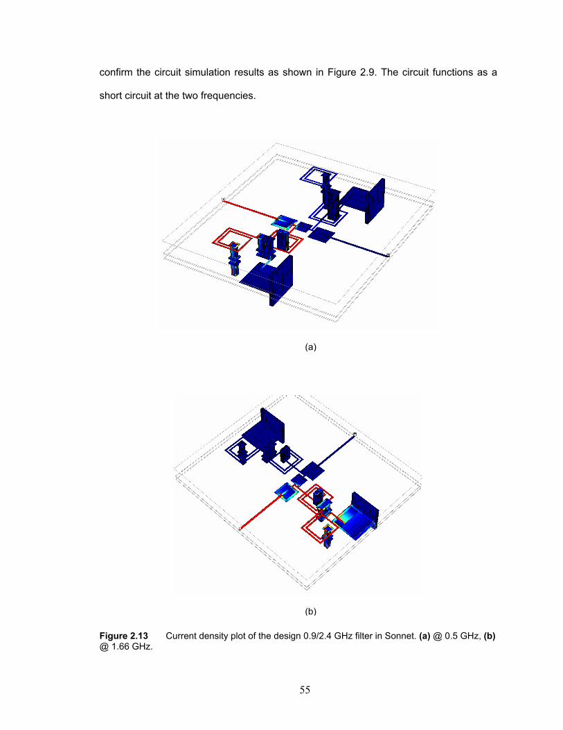
55
confirm the circuit simulation results as shown in Figure 2.9. The circuit functions as a
short circuit at the two frequencies.
Figure 2.13 Current density plot of the design 0.9/2.4 GHz filter in Sonnet. (a) @ 0.5 GHz, (b) @ 1.66 GHz.
(a)
(b)

56
Measurement Results and Correlation With Simulations
The filters were measured using an 8720ES 20 GHz vector network analyzer
(VNA) from Agilent Technologies. The measurements were made by probing onto the
ground-signal-ground (GSG) pads. The 50 Ω pads were designed using the Linecalc™
tool in ADS and then confirmed via Sonnet™. The VNA was calibrated using 2 port
SOLT technique with 1601 points and an IF bandwidth of 300 KHz. Figure 2.14 shows
the measured and the simulated (both Sonnet™ and ADS circuit simulations) plots of the
designed dual-band filter. From Figure 2.14 it can be observed that excellent model-to-
hardware correlation was obtained. The ADS simulation used lumped-element circuit
models of inductors and capacitors that included most of the layout dependent
parasitics. Table 2.4 summarizes the measurement results. The effect of the coupling
capacitor Cc on the passband ripple at 0.9 GHz as explained in Figure 2.10 was
confirmed in the measurement results. The filter was fabricated in an area of 6.2 x 6.2
mm2. This is a ~3X reduction in area as to any dual-band filter reported in the literature.

57
Figure 2.14 Summary of measured and simulated results. Solid data: Measured results. Triangle marker: Sonnet simulation results. sampled line: ADS simulation results.
Table 2.4 Summary of measured results of the 0.9/2.4 GHz dual-band filter.
Parameter Frequency
band
Volume,
mm3 Insertion loss, dB Return loss, dB %Bandwidth
0.9 GHz 4 8 5%
2.4 GHz
6.2 x 6.2 x 0.75
1.2 15 26%
2.2.2. Dual-Band Filter at 2.45/5 GHz
The previous section presented the design of a 0.9/2.45 GHz fully-packaged
dual-band filter. The filter serves as a proof-of-concept device showing the lumped-
S21, dB
Frequency, GHz
ADS
Sonnet
Measured

58
element design technique. This section extends the design methodology to produce two
passbands with controllable bandwidths at 2.45 and 5 GHz making the filter suitable for
WLAN frequencies. Additionally, the filter has two additional transmission zeros. Figure
2.15 shows the schematic of the designed 2.45/5 GHz filter.
Figure 2.15 Schematic of a 2.45/5 GHz dual-band filter with transmission zeros.
The passband center frequency is controlled by the resonating inductance
obtained from the fourth-order resonator with the series input capacitors (admittance
inverters). As compared to the 0.9/2.45 GHz filter shown in Figure 2.7b, this filter has
three additional components. The components Lf - Cf are cross-coupling elements
between the input and output providing an additional path for transmission. In effect the
components function as an admittance inverter. In transmission line implementations,
admittance inverters are quarter-wavelength lines with the characteristic admittance J at
Port 1 Port 2
C1 C2
Cc
Ca Ca La La
Cb Cb Lb Lb
Lf Cf
Lc

59
all frequencies [66]. Therefore, if the admittance inverter is terminated with Za at one
end, the impedance Zb looking from the other end is:
a
bY
JY
2
= (2.4)
In this case, Ya = Yb = 0.02 mhos. Hence, J = 0.02 mhos. A quarter
wavelength transmission line around the resonant frequency can be approximated with a
lumped element parallel or series resonator with characteristics admittance
−==
ωω
ωω 0
0L
CjYJ (2.5)
Thus the ratio ◊Lf/Cf should be close to 50 ohms to obtain a good match at both
the frequencies. Additionally, the Lf-Cf components are designed to control the
bandwidth of the second passband (~5 GHz). For these purposes, the value of Lf was
selected to be 1.1 nH and that of Cf to be 0.6 pF. Hence, the combination provides a
transmission zero at 6.2 GHz. Figure 2.16 shows the simulated effect of varying the
value of Lf with constant Cf on the performance of the filter at 5.1 GHz. It can be
observed that at Lf =5 nH the characteristic impedance is ~106 Ω, thus degrading the
return loss and insertion loss of the filter. However, by choosing appropriate values for Lf
and Cf the bandwidth of the second frequency band can be controlled and also the
return and insertion losses.
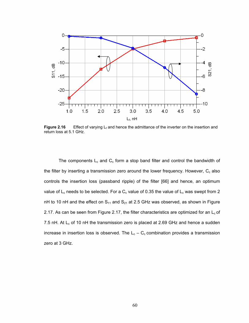
60
Figure 2.16 Effect of varying Lf and hence the admittance of the inverter on the insertion and return loss at 5.1 GHz.
The components Lc and Cc form a stop band filter and control the bandwidth of
the filter by inserting a transmission zero around the lower frequency. However, Cc also
controls the insertion loss (passband ripple) of the filter [66] and hence, an optimum
value of Lc needs to be selected. For a Cc value of 0.35 the value of Lc was swept from 2
nH to 10 nH and the effect on S11 and S21 at 2.5 GHz was observed, as shown in Figure
2.17. As can be seen from Figure 2.17, the filter characteristics are optimized for an Lc of
7.5 nH. At Lc of 10 nH the transmission zero is placed at 2.69 GHz and hence a sudden
increase in insertion loss is observed. The Lc – Cc combination provides a transmission
zero at 3 GHz.
S11, dB
Lf, nH
S21, dB

61
Figure 2.17 Effect of varying Lc on the insertion and return loss at 2.5 GHz.
Table 2.5 lists the component values used in the design of the 2.45/5.5 GHz
filter. The 0.1 pF capacitor is absorbed in La and hence the Q value is not defined.
Likewise, Lf was implemented using interconnecting segments to connect Cf to the filter.
Table 2.5 Component values used in the design of the dual-band filter.
Component C1 =
C2, pF
Cc,
pF
La,
nH
Lb,
nH
Ca,
pF
Cb,
pF
Lc,
nH
Cf,
pF
Lf,
nH
Values 0.5 0.35 5 4 0.1 0.51 7.5 0.6 1.1
Qs at 2.4 GHz 308 310 83 60 - 305 65 298 -
S11, dB
Lc, nH
S21, dB

62
Measurement Results and Correlation With EM Simulations
The filter was simulated in Sonnet™ with the component values as listed in Table
2.5. To verify the mechanism of transmission zeros, the current density simulations were
performed in Sonnet as shown in Figures 2.18a, b and c.
(a)
(b)
Cf Cc
Lb
La
Lc
Port 2 Port 1
Cb
Current flow
Current flow

63
Figure 2.18 Simulated current flow at transmission zeros in the 2.45/5.5 GHz dual-band filter. (a) at 1.5 GHz the current flows into the resonator presenting a short. (b) At 3 GHz showing the current flows into the Lc-Cc dissipated partially as loss and partly through the resonator. (c) Out of phase current flowing through two paths canceling at port 2 at 6.2 GHz.
The filter was designed on the balanced LCP process. Figure 2.19 shows the
layout of the entire filter including the input-output 500 um pitch GSG probe pads. The
resonators are placed on the same side of the resonator to avoid any coupling with the
cross-coupling path. Microstrip interconnecting metal lines are used to physically realize
the cross-coupling inductor Lf. The entire filter occupies an area of 5.1 x 5.3 mm2. The
measurement to model correlation is shown in Figure 2.20. The effect of pads was de-
embedded from the measurements by using open calibration structures. The y-
parameters of the pads were subtracted from y-parameters of the entire filter to eliminate
the effect of pads on the filter response. The transmission zero at 4.5 GHz is obtained
from the change in the resonator reactance response from capacitive to inductive. An
improvement in the rejection at the 4.5 GHz can be achieved by increasing the slope
parameter of the resonator response i.e. by adding additional reactive elements in the
resonator. Table 2.6 summarizes the performance of the filter. It should be noted that the
(c)
Current flow

64
filter can achieve an absolute bandwidth ratio of greater than 4, which was not possible
using transmission line elements (see Figure 2.4).
Figure 2.19 Layout of the designed 2.45/5.5 GHz filter.
The bandwidth at either center frequencies can be independently controlled by
changing the cross-coupling network and the Lc-Cc network. Figure 2.21 shows the
measured results of another implementation of the filter with reduced bandwidth at both
the 5 GHz band. The bandwidth at 5 GHz band was reduced by increasing the value of
capacitor Cf to 0.7 pF and reducing the value of inductor Lb that moved the transmission
zero at 4.6 GHz from the previous design to 4.9 GHz. As a result the bandwidth at 5
GHz band was reduced to 500 MHz from the previous bandwidth of 1250 MHz as shown
5.1 mm
5.3 mm
GSG pads

65
in Figure 2.20. Additionally, Lc was reduced to 6.7 nH from 7.5 nH to reduce the reduce
to bandwidth from 965 MHz to 525 MHz.
Figure 2.20 Model-to-hardware correlation for the 2.45/5.5 GHz dual-band filter. Sampled data: Measurement results, solid line: Sonnet simulations.
Table 2.6 Measured performance of the 2.45/5.5 GHz dual-band filter.
Parameter Frequency
band
Volume,
mm3 Insertion loss, dB Return loss, dB %Bandwidth
2.2 GHz 1.8 10 44%
5.3 GHz
5.1 x 5.3 x 0.75
1.5 15 24%
S21, dB
Frequency, GHz
Sonnet
Measured

66
Figure 2.21 Model-to-hardware correlation for the 2.45/5.5 GHz dual-band filter with reduced bandwidth. The measurement shows higher bandwidth at 5 GHz than expected because of reduction in Lf.
Table 2.7 summarizes the measured results of the filter. The bandwidth at the
lower band can be scaled by changing the value of Cc or Lc.
Table 2.7 Measured performance of the reduced bandwidth 2.45/5.5 GHz dual-band filter.
Parameter Frequency
band
Volume,
mm3 Insertion loss, dB Return loss, dB %Bandwidth
2.2 GHz 1.3 12 24%
5.3 GHz
5.1 x 5.3 x 0.75
1.1 15 10%
S21, dB
Frequency, GHz
S11, dB
Sonnet
Measured

67
2.3 Summary
This chapter presented need for using high-Q passives in multi-band radio
design, especially for VCOs and filters. The focus of this chapter was to introduce the
electro-mechanical properties of LCP and its feasibility for economically embedding high
Q passive components. In particular, the design of dual-band filters using lumped-
elements components on thin multi-layered LCP substrate was shown. The filters
exhibited low insertion losses in both the frequency bands even at 6 GHz. The high Qs
of the passive components on LCP permit low insertion losses with good out-of-band
rejection characteristics without prohibitively increasing the size of the components. The
design methodology coupled with broadband characteristics of passives on LCP [68]
enables the separation of the two passbands (f2/f1) beyond 2.5, with a maximum
absolute bandwidth ratio of more than 10. This is a 2.5X improvement as compared to
any implementation of transmission line-based filters as discussed in section 2.5.
Lumped-element dual-band filters find several applications in MIMO based systems or
diversity-type WLAN systems. Additionally the design methodology does not rely on the
electromagnetic coupling of components and hence, can be manufactured with high
yield.
Table 2.8 compares the performance of this filter with a few other works reported
in the literature on dual-band filters. It should be observed from Table 2.8 that the
proposed filters provide low insertion losses, controllable bandwidths, and high
maximum bandwidth ratio with 3-5X improvement in area. Additionally, the small height
of the balanced LCP process (0.75 mm) enables a volumetric reduction of the filters. The
small cross-sectional dimension allows further reduction of the lateral dimensions of the
filter by stacking more dielectric layers and thus increasing the component density.

68
Table 2.8 Performance comparisons of the lumped-element dual-band filter with other works on high Q packaging technologies
Technology and
references
Center frequencies,
GHz Insertion loss, dB Area, mm
2
LCP
[59]
2.4
5
2.4
1.8 15 x 8
LCP
[60]
2.4
5
1.4
3 34 x 24
Duroid
[62]
2.4
5 NA 125 x 30
Rogers RO3003
[61]
2.4
5
2.8
3.3. 54 x 60
LCP
This work
1
2.4
4
1.2 6.2 x 6.2
LCP
This work
2.4
5
1.8
1.5 5.1 x 5.3
LCP
This work
2.4
5
1.3
1.1 5.1 x 5.3
Furthermore, excellent properties of LCP and the ability to form heterogeneous
stack-ups make it suitable for designing high Q components with ease of manufacturing.
The stacking of thin LCP sheets provide more metal layers and these metal layers
simplify the routing of supply and signal lines as are required by any VCO. Hereafter, the
thesis focuses on the design of VCOs using lumped-element components on LCP
substrate. The aim is to first show the feasibility of using LCP with active components
and demonstrate working VCO embodiments at cellular and WLAN frequencies. Then

69
the use of high Q components for optimizing the VCO performance characteristics is
investigated. Finally, the thesis delves into a novel and complex class of oscillators
known as concurrent oscillators that use the dual-behavior of passive components,
similar to the design of the resonator used in the dual-band filters.

70
CHAPTER 3
OSCILLATOR THEORY
During the past 20 years, there have been significant advances in the field of
wireless communication that have led to the convergence of multiple and complex
functionalities in mobile communication handsets. For example, the addition of wireless
short distance voice and data services such as Bluetooth, WLAN, and UWB, to a quad-
band GSM cell phone (see Figure 1.2). In addition, developments in strained silicon
technology (SiGe) and submicron CMOS transistors have pushed fT beyond 100 GHz.
Communication transceivers rely heavily on frequency conversion using local oscillators
(LOs) and therefore the spectral purity of the oscillators in both the transceiver and
receiver is one of the factors limiting the maximum number of available channels and
users. Resultantly, considerable efforts were directed towards gaining a deeper
understanding of the fundamental issues limiting the oscillator performance and in the
development of design guidelines.
This chapter justifies the need for high Q passives in oscillators for achieving
higher performance needed by multi-band systems. The chapter discusses the need for
co-design of VCOs by comparing the performances of LOs designed with on-chip and
on-package techniques. The remainder of this chapter is organized as follows: Section
3.1 gives a brief introduction to frequency domain instability or phase noise in oscillators.
Section 3.1 also reviews the existing phase noise models. Both the time-variant and
time-invariant phase noise models prove the dependency of phase noise on oscillator
loaded Qs. Because of the narrow-band nature of communication systems the radios
need LOs with very low phase noise. This requirement is exacerbated because of the
introduction of new standards, which have caused an increase in the radio selectivity

71
requirements. Hence, section 3.2 gives the selectivity and sensitivity requirements of
different multi-band and multi-mode radios and their direct effect on the phase noise
requirements of LOs. A summary of published work on on-chip and on-package VCOs is
given in section 3.2. Finally, based on the discussions from previous sections, section
3.3 explains need for high Q passives and the need for chip-package co-design
methodology using LCP substrates for LOs.
3.1 Review of Frequency Instability in Oscillators
An oscillator consists of an amplifier and a resonant element, as well as a
feedback circuit. Since the feedback is positive the oscillator has no inputs and uses
noise of the system to generate a predictable output signal. Any practical oscillator has
fluctuations in its amplitude and frequency. Additionally, the non-idealities in the
oscillator components give rise to the amplitude (amplitude modulate or AM) and phase
(phase modulate or PM) fluctuations or instabilities in oscillator output. Because of the
limiting or saturating behavior of the amplifier, the frequency or phase instabilities are
usually of more concern than the amplitude fluctuations in oscillators. As a result the
output of a non-ideal or practical oscillator can be mathematically expressed as (3.1).
( )[ ] [ ](t)tωcostA1VV 00out φ+⋅+⋅= (3.1)
In (3.1) output amplitude Vo and frequency ω0 are modulated by the time dependent
components A(t) and φ(t), respectively. Figure 3.1 shows the output of an ideal oscillator
and non-ideal oscillator in frequency domain.

72
Figure 3.1 Output spectrum of an ideal and non-ideal oscillator.
With respect to phase or frequency, the term instability includes both short- and
long-term instability. Short-term instability refers to variations on time scales smaller than
one second and occurs mainly due to noise and other interference. Thermal [39], shot
[39], flicker (1/f noise) [39], and G-R noise [39] (occurs in a bipolar device) are examples
of the former and power supply fluctuations and noise due to substrate coupling fall in
the latter group. Long-term instability is the measure of instability over a longer sampling
time and occur with the onset of aging and electrical stress in oscillators [40]. The short
term instability in time domain is known as jitter and in frequency domain is known as
phase noise. Phase noise is a commonly used term in RF/analog applications whereas
timing jitter is commonly used in digital applications. Figure 3.2 shows the effect of noise
and interference on the output of oscillator in (a) time domain and (b) frequency domain
[40]. In Figure 3.2a ∆f(t)/f is the relative drift in the frequency and Sv(ω) is the power
spectral density.
Ideal
Practical

73
(a)
(b)
Figure 3.2 Characterization of noise sideband in time and frequency domains (a) time domain and (b) frequency domain.
Phase noise is characterized by the single side-band noise spectral density and
is given the units of decibels per below the carrier per Hertz (dBc/Hz) at a certain offset
frequency measured in a bandwidth of one Hertz (see Figure 3.2b). In general phase
noise can be defined as (3.2)
∆f (t)/f
Svω, dB
per Hertz
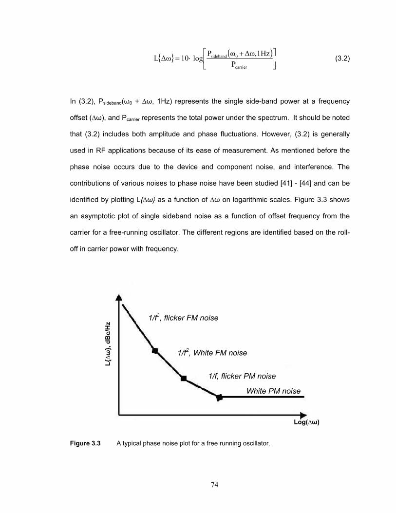
74
( )
+⋅=
carrier
0sideband
P
1Hz∆ω,ωPlog10∆ωL (3.2)
In (3.2), Psideband(ω0 + ∆ω, 1Hz) represents the single side-band power at a frequency
offset (∆ω), and Pcarrier represents the total power under the spectrum. It should be noted
that (3.2) includes both amplitude and phase fluctuations. However, (3.2) is generally
used in RF applications because of its ease of measurement. As mentioned before the
phase noise occurs due to the device and component noise, and interference. The
contributions of various noises to phase noise have been studied [41] - [44] and can be
identified by plotting L∆ω as a function of ∆ω on logarithmic scales. Figure 3.3 shows
an asymptotic plot of single sideband noise as a function of offset frequency from the
carrier for a free-running oscillator. The different regions are identified based on the roll-
off in carrier power with frequency.
Figure 3.3 A typical phase noise plot for a free running oscillator.
L∆ω, dBc/Hz 1/f3, flicker FM noise
1/f2, White FM noise
1/f, flicker PM noise
Log(∆ω)
White PM noise

75
The phase noise plot has been effectively split into four different regions. The
noise power in the three regions close to the carrier has cubic (1/f3), quadratic (1/f2), and
linear (1/f) dependence with frequency. At large offset frequencies the spectrum
becomes flat. The regions are named considering the noise source contributing to the
phase noise. References [41] – [45] explain in detail the physical mechanism and the
conversion process of the low frequency noise such as flicker noise and white noise into
phase noise. The existence of these regions has been verified by both linear time
invariant and time variant approaches. The topic of analyzing and determining phase
noise is vast and is of unprecedented interest. Hence, the following sub-sections reviews
the linear time-invariant (LTI) or the Leeson’s model and the linear time-variant (LTV) or
the Lee-Hajimiri methods of phase noise. Either of these methods sufficiently explains
the physical mechanism for the occurrence of phase noise in LOs.
3.1.1. Leeson’s LTI Phase Noise Model
Phase noise in an oscillator occurs due to the noise (losses) in the resonator and
noise in the active device. There are several methods of evaluating and calculating
phase noise of oscillators. Of all the methods the LTI method also known as the
Leeson’s method [41] of calculating phase noise is most well-known. The basic Leeson’s
model and its expanded variants [44] and [46] heuristically estimate the phase noise in
oscillators. The method intuitively explains the mechanism of the conversion of device
noise and resonator loss into phase noise. It predicts the following behavior for L∆ω
∆
∆+⋅
∆+⋅⋅=∆
ω
ω
ωω
ω3/1
2
0 12
12
log10f
LS QP
FKTL (3.3)

76
In (3.3), F is the empirical device noise parameter (also known as device excess noise
parameter), K is the Boltzmann’s constant, T is the absolute temperature in Kelvin, PS is
the average signal power, ω0 is the oscillation frequency, QL is the loaded Q of the
oscillator tank circuit, ∆ω is the offset from the carrier frequency, and ∆ω1/f3 is the 1/f3
corner frequency. Equation (3.3) does not include any AM-PM conversion and the
oscillator is modeled as an amplifier with feedback. The LTI approach basically models
the circuit as phase modulator in series with a noise-free amplifier followed by a
resonator. Equation (3.3) models the 1/f2 more accurately of all the four regions that
were highlighted in Figure 3.3. The mathematical derivation is based on one-port
equivalent circuit representation of an LC oscillator. References [40] – [42] give the
complete mathematical proof for the Leeson’s model in the 1/f2 region. The underlying
principle of LTI approach is that the oscillator can be modeled as an amplifier, A, in
positive feedback through the feedback network, F. The loop-gain (Av) of the feedback
circuit is a simple solution to the feedback network
AF
A
V
VA
in
outv −
==1
(3.4)
The model is sufficient for a simplified analysis (initial design), without much insight into
the oscillator operation, of feedback oscillators. The criteria for the circuit to be unstable
or for stable (undamped) oscillations can be given as (3.5) and (3.6)
1≥AF (3.5)
o0=∠AF (3.6)

77
According to (3.6) the phase shift around the loop should be an integer multiple of 2p
radians. Any perturbation in the phase shift due to noise sources will cause temporary
change in the phase (φ) of the network. However, depending on the loaded-Q of the
circuit the change in the phase will be compensated by an instantaneous change in
frequency, thereby causing degradation in the spectral purity. A network with higher Q
will sustain less change in the frequency to compensate for the phase change, thus
resulting in better frequency stability [42]. The aforementioned discussion is based on
the fact that in a second order system, as shown in Figure 3.4 [42], the Q is related to
the normalized phase transfer function as
ωφω
d
dQ
2
0= (3.7)
Figure 3.4 Phase transfer function of a parallel RLC network [42].
Equations (3.3) and (3.7) form the core of the LTI based phase noise model.
From (3.3) and (3.7) it is clear that better Q and hence better spectral purity can be
achieved by having a larger phase shift within a narrow pass-band of the system.

78
However, (3.3) contains additional parameters as F and ∆ω1/f3. Each of these
parameters is a curve fitting parameter in the semi-empirical Leeson’s model and are
usually used as a posteriori fitting parameters on measured data. However, further
investigation by Rael et al. in [47] allows calculation of an exact expression for F based
on device technology. Additionally, the existence of the -30 dB/decade slope in phase
noise was ascribed to the upconversion of flicker noise (AM-PM conversion) by [43] and
[47] thus bringing physical meaning to the ∆ω1/f3 term in the modified-Leeson’s equation
of (3.3).
3.1.2. Lee-Hajimiri’s LTV Model
The Lee-Hajimiri model [42] is a time-variant model for computation of phase
noise of both LC and ring oscillators. The analysis justifies the oscillator as a time-variant
system by developing an impulse response model for excess phase. As illustrated in
Figure 3.5, if an impulse, i(t), is injected onto a tuned circuit at the peak of the signal, it
will cause maximum amplitude modulation and no phase modulation and if an impulse is
injected at the zero crossing of the signal, there will be no AM and only maximum PM.
However, if the impulse is injected between the zero crossing and the peak, there will be
components of both amplitude and phase modulation.

79
Figure 3.5 LC oscillator excited by the current pulse (a) at the peak of signal, (b) at the zero crossing of the signal.
The impulse sensitivity function (ISF) mathematically represents the above
mentioned linear time variant discussion on conversion of current impulse, i(t), to phase,
φ(t). It is denoted as G(x) and is a dimensionless frequency- and amplitude-independent
periodic function with period of 2p radians. The ISF is specific to oscillator topology and
has the largest value when the maximum phase modulation occurs and the smallest
when only the amplitude modulation occurs. Since the ISF is periodic, it is expanded in a
Fourier series as [42]
( ) ( )no
n
no ncc
θτωτω ++=Γ ∑∞
=
cos2 1
0 (3.8)
In (3.8) t is the time instant at which the current impulse is applied, coefficients cn are
real-valued coefficients and θn is the phase of the nth harmonic. Finally, based on the
information of ISF the phase φ(t) and its corresponding power spectral density Sφ(ω) is

80
calculated [42]. The LTV system that converts i(t) to Sφ(ω) is followed by a nonlinear
system representing a phase modulator that converts the phase Sφ(ω) into voltage
Sv(ω). The phase modulator converts the components near the harmonics of the
oscillator frequency to low frequency noise sidebands Sφ(ω) which in turn becomes the
close-in phase noise Sv(ω). Figure 3.6 gives a graphical representation of the above
mentioned theory on LTV. The coefficients c0, c1, c2, …, cn determine the contribution of
the noise around the harmonics to the close-in phase noise at the fundamental
frequency. For example the flicker noise is weighted by the coefficient c0. Likewise, the
thermal noise and other white noise terms are weighted by other coefficients cn that
contribute to the other regions of the phase noise.
Figure 3.6 Conversion of noise at the integer multiples of ω0 into phase noise [42].
Finally, according to this theory, to achieve minimal phase noise, special
techniques have to be adopted so that any noise impulse coincides in time with the

81
peaks of the output voltage signal. Based on this theory, the phase noise equation is
expressed as
( )
∆⋅
∆⋅∆
⋅⋅=∆ω
ωω
ω fn fi
q
cL
/1
2
2
2
max
2
0
8
/log10 (3.9)
( )
∆⋅∆
⋅Γ
⋅=∆2
2
2
max
2
4
/log10
ωω
fi
qL nrms (3.10)
In (3.9) and (3.10) qmax is the maximum charge stored across the resonator capacitor,
fin ∆/2 is the noise power spectral density. Equation (3.9) calculates the phase noise in
the 1/f3 region and (3.10) is used for calculating the phase noise in the 1/f2 region. To
achieve more physical insight into the LTV model we consider the case of a cross-
coupled oscillator for which the equations (3.9) and (3.10) can be further simplified. The
charge across the capacitor is a function of Vtank and resonator inductor Ltank and is given
by [48]
2
tan
tanmax ω⋅
=k
k
L
Vq (3.11)
Now, Vtank= Ibias/gtank where Ibias is the bias current and gtank models the loss in the
resonator or the Q of the resonator [48]. As a result the equation for L∆ω in any regime
can be written as [48]
( )
⋅
⋅∝∆
bias
k
I
gLL
2
tan
2
ω (3.12)

82
From (3.12) it can be concluded that the phase noise inversely depends on the square of
the Q of the resonator.
In summary, both LTI and LTV models attribute the upconversion of thermal
noise and flicker noise via PM as the cause for the 1/f3 region of phase noise. The flat
region or plateau in the phase noise is dependent on the loss of the resonator and the
white noise contribution of the active device. The physical mechanisms for phase noise
have also been quantified and confirmed by other more robust and generic methods
known as harmonic balance [40]. These advanced methods, as used in Advance Design
System suite™ (ADS) from Agilent Technologies [49], split the oscillator circuit into linear
and non-linear sub-networks. Finally, noise conversion methods [40] and noise
modulation methods (PM) [40] are applied to get the far-carrier and near-carrier phase
noise, respectively. The noise conversion mechanisms mentioned by LTI and LTV
models correlate with that from advanced methods. Hence from the above discussion on
LTI and LTV models for phase noise it is clear that the phase noise can be reduced by
the following methods:
(1) Reduction in the device noise parameter, F [47]. However, with the trend
towards handset miniaturization submicron CMOS transistors are used in VCO
design. As feature size scale, the noise performance of transistors degrades
especially from flicker noise. Flicker noise, besides increasing the phase noise is
harmful for direct conversion receivers creating DC offset problems, which can
corrupt the data at DC.
(2) With the development of submicron feature size transistors the head-room
available for the supply voltage and hence the voltage swing across the tank
diminishes [48]. As a result maximum charged stored by the resonator capacitor

83
(qmax) decreases, from (3.11). Hence the use of smaller geometry transistors
increases the phase noise via two distinct mechanisms, (1) decrease in qmax and
(2) increase in F.
(3) The phase noise is inversely proportional to the square of the Q of the oscillator.
Hence, a dB increase in the Q of the resonator will lead to 2 dB decrease in the
1/f3 and 1/f2 regions of phase noise.
3.2 LO Requirements for Multi-Band and Multi-Mode Systems
From the discussion in Chapter 1, it is clear that the deployment of multi-band
and multi-mode radios including voice, video and data communication capability can be
expected in the forthcoming years. Therefore, future cellular handsets will contain a
mixture of narrow-band (voice) and broad-band (data) front-end modules. As a result the
system performance merits, such as noise floor (sensitivity), selectivity, noise-figure
(NF), intermodulation levels, out-of-band emission, and interference handling will
become increasingly difficult to meet for individual standards. The phase noise of a VCO
has multiple effects on the performance of a radio: (a) degradation of receiver selectivity
due to spreading of the transmitted signal, and (b) degradation of receiver sensitivity or
receiver noise floor. Additionally, a high VCO phase noise is one of the main reasons for
causing spurious emissions from any communication system. The above mentioned
effects are captured in Figure 3.7 that represents a generic wireless communication
transceiver.

84
+
+
+
+
Figure 3.7 The effects of VCO phase noise on RF transceiver performance: In the receiver chain, the VCO phase noise masks the desired channel (C) with the nearby strong interferer (I) and also raises the noise floor via self-mixing (dotted arrow); In the transmitter chain, the VCO phase noise corrupts the transmitted signal by producing “skirts” around the transmitted signal.
For instance, direct conversion architectures because of their simplicity and
reduced component count are widely used in the design of both transmitter and receiver
of radios. Additionally, the architecture promotes high integration of functionality in
CMOS, thereby leading to cost reduction and making it suitable for multi-band radios.
For direct conversion, the LO is at the same frequency as the received or the transmitted
signal. As a result the LO phase noise has a significant contribution in the determination
of adjacent and alternate channel rejection (ACPR) and DC offset [9] and [11]. In
receivers, self-mixing of LO signals via leakage through the substrate into the LNA
causes DC offset problems (as depicted in Figure 3.7). As a result the allowed phase
noise and spurs of the LO are determined by the receiver adjacent channel selectivity,
dynamic range, and the intermodulation characteristic performance. Additionally, on
transmitter-side high close-in phase noise of the LO affects the modulation accuracy

85
(error vector magnitude, EVM). Table 3.1 lists the LO phase noise specifications
recommended by standardization agencies, such as FCC and ETSI [50] for selected
voice and data communication standards.
Table 3.1 Phase noise specifications of various communication standards.
Frequency range (GHz) Standard
Uplink Downlink
Phase Noise Specification at offset
frequency (dBc/Hz)
IS54/Cellular
Band 0.824 – .849 .869 - 0.894
-116 @ 600 KHz
GSM 0.89 - .915 0.935 - 0.96 -119 @ 600 KHz
DCS 1800 1.71-1.785 1.805 -1.88 -119 @ 600 KHz
PCS 1900 1.93 - 1.99 1.85 - 1.91 -116 @ 600 KHz
WCDMA 2.11 – 2.17 1.92 – 1.98 -113 @ 100 KHz
802.11a/WLAN 5.15 - 5.825 -110 @ 1MHz
From Table 3.1 it is clear that next generation cellular handsets will be a mix of
less interference tolerant, narrowband, high dynamic range, and high output powered (~
30 dBm), voice or cellular standards (GSM, WCDMA) together with broadband, low-
powered and more interference tolerant, data standards, such as WLAN and UWB.
Additionally, the phase noise listed in Table 3.1 are the bare required noise performance
numbers to achieve the recommended system performance and a margin of atleast 5 dB
is added for safety. Reference [9] provides a detailed explanation of the various effects
of phase noise on system performance. Reference [9] effectively comes to a conclusion
that the integrated phase noise (of an LO used in a practical multi-band handset) over

86
the signal bandwidth (200 KHz for GSM and 1 MHz for WCDMA) needs to be 30 dB
below (or -125 dBc/Hz @ 100 KHz offset) the LO signal level!!
3.2.1. Review of On-chip and On-package LO Design
From the aforementioned discussion on LO requirements it is clear that the
convergence of multiple systems into one handset leads to (1) reduction in the available
power for each module, and (2) increase in the interference between standards via
emission or substrate coupling. As a result, frequency planning will be a challenging
issue and VCOs for next generation radios will be required to operate at lower power
levels with improved phase noise performance. From (3.3) it can be inferred that the
phase noise reduces with the increase in the loaded Q of the resonator and by
increasing the power consumption of the oscillator. With the power consumption limited
by the system power requirements, a feasible approach to lower the phase noise of a
VCO is to use high Q passive components. CMOS based VCOs suffer from insufficient
phase noise and higher power consumption due to the low quality factor of the on-chip
passives. A survey of work done in this field reveals that the typical Qs of the lumped-
element inductors in standard CMOS processes to be less than 15, whereas capacitor
Qs range approximately from 20 to 40 in the 1-10 GHz frequency range. The Qs of
passive elements on integrated technologies can be improved by replacing silicon with
sophisticated processes such as the semi-insulating III-V semiconductor process
technology. However such an improvement comes with an increase in the manufacturing
costs. Hence CMOS based oscillators operate at higher power levels to achieve the low
phase noise levels that are set by contemporary communication standards. Table 3.2
shows examples of VCOs fabricated in CMOS processes in the vicinity of 2 GHz. As

87
indicated by Table 3.2, most of the fabricated (Bi)CMOS VCOs operate in the power
levels in excess of 20 mW.
Table 3.2 Survey of CMOS-based VCOs at 2 GHz.
Year and
Reference
Technology
node
Frequency,
GHz
Phase noise,
dBc/Hz
Power
consumption, mW
2003, [51] 0.35u CMOS 2.14 -115 @ 100 KHz 30.8
2001, [52] 0.25u CMOS 1.8 -112 @ 100 KHz 20
2000, [53] 0.65u BiCMOS 2 -116 @ 100 KHz 34.2
1997, [54] 0.8u BiCMOS 1.5 -105 @ 100 KHz 40
1996, [55] 0.8 u BiCMOS 1.8 -83 @ 100 KHz 12
Because of the aforementioned limitations of CMOS-based VCOs, cellular
handsets embraced package-based oscillators. High-Q packaging technologies, such as
LTCC, offer high Q components as pointed out in Chapter 1. Figure 3.8a shows an
internal photograph of a dual-band GSM/PCS cellular handset from Nokia. It uses two
VCOs from Alps Inc, which is leading Japanese manufacturer of ceramic-based RF
electronic components [56]. Figure 3.8b shows the same picture with the top metal
enclosure removed from one of the VCOs revealing the internal circuitry.

88
Figure 3.8 Photograph of a Nokia dual-band handset (model 8265) with on-package VCOs.
Table 3.3 lists the performance characteristics of one of the VCOs at 2 GHz
manufactured by Alps Inc on a 15 layer LTCC substrate. Like Alps Inc., there are other
LTCC-based VCO manufacturers that are used by cellular handsets because of the high
Qs of the passives on LTCC and large number of metal layers. Additionally, placing the
VCO on the package simplifies the issues of transmission mixing and self-mixing of the
LO frequency [9] and [11] that are detrimental for a direct conversion radio.
Table 3.3 Performance summary of a LTCC-based VCO by Alps Inc.
Frequency (GHz) Power consumption,
mW
Phase noise @ offset
frequency Size, mm
2
1.8 – 1.92 20 -140 dBc/Hz @
1 MHz 5.5 x 4.8
(a) (b)

89
3.3 Summary
Oscillators are an indispensable part of communication radios. Because of the
convergence of various telecommunication standards and simultaneous operation of
multiple transceivers, the interference immunity of various systems has been severely
compromised. Additionally, the limited power-budget has led to a decrease in the power
consumption of various RF blocks. Many RF blocks, including oscillators, demonstrate a
degradation of its performance characteristics with the decrease in the supply voltage.
CMOS provides an economical method of miniaturizing components. However, CMOS-
based oscillators suffer from insufficient phase noise due to excessive losses in the
passive components (from Table 3.2). The improvement in phase noise is met via
increase in the power consumption. However, now the designers are constrained by the
limited power consumption because of excessive functionality integration in handsets.
As discussed in Chapter 1, LTCC provides high-Q passives however the mechanical
and processing characteristics of LTCC do not make it a technology choice for the multi-
band and multi-mode cellular handsets. Therefore, next generation radios require a high-
Q technology coupled with integration benefits offered by CMOS. As discussed in
Chapter 1, LCP-based SOP-L packaging technology provides a platform for the
designers to use high-Q passives (like LTCC). However, LCP-based substrates rely on
conventional PCB manufacturing methods and hence are economical (unlike LTCC).
In the recent past, LCP-based substrates have demonstrated LC passives with
high Qs (30~300) that remain constant over a broad range of frequencies [7]. Therefore,
a reduction in size, power consumption, and VCO phase noise can be achieved by (a)
carefully designing and optimizing the VCO parameters and (b) selectively embedding
high Q passives in the organic substrate while using IC technologies for the design of
active device and biasing circuitry. This design methodology is the essence of this thesis

90
and is known as system-on-package (SOP), system-in-package (SiP) or chip-package
co-design, as suggested in Chapter 1.
From the discussions made in Chapter 1 on properties of LCP and section 3.1 on
phase noise mechanisms, it can be concluded that high Q components can be
manufactured on LCP-based packaging technology in an economical manner, thereby
enabling the design of VCOs, which are suitable for multi-band cellular type applications.
Hereafter, the thesis focuses on the design of VCOs using lumped-element components
on LCP substrate. The aim is to first show the feasibility of using LCP with active
components and demonstrate working VCO embodiments at cellular and WLAN
frequencies. Then the use of high Q components for optimizing the VCO performance
characteristics is investigated. Finally, the thesis delves into a novel and complex class
of oscillators known as concurrent oscillators that use the dual-behavior of passive
components, similar to the design of the resonator used in the dual-band filters.

91
CHAPTER 4
DESIGN OF SINGLE-BAND OSCILLATORS IN LCP SUBSTRATE
The previous chapters discussed the need for VCOs with low phase noise and
low power consumption for use in multi-band cellular handsets. CMOS-based VCOs
may achieve the noise criteria but at a higher power consumption level. This can be
attributed to the design techniques that are conventionally followed in CMOS-based
VCO design. Conventionally, the design technique focuses on using the maximum
available power-budget to maximize the signal swing across the resonator [48]. The
increased signal swing reduces phase noise (see chapter 3 equations (3.3) and (3.10))
at the cost of power consumption. As a result the figure of merit of oscillators is low. The
figure of merit (FOM) tests the efficiency of the oscillator design and is used as a
comparison basis [36]. Mathematically it is represented via the expression
dBLP
FOMdc
o ,)(
1log10
2
10
∆⋅⋅
∆
⋅=ωω
ω (4.1)
In (4.1), ωo and ∆ω are the center frequency and offset frequency, Pdc is the dc power
dissipated in mW, and L(∆ω) is the phase noise at an offset ∆ω. Because of the low Qs
of on-chip passives, CMOS-based VCOs have high power consumption and suffer from
low FOMs1. The FOMs of CMOS VCOs are significantly lower (~10 – 20 dB) than those
required by multi-band cell phones, (>178 dB as suggested by [9]). For most of the
communication protocols phase noise requirements are comparable (see Table 3.1). 1 VCOs listed in Table 2.2 have FOMs in the range of 160 – 170 dB.
92
Thus any improvement in the FOM can be expected via the reduction of Pdc term in
(4.1). As per the discussion made in chapter 2 the designers need to resort to high-Q
technology that allows them to reduce Pdc.
This chapter presents the design of two different VCO configurations that were
designed and fabricated on a single LCP sheet substrate. The rest of this chapter is
organized as follows: Section 4.1 presents the results of a negative resistance-type
common-base VCO. The analysis of this widely recognized VCO has been shown in this
section. Finally, a routine for the optimization of power consumption has been
suggested. One such implementation shows a phase noise of -118 dBc/Hz at 600 KHz
offset from the 1.9 GHz center frequency while consuming dc power of only 1.8 mW.
This is the lowest power consuming fully-packaged VCO reported in the literature. The
effects of reduction in the power on oscillator’s sensitivity to other parameters have been
identified and discussed in section 4.1. Section 4.2 shows the first implementation of a
2.3 GHz Colpitt’s oscillator. The design serves as a proof-of-concept device showing
suitability of LCP for embedding passives that are put to use with surface mount
components demonstrating possibility of re-work. The designed VCO is suitable for use
in the 2.4 and 5.2 GHz WLAN applications.
4.1 Design of Negative Resistance VCO in LCP Substrate
Negative resistance type oscillators utilize compensation of energy loss in the
feedback path to generate oscillations [14] and [40]. This section discusses the design of
a common-base-type negative resistance oscillator, suitable for 1900 MHz cellular type
applications (PCS 1900, DCS 1800) on a LCP based organic substrate. Figure 4.1
shows the schematic of the designed common-base oscillator where the LC network

93
comprising L-C2-Cv-C1 constitutes the resonator section. Lm, Cm1 and Cm2 match the
collector of the transistor to a 50 Ω load. The circuit is biased using a 100 Ω surface-
mount biasing chip resistor (0603 package size). Biasing circuitry and other parasitics
are not shown for the sake of circuit schematic clarity.
ΓR
Zin (Sin)
ΓR
Zin (Sin)
Figure 4.1 Circuit schematic of the designed 1.9 GHz VCO.
Negative resistance is obtained at the emitter of the transistor only when an
inductor (in this case it is L1) is connected to the base of the bipolar transistor [14]. The
impedance (Zin) observed at the emitter terminal can be obtained through small-signal
model evaluation, as is shown in (4.2)
+−⋅⋅⋅+⋅+⋅+−⋅⋅⋅+⋅+⋅⋅+⋅+⋅
=)1)1(()(
)1)1(()()(
1
11
XZgRLsZX
XZgRLsZXRLsZRZ
mL
mSSLin
ππ
πππ (4.2)
In (4.2), RL is the transformed load impedance seen by the collector of the transistor, Zπ
is the base-emitter junction impedance, gm is the transconductance, Rs is the equivalent

94
source resistance, and X=oL
L
rR
R
+ where ro is the resistance resulting from the Early
effect. As shown in (4.2), the input reflection coefficient (Sin) corresponding to Zin is
dependent on the values of L1, gm, and RL. The relation between Sin and Zin is given as
+−
=οin
οinin
ΖΖ
ΖΖS (4.3)
where Z0 is the characteristic impedance of the port. At a given frequency, simultaneous
optimization of these variables provides negative resistance when observing at the
emitter terminal of the transistor. For sustained oscillations to occur, Sin· ΓR product
should be greater than 1, from [14]. Figure 4.2 shows a solution to (4.2) at a bias current
of 3.5 mA at 1.9 GHz. Figure 4.2a is the plot of the real part of Zin when L1 is varied from
1 to 20 nH, whereas Figure 4.2b plots the imaginary part of Zin. From Figures 4.2a and
4.2b, it can be concluded that at a given frequency the value of L1 strongly sets the
conditions for oscillations. Figures 4.2a and 4.2b indicate that for the given conditions
the transistor provides negative resistance for L1 anywhere between 5.5 nH and 9 nH.

95
Figure 4.2 (a) Effect of the base inductance (L1) on the real part of impedance looking into the emitter terminal, (b) Effect of the base inductance (L1) on the imaginary part of impedance looking into the emitter terminal.
Further insight on the dependence of real part of Zin on L1 can be obtained by
evaluating a particular solution for (4.2) around L1. Now the Real(Zin) can be extracted
from (4.2) as
[ ]
⋅⋅+⋅
+⋅⋅+
⋅−=
2
11
12
2
2
11
110
][)Real(
LKicAbs
La
LKicAbs
LaaZ in
(4.4)
where a0, a1, and K are real valued constants, and c1 is a complex number. In (4.4), Abs
evaluates the magnitude of the denominator. Figure 4.2a is expressed via (4.4) as a sum
of expression A and expression B. Figure 4.3a plots expression A of (4.4) and Figure
4.3b plots expression B of (4.4). It should be noted that the same circuit operating
conditions are used to plot Figures 4.2a, 4.3a, and 4.3b. From Figure 4.3a it can be
clearly seen that for small values of L1, Zin varies almost linearly with L1. Hence, below 6
nH, a quasi-linear variation of Zin with L1 is obtained, as depicted in Figure 4.3a. Above a
critical value of the base inductance (in this case 6 nH), the positive quadratic term in
A B

96
(4.4) (expression B) increases very rapidly to a non-negative value, as is shown in
Figure 4.3b. As the expression B reaches its maximum value, (4.4) approaches zero
from a high negative value. This effect is confirmed by Figure 4.2a, which is the
summation of Figure 4.3a and Figure 4.3b. This happens mainly because the quadratic
term B is very small for lower values of L1, as is shown in Figure 4.3b. The above
mentioned critical value of the base inductance depends strongly on the value of RL and
has a weak dependence on the bias current.
Figure 4.3 (a) Effect of the base inductance (L1) on the expression A of (4.4), (b) Effect of the base inductance (L1) on the expression B of (4.4).
Circuit simulations confirm the above mentioned theoretical analysis. The closed
loop large signal S-parameters (Sloop = Sin·ΓR) were simulated using ADS inclusive of the
varactor (CV) and the transistor package parasitics. The resonator was designed such
that, real part of Sloop >1 (|loopgain| > 1) and imaginary part of Sloop ~ 0 at 1.86 GHz,
which satisfy the conditions for oscillations, as stated in [14]
1 ·S Rin =Γ (4.5)

97
The VCO is ensured to be stable at all other frequencies. The circuit employs a
SOT-343 packaged transistor from Agilent Technologies. It is a surface mount bipolar
transistor (HBFP 0420) with an available gain of 14 dB and a noise figure of 1.3 dB @ 2
GHz. The transistor has a unity-gain cut-off frequency (ft) of 17.2 GHz at an Ic of 4 mA.
At steady-state, the circuit is biased at VCC = +1 V and VEE = -3 V, with an emitter current
of 3.5 mA. Simulations indicate that the designed circuit will oscillate at 1.864 GHz with
an output RF power of +1.3 dBm. The simulated phase noise is -118.2 dBc/Hz @ 600
KHz offset which meets the DCS1800 mobile station requirements [69]. Finally, the VCO
is linearly tunable from 1.854 GHz to 1.912 GHz using a Gallium Arsenide (GaAs)-based
flip-chip varactor (Skyworks Inc., model # GMV9822).
4.1.1. Process Details
Figure 4.4 shows the cross section of the process technology. The stack-up
consists of a 1 mil thick LCP that is laminated on a 32 mil lower melt adhesive (core)
material [70]. In total there are three metal layers with the bottom-most metal layer used
as a microstrip-type ground reference. The diclad layer consists of ½ ounce copper and
one 25µm thick LCP (see Figure 4.5). The LCP dielectric layer has a dielectric constant
of 2.95 and a loss tangent of 0.002. The adhesive laminate is from Rogers Corp.
(RO4350B) and has a loss tangent of 0.0035 with a dielectric constant of 3.38. High
density inter-metal micro-vias with diameters < 100 µm were formed using lasers. The
micro-vias enable the passive components to be closely packed together. Additionally,
through-holes (mechanically drilled and plated) were employed for connection with the
microstrip ground.

98
Thru-hole
LCP
Micro-vias
Surface mount device
Microstrip ground
M1-M2
Core materialThru-hole
LCP
Micro-vias
Surface mount device
Microstrip ground
M1-M2
Core material
Figure 4.4 Cross-section of the process technology: one mil LCP laminated on a 32 mil core.
Figure 4.5 Photograph of a copper-cladded 1 mil thick LCP sheet [33].
4.1.2. Passive Component Modeling
Full-wave EM simulations of the passive elements are the integral part of VCO
design, particularly at radio frequencies. Since the frequency of operation is in the few
GHz range, a planar EM simulator can be used with minimum loss in accuracy. Hence
passive components were modeled using a full-wave method of moments (MOM)-based
planar EM solver, Sonnet™ [71]. All the passives, as illustrated in Figure 4.1, are

99
embedded in the top two metal layers (M1 and M2) of the cross-section shown in Figure
4.4. The minimum metal widths and line-line spacing are restricted to 3 mils. Figure 4.6a
illustrates the layout of the 2.25-turn tank circuit inductor, L. Figure 4.6b shows the two
port lumped circuit model of an inductor used in circuit simulations. The inductor model
is a traditional pi model [72] but in this case, due to the semi-insulating nature of the
substrate the parasitic substrate conductance is neglected. The component parasitics
are extracted from the Y-parameters obtained on simulating the components in the EM
solver. For example Cwdg and Csub of Figure 4.6b are calculated from the self-resonant
frequency (SRF) of the inductor1. A spiral design for inductors was used for high
inductance density. Likewise, capacitors were modeled to extract their SRF and Qs.
Figure 4.6 (a) Layout of the one port inductor in Sonnet, (b) Two port circuit model of inductor extracted from layout.
Table 4.1 gives the details of the passive components used in the VCO. From
Table 4.1 it can be observed that the inductor Qs range can be scaled to a wide range
1 Since the thickness of the core is 32 mils the contribution of Csub to the SRF is negligible.

100
depending on the requirements. It should be noted that, the Qs of the component
determine the area occupied by the inductor and the area increases with an increase in
the Q.
Table 4.1 Designed components on LCP substrate for the 1.9 GHz VCO.
Component Value @ 1.9 GHz Unloaded Q @ 1.9
GHz
Self-resonant
frequency (GHz)
L 3.5 nH 80 11
C1 0.7pF 220 7.2
C2 2.1 pF 220 4.4
L1 10 nH 70 8
Lm 4.1 nH 66 10
Cm1 1.7pF 220 5.5
Cm2 0.5pF 220 8
Since the component area determines the size of the VCO a trade-off between
inductor Q and inductor area is made depending on the Q requirements. For example, a
4.1 nH microstrip-type inductor with a Q of 66 at 2 GHz can be fabricated in an area of
0.7 x 1.2 mm2. The same inductor can be redesigned to obtain a Q of approximately 80
with a slight increase in the inductor area, 1.5 x 1.1 mm2. Sonnet simulation results of
the above mentioned inductors are illustrated in Figures 4.7a and 4.7b, respectively. It
should also be observed that the technology allows the scaling of the Q of the passive
components over a wide range and over a wide frequency band, as shown in [4]-[5]. In
addition, the inductor density can be increased by approximately twice by reducing the
minimum feature size to 1.5 mils. The high Q of the integrated passive components on

101
LCP leads to a high overall Q of the VCO resonator. Finally, as will be shown in this
chapter the high Q resonator enables the design of the VCO at low power consumption
levels and at low phase noise levels. The above is in accordance to Leeson’s heuristic
model of phase noise [as discussed in chapter 3, equation (3.3)].
Figure 4.7 L and Q results of a 4.1 nH inductor modeled in planar EM solver. (a) Inductor Q of 66 at 1.9 GHz in an area of 0.84 mm
2, (b) Inductor Q of 80 at 1.9 GHz in an area of 1.6 mm
2.
4.1.3. Experimental Results
Figure 4.8 illustrates the average value of the measured phase noise. The circuit
was powered using a dual power supply module and all the measurements were made
using an HP 8563E spectrum analyzer. The dc supply and tuning voltages were applied
using ground-signal (G-S) probes (manufactured by Cascade Microtech®) through bias-
tees to filter out any noise in the supply. Additional filtering was provided on the
substrate through a 0.1 µF, 0603 package capacitor. Likewise, the output was measured
using co-planar ground-signal-ground (GSG) probes for which the 50 Ω CPW-type
output pads are required. These pads were modeled using the Linecalc™ tool in ADS
and also using Sonnet™. The center frequency of the VCO was measured at 1.92 GHz,
which was 56 MHz offset from the simulated frequency. The measured RF power was
+2.0 dBm after de-embedding the cable loss of 2.5 dB, as shown in Figure 4.9. At the

102
center frequency, the phase noise measured -118 dBc/Hz at 600 KHz offset. Good
correlation was observed between the simulated and measured parameters. The small
discrepancy between the measured and simulated results can be attributed to (a) the
deviation of the actual parasitics of the passives from the modeled parasitics, (b) RF
probe impedance (G-S-G), and (c) capacitance at the input of the spectrum analyzer.
Additionally, the parasitics of the surface mount varactor diode are the most difficult to
model and control. The model provided by the varactor manufacturer is accurate only to
the first order and does not include all the parasitics that might be introduced during the
mounting process. Exact model-hardware correlation can be expected by the
measurement of the varactor characteristics under varying bias conditions after
mounting it on the LCP.
Figure 4.8 Measured phase noise of the 1.9 GHz VCO.
-118 dBc/Hz @
600 KHz
Noise Sideband
(dBc/Hz)
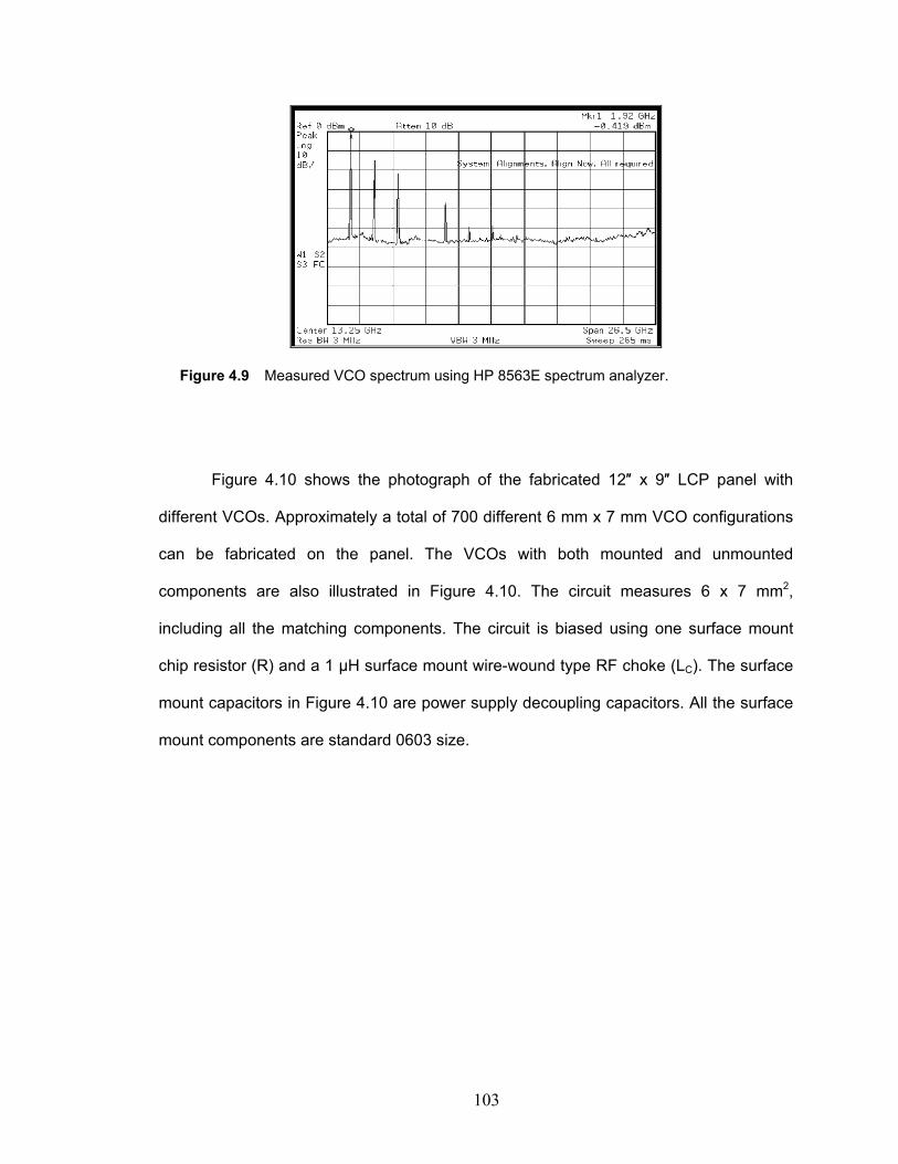
103
Figure 4.9 Measured VCO spectrum using HP 8563E spectrum analyzer.
Figure 4.10 shows the photograph of the fabricated 12″ x 9″ LCP panel with
different VCOs. Approximately a total of 700 different 6 mm x 7 mm VCO configurations
can be fabricated on the panel. The VCOs with both mounted and unmounted
components are also illustrated in Figure 4.10. The circuit measures 6 x 7 mm2,
including all the matching components. The circuit is biased using one surface mount
chip resistor (R) and a 1 µH surface mount wire-wound type RF choke (LC). The surface
mount capacitors in Figure 4.10 are power supply decoupling capacitors. All the surface
mount components are standard 0603 size.

104
Figure 4.10 Photograph of the fabricated LCP board highlighting the measured VCO.
Out of the total area occupied by a single VCO, an area of approximately 4 mm2
is occupied by the transistor and its associated biasing circuitry. To reduce the size of
the VCO, 3-D stacking of multiple LCP layers should be used. For example, the size of
the VCO can be reduced to approximately 16 mm2 by using four signal layers. However
the lower limit on the area is placed by the size and the number of surface mount
components. Additionally, by resorting to chip-package co-design methodologies, all the
active components and bias circuits can be integrated onto a small size die (<1 mm2).
Finally, the die can be wire-bonded on to the LCP substrate that provides the high Q
passive components thereby causing a significant reduction in both area and power
consumption of the VCO.

105
4.1.4. Design Techniques for Low Power Operation
The negative resistance oscillator discussed in the aforementioned sections has
phase noise suitable for use in handset-type applications with reasonable power
consumption. However, it is always useful to a designer to understand the optimization
routine that will improve the phase noise and/or the power consumption of the VCO. The
following sub-sections present a technologically-independent design technique that
enables a designer to systematically design a negative resistance VCO. The method
focuses on providing a VCO design with the lowest possible power consumption (micro-
ampere bias current) and at the same time it enables to design for low phase noise.
A. Component Selection for Power Optimization
A significant portion of the design effort is put in the optimization of the VCO power
consumption. It should be noted that when a VCO is biased at low current levels the VCO
becomes weakly non-linear i.e. there exists a high probability that the measured
characteristics of the VCO may not correlate with the simulated results. Hence, for the
VCO configuration shown in Figure 4.1, the circuit variables (L1, gm, and, RL) need to be
optimally selected to operate the VCO at very low current levels (< 1 mA). For the VCO
under investigation the oscillations are confirmed as long as the circuit provides sufficient
negative resistance, i.e. high input reflection coefficient, to compensate for the loss in the
resonator. Figure 4.11 confirms the above mentioned phenomena.
Figure 4.11 plots of the S-parameter simulation results for the VCO input reflection
coefficient (Sin) at two bias conditions with the value of inductor L1 swept between 1 to 15
nH. The solid line is when the VCO is biased at 3.5 mA (bias at which the VCO was
measured) and sampled data is for 0.9 mA bias current value. From Figure 4.11 it can be
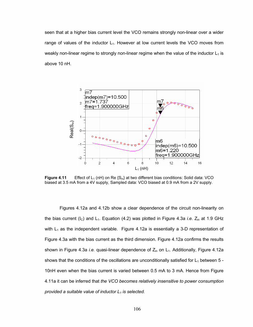
106
seen that at a higher bias current level the VCO remains strongly non-linear over a wider
range of values of the inductor L1. However at low current levels the VCO moves from
weakly non-linear regime to strongly non-linear regime when the value of the inductor L1 is
above 10 nH.
Figure 4.11 Effect of L1 (nH) on Re Sin at two different bias conditions: Solid data: VCO biased at 3.5 mA from a 4V supply, Sampled data: VCO biased at 0.9 mA from a 2V supply.
Figures 4.12a and 4.12b show a clear dependence of the circuit non-linearity on
the bias current (IC) and L1. Equation (4.2) was plotted in Figure 4.3a i.e. Zin at 1.9 GHz
with L1 as the independent variable. Figure 4.12a is essentially a 3-D representation of
Figure 4.3a with the bias current as the third dimension. Figure 4.12a confirms the results
shown in Figure 4.3a i.e. quasi-linear dependence of Zin on L1. Additionally, Figure 4.12a
shows that the conditions of the oscillations are unconditionally satisfied for L1 between 5 -
10nH even when the bias current is varied between 0.5 mA to 3 mA. Hence from Figure
4.11a it can be inferred that the VCO becomes relatively insensitive to power consumption
provided a suitable value of inductor L1 is selected.
L1 (nH)
Real(Sin)

107
0.001
0.002
0.003
0.004
0.005
5
10
15
0
20
40
60
0.001
0.002
0.003
0.004
0.005
Figure 4.12 (a) Variations in VCO ReZin from analytical models, (b) Effect of bias current on |Sin| at LB= 10 nH.
Real(Zin), Ohms
L1 (nH)
(a)
IC (A)
IC (A)
|Sin|
(b)

108
Circuit simulation results are in confirmation with the above mentioned analytical
results. Figure 4.12b is the large signal S-parameter ADS simulation result, showing the
effect of varying bias current (IC) on |Sin|. As can be seen from Figure 4.12b, |Sin| increases
and hence circuit non-linearity increases when the bias current is increased from 0.9 mA
to 3 mA. Hence, for low power operation the value of L1 should be selected only after
determining a suitable operating point of the transistor. In the oscillator shown in Figure 4.1
an increase in the Sin and hence negative resistance was observed with the increase in
the bias current until a bias current of 3.5 mA. Above this bias current level Sin decreases
with the increase in the bias current (current limited region). This means the additional
power supplied to the VCO does not lead to phase noise minimization and hence, the
region of operation should be avoided. Hence the methodology to optimize the power
consumption of the common base oscillator of Figure 4.1, on any technology, can be
generalized as follows:
(a) Determine the power budget,
(b) Bias the oscillator at the maximum allowable power (without saturating),
(c) Determine an initial inductor value and load resistance using (4.2) and via simulations,
(d) Obtain a 3-D plot of the input impedance of the oscillator with L1 and IC as the
independent variables,
(e) Determine a region where real Zin varies minimally with the bias current, and
(f) Obtain the corresponding optimized values of L1 and IC in this region.
It should be noted that (4.2) does not include all the parasitics of the packaged transistor
as well as other passive parasitics that might contribute to some discrepancy between
theory and circuit simulation.

109
Conclusively, the VCO can be operated at very low power levels provided suitable
values of the components are selected that ensures sufficient non-linearity. As a test case
and to confirm the above mentioned discussion, the VCO (Figure 4.1) was biased at
0.9mA from 2V (Vcc= +0.5 V, and VEE = -1.5 V) supply and is compared to the performance
of the same VCO biased at 3.5 mA from 4 V supply. The measured phase noise results of
the VCO biased at 3.5 mA were shown in Figure 4.8 and Figure 4.9. The phase noise
result (with bias current of 0.9 mA) for the VCO consuming only 1.8 mW is shown Figure
4.13. The simulated phase noise of the low power VCO is -118.4 dBc/Hz at 600 KHz
offset. The results of the high power VCO shown in Figure 4.9 match very closely with
the results shown in Figure 4.13 (~0.4 dB discrepancy).
Figure 4.13 Simulated phase noise of the VCO at 900 uA from a 2 V supply.
Noise Sideband (dBc/Hz)
Offset frequency (Hz)
1K 10K 100K 1M

110
B. Base Inductor Q Requirements at Low Power
The discussion in sub-section A of 4.1.4 mentioned a design methodology for the
VCO to be functional at low power dissipation levels. This section shows the importance
of high Q tank circuit to maintain low VCO phase noise at low power consumption.
Phase noise depicted by Leeson’s model explains that higher resonator Q with higher
power consumption will lead to low phase noise. In view of the fact that there exists an
inverse proportionality between phase noise and power consumption, the Qs of the
passives need to be high to reduce the power dissipated by the VCO. Additionally, at
very low power levels, the VCO phase noise becomes highly sensitive to the variations
in Qs (due to quadratic dependence). Harmonic balance noise simulations were
performed to confirm the above mentioned phenomena. The Q of the inductor L1 was
swept from 10 (on-chip) to 100 (LCP) with the VCO biased at 3.5 mA consuming 14 mW
dc power. Additionally, phase noise simulations were performed with the VCO biased at
0.9 mA from a 2V supply (1.8mW). Figure 4.14 plots the simulated VCO phase noise
against Q of L1, at a single offset frequency (600 KHz offset from a 1.9 GHz carrier) at
the two bias current levels (0.9 and 3.5 mA). From the results for the high power VCO,
Figure 4.14 (square marker), it can be seen that the phase noise varies by only
approximately 2dB when the Q of the inductor L1 is changed by a factor of 10. This is in
confirmation with the behavior explained in the previous section. However, for the low
power version (circle marker) the phase noise of the VCO at QL1 =10 is 6 dB worse when
QL1 is 100. Additionally, it can be seen from Figure 4.14 that the phase noise of the low
power VCO reaches the phase noise level of the high power VCO as the Q of the
inductor L1 is above 90. Thus the phase noise of a VCO biased at low power levels has
higher dependence on noise contribution of inductor L1 as compared to that biased at
high power levels.

111
Figure 4.14 Simulated phase noise results @ 600 KHz offset vs. Q of inductor L1 with the VCO biased at two different levels: Circle marker – Phase noise of the VCO biased at 0.9 mA (2 V supply) varies by 6 dB, Square marker- Phase noise of the VCO biased at 3.5 mA (4 V supply) varies by 2 dB.
Therefore the phase noise of the two versions of VCO becomes similar at high Q
of L1. Thus by using a high Q inductor L1, its contribution to the phase noise is
suppressed. The phase noise of the common base VCO at very low DC power levels can
be made to approach that of a high power VCO by using a high Q L1. Now the only
significant contributor to the noise is the noise contribution of the active device that is up-
converted by the mixing process, which is present in the oscillator. The underlying physical
mechanisms of noise processes in VCOs are explained in references [40], [42], [47], and
[73]. The above discussion confirms that a high Q base inductor and a high Q resonator
are required for the design of a low phase noise common-base VCO at low power levels.
6 dB @ 0.9 mA
2dB @ 3.5 mA
Noise Sideband (dBc/Hz)
Q of L1, units
Low power VCO
High power VCO

112
C. Effect of Transistors Package Parasitics
Figure 4.15 shows the model of the transistor provided by the manufacturer [74]
where all the passive components are parasitics components resulting from the SOT-
343 package. Terminal marked B is the base terminal available to the designer for
simulations and B’ is the physical base of the transistor. The lead inductances can be
ascribed to the inductive bond-wires from the intrinsic transistor die to the package pads.
The capacitances are the parasitic capacitance from pad to ground and range in the tens
of femto-Farads. To visualize the effect of the parasitics, S-parameter simulations were
performed with and without the package parasitics. Simulations show that the forward
gain of the transistor without package parasitics biased at 3.5 mA is 1.2 dB greater than
the gain of the transistor with package parasitics at the same bias. At the frequency of
interest, the package inductance (Lp) have much more pronounced effect than the shunt
capacitance. The effect of the package inductance on the Zin can be found via y-
parameter analysis. It was found that the real Zin decreases by a factor of 1/ω2Y221L
2p
[40], where Y21 is the transfer-admittance of the intrinsic transistor. Therefore the
parasitics increase the phase noise by not only adding thermal noise but also by
reducing the loop-gain or negative resistance. A reduction in loop-gain amounts to
increase in power consumption to maintain the same phase noise level.

113
Figure 4.15 Schematic of the transistor with package parasitics. Terminal marked B is the base terminal available to the designer for simulations and B’ is the physical base of the transistor.
To visualize the effects of the package parasitics on phase noise performance of
the VCO, the oscillator circuit was re-simulated by not considering the parasitics of the
package. The simulated phase noise improved by 9 dB, to -126 dBc/Hz at 600 KHz
offset, as compared to the VCO with the package parasitics of the transistor. Additional
simulations were performed after replacing the current bipolar transistor with a high gain,
high β (~160), transistor (ST Microelectronics, model # START405). The phase noise
improved by 4 dB; to -122 dBc/Hz at 600 kHz offset. Hence to make use of the high Q of
the passives provided by organic technologies a high gain transistor, mostly bare die
needs to be employed (chip-package co-design).

114
4.2 Design of Colpitt’s Oscillator in LCP Substrate
To further visualize the effects of high Q passives on VCO performance, a 2.25
GHz Colpitt’s oscillator was designed and tested. Figure 4.16 shows the designed
Colpitt’s oscillator, which is suitable for the WLAN standard (IEEE 802.11b/g). This
oscillator is a useful test circuit that clearly shows the use of high Q components causing
a reduction in power consumption without trading off phase noise.
Figure 4.16 Circuit schematic of the 2.25 GHz Colpitt’s VCO.
The circuit is in common base configuration (Figure 4.16) and uses capacitive
feedback from the collector to the emitter. RB and RE are biasing resistors and capacitor
CB connects the base terminal to ac ground. Inductor (L), capacitors (C1 and C2), and
varactor (CV) form the frequency controlling tank circuit. Capacitor Cm matches the circuit
+2.7 V
+
Vout
-
50 Ω
(Load)

115
to a 50 Ω load. Circuit simulation aspects and the design of the VCO are clearly
mentioned in [40] and [70]. It was found that the capacitance ratio (C2/C1) determines the
oscillator performance.
For simplicity of explanation, a simplified version of the loop-gain (LG) equation
can be written as,
+⋅
⋅+≥⋅
1
21:C
CRg
R
RRgLG inm
P
inLm (4.5)
In (4.5), RP is the parallel combination of biasing resistor RE and source resistance Rin,
gm is the transconductance, and RL is the load resistance seen by the oscillator.
Equation (4.5) indicates two limitations on the values of C2 and C1:
(a) For sustained oscillations, the gain, Lm Rg ⋅ , should be greater than the ratio of
the capacitors C2 and C1. Thus, C2 and C1 control the frequency of oscillation as
well as the magnitude of the loop-gain. Hence, for a given power-budget there
exists an upper limit on the value of C2 and a lower limit on the value of C1.
(b) Apart from controlling the frequency and oscillation amplitude, the capacitance
ratio also controls the phase noise [70]. As the capacitance ratio is increased,
the loaded Q of the tank circuit increases. The increase in loaded Q can be
converted to the improvement in phase noise, as is explained by Leeson’s
model.
The oscillator’s tank circuit was designed with an unloaded Q of 60. However the
tank circuit loaded Q was reduced from 60 to approximately 3 because of the loading by
116
a parasitic load impedance (Rext ~ 1/gm). This parasitic loading resistor is dependent on
the capacitance ratio, and can be expressed as,
2
1
211
+⋅
⋅+≅
C
C
Rg
RR
Em
Eext (4.6)
From (4.6) it can be concluded that the increase in the capacitance ratio will
increase the Rext thereby causing a significant improvement in the loaded Q of the tank
circuit. Hence, the capacitance ratio contributes to the phase noise, and as the
capacitance ratio increases, the phase noise decreases. However there are two
negative effects of increasing the capacitance ratio:
(a) From (4.5) it is known that as the capacitance ratio is increased the power
consumption needs to be increased, in order to satisfy the oscillation criterion.
(b) Additionally, as the ratio increases the area of the VCO increases. Also the
maximum value of the capacitors is limited by the self resonant frequency of the
capacitors.
Hence, the self-resonant frequency (SRF) and power consumption put a lower bound on
the achievable phase noise in a Colpitt’s oscillator. Figure 4.17 shows the trade-off
between phase noise and power consumption against capacitance ratio. In Figure 4.17,
the phase noise improves as the capacitance ratio increases. At the lower end of the
capacitance ratio, the phase noise is limited by the parasitic loading of the tank.
Conversely, at the higher end of the capacitance ratio the phase noise is limited by the
SRF of the largest capacitor [70]. The line represented by a series of dashes and dots

117
distinguishes the two regions. To the left of the line (at low capacitance ratio), the VCO is
loaded by the transistor’s transconductance and to the right of the line the phase noise is
limited by the maximum SRF of the capacitors and the available power budget. Hence,
the power consumption also increases with the increase in the capacitance ratio. Thus,
this oscillator clearly indicates a trade-off between the phase noise and power
consumption. It should be noted that the high Q of the passives prevented a reduction of
the loaded Q of the tank circuit. Additionally, for a similar circuit fabricated on CMOS-
based technology, the phase noise will be further degraded due to the low Qs (5-20) of
the passives. Hence, high Q embedded passives on organic process technology makes
the compact and low component count circuit configuration suitable for short distance
communication like WLAN a/b/g.
Figure 4.17 Effect of capacitance ratio on phase noise and power consumption.
Parasitic limited region
Phase noise limited by capacitor SRF and dc power
Noise sideband in dBc/Hz @ 100 KHz
offset
Power consumption (mW)
Capacitance ratio (C2/C1)

118
Design Validation
For the Colpitt’s VCO shown in Figure 4.16, the active device is from Agilent
Technologies, a SOT-343 packaged surface-mount bipolar transistor (HBFP 0420) with
an available gain of 14dB and a noise figure of 1.3 dB @ 2.4 GHz. The transistor has a
unity-gain cut-off frequency (fT) of 17.2 GHz at an Ic of 4 mA. The oscillator is biased at 4
mA from a 2.7V power supply. The VCO is tunable from 2.1 GHz to 2.45 GHz by using a
surface mount varactor (Alpha Industry, model# SMV 2023).
Figures 4.18a and 4.18b show the measurement results of the Colpitt’s oscillator
designed at 2.25 GHz. The measurement includes the cable loss of 2.2 dB. The
spectrum was measured using an HP4407B spectrum analyzer. The capacitor C2 (see
Figure 4.16) was designed to resonate at 4.8 GHz, thereby attenuating the second
harmonic at 4.5 GHz by approximately 40 dB. The measured phase noise is -92 dBc/Hz
@ 100 KHz offset from the 2.23 GHz carrier. Thus, LCP-based organic processing
technology provides good control over the component Qs and SRF, making it conducive
to a low power multi-band environment.

119
(a) (b)
Figure 4.18 (a) Measured spectrum of the 2.25 VCO, (b) Measured phase noise of the VCO.
Figure 4.19 shows the photograph of the fabricated oscillator with all the surface
mount components and integrated inductors and capacitors in LCP. The VCO occupies
an area of 5 x 5 mm2. The VCO was fabricated in the same single LCP substrate
process technology as mentioned in Figure 4.4. In Figure 4.19, the slab-type CPW
resonator inductor (L) can be seen on the top most metal layer. The inductor was
designed with a Q of 60. Coplanar GSG output pads together with GSG RF probes were
used for spectrum measurements.
Figure 4.19 Photograph of fabricated oscillator.
-92 dBc/Hz @ 100 KHz
Offset frequency, (Hz)
Noise Sideband, (dBc/Hz)

120
4.3 Summary
Sections 4.1 and 4.2 demonstrated the design of negative resistance and
Colpitt’s oscillators with passives completely embedded in a three metal-layer LCP
substrate. The sections described the design scheme and optimization routine. In the
case of a negative resistance oscillator the increase in the supply voltage leads to a
decrease of phase noise in the 1/f2 region [40]. However, the increase in the Q of the
base inductor significantly reduces the phase noise and hence, the oscillator can be
optimized for low phase noise provided the base inductor and the resonator have high
Qs. Resultantly, the VCO was optimized to meet the requirements of PCS standards,
while consuming only 1.8 mW, which is the lowest power consuming, fully-packaged
VCO reported in the literature. In the case of a Colpitt’s oscillator the phase noise is
governed by the ratio of the capacitances (C2/C1). The capacitance ratio governs the
feedback factor and hence, the start-up conditions. A larger ratio significantly improves
phase noise but at the cost of larger current consumption to meet the start-up conditions.
Table 4.2 compares the performances of the designed oscillators described in
the sections 4.1 and 4.2 with other published work. Table 4.2 shows the FOM
comparison (see equation (4.1)) of this work with the results of oscillators fabricated on
few of other high Q fabrication technologies [63], [64], such as LTCC. From Table 4.2 it
is clear that the high Q passives on LCP allow low power operation of the VCO coupled
with low phase noise. The comparison table includes a low phase noise VCO using
bond-wires as resonator inductor [65]. In this case the size of the VCO is determined by
the amount of inductance required for VCO operation1. In addition to the dependence of
1 The general rule of thumb is 1 to 1.5 nH of inductance from an 1mm length of bond-wire. Hence, a 4 nH inductor would require atleast 3 mm long bondwire.

121
the VCO size on the bond-wire inductance value, the wire-bonding mechanism places a
lower limit on the VCO area, which is the minimum bonding distance between two pads.
Table 4.2 Comparison of VCO FOM over different technologies.
Technology
And References
Center
Freq (GHz) PDC (mW)
Phase Noise
(dBc/Hz) at offset
FOM
(dB) Area, mm
2
LCP
This work 1.85 - 1.92 14 -118 @ 600 KHz 176.7 6 x 7
LCP
This work 1.8 – 1.9 1.8 -118 @ 600 KHz 185.5 6 x 7
LCP
This work 1.8 - 1.9
1.8
(high β) -122 @ 600 KHz 189.4 6 x 7
LCP
This work 2.2 – 2.32 10 -92 @ 100 KHz 169 5 x 5
LTCC
[75] 1.92 – 2 94 -154 @ 20 MHz 173.8 5.5 x 4.8
LTCC
[76] 2.29 - 2.37 39 -121 @ 100 KHz 192.3 12 x 11
SiGe HBT
[78] 2.17 - 2.31 32 -110 @ 600 KHz 166.1 1.8 x 1.2
0.35um +
bondwire [77] 1.8 – 2.4
2 + output
buffer -122 @ 600 KHz NA > 4 x 2
The designed LCP-based VCOs meet the requirements set by the cellular
standards at < 2 mW of DC power consumption. As compared to the CMOS-based
122
VCOs mentioned in chapter 3 (Table 3.2) this is a >15X improvement in the power
consumption with better phase noise. However, the VCOs were manufactured on a
three-layer process technology. The negative resistance VCO used more than 7 passive
components to achieve low phase noise and a broad-band matching and hence,
occupied 6 x 7 mm2. To support all SOP functionalities (Chapter 1), the technology
needs to scale to accommodate more metal layers. The increase in metal layers allows
(a) an increase in component density, (b) physical separation between components to
minimize coupling, and (c) flexibility in interconnection between modules or components.
The multi-band cellular handset (see Figure 1.2, Chapter 1) would require more than one
VCO to handle frequency conversion of different standards. As a result, size reduction is
one of the main criteria in VCO design along-with power reduction. Hence, improved
circuit techniques with multi-layer process technology are required for the design of low
phase noise and area-efficient VCOs, which can be used in next generation cellular
handsets. The next chapter discusses the design of novel VCOs on novel multi-layer
process technologies.

123
CHAPTER 5
IMPROVED CIRCUIT TECHNIQUES FOR VCO DESIGN
IN MULTI-BAND RADIOS
Chapter 4 presented the design and implementations of two VCO circuit
examples on LCP-based substrates. In the case of negative resistance VCO, the
oscillator needs to have a high Q inductor at the base and a high Q network at the
emitter terminal. Additionally, the tuning range of the negative resistance VCO and the
output power are governed by contradicting requirements. Appendix B explains using
analytical expressions the limitation of tuning the negative resistance VCO with constant
output power and low phase noise. Conclusively, a reasonable tuning range (~0.1f0) can
be expected out of the negative resistance VCO provided a broad-band output match
and a high Q reactive network at the emitter are used. As a result the negative
resistance VCO requires more components as compared to a Colpitt’s oscillator.
In the case of consumer portable applications, both the VCO size and power
consumption are premium commodities. Consequently, a simple oscillator core design
with low parasitic loading is the key to the design of a low phase noise oscillator in a
small area. As a result of in-depth circuit analysis, the cross-coupled and coupled-
Colpitt’s oscillators [47], [48], [79], and [80] have become the defacto standard oscillator
configurations in radio design. In each of these oscillators, the reduction in phase noise
is achieved through improvement of the oscillator loaded-Q. However, each of these
topologies exhibit significant amount of trade-off between the transistor
transconductance and resonator inductor size. In other words, in each of the described

124
topologies the phase noise design strategy is centered at maximizing the power
consumption and minimizing the inductor size (for minimum loss). By selecting an
inductor of the smallest size the phase noise requirements might be satisfied but the
start-up conditions can be violated [48]. Additionally, it was discussed in section 4.1.4
that the phase noise of a low power oscillator shows high sensitivity to variations in the
resonator Q. Hence, the manufacturing (processing) variations across the total
processing area may cause the phase noise to differ for oscillators of the same batch
even though the oscillator start-up conditions are satisfied. The above is especially true
for low power oscillators [6]. Typically the Colpitt’s oscillator (both single-ended and
differential) that has a simple core design has been the most favored topology to achieve
low phase noise [6] and [40]. It was clearly shown in Chapter 4 that in a Colpitt’s
oscillator the start-up conditions are independent of the inductor size and the phase
noise is limited by the parasitics of the bias circuitry. Hence, the small form factor and
high phase noise performance of the Colpitt’s oscillator makes it suitable for low profile
applications, such as the WLAN (IEEE 802.11 a/b/g).
This chapter presents two, novel oscillator topologies that eliminate the
dependency of the start-up conditions on the size of the resonator inductor thereby,
simplifying the design of low power and low phase noise oscillators. Both the oscillator
configurations rely on isolating the resonator from the low-Q bias circuitry. Hence in
addition to improving the phase noise, the design technique also enables the design with
a wide tuning range. Section 5.1 presents the design of the modified-Colpitt’s oscillator
[82]. The oscillator is effectively composed of three components (1) a silicon bipolar
transistor, (2) one capacitor, and (3) one inductor. The capacitive nature of the feedback
makes the functioning of the proposed circuit resemble a Colpitt’s oscillator however with
reduced loading of the resonator. As a result the VCO achieves a phase noise
improvement of more than 25 dB as compared to a Colpitt’s oscillator at lower power

125
consumption i.e. FOM of the VCO ~200 dB. Circuit implementations of the modified-
Colpitt’s oscillator are demonstrated at 700 MHz and 1.9 GHz. Section 5.2 presents the
design of VCO that uses a lumped-element transformer as the feedback network
(TVCO). The feedback network is essentially a bandpass filter that provides accurate
control and at the same time decouples the dependency of both phase noise and start-
up conditions from the size of the resonator inductor. As compared to a Colpitt’s VCO,
the TVCO provides > 24 dB improvement in phase noise at the same power level. The
section presents the design technique, measurement results and finally, discusses the
scalability and implementation issues on multi-layer substrates. Both the VCOs were
fabricated on a novel, multi-metal layer (> 6) substrate that used heterogeneous
combination of LCP and pre-preg. The technology allows a true three-dimensional
integration of passive components leading to VCO size and power optimization. The
chapter also presents a VCO implementation at 800 MHz on another novel LCP-based
substrate with eight metal layers.
5.1 Modified-Colpitt’s Oscillator - Analysis and Design
The proposed oscillator utilizes the concept of capacitive feedback from the base
terminal to the collector terminal of the transistor. The resonator inductor is placed at the
collector terminal. Since the feedback is through a capacitive-divider network, the circuit
functioning resembles a Colpitt’s oscillator [82] and hence, in this thesis is called as
modified-Colpitt’s oscillator. The modified-Colpitt’s oscillator works on a concept similar
to a Colpitt’s oscillator, as discussed in section 5.2 of chapter 4, with the exception that
in the present case the feedback is from the collector terminal to the base of the
transistor. This section discusses (a) the physical or circuit aspects of the proposed

126
feedback mechanism and compares it with the feedback mechanism of a Colpitt’s
oscillator, and (b) the full two-port open-loop circuit analysis of the proposed oscillator.
5.1.1. Circuit Operation
Figure 5.1a shows the proposed modified-Colpitt’s oscillator and Figure 5.1b
shows the Colpitt’s oscillator as was discussed in chapter 3 and [82]. The biasing details
are omitted from both Figures 5.1a and 5.1b for the sake of circuit schematic clarity. In
the case of the Colpitt’s oscillator, Figure 5.1b, the signal from the emitter terminal is fed-
back to the collector through the capacitive impedance transformer (C2 and C1). In
Chapter 4, it was demonstrated that for the Colpitt’s VCO the capacitance ratio (C2/C1)
controls the magnitude of the loop-gain and frequency of oscillation. It should be noted
that in Figure 5.1b the base is common to the input and the output terminals of the
oscillator.
Figure 5.1 (a) Schematic of the proposed modified-Colpitt’s oscillator. (b) Schematic of the Colpitt’s oscillator.
C1 L
RE
Output matching network
VO
C1
C2
L
RE
VO
VCC
(a) (b)

127
The magnitude of loop-gain in the case of a Colpitt’s oscillator, Figure 5.1b, is
given by (4.5) in Chapter 4. For clarity of discussion it is repeated as
+⋅≥⋅
1
21:C
CkRgLG Lm (5.1)
In (5.1), k is a constant, which is dependent on the biasing circuit details, gm is the
transistor transconductance and RL is the load resistance. From (5.1) it can be observed
that the loop-gain (power consumption) needs to be increased as the capacitance ratio
(C2/C1) increases, which is in accordance with the Barkhausen criterion for oscillation. In
a Colpitt’s oscillator the capacitance ratio, in addition to controlling the loop-gain and
frequency of oscillation, determines the phase noise [82]. This happens because of the
loading of the resonator circuit by parasitic impedance Zext. The impedance looking into
the emitter terminal is transformed by the capacitive transformer and is put across the
tank circuit as Zext, shown in Figure 5.2. Figure 5.2 shows the one-port equivalent circuit
of the resonator of Figure 5.1b under loading conditions. The resonator consists of the
inductor L and its associated series loss resistor (Rl). The combination is in parallel with
the series combination of capacitors C1 and C2. The resistance RC,loss represents the
total loss in the capacitors. From Figure 5.2 it can be observed that the parasitic
impedance Zext loads the resonator. Now the overall Q of the resonator will be
dependent on the value of the Zext.

128
Figure 5.2 Equivalent one-port representation of the resonator of the Colpitt’s oscillator of Figure 5.1b: Figure shows the loading of the resonator by the parasitic impedance Zext due to the transistor gm.
Chapter 4 and [6] derived the approximate expression for the transformed
impedance (Zext) as
2
1
211
+⋅≅
C
C
gZ
m
ext (5.2)
Equation (5.2) shows an inverse relation between transconductance and Zext. At
a few milli-amperes of bias current, the value of the Zext will be in the vicinity of several
hundred ohms to a few kilo-ohms, from (5.2). Hence, the overall or the loaded-Q (Ql) of
the oscillator will be reduced by Zext to a value determined by the bias current. The
relation between the loaded-Q, external-Q (Qe), and unloaded Q is given in [14] as
uel QQQ
111+= (5.3)
Thus, the phase noise will be limited by the loading of the tank circuit, in
accordance with Leeson’s model of phase noise. The phase noise can be improved by
increasing Zext. The increase in Zext requires an increase in the capacitance ratio, from
Zext
C1
C2
Rc,loss
Rl
L

129
(5.2). Additionally, from (5.1) it is also known that the gmRL product (power consumption)
needs to be increased with the capacitance ratio1. A direct effect of increasing the
capacitance ratio is the increase in the area of the oscillator. Therefore, from (5.1) and
(5.2) it can be concluded that there exists a design trade-off between power
consumption, phase noise and circuit dimensions in the case of a Colpitt’s oscillator.
In the proposed modified-Colpitt’s oscillator topology, Figure 5.1a, the capacitance
C1 and the base-emitter junction capacitance of the transistor (Cbe) are the feedback
providing elements. In this case the feedback signal is taken from the collector terminal
and is added to the base terminal through the series connected inductor (L) and the
capacitor (C1). Now the resonator is loaded by the high input impedance of the emitter-
degenerated transistor on one end and by the high collector-resistance of the transistor
on the other end. As a result, the degradation of phase noise resulting from resonator
loading is avoided. Additionally, as will be shown that the magnitude of the loop-gain has
an inverse dependence on the value of the capacitor C1. Thus, as the capacitor C1 is
increased, a lower loop-gain value and hence a lower bias current will cause the
oscillator start-up. Thus, the proposed oscillator configuration eliminates the inherent
trade-offs that are present in a Colpitt’s oscillator and at the same time presents a simple
low-phase noise solution that is scalable over a large frequency range.
5.1.2. Circuit Optimization
This section analyzes the proposed oscillator using small-signal circuit equivalent
of the transistor. The open-loop analysis assumes linear operation of the oscillator and
neglects most of the circuit parasitics. Hence, it is an approximate analysis that enables
1 The start-up conditions might be violated if the power consumption is kept constant and the capacitance ratio is increased, from (4.1).

130
in determining the component parameters for initial design and power optimization.
Figure 5.3 shows the open-loop, two-port small signal equivalent circuit representation of
the proposed modified-Colpitt’s oscillator. In Figure 5.3 Ro represents the transistor
resistance resulting from the Early effect, RL is the load resistance observed at the
collector, and Cout is the parasitic capacitance, which loads the resonator at the base of
the transistor.
Figure 5.3 Equivalent two-port representation of the proposed modified-Colpitt’s oscillator of Figure 5.1a: magnitude of the loop-gain is calculated between the terminal voltages Vo and Vin.
In Figure 5.3, Gm(s), overall transconductance, is given by
be
EEm
mm
Z
RRg
gsG
+⋅+=1
)( (5.4)
In (5.4), gm is the transistor transconductance without emitter-degeneration, Zbe is the
parallel combination of the resistance (Rbe) with the capacitance (Cbe) at the base-emitter
junction. In Figure 5.3, the open-loop gain (LG) is evaluated between the terminal
Rbe Cbe
(1+β)·RE Gm(s)·Vin
Ro
L
C1
Cout
RL
Cbc
Vin
Vo

131
voltages Vo and Vin and at the desired frequency of oscillation the magnitude of the LG
should be greater than unity and the total phase shift around the loop should be zero.
The above requirements are called the Barkhausen/Nyquist criterion for oscillations. The
loop-gain for the two-port circuit representation shown in Figure 5.3 was calculated as
+⋅
⋅⋅−
+⋅
⋅⋅−
+⋅×
+⋅
⋅⋅+
+⋅
⋅⋅−
⋅=
out
outL
out
out
out
out
outL
out
out
Lm
in
o
CC
CCRs
CC
CCL
CC
C
CC
CCR
CC
CCL
RsG
sV
sV
1
1
1
12
1
1
2
1
1
2
1
12
1
1
)(
)(
)(
ω
ωω
(5.5)
The magnitude of the loop-gain (oscillator start-up condition) and frequency of operation
are obtained by separating the real and the imaginary parts of (5.5) and equating them
to unity and zero, respectively. Equation (5.6) gives the simplified representation of the
magnitude of the loop-gain
+⋅
+⋅
⋅⋅≥⋅11
1 1)(:C
C
CC
CCRRsGLG out
out
outLoLm ω . (5.6)
Equation (5.6) shows an inverse dependence between the capacitance C1 and the loop-
gain. In (5.6), ωo represents the frequency of oscillation and is given by
1
1
CLo
⋅≅ω . (5.7)

132
It follows from (5.6) that for the same bias current level, the loop-gain increases with the
increase in value of C1. In other words, with the increase in C1 a lower transconductance
i.e. a lower bias current is required to satisfy the oscillator start-up criteria.
The aforementioned theoretical analysis is confirmed by circuit simulations.
Figure 5.4 shows the simulation results for the magnitude of loop-gain of the modified-
Colpitt’s oscillator. The circuit was simulated in Advanced Design System (ADS™) from
Agilent Technologies. The results are shown for different values of the capacitor C1 that
were swept from 0.6 pF (square marker) to 1.8 pF (triangular marker).
Figure 5.4 Simulation results for the loop-gain magnitude for different values of capacitance (C1). The simulations were performed in ADS at a bias current of 3.7 mA from a 2.7 V supply.
For the parametric loop-gain simulations the circuit was biased at a bias current
of 3.7 mA from a 2.7 V power supply. It can be observed from Figure 5.4 that the loop-
gain increases with the increase in the value of the capacitor. The advantages of using a
larger value capacitance are two-fold
Mag. loop-gain
Frequency, GHz
C1 = 0.6 pF
C1 = 1.2 pF
C1 = 1.8 pF

133
(a) As C1 increases, a lower Lm RsG ⋅)( product is required to satisfy the Barkhausen
criteria, from (5.6). This implies that the circuit can be biased at a lower bias
current level without violating the start-up conditions.
(b) As C1 increases a lower value of inductance is required, from (5.7). The decrease
in the inductance causes a decrease in both the dc and ac resistances, which
enables the design of high Q inductors. Hence, an improvement of 2-3 dB in the
phase noise can be expected.
It should be noted that as the value of C1 increases, it should be accompanied by
a corresponding reduction in the value of L1. Hence, the power optimization process will
be limited by either the self-resonance frequency of the capacitors and by the minimum
value of inductance that can be reliably fabricated. For instance, the self-resonant
frequency of a 1.1 pF parallel-plate capacitor fabricated on the multi-layer LCP
technology, as used in this work, will be in the vicinity of 8 GHz [6] and that of a 2.5 pF
will be around 4 GHz. Another negative effect of using a large valued capacitor is the
increase in the area of the oscillator. A capacitance density of 0.9 fF/mils2 is obtained
from a 1 mil thick LCP substrate. Hence, a 1 pF parallel-plate capacitor will require an
area of 34 mils x 34 mils and a 4 pF capacitor would require a sizeable area of 68 mils x
68 mils (1.8 mm x 1.8 mm). Additionally, the parasitics introduced by large size
capacitors will also be larger and hence, difficult to model and control during the
manufacturing process. Resultantly, there might be discrepancies between the simulated
and the measured values of both the frequency and phase noise.
From the above discussion it can be concluded that the proposed feedback
mechanism prevents the loading of the resonator and enables the oscillator to be
designed at low current levels and with small values of inductance. Additionally, the
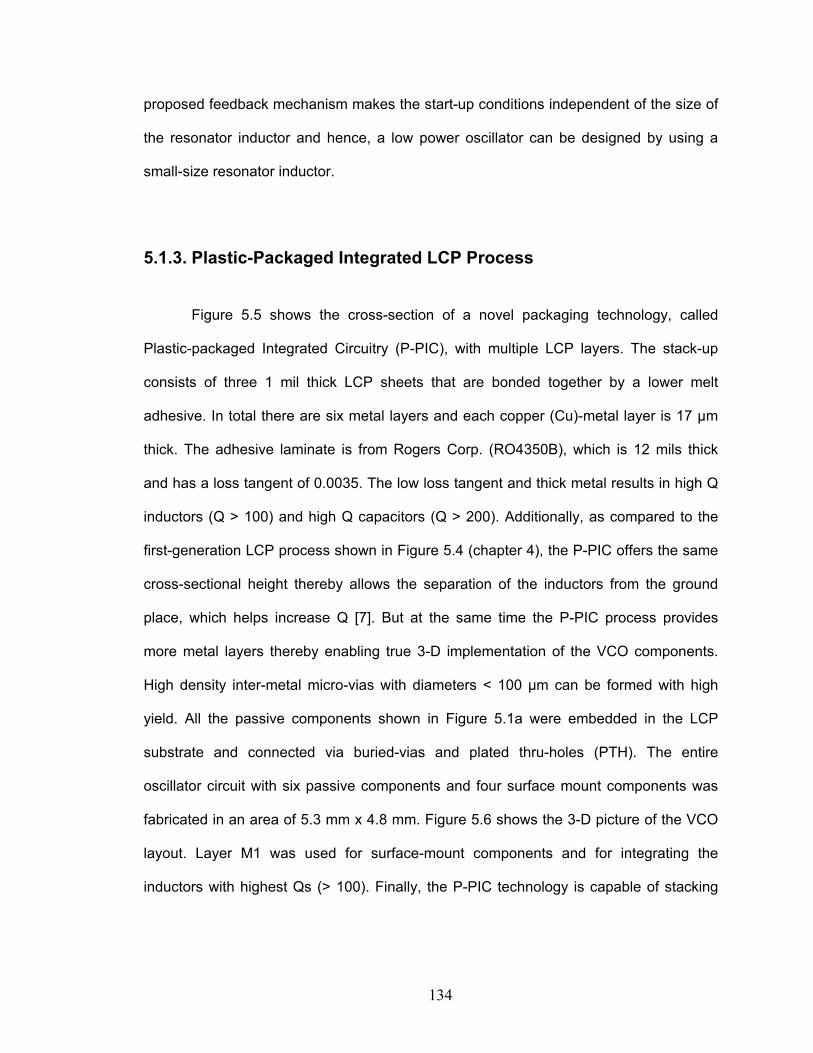
134
proposed feedback mechanism makes the start-up conditions independent of the size of
the resonator inductor and hence, a low power oscillator can be designed by using a
small-size resonator inductor.
5.1.3. Plastic-Packaged Integrated LCP Process
Figure 5.5 shows the cross-section of a novel packaging technology, called
Plastic-packaged Integrated Circuitry (P-PIC), with multiple LCP layers. The stack-up
consists of three 1 mil thick LCP sheets that are bonded together by a lower melt
adhesive. In total there are six metal layers and each copper (Cu)-metal layer is 17 µm
thick. The adhesive laminate is from Rogers Corp. (RO4350B), which is 12 mils thick
and has a loss tangent of 0.0035. The low loss tangent and thick metal results in high Q
inductors (Q > 100) and high Q capacitors (Q > 200). Additionally, as compared to the
first-generation LCP process shown in Figure 5.4 (chapter 4), the P-PIC offers the same
cross-sectional height thereby allows the separation of the inductors from the ground
place, which helps increase Q [7]. But at the same time the P-PIC process provides
more metal layers thereby enabling true 3-D implementation of the VCO components.
High density inter-metal micro-vias with diameters < 100 µm can be formed with high
yield. All the passive components shown in Figure 5.1a were embedded in the LCP
substrate and connected via buried-vias and plated thru-holes (PTH). The entire
oscillator circuit with six passive components and four surface mount components was
fabricated in an area of 5.3 mm x 4.8 mm. Figure 5.6 shows the 3-D picture of the VCO
layout. Layer M1 was used for surface-mount components and for integrating the
inductors with highest Qs (> 100). Finally, the P-PIC technology is capable of stacking

135
up to twelve LCP diclad layers, which in effect can provide very high component
densities of Ls and Cs per unit area.
Thru-hole
LCP
Micro-via
SMD
Microstripground
Core, tan δ= 0.0035
Core, tan δ= 0.0035
M1-M2
M3-M4
M5
0402
Thru-hole
LCP
Micro-via
SMD
Microstripground
Core, tan δ= 0.0035
Core, tan δ= 0.0035
M1-M2
M3-M4
M5
0402
Figure 5.5 Cross-section of the P-PIC process technology.
Figure 5.6 3-D view of the VCO layout showing components on different layers.

136
5.1.4. Experimental Results
This section discusses the measurement results of the modified-Colpitt’s
oscillator. The circuit was powered using a single, low noise, dc power supply. Additional
filtering to the supply line was provided through microwave bias-tees. All the passives
were designed using a full-wave method-of-moments (Sonnet™)-based planar
electromagnetic solver. All the passives, as illustrated in Figure 5.1a, are embedded in
the top four metal layers (M1 through M4). The spiral inductors were designed with metal
widths and line-line spacing in the range of 2-6 mils. It should be observed that the LCP
technology allows the Q of the passive components to be scaled over a wide range and
over a wide frequency band, as shown in [68]. For example, the 12 nH resonator
inductor (L), with an unloaded Q of 72 at 1.8 GHz, was designed in a square area of 57
mils x 57 mils. A two-fold reduction in the inductor area can be achieved, with a trade-off
of the inductor Q, by reducing the minimum feature size to less than 1 mil. Thus, the high
Q of the integrated passive components on the LCP substrate leads to a high overall Q
of the VCO resonator. Figure 5.7 shows the sonnet simulation results of the resonator
inductor. The unloaded Q is 70 at 1.8 GHz and the self-resonance frequency of the 12
nH inductor is in the vicinity of 5 GHz. Sonnet and thereafter ADS simulation estimates
the oscillator to have a Q of 34 under complete loading conditions.

137
Figure 5.7 L and Q results of an 11.8 nH inductor on P-PIC modeled in planar EM solver. Inductor Q of 70 @ 1.8 GHz in an area of 2 mm
2.
The proposed modified-Colpitt’s oscillator, Figure 5.1a, was designed using a
silicon bipolar transistor from Agilent Technologies; a SOT-343 packaged surface mount
bipolar transistor (HBFP 0420) with an available gain of 14dB and a noise figure of 1.2
dB @ 2 GHz. The transistor has a unity-gain cut-off frequency (fT) of 17.2 GHz at an Ic of
4 mA. Under steady-state, the oscillator was biased at 3.7 mA from a 2.7 V power
supply. The core was biased using two surface mount chip resistors and a surface
mount wire-wound type RF inductor (LC).
Figure 5.8 illustrates the average value of the measured phase noise. The phase
noise and the spectrum were measured using an E4407B spectrum analyzer from
Agilent Technologies. The RF output was measured using co-planar ground-signal-
ground (GSG) probes that require 50 Ω CPW type output pads. The pads were modeled
using the Linecalc™ tool in ADS and also using Sonnet™. The center frequency of the
VCO was measured at 1.8 GHz. The measured RF power was -6.5 dBm after de-
Inductance (nH)
Q
Frequency (GHz)

138
embedding the cable loss of 2.5 dB, as shown in Figure 5.9a and Figure 5.9b. At the
center frequency, the phase noise measured to be -117 dBc/Hz at 100 KHz offset. The
bandwidth of the output matching network was made narrowband to provide a harmonic
rejection of at least 25 dB. High harmonic rejection is very attractive in multi-band
scenario [4] since it reduces the out of band emission in the case of the transmitter, and
in the case of the receiver it improves the system noise floor.
Figure 5.8 Measured phase noise of the 1.8 GHz VCO.
Good correlation between the simulated and measured parameters was
observed. The RF output power was 4 dB lower than the simulated RF power. The
discrepancy between the measured and simulated results can be attributed to (a) the
deviation of the actual parasitics of the passives from the modeled parasitics, (b)
variation in the impedance of the probe, and (c) deviation of the capacitance at the input
of the spectrum analyzer from the modeled values. The experimental results
demonstrate the usefulness of the proposed feedback technique from the collector to the
base as a means of improving the phase noise at low power consumption levels.

139
(a) (b)
Figure 5.9 (a) Measured f0 of the 1.8 GHz VCO. (b) Illustration of the harmonic rejection better than 25 dB.
Figure 5.10 shows the photograph of the fabricated 12″ x 9″ LCP panel with
different VCOs. The oscillator with mounted components is also illustrated in Figure
5.10. The fully-packaged circuit measures 5.3 x 4.8 mm2 including all the matching
components and the output pads.
Figure 5.10 Photograph of the fabricated 12″ x 9″ LCP panel showing the measured VCO.
12 inch
9 inch 5.3 mm
LC GSG pads

140
Figure 5.11 shows the x-ray photograph of the actual fabricated VCO showing
the passive components embedded in the middle LCP layers. Out of the total 25.5 mm2
area occupied by a single oscillator, an area of approximately 4 mm x 4 mm is occupied
by the six passive components as shown in Figure 5.1a. This area is determined by (a)
the connection to other active and passive devices, (b) minimization of the undesired
coupling between inductors and capacitors [67], and (c) orientation of the components
and output pads for simplicity in assembly and measurements. However, a lower limit on
the oscillator area is placed by the size and the number of surface mount components.
By resorting to chip-package co-design methodologies, all the active components and
biasing circuitry can be integrated onto a small size die (< 1 mm2). Finally, the die can be
wire-bonded or flip-chip bonded on to the LCP substrate that provides the high Q
passive components thereby causing a significant reduction in the area of the oscillator
[6].
Figure 5.11 X-ray photograph of the fabricated VCO showing embedded passives.
Transistor
Micro-vias
PTHs

141
Figure 5.12 shows the photograph of the cross-section of the P-PIC substrate. It can be
seen that the metal on all the layers is uniform after lamination. Additionally, the PTHs
have a conformal coating of Cu on all the sides.
Figure 5.12 Cross-sectional photograph of the P-PIC substrate.
5.1.5. Frequency Scalability of the Modified-Colpitt’s VCO
The aforementioned sections discussed the design of the 1.8 GHz, 10 mW
modified-Colpitt’s VCO on a novel multi-layer LCP-based process technology (P-PIC) for
use in multi-band wireless handsets. This section presents the design of the same VCO,
however, at 700 MHz with phase noise in the range of -125 dBc/Hz @ 100 KHz offset.
Such a design is useful in the IF stages of the super-heterodyne cellular radio.
Additionally, the circuit was fabricated on a novel configuration of LCP-based process
technology. Figure 5.13 shows the schematic of the design VCO highlighting the
configuration of the varactor diode (CV) used in the circuit.
M1-M2
M3-M4
M5-M6
PTH
Core layer
Core layer

142
Figure 5.13 Schematic of the 700 MHz modified-Colpitt’s VCO.
The varactor diode is a Si abrupt-junction diode from Skyworks Inc. (model #
SMV1405 – 079) [83]. The varactor provides a capacitance of 0.6 pF to 2.0 pF over 20 V
of tuning voltage. The varactor circuit model was available from the manufacturer and
additional components, such as parasitic pad inductance and capacitance were added
for simulation. The circuit was designed to tune from 700 MHz to 757 MHz. Identical
design methodology and measurement set-up as mentioned in section 5.1 were used for
this VCO. The VCO was biased at 10 mA from a 2.7 V power supply. Table 5.1 lists the
components and its parameters, which were used for the VCO design. The parameters
were extracted using Sonnet and then were verified via measurements.
Decap
L C
CV
RE
V0
Tuning
port
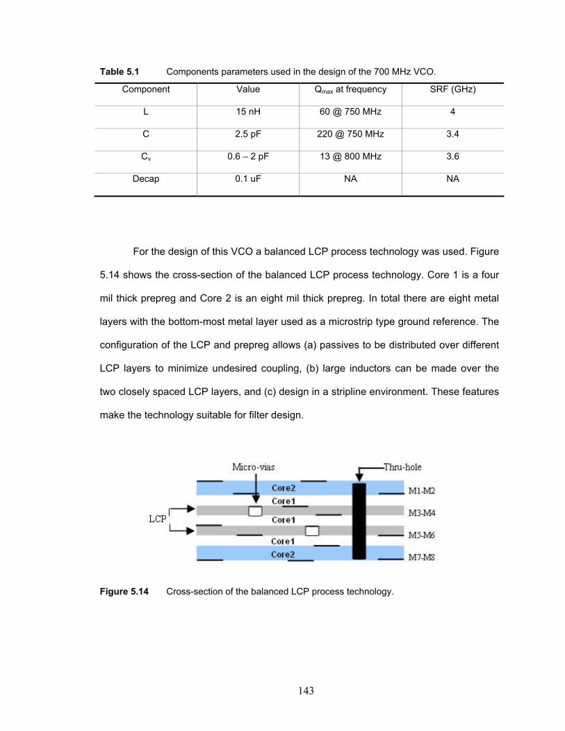
143
Table 5.1 Components parameters used in the design of the 700 MHz VCO.
Component Value Qmax at frequency SRF (GHz)
L 15 nH 60 @ 750 MHz 4
C 2.5 pF 220 @ 750 MHz 3.4
Cv 0.6 – 2 pF 13 @ 800 MHz 3.6
Decap 0.1 uF NA NA
For the design of this VCO a balanced LCP process technology was used. Figure
5.14 shows the cross-section of the balanced LCP process technology. Core 1 is a four
mil thick prepreg and Core 2 is an eight mil thick prepreg. In total there are eight metal
layers with the bottom-most metal layer used as a microstrip type ground reference. The
configuration of the LCP and prepreg allows (a) passives to be distributed over different
LCP layers to minimize undesired coupling, (b) large inductors can be made over the
two closely spaced LCP layers, and (c) design in a stripline environment. These features
make the technology suitable for filter design.
Figure 5.14 Cross-section of the balanced LCP process technology.

144
Measurement Results
Figure 5.15a shows the spectrum measurement of the designed VCO using an
E4407B spectrum analyzer with phase noise personality. The VCO has a center
frequency of 730 MHz with an output power of 6.6 dBm (after de-embedding 1 dB cable
and set-up losses). Additionally, the VCO was designed to reject the second harmonic
by > 23 dBc. Figure 5.15b shows the tuning characteristics of the VCO.
680
690
700
710
720
730
740
750
2 1 0 -2 -5 -10 -15 -20
6
6.2
6.4
6.6
Figure 5.15 (a) Measured spectrum of the modified-Colpitt’s VCO, (b) Tuning performance of the modified-Colpitt’s VCO.
(a)
Vtune (V)
Frequency, MHz
Output power (dBm)
(b)

145
From Figure 5.15b it can be clearly observed that the VCO shows an almost
linear frequency tuning characteristics from 689 MHz to 745 MHz. Additionally, the
output power shows negligible variation over the entire tuning range (~0.6 dB). Figure
5.16 shows the phase noise variation at 10 KHz offset with tuning voltage. At the lower
end of the tuning voltage the capacitance is high and lowers the SRF of the capacitor.
As a result the Q of the capacitance is low as compared to that at higher tuning voltages.
Therefore, the phase noise is 8 dB (approximately) higher at low tuning voltages than
that measured at high tuning voltage.
-120
-115
-110
-105
-100
-95
-90
-25-20-15-10-505
Figure 5.16 Measured phase noise vs. Vtune characteristics.
Figure 5.17 shows the photograph of the fabricated 12″ x 9″ panel with its
different manufactured components. Figure 5.17a shows the entire panel of the eight-
metal layer balanced LCP process with a top soldermask layer. Figure 5.17b shows four
2″ x 2″ coupons with different fabricated components. Finally, Figure 5.17c shows the
fabricated VCO.
Vtune (V)
Phase noise (dBc/Hz) at 10 KHz offset

146
`
Figure 5.17 (a) Fabricated 12″ x 9″ panel, (b) Photograph of four 2″ x 2″ coupons of the panel, and (c) Photograph of the fabricated 700 MHz VCO.
12 inch
(a)
(c)
(b)
1 inch
CV
2 inch

147
Table 5.2 summarizes the discussion of the 750 MHz VCO. It compares the
simulated and the measured parameters. From Table 5.2 it is clear that good model-to-
hardware correlation was achieved and the design techniques provides low phase noise
(< -125 dBc/Hz at 100 KHz offset) at low power consumption. The designed fully-
packaged VCO when compared to a commercially available VCO from Sirenza
Microdevices Inc. [84] achieves the same phase noise with 50% reduction in the power
consumption and with a 3.5x reduction in the area.
Table 5.2 Model-to-hardware correlation of the 700 MHz VCO.
Parameters Simulated Measured
VCC (V) 2.7
VCC min - max 2.2 – 3.2
Ibias (mA) 10
Freq. range (MHz) 700 – 757 689 – 745
% f0 (∆f0/ f0) 7.8 % 7.8 %
Phase Noise @ 10 KHz -99 to -104 -100 to -108
RF Output power (dBm) + 4.0 to +4.5 +6.1 to +6.5
Harmonics (dBc) < -17 < -20
Tuning voltage (V) + 2 to -20
Size 7.5 mm x 6.5 mm

148
5.1.6. Temperature Characterization of the Modified-Colpitt’s VCO
The aforementioned sections proposed a novel circuit methodology on LCP
substrate for use in high-end cellular systems. LCP is a relatively new, flexible thin film
material offering great temperature stability [33]. Although manufacturers provide
information on the dielectric stability with temperature there is not much information on
the combined thermal performance of actives and passives on LCP on the VCO
performance. This section presents for the first time the effect of temperature on LCP-
based VCOs. The purpose of this test was to study the effect of changes in the electro-
mechanical properties of LCP with temperature on VCO performance. The effect of
temperature on the VCO performance depends on a variety of parameters. However, the
most critical parameters among them can be identified as (a) temperature coefficient of
dielectric constant (ter), (b) LCP’s coefficient of thermal expansion (CTE) in all x, y, and z
axis, (c) CTE of copper, (d) thermal properties of surface mount components, especially
the varactor diode, and (e) ac and dc thermal properties of bipolar transistor.
Figure 5.18 shows the schematic of the investigated test circuit of the 700 MHz
modified-Colpitt’s VCO. The VCO was biased at 8.7 mA from a 2V supply. The varactor
diode (CV) is more tightly coupled to the resonator than in Figure 5.13. Cv is a surface
mount abrupt-junction Si varactor diode from Skyworks Inc. (SMV 1405). The circuit
was tested over a temperature range of 25 ±C (300 K) to 125 ±C (400 K) (military
standards). The dc and ac characteristics of the VCO were measured and verified by
ADS circuit simulations. The tests were performed using a digitally-controlled Corning
hot plate that can ramp the temperature from room temperature to over 180 ±C. The
components of the VCO were embedded in the balanced LCP process as shown in
Figure 5.14. The temperature of the board surface was measured using a digital
Omegaette® thermometer (with 3 ±C accuracy). The components were designed using a

149
microstrip ground, which was M8 layer of the stack-up (see Figure 5.14). To avoid
shorting of the signal through-holes and microstrip ground via the metallic hot plate
surface, the entire test circuit was mounted on a one cm thick aluminum bar. The
thermal resistance between the hot plate and aluminum bar was minimized by using a
thermal conductive paste from Omega Inc. Likewise, the thermal conductive paste was
applied between the aluminum bar and the test circuit. Figure 5.19 shows the
measurement setup and Figure 5.20 shows a close-up of the test circuit.
Figure 5.18 Schematic of the test circuit used for thermal characterization.
Cs
L
C
CV
Tuning port
V0
Cm
2V
RE
GND

150
Figure 5.19 Test setup for thermal characterization of the LCP-based Modified-Colpitt’s VCO.
DC Model-to-Hardware Correlation
The effect of temperature on the dc characteristics is determined by the bias
circuitry [40] and the inherent properties of the bipolar transistor. Figure 5.19 shows the
simulated and measured effect of temperature on the bias current (IC). It can be
Temperature sensor
(Thermocouple) Thermometer
Hot plate
Heat isolator
Al block

151
observed that the bias current increases with temperature and the measurements
closely follow the simulation results. This can be attributed purely to the temperature
performance of bipolar transistors [85]. In the temperature range of 27 ±C (300 K) to 127
±C (400 K) a bipolar transistor shows an increase (~25 %) in the current gain. This is due
to the increase in the electron diffusion coefficient (Dn) in the base that causes a
reduction in the base transit time with temperature [86].
Figure 5.20 Photograph of the test circuit showing the Al block and thermal conductive paste.
Thermal paste Al block
Enclosure to reduce gradients

152
Figure 5.21 Bias current vs. temperature. Solid line: ADS simulations, Sampled line: Measurements.
AC Model-to-Hardware Correlation
The ac performance measures include the effect of temperature on frequency,
output power, and phase noise. The measurements to model correlation for these
parameters are discussed now.
(1) Frequency Stability:
The effect of temperature on frequency is dependent on the temperature
coefficient of capacitance (TCC) or percent change in capacitance value on LCP, TCC of
the varactor, CTE of LCP, and LCP’s temperature coefficient of dielectric constant (ter).
Bias current, (A)
Temperature, ±C

153
The x- and y-axis CTE of LCP is low (+17 ppm/±C) and is matched to that of copper (+17
ppm/±C). However, the Z-axis CTE of LCP is much higher (+150 ppm/±C) suggesting
that the parallel plate capacitance should decrease with increasing temperature.
Additionally, the ter of LCP is +24 ppm/±C suggesting that the capacitance increases with
temperature. The TCC of the embedded capacitors are determined by the summation of
the above mentioned variables. However, a CTE of 150 ppm/±C suggest that the
dielectric thickness will increase by 0.018 mils (-1.8% decrease for a 1 mil thick LCP).
However, the increase in the lateral dimensions because of positive x- and y-axis CTE
and ter will offset the decrease in the capacitance because of Z-axis CTE. Resultantly
the effect of temperature on VCO center frequency using purely LCP-based passives will
be minimal and should be attributed to the changes in the junction parasitics of the
transistor.
Figure 5.22 shows the simulated and measurement results of the VCO over a
temperature range of 25 ±C to 125 ±C at a Vtune of 2 V. The simulations include
parameterized entries for LCP-based capacitors and their associated loss resistors. It
can be observed that there exists an inherent difference of 40 MHz (measured frequency
< simulated frequency) between measurement and simulations. This can be attributed to
the differences in the varactor model or underestimation of the parasitics. However, the
measurements and the simulations show an increase in frequency with temperature up
to 85 ±C. Up to 85 ±C simulations predict an increase of 117 KHz/±C whereas
measurements show a 140 KHz/±C increase in frequency. Beyond 85 ±C, a decrease in
the measurement frequency was observed. This was because of the positive TCC of the
varactor diode [83].
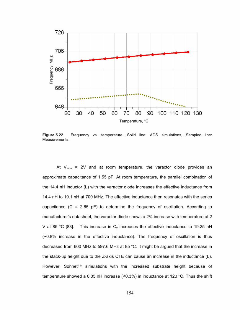
154
Figure 5.22 Frequency vs. temperature. Solid line: ADS simulations, Sampled line: Measurements.
At Vtune = 2V and at room temperature, the varactor diode provides an
approximate capacitance of 1.55 pF. At room temperature, the parallel combination of
the 14.4 nH inductor (L) with the varactor diode increases the effective inductance from
14.4 nH to 19.1 nH at 700 MHz. The effective inductance then resonates with the series
capacitance (C = 2.65 pF) to determine the frequency of oscillation. According to
manufacturer’s datasheet, the varactor diode shows a 2% increase with temperature at 2
V at 85 ±C [83]. This increase in Cv increases the effective inductance to 19.25 nH
(~0.8% increase in the effective inductance). The frequency of oscillation is thus
decreased from 600 MHz to 597.6 MHz at 85 ±C. It might be argued that the increase in
the stack-up height due to the Z-axis CTE can cause an increase in the inductance (L).
However, Sonnet™ simulations with the increased substrate height because of
temperature showed a 0.05 nH increase (<0.3%) in inductance at 120 ±C. Thus the shift
Temperature, ±C
Frequency, MHz

155
in the center frequency is attributed because of the drift in the varactor diode parameters
and transistor parasitics.
(2) Output Power Stability:
Figure 5.23 plots the simulated and measured VCO output power against
temperature. Good correlation between the measurements and simulations were
obtained. The simulations include the parameterized model of temperature dependency
of capacitors and their loss resistances. The output power in both simulations and
measurements drop by ~4 dB over the temperature range.
Figure 5.23 Output power vs. temperature. Solid line: ADS simulations, Sampled line: Measurements.
Temperature, ±C
Output power, dBm

156
The drop in the output power is traced to the reduction in the loop-gain gmRL (see
equation (5.6)). The transconductance of a bipolar transistor decreases with temperature
[85] and is given as
( )kT
TqITg C
m
)(= (5.8)
In (5.8), q is the electron charge, k is the Boltzmann constant, T is the
temperature in Kelvin, IC(T) is the temperature dependent collector current. For a
temperature range of 300 K to 400 K, gm decreases by 0.994 of its room temperature
value. However, the increase in the collector current reduces the output resistance of the
transistor (VA/Ic) to 0.77 of its initial value. Hence, the drop in the output power
(proportional to gmRL-squared) reduces by (0.994 x 0.77)2 = 0.58. This is a 10Log10(0.58)
= 2.5 dB decrease in the output power. Additionally, the open-loop impedance observed
at the load terminal changes as shown in Figure 5.24. The real part increases by 4 ohms
to 68 ohms causing a reduction in the transmitted power of 0.5 dB [64] at 400 K.
Analytical calculations give a 3 dB drop in output power with temperature, which is close
to the measured 4 dB drop in output power.

157
Figure 5.24 Output impedance observed at the load at different temperatures.
(3) Phase Noise Stability:
The phase noise in the modified-Colpitt’s oscillator (Figure 5.14) is dominated by
the loss in the inductor and in the varactor diode. The loss in the inductor is determined
by the ac resistance (skin effect), since the LCP tand shows minimum sensitivity to
temperature [35]. The process technology uses 30 um cu on the top most layer (M1).
The resistivity of the copper at room temperature (300 K) is ~1.72 x 10e-8 Ωm [64] and
[87] and it increases to 2.402 at 400 K. This causes the resistivity to have a sensitivity of
C°=−
⋅
−/1,0039.0
)300400(
1
712.1
712.1402.2 (5.9)
Frequency, MHz
Im(Zout), ohms
Re(Zout), ohms
125 ±C
100 ±C 75 ±C
50 ±C
25 ±C

158
As a result the ac resistance of the inductor increases by a factor
of )00398.01( T⋅+ , where the square root factor comes from the skin effect. This was
included in the loss model of the passives. Figure 5.25 shows the ADS and
measurement results of phase noise at 100 KHz and 10 MHz offset. The measured
phase noise @ 100 KHz offset is 2 dB higher than simulated and increase by 3 dB to -
103 dBc/Hz @ 100 KHz offset. The phase noise at 10 MHz offset is higher by 4 dB as
compared to simulations throughout the temperature range. The difference in the
measured and simulated phase noise can be attributed to the inaccuracy in the loss
model of the varactor, packaged transistor, and solder resistance. In any case the
simulated and measured phase noise show a similar trend demonstrating that the phase
noise can degrade by 3 dB provided the lossy varactor diode is loosely coupled to the
resonator (see Figure 5.13).
Figure 5.25 Phase noise vs. temperature at 100 KHz and 10 MHz offset. Solid line: Simulated, Sampled line: Measurements.
Temperature, ±C
Phase noise, dBc/Hz

159
5.2 Transformer Feedback Oscillator (TVCO)
The focus of this chapter is to provide improved circuit techniques to obtain low
power, low phase noise and small area VCOs directly applicable to multi-band wireless
handsets. Phase noise can be lowered by increasing the loaded-Q of the oscillator, from
Leeson’s phase noise model. The Leeson’s model (see chapter 2, section 2.1) is based
on linear circuit theory according to which the half-bandwidth of the resonator controls
the noise shaping around the carrier [41] and [42]. Therefore, an improvement in the
phase noise can be expected if the resonator is replaced with a network (active or
passive) that will minimize the bandwidth (maximum phase slope). Active elements in
the feedback network will add its own noise (device noise) to the phase noise and would
require more power consumption as compared to the passive solution. A multi-pole
bandpass filter performs the function of selecting or separating a band of frequencies
from the entire spectrum. Hence, a bandpass filter or a transformer with low enough
insertion loss and high group-delay (td) when used as a resonator will improve both the
near- and far-carrier phase noise. This section introduces one such VCO implementation
that uses a bandpass resonator function as the feedback network [67].
The transformer feedback VCO (TVCO) isolates the resonator from the active
circuitry and all the voltage dependent parasitics. Hence, the TVCO provides a wide and
linear tuning range, in addition to lowering phase noise, and hence, is attractive in multi-
band applications. The basic principle is to maximize the group-delay or linear phase
characteristics. The relation between td and phase (φ) characteristic is given as
ωφτ ddd /= (5.10)

160
Equation (2.7) (see chapter 2) gave the relation between the Q and the
normalized phase transfer function. Hence, from (2.7) and (5.10) it can be concluded
that the increase in the td of the network will lead to a concomitant increase in the Q of
the oscillator. The basic principle is to maximize the group-delay and minimize the
insertion loss of the transformer1. For the circuit to oscillate the amplifier must provide a
gain to compensate for the losses in the resonator. Hence, higher the insertion loss of
the filter the higher gain amplifier and hence, more power is consumed. However, the
availability of high-Q components relaxes the requirement on the gain. Additionally, not
all the components need to have high Qs, as will be shown later into the chapter. The
group delay is mostly controlled by the Q of the resonator and the number of resonators.
Increasing the number of resonators will also lead to an increase in the group-delay2 [65]
and [88].
Figure 5.26 shows the circuit schematic of the proposed transformer based VCO.
Components L1, C2, C3, L2, C4, Cv and C5 form the transformer. Cv is a surface mount
abrupt-junction silicon varactor diode manufactured by Skyworks Inc. (SMV 1405-079).
The approach is to minimize the degradation of the phase noise by minimizing the
loading of the tank circuit through a transformer type resonator [67]. In Figure 5.26
components L2, C4, C5, and Cv form the resonant tank circuit. The approximate
frequency of oscillation is given by
+⋅+⋅+⋅
⋅⋅⋅
≈
)(2
1
5
54542
0
CC
CCCCCCL
f
v
vvπ
(5.11)
1 Transformer and filter are used interchangeably in this section. Essentially the filter is performing the function of transforming the impedance across the resonator, which minimizes loading. 2 Adding resonators to the network will increase the number of poles in the system and increases the effective-phase change in the passband, thereby increasing the group-delay.

161
Figure 5.26 Schematic of the TVCO.
The feedback network consists of a second-order filter (transformer) that
(a) Provides accurate control over the loop-gain (power consumption) and loop-
bandwidth (tuning range),
(b) Isolates the tank circuit from the transistor and its associated bias circuitry, thereby
enabling a large tuning range, and
(c) Makes the start-up conditions independent of the resonator inductor size.
The aforementioned characteristics allow simultaneous optimization of the power
consumption and the phase noise of the VCO, especially at higher frequencies. In a
coupled-Colpitt’s oscillator or Colpitt’s oscillator the phase noise is limited due to the
loading of the resonator by the transistor transconductance [6] and this forces the circuit
to operate at high power levels to improve phase noise. In the proposed TVCO circuit,
Vtune
+ 2.7V
L1
L2 C2
C5
Cv
C4
Lc
Cm Lb
RF Out
C3
GND

162
however, the resonator (L2-Cv-C4-C5) is loaded at one terminal by the high collector
impedance. On the other terminal, components L1, C2, and C3 isolate the resonator from
the transistor transconductance, and the phase noise is minimized by maximizing the
group delay of the transformer [67]. The proposed oscillator can be considered as a
simple Colpitt’s oscillator (as discussed in [6]) with the exception that the tank circuit
inductor is isolated from the Gm by L1, C2, C3 and the capacitive transformer (C4, Cv, and
C5). Unlike a simple Colpitt’s oscillator, where the loop gain (or Barkhausen) conditions
and phase noise are controlled by the ratio of capacitors, the proposed resonator
modifies the dependence into a multi-variable function. For example, capacitors C2 and
C3 fine tune the loop-phase angle, and the bandwidth of the loop-gain, respectively.
Unlike a differential cross-coupled oscillator, the location of the resonator inductor (L2)
makes the start-up conditions of the TVCO almost independent of the resonator inductor
size. Hence, the proposed methodology provides improvement in cyclo-stationary noise
properties by minimizing the loading of the resonator and decouples the start-up
conditions from L2. As a result, both the near- and far-carrier phase noise of the oscillator
is minimized.
In any filter the Q of the resonator controls the group-delay of the filter [65] and
[66]. This was confirmed for this transformer via simulations and experiments. Figure
5.27 shows the effect of component Qs on phase noise. The simulations were performed
using the harmonic balance simulator in ADS™. Figure 5.27 confirms that the phase
noise has minimal dependence on the Qs of L1, C2, and C3. Hence, comparable noise
performance can be expected on replacing these passives with low Q on-chip passives.
Figure 5.27 also shows that the phase noise can be scaled to < -120 dBc/Hz by carefully
scaling the QL2 > 150 with a small penalty in area.

163
Figure 5.27 Effect of component Q on phase noise.
5.2.1. Design Validation
In the previous section it was mentioned that only the Q of L2, and C4 needs to be
high (>50). This section corroborates the component Q stipulation. To verify the effect of
Q of the inductor on phase noise two 1.9 GHz oscillator configurations were designed
with a difference only in the Q of the inductor L2 (QL2). The circuit employs a SOT-343
packaged surface mount bipolar transistor from Agilent Technologies (HBFP 04201) with
a ft of 17.2 GHz at Ic of 4 mA. At steady-state, the VCO is biased from a supply of 2.7 V
at IC 4.4 mA. One of the VCO was designed with an unloaded QL2 of 120 (VCO1)
whereas the other was designed with a QL2 of 80 (VCO2). To obtain Qs in excess of 60,
wide linewidth or slab-type inductors were employed as against spiral design. A method-
of-moment based EM solver (Sonnet™) was used to design all the passives. All the
passives were embedded in the P-PIC technology (see Figure 5.5). The electrical
1 The VCO designs discussed this far in this thesis has employed same transistor for a clear comparison of the circuit performance. However, the use of other transistors for VCO was discussed in chapter 4.
Q
Phase noise at 100 KHz offset,
dBc/Hz
QL2
QC4

164
characteristics of the passives were verified through measurements. It was observed via
simulations that there should be ~6 dB difference between the phase noises of the two
VCO versions. The measured phase noise for VCO1, Figure 5.28a, was -116 dBc/Hz at
100 KHz offset from 1.87 GHz center frequency and that of the VCO2, Figure 5.28b, was
-112 dBc/Hz at the same offset frequency from fo = 1.86 GHz. In both cases, the phase
noise and RF power (see Figure 5.29) were measured using an E4407B spectrum
analyzer from Agilent Technologies. The measured phase noise is about 2 dB worse
than expected from simulations.
(a)

165
Figure 5.28 (a) Measured phase noise of VCO1, (b) Measured phase noise of VCO2.
Figure 5.29 Measured center frequency of the TVCO.
(b)

166
Figure 5.30 shows the photograph of one of the fabricated VCO (VCO1). In
addition to the surface mount components, the L-shaped inductor L2 can be seen on the
top most metal layer. The remaining 7 passive components are embedded in the middle
LCP layer demonstrating 3-D integration of the passives, as shown in Figure 5.31.
Figure 5.30 Photograph of the TVCO (VCO1).
Figure 5.31 X-ray photograph of the TVCO showing embedded passives in the internal layers.
L2
GSG pads

167
5.2.2. Component to Component Coupling in TVCOs
The TVCO uses multiple passive components that are subject to both inter-
component magnetic and electrical coupling. As a result, the transformer’s frequency
response in its out-of-band (stopband) region will be of consequence, if not accounted in
the simulation stage. Hence, in the design and simulation stage of an oscillator it is
necessary to verify the oscillation condition over a broad frequency range [89]. The
above conditions imply that the designer needs to characterize the feedback network
over a broad frequency range. However, without resorting to EM simulators a designer
cannot take into account the effects of component coupling, which might occur because
of layout and the component SRF, on both the loop-gain and phase shift around the
loop. The foregoing discussion highlights via two circuit examples the effect of both the
coupling mechanisms on the TVCO performance.
The transformer in the TVCO has multiple components that are physically placed
close-together to minimize the area of the oscillator. In the case of VCO1 and VCO2
(see section 5.2.1) the transformer components were distributed on different metal
layers and connected through via-holes. As a result of the physical separation (in lateral
and vertical directions) between the components, the parasitic EM coupling between the
components is minimal. However, depending on the physical placement of the
components, different coupling mechanisms (electric or magnetic) can occur. As a
result, parasitic passbands at frequencies further away from the desired frequency in the
transformer can be generated. The parasitic passbands can be generated by magnetic
and/or electric coupling between the components. In this case, unlike a differential VCO,
the transformer response at frequencies further away from the band of interest cannot
be neglected. The parasitic passbands cause an undesired shift in the frequency of

168
oscillation of the TVCO. A few possible scenarios depending on the physical layout of
the transformer were investigated in this thesis as follows:
(1) The first effect was because of the EM coupling between components that
shifted the oscillation frequency to 6.1 GHz from 1.9 GHz. Figure 5.33 shows the
photograph of another TVCO (VCO3) with all the resonator components closely packed
on the top two metal layers. VCO3 is exactly identical to VCO1 (see Figure 5.30) except
that the components are fabricated on only the top two-metal layers. Figures 5.33a and
5.33b show the measured response of the transformers used in the VCO1 and VCO3.
The sampled data in Figure 5.33a and Figure 5.33b are the 2-port measured s-
parameters of only the transformer used in the design of VCO3 and the solid data is for
the resonator used in VCO1. In the frequency of interest (around 2 GHz) there is
minimum discrepancy between the two responses. However, in the case of VCO3 the
resonator elements couple around 6 GHz. This is evident from the low insertion loss in
the transformer magnitude response. Sonnet™ simulations were performed to determine
the nature of coupling. It was determined that the parasitic inductance of capacitor C2
(2.5 pF) can magnetically couple to inductor L2 (2 nH) because of the low self resonant
frequency (~5 GHz) of C2. Additionally at 6 GHz, it was observed that the phase
response matches well to satisfy the oscillation (Barkhausen) criterion (loop-gain =
1—0±). These effects coupled with the broad-band nature of the transistor Gm caused the
center frequency of VCO3 to shift to 6.1 GHz. The measurement results of VCO3 are
shown in Figure 5.34a using an HP 8563E spectrum analyzer. The measured center
frequency has shifted from 1.9 GHz to 6.1 GHz because of the coupling and the phase
characteristics of the transformer. The measured results from VCO1 were discussed in
Section 5.2.1.
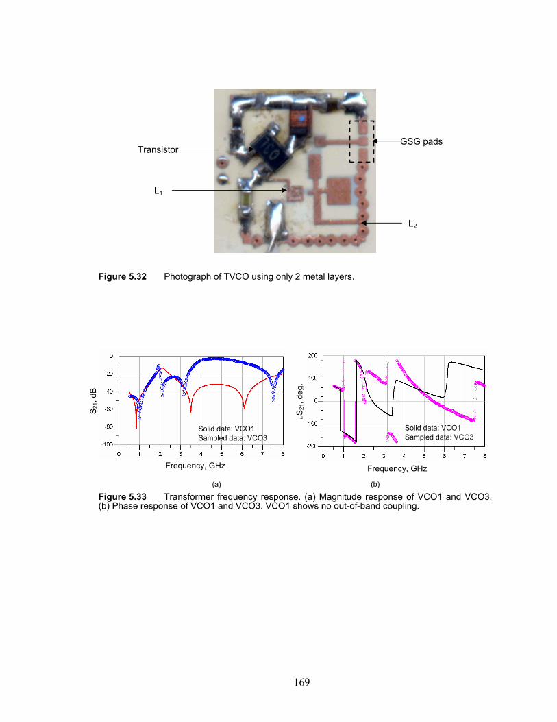
169
Figure 5.32 Photograph of TVCO using only 2 metal layers.
Figure 5.33 Transformer frequency response. (a) Magnitude response of VCO1 and VCO3, (b) Phase response of VCO1 and VCO3. VCO1 shows no out-of-band coupling.
S21, dB
Frequency, GHz Frequency, GHz
—S21, deg.
Solid data: VCO1
Sampled data: VCO3
Solid data: VCO1
Sampled data: VCO3
(a) (b)
L2
GSG pads Transistor
L1

170
Figure 5.34 (a) Measured spectrum of VCO3. fo shifted to 6.1 GHz due to EM coupling. (b) ADS simulation results showing fo shifted to 5.9 GHz with SPICE netlist from BEMP.
From the discussion on VCO3 it can be concluded that the design of a VCO
employing a multi-pole transformer or filter as a resonator can be a challenge. This is
because of the following reasons:
(a) Lumped electrical circuit models of inductors and capacitors, used in circuit
simulation, are mostly accurate only to the first order (upto the SRF).
(b) The post-layout VCO simulations are performed considering only the junction RC
parasitics resulting from the parasitic extraction process. The effects of EM coupling
at frequencies two octaves away from the frequency of interest and the effects of
component placement on resonator response are mostly not fed-back to circuit
simulators.
(c) Development of electrical models incorporating layout-based EM coupling effects
would require full-wave EM solvers that are computationally expensive.
(d) Transformer response obtained from EM simulators is usually band-limited. The
band-limited data causes errors in circuit simulators (especially in time domain)
because of violation in the passivity and stability conditions.
Pout, dBm
Frequency, GHz
(a) (b)

171
Hence, to obtain reasonable model-to-hardware correlation a broad-band circuit model
of the physical layout of the resonator is required. The model should accurately
characterize the resonator response over a bandwidth of ~10 GHz with enforced
passivity and stability conditions. In this work the circuit model was generated by a two
step process. Firstly, the resonator was simulated in Sonnet™. Finally, the s-parameters
were fed into an in-house macro-modeling tool known as broad-band efficient macro-
modeling program (BEMP) developed at Georgia Tech, see references [90] and [91].
BEMP uses rational functions to provide a SPICE netlist composed of low pass, high
pass, and band pass approximation of the resonator response over a given bandwidth. It
also ensures that the models are passive1 outside the band of interest [91].
To debug the results of VCO3, the fabricated resonator was measured and its s-
parameters were fed to BEMP, which provided a SPICE netlist. Harmonic Balance
simulations (ADS) of the VCO including the SPICE netlist of the resonator confirmed the
measurement results for VCO3 (see Figure 5.34b). Figure 5.34b shows that the center
frequency shifts to 5.9 GHz confirming the aforementioned analysis and measurement
results. The spurious oscillatory behavior of the oscillator can be avoided by reducing
the parasitic EM coupling between the resonator elements. The EM coupling between
resonator elements of VCO3 can be reduced by separating the components (especially
C2 and L2) spatially in the planar direction or by moving from microstrip to stripline type
designs. Hence, on comparing the results for VCO1 and VCO3 it can be concluded that
3-D separation of the resonator elements on multiple LCP layers reduces both the
undesired EM coupling and VCO size.
1 The passivity conditions ensure that the network is a passive network and total power input to the network is the combination of the reflected power and transmitted power.

172
(2) In the previous section it was shown that the coupling between the elements
of the transformer at frequencies further away from the band of interest cannot be
neglected. It was observed that the strong coupling of the parasitic inductance of the
capacitor C2 (because of its low SRF) with inductor L2 moved the oscillation frequency to
6.1 GHz. A circuit simulator would not be able to capture or determine this behavior.
Furthermore, the TVCO functioning is strongly dependent on the parasitic coupling
between components that occur because of physical layout. Figure 5.35 shows the
current density (Sonnet simulations) results of two transformers (namely, type 1 and type
2) with different spacing between the capacitors C1 and Cm. Type 1 transformer layout
was used in the design of VCO1 (see section 5.2.1). In both the transformer types, C1 is
the capacitance connected across inductance L1 that adds a transmission zero for
harmonic rejection. From the results it can be observed that at non-harmonic
frequencies (4.95 GHz) there is considerable current at the output terminal (Cm) that can
cause a significant shift in the magnitude of the loop-gain and phase shift around the
loop. This effect was verified via experiments. Figure 5.36a shows the measured
spectrum of the TVCO with type 2 transformer. The fundamental frequency shifted to 5.1
GHz from the design frequency of 1.9 GHz.

173
Figure 5.35 Sonnet simulation results illustrating coupling between capacitors C1 and Cm.
Top metal layer Type I network: negligible edge coupling between input and output ports at 4.95 GHz
Top metal layer type II network: undesired edge coupling between input and output ports at 4.95 GHz
(a)
(b)

174
Figure 5.36 (a) Spectrum of the TVCO with type2 transformer design. f0 shifted to 5.1 GHz from the design frequency of 1.9 GHz. (b) ADS simulation results of the TVCO with SPICE netlist of type 2 transformer showing shift of f0 to 5 GHz.
To determine the effects of the inter-component coupling on the TVCO
performance the s-parameters of the transformer from an EM simulator need to be fed
back to a circuit simulator to perform time and frequency domain simulations. BEMP was
used to determine the effect out-of-band coupling between capacitors on the TVCO
performance. Figure 5.37 shows the insertion loss of the transformer using the SPICE
netlist obtained from the macromodel. Figure 5.37 also compares the measured s-
parameters of the transformer with the macromodel. It can be observed that the tool
models the frequency response very well except for a transmission zero at 3.5 GHz. The
netlist when used with Agilent’s harmonic balance circuit simulator confirmed (see Figure
5.36b) the measurement results as shown in Figure 5.36a.
Pout, dBm
Frequency, GHz
(a) (b)

175
Figure 5.37 Comparison of modeled amplitude response of the transformer with VNA measurements.
Discussion
Thus, from the aforementioned discussion on effects of EM coupling on TVCO
performance it clear that for VCOs with filter-type resonator, the design techniques
needs to involve a combination of EM and circuit simulators. The issues can be
aggravated by the addition of more resonators to the filter to increase the group-delay.
However, the design of TVCO provides a simple method of lowering the phase noise
without compromising the power consumption of the oscillator.
Transformers can be designed using standard design techniques (Butterworth,
Chebychev, and Elliptical) or use ladder filters. Each of the filters has a trade-off
between amplitude response and group-delay1. In general, the sharper amplitude
response leads to distortion in the group-delay (related via Hilbert transform) [65] and
[92]. Hence depending on the most important parameter, the TVCOs can be designed to
provide low phase noise at low power consumption.
1 Chebychev filters have better rejection but increasing group-delay over the bandwidth as compared to maximally-flat filters [65].
Solid data: BEMP macromodel
Sampled data: VNA measurements
S21, dB
Frequency, GHz

176
5.3 Summary
This chapter presented the design and implementation of two novel oscillators
that provide low phase noise (~ -125 dBc/Hz @ 100 KHz offset) with power consumption
in the 10 mW range. As compared to the CMOS-based VCOs (see Table 2.2, chapter 2),
the circuit examples provide atleast 30 dB improvement in the FOM. Table 5.3 compares
the FOM of VCOs available from commercial manufacturers such as Murata, Alps Inc.,
and Sirenza Microdevices Inc. [93] - [96]. It can be clearly observed from Table 5.3 that
the phase noise of the proposed TVCO and modified-Colpitt’s oscillator fabricated on
LCP is comparable to the oscillators made on LTCC. However, with considerably lower
metal layer count the size of the VCOs presented in this thesis is comparable to the size
of LTCC-based VCOs. Since the LCP manufacturing process can be extended to
incorporate more than 10 LCP sheets, a considerable increase in component density
can be obtained by incorporating more LCP layers and resultantly, reduction in size.
In the case of the modified-Colpitt’s oscillator the phase noise can be reduced by
increasing the Q of the resonator inductor above 100 (present design used a Q of 50). In
the case of TVCO, by increasing the unloaded Q of the inductor L2 beyond 120 the
phase noise can be reduced below -120 dBc/Hz at 100 KHz offset. This improvement in
noise in both the designs will be with slight increase in the size of the inductor. By
considering the VCO performance listed in Table 5.3 (on 3-D LCP technologies) and
Table 3.2 in chapter 3 (on planar LCP technology), it can be concluded that LCP-based
VCOs have low power consumption (< 10 mW) and low phase noise (< -125 dBc/Hz @
100 KHz offset). All of the above properties make LCP based oscillators favorable in
multi-band cellular applications (both handhelds and base-stations) where small
oscillator size and a low power consumption-phase noise product are of prime
importance.

177
The thermal tests on the modified-Colpitt’s demonstrated that the both the
mechanical and electrical properties of LCP leads to marginal changes in the
performance of the VCO over a large temperature range (25 ±C to 125 ±C). Most of the
changes in the noise were because of the change in the resistivity of copper with
temperature. Since this change is characterized the degradation of phase noise at high
temperatures can be calibrated by marginally increasing the power consumption. The
aforementioned properties make LCP-based oscillators highly suitable for high-end
applications, such as cellular base-stations that require extremely low phase noise with
characterized thermal characteristics.

178
Table 5.3 Comparisons of the VCO performance characteristics.
Tech.
and Ref. f0 (GHz)
Pdc
(mW)
Phase Noise
(dBc/Hz) at
offset
FOM
(dB)
Area
(mm x mm)
TVCO
This work 1.86 12
-116 @
100 KHz 191 5.3 x 5.8
TVCO
This work 1.86 12
-120 @
100 KHz 194.6 5.5 x 6.0
Modified-Colpitt’s
This work 1.9 10
-117 @
100 KHz 192.5 5.3 x 4.8
Modified-Colpitt’s
This work 0.73 27
-125 @
100 KHz 188 6.5 x 7.5
Sirenza
[84] 0.7 50
-120 @
100 KHz 180 13 x 13
LTCC
[93] 2.2 39
-120 @
100 KHz 190.0 12 x 11
LTCC
[94] 1.92 94
-112 @
60 KHz 186.6 5.5 x 4.8
LTCC
[95] 1.8 21.6
-140 @
3 MHz 182.2 5.5 x 4.8
LTCC
[96] 1.65 NA
-133 @
100 KHz NA 15 x 15
SiGe
[97] 2.23 32
-110 @
600 KHz 166.1 1.8 x 1.2

179
CHAPTER 6
CONCURRENT OSCILLATORS
Chapters 4 and 5 presented the design, optimization, and implementation of
multiple VCO circuit examples on LCP-based substrates. The chapters presented fully-
packaged integrated VCO embodiments with their respective theoretical analysis, which
enables to optimize the phase noise, power consumption, and tuning range. Table 4.2
and Table 5.3 compared the performances the VCOs with those commercially available
and in the literature and it was clear that the LCP-based VCOs outperformed several
competitors and hence highly suitable for use in multi-band portable handsets.
Rapid evolution in the field of wireless communication and the convergence of
multiple communication protocols has led to the integration of multiple complex
functionalities in wireless portables. Figure 1.2 in Chapter 1 illustrated one such PDA
that included multiple different functionalities. Figure 6.1 shows the block diagram of
such a multi-band wireless handset. Figure 6.1 symbolizes a next generation cellular
handset pointing out various complex functionalities that a cellular phone would be
required to perform. Hence, in addition to standard features, such as color displays,
cameras, GPS, Bluetooth®, and television, handsets will also be “globally” operable. On
close examination of the architecture it is seen that next generation radios will need to
simultaneously transmit and receive multiple signals of differing powers and bandwidths.
Hence unlike past generations of the wireless devices, the next generation radios will be
multi-mode in nature. As pointed out in Chapter 1, the multi-mode radio architecture has
several architectural and performance merits over conventional multi-band radio
architectures.

180
Figure 6.1 Suggested architecture of a next generation cellular handset.
The basic principle of a multi-mode radio is to process two or more signals of
differing frequencies at the same time, however using only one processing Tx-Rx chain.
The idea was portrayed for a dual-mode receiver through Figure 1.5 in Chapter 1. In
Figure 1.5 the concurrent receiver consisted of dual-band antenna, a dual-band front-
end filter, and a dual-band LNA. Several references can be found on the development of
these blocks [2], [5], [15] and [16]. However, most of these works focused on
GSM
PCS
DCS
WLAN
GPS
UMTS
UWB
WLAN diversity Rx
Rx
UWB RF Chipset
UMTS RF Chipset
WLAN RF Chipset
Baseband/
MAC layer
Quad-band GSM/GPS RF
Chipset
Legend:
On-package
On-chip
Rx
Rx

181
transforming the front-end of the multi-band receiver into multi-mode and no efforts were
put for converting the down-converter stage to multi-mode. Figure 6.2 shows the multi-
mode receiver architecture as proposed in this thesis.
Figure 6.2 Architecture of the proposed dual-mode receiver architecture with dual-mode down-conversion.
Figure 1.5 and Figure 6.2 both represent one of the possibilities for implementing
a multi-mode receiver. However, Figure 6.2 presents a unique frequency plan for the
receiver. The proposed system uses a new class of oscillator that generates multiple
frequencies simultaneously. Called as concurrent oscillators, these oscillators allow a
Frequency synthesizer
Dual-mode LNA
Dual-mode filter
Diversity dual-mode antennas
Broad-band mixer
Broad-band mixer
Band 1 Band 2
f1 f2
IF1
IF1
IF2
IF2
Concurrent oscillator

182
true implementation of multi-mode systems. For instance, simultaneous transmission of
data in WLAN systems provides frequency diversity, thereby improving system through-
put. This would require oscillators that simultaneously generate signals at 2.4 GHz and
5.0 GHz. The use of concurrent oscillators is also applicable to multi-band systems
where a single oscillator controls two or more receive paths. The design method reduces
hardware count, simplifies routing of signals, and reduces power consumption. This
chapter presents the design and implementation of the first fully-packaged concurrent
oscillator using lumped-element passive components. The other highlighted block shown
in Figure 6.2 is the dual-mode single-input single-output (SISO) filter. The design of dual-
mode filters was discussed in chapter 2.
The rest of this chapter is organized as follows: Section 6.1 briefly reviews
present methods for multiple signal generation and discusses their limitations. Section
6.2 presents the design and implementation of concurrent oscillators. The prototype was
designed to generate two synchronous frequencies, namely 0.9 GHz and 1.8 GHz with
high output power and low phase noise. Section 6.2 discusses the tuning, frequency
scaling, and power and noise optimization of the concurrent oscillator. Additionally,
section 6.2 discusses another circuit implementation for concurrent signal generation,
which is based on the Colpitt’s and Hartley’s (duality principle) oscillator design
techniques. Section 6.3 compares the DFO with a conventionally used technique for
multiple signal generation, which uses an oscillator followed by multiple divider blocks.
For a broad comparison basis, an 8 GHz, 4.75 mW VCO was implemented in SiGe HBT
technology. Then a heuristic estimate of power consumption, area, design complexity,
and noise performance of the divider-based architecture is presented. Using these
performance metrics the DFO is compared against the conventionally used multiple
signal generation techniques.

183
6.1 Techniques for Multiple Signal Generation
Signal generators or local oscillators (LOs) are used for both up- and down-
conversion in transceivers. The LO requirements for use in multi-band and multi-mode
were discussed in section 3.2, Chapter 3. It is known that LOs exhibit trade-off between
power consumption and phase noise [42] and [48]. To reduce the phase noise the power
consumption is increased and/or the area is increased1. To miniaturize the system and
reduce the power consumption, multi-band system designers are forced to use a
frequency plan that employed one or more oscillators, phase locked loops (PLLs),
frequency dividers, buffer amplifiers, filters, and multipliers. For instance, a recent
publication [38] on dual-band WLAN transceivers from Intel Corp. consisted of a
frequency plan as is shown in Figure 6.3.
Figure 6.3 Transceiver frequency plan for a 2.4 GHz/5 GHz WLAN transceiver [38].
1 Regardless of on-chip or on-package, the Q and the size of the inductors are the determining factors of LO area,
since the Qs of capacitors are higher than the inductor Qs.

184
The scheme uses only one VCO at 8 GHz with a divide-by-2 frequency divider in
a frequency synthesizer to generate a 4 GHz signal. This is followed by a divide-by-4
divider. The 1 GHz and 4 GHz signals are then mixed in a Quadrature single side-band
mixer to generate the 5 GHz signal. The 5 GHz signal is then divided to obtain the 2.4
GHz signal. The implementation uses multiple buffers, LC filters, and frequency dividers.
The power-hungry blocks, in addition to increasing the design complexity, add to the size
and noise of the system [11]. Such a frequency plan and its variants can be found in
several other implementations [37]. In each of the divider-based architectures, frequency
multipliers are seldom used for the final stage of frequency conversion (RF mixers are
used) because of the difficulty of obtaining differential outputs at higher frequencies [37],
which are required by Quadrature converters [11]. Either the sum or the difference
outputs of the mixer need to be removed that require filters (typically notch). The filters
are usually implemented on-chip and hence, have poor insertion losses and selectivity
(rejection) characteristics.
At the other end of the spectrum are the oscillators that switch between different
resonators to generate different frequencies [98] and [99]. These oscillators rely on
switching between two or more resonators or inductors to be reconfigurable. However,
the design technique does not permit the signals to be generated at the same time and
suffer from higher power consumption to compensate for the degradation in Q because
of the lossy switches. It is also reminded that deep-submicron transistors use smaller
supply voltages and hence, NMOS-PMOS fully-differential cross-coupled oscillators
cannot be used to compensate for the reduction in Q. Therefore, although switched
resonators have been widely used in multi-band cellular handsets, their use for next
generation multi-mode radios looks seemingly difficult. In conclusion, the key limitations
of using a divider-based architecture for generating concurrent signal can be listed as
follows:

185
(a) Requires power consuming modules, such as dividers, buffers, and mixers
(b) Requires area-intensive LC filters for band rejection
(c) Issues with spurious signal generation resulting from frequency mixing and
division
(d) Issues with addition of noise due to spectrum folding in the mixer [42] and
thermal noise addition from buffer amplifiers
(e) Uses multiple differing components that increase the complexity of the frequency
synthesizer thereby, increasing the design cycle time.
A concurrent oscillator as will be discussed in this chapter uses neither switching
between resonators or elaborate design techniques using dividers. The underlying
principle consists of an oscillator with two outputs that uses the dual-mode or reentrant
characteristics of passives or transmission lines, respectively. Since these
characteristics are inherent to passive components the generation of multiple signals is
simplified. However, the resonator characteristics need to be controlled for generating
the desired frequencies. As a result, a simultaneous reduction in power consumption,
area and design cycle time can be achieved using a concurrent solution. The next
section discusses the design of the concurrent oscillator on LCP substrate whose
resonant circuit is synchronously tuned to two discrete frequencies. Since it generates
two frequencies the concurrent oscillator is called as the dual frequency oscillator (DFO).
It should be noted that the limitations of the divider-based architecture do not
significantly undermine the merits of the frequency plan. In cases where multiple broad-
band signals need to be generated and power consumption is not the prime criterion, the
divider-based concurrent signal generation techniques seems very attractive. Hence, a
comparative approach of evaluating both methods is taken in this thesis. The idea is to
investigate and demonstrate a new method for concurrent signal generation through

186
DFO and compare it to the pervasive divider-based architecture. For this purpose this
chapter presents the implementation of the divider-based architecture as shown in
Figure 6.3, which involves the design and measurements of an 8 GHz VCO on silicon
germanium (SiGe) HBT technology. The rest of the circuitry is taken from the literature
and an estimate of the power consumption and area is made. Finally, this chapter makes
recommendations on the use of either design methods.
6.2 Dual Frequency Oscillator (DFO)
A single frequency oscillator utilizes a second-order resonator to generate the
desired signal. This is because the resonator impedance response shows one anti-
resonance (parallel LC resonator) or resonance (series LC resonator)1. Likewise, to
generate more than one signal the order of the resonator needs to be increased. This is
the essence of dual frequency generation. The basic principle of dual frequency
oscillator can be explained with the help of the single-band one-port negative resistance
theory [100]. According to the theory [100], an oscillator circuit can be represented as
negative impedance (reflection coefficient > 1) in series with its second-order resonator.
The negative resistance cancels out the losses in the resonator and the reactance are
canceled only at a single frequency, which is the frequency of oscillation. This principle
was used to analyze the negative resistance oscillator discussed in section 4.1, Chapter
4. For ease of explanation the expression is repeated here as
o01∠≥Γ⋅ rinS (6.1)
where Gr is the reflection coefficient looking into the resonator.
1 A second-order system such as the van der Pol oscillator can be represented by a non-linear second-order differential equation that has two solutions or eigenvalues. The square root of the eigenvalues gives the frequency of oscillation.
187
The idea of negative resistance in oscillator was extended to dual frequency
oscillator by Schaffner [101] and several others [102]. However, in this case the
oscillator has to satisfy conditions in (6.1) for two frequencies (ω1 and ω2). [101]
mathematically investigates the possibility of simultaneous oscillations at two
independent and dependent frequencies. The independence of frequencies implies that
the ratio of the frequencies is irrational (ω2/ω1 ≠ integer). Likewise, a rational ratio
between the two frequencies implies that signals are dependent on each other through
phase. Appendix C concisely reviews the theory on dual frequency oscillations
presented by [101]. The analysis [101] is based on a nonlinear negative resistance
source connected across a fourth-order parallel LC resonator. For transient analysis, the
oscillator is split into two independent circuits with independent non-interacting
resonators. This is followed from the fact that the circuit can be considered to be linear at
start-up. The aforementioned analysis is applied to analyze the proposed circuit for dual-
frequency generation.
6.2.1. Design of DFOs
This section presents the design of the dual frequency oscillator and correlates
the circuit theory with the mathematical models. The analysis is uses s-parameters to
determine initial design component values (similar analysis as the negative resistance
oscillator in section 4.1). Figure 6.4 shows the circuit schematic of the proposed dual
frequency oscillator. The oscillator essentially consists of four components,
1. The fourth-order resonator, consisting of La-Ca and Lb-Cb, connected at the base
terminal of the transistor (base resonator),
2. The second-order series LC resonator (input resonator), comprising of Li and Ci,

188
which is connected to the emitter terminal of the transistor,
3. The output filtering network, and
4. The bipolar transistor.
Figure 6.4 Circuit schematic of the proposed dual frequency oscillator with reactance-frequency response of the resonators.
The circuit is biased using a biasing resistor (R) and two surface mount 1 µH
inductors. The basic operation of a negative resistance oscillator at a single frequency
can be obtained from section 4.1. At a given frequency, impedance with negative real
part is observed at the emitter terminal by adding a suitable value inductor at the base
terminal [6]. For a given base resonator inductance, the value of the negative resistance
was found to have a weak dependence on the bias current [6]. In general it is observed
that the frequency at which negative resistance occurs has an inverse dependence on
Cs1 Cs1
Cs2 Cs2
Cc1 C1 C2
L1
L2 L2 Po2
C3 C4 Cc2
Ls1
Ls2
La
Lb
Ca
Cb
Ci
Li
+
-
+
-
Im(z)
Im(z)
f, GHz f, GHz
-1.5V 1.0V
0.9 1.8 0.9 1.8
+
-
Po1 +
-
R

189
the value of the effective inductance provided by the base resonator. This negative
resistance is equivalent to an input reflection coefficient (Sin) of greater than 1, which is
given by the expression
oin
oinin
ZZ
ZZS
+−
= (6.2)
where Zo is the characteristic impedance of the port. For sustained oscillations the Sin ·Gr
product should be greater than 1 [6] and [14]. This is represented by the expression
(6.1). As with a small-signal amplifier, satisfying (6.1) at either the input or output port is
enough to ensure oscillation [103]. Equation (6.1) is the circuit equivalent oscillation
condition to (C.12), (C.13), and (C.14) in appendix C at one frequency.
The design methodology for single frequency oscillation can be modified to apply
for dual frequency oscillations. The basic requirement is to provide negative impedance
at two frequencies by synthesizing two inductors of different values, i.e. Sin greater than
1 at two frequencies. To achieve Sin greater than 1, the resonant network at the base of
the transistor should be designed to provide different values of inductance (two degrees
of freedom) at the desired center frequencies. Intuitively, a higher inductance value is
required at 900 MHz and a relatively lower inductance value is required at 1.8 GHz.
Since a simple parallel LC network is insufficient to provide such a behavior, a fourth-
order resonator is synthesized using La-Ca and Lb-Cb. The resonator is designed to
provide an effective inductance of 29 nH at 900 MHz and an inductance of 19 nH at 1.8
GHz.
In general, a parallel connected LC resonator will be inductive before the tank
resonance (anti-resonance) and capacitive after the resonant frequency [13]. At a given
frequency the effective inductance (Leff) can be determined from a parallel connected

190
resonator by performing network analysis to calculate the Zin of a resonator. These were
derived as (6.3) and (6.4). Equations (6.3) and (6.4) give the value of the inductance (Lp)
and capacitance (Cp) that are required to synthesize a Leff at a given frequency ωL and
Ceff at a given frequency ωH, with ωH > ωL.
( )( )effeffLHH
LHeffP
CLLL
222
22
ωωωωω
+
−=
(6.3)
( ) ( )( )22
2
2 11
LHeff
effeffL
effPHPL
CLCLC
ωω
ωω
−
+⋅+= (6.4)
The values (LP and CP) obtained from expressions (6.3) and (6.4) correspond to
the inductors and capacitors used in circuit simulators to obtain the desired the
inductance (Leff) at ωL. Two parallel resonators in series can be configured to synthesize
the required inductances (in this case, 29 nH and 19 nH) at different frequencies. Figure
6.5 shows the measured inductances of the base resonator (28.8 nH at 900 MHz and
18.4 nH at 1.8 GHz). Equations (6.3) and (6.4) are accurate to the first order, in that they
do not include the SRF of LP and CP. However, good model to hardware correlation was
obtained in the frequency of interest. Table 6.1 lists the components used in the design
of the base resonator. The parasitic capacitances of the inductors were absorbed in the
capacitors (Ca and Cb) during circuit simulation and layout. With the Qs of the
components, the effective unloaded-Q of the resonator was simulated to be 48 @ 0.9
GHz and 36 @ 1.8 GHz. An improvement in the effective unloaded Qs can be expected
provided the inductors were mutually coupled to each other.

191
Figure 6.5 Measured reactance and inductance (square marker) of the base resonator. Figure illustrates two anti-resonances.
Table 6.1 Component characteristics used in the base resonator.
Component Value Qmax at frequency
La 12.5 nH 60 @ 0.9 GHz
Lb 8 nH 57 @ 0.9 GHz
Ca 0.22 pF 260 @ 1 GHz
Cb 2 pF 247 @ 1 GHz
For sustained oscillations, the load at the collector should also be frequency
dependent, from [14]. Hence, a dual-band Chebychev bandpass filter is used as the
matching network at the collector, as shown in Figure 6.4. The filters are designed to
match the core of the oscillator at their designed center frequency while providing very
low insertion loss (~ 1.5 dB). The final step in the design of the oscillator is to satisfy
(6.1). Figure 6.6 shows the simulated Zin of the oscillator with the designed base
resonator, and with the dual-band filter network at the collector.
Imag (z), Ohms
Frequency, GHz
Inductance, nH

192
Figure 6.6 Simulated Zin of the oscillator with a fourth-order base resonator and a dual-band output filter: negative resistance observed at 900 MHz and 1.8 GHz.
From Figure 6.6 it can be observed that the real part of Zin is negative at 900
MHz and 1.8 GHz and at these frequencies the reactance of Zin is inductive at 900 MHz
and capacitive at 1.8 GHz. Now to satisfy the oscillation conditions (6.1), the input
resonator network should be designed such that the reactance of the resonator cancels
the reactance of Zin. Hence, in this case the input resonator is a series connected LC
network. A series connected inductor-capacitor provides capacitive reactance before the
fundamental series resonance and inductive reactance after the resonance, as shown in
Figure 6.4, thereby satisfying (6.1). The expressions (6.5) and (6.6) give the value of the
inductance (Ls) and capacitance (Cs) that are required to synthesize a Leff1 at a given
frequency ωH and Ceff1 at a given frequency ωL, with ωH > ωL.
( )( )effLeffH
effeffH
SCC
CLL
22
21
ωω
ω
−
+= (6.5)
Real(Zin), Ohms
Imag(Zin), Ohms
Frequency, GHz

193
( )effsL
eff
SCL
CC
21 ω+
= (6.6)
To confirm oscillations at only two frequencies, the Barkhausen criterion needs to
be satisfied at 0.9 GHz and 1.8 GHz. Consequently, closed-loop large signal s-
parameter simulations were performed in ADS. Figure 6.7 shows the simulated results.
From Figure 6.7 it is evident that the loop gain criterion (1∠0º) is satisfied at 890 MHz and
1.92 GHz. For instance, the phase shift around the loop is zero at 2.3 GHz and the
magnitude of loop-gain is less than one hence, oscillations are avoided at 2.3 GHz. It
should be noted that the simulations were performed at a bias current of 10 mA from a
2.5 V supply.
Figure 6.7 Simulation results of the loop-gain showing instability at only 0.9 GHz and 1.8 GHz.
|loop-gain|
Frequency, GHz
Phase loop-gain, deg.

194
6.2.2. Experimental Results
This section presents the measured results of the dual frequency oscillator. The
passive components were modeled in a similar manner as the single-band oscillators
discussed in Chapters 4 and 5. It should be noted that the base resonator inductors
were laid out to maximize the series mutual inductance. This leads to (a) reduction in the
physical value of inductance and hence reduction in area and (b) increase in the Q of the
resonator because of reduction of losses and hence improvement in the close-in phase
noise [2]. The circuit was powered using two, bench top DC power supplies providing an
emitter voltage of -1.5 V and a collector supply of 1 V. Additional filtering of the power
supply noise was provided through microwave bias-tees and surface mount decoupling
capacitors. The proposed dual frequency oscillator was designed using a silicon bipolar
transistor from Agilent Technologies. The transistor has a unity-gain cut-off frequency of
22 GHz at an Ic of 10 mA. Under steady-state, the oscillator was biased at 10 mA from
the 2.5 V supply.
Figure 6.8a shows the measured results of the oscillator at the lower frequency
(887 MHz º 900 MHz). The 900 MHz signal has an output power of +1 dBm after de-
embedding the 2 dB loss of the cable and set-up. Figure 6.8b shows the entire spectrum
measured at the port. It can be observed that all the higher-order harmonics have been
attenuated by more than 30 dB. The 1.8 GHz signal was measured simultaneously with
the 900 MHz signal as shown in Figure 6.9a. This signal has an output power of -1 dBm.
At the 1.79 GHz port, the 900 MHz signal is attenuated by atleast 50 dB, Figure 6.9b.
The phase noise measurements were performed at only one-port at a time to minimize
the frequency pulling of the oscillator during phase noise measurements. Both the
signals measure a phase noise of -120 dBc/Hz at 1 MHz offset, see Figure 6.10. All the
measurements were made using an E4407B spectrum analyzer and an 8594E spectrum

195
analyzer from Agilent Technologies. The measurements were done on-package using
co-planar ground-signal-ground probes for which 50 Ω CPW type output pads are
required. The pads were designed using a full-wave method-of-moments based EM
solver (Sonnet™). The passive components were distributed over different metal layers
to minimize the undesired electromagnetic coupling between them and hence, minimize
spurious oscillations [67].
Figure 6.8 (a) Measured center frequency of the 900 MHz signal, (b) Harmonic rejection.
(b)
(a)

196
Figure 6.9 (a) Measured center frequency of the 1.79 GHz signal, (b) Harmonic rejection at the 1.79 GHz port.
It should be noted that phase noise is dependent on only the phase response of
the resonator close to the resonant frequency (from linear circuit theory) and is
independent of the resonator structure [2]. Hence, the phase noise in the DFO
employing a fourth-order resonator can be calculated as a combination of two
(b)
(a)

197
independent second-order resonators. The resonators can be considered independent
because their respective resonant frequencies are significantly apart.
Figure 6.10 Measured phase noise of the concurrent oscillator at 1.8 GHz port. Similar performance was obtained at the 900 MHz port.
In Figure 6.10 the noise floor (plateau) around 3 MHz was because of the
thermal noise contributions resulting from losses in the 1.8 GHz filter. The thermal noise
plateau was not observed for the noise measurements at 0.9 GHz because of the
relatively high component Qs at that frequency. Section 6.2.4 discusses the elimination
of plateau in noise measurements via noise and power optimization methods. Near-
carrier contributions (<300 KHz) to phase noise were from (1) device noise (such as
shot, flicker and thermal noise) from the transistor, (2) thermal noise from biasing
resistor (R), and (3) losses in base resonator, in the order of contribution.
Each of the two second-order Chebychev filters have considerable bandwidths
and were designed to provide a rejection of atleast 30 dB of the other center frequency.
Figure 6.11 shows the measured s-parameters of the two filters shown in Figure 6.4.
Bandpass filters are used as matching networks to provide harmonic rejection
(frequency domain) or to provide a clean time domain response. Thus, the filters, in
addition to harmonic rejection, clean-up the spectrum, which helps in obtaining a clean

198
and accurate the phase noise measurement. It would be otherwise difficult to obtain an
error free noise measurement, if the filters were replaced by two single stage matching
networks. Further rejection of the harmonics can be achieved by the addition of
transmission zeros [7]. The reduction in the harmonic will cause a reduction in phase
noise because of the reduction in the contribution of the higher-order harmonics to
phase noise [42].
Figure 6.11 Measured response of the dual-band filter used in the concurrent oscillator.
Figure 6.12 shows the photograph of the fabricated prototype of the dual
frequency oscillator. The prototype was fabricated in an area of 10 mm x 14 mm. The
DFO was implemented in the 8 metal layer balanced LCP process as discussed in
section 5.1.5, Chapter 5. Since all the components are embedded in the middle two LCP
layers only the surface mount components can be seen in Figure 6.12. Hence, Figure
6.13 shows an x-ray photograph of the entire DFO and also zooms into a section of the
device showing some of the embedded passives.
S21, dB
Frequency, GHz
S11
S11, dB

199
Figure 6.12 Photograph of the fabricated DFO.
Figure 6.13 X-ray photograph of DFO showing various embedded components in LCP.
HBFP 0420.
GSG pads.
mm
0.9 GHz port
1.8 GHz port

200
6.2.3. Tuning of DFO
The DFO was implemented using a negative resistance oscillator design. Since
the DFO is sensitive to the networks at the base, collector and emitter terminals either of
them can be used to for tuning purposes. However, from the discussion on tunability on
negative resistance oscillators in Appendix B it was found that Q of the input network
(base and emitter network) determines both the near- and far-carrier phase noise. With
the limited Qs of the tuning varactor diodes or MOSCAPs, DFO tuning at the emitter or
base will lead to a higher phase noise that is constant over the tuning range. The output
filtering network provides an additional degree of freedom to efficiently tune the VCO
over a wide tuning range.
Tuning With Voltage-Tunable Filter:
Two 2nd–order Chebychev filters are used as matching and filtering networks.
The four series capacitances at the input and output (C1, C2, C3, and C4) are used for
matching the filter. The center capacitors (Cc1 and Cc2) are used to control the
bandwidth. The filters also act as frequency-dependent loads to the DFO. Shifting the
filter characteristics also will change the oscillation conditions at the input and hence, the
frequency of oscillation. A tunable filter was accordingly designed and characterized to
make the DFO tunable. Figure 6.14 shows the schematic of the tunable filter. It is similar
to the filter schematic shown in Figure 6.4 except that two tunable capacitors (varactor
diodes) as the resonator capacitors in Figure 6.14.

201
Figure 6.14 Schematic of the designed tunable filter.
The diodes are Si abrupt-junction varactor diodes from Skyworks Inc. (model
SMV1405-079). Each abrupt-junction type diode can provide a capacitance of 2.7 pF to
0.6 pF over a reverse junction voltage of 0 V to 30 V (tuning of 4.2:1). All other passive
components (C1, C2, Cc, and L) were embedded in the LCP substrate. Figure 6.15
shows the model-to-hardware correlation of the filter with fixed capacitors (1.1 pF). The
filters were measured using an 8720ES vector network analyzer (VNA) from Agilent
Technologies. The VNA was SOLT calibrated with 1601 points over 1-7 GHz using an IF
bandwidth of 300 KHz. It can be clearly seen that except for the minor shift (~100 MHz)
in the response the responses match very closely (0.1 dB difference in insertion loss).
Vtune
SMV 1405-079
C1 C2 Cc
L L

202
Figure 6.15 Model-to-hardware correlation of the fixed filter.
Figure 6.16 shows the measured results of the fixed frequency filter and the
tunable filter at Vtune= 6 V (Cv = 1.05 pF). The center frequencies are the same however
the addition of the lossy silicon varactor diode increases the bandwidth of the filter
considerably without much effect on the insertion loss. From Figure 6.15 it can be seen
that the addition of the varactor reduces the loaded Q of the filter from 5.5 to 2.6 and
consequently, increases the bandwidth.
S21, dB
Frequency, GHz
S11, dB
Square marker: Measured
Solid line: Sonnet simulation

203
Figure 6.16 Measured results of the fixed frequency and tunable filters @ 6V.
The measured center frequency and filter bandwidth as a function of varactor
bias voltage are shown in Figure 6.17. The tuning voltage was provided through a
surface mount inductive choke to minimize any phase distortion due to bias modulation.
A 2.2 pF embedded capacitor (Cg) was used to provide the RF grounding at the diode-
choke junction. The filter can be tuned from 1.75 GHz to 2.03 GHz with a tunability of 12
MHz/V (see Figure 6.17). Additionally, Figure 6.17 shows the bandwidth (and hence the
Q) of the filter is almost constant over the entire tuning range even though the Q of the
lossy varactor changes with frequency. This characteristic can be attributed to the broad-
band nature of the Q of the passives embedded in LCP. The widening of bandwidth is
Frequency, GHz
Square marker: Fixed frequency
X marker: Tunable filter
S21, dB

204
also the function of Cg. A high loaded Q was observed with a higher Cg since, the ac
resistance between the tuning ports to ground is reduced.
1.70
1.90
2.10
5 6 7 8 10 15 20 25 28
30
35
40
Figure 6.17 Measured center frequency and 3 dB bandwidth of the tunable filter as a function of tuning voltage.
An x-ray photograph of the filter with varactor diodes is shown in Figure 6.18.
The tunable filter occupies a volume of 5 x 5 x 0.76 mm3 whereas the fixed frequency
filter occupied a volume of 3.9 x 5 x 0.76 mm3. The filter response can be further
improved by incorporating transmission zeros by using both capacitive and inductive
coupling [7].
Bias voltage (V)
Center frequency (GHz)
Bandwidth (% fo)

205
Figure 6.18 X-ray photograph of the fabricated voltage-tunable filter.
The DFO was tuned using the aforementioned tunable output filter. However,
only one of the filters needs to be tuned to achieve tunability. This can be attributed to
the synchronous frequency of operation that causes the two phases to be dependent on
each other [101]. Figure 6.19 plots the frequency and output power variation with tuning
voltage at the 900 MHz port. At the 0.9 GHz port, the DFO is linearly tunable from 0.78
GHz to 1 GHz (220 MHz tuning) with output power greater than 0 dB. The 900 MHz filter
was made tunable to achieve these results. Likewise, Figure 6.20 shows the frequency
and output power variation at the 1.8 GHz port. As can be seen from Figures 6.19 and
6.20, the output power shows a variation of ~4 dB because of the high Q input and base
resonators. Figure 6.21 shows the phase noise variation @ 1 MHz offset of the DFO
against the tuning voltage. The degradation of the phase noise at the higher tuning
voltages can be attributed to the variation in the slope of the phase (non-constant group-
delay) of the Chebychev filters [65].
L SMV 1405-079
Cg/2
Cg/2

206
0.7
0.8
0.9
1
1.1
1.2
-2
0
2
4
6
8
10
Figure 6.19 Frequency (square marker) and output power (circle marker) of the 0.9 GHz signal vs. tuning voltage.
1.00
1.25
1.50
1.75
2.00
2.25
-8
-6
-4
-2
0
2
Figure 6.20 Frequency (square marker) and output power (circle marker) of the 1.8 GHz signal vs. tuning voltage.
Center frequency (GHz)
Output power, dBm
Bias voltage (V)
5 10 15 20 25 30
Center frequency (GHz)
Output power, dBm
Bias voltage (V)
5 10 15 20 25 30

207
-135
-130
-125
-120
-115
Figure 6.21 Phase noise vs. tuning voltage characteristics of the DFO.
Tuning With Voltage-Tunable Resonators:
The DFO can also be tuned via tuning the base resonator. However, the lossy
varactor diode at the base will increase the phase noise. However, the reduction in the
overall Q of the network causes the phase noise and output power to be relatively
constant over a large frequency range. La-Ca and Lb-Cb form the base resonator. The
component values are listed in Table 6.1. La-Ca network contributes to inductance at the
1.8 GHz and also to the inductance at 0.9 GHz. Hence, Ca can be used a tuning
capacitor. On tuning Ca the worst case variation in power was simulated to be 2 dB and
phase noise varied by 4 dB (worst case phase noise of -114 dBc/Hz @ 1 MHz offset).
However, a tuning range of 120 MHz was obtained at the 0.9 GHz port. This follows from
the fact that configuration does not permit wide tuning range with constant output power
and phase noise.
Phase noise @ 1 MHz offset
Bias voltage (V)
5 10 15 20 25 30
Square marker: 0.9 GHz
Circle marker: 1.8 GHz

208
6.2.4. Circuit Optimization
The aforementioned DFO was designed using the technique mentioned in
section 4.1 (see Chapter 4). Hence, the noise and power optimization routine discussed
in chapter 3 can also be applied to the DFO. Additionally, for the DFO to be used in
commercial wireless applications the phase noise needs to be further reduced (~-120
dBc/Hz @ 100 KHz offset or ~-140 dBc/Hz @ 1 MHz offset, see Table 3.2, Chapter 3).
Based on the same optimization methodology, resistor R and hence bias current was
swept to determine the Sin > 1 (ReZin < 0) in this case for both the frequencies [6].
Figure 6.22 shows the effect of the sweeping R on ReZin (ADS simulation) and Figure
6.23 plots the variation in Sin (observed at the emitter terminal) with R. It can be
observed that the instability conditions do not change significantly with R confirming the
observations in Chapter 4.
Figure 6.22 ReZin vs. bias resistor (R).
Re(Zin), ohms
R, ohms

209
Figure 6.23 Magnitude of Sin vs. R.
The increase in R has two effects on the circuit performance, (1) reduction in the
bias current (see Figure 6.24 for bias current vs. R) and (2) reduction in phase noise.
The emitter terminal is a low impedance point at the frequency of oscillation and hence,
the noise current from R more than noise voltage affects the phase noise performance in
DFO1. Additionally, reducing the bias current also reduces the device noise contribution
as the shot and thermal noises (dominant noise generators in a bipolar transistor) are
reduced. Additionally, the Qs of the output filter (especially 1.8 GHz) are major sources
of noise at high offset frequencies. Hence, the filter was redesigned with improved Qs
and component values to avoid the noise to plateau at high offset frequencies [37].
1 This is similar to the situation of using a low impedance source with a CE amplifier for reducing the noise currents that enter the amplifier [39].
|Sin|, units
R, ohms

210
Figure 6.24 Ic vs. R.
The aforementioned effects were confirmed via ADS harmonic balance
simulations. Based on the above discussion the 0.9/1.8 GHz DFO was redesigned at
3.75 mA from a 2.5 V supply (power consumption of 9.4 mW). Figure 6.25 shows the
phase noise plots of the redesigned DFO (1.8 GHz port) consuming 9.4 mW and that of
the original DFO consuming 25 mW. The redesigned DFO provides 20 dB improvement
in phase noise and also, a 2.5X improvement in power consumption.
Figure 6.25 Phase noise of the DFO after optimization (ADS simulation).
Ic, A
R, ohms
Old bias point Optimized bias point
Phase noise, dBc/Hz
Offset frequency, Hz
25 mW 10 mW
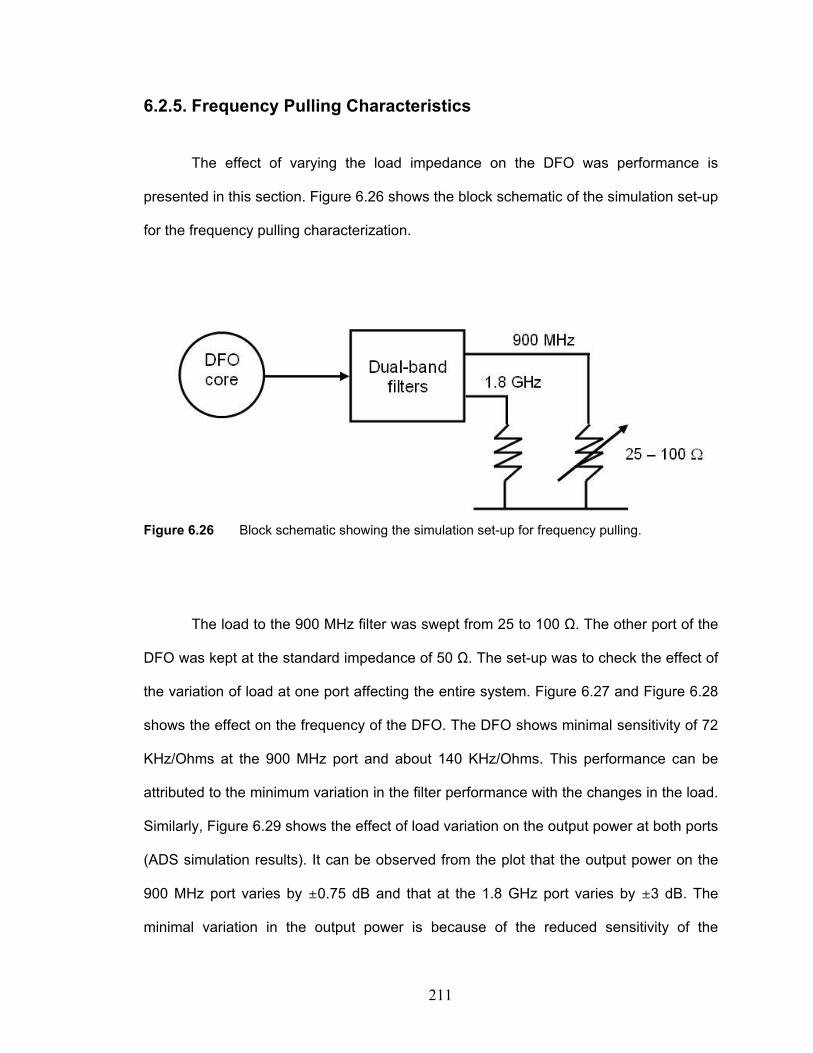
211
6.2.5. Frequency Pulling Characteristics
The effect of varying the load impedance on the DFO was performance is
presented in this section. Figure 6.26 shows the block schematic of the simulation set-up
for the frequency pulling characterization.
Figure 6.26 Block schematic showing the simulation set-up for frequency pulling.
The load to the 900 MHz filter was swept from 25 to 100 Ω. The other port of the
DFO was kept at the standard impedance of 50 Ω. The set-up was to check the effect of
the variation of load at one port affecting the entire system. Figure 6.27 and Figure 6.28
shows the effect on the frequency of the DFO. The DFO shows minimal sensitivity of 72
KHz/Ohms at the 900 MHz port and about 140 KHz/Ohms. This performance can be
attributed to the minimum variation in the filter performance with the changes in the load.
Similarly, Figure 6.29 shows the effect of load variation on the output power at both ports
(ADS simulation results). It can be observed from the plot that the output power on the
900 MHz port varies by ≤0.75 dB and that at the 1.8 GHz port varies by ≤3 dB. The
minimal variation in the output power is because of the reduced sensitivity of the

212
Chebychev filters to the variation in load. Figure 6.30 and Figure 6.31 plots the effect of
varying load on the S21 and S11 performance of both the filters. It can be observed that
the return loss in the 1.8 GHz band worsens at 25 Ω and hence, a degradation of the
output power in the 1.8 GHz signal is observed in the amplitude plot.
Figure 6.27 Effect of frequency pulling at the 900 MHz port.
Figure 6.28 Effect of frequency pulling at the 1.8 GHz port.
Frequency, MHz
Load resistance, Ω
Frequency, GHz
Load resistance, Ω

213
Figure 6.29 Effect of load variation on the power output of the DFO at both ports.
Figure 6.30 ADS simulation plots of the effect of load on the filter responses (amplitude).
Figure 6.31 ADS simulation plots showing the effect of load on filter responses (return loss).
Output power, dBm
Load resistance, Ω
900 MHz port
1.8 GHz port
S21, dB
Frequency, GHz
S11, dB
Frequency, GHz

214
6.2.6. Frequency Scalability
The DFO can be scaled to generate any other two synchronous frequencies. The
ratio of the frequencies can exceed 2 and it is dependent on
(1) The unity-gain cut-off frequency (fT) of the transistor,
(2) The maximum and minimum manufacturable component (mostly inductors).
The transistor has an fT of 22 GHz at 10 mA bias current. Following conventional circuit
design techniques, the transistor is usable up to 1/6th (~3 GHz) of this frequency range
[40]. Resultantly, the circuit was redesigned to generate 0.9 GHz and 2.7 GHz
simultaneously (applicable for handset with GSM and Bluetooth). Table 6.2 gives the
component values for the design of the resonators used in the 0.9/2.7 GHz DFO.
Table 6.2 Component parameter for the design of the 0.9/2.7 GHz DFO.
Component Resonator Value Qmax at frequency
La 10 nH 60 @ 0.9 GHz
Lb 10 nH 60 @ 0.9 GHz
Ca 0.12 pF 260 @ 1 GHz
Cb
Base resonator
2.2 pF 234 @ 1 GHz
Li 13 nH 55 @ 0.9 GHz
Ci
Input resonator
2 pF 240 @ 1 GHz
Figure 6.32 shows the simulated frequency spectrum at both the ports. The DFO
was biased at 10 mA from a 3 V supply. The power was increased by 5 mW as
compared to the 0.9/1.8 GHz DFO to increase the power output of the 2.7 GHz signal.
The 0.9 GHz signal has a considerable output power of 1 dBm and that of the 2.7 GHz

215
signal is -6 dBm. The filters from the 0.9/1.8 GHz DFO were scaled for this application.
The simulated phase noise at both the ports is shown in Figure 6.33. The DFO provides
-130 dBc/Hz @ 1 MHz offset. Further improvement in the phase noise can be expected
by using a transistor with higher gain characteristics.
Figure 6.32 Simulated frequency response of the 0.9/2.7 GHz DFO.
Figure 6.33 Simulated phase noise of the DFO. Circle marker: 2.7 GHz port, solid data: 0.9 GHz port.
Output power, dBm
Frequency, GHz
Circle marker: 0.9 GHz port
Square marker: 2.7 GHz port
Frequency, KHz
10 100 1000 10000
Phase noise, dBc/Hz

216
Conclusively, the scaling of the proposed DFO topology depends on the
manufacturable inductance and capacitance. As the spread between the frequencies
increases, a larger inductance is required at the base at the lower frequency and a
significantly lower shunt capacitance is required to create the resonance between the
frequencies. In the DFO design discussed so far, the 29 nH inductor was synthesized by
two equal size inductors and their parasitics capacitances were absorbed in the shunt
capacitors. However, as the frequency spread increases, a larger inductance is required.
A large inductor will have a larger parasitic capacitance and in some cases the parasitic
capacitance will be greater than the actual required shunt capacitor, thereby making the
design impractical (see Table 6.2 and Table 6.1). This is applicable to the series LC
resonator at the emitter of the transistor, see equations (6.5) and (6.6). Additionally, with
the design rules of the present LCP technology in the 3 mils range (line-line and line-
width), manufacturing inductors in excess of 20 nH and capacitances smaller than 0.1
pF is a challenge. Hence, other schemes of producing multiple signals from an oscillator
should be considered [2]. Reference [2] discusses a method (without actual
implementation) of 1.26 GHz and 7 GHz using multi-resonator cross-coupled oscillator.
6.2.7. Colpitt’s-Hartley’s DFO
Multi-mode oscillations were also investigated for a Colpitt’s oscillator. As discussed
in Chapter 4, the Colpitt’s oscillator has a simple core, which makes it suitable for low
profile applications such as multi-band 802.11a/b/g. Multi-mode asynchronous operation
of Colpitt’s oscillator was discussed in [2]. This thesis investigates the multi-mode
synchronous operation of another implementation of a Colpitt’s-type oscillator, which is

217
suitable for WLAN frequencies. The most convenient method of obtaining dual-band
characteristics from a feed-back network is to make use of the dual network properties of
passives. In other words, the capacitive feedback of the Colpitt’s oscillator at 2.5 GHz is
transformed into inductive feedback at 6.0 GHz (Hartley’s configuration). Figure 6.28
shows the schematic of the proposed DFO.
Figure 6.34 2.5/5.0 GHz Colpitt’s-type DFO.
Figure 6.28 shows the reactance-frequency responses of the series LC and
parallel LC resonators. As shown in Figure 6.28, at 2.5 GHz the series resonators
Frequency, GHz
Frequency, GHz
2.4 5.2
2.4 5.2
Im(z), ohms
Im(z), ohms
+
0
-
+
0
-
CS
RB
LC
L1
L2
CC
C1
C2
RE
2.7 V

218
provide capacitive reactance, whereas the parallel resonator at the collector of the
transistor provides inductive reactance. Thus the circuit functions as a Colpitt’s oscillator
with capacitive feedback from the collector to the emitter. At high frequency (5.0 GHz)
the circuit functions as Hartley oscillator due to resonance and anti-resonance of the
series and parallel resonators, respectively. L1C1 combination provides an equivalent C
of 0.85 pF at 2.45 GHz and L2C2 combination provides an equivalent C of 2.3 pF.
Similarly, the parallel resonator at the collector of the transistor provides an inductance
of 3.9 nH and a capacitance of 0.05 pF at 5.0 GHz. In designing the series and parallel
resonators it is crucial that the reactance is almost constant at the frequency of interest.
The constant reactance enables the oscillator design to be narrow-band and the
specifications for the output filters to be relaxed. The large signal loop-gain was
determined using ADS. The circuit is biased at 4 mA from a 2.7 V DC supply. The
magnitude loop-gain was adjusted to be 1.4 at 2.5 GHz and 1.5 at 5.0 GHz. For output
filtering, the DFO uses similar filtering network as shown in Figure 6.4. Figure 6.29
shows the ADS simulation results of the Colpitt’s-type DFO. The 2.5 GHz signal (Vlo) is
at +5 dBm and the 5 GHz signal (Vhi) is at – 5 dBm.

219
Figure 6.35 Simulated frequency response of the DFO.
6.3 Frequency Divider-based Multiple Frequency Generators
This section discusses the frequency divider-based multiple frequency
generation scheme. The complete frequency generation scheme uses a combination of
digital frequency dividers and analog/RF LOs and mixers and is implemented on-chip
and hence, is suitable for multi-band radios. One embodiment of the scheme is shown in
Figure 6.3, which is useful for dual-band WLAN systems. The scheme uses an 8 GHz
VCO followed by two dividers to generate the 4 GHz and 1 GHz signals. The 4 GHz and
1 GHz signals are then mixed in a Quadrature single side-band (SSB) mixer with a high
pass filter to generate a 5 GHz that is then divided to generate the 2.5 GHz signal. This
section presents the design of a power optimized 8 GHz, 4.75 mW SiGe HBT VCO using
0 2.5 5 7.5 10 12.5 15 17.5 20
Frequency, GHz
Output power, dBm

220
the transformer feedback technique as discussed in Chapter 5. The designed 8 GHz
TVCO is among the lowest power consuming designs reported in the literature for the
frequency range. Appendix D reviews different frequency dividers that are most
commonly used in frequency synthesizers.
6.3.1. Design of 8 GHz SiGe HBT TVCO
Figure 6.36 shows the schematic of the TVCO. The TVCO is a feedback
topology with the collector signal fedback to the emitter terminal of the HBT through the
transformer. The basic principle and the architecture is similar to the LCP-based TVCO
discussed in section 5.2, Chapter 5.
Figure 6.36 Schematic of the TVCO with output buffer.
Vtune
+ 2V
L1 L2
L3 C2
C5
Cv
Csh
Lc
Cm
C3
GND
Lb
R2
R1
Lb1
Cout
RF Out
+ 2V + 2V
Q1 Q2

221
Components L1, C2, L2, C3, L3, Cv and C5 form the feedback network, which is a
capacitively coupled second-order filter. However, the frequency of oscillation is
determined primarily by the components L3 - Cv - C5 (resonator). The approximate
frequency of oscillation is given by
5
53
0
2
1
CC
CCL
f
v
v
+
⋅⋅⋅⋅
≈
π
(6.7)
A divider at the output of the VCO reduces the effective tuning range by the
division ratio. For instance, an 8 GHz VCO with 1 GHz tuning range followed by a divide-
by-2 divider will produce an output signal at 4 GHz with a tuning range to 0.5 GHz.
Hence, one of the requirements of divider-based is that the VCO has a wide tuning
range. The tuning range of the TVCO is only dependent on the voltage-tunable capacitor
(Cv) in the resonator. A reasonably large tuning range (> 0.15 f0) can be expected from
the TVCO since the resonator is isolated from the parasitic capacitances of the active
device.
Experimental Results
The 8 GHz TVCO was fabricated in the commercially-available 150 GHz Jazz
SiGe-120 process using only HBTs. The technology offers a maximum cut-off frequency
(fT) of 150 GHz, in addition to 0.18 um CMOS devices [105]. The TVCO (see Figure
6.36) uses two, parallel-connected SiGe HBTs (Q1), each with an emitter area of 0.2 x
10 µm2. For the same device area, narrow width emitter strips lead to lower the base
resistance but higher parasitic capacitance. The device size was optimized via circuit

222
simulations to minimize the phase noise. In general it was observed that a large effective
length emitter minimized phase noise. This behavior can be explained by the reduction
of the base 1/f noise because of increase in the emitter area (AE) [105]. However, the fT
of the HBT was reduced because of the reduced current densities.
The base of the HBT was maintained at RF ground potential through a 1.5 pF
MIM capacitor. In Figure 6.36 the inductor Lb is a biasing inductor (2.5 nH) that isolates
the RF from the dc supply. The capacitor Csh decouples the RF from the dc at the tuning
port and also provides a RF ground to the varactor diode. A high performance junction
varactor tunable from 70 fF to 0.22 pF with a quality factor (Q) in the range of 12 (0 V) to
22 (2.5 V) was used to tune the oscillator. Spiral-shaped inductor designs were used for
increased inductance density. HBT Q2 and the resistors buffer the TVCO core. The
buffer consumes an additional 4.75 mW DC power.
The TVCO was tested on-wafer using an Agilent 8565E spectrum analyzer. The
oscillator core consumes 2.4 mA from a 2 V supply. The circuit delivers –10 dBm of
power (which includes approximately 2.5 dB resulting from cable and set-up losses) at a
center frequency of 8.5 GHz (see Figure 6.37a and Figure 6.37b). Figure 6.38 shows
the plot of the measured phase noise at Vtune of 1 V. The TVCO was tested in a shielded
room for noise isolation and the chip was powered using a battery supply.
The TVCO can be tuned over a frequency range of 1.04 GHz (8 GHz to 9.04
GHz) for a tuning voltage range of 0 – 2.5 V, as shown in Figure 6.39. A high VCO gain
(416 MHz/V) was observed due to the reduced parasitics at the resonator junction.
Figure 6.40 shows the variation in phase noise over this tuning range. A phase noise of -
108 dBc/Hz was measured at a Vtune of 0 V and it degraded by 4 dB at Vtune of 2.5 V. The
degradation of the phase noise (~4 dB) at the upper range of the tuning voltage can be
attributed to the decrease in the slope of the loop-phase angle that results from the non-

223
constant group-delay characteristics of the Chebychev transformer [65]. The
measurements were consistent over different TVCO die-samples.
Figure 6.37 (a) Measured spectrum of the TVCO at Vtune=1.25 V. (b) Measured center frequency of the TVCO at Vtune=1 V.
Figure 6.38 Measured phase noise of the TVCO at Vtune=1 V.
(a) (b)

224
7.5
8.0
8.5
9.0
9.5
-12
-11
-10
-9
-8
-7
-6
Figure 6.39 Measured frequency and power output tuning results of the TVCO.
-110
-108
-106
-104
-102
-100
Figure 6.40 Phase noise variation vs. tuning voltage at 1 MHz offset.
The chip photo-micrograph is shown in Figure 6.41. It occupies an area of 1 x 1
mm2, including DC bias and RF pads. Table 6.3 compares the performance of the TVCO
with other reported works at 8 GHz. The FOM definition follows from expression (4.1) in
Chapter 4. From Table 6.3 it can be concluded that the TVCO performance is
comparable to other differential VCO implementations at lower power consumption.
Output Power (dBm)
0 0.5 1 1.5 2.5
RF power Frequency Frequency (GHz)
Vtune (V)
0 0.5 1 1.5 2 2.5
Phase Noise (dBc/Hz)
Vtune (V)

225
Figure 6.41 Chip photo-micrograph.
Table 6.3 Performance comparisons.
Ref. Technology Frequency,
f0 (GHz)
Phase
noise @
1MHz
(dBc/Hz)
Tuning
(% f0)
Power
consumption
(mW)
Pout
(dBm)
Figure
of
merit
(dB)
[106] 0.18 um
CMOS 9.5 -114 12 35 -4.5 178.1
[107] GaAs
PHEMT 7.5 -115 5.3 150 3 170.7
[108] 0.18 um
CMOS 9.5 -110 11.3 5.8 NA 181.5
This
work SiGe HBT 8.5 -108 12 4.75 -7.5 179.8
VCC GND GND GND
GND GND SIG
1 mm
Vtune

226
6.4 Comparison between DFOs and Frequency Divider-based Concurrent Signal Generation Schemes
This section compares and contrasts the use of novel DFOs with a conventional
architecture that uses a VCO followed by one or two dividers (see Figure 6.3) and
identifies appropriate applications for each of the multiple frequency generation
techniques. The primary objective of multi-mode implementation for oscillator is to
minimize power consumption and number of integrated oscillators, thereby leading to
size reduction and at the same time increase the functionality at user disposal. Next
generation radios as depicted in Figure 6.1 may require multiple synthesizers and VCOs
to serve different communication protocols. Depending on the applications, one or more
of VCO performance characteristics, such as phase noise, frequency resolution, and
temperature stability may be of higher interest or value. For example, a cellular base-
station requires higher temperature stability and lower phase noise as compared to that
in handsets [69]. Hence, the aim of this section is to effectively compare the two
schemes and recommend their use depending on the end application.
LCP-based DFOs
LCP-based DFOs use multiple resonances of passive components to generate
two frequencies in an efficient manner. At low power consumption (< 10 mW) it provides
low phase noise (< -140 dBc/Hz @ 1 MHz offset) at both the frequencies without
constraining the separation between two frequencies. However, a higher fT transistor is
naturally required for producing higher frequencies. In radio design, it is a common
design practice to offset the VCO frequency (higher VCO operating frequency) from the
system operating frequency. This is particularly true when fully-monolithic design

227
techniques are used, since it prevents the pulling of VCO frequency because of the PA
[11] and also minimizes the effect of self-mixing, as discussed in Chapter 3. Since the
DFO architecture in this thesis has been implemented using SOP-L methodology, the
noise coupling through substrate is minimized and hence, the effect of other modules on
the DFO performance is minimized. Low Q passives with narrow-band characteristics
are major impediments in implementing the DFO using SOC approach. Additionally, the
effect of temperature on LCP-based VCOs is minimal, as presented in Chapter 5. The
DFOs also exhibits minimum performance degradation with variation in load on either or
both ports. Practically, the two ports of the DFO are independent of each other as far as
load conditions are concerned. Hence, the failure of one signal chain will have a minimal
effect on the other second signal chain (see section 6.2.6). The aforementioned
characteristics of the DFO make it aptly suitable for various high-end wireless
applications such as next generation multi-mode cellular handsets and base stations.
Divider-based Signal Generators
The second method for simultaneously generating multiple frequencies is a VCO
followed by dividers as shown in Figure 6.42. At the architecture level, dividers offer
better spectral characteristics as opposed to frequency multipliers [109], [114] and
hence, a higher frequency VCO needs to be used. The VCO frequency is limited to 10
GHz to avoid the use of area-intensive transmission lines and high-speed dividers that
increase the noise floor and also place heavy load on the power supplies. The 8 GHz
TVCO discussed in section 6.3.1, was optimized for low power consumption (~5 mW)
and reasonable phase noise performance. When implemented in a frequency plan as

228
shown in Figure 6.3, i.e. cascaded with a divide-by-2 divider to generate a 4 GHz signal
and then by a divide-by-4 stage, 1 GHz and 4 GHz signals can be generated
simultaneously. Finally, the 1 GHz and 4 GHz signals are mixed in a Quadrature SSB
mixer to generate in-phase (I) and quadrature (Q) 5 and 2.5 GHz signals1. The complete
frequency plan uses only a few inductors that are not required to be broad-band and
hence, can be implemented using SOC methodology. This attribute makes the
architecture highly attractive for cellular handset manufacturers who can leverage their
expensive IC fabrication foundries without resorting to the relatively time-exhaustive and
expensive co-design methodologies.
Figure 6.42 Divider-based architecture for generating multiple frequencies.
However when compared to the DFO, the divider-based architecture is more
complex that uses both highly sensitive analog circuitry and high-speed digital circuitry
1 Quadrature SSB mixer is used for the reasons of obtaining quadrature outputs that are required for frequency conversions. Dividers are seldom used as the final division stage due to the limitations of obtaining balanced outputs at high-speeds or frequencies [11].

229
on the same chip. This raises the issue of analog-digital coupling through the conductive
Si-substrate. Apart from the noise issues, the lowest power consuming dividers in the 8 -
10 GHz is in the few tens of milli-watts and the use of two dividers would increase the
overall power consumption (see Appendix D). In high-end applications, such as base-
stations the effect of temperature on the divider-based scheme requires expensive and
precise calibration circuitry to correct the degradation in noise and performance [115].
For example, the phase noise of the entire scheme can be increased because of the
change in the threshold voltages of the transistors in the CML latches, leading to false
triggering of the latches. Since the dividers are connected in cascade the total effect is
cumulative.
Table 6.4 summarizes the discussion on the two architectures. Conclusively,
both the architectures can generate more than two frequencies simultaneously with
differences in phase noise performance. LCP-based DFOs provide low phase noise,
suitable for the stringent GSM and PCS standards, at low power consumption. LCP’s
excellent thermal and mechanical (dimensional) properties make the DFO design
applicable to base-stations, where the area and cost can be justified. However, the size
of DFOs is considerable. As pointed out earlier in this chapter, the output filters are the
major contributors to the size of the DFO that can be replaced by compact, tuned-
amplifiers. This will also enable size reduction via chip-package co-design where only
the base resonator and input resonator (see Figure 6.4) require being on LCP and the
rest of the components can be integrated on-chip. Conversely, the divider-based
architecture provides the flexibility of design. Monolithic implementation lead to size
reduction and reduction in the number of surface mount components. The frequency
dividers provide a 10log(N), where N is the division factor, enhancement to the inherent
VCO phase noise [109]. Hence, a π4 stage at the output of the TVCO (see section
6.2.1) will provide a 2 GHz signal with a 6 dB improvement in phase noise. The design

230
methodology with its own limitations is however a faster design technique, since it
eliminates third party vendors for high frequency package design. However as compared
to the DFO, the power consumption is significantly higher. Because of the
aforementioned architectural limitations, the divider-based generators would find their
applications in low profile applications such as UWB that are operated only for a small
time period, unlike the cellular bands.
Table 6.4 Summary of the two investigated architectures as concurrent signal generators.
Parameter DFO Divider-based
Phase noise from 2
GHz carrier < -140 dBc/Hz @ 1 MHz ~ -116 dBc/Hz @ 1 MHz
Power consumption 10 - 25 mW 5 mW (VCO) + 40 mW
(dividers) + Mixers
Tuning range @
2 GHz 421 MHz 300 MHz
Area 10 x 14 mm2 (can be further
reduced via co-design)
1.5 x 1.5 mm2 (TVCO +
dividers) + mixer
Temperature
performance
(25 – 120 ±C)
<120 ppm/±C for frequency
≤2 dB for phase noise NA
231
6.5 Summary
Generating multiple frequencies using a single oscillator was undeniably
imperative for previous generations of multi-band radios and is unarguably useful in next
generations of wireless radios. This chapter presented the design of a new class of
oscillators (DFO) that can simultaneously generate two synchronous frequencies.
Because of the high Qs of the LCP-based embedded passives and their broad-band
nature [68] the oscillator could maintain low phase noise at both the frequencies. It
should be noted that the size of the DFO is significantly determined by the size of the
output filters. The output filters can be replaced by frequency tuned buffer amplifiers,
thereby leading to a significant reduction in size. Alternatively, the lower frequency
bandpass filter can be replaced by a low pass filter (LPF) that uses much less number of
components, thereby leading to size reduction.
This chapter qualitatively compared and contrasted LCP-based DFOs against the
conventionally used divider-based concurrent signal generator for use in multi-mode
radios. The advantages of using a DFO are multi-fold,
(1) Reduction in the number of oscillators.
(2) Reduction in the power consumption of the frequency scheme.
(3) Improvement in the overall routing of signal and power lines.
(4) Reduction in number of surface-mount and integrated decoupling capacitors.
(5) Reduction in the output frequency spurs because of elimination of dividers.
In addition to finding applications in cellular handsets, LCP-based DFOs seem to
be well-suited for the base-station type applications because of their better noise
performance at lower power consumption level and insensitivity to high temperatures
(~120 ±C).

232
CHAPTER 7
CONCLUSION AND FUTURE WORK
The addition of wide-area high-speed data services to cellular users will provide
a seamless transition from voice to data services. As a result next generation handsets
are rightly termed as computing cell phones. This is fostered by the progress in the
silicon-based technologies (65 nm CMOS and strained silicon technologies) that now
extend in the hundreds of gigahertz. As a result, handsets and wireless portables will
have to be compatible with many communication protocols with varied electrical
performance requirements. To provide seamless connectivity, the power-limited
handsets will have to simultaneously handle multiple protocols. As a result, radio
architectures are moving from the conventional multi-band design techniques to novel
multi-mode techniques. A practical multi-mode receiver architecture from the antenna to
the down-converter was proposed in this thesis. The novel system architecture requires
novel components that can efficiently handle multiple frequencies simultaneously.
Because of the inherent limitations of Si-based technologies for integrating key RF
components, such as filters and oscillators, novel integration methodologies are also
required. In the design of front-end components, the prime requirement is high Q
passive components that assist designers to reduce noise and relax power
requirements. In this dissertation, novel signal generation techniques and filter design
techniques were investigated using novel multi-layer LCP process technology.

233
7.1 Conclusions
The thesis primarily was focused on the design of synchronous concurrent
oscillators, which is the main contribution of this dissertation. The design uses broad-
band characteristics of the passives embedded in LCP substrate to eliminate the need
for power hungry blocks, such as dividers and frequency mixers. Optimization of
electrical parameters, such as phase noise, power consumption, area, frequency
scalability, and frequency pulling was shown. Finally, the proposed oscillator
configuration was compared to the conventionally used frequency divider-based
architecture. It was found that the concurrent oscillator is advantageous in applications
where low phase noise and performance stability are of prime importance. Additional
outcomes of this research work are as follows:
a. Investigation of oscillator implementations on LCP-based packaging technology for
use in highly selective communication systems. The thesis investigated the feasibility
of using LCP substrate as an economical alternative to the widely accepted LTCC
technology for high performance active circuit applications. This was demonstrated
via multiple embodiments of standard and novel oscillator configurations with
passives embedded in multi-metal-layer LCP substrate. The high Qs of the passive
components on LCP enabled to design VCOs at low (~1.8 mW) power consumption,
which is the lowest power consuming fully-packaged VCO reported in the literature
Novel design techniques for oscillator design, in the form of Modified-Colpitt’s and
TVCOs, were investigated in this work showed exceptionally low phase noise (~-125
dBc/Hz @ 100 KHz offset) at low power consumption (<10 mW) in small area.
b. Thermal characteristics of the VCOs on heterogeneous LCP-based substrates were
investigated. It was shown that the LCP-based VCOs showed minimal performance
variation over a temperature range of 25 ±C to 125 ±C, making them highly suitable

234
for base-station applications. In effect, this thesis has investigated and validated the
feasibility of using LCP-based VCOs in high-end applications, such as multi-band
cellular handsets and base-stations.
c. The work also investigated the design of single-input single-output dual-band filters
using lumped components on heterogeneous stack-ups that used multiple LCP
substrates. The filter embodiments showed low insertion losses and controllable
passbands. Additionally, the filters demonstrated a broad-bandwidth with a frequency
ratio greater than 2.5 in a small area of <36 mm2. The thesis has thus presented the
design of the smallest form factor dual-band filters with controllable passbands.
7.2 Recommendations for Future Work
Next generations cellular handsets will be a collage of many different
communication protocols each requiring different hardware configurations.
Paradoxically, the cost per module and even systems need to reduce with newer
generations. As a result the hardware either on-chip or on-package needs to be either
capable of reconfiguring itself over different bands or be multi-mode. An effort is made
in this dissertation to address some the above stated issues. However, there are many
other aspects of system design that the thesis has not covered. They can be listed as
follows:
1. Theoretical investigation of non-synchronous DFOs and their implementation.
2. Implementation of VCOs using pure co-design methodology. It was proved that not
all the components of a VCO need to have high Qs. Hence, investigation of
performance and size improvement by intelligently placing key components on-
package and rest of circuitry on-chip is necessary.

235
3. Reliability and humidity testing under high temperature and pressure of LCP-based
modules is essential to show promise for commercialization.
4. Development of design libraries for passives on LCP-based heterogeneous stack-
ups. The 18″ x 24″ panel would show variations in the dielectric constant and
thickness. Hence, the scalable models should include the processing issues to
achieve high yield and reduce design cycle-time.
5. Design of conformal structures. Since LCP is a flexible material with high
performance it can be used to design antennas that wraps around the package,
such as screen of a laptop, thereby providing MIMO capability without trading-off
size.
6. Size reduction of circuits by investigating stacking of multiple layers of LCP
substrates (>10) and increasing the packaging efficiency to more than 90%.
However, the major impediment is from the manufacturing capability than on the
electrical aspects. Nonetheless, the electrical characterization of multi-layered
substrates will be crucial, especially with the advent of ultra wide-band (UWB)
technologies.
7. Most of the communication protocols are narrow-band and closely spaced. Hence,
making the circuits reconfigurable will reduce the hardware count and also
minimize overheads of complex circuit calibration schemes. On-chip tunable
capacitors have low Qs and hence, fully-packaged solutions of micro electro-
mechanical structures (MEMS) will be highly useful. Hence, investigation of MEMS
on LCP substrates will provide tunability to fully-packaged modules without the
need to resort to co-design methodologies.

236
7.3 Publications and Inventions Generated
List of Publications
[1] A. Bavisi, V. Sundaram, and M. Swaminathan, “A miniaturized novel feedback LC
oscillator for UMTS type applications in a 3-D stacked Liquid Crystalline Polymer
technology,” Int. Journal RF and Microw. Comp. Aided Engg., Wiley Interscience,
Published online on Feb. 2006.
[2] A. Bavisi, S. Dalmia, M. Swaminathan, G. White, and V. Sundaram, “Chip-package
co-design of integrated VCO in LCP substrate,” accepted for publication at IEEE
Trans. Adv. Pack., 2005.
[3] A. Bavisi, M. Swaminathan, and V. Sundaram, “A GSM/PCS concurrent oscillator in
a multi-layer LCP substrate for multi-mode wireless radios,” Submitted for review to
IEEE Trans. Adv. Pack., Mar. 2006.
[4] A. Bavisi, J. P. Comeau, J. D. Cressler, M. Swaminathan, and M. Lam, “A 9 GHz, 5
mW VCO using lumped-element transformer feedback in 150 GHz fT SiGe HBT
Technology,” IEEE Topical Meeting on Silicon Monolithic ICs in RF Systems, pp.151
– 154, Jan. 2006.
[5] A.Bavisi, W. Yun, V. Sundaram, and M. Swaminathan, “Design and applications of
high Q passive devices on multi-layered LCP substrate,” in Proc. IEEE Asia Pacific
Microw. Conf., Vol.2, pp. 1-4, Dec. 2005.
[6] A.Bavisi, V. Sundaram, M. Swaminathan, S. Dalmia, and G. White, “Design of a
dual frequency oscillator for simultaneous multi-band radio communication on a

237
multi-layer Liquid Crystalline Polymer substrate,” accepted for poster presentation at
the IEEE Radio and Wireless Symp., Jan. 2006.
[7] W. Yun, A. Bavisi, V. Sundaram, M. Swaminathan, and E. Engin, “3D integration
and characterization of high Q passives on multilayer LCP substrate,” at IEEE Asia
Pacific Microw. Conf., Vol. 1, pp. 1-4, Dec. 2005. [BEST PAPER AWARD]
[8] M. Swaminathan, A.Bavisi, W. Yun, V. Sundaram, V. Govind, and P. Monajemi,
“Design and fabrication of integrated RF modules in LCP substrates,” invited paper
at the 31st IEEE Industrial Engineering Conf., pp. 2340 – 2345, IECON 2005.
[9] A. Bavisi, V. Sundaram, and M. Swaminathan, “Design of a system-in-package
based low phase noise VCO using 3-D integrated passives on a multi-layer LCP
substrate,” in Proc. 35th Euro. Microwave Conf., pp. 485-488, Oct. 2005.
[10] S. Dalmia, A. Bavisi, S. Mukherjee, V. Govind, G. White, M. Swaminathan and
V. Sundaram, “ A multiple frequency signal generator for 802.11a/b/g VoWLAN type
applications using organic packaging technology,” in Proc. of IEEE Electronic
Components and Technology Conf., Vol. 2, pp.1664 – 1670, June 2004.
[11] A. Bavisi, S. Dalmia, G. White, V. Sundaram, and M. Swaminathan, “A
3G/WLAN VCO with high Q embedded passives in high performance organic
substrate,” presented at IEEE Asia Pacific Microwave Conf., Nov. 2003.
[12] A. Bavisi, S. Dalmia, M. Swaminathan, and F. Ayazi, “An 802.11a WLAN
oscillator with high Q embedded passives on laminate-type organic package,” in
Proc. of IEEE Antenna Propagation Society’s Topical Conf. on Wireless
Communication Technology, pp. 166 – 167, Oct. 2003.

238
List of Inventions
[1] A. Bavisi, S. Dalmia, M. Swaminathan, V. Govind, G. White, and V. Sundaram,
“Multi-band RF transceivers with passive reuse in organic substrates,” United
States provisional patent, ID # 062020-1950, filed on April 2005.
[2] A. Bavisi, S. Dalmia, and M. Swaminathan, “Concurrent signal generators for
communications and computing industry using high performance organic
packaging technology”, Georgia Institute of Technology Patent, ID # 3108, April
2004.
[3] A. Bavisi, S. Dalmia, M. Swaminathan, G. White, and V. Sundaram, “Signal
generators on high performance organic laminates”, Georgia Institute of
Technology Patent, ID# 2888, March 2003.
Book Chapters
[1] M. Swaminathan, V. Govind, E. Engin, A. Bavisi, and S. Dalmia, Mixed Signal
Design, a Chapter in Packaging Handbook, Edited by R. Tummala, M.
Swaminathan, and Padmasree Warrior, To be published, 2007.

239
APPENDIX A: MANUFACTURING PROCESS STEPS FOR LTCC

240
APPENDIX A
MANUFACTURING PROCESS STEPS FOR LTCC
Figure A.1 Manufacturing process steps for LTCC starting from a green-sheet to final SMD mounting and wirebonding [26].

241
APPENDIX B: TUNING ISSUES IN NEGATIVE RESISTANCE VCOs

242
APPENDIX B
TUNING ISSUES IN NEGATIVE RESISTANCE VCOS
The negative resistance VCO utilizes compensation of energy loss in signal path
to enable VCO design with low phase noise. It was observed in chapter 3 that the
negative resistance is a function of the load resistance (RL) and the base inductor (L1).
The negative resistance compensates for the losses in the resonator. However, the
negative resistance is offered only for a fraction of the total cycle or the Q of the network
will be infinite, thereby reducing the bandwidth of the oscillator to zero (impulse). The Q
of the oscillator is determined by the loading (effective reactance in the network) of the
resonator connected to the emitter terminal (input resonator). Hence, a higher Q can be
obtained if the phase shift at the frequency of interest is large i.e. a larger-order network
(more poles) will have a greater phase shift as compared to a single inductor or
capacitor. Thus by adding more passives (higher-order network) to the input resonator a
higher-Q and hence, lower phase noise can be achieved. However, the bandwidth of the
network is determined by the Q of the input resonator. To maintain constant output
power over the entire tuning range the output impedance of the oscillator should remain
constant. Since the transistor is a bilateral device the input resonator and the base
inductor contributes to the impedance observed at the collector terminal (output
impedance, Zout). Figure B.1 plots the output impedance of the 1.9 GHz VCO with an
input resonator shown in Figure 3.1. From the Figure B.1 it is clear that at and around
(0.1f0) the design frequency the output impedance varies considerably. The Figure B.1 is
a 3-D plot showing that the impedance profile is not affected by the inductor L1 and
mostly is determined by the order of the input resonator. Hence, a significant variation in

243
output power can be expected while tuning the oscillator but a minimal variation in phase
noise.
5
10
15
201.5
2
2.5
3
3.5
0
100
200
5
10
15
20
Figure B.1 Variation in the output impedance with a second-order input resonator.
Figure B.2 shows the effect on Zout when a single capacitor is connected to the
emitter terminal. Now the input resonator has one pole at origin giving a < 90± phase
change at the frequency of interest1. Hence, the Q of the network is reduced i.e. the
bandwidth increases. This is observed in Figure B.2. Zout shows minimum variation over
both frequency and L1. As a result, the oscillator can be effortlessly matched to the load
over a wide tuning range and hence, minimize drop in the output power. However, the
phase noise of the VCO with a single passive component will be higher than that of the
one with a higher-order resonator (because of the higher phase shift).
1 It should be noted that the oscillator design was aimed for 1.9 GHz and for the component values specified in Table 3.1 (chapter 3), an L1 of 10 nH provides maximum negative resistance (instability). Hence, instability is applied to the other port of the transistor [103] thereby, verifying the veracity of this discussion. Also, The impedance variation in Figure B.1 and Figure B.2 should be checked in this frequency and L1 range.
ReZout
L1, nH Frequency, GHz

244
5
10
15
201.5
2
2.5
3
3.5
6.1775
6.18
6.1825
6.185
6.1875
5
10
15
20
Figure B.2 Variation in the oscillator output impedance with an input capacitor.
From the discussions on negative resistance VCO design in chapter 3 and in this
appendix, it is clear that the negative resistance VCO requires more components (order
≥ 2) to achieve low phase noise but with a relatively small tuning range (3 -5% f0). The
tuning range might be satisfactory for narrow-band WLAN applications (IEEE 802.11b/g)
but might be insufficient for broad-band applications that also require low phase noise at
low or modest power consumption.
ReZout
L1, nH Frequency, GHz

245
APPENDIX C: THEORY ON DUAL FREQUENCY OSCILLATIONS

246
APPENDIX C
THEORY ON DUAL FREQUENCY OSCILLATIONS
The theory behind concurrent signal generation is discussed in this appendix.
Basic principle in analyzing dual frequency oscillators is to (a) use linear circuit theory to
determine the initial frequency oscillations, and (b) use nonlinear differential equations to
determine the steady-state behavior.
Linear Circuit Theory
The fundamental principle of operation of oscillators can be explained from the
linear circuit theory. Pictorially it can be represented as an amplifier with voltage gain A
and a feedback network with gain F as shown in Figure C.1.
Figure C. 1 Oscillator representation using linear circuit theory.

247
The gain (Av) of the feedback circuit is a simple solution to the feedback network
and can be represented as
AF
A
V
VA
in
outv −
==1
(C.1)
The model is sufficient for a simplified analysis (initial design), without much insight into
the oscillator operation, of feedback oscillators. The criteria for the circuit to be unstable
or for stable (undamped) oscillations are
o01∠>AF (C.2)
1≥AF (C.3)
o0=∠AF (C.4)
In (C.2) - (C.4), AF is the gain over the feedback loop. Single-band electrical
oscillators operate at one fundamental frequency and are designed to satisfy (C.2) at
that frequency. The frequency of oscillation is determined by the resonant tank circuit,
which is in most cases also the feedback network. Linear circuit theory is sufficient to
determine the start-up conditions and the frequency of oscillations but is insufficient for
determining the harmonics and other circuit nonlinearities [103]. The nonlinearities
increase with the building of oscillations and with the saturation of the active device.
Hence, oscillators are mostly modeled using linear and nonlinear differential equations.
The order of the differential equations is determined by the order of the resonator.

248
Theory of Synchronous Dual Frequency Oscillations
The proposed dual frequency oscillator uses a higher-order, instead of second-
order, LC resonant tank circuit. The oscillator has to satisfy conditions in (C.2) for two
frequencies (ω1 and ω2). This implies that a feedback oscillator should have a resonator
of atleast fourth-order. Several theories explaining dual oscillations can be found in
literature [101], [102] and [119]. In particular Schaffner [101] investigated both
synchronous (ω2/ω1 = p/q = integer) and asynchronous (ω2/ω1 = p/q ≠ integer)
simultaneous oscillations in oscillators using differential equations. The analysis [101]
was based on a nonlinear negative resistance source connected across a fourth-order
parallel LC resonator. The analysis, as will be discussed in this appendix, is based on
method of averaging [120] and is specifically useful in analyzing higher dimension
autonomous systems. The method is a general method for determining sufficient
conditions for the existence and stability of periodic solutions of a class of nonlinear
vector differential equations. For transient analysis the solution is obtained by breaking
the fourth-order system into two second-order systems and applying superposition
theorem.
Single frequency oscillators (second-order systems) are mathematically
described using the van der Pol equation [120]
( ) 0,01 2 >=+−− kuuuku &&& (C.5)
The square root of the eigenvalues (l1, l2…., ln) of (C.5) give the frequency of
oscillation [121]. Equation (C.5) is useful in explaining the transient (oscillation build-up)
as well the steady-state behavior of an oscillator. The middle term in the expression

249
represents the nonlinearity in the system. At the transient stage, the oscillator can be
considered to be in the linear regime (small signal) and hence, the solutions to (C.5) can
be obtained by linearizing the circuit around the quiescent point. The solution, u(t), can
be obtained using the following steps:
Auu =&& (C.6)
221121)( xecxectutt λλ += (C.7)
In (C.6) and (C.7), A is the system coefficient matrix and x = (x1, x2….xn) are the
eigenvectors and the roots are usually complex conjugate pairs (ln = an ≤ ibn). The
necessary condition for the circuit to be unstable is
Re(ln) > 0 (C.8)
In this case the system equilibrium point is an unstable focus [120] and the solution
represents an outward progressing spiral with time (polar representation). Conditions in
(C.8) can be satisfied only if the variable k in (C.5) > 0. Schaffner [101] extended this
theory to fourth-order synchronous and asynchronous systems. The general circuit of
analysis is shown in Figure C.2. It consists of a nonlinear voltage source, f(u),
(representing the transistor) across two series connected parallel LC resonators with
their loss conductance. f(u) is considered to be a combination of two signals (u1 and u2).
At oscillator start-up the system is considered to be in the linear regime and the analysis
uses the concept of “equivalent impedances” [101], [119], and [120]. Hence, Figure C.2
can be broken into two separate circuits as shown in Figure C.3. In Figure C.3 G1e and

250
G2e are the Thevenin equivalent impedances of the circuit observed at the resonator1
and resonator2, respectively. G1e and G2e include the negative resistance of the
transistor.
Figure C. 2 Equivalent circuit representation of an oscillator with two resonant circuits.
Figure C. 3 Equivalent circuit representation of an oscillator using theory of equivalent impedances. Solution for the current across the resonator capacitors is determined.
f(u)
L1
L2 C2 G2
G1 C1
i
L2 C2 G2
L1 G1 C1 G1e C1e
G2e C2e U2
+
-
U1
+
-

251
The differential equations for a fourth-order synchronous oscillator are given as [101]
[ ]eGGC
UU 11
1
11
2+
−=& (C.9)
[ ]eGGC
UU 22
2
22
2+
−=& (C.10)
12 C
Cp e⋅−∆=Φω
ω& (C.11)
In (C.9), (C.10), and (C.11), u1 and u2 are the amplitudes of the periodic signals at
frequencies ω1 and ω2, respectively. Φ is the difference in the phase of the two
frequencies (φ1 and φ2). The equations are obtained by applying nodal analysis and
using i = C dv/dt, where C is the capacitance and i is the current through C. The
conditions for oscillations in this case are
[ ] 011 ≤+ eGG (C.12)
[ ] 022 ≤+ eGG (C.13)
0=Φ (C.14)
Equations (C.12), (C.13), and (C.14) are useful in determining starting conditions
and obtaining an initial guess for the frequency of oscillations (see chapter 5, section
5.2). In circuit theory, the variable k is a complex function of the transistor

252
transconductance and resonator (loop-gain) [2]. k 0 as loop-gain 1. As the circuit
begins to oscillate the transistor saturates and hence, a limiting action does not permit
the loop-gain to increase. With k = 0 the eigenvalues become purely imaginary (≤ ibn)
and the oscillations reach steady-state. Now, (C.7) can be written as a combination of
two sinusoids with frequencies determined by the eigenvalues
++
+=
)cos(
)cos()(
222
111
φβ
φβ
tc
tcatu (C.15)
Graphically, (C.15) forms closed curves and every solution is periodic with period
2p/bn [120]. The entire discussion can be graphically represented by Figure C.4. The
spirals represent the transient behavior and the ellipse represents steady-state. The
“stability” of oscillations or the steady-state behavior are determined by solving (C.9),
(C.10), and (C.11) in presence of a transient disturbance. The Re(ln) of the system of
equations should be greater than 0 to adjust for the disturbance. This condition ensures
that the system equilibrium point is a minima and hence, stable oscillations [120], [121].
In circuit terms the minima means that in the presence of disturbance the circuit will
force the oscillations to return to the natural frequency of oscillation. Mathematically,
these conditions are achieved if and only if k in (C.5) ≥ 0 [119], [120] and [2]. The
oscillator will reach a steady-state once the Re(ln) goes again to zero. References [101]
and [120] have discussed the loop dynamics in detail.

253
Figure C. 4 Solutions to the differential equations at transient (spirals) and steady-state (ellipse). The existence of periodic oscillations (ellipses) are proved using Poincaré-Bendixson theorem. [120].
Steady-state
Transient

254
APPENDIX D: FREQUENCY DIVIDERS

255
APPENDIX D
FREQUENCY DIVIDERS
This section concisely reviews different topologies of frequency dividers that are
widely used in the design of frequency synthesizers. The idea is to introduce various
components of the divider-based architecture that will enable a fair and broad
comparison basis for the two concerned concurrent signal generation architectures,
namely DFO and VCO followed by frequency dividers.
Frequency dividers usually placed inside the loop of a phase locked loop (PLL)
or at the output of synthesizers. Frequency division can be achieved by using analog or
digital methods. Both the methods have their advantages and are equally widely used in
transceivers [109]. Analog dividers, however, are mostly used in high frequency
applications (above 5 GHz) because of simplicity of design [37], [109]. Analog dividers
are categorized as parametric dividers, which are mostly varactor diode-based [109] and
regenerative dividers (that use mixers, such as Quadrature SSB using Gilbert cells).
Regenerative dividers are widely used analog dividers as, unlike the parametric dividers,
they do not require a high input drive level and are broad-band (typically, an octave)
providing fin/2 and 3fin/2 components. Among the analog dividers, regenerative dividers
have the best noise performance characteristics at the expense of higher power
consumption, larger area resulting from filters, and fixed output division ratio [110].
Digital or logic-level dividers (DFDs) have also been widely used in the design of
frequency synthesizers. They are categorized as synchronous and asynchronous.
Asynchronous DFDs are cascade of divide-by-2 stages (see Figure D.1), with the output
of one stage driving the clock of the following stage [111]. Among the DFD family,
asynchronous dividers are the widely used DFDs. Flexible design methodology
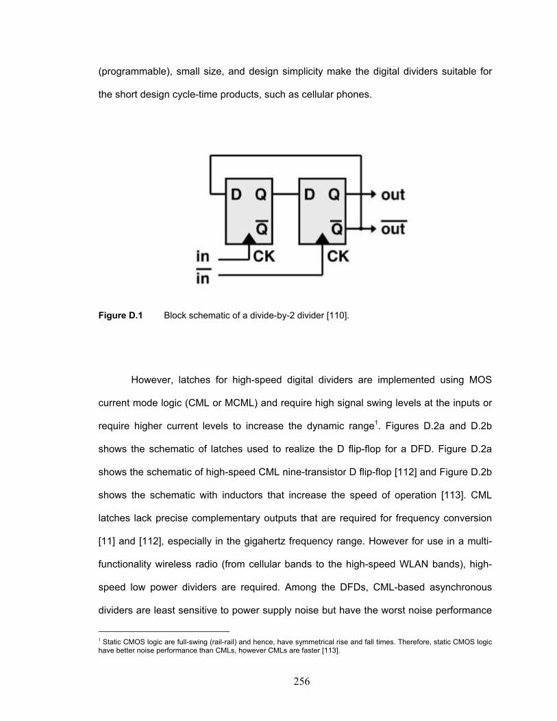
256
(programmable), small size, and design simplicity make the digital dividers suitable for
the short design cycle-time products, such as cellular phones.
Figure D.1 Block schematic of a divide-by-2 divider [110].
However, latches for high-speed digital dividers are implemented using MOS
current mode logic (CML or MCML) and require high signal swing levels at the inputs or
require higher current levels to increase the dynamic range1. Figures D.2a and D.2b
shows the schematic of latches used to realize the D flip-flop for a DFD. Figure D.2a
shows the schematic of high-speed CML nine-transistor D flip-flop [112] and Figure D.2b
shows the schematic with inductors that increase the speed of operation [113]. CML
latches lack precise complementary outputs that are required for frequency conversion
[11] and [112], especially in the gigahertz frequency range. However for use in a multi-
functionality wireless radio (from cellular bands to the high-speed WLAN bands), high-
speed low power dividers are required. Among the DFDs, CML-based asynchronous
dividers are least sensitive to power supply noise but have the worst noise performance
1 Static CMOS logic are full-swing (rail-rail) and hence, have symmetrical rise and fall times. Therefore, static CMOS logic have better noise performance than CMLs, however CMLs are faster [113].

257
and have highest noise floors [113] and [114]. This is because the time jitter of the first
stage is transferred to the following stages and the total jitter at the output stage is the
accumulation of jitter of all stages [111]. Figure D.3 compares the phase noise
performance of DFDs at 3 GHz input frequency [110].
Figure D.2 (a) Nine-transistor Yuan-Sevenson [113] CML D flip-flop. (b) Enhanced speed D flip-flop. Inductive loads are used to reduce the rise and fall times [113].
(a)
(b)

258
Figure D.3 Phase noise performance of asynchronous and synchronous dividers at 3 GHz [110]. Asynchronous DFDs have higher phase noise and noise floor.
The noise performance of the dividers is an important criterion when used inside
a phase locked loop (PLL) for frequency multiplication. However, when used at the
output of an LO to generate multiple frequency references for up- and down-conversion
the phase noise performance and noise floor are of significant consequences. As
compared to DFDs, regenerative dividers suffer from higher near-carrier phase noise
because of spectrum folding resulting from the mixing process. Kroupa in his paper
[115], showed that the single side-band phase noise at the output of a DFD is
proportional to the time jitter (sto) , which results from the random zero crossing due to
the white and flicker noise components, and the operating frequency (f0). Levantino et al.
[110] showed that the near-carrier phase noise due to flicker noise depends on the
square of the operating frequency. With smaller technology nodes, the flicker noise
component increases, which significantly increases the near-carrier phase noise. Exact
Frequency (Hz)
Phase noise (dBc/Hz)

259
contributions of flicker noise on near-carrier phase noise with increase in operating
frequency have been shown in [115].
From the aforementioned discussion on dividers it is clear that the noise floor of
the DFDs increases with the division ratio (more divide-by-2 stages) and operating
frequency. To achieve speeds > 5 GHz, the power consumption of the dividers need to
be increased. This was clearly shown in [112], where a π16 asynchronous divider at 3
GHz consumed ~100 mW whereas the same divider at 0.8 GHz consumes only 16 mW!!
A survey of work done on frequency dividers over different frequency ranges is show in
Table D.1. From Table D.1 it can be concluded that the DFDs exhibit significant trade-off
between the technology nodes, power consumption and noise floor. A good example
showing this trade-off is the π16 DFD on 0.13 um CMOS process technology [116] with
a maximum input frequency of 10 GHz. This DFD consumed only 18 mW power but with
a considerably higher noise floor. Additionally, the DFD produced a 5 GHz output signal
with a relatively high phase noise of -110 dBc/Hz at 1 MHz offset.
Table D.1 Performance summary of different DFDs over technology generations and frequency.
Ref. Tech. Division ratio Input frequency
(max.)
Noise floor,
dBc/Hz Power
[118] 0.7 um
CMOS 8 1.5 GHz -167 55
[117] 0.25 um
CMOS 220 5.5 -148 59
[116] 0.13 um
CMOS 3 10 -120 18

260
REFERENCES
[1] UMA Technology, [online document], Available HTTP:http://www.umatechnology.org, Jan. 2006.
[2] H. Hashemi, “Integrated concurrent multi-band radios and multiple antenna systems,”
Ph.D. Thesis, California Institute of Technology, Sept. 2003. [3] Z. Li, and Kenneth K.O, “A low phase noise and low-power multiband CMOS VCO,”
in IEEE J. Solid-State Circuits, vol.40, No.6, pp. 1296-1302, June 2005. [4] S. Dalmia, V. Sundaram, G. White, and M. Swaminathan, “Liquid Crystalline Polymer
based lumped element bandpass filters for multiple wireless applications,” presented at IEEE MTT-S Int. Microwave Symp. Dig., Fort Worth, TX, June 2004.
[5] V. Govind, “Design of baluns and low noise amplifiers in integrated mixed-signal
organic substrates,” Ph.D. Thesis, Georgia Institute of Technology, Aug. 2005. [6] A. Bavisi, S. Dalmia, V. Sundaram, M. Swaminathan, and G. White, “Chip-package
co-design of integrated voltage controlled oscillator in LCP substrate,” accepted for publication at IEEE Trans. Adv. Pack, 2005.
[7] S. Dalmia, “Design and implementation of high-Q passive devices for wireless
applications using SOP based organic technologies,” Ph.D. Thesis, Georgia Institute of Technology, Sept. 2002.
[8] O2 Inc., [online document], Available HTTP: http://www.o2.com/services/
xda_range.asp. [9] Q. Gu, RF System Design of Transceivers for Wireless Communication, Springer, Ed.
1, 2005. [10] H. Hashemi and A. Hajimiri, “Concurrent multiband low-noise amplifiers- theory,
design and applications,” IEEE Trans. Microwave Theory Tech., vol.50, Issue 1, pp. 288-301, Jan. 2002.
[11] B Razavi, RF Microelectronics, Prentice-Hall publications, Ed. 2, 1998.

261
[12] W-C.Y. Lee, Wireless and Cellular Communication, McGraw-Hill Publications, Ed.
3rd, 2005. [13] S. Dalmia, A. Bavisi, S. Mukherjee, V. Govind, V. Sundaram, M. Swaminathan, and
G. White , “A multiple frequency signal generator for 802.11a/b/g VoWLAN type applications using organic packaging technology,” in IEEE Elec. Comp. and Tech. Conf., Vol.2, pp. 1664-1770, 2004.
[14] D. M. Pozar, Microwave Engineering. Chapter 11, pp. 644, John Wiley Publications,
2nd Edition, 1998. [15] Z. Ying, “Progress of multi-band antenna technology in mobile phone industry,” IEE
Wideband and Multi-Band Antennas and Arrays, pp. 1-5, Sept. 2005 [16] C. Quendo, E. Rius, and C. Person, “An original topology of dual-band filter with
transmission zeros,” in IEEE MTT-S Int. Microwave Symp. Dig., pp. 1093-1096, 2003.
[17] C. Conroy and B. Kim, “RF transceivers for wireless in standard CMOS: some
perspective,” IEEE Radio and Wireless Symp., Jan. 2006. [18] B. Xavier, L. Christensen, “Cellular/WiFi multi-mode systems,” IEEE Radio and Wireless Symp., Jan. 2006.
[19] Intel Inc., [Online document], Available HTTP:
http://www.intel.com/technology/silicon/65nm_technology.htm, Feb. 2006 [20] Intel Inc., [Online document], Available HTTP: ftp://download.intel.com/technology/silicon/IDF_Aug_05_65nm_logic.pdf, Feb. 2006. [21] P. Zhang, U. Bhattacharya, Z. Chen, F. Hamzaoglu, D. Murray, N. Vallepalli, Y.
Wang, B. Zheng and Mark Bohr, “An SRAM design on 65nm CMOS technology with integrated leakage reduction schemes,” IEEE Symp. on VLSI Circuits, June 2004.
[22] A.Bavisi, V. Sundaram, M. Swaminathan, S. Dalmia, and G. White, “Design of a dual frequency oscillator for simultaneous multi-band radio communication on a multi-layer Liquid Crystalline Polymer substrate,” in IEEE Radio and Wireless Symp. Jan. 2006.

262
[23] J. N. Burghatz, D. C. Edelstein, K. A. Jenkins, and Y. H. Kwark, “Spiral inductors and transmission lines in silicon technology using copper damascene interconnects and low loss substrates,” IEEE Trans. Microwave Theory Tech., vol.45, pp. 1961-1968, Oct. 1997.
[24] M. Danesh and J. R. Long, “Differentially driven symmetric microstrip inductors,” IEEE Trans. Microwave Theory Tech., vol.50, no. 1, pp. 332-341, Jan. 2002.
[25] C. P. Yue and S. S. Wong, “On-chip spiral inductors with patterned ground shields
for si-based RF ICs,” IEEE J. Solid-State Circuits, vol.33, pp. 743-752, May 1998. [26] R. Tummala, “Microelectronics Packaging Handbook,” McGraw Hill, 2001. [27] http://www.prc.gatech.edu, Mar. 2003. [28]H. Liang, “Material parameter characterization of multilayer LTCC and
implementation of high Q resonators,” IE IEEE MTT-S Int. Microwave Symp., pp. 1901-1904, May 1999.
[29] TDK Inc., [Online Document], Available HTTP: http://www.tdkltcc.com/, Feb. 2006. [30] Prismark® Inc. survey on LTCC, EPCOS Inc., [Online Document], Available HTTP:
http://www.epcos.com/web/generator/Web/Sections/Applications/PassiveIntegration/PDF/DownloadReport,property=Data__en.pdf;/DownloadReport.pdf, Feb. 2006.
[31]Kyocera Inc., LTCC Design Guide, [Online Document], Available HTTP :
http://americas.kyocera.com/kai/semiparts/pdfs/DesignGuide.pdf, Feb. 2006. [32] Wikipedia, Online Encyclopedia, Available HTTP: http://en.wikipedia.org/wiki/Main_Page, Feb. 2006. [33] Rogers Corp., http://www.rogerscorporation.com, Feb. 2006. [34] D. C. Thompson, O. Tantot, H. Jallageas, G. E. Ponchak, M.M. Tentezeris, J.
Papapolymerou, “Characterization of liquid crystal polymer (LCP) material and transmission lines on LCP substrates from 30 to 110 GHz,” IEEE Trans. Microwave Theory and Tech., Vol.52, pp.1343-1352, April 2004.

263
[35] D. C. Thompson, J. Papapolymerou, and M.M. Tentezeris, “High temperature dielectric stability of LCP at mm-wave frequencies,” IEEE Microwave and Wireless Comp. Lett., Vol.15, pp.561-563, Sept. 2005.
[36] P. Kinget, Integrated GHz voltage controlled oscillators. Chapter in Analog Circuit Design. W. Sansen, Kluwer Academic publisher, 1999.
[37]C. Lam, B.Razavi, “A 2.6/5.2 GHz Frequency Synthesizer in 0.4um CMOS
Technology”, in IEEE J. Solid-State Circuits, Vol.35, pp. 788-79, May 2000.
[38] A. Ravi, B.R. Carlton, G. Banerjee, K. Soumyanath, “ A 1.4V, 2.4/5.2 GHz, 90 nm CMOS system in a package transceiver for next generation WLAN,” in IEEE Symp. on VLSI Tech., 2005.
[39] P. R. Gray, P. J. Hurst, S. H. Lewis, R. G. Meyer, Analysis and Design of Analog Integrated Circuits, Chapter 11, pp.748-755, John Wiley and Sons, Ed.4th, 2001.
[40] U. L. Rohde, A. K. Poddar, G. Bock, The Design of Modern Microwave Oscillators for Wireless Applications: Theory and Optimization, Chapter 2, pp. 9-32, Wiley Interscience, May 2005.
[41] D.B. Leeson, “A simple model of feedback oscillator noise spectrum,” in Proc. IEEE,
Vol.54, pp. 329, Feb. 1966. [42] A. Hajimiri, Jitter and Phase Noise in Electrical Oscillators, Ph.D. Thesis, Stanford
University, Nov. 1998. [43] J-C. Nallatamby, M. Pringet, J. J. Obregon, “On the role of additive and converted
noise in the generation of phase noise in nonlinear oscillators,” IEEE Trans. Microwave Theory and Tech., Vol.53, pp.901-906, Mar. 2005.
[44] W.P. Robins, Phase Noise in Signal Sources, Peter Peregrinus Ltd., London, 1982.
[45] S. Mass, Noise in Linear and Nonlinear Circuits, Artech House, Ed. 1st, Aug. 2005.
[46] J. Craninckx and M. Steyaert, “Low noise VCOs using enhanced LC tanks,” IEEE Trans. Circuits Syst.-II, vol. 42, pp. 794-804, Dec. 1995.

264
[47] J.J. Rael, A.A. Abidi, “Physical processes of phase noise in differential LC oscillators,” in Proc. of IEEE Custom Integrated Circuits Conf., Orlando, FL, pp. 569-572, May 2000.
[48] D. Ham, A. Hajimiri, “Concepts and methods in optimization of integrated LC VCOs,” IEEE J. Solid- State Circuits, Vol.36, Issue 6, pp. 896-909, June 2001.
[49] Advanced Design System User Guide, [Online Document], Available HTTP:
http://www.agilent.com [50] European Telecommunications Standards Institute (ETSI), Available HTTP:
http://www.etsi.org, Feb. 2006. [51] Je-Kwang Cho, Han-Il Lee, Kyung-Suc Nah , and Byeong-Ha Park, “A 2-GHz wide
band low phase noise voltage-controlled oscillator with on chip LC tank,” in Proc. of IEEE Custom Integrated Circuits Conf., San Jose, CA, pp. 559-562, 2003.
[52] M. Tiebout, “Low-Power Low-Phase-Noise Differentially Tuned Quadrature VCO Design in Standard CMOS,” IEEE J. Solid-State Circuits, Vol.36, pp. 1018-1024, July 2001.
[53] Bram De Muer, M. Borremans, M. Steyaert, and G. Li Puma, “A 2 GHz Low-Phase-Noise Integrated LC-VCO Set with Flicker Noise Upconversion Minimization,” IEEE J. Solid-State Circuits, Vol.35, No.7, pp. 1034-1038, July 2000.
[54] L. Dauphinee, M. Copeland, P. Schvan, “A balanced 1.5 GHz voltage controlled oscillator with an integrated LC resonator,” in Proc. of IEEE Int. Solid-State Circuits Conf. Dig., San Francisco, CA, pp. 390-391, May 1997.
[55] D. Pache, J.M. Fournier, G. Billiot, and P. Senn, “ An improved 3 V 2 GHz image reject mixer and a VCO – Prescalar fully integrated in a BiCMOS process,” in Proc. of IEEE Int. Symp. on Circuits and Sys. Dig., pp. 723-726, 1996.
[56] Alps Electric Company, “VCO products”, [Online Document], Available HTTP: http://www3.alps.co.jp/cgi-bin/WebObjects/catalog.woa/wa/normal?language=english
&country=com&top_mode=2003&product=1, Dec. 2004. [57] CTS Corp., Available HTTP: http://www.ctscorp.com/components/ceramic_duplex.asp, Feb. 2006.

265
[58] Semico Research Corp., Available HTTP: http://www.semico.com/studies/category.asp?id=21, Feb. 2006. [59] V. Palazzari, S. Pinela, J. Laskar, L. Roselli, M. Tentezeris, “ Design of an
asymmetrical dual-band WLAN filter in LCP system-on-package technology,” in IEEE Microw. and Wireless Comp. Lett., Vol.15, No.3, pp. 165-167, March 2005.
[60] R. Bairasubramaniam, S. Pinel, J. Papapolymerou, J. Laskar, C. Quendo, E. Rius, A. Manchec, and C. Person, “Dual-band filters for WLAN applications on LCP technology,” in IEEE MTT-S Int. Microwave Symp. Dig., June 2005.
[61] C-M. Tsai, H-M. Lee, C-C. Tsai, “Planar filter design with fully controllable second passband,” IEEE Trans. Microwave Theory and Tech., Vol.53, pp. 3429 -3439, Nov. 2005.
[62] L-C Tsai, C-W Hsue, “Dual-band bandpass filters using equal-length coupled-serial-
shunte lines and Z-transform technique,” IEEE Trans. Microwave Theory and Tech., vol.52, pp. 1111 - 1117, Apr. 2004.
[63] H. Miyake, S. Kitazawa, T. Ishizaki, T. Yamada, and Y. Nagatomi, “A miniaturized
monolithic dual band filter using ceramic lamination technique for dual mode portable telephones,” in IEEE MTT-S Int. Microwave Symp. Dig., June 1997.
[64] R. E. Collin, Foundations for Microwave Engineering, Chapter 8, pp.550 – 647,
IEEE press, Ed. 2, 2002. [65] A. I. Zverev, Handbook of Filter Synthesis, John Wiley Publications, 1967. [66] G. Matthaei, E.M.T Jones, L. Young, Microwave Filters, Impedance-Matching Networks, and Coupling Structures, Artech House Publishers, 1980.
[67] A. Bavisi, V. Sundaram, and M. Swaminathan, “Design of a system-in-package based
low phase noise VCO using 3-D integrated passives on a multi-layer LCP substrate,” at 35th Euro. Microwave Conf., Oct. 2005.
[68] W. Yun, A.Bavisi, V. Sundaram, M. Swaminathan, and E. Engin, “3D integration and
characterization of high Q passives on multilayer LCP substrate,” at IEEE Asia Pacific Microw. Conf., pp. 327-330, Dec. 2005

266
[69] J. Lin, "An Integrated Low Phase Noise Voltage Controlled Oscillator for Base Station Application,” in Proc. of IEEE Int. Solid-State Circuits Conf. Dig., pp. 432-433, 476, 7-9, Feb. 2000.
[70] A. Bavisi, S. Dalmia, G. White, V. Sundaram, and M. Swaminathan, “A 3G/WLAN
VCO with High Q embedded passives in high performance organic substrate,” IEEE Asia Pacific Microwave Conf., Seoul, Korea, Nov. 2003.
[71] Sonnet, High Frequency Electromagnetic Software, http://www.sonnetusa.com [72] A. M. Niknejad, R. G. Meyer, “Analysis, design and optimization of spiral inductors
and transformers on Si RF ICs”, IEEE J. Solid-State Circuits, Vol.33, pp. 1470-1481, October 1998.
[73] A. Ismail, A. Abidi, “CMOS Differential LC Oscillator with Suppressed Up-Converted
Flicker Noise,” in Proc. of IEEE Int. Solid-State Circuits Conf. Dig., San Francisco, CA, pp.98-99, Feb. 2003.
[74] Agilent Semiconductor Products, Transistor Guide, “High performance Isolated
collector silicon bipolar transistor.” [Online], Available HTTP: http://cp.literature.agilent.com/litweb/pdf/5988-0132EN.pdf
[75] Murata Application Product Selection Guide, “Microwave Modules and VCO.” [Online Document], Available HTTP: http://search.murata.co.jp/Ceramy/owa/expert.showser?sLbcd=L0405&sLang=2&sUbnm=Microwave+Modules, Dec. 2004.
[76] Sin-Hang Cheng, Kwok-Kueng M.Cheng, and Ke-Li Wu, “Low Phase Noise Voltage Controlled Oscillator Design using LTCC technology”, IEEE Microwave and Wireless Component Lett., Vol.30, No.8, pp. 329-331, August 2003.
[77] F. Svelto, R. Castello, “A bond-wire inductor–MOS varactor VCO tunable from 1.8GHz to 2.4GHz,” IEEE Trans. Microwave Theory and Tech., Vol. 50, Issue 1, pp. 403-407, Jan. 2002.
[78] J-Y. Lee, D. Suh, S-H. Lee, S-Y Lee, C-W. Park, S-H. Kim, K-H Shim, J-Y. Kang, K-I. Cho, and S. H. Oh, “A packaged 2.3GHz SiGe VCO with parallel-branch inductors”, in IEEE Radio Frequency IC Conf., pp. 655-658, Philadelphia, PA, June 2003.

267
[79] Je-Kwang Cho, Han-Il Lee, Kyung-Suc Nah , and Byeong-Ha Park, “A 2-GHz wide band low phase noise voltage-controlled oscillator with on chip LC tank,” in Proc. of IEEE Custom Integrated Circuits Conf., San Jose, CA, pp. 559-562, 2003.
[80] M. Tiebout, “Low-Power Low-Phase-Noise Differentially Tuned Quadrature VCO Design in Standard CMOS,” IEEE J. Solid-State Circuits, Vol.36, pp. 1018-1024, July 2001.
[82] A.Bavisi, V. Sundaram, and M. Swaminathan, “A miniaturized novel feedback LC
oscillator for UMTS type applications in a 3-D stacked Liquid Crystalline Polymer technology,” Int. Journal RF and Microw. Comp. Aided Engg., Wiley Interscience, published online on Feb. 2006.
[83] Skyworks Inc., SMV 1405 Product datasheet, [Online Document], Available HTTP:// http://www.skyworksinc.com/products_display_item.asp?did=782&filename=/200068C.pdf
[84] Sirenza Microdevices Inc., [Online Document], Available HTTP:// http://www.sirenza.com/pdfs/datasheets/vco190-775t.pdf, Nov. 2005.
[85] J. D. Cressler and G. Niu, Silicon-Germanium Heterojunction Bipolar Transistors, Artech House Publishers, Chapter 9, pp.371 – 419, 2003.
[86] J. J. Liou and A. Kager, “Theoretical prediction of the performance of Si and SiC bipolar transistors operating at high temperatures,” IEE Proceedings, vol. 140, No.4, pp. 289 – 293, Aug. 1993.
[87] E. Glenn, Physics Factbook, [Online Document], Available HTTP: http://hypertextbook.com/facts/2004/BridgetRitter.shtml, Feb. 2006.
[88] M. M. Driscoll, “The use of multi-pole bandpass filters and other multiple resonator circuitry as oscillator frequency stabilization elements,” IEEE Int. Frequency Control Symp., pp. 782-789, 1996.
[89] K. Kwok and H. C. Luong, “Ultra-low voltage high performance CMOS VCOs using
transformer feedback,” IEEE J. Solid-State Circuits, vol.40, pp. 652-660, Mar. 2005.

268
[90] Sung-Hwan Min, M. Swaminathan, “Construction of broadband passive macromodels from frequency data,” IEEE Trans. Electromagnetic Compatibility, Nov.2004.
[91] Sung-Hwan Min, “Automated Construction of macro models of distributed interconnect networks,” Ph.D Thesis, Georgia Institute of Technology, 2004.
[92] J. N. Torry, “Group delay and amplitude trade-off for equi-ripple group delay and gain-magnitude bandpass filters,” IEE Electronic Filters Colloqium, pp. 1-5, May 1988.
[93] S-H Cheng, K-K M. Cheung, and Ke-Li Wu, “Low phase noise integrated VCO design using LTCC technology”, IEEE Microwave and Wireless Comp. Lett., vol.13, pp. 329-331, Aug..2003.
[94]Murata Corp., VCO products, [Online Document], Available HTTP:
http://search.murata.co.jp/Ceramy/owa/expert.showser?sLbcd=L0405&s Lang= 2&sUbnm=Microwave+Modules, Mar. 2005.
[95]Alps Electric Company, “VCO products”, [online], Available HTTP:
http://www3.alps.co.jp/cgi-bin/WebObjects/catalog.woa/wa/normal?l anguage=english&country=com&top_mode=2003&product=1, Mar. 2005
[96]T. Prochazka, M. Fischer, B. Gruber, R. Manner, R. Matz, and S. Walter, “ High
quality LTCC resonator for voltage controlled oscillator,” IEEE Trans. Components and Packaging Technologies, Vol. 26, Issue 3, pp. 591-597, Sept. 2003.
[97]Ja-Yol Lee, D. Suh, S-H Lee, C-W Park, and S. H. Kim, “A packaged 2.3 GHz SiGe
VCO with parallel branch inductors,” Proc. IEEE Radio Freq. ICs Conf., Philadelphia, PA, June 2003, pp. 655-658
[98] M. Tiebout, “A CMOS fully-integrated 1 GHz and 2 GHz dual band VCO with a
voltage controlled inductor,” IEEE European Solid-State Circuits Conf., pp. 799 -802, Sept. 2002.
[99] M-S Yim, K.K. O, “Switched resonators and their applications in a dual band
monolithic CMOS LC tuned VCO,” IEEE Trans. Microwave Theory and Tech., Vol. 54, Issue 1, pp. 74-81, Jan. 2006.

269
[100] K. Kurokawa, "Some basic characteristics of broadband negative resistance oscillator circuits," Bell Systm. Tech. J. 48, pp. 1937-1955, July 1969.
[101] J. S. Schaffner, “Simultaneous oscillations in oscillators,” IRE Tran. Circuit Theory, vol.1, no.2, pp. 2-8, June 1954.
[102] I. Bruyland, “Simultaneous oscillations at two frequencies in RLC circuits,” Proc. of
IEEE, vol.1, pp.82-83, Jan. 1968. [103] S. A. Mass, Nonlinear microwave and RF circuits, 2nd ed., Artech House, pp.537-
550. [104] A. Bavisi, W. Yun, V. Sundaram, and M. Swaminathan, “Design and applications of
high Q passive devices on multi-layered LCP substrate,” in Proc. IEEE Asia Pacific Microw. Conf., pp. 1295-1298, Dec. 2005.
[105] A. Bavisi, J. P. Comeau, J. D. Cressler, M. Swaminathan, and M. Lam, “A 9 GHz, 5
mW VCO using lumped-element transformer feedback in 150 GHz fT SiGe HBT Technology,” IEEE Topical Meeting on Silicon Monolithic ICs in RF Systems, pp. 151 – 154, 2006.
[106] H. Wu and A. Hajimiri, “A 10 GHz CMOS distributed VCO,” IEEE Custom
Integrated Circuits Conf., pp.581-584, Sept. 2000.
[107] H. Zirath et al., “Development of 60 GHz front-end circuits for a high data rate communication system,” IEEE J. Solid-State Circuits, vol.39, pp. 1640-1649, Oct. 2004.
[108] J. Lin, J-G Ma, K.S. Yeo, and M. A. Do, “9.3 – 10.4 GHz band cross-coupled
complementary oscillator with low phase noise performance,” IEEE Trans. Microwave Theory and Tech., Vol. 52, Issue 4, pp. 1273-1278, Apr. 2004.
[109] M. M. Driscoll and T. D. Merrell, “Spectral performance of frequency multipliers and dividers,” IEEE Frequency Control Symp., pp. 193- 200, 1992.
[110] S. Levantino, L. Romano, S. Pellerano, C. Samori, and A. Lacaita, “Phase noise in digital frequency dividers,” IEEE J. Solid-State Circuits, vol.39, pp. 775-784, May 2004.

270
[111] A. M. Fahim, “Jitter analysis of digital frequency dividers in communication systems,” IEEE Int. Ultrasonics, Ferroelectrics, and Frequency Control, pp. 169 – 173, 2004.
[112] Q. Huang and R. Rogenmoser, “Speed optimization of edge-triggered CMOS
circuits for gigahertz single-phase clocks,” IEEE J. Solid-State Circuits, vol. 31, pp. 456-465, Mar. 1996.
[113] U. Singh, and M. M. Green, “High frequency CML clock dividers in 0.13-um CMOS operating up to 38 GHz,” IEEE J. Solid-State Circuits, vol. 40, pp. 1658-1661, Aug. 2005.
[114] W. E. Egan, Frequency Synthesis by Phase Lock, Chapter 2, Wiley Interscience,
2nd Ed., 2000. [115] V. F. Kroupa, “Jitter and phase noise in frequency dividers,” IEEE Trans. Instrum.
Measure., vol. 50, pp. 1241 – 1243, Oct. 2001. [116] Y. Moon and S-H Lee, “A Divide-by-16.5 circuit for 10-Gb Ethernet transceiver in
0.13- um CMOS,” IEEE J. Solid-State Circuits, vol. 40, pp. 1175-1179, May 2005. [117] N. Krishnapura and P. R. Kringet, “A 5.3 GHz programmable divider for HiPerLAN
in 0.25-um CMOS,” IEEE J. Solid-State Circuits, vol. 35, pp. 1019-1024, July 2000. [118] B. De Muer and M. Steyaert, “A single ended 1.5 GHz 8/9 modulus prescaler in 0.7
um CMOS technology with low phase noise and high input sensitivity,” in Proc. Eur. Solid State Circuits Conf., pp. 256-259, 1998.
[119] J. K. Hale, Oscillations in nonlinear systems, McGraw-Hill Publications, pp.27-95,
1963. [120] J. K. Hale, Ordinary Differential Equations, Krieger Publications, pp.175-211, 1980. [121] G. Strang, “Linear Algebra and its applications,” 3rd Ed., Saunders Publications,
1988.