intel® pxa255 processor - mdh... intel create&share, intel dot.station, intel gigablade, intel...
TRANSCRIPT

Intel® PXA255 ProcessorDeveloper’s Manual
March, 2003
Order Number: 278693-001

ii Intel® PXA255 Processor Developer’s Manual
INFORMATION IN THIS DOCUMENT IS PROVIDED IN CONNECTION WITH INTEL® PRODUCTS. NO LICENSE, EXPRESS OR IMPLIED, BY ESTOPPEL OR OTHERWISE, TO ANY INTELLECTUAL PROPERTY RIGHTS IS GRANTED BY THIS DOCUMENT. EXCEPT AS PROVIDED IN INTEL'S TERMS AND CONDITIONS OF SALE FOR SUCH PRODUCTS, INTEL ASSUMES NO LIABILITY WHATSOEVER, AND INTEL DISCLAIMS ANY EXPRESS OR IMPLIED WARRANTY, RELATING TO SALE AND/OR USE OF INTEL PRODUCTS INCLUDING LIABILITY OR WARRANTIES RELATING TO FITNESS FOR A PARTICULAR PURPOSE, MERCHANTABILITY, OR INFRINGEMENT OF ANY PATENT, COPYRIGHT OR OTHER INTELLECTUAL PROPERTY RIGHT. Intel products are not intended for use in medical, life saving, or life sustaining applications.
Intel may make changes to specifications and product descriptions at any time, without notice.
Designers must not rely on the absence or characteristics of any features or instructions marked “reserved” or “undefined.” Intel reserves these for future definition and shall have no responsibility whatsoever for conflicts or incompatibilities arising from future changes to them.
The Intel® PXA255 Processor may contain design defects or errors known as errata which may cause the product to deviate from published specifications. Current characterized errata are available on request.
MPEG is an international standard for video compression/decompression promoted by ISO. Implementations of MPEG CODECs, or MPEG enabled platforms may require licenses from various entities, including Intel Corporation.
This document and the software described in it are furnished under license and may only be used or copied in accordance with the terms of the license. The information in this document is furnished for informational use only, is subject to change without notice, and should not be construed as a commitment by Intel Corporation. Intel Corporation assumes no responsibility or liability for any errors or inaccuracies that may appear in this document or any software that may be provided in association with this document. Except as permitted by such license, no part of this document may be reproduced, stored in a retrieval system, or transmitted in any form or by any means without the express written consent of Intel Corporation.
Contact your local Intel sales office or your distributor to obtain the latest specifications and before placing your product order.
Copies of documents which have an ordering number and are referenced in this document, or other Intel literature may be obtained by calling 1-800-548-4725 or by visiting Intel's website at http://www.intel.com.
Copyright © Intel Corporation, 2003
AlertVIEW, i960, AnyPoint, AppChoice, BoardWatch, BunnyPeople, CablePort, Celeron, Chips, Commerce Cart, CT Connect, CT Media, Dialogic, DM3, EtherExpress, ETOX, FlashFile, GatherRound, i386, i486, iCat, iCOMP, Insight960, InstantIP, Intel, Intel logo, Intel386, Intel486, Intel740, IntelDX2, IntelDX4, IntelSX2, Intel ChatPad, Intel Create&Share, Intel Dot.Station, Intel GigaBlade, Intel InBusiness, Intel Inside, Intel Inside logo, Intel NetBurst, Intel NetStructure, Intel Play, Intel Play logo, Intel Pocket Concert, Intel SingleDriver, Intel SpeedStep, Intel StrataFlash, Intel TeamStation, Intel WebOutfitter, Intel Xeon, Intel XScale, Itanium, JobAnalyst, LANDesk, LanRover, MCS, MMX, MMX logo, NetPort, NetportExpress, Optimizer logo, OverDrive, Paragon, PC Dads, PC Parents, Pentium, Pentium II Xeon, Pentium III Xeon, Performance at Your Command, ProShare, RemoteExpress, Screamline, Shiva, SmartDie, Solutions960, Sound Mark, StorageExpress, The Computer Inside, The Journey Inside, This Way In, TokenExpress, Trillium, Vivonic, and VTune are trademarks or registered trademarks of Intel Corporation or its subsidiaries in the United States and other countries.
*Other names and brands may be claimed as the property of others.

Contents
Contents1 Introduction...................................................................................................................................1-1
1.1 Intel® XScale™ Microarchitecture Features......................................................................1-11.2 System Integration Features..............................................................................................1-1
1.2.1 Memory Controller ................................................................................................1-21.2.2 Clocks and Power Controllers...............................................................................1-21.2.3 Universal Serial Bus (USB) Client.........................................................................1-21.2.4 DMA Controller (DMAC) .......................................................................................1-31.2.5 LCD Controller ......................................................................................................1-31.2.6 AC97 Controller ....................................................................................................1-31.2.7 Inter-IC Sound (I2S) Controller .............................................................................1-31.2.8 Multimedia Card (MMC) Controller .......................................................................1-31.2.9 Fast Infrared (FIR) Communication Port...............................................................1-31.2.10 Synchronous Serial Protocol Controller (SSPC)...................................................1-41.2.11 Inter-Integrated Circuit (I2C) Bus Interface Unit....................................................1-41.2.12 GPIO.....................................................................................................................1-41.2.13 UARTs ..................................................................................................................1-41.2.14 Real-Time Clock (RTC).........................................................................................1-51.2.15 OS Timers.............................................................................................................1-51.2.16 Pulse-Width Modulator (PWM) .............................................................................1-51.2.17 Interrupt Control ....................................................................................................1-51.2.18 Network Synchronous Serial Protocol Port...........................................................1-5
2 System Architecture .....................................................................................................................2-1
2.1 Overview............................................................................................................................2-12.2 Intel® XScale™ Microarchitecture Implementation Options..............................................2-2
2.2.1 Coprocessor 7 Register 4 - PSFS Bit ...................................................................2-22.2.2 Coprocessor 14 Registers 0-3 - Performance Monitoring.....................................2-32.2.3 Coprocessor 14 Register 6 and 7- Clock and Power Management......................2-32.2.4 Coprocessor 15 Register 0 - ID Register Definition ..............................................2-32.2.5 Coprocessor 15 Register 1 - P-Bit ........................................................................2-4
2.3 I/O Ordering .......................................................................................................................2-52.4 Semaphores ......................................................................................................................2-52.5 Interrupts............................................................................................................................2-52.6 Reset .................................................................................................................................2-62.7 Internal Registers...............................................................................................................2-72.8 Selecting Peripherals vs. General Purpose I/O .................................................................2-72.9 Power on Reset and Boot Operation .................................................................................2-82.10 Power Management...........................................................................................................2-82.11 Pin List ...............................................................................................................................2-82.12 Memory Map....................................................................................................................2-182.13 System Architecture Register Summary..........................................................................2-21
3 Clocks and Power Manager .........................................................................................................3-1
3.1 Clock Manager Introduction...............................................................................................3-13.2 Power Manager Introduction..............................................................................................3-23.3 Clock Manager...................................................................................................................3-2
Intel® PXA255 Processor Developer’s Manual iii

Contents
3.3.1 32.768 kHz Oscillator............................................................................................3-43.3.2 3.6864 MHz Oscillator ..........................................................................................3-43.3.3 Core Phase Locked Loop .....................................................................................3-43.3.4 95.85 MHz Peripheral Phase Locked Loop ..........................................................3-53.3.5 147.46 MHz Peripheral Phase Locked Loop ........................................................3-53.3.6 Clock Gating .........................................................................................................3-6
3.4 Resets and Power Modes..................................................................................................3-63.4.1 Hardware Reset....................................................................................................3-63.4.2 Watchdog Reset ...................................................................................................3-73.4.3 GPIO Reset ..........................................................................................................3-83.4.4 Run Mode .............................................................................................................3-93.4.5 Turbo Mode ..........................................................................................................3-93.4.6 Idle Mode ............................................................................................................3-103.4.7 Frequency Change Sequence............................................................................3-113.4.8 33-MHz Idle Mode ..............................................................................................3-133.4.9 Sleep Mode.........................................................................................................3-153.4.10 Power Mode Summary .......................................................................................3-20
3.5 Power Manager Registers ...............................................................................................3-223.5.1 Power Manager Control Register (PMCR) .........................................................3-233.5.2 Power Manager General Configuration Register (PCFR)...................................3-243.5.3 Power Manager Wake-Up Enable Register (PWER)..........................................3-253.5.4 Power Manager Rising-Edge Detect Enable Register (PRER) ..........................3-263.5.5 Power Manager Falling-Edge Detect Enable Register (PFER) ..........................3-273.5.6 Power Manager GPIO Edge Detect Status Register (PEDR).............................3-283.5.7 Power Manager Sleep Status Register (PSSR) .................................................3-293.5.8 Power Manager Scratch Pad Register (PSPR) ..................................................3-303.5.9 Power Manager Fast Sleep Walk-up Configuration Register (PMFW)...............3-313.5.10 Power Manager GPIO Sleep State Registers (PGSR0, PGSR1, PGSR2).........3-313.5.11 Reset Controller Status Register (RCSR)...........................................................3-33
3.6 Clocks Manager Registers...............................................................................................3-343.6.1 Core Clock Configuration Register (CCCR) .......................................................3-343.6.2 Clock Enable Register (CKEN)...........................................................................3-363.6.3 Oscillator Configuration Register (OSCC) ..........................................................3-38
3.7 Coprocessor 14: Clock and Power Management ............................................................3-383.7.1 Core Clock Configuration Register (CCLKCFG).................................................3-393.7.2 Power Mode Register (PWRMODE)...................................................................3-40
3.8 External Hardware Considerations..................................................................................3-403.8.1 Power-On-Reset Considerations ........................................................................3-403.8.2 Power Supply Connectivity .................................................................................3-403.8.3 Driving the Crystal Pins from an External Clock Source.....................................3-413.8.4 Noise Coupling Between Driven Crystal Pins and a Crystal Oscillator...............3-41
3.9 Clocks and Power Manager Register Summary..............................................................3-413.9.1 Clocks Manager Register Locations ...................................................................3-413.9.2 Power Manager Register Summary....................................................................3-41
4 System Integration Unit ................................................................................................................4-1
4.1 General-Purpose I/O..........................................................................................................4-14.1.1 GPIO Operation ....................................................................................................4-14.1.2 GPIO Alternate Functions.....................................................................................4-24.1.3 GPIO Register Definitions.....................................................................................4-6
iv Intel® PXA255 Processor Developer’s Manual

Contents
4.2 Interrupt Controller...........................................................................................................4-204.2.1 Interrupt Controller Operation .............................................................................4-204.2.2 Interrupt Controller Register Definitions..............................................................4-21
4.3 Real-Time Clock (RTC) ...................................................................................................4-284.3.1 Real-Time Clock Operation.................................................................................4-284.3.2 RTC Register Definitions ....................................................................................4-294.3.3 Trim Procedure ...................................................................................................4-32
4.4 Operating System (OS) Timer .........................................................................................4-344.4.1 Watchdog Timer Operation.................................................................................4-354.4.2 OS Timer Register Definitions ............................................................................4-35
4.5 Pulse Width Modulator.....................................................................................................4-384.5.1 Pulse Width Modulator Operation .......................................................................4-384.5.2 Register Descriptions..........................................................................................4-404.5.3 Pulse Width Modulator Output Wave Example...................................................4-43
4.6 System Integration Unit Register Summary.....................................................................4-444.6.1 GPIO Register Locations ....................................................................................4-444.6.2 Interrupt Controller Register Locations ...............................................................4-454.6.3 Real-Time Clock Register Locations...................................................................4-454.6.4 OS Timer Register Locations..............................................................................4-454.6.5 Pulse Width Modulator Register Locations.........................................................4-46
5 DMA Controller .............................................................................................................................5-1
5.1 DMA Description ................................................................................................................5-15.1.1 DMAC Channels ...................................................................................................5-25.1.2 Signal Descriptions ...............................................................................................5-25.1.3 DMA Channel Priority Scheme .............................................................................5-35.1.4 DMA Descriptors...................................................................................................5-55.1.5 Channel States .....................................................................................................5-85.1.6 Read and Write Order...........................................................................................5-95.1.7 Byte Transfer Order ..............................................................................................5-95.1.8 Trailing Bytes ......................................................................................................5-10
5.2 Transferring Data.............................................................................................................5-115.2.1 Servicing Internal Peripherals .............................................................................5-115.2.2 Quick Reference for DMA Programming ............................................................5-135.2.3 Servicing Companion Chips and External Peripherals .......................................5-145.2.4 Memory-to-Memory Moves.................................................................................5-16
5.3 DMAC Registers ..............................................................................................................5-175.3.1 DMA Interrupt Register (DINT) ...........................................................................5-175.3.2 DMA Channel Control/Status Register (DCSRx) ................................................5-175.3.3 DMA Request to Channel Map Registers (DRCMRx) ........................................5-205.3.4 DMA Descriptor Address Registers (DDADRx) ..................................................5-205.3.5 DMA Source Address Registers .........................................................................5-215.3.6 DMA Target Address Registers (DTADRx).........................................................5-225.3.7 DMA Command Registers (DCMDx) ..................................................................5-23
5.4 Examples .........................................................................................................................5-265.5 DMA Controller Register Summary .................................................................................5-28
6 Memory Controller ........................................................................................................................6-1
6.1 Overview............................................................................................................................6-16.2 Functional Description .......................................................................................................6-2
Intel® PXA255 Processor Developer’s Manual v
Contents
6.2.1 SDRAM Interface Overview..................................................................................6-26.2.2 Static Memory Interface / Variable Latency I/O Interface .....................................6-36.2.3 16-Bit PC Card / Compact Flash Interface ...........................................................6-4
6.3 Memory System Examples ................................................................................................6-46.4 Memory Accesses .............................................................................................................6-7
6.4.1 Reads and Writes .................................................................................................6-86.4.2 Aborts and Nonexistent Memory ..........................................................................6-8
6.5 Synchronous DRAM Memory Interface .............................................................................6-86.5.1 SDRAM MDCNFG Register (MDCNFG................................................................6-86.5.2 SDRAM Mode Register Set Configuration Register (MDMRS) ..........................6-126.5.3 SDRAM MDREFR Register (MDREFR) .............................................................6-146.5.4 Fixed-Delay or Return-Clock Data Latching .......................................................6-176.5.5 SDRAM Memory Options ...................................................................................6-186.5.6 SDRAM Command Overview .............................................................................6-276.5.7 SDRAM Waveforms............................................................................................6-28
6.6 Synchronous Static Memory Interface.............................................................................6-326.6.1 Synchronous Static Memory Configuration Register (SXCNFG)........................6-326.6.2 Synchronous Static Memory Mode Register Set Configuration
Register (SXMRS) ..............................................................................................6-376.6.3 Synchronous Static Memory Timing Diagrams...................................................6-386.6.4 Non-SDRAM Timing SXMEM Operation ............................................................6-39
6.7 Asynchronous Static Memory..........................................................................................6-426.7.1 Static Memory Interface......................................................................................6-426.7.2 Asynchronous Static Memory Control Registers (MSCx) ...................................6-446.7.3 ROM Interface ....................................................................................................6-486.7.4 SRAM Interface Overview ..................................................................................6-516.7.5 Variable Latency I/O (VLIO) Interface Overview.................................................6-536.7.6 FLASH Memory Interface ...................................................................................6-56
6.8 16-Bit PC Card/Compact Flash Interface ........................................................................6-586.8.1 Expansion Memory Timing Configuration Register ............................................6-586.8.2 Expansion Memory Configuration Register (MECR) ..........................................6-616.8.3 16-Bit PC Card Overview....................................................................................6-626.8.4 External Logic for 16-Bit PC Card Implementation .............................................6-646.8.5 Expansion Card Interface Timing Diagrams and Parameters ............................6-67
6.9 Companion Chip Interface...............................................................................................6-686.9.1 Alternate Bus Master Mode ................................................................................6-70
6.10 Options and Settings for Boot Memory............................................................................6-726.10.1 Alternate Booting ................................................................................................6-726.10.2 Boot Time Defaults .............................................................................................6-726.10.3 Memory Interface Reset and Initialization...........................................................6-76
6.11 Hardware, Watchdog, or Sleep Reset Operation ............................................................6-776.12 GPIO Reset Procedure....................................................................................................6-796.13 Memory Controller Register Summary ............................................................................6-79
7 LCD Controller..............................................................................................................................7-1
7.1 Overview............................................................................................................................7-17.1.1 Features................................................................................................................7-27.1.2 Pin Descriptions....................................................................................................7-4
7.2 LCD Controller Operation ..................................................................................................7-47.2.1 Enabling the Controller .........................................................................................7-4
vi Intel® PXA255 Processor Developer’s Manual

Contents
7.2.2 Disabling the Controller ........................................................................................7-57.2.3 Resetting the Controller ........................................................................................7-5
7.3 Detailed Module Descriptions ............................................................................................7-57.3.1 Input FIFOs...........................................................................................................7-57.3.2 Lookup Palette ......................................................................................................7-67.3.3 Temporal Modulated Energy Distribution (TMED) Dithering.................................7-67.3.4 Output FIFOs ........................................................................................................7-87.3.5 LCD Controller Pin Usage ....................................................................................7-87.3.6 DMA......................................................................................................................7-9
7.4 LCD External Palette and Frame Buffers ........................................................................7-107.4.1 External Palette Buffer ........................................................................................7-107.4.2 External Frame Buffer.........................................................................................7-11
7.5 Functional Timing ............................................................................................................7-147.6 Register Descriptions.......................................................................................................7-17
7.6.1 LCD Controller Control Register 0 (LCCR0) .......................................................7-187.6.2 LCD Controller Control Register 1 (LCCR1) .......................................................7-247.6.3 LCD Controller Control Register 2 (LCCR2) .......................................................7-267.6.4 LCD Controller Control Register 3 (LCCR3) .......................................................7-287.6.5 LCD Controller DMA ...........................................................................................7-327.6.6 LCD DMA Frame Branch Registers (FBRx) .......................................................7-377.6.7 LCD Controller Status Register (LCSR)..............................................................7-387.6.8 LCD Controller Interrupt ID Register (LIIDR) ......................................................7-417.6.9 TMED RGB Seed Register (TRGBR) .................................................................7-427.6.10 TMED Control Register (TCR)............................................................................7-43
7.7 LCD Controller Register Summary ..................................................................................7-44
8 Synchronous Serial Port Controller ..............................................................................................8-1
8.1 Overview............................................................................................................................8-18.2 Signal Description..............................................................................................................8-1
8.2.1 External Interface to Synchronous Serial Peripherals ..........................................8-18.3 Functional Description .......................................................................................................8-2
8.3.1 Data Transfer........................................................................................................8-28.4 Data Formats .....................................................................................................................8-2
8.4.1 Serial Data Formats for Transfer to/from Peripherals ...........................................8-28.4.2 Parallel Data Formats for FIFO Storage ...............................................................8-6
8.5 FIFO Operation and Data Transfers ..................................................................................8-78.5.1 Using Programmed I/O Data Transfers ................................................................8-78.5.2 Using DMA Data Transfers ...................................................................................8-7
8.6 Baud-Rate Generation.......................................................................................................8-78.7 SSP Serial Port Registers..................................................................................................8-8
8.7.1 SSP Control Register 0 (SSCR0) .........................................................................8-88.7.2 SSP Control Register 1 (SSCR1) .......................................................................8-118.7.3 SSP Data Register (SSDR) ................................................................................8-158.7.4 SSP Status Register (SSSR)..............................................................................8-16
8.8 SSP Controller Register Summary ..................................................................................8-19
9 I2C Bus Interface Unit...................................................................................................................9-1
9.1 Overview............................................................................................................................9-19.2 Signal Description..............................................................................................................9-19.3 Functional Description .......................................................................................................9-1
Intel® PXA255 Processor Developer’s Manual vii

Contents
9.3.1 Operational Blocks................................................................................................9-39.3.2 I2C Bus Interface Modes .....................................................................................9-39.3.3 Start and Stop Bus States ....................................................................................9-4
9.4 I2C Bus Operation .............................................................................................................9-79.4.1 Serial Clock Line (SCL) Generation......................................................................9-79.4.2 Data and Addressing Management ......................................................................9-79.4.3 I2C Acknowledge..................................................................................................9-89.4.4 Arbitration .............................................................................................................9-99.4.5 Master Operations ..............................................................................................9-129.4.6 Slave Operations ................................................................................................9-149.4.7 General Call Address..........................................................................................9-16
9.5 Slave Mode Programming Examples ..............................................................................9-189.5.1 Initialize Unit .......................................................................................................9-189.5.2 Write n Bytes as a Slave.....................................................................................9-189.5.3 Read n Bytes as a Slave ....................................................................................9-18
9.6 Master Programming Examples ......................................................................................9-199.6.1 Initialize Unit .......................................................................................................9-199.6.2 Write 1 Byte as a Master ....................................................................................9-199.6.3 Read 1 Byte as a Master ....................................................................................9-209.6.4 Write 2 Bytes and Repeated Start Read 1 Byte as a Master..............................9-209.6.5 Read 2 Bytes as a Master - Send STOP Using the Abort ..................................9-21
9.7 Glitch Suppression Logic .................................................................................................9-219.8 Reset Conditions .............................................................................................................9-219.9 Register Definitions..........................................................................................................9-22
9.9.1 I2C Bus Monitor Register (IBMR) .......................................................................9-229.9.2 I2C Data Buffer Register (IDBR).........................................................................9-229.9.3 I2C Control Register (ICR)..................................................................................9-239.9.4 I2C Status Register (ISR) ...................................................................................9-259.9.5 I2C Slave Address Register (ISAR)....................................................................9-27
10 UARTs........................................................................................................................................10-1
10.1 Feature List......................................................................................................................10-110.2 Overview..........................................................................................................................10-2
10.2.1 Full Function UART ............................................................................................10-210.2.2 Bluetooth UART..................................................................................................10-210.2.3 Standard UART ..................................................................................................10-210.2.4 Compatibility with 16550.....................................................................................10-2
10.3 Signal Descriptions..........................................................................................................10-310.4 UART Operational Description ........................................................................................10-4
10.4.1 Reset ..................................................................................................................10-510.4.2 Internal Register Descriptions.............................................................................10-510.4.3 FIFO Interrupt Mode Operation ........................................................................10-2110.4.4 FIFO Polled Mode Operation............................................................................10-2210.4.5 DMA Requests..................................................................................................10-2210.4.6 Slow Infrared Asynchronous Interface..............................................................10-23
10.5 UART Register Summary ..............................................................................................10-2610.5.1 UART Register Differences ..............................................................................10-28
11 Fast Infrared Communication Port..............................................................................................11-1
11.1 Signal Description............................................................................................................11-1
viii Intel® PXA255 Processor Developer’s Manual

Contents
11.2 FICP Operation................................................................................................................11-111.2.1 4PPM Modulation ...............................................................................................11-211.2.2 Frame Format .....................................................................................................11-311.2.3 Address Field......................................................................................................11-311.2.4 Control Field .......................................................................................................11-311.2.5 Data Field ...........................................................................................................11-311.2.6 CRC Field ...........................................................................................................11-411.2.7 Baud Rate Generation ........................................................................................11-411.2.8 Receive Operation ..............................................................................................11-411.2.9 Transmit Operation .............................................................................................11-511.2.10 Transmit and Receive FIFOs..............................................................................11-611.2.11 Trailing or Error Bytes in the Receive FIFO........................................................11-7
11.3 FICP Register Definitions ................................................................................................11-711.3.1 FICP Control Register 0 (ICCR0)........................................................................11-811.3.2 FICP Control Register 1 (ICCR1)......................................................................11-1011.3.3 FICP Control Register 2 (ICCR2)......................................................................11-1111.3.4 FICP Data Register (ICDR)...............................................................................11-1211.3.5 FICP Status Register 0 (ICSR0) .......................................................................11-1311.3.6 FICP Status Register 1 (ICSR1) .......................................................................11-15
11.4 FICP Register Summary................................................................................................11-16
12 USB Device Controller................................................................................................................12-1
12.1 USB Overview .................................................................................................................12-112.2 Device Configuration .......................................................................................................12-212.3 USB Protocol ...................................................................................................................12-2
12.3.1 Signalling Levels .................................................................................................12-312.3.2 Bit Encoding........................................................................................................12-312.3.3 Field Formats ......................................................................................................12-412.3.4 Packet Formats...................................................................................................12-512.3.5 Transaction Formats ...........................................................................................12-612.3.6 UDC Device Requests ........................................................................................12-812.3.7 Configuration ......................................................................................................12-9
12.4 UDC Hardware Connection ...........................................................................................12-1012.4.1 Self-Powered Device ........................................................................................12-1012.4.2 Bus-Powered Devices ......................................................................................12-12
12.5 UDC Operation ..............................................................................................................12-1212.5.1 Case 1: EP0 Control Read ...............................................................................12-1212.5.2 Case 2: EP0 Control Read with a Premature Status Stage..............................12-1312.5.3 Case 3: EP0 Control Write With or Without a Premature Status
Stage ................................................................................................................12-1412.5.4 Case 4: EP0 No Data Command......................................................................12-1512.5.5 Case 5: EP1 Data Transmit (BULK-IN).............................................................12-1512.5.6 Case 6: EP2 Data Receive (BULK-OUT)..........................................................12-1612.5.7 Case 7: EP3 Data Transmit (ISOCHRONOUS-IN)...........................................12-1712.5.8 Case 8: EP4 Data Receive (ISOCHRONOUS-OUT)........................................12-1812.5.9 Case 9: EP5 Data Transmit (INTERRUPT-IN) .................................................12-2012.5.10 Case 10: RESET Interrupt ................................................................................12-2012.5.11 Case 11: SUSPEND Interrupt...........................................................................12-2112.5.12 Case 12: RESUME Interrupt.............................................................................12-21
12.6 UDC Register Definitions...............................................................................................12-21
Intel® PXA255 Processor Developer’s Manual ix

Contents
12.6.1 UDC Control Register (UDCCR).......................................................................12-2212.6.2 UDC Control Function Register (UDCCFR)......................................................12-2412.6.3 UDC Endpoint 0 Control/Status Register (UDCCS0) .......................................12-2512.6.4 UDC Endpoint x Control/Status Register (UDCCS1/6/11)................................12-2712.6.5 UDC Endpoint x Control/Status Register (UDCCS2/7/12)................................12-2912.6.6 UDC Endpoint x Control/Status Register (UDCCS3/8/13)................................12-3112.6.7 UDC Endpoint x Control/Status Register (UDCCS4/9/14)................................12-3212.6.8 UDC Endpoint x Control/Status Register (UDCCS5/10/15)..............................12-3412.6.9 UDC Interrupt Control Register 0 (UICR0) .......................................................12-3612.6.10 UDC Interrupt Control Register 1 (UICR1) .......................................................12-3812.6.11 UDC Status/Interrupt Register 0 (USIR0) .........................................................12-3912.6.12 UDC Status/Interrupt Register 1 (USIR1) .........................................................12-4112.6.13 UDC Frame Number High Register (UFNHR) ..................................................12-4212.6.14 UDC Frame Number Low Register (UFNLR) ...................................................12-4412.6.15 UDC Byte Count Register x (UBCR2/4/7/9/12/14) ...........................................12-4412.6.16 UDC Endpoint 0 Data Register (UDDR0) .........................................................12-4512.6.17 UDC Endpoint x Data Register (UDDR1/6/11) .................................................12-4612.6.18 UDC Endpoint x Data Register (UDDR2/7/12) .................................................12-4612.6.19 UDC Endpoint x Data Register (UDDR3/8/13) .................................................12-4712.6.20 UDC Endpoint x Data Register (UDDR4/9/14) .................................................12-4712.6.21 UDC Endpoint x Data Register (UDDR5/10/15) ...............................................12-48
12.7 USB Device Controller Register Summary....................................................................12-48
13 AC’97 Controller Unit..................................................................................................................13-1
13.1 Overview..........................................................................................................................13-113.2 Feature List......................................................................................................................13-113.3 Signal Description............................................................................................................13-2
13.3.1 Signal Configuration Steps .................................................................................13-213.3.2 Example AC-link .................................................................................................13-2
13.4 AC-link Digital Serial Interface Protocol...........................................................................13-313.4.1 AC-link Audio Output Frame (SDATA_OUT)......................................................13-413.4.2 AC-link Audio Input Frame (SDATA_IN).............................................................13-8
13.5 AC-link Low Power Mode ..............................................................................................13-1213.5.1 Powering Down the AC-link ..............................................................................13-1213.5.2 Waking up the AC-link ......................................................................................13-13
13.6 ACUNIT Operation.........................................................................................................13-1413.6.1 Initialization .......................................................................................................13-1513.6.2 Trailing bytes ....................................................................................................13-1713.6.3 Operational Flow for Accessing CODEC Registers..........................................13-17
13.7 Clocks and Sampling Frequencies ................................................................................13-1713.8 Functional Description ...................................................................................................13-18
13.8.1 FIFOs................................................................................................................13-1813.8.2 Interrupts...........................................................................................................13-1913.8.3 Registers...........................................................................................................13-19
13.9 AC’97 Register Summary ..............................................................................................13-35
14 Inter-Integrated-Circuit Sound (I2S) Controller...........................................................................14-1
14.1 Overview..........................................................................................................................14-114.2 Signal Descriptions..........................................................................................................14-214.3 Controller Operation ........................................................................................................14-3
x Intel® PXA255 Processor Developer’s Manual

Contents
14.3.1 Initialization .........................................................................................................14-314.3.2 Disabling and Enabling Audio Replay.................................................................14-414.3.3 Disabling and Enabling Audio Record ................................................................14-414.3.4 Transmit FIFO Errors ..........................................................................................14-514.3.5 Receive FIFO Errors ...........................................................................................14-514.3.6 Trailing Bytes ......................................................................................................14-5
14.4 Serial Audio Clocks and Sampling Frequencies..............................................................14-514.5 Data Formats ...................................................................................................................14-6
14.5.1 FIFO and Memory Format ..................................................................................14-614.5.2 I2S and MSB-Justified Serial Audio Formats......................................................14-6
14.6 Registers..........................................................................................................................14-814.6.1 Serial Audio Controller Global Control Register (SACR0) ..................................14-814.6.2 Serial Audio Controller I2S/MSB-Justified Control Register
(SACR1) ...........................................................................................................14-1014.6.3 Serial Audio Controller I2S/MSB-Justified Status Register
(SASR0)............................................................................................................14-1114.6.4 Serial Audio Clock Divider Register (SADIV)....................................................14-1214.6.5 Serial Audio Interrupt Clear Register (SAICR)..................................................14-1314.6.6 Serial Audio Interrupt Mask Register (SAIMR) .................................................14-1414.6.7 Serial Audio Data Register (SADR) ..................................................................14-14
14.7 Interrupts........................................................................................................................14-1514.8 I2S Controller Register Summary ..................................................................................14-15
15 MultiMediaCard Controller..........................................................................................................15-1
15.1 Overview..........................................................................................................................15-115.2 MMC Controller Functional Description ...........................................................................15-4
15.2.1 Signal Description ...............................................................................................15-615.2.2 MMC Controller Reset ........................................................................................15-615.2.3 Card Initialization Sequence ...............................................................................15-615.2.4 MMC and SPI Modes..........................................................................................15-615.2.5 Error Detection....................................................................................................15-815.2.6 Interrupts.............................................................................................................15-815.2.7 Clock Control ......................................................................................................15-915.2.8 Data FIFOs .......................................................................................................15-10
15.3 Card Communication Protocol.......................................................................................15-1215.3.1 Basic, No Data, Command and Response Sequence......................................15-1315.3.2 Data Transfer....................................................................................................15-1315.3.3 Busy Sequence.................................................................................................15-1615.3.4 SPI Functionality ...............................................................................................15-17
15.4 MultiMediaCard Controller Operation ............................................................................15-1715.4.1 Start and Stop Clock.........................................................................................15-1715.4.2 Initialize .............................................................................................................15-1715.4.3 Enabling SPI Mode ...........................................................................................15-1715.4.4 No Data Command and Response Sequence..................................................15-1815.4.5 Erase ................................................................................................................15-1815.4.6 Single Data Block Write ....................................................................................15-1815.4.7 Single Block Read ............................................................................................15-1915.4.8 Multiple Block Write ..........................................................................................15-2015.4.9 Multiple Block Read ..........................................................................................15-2015.4.10 Stream Write.....................................................................................................15-21
Intel® PXA255 Processor Developer’s Manual xi

Contents
15.4.11 Stream Read.....................................................................................................15-2115.5 MMC Controller Registers .............................................................................................15-22
15.5.1 MMC_STRPCL Register...................................................................................15-2215.5.2 MMC_Status Register (MMC_STAT) ...............................................................15-2315.5.3 MMC_CLKRT Register (MMC_CLKRT) ...........................................................15-2415.5.4 MMC_SPI Register (MMC_SPI) .......................................................................15-2515.5.5 MMC_CMDAT Register (MMC_CMDAT) .........................................................15-2615.5.6 MMC_RESTO Register (MMC_RESTO) ..........................................................15-2715.5.7 MMC_RDTO Register (MMC_RDTO) ..............................................................15-2815.5.8 MMC_BLKLEN Register (MMC_BLKLEN) .......................................................15-2915.5.9 MMC_NOB Register (MMC_NOB) ...................................................................15-2915.5.10 MMC_PRTBUF Register (MMC_PRTBUF) ......................................................15-3015.5.11 MMC_I_MASK Register (MMC_I_MASK) ........................................................15-3015.5.12 MMC_I_REG Register (MMC_I_REG) .............................................................15-3115.5.13 MMC_CMD Register (MMC_CMD) ..................................................................15-3315.5.14 MMC_ARGH Register (MMC_ARGH) ..............................................................15-3515.5.15 MMC_ARGL Register (MMC_ARGL) ...............................................................15-3515.5.16 MMC_RES FIFO...............................................................................................15-3615.5.17 MMC_RXFIFO FIFO.........................................................................................15-3615.5.18 MMC_TXFIFO FIFO .........................................................................................15-37
15.6 MultiMediaCard Controller Register Summary ..............................................................15-37
16 Network SSP Serial Port ............................................................................................................16-1
16.1 Overview..........................................................................................................................16-116.2 Features...........................................................................................................................16-116.3 Signal Description............................................................................................................16-216.4 Operation .........................................................................................................................16-2
16.4.1 Processor and DMA FIFO Access......................................................................16-216.4.2 Trailing Bytes in the Receive FIFO .....................................................................16-316.4.3 Data Formats ......................................................................................................16-316.4.4 Hi-Z on SSPTXD...............................................................................................16-1316.4.5 FIFO Operation.................................................................................................16-1716.4.6 Baud-Rate Generation......................................................................................16-17
16.5 Register Descriptions.....................................................................................................16-1816.5.1 SSP Control Register 0 (SSCR0) .....................................................................16-1816.5.2 SSP Control Register 1 (SSCR1) .....................................................................16-2016.5.3 SSP Programmable Serial Protocol Register (SSPSP)....................................16-2216.5.4 SSP Time Out Register (SSTO) .......................................................................16-2416.5.5 SSP Interrupt Test Register (SSITR)................................................................16-2416.5.6 SSP Status Register (SSSR)............................................................................16-2516.5.7 SSP Data Register (SSDR) ..............................................................................16-28
16.6 Network SSP Serial Port Register Summary.................................................................16-29
17 Hardware UART .........................................................................................................................17-1
17.1 Overview..........................................................................................................................17-117.2 Features...........................................................................................................................17-117.3 Signal Descriptions..........................................................................................................17-317.4 Operation .........................................................................................................................17-3
17.4.1 Reset ..................................................................................................................17-417.4.2 FIFO Operation...................................................................................................17-4
xii Intel® PXA255 Processor Developer’s Manual

Contents
17.4.3 Autoflow Control .................................................................................................17-717.4.4 Auto-Baud-Rate Detection..................................................................................17-717.4.5 Slow Infrared Asynchronous Interface................................................................17-8
17.5 Register Descriptions.....................................................................................................17-1017.5.1 Receive Buffer Register (RBR).........................................................................17-1017.5.2 Transmit Holding Register (THR)......................................................................17-1017.5.3 Divisor Latch Registers (DLL and DLH)............................................................17-1017.5.4 Interrupt Enable Register (IER) ........................................................................17-1117.5.5 Interrupt Identification Register (IIR) .................................................................17-1317.5.6 FIFO Control Register (FCR)............................................................................17-1517.5.7 Receive FIFO Occupancy Register (FOR) .......................................................17-1617.5.8 Auto-Baud Control Register (ABR) ...................................................................17-1717.5.9 Auto-Baud Count Register (ACR).....................................................................17-1717.5.10 Line Control Register (LCR)..............................................................................17-1817.5.11 Line Status Register (LSR) ...............................................................................17-1917.5.12 Modem Control Register (MCR) .......................................................................17-2117.5.13 Modem Status Register (MSR).........................................................................17-2317.5.14 Scratchpad Register (SCR) ..............................................................................17-2417.5.15 Infrared Selection Register (ISR) ......................................................................17-24
17.6 Hardware UART Register Summary..............................................................................17-25
Figures
2-1 Block Diagram ...........................................................................................................................2-22-2 Memory Map (Part One) — From 0x8000_0000 to 0xFFFF FFFF..........................................2-192-3 Memory Map (Part Two) — From 0x0000_0000 to 0x7FFF FFFF ..........................................2-203-1 Clocks Manager Block Diagram ................................................................................................3-34-1 General-Purpose I/O Block Diagram .........................................................................................4-24-2 Interrupt Controller Block Diagram ..........................................................................................4-214-3 PWMn Block Diagram..............................................................................................................4-394-4 Basic Pulse Width Waveform ..................................................................................................4-435-1 DMAC Block Diagram................................................................................................................5-15-2 DREQ timing requirements........................................................................................................5-35-3 No-Descriptor Fetch Mode Channel State.................................................................................5-65-4 Descriptor Fetch Mode Channel State.......................................................................................5-85-5 Little Endian Transfers.............................................................................................................5-106-1 General Memory Interface Configuration...................................................................................6-26-2 SDRAM Memory System Example............................................................................................6-56-3 Static Memory System Example................................................................................................6-66-4 External to Internal Address Mapping Options ........................................................................6-196-5 Basic SDRAM Timing Parameters...........................................................................................6-296-6 SDRAM_Read_diffbank_diffrow ..............................................................................................6-296-7 SDRAM_read_samebank_diffrow ...........................................................................................6-306-8 SDRAM_read_samebank_samerow .......................................................................................6-306-9 SDRAM_write ..........................................................................................................................6-316-10 SDRAM 4-Beat Read/ 4-Beat Write To Different Partitions.....................................................6-316-11 SDRAM 4-Beat Write / 4-Write Same Bank, Same Row .........................................................6-326-12 SMROM Read Timing Diagram Half-Memory Clock Frequency .............................................6-396-13 Burst-of-Eight Synchronous Flash Timing Diagram (non-divide-by-2 mode) ..........................6-41
Intel® PXA255 Processor Developer’s Manual xiii
Contents
6-14 Flash Memory Reset Using State Machine .............................................................................6-426-15 Flash Memory Reset Logic if Watchdog Reset is Not Necessary ...........................................6-426-16 MSC0/1/2.................................................................................................................................6-456-17 32-Bit Burst-of-Eight ROM or Flash Read Timing Diagram (MSC0[RDF] = 4,
MSC0[RDN] = 1, MSC0[RRR] = 1)..........................................................................................6-496-18 Eight-Beat Burst Read from 16-Bit Burst-of-Four ROM or Flash
(MSC0[RDF] = 4, MSC0[RDN] = 1, MSC0[RRR] = 0) .............................................................6-506-19 32-Bit Non-burst ROM, SRAM, or Flash Read Timing Diagram - Four Data
Beats (MSC0[RDF] = 4, MSC0[RRR] = 1)...............................................................................6-516-20 32-Bit SRAM Write Timing Diagram (4-beat Burst (MSC0[RDN] = 2,
MSC0[RRR] = 1)......................................................................................................................6-526-21 32-Bit Variable Latency I/O Read Timing (Burst-of-Four, One Wait Cycle Per
Beat) (MSC0[RDF] = 2, MSC0[RDN] = 2, MSC0[RRR] = 1) ...................................................6-546-22 32-Bit Variable Latency I/O Write Timing (Burst-of-Four, Variable Wait Cycles
Per Beat) .................................................................................................................................6-556-23 Asynchronous 32-Bit Flash Write Timing Diagram (2 Writes) .................................................6-576-24 MCMEM1.................................................................................................................................6-586-25 MCATT1 ..................................................................................................................................6-586-26 16-Bit PC Card Memory Map ..................................................................................................6-626-27 Expansion Card External Logic for a One-Socket Configuration.............................................6-656-28 Expansion Card External Logic for a Two-Socket Configuration.............................................6-666-29 16-Bit PC Card Memory or I/O 16-Bit (Half-word) Access.......................................................6-676-30 16-Bit PC Card I/O 16-Bit Access to 8-Bit Device ...................................................................6-686-31 Alternate Bus Master Mode .....................................................................................................6-696-32 Variable Latency IO .................................................................................................................6-696-33 Asynchronous Boot Time Configurations and Register Defaults.............................................6-746-34 SMROM Boot Time Configurations and Register Defaults......................................................6-756-35 SMROM Boot Time Configurations and Register Defaults......................................................6-767-1 LCD Controller Block Diagram ..................................................................................................7-37-2 Temporal Dithering Concept - Single Color ...............................................................................7-67-3 Compare Range for TMED........................................................................................................7-77-4 TMED Block Diagram ...............................................................................................................7-87-5 Palette Buffer Format ..............................................................................................................7-117-6 1 Bit Per Pixel Data Memory Organization ..............................................................................7-117-7 2 Bits Per Pixel Data Memory Organization ............................................................................7-127-8 4 Bits Per Pixel Data Memory Organization ............................................................................7-127-9 8 Bits Per Pixel Data Memory Organization ............................................................................7-127-10 16 Bits Per Pixel Data Memory Organization - Passive Mode ................................................7-137-11 16 Bits Per Pixel Data Memory Organization - Active Mode ...................................................7-137-12 Passive Mode Start-of-Frame Timing......................................................................................7-157-13 Passive Mode End-of-Frame Timing .......................................................................................7-157-14 Passive Mode Pixel Clock and Data Pin Timing......................................................................7-167-15 Active Mode Timing .................................................................................................................7-167-16 Active Mode Pixel Clock and Data Pin Timing ........................................................................7-177-17 Frame Buffer/Palette Output to LCD Data Pins in Active Mode ..............................................7-207-18 LCD Data-Pin Pixel Ordering...................................................................................................7-228-1 Texas Instruments’ Synchronous Serial Frame* Format ...........................................................8-48-2 Motorola SPI* Frame Format.....................................................................................................8-58-3 National Microwire* Frame Format............................................................................................8-68-4 Motorola SPI* Frame Formats for SPO and SPH Programming .............................................8-139-1 I2C Bus Configuration Example.................................................................................................9-2
xiv Intel® PXA255 Processor Developer’s Manual

Contents
9-2 Start and Stop Conditions..........................................................................................................9-59-3 START and STOP Conditions ...................................................................................................9-69-4 Data Format of First Byte in Master Transaction .......................................................................9-89-5 Acknowledge on the I2C Bus.....................................................................................................9-99-6 Clock Synchronization During the Arbitration Procedure.........................................................9-109-7 Arbitration Procedure of Two Masters .....................................................................................9-119-8 Master-Receiver Read from Slave-Transmitter .......................................................................9-149-9 Master-Receiver Read from Slave-Transmitter / Repeated Start / Master-Transmitter
Write to Slave-Receiver ...........................................................................................................9-149-10 A Complete Data Transfer .......................................................................................................9-149-11 Master-Transmitter Write to Slave-Receiver............................................................................9-169-12 Master-Receiver Read to Slave-Transmitter ...........................................................................9-169-13 Master-Receiver Read to Slave-Transmitter, Repeated START, Master-Transmitter
Write to Slave-Receiver ...........................................................................................................9-169-14 General Call Address...............................................................................................................9-1710-1 Example UART Data Frame ....................................................................................................10-410-2 Example NRZ Bit Encoding – (0b0100 1011 ...........................................................................10-510-3 IR Transmit and Receive Example ........................................................................................10-2510-4 XMODE Example...................................................................................................................10-2511-1 4PPM Modulation Encodings...................................................................................................11-211-2 4PPM Modulation Example .....................................................................................................11-211-3 Frame Format for IrDA Transmission (4.0 Mbps) ....................................................................11-312-1 NRZI Bit Encoding Example ....................................................................................................12-412-2 Self-Powered Device .............................................................................................................12-1113-1 Data Transfer Through the AC-link..........................................................................................13-313-2 AC’97 Standard Bidirectional Audio Frame .............................................................................13-413-3 AC-link Audio Output Frame....................................................................................................13-513-4 Start of Audio Output Frame....................................................................................................13-513-5 AC’97 Input Frame...................................................................................................................13-913-6 Start of an Audio Input Frame..................................................................................................13-913-7 AC-link Powerdown Timing....................................................................................................13-1213-8 SDATA_IN Wake Up Signaling..............................................................................................13-1313-9 PCM Transmit and Receive Operation ..................................................................................13-2713-10 Mic-in Receive-Only Operation..............................................................................................13-2913-11 Modem Transmit and Receive Operation ..............................................................................13-3214-1 I2S Data Formats (16 bits).......................................................................................................14-714-2 MSB-Justified Data Formats (16 bits .......................................................................................14-714-3 Transmit and Receive FIFO Accesses Through the SADR...................................................14-1515-1 MMC System Interaction .........................................................................................................15-115-2 MMC Mode Operation Without Data Token.............................................................................15-315-3 MMC Mode Operation With Data Token..................................................................................15-315-4 SPI Mode Operation Without Data Token ...............................................................................15-415-5 SPI Mode Read Operation.......................................................................................................15-415-6 SPI Mode Write Operation.......................................................................................................15-416-1 Texas Instruments Synchronous Serial Frame* Protocol (multiple transfers) .........................16-516-2 Texas Instruments Synchronous Serial Frame* Protocol (single transfers) ............................16-616-3 Motorola SPI* Frame Protocol (multiple transfers) ..................................................................16-716-4 Motorola SPI* Frame Protocol (single transfers) .....................................................................16-716-5 Motorola SPI* Frame Protocols for SPO and SPH Programming (multiple
transfers)..................................................................................................................................16-8
Intel® PXA255 Processor Developer’s Manual xv

Contents
16-6 Motorola SPI* Frame Protocols for SPO and SPH Programming (single transfers) .................................................................................................................................16-9
16-7 National Semiconductor Microwire* Frame Protocol (multiple transfers) ..............................16-1016-8 National Semiconductor Microwire* Frame Protocol (single transfers) .................................16-1016-9 Programmable Serial Protocol (multiple transfers)................................................................16-1116-10 Programmable Serial Protocol (single transfers)...................................................................16-1216-11 TI SSP with SSCR[TTE]=1 and SSCR[TTELP]=0.................................................................16-1316-12 TI SSP with SSCR[TTE]=1 and SSCR[TTELP]=1.................................................................16-1416-13 Motorola SPI with SSCR[TTE]=1...........................................................................................16-1416-14 National Semiconductor Microwire with SSCR1[TTE]=1.......................................................16-1516-15 PSP mode with SSCR1[TTE]=1 and SSCR1[TTELP]=0 (slave to frame) .............................16-1516-16 PSP mode with SSCR1[TTE]=1 and SSCR1[TTELP]=0 (master to frame) ..........................16-1616-17 PSP mode with SSCR1[TTE]=1 and SSCR1[TTELP]=1 (must be slave to
frame) ....................................................................................................................................16-1617-1 Example UART Data Frame....................................................................................................17-317-2 Example NRZ Bit Encoding – (0b0100 1011...........................................................................17-417-3 IR Transmit and Receive Example ..........................................................................................17-917-4 XMODE Example. ...................................................................................................................17-9
Tables
2-1 CPU Core Fault Register Bit Definitions....................................................................................2-32-2 ID Bit Definitions ........................................................................................................................2-42-3 PXA255 Processor ID Values....................................................................................................2-42-4 Effect of Each Type of Reset on Internal Register State ...........................................................2-62-5 Processor Pin Types .................................................................................................................2-82-6 Pin & Signal Descriptions for the PXA255 Processor................................................................2-92-7 Pin Description Notes ..............................................................................................................2-172-8 System Architecture Register Address Summary ...................................................................2-213-1 Core PLL Output Frequencies for 3.6864 MHz Crystal .............................................................3-53-2 95.85 MHz Peripheral PLL Output Frequencies for 3.6864 MHz Crystal ..................................3-53-3 147.46 MHz Peripheral PLL Output Frequencies for 3.6864 MHz Crystal ................................3-63-4 Power Mode Entry Sequence Table .......................................................................................3-203-5 Power Mode Exit Sequence Table .........................................................................................3-203-6 Power and Clock Supply Sources and States During Power Modes .....................................3-223-7 PMCR Bit Definitions ...............................................................................................................3-233-8 PCFR Bit Definitions................................................................................................................3-243-9 PWER Bit Definitions...............................................................................................................3-253-10 PRER Bit Definitions................................................................................................................3-263-11 PFER Bit Definitions ................................................................................................................3-273-12 PEDR Bit Definitions................................................................................................................3-283-13 PSSR Bit Definitions................................................................................................................3-293-14 PSPR Bit Definitions................................................................................................................3-303-15 PMFW Register Bitmap and Bit Definitions .............................................................................3-313-16 PGSR0 Bit Definitions .............................................................................................................3-323-17 PGSR1 Bit Definitions .............................................................................................................3-323-18 PGSR2 Bit Definitions .............................................................................................................3-333-19 RCSR Bit Definitions ...............................................................................................................3-343-20 CCCR Bit Definitions ...............................................................................................................3-35
xvi Intel® PXA255 Processor Developer’s Manual

Contents
3-21 CKEN Bit Definitions................................................................................................................3-363-22 OSCC Bit Definitions ...............................................................................................................3-383-23 Coprocessor 14 Clock and Power Management Summary.....................................................3-393-24 CCLKCFG Bit Definitions.........................................................................................................3-393-25 PWRMODE Bit Definitions.......................................................................................................3-403-26 Clocks Manager Register Summary ........................................................................................3-413-27 Power Manager Register Summary.........................................................................................3-424-1 GPIO Alternate Functions..........................................................................................................4-34-2 GPIO Register Definitions..........................................................................................................4-64-3 GPLR0 Bit Definitions ................................................................................................................4-74-4 GPLR1 Bit Definitions ................................................................................................................4-84-5 GPLR2 Bit Definitions ................................................................................................................4-84-6 GPDR0 Bit Definitions ...............................................................................................................4-94-7 GPDR1 Bit Definitions ...............................................................................................................4-94-8 GPDR2 Bit Definitions ...............................................................................................................4-94-9 GPSR0 Bit Definitions..............................................................................................................4-104-10 GPSR1 Bit Definitions..............................................................................................................4-104-11 GPSR2 Bit Definitions..............................................................................................................4-114-12 GPCR0 Bit Definitions .............................................................................................................4-114-13 GPCR1 Bit Definitions .............................................................................................................4-114-14 GPCR2 Bit Definitions .............................................................................................................4-124-15 GRER0 Bit Definitions .............................................................................................................4-134-16 GRER1 Bit Definitions .............................................................................................................4-134-17 GRER2 Bit Definitions .............................................................................................................4-134-18 GFER0 Bit Definitions..............................................................................................................4-144-19 GFER1 Bit Definitions..............................................................................................................4-144-20 GFER2 Bit Definitions..............................................................................................................4-144-21 GEDR0 Bit Definitions .............................................................................................................4-154-22 GEDR1 Bit Definitions .............................................................................................................4-154-23 GEDR2 Bit Definitions .............................................................................................................4-164-24 GAFR0_L Bit Definitions..........................................................................................................4-174-25 GAFR0_U Bit Definitions .........................................................................................................4-174-26 GAFR1_L Bit Definitions..........................................................................................................4-184-27 GAFR1_U Bit Definitions .........................................................................................................4-184-28 GAFR2_L Bit Definitions..........................................................................................................4-194-29 GAFR2_U Bit Definitions .........................................................................................................4-194-30 ICMR Bit Definitions.................................................................................................................4-224-31 ICLR Bit Definitions..................................................................................................................4-234-32 ICCR Bit Definitions .................................................................................................................4-234-33 ICIP Bit Definitions...................................................................................................................4-244-34 ICFP Bit Definitions..................................................................................................................4-244-35 ICPR Bit Definitions .................................................................................................................4-254-36 List of First–Level Interrupts ....................................................................................................4-274-37 RTTR Bit Definitions ................................................................................................................4-304-38 RTAR Bit Definitions ................................................................................................................4-304-39 RCNR Bit Definitions ...............................................................................................................4-314-40 RTSR Bit Definitions ................................................................................................................4-324-41 OSMR[x] Bit Definitions ...........................................................................................................4-364-42 OIER Bit Definitions.................................................................................................................4-364-43 OWER Bit Definitions...............................................................................................................4-37
Intel® PXA255 Processor Developer’s Manual xvii

Contents
4-44 OSCR Bit Definitions ...............................................................................................................4-374-45 OSSR Bit Definitions ...............................................................................................................4-384-46 PWM_CTRLn Bit Definitions ...................................................................................................4-414-47 PWM_DUTYn Bit Definitions ...................................................................................................4-424-48 PWM_PERVALn Bit Definitions...............................................................................................4-434-49 GPIO Register Addresses .......................................................................................................4-444-50 Interrupt Controller Register Addresses ..................................................................................4-454-51 RTC Register Addresses.........................................................................................................4-454-52 OS Timer Register Addresses.................................................................................................4-454-53 Pulse Width Modulator Register Addresses ............................................................................4-465-1 DMAC Signal List ......................................................................................................................5-25-2 Channel Priority (if all channels are running concurrently) ........................................................5-45-3 Channel Priority .........................................................................................................................5-45-4 Priority Schemes Examples.......................................................................................................5-55-5 DMA Quick Reference for Internal Peripherals .......................................................................5-135-6 DINT Bit Definitions .................................................................................................................5-175-7 DCSRx Bit Definitions..............................................................................................................5-185-8 DRCMRx Bit Definitions ..........................................................................................................5-205-9 DDADRx Bit Definitions ...........................................................................................................5-215-10 DSADRx Bit Definitions ...........................................................................................................5-225-11 DTADRx Bit Definitions ...........................................................................................................5-235-12 DCMDx Bit Definitions .............................................................................................................5-245-13 DMA Controller Register Summary .........................................................................................5-286-1 Device Transactions ..................................................................................................................6-76-2 MDCNFG Bit Definitions............................................................................................................6-96-3 MDMRS Bit Definitions ............................................................................................................6-126-4 MDMRSLP Register Bit Definitions .........................................................................................6-146-5 MDREFR Bit Definitions ..........................................................................................................6-156-6 Sample SDRAM Memory Size Options ...................................................................................6-186-7 External to Internal Address Mapping for Normal Bank Addressing .......................................6-196-8 External to Internal Address Mapping for SA-1111 Addressing ..............................................6-216-9 Pin Mapping to SDRAM Devices with Normal Bank Addressing.............................................6-236-10 Pin Mapping to SDRAM Devices with SA1111 Addressing.....................................................6-256-11 SDRAM Command Encoding ..................................................................................................6-286-12 SDRAM Mode Register Opcode Table....................................................................................6-286-13 SXCNFG Bit Definitions...........................................................................................................6-336-14 SXCNFG..................................................................................................................................6-366-15 Synchronous Static Memory External to Internal Address Mapping Options ..........................6-376-16 SXMRS Bit Definitions.............................................................................................................6-386-17 Read Configuration Register Programming Values.................................................................6-406-18 Frequency Code Configuration Values Based on Clock Speed ..............................................6-406-20 16-Bit Bus Write Access ..........................................................................................................6-446-19 32-Bit Bus Write Access ..........................................................................................................6-446-21 MSC0/1/2 Bit Definitions..........................................................................................................6-456-22 Asynchronous Static Memory and Variable Latency I/O Capabilities......................................6-486-23 MCMEM0/1 Bit Definitions.......................................................................................................6-586-24 MCATT0/1 Bit Definitions ........................................................................................................6-596-25 MCIO0/1 Bit Definitions ...........................................................................................................6-596-26 Card Interface Command Assertion Code Table.....................................................................6-606-27 MECR Bit Definition.................................................................................................................6-61
xviii Intel® PXA255 Processor Developer’s Manual

Contents
6-28 Common Memory Space Write Commands ............................................................................6-636-29 Common Memory Space Read Commands ............................................................................6-636-30 Attribute Memory Space Write Commands .............................................................................6-636-31 Attribute Memory Space Read Commands .............................................................................6-636-32 16-Bit I/O Space Write Commands (nIOIS16 = 0) ...................................................................6-636-33 16-Bit I/O Space Read Commands (nIOIS16 = 0)...................................................................6-636-34 8-Bit I/O Space Write Commands (nIOIS16 = 1).....................................................................6-646-35 8-Bit I/O Space Read Commands (nIOIS16 = 1).....................................................................6-646-36 BOOT_SEL Definitions ............................................................................................................6-726-37 BOOT_DEF Bitmap .................................................................................................................6-736-38 Valid Boot Configurations Based on Processor Type..............................................................6-736-39 Memory Controller Pin Reset Values.......................................................................................6-776-40 Memory Controller Register Summary ....................................................................................6-797-1 Pin Descriptions.........................................................................................................................7-47-2 LCD Controller Data Pin Utilization..........................................................................................7-217-3 LCCR0 Bit Definitions ..............................................................................................................7-237-4 LCCR1 Bit Definitions ..............................................................................................................7-267-5 LCCR2 Bit Definitions ..............................................................................................................7-287-6 LCCR3 Bit Definitions ..............................................................................................................7-317-7 FDADRx Bit Definitions............................................................................................................7-337-8 FSADRx Bit Definitions............................................................................................................7-347-9 FIDRx Bit Definitions................................................................................................................7-347-10 LDCMDx Bit Definitions ...........................................................................................................7-367-11 FBRx Bit Definitions.................................................................................................................7-377-12 LCSR Bit Definitions ................................................................................................................7-407-13 LIICR Bit Definitions.................................................................................................................7-417-14 TRGBR Bit Definitions .............................................................................................................7-427-15 TCR Bit Definitions ..................................................................................................................7-447-16 LCD Controller Register Summary ..........................................................................................7-448-1 External Interface to Codec .......................................................................................................8-18-2 SSCR0 Bit Definitions................................................................................................................8-98-3 SSCR1 Bit Definitions..............................................................................................................8-118-4 TFT and RFT Values for DMA Servicing .................................................................................8-158-5 SSDR Bit Definitions................................................................................................................8-158-6 SSSR Bit Definitions ................................................................................................................8-178-7 SSP Controller Register Summary ..........................................................................................8-199-1 I2C Signal Description ...............................................................................................................9-19-2 I2C Bus Definitions ...................................................................................................................9-29-3 Modes of Operation ...................................................................................................................9-39-4 START and STOP Bit Definitions ..............................................................................................9-49-5 Master Transactions ................................................................................................................9-129-6 Slave Transactions ..................................................................................................................9-159-7 General Call Address Second Byte Definitions .......................................................................9-179-8 IBMR Bit Definitions................................................................................................................9-229-9 IDBR Bit Definitions ................................................................................................................9-239-10 ICR Bit Definitions...................................................................................................................9-239-11 ISR Bit Definitions...................................................................................................................9-269-12 ISAR Bit Definitions ................................................................................................................9-2710-1 UART Signal Descriptions .......................................................................................................10-310-2 UART Register Addresses as Offsets of a Base .....................................................................10-6
Intel® PXA255 Processor Developer’s Manual xix

Contents
10-3 RBR Bit Definitions ..................................................................................................................10-610-4 THR Bit Definitions ..................................................................................................................10-710-5 DLL Bit Definitions ...................................................................................................................10-810-6 DLH Bit Definitions ..................................................................................................................10-810-7 IER Bit Definitions....................................................................................................................10-910-8 Interrupt Conditions ...............................................................................................................10-1010-9 IIR Bit Definitions ...................................................................................................................10-1010-10 Interrupt Identification Register Decode ................................................................................10-1110-11 FCR Bit Definitions ................................................................................................................10-1210-12 LCR Bit Definitions ................................................................................................................10-1410-13 LSR Bit Definitions.................................................................................................................10-1510-14 MCR Bit Definitions ...............................................................................................................10-1810-15 MSR Bit Definitions................................................................................................................10-2010-16 SPR Bit Definitions ................................................................................................................10-2110-17 ISR Bit Definitions..................................................................................................................10-2410-18 FFUART Register Summary..................................................................................................10-2610-19 BTUART Register Summary .................................................................................................10-2610-20 STUART Register Summary .................................................................................................10-2710-21 Flow Control Registers in BTUART and STUART.................................................................10-2811-1 FICP Signal Description ..........................................................................................................11-111-2 ICCR0 Bit Definitions...............................................................................................................11-811-3 ICCR1 Bit Definitions.............................................................................................................11-1011-4 ICCR2 Bit Definitions.............................................................................................................11-1111-5 ICRD Bit Definitions...............................................................................................................11-1211-6 ICSR0 Bit Definitions .............................................................................................................11-1311-7 ICSR1 Bit Definitions .............................................................................................................11-1511-8 FICP Register Summary........................................................................................................11-1612-1 Endpoint Configuration ............................................................................................................12-212-2 USB States ..............................................................................................................................12-312-3 IN, OUT, and SETUP Token Packet Format ...........................................................................12-512-4 SOF Token Packet Format......................................................................................................12-512-5 Data Packet Format.................................................................................................................12-612-6 Handshake Packet Format ......................................................................................................12-612-7 Bulk Transaction Formats........................................................................................................12-712-8 Isochronous Transaction Formats ...........................................................................................12-712-9 Control Transaction Formats ...................................................................................................12-712-10 Interrupt Transaction Formats .................................................................................................12-812-11 Host Device Request Summary ..............................................................................................12-912-12 UDCCR Bit Definitions...........................................................................................................12-2212-13 UDC Control Function Register .............................................................................................12-2412-14 UDCCS0 Bit Definitions.........................................................................................................12-2512-15 UDCCS1/6/11 Bit Definitions.................................................................................................12-2712-16 UDCCS2/7/12 Bit Definitions.................................................................................................12-2912-17 UDCCS3/8/13 Bit Definitions.................................................................................................12-3112-18 UDCCS4/9/14 Bit Definitions.................................................................................................12-3312-19 UDCCS5/10/15 Bit Definitions...............................................................................................12-3412-20 UICR0 Bit Definitions.............................................................................................................12-3712-21 UICR1 Bit Definitions.............................................................................................................12-3812-22 USIR0 Bit Definitions .............................................................................................................12-3912-23 USIR1 Bit Definitions .............................................................................................................12-41
xx Intel® PXA255 Processor Developer’s Manual

Contents
12-24 UFNHR Bit Definitions ...........................................................................................................12-4312-25 UFNLR Bit Definitions............................................................................................................12-4412-26 UBCR2/4/7/9/12/14 Bit Definitions.........................................................................................12-4512-27 UDDR0 Bit Definitions ...........................................................................................................12-4612-28 UDDR1/6/11 Bit Definitions ...................................................................................................12-4612-29 UDDR2/7/12 Bit Definitions ...................................................................................................12-4712-30 UDDR3/8/13 Bit Definitions ...................................................................................................12-4712-31 UDDR4/9/14 Bit Definitions ...................................................................................................12-4812-32 UDDR5/10/15 Bit Definitions .................................................................................................12-4812-33 USB Device Controller Register Summary ............................................................................12-4813-1 External Interface to CODECs.................................................................................................13-213-2 Supported Data Stream Formats.............................................................................................13-313-3 Slot 1 Bit Definitions.................................................................................................................13-713-4 Slot 2 Bit Definitions.................................................................................................................13-713-5 Input Slot 1 Bit Definitions......................................................................................................13-1013-6 Input Slot 2 Bit Definitions......................................................................................................13-1113-7 GCR Bit Definitions................................................................................................................13-2013-8 GSR Bit Definitions ................................................................................................................13-2213-9 POCR Bit Definitions .............................................................................................................13-2313-10 PICR Bit Definitions ...............................................................................................................13-2413-11 POSR Bit Definitions..............................................................................................................13-2513-12 PISR Bit Definitions ...............................................................................................................13-2513-13 CAR Bit Definitions ................................................................................................................13-2613-14 PCDR Bit Definitions..............................................................................................................13-2613-15 MCCR Bit Definitions .............................................................................................................13-2713-16 MCSR Bit Definitions .............................................................................................................13-2813-17 MCDR Bit Definitions .............................................................................................................13-2813-18 MOCR Bit Definitions.............................................................................................................13-2913-19 MICR Bit Definitions...............................................................................................................13-3013-20 MOSR Bit Definitions .............................................................................................................13-3013-21 MISR Bit Definitions...............................................................................................................13-3113-22 MODR Bit Definitions.............................................................................................................13-3113-23 Address Mapping for CODEC Registers ...............................................................................13-3313-24 Register Mapping Summary ..................................................................................................13-3514-1 External Interface to CODEC...................................................................................................14-214-2 Supported Sampling Frequencies ...........................................................................................14-614-3 SACR0 Bit Definitions..............................................................................................................14-914-4 FIFO Write/Read table...........................................................................................................14-1014-5 TFTH and RFTH Values for DMA Servicing ..........................................................................14-1014-6 SACR1 Bit Definitions............................................................................................................14-1114-7 SASR0 Bit Definitions ............................................................................................................14-1214-8 SADIV Bit Definitions .............................................................................................................14-1314-9 SAICR Bit Definitions.............................................................................................................14-1314-10 SAIMR Bit Descriptions .........................................................................................................14-1414-11 SADR Bit Descriptions...........................................................................................................14-1414-12 Register Memory Map ...........................................................................................................14-1615-1 Command Token Format.........................................................................................................15-215-2 MMC Data Token Format ........................................................................................................15-215-3 SPI Data Token Format ...........................................................................................................15-215-4 MMC Signal Description ..........................................................................................................15-6
Intel® PXA255 Processor Developer’s Manual xxi

15-5 MMC_STRPCL Bit Definitions...............................................................................................15-2315-6 MMC_STAT Bit Definitions....................................................................................................15-2315-7 MMC_CLK Bit Definitions ......................................................................................................15-2515-8 MMC_SPI Bit Definitions .......................................................................................................15-2515-9 MMC_CMDAT Bit Definitions ................................................................................................15-2615-10 MMC_RESTO Bit Definitions.................................................................................................15-2715-11 MMC_RDTO Register ...........................................................................................................15-2815-12 MMC_BLKLEN Bit Definitions ...............................................................................................15-2915-13 MMC_NOB Bit Definitions .....................................................................................................15-2915-14 MMC_PRTBUF Bit Definitions...............................................................................................15-3015-15 MMC_I_MASK Bit Definitions................................................................................................15-3015-16 MMC_I_REG Bit Definitions ..................................................................................................15-3215-17 MMC_CMD Register .............................................................................................................15-3315-18 Command Index Values ........................................................................................................15-3315-19 MMC_ARGH Bit Definitions...................................................................................................15-3515-20 MMC_ARGL Bit Definitions ...................................................................................................15-3515-21 MMC_RES, FIFO Entry .........................................................................................................15-3615-22 MMC_RXFIFO, FIFO Entry ...................................................................................................15-3615-23 MMC_TXFIFO, FIFO Entry....................................................................................................15-3715-24 MMC Controller Registers .....................................................................................................15-3716-1 SSP Serial Port I/O Signals .....................................................................................................16-216-2 Programmable Serial Protocol (PSP) Parameters ................................................................16-1216-3 SSCR0 Bit Definitions............................................................................................................16-1916-4 SSCR1 Bit Definitions............................................................................................................16-2116-5 SSPSP Bit Definitions............................................................................................................16-2316-6 SSTO Bit Definitions..............................................................................................................16-2416-7 SSITR Bit Definitions .............................................................................................................16-2516-8 SSSR Bit Definitions..............................................................................................................16-2616-9 SSDR Bit Definitions..............................................................................................................16-2916-10 NSSP Register Address Map ................................................................................................16-2917-1 UART Signal Descriptions .......................................................................................................17-317-2 RBR Bit Definitions ................................................................................................................17-1017-3 THR Bit Definitions ................................................................................................................17-1017-4 DLL Bit Definitions .................................................................................................................17-1117-5 Divisor Latch Register High (DLH) Bit Definitions .................................................................17-1117-6 IER Bit Definitions..................................................................................................................17-1217-7 Interrupt Conditions ...............................................................................................................17-1317-8 IIR Bit Definitions ...................................................................................................................17-1317-9 Interrupt Identification Register Decode ................................................................................17-1417-10 FCR Bit Definitions ................................................................................................................17-1517-11 FOR Bit Definitions ................................................................................................................17-1617-12 ABR Bit Definitions ................................................................................................................17-1717-13 ACR Bit Definitions ................................................................................................................17-1817-14 LCR Bit Definitions ................................................................................................................17-1817-15 LSR Bit Definitions.................................................................................................................17-2017-16 MCR Bit Definitions ...............................................................................................................17-2217-17 MSR Bit Definitions................................................................................................................17-2317-18 SCR Bit Definitions ................................................................................................................17-2417-19 ISR Bit Definitions..................................................................................................................17-2517-20 HWUART Register Locations ................................................................................................17-25

Contents
Intel® PXA255 Processor Developer’s Manual xxiii

Contents
Revision History
Date Revision Description
March 2003 -001 Initial release
xxiv Intel® PXA255 Processor Developer’s Manual

Introduction 1
This document applies to the Intel® PXA255 Processor (PXA255 processor). It is an application specific standard product (ASSP) that provides industry-leading MIPS/mW performance for handheld computing applications. The processor is a highly integrated system on a chip and includes a high-performance low-power Intel® XScale™ microarchitecture with a variety of different system peripherals.
The PXA255 processor is a 17x17mm 256-pin PBGA package configuration for high performance. The 17x17mm package has a 32-bit memory data bus and the full assortment of peripherals.
1.1 Intel® XScale™ Microarchitecture Features
The Intel® XScale™ microarchitecture provides these features:
• ARM* Architecture Version 5TE ISA compliant.
— ARM* Thumb Instruction Support
— ARM* DSP Enhanced Instructions
• Low power consumption and high performance
• Intel® Media Processing Technology
— Enhanced 16-bit Multiply
— 40-bit Accumulator
• 32-KByte Instruction Cache
• 32-KByte Data Cache
• 2-KByte Mini Data Cache
• 2-KByte Mini Instruction Cache
• Instruction and Data Memory Management Units
• Branch Target Buffer
• Debug Capability via JTAG Port
Refer to the Intel® XScale™ Microarchitecture for the Intel® PXA255 Processor User’s Manual for more details.
1.2 System Integration Features
The processor integrates the Intel® XScale™ microarchitecture with this peripheral set:
• Memory Controller
• Clock and Power Controllers
• Universal Serial Bus Client
Intel® PXA255 Processor Developer’s Manual 1-1

Introduction
• DMA Controller
• LCD Controller
• AC97
• I2S
• MultiMediaCard
• FIR Communication
• Synchronous Serial Protocol Port
• I2C
• General Purpose I/O pins
• UARTs
• Real-Time Clock
• OS Timers
• Pulse Width Modulation
• Interrupt Control
1.2.1 Memory Controller
The Memory Controller provides glueless control signals with programmable timing for a wide assortment of memory-chip types and organizations. It supports up to four SDRAM partitions; six static chip selects for SRAM, SSRAM, Flash, ROM, SROM, and companion chips; support for two PCMCIA or Compact Flash slots
1.2.2 Clocks and Power Controllers
The processor functional blocks are driven by clocks that are derived from a 3.6864-MHz crystal and an optional 32.768-kHz crystal.
The 3.6864-MHz crystal drives a core Phase Locked Loop (PLL) and a Peripheral PLL. The PLLs produce selected clock frequencies to run particular functional blocks.
The 32.768-kHz crystal provides an optional clock source that must be selected after a hard reset. This clock drives the Real Time Clock (RTC), Power Management Controller, and Interrupt Controller. The 32.768-kHz crystal is on a separate power island to provide an active clock while the processor is in sleep mode.
Power management controls the transition between the turbo/run, idle, and sleep operating modes.
1.2.3 Universal Serial Bus (USB) Client
The USB Client Module is based on the Universal Serial Bus Specification, Revision 1.1. It supports up to sixteen endpoints and it provides an internally generated 48-MHz clock. The USB Device Controller provides FIFOs with DMA access to or from memory.
1-2 Intel® PXA255 Processor Developer’s Manual
Introduction
1.2.4 DMA Controller (DMAC)
The DMAC provides sixteen prioritized channels to service transfer requests from internal peripherals and up to two data transfer requests from external companion chips. The DMAC is descriptor-based to allow command chaining and looping constructs.
The DMAC operates in Flow-Through Mode when performing peripheral-to-memory, memory-to-peripheral, and memory-to-memory transfers. The DMAC is compatible with peripherals that use word, half-word, or byte data sizes.
1.2.5 LCD Controller
The LCD Controller supports both passive (DSTN) and active (TFT) flat-panel displays with a maximum supported resolution of 640x480x16-bit/pixel. An internal 256 entry palette expands 1, 2, 4, or 8-bit encoded pixels. Non-encoded 16-bit pixels bypass the palette.
Two dedicated DMA channels allow the LCD Controller to support single- and dual-panel displays. Passive monochrome mode supports up to 256 gray-scale levels and passive color mode supports up to 64K colors. Active color mode supports up to 64K colors.
1.2.6 AC97 Controller
The AC97 Controller supports AC97 Revision 2.0 CODECs. These CODECs can operate at sample rates up to 48 KHz. The controller provides independent 16-bit channels for Stereo PCM In, Stereo PCM Out, Modem In, Modem Out, and mono Microphone In. Each channel includes a FIFO that supports DMA access to memory.
1.2.7 Inter-IC Sound (I2S) Controller
The I2S Controller provides a serial link to standard I2S CODECs for digital stereo sound. It supports both the Normal-I2S and MSB-Justified I2S formats, and provides four signals for connection to an I2S CODEC. I2S Controller signals are multiplexed with AC97 Controller pins. The controller includes FIFOs that support DMA access to memory.
1.2.8 Multimedia Card (MMC) Controller
The MMC Controller provides a serial interface to standard memory cards. The controller supports up to two cards in either MMC or SPI modes with serial data transfers up to 20 Mbps. The MMC controller has FIFOs that support DMA access to and from memory.
1.2.9 Fast Infrared (FIR) Communication Port
The FIR Communication Port is based on the 4-Mbps Infrared Data Association (IrDA) Specification. It operates at half-duplex and has FIFOs with DMA access to memory. The FIR Communication Port uses the STUART’s transmit and receive pins to directly connect to external IrDA LED transceivers.
Intel® PXA255 Processor Developer’s Manual 1-3

Introduction
1.2.10 Synchronous Serial Protocol Controller (SSPC)
The SSP Port provides a full-duplex synchronous serial interface that operates at bit rates from 7.2 kHz to 1.84 MHz. It supports National Semiconductor’s Microwire*, Texas Instruments’ Synchronous Serial Protocol*, and Motorola’s Serial Peripheral Interface*. The SSPC has FIFOs with DMA access to memory.
1.2.11 Inter-Integrated Circuit (I2C) Bus Interface Unit
The I2C Bus Interface Unit provides a general purpose 2-pin serial communication port.The interface uses one pin for data and address and a second pin for clocking.
1.2.12 GPIO
Each GPIO pin can be individually programmed as an output or an input. Inputs can cause interrupts on rising or falling edges. Primary GPIO pins are not shared with peripherals while secondary GPIO pins have alternate functions which can be mapped to the peripherals.
1.2.13 UARTs
The processor provides three Universal Asynchronous Receiver/Transmitters. Each UART can be used as a slow infrared (SIR) transmitter/receiver based on the Infrared Data Association Serial Infrared (SIR) Physical Layer Link Specification.
1.2.13.1 Full Function UART (FFUART)
The FFUART baud rate is programmable up to 230 Kbps. The FFUART provides a complete set of modem control pins: nCTS, nRTS, nDSR, nDTR, nRI, and nDCD. It has FIFOs with DMA access to or from memory.
1.2.13.2 Bluetooth UART (BTUART)
The BTUART baud rate is programmable up to 921 Kbps. The BTUART provides a partial set of modem control pins: nCTS and nRTS. Other modem control pins can be implemented via GPIOs. The BTUART has FIFOs with DMA access to or from memory.
1.2.13.3 Standard UART (STUART)
The STUART baud rate is programmable up to 230 Kbps. The STUART does not provide any modem control pins. The modem control pins can be implemented via GPIOs. The STUART has FIFOs with DMA access to or from memory.
The STUART’s transmit and receive pins are multiplexed with the Fast Infrared Communication Port.
1-4 Intel® PXA255 Processor Developer’s Manual
Introduction
1.2.13.4 Hardware UART (HWUART)
The PXA255 processor has a UART with hardware flow control. The HWUART provides a partial set of modem control pins: nCTS and nRTS. These modem control pins provide full hardware flow control. Other modem control pins can be implemented via GPIOs. The HWUART baud rate is programmable up to 921.6 Kbps.
The HWUART’s pins are multiplexed with the PCMCIA control pins. Because of this, these HWUART pins operate at the same voltage as the memory bus. Also, since the PCMCIA pin nPWE is used for variable-latency input/output (VLIO), while using these pins for the HWUART, VLIO is unavailable. The HWUART pins are also available over the BTUART pins. When operating over the BTUART pins, the HWUART pins operate at the I/O voltage.
1.2.14 Real-Time Clock (RTC)
The Real-Time Clock can be clocked from either crystal. A system with a 32.768-KHz crystal consumes less power during Sleep versus a system using only the 3.6864-MHz crystal. This crystal can be removed to save system cost. The RTC provides a constant frequency output with a programmable alarm register. This alarm register can be used to wake up the processor from Sleep mode.
1.2.15 OS Timers
The OS Timers can be used to provide a 3.68-MHz reference counter with four match registers. These registers can be configured to cause interrupts when equal to the reference counter. One match register can be used to cause a watchdog reset.
1.2.16 Pulse-Width Modulator (PWM)
The PWM has two independent outputs that can be programmed to drive two GPIOs. The frequency and duty cycle are independently programmable. For example, one GPIO can control LCD contrast and the other LCD brightness.
1.2.17 Interrupt Control
The Interrupt Controller directs the processor interrupts into the core’s IRQ and FIQ inputs. The Mask Register enables or disables individual interrupt sources.
1.2.18 Network Synchronous Serial Protocol Port
The PXA255 processor has an SSP port optimized for connection to other network ASICs. This NSSP adds a Hi-Z function to TXD, the ability to control when Hi-Z occurs, and swapping the TXD/RXD pins.
This port is not multiplexed with other interfaces.
Intel® PXA255 Processor Developer’s Manual 1-5

Introduction
1-6 Intel® PXA255 Processor Developer’s Manual

System Architecture 2
2.1 Overview
The PXA255 processor is an integrated system-on-a-chip microprocessor for high performance, low power portable handheld and handset devices. It incorporates the Intel® XScale™ microarchitecture with on-the-fly frequency scaling and sophisticated power management to provide industry leading MIPs/mW performance. The PXA255 processor is ARM* Architecture Version 5TE instruction set compliant (excluding floating point instructions) and follows the ARM* programmer’s model.
The processor’s memory interface supports a variety of memory types to allow design flexibility. Support for the connection of two companion chips permits a glueless interface to external devices. An integrated LCD display controller provides support for displays up to 640x480 pixels, and permits 1-, 2-, 4-, and 8-bit grayscale and 8- or 16-bit color pixels. A 256 entry/512 byte palette RAM provides flexibility in color mapping.
A set of serial devices and general system resources provide computational and connectivity capability for a variety of applications. Refer to Figure 2-1 for an overview of the microprocessor system architecture.
Intel® PXA255 Processor Developer’s Manual 2-1

System Architecture
2.2 Intel® XScale™ Microarchitecture Implementation Options
The processor incorporates the Intel® XScale™ microarchitecture which is described in a separate document. This core contains implementation options which an Application Specific Standard Product (ASSP) may elect to implement or omit. This section describes those options.
Most of these options are specified within the coprocessor register space. The processor does not implement any coprocessor registers beyond those defined in the Intel® XScale™ microarchitecture. The coprocessor registers which are ASSP specific, as stated in the Intel® XScale™ Microarchitecture for the Intel® PXA255 Processor User’s Manual, order number 278793, are defined in the following sections.
2.2.1 Coprocessor 7 Register 4 - PSFS Bit
Bit 5 of this register is defined as the Power Source Fault Status bit or PSFS bit. This bit is set when either nVDD_FAULT or nBATT_FAULT pins are asserted and the Imprecise Data Abort Enable (IDAE) bit in the Power Manager Control Register (PMCR) is set.
This is a read-only register. Ignore reads from reserved bits.
Figure 2-1. Block Diagram
IntelÆ XScaleôMicroarchitecture
Color orGrayscale
LCDController
RTC
OS Timer
PWM(2)
Int.ControllerClocks &
Power Man.
I2S
AC97
UARTs
NSSP
Slow IrDA
SSP
USBClient
Gen
eral
Pur
pose
I/O
ASIC
Socket 0Socket 1
3.6864MHzOsc
32.768KHzOsc
DM
A C
on
tro
ller
and
Bri
dg
eXCVR
SDRAM/SMROM4 banks
ROM/Flash/SRAM
4 banks
I2C
Fast IrDA
MMC
Per
iph
eral
Bu
sSystem Bus
MemoryController
VariableLatency I/O
Control
PCMCIA& CF
Control
DynamicMemoryControl
StaticMemoryControl
2-2 Intel® PXA255 Processor Developer’s Manual

System Architecture
2.2.2 Coprocessor 14 Registers 0-3 - Performance Monitoring
The processor does not define any performance monitoring features beyond those called out in the Intel® XScale™ Microarchitecture for the Intel® PXA255 Processor User’s Manual, order number 278793. The interrupt generated by performance monitoring events is defined in Chapter 4, “System Integration Unit”. The ASSP defined performance monitoring events (events 0x10 - 0x17), defined through the PMNC register are reserved for the processor.
2.2.3 Coprocessor 14 Register 6 and 7- Clock and Power Management
These registers allow software to use the clocking and power management modes. The valid operations are described in Table 3-23, “Coprocessor 14 Clock and Power Management Summary” on page 3-39.
2.2.4 Coprocessor 15 Register 0 - ID Register Definition
This register may be read by software to determine the device type and revision. The contents of this register for the Intel® PXA255 Processor is defined in the table below. Combined, this register must read as 0x6905 2X0R where R = 0b0000 for the first stepping and then increments for subsequent steppings, and X is the revision of the Intel® XScale™ microarchitecture present. Please see the Intel Developer Homepage at http://developer.intel.com for updates.
This is a read-only register.
Table 2-1. CPU Core Fault Register Bit Definitions
Coprocessor 7 Register 4 CPU Core Fault System Architecture
Bit 31 30 29 28 27 26 25 24 23 22 21 20 19 18 17 16 15 14 13 12 11 10 9 8 7 6 5 4 3 2 1 0
Res
erve
d
PS
FS
Res
erve
d
Reset 0 0 0 0 0 0 0 0 0 0 0 0 0 0 0 0 0 0 0 0 0 0 0 0 0 0 0 0 0 0 0 0
[31:6] —Reserved.
Read undefined.
5 PSFS
Power Source Fault Status
0 = nVDD_FAULT or nBATT_FAULT pin has not been asserted since it was last cleared by a reset or the CPU.
1 = nVDD_FAULT or nBATT_FAULT pin was asserted and PMCR[IDAE] = 1.
Read only, write ignored.
Cleared by Hardware, Watchdog, and GPIO Resets.
[4:0] —Reserved.
Read undefined.
Intel® PXA255 Processor Developer’s Manual 2-3

System Architecture
2.2.5 Coprocessor 15 Register 1 - P-Bit
Bit 1 of this register is defined as the Page Table Memory Attribute bit or P-bit. It is not implemented in the processor and must be written as zero. Similarly, the P-bit in the page table descriptor in the MMU is not implemented and must be written to zero.
Table 2-2. ID Bit Definitions
CP15 Register 0 ID CP15
Bit 31 30 29 28 27 26 25 24 23 22 21 20 19 18 17 16 15 14 13 12 11 10 9 8 7 6 5 4 3 2 1 0Im
plem
enta
tion
Tra
dem
ark
Arc
hite
ctur
e
Ver
sion
Cor
e
gene
ratio
n
Cor
e
Rev
isio
n
Pro
duct
Num
ber
Pro
duct
Rev
isio
n
Reset 0 1 1 0 1 0 0 1 0 0 0 0 0 1 0 1 0 0 1 0 0 0 0 1 0 0 0 0 0 0 0 0
[31:24]Implementation
Trademark
Implementation trademark.
0x69 – Intel® Corporation.
[23:16]Architecture
Version
ARM* Architecture version of the core.
0x05 – ARM* Architecture version 5TE
[15:13] Core Generation
This field is updated when new sets of features are added to the core. This allows software that is dependant on core features to target a specific core.
Core generation:
0b001 – Intel® XScale™ core
[12:10] Core Revision
This field is updated each time a core is revised. Differences may include errata, software workarounds, etc.
Core revision:
0b000 – First version of the core.
0b010 – Third version of the core.
0b011 – Fourth version of the core.
[9:4] Product NumberProduct Number
0b010000 – PXA255 processor
[3:0] Product Revision
This field tracks the different steppings for each ASSP.
Product Revision
0b0110 – A0 Stepping
Table 2-3. PXA255 Processor ID Values
Stepping ARM ID JTAG ID
A0 0x6905_2D06 0x6926_4013
2-4 Intel® PXA255 Processor Developer’s Manual

System Architecture
2.3 I/O Ordering
The processor uses queues that accept memory requests from the three internal masters: core, DMA Controller, and LCD Controller. Operations issued by a master are completed in the order they were received. Operations from one master may be interrupted by operations from another master. The processor does not provide a method to regulate the order of operations from different masters.
Loads and stores to internal addresses are generally completed more quickly than those issued to external addresses. The difference in completion time allows one operation to be received before another operation, but completed after the second operation.
In the following sequence, the store to the address in r4 is completed before the store to the address in r2 because the first store waits for memory in the queue while the second is not delayed.
str r1, [r2] ; store to external memory address [r2].
str r3, [r4] ; store to internal (on-chip) memory address [r4].
If the two stores are control operations that must be completed in order, the recommended sequence is to insert a load to an unbuffered, uncached memory page followed by an operation that depends on data from the load:
str r1, [r2] ; first store issued
ldr r5, [r6] ; load from external unbuffered, uncached address ([r2] if possible)
mov r5, r5 ; nop stalls until r5 is loaded
str r3, [r4] ; second store completes in program order
2.4 Semaphores
The Swap (SWP) and Swap Byte (SWPB) instructions, as described in the ARM* Architecture reference, may be used for semaphore manipulation. No on-chip master or process can access a memory location between the load and store portion of a SWP or SWPB to the same location.
Note: Semaphore coherency may be interrupted because an external companion chip that uses the MBREQ/MBGNT handshake can take ownership of the bus during a locked sequence. To allow semaphore manipulation by external companion chips, the software must manage coherency.
2.5 Interrupts
The interrupt controller is described in detail in Section 4.2, “Interrupt Controller”. All on-chip interrupts are enabled, masked, and routed to the core FIQ or IRQ. Each interrupt is enabled or disabled at the source through an interrupt mask bit. Generally, all interrupt bits in a unit are ORed together and present a single value to the interrupt controller.
Intel® PXA255 Processor Developer’s Manual 2-5

System Architecture
Each interrupt goes through the Interrupt Controller Mask Register and then the Interrupt Controller Level Register directs the interrupt into either the IRQ or FIQ. If an interrupt is taken, the software may read the Interrupt Controller Pending Register to identify the source. After it identifies the interrupt source, software is responsible for servicing the interrupt and clearing it in the source unit before exiting the service routine.
Note: Clearing interrupts may take a delay. To allow the status bit to clear before returning from an interrupt service routine (ISR), clear the interrupt early in the routine.
2.6 Reset
The processor can be reset in any of three ways: Hardware, Watchdog, and GPIO resets. Each is described in more detail in Section 3.4, “Resets and Power Modes” on page 3-6.
• Hardware reset results from asserting the nRESET pin and forces all units into reset state.
• Watchdog reset results from a time-out in the OS Timer and may be used to recover from runaway code. Watchdog reset is disabled by default and must be enabled by software.
• GPIO reset is a “soft reset” that is less destructive than Hardware and Watchdog resets.
Each type of reset affects the state of the processor pins. Table 2-4 shows each pin’s state after each type of reset.
Leaving Sleep Mode causes a Sleep Mode reset. Unlike other resets, Sleep Mode resets do not change the state of the pins.
The Reset Controller Status Register (RCSR) contains information on the type of reset, including Sleep Mode resets.
Table 2-4. Effect of Each Type of Reset on Internal Register State (Sheet 1 of 2)
Unit Sleep Mode GPIO Reset Watchdog Reset Hard Reset
Core reset reset reset reset
Memory Controller reset preserved reset reset
LCD Controller reset reset reset reset
DMA Controller reset reset reset reset
Full Function UART reset reset reset reset
Bluetooth UART reset reset reset reset
Standard UART reset reset reset reset
Hardware UART reset reset reset reset
I2C reset reset reset reset
I2S reset reset reset reset
AC97 reset reset reset reset
USB reset reset reset reset
ICP reset reset reset reset
RTC preserved preserved reset (except RTTR) reset
OS Timer reset reset reset reset
2-6 Intel® PXA255 Processor Developer’s Manual

System Architecture
2.7 Internal Registers
All internal registers are mapped in physical memory space on 32-bit address boundaries. Use word access loads and stores to access internal registers. Internal register space must be mapped as non-cacheable.
Byte and halfword accesses to internal registers are not permitted and yield unpredictable results.
Register space where a register is not specifically mapped is defined as reserved space. Reading or writing reserved space causes unpredictable results.
The processor does not use all register bit locations. The unused bit locations are marked reserved and are allocated for future use. Write reserved bit locations as zeros. Ignore the values of these bits during reads because they are unpredictable.
2.8 Selecting Peripherals vs. General Purpose I/O
Most peripherals connect to the external pins through GPIOs. To use a peripheral connected through a GPIO, the software must first configure the GPIO so that the desired peripheral is connected to its pins. The default state of the pins is GPIO inputs.
To allocate a peripheral to a pin, disable the GPIO function for that pin, then map the peripheral function onto the pin by selecting the proper alternate function for the pin. Some GPIOs have multiple alternate functions. After a function is selected for a pin, all other functions are excluded. For this reason some peripherals are mapped to multiple GPIOs, as shown in Section 4.1.2, “GPIO Alternate Functions” on page 4-2. Multiple mapping does not mean multiple instances of a peripheral - only that the peripheral is connected to the pins in several ways.
PWM reset reset reset reset
Interrupt Controller reset reset reset reset
GPIO reset reset reset reset
Power Manager preserved reset reset reset
SSP reset reset reset reset
NSSP reset reset reset reset
MMC reset reset reset reset
Clocks preserved (except CP14) preserved (except CP14) reset (except OSCC) reset
Table 2-4. Effect of Each Type of Reset on Internal Register State (Sheet 2 of 2)
Unit Sleep Mode GPIO Reset Watchdog Reset Hard Reset
Intel® PXA255 Processor Developer’s Manual 2-7
System Architecture
2.9 Power on Reset and Boot Operation
Before the device that uses the processor is powered on, the system must assert nRESET and nTRST. To allow the internal clocks to stabilize, all power supplies must be stable for a specified period before nRESET or nTRST are deasserted. When nRESET is asserted, nRESET_OUT is driven active and can be used to reset other devices in the system. For additional information, see the Intel® PXA255 Processor Design Guide.
When the system deasserts nRESET and nTRST, the processor deasserts nRESET_OUT a specified time later and the device attempts to boot from physical address location 0x0000_0000.
The BOOT_SEL[2:0] pins are sampled when reset is deasserted and let the user specify the type and width of memory device from which the processor attempts to boot. The software can read the pins as described in Section 6.10.2, “Boot Time Defaults” on page 6-72.
2.10 Power Management
The processor offers a number of modes to manage power in the system. These range widely in level of power savings and level of functionality. The following modes are supported:
• Turbo Mode: low latency (nanoseconds) switch between two preprogrammed frequencies.
• Run Mode: normal full function mode.
• Idle Mode: core clocks are stopped - resume through an interrupt.
• Sleep Mode: low power mode that does not save state but keeps I/Os powered. The RTC, Power Manager, and Clock modules are saved, except for Coprocessor 14.
Note: In low power modes, ensure that input pins are not floating and output pins are not driven by an external device that opposes how the processor is driving that pin. In either case, the system will draw excess current. Current draw that varies in sleep mode or varies greatly between parts is typically a sign of floating pins.
Section 3.4, “Resets and Power Modes” describes the modes in detail.
2.11 Pin List
Some of the processor pins can be connected to multiple signals. The signal connected to the pin is determined by the GPIO Alternate Function Select Registers (GAFRn m). Some signals can go to multiple pins. The signal must be routed to only one pin by using the GAFRn m registers. Because this is true, some pins are listed twice, once in each unit that can use the pin.
Table 2-5. Processor Pin Types
Type Function
IC CMOS input
OC CMOS output
OCZ CMOS output, Hi-Z
ICOCZ CMOS bidirectional, Hi-Z
2-8 Intel® PXA255 Processor Developer’s Manual
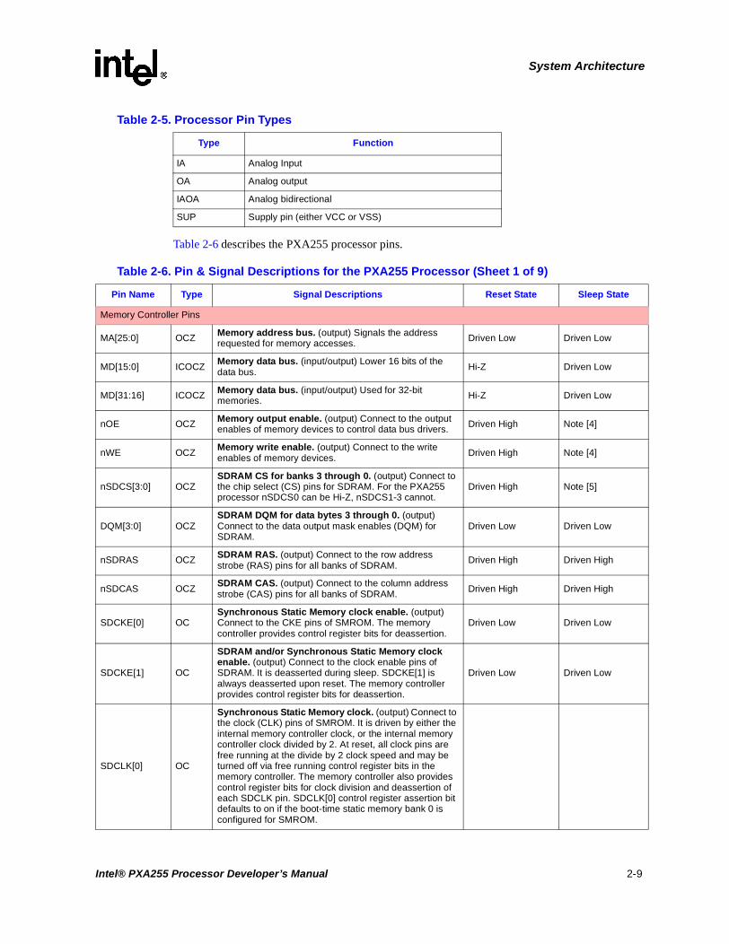
System Architecture
Table 2-6 describes the PXA255 processor pins.
IA Analog Input
OA Analog output
IAOA Analog bidirectional
SUP Supply pin (either VCC or VSS)
Table 2-5. Processor Pin Types
Type Function
Table 2-6. Pin & Signal Descriptions for the PXA255 Processor (Sheet 1 of 9)
Pin Name Type Signal Descriptions Reset State Sleep State
Memory Controller Pins
MA[25:0] OCZ Memory address bus. (output) Signals the address requested for memory accesses. Driven Low Driven Low
MD[15:0] ICOCZMemory data bus. (input/output) Lower 16 bits of the data bus. Hi-Z Driven Low
MD[31:16] ICOCZ Memory data bus. (input/output) Used for 32-bit memories. Hi-Z Driven Low
nOE OCZ Memory output enable. (output) Connect to the output enables of memory devices to control data bus drivers. Driven High Note [4]
nWE OCZMemory write enable. (output) Connect to the write enables of memory devices. Driven High Note [4]
nSDCS[3:0] OCZSDRAM CS for banks 3 through 0. (output) Connect to the chip select (CS) pins for SDRAM. For the PXA255 processor nSDCS0 can be Hi-Z, nSDCS1-3 cannot.
Driven High Note [5]
DQM[3:0] OCZSDRAM DQM for data bytes 3 through 0. (output) Connect to the data output mask enables (DQM) for SDRAM.
Driven Low Driven Low
nSDRAS OCZ SDRAM RAS. (output) Connect to the row address strobe (RAS) pins for all banks of SDRAM.
Driven High Driven High
nSDCAS OCZSDRAM CAS. (output) Connect to the column address strobe (CAS) pins for all banks of SDRAM. Driven High Driven High
SDCKE[0] OCSynchronous Static Memory clock enable. (output) Connect to the CKE pins of SMROM. The memory controller provides control register bits for deassertion.
Driven Low Driven Low
SDCKE[1] OC
SDRAM and/or Synchronous Static Memory clock enable. (output) Connect to the clock enable pins of SDRAM. It is deasserted during sleep. SDCKE[1] is always deasserted upon reset. The memory controller provides control register bits for deassertion.
Driven Low Driven Low
SDCLK[0] OC
Synchronous Static Memory clock. (output) Connect to the clock (CLK) pins of SMROM. It is driven by either the internal memory controller clock, or the internal memory controller clock divided by 2. At reset, all clock pins are free running at the divide by 2 clock speed and may be turned off via free running control register bits in the memory controller. The memory controller also provides control register bits for clock division and deassertion of each SDCLK pin. SDCLK[0] control register assertion bit defaults to on if the boot-time static memory bank 0 is configured for SMROM.
Intel® PXA255 Processor Developer’s Manual 2-9

System Architecture
SDCLK[1] OCZ SDRAM Clocks (output) Connect SDCLK[1] and SDCLK[2] to the clock pins of SDRAM in bank pairs 0/1 and 2/3, respectively. They are driven by either the internal memory controller clock, or the internal memory controller clock divided by 2. At reset, all clock pins are free running at the divide by 2 clock speed and may be turned off via free running control register bits in the memory controller. The memory controller also provides control register bits for clock division and deassertion of each SDCLK pin. SDCLK[2:1] control register assertion bits are always deasserted upon reset.
Driven Low Driven Low
SDCLK[2] OC Driven Low Driven Low
nCS[5]/
GPIO[33]ICOCZ
Static chip selects. (output) Chip selects to static memory devices such as ROM and Flash. Individually programmable in the memory configuration registers. nCS[5:0] can be used with variable latency I/O devices.
Hi-Z - Note [1] Note [4]
nCS[4]/
GPIO[80]ICOCZ
nCS[3]/
GPIO[79]ICOCZ
nCS[2]/
GPIO[78]ICOCZ
nCS[1]/
GPIO[15]ICOCZ
nCS[0] ICOCZ Static chip select 0. (output) Chip select for the boot memory. nCS[0] is a dedicated pin.
Driven High Note [4]
RD/nWR OCZ Read/Write for static interface. (output) Signals that the current transaction is a read or write. Driven Low Holds last state
RDY/
GPIO[18]ICOCZ
Variable Latency I/O Ready pin. (input) Notifies the memory controller when an external bus device is ready to transfer data.
Hi-Z - Note [1] Note [3]
L_DD[8]/
GPIO[66]ICOCZ
LCD display data. (output) Transfers pixel information from the LCD Controller to the external LCD panel.
Memory Controller alternate bus master request. (input) Allows an external device to request the system bus from the Memory Controller.
Hi-Z - Note [1] Note [3]
L_DD[15]/
GPIO[73]ICOCZ
LCD display data. (output) Transfers pixel information from the LCD Controller to the external LCD panel.
Memory Controller grant. (output) Notifies an external device that it has been granted the system bus.
Hi-Z - Note [1] Note [3]
MBGNT/GP[13] ICOCZ Memory Controller grant. (output) Notifies an external
device that it has been granted the system bus. Hi-Z - Note [1] Note [3]
MBREQ/GP[14] ICOCZ
Memory Controller alternate bus master request. (input) Allows an external device to request the system bus from the Memory Controller.
Hi-Z - Note [1] Note [3]
PCMCIA/CF Control Pins
nPOE/
GPIO[48]ICOCZ PCMCIA output enable. (output) Reads from PCMCIA
memory and to PCMCIA attribute space.Hi-Z - Note [1] Note [5]
nPWE/
GPIO[49]ICOCZ
PCMCIA write enable. (output) Performs writes to PCMCIA memory and to PCMCIA attribute space. Also used as the write enable signal for Variable Latency I/O.
Hi-Z - Note [1] Note [5]
Table 2-6. Pin & Signal Descriptions for the PXA255 Processor (Sheet 2 of 9)
Pin Name Type Signal Descriptions Reset State Sleep State
2-10 Intel® PXA255 Processor Developer’s Manual

System Architecture
nPIOW/
GPIO[51]ICOCZ PCMCIA I/O write. (output) Performs write transactions
to PCMCIA I/O space. Hi-Z - Note [1] Note [5]
nPIOR/
GPIO[50]ICOCZ
PCMCIA I/O read. (output) Performs read transactions from PCMCIA I/O space. Hi-Z - Note [1] Note [5]
nPCE[2]/
GPIO[53]ICOCZ
PCMCIA card enable 2. (output) Selects a PCMCIA card. nPCE[2] enables the high byte lane and nPCE[1] enables the low byte lane.
MMC clock. (output) Clock signal for the MMC Controller.
Hi-Z - Note [1] Note [5]
nPCE[1]/
GPIO[52]ICOCZ
PCMCIA card enable 1. (outputs) Selects a PCMCIA card. nPCE[2] enables the high byte lane and nPCE[1] enables the low byte lane.
Hi-Z - Note [1] Note [5]
nIOIS16/
GPIO[57]ICOCZ
IO Select 16. (input) Acknowledge from the PCMCIA card that the current address is a valid 16 bit wide I/O address.
Hi-Z - Note [1] Note [5]
nPWAIT/
GPIO[56]ICOCZ
PCMCIA wait. (input) Driven low by the PCMCIA card to extend the length of the transfers to/from the PXA255 processor.
Hi-Z - Note [1] Note [5]
PSKTSEL/
GPIO[54]ICOCZ
PCMCIA socket select. (output) Used by external steering logic to route control, address, and data signals to one of the two PCMCIA sockets. When PSKTSEL is low, socket zero is selected. When PSKTSEL is high, socket one is selected. Has the same timing as the address bus.
Hi-Z - Note [1] Note [5]
nPREG/
GPIO[55]ICOCZ
PCMCIA Register select. (output) Indicates that the target address on a memory transaction is attribute space. Has the same timing as the address bus.
Hi-Z - Note [1] Note [5]
LCD Controller Pins
L_DD(7:0)/
GPIO[65:58]ICOCZ
LCD display data. (outputs) Transfers pixel information from the LCD Controller to the external LCD panel. Hi-Z - Note [1] Note [3]
L_DD[8]/
GPIO[66]ICOCZ
LCD display data. (output) Transfers pixel information from the LCD Controller to the external LCD panel.
Memory Controller alternate bus master request. (input) Allows an external device to request the system bus from the Memory Controller.
Hi-Z - Note [1] Note [3]
L_DD[9]/
GPIO[67]ICOCZ
LCD display data. (output) Transfers pixel information from the LCD Controller to the external LCD panel.
MMC chip select 0. (output) Chip select 0 for the MMC Controller.
Hi-Z - Note [1] Note [3]
L_DD[10]/
GPIO[68]ICOCZ
LCD display data. (output) Transfers pixel information from the LCD Controller to the external LCD panel.
MMC chip select 1. (output) Chip select 1 for the MMC Controller.
Hi-Z - Note [1] Note [3]
L_DD[11]/
GPIO[69]ICOCZ
LCD display data. (output) Transfers pixel information from the LCD Controller to the external LCD panel.
MMC clock. (output) Clock for the MMC Controller.Hi-Z - Note [1] Note [3]
L_DD[12]/
GPIO[70]ICOCZ
LCD display data. (output) Transfers pixel information from the LCD Controller to the external LCD panel.
RTC clock. (output) Real time clock 1 Hz tick.Hi-Z - Note [1] Note [3]
Table 2-6. Pin & Signal Descriptions for the PXA255 Processor (Sheet 3 of 9)
Pin Name Type Signal Descriptions Reset State Sleep State
Intel® PXA255 Processor Developer’s Manual 2-11

System Architecture
L_DD[13]/
GPIO[71]ICOCZ
LCD display data. (output) Transfers pixel information from the LCD Controller to the external LCD panel.
3.6864 MHz clock. (output) Output from 3.6864 MHz oscillator.
Hi-Z - Note [1] Note [3]
L_DD[14]/
GPIO[72]ICOCZ
LCD display data. (output) Transfers pixel information from the LCD Controller to the external LCD panel.
32 kHz clock. (output) Output from the 32 kHz oscillator.Hi-Z - Note [1] Note [3]
L_DD[15]/
GPIO[73]ICOCZ
LCD display data. (output) Transfers pixel information from the LCD Controller to the external LCD panel.
Memory Controller grant. (output) Notifies an external device it has been granted the system bus.
Hi-Z - Note [1] Note [3]
L FCLK/
GPIO[74]ICOCZ LCD frame clock. (output) Indicates the start of a new
frame. Also referred to as Vsync. Hi-Z - Note [1] Note [3]
L LCLK/
GPIO[75]ICOCZ LCD line clock. (output) Indicates the start of a new line.
Also referred to as Hsync. Hi-Z - Note [1] Note [3]
L PCLK/
GPIO[76]ICOCZ LCD pixel clock. (output) Clocks valid pixel data into the
LCD’s line shift buffer. Hi-Z - Note [1] Note [3]
L BIAS/
GPIO[77]ICOCZ
AC bias drive. (output) Notifies the panel to change the polarity for some passive LCD panel. For TFT panels, this signal indicates valid pixel data.
Hi-Z - Note [1] Note [3]
Full Function UART Pins
FFRXD/
GPIO[34]ICOCZ
Full Function UART Receive. (input)
MMC chip select 0. (output) Chip select 0 for the MMC Controller.
Hi-Z - Note [1] Note [3]
FFTXD/
GPIO[39]ICOCZ
Full Function UART Transmit. (output)
MMC chip select 1. (output) Chip select 1 for the MMC Controller.
Hi-Z - Note [1] Note [3]
FFCTS/
GPIO[35]ICOCZ Full Function UART Clear-to-Send. (input) Hi-Z - Note [1] Note [3]
FFDCD/
GPIO[36]ICOCZ Full Function UART Data-Carrier-Detect. (input) Hi-Z - Note [1] Note [3]
FFDSR/
GPIO[37]ICOCZ Full Function UART Data-Set-Ready. (input) Hi-Z - Note [1] Note [3]
FFRI/
GPIO[38]ICOCZ Full Function UART Ring Indicator. (input) Hi-Z - Note [1] Note [3]
FFDTR/
GPIO[40]ICOCZ Full Function UART Data-Terminal-Ready. (output) Hi-Z - Note [1] Note [3]
FFRTS/
GPIO[41]ICOCZ Full Function UART Request-to-Send. (output) Hi-Z - Note [1] Note [3]
Bluetooth UART Pins
BTRXD/
GPIO[42]ICOCZ Bluetooth UART Receive. (input) Hi-Z - Note [1] Note [3]
BTTXD/
GPIO[43]ICOCZ Bluetooth UART Transmit. (output) Hi-Z - Note [1] Note [3]
Table 2-6. Pin & Signal Descriptions for the PXA255 Processor (Sheet 4 of 9)
Pin Name Type Signal Descriptions Reset State Sleep State
2-12 Intel® PXA255 Processor Developer’s Manual

System Architecture
BTCTS/
GPIO[44]ICOCZ Bluetooth UART Clear-to-Send. (input) Hi-Z - Note [1] Note [3]
BTRTS/
GPIO[45]ICOCZ Bluetooth UART Data-Terminal-Ready. (output) Hi-Z - Note [1] Note [3]
Standard UART and ICP Pins
IRRXD/
GPIO[46]ICOCZ
IrDA receive signal. (input) Receive pin for the FIR function.
Standard UART receive. (input)Hi-Z - Note [1] Note [3]
IRTXD/
GPIO[47]ICOCZ
IrDA transmit signal. (output) Transmit pin for the Standard UART, SIR and FIR functions.
Standard UART transmit. (output)Hi-Z - Note [1] Note [3]
HWUART Pins
HWTXD/GPIO[48] ICOCZ Hardware UART Transmit Data.
Pulled High
Note [1]Note [3]
HWRXD/GPIO[49] ICOCZ Hardware UART Receive Data.
Pulled High
Note [1]Note [3]
HWCTS/GPIO[50] ICOCZ Hardware UART Clear-To-Send.
Pulled High
Note [1]Note [3]
HWRTS/GPIO[51] ICOCZ Hardware UART Request-to-Send.
Pulled High
Note [1]Note [3]
MMC Controller Pins
MMCMD ICOCZ Multimedia Card Command. (bidirectional) Hi-Z Hi-Z
MMDAT ICOCZ Multimedia Card Data. (bidirectional) Hi-Z Hi-Z
nPCE[2]/
GPIO[53]ICOCZ
PCMCIA card enable 2. (outputs) Selects a PCMCIA card. Bit one enables the high byte lane and bit zero enables the low byte lane.
MMC clock. (output) Clock signal for the MMC Controller.
Hi-Z - Note [1] Note [5]
L_DD[9]/
GPIO[67]ICOCZ
LCD display data. (output) Transfers pixel information from the LCD Controller to the external LCD panel.
MMC chip select 0. (output) Chip select 0 for the MMC Controller.
Hi-Z - Note [1] Note [3]
L_DD[10]/
GPIO[68]ICOCZ
LCD display data. (output) Transfers pixel information from the LCD Controller to the external LCD panel.
MMC chip select 1. (output) Chip select 1 for the MMC Controller.
Hi-Z - Note [1] Note [3]
L_DD[11]/
GPIO[69]ICOCZ
LCD display data. (output) Transfers pixel information from the LCD Controller to the external LCD panel.
MMC clock. (output) Clock for the MMC Controller.Hi-Z - Note [1] Note [3]
FFRXD/
GPIO[34]ICOCZ
Full Function UART Receive. (input)
MMC chip select 0. (output) Chip select 0 for the MMC Controller.
Hi-Z - Note [1] Note [3]
FFTXD/
GPIO[39]ICOCZ
Full Function UART Transmit. (output)
MMC chip select 1. (output) Chip select 1 for the MMC Controller.
Hi-Z - Note [1] Note [3]
Table 2-6. Pin & Signal Descriptions for the PXA255 Processor (Sheet 5 of 9)
Pin Name Type Signal Descriptions Reset State Sleep State
Intel® PXA255 Processor Developer’s Manual 2-13

System Architecture
MMCCLK/GP[6] ICOCZ MMC clock. (output) Clock signal for the MMC
Controller. Hi-Z - Note [1] Note [3]
MMCCS0/GP[8]
ICOCZ MMC chip select 0. (output) Chip select 0 for the MMC Controller.
Hi-Z - Note [1] Note [3]
MMCCS1/GP[9] ICOCZ MMC chip select 1. (output) Chip select 1 for the MMC
Controller. Hi-Z - Note [1] Note [3]
SSP Pins
SSPSCLK/
GPIO[23]ICOCZ Synchronous Serial Port Clock. (output) Hi-Z - Note [1] Note [3]
SSPSFRM/
GPIO[24]ICOCZ Synchronous Serial Port Frame. (output) Hi-Z - Note [1] Note [3]
SSPTXD/
GPIO[25]ICOCZ Synchronous Serial Port Transmit. (output) Hi-Z - Note [1] Note [3]
SSPRXD/
GPIO[26]ICOCZ Synchronous Serial Port Receive. (input) Hi-Z - Note [1] Note [3]
SSPEXTCLK/
GPIO[27]ICOCZ Synchronous Serial Port External Clock. (input) Hi-Z - Note [1] Note [3]
Network SSP pins
NSSPSCLK/GPIO[81] ICOCZ Network Synchronous Serial Port Clock.
Pulled High
Note [1]Note [3]
NSSPSFRM/GPIO[82] ICOCZ Network Synchronous Serial Port Frame Signal.
Pulled High
Note [1]Note [3]
NSSPTXD/GPIO[83] ICOCZ Network Synchronous Serial Port Transmit.
Pulled High
Note [1]Note [3]
NSSPRXD/GPIO[84]
ICOCZ Network Synchronous Serial Port Receive.Pulled High
Note [1]Note [3]
USB Client Pins
USB P IAOAZ USB Client Positive. (bidirectional) Hi-Z Hi-Z
USB N IAOAZ USB Client Negative pin. (bidirectional) Hi-Z Hi-Z
AC97 Controller and I2S Controller Pins
BITCLK/
GPIO[28]ICOCZ
AC97 Audio Port bit clock. (input) AC97 clock is generated by Codec 0 and fed into the PXA255 processor and Codec 1.
AC97 Audio Port bit clock. (output) AC97 clock is generated by the PXA255 processor.
I2S bit clock. (input) I2S clock is generated externally and fed into PXA255 processor.
I2S bit clock. (output) I2S clock is generated by the PXA255 processor.
Hi-Z - Note [1] Note [3]
SDATA_IN0/
GPIO[29]ICOCZ
AC97 Audio Port data in. (input) Input line for Codec 0.
I2S data in. (input) Input line for the I2S Controller.Hi-Z - Note [1] Note [3]
SDATA_IN1/
GPIO[32]ICOCZ
AC97 Audio Port data in. (input) Input line for Codec 1.
I2S system clock. (output) System clock from I2S Controller.
Hi-Z - Note [1] Note [3]
Table 2-6. Pin & Signal Descriptions for the PXA255 Processor (Sheet 6 of 9)
Pin Name Type Signal Descriptions Reset State Sleep State
2-14 Intel® PXA255 Processor Developer’s Manual

System Architecture
SDATA_OUT/
GPIO[30]ICOCZ
AC97 Audio Port data out. (output) Output from the PXA255 processor to Codecs 0 and 1.
I2S data out. (output) Output line for the I2S Controller.Hi-Z - Note [1] Note [3]
SYNC/
GPIO[31]ICOCZ
AC97 Audio Port sync signal. (output) Frame sync signal for the AC97 Controller.
I2S sync. (output) Frame sync signal for the I2S Controller.
Hi-Z - Note [1] Note [3]
nACRESET OC AC97 Audio Port reset signal. (output) Driven Low Driven Low
I2C Controller Pins
SCL ICOCZ I2C clock. (bidirectional) Hi-Z Hi-Z
SDA ICOCZ I2C data. (bidirectional). Hi-Z Hi-Z
PWM Pins
PWM[1:0]/
GPIO[17:16]ICOCZ Pulse Width Modulation channels 0 and 1. (outputs) Hi-Z - Note [1] Note [3]
DMA Pins
DREQ[1:0]/
GPIO[19:20]ICOCZ
DMA Request. (input) Notifies the DMA Controller that an external device requires a DMA transaction. DREQ[1] is GPIO[19]. DREQ[0] is GPIO[20].
Hi-Z - Note [1] Note [3]
GPIO Pins
GPIO[1:0] ICOCZ General Purpose I/O. Wakeup sources on both rising and falling edges on nRESET. Hi-Z - Note [1] Note [3]
GPIO[14:2] ICOCZ General Purpose I/O. More wakeup sources for sleep mode.
Hi-Z - Note [1] Note [3]
GPIO[22:21] ICOCZ General Purpose I/O. Additional General Purpose I/O pins. Hi-Z - Note [1] Note [3]
Crystal and Clock Pins
PXTAL IA 3.6864 Mhz crystal input. No external caps are required. Note [2] Note [2]
PEXTAL OA 3.6864 Mhz crystal output. No external caps are required. Note [2] Note [2]
TXTAL IA 32 Khz crystal input. No external caps are required. Note [2] Note [2]
TEXTAL OA 32 Khz crystal output. No external caps are required. Note [2] Note [2]
L_DD[12]/
GPIO[70]ICOCZ
LCD display data. (output) Transfers pixel information from the LCD Controller to the external LCD panel.
RTC clock. (output) Real time clock 1 Hz tick.Hi-Z - Note [1] Note [3]
L_DD[13]/
GPIO[71]ICOCZ
LCD display data. (output) Transfers the pixel information from the LCD Controller to the external LCD panel.
3.6864 MHz clock. (output) Output from 3.6864 MHz oscillator.
Hi-Z - Note [1] Note [3]
L_DD[14]/
GPIO[72]ICOCZ
LCD display data. (output) Transfers pixel information from the LCD Controller to the external LCD panel.
32 kHz clock. (output) Output from the 32 kHz oscillator.Hi-Z - Note [1] Note [3]
48MHz/GP[7] ICOCZ
48 MHz clock. (output) Peripheral clock output derived from the PLL.NOTE: This clock is only generated when the USB unit
clock enable is set.
Hi-Z - Note [1] Note [3]
Table 2-6. Pin & Signal Descriptions for the PXA255 Processor (Sheet 7 of 9)
Pin Name Type Signal Descriptions Reset State Sleep State
Intel® PXA255 Processor Developer’s Manual 2-15

System Architecture
RTCCLK/GP[10] ICOCZ Real time clock. (output) 1 Hz output derived from the
32kHz or 3.6864MHz output. Hi-Z - Note [1] Note [3]
3.6MHz/GP[11] ICOCZ 3.6864 MHz clock. (output) Output from 3.6864 MHz oscillator.
Hi-Z - Note [1] Note [3]
32kHz/GP[12] ICOCZ 32 kHz clock. (output) Output from the 32 kHz oscillator. Hi-Z - Note [1] Note [3]
Miscellaneous Pins
BOOT_SEL
[2:0]IC Boot select pins. (input) Indicates type of boot device. Input Input
PWR_EN OCPower Enable for the power supply. (output) When negated, it signals the power supply to remove power to the core because the system is entering sleep mode.
Driven High
Driven low while entering sleep mode. Driven high when sleep exit sequence begins.
nBATT_FAULT IC
Main Battery Fault. (input) Signals that main battery is low or removed. Assertion causes PXA255 processor to enter sleep mode or force an Imprecise Data Exception, which cannot be masked. PXA255 processor will not recognize a walk-up event while this signal is asserted. Minimum assertion time for nBATT_FAULT is 1 ms.
Input Input
nVDD_FAULT IC
VDD Fault. (input) Signals that the main power source is going out of regulation. nVDD_FAULT causes the PXA255 processor to enter sleep mode or force an Imprecise Data Exception, which cannot be masked. nVDD_FAULT is ignored after a walk-up event until the power supply timer completes (approximately 10 ms). Minimum assertion time for nVDD_FAULT is 1 ms.
Input Input
nRESET IC
Hard reset. (input) Level sensitive input used to start the processor from a known address. Assertion causes the current instruction to terminate abnormally and causes a reset. When nRESET is driven high, the processor starts execution from address 0. nRESET must remain low until the power supply is stable and the internal 3.6864 MHz oscillator has stabilized.
Input
Input. Driving low during sleep will cause normal reset sequence and exit from sleep mode.
nRESET_OUT OC
Reset Out. (output) Asserted when nRESET is asserted and deasserts after nRESET is deasserted but before the first instruction fetch. nRESET_OUT is also asserted for “soft” reset events: sleep, watchdog reset, or GPIO reset.
Driven low during any reset sequence - driven high prior to first fetch.
Driven Low
JTAG and Test Pins
nTRST IC
JTAG Test Interface Reset. Resets the JTAG/Debug port. If JTAG/Debug is used, drive nTRST from low to high either before or at the same time as nRESET. If JTAG is not used, nTRST must be either tied to nRESET or tied low.
Input Input
TDI ICJTAG test data input. (input) Data from the JTAG controller is sent to the PXA255 processor using this pin. This pin has an internal pull-up resistor.
Input Input
TDO OCZJTAG test data output. (output) Data from the PXA255 processor is returned to the JTAG controller using this pin.
Hi-Z Hi-Z
TMS ICJTAG test mode select. (input) Selects the test mode required from the JTAG controller. This pin has an internal pull-up resistor.
Input Input
Table 2-6. Pin & Signal Descriptions for the PXA255 Processor (Sheet 8 of 9)
Pin Name Type Signal Descriptions Reset State Sleep State
2-16 Intel® PXA255 Processor Developer’s Manual

System Architecture
TCK IC JTAG test clock. (input) Clock for all transfers on the JTAG test interface. Input Input
TEST IC Test Mode. (input) Reserved. Must be grounded. Input Input
TESTCLK IC Test Clock. (input) Reserved. Must be grounded. Input Input
Power and Ground Pins
VCC SUP Positive supply for internal logic. Must be connected to the low voltage supply on the PCB. Powered Note [6]
VSS SUPGround supply for internal logic. Must be connected to the common ground plane on the PCB. Grounded Grounded
PLL_VCC SUP Positive supply for PLLs and oscillators. Must be connected to the common low voltage supply. Powered Note [6]
PLL_VSS SUP Ground supply for the PLL. Must be connected to common ground plane on the PCB. Grounded Grounded
VCCQ SUPPositive supply for all CMOS I/O except memory bus and PCMCIA pins. Must be connected to the common 3.3v supply on the PCB.
Powered Note [7]
VSSQ SUPGround supply for all CMOS I/O except memory bus and PCMCIA pins. Must be connected to the common ground plane on the PCB.
Grounded Grounded
VCCN SUPPositive supply for memory bus and PCMCIA pins. Must be connected to the common 3.3v or 2.5v supply on the PCB.
Powered Note [7]
VSSN SUPGround supply for memory bus and PCMCIA pins. Must be connected to the common ground plane on the PCB.
Grounded Grounded
Table 2-7. Pin Description Notes (Sheet 1 of 2)
Note Description
[1]
GPIO Reset Operation: Configured as GPIO inputs by default after any reset. The input buffers for these pins are disabled to prevent current drain and the pins are pulled high with 10K to 60K internal resistors. The input paths must be enabled and the pullups turned off by clearing the Read Disable Hold (RDH) bit described in Section 3.5.7, “Power Manager Sleep Status Register (PSSR)” on page 3-29. Even though sleep mode sets the RDH bit, the pull-up resistors are not re-enabled by sleep mode.
[2]Crystal oscillator pins: These pins are used to connect the external crystals to the on-chip oscillators. Refer to Section 3.3.1, “32.768 kHz Oscillator” on page 3-4 and Section 3.3.2, “3.6864 MHz Oscillator” on page 3-4 for details on Sleep Mode operation.
[3]
GPIO Sleep operation: During the transition into sleep mode, the state of these pins is determined by the corresponding PGSRn. See Section 3.5.10, “Power Manager GPIO Sleep State Registers (PGSR0, PGSR1, PGSR2)” and Section 4.1.3.2, “GPIO Pin Direction Registers (GPDR0, GPDR1, GPDR2)” on page 4-8. If selected as an input, this pin does not drive during sleep. If selected as an output, the value contained in the Sleep State Register is driven out onto the pin and held there while the PXA255 processor is in Sleep Mode.
GPIOs configured as inputs after exiting sleep mode cannot be used until PSSR[RDH] is cleared.
[4]
Static Memory Control Pins: During Sleep Mode, these pins can be programmed to either drive the value in the Sleep State Register or to be placed in Hi-Z. To select the Hi-Z state, software must set the FS bit in the Power Manager General Configuration Register. If PCFR[FS] is not set, then during the transition to sleep these pins function as described in [3], above. For nWE, nOE, and nCS[0], if PCFR[FS] is not set, they are driven high by the Memory Controller before entering sleep. If PCFR[FS] is set, these pins are placed in Hi-Z.
Table 2-6. Pin & Signal Descriptions for the PXA255 Processor (Sheet 9 of 9)
Pin Name Type Signal Descriptions Reset State Sleep State
Intel® PXA255 Processor Developer’s Manual 2-17

System Architecture
2.12 Memory Map
Figure 2-2 and Figure 2-3 show the full processor memory map.
Any unused register space from 0x4000_0000 to 0x4BFF_FFFF is reserved.
Note: Accessing reserved portions of the memory map will give unpredictable results.
The PCMCIA interface is divided into Socket 0 and Socket 1 space. These two sockets are each subdivided into I/O, memory and attribute space. Each socket is allocated 256 MB of memory space.
[5]PCMCIA Control Pins: During Sleep Mode: Can be programmed either to drive the value in the Sleep State Register or to be placed in Hi-Z. To select the Hi-Z state, software must set PCFR[FP]. If it is not set, then during the transition to sleep these pins function as described in [3], above.
[6] During sleep, this supply may be driven low. This supply must never be high impedance.
[7] Remains powered in sleep mode.
Table 2-7. Pin Description Notes (Sheet 2 of 2)
Note Description
2-18 Intel® PXA255 Processor Developer’s Manual

System Architecture
Figure 2-2. Memory Map (Part One) — From 0x8000_0000 to 0xFFFF FFFF
Reserved (64 MB)
SDRAM Bank 0 (64 MB)
SDRAM Bank 1 (64 MB)
Reserved (64 MB)
Reserved (64 MB)
Reserved (64 MB)
Reserved (64 MB)
Reserved (64 MB)
Reserved (64 MB)
Reserved (64 MB)
Reserved (64 MB)
SDRAM Bank 3 (64 MB)
0xFFFF_FFFF
Reserved (64 MB)
SDRAM Bank 2 (64 MB)
Reserved (64 MB)
Reserved (64 MB)
Reserved (64 MB)
Reserved (64 MB)
Reserved (64 MB)
Reserved (64 MB)
Reserved (64 MB)
Reserved (64 MB)
Reserved (64 MB)
Reserved (64 MB)
Reserved (64 MB)
Reserved (64 MB)
Reserved (64 MB)
Reserved (64 MB)
Reserved (64 MB)
Reserved (64 MB)
Reserved (64 MB)
Reserved (64 MB)
0x8400_0000
0x8800_0000
0x8C00_0000
0x9000_0000
0x9400_0000
0x9800_0000
0x9C00_0000
0xA000_0000
0xA400_0000
0xA800_0000
0xAC00_0000
0xB000_0000
0xB400_0000
0xB800_0000
0xBC00_0000
0xC000_0000
0xC400_0000
0xC800_0000
0xCC00_0000
0xD000_0000
0xD400_0000
0xD800_0000
0xDC00_0000
0xE000_0000
0xE400_0000
0xE800_0000
0xEC00_0000
0xF000_0000
0xF400_0000
0xF800_0000
0xFC00_0000
0x8000_0000
Intel® PXA255 Processor Developer’s Manual 2-19

System Architecture
Figure 2-3. Memory Map (Part Two) — From 0x0000_0000 to 0x7FFF FFFF
Reserved (64 MB)
Static Chip Select 0 (64 MB)
Memory Mapped registers (Peripherals)
PCMCIA/CF - Slot 0 (256MB)
Static Chip Select 2 (64 MB)
Static Chip Select 1 (64 MB)
Static Chip Select 3 (64 MB)
Static Chip Select 4 (64 MB)
Static Chip Select 5 (64 MB)
Reserved (64 MB)
Reserved (64 MB)
Reserved (64 MB)
Reserved (64 MB)
Reserved (64 MB)
Reserved (64 MB)
Reserved (64 MB)
Reserved (64 MB)
Memory Mapped registers (LCD)
Memory Mapped registers (Memory Ctl)
Reserved (64 MB)
Reserved (64 MB)
Reserved (64 MB)
Reserved (64 MB)
Reserved (64 MB)
Reserved (64 MB)
0x0000_0000
0x0400_0000
0x0800_0000
0x0C00_0000
0x1000_0000
0x1400_0000
0x1800_0000
0x1C00_0000
0x2000_0000
0x2400_0000
0x2800_0000
0x2C00_0000
0x3000_0000
0x3400_0000
0x3800_0000
0x3C00_0000
0x4000_0000
0x4400_0000
0x4800_0000
0x4C00_0000
0x5000_0000
0x5400_0000
0x5800_0000
0x5C00_0000
0x6000_0000
0x6400_0000
0x6800_0000
0x6C00_0000
0x7000_0000
0x7400_0000
0x7800_0000
0x7C00_0000
PCMCIA/CF- Slot 1 (256 MB)
0x7FFF FFFF
2-20 Intel® PXA255 Processor Developer’s Manual

System Architecture
2.13 System Architecture Register Summary
Table 2-8. System Architecture Register Address Summary (Sheet 1 of 12)
Unit Address Register Symbol Register Description
DMA Controller 0x4000_0000
0x4000_0000 DCSR0 DMA Control / Status Register for Channel 0
0x4000_0004 DCSR1 DMA Control / Status Register for Channel 1
0x4000_0008 DCSR2 DMA Control / Status Register for Channel 2
0x4000_000C DCSR3 DMA Control / Status Register for Channel 3
0x4000_0010 DCSR4 DMA Control / Status Register for Channel 4
0x4000_0014 DCSR5 DMA Control / Status Register for Channel 5
0x4000_0018 DCSR6 DMA Control / Status Register for Channel 6
0x4000_001C DCSR7 DMA Control / Status Register for Channel 7
0x4000_0020 DCSR8 DMA Control / Status Register for Channel 8
0x4000_0024 DCSR9 DMA Control / Status Register for Channel 9
0x4000_0028 DCSR10 DMA Control / Status Register for Channel 10
0x4000_002C DCSR11 DMA Control / Status Register for Channel 11
0x4000_0030 DCSR12 DMA Control / Status Register for Channel 12
0x4000_0034 DCSR13 DMA Control / Status Register for Channel 13
0x4000_0038 DCSR14 DMA Control / Status Register for Channel 14
0x4000_003C DCSR15 DMA Control / Status Register for Channel 15
0x4000_00f0 DINT DMA Interrupt Register
0x4000_0100 DRCMR0 Request to Channel Map Register for DREQ 0
0x4000_0104 DRCMR1 Request to Channel Map Register for DREQ 1
0x4000_0108 DRCMR2 Request to Channel Map Register for I2S receive Request
0x4000_010C DRCMR3 Request to Channel Map Register for I2S transmit Request
0x4000_0110 DRCMR4 Request to Channel Map Register for BTUART receive Request
0x4000_0114 DRCMR5 Request to Channel Map Register for BTUART transmit Request.
0x4000_0118 DRCMR6 Request to Channel Map Register for FFUART receive Request
0x4000_011C DRCMR7 Request to Channel Map Register for FFUART transmit Request
0x4000_0120 DRCMR8 Request to Channel Map Register for AC97 microphone Request
0x4000_0124 DRCMR9 Request to Channel Map Register for AC97 modem receive Request
0x4000_0128 DRCMR10 Request to Channel Map Register for AC97 modem transmit Request
0x4000_012C DRCMR11 Request to Channel Map Register for AC97 audio receive Request
0x4000_0130 DRCMR12 Request to Channel Map Register for AC97 audio transmit Request
0x4000_0134 DRCMR13 Request to Channel Map Register for SSP receive Request
0x4000_0138 DRCMR14 Request to Channel Map Register for SSP transmit Request
0x4000_013C DRCMR15 Request to Channel Map Register for NSSP receive Request
0x4000_0140 DRCMR16 Request to Channel Map Register for NSSP transmit Request
0x4000_0144 DRCMR17 Request to Channel Map Register for ICP receive Request
0x4000_0148 DRCMR18 Request to Channel Map Register for ICP transmit Request
Intel® PXA255 Processor Developer’s Manual 2-21

System Architecture
0x4000_014C DRCMR19 Request to Channel Map Register for STUART receive Request
0x4000_0150 DRCMR20 Request to Channel Map Register for STUART transmit Request
0x4000_0154 DRCMR21 Request to Channel Map Register for MMC receive Request
0x4000_0158 DRCMR22 Request to Channel Map Register for MMC transmit Request
0x4000_015C DRCMR23 Reserved
0x4000_0160 DRCMR24 Reserved
0x4000_0164 DRCMR25 Request to Channel Map Register for USB endpoint 1 Request
0x4000_0168 DRCMR26 Request to Channel Map Register for USB endpoint 2 Request
0x4000_016C DRCMR27 Request to Channel Map Register for USB endpoint 3 Request
0x4000_0170 DRCMR28 Request to Channel Map Register for USB endpoint 4 Request
0x4000_0174 DRCMR29 Request to Channel Map Register for HWUART receive Request
0x4000_0178 DRCMR30 Request to Channel Map Register for USB endpoint 6 Request
0x4000_017C DRCMR31 Request to Channel Map Register for USB endpoint 7 Request
0x4000_0180 DRCMR32 Request to Channel Map Register for USB endpoint 8 Request
0x4000_0184 DRCMR33 Request to Channel Map Register for USB endpoint 9 Request
0x4000_0188 DRCMR34 Request to Channel Map Register for HWUART transmit Request
0x4000_018C DRCMR35 Request to Channel Map Register for USB endpoint 11 Request
0x4000_0190 DRCMR36 Request to Channel Map Register for USB endpoint 12 Request
0x4000_0194 DRCMR37 Request to Channel Map Register for USB endpoint 13 Request
0x4000_0198 DRCMR38 Request to Channel Map Register for USB endpoint 14 Request
0x4000_019C DRCMR39 Reserved
0x4000_0200 DDADR0 DMA Descriptor Address Register Channel 0
0x4000_0204 DSADR0 DMA Source Address Register Channel 0
0x4000_0208 DTADR0 DMA Target Address Register Channel 0
0x4000_020C DCMD0 DMA Command Address Register Channel 0
0x4000_0210 DDADR1 DMA Descriptor Address Register Channel 1
0x4000_0214 DSADR1 DMA Source Address Register Channel 1
0x4000_0218 DTADR1 DMA Target Address Register Channel 1
0x4000_021C DCMD1 DMA Command Address Register Channel 1
0x4000_0220 DDADR2 DMA Descriptor Address Register Channel 2
0x4000_0224 DSADR2 DMA Source Address Register Channel 2
0x4000_0228 DTADR2 DMA Target Address Register Channel 2
0x4000_022C DCMD2 DMA Command Address Register Channel 2
0x4000_0230 DDADR3 DMA Descriptor Address Register Channel 3
0x4000_0234 DSADR3 DMA Source Address Register Channel 3
0x4000_0238 DTADR3 DMA Target Address Register Channel 3
0x4000_023C DCMD3 DMA Command Address Register Channel 3
0x4000_0240 DDADR4 DMA Descriptor Address Register Channel 4
0x4000_0244 DSADR4 DMA Source Address Register Channel 4
0x4000_0248 DTADR4 DMA Target Address Register Channel 4
Table 2-8. System Architecture Register Address Summary (Sheet 2 of 12)
Unit Address Register Symbol Register Description
2-22 Intel® PXA255 Processor Developer’s Manual

System Architecture
0x4000_024C DCMD4 DMA Command Address Register Channel 4
0x4000_0250 DDADR5 DMA Descriptor Address Register Channel 5
0x4000_0254 DSADR5 DMA Source Address Register Channel 5
0x4000_0258 DTADR5 DMA Target Address Register Channel 5
0x4000_025C DCMD5 DMA Command Address Register Channel 5
0x4000_0260 DDADR6 DMA Descriptor Address Register Channel 6
0x4000_0264 DSADR6 DMA Source Address Register Channel 6
0x4000_0268 DTADR6 DMA Target Address Register Channel 6
0x4000_026C DCMD6 DMA Command Address Register Channel 6
0x4000_0270 DDADR7 DMA Descriptor Address Register Channel 7
0x4000_0274 DSADR7 DMA Source Address Register Channel 7
0x4000_0278 DTADR7 DMA Target Address Register Channel 7
0x4000_027C DCMD7 DMA Command Address Register Channel 7
0x4000_0280 DDADR8 DMA Descriptor Address Register Channel 8
0x4000_0284 DSADR8 DMA Source Address Register Channel 8
0x4000_0288 DTADR8 DMA Target Address Register Channel 8
0x4000_028C DCMD8 DMA Command Address Register Channel 8
0x4000_0290 DDADR9 DMA Descriptor Address Register Channel 9
0x4000_0294 DSADR9 DMA Source Address Register Channel 9
0x4000_0298 DTADR9 DMA Target Address Register Channel 9
0x4000_029C DCMD9 DMA Command Address Register Channel 9
0x4000_02A0 DDADR10 DMA Descriptor Address Register Channel 10
0x4000_02A4 DSADR10 DMA Source Address Register Channel 10
0x4000_02A8 DTADR10 DMA Target Address Register Channel 10
0x4000_02AC DCMD10 DMA Command Address Register Channel 10
0x4000_02B0 DDADR11 DMA Descriptor Address Register Channel 11
0x4000_02B4 DSADR11 DMA Source Address Register Channel 11
0x4000_02B8 DTADR11 DMA Target Address Register Channel 11
0x4000_02BC DCMD11 DMA Command Address Register Channel 11
0x4000_02C0 DDADR12 DMA Descriptor Address Register Channel 12
0x4000_02C4 DSADR12 DMA Source Address Register Channel 12
0x4000_02C8 DTADR12 DMA Target Address Register Channel 12
0x4000_02CC DCMD12 DMA Command Address Register Channel 12
0x4000_02D0 DDADR13 DMA Descriptor Address Register Channel 13
0x4000_02D4 DSADR13 DMA Source Address Register Channel 13
0x4000_02D8 DTADR13 DMA Target Address Register Channel 13
0x4000_02DC DCMD13 DMA Command Address Register Channel 13
0x4000_02E0 DDADR14 DMA Descriptor Address Register Channel 14
0x4000_02E4 DSADR14 DMA Source Address Register Channel 14
0x4000_02E8 DTADR14 DMA Target Address Register Channel 14
Table 2-8. System Architecture Register Address Summary (Sheet 3 of 12)
Unit Address Register Symbol Register Description
Intel® PXA255 Processor Developer’s Manual 2-23

System Architecture
0x4000_02EC DCMD14 DMA Command Address Register Channel 14
0x4000_02F0 DDADR15 DMA Descriptor Address Register Channel 15
0x4000_02F4 DSADR15 DMA Source Address Register Channel 15
0x4000_02F8 DTADR15 DMA Target Address Register Channel 15
0x4000_02FC DCMD15 DMA Command Address Register Channel 15
Full Function UART 0x4010_0000
0x4010_0000 FFRBR Receive Buffer Register (read only)
0x4010_0000 FFTHR Transmit Holding Register (write only)
0x4010_0004 FFIER Interrupt Enable Register (read/write)
0x4010_0008 FFIIR Interrupt ID Register (read only)
0x4010_0008 FFFCR FIFO Control Register (write only)
0x4010_000C FFLCR Line Control Register (read/write)
0x4010_0010 FFMCR Modem Control Register (read/write)
0x4010_0014 FFLSR Line Status Register (read only)
0x4010_0018 FFMSR Modem Status Register (read only)
0x4010_001C FFSPR Scratch Pad Register (read/write)
0x4010_0020 FFISR Infrared Selection Register (read/write)
0x4010_0000 FFDLL Divisor Latch Low Register (DLAB = 1) (read/write)
0x4010_0004 FFDLH Divisor Latch High Register (DLAB = 1) (read/write)
Bluetooth UART 0x4020_0000
0x4020_0000 BTRBR Receive Buffer Register (read only)
0x4020_0000 BTTHR Transmit Holding Register (write only)
0x4020_0004 BTIER Interrupt Enable Register (read/write)
0x4020_0008 BTIIR Interrupt ID Register (read only)
0x4020_0008 BTFCR FIFO Control Register (write only)
0x4020_000C BTLCR Line Control Register (read/write)
0x4020_0010 BTMCR Modem Control Register (read/write)
0x4020_0014 BTLSR Line Status Register (read only)
0x4020_0018 BTMSR Modem Status Register (read only)
0x4020_001C BTSPR Scratch Pad Register (read/write)
0x4020_0020 BTISR Infrared Selection Register (read/write)
0x4020_0000 BTDLL Divisor Latch Low Register (DLAB = 1) (read/write)
0x4020_0004 BTDLH Divisor Latch High Register (DLAB = 1) (read/write)
I2C 0x4030_0000
0x4030 1680 IBMR I2C Bus Monitor Register - IBMR
0x4030 1688 IDBR I2C Data Buffer Register - IDBR
0x4030 1690 ICR I2C Control Register - ICR
0x4030 1698 ISR I2C Status Register - ISR
0x4030 16A0 ISAR I2C Slave Address Register - ISAR
Table 2-8. System Architecture Register Address Summary (Sheet 4 of 12)
Unit Address Register Symbol Register Description
2-24 Intel® PXA255 Processor Developer’s Manual

System Architecture
I2S 0x4040_0000
0x4040_0000 SACR0 Global Control Register
0x4040_0004 SACR1 Serial Audio I2S/MSB-Justified Control Register
0x4040_0008 — Reserved
0x4040_000C SASR0 Serial Audio I2S/MSB-Justified Interface and FIFO Status Register
0x4040_0010 — Reserved
0x4040_0014 SAIMR Serial Audio Interrupt Mask Register
0x4040_0018 SAICR Serial Audio Interrupt Clear Register
0x4040_001C
through
0x4040_005C
— Reserved
0x4040_0060 SADIV Audio Clock Divider Register.
0x4040_0064
through
0x4040_007C
— Reserved
0x4040_0080 SADR Serial Audio Data Register (TX and RX FIFO access Register).
AC97 0x4050_0000
0x4050_0000 POCR PCM Out Control Register
0x4050_0004 PICR PCM In Control Register
0x4050_0008 MCCR Mic In Control Register
0x4050_000C GCR Global Control Register
0x4050_0010 POSR PCM Out Status Register
0x4050_0014 PISR PCM In Status Register
0x4050_0018 MCSR Mic In Status Register
0x4050_001C GSR Global Status Register
0x4050_0020 CAR CODEC Access Register
0x4050_0024
through
0x4050_003C
— Reserved
0x4050_0040 PCDR PCM FIFO Data Register
0x4050_0044
through
0x4050_005C
— Reserved
0x4050_0060 MCDR Mic-in FIFO Data Register
0x4050_0064
through
0x4050_00FC
— Reserved
0x4050_0100 MOCR Modem Out Control Register
0x4050_0104 — Reserved
0x4050_0108 MICR Modem In Control Register
0x4050_010C — Reserved
0x4050_0110 MOSR Modem Out Status Register
Table 2-8. System Architecture Register Address Summary (Sheet 5 of 12)
Unit Address Register Symbol Register Description
Intel® PXA255 Processor Developer’s Manual 2-25

System Architecture
0x4050_0114 — Reserved
0x4050_0118 MISR Modem In Status Register
0x4050_011C
through
0x4050_013C
— Reserved
0x4050_0140 MODR Modem FIFO Data Register
0x4050_0144
through
0x4050_01FC
— Reserved
0x4050_0200
through
0x4050_02FC
— Primary Audio CODEC registers
0x4050_0300
through
0x4050_03FC
— Secondary Audio CODEC registers
0x4050_0400
through
0x4050_04FC
— Primary Modem CODEC registers
0x4050_0500
through
0x4050_05FC
— Secondary Modem CODEC registers
UDC 0x4060_0000
0x4060_0000 UDCCR UDC Control Register
0x4060_0010 UDCCS0 UDC Endpoint 0 Control/Status Register
0x4060_0014 UDCCS1 UDC Endpoint 1 (IN) Control/Status Register
0x4060_0018 UDCCS2 UDC Endpoint 2 (OUT) Control/Status Register
0x4060_001C UDCCS3 UDC Endpoint 3 (IN) Control/Status Register
0x4060_0020 UDCCS4 UDC Endpoint 4 (OUT) Control/Status Register
0x4060_0024 UDCCS5 UDC Endpoint 5 (Interrupt) Control/Status Register
0x4060_0028 UDCCS6 UDC Endpoint 6 (IN) Control/Status Register
0x4060_002C UDCCS7 UDC Endpoint 7 (OUT) Control/Status Register
0x4060_0030 UDCCS8 UDC Endpoint 8 (IN) Control/Status Register
0x4060_0034 UDCCS9 UDC Endpoint 9 (OUT) Control/Status Register
0x4060_0038 UDCCS10 UDC Endpoint 10 (Interrupt) Control/Status Register
0x4060_003C UDCCS11 UDC Endpoint 11 (IN) Control/Status Register
0x4060_0040 UDCCS12 UDC Endpoint 12 (OUT) Control/Status Register
0x4060_0044 UDCCS13 UDC Endpoint 13 (IN) Control/Status Register
0x4060_0048 UDCCS14 UDC Endpoint 14 (OUT) Control/Status Register
0x4060_004C UDCCS15 UDC Endpoint 15 (Interrupt) Control/Status Register
0x4060_0060 UFNRH UDC Frame Number Register High
0x4060_0064 UFNRL UDC Frame Number Register Low
0x4060_0068 UBCR2 UDC Byte Count Register 2
Table 2-8. System Architecture Register Address Summary (Sheet 6 of 12)
Unit Address Register Symbol Register Description
2-26 Intel® PXA255 Processor Developer’s Manual
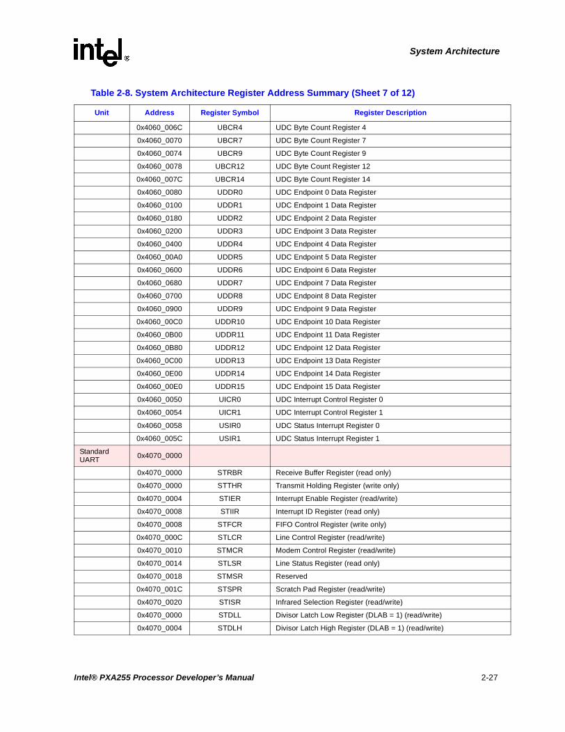
System Architecture
0x4060_006C UBCR4 UDC Byte Count Register 4
0x4060_0070 UBCR7 UDC Byte Count Register 7
0x4060_0074 UBCR9 UDC Byte Count Register 9
0x4060_0078 UBCR12 UDC Byte Count Register 12
0x4060_007C UBCR14 UDC Byte Count Register 14
0x4060_0080 UDDR0 UDC Endpoint 0 Data Register
0x4060_0100 UDDR1 UDC Endpoint 1 Data Register
0x4060_0180 UDDR2 UDC Endpoint 2 Data Register
0x4060_0200 UDDR3 UDC Endpoint 3 Data Register
0x4060_0400 UDDR4 UDC Endpoint 4 Data Register
0x4060_00A0 UDDR5 UDC Endpoint 5 Data Register
0x4060_0600 UDDR6 UDC Endpoint 6 Data Register
0x4060_0680 UDDR7 UDC Endpoint 7 Data Register
0x4060_0700 UDDR8 UDC Endpoint 8 Data Register
0x4060_0900 UDDR9 UDC Endpoint 9 Data Register
0x4060_00C0 UDDR10 UDC Endpoint 10 Data Register
0x4060_0B00 UDDR11 UDC Endpoint 11 Data Register
0x4060_0B80 UDDR12 UDC Endpoint 12 Data Register
0x4060_0C00 UDDR13 UDC Endpoint 13 Data Register
0x4060_0E00 UDDR14 UDC Endpoint 14 Data Register
0x4060_00E0 UDDR15 UDC Endpoint 15 Data Register
0x4060_0050 UICR0 UDC Interrupt Control Register 0
0x4060_0054 UICR1 UDC Interrupt Control Register 1
0x4060_0058 USIR0 UDC Status Interrupt Register 0
0x4060_005C USIR1 UDC Status Interrupt Register 1
Standard UART 0x4070_0000
0x4070_0000 STRBR Receive Buffer Register (read only)
0x4070_0000 STTHR Transmit Holding Register (write only)
0x4070_0004 STIER Interrupt Enable Register (read/write)
0x4070_0008 STIIR Interrupt ID Register (read only)
0x4070_0008 STFCR FIFO Control Register (write only)
0x4070_000C STLCR Line Control Register (read/write)
0x4070_0010 STMCR Modem Control Register (read/write)
0x4070_0014 STLSR Line Status Register (read only)
0x4070_0018 STMSR Reserved
0x4070_001C STSPR Scratch Pad Register (read/write)
0x4070_0020 STISR Infrared Selection Register (read/write)
0x4070_0000 STDLL Divisor Latch Low Register (DLAB = 1) (read/write)
0x4070_0004 STDLH Divisor Latch High Register (DLAB = 1) (read/write)
Table 2-8. System Architecture Register Address Summary (Sheet 7 of 12)
Unit Address Register Symbol Register Description
Intel® PXA255 Processor Developer’s Manual 2-27

System Architecture
ICP 0x4080_0000
0x4080_0000 ICCR0 ICP Control Register 0
0x4080_0004 ICCR1 ICP Control Register 1
0x4080_0008 ICCR2 ICP Control Register 2
0x4080_000C ICDR ICP Data Register
0x4080_0010 — Reserved
0x4080_0014 ICSR0 ICP Status Register 0
0x4080_0018 ICSR1 ICP Status Register 1
RTC 0x4090_0000
0x4090_0000 RCNR RTC Count Register
0x4090_0004 RTAR RTC Alarm Register
0x4090_0008 RTSR RTC Status Register
0x4090_000C RTTR RTC Timer Trim Register
OS Timer 0x40A0_0000
0x40A0_0000 OSMR<0>
OS Timer Match registers<3:0>0x40A0_0004 OSMR<1>
0x40A0_0008 OSMR<2>
0x40A0_000C OSMR<3>
0x40A0_0010 OSCR OS Timer Counter Register
0x40A0_0014 OSSR OS Timer Status Register
0x40A0_0018 OWER OS Timer Watchdog Enable Register
0x40A0_001C OIER OS Timer Interrupt Enable Register
PWM 0 0x40B0_0000
0x40B0_0000 PWM_CTRL0 PWM 0 Control Register
0x40B0_0004 PWM_PWDUTY0 PWM 0 Duty Cycle Register
0x40B0_0008 PWM_PERVAL0 PWM 0 Period Control Register
PWM 1 0x40C0_0000
0x40C0_0000 PWM_CTRL1 PWM 1Control Register
0x40C0_0004 PWM_PWDUTY1 PWM 1 Duty Cycle Register
0x40C0_0008 PWM_PERVAL1 PWM 1 Period Control Register
Interrupt Control 0x40D0_0000
0x40D0_0000 ICIP Interrupt Controller IRQ Pending Register
0x40D0_0004 ICMR Interrupt Controller Mask Register
0x40D0_0008 ICLR Interrupt Controller Level Register
0x40D0_000C ICFP Interrupt Controller FIQ Pending Register
0x40D0_0010 ICPR Interrupt Controller Pending Register
0x40D0_0014 ICCR Interrupt Controller Control Register
GPIO 0x40E0_0000
0x40E0_0000 GPLR0 GPIO Pin-Level Register GPIO<31:0>
0x40E0_0004 GPLR1 GPIO Pin-Level Register GPIO<63:32>
Table 2-8. System Architecture Register Address Summary (Sheet 8 of 12)
Unit Address Register Symbol Register Description
2-28 Intel® PXA255 Processor Developer’s Manual

System Architecture
0x40E0_0008 GPLR2 GPIO Pin-Level Register GPIO<80:64>
0x40E0_000C GPDR0 GPIO Pin Direction Register GPIO<31:0>
0x40E0_0010 GPDR1 GPIO Pin Direction Register GPIO<63:32>
0x40E0_0014 GPDR2 GPIO Pin Direction Register GPIO<80:64>
0x40E0_0018 GPSR0 GPIO Pin Direction Register GPIO<31:0>
0x40E0_001C GPSR1 GPIO Pin Output Set Register GPIO<63:32>
0x40E0_0020 GPSR2 GPIO Pin Output Set Register GPIO<80:64>
0x40E0_0024 GPCR0 GPIO Pin Output Clear Register GPIO<31:0>
0x40E0_0028 GPCR1 GPIO Pin Output Clear Register GPIO <63:32>
0x40E0_002C GPCR2 GPIO Pin Output Clear Register GPIO <80:64>
0x40E0_0030 GRER0 GPIO Rising-Edge Detect Register GPIO<31:0>
0x40E0_0034 GRER1 GPIO Rising-Edge Detect Register GPIO<63:32>
0x40E0_0038 GRER2 GPIO Rising-Edge Detect Register GPIO<80:64>
0x40E0_003C GFER0 GPIO Falling-Edge Detect Register GPIO<31:0>
0x40E0_0040 GFER1 GPIO Falling-Edge Detect Register GPIO<63:32>
0x40E0_0044 GFER2 GPIO Falling-Edge Detect Register GPIO<80:64>
0x40E0_0048 GEDR0 GPIO Edge Detect Status Register GPIO<31:0>
0x40E0_004C GEDR1 GPIO Edge Detect Status Register GPIO<63:32>
0x40E0_0050 GEDR2 GPIO Edge Detect Status Register GPIO<80:64>
0x40E0_0054 GAFR0_L GPIO Alternate Function Select Register GPIO<15:0>
0x40E0_0058 GAFR0_U GPIO Alternate Function Select Register GPIO<31:16>
0x40E0_005C GAFR1_L GPIO Alternate Function Select Register GPIO<47:32>
0x40E0_0060 GAFR1_U GPIO Alternate Function Select Register GPIO<63:48>
0x40E0_0064 GAFR2_L GPIO Alternate Function Select Register GPIO<79:64>
0x40E0_0068 GAFR2_U GPIO Alternate Function Select Register GPIO 80
Power Manager and Reset Control
0x40F0_0000
0x40F0_0000 PMCR Power Manager Control Register
0x40F0_0004 PSSR Power Manager Sleep Status Register
0x40F0_0008 PSPR Power Manager Scratch Pad Register
0x40F0_000C PWER Power Manager Wake-up Enable Register
0x40F0_0010 PRER Power Manager GPIO Rising-Edge Detect Enable Register
0x40F0_0014 PFER Power Manager GPIO Falling-Edge Detect Enable Register
0x40F0_0018 PEDR Power Manager GPIO Edge Detect Status Register
0x40F0_001C PCFR Power Manager General Configuration Register
0x40F0_0020 PGSR0 Power Manager GPIO Sleep State Register for GP[31-0]
0x40F0_0024 PGSR1 Power Manager GPIO Sleep State Register for GP[63-32]
0x40F0_0028 PGSR2 Power Manager GPIO Sleep State Register for GP[84-64]
0x40F0_002C — Reserved
Table 2-8. System Architecture Register Address Summary (Sheet 9 of 12)
Unit Address Register Symbol Register Description
Intel® PXA255 Processor Developer’s Manual 2-29

System Architecture
0x40F0_002C — Reserved
0x40F0_0030 RCSR Reset Controller Status Register
SSP 0x4100_0000
0x4100_0000 SSCR0 SSP Control Register 0
0x4100_0004 SSCR1 SSP Control Register 1
0x4100_0008 SSSR SSP Status Register
0x4100_000C SSITR SSP Interrupt Test Register
0x4100_0010 SSDR (Write / Read) SSP Data Write Register/SSP Data Read Register
MMC Controller 0x4110_0000
0x4110_0000 MMC_STRPCL Control to start and stop MMC clock
0x4110_0004 MMC_STAT MMC Status Register (read only)
0x4110_0008 MMC_CLKRT MMC clock rate
0x4110_000C MMC_SPI SPI mode control bits
0x4110_0010 MMC_CMDAT Command/response/data sequence control
0x4110_0014 MMC_RESTO Expected response time out
0x4110_0018 MMC_RDTO Expected data read time out
0x4110_001C MMC_BLKLEN Block length of data transaction
0x4110_0020 MMC_NOB Number of blocks, for block mode
0x4110_0024 MMC_PRTBUF Partial MMC TXFIFO FIFO written
0x4110_0028 MMC_I_MASK Interrupt Mask
0x4110_002C MMC_I_REG Interrupt Register (read only)
0x4110_0030 MMC_CMD Index of current command
0x4110_0034 MMC_ARGH MSW part of the current command argument
0x4110_0038 MMC_ARGL LSW part of the current command argument
0x4110_003C MMC_RES Response FIFO (read only)
0x4110_0040 MMC_RXFIFO Receive FIFO (read only)
0x4110_0044 MMC_TXFIFO Transmit FIFO (write only)
Clocks Manager 0x4130_0000
0x4130_0000 CCCR Core Clock Configuration Register
0x4130_0004 CKEN Clock Enable Register
0x4130_0008 OSCC Oscillator Configuration Register
Network SSP 0x4140_0000
0x4140_0000 NSSCR0 NSSP Control Register 0
0x4140_0004 NSSCR1 NSSP Control Register 1
0x4140_0008 NSSSR NSSP Status Register
0x4140_000C NSSITR NSSP Interrupt Test Register
0x4140_0010 NSSDR NSSP Data Read/Write Register
0x4140_0028 NSSTO NSSP Time Out Register
Table 2-8. System Architecture Register Address Summary (Sheet 10 of 12)
Unit Address Register Symbol Register Description
2-30 Intel® PXA255 Processor Developer’s Manual

System Architecture
0x4140_002C NSSPSP NSSP Programmable Serial Protocol
Hardware UART 0x4160_0000
0x4160_0000 HWRBR Receive Buffer Register (read only)
0x4160_0000 HWTHR Transmit Holding Register (write only)
0x4160_0004 HWIER Interrupt Enable Register (read/write)
0x4160_0008 HWIIR Interrupt ID Register (read only)
0x4160_0008 HWFCR FIFO Control Register (write only)
0x4160_000C HWLCR Line Control Register (read/write)
0x4160_0010 HWMCR Modem Control Register (read/write)
0x4160_0014 HWLSR Line Status Register (read only)
0x4160_0018 HWMSR Modem Status Register (read only)
0x4160_001C HWSPR Scratch Pad Register (read/write)
0x4160_0020 HWISR Infrared Selection Register (read/write)
0x4160_0024 HWFOR FIFO Occupancy Register (read only)
0x4160_0028 HWABR Auto-Baud Control Register (read/write)
0x4160_002C HWACR Auto-Baud Count Register
0x4160_0000 HWDLL Divisor Latch Low Register (DLAB = 1) (read/write)
0x4160_0000 HWDLH Divisor Latch High Register (DLAB = 1) (read/write)
LCD Controller 0x4400_0000
0x4400_0000 LCCR0 LCD Controller Control Register 0
0x4400_0004 LCCR1 LCD Controller Control Register 1
0x4400_0008 LCCR2 LCD Controller Control Register 2
0x4400_000C LCCR3 LCD Controller Control Register 3
0x4400_0200 FDADR0 DMA Channel 0 Frame Descriptor Address Register
0x4400_0204 FSADR0 DMA Channel 0 Frame Source Address Register
0x4400_0208 FIDR0 DMA Channel 0 Frame ID Register
0x4400_020C LDCMD0 DMA Channel 0 Command Register
0x4400_0210 FDADR1 DMA Channel 1 Frame Descriptor Address Register
0x4400_0214 FSADR1 DMA Channel 1 Frame Source Address Register
0x4400_0218 FIDR1 DMA Channel 1 Frame ID Register
0x4400_021C LDCMD1 DMA Channel 1 Command Register
0x4400_0020 FBR0 DMA Channel 0 Frame Branch Register
0x4400_0024 FBR1 DMA Channel 1 Frame Branch Register
0x4400_0038 LCSR LCD Controller Status Register
0x4400_003C LIIDR LCD Controller Interrupt ID Register
0x4400_0040 TRGBR TMED RGB Seed Register
0x4400_0044 TCR TMED Control Register
Memory Controller 0x4800_0000
Table 2-8. System Architecture Register Address Summary (Sheet 11 of 12)
Unit Address Register Symbol Register Description
Intel® PXA255 Processor Developer’s Manual 2-31

System Architecture
0x4800_0000 MDCNFG SDRAM Configuration Register 0
0x4800_0004 MDREFR SDRAM Refresh Control Register
0x4800_0008 MSC0 Static Memory Control Register 0
0x4800_000C MSC1 Static Memory Control Register 1
0x4800_0010 MSC2 Static Memory Control Register 2
0x4800_0014 MECR Expansion Memory (PCMCIA/Compact Flash) Bus Configuration Register
0x4800_001C SXCNFG Synchronous Static Memory Control Register
0x4800_0024 SXMRS MRS value to be written to SMROM
0x4800_0028 MCMEM0 Card interface Common Memory Space Socket 0 Timing Configuration
0x4800_002C MCMEM1 Card interface Common Memory Space Socket 1 Timing Configuration
0x4800_0030 MCATT0 Card interface Attribute Space Socket 0 Timing Configuration
0x4800_0034 MCATT1 Card interface Attribute Space Socket 1 Timing Configuration
0x4800_0038 MCIO0 Card interface I/O Space Socket 0 Timing Configuration
0x4800_003C MCIO1 Card interface I/O Space Socket 1 Timing Configuration
0x4800_0040 MDMRS MRS value to be written to SDRAM
0x4800_0044 BOOT_DEF Read-only Boot-Time Register. Contains BOOT_SEL and PKG SEL values.
0x4800_0058 MDMRSLP Low Power SDRAM Mode Register Set Configuration Register
0x4800_0064 SA1111CR SA1111 Compatibility Register
Table 2-8. System Architecture Register Address Summary (Sheet 12 of 12)
Unit Address Register Symbol Register Description
2-32 Intel® PXA255 Processor Developer’s Manual

Clocks and Power Manager 3
The Clocks and Power Manager for the PXA255 processor controls the clock frequency to each module and manages transitions between the different power manager (PM) operating modes to optimize both computing performance and power consumption.
3.1 Clock Manager Introduction
The Clocks and Power Manager provides fixed clocks for each peripheral unit. Many of the devices’ peripheral clocks can be disabled using the Clock Enable Register (CKEN), or through bits in the peripheral’s control registers. To minimize power consumption, turn off the clock to any unit that is not being used. The Clocks and Power Manager also provides the programmable-frequency clocks for the LCD Controller, Memory Controller, and CPU. These clocks are related to each other because they come from the same internal Phase Locked Loop (PLL) clock source. To program the PLL’s frequency, follow these steps (for information on the factors L, M, and N, see Section 3.6.1, “Core Clock Configuration Register (CCCR)” on page 3-34):
1. Determine the fastest synchronous memory requirement (SDRAM frequency).
2. If the SDRAM frequency is less than 99.5 MHz, the Memory Frequency must be twice the SDRAM Frequency and the SDRAM clock ratio in the Memory Controller must be set to two. If the SDRAM frequency is 99.5 MHz, the Memory Frequency is equal to the SDRAM frequency.
3. Round the Memory Frequency down to the nearest value of 99.5 MHz (L = 0x1B), 118.0 MHz (L = 0x20), 132.7 MHz (L = 0x24), 147.5 MHz (L = 0x28), or 165.9 MHz (L = 0x2D), and program the value of L in the Core Clock Configuration register. This frequency (or half, if the SDRAM clock ratio is 2) is the External Synchronous Memory Frequency.
4. Determine the required Core Frequency for normal (Run Mode) operation. This mode is used during normal processing, when the application must make occasional fetches to external memory. The possible values are one, two, or four times the Memory Frequency. Program this value (M) in the Core Clock Configuration register.
5. Determine the required Core Frequency for Turbo Mode operation. This mode is generally used when the application runs entirely from the caches, because any fetches to external memory slow the Core’s performance. This value is a multiple (1.0, 1.5, 2.0, or 3.0) of the Run Mode Frequency. Program the value (N) in the Core Clock Configuration register.
6. Configure the LCD Controller and Memory Controller for the new Memory Frequency and enter the Frequency Change Sequence (described in Section 3.4.7, “Frequency Change Sequence” on page 3-11).
Note: Not all frequency combinations are valid. See Section 3.3.3, “Core Phase Locked Loop” for valid combinations.
Intel® PXA255 Processor Developer’s Manual 3-1

Clocks and Power Manager
3.2 Power Manager Introduction
The Clocks and Power Manager can place the processor in one of three resets.
• Hardware Reset (nRESET asserted) is a nonmaskable total reset. It is used at power up or when no system information requires preservation.
• Watchdog Reset is asserted through the Watchdog Timer and resets the system except the Clocks and Power Manager. This reset is used as a code monitor. If code fails to complete a specified sequence, the processor assumes a fatal system error has occurred and causes a Watchdog Reset.
• GPIO Reset is enabled through the GPIO alternate function registers. It is used as an alternative to Hardware Reset that preserves the Memory Controller registers and a few critical states in the Clocks and Power Manager and the Real Time Clock (RTC).
The Clocks and Power Manager also controls the entry into and exit from any of the low power or special clocking modes on processor. These modes are:
• Turbo Mode: the Core runs at its peak frequency. In this mode, make very few external memory accesses because the Core must wait on the external memory.
• Run Mode: the Core runs at its normal frequency. In this mode, the Core is assumed to be doing frequent external memory accesses, so running slower is optimum for the best power/performance trade-off.
• Idle Mode: the Core is not being clocked, but the rest of the system is fully operational. This mode is used during brief lulls in activity, when the external system must continue operation but the Core is idle.
• Sleep Mode: places the processor in its lowest power state but maintains I/O state, RTC, and the Clocks and Power Manager. Wake-up from Sleep Mode requires re-booting the system, since most internal state was lost. The core power must be grounded in sleep to prevent current leakage.
The Clocks and Power Manager also controls the processor’s actions during the Frequency Change Sequence. The Frequency Change Sequence is a sequence that changes the Core Frequency (Run and Turbo) and Memory Frequency from the previously stored values to the new values in the Core Clock Configuration register. This sequence takes time to complete due to PLL relock time, but it allows dynamic frequency changes without compromising external memory integrity. Any peripherals that rely on the Core or Memory Controller must be configured to withstand a data flow interruption.
3.3 Clock Manager
The processor’s clocking system incorporates five major clock sources:
• 32.768 kHz Oscillator
• 3.6864 MHz Oscillator
• Programmable Frequency Core PLL
• 95.85 MHz Fixed Frequency Peripheral PLL
• 147.46 MHz Fixed Frequency PLL
3-2 Intel® PXA255 Processor Developer’s Manual

Clocks and Power Manager
The clocks manager also contains clock gating for power reduction.
Figure 3-1 shows a functional representation of the clocking network. “L” is in the core PLL.
The PXbus is the internal bus between the Core, the DMA/Bridge, the LCD Controller, and the Memory Controller as shown in Figure 3-1. This bus is clocked at 1/2 the run mode frequency. For optimal performance, the PXbus should be clocked as fast as possible. For example, if a target core frequency of 200 MHz is desired use 200 MHz run mode instead of 200 MHz turbo mode with run at 100 MHz. Increasing the PXbus frequency may help reduce the latency involved in accessing non-cacheable memory.
Figure 3-1. Clocks Manager Block Diagram
/N
/M
/4
DMA/
Bridge
/1 /112
UARTs
14.746
AC97
12.288
I2S
5.672
PWM
3.6864
SSP
3.6864
GPIO
3.6864
OST
3.6864
PWR_MGR
32.768 k
32.768kHzOSC
3.6864MHzOSC
100-400MHzPLL*
95.846MHzPLL
147.46MHzPLL
CORECPU
ControllerMEM
ControllerLCD
/2
MMC
19.169
I2C
31.949
FICP
47.923
USB
47.923
RTC
32.768 k
RETAINS POWER IN SLEEP
PXbus
Intel® PXA255 Processor Developer’s Manual 3-3
Clocks and Power Manager
3.3.1 32.768 kHz Oscillator
The 32.768 kHz oscillator is a low power, low frequency oscillator that clocks the RTC and Power Manager. This oscillator is disabled out of Hardware Reset and the RTC and Power Manager blocks use the 3.6864 MHz oscillator instead. Software writes the Oscillator On bit in the Oscillator Configuration Register to enable the 32.768 kHz.This configures the RTC and Power Manager to use the 32.768 kHz oscillator after it stabilizes.
32.768 kHz oscillator use is optional and provides the lowest power consumption during Sleep Mode. In less power-sensitive applications, disable the 32.768 kHz oscillator in the Oscillator Configuration Register (OSCC) and leave the external pins floating (no external crystal required) for cost savings. If the 32.768 kHz oscillator is not in the system, the frequency of the RTC and Power Manager will be 3.6864 MHz divided by 112 (32.914 kHz). In Sleep, the 3.6864 MHz oscillator consumes hundreds of microamps of extra power when it stays enabled. See Section 3.5.2, “Power Manager General Configuration Register (PCFR)” on page 3-24 for information on The Oscillator Power Down Enable (OPDE) bit, which determines if the 3.6864 MHz oscillator is enabled in Sleep Mode. No external capacitors are required.
3.3.2 3.6864 MHz Oscillator
The 3.6864 MHz oscillator provides the primary clock source for the processor. The on-chip PLL frequency multipliers, Synchronous Serial Port (SSP), Pulse Width Modulator (PWM), and the Operating System Timer (OST) use the 3.6864 MHz oscillator as a reference. Out of Hardware Reset, the 3.6864 MHz oscillator also drives the RTC and Power Manager (PM). The user may then enable the 32.768 kHz oscillator, which will drive the RTC and PM after it is stabilized. The 3.6864 MHz oscillator can be disabled during Sleep Mode by setting the OPDE (see Section 3.5.2) bit but only if the 32.768 kHz oscillator is enabled and stabilized (both the OON and OOK bits in the OSCC set). See Section 3.6.3 for more information. No external capacitors are required.
3.3.3 Core Phase Locked Loop
The Core PLL is the clock source of the CPU Core, the Memory Controller, the LCD Controller, and DMA Controller. The Core PLL uses the 3.6864 MHz oscillator as a reference and multiplies its frequency by the following variables:
• L: Crystal Frequency to Memory Frequency Multiplier, set to 27, 32, 36, 40, or 45.
• M: Memory Frequency to Run Mode Frequency Multiplier, set to 1 or 2.
• N: Run Mode Frequency to Turbo Mode Frequency Multiplier, set to 1.0, 1.5, 2.0, or 3.0.
The output frequency selections are shown in Table 3-1, “Core PLL Output Frequencies for 3.6864 MHz Crystal”. See Section 3.6.1 for programming information on the L, M, and N factors. See Section 3.6.1, “Core Clock Configuration Register (CCCR)” for the hexadecimal settings.
Do not choose a combination that generates a frequency that is not supported in the voltage range and package in which the processor is operating.
SDCLK must not be greater than 100 MHz. If MEMCLK is greater than 100 MHz, the SDCLK to MEMCLK ratio must be set to 1:2 in the Memory Controller.
3-4 Intel® PXA255 Processor Developer’s Manual
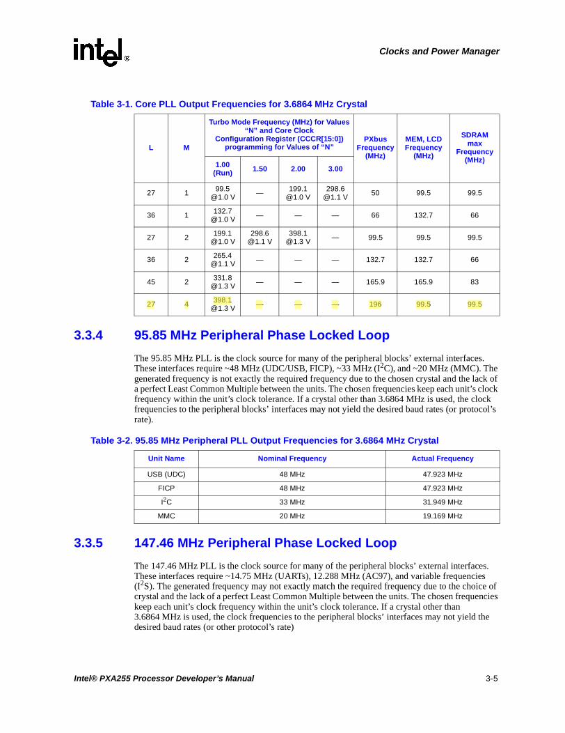
Clocks and Power Manager
3.3.4 95.85 MHz Peripheral Phase Locked Loop
The 95.85 MHz PLL is the clock source for many of the peripheral blocks’ external interfaces. These interfaces require ~48 MHz (UDC/USB, FICP), ~33 MHz (I2C), and ~20 MHz (MMC). The generated frequency is not exactly the required frequency due to the chosen crystal and the lack of a perfect Least Common Multiple between the units. The chosen frequencies keep each unit’s clock frequency within the unit’s clock tolerance. If a crystal other than 3.6864 MHz is used, the clock frequencies to the peripheral blocks’ interfaces may not yield the desired baud rates (or protocol’s rate).
3.3.5 147.46 MHz Peripheral Phase Locked Loop
The 147.46 MHz PLL is the clock source for many of the peripheral blocks’ external interfaces. These interfaces require ~14.75 MHz (UARTs), 12.288 MHz (AC97), and variable frequencies (I2S). The generated frequency may not exactly match the required frequency due to the choice of crystal and the lack of a perfect Least Common Multiple between the units. The chosen frequencies keep each unit’s clock frequency within the unit’s clock tolerance. If a crystal other than 3.6864 MHz is used, the clock frequencies to the peripheral blocks’ interfaces may not yield the desired baud rates (or other protocol’s rate)
Table 3-1. Core PLL Output Frequencies for 3.6864 MHz Crystal
L M
Turbo Mode Frequency (MHz) for Values “N” and Core Clock
Configuration Register (CCCR[15:0]) programming for Values of “N”
PXbus Frequency
(MHz)
MEM, LCD Frequency
(MHz)
SDRAMmax
Frequency(MHz)
1.00(Run) 1.50 2.00 3.00
27 1 [email protected] V
50 99.5 99.5
36 1 [email protected] V — — — 66 132.7 66
27 2 [email protected] V
[email protected] V — 99.5 99.5 99.5
36 2 [email protected] V
— — — 132.7 132.7 66
45 2 [email protected] V — — — 165.9 165.9 83
27 4 [email protected] V — — — 196 99.5 99.5
Table 3-2. 95.85 MHz Peripheral PLL Output Frequencies for 3.6864 MHz Crystal
Unit Name Nominal Frequency Actual Frequency
USB (UDC) 48 MHz 47.923 MHz
FICP 48 MHz 47.923 MHz
I2C 33 MHz 31.949 MHz
MMC 20 MHz 19.169 MHz
Intel® PXA255 Processor Developer’s Manual 3-5

Clocks and Power Manager
3.3.6 Clock Gating
The Clocks Manager contains the CKEN register. This register contains configuration bits that can disable the clocks to individual units. The configuration bits are used when a module is not being used. After Hardware Reset, any module that is not being used must have its clock disabled. If a module is temporarily quiescent but does not have clock gating functionality, the CKEN register can be used to disable the unit’s clock.
When a module’s clock is disabled, the registers in that module are still readable and writable. The AC97 is an exception and is completely inaccessible if the clock is disabled.
3.4 Resets and Power Modes
The Clocks and Power Manager Unit determines the processor’s Resets, Power Sequences and Power Modes. Each behaves differently during operation and has specific entry and exit sequences. The resets and power modes are:
• Hardware Reset
• Watchdog Reset
• GPIO Reset
• Run Mode
• Turbo Mode
• Idle Mode
• Frequency Change Sequence
• Sleep Mode
3.4.1 Hardware Reset
To invoke the Hardware Reset and reset all units in the processor to a known state, assert the nRESET pin. Hardware Reset is only intended to be used for power up and complete resets.
3.4.1.1 Invoking Hardware Reset
Hardware Reset is invoked when the nRESET pin is pulled low by an external source. The processor does not provide a method of masking or disabling the propagation of the external pin value. When the nRESET pin is asserted, Hardware Reset is invoked, regardless of the mode of operation. The nRESET_OUT pin is asserted when the nRESET pin is asserted. To enter Hardware
Table 3-3. 147.46 MHz Peripheral PLL Output Frequencies for 3.6864 MHz Crystal
Unit Name Nominal Frequency Actual Frequency
UARTs 14.746 MHz 14.746 MHz
AC97 12.288 MHz 12.288 MHz
I2S 146.76 MHz 147.46 MHz
3-6 Intel® PXA255 Processor Developer’s Manual

Clocks and Power Manager
Reset, nRESET must be held low for tDHW_NRESET to allow the system to stabilize and the reset state to propagate. Refer to the Intel® PXA255 Processor Electrical, Mechanical, and Thermal Specification for details.
3.4.1.2 Behavior During Hardware Reset
During Hardware Reset, all internal registers and units are held at their defined reset conditions. While the nRESET pin is asserted, nothing inside the processor is active except the 3.6864 MHz oscillator. The internal clocks are stopped and the chip is static. All pins return to their reset conditions and the nBATT_FAULT and nVDD_FAULT pins are ignored. Because the memory controller receives a full reset, all dynamic RAM contents are lost during Hardware Reset.
3.4.1.3 Completing Hardware Reset
To complete Hardware Reset, deassert the nRESET pin. All power supplies must be stable for tD_NRESET before nRESET is deasserted. Refer to the Intel® PXA255 Processor Electrical, Mechanical, and Thermal Specification for details. After the nRESET pin is deasserted, the following sequence occurs:
1. The 3.6864 MHz oscillator and internal PLL clock generators wait for stabilization.
2. The nRESET_OUT pin is deasserted.
3. The normal boot-up sequence begins. All processor units return to their predefined reset conditions. Software must examine the Reset Controller Status register (RCSR) to determine the cause for the boot.
3.4.2 Watchdog Reset
Watchdog Reset is invoked when software fails to properly prevent the Watchdog Time-out Event from occurring. It is assumed that Watchdog Resets are only generated when software is not executing properly and has potentially destroyed data. In Watchdog Reset all units in the are reset except the Clocks and Power Manager.
3.4.2.1 Invoking Watchdog Reset
Watchdog Reset is invoked when the Watchdog Enable bit (WE) in the OWER is set and the OSMR[3] matches the OS timer counter. When these conditions are met, they invoke Watchdog Reset, regardless of the previous mode of operation. Watchdog Reset asserts nRESET_OUT.
3.4.2.2 Behavior During Watchdog Reset
During Watchdog Reset, all units except the Real Time Clock and parts of the Clocks and Power Manager maintain their defined reset conditions. All pins except the oscillator pins assume their reset conditions and the nBATT_FAULT and nVDD_FAULT pins are ignored. All dynamic RAM contents are lost during Watchdog Reset because the memory controller receives a full reset.
Refer to Table 2-6, “Pin & Signal Descriptions for the PXA255 Processor” for the pin states during Watchdog and other Resets.
Intel® PXA255 Processor Developer’s Manual 3-7

Clocks and Power Manager
3.4.2.3 Completing a Watchdog Reset
Watchdog resets immediately revert to hardware resets when the nRESET pin is asserted. Otherwise, the completion sequence for watchdog reset is:
1. The 3.6864 MHz oscillator and internal PLL clock generators wait for stabilization. The 32.768 kHz oscillator’s configuration and status are not affected by watchdog reset.
2. The nRESET_OUT pin is deasserted after tDHW_OUT. Refer to the Intel® PXA255 Processor Electrical, Mechanical, and Thermal Specification.
3. The normal boot-up sequence begins. All processor units except the RTTR in the RTC and parts of the Clocks and Power Manager return to their predefined reset conditions. Software must examine the RCSR to determine the cause for the reboot.
3.4.3 GPIO Reset
A GPIO Reset is invoked when GP[1] is properly configured as a reset source and is asserted low for greater than four 3.6864-MHz clock cycles. In GPIO Reset all processor units except the RTC, parts of the Clocks and Power Manager, and the Memory Controller return to their predefined, known states.
3.4.3.1 Invoking GPIO Reset
To use the GPIO Reset function, set it up through the GPIO Controller. The GP[1] pin must be configured as an input and set to its alternate GPIO Reset function in the GPIO Controller. The GPIO Reset alternate function is level-sensitive and not edge-triggered. To ensure no spurious resets are generated when the alternate GPIO Reset function is set, follow these steps:
1. GP[1] must be set up as an output with its data register set to a 1.
2. Externally drive the GP[1] pin to a high state.
3. Configure GP[1] as an input.
4. Configure GP[1] for its Alternate (Reset) Function.
The previous mode of operation does not affect a GPIO Reset. When performing a GPIO Reset, nRESET_OUT is asserted. If GP[1] is asserted for less than four 3.6864-MHz clock cycles, the processor may remain in its previous mode or enter into a GPIO reset.
GPIO Reset does not function in Sleep Mode because all GPIO pins’ Alternate Function Inputs are disabled. External wake-up sources must be routed through one of the enabled GPIO wake-up sources (see Section 3.5.3 for details) during Sleep Mode. GP[1] may be enabled as a wake-up source.
3.4.3.2 Behavior During GPIO Reset
During GPIO Reset, most, but not all, internal registers and processes are held at their defined reset conditions. The exceptions are the RTC, the Clocks and Power Manager (unless otherwise noted), and the Memory Controller. During GPIO Reset, the clocks unit continues to operate with its previously programmed values, so the processor enters and exits GPIO Reset with the same clock configurations. All pins except the oscillator and Memory Controller pins return to their reset conditions and the nBATT_FAULT and nVDD_FAULT pins are ignored.
3-8 Intel® PXA255 Processor Developer’s Manual

Clocks and Power Manager
GPIO Reset does not reset the Memory Controller Configuration registers. This creates the possibility that the contents of external memories may be preserved if the external memories are properly configured before GPIO Reset is entered. To preserve SDRAM contents during a GPIO Reset, software must correctly configure the Memory Control and the time spent in GPIO Reset must be shorter than the SDRAM refresh interval. The amount of time spent in GPIO Reset depends on the CPU’s mode before GPIO Reset. See Section 6, “Memory Controller” for details.
Refer to Table 2-6, “Pin & Signal Descriptions for the PXA255 Processor” for the states of all the PXA255 processor pins during GPIO reset and other resets.
3.4.3.3 Completing GPIO Reset
GPIO Reset immediately reverts to Hardware Reset when the nRESET pin is asserted. Otherwise, the completion sequence for GPIO Reset is:
1. The GPIO Reset Source is deasserted because the internal reset has propagated to the GPIO Controller and its registers, which are set back to their reset states.
2. The nRESET_OUT pin is deasserted.
3. The normal boot-up sequence begins. All processor units except the Real Time Clock, parts of the Clocks and Power Manager, and the Memory Controller return to their predefined reset conditions. Software must examine the RCSR to determine the cause for the reset.
3.4.4 Run Mode
Run Mode is the processor’s normal operating mode. All power supplies are enabled and all functionally enabled clocks are running. Run Mode is entered after any power mode, power sequence, or reset completes its sequence. Run Mode is exited when any other power mode, power sequence, or reset begins.
3.4.5 Turbo Mode
Turbo Mode allows the user to clock the processor core at a higher frequency during peak processing requirements. It allows a synchronous switch in frequencies without disrupting the Memory Controller, LCD Controller, or any peripheral.
3.4.5.1 Entering Turbo Mode
Turbo Mode is invoked when software sets the TURBO bit in the Clock Config (CCLKCFG) Register (See Section 3.7.1). After software sets the TURBO bit, the CPU waits for all instructions currently in the pipeline to complete. When the instructions are completed, the CPU resumes operation at the higher Turbo Mode Frequency.
Software can set or clear other bits in the CCLKCFG in the same write that sets the TURBO bit. The other bits in the register take precedence over Turbo Mode, so, if another bit is set, that mode’s sequence is followed before the CPU enters Turbo Mode. When the CPU exits the other mode, it enters either Run or Turbo Mode, based on the state of the CCLKCFG [TURBO] bit.
Do not confuse the CCLKCFG Register, which is in Coprocessor 14, with the CCCR (See Section 3.6.1), which is in the processor’s Clocks and Power Manager.
Intel® PXA255 Processor Developer’s Manual 3-9

Clocks and Power Manager
3.4.5.2 Behavior in Turbo Mode
The processor’s behavior in Turbo Mode is identical to its behavior in Run Mode, except that the processor’s clock frequency relative to the memory and peripherals is increased by N, the value in the CCCR (see Section 3.6.1). Turbo mode is intended for use during peak processing, when there are very few accesses to external memory. The higher Core to external memory clock ratio increases the relative delay for each external memory access. This increased delay lowers the processor’s power efficiency. For optimum performance, software must load applications in the caches in Run Mode and execute them in Turbo Mode.
3.4.5.3 Exiting Turbo Mode
To exit Turbo Mode, software clears the TURBO bit in the CCLKCFG Register. After software clears the TURBO bit, the CPU waits for all instructions in the pipeline to complete. When the instructions are completed, the CPU enters Run Mode.
Other bits in the CCLKCFG may be set or cleared in the write that clears CCLKCFG [TURBO]. All other bits in the register take precedence over Turbo Mode, so the new mode’s proper sequence is followed.
Idle, Sleep, Frequency Change Sequence, and Reset have precedence over Turbo Mode and cause the processor to exit Turbo Mode. When the CPU exits of one of these modes, it enters either Run or Turbo Mode, based on the state of CCLKCFG [TURBO].
3.4.6 Idle Mode
Idle Mode allows the user to stop the CPU core clock during periods of processor inactivity and continue to monitor on- and off-chip interrupt service requests. Idle mode does not change clock generation, so when an interrupt occurs the CPU is quickly reactivated in the state that preceded Idle Mode.
During Idle mode these resources are active:
• System unit modules (real-time clock, operating system timer, interrupt controller, general-purpose I/O, and clocks and power manager)
• Peripheral unit modules (DMA controller, LCD controller, and all other peripheral units)
• Memory Controller resources
3.4.6.1 Entering Idle Mode
During Idle Mode, the clocks to the CPU core stop. All critical applications must be finished and peripherals must be set up to generate interrupts when they require CPU attention. To enter the Idle Mode, software selects Idle Mode in PWRMODE[M] (See Section 3.7.2). An interrupt immediately aborts Idle Mode and normal processing resumes. After software selects Idle Mode, the CPU waits until all instructions in the pipeline are completed. When the instructions are completed, the CPU clock stops and Idle Mode begins. In Idle Mode, interrupts are recognized as wake-up sources.
3-10 Intel® PXA255 Processor Developer’s Manual

Clocks and Power Manager
3.4.6.2 Behavior in Idle Mode
In Idle Mode the CPU clocks are stopped, but the remainder of the processor operates normally. For example, the LCD controller can continue refreshing the screen with the same frame buffer data in memory.
When ICCR[DIM] is cleared, any enabled interrupt wakes up the processor. When ICCR[DIM] is set, only unmasked interrupts cause wake-up.
Enabled interrupts are interrupts that are allowed at the unit level. Masked interrupts are interrupts that are prevented from interrupting the core based on the Interrupt Controller Mask Register.
3.4.6.3 Exiting Idle Mode
Idle Mode exits when any Reset is asserted. Reset entry and exit sequences take precedence over Idle Mode. When the Reset exit sequence is completed, the CPU is not in Idle Mode. If the Watchdog Timer is enabled, software must set the Watchdog Match Registers before it sets Idle Mode to ensure that another interrupt will bring the processor out of Idle Mode before the Watchdog Reset is asserted. Use an RTC alarm or another OS timer channel for this purpose.
Any enabled interrupt causes Idle Mode to exit. When ICCR[DIM] is cleared, the Interrupt Controller Mask register (ICMR) is ignored during Idle Mode. This means that an interrupt does not have to be unmasked to cause Idle Mode to exit. Idle Mode exits in the following sequence:
1. A valid, enabled Interrupt asserts.
2. The CPU clocks restart and the CPU resumes operation at the state indicated by CCLKCFG [TURBO].
Idle Mode also exits when the nBATT_FAULT or nVDD_FAULT pin is asserted. When either pin is asserted, Idle Mode exits in the following sequence:
1. The nBATT_FAULT or nVDD_FAULT pin is asserted.
2. If the Imprecise Data Abort Enable (IDAE) bit in the Power Manager Control Register (PMCR) is clear (not recommended), the processor enters Sleep Mode immediately.
3. If the IDAE bit is set, the nBATT_FAULT or nVDD_FAULT assertion is treated as a valid interrupt to the clocks module and Idle Mode exits using its normal, interrupt-driven sequence. Software must then shut down the system and enter Sleep Mode. See Section 3.4.9.3, “Entering Sleep Mode” for more details.
3.4.7 Frequency Change Sequence
The Frequency Change Sequence is used to change the processor clock frequency. During the Frequency Change Sequence, the CPU, Memory Controller, LCD Controller, and DMA clocks stop. The other peripheral units continue to function during the Frequency Change Sequence. This mode is intended to be used to change the frequency from the default condition at initial boot-up. It may also be used as a power-saving feature used to allow the processor to run at the minimum required frequency when the software requires major changes in frequency.
3.4.7.1 Preparing for a Frequency Change Sequence
Software must complete the following steps before it initiates the Frequency Change Sequence:
Intel® PXA255 Processor Developer’s Manual 3-11

Clocks and Power Manager
1. Configure the Memory Controller to ensure SDRAM contents are maintained during the Frequency Change Sequence. The Memory Controller’s refresh timer must be programmed to match the maximum refresh time associated with the slower of two frequencies (current and desired). The SDRAM divide by two must be set to a value that prevents the SDRAM frequency from exceeding the specified frequency. For example, to change from 100/100 to 133/66, the SDRAM bus must be set to divide by two before the frequency change. To change from 133/66 to 100/100, the SDRAM must be set to one-to-one after the frequency change sequence is completed. See Section 6, “Memory Controller” for more details.
2. Disable the LCD Controller or configure it to avoid the effects of an interruption in the LCD clocks and data from the processor.
3. Configure peripheral units to handle a lack of DMA service for up to 500 µs. If a peripheral unit can not function for 500 µs without DMA service, it must be disabled.
4. Disable peripheral units that can not accommodate a 500 µs interrupt latency. The interrupts generated during the Frequency Change Sequence are serviced when the sequence exits.
5. Program the CCCR (Section 3.6.1, “Core Clock Configuration Register (CCCR)”) to reflect the desired frequency.
3.4.7.2 Invoking the Frequency Change Sequence
To invoke the Frequency Change Sequence, software must set FCS in the CCLKCFG (See Section 3.7.1). When software sets FCS, it may also set or clear other bits in CCLKCFG. If software sets the TURBO bit in the same write, the CPU enters Turbo Mode when the Frequency Change Sequence exits.
After software sets the FCS:
1. The CPU clock stops and interrupts to the CPU are gated.
2. The Memory Controller completes all outstanding transactions in its buffers and from the CPU. New transactions from the LCD or DMA controllers are ignored.
3. The Memory Controller places the SDRAM in self-refresh mode.
Note: Program the Memory Controller to ensure the correct self-refresh time for SDRAM, given the slower of the current and desired clock frequencies.
3.4.7.3 Behavior During the Frequency Change Sequence
In the frequency change sequence, the processor’s PLL clock generator is in the process of locking to the correct frequency and cannot be used. This means that interrupts cannot be processed. Interrupts that occur during the frequency change sequence are serviced after the processor’s PLL has locked. The 95.85 MHz and 147.46 MHz PLL clock generators are active and peripherals, except the memory, LCD, and DMA controllers, may continue to operate normally, provided they can accommodate the inability to process DMA or interrupt requests. DMA or interrupt requests are not recognized until the frequency change sequence is complete.
The Imprecise Data Abort is also not recognized and if nVDD_FAULT or nBATT_FAULT is asserted, the assertion is ignored until the Frequency Change Sequence exits. This means that the processor does not enter Sleep Mode until the Frequency Change Sequence is complete.
3-12 Intel® PXA255 Processor Developer’s Manual

Clocks and Power Manager
3.4.7.4 Completing the Frequency Change Sequence
The Frequency Change Sequence exits when any Reset is asserted. In Hardware and Watchdog Resets, the Reset entry and exit sequences take precedence over the Frequency Change Sequence and the PLL resumes in its Reset condition. In GPIO Reset, the Reset exit sequence is delayed while the PLL relocks and the frequency is set to the desired frequency of the Frequency Change Sequence.
If the Watchdog Timer is enabled during the Frequency Change Sequence, set the Watchdog Match Register to ensure that the Frequency Change Sequence completes before the Watchdog Reset is asserted.
If Hardware or Watchdog Reset is asserted during the Frequency Change Sequence, the DRAM contents are lost because all states, including Memory Controller configuration and information about the previous Frequency Change Sequence, are reset. If GPIO Reset is asserted during the Frequency Change Sequence, the SDRAM contents will be lost during the GPIO Reset exit sequence if the SDRAM is not in self-refresh mode and the exit sequence exceeds the refresh interval.
Normally, the Frequency Change Sequence exits in the following sequence:
1. The processor’s PLL clock generator is reprogrammed with the desired values, which are in the CCCR, and begins to relock to those values.
Note: This sequence occurs even if the before and after frequencies are the same.
2. The internal PLL clock generator for the processor clock waits for stabilization. Refer to the Intel® PXA250 and PXA210 Application Processors Electrical, Mechanical, and Thermal Specification for details.
3. The CPU clocks restart and the CPU resumes operation at the state indicated by the TURBO bit (either Run or Turbo Mode). Interrupts to the CPU are no longer gated.
4. The FCS bit is not automatically cleared. To prevent an accidental return to the Frequency Change Sequence, software must not immediately clear the FCS bit. The bit must be cleared on the next required write to the register.
5. Values may be written to the CCCR, but they are ignored until the Frequency Change Sequence is re-entered.
6. The SDRAM must transition out of self-refresh mode and into its idle state. See Section 6, “Memory Controller” for details on configuring the SDRAM interface.
3.4.8 33-MHz Idle Mode
33-MHz idle mode has the lowest power consumption of any idle mode. The run mode frequency selected in the Core Clock Configuration Register (CCCR) directly affects the processor idle mode power consumption. Faster run mode frequencies consume more power. 33-MHz idle mode places the processor a special low speed run mode before entering idle. This is similar to normal idle since the CPU core clock can be stopped during periods of processor inactivity and continue to monitor on- and off-chip interrupt service requests. 33-MHz idle limitations are:
• Peripherals will not function correctly and should be disabled before entering this mode.
• A Frequency Change Sequence must be performed upon entry to and exit from 33-MHz idle mode.
Intel® PXA255 Processor Developer’s Manual 3-13
Clocks and Power Manager
• SDRAM is placed in self refresh before entering 33-MHz idle mode, because SDRAM cannot be refreshed correctly in 33-MHz idle mode. Carefully consider the processor interrupt behavior when the SDRAM in self refresh. To allow the interrupts to occur while SDRAM is in self refresh, set the I and F bits in the CPSR. This allows interrupts to wake the processor from idle mode without jumping to the interrupt handler. When the system’s SDRAM is no longer in self refresh, the I and F bits can be cleared and the interrupt is handled.
• Because nBATT_FAULT and nVDD_FAULT can cause a data abort interrupt, the function of these pins in 33-MHz idle mode also needs special consideration. Either the Imprecise Data Abort Enable (IDAE) bit in the Power Manager Control Register (PMCR) must be clear, (causing the processor to immediately enter sleep mode if either nBATT_FAULT or nVDD_FAULT are asserted) or take software precautions to avoid starting execution in or trying to use SDRAM while it is in self refresh.
During 33-Mhz idle mode these system unit modules are functional:
• Real-time clock
• Operating system timer
• Interrupt controller
• General purpose I/O
• Clocks and power manager
• Flash ROM/SRAM
Unlike normal idle mode, in 33-MHz idle mode all other peripheral units cannot be used, including SDRAM, LCD and DMA controllers.
3.4.8.1 Entering 33-MHz Idle Mode
During idle mode, the processor core clocks stop. Before the clocks stop, all critical applications must be finished and peripherals turned off. If software is executing from SDRAM, the last three of the following steps must be loaded into the cache before being performed.
1. Set the I and F bits in the CPSR register to mask all interrupts
2. Place the SDRAM into self refresh mode
3. Perform a frequency change sequence to 33MHz mode. The CCCR value for this mode is 0x13F
4. Enter idle mode by selecting the PWRMODE[M] bit (refer to Section 3.7.2)
3.4.8.2 Behavior in 33-MHz Idle Mode
In 33-MHz idle mode the CPU clocks are stopped. While in 33-MHz idle mode these features of the processor all operate normally: the RTC timer, the OS timers including the watchdog timer, and the GPIO interrupt capabilities.
When ICCR[DIM] is cleared, any enabled interrupt wakes up the processor. When ICCR[DIM] is set, only unmasked interrupts cause wake-up.
Enabled interrupts are interrupts that are allowed at the unit level. Masked interrupts are interrupts that are prevented from interrupting the core based on the Interrupt Controller Mask Register (ICMR).
3-14 Intel® PXA255 Processor Developer’s Manual

Clocks and Power Manager
3.4.8.3 Exiting 33-MHz Idle Mode
The 33-MHz idle mode exit procedure is the same as the exit procedure for normal idle mode. However, because the I and F bits are set in the CPSR, the processor does not immediately jump to the interrupt vector. Instead processing continues with the instruction following the last executed instruction before 33-MHz idle mode was entered. If execution occurs from SDRAM, steps 1 and 2 must have been previously loaded into the instruction cache. The steps below are then taken:
1. Perform a frequency change to a supported run mode frequency, greater or equal to 100 MHz.
2. Take the SDRAM out of self refresh.
3. Clear the I and F bits in the CPSR. Execution immediately jumps to the pending interrupt handler.
3.4.9 Sleep Mode
Sleep Mode offers lower power consumption at the expense of the loss of most of the internal processor state. In Sleep Mode, the processor goes through an orderly shut-down sequence and power is removed from the core. The Power Manager watches for a wake-up event and, after it receives one, re-establishes power and goes through a reset sequence. During Sleep Mode, the RTC and Power Manager continue to function. Pin states can be controlled throughout Sleep Mode and external SDRAM is preserved because it is in self-refresh mode.
Because all activity on the processor except the RTC stops when Sleep Mode starts, peripherals must be disabled to allow an orderly shutdown. When Sleep Mode exits, the processor’s state resets and processing resumes in a boot-up mode.
3.4.9.1 Sleep Mode External Voltage Regulator Requirements
To implement Sleep Mode in the simplest manner, the External Voltage Regulator, which supplies power to the processor’s internal elements, must have the following characteristics:
• A power enable input pin that enables the primary supply output connected to VCC and PLL_VCC. This pin must be connected to the processor’s PWR_EN pin. To support fast sleep walk-up by maintaining power during sleep, the regulator should be software configurable to ignore PWR_EN. When PWR_EN is not used, VCC and PLL_VCC may be powered on before or simultaneously with VCCN and VCCQ. In this configuration, when PWR_EN is deasserted, the core regulator must be able to maintain regulation when the load power is as little as 0.5 mW. Core supply current during sleep will vary with voltage and temperature.
• When core power is enabled during sleep, the power management IC or logic that generates nVDD_FAULT must assert this signal when any supply including VCC and PLL_VCC falls below the lower regulation limit during sleep. nVDD_FAULT must not be deasserted until all supplies are in regulation again since there is no power supply stabilization delay during the fast sleep walk-up sequence. If nVDD_FAULT is asserted during fast sleep walk-up, then the processor returns to Sleep Mode.
• When configured to disable the core supply to save power during sleep, the core regulator’s output must be driven to ground when PWR_EN goes low.
• Higher-voltage outputs connected to VCCQ and VCCN are continuously driven and do not change when the PWR_EN pin is asserted.
Intel® PXA255 Processor Developer’s Manual 3-15

Clocks and Power Manager
3.4.9.2 Preparing for Sleep Mode
Before Sleep Mode starts, software must take the following steps:
1. The Memory Controller must be configured to ensure SDRAM contents are maintained during Sleep Mode. See Section 6, “Memory Controller” for details.
2. If a graceful shutdown is required for a peripheral, the peripheral must be disabled before Sleep Mode asserts. This includes monitoring DMA transfers to and from peripherals or memories to ensure they are completed. All other peripherals need not be disabled, since they are held in their reset states internally during Sleep Mode.
3. The following Power Manager registers must be set up for proper sleep entry and exit:
— PM GPIO Sleep State registers (PGSR0, PGSR1, PGSR2). To avoid contention on the bus when the processor attempts to wake up, ensure that the chip selects are not set to 0 during sleep mode. If a GPIO is used as an input, it must not be allowed to float during sleep mode. The GPIO can be pulled up or down externally or changed to an output and driven with the unasserted value.
— PM General Configuration Register Float bits [FS/FP] must be configured appropriately for the system. The General Configuration Register Float bits must be cleared on wake up. To avoid contention on the bus when the processor attempts to wake up, ensure that the chip selects are not set to 0 during sleep mode. The PCFR[OPDE] bit must be cleared to leave the 3.6864 MHz enabled during sleep if the fast walk-up sleep configuration is selected by setting the PMFW[FWAKE] bit.
— PMFW configuration register must be set to select between the standard and fast sleep wakeup configurations. Set PMFW[FWAKE] to 1 to disable the 10 ms power supply stabilization delay during sleep wakeup if power is maintained during sleep. This configuration reduces the sleep wakeup time to approximately 650 µs.
4. Before the IDAE bit is set, software must configure an imprecise data abort exception handler to put the processor into sleep mode when a data abort occurs in response to nVDD_FAULT or nBATT_FAULT assertion. This abort exception event indicates that the processor is in peril of losing its main power supply.
5. The following Power Manager registers must be set up to detect wake-up sources and oscillator activity:
— PM GPIO Sleep State registers (PGSR0, PGSR,1 and PGSR2).
— PM Wake-up Enable register (PWER)
— PM GPIO Falling-edge Detect Enable and PM GPIO Rising-edge Detect Enable registers (PFER and PRER)
— OPDE bit in the Power Manager Configuration Register (PCFR)
— IDAE bit in PMCR
Note: The PCFR[OPDE] bit must be cleared to enable the 3.6864 MHz oscillator during sleep when fast sleep wakeup is selected by setting the PMFW[FWAKE] bit.
3.4.9.3 Entering Sleep Mode
Software uses the PWRMODE register to enter sleep mode (See Section 3.7.2).
3-16 Intel® PXA255 Processor Developer’s Manual

Clocks and Power Manager
If the external voltage regulator is failing or the main battery is low or missing, some systems must enter sleep mode quickly. When nBATT_FAULT or nVDD_FAULT is asserted, the system is required to shut down immediately.
To allow the assertion of nVDD_FAULT or nBATT_FAULT to cause an imprecise data abort, set the Imprecise Data Abort Enable (IDAE) bit in the PMCR. Setting the IDAE bit in the PMCR will result in software executing the data abort handler routine as part of entering sleep mode. If the IDAE bit is clear, the processor enters sleep mode immediately without executing the abort handler routine.
Note: Using an exception handler to invoke sleep in response to a power fault event is advantageous because software can clear the PMFW[FWAKE] bit and configure the power management IC to use PWR_EN to disable the core power supply during sleep to minimize power consumption from a critically low battery.
PSSR[VFS] and PSSR[BFS] can not be used prior to entering Sleep Mode to determine which type of fault occurred, VDD fault or battery fault, respectively. If either nVDD_FAULT or nBATT_FAULT signals are asserted or if both are asserted at the same time (and the IDAE bit of the PMCR is set), the software data abort handler will be called. Since there is only one common data abort handler, software must first determine if one of the two nVDD_FAULT or nBATT_FAULT assertion events resulted in an imprecise data abort by reading Coprocessor 7, Register 4, Bit 5 (PSFS). If the PSFS bit is cleared, neither a nVDD_FAULT or nBATT_FAULT assertion occurred and the data abort handler was called for some other reason. If the PSFS bit is set, this indicates either a nVDD_FAULT or nBATT_FAULT assertion occurred, but it is not possible to determine which of the two faults was asserted. For either case, nVDD_FAULT or nBATT_FAULT assertion, software should shut the system down as quickly as possible by performing the steps outlined below to enter Sleep Mode.
Note: All addresses (data and instruction) used in the abort handler routines should be resident and accessible in the memory page tables, i.e. system software developers should ensure no further aborts occur while executing an abort handler. The processor does not support recursive (nested) aborts. The system must not assert nBATT_FAULT or nVDD_FAULT signals more than once before nRESET_OUT is asserted. System software can not return to normal execution following a nBATT_FAULT or nVDD_FAULT. If a battery or VDD fault occurs while executing in the abort mode, the abort handler is reentered. This condition of a recursive abort occurrence can be detected in software by reading the Saved Program Status Register (SPSR) to see if the previous context was executing in abort mode.
To enter Sleep Mode, software must complete the following sequence:
1. Software uses external memory and the Power Manager Scratch Pad Register (PSPR) to preserve critical states.
2. Software sets Sleep Mode in PWRMODE[M]. An interrupt immediately aborts Sleep Mode and normal processing resumes.
3. The CPU waits until all instructions in the pipeline are complete.
4. The Memory Controller completes outstanding transactions in its buffers and from the CPU. New transactions from the LCD or DMA controllers are ignored.
5. The Memory Controller places the SDRAM in self-refresh mode.
6. The Power Manager switches the GPIO output pins to their sleep state. This sleep state is programmed in advance by loading the Power Manager GPIO Sleep State registers (PGSR0, PGSR1, and PGSR2). To avoid contention on the bus when the processor attempts to wake up, ensure that the chip selects are not set to 0 during sleep mode.
Intel® PXA255 Processor Developer’s Manual 3-17

Clocks and Power Manager
7. The CPU clock stops and power is removed from the Core.
8. PWR_EN is deasserted.
When the Power Manger get the indication from the Memory Controller that it has finished its outstanding transactions and has put the SDRAM into self-refresh, there are eight core clock cycles before the GPIOs latch the PGSR values and four core clock cycles after that, nRESET_OUT asserts low.
In some systems the Imprecise Data Abort latency lasts longer than the residual charge in the failed power supply can sustain operation. This normally only occurs when the processor is in a Power Mode or Sequence that requires that the processor exit before Sleep Mode starts. Frequency Change Sequence is an example of such a Power Sequence. In these Power Modes and Sequences, the IDAE bit must not be set. This allows the processor to enters Sleep Mode immediately but any critical states in the processor are lost.
If the IDAE bit is not set and the nVDD_FAULT or nBATT_FAULT pin is asserted, the Sleep Sequence begins at Step 4.
3.4.9.4 Behavior in Sleep Mode
In Sleep Mode, all processor and peripheral clocks are disabled, except the RTC. The processor does not recognize interrupts or external pin transitions except valid wake-up signals, Reset signals, and the nBATT_FAULT signal.
If the nBATT_FAULT signal is asserted while in Sleep Mode, GPIO[1:0] are set as the only valid wake-up signals.
The Power Manager watches for wake up events programmed by the CPU before Sleep Mode starts or set by the Power Manager it detects a fault condition. In order to detect a rising-edge or falling-edge on a GPIO pin, the rising- or falling-edge must be held for more than one full 32.768 kHz clock cycle. The Power Manager takes three 32.768 kHz clock cycles to acknowledge the GPIO edge and begin the wake up sequence.
Refer to Table 2-6, “Pin & Signal Descriptions for the PXA255 Processor” on page 2-9 for the PXA255 processor pin states during sleep mode reset and other resets.
3.4.9.5 Exiting Sleep Mode
Sleep Mode exits when Hardware Reset is asserted. Hardware Reset’s entry and exit sequences take precedence over Sleep Mode.
Note: If Hardware Reset is asserted during Sleep Mode, the DRAM contents are lost because all states, including Memory Controller configuration and information about the previous Sleep Mode, are reset.
Normally, Sleep Mode exits in the following sequence. Any time the nBATT_FAULT pin is asserted, the processor returns to Sleep Mode. The nVDD_FAULT pin is ignored until the external power supply stabilization timer expires.
1. A pre-programmed wake up event from an enabled GPIO or RTC source occurs. If the nBATT_FAULT pin is asserted, the wake up source is ignored.
3-18 Intel® PXA255 Processor Developer’s Manual

Clocks and Power Manager
2. The PWR_EN signal is asserted and the Power Manager waits for the external power supply to stabilize. If nVDD_FAULT is asserted after the external power supply timer expires, the processor returns to Sleep Mode.
3. If PCFR[OPDE] and OSCC[OON] were set when Sleep Mode started, the 3.6864 MHz oscillator is enabled and stabilizes. Otherwise, the 3.6864 MHz oscillator is already stable and this step is bypassed.
4. The processor’s PLL clock generator is reprogrammed with the values in the CCCR and stabilizes.
5. The Sleep Mode configuration in PWRMODE[M] is cleared.
6. The processor’s internal reset is deasserted and the CPU begins a normal boot sequence. When the normal boot sequence begins, all of the processor’s units, except the RTC and portions of the Clocks and Power Manager and the Memory Controller, return to their predefined reset settings.
7. The nRESET_OUT pin is deasserted. This indicates that the processor is about to perform a fetch from the Reset vector.
8. Clear PSSR[PH] before accessing GPIOs, including chip selects that are muxed with GPIOs.
9. Clear PCFR[FS] and PCFR[FP] if either was set before Sleep Mode was triggered.
10. The SDRAM must transition out of self-refresh mode and into its idle state. See Section 6, “Memory Controller” for details on configuring the SDRAM interface.
11. Software must examine the RCSR, to determine what caused the reboot, and the Power Manager Sleep Status register (PSSR), to determine what triggered Sleep Mode.
12. If the PSPR was used to preserve any critical states during Sleep Mode, software can now recover the information.
If the nVDD_FAULT or nBATT_FAULT pin is asserted during the Sleep Mode exit sequence, the system re-enters Sleep Mode in the following sequence:
1. Regardless of the state of the IDAE bit:
— All GPIO edge detects and the RTC alarm interrupt are cleared.
— The Power Manager wake-up source registers (PWER, PRER, and PFER) are loaded with 0x0000 0003, their wake-up fault state. This limits the potential wake-up sources to a rising or falling edge on GPIO[0] or GPIO[1]. The wake-up fault state prevents spurious events from causing an unwanted wake-up while the battery is low or the power supply is at risk. The fault state is also the default state after a Hardware Reset.
2. The PLL clock generators are disabled.
3. If the OPDE bit in the PCFR is set and the OON bit in the OSCC is set, the 3.6864 MHz oscillator is disabled. If the oscillator is disabled, Sleep Mode consumes less power. If it is enabled, Sleep Mode exits more quickly.
4. An internal reset is generated to the core and most peripheral modules. This reset asserts the nRESET_OUT pin.
5. The PWR_EN pin is deasserted. If PMFW[FWAKE] is cleared, the system must respond by grounding the VCC and PLL_VCC power supplies to minimize power consumption.
Intel® PXA255 Processor Developer’s Manual 3-19
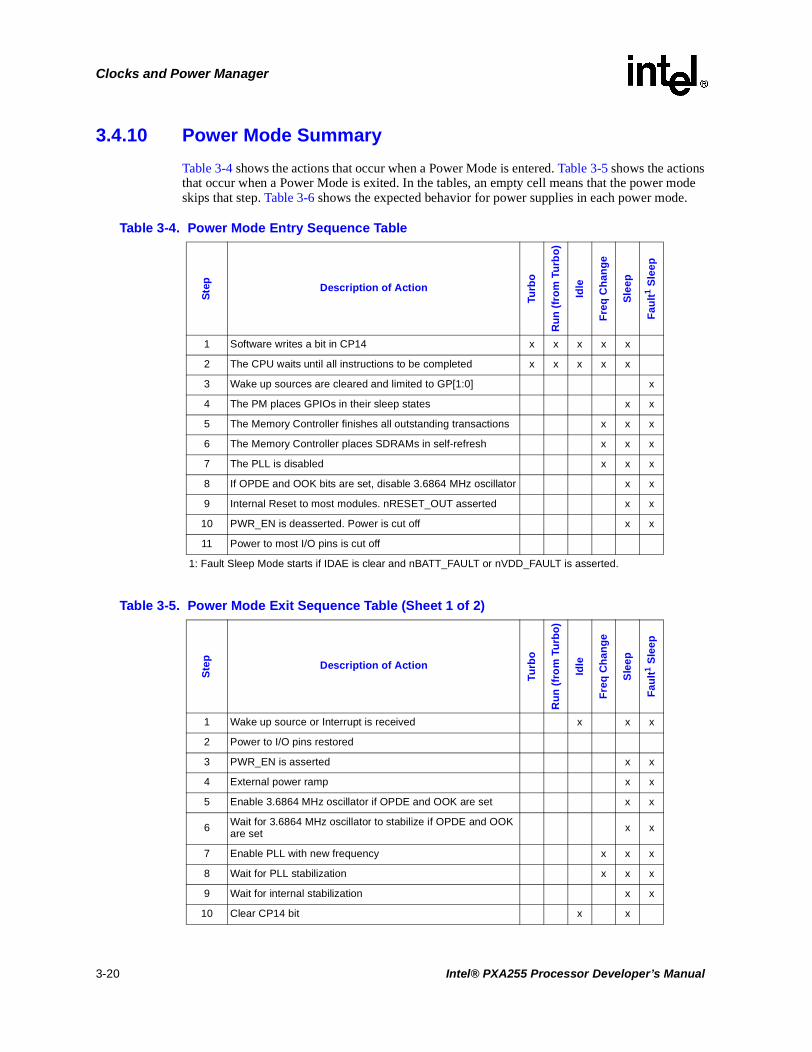
Clocks and Power Manager
3.4.10 Power Mode Summary
Table 3-4 shows the actions that occur when a Power Mode is entered. Table 3-5 shows the actions that occur when a Power Mode is exited. In the tables, an empty cell means that the power mode skips that step. Table 3-6 shows the expected behavior for power supplies in each power mode.
.
Table 3-4. Power Mode Entry Sequence Table
Ste
p
Description of Action
Turb
o
Ru
n (
fro
m T
urb
o)
Idle
Fre
q C
han
ge
Sle
ep
Fau
lt1 S
leep
1 Software writes a bit in CP14 x x x x x
2 The CPU waits until all instructions to be completed x x x x x
3 Wake up sources are cleared and limited to GP[1:0] x
4 The PM places GPIOs in their sleep states x x
5 The Memory Controller finishes all outstanding transactions x x x
6 The Memory Controller places SDRAMs in self-refresh x x x
7 The PLL is disabled x x x
8 If OPDE and OOK bits are set, disable 3.6864 MHz oscillator x x
9 Internal Reset to most modules. nRESET_OUT asserted x x
10 PWR_EN is deasserted. Power is cut off x x
11 Power to most I/O pins is cut off
1: Fault Sleep Mode starts if IDAE is clear and nBATT_FAULT or nVDD_FAULT is asserted.
Table 3-5. Power Mode Exit Sequence Table (Sheet 1 of 2)
Ste
p
Description of Action
Turb
o
Ru
n (
fro
m T
urb
o)
Idle
Fre
q C
han
ge
Sle
ep
Fau
lt1 S
leep
1 Wake up source or Interrupt is received x x x
2 Power to I/O pins restored
3 PWR_EN is asserted x x
4 External power ramp x x
5 Enable 3.6864 MHz oscillator if OPDE and OOK are set x x
6 Wait for 3.6864 MHz oscillator to stabilize if OPDE and OOK are set x x
7 Enable PLL with new frequency x x x
8 Wait for PLL stabilization x x x
9 Wait for internal stabilization x x
10 Clear CP14 bit x x
3-20 Intel® PXA255 Processor Developer’s Manual

Clocks and Power Manager
11 Deassert nRESET_OUT x x
12 Restart CPU clocks, enable interrupts x x x x x x
1: Fault Sleep Mode starts if IDAE is clear and nBATT_FAULT or nVDD_FAULT is asserted.
Table 3-5. Power Mode Exit Sequence Table (Sheet 2 of 2)
Ste
p
Description of Action
Turb
o
Ru
n (
fro
m T
urb
o)
Idle
Fre
q C
han
ge
Sle
ep
Fau
lt1
Sle
ep
Intel® PXA255 Processor Developer’s Manual 3-21

Clocks and Power Manager
3.5 Power Manager Registers
This section describes the 32-bit registers that control the Power Manager.
Table 3-6. Power and Clock Supply Sources and States During Power Modes
ModuleSupply Source
Power Mode
Turbo Run Idle Freq Change Sleep
Pw Ck Pw Ck Pw Ck Pw Ck Pw Ck Pw Ck
CPU, Caches, Buffers
VCC
Run/ Turbo
(R/T)
On
T
On
R
On
Off
On
chan
ging
Off Off
Memory Controller
Mem
On On On
LCD Controller
DMA Controller
General Periphs.
PLL
OnOS timer 3.686 MHz OscInterrupts
Real Time Clock VCC/
Reg(V/R)
32.768kHz Osc V On V On V On V On I On
Power Manager
GP[3:0], PM pads, Osc pads
HV/Batt
(H/B)
Dynamic/ Static(D/S) H D H D H D H D H S
General IO H
KEY:
T: Turbo clockR: Run clockV: Module powered off VCC.I: Module powered off internal regulatorH: Module powered off VCCQ or VCCND: Module is dynamic or actively clockedS: Module is static or clocks are gated.
3-22 Intel® PXA255 Processor Developer’s Manual

Clocks and Power Manager
3.5.1 Power Manager Control Register (PMCR)
The PMCR is used to select the manner in which Sleep Mode is entered when the nVDD_FAULT or the nBATT_FAULT pin is asserted low. When the IDAE bit is set, an Imprecise Data Abort indication is sent to the CPU. The CPU then performs an abort routine. Software must ensure that the abort routine sets the Sleep Mode configuration in the PWRMODE register (see Section 3.7.2, “Power Mode Register (PWRMODE)”). The IDAE bit is cleared in any Reset and when Sleep Mode exits. Software may also clear the IDAE bit when necessary. The PMCR must be protected through Memory Management Unit (MMU) permissions.
This is a read/write register. Ignore reads from reserved bits. Write zeros to reserved bits.
Table 3-7. PMCR Bit Definitions
0x40F0_0000 PMCR Clocks and Power Manager
Bit 31 30 29 28 27 26 25 24 23 22 21 20 19 18 17 16 15 14 13 12 11 10 9 8 7 6 5 4 3 2 1 0
Res
erve
d
IDA
E
Reset 0 0 0 0 0 0 0 0 0 0 0 0 0 0 0 0 0 0 0 0 0 0 0 0 0 0 0 0 0 0 0 0
Bits Name Description
[31:1] —Reserved.
Read undefined and must always be written with zeroes.
0 IDAE
Imprecise Data Abort Enable.
0 – Allow immediate entry to sleep mode when nVDD_FAULT or nBATT_FAULT is asserted.
1 – Force imprecise data abort signal to CPU to allow software to enter sleep mode when nVDD_FAULT or nBATT_FAULT is asserted. Recommended mode.
Cleared on hardware, watchdog, and GPIO reset, or when sleep mode exits.
Intel® PXA255 Processor Developer’s Manual 3-23

Clocks and Power Manager
3.5.2 Power Manager General Configuration Register (PCFR)
The PCFR contains bits used to configure functions in the processor. When the OPDE bit is set, it allows the 3.6864 MHz oscillator to be disabled during Sleep Mode. The OPDE bit is cleared in Hardware, Watchdog, and GPIO Resets. The Float PCMCIA (FP) and Float Static Memory (FS) bits control the state of the PCMCIA control pins and the static memory control pins during Sleep Mode.
This is a read/write register. Ignore reads from reserved bits. Write zeros to reserved bits.
Table 3-8. PCFR Bit Definitions
0x40F0_001C PCFR Clocks and Power Manager
Bit 31 30 29 28 27 26 25 24 23 22 21 20 19 18 17 16 15 14 13 12 11 10 9 8 7 6 5 4 3 2 1 0
Res
erve
d
FS
FP
OP
DE
Reset 0 0 0 0 0 0 0 0 0 0 0 0 0 0 0 0 0 0 0 0 0 0 0 0 0 0 0 0 0 0 0 0
Bits Name Description
[31:3] —Reserved.
Read undefined and must always be written with zeroes.
2 FS
Float Static Chip Selects during Sleep Mode.
0 = Static Chip Select pins are not floated in Sleep Mode. nCS[5:1] are driven to the state of the appropriate PGSR register bits. nCS[1], nWE, and nOE are driven high.
1 = Static Chip Select pins are floated in Sleep Mode. The pins nCS[5:0], nWE, and nOE are affected.
Cleared on Hardware, Watchdog, and GPIO Resets.
1 FP
Float PCMCIA controls during Sleep Mode.
0 = PCMCIA pins are not floated in Sleep Mode. They are driven to the state of the appropriate PGSR register bits.
1 = The PCMCIA signals: nPOE, nPWE, nPIOW, nPIOR, and nPCE[2:1] are floated in Sleep Mode. nPSKTSEL and nPREG are derived from address signals and assume the state of the address bus during Sleep Mode.
Cleared on Hardware, Watchdog, and GPIO Resets.
0 OPDE
3.6864 MHz oscillator power-down enable.
If the 32.7686 kHz crystal is disabled because the OON bit in the Oscillator Configuration Register is 0, OPDE is ignored and the 3.6864 MHz oscillator is not disabled.
0 = Do not stop the oscillator during Sleep Mode.1 = Stop the 3.6864 MHz oscillator during Sleep Mode.
Cleared on Hardware, Watchdog, and GPIO Resets.
3-24 Intel® PXA255 Processor Developer’s Manual
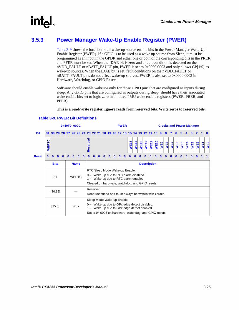
Clocks and Power Manager
3.5.3 Power Manager Wake-Up Enable Register (PWER)
Table 3-9 shows the location of all wake up source enable bits in the Power Manager Wake-Up Enable Register (PWER). If a GPIO is to be used as a wake up source from Sleep, it must be programmed as an input in the GPDR and either one or both of the corresponding bits in the PRER and PFER must be set. When the IDAE bit is zero and a fault condition is detected on the nVDD_FAULT or nBATT_FAULT pin, PWER is set to 0x0000 0003 and only allows GP[1:0] as wake-up sources. When the IDAE bit is set, fault conditions on the nVDD_FAULT or nBATT_FAULT pins do not affect wake-up sources. PWER is also set to 0x0000 0003 in Hardware, Watchdog, or GPIO Resets.
Software should enable wakeups only for those GPIO pins that are configured as inputs during sleep. Any GPIO pins that are configured as outputs during sleep, should have their associated wake enable bits set to logic zero in all three PMU wake enable registers (PWER, PRER, and PFER).
This is a read/write register. Ignore reads from reserved bits. Write zeros to reserved bits.
Table 3-9. PWER Bit Definitions
0x40F0_000C PWER Clocks and Power Manager
Bit 31 30 29 28 27 26 25 24 23 22 21 20 19 18 17 16 15 14 13 12 11 10 9 8 7 6 5 4 3 2 1 0
WE
RT
C
Res
erve
d
WE
15
WE
14
WE
13
WE
12
WE
11
WE
10
WE
9
WE
8
WE
7
WE
6
WE
5
WE
4
WE
3
WE
2
WE
1
WE
0
Reset 0 0 0 0 0 0 0 0 0 0 0 0 0 0 0 0 0 0 0 0 0 0 0 0 0 0 0 0 0 0 1 1
Bits Name Description
31 WERTC
RTC Sleep Mode Wake-up Enable.
0 – Wake-up due to RTC alarm disabled.1 – Wake-up due to RTC alarm enabled.
Cleared on hardware, watchdog, and GPIO resets.
[30:16] —Reserved.
Read undefined and must always be written with zeroes.
[15:0] WEx
Sleep Mode Wake-up Enable
0 – Wake-up due to GPx edge detect disabled.1 – Wake-up due to GPx edge detect enabled.
Set to 0x 0003 on hardware, watchdog, and GPIO resets.
Intel® PXA255 Processor Developer’s Manual 3-25
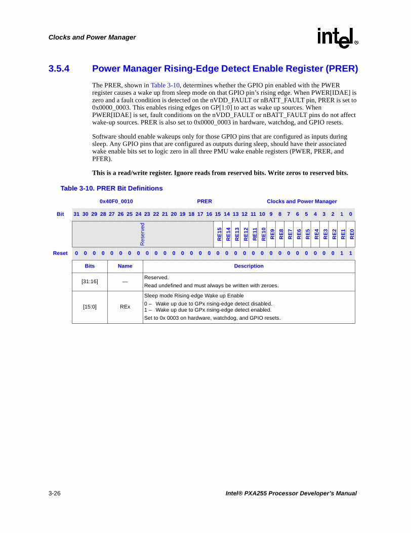
Clocks and Power Manager
3.5.4 Power Manager Rising-Edge Detect Enable Register (PRER)
The PRER, shown in Table 3-10, determines whether the GPIO pin enabled with the PWER register causes a wake up from sleep mode on that GPIO pin’s rising edge. When PWER[IDAE] is zero and a fault condition is detected on the nVDD_FAULT or nBATT_FAULT pin, PRER is set to 0x0000_0003. This enables rising edges on GP[1:0] to act as wake up sources. When PWER[IDAE] is set, fault conditions on the nVDD_FAULT or nBATT_FAULT pins do not affect wake-up sources. PRER is also set to 0x0000_0003 in hardware, watchdog, and GPIO resets.
Software should enable wakeups only for those GPIO pins that are configured as inputs during sleep. Any GPIO pins that are configured as outputs during sleep, should have their associated wake enable bits set to logic zero in all three PMU wake enable registers (PWER, PRER, and PFER).
This is a read/write register. Ignore reads from reserved bits. Write zeros to reserved bits.
Table 3-10. PRER Bit Definitions
0x40F0_0010 PRER Clocks and Power Manager
Bit 31 30 29 28 27 26 25 24 23 22 21 20 19 18 17 16 15 14 13 12 11 10 9 8 7 6 5 4 3 2 1 0
Res
erve
d
RE
15
RE
14
RE
13
RE
12
RE
11
RE
10
RE
9
RE
8
RE
7
RE
6
RE
5
RE
4
RE
3
RE
2
RE
1
RE
0
Reset 0 0 0 0 0 0 0 0 0 0 0 0 0 0 0 0 0 0 0 0 0 0 0 0 0 0 0 0 0 0 1 1
Bits Name Description
[31:16] —Reserved.
Read undefined and must always be written with zeroes.
[15:0] REx
Sleep mode Rising-edge Wake up Enable
0 – Wake up due to GPx rising-edge detect disabled.1 – Wake up due to GPx rising-edge detect enabled.
Set to 0x 0003 on hardware, watchdog, and GPIO resets.
3-26 Intel® PXA255 Processor Developer’s Manual
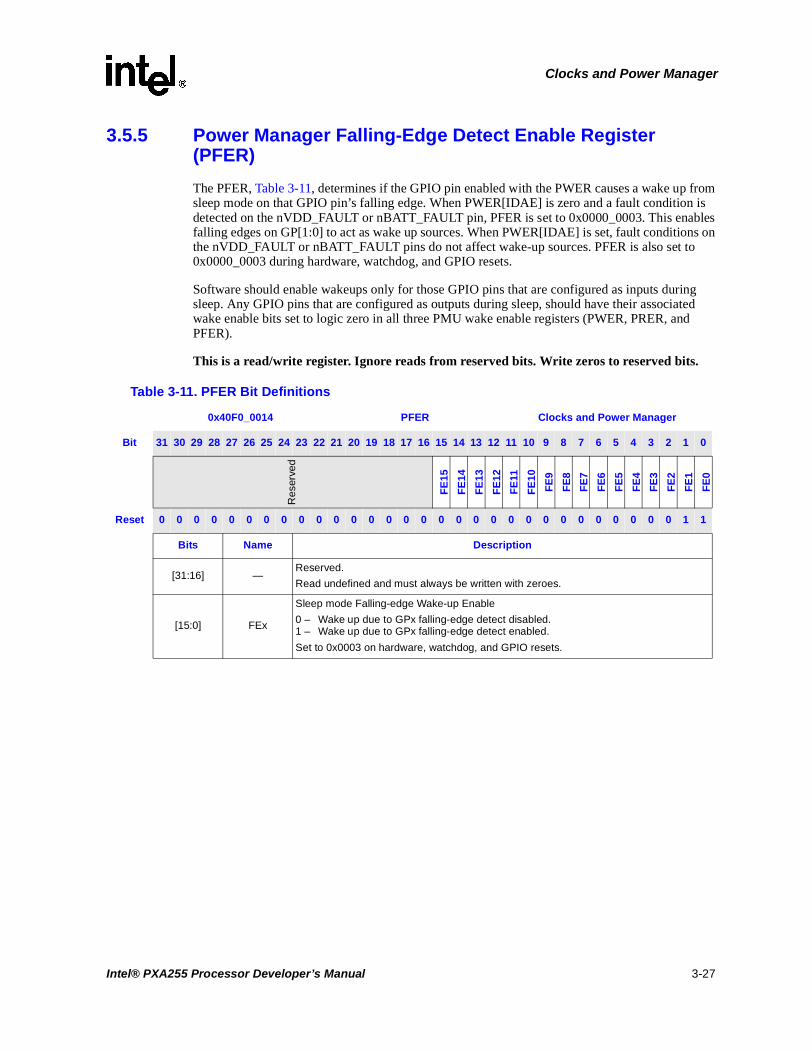
Clocks and Power Manager
3.5.5 Power Manager Falling-Edge Detect Enable Register (PFER)
The PFER, Table 3-11, determines if the GPIO pin enabled with the PWER causes a wake up from sleep mode on that GPIO pin’s falling edge. When PWER[IDAE] is zero and a fault condition is detected on the nVDD_FAULT or nBATT_FAULT pin, PFER is set to 0x0000_0003. This enables falling edges on GP[1:0] to act as wake up sources. When PWER[IDAE] is set, fault conditions on the nVDD_FAULT or nBATT_FAULT pins do not affect wake-up sources. PFER is also set to 0x0000_0003 during hardware, watchdog, and GPIO resets.
Software should enable wakeups only for those GPIO pins that are configured as inputs during sleep. Any GPIO pins that are configured as outputs during sleep, should have their associated wake enable bits set to logic zero in all three PMU wake enable registers (PWER, PRER, and PFER).
This is a read/write register. Ignore reads from reserved bits. Write zeros to reserved bits.
Table 3-11. PFER Bit Definitions
0x40F0_0014 PFER Clocks and Power Manager
Bit 31 30 29 28 27 26 25 24 23 22 21 20 19 18 17 16 15 14 13 12 11 10 9 8 7 6 5 4 3 2 1 0
Res
erve
d
FE
15
FE
14
FE
13
FE
12
FE
11
FE
10
FE
9
FE
8
FE
7
FE
6
FE
5
FE
4
FE
3
FE
2
FE
1
FE
0
Reset 0 0 0 0 0 0 0 0 0 0 0 0 0 0 0 0 0 0 0 0 0 0 0 0 0 0 0 0 0 0 1 1
Bits Name Description
[31:16] —Reserved.
Read undefined and must always be written with zeroes.
[15:0] FEx
Sleep mode Falling-edge Wake-up Enable
0 – Wake up due to GPx falling-edge detect disabled.1 – Wake up due to GPx falling-edge detect enabled.
Set to 0x0003 on hardware, watchdog, and GPIO resets.
Intel® PXA255 Processor Developer’s Manual 3-27

Clocks and Power Manager
3.5.6 Power Manager GPIO Edge Detect Status Register (PEDR)
The PEDR, Table 3-12, indicates which of the GPIO pins enabled through the PWER, PRER, and PFER registers caused a wake up from sleep mode. The bits in PEDR can only be set on a rising or falling edge on a given GPIO pin. If PRER is set, the bits in PEDR can only be set on a rising edge. If PFER is set, the bits in PEDR can only be set on a falling edge. To reset a bit in PEDR to zero, write a 1 to it. The PEDR bits are reset to zero in hardware, watchdog, and GPIO resets.
This is a read/write register. Ignore reads from reserved bits. Write zeros to reserved bits.
Table 3-12. PEDR Bit Definitions
0x40F0_0018 PEDR Clocks and Power Manager
Bit 31 30 29 28 27 26 25 24 23 22 21 20 19 18 17 16 15 14 13 12 11 10 9 8 7 6 5 4 3 2 1 0
Res
erve
d
ED
15
ED
14
ED
13
ED
12
ED
11
ED
10
ED
9
ED
8
ED
7
ED
6
ED
5
ED
4
ED
3
ED
2
ED
1
ED
0
Reset 0 0 0 0 0 0 0 0 0 0 0 0 0 0 0 0 0 0 0 0 0 0 0 0 0 0 0 0 0 0 0 0
Bits Name Description
[31:16] —Reserved.
Read undefined and must always be written with zeroes.
[15:0] EDx
Sleep mode Edge Detect Status
0 – Wake up on GPx not detected.1 – Wake up due to edge on GPx detected.
Cleared by hardware, watchdog, and GPIO resets. Cleared by writing a 1.
3-28 Intel® PXA255 Processor Developer’s Manual

Clocks and Power Manager
3.5.7 Power Manager Sleep Status Register (PSSR)
The PSSR, shown in Table 3-13, contains the following status flags:
• Software Sleep Status (SSS) flag is set when the sleep mode configuration in the PWRMODE register is set and sleep mode starts (see Section 3.7.2).
• Battery Fault Status (BFS) bit is set after wake up any time the nBATT_FAULT pin is asserted (even when the processor is already in sleep mode).
• VDD Fault Status (VFS) bit is set after wake up when the nVDD_FAULT pin is asserted and causes the processor to enter sleep mode. The VFS bit is not set if software starts the sleep mode and then the nVDD_FAULT pin is asserted.
• Peripheral Control Hold (PH) bit is set when sleep mode starts and indicates that the GPIO pins are retaining their sleep mode state values.
• Read Disable Hold (RDH) bit is set in hardware, GPIO, and watchdog resets and sleep mode. The RDH bit indicates that all the processor’s GPIO input paths are disabled. To allow a GPIO input pin to be enabled, software must reset the RDH bit by writing a one to it. Clearing RDH also disables the 10 K to 60 K GPIO pullup resistors that are present during and after hardware, GPIO and watchdog reset. Sleep mode disables the GPIO input path, but the pullup resisters are not re-enabled in this case.
To clear a status flag write a 1 to it. Writing a 0 to a status bit has no effect. Hardware, watchdog, and GPIO resets clear or set the PSSR bits.
This is a read/write register. Ignore reads from reserved bits. Write zeros to reserved bits.
Table 3-13. PSSR Bit Definitions (Sheet 1 of 2)
0x40F0_0004 PSSR Clocks and Power Manager
Bit 31 30 29 28 27 26 25 24 23 22 21 20 19 18 17 16 15 14 13 12 11 10 9 8 7 6 5 4 3 2 1 0
reservedR
DH
PH
rese
rved
VF
S
BF
S
SS
S
Reset 0 0 0 0 0 0 0 0 0 0 0 0 0 0 0 0 0 0 0 0 0 0 0 0 0 0 1 0 0 0 0 0
Bits Name Description
[31:6] — reserved
5 RDH
Read Disable Hold.
0 – GPIO pins are configured according to their GPIO configuration1 – Receivers of all GPIO pins that can act as inputs are disabled and following a
hardware, GPIO, or watchdog reset, internal GPIO pull-ups are active. Must be cleared by the processor after the peripheral and GPIO interfaces are configured but before they are used.
Set by hardware, watchdog, and GPIO resets and sleep mode. Cleared by writing a 1.
4 PH
Peripheral Control Hold.
0 – GPIO pins are configured according to their GPIO configuration 1 – GPIO pins are being held in their sleep mode state. Set when sleep mode starts.
Must be cleared by the processor after the peripheral interfaces have been configured but before they are actually used by the processor.
Cleared by hardware, watchdog, and GPIO resets. Cleared by writing a 1.
3 — reserved
Intel® PXA255 Processor Developer’s Manual 3-29

Clocks and Power Manager
3.5.8 Power Manager Scratch Pad Register (PSPR)
The PM contains a 32-bit register that can be used to save processor configuration information in any desired format. The PSPR, shown in Table 3-14, is a holding register that is powered during sleep mode and is reset by hardware, watchdog, and GPIO resets. During run and turbo modes, any value can be written to PSPR. The value can be read after sleep mode exits. The value in PSPR can be used to represent the processor’s configuration before sleep mode is invoked.
This is a read/write register. Ignore reads from reserved bits. Write zeros to reserved bits.
2 VFS
VDD Fault Status.
0 – nVDD_FAULT pin has not been asserted since it was last cleared by a reset or the CPU.
1 – nVDD_FAULT pin was asserted in Run or idle mode and caused the chip to enter sleep mode; bit is set only after wake up.
This bit is not set when nVDD_FAULT is asserted while in sleep mode.
Cleared by hardware, watchdog, and GPIO resets.
1 BFS
Battery Fault Status.
0 – nBATT_FAULT pin has not been asserted since it was last cleared by a reset or the CPU.
1 – nBATT_FAULT pin has been asserted; bit is set only after wake up.
This bit can be set when nBATT_FAULT is asserted while in sleep mode.
Cleared by hardware, watchdog, and GPIO resets.
0 SSS
Software Sleep Status.
0 – Software has not entered sleep mode through the sleep mode bit since the SSS was last cleared by a reset or the CPU.
1 – Chip was placed in sleep mode by setting the sleep mode bit.
Cleared by hardware, watchdog, and GPIO resets.
Table 3-13. PSSR Bit Definitions (Sheet 2 of 2)
0x40F0_0004 PSSR Clocks and Power Manager
Bit 31 30 29 28 27 26 25 24 23 22 21 20 19 18 17 16 15 14 13 12 11 10 9 8 7 6 5 4 3 2 1 0
reserved
RD
H
PH
rese
rved
VF
S
BF
S
SS
S
Reset 0 0 0 0 0 0 0 0 0 0 0 0 0 0 0 0 0 0 0 0 0 0 0 0 0 0 1 0 0 0 0 0
Bits Name Description
Table 3-14. PSPR Bit Definitions
0x40F0_0008 PSPR Clocks and Power Manager
Bit 31 30 29 28 27 26 25 24 23 22 21 20 19 18 17 16 15 14 13 12 11 10 9 8 7 6 5 4 3 2 1 0
SP
Reset 0 0 0 0 0 0 0 0 0 0 0 0 0 0 0 0 0 0 0 0 0 0 0 0 0 0 0 0 0 0 0 0
Bits Name Description
[31:0] SP
Scratch Pad
32-bit word is preserved in sleep mode.
Cleared by hardware, watchdog, and GPIO resets.
3-30 Intel® PXA255 Processor Developer’s Manual

Clocks and Power Manager
3.5.9 Power Manager Fast Sleep Walk-up Configuration Register (PMFW)
The PSPR, shown in Table 3-15, provides a single bit called FWAKE which is used to select between the standard and fast sleep walk-up sequences. The PMFW register is reset by a hardware reset, GPIO reset, watchdog reset, but is not cleared by the sleep walk-up sequence. Using an exception handler to invoke sleep in response to a power fault event is advantageous because software can clear the PMFW[FWAKE] bit and configure the power management IC to use PWR_EN to disable the core power supply during sleep to minimize power consumption from a critically low battery. Also, the PCFR[OPDE] bit must be cleared to enable the 3.6864 MHz oscillator during sleep when fast sleep walk-up is selected by setting the PMFW[FWAKE] bit.
This is a read/write register. Ignore reads from reserved bits. Write zeros to reserved bits.
3.5.10 Power Manager GPIO Sleep State Registers (PGSR0, PGSR1, PGSR2)
PGSR0, PGSR1, and PGSR2, shown in Table 3-16, Table 3-17, and Table 3-18 allow software to select the output state of each GPIO pin when the processor goes into sleep mode. When a transition to sleep mode is required (through software or the nBATT_FAULT or nVDD_FAULT pin), the contents of the PGSR registers are loaded into the GPIO output data registers that software normally controls through the GPSR and GPCR registers. Only pins that are already configured as outputs reflect the new state. All bits in the output registers are loaded. When the processor re-enters the run mode, these GPIO pins retain the programmed sleep state until software resets PSSR[PH]. If a pin is reconfigured from an input to an output, the register’s last contents are driven onto the pin.
This is a read/write register. Ignore reads from reserved bits. Write zeros to reserved bits.
Table 3-15. PMFW Register Bitmap and Bit Definitions
0x40F0 0034 Power Manager Fast Sleep Wakeup Configuration Register (PMFW) Power Manager
Bit 31 30 29 28 27 26 25 24 23 22 21 20 19 18 17 16 15 14 13 12 11 10 9 8 7 6 5 4 3 2 1 0R
eser
ved
FW
AK
E
Res
erve
d
Reset 0 0 0 0 0 0 0 0 0 0 0 0 0 0 0 0 0 0 0 0 0 0 0 0 0 0 0 0 0 0 0 0
[31:3] —Reserved
Read undefined and must always be written with zeroes.
[1] FWAKE
FAST WAKEUP ENABLE
0 – Selects the standard sleep wakeup sequence with a 10 ms power supply stabilization delay when power is disabled during sleep.
1 – Selects the fast sleep wakeup sequence without a power supply stabilization delay when power is maintained during sleep.
Cleared by hardware reset.
[0] —Reserved
Read undefined and must always be written with zeroes.
Intel® PXA255 Processor Developer’s Manual 3-31

Clocks and Power Manager
This is a read/write register. Ignore reads from reserved bits. Write zeros to reserved bits.
This is a read/write register. Ignore reads from reserved bits. Write zeros to reserved bits.
Table 3-16. PGSR0 Bit Definitions
0x40F0_0020 PGSR0 Clocks and Power Manager
Bit 31 30 29 28 27 26 25 24 23 22 21 20 19 18 17 16 15 14 13 12 11 10 9 8 7 6 5 4 3 2 1 0
SS
31
SS
30
SS
29
SS
28
SS
27
SS
26
SS
25
SS
24
SS
23
SS
22
SS
21
SS
20
SS
19
SS
18
SS
17
SS
16
SS
15
SS
14
SS
13
SS
12
SS
11
SS
10
SS
9
SS
8
SS
7
SS
6
SS
5
SS
4
SS
3
SS
2
SS
1
SS
0
Reset 0 0 0 0 0 0 0 0 0 0 0 0 0 0 0 0 0 0 0 0 0 0 0 0 0 0 0 0 0 0 0 0
Bits Name Description
[31:0] SSx
If programmed as an output, Sleep state of GPx
0 – Pin is driven to a zero during sleep mode1 – Pin is driven to a one during sleep mode
Cleared by hardware, watchdog, and GPIO resets.
Table 3-17. PGSR1 Bit Definitions
0x40F0_0024 PGSR1 Clocks and Power Manager
Bit 31 30 29 28 27 26 25 24 23 22 21 20 19 18 17 16 15 14 13 12 11 10 9 8 7 6 5 4 3 2 1 0
SS
63
SS
62
SS
61
SS
60
SS
59
SS
58
SS
57
SS
56
SS
55
SS
54
SS
53
SS
52
SS
51
SS
50
SS
49
SS
48
SS
47
SS
46
SS
45
SS
44
SS
43
SS
42
SS
41
SS
40
SS
39
SS
38
SS
37
SS
36
SS
35
SS
34
SS
33
SS
32
Reset 0 0 0 0 0 0 0 0 0 0 0 0 0 0 0 0 0 0 0 0 0 0 0 0 0 0 0 0 0 0 0 0
Bits Name Description
[31:0] SSx
If programmed as an output, Sleep state of GPx
0 – Pin is driven to a zero during sleep mode1 – Pin is driven to a one during sleep mode
Cleared by hardware, watchdog, and GPIO resets.
3-32 Intel® PXA255 Processor Developer’s Manual

Clocks and Power Manager
3.5.11 Reset Controller Status Register (RCSR)
The CPU uses the RCSR, shown in Table 3-19, to determine a reset’s last cause or causes. The processor can be reset in four ways:
• Hardware reset
• Watchdog reset
• Sleep mode
• GPIO reset
Refer to Table 2-4, “Effect of Each Type of Reset on Internal Register State” on page 2-6 for details of the behavior of different modules during each type of reset.
Each RCSR status bit is set by a different reset source and can be cleared by writing a 1 back to the bit. The RCSR status bits for watchdog reset, sleep mode, and GPIO resets have a hardware reset state of zero.
This is a read/write register. Ignore reads from reserved bits. Write zeros to reserved bits.
Table 3-18. PGSR2 Bit Definitions
0x40F0_0028 PGSR2 Clocks and Power Manager
Bit 31 30 29 28 27 26 25 24 23 22 21 20 19 18 17 16 15 14 13 12 11 10 9 8 7 6 5 4 3 2 1 0
reserved
SS
84
SS
83
SS
82
SS
81
SS
80
SS
79
SS
78
SS
77
SS
76
SS
75
SS
74
SS
73
SS
72
SS
71
SS
70
SS
69
SS
68
SS
67
SS
66
SS
65
SS
64
Reset 0 0 0 0 0 0 0 0 0 0 0 0 0 0 0 0 0 0 0 0 0 0 0 0 0 0 0 0 0 0 0 0
Bits Name Description
[31:17] — reserved
[16:0] SSx
If programmed as an output, Sleep state of GPx
0 – Pin is driven to a zero during sleep mode1 – Pin is driven to a one during sleep mode
Cleared by hardware, watchdog, and GPIO resets.
Intel® PXA255 Processor Developer’s Manual 3-33

Clocks and Power Manager
3.6 Clocks Manager Registers
The Clocks Manager contains three registers:
• Core Clock Configuration Register (CCCR)
• Clock Enable Register (CKEN)
• Oscillator Configuration Register (OSCC)
3.6.1 Core Clock Configuration Register (CCCR)
The CCCR, shown in Table 3-20, controls the core clock frequency, from which the core, memory controller, LCD controller, and DMA controller frequencies are derived. The crystal frequency to memory frequency multiplier (L), memory frequency to run mode frequency multiplier (M), and run mode frequency to turbo mode frequency multiplier (N) are set in this register. The clock frequencies are shown below.
Table 3-19. RCSR Bit Definitions
0x40F0_0030 RCSR Clocks and Power Manager
Bit 31 30 29 28 27 26 25 24 23 22 21 20 19 18 17 16 15 14 13 12 11 10 9 8 7 6 5 4 3 2 1 0
reserved
GP
R
SM
R
WD
R
HW
R
Reset 0 0 0 0 0 0 0 0 0 0 0 0 0 0 0 0 0 0 0 0 0 0 0 0 0 0 0 0 0 0 0 1
Bits Name Description
[31:4] — reserved
3 GPR
GPIO Reset.
0 – GPIO reset has not occurred since the last time the CPU or hardware reset cleared this bit.
1 – GPIO reset has occurred since the last time the CPU or hardware reset cleared this bit.
Cleared by hardware reset and by setting to a 1.
2 SMR
Sleep Mode.
0 – Sleep mode has not occurred since the last time the CPU or hardware reset cleared this bit.
1 – Sleep mode has occurred since the last time the CPU or hardware reset cleared this bit.
Cleared by hardware reset and by setting to a 1.
1 WDR
Watchdog Reset.
0 – Watchdog reset has not occurred since the last time the CPU or hardware reset cleared this bit.
1 – Watchdog reset has occurred since the last time the CPU or hardware reset cleared this bit.
Cleared by hardware reset and by setting to a 1.
0 HWR
Hardware Reset.
0 – Hardware reset has not occurred since the last time the CPU cleared this bit.1 – Hardware reset has occurred since the last time the CPU cleared this bit.
Set by hardware reset. Cleared by setting to a 1.
3-34 Intel® PXA255 Processor Developer’s Manual

Clocks and Power Manager
Memory frequency = 3.6864 MHz crystal freq. * crystal frequency to memory frequency multiplier (L)
Run mode frequency = Memory frequency * memory frequency to run mode frequency multiplier (M)
Turbo mode frequency = run mode frequency * run mode frequency to turbo mode frequency multiplier (N)
The value for L is chosen based on external memory or LCD requirements and can be constant while M and N change to allow run and turbo mode frequency changes without disrupting memory settings. The value for M is chosen based on bus bandwidth requirements and minimum core performance requirements. The value for N is chosen based on peak core performance requirements.
Table 3-20. CCCR Bit Definitions
0x4130_0000 Core Clock Configuration Register (CCCR) Clocks Manager
Bit 31 30 29 28 27 26 25 24 23 22 21 20 19 18 17 16 15 14 13 12 11 10 9 8 7 6 5 4 3 2 1 0
reserved N M L
Reset 0 0 0 0 0 0 0 0 0 0 0 0 0 0 0 0 0 0 0 0 0 0 0 1 0 0 1 0 0 0 0 1
Bits Name Description
31:10 — reserved
[9:7] N
Run Mode Frequency to Turbo Mode Frequency Multiplier
Turbo mode Freq. = Run mode frequency * N
000 – reserved
001 – reserved
010 – Multiplier = 1
011 – Multiplier = 1.5
100 – Multiplier = 2
101 – reserved
110 – Multiplier = 3
111 – reserved
Set to 010 on hardware and watchdog resets.
[6:5] M
Memory Frequency to Run Mode Frequency Multiplier
Memory Freq. = Crystal Freq. * L
00 – reserved
01 – Multiplier = 1 (Run mode frequency is equal to memory frequency)
10 – Multiplier = 2 (Run mode frequency is 2 times the memory frequency)
11 – Multiplier = 3 (run mode frequency is 4 times the memory frequency)
Set to 01 on hardware and watchdog resets.
[4:0] L
Crystal Frequency to Memory Frequency Multiplier
00000 – reserved
00001 – Multiplier = 27 (Memory Frequency is 99.53MHz from 3.6864 MHz crystal)
00010 – reserved
00011 – Multiplier = 36 (Memory Frequency is 132.71MHz from 3.6864 MHz crystal)
00100 – reserved
00101 – Multiplier = 45 (Memory Frequency is 165.89MHz from 3.6864 MHz crystal)
00110 to 11111 – reserved
Set to 00001 on hardware and watchdog resets.
Intel® PXA255 Processor Developer’s Manual 3-35
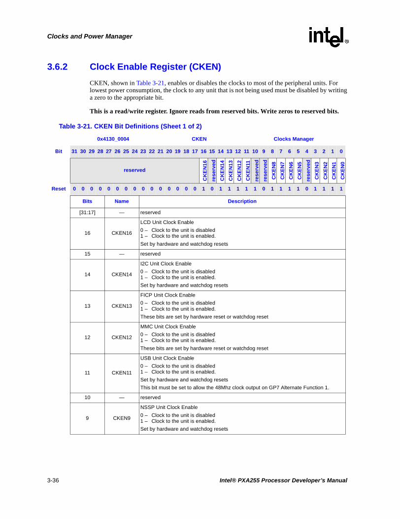
Clocks and Power Manager
3.6.2 Clock Enable Register (CKEN)
CKEN, shown in Table 3-21, enables or disables the clocks to most of the peripheral units. For lowest power consumption, the clock to any unit that is not being used must be disabled by writing a zero to the appropriate bit.
This is a read/write register. Ignore reads from reserved bits. Write zeros to reserved bits.
Table 3-21. CKEN Bit Definitions (Sheet 1 of 2)
0x4130_0004 CKEN Clocks Manager
Bit 31 30 29 28 27 26 25 24 23 22 21 20 19 18 17 16 15 14 13 12 11 10 9 8 7 6 5 4 3 2 1 0
reserved
CK
EN
16
rese
rved
CK
EN
14
CK
EN
13
CK
EN
12
CK
EN
11
rese
rved
rese
rved
CK
EN
8
CK
EN
7
CK
EN
6
CK
EN
5
rese
rved
CK
EN
3
CK
EN
2
CK
EN
1
CK
EN
0
Reset 0 0 0 0 0 0 0 0 0 0 0 0 0 0 0 1 0 1 1 1 1 1 0 1 1 1 1 0 1 1 1 1
Bits Name Description
[31:17] — reserved
16 CKEN16
LCD Unit Clock Enable
0 – Clock to the unit is disabled1 – Clock to the unit is enabled.
Set by hardware and watchdog resets
15 — reserved
14 CKEN14
I2C Unit Clock Enable
0 – Clock to the unit is disabled1 – Clock to the unit is enabled.
Set by hardware and watchdog resets
13 CKEN13
FICP Unit Clock Enable
0 – Clock to the unit is disabled1 – Clock to the unit is enabled.
These bits are set by hardware reset or watchdog reset
12 CKEN12
MMC Unit Clock Enable
0 – Clock to the unit is disabled1 – Clock to the unit is enabled.
These bits are set by hardware reset or watchdog reset
11 CKEN11
USB Unit Clock Enable
0 – Clock to the unit is disabled1 – Clock to the unit is enabled.
Set by hardware and watchdog resets
This bit must be set to allow the 48Mhz clock output on GP7 Alternate Function 1.
10 — reserved
9 CKEN9
NSSP Unit Clock Enable
0 – Clock to the unit is disabled1 – Clock to the unit is enabled.
Set by hardware and watchdog resets
3-36 Intel® PXA255 Processor Developer’s Manual

Clocks and Power Manager
8 CKEN8
I2S Unit Clock Enable
0 – Clock to the unit is disabled1 – Clock to the unit is enabled.
Set by hardware and watchdog resets
7 CKEN7
BTUART Unit Clock Enable
0 – Clock to the unit is disabled1 – Clock to the unit is enabled.
These bits are set by hardware reset or watchdog reset
6 CKEN6
FFUART Unit Clock Enable
0 – Clock to the unit is disabled1 – Clock to the unit is enabled.
Set by hardware and watchdog resets
5 CKEN5
STUART Unit Clock Enable
0 – Clock to the unit is disabled1 – Clock to the unit is enabled.
Set by hardware and watchdog resets
4 CKEN4
HWUART Unit Clock Enable
0 – Clock to the unit is disabled1 – Clock to the unit is enabled.
Set by hardware and watchdog resets
3 CKEN3
SSP Unit Clock Enable
0 – Clock to the unit is disabled1 – Clock to the unit is enabled.
Set by hardware and watchdog resets
2 CKEN2
AC97 Unit Clock Enable
0 – Clock to the unit is disabled1 – Clock to the unit is enabled.
Set by hardware and watchdog resets
1 CKEN1
PWM1 Clock Enable
0 – Clock to the unit is disabled1 – Clock to the unit is enabled.
Set by hardware and watchdog resets
0 CKEN0
PWM0 Clock Enable
0 – Clock to the unit is disabled1 – Clock to the unit is enabled.
Set by hardware and watchdog resets
Table 3-21. CKEN Bit Definitions (Sheet 2 of 2)
0x4130_0004 CKEN Clocks Manager
Bit 31 30 29 28 27 26 25 24 23 22 21 20 19 18 17 16 15 14 13 12 11 10 9 8 7 6 5 4 3 2 1 0
reserved
CK
EN
16
rese
rved
CK
EN
14
CK
EN
13
CK
EN
12
CK
EN
11
rese
rved
rese
rved
CK
EN
8
CK
EN
7
CK
EN
6
CK
EN
5
rese
rved
CK
EN
3
CK
EN
2
CK
EN
1
CK
EN
0
Reset 0 0 0 0 0 0 0 0 0 0 0 0 0 0 0 1 0 1 1 1 1 1 0 1 1 1 1 0 1 1 1 1
Bits Name Description
Intel® PXA255 Processor Developer’s Manual 3-37

Clocks and Power Manager
3.6.3 Oscillator Configuration Register (OSCC)
The OSCC, shown in Table 3-22, controls the 32.768 kHz oscillator configuration. It contains two bits, the set-only 32.768 KHz OSCC[OON] and the read-only 32.768 kHz OSCC[OOK]. OSCC[OON] enables the external 32.768 kHz oscillator and can only be set by software. When the oscillator is enabled, it takes up to 10 seconds for to stabilize. When the oscillator is stabilized, the processor sets OSCC[OOK].
When OSCC[OOK] is set, the RTC and PM are clocked from the 32.768 KHz oscillator. Otherwise, the 3.6864 MHz oscillator is used. The OPDE bit, which allows the 3.6864 MHz oscillator to be disabled in sleep mode, is ignored (treated as if it were clear) if OSCC[OOK] is clear. OSCC[OOK] can only be reset by a hardware reset.
This is a read/write register. Ignore reads from reserved bits. Write zeros to reserved bits.
3.7 Coprocessor 14: Clock and Power Management
Coprocessor 14 contains two registers that control the power modes and sequences:
• CP14 register 6 – CCLKCFG register
• CP14 register 7 – PWRMODE register
Table 3-22. OSCC Bit Definitions
0x4130_0008 OSCC Clocks and Power Manager
Bit 31 30 29 28 27 26 25 24 23 22 21 20 19 18 17 16 15 14 13 12 11 10 9 8 7 6 5 4 3 2 1 0
reserved
OO
N
OO
K
Reset 0 0 0 0 0 0 0 0 0 0 0 0 0 0 0 0 0 0 0 0 0 0 0 0 0 0 0 0 0 0 0 0
Bits Name Description
[31:2] — reserved
1 OON
32.768 KHz OON (write-once only bit)
0 – 32.768 KHz oscillator is disabled. The 3.6864 MHz oscillator (divided by 112) clocks the RTC and PM.
1 – 32.768 KHz oscillator is enabled. OON can not be cleared once written except by hardware reset.
Cleared by hardware reset.
0 OOK
32.768 kHz OOK (read-only bit)
0 – 32.768 KHz oscillator is disabled or not stable. The 3.6864 MHz oscillator (divided by 112) clocks the RTC and PM.
1 – 32.768 KHz oscillator has been enabled (OON=1) and stabilized. It will clock the RTC and PM.
Cleared by hardware reset.
3-38 Intel® PXA255 Processor Developer’s Manual

Clocks and Power Manager
3.7.1 Core Clock Configuration Register (CCLKCFG)
The CCLKCFG register (CP14 register 6), shown in Table 3-24, is used to enter the turbo mode and frequency change sequence. To enter the mode or sequence, software executes the appropriate function from Table 3-23. All core-initiated memory requests are completed before the Clocks and Power Manager initiates the desired mode or sequence.
To ensure that CCLKCFG[TURBO] does not change when entering the frequency change sequence, software must do a read-modify-write.
This is a read/write register. Ignore reads from reserved bits. Write zeros to reserved bits.
Table 3-23. Coprocessor 14 Clock and Power Management Summary
Function Data in Rd Instruction
Read CCLKCFG — MRC p14, 0, Rd, c6, c0, 0
Enter turbo mode TURBO = 1 MCR p14, 0, Rd, c6, c0, 0
Enter frequency change sequenceFCS = 1
(Turbo mode bit may be set or cleared in the same write)
MCR p14, 0, Rd, c6, c0, 0
Enter idle mode M = 1 MCR p14, 0, Rd, c7, c0, 0
Enter sleep mode M = 3 MCR p14, 0, Rd, c7, c0, 0
Table 3-24. CCLKCFG Bit Definitions
CP14Register 6 CCLKCFG Clocks and Power Manager
Bit 31 30 29 28 27 26 25 24 23 22 21 20 19 18 17 16 15 14 13 12 11 10 9 8 7 6 5 4 3 2 1 0
reserved
FC
S
TU
RB
O
Reset 0 0 0 0 0 0 0 0 0 0 0 0 0 0 0 0 0 0 0 0 0 0 0 0 0 0 0 0 0 0 0 0
Bits Name Description
[31:2] — reserved
1 FCS
Frequency Change Sequence
0 – Do not enter frequency change sequence1 – Enter frequency change sequence
Cleared on hardware, watchdog, and GPIO reset and when sleep mode exits.
0 TURBO
Turbo Mode
0 – Do not enter turbo mode/Exit turbo mode1 – Enter turbo mode
Cleared on hardware, watchdog, and GPIO reset and when sleep mode exits.
Intel® PXA255 Processor Developer’s Manual 3-39
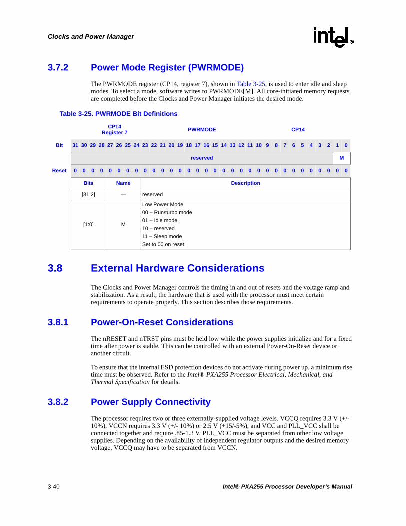
Clocks and Power Manager
3.7.2 Power Mode Register (PWRMODE)
The PWRMODE register (CP14, register 7), shown in Table 3-25, is used to enter idle and sleep modes. To select a mode, software writes to PWRMODE[M]. All core-initiated memory requests are completed before the Clocks and Power Manager initiates the desired mode.
3.8 External Hardware Considerations
The Clocks and Power Manager controls the timing in and out of resets and the voltage ramp and stabilization. As a result, the hardware that is used with the processor must meet certain requirements to operate properly. This section describes those requirements.
3.8.1 Power-On-Reset Considerations
The nRESET and nTRST pins must be held low while the power supplies initialize and for a fixed time after power is stable. This can be controlled with an external Power-On-Reset device or another circuit.
To ensure that the internal ESD protection devices do not activate during power up, a minimum rise time must be observed. Refer to the Intel® PXA255 Processor Electrical, Mechanical, and Thermal Specification for details.
3.8.2 Power Supply Connectivity
The processor requires two or three externally-supplied voltage levels. VCCQ requires 3.3 V (+/- 10%), VCCN requires 3.3 V (+/- 10%) or 2.5 V (+15/-5%), and VCC and PLL_VCC shall be connected together and require .85-1.3 V. PLL_VCC must be separated from other low voltage supplies. Depending on the availability of independent regulator outputs and the desired memory voltage, VCCQ may have to be separated from VCCN.
Table 3-25. PWRMODE Bit Definitions
CP14Register 7 PWRMODE CP14
Bit 31 30 29 28 27 26 25 24 23 22 21 20 19 18 17 16 15 14 13 12 11 10 9 8 7 6 5 4 3 2 1 0
reserved M
Reset 0 0 0 0 0 0 0 0 0 0 0 0 0 0 0 0 0 0 0 0 0 0 0 0 0 0 0 0 0 0 0 0
Bits Name Description
[31:2] — reserved
[1:0] M
Low Power Mode
00 – Run/turbo mode
01 – Idle mode
10 – reserved
11 – Sleep mode
Set to 00 on reset.
3-40 Intel® PXA255 Processor Developer’s Manual

Clocks and Power Manager
3.8.3 Driving the Crystal Pins from an External Clock Source
The information in this section is provided as a guideline. The electrical specifications for the crystal oscillator pins are in Intel® PXA255 Processor Electrical, Mechanical, and Thermal Specification.
A 3.6864 MHz crystal must be connected between the PXTAL and PEXTAL pins. A 32.768 kHz crystal is normally connected between the TXTAL and TEXTAL pins. This configuration gives the lowest overall power consumption because the crystal’s resonant nature provides better power efficiency than an external source that drives the crystal pins. Some applications have other clock sources of the same frequency and can reduce overall cost by driving the crystal pins externally.
Refer to the Oscillator Electrical Specifications in the Intel® PXA255 Processor Design Guide for more information.
Note: No external capacitors are required.
3.8.4 Noise Coupling Between Driven Crystal Pins and a Crystal Oscillator
The two pairs of crystal pins are located near each other on the processor. When crystal oscillators are connected to the pins, this proximity leads to low signal swings and slow edges that result in limited noise coupling between the pins. If one of the crystal oscillators is replaced by an independent signal source and the other is not, the noise coupling may increase. To limit this effect, reduce the slew rate on the pins driven by the independent source.
3.9 Clocks and Power Manager Register Summary
3.9.1 Clocks Manager Register Locations
Table 3-26 shows the registers associated with the clocks manager and the physical addresses used to access them.
3.9.2 Power Manager Register Summary
Table 3-27 shows the registers associated with the PM and the physical addresses used to access them.
Table 3-26. Clocks Manager Register Summary
Address Name Description
0x4130_0000 CCCR Core Clock Configuration Register
0x4130_0004 CKEN Clock Enable Register
0x4130_0008 OSCC Oscillator Configuration Register
Intel® PXA255 Processor Developer’s Manual 3-41

Clocks and Power Manager
.
Table 3-27. Power Manager Register Summary
Address Name Description
0x40F0_0000 PMCR Power Manager Control register
0x40F0_0004 PSSR Power Manager Sleep Status register
0x40F0_0008 PSPR Power Manager Scratch Pad register
0x40F0_000C PWER Power Manager Wake-up Enable register
0x40F0_0010 PRER Power Manager GPIO Rising-edge Detect Enable register
0x40F0_0014 PFER Power Manager GPIO Falling-edge Detect Enable register
0x40F0_0018 PEDR Power Manager GPIO Edge Detect Status register
0x40F0_001C PCFR Power Manager General Configuration register
0x40F0_0020 PGSR0 Power Manager GPIO Sleep State register for GP[31-0]
0x40F0_0024 PGSR1 Power Manager GPIO Sleep State register for GP[63-32]
0x40F0_0028 PGSR2 Power Manager GPIO Sleep State register for GP[84-64]
0x40F0_0030 RCSR Reset controller status register
3-42 Intel® PXA255 Processor Developer’s Manual
System Integration Unit 4
This chapter describes the System Integration Unit (SIU) for the PXA255 processor. The SIU controls several processor-wide system functions. The units contained in the SIU are:
• General-purpose I/O (GPIO) ports
• Interrupt controller
• Real-time clock (RTC)
• Operating system timer (OS timer)
• Pulse Width modulator
4.1 General-Purpose I/O
The PXA255 processor enables and controls its 81 GPIO pins through the use of 27 registers which configure the pin direction (input or output), pin function, pin state (outputs only), pin level detection (inputs only), and selection of alternate functions. A portion of the GPIOs can be used to bring the processor out of Sleep mode. Take care when choosing which GPIO pin is assigned as a GPIO function because many of the GPIO pins have alternate functions and can be configured to support processor peripherals.
Configure all unused GPIOs as outputs to minimize power consumption.
4.1.1 GPIO Operation
The PXA255 processor provides 81 GPIO pins for use in generating and capturing application-specific input and output signals. Each pin can be programmed as either an input or output. When programmed to be an input, a GPIO can also serve as an interrupt source. All 81 pins are configured as inputs during the assertion of all resets, and remain as inputs until they are configured otherwise.
Use the GPIO Pin Direction Register (GPDR) to set whether the GPIO pins are outputs or inputs. When programmed as an output, the pin can be set high by writing to the GPIO Pin Output Set Register (GPSR) and cleared low by writing to the GPIO Pin Output Clear Register (GPCR). The set and clear registers can be written to regardless of whether the pin is configured as an input or an output. If a pin is configured as an input, the programmed output state occurs when the pin is reconfigured to be an output.
Validate each GPIO pin’s state by reading the GPIO Pin Level Register (GPLR). You can read this register any time to confirm the state of a pin. In addition, use the GPIO Rising Edge Detect Enable Register (GRER) and GPIO Falling Edge Detect Enable Register (GFER) to detect either a rising edge or falling edge on each GPIO pin. Use the GPIO Edge Detect Status register (GEDR) to read edge detect state. These edge detects can be programmed to generate interrupts (see Section 4.2). Also use GPIO[15:0] to generate wake-up events that bring the PXA255 processor out of sleep mode (refer to Section 3.4.9.5, “Exiting Sleep Mode” on page 3-18).
Intel® PXA255 Processor Developer’s Manual 4-1

System Integration Unit
When the processor enters sleep mode, the contents of the Power Manager Sleep State registers (PGSR0, PGSR1 and PGSR2) are loaded into the output data registers. If the particular pin is programmed as an output, then the value in the PGSR is driven onto the pin before entering sleep mode. When the processor exits sleep mode, these values remain driven until the GPIO pins are reprogrammed by writing to the GPDR, GPSR or GPCR, and setting the GPIO bit in the Power Manager Sleep Status register (PSSR) to indicate that the GPIO registers have been re-initialized after sleep mode. This is necessary since the GPIO logic loses power during sleep mode
Most GPIO pins can also serve an alternate function within the processor. Certain modes within the serial controllers and LCD controller require extra pins. These functions are hardwired into specific GPIO pins and their use is described in the following paragraphs. Even though a GPIO pin is used for an alternate function, you must still program the proper direction of that pin through the GPDR. Details on alternate functions are provided in Section 4.1.2. Figure 4-1 shows a block diagram of a single GPIO pin.
4.1.2 GPIO Alternate Functions
GPIO pins are capable of having as many as six alternate functions that can be set to enable additional functionality within the processor. If a GPIO is used for an alternate function, then it cannot be used as a GPIO at the same time. GPIO[0] is reserved because of its special use during sleep mode and is not available for alternate functions. GPIO[15:0] are used for walk-up from sleep mode. The walk-up functionality is described in Section 3.4.9.5, “Exiting Sleep Mode” on page 3-18. Table 4-1 shows each GPIO pin and its corresponding alternate functions.
Figure 4-1. General-Purpose I/O Block Diagram
EdgeDetect
GPIO Pin
Pin DirectionRegister
Pin Set andClear Registers
Edge DetectStatus Register
Pin-LevelRegister
0
Alternate FunctionRegisters
Rising Edge DetectEnable Register
Falling Edge DetectEnable Register
123
Alternate Functions(Outputs)
Alternate Functions(Inputs)
0123
Power Manager Sleep Wake-up logic
2
4-2 Intel® PXA255 Processor Developer’s Manual

System Integration Unit
For more information on alternate functions, refer to the Source Unit column in Table 4-1 for the appropriate section of this document.
Table 4-1. GPIO Alternate Functions (Sheet 1 of 4)
Pin Alternate Function Name
Alternate Function Assignment
AFn encoding Source Unit Signal Description and comments
GP1 GP_RST ALT_FN_1_IN 01 Clocks & Power Manager Unit Active low GP_reset
GP6 MMCCLK ALT_FN_1_OUT 01 Multimedia Card (MMC) Controller
MMC Clock
GP7 48 MHz clock† ALT_FN_1_OUT 01 Clocks & Power Manager Unit 48 MHz clock output
GP8 MMCCS0 ALT_FN_1_OUT 01 Multimedia Card (MMC) Controller
MMC Chip Select 0
GP9 MMCCS1 ALT_FN_1_OUT 01 MMC Chip Select 1
GP10 RTCCLK ALT_FN_1_OUT 01 System Integation Unit real time clock (1 Hz)
GP11 3.6 MHz ALT_FN_1_OUT 01 Clocks & Power Manager Unit
3.6 MHz oscillator out
GP12 32 kHz ALT_FN_1_OUT 01 32 kHz out
GP13 MBGNT ALT_FN_2_OUT 10
Memory Controller
memory controller grant
GP14 MBREQ ALT_FN_1_IN 01 memory controller alternate bus master request
GP15 nCS_1 ALT_FN_2_OUT 10 Active low chip select 1
GP16 PWM0 ALT_FN_2_OUT 10 PWM0 output
GP17 PWM1 ALT_FN_2_OUT 10 PWM1 output
GP18 RDY ALT_FN_1_IN 01 Ext. Bus Ready
GP19 DREQ[1] ALT_FN_1_IN 01 External DMA Request
GP20 DREQ[0] ALT_FN_1_IN 01 External DMA Request
GP23 SCLK ALT_FN_2_OUT 10
SSP Serial Port
SSP clock
GP24 SFRM ALT_FN_2_OUT 10 SSP Frame
GP25 TXD ALT_FN_2_OUT 10 SSP transmit
GP26 RXD ALT_FN_1_IN 01 SSP receive
GP27 EXTCLK ALT_FN_1_IN 01 SSP ext_clk
GP28
BITCLK ALT_FN_1_IN 01 AC97 Controller Unit AC97 bit_clk
BITCLK ALT_FN_2_IN 10I2S Controller
I2S bit_clk
BITCLK ALT_FN_1_OUT 01 I2S bit_clk
GP29SDATA_IN0 ALT_FN_1_IN 01 AC97 Controller Unit AC97 Sdata_in0
SDATA_IN ALT_FN_2_IN 10 I2S Controller I2S Sdata_in
GP30SDATA_OUT ALT_FN_1_OUT 01 I2S Controller I2S Sdata_out
SDATA_OUT ALT_FN_2_OUT 10 AC97 Controller Unit AC97 Sdata_out
GP31SYNC ALT_FN_1_OUT 01 I2S Controller I2S sync
SYNC ALT_FN_2_OUT 10 AC97 Controller Unit AC97 sync
GP32SDATA_IN1 ALT_FN_1_IN 01 AC97 Controller Unit AC97 Sdata_in1
SYSCLK ALT_FN_1_OUT 01 I2S Controller I2S System Clock
Intel® PXA255 Processor Developer’s Manual 4-3

System Integration Unit
GP33 nCS[5] ALT_FN_2_OUT 10 Memory Controller Active low chip select 5
GP34
FFRXD ALT_FN_1_IN 01 UARTs FFUART receive
MMCCS0 ALT_FN_2_OUT 10 Multimedia Card (MMC) Controller
MMC Chip Select 0
GP35 CTS ALT_FN_1_IN 01
UARTs
FFUART Clear to send
GP36 DCD ALT_FN_1_IN 01 FFUART Data carrier detect
GP37 DSR ALT_FN_1_IN 01 FFUART data set ready
GP38 RI ALT_FN_1_IN 01 FFUART Ring Indicator
GP39MMCCS1 ALT_FN_1_OUT 01
Multimedia Card (MMC) Controller MMC Chip Select 1
FFTXD ALT_FN_2_OUT 10 UARTs FFUART transmit data
GP40 DTR ALT_FN_2_OUT 10UARTs
FFUART data terminal Ready
GP41 RTS ALT_FN_2_OUT 10 FFUART request to send
GP42BTRXD ALT_FN_1_IN 01 UARTs BTUART receive data
HWRXD ALT_FN_3_IN 11 HWUART HWUART receive data
GP43BTTXD ALT_FN_2_OUT 10 UARTs BTUART transmit data
HWTXD ALT_FN_3_OUT 11 HWUART HWUART transmit data
GP44BTCTS ALT_FN_1_IN 01 UARTs BTUART clear to send
HWCTS ALT_FN_3_IN 11 HWUART HWUART clear to send
GP45BTRTS ALT_FN_2_OUT 10 UARTs BTUART request to send
HWRTS ALT_FN_3_OUT 11 HWUART HWUART request to send
GP46ICP_RXD ALT_FN_1_IN 01 Infrared
Communication PortICP receive data
RXD ALT_FN_2_IN 10 UARTs STD_UART receive data
GP47
TXD ALT_FN_1_OUT 01 UARTs STD_UART transmit data
ICP_TXD ALT_FN_2_OUT 10 Infrared Communication Port ICP transmit data
GP48nPOE ALT_FN_2_OUT 10 Memory Controller Output Enable for Card Space
HWTXD ALT_FN_1_OUT 01 HWUART HWUART transmit data
GP49nPWE ALT_FN_2_OUT 10 Memory Controller Write Enable for Card Space
HWRXD ALT_FN_1_IN 01 HWUART HWUART receive data
GP50nPIOR ALT_FN_2_OUT 10 Memory Controller I/O Read for Card Space
HWCTS ALT_FN_1_IN 01 HWUART HWUART clear to send
GP51nPIOW ALT_FN_2_OUT 10 Memory Controller I/O Write for Card Space
HWRTS ALT_FN_1 OUT 01 HWUART HWUART request to send
GP52 nPCE[1] ALT_FN_2_OUT 10Memory Controller
Card Enable for Card Space
GP53 nPCE[2] ALT_FN_2_OUT 10 Card Enable for Card Space
GP53 MMCCLK ALT_FN_1_OUT 01Multimedia Card (MMC) Controller MMC Clock
Table 4-1. GPIO Alternate Functions (Sheet 2 of 4)
Pin Alternate Function Name
Alternate Function Assignment
AFn encoding Source Unit Signal Description and comments
4-4 Intel® PXA255 Processor Developer’s Manual

System Integration Unit
GP54 MMCCLK ALT_FN_1_OUT 01 Multimedia Card (MMC) Controller
MMC Clock
GP54 nPSKTSEL ALT_FN_2_OUT 10 Memory Controller Socket Select for Card Space
GP55 nPREG ALT_FN_2_OUT 10Memory Controller
Card Address bit 26
GP56 nPWAIT ALT_FN_1_IN 01 Wait signal for Card Space
GP57 nIOIS16 ALT_FN_1_IN 01 Memory Controller Bus Width select for I/O Card Space
GP58 LDD[0] ALT_FN_2_OUT 10
LCD Controller
LCD data pin 0
GP59 LDD[1] ALT_FN_2_OUT 10 LCD data pin 1
GP60 LDD[2] ALT_FN_2_OUT 10 LCD data pin 2
GP61 LDD[3] ALT_FN_2_OUT 10 LCD data pin 3
GP62 LDD[4] ALT_FN_2_OUT 10 LCD data pin 4
GP63 LDD[5] ALT_FN_2_OUT 10 LCD data pin 5
GP64 LDD[6] ALT_FN_2_OUT 10 LCD data pin 6
GP65 LDD[7] ALT_FN_2_OUT 10 LCD data pin 7
GP66
LDD[8] ALT_FN_2_OUT 10 LCD Controller LCD data pin 8
MBREQ ALT_FN_1_IN 01 Memory Controller memory controller alternate bus master req
GP67
LDD[9] ALT_FN_2_OUT 10 LCD Controller LCD data pin 9
MMCCS0 ALT_FN_1_OUT 01Multimedia Card (MMC) Controller MMC Chip Select 0
GP68MMCCS1 ALT_FN_1_OUT 01 Multimedia Card
(MMC) Controller MMC Chip Select 1
LDD[10] ALT_FN_2_OUT 10 LCD Controller LCD data pin 10
GP69MMCCLK ALT_FN_1_OUT 01 Multimedia Card
(MMC) Controller MMC_CLK
LDD[11] ALT_FN_2_OUT 10 LCD Controller LCD data pin 11
GP70RTCCLK ALT_FN_1_OUT 01
System Integation Unit Real Time clock (1 Hz)
LDD[12] ALT_FN_2_OUT 10 LCD Controller LCD data pin 12
GP713.6 MHz ALT_FN_1_OUT 01 Clocks & Power
Manager Unit 3.6 MHz Oscillator clock
LDD[13] ALT_FN_2_OUT 10 LCD Controller LCD data pin 13
GP7232 kHz ALT_FN_1_OUT 01 Clocks & Power
Manager Unit 32 kHz clock
LDD[14] ALT_FN_2_OUT 10 LCD Controller LCD data pin 14
GP73LDD[15] ALT_FN_2_OUT 10 LCD Controller LCD data pin 15
MBGNT ALT_FN_1_OUT 01 Memory Controller Memory controller grant
Table 4-1. GPIO Alternate Functions (Sheet 3 of 4)
Pin Alternate Function Name
Alternate Function Assignment
AFn encoding Source Unit Signal Description and comments
Intel® PXA255 Processor Developer’s Manual 4-5

System Integration Unit
4.1.3 GPIO Register Definitions
There are twenty-seven 32-bit registers within the GPIO control block. There are nine distinct register functions and there are three sets of each of the nine registers to serve the 81 GPIOs. The various functions of the nine registers corresponding to each GPIO pin are described here:
• Three monitor pin state (GPLR)
• Six control output pin state (GPSR, GPCR)
• Three control pin direction (GPDR)
• Six control whether rising edges and/or falling edges are detected (GRER & GFER)
• Three indicate when specified edge types have been detected on pins (GEDR).
• Six determine whether a pin is used as a normal GPIO or whether it is to be taken over by one of three possible alternate functions (GAFR_L, GAFR_U).
GP74 LCD_FCLK ALT_FN_2_OUT 10
LCD Controller
LCD Frame clock
GP75 LCD_LCLK ALT_FN_2_OUT 10 LCD line clock
GP76 LCD_PCLK ALT_FN_2_OUT 10 LCD Pixel clock
GP77 LCD_ACBIAS ALT_FN_2_OUT 10 LCD AC Bias
GP78 nCS[2] ALT_FN_2_OUT 10 Memory Controller Active low chip select 2
GP79 nCS[3] ALT_FN_2_OUT 10 Memory Controller Active low chip select 3
GP80 nCS[4] ALT_FN_2_OUT 10 Memory Controller Active low chip select 4
GP81NSSPSCLK ALT_FN_1_IN 01
Network SSP
NSSP Serial clock is input
NSSPSCLK ALT_FN_1_OUT 01 NSSP Serial clock is output
GP82NSSPSFRM ALT_FN_1_IN 01 NSSP frame is input
NSSPSFRM ALT_FN_1_OUT 01 NSSP frame is output
GP83NSSPTXD ALT_FN_1_OUT 01 NSSP transmit
NSSPRXD ALT_FN_2_IN 10 NSSP receive
GP84NSSPTXD ALT_FN_1_OUT 01 NSSP transmit
NSSPRXD ALT_FN_2_IN 10 NSSP receive
† CKEN[11] - USB Unit Clock Enable bit must be enabled to allow the 48 MHz clock output on GP7
Table 4-1. GPIO Alternate Functions (Sheet 4 of 4)
Pin Alternate Function Name
Alternate Function Assignment
AFn encoding Source Unit Signal Description and comments
Table 4-2. GPIO Register Definitions (Sheet 1 of 2)
Register Type
Register Function GPIO[15:0] GPIO[31:16] GPIO[47:32] GPIO[63:48] GPIO[79:64] GPIO[80]
GPLR Monitor Pin State GPLR0 GPLR1 GPLR2
GPSR Control Output Pin State
GPSR0 GPSR1 GPSR2
GPCR GPCR0 GPCR1 GPCR2
GPDR Set Pin Direction GPDR0 GPDR1 GPDR2
4-6 Intel® PXA255 Processor Developer’s Manual

System Integration Unit
Note: GPLR2[31:17], GPSR2[31:17], GPCR2[31:17], GPDR2[31:17], GRER2[31:17], GFER2[31:17], GEDR2[31:17] and GAFR2_U[31:2] are reserved bits. Write zeros to these bits and ignore all reads from these bits.
Note: All GPIO registers are initialized to 0x0 at reset, which results in all GPIO pins being initialized as inputs.
4.1.3.1 GPIO Pin-Level Registers (GPLR0, GPLR1, GPLR2)
Check the state of each of the GPIO pins by reading the GPIO Pin Level register (GPLR). Each bit in the GPLR corresponds to one pin in the GPIO. GPLR0[31:0] correspond to GPIO[31:0], GPLR1[31:0] correspond to GPIO[63:32] and GPLR2[16:0] correspond to GPIO[80:64]. Use the GPLR0–2 read-only registers to determine the current value of a particular pin (regardless of the programmed pin direction). For reserved bits (GPLR2[31:17]), reads return zero.
This is read/write register. Ignore reads from reserved bits. Write zeros to reserved bits.
GRER Detect Rising/Falling Edge
GRER0 GRER1 GRER2
GFER GFER0 GFER1 GFER2
GEDR Detect Edge Type GEDR0 GEDR1 GEDR2
GAFR Set Alternate Functions GAFR0_L GAFR0_U GAFR1_L GAFR1_U GAFR2_L GAFR2_U
NOTE: For the alternate function registers, the designator _L signifies that the lower 16 GPIOs’ alternate functions are configured by that register and _U designates that the upper 16 GPIOs’ alternate functions are configured by that register.
Table 4-2. GPIO Register Definitions (Sheet 2 of 2)
Register Type
Register Function GPIO[15:0] GPIO[31:16] GPIO[47:32] GPIO[63:48] GPIO[79:64] GPIO[80]
Table 4-3. GPLR0 Bit Definitions
Physical Address0x40E0_0000 GPLR0 System Integration Unit
Bit 31 30 29 28 27 26 25 24 23 22 21 20 19 18 17 16 15 14 13 12 11 10 9 8 7 6 5 4 3 2 1 0
PL
31
PL
30
PL
29
PL
28
PL
27
PL
26
PL
25
PL
24
PL
23
PL
22
PL
21
PL
20
PL
19
PL
18
PL
17
PL
16
PL
15
PL
14
PL
13
PL
12
PL
11
PL
10
PL
9
PL
8
PL
7
PL
6
PL
5
PL
4
PL
3
PL
2
PL
1
PL
0
Reset 0 0 0 0 0 0 0 0 0 0 0 0 0 0 0 0 0 0 0 0 0 0 0 0 0 0 0 0 0 0 0 0
Bits Name Description
<31:0> PL[x]
GPIO Pin Level ‘x’ (where x = 0 to 31).
This read-only field indicates the current value of each GPIO.
0 – Pin state is low1 – Pin state is high
Intel® PXA255 Processor Developer’s Manual 4-7

System Integration Unit
This is read/write register. Ignore reads from reserved bits. Write zeros to reserved bits.
4.1.3.2 GPIO Pin Direction Registers (GPDR0, GPDR1, GPDR2)
GPDR0, GPDR1, GPDR2, shown in Table 4-6, Table 4-7, and Table 4-8, control whether a pin is an input or an output. The GPDR contain one direction control bit for each of the 81 GPIO pins. If a direction bit is programmed to a one, the GPIO is an output. If it is programmed to a zero, it is an input. Reserved bits (GPDR2[31:17]), must be written to zeros and reads to the reserved bits must be ignored.
Note: A reset clears all bits in the GPDR0-2 registers and configures all GPIO pins as inputs.
Table 4-4. GPLR1 Bit Definitions
Physical Address0x40E0_0004 GPLR1 System Integration Unit
Bit 31 30 29 28 27 26 25 24 23 22 21 20 19 18 17 16 15 14 13 12 11 10 9 8 7 6 5 4 3 2 1 0
PL
63
PL
62
PL
61
PL
60
PL
59
PL
58
PL
57
PL
56
PL
55
PL
54
PL
53
PL
52
PL
51
PL
50
PL
49
PL
48
PL
47
PL
46
PL
45
PL
44
PL
43
PL
42
PL
41
PL
40
PL
39
PL
38
PL
37
PL
36
PL
35
PL
34
PL
33
PL
32
Reset 0 0 0 0 0 0 0 0 0 0 0 0 0 0 0 0 0 0 0 0 0 0 0 0 0 0 0 0 0 0 0 0
Bits Name Description
<31:0> PL[x]
GPIO Pin Level ‘x’ (where x = 32 to 63).
This read-only field indicates the current value of each GPIO.
0 – Pin state is low1 – Pin state is high
Table 4-5. GPLR2 Bit Definitions
Physical Address0x40E0_0008 GPLR2 System Integration Unit
Bit 31 30 29 28 27 26 25 24 23 22 21 20 19 18 17 16 15 14 13 12 11 10 9 8 7 6 5 4 3 2 1 0
reserved
PL
84
PL
83
PL
82
PL
81
PL
80
PL
79
PL
78
PL
77
PL
76
PL
75
PL
74
PL
73
PL
72
PL
71
PL
70
PL
69
PL
68
PL
67
PL
66
PL
65
PL
64
Reset 0 0 0 0 0 0 0 0 0 0 0 0 0 0 0 0 0 0 0 0 0 0 0 0 0 0 0 0 0 0 0 0
Bits Name Description
<31:21> — reserved
<20:0> PL[x]
GPIO Pin Level ‘x’ (where x = 64 to 80).
This read-only field indicates the current value of each GPIO.
0 – Pin state is low1 – Pin state is high
4-8 Intel® PXA255 Processor Developer’s Manual

System Integration Unit
4.1.3.3 GPIO Pin Output Set Registers (GPSR0, GPSR1, and GPSR2) and Pin Output Clear Registers (GPCR0, GPCR1, GPCR2)
Table 4-6. GPDR0 Bit Definitions
Physical Address0x40E0_000C GPDR0 System Integration Unit
Bit 31 30 29 28 27 26 25 24 23 22 21 20 19 18 17 16 15 14 13 12 11 10 9 8 7 6 5 4 3 2 1 0
PD
31
PD
30
PD
29
PD
28
PD
27
PD
26
PD
25
PD
24
PD
23
PD
22
PD
21
PD
20
PD
19
PD
18
PD
17
PD
16
PD
15
PD
14
PD
13
PD
12
PD
11
PD
10
PD
9
PD
8
PD
7
PD
6
PD
5
PD
4
PD
3
PD
2
PD
1
PD
0
Reset 0 0 0 0 0 0 0 0 0 0 0 0 0 0 0 0 0 0 0 0 0 0 0 0 0 0 0 0 0 0 0 0
Bits Name Description
<31:0> PD[x]GPIO Pin ‘x’ Direction (where x = 0 to 31).
0 – Pin configured as an input1 – Pin configured as an output
Table 4-7. GPDR1 Bit Definitions
Physical Address0x40E0_0010 GPDR1 System Integration Unit
Bit 31 30 29 28 27 26 25 24 23 22 21 20 19 18 17 16 15 14 13 12 11 10 9 8 7 6 5 4 3 2 1 0
PD
63
PD
62
PD
61
PD
60
PD
59
PD
58
PD
57
PD
56
PD
55
PD
54
PD
53
PD
52
PD
51
PD
50
PD
49
PD
48
PD
47
PD
46
PD
45
PD
44
PD
43
PD
42
PD
41
PD
40
PD
39
PD
38
PD
37
PD
36
PD
35
PD
34
PD
33
PD
32
Reset 0 0 0 0 0 0 0 0 0 0 0 0 0 0 0 0 0 0 0 0 0 0 0 0 0 0 0 0 0 0 0 0
Bits Name Description
<31:0> PD[x]GPIO Pin ‘x’ Direction (where x = 32 to 63).
0 – Pin configured as an input.1 – Pin configured as an output.
Table 4-8. GPDR2 Bit Definitions
Physical Address0x40E0_0014 GPDR2 System Integration Unit
Bit 31 30 29 28 27 26 25 24 23 22 21 20 19 18 17 16 15 14 13 12 11 10 9 8 7 6 5 4 3 2 1 0
reserved
PD
84
PD
83
PD
82
PD
81
PD
80
PD
79
PD
78
PD
77
PD
76
PD
75
PD
74
PD
73
PD
72
PD
71
PD
70
PD
69
PD
68
PD
67
PD
66
PD
65
PD
64
Reset 0 0 0 0 0 0 0 0 0 0 0 0 0 0 0 0 0 0 0 0 0 0 0 0 0 0 0 0 0 0 0 0
Bits Name Description
<31:21> — reserved
<20:0> PD[x]GPIO Pin ‘x’ Direction (where x = 64 to 80).
0 – Pin configured as an input.1 – Pin configured as an output
Intel® PXA255 Processor Developer’s Manual 4-9

System Integration Unit
When a GPIO is configured as an output, the state of the pin can be controlled by writing to either the GPSR or GPCR. An output pin is set high by writing a one to its corresponding bit within the GPSR. To clear an output pin, a one is written to the corresponding bit within the GPCR. GPSR and GPCR are write-only registers. Reads return unpredictable values.
Writing a zero to any of the GPSR or GPCR bits has no effect on the state of the pin. Writing a one to a GPSR or GPCR bit corresponding to a pin that is configured as an input is effective only after the pin is configured as an output. Reserved bits (GPSR2[31:17] and GPCR2[31:17]), must be written with zeros and reads must be ignored.
Table 4-9, Table 4-10, and Table 4-11 show the bit definitions of GPSR0, GPSR1, and GPSR2. Table 4-12, Table 4-13, and Table 4-14 show the bit definitions of GPCR0, GPCR1, and GPCR2.
Table 4-9. GPSR0 Bit Definitions
Physical Address0x40E0_0018 GPSR0 System Integration Unit
Bit 31 30 29 28 27 26 25 24 23 22 21 20 19 18 17 16 15 14 13 12 11 10 9 8 7 6 5 4 3 2 1 0
PS
31
PS
30
PS
29
PS
28
PS
27
PS
26
PS
25
PS
24
PS
23
PS
22
PS
21
PS
20
PS
19
PS
18
PS
17
PS
16
PS
15
PS
14
PS
13
PS
12
PS
11
PS
10
PS
9
PS
8
PS
7
PS
6
PS
5
PS
4
PS
3
PS
2
PS
1
PS
0
Reset 0 0 0 0 0 0 0 0 0 0 0 0 0 0 0 0 0 0 0 0 0 0 0 0 0 0 0 0 0 0 0 0
Bits Name Description
<31:0> PS[x]GPIO Pin ‘x’ Output Pin Set (where x= 0 through 31).
0 – Pin level unaffected.1 – If pin configured as an output, set pin level high (one).
Table 4-10. GPSR1 Bit Definitions
Physical Address0x40E0_001C GPSR1 System Integration Unit
Bit 31 30 29 28 27 26 25 24 23 22 21 20 19 18 17 16 15 14 13 12 11 10 9 8 7 6 5 4 3 2 1 0
PS
63
PS
62
PS
61
PS
60
PS
59
PS
58
PS
57
PS
56
PS
55
PS
54
PS
53
PS
52
PS
51
PS
50
PS
49
PS
48
PS
47
PS
46
PS
45
PS
44
PS
43
PS
42
PS
41
PS
40
PS
39
PS
38
PS
37
PS
36
PS
35
PS
34
PS
33
PS
32
Reset 0 0 0 0 0 0 0 0 0 0 0 0 0 0 0 0 0 0 0 0 0 0 0 0 0 0 0 0 0 0 0 0
Bits Name Description
<31:0> PS[x]GPIO Pin ‘x’ Output Pin Set (where x= 32 through 63).
0 – Pin level unaffected.1 – If pin configured as an output, set pin level high (one).
4-10 Intel® PXA255 Processor Developer’s Manual

System Integration Unit
Table 4-11. GPSR2 Bit Definitions
Physical Address0x40E0_0020 GPSR2 System Integration Unit
Bit 31 30 29 28 27 26 25 24 23 22 21 20 19 18 17 16 15 14 13 12 11 10 9 8 7 6 5 4 3 2 1 0
reserved
PS
84
PS
83
PS
82
PS
81
PS
80
PS
79
PS
78
PS
77
PS
76
PS
75
PS
74
PS
73
PS
72
PS
71
PS
70
PS
69
PS
68
PS
67
PS
66
PS
65
PS
64
Reset 0 0 0 0 0 0 0 0 0 0 0 0 0 0 0 0 0 0 0 0 0 0 0 0 0 0 0 0 0 0 0 0
Bits Name Description
<31:21> — reserved
<20:0> PS[x]GPIO Pin ‘x’ Output Pin Set (where x= 64 through 80).
0 – Pin level unaffected.1 – If pin configured as an output, set pin level high (one).
Table 4-12. GPCR0 Bit Definitions
Physical Address0x40E0_0024 GPCR0 System Integration Unit
Bit 31 30 29 28 27 26 25 24 23 22 21 20 19 18 17 16 15 14 13 12 11 10 9 8 7 6 5 4 3 2 1 0
PC
31
PC
30
PC
29
PC
28
PC
27
PC
26
PC
25
PC
24
PC
23
PC
22
PC
21
PC
20
PC
19
PC
18
PC
17
PC
16
PC
15
PC
14
PC
13
PC
12
PC
11
PC
10
PC
9
PC
8
PC
7
PC
6
PC
5
PC
4
PC
3
PC
2
PC
1
PC
0
Reset 0 0 0 0 0 0 0 0 0 0 0 0 0 0 0 0 0 0 0 0 0 0 0 0 0 0 0 0 0 0 0 0
Bits Name Description
<31:0> PC[x]GPIO Pin ‘x’ Output Pin Clear (where x= 0 through 31).
0 – Pin level unaffected.1 – If pin configured as an output, clear pin level low (zero).
Table 4-13. GPCR1 Bit Definitions
Physical Address0x40E0_0028 GPCR1 System Integration Unit
Bit 31 30 29 28 27 26 25 24 23 22 21 20 19 18 17 16 15 14 13 12 11 10 9 8 7 6 5 4 3 2 1 0
PC
63
PC
62
PC
61
PC
60
PC
59
PC
58
PC
57
PC
56
PC
55
PC
54
PC
53
PC
52
PC
51
PC
50
PC
49
PC
48
PC
47
PC
46
PC
45
PC
44
PC
43
PC
42
PC
41
PC
40
PC
39
PC
38
PC
37
PC
36
PC
35
PC
34
PC
33
PC
32
Reset 0 0 0 0 0 0 0 0 0 0 0 0 0 0 0 0 0 0 0 0 0 0 0 0 0 0 0 0 0 0 0 0
Bits Name Description
<31:0> PC[x]GPIO Pin ‘x’ Output Pin Clear (where x= 32 through 63).
0 – Pin level unaffected.1 – If pin configured as an output, clear pin level low (zero).
Intel® PXA255 Processor Developer’s Manual 4-11

System Integration Unit
4.1.3.4 GPIO Rising Edge Detect Enable Registers (GRER0, GRER1, GRER2) and Falling Edge Detect Enable Registers (GFER0, GFER1, GFER2)
Each GPIO can also be programmed to detect a rising-edge, falling-edge, or either transition on a pin. When an edge is detected that matches the type of edge programmed for the pin, a status bit is set. The interrupt controller can be programmed so that an interrupt is signalled to the core when any of these status bits are set. Additionally, the interrupt controller can be programmed so that a subset of the status bits causes the processor to wake from Sleep mode when they are set. Refer to Section 3.4.9, “Sleep Mode” on page 3-15 and Section 3.5.6, “Power Manager GPIO Edge Detect Status Register (PEDR)” on page 3-28 for more information on which status bits can cause a wake up from Sleep mode.
Use the GRER and the GFER to select the type of transition on a GPIO pin that causes a bit within the GPIO Edge Detect Enable Status register (GEDR) to be set. For a given GPIO pin, its corresponding GRER bit is set causing a GEDR status bit to be set when the pin transitions from logic level zero to logic level one. Likewise, the GFER is used to set the corresponding GEDR status bit when a transition from logic level one to logic level zero occurs. When the corresponding bits are set in both registers, either a falling- or a rising-edge transition causes the corresponding GEDR status bit to be set.
Note: The minimum pulse width duration to guarantee edge detection is 1µS.
Table 4-15 through Table 4-17 show the bitmaps of the GRER0, GRER1, and GRER2. Table 4-18 through Table 4-20 show the bitmaps of the GFER, GFER1, and GFER2.
Note: For reserved bits in GRER2 and GFER2, writes must be zeros and reads must be ignored.
Table 4-14. GPCR2 Bit Definitions
Physical Address0x40E0_002C GPCR2 System Integration Unit
Bit 31 30 29 28 27 26 25 24 23 22 21 20 19 18 17 16 15 14 13 12 11 10 9 8 7 6 5 4 3 2 1 0
reserved
PC
84
PC
83
PC
82
PC
81
PC
80
PC
79
PC
78
PC
77
PC
76
PC
75
PC
74
PC
73
PC
72
PC
71
PC
70
PC
69
PC
68
PC
67
PC
66
PC
65
PC
64
Reset 0 0 0 0 0 0 0 0 0 0 0 0 0 0 0 0 0 0 0 0 0 0 0 0 0 0 0 0 0 0 0 0
Bits Name Description
<31:21> — reserved
<20:0> PC[x]GPIO Pin ‘x’ Output Pin Clear (where x= 64 through 80).
0 – Pin level unaffected.1 – If pin configured as an output, clear pin level low (zero).
4-12 Intel® PXA255 Processor Developer’s Manual

System Integration Unit
Table 4-15. GRER0 Bit Definitions
Physical Address0x40E0_0030 GRER0 System Integration Unit
Bit 31 30 29 28 27 26 25 24 23 22 21 20 19 18 17 16 15 14 13 12 11 10 9 8 7 6 5 4 3 2 1 0
RE
31
RE
30
RE
29
RE
28
RE
27
RE
26
RE
25
RE
24
RE
23
RE
22
RE
21
RE
20
RE
19
RE
18
RE
17
RE
16
RE
15
RE
14
RE
13
RE
12
RE
11
RE
10
RE
9
RE
8
RE
7
RE
6
RE
5
RE
4
RE
3
RE
2
RE
1
RE
0
Reset 0 0 0 0 0 0 0 0 0 0 0 0 0 0 0 0 0 0 0 0 0 0 0 0 0 0 0 0 0 0 0 0
Bits Name Description
<31:0> RE[x]GPIO Pin ‘x’ Rising Edge Detect Enable (where x = 0 through 31).
0 – Disable rising-edge detect enable.1 – Set corresponding GEDR status bit when a rising edge is detected on the GPIO pin
Table 4-16. GRER1 Bit Definitions
Physical Address0x40E0_0034 GRER1 System Integration Unit
Bit 31 30 29 28 27 26 25 24 23 22 21 20 19 18 17 16 15 14 13 12 11 10 9 8 7 6 5 4 3 2 1 0
RE
63
RE
62
RE
61
RE
60
RE
59
RE
58
RE
57
RE
56
RE
55
RE
54
RE
53
RE
52
RE
51
RE
50
RE
49
RE
48
RE
47
RE
46
RE
45
RE
44
RE
43
RE
42
RE
41
RE
40
RE
39
RE
38
RE
37
RE
36
RE
35
RE
34
RE
33
RE
32
Reset 0 0 0 0 0 0 0 0 0 0 0 0 0 0 0 0 0 0 0 0 0 0 0 0 0 0 0 0 0 0 0 0
Bits Name Description
<31:0> RE[x]GPIO Pin ‘x’ Rising Edge Detect Enable (where x = 32 through 63).
0 – Disable rising-edge detect enable.1 – Set corresponding GEDR status bit when a rising edge is detected on the GPIO pin
Table 4-17. GRER2 Bit Definitions
Physical Address0x40E0_0038 GRER2 System Integration Unit
Bit 31 30 29 28 27 26 25 24 23 22 21 20 19 18 17 16 15 14 13 12 11 10 9 8 7 6 5 4 3 2 1 0
reserved
RE
84
RE
83
RE
82
RE
81
RE
80
RE
79
RE
78
RE
77
RE
76
RE
75
RE
74
RE
73
RE
72
RE
71
RE
70
RE
69
RE
68
RE
67
RE
66
RE
65
RE
64
Reset 0 0 0 0 0 0 0 0 0 0 0 0 0 0 0 0 0 0 0 0 0 0 0 0 0 0 0 0 0 0 0 0
Bits Name Description
<31:21> — reserved
<20:0> RE[x]GPIO Pin ‘x’ Rising Edge Detect Enable (where x = 64 through 80).
0 – Disable rising-edge detect enable.1 – Set corresponding GEDR status bit when a rising edge is detected on the GPIO pin
Intel® PXA255 Processor Developer’s Manual 4-13

System Integration Unit
Table 4-18. GFER0 Bit Definitions
Physical Address0x40E0_003C GFER0 System Integration Unit
Bit 31 30 29 28 27 26 25 24 23 22 21 20 19 18 17 16 15 14 13 12 11 10 9 8 7 6 5 4 3 2 1 0
FE
31
FE
30
FE
29
FE
28
FE
27
FE
26
FE
25
FE
24
FE
23
FE
22
FE
21
FE
20
FE
19
FE
18
FE
17
FE
16
FE
15
FE
14
FE
13
FE
12
FE
11
FE
10
FE
9
FE
8
FE
7
FE
6
FE
5
FE
4
FE
3
FE
2
FE
1
FE
0
Reset 0 0 0 0 0 0 0 0 0 0 0 0 0 0 0 0 0 0 0 0 0 0 0 0 0 0 0 0 0 0 0 0
Bits Name Description
<31:0> FE[x]GPIO Pin ‘x’ Falling Edge Detect Enable (where x = 0 through 31).
0 – Disable falling-edge detect enable.1 – Set corresponding GEDR status bit when a falling edge is detected on the GPIO pin
Table 4-19. GFER1 Bit Definitions
Physical Address0x40E0_0040 GFER1 System Integration Unit
Bit 31 30 29 28 27 26 25 24 23 22 21 20 19 18 17 16 15 14 13 12 11 10 9 8 7 6 5 4 3 2 1 0
FE
63
FE
62
FE
61
FE
60
FE
59
FE
58
FE
57
FE
56
FE
55
FE
54
FE
53
FE
52
FE
51
FE
50
FE
49
FE
48
FE
47
FE
46
FE
45
FE
44
FE
43
FE
42
FE
41
FE
40
FE
39
FE
38
FE
37
FE
36
FE
35
FE
34
FE
33
FE
32
Reset 0 0 0 0 0 0 0 0 0 0 0 0 0 0 0 0 0 0 0 0 0 0 0 0 0 0 0 0 0 0 0 0
Bits Name Description
<31:0> FE[x]GPIO Pin ‘x’ Falling Edge Detect Enable (where x = 32 through 63).
0 – Disable falling-edge detect enable.1 – Set corresponding GEDR status bit when a falling edge is detected on the GPIO pin
Table 4-20. GFER2 Bit Definitions
Physical Address0x40E0_0044 GFER2 System Integration Unit
Bit 31 30 29 28 27 26 25 24 23 22 21 20 19 18 17 16 15 14 13 12 11 10 9 8 7 6 5 4 3 2 1 0
reserved
FE
84
FE
83
FE
82
FE
81
FE
80
FE
79
FE
78
FE
77
FE
76
FE
75
FE
74
FE
73
FE
72
FE
71
FE
70
FE
69
FE
68
FE
67
FE
66
FE
65
FE
64
Reset 0 0 0 0 0 0 0 0 0 0 0 0 0 0 0 0 0 0 0 0 0 0 0 0 0 0 0 0 0 0 0 0
Bits Name Description
<31:21> — reserved
<20:0> FE[x]GPIO Pin ‘x’ Falling Edge Detect Enable (where x = 64 through 80).
0 – Disable falling-edge detect enable.1 – Set corresponding GEDR status bit when a falling edge is detected on the GPIO pin
4-14 Intel® PXA255 Processor Developer’s Manual

System Integration Unit
4.1.3.5 GPIO Edge Detect Status Register (GEDR0, GEDR1, GEDR2)
GEDR0, GEDR1, GEDR2, shown in Table 4-21, Table 4-22, and Table 4-23, contain a total of 81 status bits that correspond to the 81 GPIO pins. When an edge detect occurs on a pin that matches the type of edge programmed in the GRER and/or GFER registers, the corresponding status bit is set in GEDR. Once a GEDR bit is set by an edge event, the bit remains set until the user clears it by writing a one to the status bit. Writing a zero to a GEDR status bit has no effect.
Each edge detect that sets the corresponding GEDR status bit for GPIO[80:0] can trigger an interrupt request. GPIO[80:2] together form a group that can cause one interrupt request to be triggered when any one of GEDR[80:2] are set. GPIO[0] and GPIO[1] cause independent first-level interrupts. Refer to Section 4.2, for a description of the programming of GPIO interrupts.
Table 4-21 through Table 4-23 show the bitmaps of the GEDR0, GEDR1, and GEDR2.
Table 4-21. GEDR0 Bit Definitions
Physical Address0x40E0_0048 GEDR0 System Integration Unit
Bit 31 30 29 28 27 26 25 24 23 22 21 20 19 18 17 16 15 14 13 12 11 10 9 8 7 6 5 4 3 2 1 0
ED
31
ED
30
ED
29
ED
28
ED
27
ED
26
ED
25
ED
24
ED
23
ED
22
ED
21
ED
20
ED
19
ED
18
ED
17
ED
16
ED
15
ED
14
ED
13
ED
12
ED
11
ED
10
ED
9
ED
8
ED
7
ED
6
ED
5
ED
4
ED
3
ED
2
ED
1
ED
0
Reset 0 0 0 0 0 0 0 0 0 0 0 0 0 0 0 0 0 0 0 0 0 0 0 0 0 0 0 0 0 0 0 0
Bits Name Description
<31:0> ED[x]
GPIO Pin ‘x’ Edge Detect Status (where x= 0 through 31).
READ
0 – No edge detect has occurred on pin as specified in GRER and/or GFER.1 – Edge detect has occurred on pin as specified in GRER and/or GFER.
WRITE
0 – No effect.1 – Clear edge detect status field.
Table 4-22. GEDR1 Bit Definitions
Physical Address0x40E0_004C GEDR1 System Integration Unit
Bit 31 30 29 28 27 26 25 24 23 22 21 20 19 18 17 16 15 14 13 12 11 10 9 8 7 6 5 4 3 2 1 0
ED
63
ED
62
ED
61
ED
60
ED
59
ED
58
ED
57
ED
56
ED
55
ED
54
ED
53
ED
52
ED
51
ED
50
ED
49
ED
48
ED
47
ED
46
ED
45
ED
44
ED
43
ED
42
ED
41
ED
40
ED
39
ED
38
ED
37
ED
36
ED
35
ED
34
ED
33
ED
32
Reset 0 0 0 0 0 0 0 0 0 0 0 0 0 0 0 0 0 0 0 0 0 0 0 0 0 0 0 0 0 0 0 0
Bits Name Description
<31:0> ED[x]
GPIO Pin ‘x’ Edge Detect Status (where x= 32 through 63).
READ
0 – No edge detect has occurred on pin as specified in GRER and/or GFER.1 – Edge detect has occurred on pin as specified in GRER and/or GFER.
WRITE
0 – No effect.1 – Clear edge detect status field.
Intel® PXA255 Processor Developer’s Manual 4-15

System Integration Unit
4.1.3.6 GPIO Alternate Function Register (GAFR0_L, GAFR0_U, GAFR1_L, GAFR1_U, GAFR2_L, GAFR2_U)
GAFR0_L, GAFR0_U, GAFR1_L, GAFR1_U, GAFR2_L, GAFR2_U, shown in Table 4-24, Table 4-25, Table 4-26, Table 4-27, Table 4-28, and Table 4-29, contain select bits that correspond to the 81 GPIO pins. Each GPIO can be configured to be either a generic GPIO pin, one of 3 alternate input functions, or one of 3 alternate output functions. To select any of the alternate functions, the GPDR register must configure the GPIO to be an input. Similarly, only GPIOs configured as outputs by the GPDR can be configured for alternate output functions. Each GPIO pin has a pair of bits assigned to it whose values determine which function (normal GPIO, alternate function 1, alternate function 2 or alternate function 3) the GPIO performs. The function selected is determined by writing the GAFR bit pair as below:
• “00” indicates normal GPIO function
• “01” selects alternate input function 1 (ALT_FN_1_IN) or alternate output function 1 (ALT_FN_1_OUT)
• “10” selects alternate input function 2 (ALT_FN_2_IN) or alternate output function 2 (ALT_FN_2_OUT)
• “11” selects alternate input function 3 (ALT_FN_3_IN) or alternate output function 3 (ALT_FN_3_OUT)
Table 4-23. GEDR2 Bit Definitions
Physical Address0x40E0_0050 GEDR2 System Integration Unit
Bit 31 30 29 28 27 26 25 24 23 22 21 20 19 18 17 16 15 14 13 12 11 10 9 8 7 6 5 4 3 2 1 0
reserved
ED
84
ED
83
ED
82
ED
81
ED
80
ED
79
ED
78
ED
77
ED
76
ED
75
ED
74
ED
73
ED
72
ED
71
ED
70
ED
69
ED
68
ED
67
ED
66
ED
65
ED
64
Reset 0 0 0 0 0 0 0 0 0 0 0 0 0 0 0 0 0 0 0 0 0 0 0 0 0 0 0 0 0 0 0 0
Bits Name Description
<31:21> — reserved
<20:0> ED[x]
GPIO Pin ‘x’ Edge Detect Status (where x=64 through 80).
READ
0 – No edge detect has occurred on pin as specified in GRER and/or GFER.1 – Edge detect has occurred on pin as specified in GRER and/or GFER.
WRITE
0 – No effect.1 – Clear edge detect status field.
4-16 Intel® PXA255 Processor Developer’s Manual

System Integration Unit
Caution: Configuring a GPIO to map to an alternate function that is not available causes indeterminate results.
Table 4-24. GAFR0_L Bit Definitions
Physical Address0x40E0_0054 GAFR0_L System Integration Unit
Bit 31 30 29 28 27 26 25 24 23 22 21 20 19 18 17 16 15 14 13 12 11 10 9 8 7 6 5 4 3 2 1 0
AF15 AF14 AF13 AF12 AF11 AF10 AF9 AF8 AF7 AF6 AF5 AF4 AF3 AF2 AF1 AF0
Reset 0 0 0 0 0 0 0 0 0 0 0 0 0 0 0 0 0 0 0 0 0 0 0 0 0 0 0 0 0 0 0 0
Bits Name Description
<31:0> AF[x]
GPIO Pin ‘x’ Alternate Function Select Bits (where x=0 through 15).
A bit-pair in this register determines the corresponding GPIO pin’s functionality as one of the alternate functions that is mapped to it or as a generic GPIO pin.
00 – The corresponding GPIO pin (GPIO[x]) is used as a general purpose I/O.
01 – The corresponding GPIO pin (GPIO[x]) is used for its alternate function 1.
10 – The corresponding GPIO pin (GPIO[x]) is used for its alternate function 2.
11 – The corresponding GPIO pin (GPIO[x]) is used for its alternate function 3.
Table 4-25. GAFR0_U Bit Definitions
Physical Address0x40E0_0058 GAFR0_U System Integration Unit
Bit 31 30 29 28 27 26 25 24 23 22 21 20 19 18 17 16 15 14 13 12 11 10 9 8 7 6 5 4 3 2 1 0
AF31 AF30 AF29 AF28 AF27 AF26 AF25 AF24 AF23 AF22 AF21 AF20 AF19 AF18 AF17 AF16
Reset 0 0 0 0 0 0 0 0 0 0 0 0 0 0 0 0 0 0 0 0 0 0 0 0 0 0 0 0 0 0 0 0
Bits Name Description
<31:0> AF[x]
GPIO Pin ‘x’ Alternate Function Select Bits (where x=16 through 31).
A bit-pair in this register determines the corresponding GPIO pin’s functionality as one of the alternate functions that is mapped to it or as a generic GPIO pin.
00 – The corresponding GPIO pin (GPIO[x]) is used as a general purpose I/O.
01 – The corresponding GPIO pin (GPIO[x]) is used for its alternate function 1.
10 – The corresponding GPIO pin (GPIO[x]) is used for its alternate function 2.
11 – The corresponding GPIO pin (GPIO[x]) is used for its alternate function 3.
Intel® PXA255 Processor Developer’s Manual 4-17

System Integration Unit
Table 4-26. GAFR1_L Bit Definitions
Physical Address0x40E0_005C GAFR1_L System Integration Unit
Bit 31 30 29 28 27 26 25 24 23 22 21 20 19 18 17 16 15 14 13 12 11 10 9 8 7 6 5 4 3 2 1 0
AF47 AF46 AF45 AF44 AF43 AF42 AF41 AF40 AF39 AF38 AF37 AF36 AF35 AF34 AF33 AF32
Reset 0 0 0 0 0 0 0 0 0 0 0 0 0 0 0 0 0 0 0 0 0 0 0 0 0 0 0 0 0 0 0 0
Bits Name Description
<31:0> AF[x]
GPIO Pin ‘x’ Alternate Function Select Bits (where x=32 through 47).
A bit-pair in this register determines the corresponding GPIO pin’s functionality as one of the alternate functions that is mapped to it or as a generic GPIO pin.
00 – The corresponding GPIO pin (GPIO[x]) is used as a general purpose I/O.
01 – The corresponding GPIO pin (GPIO[x]) is used for its alternate function 1.
10 – The corresponding GPIO pin (GPIO[x]) is used for its alternate function 2.
11 – The corresponding GPIO pin (GPIO[x]) is used for its alternate function 3.
Table 4-27. GAFR1_U Bit Definitions
Physical Address0x40E0_0060 GAFR1_U System Integration Unit
Bit 31 30 29 28 27 26 25 24 23 22 21 20 19 18 17 16 15 14 13 12 11 10 9 8 7 6 5 4 3 2 1 0
AF63 AF62 AF61 AF60 AF59 AF58 AF57 AF56 AF55 FA54 AF53 AF52 AF51 AF50 AF49 AF48
Reset 0 0 0 0 0 0 0 0 0 0 0 0 0 0 0 0 0 0 0 0 0 0 0 0 0 0 0 0 0 0 0 0
Bits Name Description
<31:0> AF[x]
GPIO Pin ‘x’ Alternate Function Select Bits (where x=48 through 63).
A bit-pair in this register determines the corresponding GPIO pin’s functionality as one of the alternate functions that is mapped to it or as a generic GPIO pin.
00 – The corresponding GPIO pin (GPIO[x]) is used as a general purpose I/O.
01 – The corresponding GPIO pin (GPIO[x]) is used for its alternate function 1.
10 – The corresponding GPIO pin (GPIO[x]) is used for its alternate function 2.
11 – The corresponding GPIO pin (GPIO[x]) is used for its alternate function 3.
4-18 Intel® PXA255 Processor Developer’s Manual

System Integration Unit
4.1.3.7 Example Procedure for Configuring the Alternate Function Registers
In this example, GP0 is used as a generic GPIO and GP[15:1] are configured as their alternate functions. Refer to Table 4-1 for the list of alternate functions. No other GPIOs are configured. After the de-assertion of any RESET, GPDR0[15:0] configures GPIO pins in this example to be inputs. GAFR00[31:0] will be 0x0000_ 0000 to indicate normal GPIO function. For simplicity, assume that GP[16-31] are inputs configured as normal GPIOs.
In this example,
• GPIO[0] is configured as a normal GPIO input
Table 4-28. GAFR2_L Bit Definitions
Physical Address0x40E0_0064 GAFR2_L System Integration Unit
Bit 31 30 29 28 27 26 25 24 23 22 21 20 19 18 17 16 15 14 13 12 11 10 9 8 7 6 5 4 3 2 1 0
AF79 AF78 AF77 AF76 AF75 AF74 AF73 AF72 AF71 AF70 AF69 AF68 AF67 AF66 AF65 AF64
Reset 0 0 0 0 0 0 0 0 0 0 0 0 0 0 0 0 0 0 0 0 0 0 0 0 0 0 0 0 0 0 0 0
Bits Name Description
<31:0> AF[x]
GPIO Pin ‘x’ Alternate Function Select Bits (where x=64 through 79).
A bit-pair in this register determines the corresponding GPIO pin’s functionality as one of the alternate functions that is mapped to it or as a generic GPIO pin.
00 – The corresponding GPIO pin (GPIO[x]) is used as a general purpose I/O.
01 – The corresponding GPIO pin (GPIO[x]) is used for its alternate function 1.
10 – The corresponding GPIO pin (GPIO[x]) is used for its alternate function 2.
11 – The corresponding GPIO pin (GPIO[x]) is used for its alternate function 3.
Table 4-29. GAFR2_U Bit Definitions
Physical Address0x40E0_0068 GAFR2_U System Integration Unit
Bit 31 30 29 28 27 26 25 24 23 22 21 20 19 18 17 16 15 14 13 12 11 10 9 8 7 6 5 4 3 2 1 0
reserved AF84 AF83 AF82 AF81 AF80
Reset 0 0 0 0 0 0 0 0 0 0 0 0 0 0 0 0 0 0 0 0 0 0 0 0 0 0 0 0 0 0 0 0
Bits Name Description
<31:10> — reserved
<9:0> AF[x]
GPIO Pin ‘x’ Alternate Function Select Bits (where x=80 through 84).
A bit-pair in this register determines the corresponding GPIO pin’s functionality as one of the alternate functions that is mapped to it or as a generic GPIO pin.
00 – The corresponding GPIO pin (GPIO[x]) is used as a general purpose I/O.
01 – The corresponding GPIO pin (GPIO[x]) is used for its alternate function 1.
10 – The corresponding GPIO pin (GPIO[x]) is used for its alternate function 2.
11 – The corresponding GPIO pin (GPIO[x]) is used for its alternate function 3.
Intel® PXA255 Processor Developer’s Manual 4-19

System Integration Unit
• GPIO[1] is an input configured to alternate function 1 (ALT_FN_1_IN)
• GPIO[5:2] are reserved and configured as normal GPIOs inputs
• GPIO[12:6] are outputs configured to alternate function 1 (ALT_FN_1_OUT)
• GPIO[13] is an output configured to alternate function 2 (ALT_FN_2_OUT)
• GPIO[14] is an input configured to alternate function 1 (ALT_FN_1_IN)
• GPIO[15] is an output configured to alternate function 2 (ALT_FN_2_OUT)
This programming sequence is required for programming the GPIO alternate functions out of reset:
1. WRITE GPSR0 0x0000_8000 – this sets GPIO15 (active low chip select) when it is configured as an output.
2. WRITE GPDR0 0x0000_BFC0 – GPIO[12:6], GPIO[13] and GPIO[15] as outputs. This drives GPIO[15] high until the alternate function information is programmed. This is required for active low outputs.
3. WRITE GAFR0_L 0x9955_5004 – this maps the alternate functions of GPIO[15:0]
For GPIOs that need to be configured as outputs, you must first program the GPSR and GPCR signals so the pin direction is changed. Change pin direction by setting the bit in the GPDR register—a ‘0’ is driven for active high signals and ‘1’ for active low signals.
Note: For more information on alternate functions, refer to the Source Unit column in Table 4-1 for the appropriate section of this document.
Table 4-24 through Table 4-29 show the bitmaps of the GPIO Alternate Function registers.
4.2 Interrupt Controller
The Interrupt Controller controls the interrupt sources available to the processor and also contains the location to determine the first level source of all interrupts. It also determines whether interrupts cause an IRQ or an FIQ to occur and masks the interrupts. The interrupt controller only supports a single priority level, however, interrupts can be routed to either IRQs or FIQ, with FIQs having priority over IRQs.
4.2.1 Interrupt Controller Operation
The interrupt controller provides masking capability for all interrupt sources and generates either an FIQ or IRQ processor interrupt. The interrupt hierarchy of the processor is a two-level structure.
• The first level identifies the interrupts from all the enabled and unmasked interrupt sources in the Interrupt Controller Mask Register (ICMR). First level interrupts are controlled by these registers:
— Interrupt Controller Pending Register (ICPR) – identifies all the active interrupts within the system
— Interrupt Controller IRQ Pending Register (ICIP) – contains the interrupts from all sources that can generate an IRQ interrupt. The Interrupt Controller Level Register (ICLR) is programmed to send interrupts to the ICIP to generate an IRQ.
4-20 Intel® PXA255 Processor Developer’s Manual

System Integration Unit
— Interrupt Controller FIQ Pending Register (ICFP) – contains the interrupts from all sources that can generate an FIQ interrupt. The Interrupt Controller Level register (ICLR) is programmed to send interrupts to the ICFP to generate an FIQ.
• The second level uses registers contained in the source device (the device generating the first-level interrupt bit). The second-level interrupt status gives additional information about the interrupt and is used inside the interrupt service routine. In general, multiple second-level interrupts are OR’ed to produce a first-level interrupt bit.
In most cases, the root cause of an interrupt can be determined by reading two register locations: the ICIP for an IRQ interrupt or the ICFP for an FIQ interrupt to determine the interrupting device. You then read the status register within that device to find the exact function requesting service.
When the ICCR[DIM] bit is zero, the Interrupt Mask Register is ignored during Idle mode, and all enabled interrupts cause the processor to exit from idle mode. Otherwise, only unmasked interrupts cause the processor to exit from idle mode. The reset state of ICCR[DIM] is zero.
Figure 4-2 shows a block diagram of the Interrupt Controller.
4.2.2 Interrupt Controller Register Definitions
The interrupt controller contains the following registers:
• Interrupt Controller IRQ Pending register (ICIP)
• Interrupt Controller FIQ Pending register (ICFP)
• Interrupt Controller Pending register (ICPR)
• Interrupt Controller Mask register (ICMR)
• Interrupt Controller Level register (ICLR)
• Interrupt Controller Control register (ICCR)
Figure 4-2. Interrupt Controller Block Diagram
Interrupt MaskRegister (ICMR)
Interrupt SourceBit
Interrupt LevelRegister (ICLR)
FIQInterrupt
IRQInterrupt
toProcessor
toProcessor
Interrupt PendingRegister (ICPR)
FIQ InterruptPending Register
IRQ InterruptPending Register
2323
All Other Qualified Interrupt Bits
ICCR[DIM]=0 & Idle mode=’1’
(ICFP)
(ICIP)
Intel® PXA255 Processor Developer’s Manual 4-21

System Integration Unit
After a reset, the FIQ and IRQ interrupts are disabled within the CPU, and the states of all of the interrupt controller registers are set to 0x0. The interrupt controller registers must be initialized by software before interrupts are again enabled within the CPU.
4.2.2.1 Interrupt Controller Mask Register (ICMR)
The ICMR, shown in Table 4-30, contains one mask bit per pending interrupt bit (22 total). The mask bits control whether a pending interrupt bit generates a processor interrupt (IRQ or FIQ). When a pending interrupt becomes active, it is only processed by the CPU if the corresponding ICMR mask bit is set to 1. While in Idle mode, ICCR[DIM] must be set for the mask to be effective, otherwise any interrupt source that makes a request sets the corresponding pending bit and the interrupt is automatically processed, regardless of the state of its mask bit.
Mask bits allow periodic software polling of interruptible sources while preventing them from actually causing an interrupt. The ICMR is initialized to zero at reset, indicating that all interrupts are masked and the ICMR has to be configured by the user to select the desired interrupts.
Table 4-36 describes the available first-level interrupts and their location in the ICPR.
4.2.2.2 Interrupt Controller Level Register (ICLR)
The ICLR register, shown in Table 4-31, controls whether a pending interrupt generates an FIQ or an IRQ interrupt. If a pending interrupt is unmasked, the corresponding ICLR bit field is decoded to select which processor interrupt is asserted. If the interrupt is masked, then the corresponding bit in the ICLR has no effect. At reset the ICLR is initialized to all zeros, and software must configure the ICLR to reflect the normal operation value.
Table 4-36 describes the available first-level interrupts and their location in the ICPR.
Table 4-30. ICMR Bit Definitions
Physical Address0x40D0_0004 ICMR System Integration Unit
Bit 31 30 29 28 27 26 25 24 23 22 21 20 19 18 17 16 15 14 13 12 11 10 9 8 7 6 5 4 3 2 1 0
IM31
IM30
IM29
IM28
IM27
IM26
IM25
IM24
IM23
IM22
IM21
IM20
IM19
IM18
IM17
rese
rved
rese
rved
IM14
IM13
IM12
IM11
IM10
IM9
IM8 reserved
Reset 0 0 0 0 0 0 0 0 0 0 0 0 0 0 0 0 0 0 0 0 0 0 0 0 ? ? ? ? ? ? ? ?
Bits Name Description
<31:8> IM[x]
Interrupt Mask ‘x’ (where x= 8 through 14 and 17 through 31).
0 – Pending interrupt is masked from becoming active (interrupts are NOT sent to CPU or Power Manager).
1 – Pending interrupt is allowed to become active (interrupts are sent to CPU and Power Manager).
NOTE: In idle mode, the IM bits are ignored if ICCR[DIM] is cleared.
<7:0> — reserved
4-22 Intel® PXA255 Processor Developer’s Manual
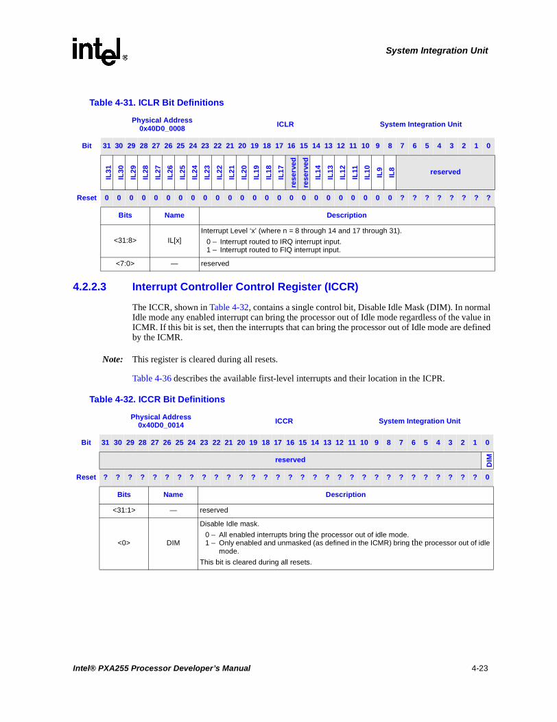
System Integration Unit
4.2.2.3 Interrupt Controller Control Register (ICCR)
The ICCR, shown in Table 4-32, contains a single control bit, Disable Idle Mask (DIM). In normal Idle mode any enabled interrupt can bring the processor out of Idle mode regardless of the value in ICMR. If this bit is set, then the interrupts that can bring the processor out of Idle mode are defined by the ICMR.
Note: This register is cleared during all resets.
Table 4-36 describes the available first-level interrupts and their location in the ICPR.
Table 4-31. ICLR Bit Definitions
Physical Address0x40D0_0008 ICLR System Integration Unit
Bit 31 30 29 28 27 26 25 24 23 22 21 20 19 18 17 16 15 14 13 12 11 10 9 8 7 6 5 4 3 2 1 0
IL31
IL30
IL29
IL28
IL27
IL26
IL25
IL24
IL23
IL22
IL21
IL20
IL19
IL18
IL17
rese
rved
rese
rved
IL14
IL13
IL12
IL11
IL10
IL9
IL8 reserved
Reset 0 0 0 0 0 0 0 0 0 0 0 0 0 0 0 0 0 0 0 0 0 0 0 0 ? ? ? ? ? ? ? ?
Bits Name Description
<31:8> IL[x]Interrupt Level ‘x’ (where n = 8 through 14 and 17 through 31).
0 – Interrupt routed to IRQ interrupt input.1 – Interrupt routed to FIQ interrupt input.
<7:0> — reserved
Table 4-32. ICCR Bit Definitions
Physical Address0x40D0_0014 ICCR System Integration Unit
Bit 31 30 29 28 27 26 25 24 23 22 21 20 19 18 17 16 15 14 13 12 11 10 9 8 7 6 5 4 3 2 1 0
reserved
DIM
Reset ? ? ? ? ? ? ? ? ? ? ? ? ? ? ? ? ? ? ? ? ? ? ? ? ? ? ? ? ? ? ? 0
Bits Name Description
<31:1> — reserved
<0> DIM
Disable Idle mask.
0 – All enabled interrupts bring the processor out of idle mode.1 – Only enabled and unmasked (as defined in the ICMR) bring the processor out of idle
mode.
This bit is cleared during all resets.
Intel® PXA255 Processor Developer’s Manual 4-23

System Integration Unit
4.2.2.4 Interrupt Controller IRQ Pending Register (ICIP) and FIQ Pending Register (ICFP)
The ICIP and the ICFP, shown in Table 4-33 and Table 4-34, contain one bit per interrupt (22 total.) These bits indicate an interrupt request has been made by a unit. Inside the interrupt service routine, read the ICIP and ICFP to determine the interrupt source. In general, software then reads status registers within the interrupting device to determine how to service the interrupt. Bits within the ICPR (see Section 4.2.2.5) are read only, and represent the logical OR of the status bits in the ICIP and ICFP for a given interrupt. Once an interrupt has been serviced, the handler writes a one to the required status bit, clearing the pending interrupt at the source.
Clearing the interrupt status bit at the source, automatically clears the corresponding ICIP or ICFP flag, provided there are no other interrupt status bits set within the source unit.
Table 4-36 describes the available first-level interrupts and their location in the ICPR.
Table 4-33. ICIP Bit Definitions
Physical Address0x40D0_0000 ICIP System Integration Unit
Bit 31 30 29 28 27 26 25 24 23 22 21 20 19 18 17 16 15 14 13 12 11 10 9 8 7 6 5 4 3 2 1 0
IP31
IP30
IP29
IP28
IP27
IP26
IP25
IP24
IP23
IP22
IP21
IP20
IP19
IP18
IP17
rese
rved
rese
rved
IP14
IP13
IP12
IP11
IP10
IP9
IP8 reserved
Reset 0 0 0 0 0 0 0 0 0 0 0 0 0 0 0 0 0 0 0 0 0 0 0 0 ? ? ? ? ? ? ? ?
Bits Name Description
<31:8> IP[x]IRQ Pending x (where x = 8 through 14 and 17 through 31).
0 – IRQ NOT requested by any enabled source.1 – IRQ requested by an enabled source.
<7:0> — reserved
Table 4-34. ICFP Bit Definitions
Physical Address0x40D0_000C ICFP System Integration Unit
Bit 31 30 29 28 27 26 25 24 23 22 21 20 19 18 17 16 15 14 13 12 11 10 9 8 7 6 5 4 3 2 1 0
FP
31
FP
30
FP
29
FP
28
FP
27
FP
26
FP
25
FP
24
FP
23
FP
22
FP
21
FP
20
FP
19
FP
18
FP
17
rese
rved
rese
rved
FP
14
FP
13
FP
12
FP
11
FP
10
FP
9
FP
8 reserved
Reset 0 0 0 0 0 0 0 0 0 0 0 0 0 0 0 0 0 0 0 0 0 0 0 0 ? ? ? ? ? ? ? ?
Bits Name Description
<31:8> FP[x]FIQ Pending x (where x = 8 through 14 and 17 through 31).
0 – FIQ NOT requested by any enabled source.1 – FIQ requested by an enabled source.
<7:0> — reserved
4-24 Intel® PXA255 Processor Developer’s Manual

System Integration Unit
4.2.2.5 Interrupt Controller Pending Register (ICPR)
The ICPR, shown in Table 4-35, is a 32-bit read-only register that shows all active interrupts in the system. These bits are not affected by the state of the mask register (ICMR). Clearing the interrupt status bit at the source, automatically clears the corresponding ICPR flag, provided there are no other interrupt status bits set within the source unit.
Table 4-36 shows the pending interrupt source assigned to each bit position in the ICPR. Also included in the table are the source units for the interrupts and the number of second-level interrupts associated with each. For more information on the second-level interrupts, see the section that corresponds to its name in the Source Unit column.
Table 4-35. ICPR Bit Definitions (Sheet 1 of 3)
Physical Address0x40D0_0010 ICPR System Integration Unit
Bit 31 30 29 28 27 26 25 24 23 22 21 20 19 18 17 16 15 14 13 12 11 10 9 8 7 6 5 4 3 2 1 0
IS31
IS30
IS29
IS28
IS27
IS26
IS25
IS24
IS23
IS22
IS21
IS20
IS19
IS18
IS17
rese
rved
IS14
IS13
IS12
IS11
IS10
IS9
IS8
rese
rved
Reset 0 0 0 0 0 0 0 0 0 0 0 0 0 0 0 0 0 0 0 0 0 0 0 0 0 0 0 0 0 0 0 0
Bits Name Description
<31> IS31RTC Alarm Match Register Interrupt Pending
0 – Interrupt NOT pending due to RTC Alarm Match Register. 1 – Interrupt pending due to RTC Alarm Match Register.
<30> IS30RTC HZ Clock Tick Interrupt Pending
0 – Interrupt NOT pending due to RTC HZ Clock Tick. 1 – Interrupt pending due to RTC HZ Clock Tick.
<29> IS29OS Timer Match Register 3 Interrupt Pending
0 – Interrupt NOT pending due to OS Timer Match Register 3. 1 – Interrupt pending due to OS Timer Match Register 3.
<28> IS28OS Timer Match Register 2 Interrupt Pending
0 – Interrupt NOT pending due to OS Timer Match Register 2. 1 – Interrupt pending due to OS Timer Match Register 2.
<27> IS27OS Timer Match Register 1 Interrupt Pending
0 – Interrupt NOT pending due to OS Timer Match Register 1.1 – Interrupt pending due to OS Timer Match Register 1.
<26> IS26OS Timer Match Register 0 Interrupt Pending
0 – Interrupt NOT pending due to OS Timer Match Register 0.1 – Interrupt pending due to OS Timer Match Register 0.
<25> IS25DMA Channel Service Request Interrupt Pending
0 – Interrupt NOT pending due to DMA Channel Service Request. 1 – Interrupt pending due to DMA Channel Service Request.
<24> IS24SSP Service Request Interrupt Pending
0 – Interrupt NOT pending due to SSP Service Request.1 – Interrupt pending due to SSP Service Request.
<23> IS23MMC Status/Error Detection Interrupt Pending
0 – Interrupt NOT pending due to MMC Status/Error Detection. 1 – Interrupt pending due to MMC Status/Error Detection.
Intel® PXA255 Processor Developer’s Manual 4-25

System Integration Unit
<22> IS22FFUART Transmit/Receive/Error Interrupt Pending
0 – Interrupt NOT pending due to FFUART Transmit/Receive/Error.1 – Interrupt pending due to FFUART Transmit/Receive/Error.
<21> IS21BTUART Transmit/Receive/Error Interrupt Pending
0 – Interrupt NOT pending due to BTUART Transmit/Receive/Error.1 – Interrupt pending due to BTUART Transmit/Receive/Error.
<20> IS20STUART Transmit/Receive/Error Interrupt Pending
0 – Interrupt NOT pending due to STUART Transmit/Receive/Error.1 – Interrupt pending due to STUART Transmit/Receive/Error.
<19> IS19ICP Transmit/Receive/Error Interrupt Pending
0 – Interrupt NOT pending due to ICP Transmit/Receive/Error. 1 – Interrupt pending due to ICP Transmit/Receive/Error.
<18> IS18I2C Service Request Interrupt Pending
0 – Interrupt NOT pending due to I2C Service Request.1 – Interrupt pending due to I2C Service Request.
<17> IS17LCD Controller Service Request Interrupt Pending
0 – Interrupt NOT pending due to LCD Controller Service Request. 1 – Interrupt pending due to LCD Controller Service Request.
<16> IS16
NETWORK SSP SERVICE REQUEST INTERRUPT PENDING:
0 – Interrupt NOT pending due to Network SSP Service Request.
1 – Interrupt pending due to Network SSP Service Request.
<15> — reserved
<14> IS14AC97 Interrupt Pending
0 – Interrupt NOT pending due to AC97 unit1 – Interrupt pending due to AC97 unit.
<13> IS13I2S Interrupt Pending
0 – Interrupt NOT pending due to I2S unit1 – Interrupt pending due to I2S unit.
<12> IS12Performance Monitoring Unit (PMU) Interrupt Pending
0 – Interrupt NOT pending due to PMU unit.1 – Interrupt pending due to PMU unit.
<11> IS11USB Service Interrupt Pending
0 – Interrupt NOT pending due to USB service request.1 – Interrupt pending due to USB service request.
<10> IS10GPIO[80:2] Edge Detect Interrupt Pending
0 – Interrupt NOT pending due to edge detect on one (or more) of GPIO[80:2]. 1 – Interrupt pending due to edge detect on one (or more) of GPIO[80:2].
Table 4-35. ICPR Bit Definitions (Sheet 2 of 3)
Physical Address0x40D0_0010 ICPR System Integration Unit
Bit 31 30 29 28 27 26 25 24 23 22 21 20 19 18 17 16 15 14 13 12 11 10 9 8 7 6 5 4 3 2 1 0
IS31
IS30
IS29
IS28
IS27
IS26
IS25
IS24
IS23
IS22
IS21
IS20
IS19
IS18
IS17
rese
rved
IS14
IS13
IS12
IS11
IS10
IS9
IS8
rese
rved
Reset 0 0 0 0 0 0 0 0 0 0 0 0 0 0 0 0 0 0 0 0 0 0 0 0 0 0 0 0 0 0 0 0
Bits Name Description
4-26 Intel® PXA255 Processor Developer’s Manual

System Integration Unit
<9> IS9GPIO[1] Edge Detect Interrupt Pending
0 – Interrupt NOT pending due to edge detect on GPIO[1]. 1 – Interrupt pending due to edge detect on GPIO[1].
<8> IS8GPIO[0] Edge Detect Interrupt Pending
0 – Interrupt NOT pending due to edge detect on GPIO[0].1 – Interrupt pending due to edge detect on GPIO[0].
<7> IS7
Hardware UART Service Request Interrupt Pending
0 – Interrupt NOT pending due to Hardware UART Service Request.
1 – Interrupt pending due to Hardware UART Service Request.
<6:0> — reserved
Table 4-36. List of First–Level Interrupts (Sheet 1 of 2)
Bit Position Source Unit # of Level 2 Sources Bit Field Description
IS<31>Real-time clock
1 RTC equals alarm register.
IS<30> 1 One Hz clock TIC occurred.
IS<29>
Operating system timer
1 OS timer equals match register 3.
IS<28> 1 OS timer equals match register 2.
IS<27> 1 OS timer equals match register 1.
IS<26> 1 OS timer equals match register 0.
IS<25> DMA controller 16 DMA Channel service request.
IS<24> Synchronous Serial Port 3 SSP service request.
IS<23> MUlti Media Card 9 MMC status / error detection
IS<22> FFUART 5 x-mit, receive, error in FFUART.
IS<21> BTUART 5 x-mit, receive, error in BTUART
IS<20> STUART 4 x-mit, receive, error in STUART
IS<19> ICP 6 x-mit, receive, error in ICP.
IS<18> I2C 6 I2C service request.
IS<17> LCD controller 15 LCD controller service request.
IS<16> Network SSP 4 Network SSP service request
IS<15> reserved
IS<14> AC97 10 AC97 interrupt
Table 4-35. ICPR Bit Definitions (Sheet 3 of 3)
Physical Address0x40D0_0010 ICPR System Integration Unit
Bit 31 30 29 28 27 26 25 24 23 22 21 20 19 18 17 16 15 14 13 12 11 10 9 8 7 6 5 4 3 2 1 0
IS31
IS30
IS29
IS28
IS27
IS26
IS25
IS24
IS23
IS22
IS21
IS20
IS19
IS18
IS17
rese
rved
IS14
IS13
IS12
IS11
IS10
IS9
IS8
rese
rved
Reset 0 0 0 0 0 0 0 0 0 0 0 0 0 0 0 0 0 0 0 0 0 0 0 0 0 0 0 0 0 0 0 0
Bits Name Description
Intel® PXA255 Processor Developer’s Manual 4-27

System Integration Unit
Several units have more than one source per interrupt signal. When an interrupt is signalled from one of these units, the interrupt handler routine identifies which interrupt was signalled using the interrupt controller’s pending register. This identifies the unit that made the request, but not the exact source. The handler then reads the interrupting unit’s status register to identify which source within the unit signalled the interrupt. For all interrupts that have one corresponding source, the interrupt handler routine needs to use only the interrupt controller’s registers to identify the exact cause of the interrupt. ICPR[16:15] and ICPR[7:0] are reserved bits and must be written as zeros. Reads to these bits must be ignored.
4.3 Real-Time Clock (RTC)
Use the RTC to configure a clock source with a wide range of frequencies. Typically, the RTC is set to be a 1 Hz output and is utilized as a system time keeper. There is also an alarm feature that enables an interrupt or a wake up event when the RTC output clock increments to a pre-set value.
4.3.1 Real-Time Clock Operation
The RTC provides a general-purpose real-time reference for your design. The RTC Counter register (RCNR) is initialized to zero after a hardware reset or a watchdog reset. It is a free running counter that starts incrementing the count value after the deassertion of reset. The counter is incremented one 32kHz cycle after the rising edge of the Hz clock. Since the high phase of the 1 Hz clock is one 32kHz cycle wide, it appears to increment on the falling edge of the 1 Hz clock. Set this counter to the desired value. If the counter is set to a value other than zero, write the desired value to the RCNR. The value of the counter is unaffected by transitions into and out of Sleep or Idle mode.
IS<13> I2S 5 I2S interrupt
IS<12> Core 1 PMU (Performance Monitor) interrupt
IS<11> USB 7 USB interrupt
IS<10> 79 “OR” of GPIO edge detects 80-2
IS<9> 1 GPIO<1> edge detect
IS<8> 1 GPIO<0> edge detect
IS<7> Hardware UART 7 Hardware UART service request
IS<6> reserved
IS<5> reserved
IS<4> reserved
IS<3> reserved
IS<2> reserved
IS<1> reserved
IS<0> reserved
Total level 2 interrupt
sources179
Table 4-36. List of First–Level Interrupts (Sheet 2 of 2)
Bit Position Source Unit # of Level 2 Sources Bit Field Description
4-28 Intel® PXA255 Processor Developer’s Manual

System Integration Unit
In addition to the RCNR, the RTC incorporates a 32-bit, RTC Alarm register (RTAR). The RTAR may be programmed with a value that is compared against the RCNR. One 32-kHz cycle after each rising edge of the HZ clock, the counter is incremented and then compared to the RTAR. If the values match, and the enable bit is set, then the RTC Status register (RTSR) alarm match bit (RTSR[AL]) is set. This status bit is also routed to the interrupt controller and may be unmasked in the interrupt controller to generate a processor interrupt. Another available interruptible status bit that can be set whenever the HZ clock transitions is the RTSR. By writing a one to the AL or HZ bit in the RTSR, the status bit is cleared.
The HZ clock is generated by dividing one of two selectable clock sources, both approximately 32.768 kHz in frequency. The first source is the output of the 3.6864 MHz crystal oscillator further divided by 112 to approximately 32.914 kHz. The other source is the optional 32.768 kHz crystal oscillator output itself. Your system may be built with both the 32.768 kHz crystal oscillator and the 3.6864 MHz crystal oscillator. ALternately, your system may only use the 3.6864 MHz crystal oscillator, if the additional power consumption during sleep mode is acceptable.
The divider logic for generating the HZ clock is programmable. This lets you trim the counter to adjust for inherent inaccuracies in the crystal’s frequency and the inaccuracy caused by the division of the 3.6864 MHz oscillator which yields only an approximate 32 kHz frequency. The trimming mechanism lets you adjust the RTC to an accuracy of +/- 5 seconds per month. The trimming procedure is described in a later paragraph.
All registers in the RTC, with the exception RTTR, are reset by hardware reset and the watchdog reset. The trim register, RTTR is reset only by hardware reset.
4.3.2 RTC Register Definitions
The following sections provide register descriptions for the RTC.
4.3.2.1 RTC Trim Register (RTTR)
Program the RTTR to set the frequency of the HZ clock. The reset value of this register (0x0000_7FFF) (assuming a perfect 32.768 kHz crystal) would produce an HZ clock output of exactly 1 Hz. However, by using values other than 0x0000_7FFF, a different HZ clock frequency is possible. Additionally, developers can use a crystal that is not exactly 32.768 kHz and compensate by writing a value other than 0x0000_7FFF to the RTTR. Section 4.3.3 describes how to calculate the value in this register. A write to the RTTC will increment the RTC Count Register (RCNR) by one. RTTC[LCK] does not prevent the RCNR from incrementing.
All reserved bits must be written to zeros and reads to these bits must be ignored. You can only reset the RTTR with a hardware reset. To safeguard the validity of the data written into the trim register, bit 31 is used as a Lock Bit. The data in RTTR may be changed only if RTTR[LCK] is cleared. Once, RTTR[LCK] is set to be a one, only a hardware reset can clear the RTTR.
Intel® PXA255 Processor Developer’s Manual 4-29

System Integration Unit
4.3.2.2 RTC Alarm Register (RTAR)
The RTAR, Table 4-38, is a 32-bit register. The processor can both read and write to this register. Following each rising edge of the HZ clock, this register is compared to the RCNR. If the two are equal and RTSR[ALE] is set, then RTSR[AL] is set.
Because of the asynchronous nature of the HZ clock relative to the processor clock, writes to this register are controlled by a hardware mechanism that delays the actual write to the register by two 32 kHz clock cycles after the processor store is performed.
The RTAR is initialized to 0x0 at reset.
Table 4-37. RTTR Bit Definitions
Physical Address0x4090_000C RTTR System Integration Unit
Bit 31 30 29 28 27 26 25 24 23 22 21 20 19 18 17 16 15 14 13 12 11 10 9 8 7 6 5 4 3 2 1 0
LC
K reserved DEL CK_DIV
Reset 0 ? ? ? ? ? 0 0 0 0 0 0 0 0 0 0 0 1 1 1 1 1 1 1 1 1 1 1 1 1 1 1
Bits Name Description
<31> LCKLocking bit for the trim value.
0 – RTTR value is allowed to be altered.1 – RTTR value is not allowed to be altered.
<30:26> — reserved
<25:16> DELTrim delete count.
This value represents the number of 32 kHz clocks to delete when clock trimming begins.
<15:0> CK_DIVClock divider count.
This value is the number of 32 kHz clock cycles, plus 1, per HZ clock cycle.
Table 4-38. RTAR Bit Definitions
Physical Address0x4090_0004 RTAR System Integration Unit
Bit 31 30 29 28 27 26 25 24 23 22 21 20 19 18 17 16 15 14 13 12 11 10 9 8 7 6 5 4 3 2 1 0
RTMV
Reset 0 0 0 0 0 0 0 0 0 0 0 0 0 0 0 0 0 0 0 0 0 0 0 0 0 0 0 0 0 0 0 0
Bits Name Description
<31:0> RTMVRTC Target Match Value.
The value compared against the RTC counter.
4-30 Intel® PXA255 Processor Developer’s Manual

System Integration Unit
4.3.2.3 RTC Counter Register (RCNR)
The RCNR, shown in Table 4-39, is a read/write register. The counter may be written by the processor at any time although it is recommended that the operating system prevent inadvertent writes to the RCNR through the use of the MMU protection mechanisms (refer to the Intel® XScale™ Microarchitecture for the Intel® PXA255 Processor User’s Manual for details of MMU operation.)
Because of the asynchronous nature of the HZ clock relative to the processor clock, writes to this counter are controlled by a hardware mechanism that delays the actual write to the counter after the processor store is performed by approximately two 32 kHz clock cycles. In case of multiple writes to RCNR in quick succession, the final update to the RCNR counter may be delayed by up to two 32 kHz clock cycles.
The RCNR may be read at any time. Reads reflect the value in the counter after it increments or has been written and does not have the two 32 kHz clock cycle delay.
4.3.2.4 RTC Status Register (RTSR)
The RTSR, shown in Table 4-40, is cleared to all zeroes at hardware reset. The ALE and HZE bits enable both the interrupt for the functions as well as the updating the AL and HZ bits. The AL and HZ bits are status bits and are set by the RTC logic if the ALE and HZE bits are set respectively. They are cleared by writing ones to the AL and HZ bits. The AL and HZ bits are routed to the interrupt controller where they may be enabled to cause a first level interrupt. Write zeros to all reserved bits and ignore all reads to the reserved bits.
In Sleep mode, only AL events set the status bit in the RTSR register. The HZ bit is not set in Sleep mode since it is a recurring event.
Table 4-40 shows the bitmap of the RTC Status Register.
Table 4-39. RCNR Bit Definitions
Physical Address0x4090_0000 RCNR System Integration Unit
Bit 31 30 29 28 27 26 25 24 23 22 21 20 19 18 17 16 15 14 13 12 11 10 9 8 7 6 5 4 3 2 1 0
RCV
Reset 0 0 0 0 0 0 0 0 0 0 0 0 0 0 0 0 0 0 0 0 0 0 0 0 0 0 0 0 0 0 0 0
Bits Name Description
<31:0> RCVRTC Count Value.
The current value of the RTC counter.
Intel® PXA255 Processor Developer’s Manual 4-31
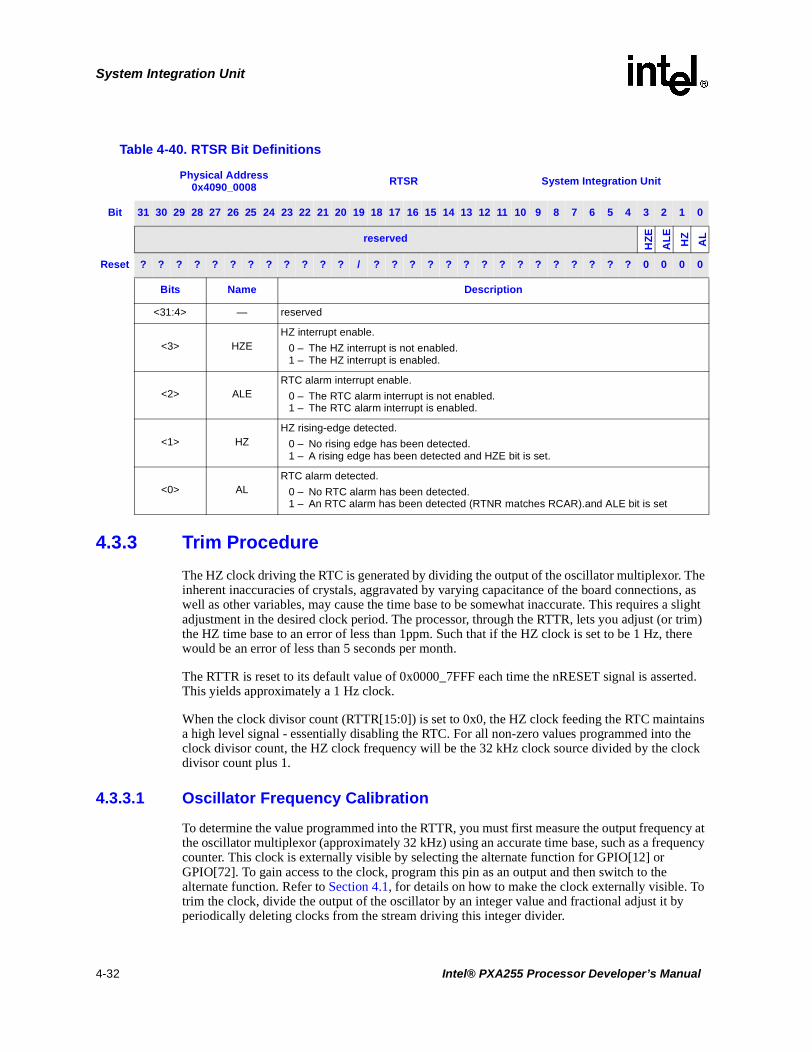
System Integration Unit
4.3.3 Trim Procedure
The HZ clock driving the RTC is generated by dividing the output of the oscillator multiplexor. The inherent inaccuracies of crystals, aggravated by varying capacitance of the board connections, as well as other variables, may cause the time base to be somewhat inaccurate. This requires a slight adjustment in the desired clock period. The processor, through the RTTR, lets you adjust (or trim) the HZ time base to an error of less than 1ppm. Such that if the HZ clock is set to be 1 Hz, there would be an error of less than 5 seconds per month.
The RTTR is reset to its default value of 0x0000_7FFF each time the nRESET signal is asserted. This yields approximately a 1 Hz clock.
When the clock divisor count (RTTR[15:0]) is set to 0x0, the HZ clock feeding the RTC maintains a high level signal - essentially disabling the RTC. For all non-zero values programmed into the clock divisor count, the HZ clock frequency will be the 32 kHz clock source divided by the clock divisor count plus 1.
4.3.3.1 Oscillator Frequency Calibration
To determine the value programmed into the RTTR, you must first measure the output frequency at the oscillator multiplexor (approximately 32 kHz) using an accurate time base, such as a frequency counter. This clock is externally visible by selecting the alternate function for GPIO[12] or GPIO[72]. To gain access to the clock, program this pin as an output and then switch to the alternate function. Refer to Section 4.1, for details on how to make the clock externally visible. To trim the clock, divide the output of the oscillator by an integer value and fractional adjust it by periodically deleting clocks from the stream driving this integer divider.
Table 4-40. RTSR Bit Definitions
Physical Address0x4090_0008 RTSR System Integration Unit
Bit 31 30 29 28 27 26 25 24 23 22 21 20 19 18 17 16 15 14 13 12 11 10 9 8 7 6 5 4 3 2 1 0
reserved
HZ
E
AL
E
HZ
AL
Reset ? ? ? ? ? ? ? ? ? ? ? ? / ? ? ? ? ? ? ? ? ? ? ? ? ? ? ? 0 0 0 0
Bits Name Description
<31:4> — reserved
<3> HZEHZ interrupt enable.
0 – The HZ interrupt is not enabled.1 – The HZ interrupt is enabled.
<2> ALERTC alarm interrupt enable.
0 – The RTC alarm interrupt is not enabled.1 – The RTC alarm interrupt is enabled.
<1> HZHZ rising-edge detected.
0 – No rising edge has been detected.1 – A rising edge has been detected and HZE bit is set.
<0> ALRTC alarm detected.
0 – No RTC alarm has been detected.1 – An RTC alarm has been detected (RTNR matches RCAR).and ALE bit is set
4-32 Intel® PXA255 Processor Developer’s Manual

System Integration Unit
4.3.3.2 RTTR Value Calculations
After the true frequency of the oscillator is known, it must be divided by the desired HZ clock frequency and this value split into integer and fractional portions. The integer portion of the value (minus one) is loaded into the Clock Divider Count field of the RTTR. This value is compared against a 16-bit counter clocked by the output of the oscillator multiplexor at approximately 32 kHz. When the two values are equal, the counter resets and generates a pulse which constitutes the raw HZ clock signal.
The fractional part of the adjustment is done by periodically deleting clocks from the clock stream driving the integer counter. The trim interval period is hardwired to be 210-1 periods of the HZ clock. If the HZ clock is programed to be 1 Hz the trim interval would be approximately 17 minutes. The number of clocks deleted (the trim delete value) is a 10-bit programmable counter allowing from 0 to 210-1 32 kHz clocks to be deleted from the input clock stream once per trim interval. RTTR[25:16] represents the number of 32 kHz clocks deleted per trim operation.
In summary, every 210-1 HZ clock periods, the integer counter stops clocking for a period equal to the fractional error that has accumulated. If this fractional error is programmed to be zero, then no trim operations occur and the RTC is clocked with the raw 32 kHz clock. The relationship between the HZ clock frequency and the nominal 32 kHz clock (f1 and f32K, respectively) is shown in the following equation.
f1 = HZ clock frequency
f32k = RTC internal clock - either the 32.678 kHz crystal output or the 3.68 MHz crystal output divided down to 32.914 kHz
RTTR[DEL] = RTTR(25:16)
RTTR[CK_DIV] = RTTR(15:0)
4.3.3.2.1 Trim Example #1 – Measured Value Has No Fractional Component
In this example, the desired HZ clock frequency is 1 Hz. The oscillator output is measured as 36045.000 cycles/s (Hz). This output is exactly 3277 cycles over the nominal frequency of the crystal (32.768 kHz) and has no fractional component. As such, only the integer trim function is needed - no fractional trim is required. Accordingly, RTTR[15:0] is loaded with the binary equivalent of 36045-1, or 0x0000_8CCC. RTTR[25:16] is left at zero (power-up state) to disable fractional trimming. This trim exercise leaves an error of zero in trimming.
4.3.3.2.2 Trim Example #2 – Measured Value Has a Fractional Component
This example is more common in that the measured frequency of the oscillator has a fractional component. Again, the desired HZ clock output frequency is 1 Hz. If the oscillator output is measured as 32768.92 cycles/s (Hz), an integer trim is necessary so that the average number of cycles counted before generating one 1 Hz clock is 32768.92. Similar to the previous example, the integer field RTTR[15:0] is loaded with the hexadecimal equivalent of 32768-1 or 0x0000_7FFF (reset value).
Because the actual clock frequency is 0.92 cycles per second faster than the integer value, the HZ clock generated by just the integer trimming is slightly faster than needed and must be slowed down. Accordingly, program the fractional trim to delete 0.92 cycles per second on average to
f1=(2^10-1)*(RTTR[CK_DIV]+1) - RTTR[DEL]
(2^10-1)*(RTTR[CK_DIV]+1)*
f32k
(RTTR[CK_DIV]+1)
Intel® PXA255 Processor Developer’s Manual 4-33

System Integration Unit
bring the HZ output frequency down to the proper value. Since the trimming procedure is performed every 1023 (210-1) seconds, the trim must be set to delete 941.16 clocks every 1023 seconds (.92 x 1023 = 941.16). Load the counter with the hexadecimal equivalent of 941, or 0x3AD. The fractional component of this value cannot be trimmed out and constitutes the error in trimming, described below.
This trim setting leaves an error of. 16 cycles per 1023 seconds. The error calculation yields (in parts-per-million or ppm):
4.3.3.2.3 Maximum Error Calculation Versus RTC Accuracy
As seen from trim example #2, the maximum possible error approaches 1 clock per 210-1 seconds. Calculating the ppm error for this scenario yields:
To maintain an accuracy of +/- 5 seconds per month, the required accuracy is calculated to be:
This calculation indicates that the HZ clock output can be made very accurate through the use of the trim procedure. Likewise, use the trim procedure to compensate for a range of factors that can affect crystal oscillators. Such factors can include, but are not limited to:
• Manufacturing and supplier variance in the crystals
• Crystal aging effects
• System voltage differences
• System manufacturing variance
The trim procedure can counteract these factors by providing a highly accurate mechanism to remove the variance and shifts from the manufacturing and static environment variables on an individual system level. However, since this is a calibration solution, it is not a practical solution for dynamic changes in the system and environment and can most likely only be done in a factory setting due to the equipment required.
4.4 Operating System (OS) Timer
The processor contains a 32-bit OS timer that is clocked by the 3.6864 MHz oscillator. The Operating System Count register (OSCR) is a free running up-counter. The OS timer also contains four 32-bit match registers (OSMR3, OSMR2, OSMR1, OSMR0). Developers can read and write to each register. When the value in the OSCR is equal to the value within any of the match registers, and the interrupt enable bit is set, the corresponding bit in the OSSR is set. These bits are
Error 0.16 cycles1023 sec
---------------------------X 1 sec32768 cycles------------------------------- 0.002 ppm= =
Error (maximum) 1 cycle1023 sec---------------------X 1 sec
32768 cycles---------------------------------- 0.03 ppm= =
Error 5 secmonth---------------X 1 month
2592000 sec------------------------------ 1.9 ppm= =
4-34 Intel® PXA255 Processor Developer’s Manual
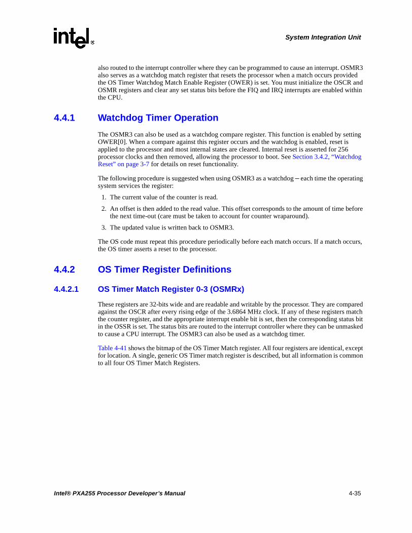
System Integration Unit
also routed to the interrupt controller where they can be programmed to cause an interrupt. OSMR3 also serves as a watchdog match register that resets the processor when a match occurs provided the OS Timer Watchdog Match Enable Register (OWER) is set. You must initialize the OSCR and OSMR registers and clear any set status bits before the FIQ and IRQ interrupts are enabled within the CPU.
4.4.1 Watchdog Timer Operation
The OSMR3 can also be used as a watchdog compare register. This function is enabled by setting OWER[0]. When a compare against this register occurs and the watchdog is enabled, reset is applied to the processor and most internal states are cleared. Internal reset is asserted for 256 processor clocks and then removed, allowing the processor to boot. See Section 3.4.2, “Watchdog Reset” on page 3-7 for details on reset functionality.
The following procedure is suggested when using OSMR3 as a watchdog – each time the operating system services the register:
1. The current value of the counter is read.
2. An offset is then added to the read value. This offset corresponds to the amount of time before the next time-out (care must be taken to account for counter wraparound).
3. The updated value is written back to OSMR3.
The OS code must repeat this procedure periodically before each match occurs. If a match occurs, the OS timer asserts a reset to the processor.
4.4.2 OS Timer Register Definitions
4.4.2.1 OS Timer Match Register 0-3 (OSMRx)
These registers are 32-bits wide and are readable and writable by the processor. They are compared against the OSCR after every rising edge of the 3.6864 MHz clock. If any of these registers match the counter register, and the appropriate interrupt enable bit is set, then the corresponding status bit in the OSSR is set. The status bits are routed to the interrupt controller where they can be unmasked to cause a CPU interrupt. The OSMR3 can also be used as a watchdog timer.
Table 4-41 shows the bitmap of the OS Timer Match register. All four registers are identical, except for location. A single, generic OS Timer match register is described, but all information is common to all four OS Timer Match Registers.
Intel® PXA255 Processor Developer’s Manual 4-35

System Integration Unit
4.4.2.2 OS Timer Interrupt Enable Register (OIER)
The OIER, shown in Table 4-42, contains four enable bits that indicate whether a match between one of the match registers and the OS timer counter sets a status bit in the OSSR. Each match register has a corresponding enable bit. Clearing an enable bit does not clear the corresponding interrupt status bit if it is already set.
Table 4-41. OSMR[x] Bit Definitions
Physical Address0x40A0_00000x40A0_00040x40A0_00080x40A0_000C
OS Timer Match Register 0-3(OSMR3, OSMR2, OSMR1,
OSMR0)System Integration Unit
Bit 31 30 29 28 27 26 25 24 23 22 21 20 19 18 17 16 15 14 13 12 11 10 9 8 7 6 5 4 3 2 1 0
OSMV
Reset 0 0 0 0 0 0 0 0 0 0 0 0 0 0 0 0 0 0 0 0 0 0 0 0 0 0 0 0 0 0 0 0
Bits Name Description
<31:0> OSMVOS Timer Match Value.
The value compared against the OS timer counter.
Table 4-42. OIER Bit Definitions
Physical Address0x40A0_001C
OS Timer Interrupt Enable Register (OIER) System Integration Unit
Bit 31 30 29 28 27 26 25 24 23 22 21 20 19 18 17 16 15 14 13 12 11 10 9 8 7 6 5 4 3 2 1 0
reserved E3
E2
E1
E0
Reset ? ? ? ? ? ? ? ? ? ? ? ? ? ? ? ? ? ? ? ? ? ? ? ? ? ? ? ? 0 0 0 0
Bits Name Description
<31:4> — reserved
<3> E3Interrupt enable channel 3.
0 – A match between OSMR3 and the OS Timer will NOT assert OSSR[M3].1 – A match between OSMR3 and the OS Timer asserts OSSR[M3].
<2> E2Interrupt enable channel 2.
0 – A match between OSMR2 and the OS Timer will NOT assert OSSR[M2].1 – A match between OSMR2 and the OS Timer asserts OSSR[M2].
<1> E1Interrupt enable channel 1.
0 – A match between OSMR1 and the OS Timer will NOT assert OSSR[M1].1 – A match between OSMR1 and the OS Timer asserts OSSR[M1].
<0> E0Interrupt enable channel 0.
0 – A match between OSMR0 and the OS Timer will NOT assert OSSR[M0].1 – A match between OSMR0 and the OS Timer asserts OSSR[M0].
4-36 Intel® PXA255 Processor Developer’s Manual

System Integration Unit
4.4.2.3 OS Timer Watchdog Match Enable Register (OWER)
The OWER, shown in Table 4-43, contains a single control bit (bit 0) that enables the watchdog function. This bit is set by writing a one to it and can only be cleared by one of the reset functions such as, hardware reset, sleep reset, watchdog reset, and GPIO reset.
4.4.2.4 OS Timer Count Register (OSCR)
The OSCR, shown in Table 4-44, is a 32-bit counter that increments on rising edges of the 3.6864 MHz clock. This counter can be read or written at any time. It is recommended that the system write-protect this register through the MMU protection mechanisms.
After the OSCR is written, there is a delay before the register is actually updated. Software must make sure the register has changed to the new value before relying on the contents of the register.
4.4.2.5 OS Timer Status Register (OSSR)
The OSSR, shown in Table 4-45, contains status bits that indicate a match has occurred between any of the four match registers and the OSCR. These bits are set when the match event occurs (following the rising edge of the 3.6864 MHz clock) and the corresponding interrupt enable bit is set in the OIER. The OSSR bits are cleared by writing a one to the proper bit position. Writing zeros to this register has no effect. Write all reserved bits as zeros and ignore all reads.
Table 4-43. OWER Bit Definitions
Physical Address0x40A0_0018
OS Timer Watchdog Match Enable Register (OWER) System Integration Unit
Bit 31 30 29 28 27 26 25 24 23 22 21 20 19 18 17 16 15 14 13 12 11 10 9 8 7 6 5 4 3 2 1 0
reserved
WM
E
Reset 0 0 0 0 0 0 0 0 0 0 0 0 0 0 0 0 0 0 0 0 0 0 0 0 0 0 0 0 0 0 0 0
Bits Name Description
<31:1> — reserved
<0> WMEWatchdog Match Enable
0 – OSMR3 match will NOT cause a reset of the processor1 – OSMR3 match causes a reset of the processor.
Table 4-44. OSCR Bit Definitions
Physical Address0x40A0_0010 OS Timer Count Register (OSCR) System Integration Unit
Bit 31 30 29 28 27 26 25 24 23 22 21 20 19 18 17 16 15 14 13 12 11 10 9 8 7 6 5 4 3 2 1 0
OSCV
Reset 0 0 0 0 0 0 0 0 0 0 0 0 0 0 0 0 0 0 0 0 0 0 0 0 0 0 0 0 0 0 0 0
Bits Name Description
<31:0> OSCVOS Timer Counter Value.
The current value of the OS timer counter.
Intel® PXA255 Processor Developer’s Manual 4-37

System Integration Unit
4.5 Pulse Width Modulator
Use the Pulse Width Modulator (PWM) to generate as many as two signals to be output from the processor. The signals are based on the 3.6864 MHz clock and must be a minimum of 2 clock cycles wide. These signals are output from the processor by configuring the GPIOs.
4.5.1 Pulse Width Modulator Operation
The processor contains two pulse width modulators: PWM0 and PWM1. Each PWM operates independently of the other, is controlled by its own set of registers. They provide a pulse width modulated signal on an external pin. Since each PWM contains identical circuitry, a generic PWMn, where n is 0 or 1, is described.
Each PWM contains:
• Two Pulse Width Modulator channels
• Enhanced Period control through 6-Bit Clock divider and 10-Bit Period counter
• 10-Bit Pulse control
A block diagram of one of the PWMs is shown in Figure 4-3.
Table 4-45. OSSR Bit Definitions
Physical Address0x40A0_0014 OS Timer Status Register (OSSR) System Integration Unit
Bit 31 30 29 28 27 26 25 24 23 22 21 20 19 18 17 16 15 14 13 12 11 10 9 8 7 6 5 4 3 2 1 0
reserved M3
M2
M1
M0
Reset ? ? ? ? ? ? ? ? ? ? ? ? ? ? ? ? ? ? ? ? ? ? ? ? ? ? ? ? 0 0 0 0
Bits Name Description
<31:4> — reserved
<3> M3
Match status channel 3.
If OIER[3] is set then:
0 – OSMR[3] has NOT matched the OS timer counter since last being cleared.1 – OSMR[3] has matched the OS timer counter.
<2> M2
Match status channel 2.
If OIER[2] is set then:
0 – OSMR[2] has NOT matched the OS timer counter since last being cleared.1 – OSMR[2] has matched the OS timer counter.
<1> M1
Match status channel 1.
If OIER[1] is set then:
0 – OSMR[1] has NOT matched the OS timer counter since last being cleared.1 – OSMR[1] has matched the OS timer counter.
<0> M0
Match status channel 0.
If OIER[0] is set then:
0 – OSMR[0] has NOT matched the OS timer counter since last being cleared.1 – OSMR[0] has matched the OS timer counter.
4-38 Intel® PXA255 Processor Developer’s Manual

System Integration Unit
4.5.1.1 Interdependencies
The PWM unit is clocked off the 3.6864 MHz oscillator output.
Each Pulse Width Modulator Unit (PWMn) is controlled by three registers:
• Pulse Width Control Register (PWM_CTRL)
• Duty Cycle Control Register (PWM_DUTY)
• Period Control Register (PWM_PERVAL)
By setting the values in these registers the PWMn unit produces a pulse width modulated output signal. The registers contain the values for PWMn’s counters and PWMn power management mode.
Each register contains one or more fields which determine an attribute of the PWM_OUTn waveform. PWM_CTRLn[PRESCALE] specifies the divisor for the PWM module clock. Note that the actual PWM module clock divisor used is 1 greater than the value programmed into PWM_CTRLn[PRESCALE]. This divided PWM module clock drives a 10 bit up-counter. This up-counter feeds 2 separate comparators. The first comparator contains the value of PWM_DUTYn[DCYCLE]. When the values match, the PWM_OUT signal is set high. The other
Figure 4-3. PWMn Block Diagram
Value of PWM_DUTYn[DCYCLE]
Comparator
10-bit up counter
Comparator
Value of PWM_PERVALn[PV]
Value of PWM_CTRLn[PRESCALE]
6-bit down counter
Clock Gate
PSCLK_PWMn
PWM_OUTn
RESET
SET
FLIP-FLOP
3.6864 MHz
Bus Interfac
Control Block
Intel® PXA255 Processor Developer’s Manual 4-39

System Integration Unit
comparator contains PWM_PERVALn[PV] and clears the PWM_OUT signal low when PWM_PERVALn[PV] + 1 and the 10-bit up counter are equal. Both PWM_PERVALn[PV] and PWM_DUTYn[DCYCLE] are 10 bit fields.
Note: Take care to ensure that the value of the PWM_PERVALn register remains larger than PWM_DUTYn register. In the case where PWM_PERVALn is less than PWM_DUTYn the output maintains a high state.
4.5.1.2 Reset Sequence
A system reset results in no pulse width modulated signal. During system reset the PWM_CTRLn and PWM_DUTYn registers are reset to 0x0 and the PWM_PERVALn register is set to 0x004. This sets the PWM_OUTn pin low with a zero duty cycle. The six bit down-counter is reset to 0x0 and thus the 3.68 MHz input clock directly drives the 10 bit up-counter. The PWM_OUTn pin remains reset low until the PWM_DUTYn register is programmed with a non zero value.
A basic pulse width waveform is shown in Figure 4-4.
4.5.1.3 Power Management Requirements
Each PWM may be disabled through a pair of clock enable bits (see Section 3.6.2, “Clock Enable Register (CKEN)” on page 3-36). If the clock is disabled, the unit shuts down in one of two ways:
• Abrupt – the PWM stops immediately.
• Graceful – the PWM completes the current duty cycle before stopping.
Shutdown is selected by PWM_CTRL[PWM_SD] and described in Section 4.5.2.1.
4.5.2 Register Descriptions
The following paragraphs provide register descriptions for the Pulse Width Modulator.
4.5.2.1 PWM Control Registers (PWM_CTRLn)
The PWM_CTRLn, shown in Table 4-46, contains two fields:
• PRESCALE – The PRESCALE field contains the 6-bit prescale counter load value. This field allows the 3.6864 MHz input clock PSCLK_PWMn, to be divided by values between 1 (PWM_CTL[PRESCALE] = 0) and 64 (PWM_CTL[PRESCALE] = 63).
Note: The value of the divisor is one greater than the value programmed into the PRESCALE field.
• PWM_SD – PWMn can shut down in one of two ways, gracefully or abruptly, depending on the setting of PWM_CTRLn[PWM_SD]. If gracefully is chosen, then the duty cycle counter completes its count before PWMn is shut down. If abruptly is chosen, then the prescale counter and the duty cycle counter are reset to the reload values in their associated registers and PWMn is immediately shut down.
Note: During abrupt shut down the PWM_OUTn signal may be delayed by up to one PSCLK_PWMn clock period.
4-40 Intel® PXA255 Processor Developer’s Manual

System Integration Unit
4.5.2.2 PWM Duty Cycle Registers (PWM_DUTYn)
The PWM_DUTYn, shown in Table 4-47, contains two fields:
• FDCYCLE
• DCYCLE
The FDCYCLE bit determines whether or not PWM_OUTn is a function of the DCYCLE bits in the PWM_DUTYn register or is set high. When the FDCYCLE bit is cleared low (normal operation), the output waveform of PWM_OUTn is cyclic, with PWM_OUTn being high for the number of PSCLK_PWMn periods equal to DCYCLE.
If FDCYCLE=0x0 and DCYCLE=0x0, PWM_OUTn is set low and does not toggle.
Note: If FDCYCLE is 0b1, PWM_OUTn is high for the entire period and is not influenced by the value programmed in the DCYCLE bits.
Table 4-46. PWM_CTRLn Bit Definitions
Physical Address0x40B0_00000x40C0_0000
PWM Control Registers (PWM_CTRL0, PWM_CTRL1) System Integration Unit
Bit 31 30 29 28 27 26 25 24 23 22 21 20 19 18 17 16 15 14 13 12 11 10 9 8 7 6 5 4 3 2 1 0
reserved
PW
M_S
D
PRESCALE
Reset 0 0 0 0 0 0 0 0 0 0 0 0 0 0 0 0 0 0 0 0 0 0 0 0 0 0 0 0 0 0 0 0
Bits Name Description
<31:7> — reserved
<6> PWM_SD
PWMn Shutdown Method:
0 – Graceful shutdown of PWMn when the clock enable bit in the CKEN register is cleared.
1 – Abrupt shutdown of PWMn when the clock enable bit in the CKEN register is cleared.
<5:0> PRESCALE
PWMn Prescale Divisor.
Determines the frequency of the PWM module clock (in terms of the 3.86 MHz clock)
PSCLK_PWMn = 3.6864 MHz / (PWM_CTRL[PRESCALE] + 1)
Intel® PXA255 Processor Developer’s Manual 4-41

System Integration Unit
4.5.2.3 PWM Period Control Register (PWM_PERVALn)
The PWM_PERVALn, shown in Table 4-48, contains a 10 bit field called PV. This field determines the period of the PWM_OUTn waveform in terms of the PSCLK_PWMn clock. If this field is cleared to zero PWMn is effectively turned off and PWM_OUTn remains in a high state. For any non-zero value written to the PV field, the output frequency of PWMn is the frequency of the PSCLK_OUTn divided by the value of (PV + 1). The range of the clock gate extends from a pass-through of the PSCLK_PWMn to a clock delay of 26 or 64 input clocks per output pulse.
When the value of the 10 bit up-counter equals the value of (PV +1), the up-counter and the flip-flop are reset and the values of PWM_CTRLn, PWM_PERVALn and PWM_DUTYn are loaded into the internal versions of these registers. Resetting this flip-flop causes PWM_OUTn to go low and the PWM cycle to start again.
Writing all zeroes to this register results in the output maintaining a high state unless FDCYCLE=0x0 and DCYCLE=0x0. If FDCYCLE=0x0 and DCYCLE=0x0, the output maintains a low state regardless of the value in the PV bit field.
Note: Due to internal timing requirements, all changes to any of the PWM registers must be complete a minimum of 4 core clock cycles before the start of end of a PWM clock cycle in order to guarantee that the following PWM cycle implements the new values.
Table 4-47. PWM_DUTYn Bit Definitions
Physical Address0x40B0_00040x40C0_0004
PWM Duty Cycle Registers (PWM_DUTY0, PWM_DUTY1) System Integration Unit
Bit 31 30 29 28 27 26 25 24 23 22 21 20 19 18 17 16 15 14 13 12 11 10 9 8 7 6 5 4 3 2 1 0
reserved
FD
CY
CL
E
DCYCLE
Reset 0 0 0 0 0 0 0 0 0 0 0 0 0 0 0 0 0 0 0 0 0 0 0 0 0 0 0 0 0 0 0 0
Bits Name Description
<31:11> — reserved
<10> FDCYCLEPWMn Full Duty Cycle
0 – PWM clock (PWM_OUTn) duty cycle is determined by DCYCLE field.1 – PWM_OUTn is set high and does not toggle.
<9:0> DCYCLEPWMn Duty Cycle
Duty cycle of PWMn clock, i.e. the number of PSCLK_PWM cycles PWMn is asserted within one cycle of PWMn.
4-42 Intel® PXA255 Processor Developer’s Manual

System Integration Unit
4.5.3 Pulse Width Modulator Output Wave Example
Figure 4-4 is an example of the output of a Pulse Width Modulator for reference.
PWM_PERVAL[PV] = 0xAPWM_DUTY[FDCYCLE] = 0x0PWM_DUTY[DCYCLE] = 0x6PWM_CTRL[PRESCALE] = 0x0
The output waveform in Figure 4-4 is created by writing PWM_PERVALn[PV] with a decimal value of 10 (11 clocks) and PWM_DUTYn[DCYCLE] with 6. Figure 4-4 also shows that PWM_CTRLn[PRESCALE] is configured with a value of 0x0 loaded, which results in the PSCLK_PWMn having the same frequency as the 3.6864 MHz input clock.
Table 4-48. PWM_PERVALn Bit Definitions
Physical Address0x40B0_00080x40C0_0008
PWM Period Control Registers (PWM_PERVAL0, PWM_PERVAL1) System Integration Unit
Bit 31 30 29 28 27 26 25 24 23 22 21 20 19 18 17 16 15 14 13 12 11 10 9 8 7 6 5 4 3 2 1 0
reserved PV
Reset 0 0 0 0 0 0 0 0 0 0 0 0 0 0 0 0 0 0 0 0 0 0 0 0 0 0 0 0 0 1 0 0
Bits Name Description
<31:10> — reserved
<9:0> PV
PWMn Period Control:
The number of PSCLK_PWMn cycles that comprise one PWM_OUTn cycleNOTE: If PV = 0x0, the PWMn clock (PWM_OUTn) is set high and does not toggle unless
FDCYCLE=0x0 and DCYCLE=0x0. In this case PWM_OUTn is set low and does not toggle regardless of the value in PV.
Figure 4-4. Basic Pulse Width Waveform
PWM_OUTn
PSCLK_PWMn
PWM_DUTYn = 6
PWM_PERVALn = 10 (+1)
3.6864 MHz
Intel® PXA255 Processor Developer’s Manual 4-43

System Integration Unit
4.6 System Integration Unit Register Summary
4.6.1 GPIO Register Locations
Table 4-49 shows the registers associated with the GPIO block and their physical addresses.
Table 4-49. GPIO Register Addresses (Sheet 1 of 2)
Address Name Description
0x40E0_0000 GPLR0 GPIO pin level register GPIO[31:0]
0x40E0_0004 GPLR1 GPIO pin level register GPIO[63:32]
0x40E0_0008 GPLR2 GPIO pin level register GPIO[80:64]
0x40E0_000C GPDR0 GPIO pin direction register GPIO[31:0]
0x40E0_0010 GPDR1 GPIO pin direction register GPIO[63:32]
0x40E0_0014 GPDR2 GPIO pin direction register GPIO[80:64]
0x40E0_0018 GPSR0 GPIO pin output set register GPIO[31:0]
0x40E0_001C GPSR1 GPIO pin output set register GPIO[63:32]
0x40E0_0020 GPSR2 GPIO pin output set register GPIO[80:64]
0x40E0_0024 GPCR0 GPIO pin output clear register GPIO[31:0]
0x40E0_0028 GPCR1 GPIO pin output clear register GPIO[63:32]
0x40E0_002C GPCR2 GPIO pin output clear register GPIO[80:64]
0x40E0_0030 GRER0 GPIO rising-edge detect enable register GPIO[31:0]
0x40E0_0034 GRER1 GPIO rising-edge detect enable register GPIO[63:32]
0x40E0_0038 GRER2 GPIO rising-edge detect enable register GPIO[80:64]
0x40E0_003C GFER0 GPIO falling-edge detect enable register GPIO[31:0]
0x40E0_0040 GFER1 GPIO falling-edge detect enable register GPIO[63:32]
0x40E0_0044 GFER2 GPIO falling-edge detect enable register GPIO[80:64]
0x40E0_0048 GEDR0 GPIO edge detect status register GPIO[31:0]
0x40E0_004C GEDR1 GPIO edge detect status register GPIO[63:32]
0x40E0_0050 GEDR2 GPIO edge detect status register GPIO[80:64]
0x40E0_0054 GAFR0_L GPIO alternate function select register GPIO[15:0]
0x40E0_0058 GAFR0_UGPIO alternate function select register GPIO[31:16]
0x40E0_005C GAFR1_L GPIO alternate function select register GPIO[47:32]
4-44 Intel® PXA255 Processor Developer’s Manual

System Integration Unit
4.6.2 Interrupt Controller Register Locations
Table 4-50 shows the registers associated with the interrupt controller block and their physical addresses.
4.6.3 Real-Time Clock Register Locations
Table 4-51 describes the location of the RTC registers.
4.6.4 OS Timer Register Locations
Table 4-52 shows the registers associated with the OS timer and the physical addresses used to access them.
0x40E0_0060 GAFR1_U GPIO alternate function select register GPIO[63:48]
0x40E0_0064 GAFR2_LGPIO alternate function select register GPIO[79:64]
0x40E0_0068 GAFR2_U GPIO alternate function select register GPIO[80]
Table 4-49. GPIO Register Addresses (Sheet 2 of 2)
Table 4-50. Interrupt Controller Register Addresses
Address Name Description
0x40D0_0000 ICIP Interrupt controller IRQ pending register
0x40D0_0004 ICMR Interrupt controller mask register
0x40D0_0008 ICLR Interrupt controller level register
0x40D0_000C ICFP Interrupt controller FIQ pending register
0x40D0_0010 ICPR Interrupt controller pending register
0x40D0_0014 ICCR Interrupt controller control register
Table 4-51. RTC Register Addresses
Address Name Description
0x4090_0000 RCNR RTC count register
0x4090_0004 RTAR RTC alarm register
0x4090_0008 RTSR RTC status register
0x4090_000C RTTR RTC trim register
Table 4-52. OS Timer Register Addresses (Sheet 1 of 2)
Address Name Description
0x40A0_0000 OSMR0 OS timer match register 0
0x40A0_0004 OSMR1 OS timer match register 1
0x40A0_0008 OSMR2 OS timer match register 2
Intel® PXA255 Processor Developer’s Manual 4-45

System Integration Unit
4.6.5 Pulse Width Modulator Register Locations
Table 4-53 shows the registers associated with the PWM and the physical addresses used to access them.
0x40A0_000C OSMR3 OS timer match register 3
0x40A0_0010 OSCR OS timer counter register
0x40A0_0014 OSSR OS timer status register
0x40A0_0018 OWER OS timer watchdog enable register
0x40A0_001C OIER OS timer interrupt enable register
Table 4-52. OS Timer Register Addresses (Sheet 2 of 2)
Table 4-53. Pulse Width Modulator Register Addresses
Address Name Description
0x40B0_0000 PWM_CTRL0 PWM0 Control Register
0x40B0_0004 PWM_PWDUTY0 PWM0 Duty Cycle Register
0x40B0_0008 PWM_PERVAL0 PWM0 Period Control Register
0x40C0_0000 PWM_CTRL1 PWM1 Control Register
0x40C0_0004 PWM_PWDUTY1 PWM1 Duty Cycle Register
0x40C0_0008 PWM_PERVAL1 PWM1 Period Control Register
4-46 Intel® PXA255 Processor Developer’s Manual

DMA Controller 5
This chapter describes the on-chip DMA controller (DMAC) for the PXA255 processor. The DMAC transfers data to and from main memory in response to requests generated by internal and external peripherals. The peripherals do not directly supply addresses and commands to the memory system. The DMAC has 16 DMA channels, 0 through 15, and every DMA request from the peripheral generates at least one memory bus cycle.
5.1 DMA Description
The DMAC supports only flow-through transfers.
Flow-through data passes through the DMAC before the data is latched by the destination in its buffers/memory. This DMAC can perform memory-to-memory moves with flow-through transfers.
Figure 5-1 provides an overview of the DMAC. Table 5-1 provides a list of the DMAC signals and descriptions.
Figure 5-1. DMAC Block Diagram
DDADR0
DSADR0
DTADR0
DCMD0
Channel 0
Channel 15
16 DMA Channels
DRCMR0
Control Registers
System Bus (internal)
Peripheral Bus
DREQ[1:0]
PREQ[37:0]
DMA_IRQ
DMA Controller
DINT
DCSR0(external)
(internal)
(internal)
(internal)
Memory Controller
Intel® PXA255 Processor Developer’s Manual 5-1

DMA Controller
5.1.1 DMAC Channels
The DMAC has 16 channels, each controlled by four 32-bit registers. Each channel can be configured to service any internal peripheral or one of the external peripherals for flow-through transfers. Each channel is serviced in increments of the peripheral device’s burst size and is delivered in the granularity appropriate to that device’s port width. The burst size and port width for each device is programmed in the channel registers and is based on the device’s FIFO depth and bandwidth needs. Due to performance issues, it is highly recommended that the user set the burst size equal to the FIFO DMA interrupt trigger level, also called the FIFO threshold level. When multiple channels are actively executing, the DMAC services each channel with a burst of data. After the data burst is sent, the DMAC may perform a context switch to another active channel. The DMAC performs context switches based on a channel’s activity, whether its target device is currently requesting service, and where that channel lies in the priority scheme.
Channel information must be maintained on a per-channel basis and is contained in the DMAC registers see in Table 5-13. The DMAC supports two methods of loading the DMAC register, No-Descriptor and Descriptor Fetch Modes. The fetch modes are discussed in further detail in Section 5.1.4.
Software must ensure cache coherency when it configures the DMA channels. The DMAC does not check the cache so target and source addresses must be configured as non-cacheable in the Memory Management Unit.
Each demand for data that a peripheral generates results in a read or write to memory data. A peripheral must not request a DMA transfer unless it is prepared to read or write the full data block (8, 16, or 32 bytes) and it is equipped to handle reads and writes less than a full data block. Reads and writes less than a full data block can occur at the end of a DMA transfer.
5.1.2 Signal Descriptions
The DREQ[1:0], PREQ[37:0] and DMA_IRQ signals are controlled by the DMAC as indicated in Table 5-1.
5.1.2.1 DREQ[1:0] and PREQ[37:0] Signals
The external companion chip asserts the positive edge triggered DREQ[1:0] signals when a DMA transfer request is needed. The DREQ[1:0] signal must remain asserted for four MEMCLKs to allow the DMA to recognize the 0 to 1 transition. When the DREQ[1:0] signals are deasserted, they
Table 5-1. DMAC Signal List
Signal Signal TypeIn/Out To/From Definition
DREQ[1:0] Input Pins External companion chip request lines. DMA detects the positive edge of this signal as a request.
DMA_IRQ Output Interrupt Controller Active high signal indicating an interrupt.
PREQ[37:0] Input On-chip peripherals
Internal peripheral DMA request lines. On chip peripherals send requests using the PREQ signals.
The DMAC does not sample the PREQ signals until it completely finishes the data transfer from peripheral to the memory.
5-2 Intel® PXA255 Processor Developer’s Manual

DMA Controller
must remain deasserted for at least four MEMCLKs. The DMAC registers the transition from 0 to 1 to identify a new request. The external companion chip must not assert another DREQ until the previous DMA data transfer starts.
The PREQ[37:0] bits are the active high internal signals from the on-chip peripherals. Unlike DREQ[1:0], they are level sensitive. The DMAC does not sample the PREQ[37:0] signals until it completely finishes the current data transfer. For a write request to the on-chip peripheral, the DMAC begins to sample the PREQ[37:0] signals after it sends the last byte of the write request. For a read request, the DMAC begins to sample the PREQ[37:0] signals after it sends the last byte that pertains to the read on the internal bus.
The DCSR[REQPEND] bit indicates the status of the pending request for the channel.
If a DREQx assertion sets the DCSR[REQPEND] bit and software resets the DCSR[RUN] bit to stop the channel, the DCSR[REQPEND] bit and the internal registers that hold the DREQx assertion information may remain set even though the channel has stopped. To reset the DCSR[REQPEND] bit, software must send a dummy descriptor that transfers some data.
5.1.2.2 DMA_IRQ Signal
The processor has 16 IRQ signals, one for each DMA channel. Each DMA IRQ can be read in the DINT register that is shown in Table 5-6. The user can mask some bits that cause interrupts on a channel, such as ENDIRQEN, STARTIRQEN, and STOPIRQEN.
When DMA interrupt occurs, it is visible in Pending Interrupt Register Bit 25 (see Section 4.2.2.5, “Interrupt Controller Pending Register (ICPR)” on page 4-25). When a pending interrupt becomes active, it is sent to the CPU if its corresponding ICMR mask Bit 25 (see Section 4.2.2.1, “Interrupt Controller Mask Register (ICMR)” on page 4-22) is set to a one.
5.1.3 DMA Channel Priority Scheme
The DMA channel priority scheme allows peripherals that require high bandwidth to be serviced more often than those requiring less bandwidth. The DMA channels are internally divided into four sets. Each set contains four channels. The channels get a round-robin priority in each set. Set zero has the highest priority. Set 1 has higher priority than sets two and three. Sets two and three are low priority sets. Refer to Table 5-2 for details. High bandwidth peripherals must be programmed in set zero. Memory-to-memory moves and low bandwidth peripherals must be programmed in set two or three. When all channels are running concurrently, set zero is serviced four times out of any eight consecutive channel servicing instances. Set one is serviced twice and sets two and three are each serviced once.
If two or more channels are active and request a DMA, the priority scheme in Table 5-2 applies.
Request priority does not affect requests that have already started. The DMAC priority scheme is considered when the smaller dimension of the DCMDx[SIZE] or DCMDx[LENGTH] is complete.
Figure 5-2. DREQ timing requirements
dreq_deassert_mindreq_deassert_mindreq_assert_mindreq_assert_minmem_clk
DREQ
Intel® PXA255 Processor Developer’s Manual 5-3

DMA Controller
If all channels request data transfers, the Sets are prioritized in following order:
• Set zero
• Set one
• Set zero
• Set two
• Set zero
• Set one
• Set zero
• Set three
The pattern repeats for the next eight channel services. In each set, the channels are given round-robin priority.
The state machine used to determine the priority of the DMA channels is shown in Table 5-3. Use this table to determine the exact sequence the DMA controller gives to each channel when not all channels are running concurrently.
The channels get a round-robin priority in each set. Out of reset, the state machine state is zero. If a channel in set zero has a pending request, that channel is serviced. If a channel in set one has a pending request, that channel is serviced and so on. Once a request is serviced, the state machine
Table 5-2. Channel Priority (if all channels are running concurrently)
Set Channels Priority Number of times served
0 0,1,2,3 Highest 4 / 8
1 4,5,6,7 Higher 2 / 8
2 8,9,10,11 Low 1 / 8
3 12,13,14,15 Low 1 / 8
Table 5-3. Channel Priority
State Machine State DMA Set Priority within each State Machine State
0 S0 > S1 > S2 > S3
1 S1 > S0 > S3 > S2
2 S0 > S1 > S2 > S3
3 S2 > S3 > S0 > S1
4 S0 > S1 > S2 > S3
5 S1 > S0 > S3 > S2
6 S0 > S1 > S2 > S3
7 S3 > S2 > S1 > S0
5-4 Intel® PXA255 Processor Developer’s Manual

DMA Controller
state is incremented, wrapping around from state machine state seven back to state machine state zero. If there is no pending request, the state machine stays in the current state machine state until there is a pending request. See Table 5-4 for priority scheme examples.
5.1.4 DMA Descriptors
The DMAC operates in two distinct modes: Descriptor Fetch Mode and No-Descriptor Fetch Mode. The mode used is determined by the DCSRx[NODESCFETCH] bit.
The Descriptor Fetch and No-Descriptor modes can be used simultaneously on different channels. This means that some DMA channels can be active in one mode while other channels are active in the other mode.
A channel must be stopped before it can be switched from one mode to the other.
If an error occurs in a channel, it returns to its stopped state and remains there until software clears the error condition and writes a 1 to the DCSR[RUN] register.
5.1.4.1 No-Descriptor Fetch Mode
In No-Descriptor Fetch Mode, the DDADRx is reserved. Software must not write to the DDADRx and must load the DSADRx, DTADRx, and DCMDx registers. When the Run bit is set, the DMAC immediately begins to transfer data. No-Descriptor fetches are performed at the beginning of the transfer. The channel stops when it finishes the transfer.
Ensure that the software does not program the channel’s DDADx No-Descriptor Fetch Mode.
A typical No-Descriptor Fetch Mode (DCSR[NODESCFETCH] = 1) operation follows:
1. The channel is in an uninitialized state after reset.
2. The DCSR[RUN] bit is set to a 0 and the DCSR[NODESCFETCH] bit is set to a 1.
3. The software writes a source address to the DSADR register, a target address to the DTADR register, and a command to the DCMD register. The DDADR register is reserved in this No-Descriptor Fetch Mode and must not be written.
4. The software writes a 1 to the DCSR[RUN] bit and the No-Descriptor fetches are performed.
5. The channel waits for the request or starts the data transfer, as determined by the DCMD[FLOW] source and target bits.
6. The channel transmits a number of bytes equal to the smaller of DCMD[SIZE] and DCMD[LENGTH].
Table 5-4. Priority Schemes Examples
Channels Programmed DMA Channel Priority
ch0, ch1 0,1,0,1,0,1,0,1,etc.
ch0, ch15 0,0,0,15,0,0,0,15,etc.
ch0, ch4, ch8, ch12 0,4,0,8,0,4,0,12,etc.
ch0, ch1, ch8, ch12 0,1,0,8,0,1,0,12,etc.
ch0, ch4 0,4,0,0,0,4,0,4,etc.
ch8, ch12 8,12,8,8,8,12,8,12,etc.
Intel® PXA255 Processor Developer’s Manual 5-5
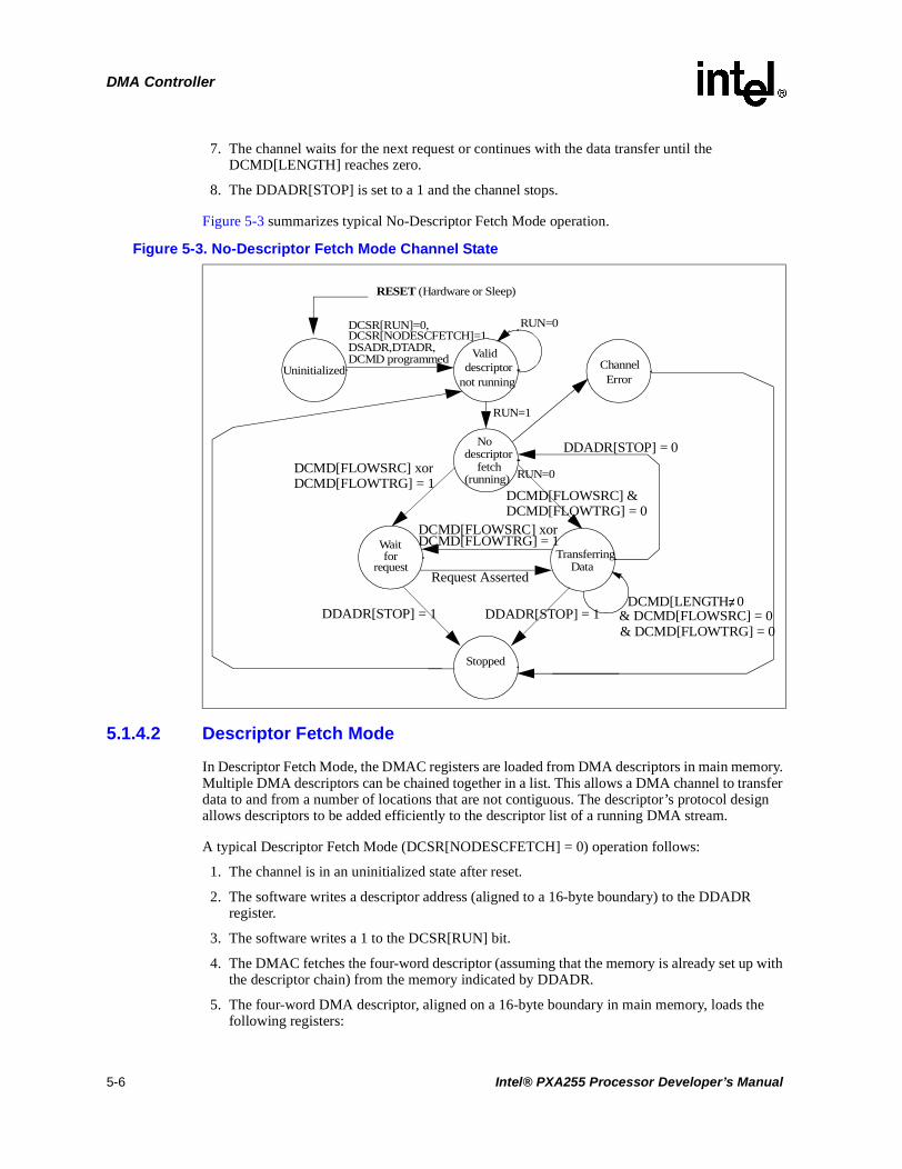
DMA Controller
7. The channel waits for the next request or continues with the data transfer until the DCMD[LENGTH] reaches zero.
8. The DDADR[STOP] is set to a 1 and the channel stops.
Figure 5-3 summarizes typical No-Descriptor Fetch Mode operation.
5.1.4.2 Descriptor Fetch Mode
In Descriptor Fetch Mode, the DMAC registers are loaded from DMA descriptors in main memory. Multiple DMA descriptors can be chained together in a list. This allows a DMA channel to transfer data to and from a number of locations that are not contiguous. The descriptor’s protocol design allows descriptors to be added efficiently to the descriptor list of a running DMA stream.
A typical Descriptor Fetch Mode (DCSR[NODESCFETCH] = 0) operation follows:
1. The channel is in an uninitialized state after reset.
2. The software writes a descriptor address (aligned to a 16-byte boundary) to the DDADR register.
3. The software writes a 1 to the DCSR[RUN] bit.
4. The DMAC fetches the four-word descriptor (assuming that the memory is already set up with the descriptor chain) from the memory indicated by DDADR.
5. The four-word DMA descriptor, aligned on a 16-byte boundary in main memory, loads the following registers:
Figure 5-3. No-Descriptor Fetch Mode Channel State
DCSR[RUN]=0,DCSR[NODESCFETCH]=1,DSADR,DTADR,DCMD programmed
Uninitialized
Valid
RESET (Hardware or Sleep)
not running
(running)
Waitfor
requestTransferring
Data
Stopped
descriptorError
Channel
RUN=1
DCMD[LENGTH] 0& DCMD[FLOWSRC] = 0& DCMD[FLOWTRG] = 0
DDADR[STOP] = 1DDADR[STOP] = 1
DCMD[FLOWSRC] xorDCMD[FLOWTRG] = 1
DCMD[FLOWSRC] &DCMD[FLOWTRG] = 0
Request Asserted
DDADR[STOP] = 0
DCMD[FLOWSRC] xorDCMD[FLOWTRG] = 1
Nodescriptor
fetchRUN=0
RUN=0
≠
5-6 Intel® PXA255 Processor Developer’s Manual

DMA Controller
a. Word [0] -> DDADRx register and a single flag bit. Points to the next four-word descriptor.
b. Word [1] -> DSADRx register for the current transfer.
c. Word [2] -> DTADRx register for the current transfer.
d. Word [3] -> DCMDx register for the current transfer.
6. The channel waits for the request or starts the data transfer, as determined by the DCMD[FLOW] source and target bits.
7. The channel transmits a number of bytes equal to the smaller of DCMD[SIZE] and DCMD[LENGTH].
8. The channel waits for the next request or continues with the data transfer until the DCMD[LENGTH] reaches zero.
9. The channel stops or continues with a new descriptor fetch from the memory, as determined by the DDADR[STOP] bit.
Bit [0] (STOP) of Word [0] in a DMA descriptor (the low bit of the DDADRx field) marks the descriptor at the end of a descriptor list. The value of the STOP bit does not affect the manner in which the channel’s registers load the descriptor’s fields. If a descriptor with its STOP bit set is loaded into a channel's registers, the channel stops after it completely transfers the data that pertains to that descriptor. Figure 5-4 summarizes this operation.
Software must set the DCSR[RUN] bit to 1 after it loads the DDADR. The channel descriptor fetch does not take place unless the DDADR register is loaded and the DCSR[RUN] bit is set to a 1.
The DMAC priority scheme does not affect DMA descriptor fetches. The next descriptor is fetched immediately after the previous descriptor is serviced.
Intel® PXA255 Processor Developer’s Manual 5-7

DMA Controller
5.1.4.3 Servicing an Interrupt
If software receives an interrupt caused by a successful descriptor fetch, i.e. DCSRx[STARTINTR] = 0b1, then software must write a 1 to this bit to reset the corresponding interrupt. Software normally accomplishes this by reading the DCSRx register, modifying the data value by setting the DCSRx[STARTINTR]=0b1 and leaving the DCSRx[RUN] bit set, and then writing this modified value back to the DCSRx. If the channel stops, DCSRx[RUN] = 0b0, before writing this value back to the DCSRx, then software can inadvertently set the DCSRx[RUN] bit before properly configuring other DMA registers. In order to avoid this problem, after writing the modified value back to the DCSRx, software must read the DCSRx and check to see if DCSRx[RUN] and DCSRx[STOPSTATE] are both set. If they are, then software must clear the DCSRx[RUN] bit and re-initialize the DMA channel.
5.1.5 Channel States
A DMA channel can go through any of the following states:
• Uninitialized: Channel is in an uninitialized state after reset.
• Valid Descriptor, Not Running: Software has loaded a descriptor in the DDADR of the channel, in the Descriptor Fetch Mode, or has programmed DSADR, DTADR and DCMD values, in No-Descriptor Fetch Mode, but the corresponding run bit in the DCSR[RUN] register is not set to a 1.
• Descriptor Fetch, Running: Fetching four words of descriptors from the memory.
Figure 5-4. Descriptor Fetch Mode Channel State
Uninitialized
Valid
Descriptor
RESET (Hardware or Sleep)
not running
(running)
Waitfor
requestTransferring
Data
Stopped
descriptor
fetch
ErrorChannel
RUN=1
DCMD[LENGTH] 0& DCMD[FLOWSRC] = 0& DCMD[FLOWTRG] = 0
DDADR[STOP] = 1DDADR[STOP] = 1
DCMD[FLOWSRC] xorDCMD[FLOWTRG] = 1
DCMD[FLOWSRC] &DCMD[FLOWTRG] = 0
Request Asserted
DDADR[STOP] = 0DCMD[FLOWSRC] xorDCMD[FLOWTRG] = 1
RUN=0
≠
5-8 Intel® PXA255 Processor Developer’s Manual

DMA Controller
• Wait for Request: Channel is waiting for a request before it starts to transfer the data.
• Transfer Data: Channel is transferring data.
• Channel Error: Channel has an error. It remains in the stopped state until software clears the error condition, re-initializes the channel, and writes a 1 to the DCSR[RUN] bit. See Section 5.3.1 and Section 5.3.2 for details.
• Stopped: Channel is stopped.
Figure 5-3 and Figure 5-4 show the progression from state to state.
5.1.6 Read and Write Order
The DMAC does not ensure the order of programmed I/O reads and writes made from the processor to the I/O devices (including the on-chip I/O devices). Software must ensure the order.
The DMAC ensures that all memory references made by a single DMA data stream are presented to main memory in the order in which they were made. The descriptor fetches occurs between the data blocks. This allows self-modifying DMA descriptor chains to function correctly (see Example 4 on page 5-27). It also allows schemes in which a DMA stream writes data blocks followed by status blocks and schemes in which another DMA stream (probably from the processor) polls the same field in the status block.
The DMAC ensures that data is not retained in per-channel buffers between descriptors. When a descriptor is completely processed, any read data that is buffered in the channel is discarded and any write data that is buffered in the channel is sent to memory (although it may not be there yet). The DMA interrupt is not posted until the descriptor is completely processed.
5.1.7 Byte Transfer Order
The DCMD[ENDIAN] bit indicates the byte ordering in a word when data is read from or written to memory. Refer to Figure 5-5 for details. The DCMD[ENDIAN bit must be set to 0, which is little endian transfers.
Figure 5-5 shows the order which data is transferred as determined by the DCMD[ENDIAN] and DCMD[SIZE] bits.
If data is being transferred from an internal device to memory, DCMD[ENDIAN] is set to a 0, and DCMD[SIZE] is set to a 1, the memory receives the data in the following order:
1. Byte[0]
2. Byte[1]
3. Byte[2]
4. Byte[3]
Intel® PXA255 Processor Developer’s Manual 5-9

DMA Controller
5.1.8 Trailing Bytes
The DMA normally transfers bytes equal to the transaction size specified by DCMD[SIZE]. As the descriptor nears the end its data, the number of trailing bytes in the DCMD[LENGTH] field may be smaller than the transfer size. The DMA can transfer the exact number of trailing bytes if the DCMD[FLOWSRC] and DCMD[FLOWTRG] bits are both 0 or if it receives a corresponding request from a peripheral or companion chip.
Trailing bytes must be considered in the following cases:
• Memory-to-Memory Moves: The DMA transfers a number bytes equal to the smaller of DCMD[LENGTH] or DCMD[SIZE].
• Companion-Chip Related Transfers: The companion-chip must assert the request if the DMAC must handle the trailing bytes. If the request is asserted, the DMA transfers a number of bytes equal to the smaller of DCMD[LENGTH] or DCMD[SIZE].
• Memory to Internal Peripheral Transfers: Most peripherals send a request for trailing bytes during memory to internal peripheral transfers. Refer to the appropriate section in this document for details of a peripheral’s operation. The DMA transfers bytes equal to the smaller of DCMD[LENGTH] or DCMD[SIZE].
Figure 5-5. Little Endian Transfers
D[31] D[0]from memory3 2 1 0
DMAC
FromToToFrom
3
2
1
0 3
2
1
0
1 0
1 0
3 2
3 2
Half-Word WideDevice
Byte WideDevice
Little Endian DMA Transfers
3 2 1 0
To/From
Word WideDevice
5-10 Intel® PXA255 Processor Developer’s Manual

DMA Controller
• Internal Peripheral to Memory Transfers: Most peripherals do not send a request for trailing bytes for on-chip peripheral to memory transfers. Refer to the appropriate section in this document for details of a peripheral’s operation. If the peripheral sends out a request, the DMA transfers the number of bytes equal to the smaller of DCMD[LENGTH] or DCMD[SIZE]. If software must us programmed I/O to handle the trailing bytes, it must follow this sequence of operation:
1. Writing a 0 to the DCSR[RUN] bit to stop the DMA channel.
2. Wait until the channel to stops.
3. Make reads to the channel’s registers to check the channel’s status.
4. Perform the programmed I/O transfers to the peripheral.
5. Set the DCSR[RUN] bit to a 1 and reset the DMA channel for future data transfers.
5.2 Transferring Data
The internal peripherals are connected to the DMAC via the peripheral bus and use flow-through data transfers. The DMAC can also transfer data to and from any memory location with memory-to-memory moves in flow-through transfer mode. External devices, such as companion chips, that are directly connected to the external data pins must use flow-through data transfers.
Main memory includes any memory that the processor supports, except writes to flash. Writes to flash are not supported and cause a bus error.
In flow-through transfer mode, data passes through the DMAC before it is latched by the destination in its buffers/memory. The DMAC can also perform memory-to-memory moves in flow-through transfer mode.
5.2.1 Servicing Internal Peripherals
The DMAC provides the DMA Request to Channel Map Registers (DRCMRx) that contain four bits used to assign a channel number for each possible DMA request. An internal peripheral can be mapped to any of the 16 available channels. See Table 5-5 to configure the internal peripherals for DMA accesses. Internal peripherals assert the request bit through the peripheral request bus (PREQ). The signals from the PREQ are sampled on every peripheral clock (PCLK) and if any of the PREQ signals are not zeroes, a lookup is performed on the corresponding bits of the DRCMRx. This allows the request to be mapped to one of the channels.
If the internal peripheral address is in the DSADR, the DCMDx[FLOWSRC] bit must be set to a 1. This allows the processor to wait for the request before it initiates the transfer. If the internal peripheral address is in the DTADR, the DCMDx[FLOWTRG] bit must be set to a 1.
If DCMDx[IRQEN] is set to a 1, a DMA interrupt is requested at the end of the last cycle associated with the byte that caused DCMDx[LENGTH] to decrement to 0.
Intel® PXA255 Processor Developer’s Manual 5-11
DMA Controller
5.2.1.1 Using Flow-Through DMA Read Cycles to Service Internal Peripherals
A flow-through DMA read for an internal peripheral begins when the internal peripheral sends a request, via the PREQ bus, to a DMAC channel that is running and configured for a flow-through read. The number of bytes to be transferred is specified with DCMDx[SIZE]. When the request is the highest priority request, the following process begins:
1. The DMAC sends the memory controller a request to read the number of bytes addressed by DSADRx[31:0] into a 32-byte staging buffer in the DMAC.
2. The DMAC transfers the data to the I/O device addressed in DTADRx[31:0]. DCMD[WIDTH] specifies the width of the internal peripheral to which the data is transferred.
3. At the end of the transfer, DSADRx is increased by the smaller value of DCMDx[LENGTH] and DCMD[SIZE]. DCMDx[LENGTH] is decreased by the same value.
For a flow-through DMA read to an internal peripheral, use the following settings for the DMAC register bits:
• DSADR[SRCADDR] = external memory address
• DTADR[TRGADDR] = internal peripheral’s address
• DCMD[INCSRCADDR] = 1
• DCMD[FLOWSRC] = 0
• DCMD[FLOWTRG] = 1
5.2.1.2 Using Flow-Through DMA Write Cycles to Service Internal Peripherals
A flow-through DMA write for an internal peripheral begins when the internal peripheral sends a request, via the PREQ bus, to a DMAC channel that is running and configured for a flow-through write. The number of bytes to be transferred are specified with DCMDx[SIZE]. When the request is the highest priority request, the following process begins:
1. The DMAC transfers the required number of bytes from the I/O device addressed by DSADRx[31:0] to the DMAC write buffer.
2. The DMAC transfers the data to the memory controller via the internal bus. DCMD[WIDTH] specifies the width of the internal peripheral to which the transfer is being made.
3. At the end of the transfer, DTADRx is increased by the smaller value of DCMDx[LENGTH] and DCMD[SIZE]. DCMDx[LENGTH] is decreased by the same number.
For a flow-through DMA write to an internal peripheral, use the following settings for the DMAC register bits:
• DSADR[SRCADDR] = internal peripheral address
• DTADR[TRGADDR] = external memory address
• DCMD[INCTRGADDR] = 1
• DCMD[FLOWSRC] = 1
• DCMD[FLOWTRG] = 0
5-12 Intel® PXA255 Processor Developer’s Manual

DMA Controller
5.2.2 Quick Reference for DMA Programming
Use Table 5-5 as a quick reference sheet for programming the DMA.
Table 5-5. DMA Quick Reference for Internal Peripherals (Sheet 1 of 2)
Unit Function FIFO Address Width (bytes)
DCMD.Width
(binary)
Burst Size (bytes)
Sourceor
TargetDRCMR
I2Sreceive 0x4040_0080 4 11 8, 16, 32 Source 0x4000_0108
transmit 0x4040_0080 4 11 8, 16, 32 Target 0x4000_010c
BTUART
receive 0x4020_0000 1 01 8, 16, 32 Source 0x4000_0110
transmit 0x4020_0000 1 01 8, 16, 32 or trailing Target 0x4000_0114
FFUART
receive 0x4010_0000 1 01 8, 16, 32 Source 0x4000_0118
transmit 0x4010_0000 1 018, 16, 32 or
trailing Target 0x4000_011c
AC97
microphone 0x4050_0060 4 11 8, 16, 32 Source 0x4000_0120
modem receive 0x4050_0140 4 11 8, 16, 32 Source 0x4000_0124
modem transmit 0x4050_0140 4 11 8, 16, 32 Target 0x4000_0128
audio receive 0x4050_0040 4 11 8, 16, 32 Source 0x4000_012c
audio transmit 0x4050_0040 4 11 8, 16, 32 Target 0x4000_0130
SSPreceive 0x4100_0010 2 10 8, 16 Source 0x4000_0134
transmit 0x4100_0010 2 10 8, 16 Target 0x4000_0138
FICP
receive 0x4080_000C 1 01 8, 16, 32 Source 0x4000_0144
transmit 0x4080_000C 1 01 8, 16, 32 or trailing
Target 0x4000_0148
STUART
receive 0x4070_0000 1 01 8, 16, 32 Source 0x4000_014c
transmit 0x4070_0000 1 018, 16, 32, or
trailing Target 0x4000_0150
MMCreceive 0x4110_0040 1 01 32 or trailing Source 0x4000_0154
transmit 0x4110_0044 1 01 32 or trailing Target 0x4000_0158
Intel® PXA255 Processor Developer’s Manual 5-13

DMA Controller
5.2.3 Servicing Companion Chips and External Peripherals
Companion chips and external peripherals can be serviced with flow-through transfers. The DMAC provides DMA Request to Channel Map Registers (DRCMRx) that contain four bits that assign a channel number for each of the possible DMA requests. The companion-chip requests are DREQ[1:0]. The DREQ signal can be mapped to one of the 16 available channels. The DREQ signals are sampled on every peripheral clock (PCLK) and if any of the DREQ signals are sampled non-zero, a lookup is performed on the corresponding bits in the DRCMRx. This allows requests to one of the channels to be mapped. If the external peripheral address is in the DSADR, the DCMDx[FLOWSRC] bit must be set to a 1. If the external peripheral address is in the DTADR, the DCMDx[FLOWTRG] bit must be set to a 1. This allows the processor to wait for the request before it initiates the transfer.
If DCMDx[IRQEN] is set to a 1, a DMA interrupt can be requested at the end of the last cycle associated with the byte that caused DCMDx[LENGTH] to decrease from a 1 to a 0.
USB
endpoint 1 transmit 0x4060_0100 1 01 32 Target 0x4000_0164
endpoint 2 receive 0x4060_0180 1 01 32 Source 0x4000_0168
endpoint 3 transmit
0x4060_0200 1 01 32 Target 0x4000_016C
endpoint 4 receive 0x4060_0400 1 01 32 Source 0x4000_0170
endpoint 6 transmit 0x4060_0600 1 01 32 Target 0x4000_0178
endpoint 7 receive
0x4060_0680 1 01 32 Source 0x4000_017C
endpoint 8 transmit 0x4060_0700 1 01 32 Target 0x4000_0180
endpoint 9 receive 0x4060_0900 1 01 32 Source 0x4000_0184
endpoint 11 transmit 0x4060_0B00 1 01 32 Target 0x4000_018C
endpoint 12 receive 0x4060_0B80 1 01 32 Source 0x4000_0190
endpoint 13 transmit 0x4060_0C00 1 01 32 Target 0x4000_0194
endpoint 14 receive 0x4060_0E00 1 01 32 Source 0x4000_0198
Table 5-5. DMA Quick Reference for Internal Peripherals (Sheet 2 of 2)
Unit Function FIFO Address Width (bytes)
DCMD.Width
(binary)
Burst Size (bytes)
Sourceor
TargetDRCMR
5-14 Intel® PXA255 Processor Developer’s Manual

DMA Controller
5.2.3.1 Using Flow-Through DMA Read Cycles to Service External Peripherals
A flow-through DMA read for an external peripheral begins when the external peripheral sends a request, via the DREQ[1:0] bus, to a DMAC channel that is running and configured for a flow-through read. DCMDx[SIZE] specifies the number of bytes to be transferred. When the request is the highest priority request, the follow process begins.
1. The DMAC sends a request to the memory controller to read the number of bytes addressed by DSADRx[31:0] into a 32-byte staging buffer in the DMAC.
2. The DMAC transfers the data in the buffer to the external device addressed in DTADRx[31:0].
3. At the end of the transfer, DSADRx is increased by the smaller value of DCMDx[LENGTH] and DCMD[SIZE]. DCMDx[LENGTH] is decreased by the same value.
Note: The process shown for a flow-through DMA read to an external peripheral indicates that the external address increases. Some external peripherals, such as FIFOs, do not require an increment in the external address.
For a flow-through DMA read to an external peripheral, use the following settings for the DMAC register bits:
• DSADR[SRCADDR] = external memory address
• DTADR[TRGADDR] = companion chip’s address
• DCMD[INCSRCADDR] = 1
• DCMD[INCTRGADDR] = 0
• DCMD[FLOWSRC] = 0
• DCMD[FLOWTRG] = 1
5.2.3.2 Using Flow-Through DMA Write Cycles to Service External Peripherals
A flow-through DMA write to an external peripheral begins when the external peripheral sends a request, via the DREQ bus, to a DMAC channel that is running and configured for a flow-through write. DCMDx[SIZE] specifies the number of bytes to be transferred. When the request is the highest priority request, the following process begins:
1. The DMAC transfers the required number of bytes from the I/O device addressed by DSADRx[31:0] to the DMAC write buffer.
2. The DMAC transfers the data to the memory controller via the internal bus.
3. At the end of the transfer, DTADRx is increased by the smaller value of DCMDx[LENGTH] and DCMD[SIZE]. DCMDx[LENGTH] is decreased by the same number.
Note: The process shown for a flow-through DMA write to an external peripheral indicates that the external address increases. Some external peripherals, such as FIFOs, do not require an increment in the external address.
Intel® PXA255 Processor Developer’s Manual 5-15

DMA Controller
For a flow-through DMA write to an external peripheral, use the following settings for the DMAC register bits:
• DSADR[SRCADDR] = companion chip address
• DTADR[TRGADDR] = external memory address.
• DCMD[INCSRCADDR] = 0
• DCMD[INCTRGADDR] = 1
• DCMD[FLOWSRC] = 1
• DCMD[FLOWTRG] = 0
5.2.4 Memory-to-Memory Moves
Memory-to-memory moves do not involve the DREQ and PREQ request signals. The processor writes to the DCSR[RUN] bit and a channel is configured for a memory-to-memory move. The DCMDx[FLOWSRC] and the DCMD[FLOWTRG] bits must be set to 0.
If DCMD[IRQEN] is set to a 1, a DMA interrupt is requested at the end of the last cycle associated with the byte that caused DCMDx[LENGTH] to decrease from 1 to 0.
A flow-through DMA memory-to-memory read or write goes through these steps:
1. The processor writes to the DCSR[RUN] register bit and starts the memory-to-memory moves.
2. If the processor is in the Descriptor Fetch Mode, the channel configured for the move fetches the four-word descriptor. The channel transfers data without waiting for PREQ or DREQ to be asserted. The smaller value of DCMDx[SIZE] or DCMDx[LENGTH] specifies the number of bytes to be transferred.
3. The DMAC sends a request to the memory controller to read the number of bytes addressed by DSADRx[31:0] into a 32-byte staging buffer in the DMAC.
4. The DMAC generates a write cycle to the location addressed in DTADRx[31:0].
5. At the end of the transfer, DSADRx and DTADRx are increased by the smaller value of DCMD[SIZE] and DCMDx[LENGTH]. If DCMD[SIZE] is smaller than DCMDx[LENGTH], DCMDx[LENGTH] is decreased by DCMD[SIZE]. If DCMD[SIZE] is equal to or larger than DCMDx[LENGTH], DCMDx[LENGTH] is zero.
Note: The process shown for a memory-to-memory transfer indicates that the external address increases. Some external peripherals, such as FIFOs, do not require an increment in the external address.
For a memory-to-memory read or write, use these settings for the DMAC registers:
• DSADR[SRCADDR] = external memory address
• DTADR[TRGADDR] = external memory address
• DCMD[INCSRCADDR] = 1
• DCMD[INCTRGADDR] = 1
• DCMD[FLOWSRC] = 0
• DCMD[FLOWTRG] = 0
• DCSR[RUN] =1
5-16 Intel® PXA255 Processor Developer’s Manual

DMA Controller
5.3 DMAC Registers
The section describes the DMAC registers.
5.3.1 DMA Interrupt Register (DINT)
The DINT, shown in Table 5-6, logs the interrupts for each channel.
An interrupt is generated if any of these events occur:
• Any kind of transaction error on the internal bus that is associated with the relevant channel.
• The current transfer finishes successfully and the DCMD[ENDIRQEN] bit is set.
• The current descriptor loads successfully and the DCMD[STARTIRQEN] bit is set.
• The DCSR:STOPIRQEN is set to a 1 and the relevant channel is in the uninitialized or stopped state.
Software must set the corresponding DCSR register error bit to reset the interrupt.
This is a read/write register. Ignore reads from reserved bits. Write zeros to reserved bits.
5.3.2 DMA Channel Control/Status Register (DCSRx)
The DCSRx, shown in Table 5-7 contains the control and status bit for each channel. Read this register to find the source of an interrupt. Write the read value back to the register to clear the interrupt.
This is a read/write register. Ignore reads from reserved bits. Write zeros to reserved bits.
Table 5-6. DINT Bit Definitions
Physical Address0x4000_00F0 DMA Interrupt Register (DINT) DMA Controller
Bit 31 30 29 28 27 26 25 24 23 22 21 20 19 18 17 16 15 14 13 12 11 10 9 8 7 6 5 4 3 2 1 0
reserved
Ch
lIntr
15
Ch
lIntr
14
Ch
lIntr
13
Ch
lIntr
12
Ch
lIntr
11
Ch
lIntr
10
Ch
lIntr
9
Ch
lIntr
8
Ch
lIntr
7
Ch
lIntr
6
Ch
lIntr
5
Ch
lIntr
4
Ch
lIntr
3
Ch
lIntr
2
Ch
lIntr
1
Ch
lIntr
0
Reset 0 0 0 0 0 0 0 0 0 0 0 0 0 0 0 0 0 0 0 0 0 0 0 0 0 0 0 0 0 0 0 0
Bits Name Description
31:16 — reserved
15:0 CHLINTRxChannel ‘x’ Interrupt (read-only).
0 – No interrupt1 – Interrupt
Intel® PXA255 Processor Developer’s Manual 5-17

DMA Controller
Table 5-7. DCSRx Bit Definitions (Sheet 1 of 2)
Physical Address0x4000_0000 - 0x4000_003C
DMA Channel Control/Status Register (DCSRx) DMA Controller
Bit 31 30 29 28 27 26 25 24 23 22 21 20 19 18 17 16 15 14 13 12 11 10 9 8 7 6 5 4 3 2 1 0
RU
N
NO
DE
SC
FE
TC
H
ST
OP
IRQ
EN
reserved
RE
QP
EN
D
reserved
STO
PS
TAT
E
EN
DIN
TR
STA
RT
INT
R
BU
SE
RR
INT
R
Reset 0 0 0 0 0 0 0 0 0 0 0 0 0 0 0 0 0 0 0 0 0 0 0 0 0 0 0 0 1 0 0 0
Bits Name Description
31 RUN
Run Bit (read / write).
0 – stops the channel1 – starts the channel
Lets software start or stop the channel. If the run bit is cleared in the middle of the burst, the burst will complete before the channel is stopped.
Software must write to DDADRx before it sets this bit for Descriptor Fetch Mode.
After the channel stops, the DCSR[STOPSTATE] bit is set to 1. Software must poll the DCSR[STOPSTATE] bit to determine the channel’s status or set the STOPIRQEN to force an interrupt after the channel stops. Software must write a 1 to the bit to restart a stopped channel.
After clearing the run bit to stop the channel, an end interrupt is not guaranteed to happen if the length bits, DCMDx[LENGTH], is zero. Software must determine if the transfer is done after clearing the run bit.
30NODESC
FETCH
No-Descriptor Fetch (read / write).
0 – Descriptor Fetch Mode1 – No-Descriptor Fetch Mode
Determines if the channel has a descriptor.
If this bit is set to a 0, the channel is in Descriptor Fetch Mode. See Section 5.1.4.2 for information on the DMAC registers.
If this bit is set to a 1, the channel is in No-Descriptor Fetch Mode. See Section 5.1.4.1 for information on the DMAC registers.
29 STOPIRQEN
Stop Interrupt Enable (read / write).
0 – no interrupt if the channel is in uninitialized or stopped state 1 – enables an interrupt if the channel is in uninitialized or stopped state
Allows an interrupt to pass to the interrupt controller if the DCSR[STOPSTATE] bit is 1. If the DCSR[STOPINTEN] bit is 0, the interrupt is not generated after the channel stops. If software writes a 1 to this bit before the channel starts, an interrupt is generated.
28:9 — reserved
8 REQPEND
Request Pending (read-only).
0 – no pending request1 – the channel has a pending request
Indicates that the DMA channel has a pending request.
7:4 — reserved
5-18 Intel® PXA255 Processor Developer’s Manual

DMA Controller
3 STOPSTATE
Stop State (read-only).
0 – channel is running1 – channel is in uninitialized or stopped state.
If the channel is in the uninitialized or stopped state, this status bit is set. If the DCSR[STOPIRQEN] is set to 1, the DMAC generates an interrupt. Channel States are described in Section 5.1.5.
Software must reprogram the DDADRx and write a 1 to the DCSR[RUN] bit to restart the channel and clear this bit.
Software must write a 0 to the DCSR[STOPIRQEN] bit to reset the interrupt
2 ENDINTR
End Interrupt (read / write).
0 – no interrupt1 – interrupt caused because the current transaction was successfully completed and
DCMD[LENGTH] = 0.
DCMD[ENDIRQEN] bit must be set for an interrupt to occur. Software must write a 1 to this bit to reset the corresponding interrupt. Writing a 0 to this bit has no effect.
1 STARTINTR
Start Interrupt (read / write).
0 – no interrupt1 – interrupt caused due to successful descriptor fetch
DCMD[STARTIRQEN] bit must be set for an interrupt to occur. Software must write a 1 to this bit to reset the corresponding interrupt. Writing a 0 to this bit has no effect.
0BUSERR
INTR
Bus Error Interrupt (read / write).
0 – no interrupt1 – bus error caused interrupt
Indicates that there was an error while transferring data. An error during data transfer occurs when the channel has a bad descriptor, source, or target address. An address is considered bad when it points to a non-busable location or reserved space. Software must write a 1 to this bit to reset the corresponding interrupt. Writing a 0 to this bit has no effect. Only one error incidence per channel is logged. The channel that caused the error is updated at the end of the transfer and is accessible after it logs an error until it is reprogrammed and the corresponding run bit is set.
Table 5-7. DCSRx Bit Definitions (Sheet 2 of 2)
Physical Address0x4000_0000 - 0x4000_003C
DMA Channel Control/Status Register (DCSRx) DMA Controller
Bit 31 30 29 28 27 26 25 24 23 22 21 20 19 18 17 16 15 14 13 12 11 10 9 8 7 6 5 4 3 2 1 0
RU
N
NO
DE
SC
FE
TC
H
ST
OP
IRQ
EN
reserved
RE
QP
EN
D
reserved
ST
OP
STA
TE
EN
DIN
TR
STA
RT
INT
R
BU
SE
RR
INT
R
Reset 0 0 0 0 0 0 0 0 0 0 0 0 0 0 0 0 0 0 0 0 0 0 0 0 0 0 0 0 1 0 0 0
Bits Name Description
Intel® PXA255 Processor Developer’s Manual 5-19

DMA Controller
5.3.3 DMA Request to Channel Map Registers (DRCMRx)
DRCMRx, shown in Table 5-8, map each DMA request to a channel. Refer to Table 5-13 for details.
This is a read/write register. Ignore reads from reserved bits. Write zeros to reserved bits.
5.3.4 DMA Descriptor Address Registers (DDADRx)
The DDADRx) (see Table 5-9) contain the memory address of the next descriptor for a specific channel. On power up, the bits in this register are undefined. The address must be aligned to a 16-byte boundary. This means that bits [3:1] of the address are reserved and must be read and written as zeroes. DDADR must not contain the address of any other internal peripheral register or DMA register.
DDADR is reserved if the channel is No-Descriptor Fetch Mode.
Table 5-8. DRCMRx Bit Definitions
Physical Address0x4000_0100 - 0x4000_019C
DMA Request to Channel Map Register (DRCMRx) DMA Controller
Bit 31 30 29 28 27 26 25 24 23 22 21 20 19 18 17 16 15 14 13 12 11 10 9 8 7 6 5 4 3 2 1 0
reserved
MA
PV
LD
rese
rved
CHLNUM
Reset 0 0 0 0 0 0 0 0 0 0 0 0 0 0 0 0 0 0 0 0 0 0 0 0 0 0 0 0 0 0 0 0
Bits Name Description
31:8 — reserved
7 MAPVLD
Map Valid (read / write).
0 – Request is unmapped1 – Request is mapped to a channel indicated by DRCMRx[3:0]
Determines whether the request is mapped to a channel or not. If the bit is set to a 1, the request is mapped to a channel indicated in DRCMRx[3:0]. If the bit is 0, the request is unmapped. This bit can also be used to mask the request.
6:4 — reserved
3:0 CHLNUM
Channel Number (read / write).
Indicates the channel number if DRCMR[MAPVLD] is set to a 1.
Do not map two active requests to the same channel. It produces unpredictable results. Refer to Section 5.1.3 to review the channel priority scheme.
5-20 Intel® PXA255 Processor Developer’s Manual

DMA Controller
5.3.5 DMA Source Address Registers
DSADRx, shown in Table 5-10, are read only in the Descriptor Fetch Mode and are read/write in the No-Descriptor Fetch Mode.
DSADRx contains the Source Address for the current descriptor of a specific channel. The Source Address is the address of the internal peripheral or a memory location. On power up, the bits in this register are undefined. If the Source Address is the address of a companion chip or external peripheral, the source address must be aligned to an 8-byte boundary. This allows bits [2:0] of the address to be reserved. If the source address is the address for an internal peripheral, the address must be 32-bit aligned, so bits [1:0] are reserved. DSADR cannot contain the address of any other internal DMA, LCD, or MEMC registers.
This is a read/write register. Ignore reads from reserved bits. Write zeros to reserved bits.
Table 5-9. DDADRx Bit Definitions
0x4000_02x0 DMA Descriptor Address Register (DDADRx) DMA Controller
Bit 31 30 29 28 27 26 25 24 23 22 21 20 19 18 17 16 15 14 13 12 11 10 9 8 7 6 5 4 3 2 1 0
DESCRIPTOR ADDRESS reserved
STO
P
Reset Uninitialized 0
Bits Name Description
31:4 DESCRIPTOR ADDRESS Address of next descriptor (read / write).
3:1 — reserved
0 STOP
Stop (read / write).
0 – Run channel.1 – Stop channel after completely processing this descriptor and before fetching the next
descriptor, i.e., DCMD[LENGTH]= 0.
If this bit is set, the channel to stops after it completely processes the descriptor and before it fetches the next descriptor. If the DDADRx[STOP] bit is 0, a new descriptor fetch based on the DDADR starts when the current descriptor is completely processed.
Intel® PXA255 Processor Developer’s Manual 5-21

DMA Controller
5.3.6 DMA Target Address Registers (DTADRx)
To software, DTADRx (Table 5-11) is read only in the Descriptor Fetch Mode and is read/write in the No-Descriptor Fetch Mode.
These registers contain the target address for the current descriptor in a channel. The target address is the address of an internal peripheral or a memory location. On power up, the bits in this register are undefined. If the target address is the address of a companion chip or external peripheral, the target address must be aligned to an 8-byte boundary. This allows bits [2:0] of the address to be reserved. If the target address is the address for an internal peripheral, the address must be 32-bit aligned so that bits [1:0] are reserved. DTADRx must not contain the address of any other internal DMA, LCD, or MEMC register.
The DTADRx must not contain a flash address because writes to flash from the DMAC are not supported.
This is a read/write register. Ignore reads from reserved bits. Write zeros to reserved bits.
Table 5-10. DSADRx Bit Definitions
0x4000_02x4 DMA Source Addr Register (DSADRx) DMA Controller
Bit 31 30 29 28 27 26 25 24 23 22 21 20 19 18 17 16 15 14 13 12 11 10 9 8 7 6 5 4 3 2 1 0
SOURCE ADDRESS
rese
rved
Reset Uninitialized
Bits Name Description
31:3 SRCADDR
Source Address (read / write).
Address of the internal peripheral or address of a memory location.
Address of a memory location for companion -chip transfer
2 SRCADDR
Source Address Bit 2
Reserved if DSADR.SrcAddr is an external memory location
Not reserved if DSADR.SrcAddr is an internal peripheral (read / write).
1:0 — reserved
5-22 Intel® PXA255 Processor Developer’s Manual

DMA Controller
5.3.7 DMA Command Registers (DCMDx)
For software, DCMDx (Table 5-12) is read only in Descriptor Fetch Mode and is read/write in No-Descriptor Fetch Mode.
These registers contain the channel’s control bits and the length of the current transfer in that channel. On power up, the bits in this register are set to 0.
This is a read/write register. Ignore reads from reserved bits. Write zeros to reserved bits.
Table 5-11. DTADRx Bit Definitions
0x4000_02x8 DMA Target Addr Register (DTADRx) DMA Controller
Bit 31 30 29 28 27 26 25 24 23 22 21 20 19 18 17 16 15 14 13 12 11 10 9 8 7 6 5 4 3 2 1 0
TARGET ADDRESS
rese
rved
Reset Uninitialized
Bits Name Description
31:3 TRGADDR
Target Address (read / write):
Address of the on chip peripheral or the address of a memory location
Address of a memory location for companion chip transfer
2 TRGADDR
Target Address Bit 2
Reserved if DTADR.TrgAddr is an external memory location
Not reserved if DTADR.trgAddr is an internal peripheral (read / write).
1:0 — reserved
Intel® PXA255 Processor Developer’s Manual 5-23

DMA Controller
Table 5-12. DCMDx Bit Definitions (Sheet 1 of 2)
0x4000_02xC DMA Command Register (DCMDx) DMA Controller
Bit 31 30 29 28 27 26 25 24 23 22 21 20 19 18 17 16 15 14 13 12 11 10 9 8 7 6 5 4 3 2 1 0
INC
SR
CA
DD
R
INC
TR
GA
DD
R
FL
OW
SR
C
FL
OW
TR
G
reserved
STA
RT
IRQ
EN
EN
DIR
QE
N
rese
rved
EN
DIA
N
SIZ
E
WID
TH
rese
rved
LENGTH
Reset 0 0 0 0 0 0 0 0 0 0 0 0 0 0 0 0 0 0 0 0 0 0 0 0 0 0 0 0 0 0 0 0
Bits Name Description
31 INCSRCADDR
Source Address Increment Setting. (read / write).
0 – Do not increment Source Address1 – Increment Source Address at the end of each internal bus transaction initiation by
DCMD[SIZE]
If the source address is an internal peripheral’s FIFO address or external IO address, the address is not incremented on each successive access. In this case, this bit must be 0.
30 INCTRGADDR
Target Address Increment Setting. (read / write).
0 – Do not increment Target Address1 – Increment Target Address at the end of each internal bus transaction initiated by
DCMD[SIZE]
If the target address is an internal peripheral’s FIFO address or external IO address, the address is incremented on each successive access. In this cases the bit must be 0.
29 FLOWSRC
Flow Control by the source. (read / write).
0 – Start the data transfer immediately.1 – Wait for a request signal before initiating the data transfer.
Indicates the flow control of the source. This bit must be ‘1’ if the source is an onchip or external peripheral.
If either the DCMD[FLOWSRC] or DCMD[FLOWTRG] bit is set, the current DMA does not initiate a transfer until it receives a request. Do not set both the DCMD[FLOWTRG] and DCMD[FLOWSRC] bit to1.
28 FLOWTRG
Flow Control by the target. (read / write).
0 – Start the data transfer immediately.1 – Wait for a request signal before initiating the data transfer.
Indicates the Flow Control of the target. This bit must be ‘1’ if the target is an onchip or external peripheral.
If either the DCMD[FLOWSRC] or DCMD[FLOWTRG] bit is set, the current DMA does not initiate a transfer until it receives a request. Do not set both the DCMD[FLOWTRG] and DCMD[FLOWSRC] bit to 1.
27:23 — reserved
22 STARTIRQEN
Start Interrupt Enable (read / write), Reserved for the No-Descriptor Fetch Mode
0 – no interrupt is generated.1 – Allow interrupt to pass when the descriptor (i.e., 4 words) for the channel are loaded.
Sets DCSR[StartIntr] interrupt for the channel when this descriptor is loaded.
21 ENDIRQEN
End Interrupt Enable (read / write).
0 – no interrupt is generated.1 – set DCSR[EndIntr] interrupt for the channel when DCMD[LENGTH] is decreased to
zero.
Indicates that the interrupt is enabled as soon as the data transfer is completed.
20:19 — reserved
5-24 Intel® PXA255 Processor Developer’s Manual

DMA Controller
18 ENDIANDevice Endian-ness. (read / write).
0 – Byte ordering is little endian1 – reserved
17:16 SIZE
Maximum Burst Size of each data transferred (read / write).
00 – reserved
01 – 8 Bytes
10 – 16 Bytes
11 – 32 Bytes
If DCMDx[LENGTH] is less than DCMDx[SIZE] the data transfer size equals DCMDx[LENGTH].
15:14 WIDTH
Width of the on-chip peripheral. (read / write/).
00 – reserved
01 – 1 byte
10 – HalfWord (2 bytes)
11 – Word (4 Bytes)
Must be programmed 00 for memory-to-memory moves or companion-chip related operations.
13 — reserved
12:0 LENGTH
Length of transfer in bytes. (read / write).
Indicates the length of transfer in bytes. DCMD[LENGTH] = 0 means zero bytes for Descriptor Fetch Mode only. DCMD[LENGTH] = 0 is an invalid setting for the No-Descriptor Fetch Mode. The maximum transfer length is (8K-1) bytes. If the transfer involves any of the internal peripherals, the length of the transfer must be an integer multiple of the width of that peripheral.
Table 5-12. DCMDx Bit Definitions (Sheet 2 of 2)
0x4000_02xC DMA Command Register (DCMDx) DMA Controller
Bit 31 30 29 28 27 26 25 24 23 22 21 20 19 18 17 16 15 14 13 12 11 10 9 8 7 6 5 4 3 2 1 0
INC
SR
CA
DD
R
INC
TR
GA
DD
R
FL
OW
SR
C
FL
OW
TR
G
reserved
STA
RT
IRQ
EN
EN
DIR
QE
N
rese
rved
EN
DIA
N
SIZ
E
WID
TH
rese
rved
LENGTH
Reset 0 0 0 0 0 0 0 0 0 0 0 0 0 0 0 0 0 0 0 0 0 0 0 0 0 0 0 0 0 0 0 0
Bits Name Description
Intel® PXA255 Processor Developer’s Manual 5-25

DMA Controller
5.4 Examples
This section contains examples that show how to:
• Set up and start a channel
• Initialize a descriptor list for a channel that is running
• Add a descriptor to the end of a descriptor list for a channel that is running
• Initialize a channel that is going to be used by a direct DMA master
Example 1. How to set up and start a channel:
The following example shows how to set up a channel to transfer LENGTH words from the address DSADR to the I/O address DTADR. The example also shows how to start the transfer. The example sets the stop bit in the DDADR, so the DMA channel stops after it completely transfers LENGTH bytes of data.
// build real descriptor
desc[0].ddadr = STOP
desc[0].dsadr = DSADR
desc[0].dtadr = DTADR
desc[0].dcmd = DCMD
// start the channel
DMANEXT[CHAN] = &desc[0]
DRUN = 1
Example 2. How to initialize a descriptor list for a channel that is running:
// Allocate a new descriptor, and make it an end
// descriptor whose “ddadr” field points back at itself
newDesc = New Desc()
newDesc->ddadr = newDesc | STOP
// make it a zero length descriptor
newDesc->dcmd = ZERO
// Start the channel
DMANEXT[CHAN] = newDesc
DRUN = 1
The channel starts, loads the descriptor in its registers, and stops because the transfer length is 0 and the STOP bit is set. No data is transferred in this example. The channel can be restarted by writing to its DDADR and writing a 1 to the DCSR[RUN] bit.
Example 3. How to add a descriptor to the end of a descriptor list for a channel that is running:
The example in this section assumes that the Descriptor Fetch Mode is active.
DMA descriptor lists are used as queues of full buffers for network transmitters and as queues of empty buffers for network receivers. Because the buffers in a queue are often small (in particular, as small as an ATM cell), on-the-fly DMA descriptor lists manipulation must be efficient.
1. Write a 0 to DCSR[RUN].
2. Wait until the channel stops. The channel stop state is reflected in the DCSR:STOPSTATE bit.
5-26 Intel® PXA255 Processor Developer’s Manual

DMA Controller
3. In memory, create the descriptor to be added and set its stop bit to a 1.
4. In the memory, manipulate the DDADR of the current chain’s last descriptor such that its DDADR points to the descriptor created in Step 3.
5. In the memory, create a new descriptor that has the same DDADR, DSADR, DTADR, and CMD as those of the stopped DMA channel. The new descriptor is the next descriptor for the list.
6. Examine the DMA channel registers and determine if the channel stopped in the chain’s last descriptor of the chain. If it did, manipulate the DDADR of the last descriptor in the memory so that its DDADR points to the descriptor created in Step 3. Otherwise, continue to Step 7.
7. Program the channel’s DDADR with the descriptor created in Step 5.
8. Set the DCSR[RUN] to a 1.
Example 4. How to initialize a channel that is going to be used by a direct DMA master:
The most efficient way to move data between an I/O device and main memory is the processor’s descriptor-based DMA system. Each application has different requirements, so a descriptor-based DMA may be best for some applications while a non-descriptor-based DMA is best for others. For applications that can not tolerate the time needed to fetch a descriptor before each DMA transfer, choose the non descriptor-based DMA method. For applications that can tolerate it, a descriptor-based DMA method can reduce the amount of core intervention.
Self–Modifying Descriptors: The descriptor-based DMA system can be used to provide true direct memory access to devices that require it.
In this example, a companion chip has these requirements:
1. When the companion chip asserts DREQ from 0 to 1, the DMA must fetch four words of the descriptor from one of the chip’s ports.
2. Based on the information contained in the four descriptor words, the DMA must transfer data from the source address to the destination address without waiting for another request from the companion chip.
3. After it transfers the number of bytes in DCMD:LENGTH, the DMA returns to Step 1.
An external device with these requirements can use a constant descriptor in memory.
struct longddadr;
longdsadr;
longdtadr;
shortlength;
shortdcmd;
desc[2];
desc[0].ddadr = &desc[1]
desc[0].dsadr = I_ADR + I_DESC_OFFS
desc[0].dtadr = &desc[1].dsadr
desc[0].length = 8;
desc[0].dcmd = CMD_IncTrgAdr | CMD_FlowThru;
desc[1].ddadr = &desc[0]
desc[1].dtadr = I_ADR + I_DATA_OFFS
desc[1].dsadr = 0
desc[1].length = 0
desc[1].dcmd = 0
Intel® PXA255 Processor Developer’s Manual 5-27

DMA Controller
When the external device has data to transfer, it makes a DMA request in the standard way. The DMAC wakes up and reads four words from the device’s I_DESC_OFFS address (the DMAC only transfers four words because the first descriptor has an 8-byte count.). The four words from the external device are written in the DSADR, DTADR, and DCMD fields of the next descriptor. The DMAC then steps into the next (dynamically modified) descriptor and, using the I_DATA_OFFS address on the external device, starts the transfer that the external device requested. When the transfer is finished, the DMAC steps back into the first descriptor and the process is repeated.
This example lends itself to any number of variations. For example, a DMA channel that is programmed in this way can be used to transfer messages from a network device directly into client buffers. Each block of data would be preceded by its final destination address and a count.
5.5 DMA Controller Register Summary
This section describes the DMAC Registers. Refer to Table 5-13.
Table 5-13. DMA Controller Register Summary (Sheet 1 of 5)
Address Name Description
0x4000_0000 DCSR0 DMA Control / Status Register for Channel 0
0x4000_0004 DCSR1 DMA Control / Status Register for Channel 1
0x4000_0008 DCSR2 DMA Control / Status Register for Channel 2
0x4000_000C DCSR3 DMA Control / Status Register for Channel 3
0x4000_0010 DCSR4 DMA Control / Status Register for Channel 4
0x4000_0014 DCSR5 DMA Control / Status Register for Channel 5
0x4000_0018 DCSR6 DMA Control / Status Register for Channel 6
0x4000_001C DCSR7 DMA Control / Status Register for Channel 7
0x4000_0020 DCSR8 DMA Control / Status Register for Channel 8
0x4000_0024 DCSR9 DMA Control / Status Register for Channel 9
0x4000_0028 DCSR10 DMA Control / Status Register for Channel 10
0x4000_002C DCSR11 DMA Control / Status Register for Channel 11
0x4000_0030 DCSR12 DMA Control / Status Register for Channel 12
0x4000_0034 DCSR13 DMA Control / Status Register for Channel 13
0x4000_0038 DCSR14 DMA Control / Status Register for Channel 14
0x4000_003C DCSR15 DMA Control / Status Register for Channel 15
0x4000_00F0 DINT DMA Interrupt Register
0x4000_0100 DRCMR0Request to Channel Map Register for DREQ 0 (companion chip request 0)
0x4000_0104 DRCMR1 Request to Channel Map Register for DREQ 1 (companion chip request 1)
0x4000_0108 DRCMR2 Request to Channel Map Register for I2S receive Request
0x4000_010C DRCMR3Request to Channel Map Register for I2S transmit Request
5-28 Intel® PXA255 Processor Developer’s Manual

DMA Controller
0x4000_0110 DRCMR4 Request to Channel Map Register for BTUART receive Request
0x4000_0114 DRCMR5 Request to Channel Map Register for BTUART transmit Request.
0x4000_0118 DRCMR6Request to Channel Map Register for FFUART receive Request
0x4000_011C DRCMR7 Request to Channel Map Register for FFUART transmit Request
0x4000_0120 DRCMR8 Request to Channel Map Register for AC97 microphone receive Request
0x4000_0124 DRCMR9Request to Channel Map Register for AC97 modem receive Request
0x4000_0128 DRCMR10 Request to Channel Map Register for AC97 modem transmit Request
0x4000_012C DRCMR11 Request to Channel Map Register for AC97 audio receive Request
0x4000_0130 DRCMR12Request to Channel Map Register for AC97 audio transmit Request
0x4000_0134 DRCMR13 Request to Channel Map Register for SSP receive Request
0x4000_0138 DRCMR14 Request to Channel Map Register for SSP transmit Request
0x4000_013C DRCMR15 reserved
0x4000_0140 DRCMR16 reserved
0x4000_0144 DRCMR17Request to Channel Map Register for FICP receive Request
0x4000_0148 DRCMR18 Request to Channel Map Register for FICP transmit Request
0x4000_014C DRCMR19 Request to Channel Map Register for STUART receive Request
0x4000_0150 DRCMR20Request to Channel Map Register for STUART transmit Request
0x4000_0154 DRCMR21 Request to Channel Map Register for MMC receive Request
0x4000_0158 DRCMR22 Request to Channel Map Register for MMC transmit Request
0x4000_015C DRCMR23 reserved
0x4000_0160 DRCMR24 reserved
0x4000_0164 DRCMR25Request to Channel Map Register for USB endpoint 1 Request
0x4000_0168 DRCMR26 Request to Channel Map Register for USB endpoint 2 Request
0x4000_016C DRCMR27 Request to Channel Map Register for USB endpoint 3 Request
0x4000_0170 DRCMR28Request to Channel Map Register for USB endpoint 4 Request
Table 5-13. DMA Controller Register Summary (Sheet 2 of 5)
Address Name Description
Intel® PXA255 Processor Developer’s Manual 5-29

DMA Controller
0x4000_0174 DRCMR29 reserved
0x4000_0178 DRCMR30 Request to Channel Map Register for USB endpoint 6 Request
0x4000_017C DRCMR31 Request to Channel Map Register for USB endpoint 7 Request
0x4000_0180 DRCMR32Request to Channel Map Register for USB endpoint 8 Request
0x4000_0184 DRCMR33 Request to Channel Map Register for USB endpoint 9 Request
0x4000_0188 DRCMR34 reserved
0x4000_018C DRCMR35 Request to Channel Map Register for USB endpoint 11 Request
0x4000_0190 DRCMR36Request to Channel Map Register for USB endpoint 12 Request
0x4000_0194 DRCMR37 Request to Channel Map Register for USB endpoint 13 Request
0x4000_0198 DRCMR38 Request to Channel Map Register for USB endpoint 14 Request
0x4000_019C DRCMR39 reserved
0x4000_0200 DDADR0 DMA Descriptor Address Register channel 0
0x4000_0204 DSADR0 DMA Source Address Register channel 0
0x4000_0208 DTADR0 DMA Target Address Register channel 0
0x4000_020C DCMD0 DMA Command Address Register channel 0
0x4000_0210 DDADR1 DMA Descriptor Address Register channel 1
0x4000_0214 DSADR1 DMA Source Address Register channel 1
0x4000_0218 DTADR1 DMA Target Address Register channel 1
0x4000_021C DCMD1 DMA Command Address Register channel 1
0x4000_0220 DDADR2 DMA Descriptor Address Register channel 2
0x4000_0224 DSADR2 DMA Source Address Register channel 2
0x4000_0228 DTADR2 DMA Target Address Register channel 2
0x4000_022C DCMD2 DMA Command Address Register channel 2
0x4000_0230 DDADR3 DMA Descriptor Address Register channel 3
0x4000_0234 DSADR3 DMA Source Address Register channel 3
0x4000_0238 DTADR3 DMA Target Address Register channel 3
0x4000_023C DCMD3 DMA Command Address Register channel 3
0x4000_0240 DDADR4 DMA Descriptor Address Register channel 4
0x4000_0244 DSADR4 DMA Source Address Register channel 4
0x4000_0248 DTADR4 DMA Target Address Register channel 4
0x4000_024C DCMD4 DMA Command Address Register channel 4
0x4000_0250 DDADR5 DMA Descriptor Address Register channel 5
0x4000_0254 DSADR5 DMA Source Address Register channel 5
Table 5-13. DMA Controller Register Summary (Sheet 3 of 5)
Address Name Description
5-30 Intel® PXA255 Processor Developer’s Manual

DMA Controller
0x4000_0258 DTADR5 DMA Target Address Register channel 5
0x4000_025C DCMD5 DMA Command Address Register channel 5
0x4000_0260 DDADR6 DMA Descriptor Address Register channel 6
0x4000_0264 DSADR6 DMA Source Address Register channel 6
0x4000_0268 DTADR6 DMA Target Address Register channel 6
0x4000_026C DCMD6 DMA Command Address Register channel 6
0x4000_0270 DDADR7 DMA Descriptor Address Register channel 7
0x4000_0274 DSADR7 DMA Source Address Register channel 7
0x4000_0278 DTADR7 DMA Target Address Register channel 7
0x4000_027C DCMD7 DMA Command Address Register channel 7
0x4000_0280 DDADR8 DMA Descriptor Address Register channel 8
0x4000_0284 DSADR8 DMA Source Address Register channel 8
0x4000_0288 DTADR8 DMA Target Address Register channel 8
0x4000_028C DCMD8 DMA Command Address Register channel 8
0x4000_0290 DDADR9 DMA Descriptor Address Register channel 9
0x4000_0294 DSADR9 DMA Source Address Register channel 9
0x4000_0298 DTADR9 DMA Target Address Register channel 9
0x4000_029C DCMD9 DMA Command Address Register channel 9
0x4000_02A0 DDADR10 DMA Descriptor Address Register channel 10
0x4000_02A4 DSADR10 DMA Source Address Register channel 10
0x4000_02A8 DTADR10 DMA Target Address Register channel 10
0x4000_02AC DCMD10 DMA Command Address Register channel 10
0x4000_02B0 DDADR11 DMA Descriptor Address Register channel 11
0x4000_02B4 DSADR11 DMA Source Address Register channel 11
0x4000_02B8 DTADR11 DMA Target Address Register channel 11
0x4000_02BC DCMD11 DMA Command Address Register channel 11
0x4000_02C0 DDADR12 DMA Descriptor Address Register channel 12
0x4000_02C4 DSADR12 DMA Source Address Register channel 12
0x4000_02C8 DTADR12 DMA Target Address Register channel 12
0x4000_02CC DCMD12 DMA Command Address Register channel 12
0x4000_02D0 DDADR13 DMA Descriptor Address Register channel 13
0x4000_02D4 DSADR13 DMA Source Address Register channel 13
0x4000_02D8 DTADR13 DMA Target Address Register channel 13
0x4000_02DC DCMD13 DMA Command Address Register channel 13
0x4000_02E0 DDADR14 DMA Descriptor Address Register channel 14
0x4000_02E4 DSADR14 DMA Source Address Register channel 14
0x4000_02E8 DTADR14 DMA Target Address Register channel 14
Table 5-13. DMA Controller Register Summary (Sheet 4 of 5)
Address Name Description
Intel® PXA255 Processor Developer’s Manual 5-31

DMA Controller
0x4000_02EC DCMD14 DMA Command Address Register channel 14
0x4000_02F0 DDADR15 DMA Descriptor Address Register channel 15
0x4000_02F4 DSADR15 DMA Source Address Register channel 15
0x4000_02F8 DTADR15 DMA Target Address Register channel 15
0x4000_02FC DCMD15 DMA Command Address Register channel 15
Table 5-13. DMA Controller Register Summary (Sheet 5 of 5)
Address Name Description
5-32 Intel® PXA255 Processor Developer’s Manual

Memory Controller 6
This chapter describes the external memory interface structures and memory-related registers supported by the PXA255 processor.
6.1 Overview
The processor external memory bus interface supports Synchronous Dynamic Memory (SDRAM), synchronous and asynchronous burst modes, Page-mode flash, Synchronous Mask ROM (SMROM), Page Mode ROM, SRAM, SRAM-like Variable Latency I/O (VLIO), 16-bit PC Card expansion memory, and Compact Flash. Memory types can be programmed through the Memory Interface Configuration registers. Figure 6-1 is a block diagram of the maximum configuration of the memory controller.
Intel® PXA255 Processor Developer’s Manual 6-1

Memory Controller
6.2 Functional Description
The processor has three different memory spaces: SDRAM, Static Memory, and Card Memory.
SDRAM has four partitions, Static Memory has six, and Card space has two. When memory access attempts to burst across the boundary between adjacent partitions, ensure that the configurations for the partitions are identical. The configurations must be identical in every aspect, including external bus width and burst length.
6.2.1 SDRAM Interface Overview
The processor supports the SDRAM interface, which supports four 16- and 32-bit-wide SDRAM partitions. Each partition is allocated 64 Mbytes of the internal memory map, but the actual size of each partition depends on the SDRAM configuration. The four partitions are divided into two
Figure 6-1. General Memory Interface Configuration
MemoryControllerInterface
SDRAM Partition 0
SDRAM Partition 1
SDRAM Partition 2
SDRAM Partition 3
nSDCS<0>
nSDCS<1>
nSDCS<2>
nSDCS<3>
nCS<0>
nCS<1>
nCS<2>
nCS<3>
nCS<4>
nCS<5>
Static Bank 3
Static Bank 4
Static Bank 5
Buffers andTransceivers
DQM[3:0]
nSDRAS, nSDCAS
SDCLK<2>, SDCKE<1>
SDCLK<1>, SDCKE<1>
SDCLK<0>,
MD[31:0]
MA[25:0]
Card Control
RDY
SDRAM Memory InterfaceUp to 4 partitions of SDRAMmemory (16- or 32-bit wide)
16-bit PC Card Memory InterfaceUp to 2-socket support.Requires someexternal buffering
Synchronous Static Memory Interface
Up to 6 banks of ROM, Flash,
NOTE:Static Bank 0 must be populated by
Static Memory orVariable Latency I/O Interface
(16 or 32-bit wide)
(16 or 32-bit wide)SRAM, Variable Latency I/O,
“bootable” memory
Static Bank 0
Static Bank 1
Static Bank 2SDCKE<0>
Up to 4 banks of synchronousstatic memory (nCS[3:0]).
NOTE:Static Bank 0 must be populated by “bootable” memory
MD[15:0]
MA[24:10]
6-2 Intel® PXA255 Processor Developer’s Manual

Memory Controller
partition pairs: the 0/1 pair and the 2/3 pair. The partitions in a pair must be identical in size and configuration. The two pairs may be different (for example, the 0/1 pair can be 100 MHz SDRAM on a 32-bit data bus, while the 2/3 pair can be 50 MHz SDRAM on a 16-bit data bus).
The processor SDRAM Controller includes the following signals:
• 4 partition selects (nSDCS[3:0])
• 4 byte selects (DQM[3:0])
• 15 multiplexed bank/row/column address signals (MA[24:10])
• 1 write enable (nWE)
• 1 column-address strobe (nSDCAS)
• 1 row-address strobe (nSDRAS)
• 1 clock enable (SDCKE[1])
• 2 clocks (SDCLK[2:1])
• 32 data (MD[31:0])
The processor performs auto-refresh (CBR) during normal operation, and supports self-refreshing SDRAM during Sleep mode. An SDRAM auto-power-down mode bit can be set so that the clock and clock enable to SDRAM are automatically de-asserted whenever none of the corresponding partitions is being accessed.
The processor supports x8, x16, and x32 SDRAM chips.
Upon enabling an SDRAM partition, a mode register set command (MRS), see Section 6.5.6, is sent to the SDRAM devices by writing to the MDMRS register. The PXA255 processor adds support for low-power SDRAM by giving software access to the Extended Mode Register via the MDMRSLP register.
MRS commands always configure SDRAM internal mode registers for sequential burst type and a burst length of four.
The CAS latency is determined by the DTC0 or DTC2 field of MDCNFG.
6.2.2 Static Memory Interface / Variable Latency I/O Interface
The static memory and variable latency I/O interface has six chip selects (nCS[5:0]) and 26 bits of byte address (MA[25:0]) for accesses of up to 64 Mbytes of memory in each of six banks. Each chip select is individually programmed for selecting one of the supported static memory types:
• Non-burst ROM or Flash memory is supported on nCS[5:0]
• Burst ROM or Flash (with non-burst writes) is supported on nCS[5:0]
• Burst and non-burst SRAM is supported on nCS[5:0]
• Variable Latency I/O is supported on nCS[5:0]
• Synchronous static memory is supported on nCS[3:0]
The Variable Latency I/O interface differs from SRAM in that it allows the data-ready input signal, RDY, to insert a variable number of wait states. For all static memory types, each chip select can be individually configured to a 16-bit or 32-bit-wide data bus. nOE is asserted on all reads, nPWE is
Intel® PXA255 Processor Developer’s Manual 6-3

Memory Controller
asserted on writes to Variable Latency I/O devices, and nWE is asserted on writes to all other static devices, both synchronous and asynchronous. For SRAM and variable latency I/O, DQM[3:0] are byte selects for both reads and writes.
When the processor comes out of reset, it starts fetches and executes instructions at address 0x00, which corresponds to memory selected by nCS<0>. The boot ROM must be located at this address. The BOOT_SEL pins determine the type of boot memory (refer to Section 6.10.1).
6.2.3 16-Bit PC Card / Compact Flash Interface
The processor card interface is based on The PC Card Standard - Volume 2 - Electrical Specification, Release 2.1, and CF+ and CompactFlash Specification Revision 1.4. The 16-bit PC Card/Compact Flash interface provides control signals to support any combination of 16-bit PC Card/Compact Flash for two card sockets, using address line (MA[25:0]) and data lines (MD[15:0]).
The processor 16-bit PC Card / Compact Flash Controller provides the following signals.
• nPREG is muxed with MA[26] and selects register space (I/O or attribute) versus memory space
• nPOE and nPWE allow memory and attribute reads and writes
• nPIOR, nPIOW, and nIOIS16 control I/O reads and writes
• nPWAIT allows extended access times
• nPCE2 and nPCE1 are byte select high and low for a 16-bit data bus
• PSKTSEL selects between two card sockets
6.3 Memory System Examples
This section provides examples of memory configurations that are possible with the processor. Figure 6-2 shows a system that uses 1M x 16-bit x 4-bank SDRAM devices for a total of 48 Mbytes.
6-4 Intel® PXA255 Processor Developer’s Manual

Memory Controller
Figure 6-2. SDRAM Memory System Example
4Mx16SDRAM
nCS
nRAS
nCAS
CLK
CKE
nWE
addr(11:0)
BA(1:0)
DQML
DQMH
DQ(15:0)
4Mx16SDRAM
nCS
nRAS
nCAS
CLK
CKE
nWE
addr(11:0)
BA(1:0)
DQML
DQMH
DQ(15:0)
4Mx16SDRAM
nCS
nRAS
nCAS
CLK
CKE
nWE
addr(11:0)
BA(1:0)
DQML
DQMH
DQ(15:0)
4Mx16SDRAM
nCS
nRAS
nCAS
CLK
CKE
nWE
addr(11:0)
BA(1:0)
DQML
DQMH
DQ(15:0)
4Mx16SDRAM
nCS
nRAS
nCAS
CLK
CKE
nWE
addr(11:0)
BA(1:0)
DQML
DQMH
DQ(15:0)
4Mx16SDRAM
nCS
nRAS
nCAS
CLK
CKE
nWE
addr(11:0)
BA(1:0)
DQML
DQMH
DQ(15:0)
MD(31:0)
DQM(3:0)
MA(23:10)
SDCLK(2:1)
nSDRAS, nSDCAS, nWE, CKE(1)nSDCS(2:0)
0
0
1
1
2
2
1
1
1
1
2
2
21:10
23:22
15:0
31:16
0
3
2
31:1631:16
15:0 15:0
23:2223:22
23:22 23:22 23:22
21:1021:10
21:10 21:10 21:10
1 1 1
00
2
3 3
2
Intel® PXA255 Processor Developer’s Manual 6-5

Memory Controller
Figure 6-3 shows an alternate memory configuration. This system uses 2M x 16 SMROM devices in static banks 0 and 1, and RAM devices in static bank 2.
Figure 6-3. Static Memory System Example
2Mx16SMROM
nCS
nRAS
nCAS
CLK
CKE
nMR
addr(12:0)
DQML
DQMH
DQ(15:0)
2Mx16SMROM
nCS
nRAS
nCAS
CLK
CKE
nMR
addr(12:0)
DQML
DQMH
DQ(15:0)
SRAM
nCS
nOE
nWE
addr(20:0)
DQML
DQMH
DQ(15:0)
2Mx16SMROM
nCS
nRAS
nCAS
CLK
CKE
nMR
addr(12:0)
DQML
DQMH
DQ(15:0)
2Mx16SMROM
nCS
nRAS
nCAS
CLK
CKE
nMR
addr(12:0)
DQML
DQMH
DQ(15:0)
SRAM
nCS
nOE
nWE
addr(20:0)
DQML
DQMH
DQ(15:0)
MD(31:0)
nOE
MA(22:2)
SDCLK(0)
nSDRAS, nSDCAS, nWE, CKE(0)
nCS(2:0)
0
0
1
1
2
2
15:0
31:16
DQM[3:0]
31:16 31:16
3
2
1
0
15:0 15:0
22:10 22:10
22:10 22:10
22:2
22:2
00
11
22
33
6-6 Intel® PXA255 Processor Developer’s Manual

Memory Controller
6.4 Memory Accesses
If a memory access is followed by an idle bus period, the control signals return to their inactive state. The address and data signals remain at their previous values to avoid unnecessary bus transitions and eliminate the need for multiple pull-up resistors.
Table 6-1 lists all the transactions that the processor can generate. No burst can cross an aligned 32-byte boundary. On a 16-bit data bus, each full word access becomes a two half-word burst, with address bit 1 set to a 0. Each write access to Flash memory space must take place in one non-burst operation, regardless of the bus size.
Table 6-1. Device Transactions
Bus Operation Burst Size(Words)
Start AddressBits [4:2] Description
Read single 1 Any Generated by core, DMA, or LCD request.
Read burst 40
4Generated by DMA or LCD request.
Read burst 8 0 Generated by cache line fills.
Write single 1 Any 1..4 bytes are written as specified by the byte mask. Generated by DMA request.
Write burst 2 0,1,24,5,6
All 4 bytes of each word are written. Generated by DMA request.
Write burst 3 0,14,5
All 4 bytes of each word are written. Generated by DMA request.
Write burst 40
4All 4 bytes of each word are written. Generated by DMA request.
Write burst 8 0 Cacheline copyback. All 32 bytes are written.
Intel® PXA255 Processor Developer’s Manual 6-7

Memory Controller
6.4.1 Reads and Writes
DQM[3:0] are data masking bits. When asserted (high), the corresponding bit masks the associated byte of data on the MD[31:0] bus. When deasserted (low), the corresponding bit does not mask the associated byte of data on the MD[31:0] bus.
• DQM[3] corresponds to MD[31:24]
• DQM[2] corresponds to MD[23:16]
• DQM[1] corresponds to MD[15:8]
• DQM[0] corresponds to MD[7:0]
For writes to SDRAM, SRAM, or Variable Latency I/O memory spaces, the DQM[3:0] lines enable the corresponding byte of the data bus. Flash memory space stores must be exactly the width of the Flash data bus, either 16- or 32-bits. See Section 6.7.6 for more information.
For reads to all memory types, the DQM[3:0] lines are deasserted (set low so data is not masked).
6.4.2 Aborts and Nonexistent Memory
Accessing reserved portions of the memory map results in a data abort exception.
Hardware does not detect reads and writes from or to enabled and nonexistent memory. If memory in an enabled partition is not present, a read returns indeterminate data.
If memory does not occupy all 64 MB of the partition, reads and writes from or to the unoccupied portion are processed as if the memory occupies the entire 64 MB of the memory partition.
A single word (or half-word if the data bus width is defined as 16-bits) access to a disabled SDRAM partition (MDCNFG:DEx=0) causes a CBR refresh cycle to all four partitions. This technique is used in the hardware initialization procedure. Read return data is indeterminate and writes are not executed on the external memory bus.
A burst read access to a disabled SDRAM partition results in a target-abort exception. Target aborts are also generated for burst writes to Flash/ROM space and bursts to configuration space. Attempted single beat writes to ROM are not aborted. Bursts to configuration space also result in target aborts. Target aborts can be either Data or Prefetch abort depending on the source of the attempted burst transaction.
6.5 Synchronous DRAM Memory Interface
Each possible SDRAM portion of the Memory Map is referred to as a partition, to distinguish them from banks internal to SDRAM devices.
The signals used to control the SDRAM memory are listed in Section 6.2.1.
6.5.1 SDRAM MDCNFG Register (MDCNFG
MDCNFG, shown in Table 6-2, is a read/write register and contains control bits for configuring the SDRAM. Both SDRAM partitions in a pair (0/1 or 2/3) must be implemented with the same type of SDRAM devices, but the two partition pairs may differ.
6-8 Intel® PXA255 Processor Developer’s Manual
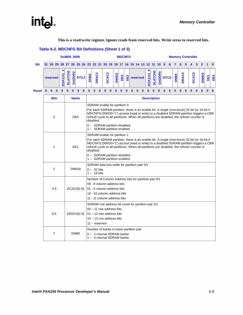
Memory Controller
This is a read/write register. Ignore reads from reserved bits. Write zeros to reserved bits.
Table 6-2. MDCNFG Bit Definitions (Sheet 1 of 3)
0x4800_0000 MDCNFG Memory Controller
Bit 31 30 29 28 27 26 25 24 23 22 21 20 19 18 17 16 15 14 13 12 11 10 9 8 7 6 5 4 3 2 1 0
reserved
DS
A11
11_2
DL
AT
CH
2
DA
DD
R2
DTC2
DN
B2
DR
AC
2
DC
AC
2
DW
ID2
DE
3
DE
2
reserved
DS
A11
11_0
DL
AT
CH
0
DA
DD
R0
DTC0
DN
B0
DR
AC
0
DC
AC
0
DW
ID0
DE
1
DE
0
Reset 0 0 0 0 0 0 0 0 0 0 0 0 0 0 0 0 0 0 0 0 0 0 0 0 0 0 0 0 0 0 0 0
Bits Name Description
0 DE0
SDRAM enable for partition 0
For each SDRAM partition, there is an enable bit. A single (non-burst) 32-bit (or 16-bit if MDCNFG:DWID0=’1’) access (read or write) to a disabled SDRAM partition triggers a CBR refresh cycle to all partitions. When all partitions are disabled, the refresh counter is disabled.
0 – SDRAM partition disabled1 – SDRAM partition enabled
1 DE1
SDRAM enable for partition 1
For each SDRAM partition, there is an enable bit. A single (non-burst) 32-bit (or 16-bit if MDCNFG:DWID0=’1’) access (read or write) to a disabled SDRAM partition triggers a CBR refresh cycle to all partitions. When all partitions are disabled, the refresh counter is disabled.
0 – SDRAM partition disabled1 – SDRAM partition enabled
2 DWID0SDRAM data bus width for partition pair 0/1
0 – 32 bits1 – 16 bits
4:3 DCAC0[1:0]
Number of Column Address bits for partition pair 0/1
00 - 8 column address bits
01 - 9 column address bits
10 - 10 column address bits
11 - 11 column address bits
6:5 DRAC0[1:0]
SDRAM row address bit count for partition pair 0/1
00 – 11 row address bits
01 – 12 row address bits
10 – 13 row address bits
11 – reserved
7 DNB0Number of banks in lower partition pair
0 – 2 internal SDRAM banks1 – 4 internal SDRAM banks
Intel® PXA255 Processor Developer’s Manual 6-9

Memory Controller
9:8 DTC0[1:0]
Timing Category for SDRAM pair 0/1.
00 - tRP = 2 clks, CL = 2, tRCD = 1 clks, tRAS(min) = 3 clks, tRC = 4 clks
01 - tRP = 2 clks, CL = 2, tRCD = 2 clks, tRAS(min) = 5 clks, tRC = 8 clks
10 - tRP = 3 clks, CL = 3, tRCD = 3 clks, tRAS(min) =7 clks, tRC=10 clks
11 - tRP = 3 clks, CL = 3, tRCD = 3 clks, tRAS(min) = 7 clks, tRC = 11 clks
tWR (write recovery time) is fixed at 2 clocks.
Used to configure the SDRAM timings to the SDRAM manufacturer’s specifications. Clocks referred to in the timings above are the number of SDCLKs. SDCLKs may not be equivalent to memory clocks based on the MDREFRx[KxDB2].
See Figure 6-5 for a description of these timing numbers.
10 DADDR0reserved
For an explanation on how the alternate addressing works, see Figure 6-4
11 DLATCH0
Return Data from SDRAM latching scheme for pair 0/1
0 – Latch return data using fixed delay from MEMCLK1 – Latch return data with return clock
This bit must always be written with a ‘1’ to enable using the return clock SDCLK for latching data. For more detail on this return data latching, see Section 6.5.4
12 DSA1111_0Use SA1111 Addressing Muxing Mode for pair 0/1. Setting this bit will override the addressing bit programmed in MDCNFG:DADDR0.
For an explanation on how the SA1111 addressing works, see Table 6-8.
15:13 — reserved
16 DE2
SDRAM enable for partition 2
For each SDRAM partition, there is an enable bit. A single (non-burst) 32-bit (or 16-bit if MDCNFG:DWID2=’1’) access (read or write) to a disabled SDRAM partition triggers a CBR refresh cycle to all partitions. When all partitions are disabled, the refresh counter is disabled.
0 – SDRAM partition disabled1 – SDRAM partition enabled
17 DE3
SDRAM enable for partition 3
For each SDRAM partition, there is an enable bit. A single (non-burst) 32-bit (or 16-bit if MDCNFG:DWID2=’1’) access (read or write) to a disabled SDRAM partition triggers a CBR refresh cycle to all partitions. When all partitions are disabled, the refresh counter is disabled.
0 – SDRAM partition disabled1 – SDRAM partition enabled
18 DWID2SDRAM data bus width for partition pair 2/3
0 – 32 bits1 – 16 bits
Table 6-2. MDCNFG Bit Definitions (Sheet 2 of 3)
0x4800_0000 MDCNFG Memory Controller
Bit 31 30 29 28 27 26 25 24 23 22 21 20 19 18 17 16 15 14 13 12 11 10 9 8 7 6 5 4 3 2 1 0
reserved
DS
A11
11_2
DL
AT
CH
2
DA
DD
R2
DTC2
DN
B2
DR
AC
2
DC
AC
2
DW
ID2
DE
3
DE
2
reserved
DS
A11
11_0
DL
AT
CH
0
DA
DD
R0
DTC0
DN
B0
DR
AC
0
DC
AC
0
DW
ID0
DE
1
DE
0
Reset 0 0 0 0 0 0 0 0 0 0 0 0 0 0 0 0 0 0 0 0 0 0 0 0 0 0 0 0 0 0 0 0
Bits Name Description
6-10 Intel® PXA255 Processor Developer’s Manual

Memory Controller
20:19 DCAC2[1:0]
Number of Column Address bits for partition pair 2/3
00 – 8 column address bits
01 – 9 column address bits
10 – 10 column address bits
11 – 11 column address bits
22:21 DRAC2[1:0]
SDRAM row address bit count for partition pair 2/3
00 – 11 row address bits
01 – 12 row address bits
10 – 13 row address bits
11 – reserved
23 DNB2Number of banks in upper partition pair
0 – 2 internal SDRAM banks1 – 4 internal SDRAM banks
25:24 DTC2[1:0]
Timing Category for SDRAM pair 2/3
00 – tRP = 2 clks, CL = 2, tRCD = 1 clks, tRAS(min) = 3 clks, tRC = 4 clks
01 – tRP = 2 clks, CL = 2, tRCD = 2 clks, tRAS(min) = 5 clks, tRC = 8 clks
10 – tRP = 3 clks, CL = 3, tRCD = 3 clks, tRAS(min) =7 clks, tRC=10 clks
11 – tRP = 3 clks, CL = 3, tRCD = 3 clks, tRAS(min) = 7 clks, tRC = 11 clks
tWR (write recovery time) is fixed at 2 clocks.
These bits are used to configure the SDRAM timings per the SDRAM manufacturer’s specifications. Clocks referred to in the timings above are the number of SDCLKs. SDCLKs may not be equivalent to memory clocks based on the MDREFRx[KxDB2].
See Figure 6-5 for a description of these timing numbers.
26 DADDR2reserved
For an explanation on how the alternate addressing works, see Figure 6-4.
27 DLATCH2
Return Data from SDRAM latching scheme for pair 2/3
0 – Latch return data using fixed delay from MEMCLK1 – Latch return data with return clock
This bit must always be written with a ‘1’ to enable using the return clock SDCLK for latching data. For more detail on this return data latching, see Section 6.5.4.
28 DSA1111_2Use SA1111 Addressing Muxing Mode for pair 2/3. Setting this bit will override the addressing bit programmed in MDCNFG:DADDR2.
For an explanation on how the SA1111 addressing works, see Table 6-8.
31:29 — reserved
Table 6-2. MDCNFG Bit Definitions (Sheet 3 of 3)
0x4800_0000 MDCNFG Memory Controller
Bit 31 30 29 28 27 26 25 24 23 22 21 20 19 18 17 16 15 14 13 12 11 10 9 8 7 6 5 4 3 2 1 0
reserved
DS
A11
11_2
DL
AT
CH
2
DA
DD
R2
DTC2
DN
B2
DR
AC
2
DC
AC
2
DW
ID2
DE
3
DE
2
reserved
DS
A11
11_0
DL
AT
CH
0
DA
DD
R0
DTC0
DN
B0
DR
AC
0
DC
AC
0
DW
ID0
DE
1
DE
0
Reset 0 0 0 0 0 0 0 0 0 0 0 0 0 0 0 0 0 0 0 0 0 0 0 0 0 0 0 0 0 0 0 0
Bits Name Description
Intel® PXA255 Processor Developer’s Manual 6-11

Memory Controller
6.5.2 SDRAM Mode Register Set Configuration Register (MDMRS)
The MDMRS, shown in Table 6-3, issues an Mode Register Set (MRS) command to the SDRAM. The value written in this register is placed directly on address lines MA[24:17] during the MRS command. For MA[16:10], values which are fixed or derived from the MDCNFG register are placed on the address bus. When setting the values to be written out on the address lines, base the values on the addressing mode being used. Although writing to this register triggers an MRS command, the corresponding chip-select values are asserted only if the memory banks are enabled via the MDCNFG register. Therefore, to appropriately write a new MRS value to SDRAM, first enable the memory via the MDCNFG register, and then write the MDMRS register. This register is used solely for generating the MRS command.
All values in the MDCNFG register must be programmed correctly to ensure proper operation of the device.
The MDMRS[MDBLx] bits configure the SDRAM to a burst length of four. This value is fixed and cannot be changed. For transfer cycles that require more data than the set burst length of four, the controller can preform as many bursts as necessary to transfer the required amount of data. For example, during a cache line fill the controller can perform a four-beat burst followed immediately by another four-beat burst. This approach requires the controller to generate the first address for the second burst. During transfer cycles less than four beats, the controller ignores the data it does not need. For instance, if the SDRAM is configured as non-cacheable, single beat reads are seen on the bus as a four-beat read with only one beat that is used by the processor. This also applies to a single-beat write.
This is a read/write register. Ignore reads from reserved bits. Write zeros to reserved bits.
Table 6-3. MDMRS Bit Definitions (Sheet 1 of 2)
0x4800_0040 MDMRS Memory Controller
Bit 31 30 29 28 27 26 25 24 23 22 21 20 19 18 17 16 15 14 13 12 11 10 9 8 7 6 5 4 3 2 1 0
rese
rved
MDMRS2 MDCL2
MD
AD
D2
MD
BL
2
rese
rved
MDMRS0 MDCL0M
DA
DD
0MDBL0
Reset 0 0 0 0 0 0 0 0 0 0 1 0 0 0 1 0 0 0 0 0 0 0 0 0 0 0 1 0 0 0 1 0
31 — reserved
30:23 MDMRS2 MRS value to be written to SDRAM for partition pair 2.
22:20 MDCL2 SDRAM partition pair 2 CAS Latency - derived from MDCNFG:DTC2. Writes are ignored. Ready-only.
19 MDADD2 SDRAM partition pair 2 Burst Type. Fix to sequential addressing. Writes are ignored. Always reads 0.
18:16 MDBL2 SDRAM partition pair 2 burst length. Fixed to a burst length of four. Writes are ignored. Always reads 010.
15 — reserved
14:7 MDMRS0 MRS value to be written to SDRAM for Partition Pair 0.
6-12 Intel® PXA255 Processor Developer’s Manual

Memory Controller
6.5.2.1 Low-Power SDRAM Mode Register Set Configuration Register
The Low-Power SDRAM Mode Register Set Configuration register (MDMRSLP) is used to issue a special low-power MRS command to SDRAM. Writing this register will trigger a two-stage MRS command to be issued to external SDRAM. The first stage will write the low- power MRS value to SDRAM partitions 0 and 1; the second stage will write the low-power MRS value to SDRAM partitions 2 and 3. The value written in this register will be placed directly on address lines MA[24:10] during the MRS command. When setting the values to be written out on the address lines, they must be written out properly based on the addressing mode which is being used. Although writing to this register will trigger an MRS command, the corresponding chip select values will be asserted only if the memory banks are enabled via the MDCNFG register and if the corresponding MDMRSLP[MDLPENx] bit is set. To write a new low- power MRS value to SDRAM, first enable the memory via the MDCNFG register, and then write the MDMRSLP register with the enable bits set.
This register is not used with in the processor except to write the value during the MRS command. All values in the MDCNFG register must be programmed correctly to ensure proper operation of the SDRAM. The register is used by a low-power SDRAM to control the Partial Array Self-Refresh (PASR) and Temperature Compensated Self-Refresh (TCSR) settings.
6:4 MDCL0 SDRAM partition pair 0 CAS Latency - derived from MDCNFG:DTC0. Writes are ignored. This field is ready-only.
3 MDADD0 SDRAM partition pair 0 Burst Type. Fix to sequential addressing. Writes are ignored. Always reads 0.
2:0 MDBL0 SDRAM partition pair 0 burst length. Fixed to a burst length of four. Writes are ignored. Always reads 010.
Table 6-3. MDMRS Bit Definitions (Sheet 2 of 2)
0x4800_0040 MDMRS Memory Controller
Bit 31 30 29 28 27 26 25 24 23 22 21 20 19 18 17 16 15 14 13 12 11 10 9 8 7 6 5 4 3 2 1 0
rese
rved
MDMRS2 MDCL2
MD
AD
D2
MD
BL
2
rese
rved
MDMRS0 MDCL0
MD
AD
D0
MDBL0
Reset 0 0 0 0 0 0 0 0 0 0 1 0 0 0 1 0 0 0 0 0 0 0 0 0 0 0 1 0 0 0 1 0
Intel® PXA255 Processor Developer’s Manual 6-13

Memory Controller
6.5.3 SDRAM MDREFR Register (MDREFR)
MDREFR, shown in Table 6-5, is a read/write register and contains control bits that refresh both SDRAM partition pairs. MDREFR also contains control and status bits for SDRAM self-refresh, SDRAM/SMROM clock divisors, SDRAM/SMROM clocks running, and SDRAM/SMROM clock-enable pin states. Independent control/status is provided for each of the clock pins (SDCLK[2:0]) and clock-enable pins (SDCKE[1:0]).
The clock-run bits (K0RUN, K1RUN, and K2RUN) and clock-enable bits (E0PIN and E1PIN) provide software control of SDRAM and Synchronous Static Memory low-power modes. When the clock-run bits and clock-enable bits are cleared, the corresponding memory is inaccessible.
Automatic power-down, enabled by the APD bit, is an mechanism for minimizing power consumption in the processor SDCLK pin drivers and/or the SDRAM/Synchronous Static Memory devices. A latency penalty of one memory cycle is incurred when SDCLK and SDCKE are restarted between non-consecutive SDRAM/Synchronous Static Memory transfers.
The following conditions determine whether SDRAM refreshes occur.
• No refreshes are sent to SDRAM when the refresh counter is cleared to zero.
• If a single transaction to a disabled SDRAM partition is requested, a refresh to all four partitions is performed.
• If all four SDRAM partitions are disabled, the refresh counter is disabled.
• If the clock frequency is changed, the register must be rewritten, even if the value has not changed. This results in a refresh and the refresh counter being reset to the next refresh interval.
Table 6-4. MDMRSLP Register Bit Definitions
0X4800 0058 MDMRSLP
Bit 31 30 29 28 27 26 25 24 23 22 21 20 19 18 17 16 15 14 13 12 11 10 9 8 7 6 5 4 3 2 1 0
MD
LP
EN
2
MD
MR
SL
P2
MD
LP
EN
0
MD
MR
SL
P0
Reset 0 0 0 0 0 0 0 0 0 0 0 0 0 0 0 0 0 0 0 0 0 0 0 0 0 0 0 0 0 0 0 0
Bits Name Description
31 MDLPEN2ENABLE BIT FOR LOW POWER MRS VALUE FOR PARTITION PAIR 2/3:
0 – Disable low power MRS for Partition Pair 2/31 – Enable low power MRS for Partition Pair 2/3
30:16 MDMRSLP2 LOW POWER MRS VALUE TO BE WRITTEN TO SDRAM FOR PARTITION PAIR 2/3
15 MDLPEN0Enable bit for low power MRS value for Partition Pair 0/1.
0 – Disable low power MRS for Partition Pair 0/11 – Enable low power MRS for Partition Pair 0/1
14:0 MDMRSLP0 LOW POWER MRS VALUE TO BE WRITTEN TO SDRAM FOR PARTITION PAIR 0/1
6-14 Intel® PXA255 Processor Developer’s Manual

Memory Controller
This is a read/write register. Ignore reads from reserved bits. Write zeros to reserved bits.
Table 6-5. MDREFR Bit Definitions (Sheet 1 of 3)
0x4800_0004 MDREFR Memory Controller
Bit 31 30 29 28 27 26 25 24 23 22 21 20 19 18 17 16 15 14 13 12 11 10 9 8 7 6 5 4 3 2 1 0
reservedK
2FR
EE
K1F
RE
E
K0F
RE
E
SL
FR
SH
rese
rved
AP
D
K2D
B2
K2R
UN
K1D
B2
K1R
UN
E1P
IN
K0D
B2
K0R
UN
E0P
IN
DRI
Reset 0 0 0 0 0 0 1 1 1 1 0 0 1 0 1 0 0 1 * * 1 1 1 1 1 1 1 1 1 1 1 1
Bits Name Description
31:26 — reserved
25 K2FREE
SDRAM Free-Running Control
0 – SDCLK2 is not free-running 1 – SDCLK2 is free-running (ignores MDREFR[APD] or MDREFR[K2RUN] bits)
Provides synchronous memory with SDCLK2 following a reset in order to reset internal circuitry.
24 K1FREE
SDRAM Free-Running Control
0 – SDCLK1 is not free-running 1 – SDCLK1 is free-running (ignores MDREFR[APD] or MDREFR[K1RUN] bits)
Provides synchronous memory with SDCLK1 following a reset to reset internal circuitry.
23 K0FREE
SDRAM Free-Running Control
0 – SDCLK0 is not free-running 1 – SDCLK0 is free-running (ignores MDREFR[APD] or MDREFR[K0RUN] bits)
Provides synchronous memory with SDCLK0 following a reset to reset internal circuitry.
22 SLFRSH
SDRAM Self-Refresh Control/Status
Control/status bit for entering and exiting SDRAM self-refresh and is automatically set on a hardware or sleep reset.
0 – Self refresh disabled1 – Self refresh enabled
SLFRSH can be set by software to force a self-refresh command. E1PIN does not have to be cleared. The appropriate clock run bits (K1RUN and/or K2RUN) must remain set until SDRAM has entered self-refresh and must be set prior to exiting self-refresh (clearing SLFRSH). This capability must be used with extreme caution because the resulting state prohibits automatic transitions for any commands.
Clearing SLFRSH is a part of the hardware or sleep reset procedure for SDRAM.
21 — reserved
20 APD
SDRAM/Synchronous Static Memory Auto-Power-Down Enable.
If APD=1, the clock enables and clock pins are automatically deasserted when none of the corresponding partitions are being accessed unless the KxFREE bits are set.
If no SDRAM partitions are being accessed, the SDRAM chips are put into Power-Down mode and the clocks and clock-enable pins are turned off.
If one SDRAM partition is being used and the other is not, the clock to the partition that is not being used are turned off.
If no Synchronous Static Memory partitions are being used, the clock and clock enable to these partitions are turned off and the memory chips are put into Power-Down mode. See Section 6.7.
19 K2DB2SDRAM Clock Pin 2 (SDCLK2) Divide by 2 Control/Status
0 – SDCLK2 is same frequency as MEMCLK1 – SDCLK2 runs at one-half the MEMCLK frequency
Intel® PXA255 Processor Developer’s Manual 6-15

Memory Controller
18 K2RUN
SDRAM Clock Pin 2 (SDCLK<2>) Run Control/Status
0 – SDCLK2 disabled1 – SDCLK2 enabled
K2RUN also can be cleared by program. Use with caution because the resulting state prohibits automatic transitions for any commands.
Setting K1RUN and/or K2RUN is a part of the hardware and sleep reset procedure for SDRAM.
17 K1DB2SDRAM Clock Pin 1 (SDCLK1) Divide by 2 Control/Status
0 – SDCLK1 is same frequency as MEMCLK1 – SDCLK1 runs at one-half the MEMCLK frequency
16 K1RUN
SDRAM Clock Pin 1 (SDCLK<1>) Run Control/Status
0 – SDCLK1 disabled1 – SDCLK1 enabled
K1RUN can be cleared by software. Use with caution because the resulting state prohibits automatic transitions for any commands.
Setting K1RUN and/or K2RUN is a part of the hardware and sleep reset procedure for SDRAM.
15 E1PIN
SDRAM Clock Enable Pin 1 (SDCKE1) Level Control/Status
0 – SDCKE1 is disabled1 – SDCKE1 is enabled
E1PIN can be cleared by program to cause a power-down command (if K1RUN=1 and/or K2RUN=1, and SLFRSH=0). Use with caution because the resulting state prohibits automatic transitions for mode register set, read, write, and refresh commands. E1PIN can be set by program to cause a power-down-exit command (if K1RUN=1 and/or K2RUN=1, and SLFRSH=0).
Setting E1PIN is a part of the hardware reset or sleep reset procedure for SDRAM.
14 K0DB2
Synchronous Static Memory Clock Pin 0 (SDCLK<0>) Divide by 2 Control/Status
0 – SDCLK0 runs at the memory clock frequency. 1 – SDCLK0 runs at one-half the memory clock frequency.
This bit is automatically set upon hardware or sleep reset.
Table 6-5. MDREFR Bit Definitions (Sheet 2 of 3)
0x4800_0004 MDREFR Memory Controller
Bit 31 30 29 28 27 26 25 24 23 22 21 20 19 18 17 16 15 14 13 12 11 10 9 8 7 6 5 4 3 2 1 0
reserved
K2F
RE
E
K1F
RE
E
K0F
RE
E
SL
FR
SH
rese
rved
AP
D
K2D
B2
K2R
UN
K1D
B2
K1R
UN
E1P
IN
K0D
B2
K0R
UN
E0P
IN
DRI
Reset 0 0 0 0 0 0 1 1 1 1 0 0 1 0 1 0 0 1 * * 1 1 1 1 1 1 1 1 1 1 1 1
Bits Name Description
6-16 Intel® PXA255 Processor Developer’s Manual
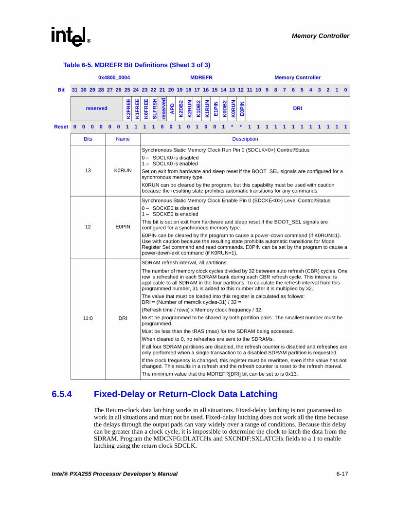
Memory Controller
6.5.4 Fixed-Delay or Return-Clock Data Latching
The Return-clock data latching works in all situations. Fixed-delay latching is not guaranteed to work in all situations and must not be used. Fixed-delay latching does not work all the time because the delays through the output pads can vary widely over a range of conditions. Because this delay can be greater than a clock cycle, it is impossible to determine the clock to latch the data from the SDRAM. Program the MDCNFG:DLATCHx and SXCNDF:SXLATCHx fields to a 1 to enable latching using the return clock SDCLK.
13 K0RUN
Synchronous Static Memory Clock Run Pin 0 (SDCLK<0>) Control/Status
0 – SDCLK0 is disabled1 – SDCLK0 is enabled
Set on exit from hardware and sleep reset if the BOOT_SEL signals are configured for a synchronous memory type.
K0RUN can be cleared by the program, but this capability must be used with caution because the resulting state prohibits automatic transitions for any commands.
12 E0PIN
Synchronous Static Memory Clock Enable Pin 0 (SDCKE<0>) Level Control/Status
0 – SDCKE0 is disabled1 – SDCKE0 is enabled
This bit is set on exit from hardware and sleep reset if the BOOT_SEL signals are configured for a synchronous memory type.
E0PIN can be cleared by the program to cause a power-down command (if K0RUN=1). Use with caution because the resulting state prohibits automatic transitions for Mode Register Set command and read commands. E0PIN can be set by the program to cause a power-down-exit command (if K0RUN=1).
11:0 DRI
SDRAM refresh interval, all partitions.
The number of memory clock cycles divided by 32 between auto refresh (CBR) cycles. One row is refreshed in each SDRAM bank during each CBR refresh cycle. This interval is applicable to all SDRAM in the four partitions. To calculate the refresh interval from this programmed number, 31 is added to this number after it is multiplied by 32.
The value that must be loaded into this register is calculated as follows: DRI = (Number of memclk cycles-31) / 32 =
(Refresh time / rows) x Memory clock frequency / 32.
Must be programmed to be shared by both partition pairs. The smallest number must be programmed.
Must be less than the tRAS (max) for the SDRAM being accessed.
When cleared to 0, no refreshes are sent to the SDRAMs.
If all four SDRAM partitions are disabled, the refresh counter is disabled and refreshes are only performed when a single transaction to a disabled SDRAM partition is requested.
If the clock frequency is changed, this register must be rewritten, even if the value has not changed. This results in a refresh and the refresh counter is reset to the refresh interval.
The minimum value that the MDREFR[DRI] bit can be set to is 0x13.
Table 6-5. MDREFR Bit Definitions (Sheet 3 of 3)
0x4800_0004 MDREFR Memory Controller
Bit 31 30 29 28 27 26 25 24 23 22 21 20 19 18 17 16 15 14 13 12 11 10 9 8 7 6 5 4 3 2 1 0
reserved
K2F
RE
E
K1F
RE
E
K0F
RE
E
SL
FR
SH
rese
rved
AP
D
K2D
B2
K2R
UN
K1D
B2
K1R
UN
E1P
IN
K0D
B2
K0R
UN
E0P
IN
DRI
Reset 0 0 0 0 0 0 1 1 1 1 0 0 1 0 1 0 0 1 * * 1 1 1 1 1 1 1 1 1 1 1 1
Bits Name Description
Intel® PXA255 Processor Developer’s Manual 6-17
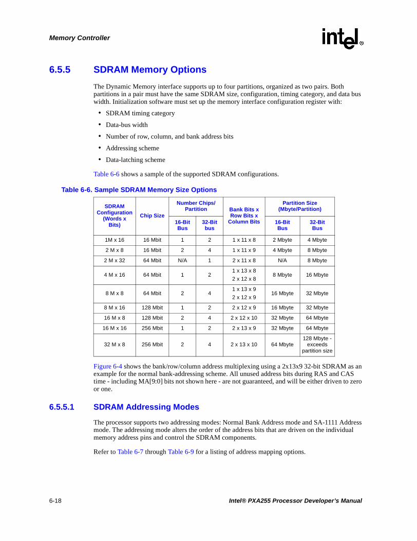
Memory Controller
6.5.5 SDRAM Memory Options
The Dynamic Memory interface supports up to four partitions, organized as two pairs. Both partitions in a pair must have the same SDRAM size, configuration, timing category, and data bus width. Initialization software must set up the memory interface configuration register with:
• SDRAM timing category
• Data-bus width
• Number of row, column, and bank address bits
• Addressing scheme
• Data-latching scheme
Table 6-6 shows a sample of the supported SDRAM configurations.
Figure 6-4 shows the bank/row/column address multiplexing using a 2x13x9 32-bit SDRAM as an example for the normal bank-addressing scheme. All unused address bits during RAS and CAS time - including MA[9:0] bits not shown here - are not guaranteed, and will be either driven to zero or one.
6.5.5.1 SDRAM Addressing Modes
The processor supports two addressing modes: Normal Bank Address mode and SA-1111 Address mode. The addressing mode alters the order of the address bits that are driven on the individual memory address pins and control the SDRAM components.
Refer to Table 6-7 through Table 6-9 for a listing of address mapping options.
Table 6-6. Sample SDRAM Memory Size Options
SDRAMConfiguration
(Words x Bits)
Chip Size
Number Chips/Partition Bank Bits x
Row Bits xColumn Bits
Partition Size(Mbyte/Partition)
16-BitBus
32-Bitbus
16-BitBus
32-BitBus
1M x 16 16 Mbit 1 2 1 x 11 x 8 2 Mbyte 4 Mbyte
2 M x 8 16 Mbit 2 4 1 x 11 x 9 4 Mbyte 8 Mbyte
2 M x 32 64 Mbit N/A 1 2 x 11 x 8 N/A 8 Mbyte
4 M x 16 64 Mbit 1 21 x 13 x 8
2 x 12 x 88 Mbyte 16 Mbyte
8 M x 8 64 Mbit 2 41 x 13 x 9
2 x 12 x 916 Mbyte 32 Mbyte
8 M x 16 128 Mbit 1 2 2 x 12 x 9 16 Mbyte 32 Mbyte
16 M x 8 128 Mbit 2 4 2 x 12 x 10 32 Mbyte 64 Mbyte
16 M x 16 256 Mbit 1 2 2 x 13 x 9 32 Mbyte 64 Mbyte
32 M x 8 256 Mbit 2 4 2 x 13 x 10 64 Mbyte128 Mbyte -
exceeds partition size
6-18 Intel® PXA255 Processor Developer’s Manual

Memory Controller
Table 6-4 shows how the SDRAM row and column addresses are mapped to the internal SDRAM address. The SDRAM row and column addresses are muxed. The SDRAM row is sent during an Active command and is followed by the column address during the read or write command. MA<20> is driven with 0 during column addressing. BA[1:0] is used to tell the SDRAM which bank is being read from and remains stable during column addressing. During SDRAM configuration, all the address pins are used to transfer the MRS command.
Figure 6-4. External to Internal Address Mapping Options
Table 6-7. External to Internal Address Mapping for Normal Bank Addressing (Sheet 1 of 3)
# Bits
Bank xRow xCol xData
External Address pins at SDRAM RAS Time MA<24:10>
External Address pins at SDRAM CAS Time MA<24:10>
24 23 22 21 20 19 18 17 16 15 14 13 12 11 10 24 23 22 21 20 19 18 17 16 15 14 13 12 11 10
1x11x8x32 21 20 19 18 17 16 15 14 13 12 11 10 21 ‘0’ 9 8 7 6 5 4 3 2
1x11x8x16 20 19 18 17 16 15 14 13 12 11 10 9 20 ‘0’ 8 7 6 5 4 3 2 1
1x11x9x32 22 21 20 19 18 17 16 15 14 13 12 11 22 ‘0’ 10 9 8 7 6 5 4 3 2
1x11x9x16 21 20 19 18 17 16 15 14 13 12 11 10 21 ‘0’ 9 8 7 6 5 4 3 2 1
1x11x10x32 23 22 21 20 19 18 17 16 15 14 13 12 23 ‘0’ 11 10 9 8 7 6 5 4 3 2
1x11x10x16 22 21 20 19 18 17 16 15 14 13 12 11 22 ‘0’ 10 9 8 7 6 5 4 3 2 1
1x11x11x32 NOT VALID (illegal addressing combination) NOT VALID (illegal addressing combination)
1x11x11x16 NOT VALID (illegal addressing combination) NOT VALID (illegal addressing combination)
1x12x8x32 22 21 20 19 18 17 16 15 14 13 12 11 10 22 ‘0’ 9 8 7 6 5 4 3 2
1x12x8x16 21 20 19 18 17 16 15 14 13 12 11 10 9 21 ‘0’ 8 7 6 5 4 3 2 1
1x12x9x32 23 22 21 20 19 18 17 16 15 14 13 12 11 23 ‘0’ 10 9 8 7 6 5 4 3 2
1x12x9x16 22 21 20 19 18 17 16 15 14 13 12 11 10 22 ‘0’ 9 8 7 6 5 4 3 2 1
1x12x10x32 24 23 22 21 20 19 18 17 16 15 14 13 12 24 ‘0’ 11 10 9 8 7 6 5 4 3 2
Intel® PXA255 Processor Developer’s Manual 6-19

Memory Controller
1x12x10x16 23 22 21 20 19 18 17 16 15 14 13 12 11 23 ‘0’ 10 9 8 7 6 5 4 3 2 1
1x12x11x32 25 24 23 22 21 20 19 18 17 16 15 14 13 25 12 ‘0’ 11 10 9 8 7 6 5 4 3 2
1x12x11x16 24 23 22 21 20 19 18 17 16 15 14 13 12 24 11 ‘0’ 10 9 8 7 6 5 4 3 2 1
1x13x8x32 23 22 21 20 19 18 17 16 15 14 13 12 11 10 23 ‘0’ 9 8 7 6 5 4 3 2
1x13x8x16 22 21 20 19 18 17 16 15 14 13 12 11 10 9 22 ‘0’ 8 7 6 5 4 3 2 1
1x13x9x32 24 23 22 21 20 19 18 17 16 15 14 13 12 11 24 ‘0’ 10 9 8 7 6 5 4 3 2
1x13x9x16 23 22 21 20 19 18 17 16 15 14 13 12 11 10 23 ‘0’ 9 8 7 6 5 4 3 2 1
1x13x10x32 25 24 23 22 21 20 19 18 17 16 15 14 13 12 25 ‘0’ 11 10 9 8 7 6 5 4 3 2
1x13x10x16 24 23 22 21 20 19 18 17 16 15 14 13 12 11 24 ‘0’ 10 9 8 7 6 5 4 3 2 1
1x13x11x32 13 26 25 24 23 22 21 20 19 18 17 16 15 14 13 12 ‘0’ 11 10 9 8 7 6 5 4 3 2
1x13x11x16 25 24 23 22 21 20 19 18 17 16 15 14 13 12 25 11 ‘0’ 10 9 8 7 6 5 4 3 2 1
2x11x8x32 22 21 20 19 18 17 16 15 14 13 12 11 10 22 21 ‘0’ 9 8 7 6 5 4 3 2
2x11x8x16 21 20 19 18 17 16 15 14 13 12 11 10 9 21 20 ‘0’ 8 7 6 5 4 3 2 1
2x11x9x32 23 22 21 20 19 18 17 16 15 14 13 12 11 23 22 ‘0’ 10 9 8 7 6 5 4 3 2
2x11x9x16 22 21 20 19 18 17 16 15 14 13 12 11 10 22 21 ‘0’ 9 8 7 6 5 4 3 2 1
2x11x10x32 24 23 22 21 20 19 18 17 16 15 14 13 12 24 23 ‘0’ 11 10 9 8 7 6 5 4 3 2
2x11x10x16 23 22 21 20 19 18 17 16 15 14 13 12 11 23 22 ‘0’ 10 9 8 7 6 5 4 3 2 1
2x11x11x32 NOT VALID (illegal addressing combination) NOT VALID (illegal addressing combination)
2x11x11x16 NOT VALID (illegal addressing combination) NOT VALID (illegal addressing combination)
2x12x8x32 23 22 21 20 19 18 17 16 15 14 13 12 11 10 23 22 ‘0’ 9 8 7 6 5 4 3 2
2x12x8x16 22 21 20 19 18 17 16 15 14 13 12 11 10 9 22 21 ‘0’ 8 7 6 5 4 3 2 1
2x12x9x32 24 23 22 21 20 19 18 17 16 15 14 13 12 11 24 23 ‘0’ 10 9 8 7 6 5 4 3 2
2x12x9x16 23 22 21 20 19 18 17 16 15 14 13 12 11 10 23 22 ‘0’ 9 8 7 6 5 4 3 2 1
2x12x10x32 25 24 23 22 21 20 19 18 17 16 15 14 13 12 25 24 ‘0’ 11 10 9 8 7 6 5 4 3 2
2x12x10x16 24 23 22 21 20 19 18 17 16 15 14 13 12 11 24 23 ‘0’ 10 9 8 7 6 5 4 3 2 1
2x12x11x32 26 25 24 23 22 21 20 19 18 17 16 15 14 13 26 25 12 ‘0’ 11 10 9 8 7 6 5 4 3 2
2x12x11x16 25 24 23 22 21 20 19 18 17 16 15 14 13 12 25 24 11 ‘0’ 10 9 8 7 6 5 4 3 2 1
Table 6-7. External to Internal Address Mapping for Normal Bank Addressing (Sheet 2 of 3)
# Bits
Bank xRow xCol xData
External Address pins at SDRAM RAS Time MA<24:10>
External Address pins at SDRAM CAS Time MA<24:10>
24 23 22 21 20 19 18 17 16 15 14 13 12 11 10 24 23 22 21 20 19 18 17 16 15 14 13 12 11 10
6-20 Intel® PXA255 Processor Developer’s Manual
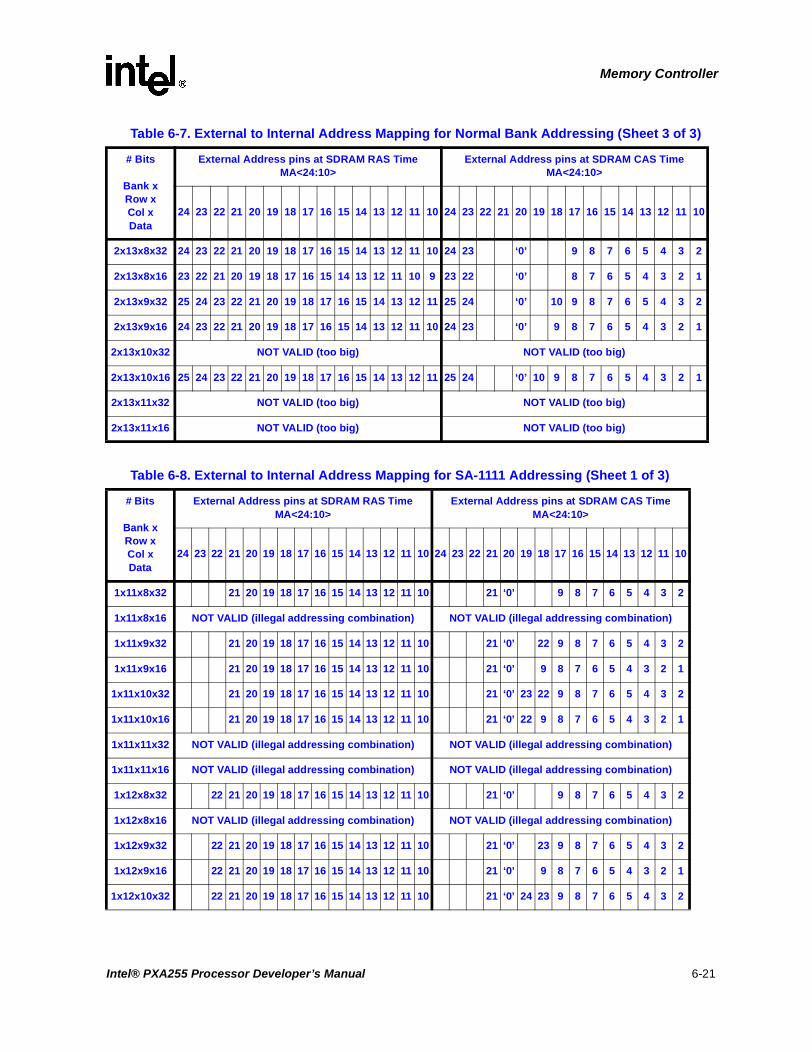
Memory Controller
2x13x8x32 24 23 22 21 20 19 18 17 16 15 14 13 12 11 10 24 23 ‘0’ 9 8 7 6 5 4 3 2
2x13x8x16 23 22 21 20 19 18 17 16 15 14 13 12 11 10 9 23 22 ‘0’ 8 7 6 5 4 3 2 1
2x13x9x32 25 24 23 22 21 20 19 18 17 16 15 14 13 12 11 25 24 ‘0’ 10 9 8 7 6 5 4 3 2
2x13x9x16 24 23 22 21 20 19 18 17 16 15 14 13 12 11 10 24 23 ‘0’ 9 8 7 6 5 4 3 2 1
2x13x10x32 NOT VALID (too big) NOT VALID (too big)
2x13x10x16 25 24 23 22 21 20 19 18 17 16 15 14 13 12 11 25 24 ‘0’ 10 9 8 7 6 5 4 3 2 1
2x13x11x32 NOT VALID (too big) NOT VALID (too big)
2x13x11x16 NOT VALID (too big) NOT VALID (too big)
Table 6-8. External to Internal Address Mapping for SA-1111 Addressing (Sheet 1 of 3)
# Bits
Bank xRow xCol xData
External Address pins at SDRAM RAS Time MA<24:10>
External Address pins at SDRAM CAS Time MA<24:10>
24 23 22 21 20 19 18 17 16 15 14 13 12 11 10 24 23 22 21 20 19 18 17 16 15 14 13 12 11 10
1x11x8x32 21 20 19 18 17 16 15 14 13 12 11 10 21 ‘0’ 9 8 7 6 5 4 3 2
1x11x8x16 NOT VALID (illegal addressing combination) NOT VALID (illegal addressing combination)
1x11x9x32 21 20 19 18 17 16 15 14 13 12 11 10 21 ‘0’ 22 9 8 7 6 5 4 3 2
1x11x9x16 21 20 19 18 17 16 15 14 13 12 11 10 21 ‘0’ 9 8 7 6 5 4 3 2 1
1x11x10x32 21 20 19 18 17 16 15 14 13 12 11 10 21 ‘0’ 23 22 9 8 7 6 5 4 3 2
1x11x10x16 21 20 19 18 17 16 15 14 13 12 11 10 21 ‘0’ 22 9 8 7 6 5 4 3 2 1
1x11x11x32 NOT VALID (illegal addressing combination) NOT VALID (illegal addressing combination)
1x11x11x16 NOT VALID (illegal addressing combination) NOT VALID (illegal addressing combination)
1x12x8x32 22 21 20 19 18 17 16 15 14 13 12 11 10 21 ‘0’ 9 8 7 6 5 4 3 2
1x12x8x16 NOT VALID (illegal addressing combination) NOT VALID (illegal addressing combination)
1x12x9x32 22 21 20 19 18 17 16 15 14 13 12 11 10 21 ‘0’ 23 9 8 7 6 5 4 3 2
1x12x9x16 22 21 20 19 18 17 16 15 14 13 12 11 10 21 ‘0’ 9 8 7 6 5 4 3 2 1
1x12x10x32 22 21 20 19 18 17 16 15 14 13 12 11 10 21 ‘0’ 24 23 9 8 7 6 5 4 3 2
Table 6-7. External to Internal Address Mapping for Normal Bank Addressing (Sheet 3 of 3)
# Bits
Bank xRow xCol xData
External Address pins at SDRAM RAS Time MA<24:10>
External Address pins at SDRAM CAS Time MA<24:10>
24 23 22 21 20 19 18 17 16 15 14 13 12 11 10 24 23 22 21 20 19 18 17 16 15 14 13 12 11 10
Intel® PXA255 Processor Developer’s Manual 6-21

Memory Controller
1x12x10x16 22 21 20 19 18 17 16 15 14 13 12 11 10 21 ‘0’ 23 9 8 7 6 5 4 3 2 1
1x12x11x32 NOT VALID (illegal addressing combination) NOT VALID (illegal addressing combination)
1x12x11x16 NOT VALID (illegal addressing combination) NOT VALID (illegal addressing combination)
1x13x8x32 23 22 21 20 19 18 17 16 15 14 13 12 11 10 21 ‘0’ 9 8 7 6 5 4 3 2
1x13x8x16 NOT VALID (illegal addressing combination) NOT VALID (illegal addressing combination)
1x13x9x32 23 22 21 20 19 18 17 16 15 14 13 12 11 10 21 ‘0’ 24 9 8 7 6 5 4 3 2
1x13x9x16 23 22 21 20 19 18 17 16 15 14 13 12 11 10 21 ‘0’ 9 8 7 6 5 4 3 2 1
1x13x10x32 23 22 21 20 19 18 17 16 15 14 13 12 11 10 21 ‘0’ 25 24 9 8 7 6 5 4 3 2
1x13x10x16 23 22 21 20 19 18 17 16 15 14 13 12 11 10 21 ‘0’ 24 9 8 7 6 5 4 3 2 1
1x13x11x32 NOT VALID (illegal addressing combination) NOT VALID (illegal addressing combination)
1x13x11x16 NOT VALID (illegal addressing combination) NOT VALID (illegal addressing combination)
2x11x8x32 22 21 20 19 18 17 16 15 14 13 12 11 10 22 21 ‘0’ 9 8 7 6 5 4 3 2
2x11x8x16 NOT VALID (illegal addressing combination) NOT VALID (illegal addressing combination)
2x11x9x32 22 21 20 19 18 17 16 15 14 13 12 11 10 22 21 ‘0’ 23 9 8 7 6 5 4 3 2
2x11x9x16 22 21 20 19 18 17 16 15 14 13 12 11 10 22 21 ‘0’ 9 8 7 6 5 4 3 2 1
2x11x10x32 22 21 20 19 18 17 16 15 14 13 12 11 10 22 21 ‘0’ 24 23 9 8 7 6 5 4 3 2
2x11x10x16 22 21 20 19 18 17 16 15 14 13 12 11 10 22 21 ‘0’ 23 9 8 7 6 5 4 3 2 1
2x11x11x32 NOT VALID (illegal addressing combination) NOT VALID (illegal addressing combination)
2x11x11x16 NOT VALID (illegal addressing combination) NOT VALID (illegal addressing combination)
2x12x8x32 23 22 21 20 19 18 17 16 15 14 13 12 11 10 23 22 ‘0’ 9 8 7 6 5 4 3 2
2x12x8x16 NOT VALID (illegal addressing combination) NOT VALID (illegal addressing combination)
2x12x9x32 23 22 21 20 19 18 17 16 15 14 13 12 11 10 23 22 ‘0’ 24 9 8 7 6 5 4 3 2
2x12x9x16 23 22 21 20 19 18 17 16 15 14 13 12 11 10 23 22 ‘0’ 9 8 7 6 5 4 3 2 1
2x12x10x32 23 22 21 20 19 18 17 16 15 14 13 12 11 10 23 22 ‘0’ 25 24 9 8 7 6 5 4 3 2
2x12x10x16 23 22 21 20 19 18 17 16 15 14 13 12 11 10 23 22 ‘0’ 24 9 8 7 6 5 4 3 2 1
2x12x11x32 NOT VALID (illegal addressing combination) NOT VALID (illegal addressing combination)
2x12x11x16 NOT VALID (illegal addressing combination) NOT VALID (illegal addressing combination)
Table 6-8. External to Internal Address Mapping for SA-1111 Addressing (Sheet 2 of 3)
# Bits
Bank xRow xCol xData
External Address pins at SDRAM RAS Time MA<24:10>
External Address pins at SDRAM CAS Time MA<24:10>
24 23 22 21 20 19 18 17 16 15 14 13 12 11 10 24 23 22 21 20 19 18 17 16 15 14 13 12 11 10
6-22 Intel® PXA255 Processor Developer’s Manual
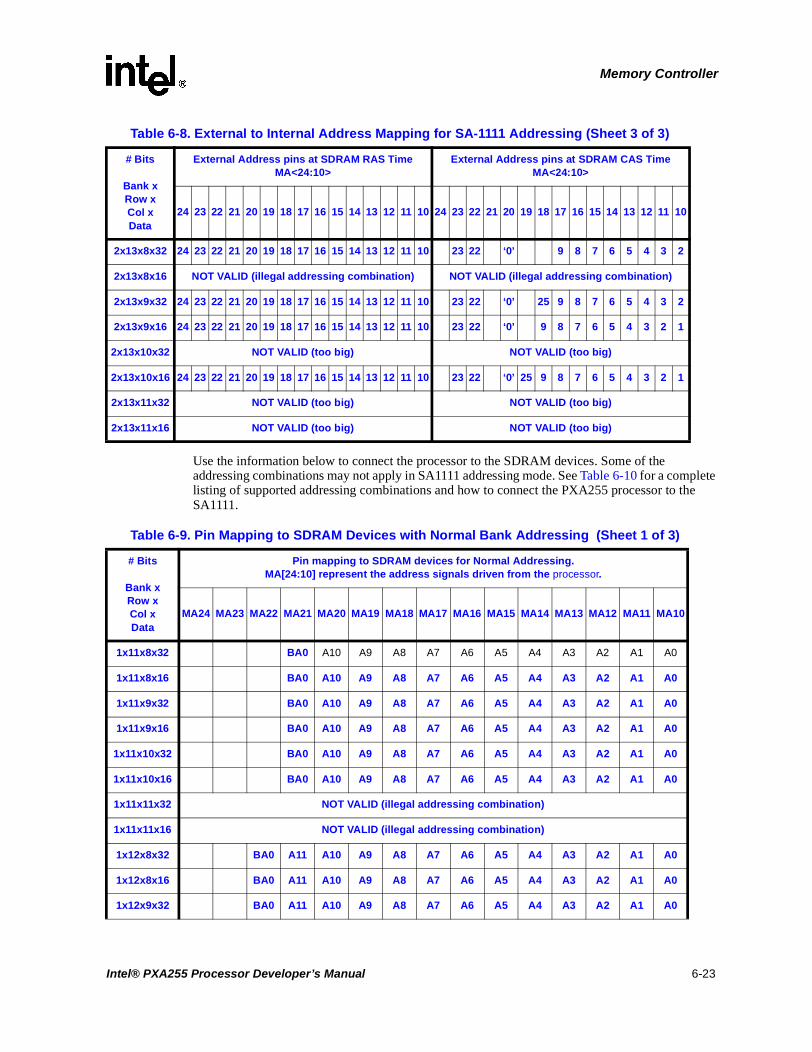
Memory Controller
Use the information below to connect the processor to the SDRAM devices. Some of the addressing combinations may not apply in SA1111 addressing mode. See Table 6-10 for a complete listing of supported addressing combinations and how to connect the PXA255 processor to the SA1111.
2x13x8x32 24 23 22 21 20 19 18 17 16 15 14 13 12 11 10 23 22 ‘0’ 9 8 7 6 5 4 3 2
2x13x8x16 NOT VALID (illegal addressing combination) NOT VALID (illegal addressing combination)
2x13x9x32 24 23 22 21 20 19 18 17 16 15 14 13 12 11 10 23 22 ‘0’ 25 9 8 7 6 5 4 3 2
2x13x9x16 24 23 22 21 20 19 18 17 16 15 14 13 12 11 10 23 22 ‘0’ 9 8 7 6 5 4 3 2 1
2x13x10x32 NOT VALID (too big) NOT VALID (too big)
2x13x10x16 24 23 22 21 20 19 18 17 16 15 14 13 12 11 10 23 22 ‘0’ 25 9 8 7 6 5 4 3 2 1
2x13x11x32 NOT VALID (too big) NOT VALID (too big)
2x13x11x16 NOT VALID (too big) NOT VALID (too big)
Table 6-8. External to Internal Address Mapping for SA-1111 Addressing (Sheet 3 of 3)
# Bits
Bank xRow xCol xData
External Address pins at SDRAM RAS Time MA<24:10>
External Address pins at SDRAM CAS Time MA<24:10>
24 23 22 21 20 19 18 17 16 15 14 13 12 11 10 24 23 22 21 20 19 18 17 16 15 14 13 12 11 10
Table 6-9. Pin Mapping to SDRAM Devices with Normal Bank Addressing (Sheet 1 of 3)
# Bits
Bank xRow xCol xData
Pin mapping to SDRAM devices for Normal Addressing.MA[24:10] represent the address signals driven from the processor.
MA24 MA23 MA22 MA21 MA20 MA19 MA18 MA17 MA16 MA15 MA14 MA13 MA12 MA11 MA10
1x11x8x32 BA0 A10 A9 A8 A7 A6 A5 A4 A3 A2 A1 A0
1x11x8x16 BA0 A10 A9 A8 A7 A6 A5 A4 A3 A2 A1 A0
1x11x9x32 BA0 A10 A9 A8 A7 A6 A5 A4 A3 A2 A1 A0
1x11x9x16 BA0 A10 A9 A8 A7 A6 A5 A4 A3 A2 A1 A0
1x11x10x32 BA0 A10 A9 A8 A7 A6 A5 A4 A3 A2 A1 A0
1x11x10x16 BA0 A10 A9 A8 A7 A6 A5 A4 A3 A2 A1 A0
1x11x11x32 NOT VALID (illegal addressing combination)
1x11x11x16 NOT VALID (illegal addressing combination)
1x12x8x32 BA0 A11 A10 A9 A8 A7 A6 A5 A4 A3 A2 A1 A0
1x12x8x16 BA0 A11 A10 A9 A8 A7 A6 A5 A4 A3 A2 A1 A0
1x12x9x32 BA0 A11 A10 A9 A8 A7 A6 A5 A4 A3 A2 A1 A0
Intel® PXA255 Processor Developer’s Manual 6-23

Memory Controller
1x12x9x16 BA0 A11 A10 A9 A8 A7 A6 A5 A4 A3 A2 A1 A0
1x12x10x32 BA0 A11 A10 A9 A8 A7 A6 A5 A4 A3 A2 A1 A0
1x12x10x16 BA0 A11 A10 A9 A8 A7 A6 A5 A4 A3 A2 A1 A0
1x12x11x32 BA0 A11 A10 A9 A8 A7 A6 A5 A4 A3 A2 A1 A0
1x12x11x16 BA0 A11 A10 A9 A8 A7 A6 A5 A4 A3 A2 A1 A0
1x13x8x32 BA0 A12 A11 A10 A9 A8 A7 A6 A5 A4 A3 A2 A1 A0
1x13x8x16 BA0 A12 A11 A10 A9 A8 A7 A6 A5 A4 A3 A2 A1 A0
1x13x9x32 BA0 A12 A11 A10 A9 A8 A7 A6 A5 A4 A3 A2 A1 A0
1x13x9x16 BA0 A12 A11 A10 A9 A8 A7 A6 A5 A4 A3 A2 A1 A0
1x13x10x32 BA0 A12 A11 A10 A9 A8 A7 A6 A5 A4 A3 A2 A1 A0
1x13x10x16 BA0 A12 A11 A10 A9 A8 A7 A6 A5 A4 A3 A2 A1 A0
1x13x11x32 BA0 A12 A11 A10 A9 A8 A7 A6 A5 A4 A3 A2 A1 A0
1x13x11x16 BA0 A12 A11 A10 A9 A8 A7 A6 A5 A4 A3 A2 A1 A0
2x11x8x32 BA1 BA0 A10 A9 A8 A7 A6 A5 A4 A3 A2 A1 A0
2x11x8x16 BA1 BA0 A10 A9 A8 A7 A6 A5 A4 A3 A2 A1 A0
2x11x9x32 BA1 BA0 A10 A9 A8 A7 A6 A5 A4 A3 A2 A1 A0
2x11x9x16 BA1 BA0 A10 A9 A8 A7 A6 A5 A4 A3 A2 A1 A0
2x11x10x32 BA1 BA0 A10 A9 A8 A7 A6 A5 A4 A3 A2 A1 A0
2x11x10x16 BA1 BA0 A10 A9 A8 A7 A6 A5 A4 A3 A2 A1 A0
2x11x11x32 NOT VALID (illegal addressing combination)
2x11x11x16 NOT VALID (illegal addressing combination)
2x12x8x32 BA1 BA0 A11 A10 A9 A8 A7 A6 A5 A4 A3 A2 A1 A0
2x12x8x16 BA1 BA0 A11 A10 A9 A8 A7 A6 A5 A4 A3 A2 A1 A0
2x12x9x32 BA1 BA0 A11 A10 A9 A8 A7 A6 A5 A4 A3 A2 A1 A0
2x12x9x16 BA1 BA0 A11 A10 A9 A8 A7 A6 A5 A4 A3 A2 A1 A0
2x12x10x32 BA1 BA0 A11 A10 A9 A8 A7 A6 A5 A4 A3 A2 A1 A0
2x12x10x16 BA1 BA0 A11 A10 A9 A8 A7 A6 A5 A4 A3 A2 A1 A0
Table 6-9. Pin Mapping to SDRAM Devices with Normal Bank Addressing (Sheet 2 of 3)
# Bits
Bank xRow xCol xData
Pin mapping to SDRAM devices for Normal Addressing.MA[24:10] represent the address signals driven from the processor.
MA24 MA23 MA22 MA21 MA20 MA19 MA18 MA17 MA16 MA15 MA14 MA13 MA12 MA11 MA10
6-24 Intel® PXA255 Processor Developer’s Manual

Memory Controller
2x12x11x32 BA1 BA0 A11 A10 A9 A8 A7 A6 A5 A4 A3 A2 A1 A0
2x12x11x16 BA1 BA0 A11 A10 A9 A8 A7 A6 A5 A4 A3 A2 A1 A0
2x13x8x32 BA1 BA0 A12 A11 A10 A9 A8 A7 A6 A5 A4 A3 A2 A1 A0
2x13x8x16 BA1 BA0 A12 A11 A10 A9 A8 A7 A6 A5 A4 A3 A2 A1 A0
2x13x9x32 BA1 BA0 A12 A11 A10 A9 A8 A7 A6 A5 A4 A3 A2 A1 A0
2x13x9x16 BA1 BA0 A12 A11 A10 A9 A8 A7 A6 A5 A4 A3 A2 A1 A0
2x13x10x32 NOT VALID (too big)
2x13x10x16 BA1 BA0 A12 A11 A10 A9 A8 A7 A6 A5 A4 A3 A2 A1 A0
2x13x11x32 NOT VALID (too big)
2x13x11x16 NOT VALID (too big)
Table 6-10. Pin Mapping to SDRAM Devices with SA1111 Addressing (Sheet 1 of 3)
# Bits
Bank xRow xCol xData
Pin mapping to SDRAM devices for SA1111 Addressing Options.MA[24:10] represent the address signals driven from the PXA255 processor.
MA24 MA23 MA22 MA21 MA20 MA19 MA18 MA17 MA16 MA15 MA14 MA13 MA12 MA11 MA10
1x11x8x32 BA0 A10 A9 A8 A7 A6 A5 A4 A3 A2 A1 A0
1x11x8x16 NOT VALID (illegal addressing combination)
1x11x9x32 BA0 A10 A9 A8 A7 A6 A5 A4 A3 A2 A1 A0
1x11x9x16 BA0 A10 A9 A8 A7 A6 A5 A4 A3 A2 A1 A0
1x11x10x32 BA0 A10 A9 A8 A7 A6 A5 A4 A3 A2 A1 A0
1x11x10x16 BA0 A10 A9 A8 A7 A6 A5 A4 A3 A2 A1 A0
1x11x11x32 NOT VALID (illegal addressing combination)
1x11x11x16 NOT VALID (illegal addressing combination)
1x12x8x32 A11 BA0 A10 A9 A8 A7 A6 A5 A4 A3 A2 A1 A0
1x12x8x16 NOT VALID (illegal addressing combination)
1x12x9x32 A11 BA0 A10 A9 A8 A7 A6 A5 A4 A3 A2 A1 A0
Table 6-9. Pin Mapping to SDRAM Devices with Normal Bank Addressing (Sheet 3 of 3)
# Bits
Bank xRow xCol xData
Pin mapping to SDRAM devices for Normal Addressing.MA[24:10] represent the address signals driven from the processor.
MA24 MA23 MA22 MA21 MA20 MA19 MA18 MA17 MA16 MA15 MA14 MA13 MA12 MA11 MA10
Intel® PXA255 Processor Developer’s Manual 6-25

Memory Controller
1x12x9x16 A11 BA0 A10 A9 A8 A7 A6 A5 A4 A3 A2 A1 A0
1x12x10x32 A11 BA0 A10 A9 A8 A7 A6 A5 A4 A3 A2 A1 A0
1x12x10x16 A11 BA0 A10 A9 A8 A7 A6 A5 A4 A3 A2 A1 A0
1x12x11x32 NOT VALID (illegal addressing combination)
1x12x11x16 NOT VALID (illegal addressing combination)
1x13x8x32 A12 A11 BA0 A10 A9 A8 A7 A6 A5 A4 A3 A2 A1 A0
1x13x8x16 NOT VALID (illegal addressing combination)
1x13x9x32 A12 A11 BA0 A10 A9 A8 A7 A6 A5 A4 A3 A2 A1 A0
1x13x9x16 A12 A11 BA0 A10 A9 A8 A7 A6 A5 A4 A3 A2 A1 A0
1x13x10x32 A12 A11 BA0 A10 A9 A8 A7 A6 A5 A4 A3 A2 A1 A0
1x13x10x16 A12 A11 BA0 A10 A9 A8 A7 A6 A5 A4 A3 A2 A1 A0
1x13x11x32 NOT VALID (illegal addressing combination)
1x13x11x16 NOT VALID (illegal addressing combination)
2x11x8x32 BA1 BA0 A10 A9 A8 A7 A6 A5 A4 A3 A2 A1 A0
2x11x8x16 NOT VALID (illegal addressing combination)
2x11x9x32 BA1 BA0 A10 A9 A8 A7 A6 A5 A4 A3 A2 A1 A0
2x11x9x16 BA1 BA0 A10 A9 A8 A7 A6 A5 A4 A3 A2 A1 A0
2x11x10x32 BA1 BA0 A10 A9 A8 A7 A6 A5 A4 A3 A2 A1 A0
2x11x10x16 BA1 BA0 A10 A9 A8 A7 A6 A5 A4 A3 A2 A1 A0
2x11x11x32 NOT VALID (illegal addressing combination)
2x11x11x16 NOT VALID (illegal addressing combination)
2x12x8x32 BA1 BA0 A11 A10 A9 A8 A7 A6 A5 A4 A3 A2 A1 A0
2x12x8x16 NOT VALID (illegal addressing combination)
2x12x9x32 BA1 BA0 A11 A10 A9 A8 A7 A6 A5 A4 A3 A2 A1 A0
2x12x9x16 BA1 BA0 A11 A10 A9 A8 A7 A6 A5 A4 A3 A2 A1 A0
2x12x10x32 BA1 BA0 A11 A10 A9 A8 A7 A6 A5 A4 A3 A2 A1 A0
2x12x10x16 BA1 BA0 A11 A10 A9 A8 A7 A6 A5 A4 A3 A2 A1 A0
Table 6-10. Pin Mapping to SDRAM Devices with SA1111 Addressing (Sheet 2 of 3)
# Bits
Bank xRow xCol xData
Pin mapping to SDRAM devices for SA1111 Addressing Options.MA[24:10] represent the address signals driven from the PXA255 processor.
MA24 MA23 MA22 MA21 MA20 MA19 MA18 MA17 MA16 MA15 MA14 MA13 MA12 MA11 MA10
6-26 Intel® PXA255 Processor Developer’s Manual

Memory Controller
6.5.6 SDRAM Command Overview
The processor accesses SDRAM with the following subset of standard interface commands:
• Mode Register Set (MRS)
• Bank Activate (ACT)
• Read (READ)
• Write (WRITE)
• Pre-charge All Banks (PALL)
• Pre-charge One Bank (PRE)
• Auto-Refresh (CBR)
• Power-Down (PWRDN)
• Enter Self-Refresh (SLFRSH)
• Exit Power-Down (PWRDNX)
• No Operation (NOP)
Table 6-11 shows the SDRAM interface commands. The table assumes the bank bits for the SDRAM are sent out on external address lines MA<24:23>.
2x12x11x32 NOT VALID (illegal addressing combination)
2x12x11x16 NOT VALID (illegal addressing combination)
2x13x8x32 A12 BA1 BA0 A11 A10 A9 A8 A7 A6 A5 A4 A3 A2 A1 A0
2x13x8x16 NOT VALID (illegal addressing combination)
2x13x9x32 A12 BA1 BA0 A11 A10 A9 A8 A7 A6 A5 A4 A3 A2 A1 A0
2x13x9x16 A12 BA1 BA0 A11 A10 A9 A8 A7 A6 A5 A4 A3 A2 A1 A0
2x13x10x32 NOT VALID (too big)
2x13x10x16 A12 BA1 BA0 A11 A10 A9 A8 A7 A6 A5 A4 A3 A2 A1 A0
2x13x11x32 NOT VALID (too big)
2x13x11x16 NOT VALID (too big)
Table 6-10. Pin Mapping to SDRAM Devices with SA1111 Addressing (Sheet 3 of 3)
# Bits
Bank xRow xCol xData
Pin mapping to SDRAM devices for SA1111 Addressing Options.MA[24:10] represent the address signals driven from the PXA255 processor.
MA24 MA23 MA22 MA21 MA20 MA19 MA18 MA17 MA16 MA15 MA14 MA13 MA12 MA11 MA10
Intel® PXA255 Processor Developer’s Manual 6-27

Memory Controller
The programmable opcode for address bits MA<24:17> used during the mode-register set command (MRS) is exactly what is programmed in the MDMRS register.
6.5.7 SDRAM Waveforms
Normal operation of the SDRAM controller is shown in Figure 6-5 through Figure 6-11.
Table 6-11. SDRAM Command Encoding
Command
Pins
SDCKE(at clkn-1)
SDCKE(at clk
n)
nSDCS3:0 nSDRAS nSDCAS nWE DQM
3:0
MA <24:10>
24:23 22:21 20 19:10
PWRDN 1 0 1 1 1 1 1 x
PWRDNX 0 1 1 1 1 1 1 x
SLFRSH 1 0 0 0 0 1 0 x
CBR 1 1 0 0 0 1 x x
MRS 1 x 0 0 0 0 0 OP code
ACT 1 x 0 0 1 1 x bank row
READ 1 x 0 1 0 1 0 bank col 0 col
WRITE 1 x 0 1 0 0 mask bank col 0 col
PALLPRE
All1 x 0 0 1 0 x
xx
1x
Bank bank 0
NOP 1 x1 x x x
x x0 1 1 1
Table 6-12. SDRAM Mode Register Opcode Table
Address Bits Option Value
MA<24:17> reserved MDMRSx
MA[16:14]CAS Latency = 2 010
CAS Latency = 3 011
MA[13] Sequential Burst 0
MA[12:10] Burst Length = 4 010
6-28 Intel® PXA255 Processor Developer’s Manual

Memory Controller
Figure 6-5. Basic SDRAM Timing Parameters
Figure 6-6. SDRAM_Read_diffbank_diffrow
CLCLtRCDtRCDtRPtRP
bank row col
0 1 2 3
tRP = 2 clkstRAS = 2 clkstRCD = 2 clksCL = 2 clks
0000
0ns 50ns 100ns 150ns 200ns
SDCLK
nSDCS
MA[24:0]
nSDRAS
nSDCAS
nWE
DATA
DQM[3:0]
CLCLtRCDtRCDtRP
CLtRP
CLtRCDtRCD
row col
0 1 2 3
0000
tRP = 2 clkstRAS = 7 clkstRCD = 2 clksCL = 2 clks
bank0 row
1 2 3 4
col
0ns 25ns 50ns 75ns 100ns 125ns
SDCLK
nSDCS
MA[24:0]
nSDRAS
nSDCAS
nWE
DATA
DQM[3:0]
Intel® PXA255 Processor Developer’s Manual 6-29

Memory Controller
Figure 6-7. SDRAM_read_samebank_diffrow
Figure 6-8. SDRAM_read_samebank_samerow
CLCLtRCDtRP tRCD
tRAS
tRPCLCLtRCD
tRAS
tRCD
row col
0 1 2 3
0000
tRP = 2 clkstRAS = 7 clkstRCD = 2 clksCL = 2 clks
bank row
4 5 6 7
col
0000
0ns 50ns 100ns 150ns
SDCLK
nSDCS
MA[24:0]
nSDRAS
nSDCAS
nWE
DATA
DQM[3:0]
CLCLCLCLtRCDtRCDtRPtRP
bank row col
0 1 2 3
0000
tRP = 2 clkstRAS = 5 clkstRCD = 2 clksCL = 2 clks
col
4 5 6 7
0ns 50ns 100ns
SDCLK
nSDCS
MA[24:0]
nSDRAS
nSDCAS
nWE
DATA
DQM[3:0]
6-30 Intel® PXA255 Processor Developer’s Manual
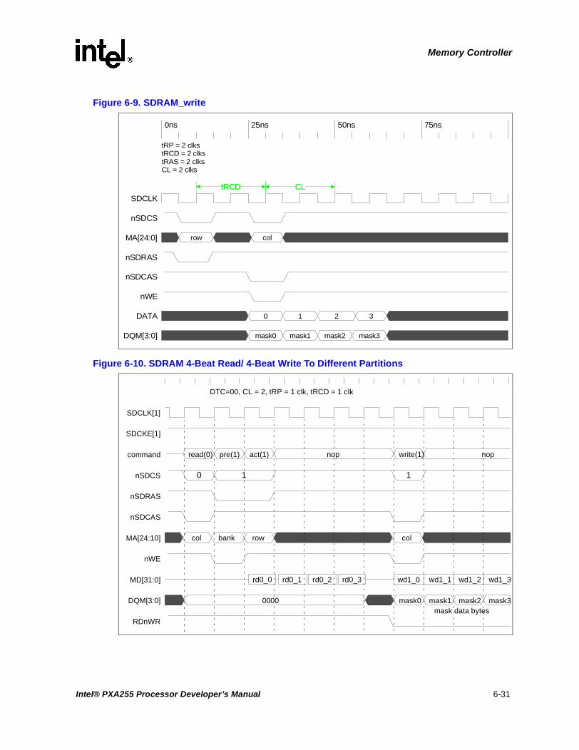
Memory Controller
Figure 6-9. SDRAM_write
Figure 6-10. SDRAM 4-Beat Read/ 4-Beat Write To Different Partitions
CLtRCD CLtRCD
row col
0 1 2 3
mask0 mask1 mask3mask2
tRP = 2 clkstRCD = 2 clkstRAS = 2 clksCL = 2 clks
0ns 25ns 50ns 75ns
SDCLK
nSDCS
MA[24:0]
nSDRAS
nSDCAS
nWE
DATA
DQM[3:0]
read(0) pre(1) act(1) nop write(1) nop
0 1 1
col bank row col
rd0_0 rd0_1 rd0_2 rd0_3 wd1_0 wd1_1 wd1_2 wd1_3
0000 mask0 mask1 mask2 mask3
DTC=00, CL = 2, tRP = 1 clk, tRCD = 1 clk
mask data bytes
SDCLK[1]
SDCKE[1]
command
nSDCS
nSDRAS
nSDCAS
MA[24:10]
nWE
MD[31:0]
DQM[3:0]
RDnWR
Intel® PXA255 Processor Developer’s Manual 6-31

Memory Controller
6.6 Synchronous Static Memory Interface
The synchronous static memory interface supports SMROM and non-SDRAM-like Flash memories. The synchronous static memory can be configured for any of the nCS[3:0] signals. Chip Select 0 must be used for boot memory. Synchronous static memories in bank pairs 1/0 or 3/2 must be set to the same timing.
If any of the nCS[3:0] banks are configured for Synchronous Static Memory via SXCNFG[SXENx], the corresponding half-words of MSC0 (see Section 6.7.2) and MSC1, except the data width in MSCx[RBWx], are ignored.
6.6.1 Synchronous Static Memory Configuration Register (SXCNFG)
SXCNFG controls all synchronous static memory. SXCNFG[15:0] configures chip select signals 0 and 1. SXCNFG[31:16] configures chip select signals 2 and 3.
This is a read/write register. Ignore reads from reserved bits. Write zeros to reserved bits.
Figure 6-11. SDRAM 4-Beat Write / 4-Write Same Bank, Same Row
CLtRCD CLtRCD
row col
0 1 2 3
mask0 mask1 mask3mask2
tRP = 2 clkstRCD = 2 clkstRAS = 2 clksCL = 2 clks
col
4 5 6 7
mask4 mask5 mask6 mask7
0ns 25ns 50ns 75ns 100ns
SDCLK
nSDCS
MA[24:0]
nSDRAS
nSDCAS
nWE
DATA
DQM[3:0]
6-32 Intel® PXA255 Processor Developer’s Manual

Memory Controller
Table 6-13. SXCNFG Bit Definitions (Sheet 1 of 4)
0x4800_001C SXCNFG Memory Controller
Bit 31 30 29 28 27 26 25 24 23 22 21 20 19 18 17 16 15 14 13 12 11 10 9 8 7 6 5 4 3 2 1 0
rese
rved
SX
LA
TC
H2
SX
TP
2
SX
CA
2
SX
RA
2
SXRL2 SXCL2
SX
EN
2
rese
rved
SX
LA
TC
H0
SX
TP
0
SX
CA
0
SX
RA
0
SXRL0 SXCL0
SX
EN
0
Reset 0 0 0 0 0 0 0 0 0 0 0 0 0 0 0 0 0 * * * * * * * * * * * * * 0 *
Bits Name Description
31 — reserved
30 SXLATCH2
SXMEM latching scheme for pair 2/3
0 – Latch return data with fixed delay on MEMCLK1 – Latch return data with return clock
Must be set to a 1 to enable the return clock SDCLK for latching data. For more details on this return data latching, see Section 6.5.4.
29:28 SXTP2
SX Memory type for partition pair 2/3
00 – Synchronous Mask ROM (SMROM)
01 – reserved
10 – non-SDRAM-like Synchronous Flash
11 – reserved
27:26 SXCA2
SX Memory column address bit count for partition pair 2/3
00 – 7 column address bits
01 – 8 column address bits
10 – 9 column address bits
11 – 10 column address bits
25:24 SXRA2
SX Memory row address bit count for partition pair 2/3
00 – 12 row address bits
01 – 13 row address bits
10 – reserved
11 – reserved
23:21 SXRL2
RAS Latency for SX Memory partition pair 2/3.
Number of external SDCLK cycles between receiving the ACT command and the READ command. The unit size for SXRL2 is the external SDCLK cycle.
IF SXTP2 = “00” (SMROM):
000 – 1 clock
001 – 2 clocks
010 – 3 clocks
011 – 4 clocks
100 – 5 clocks
101 – 6 clocks
110 – 7 clocks
111 – 8 clocks
IF SXTP2 = 10 (non-SDRAM timing Fast Flash), this field is not used and must be programmed to 111.
Intel® PXA255 Processor Developer’s Manual 6-33

Memory Controller
20:18 SXCL2
CAS Latency for SX Memory partition pair 2/3
Number of external SDCLK cycles between receiving the READ command and latching the data. The unit size for SXCL2 is the external SDCLK cycle. When SX Memory runs at half the memory clock frequency (MDREFR:K0DB2 = 1), the delay is 2*memclk. When in doubt as to which CAS Latency to use, use the next larger.
IF SXTP2 = 00”(SMROM):
000 – reserved
001 – reserved
010 – 3 clocks
011 – 4 clocks
100 – 5 clocks
101 – 6 clocks
110 – reserved
111 – reserved
IF SXTP2 = 10 (non-SDRAM timing Fast Flash)
000 – reserved
001 – reserved
010 – 3 clocks
011 – 4 clocks
100 – 5 clocks
101 – 6 clocks
110 – 7 clocks
111 – reserved
17:16 SXEN2Enable Bits for SX Memory Partition 2 (bit 16) and Partition 3 (bit 17)
0 – Partition is not Enabled as SX Memory1 – Partition is Enabled as SX Memory
15 — reserved
14 SXLATCH0
SXMEM latching scheme for pair 0/1
0 – Latch return data with fixed delay on MEMCLK1 – Latch return data with return clock
Must always be written with a 1 to enable the return clock SDCLK for latching data. For more detail on this return data latching, see Section 6.5.4
13:12 SXTP0
SX Memory type for partition pair 0/1
00 – Synchronous Mask ROM (SMROM)
01 – reserved
10 – non-SDRAM-like Synchronous Flash
11 – reserved
Table 6-13. SXCNFG Bit Definitions (Sheet 2 of 4)
0x4800_001C SXCNFG Memory Controller
Bit 31 30 29 28 27 26 25 24 23 22 21 20 19 18 17 16 15 14 13 12 11 10 9 8 7 6 5 4 3 2 1 0
rese
rved
SX
LA
TC
H2
SX
TP
2
SX
CA
2
SX
RA
2
SXRL2 SXCL2
SX
EN
2
rese
rved
SX
LA
TC
H0
SX
TP
0
SX
CA
0
SX
RA
0
SXRL0 SXCL0
SX
EN
0
Reset 0 0 0 0 0 0 0 0 0 0 0 0 0 0 0 0 0 * * * * * * * * * * * * * 0 *
Bits Name Description
6-34 Intel® PXA255 Processor Developer’s Manual

Memory Controller
11:10 SXCA0
SX Memory column address bit count for partition pair 0/1
00 – 7 column address bits
01 – 8 column address bits
10 – 9 column address bits
11 – 10 column address bits
9:8 SXRA0
SX Memory row address bit count for partition pair 0/1
00 – 12 row address bits
01 – 13 row address bits
10 – reserved
11 – reserved
7:5 SXRL0
RAS Latency for Synchronous Static (SX) Memory partition pair 0/1
Number of external SDCLK cycles between reception of the ACT command and reception of the READ command. The unit size for SXRL0 is the external SDCLK cycle.
IF SXTP0 = 00 (SMROM):
000 – 1 clock
001 – 2 clocks
010 – 3 clocks
011 – 4 clocks
100 – 5 clocks
101 – 6 clocks
110 – 7 clocks
111 – 8 clocks
IF SXTP0 = 10 (non-SDRAM timing Fast Flash), this field is not used and must be programmed to 111
Table 6-13. SXCNFG Bit Definitions (Sheet 3 of 4)
0x4800_001C SXCNFG Memory Controller
Bit 31 30 29 28 27 26 25 24 23 22 21 20 19 18 17 16 15 14 13 12 11 10 9 8 7 6 5 4 3 2 1 0
rese
rved
SX
LA
TC
H2
SX
TP
2
SX
CA
2
SX
RA
2
SXRL2 SXCL2
SX
EN
2
rese
rved
SX
LA
TC
H0
SX
TP
0
SX
CA
0
SX
RA
0
SXRL0 SXCL0
SX
EN
0
Reset 0 0 0 0 0 0 0 0 0 0 0 0 0 0 0 0 0 * * * * * * * * * * * * * 0 *
Bits Name Description
Intel® PXA255 Processor Developer’s Manual 6-35

Memory Controller
6.6.1.1 SMROM Memory Options
Table 6-15 shows the possible external-to-internal address multiplexing options. For SMROM, there are no bank-address bits, but the corresponding bits are put on the external address bus. The number of banks per device always defaults to four.
4:2 SXCL0
CAS Latency for SX Memory partition pair 0/1
Number of external SDCLK cycles between reception of the READ command and latching of the data. The unit size for SXCL0 is the external SDCLK cycle. When SX Memory is run at half the memory clock frequency (MDREFR:K0DB2 = 1), the delay is 2*MEMCLK When in doubt as to which CAS Latency to use, the next larger must be used.
IF SXTP0 = 00 (SMROM):
000 – reserved
001 – reserved
010 – 3 clocks
011 – 4 clocks
100 – 5 clocks
101 – 6 clocks
110 – reserved
111 – reserved
IF SXTP0 = 10 (non-SDRAM timing Fast Flash)
000 – reserved
001 – reserved
010 – 3 clocks
011 – 4 clocks
100 – 5 clocks
101 – 6 clocks
110 – 7 clocks
111 – reserved
1:0 SXEN0
Enable Bits for SX Memory Partition 0 (bit 0) and Partition 1 (bit 1)
0 – Partition is not enabled as SX Memory1 – Partition is enabled as SX Memory
For reset values, see Section 6.10.
Table 6-13. SXCNFG Bit Definitions (Sheet 4 of 4)
0x4800_001C SXCNFG Memory Controller
Bit 31 30 29 28 27 26 25 24 23 22 21 20 19 18 17 16 15 14 13 12 11 10 9 8 7 6 5 4 3 2 1 0
rese
rved
SX
LA
TC
H2
SX
TP
2
SX
CA
2
SX
RA
2
SXRL2 SXCL2
SX
EN
2
rese
rved
SX
LA
TC
H0
SX
TP
0
SX
CA
0
SX
RA
0
SXRL0 SXCL0
SX
EN
0
Reset 0 0 0 0 0 0 0 0 0 0 0 0 0 0 0 0 0 * * * * * * * * * * * * * 0 *
Bits Name Description
6-36 Intel® PXA255 Processor Developer’s Manual

Memory Controller
6.6.2 Synchronous Static Memory Mode Register Set Configuration Register (SXMRS)
On power up, a MRS command that contains the default boot-up value is written to the external memory if the system is configured to boot out of SMROM (see Section 6.10.2). Otherwise, SXMRS, shown in Table 6-16, is used to issue an MRS command to SMROM. The value written in this register is placed directly on address lines MA<24:10> during the MRS command. Writing to this register triggers a two-stage MRS command that is sent to the external synchronous static memory. The first state issues an MRS command to banks 0 and 1. The second stage issues an MRS command to banks 2 and 3. The corresponding chip select values are only asserted if the memory banks are enabled via the SXCNFG register and the memory type is configured as SMROM.
To write a new MRS value to a synchronous static memory, first enable and configure the memory via the SXCNFG register, then write the SXMRS register. This register is only used for the value written during the MRS command. All values in the SXCNFG register must be programmed correctly to ensure proper device operation (refer to the external memory chip product documentation for proper MRS encoding). Information programmed in the SXCNFG[CL] and
Table 6-15. Synchronous Static Memory External to Internal Address Mapping Options
# Bits
Bank xRow xCol xData
External Address pins at SXMEM RAS Time MA<24:10>
External Address pins at SXMEM CAS Time MA<24:10>
24 23 22 21 20 19 18 17 16 15 14 13 12 11 10 24 23 22 21 20 19 18 17 16 15 14 13 12 11 10
2x12x7x32 22 21 20 19 18 17 16 15 14 13 12 11 10 9 22 21 0 8 7 6 5 4 3 2
2x12x7x16 21 20 19 18 17 16 15 14 13 12 11 10 9 8 21 20 0 7 6 5 4 3 2 1
2x12x8x32 23 22 21 20 19 18 17 16 15 14 13 12 11 10 23 22 0 9 8 7 6 5 4 3 2
2x12x8x16 22 21 20 19 18 17 16 15 14 13 12 11 10 9 22 21 0 8 7 6 5 4 3 2 1
2x12x9x32 24 23 22 21 20 19 18 17 16 15 14 13 12 11 24 23 0 10 9 8 7 6 5 4 3 2
2x12x9x16 23 22 21 20 19 18 17 16 15 14 13 12 11 10 23 22 0 9 8 7 6 5 4 3 2 1
2x12x10x32 25 24 23 22 21 20 19 18 17 16 15 14 13 12 25 24 0 11 10 9 8 7 6 5 4 3 2
2x12x10x16 24 23 22 21 20 19 18 17 16 15 14 13 12 11 24 23 0 10 9 8 7 6 5 4 3 2 1
2x13x7x32 23 22 21 20 19 18 17 16 15 14 13 12 11 10 9 23 22 0 8 7 6 5 4 3 2
2x13x7x16 22 21 20 19 18 17 16 15 14 13 12 11 10 9 8 22 21 0 7 6 5 4 3 2 1
2x13x8x32 24 23 22 21 20 19 18 17 16 15 14 13 12 11 10 24 23 0 9 8 7 6 5 4 3 2
2x13x8x16 23 22 21 20 19 18 17 16 15 14 13 12 11 10 9 23 22 0 8 7 6 5 4 3 2 1
2x13x9x32 25 24 23 22 21 20 19 18 17 16 15 14 13 12 11 25 24 0 10 9 8 7 6 5 4 3 2
2x13x9x16 24 23 22 21 20 19 18 17 16 15 14 13 12 11 10 24 23 0 9 8 7 6 5 4 3 2 1
2x13x10x16 25 24 23 22 21 20 19 18 17 16 15 14 13 12 11 25 24 0 10 9 8 7 6 5 4 3 2 1
Intel® PXA255 Processor Developer’s Manual 6-37
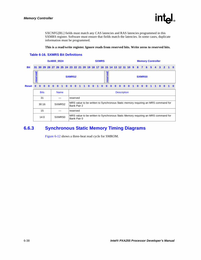
Memory Controller
SXCNFG[RL] fields must match any CAS latencies and RAS latencies programmed in this SXMRS register. Software must ensure that fields match the latencies. In some cases, duplicate information must be programmed.
This is a read/write register. Ignore reads from reserved bits. Write zeros to reserved bits.
6.6.3 Synchronous Static Memory Timing Diagrams
Figure 6-12 shows a three-beat read cycle for SMROM.
Table 6-16. SXMRS Bit Definitions
0x4800_0024 SXMRS Memory Controller
Bit 31 30 29 28 27 26 25 24 23 22 21 20 19 18 17 16 15 14 13 12 11 10 9 8 7 6 5 4 3 2 1 0
rese
rved
SXMRS2
rese
rved
SXMRS0
Reset 0 0 0 0 0 0 1 0 0 0 1 1 0 0 1 0 0 0 0 0 0 0 1 0 0 0 1 1 0 0 1 0
Bits Name Description
31 — reserved
30:16 SXMRS2 MRS value to be written to Synchronous Static memory requiring an MRS command for Bank Pair 2
15 — reserved
14:0 SXMRS0 MRS value to be written to Synchronous Static Memory requiring an MRS command for Bank Pair 0
6-38 Intel® PXA255 Processor Developer’s Manual

Memory Controller
6.6.4 Non-SDRAM Timing SXMEM Operation
Non-SDRAM Timing Synchronous Flash operation resets to asynchronous mode (page-mode for reads and asynchronous single word writes). Software can change the Read Configuration Register (RCR) to synchronous mode (burst-timing synchronous reads and asynchronous single word writes). At boot time, the Non-SDRAM Timing Synchronous Flash operates similarly to an asynchronous boot ROM (See Section 6.8).
Consult the documentation for the memory being used. Table 6-17 is provided only as a reference. The frequency configuration must be determined based on the CLK-to-output delay, the CLK period, and the nADV-to-output delay timing parameters of the Flash device.
The values for this part number are shown as an example. For Intel part number 28F800F3, programming values for this register to ensure proper operation with the processors are shown in Table 6-17.
Software must ensure that the CLK-to-output delay is less than 1 SDCLK period for non-SDRAM Timing Synchronous Flash.
Figure 6-12. SMROM Read Timing Diagram Half-Memory Clock Frequency
NOP ACT NOP READ NOP STOP NOP
row col
d0 d1 d2
0000
CL = 5CL = 5RL = 2RL = 2
0ns 50ns 100ns 150ns
SDCLK
SDCKE
command
nCS[0]
nSDRAS
nSDCAS
MA[24:10]
nWE
nOE
MD
DQM[3:0]
RDnWR
Intel® PXA255 Processor Developer’s Manual 6-39

Memory Controller
Table 6-18 shows sample frequency configurations for programming non-SDRAM Timing Fast Flash. When in doubt, the higher frequency configuration and corresponding CAS latency must be used.
Table 6-17. Read Configuration Register Programming Values
Bits Field Name Value to Program
2:0 BURST LENGTH010
8 Word Burst
5:3 reserved 000
6 CLOCK CONFIGURATION1
Use rising edge of clock
7 BURST SEQUENCE
1
Linear burst Order
(INTEL BURST ORDER IS NOT SUPPORTED)
8 WAIT CONFIGURATIONN/A
nWAIT from the Flash device is ignored by the processor.
9 DATA OUTPUT CONFIGURATION0
Hold data for one clock
10 reserved 0
13:11 FREQUENCY CONFIGURATION
010 -> CAS Latency 3
011 -> CAS Latency 4
100 -> CAS Latency 5
101 -> CAS Latency 6
110 -> CAS Latency 7
Chosen based on the AC Characteristics - Read only Operation section of the Flash device data sheet
14 reserved 0
15 READ MODE0 - Synchronous Operation
1 - Asynchronous Operation
Table 6-18. Frequency Code Configuration Values Based on Clock Speed (Sheet 1 of 2)
MEMCLKFrequency
SDCLK0Frequency
MDREFR:K0DB2
ValidFrequency
Configurations
CorrespondingCAS Latencies
20 20 0 2 / 3 / 4 / 5 / 6 3 / 4 / 5 / 6 / 7
33 33 0 3 / 4 / 5 / 6 4 / 5 / 6 / 7
5050 0 4 / 5 / 6 5 / 6 / 7
25 1 2 / 3 / 4 / 5 / 6 3 / 4 / 5 / 6 / 7
6666 0 5 / 6 6 / 7
33 1 3 / 4 / 5 / 6 4 / 5 / 6 / 7
100 50 1 4 / 5 / 6 5 / 6 / 7
118 59 1 5 / 6 6 / 7
6-40 Intel® PXA255 Processor Developer’s Manual

Memory Controller
6.6.4.1 Non-SDRAM Timing Flash Read Timing Diagram
Figure 6-12 shows the burst-of-eight read timing diagram.
In Figure 6-13, the following timing parameters apply:
• nADV asserted time = 1 MEMCLK
• MA, nCS setup to nADV asserted = 1 MEMCLK
• nADV deasserted to nOE asserted = Code - 2 MEMCLKs
133 66 1 5 / 6 6 / 7
147 Not supported
166 Not supported
Table 6-18. Frequency Code Configuration Values Based on Clock Speed (Sheet 2 of 2)
MEMCLKFrequency
SDCLK0Frequency
MDREFR:K0DB2
ValidFrequency
Configurations
CorrespondingCAS Latencies
Figure 6-13. Burst-of-Eight Synchronous Flash Timing Diagram (non-divide-by-2 mode)
byte address
0000
SXCNFG[CL]
This diagram is for SXCNFG:CL = "100" (CAS Latency = 5) (Frequency Code Configuration = 4)
0ns 50ns 100ns 150ns 200ns
SDCLK[0]
MA[19:0]
nCS[0]
nADV(nSDCAS)
nOE
nWE
MD[31:0]
DQM[3:0]
Intel® PXA255 Processor Developer’s Manual 6-41

Memory Controller
For divide-by-two mode, the following timing parameters apply:
• nADV assert time = 3 MEMCLKs
• MA, nCS setup to nADV asserted = 1 MEMCLK
• nADV deasserted to nOE asserted = (Code * 2) - 4 MEMCLKs
6.6.4.2 K3 Synchronous StrataFlash Reset
The PXA255 processor nRESET_OUT pin must be connected to the K3 #RST pin for Hardware reset, Watchdog reset and sleep mode to work properly. GPIO reset however does not reset the contents of the memory controller configuration register. If GPIO reset operation is required, a state machine is necessary between nRESET, nRESET_OUT, GPIO[1], and #RST to ensure that #RST is asserted during Hardware reset, Watchdog reset, and sleep mode, and not asserted during GPIO reset. Figure 6-14 shows the required logic. GPIO_a is an unused GPIO that is driven low by software during the initialization sequence and left high during normal operation. After this is completed, then enable GPIO reset.
If Watchdog reset is not necessary, a secondary GPIO can control nRESET_OUT using the equation #RST = nRESET & (nRESET_OUT | GPIO_a). This allows sleep mode entry to reset the flash memory while keeping it in synchronous mode during a GPIO reset. Figure 6-15 shows the required logic. GPIO_a is an unused GPIO that is kept high during normal operation and driven low before sleep mode entry.
6.7 Asynchronous Static Memory
6.7.1 Static Memory Interface
The Static Memory interface is made up of six chip selects: nCS[5:0]. The chip selects can be configured as the following:
Figure 6-14. Flash Memory Reset Using State Machine
nS
nR
GPIO[1]
GPIO_a
Q
nRESET_OUTnRESET
#RST
K3 Flash
Figure 6-15. Flash Memory Reset Logic if Watchdog Reset is Not Necessary
GPIO_a
nRESET_OUTnRESET
#RST
K3 Flash
6-42 Intel® PXA255 Processor Developer’s Manual

Memory Controller
• Non-burst ROM or Flash memory
• Burst ROM or Flash
• SRAM
• SRAM-like variable latency I/O devices
The Variable Latency I/O interface differs from SRAM in that it allows the use of the data-ready input signal, RDY, to insert a variable number of memory-cycle wait states. The data bus width for each chip-select region can be programmed as 16- or 32-bit. nCS[3:0] can also be configured for Synchronous Static Memory (refer to Section 6.6). During Variable Latency I/O writes, nPWE is used instead of nWE so SDRAM refreshes can be executed while performing the VLIO transfers.
The use of the signals nOE, nWE, and nPWE is summarized below:
• nOE is asserted for all reads
• nWE is asserted for Flash and SRAM writes
• nPWE is asserted for Variable Latency I/O writes
For SRAM and Variable Latency I/O implementations, DQM[3:0] signals are used for the write byte enables, where DQM[3] corresponds to the MSB. The processor supplies 26-bits of byte address for access of up to 64 Mbytes per chip select. This byte address is sent out on the 26 external address pins. Do not connect MA[1:0] for 32-bit systems. Do not connect MA[0] for 16-bit systems (the PXA255 processor operating in 16-bit mode). For all reads on a 32 bit system DQM[3:0] and MA[1:0] are 0. For all reads on a 16 bit system DQM[1:0] and MA[0] are 0. In the timing diagrams, these byte addresses are shown and referred to as “addr”.
Intel® PXA255 Processor Developer’s Manual 6-43
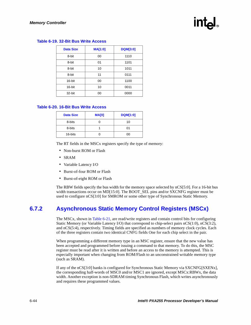
Memory Controller
The RT fields in the MSCx registers specify the type of memory:
• Non-burst ROM or Flash
• SRAM
• Variable Latency I/O
• Burst-of-four ROM or Flash
• Burst-of-eight ROM or Flash
The RBW fields specify the bus width for the memory space selected by nCS[5:0]. For a 16-bit bus width transactions occur on MD[15:0]. The BOOT_SEL pins and/or SXCNFG register must be used to configure nCS[3:0] for SMROM or some other type of Synchronous Static Memory.
6.7.2 Asynchronous Static Memory Control Registers (MSCx)
The MSCx, shown in Table 6-21, are read/write registers and contain control bits for configuring Static Memory (or Variable Latency I/O) that correspond to chip-select pairs nCS(1:0), nCS(3:2), and nCS(5:4), respectively. Timing fields are specified as numbers of memory clock cycles. Each of the three registers contain two identical CNFG fields One for each chip select in the pair.
When programming a different memory type in an MSC register, ensure that the new value has been accepted and programmed before issuing a command to that memory. To do this, the MSC register must be read after it is written and before an access to the memory is attempted. This is especially important when changing from ROM/Flash to an unconstrained writable memory type (such as SRAM).
If any of the nCS[3:0] banks is configured for Synchronous Static Memory via SXCNFG[SXENx], the corresponding half-words of MSC0 and/or MSC1 are ignored, except MSCx:RBWx, the data width. Another exception is non-SDRAM timing Synchronous Flash, which writes asynchronously and requires these programmed values.
Table 6-19. 32-Bit Bus Write Access
Data Size MA[1:0] DQM[3:0]
8-bit 00 1110
8-bit 01 1101
8-bit 10 1011
8-bit 11 0111
16-bit 00 1100
16-bit 10 0011
32-bit 00 0000
Table 6-20. 16-Bit Bus Write Access
Data Size MA[0] DQM[1:0]
8-bits 0 10
8-bits 1 01
16-bits 0 00
6-44 Intel® PXA255 Processor Developer’s Manual

Memory Controller
This is a read/write register. Ignore reads from reserved bits. Write zeros to reserved bits.
Table 6-21. MSC0/1/2 Bit Definitions (Sheet 1 of 3)
0x4800_00080x4800_000C0x4800_0010
MSC0MSC1MSC2
Memory Controller
Bit 31 30 29 28 27 26 25 24 23 22 21 20 19 18 17 16 15 14 13 12 11 10 9 8 7 6 5 4 3 2 1 0
RB
UF
F1/
3/5
RRR1/3/5 RDN1/3/5 RDF1/3/5
RB
W1/
3/5
RT1/3/5
RB
UF
F0/
2/4
RR
R0/
2/4
RDN0/2/4 RDF0/2/4
RB
W0/
2/4
RT0/2/4
Reset 0 1 1 1 1 1 1 1 1 1 1 1 0 0 0 0 0 1 1 1 1 1 1 1 1 1 1 1 * 0 0 0
Bits Access Name Description
15 R/W RBUFFx
Return Data Buffer vs. Streaming behavior.
When slower memory devices are being used in the system (e.g. VLIO, slow SRAM/ROM), this bit must be reset to allow the system to not have to remain idle while all data is being read from the device. By resetting this bit, the system is allowed to process other information. When set, the internal bus may halt while all data is returned from the device. The value of the RBUFF bit does not affect the behavior of the external memory bus. Once a transaction begins on the memory bus, it must be completed before another transaction starts.
When Synchronous Static memory devices have been enabled for a given bank, this value will default to Streaming behavior (assuming a faster device). The register bit will still read as 0 (Return Data Buffer) unless it has specifically been programmed to a 1. This cannot be overridden.
0 – Slower device (Return Data Buffer)1 – Faster device (Streaming behavior)
14:12 R/W RRRx<2:0>
ROM/SRAM recovery time.
Chip select deasserted after a read/write to next chip select (including the same static memory bank) or nSDCS asserted is equal to (RRRx * 2) memclks.
This field must be programmed with the maximum of tOFF (divided by 2), write pulse high time (Flash/SRAM), and write recovery before read (Flash).
11:8 R/W RDNx<3:0>
ROM delay next access
Address to data valid for subsequent access to burst ROM or Flash is equal to (RDNx + 1) memclks.
nWE assertion for write accesses to SRAM is equal to (RDFx + 1) memclks.
The nOE (nPWE) deassert time between each beat of read/write for Variable Latency I/O is equal to (RDNx + 2) memclks. For variable latency I/O, this number must be greater than or equal to 2.
Intel® PXA255 Processor Developer’s Manual 6-45

Memory Controller
7:4 R/W RDFx<3:0>
ROM delay first access.
RDF programmed RDF value interpreted
0-11 0-11
12 13
13 15
14 18
15 23
Address to data valid for the first read access from all devices except VLIO is equal to (RDFx + 2) memclks.
Address to data valid for subsequent read accesses to non-burst devices is equal to (RDFx + 1) memclks.
nWE assertion for write accesses (which are non-burst) to all Flash is equal to (RDFx + 1) memclks.
nOE (nPWE) assert time for each beat of read (write) is equal to (RDFx + 1) memclks for Variable Latency I/O (nCS[5:0]). For Variable Latency I/O, RDFx must be greater than or equal to 3.
3 R/W RBWx
ROM bus width
0 – 32 bits1 – 16 bits
For reset value for RBW0, see Section 6.8.
This value must be programmed with all memory types including Synchronous Static Memory.
This value must not change during normal operation.
Table 6-21. MSC0/1/2 Bit Definitions (Sheet 2 of 3)
0x4800_00080x4800_000C0x4800_0010
MSC0MSC1MSC2
Memory Controller
Bit 31 30 29 28 27 26 25 24 23 22 21 20 19 18 17 16 15 14 13 12 11 10 9 8 7 6 5 4 3 2 1 0
RB
UF
F1/
3/5
RRR1/3/5 RDN1/3/5 RDF1/3/5
RB
W1/
3/5
RT1/3/5
RB
UF
F0/
2/4
RR
R0/
2/4
RDN0/2/4 RDF0/2/4
RB
W0/
2/4
RT0/2/4
Reset 0 1 1 1 1 1 1 1 1 1 1 1 0 0 0 0 0 1 1 1 1 1 1 1 1 1 1 1 * 0 0 0
Bits Access Name Description
6-46 Intel® PXA255 Processor Developer’s Manual

Memory Controller
2:0 R/W RTx<2:0>
ROM type
000 - Nonburst ROM or Flash Memory
001 - SRAM
010 - Burst-of-four ROM or Flash (with non-burst writes)
011 - Burst-of-eight ROM or Flash (with non-burst writes)
100 - Variable Latency I/O (VLIO)
101 - reserved
110 - reserved
111 - reserved
Burst refers to the device’s timing. When the subsequent reads from the device take less time than the first read from a device, it is referred to as burst timing. The address bits must also be taken into account for burst timing devices. For example, in a burst-of-four device, only the lower two non-byte address bits can change for burst timing. For 32-bit devices, this is MA[3:2]. The address order can go 00, 01, 10, 11 where the reads from 01, 10, and 11, take less time to come out of the device. For burst-of-eight devices, the lower three non-byte address bits can change. Writes to these devices are non-burst.
Table 6-21. MSC0/1/2 Bit Definitions (Sheet 3 of 3)
0x4800_00080x4800_000C0x4800_0010
MSC0MSC1MSC2
Memory Controller
Bit 31 30 29 28 27 26 25 24 23 22 21 20 19 18 17 16 15 14 13 12 11 10 9 8 7 6 5 4 3 2 1 0
RB
UF
F1/
3/5
RRR1/3/5 RDN1/3/5 RDF1/3/5
RB
W1/
3/5
RT1/3/5
RB
UF
F0/
2/4
RR
R0/
2/4
RDN0/2/4 RDF0/2/4
RB
W0/
2/4
RT0/2/4
Reset 0 1 1 1 1 1 1 1 1 1 1 1 0 0 0 0 0 1 1 1 1 1 1 1 1 1 1 1 * 0 0 0
Bits Access Name Description
Intel® PXA255 Processor Developer’s Manual 6-47

Memory Controller
Table 6-22 provides a comparison of supported Asynchronous Static Memory types.
6.7.3 ROM Interface
The processor provides programmable timing for both burst and non-burst ROMs. The RDF field in MSCx is the latency (in memory clock cycles) for the first, and all subsequent, data beats from non-burst ROMs, and the first data beat from a burst ROM. RDN is the latency for the burst data beats after the first for burst ROMs. RRR delays the following access to a different memory space to allow time for the current ROM to three-state the data bus.
RRR must be programmed with the maximum tOFF value, as specified by the ROM manufacturer.
For hardware reset initialization values, refer to Section 6.8. MSC0[15:0] is selected when the address space corresponding to nCS0 is accessed. The processor supports a ROM burst size of 1, 4, or 8 by configuring the MSCx[RTx] register bits to 0, 2 or 3 respectfully.
Table 6-22. Asynchronous Static Memory and Variable Latency I/O Capabilities
MSCx[RTx]DeviceType
Timing (Memory Clocks)
BurstRead
AddressAssert
nOEAssert
BurstnOE
Deassert
BurstWrite
AddressAssert
nWEAssert
BurstnWEDe-
assert
000
Non-burst
ROM or
Flash
RDF+1 RDF+1 0 N/A RDF+1 N/A
001 SRAM RDF+1 RDF+1 0 RDN+2 RDN+1 1
010
Burst-of-4
ROM or
Flash (non-
burst writes)
RDF+1
(0,4)
RDN+1
(1:3,5:7)
RDF+1
(0,4)
RDN+1
(1:3,5:7)
0 N/A RDF+1 N/A
011
Burst-of-8
ROM or
Flash
(non-burst
writes)
RDF+1
(0)
RDN+1
(1:7)
RDF+1
(0)
RDN+1
(1:7)
0 N/A RDF+1 N/A
100Variable
Latency I/O
RDF+
RDN+2+waits
RDF+1+
waitsRDN+2
RDF+
RDN+2+waits
RDF+1+
waitsRDN+2
6-48 Intel® PXA255 Processor Developer’s Manual

Memory Controller
6.7.3.1 ROM Timing Diagrams and Parameters
Figure 6-17, Figure 6-18, and Figure 6-19 show the timings for burst and non-burst ROMs.
Figure 6-17. 32-Bit Burst-of-Eight ROM or Flash Read Timing Diagram (MSC0[RDF] = 4, MSC0[RDN] = 1, MSC0[RRR] = 1)
0 1 2 3 4 5 6 7
"00"
"0000"
tDOHtDSOH
tCEHtCES
RRR*2+1RDF+1
RDN+1RDF+2 RDN+1RDF+2
tAS
tAS = Address Setup to nCS asserted = 1 clk_memtCES = nCS setup to nOE asserted = 0 nstCEH = nCS hold from nOE deasserted = 0 nstDSOH = MD setup to Address changing = 1.5 clk_mems plus board routing delaystDOH = MD hold from Address changing = 0 ns
* MSC0:RDF0 = 4, RDN0 = 1, RRR0 = 1
0ns 50ns 100ns 150ns 200ns 250ns
CLK_MEM
nCS[0]
MA[25:5]
MA[4:2]
MA[1:0]
nADV(nSDCAS)
nOE
nWE
RDnWR
MD[31:0]
DQM[3:0]
nCS[1]
Intel® PXA255 Processor Developer’s Manual 6-49

Memory Controller
Figure 6-18. Eight-Beat Burst Read from 16-Bit Burst-of-Four ROM or Flash (MSC0[RDF] = 4, MSC0[RDN] = 1, MSC0[RRR] = 0)
0 1 2 3 4 5 6 7
"00"
"0000"
tDOHtDSOH
tCEHtCES
RRR*2+1RDF+1
RDN+1RDF+2 RDN+1RDF+2
tAS
tAS = Address Setup to nCS asserted = 1 clk_memtCES = nCS setup to nOE asserted = 0 nstCEH = nCS hold from nOE deasserted = 0 nstDSOH = MD setup to Address changing = 1.5 clk_mems plus board routing delaystDOH = MD hold from Address changing = 0 ns
* MSC0:RDF0 = 4, RDN0 = 1, RRR0 = 1
0ns 50ns 100ns 150ns 200ns 250ns
CLK_MEM
nCS[0]
MA[25:5]
MA[4:2]
MA[1:0]
nADV(nSDCAS)
nOE
nWE
RDnWR
MD[31:0]
DQM[3:0]
nCS[1]
6-50 Intel® PXA255 Processor Developer’s Manual

Memory Controller
6.7.4 SRAM Interface Overview
The processor provides a 16-bit or 32-bit asynchronous SRAM interface that uses the DQM pins for byte selects on writes. nCS[5:0] select the SRAM bank. nOE is asserted on reads and nWE is asserted on writes. Address bits MA[25:0] allow up to 64 Mbytes of SRAM per bank to be addressed.
The timing for a read access is identical to that for a non-burst ROM (see Section 6.7.3.1). The RDF fields in the MSCx registers select the latency for a read access. The MSCx[RDN] field controls the nWE low time during a write cycle. MSCx[RRR] is the time from nCS deassertion after a memory access to the start of another memory access. MSCx[RTx] must be configured to 0b001 to select SRAM.
6.7.4.1 SRAM Timing Diagrams and Parameters
As shown in Figure 6-17, SRAM reads have the same timing as non-burst ROMs, except DQM[3:0] are used as byte selects. For all reads, DQM[3:0] are 0b0000. During writes, all 32 data pins are actively driven by the processor regardless of the state of the individual DQM pins.
Figure 6-19. 32-Bit Non-burst ROM, SRAM, or Flash Read Timing Diagram - Four Data Beats (MSC0[RDF] = 4, MSC0[RRR] = 1)
0 1 2 3
00
0000
RDF+1RRR*2+1RDF+1
RDF+1RDF+1RDF+1RDF+2 RDF+1RDF+2
MEMCLK
nCS[0]
MA[25:2]
MA[1:0]
nADV(nSDCAS)
nOE
nWE
RDnWR
MD[31:0]
DQM[3:0]
nCS[1]
Intel® PXA255 Processor Developer’s Manual 6-51

Memory Controller
For writes to SRAM, if all byte enables are turned off (masking out the data, DQM = 1111), then the write enable are 1 (nWE = 1) for this write beat. This can result in a period when nCS is asserted, but neither nOE nor nWE is asserted. This happens with a write of 1 beat to SRAM, but all byte enables are turned off.
Figure 6-20 shows the timing for SRAM writes.
In Figure 6-20, the parameters are defined as follows:
• tAS = Address setup to nCS = 1 MEMCLK
• tCES = nCS setup to nWE = 2 MEMCLKs
• tASW = Address setup to nWE low (asserted) = 1 MEMCLK
• tDSWH = Write data setup, DQM to nWE high (deasserted) = (RDN+2) = 4 MEMCLKs
• tDH = Data, DQM hold after nWE high (deasserted) = 1 MEMCLK
• tCEH = nCS held asserted after nWE deasserted = 1 MEMCLK
• tAH = Address hold after nWE deasserted = 1 MEMCLK
• nWE high time between burst beats = 2 MEMCLKs
Figure 6-20. 32-Bit SRAM Write Timing Diagram (4-beat Burst (MSC0[RDN] = 2, MSC0[RRR] = 1)
0 1 2 3
byte addr byte addr byte addr byte addr
D0 D1 D2 D3
mask0 mask1 mask2 mask3
tDHtDSWH
tCEH
RDN+1RRR*2+1
RDN+1RDN+1RDN+1RDN+1
tASW
RDN+1
tAH
RDN+1
tCES
RDN
tAS
mask data bytes
MEMCLK
nCS[0]
MA[25:2]
MA[1:0]
nWE
nOE
RDnWR
MD[31:0]
DQM[3:0]
nCS[1]
nADV(nSDCAS)
6-52 Intel® PXA255 Processor Developer’s Manual

Memory Controller
6.7.5 Variable Latency I/O (VLIO) Interface Overview
Variable Latency I/O read accesses differ from SRAM read accesses in that the nOE toggles for each beat of a burst. The first nOE assertion occurs two memory cycles after the assertion of the chip select nCS<x>. Also, for Variable Latency I/O writes, nPWE is used instead of nWE so SDRAM refreshes can be executed while performing the VLIO transfers. Variable Latency I/O is selected by programming the MSCx[RTx] bits as 0b100.
Both reads and writes for VLIO differ from SRAM in that the processor samples the data-ready input, RDY. The RDY signal is level sensitive and goes through a two-stage synchronizer on input. When the internal RDY signal is high, the I/O device is ready for data transfer. This means that for a transaction to complete at the minimum assertion time for either nOE or nPWE (RDF+1), the RDY signal must be high two clocks prior to the minimum assertion time for either nOE or nPWE (RDF-1). Data will be latched on the rising edge of MEMCLK once the internal RDY signal is high and the minimum assertion time of RDF+1 has been reached. Once the data has been latched, the address may change on the next rising edge of MEMCLK or any cycles thereafter. The nOE or nPWE signal will de-assert one MEMCLK after data is latched. Before a subsequent data beat, nOE or nPWE remains deasserted for RDN+2 memory cycles. The chip select and byte selects, DQM[3:0], remain asserted for one memory cycle after the burst’s final nOE or nPWE deassertion.
For both reads and writes from/to VLIO, a DMA mode exists that does not increment the address to the VLIO, which will allow port-type VLIO chips to interface to the processor. See DCMDx[INCSRCADDR] and DCMDx[INCTRGADDR] in Table 5-12, “DCMDx Bit Definitions” on page 5-24.
For writes to VLIO, if all byte enables are turned off, masking out the data, DQM = 1111, the write enable is suppressed (nPWE = 1) for this write beat to VLIO. This can result in a period when nCS is asserted, but neither nOE nor nPWE is asserted (this happens when there is a write of 1 beat to VLIO, but all byte enables are turned off).
Intel® PXA255 Processor Developer’s Manual 6-53

Memory Controller
6.7.5.1 Variable Latency I/O Timing Diagrams and Parameters
Figure 6-21 shows the timing for Variable Latency I/O reads and Figure 6-22 shows the timing for Variable Latency I/O writes.
Figure 6-21. 32-Bit Variable Latency I/O Read Timing (Burst-of-Four, One Wait Cycle Per Beat) (MSC0[RDF] = 2, MSC0[RDN] = 2, MSC0[RRR] = 1)
addr addr + 1 addr + 2 addr + 3
"00"
"0000"
RDF+1+Waits RRR*2+1
RDN+2
RDF+1+Waits
RDN+
RDF+1+Waits
RDN+2
RDF+1+Waits
RDN+
RDF+1+Waits
RDN
RDF+1+Waits
RDN+2
tAS
tAS = Address Setup to nCS asserted = 1 clk_memtAH = Address Hold from nOE deasserted = 1 clk_memtASRW0 = Address Setup to nOE asserted (1st access) = 3 clk_memstASRWn = Address Setup to nOE asserted (next access(s)) = RDN clk_memstCES = nCS setup to nOE asserted = 2 clk_memstCEH = nCS hold from nOE deasserted = 1 clk_memtDSOH = MD setup to Address changing = 1.5 clk_mems plus board routing delaystDOH = MD hold from Address changing = 0 nstRDYH = RDY Hold from nOE deasserted = 0 ns
0 Waits
*MSC0: RDF0 = 3, RDN0 = 2, RRR0 = 1
1 Wait 2 Waits 3 Waits
0ns 100ns 200ns 300ns
CLK_MEM
nCS[0]
MA[25:2]
MA[1:0]
nOE
nPWE
RDnWR
RDY
RDY_sync
MD[31:0]
DQM[3:0]
6-54 Intel® PXA255 Processor Developer’s Manual

Memory Controller
In Figure 6-21 and Figure 6-22, some of the parameters are defined as follows:
• tAS = Address setup to nCS = 1 MEMCLK
• tCES = nCS setup to nOE or nPWE = 2 MEMCLKs
• tASRW0 = Address setup to nOE or nPWE low (asserted) = 3 MEMCLKs
• tASRWn = Address setup to nOE or nPWE low (asserted) = RDN MEMCLKs
• tDSWH,min = Minimum write data, DQM setup to nPWE high (deasserted) = (RDF+2) MEMCLKs
• tDHW = Data, DQM hold after nPWE high (deasserted) = 1 MEMCLK
• tDHR = Data hold required after nOE deasserted = 0 ns
• tCEH = nCS held asserted after nOE or nPWE deasserted = 1 MEMCLK
• tAH = Address hold after nOE or nPWE deasserted = 1 MEMCLK
• nOE or nPWE high time between burst beats = (RDN+2) MEMCLKs
Figure 6-22. 32-Bit Variable Latency I/O Write Timing (Burst-of-Four, Variable Wait Cycles Per Beat)
0 1 2 3
byte addr byte addr byte addr byte addr
D0 D1 D2 D3
mask0 mask1 mask2 mask3
tDHtDSWH
tCEH
RRR*2+1
RDF+1+Waits
RDN+2
tASWN
RDF+1+Waits
RDN+
tAHtASRW0
tCES
tAS
MEMCLK
nCS[0]
MA[25:2]
MA[1:0]
nPWE
nOE
RDnWR
RDY
MD[31:0]
DQM[3:0]
nCS[1]
Intel® PXA255 Processor Developer’s Manual 6-55

Memory Controller
6.7.6 FLASH Memory Interface
The processor provides an SRAM-like interface for access of Flash memory. The RDF fields in the MSCx registers are the latency for each read access to non-burst Flash, or the first read access to burst Flash. The RDF fields also control the nWE low time during a write cycle to Flash. The RDN field controls subsequent read access times to burst Flash and the nWE low time during a write cycle to non-burst Flash. RRR is the time from nCS deassertion after a read to the start of a read from a different memory, or after a write to another memory access.
Reads from Flash memory have the following requirements:
• Because Flash defaults to Read-Array mode, burst reads are permitted out of Flash, which allows instruction caching and DMA reads from Flash.
• Software partitions commands and data and writes the commands to Flash before the read. The Memory controller does not insert any commands before Flash reads.
Writes to Flash memory have the following requirements:
• Flash memory space must be uncacheable and unbuffered.
• Burst writes to Flash are not supported. Writes to Flash must be exactly the width of the populated Flash devices on the data bus and must be a burst length of one write, for example no byte writes to a 32-bit bus. The allowable writes are: 2 bytes written to a 16-bit bus, and 4-bytes written to a 32-bit bus.
• For asynchronous writes to Flash, the command and data must be given in separate write instructions to the Memory controller, the first carries the command, the next carries the data.
• The Memory controller does not insert any commands before Flash writes. Software must write the commands and data in the correct order.
• No Flash writes can be bursts. DMA must never write to Flash.
For writes to Flash, if all byte enables are turned off (masking out the data, DQM = 1111), the write enable is suppressed (nWE = 1) for the write beat, which can result in a period when nCS is asserted, but neither nOE nor nWE is asserted. This happens when there is a 1-beat write to Flash, but all byte enables are turned off.
6.7.6.1 FLASH Memory Timing Diagrams and Parameters
Non-burst Flash reads have the same timing as non-burst ROMs reads. Figure 6-23 shows the timing for writes to non-burst asynchronous Flash.
6-56 Intel® PXA255 Processor Developer’s Manual

Memory Controller
In Figure 6-23 some of the parameters are defined as follows:
• tAS = Address setup to nCS = 1 MEMCLK
• tCES = nCS setup to nWE = 2 MEMCLKs
• tASW = Address setup time to nWE asserted = 3 MEMCLKs
• tDSWH = Write data, DQM setup to nWE deasserted = (RDF+2) MEMCLKs
• tDH = Data, DQM hold after nWE deasserted = 1 MEMCLKs
• tCEH = nCS held asserted after nWE deasserted = 1 MEMCLK
• tAH = Address hold after nWE deasserted = 1 MEMCLKs
Figure 6-23. Asynchronous 32-Bit Flash Write Timing Diagram (2 Writes)
command address data address
'0' '0'
CMD DATA
"00" "00"
tDHtDSWH
tDHtDSWH
RDF+1
tAHtCEH
RDF+1
tCEStASW
RDF+1
tAHtCEH
RDF+1
tCEStASW
tAStAS
RRR*2+1RRR*2+1
tAS = Address Setup to nCS asserted = 1 clk_memtAH = Address Hold from nWE deasserted = 2 clk_memtASW = Address Setup to nWE asserted = 3 clk_memtCES = nCS setup to nWE asserted = 2 clk_memstCEH = nCS hold from nWE deasserted = 1 clk_memtDSWH = MD/DQM setup to nWE deasserted = RDF+2 clk_memstDH = MD/DQM hold from nWE deasserted = 1 clk_mem
* A command and data write to Flash MSC0:RDF0 = 2, RRR0 = 2
0ns 50ns 100ns 150ns 200ns
CLK_MEM
nCS[0]
MA[25:2]
MA[1:0]
nWE
nOE
RDnWR
MD[31:0]
DQM[3:0]
nADV(nSDCAS)
Intel® PXA255 Processor Developer’s Manual 6-57

Memory Controller
6.8 16-Bit PC Card/Compact Flash Interface
The following sections provide information on the card interface based on the PC Card Standard - Volume 2 - Electrical Specification, Release 2.1, and CF+ and CompactFlash Specification Revision 1.4. Only 8- and 16-bit data transfers are supported.
6.8.1 Expansion Memory Timing Configuration Register
MCMEM0, MCMEM1, MCATT0, MCATT1, MCIO0, and MCIO1 are read/write registers that contain control bits for configuring the timing of the 16-bit PC Card/Compact Flash interface.
The programming of each of the four fields in each of the six registers lets software to individually select the duration of accesses to I/O, common memory, and attribute space for each of two 16-bit PC Card/Compact Flash card slots.
Refer to Table 6-23 through Table 6-25 for bitmaps of the MCMEMx registers. Also refer to Table 6-26. Refer to Figure 6-29 and Figure 6-30 for a 16-bit PC Card/Compact Flash timing diagram.
These are read/write registers. Ignore reads from reserved bits. Write zeros to reserved bits.
These are read/write registers. Ignore reads from reserved bits. Write zeros to reserved bits.
Table 6-23. MCMEM0/1 Bit Definitions
0x4800_00280x4800_002C
MCMEM0MCMEM1 Memory Controller
Bit 31 30 29 28 27 26 25 24 23 22 21 20 19 18 17 16 15 14 13 12 11 10 9 8 7 6 5 4 3 2 1 0
reserved MEMx_HOLD
rese
rved
MEMx_ASST MEMx_SET
Reset 0 0 0 0 0 0 0 0 0 0 0 0 0 0 0 0 0 0 0 0 0 0 0 0 0 0 0 0 0 0 0 0
Bits Name Description
31:20 — reserved
19:14 MCMEMx_HOLD
Minimum Number of memory clocks to set up address before command assertion for MCMEM for socket x is equal to MCMEMx_HOLD + 2.
13:12 — reserved
11:7 MCMEMx_ASST
Code for the command assertion time. See Table 6-26 for a description of this code and its affects on the command assertion.
6:0MCMEMx_S
ETMinimum Number of memory clocks to set up address before command assertion for MCMEM for socket x is equal to MCMEMx_SET + 2.
6-58 Intel® PXA255 Processor Developer’s Manual

Memory Controller
These are read/write registers. Ignore reads from reserved bits. Write zeros to reserved bits.
Table 6-24. MCATT0/1 Bit Definitions
0x4800_00300x4800_0030
MCATT0MCATT1 Memory Controller
Bit 31 30 29 28 27 26 25 24 23 22 21 20 19 18 17 16 15 14 13 12 11 10 9 8 7 6 5 4 3 2 1 0
reserved ATTx_HOLD
rese
rved
ATTx_ASST ATTx_SET
Reset 0 0 0 0 0 0 0 0 0 0 0 0 0 0 0 0 0 0 0 0 0 0 0 0 0 0 0 0 0 0 0 0
Bits Name Description
31:20 — reserved
19:14MCATTx_HO
LDMinimum Number of memory clocks to set up address before command assertion for MCATT for socket x is equal to MCATTx_HOLD + 2.
13:12 — reserved
11:7MCATTx_AS
STCode for the command assertion time. See Table 6-26 for a description of this code and its affects on the command assertion.
6:0 MCATTx_SET
Minimum Number of memory clocks to set up address before command assertion for MCATT for socket x is equal to MCATTx_SET + 2.
Table 6-25. MCIO0/1 Bit Definitions
0x4800_00380x4800_003C
MCIO0MCIO1 Memory Controller
Bit 31 30 29 28 27 26 25 24 23 22 21 20 19 18 17 16 15 14 13 12 11 10 9 8 7 6 5 4 3 2 1 0
reserved IOx_HOLD
rese
rved
IOx_ASST IOx_SET
Reset 0 0 0 0 0 0 0 0 0 0 0 0 0 0 0 0 0 0 0 0 0 0 0 0 0 0 0 0 0 0 0 0
Bits Name Description
31:20 — reserved
19:14 MCIOx_HOLD
Minimum Number of memory clocks to set up address before command assertion for MCIO for socket x is equal to MCIOx_HOLD + 2.
13:12 — reserved
11:7 MCIOx_ASST
Code for the command assertion time. See Table 6-26 for a description of this code and its affects on the command assertion.
6:0 MCIOx_SET Minimum Number of memory clocks to set up address before command assertion for MCIO for socket x is equal to MCIOx_SET + 2.
Intel® PXA255 Processor Developer’s Manual 6-59

Memory Controller
Table 6-26. Card Interface Command Assertion Code Table
MCMEMx_ASSTMCATTx_ASSTMCIOx_ASST
x_ASST_WAITx_ASST_HOLD x_ASST_WAIT +
x_ASST_HOLD
(nPIOW asserted) (nPIOR asserted) (nPIOW asserted) (nPIOR asserted)
ProgrammedBit Value
Codedecimal
value
# MEMCLKs(minimum)
to wait beforechecking fornPWAIT=’1’
# MEMCLKs(minimum)to assert
command(nPIOW) afternPWAIT=’1’
# MEMCLKs(minimum)to assert
command(nPIOR) afternPWAIT=’1’
# MEMCLKs(minimum)command
assertion time
# MEMCLKs(minimum)command
assertion time
(Code) (Code) (Code + 2) (2*Code + 3) (2*Code + 4) (3*Code + 5) (3*Code + 6)
00000 0 2 3 4 5 6
00001 1 3 5 6 8 9
00010 2 4 7 8 11 12
00011 3 5 9 10 14 15
00100 4 6 11 12 17 18
00101 5 7 13 14 20 21
00110 6 8 15 16 23 24
00111 7 9 17 18 26 27
01000 8 10 19 20 29 30
01001 9 11 21 22 32 33
01010 10 12 23 24 35 36
01011 11 13 25 26 38 39
01100 12 14 27 28 41 42
01101 13 15 29 30 44 45
01110 14 16 31 32 47 48
01111 15 17 33 34 50 51
10000 16 18 35 36 53 54
10001 17 19 37 38 56 57
10010 18 20 39 40 59 60
10011 19 21 41 42 62 63
10100 20 22 43 44 65 66
10101 21 23 45 46 68 69
10110 22 24 47 48 71 72
10111 23 25 49 50 74 75
11000 24 26 51 52 77 78
11001 25 27 53 54 80 81
11010 26 28 55 56 83 84
11011 27 29 57 58 86 87
11100 28 30 59 60 89 90
6-60 Intel® PXA255 Processor Developer’s Manual
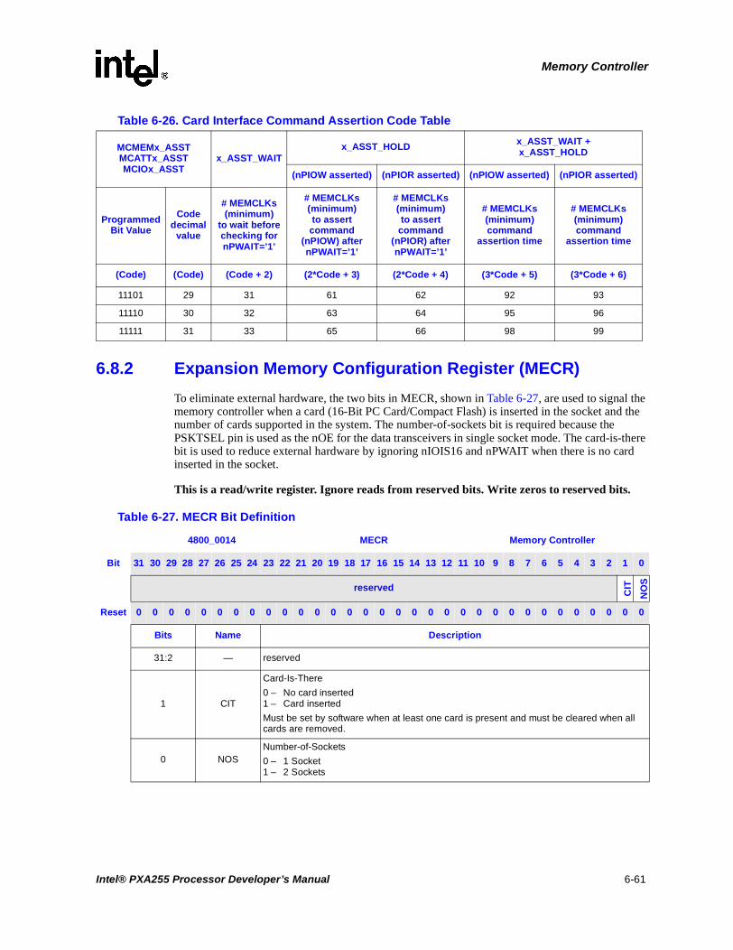
Memory Controller
6.8.2 Expansion Memory Configuration Register (MECR)
To eliminate external hardware, the two bits in MECR, shown in Table 6-27, are used to signal the memory controller when a card (16-Bit PC Card/Compact Flash) is inserted in the socket and the number of cards supported in the system. The number-of-sockets bit is required because the PSKTSEL pin is used as the nOE for the data transceivers in single socket mode. The card-is-there bit is used to reduce external hardware by ignoring nIOIS16 and nPWAIT when there is no card inserted in the socket.
This is a read/write register. Ignore reads from reserved bits. Write zeros to reserved bits.
11101 29 31 61 62 92 93
11110 30 32 63 64 95 96
11111 31 33 65 66 98 99
Table 6-26. Card Interface Command Assertion Code Table
MCMEMx_ASSTMCATTx_ASSTMCIOx_ASST
x_ASST_WAITx_ASST_HOLD x_ASST_WAIT +
x_ASST_HOLD
(nPIOW asserted) (nPIOR asserted) (nPIOW asserted) (nPIOR asserted)
ProgrammedBit Value
Codedecimal
value
# MEMCLKs(minimum)
to wait beforechecking fornPWAIT=’1’
# MEMCLKs(minimum)to assert
command(nPIOW) afternPWAIT=’1’
# MEMCLKs(minimum)to assert
command(nPIOR) afternPWAIT=’1’
# MEMCLKs(minimum)command
assertion time
# MEMCLKs(minimum)command
assertion time
(Code) (Code) (Code + 2) (2*Code + 3) (2*Code + 4) (3*Code + 5) (3*Code + 6)
Table 6-27. MECR Bit Definition
4800_0014 MECR Memory Controller
Bit 31 30 29 28 27 26 25 24 23 22 21 20 19 18 17 16 15 14 13 12 11 10 9 8 7 6 5 4 3 2 1 0
reserved CIT
NO
S
Reset 0 0 0 0 0 0 0 0 0 0 0 0 0 0 0 0 0 0 0 0 0 0 0 0 0 0 0 0 0 0 0 0
Bits Name Description
31:2 — reserved
1 CIT
Card-Is-There
0 – No card inserted1 – Card inserted
Must be set by software when at least one card is present and must be cleared when all cards are removed.
0 NOSNumber-of-Sockets
0 – 1 Socket1 – 2 Sockets
Intel® PXA255 Processor Developer’s Manual 6-61

Memory Controller
6.8.3 16-Bit PC Card Overview
The PXA255 processor 16-bit PC Card interface provides control for one 16-bit PC Card card slot with a PSKTSEL pin for support of a second slot. The PXA255 processor interface supports 8- and 16-bit peripherals and handles common memory, I/O, and attribute-memory accesses. The duration of each access is based on the values programmed in the fields in the MCMEMx, MCATTx, and MCIOx registers. Figure 6-26 shows the memory map for the 16-bit PC Card space.
The 16-bit PC Card Memory Map space is divided into eight partitions, four for each card slot. The four partitions for each card slot are: common memory, I/O, attribute memory, and a reserved space. Each partition starts on a 64-Mbyte boundary.
During an access, pins MA[25:0], nPREG, and PSKTSEL are driven at the same time. nPCE1 and nPCE2 are driven concurrently with the address signals for common memory and attribute- memory accesses. For I/O accesses, their value depends on the value of nIOIS16 and is valid a fixed amount of time after nIOIS16 is valid.
Common memory and attribute memory accesses assert the nPOE or nPWE control signals. I/O accesses assert the nIOR or nIOW control signals and use the nIOIS16 input signal to determine the bus width of the transfer (8 or 16 bits). The PXA255 processor uses nPCE2 to indicate to the expansion device that the upper half of the data bus (MD[15:8]) are used for the transfer, and nPCE1 to indicate that the lower half of the data bus (MD[7:0]) are used. nPCE1 and nPCE2 are asserted for 16-bit accesses.
Refer to Table 6-28 through Table 6-35 for signal combinations during common memory, I/O, and attribute accesses.
Figure 6-26. 16-Bit PC Card Memory Map
Socket 1 Common Memory Space
Socket 1 Attribute Memory Space
Socket 1 I/O Space
Socket 0 Common Memory Space
Socket 0 Attribute Memory Space
Socket 0 I/O Space
reserved
reserved
0x3C00_0000
0x3800_0000
0x3400_0000
0x3000_0000
0x2C00_0000
0x2800_0000
0x2400_0000
0x2000_0000
6-62 Intel® PXA255 Processor Developer’s Manual
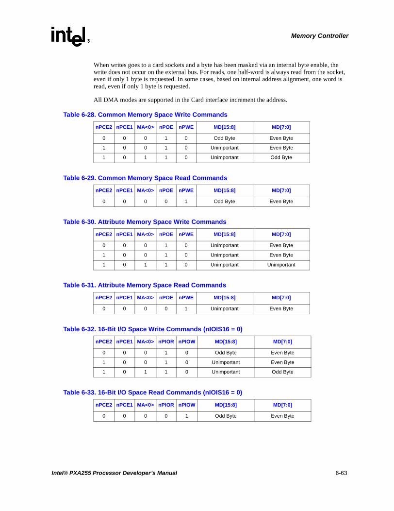
Memory Controller
When writes goes to a card sockets and a byte has been masked via an internal byte enable, the write does not occur on the external bus. For reads, one half-word is always read from the socket, even if only 1 byte is requested. In some cases, based on internal address alignment, one word is read, even if only 1 byte is requested.
All DMA modes are supported in the Card interface increment the address.
Table 6-28. Common Memory Space Write Commands
nPCE2 nPCE1 MA<0> nPOE nPWE MD[15:8] MD[7:0]
0 0 0 1 0 Odd Byte Even Byte
1 0 0 1 0 Unimportant Even Byte
1 0 1 1 0 Unimportant Odd Byte
Table 6-29. Common Memory Space Read Commands
nPCE2 nPCE1 MA<0> nPOE nPWE MD[15:8] MD[7:0]
0 0 0 0 1 Odd Byte Even Byte
Table 6-30. Attribute Memory Space Write Commands
nPCE2 nPCE1 MA<0> nPOE nPWE MD[15:8] MD[7:0]
0 0 0 1 0 Unimportant Even Byte
1 0 0 1 0 Unimportant Even Byte
1 0 1 1 0 Unimportant Unimportant
Table 6-31. Attribute Memory Space Read Commands
nPCE2 nPCE1 MA<0> nPOE nPWE MD[15:8] MD[7:0]
0 0 0 0 1 Unimportant Even Byte
Table 6-32. 16-Bit I/O Space Write Commands (nIOIS16 = 0)
nPCE2 nPCE1 MA<0> nPIOR nPIOW MD[15:8] MD[7:0]
0 0 0 1 0 Odd Byte Even Byte
1 0 0 1 0 Unimportant Even Byte
1 0 1 1 0 Unimportant Odd Byte
Table 6-33. 16-Bit I/O Space Read Commands (nIOIS16 = 0)
nPCE2 nPCE1 MA<0> nPIOR nPIOW MD[15:8] MD[7:0]
0 0 0 0 1 Odd Byte Even Byte
Intel® PXA255 Processor Developer’s Manual 6-63

Memory Controller
6.8.4 External Logic for 16-Bit PC Card Implementation
The PXA255 processor requires external glue logic to complete the 16-bit PC Card socket interface that allows either 1-socket or 2-socket solutions.
Figure 6-27 and Figure 6-28 show general solutions for a one- and two-socket configuration. The pull-ups shown are included as specified in the PC Card Standard - Volume 2 - Electrical Specification. Low-power systems must remove power from the pull-ups during sleep to avoid unnecessary power consumption.
GPIO or memory-mapped external registers can be used to control the reset of the 16-bit PC Card interface, power selection (VCC and VPP), and drive enables. The INPACK# signal is not used.
Figure 6-27 and Figure 6-28 provide the logical connections necessary to support hot insertion capability. For dual-voltage support, level shifting buffers are required for all PXA255 processor input signals. Hot insertion capability requires that each socket be electrically isolated from the other and from the remainder of the memory system. If one or both of these features is not required, then some of the logic shown in the following diagrams can be eliminated.
Software is responsible for setting the MECR[NOS] and MECR[CIT] bits. NOS indicates the number of sockets that the system support while CIT is written when the Card is in place. Input pins nPWAIT and nIOIS16 are three stated until card detect (CD) signal is asserted. To achieve this, software programs the MECR[CIT] bit when a card is detected. If the MECR[CIT] is 0, the nPWAIT and nIOIS16 inputs are ignored.
Figure 6-27 shows the minimal glue logic needed for a 1-socket system, including: data transceivers, address buffers, and level shifting buffers. The transceivers are enabled by the PSKTSEL signal. The DIR pin of the transceiver is driven by the RD/nWR pin. A GPIO is used for the three-state signal of the address and nPWE lines. These signals must be three-stated because they are used for memories other than the card interface. The Card Detect[1:0] signals are driven by the signal device.
Table 6-34. 8-Bit I/O Space Write Commands (nIOIS16 = 1)
nPCE2 nPCE1 MA<0> nPIOR nPIOW MD[15:8] MD[7:0]
1 0 0 1 0 Unimportant Even Byte
1 0 1 1 0 Unimportant Odd Byte
Table 6-35. 8-Bit I/O Space Read Commands (nIOIS16 = 1)
nPCE2 nPCE1 MA<0> nPIOR nPIOW MD[15:8] MD[7:0]
1 0 0 0 1 Unimportant Even Byte
1 0 1 0 1 Unimportant Odd Byte
6-64 Intel® PXA255 Processor Developer’s Manual

Memory Controller
Figure 6-28 shows the glue logic need for a 2-socket system. RDY/nBSY signals are routed through a buffer to two separate GPIO pins. In the data bus transceiver control logic, nPCE1 controls the enable for the low byte lane and nPCE2 controls the enable for the high byte lane.\
Figure 6-27. Expansion Card External Logic for a One-Socket Configuration
MD<15:0> D<15:0>
nOEDIR
nCD<1>
nCD<2>
RDY/nBSY
A[25:0]
nREG
nCE<2:1>nOE
nWE
nIORnIOW
nWAIT
nIOIS16
GPIO<w>
GPIO<x>
MA[25:0]
nPREG
nPOE
nPWE
nPIORnPIOW
nPWAIT
nIOIS16
nPCE<2:1>
GPIO<y>
PSKTSEL
RD/nWR
GPIO<z>
Intel® - PXA255 Processor Socket 0
nPCD0
nPCD1
PRDY_BSY0
PADDR_EN0
5V to 3.3V or 2.5V
5V to 3.3V or 2.5V
Intel® PXA255 Processor Developer’s Manual 6-65

Memory Controller
Figure 6-28. Expansion Card External Logic for a Two-Socket Configuration
D(15:0)
GPIO(w)
GPIO(x)
GPIO(y)
GPIO(z)
PSKTSEL
MA(25:0)nPREG
nPWAIT
nPIOIS16
nPCE(1:2)nPOE,nPWE
nPIOW,nPIOR
PXA255Processor
D(15:0)
CD1#
CD2#
RDY/BSY#
WAIT#
WAIT#
IOIS1616#
A(25:0)REG#
CE(1:2)#OE#WE#IOR#IOW#
Socket 0
D(15:0)
Socket 1
DIR
nPCEx
nPCEx
nPOE
nPIOR
OE#
DIR OE#
RDY/BSY#
CD1#
CD2#
A(25:0)REG#
CE(1:2)#OE#WE#IOR#IOW#
IOIS1616#
WAIT#
6 6
6
WAIT#
6-66 Intel® PXA255 Processor Developer’s Manual

Memory Controller
6.8.5 Expansion Card Interface Timing Diagrams and Parameters
Figure 6-29 shows a 16-bit access to a 16-bit memory or I/O device. When common memory is accessed, the MCMEM0 and MCMEM1 registers are used, depending on whether card socket 0 or 1 is addressed. MCIO0 and MCIO1 are used for I/O accesses and MCATT0 and MCATT1 are used for access to attribute memory.
Figure 6-29. 16-Bit PC Card Memory or I/O 16-Bit (Half-word) Access
x_ASST_HOLD
x_ASST_WAIT + wait states
x_HOLDx_SET
0ns 50ns 100ns 150ns
MEMCLK
MA,nPREG,PSKTSEL
nPCE2,nPCE1
nPWE,nPOE,nPIOW,nPIOR
RDnWR
nIOIS16
nPWAIT
read_data
write_data
Intel® PXA255 Processor Developer’s Manual 6-67

Memory Controller
The interface waits the smallest possible amount of time (x_ASST_WAIT) before it checks the value of the nPWAIT signal. If the nPWAIT signal is asserted (active low), the interface continues to wait (for a variable number of wait states) until nPWAIT is deasserted. When the nPWAIT signal is deasserted, the command continues to be asserted for a fixed amount of time (x_ASST_HOLD).
6.9 Companion Chip Interface
The processor can be connected to a companion chip in two different ways:
• Alternate Bus Master Mode
• Variable Latency I/O (See Section 6.7.5)
The connection methods are illustrated in Figure 6-31 and Figure 6-32.
Figure 6-30. 16-Bit PC Card I/O 16-Bit Access to 8-Bit Device
Low Byte High Byte
IOx_ASST_HOLD
IOx_ASST_WAIT + wait states
IOx_ASST_HOLD
IOx_ASST_WAIT + wait states
IOx_HOLD
IOx_SET
IOx_HOLD
IOx_SET
0ns 100ns 200ns 300ns
MEMCLK
MA[25:1],nPREG,PSKTSEL
MA[0]
nPCE2
nPCE1
nPIOW,nPIOR
RDnWR
nIOIS16
nPWAIT
read_data
write_data
6-68 Intel® PXA255 Processor Developer’s Manual

Memory Controller
Figure 6-31. Alternate Bus Master Mode
Figure 6-32. Variable Latency IO
Processor
EXTERNAL SYSTEM
MB
RE
Q
MB
GN
T
GPIO<13> (MBGNT)
GPIO<14> (MBREQ)
nSDCS(0)
nWE
nSDRAS
nSDCAS
MD[31:0]
MA[25:0]
SDCLK<1>
DQM[3:0]
SDCKE<1>
MemoryControlle
ExternalSDRAMBank 0
Companion Chip
GPIOBlock
ProcessorEXTERNAL SYSTEM
nCS(0,1,2,3,4,5)
nPWE
nOE
RDY
MD[31:0]
MA[25:0]
DQM[3:0]
CompanionChip
MemoryController
Intel® PXA255 Processor Developer’s Manual 6-69

Memory Controller
6.9.1 Alternate Bus Master Mode
The processor supports the presence of an alternate master on the SDRAM memory bus. The alternate master is given control of the bus with a hardware handshake that is performed through MBREQ and MBGNT, which are invoked through the alternate functions on GPIO[14] and GPIO[13], respectively. The Memory Controller performs an SDRAM refresh if SDRAM clocks and clock enable are turned on. When the alternate master must take control of the memory bus, it asserts MBREQ. It then deasserts SDCKE<1> and three-states all memory bus pins used with SDRAM bank 0 (nSDCS<0>, MA[25:0], nOE, nWE, nSDRAS, nSDCAS, SDCLK<1>, MD[31:0], DQM[3:0]). All other memory and 16-bit PC Card pins remain driven. RD/nWR remain low. Then the processor asserts MBGNT, the alternate master starts to drive all pins including SDCLK<1>, and the processor reasserts SDCKE<1>.
The grant sequence and timing follow:
1. The Alternate master asserts MBREQ.
2. The Memory Controller performs an SDRAM refresh if SDRAM clocks and clock enable are turned on
3. If the MDCNFG:SA1111x bit is enabled, the Memory Controller sends the SDRAMs an MRS command to change the SDRAM burst length to one. The burst length is changed to one for SA-1111 compatibility.
4. The processor deasserts SDCKE<1> at time (t).
5. The processor three-states SDRAM outputs at time (t + 1 MEMCLK).
6. The processor asserts MBGNT at time (t + 2 MEMCLKS).
7. The Alternate master drives SDRAM outputs before time (t + 3 MEMCLKS).
8. The processor asserts SDCKE<1> at time (t + 4 MEMCLKS).
During the three-state period, both MBREQ and MBGNT remain high and an external device can take control of the three-stated pins. The external device must drive all the three-stated pins. Floating inputs can cause excessive crossover current and erroneous SDRAM commands. During the three-state period, the processor can not perform SDRAM refresh cycles.
The alternate master must assume the responsibility for SDRAM integrity during the three-state period. The system must be designed to ensure that the period of alternate mastership is limited to less than the refresh period or that the alternate master implements a refresh counter to perform refreshes at the proper intervals.
To surrender the bus, the alternate master deasserts MBREQ. The processor deasserts SDCKE<1> and MBGNT. The alternate master stops driving the SDRAM pins. The processor drives all SDRAM pins and then re-asserts SDCKE<1>.
The release sequence and timing follows:
1. The Alternate master deasserts MBREQ.
2. The processor deasserts SDCKE<1> at time (t).
3. The processor deasserts MBGNT at time (t + 1 MEMCLK).
4. The Alternate master three-states SDRAM outputs prior to time (t + 2 MEMCLKS).
5. The processor drives SDRAM outputs at time (t + 3 MEMCLKS).
6. The processor asserts SDCKE<1> at time (t + 4 MEMCLKS).
6-70 Intel® PXA255 Processor Developer’s Manual
Memory Controller
7. The Memory Controller performs an SDRAM refresh if SDRAM clocks and clock enable are turned on.
8. The Memory Controller sends an MRS command to the SDRAMs if the MDCNFG:SA1111x bit is enabled. This changes the SDRAM burst length back to four.
If the refresh counter for the processor requested a refresh cycle during the alternate master’s tenure, a refresh cycle runs first, followed by any other bus transactions that stalled during that period.
To enable alternate bus master, the set up the signals by writing the following registers:
• Write the GPIO Pin Direction register GPDR0 to set bit 13 (make GPIO[13] an output) and clear bit 14 (make GPIO[14] an input)
• Write the GPIO Alternate Function register GAFR0_L to set bits 27 and 26 to 0b11 (enable the MBGNT alternate function 3) and set bits 29 and 28 to 0b01 (enable the MBREQ alternate function 1).
6.9.1.1 GPIO Reset
During GPIO reset, the GPIOs, including MBREQ and MBGNT, are set to their reset state. The MBREQ and MBGNT pins become general purpose inputs. The system must have external put-downs on these pins to prevent the pins from floating.
If a transaction is in progress when GPIO reset is asserted, the alternate master loses ownership of the bus. The alternate master must immediately give up the bus when MBGNT is deasserted. Because the memory controller is not reset, an SDRAM refresh can occur immediately after the GPIO reset assertion.
6.9.1.2 nVDD_FAULT/nBATT_FAULT with PMCR[IDAE] Disabled
If an nVDD_FAULT or nBATT_FAULT occurs, the processor places the GPIOs into their sleep states. MBGNT must be programmed to go low during sleep.
The memory controller prevents the processor from entering sleep until all outstanding transactions have completed. This includes waiting for the MBREQ signal from the alternate master to deassert. For best sleep performance, the alternate master must immediately give up the bus when MBGNT is deasserted. If necessary, the alternate master can hold the bus until its transaction is completed. After the memory controller has completed all outstanding transactions, it places SDRAM into self-refresh and allows the processor to complete the sleep entry sequence.
Note: The alternate bus master must de-assert MBREQ when nVDD_FAULT or nBATT_FAULT is asserted.
6.9.1.3 nVDD_FAULT/nBATT_FAULT with PMCR[IDAE] Enabled
If an nVDD_FAULT or nBATT_FAULT occurs with PMCR[IDAE] enabled, the processor causes an Imprecise Data Abort Exception. This allows the processor to do any required actions before sleep entry. Sleep entry with PMCR[IDAE] enabled is similar to normal sleep entry. The processor places the GPIOs into their sleep states. MBGNT must be programmed to go low during sleep.
The memory controller prevents the processor from entering sleep until all outstanding transactions have completed. This includes waiting for the MBREQ signal from the alternate master to deassert. For best sleep performance, the alternate master must immediately give up the bus when MBGNT
Intel® PXA255 Processor Developer’s Manual 6-71

Memory Controller
is deasserted or, as part of the sleep entry routine, the alternate master can be disabled. If necessary, the alternate master can hold the bus until its transaction is completed. After the memory controller has completed all outstanding transactions, it places SDRAM into self-refresh and allows the processor to complete the sleep entry sequence.
Note: The alternate bus master must de-assert MBREQ when nVDD_FAULT or nBATT_FAULT is asserted.
6.10 Options and Settings for Boot Memory
This section explains the settings that control Boot Memory configurations.
6.10.1 Alternate Booting
The processor allows six boot configurations. These configurations are determined by the three BOOT_SEL(2:0) pins and are described in Table 6-36. A description of the effect of these input pins on the Configuration registers at boot time is included in Section 6.8.
6.10.2 Boot Time Defaults
The following sections provide information on boot time default parameters.
6.10.2.1 BOOT_DEF Read-Only Register (BOOT_DEF)
BOOT_DEF, shown in Table 6-37, contains the boot-up values for the three BOOT_SEL pins and the single package-type bit.
This is a read-only register. Ignore reads from reserved bits.
Table 6-36. BOOT_SEL Definitions
BOOT_SELBoot From...
2 1 0
0 0 0 Asynchronous 32-bit ROM
0 0 1 Asynchronous 16-bit ROM
0 1 0 reserved
0 1 1 reserved
1 0 01- 32-bit Synchronous Mask ROM (64 Mbit)
2- 16-bit Synchronous Mask ROMs = 32 bits (32 Mbit each)
1 0 1 1- 16-bit Synchronous Mask ROM (64 Mbit)
1 1 0 2- 16-bit Synchronous Mask ROMs = 32 bits (64 Mbit each)
1 1 1 1- 16-bit Synchronous Mask ROM (32 Mbit)
6-72 Intel® PXA255 Processor Developer’s Manual

Memory Controller
Table 6-37. BOOT_DEF Bitmap
0x4800_0044 BOOT_DEF Memory Controller
Bit 31 30 29 28 27 26 25 24 23 22 21 20 19 18 17 16 15 14 13 12 11 10 9 8 7 6 5 4 3 2 1 0
reserved
PK
G_T
YP
E
BO
OT
_SE
L
Reset 0 0 0 0 0 0 0 0 0 0 0 0 0 0 0 0 0 0 0 0 0 0 0 0 0 0 0 0 * * * *
Bits Name Description
31:4 — reserved
3 PKG_TYPEPROCESSOR TYPE (read only):
0 – Reserved1 – PXA255 processor
2:0 BOOT_SEL
BOOT SELECT (read only):
Contains the three inputs pins BOOT_SEL[2:0] for the processor. See Table 6-36.
See Table 6-38 for valid boot configurations. See Section 6.10.2.2 for descriptions of Boot Time Configurations.
Table 6-38. Valid Boot Configurations Based on Processor Type
Processor Type Boot_Sel SignalsValid Booting Configurations
(PXA255 processor)
000
001
100
101
110
111
Intel® PXA255 Processor Developer’s Manual 6-73

Memory Controller
6.10.2.2 Boot-Time Configurations
The boot time configurations are shown in Figure 6-33 - Figure 6-35. A boot from a single 32-Mbit SMROM with nWORD = 1 is not supported.
Three Configuration registers are affected at reset - MSC0:RBW0, MDREFR:E0PIN/K0RUN, and SXCNFG.
Figure 6-33. Asynchronous Boot Time Configurations and Register Defaults
BOOT_SEL[2:0] = 000
Asynchronous
32-bit
ROM
32
MSC0
SXCNFG
0x7FF0_7FF0
0x0004_0004
RBW0 = 0
BOOT_SEL[2:0] = 001
Asynchronous
16-bitROM
16
MSC0
SXCNFG
0x7FF0_7FF8
0x0004_0004
RBW0 = 1
MDREFR 0x03CA_4FFF
E0PIN = 0, K0RUN = 0
MDREFR 0x03CA_4FFF
E0PIN = 0, K0RUN = 0
BOOT_SEL[2:0] = 000
BOOT_SEL[2:0] = 000
SXMRS
SXMRS
0000_0000
0000_0000
6-74 Intel® PXA255 Processor Developer’s Manual
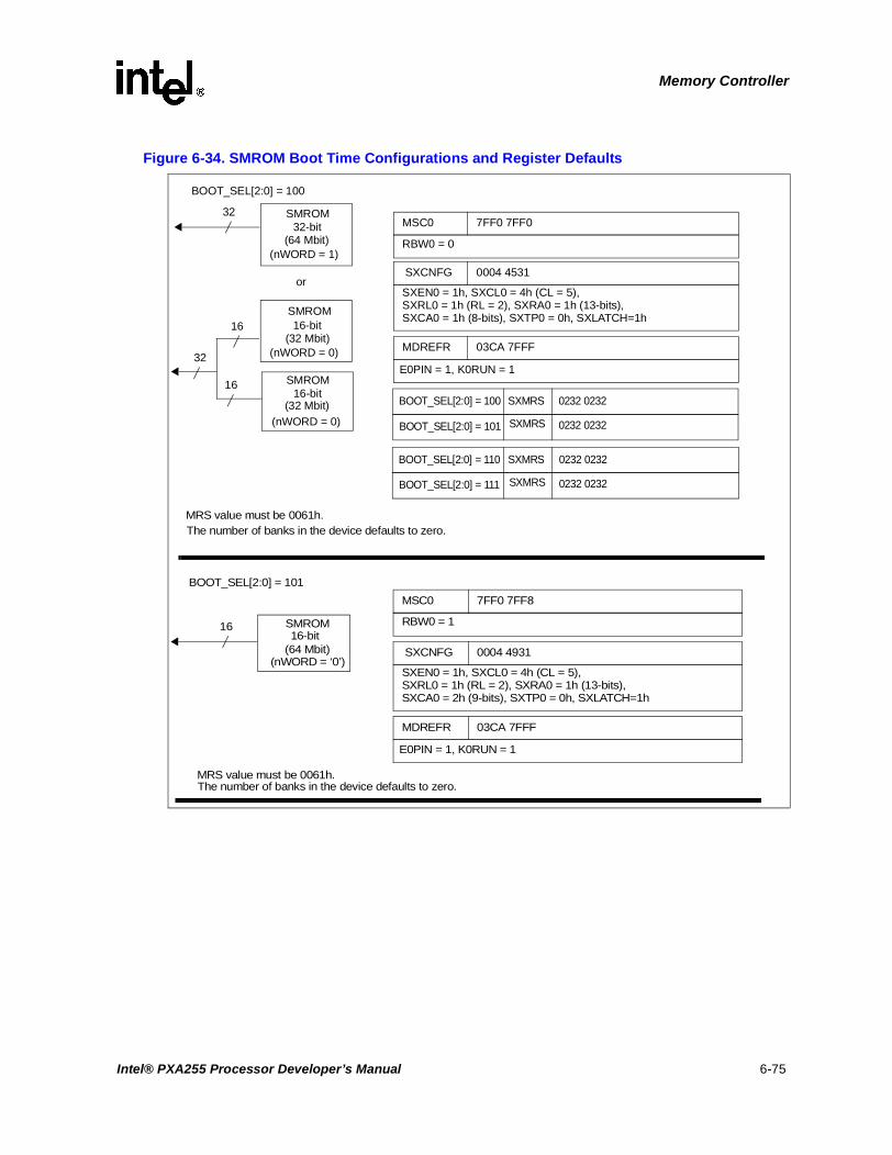
Memory Controller
Figure 6-34. SMROM Boot Time Configurations and Register Defaults
BOOT_SEL[2:0] = 100
SMROM32-bit
32MSC0
SXCNFG
7FF0 7FF0
0004 4531
SXEN0 = 1h, SXCL0 = 4h (CL = 5),SXRL0 = 1h (RL = 2), SXRA0 = 1h (13-bits),SXCA0 = 1h (8-bits), SXTP0 = 0h, SXLATCH=1h
RBW0 = 0
MRS value must be 0061h.
BOOT_SEL[2:0] = 101
SMROM16-bit
16
MSC0
SXCNFG
7FF0 7FF8
0004 4931
SXEN0 = 1h, SXCL0 = 4h (CL = 5),SXRL0 = 1h (RL = 2), SXRA0 = 1h (13-bits),SXCA0 = 2h (9-bits), SXTP0 = 0h, SXLATCH=1h
RBW0 = 1
MRS value must be 0061h.
The number of banks in the device defaults to zero.
The number of banks in the device defaults to zero.
MDREFR 03CA 7FFF
E0PIN = 1, K0RUN = 1
MDREFR 03CA 7FFF
E0PIN = 1, K0RUN = 1
(64 Mbit)(nWORD = 1)
or
SMROM16-bit
(32 Mbit)(nWORD = 0)
SMROM16-bit
(32 Mbit)(nWORD = 0)
16
16
32
(64 Mbit)(nWORD = ‘0’)
BOOT_SEL[2:0] = 100
BOOT_SEL[2:0] = 101
SXMRS
SXMRS
0232 0232
0232 0232
BOOT_SEL[2:0] = 110
BOOT_SEL[2:0] = 111
SXMRS
SXMRS
0232 0232
0232 0232
Intel® PXA255 Processor Developer’s Manual 6-75

Memory Controller
6.10.3 Memory Interface Reset and Initialization
On reset, the SDRAM Interface is disabled. Reset values for the Boot ROM are determined by BOOT_SEL. The memory pins and controller are in the state shown in Table 6-39.
Figure 6-35. SMROM Boot Time Configurations and Register Defaults
BOOT_SEL[2:0] = 110
MSC0
SXCNFG
7FF0 7FF0
0004 4931
SXEN0 = 1h, SXCL0 = 4h (CL = 5),SXRL0 = 1h (RL = 2), SXRA0 = 1h (13-bits),SXCA0 = 2h (9-bits), SXTP0 = 0h, SXLATCH=1h
RBW0 = 0
MRS value must be 0061h.
BOOT_SEL[2:0] = 111
The number of banks in the device defaults to zero.
MDREFR 03CA 7FFF
E0PIN = 1, K0RUN = 1
SMROM16-bit
(64 Mbit)(nWORD = 0)
SMROM16-bit
(64 Mbit)(nWORD = 0)
16
16
32
MSC0
SXCNFG
7FF0 7FF8
0004 4531
SXEN0 = 1h, SXCL0 = 4h (CL = 5),SXRL0 = 1h (RL = 2), SXRA0 = 1h (13-bits),SXCA0 = 1h (8-bits), SXTP0 = 0h, SXLATCH=1h
RBW0 = 1
MRS value must be 0061h.The number of banks in the device defaults to zero.
MDREFR 03CA 7FFF
E0PIN = 1, K0RUN = 1
SMROM16-bit
(32 Mbit)(nWORD = 0)
16
BOOT_SEL[2:0] = 100
BOOT_SEL[2:0] = 101
SXMRS
SXMRS
0232 0232
0232 0232
BOOT_SEL[2:0] = 110
BOOT_SEL[2:0] = 111
SXMRS
SXMRS
0232 0232
0232 0232
6-76 Intel® PXA255 Processor Developer’s Manual

Memory Controller
In sleep mode, the memory pins and controller are in the same state as they are after a hardware reset, except that the GPIO signals are driven high. If SDRAMs are in self-refresh, they are held there by setting SDCKE<1> to a 0.
6.11 Hardware, Watchdog, or Sleep Reset Operation
Software performs the following procedures when the processor comes out of a reset:
1. After hardware reset, complete a power-on wait period of 200 µs, which allows the internal clocks that generate SDCLK to stabilize. Enable MDREFR:K0RUN and E0PIN for Synchronous Static memory. When MDREFR is written, a refresh interval value (MDREFR:DRI) must also be written. The following writes are allowed:
a. Write MSC0, MSC1, MSC2
b. Write MECR, MCMEM0, MCMEM1, MCATT0, MCATT1, MCIO0, MCIO1
c. Write MDREFR:K0RUN and MDREFR:E0PIN. Configure MDREFR:K0DB2. Retain the current values of MDREFR:APD and MDREFR:SLFRSH. MDREFR:DRI must contain a valid value. Deassert MDREFR:KxFREE.
2. In systems that contain Synchronous Static memory, write to the SXCNFG to configure all appropriate bits, including the enable bits. Software must perform a sequence that involves a subsequent write to SXCNFG to change the RAS latencies. While any SMROM banks are
Table 6-39. Memory Controller Pin Reset Values
Pin Name PXA255 Processor Reset Value
SDCLK [2:0] 000
SDCKE <1> 00
SDCKE <0> 1 if BOOT_SEL = Synchronous Memory
DQM [3:0] 0000
nSDCS [3:0] 1111
nWE 1
nSDRAS 1
nSDCAS 1
nOE 1
MA [25:0] 0x0000000h
RDnWR 0
MD [31:0] 0x00000000h
nCS <0> 1
nCS <5:1> GPIO Input
nPIOIR GPIO Input
nPIOIW GPIO Input
nPOE GPIO Input
nPWE GPIO Input
Intel® PXA255 Processor Developer’s Manual 6-77

Memory Controller
being configured, the SDRAM banks must be disabled and MDREFR:APD must be deasserted (auto-power-down disabled).
a. Write SXCNFG (with enable bits asserted).
b. Write to SXMRS to trigger an MRS command to all enabled banks of synchronous static memory.
c. SXLCR must only be written when it is required by the SDRAM-like synchronous flash device for command encoding.
3. In systems that contain SDRAM, transition the SDRAM controller through the following state sequence:
a. self-refresh and clock-stop
b. self-refresh
c. power-down
d. PWRDNX
e. NOP
4. The SDRAM clock run and enable bits (MDREFR:K1RUN, K2RUN, and E1PIN), described in Section 6.5.3. MDREFR:SLFRSH must not be asserted.
a. Write MDREFR:K1RUN, K2RUN (self-refresh and clock-stop -> self-refresh). Configure MDREFR:K1DB2,K2DB2.
b. Write MDREFR:SLFRSH (self-refresh -> power-down).
c. Write MDREFR:E1PIN (power-down -> PWRDNX).
d. a write is not required for this state transition (PWRDNX -> NOP).
e. Configure, but do not enable, each SDRAM partition pair.
f. Write MDCNFG (with enable bits deasserted), MDCNFG:DE3:2,1:0 set to ‘0’.
5. For systems that contain SDRAM, wait a specified NOP power-up waiting period required by the SDRAMs to ensure the SDRAMs receive a stable clock with a NOP condition
6. Ensure the Data Cache bit (DCACHE) is disabled. If this bit is enabled, the refreshes triggered by the next step may not pass through to the Memory Controller properly.
7. On a hardware reset in systems that contain SDRAM, trigger the specified number (typically eight) of refresh cycles by attempting non-burst read or write accesses to any disabled SDRAM bank. Each such access causes a simultaneous CBR refresh cycles for all four banks, which causes a pass through the CBR state and back to NOP. On the first pass, the PALL state occurs before the CBR state.
8. Re-enable the DCACHE bit if it is disabled.
9. In systems that contain SDRAM, enable SDRAM partitions by setting MDCNFG:DE3:2,DE1:0.
10. In systems containing SDRAM, write the MDMRS register to trigger an MRS command to all enabled banks of SDRAM. For each SDRAM partition pair that has one or both partitions enabled, this forces a pass through the MRS state and back to NOP. The CAS latency must be the only variable option and is derived from the value programmed in the MDCNFG:MDTC0,2 fields. The burst type is programmed to sequential and the length is set to four.
6-78 Intel® PXA255 Processor Developer’s Manual

Memory Controller
11. Optionally, in systems that contain SDRAM or Synchronous Static memory, enable auto-power-down by setting MDREFR[APD].
6.12 GPIO Reset Procedure
On a GPIO Reset, the Memory Controller registers keep the values they had before the reset. No new configuration programming is required. However, SDRAM refreshes do not occur during the reset time. After nRESET_OUT is deasserted, the memory controller will continue refreshing. By ensuring a refresh time for SDRAM that is smaller than the default, it is possible to preserve the SDRAM contents. To do this, follow this procedure:
The SDRAM refresh time is chosen by taking the specified refresh time, typically 64 ms, and subtracting the GPIO Reset time (found in the Intel® PXA255 Applications Processors Electrical, Mechanical, and Thermal Specification). For example, the GPIO Reset time is ~360 microseconds, leaving an SDRAM refresh time of (64 ms - .360 ms) = 63.64 ms. Use this time to program the MDREFR[DRI].
In the boot code, determine the type of reset. If the reset was a GPIO reset, then refresh all the SDRAM rows. Refreshing all the SDRAM rows preserves their value in case GPIO reset occurs again.
After all the SDRAM rows have been refreshed, enable GPIO reset
6.13 Memory Controller Register Summary
Table 6-40 shows the registers associated with the memory interface and the physical addresses used to access them. These registers must be mapped as non-cacheable and non-bufferable and can only be a single word access. They are grouped together in one page and all have the same memory protections.
Table 6-40. Memory Controller Register Summary (Sheet 1 of 2)
Physical Address Symbol Register Name
0x4800_0000 MDCNFG SDRAM Configuration Register
0x4800_0004 MDREFR SDRAM Refresh Control Register
0x4800_0008 MSC0 Static Memory Control Register 0
0x4800_000C MSC1 Static Memory Control Register 1
0x4800_0010 MSC2 Static Memory Control Register 2
0x4800_0014 MECR Expansion Memory (16-bit PC Card / Compact Flash) Bus Configuration register
0x4800_001C SXCNFG Synchronous Static Memory Control Register
0x4800_0024 SXMRS MRS value to be written to SMROM
0x4800_0028 MCMEM0 Card interface Common Memory Space Socket 0 Timing Configuration
0x4800_002C MCMEM1 Card interface Common Memory Space Socket 1 Timing Configuration
0x4800_0030 MCATT0 Card interface Attribute Space Socket 0 Timing Configuration
0x4800_0034 MCATT1 Card interface Attribute Space Socket 1 Timing Configuration
0x4800_0038 MCIO0 Card interface I/O Space Socket 0 Timing Configuration
Intel® PXA255 Processor Developer’s Manual 6-79
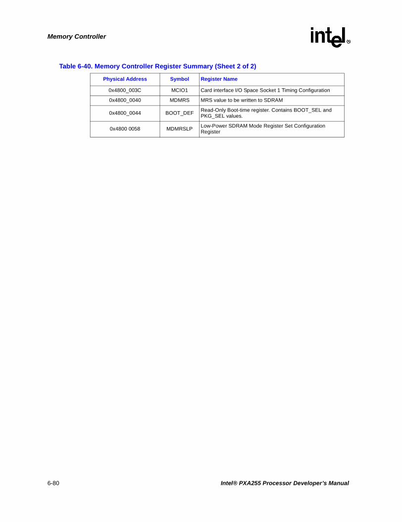
Memory Controller
0x4800_003C MCIO1 Card interface I/O Space Socket 1 Timing Configuration
0x4800_0040 MDMRS MRS value to be written to SDRAM
0x4800_0044 BOOT_DEF Read-Only Boot-time register. Contains BOOT_SEL and PKG_SEL values.
0x4800 0058 MDMRSLP Low-Power SDRAM Mode Register Set Configuration Register
Table 6-40. Memory Controller Register Summary (Sheet 2 of 2)
Physical Address Symbol Register Name
6-80 Intel® PXA255 Processor Developer’s Manual

LCD Controller 7
The LCD controller provides an interface from the PXA255 processor to a passive (DSTN) or active (TFT) flat panel display. Monochrome and several color pixel formats are supported.
7.1 Overview
The processor LCD controller supports single- or dual-panel displays. Encoded pixel data created by the core is stored in external memory in a frame buffer in 1, 2, 4, 8, or 16-bit increments. The data is fetched from external memory and loaded into a first-in first-out (FIFO) buffer on a demand basis, using the LCD controller’s dedicated dual-channel DMA controller (DMAC). One channel is used for single-panel displays and two are used for dual-panel displays.
Frame buffer data contains encoded pixel values that are used by the LCD controller as pointers to index a 256-entry x 16-bit-wide palette. For 16 bit per pixel frame buffer entries, the palette RAM is bypassed. Monochrome palette entries are eight bits wide, and color palette entries are 16 bits wide. The encoded pixel data determines the number of possible colors within the palette as follows:
• 1-bit-wide pixels address the top 2 locations of the palette
• 2-bit-wide pixels address the top 4 locations of the palette
• 4-bit-wide pixels address the top 16 locations of the palette
• 8-bit-wide pixels address any of the 256 entries within the palette
• 16-bit-wide pixels bypass the palette
When passive color 16-bit pixel mode is enabled, the color pixel values bypass the palette and are fed directly to the LCD controller’s Frame Rate Control logic. When active color 16-bit pixel mode is enabled, the pixel value bypasses the palette and the Frame Rate Control logic and is sent directly to the LCD controller’s data pins. Optionally, the palette RAM is loaded for each frame by the LCD controller’s DMAC.
Once the encoded pixel value is used to select a palette entry, the value programmed within the entry is transferred to the Frame Rate Control logic, which uses the Temporal Modulated Energy Distribution (TMED) algorithm to produce the pixel data that is sent to the screen. Frame Rate Control is a technique used to create additional color shades by rapidly turning on and off a pixel on the LCD screen. This is also known as temporal dithering. The data output from the dither logic is grouped into the selected format (e.g., 8-bit color, dual panel, 16-bit color., etc.) and placed in a FIFO buffer before being sent out on the LCD controller’s pins and driven to the display using the pixel clock.
Depending on the type of panel used, the LCD controller is programmed to use either 4-, 8-, or 16-pixel data output pins. Single-panel monochrome displays use either four or eight data pins to send 4 or 8 pixels for each pixel clock. Single-panel color displays use eight pins to send 2-2/3 pixels each pixel clock (8 pins / 3 colors/pixel = 2 2/3 pixels per clock). The LCD controller also supports dual-panel mode, in which the LCD controller’s data lines are split into two groups, one to drive the top half and one to drive the bottom half of the screen. For dual-panel displays, the number of pixel data output pins is doubled, allowing twice as many pixels to be sent each pixel clock to the two halves of the screen.
Intel® PXA255 Processor Developer’s Manual 7-1

LCD Controller
In active color display mode, the LCD controller can drive TFT displays. When using 1-, 2-, 4-, or 8-bit modes, the LCD’s dither logic is bypassed, and the pixel value is sent from the palette buffer directly to the LCD’s data output pins. 16-bit pixel mode bypasses both the palette and the dither logic.
7.1.1 Features
The processor LCD controller supports the following features:
• Display modes:
— single- or dual-panel displays
— up to 256 gray-scale levels (8 bits) in Passive Monochrome Mode
— a total of 65536 possible colors in Passive Color Mode (using the 16-bit TMED dithering algorithm)
— up to 65536 colors in Active Color Mode (16 bits, bypasses palette)
— passive 8-bit color single-panel displays
— passive 8-bit (per panel) color dual-panel displays
• Display sizes up to 1024x1024 pixels, recommended maximum of 640x480
• Internal color palette RAM 256 entry by 16 bits (can be loaded automatically at the beginning of each frame)
• Encoded pixel data of 1, 2, 4, 8, or 16 bits
• Programmable toggle of AC bias pin output (toggled by line count)
• Programmable pixel clock from 195 kHz to 83 MHz (100 MHz/512 to 166 MHz/2)
• Integrated 2-channel DMA (one channel for palette and single panel, the other channel for second panel in dual-panel mode).
• Programmable wait-state insertion at the beginning and end of each line
• Programmable polarity for output enable, frame clock, and line clock
• Programmable interrupts for input and output FIFO underrun
• Programmable frame and line clock polarity, pulse width, and wait counts
7-2 Intel® PXA255 Processor Developer’s Manual
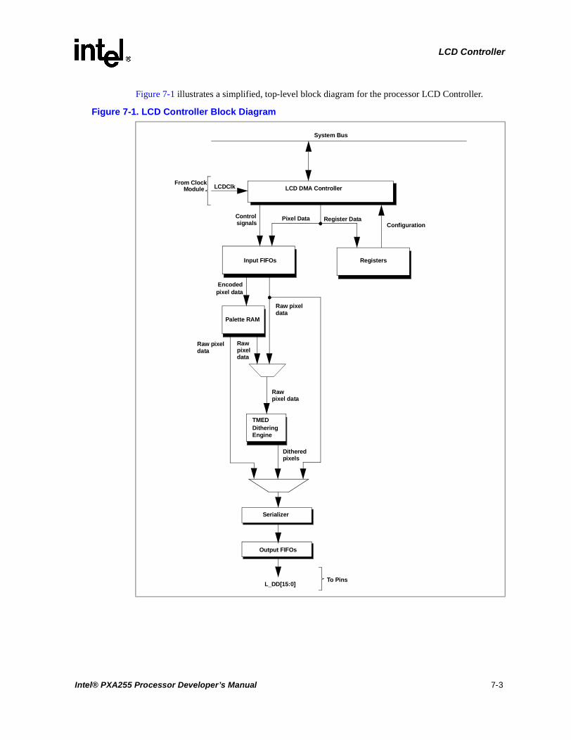
LCD Controller
Figure 7-1 illustrates a simplified, top-level block diagram for the processor LCD Controller.
Figure 7-1. LCD Controller Block Diagram
LCD DMA Controller
Registers
Palette RAM
Output FIFOs
Serializer
To Pins
From ClockModule LCDClk
Pixel Data Register Data
Input FIFOs
TMEDDitheringEngine
L_DD[15:0]
System Bus
Controlsignals Configuration
Encoded pixel data
Raw pixeldata
Raw pixeldata
Rawpixel data
Raw pixel data
Ditheredpixels
Intel® PXA255 Processor Developer’s Manual 7-3

LCD Controller
7.1.2 Pin Descriptions
When the LCD controller is enabled, all of the LCD pins are outputs only. When the LCD controller is disabled, its pins can be use for general-purpose input/output (GPIO). Refer to the System Integration Unit chapter for details.
Table 7-1 describes the LCD controller’s pins. For more detailed information, see Section 7.3.5. All of the LCD pins are outputs only.
7.2 LCD Controller Operation
7.2.1 Enabling the Controller
If the LCD controller is being enabled for the first time after system reset or sleep reset, all of the LCD registers must be programmed as follows:
1. Configure the General Purpose I/O (GPIO) pins for LCD controller functionality. See Chapter 4, “System Integration Unit” for details.
2. Write the frame descriptors and, if needed, the palette descriptor to memory.
3. Program all of the LCD configuration registers except the Frame Descriptor Address Registers (FDADRx) and the LCD Controller Configuration Register 0 (LCCR0). See Section 7.6 for details of all registers.
4. Program FDADRx with the memory address of the palette/frame descriptor, as described in Section 7.6.5.2.
5. Enable the LCD controller by writing to LCCR0, as described in Section 7.6.1.
Table 7-1. Pin Descriptions
Pin Definition
L_DD[7:0]
These data lines transmit either four or eight data values at a time to the LCD display. For monochrome displays, each pin value represents a single pixel. For passive color, groupings of three pin values represent one pixel (red, green, and blue subpixel data values). In single-panel monochrome mode, L_DD<3:0> pins are used. For double-pixel data, single-panel monochrome, dual-panel monochrome, single-panel color, and active color modes, L_DD[7:0] are used.
L_DD[15:8] When dual-panel color or TFT (active color mode) operation is programmed, these data outputs are also required to send pixel data to the screen.
L_PCLK
The Pixel Clock is used by the LCD display to clock the pixel data into the line shift register. In passive mode, the pixel clock toggles only when valid data is available on the data pins. In active mode, the pixel clock toggles continuously, and L_BIAS serves as an output to signal when data is valid on the LCD’s data pins.
L_LCLKThe Line Clock is used by the LCD display to signal the end of a line of pixels. The display transfers the line data from the shift register to the screen and increments the line pointer. In active mode, it is the horizontal synchronization signal.
L_FCLKThe Frame Clock is used by the LCD display to signal the start of a new frame of pixels. The display resets the line pointer to the top of the screen. In active mode, it is the vertical synchronization signal.
L_BIASAC Bias is used to signal the LCD display to switch the polarity of the power supplies to the row and column drivers of the screen to counteract DC offset. In active mode, it serves as the output enable to signal when data is latched from the data pins using the Pixel Clock.
7-4 Intel® PXA255 Processor Developer’s Manual

LCD Controller
If the LCD controller is being re-enabled, there has not been a reset since the last programming, and the GPIO pins are still configured for LCD Controller functionality, only the registers FDADRx and LCCR0 need to be reprogrammed. The LCD Controller Status Register (LCSR) must also be written to clear any old status flags before re-enabling the LCD controller. See Section 7.6.7 for details.
7.2.2 Disabling the Controller
The LCD controller can be disabled in two ways: regular and quick.
Regular disabling, the recommended method for stopping the LCD controller, is accomplished by setting the disable bit, LCCR0[DIS]. The other bits in LCCR0 must not be changed — read the register, set the DIS bit, and rewrite the register. This method causes the LCD controller to stop cleanly at the end of the frame currently being fetched from memory. If the LCD DMAC is fetching palette data when DIS is set, the palette RAM load is completed, and the next frame is displayed before the LCD is disabled. The LCD Disable Done bit, LCSR[LDD], is set when the LCD controller finishes displaying the last frame fetched, and the enable bit, LCCR0[ENB], is cleared automatically by hardware.
Quick disabling is accomplished by clearing the enable bit, LCCR0[ENB]. The LCD controller will finish any current DMA transfer, stop driving the panel, and shut down immediately, setting the quick-disable bit, LCSR[QD]. This method is intended for situations such as a battery fault, where system bus traffic has to be minimized immediately so the processor can have enough time to store critical data to memory before the loss of power. The LCD controller must not be re-enabled until the QD bit is set, indicating that the quick shutdown is complete.
Once disabled, the LCD Controller automatically disables its clocks to conserve power.
7.2.3 Resetting the Controller
At reset, the LCD Controller is disabled, and the output pins are configured as GPIO pins. All LCD Controller Registers are reset to the conditions shown in the register descriptions.
7.3 Detailed Module Descriptions
This section describes the functions of the modules in the LCD Controller:
7.3.1 Input FIFOs
Data fetched from external memory by the dedicated DMAC is placed in one of two input FIFO buffers. Each input FIFO comprises 128 bytes, organized as 16 entries by 8 bytes. In single-panel mode, one FIFO is used to queue both encoded pixel data and data for writing to the internal palette RAM. In dual-panel mode, this FIFO queues data for the internal palette RAM and the upper half of the LCD display, while the second FIFO buffer holds data for the lower half of the LCD display.
The FIFO signals a service request to the DMAC whenever four FIFO entries are empty. In turn, the DMAC automatically fills the FIFO with a 32-byte burst. Pixel data from the frame buffer remains packed within individual 8-byte entries when it is loaded into the FIFO. If the pixel size is
Intel® PXA255 Processor Developer’s Manual 7-5

LCD Controller
1, 2, 4, or 8-bits, the FIFO entries are unpacked and used to index the palette RAM to read the color value. In 16-bit passive mode, the entries bypass the palette and go directly to the TMED dither logic. In 16-bit active mode, the pixels are sent directly to the pins.
7.3.2 Lookup Palette
The internal palette RAM holds up to 256 16-bit color values. Color palette RAM entries are 16 bits wide, with 5 bits of red, 6 bits of green, and 5 bits of blue. Monochrome entries are 8 bits wide. Encoded pixel values from the input FIFO are used as an address to index and select individual palette locations. 1-bit pixel encodings address the first 2 entries, 2-bit pixel encodings address the first 4 entries, 4-bit pixel encodings address 16 locations, and 8-bit pixel encodings select any of the 256 palette entries. In 16-bit pixel mode, the palette RAM is not used and must not be loaded.
7.3.3 Temporal Modulated Energy Distribution (TMED) Dithering
For passive displays, entries selected from the lookup palette (or directly from memory for 16-bit pixels) are sent to the TMED dithering algorithm. TMED is a form of temporal dithering, also know as frame rate control. The algorithm determines whether a pixel is on or off.
Understanding how the TMED dithering algorithm works is not necessary to use the processor LCD controller. However, certain characteristics of the algorithm can be controlled through the use of the TMEDRGB Seed Register (Table 7-14) and the TMED Control Register (TCR, Table 7-15). If these registers are to be modified from their default values, refer to this section. Figure 7-2 illustrates the TMED concept.
This dithering concept is applied separately to each color displayed. Each color has zeros added to make the data for each color 8 bits. If a monochrome display is used, only a single matrix (blue) is used.
The processor LCD Controller implements the following algorithm, which is used by TMED to determine an upper and lower boundary:
LowerBoundary = [(PixelValue * FrameNumber) mod 256] + Offset
UpperBoundary = [(PixelValue + LowerBoundary) mod 256]
A 16x16 matrix uses the row (line), column (pixel number), and frame number (which wraps back to 0 from 255) to select a matrix value. When the matrix value is between the lower and upper boundaries from the algorithm, the LCD controller sends a “1” to the LCD panel. The boundaries created by the algorithm are circular, wrapping from 255 back to 0, as shown in Figure 7-3.
Figure 7-2. Temporal Dithering Concept - Single Color
EYEColorCode
TemporalModulator
LowPassFilter(Panel)
1 bit8 bits
Y X
positionposition
Time(frame #)
7-6 Intel® PXA255 Processor Developer’s Manual

LCD Controller
Either of two matrices may be used for each color, chosen by bits 0, 1, and 14 of the TMED Control Register (TCR, Section 7.6.10). Offsets may be selected for the shading of each color to avoid gray color problems. Although these offset values are panel dependent, the recommended values are listed in Section 7.6.9, with the blue data path being used for monochrome modes. Offsets may also be chosen in the TMED Control Register for shifting the row (horizontal) value, line (vertical) value, and frame number.
Figure 7-4 shows the block diagram for TMED. Pixel data (up to 8 bits) enters the module and is sent through the Color Value (CV) generator. Depending on the value of the TCR[TSCS] field, the CV generator rounds off between 0 and 3 of the least-significant bits, creating a new CV. If the original pixel value is 254 or 255, the final data output is set to one. Otherwise, the following occurs:
1. The new CV is sent through the Color Offset Adjuster, where it is used as a lookup into the matrix selected by TCR[COAM].
2. Either the 8-bit output of the chosen matrix or 00h, as selected by TCR[COAE], is added to the appropriate color’s seed register value in register TRGBR to form an offset.
3. This offset is added to the result of the multiplication of the Frame Number and the CV to form the algorithm’s lower boundary (only the lower 8 bits are used).
4. The CV is added to the lower boundary to obtain the upper boundary.
5. Row (line) and column (pixel) counters are combined with beat suppression (offset) values in the Pixel Number Adjuster and Address Generator to form yet another address for a matrix lookup.
6. The output of the chosen matrix is compared to the lower and upper boundaries in the Data Generator.
7. If the matrix output is between these boundaries or the original pixel value is 254 or 255, then the data output to the panel is one. In all other cases, it is zero.
Figure 7-3. Compare Range for TMED
0255
128
192 64
CompareRange
(LB+PV) mod 256
LB=(PixelValue * Frame#) mod 256 + Offset
Intel® PXA255 Processor Developer’s Manual 7-7

LCD Controller
7.3.4 Output FIFOs
The LCD controller has two output FIFOs to queue pixel data before it is sent out to the pins. Each output FIFO is 16 bytes, organized as 16 entries by 8 bits wide. Pixel values are accumulated in a serial shifter and written to the FIFO buffers in 4-, 8-, or 16-bit quantities. Four pins are used for single-panel monochrome screens, 8 pins are used for single- and dual-panel monochrome screens and single-panel color displays, and 16 pins are used for dual-panel color and active displays. Each time a value is taken from the bottom of the FIFO, the entry is invalidated, and all data in the FIFO moves down one position.
7.3.5 LCD Controller Pin Usage
The timing of the line (L_LCLK) and frame (L_FCLK) clocks is programmable to support both passive display and active display modes. Programming options include: wait state insertion at the beginning and end of each line and frame, pixel clock (L_PCLK), line clock, frame clock (L_FCLK), output enable signal polarity, and frame clock pulse width.
See Section 7.5 for pin timing diagrams. When the LCD controller is disabled, all of its pins can be used for GPIO. See Chapter 4, “System Integration Unit” for further details. See also Table 7-1.
Figure 7-4. TMED Block Diagram
Lower Boundary
LB =FN x CV + OffsetGenerator
FrameCounter
Upper Boundary
UB =LB + CVGenerator
Color ValueGenerator
ColorOffsetAdjuster
DataGenerator
LB > ME > UBor Pixel > 253
Single Color Component Path (GREEN)
Single Color Component Path (BLUE)
Single Color Component Path (RED)
Outpu
Data
Bit
FrameNumberAdjuster
FN
CV
LB
UB
LB
Outpu
Data
Bit
Outpu
Data
Bit
Line Counter Pixel NumberAdjustor
AddressGenerator Matrix
Pixel Counter
frame_clk
line clk
pixel clk
TCR is the TMED Control Register
TCR<13:12>
pixeldata
TCR<1>
TCR<0>TCR<2>
TSR is the TMED Seed Register
TSR<7:0>
TCR<3>
TCR<14>
TCR<11:8>
TCR<7:4>
force to 1
ME
7-8 Intel® PXA255 Processor Developer’s Manual

LCD Controller
7.3.5.1 Passive Display Timing
In passive display mode (LCCR0[PAS] = 0), L_PCLK toggles only when data is being written to the panel. When an entire line of pixels has been sent to the display, L_LCLK is asserted. When an entire frame of pixels has been sent to the display, L_FCLK is asserted.
If an output FIFO underrun occurs (i.e., the LCD controller runs out of data), L_PCLK stalls until valid data is available. This results in a slower pixel clock, but data sent to the display is always valid.
To prevent a D.C. charge from building within a passive display, its power and ground supplies must be switched periodically. Many modern panels do this automatically. If not, the LCD controller can toggle the AC bias pin (L_BIAS) to signal the display to switch the polarity. The frequency of the L_BIAS toggle is controlled by programming the number of line clock transitions between each toggle (LCCR3[ACB]).
7.3.5.2 Active Display Timing
In active display mode (LCCR0[PAS] = 1), L_PCLK toggles continuously as long as the LCD controller is enabled. The other pins function as follows:
L_BIAS — output enable. When asserted, the LCD latches L_DD data using L_PCLK.
L_LCLK — horizontal synchronization signal (HSYNC)
L_FCLK — vertical synchronization signal (VSYNC)
If an output FIFO underrun occurs, the data on the L_DD pins is repeated, L_BIAS stays asserted, and L_PCLK keeps running. As valid data enters the output FIFO, it is sent to the display. Additional pixel clocks are inserted at the end of the line to drain the remaining valid pixels from the output FIFO before HSYNC is asserted. This mechanism allows an underrun to corrupt only a single line rather than an entire frame.
7.3.5.3 Pixel Data Pins (L_DDx)
Pixel data is removed from the bottom of the output FIFO and driven in parallel onto the LCD data lines on the edge of the pixel clock selected by Pixel Clock Polarity (LCCR3[PCP]). For a 4-bit wide bus, data goes out on the LCD data lines L_DD[3:0]. For an 8-bit wide bus, data goes out on L_DD[7:0]. For a 16-bit bus, data goes out on L_DD[15:0]. In monochrome dual-panel mode, the pixels for the upper half of the screen go out on L_DD[3:0] and those for the lower half on L_DD[7:4]. In color dual-panel mode, the upper panel pixels go out on L_DD[7:0] and the lower panel pixels on L_DD[15:8]. The LCD data pins are driven at their last value during the inactive portion of the LCD frame.
7.3.6 DMA
Values for palette RAM entries and encoded pixel data are stored in off-chip memory and are transferred to the LCD controller’s input FIFO buffers, on a demand basis, using the LCD controller’s dedicated DMA controller (DMAC). The LCD’s descriptor-based DMAC contains two channels that transfer data from external memory to the input FIFOs. One channel is used for single-panel displays and two are used for dual-panel displays.
The LCD controller issues a service request to the DMAC after it has been initialized and enabled. The DMAC automatically performs eight word transfers, filling four entries of the input FIFO. Values are fetched from the bottom of the FIFO, one entry at a time, and each 64-bit value is
Intel® PXA255 Processor Developer’s Manual 7-9

LCD Controller
unpacked into individual pixel encodings of 1, 2, 4, 8, or 16 bits each. After the value is removed from the bottom of the FIFO, the entry is invalidated, and all data in the FIFO is shifted down one entry. When four of the entries are empty, a service request is issued to the DMAC. If the DMAC is not able to keep the FIFO filled with enough pixel data (due to insufficient external memory access speed) and the FIFO is emptied, the appropriate FIFO underrun status bit is set (bit IUL or IUU in register LCSR), and an interrupt request is issued (unless it is masked).
7.4 LCD External Palette and Frame Buffers
The LCD controller supports a variety of user-programmable options, including display type and size, frame buffer location, encoded pixel size, and output data width. Although all programmable combinations are possible, the displays available on the market dictate which combinations of these programmable options are practical. The processor external system memory limits the throughput of the LCD controller’s DMAC, which, in turn, limits the size and type of display that can be controlled. The user must also determine the maximum bandwidth of the processor external bus that the LCD controller is allowed to use without negatively affecting all other functions that the processor must perform.
7.4.1 External Palette Buffer
The external palette buffer is an off-chip memory area containing up to 256 16-bit entries to be loaded into the internal palette RAM. The palette buffer data does not have to be at the beginning of the external frame buffer, it can also be in a separate memory location. Palette data is 8 bytes (4 entries) for 1 and 2-bit pixels (the last 2 entries are loaded but not used with 1-bit pixels), 32 bytes (16 entries) for 4-bit pixels, and 512 bytes (256 entries) for 8-bit pixels. The palette RAM is not used and must not be loaded when using 16 bits per pixel.
After enabling the LCD controller, the user must first load the palette RAM before processing any frame data. After the initial load, the palette can be reloaded optionally on a frame-by-frame basis. This would be done when the color selection changes frame to frame. The palette RAM is always loaded with DMA channel 0.
Figure 7-5 shows the format of the palette entries in little endian. “Endian” does not imply endianness with respect to bytes and half-words within memory. It refers strictly to the ordering of the palette entries; i.e., whether palette entry 0 is at the MSB or the LSB of a word boundary. The ordering of RGB values within the 16-bit entry is fixed for little endian. In Figure 7-5, “Base” is the palette buffer base programmed in register FSADR.
7-10 Intel® PXA255 Processor Developer’s Manual

LCD Controller
7.4.2 External Frame Buffer
The external frame buffer is an off-chip memory area used to supply enough encoded pixel values to fill the entire screen one or more times. The number of pixel data values depends on the size of the screen (for example, 640 x 480 = 307,200 encoded pixel values). Figure 7-6 through Figure 7-18 show the memory organization within the frame buffer for each size pixel encoding.
In the following figures, “Base” refers to the initial address programmed in the FSADR register, “Palette Buffer Index” refers to the data that specifies the location in the palette buffer, and “Raw Pixel Data” refers to the actual 16-bit RGB data when the palette RAM is bypassed.
Figure 7-6. 1 Bit Per Pixel Data Memory Organization
Figure 7-5. Palette Buffer FormatIndividual Palette Entry
Bit 15 14 13 12 11 10 9 8 7 6 5 4 3 2 1 0
Color Red (R) Green (G) Blue (B)
Bit 15 14 13 12 11 10 9 8 7 6 5 4 3 2 1 0
Mono unused Monochrome (M)
Little Endian Palette Entry Ordering
4-, 16- or 256-Entry Palette Buffer
Bit 31 16 15 0
Base + 0x0 Palette entry 1 Palette entry 0
Base + 0x4 Palette entry 3 Palette entry 2
Entries 4 through 255 do not exist for 1 and 2 bits/pixel.
Base + 0x1C Palette entry 15 Palette entry 14
Base + 0x20 Palette entry 17 Palette entry 16
Entries 16 through 255 do not exist for 1, 2, and 4 bits/pixel.
Base + 0x1FC
Palette entry 255 Palette entry 254
Bit 0
1 bit/pixel Palette Buffer Index[0]
Bit 31 30 29 28 ... 3 2 1 0
Base +0x0 Pixel 31 Pixel 30 Pixel 29 Pixel 28 ... Pixel 3 Pixel 2 Pixel 1 Pixel 0
Base +0x4 Pixel 63 Pixel 62 Pixel 61 Pixel 60 ... Pixel 35 Pixel 34 Pixel 33 Pixel 32
Intel® PXA255 Processor Developer’s Manual 7-11

LCD Controller
Figure 7-7. 2 Bits Per Pixel Data Memory Organization
Figure 7-8. 4 Bits Per Pixel Data Memory Organization
Figure 7-9. 8 Bits Per Pixel Data Memory Organization
Bit 1 0
2 bits/pixel Palette Buffer Index<1:0>
Bit 31 30 29 28 27 26 ... 7 6 5 4 3 2 1 0
Base+ 0x0 Pixel 15 Pixel 14 Pixel 13 ... Pixel 3 Pixel 2 Pixel 1 Pixel 0
Base+ 0x4 Pixel 31 Pixel 30 Pixel 29 ... Pixel 19 Pixel18 Pixel 17 Pixel 16
Bit 3 2 1 0
4 bits/pixel Palette Buffer Index<3:0>
Bit 31 28 27 24 23 20 19 16 15 12 11 8 7 4 3 0
Base+ 0x0 Pixel 7 Pixel 6 Pixel 5 Pixel 4 Pixel 3 Pixel 2 Pixel 1 Pixel 0
Base+ 0x4 Pixel 15 Pixel 14 Pixel 13 Pixel 12 Pixel 11 Pixel 10 Pixel 9 Pixel 8
Bit 7 6 5 4 3 2 1 0
8 bits/pixel Palette Buffer Index<7:0>
Bit 31 24 23 16 15 8 7 0
Base+ 0x0 Pixel 3 Pixel 2 Pixel 1 Pixel 0
Base+ 0x4 Pixel 7 Pixel 6 Pixel 5 Pixel 4
7-12 Intel® PXA255 Processor Developer’s Manual

LCD Controller
Figure 7-10. 16 Bits Per Pixel Data Memory Organization - Passive Mode)
Note: For passive 16 bits per pixel operation, the Raw Pixel Data must be organized as shown above.
Figure 7-11. 16 Bits Per Pixel Data Memory Organization - Active Mode)
Note: For active 16 bits per pixel operation, the Raw Pixel Data is sent directly to the LCD panel pins and must be in the same format as required by the LCD panel.
In dual-panel mode, pixels are presented to two halves of the screen at the same time (upper and lower). A second DMA channel, input FIFO, and output FIFO exist to support dual-panel operation. The palette buffer is implemented in DMA channel 0, but not channel 1. The frame source address for the lower half always points to the top of the encoded pixel values for channel 1. The frame source address of both DMA channels must be configured such that the least significant three address bits are all zero (address bits 2 through 0 must be zero). This requires that the source address of the frame buffer start at 8-byte boundaries.
Each line in the frame buffer must start at a word boundary. For the various pixel sizes, this requires each line of the display to have pixels in multiples of: 32 pixels for 1-bit pixels, 16 pixels for 2-bit pixels, 8 pixels for 4-bit pixels, 4 pixels for 8-bit pixels, and 2 pixels for 16-bit pixels. If the LCD screen does not naturally have the correct multiple of pixels per line, the user must adjust the start address for each line by adding dummy pixel values to the end of the previous line.
Note: There are two special conditions: 8 bits/pixel monochrome screens with double-pixel-data mode and 8 or 16 bits/pixel passive color screens require a multiple of 8 pixels for each line.
For example, if the screen being driven is 107 pixels wide, and 4 bits/pixel mode is used, each line is 107 pixels or nibbles in length (53.5 bytes). The next nearest 8-pixel boundary (for 4-bit pixels) occurs at 112 pixels or nibbles (56 bytes). Each new line in the frame buffer must start at multiples of 56 bytes by adding an extra 5 dummy pixels per line (2.5 bytes) to LCCR1[PPL].
If dummy pixels are to be inserted, the panel must ignore the extra pixel clocks at the end of each line that correspond to the dummy pixels.
Bit 15 14 13 12 11 10 9 8 7 6 5 4 3 2 1 0
16 bits/pixelRaw Pixel Data<15:0>
Red Data<4:0> Green Data<5:0> Blue Data<4:0>
Bit 31 16 15 0
Base +0x0 Pixel 1 Pixel 0
Base +0x4 Pixel 3 Pixel 2
Bit 15 14 13 12 11 10 9 8 7 6 5 4 3 2 1 0
16 bits/pixel Raw Pixel Data<15:0>
Bit 31 16 15 0
Base +0x0 Pixel 1 Pixel 0
Base +0x4 Pixel 3 Pixel 2
Intel® PXA255 Processor Developer’s Manual 7-13

LCD Controller
Use the following equation to calculate the total size of the frame buffer (in bytes). This calculation is used to encode the length of the frame buffer in the DMA descriptors (Section 7.6.5.4). The first term is the size required for the encoded pixel values. “Lines” is the number of lines for the display. “Pixels” is the number of pixels per line. Use the actual line/pixel count, not minus 1 as in the LCCR registers. “n” = the number of extra dummy pixels required per line, as described above. For dual-panel mode, the frame buffer size is equally distributed between the two DMA channels. Therefore, “Lines” in this equation are divided in half for dual-panel mode.
The bandwidth required for the LCD Controller can be calculated using the following equations. FrameBufferSize is the result of the previous equation. Bandwidth is always an important part of any system analysis. Systems with large panels and high bits per pixel must ensure that the panel is not starved for data.
Sample calculations for an 640x480 panel, 16 bits per pixel, 60 Hz refresh rate:
FrameBufferSize = 16*640*480/8 = 614,400 bytes
Bus Bandwidth = 614,400 * 60 = 36.9 MB/sec
7.5 Functional Timing
Figure 7-12 through Figure 7-14 illustrate LCD controller timing in passive display mode. The example used is a 320x240 panel. Figure 7-15 and Figure 7-16 illustrate the LCD controller timing in active display mode.For precise timing relationships, see the Intel® PXA255 Processor Electrical, Mechanical, and Thermal Specification.
FrameBufferSize BitsPerPixel Lines Pixels n+( )••8
--------------------------------------------------------------------------=
BusBandwidth FrameBufferSize PaletteSize+( ) RefreshRate•=
BusBandwidth DualPanel( ) FrameBufferSize 2• PaletteSize+( ) RefreshRate•=
7-14 Intel® PXA255 Processor Developer’s Manual

LCD Controller
Figure 7-12. Passive Mode Start-of-Frame Timing
Figure 7-13. Passive Mode End-of-Frame Timing
Line 0 Data Line 1 Data Line 2 Data
PPL = 319
ELW = 0 ELW = 0 BLW = 0 BLW = 0
HSW = 1 HSW = 1 VSW = 1 VSW = 1
ENB - LCD Enable 0 - LCD is disabled 1 - LCD is enabled
VSP - Vertical Sync Polarity 0 - Frame clock is active high, inactive low 1 - Frame clock is active low, inactive high
HSP - Horizontal Sync Polarity 0 - Line clock is active high, inactive low 1 - Line clock is active low, inactive high
PCP - Pixel Clock Polarity 0 - Pixels sampled from data pins on rising edge of clock 1 - Pixels sampled from data pins on falling edge of clock
For PCP = 0 the L_PCLK waveform is inverted, but the timing is identical.
VSW = Vertical Sync Pulse Width - 1HSW = Horizontal Sync (Line Clock) Pulse Width - 1BLW = Beginning-of-Line Pixel Clock Wait Count - 1ELW = End-of-Line Pixel Clock Wait Count - 1
L_FCLK
L_LCLK
L_PCLK
LDD[3:0]
ENB set to 1
PCP = 1
VSP = 0
HSP = 0
Line 239 Data Line 0 Data
PPL = 319
BLW = 0 BLW = 0 ELW = 0 ELW = 0
VSW = 2 VSW = 2 HSW = 1 HSW = 1
ENB - LCD Enable 0 - LCD is disabled 1 - LCD is enabled
VSP - Vertical Sync Polarity 0 - Frame clock is active high, inactive low 1 - Frame clock is active low, inactive high
HSP - Horizontal Sync Polarity 0 - Line clock is active high, inactive low 1 - Line clock is active low, inactive high
PCP - Pixel Clock Polarity 0 - Pixels sampled from data pins on rising edge of clock 1 - Pixels sampled from data pins on falling edge of clock
For PCP = 0 the L_PCLK waveform is inverted, but the timing is identical.
VSW = Vertical Sync Pulse Width - 1HSW = Horizontal Sync (Line Clock) Pulse Width - 1BLW = Beginning-of-Line Pixel Clock Wait Count - 1ELW = End-of-Line Pixel Clock Wait Count - 1PPL = Pixels Per Line - 1
L_FCLK
L_LCLK
L_PCLK
LDD[3:0]
ENB set to 1
PCP = 1
VSP = 0
HSP = 0
LPP = Lines Per Panel - 1
LPP = 239
Intel® PXA255 Processor Developer’s Manual 7-15

LCD Controller
Figure 7-14. Passive Mode Pixel Clock and Data Pin Timing
Figure 7-15. Active Mode Timing
Pixels 0 .. 3 Pixels 4 .. 7 Pixels 8 .. 11 Pixels 12 .. 15 Pixels 16 .. 19
PCP - Pixel Clock Polarity 0 - Pixels sampled from data pins on rising edge of clock 1 - Pixels sampled from data pins on falling edge of clock
For PCP = 1 the L_PCLK waveform is inverted, but the timing is identical.
L_FCLK
L_LCLK
L_PCLK
LDD[3:0]
PCP = 0
Line 0 Data Line 1 Data Line 2 Data
PPL = 7 PPL = 7
ELW = 0 ELW = 0 BLW = 0 BLW = 0
BFW = 1 BFW = 1 HSW = 1 HSW = 1
VSW = 0 VSW = 0
ENB - LCD Enable 0 - LCD is disabled 1 - LCD is enabled
VSP - Vertical Sync Polarity 0 - Vertical sync clock is active high, inactive low 1 - Vertical sync clock is active low, inactive high
HSP - Horizontal Sync Polarity 0 - Horizontal sync clock is active high, inactive low 1 - Horizontal sync clock is active low, inactive high
PCP - Pixel Clock Polarity 0 - Pixels sampled from data pins on rising edge of clock 1 - Pixels sampled from data pins on falling edge of clock
For PCP = 1 the L_PCLK waveform is inverted, but the timing is identical.
VSW = Vertical Sync Pulse Width - 1HSW = Horizontal Sync Pulse Width - 1BFW = Beginning-of-Frame Horizontal Sync Clock Wait CountBLW = Beginning-of-Line Pixel Clock Wait Count - 1ELW = End-of-Line Pixel Clock Wait Count - 1PPL = Pixels Per Line - 1
L_FCLK
(VSYNC)
L_LCLK
(HSYNC)
L_BIAS
(OE)
L_PCLK
LDD[15:0]
VSP = 0
HSP = 0
PCP = 0
ENB set to 1
7-16 Intel® PXA255 Processor Developer’s Manual
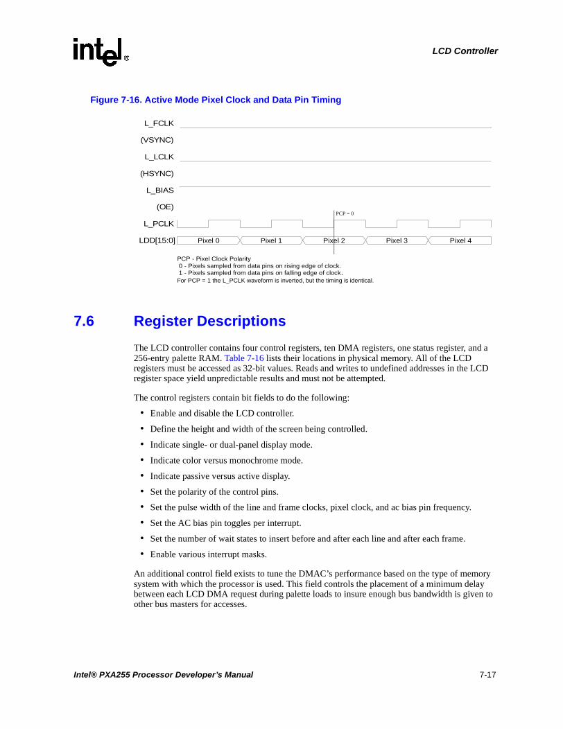
LCD Controller
7.6 Register Descriptions
The LCD controller contains four control registers, ten DMA registers, one status register, and a 256-entry palette RAM. Table 7-16 lists their locations in physical memory. All of the LCD registers must be accessed as 32-bit values. Reads and writes to undefined addresses in the LCD register space yield unpredictable results and must not be attempted.
The control registers contain bit fields to do the following:
• Enable and disable the LCD controller.
• Define the height and width of the screen being controlled.
• Indicate single- or dual-panel display mode.
• Indicate color versus monochrome mode.
• Indicate passive versus active display.
• Set the polarity of the control pins.
• Set the pulse width of the line and frame clocks, pixel clock, and ac bias pin frequency.
• Set the AC bias pin toggles per interrupt.
• Set the number of wait states to insert before and after each line and after each frame.
• Enable various interrupt masks.
An additional control field exists to tune the DMAC’s performance based on the type of memory system with which the processor is used. This field controls the placement of a minimum delay between each LCD DMA request during palette loads to insure enough bus bandwidth is given to other bus masters for accesses.
Figure 7-16. Active Mode Pixel Clock and Data Pin Timing
Pixel 0 Pixel 1 Pixel 2 Pixel 3 Pixel 4
PCP - Pixel Clock Polarity 0 - Pixels sampled from data pins on rising edge of clock. 1 - Pixels sampled from data pins on falling edge of clock.For PCP = 1 the L_PCLK waveform is inverted, but the timing is identical.
L_FCLK
(VSYNC)
L_LCLK
(HSYNC)
L_BIAS
(OE)
L_PCLK
LDD[15:0]
PCP = 0
Intel® PXA255 Processor Developer’s Manual 7-17

LCD Controller
The DMA descriptor addresses are initially programmed by software. After that, the other DMA registers are programmed by the hardware. Section 7.6.5 provides a complete description of how the DMA is programmed.
The status registers contain bits that signal:
• Input and output FIFO overrun and underrun errors
• DMA bus errors
• When the DMAC starts and ends a frame
• When the last active frame has completed after the LCD is disabled
• Each time the L_BIAS pin has toggled a programmed number of times
Each of these hardware-detected events can signal an interrupt request to the interrupt controller.
7.6.1 LCD Controller Control Register 0 (LCCR0)
The control bits in LCCR0, shown in Table 7-3, within all other control registers must be programmed before setting ENB=1 (a word write can be used to configure LCCR0 while setting ENB after all other control registers have been programmed). The LCD controller must be disabled when changing the state of any control bit within the LCD controller.
LCD Output Fifo Underrun Mask (OUM) — used to mask interrupt requests that are asserted whenever an output FIFO underrun error occurs. When OUM=0, underrun interrupts are enabled, and whenever an output FIFO underrun (OU) status bit within the LCD status register (LCSR) is set (one), an interrupt request is made to the interrupt controller. When OUM=1, underrun interrupts are masked and the state of the underrun status bit (OU) is ignored by the interrupt controller. Setting OUM does not affect the current state of the status bit or the LCD controller’s ability to set and clear it, it only blocks the generation of the interrupt request. Output FIFO underruns are more critical than Input FIFO underruns, since Output FIFO underruns will affect the display.
Branch Mask (BM) — used to mask interrupt requests that are asserted after the LCD Controller has branched to a new set of frame descriptors. See Section 7.6.6 for details.
Palette DMA Request Delay (PDD) — used to select the minimum number of internal bus clock cycles to wait between the servicing of each DMA request issued while the on-chip palette is loaded. When the palette is optionally loaded at the beginning of a frame, up to 512 bytes of data may be accessed by the LCD’s DMAC. Using PDD allows other bus masters to gain access to shared memory in between palette DMA loads. PDD must be used carefully, as it can severely degrade LCD controller performance if not used properly. It is recommended to leave PDD zero and add delay only when necessary. PDD does not apply to the normal input FIFO DMA requests for frame buffer information, since these DMA requests do not occur back-to-back. The input FIFO DMA request rate is a function of the rate at which pixels are displayed on the screen.
After a word of palette data is written to the input FIFO, the value contained within PDD is loaded to a down counter that disables the palette from issuing another DMA request until the counter decrements to zero. This counter ensures that the LCD’s DMAC does not tie up the full bandwidth of the processor system bus. Once the counter reaches zero, any pending or future DMA requests by the palette cause the DMAC to arbitrate for the bus. Once the DMA burst cycle has completed, the process starts over, and the value in PDD is loaded to the counter to create another wait state period, which disables the palette from issuing a DMA request. PDD can be programmed with a
7-18 Intel® PXA255 Processor Developer’s Manual

LCD Controller
value that causes the FIFO to wait from 0 to 255 clock cycles after the completion of one DMA request to the start of the next request. When PDD=0x00, the FIFO DMA request delay function is disabled.
LCD Quick Disable Interrupt Mask (QDM) — used to mask interrupt requests that are asserted after the LCD Enable bit (ENB) is cleared and the DMAC finishes the current burst transfer. The LCD controller immediately stops requesting new data and the current frame is not completed. This shutdown is for Sleep shutdown. When QDM=0, the quick disable interrupt is enabled, and whenever the LCD quick disable (QD) status bit in the LCD Status Register (LCSR) is set, an interrupt request is made to the interrupt controller. When QDM=1, the quick disable interrupt is masked and the state of the QD status bit is ignored by the interrupt controller. Setting QDM does not affect the current state of QD or the LCD controller’s ability to set and clear QD, it only blocks the generation of the interrupt request.
LCD Disable (DIS) — During LCD Controller operation, setting DIS=1 causes the LCD Controller to finish fetching the current frame from memory and then shut down cleanly. If the LCD DMAC is loading the palette RAM when DIS is set, the load will complete followed by the next frame, and then the LCD controller is disabled. Completion of the current frame is signalled by the LCD when it sets the LCD disable done flag (LDD) in register LCSR. Use a read-modify-write procedure to set this bit, since the other bit fields within LCCR0 continue to be used until the current frame is completed. The LCD Enable bit (ENB) is cleared when the disable is completed. Section 7.2.2 for more information.
Double-Pixel Data (DPD) Pin Mode — selects whether four or eight data pins are used for pixel data output to the LCD screen in single-panel monochrome mode. When DPD=0, L_DD[3:0] pins are used to send 4 pixel values each pixel clock transition. When DPD=1, L_DD[7:0] pins are used to send 8 pixel values each pixel clock. See Table 7-3 for a comparison of how the LCD’s data pins are used in each of its display modes.
Note: DPD does not affect dual-panel monochrome mode, any of the color modes, or active mode. Clear DPD in these modes.
Passive/Active Display Select (PAS) — selects whether the LCD controller operates in passive (STN) or active (TFT) display control mode. When PAS=0, passive mode is selected. All LCD data flow operates normally (including the LCD’s dither logic), and all LCD controller pin timing operates as described in Table 7.5.
When PAS=1, active mode is selected. 1- and 2-bit pixel modes are not supported in active mode. For 4- and 8-bit pixel modes, pixel data is transferred via DMA from off-chip memory to the input FIFO, unpacked, and used to select an entry from the palette, just as in passive mode. However, the value read from the palette bypasses the LCD controller’s dither logic and is sent directly to the output FIFO to be driven onto the LCD’s data pins. This 16-bit output to the pins represents 5 bits of red, 6 bits of green, and 5 bits of blue data. For 16-bit pixel encoding mode, two 16-bit values are packed into each word in the frame buffer. Each 16-bit value is transferred via DMA from off-chip memory to the input FIFO. Unlike 4 and 8 bit per pixel modes, the 16-bit value bypasses both the palette and the dither logic and is placed directly in the output FIFO to be sent to the LCD’s data pins. Using the 16-bit pixel encoding mode allows a total of 64K colors to be generated.
The 16-bit output from either the palette or frame buffer to the pins can be organized in any fashion necessary to correctly interface with the LCD panel. Typically, the output is configured into one of three user-specified RGB color formats: 6 bits of red, 5 bits of green, and 5 bits of blue data; 5 bits of red, 6 bits of green, and 5 bits of blue data; and 5 bits of red, 5 bits of green, and 6 bits of blue data. The RGB format 5:6:5 is normally used, since the human eye can distinguish more shades of green than of red or blue.
Intel® PXA255 Processor Developer’s Manual 7-19

LCD Controller
The LCD pin timing changes when active mode is selected. Timing of each pin is described in subsequent bit-field sections for both passive and active mode.
The LCD controller can be configured in active color display mode and used with an external DAC and optionally an external palette to drive a video monitor. Only monitors that implement the RGB data format can be used. The LCD controller does not support the NTSC standard. However, the 2X pixel clock mode allows the LCD controller to easily interface with an NTSC encoder, such as the Analog Devices 7171 encoder.
Figure 7-17 shows which bits are sent to the individual LCD data pins for both a frame buffer entry (for 16-bit/pixel mode) and a selected palette entry (for 1, 2, 4 and 8 bit/pixel mode). The pixel bits corresponding to L_DD pins when using an RGB format of 5:6:5 are also shown. In active mode, L_DD pins [15:8] are also used. The user must configure the proper GPIO pins for LCD operation to enable LCD Controller operation. See Chapter 4, “System Integration Unit” for GPIO configuration information.
The processor LCD controller may be used with active panels having more than 16 data pins, but the panel will be limited to a total of 64K colors. There are three options:
1. To maintain the panel’s full range of colors and increase the granularity of the spectrum, connect the LCD controller’s 16 data pins to the panel’s most significant R, G, and B pixel data input pins and tie the panel’s least significant R, G, and B data pins either high or low.
2. To maintain the granularity of the spectrum and limit the overall range of colors possible, connect the LCD controller’s 16 data pins to the panel’s least significant R, G, and B pixel data input pins and tie the panel’s most significant data pins either high or low.
3. Sometimes, better results can be obtained by replicating the upper bits on the lower bits.
End of Frame Mask (EFM) — used to mask interrupt requests that are asserted at the end of each frame (when the DMA length of transfer counter decrements to zero). When EFM=0, the interrupt is enabled, and whenever the EOF status bit in the LCD status register (LCSR) is set to one, an interrupt request is made to the interrupt controller. When EFM=1, the interrupt is masked, and the state of the EOF status bit is ignored by the interrupt controller. Setting EFM does not affect the current state of EOF or the LCD controller’s ability to set and clear EOF, it only blocks the generation of the interrupt request.
Input Fifo Underrun Mask (IUM) — used to mask interrupt requests that are asserted whenever an input FIFO underrun error occurs. When IUM=0, underrun interrupts are enabled, and whenever an input FIFO underrun (IUL, IUU) status bit in the LCD status register (LCSR) is set to one, an interrupt request is made to the interrupt controller. When IUM=1, underrun interrupts are masked and the state of the underrun status bits (IUL, IUU) is ignored by the interrupt controller. Setting IUM does not affect the current state of these status bits or the LCD controller’s ability to set and clear them, it only blocks the generation of the interrupt requests.
Start Of Frame Mask (SFM) — used to mask interrupt requests that are asserted at the beginning of each frame when the LCD’s frame descriptor has been loaded into the internal DMA registers. When SFM=0, the interrupt is enabled, and whenever the start of frame (SOF) status bit in the LCD
Figure 7-17. Frame Buffer/Palette Output to LCD Data Pins in Active Mode4/8/16 Bits/Pixel Mode, Frame Buffer or Palette Entry
PIxel R4 R3 R2 R1 R0 G5 G4 G3 G2 G1 G0 B4 B3 B2 B1 B0
Bit 15 14 13 12 11 10 9 8 7 6 5 4 3 2 1 0
L_DD Pin
15 14 13 12 11 10 9 8 7 6 5 4 3 2 1 0
7-20 Intel® PXA255 Processor Developer’s Manual

LCD Controller
status register (LCSR) is set, an interrupt request is made to the interrupt controller. When SFM=1, the interrupt is masked and the state of the SOF status bit is ignored by the interrupt controller. Setting SFM does not affect the current state of SOF or the LCD controller’s ability to set and clear SOF, it only blocks the generation of the interrupt request.
LCD Disable Done Interrupt Mask (LDM) — used to mask interrupt requests that are asserted after the LCD is disabled and the frame currently being sent to the output pins has completed. When LDM=0, the interrupt is not masked, and whenever the LCD disable done (LDD) status bit in the LCD status register (LCSR) is set to one, an interrupt request is made to the interrupt controller. When LDM=1, the interrupt is masked, and the state of the LDD status bit is ignored by the interrupt controller. Setting LDM does not affect the current state of LDD or the LCD controller’s ability to set and clear LDD, it only blocks the generation of the interrupt request. This interrupt is used when the LCD must be disabled after the current frame being sent to the output pins has completed. Clearing LCD Enable (ENB) is a quick disable, and LDD is not set.
Note: This mask bit applies only to regular shutdowns using the LCD Disable (DIS) bit.
Single-/Dual-Panel Select (SDS) — In passive mode (PAS=0), SDS is used to select the type of display control implemented by the LCD screen. When SDS=0, single-panel operation is selected (pixels presented to screen a line at a time). When SDS=1, dual-panel operation is selected (pixels presented to screen two lines at a time). Single-panel LCD drivers have one line/row shifter and driver for pixels and one line pointer. Dual-panel LCD controller drivers have two line/row shifters (one for the top half of the screen, one for the bottom) and two line pointers (one for the top half of the screen, one for the bottom).
When dual-panel mode is programmed, both of the LCD controller’s DMA channels are used. DMA channel 0 is used to load the palette RAM from the frame buffer and to drive the upper half of the display, and DMA channel 1 drives the lower half. The two channels alternate when fetching data for both halves of the screen, placing encoded pixel values in the two separate input FIFOs.
When dual-panel operation is enabled, the LCD controller doubles its pin usage. For monochrome screens, eight pins are used and for color screens, 16 pins are used.
Note: SDS must be set to 0 in active mode (PAS=1).
Table 7-3 shows the LCD data pins and GPIO pins used for each mode of operation and the ordering of pixels delivered to a screen for each mode of operation.
Note: In passive color mode, the data pin ordering switches. Figure 7-18 shows the LCD data pin pixel ordering.
.
Table 7-2. LCD Controller Data Pin Utilization (Sheet 1 of 2)
Color/Monochrome Panel
Single/Dual Panel
Passive/Active Panel Screen Portion Pins
Monochrome Single Passive Whole L_DD[3:0]
Monochrome Single Passive Whole L_DD[7:0]†
Monochrome Dual PassiveTop L_DD[3:0]
Bottom L_DD[7:4]
Color Single Passive Whole L_DD[7:0]
Intel® PXA255 Processor Developer’s Manual 7-21

LCD Controller
† Double-pixel data mode (DPD) = 1.
Color Dual PassiveTop L_DD[7:0]
Bottom L_DD[15:8]
Color Single Active Whole L_DD[15:0]
Table 7-2. LCD Controller Data Pin Utilization (Sheet 2 of 2)
Color/Monochrome Panel
Single/Dual Panel
Passive/Active Panel Screen Portion Pins
Figure 7-18. LCD Data-Pin Pixel Ordering
LDD[0] LDD[1] LDD[2] LDD[3] LDD[0] LDD[1] LDD[2] LDD[3] LDD[0]
Top Left Corner of ScreenColumn 0 Column 1 Column 2 Column 3 Column 4 Column 5 Column 6 Column 7 Column 8
Row 0
Row 1
Row 2
Row 3
LDD[0] LDD[1] LDD[2] LDD[3] LDD[0] LDD[1] LDD[2] LDD[3] LDD[0]
LDD[0] LDD[1] LDD[2] LDD[3] LDD[0] LDD[1] LDD[2] LDD[3] LDD[0]
LDD[0] LDD[1] LDD[2] LDD[3] LDD[0] LDD[1] LDD[2] LDD[3] LDD[0]
Passive Monochrome Single-Panel Display Pixel Ordering
LDD[0] LDD[1] LDD[2] LDD[3] LDD[4] LDD[5] LDD[6] LDD[7] LDD[0]
Top Left Corner of ScreenColumn 0 Column 1 Column 2 Column 3 Column 4 Column 5 Column 6 Column 7 Column 8
Row 0
Row 1
Row 2
Row 3
LDD[0] LDD[1] LDD[2] LDD[3] LDD[4] LDD[5] LDD[6] LDD[7] LDD[0]
LDD[0] LDD[1] LDD[2] LDD[3] LDD[4] LDD[5] LDD[6] LDD[7] LDD[0]
LDD[0] LDD[1] LDD[2] LDD[3] LDD[4] LDD[5] LDD[6] LDD[7] LDD[0]
Passive Monochrome Single-Panel Double-Pixel Display Pixel Ordering
LDD[7] LDD[6] LDD[0] LDD[7] LDD[1] LDD[0] LDD[7]
Top Left Corner of ScreenColumn 0 Column 0 Column 2 Column 2 Column 4 Column 5 Column 5
Row 0
Row 1
Row n/2
Row n/2+1
LDD[7] LDD[6] LDD[0] LDD[7] LDD[1] LDD[0] LDD[7]
LDD[15] LDD[14] LDD[8] LDD[15] LDD[9] LDD[8] LDD[15]
LDD[15] LDD[14] LDD[8] LDD[15] LDD[9] LDD[8] LDD[15]
LDD<7> LDD<6> LDD<5> LDD<4> LDD<3> LDD<2> LDD<1> LDD<0> LDD<7>
Top Left Corner of ScreenColumn 0 Column 0 Column 0 Column 1 Column 1 Column 1 Column 2 Column 2 Column 2
Row 0
Row 1
Row 2
Row 3
LDD<7> LDD<6> LDD<5> LDD<4> LDD<3> LDD<2> LDD<1> LDD<0> LDD<7>
LDD<7> LDD<6> LDD<5> LDD<4> LDD<3> LDD<2> LDD<1> LDD<0> LDD<7>
LDD<7> LDD<6> LDD<5> LDD<4> LDD<3> LDD<2> LDD<1> LDD<0> LDD<7>
Passive Color Single-Panel Display Pixel Ordering
Red Green Blue Red Green Blue Red Green Blue
Red Green Green Blue Blue Red Green
LDD<0> LDD<1> LDD<3> LDD<0> LDD<2> LDD<3> LDD<0>
Top Left Corner of Screen
Row 0
Row 1
Row n/2
Row n/2+1
LDD<0> LDD<1> LDD<3> LDD<0> LDD<2> LDD<3> LDD<0>
LDD<2> LDD<1>
LDD<2> LDD<1>
LDD<4> LDD<5> LDD<7> LDD<4> LDD<6> LDD<7> LDD<4>
LDD<4> LDD<5> LDD<7> LDD<4> LDD<6> LDD<7> LDD<4>
LDD<6> LDD<5>
LDD<6> LDD<5>
Column 0 Column 1 Column 2 Column 3 Column 4 Column 5 Column 6 Column 7 Column 8
Passive Color Dual-Panel Display Pixel Ordering
Passive Monochrome Dual-Panel Display Pixel Orderingn = # of rows
n = # of rows
7-22 Intel® PXA255 Processor Developer’s Manual

LCD Controller
Color/Monochrome Select (CMS) — selects whether the LCD controller operates in color or monochrome mode. When CMS=0, color mode is selected. Palette entries are 16 bits wide (5-bits red, 6-bits green, 5-bits blue), 8 data pins are enabled for single-panel mode, 16 data pins are enabled for dual-panel mode, and all three dither blocks are used, one each for the red, green, and blue pixel components. When CMS=1, monochrome mode is selected, palette entries are 8 bits wide, 4 or 8 data pins are enabled for single-panel mode, 8 data pins are enabled for dual-panel mode, and the blue dither block is used.
LCD Enable (ENB) — used to enable and quickly disable all LCD controller operation. When ENB=0, the LCD controller is either disabled or in the process of quickly disabling, and all of the LCD pins can be used for GPIO. When ENB=1, the LCD controller is enabled.
All other control registers must be initialized before setting ENB. LCCR0 can be programmed last, and all bit fields can be configured at the same time with a word write to the register. If ENB is cleared while the LCD controller is enabled, the LCD controller will immediately stop requesting data from the LCD DMAC, and the current frame will not complete. The LCD controller must not be re-enabled until the QD status flag is set in register LCSR, indicating the quick disable is complete. Quick disable is for sleep shutdown. Regular shutdown of the LCD controller at the end of the frame can be done via the LCD Disable bit, LCCR0[DIS]. There are separate maskable interrupts for quick disable and regular disable. See Section 7.2.1 for more information.
This is a read/write register. Ignore reads from reserved bits. Write zeros to reserved bits.
Table 7-3. LCCR0 Bit Definitions (Sheet 1 of 2)
Physical Address0x4400_0000 LCCR0 LCD Controller
Bit 31 30 29 28 27 26 25 24 23 22 21 20 19 18 17 16 15 14 13 12 11 10 9 8 7 6 5 4 3 2 1 0
reserved
OU
M
BM PDD
QD
M
DIS
DP
D
rese
rved
PAS
EF
M
IUM
SF
M
LD
M
SD
S
CM
S
EN
B
Reset X X X X X X X X X X X X 0 0 0 0 0 0 0 0 0 0 0 0 0 0 0 0 0 0 0 0
Bits Name Description
31:22 — reserved
21 OUMOutput FIFO Underrun mask:
0 = FIFO underrun errors generate an interrupt.1 = FIFO underrun errors do not generate an interrupt.
20 BMBranch Mask:
0 = Generates an interrupt after branching to a new frame.1 = Branch Start (BS) condition does not generate an interrupt.
19:12 PDD
Palette DMA Request Delay:
Value (0–255) specifies the number of internal bus clocks to wait before requesting another burst of palette data. The counter starts decrementing when the first word is written to the input FIFO buffer. PDD = 0x00 disables this function.
11 QDMLCD Quick Disable Mask:
0 = Generate an interrupt after quick disable.1 = Quick Disable (QD) status does not generate an interrupt.
10 DISLCD Disable:
0 = LCD Controller has not been disabled.1 = LCD Controller has been disabled, or is in the process of disabling.
Intel® PXA255 Processor Developer’s Manual 7-23

LCD Controller
7.6.2 LCD Controller Control Register 1 (LCCR1)
LCCR1, shown in Table 7-4, contains four bit fields that are used as modulus values for a collection of down counters, each of which performs a different function to control the timing of several of the LCD pins. These values must be programmed before enabling the LCD Controller.
9 DPD
Double-Pixel Data (DPD) pin mode:
In passive monochrome single panel mode,
0 = L_DD[3:0] pins are used to send 4 pixel values each pixel clock transition.1 = L_DD[7:0] pins are used to send 8 pixel values each pixel clock.
In any other mode, DPD must be 0.
8 — reserved
7 PASPassive/Active Display select:
0 = Passive (or STN) display operation enabled.1 = Active (or TFT) display operation enabled.
6 EFMEnd of Frame Mask:
0 = Generates an interrupt at the end of a frame.1 = End of frame (EOF) condition does not generate an interrupt.
5 IUMInput FIFO Underrun Mask:
0 = FIFO underrun errors generate an interrupt.1 = FIFO underrun errors do not generate an interrupt.
4 SFMStart of Frame Mask:
0 = Starting a new frame (after loading frame descriptor) generates an interrupt.1 = Start of frame (SOF) condition does not generate an interrupt.
3 LDM
LCD Disable Done Mask:
0 = LCD disable done condition generates an interrupt (state of LDD status sent to the interrupt controller).
1 = LCD disable done condition does not generate an interrupt (LDD status bit ignored).
2 SDS
Single-/Dual-panel Display Select:
0 = Single-panel display enabled. 1 = Dual-panel display enabled.
SDS must be 0 in active mode (PAS=1).
1 CMSColor/Monochrome Select:
0 = Color operation enabled.1 = Monochrome operation enabled.
0 ENBLCD Controller Enable:
0 = LCD controller disabled or in the process of quickly disabling.1 = LCD controller enabled.
Table 7-3. LCCR0 Bit Definitions (Sheet 2 of 2)
Physical Address0x4400_0000 LCCR0 LCD Controller
Bit 31 30 29 28 27 26 25 24 23 22 21 20 19 18 17 16 15 14 13 12 11 10 9 8 7 6 5 4 3 2 1 0
reserved
OU
M
BM PDD
QD
M
DIS
DP
D
rese
rved
PA
S
EF
M
IUM
SF
M
LD
M
SD
S
CM
S
EN
B
Reset X X X X X X X X X X X X 0 0 0 0 0 0 0 0 0 0 0 0 0 0 0 0 0 0 0 0
Bits Name Description
7-24 Intel® PXA255 Processor Developer’s Manual

LCD Controller
Beginning-of-Line Pixel Clock Wait Count (BLW) — used to specify the number of dummy pixel clocks to insert at the beginning of each line or row of pixels. After the line clock for the previous line has been negated, the value in BLW is used to count the number of pixel clocks to wait before starting to output the first set of pixels in the next line. BLW generates a wait period ranging from 1 to 256 pixel clock cycles. BLW must be programmed with the desired number of pixel clocks minus one. L_PCLK does not toggle during these “dummy” pixel clock cycles in passive display mode. It does toggle continuously in active display mode.
End-of-Line Pixel Clock Wait Count (ELW) — used to specify the number of “dummy” pixel clocks to insert at the end of each line or row of pixels before pulsing the line clock pin. Once a complete line of pixels is transmitted to the LCD driver, the value in ELW is used to count the number of pixel clocks to wait before pulsing the line clock. ELW generates a wait period ranging from 1 to 256 pixel clock cycles. ELW must be programmed with the desired number of pixel clocks minus one. L_PCLK does not toggle during these dummy pixel clock cycles in passive display mode. It does toggle continuously in active display mode.
Horizontal Sync Pulse Width (HSW) — specifies the pulse width (minus 1) of the line clock in passive mode or the horizontal synchronization pulse in active mode. L_LCLK is asserted each time a line is sent to the display and a programmable number of pixel clock wait states have elapsed. When L_LCLK is asserted, the value in HSW is transferred to a 6-bit down counter, which decrements at the programmed pixel clock frequency. When the counter reaches zero, L_LCLK is negated. HSW can be programmed to generate a line clock pulse width ranging from 1 to 64 pixel clock periods.
The pixel clock does not toggle during the line clock pulse in passive display mode but does toggle in active display mode. The polarity (active and inactive state) of the line clock pin is programmed using the horizontal sync polarity (HSP) bit in LCCR3.
HSW must be programmed with the desired number of pixel clocks minus one.
Note: The term “pulse width” refers to the time which L_LCLK is asserted, rather than the time for a cycle of the line clock to occur.
Pixels Per Line (PPL) — used to specify the number of pixels in each line or row on the screen (minus one). PPL is a 10-bit value that represents between 1 and 1024 pixels per line. It is recommended not to exceed 640 pixels. It is used to count the number of pixel clocks that must occur before the line clock can be asserted. As discussed in Section 7.4.2, pixels per line must be multiples of: 32 pixels for 1-bit pixels, 16 pixels for 2-bit pixels, 8 pixels for 4-bit pixels, 4 pixels for 8-bit pixels, and 2 pixels for 16-bit pixels. The two special conditions are: 8-bits/pixel monochrome screens with double-pixel-data mode and 8 or 16 bits/pixel passive color screens require a multiple of 8 pixels for each line.
If the display used is not naturally a multiple of the above, “dummy” pixels must be added to each line to keep the frame buffer aligned in memory. For example, if the display being controlled is 250 pixels wide and the pixel-size is 8-bits, the nearest greater multiple of 8 is 256. Pixels per line must be set to 255. 6 extra “dummy” pixel values must be added to the end of each line in the frame buffer. The display being controlled must ignore the dummy pixel clocks at the end of each line.
This is a read/write register. Ignore reads from reserved bits. Write zeros to reserved bits.
Intel® PXA255 Processor Developer’s Manual 7-25

LCD Controller
7.6.3 LCD Controller Control Register 2 (LCCR2)
LCCR2, shown in Table 7-5, contains four bit fields that are used as values for a collection of down counters, each of which performs a different function to control the timing of several of the LCD’s pins.
Beginning-of-Frame Line Clock Wait Count (BFW) — used in active mode (LCCR0[PAS] = 1) to specify the number of line clocks to insert at the beginning of each frame. The BFW count starts when the VSYNC signal for the previous frame is negated. The value in BFW is used to count the number of line clock periods to insert before starting pixel output in the next frame. BFW generates a wait period ranging from 0 to 255 extra L_LCLK cycles (BFW=0x00 disables the wait count). L_LCLK does toggle during the generation of the BFW line clock wait periods.
In passive mode, BFW must be set to zero so that no beginning-of-frame wait states are generated. Use VSW exclusively in passive mode to insert line clock wait states, which allow the LCD controller’s DMAC to fill the palette and insert additional pixels before the start of the next frame.
End-of-Frame Line Clock Wait Count (EFW) — used in active mode (LCCR0[PAS] = 1) to specify the number of line clocks to insert at the end of each frame. Once a complete frame of pixels is transmitted to the LCD display, the value in EFW is used to count the number of line clock periods to wait. After the count has elapsed, the VSYNC (L_FCLK) signal is pulsed. EFW generates a wait period ranging from 0 to 255 line clock cycles (EFW = 0x00 disables the EOF wait count). L_LCLK does not toggle during the generation of the EFW line clock periods.
Table 7-4. LCCR1 Bit Definitions
Physical Address0x4400_0004 LCD Controller Control Register 1 LCD Controller
Bit 31 30 29 28 27 26 25 24 23 22 21 20 19 18 17 16 15 14 13 12 11 10 9 8 7 6 5 4 3 2 1 0
BLW ELW HSW PPL
Reset 0 0 0 0 0 0 0 0 0 0 0 0 0 0 0 0 0 0 0 0 0 0 0 0 0 0 0 0 0 0 0 0
Bits Name Description
31:24 BLWBeginning-of-Line pixel clock Wait count:
Value (0–255) specifies the number of pixel clock periods to add to the beginning of a line transmission before the first set of pixels is sent to the display. BOL wait = (BLW + 1).
23:16 ELW
End-of-line pixel clock wait count:
Value (0–255) specifies the number of pixel clock periods to add to the end of a line transmission before line clock is asserted. EOL = (ELW+1).
In passive display mode, Pixel Clock is held in its inactive state during the end-of-line wait period. In active display mode, it toggles.
15:10 HSW
Horizontal sync pulse width:
Value (0–63) specifies the number of pixel clock periods to pulse the line clock at the end of each line. HSYNC pulse width = (HSW+1).
In passive display mode, Pixel Clock is held in its inactive state during the generation of the line clock. In active display mode, it toggles.
9:0 PPLPixels per line:
Specifies the number of pixels contained within each line on the LCD display. Actual pixels per line = (PPL+1).
7-26 Intel® PXA255 Processor Developer’s Manual

LCD Controller
In passive mode, EFW must be set to zero so that no EOF wait states are generated. Use VSW exclusively in passive mode to insert line clock wait states, which allow the LCD controller’s DMAC to fill the palette and insert additional pixels before the start of the next frame.
Vertical Sync Pulse Width (VSW) — used to specify the pulse width of the vertical synchronization pulse in active mode or to add extra “dummy” line clock wait states between the end and beginning of frame in passive mode.
In active mode (LCCR0[PAS]=1), L_FCLK is used to generate the vertical sync signal and is asserted each time the last line or row of pixels for a frame is sent to the display and a programmable number of line clock wait states as specified by LCCR1[BLW] have elapsed. When L_FCLK is asserted, the value in VSW is transferred to a 6-bit down counter, which uses the line clock frequency to decrement. When the counter reaches zero, L_FCLK is negated. VSW can be programmed to generate a vertical sync pulse width ranging from 1 to 64 line clock periods. VSW must be programmed with the desired number of line clocks minus one. The polarity (active and inactive state) of the L_FCLK pin is programmed using the vertical sync polarity (VSP) bit in LCCR3.
In passive mode (LCCR0[PAS]=0), VSW does not affect the timing of the L_FCLK pin, but rather can be used to add extra line clock wait states between the end of each frame and the beginning of the next frame. When the last line clock of a frame is negated, the value in VSW is transferred to a 6-bit down counter that uses the line clock frequency to decrement. When the counter reaches zero, the next frame begins. VSW can be programmed to generate from 1 to 64 dummy line clock periods between each frame in passive mode. VSW must be programmed to allow:
• enough wait states to occur between frames such that the LCD’s DMAC is able to fully load the on-chip palette (if applicable)
• a sufficient number of encoded pixel values to be fetched from the frame buffer, to be processed by the dither logic and placed in the output FIFO, ready to be sent to the LCD data pins.
The number of wait states required is system dependent, depending on such factors as:
• palette buffer size (none; 8, 32 or 512 bytes)
• memory system speed (number of wait states, burst speed, number of beats)
• Palette DMA request delay, LCCR0[PDD].
The line clock pin does toggle during the insertion of the line clock wait state periods.
VSW does not affect generation of the frame clock signal in passive mode. Passive LCD displays require that the frame clock be active on the rising edge of the first line clock pulse of each frame, with adequate setup and hold time. To meet this requirement, the LCD controller’s frame clock pin is asserted on the rising edge of the first pixel clock for each frame. The frame clock remains asserted for the remainder of the first line as pixels are sent to the display. It is then negated on the rising edge of the first pixel clock of the second line of each frame.
Lines Per Panel (LPP) — specifies the number of lines or rows present on the LCD panel being controlled. In single-panel mode, it represents the total number of lines for the entire LCD display. LPP is used to count the correct number of line clocks that must occur before the frame clock can be pulsed. In dual-panel mode, it represents half the number of lines of the entire LCD display, which is split into two panels. LPP is a 10-bit value that represents between 1 and 1024 lines per screen. It must be programmed with the actual height of the display minus one. It is recommended not to exceed 480 pixels. For portrait mode panels, more than 480 pixels can be used as long as total pixels do not exceed 480,000. For example, a 480x640 portrait mode panel can be used.
Intel® PXA255 Processor Developer’s Manual 7-27

LCD Controller
This is a read/write register. Ignore reads from reserved bits. Write zeros to reserved bits.
7.6.4 LCD Controller Control Register 3 (LCCR3)
LCCR3, shown in Table 7-6, contains bits and bit fields used to control various functions within the LCD controller.
Double Pixel Clock (DPC) — doubles the rate of the pixel clock on the L_PCLK pin. This allows direct connection to an NTSC encoder (e.g., the Analog Devices 7171). All of the LCD controller settings are still specified in terms of the “original” pixel clock and this mode affects only the L_PCLK output pin. If DPC is set to 1, the pixel clock divisor (PCD) must be greater than or equal to 1.
Bits Per Pixel (BPP) — BPP specifies the size of encoded pixel values in memory. Pixel sizes of 1, 2, 4, and 8 bits require that the internal palette RAM be loaded before pixels can be displayed on the screen. See Section 7.6.5 for details on programming the DMAC to load the palette RAM. BPP is programmed as follows:
0b000 = 1-bit pixels0b001 = 2-bit pixels0b010 = 4-bit pixels
Table 7-5. LCCR2 Bit Definitions
Physical Address0x4400_0008 LCD Controller Control Register 2 LCD Controller
Bit 31 30 29 28 27 26 25 24 23 22 21 20 19 18 17 16 15 14 13 12 11 10 9 8 7 6 5 4 3 2 1 0
BFW EFW VSW LPP
Reset 0 0 0 0 0 0 0 0 0 0 0 0 0 0 0 0 0 0 0 0 0 0 0 0 0 0 0 0 0 0 0 0
Bits Name Description
31:24 BFW
Beginning-of-frame line clock wait count:
In active mode (LCCR0[PAS]=1), value (0–255) specifies the number of line clock periods to add to the beginning of a frame before the first set of pixels is sent to the display. The Line clock does toggle during the insertion of the extra line clock periods.
BFW must be cleared to zero (disabled) in passive mode.
23:16 EFW
End-of-frame line clock wait count:
In active mode (LCCR0[PAS] = 1), value (0–255) specifies the number of line clock periods to add to the end of each frame. The Line clock does toggle during the insertion of the extra line clock periods.
EFW must be cleared to zero (disabled) in passive mode.
15:10 VSW
Vertical sync pulse width:
In active mode (LCCR0[PAS] = 1), value (0–63) specifies the number of line clock periods to pulse the L_FCLK pin at the end of each frame after the end-of-frame wait (EFW) period elapses. Frame clock used as VSYNC signal in active mode. The line clock does toggle during VSYNC. VSYNC width = (VSW+1)
In passive mode (LCCR0[PAS] = 0), value (0–63) specifies the number of extra line clock periods to insert after the end-of-frame. The time for which L_FCLK is asserted is not affected by VSW in passive mode. The line clock does toggle during the insertion of the extra line clock periods. VSYNC width = (VSW+1).
9:0 LPP
Lines per panel:
Specifies the number of lines per panel. For single-panel mode, this represents the total number of lines on the LCD display. For dual-panel mode, it is half the number of lines on the whole LCD display. Lines per panel = (LPP+1).
7-28 Intel® PXA255 Processor Developer’s Manual

LCD Controller
0b011 = 8-bit pixels0b100 = 16-bit pixels0b101–0b111 = reserved
Output Enable Polarity (OEP) — In active display mode (LCCR0[PAS] = 1), the OEP bit selects the active and inactive states of the output enable signal (L_BIAS). In this mode, the AC bias pin serves as an enable that signals the off-chip device when data is actively being driven using the pixel clock, which continuously toggles in active mode. When OEP = 0, L_BIAS is active high and inactive low. When OEP = 1, L_BIAS is active low and inactive high. When L_BIAS is in its active state, data is driven onto the LCD data pins on the programmed edge of the pixel clock.
In passive display mode, OEP does not affect L_BIAS.
Pixel Clock Polarity (PCP) — selects the edge of the pixel clock (L_PCLK) on which data is sampled at the LCD pins. When PCP = 0, sampling occurs on the rising edge of L_PCLK. When PCP = 1, sampling occurs on the falling edge. PCP does not affect the timing of data being driven, it simply inverts L_PCLK.
Horizontal Sync Polarity (HSP) — selects the active and inactive states of the L_LCLK pin. When HSP = 0, L_LCLK is active high and inactive low. When HSP = 1, it is active low and inactive high. In active display mode, L_LCLK serves as the horizontal sync signal and in passive display mode, it is the line clock.
In both active and passive display modes, the L_FCLK pin is forced to its inactive state whenever pixels are transmitted. After the end of each line and a programmable number of pixel clocks occur (controlled by LCCR1[ELW]), the L_FCLK pin is forced to its active state for a programmable number of line clocks (controlled by LCCR1[HSW]), and is then again forced to its inactive state.
Vertical Sync Polarity (VSP) — selects the active and inactive states of the L_FCLK pin. When VSP = 0, L_FCLK is active high and inactive low. When VSP = 1, L_FCLK is active low and inactive high.
In active display mode (LCCR0[PAS] = 1), L_FCLK serves as the vertical sync signal. It is forced to its inactive state while pixels are transmitted during the frame. After the end of the frame and a programmable number of line clocks occur (controlled by LCCR2[EFW]), it is forced to its active state for a programmable number of line clocks (controlled by LCCR2[VSW]), and is then again forced to its inactive state.
In passive display mode, L_FCLK serves as the frame clock. It is forced to its active state on the rising edge of the first pixel clock of each frame. It remains active during the transmission of the entire first line of pixels in the frame and is then forced back to its inactive state on the rising edge of the first pixel clock of the second line of the frame. It remains at this state through the end of the frame.
AC Bias Pin Transitions Per Interrupt (API) — specifies the number of AC bias pin (L_BIAS) transitions to count before setting the AC bias count status (ACS) bit in the LCD Controller Status Register (LCSR), which signals an interrupt request. After the LCD controller is enabled, the value in API is loaded to a 4-bit down counter, and the counter decrements each time L_BIAS is inverted. When the counter reaches zero, it stops, and the AC bias count bit, LCSR[ABC], is set. Once ABC is set, the 4-bit down counter is reloaded with the value in API and is disabled until ABC is cleared. When ABC is cleared by the CPU, the down counter is enabled and again decrements each time the AC bias pin is inverted. The number of AC bias pin transitions between each interrupt request ranges from 1 to 15. Setting API to 0x0 disables the API function.
Intel® PXA255 Processor Developer’s Manual 7-29
LCD Controller
In active display mode (LCCR0[PAS] = 1), L_BIAS is the output enable signal. However, signalling of the API interrupt may still occur. The ACB bit field can be used to count line clock pulses in active mode. When the programmed number of line clock pulses occurs, an internal signal is toggled that is used to decrement the 4-bit counter used by the API interrupt logic. Once this internal signal toggles the programmed number of times, as specified by API, an interrupt is generated. The user must program API to zero if the API interrupt function is not required in active mode.
AC Bias Pin Frequency (ACB) — In passive display mode (LCCR0[PAS] = 1), the 8-bit ACB field specifies the number of line clocks to count between each toggle of the AC bias pin (L_BIAS). After the LCD controller is enabled, the value in ACB is loaded to an 8-bit down counter, which begins to decrement using the line clock (L_LCLK). When the counter reaches zero, it stops, L_BIAS is toggled, and the whole procedure starts again. The number of line clocks between each bias pin transition ranges from 1 to 256, corresponding to ACB values from 0 to 255. Thus, the value to program into ACB is the desired number of line clocks minus 1.
AC bias is used by a passive LCD display to periodically reverse the polarity of the power supplied to the screen in order to eliminate D.C. offset. If the LCD display being controlled has its own internal means of switching its power supply, set ACB to its maximum value (0xFF) to reduce power consumption. ACB must be programmed conservatively in a system with bandwidth problems that result in output FIFO underruns in the LCD Controller. In these cases, the pixel clock is stalled for passive displays, which can result in more time between line clocks than expected. See Section 7.3.5 for more information on how output FIFO underruns are handled.
In active display mode, the ACB bit field has no effect on the L_BIAS pin. Because the pixel clock toggles continuously in active mode, the AC bias pin is used as an output enable signal. It is asserted automatically by the LCD controller in active mode whenever pixel data is driven out to the data pins to signal the display when it may latch pixels using the pixel clock. ACB can be used in active mode to count line clocks and generate API interrupts.
Pixel Clock Divider (PCD) — selects the frequency of the pixel clock (L_CLK). PCD can be any value from 0 to 255. It generates a range of pixel clock frequencies from LCLK/2 to LCLK/512, where LCLK is the programmed frequency of the LCD/Memory Controller clock. LCLK can vary from 100MHz to 166 MHz.
The pixel clock frequency must be adjusted to meet the required screen refresh rate, which depends on:
• number of pixels for the target display
• number of panels (single or dual)
• display type (monochrome or color)
• number of pixel clock wait states programmed at the beginning and end of each line
• number of line clocks inserted at the beginning and end of each frame
• width of the VSYNC signal in active mode or VSW line clocks inserted in passive mode
• width of the frame clock or HSYNC signal.
All of these factors alter the time duration from one frame transmission to the next. Different display manufacturers require different frame refresh rates, depending on the physical characteristics of the display. PCD is used to alter the pixel clock frequency in order to meet these requirements. The frequency of the pixel clock for a set PCD value or the required PCD value to yield a target pixel clock frequency can be calculated using the two following equations. If double pixel clock mode (DPC) is enabled, PCD must be set greater than or equal to 1.
7-30 Intel® PXA255 Processor Developer’s Manual

LCD Controller
whereLCLK = LCD/Memory Clock
PCD = LCCR3[7:0]
This is a read/write register. Ignore reads from reserved bits. Write zeros to reserved bits.
PixelClockLCLK
2 PCD 1+( )------------------------------=
PCDLCLK
2 PixelClock( )------------------------------------- 1–=
Table 7-6. LCCR3 Bit Definitions (Sheet 1 of 2)
Physical Address0x4400_000C LCD Controller Control Register 3 LCD Controller
Bit 31 30 29 28 27 26 25 24 23 22 21 20 19 18 17 16 15 14 13 12 11 10 9 8 7 6 5 4 3 2 1 0
reserved
DP
C BPP
OE
P
PC
P
HS
P
VS
P API ACB PCD
Reset X X X X 0 0 0 0 0 0 0 0 0 0 0 0 0 0 0 0 0 0 0 0 0 0 0 0 0 0 0 0
Bits Name Description
31:28 - reserved
27 DPCDouble Pixel Clock mode:
0 = The L_PCLK pin is driven at the frequency specified by PCD.1 = The L_PCLK pin is driven at double the frequency specified by PCD.
26:24 BPP
Bits Per Pixel:
000 – 1-bits/pixel [4 entry, 8 byte palette buffer (only first 2 entries are used)]001 – 2-bits/pixel [4 entry, 8 byte palette buffer]010 – 4-bits/pixel [16 entry, 32 byte palette buffer]011 – 8-bits/pixel [256 entry, 512 byte palette buffer]100 – 16-bits/pixel [no palette buffer]101, 110, 111 – reserved
23 OEP
Output Enable Polarity:
0 = L_BIAS pin is active high and inactive low in active display mode.1 = L_BIAS pin is active low and inactive high in active display mode.
In active display mode, data is driven out to the LCD’s data pins on the programmed pixel clock edge when the L_BIAS pin is active. OEP is ignored in passive display mode.
22 PCPPixel Clock Polarity:
0 = Data is sampled on the LCD data pins on the rising edge of L_PCLK.1 = Data is sampled on the LCD data pins on the falling edge of L_PCLK.
21 HSPHorizontal Sync Polarity:
0 = L_LCLK pin is active high and inactive low.1 = L_LCLK pin is active low and inactive high.
20 VSPVertical Sync Polarity:
0 = L_FCLK pin is active high and inactive low.1 = L_FCLK pin is active low and inactive high.
Intel® PXA255 Processor Developer’s Manual 7-31
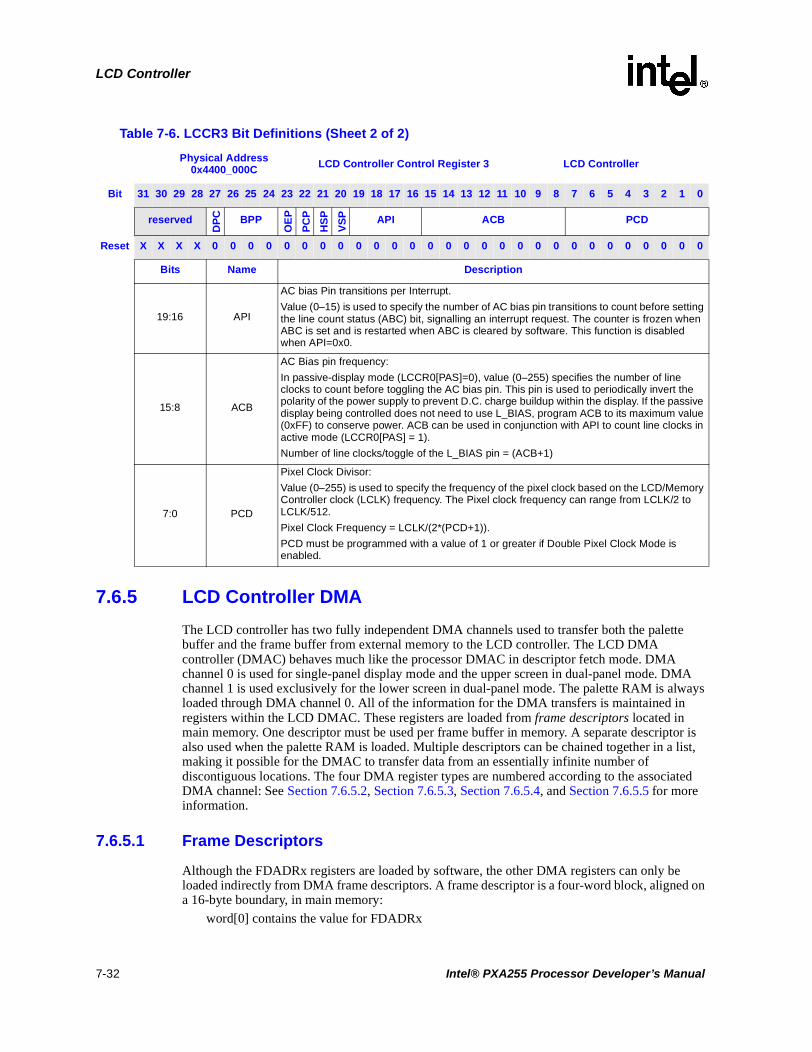
LCD Controller
7.6.5 LCD Controller DMA
The LCD controller has two fully independent DMA channels used to transfer both the palette buffer and the frame buffer from external memory to the LCD controller. The LCD DMA controller (DMAC) behaves much like the processor DMAC in descriptor fetch mode. DMA channel 0 is used for single-panel display mode and the upper screen in dual-panel mode. DMA channel 1 is used exclusively for the lower screen in dual-panel mode. The palette RAM is always loaded through DMA channel 0. All of the information for the DMA transfers is maintained in registers within the LCD DMAC. These registers are loaded from frame descriptors located in main memory. One descriptor must be used per frame buffer in memory. A separate descriptor is also used when the palette RAM is loaded. Multiple descriptors can be chained together in a list, making it possible for the DMAC to transfer data from an essentially infinite number of discontiguous locations. The four DMA register types are numbered according to the associated DMA channel: See Section 7.6.5.2, Section 7.6.5.3, Section 7.6.5.4, and Section 7.6.5.5 for more information.
7.6.5.1 Frame Descriptors
Although the FDADRx registers are loaded by software, the other DMA registers can only be loaded indirectly from DMA frame descriptors. A frame descriptor is a four-word block, aligned on a 16-byte boundary, in main memory:
word[0] contains the value for FDADRx
19:16 API
AC bias Pin transitions per Interrupt.
Value (0–15) is used to specify the number of AC bias pin transitions to count before setting the line count status (ABC) bit, signalling an interrupt request. The counter is frozen when ABC is set and is restarted when ABC is cleared by software. This function is disabled when API=0x0.
15:8 ACB
AC Bias pin frequency:
In passive-display mode (LCCR0[PAS]=0), value (0–255) specifies the number of line clocks to count before toggling the AC bias pin. This pin is used to periodically invert the polarity of the power supply to prevent D.C. charge buildup within the display. If the passive display being controlled does not need to use L_BIAS, program ACB to its maximum value (0xFF) to conserve power. ACB can be used in conjunction with API to count line clocks in active mode (LCCR0[PAS] = 1).
Number of line clocks/toggle of the L_BIAS pin = (ACB+1)
7:0 PCD
Pixel Clock Divisor:
Value (0–255) is used to specify the frequency of the pixel clock based on the LCD/Memory Controller clock (LCLK) frequency. The Pixel clock frequency can range from LCLK/2 to LCLK/512.
Pixel Clock Frequency = LCLK/(2*(PCD+1)).
PCD must be programmed with a value of 1 or greater if Double Pixel Clock Mode is enabled.
Table 7-6. LCCR3 Bit Definitions (Sheet 2 of 2)
Physical Address0x4400_000C LCD Controller Control Register 3 LCD Controller
Bit 31 30 29 28 27 26 25 24 23 22 21 20 19 18 17 16 15 14 13 12 11 10 9 8 7 6 5 4 3 2 1 0
reservedD
PC BPP
OE
P
PC
P
HS
P
VS
P API ACB PCD
Reset X X X X 0 0 0 0 0 0 0 0 0 0 0 0 0 0 0 0 0 0 0 0 0 0 0 0 0 0 0 0
Bits Name Description
7-32 Intel® PXA255 Processor Developer’s Manual

LCD Controller
word[1] contains the value for FSADRxword[2] contains the value for FIDRxword[3] contains the value for LDCMDx
Software must write the location of the first descriptor to FDADRx before enabling the LCD controller. Once the controller is enabled, the first descriptor is read, and all four registers are written by the DMAC. The next frame descriptor pointed to by FDADRx is loaded into the registers for the associated DMA channel after all data for the current descriptor has been transferred.
The address in FDADRx is not used when the BRA bit in the Frame Branch Register (FBRx) is set. In this case, the Frame Branch Address is used to fetch the descriptor for the next frame. Branches can be used to load a new palette or to process a regular frame, as detailed in Section 7.6.6.
Note: If only one frame buffer is used in external memory, the FDADRx field (word[0] of the frame descriptor) must point back to itself.
7.6.5.2 LCD DMA Frame Descriptor Address Registers (FDADRx)
FDADR0 and FDADR1, shown in Table 7-7, correspond to DMA channels 0 and 1 and contain the memory address of the next descriptor for the DMA channel. The DMAC fetches the descriptor at this location after finishing the current descriptor. On reset, the bits in this register are undefined. The target address must be aligned to a 16-byte boundary. Bits [2:0] of the address must be zero.
These are read/write registers. Ignore reads from reserved bits. Write zeros to reserved bits.
7.6.5.3 LCD DMA Frame Source Address Registers (FSADRx)
FSADR0 and FSADR1, shown in Table 7-8, correspond to DMA channels 0 and 1 and contain the source address of the current descriptor for the DMA channel. The address must be aligned on an 8-byte boundary. Bits [2:0] must be zero. If this descriptor is a palette load, FSADRx points to the memory location at the beginning of the palette data. The size of the palette data must be four 16-bit entries for 1- and 2-bit pixels, sixteen 16-bit entries for 4-bit pixels, or 256 16-bit entries for 8-bit pixels. If this descriptor is for pixel data, FSADRx points to the beginning of the frame buffer in memory. This address is incremented as the DMAC fetches from memory. If desired, the DMA Frame ID Register can be used to hold the initial frame source address.
These read-only registers are loaded indirectly via the frame descriptors, as described in Section 7.6.5.1.
Table 7-7. FDADRx Bit Definitions
Physical Addresschannel 0: 0x4400_0200channel 1: 0x4400_0210
FDADR0 FDADR1 LCD Controller
Bit 31 30 29 28 27 26 25 24 23 22 21 20 19 18 17 16 15 14 13 12 11 10 9 8 7 6 5 4 3 2 1 0
Descriptor Address
Reset ? ? ? ? ? ? ? ? ? ? ? ? ? ? ? ? ? ? ? ? ? ? ? ? ? ? ? ? ? ? ? ?
Bits Name Description
31:0 Descriptor Address
Address of next descriptor.
Bits [2:0] must be zero for proper memory alignment.
Intel® PXA255 Processor Developer’s Manual 7-33

LCD Controller
These are read-only registers. Ignore reads from reserved bits.
7.6.5.4 LCD DMA Frame ID Registers (FIDRx)
FIDRx, shown in Table 7-9, correspond to DMA channels 0 and 1 and contain an ID field that describes the current frame. The particular use of this field is up to the user. This ID register is copied to the LCD Controller Interrupt ID Register when an interrupt occurs.
These read-only registers are loaded indirectly via the frame descriptors, as described in Section 7.6.5.1.
These are read-only registers. Ignore reads from reserved bits.
Table 7-8. FSADRx Bit Definitions
Physical Addresschannel 0: 0x4400_0204channel 1: 0x4400_0214
FSADR0FSADR1 LCD Controller
Bit 31 30 29 28 27 26 25 24 23 22 21 20 19 18 17 16 15 14 13 12 11 10 9 8 7 6 5 4 3 2 1 0
Frame Source Address
Reset ? ? ? ? ? ? ? ? ? ? ? ? ? ? ? ? ? ? ? ? ? ? ? ? ? ? ? ? ? ? ? ?
Bits Name Description
31:0Frame Source Address
Address of the palette or pixel frame data in memory.
Bits [2:0] must be zero for proper memory alignment.
Table 7-9. FIDRx Bit Definitions
Physical Addresschannel 0: 0x4400_0208channel 1: 0x4400_0218
FIDR0FIDR1 LCD Controller
Bit 31 30 29 28 27 26 25 24 23 22 21 20 19 18 17 16 15 14 13 12 11 10 9 8 7 6 5 4 3 2 1 0
Frame ID reserved
Reset ? ? ? ? ? ? ? ? ? ? ? ? ? ? ? ? ? ? ? ? ? ? ? ? ? ? ? ? ? X X X
Bits Name Description
31:3 Frame ID Frame ID.
2:0 — reserved
7-34 Intel® PXA255 Processor Developer’s Manual

LCD Controller
7.6.5.5 LCD DMA Command Registers (LDCMDx)
LDCMDx, shown in Table 7-10, correspond to DMA channels 0 and 1 and contain configuration fields and the length of the current descriptor for the DMA channel. On reset, the bits in these register are initialized to zero. Reserved bits must be written with zeros and reads from reserved bits must be ignored.
These read-only registers are loaded indirectly via the frame descriptors, as described in Section 7.6.5.1.
Load Palette (PAL) — indicates that data being fetched will be loaded into the palette RAM. If PAL is set to one, the palette RAM is loaded with the first 8, 32, or 512-bytes of data as follows:
8 bytes for 1 and 2-bit pixels
32 bytes for 4-bit pixels
512 bytes for 8-bit pixels.
Software must load the palette at least once after enabling the LCD. Otherwise, the palette entries will not be initialized, and the frame data will not have a valid frame palette to reference.
The palette must not be loaded if the LCD is operating in 16-bit pixel mode.
Note: The PAL bit must never be set in LDCMD1, since the palette is always loaded with Channel 0.
Start Of Frame Interrupt (SOFINT) — when set, the DMAC sets the start of frame bit (LCSR[SOF]) when starting a new frame. The SOF bit is set after a new descriptor is loaded from memory and before the palette/frame data is fetched.
In dual-panel mode, LCSR[SOF] is set only when both channels reach the start of frame and both frame descriptors have SOFINT set. SOFINT must not be set for palette descriptors in dual-panel mode, since only one channel is ever used to load the palette RAM.
End Of Frame Interrupt (EOFINT) — when set, the DMAC sets the end of frame bit (LCSR[EOF]) after fetching the last word in the frame buffer.
In dual-panel mode, LCSR[EOF] is set only when both channels reach the end of frame and both frame descriptors have EOFINT set. EOFINT must not be set for palette descriptors in dual-panel mode, since only one channel is ever used to load the palette RAM.
Transfer Length (LEN) — determines the number of bytes fetched by the DMAC. LEN = 0 is not valid. If PAL is set to one, LEN must be programmed with the size of the palette RAM. This corresponds to:
8 bytes for 1 and 2-bit pixels (only the top 2 entries are actually used for 1-bit pixels)
32 bytes for 4-bit pixels
512 bytes for 8-bit pixels.
Note: A separate descriptor must be used to fetch the frame data.
The value of LEN for frame data is a function of the screen size and the pixel size and it must be consistent with the values used for LCCR1[PPL], LCCR2[LPP], and LCCR3[BPP]. See Section 7.4.2 for instructions on calculating length. The LCD DMAC decrements LEN as it fetches data, allowing the user to read the number of bytes remaining for the current descriptor.
These are read-only registers. Ignore reads from reserved bits.
Intel® PXA255 Processor Developer’s Manual 7-35

LCD Controller
Table 7-10. LDCMDx Bit Definitions
Physical Addresschannel 0: 0x4400_020Cchannel 1: 0x4400_021C
LDCMD0LDCMD1 LCD Controller
Bit 31 30 29 28 27 26 25 24 23 22 21 20 19 18 17 16 15 14 13 12 11 10 9 8 7 6 5 4 3 2 1 0
reserved
PAL reserved
SO
FIN
T
EO
FIN
T
LEN
Reset X X X X X 0 X X X 0 0 0 0 0 0 0 0 0 0 0 0 0 0 0 0 0 0 0 0 0 0 0
Bits Name Description
31:27 — reserved
26 PAL
Load Palette:
0 = DMA in progress is not the palette buffer.1 = DMA in progress is the palette buffer.
PAL must not be set in LDCMD1.
25:23 — reserved
22 SOFINT
Start of Frame Interrupt:
0 = Do not set the SOF interrupt bit in the LCD status register when starting a new frame.1 = Set the start of frame (SOF) interrupt bit in the LCD status register when starting a new
frame (after loading the frame descriptor).
21 EOFINT
End of Frame Interrupt:
0 = Do not set the EOF interrupt bit in the LCD status register when finished fetching the last word of this frame.
1 = Set the end of frame (EOF) interrupt bit in the LCD status register when finished fetching the last word of this frame.
20:0 LEN
Length of transfer in bytes:
The two lowest bits [1:0] are part of the length calculation but must always be zero for proper memory alignment.
LEN = 0 is illegal.
7-36 Intel® PXA255 Processor Developer’s Manual
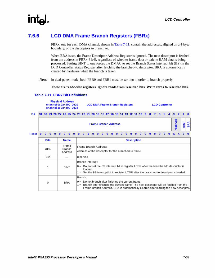
LCD Controller
7.6.6 LCD DMA Frame Branch Registers (FBRx)
FBRx, one for each DMA channel, shown in Table 7-11, contain the addresses, aligned on a 4-byte boundary, of the descriptors to branch to.
When BRA is set, the Frame Descriptor Address Register is ignored. The next descriptor is fetched from the address in FBRx[31:4], regardless of whether frame data or palette RAM data is being processed. Setting BINT to one forces the DMAC to set the Branch Status interrupt bit (BS) in the LCD Controller Status Register after fetching the branched-to descriptor. BRA is automatically cleared by hardware when the branch is taken.
Note: In dual-panel mode, both FBR0 and FBR1 must be written in order to branch properly.
These are read/write registers. Ignore reads from reserved bits. Write zeros to reserved bits.
Table 7-11. FBRx Bit Definitions
Physical Addresschannel 0: 0x4400_0020channel 1: 0x4400_0024
LCD DMA Frame Branch Registers LCD Controller
Bit 31 30 29 28 27 26 25 24 23 22 21 20 19 18 17 16 15 14 13 12 11 10 9 8 7 6 5 4 3 2 1 0
Frame Branch Address
rese
rved
BIN
T
BR
A
Reset 0 0 0 0 0 0 0 0 0 0 0 0 0 0 0 0 0 0 0 0 0 0 0 0 0 0 0 0 X X 0 0
Bits Name Description
31:4Frame Branch Address
Frame Branch Address:
Address of the descriptor for the branched-to frame.
3:2 — reserved
1 BINT
Branch Interrupt:
0 = Do not set the BS interrupt bit in register LCSR after the branched-to descriptor is loaded.
1 = Set the BS interrupt bit in register LCSR after the branched-to descriptor is loaded.
0 BRA
Branch:
0 = Do not branch after finishing the current frame.1 = Branch after finishing the current frame. The next descriptor will be fetched from the
Frame Branch Address. BRA is automatically cleared after loading the new descriptor.
Intel® PXA255 Processor Developer’s Manual 7-37

LCD Controller
7.6.7 LCD Controller Status Register (LCSR)
LCSR, shown in Table 7-12, contains bits that signal:
• Underrun errors for both the input and output FIFOs
• AC bias pin transition count
• LCD disable and quick disable
• DMA start/end frame and branch status
• DMA transfer bus error conditions.
Unless masked, each of these hardware-detected events signals an interrupt request to the interrupt controller. Two bits, BER and ABC, generate nonmaskable interrupts.
Each of the LCD’s status bits continues to signal an interrupt request for as long as the bit is set. Once the bit is cleared, the interrupt is cleared. Status bits are referred to as sticky (once set by hardware, they must be cleared by software). Writing one to a sticky status bit clears it. Writing zero has no effect. All LCD interrupts can be masked by programming the Interrupt Controller Mask Register (ICMR). See Section 4.2, “Interrupt Controller” on page 4-20 for more details.
Subsequent Interrupt Status (SINT) — set when an unmasked interrupt occurs and there is already a pending interrupt. The frame ID of the first interrupt is saved in the LCD controller interrupt ID register (LIIDR). SINT is set only for bus error, start of frame, end of frame, and branch status interrupts.
Note: If a branched-to descriptor has SOF set, both the SOF and branch interrupts are signalled at the same time, and SINT is not set.
Branch Status (BS) — set after the DMA controller has branched and loaded the descriptor from the frame branch address in the frame branch register, and the branch interrupt (BINT) bit in the frame branch register is set. When BS is set, an interrupt request is made to the interrupt controller if it is unmasked (LCCR0[BM] = 0).
In dual-panel mode (LCCR0[SDS = 1]), both DMA channels are enabled, and BS is set only after both channels’ frames have been fetched. BS remains set until cleared by software.
End Of Frame Status (EOF) — set after the DMA controller has finished fetching a frame from memory and that frame’s descriptor has the end-of-frame interrupt bit set (LDCMDx[EOFINT] = 1). When EOF is set, an interrupt request is made to the interrupt controller if it is unmasked (LCCR0[EFM] = 0).
When dual-panel mode is enabled (LCCR0[SDS] = 1), both DMA channels are enabled, and SOF is set only after both channels’ frames have been fetched. EOF remains set until cleared by software.
LCD Quick Disable Status (QD) — set when LCD Enable (LCCR0[ENB]) is cleared and the DMA controller finishes any current data burst. When QD is set, an interrupt request is made to the interrupt controller if it is unmasked (LCCR0[QDM] = 0). This forces the LCD controller to stop immediately and quit driving the LCD pins. Quick disable is intended for use with Sleep shutdown.
Output FIFO Underrun Status (OU) — set when an output FIFO is completely empty and the LCD’s data pin driver logic attempts to fetch data from the FIFO. It is cleared by writing one to the bit. OU is used for single- and dual-panel displays. In dual-panel mode (LCCR0[SDS] = 1), both FIFOs are filled and emptied at the same time, so that underrun occurs at the same time for both
7-38 Intel® PXA255 Processor Developer’s Manual

LCD Controller
panels. When OU is set, an interrupt request is made to the interrupt controller if it is unmasked (LCCR0[OUM] = 0). Output FIFO underruns are more important that Input FIFO underruns, because they affect the panel.
Input FIFO Underrun Upper Panel Status (IUU) — set when the upper panel’s input FIFO is completely empty and the LCD controller’s pixel unpacking logic attempts to fetch data from the FIFO. It is cleared by writing one to the bit. IUU is used in both single-panel (LCCR0[SDS] = 0) and dual-panel (SDS = 1) modes. When IUU is set, an interrupt request is made to the interrupt controller if it is unmasked (LCCR0[IUM] = 0).
Input FIFO Underrun Lower Panel Status (IUL) — used only in dual-panel mode (LCCR0[SDS] = 1) and is set when the lower panel’s input FIFO is completely empty and the LCD controller’s pixel unpacking logic attempts to fetch data from the FIFO. It is cleared by writing one to the bit. When IUL is set, an interrupt request is made to the interrupt controller if it is unmasked (LCCR0[IUM]=0).
AC Bias Count Status (ABC) — set each time the AC bias pin (L_BIAS) toggles the number of times specified in the AC bias pin transitions per interrupt (API) field in LCCR3. If API is programmed with a non-zero value, a counter is loaded with the value in API and is decremented each time L_BIAS toggles. When the counter reaches zero, ABC is set, which signals an interrupt request to the interrupt controller. The counter reloads using the value in API but does not start to decrement again until ABC is cleared by software.
Bus Error Status (BER) — set when a DMA transfer causes a system bus error. The error is signalled when the DMA controller attempts to access a reserved or nonexistent memory space. When this occurs, the DMA controller stops and remains halted until software installs a valid memory address into the FDADRx register. In dual-channel mode, both channels are stopped. FDADR0 and FDADR1 must be rewritten to continue LCD operation. BER remains set until cleared by software.
Start Of Frame Status (SOF) — set after the DMA controller has loaded a new descriptor and that descriptor has the start of frame interrupt bit set (LDCMDx[SOFINT] = 1). When SOF is set, an interrupt request is made to the interrupt controller if it is unmasked (LCCR0[SFM] = 0). In dual-panel mode (LCCR0[SDS] = 1), both DMA channels are enabled, and SOF is set only after both channels’ descriptors have been loaded. SOF remains set until cleared by software.
LCD Disable Done Status (LDD) — set by hardware after the LCD has been disabled and the frame that is active has been sent to the LCD data pins. When the LCD controller is disabled by setting the LCD disable bit in LCCR0, the current frame is completed before the controller is disabled. After the last set of pixels is clocked out onto the LCD data pins by the pixel clock, the LCD controller is disabled, LDD is set, and an interrupt request is made to the interrupt controller if it is unmasked (LCCR0[LDM] = 0). LDD remains set until cleared by software.
Performing a quick disable by clearing LCCR0[ENB] does not set LDD.
This is a read/write register. Ignore reads from reserved bits. Write zeros to reserved bits.
Intel® PXA255 Processor Developer’s Manual 7-39

LCD Controller
Table 7-12. LCSR Bit Definitions (Sheet 1 of 2)
Physical Address0x4400_0038 LCD Controller Status Register 1 LCD Controller
Bit 31 30 29 28 27 26 25 24 23 22 21 20 19 18 17 16 15 14 13 12 11 10 9 8 7 6 5 4 3 2 1 0
reserved
SIN
T
BS
EO
F
QD
OU
IUU
IUL
AB
C
BE
R
SO
F
LD
D
Reset X X X X X X X X X X X X X X X X X X X X X 0 0 0 0 0 0 0 0 0 0 0
Bits Name Description
31:11 — reserved
10 SINT
Subsequent Interrupt status, maskable interrupt:
0 = A second unmasked branch, start of frame, end of frame, or bus error interrupt has NOT occurred before a previous interrupt has completed.
1 = A second unmasked branch, start of frame, end of frame, or bus error interrupt has occurred before the previous interrupt has been cleared. The value in the Interrupt Frame ID Register is not replaced with the value from the second interrupt.
9 BS
Branch Status, maskable interrupt:
0 = The DMA has not loaded a branched-to descriptor, or the DMA has loaded a branched-to descriptor, but the branch interrupt (BINT) bit is not set in the Frame Branch Register.
1 = The DMA has loaded a branched-to descriptor, and the BINT bit is set.
8 EOFEnd Of Frame status, maskable interrupt:
0 = A new frame with the EOFINT bit set in its descriptor has not been processed.1 = The DMA has finished fetching a frame with the EOFINT bit set in its descriptor.
7 QDLCD Quick Disable status, maskable interrupt:
0 = LCD has not been quickly disabled by clearing LCCCR0[ENB].1 = LCD has been quickly disabled.
6 OU
Output FIFO Underrun status, maskable interrupt:
0 = Output FIFOs have not underrun.1 = LCD dither logic is not supplying data to output FIFOs for the panel at a sufficient rate.
The output FIFOs have completely emptied.
5 IUU
Input FIFO Underrun Upper panel status, maskable interrupt:
0 = The input FIFO for the upper (dual-panel mode) or whole panel (single-panel mode) display has not underrun.
1 = DMA is not supplying data to the input FIFO for the upper or whole panel at a sufficient rate. The FIFO has completely emptied, and the pixel unpacking logic has attempted to take data from the FIFO.
4 IUL
Input FIFO Underrun Lower panel status, dual-panel mode only, maskable interrupt:
0 = The input FIFO for the lower panel display has not underrun.1 = DMA is not supplying data to the input FIFO for the lower panel at a sufficient rate. The
FIFO has completely emptied, and the pixel unpacking logic has attempted to take data from the FIFO.
3 ABC
AC Bias Count status, nonmaskable interrupt:
0 = The AC bias transition counter has not decremented to zero.1 = The AC bias transition counter has decremented to zero, indicating that the L_BIAS
pin has toggled the number of times specified by the LCCR3[API] control-bit field. The counter is reloaded with the value in API but is disabled until the user clears ABC.
7-40 Intel® PXA255 Processor Developer’s Manual

LCD Controller
7.6.8 LCD Controller Interrupt ID Register (LIIDR)
LIIDR, shown in Table 7-13, contains a copy of the Frame ID Register (FIDR) from the descriptor currently being processed when a start of frame (SOF), end of frame (EOF), branch (BS), or bus error (BER) interrupt is signalled. LIIDR is written to only when an unmasked interrupt of the above type is signalled and there are no other unmasked interrupts in the LCD controller pending. As such, the register is considered to be sticky and will be overwritten only when the signalled interrupt is cleared by writing the LCD controller status register. Except for a bus error, in dual panel mode LIIDR is written only when both channels have reached a given state. LIIDR is written with the last channel to reach that state. (i.e. FIDR of the last channel to reach SOF would be written in LIIDR if SOF interrupts are enabled).
This is a read/write register. Ignore reads from reserved bits. Write zeros to reserved bits.
2 BERBus error status, nonmaskable interrupt:
0 = DMA has not attempted an access to reserved/nonexistent memory space.1 = DMA has attempted an access to a reserved/nonexistent location in external memory.
1 SOFStart Of Frame status, maskable interrupt:
0 = A new frame descriptor with its SOFINT bit set has not been fetched.1 = The DMA has begun fetching a new frame with its SOFINT bit set.
0 LDDLCD Disable Done status, maskable interrupt:
0 = LCD has not been disabled or the last active frame completed.1 = LCD has been disabled and the last active frame has completed.
Table 7-12. LCSR Bit Definitions (Sheet 2 of 2)
Physical Address0x4400_0038 LCD Controller Status Register 1 LCD Controller
Bit 31 30 29 28 27 26 25 24 23 22 21 20 19 18 17 16 15 14 13 12 11 10 9 8 7 6 5 4 3 2 1 0
reserved
SIN
T
BS
EO
F
QD
OU
IUU
IUL
AB
C
BE
R
SO
F
LD
D
Reset X X X X X X X X X X X X X X X X X X X X X 0 0 0 0 0 0 0 0 0 0 0
Bits Name Description
Table 7-13. LIICR Bit Definitions
Physical Address0x4400_003C
LCD Controller Interrupt ID Register LCD Controller
Bit 31 30 29 28 27 26 25 24 23 22 21 20 19 18 17 16 15 14 13 12 11 10 9 8 7 6 5 4 3 2 1 0
IFRAMEID reserved
Reset ? ? ? ? ? ? ? ? ? ? ? ? ? ? ? ? ? ? ? ? ? ? ? ? ? ? ? ? ? X X X
Bits Name Description
31:3 IFRAMEID Interrupt Frame ID
2:0 — reserved
Intel® PXA255 Processor Developer’s Manual 7-41
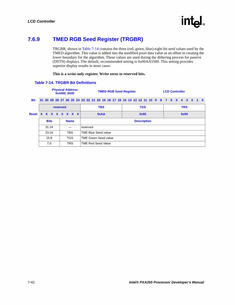
LCD Controller
7.6.9 TMED RGB Seed Register (TRGBR)
TRGBR, shown in Table 7-14 contains the three (red, green, blue) eight-bit seed values used by the TMED algorithm. This value is added into the modified pixel data value as an offset in creating the lower boundary for the algorithm. These values are used during the dithering process for passive (DSTN) displays. The default, recommended setting is 0x00AA5500. This setting provides superior display results in most cases.
This is a write-only register. Write zeros to reserved bits.
Table 7-14. TRGBR Bit Definitions
Physical Address0x4400_0040 TMED RGB Seed Register LCD Controller
Bit 31 30 29 28 27 26 25 24 23 22 21 20 19 18 17 16 15 14 13 12 11 10 9 8 7 6 5 4 3 2 1 0
reserved TBS TGS TRS
Reset X X X X X X X X 0xAA 0x55 0x00
Bits Name Description
31:24 — reserved
23:16 TBS TME Blue Seed value
15:8 TGS TME Green Seed value
7:0 TRS TME Red Seed Value
7-42 Intel® PXA255 Processor Developer’s Manual

LCD Controller
7.6.10 TMED Control Register (TCR)
TCR, shown in Table 7-15, selects various options available in the TMED dither algorithm. There are two Temporal Modulated Energy Distribution algorithms that can be used. The default, recommended setting is 0x0000754F. This setting provides superior display results in most cases.
For more details on the effects of the individual fields within this register, please refer to Section 7.3.3.
TMED Energy Distribution Select (TED) — selects which matrix is used in the final step of TMED algorithm. TMED = 1 selects the (preferred) TMED2 matrix. TMED = 0 selects the older TMED matrix. After the pixel value has gone through the algorithm to determine a lower and upper boundary, the row and column counters are combined and run through one of the matrices to obtain a number that will be compared to the 2 boundaries. If that number is between the 2 boundaries, then the data out for this pixel in this frame is a 1, otherwise it is a 0.
TMED Horizontal Beat Suppression (THBS) — is the column shift value used as an offset that is combined with the row (line) counter and the pixel counter to create an address to lookup in the matrix. The matrix output is compared to the upper and lower boundaries defined in Section 7.3.3.
TMED Vertical Beat Suppression (TVBS) — is the block shift value used as an offset that is combined with the pixel counter.
TMED Frame Number Adjuster Enable (FNAME) — allows the frame number adjuster to add an offset to the current frame number before the value is sent through the algorithm. Setting this bit enables the addition of the current frame number to a value composed from the row and column counters. This value comes from one of the two look up matrices which is selected by TMED[FNAM].
TMED Color Offset Adjuster Enable (COAE) — enables the color offset adjuster for each color. The color offset adjuster creates the offset in the lower boundary in the TMED algorithm (refer to Section 7.3.3). The Offset is created by adding either the output of the lookup matrix (input was the Color Value) or‘00’ to the Seed value in the TSR for that color. The color offset adjuster for each color can be disabled by clearing this bit. When cleared, this bit allows only the Seed Register value to go through the algorithm.
TMED Frame Number Adjuster Matrix (FNAM) — selects which matrix is used when using the frame number adjuster. A 1 will select the (recommended) TMED2 matrix, and a 0 will select the older TMED matrix.
TMED Color Offset Adjuster Matrix (COAM) — selects which matrix is used when using the color offset adjuster. A 1 will select the (recommended) TMED2 matrix, and a 0 will select the older TMED matrix.
This is a read/write register. Ignore reads from reserved bits. Write zeros to reserved bits.
Intel® PXA255 Processor Developer’s Manual 7-43

LCD Controller
7.7 LCD Controller Register Summary
Table 7-16 shows the registers associated with the LCD Controller and the physical addresses used to access them. All of the LCD registers must be accessed as 32-bit values.
Table 7-15. TCR Bit Definitions
Physical Address0X4400_0044 TMED Control Register LCD Controller
Bit 31 30 29 28 27 26 25 24 23 22 21 20 19 18 17 16 15 14 13 12 11 10 9 8 7 6 5 4 3 2 1 0
reserved
TE
D
rese
rved
THBS TVBS
FN
AM
E
CO
AE
FN
AM
CO
AM
Reset X X X X X X X X X X X X X X X X X 1 1 1 0 1 0 1 0 1 0 0 1 1 1 1
Bits Name Description
31:15 — reserved
14 TEDTMED Energy Distribution Matrix Select
0 = Selects Matrix 11 = Selects Matrix 2
13:12 — reserved
11:8 THBSTMED Horizontal Beat Suppression
Specifies the column shift value.
7:4 TVBSTMED Vertical Beat Suppression
Specifies the block shift value.
3 FNAMETMED Frame Number Adjuster Enable
0 = Disable frame number adjuster.1 = Enable frame number adjuster.
2 COAETMED Color Offset Adjuster Enable
0 = Disable color offset adjuster.1 = Enable color offset adjuster.
1 FNAMTMED Frame Number Adjuster Matrix
0 = Selects Matrix 1 for frame number adjuster.1 = Selects Matrix 2 for frame number adjuster.
0 COAMTMED Color Offset Adjuster Matrix
0 = Selects Matrix 1 for color offset adjuster.1 = Selects Matrix 2 for color offset adjuster.
Table 7-16. LCD Controller Register Summary (Sheet 1 of 2)
Address Name Description
0x4400_0000 LCCR0 LCD controller control register 0
0x4400_0004 LCCR1 LCD controller control register 1
0x4400_0008 LCCR2 LCD controller control register 2
0x4400_000C LCCR3 LCD controller control register 3
0x4400_0020 FBR0 DMA channel 0 frame branch register
7-44 Intel® PXA255 Processor Developer’s Manual

LCD Controller
0x4400_0024 FBR1 DMA channel 1 frame branch register
0x4400_0038 LCSR LCD controller status register
0x4400_003C LIIDR LCD controller interrupt ID register
0x4400_0040 TRGBR TMED RGB Seed Register
0x4400_0044 TCR TMED Control Register
0x4400_0200 FDADR0 DMA channel 0 frame descriptor address register
0x4400_0204 FSADR0 DMA channel 0 frame source address register
0x4400_0208 FIDR0 DMA channel 0 frame ID register
0x4400_020C LDCMD0 DMA channel 0 command register
0x4400_0210 FDADR1 DMA channel 1 frame descriptor address register
0x4400_0214 FSADR1 DMA channel 1 frame source address register
0x4400_0218 FIDR1 DMA channel 1 frame ID register
0x4400_021C LDCMD1 DMA channel 1 command register
Table 7-16. LCD Controller Register Summary (Sheet 2 of 2)
Address Name Description
Intel® PXA255 Processor Developer’s Manual 7-45

LCD Controller
7-46 Intel® PXA255 Processor Developer’s Manual

Synchronous Serial Port Controller 8
This chapter describes the Synchronous Serial Port Controller’s (SSPC) signal definitions and operation for the PXA255 processor usage.
8.1 Overview
The SSPC is a full-duplex synchronous serial interface and can connect to a variety of external analog-to-digital (A/D) converters, audio and telecom codecs, and other devices that use serial protocols for transferring data. The SSPC supports National’s Microwire* , Texas Instruments’ Synchronous Serial Protocol* (SSP), and Motorola’s Serial Peripheral Interface* (SPI) protocol.
The SSPC operates in master mode (the attached peripheral functions as a slave) and supports serial bit rates from 7.2 KHz to 1.84 MHz. Serial data formats may range from 4 to 16 bits in length. The SSPC provides 16 entries deep x 16 bits wide transmit and receive data FIFOs.
The FIFOs may be loaded or emptied by the Central Processor Unit (CPU) using programmed I/O, or DMA burst transfers of 4 or 8 half-words per transfer while receiving or transmitting.
8.2 Signal Description
This section describes the SSPC signals.
8.2.1 External Interface to Synchronous Serial Peripherals
Table 8-1 lists the external signals that connect the SSP to an external peripheral.
SSPSCLK is the bit-rate clock driven from the SSPC to the peripheral. SSPSCLK is toggled only when data is actively being transmitted and received.
SSPSFRM is the framing signal, indicating the beginning and the end of a serialized data word.
SSPTXD and SSPRXD are the Transmit and Receive serial data lines.
Table 8-1. External Interface to Codec
Name Direction Description
SSPSCLK Output Serial bit-rate clock
SSPSFRM Output Frame indicator
SSPTXD Output Transmit Data (serial data out)
SSPRXD Input Receive Data (serial data in)
SSPEXTCLK Input External clock which can be selected to drive the serial clock (SSPSCLK)
Intel® PXA255 Processor Developer’s Manual 8-1

Synchronous Serial Port Controller
SSPEXTCLK is an external clock (input through GPIO27) that replaces the standard 3.6864 MHz clock used to generate the serial bit-rate clock (SSPSCLK). The external clock is internally divided by 2 and then further divided by the value in SSCR0[SCR].
If SSP operation is disabled, the five SSP pins are available for GPIO use. See Chapter 4, “System Integration Unit” for details on configuring pin direction and interrupt capabilities.
8.3 Functional Description
Serial data is transferred between the processor and an external peripheral through FIFO buffers in the SSPC. Data transfers to system memory are handled by either the CPU (using programmed I/O) or by DMA. Operation is full duplex - separate buffers and serial data paths permit simultaneous transfers to and from the external peripheral.
Programmed I/O transmits and receives data directly between the CPU and the transmit/receive FIFO’s. The DMA controller transfers data during transmit and receive operations between memory and the FIFO’s. DMA programming guidelines are found in Chapter 5, “DMA Controller”.
8.3.1 Data Transfer
Transmit data is written by the CPU or DMA to the SSPC’s transmit FIFO. The write takes the form of a programmed I/O or a DMA burst, with 4 or 8 half-words being transferred per burst. The SSPC then takes the data from the FIFO, serializes it, and transmits it via the SSPTXD signal to the peripheral. Data from the peripheral is received via the SSPRXD signal, converted to parallel words and is stored in the Receive FIFO. Read operations automatically target the receive FIFO, while write operations write data to the transmit FIFO. Both the transmit and receive FIFO buffers are 16 entries deep by 16 bits wide.
As the received data fills the receive FIFO, a programmable threshold triggers an interrupt to the Interrupt Controller. If enabled, an interrupt service routine responds by identifying the source of the interrupt and then performs one or several read operations from the inbound (receive) FIFO buffer.
8.4 Data Formats
The SSPC uses serial data formats to transfer and store data. This section describes the data formats.
8.4.1 Serial Data Formats for Transfer to/from Peripherals
Four signals are used to transfer data between the processor and external codecs or modems. Although there are three formats for serial data, they have the same basic structure:
• SSPSCLK–Defines the bit rate at which serial data is transmitted and received from the port.
• SSPSFRM–Depending on the transmission format selected, defines the boundaries of a data frame, or marks the beginning of a data frame.
• SSPTXD–Transmit signal for outbound data, from system to peripheral.
8-2 Intel® PXA255 Processor Developer’s Manual

Synchronous Serial Port Controller
• SSPRXD–Receive signal for inbound data, from peripheral to system.
A data frame can be configured to contain from 4 to 16 bits. Serial data is transmitted most significant bit first.
The SSPC supports three formats: Motorola SPI, Texas Instruments SSP, and National Microwire. The three formats have significant differences, as described below.
SSPSFRM varies for each protocol as follows:
• For SPI and Microwire formats, SSPSFRM functions as a chip select to enable the external device (target of the transfer), and is held active-low during the data transfer.
• For SSP format, SSPSFRM is pulsed high for one serial bit-clock period at the start of each frame.
SSPSCLK varies for each protocol as follows:
• For Microwire, both transmit and receive data sources switch data on the falling edge of SSPSCLK, and sample incoming data on the rising edge.
• For SSP, transmit and receive data sources switch data on the rising edge of SSPSCLK, and sample incoming data on the falling edge.
• For SPI, the user has the choice of which edge of SSPSCLK to use for switching outgoing data, and for sampling incoming data. In addition, the user can move the phase of SSPSCLK, shifting its active state one-half period earlier or later at the start and end of a frame.
While SSP and SPI are full-duplex protocols, Microwire uses a half-duplex master-slave messaging protocol. At the start of a frame, a 1 or 2-byte control message is transmitted from the controller to the peripheral. The peripheral does not send any data. The peripheral interprets the message and, if it is a READ request, responds with requested data, one clock after the last bit of the requesting message. Return data (part of the same frame) can be from 4 to 16 bits in length. Total frame length is 13 to 33 bits.
The serial clock (SSPSCLK) only toggles during an active frame. At other times it is held in an inactive or idle state, as defined by its specified protocol.
8.4.1.1 SSP Format Details
When outgoing data in the SSP controller is ready to be transmitted, SSPSFRM is asserted for one clock period. On the following clock period, data to be transmitted is driven on SSPTXD one bit at a time, most significant bit first. Similarly, the peripheral drives data on the SSPRXD pin. Word length is from 4 to 16 bits. All transitions take place on the SSPSCLK rising edge and data is sampled on the falling edge. At the end of the transfer, SSPTXD retains the value of the last bit sent (bit 0) through the next idle period. If the SSP Port is disabled or reset, SSPTXD is forced to zero. Figure 8-1 shows the Texas Instruments’ Synchronous Serial Frame* format for a single transmitted frame and when back-to-back frames are transmitted. When the bottom entry of the transmit FIFO contains data, SSPSFRM is pulsed high for one SSPSCLK period and the value to be transmitted is transferred from the transmit FIFO to the transmit logic’s serial shift register. On the next rising edge of SSPSCLK, the most significant bit of the 4 to 16-bit data frame is shifted to the SSPTXD pin. Likewise, the most significant bit of the received data is shifted onto the SSPRXD pin by the off-chip serial slave device. Both the SSP and the off-chip serial slave device then latch each data bit into their serial shifter on the falling edge of each SSPSCLK. The received data is transferred from the serial shifter to the receive FIFO on the first rising edge of SSPSCLK after the last bit has been latched.
Intel® PXA255 Processor Developer’s Manual 8-3
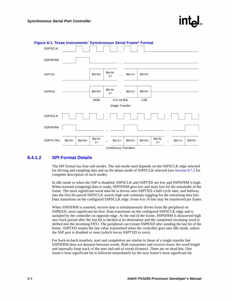
Synchronous Serial Port Controller
.
8.4.1.2 SPI Format Details
The SPI format has four sub-modes. The sub-mode used depends on the SSPSCLK edge selected for driving and sampling data and on the phase mode of SSPSCLK selected (see Section 8.7.2 for complete description of each mode).
In idle mode or when the SSP is disabled, SSPSCLK and SSPTXD are low and SSPSFRM is high. When transmit (outgoing) data is ready, SSPSFRM goes low and stays low for the remainder of the frame. The most significant serial data bit is driven onto SSPTXD a half-cycle later, and halfway into the first bit period SSPSCLK asserts high and continues toggling for the remaining data bits. Data transitions on the configured SSPSCLK edge. From 4 to 16 bits may be transferred per frame.
When SSPSFRM is asserted, receive data is simultaneously driven from the peripheral on SSPRXD, most significant bit first. Data transitions on the configured SSPSCLK edge and is sampled by the controller on opposite edge. At the end of the frame, SSPSFRM is deasserted high one clock period after the last bit is latched at its destination and the completed incoming word is shifted into the incoming FIFO. The peripheral can tristate SSPRXD after sending the last bit of the frame. SSPTXD retains the last value transmitted when the controller goes into idle mode, unless the SSP port is disabled or reset (which forces SSPTXD to zero).
For back-to-back transfers, start and completion are similar to those of a single transfer but SSPSFRM does not deassert between words. Both transmitter and receiver know the word length and internally keep track of the start and end of words (frames). There are no dead bits. One frame’s least significant bit is followed immediately by the next frame’s most significant bit.
Figure 8-1. Texas Instruments’ Synchronous Serial Frame* FormatSSPSCLK
...
SSPSFRM...
SSPTXD Bit<N> Bit<N-1> ... Bit<1> Bit<0>
SSPRXD Bit<N> Bit<N-1> ... Bit<1> Bit<0>
MSB 4 to 16 Bits LSB
Single Transfer
SSPSCLK... ...
SSPSFRM... ...
SSPTX /RX Bit<0> Bit<N> Bit<N-1> ... Bit<1> Bit<0> Bit<N> Bit<N-
1> ... Bit<1> Bit<0>
Continuous Transfers
8-4 Intel® PXA255 Processor Developer’s Manual
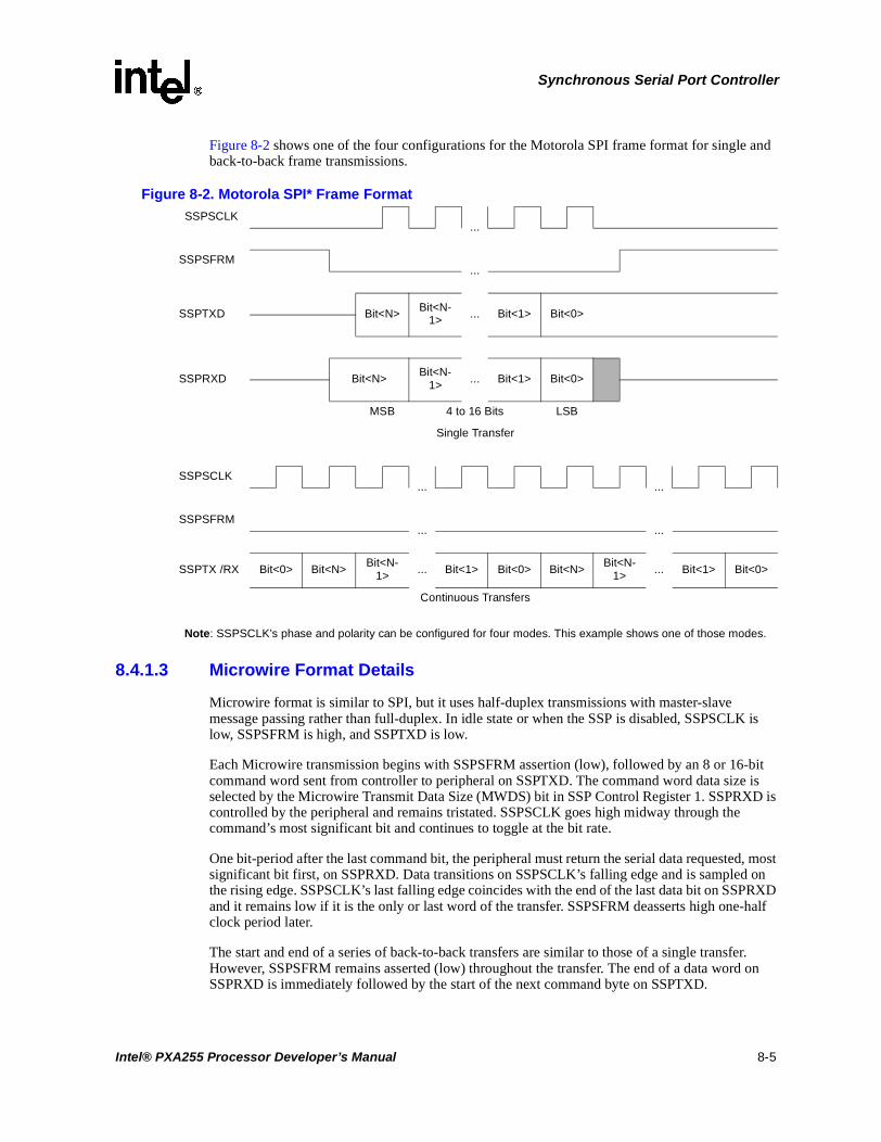
Synchronous Serial Port Controller
Figure 8-2 shows one of the four configurations for the Motorola SPI frame format for single and back-to-back frame transmissions.
8.4.1.3 Microwire Format Details
Microwire format is similar to SPI, but it uses half-duplex transmissions with master-slave message passing rather than full-duplex. In idle state or when the SSP is disabled, SSPSCLK is low, SSPSFRM is high, and SSPTXD is low.
Each Microwire transmission begins with SSPSFRM assertion (low), followed by an 8 or 16-bit command word sent from controller to peripheral on SSPTXD. The command word data size is selected by the Microwire Transmit Data Size (MWDS) bit in SSP Control Register 1. SSPRXD is controlled by the peripheral and remains tristated. SSPSCLK goes high midway through the command’s most significant bit and continues to toggle at the bit rate.
One bit-period after the last command bit, the peripheral must return the serial data requested, most significant bit first, on SSPRXD. Data transitions on SSPSCLK’s falling edge and is sampled on the rising edge. SSPSCLK’s last falling edge coincides with the end of the last data bit on SSPRXD and it remains low if it is the only or last word of the transfer. SSPSFRM deasserts high one-half clock period later.
The start and end of a series of back-to-back transfers are similar to those of a single transfer. However, SSPSFRM remains asserted (low) throughout the transfer. The end of a data word on SSPRXD is immediately followed by the start of the next command byte on SSPTXD.
Figure 8-2. Motorola SPI* Frame FormatSSPSCLK
...
SSPSFRM...
SSPTXD Bit<N> Bit<N-1> ... Bit<1> Bit<0>
SSPRXD Bit<N>Bit<N-
1> ... Bit<1> Bit<0>
MSB 4 to 16 Bits LSB
Single Transfer
SSPSCLK... ...
SSPSFRM... ...
SSPTX /RX Bit<0> Bit<N>Bit<N-
1> ... Bit<1> Bit<0> Bit<N>Bit<N-
1> ... Bit<1> Bit<0>
Continuous Transfers
Note: SSPSCLK’s phase and polarity can be configured for four modes. This example shows one of those modes.
Intel® PXA255 Processor Developer’s Manual 8-5

Synchronous Serial Port Controller
Figure 8-3 shows the National Microwire frame format with 8-bit command words for single and back-to-back frame transmissions.
8.4.2 Parallel Data Formats for FIFO Storage
Data in the FIFOs is stored with one 16-bit value per data sample with no regard to the format’s data word length. In each 16-bit field, the stored data sample is right-justified, the word’s least significant bit is stored in bit 0, and unused bits are packed as zeroes above the most significant bit. Logic in the SSPC automatically left-justifies data in the Transmit FIFO so the sample is properly transmitted on SSPTXD in the selected frame format.
Figure 8-3. National Microwire* Frame FormatSSPSCLK
... ...
SSPSFRM... ...
SSPTXD Bit<7> ... Bit<0> ...
8-Bit Control 1 Clk
SSPRXD ... Bit<N> ... Bit<0>
4 to 16 Bits
Single Transfer
SSPSCLK... ... ...
SSPSFRM... ... ...
SSPTXD Bit<0> ... Bit<7> ... Bit<0> ...
1 Clk 1 Clk
SSPRXD Bit<N> ... Bit<0> ... Bit<N> ... Bit<0>
Continuous Transfers
8-6 Intel® PXA255 Processor Developer’s Manual

Synchronous Serial Port Controller
8.5 FIFO Operation and Data Transfers
Transmit and receive serial data use independent FIFOs. FIFOs are filled or emptied by programmed I/O or DMA bursts that the DMAC initiates. Bursts may be 4 or 8 half-words in length during transmission or reception.
8.5.1 Using Programmed I/O Data Transfers
Data words are 32 bits wide, but only 16-bit samples are transferred. Only the lower 2 bytes of a 32-bit word have valid data. The upper 2 bytes are not used and include invalid data that must be discarded.
The processor can fill or empty FIFOs in response to an interrupt from the FIFO logic. Each FIFO has a programmable interrupt threshold. When the threshold value is exceeded and an interrupt is enabled, an interrupt that signals the CPU to empty the receive FIFO or refill the transmit FIFO is generated.
The user can also poll the SSP Status Register (see Section 8.7.4) to determine how many samples are in a FIFO or whether the FIFO is full or empty.
8.5.2 Using DMA Data Transfers
The DMA controller can also be programmed to transfer data to and from the SSP’s FIFO’s. Refer to Chapter 5, “DMA Controller” for instructions on programming the DMA channels.
The steps for the DMA programming model are:
1. Program the transmit/receive byte count (buffer length) and burst size.
2. Program the DMA request to channel map register for SSP.
3. Set the run bit in the DMA control register.
4. Set the desired values in the SSP control registers.
5. Enable the SSP by setting the SSE bit in the SSP Control Register 0 (see Section 8.7.1).
6. Wait for both the DMA transmit and receive interrupt requests.
Note: If the transmit/receive byte count is not a multiple of the transfer burst size, the user must check the SSP Status Register (see Section 8.7.4) to determine if any data remains in the Receive FIFO.
8.6 Baud-Rate Generation
The baud (or bit-rate clock) is generated internally by dividing the internal clock (3.6864 MHz). The internal clock is first divided by 2 and this divided clock feeds a programmable divider to generate baud rates from 7.2 kbps to 1.8432 Mbps. Setting the External Clock Select (ECS) bit to 1 enables an external clock (SSPEXTCLK) to replace the 3.6864 MHz standard internal clock. The external clock is also divided by 2 before it is fed to the programmable divider.
Intel® PXA255 Processor Developer’s Manual 8-7

Synchronous Serial Port Controller
8.7 SSP Serial Port Registers
The SSPC has five registers: two control, one data, one status, and one “reserved” register:
• The SSPC Control Registers (SSCR0 and SSCR1) are used to program the baud rate, data length, frame format, data transfer mechanism, and port enabling. They also control the FIFO “fullness” threshold that triggers an interrupt. These registers must be written before the SSP is enabled after reset and must only be changed when SSP is disabled.
• The SSPC Data Register (SSDR) is mapped as one 32-bit location that consists of two 16-bit registers. One register is for write operations and transfers data to the transmit FIFO. The other is for read operations and takes data from the receive FIFO. A write cycle, or burst write, loads successive half-words into the transmit FIFO. The write data occupies the lower 2 bytes of the 32-bit word. A read cycle, or burst read, similarly transfers data from the receive FIFO. The FIFOs are independent buffers that allow full duplex operation.
• The SSPC Status Register (SSSR) indicates the state of the FIFO buffers, whether the programmable threshold has been passed, and whether a transmit or receive FIFO service request is active. It also shows how many entries are occupied in the FIFO. Flag bits are set when the SSPC is actively transmitting or receiving data, when the transmit FIFO is not full, and when the receive FIFO is not empty. An error bit signals an overrun of the receive FIFO.
When the registers are programmed, reserved bits must be written as zeros and are read as undefined.
8.7.1 SSP Control Register 0 (SSCR0)
SSCR0, shown in Table 8-2, contains five bit fields that control SSP data size, frame format, external clock selection, clock divisor, and SSP enable. The SSE bit is reset to a zero state to ensure the SSP is disabled. The reset states for the other control bits are shown in the table, but each reset state must be set to the desired value before the SSPC is enabled.
8-8 Intel® PXA255 Processor Developer’s Manual

Synchronous Serial Port Controller
8.7.1.1 Data Size Select (DSS)
The 4-bit data size select (DSS) field is used to determine the size of the data that the SSPC transmits and receives. The data can range from 4 to 16 bits in length. When data is programmed to be less than 16 bits, received data is automatically right-justified and the upper bits in the receive FIFO are zero-filled by receive logic. Do not left-justify transmit data before placing it in the
Table 8-2. SSCR0 Bit Definitions
0x4100_0000 SSP Control Register 0 (SSCR0) Synchronous Serial Port Controller
Bit 31 30 29 28 27 26 25 24 23 22 21 20 19 18 17 16 15 14 13 12 11 10 9 8 7 6 5 4 3 2 1 0
reserved SCR
SS
E
EC
S
FR
F DSS
Reset X 0x00 0 0 0 0
Bits Name Description
3:0DSS
Data Size Select
0000 - reserved, undefined operation
0001 - reserved, undefined operation
0010 - reserved, undefined operation
0011 - 4-bit data
0100 - 5-bit data
0101 - 6-bit data
0110 - 7-bit data
0111 - 8-bit data
1000 - 9-bit data
1001 - 10-bit data
1010 - 11-bit data
1011 - 12-bit data
1100 - 13-bit data
1101 - 14-bit data
1110 - 15-bit data
1111 - 16-bit data
5:4 FRF
Frame Format
00 - Motorola’s Serial Peripheral Interface (SPI)
01 - Texas Instruments’ Synchronous Serial Protocol (SSP)
10 - National Microwire
11 - reserved, undefined operation
6 ECSExternal clock select:
0 = On-chip clock used to produce the SSP’s serial clock (SSPSCLK).1 = SSPEXTCLK is used to create the SSPSCLK.
7 SSESynchronous Serial Port Enable:
0 = 0 - SSP operation disabled (pins may function as GPIOs)1 = 1 - SSP operation enabled
15:8 SCR
Serial Clock Rate
Value (0 to 255) used to generate transmission rate of SSP.
Bit rate = 3.6864x10⁶ / (2 x (SCR + 1)) or SSPEXTCLK / (2 x (SCR + 1))
31:16 — reserved
Intel® PXA255 Processor Developer’s Manual 8-9

Synchronous Serial Port Controller
transmit FIFO. The transmit logic in the SSPC left-justifies the data sample according to the DSS bits before the sample is transmitted. Data sizes of 1, 2, and 3 bits are reserved and produce unpredictable results in the SSPC.
In National Microwire frame format, this bit field selects the size of the received data. The size of the transmitted command data is either 8-bit or 16-bit as selected by the MWDS bit in SSCR1.
8.7.1.2 Frame Format (FRF)
The 2-bit frame format (FRF) field is used to select Motorola SPI (FRF=00), Texas Instruments Synchronous Serial (FRF=01), or National Microwire (FRF=10) frame format.
FRF=11 is reserved and the SSPC produces unpredictable results if this value is used.
8.7.1.3 External Clock Select (ECS)
The external clock select (ECS) bit determines whether the SSPC uses the on-chip 3.6864-MHz clock or an off-chip clock supplied via SSPEXTCLK. When ECS=0, the SSPC uses the on-chip 3.6864-MHz clock to produce a range of serial transmission rates from 7.2 Kbps to 1.8432 Mbps. When ECS=1, the SSP uses SSPEXTCLK to access an off-chip clock. The off-chip clock’s frequency can be any value up to 3.6864 MHz. The off-chip clock is useful when a serial transmission rate not evenly divisible from 3.6864 MHz is required for synchronization with the target off-chip slave device.
If the off-chip clock is used, the user must set the appropriate bits in the GPIO alternate function and pin direction registers that correspond to the pin. See Chapter 4, “System Integration Unit” for more details on configuring GPIO pins for alternate functions.
Note: Disable the SSPC by setting the SSPC Enable (SSE) to a 0 before setting the ECS bit to a 1. The ECS bit may be set to one either before the SSE is set to one or at the same time.
8.7.1.4 Synchronous Serial Port Enable (SSE)
The SSCR0[SSE] bit is used to enable and disable all SSP operations. When SSCR0[SSE]=0, the SSP is disabled. When SSCR0[SSE]=1, the SSP is enabled. When the SSP is disabled, all of its clocks are powered down to minimize power consumption.The SSP is disabled following a reset.
When the SSCR0[SSE] bit is cleared during active operation, the SSP is immediately disabled and the frame being transmitted is terminated. Clearing SSCR0[SSE] resets the SSP’s FIFOs and the SSP status bits. The SSP’s control registers are not reset when SSCR0[SSE] is cleared.
Note: After reset or after the SSCR0[SSE] is cleared, ensure that the SSCR1 and SSSR registers are properly reconfigured or reset before re-enabling the SSP with the SSCR0[SSE]. Other control bits in SSCR0 may be written at the same time as the SSCR0[SSE].
When the SSPC is disabled, its five pins may be used as GPIOs. They are configured as inputs or outputs with the control registers described in Chapter 4, “System Integration Unit”. In Sleep mode, the pins’ states are controlled by the GPIO sleep register. SSPC register settings have no effect on the pins in Sleep mode.
8-10 Intel® PXA255 Processor Developer’s Manual

Synchronous Serial Port Controller
8.7.1.5 Serial Clock Rate (SCR)
The 8-bit serial clock rate (SCR) bit-field is used to select the SSPC bit rate. The SSPC has 256 bit rates, from 7.2 Kbps to 1.8432 Mbps. The serial clock generator uses the internal 3.6864 MHz clock or an external clock provided through SSPEXTCLK. The clock is divided by 2, then divided by the programmable SCR value (0 to 255) plus 1 to generate the serial clock (SSPSCLK). The resultant clock is driven on the SSPSCLK pin and is used by the SSP’s transmit logic to drive data on the SSPTXD pin and to latch data on the SSPRXD pin. Depending on the frame format selected, each transmitted bit is driven on either SSPSCLK’s rising or falling edge and sampled on the opposite clock edge.
This is a read/write register. Ignore reads from reserved bits. Write zeros to reserved bits.
8.7.2 SSP Control Register 1 (SSCR1)
SSCR1, shown in Table 8-3, contains bit fields that control SSP functions.
Table 8-3. SSCR1 Bit Definitions (Sheet 1 of 2)
0x4100_0004 SSP Control Register 1 (SSCR1) Synchronous Serial Port Controller
Bit 31 30 29 28 27 26 25 24 23 22 21 20 19 18 17 16 15 14 13 12 11 10 9 8 7 6 5 4 3 2 1 0
reserved RFT TFT
MW
DS
SP
H
SP
O
LB
M
TIE
RIE
Reset X 0x0 0x0 0 0 0 0 0 0
Bits Name Description
0RIE
Receive FIFO Interrupt Enable
0 = Receive FIFO interrupt is disabled1 = Receive FIFO interrupt is enabled
1 TIETransmit FIFO Interrupt Enable
0 = Transmit FIFO interrupt is disabled1 = 1 - Transmit FIFO interrupt is enabled
2 LBMLoop-Back Mode
0 = Normal serial port operation enabled1 = Output of transmit serial shifter internally connected to input of receive serial shifter
3 SPOMotorola SPI SSPSCLK polarity setting:
0 = The inactive or idle state of SSPSCLK is low.1 = The inactive or idle state of SSPSCLK is high.
4 SPH
Motorola SPI SSPSCLK phase setting:
0 = SSPSCLK is inactive one cycle at the start of a frame and 1/2 cycle at the end of a frame.
1 = SSPSCLK is inactive 1/2 cycle at the start of a frame and one cycle at the end of a frame.
5 MWDSMicrowire Transmit Data Size:
0 = 8-bit command words are transmitted.1 = 16-bit command words are transmitted.
Intel® PXA255 Processor Developer’s Manual 8-11

Synchronous Serial Port Controller
8.7.2.1 Receive FIFO Interrupt Enable (RIE)
The Receive FIFO Interrupt Enable (RIE) bit is used to mask or enable the receive FIFO service request interrupt. When RIE=0, the interrupt is masked and the interrupt controller ignores the state of the Receive FIFO Service Request (RFS) bit in the SSPC Status Register. When the RIE bit is set to a 1, the interrupt is enabled and, if the RFS bit is set to a 1, an interrupt request is made to the interrupt controller. If the RIE bit is set to 0 neither the RFS bit’s current state nor the receive FIFO logic’s ability to set and clear the RFS bit is affected. However, the interrupt request generation is blocked.
The RIE bit’s state does not affect the receive FIFO DMA request generation that is asserted when the RFS bit is set to a 1.
8.7.2.2 Transmit FIFO Interrupt Enable (TIE)
The Transmit FIFO Interrupt Enable (TIE) bit is used to mask or enable the transmit FIFO service request interrupt. When the TIE bit is set to a 0, the interrupt is masked and the interrupt controller ignores the state of the Transmit FIFO Service Request (TFS) bit in the SSPC Status Register. When the TIE bit is set to a 1, the interrupt is enabled and, if the TFS bit is set to a 1, an interrupt request is made to the interrupt controller. If the TIE bit is set to a 0, neither the TFS bit’s current state nor the transmit FIFO logic’s ability to set and clear the TFS bit is affected. However, the interrupt request generation is blocked.
The TIE bit’s state does not affect the transmit FIFO DMA request generation that is asserted when the TFS bit is set to a 1.
8.7.2.3 Loop Back Mode (LBM)
The loop back mode (LBM) bit is used to enable and disable the SSP transmit and receive logic. When LBM=0, the SSP operates normally. The transmit and receive data paths are separate and communicate via their respective pins. However, since the SSP is a master device, it must transmit in order to receive while in either SSP or SPI mode. When LBM=1, the transmit serial shifter’s output is directly connected internally to the receive serial shifter’s input.
9:6TFT
(Transmit FIFO Threshold)
Sets threshold level at which Transmit FIFO generates an interrupt or DMA request. This level must be set to the desired threshold value minus 1.
13:10RFT
(Receive FIFO Threshold)
Sets threshold level at which Receive FIFO generates an interrupt or DMA request. This level must be set to the desired threshold value minus 1.
31:14 — reserved
Table 8-3. SSCR1 Bit Definitions (Sheet 2 of 2)
0x4100_0004 SSP Control Register 1 (SSCR1) Synchronous Serial Port Controller
Bit 31 30 29 28 27 26 25 24 23 22 21 20 19 18 17 16 15 14 13 12 11 10 9 8 7 6 5 4 3 2 1 0
reserved RFT TFT
MW
DS
SP
H
SP
O
LB
M
TIE
RIE
Reset X 0x0 0x0 0 0 0 0 0 0
Bits Name Description
8-12 Intel® PXA255 Processor Developer’s Manual

Synchronous Serial Port Controller
Note: Loop back mode cannot be used with Microwire frame format.
8.7.2.4 Serial Clock Polarity (SPO)
The serial clock polarity bit (SPO) selects the SSPSCLK signal’s inactive state in the Motorola SPI format (FRF=00). For SPO=0, the SSPSCLK is held low in the inactive or idle state when the SSP is not transmitting/receiving data. When the SPO bit is set to a 1, the SSPSCLK is held high during the inactive/idle state. The SPO bit’s programmed setting alone does not determine which SSPSCLK edge is used to transmit or receive data. The SPO bit’s setting combined with the SSPSCLK phase bit (SPH) determine which edge is used.
Note: The SPO bit is ignored for all data frame formats except for the Motorola SPI format (FRF=00).
8.7.2.5 Serial Clock Phase (SPH)
The serial clock (SSPSCLK) phase bit (SPH) determines the phase relationship between the SSPSCLK and the serial frame (SSPSFRM) pins for the Motorola SPI format (FRF=00). When SPH=0, SSPSCLK remains in its inactive/idle state (as determined by the SPO setting) for one full cycle after SSPSFRM is asserted low at the beginning of a frame. SSPSCLK continues to transition for the rest of the frame and is then held in its inactive state for one-half of an SSPSCLK period before SSPSFRM is deasserted high at the end of the frame. When SPH=1, SSPSCLK remains in its inactive/idle state (as determined by the SPO setting) for one-half cycle after SSPSFRM is asserted low at the beginning of a frame. SSPSCLK continues to transition for the rest of the frame and is then held in its inactive state for one full SSPSCLK period before SSPSFRM is deasserted high at the end of the frame.
The combination of the SPO and SPH settings determines when SSPSCLK is active during the assertion of SSPSFRM and which SSPSCLK edge is used to transmit and receive data on the SSPTXD and SSPRXD pins. When SPO and SPH are programmed to the same value, transmit data is driven on SSPSCLK’s falling edge and receive data is latched on SSPSCLK’s rising edge. When SPO and SPH are programmed to opposite values (one 0 and the other 1), transmit data is driven on SSPSCLK’s rising edge and receive data is latched on SSPSCLK’s falling edge.
The SPH is ignored for all data frame formats except the Motorola SPI format (FRF=00).
Figure 8-4 shows the pin timing for the four SPO and SPH programming combinations. SPO inverts the SSPSCLK signal’s polarity and SPH determines the phase relationship between SSPSCLK and SSPSFRM, shifting the SSPSCLK signal one-half phase to the left or right during the SSPSFRM assertion.
Figure 8-4. Motorola SPI* Frame Formats for SPO and SPH ProgrammingSSPSCLK SPO=0
...
SSPSCLK SPO=1...
SSPSFRM...
SSPTXD Bit<N> Bit<N-1> ... Bit<1> Bit<0>
Intel® PXA255 Processor Developer’s Manual 8-13

Synchronous Serial Port Controller
8.7.2.6 Microwire Transmit Data Size (MWDS)
The Microwire Transmit Data Size (MWDS) bit is used to select the 8- or 16-bit size for command word transmissions in the National Microwire frame format. When the MWDS is set to “0”, 8-bit command words are transmitted. When the MWDS is set to “1”, 16-bit command words are transmitted. The MWDS setting is ignored for all other frame formats.
8.7.2.7 Transmit FIFO Interrupt/DMA Threshold (TFT)
This 4-bit value sets the level at or below which the FIFO controller triggers a DMA service request and, if enabled, an interrupt request. Refer to Table 8-4 for suggested TFT values associated with DMA servicing.
8.7.2.8 Receive FIFO Interrupt/DMA Threshold (RFT)
This 4-bit value sets the level at or above which the FIFO controller triggers a DMA service interrupt and, if enabled, an interrupt request. Refer to Table 8-4 for suggested RFT values associated with DMA servicing.
Be careful not to set the RFT value too high for your system or the FIFO could overrun because of the bus latencies caused by other internal and external peripherals. This is especially the case for interrupt and polled modes that require a longer time to service.
SSPRXD Bit<N> Bit<N-1> ... Bit<1> Bit<0>
MSB 4 to 16 Bits LSB
SPH = 0
SSPSCLK SPO=0...
SSPSCLK SPO=1...
SSPSFRM...
SSPTXD Bit<N> Bit<N-1> ... Bit<1> Bit<0>
SSPRXD Bit<N> Bit<N-1> ... Bit<1> Bit<0>
MSB 4 to 16 Bits LSB
SPH = 1
Figure 8-4. Motorola SPI* Frame Formats for SPO and SPH Programming
8-14 Intel® PXA255 Processor Developer’s Manual

Synchronous Serial Port Controller
This is a read/write register. Ignore reads from reserved bits. Write zeros to reserved bits.
8.7.3 SSP Data Register (SSDR)
SSDR, shown in Table 8-5, is a single address location that can be accessed by read/write data transfers. Transfers can be single transfers, 4 half-word bursts, or 8 half-word bursts.
As the system accesses the register, FIFO control logic transfers data automatically between register and FIFO as fast as the system moves data. The SSP Status Register has bits that indicate whether either FIFO is full, above/below a programmable threshold, or empty.
For transmit operations from SSPC to SSP peripheral, the CPU (using programmed I/O) may write to the SSDR when the transmit FIFO is below its threshold level.
When a data size less than 16-bits is selected, do not left-justify data before it is written to the SSDR. Transmit logic left-justifies the data and ignores any unused bits. Received data less than 16-bits is automatically right-justified in the receive FIFO.
When the SSPC is programmed for National Microwire frame format and the size for transmit data is 8-bits, as selected by the MWDS bit in the SSCR1, the most significant byte is ignored. SSCR0[DSS] controls receive data size.
Note: Both FIFOs are cleared when the SSPC is reset or a zero is written to the SSCR0[SSE] bit.
This is a read/write register. Ignore reads from reserved bits. Write zeros to reserved bits.
Table 8-4. TFT and RFT Values for DMA Servicing
DMA Burst Size TFT Value RFT Value
Min Max Min Max
8 Bytes 0 11 3 15
16 Bytes 0 7 7 15
Table 8-5. SSDR Bit Definitions
0x4100_0010 SSP Data Register (SSDR) Synchronous Serial Port Controller
Bit 31 30 29 28 27 26 25 24 23 22 21 20 19 18 17 16 15 14 13 12 11 10 9 8 7 6 5 4 3 2 1 0
reserved Transmit/Receive Data
Reset X 0x0000
Bits Name Description
15:0 Data
(Low Word)Data word to be written to/read from Transmit/Receive FIFO
31:16 — reserved
Intel® PXA255 Processor Developer’s Manual 8-15

Synchronous Serial Port Controller
8.7.4 SSP Status Register (SSSR)
The SSP Status Register (SSSR) is shown in Table 8-6. The SSSR contains bits that signal overrun errors and transmit and receive FIFO service requests. These hardware-detected events signal an interrupt request to the interrupt controller. The status register also contains flags that indicate when the SSP is actively transmitting or receiving characters, when the transmit FIFO is not full, and when the receive FIFO is not empty (no interrupt generated).
Bits that cause an interrupt will signal the request as long as the bit is set. When the bit is cleared, the interrupt is cleared. Read/write bits are called status bits, read-only bits are called flags. Status bits are referred to as sticky (once set by hardware, they must be cleared by software). Writing a 1 to a sticky status bit clears it. Writing a 0 has no effect. Read-only flags are set and cleared by hardware. Writes have no effect. Some bits that cause interrupts have corresponding mask bits in the control registers.
All bits are read-only except ROR, which is read/write. ROR’s reset state is zero. Writes to TNF, RNE, BSY, TFS, and RFS have no effect. Writes to reserved bits are ignored and reads from these bits are undetermined.
8-16 Intel® PXA255 Processor Developer’s Manual

Synchronous Serial Port Controller
8.7.4.1 Transmit FIFO Not Full Flag (TNF)
This non-interruptible bit is set whenever the transmit FIFO is not full. TNF is cleared when the FIFO is completely full. This bit can be polled when using programmed I/O to fill the transmit FIFO over its threshold level. This bit does not request an interrupt.
Table 8-6. SSSR Bit Definitions
0x4100_0008 SSP Status Register (SSSR) Synchronous Serial Port Controller
Bit 31 30 29 28 27 26 25 24 23 22 21 20 19 18 17 16 15 14 13 12 11 10 9 8 7 6 5 4 3 2 1 0
reserved RFL TFL
RO
R
RF
S
TF
S
BS
Y
RN
E
TN
F
rese
rved
Reset X 0xF 0x0 0 0 0 0 0 1 0
Bits Name Description
1:0 — reserved
2 TNFTransmit FIFO Not Full (read only)
0 = Transmit FIFO is full1 = Transmit FIFO is not full
3 RNEReceive FIFO Not Empty (read only)
0 = Receive FIFO is empty1 = Receive FIFO is not empty
4 BSYSSP Busy (read only)
0 = SSP is idle or disabled1 = SSP currently transmitting or receiving a frame
5 TFSTransmit FIFO Service Request (read only)
0 = Transmit FIFO level exceeds TFT threshold, or SSP disabled1 = Transmit FIFO level is at or below TFT threshold, generate interrupt or DMA request
6 RFSReceive FIFO Service Request (read only)
0 = Receive FIFO level exceeds RFT threshold, or SSP disabled1 = Receive FIFO level is at or above RFT threshold, generate interrupt or DMA request
7 RORReceive FIFO Overrun (read/write)
0 = Receive FIFO has not experienced an overrun1 = Attempted data write to full Receive FIFO, request interrupt
11:8 TFLTransmit FIFO Level (read only)
Number of entries in Transmit FIFO. Note: When the value 0x0 is read, the FIFO is either empty or full and the software must refer to the TNF bit.
15:12 RFLReceive FIFO Level (read only)
Number of entries minus one in Receive FIFO. Note: When the value 0xF is read, the FIFO is either empty or full and the software must refer to the RNE bit.
31:16 — reserved
Intel® PXA255 Processor Developer’s Manual 8-17

Synchronous Serial Port Controller
8.7.4.2 Receive FIFO Not Empty Flag (RNE)
This non-interruptible bit is set when the receive FIFO contains one or more entries and is cleared when the FIFO is empty. Because CPU interrupt requests are only made when the Receive FIFO Threshold has been met or exceeded, the RNE bit can be polled when programmed I/O removes remaining bytes of data from the receive FIFO. This bit does not request an interrupt.
8.7.4.3 SSP Busy Flag (BSY)
This is a non-interruptible read-only bit that is set when the SSP is actively transmitting and/or receiving data and is cleared when the SSP is idle or disabled (SSE=0). This bit does not request an interrupt. Since the software can read this bit before the SSP starts to transmit data, software must read SSSP[TFL]=0x0 and SSSP[TNF]=0b1 and SSSP[BSY]=0b0 in order to insure that all data has transmitted completely.
8.7.4.4 Transmit FIFO Service Request Flag (TFS)
This bit contains a maskable interrupt and is set when the transmit FIFO is nearly empty and requires service to prevent an underrun. TFS is set any time the transmit FIFO has the same or fewer valid data entries than indicated by the Transmit FIFO Threshold. It is cleared when it has more valid data entries than the threshold value. When the TFS bit is set, an interrupt request is made unless the transmit FIFO interrupt request enable (TIE) bit is cleared. The TFS bit’s setting indicates whether a DMA service has been requested from the DMA controller. The DMA request cannot be masked by the TIE bit. After the CPU or the DMA fills the FIFO such that it exceeds the threshold, the TFS flag (and the service request and/or interrupt) is automatically cleared.
8.7.4.5 Receive FIFO Service Request Flag (RFS)
This bit contains a maskable interrupt and is set when the receive FIFO is nearly filled and requires service to prevent an overrun. RFS is set any time the receive FIFO has the same or more valid data entries than indicated by the Receive FIFO Threshold. It is cleared when it has fewer entries than the threshold value. When the RFS bit is set, an interrupt request is made unless the receive FIFO interrupt request enable (RIE) bit is cleared. The RFS bit’s setting indicates that DMA service has been requested from the DMA controller. This DMA request cannot be masked by the RIE bit. After the CPU or DMA reads the FIFO such that it has fewer entries than the RFT value, the RFS flag (and the service request and/or interrupt) is automatically cleared.
8.7.4.6 Receiver Overrun Status (ROR)
This is a non-interruptible bit that is set when the receive logic attempts to place data into the receive FIFO after it has been completely filled. Each time a new piece of data is received, the set signal to the ROR bit is asserted and the newly received data is discarded. This process is repeated for each new piece of data received until at least one empty FIFO entry exists. When the ROR bit is set, an interrupt request that cannot be locally masked by any SSPC register bit is made to the CPU. The ROR bit’s setting does not generate any DMA service request. Writing 0b1 to this bit resets ROR status and its interrupt request. Writing a “0” does not affect ROR status.
8.7.4.7 Transmit FIFO Level (TFL)
This bit indicates the number of entries currently in the Transmit FIFO.
8-18 Intel® PXA255 Processor Developer’s Manual

Synchronous Serial Port Controller
8.7.4.8 Receive FIFO Level (RFL)
This bit indicates the one less than number of entries in the Receive FIFO.
This is a read/write register. Ignore reads from reserved bits. Write zeros to reserved bits.
8.8 SSP Controller Register Summary
Table 8-7 shows the SSP registers associated with the SSP controller and their physical addresses.
Table 8-7. SSP Controller Register Summary
Address Abbreviation Full Name
0x4100_0000 SSCR0 SSP Control Register 0
0x4100_0004 SSCR1 SSP Control Register 1
0x4100_0008 SSSR SSP Status Register
0x4100_000C — reserved
0x4100_0010 SSDR (Write / Read) SSP Data Write Register/SSP Data Read Register
Intel® PXA255 Processor Developer’s Manual 8-19
Synchronous Serial Port Controller
8-20 Intel® PXA255 Processor Developer’s Manual

I2C Bus Interface Unit 9
This chapter describes the Inter-Integrated Circuit (I2C) bus interface unit, including the operation modes and setup for the PXA255 processor.
9.1 Overview
The I2C bus was created by the Phillips Corporation and is a serial bus with a two-pin interface. The SDA data pin is used for input and output functions and the SCL clock pin is used to control and reference the I2C bus. The I2C unit allows the processor to serve as a master and slave device that resides on the I2C bus.
The I2C unit enables the processor to communicate with I2C peripherals and microcontrollers for system management functions. The I2C bus requires a minimum amount of hardware to relay status and reliability information concerning the processor subsystem to an external device.
The I2C unit is a peripheral device that resides on the processor internal bus. Data is transmitted to and received from the I2C bus via a buffered interface. Control and status information is relayed through a set of memory-mapped registers. Refer to The I2C-Bus Specification for complete details on I2C bus operation.
Note: The I2C unit does not support the hardware general call, 10-bit addressing, or CBUS compatibility.
9.2 Signal Description
The I2C unit signals are SDA and SCL. Table 9-1 describes each signal’s function.
9.3 Functional Description
The I2C bus defines a serial protocol for passing information between agents on the I2C bus using a two pin interface that consists of a Serial Data/Address (SDA) line and a Serial Clock Line (SCL). Each device on the I2C bus is recognized by a unique 7-bit address and can operate as a transmitter or as a receiver in master or slave mode. Table 9-2 lists the I2C operation modes.
Table 9-1. I2C Signal Description
Signal Name Input/Output Description
SDA Bidirectional I2C Serial Data/Address signal
SCL Bidirectional I2C Serial Clock Line signal
Intel® PXA255 Processor Developer’s Manual 9-1

I2C Bus Interface Unit
For example, when the processor I2C unit acts as a master on the bus, it addresses an EEPROM as a slave to receive data (see Figure 9-1). When the I2C unit is addressing the EEPROM, it is a master-transmitter and the EEPROM is a slave-receiver. When the I2C reads data, it is a master-receiver and the EEPROM is a slave-transmitter. Whether it is a transmitter or receiver, the master generates the clock, initiates the transaction, and terminates the transaction.
The I2C bus allows for a multi-master system, which means more than one device can initiate data transfers at the same time. To support this feature, the I2C bus arbitration relies on the wired-AND connection of all I2C interfaces to the I2C bus. Two masters can drive the bus simultaneously, provided they drive identical data. If a master tries to drive SDA high while another master drives SDA low, it loses the arbitration. The SCL line is a synchronized combination of clocks generated by the masters using the wired-AND connection to the SCL line.
The I2C bus serial operation uses an open-drain wired-AND bus structure, which allows multiple devices to drive the bus lines and to communicate status about events such as arbitration, wait states, error conditions, etc. For example, when a master drives the clock (SCL) line during a data transfer, it transfers a bit on every instance that the clock is high. When the slave is unable to accept or drive data at the rate that the master is requesting, the slave can hold the clock line low between the high states to insert a wait interval. The master’s clock can only be altered by another master during arbitration or a slow slave peripheral that keeps the clock line low.
I2C transactions are either initiated by the processor as a master or received by the processor as a slave. Both conditions may result in reads, writes, or both to the I2C bus.
Table 9-2. I2C Bus Definitions
I2C Device Definition
Transmitter Sends data to the I2C bus.
Receiver Receives data from the I2C bus.
Master Initiates a transfer, generates the clock signal, and terminates the transactions.
Slave Device addressed by a master.
Multi-master More than one master can attempt to control the bus at the same time without corrupting the message.
Arbitration Ensures that only one master controls the bus when more than one master simultaneously tries to control the bus. This ensures that messages are not corrupted.
Figure 9-1. I2C Bus Configuration Example
Micro - Controller
Gate Array
EEPROM
SCL
SDA
Processor
9-2 Intel® PXA255 Processor Developer’s Manual

I2C Bus Interface Unit
9.3.1 Operational Blocks
The I2C unit is connected to the peripheral bus. The processor interrupt mechanism can be used to notify the CPU that there is activity on the I2C bus. Polling can be used instead of interrupts. The I2C unit consists of the two wire interface to the I2C bus, an 8-bit buffer for passing data to and from the processor, a set of control and status registers, and a shift register for parallel/serial conversions.
The I2C unit initiates an interrupt to the processor when a buffer is full, a buffer is empty, the I2C unit slave address is detected, arbitration is lost, or a bus error condition occurs. All interrupt conditions must be cleared explicitly by software. See Section 9.9.4 for details.
The 8-bit I2C Data Buffer Register (IDBR) is loaded with a byte of data from the shift register interface to the I2C bus when receiving data and from the processor internal bus when writing data. The serial shift register is not user accessible.
The I2C Control Register (ICR) and the I2C Status Register (ISR) are located in the I2C memory-mapped address space. The registers and their functions are defined in Section 9.9.
The I2C unit supports a fast mode operation of 400 Kbits/sec and a standard mode of 100 Kbits/sec. Refer to The I2C-Bus Specification for details.
9.3.2 I2C Bus Interface Modes
The I2C unit can accomplish a transfer in different operation modes. Table 9-3 summarizes the different modes.
While the I2C unit is idle, it defaults to slave-receive mode. This allows the interface to monitor the bus and receive any slave addresses intended for the processor.
Table 9-3. Modes of Operation
Mode Description
Master - Transmit
• I2C unit acts as a master.
• Used for a write operation.
• I2C unit sends the data.
• I2C unit is responsible for clocking.
• Slave device in slave-receive mode
Master - Receive
• I2C unit acts as a master.
• Used for a read operation.
• I2C unit receives the data.
• I2C unit is responsible for clocking.
• Slave device in slave-transmit mode
Slave - Transmit
• I2C unit acts as a slave.
• Used for a master read operation.
• I2C unit sends the data.
• Master device in master-receive mode.
Slave - Receive (default)
• I2C unit acts as a slave.
• Used for a master write operation.
• I2C unit receives the data.
• Master device in master-transmit mode.
Intel® PXA255 Processor Developer’s Manual 9-3

I2C Bus Interface Unit
When the I2C unit receives an address that matches the 7-bit address found in the I2C Slave Address Register (ISAR) or the general call address (see Section 9.4.7), the interface either remains in slave-receive mode or transitions to slave-transmit mode. The Read/Write bit (R/nW) determines which mode the interface enters. The R/nW bit is the least significant bit of the byte containing the slave address. If the R/nW bit is low, the master that initiated the transaction intends write data and the I2C unit remains in slave-receive mode. If the R/nW is high, the master that initiated the transaction intends to read data and the I2C unit transitions to slave-transmit mode. Section 9.4.6 further defines slave operation.
When the I2C unit initiates a read or write on the I2C bus, it transitions from the default slave-receive mode to the master-transmit mode. If the transaction is a write, the I2C unit remains in master-transmit mode after the address transfer is completed. If the transaction is a read, the I2C unit transmits the start address, then transitions to master-receive mode. Section 9.4.5 further defines master operation.
9.3.3 Start and Stop Bus States
The I2C bus specification defines a transaction START, used at the beginning of a transfer, and a transaction STOP bus state, used at the end of a transfer. A START condition occurs if a high to low transition takes place on the SDA line when SCL is high. A STOP condition occurs if a low to high transition takes place on the SDA line when SCL is high.
The I2C unit uses the ICR[START] and ICR[STOP] bits to:
• Initiate an additional byte transfer
• Initiate a START condition on the I2C bus
• Enable Data Chaining (repeated START)
• Initiate a STOP condition on the I2C bus
Table 9-4 defines the START and STOP bits in the ICR.
Table 9-4. START and STOP Bit Definitions
STOP bit
START bit
Condition Notes
0 0 No START or STOP I2C unit sends a no START or STOP condition. Used when multiple data bytes need to be transferred.
0 1START Condition and
Repeated START
I2C unit sends a START condition and transmit the 8-bit IDBR’s contents. The IDBR must contain the 7-bit address and the R/nW bit before a START is initiated.
For a Repeated Start, the IDBR contains the target slave address and the R/nW bit. This allows a master to make multiple transfers to different slaves without giving up the bus.
The interface stays in master-transmit mode for writes and transitions to master-receive mode for reads.
1 X STOP Condition
In master-transmit mode, the I2C unit transmits the 8-bit IDBR and sends a STOP condition on the I2C bus.
In master-receive mode, the ICR[ACKNAK] must be changed to a negative ACK (see Section 9.4.3). The I2C unit transmits the NAK bit, receives the data byte in the IDBR, and sends a STOP condition on the I2C bus.
9-4 Intel® PXA255 Processor Developer’s Manual

I2C Bus Interface Unit
Figure 9-2 shows the relationship between the SDA and SCL lines for START and STOP conditions.
9.3.3.1 START Condition
The START condition (ICR[START]=1, ICR[STOP]=0) initiates a master transaction or repeated START. Before it sets the START ICR bit, software must load the target slave address and the R/nW bit in the IDBR (see Section 9.9.2). The START and the IDBR contents are transmitted on the I2C bus after the ICR[TB] bit is set. The I2C bus stays in master-transmit mode for write requests and enters master-receive mode for read requests. For a repeated start, a change in read or write, or a change in the target slave address, the IDBR contains the updated target slave address and the R/nW bit. A repeated start enables a master to make multiple transfers to different slaves without surrendering the bus.
The START condition is not cleared by the I2C unit. If the I2C loses arbitration while initiating a START, it may re-attempt the START when the bus is freed. See Section 9.4.4 for details on how the I2C unit functions in those circumstances.
9.3.3.2 No START or STOP Condition
The no START or STOP condition (ICR[START]=0, ICR[STOP]=0) is used in master-transmit mode while the I2C unit is transmitting multiple data bytes (see Figure 9-2). Software writes the data byte and the I2C unit sets the ISR[ITE] bit and clears the ICR[TB] bit. The software then writes a new byte to the IDBR and sets the ICR[TB] bit, which initiates the new byte transmission. This process continues until the software sets the ICR[START] or ICR[STOP] bit. The ICR[START] and ICR[STOP] bits are not automatically cleared by the I2C unit after the transmission of a START, STOP, or repeated START.
After each byte transfer, including the ICR[ACKNAK] bit, the I2C unit holds the SCL line low to insert wait states until the ICR[TB] bit is set. This action notifies the I2C unit to release the SCL line and allow the next information transfer to proceed.
9.3.3.3 STOP Condition
The STOP condition (ICR[START]=X, ICR[STOP]=1) terminates a data transfer. In master-transmit mode, the ICR[STOP] bit and the ICR[TB] bit must be set to initiate the last byte transfer (see Figure 9-2). In master-receive mode, the I2C unit must set the ICR[ACKNAK] bit, the ICR[STOP] bit, and the ICR[TB] bit to initiate the last transfer. Software must clear the ICR[STOP] condition after it is transmitted.
Figure 9-2. Start and Stop Conditions
SDA
SCL
Start Condition
~ ~~ ~
~ ~
Stop Condition
Intel® PXA255 Processor Developer’s Manual 9-5

I2C Bus Interface Unit
Figure 9-3. START and STOP Conditions
Data byteACK/NAK
ACK/NAKR/nWSTART Target Slave Address
ACK/NAK
Data Byte STOP
No START or STOP Condition
START Condition
STOP Condition
9-6 Intel® PXA255 Processor Developer’s Manual

I2C Bus Interface Unit
9.4 I2C Bus Operation
The I2C unit transfers data in 1-byte increments and always follows this sequence:1) START2) 7-bit Slave Address3) R/nW Bit4) Acknowledge Pulse5) 8 Bits of Data6) ACK/NAK Pulse7) Repeat of Steps 5 and 6 for required number of bytes8) Repeated START (Repeat Step 1) or STOP
9.4.1 Serial Clock Line (SCL) Generation
When the I2C unit is in master-transmit or master-receive mode, it generates the I2C clock output. The SCL clock is generated by setting the ICR[FM] bit for either 100KBit/sec or 400Kbit/sec operation.
9.4.2 Data and Addressing Management
The I2C Data Buffer Register (IDBR) and the I2C Slave Address Register (ISAR) manage data and slave addressing. The IDBR (see Section 9.9.2) contains one byte of data or a 7-bit slave address and the R/nW bit. The ISAR contains the processor programmable slave address. The I2C unit puts received data in the IDBR after a full byte is received and acknowledged. To transmit data, the CPU writes to the IDBR, and the I2C unit passes the information to the serial bus when the ICR[TB] bit is set. See Section 9.9.3.
When the I2C unit is in master- or slave-transmit mode:
1. Software writes data to the IDBR over the internal bus. This initiates a master transaction or sends the next data byte after the ISR[ITE] bit is set.
2. I2C unit transmits data from the IDBR when the ICR[TB] bit is set.
3. When enabled, an IDBR transmit empty interrupt is signalled when a byte is transferred on the I2C bus and the acknowledge cycle is complete.
4. When the I2C unit is ready to transfer the next byte before the CPU has written the IDBR and a STOP condition is not in place, the I2C unit inserts wait states until the CPU writes a new value into the IDBR and sets the ICR[TB] bit.
When the I2C unit is in master- or slave-receive mode:
1. The processor reads IDBR data over the internal bus after the IDBR receive full interrupt is signalled.
2. I2C unit transfers data from the shift register to the IDBR after the acknowledge cycle completes.
3. I2C unit inserts wait states until the IDBR is read. Refer to Section 9.4.3 for acknowledge pulse information in receiver mode.
4. After the CPU reads the IDBR, the I2C unit writes the ICR[ACKNAK] bit and the ICR[TB] bit, allowing the next byte transfer to proceed.
Intel® PXA255 Processor Developer’s Manual 9-7

I2C Bus Interface Unit
9.4.2.1 Addressing a Slave Device
As a master device, the I2C unit must compose and send the first byte of a transaction. This byte consists of the slave address for the intended device and a R/nW bit for transaction definition. The MSB is transmitted first. The slave address and the R/nW bit are written to the IDBR (see Figure 9-4).
The first byte transmission must be followed by an ACK pulse from the addressed slave. When the transaction is a write, the I2C unit remains in master-transmit mode and the addressed slave device stays in slave-receive mode. When the transaction is a read, the I2C unit transitions to master-receive mode immediately following the ACK and the addressed slave device transitions to slave-transmit mode. When a NAK is returned, the I2C unit aborts the transaction by automatically sending a STOP and setting the ISR[BED] bit.
When the I2C unit is enabled and idle, it remains in slave-receive mode and monitors the I2C bus for a START signal. When it detects a START pulse, the I2C unit reads the first seven bits and compares them to those in the ISAR and the general call address (0x00). When the bits match those in the ISAR register, the I2C unit reads the eighth bit (R/nW bit) and transmits an ACK pulse. The I2C unit either remains in slave-receive mode (R/nW = 0) or transitions to slave-transmit mode (R/nW = 1). See Section 9.4.7 for actions when a general call address is detected.
9.4.3 I2C Acknowledge
Every I2C byte transfer must be accompanied by an acknowledge pulse that the master- or slave-receiver must generate. The transmitter must release the SDA line for the receiver to transmit the acknowledge pulse (see Figure 9-5).
Figure 9-4. Data Format of First Byte in Master Transaction
0
7-Bit I2C Slave Address
7
Read/Write Transaction
MSB LSB
(0) Write(1) Read
9-8 Intel® PXA255 Processor Developer’s Manual

I2C Bus Interface Unit
In master-transmit mode, if the target slave-receiver device cannot generate the acknowledge pulse, the SDA line remains high. The lack of an acknowledge NAK causes the I2C unit to set the ISR[BED] bit and generate the associated interrupt when enabled. The I2C unit automatically generates a STOP condition and aborts the transaction.
In master-receive mode, the I2C unit sends a negative acknowledge (NAK) to signal the slave-transmitter to stop sending data. The ICR[ACKNAK] bit controls the ACK/NAK bit value that the I2C bus drives. As required by the I2C bus protocol, the ISR[BED] bit is not set for a master-receive mode NAK. The I2C unit automatically transmits the ACK pulse after it receives each byte from the serial bus. Before the unit receives the last byte, software must set the ICR[ACKNAK] bit to 1 (NAK). The NAK pulse is sent after the last byte to indicate that the last byte has been sent.
In slave mode, the I2C unit automatically acknowledges its own slave address, independent of the value in the ICR[ACKNAK] bit. In slave-receive mode, an ACK response automatically follows a data byte, independent of the value in the ICR[ACKNAK] bit. The I2C unit sends the ACK value after it receives the eighth data bit in a byte.
In slave-transmit mode, the I2C unit receives a NAK from the master to indicate the last byte has been transferred. The master then sends a STOP or repeated START. The ISR[UB] bit remains set until a STOP or repeated START is received.
9.4.4 Arbitration
The I2C bus’ multi-master capabilities require I2C bus arbitration. Arbitration takes place when two or more masters generate a START condition in the minimum hold time.
Arbitration can take a long time. If the address bit and the R/nW are the same, the arbitration scheme considers the data. Because the I2C bus has a wired-AND nature, a transfer does not lose data if multiple masters signal the same bus states. If the address and the R/nW bit or the data they contain are different, the master signals a high state loses arbitration and shuts off its data drivers. If the I2C unit loses arbitration, it shuts off the SDA or SCL drivers for the rest of the byte transfer, sets the ISR[ALD] bit, and returns to slave-receive mode.
Figure 9-5. Acknowledge on the I2C Bus
1 2-7 8 9SCL from
Master
Data Output by Receiver
Data Output by Transmitter
Clock Pulse for Acknowledge
SDA released
SDA pulled lowby Receiver (ACK)
Start Condition
∼ ∼∼ ∼
∼ ∼∼ ∼
(SDA)
(SDA)
Intel® PXA255 Processor Developer’s Manual 9-9
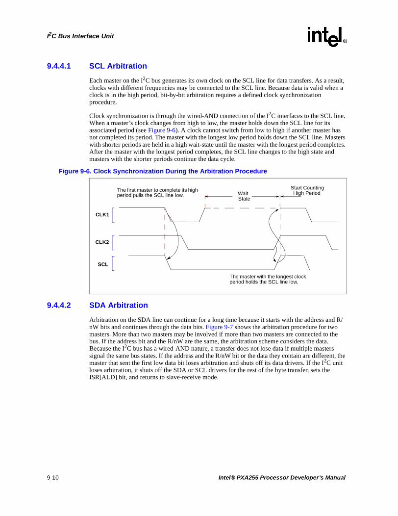
I2C Bus Interface Unit
9.4.4.1 SCL Arbitration
Each master on the I2C bus generates its own clock on the SCL line for data transfers. As a result, clocks with different frequencies may be connected to the SCL line. Because data is valid when a clock is in the high period, bit-by-bit arbitration requires a defined clock synchronization procedure.
Clock synchronization is through the wired-AND connection of the I2C interfaces to the SCL line. When a master’s clock changes from high to low, the master holds down the SCL line for its associated period (see Figure 9-6). A clock cannot switch from low to high if another master has not completed its period. The master with the longest low period holds down the SCL line. Masters with shorter periods are held in a high wait-state until the master with the longest period completes. After the master with the longest period completes, the SCL line changes to the high state and masters with the shorter periods continue the data cycle.
9.4.4.2 SDA Arbitration
Arbitration on the SDA line can continue for a long time because it starts with the address and R/nW bits and continues through the data bits. Figure 9-7 shows the arbitration procedure for two masters. More than two masters may be involved if more than two masters are connected to the bus. If the address bit and the R/nW are the same, the arbitration scheme considers the data. Because the I2C bus has a wired-AND nature, a transfer does not lose data if multiple masters signal the same bus states. If the address and the R/nW bit or the data they contain are different, the master that sent the first low data bit loses arbitration and shuts off its data drivers. If the I2C unit loses arbitration, it shuts off the SDA or SCL drivers for the rest of the byte transfer, sets the ISR[ALD] bit, and returns to slave-receive mode.
Figure 9-6. Clock Synchronization During the Arbitration Procedure
CLK2
SCL
WaitState
Start Counting High Period
CLK1
The first master to complete its high period pulls the SCL line low.
The master with the longest clock period holds the SCL line low.
9-10 Intel® PXA255 Processor Developer’s Manual

I2C Bus Interface Unit
If the I2C unit loses arbitration as the address bits are transferred and it is not addressed by the address bits, the I2C unit resends the address when the I2C bus becomes free. A resend is possible because the IDBR and ICR registers are not overwritten when arbitration is lost.
If the I2C unit loses arbitration because another bus master addresses the processor as a slave device, the I2C unit switches to slave-receive mode and overwrites the original data in the I2C data buffer register. Software can clear the start and re-initiate the master transaction.
Note: Software must prevent the I2C unit from starting a transaction to its own slave address because such a transaction puts the I2C unit in an indeterminate state.
Arbitration has boundary conditions in case an arbitration process is interrupted by a repeated START or STOP condition transmitted on the I2C bus. To prevent errors, the I2C unit acts as a master if no arbitration takes place in the following circumstances:
• Between a repeated START condition and a data bit
• Between a data bit and a STOP condition
• Between a repeated START condition and a STOP condition
These situations occur if different masters write identical data to the same target slave simultaneously and arbitration cannot be resolved after the first data byte transfer.
Note: Software ensures that arbitration is resolved quickly. For example, software can ensure that masters send unique data by requiring that each master transmit its I2C address as the first data byte of any transaction. When arbitration is resolved, the winning master sends a restart and begins a valid data transfer. The slave discards the master’s address and use the other data.
Figure 9-7. Arbitration Procedure of Two Masters
SDA
SCL
Data 1
Data 2
Transmitter 1 Leaves Arbitration Data 1 SDA
Intel® PXA255 Processor Developer’s Manual 9-11

I2C Bus Interface Unit
9.4.5 Master Operations
When software initiates a read or write on the I2C bus, the I2C unit transitions from the default slave-receive mode to master-transmit mode. The 7-bit slave address and the R/nW bit follow the start pulse. After the master receives an acknowledge, the I2C unit enters one of two master modes:
• Master-Transmit — I2C unit writes data
• Master-Receive — I2C unit reads data
The CPU writes to the ICR register to initiate a master transaction. Data is read and written from the I2C unit through the memory-mapped registers. Table 9-5 describes the I2C unit’s responsibilities as a master device.
Table 9-5. Master Transactions (Sheet 1 of 2)
I2C Master Action
Mode of Operation Definition
Generate clock output
Master-transmit
Master-receive
• Master drives the SCL line.
• ICR[SCLE] bit must be set.
• ICR[IUE] bit must be set.
Write target slave address to IDBR
Master-transmit
Master-receive
• CPU writes to IDBR bits 7-1 before a START condition enabled.
• First seven bits sent on bus after START.
• See Section 9.3.3.
Write R/nW Bit to IDBR
Master-transmit
Master-receive
• CPU writes to least significant IDBR bit with target slave address.
• If low, master remains a master-transmitter. If high, master transitions to a master-receiver.
• See Section 9.4.2.
Signal START Condition
Master-transmit
Master-receive
• See “Generate clock output” above.
• Performed after target slave address and R/nW bit are in IDBR.
• Software sets ICR[START] bit.
• Software sets ICR[TB] bit to initiate start condition.
• See Section 9.3.3.
Initiate first data byte transfer
Master-transmit
Master-receive
• CPU writes byte to IDBR
• I2C unit transmits byte when ICR[TB] bit is set.
• I2C unit clears ICR[TB] bit and sets ISR[ITE] bit when transfer is complete.
Arbitrate for I2C Bus
Master-transmit
Master-receive
• If two or more masters signal a start within the same clock period, arbitration must occur.
• I2C unit arbitrates for as long as needed. Arbitration takes place during slave address and R/nW bit or data transmission and continues until all but one master loses the bus. No data lost.
• If I2C unit loses arbitration, it sets ISR[ALD] bit after byte transfer is completed and transitions to slave-receive mode.
• If I2C unit loses arbitration as it attempts to send target address byte, I2C unit attempts to resend it when the bus becomes free.
• System designer must ensure boundary conditions described in Section 9.4 do not occur.
9-12 Intel® PXA255 Processor Developer’s Manual

I2C Bus Interface Unit
When the CPU needs to read data, the I2C unit transitions from slave-receive mode to master-transmit mode to transmit the start address, R/nW bit, and the ACK pulse. After it sends the ACK pulse, the I2C unit transitions to master-receive mode and waits to receive the read data from the slave device (see Figure 9-8).Multiple transactions can take place during an I2C operation. For example, transitioning from master-receive to master-transmit through a repeated start.
Write one data byte to the IDBR
Master-transmit only
• I2C master operation data transmit mode.
• Occurs when the ISR[ITE] bit is set and the ICR[TB] bit is clear. If the IDBR Transmit Empty Interrupt is enabled, it is signalled to the processor.
• CPU writes one data byte to the IDBR, sets the appropriate START/STOP bit combination, and sets the ICR[TB] bit to send the data. Eight bits are taken from the shift register and written to the serial bus. The eight bits are followed by a STOP, if requested.
Wait for Acknowledge from slave-receiver
Master-transmit only
• As a master-transmitter, the I2C unit generates the clock for the acknowledge pulse. The I2C unit releases the SDA line to allow slave-receiver ACK transmission.
• See Section 9.4.3.
Read one byte of I2C Data from the IDBR
Master-receive only
• I2C master operation data receive mode.
• Eight bits are read from the serial bus, collected in the shift register then transferred to the IDBR after the ICR[ACKNAK] bit is read.
• The CPU reads the IDBR when the ISR[IRF] bit is set and the ICR[TB] bit is clear. If IDBR Receive Full Interrupt is enabled, it is signalled to the CPU.
• When the IDBR is read, if the ISR[ACKNAK] is clear (indicating ACK), the processor writes the ICR[ACKNAK] bit and set the ICR[TB] bit to initiate the next byte read.
• If the ISR[ACKNAK] bit is set (indicating NAK), ICR[TB] bit is clear, ICR[STOP] bit is set, and ISR[UB] bit is set, then the last data byte has been read into the IDBR and the I2C unit is sending the STOP.
• If the ISR[ACKNAK] bit is set (indicating NAK), ICR[TB] bit is clear, but the ICR[STOP] bit is clear, then the CPU has two options: 1. set the ICR[START] bit, write a new target address to the IDBR, and set the ICR[TB] bit which will send a repeated start condition or 2. set the ICR[MA] bit and leave the ICR[TB] bit clear which will send a STOP only.
Transmit Acknowledge to slave-transmitter
Master-receive only
• As a master-receiver, the I2C unit will generate the clock for the acknowledge pulse. The I2C unit is also responsible for driving the SDA line during the ACK cycle.
• If the next data byte is to be the last transaction, the CPU will set the ICR[ACKNAK] bit for NAK generation.
• See Section 9.4.3.
Generate a Repeated START to chain I2C transactions
Master-transmit
Master-receive
• If data chaining is desired, a repeated START condition is used instead of a STOP condition.
• This occurs after the last data byte of a transaction has been written to the bus.
• The CPU will write the next target slave address and the R/nW bit to the IDBR, set the ICR[START] bit, and set the ICR[TB] bit.
• See Section 9.3.3.
Generate a STOP
Master-transmit
Master-receive
• Generated after the CPU writes the last data byte on the bus.
• CPU generates a STOP condition by setting the ICR[STOP] bit.
• See Section 9.3.3.
Table 9-5. Master Transactions (Sheet 2 of 2)
I2C Master Action
Mode of Operation Definition
Intel® PXA255 Processor Developer’s Manual 9-13
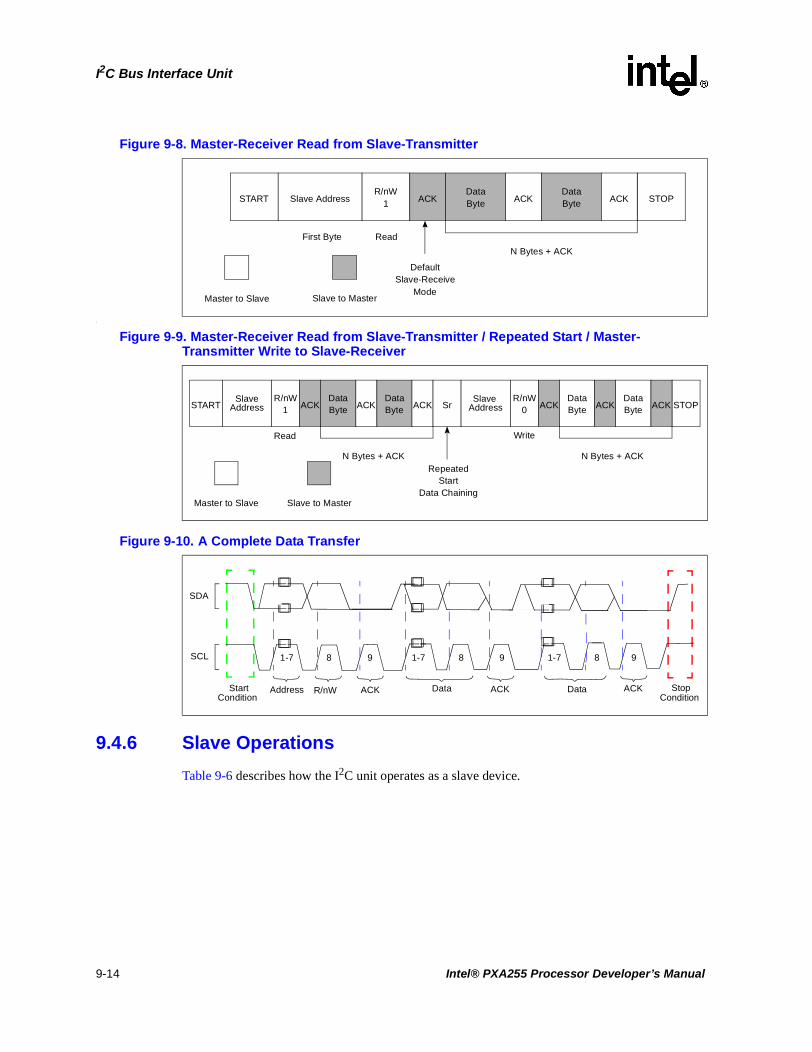
I2C Bus Interface Unit
.
\
9.4.6 Slave Operations
Table 9-6 describes how the I2C unit operates as a slave device.
Figure 9-8. Master-Receiver Read from Slave-Transmitter
Figure 9-9. Master-Receiver Read from Slave-Transmitter / Repeated Start / Master-Transmitter Write to Slave-Receiver
Figure 9-10. A Complete Data Transfer
Master to Slave Slave to Master
START Slave AddressR/nW
1 ACKDataByte ACK
DataByte STOP
N Bytes + ACK
ACK
DefaultSlave-Receive
Mode
First Byte Read
STARTSlave R/nW
1 ACKDataByte ACK
DataByte
N Bytes + ACK
Read
ACK SrSlave R/nW
0 ACKDataByte ACK
DataByte STOP
N Bytes + ACK
Write
ACKAddress Address
Master to Slave Slave to Master
RepeatedStart
Data Chaining
SDA
SCL
StartCondition
Address R/nW ACK Data ACK Data
1-7 8 9 8 9891-7 1-7
ACK StopCondition
∼ ∼∼ ∼
∼ ∼
∼ ∼∼ ∼
∼ ∼
∼ ∼∼ ∼
∼ ∼
9-14 Intel® PXA255 Processor Developer’s Manual

I2C Bus Interface Unit
Figure 9-11 through Figure 9-13 are examples of I2C transactions and show the relationships between master and slave devices.
Table 9-6. Slave Transactions
I2C Slave Action Mode of Operation Definition
Slave-receive
(default mode)Slave-receive only
• I2C unit monitors all slave address transactions.
• ICR[IUE] bit must be set.
• I2C unit monitors bus for START conditions. When a START is detected, the interface reads the first 8 bits and compares the most significant seven bits with the 7-bit ISAR and the general call address (0x00). If there is a match, the I2C unit sends an ACK.
• If the first 8 bits are zero’s, this is a general call address. If the ICR[GCD] bit is clear, both the ISR[GCAD] bit and the ISR[SAD] bit will be set. See Section 9.4.7.
• If the eighth bit of the first byte (R/nW bit) is low, the I2C unit stays in slave-receive mode and the ISR[SAD] bit is cleared. If R/nW bit is high, I2C unit switches to slave-transmit and ISR[SAD] bit is set.
Setting the Slave Address Detected bit
Slave-receive
Slave-transmit
• Indicates the interface has detected an I2C operation that addresses the processor including the general call address. The processor can distinguish an ISAR match from a General Call by reading the ISR[GCAD] bit.
• An interrupt is signalled, if enabled, after the matching slave address is received and acknowledged.
Read one byte of I2C Data from the IDBR
Slave-receive only
• Data receive mode of I2C slave operation.
• Eight bits are read from the serial bus into the shift register. When a full byte is received and the ACK/NAK bit is completed, the byte is transferred from the shift register to the IDBR.
• Occurs when the ISR[IRF] bit is set and the ICR[TB] bit is clear. If enabled, the IDBR Receive Full Interrupt is signalled to the CPU.
• Software reads one data byte from the IDBR. When the IDBR is read, the processor writes the desired ICR[ACKNAK] bit and sets the ICR[TB] bit. This causes the I2C unit to stop inserting wait states and let the master transmitter write the next piece of information.
Transmit Acknowledge to master-transmitter
Slave-receive only
• As a slave-receiver, the I2C unit pulls the SDA line low to generate the ACK pulse during the high SCL period.
• ICR[ACKNAK] bit controls the ACK data the I2C unit drives. See Section 9.4.3.
Write one byte of I2C data to the IDBR
Slave-transmit only
• Data transmit mode of I2C slave operation.
• Occurs when ISR[ITE] bit is set and ICR[TB] bit is clear. If enabled, the IDBR Transmit Empty Interrupt is signalled to the processor.
• The processor writes a data byte to IDBR and sets ICR[TB] bit to start the transfer.
Wait for Acknowledge from master-receiver
Slave-transmit only
• As a slave-transmitter, the I2C unit releases the SDA line to allow the master-receiver to pull the line low for the ACK.
• See Section 9.4.3.
Intel® PXA255 Processor Developer’s Manual 9-15

I2C Bus Interface Unit
9.4.7 General Call Address
A general call address is a transaction with a slave address of 0x00. When a device requires the data from a general call address, it acknowledges the transaction and stays in slave-receiver mode. Otherwise, the device ignores the general call address. The other bytes in a general call transaction are acknowledged by every device that uses it on the bus. Devices that do not use these bytes must not send an ACK. The meaning of a general call address is defined in the second byte sent by the master-transmitter. Figure 9-14 shows a general call address transaction. The least significant bit of the second byte, called B, defines the transaction. Table 9-7 shows the valid values and definitions when B=0.
Figure 9-11. Master-Transmitter Write to Slave-Receiver
Figure 9-12. Master-Receiver Read to Slave-Transmitter
Figure 9-13. Master-Receiver Read to Slave-Transmitter, Repeated START, Master-Transmitter Write to Slave-Receiver
Master to Slave Slave to Master
START Slave AddressR/nW
0 ACKDataByte ACK
DataByte STOP
N Bytes + ACKWrite
ACK
First Byte
Master to Slave Slave to Master
START Slave AddressR/nW
1 ACKDataByte ACK
DataByte STOP
N Bytes + ACKRead
NAK
DefaultSlave-Receive
Mode
First Byte
STARTSlave R/nW
1 ACKDataByte ACK
DataByte
N Bytes + ACKRead
ACK SRSlave R/nW
0 ACKDataByte ACK
DataByte STOP
N Bytes + ACKWrite
ACKAddress Address
Master to Slave Slave to Master
RepeatedSTART
Data Chaining
9-16 Intel® PXA255 Processor Developer’s Manual

I2C Bus Interface Unit
The I2C unit supports sending and receiving general call address transfers on the I2C bus. When software sends a general call message from the I2C unit, it must set the ICR[GCD] bit to prevent the I2C unit from responding as a slave. If the ICR[GCD] is not set, the I2C bus enters an indeterminate state.
If the I2C unit acts as a slave and receives a general call address while the ICR[GCD] bit is clear, it:
• Sets the ISR[GCAD] bit
• Sets the ISR[SAD] bit
• Interrupts the processor (if the interrupt is enabled)
If the I2C unit receives a general call address and the ICR[GCD] bit is set, it ignores the general call address.
Software must ensure that the I2C unit is not busy before it asserts a reset. Software must also ensure that the I2C bus is idle when the unit is enabled after reset. When directed to reset, the I2C unit, except for ISAR, returns to the default reset condition. ISAR is not affected by a reset.
When B=1, the sequence is a hardware general call and is not supported by the I2C unit. Refer to the The I2C-Bus Specification for information on hardware general calls.
I2C 10-bit addresses and CBUS compatibility are not supported.
Figure 9-14. General Call Address
Table 9-7. General Call Address Second Byte Definitions
Least Significant
Bit of Second Byte (B)
Second Byte Value
Definition
0 0x06 2-byte transaction in which the second byte tells the slave to reset and store this value in the programmable part of its address.
0 0x04 2-byte transaction in which the second byte tells the slave to store this value in the programmable part of its address. No reset.
0 0x00 Not allowed as a second byte
NOTE: Other values are not fixed and must be ignored.
Master to Slave Slave to Master
START 00000000 ACKDataByte ACK
DataByte STOP
N Bytes + ACK
Least Significant Bit of Master Address
ACK
Second Byte
Second Byte 0 ACK
First Byte
Defines Transaction
Intel® PXA255 Processor Developer’s Manual 9-17

I2C Bus Interface Unit
9.5 Slave Mode Programming Examples
9.5.1 Initialize Unit
1. Set the slave address in the ISAR.
2. Enable desired interrupts in the ICR.
3. Set the ICR[IUE] bit to enable the I2C unit.
9.5.2 Write n Bytes as a Slave
1. When a Slave Address Detected interrupt occurs.Read ISR: Slave Address Detected (1), Unit Busy (1), R/nW bit (1), ACK/NAK (0)
2. Write a 1 to the ISR[SAD] bit to clear the interrupt.
3. Return from interrupt.
4. Load data byte to transfer in the IDBR.
5. Set ICR[TB] bit.
6. When a IDBR Transmit Empty interrupt occurs.Read ISR: IDBR Transmit Empty (1), ACK/NAK (0), R/nW bit (0)
7. Load data byte to transfer in the IDBR.
8. Set the ICR[TB] bit.
9. Write a 1 to the ISR[ITE] bit to clear interrupt.
10. Return from interrupt.
11. Repeat steps 6 to 10 for n-1 times. If, at any time, the slave does not have data, the I2C unit keeps SCL low until data is available.
12. When a IDBR Transmit Empty interrupt occurs.Read ISR: IDBR Transmit Empty (1), ACK/NAK (1), R/nW bit (0)
13. Write a 1 to the ISR[ITE] bit to clear interrupt.
14. Return from interrupt
15. When Slave Stop Detected interrupt occurs.Read ISR: Unit Busy (0), Slave STOP Detected (1)
16. Write a 1 to the ISR[SSD] bit to clear interrupt.
9.5.3 Read n Bytes as a Slave
1. When a Slave Address Detected interrupt occurs.Read ISR: Slave Address Detected (1), Unit busy (1), R/nW bit (0)
2. Write a 1 to the ISR[SAD] bit to clear the interrupt.
3. Return from interrupt.
4. Set ICR[TB] bit to initiate the transfer.
9-18 Intel® PXA255 Processor Developer’s Manual

I2C Bus Interface Unit
5. When an IDBR Receive Full interrupt occurs.Read ISR: IDBR Receive Full (1), ACK/NAK (0), R/nW bit (0)
6. Read IDBR to get the received byte.
7. Write a 1 to the ISR[IRF] bit to clear interrupt.
8. Return from interrupt.
9. Repeat steps 4 to 8 for n-1 times. Once the IDBR is full, the I2C unit will keep SCL low until the data is read.
10. Set ICR[TB] bit to release I2C bus and allow next transfer.
11. When a Slave Stop Detected interrupt occurs.Read ISR: Unit busy (0), Slave STOP Detected (1)
12. Write a 1 to the ISR[SSD] bit to clear interrupt.
9.6 Master Programming Examples
9.6.1 Initialize Unit
1. Set the slave address in the ISAR.
2. Enable desired interrupts in the ICR. Do not enable Arbitration Loss Detected interrupt
3. Set the ICR[IUE] and ICR[SCLE] bits to enable the I2C unit and SCL.
9.6.2 Write 1 Byte as a Master
1. Load target slave address and R/nW bit in the IDBR. R/nW must be 0 for a write.
2. Initiate the write.Set ICR[START], clear ICR[STOP], clear ICR[ALDIE], set ICR[TB]
3. When an IDBR Transmit Empty interrupt occurs.Read ISR: IDBR Transmit Empty (1), Unit Busy (1), R/nW bit (0)
4. Write a 1 to the ISR[ITE] bit to clear interrupt.
5. Write a 1 to the ISR[ALD] bit if set.If the master loses arbitration, it performs an address retry when the bus becomes free. The Arbitration Loss Detected interrupt is disabled to allow the address retry.
6. Load data byte to be transferred in the IDBR.
7. Initiate the write.Clear ICR[START], set ICR[STOP], set ICR[ALDIE], set ICR[TB]
8. When an IDBR Transmit Empty interrupt occurs (unit is sending STOP).Read ISR: IDBR Transmit Empty (1), Unit busy (x), R/nW bit (0)
9. Write a 1 to the ISR[ITE] bit to clear the interrupt.
10. Clear ICR[STOP] bit.
Intel® PXA255 Processor Developer’s Manual 9-19

I2C Bus Interface Unit
9.6.3 Read 1 Byte as a Master
1. Load target slave address and R/nW bit in the IDBR. R/nW must be 1 for a read.
2. Initiate the write.Set ICR[START], clear ICR[STOP], clear ICR[ALDIE], set ICR[TB]
3. When an IDBR Transmit Empty interrupt occurs.Read ISR: IDBR Transmit Empty (1), Unit busy (1), R/nW bit (1)
4. Write a 1 to the ISR[ITE] bit to clear the interrupt.
5. Initiate the read.Clear ICR[START], set ICR[STOP], set ICR[ALDIE], set ICR[ACKNAK], set ICR[TB]
6. When an IDBR Receive full interrupt occurs (unit is sending STOP).Read ISR: IDBR Receive Full (1), Unit Busy (x), R/nW bit (1), ACK/NAK bit (1)
7. Write a 1 to the ISR[IRF] bit to clear the interrupt.
8. Read IDBR data.
9. Clear ICR[STOP] and ICR[ACKNAK] bits
9.6.4 Write 2 Bytes and Repeated Start Read 1 Byte as a Master
1. Load target slave address and R/nW bit in the IDBR. R/nW must be 0 for a write.
2. Initiate the write.Set ICR[START], clear ICR[STOP], clear ICR[ALDIE], set ICR[TB]
3. When an IDBR Transmit Empty interrupt occurs.Read ISR: IDBR Transmit Empty (1), Unit Busy (1), R/nW bit (0)
4. Write a 1 to the ISR[ITE] bit to clear interrupt.
5. Load data byte to be transferred in the IDBR.
6. Initiate the write.Clear ICR[START], clear ICR[STOP], set ICR[ALDIE], set ICR[TB]
7. When an IDBR Transmit Empty interrupt occurs.Read ISR: IDBR Transmit Empty (1), Unit busy (1), R/nW bit (0)
8. Write a 1 to the ISR[ITE] bit to clear interrupt.
9. Repeat steps 5-8 one time.
10. Load target slave address and R/nW bit in the IDBR. R/nW must be 1 for a read.
11. Send repeated start as a master.Set ICR[START], clear ICR[STOP], clear ICR[ALDIE], set ICR[TB]
12. When an IDBR Transmit Empty interrupt occurs.Read ISR: IDBR Transmit Empty (1), Unit busy (1), R/nW bit (1)
13. Write a 1 to the ISR[ITE] bit to clear interrupt.
14. Initiate the read.Clear ICR[START], set ICR[STOP], set ICR[ALDIE], set ICR[ACKNAK], set ICR[TB]
15. When an IDBR Receive full interrupt occurs (unit is sending stop).Read ISR: IDBR Receive Full (1), Unit Busy (x), R/nW bit (1), ACK/NAK bit (1)
9-20 Intel® PXA255 Processor Developer’s Manual

I2C Bus Interface Unit
16. Write a 1 to the ISR[IRF] bit to clear the interrupt.
17. Read IDBR data.
18. Clear ICR[STOP] and ICR[ACKNAK] bits
9.6.5 Read 2 Bytes as a Master - Send STOP Using the Abort
1. Load target slave address and R/nW bit in the IDBR. R/nW must be 1 for a read.
2. Initiate the write.Set ICR[START], clear ICR[STOP], clear ICR[ALDIE], set ICR[TB]
3. When an IDBR Transmit Empty interrupt occurs.Read ISR: IDBR Transmit Empty (1), Unit busy (1), R/nW bit (1)
4. Write a 1 to the ISR[ITE] bit to clear interrupt.
5. Initiate the readClear ICR[START], clear ICR[STOP], set ICR[ALDIE], clear ICR[ACKNAK], set ICR[TB]
6. When an IDBR Receive full interrupt occurs.Read ISR: IDBR Receive Full (1), Unit Busy (1), R/nW bit (1), ACK/NAK bit (0)
7. Write a 1 to the ISR[IRF] bit to clear the interrupt.
8. Read IDBR data.
9. Clear ICR[STOP] and ICR[ACKNAK] bits
10. Initiate the read.Clear ICR[START], clear ICR[STOP], set ICR[ALDIE], set ICR[ACKNAK], set ICR[TB]ICR[STOP] is not set because STOP or repeated start will be decided on the byte read.
11. When an IDBR Receive full interrupt occurs.Read ISR: IDBR Receive Full (1), Unit Busy (1), R/nW bit (1), ACK/NAK bit (1)
12. Write a 1 to the ISR[IRF] bit to clear the interrupt.
13. Read IDBR data.
14. Initiate STOP abort condition (STOP with no data transfer).Set ICR[MA]
Note: If a NAK is not sent in Step 11, the next transaction must involve another data byte read.
9.7 Glitch Suppression Logic
The I2C unit has built-in glitch suppression logic that suppresses glitches of 60ns or less. This is within the 50ns glitch suppression specification.
9.8 Reset Conditions
Software must ensure that the I2C unit is not busy before it asserts a reset. Software must also ensure that the I2C bus is idle when the unit is enabled after reset. When directed to reset, the I2C unit, except for ISAR, returns to the default reset condition. ISAR is not affected by a reset.
Intel® PXA255 Processor Developer’s Manual 9-21
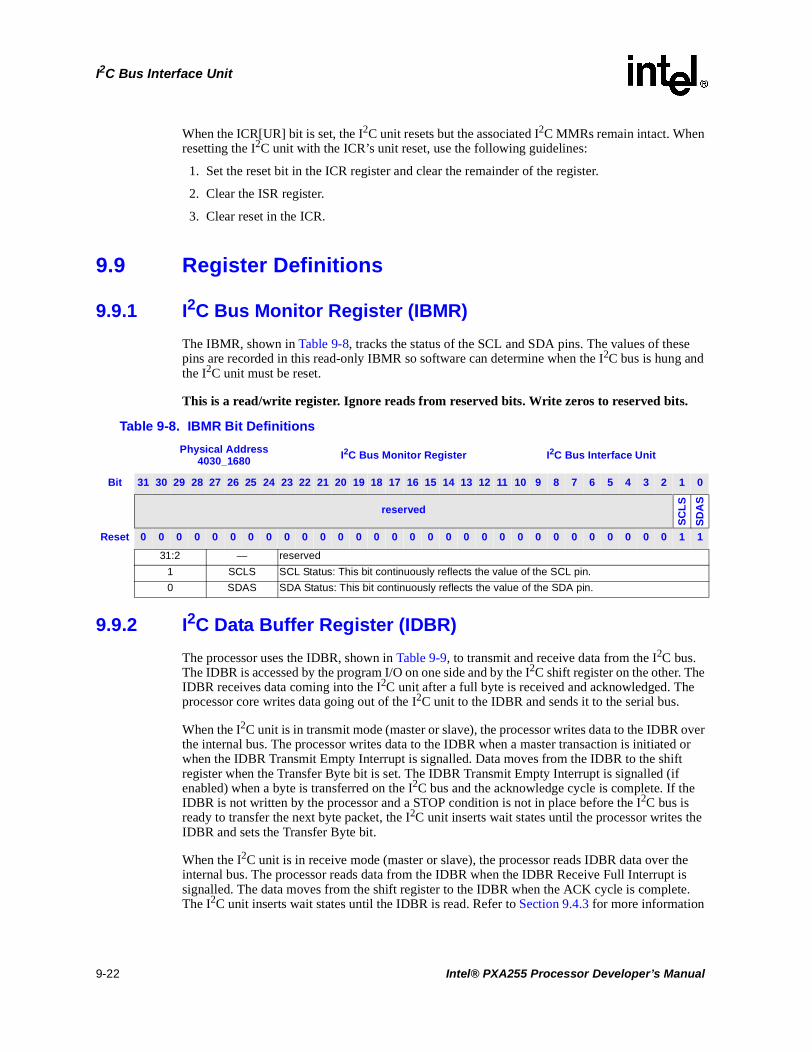
I2C Bus Interface Unit
When the ICR[UR] bit is set, the I2C unit resets but the associated I2C MMRs remain intact. When resetting the I2C unit with the ICR’s unit reset, use the following guidelines:
1. Set the reset bit in the ICR register and clear the remainder of the register.
2. Clear the ISR register.
3. Clear reset in the ICR.
9.9 Register Definitions
9.9.1 I2C Bus Monitor Register (IBMR)
The IBMR, shown in Table 9-8, tracks the status of the SCL and SDA pins. The values of these pins are recorded in this read-only IBMR so software can determine when the I2C bus is hung and the I2C unit must be reset.
This is a read/write register. Ignore reads from reserved bits. Write zeros to reserved bits.
9.9.2 I2C Data Buffer Register (IDBR)
The processor uses the IDBR, shown in Table 9-9, to transmit and receive data from the I2C bus. The IDBR is accessed by the program I/O on one side and by the I2C shift register on the other. The IDBR receives data coming into the I2C unit after a full byte is received and acknowledged. The processor core writes data going out of the I2C unit to the IDBR and sends it to the serial bus.
When the I2C unit is in transmit mode (master or slave), the processor writes data to the IDBR over the internal bus. The processor writes data to the IDBR when a master transaction is initiated or when the IDBR Transmit Empty Interrupt is signalled. Data moves from the IDBR to the shift register when the Transfer Byte bit is set. The IDBR Transmit Empty Interrupt is signalled (if enabled) when a byte is transferred on the I2C bus and the acknowledge cycle is complete. If the IDBR is not written by the processor and a STOP condition is not in place before the I2C bus is ready to transfer the next byte packet, the I2C unit inserts wait states until the processor writes the IDBR and sets the Transfer Byte bit.
When the I2C unit is in receive mode (master or slave), the processor reads IDBR data over the internal bus. The processor reads data from the IDBR when the IDBR Receive Full Interrupt is signalled. The data moves from the shift register to the IDBR when the ACK cycle is complete. The I2C unit inserts wait states until the IDBR is read. Refer to Section 9.4.3 for more information
Table 9-8. IBMR Bit Definitions
Physical Address4030_1680 I2C Bus Monitor Register I2C Bus Interface Unit
Bit 31 30 29 28 27 26 25 24 23 22 21 20 19 18 17 16 15 14 13 12 11 10 9 8 7 6 5 4 3 2 1 0
reserved
SC
LS
SD
AS
Reset 0 0 0 0 0 0 0 0 0 0 0 0 0 0 0 0 0 0 0 0 0 0 0 0 0 0 0 0 0 0 1 1
31:2 — reserved
1 SCLS SCL Status: This bit continuously reflects the value of the SCL pin.
0 SDAS SDA Status: This bit continuously reflects the value of the SDA pin.
9-22 Intel® PXA255 Processor Developer’s Manual

I2C Bus Interface Unit
on the acknowledge pulse in receiver mode. After the processor reads the IDBR, the ACK/NAK Control bit is written and the Transfer Byte bit is written, allowing the next byte transfer to proceed to the I2C bus. The IDBR register is 0x00 after reset.
This is a read/write register. Ignore reads from reserved bits. Write zeros to reserved bits.
9.9.3 I2C Control Register (ICR)
The processor uses the ICR, shown in Table 9-10, to control the I2C unit.
This is a read/write register. Ignore reads from reserved bits. Write zeros to reserved bits.
Table 9-9. IDBR Bit Definitions
Physical Address4030_1688 I2C Data Buffer Register I2C Bus Interface Unit
Bit 31 30 29 28 27 26 25 24 23 22 21 20 19 18 17 16 15 14 13 12 11 10 9 8 7 6 5 4 3 2 1 0
reserved IDB
Reset 0 0 0 0 0 0 0 0 0 0 0 0 0 0 0 0 0 0 0 0 0 0 0 0 0 0 0 0 0 0 0 0
31:8 — reserved
7:0 IDB I2C Data Buffer: Buffer for I2C bus send/receive data.
Table 9-10. ICR Bit Definitions (Sheet 1 of 3)
Physical Address4030_1690 I2C Control Register I2C Bus Interface Unit
Bit 31 30 29 28 27 26 25 24 23 22 21 20 19 18 17 16 15 14 13 12 11 10 9 8 7 6 5 4 3 2 1 0
reserved FM
UR
SA
DIE
AL
DIE
SS
DIE
BE
IE
IRF
IE
ITE
IE
GC
D
IUE
SC
LE
MA
TB
AC
KN
AK
STO
P
STA
RT
Reset 0 0 0 0 0 0 0 0 0 0 0 0 0 0 0 0 0 0 0 0 0 0 0 0 0 0 0 0 0 0 0
31:16 — reserved
15 FMFast Mode:
0 = 100 KBit/sec. operation1 = 400 KBit/sec. operation
14 URUnit Reset:
0 = No reset.1 = Reset the I2C unit only.
13 SADIE
Slave Address Detected Interrupt Enable:
0 = Disable interrupt.1 = Enables the I2C unit to interrupt the processor when it detects a slave address match or
general call address.
12 ALDIEArbitration Loss Detected Interrupt Enable:
0 = Disable interrupt.1 = Enables the I2C unit to interrupt the processor when it loses arbitration in master mode.
11 SSDIE
Slave STOP Detected Interrupt Enable:
0 = Disable interrupt.1 = Enables the I2C unit to interrupt the processor when it detects a STOP condition in
slave mode.
Intel® PXA255 Processor Developer’s Manual 9-23
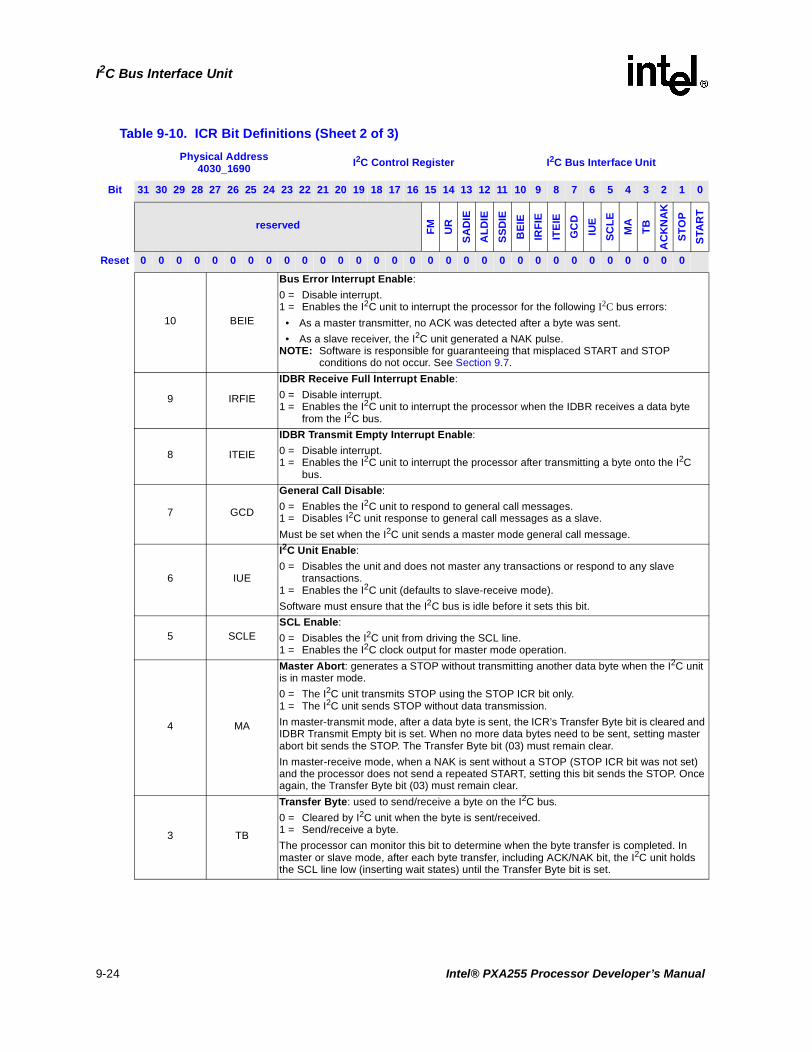
I2C Bus Interface Unit
10 BEIE
Bus Error Interrupt Enable:
0 = Disable interrupt.1 = Enables the I2C unit to interrupt the processor for the following I2C bus errors:
• As a master transmitter, no ACK was detected after a byte was sent.
• As a slave receiver, the I2C unit generated a NAK pulse.NOTE: Software is responsible for guaranteeing that misplaced START and STOP
conditions do not occur. See Section 9.7.
9 IRFIE
IDBR Receive Full Interrupt Enable:
0 = Disable interrupt.1 = Enables the I2C unit to interrupt the processor when the IDBR receives a data byte
from the I2C bus.
8 ITEIE
IDBR Transmit Empty Interrupt Enable:
0 = Disable interrupt.1 = Enables the I2C unit to interrupt the processor after transmitting a byte onto the I2C
bus.
7 GCD
General Call Disable:
0 = Enables the I2C unit to respond to general call messages.1 = Disables I2C unit response to general call messages as a slave.
Must be set when the I2C unit sends a master mode general call message.
6 IUE
I2C Unit Enable:
0 = Disables the unit and does not master any transactions or respond to any slave transactions.
1 = Enables the I2C unit (defaults to slave-receive mode).
Software must ensure that the I2C bus is idle before it sets this bit.
5 SCLESCL Enable:
0 = Disables the I2C unit from driving the SCL line.1 = Enables the I2C clock output for master mode operation.
4 MA
Master Abort: generates a STOP without transmitting another data byte when the I2C unit is in master mode.
0 = The I2C unit transmits STOP using the STOP ICR bit only.1 = The I2C unit sends STOP without data transmission.
In master-transmit mode, after a data byte is sent, the ICR’s Transfer Byte bit is cleared and IDBR Transmit Empty bit is set. When no more data bytes need to be sent, setting master abort bit sends the STOP. The Transfer Byte bit (03) must remain clear.
In master-receive mode, when a NAK is sent without a STOP (STOP ICR bit was not set) and the processor does not send a repeated START, setting this bit sends the STOP. Once again, the Transfer Byte bit (03) must remain clear.
3 TB
Transfer Byte: used to send/receive a byte on the I2C bus.
0 = Cleared by I2C unit when the byte is sent/received.1 = Send/receive a byte.
The processor can monitor this bit to determine when the byte transfer is completed. In master or slave mode, after each byte transfer, including ACK/NAK bit, the I2C unit holds the SCL line low (inserting wait states) until the Transfer Byte bit is set.
Table 9-10. ICR Bit Definitions (Sheet 2 of 3)
Physical Address4030_1690 I2C Control Register I2C Bus Interface Unit
Bit 31 30 29 28 27 26 25 24 23 22 21 20 19 18 17 16 15 14 13 12 11 10 9 8 7 6 5 4 3 2 1 0
reserved FM
UR
SA
DIE
AL
DIE
SS
DIE
BE
IE
IRF
IE
ITE
IE
GC
D
IUE
SC
LE
MA
TB
AC
KN
AK
ST
OP
STA
RT
Reset 0 0 0 0 0 0 0 0 0 0 0 0 0 0 0 0 0 0 0 0 0 0 0 0 0 0 0 0 0 0 0
9-24 Intel® PXA255 Processor Developer’s Manual

I2C Bus Interface Unit
9.9.4 I2C Status Register (ISR)
The ISR, shown in Table 9-11, signals I2C interrupts to the processor interrupt controller. Software can use the ISR bits to check the status of the I2C unit and bus. ISR bits (bits 9-5) are updated after the ACK/NAK bit is completed on the I2C bus.
The ISR also clears the following interrupts signalled from the I2C unit:
• IDBR Receive Full
• IDBR Transmit Empty
• Slave Address Detected
• Bus Error Detected
• STOP Condition Detect
• Arbitration Lost
This is a read/write register. Ignore reads from reserved bits. Write zeros to reserved bits.
2 ACKNAK
ACK/NAK Control: defines the type of ACK pulse sent by the I2C unit when in master-receive mode.
0 = The I2C unit sends an ACK pulse after it receives a data byte.1 = The I2C unit sends a negative ACK (NAK) after it receives a data byte.
The I2C unit automatically sends an ACK pulse when it responds to its slave address or when it responds in slave-receive mode, independent of the ACK/NAK control bit setting.
1 STOP
STOP: initiates a STOP condition after the next data byte on the I2C bus is transferred in master mode. In master-receive mode, the ACK/NAK control bit must be set along with this bit. See Section 9.3.3.3 for more details on the STOP state.
0 = Do not send a STOP.1 = Send a STOP.
0 START
START: initiates a START condition to the I2C unit when in master mode. See Section 9.3.3.1 for more details on the START state.
0 = Do not send a START.1 = Send a START.
Table 9-10. ICR Bit Definitions (Sheet 3 of 3)
Physical Address4030_1690 I2C Control Register I2C Bus Interface Unit
Bit 31 30 29 28 27 26 25 24 23 22 21 20 19 18 17 16 15 14 13 12 11 10 9 8 7 6 5 4 3 2 1 0
reserved FM
UR
SA
DIE
AL
DIE
SS
DIE
BE
IE
IRF
IE
ITE
IE
GC
D
IUE
SC
LE
MA
TB
AC
KN
AK
ST
OP
STA
RT
Reset 0 0 0 0 0 0 0 0 0 0 0 0 0 0 0 0 0 0 0 0 0 0 0 0 0 0 0 0 0 0 0
Intel® PXA255 Processor Developer’s Manual 9-25

I2C Bus Interface Unit
Table 9-11. ISR Bit Definitions (Sheet 1 of 2)
Physical Address4030_1698 I2C Status Register I2C Bus Interface Unit
Bit 31 30 29 28 27 26 25 24 23 22 21 20 19 18 17 16 15 14 13 12 11 10 9 8 7 6 5 4 3 2 1 0
reserved
BE
D
SA
D
GC
AD
IRF
ITE
AL
D
SS
D
IBB
UB
AC
KN
AK
RW
M
Reset 0 0 0 0 0 0 0 0 0 0 0 0 0 0 0 0 0 0 0 0 0 0 0 0 0 0 0 0 0 0 0 0
31:11 — reserved
10 BED
Bus Error Detected:
0 = No error detected.1 = The I2C unit sets this bit when it detects one of the following error conditions:
• As a master transmitter, no ACK is detected on the interface after a byte is sent.
• As a slave receiver, the I2C unit generates a NAK pulse.NOTE:When an error occurs, I2C bus transactions continue. Software must ensure that
misplaced START and STOP conditions do not occur. See Section 9.4.4.
To clear this bit, write a 1 to it.
9 SAD
Slave Address Detected:
0 = No slave address detected. 1 = I2C unit detected a 7-bit address that matches the general call address or ISAR. An
interrupt is signalled when the SADIE interrupt is set to a 1.
To clear this bit, write a 1 to it.
8 GCADGeneral Call Address Detected:
0 = No general call address received.1 = I2C unit received a general call address.
7 IRF
IDBR Receive Full:
0 = The IDBR has not received a new data byte or the I2C unit is idle.1 = The IDBR register received a new data byte from the I2C bus. An interrupt is signalled
when the IRFIE is set to a 1.
To clear this bit, write a 1 to it.
6 ITE
IDBR Transmit Empty:
0 = The data byte is still being transmitted.1 = The I2C unit has finished transmitting a data byte on the I2C bus. An interrupt is
signalled when the ITEIE interrupt is set to 1.
To clear this bit, write a 1 to it.
5 ALD
Arbitration Loss Detected: used during multi-master operation.
0 = Cleared when arbitration is won or never took place.1 = Set when the I2C unit loses arbitration.
To clear this bit, write a 1 to it.
4 SSD
Slave STOP Detected:
0 = No STOP detected.1 = Set when the I2C unit detects a STOP while in slave-receive or slave-transmit mode.
To clear this bit, write a 1 to it.
3 IBBI2C Bus Busy:
0 = I2C bus is idle or the I2C unit is using the bus (i.e., unit busy).1 = Set when the I2C bus is busy but the I2C unit is not involved in the transaction.
2 UBUnit Busy:
0 = I2C unit not busy.1 = Set when the I2C unit is busy. Defined as the time between the first START and STOP.
9-26 Intel® PXA255 Processor Developer’s Manual

I2C Bus Interface Unit
9.9.5 I2C Slave Address Register (ISAR)
The ISAR, shown in Table 9-12, defines the I2C unit’s 7-bit slave address. In slave-receive mode, the processor responds when the 7-bit address matches the value in this register. The processor writes this register before it enables I2C operations. The ISAR is fully programmable (no address is assigned to the I2C unit) so it can be set to a value other than those of hard-wired I2C slave peripherals in the system. If the processor is reset, the ISAR is not affected. The ISAR register default value is 00000002.
This is a read/write register. Ignore reads from reserved bits. Write zeros to reserved bits.
1 ACKNAK
ACK/NAK Status:
0 = I2C unit received or sent an ACK on the bus. 1 = I2C unit received or sent a NAK.
Used in slave-transmit mode to determine when the transferred byte is the last one. Updated after each byte and ACK/NAK information is received.
0 RWM
Read/Write Mode:
0 = I2C unit is in master-transmit or slave-receive mode. 1 = I2C unit is in master-receive or slave-transmit mode.
R/nW bit of the slave address. Automatically cleared by hardware after a stop state.
Table 9-11. ISR Bit Definitions (Sheet 2 of 2)
Physical Address4030_1698 I2C Status Register I2C Bus Interface Unit
Bit 31 30 29 28 27 26 25 24 23 22 21 20 19 18 17 16 15 14 13 12 11 10 9 8 7 6 5 4 3 2 1 0
reserved
BE
D
SA
D
GC
AD
IRF
ITE
AL
D
SS
D
IBB
UB
AC
KN
AK
RW
M
Reset 0 0 0 0 0 0 0 0 0 0 0 0 0 0 0 0 0 0 0 0 0 0 0 0 0 0 0 0 0 0 0 0
Table 9-12. ISAR Bit Definitions
Physical Address4030_16A0 I2C Slave Address Register I2C Bus Interface Unit
Bit 31 30 29 28 27 26 25 24 23 22 21 20 19 18 17 16 15 14 13 12 11 10 9 8 7 6 5 4 3 2 1 0
reserved ISA
Reset 0 0 0 0 0 0 0 0 0 0 0 0 0 0 0 0 0 0 0 0 0 0 0 0 0 0 0 0 0 0 0 0
31:7 — reserved
6:0 ISA I2C Slave Address: 7-bit address that the I2C unit responds to when in slave-receive mode.
Intel® PXA255 Processor Developer’s Manual 9-27

I2C Bus Interface Unit
9-28 Intel® PXA255 Processor Developer’s Manual

UARTs 10
This chapter describes the universal asynchronous receiver/transmitter (UART) serial ports. The serial ports are controlled via direct memory access (DMA) or programmed I/O. The PXA255 processor has four UARTs: Full Function UART (FFUART), Bluetooth UART (BTUART), Standard UART (STUART) and Hardware UART (HWUART). The HWUART is covered in Chapter 17. The UARTs use the same programming model.
10.1 Feature List
The UARTs share the following features:
• Functionally compatible with the 16550
• Ability to add or delete standard asynchronous communications bits (start, stop, and parity) in the serial data
• Independently controlled transmit, receive, line status, and data set interrupts
• Programmable baud rate generator that allows the internal clock to be divided by 1 to (216–1) to generate an internal 16X clock
• Modem control pins that allow flow control through software. Each UART has different modem control capability.
• Fully programmable serial-interface:
— 5-, 6-, 7-, or 8-bit characters
— Even, odd, and no parity detection
— 1, 1.5, or 2 stop bit generation
— Baud rate generation up to 921 Kbps for the BTUART and HWUART. Up to 230 Kbps for other UARTs.
• 64-byte transmit FIFO
• 64-byte receive FIFO
• Complete status reporting capability
• Ability to generate and detect line breaks
• Internal diagnostic capabilities that include:
— Loopback controls for communications link fault isolation
— Break, parity, and framing error simulation
• Fully prioritized interrupt system controls
• Separate DMA requests for transmit and receive data services
• Slow infrared asynchronous interface that conforms to the Infrared Data Association (IRDA) standard
Intel® PXA255 Processor Developer’s Manual 10-1

UARTs
10.2 Overview
Each serial port contains a UART and a slow infrared transmit encoder and receive decoder that conforms to the IRDA Serial Infrared (SIR) Physical Layer Link Specification.
Each UART performs serial-to-parallel conversion on data characters received from a peripheral device or a modem and parallel-to-serial conversion on data characters received from the processor. The processor can read a UART’s complete status during functional operation. Status information includes the type and condition of transfer operations and error conditions (parity, overrun, framing, or break interrupt) associated with the UART.
Each serial port operates in FIFO or non-FIFO mode. In FIFO mode, a 64-byte Transmit FIFO holds data from the processor until it is transmitted on the serial link and a 64-byte Receive FIFO buffers data from the serial link until it is read by the processor. In non-FIFO mode, the transmit and Receive FIFOs are bypassed.
Each UART includes a programmable baud rate generator that can divide the input clock by 1 to (216–1). This produces a 16X clock that can be used to drive the internal transmitter and receiver logic. Software can program interrupts to meet its requirements. This minimizes the number of computations required to handle the communications link. Each UART operates in an environment that is controlled by software and can be polled or is interrupt driven.
10.2.1 Full Function UART
The FFUART supports modem control capability. The maximum tested baud rate on this UART is 230.4 kbps. The divisor programmed in the divisor latch registers must be equal to or greater than four.
10.2.2 Bluetooth UART
The BTUART is a high speed UART that supports baud rates up to 921.6 kbps and can be connected to a Bluetooth module. It supports the functions in the feature list, (see Section 10.1) but only supports two modem control pins (nCTS, nRTS).
10.2.3 Standard UART
The STUART supports all functions in the feature list (see Section 10.1), but does not support modem control capability. The UART’s maximum tested baud rate is 230.4 kbps. The divisors programmed in divisor latch registers must be equal to or greater than four.
10.2.4 Compatibility with 16550
The processor UARTs are functionally compatible with the 16550 industry standard. Each UART supports all of the 16550’s functions as well as the following features:
• DMA requests for transmit and receive data services
• Slow infrared asynchronous interface
• Non-Return-to-Zero (NRZ) encoding/decoding function
10-2 Intel® PXA255 Processor Developer’s Manual

UARTs
10.3 Signal Descriptions
Table 10-1 lists and describes each external signal that is connected to a UART module. The pins are connected through the System Integration Unit to GPIOs. Refer to Section 4.1, “General-Purpose I/O” on page 4-1 for details on the GPIOs.
Table 10-1. UART Signal Descriptions (Sheet 1 of 2)
Name Type Description
RXD InputSERIAL INPUT: Serial data input to the receive shift register. In infrared mode, it is connected to the infrared receiver input. This signal is present on all three UARTs.
TXD Output
SERIAL OUTPUT: Serial data output to the communications link-peripheral, modem, or data set. The TXD signal is set to the logic 1 state upon a Reset operation. It is connected to the output of the infrared transmitter in infrared mode. This signal is present all three UARTs.
nCTS Input
CLEAR TO SEND: When low, indicates that the modem or data set is ready to exchange data. The nCTS signal is a modem status input and its condition can be tested by reading bit 4 (CTS) of the Modem Status Register. Bit 4 is the complement of the nCTS signal. Bit 0 (DCTS) of the Modem Status Register (MSR) indicates whether the nCTS input has changed state since the last time the Modem Status Register was read. nCTS has no effect on the transmitter. This signal is present on the FFUART and BTUART.
When the CTS bit of the MSR changes state and the Modem Status interrupt is enabled, an interrupt is generated.
nDSR Input
DATA SET READY: When low, indicates that the modem or data set is ready to establish a communications link with a UART. The nDSR signal is a Modem Status input and its condition can be tested by reading Bit 5 (DSR) of the MSR. Bit 5 is the complement of the nDSR signal. Bit 1 (DDSR) of the MSR indicates whether the nDSR input has changed state since the MSR was last read. This signal is only present on the FFUART.
When the DSR bit of the MSR changes state, an interrupt is generated if the Modem Status interrupt is enabled.
nDCD Input
DATA CARRIER DETECT: When low, indicates that the data carrier has been detected by the modem or data set. The nDCD signal is a modem status input and its condition can be tested by reading Bit 7 (DCD) of the MSR. Bit 7 is the complement of the nDCD signal. Bit 3 (DDCD) of the MSR indicates whether the nDCD input has changed state since the previous reading of the Modem Status Register. nDCD has no effect on the receiver. This signal is only present on the FFUART.
When the DCD bit changes state and the Modem Status interrupt is enabled, an interrupt is generated.
Intel® PXA255 Processor Developer’s Manual 10-3

UARTs
10.4 UART Operational Description
The format of a UART data frame is shown in Figure 10-1.
Receive data sample counter frequency is 16 times the value of the bit frequency. The 16X clock is created by the baud rate generator. Each bit is sampled three times in the middle. Shaded bits in Figure 10-1 are optional and can be programmed by software.
Each data frame is between seven and 12 bits long, depending on the size of the data programmed, whether parity is enabled, and the number of stop bits. A data frame begins by transmitting a start bit that is represented by a high to low transition. The start bit is followed by from five to eight bits of data that begin with the least significant bit (LSB). The data bits are followed by an optional parity bit. The parity bit is set if even parity is enabled and the data byte has an odd number of ones
nRI Input
RING INDICATOR: When low, indicates that the modem or data set has received a telephone ringing signal. The nRI signal is a Modem Status input whose condition can be tested by reading Bit 6 (RI) of the MSR. Bit 6 is the complement of the nRI signal. Bit 2, the trailing edge of ring indicator (TERI), of the MSR indicates whether the nRI input signal has changed from low to high since the MSR was last read. This signal is only present on the FFUART.
When the RI bit of the MSR changes from a high to low state and the Modem Status interrupt is enabled, an interrupt is generated.
nDTR Output
DATA TERMINAL READY: When low, signals the modem or the data set that the UART is ready to establish a communications link. The nDTR output signal can be set to an active low by programming Bit 0 (DTR) of the MSR to a 1. A Reset operation sets this signal to its inactive state. LOOP mode operation holds this signal in its inactive state. This signal is only present on the FFUART.
nRTS Output
REQUEST TO SEND: When low, signals the modem or the data set that the UART is ready to exchange data. The nRTS output signal can be set to an active low by programming Bit 1 (RTS) of the Modem Control Register to a 1. A Reset operation sets this signal to its inactive (high) state. LOOP mode operation holds this signal in its inactive state. This signal is used by the FFUART and BTUART.
Table 10-1. UART Signal Descriptions (Sheet 2 of 2)
Name Type Description
Figure 10-1. Example UART Data Frame
Start
Bit
Data
<0>
Data
<1>
Data
<2>
Data
<3>
Data
<4>
Data
<5>
Data
<6>
Data
<7>
Parity
Bit
Stop
Bit 1
Stop
Bit 2
TXD or RXD pin
LSB MSB
10-4 Intel® PXA255 Processor Developer’s Manual

UARTs
or if odd parity is enabled and the data byte has an even number of ones. The data frame ends with one, one and a half or two stop bits, as programmed by software. The stop bits are represented by one, one and a half, or two successive bit periods of a logic one.
Each UART has two FIFOs: one transmit and one receive. The transmit FIFO is 64 bytes deep and eight bits wide. The receive FIFO is 64 bytes deep and 11 bits wide. Three bits are used for tracking errors.
The UART can use NRZ coding to represent individual bit values. NRZ coding is enabled when the Interrupt Enable Register’s (IER) bit 5, IER[5] is set to high. A one is represented by a line transition and a zero is represented by no line transition. Figure 10-2 shows the data byte 0b 0100 1011 in NRZ coding. The byte’s LSB is transmitted first.
)E
10.4.1 Reset
The UARTs are disabled on reset. To enable a UART, Software must program the GPIO registers (see Section 4.1, “General-Purpose I/O” on page 4-1) then set IER[UUE]. When the UART is enabled, the receiver waits for a frame start bit and the transmitter sends data if it is available in the Transmit Holding Register. Transmit data can be written to the Transmit Holding Register before the UART unit is enabled. In FIFO mode, data is transmitted from the FIFO to the Transmit Holding Register before it goes to the pin.
When the UART unit is disabled, the transmitter or receiver finishes the current byte and stops transmitting or receiving more data. Data in the FIFO is not cleared and transmission resumes when the UART is enabled.
10.4.2 Internal Register Descriptions
Each UART has 13 registers: 12 registers for UART operation and one register for slow infrared configuration. The registers are all 32-bit registers but only the lower eight bits have valid data. The 12 UART operation registers share nine address locations in the I/O address space. Table 10-2 shows the registers and their addresses as offsets of a base address. The base address for each UART is 32 bits. The state of the SLCR[DLAB] bit affects the selection of some UART registers. To access the Baud Rate Generator Divisor Latch registers, software must set the SLCR[DLAB] bit high.
Figure 10-2. Example NRZ Bit Encoding – (0b0100 1011
DigitalData
NRZData
BitValue
1 1 0 1 0 0 1 0
LSB MSB
Intel® PXA255 Processor Developer’s Manual 10-5

UARTs
.
10.4.2.1 Receive Buffer Register (RBR)
In non-FIFO mode, the RBR, shown in Table 10-3, holds the character received by the UART’s Receive Shift Register. If the RBR is configured to use fewer than eight bits, the bits are right-justified and the most significant bits (MSB) are zeroed. Reading the register empties the register and clears the Data Ready (DR) bit in the Line Status Register (LSR) to a 0.
In FIFO mode, the RBR latches the value of the data byte at the front of the FIFO.
This is a read-only register. Ignore reads from reserved bits.
Table 10-2. UART Register Addresses as Offsets of a Base
UART Register Addresses
(Base + offset)DLAB Bit Value Register Accessed
Base 0 Receive Buffer (read only)
Base 0 Transmit Buffer (write only)
Base + 0x04 0 Interrupt Enable (read/write)
Base + 0x08 X Interrupt Identification (read only)
Base + 0x08 X FIFO Control (write only)
Base + 0x0C X Line Control (read/write)
Base + 0x10 X Modem Control (read/write)
Base + 0x14 X Line Status (read only)
Base + 0x18 X Modem Status (read only)
Base + 0x1C X Scratch Pad (read/write)
Base + 0x20 X Infrared Selection (read/write)
Base 1 Divisor Latch Low (read/write)
Base + 0x04 1 Divisor Latch High (read/write)
Table 10-3. RBR Bit Definitions
Base (DLAB=0) Receive Buffer Register UART
Bit 31 30 29 28 27 26 25 24 23 22 21 20 19 18 17 16 15 14 13 12 11 10 9 8 7 6 5 4 3 2 1 0
reserved
RB
R7
RB
R6
RB
R5
RB
R4
RB
R3
RB
R2
RB
R1
RB
R0
Reset 0 0 0 0 0 0 0 0 0 0 0 0 0 0 0 0 0 0 0 0 0 0 0 0 0 0 0 0 0 0 0 0
Bits Name Description
31:8 — reserved
7:0 RBR[7:0] Data byte received least significant bit first.
10-6 Intel® PXA255 Processor Developer’s Manual

UARTs
10.4.2.2 Transmit Holding Register (THR)
In non-FIFO mode, the THR, shown in Table 10-4, holds the data byte that is to be transmitted next. When the TSR is emptied, the contents of the THR are loaded in the TSR and the LSR[TDRQ] is set to a 1.
In FIFO mode, a write to the THR puts data into the top of the FIFO. The data at the front of the FIFO is loaded to the TSR when that register is empty.
This is a write-only register. Write zeros to reserved bits.
10.4.2.3 Divisor Latch Registers (DLL and DLH)
Each UART contains a programmable baud rate generator that can take the 14.7456 MHz fixed input clock and divide it by 1 to (216–1). For the FFUART and the STUART, the divisor is from 4 to (216–1). The baud rate generator output frequency is 16 times the baud rate. Two 8-bit latch registers, shown in Table 10-5 and Table 10-6, store the divisor in a 16-bit binary format. Load these divisor latches during initialization to ensure that the baud rate generator operates properly. If each Divisor Latch is loaded with a 0, the 16X clock stops. The Divisor Latches are accessed with a word write.
The baud rate of the data shifted in to or out of a UART is given by the formula:
For example: if the divisor is 24, the baud rate is 38400 bps.
The divisor’s reset value is 0x0002. For the FFUART and the STUART, the divisor must be set to at least 0x0004 before the UART unit is enabled.
These are read/write registers. Ignore reads from reserved bits. Write zeros to reserved bits.
Table 10-4. THR Bit Definitions
Base (DLAB=0) Transmit Holding Register UART
Bit 31 30 29 28 27 26 25 24 23 22 21 20 19 18 17 16 15 14 13 12 11 10 9 8 7 6 5 4 3 2 1 0
reserved
TH
R7
TH
R6
TH
R5
TH
R4
TH
R3
TH
R2
TH
R1
TH
R0
Reset 0 0 0 0 0 0 0 0 0 0 0 0 0 0 0 0 0 0 0 0 0 0 0 0 0 0 0 0 0 0 0 0
Bits Name Description
31:8 — reserved
7:0 THR[7:0] Data byte transmitted least significant bit first.
BaudRate 14.7456 MHz16xDivisor( )
----------------------------------=
Intel® PXA255 Processor Developer’s Manual 10-7

UARTs
10.4.2.4 Interrupt Enable Register (IER)
The IER, shown in Table 10-7, enables the five types of interrupts that set a value in the Interrupt Identification Register (IIR). To disable an interrupt, software must clear the appropriate bit in the IER. Software can enable some interrupts by setting the appropriate bit.
The Character Timeout Indication interrupt is separated from the Received Data Available interrupt to ensure that the processor and the DMA controller do not service the receive FIFO at the same time. When a Character Timeout Indication interrupt occurs, the processor must handle the data in the Receive FIFO through programmed I/O.
An error interrupt is used when DMA requests are enabled. The interrupt is generated when LSR bit 7 is set to a 1, because a receive DMA request is not generated when the receive FIFO has an error. The error interrupt tells the processor to handle the data in the receive FIFO through programmed I/O. The error interrupt is enabled when DMA requests are enabled and it can not be masked. Receiver Line Status interrupts occur when the error is at the front of the FIFO.
Note: When DMA requests are enabled and an interrupt occurs, software must first read the LSR to see if an error interrupt exists, then check the IIR for the source of the interrupt. When the last error byte is read from the FIFO, DMA requests are automatically enabled. Software is not required to check for the error interrupt if DMA requests are disabled because an error interrupt only occurs when DMA requests are enabled.
Table 10-5. DLL Bit Definitions
Base (DLAB=1) Divisor Latch Low Register UART
Bit 31 30 29 28 27 26 25 24 23 22 21 20 19 18 17 16 15 14 13 12 11 10 9 8 7 6 5 4 3 2 1 0
reserved
DLL
7
DLL
6
DLL
5
DLL
4
DLL
3
DLL
2
DLL
1
DLL
0
Reset 0 0 0 0 0 0 0 0 0 0 0 0 0 0 0 0 0 0 0 0 0 0 0 0 0 0 0 0 0 0 0 0
Bits Name Description
31:8 — reserved
7:0 DLL[7:0] Low byte compare value to generate baud rate.
Table 10-6. DLH Bit Definitions
Base+0x04 (DLAB=1) Divisor Latch High Register UART
Bit 31 30 29 28 27 26 25 24 23 22 21 20 19 18 17 16 15 14 13 12 11 10 9 8 7 6 5 4 3 2 1 0
reserved
DLH
15
DLH
14
DLH
13
DLH
12
DLH
11
DLH
10
DLH
9
DLH
8
Reset 0 0 0 0 0 0 0 0 0 0 0 0 0 0 0 0 0 0 0 0 0 0 0 0 0 0 0 0 0 0 0 0
Bits Name Description
31:8 — reserved
7:0 DLH[7:0] High byte compare value to generate baud rate.
10-8 Intel® PXA255 Processor Developer’s Manual

UARTs
Bit 7 of the IER is used to enable DMA requests. The IER also contains the unit enable and NRZ coding enable control bits. Bits 7 through 4 are used differently from the standard 16550 register definition.
This is a read/write register. Ignore reads from reserved bits. Write zeros to reserved bits.
Note: To ensure that the DMA controller and programmed I/O do not access the same FIFO, software must not set the DMAE while the TIE or RAVIE bits are set to a 1.
10.4.2.5 Interrupt Identification Register (IIR)
The UART prioritizes interrupts in four levels (see Table 10-8) and records them in the IIR. The IIR, shown in Table 10-9, stores information that indicates that a prioritized interrupt is pending and identifies the source of the interrupt.
Table 10-7. IER Bit Definitions
Base+0x04 (DLAB=0) Interrupt Enable Register UART
Bit 31 30 29 28 27 26 25 24 23 22 21 20 19 18 17 16 15 14 13 12 11 10 9 8 7 6 5 4 3 2 1 0
reserved
DM
AE
UU
E
NR
ZE
RT
OIE
MIE
RLS
E
TIE
RA
VIE
Reset 0 0 0 0 0 0 0 0 0 0 0 0 0 0 0 0 0 0 0 0 0 0 0 0 0 0 0 0 0 0 0 0
Bits Name Description
31:8 — reserved
7 DMAEDMA Requests Enable.
0 – DMA requests are disabled1 – DMA requests are enabled
6 UUEUART Unit Enable.
0 – The unit is disabled1 – The unit is enabled
5 NRZE
NRZ coding Enable. NRZ encoding/decoding is only used in UART mode, not in infrared mode. If the slow infrared receiver or transmitter is enabled, NRZ coding is disabled.
0 – NRZ coding disabled1 – NRZ coding enabled
4 RTOIECharacter Timeout Indication Interrupt Enable.
0 – Character Timeout Indication interrupt disabled1 – Character Timeout Indication interrupt enabled
3 MIEModem Interrupt Enable.
0 – Modem Status interrupt disabled1 – Modem Status interrupt enabled
2 RLSEReceiver Line Status Interrupt Enable.
0 – Receiver Line Status interrupt disabled1 – Receiver Line Status interrupt enabled
1 TIETransmit Data request Interrupt Enable.
0 – Transmit FIFO Data Request interrupt disabled1 – Transmit FIFO Data Request interrupt enabled
0 RAVIEReceiver Data Available Interrupt Enable.
0 – Receiver Data Available (Trigger level reached) interrupt disabled1 – Receiver Data Available (Trigger level reached) interrupt enabled
Intel® PXA255 Processor Developer’s Manual 10-9

UARTs
In FIFO mode, the “Received Data is available” interrupt (Priority Level 2) takes priority over the “Character Timeout Indication” interrupt (Priority Level 2). For example, if the UART is in FIFO mode and FIFO Control Register[ITL] = 0b00, this will cause the UART to generate an interrupt when there is one byte in the FIFO. In this scenario, if there is one byte in the FIFO, an interrupt is generated, and IIR[3:0] = 0b0100, which indicates that Received Data is available. If data remains in the FIFO and if a Character Timeout occurs (no data has been sent for 4 character times), then the interrupt status does not change to IIR[3:0] = 0b1100 (Character Timeout Indication).
The error interrupt is reported separately in the LSR. In DMA mode, software must check for the error interrupt before it checks the IIR.
If additional data is received before a Character Timeout Indication interrupt is serviced, the interrupt is deasserted.
This is a read-only register. Ignore reads from reserved bits.
Table 10-8. Interrupt Conditions
Priority Level Interrupt origin
1 (highest) Receiver Line Status: one or more error bits were set.
2 Received Data is available. In FIFO mode, trigger level was reached. In non-FIFO mode, RBR has data.
2 Character Timeout Indication occurred. Occurs only in FIFO mode, when data is in the receive FIFO but no data has been sent for a set time period.
3 Transmitter requests data. In FIFO mode, the transmit FIFO is at least half empty. In non-FIFO mode, the THR has been transmitted.
4 (lowest) Modem Status: one or more modem input signal has changed state.
Table 10-9. IIR Bit Definitions (Sheet 1 of 2)
Base+0x8 Interrupt Identification Register UART
Bit 31 30 29 28 27 26 25 24 23 22 21 20 19 18 17 16 15 14 13 12 11 10 9 8 7 6 5 4 3 2 1 0
reserved
FIF
OE
S1
FIF
OE
S0
rese
rved
rese
rved
IID3
IID2
IID1
IPReset 0 0 0 0 0 0 0 0 0 0 0 0 0 0 0 0 0 0 0 0 0 0 0 0 0 0 0 0 0 0 0 1
Bits Name Description
31:8 — reserved
7:6 FIFOES[1:0]
FIFO Mode Enable Status:
00 – Non-FIFO mode is selected01 – reserved10 – reserved11 – FIFO mode is selected (FCR[TRFIFOE] = 1)
5:4 — reserved
10-10 Intel® PXA255 Processor Developer’s Manual

UARTs
3 TOD(IID3)
Character Timeout Indication Detected:
0 – No Character Timeout Indication interrupt is pending1 – Character Timeout Indication interrupt is pending (FIFO mode only)
2:1 IID[2:1]
Interrupt Source Encoded:
00 – Modem Status (CTS, DSR, RI, DCD modem signals changed state)01 – Transmit FIFO request data10 – Received Data Available11 – Receive error (Overrun, parity, framing, break, FIFO error)
0 IPInterrupt Pending:
0 – Interrupt is pending (Active low)1 – No interrupt is pending
Table 10-10. Interrupt Identification Register Decode (Sheet 1 of 2)
Interrupt ID Bits Interrupt SET/RESET Function
3 2 1 0 Priority Type Source Cleared By...
0 0 0 1 — None No interrupt is pending —
0 1 1 0 Highest Receiver Line Status
Overrun error, parity error, framing error, break interrupt
Reading the LSR
0 1 0 0 Second Highest
Received Data Available
Non-FIFO mode: Receive buffer is full
FIFO mode: Trigger level was reached
Non-FIFO mode: Reading the Receiver Buffer Register
FIFO mode: Reading bytes until Receiver FIFO drops below trigger level or setting FCR[RESETRF].
Table 10-9. IIR Bit Definitions (Sheet 2 of 2)
Base+0x8 Interrupt Identification Register UART
Bit 31 30 29 28 27 26 25 24 23 22 21 20 19 18 17 16 15 14 13 12 11 10 9 8 7 6 5 4 3 2 1 0
reserved
FIF
OE
S1
FIF
OE
S0
rese
rved
rese
rved
IID3
IID2
IID1
IP
Reset 0 0 0 0 0 0 0 0 0 0 0 0 0 0 0 0 0 0 0 0 0 0 0 0 0 0 0 0 0 0 0 1
Bits Name Description
Intel® PXA255 Processor Developer’s Manual 10-11

UARTs
10.4.2.6 FIFO Control Register (FCR)
The FCR, shown in Table 10-11, is a write-only register that is located at the same address as the IIR, which is a read-only register. The FCR enables/disables the transmitter/receiver FIFOs, clears the transmitter/receiver FIFOs, and sets the receiver FIFO trigger level.
This is a write-only register. Write zeros to reserved bits.
1 1 0 0Second Highest
Character Timeout Indication
FIFO mode only: At least one character is in the Receive FIFO and no data has been sent for four character times.
Reading the Receiver FIFO, setting FCR[RESETRF] or a new start bit is received
0 0 1 0 Third Highest
Transmit FIFO Data Request
Non-FIFO mode: Transmit Holding register empty
FIFO mode: Transmit has half, or less than half, data
Non-FIFO mode: Reading the IIR Register (if the source of the interrupt) or writing into the Transmit Holding Register
FIFO mode: Reading the IIR Register (if the source of the interrupt) or writing to the Transmitter FIFO
0 0 0 0 Fourth Highest Modem Status
Clear to Send, Data Set Ready, Ring Indicator, Data Carrier Detect
Reading the Modem Status Register
Table 10-10. Interrupt Identification Register Decode (Sheet 2 of 2)
Interrupt ID Bits Interrupt SET/RESET Function
Table 10-11. FCR Bit Definitions (Sheet 1 of 2)
Base+0x08 FIFO Control Register UART
Bit 31 30 29 28 27 26 25 24 23 22 21 20 19 18 17 16 15 14 13 12 11 10 9 8 7 6 5 4 3 2 1 0
reserved ITL
rese
rved
rese
rved
rese
rved
RE
SE
TT
F
RE
SE
TR
F
TR
FIF
OE
Reset 0 0 0 0 0 0 0 0 0 0 0 0 0 0 0 0 0 0 0 0 0 0 0 0 0 0 0 0 0 0 0 0
Bits Name Description
31:8 — reserved
7:6 ITL
Interrupt Trigger Level: When the number of bytes in the receiver FIFO equals the interrupt trigger level programmed into this field and the Received Data Available Interrupt is enabled via the IER, an interrupt is generated and appropriate bits are set in the IIR. The receive DMA request is also generated when the trigger level is reached.
0b00 – 1 byte or more in FIFO causes interrupt (Not valid in DMA mode)
0b01 – 8 bytes or more in FIFO causes interrupt and DMA request
0b10 – 16 bytes or more in FIFO causes interrupt and DMA request
0b11 – 32 bytes or more in FIFO causes interrupt and DMA request
5:3 — reserved
10-12 Intel® PXA255 Processor Developer’s Manual
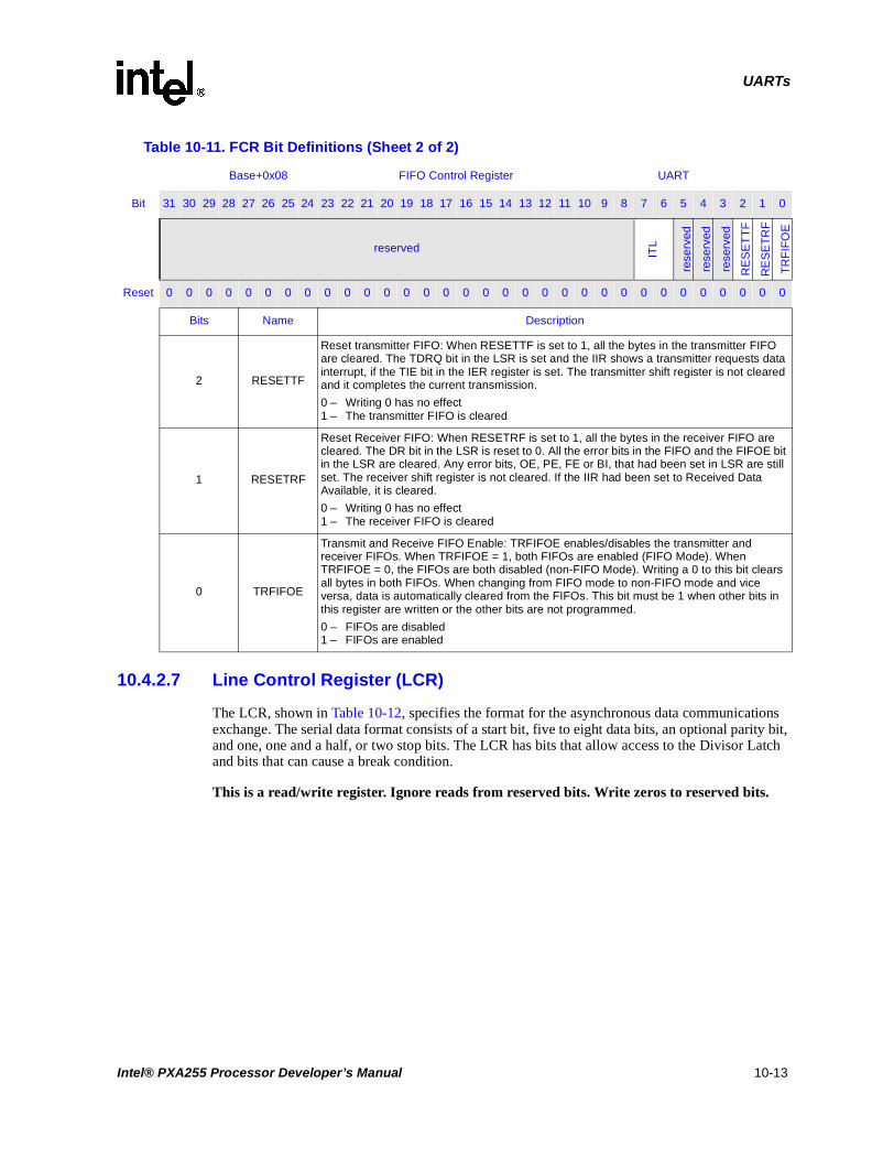
UARTs
10.4.2.7 Line Control Register (LCR)
The LCR, shown in Table 10-12, specifies the format for the asynchronous data communications exchange. The serial data format consists of a start bit, five to eight data bits, an optional parity bit, and one, one and a half, or two stop bits. The LCR has bits that allow access to the Divisor Latch and bits that can cause a break condition.
This is a read/write register. Ignore reads from reserved bits. Write zeros to reserved bits.
2 RESETTF
Reset transmitter FIFO: When RESETTF is set to 1, all the bytes in the transmitter FIFO are cleared. The TDRQ bit in the LSR is set and the IIR shows a transmitter requests data interrupt, if the TIE bit in the IER register is set. The transmitter shift register is not cleared and it completes the current transmission.
0 – Writing 0 has no effect1 – The transmitter FIFO is cleared
1 RESETRF
Reset Receiver FIFO: When RESETRF is set to 1, all the bytes in the receiver FIFO are cleared. The DR bit in the LSR is reset to 0. All the error bits in the FIFO and the FIFOE bit in the LSR are cleared. Any error bits, OE, PE, FE or BI, that had been set in LSR are still set. The receiver shift register is not cleared. If the IIR had been set to Received Data Available, it is cleared.
0 – Writing 0 has no effect1 – The receiver FIFO is cleared
0 TRFIFOE
Transmit and Receive FIFO Enable: TRFIFOE enables/disables the transmitter and receiver FIFOs. When TRFIFOE = 1, both FIFOs are enabled (FIFO Mode). When TRFIFOE = 0, the FIFOs are both disabled (non-FIFO Mode). Writing a 0 to this bit clears all bytes in both FIFOs. When changing from FIFO mode to non-FIFO mode and vice versa, data is automatically cleared from the FIFOs. This bit must be 1 when other bits in this register are written or the other bits are not programmed.
0 – FIFOs are disabled1 – FIFOs are enabled
Table 10-11. FCR Bit Definitions (Sheet 2 of 2)
Base+0x08 FIFO Control Register UART
Bit 31 30 29 28 27 26 25 24 23 22 21 20 19 18 17 16 15 14 13 12 11 10 9 8 7 6 5 4 3 2 1 0
reserved ITL
rese
rved
rese
rved
rese
rved
RE
SE
TT
F
RE
SE
TR
F
TR
FIF
OE
Reset 0 0 0 0 0 0 0 0 0 0 0 0 0 0 0 0 0 0 0 0 0 0 0 0 0 0 0 0 0 0 0 0
Bits Name Description
Intel® PXA255 Processor Developer’s Manual 10-13

UARTs
Table 10-12. LCR Bit Definitions
Base+0x0C Line Control Register UART
Bit 31 30 29 28 27 26 25 24 23 22 21 20 19 18 17 16 15 14 13 12 11 10 9 8 7 6 5 4 3 2 1 0
reserved
DL
AB
SB
ST
KY
P
EP
S
PE
N
ST
B
WL
S1
WL
S0
Reset 0 0 0 0 0 0 0 0 0 0 0 0 0 0 0 0 0 0 0 0 0 0 0 0 0 0 0 0 0 0 0 0
Bits Name Description
31:8 — reserved
7 DLAB
Divisor Latch Access Bit: Must be set high (logic 1) to access the Divisor Latches of the Baud Rate Generator during a READ or WRITE operation. Must be set low (logic 0) to access the Receiver Buffer, the Transmit Holding Register, or the IER.
0 – access Transmit Holding register (THR), Receive Buffer register (RBR) and IER.1 – access Divisor Latch registers (DLL and DLH)
6 SB
Set Break: Causes a break condition to be transmitted to the receiving UART. Acts only on the TXD pin and has no effect on the transmitter logic. In FIFO mode, wait until the transmitter is idle, LSR[TEMT]=1, to set and clear SB.
0 – no effect on TXD output1 – forces TXD output to 0 (space)
5 STKYP
Sticky Parity: Forces the bit value at the parity bit location to be the opposite of the EPS bit, rather than the parity value. This stops parity generation. If PEN = 0, STKYP is ignored.
0 – no effect on parity bit1 – forces parity bit to be opposite of EPS bit value
4 EPSEven Parity Select: Even parity select bit. If PEN = 0, EPS is ignored.
0 – sends or checks for odd parity1 – sends or checks for even parity
3 PEN
Parity Enable: Enables a parity bit to be generated on transmission or checked on reception.
0 – no parity1 – parity
2 STB
Stop Bits: Specifies the number of stop bits transmitted and received in each character. When receiving, the receiver only checks the first stop bit.
0 – 1 stop bit1 – 2 stop bits, except for 5-bit character then 1-1/2 bits
1:0 WLS[1:0]
Word Length Select: Specifies the number of data bits in each transmitted or received character.
00 – 5-bit character
01 – 6-bit character
10 – 7-bit character
11 – 8-bit character
10-14 Intel® PXA255 Processor Developer’s Manual

UARTs
10.4.2.8 Line Status Register (LSR)
The LSR, shown in Table 10-13, provides data transfer status information to the processor.
In non-FIFO mode, LSR[4:2]: parity error, framing error, and break interrupt, show the error status of the character that has just been received.
In FIFO mode, LSR[4:2] show the status bits of the character that is currently at the front of the FIFO.
LSR[4:1] produce a receiver line status interrupt when the corresponding conditions are detected and the interrupt is enabled. In FIFO mode, the receiver line status interrupt only occurs when the erroneous character reaches the front of the FIFO. If the erroneous character is not at the front of the FIFO, a line status interrupt is generated after the other characters are read and the erroneous character becomes the character at the front of the FIFO.
The LSR must be read before the erroneous character is read. LSR[4:1] bits are set until software reads the LSR.
See Section 10.4.5 for details on using the DMA to receive data.
This is a read-only register. Ignore reads from reserved bits.
Table 10-13. LSR Bit Definitions (Sheet 1 of 3)
Base+0x14 Line Status Register UART
Bit 31 30 29 28 27 26 25 24 23 22 21 20 19 18 17 16 15 14 13 12 11 10 9 8 7 6 5 4 3 2 1 0
reserved
FIF
OE
TE
MT
TD
RQ
BI
FE
PE
OE
DR
Reset 0 0 0 0 0 0 0 0 0 0 0 0 0 0 0 0 0 0 0 0 0 0 0 0 0 1 1 0 0 0 0 0
Bits Name Description
31:8 — reserved
7 FIFOE
FIFO Error Status: In non-FIFO mode, this bit is 0. In FIFO Mode, FIFOE is set to 1 when there is at least one parity error, framing error, or break indication for any of the characters in the FIFO. A processor read to the LSR does not reset this bit. FIFOE is reset when all erroneous characters have been read from the FIFO. If DMA requests are enabled (IER bit 7 is set to 1) and FIFOE is set to 1, the error interrupt is generated and no receive DMA request is generated even when the receive FIFO reaches the trigger level. Once the errors have been cleared by reading the FIFO, DMA requests are re-enabled automatically. If DMA requests are not enabled (IER bit7 is set to 0), FIFOE set to 1 does not generate an error interrupt.
0 – No FIFO or no errors in receiver FIFO1 – At least one character in receiver FIFO has errors
6 TEMT
Transmitter Empty: Set when the Transmit Holding Register and the Transmitter Shift Register are both empty. It is cleared when either the Transmit Holding Register or the Transmitter Shift Register contains a data character. In FIFO mode, TEMT is set when the transmitter FIFO and the Transmit Shift Register are both empty.
0 – There is data in the Transmit Shift Register, the Transmit Holding Register, or the FIFO1 – All the data in the transmitter has been shifted out
Intel® PXA255 Processor Developer’s Manual 10-15

UARTs
5 TDRQ
Transmit Data Request: Indicates that the UART is ready to accept a new character for transmission. In addition, this bit causes the UART to issue an interrupt to the processor when the transmit data request interrupt enable is set high and generates the DMA request to the DMA controller if DMA requests and FIFO mode are enabled. The TDRQ bit is set when a character is transferred from the Transmit Holding register into the Transmit Shift register. The bit is cleared with the loading of the Transmit Holding Register. In FIFO mode, TDRQ is set to 1 when half of the characters in the FIFO have been loaded into the Shift register or the RESETTF bit in FCR has been set. It is cleared when the FIFO has more than half data. If more than 64 characters are loaded into the FIFO, the excess characters are lost.
0 – There is data in Holding register or FIFO waiting to be shifted out1 – Transmit FIFO has half or less than half data
4 BI
Break Interrupt: BI is set when the received data input is held low for longer than a full word transmission time (that is, the total time of Start bit + data bits + parity bit + stop bits). The Break indicator is reset when the processor reads the LSR. In FIFO mode, only one character equal to 0x00, is loaded into the FIFO regardless of the length of the break condition. BI shows the break condition for the character at the front of the FIFO, not the most recently received character.
0 – No break signal has been received1 – Break signal received
3 FE
Framing Error: FE indicates that the received character did not have a valid stop bit. FE is set when the bit following the last data bit or parity bit is detected to be 0. If the LCR had been set for two stop bit mode, the receiver does not check for a valid second stop bit. The FE indicator is reset when the processor reads the LSR. The UART will resynchronize after a framing error. To do this it assumes that the framing error was due to the next start bit, so it samples this “start” bit twice and then reads in the “data”. In FIFO mode, FE shows a framing error for the character at the front of the FIFO, not for the most recently received character.
0 – No Framing error1 – Invalid stop bit has been detected
Table 10-13. LSR Bit Definitions (Sheet 2 of 3)
Base+0x14 Line Status Register UART
Bit 31 30 29 28 27 26 25 24 23 22 21 20 19 18 17 16 15 14 13 12 11 10 9 8 7 6 5 4 3 2 1 0
reserved
FIF
OE
TE
MT
TD
RQ
BI
FE
PE
OE
DR
Reset 0 0 0 0 0 0 0 0 0 0 0 0 0 0 0 0 0 0 0 0 0 0 0 0 0 1 1 0 0 0 0 0
Bits Name Description
10-16 Intel® PXA255 Processor Developer’s Manual

UARTs
2 PE
Parity Error: Indicates that the received data character does not have the correct even or odd parity, as selected by the even parity select bit. PE is set upon detection of a parity error and is cleared when the processor reads the LSR. In FIFO mode, PE shows a parity error for the character at the front of the FIFO, not the most recently received character.
0 – No Parity error1 – Parity error has occurred
1 OE
Overrun Error: In non-FIFO mode, indicates that data in the Receive Buffer Register was not read by the processor before the next character was received. The new character is lost. In FIFO mode, OE indicates that all 64 bytes of the FIFO are full and the most recently received byte has been discarded. The OE indicator is set upon detection of an overrun condition and cleared when the processor reads the LSR.
0 – No data has been lost1 – Received data has been lost
0 DR
Data Ready: Set when a complete incoming character has been received and transferred into the Receive Buffer Register or the FIFO. In non-FIFO mode, DR is cleared when the receive buffer is read. In FIFO mode, DR is cleared if the FIFO is empty (last character has been read from RBR) or the FIFO is reset with FCR[RESETRF].
0 – No data has been received1 – Data is available in RBR or the FIFO
Table 10-13. LSR Bit Definitions (Sheet 3 of 3)
Base+0x14 Line Status Register UART
Bit 31 30 29 28 27 26 25 24 23 22 21 20 19 18 17 16 15 14 13 12 11 10 9 8 7 6 5 4 3 2 1 0
reserved
FIF
OE
TE
MT
TD
RQ
BI
FE
PE
OE
DR
Reset 0 0 0 0 0 0 0 0 0 0 0 0 0 0 0 0 0 0 0 0 0 0 0 0 0 1 1 0 0 0 0 0
Bits Name Description
Intel® PXA255 Processor Developer’s Manual 10-17
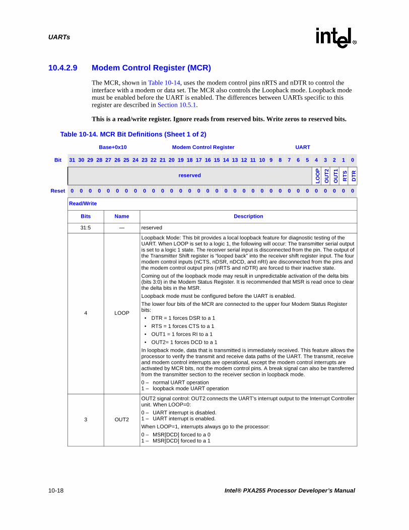
UARTs
10.4.2.9 Modem Control Register (MCR)
The MCR, shown in Table 10-14, uses the modem control pins nRTS and nDTR to control the interface with a modem or data set. The MCR also controls the Loopback mode. Loopback mode must be enabled before the UART is enabled. The differences between UARTs specific to this register are described in Section 10.5.1.
This is a read/write register. Ignore reads from reserved bits. Write zeros to reserved bits.
Table 10-14. MCR Bit Definitions (Sheet 1 of 2)
Base+0x10 Modem Control Register UART
Bit 31 30 29 28 27 26 25 24 23 22 21 20 19 18 17 16 15 14 13 12 11 10 9 8 7 6 5 4 3 2 1 0
reserved
LO
OP
OU
T2
OU
T1
RT
S
DT
R
Reset 0 0 0 0 0 0 0 0 0 0 0 0 0 0 0 0 0 0 0 0 0 0 0 0 0 0 0 0 0 0 0 0
Read/Write
Bits Name Description
31:5 — reserved
4 LOOP
Loopback Mode: This bit provides a local loopback feature for diagnostic testing of the UART. When LOOP is set to a logic 1, the following will occur: The transmitter serial output is set to a logic 1 state. The receiver serial input is disconnected from the pin. The output of the Transmitter Shift register is “looped back” into the receiver shift register input. The four modem control inputs (nCTS, nDSR, nDCD, and nRI) are disconnected from the pins and the modem control output pins (nRTS and nDTR) are forced to their inactive state.
Coming out of the loopback mode may result in unpredictable activation of the delta bits (bits 3:0) in the Modem Status Register. It is recommended that MSR is read once to clear the delta bits in the MSR.
Loopback mode must be configured before the UART is enabled.
The lower four bits of the MCR are connected to the upper four Modem Status Register bits:
• DTR = 1 forces DSR to a 1
• RTS = 1 forces CTS to a 1
• OUT1 = 1 forces RI to a 1
• OUT2= 1 forces DCD to a 1
In loopback mode, data that is transmitted is immediately received. This feature allows the processor to verify the transmit and receive data paths of the UART. The transmit, receive and modem control interrupts are operational, except the modem control interrupts are activated by MCR bits, not the modem control pins. A break signal can also be transferred from the transmitter section to the receiver section in loopback mode.
0 – normal UART operation1 – loopback mode UART operation
3 OUT2
OUT2 signal control: OUT2 connects the UART’s interrupt output to the Interrupt Controller unit. When LOOP=0:
0 – UART interrupt is disabled.1 – UART interrupt is enabled.
When LOOP=1, interrupts always go to the processor:
0 – MSR[DCD] forced to a 01 – MSR[DCD] forced to a 1
10-18 Intel® PXA255 Processor Developer’s Manual

UARTs
10.4.2.10 Modem Status Register (MSR)
The MSR, shown in Table 10-15, provides the current state of the control lines from the modem or data set (or a peripheral device emulating a modem) to the processor. In addition to this current state information, four bits of the MSR provide change information. MSR[3:0] are set when a control input from the Modem changes state. They are cleared when the processor reads the MSR. Differences between UARTs specific to this register are described in Section 10.5.1.
The status of the modem control lines do not affect the FIFOs. To use these lines for flow control, IER[MIE] must be set. When an interrupt on one of the flow control pins occurs, the interrupt service routine must disable the UART. The UART will continue transmission/reception of the current character and then stop. The contents of the FIFOs will be preserved. If the UART is re-enabled, transmission will continue where it stopped. Interrupts from the flow control pins will not come through the UART unit if the unit is disabled. When disabling the unit because of flow control, interrupts must be enabled in the processor Interrupt Controller for the flow control pins. The Interrupt Controller will still trigger interrupts if the pins are in Alternate Function Mode.
Note: When bit 0, 1, 2, or 3 is set, a Modem Status interrupt is generated if IER[MIE] is set.
This is a read-only. Ignore reads from reserved bits.
2 OUT1Test bit. This bit is used only in Loopback mode. It is ignored otherwise.
0 – Force MSR[RI] to 01 – Force MSR[RI] to 1
1 RTSRequest to Send.
0 – nRTS pin is 11 – nRTS pin is 0
0 DTRData Terminal Ready.
0 – nDTR pin is 11 – nDTR pin is 0
Table 10-14. MCR Bit Definitions (Sheet 2 of 2)
Base+0x10 Modem Control Register UART
Bit 31 30 29 28 27 26 25 24 23 22 21 20 19 18 17 16 15 14 13 12 11 10 9 8 7 6 5 4 3 2 1 0
reserved
LO
OP
OU
T2
OU
T1
RT
S
DT
R
Reset 0 0 0 0 0 0 0 0 0 0 0 0 0 0 0 0 0 0 0 0 0 0 0 0 0 0 0 0 0 0 0 0
Read/Write
Bits Name Description
Intel® PXA255 Processor Developer’s Manual 10-19

UARTs
Table 10-15. MSR Bit Definitions
Base+0x18 Modem Status Register UART
Bit 31 30 29 28 27 26 25 24 23 22 21 20 19 18 17 16 15 14 13 12 11 10 9 8 7 6 5 4 3 2 1 0
reserved
DC
D
RI
DS
R
CT
S
DD
CD
TE
RI
DD
SR
DC
TS
Reset 0 0 0 0 0 0 0 0 0 0 0 0 0 0 0 0 0 0 0 0 0 0 0 0 0 0 0 0 0 0 0 0
Bits Name Description
31:8 — reserved
7 DCD
Data Carrier Detect: Complement of the Data Carrier Detect (nDCD) input. Equivalent to MCR[OUT2] if MCR[LOOP] is set.
0 – nDCD pin is 11 – nDCD pin is 0
6 RI
Ring Indicator: Complement of the Ring Indicator (nRI) input. Equivalent to MCR[OUT1] if MCR[LOOP] is set.
0 – nRI pin is 11 – nRI pin is 0
5 DSR
Data Set Ready: Complement of the Data Set Ready (nDSR) input. Equivalent to MCR[DTR] if MCR[LOOP] is set.
0 – nDSR pin is 11 – nDSR pin is 0
4 CTS
Clear To Send: Complement of the Clear to Send (nCTS) input. Equivalent to MCR[RTS] if MCR[LOOP] is set.
0 – nCTS pin is 11 – nCTS pin is 0
3 DDCDDelta Data Carrier Detect:
0 – No change in nDCD pin since last read of MSR1 – nDCD pin has changed state
2 TERITrailing Edge Ring Indicator:
0 – nRI pin has not changed from 0 to 1 since last read of MSR1 – nRI pin has changed from 0 to 1
1 DDSRDelta Data Set Ready:
0 – No change in nDSR pin since last read of MSR1 – nDSR pin has changed state
0 DCTSDelta Clear To Send:
0 – No change in nCTS pin since last read of MSR1 – nCTS pin has changed state
10-20 Intel® PXA255 Processor Developer’s Manual

UARTs
10.4.2.11 Scratchpad Register (SPR)
The SPR, shown in Table 10-16, has no effect on the UART. It is intended as a scratchpad register for use by the programmer. It is included for 16550 compatibility.
This is a read/write register. Ignore reads from reserved bits. Write zeros to reserved bits.
10.4.3 FIFO Interrupt Mode Operation
This section describes how to service interrupts in FIFO mode.
10.4.3.1 Receive Interrupt
For a receive interrupt to occur, the receive FIFO and receive interrupts must be enabled. IIR[IID] changes to show that receive data is available when the FIFO reaches its trigger level. IIR[IID] changes to show the next waiting interrupt when the FIFO drops below the trigger level. A change in IIR[IID] triggers an interrupt to the core. Software reads IIR[IID] to determine the cause of the interrupt.
The receiver line status interrupt (IIR = 0xC6) has the highest priority and the received data available interrupt (IIR = 0xC4) is lower. The line status interrupt occurs only when the character at the front of the FIFO has errors.
The data ready bit (DR in the LSR) is set when a character is transferred from the shift register to the Receive FIFO. The DR bit is cleared when the FIFO is empty.
10.4.3.2 Character Timeout Indication Interrupt
A character timeout indication interrupt occurs when the receive FIFO and character timeout indication interrupt are enabled and all of the following conditions exist:
• At least one character is in the FIFO.
• The most recently received character was received more than four continuous character times ago. If two stop bits are programmed, the second is included in this interval.
• The most recent FIFO read was performed more than four continuous character times ago.
Table 10-16. SPR Bit Definitions
Base+0x1C Scratch Pad Register UART
Bit 31 30 29 28 27 26 25 24 23 22 21 20 19 18 17 16 15 14 13 12 11 10 9 8 7 6 5 4 3 2 1 0
reserved SP
Reset 0 0 0 0 0 0 0 0 0 0 0 0 0 0 0 0 0 0 0 0 0 0 0 0 0 0 0 0 0 0 0 0
Bits Name Description
31:8 — reserved
7:0 SPScratch Pad
No effect on UART functionality
Intel® PXA255 Processor Developer’s Manual 10-21

UARTs
After the processor reads one character from the receive FIFO or a new start bit is received, the character timeout indication interrupt is cleared and the timeout is reset. If a character timeout indication interrupt has not occurred, the timeout is reset when a new character is received or the processor reads the receive FIFO.
10.4.3.3 Transmit Interrupt
Transmit interrupts can only occur when the transmit FIFO and transmit interrupt are enabled. The transmit data request interrupt occurs when the transmit FIFO is at least half empty. The interrupt is cleared when the THR is written or the IIR is read.
10.4.4 FIFO Polled Mode Operation
When the FIFOs are enabled, setting IER[7] and IER[4:0] to all zeroes puts the serial port in the FIFO polled mode of operation. The receiver and the transmitter are controlled separately. Either one or both can be in the polled mode. In polled mode, software checks receiver and transmitter status via the LSR.
10.4.5 DMA Requests
The FIFO data is one byte wide. DMA requests are either transmit data service requests or receive data service requests. DMA requests are only generated in FIFO mode.
The transmit DMA request is generated when the transmit FIFO is at least half empty and IER[DMAE] is set. After the transmit DMA request is generated, the DMA Controller (DMAC) writes data to the FIFO. For each DMA request, the DMAC sends 8, 16, or 32 bytes of data to the FIFO. The number of bytes to be transmitted is programmed in the DMA channel.
The receive DMA request is generated when the receive FIFO reaches its trigger level with no errors in its entries and the IER[DMAE] is set. A receive DMA request is not generated if the trigger level is set to 1.
The DMAC then reads data from the FIFO. For each DMA request, the DMA controller can read 8, 16 or 32 bytes of data from the FIFO. The number of bytes to be read is programmed in the DMA channel.
Note: Do not program the channel to read more data than the FIFO trigger level.
If DMA requests are enabled and an erroneous character is received, the receive DMA requests are automatically disabled and an error interrupt is generated. The erroneous character is placed in the receive FIFO. If the UART was requesting a receive DMA transaction, the request is immediately cancelled. This prevents the DMAC from attempting to access the FIFOs while software clears the error.
When all the errors in the receive FIFO are cleared, receive DMA requests are automatically enabled and can be generated when the trigger level is reached.
10-22 Intel® PXA255 Processor Developer’s Manual

UARTs
Note: Ensure that the DMAC has finished previous receive DMA requests before the error interrupt handler begins to clear the errors from the FIFO.
10.4.5.1 Trailing Bytes in the Receive FIFO
Trailing bytes occur when the number of entries in the receive FIFO is less than its trigger level and no more data is being received. In such a case, a receive DMA request is not generated. To read the trailing bytes follow these steps:
1. Wait for a character timeout indication interrupt. The character timeout indication interrupt must be enabled.
2. Disable the receive DMA channel and wait for it to stop.
3. Read one byte at a time. The FIFO is empty when LSR[DR] is cleared.
4. Re-enable the receive DMA channel.
10.4.6 Slow Infrared Asynchronous Interface
The Slow Infrared (SIR) interface is used with the STUART to support two-way wireless communication that uses infrared transmission. The SIR provides a transmit encoder and receive decoder to support a physical link that conforms to the IRDA Serial Infrared Specification Version 1.1.
The SIR interface does not contain the actual IR LED driver or the receiver amplifier. The I/O pins attached to the SIR only have digital CMOS level signals. The SIR supports two-way communication, but full duplex communication is not possible because reflections from the transmit LED enter the receiver. The SIR interface supports frequencies up to 115.2 kbps. Because the input clock is 14.7456 MHz, the baud divisor must be eight or more.
10.4.6.1 Infrared Selection Register (ISR)
The IRDA module is managed through the UART to which it is attached. The ISR, shown in Table 10-17, controls IRDA functions.
This is a read/write register. Ignore reads from reserved bits. Write zeros to reserved bits.
Intel® PXA255 Processor Developer’s Manual 10-23

UARTs
10.4.6.2 Operation
The SIR modulation technique works with 5-, 6-, 7-, or 8-bit characters with an optional parity bit. The data is preceded by a zero value start bit and ends with one or more stop bits. The encoding scheme is to set a pulse 3/16 of a bit wide in the middle of every zero bit and send no pulses for bits that are ones. The pulse for each zero bit must occur, even for consecutive bits with no edge between them.
Table 10-17. ISR Bit Definitions
Base+0x20 Infrared Selection Register UART
Bit 31 30 29 28 27 26 25 24 23 22 21 20 19 18 17 16 15 14 13 12 11 10 9 8 7 6 5 4 3 2 1 0
reserved
RX
PL
TX
PL
XM
OD
E
RC
VE
IR
XM
ITIR
Reset 0 0 0 0 0 0 0 0 0 0 0 0 0 0 0 0 0 0 0 0 0 0 0 0 0 0 0 0 0 0 0 0
Bits Name Description
31:5 — reserved
4 RXPLReceive Data Polarity:
0 – SIR decoder interprets positive pulses as zeroes1 – SIR decoder interprets negative pulses as zeroes
3 TXPLTransmit Data Polarity:
0 – SIR encoder generates a positive pulse for a data bit of zero1 – SIR encoder generates a negative pulse for a data bit of zero
2 XMODE
Transmit Pulse Width Select: When XMODE is cleared, the UART 16X clock is used to clock the IRDA transmit and receive logic. When XMODE is set, the transmit encoder generates 1.6 µs pulses (that are 3/16 of a bit time at 115.2 kbps) instead of pulses 3/16 of a bit time wide, and the receive decoder expects pulses will be 1.6µs wide also.
0 – Transmit pulse width is 3/16 of a bit time wide1 – Transmit pulse width is 1.6 µs
1 RCVEIR
Receiver SIR Enable: When RCVEIR is set, the signal from the RXD pin is processed by the IRDA decoder before it is fed to the UART. If RCVEIR is cleared, then all clocking to the IRDA decoder is blocked and the RXD pin is fed directly to the UART.
0 – Receiver is in UART mode1 – Receiver is in infrared mode
0 XMITIR
Transmitter SIR Enable: When XMITIR is set to a 1, the normal TXD output from the UART is processed by the IRDA encoder before it is fed to the device pin. If XMITIR is cleared, all clocking to the IRDA encoder is blocked and the UART’s TXD signal is connected directly to the device pin.
When Transmitter SIR Enable is set, the TXD output pin, which is in a normally high default state, will switch to a normally low default state. This can cause a false start bit unless the infrared LED is disabled before XMITIR is set.
0 – Transmitter is in UART mode1 – Transmitter is in infrared mode
10-24 Intel® PXA255 Processor Developer’s Manual

UARTs
The top line in Figure 10-3 shows an asynchronous transmission as it is sent from the UART. The second line shows the pulses generated by the IR encoder at the TXD pin. A pulse is generated in the middle of the START bit and any data bit that is a zero. The third line shows the values received at the RXD input pin. The fourth line shows the receive decoder’s output. The receive decoder drives the receiver data line low when it detects a pulse. The bottom line shows how the UART’s receiver interprets the decoder’s action. This last line is the same as the first, but it is shifted half a bit period.
When XMODE is cleared, each zero bit has a pulse width of 3/16 of a bit time. When XMODE is set, a pulse of 1.6 µs is generated in the middle of each zero bit. The shorter infrared pulse generated when XMODE is set reduces the LEDs’ power consumption. At 2400 bps, the LED is normally on for 78 µs for each zero bit that is transmitted. When XMODE is set, the LED is on only 1.6 µs. XMode changes the behavior of the receiver. The receiver expects pulses of the correct pulse width. If the transceiver crops the incoming pulse, then Xmode must be set.
Note:
Note: Note: The SIR TXD output pin is automatically held deasserted when the RCVEIR bit is set. Before setting the RCVEIR bit, check that the TEMT bit is 1. While receiving, any data placed in
Figure 10-3. IR Transmit and Receive Example
START
BIT STOPBIT
1 0 0 0 1 0 1 0
STARTBIT 1 0 0 0 1 0 1 0
TRANSMIT
IR ENCODER OUTPUT
IR DECODER OUTPUT
UART
UART RECEIVE
(TXD PIN VALUE)
SHIFT VALUE
RXD PIN VALUE
SHIFT VALUESTOP
BIT
Figure 10-4. XMODE Example
1 7 11 16
1.6 µs
3 16X BAUD Clock periodsIR_TXD Pin valueXMODE = 1
IR_TXD Pin valueXMODE = 0
Transmit Start bitfollowed by 1
16X Baud Clock(14.7456 MHz)
Intel® PXA255 Processor Developer’s Manual 10-25

UARTs
the Transmit FIFO will not be held. Only add data to the Transmit FIFO while not receiving. To start transmission, the RCVEIR bit must be cleared.
To disable SIR, disable the IrDA LED first, if possible. Second, set the TXD GPIO pin to the infrared LED's default state using the GPCR/GPSR registers. Next, change the TXD pin from alternate function to GPIO mode. Now the SIR can be disabled without causing spurious transmit pulses.
10.5 UART Register Summary
Table 10-18, Table 10-19, and Table 10-20 contain the register addresses for the FFUART, BTUART, and STUART.
Table 10-18. FFUART Register Summary
Register Addresses DLAB Bit
ValueName Description
0x4010_0000 0 FFRBR Receive Buffer register (read only)
0x4010_0000 0 FFTHR Transmit Holding register (write only)
0x4010_0004 0 FFIER IER (read/write)
0x4010_0008 X FFIIR Interrupt ID register (read only)
0x4010_0008 X FFFCR FCR (write only)
0x4010_000C X FFLCR LCR (read/write)
0x4010_0010 X FFMCR MCR (read/write)
0x4010_0014 X FFLSR LSR (read only)
0x4010_0018 X FFMSR MSR (read only)
0x4010_001C X FFSPR Scratch Pad Register
0x4010_0020 X FFISR Infrared Selection register (read/write)
0x4010_0000 1 FFDLL Divisor Latch Low register (read/write)
0x4010_0004 1 FFDLH Divisor Latch High register (read/write)
Table 10-19. BTUART Register Summary (Sheet 1 of 2)
Register Addresses DLAB Bit
ValueName Description
0x4020_0000 0 BTRBR Receive Buffer register (read only)
0x4020_0000 0 BTTHR Transmit Holding register (write only)
0x4020_0004 0 BTIER IER (read/write)
0x4020_0008 X BTIIR Interrupt ID register (read only)
0x4020_0008 X BTFCR FCR (write only)
0x4020_000C X BTLCR LCR (read/write)
0x4020_0010 X BTMCR MCR (read/write)
0x4020_0014 X BTLSR LSR (read only)
0x4020_0018 X BTMSR MSR (read only)
10-26 Intel® PXA255 Processor Developer’s Manual

UARTs
0x4020_001C X BTSPR Scratch Pad Register
0x4020_0020 X BTISR Infrared Selection register (read/write)
0x4020_0000 1 BTDLL Divisor Latch Low register (read/write)
0x4020_0004 1 BTDLH Divisor Latch High register (read/write)
Table 10-20. STUART Register Summary
Register Addresses DLAB Bit
ValueName Description
0x4070_0000 0 STRBR Receive Buffer register (read only)
0x4070_0000 0 STTHR Transmit Holding register (write only)
0x4070_0004 0 STIER IER (read/write)
0x4070_0008 X STIIR Interrupt ID register (read only)
0x4070_0008 X STFCR FCR (write only)
0x4070_000C X STLCR LCR (read/write)
0x4070_0010 X STMCR MCR (read/write)
0x4070_0014 X STLSR LSR (read only)
0x4070_0018 X STMSR reserved (no modem control pins)
0x4070_001C X STSPR Scratch Pad Register
0x4070_0020 X STISR Infrared Selection register (read/write)
0x4070_0000 1 STDLL Divisor Latch Low register (read/write)
0x4070_0004 1 STDLH Divisor Latch High register (read/write)
Table 10-19. BTUART Register Summary (Sheet 2 of 2)
Register Addresses DLAB Bit
ValueName Description
Intel® PXA255 Processor Developer’s Manual 10-27

UARTs
10.5.1 UART Register Differences
The default descriptions for BTMCR, BTMSR and STMCR are modified as shown in Table 10-21..
Table 10-21. Flow Control Registers in BTUART and STUART
Bit7-5 Bit4 Bit3 Bit2 Bit1 Bit0
BTMCR reserved LOOP OUT2 reserved RTS reserved
BTMSR reserved CTS reserved reserved reserved DCTS
STMCR reserved LOOP OUT2 reserved reserved reserved
10-28 Intel® PXA255 Processor Developer’s Manual

Fast Infrared Communication Port 11
The Fast Infrared Communications Port (FICP) for the PXA255 processor operates at half-duplex and provides direct connection to commercially available Infrared Data Association (IrDA) compliant LED transceivers. The FICP is based on the 4-Mbps IrDA standard and uses four-position pulse modulation (4PPM) and a specialized serial packet protocol developed for IrDA transmission. To support the standard, the FICP has:
• A bit encoder/decoder,
• A serial-to-parallel data engine
• A transmit FIFO 128 entries deep and 8 bits wide
• A receive FIFO 128 entries deep and 11 bits wide
The FICP shares GPIO pins for transmit and receive data with the Standard UART. Only one of the ports can be used at a time. To support a variety of IrDA transceivers, both the transmit and receive data pins can be individually configured to communicate using normal or active low data.
11.1 Signal Description
The FICP signals are IRRXD and IRTXD. Table 11-1 describes each signal’s function. Most IrDA transceivers also have enable and speed pins. Use GPIOs to enable the transceiver and select the speed. See Section 4, “System Integration Unit” on page 4-1 for more information.
11.2 FICP Operation
The FICP is disabled and does not have control of the port’s pins after a reset. Before software enables the FICP for high-speed operation, it must set the control registers to reflect the desired operating mode. After the control registers are set, software can either preload the FICP’s transmit FIFO with up to 128 bytes, or leave the FIFO empty and use the DMA to service it after the FICP is enabled. Once the FICP is enabled, transmit/receive data can be sent on the transmit and receive pins.
The transmit/receive data is modulated according to the 4PPM IrDA standard and converted to serial or parallel data. The modulation technique and the frame format are discussed in the sections that follow.
Table 11-1. FICP Signal Description
Signal Name Input/Output Description
IRRXD Input Receive pin for FICP
IRTXD Output Transmit pin for FICP
Intel® PXA255 Processor Developer’s Manual 11-1

Fast Infrared Communication Port
11.2.1 4PPM Modulation
Four-position pulse modulation (4PPM) is used to transmit data at the high-speed rate, 4.0 Mbps. Data bits are encoded two at a time by placing a single 125 ns light pulse in one of four timeslots. The four timeslots are collectively termed a chip. Bytes are encoded one at a time. They are divided into four individual 2-bit pairings called nibbles. The least significant nibble is transmitted first. Figure 11-1 shows the 4PPM encoding for the possible 2-bit combinations and Figure 11-2 shows an example of 4PPM modulation for the byte 0b10110001, which is constructed with four chips. Bits within each nibble are not reordered, but nibble 0 (least significant) is transmitted first and nibble 3 (most significant) is transmitted last.
Figure 11-1. 4PPM Modulation Encodings
Chip
Timeslots
1 2 3 4
Data = 0b00
Data = 0b01
Data = 0b10
Data = 0b11
Figure 11-2. 4PPM Modulation Example
4PPMData
ReorderedNibbles
0 1 0 0 1 1 1 0
125 ns
Timeslots
1 2 3 4 1 2 3 4 1 2 3 4 1 2 3 4
Chips 1 2 3 4
Receive data sample counter frequency = 6/pulse width. Each timeslot is sampled on the third clock.
OriginalByte Order
1 0 1 1 0 0 0 1Nibble 3 Nibble 2 Nibble 1 Nibble 0
Nibble 0 Nibble 1 Nibble 2 Nibble 3
48 MHz
11-2 Intel® PXA255 Processor Developer’s Manual

Fast Infrared Communication Port
11.2.2 Frame Format
The frame format used with 4-Mbps transmission is shown in Figure 11-3.
The preamble, start, and stop flags are a mixture of chips that contain 0, 1, or 2 pulses in their timeslots. Chips with 0 and 2 pulses are used to construct flags because the chips represent invalid data bit pairings. The preamble contains 16 repeated transmissions of the chips: 1000 0000 1010 1000. The start flag contains one transmission of eight chips: 0000 1100 0000 1100 0110 0000 0110 0000. The stop flag contains one transmission of eight chips: 0000 1100 0000 1100 0000 0110 0000 0110. The address, control, data, and CRC-32 use the standard 4PPM chip encoding to represent two bits per chip.
11.2.3 Address Field
A transmitter uses the 8-bit address field to target a receiver when multiple stations are connected to the same set of serial lines. The address allows up to 255 stations to be uniquely addressed (0x00 to 0xFE). The broadcast address 0xFF is used to send messages to all of the connected stations.
For reception, FICP control register 1 (ICCR1) is used to program a unique receive address. The AME bit in the FICP control register 0 (ICCR0) determines the address match function. The received frames’ addresses are stored in the receive FIFO with normal data.
11.2.4 Control Field
The control field is an optional 8-bit field that is defined by software. The FICP does not provide hardware decode support for the control byte. It treats all bytes between the address and the CRC as data.
11.2.5 Data Field
The data field can have a length from 0 to 2045 bytes. Application requirements and target system’s transmission characteristics affect the data field’s length. Software must determine the length of the data to maximize the amount that can be transmitted in each frame while allowing the CRC to detect all errors during transmission. The serial port does not contain hardware that restricts the maximum amount of data that can be transmitted or received. If a data field that is not a multiple of eight bits is received, an abort is signalled.
Figure 11-3. Frame Format for IrDA Transmission (4.0 Mbps)
64 chips 8 chips4 chips
(8 bits)
4 chips
(8 bits)
8180 chips max
(2045 bytes)
16 chips
(32 bits)8 chips
Preamble Start FlagAddress
(optional)
Control
(optional)Data CRC-32 Stop Flag
Preamble - | 1000 | 0000 | 1010 | 1000 |... repeated at least 16 times
Start flag - | 0000 | 1100 | 0000 | 1100 | 0110 | 0000 | 0110 | 0000 |
Stop Flag - | 0000 |1100 | 0000 | 1100 | 0000 | 0110 | 0000 | 0110 |
Intel® PXA255 Processor Developer’s Manual 11-3

Fast Infrared Communication Port
11.2.6 CRC Field
The FICP uses a 32-bit Cyclic Redundancy Check (CRC) to detect bit errors that occur during transmission. The CRC is generated from the address, control, and data fields, and is included in each frame. Transmit and receive logic have separate CRC generators. The CRC computation logic is set to all ones before each frame is transmitted or received and the result is inverted before it is used for comparison or transmission. The transmitter calculates a CRC as data is transmitted and places the inverse of the resulting 32-bit value at the end of each frame until the stop flag is transmitted. The receiver also calculates a CRC and inverts it for each data frame that it receives. The receiver compares the calculated CRC to the expected CRC value at the end of each frame.
If the calculated value does not match the expected value, the CRC error bit that corresponds to the last data byte received is set. When this byte reaches the trigger level range, an interrupt is generated.
Note: Unlike the address, control, and data fields, the 32-bit inverted CRC value is transmitted and received most significant nibble first.
The cyclic redundancy checker uses the 32-term polynomial:
11.2.7 Baud Rate Generation
The baud rate is derived by dividing a fixed 48-MHz clock by six. Using a digital PLL, the 8-MHz baud (or timeslot) clock for the receive logic is synchronized with the 4PPM data stream each time a transition is detected on the receive data line. To encode a 4-Mbps data stream, the required chip frequency is 2.0 MHz, with four timeslots per chip at a frequency of 8.0 MHz. Receive data is sampled halfway through each timeslot period by counting three of the six 48-MHz clock periods that make up each timeslot (see Figure 11-2). The chips are synchronized during the reception preamble. The pattern of four chips repeated 16 times is used to identify the first timeslot (or the beginning of a chip) and resets the 2-bit timeslot counter logic.
11.2.8 Receive Operation
The IrDA standard specifies that all transmission occurs at half-duplex. This restriction forces software to enable one direction at a given time. Either the transmit or receive logic can be enabled, but not both. The FICP’s hardware does not impose such a restriction.The software can enable both the transmitter and receiver. This feature is used with the FICP’s loopback mode, which internally connects the output of the transmit serial shifter to the input of the receive serial shifter.
After the FICP is enabled, the receiver logic begins and selects an arbitrary chip boundary, uses a serial shifter to receive four incoming 4PPM chips from the receive data pin, and latches and decodes the chips one at a time. If the chips do not have the correct preamble, the timeslot counter’s clock skips one 8-MHz period and effectively delays the timeslot count by one. This process is called hunt mode and is repeated until the chips have the correct preamble, which indicates that the timeslot counter is synchronized. The preamble can be repeated as few as 16 times or can be continuously repeated to indicate an idle transmit line.
CRC x( ) x32 x26 x23 x22 x16 x12 x11 x10 x8 x7 x5 x4 x2 x 1+ + + + + + + + + + + + + +( )=
11-4 Intel® PXA255 Processor Developer’s Manual

Fast Infrared Communication Port
After 16 preambles are transmitted, the start flag is received. The start flag is eight chips long. If any portion of the start flag does not match the encoding, the receive logic signals a framing error and the receive logic returns to hunt mode.
When the correct start flag is recognized, each following group of four chips is decoded into a data byte and placed in a 5-byte temporary FIFO that is used to prevent the CRC from being placed in the receive FIFO. When the temporary FIFO is full, data values are transferred to the receive FIFO one at a time. A frame’s first data byte is the address. If receiver address matching is enabled, the received address is compared to the address in the address match value field in ICCR1. If the values match or the incoming address contains all ones, all following data bytes, including the address byte, are stored in the receive FIFO. If the values do not match, the receiver logic does not store any data in the receive FIFO, ignores the remainder of the frame, and searches for the next preamble. If receiver address matching is not enabled, the frame’s first data byte is stored in the FIFO as normal data. The frame’s second data byte can contain an optional control field and must be decoded in software.
The IrDA standard limits frames to any amount of data up to a 2047 bytes (including the address and control bytes). The FICP does not limit frame size. Software must ensure that each incoming frame does not exceed 2047 bytes.
When the receive FIFO reaches its trigger level, an interrupt (if enabled) and DMA transfer request (if no errors are detected in the data) are signalled. If the data is not removed quickly enough to prevent the FIFO from completely filling, the receive logic attempts to place additional data into the full FIFO and an overrun error is signalled. When the FIFO is full, all subsequent data bytes received are lost and all FIFO contents remain intact.
If the data field contains any invalid chips (such as 0011, 1010, 1110) the frame aborts and the oldest byte in the temporary FIFO is moved to the receive FIFO, the remaining temporary FIFO entries are discarded, the end-of-frame (EOF) tag is set in the FIFO entry that holds the last valid byte of data, and the receiver logic searches for the preamble.
The receive logic continuously searches for the 8-chip stop flag. When the stop flag is recognized, the last byte that was placed within the receive FIFO is flagged as the frame’s last byte and the data in the temporary FIFO is removed and used as the CRC value for the frame. The receive logic compares the frame’s CRC value to the CRC-32 value, which is continuously calculated from the incoming data stream. If CRC and CRC-32 values do not match, the last byte that was placed in the receive FIFO is also tagged with a CRC error. The frame’s CRC value is not placed in the receive FIFO. If the stop flag is not properly detected, an abort is signalled.
If software disables the FICP’s receiver while it is operating, the data byte being received stops immediately, the serial shifter and receive FIFO are cleared, the System Integration Unit (SIU) takes control of the receive data pin, and the clocks used by the receive logic are shut off to conserve power. The receive data input polarity must be reprogrammed if the receive data pin is used as a GPIO input.
11.2.9 Transmit Operation
Before it enables the FICP for transmission, the software can either preload the transmit FIFO by filling it with data or allow service requests to cause the CPU or DMA to fill the FIFO after the FICP is enabled. When the FICP is enabled, the transmit logic issues a service request if its FIFO requires more data.
Intel® PXA255 Processor Developer’s Manual 11-5

Fast Infrared Communication Port
A minimum of 16 preambles are transmitted for each frame. If data is not available after the sixteenth preamble, additional preambles are transmitted until a byte of valid data resides in the bottom of the transmit FIFO. The preambles are followed by the start flag and the data from the transmit FIFO. Groups of four chips (eight bits) are encoded and loaded in a serial shift register. The contents of the serial shift register are sent out on the transmit data pin, which is clocked by the 8-MHz baud clock. The preamble, start and stop flags, and CRC value are transmitted automatically.
When the transmit FIFO has 32 or more empty entries, an interrupt (if enabled) and DMA service request are sent. If new data does not arrive quickly enough to prevent the FIFO from becoming empty, the transmit logic attempts to transfer additional data from the empty FIFO. Software determines whether to interpret the data underrun (a lack of data) as a signal of normal frame completion or as an unexpected frame termination.
When software selects normal frame completion and an underrun occurs, the transmit logic transmits the CRC value that was calculated during data transmission, including the address and control bytes, followed by the stop flag that marks the end of the frame. The transmitter then continuously transmits preambles until data is available in the FIFO. When data is available, the transmitter starts to transmit the next frame.
When software selects unexpected frame termination and an underrun occurs, the transmit logic transmits an abort and interrupts the CPU. The transmitter continues to send the abort until data is available in the transmit FIFO. When data is available, the FICP transmits 16 preambles and a start flag and starts the new frame. The off-chip receiver can choose to ignore the abort and continue to receive data or signal the FICP to attempt to transmit the aborted frame again.
At the end of each transmitted frame, the FICP sends a pulse called the serial infrared interaction pulse (SIP). A SIP must be sent at least every 500 ms to ensure that low-speed devices (115.2 Kbps and slower) do not interfere with devices that transmit at higher speeds. The SIP simulates a start bit that causes low-speed devices to stay off the air for at least another 500 ms. The SIP pulse forces the transmit data pin high for 1.625 µs and low for 7.375 µs (the total SIP period is 9.0 µs). After the SIP period, the preamble is transmitted continuously to indicate to the off-chip receiver that the FICP’s transmitter is in the idle state. The preamble is transmitted until new data is available in the transmit FIFO or the FICP’s transmitter is disabled. At least one frame must be completed every 500 ms to ensure that an SIP pulse can keep low-speed devices from interrupting the transmission. Because most IrDA compatible devices produce an SIP after each frame transmitted, software only needs to ensure that a frame is either transmitted or received by the FICP every 500 ms. Frame length does not represent a significant portion of the 500 ms timeframe in which an SIP must be produced. At 4.0 Mbps, the longest frame allowed is 16,568 bits, which takes just over 4 ms to transmit. The FICP also issues an SIP when the transmitter is first enabled. This ensures that low-speed devices do not interfere as the FICP transmits its data.
If software disables the FICP’s transmitter during operation, data transmission stops immediately, the serial shifter and transmit FIFO are cleared, and the SIU takes control of the transmit data pin. The transmit data output’s polarity must be properly reprogrammed if the pin is used as a GPIO output.
11.2.10 Transmit and Receive FIFOs
The transmit FIFO is 128 entries deep and 8 bits wide. The receive FIFO is 128 entries deep, 11 bits wide. The receive FIFO uses 3 bits of its entries as status bits. The transmit FIFO and the receive FIFO use two separate, dedicated DMA requests.
11-6 Intel® PXA255 Processor Developer’s Manual

Fast Infrared Communication Port
When the transmit FIFO has 32 or more empty bytes, the transmit DMA request and an interrupt (if enabled) are generated and tell the processor to send more data to the FIFO. When the transmit FIFO is full, any more data from the processor is lost. When the receive FIFO reaches its trigger level (programmed in ICCR2), the receive DMA request (if no errors are found within the entries) and an interrupt (if enabled) are generated and tell the processor to remove the data from the FIFO. If an error is found in the FIFO’s trigger level range, DMA requests are disabled and an interrupt is generated to ensure that the DMAC does not read the error bytes.
The number of bytes being transferred for each DMA request is programmed in the DMAC and can be 8, 16, or 32 bytes. The receive FIFO’s trigger level must be set so the FIFO has enough data for the DMAC to read. The transmit FIFO does not have programmable trigger levels. Its DMA request is generated when the FIFO has 32 or more empty bytes, regardless of the DMA transfer size.
The DMA controller must not service the receive FIFO when the processor tries to respond to a receive error interrupt. The error interrupt may be set high before the DMA controller finishes the previous request. The processor can not remove the error bytes until the DMAC has completed its transaction.
11.2.11 Trailing or Error Bytes in the Receive FIFO
When the number of bytes in the receive FIFO is less than the trigger level and no more data is being received, the bytes in the FIFO are called trailing bytes. Trailing bytes do not trigger a receive DMA request. Instead they trigger the end/error in FIFO, ICSR0[EIF] interrupt, which is nonmaskable. When ICSR0[EIF] is set, DMA requests are disabled. The core must read bytes from the FIFO until ICSR0[EIF] is cleared.
The core must also read bytes from the FIFO until ICSR0[EIF] is cleared if there are errors in FIFO entries below the DMA trigger level. When the entries below the DMA trigger level no longer contain status flags, DMA requests are enabled.
11.3 FICP Register Definitions
The FICP has six registers: three control registers, one data register, and two status registers. The FICP registers are 32 bits wide, but only the lower 8 bits have valid data. The FICP does not support byte or half-word operations. CPU reads and writes to the FICP registers must be word wide.
The control registers determine: IrDA transmission rate, address match value, how transmit FIFO underruns are handled, normal or active low transmit and receive data, whether transmit and receive operations are enabled, the FIFO interrupt service requests, receive address matching, and loopback mode.
The data register addresses the top of the transmit FIFO and the bottom of the receive FIFO. Reads to the data register access the receive FIFO. Writes to the data register access the transmit FIFO.
The status registers contain: CRC, overrun, underrun, framing, and receiver abort errors; the transmit FIFO service request; the receive FIFO service request; and end-of-frame conditions. Each of these hardware-detected events signals an interrupt request to the interrupt controller. The status registers also contain flags for transmitter busy, receiver synchronized, receive FIFO not empty, and transmit FIFO not full (no interrupt generated).
Intel® PXA255 Processor Developer’s Manual 11-7

Fast Infrared Communication Port
11.3.1 FICP Control Register 0 (ICCR0)
The ICCR0, shown in Table 11-2, contains eight valid bit fields that control various functions for 4 Mbps IrDA transmission. The FICP must be disabled (RXE=TXE=0) when ICCR0[ITR] and ICCR0[LBM] are changed. To allow various modes to be changed during active operation, ICCR0[7:2] may be written when the FICP is enabled.
This is a read/write register. Ignore reads from reserved bits. Write zeros to reserved bits.
Table 11-2. ICCR0 Bit Definitions (Sheet 1 of 2)
0x4080_0000 Fast Infrared Communication Port Control Register 0 (ICCR0) Fast Infrared Communication Port
Bit 31 30 29 28 27 26 25 24 23 22 21 20 19 18 17 16 15 14 13 12 11 10 9 8 7 6 5 4 3 2 1 0
reserved
AM
E
TIE
RIE
RX
E
TX
E
TU
S
LBM
ITR
Reset 0 0 0 0 0 0 0 0 0 0 0 0 0 0 0 0 0 0 0 0 0 0 0 0 0 0 0 0 0 0 0 0
Bits Name Description
[31:8] — reserved
7 AME
Address match enable.
Receive logic will compare the address of the incoming frames to the Address Match Value field in ICCR1.
0 = Disable receiver address match function. Store data in receive FIFO.1 = Enable receiver address match function. Do not put data in the receive FIFO unless
address is recognized or address is the broadcast address.
6 TIE
Transmit FIFO interrupt enable.
0 = Transmit FIFO service request, ICSR0[TFS], does not generate an interrupt.1 = Transmit FIFO service request generates an interrupt.
Setting TIE does not clear TFS or prevent TFS from being set or cleared by the transmit FIFO. TIE does not affect transmit FIFO DMA requests.
5 RIE
Receive FIFO interrupt enable.
0 = Receive FIFO service request, ICSR0[RFS], does not generate an interrupt.1 = Receive FIFO service request generates an interrupt
Setting RIE does not clear RFS or prevent RFS from being set or cleared by the receive FIFO. RIE does not affect receive FIFO DMA requests.
4 RXE
Receive enable.
0 = FICP receive logic disabled.1 = FICP receive logic enabled if ICCR0[ITR] is set.
All other control bits must be configured before setting RXE. If RXE is cleared while receiving data then reception is stopped immediately, all data within the receive FIFO and serial input shifter is cleared, and control of the receive data pin is given to the SIU.
While communication is normally half-duplex, it is possible to transmit and receive data at the same time. This is used for testing in Loopback Mode.
If RXE is used to clear the receive FIFO, check ICSR1[RNE] to ensure the receive FIFO is clear before re-enabling the receiver.
11-8 Intel® PXA255 Processor Developer’s Manual

Fast Infrared Communication Port
3 TXE
Transmit enable.
0 = FICP transmit logic disabled.1 = FICP transmit logic enabled if ICCR0[ITR] is set.
All other control bits must be configured before TXE is set. An SIP is transmitted immediately after the transmitter is enabled. If the transmit FIFO is empty, preambles are sent until data is placed in the FIFO.
If TXE is cleared while it transmits data, transmission stops immediately, all data in the transmit FIFO and serial output shifter is cleared, and the SIU takes control of the transmit data pin.
While communication is normally half-duplex, it is possible to transmit and receive data at the same time. Duplex communication is used for testing in Loopback Mode.
If TXE is used to clear the transmitter, check ICSR1[TBY] to ensure the transmitter is not busy before the transmitter is re-enabled.
2 TUS
Transmit FIFO underrun select.
A transmit FIFO underrun can either end the current frame normally, or transmit an abort.
0 = Transmit FIFO underrun causes CRC, stop flag, and SIP to be transmitted, and masks transmit underrun interrupt generation.
1 = Transmit FIFO underrun causes abort to be transmitted, and generates an interrupt.
Clearing ICCR0[TUS] does not affect the current state of ICSR0[TUR] or prevent TUR from being set or cleared by the transmit FIFO. After an abort, a SIP is transmitted followed by 16 preambles. Preambles continue until data is in the FIFO.
1 LBM
Loopback mode.
Used for testing FICP.
0 = Normal FICP operation enabled.1 = Output of transmit serial shifter is connected to input of receive serial shifter.
0 ITRIrDA transmission.
0 = ICP unit is not enabled.1 = ICP unit is enabled.
Table 11-2. ICCR0 Bit Definitions (Sheet 2 of 2)
0x4080_0000 Fast Infrared Communication Port Control Register 0 (ICCR0) Fast Infrared Communication Port
Bit 31 30 29 28 27 26 25 24 23 22 21 20 19 18 17 16 15 14 13 12 11 10 9 8 7 6 5 4 3 2 1 0
reserved
AM
E
TIE
RIE
RX
E
TX
E
TU
S
LBM
ITR
Reset 0 0 0 0 0 0 0 0 0 0 0 0 0 0 0 0 0 0 0 0 0 0 0 0 0 0 0 0 0 0 0 0
Bits Name Description
Intel® PXA255 Processor Developer’s Manual 11-9

Fast Infrared Communication Port
11.3.2 FICP Control Register 1 (ICCR1)
The ICCR1, shown in Table 11-3, contains the 8-bit address match value field that the FICP uses to selectively receive frames. To allow the address match value to be changed during active receive operation, ICCR1 may be written while the FICP is enabled.
This is a read/write register. Ignore reads from reserved bits. Write zeros to reserved bits.
Table 11-3. ICCR1 Bit Definitions
0x4080_0004 Fast Infrared Communication Port Control Register 1 (ICCR1) Fast Infrared Communication Port
Bit 31 30 29 28 27 26 25 24 23 22 21 20 19 18 17 16 15 14 13 12 11 10 9 8 7 6 5 4 3 2 1 0
reserved AMV
Reset 0 0 0 0 0 0 0 0 0 0 0 0 0 0 0 0 0 0 0 0 0 0 0 0 0 0 0 0 0 0 0 0
Bits Name Description
[31:8] — reserved
[7:0] AMV
Address match value.
The 8-bit value used by receiver logic to compare to address of incoming frames. If AME=1 and AMV matches the address of the incoming frame, store the frame address, control, and data in receive FIFO. If the address does not match, ignore the frame and search for the next preamble.
The broadcast address 0xFF in the incoming frame always generates a match.
11-10 Intel® PXA255 Processor Developer’s Manual

Fast Infrared Communication Port
11.3.3 FICP Control Register 2 (ICCR2)
The ICCR2, shown in Table 11-4, contains two bit fields that control the polarity of the transmit and receive data pins and two bits that determine the trigger level for the receive FIFO. The FICP must be disabled (RXE=TXE=0) when these bits are changed.
This is a read/write register. Ignore reads from reserved bits. Write zeros to reserved bits.
Table 11-4. ICCR2 Bit Definitions
0x4080_0008 Fast Infrared Communication Port Control Register 2 (ICCR2) Fast Infrared Communication Port
Bit 31 30 29 28 27 26 25 24 23 22 21 20 19 18 17 16 15 14 13 12 11 10 9 8 7 6 5 4 3 2 1 0
reserved
RX
P
TX
P
TR
IG
Reset 0 0 0 0 0 0 0 0 0 0 0 0 0 0 0 0 0 0 0 0 0 0 0 0 0 0 0 0 1 1 0 0
Bits Name Description
[31:4] — reserved
3 RXP
Receive pin polarity select.
0 = Data from the receive data pin is inverted before being used by the FICP unit.1 = Data from the receive data pin to the FICP unit is not inverted.
Set on reset.
2 TXP
Transmit pin polarity select.
0 = Data from the FICP is inverted before being sent to the transmit data pin.1 = Data from the FICP is not inverted before being sent to the transmit data pin.
Set on reset.
[1:0] TRIG
Receive FIFO trigger level
The receive FIFO generates service requests when the FIFO has reached the trigger level and has no errors in its data. The DMA controller data transfer size must be set to the same size as the Receive FIFO trigger level. To change the trigger level, the Receive FIFO must be disabled.
0b00- receive FIFO service request is generated when the FIFO has 8 bytes or more
0b01- receive FIFO service request is generated when the FIFO has 16 bytes or more
0b10- receive FIFO service request is generated when the FIFO has 32 bytes or more
0b11- reserved
Intel® PXA255 Processor Developer’s Manual 11-11

Fast Infrared Communication Port
11.3.4 FICP Data Register (ICDR)
The ICDR, shown in Table 11-5, is a 32-bit register and its lower 8 bits are the top entry of the transmit FIFO when the register is written and the bottom entry of the receive FIFO when the register is read.
Reads to ICDR access the lower 8 bits of the receive FIFO’s bottom entry. As data enters the top of the receive FIFO, bits 8 – 10 are used as tags to indicate conditions that occur as each piece of data is received. The tag bits are transferred down the FIFO with the data byte that encountered the condition. When data reaches the bottom of the FIFO, bit 8 of the FIFO entry is transferred to the end-of-frame (EOF) flag, bit 9 to the CRC error (CRE) flag, and bit 10 to the receiver overrun (ROR) flag. All these flags are in FICP status register 1. These flags can be read to determine whether the value at the bottom of the FIFO represents the frame’s last byte or an error that was encountered during reception. After the flags are checked, the FIFO value can be read. This causes the data in the next location of the receive FIFO to be transferred to the bottom entry and its EOF, CRE, and ROR bits to be transferred to the status register.
The end/error in FIFO (EIF) flag is set in status register 0 when a tag bit is set in any of the receive FIFO’s bottom eight, 16, or 32 entries, as determined by the trigger level. The EIF flag is cleared when no error bits are set in the FIFO’s bottom entries. When EIF is set, an interrupt is generated and the receive FIFO DMA request is disabled. Software must empty the FIFO and check for the EOF, CRE, and ROR error flags in ICSR1 before it removes each data value from the FIFO. After each entry is removed, the EIF bit must be checked to determine if any set end or error tag remains and the procedure is repeated until all set tags are flushed from the FIFO’s bottom entries. When EIF is cleared, DMA service for the receive FIFO is re-enabled.
Both FIFOs are cleared when the processor is reset. The transmit FIFO is cleared when TXE is 0. The receive FIFO is cleared when RXE is 0.
This is a read/write register. Ignore reads from reserved bits. Write zeros to reserved bits.
Table 11-5. ICRD Bit Definitions
0x4080_000CFast Infrared Communication Port
Data Register (ICDR) Fast Infrared Communication Port
Bit 31 30 29 28 27 26 25 24 23 22 21 20 19 18 17 16 15 14 13 12 11 10 9 8 7 6 5 4 3 2 1 0
reserved DATA
Reset 0 0 0 0 0 0 0 0 0 0 0 0 0 0 0 0 0 0 0 0 0 0 0 0 0 0 0 0 0 0 0 0
Bits Name Description
[31:8] — reserved
[7:0] DATA
Top/bottom of transmit/receive FIFO.
Read - Read data from front of receive FIFO
Write - Place data at end of transmit FIFO
11-12 Intel® PXA255 Processor Developer’s Manual

Fast Infrared Communication Port
11.3.5 FICP Status Register 0 (ICSR0)
The ICSR0, shown in Table 11-6, contains bits that signal the transmit FIFO service request, receive FIFO service request, receiver abort, transmit FIFO underrun, framing error, and the end/error in receive FIFO conditions. Each of these hardware-detected events signal an interrupt request to the interrupt controller.
If a bit signals an interrupt request, it signals the interrupt request as long as the bit is set. When the bit is cleared, the interrupt is cleared. Read/write bits are called status bits. Read-only bits are called flags. Status bits that must be cleared by software after they are set by hardware are called sticky status bits. Writing a 1 to a sticky status bit clears it. Writing a 0 to a sticky status bit has no effect. Read-only flags are set and cleared by hardware. Writes to read-only flags have no effect. Some bits that cause interrupts have corresponding mask bits in the control registers.
This is a read/write register. Ignore reads from reserved bits. Write zeros to reserved bits..
Table 11-6. ICSR0 Bit Definitions (Sheet 1 of 2)
0x4080_0014 Fast Infrared Communication Port Status Register 0 (ICSR0) Fast Infrared Communication Port
Bit 31 30 29 28 27 26 25 24 23 22 21 20 19 18 17 16 15 14 13 12 11 10 9 8 7 6 5 4 3 2 1 0
reserved
FR
E
RF
S
TF
S
RA
B
TU
R
EIF
Reset 0 0 0 0 0 0 0 0 0 0 0 0 0 0 0 0 0 0 0 0 0 0 0 0 0 0 0 0 0 0 0 0
Bits Name Description
[31:6] — reserved
5 FRE
Framing error.
0 = No framing errors encountered in the receipt of this data.1 = Framing error occurred. A preamble was followed by something other than another
preamble or start flag, request interrupt.
4 RFS
Receive FIFO service request (read-only).
0 = Receive FIFO has not reached it trigger level or receiver disabled.1 = Receive FIFO has reached its trigger level and receiver is enabled. DMA service
request signalled. Interrupt request signalled if not masked by ICCR0[RIE].
3 TFS
Transmit FIFO service request (read-only).
0 = Transmit FIFO has more than 96 entries of data or transmitter disabled.1 = Transmit FIFO has 96 or less entries of data and transmitter is enabled. DMA service
request signalled. Interrupt request signalled if not masked by ICCR0[TIE].
Intel® PXA255 Processor Developer’s Manual 11-13

Fast Infrared Communication Port
2 RAB
Receiver abort.
0 = No abort has been detected for the incoming frame.1 = Abort detected during receipt of incoming frame. Two or more chips containing no
pulses or any invalid chips were detected on the receive pin. EOF bit set on last piece of “good” data received before the abort, interrupt requested.
1 TUR
Transmit FIFO underrun.
0 – Transmit FIFO has not experienced an underrun.
1 – Transmit logic attempted to fetch data from transmit FIFO while it was empty. Interrupt request signalled if not masked by ICCR0[TUS].
Underruns are not generated when the FICP transmitter is first enabled and is idle.
0 EIF
End/error in FIFO (read-only).
0 – Bits 8–10 are not set within any of the entries at or below the trigger level of the receive FIFO. Receive FIFO DMA service requests are enabled.
1 – One or more tag bits (8 – 10) are set within the entries at or below the trigger level of the receive FIFO. Request interrupt, disable receive FIFO DMA service requests.
This interrupt is not maskable in the FICP. Once the bad bytes have been removed from the FIFO and EIF is cleared, DMA requests are automatically enabled.
Table 11-6. ICSR0 Bit Definitions (Sheet 2 of 2)
0x4080_0014 Fast Infrared Communication Port Status Register 0 (ICSR0) Fast Infrared Communication Port
Bit 31 30 29 28 27 26 25 24 23 22 21 20 19 18 17 16 15 14 13 12 11 10 9 8 7 6 5 4 3 2 1 0
reserved
FR
E
RF
S
TF
S
RA
B
TU
R
EIF
Reset 0 0 0 0 0 0 0 0 0 0 0 0 0 0 0 0 0 0 0 0 0 0 0 0 0 0 0 0 0 0 0 0
Bits Name Description
11-14 Intel® PXA255 Processor Developer’s Manual

Fast Infrared Communication Port
11.3.6 FICP Status Register 1 (ICSR1)
ICSR1, shown in Table 11-7, contains flags that indicate that the receiver is synchronized, the transmitter is active, the transmit FIFO is not full, the receive FIFO is not empty, and that an EOF, CRE, or underrun error has occurred.
This is a read-only register. Ignore reads from reserved bits. .
Table 11-7. ICSR1 Bit Definitions
0x4080_0018 Fast Infrared Communication Port Status Register 1 (ICSR1) Fast Infrared Communication Port
Bit 31 30 29 28 27 26 25 24 23 22 21 20 19 18 17 16 15 14 13 12 11 10 9 8 7 6 5 4 3 2 1 0
reserved
RO
R
CR
E
EO
F
TN
F
RN
E
TB
Y
RS
Y
Reset 0 0 0 0 0 0 0 0 0 0 0 0 0 0 0 0 0 0 0 0 0 0 0 0 0 0 0 0 1 0 0 0
Bits Name Description
[31:7] — reserved
6 ROR
Receive FIFO overrun (read-only).
0 = Receive FIFO has not experienced an overrun.1 = Receive logic attempted to place data into receive FIFO while it was full. Data received
after the FIFO is full are lost.
Each time an 11-bit value reaches the bottom of the receive FIFO, bit 10 from the last FIFO entry is transferred to the ROR bit.
5 CRE
CRC error (read-only).
0 = CRC not encountered yet or no CRC check errors encountered in the receipt of data.1 = CRC calculated on the incoming data. Does not match CRC value contained within
the received frame.
Each time an 11-bit value reaches the bottom of the receive FIFO, bit 9 from the last FIFO entry is transferred to the CRE bit.
4 EOF
End of frame (read-only).
0 = Current frame has not completed.1 = The value at the bottom of the receive FIFO is the last byte of data within the frame,
including aborted frames.
Each time an 11-bit value reaches the bottom of the receive FIFO, bit 8 from the last FIFO entry is transferred to the EOF bit.
3 TNFTransmit FIFO not full (read-only).
0 = Transmit FIFO is full.1 = Transmit FIFO is not full (no interrupt generated).
2 RNEReceive FIFO not empty (read-only).
0 = Receive FIFO is empty.1 = Receive FIFO is not empty (no interrupt generated).
1 TBY
Transmitter busy flag (read-only).
0 = Transmitter is idle (continuous preambles) or disabled.1 = Transmit logic is currently transmitting a frame (address, control, data, CRC, or start/
stop flag). No interrupt generated.
0 RSYReceiver synchronized flag (read-only).
0 = Receiver is in hunt mode or is disabled.1 = Receiver logic is synchronized with the incoming data (no interrupt generated).
Intel® PXA255 Processor Developer’s Manual 11-15

Fast Infrared Communication Port
11.4 FICP Register Summary
Table 11-8 shows the registers associated with the FICP block and the physical addresses used to access them.
Table 11-8. FICP Register Summary
Address Name Description
0x4080_0000 ICCR0 FICP control register 0
0x4080_0004 ICCR1 FICP control register 1
0x4080_0008 ICCR2 FICP control register 2
0x4080_000C ICDR FICP data register
0x4080_0010 — reserved
0x4080_0014 ICSR0 FICP status register 0
0x4080_0018 ICSR1 FICP status register 1
11-16 Intel® PXA255 Processor Developer’s Manual

USB Device Controller 12
This section describes the Universal Serial Bus (USB) protocol and its implementation-specific options for device controllers for the PXA255 processor. These options include endpoint number, type, and function; interrupts to the core; and a transmit/receive FIFO interface. A working knowledge of the USB standard is vital to using this section effectively. The Universal Serial Bus Device Controller (UDC) is USB-compliant and supports all standard device requests issued by the host. UDC operation summaries and quick reference tables are provided. Refer to the Universal Serial Bus Specification, revision 1.1, for a full description of the USB protocol. The Universal Serial Bus Specification is available at http://www.usb.org.
12.1 USB Overview
The UDC supports 16 endpoints and can operate half-duplex at a rate of 12 Mbps (as a slave only, not as a host or hub controller). The UDC supports four device configurations. Configurations 1, 2, and 3 each support two interfaces. Alternate interface settings are not supported. This allows the host to accommodate dynamic changes in the physical bus topology. A configuration is a specific combination of USB resources available on the device. An interface is a related set of endpoints that present a device feature or function to the host.
The UDC transmits serial information that contains layers of communication protocols. Fields are the most basic protocol. UDC fields include: sync, packet identifier (PID), address, endpoint, frame number, data, and Cyclic Redundancy Check (CRC). Fields are combined to produce packets. A packet’s function determines the combination and number of fields that make up the packet. Packet types include: token, start of frame, data, and handshake. Packets are assembled into groups to produce transactions. Transactions fall into four groups: bulk, control, interrupt, and isochronous. Endpoint 0 is used only to communicate the control transactions that configure the UDC. Endpoint 0’s responsibilities include: connection, address assignment, endpoint configuration, bus enumeration, and disconnection.
The UDC uses a dual-port memory to support FIFO operations. Each Bulk and Isochronous Endpoint FIFO structure is double buffered to enable the endpoint to process one packet as it assembles another. The DMA and the Megacell can fill and empty the FIFOs. An interrupt or DMA service request is generated when a packet has been received. The DMA engine services the UDC FIFOs in 32-byte increments. Interrupts are also generated when the FIFO encounters a short packet or zero-length packet. Endpoint 0 has a 16-entry long, 8-bit wide FIFO that can only be read or written by the processor.
For endpoints 1-15, the UDC uses its dual-ported memory to hold data for a Bulk OUT transaction while the transaction is checked for errors. If the Bulk OUT transaction data is invalid, the UDC sends a NAK handshake to request the host to resend the data. The software is not notified that the OUT data is invalid until the Bulk OUT data is received and verified. If the host sends a NAK handshake in response to a Bulk IN data transmission, the UDC resends the data. Because the FIFO maintains a copy of the data, the software does not have to reload the data.
The external pins dedicated to the UDC interface are UDC+ and UDC-. The USB protocol uses differential signalling between the two pins for half-duplex data transmission. A 1.5 kΩ pull-up resistor must be connected to the USB cable’s D+ signal to pull the UDC+ pin high when it is not driven. Pulling the UDC+ pin high when it is not driven allows the UDC to be a high-speed,
Intel® PXA255 Processor Developer’s Manual 12-1

USB Device Controller
12-Mbps device and provides the correct polarity for data transmission. The serial bus uses differential signalling to transmit multiple states simultaneously. These states are combined to produce transmit data and various bus conditions, including: Idle, Resume, Start of Packet, End of Packet, Disconnect, Connect, and Reset.
12.2 Device Configuration
Table 12-1 shows the device’s configuration.
Data flow is relative to the USB host. IN packets represent data flow from the UDC to the host. OUT packets represent data flow from the host to the UDC.
The FIFOs for the Bulk and Isochronous endpoints are double-buffered so one packet can be processed as the next is assembled. While the UDC transmits an IN packet from a particular endpoint, the Megacell can load the same endpoint for the next frame transmission. While the Megacell unloads an OUT endpoint, the UDC can continue to process the next incoming packet to that endpoint.
12.3 USB Protocol
After a core reset or when the USB host issues a USB reset, the UDC configures all endpoints and is forced to use the USB default address, zero. After the UDC configures the endpoints, the host assigns the UDC a unique address. At this point, the UDC is under the host’s control and responds to commands that use control transactions to transmit to endpoint 0.
Table 12-1. Endpoint Configuration
Endpoint Number Type Function FIFO Size (bytes) X number of FIFOs
0 Control IN/OUT 16
1 Bulk IN 64x2
2 Bulk OUT 64x2
3 Isochronous IN 256x2
4 Isochronous OUT 256x2
5 Interrupt IN 8
6 Bulk IN 64x2
7 Bulk OUT 64x2
8 Isochronous IN 256x2
9 Isochronous OUT 256x2
10 Interrupt IN 8
11 Bulk IN 64x2
12 Bulk OUT 64x2
13 Isochronous IN 256x2
14 Isochronous OUT 256x2
15 Interrupt IN 8
12-2 Intel® PXA255 Processor Developer’s Manual

USB Device Controller
12.3.1 Signalling Levels
USB uses differential signalling to encode data and to indicate various bus conditions. The USB specification refers to the J and K data states to differentiate between high- and low-speed transmissions. Because the UDC supports only 12 Mbps transmissions, references are only made to actual data state 0 and actual data state 1.
By decoding the polarity of the UDC+ and UDC- pins and using differential data, four distinct states are represented. Two of the four states are used to represent data. A 1 indicates that UDC+ is high and UDC- is low. A 0 indicates that UDC+ is low and UDC- is high. The two remaining states and pairings of the four encodings are further decoded to represent the current state of the USB. Table 12-2 shows how differential signalling represents eight different bus states.
Hosts and hubs have pull-down resistors on both the D+ and D- lines. When a device is not attached to the cable, the pull-down resistors cause D+ and D- to be pulled down below the single-ended low threshold of the host or hub. This creates a state called single-ended zero (SE0). The host detects a disconnect when an SE0 persists for more than 2.5 µs (30 bit times). When the UDC is connected to the USB cable, the pull-up resistor on the UDC+ pin causes D+ to be pulled above the single-ended high threshold level. After 2.5 µs, the host detects a connect.
After the host detects a Connect, the bus is in the Idle state because UDC+ is high and UDC- is low. The bus transitions from the Idle state to the Resume state (a 1 to 0 transition) to signal the Start of Packet (SOP). Each USB packet begins with a Sync field that starts with the 1-to-0 transition (see Section 12.3.1). After the packet data is transferred, the bus signals the End of Packet (EOP) state by pulling both UDC+ and UDC- low for 2 bit times followed by an Idle state for 1 bit time. If the idle persists for more than 3 ms, the UDC enters Suspend state and is placed in low-power mode. The host can awaken the UDC from the Suspend state by signalling a reset or by switching the bus to the resume state via normal bus activity. Under normal operating conditions, the host periodically signals an Start of Frame (SOF) to ensure that devices do not enter the suspend state.
12.3.2 Bit Encoding
USB uses nonreturn to zero inverted (NRZI) to encode individual bits. Both the clock and the data are encoded and transmitted in the same signal. Data is represented by transitions rather than by the signal’s state. A zero is represented by a transition, and a one is represented by no transition, which produces the data. Each time a zero occurs, the receiver logic synchronizes the baud clock to the
Table 12-2. USB States
Bus State UDC+/UDC- Pin Levels
Idle UDC+ high, UDC- low (same as a 1).
Suspend Idle state for more than 3 ms.
Resume UDC+ low, UDC- high (same as a 0).
Start of Packet Transition from idle to resume.
End of Packet UDC+ AND UDC- low for 2 bit times followed by an idle for 1 bit time.
DisconnectUDC+ AND UDC- below single-ended low threshold for more than 2.5 µs.
(Disconnect is the static bus condition that results when no device is plugged into a hub port.)
Connect UDC+ OR UDC- high for more than 2.5 µs.
Reset UDC+ AND UDC- low for more than 2.5 µs. (Reset is driven by the host controller and sensed by a device controller.)
Intel® PXA255 Processor Developer’s Manual 12-3

USB Device Controller
incoming data, which produces the clock. To ensure the receiver is periodically synchronized, six consecutive ones in the serial bit stream trigger the transmitter to insert a zero. This procedure is known as bit stuffing. The receiver logic detects stuffed bits and removes them from incoming data. Bit stuffing causes a transition on the incoming signal at least once every 7 bit times to ensure the baud clock is locked. Bit stuffing is enabled for an entire packet from the time the SOP is detected until the EOP is detected (enabled during the Sync field through the CRC field). Figure 12-1 shows the NRZI encoding of the data byte 0b1101 0010.
12.3.3 Field Formats
Individual bits are assembled into groups called fields. Fields are used to construct packets and packets are used to construct frames or transactions. There are seven USB field types: Sync, PID, Address, Endpoint, Frame Number, Data, and CRC.
A Sync is preceded by the Idle state and is the first field of every packet. The first bit of a Sync field signals the SOP to the UDC or host. A Sync is 8 bits wide and consists of seven zeros followed by a one (0x80). Bits are transmitted to the bus least significant bit first in every field, except the CRC field.
The PID is 1 byte wide and always follows the sync field. The first four bits contain an encoded value that represents packet type (Token, Data, Handshake, and Special), packet format, and type of error detection. The last four bits contain a check field that ensures the PID is transmitted without errors. The check field is generated by performing a ones complement of the PID. The UDC XORs the PID and CRC fields and takes the action prescribed in the USB standard if the result does not contain all ones, which indicates an error has occurred in transmission.
The Address and Endpoint fields are used to access the UDC’s 16 endpoints. The Address field contains seven bits and permits 127 unique devices to be placed on the USB. After the USB host signals a reset, the UDC and all other devices are assigned the default address, zero. The host is then responsible for assigning a unique address to each device on the bus. Addresses are assigned in the enumeration process, one device at a time. After the host assigns the an address to the UDC, the UDC only responds to transactions directed to that address. The Address field follows the PID in every packet transmitted.
When the UDC detects a packet that is addressed to it, it uses the Endpoint field to determine which of the UDC’s endpoints is being addressed. The Endpoint field contains four bits. Encodings for endpoints 0 (0000b) through 15 (1111b) are allowed. The Endpoint field follows the Address field.
Figure 12-1. NRZI Bit Encoding Example
12-4 Intel® PXA255 Processor Developer’s Manual

USB Device Controller
The Frame Number is an 11-bit field incremented by the host each time a frame is transmitted. When it reaches its maximum value, 2047 (0x7FF), its value rolls over. Frame Number is transmitted in the SOF packet, which the host outputs in 1 ms intervals. Device controllers use the Frame Number field to control isochronous transfers. Data fields are used to transmit the packet data between the host and the UDC. A data field consists of 0 to 1023 bytes. Each byte is transmitted least significant bit first. The UDC generates an interrupt to indicate that a Start of Frame event has occurred.
CRC fields are used to detect errors introduced during token and data packet transmission, and are applied to all the fields in the packet except the PID field. The PID contains its own 4-bit ones complement check field for error detection. Token packets use a 5-bit CRC (x5+x2+1) called CRC5 and Data packets use a 16-bit CRC (x16+x15+x2+1) called CRC16. For both CRCs, the checker resets to all ones at the start of each packet.
12.3.4 Packet Formats
USB supports four packet types: Token, Data, Handshake, and Special. A PRE (Preamble) PID precedes a low-speed (1.5 Mbps) USB transmission. The UDC supports high-speed (12 Mbps) USB transfers only. PRE packets that signify low-speed devices and the low-speed data transfer that follows such PRE packets are ignored.
12.3.4.1 Token Packet Type
A Token packet is placed at the beginning of a frame and is used to identify OUT, IN, SOF, and SETUP transactions. OUT and IN frames are used to transfer data, SOF packets are used to time isochronous transactions, and SETUP packets are used for control transfers to configure endpoints. A Token packet consists of a sync, a PID, an address, an endpoint, and a CRC5 field (see Table 12-3). For OUT and SETUP transactions, the address and endpoint fields are used to select the UDC endpoint that receives the data. For an IN transaction, the address and endpoint fields are used to select the UDC endpoint that transmits data.
12.3.4.2 Start of Frame Packet Type
An SOF is a special type of Token packet that the host issues at a nominal interval of once every 1 ms +/- 0.0005 ms. SOF packets consist of a Sync, a PID, a Frame Number (incremented after each frame is transmitted), and a CRC5 field (see Table 12-4). The presence of SOF packets every 1 ms prevents the UDC from entering Suspend mode.
Table 12-3. IN, OUT, and SETUP Token Packet Format
8 bits 8 bits 7 bits 4 bits 5 bits
Sync PID Address Endpoint CRC5
Table 12-4. SOF Token Packet Format
8 bits 8 bits 11 bits 5 bits
Sync PID Frame Number CRC5
Intel® PXA255 Processor Developer’s Manual 12-5
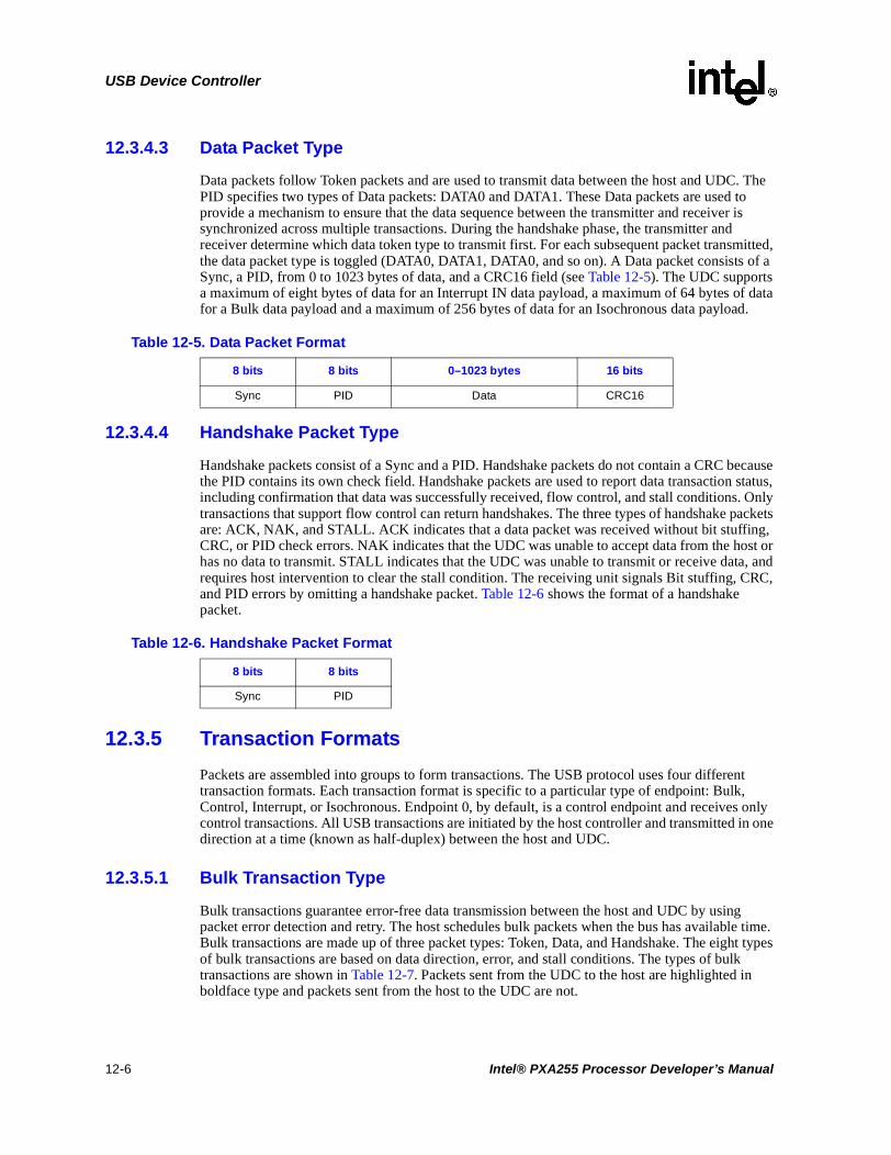
USB Device Controller
12.3.4.3 Data Packet Type
Data packets follow Token packets and are used to transmit data between the host and UDC. The PID specifies two types of Data packets: DATA0 and DATA1. These Data packets are used to provide a mechanism to ensure that the data sequence between the transmitter and receiver is synchronized across multiple transactions. During the handshake phase, the transmitter and receiver determine which data token type to transmit first. For each subsequent packet transmitted, the data packet type is toggled (DATA0, DATA1, DATA0, and so on). A Data packet consists of a Sync, a PID, from 0 to 1023 bytes of data, and a CRC16 field (see Table 12-5). The UDC supports a maximum of eight bytes of data for an Interrupt IN data payload, a maximum of 64 bytes of data for a Bulk data payload and a maximum of 256 bytes of data for an Isochronous data payload.
12.3.4.4 Handshake Packet Type
Handshake packets consist of a Sync and a PID. Handshake packets do not contain a CRC because the PID contains its own check field. Handshake packets are used to report data transaction status, including confirmation that data was successfully received, flow control, and stall conditions. Only transactions that support flow control can return handshakes. The three types of handshake packets are: ACK, NAK, and STALL. ACK indicates that a data packet was received without bit stuffing, CRC, or PID check errors. NAK indicates that the UDC was unable to accept data from the host or has no data to transmit. STALL indicates that the UDC was unable to transmit or receive data, and requires host intervention to clear the stall condition. The receiving unit signals Bit stuffing, CRC, and PID errors by omitting a handshake packet. Table 12-6 shows the format of a handshake packet.
12.3.5 Transaction Formats
Packets are assembled into groups to form transactions. The USB protocol uses four different transaction formats. Each transaction format is specific to a particular type of endpoint: Bulk, Control, Interrupt, or Isochronous. Endpoint 0, by default, is a control endpoint and receives only control transactions. All USB transactions are initiated by the host controller and transmitted in one direction at a time (known as half-duplex) between the host and UDC.
12.3.5.1 Bulk Transaction Type
Bulk transactions guarantee error-free data transmission between the host and UDC by using packet error detection and retry. The host schedules bulk packets when the bus has available time. Bulk transactions are made up of three packet types: Token, Data, and Handshake. The eight types of bulk transactions are based on data direction, error, and stall conditions. The types of bulk transactions are shown in Table 12-7. Packets sent from the UDC to the host are highlighted in boldface type and packets sent from the host to the UDC are not.
Table 12-5. Data Packet Format
8 bits 8 bits 0–1023 bytes 16 bits
Sync PID Data CRC16
Table 12-6. Handshake Packet Format
8 bits 8 bits
Sync PID
12-6 Intel® PXA255 Processor Developer’s Manual

USB Device Controller
12.3.5.2 Isochronous Transaction Type
Isochronous transactions ensure constant rate, error-tolerant transmission of data between the host and UDC. The host schedules isochronous packets during every frame. USB protocol allows isochronous transfers to take up to 90% of the USB bandwidth. Unlike bulk transactions, if corrupted data is received, the UDC will continue to process the corrupted data that corresponds to the current start of frame indicator. Isochronous transactions do not support a handshake phase or retry capability. Two packet types are used to construct isochronous transactions: token and data. The types of isochronous transactions based on data direction are shown in Table 12-8.
12.3.5.3 Control Transaction Type
The host uses control transactions to configure endpoints and query their status. Like bulk transactions, control transactions begin with a setup packet, followed by an optional data packet, then a handshake packet. Control transactions, by default, use DATA0 type transfers. Table 12-9 shows the four types of control transactions.
Table 12-7. Bulk Transaction Formats
Action Token Packet Data Packet Handshake Packet
Host successfully received data from UDC IN DATA0/DATA1 ACK
UDC temporarily unable to transmit data IN None NAK
UDC endpoint needs host intervention IN None STALL
Host detected PID, CRC, or bit stuff error IN DATA0/DATA1 None
UDC successfully received data from host OUT DATA0/DATA1 ACK
UDC temporarily unable to receive data OUT DATA0/DATA1 NAK
UDC endpoint needs host intervention OUT DATA0/DATA1 STALL
UDC detected PID, CRC, or bit stuff error OUT DATA0/DATA1 None
Packets from UDC to host are boldface
Table 12-8. Isochronous Transaction Formats
Action Token Packet Data Packet
Host received data from UDC IN DATA0
UDC received data from host OUT DATA0
Packets from UDC to host are boldface
Table 12-9. Control Transaction Formats
Action Token Packet Data Packet Handshake Packet
UDC successfully received control from host SETUP DATA0 ACK
UDC temporarily unable to receive data SETUP DATA0 NAK
UDC endpoint needs host intervention SETUP DATA0 STALL
UDC detected PID, CRC, or bit stuff error SETUP DATA0 None
Packets from UDC to host are boldface
Intel® PXA255 Processor Developer’s Manual 12-7

USB Device Controller
To assemble control transfers, the host sends a control transaction to tell the UDC what type of control transfer is taking place (control read or control write), followed by one or more data transactions. The setup is the first stage of the control transfer. The device must respond with an ACK or no handshake (if the data is corrupted). The control transaction, by default, uses a DATA0 transfer and each subsequent data transaction toggles between DATA1 and DATA0 transfers. A control write to an endpoint uses OUT transactions. Control reads use IN transactions. The transfer direction is the opposite of the last data transaction. The transfer direction is used to report status and functions as a handshake. For a control write, the last transaction is an IN from the UDC to the host. For a control read, the last transaction is an OUT from the host to the UDC. The last data transaction always uses a DATA1 transfer, even if the previous transaction used DATA1.
12.3.5.4 Interrupt Transaction Type
The host uses interrupt transactions to query the status of the device. Like bulk transactions, interrupt transactions begin with a setup packet, followed by an optional data packet, then a handshake packet. Interrupt transactions, by default, use DATA0 type transfers. Figure 12-10 shows the four types of interrupt transactions.
12.3.6 UDC Device Requests
The UDC uses its control, status, and data registers to control and monitor the transmit and receive FIFOs for endpoints 1 - 15. The host controls all other UDC configuration and status reporting using device requests that are sent as control transactions to endpoint 0 via the USB. Each setup packet to Endpoint 0 is 8 bytes long and specifies:
• Data transfer direction: host to device, device to host
• Data transfer type: standard, class, vendor
• Data recipient: device, interface, endpoint, other
• Number of bytes to transfer
• Index or offset
• Value: used to pass a variable-sized data parameter
• Device request
Table 12-11 shows a summary of all device requests. Refer to the Universal Serial Bus Specification Revision 1.1 for a full description of host device requests.
Table 12-10. Interrupt Transaction Formats
Action Token Packet Data Packet Handshake Packet
Host successfully received data from UDC IN DATA0 ACK
UDC temporarily unable to transmit data IN None NAK
UDC endpoint needs host intervention IN None STALL
Host detected PID, CRC, or bit stuff error IN DATA0 None
Packets from UDC to host are boldface
12-8 Intel® PXA255 Processor Developer’s Manual

USB Device Controller
The UDC decodes most standard device commands with no intervention required by the user. The following commands are not passed to the user are: Set Address, Set Feature, Clear Feature, Get Configuration, Get Status, Get Interface, and Sync Frame. The Set Configuration and Set Interface commands are passed to the user to indicate that the host set the specified configuration or interface and the software must take any necessary actions. Alternate interfaces settings are not supported; the host must set the alternate settings field in SET_INTERFACE requests to zero. If the UDC receives a SET_INTERFACE request with the alternate settings field non-zero, the UDC responds with a STALL. The Get Descriptor and Set Descriptor commands are passed to the user to be decoded.
Because the Set Feature and Clear Feature commands are not passed on, the user is not able decode the device remote wakeup feature commands. To solve this problem, the status bit UDCCS0:DRWF indicates whether or not the device remote wakeup feature is enabled. UDCCS0: DRWF is a read-only bit. When the bit is set to 1, the device remote wakeup feature is enabled. When the bit is set to 0, the feature is not enabled.
12.3.7 Configuration
In response to the GET_DESCRIPTOR command, the user device sends back a description of the UDC configuration. The UDC can physically support more data channel bandwidth than the USB specification allows. When the device responds to the host, it must specify a legal USB configuration. For example, if the device specifies a configuration of six isochronous endpoints of 256 bytes each, the host is not be able to schedule the proper bandwidth and does not take the UDC out of Configuration 0. The user device determines which endpoints to report to the host. If an endpoint is not reported, it is not used. Another option, attractive for use with isochronous endpoints, is to describe a configuration of a packet with a maximum size less than 256 bytes to the host. For example, if software responds to the GET_DESCRIPTOR command that Endpoint 3 only supports 64 bytes maximum packet Isochronous IN data, the user device must set the UDCCS3[TSP] bit after it loads 64 bytes for transmission. Similarly, if Endpoint 4 is described as supporting 128 bytes maximum packet Isochronous OUT data, the UDC recognizes the end of the packet, sets UDCCS4[RPC], and an interrupt is generated.
Table 12-11. Host Device Request Summary
Request Name
SET_FEATURE Enables a specific feature such as device remote wake-up or endpoint stalls.
CLEAR_FEATURE Clears or disables a specific feature.
SET_CONFIGURATION Configures the UDC for operation. Used after a reset of the Megacell or after a reset has been signalled via the USB.
GET_CONFIGURATION Returns the current UDC configuration to the host.
SET_DESCRIPTOR Sets existing descriptors or add new descriptors. Existing descriptors include: device, configuration, string, interface, and endpoint.
GET_DESCRIPTOR Returns the specified descriptor, if it exists.
SET_INTERFACE Selects an alternate setting for the UDC’s interface.
GET_INTERFACE Returns the selected alternate setting for the specified interface.
GET_STATUSReturns the UDC’s status including: remote wake-up, self-powered, data direction, endpoint number, and stall status.
SET_ADDRESS Sets the UDC’s 7-bit address value for all future device accesses.
SYNCH_FRAME Sets then reports an endpoint’s synchronization frame.
Intel® PXA255 Processor Developer’s Manual 12-9

USB Device Controller
The direction of the endpoints is fixed. Physically, the UDC only supports interrupt endpoints with a maximum packet size of 8 bytes or less, bulk endpoints with a maximum packet size of 64 bytes or less, and isochronous endpoints with a maximum packet size of 256 bytes or less.
To make the processor more adaptable, the UDC supports a total of four configurations. Each of these configurations are identical in the UDC, software can make three distinct configurations, each with two interfaces. Configuration 0 is a default configuration of Endpoint 0 only and cannot be defined as any other arrangement.
After the host completes a SET_CONFIGURATION or SET_INTERFACE command, the software must decode the command to empty the OUT endpoint FIFOs and allow the Megacell to set up the proper power/peripheral configurations.
12.4 UDC Hardware Connection
This section explains how to connect the USB interface for a variety of devices.
12.4.1 Self-Powered Device
Figure 12-2 shows how to connect the USB interface for a self-powered device. The 0 Ω resistors are optional and if they are not used, USB D+ must connect directly to the device UDC D+ and connect USB D- must connect directly to the device UDC D-. The UDC D+ and UDC D- pins are designed to match the impedance of a USB cable, 90 Ω, without external series resistors. To allow minor impedance corrections to compensate for the impedance that results from the board trace, 0 Ω resistors are recommended on the board.
The “5 V to 3.3 V” device is required because the input pins of the processor can only tolerate 3.3 V. The device can be implemented in a number of ways. The most robust and expensive solution is a Power-On-Reset device such as a MAX6348. This solution produces a clean signal edge and minimizes signal bounce. A more inexpensive solution is a 3.3 V line buffer with inputs that can tolerate 5 V. This solution does not reduce signal bounce, so software must compensate by reading the GPIO repeatedly until it proves to be stable. A third solution is a signal bounce minimization circuit that can tolerate 5 V but produces a 3.3 V signal to the GPIO pin.
12-10 Intel® PXA255 Processor Developer’s Manual

USB Device Controller
12.4.1.1 When GPIOn and GPIOx are Different Pins
The GPIOn and GPIOx pins can be any GPIO pins. GPIOn must be a GPIO that can wake the device from sleep mode. After a reset, GPIOx is configured as an input. This causes the UDC+ line to float. GPIOn is configured to act as an input and to cause an interrupt on a rising or falling edge. When an interrupt occurs, software must read the GPIOn pin to determine if the cable is connected. The GPIOn pin is set to a 1 when the cable is connected and a 0 when the cable is disconnected. When a USB connect is detected, software must enable the UDC peripheral and drive a 1 to the GPIOx pin to indicate to the host PC that a high-speed USB device is connected. When a USB disconnect is detected, software must configure the GPIOx pin as an input, configure the GPIOn pin to detect a wakeup event, and put the disconnected peripheral in sleep mode, if desired.
If software must put a peripheral in sleep mode, it configures the GPIOx pin as an input. This causes the UDC+ line to float, which appears to be a disconnect to the host PC. The peripheral is put in sleep mode. When the peripheral comes out of sleep mode, software must drive a 1 to the GPIOx pin to indicate to the host PC that a high-speed USB peripheral is connected.
12.4.1.2 When GPIOn and GPIOx are the Same Pin
After a reset, GPIOn is configured to act as an input and to cause an interrupt on a rising or falling edge. When an interrupt occurs, software must read the GPIOn pin to determine if the cable is connected. GPIOn is set to a 1 when the cable is connected and a 0 when the cable is disconnected. If a USB connect is detected, software must enable the UDC peripheral before the host PC sends the first USB command. If a USB disconnect is detected, software must configure the GPIOn pin to detect a wakeup event and put the peripheral in sleep mode, if desired.
When GPIOn and GPIOx are the same pin, do not put a peripheral in sleep mode if the USB cable is connected to the device. During sleep, the USB controller is in reset and does not respond to the host PC. When it returns from sleep mode, the peripheral does not respond to its host-assigned address.
Figure 12-2. Self-Powered Device
USB 5V
USB D+
USB D-
USB GND
5 V to 3.3 V
1.5K
GPIOn
UDC D+
UDC D-
0 ohm(optional)
0 ohm(optional)
Board GND
470KGPIOx
Intel® PXA255 Processor Developer’s Manual 12-11

USB Device Controller
12.4.2 Bus-Powered Devices
The processor does not support bus-powered devices because it is required to consume less that 500 µA when the host issues a suspend (see Section 7.2.3 of the USB Specification, version 1.1). The processor cannot limit the amount of current it consumes to 500 µA unless it enters sleep mode. When processor enters sleep mode it resets the USB registers and does not respond to its host-assigned address.
12.5 UDC Operation
When a USB interrupt is received, software is directed to the USB ISR. USIR is level sensitive. Be sure to clear USIR as the last step before exiting the ISR. Upon exiting the ISR, the user should always clear the interrupt source bit, then clear the USIR. On power up or after a reset, software initially enables only EP0 interrupt. The other interrupts are enabled as required by the SET_CONFIG command.
12.5.1 Case 1: EP0 Control Read
1. When software starts, it initializes a software state machine to EP0_IDLE. The software state machine is used to track endpoints stages when software communicates with the host PC.
2. The host PC sends a SETUP command.
3. UDC generates an EP0 Interrupt.
4. Software determines that the UDCCS0[SA] and UDCCS0[OPR] bits are set. This indicates that a new OUT packet is in the EP0 Buffer and identifies a SETUP transaction.
5. Software reads the data into a buffer while UDCCS0[RNE] bit (receiver not empty) is set.
6. Software parses the command in the buffer and determines that it is a Control Read.
7. Software starts to load the UDDR0 register FIFO with the first data packet and sets the internal state machine to EP0_IN_DATA_PHASE.
8. After it reads and parses the data, software clears the UDCCS0[SA] and the UDCCS0[OPR] bits and sets the UDCCS0[IPR] bit, if transmitting less than MAX_PACKET bytes, which prompts the UDC to transmit the data on the next IN. The UDC sends NAKs to all requests on this EP until the UDCCS0[IPR] bit is set.
9. Software clears the UDC interrupt bit and returns from the interrupt service routine.
10. The host PC issues an IN packet, which the UDC sends data back to the host. After the host PC sends an ACK to the UDC, the UDC clears the UDDCS0[IPR] bit and generates an interrupt.
11. Software enters the ISR routine and examines its internal state machine. It determines that it is in the EP0_IN_DATA_PHASE state and must transmit more data. Software loads the next amount of data, sets the UDCCS0[IPR] bit if necessary, and returns from the interrupt. The internal state machine is not affected.
12. Repeat Steps 10 and 11 until all the data is transmitted or the last data packet is a short packet.
13. If the last packet software sends is a short packet, it sets its internal state machine to EP0_END_XFER. If the last data packet ends on a 16-byte boundary, software sets UDCCS0[IPR] to send a zero-length packet without loading data in the FIFO. After it sends the zero-length packet, software sets the internal state machine to EP0_END_XFER.
12-12 Intel® PXA255 Processor Developer’s Manual

USB Device Controller
14. When the host executes the STATUS OUT stage (zero-length OUT), the UDC sets the UDDCS0[OPR] bit, which causes an interrupt.
15. Software enters the ISR routine and determines that the UDCCS0[OPR] bit is set, the UDCCS0[SA] bit is clear, and its internal state machine is EP0_END_XFER. Software clears the UDCCS0[OPR] bit and transfers its internal state machine to EP0_IDLE.
16. Software clears the UDC interrupt bit and returns from the interrupt service routine.
If the host sends another SETUP command during these steps, the software must terminate the first SETUP command and start the new command.
12.5.2 Case 2: EP0 Control Read with a Premature Status Stage
Case 2 occurs during an enumeration cycle when the host PC sends a premature status stage during a Get Device Descriptor command.
1. When software starts, it initializes a software state machine to EP0_IDLE. The software state machine is used to track endpoints stages when software communicates with the host PC.
2. The host PC sends a SETUP command.
3. UDC generates an EP0 Interrupt.
4. Software determines that the UDCCS0[SA] and UDCCS0[OPR] bits are set. This indicates that a new OUT packet is in the EP0 Buffer and identifies a SETUP transaction.
5. Software reads the data into a buffer while UDCCS0[RNE] bit (receiver not empty) is set.
6. Software parses the command in the buffer and determines that it is a Control Read.
7. Software starts to load the UDDR0 register FIFO with the first data packet and sets the internal state machine to EP0_IN_DATA_PHASE.
8. After it reads and parses the data, software clears the UDCCS0[SA] and the UDCCS0[OPR] bits and sets the UDCCS0[IPR] bit, if transmitting less than MAX_PACKET bytes, which prompts the UDC to transmit the data on the next IN. The UDC sends NAKs to all requests on this EP until the UDCCS0[IPR] bit is set.
9. Software clears the UDC interrupt bit and returns from the interrupt service routine.
10. The host PC issues an IN packet, which the UDC sends back to the host. After the host PC sends an ACK to the UDC, the UDC clears the UDDCS0[IPR] bit and generates an interrupt.
11. Software enters the ISR routine and examines its internal state machine. It determines that it is in the EP0_IN_DATA_PHASE state and must transmit more data. Software loads the next amount of data, sets the UDCCS0[IPR] bit, if transmitting less than MAX_PACKET bytes, and returns from the interrupt. The internal state machine is not affected.
12. Repeat Steps 10 and 11 until all the data is transmitted or the last data packet is a short packet.
13. As Steps 10 and 11 are repeated, the host sends a premature STATUS OUT stage, which indicates that the host PC can not accept more data, instead of an IN packet.
14. When the EP0 interrupt occurs, software determines that the UDCCS0[OPR] bit is set, the UDCCS0[SA] bit is cleared, and its machine state is EP0_IN_DATA_PHASE. This indicates that a premature STATUS OUT occurred.
15. Software clears the UDCCS0[OPR] bit and changes the pin’s state to EP0_IDLE. The software writes to the UDCCS0[FTF] bit to clean up any buffer pointers and empty the transmit FIFO.
Intel® PXA255 Processor Developer’s Manual 12-13

USB Device Controller
16. Software clears the UDC interrupt bit and returns from the interrupt service routine.
If the host sends another SETUP command during these steps, the software must terminate the first SETUP command and start the new command.
12.5.3 Case 3: EP0 Control Write With or Without a Premature Status Stage
1. When software starts, it initializes a software state machine to EP0_IDLE. The software state machine is used to track stages when software communicates with the host PC.
2. The host PC sends a SETUP command.
3. UDC generates an EP0 Interrupt.
4. Software determines that the UDCCS0[SA] and UDCCS0[OPR] bits are set. This indicates that a new OUT packet is in the EP0 Buffer and identifies a SETUP transaction.
5. Software reads the data into a buffer while UDCCS0[RNE] bit (receiver not empty) is set.
6. Software parses the command in the buffer and determines that it is a Control Write (such as Set Descriptor).
7. Software sets the internal to EP0_OUT_DATA_PHASE and clears the UDCCS0[OPR] and UDCCS0[SA] bits.
8. To allow a premature STATUS IN stage, software sets the UDCCS0[IPR] bit and loads a zero-length packet in the transmit FIFO.
9. Software clears the UDC interrupt bit and returns from the interrupt service routine.
10. The host PC issues an OUT packet and the UDC issues an EP0 interrupt.
11. Software enters the ISR routine and determines that it is in the EP0_OUT_DATA_PHASE state, the UDCCS0[OPR] bit is set, and the UDCCS0[SA] bit is clear. This indicates that there is more data to receive.
12. Software reads the data into a buffer while UDCCS0[RNE] bit is set and clears the UDDCCS0[OPR] bit.
13. Software sets the UDCCS0[IPR] bit to allow a premature STATUS IN stage.
14. Software clears the UDC interrupt bit and returns from the interrupt service routine.
15. Steps 11 through 14 are repeated until all of the data is received.
16. As Steps 11 through 14 are repeated, the host sends a STATUS IN stage, which indicates that the host PC can not send more data, instead of an OUT packet. The STATUS IN stage may be premature or not.
17. Because software loaded a zero-length packet (see Step 8), the UDC responds to the STATUS IN by sending a a zero-length packet back to the host PC. This causes an interrupt.
18. Software enters the ISR routine and determines that it is in the EP0_OUT_DATA_PHASE state and the UDCCS0[OPR] and UDCCS0[IPR] bits are clear. This indicates that a STATUS IN stage occurred.
19. Software determines how many bytes were received before the interrupt and compares the number of received bytes to the wLength field in the original SETUP packet. If the correct amount of data was sent, software parses the data and performs the action the data indicates. If
12-14 Intel® PXA255 Processor Developer’s Manual

USB Device Controller
the wrong amount of data was sent, software cleans up any buffer pointers and disregards the received data.
20. Software changes its internal state machine to EP0_IDLE.
21. Software clears the UDC interrupt bit and returns from the interrupt service routine.
If the host sends another SETUP command during these steps, the software must terminate the first SETUP command and start the new command.
12.5.4 Case 4: EP0 No Data Command
1. When software starts, it initializes a software state machine to EP0_IDLE. The software state machine is used to track stages when software communicates with the host PC.
2. The host PC sends a SETUP command.
3. UDC generates an EP0 Interrupt.
4. Software determines that the UDCCS0[SA] and UDCCS0[OPR] bits are set. This indicates that a new OUT packet is in the EP0 Buffer and identifies a SETUP transaction.
5. Software reads the data into a buffer while UDCCS0[RNE] bit (receiver not empty) is set.
6. Software parses the data in the buffer and determines that it is a No Data command.
7. Software executes the command and sets its internal state machine to EP0_IDLE. Software clears the UDCCS0[IPR] and UDCCS0[SA] bits. If the command is a No-Data-Phase Standard command, then do not set the UDCCS0[IPR] bit. If the command is not a No-Data-Phase Standard command, e.g a No-Data-Phase Vendor command or No-Data-Phase Class command, then software must set the UDCCS0[IPR] bit.
8. When the host PC executes the STATUS IN stage, the UDC sends back a zero-length packet, which indicates a successful handshake. This does not cause an interrupt.
If the host sends another SETUP command during these steps, the software must terminate the first SETUP command and start the new command.
12.5.5 Case 5: EP1 Data Transmit (BULK-IN)
The procedure in Case 5 can also be used to operate Endpoints 6 and 11.
In Case 5, the Transmit Short Packet is only set if a packet size of less than 64 bytes is sent. If the packet size is 64 bytes, the system arms when the 64th byte is loaded. Loading the 64th byte and setting the UDCCS1[TSP] bit produces one 64-byte packet and one zero-length packet.
When software receives a SETUP VENDOR command to set up an EP1 BULK IN transaction, it may take one of two courses of action, as appropriate for the chosen operating model:
• Configure the DMA engine and disable the EP1 interrupt to allow the DMA engine to handle the transaction.
• Enable the EP1 interrupt to allow the Megacell to directly handle the transaction.
12.5.5.1 Software Enables the DMA
If software enables the DMA engine, use the following steps:
Intel® PXA255 Processor Developer’s Manual 12-15

USB Device Controller
1. During the SETUP VENDOR command, software enables the DMA engine and masks the EP1 interrupt. The DMA start address must be aligned on a 16-byte boundary.
a. If the packet size is 64 bytes, software transfers the all the data in one DMA descriptor and sets the UDCCS1[TSP] bit in the second DMA descriptor.
b. If the packet size is less than 64 bytes, software sets up a string of descriptors in which the odd numbered descriptors point to the data and the even numbered descriptors are writes to the UDCCS1[TSP] bit.
2. The host PC sends a BULK-IN and the UDC sends a data packet back to the host PC.
3. The UDC generates an interrupt that is masked from the Megacell.
4. The DMA engine fills the EP1 data FIFO (UDDR1) with data and sets the UDCCS1[TSP] bit if the data packet is a short packet.
5. Steps 2 through 4 repeat until all the bulk data is sent to the host PC.
12.5.5.2 Software Enables the EP1 Interrupt
If software enables the EP1 interrupt to allow the Megacell to directly handle the transaction:
1. During the SETUP VENDOR command, software fills the EP1 data FIFO (UDDR1) with data and clears the UDCCS1[TPC] bit. If the data packet is a short packet, software also sets the UDCCS1[TSP] bit.
2. The host PC sends a BULK-IN and the UDC sends a data packet back to the host PC and generates an EP1 Interrupt.
3. Software fills the EP1 data FIFO (UDDR1) with data and clears the UDCCS1[TPC] bit. If the data packet is a short packet, software also sets the UDCCS1[TSP] bit.
4. Return from interrupt.
5. Steps 2 through 4 repeat until all of the data is sent to the host PC.
12.5.6 Case 6: EP2 Data Receive (BULK-OUT)
This procedure can also be used to operate Endpoints 7 and 12.
When software receives a SETUP VENDOR command to set up an EP2 BULK OUT transaction, it may take one of two courses of action, as appropriate for the chosen operating model:
• Enable the DMA engine to handle the transaction.
• Allow the Megacell to directly handle the transaction.
12.5.6.1 Software Enables the DMA
If software enables the DMA engine to handle the transaction:
1. During the SETUP VENDOR command, software sets up the DMA engine and sets the UDCCS2[DME] bit.
a. If the packet size is 32 or 64 bytes, software sets up a string of descriptors, each with a length of modulo 32 or 64. Software sets the interrupt bit for the appropriate descriptor.
b. If the packet size is less than 32 bytes, software uses interrupt mode.
12-16 Intel® PXA255 Processor Developer’s Manual

USB Device Controller
2. The host PC sends a BULK-OUT.
3. The DMA engine reads data from the EP2 data FIFO (UDDR2).
4. Steps 2 and 3 repeat until all the data has been read from the host.
5. If the software receives an EP2 interrupt it completes the following process:
a. If UDCCS2[RNE] is clear and UDCCS2[RSP] is set, the data packet was a zero-length packet.
b. If UDCCS2[RNE] is set, the data packet was a short packet and software must use the UDCWC2 count register to read the proper amount of data from the EP2 data FIFO (UDDR2).
c. Software clears the UDCCS2[RPC] bit.
6. Return from interrupt.
12.5.6.2 Software Allows the Megacell to Handle the Transaction
If software allows the Megacell to handle the transaction:
1. During the SETUP VENDOR command, software clears the UDCCS2[DME] bit.
2. The host PC sends a BULK-OUT and the UDC generates an EP2 Interrupt.
3. If UDCCS2[RNE] is clear and UDCCS2[RSP] is set, the data packet was a zero-length packet.
4. If UDCCS2[RNE] is set, software uses the UDCWC2 count register to read the proper amount of data from the EP2 data FIFO (UDDR2).
5. Software clears the UDCCS2[RPC] bit.
6. Return from interrupt.
7. Steps 2 through 6 repeat until all the data has been read from the host.
12.5.7 Case 7: EP3 Data Transmit (ISOCHRONOUS-IN)
The procedure in Case 7 can also be used to operate Endpoints 8 and 13.
In Case 7, the Transmit Short Packet is only set if a packet size of less than 256 bytes is sent. If the packet size is 256 bytes, the system arms when the 256th byte is loaded. Loading the 256th byte and setting the UDCCS3[TSP] bit produces one 256-byte packet and one zero-length packet.
When software receives a SETUP VENDOR command to set up an EP3 ISOCHRONOUS IN transaction, it may take one of three courses of action, as appropriate for the chosen operating model:
• Configure the DMA engine and disable the EP3 interrupt to allow the DMA engine to handle the transaction.
• Enable the EP3 interrupt to allow the Megacell to directly handle the transaction.
• Enable the SOF interrupt to handle the transaction on a frame count basis.
12.5.7.1 Software Enables DMA
If software enables the DMA engine to handle the transaction:
Intel® PXA255 Processor Developer’s Manual 12-17

USB Device Controller
1. During the SETUP VENDOR command, software enables the DMA engine and masks the EP3 interrupt. The DMA start address must be aligned on a 16-byte boundary.
a. If the packet size is 256 bytes, software transfers the all the data in one DMA descriptor.
b. If the packet size is less than 256 bytes, software sets up a string of descriptors in which the odd numbered descriptors point to the data and the even numbered descriptors are writes to the UDCCS1[TSP] bit.
2. The host PC sends an ISOC-IN and the UDC sends a data packet back to the host PC.
3. The UDC generates an interrupt that is masked from the Megacell.
4. The DMA engine fills the EP3 data FIFO (UDDR3) with data and sets the UDCCS3[TSP] bit if the data packet is a short packet.
5. Steps 2 through 4 repeat until all the data has been sent to the host.
12.5.7.2 Software Enables the EP3 Interrupt
If software enables the EP3 interrupt to allow the Megacell to directly handle the transaction:
1. During the SETUP VENDOR command, software fills the EP3 data FIFO (UDDR3) with data and clears the UDCCS3[TPC] bit. If the data packet is a short packet, software also sets the UDCCS3[TSP] bit.
2. The host PC sends a ISOC-IN command and the UDC sends a data packet back to the host PC and generates an EP3 Interrupt.
3. Software fills the EP3 data FIFO (UDDR3) with data and clears the UDCCS3[TPC] bit. If the data packet is a short packet, software also sets the UDCCS3[TSP] bit.
4. Return from interrupt.
5. Steps 2 through 4 repeat until all of the data is sent to the host PC.
12.5.7.3 Software Enables the SOF Interrupt
If software enables the SOF interrupt to handle the transaction on a frame count basis:
1. Software disables the UDCCS3 Interrupt by setting UICR0[IM3] to a 1 and enables the SOF interrupt in the UFNHR register by setting UFNHR[SIM] to a 0.
2. When the host PC sends an SOF, the UDC sets the UFNHR[SIR] bit, which causes an SOF interrupt.
3. Software checks the UDCCS3[TFS] bit to determine if there is room for a data packet. If there is room, software fills the EP3 data FIFO (UDDR3) with data and clears the UDCCS3[TPC] bit. If the data packet is a short packet, software sets the UDCCS3[TSP] bit.
4. Software clears the UFNHR[SIR] bit.
5. Return from interrupt.
6. Steps 2 through 5 repeat until all the data is sent to the host PC.
12.5.8 Case 8: EP4 Data Receive (ISOCHRONOUS-OUT)
The procedure in Case 8 can also be used to operate Endpoints 9 and 14.
12-18 Intel® PXA255 Processor Developer’s Manual

USB Device Controller
When software receives a SETUP VENDOR command to set up an EP4 ISOCHRONOUS OUT transaction, it may take one of three courses of action, as appropriate for the chosen operating model:
• Configure the DMA engine and disable the EP4 interrupt to allow the DMA engine to handle the transaction.
• Enable the EP4 interrupt to allow the Megacell to directly handle the transaction.
• Enable the SOF interrupt to handle the transaction on a frame count basis.
12.5.8.1 Software Enables the DMA
If software enables the DMA engine, use the following steps:
1. During the SETUP VENDOR command, software enables the DMA engine and sets the UDCCS4[DME] bit. ISO packet sizes are not restricted, but a packet size of modulo 32 is highly recommended efficiency.
a. If the packet size is between 32 and 256 bytes modulo 32, software determines the number of descriptors needed and sets up a string of descriptors. Software sets the interrupt bit for the appropriate descriptor.
b. If the packet size is between 32 bytes and 256 bytes, but not modulo 32 bytes, software sets up a descriptor to receive each data packet, then reads the remaining data on each UDCCS2[RSP] bit interrupt and sets up another descriptor.
c. If the packet size is less than 32 bytes, software must use interrupt mode.
2. The host PC sends a ISOC-OUT.
3. The DMA engine reads the data from the EP4 data FIFO (UDDR4).
4. Steps 2 and 3 repeat until all the data has been read from the host.
5. If the software receives an EP4 interrupt it completes the following process:
a. If UDCCS4[RNE] is clear and UDCCS4[RSP] is set, the data packet was a zero-length packet.
b. If UDCCS4[RNE] is set, the data packet was a short packet and software uses the UDCWC4 count register to read the proper amount of data from the EP4 data FIFO (UDDR4).
c. Software clears the UDCCS4[RPC] bit.
6. Return from interrupt.
12.5.8.2 Software Allows the Megacell to Handle the Transaction
If software allows the Megacell to handle the transaction:
1. During the SETUP VENDOR command, software clears the UDCCS4[DME] bit.
2. The host PC sends a ISOC-OUT and the UDC generates an EP4 Interrupt.
3. If UDCCS4[RNE] is clear and UDCCS4[RSP] is set, the data packet was a zero-length packet.
4. If UDCCS4[RNE] is set, software uses the UDCWC4 count register to read the proper amount of data from the EP4 data FIFO (UDDR4).
5. Software clears the UDCCS4[RPC] bit.
Intel® PXA255 Processor Developer’s Manual 12-19

USB Device Controller
6. Return from interrupt.
7. Steps 2 through 6 repeat until all the data has been read from the host.
12.5.8.3 Software Enables the SOF Interrupt
If software enables the SOF interrupt to handle the transaction on a frame count basis:
1. Software disables the UDCCS4 Interrupt by setting UICR0[IM4] to a 1 and enables the SOF interrupt in the UFNHR register by setting UFNHR[SIM] to a 0.
2. When the host PC sends an SOF, the UDC sets the UFNHR[SIR] bit, which causes an SOF interrupt.
3. If UDCCS4[RNE] is clear and UDCCS4[RSP] is clear, no data packet was received.
4. If UDCCS4[RNE] is clear and UDCCS4[RSP] is set, the data packet was a zero-length packet.
5. If UDCCS4[RNE] is set, the data packet was a short packet and software uses the UDCWC4 count register to read the proper amount of data from the EP4 data FIFO (UDDR4).
6. Software clears the UDCCS4[RPC] and UFNHR[SIR] bits.
7. Return from interrupt.
8. Steps 2 through 7 repeat until all the data is sent to the host PC.
12.5.9 Case 9: EP5 Data Transmit (INTERRUPT-IN)
The procedure in Case 9 can also be used to operate Endpoints 10 and 15.
In Case 9, the Transmit Short Packet is only set if a packet size of less than 8 bytes is sent. If the packet size is 8 bytes, the system arms when the 8th byte is loaded. Loading the 8th byte and setting the UDCCS5[TSP] bit produces one 8-byte packet and one zero-length packet.
When software receives a SETUP VENDOR command to set up an EP5 INTERRUPT-IN transaction, it can only allow the Megacell to handle the transaction:
1. During the SETUP VENDOR command, software fills the EP5 data FIFO (UDDR5) with data and clears the UDCCS5[TPC] bit.
2. The host PC sends an INTERRUPT-IN and the UDC generates an EP5 Interrupt.
3. Software fills the EP5 data FIFO (UDDR5) with data and clears the UDCCS5[TPC] bit. If the data packet is a short packet, software also sets the UDCCS5[TSP] bit.
4. Return from interrupt.
5. Steps 2 through 4 repeat until all the data is sent to the host PC.
12.5.10 Case 10: RESET Interrupt
1. After a system reset, software loads the registers with the required values.
2. Software enables the UDC by setting the UDCCR[UDE] bit and immediately reads the UDCCR[UDA] bit to determine if a USB reset is currently on the USB bus.
a. If UDCCR[UDA] is a 0, there is currently a USB reset on the bus and software clears the interrupt by writing a 1 to the UDCCR[RSTIR] bit. Software enables future reset interrupts by clearing the UDCCR[REM] bit.
12-20 Intel® PXA255 Processor Developer’s Manual

USB Device Controller
b. If UDCCR[UDA] is a 1, there is currently no USB reset on the bus and software enables future reset interrupts by clearing the UDCCR[REM] bit.
3. Return from interrupt.
4. The host either asserts a USB reset or negates a USB reset.
5. The UDC generates a Reset Interrupt.
6. Software determines that the UDCCR[RSTIR] bit is set and clears the interrupt by writing a 1 to the UDCCR[RSTIR] bit. Software then examines the UDCCR[UDA] bit to determine the type of reset that took place:
a. If UDCCR[UDA] is a 0, a Reset Assertion took place. Software returns from the interrupt and waits for the Reset Negation interrupt.
b. If UDDCR[UDA] is a 1, a Reset Negation took place. Software sets any initialization that is necessary.
7. Return from interrupt.
12.5.11 Case 11: SUSPEND Interrupt
1. As software starts, it clears the UDCCR[SRM] bit to allow a USB suspend interrupt.
2. The host PC asserts a USB suspend by stopping activity on the UDC+ and UDC- signals.
3. The UDC generates a Suspend Interrupt.
4. Software determines that the UDCCR[SUSIR] bit is set.This indicates that a USB suspend has occurred and software takes any necessary actions to turn off other peripherals, clean up internal buffers, perform power management, and perform similar functions. Software must not disable the UDC and must not allow the processor to go into sleep mode while the USB cable is attached.
12.5.12 Case 12: RESUME Interrupt
1. As software starts, it clears the UDCCR[SRM] bit to allow a USB resume.
2. The host PC asserts a USB resume by resuming activity after a suspend state on the UDC+ and UDC- signals.
3. The UDC generates a Resume Interrupt.
4. Software determines that the UDCCR[RESIR] bit is set. This indicates that a USB resume has occurred and the OS may take any necessary actions to turn on other peripherals, initialize internal buffers, perform power management, and perform similar functions.
12.6 UDC Register Definitions
All configuration, request/service, and status reporting is controlled by the USB host controller and is communicated to the UDC via the USB. The UDC has registers that control the interface between the UDC and the software. A control register enables the UDC and masks the interrupt sources in the UDC. A status register indicates the state of the interrupt sources. Each of the sixteen endpoints (control, OUT, and IN) have a control or status register. Endpoint 0 (control) has an
Intel® PXA255 Processor Developer’s Manual 12-21

USB Device Controller
address for the 16 x 8 data FIFO that can be used to transmit and receive data. Endpoint 0 also has a write count register that is used to determine the number of bytes the USB host controller has sent to Endpoint 0.
12.6.1 UDC Control Register (UDCCR)
UDCCR, shown in Table 12-12, contains seven control bits: one to enable the UDC, one to show activity, and five to show status and associated control functions.
12.6.1.1 UDC Enable (UDE)
Enables the UDC. When UDE is set to a 1, the UDC is enabled for USB serial transmission or reception. When UDE is set to a 0, the UDC is disabled and the UDC+ and UDC- pins are tristated. This means that the UDC ignores all activity on the USB bus.
If UDE is set to a 0 the entire UDC design is reset. If the reset occurs while the UDC is actively transmitting or receiving data, it stops immediately and the remaining bits in the transmit or receive serial shifter are reset. All entries in the transmit and receive FIFO are also reset.
Table 12-12. UDCCR Bit Definitions
0x 4060_0000 UDCCR Read/Write and Read-Only
Bit 31 30 29 28 27 26 25 24 23 22 21 20 19 18 17 16 15 14 13 12 11 10 9 8 7 6 5 4 3 2 1 0
reserved
RE
M
RS
TIR
SR
M
SU
SIR
RE
SIR
RS
M
UD
A
UD
E
x x x x x x x x x x x x x x x x x x x x x x x x 1 0 1 0 0 0 0 0
Bits Name Description
31:8 — reserved
7 REMReset interrupt mask.(read/write)
0 = Reset interrupt enabled.1 = Reset interrupt disabled.
6 RSTIR Reset interrupt request (read/write 1 to clear).1 = UDC was reset by the host.
5 SRMSuspend/resume interrupt mask (read/write).
0 = Suspend/resume interrupt enabled.1 = Suspend/resume interrupt disabled.
4 SUSIR Suspend interrupt request (read/write 1 to clear).1 = UDC received, suspend signalling from the host.
3 RESIR Resume interrupt request (read/write 1 to clear).1 = UDC received, resume signalling from the host.
2 RSMDevice Resume (read/write 1 to set)
0 = Maintain UDC suspend state1 = Force UDC out of suspend
1 UDAUDC active (read-only).
0 = UDC currently receiving a USB reset.1 = UDC currently not receiving a USB reset.
0 UDEUDC enable.(read/write)
0 = UDC disable.1 = UDC enabled.
12-22 Intel® PXA255 Processor Developer’s Manual
USB Device Controller
12.6.1.2 UDC Active (UDA)
This read-only bit can be read to determine if the UDC is currently active or in a USB reset. This bit is only valid when the UDC is enabled. A zero indicates that the UDC is currently receiving a USB reset from the host. A one indicates that the UDC is currently involved in a transaction.
12.6.1.3 UDC Resume (RSM)
When the UDC is in a suspend state, this bit can be written to force the UDC into a non-idle state (K state) for 3 ms to perform a remote wakeup operation. If the host PC does not start a wakeup sequence in 3 ms, the UDC returns to the suspend mode. This bit is a trigger bit for the UDC and is automatically cleared.
12.6.1.4 Resume Interrupt Request (RESIR)
The resume interrupt request bit is set if the SRM bit in the UDC control register is cleared, the UDC is currently in the suspended state, and the USB is driven with resume signalling.
12.6.1.5 Suspend Interrupt Request (SUSIR)
The suspend interrupt request register is set when the USB remains idle for more than 6 ms. The SUSIR bit retains state so software can determine that the USB is idle. If SRM is zero, SUSIR being set will not generate an interrupt but status continues to be updated.
12.6.1.6 Suspend/Resume Interrupt Mask (SRM)
This bit masks or enables the suspend interrupt request to the interrupt controller. When SRM is 1, the interrupt is masked and the setting of SUSIR will not generate an interrupt. When SRM is 0, the setting of SUSIR generates an interrupt when the USB is idle for more than 6ms. Programming SRM does not affect the state of SUSIR.
12.6.1.7 Reset Interrupt Request (RSTIR)
The reset interrupt request register is set when the host issues a reset. When the host issues a reset, the entire UDC is reset. The RSTIR bit retains its state so software can determine that the design was reset. If REM is zero, RSTIR being set does not generate an interrupt but status continues to be updated.
12.6.1.8 Reset Interrupt Mask (REM)
This bit masks or enables the reset interrupt request to the interrupt controller. When REM is 1, the interrupt is masked and the setting of RSTIR does not generate an interrupt. When REM is 0, the RSTIR setting generates an interrupt when the USB host controller issues an UDC reset. Programming REM does not affect the state of RSTIR.
The UDE bit is cleared to zero, which disables the UDC following a Megacell reset. Writes to reserved bits are ignored and reads return zeros.
These are read/write registers. Ignore reads from reserved bits. Write zeros to reserved bits.
Intel® PXA255 Processor Developer’s Manual 12-23
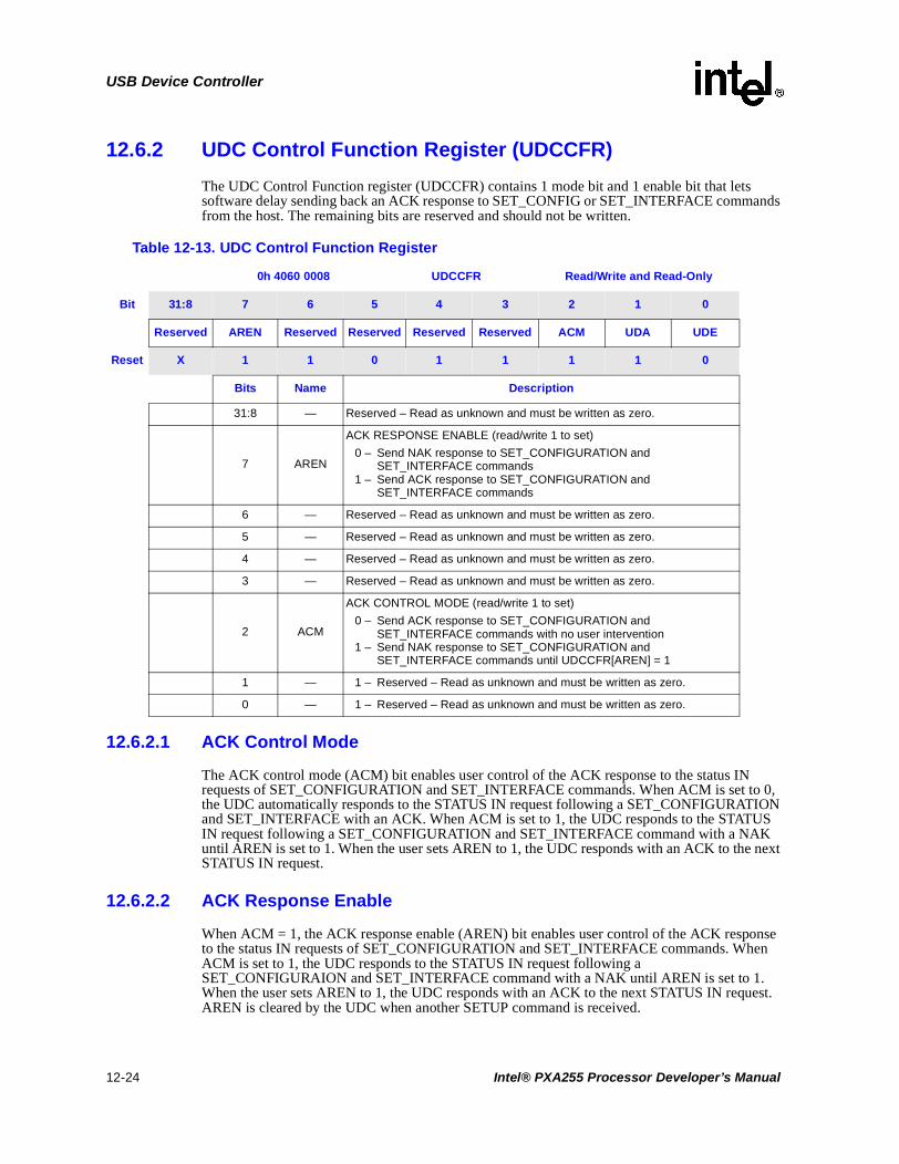
USB Device Controller
12.6.2 UDC Control Function Register (UDCCFR)
The UDC Control Function register (UDCCFR) contains 1 mode bit and 1 enable bit that lets software delay sending back an ACK response to SET_CONFIG or SET_INTERFACE commands from the host. The remaining bits are reserved and should not be written.
12.6.2.1 ACK Control Mode
The ACK control mode (ACM) bit enables user control of the ACK response to the status IN requests of SET_CONFIGURATION and SET_INTERFACE commands. When ACM is set to 0, the UDC automatically responds to the STATUS IN request following a SET_CONFIGURATION and SET_INTERFACE with an ACK. When ACM is set to 1, the UDC responds to the STATUS IN request following a SET_CONFIGURATION and SET_INTERFACE command with a NAK until AREN is set to 1. When the user sets AREN to 1, the UDC responds with an ACK to the next STATUS IN request.
12.6.2.2 ACK Response Enable
When ACM = 1, the ACK response enable (AREN) bit enables user control of the ACK response to the status IN requests of SET_CONFIGURATION and SET_INTERFACE commands. When ACM is set to 1, the UDC responds to the STATUS IN request following a SET_CONFIGURAION and SET_INTERFACE command with a NAK until AREN is set to 1. When the user sets AREN to 1, the UDC responds with an ACK to the next STATUS IN request. AREN is cleared by the UDC when another SETUP command is received.
Table 12-13. UDC Control Function Register
0h 4060 0008 UDCCFR Read/Write and Read-Only
Bit 31:8 7 6 5 4 3 2 1 0
Reserved AREN Reserved Reserved Reserved Reserved ACM UDA UDE
Reset X 1 1 0 1 1 1 1 0
Bits Name Description
31:8 — Reserved – Read as unknown and must be written as zero.
7 AREN
ACK RESPONSE ENABLE (read/write 1 to set)
0 – Send NAK response to SET_CONFIGURATION and SET_INTERFACE commands
1 – Send ACK response to SET_CONFIGURATION and SET_INTERFACE commands
6 — Reserved – Read as unknown and must be written as zero.
5 — Reserved – Read as unknown and must be written as zero.
4 — Reserved – Read as unknown and must be written as zero.
3 — Reserved – Read as unknown and must be written as zero.
2 ACM
ACK CONTROL MODE (read/write 1 to set)
0 – Send ACK response to SET_CONFIGURATION and SET_INTERFACE commands with no user intervention
1 – Send NAK response to SET_CONFIGURATION and SET_INTERFACE commands until UDCCFR[AREN] = 1
1 — 1 – Reserved – Read as unknown and must be written as zero.
0 — 1 – Reserved – Read as unknown and must be written as zero.
12-24 Intel® PXA255 Processor Developer’s Manual

USB Device Controller
12.6.3 UDC Endpoint 0 Control/Status Register (UDCCS0)
UDCCS0, shown in Table 12-14, contains seven bits that are used to operate endpoint zero, the control endpoint.
12.6.3.1 OUT Packet Ready (OPR)
The OUT packet ready bit is set by the UDC when it receives a valid OUT packet to endpoint zero. When this bit is set, the USIR0[IR0] bit will be set in the UDC status/interrupt register if endpoint zero interrupts are enabled. This bit is cleared by writing a one. The UDC is not allowed to enter the data phase of a transaction until this bit is cleared.
12.6.3.2 IN Packet Ready (IPR)
The IN packet ready bit is set by the core if less than max_packet bytes (16) have been written to the endpoint 0 FIFO to be transmitted. The core must not set this bit if a max_packet is to be transmitted. The UDC clears this bit when the packet has been successfully transmitted, the UDCCS0[FTF] bit has been set, or a control OUT is received. When this bit is cleared due to a successful IN transmission or the reception of a control OUT, the USIR0[IR0] bit in the UDC interrupt register is set if the endpoint 0 interrupt is enabled via UICR0[IM0]. The Intel® XScale™ microarchitecture is not able to clear UDCCS0[IPR] and always reads back a zero
Table 12-14. UDCCS0 Bit Definitions
0x 4060_0010 UDCCS0 USB Device Controller
Bit 31 30 29 28 27 26 25 24 23 22 21 20 19 18 17 16 15 14 13 12 11 10 9 8 7 6 5 4 3 2 1 0
reserved SA
RN
E
FS
T
SS
T
DR
WF
FT
F
IPR
OP
R
x x x x x x x x x x x x x x x x x x x x x x x x 0 0 0 0 0 0 0 0
Bits Name Description
0 OPROUT packet ready (read/write 1 to clear)
0 = OUT packet ready.
1 IPRIN packet ready (always read 0/write 1 to set).1 = IN packet ready.
2 FTF Flush Tx FIFO (always read 0/write 1 to set)1 = Flush the contents of Tx FIFO.
3 DRWFDevice remote wakeup feature (read-only)
0 = Device Remote Wakeup Feature is disabled.1 = Device Remote Wakeup Feature is enabled.
4 SST Sent stall (read/write 1 to clear).1 = UDC sent stall handshake
5 FST Force stall (read/write 1 to set).1 = Force stall handshake
6 RNEReceive FIFO not empty (read-only).
0 = Receive FIFO empty.1 = Receive FIFO not empty.
7 SA Setup Active (read/write 1 to clear)1 = Setup command is active on the USB
31:8 — reserved
Intel® PXA255 Processor Developer’s Manual 12-25

USB Device Controller
When software enables the status stage for Vendor/Class commands and control data commands such as GET_DESCRIPTOR, GET_CONFIGURATION, GET_INTERFACE, GET_STATUS, and SET_DECSCRIPTOR, software must also set IPR. The data in the Transmit FIFO must be transmitted and the interrupt must be processed before the IPR is set for the status stage.
The status stage for all other USB Standard Commands that do not have a data stage, such as SET_ADDRESS, SET_CONFIGURATION, SET_INTERFACE, SET_FEATURE, and CLEAR_FEATURE, is handled by the UDC and the software must not set IPR.
12.6.3.3 Flush Tx FIFO (FTF)
The Flush Tx FIFO bit triggers the reset of the endpoint 0 transmit FIFO. It is set when software writing a one or when the UDC receives an OUT packet from the host on endpoint 0. This bit always reads back a zero value.
12.6.3.4 Device Remote Wakeup Feature (DRWF)
The host indicates the state of the device remote wakeup feature by sending a Set Feature command or a Clear Function command. The UDC decodes the command sent by the host and sets this bit to a 1 if the feature is enabled and a 0 if the feature is disabled. This bit is read-only.
12.6.3.5 Sent Stall (SST)
The sent stall bit is set by the UDC when FST successfully forces a software-induced STALL on the USB bus. This bit is not set if the UDC detects a protocol violation from the host when a STALL handshake is returned automatically. In this event, there is no intervention by the core and the UDC clears the STALL status before the host sends the next SETUP command. When the UDC sets this bit, the transmit FIFO is flushed. The core writes a one to this bit to clear it.
12.6.3.6 Force Stall (FST)
The force stall bit can be set by the core to force the UDC to issue a STALL handshake. The UDC issues a STALL handshake for the current setup control transfer and the bit is cleared by the UDC because endpoint zero can not remain in a stalled condition.
12.6.3.7 Receive FIFO Not Empty (RNE)
The receive FIFO not empty bit indicates that the receive FIFO contains unread data. To determine if the FIFO has data in it, this bit must be read when the UDCCS0[OPR] bit is set. The receive FIFO must continue to be read until this bit clears or the data will be lost.
If UDCCS0[RNE] is not set when an interrupt generated by UDCCS0[OPR] is initially serviced, it indicates that a zero-length OUT packet was received.
12.6.3.8 Setup Active (SA)
The Setup Active bit indicates that the current packet in the FIFO is part of a USB setup command. This bit generates an interrupt and becomes active at the same time as UDCCS0[OPR]. Software must clear this bit by writing a 1 to it. Both UDCS0[OPR] and UDCCS0[SA] must be cleared.
12-26 Intel® PXA255 Processor Developer’s Manual

USB Device Controller
12.6.4 UDC Endpoint x Control/Status Register (UDCCS1/6/11)
UDCCS1/6/11, shown in Table 12-15, contains 6 bits that are used to operate endpoint(x), a Bulk IN endpoint).
12.6.4.1 Transmit FIFO Service (TFS)
The transmit FIFO service bit is active if one or fewer data packets remain in the transmit FIFO. TFS is cleared when two complete packets of data remain in the FIFO. A complete packet of data is signified by loading 64 bytes of data or by setting UDCCSx[TSP].
12.6.4.2 Transmit Packet Complete (TPC)
The transmit packet complete bit is set by the UDC when an entire packet is sent to the host. When this bit is set, the IRx bit in the appropriate UDC status/interrupt register is set if transmit interrupts are enabled. This bit can be used to validate the other status/error bits in the endpoint(x) control/status register. The UDCCSx[TPC] bit is cleared by writing a 1 to it. This clears the interrupt source for the IRx bit in the appropriate UDC status/interrupt register, but the IRx bit must also be cleared.
Table 12-15. UDCCS1/6/11 Bit Definitions
0x 4060_00140x 4060_00280x 4060_003C
UDCCS1UDCCS6UDCCS11
USB Device Controller
Bit 31 30 29 28 27 26 25 24 23 22 21 20 19 18 17 16 15 14 13 12 11 10 9 8 7 6 5 4 3 2 1 0
reserved
TS
P
rese
rved
FS
T
SS
T
TU
R
FT
F
TP
C
TF
S
X X X X X X X X X X X X X X X X X X X X X X X X 0 0 0 0 0 0 0 1
Bit Name Description
31:8 — reserved
7 TSP Transmit short packet1 = Short packet ready for transmission.
6 — reserved
5 FST Force STALL1 = Issue STALL handshakes to IN tokens.
4 SST Sent STALL1 = STALL handshake was sent.
3 TUR Transmit FIFO underrun1 = Transmit FIFO experienced an underrun.
2 FTF Flush Tx FIFO1 = Flush Contents of TX FIFO
1 TPCTransmit packet complete
0 = Error/status bits invalid.1 = Transmit packet has been sent and error/status bits are valid.
0 TFSTransmit FIFO service
0 = Transmit FIFO has no room for new data1 = Transmit FIFO has room for at least 1 complete data packet
Intel® PXA255 Processor Developer’s Manual 12-27
USB Device Controller
Setting this bit does not prevent the UDC from transmitting the next buffer. The UDC issues NAK handshakes to all IN tokens if this bit is set and neither buffer has been triggered by writing 64-bytes or setting UDCCSx[TSP].
When DMA loads the transmit buffers, the interrupt generated by UDCCSx[TPC] can be masked to allow data to be transmitted without core intervention.
12.6.4.3 Flush Tx FIFO (FTF)
The Flush Tx FIFO bit triggers a reset for the endpoint's transmit FIFO. The Flush Tx FIFO bit is set when software writes a 1 to it or when the host performs a SET_CONFIGURATION or SET_INTERFACE. The bit’s read value is zero.
12.6.4.4 Transmit Underrun (TUR)
The transmit underrun bit is set if the transmit FIFO experiences an underrun. When the UDC experiences an underrun, NAK handshakes are sent to the host. UDCCSx[TUR] does not generate an interrupt and is for status only. UDCCSx[TUR] is cleared by writing a 1 to it.
12.6.4.5 Sent STALL (SST)
The sent stall bit is set by the UDC in response to FST successfully forcing a user induced STALL on the USB bus. This bit is not set if the UDC detects a protocol violation from the host PC when a STALL handshake is returned automatically. In either event, the core does not intervene and the UDC clears the STALL status when the host sends a CLEAR_FEATURE command. The endpoint operation continues normally and does not send another STALL condition, even if the UDCCSx[SST] bit is set. To allow the software to continue to send the STALL condition on the USB bus, the UDCCSx[FST] bit must be set again. The core writes a 1 to the sent stall bit to clear it.
12.6.4.6 Force STALL (FST)
The core can set the force stall bit to force the UDC to issue a STALL handshake to all IN tokens. STALL handshakes continue to be sent until the core clears this bit by sending a Clear Feature command. The UDCCSx[SST] bit is set when the STALL state is actually entered, but this may be delayed if the UDC is active when the UDCCSx[FST] bit is set. The UDCCSx[FST] bit is automatically cleared when the UDCCSx[SST] bit is set. To ensure that no data is transmitted after the Clear Feature command is sent and the host resumes IN requests, software must clear the transmit FIFO by setting the UDCCSx[FTF] bit.
12.6.4.7 Bit 6 Reserved
Bit 6 is reserved for future use.
12.6.4.8 Transmit Short Packet (TSP)
The software uses the transmit short packet bit to indicate that the last byte of a data transfer to the FIFO has occurred. This indicates to the UDC that a short packet or zero-sized packet is ready to transmit. Software must not set this bit if a 64-byte packet is to be transmitted. When the data packet is successful transmitted, the UDC clears this bit.
These are read/write registers. Ignore reads from reserved bits. Write zeros to reserved bits.
12-28 Intel® PXA255 Processor Developer’s Manual

USB Device Controller
12.6.5 UDC Endpoint x Control/Status Register (UDCCS2/7/12)
UDCCS2/7/12, shown in Table 12-16, contains 7 bits that are used to operate endpoint x, a Bulk OUT endpoint.
12.6.5.1 Receive FIFO Service (RFS)
The receive FIFO service bit is set if the receive FIFO has one complete data packet in it and the packet has been error checked by the UDC. A complete packet may be 64 bytes, a short packet, or a zero packet. This bit is not cleared until all data has been read from both buffers.
12.6.5.2 Receive Packet Complete (RPC)
The receive packet complete bit is set by the UDC when an OUT packet is received. When this bit is set, the IRx bit in the appropriate UDC status/interrupt register is set, if receive interrupts are enabled. This bit must be used to validate the other status/error bits in the endpoint(x) control/status register. Status bits are not updated until RPC is set. Status bits stay set until RPC is cleared. The
Table 12-16. UDCCS2/7/12 Bit Definitions
0x 4060_00180x 4060_002C0x 4060_0040
UDCCS2UDCCS7
UDCCS12USB Device Controller
Bit 31 30 29 28 27 26 25 24 23 22 21 20 19 18 17 16 15 14 13 12 11 10 9 8 7 6 5 4 3 2 1 0
reserved
RS
P
RN
E
FS
T
SS
T
DM
E
rese
rved
RP
C
RF
S
x x x x x x x x x x x x x x x x x x x x x x x x 0 0 0 0 0 0 0 0
Bit Name Description
31:8 — reserved
7 RSP Receive short packet (read-only).1 = Short packet received and ready for reading.
6 RNEReceive FIFO not empty (read-only).
0 = Receive FIFO empty.1 = Receive FIFO not empty.
5 FST Force stall (read/write).1 = Issue STALL handshakes to OUT tokens.
4 SST Sent stall (read/write 1 to clear).1 = STALL handshake was sent.
3 DME
DMA Enable(read/write)
0 = Send data received interrupt after EOP received1 = Send data received interrupt after EOP received and Receive FIFO has < 32 bytes of
data
2 — reserved
1 RPCReceive packet complete (read/write 1 to clear).
0 = Error/status bits invalid.1 = Receive packet has been received and error/status bits are valid.
0 RFSReceive FIFO service (read-only).
0 = Receive FIFO has less than 1 data packet.1 = Receive FIFO has 1 or more data packets.
Intel® PXA255 Processor Developer’s Manual 12-29

USB Device Controller
exception is RNE which will get set with RPC but will clear itself once the active FIFO is empty. After clearing RPC, the next buffer will become active and the status bits will be updated accordingly, including RPC. The UDCCSx[RPC] bit is cleared by writing a 1 to it. The UDC issues NAK handshakes to all OUT tokens while this bit is set and both buffers have unread data.
12.6.5.3 Bit 2 Reserved
Bit 2 is reserved for future use.
12.6.5.4 DMA Enable (DME)
The dma enable is used by the UDC to control the timing of the data received interrupt. If the bit is set, the interrupt is asserted if the end of packet has been received and the receive FIFO has less than 32 bytes of data remaining in it. If the bit is not set, the interrupt is asserted when the end of packet is received and all of the received data is still in the receive FIFO.
12.6.5.5 Sent Stall (SST)
The sent stall bit is set by the UDC in response to FST successfully forcing a user induced STALL on the USB bus. This bit is not set if the UDC detects a protocol violation from the host PC when a STALL handshake is returned automatically. In either event, the core does not intervene and the UDC clears the STALL status when the host sends a CLEAR_FEATURE command. Any valid data in the FIFO remains valid and the software must unload it. The endpoint operation continues normally and does not send another STALL condition, even if the UDCCSx[SST] bit is set. To allow the software to continue to send the STALL condition on the USB bus, the UDCCSx[FST] bit must be set again. The core writes a 1 to the sent stall bit to clear it.
12.6.5.6 Force Stall (FST)
The core can set the force stall bit to force the UDC to issue a STALL handshake to all OUT tokens. STALL handshakes continue to be sent until the core clears this bit by sending a Clear Feature command. The UDCCSx[SST] bit is set when the STALL state is actually entered, but this may be delayed if the UDC is active when the UDCCSx[FST] bit is set. The UDCCSx[FST] bit is automatically cleared when the UDCCSx[SST] bit is set. To ensure that no data is transmitted after the Clear Feature command is sent and the host resumes IN requests, software must clear the transmit FIFO by setting the UDCCSx[FTF] bit.
12.6.5.7 Receive FIFO Not Empty (RNE)
The receive FIFO not empty bit indicates that unread data remains in the receive FIFO. This bit must be polled when the UDCCSx[RPC] bit is set to determine if there is any data in the FIFO that the DMA did not read. The receive FIFO must continue to be read until this bit clears or data will be lost.
12.6.5.8 Receive Short Packet (RSP)
The UDC uses the receive short packet bit to indicate that the received OUT packet in the active buffer currently being read is a short packet or zero-sized packet. This bit is updated by the UDC after the last byte is read from the active buffer and reflects the status of the new active buffer. If UDCCSx[RSP] is a one and UDCCSx[RNE] is a 0, it indicates a zero-length packet. If a zero-length packet is present, the core must not read the data register. UDCCSx[RSP] is cleared when the next OUT packet is received.
12-30 Intel® PXA255 Processor Developer’s Manual

USB Device Controller
These are read/write registers. Ignore reads from reserved bits. Write zeros to reserved bits.
12.6.6 UDC Endpoint x Control/Status Register (UDCCS3/8/13)
USCCS3/8/13, shown in Table 12-17, contains 4 bits that are used to operate endpoint(x), an Isochronous IN endpoint.
12.6.6.1 Transmit FIFO Service (TFS)
The transmit FIFO service bit is be set if one or fewer data packets remain in the transmit FIFO. UDCCSx[TFS] is cleared when two complete data packets are in the FIFO. A complete packet of data is signified by loading 256 bytes or by setting UDCCSx[TSP].
12.6.6.2 Transmit Packet Complete (TPC)
The the UDC sets transmit packet complete bit when an entire packet is sent to the host. When this bit is set, the IRx bit in the appropriate UDC status/interrupt register is set if transmit interrupts are enabled. This bit can be used to validate the other status/error bits in the endpoint(x) control/status register. The UDCCSx[TPC] bit gets cleared by writing a one to it. This clears the interrupt source for the IRx bit in the appropriate UDC status/interrupt register, but the IRx bit must also be cleared.
Setting this bit does not prevent the UDC from transmitting the next buffer. The UDC issues NAK handshakes to all IN tokens if this bit is set and neither buffer has been triggered by writing 64 bytes or setting UDCCSx[TSP].
Table 12-17. UDCCS3/8/13 Bit Definitions
0x4060_001C0x4060_00300x4060_0044
UDCCS3UDCCS8UDCC13
USB Device Controller
Bit 31 30 29 28 27 26 25 24 23 22 21 20 19 18 17 16 15 14 13 12 11 10 9 8 7 6 5 4 3 2 1 0
reserved
TS
P reserved
TU
R
FT
F
TP
C
TF
S
Reset X X X X X X X X X X X X X X X X X X X X X X X X 0 0 0 0 0 0 0 1
Bit Name Description
31:8 — reserved
7 TSPTransmit short packet (read/write 1 to set).1 = Short packet ready for transmission.
6:4 — reserved
3 TUR Transmit FIFO underrun (read/write 1 to clear)1 = Transmit FIFO experienced an underrun.
2 FTF Flush Tx FIFO (always read 0/ write a 1 to set)1 = 1 – Flush Contents of TX FIFO
1 TPCTransmit packet complete (read/write 1 to clear).
0 = Error/status bits invalid.1 = Transmit packet has been sent and error/status bits are valid.
0 TFSTransmit FIFO service (read-only).
0 = Transmit FIFO has no room for new data1 = Transmit FIFO has room for at least 1 complete data packet
Intel® PXA255 Processor Developer’s Manual 12-31

USB Device Controller
When DMA is used to load the transmit buffers, the interrupt generated by UDCCSx[TPC] can be masked to allow data to be transmitted without core intervention.
12.6.6.3 Flush Tx FIFO (FTF)
The Flush Tx FIFO bit triggers a reset for the endpoint's transmit FIFO. The Flush Tx FIFO bit is set when software writes a 1 to it or when the host performs a SET_CONFIGURATION or SET_INTERFACE. The bit’s read value is zero.
12.6.6.4 Transmit Underrun (TUR)
The transmit underrun bit is be set if the transmit FIFO experiences an underrun. When the UDC experiences an underrun, UDCCSx[TUR] generates an interrupt. UDCCSx[TUR] is cleared by writing a 1 to it.
12.6.6.5 Bits 6:4 Reserved
Bits 6:4 are reserved for future use.
12.6.6.6 Transmit Short Packet (TSP)
Software uses the transmit short packet to indicate that the last byte of a data transfer has been sent to the FIFO. This indicates to the UDC that a short packet or zero-sized packet is ready to transmit. Software must not set this bit if a packet of 256 bytes is to be transmitted. When the data packet is successfully transmitted, this bit is cleared by the UDC.
These are read/write registers. Ignore reads from reserved bits. Write zeros to reserved bits.
12.6.7 UDC Endpoint x Control/Status Register (UDCCS4/9/14)
UDCCS4/9/14, shown in Table 12-18, contains six bits that are used to operate endpoint(x), an Isochronous OUT endpoint.
12-32 Intel® PXA255 Processor Developer’s Manual

USB Device Controller
12.6.7.1 Receive FIFO Service (RFS)
The receive FIFO service bit is set if the receive FIFO has one complete data packet in it and the packet has been error checked by the UDC. A complete packet may be 256 bytes, a short packet, or a zero packet. UDCCSx[RFS] is not cleared until all data is read from both buffers.
12.6.7.2 Receive Packet Complete (RPC)
The receive packet complete bit gets set by the UDC when an OUT packet is received. When this bit is set, the IRx bit in the appropriate UDC status/interrupt register is set if receive interrupts are enabled. This bit can be used to validate the other status/error bits in the endpoint(x) control/status register. The UDCCSx[RPC] bit is cleared by writing a 1 to it.
12.6.7.3 Receive Overflow (ROF)
The receive overflow bit generates an interrupt on IRx in the appropriate UDC status/interrupt register to alert the software that Isochronous data packets are being dropped because neither FIFO buffer has room for them. This bit is cleared by writing a 1 to it.
Table 12-18. UDCCS4/9/14 Bit Definitions
0x 4060_00200x 4060_00340x4060_0048
UDCCS4UDCCS9
UDCCS14USB Device Controller
Bit 31 30 29 28 27 26 25 24 23 22 21 20 19 18 17 16 15 14 13 12 11 10 9 8 7 6 5 4 3 2 1 0
reserved
RS
P
RN
E
rese
rved
DM
E
RO
F
RP
C
RF
S
Reset x x x x x x x x x x x x x x x x x x x x x x x x 0 0 0 0 0 0 0 0
Bits Name Description
31:8 — reserved
7 RSPReceive short packet (read-only)
0 = Short packet received and ready for reading.
6 RNEReceive FIFO not empty (read-only).
0 = Receive FIFO empty.1 = Receive FIFO not empty.
5:4 — reserved
3 DME
DMA Enable(read/write)
0 = Send receive interrupt after EOP receive1 = Send data received interrupt after EOP received and Receive FIFO has < 32 bytes of
data
2 ROFReceive overflow (read/write 1 to clear)1 = Isochronous data packets are being dropped from the host because the receiver is full.
1 RPCReceive packet complete (read/write 1 to clear).
0 = Error/status bits invalid.1 = Receive packet has been received and error/status bits are valid.
0 RFSReceive FIFO service (read-only).
0 = Receive FIFO has less than 1 data packet.1 = Receive FIFO has 1 or more data packets.
Intel® PXA255 Processor Developer’s Manual 12-33

USB Device Controller
12.6.7.4 DMA Enable (DME)
The DMA enable is used by the UDC to control the timing of the data received interrupt. If the bit is set, the interrupt is asserted when the end of packet is received and the receive FIFO has less than 32 bytes of data in it. If the bit is not set, the interrupt is asserted when the end of packet is received and all of the received data is still in the receive FIFO.
12.6.7.5 Bits 5:4 Reserved
Bits 5:4 are reserved for future use.
12.6.7.6 Receive FIFO Not Empty (RNE)
The receive FIFO not empty bit indicates that the receive FIFO has unread data in it. When the UDCCSx[RPC] bit is set, this bit must be read to determine if there is any data in the FIFO that DMA did not read. The receive FIFO must continue to be read until this bit clears or data will be lost.
12.6.7.7 Receive Short Packet (RSP)
The receive short packet bit is used by the UDC to indicate that the received OUT packet in the active buffer currently being read is a short packet or zero-sized packet. This bit is updated by the UDC after the last byte is read from the active buffer and reflects the status of the new active buffer. If UDCCSx[RSP] is a one and UDCCSx[RNE] is a zero, it indicates a zero-length packet. If a zero-length packet is present, the core must not read the data register. UDCCSx[RSP] clears when the next OUT packet is received.
These are read/write registers. Ignore reads from reserved bits. Write zeros to reserved bits.
12.6.8 UDC Endpoint x Control/Status Register (UDCCS5/10/15)
UDCCS5/10/15, shown in Table 12-19 contains 6 bits that are used to operate endpoint(x), an Interrupt IN endpoint.
Table 12-19. UDCCS5/10/15 Bit Definitions (Sheet 1 of 2)
0x 4060_00240x 4060_00380x 4060_004C
UDCCS5UDCCS5
UDCCS15USB Device Controller
Bit 31 30 29 28 27 26 25 24 23 22 21 20 19 18 17 16 15 14 13 12 11 10 9 8 7 6 5 4 3 2 1 0
reserved
TS
P
rese
rved
FS
T
SS
T
TU
R
FT
F
TP
C
TF
S
Reset x x x x x x x x x x x x x x x x x x x x x x x x 0 0 0 0 0 0 0 1
Bits Name Description
31:8 — reserved
7 TSP Transmit short packet (read/write 1 to set).1 = Short packet ready for transmission.
6 — reserved
12-34 Intel® PXA255 Processor Developer’s Manual

USB Device Controller
12.6.8.1 Transmit FIFO Service (TFS)
The transmit FIFO service bit is set if the FIFO does not contain any data bytes and UDCCSx[TSP] is not set.
12.6.8.2 Transmit Packet Complete (TPC)
The transmit packet complete bit is be set by the UDC when an entire packet is sent to the host. When this bit is set, the IRx bit in the appropriate UDC status/interrupt register is set if transmit interrupts are enabled. This bit can be used to validate the other status/error bits in the endpoint(x) control/status register. The UDCCSx[TPC] bit is cleared by writing a 1 to it. This clears the interrupt source for the IRx bit in the appropriate UDC status/interrupt register, but the IRx bit must also be cleared.
The UDC issues NAK handshakes to all IN tokens if this bit is set and the buffer is not triggered by writing 8 bytes or setting UDCCSx[TSP].
12.6.8.3 Flush Tx FIFO (FTF)
The Flush Tx FIFO bit triggers a reset for the endpoint's transmit FIFO. The Flush Tx FIFO bit is set when software writes a 1 to it or when the host performs a SET_CONFIGURATION or SET_INTERFACE. The bit’s read value is zero.
5 FSTForce STALL (read/write).1 = Issue STALL handshakes to IN tokens.
4 SST Sent STALL (read/write 1 to clear).1 = STALL handshake was sent.
3 TUR Transmit FIFO underrun (read/write 1 to clear)1 = Transmit FIFO experienced an underrun.
2 FTF Flush Tx FIFO (always read 0/ write a 1 to set)1 = Flush Contents of TX FIFO
1 TPCTransmit packet complete (read/write 1 to clear).
0 = Error/status bits invalid.1 = Transmit packet has been sent and error/status bits are valid.
0 TFSTransmit FIFO service (read-only).
0 = Transmit FIFO has no room for new data1 = Transmit FIFO has room for 1 complete data packet
Table 12-19. UDCCS5/10/15 Bit Definitions (Sheet 2 of 2)
0x 4060_00240x 4060_00380x 4060_004C
UDCCS5UDCCS5
UDCCS15USB Device Controller
Bit 31 30 29 28 27 26 25 24 23 22 21 20 19 18 17 16 15 14 13 12 11 10 9 8 7 6 5 4 3 2 1 0
reserved
TS
P
rese
rved
FS
T
SS
T
TU
R
FT
F
TP
C
TF
S
Reset x x x x x x x x x x x x x x x x x x x x x x x x 0 0 0 0 0 0 0 1
Bits Name Description
Intel® PXA255 Processor Developer’s Manual 12-35

USB Device Controller
12.6.8.4 Transmit Underrun (TUR)
The transmit underrun bit is be set if the transmit FIFO experiences an underrun. When the UDC experiences an underrun, NAK handshakes are sent to the host. UDCCSx[TUR] does not generate an interrupt and is for status only. UDCCSx[TUR] is cleared by writing a 1 to it.
12.6.8.5 Sent STALL (SST)
The sent stall bit is set by the UDC in response to FST successfully forcing a user induced STALL on the USB bus. This bit is not set if the UDC detects a protocol violation from the host PC when a STALL handshake is returned automatically. In either event, the core does not intervene and the UDC clears the STALL status when the host sends a CLEAR_FEATURE command. The endpoint operation continues normally and does not send another STALL condition, even if the UDCCSx[SST] bit is set. To allow the software to continue to send the STALL condition on the USB bus, the UDCCSx[FST] bit must be set again. The core writes a 1 to the sent stall bit to clear it.
12.6.8.6 Force STALL (FST)
The core can set the force stall bit to force the UDC to issue a STALL handshake to all IN tokens. STALL handshakes continue to be sent until the core clears this bit by sending a Clear Feature command. The UDCCSx[SST] bit is set when the STALL state is actually entered, but this may be delayed if the UDC is active when the UDCCSx[FST] bit is set. The UDCCSx[FST] bit is automatically cleared when the UDCCSx[SST] bit is set. To ensure that no data is transmitted after the Clear Feature command is sent and the host resumes IN requests, software must clear the transmit FIFO by setting the UDCCSx[FTF] bit.
12.6.8.7 Bit 6 Reserved
Bit 6 is reserved for future use.
12.6.8.8 Transmit Short Packet (TSP)
Software uses the transmit short to indicate that the last byte of a data transfer has been sent to the FIFO. This indicates to the UDC that a short packet or zero-sized packet is ready to transmit. Software must not set this bit if a packet of 8 bytes is to be transmitted. When the data packet is successfully transmitted, the UDC clears this bit.
These are read/write registers. Ignore reads from reserved bits. Write zeros to reserved bits.
12.6.9 UDC Interrupt Control Register 0 (UICR0)
UICR0, shown in Table 12-20, contains 8 control bits to enable/disable interrupt service requests from data endpoints 0 - 7. All of the UICR0 bits are reset to a 1 so interrupts are not generated on initial system reset.
12-36 Intel® PXA255 Processor Developer’s Manual

USB Device Controller
12.6.9.1 Interrupt Mask Endpoint x (IMx), Where x is 0 through 7
The UICR0[IMx] bit is used to mask or enable the corresponding endpoint interrupt request, USIR0[IRx]. When the mask bit is set, the interrupt is masked and the corresponding bit in the USIR0 register is not allowed to be set. When the mask bit is cleared and an interruptible condition occurs in the endpoint, the appropriate interrupt bit is set. Programming the mask bit to a 1 does not affect the current state of the interrupt bit. It only blocks future zero to one transitions of the interrupt bit.
These are read/write registers. Ignore reads from reserved bits. Write zeros to reserved bits.
Table 12-20. UICR0 Bit Definitions
0x 4060_0050 UICR0 USB Device Controller
Bit 31 30 29 28 27 26 25 24 23 22 21 20 19 18 17 16 15 14 13 12 11 10 9 8 7 6 5 4 3 2 1 0
reserved
IM7
IM6
IM5
IM4
IM3
IM2
IM1
IM0
Reset x x x x x x x x x x x x x x x x x x x x x x x x 1 1 1 1 1 1 1 1
Bits Name Description
31:8 — reserved
7 IM7Interrupt Mask for Endpoint 7
0 = Receive interrupt enabled1 = Receive interrupt disabled
6 IM6Interrupt Mask for Endpoint 6
0 = Transmit interrupt enabled1 = Transmit interrupt disabled
5 IM5Interrupt mask for Endpoint 5
0 = Transmit interrupt enabled1 = Transmit interrupt disabled
4 IM4Interrupt mask for Endpoint 4
0 = Receive Interrupt enabled1 = Receive Interrupt disabled
3 IM3Interrupt mask for Endpoint 3
0 = Transmit interrupt enabled1 = Transmit interrupt disabled
2 IM2Interrupt Mask for Endpoint 2
0 = Receive interrupt enabled1 = Receive interrupt disabled
1 IM1Interrupt Mask for Endpoint 1
0 = Transmit interrupt enabled1 = Transmit interrupt disabled
0 IM0Interrupt mask for endpoint 0
0 = Endpoint zero interrupt enabled1 = Endpoint zero interrupt disabled
Intel® PXA255 Processor Developer’s Manual 12-37

USB Device Controller
12.6.10 UDC Interrupt Control Register 1 (UICR1)
UICR1, shown in Table 12-21, contains 8 control bits to enable/disable interrupt service requests from endpoints 8 - 15. The UICR1 bits are reset to 1 so interrupts are not generated on initial system reset.
12.6.10.1 Interrupt Mask Endpoint x (IMx), where x is 8 through 15.
The UICR1[IMx] bit is used to mask or enable the corresponding endpoint interrupt request, USIR1[IRx]. When the mask bit is set, the interrupt is masked and the corresponding bit in the USIR1 register is not allowed to be set. When the mask bit is cleared and an interruptible condition occurs in the endpoint, the appropriate interrupt bit is set. Programming the mask bit to a 1 does not affect the current state of the interrupt bit. It only blocks future zero to one transitions of the interrupt bit.
These are read/write registers. Ignore reads from reserved bits. Write zeros to reserved bits.
Table 12-21. UICR1 Bit Definitions
0x 4060_0054 UICR1 USB Device Controller
Bit 31 30 29 28 27 26 25 24 23 22 21 20 19 18 17 16 15 14 13 12 11 10 9 8 7 6 5 4 3 2 1 0
reserved
IM15
IM14
IM13
IM12
IM11
IM10
IM9
IM8
Reset X X X X X X X X X X X X X X X X X X X X X X X X 1 1 1 1 1 1 1 1
Bits Name Description
31:8 — reserved
7 IM15Interrupt mask for Endpoint 15
0 = Transmit interrupt enabled1 = Transmit interrupt disabled
6 IM14Interrupt mask for Endpoint 14
0 = Receive interrupt enabled1 = Receive interrupt disabled
5 IM13Interrupt mask for Endpoint 13
0 = Transmit interrupt enabled1 = Transmit interrupt disabled.
4 IM12Interrupt mask for Endpoint 12
0 = Receive interrupt enabled1 = Receive interrupt disabled
3 IM11Interrupt mask for Endpoint 11
0 = Transmit interrupt enabled1 = Transmit interrupt disabled
2 IM10Interrupt mask for Endpoint 10
0 = Receive interrupt enabled1 = Receive interrupt disabled
1 IM9Interrupt mask for Endpoint 9
0 = Receive interrupt enabled1 = Receive interrupt disabled
0 IM8Interrupt Mask for Endpoint 8
0 = Transmit interrupt enabled1 = Transmit interrupt disabled
12-38 Intel® PXA255 Processor Developer’s Manual

USB Device Controller
12.6.11 UDC Status/Interrupt Register 0 (USIR0)
USIR0, shown in Table 12-22, and USIR1, shown in Table 12-23, contain bits that are used to generate the UDC’s interrupt request. Each bit in the UDC status/interrupt registers is logically ORed together to produce one interrupt request. When the ISR for the UDC is executed, it must read the UDC status/interrupt register to determine why the interrupt occurred. USIRx is level sensitive. Be sure to clear USIRx as the last step before exiting the ISR.
The bits in USIR0 and USIR1 are controlled by a mask bit in the UDC Interrupt Control Register (UICR0/1). The mask bits, when set, prevent a status bit in the USIRx from being set. If the mask bit for a particular status bit is cleared and an interruptible condition occurs, the status bit is set. To clear status bits, the core must write a 1 to the position to be cleared. The interrupt request for the UDC remains active as long as the value of the USIRx is non-zero.
12.6.11.1 Endpoint 0 Interrupt Request (IR0)
The endpoint 0 interrupt request is set if the IM0 bit in the UDC control register is cleared and, in the UDC endpoint 0 control/status register, the OUT packet ready bit is set, the IN packet ready bit is cleared, or the sent STALL bit is set. The IR0 bit is cleared by writing a 1 to it.
12.6.11.2 Endpoint 1 Interrupt Request (IR1)
The interrupt request bit is set if the IM1 bit in the UDC interrupt control register is cleared and the IN packet complete (TPC) in UDC endpoint 1 control/status register is set. The IR1 bit is cleared by writing a 1 to it.
Table 12-22. USIR0 Bit Definitions
0x 4060_0058 USIR0 USB Device Controller
Bit 31 30 29 28 27 26 25 24 23 22 21 20 19 18 17 16 15 14 13 12 11 10 9 8 7 6 5 4 3 2 1 0
reserved
IR7
IR6
IR5
IR4
IR3
IR2
IR1
IR1
Reset x x x x x x x x x x x x x x x x x x x x x x x x 0 0 0 0 0 0 0 0
Bits Name Description
31:8 — reserved
7 IR7 Interrupt Request Endpoint 7 (read/write 1 to clear)1 = Endpoint 7 needs service.
6 IR6 Interrupt Request Endpoint 6 (read/write 1 to clear)1 = Endpoint 6 needs service.
5 IR5 Interrupt Request Endpoint 5 (read/write 1 to clear)1 = Endpoint 5 needs service.
4 IR4Interrupt Request Endpoint 4 (read/write 1 to clear)1 = Endpoint 4 needs service.
3 IR3 Interrupt Request Endpoint 3 (read/write 1 to clear)1 = Endpoint 3 needs service.
2 IR2 Interrupt Request Endpoint 2 (read/write 1 to clear)1 = Endpoint 2 needs service.
1 IR1 Interrupt Request Endpoint 1 (read/write 1 to clear)1 = Endpoint 1 needs service.
0 IR0 Interrupt Request Endpoint 0 (read/write 1 to clear)1 = Endpoint 0 needs service.
Intel® PXA255 Processor Developer’s Manual 12-39

USB Device Controller
12.6.11.3 Endpoint 2 Interrupt Request (IR2)
The interrupt request bit is set if the IM2 bit in the UDC interrupt control register is cleared and the OUT packet ready bit (RPC) in the UDC endpoint 2 control/status register is set. The IR2 bit is cleared by writing a 1 to it.
12.6.11.4 Endpoint 3 Interrupt Request (IR3)
The interrupt request bit is set if the IM3 bit in the UDC interrupt control register is cleared and the IN packet complete (TPC) or Transmit Underrun (TUR) in UDC endpoint 3 control/status register is set. The IR3 bit is cleared by writing a 1 to it
12.6.11.5 Endpoint 4 Interrupt Request (IR4)
The interrupt request bit is set if the IM4 bit in the UDC interrupt control register is cleared and the OUT packet ready (RPC) or receiver overflow (ROF) in the UDC endpoint 4 control/status register or the Isochronous Error Endpoint 4 (IPE4) in the UFNHR are set. The IR4 bit is cleared by writing a 1 to it.
12.6.11.6 Endpoint 5 Interrupt Request (IR5)
The interrupt request bit is set if the IM5 bit in the UDC interrupt control register is cleared and the IN packet complete (TPC) in UDC endpoint 5 control/status register is set. The IR5 bit is cleared by writing a 1 to it.
12.6.11.7 Endpoint 6 Interrupt Request (IR6)
The interrupt request bit gets set if the IM6 bit in the UDC interrupt control register is cleared and the IN packet complete (TPC) in UDC endpoint 6 control/status register gets set. The IR6 bit is cleared by writing a one to it.
12.6.11.8 Endpoint 7 Interrupt Request (IR7)
The interrupt request bit is set if the IM7 bit in the UDC interrupt control register is cleared and the OUT packet ready bit (RPC) in the UDC endpoint 7 control/status register is set. The IR7 bit is cleared by writing a 1 to it.
This is a read/write register. Ignore reads from reserved bits. Write zeros to reserved bits.
12-40 Intel® PXA255 Processor Developer’s Manual

USB Device Controller
12.6.12 UDC Status/Interrupt Register 1 (USIR1)
12.6.12.1 Endpoint 8 Interrupt Request (IR8)
The interrupt request bit is set if the IM8 bit in the UDC interrupt control register is cleared and the IN packet complete (TPC) or Transmit Underrun (TUR) in UDC endpoint 8 control/status register is set. The IR8 bit is cleared by writing a 1 to it.
12.6.12.2 Endpoint 9 Interrupt Request (IR9)
The interrupt request bit is set if the IM9 bit in the UDC interrupt control register is cleared and the OUT packet ready (RPC) or receiver overflow (ROF) in the UDC endpoint 9 control/status register or the Isochronous Error Endpoint 9 (IPE9) in the UFNHR are set. The IR9 bit is cleared by writing a 1 to it.
12.6.12.3 Endpoint 10 Interrupt Request (IR10)
The interrupt request bit is set if the IM10 bit in the UDC interrupt control register is cleared and the IN packet complete (TPC) or in UDC endpoint 10 control/status register is set. The IR10 bit is cleared by writing a 1 to it.
Table 12-23. USIR1 Bit Definitions
0x 4060_005C USIR1 USB Device Controller
Bit 31 30 29 28 27 26 25 24 23 22 21 20 19 18 17 16 15 14 13 12 11 10 9 8 7 6 5 4 3 2 1 0
reserved
IR15
IR14
IR13
IR12
IR11
IR10
IR9
IR8
x x x x x x x x x x x x x x x x x x x x x x x x 0 0 0 0 0 0 0 0
Bits Name Description
31:8 — reserved
7 IR15 Interrupt Request Endpoint 15 (read/write 1 to clear)1 = Endpoint 15 needs service.
6 IR14 Interrupt Request Endpoint 14 (read/write 1 to clear)1 = Endpoint 14 needs service.
5 IR13 Interrupt Request Endpoint 13 (read/write 1 to clear)1 = Endpoint 13 needs service.
4 IR12Interrupt Request Endpoint 12 (read/write 1 to clear)1 = Endpoint 12 needs service.
3 IR11 Interrupt Request Endpoint 11 (read/write 1 to clear)1 = Endpoint 11 needs service.
2 IR10 Interrupt Request Endpoint 10 (read/write 1 to clear)1 = Endpoint 10 needs service.
1 IR9 Interrupt Request Endpoint 9 (read/write 1 to clear)1 = Endpoint 9needs service.
0 IR8 Interrupt Request Endpoint 8 (read/write 1 to clear)1 = Endpoint 8 needs service.
Intel® PXA255 Processor Developer’s Manual 12-41

USB Device Controller
12.6.12.4 Endpoint 11 Interrupt Request (IR11)
The interrupt request bit is set if the IM11 bit in the UDC interrupt control register is cleared and the IN packet complete (TPC) in UDC endpoint 11 control/status register is set. The IR11 bit is cleared by writing a 1 to it.
12.6.12.5 Endpoint 12 Interrupt Request (IR12)
The interrupt request bit is set if the IM12 bit in the UDC interrupt control register is cleared and the OUT packet ready bit (RPC) in the UDC endpoint 12 control/status register is set. The IR12 bit is cleared by writing a 1 to it.
12.6.12.6 Endpoint 13 Interrupt Request (IR13)
The interrupt request bit is set if the IM13 bit in the UDC interrupt control register is cleared and the IN packet complete (TPC) or Transmit Underrun (TUR) in UDC endpoint 13 control/status register is set. The IR13 bit is cleared by writing a 1 to it.
12.6.12.7 Endpoint 14 Interrupt Request (IR14)
The interrupt request bit is set if the IM14 bit in the UDC interrupt control register is cleared and the OUT packet ready (RPC) or receiver overflow (ROF) in the UDC endpoint 14 control/status register or the Isochronous Error Endpoint 14 (IPE14) in the UFNHR are set. The IR14 bit is cleared by writing a 1 to it.
12.6.12.8 Endpoint 15 Interrupt Request (IR15)
The interrupt request bit is set if the IM15 bit in the UDC interrupt control is set. The IR15 bit is cleared by writing a 1 to it.
This is a read/write register. Ignore reads from reserved bits. Write zeros to reserved bits.
12.6.13 UDC Frame Number High Register (UFNHR)
UFNHR, shown in Table 12-24, holds the three most significant bits of the frame number contained in the last received SOF packet, the isochronous OUT endpoint error status, and the SOF interrupt status/interrupt mask bit.
12-42 Intel® PXA255 Processor Developer’s Manual

USB Device Controller
12.6.13.1 UDC Frame Number MSB (FNMSB)
The UFNHR[FNMSB] is the three most significant bits of the 11-bit frame number contained in the last received SOF packet. The remaining bits are located in the UFNLR. This information is used for isochronous transfers. These bits are updated every SOF.
12.6.13.2 Isochronous Packet Error Endpoint 4 (IPE4)
The isochronous packet error for Endpoint 4 is set if Endpoint 4 is loaded with a data packet that is corrupted. This status bit is used in the interrupt generation of endpoint 4. To maintain synchronization, the software must monitor this bit when it services an SOF interrupt and reads the frame number. This bit is not set if the token packet is corrupted or if the sync or PID fields of the data packet are corrupted.
12.6.13.3 Isochronous Packet Error Endpoint 9 (IPE9)
The isochronous packet error for Endpoint 9 is set if Endpoint 9 is loaded with a data packet that is corrupted. This status bit is used in the interrupt generation of endpoint 9. To maintain synchronization, software must monitor this bit when it services the SOF interrupt and reads the frame number. This bit is not set if the token packet is corrupted or if the sync or PID fields of the data packet are corrupted.
Table 12-24. UFNHR Bit Definitions
0x 4060_0060 UFNHR USB Device Controller
Bit 31 30 29 28 27 26 25 24 23 22 21 20 19 18 17 16 15 14 13 12 11 10 9 8 7 6 5 4 3 2 1 0
reserved
SIR
SIM
IPE
14
IPE
9
IPE
4
3-Bit Frame
Number MSB
Reset x x x x x x x x x x x x x x x x x x x x x x x x 0 1 0 0 0 0 0 0
Bits Name Description
31:8 — reserved
7 SIRSOF Interrupt Request (read/write 1 to clear)1 = SOF has been received.
6 SIMSOF interrupt mask
0 = SOF interrupt enabled.1 = SOF interrupt disabled.
5 IPE14Isochronous Packet Error Endpoint 14 (read/write 1 to clear)1 = Status indicator that data in the endpoint FIFO is corrupted
4 IPE9 Isochronous Packet Error Endpoint 9 (read/write 1 to clear)1 = Status indicator that data in the endpoint FIFO is corrupted
3 IPE4 Isochronous Packet Error Endpoint 4 (read/write 1 to clear)1 = Status indicator that data in the endpoint FIFO is corrupted
2:0 FNMSBFrame Number MSB.
Most significant 3-bits of 11-bit frame number associated with last receive SOF.
Intel® PXA255 Processor Developer’s Manual 12-43

USB Device Controller
12.6.13.4 Isochronous Packet Error Endpoint 14 (IPE14)
The isochronous packet error for Endpoint 14 is set if Endpoint 14 is loaded with a data packet that is corrupted. This status bit is used in the interrupt generation of endpoint 14. To maintain synchronization, software must monitor this bit when it services the SOF interrupt and reads the frame number. This bit is not set if the token packet is corrupted or if the sync or PID fields of the data packet are corrupted.
12.6.13.5 Start of Frame Interrupt Mask (SIM)
The UFNHR[SIM] bit is used to mask or enable the SOF interrupt request. When UFNHR[SIM]=1, the interrupt is masked and the SIR bit is not allowed to be set. When UFNHR[SIM]=0, the interrupt is enabled and when an interruptible condition occurs in the receiver, the UFNHR[SIR] bit is set. Setting UFNHR[SIM] to a 1 does not affect the current state of UFNHR[SIR]. It only blocks future zero to one transitions of UFNHR[SIR].
12.6.13.6 Start of Frame Interrupt Request (SIR)
The interrupt request bit is set if the UFNHR[SIM] bit is cleared and an SOF packet is received. The UFNHR[SIR] bit is cleared by writing a 1 to it.
This is a read/write register. Ignore reads from reserved bits. Write zeros to reserved bits.
12.6.14 UDC Frame Number Low Register (UFNLR)
UFNLR, shown in Table 12-25, is the eight least significant bits of the 11-bit frame number contained in the last received SOF packet. The three remaining bits are located in the UFNHR. This information is used for isochronous transfers. These bits are updated every SOF.
This is a read-only register. Ignore reads from reserved bits.
12.6.15 UDC Byte Count Register x (UBCR2/4/7/9/12/14)
UBCR2/4/7/9/12/14, shown in Table 12-26, maintains the remaining byte count in the active buffer of OUT endpoint(x).
Table 12-25. UFNLR Bit Definitions
0x 4060_0064 UFNLR USB Device Controller
Bit 31 30 29 28 27 26 25 24 23 22 21 20 19 18 17 16 15 14 13 12 11 10 9 8 7 6 5 4 3 2 1 0
reserved 8-Bit Frame Number LSB
Reset X X X X X X X X X X X X X X X X X X X X X X X X 0 0 0 0 0 0 0 0
Bits Name Description
31:8 — reserved
7:0 FNLSBFrame number LSB
Least significant 8-bits of frame number associated with last received SOF.
12-44 Intel® PXA255 Processor Developer’s Manual

USB Device Controller
12.6.15.1 Endpoint x Byte Count (BC)
The byte count is updated after each byte is read. When software receives an interrupt that indicates the endpoint has data, it can read the byte count register to determine the number of bytes that remain to be read. The number of bytes that remain in the input buffer is equal to the byte count +1.
This is a read-only register. Ignore reads from reserved bits.
12.6.16 UDC Endpoint 0 Data Register (UDDR0)
UDDR0, shown in, Table 12-27, is a 16-entry by 8-bit bidirectional FIFO. When the host transmits data to the UDC Endpoint 0, the core reads the UDC endpoint 0 register to access the data. When the UDC sends data to the host, the core writes the data to be sent in the UDC endpoint 0 register. The core can only read and write the FIFO at specific points in a control sequence. The direction that the FIFO flows is controlled by the UDC. Normally, the UDC is in an idle state, waiting for the host to send commands. When the host sends a command, the UDC fills the FIFO with the command from the host and the core reads the command from the FIFO when it arrives. The only time the core may write the endpoint 0 FIFO is after a valid command from the host is received and it requires a transmission in response.
This is a read/write register. Ignore reads from reserved bits. Write zeros to reserved bits.
Table 12-26. UBCR2/4/7/9/12/14 Bit Definitions
0x 4060_00680x 4060_006C0x 4060_00700x 4060_00740x 4060_00780x 4060_007C
UBCR2UBCR4UBCR7UBCR9
UBCR12UBCR14
USB Device Controller
Bit 31 30 29 28 27 26 25 24 23 22 21 20 19 18 17 16 15 14 13 12 11 10 9 8 7 6 5 4 3 2 1 0
reserved BC
Reset x x x x x x x x x x x x x x x x x x x x x x x x 0 0 0 0 0 0 0 0
Bits Name Description
31:8 — reserved
7:0 BC Byte Count (read-only). Number of bytes in the FIFO is Byte Count plus 1 (BC+1).
Intel® PXA255 Processor Developer’s Manual 12-45

USB Device Controller
12.6.17 UDC Endpoint x Data Register (UDDR1/6/11)
UDDR1/6/11, shown in Table 12-28, is a double-buffered bulk IN endpoint that is 64 bytes deep. Data can be loaded via DMA or direct core writes. Because it is double buffered, up to two packets of data may be loaded for transmission.
These are write-only registers. Write zeros to reserved bits.
12.6.18 UDC Endpoint x Data Register (UDDR2/7/12)
UDDR2/7/12, shown in Table 12-29, is a double-buffered bulk OUT endpoint that is 64 bytes deep. The UDC will generate either an interrupt or DMA request as soon as the EOP is received. Since it is double buffered, up to two packets of data may be ready. Via DMA or by direct read from the core, the data can be removed from the UDC. If one packet is being removed and the packet behind it has already been received, the UDC will issue a NAK to the host the next time it sends an OUT packet to endpoint(x). This NAK condition will remain in place until a full packet space is available in the UDC at Endpoint(x).
Table 12-27. UDDR0 Bit Definitions
0x 4060_0080 UDDR0 USB Device Controller
Bit 31 30 29 28 27 26 25 24 23 22 21 20 19 18 17 16 15 14 13 12 11 10 9 8 7 6 5 4 3 2 1 0
reserved
Bottom of Endpoint 0 FIFO (for Reads) Top of
Endpoint 0 FIFO (for Writes)
Reset x x x x x x x x x x x x x x x x x x x x x x x x 0 0 0 0 0 0 0 0
Bits Name Description
31:8 — reserved
7:0 DATA
Top/bottom of endpoint 0 FIFO data.
Read – Bottom of endpoint 0 FIFO data.
Write – Top of endpoint 0 FIFO data.
Table 12-28. UDDR1/6/11 Bit Definitions
0x 4060_01000x 4060_06000x 4060_0B00
UDDR1UDDR6UDDR11
USB Device Controller
Bit 31 30 29 28 27 26 25 24 23 22 21 20 19 18 17 16 15 14 13 12 11 10 9 8 7 6 5 4 3 2 1 0
reserved 8-Bit Data
Reset x x x x x x x x x x x x x x x x x x x x x x x x x x 0 0 0 0 0 0
Bits Name Description
31:8 — reserved
7:0 DATA Top of endpoint data currently being loaded
12-46 Intel® PXA255 Processor Developer’s Manual

USB Device Controller
These are read-only registers. Ignore reads from reserved bits.
12.6.19 UDC Endpoint x Data Register (UDDR3/8/13)
UDDR3/8/13, shown in Table 12-30, is a double-buffered isochronous IN endpoint that is 256 bytes deep. Data can be loaded via DMA or direct core writes. Because it-is double buffered, up to two packets of data may be loaded for transmission.
These are write-only registers. Write zeros to reserved bits.
12.6.20 UDC Endpoint x Data Register (UDDR4/9/14)
UDDR4/9/14, shown in Table 12-31, is a double-buffered isochronous OUT endpoint that is 256 bytes deep. The UDC generates an interrupt or DMA request when the EOP is received. Because it is double-buffered, up to two packets of data may be ready. The data can be removed from the UDC via DMA or by a direct read from the Megacell. If one packet is being removed and the packet behind it has already been received, the UDC issues a NAK to the host the next time it sends an OUT packet to Endpoint(x). This NAK condition remains in place until a full packet space is available in the UDC at Endpoint(x).
These are read-only registers. Ignore reads from reserved bits.
Table 12-29. UDDR2/7/12 Bit Definitions
0x 4060_01800x 4060_06800x 4060_0B80
UDDR2UDDR7
UDDR12USB Device Controller
Bit 31 30 29 28 27 26 25 24 23 22 21 20 19 18 17 16 15 14 13 12 11 10 9 8 7 6 5 4 3 2 1 0
reserved 8-bit Data
Reset x x x x x x x x x x x x x x x x x x x x x x x x 0 0 0 0 0 0 0 0
Bits Name Description
31:8 — reserved
7:0 DATA Top of endpoint data currently being read
Table 12-30. UDDR3/8/13 Bit Definitions
0x 4060_02000x 4060_07000x 4060_0C00
UDDR3UDDR8
UDDR13USB Device Controller
Bit 31 30 29 28 27 26 25 24 23 22 21 20 19 18 17 16 15 14 13 12 11 10 9 8 7 6 5 4 3 2 1 0
reserved 8-bit Data
Reset x x x x x x x x x x x x x x x x x x x x x x x x 0 0 0 0 0 0 0 0
Bits Name Description
31:8 — reserved
7:0 DATA Top of endpoint data currently being loaded
Intel® PXA255 Processor Developer’s Manual 12-47

USB Device Controller
12.6.21 UDC Endpoint x Data Register (UDDR5/10/15)
UDDR5/10/15, shown in Table 12-32, is an interrupt IN endpoint that is 8 bytes deep. Data must be loaded via direct Megacell writes. Because the USB system is a host initiator model, the host must poll Endpoint 5 to determine interrupt conditions. The UDC can not initiate the transaction.
12.7 USB Device Controller Register Summary
Table 12-33 shows the registers associated with the UDC and the physical addresses used to access them.
Table 12-31. UDDR4/9/14 Bit Definitions
0x 4060_04000x 4060_09000x 4060_0E00
UDDR4UDDR9
UDDR14USB Device Controller
Bit 31 30 29 28 27 26 25 24 23 22 21 20 19 18 17 16 15 14 13 12 11 10 9 8 7 6 5 4 3 2 1 0
reserved 8-bit Data
Reset x x x x x x x x x x x x x x x x x x x x x x x x 0 0 0 0 0 0 0 0
Bits Name Description
31:8 — reserved
7:0 DATA Top of endpoint data currently being loaded
Table 12-32. UDDR5/10/15 Bit Definitions
0x 4060_00A00x 4060_00C00x 4060_00E0
UDDR5UDDR10UDDR15
USB Device Controller
Bit 31 30 29 28 27 26 25 24 23 22 21 20 19 18 17 16 15 14 13 12 11 10 9 8 7 6 5 4 3 2 1 0
reserved 8-bit Data
Reset x x x x x x x x x x x x x x x x x x x x x x x x 0 0 0 0 0 0 0 0
Bits Name Description
31:8 — reserved
7:0 DATA Top of endpoint data currently being loaded
Table 12-33. USB Device Controller Register Summary (Sheet 1 of 3)
Address Name Description
0x4060_0000 UDCCR UDC Control Register
0x4060_0004 — reserved for future use
0x4060_0008 UDCCFR UDC Control Function Register
0x4060_000C — reserved for future use
12-48 Intel® PXA255 Processor Developer’s Manual

USB Device Controller
0x4060_0010 UDCCS0 UDC Endpoint 0 Control/Status Register
0x4060_0014 UDCCS1 UDC Endpoint 1 (IN) Control/Status Register
0x4060_0018 UDCCS2 UDC Endpoint 2 (OUT) Control/Status Register
0x4060_001C UDCCS3 UDC Endpoint 3 (IN) Control/Status Register
0x4060_0020 UDCCS4 UDC Endpoint 4 (OUT) Control/Status Register
0x4060_0024 UDCCS5 UDC Endpoint 5 (Interrupt) Control/Status Register
0x4060_0028 UDCCS6 UDC Endpoint 6 (IN) Control/Status Register
0x4060_002C UDCCS7 UDC Endpoint 7 (OUT) Control/Status Register
0x4060_0030 UDCCS8 UDC Endpoint 8 (IN) Control/Status Register
0x4060_0034 UDCCS9 UDC Endpoint 9 (OUT) Control/Status Register
0x4060_0038 UDCCS10 UDC Endpoint 10 (Interrupt) Control/Status Register
0x4060_003C UDCCS11 UDC Endpoint 11 (IN) Control/Status Register
0x4060_0040 UDCCS12 UDC Endpoint 12 (OUT) Control/Status Register
0x4060_0044 UDCCS13 UDC Endpoint 13 (IN) Control/Status Register
0x4060_0048 UDCCS14 UDC Endpoint 14 (OUT) Control/Status Register
0x4060_004C UDCCS15 UDC Endpoint 15 (Interrupt) Control/Status Register
0x4060_0050 UICR0 UDC Interrupt Control Register 0
0x4060_0054 UICR1 UDC Interrupt Control Register 1
0x4060_0058 USIR0 UDC Status Interrupt Register 0
0x4060_005C USIR1 UDC Status Interrupt Register 1
0x4060_0060 UFNHR UDC Frame Number Register High
0x4060_0064 UFNLR UDC Frame Number Register Low
0x4060_0068 UBCR2 UDC Byte Count Register 2
0x4060_006C UBCR4 UDC Byte Count Register 4
0x4060_0070 UBCR7 UDC Byte Count Register 7
0x4060_0074 UBCR9 UDC Byte Count Register 9
0x4060_0078 UBCR12 UDC Byte Count Register 12
0x4060_007C UBCR14 UDC Byte Count Register 14
0x4060_0080 UDDR0 UDC Endpoint 0 Data Register
0x4060_0100 UDDR1 UDC Endpoint 1 Data Register
0x4060_0180 UDDR2 UDC Endpoint 2 Data Register
0x4060_0200 UDDR3 UDC Endpoint 3 Data Register
0x4060_0400 UDDR4 UDC Endpoint 4 Data Register
0x4060_00A0 UDDR5 UDC Endpoint 5 Data Register
0x4060_0600 UDDR6 UDC Endpoint 6 Data Register
0x4060_0680 UDDR7 UDC Endpoint 7 Data Register
0x4060_0700 UDDR8 UDC Endpoint 8 Data Register
0x4060_0900 UDDR9 UDC Endpoint 9 Data Register
Table 12-33. USB Device Controller Register Summary (Sheet 2 of 3)
Address Name Description
Intel® PXA255 Processor Developer’s Manual 12-49

USB Device Controller
0x4060_00C0 UDDR10 UDC Endpoint 10 Data Register
0x4060_0B00 UDDR11 UDC Endpoint 11 Data Register
0x4060_0B80 UDDR12 UDC Endpoint 12 Data Register
0x4060_0C00 UDDR13 UDC Endpoint 13 Data Register
0x4060_0E00 UDDR14 UDC Endpoint 14 Data Register
0x4060_00E0 UDDR15 UDC Endpoint 15 Data Register
Table 12-33. USB Device Controller Register Summary (Sheet 3 of 3)
Address Name Description
12-50 Intel® PXA255 Processor Developer’s Manual

AC’97 Controller Unit 13
13.1 Overview
The AC’97 Controller Unit (ACUNIT) of the PXA255 processor supports the AC’97 revision 2.0 features listed in Section 13.2. The ACUNIT also supports audio controller link (AC-link). AC-link is a serial interface for transferring digital audio, modem, mic-in, CODEC register control, and status information.
The AC’97 CODEC sends the digitized audio samples that the ACUNIT stores in memory. For playback or synthesized audio production, the processor retrieves stored audio samples and sends them to the CODEC through the AC-link. The external digital-to-analog converter (DAC) in the CODEC then converts the audio samples to an analog audio waveform.
This chapter describes the programming model for the ACUNIT. The information in this chapter requires an understanding of the AC’97 revision 2.0 specification.
Note: The ACUNIT and the I2S Controller cannot be used at the same time.
13.2 Feature List
The processor ACUNIT supports the following AC’97 features:
• Independent channels for stereo Pulse Code Modulated (PCM) In, Stereo PCM Out, modem-out, modem-in and mono mic-in
All of the above channels support only 16-bit samples in hardware. Samples less than 16 bits are supported through software.
• Multiple sample rate AC’97 2.0 CODECs (48 kHz and below). The ACUNIT depends on the CODEC to control the varying rate.
• Read/write access to AC’97 registers
• Secondary CODEC support
• Three Receive FIFOs (32-bit, 16 entries)
• Two Transmit FIFOs (32-bit, 16 entries)
The processor ACUNIT does not support these optional AC’97 features:
• Double-rate sampling (n+1 sample for PCM L, R & C)
• 18- and 20-bit sample lengths
Intel® PXA255 Processor Developer’s Manual 13-1

AC’97 Controller Unit
13.3 Signal Description
The AC’97 signals form the AC-link, which is a point-to-point synchronous serial interconnect that supports full-duplex data transfers. All digital audio streams, Modem line CODEC streams, and command/status information are communicated over the AC-link. The AC-link uses General Purpose I/Os (GPIOs). Software must reconfigure the GPIOs to use them as the AC-link. The AC-link pins are listed and described in Table 13-1.
13.3.1 Signal Configuration Steps
1. Configure SYNC and SDATA_OUT as outputs.
2. Configure BITCLK, SDATA_IN_0, and SDATA_IN_1 as inputs.
3. nACRESET is a dedicated output. It remains asserted on power-up. Complete these steps to deassert nACRESET:
a. Configure the other AC’97 signals as previously described.
b. In the Global Control Register (GCR), Set the GCR[COLD_RST] bit. Refer to Table 13-7 for more details.
Note: Refer to Section 4.1.3, “GPIO Register Definitions” on page 4-6 for details on programing the GPDR and GAFR for use with the ACUNIT.
13.3.2 Example AC-link
Figure 13-1 shows an example interconnect for an AC-link. The ACUNIT supports one or two CODECs on the AC-link. SDATA_IN_1 is not needed if only a Primary CODEC is connected.
Table 13-1. External Interface to CODECs
Name Direction Description summary
nACRESET O Active-low CODEC reset. The CODEC’s registers reset when nACRESET is asserted.
GP28/BITCLK I 12.288 MHz bit-rate clock.
GP31/SYNC O 48 kHz frame indicator and synchronizer.
GP30/SDATA_OUT O Serial audio output data to CODEC for digital-to-analog conversion.
GP29/SDATA_IN_0 I Serial audio input data from Primary CODEC.
GP32/SDATA_IN_1 I Serial audio input data from Secondary CODEC.
13-2 Intel® PXA255 Processor Developer’s Manual

AC’97 Controller Unit
13.4 AC-link Digital Serial Interface Protocol
Each AC’97 CODEC incorporates a five-pin digital serial interface that links it to the ACUNIT. AC-link is a full-duplex, fixed-clock, PCM digital stream. It employs a time division multiplexed (TDM) scheme to handle control register accesses and multiple input and output audio streams. The AC-link architecture divides each audio frame into 12 outgoing and 12 incoming data streams. Each stream has 20-bit sample resolution, but only 16-bit samples are supported in hardware. Each stream requires a DAC or an analog-to-digital converter (ADC), both having a minimum 16-bit resolution. The ACUNIT supports the data streams shown in Table 13-2.
Figure 13-1. Data Transfer Through the AC-link
nACRESET
SDATA_OUT
SYNC (48 kHz)
SDATA_IN_0
BITCLK (12.288 MHz)
AC’97 Controller UnitAC’97 Primary CODEC
AC’97 Secondary CODEC
SDATA_IN_1
(ACUNIT) AC-link
Table 13-2. Supported Data Stream Formats (Sheet 1 of 2)
Channel Slots Comments
PCM Playback Two output slots Two-channel composite PCM output stream
PCM Record data Two input slots Two-channel composite PCM input stream
CODEC control Two output slots Control register write port
CODEC status Two input slots Control register read port
Modem Line CODEC Output One output slot Modem line CODEC DAC input stream
Modem Line CODEC Input
One input slot Modem line CODEC ADC output stream
Intel® PXA255 Processor Developer’s Manual 13-3

AC’97 Controller Unit
The ACUNIT provides synchronization for all data transaction on the AC-link. A data transaction is made up of 256 bits of information broken up into groups of 13 time slots and is called a frame. Time slot 0 is called the Tag Phase and is 16 bits long. The other 12 time slots are called the Data Phase. The Tag Phase contains one bit that identifies a valid frame and 12 bits that identify the time slots in the Data Phase that contain valid data. Each time slot in the Data Phase is 20 bits long.
A frame begins when SYNC goes high. The amount of time that SYNC is high corresponds to the Tag Phase. AC’97 frames occur at fixed 48 kHz intervals and are synchronous to the 12.288 MHz bit rate clock, BITCLK.
The ACUNIT and the CODEC use the SYNC and BITCLK to determine when to send transmit data and when to sample receive data. A transmitter transitions the serial data stream on each rising edge of BITCLK and a receiver samples the serial data stream on each falling edge of BITCLK. The transmitter must tag the valid slots in its serial data stream. The valid slots are tagged in slot 0.
Serial data on the AC-link is ordered most significant bit (MSB) to least significant bit (LSB). The Tag Phase’s first bit is bit 15 and the first bit of each slot in Data Phase is bit 19. The last bit in any slot is bit 0.
Figure 13-2 shows Tag and Data Phase organization for the ACUNIT and the CODEC. The figure also lists the slot definitions that the ACUNIT supports.
13.4.1 AC-link Audio Output Frame (SDATA_OUT)
The audio output frame data stream corresponds to the multiplexed bundles that make up the digital output data that targets the AC’97 DAC inputs and control registers. Each audio output frame supports up to twelve 20-bit outgoing data time slots. The ACUNIT does not generate samples larger than 16 bits. The four least significant bits are padded with zeroes.
Dedicated Microphone Input One input slot Dedicated microphone input stream in support of stereo AEC and
other voice applications.
I/O Control One output slot One slot dedicated to GPOs on the modem CODEC.
I/O Status One input slot One slot dedicated to status from GPIs on the modem CODEC. Data is returned on every frame.
Table 13-2. Supported Data Stream Formats (Sheet 2 of 2)
Channel Slots Comments
Figure 13-2. AC’97 Standard Bidirectional Audio Frame
SYNC
OUTGOING STREAMS
INCOMING STREAMS
TAG
TAG
CMD ADR
CMD DATA
PCM LEFT
PCM RIGHT
MDM CDC RSRVD RSRVD RSRVD RSRVD I/O control
STATUS ADR
STATUS DATA
PCM LEFT
PCM RIGHT
MIC RSRVD RSRVD RSRVD RSRVD RSRVD I/O Status
Slot # 0 1 2 3 4 5
MDM CDC
6 7 8 9 10 11 12
Data PhaseTag Phase
RSRVDRSRVD
13-4 Intel® PXA255 Processor Developer’s Manual

AC’97 Controller Unit
A new audio output frame begins with a low-to-high SYNC transition synchronous to BITCLK’s rising edge. BITCLK’s falling edge immediately follows and AC’97 samples SYNC’s assertion. BITCLK’s falling edge marks the instance that AC-link’s sides are each aware that a new audio frame has started. On BITCLK’s next rising edge, the ACUNIT transitions SDATA_OUT into the slot 0’s first bit position (valid frame bit). Each new bit position is presented to AC-link on a BITCLK rising edge and then sampled by AC’97 on the following BITCLK falling edge. This sequence ensures that data transitions and subsequent sample points for both incoming and outgoing data streams are time aligned.
The SDATA_OUT composite stream is MSB-justified (MSB first). The ACUNIT fills all non-valid slot bit positions with zeroes. If fewer than 20 valid bits exist in an assigned valid time slot, the ACUNIT stuffs all trailing non-valid bit positions of the 20-bit slot with zeroes.
For example, if a 16-bit sample stream is being played to an AC’97 DAC, the first 16 bit positions are presented to the DAC MSB-justified. They are followed by the next four bit positions that the ACUNIT stuffs with zeroes. This process ensures that the least significant bits do not introduce any DC biasing, regardless of the implemented DAC’s resolution (16-, 18-, or 20-bit).
Note: When the ACUNIT transmits mono audio sample streams, software must ensure that the left and right sample stream time slots are filled with identical data.
Figure 13-3. AC-link Audio Output Frame
SYNC
BIT_CLK
SDATA_OUT slot(1)
Time Slot "Valid"Bits
20.8uS(48 KHz)
Slot 1 Slot 2
0 19 0 19 0 19 0
Slot 3 Slot 12
81.4 nS
12.288 MHz
slot(2) codec IDcodec ID"0"slot(12)
("1" = time slot contains valid PCM data)
19ValidFrame
End of previousAudio Frame
Tag Phase Data Phase
Figure 13-4. Start of Audio Output Frame
SYNC
SDATA_OUT slot(1) slot(2)ValidFrame
End of previousAudio Frame
AC '97 samples SYNC assertion here
AC '97 samples first SDATA_OUT bit of frame here
BIT_CLK
Intel® PXA255 Processor Developer’s Manual 13-5
AC’97 Controller Unit
13.4.1.1 Slot 0: Tag Phase
In slot 0, the first bit is a global bit (SDATA_OUT slot 0, bit 15) that flags the validity for the entire audio frame. If the valid frame bit is a 1, the current audio frame contains at least one slot time of valid data. The next 12 bit positions sampled by AC’97 indicate which of the corresponding 12 time slots contain valid data. Bits 0 and 1 of slot 0 are used as CODEC ID bits for I/O reads and writes to the CODEC registers as described in the next section. This way, data streams of differing sample rates can be transmitted across AC-link at its fixed 48 kHz audio frame rate. The CODEC can control the output sample rate of the ACUNIT using the SLOTREQ bits as described later (in the Input frame description).
13.4.1.2 Slot 1: Command Address Port
Slot 1 is the Command Address Port. Slot 1 (in conjunction with the Command Data Port of Slot 2) controls features and monitors status for AC’97 functions including, but not limited to, mixer settings and power management (refer to AC’97 Specification revision 2.0 for more details).
The control-interface architecture supports up to sixty-four16-bit read/write registers, addressable on even byte boundaries. Only accesses to even registers (0x00, 0x02, etc.) are valid. Accesses to odd registers (0x01, 0x03, etc.) are not valid.
Audio output frame slot 1 communicates control register address and write/read command information to the ACUNIT.
Two CODECs are connected to the single SDATA_OUT. To address the primary and secondary CODECs individually, follow these steps:
To access the primary CODEC:
1. Set the Valid Frame bit (slot 0, bit 15)
2. Set the valid bits for slots 1 and 2 (slot 0, bits 14 and 13)
3. Write 0b00 to the CODEC ID field (slot 0, bits 1 and 0)
4. Specify the read/write direction of the access (slot 1, bit 19).
5. Specify the index to the CODEC register (slot 1, bits 18-12)
6. If the access is a write, write the data to the command data port (slot 2, bits 19-4)
To access the secondary CODEC:
1. Set the Valid Frame bit (slot 0, bit 15)
2. Clear the valid bits for slots 1 and 2 (slot 0, bits 14 and 13)
3. Write a non-zero value (0b01, 0b10, 0b11) to the CODEC ID field (slot 0, bits 1 and 0)
4. Specify the read/write direction of the access (slot 1, bit 19).
5. Specify the index to the CODEC register (slot 1, bits 18-12)
6. If the access is a write, write the data to the command data port (slot 2, bits 19-4).
13-6 Intel® PXA255 Processor Developer’s Manual

AC’97 Controller Unit
Only one I/O cycle can be pending across the AC-link at any time. The ACUNIT uses write and read posting on I/O accesses across the link. For example, read data from a CODEC register is not sent over the AC-link (Slot 2 of incoming stream) within the same frame that the read request is sent.
For CODEC reads, the ACUNIT gives the CODEC a maximum of four subsequent frames to respond -- if no response is received, the ACUNIT returns a dummy read completion (0xFFFF_FFFF) to the CPU and sets the Read Completion Status (RDCS) bit of the Global Status Register (GSR).
The CAIP bit of the CODEC Access Register (CAR) is used to assure that only one I/O cycle occurs across the AC-link at any time. Software must read the CAIP bit before initiating an I/O cycle. If the CAIP bit reads as a one, another driver is performing an I/O cycle; if the CAIP bit reads as a zero, a new I/O cycle can be initiated.
The exception to posted accesses is reads to the CODEC GPIO Pin Status register (address 0x54). CODEC GPIO Pin Status read data is sent by the CODEC over the AC-link in the same frame that the read request was sent to the CODEC. The CODEC GPIO Pin Status read data is sent in Slot 12 of the incoming stream. A CODEC with a GPIO Pin Status register must constantly send the status of the register in slot 12.
13.4.1.3 Slot 2: Command Data Port
Slot 2 is the Command Data Port. Slot 2 (in conjunction with the Command Address Port of Slot 1) delivers 16-bit control register write data in the event that the current command port operation is a write cycle (as indicated by slot 1, bit 19).
If the current command port operation is a read, the ACUNIT fills Slot 2 with zeroes.
13.4.1.4 Slot 3: PCM Playback Left Channel
Slot 3 contains the composite digital audio left playback stream. If the playback stream contains an audio sample with a resolution that is less than 20 bits, the ACUNIT fills all trailing non-valid bit positions with zeroes.
Table 13-3. Slot 1 Bit Definitions
Bit Name Description
Bit(19) RW 1 = read, 0 = write
Bit(18:12) IDX Code register index
Bit(11:0) reserved Stuff with 0s
Table 13-4. Slot 2 Bit Definitions
Bit Name Description
Bit(19:4) Control register write data Stuffed with 0s if current operation is a read
Bit(3:0) reserved Stuffed with 0s
Intel® PXA255 Processor Developer’s Manual 13-7

AC’97 Controller Unit
13.4.1.5 Slot 4: PCM Playback Right Channel
Slot 4 is the composite digital audio right playback stream. If the playback stream contains an audio sample with a resolution that is less than 20 bits, the ACUNIT fills all trailing non-valid bit positions with zeroes.
13.4.1.6 Slot 5: Modem Line CODEC
Slot 5 contains the MSB justified modem DAC input data if the modem line CODEC is supported. The optional modem DAC input resolution can be implemented as 16, 18, or 20 bits. If the modem line CODEC is supported, the ACUNIT driver determines the DAC resolution at boot time. During normal runtime operation, the ACUNIT fills all trailing non-valid bit positions in the Slot 5 with zeroes. The modem line CODEC may be a separate CODEC on the secondary line or it may be integrated with the audio CODEC.
13.4.1.7 Slots 6-11: Reserved
These slots are reserved for future use. The ACUNIT fills them with zeroes.
13.4.1.8 Slot 12: I/O Control
Slot 12 contains 16 MSB bits for GPO Status (output). The following rules govern the use of Slot 12:
1. Slot 12 is initially marked invalid by default.
2. A write to address 0x54 in CODEC IO space (using Slot 1 and Slot 2 in the outgoing stream of the present frame) results in the same write data (sent in Slot 2 of the present outgoing frame) being sent in Slot 12 of the next outgoing frame, where Slot 12 is then marked as valid.
3. After the first write to address 0x54, Slot 12 remains valid for all subsequent frames. The data transmitted on Slot 12 is the data last written to address 0x54. Any subsequent write to the register sends the new data out on the next frame.
4. Following a system reset or AC’97 cold reset, Slot 12 is invalidated. Slot 12 remains invalid until the next write to address 0x54.
13.4.2 AC-link Audio Input Frame (SDATA_IN)
The ACUNIT has two SDATA_IN lines, one primary and one secondary. Each line can have CODECs attached. The type of CODEC attached determines which slots are valid or invalid. The data slots on the two inputs are completely orthogonal, i.e., no two data slots at the same location will be valid on both lines.
Multiple input data streams are received and multiplexed on slot boundaries as dictated by the slot valid bits in each stream. Each AC-link audio input frame consists of twelve 20-bit time slots. Slot 0 is reserved and contains 16 bits that are used for AC-link protocol infrastructure.
Software must poll the first bit in the audio input frame (SDATA_IN slot 0, bit 15) for an indication that the CODEC is in the CODEC ready state before it places the ACUNIT into data transfer operation. When the “CODEC is ready” state is sampled, the next 12 sampled bits indicate which of the 12 time slots are assigned to input data streams and whether they contain valid data. Figure 13-5, “AC’97 Input Frame” illustrates the time slot-based AC-link protocol.
13-8 Intel® PXA255 Processor Developer’s Manual

AC’97 Controller Unit
A new audio input frame begins when SYNC transitions from low to high. The low to high transition is synchronous to BITCLK’s rising edge. On BITCLK’s next falling edge, AC’97 samples SYNC’s assertion. This falling edge marks the moment that AC-link’s sides are each aware that a new audio frame has started. The next time BITCLK rises, the ACUNIT transitions SDATA_IN to the first bit position in slot 0 (CODEC ready bit). Each new bit position is presented to AC-link on a BITCLK’s rising edge and then sampled by ACUNIT on the following BITCLK’s falling edge. This sequence ensures that data transitions and subsequent sample points are time aligned for both incoming and outgoing data streams.
The SDATA_IN composite stream is MSB justified (MSB first) and the AC’97 CODEC fills non-valid bit positions with zeroes. SDATA_IN data is sampled on BITCLK’s falling edge.
13.4.2.1 Slot 0: Tag Phase
In Slot 0, the first bit is a global bit (SDATA_IN slot 0, bit 15) that indicates whether or not the CODEC is in the CODEC ready state. If the CODEC Ready bit is a 0, the CODEC is not ready for operation. This condition is normal after power is asserted on reset, i.e., while the CODEC voltage references are settling. When the AC-link CODEC Ready indicator bit is a one, the AC-link and AC’97 control and status registers are fully operational. The ACUNIT must probe the CODEC Powerdown Control/Status register to determine which subsections are ready.
Figure 13-5. AC’97 Input Frame
SYNC
BIT_CLK
SDATA_IN slot(1)
Time Slot "Valid"Bits
20.8uS(48 KHz)
Slot 1 Slot 2
0 19 0 19 0 19 0
Slot 3 Slot 12
81.4 nS
12.288 MHz
slot(2) "0""0""0"slot(12)
("1" = time slot contains valid PCM data)
19CodecReady
End of previousAudio Frame
Tag Phase Data Phase
Figure 13-6. Start of an Audio Input Frame
SYNC
SDATA_IN slot(1) slot(2)CodecReady
End of previousAudio Frame
AC '97 samples SYNC assertion here
AC '97 Controller samples first SDATA_IN bit of frame here
BIT_CLK
Intel® PXA255 Processor Developer’s Manual 13-9

AC’97 Controller Unit
CODEC Ready, sent by the CODEC on its data out stream in bit 15 of Slot 0, is not expected to change during normal operation. The AC’97 Specification revision 2.0 requires that a CODEC only change its CODEC Ready status in response to a power down (PR) state change issued by the ACUNIT. The ACUNIT’s hardware by itself does not monitor the CODEC Ready for the purpose of sending or receiving data. The ACUNIT stores CODEC Ready in the PCR bit of the GSR for a primary CODEC and SCR bit of the GSR for a secondary CODEC. Software should monitor PCR or SCR to trigger a DMA or a programmed I/O operation. The ACUNIT only samples CODEC Ready valid once and then ignores it for subsequent frames. CODEC Ready is only resampled after a PR state change.
13.4.2.2 Slot 1: Status Address Port/SLOTREQ bits
Slot 1 is the Status Address Port. Slot 1 monitors the status of ACUNIT functions including, but not limited to, mixer settings and power management.
Slot 1 echoes the control register index for the data to be returned in Slot 2, if the ACUNIT tags Slot 1 and Slot 2 as valid during Slot 0.
The ACUNIT only accepts status data (Slot 2 of incoming stream) if the accompanying control register index (Slot 1 of incoming stream) matches the last valid control register index that was sent in Slot 1 of the outgoing stream of the most recent previous frame.
For multiple sample rate output, the CODEC examines its sample-rate control registers, its FIFOs’ states, and the incoming SDATA_OUT tag bits at the beginning of each audio output frame to determine which SLOTREQ bits to set active (low). SLOTREQ bits asserted during the current audio input frame indicate which output slots require data from the ACUNIT in the next audio output frame. For fixed 48 kHz operation, the SLOTREQ bits are set active (low), and a sample is transferred during each frame.
For multiple sample-rate input, the tag bit for each input slot indicates whether valid data is present.
Again, Slot 1 delivers a CODEC control register index and multiple “sample-rate slot request flags” for all output slots. AC’97 defines the ten least significant bits of Slot 1 as CODEC on-demand data request flags for outgoing stream Slots 3-12. For two-channel audio, only data-request flags corresponding to slots 3 and 4 are meaningful.
Table 13-5. Input Slot 1 Bit Definitions (Sheet 1 of 2)
Bit Description
19 reserved (Filled with zero)
18-12 Control register Index (Filled with zeroes if AC’97 tags it invalid)
11 Slot 3 request: PCM Left channel
10 Slot 4 request: PCM Right channel
9 Slot 5 request: Modem Line 1
8 Slot 6 request: NA
7 Slot 7 request: NA
6 Slot 8 request: NA
5 Slot 9 request: NA
13-10 Intel® PXA255 Processor Developer’s Manual
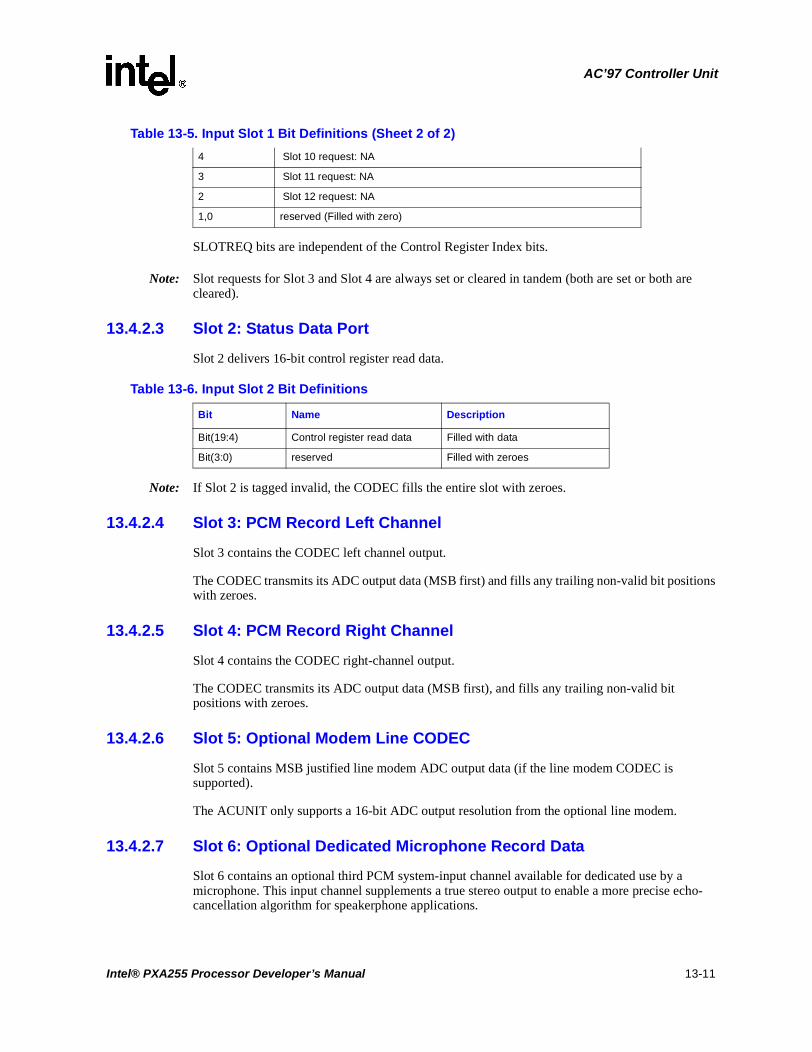
AC’97 Controller Unit
SLOTREQ bits are independent of the Control Register Index bits.
Note: Slot requests for Slot 3 and Slot 4 are always set or cleared in tandem (both are set or both are cleared).
13.4.2.3 Slot 2: Status Data Port
Slot 2 delivers 16-bit control register read data.
Note: If Slot 2 is tagged invalid, the CODEC fills the entire slot with zeroes.
13.4.2.4 Slot 3: PCM Record Left Channel
Slot 3 contains the CODEC left channel output.
The CODEC transmits its ADC output data (MSB first) and fills any trailing non-valid bit positions with zeroes.
13.4.2.5 Slot 4: PCM Record Right Channel
Slot 4 contains the CODEC right-channel output.
The CODEC transmits its ADC output data (MSB first), and fills any trailing non-valid bit positions with zeroes.
13.4.2.6 Slot 5: Optional Modem Line CODEC
Slot 5 contains MSB justified line modem ADC output data (if the line modem CODEC is supported).
The ACUNIT only supports a 16-bit ADC output resolution from the optional line modem.
13.4.2.7 Slot 6: Optional Dedicated Microphone Record Data
Slot 6 contains an optional third PCM system-input channel available for dedicated use by a microphone. This input channel supplements a true stereo output to enable a more precise echo-cancellation algorithm for speakerphone applications.
4 Slot 10 request: NA
3 Slot 11 request: NA
2 Slot 12 request: NA
1,0 reserved (Filled with zero)
Table 13-5. Input Slot 1 Bit Definitions (Sheet 2 of 2)
Table 13-6. Input Slot 2 Bit Definitions
Bit Name Description
Bit(19:4) Control register read data Filled with data
Bit(3:0) reserved Filled with zeroes
Intel® PXA255 Processor Developer’s Manual 13-11

AC’97 Controller Unit
The ACUNIT only supports a 16-bit resolution from the microphone.
13.4.2.8 Slots 7-11: Reserved
Slots 7-11 are reserved for future use. The ACUINT ignores them.
13.4.2.9 Slot 12: I/O Status
GPIOs which are configured as inputs return their status in Slot 12 of every frame. Only the 16 MSBs are used to return GPIO status. Bit 0 in the LSBs indicates a GPI Input Interrupt event. See the AC’97 revision 2.0 spec for more information.
The data returned on the latest frame is also accessible to software through the CODEC register at address 0x54 in the modem CODEC I/O space. Data received in Slot 12 is stored internally in the ACUNIT. So when software initiates a read of the CODEC register at address 0x54 in the modem CODEC I/O space, the read data is already inside the ACUNIT.
13.5 AC-link Low Power Mode
Software must set the ACLINK_OFF bit of the GCR to one before the processor enters Sleep Mode. The ACUNIT then drives SYNC and SDATA_OUT to a logic low level . The ACUNIT maintains nACRESET high when ACLINK_OFF is set to one.
13.5.1 Powering Down the AC-link
The AC-link signals enter a low power mode after the PR4 bit of the AC’97 CODEC Powerdown Register (0x26) is set to a 1 (by writing 0x1000). Then, the Primary CODEC drives both BITCLK and SDATA_IN to a logic low voltage level. The sequence follows the timing diagram shown in Figure 13-7.
Figure 13-7. AC-link Powerdown Timing
SDATA_OUT TAG
SYNC
BITCLK
Write to 0x26
Data PR4
slot 12 prev. frame
TAG slot 12 prev. frame SDATA_IN
Note: BITCLK not to scale
13-12 Intel® PXA255 Processor Developer’s Manual

AC’97 Controller Unit
The ACUNIT transmits the write to the Powerdown Register (0x26) over the AC-link. Set up the ACUNIT so that it does not transmit data in Slots 3-12 when it writes 0x1000 to the PR4 bit of the Powerdown Register. AC’97 revision 2.0 does not require the CODEC to process other data when it receives a power down request. When the CODEC receives the power down request, it immediately transitions BITCLK and SDATA_IN to a logic low level.
13.5.2 Waking up the AC-link
13.5.2.1 Wake up triggered by the CODEC
To wake up the AC-link, a CODEC drives SDATA_IN to a logic high level. The rising edge triggers the Resume Interrupt if that CODEC’s resume enable bit is set to a one. The CPU then wakes up the CODEC using the cold or warm reset sequence. The ACUNIT uses a warm reset to wake up the primary CODEC. The CODEC detects a warm reset when SYNC is driven high for a minimum of one microsecond and the BITCLK is absent. The CODEC must wait until it samples SYNC low before it can start BITCLK. The CODEC that signaled the wake event must keep its SDATA_IN high until it detects that a warm reset has been completed. The CODEC can then transition its SDATA_IN low.
Figure 13-8 shows the AC-link timing for a wake up triggered by a CODEC. Because the processor may need to be awakened, the Power Management unit detects the AC’97 wake-up event (SDATA_IN high for more than one microsecond). When the ACUNIT is ready, it responds to the wake-up event by asserting a warm or cold reset (see Figure 13-8). A Modem CODEC may require the capacity to wake up the AC-link to report events such as Caller-ID and wake-up-on-ring.
Figure 13-8. SDATA_IN Wake Up Signaling
NOTES:1. After SDATA_IN goes high, SYNC must be held for a minimum of 1 µSec.2. The minimum SDATA_IN wake up pulse width is 1 µSec.3. BITCLK not to scale
B1027-01
TAG
Note 1
Note 2
Notes:After SDATA_IN goes high, SYNC must be held for a minimum of 1 µSec.The minimum SDATA_IN wake up pulse width is 1 µSec.BITCLK not to scale.
slot12prev.frame
slot12prev.frame
TAG
TAG
TAG Slot1
Slot1
Slot2
Slot2
Writeto
0x26DataFR4
Power DownFrame
Codec SleepState
WakeEvent
New AudioFrame
SYNC
BITCLK
SDATA_OUT
SDATA_IN
Intel® PXA255 Processor Developer’s Manual 13-13
AC’97 Controller Unit
13.5.2.2 Wake Up Triggered by the ACUNIT
AC-link protocol provides for a cold AC’97 reset and a warm AC’97 reset. The current power-down state ultimately dictates which AC’97 reset is used. Registers must stay in the same state during all power-down modes unless a cold AC’97 reset is performed. In a cold AC’97 reset, the AC’97 registers are initialized to their default values.
After a power down, the AC-link must wait for a minimum of four audio frame times after the frame in which the power down occurred before it can be reactivated by reasserting the SYNC signal. When AC-link powers up, it indicates readiness through the CODEC ready bit (input slot 0, bit 15).
13.5.2.2.1 Cold AC’97 Reset
A cold reset is generated when the nACRESET pin is asserted by software setting the COLD_RST bit of the GCR to zero. Asserting and deasserting nACRESET activates SDATA_OUT and causes the CODEC to activate BITCLK. All AC’97 control registers are initialized to their default power-on reset values. nACRESET is an asynchronous input to the AC’97 CODEC.
13.5.2.2.2 Warm AC’97 Reset
A warm AC’97 reset reactivates the AC-link without altering the current AC’97 register values. A warm reset is generated by software setting the WARM_RST bit of the GCR to one. When BITCLK is absent, generation of a warm reset results in SYNC being driven high for a minimum of one microsecond. The CODEC must not activate BITCLK until it samples SYNC low again. This prevents a new audio frame from being falsely detected.
13.6 ACUNIT Operation
The ACUNIT can be accessed through the processor or the DMA controller. The processor uses programmed I/O instructions to access the ACUNIT, and it can access four register types:
• ACUNIT registers: Accessible at 32-bit boundaries. They are listed in Section 13.8.3.
• CODEC registers: An audio or modem CODEC can contain up to sixty-four 16-bit registers. A CODEC uses a 16-bit address boundary for registers. The ACUNIT supplies access to the CODEC registers by mapping them to its 32-bit address domain boundary. Section 13.8.3.17 describes the mapping from the 32-bit to 16-bit boundary. A write or read operation that targets these registers is sent across the AC-link.
• Modem CODEC GPIO register: If the ACUNIT is connected to a modem CODEC, the CODEC GPIO register can also be accessed. The CODEC GPIO register uses access address 0x0054 in the CODEC domain. The GPIO write operation goes across the AC-link, but a read does not. The GPIO register contents are continuously updated into a shadow register in the ACUNIT when a frame is received from the CODEC. When the processor tries to read the CODEC GPIO register, this shadow register is read instead.
• ACUNIT FIFO data: The ACUNIT has two Transmit FIFOs for audio-out and modem-out and three receive FIFOs for audio-in, modem-in, and mic-in. Data enters the transmit FIFOs by writing to either the PCM Data Register (PCDR) or the Modem Data Register (MODR).
13-14 Intel® PXA255 Processor Developer’s Manual

AC’97 Controller Unit
Receive FIFO entries are read through the PCDR, the MODR, or the Mic-in Data Register (MCDR).
Note: After it is enabled, the ACUNIT requests the DMA to fill the transmit FIFO.
Note: The ACUNIT registers do not store the status of DMA requests or information regarding the number of data samples in each FIFO. As a result, programmed I/O must not be used in place of DMA requests for data transfers.
Only the DMA can access the FIFOs. The DMA controller accesses FIFO data in 8-, 16-, or 32-byte blocks. The DMA request thresholds are not programmable.The ACUNIT makes a transmit DMA request when the transmit FIFO has less than 32 bytes. The ACUNIT makes a receive DMA request when the receive FIFO has 32 bytes or more. Regardless of burst size, the DMA descriptor length must be a multiple of 32 bytes to prevent audio artifacts from being introduced onto the AC-link.
The DMA controller responds to the following ACUNIT DMA requests:
• PCM FIFO transmit and receive DMA requests made when the PCM transmit and receive FIFOs are half full.
• Modem FIFO transmit and receive DMA requests made when the modem transmit and receive FIFOs are half full.
• Mic-in receive DMA requests made when the Mic-in receive FIFO is half full.
13.6.1 Initialization
The AC’97 CODEC and ACUNIT are reset on power up. After power up, the nACRESET signal remains asserted until the audio or modem driver sets the COLD_RST bit of the GCR to one. During operation, clearing the COLD_RST bit to zero resets the ACUNIT and CODEC. To initialize the ACUNIT follow theses steps:
1. Program the GPIO Direction register and GPIO Alternate Function Select register to assign proper pin directions for the ACUNIT ports. Refer to Section 13.3 for details.
2. Set the COLD_RST bit of the GCR to one to deassert nACRESET. Until this is done, all other registers remain in a reset state. Deasserting nACRESET has the following effects:
a. Frames filled with zeroes are transmitted because the transmit FIFO is still empty. This situation does not cause an error condition.
b. The ACUNIT records zeroes until the CODEC sends valid data.
c. DMA requests are enabled.
3. Enable the Primary Ready Interrupt Enable and/or the Secondary Ready Interrupt Enable by setting the PRIRDY_IEN bit and/or the SECRDY_IEN bit of the GCR to one.
4. Software enables DMA operation in response to primary and secondary ready interrupts.
5. The ACUNIT triggers transmit DMA requests. The DMA fills the transmit FIFO in response.
6. The ACUNIT continues to transmit zeroes until the transmit FIFO is half full. When it is half full, valid transmit FIFO data is sent across the AC-link.
Note: When nACRESET is deasserted, a read to the CODEC Mixer register returns the type of hardware that resides in the CODEC. If the CODEC is not present or if the AC’97 is not supported, the
Intel® PXA255 Processor Developer’s Manual 13-15

AC’97 Controller Unit
ACUNIT does not set the CODEC-ready bit, GCR[PCRDY] for the Primary CODEC or GCR[SCRDY] for the Secondary CODEC.
13-16 Intel® PXA255 Processor Developer’s Manual

AC’97 Controller Unit
13.6.2 Trailing bytes
Trailing bytes in the transmit and receive FIFOs are handled as follows:
If the transmit buffers do not have 32-byte resolution, the trailing bytes in the Transmit FIFO are not transmitted. A transmit buffer must be padded with zeroes if it is smaller than a multiple of 32 bytes. Regardless of burst size, the DMA descriptor length must be a multiple of 32 bytes to prevent audio artifacts from being introduced onto the AC-link.
If the CODEC transmitted data has a total buffer size smaller than a multiple of 32 bytes, zeroes are recorded. A receive DMA request is made when the receive FIFO is half-full.
13.6.3 Operational Flow for Accessing CODEC Registers
Software accesses the CODEC registers by translating a 32-bit processor physical address to a 7-bit CODEC address. For details regarding the address translation, refer to Section 13.8.3.17.
Software must read the CODEC Access Register (CAR) to lock the AC-link. The AC-link is free if the CAIP bit of the CAR is zero. For details about the CAR, refer to Table 13-13.
A read access to the CAR sets the CAIP bit. The ACUNIT clears the CAIP bit when the CODEC-write or CODEC-read operation completes. Software can also clear the CAIP bit by writing a zero to it.
After it locks the AC-link, software can write or read a CODEC register using the appropriate processor physical address.
The ACUNIT sets the CDONE bit of the GSR to one after the completion of a CODEC write operation. For details, refer to Table 13-8. Software clears this bit by writing a 1 to it.
To read a CODEC, the software must complete the following steps:
1. Software issues a dummy read to the CODEC register. The ACUNIT responds to this read operation with invalid data. The ACUNIT then initiates the read access across the AC-link.
2. When the CODEC read operation completes, the ACUNIT sets the SDONE bit of the GSR to one. For details, refer to Table 13-8. Software clears this bit by writing a 1 it.
3. Software repeats the read operation as detailed in Step 1. The ACUNIT now returns the data sent by the CODEC. The second read operation also initiates a read access across the AC-link.
4. The ACUNIT times-out the read operation if the CODEC fails to respond in four SYNC frames. In this case, the second read operation returns a timed-out data value of 0x0000_FFFF.
13.7 Clocks and Sampling Frequencies
By default, the ACUNIT transmits and receives data at a sampling frequency of 48 kHz. It can, however, sample data at frequencies less than 48 kHz if the CODEC supports on-demand slot requests. The CODEC in this case executes a certain algorithm and informs the ACUNIT not to transmit valid data in certain frames. For example, if the ACUNIT sends out 480 frames, and the CODEC instructs the ACUNIT not to send valid data in 39 of those 480 frames, the CODEC would have in effect sampled data at 44.1 kHz. When the CODEC transmits data (ACUNIT-receive mode), it can use the same algorithm to transmit valid frames with some empty ones mixed in between.
Intel® PXA255 Processor Developer’s Manual 13-17

AC’97 Controller Unit
All data transfers across the AC-link are synchronized to SYNC’s rising edge. The ACUNIT divides the BITCLK by 256 to generate the SYNC signal. This calculation yields a 48 kHz SYNC signal, and its period defines a frame. Data is transitioned on AC-link on every BITCLK rising edge and subsequently sampled on AC-link’s receiving side on each following BITCLK falling edge. For a timing diagram see Figure 13-3.
The ACUNIT synchronizes data between two different clock domains: the BITCLK and an internal system clock. This internal system clock is always half the run mode frequency. The run mode frequency is equal to or greater than eight times the BITCLK frequency.
13.8 Functional Description
The functional description section applies to all channels.
13.8.1 FIFOs
The ACUNIT has five FIFOs:
• PCM Transmit FIFO, with sixteen 32-bit entries.
• PCM Receive FIFO, with sixteen 32-bit entries.
• Modem Transmit FIFO, with sixteen 32-bit entries (upper 16 bits must always be zero).
• Modem Receive FIFO, with sixteen 32-bit entries (upper 16 bits are always zero).
• Mic-in Receive FIFO, with sixteen 32-bit entries (upper 16 bits are always zero).
A receive FIFO triggers a DMA request when the FIFO has eight or more entries. A transmit FIFO triggers a DMA request when it holds less than eight entries. A transmit FIFO must be half full (filled with eight entries) before any data is transmitted across the AC-link.
13.8.1.1 Transmit FIFO Errors
Channel-specific status bits are updated during transmit under-run conditions and will trigger interrupts if enabled. Refer to Table 13-11 and Table 13-20 for details regarding the status bits. During transmit under-run conditions, the last valid sample is continuously sent out across the AC-link. A transmit under-run can occur under the following conditions:
• Valid transmit data is still available in memory but the DMA controller starves the transmit FIFO because it is servicing other higher priority peripherals.
• The DMA controller has transferred all valid data from memory to the transmit FIFO. This prompts the last valid sample to be echoed across the AC-link until nACRESET is asserted to turn off the ACUNIT.
13.8.1.2 Receive FIFO Errors
Channel-specific status bits are updated during receive overrun conditions and trigger interrupts when enabled. Refer to Table 13-12, Table 13-16, and Table 13-21 for details regarding the status bits. During receive over-run conditions, data that the CODEC sends is not recorded.
13-18 Intel® PXA255 Processor Developer’s Manual

AC’97 Controller Unit
13.8.2 Interrupts
The following status bits interrupt the processor when the interrupts are enabled:
• Mic-in FIFO error: Mic-in Receive FIFO’s over-run or under-run error.
• Modem-in FIFO error: Modem Receive FIFO’s over-run or under-run error.
• PCM-in FIFO error: Audio Receive FIFO’s over-run or under-run error.
• Modem-out FIFO error: Modem Transmit FIFO’s over-run or under-run error.
• PCM-out FIFO error: Audio Transmit FIFO’s over-run or under-run error.
• Modem CODEC GPI status change interrupt: Interrupts the CPU if bit 0 of Slot 12 is set. This indicates a change in one of the bits in the modem CODEC’s GPIO register.
• Primary CODEC resume interrupt: Sets a status register bit when the Primary CODEC resumes from a lower power mode. Software writes a one to this bit to clear it.
• Secondary CODEC resume interrupt: Sets a status register bit when the Secondary CODEC resumes from a lower power mode. Software writes a one to this bit to clear it.
• CODEC command done interrupt: Interrupts the CPU when a CODEC register’s command is completed. Software writes a one to this bit to clear it.
• CODEC status done interrupt: Interrupts the CPU when a CODEC register’s status address and data reception are completed. Software writes a one to this bit to clear it.
• Primary CODEC ready interrupt: Sets a status register bit when the Primary CODEC is ready. The CODEC sets bit 0 of Slot 0 on the input frame to signal that it is ready. Software clears the PRIRDY_IEN bit of the GCR to clear this interrupt.
• Secondary CODEC ready interrupt: Sets a status register bit when the Secondary CODEC is ready. The CODEC sets bit 0 of Slot 0 on the input frame to signal that it is ready. Software clears the SECRDY_IEN bit of the GCR to clear this interrupt.
13.8.3 Registers
The ACUNIT and CODEC registers are mapped in addresses ranging from 0x4050_0000 through 0x405F_FFFF. All ACUNIT registers are 32-bit addressable. Even though a CODEC has up to sixty-four 16-bit registers that are 16-bit addressable, they are accessed via a 32-bit address map and translated to 16-bits for the CODEC.
Programmed I/O and DMA bursts can access the following registers:
• Global registers: The ACUNIT has three global registers: Status, Control, and CODEC access registers that are common to the audio and modem domains.
• Channel-specific audio ACUNIT registers refer to PCM-out, PCM-in, and mic-in channels.
• Channel-specific Modem ACUNIT registers refer to modem-out and modem-in channels.
• Audio CODEC registers
• Modem CODEC registers
Intel® PXA255 Processor Developer’s Manual 13-19

AC’97 Controller Unit
Channel specific data registers are for FIFO accesses and the PCM, Modem, and Mic-in FIFOs each have a register. A write access to one of these registers updates the written data in the corresponding Transmit FIFO. A read access to one of these registers flushes out an entry from the corresponding Receive FIFO.
Note: Register tables show organization and individual bit definitions. All reserved bits are read as unknown values and must be written with a 0. A question mark indicates the value is unknown at reset.
Note: Some register bits receive status from CODECs. The CODEC status sets the bit and software clears the bit (write a one to clear). The status can come in at any time, even when the bit is set or during a software clear. If software clears the bit as the CODEC status updates the bit, the CODEC status event takes higher priority. The term “interruptible” denotes bits that can be affected by this condition.
13.8.3.1 Global Control Register (GCR)
This is a read/write register. Ignore reads from reserved bits. Write zeros to reserved bits.
Table 13-7. GCR Bit Definitions (Sheet 1 of 2)
Physical Address4050_000C GCR Register AC’97 Controller Unit
Bit 31 30 29 28 27 26 25 24 23 22 21 20 19 18 17 16 15 14 13 12 11 10 9 8 7 6 5 4 3 2 1 0
reserved
CD
ON
E_I
E
SD
ON
E_I
E
reserved
SE
CR
DY
_IE
N
PR
IRD
Y_I
EN
rese
rved
SE
CR
ES
_IE
N
PR
IRE
S_I
EN
AC
LIN
K_O
FF
WA
RM
_RS
T
CO
LD
_RS
T
GIE
Reset 0 0 0 0 0 0 0 0 0 0 0 0 0 0 0 0 0 0 0 0 0 0 0 0 0 0 0 0 0 0 0 0
Bits Name Description
31:20 — reserved
19 CDONE_IE
Command Done Interrupt Enable (CDONE_IE):
0 = The ACUNIT does not trigger an interrupt to the CPU after sending the command address and data to the CODEC.
1 = The ACUNIT triggers an interrupt to the CPU after sending the command address and data to the CODEC.
18 SDONE_IE
Status Done Interrupt Enable (SDONE_IE):
0 = Interrupt is disabled1 = Enables an interrupt to occur after receiving the status address and data from the
CODEC
17:10 — reserved
9 SECRDY_IEN
Secondary Ready Interrupt Enable (SECRDY_IEN):
0 = Interrupt is disabled1 = Enables an interrupt to occur when the Secondary CODEC sends the CODEC READY
bit on the SDATA_IN_1 pin
8 PRIRDY_IEN
Primary Ready Interrupt Enable (PRIRDY_IEN):
0 = Interrupt is disabled1 = Enables an interrupt to occur when the Primary CODEC sends the CODEC READY bit
on the SDATA_IN_0 pin.
7:6 — reserved
13-20 Intel® PXA255 Processor Developer’s Manual

AC’97 Controller Unit
13.8.3.2 Global Status Register (GSR)
This is a read/write register. Ignore reads from reserved bits. Write zeros to reserved bits.
5 SECRES_IEN
Secondary Resume Interrupt Enable:
0 = Interrupt is disabled1 = Enables an interrupt to occur when the Secondary CODEC causes a resume event on
the AC-link
4 PRIRES_IEN
Primary Resume Interrupt Enable:
0 = Interrupt is disabled1 = Enables an interrupt to occur when the Primary CODEC causes a resume event on the
AC-link
3 ACLINK_OFF
AC-link Shut Off:
0 = If the AC-link was off, turns it back on, otherwise this bit has no effect.1 = Causes the ACUNIT to drive SDATA_OUT and SYNC outputs low and turn off input
buffer enables. The reset output is however maintained high. The AC-link will not be allowed to access any of the FIFOs.
Setting this bit does not ensure a clean shut down. Software must make sure that all transactions are complete before setting this bit.
2 WARM_RST
AC’97 Warm Reset
0 = A warm reset is not generated.1 = Causes a warm reset to occur on the AC-link. The warm reset will awaken a
suspended CODEC without clearing it’s internal registers.
If software attempts to perform a warm reset while BITCLK is running, the write will be ignored and the bit will not change. This bit is self clearing i.e., it remains set until the reset completes and BITCLK is seen on the AC-link after which it clears itself.
1 COLD_RST
AC'97 Cold Reset
0 = Causes a cold reset to occur throughout the AC'97 circuitry. All data in the ACUNIT and the CODEC will be lost.
1 = A cold reset is not generated.
Defaults to 0. After reset, the driver must to set this bit to a 1.The value of this bit is retained after suspends, hence, if this bit was set to a 1 before a suspend, a cold reset is not generated on a resume.
0 GIE
CODEC GPI Interrupt Enable (GIE)
This bit controls whether the change in status of any Modem CODEC GPI causes an interrupt.
0 = If this bit is not set, bit 0 of the Global Status Register is set, but an interrupt is not generated.
1 = If this bit is set, the change in value of a GPI (as indicated by bit 0 of slot 12) causes an interrupt and sets bit 0 of the Global Status Register
Table 13-7. GCR Bit Definitions (Sheet 2 of 2)
Physical Address4050_000C GCR Register AC’97 Controller Unit
Bit 31 30 29 28 27 26 25 24 23 22 21 20 19 18 17 16 15 14 13 12 11 10 9 8 7 6 5 4 3 2 1 0
reserved
CD
ON
E_I
E
SD
ON
E_I
E
reserved
SE
CR
DY
_IE
N
PR
IRD
Y_I
EN
rese
rved
SE
CR
ES
_IE
N
PR
IRE
S_I
EN
AC
LIN
K_O
FF
WA
RM
_RS
T
CO
LD
_RS
T
GIE
Reset 0 0 0 0 0 0 0 0 0 0 0 0 0 0 0 0 0 0 0 0 0 0 0 0 0 0 0 0 0 0 0 0
Bits Name Description
Intel® PXA255 Processor Developer’s Manual 13-21

AC’97 Controller Unit
Table 13-8. GSR Bit Definitions (Sheet 1 of 2)
Physical Address4050_001C GSR Register AC’97 Controller Unit
Bit 31 30 29 28 27 26 25 24 23 22 21 20 19 18 17 16 15 14 13 12 11 10 9 8 7 6 5 4 3 2 1 0
reserved
CD
ON
E
SD
ON
E
rese
rved
RD
CS
BIT
3SLT
12
BIT
2SLT
12
BIT
1SLT
12
SE
CR
ES
PR
IRE
S
SC
R
PC
R
MIN
T
PO
INT
PIIN
T
rese
rved
MO
INT
MIIN
T
GS
CI
Reset 0 0 0 0 0 0 0 0 0 0 0 0 0 0 0 0 0 0 0 0 0 0 0 0 0 0 0 0 0 0 0 0
Bits Name Description
31:20 — reserved
19 CDONE
Command Done (CDONE):
0 = ACUNIT has not sent command address and data to the CODEC.1 = ACUNIT has sent command address and data to the CODEC.
This bit is cleared by software writing a ‘1’ to this location (interruptible)
18 SDONE
Status Done (SDONE):
0 = ACUNIT has not received status address and data from the CODEC.1 = ACUNIT has received status address and data from the CODEC.
This bit is cleared by software writing a ‘1’ to this location (interruptible)
17:16 — reserved
15 RDCS
Read Completion Status:
This bit indicates the status of CODEC read completions.
0 = The CODEC read completed normally1 = The CODEC read resulted in a timeout.
The bit remains set until cleared by software. This bit is cleared by software writing a ‘1’ to this location.
14 BIT3SLT12Bit 3 of slot 12:
Display Bit 3 of the most recent valid slot 12
13 BIT2SLT12Bit 2 of slot 12:
Display Bit 2 of the most recent valid slot 12
12 BIT1SLT12Bit 1 of slot 12:
Display Bit 1 of the most recent valid slot 12
11 SECRES
Secondary Resume Interrupt:
0 = A resume event has not occurred on the SDATA_IN_1.1 = A resume event occurred on the SDATA_IN_1.
This bit is cleared by software writing a ‘1’ to this location (interruptible).
10 PRIRES
Primary Resume Interrupt:
0 = A resume event has not occurred on the SDATA_IN_0.1 = A resume event occurred on the SDATA_IN_0.
This bit is cleared by software writing a ‘1’ to this location (interruptible).
9 SCRSecondary CODEC Ready (SCR)
Reflects the state of the CODEC ready bit in SDATA_IN_1 (interruptible)
8 PCRPrimary CODEC Ready (PCR)
Reflects the state of the CODEC ready bit in SDATA_IN_0 (interruptible)
7 MINT
Mic In Interrupt (MINT)
0 = None of the mic-in channel interrupts occurred.1 = One of the mic-in channel interrupts occurred.
When the specific interrupt is cleared, this bit will be cleared (interruptible).
13-22 Intel® PXA255 Processor Developer’s Manual
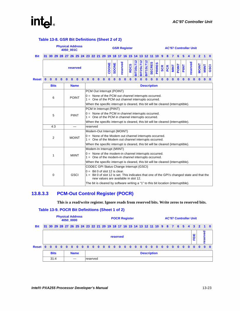
AC’97 Controller Unit
13.8.3.3 PCM-Out Control Register (POCR)
This is a read/write register. Ignore reads from reserved bits. Write zeros to reserved bits.
6 POINT
PCM Out Interrupt (POINT)
0 = None of the PCM out channel interrupts occurred.1 = One of the PCM out channel interrupts occurred.
When the specific interrupt is cleared, this bit will be cleared (interruptible).
5 PIINT
PCM In Interrupt (PIINT)
0 = None of the PCM in channel interrupts occurred.1 = One of the PCM in channel interrupts occurred.
When the specific interrupt is cleared, this bit will be cleared (interruptible).
4:3 — reserved
2 MOINT
Modem-Out Interrupt (MOINT)
0 = None of the Modem out channel interrupts occurred.1 = One of the Modem out channel interrupts occurred.
When the specific interrupt is cleared, this bit will be cleared (interruptible).
1 MIINT
Modem-In Interrupt (MIINT)
0 = None of the modem-in channel interrupts occurred.1 = One of the modem-in channel interrupts occurred.
When the specific interrupt is cleared, this bit will be cleared (interruptible).
0 GSCI
CODEC GPI Status Change Interrupt (GSCI)
0 = Bit 0 of slot 12 is clear.1 = Bit 0 of slot 12 is set. This indicates that one of the GPI’s changed state and that the
new values are available in slot 12.
The bit is cleared by software writing a “1” to this bit location (interruptible).
Table 13-8. GSR Bit Definitions (Sheet 2 of 2)
Physical Address4050_001C GSR Register AC’97 Controller Unit
Bit 31 30 29 28 27 26 25 24 23 22 21 20 19 18 17 16 15 14 13 12 11 10 9 8 7 6 5 4 3 2 1 0
reserved
CD
ON
E
SD
ON
E
rese
rved
RD
CS
BIT
3SLT
12
BIT
2SLT
12
BIT
1SLT
12
SE
CR
ES
PR
IRE
S
SC
R
PC
R
MIN
T
PO
INT
PIIN
T
rese
rved
MO
INT
MIIN
T
GS
CI
Reset 0 0 0 0 0 0 0 0 0 0 0 0 0 0 0 0 0 0 0 0 0 0 0 0 0 0 0 0 0 0 0 0
Bits Name Description
Table 13-9. POCR Bit Definitions (Sheet 1 of 2)
Physical Address4050_0000 POCR Register AC’97 Controller Unit
Bit 31 30 29 28 27 26 25 24 23 22 21 20 19 18 17 16 15 14 13 12 11 10 9 8 7 6 5 4 3 2 1 0
reserved
FE
IE
rese
rved
Reset 0 0 0 0 0 0 0 0 0 0 0 0 0 0 0 0 0 0 0 0 0 0 0 0 0 0 0 0 0 0 0 0
Bits Name Description
31:4 — reserved
Intel® PXA255 Processor Developer’s Manual 13-23

AC’97 Controller Unit
13.8.3.4 PCM-In Control Register (PICR)
This is a read/write register. Ignore reads from reserved bits. Write zeros to reserved bits.
3 FEIE
FIFO Error Interrupt Enable (FEIE)
This bit controls whether the occurrence of a transmit FIFO error will cause an interrupt or not.
0 = No interrupt will occur even if bit 4 in the POSR is set1 = An interrupt will occur if bit 4 in the POSR is set.
2:0 — reserved
Table 13-9. POCR Bit Definitions (Sheet 2 of 2)
Physical Address4050_0000 POCR Register AC’97 Controller Unit
Bit 31 30 29 28 27 26 25 24 23 22 21 20 19 18 17 16 15 14 13 12 11 10 9 8 7 6 5 4 3 2 1 0
reserved
FE
IE
rese
rved
Reset 0 0 0 0 0 0 0 0 0 0 0 0 0 0 0 0 0 0 0 0 0 0 0 0 0 0 0 0 0 0 0 0
Bits Name Description
Table 13-10. PICR Bit Definitions
Physical Address4050_0004 PICR Register AC’97 Controller Unit
Bit 31 30 29 28 27 26 25 24 23 22 21 20 19 18 17 16 15 14 13 12 11 10 9 8 7 6 5 4 3 2 1 0
reserved
FE
IE
rese
rved
Reset 0 0 0 0 0 0 0 0 0 0 0 0 0 0 0 0 0 0 0 0 0 0 0 0 0 0 0 0 0 0 0 0
Bits Name Description
31:4 — reserved
3 FEIE
FIFO Error Interrupt Enable (FEIE)
This bit controls whether the occurrence of a receive FIFO error will cause an interrupt or not.
0 = No interrupt will occur even if bit 4 in the PISR is set1 = An interrupt will occur if bit 4 in the PISR is set.
2:0 — reserved
13-24 Intel® PXA255 Processor Developer’s Manual

AC’97 Controller Unit
13.8.3.5 PCM-Out Status Register (POSR)
This is a read/write register. Ignore reads from reserved bits. Write zeros to reserved bits.
13.8.3.6 PCM_In Status Register (PISR)
This is a read/write register. Ignore reads from reserved bits. Write zeros to reserved bits.
Table 13-11. POSR Bit Definitions
Physical Address4050_0010 POSR Register AC’97 Controller Unit
Bit 31 30 29 28 27 26 25 24 23 22 21 20 19 18 17 16 15 14 13 12 11 10 9 8 7 6 5 4 3 2 1 0
reserved
FIF
OE
rese
rved
Reset 0 0 0 0 0 0 0 0 0 0 0 0 0 0 0 0 0 0 0 0 0 0 0 0 0 0 0 0 0 0 0 0
Bits Name Description
31:5 — reserved
4 FIFOE
FIFO error (FIFOE)
0 = No transmit FIFO errors have occurred1 = A transmit FIFO error occurred. This bit is set if a transmit FIFO underrun occurs. In
this case, the last valid sample is repetitively sent out and the pointers are not incremented.This could happen due to:
a. No more valid buffer data available for transmits.
b. Buffer data available but DMA controller has excessive bandwidth requirements.Bit is cleared by writing a 1 to this bit position.
3:0 — reserved
Table 13-12. PISR Bit Definitions
Physical Address4050_0014 PISR Register AC’97 Controller Unit
Bit 31 30 29 28 27 26 25 24 23 22 21 20 19 18 17 16 15 14 13 12 11 10 9 8 7 6 5 4 3 2 1 0
reserved
FIF
OE
rese
rved
Reset 0 0 0 0 0 0 0 0 0 0 0 0 0 0 0 0 0 0 0 0 0 0 0 0 0 0 0 0 0 0 0 0
Bits Name Description
31:5 — reserved
4 FIFOE
FIFO error (FIFOE)
0 = No Receive FIFO error has occurred.1 = A receive FIFO error occurred. This bit is set if a receive FIFO overrun occurs. In this
case, the FIFO pointers don't increment, the incoming data from the AC-link is not written into the FIFO and will be lost. This could happen due to DMA controller having excessive bandwidth requirements and hence not being able to flush out the receive FIFO in time.
Bit is cleared by writing a 1 to this bit position.
3:0 — reserved
Intel® PXA255 Processor Developer’s Manual 13-25

AC’97 Controller Unit
13.8.3.7 CODEC Access Register (CAR)This is a read/write register. Ignore reads from reserved bits. Write zeros to reserved bits.
13.8.3.8 PCM Data Register (PCDR)This is a read/write register. Ignore reads from reserved bits. Write zeros to reserved bits.
Writing a 32-bit sample to this register updates the data into the PCM Transmit FIFO. Reading this register gets a 32-bit sample from the PCM Receive FIFO.
Table 13-13. CAR Bit Definitions
Physical Address4050_0020 CAR Register AC’97 Controller Unit
Bit 31 30 29 28 27 26 25 24 23 22 21 20 19 18 17 16 15 14 13 12 11 10 9 8 7 6 5 4 3 2 1 0
reserved
CA
IP
Reset 0 0 0 0 0 0 0 0 0 0 0 0 0 0 0 0 0 0 0 0 0 0 0 0 0 0 0 0 0 0 0 0
Bits Name Description
31:1 — reserved
0 CAIP
CODEC Access In Progress (CAIP)
This bit is read by software to check whether a CODEC IO cycle is currently in progress.
0 = No cycle is in progress and the act of reading the register sets this bit to ‘1’. This reserves the right for the software driver to perform the IO cycle. Once the cycle is complete, this bit is automatically cleared. Software can clear this bit by writing a ‘0’ to this bit location if it decides not to perform a CODEC IO cycle after having read this bit.
1 = Indicates that another driver is performing a CODEC IO cycle across the AC-link and the currently accessing driver must try again later. (This bit applies to all CODEC IO cycles - GPIO or otherwise).
Table 13-14. PCDR Bit Definitions
Physical Address4050_0040 PCDR Register AC’97 Controller Unit
Bit 31 30 29 28 27 26 25 24 23 22 21 20 19 18 17 16 15 14 13 12 11 10 9 8 7 6 5 4 3 2 1 0
PCM_RDATA PCM_LDATA
Reset 0 0 0 0 0 0 0 0 0 0 0 0 0 0 0 0 0 0 0 0 0 0 0 0 0 0 0 0 0 0 0 0
Bits Name Description
31:16 PCM_RDATA PCM right-channel data
15:0 PCM_LDATA PCM left-channel data
13-26 Intel® PXA255 Processor Developer’s Manual

AC’97 Controller Unit
13.8.3.9 Mic-In Control Register (MCCR)
This is a read/write register. Ignore reads from reserved bits. Write zeros to reserved bits.
13.8.3.10 Mic-In Status Register (MCSR)
This is a read/write register. Ignore reads from reserved bits. Write zeros to reserved bits.
Figure 13-9. PCM Transmit and Receive Operation
TxEntry0
TxEntry1
TxEntry2
TxEntry3
TxEntry15
31Right Left
16 15 0
RxEntry0
RxEntry1
RxEntry2
RxEntry3
RxEntry15
31Right Left
16 15 0
PCDR Register
31 0
Processor/DMA
TxFIFOWritten
Processor/DMA
RxFIFORead
PCM Transmit FIFO PCM Receive FIFO
Write
Read
Transmit Data Receive Data
Table 13-15. MCCR Bit Definitions
Physical Address4050_0008 MCCR Register AC’97 Controller Unit
Bit 31 30 29 28 27 26 25 24 23 22 21 20 19 18 17 16 15 14 13 12 11 10 9 8 7 6 5 4 3 2 1 0
reserved
FE
IE
rese
rved
Reset 0 0 0 0 0 0 0 0 0 0 0 0 0 0 0 0 0 0 0 0 0 0 0 0 0 0 0 0 0 0 0 0
Bits Name Description
31:4 — reserved
3 FEIE
FIFO Error Interrupt Enable (FEIE
This bit controls whether the occurrence of a receive FIFO error will cause an interrupt or not.
0 = No interrupt will occur even if bit 4 in the MCSR is set1 = An interrupt will occur if bit 4 in the MCSR is set.
2:0 — reserved
Intel® PXA255 Processor Developer’s Manual 13-27

AC’97 Controller Unit
13.8.3.11 Mic-In Data Register (MCDR)
The Mic-In Data Register is a read-only register. A write to this register has no effect. A read to this register gets a 32-bit sample from the Mic-in Receive FIFO.
This is a read-only register. Ignore reads from reserved bits.
Table 13-16. MCSR Bit Definitions
Physical Address4050_0018 MCSR Register AC’97 Controller Unit
Bit 31 30 29 28 27 26 25 24 23 22 21 20 19 18 17 16 15 14 13 12 11 10 9 8 7 6 5 4 3 2 1 0
reserved
FIF
OE
rese
rved
Reset 0 0 0 0 0 0 0 0 0 0 0 0 0 0 0 0 0 0 0 0 0 0 0 0 0 0 0 0 0 0 0 0
Bits Name Description
31:5 — reserved
4 FIFOE
FIFO error (FIFOE)
0 = No Receive FIFO error has occurred.1 = A receive FIFO error occurred. This bit is set if a receive FIFO overrun occurs. In this
case, the FIFO pointers don't increment, the incoming data from the AC-link is not written into the FIFO and will be lost. This could happen due to DMA controller having excessive bandwidth requirements and hence not being able to flush out the Receive FIFO in time.
Bit is cleared by writing a 1 to this bit position.
3:0 — reserved
Table 13-17. MCDR Bit Definitions
Physical Address4050_0060 MCDR Register AC’97 Controller Unit
Bit 31 30 29 28 27 26 25 24 23 22 21 20 19 18 17 16 15 14 13 12 11 10 9 8 7 6 5 4 3 2 1 0
reserved MIC_IN_DAT
Reset 0 0 0 0 0 0 0 0 0 0 0 0 0 0 0 0 0 0 0 0 0 0 0 0 0 0 0 0 0 0 0 0
Bits Name Description
31:16 — reserved
15:0 MIC_IN_DAT mic-in data
13-28 Intel® PXA255 Processor Developer’s Manual

AC’97 Controller Unit
13.8.3.12 Modem-Out Control Register (MOCR)
This is a read/write register. Ignore reads from reserved bits. Write zeros to reserved bits.
13.8.3.13 Modem-In Control Register (MICR)
This is a read/write register. Ignore reads from reserved bits. Write zeros to reserved bits.
Figure 13-10. Mic-in Receive-Only Operation
RxEntry0
RxEntry1
RxEntry2
RxEntry3
RxEntry15
15 0
Processor/DMA
RxFIFORead
Mic-in Receive FIFOMCDR Register
31 01516
0x0000
Read
ReceiveData
Table 13-18. MOCR Bit Definitions
Physical Address4050_0100 MOCR Register AC’97
Bit 31 30 29 28 27 26 25 24 23 22 21 20 19 18 17 16 15 14 13 12 11 10 9 8 7 6 5 4 3 2 1 0
reserved
FE
IE
rese
rved
Reset 0 0 0 0 0 0 0 0 0 0 0 0 0 0 0 0 0 0 0 0 0 0 0 0 0 0 0 0 0 0 0 0
Bits Name Description
31:4 — reserved
3 FEIE
FIFO Error Interrupt Enable (FEIE)
This bit controls whether the occurrence of a transmit FIFO error will cause an interrupt or not.
0 = No interrupt will occur even if bit 4 in the MOSR is set1 = An interrupt will occur if bit 4 in the MOSR is set.
2:0 — reserved
Intel® PXA255 Processor Developer’s Manual 13-29

AC’97 Controller Unit
13.8.3.14 Modem-Out Status Register (MOSR)
This is a read/write register. Ignore reads from reserved bits. Write zeros to reserved bits.
13.8.3.15 Modem-In Status Register (MISR)
This is a read/write register. Ignore reads from reserved bits. Write zeros to reserved bits.
Table 13-19. MICR Bit Definitions
Physical Address4050_0108 MICR Register AC’97 Controller Unit
Bit 31 30 29 28 27 26 25 24 23 22 21 20 19 18 17 16 15 14 13 12 11 10 9 8 7 6 5 4 3 2 1 0
reserved
FE
IE
rese
rved
Reset 0 0 0 0 0 0 0 0 0 0 0 0 0 0 0 0 0 0 0 0 0 0 0 0 0 0 0 0 0 0 0 0
Bits Name Description
31:4 — reserved
3 FEIE
FIFO Error Interrupt Enable (FEIE)
Controls whether a receive FIFO error causes an interrupt.
0 = No interrupt will occur even if bit 4 in the MISR is set1 = An interrupt will occur if bit 4 in the MISR is set.
2:0 — reserved
Table 13-20. MOSR Bit Definitions
Physical Address4050_0110 MOSR Register AC’97 Controller Unit
Bit 31 30 29 28 27 26 25 24 23 22 21 20 19 18 17 16 15 14 13 12 11 10 9 8 7 6 5 4 3 2 1 0
reserved
FIF
OE
rese
rved
Reset 0 0 0 0 0 0 0 0 0 0 0 0 0 0 0 0 0 0 0 0 0 0 0 0 0 0 0 0 0 0 0 0
Bits Name Description
31:5 — reserved
4 FIFOE
FIFO error (FIFOE)
0 = No transmit FIFO errors have occurred1 = A transmit FIFO error occurred. This bit is set if a transmit FIFO underrun occurs. In
this case, the last valid sample is repetitively sent out and the pointers are not incremented.This could happen due to:
c. No more valid buffer data available for transmits.
d. Buffer data available but DMA controller has excessive bandwidth requirements.Bit is cleared by writing a 1 to this bit position.
3:0 — reserved
13-30 Intel® PXA255 Processor Developer’s Manual

AC’97 Controller Unit
13.8.3.16 Modem Data Register (MODR)
This is a read/write register. Ignore reads from reserved bits. Write zeros to reserved bits.
A 32-bit sample write to this register updates the data into the Modem Transmit FIFO. A read to this register gets a 32-bit sample from the Modem Receive FIFO.
Table 13-21. MISR Bit Definitions
Physical Address4050_0118 MISR Register AC’97 Controller Unit
Bit 31 30 29 28 27 26 25 24 23 22 21 20 19 18 17 16 15 14 13 12 11 10 9 8 7 6 5 4 3 2 1 0
reserved
FIF
OE
rese
rved
Reset 0 0 0 0 0 0 0 0 0 0 0 0 0 0 0 0 0 0 0 0 0 0 0 0 0 0 0 0 0 0 0 0
Bits Name Description
31:5 — reserved
4 FIFOE
FIFO error (FIFOE)
0 = No Receive FIFO error has occurred.1 = A receive FIFO error occurred. This bit is set if a receive FIFO overrun occurs. In this
case, the FIFO pointers don't increment, the incoming data from the AC-link is not written into the FIFO and will be lost. This could happen due to DMA controller having excessive bandwidth requirements and hence not being able to flush out the Receive FIFO in time.
Bit is cleared by writing a 1 to this bit position.
3:0 — reserved
Table 13-22. MODR Bit Definitions
Physical Address4050_0140 MODR Register AC’97 Controller Unit
Bit 31 30 29 28 27 26 25 24 23 22 21 20 19 18 17 16 15 14 13 12 11 10 9 8 7 6 5 4 3 2 1 0
reserved MODEM_DAT
Reset 0 0 0 0 0 0 0 0 0 0 0 0 0 0 0 0 0 0 0 0 0 0 0 0 0 0 0 0 0 0 0 0
Bits Name Description
31:16 — reserved
15:0 MODEM_DAT Modem data
Intel® PXA255 Processor Developer’s Manual 13-31

AC’97 Controller Unit
13.8.3.17 Accessing CODEC Registers
Each CODEC has up to sixty-four 16-bit registers that are addressable internal to the CODEC at half-word boundaries (16-bit boundaries). Because the processor only supports internal register accesses at word boundaries (32-bit boundaries), software must select the one of the following formulas to translate a 7-bit CODEC address into a 32-bit processor address:
• Processor physical address for a Primary Audio CODEC= 0x4050-0200 + Shift_Left_Once(Internal 7-bit CODEC Register Address)
• Processor physical address for a Secondary Audio CODEC = 0x4050-0300 + Shift_Left_Once(Internal 7-bit CODEC Register Address)
• Processor physical address for a Primary Modem CODEC = 0x4050-0400 + Shift_Left_Once(Internal 7-bit CODEC Register Address)
• Processor physical address for a Secondary Modem CODEC = 0x4050-0500 + Shift_Left_Once(Internal 7-bit CODEC Register Address)
In the equations, Shift_Left_Once() shifts the 7-bit CODEC address left by one bit and shifts a 0 to the LSB. The address translations are shown in Table 13-23.
Figure 13-11. Modem Transmit and Receive Operation
TxEntry0
TxEntry1
TxEntry2
TxEntry3
TxEntry15
15 0
RxEntry0
RxEntry1
RxEntry2
RxEntry3
RxEntry15
15 0
MODR Register
31 0
Processor/DMA Processor DMA
Modem Transmit FIFO Modem Receive FIFO1516
0x0000
Write Read
Transmitdata
ReceiveData
13-32 Intel® PXA255 Processor Developer’s Manual

AC’97 Controller Unit
Table 13-23. Address Mapping for CODEC Registers (Sheet 1 of 2)
7-bit CODEC Address
Processor Physical Address for a Primary Audio CODEC
Processor Physical Address for a Secondary Audio CODEC
Processor Physical Address for a Primary Modem CODEC
Processor Physical Address for a SecondaryModem CODEC
0x00 0x4050_0200 0x4050_0300 0x4050_0400 0x4050_0500
0x02 0x4050_0204 0x4050_0304 0x4050_0404 0x4050_0504
0x04 0x4050_0208 0x4050_0308 0x4050_0408 0x4050_0508
0x06 0x4050_020C 0x4050_030C 0x4050_040C 0x4050_050C
0x08 0x4050_0210 0x4050_0310 0x4050_0410 0x4050_0510
0x0A 0x4050_0214 0x4050_0314 0x4050_0414 0x4050_0514
0x0C 0x4050_0218 0x4050_0318 0x4050_0418 0x4050_0518
0x0E 0x4050_021C 0x4050_031C 0x4050_041C 0x4050_051C
0x10 0x4050_0220 0x4050_0320 0x4050_0420 0x4050_0520
0x12 0x4050_0224 0x4050_0324 0x4050_0424 0x4050_0524
0x14 0x4050_0228 0x4050_0328 0x4050_0428 0x4050_0528
0x16 0x4050_022C 0x4050_032C 0x4050_042C 0x4050_052C
0x18 0x4050_0230 0x4050_0330 0x4050_0430 0x4050_0530
0x1A 0x4050_0234 0x4050_0334 0x4050_0434 0x4050_0534
0x1C 0x4050_0238 0x4050_0338 0x4050_0438 0x4050_0538
0x1E 0x4050_023C 0x4050_033C 0x4050_043C 0x4050_053C
0x20 0x4050_0240 0x4050_0340 0x4050_0440 0x4050_0540
0x22 0x4050_0244 0x4050_0344 0x4050_0444 0x4050_0544
0x24 0x4050_0248 0x4050_0348 0x4050_0448 0x4050_0548
0x26 0x4050_024C 0x4050_034C 0x4050_044C 0x4050_054C
0x28 0x4050_0250 0x4050_0350 0x4050_0450 0x4050_0550
0x2A 0x4050_0254 0x4050_0354 0x4050_0454 0x4050_0554
0x2C 0x4050_0258 0x4050_0358 0x4050_0458 0x4050_0558
0x2E 0x4050_025C 0x4050_035C 0x4050_045C 0x4050_055C
0x30 0x4050_0260 0x4050_0360 0x4050_0460 0x4050_0560
0x32 0x4050_0264 0x4050_0364 0x4050_0464 0x4050_0564
0x34 0x4050_0268 0x4050_0368 0x4050_0468 0x4050_0568
0x36 0x4050_026C 0x4050_036C 0x4050_046C 0x4050_056C
0x38 0x4050_0270 0x4050_0370 0x4050_0470 0x4050_0570
0x3A 0x4050_0274 0x4050_0374 0x4050_0474 0x4050_0574
0x3C 0x4050_0278 0x4050_0378 0x4050_0478 0x4050_0578
0x3E 0x4050_027C 0x4050_037C 0x4050_047C 0x4050_057C
0x40 0x4050_0280 0x4050_0380 0x4050_0480 0x4050_0580
0x42 0x4050_0284 0x4050_0384 0x4050_0484 0x4050_0584
Intel® PXA255 Processor Developer’s Manual 13-33

AC’97 Controller Unit
0x44 0x4050_0288 0x4050_0388 0x4050_0488 0x4050_0588
0x46 0x4050_028C 0x4050_038C 0x4050_048C 0x4050_058C
0x48 0x4050_0290 0x4050_0390 0x4050_0490 0x4050_0590
0x4A 0x4050_0294 0x4050_0394 0x4050_0494 0x4050_0594
0x4C 0x4050_0298 0x4050_0398 0x4050_0498 0x4050_0598
0x4E 0x4050_029C 0x4050_039C 0x4050_049C 0x4050_059C
0x50 0x4050_02A0 0x4050_03A0 0x4050_04A0 0x4050_05A0
0x52 0x4050_02A4 0x4050_03A4 0x4050_04A4 0x4050_05A4
0x54 0x4050_02A8 0x4050_03A8 0x4050_04A8 0x4050_05A8
0x56 0x4050_02AC 0x4050_03AC 0x4050_04AC 0x4050_05AC
0x58 0x4050_02B0 0x4050_03B0 0x4050_04B0 0x4050_05B0
0x5A 0x4050_02B4 0x4050_03B4 0x4050_04B4 0x4050_05B4
0x5C 0x4050_02B8 0x4050_03B8 0x4050_04B8 0x4050_05B8
0x5E 0x4050_02BC 0x4050_03BC 0x4050_04BC 0x4050_05BC
0x60 0x4050_02C0 0x4050_03C0 0x4050_04C0 0x4050_05C0
0x62 0x4050_02C4 0x4050_03C4 0x4050_04C4 0x4050_05C4
0x64 0x4050_02C8 0x4050_03C8 0x4050_04C8 0x4050_05C8
0x66 0x4050_02CC 0x4050_03CC 0x4050_04CC 0x4050_05CC
0x68 0x4050_02D0 0x4050_03D0 0x4050_04D0 0x4050_05D0
0x6A 0x4050_02D4 0x4050_03D4 0x4050_04D4 0x4050_05D4
0x6C 0x4050_02D8 0x4050_03D8 0x4050_04D8 0x4050_05D8
0x6E 0x4050_02DC 0x4050_03DC 0x4050_04DC 0x4050_05DC
0x70 0x4050_02E0 0x4050_03E0 0x4050_04E0 0x4050_05E0
0x72 0x4050_02E4 0x4050_03E4 0x4050_04E4 0x4050_05E4
0x74 0x4050_02E8 0x4050_03E8 0x4050_04E8 0x4050_05E8
0x76 0x4050_02EC 0x4050_03EC 0x4050_04EC 0x4050_05EC
0x78 0x4050_02F0 0x4050_03F0 0x4050_04F0 0x4050_05F0
0x7A 0x4050_02F4 0x4050_03F4 0x4050_04F4 0x4050_05F4
0x7C 0x4050_02F8 0x4050_03F8 0x4050_04F8 0x4050_05F8
0x7E 0x4050_02FC 0x4050_03FC 0x4050_04FC 0x4050_05FC
Table 13-23. Address Mapping for CODEC Registers (Sheet 2 of 2)
7-bit CODEC Address
Processor Physical Address for a Primary Audio CODEC
Processor Physical Address for a Secondary Audio CODEC
Processor Physical Address for a Primary Modem CODEC
Processor Physical Address for a SecondaryModem CODEC
13-34 Intel® PXA255 Processor Developer’s Manual

AC’97 Controller Unit
13.9 AC’97 Register Summary
All AC’97 registers are word-addressable (32 bits wide) and increment in units of 0x00004. The registers in the CODEC are half-word addressable (16 bits wide), and increment in units of 0x00002. These register sets are mapped in the address range of 0x4050_000 through 0x405F_FFFF.
Table 13-24. Register Mapping Summary
Address Name Description
0x4050_0000 POCR PCM Out Control Register
0x4050_0004 PICR PCM In Control Register
0x4050_0008 MCCR Mic In Control Register
0x4050_000C GCR Global Control Register
0x4050_0010 POSR PCM Out Status Register
0x4050_0014 PISR PCM In Status Register
0x4050_0018 MCSR Mic-In Status Register
0x4050_001C GSR Global Status Register
0x4050_0020 CAR CODEC Access Register
0x4050_0024 - 0x4050_003C — reserved
0x4050_0040 PCDR PCM FIFO Data Register
0x4050_0044 - 0x4050_005C — reserved
0x4050_0060 MCDR Mic-in FIFO Data Register
0x4050_0064 - 0x4050_00FC — reserved
0x4050_0100 MOCR Modem-Out Control Register
0x4050_0104 — reserved
0x4050_0108 MICR Modem-In Control Register
0x4050_010C — reserved
0x4050_0110 MOSR Modem-Out Status Register
0x4050_0114 — reserved
0x4050_0118 MISR Modem-In Status Register
0x4050_011C - 0x4050_013C — reserved
0x4050_0140 MODR Modem FIFO Data Register
0x4050_0144 - 0x4050_01FC — reserved
(0x4050_0200 - 0x4050_02FC)
with all in increments of 0x00004— Primary Audio CODEC registers
(0x4050_0300 - 0x4050_03FC)
with all in increments of 0x00004— Secondary Audio CODEC registers
(0x4050_0400 - 0x4050_04FC)
with all in increments of 0x0000_0004— Primary Modem CODEC registers
(0x4050_0500 - 0x4050_05FC)
with all in increments of 0x00004— Secondary Modem CODEC registers
Intel® PXA255 Processor Developer’s Manual 13-35

AC’97 Controller Unit
13-36 Intel® PXA255 Processor Developer’s Manual

Inter-Integrated-Circuit Sound (I2S) Controller 14
I2S is a protocol for digital stereo audio. The I2S Controller (I2SC) functional block for the PXA255 processor controls the I2S link (I2SLINK), which is a low-power four-pin serial interface for stereo audio. The I2S interface and the Audio CODEC ‘97 (AC’97) interface may not be used at the same time.
14.1 Overview
The I2SC consists of buffers, status and control registers, serializers, and counters for transferring digitized audio between the processor system memory and an external I2S CODEC.
For playback of digitized audio or production of synthesized audio, the I2SC retrieves digitized audio samples from processor system memory and sends them to a CODEC through the I2SLINK. The external digital-to-analog converter in the CODEC then converts the audio samples into an analog audio waveform.
For recording of digitized audio, the I2SC receives digitized audio samples from a CODEC (through the I2SLINK) and stores them in processor system memory.
The I2S controller supports the normal-I2S and the MSB-Justified-I2S formats. Four, or optionally five, pins connect the controller to an external CODEC:
• A bit-rate clock, which can use either an internal or an external source.
• A formatting or “Left/Right” control signal.
• Two serial audio pins, one input and one output.
• The bit-rate clock, an optional system clock also sent to the CODEC by the I2SC.
The I2S data can be stored to and retrieved from system memory either by the DMA controller or by programmed I/O.
For I2S systems, additional pins are required to control the external CODEC. Some CODECs use an L3 control bus, which requires 3 signals — L3_CLK, L3_DATA, and L3_MODE — for writing bytes into the L3-bus register. The I2SC supports the L3 bus protocol via software control of the general-purpose I/O (GPIO) pins. The I2SC does not provide hardware control for the L3 bus protocol.
Two similar protocols exist for transmitting digitized stereo audio over a serial path: Normal-I2S and MSB-Justified-I2S. Both work with a variety of clock rates, which can be obtained by dividing the PLL clock by a programmable divider, or from an external clock source. For further details regarding clock rates, see Table 14-2.
Intel® PXA255 Processor Developer’s Manual 14-1

Inter-Integrated-Circuit Sound (I2S) Controller
14.2 Signal Descriptions
SYSCLK is the clock on which all other clocks in the I2S unit are based. SYSCLK generates a frequency between approximately 2 MHz and 12.2 MHz by dividing down the PLL clock with a programmable divisor. This frequency is always 256 times the audio sampling frequency. SYSCLK is driven out of the processor system only if BITCLK is configured as an output.
BITCLK supplies the serial audio bit rate, which is the basis for the external CODEC bit-sampling logic. BITCLK is one-quarter the frequency of SYSCLK and is 64 times the audio sampling frequency. One bit of the serial audio data sample is transmitted or received each BITCLK period. A single serial audio sample comprises a “left” and “right” signal, each containing either 8, 16 or 32 bits.
SYNC is BITCLK divided by 64, resulting in an 8 kHz to 48 kHz signal. The state of SYNC is used to denote whether the current serial data samples are “Left” or “Right” channel data.
The SDATA_IN and SDATA_OUT data pins are used to send/receive the serial audio data to/from the CODEC.
Table 14-1 lists the signals between the I2S and an external CODEC device.
BITCLK can be configured either as an input or as an output. To program the direction, follow these steps:
1. Program SYSUNIT’s GPIO Direction Register (GPDR). See Section 4.1.3.2, “GPIO Pin Direction Registers (GPDR0, GPDR1, GPDR2)” on page 4-8 for details regarding the GPDR.
2. Program SYSUNIT’s GPIO Alternate Function Select Register (GAFR). See Section 4.1.3.6, “GPIO Alternate Function Register (GAFR0_L, GAFR0_U, GAFR1_L, GAFR1_U, GAFR2_L, GAFR2_U)” on page 4-16 for details regarding the GAFR.
3. Program the BCKD bit in the I2SC’s Serial Audio Control Register. See Section 14.6.1, “Serial Audio Controller Global Control Register (SACR0)” for more details.
Note: Modifying the status of the SACR0[BCKD] bit during normal operation can cause jitter on the BITCLK and can affect serial activity.
If BITCLK is an output, SYSCLK must be configured as an output. If BITCLK is supplied by the CODEC, the GPIO pin GP32 can be used for an alternate function. To configure the pin as an output, follow these steps:
1. Program SYSUNIT’s GPIO Direction Register (GPDR). See Section 4.1.3.2, “GPIO Pin Direction Registers (GPDR0, GPDR1, GPDR2)” on page 4-8 for details regarding the GPDR.
Table 14-1. External Interface to CODEC
Name Direction Description
GP32/SYSCLK O System Clock = BITCLK * 4 used by the CODEC only.
GP28/BITCLK I or O bit-rate clock = SYNC * 64
GP31/SYNC O Left/Right identifier
GP30/SDATA_OUT O Serial audio output data to CODEC
GP29/SDATA_IN I Serial audio input data from CODEC
14-2 Intel® PXA255 Processor Developer’s Manual

Inter-Integrated-Circuit Sound (I2S) Controller
2. Program SYSUNIT’s GPIO Alternate Function Select Register (GAFR). See Section 4.1.3.6, “GPIO Alternate Function Register (GAFR0_L, GAFR0_U, GAFR1_L, GAFR1_U, GAFR2_L, GAFR2_U)” on page 4-16 for details regarding the GAFR.
To configure SYNC and SDATA_OUT as outputs, follow these steps:
1. Program SYSUNIT’s GPIO Direction Register (GPDR). See Section 4.1.3.2, “GPIO Pin Direction Registers (GPDR0, GPDR1, GPDR2)” on page 4-8 for details regarding the GPDR.
2. Program SYSUNIT’s GPIO Alternate Function Select Register (GAFR). See Section 4.1.3.6, “GPIO Alternate Function Register (GAFR0_L, GAFR0_U, GAFR1_L, GAFR1_U, GAFR2_L, GAFR2_U)” on page 4-16 for details regarding the GAFR.
To configure SDATA_IN as an input, follow these steps:
1. Program SYSUNIT’s GPIO Direction Register (GPDR). See Section 4.1.3.2, “GPIO Pin Direction Registers (GPDR0, GPDR1, GPDR2)” on page 4-8 for details regarding the GPDR.
2. Program SYSUNIT’s GPIO Alternate Function Select Register (GAFR). See Section 4.1.3.6, “GPIO Alternate Function Register (GAFR0_L, GAFR0_U, GAFR1_L, GAFR1_U, GAFR2_L, GAFR2_U)” on page 4-16 for details regarding the GAFR.
14.3 Controller Operation
The I2S Controller (I2SC) can be accessed either by the processor or by the DMA controller.
The processor uses programmed I/O instructions to access the I2SC and can access the following types of data:
• I2SC registers data — All registers are 32 bits wide and are aligned to word boundaries. See Section 14.6 for further details.
• I2SC FIFO data — An entry is placed into the Transmit FIFO by writing to the I2SC’s Serial Audio Data register (SADR). Writing to SADR updates a Transmit FIFO entry. Reading SADR flushes out a Receive FIFO entry.
• I2S CODEC data — The CODEC registers can be accessed through the L3 bus. The L3 bus operation is emulated by software controlling 3 GPIO pins.
The DMA controller can only access the FIFOs. Accesses are made through the SADR, as explained in the previous paragraph. The DMA controller accesses FIFO data in blocks of 8, 16, or 32 bytes. The DMA controller responds to the following DMA requests made by the I2SC:
• The Transmit FIFO request is based on the transmit threshold (TFTH) setting and is asserted if the Transmit FIFO has less than TFTH+1 entries. See Table 14-3 for further details regarding TFTH.
• The Receive FIFO request is based on the receive threshold (RFTH) setting and is asserted if the Receive FIFO has RFTH+1 or more entries. See Table 14-3 for further details regarding RFTH.
14.3.1 Initialization
1. Set the BITCLK direction by programming the SYSUNIT’s GPIO Direction register, the SYSUNIT’s GPIO Alternate Function Select register, and bit 2 of the I2SC’s Serial Audio Controller Global Control Register (SACR0).
Intel® PXA255 Processor Developer’s Manual 14-3

Inter-Integrated-Circuit Sound (I2S) Controller
2. Choose between Normal I2S or MSB-Justified modes of operation. This can be done by programming bit 0 of Serial Audio Controller I2S/MSB-Justified Control Register (SACR1). For further details, see Section 14.6.2.
3. Optional: Programmed I/O may be used for priming the Transmit FIFO with a few samples (ranging from 1 to 16). If the I2SLINK is enabled with an empty Transmit FIFO, a Transmit Under-run error bit will be set in the Status register. For further details, see Section 14.6.3. This is hence an optional step, which prevents such an error. If Step 3 is not executed, then Programmed I/O must clear the Transmit Under-run status bit by setting bit 5 of the Interrupt Clear Register. For further details, see Section 14.6.5.
4. The following control bits can be simultaneously programmed in the I2SC’s Serial Audio Controller Global Control register (SACR0):
a. Enable I2SLINK by setting the ENB bit (bit-0) of SACR0.
b. Maintain BITCLK direction as programmed in Step1. Modifying BITCLK direction will glitch the clock and affect I2SLINK activity.
c. Program transmit and receive threshold levels by programming the TFTH and RFTH bits of SACR0[11:8] and SACR0(15:12), respectively. See Section 14.6.1.2, regarding permitted threshold levels.
Once the I2SLINK is enabled, frames filled with 0s will be transmitted if the Transmit FIFO is still empty. This will set a Transmit Under-run status bit in SASR0. Step 3 can be executed to avoid this error condition. Valid data is sent across the I2SLINK after filling the Transmit FIFO with at least one sample. One sample consists of a 32-bit value with 16 bits each dedicated to a left and a right value.
Enabling the I2SLINK will also cause zeros to be recorded by the I2SC until the CODEC sends in valid data.
Enabling the I2SLINK also enables transmit and receive DMA Requests.
14.3.2 Disabling and Enabling Audio Replay
Audio transmission is enabled automatically when the I2SC is enabled. Transmission, or replay, can be stopped by asserting the DRPL bit of the SACR1 Register. For more details, see Section 14.6.2.
Asserting the DRPL bit in SACR1 has the following effects:
1. All I2SLINK replay activity is disabled. The frame or data sample, in the midst of which the replay is disabled, will have invalid data (some data bits will be over-written with zeros). To avoid this, disable replay only after the transfer of valid data. In this case, frames with zeros are transmitted.
2. Transmit FIFO pointers are reset to zero.
3. Transmit FIFO fill-level is reset to zero.
4. Zeros are transmitted across the I2SLINK.
5. Transmit DMA requests are disabled.
14.3.3 Disabling and Enabling Audio Record
Audio recording is enabled automatically when the I2SC is enabled. Recording can also be stopped by asserting the DREC bit of the SACR1 Register. For more details, see Section 14.6.2.
14-4 Intel® PXA255 Processor Developer’s Manual

Inter-Integrated-Circuit Sound (I2S) Controller
Asserting the DREC bit in SACR1 has the following effects:
1. I2SLINK recording activity is disabled. The frame or data sample, in the midst of which the recording is disabled, could have invalid data (some data bits will be over-written with zeros). To avoid this, disable record only after the transfer of valid data.
2. Receive FIFO pointers are reset to zero.
3. Receive FIFO fill-level is reset to zero.
4. Any read operations by the DMA/CPU are returned with zeros.
5. Receive DMA requests are disabled.
14.3.4 Transmit FIFO Errors
A status bit is set during Transmit Under-run conditions. If enabled, this can trigger an interrupt. For further details, see Section 14.6.3, Section 14.6.6 and Section 14.6.5. During Transmit Under-run conditions, the last valid sample is continuously sent out across the I2SLINK. Transmit Under-run can occur under the following conditions:
1. Valid transmit data is still available in memory, but the DMA controller starves the Transmit FIFO, as it is busy servicing other higher-priority peripherals.
2. The DMA controller has transferred all valid data from memory to the Transmit FIFO.
During the second condition, the last valid sample is continuously sent across the I2SLINK until the I2SC is turned off by disabling the SACR0[ENB] bit.
14.3.5 Receive FIFO Errors
A status bit is set during Receive Over-run conditions. If enabled, this can trigger an interrupt. For further details, see Section 14.6.3, Section 14.6.6 and Section 14.6.5. During Receive Over-run conditions, data sent by the CODEC is lost (will not be recorded).
14.3.6 Trailing Bytes
When the CODEC has completed transmitting valid data, zeros will be recorded by the I2SC, and this will continue until the unit is turned off by disabling the SACR0[ENB] bit.
If the total buffer size of the received data is less than a factor of the receive threshold, zeross will be recorded. A receive DMA request is made when the programmed threshold is reached.
14.4 Serial Audio Clocks and Sampling Frequencies
The BITCLK is the rate at which audio data bits enter or leave the I2SLINK. If BITCLK is an output, SYSCLK is used by the CODEC to run delta sigma ADC operations.
BITCLK can be supplied either by the CODEC or by an internal PLL. If supplied internally, BITCLK and SYSCLK are configured as output pins, and both are supplied to the CODEC. If BITCLK is supplied by the CODEC, then it is configured as an input pin. In this case, the SYSCLK’s GPIO pin can be used for an alternate function.
Intel® PXA255 Processor Developer’s Manual 14-5

Inter-Integrated-Circuit Sound (I2S) Controller
The BITCLK, as shown in Table 14-2, is different for different sampling frequencies. If the BITCLK is chosen as an output, the Audio Clock Divider Register divides the 147.46MHz PLL clock to generate the SYSCLK. The SYSCLK is further divided by four to generate the BITCLK. The sampling frequency is the frequency of the SYNC signal, which is generated by dividing the BITCLK by 64. See Section 14.6.4, for further details about the register.
A sampling rate of 48kHz supports MPEG2 and MPEG4. A rate of 44.1kHz supports MP3.
14.5 Data Formats
14.5.1 FIFO and Memory Format
FIFO buffers are 16 levels deep and 32 bits wide. This stores 32 samples per channel in each direction.
Audio data is stored with two samples (Left + Right) per 32-bit word, even if samples are smaller than 16 bits. The Left channel data occupies bits [15:0], while the Right channel data uses bits [31:16] of the 32-bit word. Within each 16-bit field, the audio sample is left-justified, with unused bits packed as zeroes on the right-hand (LSB) side.
In memory, the mapping of stereo samples is the same as in the FIFO buffers. However, single-channel audio occupies a full 32-bit word per sample, using either the upper or lower half of the word, depending on whether it’s considered a Left or Right sample.
14.5.2 I2S and MSB-Justified Serial Audio Formats
I2S and MSB-Justified are similar protocols for digitized stereo audio transmitted over a serial path.
The BITCLK supplies the serial audio bit rate, the basis for the external CODEC bit-sampling logic. Its frequency is 64 times the audio sampling frequency. Divided by 64, the resulting 8 kHz to 48 kHz signal signifies timing for Left and Right serial data samples passing on the serial data paths. This Left/Right signal is sent to the CODEC on the SYNC pin. Each phase of the Left/Right signal is accompanied by one serial audio data sample on the data pins SDATA_IN and SDATA_OUT.
Table 14-2. Supported Sampling Frequencies
Audio Clock Divider
Register(31:0)
SYSCLK = 147.6 MHz / (SADIV)
BITCLK =SYSCLK / 4
SYNC or Sampling frequency =BITCLK / 64
0x0000_000C 12.288 MHz 3.072 MHz 48.000 kHz (closest std = 48 kHz)
0x0000_000D 11.343 MHz 2.836 MHz 44.308 kHz (closest std = 44.1 kHz)
0x0000_001A 5.671 MHz 1.418 MHz 22.154 kHz (closest std = 22.05 kHz)
0x0000_0024 4.096 MHz 1.024 MHz 16.000 kHz (closest std = 16.00 kHz)
0x0000_0034 2.836 MHz 708.92 kHz 11.077 kHz (closest std = 11.025 kHz)
0x0000_0048 2.048 MHz 512.00 kHz 8.000 kHz (closest std = 8.00 kHz)
14-6 Intel® PXA255 Processor Developer’s Manual

Inter-Integrated-Circuit Sound (I2S) Controller
Figure 14-1 and Figure 14-2 provide timing diagrams that show formats for I2S and MSB-justified modes of operations.
Data is transmitted and received in frames of 64 BITCLK cycles. Each frame consists of a Left sample and a Right sample. Each frame holds 16-bits of valid sample data (shown in the figures) and 16-bits of padded zeros (not shown in the figures). The transmit and receive FIFOs only hold valid sample data (not padded zero data).
In the Normal I2S mode, the SYNC is low for the Left sample and high for the Right sample. Also, the MSB of each data sample lags behind the SYNC edges by one BITCLK cycle.
In the MSB-Justified mode, the SYNC is high for the Left sample and low for the Right sample. Also, the MSB of each data sample is aligned with the SYNC edges.
Figure 14-1. I2S Data Formats (16 bits)
Figure 14-2. MSB-Justified Data Formats (16 bits
A8842-01
SYNC
BITCLK
Note: Timing for SData_In is identical to SData_Out.
SData_Out
cycle0
Left Right
0 1 2
15 14 13 3 2 1 0 15 14 13 12 3 2 1 0
3 13 14 15 16 29 30 31 32 33 34 35 45 46 47 48 62 63 0
A8843-01
SYNC
BITCLK
Note: Timing for SData_In is identical to SData_Out.
SData_Out
cycle0
Left Right
0 1 2
15 14 13 3 2 1 0 15 14 13 12 3 2 1 0
3 13 14 15 16 29 30 31 32 33 34 35 45 46 47 48 62 63 0
Intel® PXA255 Processor Developer’s Manual 14-7

Inter-Integrated-Circuit Sound (I2S) Controller
14.6 Registers
The I2S Controller registers are all 32-bit addressable, ranging from 0x4040_0000 through 0x404F_FFFF.
The I2S Controller has the following types of registers:
• Control registers are used to program common control, alternate mode specific control.
• The Data Register is used for Transmit and Receive FIFO accesses.
• The Status Register signals the state of the FIFO buffers and the status of the interface that is selected by the common control register.
• The Interrupt Registers include the Interrupt Mask Register, the Interrupt Clear Register, and the Interrupt Test Register.
14.6.1 Serial Audio Controller Global Control Register (SACR0)
SACR0, shown in Table 14-3, controls common I2S functions.
The ENB bit controls the I2SLINK, as follows:
• Clearing ENB to zero does the following:
— disables any I2SLINK activity
— resets all Receive FIFO pointers and also the counter that controls the I2SLINK
— resets the Receive FIFO
— does not affect the Transmit FIFO
— the output pin SYNC will not toggle
— de-asserts all DMA requests
— any read accesses to the Data Register (SADR), by the processor, or by the DMA controller is returned with zeros
— disables all interrupts.
• Setting ENB to one does the following:
— enables I2SLINK activity
— enables DMA requests.
Note: If ENB is toggled in the middle of a normal operation, the RST bit must also be set and cleared to reset all I2SC registers.
Note: The SACR0[ENB] control signal crosses clock domains. It is registered in an internal clock domain that is much faster than the BITCLK domain. It takes four BITCLK cycles and four internal clock cycles before SACR0[ENB] is conveyed to the slower BITCLK domain. If the control setting is modified at a rate faster than (4 BITCLK + 4 internal clock) cycles, the last updated value in this time frame is stored in a temporary register and is transferred to the BITCLK domain.
This is a read/write register. Ignore reads from reserved bits. Write zeros to reserved bits.
14-8 Intel® PXA255 Processor Developer’s Manual
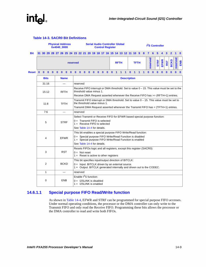
Inter-Integrated-Circuit Sound (I2S) Controller
14.6.1.1 Special purpose FIFO Read/Write function
As shown in Table 14-4, EFWR and STRF can be programmed for special purpose FIFO accesses. Under normal operating conditions, the processor or the DMA controller can only write to the Transmit FIFO and only read the Receive FIFO. Programming these bits allows the processor or the DMA controller to read and write both FIFOs.
Table 14-3. SACR0 Bit Definitions
Physical Address0x4040_0000
Serial Audio Controller Global Control Register I2S Controller
Bit 31 30 29 28 27 26 25 24 23 22 21 20 19 18 17 16 15 14 13 12 11 10 9 8 7 6 5 4 3 2 1 0
reserved RFTH TFTH
rese
rved
ST
RF
EF
WR
RS
T
BC
KD
rese
rved
EN
B
Reset 0 0 0 0 0 0 0 0 0 0 0 0 0 0 0 0 0 1 1 1 0 1 1 1 0 0 0 0 0 0 0 0
Bits Name Description
31:16 — reserved
15:12 RFTHReceive FIFO interrupt or DMA threshold. Set to value 0 – 15. This value must be set to the threshold value minus 1.
Receive DMA Request asserted whenever the Receive FIFO has >= (RFTH+1) entries.
11:8 TFTHTransmit FIFO interrupt or DMA threshold. Set to value 0 – 15. This value must be set to the threshold value minus 1.
Transmit DMA Request asserted whenever the Transmit FIFO has < (TFTH+1) entries.
7:6 — reserved
5 STRF
Select Transmit or Receive FIFO for EFWR based special purpose function:
0 = Transmit FIFO is selected1 = Receive FIFO is selected
See Table 14-4 for details.
4 EFWR
This bit enables a special purpose FIFO Write/Read function:
0 = Special purpose FIFO Write/Read Function is disabled 1 = Special purpose FIFO Write/Read Function is enabled
See Table 14-4 for details.
3 RSTResets FIFOs logic and all registers, except this register (SACR0):
0 = Not reset1 = Reset is active to other registers
2 BCKDThis bit specifies input/output direction of BITCLK:
0 = Input. BITCLK driven by an external source.1 = Output. BITCLK generated internally and driven out to the CODEC.
1 — reserved
0 ENBEnable I2S function:
0 = I2SLINK is disabled1 = I2SLINK is enabled
Intel® PXA255 Processor Developer’s Manual 14-9

Inter-Integrated-Circuit Sound (I2S) Controller
14.6.1.2 Suggested TFTH and RFTH for DMA servicing
The DMA controller can only be programmed to transfer 8, 16, or 32 bytes of data. This corresponds to 2, 4, or 8 FIFO samples. Table 14-5 shows the recommended TFTH and RFTH values to prevent Transmit FIFO over-run errors and Receive FIFO under-run errors.
14.6.2 Serial Audio Controller I2S/MSB-Justified Control Register (SACR1)
SACR1, shown in Table 14-6, specifically controls the I2S and MSB-Justified modes.
SACR1 bits DRPL, DREC, and AMSL cross clock domains. They are registered in an internal clock domain that is much faster than the BITCLK domain. It takes 4 BITCLK cycles and 4 internal clock cycles before these controls are conveyed to the slower BITCLK domain. If the above control settings are modified at a rate faster than (4 BITCLK + 4 internal clock) cycles, the last updated value in this time frame is stored in a temporary register and is transferred to the BITCLK domain.
This is a read/write register. Ignore reads from reserved bits. Write zeros to reserved bits.
Table 14-4. FIFO Write/Read table
EFWR STRF Description
0 x
Normal CPU/DMA Write/Read condition:
• A write access to the Data Register writes a Transmit FIFO entry.
• A read access to the Data Register reads out a Receive FIFO entry.
• I2SLINK reads from the Transmit FIFO and writes to the Receive FIFO.
1 0
CPU or DMA only writes and reads Transmit FIFO:
• A write access to the Data Register writes a Transmit FIFO entry.
• A read access to the Data Register reads out a Transmit FIFO entry.
• I2SLINK cannot read the Transmit FIFO but can write to the Receive FIFO.
1 1
CPU or DMA only writes and reads Receive FIFO:
• A write access to the Data Register writes a Receive FIFO entry.
• A read access to the Data Register reads out a Receive FIFO entry.
• I2SLINK can read the Transmit FIFO but cannot write to the Receive FIFO.
Table 14-5. TFTH and RFTH Values for DMA Servicing
DMA Transfer Size # of FIFO entries TFTH Value RFTH Value
Min Max Min Max
8 Bytes 2 0 14 1 15
16 Bytes 4 0 12 3 15
32 Bytes 8 0 8 7 15
14-10 Intel® PXA255 Processor Developer’s Manual
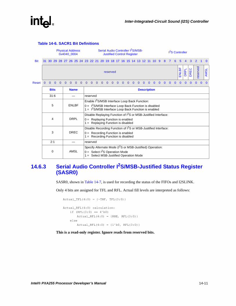
Inter-Integrated-Circuit Sound (I2S) Controller
14.6.3 Serial Audio Controller I2S/MSB-Justified Status Register (SASR0)
SASR0, shown in Table 14-7, is used for recording the status of the FIFOs and I2SLINK.
Only 4 bits are assigned for TFL and RFL. Actual fill levels are interpreted as follows:
Actual_TFL(4:0) = ~TNF, TFL(3:0)
Actual_RFL(4:0) calculation:
if (RFL(3:0) == 4’b0)
Actual_RFL(4:0) = RNE, RFL(3:0)
else
Actual_RFL(4:0) = 1’b0, RFL(3:0)
This is a read-only register. Ignore reads from reserved bits.
Table 14-6. SACR1 Bit Definitions
Physical Address0x4040_0004
Serial Audio Controller I2S/MSB-Justified Control Register
I2S Controller
Bit 31 30 29 28 27 26 25 24 23 22 21 20 19 18 17 16 15 14 13 12 11 10 9 8 7 6 5 4 3 2 1 0
reserved
EN
LBF
DR
PL
DR
EC
rese
rved
AM
SL
Reset 0 0 0 0 0 0 0 0 0 0 0 0 0 0 0 0 0 0 0 0 0 0 0 0 0 0 0 0 0 0 0 0
Bits Name Description
31:6 — reserved
5 ENLBFEnable I2S/MSB Interface Loop Back Function:
0 = I2S/MSB Interface Loop Back Function is disabled 1 = I2S/MSB Interface Loop Back Function is enabled
4 DRPLDisable Replaying Function of I2S or MSB-Justified Interface:
0 = Replaying Function is enabled 1 = Replaying Function is disabled
3 DRECDisable Recording Function of I2S or MSB-Justified Interface:
0 = Recording Function is enabled 1 = Recording Function is disabled
2:1 — reserved
0 AMSLSpecify Alternate Mode (I2S or MSB-Justified) Operation:
0 = Select I2S Operation Mode 1 = Select MSB-Justified Operation Mode
Intel® PXA255 Processor Developer’s Manual 14-11

Inter-Integrated-Circuit Sound (I2S) Controller
14.6.4 Serial Audio Clock Divider Register (SADIV)
SADIV, shown in Table 14-8, is used for generating six different BITCLK frequencies and hence six different sampling frequencies.
Table 14-7. SASR0 Bit Definitions
Physical Address0x4040_000C
Serial Audio Controller I2S/MSB-Justified Status Register
I2S Controller
Bit 31 30 29 28 27 26 25 24 23 22 21 20 19 18 17 16 15 14 13 12 11 10 9 8 7 6 5 4 3 2 1 0
reserved RFL TFL
rese
rved
RO
RT
UR
RF
S
TF
S
BS
Y
RN
E
TN
F
Reset 0 0 0 0 0 0 0 0 0 0 0 0 0 0 0 0 0 0 0 0 0 0 0 0 0 0 0 0 0 0 0 1
Bits Name Description
31:16 — reserved
15:12 RFL Receive FIFO Level: number of entries in Receive FIFO
11:8 TFL Transmit FIFO Level: number of entries in Transmit FIFO
7 — reserved
6 ROR
Receive FIFO Overrun:
0 = Receive FIFO has not experienced an overrun 1 = I2S attempted data write to full Receive FIFO (Interruptible)
Can interrupt processor if bit6 of Serial Audio Interrupt Mask Register is set.
Cleared by setting bit 6 of Serial Audio Interrupt Clear Register.
5 TUR
Transmit FIFO Under-run:
0 = Transmit FIFO has not experienced an under-run 1 = I2S attempted data read from an empty Transmit FIFO
Can interrupt processor if bit 5 of Serial Audio Interrupt Mask Register is set.
Cleared by setting bit 5 of Serial Audio Interrupt Clear Register.
4 RFS
Receive FIFO Service Request:
0 = Receive FIFO level below RFL threshold, or I2S disabled 1 = Receive FIFO level is at or above RFL threshold.
Can interrupt processor if bit 4 of Serial Audio Interrupt Mask Register is set.
Cleared automatically when # of Receive FIFO entries < (RFTH + 1).
3 TFS
Transmit FIFO Service Request:
0 = Transmit FIFO level exceeds TFL threshold, or I2S disabled 1 = Transmit FIFO level is at or below TFL threshold
Can interrupt processor if bit 3 of Serial Audio Interrupt Mask Register is set.
Cleared automatically when # of Transmit FIFO entries >= (TFTH + 1).
2 BSYI2S Busy:
0 = I2S is idle or disabled 1 = I2S currently transmitting or receiving a frame
1 RNEReceive FIFO not empty:
0 = Receive FIFO is empty 1 = Receive FIFO is not empty
0 TNFTransmit FIFO not full:
0 = Transmit FIFO is full 1 = Transmit FIFO is not full
14-12 Intel® PXA255 Processor Developer’s Manual

Inter-Integrated-Circuit Sound (I2S) Controller
The reset value, 0x0000001A, defaults to a sampling frequency of 22.05 kHz.
Note: Setting this register to values other than those shown in Section 14.2 is not allowed and will cause unpredictable activity.
This is a read/write register. Ignore reads from reserved bits. Write zeros to reserved bits.
14.6.5 Serial Audio Interrupt Clear Register (SAICR)
SAICR, shown in Table 14-9, is the Interrupt Control Register. This is only an addressable location and no data is actually stored. These addressable locations are used only for clearing status register (SASR0) bits. Each bit position corresponds to an interrupt source bit position in the Status register.
This is a write-only register. Write zeros to reserved bits.
Table 14-8. SADIV Bit Definitions
Physical Address0x4040_0060 Serial Audio Clock Divider Register I2S Controller
Bit 31 30 29 28 27 26 25 24 23 22 21 20 19 18 17 16 15 14 13 12 11 10 9 8 7 6 5 4 3 2 1 0
reserved SADIV
Reset 0 0 0 0 0 0 0 0 0 0 0 0 0 0 0 0 0 0 0 0 0 0 0 0 0 0 0 1 1 0 1 0
Bits Name Description
31:7 — reserved
6:0 SADIV
Audio clock divider. Valid SADIV(6:0) are:
000 1100 – BITCLK of 3.072MHz
000 1101 – BITCLK of 2.836 MHz
001 1010 – BITCLK of 1.418MHz
010 0100 – BITCLK of 1.024MHz
011 0100 – BITCLK of 708.92 KHz
100 1000 – BITCLK of 512.00 KHz
Table 14-9. SAICR Bit Definitions
Physical Address0x4040_0018 Serial Audio Interrupt Clear Register I2S Controller
Bit 31 30 29 28 27 26 25 24 23 22 21 20 19 18 17 16 15 14 13 12 11 10 9 8 7 6 5 4 3 2 1 0
reserved
RO
R
TU
R reserved
Reset r r r r r r r r r r r r r r r r r r r r r r r r r r r r r r r r
Bits Name Description
31:7 — reserved
6 ROR Clear Receive FIFO overrun Interrupt and ROR status bit in SASR0.
5 TUR Clear Transmit FIFO under-run Interrupt and TUR status bit in SASR0.
4:0 — reserved
Intel® PXA255 Processor Developer’s Manual 14-13

Inter-Integrated-Circuit Sound (I2S) Controller
14.6.6 Serial Audio Interrupt Mask Register (SAIMR)
Writing a one to the corresponding bit position in the SAIMR, shown in Table 14-10, enables the corresponding interrupt signal.
This is a read/write register. Ignore reads from reserved bits. Write zeros to reserved bits.
14.6.7 Serial Audio Data Register (SADR)
Writing a 32-bit sample to SADR, shown in Table 14-11, updates the data into the Transmit FIFO. Reading this register flushes a 32-bit sample from the Receive FIFO.
Figure 14-3 illustrates data flow through the FIFOs and SADR.
This is a read/write register. Ignore reads from reserved bits. Write zeros to reserved bits.
Table 14-10. SAIMR Bit Descriptions
Physical Address0x4040_0014 Serial Audio Interrupt Mask Register I2S Controller
Bit 31 30 29 28 27 26 25 24 23 22 21 20 19 18 17 16 15 14 13 12 11 10 9 8 7 6 5 4 3 2 1 0
reserved
RO
RT
UR
RF
S
TF
S reserved
Reset 0 0 0 0 0 0 0 0 0 0 0 0 0 0 0 0 0 0 0 0 0 0 0 0 0 0 0 0 0 0 0 0
Bits Name Description
31:7 — reserved
6 ROR Enable Receive FIFO Overrun condition based interrupt.
5 TUR Enable FIFO Under-run condition based interrupt.
4 RFS Enable Receive FIFO Service Request based interrupt.
3 TFS Enable Transmit FIFO Service Request based interrupt.
2:0 — reserved
Table 14-11. SADR Bit Descriptions
Physical Address0x4040_0080 Serial Audio Data Register I2S Controller
Bit 31 30 29 28 27 26 25 24 23 22 21 20 19 18 17 16 15 14 13 12 11 10 9 8 7 6 5 4 3 2 1 0
DTH DTL
Reset 0 0 0 0 0 0 0 0 0 0 0 0 0 0 0 0 0 0 0 0 0 0 0 0 0 0 0 0 0 0 0 0
Bits Name Description
31:16 DTH Right data sample
15:0 DTL Left data sample
14-14 Intel® PXA255 Processor Developer’s Manual

Inter-Integrated-Circuit Sound (I2S) Controller
14.7 Interrupts
The following SASR0 status bits, if enabled, interrupt the processor:
• Receive FIFO Service DMA Request (RFS)
• Transmit FIFO Service DMA Request (TFS)
• Transmit Under-run (TUR)
• Receive Over-run (ROR).
Note: For further details, see Section 14.6.3.
14.8 I2S Controller Register Summary
All registers are word addressable (32 bits wide) and hence increment in units of 0x00004. All I2SC registers are mapped in the address range of 0x4040_0000 through 0x4040_0080, as shown in Table 14-12.
Figure 14-3. Transmit and Receive FIFO Accesses Through the SADR
TxEntry0
TxEntry1
TxEntry2
TxEntry3
TxEntry15
31Right Left
16 15 0
RxEntry0
RxEntry1
RxEntry2
RxEntry3
RxEntry15
31Right Left
16 15 0
SADR Register
31 0
Processor/DMA
TxFIFOWritten
Processor/DMA
RxFIFORead
PCM Transmit FIFO PCM Receive FIFO
Write Read
Transmit Data Receive Data
Intel® PXA255 Processor Developer’s Manual 14-15

Inter-Integrated-Circuit Sound (I2S) Controller
Table 14-12. Register Memory Map
Address(paddr(9:0)
Register name Description
0x4040_0000 SACR0 Global Control Register
0x4040_0004 SACR1 Serial Audio I2S/MSB-Justified Control Register
0x4040_0008 — reserved
0x4040_000C SASR0 Serial Audio I2S/MSB-Justified Interface and FIFO Status Register
0x4040_0014 SAIMR Serial Audio Interrupt Mask Register
0x4040_0018 SAICR Serial Audio Interrupt Clear Register
0x4040_001C
through
0x4040_005C
— reserved
0x4040_0060 SADIV Audio clock divider register. See Section 14.4.
0x4040_0064
through
0x4040_007C
— reserved
0x4040_0080 SADR Serial Audio Data Register (TX and RX FIFO access register).
14-16 Intel® PXA255 Processor Developer’s Manual

MultiMediaCard Controller 15
15.1 Overview
The PXA255 processor MultiMediaCard (MMC) controller acts as a link between the software used to access the processor and the MMC stack (a set of memory cards). The MMC controller is designed to support the MMC system, a low-cost data storage and communications system. A detailed description of the MMC system is available through the MMC Association’s web site at www.mmca.org. The processor’s MMC controller is based on the standards outlined in The MultiMediaCard System Specification Version 2.1 with the exception that one- and three-byte data transfers are not supported and the maximum block length is 1023.
The MMC controller supports the translation protocol from a standard MMC or Serial Peripheral Interface (SPI) bus to the MMC stack. The software used to access the processor must indicate whether to use MMC or SPI mode as the protocol to communicate with the MMC controller.
The MMC controller features:
• Data transfer rates up to 20 Mbps
• A response FIFO
• Dual receive data FIFOs
• Dual transmit FIFOs
• Support for two MMCs in either MMC or SPI mode
The MMC controller contains all card-specific functions, serves as the bus master for the MMC system, and implements the standard interface to the card stack. The controller handles card initialization; CRC generation and validation; and command, response, and data transactions.
The MMC controller is a slave to the software and consists of command and control registers, a response FIFO, and data FIFOs. The software has access to these registers and FIFOs and generates commands, interprets responses, and controls subsequent actions.
Figure 15-1 shows a block diagram of the interaction of a typical MMC stack, the MMC controller, and a software.
Figure 15-1. MMC System Interaction
MMCCS1
MMCCS0
Software
Interface
MMCLK
MMCMD
MMDAT MMCStack
MMCCS0 and MMCCS1 are only used in SPI mode.
MMCController
Processor’s
Intel® PXA255 Processor Developer’s Manual 15-1

MultiMediaCard Controller
The MMC bus connects the card stack to the controller. The software and controller can turn the MMC clock on and off. The card stack and the controller communicate serially through the command and data lines and implement a message-based protocol. The messages consist of the following tokens:
• Command: a 6-byte command token starts an operation. The command set includes card initialization, card register reads and writes, data transfers, etc. The MMC controller sends the command token serially on the MMCMD signal. The format for a command token is shown in Table 15-1.
• Response: a response token is an answer to a command token. Each command has either a specific response type or no response type. The format for a response token varies according to the response expected and the card’s mode. Response token formats are detailed The MultiMediaCard System Specification Version 2.1.
• Data: data is transferred serially between the controller and the card in 8-bit blocks at rates up to 20 Mbps. The format for the data token depends on the card’s mode. Table 15-2 shows the data token format for MMC mode and Table 15-3 shows the data token format for SPI mode.
In MMC mode, all operations contain command tokens and most commands have an associated response token. Read and write commands also have a data token. Command and response tokens are sent and received on the bidirectional MMCMD signal and data tokens are sent and received on
Table 15-1. Command Token Format
Bit Position Width (bits) Value Description
47 1 0 start bit
46 1 1 transmission bit
[45:40] 6 x command index
[39:8] 32 x argument
[7:1] 7 x CRC7
0 1 1 end bit
Table 15-2. MMC Data Token Format
Stream Data Block Data Description
1 0 start bit
x x data
no CRC x CRC7
1 1 end bit
Table 15-3. SPI Data Token Format
Value Description
11111110 start byte
x data
x CRC16
15-2 Intel® PXA255 Processor Developer’s Manual

MultiMediaCard Controller
the bidirectional MMDAT signal. A typical MMC mode command timing diagram with and without a response is shown in Figure 15-2 while Figure 15-3 shows a typical MMC mode timing diagram for a sequential read or write
.
In SPI mode, not all commands are available. The available commands have both a command and response token. The MMCMD and MMDAT signals are no longer bidirectional in SPI mode. The MMCMD is an output and the MMDAT is an input with respect to the processor. The command and data tokens to be written are sent on the MMCMD signal and the response and read data tokens are received on the MMDAT signal. Figure 15-4 shows a typical SPI mode timing diagram without a data token. Figure 15-5 and Figure 15-6 show SPI mode read and write timing diagrams, respectively.
Figure 15-2. MMC Mode Operation Without Data Token
Figure 15-3. MMC Mode Operation With Data Token
CommandMMCMD
MMDAT
Operation (No Response) Operation (No Data)
Command Response
from host to card(s) from card to hostfrom host to card
CommandMMCMD
MMDAT
Data Transfer Operation Data Stop Operation
Response
Data Stream
from host to
from stop commandstops data transfer
Command Response
data to/from
Intel® PXA255 Processor Developer’s Manual 15-3

MultiMediaCard Controller
Note: One- and three-byte data transfers are not supported with this controller. Data transfers of 10 or more bytes are supported for stream writes only.
Refer to The MultiMediaCard System Specification for detailed information on MMC and SPI modes of operation.
15.2 MMC Controller Functional Description
The software must read and write the MMC controller registers and FIFOs to initiate communication to a card.
Figure 15-4. SPI Mode Operation Without Data Token
Figure 15-5. SPI Mode Read Operation
Figure 15-6. SPI Mode Write Operation
CommandMMCMD
MMDAT
Command
Response
from host to card
from card to host
from host to card
Response Busy
from card to host
CommandMMCMD
MMDAT
Command
Response
from host to data from card to Next
Data Block CRC
from card to
CommandMMCMD
MMDAT
Command
Response
from host to data from host to new
Data Response Busy
from card to
Data Block
Data response
15-4 Intel® PXA255 Processor Developer’s Manual

MultiMediaCard Controller
The MMC controller is the interface between the software and the MMC bus. It is responsible for the timing and protocol between the software and the MMC bus. It consists of control and status registers, a 16-bit response FIFO that is eight entries deep, two 8-bit receive data FIFOs that are 32 entries deep, and two 8-bit transmit FIFOs that are 32 entries deep. The registers and FIFOs are accessible by the software.
The MMC controller also enables minimal data latency by buffering data and generating and checking CRCs.
Refer to Section 15.4 for examples.
Intel® PXA255 Processor Developer’s Manual 15-5

MultiMediaCard Controller
15.2.1 Signal Description
The MMC controller signals are MMCLK, MMCMD, MMDAT, MMCCS0, and MMCCS1. Table 15-4 describes each signal’s function.
The MMCLK, MMCCS0, and MMCCS1 signals are routed through alternate functions within the GPIO. Refer to Section 4.1, “General-Purpose I/O” on page 4-1 for a description of the process used to assign these signals to a specific GPIO. Even though there are several GPIO assigned to each signal, each signal must be programmed to one of the possible GPIOs. Refer to Section 4.1.2, “GPIO Alternate Functions” on page 4-2 for a complete description of the GPIO alternate functions.
15.2.2 MMC Controller Reset
The MMC controller can only be reset by a hard or soft reset of the processor. The ways to reset the processor and the MMC controller can be found in Section 2.6, “Reset” on page 2-6. All registers and FIFO controls are set to their default values after any reset.
15.2.3 Card Initialization Sequence
After reset, the MMC card must be initialized by sending 80 clocks to it on the MMCLK signal. To initialize the MMC card, set the MMC_CMDAT[INIT] bit to a 1. This sends 80 clocks before the current command in the MMC_CMD register. This function is useful for acquiring new cards that have been inserted on the bus. Chip selects are not asserted during the initialization sequence.
After the 80-clock initialization sequence, the software must continuously send CMD1 (see Table 15-18 for command definitions) by loading the appropriate command index into the MMC_CMD register until the card indicates that the power-up sequence is complete. The software can then assign an address to the card or put it into SPI mode.
15.2.4 MMC and SPI Modes
After reset, the MMC card is in the MMC mode. The card may remain in MMC mode or be configured to SPI mode by setting the MMC_SPI register bits. The following sections briefly describe each mode as it pertains to the MMC controller.
Table 15-4. MMC Signal Description
Signal Name Input/Output Description
MMCLK Output Clock signal to MMC
MMCMD BiDirectional Command line
MMDAT BiDirectional Data line
MMCCS0 Output Chip Select 0 (used only in SPI mode)
MMCCS1 Output Chip Select 1 (used only in SPI mode)
15-6 Intel® PXA255 Processor Developer’s Manual

MultiMediaCard Controller
15.2.4.1 MMC Mode
In MMC mode, the MMCMD and MMDAT signals are bidirectional and require external pullups. The command and response tokens are sent and received via the MMCMD signal and data is read and written via the MMDAT signal.
After an MMC card is powered on, it is assigned a default relative card address (RCA) of 0x0001. The software assigns different addresses to each card during the initialization sequence described in Section 15.2.3. A card is then addressed by its new relative address in the argument portion of the command token that is protected with a 7-bit CRC (see Table 15-1). For a description of the identification process when multiple cards are connected to a system, refer to the Card Identification Process as described in The MultiMediaCard System Specification.
There are five formats for the response token, including a no response token. The response token length is 48 or 136 bits and may be protected with a 7-bit CRC. Details of the response token can be found in The MultiMediaCard System Specification.
In write data transfers, the data is suffixed with a 5-bit CRC status token from the card. After the CRC status token, the card may indicate that it is busy by pulling the MMDAT line low.
The start address for a read operation can be any random byte address in the valid address space of the card memory. For a write operation, the start address must be on a sector boundary and the data length must be an integer multiple of the sector length. A sector is the number of blocks that will be erased during the write operation and is fixed for each MMC card. A block is the number of bytes to be transferred.
The MMC mode supports these data transfer modes:
• Single block read/write: in single block mode, a single block of data is transferred. The starting address is specified in the command token of the read or write command used. The software must set the block size in the controller by entering the number of bytes to be transferred in the MMC_BLKLEN register. The data block is protected with a 16-bit CRC that is generated by the sending unit and checked by the receiving unit. The CRC is appended to the data after the last data bit is transferred.
• Multiple block read/write: in multiple block mode, multiple blocks of data are transferred. Each block is the same length as specified by the software in the MMC_BLKLEN register. The blocks of data are stored or retrieved from contiguous memory addresses starting at the address specified in the command token. The software specifies the number of blocks to transfer in the MMC_NOB register. Each data block is protected by appending a 16-bit CRC. Multiple block data transfers are terminated with a stop transmission command.
• Stream read/write: in stream mode, a continuous stream of data is transferred. The starting address is specified in the command token of the read or write command used. The data stream is terminated with a stop transmission command. For write transfers, the stop transmission command must be transmitted with the last six bytes of data. This ensures that the correct amount of data is written to the card. For read transfers, the stop transmission command may occur after the data transmission has occurred. There is no CRC protection for data in this mode.
Intel® PXA255 Processor Developer’s Manual 15-7

MultiMediaCard Controller
15.2.4.2 SPI Mode
SPI mode is an optional secondary communication protocol. In SPI mode, the MMCMD and MMDAT lines are unidirectional and only single block data transfers are allowed. The MMCMD signal is an output from the controller and sends the command token and write data to the MMC card. The MMDAT signal is an input to the controller and receives the response token and read data from the MMC card.
Note: When the card is in SPI mode, the only way to return to MMC mode is by toggling the power to the card.
Card addressing is implemented with hardware chip selects, MMCCS1 and MMCCS0. All command, response, and data tokens are 8-bits long and are transmitted immediately following the assertion of the respective chip select.
The command token is protected with a 7-bit CRC. The card always sends a response to a command token. The response token has four formats, including an 8-bit error response. The length of the response tokens is one, two, or five bytes.
SPI mode offers a non protected mode. In this mode, CRC bits of the command, response, and data tokens are still required in the tokens but these bits are ignored by the card and the controller.
In write data transfers, the data is suffixed with an 8-bit CRC status token from the card. As in MMC mode, the card may indicate that it is busy by pulling the MMDAT line low after the status token. In read data transfers, the card may respond with the data or a data error token one byte long.
15.2.5 Error Detection
The MMC controller detects these errors on the MMC bus and reports them in the status register (MMC_STAT):
• Response CRC error: a CRC error was calculated on the command response.
• Response time out: the response did not begin before the specified number of clocks.
• Write data CRC error: the card returned a CRC status error on the data.
• Read data CRC error: a CRC error was calculated on the data.
• Read time out: the read data operation did not begin before the specified number of clocks.
• SPI data error: a read data error token was detected In SPI mode.
15.2.6 Interrupts
The MMC controller generates interrupts to signal the status of a command sequence. The software is responsible for masking the interrupts appropriately, verifying the interrupts, and performing the appropriate action as necessary.
Interrupts and masking are described in Section 15.5.11 and Section 15.5.12. The CMDAT[DMA_EN] bit will also mask the MMC_I_MASK[RXFIFO_RD_REQ] and MMC_I_MASK[TXFIFO_WR_REQ] interrupt bits.
15-8 Intel® PXA255 Processor Developer’s Manual

MultiMediaCard Controller
15.2.7 Clock Control
Both the MMC controller and the software can control the MMC bus clock (MMCLK) by turning it on and off. This helps to control the data flow to prevent under runs and overflows and also conserves power. The software can also change the frequency at any time to achieve the maximum data transfer rate specified for a card’s identification frequency.
The MMC controller has an internal frequency generator that may start, stop, and divide the MMC bus clock. The software may start and stop the clock by setting the appropriate bits in the MMC_STRPCL register. The MMCLK frequency is controlled by the value written in the MMC_CLKRT register.
To write any MMC controller register for the next command sequence, software must:
1. Stop the clock.
2. Write the registers.
3. Restart the clock.
Software must not stop the clock when it attempts to read the receive FIFOs or write the transmit FIFOs. When the clock stops, it resets the pointers in the FIFOs and any data left in the FIFOs can not be transmitted or accessed. When the receive FIFOs are empty and the MMC_STAT[DATA_TRAN_DONE] is set, software may stop the clock.
The software can specify the clock divisor of the 20 Mhz clock by setting the MMC_CLKRT register. The clock rate may be set as:
• 20 Mhz
• 1/2 of 20 Mhz, 10 Mhz
• 1/4 of 20 Mhz, 5 Mhz
• 1/8 of 20 Mhz, 2.5 Mhz
• 1/16 of 20 Mhz, 1.25 Mhz
• 1/32 of 20 Mhz, 625 khz
• 1/64 if 20 Mhz, 312.5 khz
The controller can also turn the clock off automatically. If both receive FIFOs become full during data reads, or one receive FIFO is being read by the software and the other receive FIFO becomes full, or both transmit FIFOs become empty during data writes, or one transmit FIFO is being written by the software and the other transmit FIFO is empty, the controller will automatically turn the clock off to prevent data overflows and under runs. For read data transfers, the controller turns the clock back on after a receive FIFO has been emptied. For write data transfers, the controller turns the clock back on after the transmit FIFO is no longer empty.
Warning: Stopping the clock while data is in the transmit or receive FIFOs will cause unpredictable results.
If the software stops the clock at any time, it must wait for the MMC_STAT[CLK_EN] status bit to be cleared before proceeding.
Intel® PXA255 Processor Developer’s Manual 15-9

MultiMediaCard Controller
15.2.8 Data FIFOs
The controller FIFOs for the response tokens, received data, and transmitted data are MMC_RES, MMC_RXFIFO, and MMC_TXFIFO, respectively. These FIFOs are accessible by the software and are described in the following paragraphs.
15.2.8.1 Response Data FIFO (MMC_RES)
The response FIFO, MMC_RES, contains the response received from an MMC card after a command is sent from the controller. MMC_RES is a read only, 16-bit, and 8-entry deep FIFO.
The FIFO will hold all possible response lengths. Responses that are only one byte long are located on the MSB of the 16-bit entry in the FIFO. The first half-word read from the response FIFO is the most significant half-word of the received response.
The FIFO does not contain the response CRC. The status of the CRC check is in the status register, MMC_STAT.
15.2.8.2 Receive Data FIFO, MMC_RXFIFO
The two receive data FIFOs are read only by the software and are readable on a single byte basis. They are dual FIFOs, where each FIFO is 32 entries of 1-byte data. Access to the FIFOs is controlled by the controller and depends on the status of the FIFOs.
Both FIFOs and their controls are cleared to a starting state after a system reset and at the beginning of all command sequences.
The FIFOs swap between the software and MMC bus. At any time, while the software has read access to one of the FIFOs, the MMC bus has write access to the other FIFO.
For purposes of an example, the FIFOs are called RXFIFO1 and RXFIFO2. After a reset or at the beginning of a command sequence, both FIFOs are empty and the software has read access to RXFIFO1 and the MMC has write access to RXFIFO2. When RXFIFO2 becomes full and RXFIFO1 is empty, the FIFOs swap and the software has read access to RXFIFO2 and the MMC has write access to RXFIFO1. When RXFIFO1 becomes full and RXFIFO2 is empty, the FIFOs swap and the software has read access to RXFIFO1 and the MMC has write access to RXFIFO2.
This swapping process continues through out the data transfer and is transparent to both the software and the MMC controller.
If at any time both FIFOs become full and the data transmission is not complete, the controller turns the MMCLK off to prevent any overflows. When the clock is off, data transmission from the card stops until the clock is turned back on. After the software has emptied the FIFO that it is connected to, the controller turns the clock on to continue data transmission.
The full status of the FIFO that the software is connected to is registered in the MMC_STAT[RECV_FIFO_FULL] bit.
The receive FIFO is readable on byte boundaries and the FIFO read request is only asserted once per FIFO access (once per 32 bytes available). Therefore, 32 bytes must be read for each request, except for the last read which may be less than 32 bytes.
15-10 Intel® PXA255 Processor Developer’s Manual

MultiMediaCard Controller
If the DMA is used, it must be programmed to do 1-byte reads of 32-byte bursts. The last read can be less than a 32-byte burst. Some examples are:
• Receive 96 bytes of data:
Read 32 bytes three times.
For the DMA, use three descriptors of 32 bytes and 32-byte bursts.
• Receive 98 bytes of data:
Read 32 bytes three times, then read two more bytes.
For the DMA, use three descriptors of 32 bytes and 32-byte bursts and one descriptor of two more bytes and 8-, 16-, or 32- byte bursts.
• Receive 105 bytes:
Read 32 bytes three times, then read nine more bytes.
For the DMA, use three descriptors of 32 bytes and 32-byte bursts and one descriptor of nine or more bytes and 16- or 32-byte bursts.
15.2.8.3 Transmit Data FIFO, MMC_TXFIFO
The two transmit data FIFOs are written only by the software and are writable on a single byte basis. They are dual FIFOs, where each FIFO is 32 entries of one byte data. Access to the FIFOs is controlled by the controller and depends on the status of the FIFOs.
Both FIFOs and their controls are cleared to a starting state after a system reset and at the beginning of all command sequences.
The FIFOs swap between the software and MMC bus. At any time, while the software has write access to one of the FIFOs, the MMC bus has read access to the other FIFO.
For purposes of an example, the FIFOs are called TXFIFO1 and TXFIFO2. After a reset or at the beginning of a command sequence, both FIFOs are empty and the software has write access to TXFIFO1 and the MMC has read access to TXFIFO2. When TXFIFO1 becomes full and TXFIFO2 is empty, the FIFOs swap and the software has write access to TXFIFO2 and the MMC has read access to TXFIFO1. When TXFIFO2 becomes full and TXFIFO1 is empty, the FIFOs swap and the software has write access to TXFIFO1 and the MMC has read access to TXFIFO2.
This swapping process continues through out the data transfer and is transparent to both the software and the MMC controller.
If at any time both FIFOs become empty and the data transmission is not complete, the controller turns the MMCLK off to prevent any underruns. When the clock is off, data transmission to the card stops until the clock is turned back on. When the transmit FIFO is no longer empty, the MMC controller automatically restarts the clock.
If the software does not fill the FIFO to which it is connected, the MMC_PRTBUF[BUF_PART_FULL] bit must be set to a 1. This enables the FIFOs to swap without filling the FIFO.
The empty status of the FIFO that the software is connected to is registered in the MMC_STAT[XMIT_FIFO_EMPTY] bit.
The transmit FIFO is writable on byte boundaries and the FIFO write request is only asserted once per FIFO access (once per 32 entries available). Therefore, 32 bytes must be written for each request, except for the last write which may be less than 32 bytes.
Intel® PXA255 Processor Developer’s Manual 15-11

MultiMediaCard Controller
When the DMA is used, it must be programmed to do 1-byte writes of 32-byte bursts. The last write can be less than a 32-byte burst.
If the last write is less than 32 bytes, then the MMC_PRTBUF[BUF_PART_FULL] bit must be set. When the DMA is used, the last descriptor must be programmed to allow the DMA to set an interrupt after the data is written to the FIFO. After the interrupt occurs, the software must set the MMC_PRTBUF[BUF_PART_FULL] bit.
Some examples are:
• Transmit 96 bytes of data:
Write 32 bytes three times.
For the DMA, use three descriptors of 32 bytes and 32-byte bursts.
• Transmit 98 bytes of data:
Write 32 bytes three times, then write two more bytes.
For the DMA, use three descriptors of 32 bytes and 32-byte bursts and one descriptor of two more bytes and 8-, 16- or 32-byte bursts and program the descriptor to set an interrupt, for the software to write the MMC_PRTBUF[BUF_PART_FULL] bit.
• Transmit 105 bytes:
Write 32 bytes three times, then write nine more bytes.
For the DMA, use three descriptors of 32 bytes and 32-byte bursts and one descriptor of nine more bytes and 16- or 32-byte bursts and program the descriptor to set an interrupt, for the software to write MMC_PRTBUF[BUF_PART_FULL] bit.
15.2.8.4 DMA and Program I/O
The software may communicate to the MMC controller via the DMA or program I/O.
To access the FIFOs with the DMA, the software must program the DMA to read or write the MMC FIFOs with single byte transfers, and 32-byte bursts. For example, to write 64 bytes of data to the MMC_TXFIFO, the software must program the DMA to write 64 bytes with an 8-bit port size to the MMC and for 32-byte bursts. The MMC issues a request to read the MMC_RXFIFO and a request to write the MMC_TXFIFO.
With program I/O, the software waits for the MMC_I_REG[RXFIFO_RD_REQ] or MMC_I_REG[TXFIFO_WR_REQ] interrupts before reading or writing the respective FIFO.
The CMDAT[DMA_EN] bit must be set to a 1 to enable communication with the DMA and it must be set to a 0 to enable program I/O.
15.3 Card Communication Protocol
This section discusses the software’s responsibilities and the communication protocols used between the MMC and the card.
15-12 Intel® PXA255 Processor Developer’s Manual
MultiMediaCard Controller
15.3.1 Basic, No Data, Command and Response Sequence
The MMC controller performs the basic MMC or SPI bus transaction. It formats the command from the command registers and generates and appends the 7-bit CRC if applicable. It then serially translates this to the MMCMD bus, collects the response data, and validates the response CRC. It also checks for response time-outs and card busy if applicable. The response data is in the MMC_RES FIFO and the status of the transaction is in the status register, MMC_STAT.
The protocol of events for the software is:
1. Stop the clock
2. Write 0x6f to the MMC_I_MASK register and wait for and verify the MMC_I_REG[CLK_IS_OFF] interrupt
3. Write to these registers, as necessary:
— MMC_CMD
— MMC_ARGH
— MMC_ARGL
— MMC_CMDAT, this register must be written, even if there is no change to the register
— MMC_CLKRT
— MMC_SPI
— MMC_RESTO
4. Start the clock
5. Write 0x7b to the MMC_I_MASK register and wait for and verify the MMC_I_REG[END_CMD_RES] interrupt
6. Read the MMC_RES FIFO and MMC_STAT registers
Some cards may become busy as the result of a command. The software may wait for the card to become not busy by writing the MMC_I_MASK register and waiting for the MMC_I_REG[PRG_DONE] interrupt or the software can start communication to another card. The software may not access the same card again until the card is no longer busy. Refer to The MultiMediaCard System Specification for additional information.
15.3.2 Data Transfer
A data transfer is a command and response sequence with the addition of a data transfer to a card.
Refer to the examples in Section 15.4.
The software must follow the steps as described in Section 15.3.1. In addition, before starting the clock, the software must write these registers as necessary.
• MMC_RDTO
• MMC_BLKLEN
• MMC_NOB
After the software writes the registers and starts the clock, the software must read the MMC_RES as described above and read or write the MMC_RXFIFO or MMC_TXFIFO FIFOs.
Intel® PXA255 Processor Developer’s Manual 15-13

MultiMediaCard Controller
After completely reading or writing the data FIFOs, the software must wait for the appropriate interrupts. The status register, MMC_STAT, must be read to ensure that the transaction is complete and to check the status of the transaction.
When using DMA request signals, the controller indicates to the DMA when a FIFO is ready for reading or writing. It is expected that all FIFO reads and writes will empty and fill the FIFO to which it is connected. If at any time the MMC_TXFIFO is not filled (32 bytes) by the software, the software must notify the controller by setting the MMC_PRTBUF[BUF_PART_FULL]. The software can write more bytes of data than is needed into the MMC_TXFIFO, but the controller will only transmit the number of bytes in the MMC_BLKLEN register.
At the end of any data transfer or busy signal on the MMC bus, the MMC controller waits eight MMC clocks before asserting the MMC_I_REG[DATA_TRAN_DONE] interrupt to notify the software that the data transfer is complete. This guarantees that the specified minimum of eight MMC clocks occurs between a data transfer and the next command.
On write data transfers, a card may become busy while programming the data. The software may wait for the card to become not busy by writing the MMC_I_MASK register and waiting for the MMC_I_REG[PRG_DONE] interrupt or the software can start communication to another card. Refer to The MultiMediaCard System Specification for additional information.
The MMC controller performs data transactions in all the basic modes: single block, multiple blocks, and stream modes.
15.3.2.1 Block Data Write
In a single block data write, a block of data is written to a card. In a multiple block write, the controller performs multiple single block write data transfers on the MMC bus.
After turning the clock on to start the command sequence, the software must program the DMA to fill the MMC_TXFIFO (write 32 bytes). The software must continue to fill the FIFO until all of the data has been written to the FIFOs. The software must then wait for the transmission to complete by waiting for the MMC_I_REG[DATA_TRAN_DONE] interrupt and MMC_I_REG[PRG_DONE] interrupt. The software can then read the status register, MMC_STAT, to verify the status of the transaction.
For multiple block writes, The MultiMediaCard System Specification specifies that the card will continue to receive blocks of data until the stop transmission command is received. After the controller has transmitted the number of bytes specified in the MMC_NOB register, the controller will stop transmitting data. After the MMC_I_REG[DATA_TRAN_DONE] interrupt is detected, the software must setup the controller to send the stop transmission command, CMD12. Consult The MultiMediaCard System Specification for a description of the stop transmission command.
If both transmit FIFOs become empty during data transmission, the MMC controller turns the clock off. After a FIFO has been written, the controller turns the clock back on.
In a block data write, these parameters must be specified:
• The data transfer is a write.
• The block length if the block length is different from the previous block data transfer or this is the first time that the parameter is being specified.
• The number of blocks to be transferred.
15-14 Intel® PXA255 Processor Developer’s Manual

MultiMediaCard Controller
15.3.2.2 Block Data Read
In a single block data read, a block of data is read from a card. In a multiple block read, the controller performs multiple single block read data transfers on the MMC bus.
After turning the clock on to start the command sequence, the software must program the DMA to empty the MMC_RXFIFO (read 32 bytes). The software will continue the process of emptying the FIFO until all of the data has been read from the FIFO. The software must then wait for the transmission to complete by waiting for the MMC_I_REG[DATA_TRAN_DONE] interrupt. The software can then read the status register, MMC_STAT, to verify the status of the transaction.
For multiple block reads, The MultiMediaCard System Specification specifies that the card will continue to send blocks of data until the stop transmission command is received. After the controller has received the number of bytes specified in the MMC_NOB register, the controller will stop receiving data. After the MMC_I_REG[DATA_TRAN_DONE] interrupt is detected, the software must set up the controller to send the stop transmission command, CMD12. Consult The MultiMediaCard System Specification for a description of the stop transmission command.
If both receive FIFOs become full during the data transmission, the controller turns the clock off. Once the software empties the FIFO to which it is connected, the controller turns the clock back on.
In a block data read, the following parameters must be specified:
• The data transfer is a read.
• The block length, if the block length is different from the previous block data transfer or this is the first time that the parameter is being specified.
• The number of blocks to be transferred.
• The receive data time-out period.
The controller will mark the data transaction as timed out if data is not received before the time-out period. The delay for the time-out period is defined as:
The software is required to calculate this value and write the appropriate value into the MMC_RDTO register.
15.3.2.3 Stream Data Write
The stream data write looks like the single block write except a stop transmission command is sent in parallel with the last six bytes of data.
After turning the clock on to start the command sequence, the software must start the process of filling the MMC_TXFIFO and starting the clock as describe in Section 15.3.2.1. The software must then wait for the MMC_I_REG[STOP_CMD] interrupt. This interrupt indicates that the MMC controller is ready for the stop transmission command. The software must then stop the clock, write the registers for a stop transmission command, and then start the clock. At this point, the software must wait for the MMC_I_REG[DATA_TRAN_DONE] and MMC_I_REG[PRG_DONE] interrupts.
Time-out DelayMMC_RDTO[READ_TO]( ) 128( )×
107------------------------------------------------------------------------------------------sec=
Intel® PXA255 Processor Developer’s Manual 15-15

MultiMediaCard Controller
In a stream data write, the following parameters must be specified:
• The data transfer is a write.
• The data transfer is in stream mode
• The block length, if the block length is different from the previous block data transfer or this is the first time that the parameter is being specified.
• The number of blocks to be transferred as 0xffff.
15.3.2.4 Stream Data READ
The stream data read looks like the single block read except a stop transmission command must be sent after the data transfer.
After turning the clock on to start the command sequence, the software must start the process of reading the MMC_RXFIFO as described in Section 15.3.2.2.
When it uses the DMA, the software must also configure the DMA to send an interrupt after all data has been read. After the DMA interrupt or the program has read all of the data, the software must send the stop transmission command. The MCC_STAT[DATA_TRAN_DONE] bit is not set until after software sends the stop transmission command.
In a stream data read, the following parameters must be specified:
• The data transfer is a read.
• The data transfer is in stream mode.
• The block length, if the block length is different from the previous block data transfer or this is the first time that the parameter is being specified.
• The number of blocks to be transferred as 0xffff.
• The receive data time-out period.
15.3.3 Busy Sequence
The MMC controller expects a busy signal automatically from the card after every block of data for single and multiple block write operations. It will also expect a busy at the end of a command every time that the software specifies that a busy signal is expected (i.e. a busy signal is expected after the commands for stop transmission, card select, erase, program CID, etc.). Refer to the The MultiMediaCard System Specification.
While a busy signal is on the MMC bus, the software can send only one of two commands:
• Send status command (CMD13).
• Disconnect command (CMD7).
If the software disconnects a card while it is in a busy state, the busy signal will be turned off and the software can connect a different card. The software may not start another command sequence on the same card while the card is busy.
15-16 Intel® PXA255 Processor Developer’s Manual

MultiMediaCard Controller
15.3.4 SPI Functionality
The MMC controller can address up to two cards in SPI mode using the MMCCS[1:0] chip select signals. Once the software specifies which chip select to enable in the MMC_SPI register, the selected signal is driven active low at a falling edge of the MMC clock. The chip select remains asserted until software clears the chip select enable bit or selects another card.
Note: The clock must be stopped before writing to any registers as described in Section 15.3.1.
In SPI mode, the software has the option of performing a CRC check. The default is no CRC checking.
The command and data are sent on the MMC bus aligned to every 8 clocks as described in the SPI section of The MultiMediaCard System Specification.
In a read sequence, the card may return data or a data error token. If a data error token is received, the controller will stop the transmission and update the status register.
15.4 MultiMediaCard Controller Operation
The software directs all communication between the card and the controller. The operations shown in the preceding sections are valid for MMC mode only.
15.4.1 Start and Stop Clock
The set of registers is accessed by stopping the clock, writing the registers, and starting the clock.
The software stops the clock, as:
1. Write 0x01 in MMC_STRPCL to stop the MMC clock.
2. Write 0x0f in MMC_I_MASK to mask all interrupts except the MMC_I_REG[CLK_IS_OFF] interrupt.
3. Wait for the MMC_I_REG[CLK_IS_OFF] interrupt.
To start the clock the software writes 0x02 in MMC_STRPCL.
15.4.2 Initialize
Card initialization sequences must be prefixed with 80 clock cycles. To generate 80 clock cycles before any command, the software must set the MMC_CMDAT[INIT] bit.
15.4.3 Enabling SPI Mode
To communicate with a card in SPI mode, the software must set the MMC_SPI register as follows:
1. MMC_SPI[SPI_EN] must be set to 1.
2. MMC_SPI[SPI_CS_EN] must be set to 1.
Intel® PXA255 Processor Developer’s Manual 15-17

MultiMediaCard Controller
3. MMC_SPI[SPI_CS_ADDRESS] must be set to specify the card that the software wants to address. A 1 enables CS0 and a 0 enables CS1.
Note: When the card is in SPI mode, the only way to return to MMC mode is by toggling power to the card.
15.4.4 No Data Command and Response Sequence
For the basic no data transfer, command and response transaction, the software must:
1. Turn the clock off, as described in Section 15.4.1.
2. Write the command index in the MMC_CMD[CMD_INDEX] bits.
3. Write the command argument in the MMC_ARGH and MMC_ARGL registers.
4. Write the MMC_CMDAT register set as:
a. Write 0b00 to MMC_CMDAT[RESPONSE_FORMAT].
b. Clear the MMC_CMDAT[DATA_EN] bit.
c. Clear the MMC_CMDAT[BUSY] bit, unless the card may respond busy.
d. Clear the MMC_CMDAT[INIT] bit.
5. Write MMC_RESTO register with the appropriate value.
6. Write 0x1b in MMC_I_MASK to unmask the MMC_I_REG[END_CMD_RES] interrupt.
7. Start the clock, as described in Section 15.4.1.
The software must not make changes in the set of registers until the end of the command and response sequence, after the clock is turned on.
After the clock is turned on, the software must wait for the MMC_I_REG[END_CMD_RES] interrupt, which indicates that the command and response sequence is finished and the response is in the MMC_RES FIFO.
The software may then read the MMC_STAT register to verify the status of the transaction and then read MMC_RES FIFO. If a response time-out occurred, the MMC_RES FIFO will not contain any valid data.
15.4.5 Erase
An erase command is performed as described in Section 15.4.4 with the following additions: the BUSY_BIT in the MMC_CMDAT register must be set to a 1 after it reads the MMC_RES FIFO.
15.4.6 Single Data Block Write
In a single block write command, the software must stop the clock and set the registers as described in Section 15.4.4. These registers must be set before the clock is started:
• Set MMC_NOB register to 0x0001.
• Set MMC_BLKLEN to the number of bytes per block.
15-18 Intel® PXA255 Processor Developer’s Manual

MultiMediaCard Controller
• Update the MMC_CMDAT register as:
— Write 0x01 to MMC_CMDAT[RESPONSE_FORMAT]
— Set the MMC_CMDAT[DATA_EN] bit.
— Set the MMC_CMDAT[WRITE/READ] bit.
— Clear the MMC_CMDAT[STREAM_BLOCK] bit.
— Clear the MMC_CMDAT[BUSY] bit.
— Clear the MMC_CMDAT[INIT] bit.
• Turn the clock on.
After it starts the clock, the software must perform these steps:
1. Wait for the response as described in Section 15.4.4.
2. Write data to the MMC_TXFIFO FIFO and continue until all of the data has been written to the FIFO.
Note: If a piece of data smaller than 32 bytes is written to the FIFO, the MMC_PRTBUF register must be set.
3. Set MMC_I_MASK register to 0x1e and wait for MMC_I_REG[DATA_TRAN_DONE] interrupt.
4. Set MMC_I_MASK to 0x1d.
5. Wait for MMC_I_REG[PRG_DONE] interrupt. This interrupt indicates that the card has finished programming. Software may wait for MMC_I_REG[PRG_DONE] or start another command sequence on a different card.
6. Read the MMC_STAT register to verify the status of the transaction (i.e. CRC error status).
To address a different card, the software sends a select command to that card by sending a basic no data command and response transaction. To address the same card, the software must wait for MMC_I_REG[PRG_DONE] interrupt. This ensures that the card is not in the busy state.
15.4.7 Single Block Read
In a single block read command, the software must stop the clock and set the registers as described in Section 15.4.4.
Intel® PXA255 Processor Developer’s Manual 15-19

MultiMediaCard Controller
These registers must be set before the clock is started:
• Update these MMC_CMDAT register bits:
— Set the MMC_CMDAT[RESPONSE_FORMAT] bit.
— Set the MMC_CMDAT[DATA_EN] bit.
— Clear the MMC_CMDAT[WRITE/READ] bit.
— Clear the MMC_CMDAT[STREAM_BLOCK] bit.
— Clear the MMC_CMDAT[BUSY] bit.
— Clear the MMC_CMDAT[INIT] bit.
• Set MMC_NOB register to 0x0001.
• Set MMC_BLKLEN register to the number of bytes per block.
• Turn the clock on.
After it turns the clock on, the software must perform these steps:
1. Wait for the response as described in Section 15.4.4.
2. Read data from the MMC_RXFIFO FIFO, as data becomes available in the FIFO, and continue reading until all data is read from the FIFO.
3. Set MMC_I_MASK to 0x1e.
4. Wait for the MMC_I_REG[DATA_TRAN_DONE] interrupt.
5. Read the MMC_STAT register to verify the status of the transaction (i.e. CRC error status).
15.4.8 Multiple Block Write
The multiple block write mode is similar to the single block write mode, except that multiple blocks of data are transferred. Each block is the same length. All the registers are set as they are for the single block write, except that the MMC_NOB register is set to the number of blocks to be written.
The multiple block write mode also requires a stop transmission command, CMD12, after the data is transferred to the card. After the MMC_I_REG[DATA_TRAN_DONE] interrupt occurs, the software must program the controller registers to send a stop data transmission command.
15.4.9 Multiple Block Read
The multiple block read mode is similar to the single block read mode, except that multiple blocks of data are transferred. Each block is the same length. All the registers are set as they are for the single block read, except that the MMC_NOB register is set to the number of blocks to be read.
The multiple block read mode requires a stop transmission command, CMD12, after the data from the card is received. After the MMC_I_REG[DATA_TRAN_DONE] interrupt has occurred, the software must program the controller registers to send a stop data transmission command.
15-20 Intel® PXA255 Processor Developer’s Manual

MultiMediaCard Controller
15.4.10 Stream Write
In a stream write command, the software must stop the clock and set the registers as described in Section 15.4.4. These registers must be set before the clock is started:
• Set MMC_NOB register to ffffh.
• Set MMC_BLKLEN register to the number of bytes per block.
• Update MMC_CMDAT register as:
— Write 0b01 to the MMC_CMDAT[RESPONSE_FORMAT].
— Set the MMC_CMDAT[DATA_EN] bit.
— Set the MMC_CMDAT[WRITE/READ] bit.
— Set the MMC_CMDAT[STREAM_BLOCK] bit.
— Clear the MMC_CMDAT[BUSY] bit.
— Clear the MMC_CMDAT[INIT] bit.
• Turn the clock on.
After it turns the clock on, the software must perform these steps:
1. Wait for the response as described in Section 15.4.4.
2. Write data to the MMC_TXFIFO FIFO and continue until all of the data is written to the FIFO.
Note: When data less than 32 bytes is written to the FIFO, the MMC_PRTBUF[BUF_PART_FULL] bit must be set.
3. Set MMC_I_MASK to 0x77 and wait for MMC_I_REG[STOP_CMD] interrupt.
4. Set the command registers for a stop transaction command (CMD12).
5. Wait for a response to the stop transaction command as described in Section 15.4.4.
6. Set MMC_I_MASK to 0x1e.
7. Wait for MMC_I_REG[DATA_TRAN_DONE] interrupt.
8. Set MMC_I_MASK to 0x1d.
9. Wait for MMC_I_REG[PRG_DONE] interrupt. This interrupt indicates that the card has finished programming. Software may wait for MMC_I_REG[PRG_DONE] interrupt or start another command sequence on a different card.
10. Read the MMC_STAT register to verify the status of the transaction (i.e. CRC error status).
To address a different card, the software must send a select command to that card by sending a basic no data command and response transaction. To address the same card, the software must wait for MMC_I_REG[PRG_DONE] interrupt. This ensures that the card is not in the busy state.
15.4.11 Stream Read
In a stream read command, the software must stop the clock and set the registers as described in Section 15.4.4. These registers must be set before the clock is turned on:
• Set MMC_NOB register to ffffh.
Intel® PXA255 Processor Developer’s Manual 15-21

MultiMediaCard Controller
• Set MMC_BLKLEN register to the number of bytes per block.
• Update the MMC_CMDAT register as:
— Write 0x01 to the MMC_CMDAT[RESPONSE_FORMAT].
— Set the MMC_CMDAT[DATA_EN] bit.
— Clear the MMC_CMDAT[WRITE/READ] bit.
— Set the MMC_CMDAT[STREAM_BLOCK] bit.
— Clear the MMC_CMDAT[BUSY] bit.
— Clear the MMC_CMDAT[INIT] bit.
• Turn the clock on.
After it turns the clock on, the software must perform these steps:
1. Wait for the response as described in Section 15.4.4.
2. Read data from the MMC_RXFIFO FIFO and continue until all of the data has been read from the FIFO.
3. Set the command registers for a stop transaction command (CMD12). If the DMA is being used, the last descriptor must set the DMA to send an interrupt to signal that all the data has been read.
4. Wait for a response to the stop transaction command as described in Section 15.4.4.
5. Set MMC_I_MASK to 0x1e.
6. Wait for MMC_I_REG[DATA_TRAN_DONE] interrupt.
7. Read the MMC_STAT register to verify the status of the transaction (i.e. CRC error status).
15.5 MMC Controller Registers
The MMC controller is controlled by a set of registers that software configures before every command sequence on the MMC bus.
Table 15-5 through Table 15-23 describe the registers and FIFOs.
15.5.1 MMC_STRPCL Register
The MMC_STRPCL, shown in Table 15-5, allows the software to start and stop the MMC bus clock. Reads from this register are unpredictable.
This is a write-only register. Write zeros to reserved bits.
15-22 Intel® PXA255 Processor Developer’s Manual

MultiMediaCard Controller
15.5.2 MMC_Status Register (MMC_STAT)
MMC_STAT, shown in Table 15-6, is the status register for the MMC controller. The register is cleared at the beginning of every command sequence.
This is a read/write register. Ignore reads from reserved bits. Write zeros to reserved bits.
Table 15-5. MMC_STRPCL Bit Definitions
Physical Address0x4110_0000 MMC_STRPCL Register MultiMediaCard Controller
Bit 31 30 29 28 27 26 25 24 23 22 21 20 19 18 17 16 15 14 13 12 11 10 9 8 7 6 5 4 3 2 1 0
reserved
ST
RP
CL
Reset 0 0 0 0 0 0 0 0 0 0 0 0 0 0 0 0 0 0 0 0 0 0 0 0 0 0 0 0 0 0 0 0
Bits Name Description
31:2 — reserved
1:0 strpcl
Start/Stop the MMC Clock
00 – Do nothing01 – Stop the MMC clock10 – Start the MMC clock11 – reserved
Table 15-6. MMC_STAT Bit Definitions (Sheet 1 of 2)
Physical Address0x4110_0004 MMC_STAT Register MultiMediaCard Controller
Bit 31 30 29 28 27 26 25 24 23 22 21 20 19 18 17 16 15 14 13 12 11 10 9 8 7 6 5 4 3 2 1 0
reserved
EN
D_C
MD
_RE
S
PR
G_D
ON
E
DA
TA_T
RA
N_D
ON
E
rese
rved
CL
K_E
N
RE
CV
_FIF
O_F
UL
L
XM
IT_F
IFO
_EM
PT
Y
RE
S_C
RC
_ER
R
SP
I_R
EA
D_E
RR
OR
_TO
KE
N
CR
C_R
EA
D_E
RR
OR
CR
C_W
RIT
E_E
RR
OR
TIM
E_O
UT
_RE
SP
ON
SE
RE
AD
_TIM
E_O
UT
Reset 0 0 0 0 0 0 0 0 0 0 0 0 0 0 0 0 0 0 0 0 0 0 0 0 0 1 0 0 0 0 0 0
Bits Name Description
31:14 — reserved
13 END_CMD_RES
End Command Response
0 – Command and response sequence has not completed1 – Command and response sequence has completed
12 PRG_DONEProgram Done
0 – Card has not finished programming and is busy1 – 1 = Card has finished programming and is not busy
11 DATA_TRAN_DONE
Data Transmission Done
0 – Data transmission to card has not completed1 – Data transmission to card has completed
10:9 — reserved
Intel® PXA255 Processor Developer’s Manual 15-23

MultiMediaCard Controller
15.5.3 MMC_CLKRT Register (MMC_CLKRT)
MMC_CLKRT, shown in Table 15-7, specifies the frequency division of the MMC bus clock. The software is responsible for setting this register.
The software can only write this register after the clock is turned off and the software has received an interrupt that indicates the clock is turned off.
8 CLK_ENClock Enabled
0 – MMC clock is off1 – MMC clock is on
7 RECV_FIFO_FULL
Receive FIFO Full
0 – Receive FIFO is not full1 – Receive FIFO is full
6 XMIT_FIFO_EMPTY
Transmit FIFO Empty
0 – Transmit FIFO is not empty1 – Transmit FIFO is empty
5 RES_CRC_ERR
Response CRC Error
0 – No error on the response CRC1 – CRC error occurred on the response
4SPI_READ_ERROR_TOKE
N
SPI Read Error Token
0 – SPI data error token has not been received1 – SPI data error token has been received
3 CRC_READ_ERROR
CRC Read Error
0 – No error on received data1 – CRC error occurred on received data
2 CRC_WRITE_ERROR
CRC Write Error
0 – No error on transmission of data1 – Card observed erroneous transmission of data
1TIME_OUT_R
ESPONSE
Time Out Response
0 – Card response has not timed out1 – Card response timed out
0 READ_TIME_OUT
Read Time Out
0 – Card read data has not timed out1 – Card read data timed out
Table 15-6. MMC_STAT Bit Definitions (Sheet 2 of 2)
Physical Address0x4110_0004 MMC_STAT Register MultiMediaCard Controller
Bit 31 30 29 28 27 26 25 24 23 22 21 20 19 18 17 16 15 14 13 12 11 10 9 8 7 6 5 4 3 2 1 0
reserved
EN
D_C
MD
_RE
S
PR
G_D
ON
E
DA
TA_T
RA
N_D
ON
E
rese
rved
CL
K_E
N
RE
CV
_FIF
O_F
UL
L
XM
IT_F
IFO
_EM
PT
Y
RE
S_C
RC
_ER
R
SP
I_R
EA
D_E
RR
OR
_TO
KE
N
CR
C_R
EA
D_E
RR
OR
CR
C_W
RIT
E_E
RR
OR
TIM
E_O
UT
_RE
SP
ON
SE
RE
AD
_TIM
E_O
UT
Reset 0 0 0 0 0 0 0 0 0 0 0 0 0 0 0 0 0 0 0 0 0 0 0 0 0 1 0 0 0 0 0 0
Bits Name Description
15-24 Intel® PXA255 Processor Developer’s Manual

MultiMediaCard Controller
This is a read/write register. Ignore reads from reserved bits. Write zeros to reserved bits.
15.5.4 MMC_SPI Register (MMC_SPI)
MMC_SPI, shown in Table 15-8, is for SPI mode only and is set by the software.
This is a read/write register. Ignore reads from reserved bits. Write zeros to reserved bits.
Table 15-7. MMC_CLK Bit Definitions
Physical Address0x4110_0008 MMC_CLKRT Register MultiMediaCard Controller
Bit 31 30 29 28 27 26 25 24 23 22 21 20 19 18 17 16 15 14 13 12 11 10 9 8 7 6 5 4 3 2 1 0
reserved CLK_RATE[2:0]
Reset 0 0 0 0 0 0 0 0 0 0 0 0 0 0 0 0 0 0 0 0 0 0 0 0 0 0 0 0 0 0 0 0
Bits Name Description
31:3 — reserved
2:0 CLK_RATE[2:0]
000 – 20 MHz clock
001 – 10 MHz clock, 1/2 of 20 MHz clock
010 – 5 MHz clock, 1/4 of 20 MHz clock
011 – 2.5 MHz clock, 1/8 of 20MHz clock
100 – 1.25MHz clock, 1/16 of 20 MHz clock
101 – 0.625 MHz clock, 1/32 of 20 MHz clock
110 – 0.3125 MHz clock, 1/64 of 20 MHz clock
111 – reserved
Table 15-8. MMC_SPI Bit Definitions (Sheet 1 of 2)
Physical Address0x4110_000c MMC_SPI Register MultiMediaCard Controller
Bit 31 30 29 28 27 26 25 24 23 22 21 20 19 18 17 16 15 14 13 12 11 10 9 8 7 6 5 4 3 2 1 0
reserved
SP
I_C
S_A
DD
RE
SS
SP
I_C
S_E
N
CR
C_O
N
SP
I_E
N
Reset 0 0 0 0 0 0 0 0 0 0 0 0 0 0 0 0 0 0 0 0 0 0 0 0 0 0 0 0 0 0 0 0
Bits Name Description
31:4 — reserved
3 SPI_CS_ADDRESS
Specifies the relative address of the card to activate the SPI CS
0 – Enables CS11 – Enables CS0
2 SPI_CS_ENSPI Chip Select Enable
0 – Disables the SPI chip select1 – Enables the SPI chip select
1 CRC_ONCRC Generation Enable
0 – Disables CRC generation and verification1 – Enables CRC generation and verification
Intel® PXA255 Processor Developer’s Manual 15-25

MultiMediaCard Controller
15.5.5 MMC_CMDAT Register (MMC_CMDAT)
MMC_CMDAT, shown in Table 15-9, controls the command sequence. Writing to this register starts the command sequence on the MMC bus when the MMC bus clock is turned on.
This is a read/write register. Ignore reads from reserved bits. Write zeros to reserved bits.
0 SPI_ENSPI Mode Enable
0 – Disables SPI mode1 – Enables SPI mode
Table 15-8. MMC_SPI Bit Definitions (Sheet 2 of 2)
Physical Address0x4110_000c MMC_SPI Register MultiMediaCard Controller
Bit 31 30 29 28 27 26 25 24 23 22 21 20 19 18 17 16 15 14 13 12 11 10 9 8 7 6 5 4 3 2 1 0
reserved
SP
I_C
S_A
DD
RE
SS
SP
I_C
S_E
N
CR
C_O
N
SP
I_E
N
Reset 0 0 0 0 0 0 0 0 0 0 0 0 0 0 0 0 0 0 0 0 0 0 0 0 0 0 0 0 0 0 0 0
Bits Name Description
Table 15-9. MMC_CMDAT Bit Definitions (Sheet 1 of 2)
Physical Address0x4110_0010 MMC_CMDAT Register MultiMediaCard Controller
Bit 31 30 29 28 27 26 25 24 23 22 21 20 19 18 17 16 15 14 13 12 11 10 9 8 7 6 5 4 3 2 1 0
reserved
MM
C_D
MA
_EN
INIT
BU
SY
ST
RE
AM
_BL
OC
K
WR
ITE
/RE
AD
DA
TA_E
N
RE
SP
ON
SE
_FO
RM
AT
[1:0
]
Reset 0 0 0 0 0 0 0 0 0 0 0 0 0 0 0 0 0 0 0 0 0 0 0 0 1 0 0 0 0 0 0 0
Bits Name Description
31:8 — reserved
7 MMC_DMA_EN
DMA Mode Enable
0 – Program I/O mode1 – DMA mode
When DMA mode is used, this bit is a mask on RXFIFO_RD_REQ and TXFIFO_WR_REQ interrupts.
6 INIT80 Initialization Clocks
0 – Do not precede command sequence with 80 clocks1 – Precede command sequence with 80 clocks
5 BUSYSpecifies whether a busy signal is expected after the current command.
This bit is for no data command/response transactions only.
15-26 Intel® PXA255 Processor Developer’s Manual

MultiMediaCard Controller
15.5.6 MMC_RESTO Register (MMC_RESTO)
The MMC_RESTO, shown in Table 15-10, controls the number of MMC clocks that the controller must wait after the command before it can turn on the time-out error if a response has not occurred. The default value of this register is 64.
This is a read/write register. Ignore reads from reserved bits. Write zeros to reserved bits.
4 STREAM_BLOCK
Stream Mode
0 – Data transfer of the current command sequence is not in stream mode1 – Data transfer of the current command sequence is in stream mode
3 WRITE/READRead or Write Operation
0 – Specifies that the data transfer of the current command is a read operation1 – Specifies that the data transfer of the current command is a write operation
2 DATA_ENData Transfer Enable
0 – No data transfer with current command1 – Specifies that the current command includes a data transfer
1:0RESPONSE_FORMAT[1:0]
These bits specify the response format for the current command.
00 – No response in MMC mode. Not supported in SPI mode
01 – Format R1, R1b, R4, and R5 in MMC mode. Format R1 and R1b in SPI mode
10 – Format R2 in MMC mode. Format R2 in SPI mode
11 – Format R3 in MMC mode. Format R3 in SPI mode
Table 15-9. MMC_CMDAT Bit Definitions (Sheet 2 of 2)
Physical Address0x4110_0010 MMC_CMDAT Register MultiMediaCard Controller
Bit 31 30 29 28 27 26 25 24 23 22 21 20 19 18 17 16 15 14 13 12 11 10 9 8 7 6 5 4 3 2 1 0
reserved
MM
C_D
MA
_EN
INIT
BU
SY
ST
RE
AM
_BL
OC
K
WR
ITE
/RE
AD
DA
TA_E
N
RE
SP
ON
SE
_FO
RM
AT
[1:0
]
Reset 0 0 0 0 0 0 0 0 0 0 0 0 0 0 0 0 0 0 0 0 0 0 0 0 1 0 0 0 0 0 0 0
Bits Name Description
Table 15-10. MMC_RESTO Bit Definitions
Physical Address0x4110_0014 MMC_RESTO Register MultiMediaCard Controller
Bit 31 30 29 28 27 26 25 24 23 22 21 20 19 18 17 16 15 14 13 12 11 10 9 8 7 6 5 4 3 2 1 0
reserved RES_TO
Reset 0 0 0 0 0 0 0 0 0 0 0 0 0 0 0 0 0 0 0 0 0 0 0 0 0 1 0 0 0 0 0 0
Bits Name Description
31:7 — reserved
6:0 RES_TO Number of MMC clocks before a response time-out
Intel® PXA255 Processor Developer’s Manual 15-27

MultiMediaCard Controller
15.5.7 MMC_RDTO Register (MMC_RDTO)
MMC_RDTO, shown in Table 15-11, determines the length of time that the controller waits after a command before it turns on the time-out error if data has not been received. The length of time before a time-out occurs is measured in increments of 256 20 MHz periods and can be calculated as follows:
It is the software’s responsibility to calculate the value for READ_TO. The default value is 0xffff, which corresponds to 838.848 ms.
This is a read/write register. Ignore reads from reserved bits. Write zeros to reserved bits.
Time-out DelayMMC_RDTO[READ_TO]( ) 256( )×
20MHz------------------------------------------------------------------------------------------
MMC_RDTO[READ_TO]( ) 128( )×107
------------------------------------------------------------------------------------------sec==
Table 15-11. MMC_RDTO Register
Physical Address0x4110_0018 MMC_RDTO Register MultiMediaCard Controller
Bit 31 30 29 28 27 26 25 24 23 22 21 20 19 18 17 16 15 14 13 12 11 10 9 8 7 6 5 4 3 2 1 0
reserved READ_TO
Reset 0 0 0 0 0 0 0 0 0 0 0 0 0 0 0 0 1 1 1 1 1 1 1 1 1 1 1 1 1 1 1 1
Bits Name Description
31:16 — reserved
15:0 READ_TO Specifies the length of time before a data read time-out
15-28 Intel® PXA255 Processor Developer’s Manual

MultiMediaCard Controller
15.5.8 MMC_BLKLEN Register (MMC_BLKLEN)
MMC_BLKLEN, shown in Table 15-12, specifies the number of bytes in a block of data.
This is a read/write register. Ignore reads from reserved bits. Write zeros to reserved bits.
15.5.9 MMC_NOB Register (MMC_NOB)
In block mode, MMC_NOB, shown in Table 15-13, specifies the number of blocks.
This is a read/write register. Ignore reads from reserved bits. Write zeros to reserved bits.
Table 15-12. MMC_BLKLEN Bit Definitions
Physical Address0x4110_001c MMC_BLKLEN Register MultiMediaCard Controller
Bit 31 30 29 28 27 26 25 24 23 22 21 20 19 18 17 16 15 14 13 12 11 10 9 8 7 6 5 4 3 2 1 0
reserved BLK_LEN
Reset 0 0 0 0 0 0 0 0 0 0 0 0 0 0 0 0 0 0 0 0 0 0 0 0 0 0 0 0 0 0 0 0
Bits Name Description
31:10 — reserved
9:0 BLK_LEN Number of bytes in the block.
Table 15-13. MMC_NOB Bit Definitions
Physical Address0x4110_0020 MMC_NOB Register MultiMediaCard Controller
Bit 31 30 29 28 27 26 25 24 23 22 21 20 19 18 17 16 15 14 13 12 11 10 9 8 7 6 5 4 3 2 1 0
reserved MMC_NOB
Reset 0 0 0 0 0 0 0 0 0 0 0 0 0 0 0 0 0 0 0 0 0 0 0 0 0 0 0 0 0 0 0 0
Bits Name Description
31:16 — reserved
15:0 MMC_NOB Number of blocks for a multiple block transfer
Intel® PXA255 Processor Developer’s Manual 15-29

MultiMediaCard Controller
15.5.10 MMC_PRTBUF Register (MMC_PRTBUF)
MMC_PRTBUF, shown in Table 15-14, is used when MMC_TXFIFO is partially written. The FIFOs swap when either FIFO is full (32 bytes) or the MMC_PRTBUF register is set to a 1.
This is a read/write register. Ignore reads from reserved bits. Write zeros to reserved bits.
15.5.11 MMC_I_MASK Register (MMC_I_MASK)
MMC_I_MASK, shown in Table 15-15, masks off the various interrupts when set to a 1.
This is a read/write register. Ignore reads from reserved bits. Write zeros to reserved bits.
Table 15-14. MMC_PRTBUF Bit Definitions
Physical Address0x4110_0024 MMC_PRTBUF Register MultiMediaCard Controller
Bit 31 30 29 28 27 26 25 24 23 22 21 20 19 18 17 16 15 14 13 12 11 10 9 8 7 6 5 4 3 2 1 0
reserved
BU
F_P
AR
T_F
UL
L
Reset 0 0 0 0 0 0 0 0 0 0 0 0 0 0 0 0 0 0 0 0 0 0 0 0 0 0 0 0 0 0 0 0
Bits Name Description
31:1 — reserved
0BUF_PART_F
ULL
Buffer Partially Full
0 – Buffer is not partially full.1 – Buffer is partially full and must be swapped to the other transmit buffer
Software must clear this bit before sending the next command.
Table 15-15. MMC_I_MASK Bit Definitions (Sheet 1 of 2)
Physical Address0x4110_0028 MMC_I_MASK Register MultiMediaCard Controller
Bit 31 30 29 28 27 26 25 24 23 22 21 20 19 18 17 16 15 14 13 12 11 10 9 8 7 6 5 4 3 2 1 0
reserved
TX
FIF
O_W
R_R
EQ
RX
FIF
O_R
D_R
EQ
CL
K_I
S_O
FF
ST
OP
_CM
D
EN
D_C
MD
_RE
S
PR
G_D
ON
E
DA
TA_T
RA
N_D
ON
E
Reset 0 0 0 0 0 0 0 0 0 0 0 0 0 0 0 0 0 0 0 0 0 0 0 0 0 1 1 1 1 1 1 1
Bits Name Description
31:7 — reserved
6 TXFIFO_WR_REQ
Transmit FIFO Write Request
0 – Not masked1 – Masked
15-30 Intel® PXA255 Processor Developer’s Manual

MultiMediaCard Controller
15.5.12 MMC_I_REG Register (MMC_I_REG)
MMC_I_REG, shown in Table 15-16, shows the currently requested interrupt. The FIFO request interrupts, TXFIFO_WR_REQ, and RXFIFO_RD_REQ are masked off with the MMC_DMA_EN bit in the MMC_CMDAT register. The software is responsible for monitoring these bits in program I/O mode.
This is a read/write register. Ignore reads from reserved bits. Write zeros to reserved bits.
5RXFIFO_RD_
REQ
Receive FIFO Read Request
0 – Not masked1 – Masked
4CLK_IS_
OFF
Clock Is Off
0 – Not masked1 – Masked
3 STOP_CMDReady for Stop Transaction Command
0 – Not masked1 – Masked
2 END_CMD_RES
End Command Response
0 – Not masked1 – Masked
1 PRG_DONEProgramming Done
0 – Not masked1 – Masked
0 DATA_TRAN_DONE
Data Transfer Done
0 – Not masked1 – Masked
Table 15-15. MMC_I_MASK Bit Definitions (Sheet 2 of 2)
Physical Address0x4110_0028 MMC_I_MASK Register MultiMediaCard Controller
Bit 31 30 29 28 27 26 25 24 23 22 21 20 19 18 17 16 15 14 13 12 11 10 9 8 7 6 5 4 3 2 1 0
reserved
TX
FIF
O_W
R_R
EQ
RX
FIF
O_R
D_R
EQ
CL
K_I
S_O
FF
STO
P_C
MD
EN
D_C
MD
_RE
S
PR
G_D
ON
E
DA
TA_T
RA
N_D
ON
E
Reset 0 0 0 0 0 0 0 0 0 0 0 0 0 0 0 0 0 0 0 0 0 0 0 0 0 1 1 1 1 1 1 1
Bits Name Description
Intel® PXA255 Processor Developer’s Manual 15-31

MultiMediaCard Controller
Table 15-16. MMC_I_REG Bit Definitions
Physical Address0x4110_002c MMC_I_REG Register MultiMediaCard Controller
Bit 31 30 29 28 27 26 25 24 23 22 21 20 19 18 17 16 15 14 13 12 11 10 9 8 7 6 5 4 3 2 1 0
reserved
TX
FIF
O_W
R_R
EQ
RX
FIF
O_R
D_R
EQ
CL
K_I
S_O
FF
STO
P_C
MD
EN
D_C
MD
_RE
S
PR
G_D
ON
E
DA
TA_T
RA
N_D
ON
E
Reset 0 0 0 0 0 0 0 0 0 0 0 0 0 0 0 0 0 0 0 0 0 0 0 0 0 0 0 0 0 0 0 0
Bits Name Description
31:5 — reserved
6 TXFIFO_WR_REQ
Transmit FIFO Write Request
0 – No Request for data write to MMC_TXFIFO FIFO1 – Request for data write to MMC_TXFIFO FIFO
Cleared after each write but immediately set again unless there are no entries left in the FIFIO.
5 RXFIFO_RD_REQ
Receive FIFO Read Request
0 – No Request for data read from MMC_RXFIFO FIFO1 – Request for data read from MMC_RXFIFO FIFO
Cleared after each read but immediately set again unless the FIFO is empty.
4CLK_IS_
OFF
Clock Is Off
0 – MMC clock has not been turned off1 – MMC clock has been turned off, due to stop bit in STRP_CLK register
Cleared by the MMC_STAT[CLK_EN] bit when the clock is started.
3 STOP_CMD
For stream mode writes.
0 – MMC is not ready for the stop transmission command1 – MMC is ready for the stop transmission command
Cleared when CMD12 is loaded in the MMC_CMD register and the clock is started.
2 END_CMD_RES
End Command Response
0 – MMC has not received the response1 – MMC has received the response or a response time-out has occurred
Cleared by the MMC_STAT[END_CMD_RES] bit.
1 PRG_DONE
Programming Done
0 – Card has not finished programming and is busy1 – Card has finished programming and is no longer busy
Cleared by the MMC_STAT[PRG_DONE] bit.
0DATA_TRAN_
DONE
Data Transfer Done
0 – Data transfer is not complete1 – Data transfer has completed or a read data time-out has occurred
Cleared by the MMC_STAT[DATA_TRAN_DONE] bit.
15-32 Intel® PXA255 Processor Developer’s Manual

MultiMediaCard Controller
15.5.13 MMC_CMD Register (MMC_CMD)
MMC_CMD, shown in Table 15-17, specifies the command number.
This is a read/write register. Ignore reads from reserved bits. Write zeros to reserved bits.
Table 15-17. MMC_CMD Register
Physical Address0x4110_0030 MMC_CMD Register MultiMediaCard Controller
Bit 31 30 29 28 27 26 25 24 23 22 21 20 19 18 17 16 15 14 13 12 11 10 9 8 7 6 5 4 3 2 1 0
reserved
rese
rved
rese
rved
CMD_INDEX
Reset 0 0 0 0 0 0 0 0 0 0 0 0 0 0 0 0 0 0 0 0 0 0 0 0 0 1 0 0 0 0 0 0
Bits Name Description
31:8 — reserved
7 — reserved Start bit for command sequence and cannot be changed.
6 — reserved Transmission bit in command sequence and cannot be changed.
5:0 CMD_INDEX Command index (see Table 15-18)
Table 15-18. Command Index Values (Sheet 1 of 3)
CMD INDEX
COMMAND MODE ABBREVIATION
000000 CMD0 MMC/SPI GO_IDLE_STATE
000001 CMD1 MMC/SPI SEND_OP_COND
000010 CMD2 MMC ALL_SEND_CID
000011 CMD3 MMC SET_RELATIVE_ADDR
000100 CMD4 MMC SET_DSR
000101 CMD5 reserved
000110 CMD6 reserved
000111 CMD7 MMC SELECT/DESELECT_CARD
001000 CMD8 reserved
001001 CMD9 MMC/SPI SEND_CSD
001010 CMD10 MMC/SPI SEND_CID
001011 CMD11 MMC READ_DAT_UNTIL_STOP
001100 CMD12 MMC STOP_TRANSMISSION
001101 CMD13 MMC/SPI SEND_STATUS
001110 CMD14 reserved
001111 CMD15 MMC GO_INACTIVE_STATE
010000 CMD16 MMC/SPI SET_BLOCKLEN
010001 CMD17 MMC/SPI READ_SINGLE_BLOCK
010010 CMD18 MMC READ_MULTIPLE_BLOCK
010011 CMD19 reserved
Intel® PXA255 Processor Developer’s Manual 15-33

MultiMediaCard Controller
010100 CMD20 MMC WRITE_DAT_UNTIL_STOP
010101 CMD21 reserved
010110 CMD22 reserved
010111 CMD23 reserved
011000 CMD24 MMC/SPI WRITE_BLOCK
011001 CMD25 MMC WRITE_MULTIPLE_BLOCK
011010 CMD26 MMC PROGRAM_CID
011011 CMD27 MMC/SPI PROGRAM_CSD
011100 CMD28 MMC/SPI SET_WRITE_PROT
011101 CMD29 MMC/SPI CLR_WRITE_PROT
011110 CMD30 MMC/SPI SEND_WRITE_PROT
011111 CMD31 reserved
100000 CMD32 MMC/SPI TAG_SECTOR_START
100001 CMD33 MMC/SPI TAG_SECTOR_END
100010 CMD34 MMC/SPI UNTAG_SECTOR
100011 CMD35 MMC/SPI TAG_ERASE_GROUP_START
100100 CMD36 MMC/SPI TAG_ERASE_GROUP_END
100101 CMD37 MMC/SPI UNTAG_ERASE_GROUP
100110 CMD38 MMC/SPI ERASE
100111 CMD39 MMC FAST_IO
101000 CMD40 MMC GO_IRQ_STATE
101001 CMD41 reserved
101010 CMD42 MMC/SPI LOCK_UNLOCK
101011 CMD43 reserved
101100 CMD44 reserved
101101 CMD45 reserved
101110 CMD46 reserved
101111 CMD47 reserved
110000 CMD48 reserved
110001 CMD49 reserved
110010 CMD50 reserved
110011 CMD51 reserved
110100 CMD52 reserved
110101 CMD53 reserved
110110 CMD54 reserved
110111 CMD55 MMC/SPI APP_CMD
111000 CMD56 MMC/SPI GEN_CMD
Table 15-18. Command Index Values (Sheet 2 of 3)
CMD INDEX
COMMAND MODE ABBREVIATION
15-34 Intel® PXA255 Processor Developer’s Manual

MultiMediaCard Controller
15.5.14 MMC_ARGH Register (MMC_ARGH)
MMC_ARGH, shown in Table 15-19, specifies the upper 16 bits of the argument for the current command.
This is a read/write register. Ignore reads from reserved bits. Write zeros to reserved bits.
15.5.15 MMC_ARGL Register (MMC_ARGL)
MMC_ARGL, shown in Table 15-20, specifies the lower 16 bits of the argument in the current command.
This is a read/write register. Ignore reads from reserved bits. Write zeros to reserved bits.
111001 CMD57 reserved
111010 CMD58 SPI READ_OCR
111011 CMD59 SPI CRC_ON_OFF
111100 CMD60 MMC reserved for manufacturer
111101 CMD61 MMC reserved for manufacturer
111110 CMD62 MMC reserved for manufacturer
111111 CMD63 MMC reserved for manufacturer
Table 15-18. Command Index Values (Sheet 3 of 3)
CMD INDEX
COMMAND MODE ABBREVIATION
Table 15-19. MMC_ARGH Bit Definitions
Physical Address0x4110_0034 MMC_ARGH Register MultiMediaCard Controller
Bit 31 30 29 28 27 26 25 24 23 22 21 20 19 18 17 16 15 14 13 12 11 10 9 8 7 6 5 4 3 2 1 0
reserved ARG_H
Reset 0 0 0 0 0 0 0 0 0 0 0 0 0 0 0 0 0 0 0 0 0 0 0 0 0 0 0 0 0 0 0 0
Bits Name Description
31:16 — reserved
15:0 ARG_H Upper 16 bits of command argument
Table 15-20. MMC_ARGL Bit Definitions
Physical Address0x4110_0038 MMC_ARGL Register MultiMediaCard Controller
Bit 31 30 29 28 27 26 25 24 23 22 21 20 19 18 17 16 15 14 13 12 11 10 9 8 7 6 5 4 3 2 1 0
reserved ARG_L
Reset 0 0 0 0 0 0 0 0 0 0 0 0 0 0 0 0 0 0 0 0 0 0 0 0 0 0 0 0 0 0 0 0
Bits Name Description
31:16 — reserved
15:0 ARG_L Lower 16 bits of command argument
Intel® PXA255 Processor Developer’s Manual 15-35

MultiMediaCard Controller
15.5.16 MMC_RES FIFO
MMC_RES FIFO, shown in Table 15-21, contains the response after a command. It is 16 bits wide by eight entries.The RES FIFO does not contain the 7-bit CRC for the response. The status for CRC checking and response time-out status is in the status register, MMC_STAT.
The first half-word read from the response FIFO is the most significant half-word of the received response.
This is a read-only register. Ignore reads from reserved bits.
15.5.17 MMC_RXFIFO FIFO
MMC_RXFIFO, shown in Table 15-22, consists of two dual FIFOs, where each FIFO is eight bits wide by 32 entries deep. This FIFO holds the data read from a card. It is a read only FIFO to the software, and is read on 8-bit boundaries. The eight bits of data are read on a 32-bit boundary and occupying the least significant byte lane (7:0).
This is a read-only register. Ignore reads from reserved bits.
Table 15-21. MMC_RES, FIFO Entry
Physical Address0x4110_003c MMC_RES FIFO Entry MultiMediaCard Controller
Bit 31 30 29 28 27 26 25 24 23 22 21 20 19 18 17 16 15 14 13 12 11 10 9 8 7 6 5 4 3 2 1 0
reserved RESPONSE_DATA
Reset 0 0 0 0 0 0 0 0 0 0 0 0 0 0 0 0 x x x x x x x x x x x x x x x x
Bits Name Description
31:16 — reserved
15:0 RESPONSE_DATA Two bytes of response data
Table 15-22. MMC_RXFIFO, FIFO Entry
Physical Address0x4110_0040 MMC_RXFIFO Entry MultiMediaCard Controller
Bit 31 30 29 28 27 26 25 24 23 22 21 20 19 18 17 16 15 14 13 12 11 10 9 8 7 6 5 4 3 2 1 0
reserved READ_DATA
Reset 0 0 0 0 0 0 0 0 0 0 0 0 0 0 0 0 0 0 0 0 0 0 0 0 x x x x x x x x
Bits Name Description
31:8 — reserved
7:0 READ_DATA One byte of read data
15-36 Intel® PXA255 Processor Developer’s Manual

MultiMediaCard Controller
15.5.18 MMC_TXFIFO FIFO
MMC_TXFIFO, shown in Table 15-23, consists of two dual FIFOs, where each FIFO is eight bits wide by 32 entries deep. This FIFO holds the data to be written to a card. It is a write only FIFO to the software, and is written on boundaries eight bits wide. The eight bits of data are written on a 32-bit APB and occupy the least significant byte lane (7:0).
This is a read/write register. Ignore reads from reserved bits. Write zeros to reserved bits.
15.6 MultiMediaCard Controller Register Summary
Table 15-24 lists the address, name, and description of the MMC Controller Registers.
Table 15-23. MMC_TXFIFO, FIFO Entry
Physical Address0x4110_0044 MMC_TXFIFO Entry MultiMediaCard Controller
Bit 31 30 29 28 27 26 25 24 23 22 21 20 19 18 17 16 15 14 13 12 11 10 9 8 7 6 5 4 3 2 1 0
reserved WRITE_DATA
Reset 0 0 0 0 0 0 0 0 0 0 0 0 0 0 0 0 0 0 0 0 0 0 0 0 x x x x x x x x
Bits Name Description
31:16 — reserved
7:0 WRITE_DATA One byte of write data
Table 15-24. MMC Controller Registers (Sheet 1 of 2)
Address Name Description
0x4110_0000 MMC_STRPCL Control to start and stop MMC clock
0x4110_0004 MMC_STAT MMC status register (read only)
0x4110_0008 MMC_CLKRT MMC clock rate
0x4110_000c MMC_SPI SPI mode control bits
0x4110_0010 MMC_CMDAT Command/response/data sequence control
0x4110_0014 MMC_RESTO Expected response time out
0x4110_0018 MMC_RDTO Expected data read time out
0x4110_001c MMC_BLKLEN Block length of data transaction
0x4110_0020 MMC_NOB Number of blocks, for block mode
0x4110_0024 MMC_PRTBUF Partial MMC_TXFIFO FIFO written
0x4110_0028 MMC_I_MASK Interrupt Mask
0x4110_002c MMC_I_REG Interrupt Register (read only)
0x4110_0030 MMC_CMD Index of current command
0x4110_0034 MMC_ARGH MSW part of the current command argument
0x4110_0038 MMC_ARGL LSW part of the current command argument
Intel® PXA255 Processor Developer’s Manual 15-37

MultiMediaCard Controller
0x4110_003c MMC_RES Response FIFO (read only)
0x4110_0040 MMC_RXFIFO Receive FIFO (read only)
0x4110_0044 MMC_TXFIFO Transmit FIFO (write only)
Table 15-24. MMC Controller Registers (Sheet 2 of 2)
Address Name Description
15-38 Intel® PXA255 Processor Developer’s Manual

Network SSP Serial Port 16
This chapter describes the signal definitions and operation of the Intel® PXA255 Processor Network Synchronous Serial Protocol (NSSP) serial port.
The NSSP is configured differently than the SSPC.
16.1 Overview
The NSSP is a synchronous serial interface that connects to a variety of external analog-to-digital (A/D) converters, telecommunication CODECs, and many other devices that use serial protocols for data transfer. The NSSP provides support for the following protocols:
• Texas Instruments (TI) Synchronous Serial Protocol*
• Motorola Serial Peripheral Interface* (SPI) protocol
• National Semiconductor Microwire*
• Programmable Serial Protocol (PSP)
The NSSP operates as full-duplex devices for the TI Synchronous Serial Protocol*, SPI*, and PSP protocols and as half-duplex devices for the Microwire* protocol.
The FIFOs can be loaded or emptied by the CPU using programmed I/O or DMA burst transfers.
16.2 Features
• Supports the TI Synchronous Serial Protocol*, the Motorola SPI* protocol, National Semiconductor Microwire*, and a Programmable Serial Protocol (PSP)
• Two independent transmit and receive FIFOs, each 16 samples deep by 32-bits wide
• Sample sizes from four to 32-bits
• Maximum bit rate of 13 Mbps in slave of clock mode, requires using DMA
• Master-mode and slave-mode operation
• Receive-without-transmit operation
Intel® PXA255 Processor Developer’s Manual 16-1
Network SSP Serial Port
16.3 Signal Description
Table 16-1 lists the external signals between the SSP serial ports and external device. If the port is disabled, its pins are available for GPIO use. See Section 4.1, “General-Purpose I/O” for details on configuring pin direction and Section 4.2, “Interrupt Controller” for Interrupt capabilities.
The Network SSP can output either NSSPTXD and NSSPRXD on either GPIO[83] or GPIO[84]. This allows a system to dynamically change the direction of transfer for this port. The NSSP can change direction if enabled, but it must be idle.
16.4 Operation
The SSP controller transfers serial data between the PXA255 processor and an external device through FIFOs. The PXA255 processor CPU initiates the transfers using programmed I/O or DMA bursts to and from memory. Separate transmit and receive FIFOs and serial data paths permit simultaneous transfers in both directions to and from the external device, depending on the protocols chosen.
Programmed I/O transfers data directly between the CPU and the SSP Data Register (SSDR). DMA transfers data between memory and the SSP Data Register (SSDR). Data written to the SSP Data Register (by either the CPU or DMA) is automatically transmitted by the transmit FIFO. Data received by the receive FIFO is automatically sent to the SSP Data Register.
16.4.1 Processor and DMA FIFO Access
The CPU or DMA accesses data through the SSP transmit and receive FIFOs. A CPU access takes the form of programmed I/O, transferring one FIFO entry per access. The FIFO are seen as one 32-bit location by the processor. CPU accesses are normally triggered by an SSSR interrupt and are always 32-bits wide. CPU writes to the FIFOs ignore bits beyond the programmed FIFO data size (EDSS/DSS value); and CPU reads return zeroes in the MSBs down to the programmed data size.
Table 16-1. SSP Serial Port I/O Signals
Name Direction Description
NSSPSCLK Input/Output
NSSPSCLK is the serial bit clock used to control the timing of a transfer. NSSPSCLK is generated internally (master mode) or is supplied externally (slave mode) as indicated by SSCR1[SCLKDIR] as defined in Table 16-4.
NSSPSFRM Input/Output
NSSPSFRM is the serial frame indicator that indicates the beginning and the end of a serialized data word. SSPSFRM is generated internally (master mode) or is supplied externally (slave mode) as indicated by SSCR1[SFRMDIR] as defined in Table 16-4.
NSSPTXD OutputNSSPTXD is the transmit data (serial data out) serialized data line. It is available on two GPIO pins, GPIO[83] or GPIO[84]. See Section 4.1, “General-Purpose I/O” for details.
NSSPRXD InputNSSPRXD is the receive data (serial data in) serialized data line. It is available on two GPIO pins, GPIO[83] or GPIO[84]. See Section 4.1, “General-Purpose I/O” for details.
16-2 Intel® PXA255 Processor Developer’s Manual

Network SSP Serial Port
The FIFOs can also be accessed by DMA bursts (in multiples of one, two or four bytes) depending upon the EDSS value. When SSCR0[EDSS] is set, DMA bursts must be in multiples of four bytes (the DMA must have the SSP configured as a 32-bit peripheral).When SSCR0[EDSS] is cleared, DMA bursts must be in multiples of one or two bytes (the DMA’s DCMD[WIDTH] register must be at least the SSP data size programmed into the SSCR0[EDSS] and SSCR0[DSS]. If the DMA DCMD[WIDTH] field is configured for 1 byte width, the DMA burst size must be 8 or 16.
For writes, the SSP takes the data from the transmit FIFO, serializes it, and sends it over the serial wire (SSPTXD) to the external device. Receive data from the external device (on SSPRXD) is converted to parallel words and stored in the receive FIFO.
When exceeded, a programmable trigger threshold generates an interrupt or DMA service request that, if SSCR1[TIE] or SSCR1[TSRE] are enabled, signal the CPU or DMA, respectively, to refill the transmit FIFO. Similarly, a programmable trigger threshold generates an interrupt or DMA service request that, if SSCR1[RIE] or SSCR1[RSRE] are enabled, signal the CPU or DMA, respectively, to empty the receive FIFO.
The receive and transmit FIFOs are differentiated by whether the access is a read or a write transfer. Reads automatically target the receive FIFO, while writes write data to the transmit FIFO. From a memory-map perspective, both reads and writes are at the same address. The FIFOs are 16 samples deep by one word wide.
16.4.2 Trailing Bytes in the Receive FIFO
When the number of samples in the receive FIFO is less than the trigger threshold and no additional data is received, the remaining bytes are called trailing bytes. Trailing bytes must be handled by the processor. Trailing bytes are identified via a time-out mechanism and the existence of data within the receive FIFO.
16.4.2.1 Time-out
A time-out condition exists when the receive FIFO is idle for the period of time defined by the Time-Out Register (SSTO). When a time-out occurs, the receiver time-out interrupt (SSSR[TINT]) is set. If the time-out interrupt is enabled (SSCR1[TINTE] set) a time-out interrupt occurs to signal the processor that a time-out condition has occurred. The time-out timer is reset after receiving a new sample or after the processor reads the receive FIFO. Once SSSR[TINT] is set it must be cleared by writing a one to it. If the time-out interrupt is enabled, clearing SSCR1[TINTE] also causes the time-out interrupt to be de-asserted.
16.4.2.2 Removing Trailing Bytes
In this case, no receive DMA service request is generated. To read out the trailing bytes, have the software wait for the time-out interrupt and then read all remaining entries as indicated by SSSR[RFL] and SSSR[RNE].
Note: The time-out interrupt must be enabled by setting SSCR1[TINTE].
16.4.3 Data Formats
Four pins transfer data between the PXA255 processor and external CODECs or modems. Although four serial-data formats exist, each has the same basic structure and in all cases the pins are used as follows:
Intel® PXA255 Processor Developer’s Manual 16-3

Network SSP Serial Port
• SSPSCLK–Defines the bit rate at which serial data is driven onto and sampled from the port.
• SSPSFRM–Defines the boundaries of a basic data unit, comprised of multiple serial bits.
• SSPTXD–The serial data path for transmitted data, from system to peripheral.
• SSPRXD–The serial data path for received data, from peripheral to system.
A data frame can contain from four to 32-bits, depending on the selected protocol. Serial data is transmitted most significant bit first. Four protocols are supported: TI Synchronous Serial Protocol*, SPI, Microwire*, and a PSP.
The SSPSFRM function and use varies between each protocol.
• For the TI Synchronous Serial Protocol*, SSPSFRM is pulsed high for one (serial) data period at the start of each frame. Master and slave modes are supported. TI Synchronous Serial Protocol* is a full-duplex protocol.
• For the SPI* protocol, SSPSFRM functions as a chip select to enable the external device (target of the transfer) and is held active-low during the data transfer (during continuous transfers, the SSPSFRM signal can be either held low or pulsed depending upon the value of SSCR1_x[SPH]). Master and slave modes are supported. SPI* is a full-duplex protocol.
• For the Microwire* protocol, SSPSFRM functions as a chip select to enable the external device (target of the transfer) and is held active-low during the data transfer. Slave mode is not supported for Microwire*. SSPSFRM for Microwire* is also held low during continuous transfers. Microwire* is a half-duplex protocol.
• For the PSP, SSPSFRM is programmable in direction, delay, polarity, and width. Master and slave modes are supported. PSP can be programmed to be either full or half duplex.
The SSPSCLK function and use varies between each protocol.
• For TI Synchronous Serial Protocol*, data sources switch transmit data on the rising edge of SSPSCLK and sample receive data on the falling edge. Master and slave modes are supported.
• For SPI*, the SSP lets programmers select which edge of SSPSCLK to use for switching transmit data and for sampling receive data. In addition, users can move the phase of SSPSCLK, shifting its active state one-half cycle earlier or later at the start and end of a frame. Master and slave modes are supported.
• For Microwire*, both data sources switch (change to the next bit) transmit data on the falling edge of SSPSCLK and sample receive data on the rising edge. Slave mode is not supported for Microwire*.
• For PSP, the protocol allows for the configuration of which edge of the SSPSCLK is used for switching transmit data and the edge for sampling receive data. In addition, the idle state for SSPSCLK can be controlled and the number of active clocks that precede and follow the data transmission. Master and slave modes are supported.
Microwire* uses a half-duplex, master-slave messaging protocol. At the start of a frame, the controller transmits a one or two-byte control message to the peripheral; no data is sent by the peripheral. The peripheral interprets the message and if the message is a read request, the peripheral responds with the requested data, one clock after the last bit of the request message. Return data—part of the same frame—can be from four to 16-bits in length. The total frame length is 13 to 33 bits. The SSPSCLK is active during the entire frame.
Note: The serial clock (SSPSCLK), if driven by the SSP, toggles only while an active data transfer is underway, unless receive-without-transmit mode is enabled by setting SSCR1[RWOT] and the frame format is not Microwire*, in which case the SSPSCLK toggles regardless of whether
16-4 Intel® PXA255 Processor Developer’s Manual

Network SSP Serial Port
transmit data exist within the transmit FIFO. At other times, SSPSCLK holds in an inactive or idle state as defined by the protocol.
16.4.3.1 TI Synchronous Serial Protocol* Details
When outgoing data in the SSP controller is ready to transmit, SSPSFRM asserts for one clock period. On the following clock, data to be transmitted is driven on SSPTXD one bit at a time, the most significant bit first. For receive data, the peripheral similarly drives data on the SSPRXD pin. The word length can be from four to 32-bits. All output transitions occur on the rising edge of SSPSCLK while data sampling occurs on the falling edge. At the end of the transfer, the SSPTXD signal either retains the value of the last bit sent (LSB) or clears depending on the serial form and the value of the SSPSP[ETDS] (See Figure 16-1 through Figure 16-8). If the SSP is disabled or reset, SSPTXD is forced low.
Figure 16-1 shows the TI Synchronous Serial Protocol for when back-to-back frames are transmitted. Figure 16-2 shows the TI Synchronous Serial Protocol for a single transmitted frame. Once the transmit FIFO contains data, SSPSFRM is pulsed high for one SSPSCLK period and the value to be transmitted is transferred from the transmit FIFO to the transmit logic serial shift register. On the next rising edge of SSPSCLK, the most significant bit of the four to 32-bit data frame is shifted to the SSPTXD pin. Likewise, the MSB of the received data is shifted onto the SSPRXD pin by the off-chip serial slave device. Both the SSP and the off-chip serial slave device then latch each data bit into the serial shifter on the falling edge of each SSPSCLK. The received data is transferred from the serial shifter to the receive FIFO on the first rising edge of SSPSCLK after the last bit has been latched.
For back-to-back transfers, the start of one frame is the completion of the previous frame. The MSB of one transfer immediately follows the LSB of the preceding with no “dead” time between them. When the SSP is a master to the frame sync (SSPSFRM) and a slave to the clock (SSPSCLK), at least three extra clocks are needed at the beginning and end of each block of transfers to synchronize internal control signals (a block of transfers is a group of back-to-back continuous transfers).
Figure 16-1. Texas Instruments Synchronous Serial Frame* Protocol (multiple transfers)
A9650-01
SSPSCLK
SSPSFRM
SSPTX Bit[N] Bit[N-1] Bit[1] Bit[0] Bit[N] Bit[N-1] Bit[1]Bit[0]
SSPRX Bit[N] Bit[N-1] Bit[1] Bit[0] Bit[N] Bit[N-1] Bit[1] Bit[0]
Bit[0]
Bit[0]
Intel® PXA255 Processor Developer’s Manual 16-5

Network SSP Serial Port
16.4.3.2 SPI Protocol Details
The SPI protocol has four possible sub-modes, depending on the SSPSCLK edges selected for driving data and sampling received data and on the selection of the phase mode of SSPSCLK (see Section 16.4.3.2.1 for complete descriptions of each mode).
When the SSP is disabled or in idle mode, SSPSCLK and SSPTXD are low and SSPSFRM is high. When transmit data is available to send, SSPSFRM goes low (one clock period before the first rising edge of SSPSCLK) and stays low for the remainder of the frame. The most significant bit of the serial data is driven onto SSPTXD one half-cycle later. Halfway into the first bit period, SSPSCLK asserts high and continues toggling for the remaining data bits. Data transitions on the falling edge of SSPSCLK. Four to 32 bits can be transferred per frame.
With the assertion of SSPSFRM, receive data is simultaneously driven from the peripheral on SSPRXD, MSB first. Data transitions on SSPSCLK falling edges and is sampled by the controller on rising edges. At the end of the frame, SSPSFRM is de-asserted high one clock period (one half clock cycle after the last falling edge of SSPSCLK) after the last bit latched at its destination and the completed incoming word is shifted into the incoming FIFO. The peripheral can drive SSPRXD to a high-impedance state after sending the last bit of the frame. SSPTXD retains the last value transmitted when the controller goes into idle mode, unless the SSP is disabled or reset (which forces SSPTXD low).
For back-to-back transfers, frames start and complete similar to single transfers, except SSPSFRM does not de-assert between words. Both transmitter and receiver are configured for the word length and internally track the start and end of frames. There are no dead bits; the least significant bit of one frame is followed immediately by the most significant bit of the next.
When using the SPI protocol, the SSP can either be a master or a slave device. However, the clock and frame direction must be the same. For example, the SSCR1[SCLKDIR] and SSCR0[SFRMDIR] must both be set or both be cleared.
Figure 16-3 shows when back-to-back frames are transmitted for the Motorola SPI* frame protocol. Figure 16-4 shows one of the four possible configurations for the Motorola SPI* frame protocol for a single transmitted frame.
Figure 16-2. Texas Instruments Synchronous Serial Frame* Protocol (single transfers)
A9518-02
SSPRXD
SSPSFRM
SSPSCLK
SSPTXD
MSB 4 to 32 Bits LSB
Bit[N] Bit[N-1] Bit[1] Bit[0]
Bit[N] Bit[N-1] Bit[1] Bit[0]
Undefined Undefined
16-6 Intel® PXA255 Processor Developer’s Manual

Network SSP Serial Port
Note: When configured as either master or slave (to clock or frame) the SSP continues to drive SSPTXD with the last bit of data sent (the LSB). If SSCR0[SSE] is cleared, SSPTXD goes low. The state of SSPRXD is undefined before the MSB and after the LSB is transmitted. For minimum power consumption, this pin must not float.
Note: The phase and polarity of SSPSCLK can be configured for four different modes. This example shows just one of those modes (SSCR1[SPO] = 0, SSCR1[SPH] = 0).
Note: When configured as either master or slave (to clock or frame) the SSP continues to drive SSPTXD with the last bit of data sent (the LSB). If SSCR0[SSE] is cleared, SSPTXD goes low. The state of SSPRXD is undefined before the MSB and after the LSB is transmitted. For minimum power consumption, this pin must not float.
16.4.3.2.1 Serial Clock Phase (SPH)
The phase relationship between the SSPSCLK and the serial frame (SSPSFRM) pins when the Motorola SPI* protocol is selected is controlled by SSCR1[SPH].
When SPH is cleared, SSPSCLK remains in its inactive or idle state (as determined by SSCR1[SPO]) for one full cycle after SSPSFRM is asserted low at the beginning of a frame. SSPSCLK continues to transition for the rest of the frame. It is then held in its inactive state for one-half of an SSPSCLK period before SSPSFRM is de-asserted high at the end of the frame.
Figure 16-3. Motorola SPI* Frame Protocol (multiple transfers)
Figure 16-4. Motorola SPI* Frame Protocol (single transfers)
A9651-01
SSPSCLK
SSPSFRM
Bit[N] Bit[N-1] Bit[0] Bit[N] Bit[N-1] Bit[1] Bit[0]Bit[0]SSPTX
SSPRX
Bit[1] Bit[0]
Bit[N] Bit[N-1] Bit[0] Bit[N] Bit[N-1] Bit[1] Bit[0]Bit[0] Bit[1] Bit[0]
A9519-02
SSPRXD
SSPSFRM
SSPSCLK
SSPTXD
MSB LSB
Bit[N]Undefined Undefined
End of Transfer Data State
Bit[N-1] Bit[1] Bit[0]
Bit[N] Bit[N-1] Bit[1] Bit[0]
4 to 32 Bits
Intel® PXA255 Processor Developer’s Manual 16-7

Network SSP Serial Port
When SPH is set, SSPSCLK remains in its inactive or idle state (as determined by SSCR1[SPO]) for one-half cycle after SSPSFRM is asserted low at the beginning of a frame. SSPSCLK continues to transition for the remainder of the frame and is then held in its inactive state for one full SSPSCLK period before SSPSFRM is de-asserted high at the end of the frame.
The combination of the SSCR1[SPO] and SSCR1[SPH] settings determine when SSPSCLK is active during the assertion of SSPSFRM and which SSPSCLK edge transmits and receives data on the SSPTXD and SSPRXD pins.
When programming SSCR1[SPO] and SSCR1[SPH] to the same value (both set or both cleared), transmit data is driven on the falling edge of SSPSCLK and receive data is latched on the rising edge of SSPSCLK. When programming SSCR1[SPO] and SSCR1[SPH] to opposite values (one set and the other cleared), transmit data is driven on the rising edge of SSPSCLK and receive data is latched on the falling edge of SSPSCLK.
Note: SSCR1[SPH] is ignored for all data frame formats except for the Motorola SPI* protocol.
Figure 16-6 shows the pin timing for all four programming combinations of SSCR1[SPO] and SSCR1[SPH]. The SSCR1[SPO] inverts the polarity of the SSPSCLK signal and SSCR1[SPH] determines the phase relationship between SSPSCLK and SSPSFRM, shifting the SSPSCLK signal one-half phase to the left or right during the assertion of SSPSFRM.
Note: When configured as either master or slave (to clock or frame) the SSP continues to drive SSPTXD with the last bit of data sent (the LSB). If SSCR0[SSE] is cleared, SSPTXD goes low. The state of
Figure 16-5. Motorola SPI* Frame Protocols for SPO and SPH Programming (multiple transfers)
A9652-01
SSPRXD
SSPSFRM
SSPSCLK SPO=0
SSPSCLKSPO=1
SSPTXD
MSB 4 to 32 Bits LSB
Bit[N] Bit[N-1] Bit[1] Bit[0]
Bit[N] Bit[N-1] Bit[1] Bit[0]
Undefined Undefined
End of Transfer Data State
16-8 Intel® PXA255 Processor Developer’s Manual

Network SSP Serial Port
SSPRXD is undefined before the MSB and after the LSB is transmitted. For minimum power consumption, this pin must not float.
Note: When configured as either master or slave (to clock or frame) the SSP continues to drive SSPTXD with the last bit of data sent (the LSB). If SSCR0[SSE] is cleared, SSPTXD goes low. The state of SSPRXD is undefined before the MSB and after the LSB is transmitted. For minimum power consumption, this pin must not float.
16.4.3.3 Microwire* Protocol Details
The Microwire* protocol is similar to SPI, except transmission is half-duplex instead of full-duplex and it uses master-slave message passing. While in the idle state or when the SSP is disabled, SSPSCLK and SSPTXD are low and SSPSFRM is high.
Each serial transmission begins with SSPSFRM asserting low, followed by an eight or 16-bit command word sent from the controller to the peripheral on SSPTXD. The command word data size is selected by the Microwire* transmit data size bit (SSCR1[MWDS]). SSPRXD is controlled by the peripheral and remains in a high-impedance state. SSPSCLK asserts high midway into the command’s most significant bit and continues toggling at the bit rate.
One bit-period after the last command bit, the peripheral returns the serial-data requested most significant bit first on SSPRXD. Data transitions on the falling edge of SSPSCLK and is sampled on the rising edge. The last falling edge of SSPSCLK coincides with the end of the last data bit on SSPRXD and SSPSCLK remains low after that (if it is the only word or the last word of the transfer). SSPSFRM de-asserts high one-half clock period later.
The start and end of a series of back-to-back transfers are like those of a single transfer; however, SSPSFRM remains asserted (low) throughout the transfer. The end of a data word on SSPRXD is followed immediately by the start of the next command byte on SSPTXD with no dead time.
When using the Microwire* protocol, the SSP can function only as a master (frame and clock are outputs). Therefore, both SSCR1[SCLKDIR] and SSCR0[SFRMDIR] must both be cleared. Figure 16-7 shows the National Semiconductor Microwire* frame protocol with eight-bit command words when back-to-back frames are transmitted. Figure 16-8 shows the National Semiconductor Microwire* frame protocol with eight-bit command words for a single transmitted frame.
Figure 16-6. Motorola SPI* Frame Protocols for SPO and SPH Programming (single transfers)
A9520-02
SSPRXD
SSPSFRM
SSPSCLK SPO=0
SSPSCLKSPO=1
SSPTXD
MSB 4 to 32 Bits LSB
Bit[N] Bit[N-1] Bit[1] Bit[0]
Bit[N] Bit[N-1] Bit[1] Bit[0]
Undefined Undefined
End of Transfer Data State
Intel® PXA255 Processor Developer’s Manual 16-9

Network SSP Serial Port
Note: When configured master the SSP continues to drive SSPTXD with the last bit of data sent (the LSB) or it drives zero, depending on the status of SSPSP[ETDS]. If SSCR0[SSE] is cleared, SSPTXD goes low. The state of SSPRXD is undefined before the MSB and after the LSB is transmitted. For minimum power consumption, this pin must not float.
Note: When configured master the SSP continues to drive SSPTXD with the last bit of data sent (the LSB) or it drives zero, depending on the status of SSPSP[ETDS]. If SSCR0[SSE] is cleared, SSPTXD goes low. The state of SSPRXD is undefined before the MSB and after the LSB is transmitted. For minimum power consumption, this pin must not float.
16.4.3.4 PSP Details
The PSP provides programmability for several parameters that determine the transfer timings between data.
There are four possible serial clock sub-modes, depending on the SSPSCLK edges selected for driving data and sampling received data and the selection of idle state of the clock.
For the PSP, the idle and disable modes of the SSPTXD, SSPSCLK, and SSPSFRM are programmable via SSPSP[ETDS], SSPSP[SCMODE] and SSPSP[SFRMP]. When transmit data is ready, the SSPSCLK remains in its idle state for the number of serial clock (SSPSCLK) clock periods programmed within the start delay (SSPSP[STRTDLY]) field. SSPSCLK then starts toggling, SSPTXD remains in the idle state for the number of cycles programmed within the dummy start field (SSPSP[DMYSTRT]). The SSPSFRM signal asserts after the number of half-
Figure 16-7. National Semiconductor Microwire* Frame Protocol (multiple transfers)
Figure 16-8. National Semiconductor Microwire* Frame Protocol (single transfers)
A9653-01
SSPSCLK
SSPSFRM
SSPTX/RX Bit[0] Bit[7] orBit[15] Bit[0]Bit[1]
SSPTX/RX Bit[N] Bit[0] Bit[N]Undefined Undefined Undefined
A9521-02
SSPRXD
SSPSFRM
SSPSCLK
SSPTXD
4 to 32 Bits
Bit[7] orBit[15]
8 or 16-Bit Control
Bit[0]
Bit[N] Bit[0]
End of Transfer Data State
UndefinedUndefinedUndefined
16-10 Intel® PXA255 Processor Developer’s Manual

Network SSP Serial Port
clocks programmed in the field SSPSP[SFRMP]. The SSPSFRM remains asserted for the number of half-clocks programmed within SSPSP[SFRMWDTH]. Four to 32-bits can be transferred per frame. Once the LSB transfers, the SSPSCLK continues toggling based on the dummy stop field (SSPSP[DMYSTOP]). SSPTXD either retains the last value transmitted or is forced to zero, depending on the value programmed within the end of transfer data state field (SSPSP[ETDS]), when the controller goes into idle mode, unless the SSP is disabled or reset (which forces SSPTXD low). Refer to Table 16-2 for more information.
With the assertion of SSPSFRM, receive data is simultaneously driven from the peripheral on SSPRXD, MSB first. Data transitions on SSPSCLK based on the serial clock mode selected and are sampled by the controller on the opposite edge. When the SSP is a master to the frame sync (SSPSFRM) and a slave to the clock (SSPSCLK), at least three extra clocks are needed at the beginning and end of each block of transfers to synchronize internal control signals (a block of transfers is a group of back-to-back continuous transfers).
Figure 16-9. Programmable Serial Protocol (multiple transfers)
A9523-02
SSPSCLK(when SCMODE = 0)
SSPSCLK(when SCMODE = 1)
SSPSCLK(when SCMODE = 2)
SSPSCLK(when SCMODE = 3)
SSPSFRM(when SFRMP = 1)
SSPSFRM(when SFRMP = 0)
SSPTXD
SSPRXD
MSBUndefined
T1 T2 T3 T3
MSB LSB
End ofTransfer
Data State
LSB End of TransferData State
MSB MSB LSBLSB
T1 T2
T6T5 T5 T6
T4
Undefined Undefined Un-defined
Intel® PXA255 Processor Developer’s Manual 16-11

Network SSP Serial Port
Note: The SSPSFRM delay must not extend beyond the end of T4. SSPSFRM Width must be asserted for at least 1 SSPSCLK, and must be deasserted before the end of the T4 cycle (i.e. in terms of time, not bit values, (T5 + T6) <= (T1 + T2 + T3 + T4), 1<= T6 < (T2 + T3 + T4), and (T5 + T6) >= (T1 + 1) to ensure that SSPSFRM is asserted for at least 2 edges of the SSPSCLK). While the PSP can be programmed to generate the assertion of SSPSFRM during the middle of the data transfer (after the MSB was sent), the SSP is not able to receive data in frame slave mode (SSCR1[SFRMDIR] is
Figure 16-10. Programmable Serial Protocol (single transfers)
Table 16-2. Programmable Serial Protocol (PSP) Parameters
Symbol Definition Range Units
—Serial clock mode
(SSPSP[SCMODE])
(Drive, Sample, SSPSCLK Idle)
0 - Fall, Rise, Low
1 - Rise, Fall, Low
2 - Rise, Fall, High
3 - Fall, Rise, High
—
—Serial frame polarity
(SSPSP[SFRMP])High or Low —
T1Start delay
(SSPSP[STRTDLY])0 - 7 Clock period
T2Dummy start
(SSPSP[DMYSTRT])0 - 3 Clock period
T3Data size
(SSCR0[EDSS] and SSCR0[DSS])4 - 32 Clock period
T4 Dummy stop (SSPSP[DMYSTOP]) 0 - 3 Clock period
T5 SSPSFRM delay (SSPSP[SFRMDLY] 0 - 88 Half clock period
T6 SSPSFRM width (SSPSP[SFRMWDTH] 1 - 44 Clock period
End of transfer data state (SSPSP[ETDS]) Low or [bit 0] —
A9522-02
MSBUndefined
Undefined Undefined
T1 T2 T3 T4
LSB
MSB LSB
End of TransferData State
T6T5
SSPSCLK(when SCMODE = 0)
SSPSCLK(when SCMODE = 1)
SSPSCLK(when SCMODE = 2)
SSPSCLK(when SCMODE = 3)
SSPSFRM(when SFRMP = 1)
SSPSFRM(when SFRMP = 0)
SSPTXD
SSPRXD
16-12 Intel® PXA255 Processor Developer’s Manual

Network SSP Serial Port
set) if the assertion of frame is not before the MSB is sent (For example, T5 <= T2 if SSCR1[SFRMDIR] is set). Transmit Data transitions from the “End of Transfer Data State” to the next MSB value upon the assertion of frame. The start delay field should be programmed to 0 whenever SSPSCLK or SSPSFRM is configured as an input.
16.4.4 Hi-Z on SSPTXD
The PXA255 processor NSSP supports placing SSPTXD into Hi-Z during idle times instead of driving SSPTXD.
SSCR1[TTE] enables Hi-Z on SSPTXD. SSCR1[TTELP] controls when SSPTXD is placed into Hi-Z.
16.4.4.1 TI Synchronous Serial Port
When SSCR1[TTE] is 0, the SSP behaves as described in Section 16.4.3.1.
If SSCR1[TTE] is 1 and SSCR1[TTELP] is 0, SSPTXD is driven with the MSB at the first rising edge of SSPSCLK after SSPSFRM is asserted. SSPTXD is Hi-Z after the falling edge of SSPSCLK for the LSB (1 clock edge after the clock edge that starts the LSB). Figure 16-11shows the pin timing for this mode.
If SSCR1[TTE] is 1 and SSCR1[TTELP] is 1, SSPTXD is driven with the MSB at the first rising edge of SSPSCLK after SSPSFRM is asserted. SSPTXD is Hi-Z at the next rising edge of SSPSCLK after the LSB (2 clock edges after the clock edge that starts the LSB). Figure 16-12 shows the pin timing for this mode.
Figure 16-11. TI SSP with SSCR[TTE]=1 and SSCR[TTELP]=0
A9974-01
SSPRXD
SSPSFRM
SSPSCLK
SSPTXD
MSB 4 to 32 Bits LSB
Bit[N] Bit[N-1] Bit[1] Bit[0]
Bit[N] Bit[N-1] Bit[1] Bit[0]
Undefined Undefined
Intel® PXA255 Processor Developer’s Manual 16-13

Network SSP Serial Port
Note: If SSPSCLK is an input, the device driving SSPSCLK must provide another clock edge to cause the TXD line to go to Hi-Z.
16.4.4.2 Motorola SPI
When SSCR1[TTE] is 0, the SSP behaves as described in Section 16.4.3.2.
If SSCR1[TTE] is 1, SSPTXD is driven only when SSPSFRM is 0. When SSPSFRM is 1, SSPTXD is Hi-Z. During the time between the last falling edge and SSPSFRM rising, SSPSP[EDTS] controls the value driven on SSPTXD. Figure 16-13 shows the pin timing for this mode.
Note: SSCR1[TTELP] must be 0 for Motorola SPI.
16.4.4.3 National Semiconductor Microwire
When SSCR1[TTE] is 0, the SSP behaves as described in Section 16.4.3.3.
If SSCR1[TTE] is 1, SSPTXD is driven at the same clock edge that the MSB is driven. SSPTXD is Hi-Z after the next rising edge of SSPSCLK for the LSB (1 clock edge after the clock edge that starts the LSB). Figure 16-14 shows the pin timing for this mode.
Figure 16-12. TI SSP with SSCR[TTE]=1 and SSCR[TTELP]=1
A9975-01
SSPRXD
SSPSFRM
SSPSCLK
SSPTXD
MSB 4 to 32 Bits LSB
Bit[N] Bit[N-1] Bit[1] Bit[0]
Bit[N] Bit[N-1] Bit[1] Bit[0]
Undefined Undefined
Figure 16-13. Motorola SPI with SSCR[TTE]=1
A9976-01
SSPRXD
SSPSFRM
SSPSCLK
SSPTXD
MSB LSB
Bit[N]Undefined UndefinedBit[N-1] Bit[1] Bit[0]
Bit[N] Bit[N-1] Bit[1] Bit[0]
4 to 32 Bits
16-14 Intel® PXA255 Processor Developer’s Manual
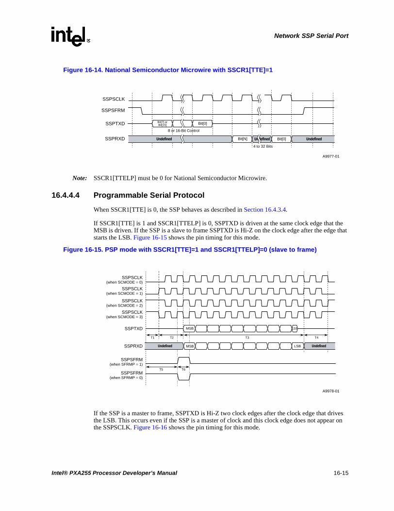
Network SSP Serial Port
Note: SSCR1[TTELP] must be 0 for National Semiconductor Microwire.
16.4.4.4 Programmable Serial Protocol
When SSCR1[TTE] is 0, the SSP behaves as described in Section 16.4.3.4.
If SSCR1[TTE] is 1 and SSCR1[TTELP] is 0, SSPTXD is driven at the same clock edge that the MSB is driven. If the SSP is a slave to frame SSPTXD is Hi-Z on the clock edge after the edge that starts the LSB. Figure 16-15 shows the pin timing for this mode.
If the SSP is a master to frame, SSPTXD is Hi-Z two clock edges after the clock edge that drives the LSB. This occurs even if the SSP is a master of clock and this clock edge does not appear on the SSPSCLK. Figure 16-16 shows the pin timing for this mode.
Figure 16-14. National Semiconductor Microwire with SSCR1[TTE]=1
A9977-01
SSPRXD
SSPSFRM
SSPSCLK
SSPTXD
4 to 32 Bits
Bit[7] orBit[15]
8 or 16-Bit Control
Bit[0]
Bit[N] Bit[0] UndefinedUndefinedUndefined
Figure 16-15. PSP mode with SSCR1[TTE]=1 and SSCR1[TTELP]=0 (slave to frame)
A9978-01
MSB
Undefined Undefined
T1 T2 T3 T4
LSB
MSB LSB
T6T5
SSPSCLK(when SCMODE = 0)
SSPSCLK(when SCMODE = 1)
SSPSCLK(when SCMODE = 2)
SSPSCLK(when SCMODE = 3)
SSPSFRM(when SFRMP = 1)
SSPSFRM(when SFRMP = 0)
SSPTXD
SSPRXD
Intel® PXA255 Processor Developer’s Manual 16-15

Network SSP Serial Port
SSCR1[TTELP] can only be set to 1 in PSP mode if the SSP is a slave to frame. If SSCR1[TTE] is 1 and SSCR1[TTELP] is 1 and the SSP is a slave to frame, SSPTXD is driven at the same clock edge that the MSB is driven. SSPTXD is Hi-Z two clock edges after the clock edge that starts the LSB. This occurs even if the SSP is a master of clock and this clock edge does not appear on the SSPSCLK. If the SSP is a slave of clock, then the device driving SSPSCLK must provide another clock edge. Figure 16-17 shows the pin timing for this mode.
Figure 16-16. PSP mode with SSCR1[TTE]=1 and SSCR1[TTELP]=0 (master to frame)
A9979-01
MSB
Undefined Undefined
T1 T2 T3 T4
LSB
MSB LSB
T6T5
SSPSCLK(when SCMODE = 0)
SSPSCLK(when SCMODE = 1)
SSPSCLK(when SCMODE = 2)
SSPSCLK(when SCMODE = 3)
SSPSFRM(when SFRMP = 1)
SSPSFRM(when SFRMP = 0)
SSPTXD
SSPRXD
Figure 16-17. PSP mode with SSCR1[TTE]=1 and SSCR1[TTELP]=1 (must be slave to frame)
A9980-01
MSB
Undefined Undefined
T1 T2 T3 T4
LSB
MSB LSB
T6T5
SSPSCLK(when SCMODE = 0)
SSPSCLK(when SCMODE = 1)
SSPSCLK(when SCMODE = 2)
SSPSCLK(when SCMODE = 3)
SSPSFRM(when SFRMP = 1)
SSPSFRM(when SFRMP = 0)
SSPTXD
SSPRXD
16-16 Intel® PXA255 Processor Developer’s Manual

Network SSP Serial Port
16.4.5 FIFO Operation
Two separate and independent FIFOs are present for transmit (to peripheral) and receive (from peripheral) serial data. FIFOs are filled or emptied by programmed I/O or DMA bursts.
16.4.5.1 Using Programmed I/O Data Transfers
The PXA255 processor can perform FIFO filling and emptying in response to an interrupt from the FIFO logic. Each FIFO has a programmable trigger threshold at which an interrupt is triggered. When the number of entries in the receive FIFO exceeds the value in SSCR1[RFT], an interrupt is generated (if enabled). This interrupt signals the CPU to empty the receive FIFO. When the number of entries in the transmit FIFO is less than or equal to the value of (SSCR1[TFT] + 1), an interrupt is generated (if enabled). This interrupt signals the CPU to refill the transmit FIFO.
Reading the SSP Status Register (see Section 16.5.3) shows whether the FIFO is full, empty or how many samples it contains.
16.4.5.2 Using DMA Data Transfers
The DMA controller can be programmed to transfer data to and from the SSP FIFOs. To prevent overruns of the transmit FIFO or underruns of the receive FIFO when using the DMA, take care when setting the transmit and receive trigger thresholds.
The programming model for using the DMA is as:
• Program the total number of transmit and receive byte lengths, burst sizes, and peripheral width. Program DCMD[WIDTH] to 0b01 for SSP formats of 8 bits or less; to 0b10 for SSP formats of 9 to 16 bits; to 0b11 for SSP formats of more than 16 bits. When DCMD[WIDTH] is 0b01 (1 byte), then the DMA burst size must be configured for 8 or 16 bytes per burst.
• Set the preferred values in the SSP control registers.
• Set the SSE bit in the SSP Control Register 0 to enable the SSP (see Section 16.5.1).
• Set the run bits in the DMA Command Register.
• Wait for both the DMA transmit and receive interrupt requests.
• If the transmit/receive byte length is not an even multiple of the transfer burst size, a trailing- byte condition may occur as described within Section 16.4.2.
• In full-duplex formats where the SSP always receives the same number of data samples as it transmits, the DMA channel must be set up to transmit and receive the same number of bytes.
16.4.6 Baud-Rate Generation
When the SSP is configured as the master of the SSPSCLK (as determined by SSCR1[SCLKDIR]), the baud rate (or serial bit-rate clock SSPSCLK) is generated internally by dividing the 3.6864 MHz clock by a programmable divider (SSCR0[SCR]).
This generates baud rates up to a maximum of 3.68 Mbits per second. When driven by an external clock, SSPSCLK can be driven up to 13 MHz, generating baud rates up to 13 Mbits per second. At these fast baud rates, using polled/interrupt mode is insufficient to keep the FIFO filled. You must use DMA mode.
Intel® PXA255 Processor Developer’s Manual 16-17

Network SSP Serial Port
16.5 Register Descriptions
Each SSP consists of seven registers: three control, one data, one status, one time-out, and one test.
• The SSP control registers (SSCR0, SSCR1) configure the baud rate, data length, frame format, data-transfer mechanism, and port enabling. They also permit setting the FIFO trigger threshold that triggers an interrupt.
• Access all registers using aligned words.
Note: Write the SSP registers after a reset but before the SSP is enabled.
• The SSP Time-Out (SSTO) register programs the time-out value used to signal a specified period of receive FIFO inactivity.
• While in PSP mode, the SSP Programmable Serial Protocol (SSPSP) register programs the parameters used in defining the data transfer.
• The data register is mapped as one 32-bit location, which physically points to either of two 32-bit registers: one register is for writes of data transfers to the transmit FIFO and the other register is for reads that take data from the receive FIFO. A write cycle or burst write puts successive words into the SSP write register and then into the transmit FIFO. A read cycle or burst read takes data from the SSP read register and the receive FIFO reloads it with available data bits it has stored.
Do not increment the address using read and write DMA bursts.
• Besides showing the state of the FIFO buffers, the status register shows whether the programmable trigger threshold has been passed and whether a transmit or receive FIFO service request is active. The status register also shows how full the FIFO is. Flag bits indicate when the SSP is actively transmitting data, when the transmit FIFO is not full, and when the receive FIFO is not empty. The SSSR[ROR] bit signals an overrun of the receive FIFO In this case newly received data is discarded.
When programming registers, reserved bits must be written as zeroes and read as undefined.
16.5.1 SSP Control Register 0 (SSCR0)
SSCR0, shown in Table 16-3, contains bit fields that control various functions within the SSP. Before enabling the SSP (via SSE) the desired values for this register must be set.
These are read/write registers. Ignore reads from reserved bits. Write zeros to reserved bits.
16-18 Intel® PXA255 Processor Developer’s Manual

Network SSP Serial Port
.
e
t
d n
Table 16-3. SSCR0 Bit Definitions (Sheet 1 of 2)
0x4140_0000 SSCR0 Network SSP Serial Port
31 30 29 28 27 26 25 24 23 22 21 20 19 18 17 16 15 14 13 12 11 10 9 8 7 6 5 4 3 2 1 0
reserved
ED
SS
SC
R
SS
E
rese
rved
FR
F
DS
S
? ? ? ? ? ? ? ? ? ? ? 0 0 0 0 0 0 0 0 0 0 0 0 0 0 ? 0 0 0 0 0 0
Bits Name Description
31:21 — reserved
20 EDSS
EXTENDED DATA SIZE SELECT:
Used in conjunction with DSS to select the size of the data transmitted and received by the SSP
0 – Pre-appended to the DSS value. Sets the DSS range from 4-16- bits.
1 – Pre-appended to the DSS value. Sets the DSS range from 17-32-bits.
19:8 SCR
THE SERIAL CLOCK RATE:
Selects the bit rate of the SSP when in master mode with respect to the SSPSCLK (as definedby SSCR1[SCLKDIR]). The maximum bit rate is 3.6864 Mbps. The clock is divided by the valuof SCR plus 1 (a range of 1 to 4096) to generate the serial clock (SSPSCLK).
This field is ignored when the SSP is a slave with respect to SSPSCLK (defined by SSCR1[SCLKDIR]) and transmission data rates are determined by the external device (Maximum of 13 MHz). At these fast baud rates, using polled/interrupt mode is insufficient to keep the FIFO filled. You must use DMA mode.
NOTE: Software must not change SCR when the SSPSCLK is enabled because doing so causes the SSPSCLK frequency to immediately change.
Serial bit rate = SSP Clock / (SCR + 1)
7 SSE
SYNCHRONOUS SERIAL PORT ENABLE/DISABLE:
Enables and disables all SSP operations. When the port is disabled, all of its clocks can be stopped by programmers to minimize power consumption.
When cleared during active operation, the SSP is disabled immediately, terminating the currenframe being transmitted or received. Clearing SSE resets the port FIFOs and the status bits; however, the SSP control registers are not reset.
NOTE: After reset or after clearing the SSE, software must ensure that the SSCR1, SSITR, SSTO, and SSPSP control registers are properly re-configured and that the SSSR register is reset before re-enabling the SSP by setting SSE. Also, SSE must be clearebefore re-configuring the SSCR0, SSCR1, or SSPSP registers; any or all control bits iSSCR0 can be written at the same time as the SSE.
0 – SSP operation disabled
1 – SSP operation enabled
6 — reserved
5:4 FRF
FRAME FORMAT:
SELECTS which frame format to use.
0b00 – Serial Peripheral Interface*
0b01 – TI Synchronous Serial Protocol*
0b10 – Microwire*
0b11 – Programmable Serial Protocol
Intel® PXA255 Processor Developer’s Manual 16-19

Network SSP Serial Port
s
.
16.5.2 SSP Control Register 1 (SSCR1)
SSCR1, shown in Table 16-4, contains bit fields that control various SSP functions. Before enabling the port (using SSCR0[SSE]), the desired values for this register must be set.
These are read/write registers. Ignore reads from reserved bits. Write zeros to reserved bits.
3:0 DSS
DATA SIZE SELECT:
Used in conjunction with EDSS to select the size of the data transmitted and received by the SSP. The concatenated 5-bit value of EDSS and DSS provides a data range from four to 32-bitin length.
For the Microwire* protocol, DSS and EDSS are used to determine the receive data size. The size of the transmitted data is either eight or 16-bits (determined by SSCR1[MWDS]) and the EDSS bit is ignored. The EDSS and DSS fields are ignored for Microwire* transmit data size - MWDS (alone) configures this. However, for all modes (including Microwire*) EDSS and DSS are used to determine the receive data size.
When data is programmed to be less than 32 bits, the FIFO must be programmed right-justified
EDSS DSS Data Size EDSS DSS Data Size
1
1
1
1
1
1
1
1
1
1
1
1
1
1
1
1
0b0000
0b0001
0b0010
0b0011
0b0100
0b0101
0b0110
0b0111
0b1000
0b1001
0b1010
0b1011
0b1100
0b1101
0b1110
0b1111
17-bit data
18-bit data
19-bit data
20-bit data
21-bit data
22-bit data
23-bit data
24-bit data
25-bit data
26-bit data
27-bit data
28-bit data
29-bit data
30-bit data
31-bit data
32-bit data
0
0
0
0
0
0
0
0
0
0
0
0
0
0
0
0
0b0000
0b0001
0b0010
0b0011
0b0100
0b0101
0b0110
0b0111
0b1000
0b1001
0b1010
0b1011
0b1100
0b1101
0b1110
0b1111
reserved, undefined
reserved, undefined
reserved, undefined
4-bit data
5-bit data
6-bit data
7-bit data
8-bit data
9-bit data
10-bit data
11-bit data
12-bit data
13-bit data
14-bit data
15-bit data
16-bit data
Table 16-3. SSCR0 Bit Definitions (Sheet 2 of 2)
0x4140_0000 SSCR0 Network SSP Serial Port
31 30 29 28 27 26 25 24 23 22 21 20 19 18 17 16 15 14 13 12 11 10 9 8 7 6 5 4 3 2 1 0
reserved
ED
SS
SC
R
SS
E
rese
rved
FR
F
DS
S
? ? ? ? ? ? ? ? ? ? ? 0 0 0 0 0 0 0 0 0 0 0 0 0 0 ? 0 0 0 0 0 0
Bits Name Description
16-20 Intel® PXA255 Processor Developer’s Manual

Network SSP Serial Port
RIE
e
.
r
t k
Table 16-4. SSCR1 Bit Definitions (Sheet 1 of 2)
0x04140_0004 SSCR1 Network SSP Serial Port
Bit 31 30 29 28 27 26 25 24 23 22 21 20 19 18 17 16 15 14 13 12 11 10 9 8 7 6 5 4 3 2 1 0
TT
EL
P
TT
E
EB
CE
I
SC
FR
rese
rved
SC
LK
DIR
SF
RM
DIR
RW
OT
rese
rved
TS
RE
RS
RE
TIN
TE
rese
rved
ST
RF
EF
WR
RFT TFT
MW
DS
SP
H
SP
O
LB
M
TIE
Reset 0 0 0 0 ? ? 0 0 0 0 0 0 0 ? ? ? 0 0 0 0 0 0 0 0 0 0 0 0 0 0 0 0
Bits Name Description
31 TTELP
TRANSMIT HI-Z LATER PHASE:
This bit modifies the behavior of TTE. It causes SSPTXD to become Hi-Z 1/2 phase (or onclock edge) later than normal.
This only occurs with the TI SSP format, and the PSP format if the SSP is a slave to frame
For TI SSP format, this means the SSPTXD is Hi-Z after the rising edge after the LSB (TheLSB is present a full clock).
For PSP format if the SSP is a slave to frame, this means the SSPTXD is Hi-Z two clock edges after the LSB (the LSB is present a full clock).
If SSPSCLK is an input, the device driving SSPSCLK must provide another clock edge.
0 – SSPTXD Hi-Z timing is as described below for TTE.
1 – SSPTXD Hi-Z timing is extended by 1/2 phase. Only valid for TI SSP, and PSP if the SSP is a slave to frame.
30 TTE
TRANSMIT HI-Z ENABLE:
This bit controls whether or not SSPTXD is driven or Hi-Z when the SSP is idle.
For Microwire* SSPTXD is driven at the same clock edge that the MSB is driven, and SSPTXD is Hi-Z after the next rising edge of SSPSCLK for the LSB (1 clock edge after theclock edge that starts the LSB).
For SPI, SSPTXD is Hi-Z whenever SSPFRM is deasserted.
For TI SSP format, SSPTXD is driven with the MSB at the first rising edge of SSPSCLK afteSSPSFRM is asserted and is Hi-Z after the falling edge of SSPSCLK for the LSB (1 clock edge after the clock edge that starts the LSB).
For PSP format, if the SSP is a slave to frame SSPTXD is Hi-Z on the same clock edge thastarts the LSB. For PSP format if the SSP is a master to frame, SSPTXD is Hi-Z on the clocedge after the clock edge for the LSB. This occurs even if the SSP is a master of clock andthis clock edge does not appear on SSPSCLK.
0 – SSPTXD line is driven when SSP is idle
1 – SSPTXD line is Hi-Z when SSP is idle
29 EBCEI
BIT COUNT ERROR INTERRUPT MASK:
Disables bit count error interrupts. SSSR will still indicate an error. A bit count error occurswhen the SSP is a slave to clock or frame and the SSP detects a new frame before the internal bit counter has reached 0.
0 – Bit count error events will generate an interrupt.
1 – Bit count error events will not generate an interrupt.
28 SCFR
SLAVE CLOCK FREE RUNNING:
SCFR in slave mode (SCLKDIR set) must be cleared if the input clock from the external source is running continuously.
In master mode (SCLKDIR cleared) this bit is ignored.
Master mode only:
0 – Clock input to SSPSCLK is continuously running
1 – Clock input to SSPSCLK is active only during transfers.
27:26 — reserved
Intel® PXA255 Processor Developer’s Manual 16-21

Network SSP Serial Port
n
s
t
n ]) l
RIE
16.5.3 SSP Programmable Serial Protocol Register (SSPSP)
SSPSPx, shown in Table 16-5, contains bit fields used to program the various programmable serial-protocol parameters. The contents of these registers are ignored if the PSP is not selected.
These are read/write registers. Ignore reads from reserved bits. Write zeros to reserved bits.
25 SCLKDIR
SSP SERIAL BIT RATE CLOCK DIRECTION:
Determines whether the port is the master or slave (with respect to driving SSPSCLK).
0 – Master mode, the port generates SSPSCLK internally, acts as the master, and drives SSPSCLK.
1 – Slave mode, the port acts as a slave, receives SSPSCLK from an external device anduses it to determine when to drive transmit data on SSPTXD and when to sample Receive data on SSPRXD.
24 SFRMDIR
SSP FRAME DIRECTION:
Determines whether the SSP is the master or slave (with respect to driving SSPSFRM.)
When SFRMDIR is set, the port acts as the slave and receives the SSPSFRM signal from aexternal device. When the port is configured as a slave to the frame, the external device driving frame must wait at least the equivalent of 10 SSPSCLKS after enabling the port before asserting frame. (No external clock cycles are needed, the external device just needto wait a certain amount of time before asserting frame).
NOTE: When the GPIO alternate function is selected for the port, this bit has precedenceover the GPIO direction bit. For example, the GPIO pin is an input if SFRMDIR=1.Alternately, the GPIO pin is an output if SFRMDIR=0.
0 – Master mode, the port generates SSPSFRM internally, acts as the master and drives SSPSFRM.
1 – Slave mode, the port acts as a slave, receives SSPSFRM from an external device.
23 RWOT
RECEIVE WITH OUT TRANSMIT:
Puts the SSP into a mode similar to half duplex. This allows the port to receive data withoutransmitting data (half-duplex only).
When RWOT is set, the port continues to clock in receive data, regardless of data existing ithe transmit FIFO. Data is sent/received immediately after the port enable bit (SSCR0[SSEis set. In this mode, if there is no data to send, the DMA service requests and interrupts forthe transmit FIFO must be disabled (clear TSRE and TIE). If the transmit FIFO is empty, alzeroes are transmitted which must be discarded by the external peripheral.
The transmit FIFO underrun condition does not occur when RWOT is set. When RWOT is enabled, SSSR[BUSY] remains active (set to 1) until software clears the RWOT bit.
0 – Transmit/Receive mode.
1 – Receive With Out Transmit mode.
22 — reserved
Table 16-4. SSCR1 Bit Definitions (Sheet 2 of 2)
0x04140_0004 SSCR1 Network SSP Serial Port
Bit 31 30 29 28 27 26 25 24 23 22 21 20 19 18 17 16 15 14 13 12 11 10 9 8 7 6 5 4 3 2 1 0
TT
EL
P
TT
E
EB
CE
I
SC
FR
rese
rved
SC
LK
DIR
SF
RM
DIR
RW
OT
rese
rved
TS
RE
RS
RE
TIN
TE
rese
rved
ST
RF
EF
WR
RFT TFT
MW
DS
SP
H
SP
O
LB
M
TIE
Reset 0 0 0 0 ? ? 0 0 0 0 0 0 0 ? ? ? 0 0 0 0 0 0 0 0 0 0 0 0 0 0 0 0
Bits Name Description
16-22 Intel® PXA255 Processor Developer’s Manual

Network SSP Serial Port
e
l
/
s .
Table 16-5. SSPSP Bit Definitions (Sheet 1 of 2)
0x4140_002C SSPSP Network SSP Serial Port
Bit 31 30 29 28 27 26 25 24 23 22 21 20 19 18 17 16 15 14 13 12 11 10 9 8 7 6 5 4 3 2 1 0
reserved
DM
YS
TOP
rese
rved
SFRMWDTH SFRMDLY
DM
YS
TR
T
ST
RT
DLY
ET
DS
SF
RM
P
SC
MO
DE
Reset ? ? ? ? ? ? ? 0 0 ? 0 0 0 0 0 0 0 0 0 0 0 0 0 0 0 0 0 0 0 0 0 0
Bits Name Description
31:25 — reserved
24:23 DMYSTOPDUMMY STOP
Determines the number of serial clock (SSPSCLK) cycles that SSPSCLK is active following thlast bit (bit 0) of transmitted (SSPTXD) or received data (SSPRXD).
22:16 SFRMWDTH
SERIAL FRAME WIDTH:
Determines the number of serial clock periods of the frame width (SSPSFRM active).
The programmed value must not be greater than:
(Start Delay)max + (Dummy start)max + (Data size)max + (Dummy Stop)max.
In slave mode (SSCR1[SFRMDIR] set), this field is ignored, however the incoming frame signamust be asserted for at least 1 SSPSCLK duration.
In PSP mode, the incoming frame signal must be deasserted for at least 1 SSPSCLK after assertion (before the next sample is transferred).
15:9 SFRMDLY
SERIAL FRAME DELAY:
Determines the number of half serial clock periods that SSPSFRM is delayed from the start of the transfer. The programed value sets the number of half SSPSCLK cycles from the time TXDRXD starts being driven to the time SSPSFRM is asserted, from 0 to 74.
8:7 DMYSTRTDUMMY START:
Determines the number of SSPSCLK cycles after STRTDLY that precede the transmitted (SSPTXD) or received data (SSPRXD).
6:4 STRTDLY
THREE-BIT START DELAY FIELD:
Determines the number of SSPSCLK cycles that SSPSCLK remains in its Idle state between data transfers. The start delay field must be programmed to 0 whenever SSPSCLK or SSPSFRM is configured as an input (SSCR1[SCLKDIR] = 1 or SSCR1[SFRMDIR] = 1).
3 ETDS
END OF TRANSFER DATA STATE:
Determines the state of SSPTXD at the end of a transfer. When cleared, the state of SSPTXD iforced to 0 after the last bit (bit 0) of the frame is sent and remains 0 through the next idle periodWhen set, the state of SSPTXD retains the value of the last bit sent (bit 0) through the next idleperiod.
0 – Low
1 – Last Value <Bit 0>
2 SFRMP
SERIAL FRAME POLARITY:
Determines the active state of the Serial Frame signal (SSPSFRM).
In Idle mode or when the SSP is disabled, SSPSFRM is in its inactive state. In slave mode (SSCR1[SFRMDIR] set), this bit indicates the polarity of the incoming frame signal.
0 – SSPSFRM is active low.
1 – SSPSFRM is active high.
Intel® PXA255 Processor Developer’s Manual 16-23

Network SSP Serial Port
e
s
k
16.5.4 SSP Time Out Register (SSTO)
The SSTO register, shown in Table 16-6,specifies the time-out value used to signal a period of inactivity within the receive FIFO.
This is a read/write registers. Ignore reads from reserved bits. Write zeros to reserved bits.
16.5.5 SSP Interrupt Test Register (SSITR)
SSITR, shown in Table 16-7 on page 16-25, contains bit fields used for testing purposes only.
Setting bits in this register causes the SSP controller to generate interrupts and DMA requests if enabled. This is useful in testing the port’s functionality.
1:0 SCMODE
SERIAL BIT-RATE CLOCK MODE:
Selects one of four serial clock modes when the PSP is selected (SSCR0[FRF]=0b11).
Its operation is similar to how SSCR1[SPO] and SSCR1[SPH] together determine the idle statof SSPSCLK and on which edges data is driven and sampled.
0b00 - Data Driven (Falling), Data Sampled (Rising), Idle State (Low)
0b01 - Data Driven (Rising), Data Sampled (Falling), Idle State (Low)
0b10 - Data Driven (Rising), Data Sampled (Falling), Idle State (High)
0b11- Data Driven (Falling), Data Sampled (Rising), Idle State (High)
Table 16-5. SSPSP Bit Definitions (Sheet 2 of 2)
0x4140_002C SSPSP Network SSP Serial Port
Bit 31 30 29 28 27 26 25 24 23 22 21 20 19 18 17 16 15 14 13 12 11 10 9 8 7 6 5 4 3 2 1 0
reserved
DM
YS
TO
P
rese
rved
SFRMWDTH SFRMDLY
DM
YS
TR
T
ST
RT
DLY
ET
DS
SF
RM
P
SC
MO
DE
Reset ? ? ? ? ? ? ? 0 0 ? 0 0 0 0 0 0 0 0 0 0 0 0 0 0 0 0 0 0 0 0 0 0
Bits Name Description
Table 16-6. SSTO Bit Definitions
0X4140_0028 SSTO Network SSP Serial Port
Bit 31 30 29 28 27 26 25 24 23 22 21 20 19 18 17 16 15 14 13 12 11 10 9 8 7 6 5 4 3 2 1 0
reserved TIMEOUT
Reset ? ? ? ? ? ? ? ? 0 0 0 0 0 0 0 0 0 0 0 0 0 0 0 0 0 0 0 0 0 0 0 0
Bits Name Description
31:24 — reserved
23:0 TIMEOUT
TIMEOUT:
Value used to set the time-out interval. When the TIMEOUT value is cleared, no time-out occurand SSSR[TINT] is not set.
The time-out interval is given by the equation: Time-out Interval = (TIMEOUT) / Peripheral ClocFrequency
16-24 Intel® PXA255 Processor Developer’s Manual

Network SSP Serial Port
Setting any of these bits also causes the corresponding status bit(s) to be set in the SSP Status Register (SSSR). The interrupt or service request caused by the setting of one of these bits remains active until the bit is cleared.
This is a read/write register. Ignore reads from reserved bits. Write zeros to reserved bits.
16.5.6 SSP Status Register (SSSR)
SSSR, shown in Table 16-8 contains bit fields that signal overrun errors and the transmit and receive FIFO service requests. Each of these hardware-detected events signals an interrupt request to the interrupt controller. The status register also contains flags that indicate:
• When the SSP is actively transmitting data
• When the transmit FIFO is not full
• When the receive FIFO is not empty
One interrupt signal is sent to the interrupt controller for each SSP. These events can cause an interrupt:
• Receiver time-out,
• Receive FIFO overrun,
• Receive FIFO request
• Transmit FIFO request.
Table 16-7. SSITR Bit Definitions
0x4140_000C SSITR Network SSP Serial Port
Bit 31 30 29 28 27 26 25 24 23 22 21 20 19 18 17 16 15 14 13 12 11 10 9 8 7 6 5 4 3 2 1 0
reserved
TR
OR
TR
FS
TT
FS
reserved
Reset ? ? ? ? ? ? ? ? ? ? ? ? ? ? ? ? ? ? ? ? ? ? ? ? 0 0 0 ? ? ? ? ?
Bits Access Name Description
31:8 — — reserved
7 R/W TROR
TEST RECEIVE FIFO OVERRUN:
0 – No receive FIFO overrun service request is generated.
1 – Generates a non-maskable Interrupt to the CPU. No DMA request is generated.
6 R/W TRFS
TEST RECEIVE FIFO SERVICE REQUEST:
0 – No receive FIFO service request is generated.
1 – Generates a non-maskable Interrupt to the CPU and a DMA request for the receive FIFO.
5 R/W TTFS
TEST TRANSMIT FIFO SERVICE REQUEST:
0 – No transmit FIFO service request is generated.
1 – Generates a non-maskable Interrupt to the CPU and a DMA request for the transmit FIFO.
4:0 — — reserved
Intel® PXA255 Processor Developer’s Manual 16-25

Network SSP Serial Port
it
y
s
d
Bits that cause an interrupt signal the request as long as the bit is set. The interrupt clears when the bits clear. Read and write bits are called status bits (status bits are referred to as sticky and once set by hardware, they must be cleared by software); Read-only bits are called flags. Writing a 1 to a status bit clears it; writing a 0 has no effect. Read-only flags are set and cleared by hardware; writes have no effect. The reset state of read-write bits is zero and all bits return to their reset state when SSCR0[SSE] is cleared. Additionally, some bits that cause interrupts have corresponding mask bits in the control registers and are indicated in the section headings that follow.
Set the desired values for this register before enabling the SSP (via SSCR0[SSE]).
These are read/write registers. Ignore reads from reserved bits. Write zeros to reserved bits.
Table 16-8. SSSR Bit Definitions (Sheet 1 of 3)
0x4140_0008 SSSR Network SSP Serial Port
Bit 31 30 29 28 27 26 25 24 23 22 21 20 19 18 17 16 15 14 13 12 11 10 9 8 7 6 5 4 3 2 1 0
reserved
BC
E
CS
S
TU
R
rese
rved
TIN
T
rese
rved
RF
L
TF
L
RO
R
RF
S
TF
S
BS
Y
RN
E
TN
F
rese
rved
Reset ? ? ? ? ? ? ? ? 0 0 0 ? 0 ? ? ? 1 1 1 1 0 0 0 0 0 0 0 0 0 1 ? ?
Bits Name Description
31:24 — reserved
23 BCE
BIT COUNT ERROR:
Indicates that the SSP has detected the SSPSFRM signal asserted at an incorrect time. This bwill cause an interrupt if SSCR1[BCE] is set. The SSP will ignore the current sample and the next sample in order to re-synchronize with the master.
Write one to clear this bit.
0 – SSPSFRM has not been asserted out of synchronization.
1 – SSPSFRM has been asserted out of synchronization.
22 CSS
CLOCK SYNCHRONIZATION STATUS:
A read-only bit that indicates the SSP is busy synchronizing the control signals. This bit is onlyvalid when the SSP is a slave to frame.
Software must wait until this bit is a 0 before allowing an external device to assert the SSPSFRMsignal.
0 – The SSP is ready for slave operations.
1 – The SSP is busy synchronizing slave mode signals.
21 TUR
TRANSMIT FIFO UNDER RUN:
Indicates that the transmitter tried to send data from the transmit FIFO when the transmit FIFOwas empty. When set, an interrupt is generated to the CPU that cannot be locally masked by anSSP register bit. Setting TUR does not generate any DMA service request. To clear TUR, software sets it. TUR remains set until cleared by software writing a one to it which also reset itInterrupt request. Writing a zero to this bit does not affect TUR.
TUR can be set only when the port is a slave to the FRAME signal (SSCR1[SFRMDIR] set) anis not set if the port is in receive-without-transmit mode (SSCR1[RWOT] set).
Write one to clear this bit.
0 – Transmit FIFO has not experienced an under run
1 – Attempted read from the transmit FIFO when the FIFO was empty, request interrupt.
20 — reserved
16-26 Intel® PXA255 Processor Developer’s Manual

Network SSP Serial Port
y
19 TINT
RECEIVER TIME-OUT INTERRUPT:
Indicates that the receive FIFO has been idle (no samples received) for the period of time defined by the value programmed within SSTO. This interrupt can be masked by SSCR1[TINTE].
Write one to clear this bit.
0 – No Receiver Time-out pending
1 – Receiver Time-out pending
18:16 — reserved
15:12 RFL
RECEIVE FIFO LEVEL:
The number of valid entries (minus 1) currently in the receive FIFO.
When the value of 0xF is read, the FIFO is either empty or full and programmers must refer to RNE.
11:8 TFL
TRANSMIT FIFO LEVEL:
Number of valid entries (minus 1) currently in the transmit FIFO.
When the value of 0x0 is read, the FIFO is either empty or full and programmers must refer to TNF.
7 ROR
RECEIVE FIFO OVERRUN:
Indicates that the Receive logic attempted to place data into the receive FIFO after it had beencompletely filled. When new data is received, ROR is asserted and the newly received data is discarded. This process is repeated for all new data received until at least one empty FIFO entrexists.
When set, an interrupt is generated to the CPU that cannot be locally masked by any SSP register bit. The setting of ROR does not generate any DMA service request. Clearing this bit resets its interrupt request.
Write one to clear this bit.
0 – Receive FIFO has not experienced an overrun
1 – Attempted data write to full receive FIFO, request Interrupt
6 RFS
RECEIVE FIFO SERVICE REQUEST:
Indicates that the receive FIFO requires service to prevent an overrun. RFS is set when the number of valid entries in the receive FIFO is equal to or greater than the receive FIFO trigger threshold. It is cleared when it has fewer entries than the trigger threshold value. When RFS isset, an Interrupt is generated when SSCR1[RIE] is set. Setting RFS signals a DMA service request if SSCR1[RSRE] is set. After the CPU or DMA reads the FIFO such that it has fewer entries than the value of SSCR1[RFT], RFS (and the service request or interrupt) is automatically cleared. SSCR1[RSRE] and SSCR1[RIE] must not both be set.
0 – Receive FIFO level exceeds RFT trigger threshold or the SSP is disabled
1 – Receive FIFO level is at or above RFT trigger threshold, request Interrupt
Table 16-8. SSSR Bit Definitions (Sheet 2 of 3)
0x4140_0008 SSSR Network SSP Serial Port
Bit 31 30 29 28 27 26 25 24 23 22 21 20 19 18 17 16 15 14 13 12 11 10 9 8 7 6 5 4 3 2 1 0
reserved
BC
E
CS
S
TU
R
rese
rved
TIN
T
rese
rved
RF
L
TF
L
RO
R
RF
S
TF
S
BS
Y
RN
E
TN
F
rese
rved
Reset ? ? ? ? ? ? ? ? 0 0 0 ? 0 ? ? ? 1 1 1 1 0 0 0 0 0 0 0 0 0 1 ? ?
Bits Name Description
Intel® PXA255 Processor Developer’s Manual 16-27
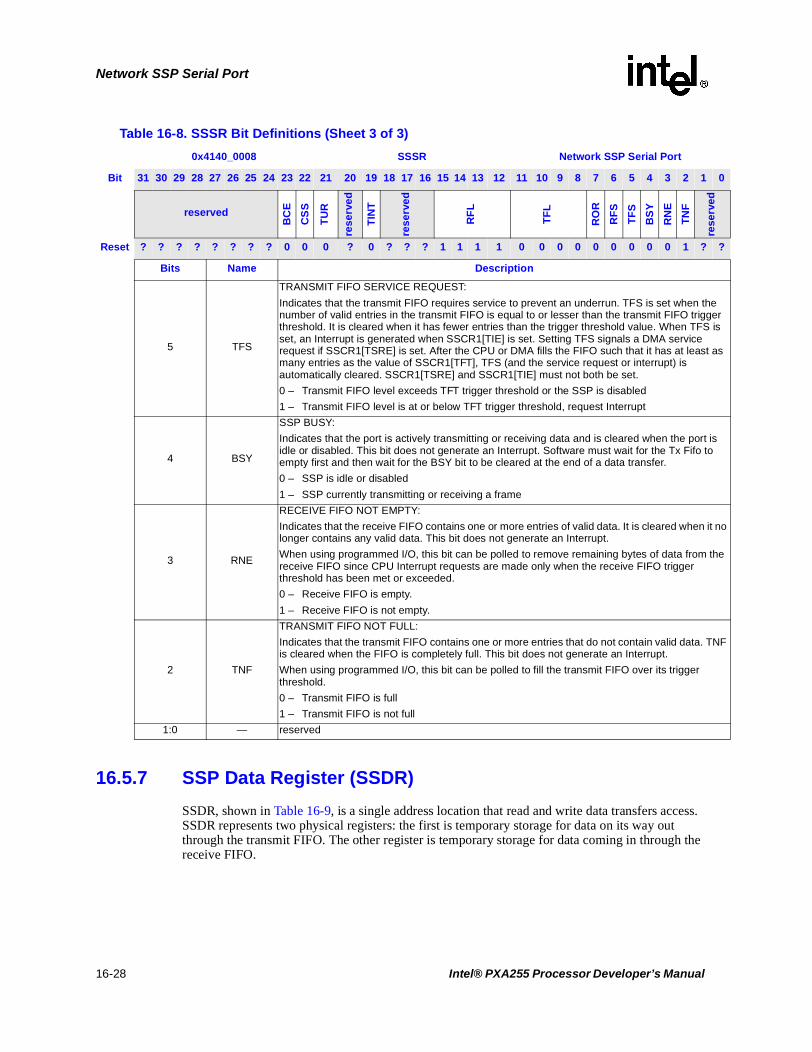
Network SSP Serial Port
o
F
16.5.7 SSP Data Register (SSDR)
SSDR, shown in Table 16-9, is a single address location that read and write data transfers access. SSDR represents two physical registers: the first is temporary storage for data on its way out through the transmit FIFO. The other register is temporary storage for data coming in through the receive FIFO.
5 TFS
TRANSMIT FIFO SERVICE REQUEST:
Indicates that the transmit FIFO requires service to prevent an underrun. TFS is set when the number of valid entries in the transmit FIFO is equal to or lesser than the transmit FIFO triggerthreshold. It is cleared when it has fewer entries than the trigger threshold value. When TFS isset, an Interrupt is generated when SSCR1[TIE] is set. Setting TFS signals a DMA service request if SSCR1[TSRE] is set. After the CPU or DMA fills the FIFO such that it has at least asmany entries as the value of SSCR1[TFT], TFS (and the service request or interrupt) is automatically cleared. SSCR1[TSRE] and SSCR1[TIE] must not both be set.
0 – Transmit FIFO level exceeds TFT trigger threshold or the SSP is disabled
1 – Transmit FIFO level is at or below TFT trigger threshold, request Interrupt
4 BSY
SSP BUSY:
Indicates that the port is actively transmitting or receiving data and is cleared when the port is idle or disabled. This bit does not generate an Interrupt. Software must wait for the Tx Fifo to empty first and then wait for the BSY bit to be cleared at the end of a data transfer.
0 – SSP is idle or disabled
1 – SSP currently transmitting or receiving a frame
3 RNE
RECEIVE FIFO NOT EMPTY:
Indicates that the receive FIFO contains one or more entries of valid data. It is cleared when it nlonger contains any valid data. This bit does not generate an Interrupt.
When using programmed I/O, this bit can be polled to remove remaining bytes of data from thereceive FIFO since CPU Interrupt requests are made only when the receive FIFO trigger threshold has been met or exceeded.
0 – Receive FIFO is empty.
1 – Receive FIFO is not empty.
2 TNF
TRANSMIT FIFO NOT FULL:
Indicates that the transmit FIFO contains one or more entries that do not contain valid data. TNis cleared when the FIFO is completely full. This bit does not generate an Interrupt.
When using programmed I/O, this bit can be polled to fill the transmit FIFO over its trigger threshold.
0 – Transmit FIFO is full
1 – Transmit FIFO is not full
1:0 — reserved
Table 16-8. SSSR Bit Definitions (Sheet 3 of 3)
0x4140_0008 SSSR Network SSP Serial Port
Bit 31 30 29 28 27 26 25 24 23 22 21 20 19 18 17 16 15 14 13 12 11 10 9 8 7 6 5 4 3 2 1 0
reserved
BC
E
CS
S
TU
R
rese
rved
TIN
T
rese
rved
RF
L
TF
L
RO
R
RF
S
TF
S
BS
Y
RN
E
TN
F
rese
rved
Reset ? ? ? ? ? ? ? ? 0 0 0 ? 0 ? ? ? 1 1 1 1 0 0 0 0 0 0 0 0 0 1 ? ?
Bits Name Description
16-28 Intel® PXA255 Processor Developer’s Manual

Network SSP Serial Port
As the system accesses the register, FIFO control logic transfers data automatically between the registers and FIFOs as fast as the system moves it. Unless attempting a write to a full transmit FIFO, data in the FIFO shifts up or down to accommodate the new word(s). Status bits show users whether the FIFO is full, above the programmable trigger threshold, below the programmable trigger threshold or empty.
For transmit data transfers, the register can be written by the system processor anytime it falls below its trigger threshold when using programmed I/O.
When a data size of less than 32-bits is selected, do not left-justify data written to the transmit FIFO. Transmit logic left-justifies the data and ignores any unused bits. Received data of less than 32-bits is automatically right-justified in the receive FIFO.
When the SSP is programmed for the Microwire* protocol and the size of the Transmit data is eight bits (SSCR1[MWDS] cleared), the most significant bits are ignored. Similarly, if the size for the Transmit data is 16 bits (SSCR1[MWDS] set), the most significant 16 bits are ignored. SSCR0[DSS] controls the Receive data size.
Both FIFOs are cleared when the port is reset, or by clearing SSCR0[SSE].
This is a read/write register. Ignore reads from reserved bits. Write zeros to reserved bits.
16.6 Network SSP Serial Port Register Summary
Table 16-10 shows the registers associated with the NSSP and their physical addresses.
Table 16-9. SSDR Bit Definitions
0x4140_0010 SSDR Network SSP Serial Port
Bit 31 30 29 28 27 26 25 24 23 22 21 20 19 18 17 16 15 14 13 12 11 10 9 8 7 6 5 4 3 2 1 0
DATA
Reset ? ? ? ? ? ? ? ? ? ? ? ? ? ? ? ? ? ? ? ? ? ? ? ? ? ? ? ? ? ? ? ?
Bits Name Description
31:0 DATATRANSMIT/RECEIVE DATA:
Data word to be written to/read from Transmit/receive FIFO
Table 16-10. NSSP Register Address Map
Physical Address Name Description
0x4140_0000 NSSCR0 NSSP Control register 0
0x4140_0004 NSSCR1 NSSP Control register 1
0x4140_0008 NSSSR NSSP Status register
0x4140_000C NSSITR NSSP Interrupt Test register
0x4140_0010 NSSDR NSSP Data Write Register / Data Read register
0x4140_0028 NSSTO NSSP Time Out register
0x4140_002C NSSPSP NSSP Programmable Serial Protocol
Intel® PXA255 Processor Developer’s Manual 16-29

Network SSP Serial Port
16-30 Intel® PXA255 Processor Developer’s Manual

Hardware UART 17
This chapter describes the signal definitions and operations of the PXA255 processor hardware UART (HWUART) port.
The HWUART interface pins are available via either the PCMCIA general purpose I/O (GPIO) pins or the BTUART pins. Refer to Section 4.1.2, “GPIO Alternate Functions” for more information. When using the HWUART through the PCMCIA pins, they are driven at the same voltage level as the memory interface. Because the PCMCIA signal nPWE is used for variable-latency input / output (VLIO), VLIO cannot be used while the HWUART interface is using the PCMCIA pins.
The HWUART is configured differently than the other UARTs. The HWUART supports full hardware flow control.
17.1 Overview
The HWUART contains a UART and a slow infrared transmit encoder and receive decoder that conforms to the IrDA Serial Infrared (SIR) Physical Layer Link Specification.
The UART performs serial-to-parallel conversion on data characters received from a peripheral device or a modem and parallel-to-serial conversion on data characters received from the processor. The processor can read the UART’s complete status during functional operation. Status information includes the type and condition of transfer operations and error conditions (parity, overrun, framing, or break interrupt) associated with the UART.
The HWUART operates in FIFO or non-FIFO mode. In FIFO mode, a 64-byte transmit FIFO holds data from the processor until it is transmitted on the serial link and a 64-byte receive FIFO buffers data from the serial link until it is read by the processor. In non-FIFO mode, the transmit and receive FIFOs are bypassed.
The HWUART can also use direct memory access (DMA) to transfer data to and from the HWUART.
17.2 Features
Software can program interrupts to meet its requirements. This minimizes the number of computations required to handle the communications link. The UART operates in an environment that is controlled by software and can be polled or is interrupt driven. The HWUART has these features:
• Functionally compatible with the 16550A and 16750 UART specifications. The UART supports not only the 16550A and 16750 industry standards but these additional functions as well:
— DMA requests for transmit and receive data services
— Slow infrared asynchronous interface
Intel® PXA255 Processor Developer’s Manual 17-1

Hardware UART
— Non-Return-to-Zero (NRZ) encoding/decoding function
— 64 byte transmit/receive FIFO buffers
— Programmable receive FIFO trigger threshold
— Auto baud-rate detection
— Auto flow
• Maximum baud rate of 921,600 bps.
• Ability to add or delete standard asynchronous communications bits (start, stop, and parity) in the serial data
• Independently controlled transmit, receive, line status, and data set interrupts
• Programmable baud rate generator that allows the internal clock to be divided by 1 to 216–1 to generate an internal 16X clock. This clock can be used to drive the internal transmitter and receiver logic.
• Modem control functions – clear to send (nCTS) and request to send (nRTS)
• Autoflow capability controls data I/O without generating interrupts:
— nRTS (output) controlled by UART receiver FIFO
— nCTS (input) from modem controls UART transmitter
• Fully programmable serial-interface:
— 5-, 6-, 7-, or 8-bit characters
— Even, odd, and no parity detection
— 1, 1.5, or 2 stop bit generation
— Baud rate generation up to 921 Kbps
— False start bit detection.
• 64-byte transmit FIFO
• 64-byte receive FIFO
• Complete status reporting capability
• Ability to generate and detect line breaks
• Internal diagnostic capabilities that include:
— Loopback controls for communications link fault isolation
— Break, parity, and framing error simulation
• Fully prioritized interrupt system controls
• Separate DMA requests for transmit and receive data services
• Slow infrared asynchronous interface that conforms to the Infrared Data Association (IrDA) standard
17-2 Intel® PXA255 Processor Developer’s Manual

Hardware UART
17.3 Signal Descriptions
Table 17-1 lists and describes each external signal that is connected to the UART module. The pins are connected to the PXA255 processor through GPIOs.
17.4 Operation
The format of a UART data frame is shown in Figure 17-1.
Table 17-1. UART Signal Descriptions
Name Type Description
RXD InputSERIAL INPUT – Serial data input to the receive shift register. In infrared mode, it is connected to the infrared receiver input.
TXD OutputSERIAL OUTPUT – Serial data output to the communications link-peripheral, modem, or data set. The TXD signal is set to the logic 1 state upon a Reset operation. It is connected to the output of the infrared transmitter in infrared mode.
nCTS Input
CLEAR TO SEND – When low, indicates that the modem or data set is ready to exchange data.
Non-Autoflow Mode: When not in autoflow mode, bit 4 (CTS) of the Modem Status register (MSR) indicates the state of nCTS. Bit 4 is the complement of the nCTS signal. Bit 0 (DCTS) of the Modem Status register indicates whether the nCTS input has changed state since the previous reading of the Modem Status register. When the CTS bit of the MSR changes state and the modem status interrupt is enabled, an interrupt is generated. nCTS has no effect on the transmitter. The user can program the UART to interrupt the processor when DCTS changes state. The programmer can then stall the outgoing data stream by starving the transmit FIFO or disabling the UART with the Interrupt Enable register (IER).
NOTE: If UART transmission is stalled by disabling the UART, the user will not receive an MSR interrupt when nCTS reasserts. This is because disabling the UART also disables interrupts. To get around this, either use Auto CTS in Autoflow Mode, or program the nCTS GPIO pin to interrupt.
Autoflow Mode: In autoflow mode, the UART transmit circuity checks the state of nCTS before transmitting each byte. If nCTS is high, no data is transmitted.
nRTS Output
REQUEST TO SEND – When low, signals the modem or the data set that the UART is ready to exchange data.
Non-Autoflow Mode: The nRTS output signal can be asserted by setting bit 1 (RTS) of the Modem Control register to 1. The RTS bit is the complement of the nRTS signal.
Autoflow Mode: nRTS is automatically asserted by the autoflow circuitry when the receive buffer exceeds its programmed trigger threshold. It is deasserted when enough bytes are removed from the buffer to lower the data level back to the trigger threshold.
Figure 17-1. Example UART Data Frame
Start
Bit
Data
<0>
Data
<1>
Data
<2>
Data
<3>
Data
<4>
Data
<5>
Data
<6>
Data
<7>
Parity
Bit
Stop
Bit 1
Stop
Bit 2
TXD or RXD pin
LSB MSB
Intel® PXA255 Processor Developer’s Manual 17-3

Hardware UART
Receive data sample counter frequency is 16 times the value of the bit frequency. The 16X clock is created by the baud rate generator. Each bit is sampled three times in the middle. Shaded bits in Figure 17-1 are optional and can be programmed by software.
Each data frame is between seven and 12 bits long, depending on the size of the data programmed, whether parity is enabled, and the number of stop bits. A data frame begins by transmitting a start bit that is represented by a high to low transition. The start bit is followed by data that is five to eight bits wide and begins with the least significant bit (LSB). The data bits are followed by an optional parity bit. The parity bit is set if even parity is enabled and the data byte has an odd number of ones or if odd parity is enabled and the data byte has an even number of ones. The data frame ends with one, one and a half, or two stop bits, as programmed by software. The stop bits are represented by one, one and a half, or two successive bit periods of a logic one.
The UART has two FIFOs: one transmit and one receive. The transmit FIFO is 64 bytes deep and eight bits wide. The receive FIFO is 64 bytes deep and 11 bits wide. Three bits are used for tracking errors.
The UART can use NRZ coding to represent individual bit values. NRZ coding is enabled when Interrupt Enable register (IER) bit 5 (IER[5]) is set to high. A one is represented by a line transition and a zero is represented by no line transition. Figure 17-2 shows the data byte 0b 0100 1011 in NRZ coding. The LSB is transmitted first.
17.4.1 Reset
The UART is disabled on reset. To enable the UART, use software to program the GPIO registers then set IER[UUE]. When the UART is enabled, the receiver waits for a frame start bit and the transmitter sends data if it is available in the Transmit Holding register. Transmit data can be written to the Transmit Holding register before the UART is enabled. In FIFO mode, data is transmitted from the FIFO to the Transmit Holding register before it goes to the pin.
When the UART unit is disabled, the transmitter or receiver finishes the current byte and stops transmitting or receiving data. When the UART is enabled, data in the FIFO is not cleared and transmission resumes.
17.4.2 FIFO Operation
The UART has a transmit FIFO and a receive FIFO each holding 64 characters of data. There are three separate methods for moving data into and out of the FIFOs: interrupts, polling, and DMA.
Figure 17-2. Example NRZ Bit Encoding – (0b0100 1011
DigitalData
NRZData
BitValue
1 1 0 1 0 0 1 0
LSB MSB
17-4 Intel® PXA255 Processor Developer’s Manual

Hardware UART
17.4.2.1 FIFO Interrupt Mode Operation
17.4.2.1.1 Receive Interrupt
For a receive interrupt to occur, the receive FIFO and receive interrupts must be enabled. The Interrupt Identification register (IIR) bits 1 and 2 (IIR[IID]) change to show that receive data is available when the FIFO reaches its trigger threshold. IIR[IID] changes to show the next waiting interrupt when the FIFO drops below the trigger threshold. A change in IIR[IID] triggers an interrupt to the core. Software reads IIR[IID] to determine the cause of the interrupt.
The receiver line status interrupt (IIR = 0xC6) has the highest priority and the received data available interrupt (IIR = 0xC4) is lower. The line status interrupt occurs only when the character at the front of the FIFO has errors.
The data ready bit (DR in the Line Status register) is set when a character is transferred from the shift register to the receive FIFO. The DR bit is cleared when the FIFO is empty.
17.4.2.1.2 Character Timeout Interrupt
A character timeout interrupt occurs when the receive FIFO and receive timeout interrupt are enabled and these conditions exist:
• At least one character is in the FIFO.
• The most recently received character was received more than four continuous character times ago. If two stop bits are programmed, the second is included in this interval.
• The most recent FIFO read was performed more than four continuous character times ago.
After the processor reads one character from the receive FIFO or a new start bit is received, the timeout interrupt is cleared and the timeout is reset. If a timeout interrupt has not occurred, the timeout is reset when a new character is received or the processor reads the receive FIFO.
17.4.2.1.3 Transmit Interrupt
Transmit interrupts can only occur when the transmit FIFO and transmit interrupt are enabled. The transmit data request interrupt occurs when the transmit FIFO is at least half empty. The interrupt is cleared when the Transmit Holding register (THR) is written or the IIR is read.
17.4.2.2 FIFO Polled Mode Operation
When the FIFOs are enabled, clearing both IER[DMAE] and IER[4:0] places the serial port in FIFO polled operating mode. The receiver and the transmitter are controlled separately. Either one or both can be in polled mode. In polled mode, software checks receiver and transmitter status via the Line Status register (LSR). The processor polls the following bits for receive and transmit data service:
• Receive Data Service – The processor checks the data ready (LSR[DR]) bit which is set when one or more bytes remain in the receive FIFO or Receive Buffer register (RBR).
• Transmit Data Service – The processor checks the transmit data request (LSR[TDRQ]) bit which is set when transmitter needs data.
The processor can also check the transmitter empty (LSR[TEMT]) bit, which is set when the transmit FIFO and Transmit Holding register are empty.
Intel® PXA255 Processor Developer’s Manual 17-5

Hardware UART
17.4.2.3 FIFO DMA Mode Operation
The UART has two DMA requests: one for transmit data service, and one for receive data service. DMA requests are generated in FIFO mode only. The requests are activated by setting IER[DMAE].
• Data Transmit Data Service – When IER[DMAE] is set, if the transmit FIFO is less than half full, the transmit-DMA request is generated. The DMA controller then writes data to the FIFO. For each DMA request, the DMA controller can send 8, 16, or 32 bytes of data to the FIFO. The actual number of bytes to be transmitted is programmed in the DMA controller.
• Data Receive Data Service – When IER[DMAE] is set, the receive-DMA request is generated when the receive FIFO reaches its trigger threshold with no errors in its entries. The DMA controller then reads data from the FIFO. For each DMA request, the DMA controller can read 8, 16, or 32 bytes of data from the FIFO. The actual number of bytes to be read is programmed in the DMA controller along with the bus width.
17.4.2.4 DMA Receive Programming Errors
If the DMA channel stops prematurely, because it encounters the end of a descriptor chain or other error, the processor must be notified, since the DMA controller can no longer service the UARTs FIFOs. If this occurs, the processor must correct the situation by programming another descriptor or by servicing the FIFOs via interrupt or polling modes as previously described. The DMA must set DCSR[StopIrqEn] to generate an interrupt if a stopped channel occurs.
17.4.2.5 DMA Error Handling
An error interrupt is used when DMA requests are enabled. The interrupt is generated when LSR bit 7 is set to 1. This happens when a receive DMA request is not generated and the receive FIFO has an error. The error interrupt tells the processor to handle the data in the receive FIFO through programmed I/O. The error interrupt is enabled when DMA requests are enabled and cannot be masked. Receiver line status interrupts occur when the error is at the front of the FIFO.
Note: When DMA requests are enabled and an interrupt occurs, software must first read the LSR to verify an error interrupt exists, then check the IIR for the source of the interrupt. If an interrupt occurs and LSR[FIFOE] is clear, software must read the ISR to determine the error condition. When the last error byte is read from the FIFO, DMA requests are automatically enabled. Software is not required to check for the error interrupt if DMA requests are disabled. Error interrupts only occur when DMA requests are enabled.
If an error occurs while in DMA mode:
• receive-DMA requests are disabled
• error interrupt IIR[IID] is generated
The processor must now read the error bytes through programmed I/O. When all errors have been removed from the FIFO, the receive DMA requests are once again enabled automatically by the UART.
If an error occurs when the receive FIFO trigger threshold has been reached, such that a receive DMA request is set, users need to wait for the DMA to finish the transfer before reading out the error bytes through programmed I/O. If not, FIFO underflow could occur.
17-6 Intel® PXA255 Processor Developer’s Manual

Hardware UART
Note: Ensure that the DMA controller has completed the previous receive DMA requests before the error interrupt handler begins to clear the errors from the FIFO. If not, FIFO underflow could occur.
17.4.2.6 Removing Trailing Bytes In DMA Mode
When the number of entries in the receive FIFO is less than its trigger threshold, and no additional data is received, the remaining bytes are called trailing bytes. The remaining bytes must then be removed via the processor as described in Section 17.4.2.1.
17.4.3 Autoflow Control
Autoflow control uses the clear to send (nCTS) and request to send (nRTS) signals to automatically control the flow of data between the UART and external modem. When autoflow is enabled, the remote device is not allowed to send data unless the UART asserts nRTS low. If the UART deasserts nRTS while the remote device is sending data, the remote device is allowed to send one additional byte after nRTS is deasserted. An overflow could occur if the remote device violates this rule. Likewise, the UART is not allowed to transmit data unless the remote device asserts nCTS low. This feature increases system efficiency and eliminates the possibility of a receive FIFO overflow error due to long interrupt latency.
Autoflow mode can be used in two ways: full autoflow, automating both nCTS and nRTS; and half autoflow, automating only nCTS. Full autoflow is enabled by setting MCR[AFE] and MCR[RTS] to 1. Auto-nCTS-only mode is enabled by setting MCR[AFE] and clearing MCR[RTS].
When in full autoflow mode, nRTS is asserted when the UART FIFO is ready to receive data from the remote transmitter. This occurs when the amount of data in the receive FIFO is below the programmable trigger threshold value. When the amount of data in the receive FIFO reaches the programmable trigger threshold, nRTS is deasserted. It is asserted once again when enough bytes are removed from the FIFO to lower the data level below the trigger threshold.
When in full or half-autoflow mode, nCTS is asserted by the remote receiver when the receiver is ready to receive data from the UART. The UART checks nCTS before sending the next byte of data and will not transmit the byte until nCTS is low. If nCTS goes high while the transfer of a byte is in progress, the transmitter sends the byte.
Note: Autoflow mode can be used only in conjunction with FIFO mode.
17.4.4 Auto-Baud-Rate Detection
The HWUART supports auto-baud-rate detection. When enabled, the UART counts the number of 14.7456 MHz clock cycles within the start-bit pulse. This number is then written into the Auto- Baud-Count register (ACR, see Table 17-13) and is used to calculate the baud rate. When the ACR is written, a auto-baud-lock interrupt is generated (if enabled), and the UART automatically programs the Divisor Latch registers (Section 17.5.3) with the appropriate baud rate. If preferred, the processor can read the ACR and use this information to program the Divisor-Latch registers with a baud rate calculated by the processor. After the baud rate has been programmed, it is the responsibility of the processor to verify that the predetermined characters (usually AT or at) are being received correctly. For the autobaud rate detection circuit to work correctly, the first data bit transmitted after the start bit must be a logic '1'. If a logic '0' is transmitted, the auto-baud circuit counts the zero as part of the start bit, resulting in an incorrect baud rate being programmed into the Divisor Latch Register Low (DLL) and Divisor Latch Register High (DLH) registers.
Intel® PXA255 Processor Developer’s Manual 17-7

Hardware UART
If the UART is to program the Divisor Latch registers, you can choose one of two methods for auto-baud calculation: table-based and formula-based. Set Auto-Baud Control register (ABR), bit 3 (ABR[ABT]) to select which method you want to use (refer to Section 17.5.8). When the formula method is used, any baud rate defined by the parameters in Section 17.5.3 can be programmed by the UART. The formula method works well for higher baud rates, but could possibly fail below 28.8 kbps if the remote transmitter’s actual baud rate differs by more than one percent of its target. The table method is more immune to such errors as the table rejects uncommon baud rates and rounds to the common ones. The table method allows any baud rate defined by the formula in Section 17.5.3 above 28.8 kbps. Below 28.8 kbps the only baud rates which can be programmed by the UART are 19200, 14400, 9600, 4800, 1200, and 300 baud.
When the baud rate is detected, the auto-baud circuitry disables itself by clearing ABR, bit 0 (ABR[ABE]). If users want to re-enable auto-baud detection, ABR[ABE] must be set.
Note: Auto-baud rate detection is not supported with IrDA (slow infrared) mode.
See Section 17.5.8 for more information on auto-baud.
17.4.5 Slow Infrared Asynchronous Interface
The Slow Infrared (SIR) interface supports two-way wireless communication that uses infrared transmission. The SIR provides a transmit encoder and receive decoder to support a physical link that conforms to the Infrared Data Association, Serial Infrared Physical Layer Link Specification, October 17, 1995, Version 1.1.
The SIR interface does not contain the actual IR LED driver or the receiver amplifier. The I/O pins attached to the SIR only have digital CMOS level signals. The SIR supports two-way communication, but full duplex communication is not possible because reflections from the transmit LED enter the receiver. The SIR interface supports frequencies up to 115.2 Kbps. Because the input clock is 14.7456 MHz, the baud divisor must be eight or more.
17.4.5.1 Operation
The SIR modulation technique works with 5-, 6-, 7-, or 8-bit characters with an optional parity bit. The data is preceded by a zero value start bit and ends with one or more stop bits. The encoding scheme is to set a pulse 3/16 of a bit wide in the middle of every zero bit and send no pulses for bits that are ones. The pulse for each zero bit must occur, even for consecutive bits with no edge between them.
17-8 Intel® PXA255 Processor Developer’s Manual

Hardware UART
The top line in Figure 17-3 shows an asynchronous transmission as it is sent from the UART. The second line shows the pulses generated by the IR encoder at the TXD pin. A pulse is generated in the middle of the START bit and any data bit that is a zero. The third line shows the values received at the RXD input pin. The fourth line shows the receive decoder’s output. The receive decoder drives the receiver data line low when it detects a pulse. The bottom line shows how the UART’s receiver interprets the decoder’s action. This last line is the same as the first, but it is shifted half a bit period.
When XMODE is cleared, each zero bit has a pulse width of 3/16 of a bit time. When XMODE is set, a pulse of 1.6 µs is generated in the middle of each zero bit. The shorter infrared pulse generated when XMODE is set reduces the LED’s power consumption. At 2400 bps, the LED is normally on for 78 µs for each zero bit that is transmitted. When XMODE is set, the LED is on only 1.6 µs (as show in Figure 17-4).
To prevent transmitter LED reflection feed back to the receiver, disable the IR receiver decoder when the IR transmit encoder transmits data and disables the IR transmit encoder when the IR receiver decoder receives data. The RCVEIR and XMITIR bits in the Infrared Selection Register (ISR) must not be set at the same time (refer to Section 17.5.15).
Figure 17-3. IR Transmit and Receive Example
START
BIT STOPBIT
1 0 0 0 1 0 1 0
STARTBIT 1 0 0 0 1 0 1 0
TRANSMIT
IR ENCODER OUTPUT
IR DECODER OUTPUT
UART
UART RECEIVE
(TXD PIN VALUE)
SHIFT VALUE
RXD PIN VALUE
SHIFT VALUESTOP
BIT
Figure 17-4. XMODE Example.
1 7 11 16
1.6 µs
3 16X BAUD Clock periodsIR_TXD Pin valueXMODE = 1
IR_TXD Pin valueXMODE = 0
Transmit Start bitfollowed by 1
16X Baud Clock
Intel® PXA255 Processor Developer’s Manual 17-9

Hardware UART
17.5 Register Descriptions
17.5.1 Receive Buffer Register (RBR)
In non-FIFO mode, the RBR, shown in Table 17-2, holds the character(s) received by the UART’s Receive Shift Register. If the RBR is configured to use fewer than eight bits, the bits are right-justified and the most significant bits (MSB) are zeroed. Reading the register empties the register and clears LSR[DR] (refer to Section 17.5.11, “Line Status Register (LSR)” on page 17-19).
In FIFO mode, the RBR latches the value of the data byte at the front of the FIFO (see Table 17-2).
This is a write-only register. Write zeros to reserve bits.
17.5.2 Transmit Holding Register (THR)
In non-FIFO mode, the THR, shown in Table 17-3, holds the next data byte(s) to be transmitted. When the transmit shift register (TSR) is emptied, the contents of the THR are loaded in the TSR and the LSR[TDRQ] is set to 1 (refer to Section 17.5.15).
In FIFO mode, a write to the THR puts data into the end of the FIFO. The data at the front of the FIFO is loaded to the TSR when that register is empty.
This is a write-only register. Write zeros to reserve bits.
17.5.3 Divisor Latch Registers (DLL and DLH)
The HWUART contains a programmable baud rate generator that can take the 14.7456 MHz fixed input clock and divide it by a number that is between 1 and 216–1. The baud rate generator output frequency is 16 times the baud rate. Two 8-bit latches store the divisor in a 16-bit binary format.
Table 17-2. RBR Bit Definitions
Physical Address0x4160_0000 (DLAB=0) Read Buffer Register (RBR) PXA255 Processor Hardware UART
Bit 31 30 29 28 27 26 25 24 23 22 21 20 19 18 17 16 15 14 13 12 11 10 9 8 7 6 5 4 3 2 1 0
reserved Byte 0
Bits Name Description
31:8 — reserved
7:0 Byte 0 Byte 0
Table 17-3. THR Bit Definitions
Physical Address0x4160_0000 (DLAB=0) Transmit Holding Register (THR) PXA255 Processor Hardware UART
Bit 31 30 29 28 27 26 25 24 23 22 21 20 19 18 17 16 15 14 13 12 11 10 9 8 7 6 5 4 3 2 1 0
reserved Byte 0
Reset ? ? ? ? ? ? ? ? ? ? ? ? ? ? ? ? ? ? ? ? ? ? ? ? 0 0 0 0 0 0 0 0
Bits Name Description
31:8 — reserved
7:0 Byte 0 Byte 0
17-10 Intel® PXA255 Processor Developer’s Manual

Hardware UART
Load these divisor latches during initialization to ensure that the baud rate generator operates properly. If each divisor latch is loaded with a 0, the 16X clock stops. The divisor latches are accessed with a word write.
The baud rate of the data shifted in to or out of a UART is given by the formula:
For example, if the divisor is 24, the baud rate is 38400 bps.
The divisor’s reset value is 0x0002.
Table 17-4 and Table 17-5 describe the DLL and DLH registers.
These are read/write registers. Ignore reads from reserved bits. Write zeros to reserved bits.
17.5.4 Interrupt Enable Register (IER)
The IER, shown in Table 17-6, enables the five types of interrupts that set a value in the Interrupt Identification register (IIR) (refer to Section 17.5.5). To disable an interrupt, software must clear the appropriate bit in the IER. Software can enable some interrupts by setting the appropriate bit.
The character timeout indication interrupt is separated from the received data available interrupt to ensure that the processor and the DMA controller do not service the receive FIFO at the same time. When a character timeout indication interrupt occurs, the processor must handle the data in the receive FIFO through programmed I/O.
BaudRate 14.7456 MHz16xDivisor( )
----------------------------------=
Table 17-4. DLL Bit Definitions
Physical Address0x4160_0000 (DLAB=1) Divisor Latch Register Low (DLL) PXA255 Processor Hardware UART
Bit 31 30 29 28 27 26 25 24 23 22 21 20 19 18 17 16 15 14 13 12 11 10 9 8 7 6 5 4 3 2 1 0
reserved DLL
Reset ? ? ? ? ? ? ? ? ? ? ? ? ? ? ? ? ? ? ? ? ? ? ? ? 0 0 0 0 0 0 1 0
Bits Name Description
31:8 — reserved
7:0 DLL Low byte compare value to generate baud rate
Table 17-5. Divisor Latch Register High (DLH) Bit Definitions
Physical Address0x4160_0004 (DLAB=1) Divisor Latch Register High (DLH) PXA255 Processor Hardware UART
Bit 31 30 29 28 27 26 25 24 23 22 21 20 19 18 17 16 15 14 13 12 11 10 9 8 7 6 5 4 3 2 1 0
reserved DLH
Reset ? ? ? ? ? ? ? ? ? ? ? ? ? ? ? ? ? ? ? ? ? ? ? ? 0 0 0 0 0 0 0 0
Bits Name Description
31:8 — reserved
7:0 DLH High byte compare value to generate baud rate
Intel® PXA255 Processor Developer’s Manual 17-11

Hardware UART
Enabling DMA requests also enables a separate error interrupt. For additional information see Section 17.4.2.5.
Set bit 7 of the IER to enable DMA requests. The IER also contains the unit enable and NRZ coding enable control bits. Bits 7 through 4 are used differently from the standard 16550A register definition.
Note: MCR[OUT2] is a global interrupt enable, and must be set to enable UART interrupts.
Note: To ensure that the DMA controller and programmed I/O do not access the same FIFO, software must not set DMAE (bit 7) while TIE (bit 1) or RAVIE (bit 0) are set to 1.
This is a read/write register. Ignore reads from reserved bits. Write zeros to reserved bits.
Table 17-6. IER Bit Definitions
Physical Address0x4160_0004 Interrupt Enable Register (IER) PXA255 Processor Hardware UART
Bit 31 30 29 28 27 26 25 24 23 22 21 20 19 18 17 16 15 14 13 12 11 10 9 8 7 6 5 4 3 2 1 0
reserved
DM
AE
UU
E
NR
ZE
RT
OIE
MIE
RL
SE
TIE
RA
VIE
Reset ? ? ? ? ? ? ? ? ? ? ? ? ? ? ? ? ? ? ? ? ? ? ? ? 0 0 0 0 0 0 0 0
Bits Name Description
31:8 — reserved
7 DMAEDMA REQUESTS ENABLE:
0 = DMA requests are disabled1 = DMA requests are enabled
6 UUEUART Unit Enable:
0 = the unit is disabled1 = the unit is enabled
5 NRZE
NRZ CODING ENABLE.
NRZ encoding/decoding is only used in UART mode, not in infrared mode. If the slow infrared receiver or transmitter is enabled, NRZ coding is disabled.
0 = NRZ coding disabled1 = NRZ coding enabled
4 RTOIERECEIVER TIME OUT INTERRUPT ENABLE (Source IIR[TOD]):
0 = Receiver data Time out Interrupt disabled1 = Receiver data Time out Interrupt enabled
3 MIEMODEM INTERRUPT ENABLE (Source IIR[IID]):
0 = Modem Status Interrupt disabled1 = Modem Status Interrupt enabled
2 RLSERECEIVER LINE STATUS INTERRUPT ENABLE (Source IIR[IID]):
0 = Receiver Line Status Interrupt disabled1 = Receiver Line Status Interrupt enabled
1 TIETRANSMIT DATA REQUEST INTERRUPT ENABLE (Source IIR[IID]):
0 = Transmit FIFO Data Request Interrupt disabled1 = Transmit FIFO Data Request Interrupt enabled
0 RAVIERECEIVER DATA AVAILABLE INTERRUPT ENABLE (Source IIR[IID]):
0 = Receiver Data Available (trigger threshold reached) Interrupt disabled1 = Receiver Data Available (trigger threshold reached) Interrupt enabled
17-12 Intel® PXA255 Processor Developer’s Manual

Hardware UART
17.5.5 Interrupt Identification Register (IIR)
The UART prioritizes interrupts in four levels (see Table 17-7) and records them in the IIR. The IIR stores information that indicates that a prioritized interrupt is pending and identifies the source of the interrupt. The Interrupt Identification Register (IIR) bit definitions are shown in Table 17-8.
If additional data is received before a receiver time out interrupt is serviced, the interrupt is deasserted.
Read IIR to determine the type and source of UART interrupts. To be 16550 compatible, the lower 4 bits of the IIR are priority encoded, shown in Table 17-9. If two or more interrupts represented by these bits occur, only the interrupt with the highest priority is displayed. The autobaud lock interrupt is not priority encoded. It asserts/deasserts independently of the lower 4 bits.
IIR[nIP] indicates the existence of an interrupt in the lower four bits of the IIR. A low signal on this bit indicates an encoded interrupt is pending. If this bit is high, no encoded interrupt is pending, regardless of the state of the other 3 bits. nIP has no effect or association with IIR[ABL], which asserts/deasserts independently of nIP.
This is a read-only register. Ignore reads from reserved bits.
Table 17-7. Interrupt Conditions
Priority Level Interrupt origin
1 (highest) Receiver line status – One or more error bits were set.
2 Received data is available. In FIFO mode, trigger threshold was reached. In non-FIFO mode, RBR has data.
2 Receiver timeout occurred. Occurs only in FIFO mode, when data is in the receive FIFO but no data has been sent for a set time period.
3 Transmitter requests data. In FIFO mode, the transmit FIFO is at least half empty. In non-FIFO mode, the THR has been transmitted.
4 (lowest) Modem status – One or more modem input signal has changed state.
Table 17-8. IIR Bit Definitions (Sheet 1 of 2)
Physical Address0x4160_0008
Interrupt Identification Register (IIR) PXA255 Processor Hardware UART
Bit 31 30 29 28 27 26 25 24 23 22 21 20 19 18 17 16 15 14 13 12 11 10 9 8 7 6 5 4 3 2 1 0
reserved
FIF
OE
S
rese
rved
AB
L
TOD
IID nIP
Reset ? ? ? ? ? ? ? ? ? ? ? ? ? ? ? ? ? ? ? ? ? ? ? ? 0 0 ? 0 0 0 0 1
Bits Name Description
31:8 — reserved
7:6 FIFOES[1:0]
FIFO MODE ENABLE STATUS:
00 – Non-FIFO mode is selected
01 – reserved
10 – reserved
11 – FIFO mode is selected (TRFIFOE = 1)
5 — reserved
Intel® PXA255 Processor Developer’s Manual 17-13

Hardware UART
Table 17-9 shows the priority, type, and source of the Interrupt Identification register interrupts. It also gives the reset condition used to deassert the interrupts. Bits (0-3) of the IIR register represent priority encoded interrupts. Bits (4-7) do not.
4 ABLAutobaud Lock (Section 17.4.4):0 = Autobaud circuitry has not programmed Divisor Latch registers (DLR).1 = Divisor Latch registers (DLR) programmed by auto-baud circuitry.
3 TODTime Out Detected (See Section 17.4.2.1.2, “Character Timeout Interrupt”):0 = No time out interrupt is pending1 = Time out Interrupt is pending. (FIFO mode only)
2:1 IID[1:0]
Interrupt Source Encoded:
00 – Modem status (CTS, DSR, RI, DCD modem signals changed state)
01 – Transmit FIFO requests data
10 – Received data available
11 – Receive error (overrun, parity, framing, break, FIFO error. See Table 17-17)
0 nIPInterrupt Pending:
0 = Interrupt is pending. (Active low)1 = No interrupt is pending
Table 17-8. IIR Bit Definitions (Sheet 2 of 2)
Physical Address0x4160_0008
Interrupt Identification Register (IIR) PXA255 Processor Hardware UART
Bit 31 30 29 28 27 26 25 24 23 22 21 20 19 18 17 16 15 14 13 12 11 10 9 8 7 6 5 4 3 2 1 0
reserved
FIF
OE
S
rese
rved
AB
L
TOD
IID nIP
Reset ? ? ? ? ? ? ? ? ? ? ? ? ? ? ? ? ? ? ? ? ? ? ? ? 0 0 ? 0 0 0 0 1
Bits Name Description
Table 17-9. Interrupt Identification Register Decode (Sheet 1 of 2)
Interrupt ID bits Interrupt SET/RESET Function
3 2 1 0 Priority Type Source RESET Control
nIP 0 0 0 1 - None No interrupt is pending. —
IID[11] 0 1 1 0 HighestReceiver Line Status
Overrun error, parity error, framing error, break interrupt. Reading the Line Status register.
IID[10] 0 1 0 0 Second Highest
Received Data Available.
Non-FIFO mode – Receive buffer is full.
FIFO mode – Trigger threshold was reached.
Non-FIFO mode – Reading the Receiver Buffer register.
FIFO mode – Reading bytes until receiver FIFO drops below trigger threshold or setting RESETRF bit in FIFO Control register (FCR).
TOD 1 1 0 0 Second Highest
Character Timeout indication.
FIFO mode only: At least 1 character is left in the receive buffer indicating trailing bytes.
Reading the receiver FIFO or setting RESETRF bit in FCR.
IID[01] 0 0 1 0Third Highest
Transmit FIFO Data Request
Non-FIFO mode: Transmit Holding register empty
FIFO mode: transmit FIFO has half or less than half data.
Reading the IIR (if the source of the interrupt) or writing into the Transmit Holding register.
Reading the IIR (if the source of the interrupt) or writing to the transmitter FIFO.
17-14 Intel® PXA255 Processor Developer’s Manual

Hardware UART
17.5.6 FIFO Control Register (FCR)
The FCR, shown in Table 17-10, is a write-only register that is located at the same address as the IIR, which is a read-only register. The FCR enables/disables the transmitter/receiver FIFOs, clears the transmitter/receiver FIFOs, and sets the receiver FIFO trigger threshold.
This is a write-only register. Write zeros to reserved bits.
IID[00] 0 0 0 0 Fourth Highest Modem Status Clear to send, data set ready, ring
indicator, received line signal detect. Reading the Modem Status register.
Non Prioritized Interrupts:
ABL 4 None Autobaud Lock indication.
Autobaud circuitry has locked onto the baud rate. Reading the IIR register
Table 17-9. Interrupt Identification Register Decode (Sheet 2 of 2)
Interrupt ID bits Interrupt SET/RESET Function
3 2 1 0 Priority Type Source RESET Control
Table 17-10. FCR Bit Definitions (Sheet 1 of 2)
Physical Address0x4160_0008 FIFO Control Register (FCR) PXA255 Processor Hardware UART
Bit 31 30 29 28 27 26 25 24 23 22 21 20 19 18 17 16 15 14 13 12 11 10 9 8 7 6 5 4 3 2 1 0
reserved ITL
rese
rved
TIL
RE
SE
TT
F
RE
SE
TR
F
TR
FIF
OE
Reset ? ? ? ? ? ? ? ? ? ? ? ? ? ? ? ? ? ? ? ? ? ? ? ? 0 0 ? ? 0 0 0 0
Bits Name Description
31:8 — reserved
7:6 ITL
Interrupt Trigger Level (threshold) – When the number of bytes in the receiver FIFO equals the interrupt trigger threshold programmed into this field and the received data available interrupt is enabled via the IER, an interrupt is generated and appropriate bits are set in the IIR. The receive DMA request is also generated when the trigger threshold is reached.
0b00 – 1 byte or more in FIFO causes interrupt (not valid in DMA mode)
0b01 – 8 bytes or more in FIFO causes interrupt and DMA request
0b10 – 16 bytes or more in FIFO causes interrupt and DMA request
0b11 – 32 bytes or more in FIFO causes interrupt and DMA request
5:4 — reserved
3 TIL
Transmitter Interrupt Level – Determines when interrupts or DMA requests are sent from the transmit FIFO.
0 = Interrupt/DMA request when FIFO is half empty.1 = Interrupt/DMA request when FIFO is empty
2 RESETTF
Reset Transmitter FIFO – When RESETTF is set to 1, all the bytes in the transmitter FIFO are cleared. The TDRQ bit in the LSR is set and the IIR shows a transmitter requests data interrupt, if the TIE bit in the IER is set. The Transmitter Shift register is not cleared and it completes the current transmission.
0 = Writing 0 has no effect1 = The transmitter FIFO is cleared
Intel® PXA255 Processor Developer’s Manual 17-15
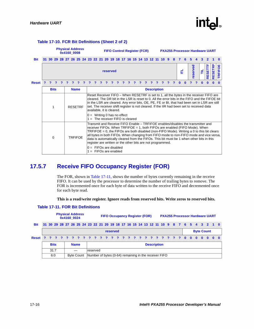
Hardware UART
17.5.7 Receive FIFO Occupancy Register (FOR)
The FOR, shown in Table 17-11, shows the number of bytes currently remaining in the receive FIFO. It can be used by the processor to determine the number of trailing bytes to remove. The FOR is incremented once for each byte of data written to the receive FIFO and decremented once for each byte read.
This is a read/write register. Ignore reads from reserved bits. Write zeros to reserved bits.
1 RESETRF
Reset Receiver FIFO – When RESETRF is set to 1, all the bytes in the receiver FIFO are cleared. The DR bit in the LSR is reset to 0. All the error bits in the FIFO and the FIFOE bit in the LSR are cleared. Any error bits, OE, PE, FE or BI, that had been set in LSR are still set. The receiver shift register is not cleared. If the IIR had been set to received data available, it is cleared.
0 = Writing 0 has no effect1 = The receiver FIFO is cleared
0 TRFIFOE
Transmit and Receive FIFO Enable – TRFIFOE enables/disables the transmitter and receiver FIFOs. When TRFIFOE = 1, both FIFOs are enabled (FIFO Mode). When TRFIFOE = 0, the FIFOs are both disabled (non-FIFO Mode). Writing a 0 to this bit clears all bytes in both FIFOs. When changing from FIFO mode to non-FIFO mode and vice versa, data is automatically cleared from the FIFOs. This bit must be 1 when other bits in this register are written or the other bits are not programmed.
0 = FIFOs are disabled1 = FIFOs are enabled
Table 17-10. FCR Bit Definitions (Sheet 2 of 2)
Physical Address0x4160_0008 FIFO Control Register (FCR) PXA255 Processor Hardware UART
Bit 31 30 29 28 27 26 25 24 23 22 21 20 19 18 17 16 15 14 13 12 11 10 9 8 7 6 5 4 3 2 1 0
reserved ITL
rese
rved
TIL
RE
SE
TT
F
RE
SE
TR
F
TR
FIF
OE
Reset ? ? ? ? ? ? ? ? ? ? ? ? ? ? ? ? ? ? ? ? ? ? ? ? 0 0 ? ? 0 0 0 0
Bits Name Description
Table 17-11. FOR Bit Definitions
Physical Address0x4160_0024 FIFO Occupancy Register (FOR) PXA255 Processor Hardware UART
Bit 31 30 29 28 27 26 25 24 23 22 21 20 19 18 17 16 15 14 13 12 11 10 9 8 7 6 5 4 3 2 1 0
reserved Byte Count
Reset ? ? ? ? ? ? ? ? ? ? ? ? ? ? ? ? ? ? ? ? ? ? ? ? ? 0 0 0 0 0 0 0
Bits Name Description
31:7 — reserved
6:0 Byte Count Number of bytes (0-64) remaining in the receiver FIFO
17-16 Intel® PXA255 Processor Developer’s Manual

Hardware UART
17.5.8 Auto-Baud Control Register (ABR)
The ABR, shown in Table 17-12, controls the functionality and options for auto-baud-rate detection within the UART. Through this register, users can enable or disable the auto-baud lock interrupt, direct either the processor or UART to program the final baud rate in the Divisor Latch registers, and choose between the two methods used to calculate the final baud rate.
The auto-baud circuitry counts the number of clocks in the start bit and writes this count into the Auto-Baud Count register (ACR – refer to Section 17.5.9). It then interrupts the processor if ABR[ABLIE] is set. It also automatically programs the Divisor Latch registers (DLL and DLH – refer to Section 17.5.3) if ABR[ABUP] bit is set.
See Section 17.4.4 for more information on auto-baud rate.
Note: Auto-baud rate detection is not supported with slow infrared Mode.
This is a read/write register. Ignore reads from reserved bits. Write zeros to reserved bits.
17.5.9 Auto-Baud Count Register (ACR)
The ACR, shown in Table 17-13, stores the number of 14.7456 MHz clock cycles within a start bit pulse. This value is then used by the processor or the UART to calculate the baud rate. If auto-baud mode (ABR[ABE] – Section 17.5.8) and auto-baud interrupts (ABR[ABLIE]) are enabled, the UART interrupts the processor with the auto-baud lock interrupt (IIR[ABL] – Section 17.5.5) after it has written the count value into the ACR. The value is written regardless of the state of the auto-baud UART program bit (ABR[ABUP]).
Table 17-12. ABR Bit Definitions
Physical Address0x4160_0028 Autobaud Control Register (ABR) PXA255 Processor Hardware UART
Bit 31 30 29 28 27 26 25 24 23 22 21 20 19 18 17 16 15 14 13 12 11 10 9 8 7 6 5 4 3 2 1 0
reserved
AB
T
AB
UP
AB
LIE
AB
E
Reset ? ? ? ? ? ? ? ? ? ? ? ? ? ? ? ? ? ? ? ? ? ? ? ? ? ? ? ? 0 0 0 0
Bits Name Description
31:4 — reserved
3 ABT
AutoBaud Table. Uses a table to select low-speed baud rates instead of a formula. Only valid if ABR[ABUP] is set.
0 = Table used to calculate baud rates which limits UART to choosing common baud rates as shown in Section 17.4.4, “Auto-Baud-Rate Detection” on page 17-7
1 = Formula used to calculate baud rates allowing all possible baud rates to be chosen by UART.
2 ABUP
AutoBaud UART Program. Controls if the UART automatically programs DLL and DLH or if the processor must program DLL and DLH based on the results in the ACR.
0 = Processor Programs Divisor Latch registers1 = UART Programs Divisor Latch registers
1 ABLIEAutobaud Lock Interrupt Enable.
0 = Autobaud Lock Interrupt disabled (Source IIR[ABL])1 = Autobaud Lock Interrupt enabled (Source IIR[ABL])
0 ABEAutobaud Enable.
0 = Autobaud Disabled1 = Autobaud Enabled
Intel® PXA255 Processor Developer’s Manual 17-17

Hardware UART
This is a read-only register. Ignore reads from reserved bits.
17.5.10 Line Control Register (LCR)
The LCR., shown in Table 17-14 specifies the format for the asynchronous data communications exchange. The serial data format consists of a start bit, five to eight data bits, an optional parity bit, and one, one and a half, or two stop bits. The LCR has bits that allow access to the divisor latch and bits that can cause a break condition.
This is a read/write register. Ignore reads from reserved bits. Write zeros to reserved bits.
Table 17-13. ACR Bit Definitions
Physical Address0x4160_002C Autobaud Count Register (ACR) PXA255 Processor Hardware UART
Bit 31 30 29 28 27 26 25 24 23 22 21 20 19 18 17 16 15 14 13 12 11 10 9 8 7 6 5 4 3 2 1 0
reserved Count Value
Reset ? ? ? ? ? ? ? ? ? ? ? ? ? ? ? ? 0 0 0 0 0 0 0 0 0 0 0 0 0 0 0 0
Bits Name Description
31:16 — reserved
15:0 ACR Number of 14.7456 MHz clock cycles within a start bit pulse.
Table 17-14. LCR Bit Definitions (Sheet 1 of 2)
Physical Address0x4160_000C Line Control Register (LCR) PXA255 Processor Hardware UART
Bit 31 30 29 28 27 26 25 24 23 22 21 20 19 18 17 16 15 14 13 12 11 10 9 8 7 6 5 4 3 2 1 0
reservedD
LA
B
SB
ST
KY
P
EP
S
PE
N
ST
B
WL
S
Reset ? ? ? ? ? ? ? ? ? ? ? ? ? ? ? ? ? ? ? ? ? ? ? ? 0 0 0 0 0 0 0 0
Bits Name Description
31:8 — reserved
7 DLAB
DIVISOR LATCH ACCESS BIT
Must be set to access the divisor latches of the baud rate generator during a READ or WRITE operation. Must be cleared to access the receiver buffer, the Transmit Holding register, or the IER.
0 = Access Transmit Holding register (THR), Receive Buffer register (RBR) and IER.1 = Access Divisor Latch registers (DLL and DLH)
6 SB
SET BREAK
Causes a break condition to be transmitted to the receiving UART. Acts only on the TXD pin and has no effect on the transmitter logic. In FIFO mode, wait until the transmitter is idle, LSR[TEMT]=1, to set and clear SB.
0 = No effect on TXD output1 = Forces TXD output to 0 (space)
5 STKYP
STICKY PARITY
Forces the bit value at the parity bit location to be the opposite of the EPS bit, rather than the parity value. This stops parity generation. If PEN = 0, STKYP is ignored.
0 = No effect on parity bit1 = Forces parity bit to be opposite of EPS bit value
17-18 Intel® PXA255 Processor Developer’s Manual

Hardware UART
17.5.11 Line Status Register (LSR)
The LSR, shown in Table 17-15, provides data transfer status information to the processor.
In non-FIFO mode, LSR[4:2] show the parity error, framing error, break interrupt, and show the error status of the character that has just been received.
In FIFO mode, LSR[4:2] show the status bits of the character that is currently at the front of the FIFO.
LSR[4:1] produce a receiver line status interrupt when the corresponding conditions are detected and the interrupt is enabled. In FIFO mode, the receiver line status interrupt only occurs when the erroneous character reaches the front of the FIFO. If the erroneous character is not at the front of the FIFO, a line status interrupt is generated after the other characters are read and the erroneous character becomes the character at the front of the FIFO.
The LSR must be read before the erroneous character is read. LSR[4:1] bits are set until software reads the LSR.
See Section 17.4.2.3 for details on using the DMA to receive data.
This is a read-only register. Ignore reads from reserved bits.
4 EPS
EVEN PARITY SELECT
Even parity select bit. If PEN = 0, EPS is ignored.
0 = Sends or checks for odd parity1 = Sends or checks for even parity
3 PEN
PARITY ENABLE
Enables a parity bit to be generated on transmission or checked on reception.
0 = No parity1 = Parity
2 STB
STOP BITS
Specifies the number of stop bits transmitted and received in each character. When receiving, the receiver only checks the first stop bit.
0 = 1 Stop bit1 = 2 Stop bits, except for 5-bit character then 1-1/2 bits
1:0 WLS[1:0]
WORD LENGTH SELECT
Specifies the number of data bits in each transmitted or received character.
00 – 5-bit character
01 – 6-bit character
10 – 7-bit character
11 – 8-bit character
Table 17-14. LCR Bit Definitions (Sheet 2 of 2)
Physical Address0x4160_000C Line Control Register (LCR) PXA255 Processor Hardware UART
Bit 31 30 29 28 27 26 25 24 23 22 21 20 19 18 17 16 15 14 13 12 11 10 9 8 7 6 5 4 3 2 1 0
reserved
DL
AB
SB
ST
KY
P
EP
S
PE
N
ST
B
WL
S
Reset ? ? ? ? ? ? ? ? ? ? ? ? ? ? ? ? ? ? ? ? ? ? ? ? 0 0 0 0 0 0 0 0
Bits Name Description
Intel® PXA255 Processor Developer’s Manual 17-19

Hardware UART
Table 17-15. LSR Bit Definitions (Sheet 1 of 2)
Physical Address0x4160_0014 Line Status Register (LSR) PXA255 Processor Hardware UART
Bit 31 30 29 28 27 26 25 24 23 22 21 20 19 18 17 16 15 14 13 12 11 10 9 8 7 6 5 4 3 2 1 0
reserved
FIF
OE
TE
MT
TD
RQ
BI
FE
PE
OE
DR
Reset ? ? ? ? ? ? ? ? ? ? ? ? ? ? ? ? ? ? ? ? ? ? ? ? 0 1 1 0 0 0 0 0
Bits Name Description
31:8 — reserved
7 FIFOE
FIFO ERROR STATUS
In non-FIFO mode, this bit is 0. In FIFO mode, FIFOE is set to 1 when there is at least one parity error, framing error, or break indication for any of the characters in the FIFO. A processor read to the LSR does not reset this bit. FIFOE is reset when all erroneous characters have been read from the FIFO. If DMA requests are enabled (IER bit 7 is set to 1) and FIFOE is set to 1, the error interrupt is generated and no receive DMA request is generated even when the receive FIFO reaches the trigger threshold. Once the errors have been cleared, by reading the FIFO, DMA requests are automatically re-enabled. If DMA requests are not enabled (IER bit 7 is set to 0), then FIFOE set to 1 does not generate an error interrupt.
0 = No FIFO or no errors in receiver FIFO1 = At least one character in receiver FIFO has errors
6 TEMT
TRANSMITTER EMPTY
Set when the Transmit Holding register and the Transmitter Shift register are both empty. It is cleared when either the Transmit Holding register or the Transmitter Shift register contains a data character. In FIFO mode, TEMT is set when the transmitter FIFO and the Transmit Shift register are both empty.
0 = There is data in the Transmit Shift register, the Transmit Holding register, or the FIFO1 = All the data in the transmitter has been shifted out
5 TDRQ
TRANSMIT DATA REQUEST
Indicates that the UART is ready to accept a new character for transmission. In addition, this bit causes the UART to issue an interrupt to the processor when the transmit data request interrupt enable is set high and generates the DMA request to the DMA controller if DMA requests and FIFO mode are enabled.
In non-FIFO mode, TDRQ is set when a character is transferred from the Transmit Holding register into the Transmit Shift register. The bit is cleared with the loading of the Transmit Holding register.
In FIFO mode, TDRQ is set to 1 when half of the characters in the FIFO have been loaded into the Shift register if FCR[TIL]=0, or the FIFO is empty and FCR[TIL]=1, or the RESETTF bit in FCR has been set. It is cleared when the FIFO has more data than required by FCR[TIL].
If more than 64 characters are loaded into the FIFO, the excess characters are lost.
0 = There is data in Transmit Holding register or FIFO waiting to be shifted out1 = Transmit FIFO has half or less than half data (FCR[TIL]=0), or the transmit FIFO is
empty (FCR[TIL]=1), or the UART is waiting for data (non-FIFO mode)
4 BI
BREAK INTERRUPT
BI is set when the received data input is held low for longer than a full word transmission time (that is, the total time of start bit + data bits + parity bit + stop bits). The break indicator is reset when the processor reads the LSR. In FIFO mode, only one character equal to 0x00, is loaded into the FIFO regardless of the length of the break condition. BI shows the break condition for the character at the front of the FIFO, not the most recently received character.
0 = No break signal has been received1 = Break signal received
17-20 Intel® PXA255 Processor Developer’s Manual

Hardware UART
17.5.12 Modem Control Register (MCR)
The MCR, shown in Table 17-16, uses the modem control pin nRTS to control the interface with a modem or data set. The MCR also controls the loopback mode. Loopback mode must be enabled before the UART is enabled.
This is a read/write register. Ignore reads from reserved bits. Write zeros to reserved bits.
3 FE
FRAMING ERROR
FE indicates that the received character did not have a valid stop bit. FE is set when the bit following the last data bit or parity bit is detected as 0. If the LCR had been set for two stop bit mode, the receiver does not check for a valid second stop bit. The FE indicator is reset when the processor reads the LSR. The UART re-synchronizes after a framing error. To do this it assumes that the framing error was due to the next start bit, so it samples this “start” bit twice and then reads in the “data”. In FIFO mode, FE shows a framing error for the character at the front of the FIFO, not for the most recently received character.
0 = No framing error1 = Invalid stop bit has been detected
2 PE
PARITY ERROR
Indicates that the received data character does not have the correct even or odd parity, as selected by the even parity select bit. PE is set when a parity error is detected and is cleared when the processor reads the LSR. In FIFO mode, PE shows a parity error for the character at the front of the FIFO, not the most recently received character.
0 = No parity error1 = Parity error has occurred
1 OE
OVERRUN ERROR
In non-FIFO mode, OE indicates that data in the Receive Buffer register was not read by the processor before the next character was received. The new character is lost. In FIFO mode, OE indicates that all 64 bytes of the FIFO are full and the most recently received byte has been discarded. The OE indicator is set when an overrun condition is detected and cleared when the processor reads the LSR.
0 = No data has been lost1 = Received data has been lost
0 DR
DATA READY
DR is set when a complete incoming character has been received and transferred into the Receive Buffer register or the FIFO. In non-FIFO mode, DR is cleared when the receive buffer is read. In FIFO mode, DR is cleared if the FIFO is empty (last character has been read from Receive Buffer register) or the FIFO is reset with FCR[RESETRF].
0 = No data has been received1 = Data is available in RBR or the FIFO
Table 17-15. LSR Bit Definitions (Sheet 2 of 2)
Physical Address0x4160_0014 Line Status Register (LSR) PXA255 Processor Hardware UART
Bit 31 30 29 28 27 26 25 24 23 22 21 20 19 18 17 16 15 14 13 12 11 10 9 8 7 6 5 4 3 2 1 0
reserved
FIF
OE
TE
MT
TD
RQ
BI
FE
PE
OE
DR
Reset ? ? ? ? ? ? ? ? ? ? ? ? ? ? ? ? ? ? ? ? ? ? ? ? 0 1 1 0 0 0 0 0
Bits Name Description
Intel® PXA255 Processor Developer’s Manual 17-21

Hardware UART
Table 17-16. MCR Bit Definitions (Sheet 1 of 2)
Physical Address0x4160_0010 Modem Control Register (MCR) PXA255 Processor Hardware UART
Bit 31 30 29 28 27 26 25 24 23 22 21 20 19 18 17 16 15 14 13 12 11 10 9 8 7 6 5 4 3 2 1 0
reserved
AF
E
LO
OP
OU
T2
rese
rved
RT
S
rese
rved
Reset ? ? ? ? ? ? ? ? ? ? ? ? ? ? ? ? ? ? ? ? ? ? ? ? ? ? 0 0 0 ? 0 ?
Bits Name Description
31:8 — reserved
5 AFE
AUTOFLOW CONTROL ENABLE
0 = Auto-RTS and auto-CTS are disabled.1 = Auto-CTS is enabled. If MCR[RTS] is also set, both auto-CTS and auto-RTS is
enabled.
4 LOOP
LOOPBACK MODE
This bit provides a local loopback feature for diagnostic testing of the UART. When LOOP is set to a logic 1, the following occurs:
• The transmitter serial output is set to a logic 1 state.
• The receiver serial input is disconnected from the pin.
• The output of the Transmitter Shift register is “looped back” into the Receiver Shift register input.
• The four modem control inputs (nCTS, nDSR, nDCD, and nRI) are disconnected from the pins and the modem control output pins (nRTS and nDTR) are forced to their inactive state.
Coming out of the loopback mode may result in unpredictable activation of the delta bits (bits 3:0) in the Modem Status register (MSR). It is recommended that MSR is read once to clear the delta bits in the MSR.
Loopback mode must be configured before the UART is enabled.
MCR[RTS] is connected to the Modem Status register CTS bit: This allows software to test CTS functionality by setting or clearing MCR[RTS]
• RTS = 1 forces CTS to 1
• RTS = 0 forces CTS to a 0
In loopback mode, data that is transmitted is immediately received. This feature lets the processor verify the transmit and receive data paths of the UART. The transmit, receive and modem control interrupts are operational, except the modem control interrupts are activated by MCR bits, not the modem control pins. A break signal can also be transferred from the transmitter section to the receiver section in loopback mode.
0 = Normal UART operation1 = Loopback mode UART operation
3 OUT2
OUT2 SIGNAL CONTROL
OUT2 connects the UART’s interrupt output to the interrupt controller unit. When LOOP=0:
0 = UART interrupt is disabled1 = UART interrupt is enabled.
When LOOP=1, interrupts always go to the processor.
2 — reserved
17-22 Intel® PXA255 Processor Developer’s Manual

Hardware UART
17.5.13 Modem Status Register (MSR)
The MSR, shown in Table 17-17, provides the current state of the control lines from the modem or data set (or a peripheral device emulating a modem) to the processor. In addition to this current state information, four bits of the MSR provide change information. MSR[3:0] are set when a control input from the modem changes state. They are cleared when the processor reads the MSR.
The status of the modem control lines do not affect the FIFOs. To use these lines for flow control, IER[MIE] must be set. When an interrupt on one of the flow control pins occurs, the interrupt service routine must disable the UART. The UART continues transmission and reception of the current character and then stops. The contents of the FIFOs is preserved. If the UART is re-enabled, transmission continues where it stopped.
Note: When bit 0, 1, 2, or 3 is set, a modem status interrupt is generated if IER[MIE] is set.
This is a read-only register. Ignore reads from reserved bits.
1 RTS
REQUEST TO SEND
Controls the status of the nRTS pin when the AFE bit is clear. When AFE is set, switches between full autoflow and half autoflow.
Autoflow mode disabled:
0 = nRTS pin is 11 = nRTS pin is 0
Autoflow mode enabled:
0 = Auto-RTS disabled. Auto flow works only with auto-CTS1 = Auto-RTS enabled. Auto flow works with both auto-CTS and auto-RTS
In loopback mode, controls status of CTS input signal.
0 — reserved
Table 17-16. MCR Bit Definitions (Sheet 2 of 2)
Physical Address0x4160_0010 Modem Control Register (MCR) PXA255 Processor Hardware UART
Bit 31 30 29 28 27 26 25 24 23 22 21 20 19 18 17 16 15 14 13 12 11 10 9 8 7 6 5 4 3 2 1 0
reserved
AF
E
LO
OP
OU
T2
rese
rved
RT
S
rese
rved
Reset ? ? ? ? ? ? ? ? ? ? ? ? ? ? ? ? ? ? ? ? ? ? ? ? ? ? 0 0 0 ? 0 ?
Bits Name Description
Table 17-17. MSR Bit Definitions (Sheet 1 of 2)
Physical Address0x4160_0018 Modem Status Register (MSR) PXA255 Processor Hardware UART
Bit 31 30 29 28 27 26 25 24 23 22 21 20 19 18 17 16 15 14 13 12 11 10 9 8 7 6 5 4 3 2 1 0
reserved
CT
S
rese
rved
DC
TS
Reset ? ? ? ? ? ? ? ? ? ? ? ? ? ? ? ? ? ? ? ? ? ? ? ? ? ? ? 1 ? ? ? 0
Bits Name Description
31:5 — reserved
Intel® PXA255 Processor Developer’s Manual 17-23

Hardware UART
17.5.14 Scratchpad Register (SCR)
The SCR, shown in Table 17-18, has no effect on the UART. It is intended as a scratchpad register for use by the programmer. It is included for 16550A compatibility.
This is a read-only register. Ignore reads from reserved bits.
17.5.15 Infrared Selection Register (ISR)
Each UART can manage an IrDA module. The ISR, shown in Table 17-19, controls IrDA functions (see Section 17.4.5).
This is a read/write register. Ignore reads to reserved bits. Write zeros to reserved bits.
4 CTS
CLEAR TO SEND
Complement of the clear to send (nCTS) input. Equivalent to MCR[RTS] if MCR[LOOP] is set.
0 = nCTS pin is 11 = nCTS pin is 0
3:1 — reserved
0 DCTSDELTA CLEAR TO SEND
0 = No change in nCTS pin since last read of MSR1 = nCTS pin has changed state
Table 17-17. MSR Bit Definitions (Sheet 2 of 2)
Physical Address0x4160_0018 Modem Status Register (MSR) PXA255 Processor Hardware UART
Bit 31 30 29 28 27 26 25 24 23 22 21 20 19 18 17 16 15 14 13 12 11 10 9 8 7 6 5 4 3 2 1 0
reserved
CT
S
rese
rved
DC
TS
Reset ? ? ? ? ? ? ? ? ? ? ? ? ? ? ? ? ? ? ? ? ? ? ? ? ? ? ? 1 ? ? ? 0
Bits Name Description
Table 17-18. SCR Bit Definitions
Physical Address0x4160_001C Scratchpad Register (SCR) PXA255 Processor Hardware UART
Bit 31 30 29 28 27 26 25 24 23 22 21 20 19 18 17 16 15 14 13 12 11 10 9 8 7 6 5 4 3 2 1 0
reserved SCR
Reset ? ? ? ? ? ? ? ? ? ? ? ? ? ? ? ? ? ? ? ? ? ? ? ? 0 0 0 0 0 0 0 0
Bits Name Description
31:8 — reserved
7:0 SCR No effect on UART function
17-24 Intel® PXA255 Processor Developer’s Manual

Hardware UART
17.6 Hardware UART Register Summary
Table 17-20 contains the register addresses for the HWUART.
Table 17-19. ISR Bit Definitions
Physical Address0x4160_0020 Infrared Selection Register (ISR) PXA255 Processor Hardware UART
Bit 31 30 29 28 27 26 25 24 23 22 21 20 19 18 17 16 15 14 13 12 11 10 9 8 7 6 5 4 3 2 1 0
reserved
RX
PL
TX
PL
XM
OD
E
RC
VE
IR
XM
ITIR
Reset ? ? ? ? ? ? ? ? ? ? ? ? ? ? ? ? ? ? ? ? ? ? ? ? ? ? ? 0 0 0 0 0
Bits Name Description
31:5 — reserved
4 RXPLRECEIVE DATA POLARITY
0 = SIR decoder takes positive pulses as zeros1 = SIR decoder takes negative pulses as zeros
3 TXPLTRANSMIT DATA POLARITY
0 = SIR encoder generates a positive pulse for a data bit of zero1 = SIR encoder generates a negative pulse for a data bit of zero
2 XMODE
TRANSMIT PULSE WIDTH SELECT
When XMODE is cleared, the UART 16X clock clocks the IrDA transmit and receive logic. When XMODE is set, receive decoder operation does not change and the transmit encoder generates 1.6 µs pulses (that are 3/16 of a bit time at 115.2 Kbps) instead of pulses 3/16 of a bit time wide.
0 = Transmit pulse width is 3/16 of a bit time wide1 = Transmit pulse width is 1.6 µs
1 RCVEIR
RECEIVER SIR ENABLE
When RCVEIR is set, the signal from the RXD pin is processed by the IrDA decoder before it is fed to the UART. If RCVEIR is cleared, then all clocking to the IrDA decoder is blocked and the RXD pin is fed directly to the UART.
0 = Receiver is in UART mode1 = Receiver is in infrared mode
0 XMITIR
TRANSMITTER SIR ENABLE
When XMITIR is set to 1, the normal TXD output from the UART is processed by the IrDA encoder before it is fed to the device pin. If XMITIR is cleared, all clocking to the IrDA encoder is blocked and the UART’s TXD signal is connected directly to the device pin.
When Transmitter SIR Enable is set, the TXD output pin, which is in a normally high default state, switches to a normally low default state. This can cause a false start bit unless the infrared LED is disabled before XMITIR is set.
0 = Transmitter is in UART mode1 = Transmitter is in infrared mode
Table 17-20. HWUART Register Locations (Sheet 1 of 2)
Register Addresses
DLAB Bit Value Name Description
0x4160_0000 0 HWRBR “Receive Buffer Register (RBR)” (read only)
0x4160_0000 0 HWTHR “Transmit Holding Register (THR)” (write only)
0x4160_0004 0 HWIER “Interrupt Enable Register (IER)” (read/write)
Intel® PXA255 Processor Developer’s Manual 17-25

Hardware UART
0x4160_0008 X HWIIR “Interrupt Identification Register (IIR)” (read only)
0x4160_0008 X HWFCR “FIFO Control Register (FCR)” (write only)
0x4160_000C X HWLCR “Line Control Register (LCR)” (read/write)
0x4160_0010 X HWMCR “Modem Control Register (MCR)” (read/write)
0x4160_0014 X HWLSR “Line Status Register (LSR)” (read only)
0x4160_0018 X HWMSR “Modem Status Register (MSR)” (read only)
0x4160_001C X HWSPR “Scratchpad Register (SCR)” (read/write)
0x4160_0020 X HWISR “Infrared Selection Register (ISR)” (read/write)
0x4160_0024 X HWFOR “Receive FIFO Occupancy Register (FOR)” (read only)
0x4160_0028 X HWABR “Auto-Baud Control Register (ABR)” (read/write)
0x4160_002C X HWACR “Auto-Baud Count Register (ACR)”
0x4160_0000 1 HWDLL “Divisor Latch Registers (DLL and DLH)” low byte (read/write)
0x4160_0004 1 HWDLH “Divisor Latch Registers (DLL and DLH)” high byte (read/write)
Table 17-20. HWUART Register Locations (Sheet 2 of 2)
Register Addresses
DLAB Bit Value Name Description
17-26 Intel® PXA255 Processor Developer’s Manual

Hardware UART
Intel® PXA255 Processor Developer’s Manual 17-27
