intel® stratix® 10 jtag boundary-scan testing user guide · 1. intel ® stratix ® 10 overview....
TRANSCRIPT

Intel® Stratix® 10 JTAG Boundary-Scan Testing User Guide
SubscribeSend Feedback
UG-S10JTAG | 2020.06.30Latest document on the web: PDF | HTML
Contents
1. Intel® Stratix® 10 Overview............................................................................................3
2. Intel Stratix 10 JTAG BST Architecture........................................................................... 42.1. JTAG Circuitry Functional Model............................................................................... 42.2. JTAG Pins............................................................................................................ 52.3. IEEE Std. 1149.1 Boundary-Scan Register ................................................................5
2.3.1. Boundary-Scan Cells of Intel Stratix 10 Device I/O Pin....................................62.4. IEEE Std. 1149.6 Boundary-Scan Register.................................................................7
2.4.1. IEEE Std. 1149.6 BST Circuitry for Intel Stratix 10 E-Tile Transceiver.............. 102.4.2. IEEE Std. 1149.6 BST Circuitry for Intel Stratix 10 P-Tile Transceiver.............. 11
3. Intel Stratix 10 BST Operation Control .........................................................................133.1. Device ID .......................................................................................................... 133.2. Supported JTAG Instructions ................................................................................ 153.3. JTAG Secure Mode .............................................................................................. 16
4. Intel Stratix 10 I/O Voltage for JTAG Operation .......................................................... 17
5. Performing Intel Stratix 10 Boundary-Scan Testing......................................................18
6. Enabling and Disabling Intel Stratix 10 BST Circuitry ...................................................206.1. Enabling BST Circuitry.......................................................................................... 206.2. Disabling BST Circuitry ........................................................................................ 20
7. Intel Stratix 10 IEEE Std. 1149.1 BST Guidelines.......................................................... 21
8. Document Revision History for the Intel Stratix 10 JTAG Boundary-Scan TestingUser Guide...............................................................................................................22
Contents
Intel® Stratix® 10 JTAG Boundary-Scan Testing User Guide Send Feedback
2

1. Intel® Stratix® 10 OverviewIntel® Stratix® 10 devices support IEEE Std. 1149.1 BST and IEEE Std. 1149.6 BST.When you perform Boundary-Scan Test (BST), you can test pin connections withoutusing physical test probes and capture functional data during normal operation. Theboundary-scan cells (BSCs) in a device can force signals onto pins, or capture datafrom pin or core logic signals. Forced test data is serially shifted into the BSCs.Captured data is serially shifted out and externally compared to expected results.
Intel Stratix 10 devices are implemented using multiple die inside the package,connected together using EMIB (Embedded Multi-die Interconnect Bridge) technology.The multiple die implementation is transparent to BST. There is a single boundary-scan chain for the complete device that includes every die inside the package.
You can perform BST on Intel Stratix 10 devices before, after, and duringconfiguration.
Related Information
Performing Intel Stratix 10 Boundary-Scan Testing on page 18
UG-S10JTAG | 2020.06.30
Send Feedback
Intel Corporation. All rights reserved. Agilex, Altera, Arria, Cyclone, Enpirion, Intel, the Intel logo, MAX, Nios,Quartus and Stratix words and logos are trademarks of Intel Corporation or its subsidiaries in the U.S. and/orother countries. Intel warrants performance of its FPGA and semiconductor products to current specifications inaccordance with Intel's standard warranty, but reserves the right to make changes to any products and servicesat any time without notice. Intel assumes no responsibility or liability arising out of the application or use of anyinformation, product, or service described herein except as expressly agreed to in writing by Intel. Intelcustomers are advised to obtain the latest version of device specifications before relying on any publishedinformation and before placing orders for products or services.*Other names and brands may be claimed as the property of others.
ISO9001:2015Registered

2. Intel Stratix 10 JTAG BST Architecture
2.1. JTAG Circuitry Functional Model
The JTAG BST circuitry requires the following registers:
• Instruction register—determines which action to perform and which data registerto access.
• Bypass register (1-bit long data register)—provides a minimum-length serial pathbetween the TDI and TDO pins.
• Boundary-scan register—shift register composed of all the BSCs of the device.
Figure 1. JTAG Circuitry Functional Model• Test access port (TAP) controller—controls the JTAG BST.
• TMS and TCK pins—operate the TAP controller.
• TDI and TDO pins—provide the serial path for the data and instruction registers.
Note: TRST pin is not available in Intel Stratix 10 devices.
a
UPDATEIRCAPTUREIR
SHIFTIR
UPDATEDRCAPTUREDR
SHIFTDR
TDI
Instruction Register
Bypass Register
Boundary-Scan Register
Instruction DecodeTMSTCK
TAPController
Implementation-Defined Registers
TDO
Data Registers
Device ID Register
UG-S10JTAG | 2020.06.30
Send Feedback
Intel Corporation. All rights reserved. Agilex, Altera, Arria, Cyclone, Enpirion, Intel, the Intel logo, MAX, Nios,Quartus and Stratix words and logos are trademarks of Intel Corporation or its subsidiaries in the U.S. and/orother countries. Intel warrants performance of its FPGA and semiconductor products to current specifications inaccordance with Intel's standard warranty, but reserves the right to make changes to any products and servicesat any time without notice. Intel assumes no responsibility or liability arising out of the application or use of anyinformation, product, or service described herein except as expressly agreed to in writing by Intel. Intelcustomers are advised to obtain the latest version of device specifications before relying on any publishedinformation and before placing orders for products or services.*Other names and brands may be claimed as the property of others.
ISO9001:2015Registered
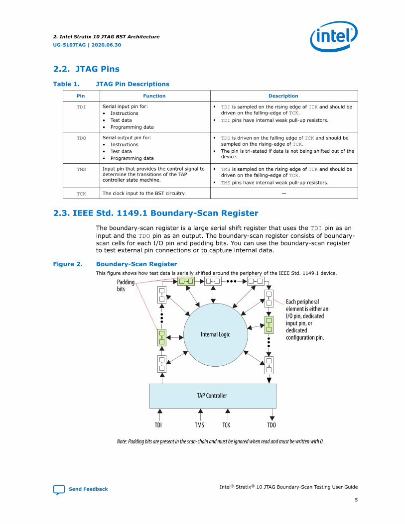
2.2. JTAG Pins
Table 1. JTAG Pin Descriptions
Pin Function Description
TDI Serial input pin for:• Instructions• Test data• Programming data
• TDI is sampled on the rising edge of TCK and should bedriven on the falling-edge of TCK.
• TDI pins have internal weak pull-up resistors.
TDO Serial output pin for:• Instructions• Test data• Programming data
• TDO is driven on the falling edge of TCK and should besampled on the rising-edge of TCK.
• The pin is tri-stated if data is not being shifted out of thedevice.
TMS Input pin that provides the control signal todetermine the transitions of the TAPcontroller state machine.
• TMS is sampled on the rising edge of TCK and should bedriven on the falling-edge of TCK.
• TMS pins have internal weak pull-up resistors.
TCK The clock input to the BST circuitry. —
2.3. IEEE Std. 1149.1 Boundary-Scan Register
The boundary-scan register is a large serial shift register that uses the TDI pin as aninput and the TDO pin as an output. The boundary-scan register consists of boundary-scan cells for each I/O pin and padding bits. You can use the boundary-scan registerto test external pin connections or to capture internal data.
Figure 2. Boundary-Scan RegisterThis figure shows how test data is serially shifted around the periphery of the IEEE Std. 1149.1 device.
TCK TMSTDI TDO
Internal Logic
TAP Controller
Each peripheralelement is either anI/O pin, dedicatedinput pin, or dedicated configuration pin.
Paddingbits
Note: Padding bits are present in the scan-chain and must be ignored when read and must be written with 0.
2. Intel Stratix 10 JTAG BST Architecture
UG-S10JTAG | 2020.06.30
Send Feedback Intel® Stratix® 10 JTAG Boundary-Scan Testing User Guide
5

2.3.1. Boundary-Scan Cells of Intel Stratix 10 Device I/O Pin
The Intel Stratix 10 device 3-bit BSC consists of the following registers:
• Capture registers—connect to internal device data through the OUTJ, OEJ, andPIN_IN signals.
• Update registers—connect to external data through the PIN_OUT and PIN_OEsignals.
The TAP controller generates the global control signals for the IEEE Std. 1149.1 BSTregisters (SHIFT, CLOCK, and UPDATE) internally. A decode of the instruction registergenerates the MODE signal.
The data signal path for the boundary-scan register runs from the serial data in (SDI)signal to the serial data out (SDO) signal. The scan register begins at the TDI pin andends at the TDO pin of the device.
Figure 3. User I/O BSC with IEEE Std. 1149.1 BST Circuitry for Intel Stratix 10 Devices
01
01
01
01
01
01
01
D QInput
D QInput
D QOE
D QOE
D QOutput
D QOutput
GlobalSignals
From or to device
I/O circuitryand/or
logic array
CaptureRegisters
UpdateRegisters
PadPIN_OUT
OutputBuffer
InputBuffer
PIN_ININJ
SDO
RDEBUGOEJ
OUTJ
SHIFT SDIN CLK UPDATE HIGHZ MODE
PIN_OE
1
Note: TDI, TDO, TMS, TCK, TRST, VCC, GND, VREF, VSIGP, VSIGN, TEMPDIODE, and RREFpins do not have BSCs.
2. Intel Stratix 10 JTAG BST Architecture
UG-S10JTAG | 2020.06.30
Intel® Stratix® 10 JTAG Boundary-Scan Testing User Guide Send Feedback
6

Table 2. Boundary-Scan Cell Descriptions for Intel Stratix 10 DevicesThis table lists the capture and update register capabilities of all BSCs within Intel Stratix 10 devices.
Pin Type Captures Drives Comments
OutputCaptureRegister
OE CaptureRegister
InputCaptureRegister
OutputUpdate
Register
OE UpdateRegister
InputUpdate
Register
User I/O pins OUTJ OEJ PIN_IN PIN_OUT PIN_OE INJ —
Dedicatedinput
0 1 PIN_IN N.C. N.C. N.C. PIN_INdrives to thecore logic
Dedicatedbidirectional(1)
0 OEJ PIN_IN N.C. N.C. N.C. PIN_INdrives to thecore logic
Dedicatedoutput (2)
OUTJ 0 0 N.C. N.C. N.C. OUTJ drivesto the outputbuffer
2.4. IEEE Std. 1149.6 Boundary-Scan Register
The BSCs for HSSI transmitters (GXB_TX[p,n]) and receivers/input clock buffers(GXB_RX[p,n])/(REFCLK[p,n]) in Intel Stratix 10 devices are different from theBSCs for the I/O pins.
Note: You have to use the EXTEST_PULSE JTAG instruction for AC-coupling on HSSItransceiver. Do not use the EXTEST JTAG instruction for AC-coupling on HSSItransceiver. You can perform AC JTAG on the Intel Stratix 10 device before, after, andduring configuration.
(1) This includes the NCONFIG, MSEL0, MSEL1, MSEL2, MSEL3, NCE, and PORSEL pins.
(2) This includes the CONF_DONE, NSTATUS, and DCLK pins.
2. Intel Stratix 10 JTAG BST Architecture
UG-S10JTAG | 2020.06.30
Send Feedback Intel® Stratix® 10 JTAG Boundary-Scan Testing User Guide
7
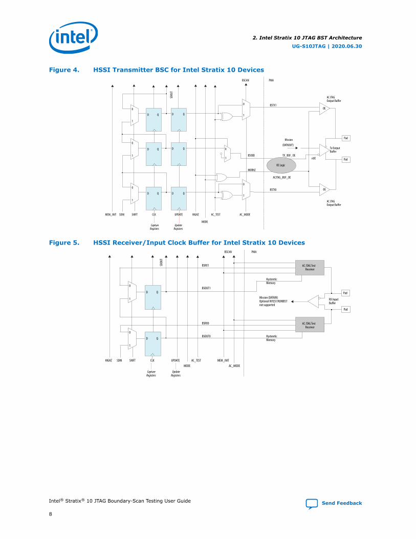
Figure 4. HSSI Transmitter BSC for Intel Stratix 10 Devices
MEM_INIT SDIN SHIFT
0
1
0
1
D Q
D Q
CLK
SDOU
T
MODE
AC_TEST AC_MODE
CaptureRegisters
UpdateRegisters
BSTX1
Tx OutputBuffer
0
1
D Q
D Q
D Q
D Q
HIGHZUPDATE
BSCAN PMA
0
1
0
1
0
1BSOEB
MORHZOE Logic
BSTX0 OE
OE
nOE
Mission
(DATAOUT)
TX_BUF_OE
ACJTAG_BUF_OE
AC JTAGOutput Buffer
AC JTAGOutput Buffer
Pad
Pad
Figure 5. HSSI Receiver/Input Clock Buffer for Intel Stratix 10 Devices
HIGHZ SDIN SHIFT
0
1
0
1
D Q
D Q
CLK
SDOU
T
MODE
AC_TEST
CaptureRegisters
UpdateRegisters
BSRX1
BSOUT1
BSRX0
BSOUT0
MEM_INIT
AC_MODE
BSCAN PMA
UPDATE
HystereticMemory
HystereticMemory
AC JTAG TestReceiver
Mission (DATAIN)Optional INTEST/RUNBISTnot supported
RX InputBuffer
Pad
Pad
AC JTAG TestReceiver
2. Intel Stratix 10 JTAG BST Architecture
UG-S10JTAG | 2020.06.30
Intel® Stratix® 10 JTAG Boundary-Scan Testing User Guide Send Feedback
8

Figure 6. UIB and eSRAM BSC for Intel Stratix 10 DevicesThe differential reference clock input pins for UIB and eSRAM are sharing the BSC per pair as shown in thisfigure. The capture value (DATAIN) would be invalid if one or both differential inputs are abnormal.
01
D Q D Q
D Q
SDOUT
DATAIN
D Q
D Q D Q01
CLK UPDATE SAMPLE HIGHZ MODESHIFTSDIN
NOE(Tied to 1)
DATAOUT(Tied to 0)
CaptureRegisters
UpdateRegisters
01 CLK_ESRAMp/
UIB_PLL_REF_CLKp
CLK_ESRAMn/UIB_PLL_REF_CLKn
InputBuffer
Pad
Pad
01
2. Intel Stratix 10 JTAG BST Architecture
UG-S10JTAG | 2020.06.30
Send Feedback Intel® Stratix® 10 JTAG Boundary-Scan Testing User Guide
9

2.4.1. IEEE Std. 1149.6 BST Circuitry for Intel Stratix 10 E-TileTransceiver
Figure 7. HSSI Transmitter BSC for Intel Stratix 10 E-Tile Transceiver
SDOU
T
0
1
0
1 1
TX_nTransmit Driver
CLKSHIFTSDIN UPDATE
UpdateRegisters
CaptureRegisters
1
Transmit Driver
Logic ControlBlock
Logic ControlBlock
TX_p
Pad
Pad
D Q D Q
D Q D Q
Figure 8. HSSI Receiver BSC for Intel Stratix 10 E-Tile Transceiver
AC JTAG TestReceiver
AC JTAG TestReceiver
RX InputBuffer
Mission (DATAIN)
RX_n
RX_p
Pad
Pad
0
1
0
1
CLKSHIFTSDIN
CaptureRegisters
D Q
D Q
SDOU
T
2. Intel Stratix 10 JTAG BST Architecture
UG-S10JTAG | 2020.06.30
Intel® Stratix® 10 JTAG Boundary-Scan Testing User Guide Send Feedback
10

2.4.2. IEEE Std. 1149.6 BST Circuitry for Intel Stratix 10 P-TileTransceiver
Figure 9. HSSI Transmitter BSC for Intel Stratix 10 P-Tile Transceiver
TX_p
CLKSHIFTSDIN
SDOUT
CaptureRegisters
00
1D Q
UPDATE
UpdateRegisters
D Q
PadLogic Control
Block1
Transmit Driver
TX_n
Pad1
Transmit Driver
Figure 10. HSSI Receiver BSC for Intel Stratix 10 P-Tile Transceiver
CLKSHIFT
RX InputBuffer
RX_p
SDIN
CaptureRegisters
RX_n
SDOUT
0
1
0
1D Q
D Q
Pad
Pad
2. Intel Stratix 10 JTAG BST Architecture
UG-S10JTAG | 2020.06.30
Send Feedback Intel® Stratix® 10 JTAG Boundary-Scan Testing User Guide
11

Figure 11. I_PIN_PERST_N Input Pin BSC for Intel Stratix 10 P-Tile Transceiver
CLKSHIFTSDIN
SDOUT
DATAIN
CaptureRegisters
UPDATE MODE
UpdateRegisters
InputBuffer
D Q0
1
D Q
0
1
2. Intel Stratix 10 JTAG BST Architecture
UG-S10JTAG | 2020.06.30
Intel® Stratix® 10 JTAG Boundary-Scan Testing User Guide Send Feedback
12

3. Intel Stratix 10 BST Operation Control
3.1. Device ID
The device ID is unique for each Intel Stratix 10 device. Use this code to identify thedevices in a JTAG chain.
Table 3. Device ID Information for Intel Stratix 10 Devices
Product Line Device ID (32 bits)
Version (4 bits) Part Number (16 Bits) Manufacture Identity (11 Bits) LSB (1 Bit)
1SG10MH_U1 0000 0011 0010 0010 0111 000 0110 1110 1
1SG10MH_U2 0000 0011 0010 0010 1111 000 0110 1110 1
1SG040H 0000 0011 0010 0010 0000 000 0110 1110 1
1SG065H 0000 0011 0010 0010 0001 000 0110 1110 1
1SG085H 0001 0011 0010 0010 0010 000 0110 1110 1
1SG110H 0000 0011 0010 0010 0010 000 0110 1110 1
1SG165H 1111 0011 0010 0010 0101 000 0110 1110 1
1SG166H 0101 0011 0010 0010 0100 000 0110 1110 1
1SG210H 1110 0011 0010 0010 0101 000 0110 1110 1
1SG210H(ES1) 0010 0011 0010 0010 0101 000 0110 1110 1
1SG211H 0100 0011 0010 0010 0100 000 0110 1110 1
1SG250L 1101 0011 0010 0001 0101 000 0110 1110 1
1SG250H 1101 0011 0010 0010 0101 000 0110 1110 1
1SG280L 1100 0011 0010 0001 0101 000 0110 1110 1
1SG280L(ES1) 0000 0011 0010 0001 0101 000 0110 1110 1
1SG280L(ES2) 0000 0011 0010 0010 0101 000 0110 1110 1
1SG280L(ES3) 1100 0011 0010 0001 0101 000 0110 1110 1
1SG280H 1100 0011 0010 0010 0101 000 0110 1110 1
1SG280H(ES1) 0000 0011 0010 0010 0101 000 0110 1110 1
1SG280H(ES2) 1100 0011 0010 0001 0101 000 0110 1110 1
1SG280H(ES3) 1100 0011 0010 0010 0101 000 0110 1110 1
1SX040H 0000 0011 0010 0010 1000 000 0110 1110 1
1SX065H 0000 0011 0010 0010 1001 000 0110 1110 1
continued...
UG-S10JTAG | 2020.06.30
Send Feedback
Intel Corporation. All rights reserved. Agilex, Altera, Arria, Cyclone, Enpirion, Intel, the Intel logo, MAX, Nios,Quartus and Stratix words and logos are trademarks of Intel Corporation or its subsidiaries in the U.S. and/orother countries. Intel warrants performance of its FPGA and semiconductor products to current specifications inaccordance with Intel's standard warranty, but reserves the right to make changes to any products and servicesat any time without notice. Intel assumes no responsibility or liability arising out of the application or use of anyinformation, product, or service described herein except as expressly agreed to in writing by Intel. Intelcustomers are advised to obtain the latest version of device specifications before relying on any publishedinformation and before placing orders for products or services.*Other names and brands may be claimed as the property of others.
ISO9001:2015Registered

Product Line Device ID (32 bits)
Version (4 bits) Part Number (16 Bits) Manufacture Identity (11 Bits) LSB (1 Bit)
1SX085H 0001 0011 0010 0010 1010 000 0110 1110 1
1SX110H 0000 0011 0010 0010 1010 000 0110 1110 1
1SX165H 1111 0011 0010 0010 1101 000 0110 1110 1
1SX210H 1110 0011 0010 0010 1101 000 0110 1110 1
1SX250L 1101 0011 0010 0001 1101 000 0110 1110 1
1SX250H 1101 0011 0010 0010 1101 000 0110 1110 1
1SX280L 1100 0011 0010 0001 1101 000 0110 1110 1
1SX280L(ES1) 0100 0011 0010 0001 1101 000 0110 1110 1
1SX280L(ES2) 0100 0011 0010 0001 1101 000 0110 1110 1
1SX280H 1100 0011 0010 0010 1101 000 0110 1110 1
1SX280H(ES1) 0100 0011 0010 0010 1101 000 0110 1110 1
1SX280H(ES2) 1100 0011 0010 0010 1101 000 0110 1110 1
1ST040E 0000 0011 0010 0011 1000 000 0110 1110 1
1ST085E 0001 0011 0010 0011 1010 000 0110 1110 1
1ST110E 0000 0011 0010 0011 1010 000 0110 1110 1
1ST165E 0001 0011 0010 0011 0100 000 0110 1110 1
1ST210E 0000 0011 0010 0011 0100 000 0110 1110 1
1ST250E 1101 0011 0010 0011 1101 000 0110 1110 1
1ST280E1ST280E(ES1)
1100 0011 0010 0011 1101 000 0110 1110 1
1SM16BE1SM16BE(ES1)
0011 0011 0010 1011 1100 000 0110 1110 1
1SM16BH 0011 0011 0010 1010 1100 000 0110 1110 1
1SM16CH 0001 0011 0010 1010 1100 000 0110 1110 1
1SM21BE1SM21BE(ES1)
0010 0011 0010 1011 1100 000 0110 1110 1
1SM21BH1SM21BH(ES1)
0010 0011 0010 1010 1100 000 0110 1110 1
1SM21CH1SM21CH(ES1)
0000 0011 0010 1010 1100 000 0110 1110 1
1SD110P 0000 0011 0010 0100 1010 000 0110 1110 1
1SD21BP 0110 0011 0010 1100 1100 000 0110 1110 1
1SD280P 1100 0011 0010 0100 0101 000 0110 1110 1
3. Intel Stratix 10 BST Operation Control
UG-S10JTAG | 2020.06.30
Intel® Stratix® 10 JTAG Boundary-Scan Testing User Guide Send Feedback
14

3.2. Supported JTAG Instructions
Table 4. JTAG Instructions Supported by Intel Stratix 10 Devices
Caution: Never invoke instruction codes other than the supported JTAG instructions in the followingtable. Invoking unsupported instruction can damage and render the device unusable.
JTAG Instruction Instruction Code Description
MISCCTRL 00 0001 0011 • Required instruction to enable the boundary-scan circuitry for JTAGBST.
• Set the LSB of the 8-bit data register to '1' and the remaining bits to'0' to enable the boundary-scan circuitry.
SAMPLE(3)/PRELOAD 00 0000 0101 • Allows you to capture and examine a snapshot of signals at thedevice pins during normal device operation and permits an initialdata pattern to be an output at the device pins.
• Use this instruction to preload the test pattern into the updateregisters before loading the EXTEST instruction.
EXTEST 00 0000 1111 • Board-level interconnects by forcing a test pattern at the output pins,and capturing the test results at the input pins. Forcing known logichigh and low levels on output pins allows you to detect opens andshorts at the pins of any device in the scan chain.
• The high-impedance state of EXTEST is overridden by bus hold andweak pull-up resistor features.
BYPASS 11 1111 1111 • Places the 1-bit bypass register between the TDI and TDO pins.During normal device operation, the 1-bit bypass register allows theBST data to pass synchronously through the selected devices toadjacent devices.
• You will get a '0' reading in the bypass register out.
USERCODE 00 0000 0111 • Selects the 32-bit USERCODE register and places it between the TDIand TDO pins to allow serial shifting of USERCODE out of TDO.
• The 32-bit USERCODE is a programmable user-defined pattern.
IDCODE 00 0000 0110 • Identifies the devices in a JTAG chain. When the IDCODE register isselected by the IR then in the CAPTURE_DR state, the IDCODEinstruction places the 32-bit Device ID register between the TDI andTDO pins to allow serial shifting of Device ID out of TDO.
• Selects the Device ID register and places it between the TDI andTDO pins to allow serial shifting of Device ID register out of TDO.
• IDCODE instruction is the default instruction in the Test-Logic-Resetstate.
HIGHZ 00 0000 1011 • Sets all user I/O pins to an inactive drive state.• Places the 1-bit bypass register between the TDI and TDO pins.• The programmable weak pull-up resistor or the bus hold feature
overrides the HIGHZ value at the pin.
CLAMP 00 0000 1010 • Places the 1-bit bypass register between the TDI and TDO pins.• The programmable weak pull-up resistor or the bus hold feature
overrides the CLAMP value at the pin. The CLAMP value is the valuestored in the update register of the boundary-scan cell (BSC).
EXTEST_PULSE 00 1000 1111 Enables board-level connectivity checking between the transmitters andreceivers that are AC coupled by generating three output transitions:
continued...
(3) SAMPLE instruction is not supported for high-speed serial interface (HSSI) pins.
3. Intel Stratix 10 BST Operation Control
UG-S10JTAG | 2020.06.30
Send Feedback Intel® Stratix® 10 JTAG Boundary-Scan Testing User Guide
15

JTAG Instruction Instruction Code Description
• Driver drives data on the falling edge of TCK in the UPDATE_IR/DRstate.
• Driver drives inverted data on the falling edge of TCK after enteringthe RUN_TEST/IDLE state.
• Driver drives data on the falling edge of TCK after leaving theRUN_TEST/IDLE state.
EXTEST_TRAIN 00 0100 1111 Behaves the same as the EXTEST_PULSE instruction except that theoutput continues to toggle on the TCK falling edge provided that the TAPcontroller is in the RUN_TEST/IDLE state.
Related Information
Device ID on page 13
3.3. JTAG Secure Mode
JTAG Secure mode in Intel Stratix 10 devices is supported through the Secure DeviceManager (SDM).
3. Intel Stratix 10 BST Operation Control
UG-S10JTAG | 2020.06.30
Intel® Stratix® 10 JTAG Boundary-Scan Testing User Guide Send Feedback
16

4. Intel Stratix 10 I/O Voltage for JTAG OperationThe Intel Stratix 10 device operating in IEEE Std. 1149.1 and IEEE Std. 1149.6 modesuses four required JTAG pins—TDI, TDO, TMS, and TCK.
The TCK pin has an internal weak pull-down resistor, while the TDI and TMS pins haveinternal weak pull-up resistors. The VCCIO_SDM supply powers the TDI, TDO, TMS, andTCK pins.
The JTAG pins support 1.8 V TTL/CMOS I/O standard.
Note: For any voltages higher than 1.8 V, you have to use level shifter. The output voltage ofthe level shifter for the JTAG pins must be the same as set for the VCCIO_SDM supply.
Table 5. TDO Output Buffer
TDO Output Buffer Condition Voltage (V)
VCCIO_SDM 1.8
UG-S10JTAG | 2020.06.30
Send Feedback
Intel Corporation. All rights reserved. Agilex, Altera, Arria, Cyclone, Enpirion, Intel, the Intel logo, MAX, Nios,Quartus and Stratix words and logos are trademarks of Intel Corporation or its subsidiaries in the U.S. and/orother countries. Intel warrants performance of its FPGA and semiconductor products to current specifications inaccordance with Intel's standard warranty, but reserves the right to make changes to any products and servicesat any time without notice. Intel assumes no responsibility or liability arising out of the application or use of anyinformation, product, or service described herein except as expressly agreed to in writing by Intel. Intelcustomers are advised to obtain the latest version of device specifications before relying on any publishedinformation and before placing orders for products or services.*Other names and brands may be claimed as the property of others.
ISO9001:2015Registered

5. Performing Intel Stratix 10 Boundary-Scan Testing
You can issue BYPASS, IDCODE, and SAMPLE JTAG instructions before, after, or duringconfiguration without having to interrupt configuration.
To interrupt configuration in order to perform BST, you can either hold nCONFIG low orissue the following sequence via JTAG: an IR scan updating with 0x201 (COMMAND)followed by two 34 bit DR scans updating with 34’h3_0000_0000 then35’h1_0000_0005. Once configuration is interrupted, you can issue other JTAGinstructions to perform BST.
If you design a board for JTAG configuration using Intel Stratix 10 devices, considerthe connections for the dedicated configuration pins.
Note: Dummy bits exist in the boundary-scan register during boundary-scan operations inIntel Stratix 10 devices. However, these dummy bits do not have any impact on thepins. The dummy bits appear on the TDO immediately before the correspondingboundary-scan register segment and have an unknown value X, which can be either a0 or 1.
SoC Devices
For SoC device, you can only see the FPGA TAP controller in the JTAG chain upondevice power up. The TAP controller for the HPS component only appears in the JTAGchain once the device is configured with a programming file/design containing the HPScomponent. You need to include the information about the HPS component whengenerating the test patterns for boundary-scan testing. You can download theboundary-scan description language (BSDL) file for the SoC device from the IntelStratix 10 Device BSDL Files page.
1SG040 and 1SX040 Devices
For 1SG040 and 1SX040 devices, you must follow the guidelines to perform BST onI/O bank 3C to avoid broken chain in the device.
Table 6. Boundary-Scan Cell Location and the Corresponding I/O PinsYou must set a constant value on the dedicated boundary-scan cell.
Boundary-Scan Cell Location in BSDL File Boundary-Scan Cell Value I/O Pins Location
469 1 U3, V3, U5, V4, W2, Y1, W3, W4
466 0
457 (4) 0 = output
continued...
(4) Set this boundary-scan cell to '0' to perform drive-out test on the listed I/O pins. Set to ‘1’ toperform capture test on the listed I/O pins.
UG-S10JTAG | 2020.06.30
Send Feedback
Intel Corporation. All rights reserved. Agilex, Altera, Arria, Cyclone, Enpirion, Intel, the Intel logo, MAX, Nios,Quartus and Stratix words and logos are trademarks of Intel Corporation or its subsidiaries in the U.S. and/orother countries. Intel warrants performance of its FPGA and semiconductor products to current specifications inaccordance with Intel's standard warranty, but reserves the right to make changes to any products and servicesat any time without notice. Intel assumes no responsibility or liability arising out of the application or use of anyinformation, product, or service described herein except as expressly agreed to in writing by Intel. Intelcustomers are advised to obtain the latest version of device specifications before relying on any publishedinformation and before placing orders for products or services.*Other names and brands may be claimed as the property of others.
ISO9001:2015Registered

Boundary-Scan Cell Location in BSDL File Boundary-Scan Cell Value I/O Pins Location
1 = input
577 1 Y2, AA2, AB1, AB2, AC1, AD1, AF2, AG2
586 0
574 (4) 0 = output1 = input
481 1 AE1, AE2, AD2, AD3, AF3, AF4, AG3, AH3
478 0
454 (4) 0 = output1 = input
583 1 AG1, AH1, AJ1, AK1, AJ2, AJ3, AK2, AL2
589 0
580 (4) 0 = output1 = input
475 1 AE4, AE5, Y4, AA4, AA3, AB3, AC3, AD4
472 0
463 (4) 0 = output1 = input
451 1 AM1, AM2, Y5, AA5, AC4, AB5, AC5, AB6
460 0
448 (4) 0 = output1 = input
Related Information
Intel Stratix 10 Device BSDL Files pageProvides the BSDL files for the Intel Stratix 10 devices.
5. Performing Intel Stratix 10 Boundary-Scan Testing
UG-S10JTAG | 2020.06.30
Send Feedback Intel® Stratix® 10 JTAG Boundary-Scan Testing User Guide
19

6. Enabling and Disabling Intel Stratix 10 BST Circuitry
6.1. Enabling BST Circuitry
The IEEE Std. 1149.1 BST circuitry is enabled after the device is configured. If youneed to perform the boundary-scan test prior to configuration, you must execute theMISCCTRL instruction upon device power up to enable the BST circuitry.
Example 1. MISCCTRL Instruction
!Shift 10-bit MISCCTRL instruction (0x013) to Instruction RegisterSIR 10 TDI (013); !Transition to Run-Test-Idle stateSTATE IDLE; !Shift 8-bit data (0x01) to Data Register for BST circuitry enablingSDR 8 TDI (01);
6.2. Disabling BST Circuitry
To ensure that you do not inadvertently enable the IEEE Std. 1149.1 circuitry when itis not required, disable the circuitry permanently with pin connections as listed in thefollowing table.
Table 7. Pin Connections to Permanently Disable the IEEE Std. 1149.1 Circuitry forIntel Stratix 10 Devices
JTAG Pins(5) Connection for Disabling
TMS VCCIO_SDM
TCK GND
TDI VCCIO_SDM
TDO Leave open
(5) The JTAG pins are dedicated. Software option is not available to disable JTAG in Intel Stratix10 devices.
UG-S10JTAG | 2020.06.30
Send Feedback
Intel Corporation. All rights reserved. Agilex, Altera, Arria, Cyclone, Enpirion, Intel, the Intel logo, MAX, Nios,Quartus and Stratix words and logos are trademarks of Intel Corporation or its subsidiaries in the U.S. and/orother countries. Intel warrants performance of its FPGA and semiconductor products to current specifications inaccordance with Intel's standard warranty, but reserves the right to make changes to any products and servicesat any time without notice. Intel assumes no responsibility or liability arising out of the application or use of anyinformation, product, or service described herein except as expressly agreed to in writing by Intel. Intelcustomers are advised to obtain the latest version of device specifications before relying on any publishedinformation and before placing orders for products or services.*Other names and brands may be claimed as the property of others.
ISO9001:2015Registered

7. Intel Stratix 10 IEEE Std. 1149.1 BST GuidelinesConsider the following guidelines when you perform BST with IEEE Std. 1149.1devices:
• If the first two bits shifted out of the instruction register in the SHIFT_IR stateare not 1 and then 0, the TAP controller did not reach the proper state. To solvethis problem, try one of the following procedures:
— Verify that the TAP controller has reached the SHIFT_IR state correctly. Toadvance the TAP controller to the SHIFT_IR state, return to the TEST-LOGIC-RESET state and send the 01100 code to the TMS pin.
— Check the connections to the VCC, GND, JTAG, and dedicated configurationpins on the device.
• Perform a SAMPLE/PRELOAD test cycle before the first EXTEST test cycle toensure that known data is present at the device pins when you enter EXTESTmode. If the OEJ update register contains 0, the data in the OUTJ update registeris driven out. The state must be known and correct to avoid contention with otherdevices in the system.
• Do not perform EXTEST testing during in-circuit reconfiguration because EXTESTis not supported during in-circuit reconfiguration.
• After configuration, you cannot test any pins in a differential pin pair. To performBST after configuration, edit and redefine the BSC group that correspond to thesedifferential pin pairs as an internal cell.
UG-S10JTAG | 2020.06.30
Send Feedback
Intel Corporation. All rights reserved. Agilex, Altera, Arria, Cyclone, Enpirion, Intel, the Intel logo, MAX, Nios,Quartus and Stratix words and logos are trademarks of Intel Corporation or its subsidiaries in the U.S. and/orother countries. Intel warrants performance of its FPGA and semiconductor products to current specifications inaccordance with Intel's standard warranty, but reserves the right to make changes to any products and servicesat any time without notice. Intel assumes no responsibility or liability arising out of the application or use of anyinformation, product, or service described herein except as expressly agreed to in writing by Intel. Intelcustomers are advised to obtain the latest version of device specifications before relying on any publishedinformation and before placing orders for products or services.*Other names and brands may be claimed as the property of others.
ISO9001:2015Registered
8. Document Revision History for the Intel Stratix 10JTAG Boundary-Scan Testing User Guide
DocumentVersion
Changes
2020.06.30 Added the following devices in the Device ID Information for Intel Stratix 10 Devices table.• 1SG10MH_U1• 1SG10MH_U2
2020.03.13 Updated the Device ID Information for Intel Stratix 10 Devices table.• Added 1SG280H(S3) device.• Rearranged the device ID information for better clarity.
2019.12.24 • Added the following devices in the Device ID Information for Intel Stratix 10 Devices table:— 1SG040H— 1SX040H
• Updated the descriptions for HIGHZ and CLAMP JTAG instructions in the JTAG InstructionsSupported by Intel Stratix 10 Devices table.
• Added information for 1SG040 and 1SX040 devices in the Performing Intel Stratix 10 Boundary-Scan Testing section.
2019.11.07 • Added diagrams for IEEE Std. 1149.6 BST Circuitry for Intel Stratix 10 P-Tile Transceiver.• Added the following devices in the Device ID Information for Intel Stratix 10 Devices table:
— 1SD110P— 1SD21BP— 1SD280P— 1SX065H
2019.09.30 Added the following devices in the Device ID Information for Intel Stratix 10 Devices table.• 1SG065H• 1ST040E• 1ST085E• 1ST110E
2019.07.01 • Updated the figure titles in the following sections:— IEEE Std. 1149.6 Boundary-Scan Register— IEEE Std. 1149.6 BST Circuitry for Intel Stratix 10 E-Tile Transceiver
• Updated the Device ID Information for Intel Stratix 10 Devices table.— Added 1SG166H and 1SG211H.— Removed unsupported device: 1SM11AH.
• Updated the description for SAMPLE/PRELOAD in the JTAG Instructions Supported by Intel Stratix10 Devices table.
2019.01.08 Added the following diagrams in the IEEE Std. 1149.6 Boundary-Scan Register section.• UIB and eSRAM BSC with IEEE Std. 1149.1 BST Circuitry for Intel Stratix 10 Devices• HSSI Transmitter BSC with IEEE Std. 1149.6 BST Circuity for Intel Stratix 10 E-Tile Transceiver• HSSI Receiver BSC with IEEE Std. 1149.6 BST Circuity for Intel Stratix 10 E-Tile Transceiver
continued...
UG-S10JTAG | 2020.06.30
Send Feedback
Intel Corporation. All rights reserved. Agilex, Altera, Arria, Cyclone, Enpirion, Intel, the Intel logo, MAX, Nios,Quartus and Stratix words and logos are trademarks of Intel Corporation or its subsidiaries in the U.S. and/orother countries. Intel warrants performance of its FPGA and semiconductor products to current specifications inaccordance with Intel's standard warranty, but reserves the right to make changes to any products and servicesat any time without notice. Intel assumes no responsibility or liability arising out of the application or use of anyinformation, product, or service described herein except as expressly agreed to in writing by Intel. Intelcustomers are advised to obtain the latest version of device specifications before relying on any publishedinformation and before placing orders for products or services.*Other names and brands may be claimed as the property of others.
ISO9001:2015Registered

DocumentVersion
Changes
2018.09.24 • Updated the following product lines in the Device ID Information for Intel Stratix 10 Devices table.— Updated 1ST280E/ES1 to 1ST280E and 1ST280E(ES1)— Updated 1SM11AH/ES1 to 1SM11AH— Updated 1SM16BE/ES1 to 1SM16BE and 1SM16BE(ES1)— Updated 1SM16BH/ES1 to 1SM16BH— Updated 1SM16CH/ES1 to 1SM16CH— Updated 1SM21BE/ES1 to 1SM21BE and 1SM21BE(ES1)— Updated 1SM21BH/ES1 to 1SM21BH and 1SM21BH(ES1)— Updated 1SM21CH/ES1 to 1SM21CH and 1SM21CH(ES1)
• Updated the JTAG Instructions Supported by Intel Stratix 10 Devices table.— Updated the description for the USERCODE JTAG instruction.— Removed the COMMAND, RESPONSE, and PROGRAM JTAG instructions.
• Updated the note in the Performing Intel Stratix 10 Boundary-Scan Testing section.• Updated the description in the Enabling BST Circuitry section.• Updated the MISCCTRL Instruction example.
2018.07.11 Updated the device ID – part number for 1SG280L (ES2) and 1SG280H (ES2) in the Device IDInformation for Intel Stratix 10 Devices table.
2018.05.07 • Added MISCCTRL instruction code in Supported JTAG Instructions.• Added a note to Enabling BST Circuitry stating that the MISCCTRL instruction is required before
performing boundary-scan testing.• Updated the Device ID Information for Intel Stratix 10 Devices table.
Date Version Changes
November 2017.11.06 Updated Device ID code.
May 2017 2017.05.08 Updated Device ID code.
October 2016 2016.10.31 Initial release.
8. Document Revision History for the Intel Stratix 10 JTAG Boundary-Scan Testing User Guide
UG-S10JTAG | 2020.06.30
Send Feedback Intel® Stratix® 10 JTAG Boundary-Scan Testing User Guide
23