intel x58 express chipset · intel® x58 express chipset datasheet november 2009. 2 datasheet...
TRANSCRIPT

Document #320838-004
Intel® X58 Express ChipsetDatasheet
November 2009

2 Datasheet
INFORMATION IN THIS DOCUMENT IS PROVIDED IN CONNECTION WITH INTEL PRODUCTS. NO LICENSE, EXPRESS OR IMPLIED, BY ESTOPPEL OR OTHERWISE, TO ANY INTELLECTUAL PROPERTY RIGHTS IS GRANTED BY THIS DOCUMENT. EXCEPT AS PROVIDED IN INTEL'S TERMS AND CONDITIONS OF SALE FOR SUCH PRODUCTS, INTEL ASSUMES NO LIABILITY WHATSOEVER, AND INTEL DISCLAIMS ANY EXPRESS OR IMPLIED WARRANTY, RELATING TO SALE AND/OR USE OF INTEL PRODUCTS INCLUDING LIABILITY OR WARRANTIES RELATING TO FITNESS FOR A PARTICULAR PURPOSE, MERCHANTABILITY, OR INFRINGEMENT OF ANY PATENT, COPYRIGHT OR OTHER INTELLECTUAL PROPERTY RIGHT. INTEL PRODUCTS ARE NOT INTENDED FOR USE IN MEDICAL, LIFE SAVING, OR LIFE SUSTAINING APPLICATIONS.
Intel may make changes to specifications and product descriptions at any time, without notice.
Designers must not rely on the absence or characteristics of any features or instructions marked "reserved" or "undefined." Intel reserves these for future definition and shall have no responsibility whatsoever for conflicts or incompatibilities arising from future changes to them.
The Intel® X58 Chipset IOH, Intel® Core™ i7 processor, and Intel® Xeon® processor 3500 series may contain design defects or errors known as errata which may cause the product to deviate from published specifications. Current characterized errata are available on request.
±Intel® Virtualization Technology requires a computer system with an enabled Intel® processor, BIOS, virtual machine monitor (VMM) and, for some uses, certain platform software enabled for it. Functionality, performance or other benefits will vary depending on hardware and software configurations and may require a BIOS update. Software applications may not be compatible with all operating systems. Please check with your application vendor.
No computer system can provide absolute security under all conditions. Intel® Trusted Execution Technology (Intel® TXT) requires a computer system with Intel® Virtualization Technology, an Intel TXT-enabled processor, chipset, BIOS, Authenticated Code Modules and an Intel TXT-compatible measured launched environment (MLE). The MLE could consist of a virtual machine monitor, an OS or an application. In addition, Intel TXT requires the system to contain a TPM v1.2, as defined by the Trusted Computing Group and specific software for some uses. For more information, see http://www.intel.com/technology/security
Contact your local Intel sales office or your distributor to obtain the latest specifications and before placing your product order.
Intel, Intel Core, Intel Trusted Execution Technology, Intel Virtulization Technology, Intel High Definition Audio, and the Intel logo are registered trademarks of Intel Corporation or its subsidiaries in the United States and other countries.
*Other names and brands may be claimed as the property of others.
Copyright © 2008–2009, Intel Corporation.

Datasheet 3
Contents
1 Introduction............................................................................................................. 171.1 Feature Summary ............................................................................................. 19
1.1.1 Features By Segment based on PCI Express Ports.................................... 201.1.2 Features Supported By Platform ............................................................ 201.1.3 Intel® QPI Features............................................................................. 201.1.4 PCI Express Features ........................................................................... 201.1.5 Direct Media Interface (DMI) Features.................................................... 211.1.6 Intel® QuickData Technology ............................................................... 211.1.7 Controller Link (CL) ............................................................................. 211.1.8 Intel® Virtualization Technology for Directed I/O
(Intel® VT-d), Second Revision ............................................................. 211.1.9 Intel® Trusted Execution Technology (Intel® TXT) ................................... 211.1.10 Reliability, Availability, Serviceability (RAS) Features ............................... 221.1.11 Power Management Support ................................................................. 221.1.12 Security ............................................................................................. 221.1.13 Other ................................................................................................ 22
1.2 Terminology ..................................................................................................... 221.3 Related Documents ........................................................................................... 24
2 Platform Topology.................................................................................................... 272.1 IOH Supported Topologies .................................................................................. 27
2.1.1 Platform Topology ............................................................................... 27
3 Interfaces ................................................................................................................ 293.1 Intel® QuickPath Interconnect (Intel® QPI) .......................................................... 29
3.1.1 Physical Layer..................................................................................... 293.1.2 Link Layer .......................................................................................... 313.1.3 Routing Layer ..................................................................................... 313.1.4 Protocol Layer..................................................................................... 31
3.2 PCI Express Interface ........................................................................................ 333.2.1 Gen1/Gen2 Support............................................................................. 333.2.2 PCI Express Link Characteristics - Link Training,
Bifurcation, and Lane Reversal Support .................................................. 333.2.3 Degraded Mode................................................................................... 353.2.4 Lane Reversal ..................................................................................... 353.2.5 IOH Performance Policies ..................................................................... 363.2.6 PCI Express RAS ................................................................................ 373.2.7 Power Management ............................................................................. 37
3.3 Direct Media Interface (DMI)............................................................................... 383.3.1 Interface and Speed and Bandwidth....................................................... 383.3.2 Supported Widths................................................................................ 383.3.3 Bifurcation, Dynamic Link Width Reduction, and Lane Reversal Support ...... 383.3.4 Performance Policies on DMI................................................................. 383.3.5 Error Handling .................................................................................... 39
3.4 Reduced Media Independent Interface (RMII)........................................................ 393.5 Control Link (CLink) Interface ............................................................................. 393.6 System Management Bus (SMBus) ...................................................................... 39
3.6.1 SMBus Physical Layer .......................................................................... 393.6.2 SMBus Supported Transactions ............................................................. 403.6.3 Addressing ......................................................................................... 413.6.4 SMBus Initiated Southbound Configuration Cycles.................................... 423.6.5 SMBus Error Handling .......................................................................... 423.6.6 SMBus Interface Reset ......................................................................... 43

4 Datasheet
3.6.7 Configuration and Memory Read Protocol ................................................433.7 JTAG Test Access Port Interface...........................................................................49
3.7.1 JTAG Configuration Register Access........................................................493.7.2 JTAG Initiated Southbound Configuration Cycles ......................................513.7.3 Error Conditions ..................................................................................51
4 Intel® QuickPath Interconnect .................................................................................534.1 Physical Layer ...................................................................................................53
4.1.1 Supported Frequencies .........................................................................534.1.2 Initialization........................................................................................53
4.2 Link Layer.........................................................................................................544.2.1 Link Layer Initialization.........................................................................544.2.2 Initialization........................................................................................554.2.3 Packet Framing ...................................................................................554.2.4 Sending Credit Counter ........................................................................554.2.5 Retry Queue Depth ..............................................................................554.2.6 Receiving Queue..................................................................................564.2.7 Link Error Protection ............................................................................564.2.8 Message Class.....................................................................................564.2.9 Link Level Credit Return Policy...............................................................564.2.10 Ordering Requirements.........................................................................57
4.3 Routing Layer....................................................................................................574.3.1 Routing Table......................................................................................57
4.4 Protocol Layer ...................................................................................................584.4.1 NodeID Assignment .............................................................................584.4.2 Source Address Decoder (SAD)..............................................................584.4.3 Special Response Status .......................................................................604.4.4 Inbound Coherent Transactions .............................................................614.4.5 Inbound Non-Coherent Transactions.......................................................624.4.6 Outbound Snoops ................................................................................644.4.7 Outbound Non-Coherent .......................................................................64
4.5 Profile Support ..................................................................................................664.6 Lock Arbiter ......................................................................................................66
4.6.1 Lock Arbiter Time-Out ..........................................................................674.7 Write Cache ......................................................................................................67
4.7.1 Write Cache Depth...............................................................................674.7.2 Coherent Write Flow.............................................................................674.7.3 Cache State ........................................................................................67
4.8 Outgoing Request Buffer (ORB) ...........................................................................674.8.1 ORB Depth .........................................................................................684.8.2 Tag Allocation .....................................................................................684.8.3 Time-Out Counter................................................................................68
4.9 Conflict Handling ...............................................................................................694.9.1 Coherent Local-Local Conflicts ...............................................................694.9.2 Coherent Remote-Local Conflicts............................................................704.9.3 Resource Conflicts ...............................................................................71
4.10 Deadlock Avoidance ...........................................................................................714.10.1 Protocol Channel Dependence ...............................................................71
5 PCI Express* and DMI Interfaces.............................................................................735.1 PCI Express Link Characteristics — Link Training,
Bifurcation, Downgrading and Lane Reversal Support .............................................735.1.1 Link Training.......................................................................................735.1.2 Port Bifurcation ...................................................................................735.1.3 Degraded Mode ...................................................................................745.1.4 PCI Express Port Mapping .....................................................................755.1.5 Lane Reversal .....................................................................................75

Datasheet 5
5.1.6 PCI Express Gen1/Gen2 Speed Selection ................................................ 755.1.7 Form-Factor Support ........................................................................... 76
5.2 IOH Performance Policies.................................................................................... 765.2.1 Max_Payload_size ............................................................................... 765.2.2 Isochronous Support and Virtual Channels.............................................. 765.2.3 Non-Coherent Transaction Support ........................................................ 765.2.4 Completion Policy................................................................................ 765.2.5 Read Prefetching Policies...................................................................... 775.2.6 Error Reporting ................................................................................... 775.2.7 Intel Chipset-Specific Vendor-Defined Messages ...................................... 77
5.3 Inbound Transactions ........................................................................................ 785.3.1 Inbound Memory, I/O and Configuration Transactions Supported ............... 785.3.2 PCI Express Messages Supported .......................................................... 795.3.3 Intel® Chipset-Specific Vendor-Defined .................................................. 80
5.4 Outbound Transactions ...................................................................................... 805.4.1 Memory, I/O, and Configuration Transactions Supported .......................... 805.4.2 Lock Support ...................................................................................... 805.4.3 Outbound Messages Supported ............................................................. 81
5.5 32-/64-Bit Addressing........................................................................................ 815.6 Transaction Descriptor ....................................................................................... 82
5.6.1 Transaction ID .................................................................................... 825.6.2 Attributes........................................................................................... 835.6.3 Traffic Class ....................................................................................... 83
5.7 Completer ID.................................................................................................... 835.8 Miscellaneous ................................................................................................... 84
5.8.1 Number of Outbound Non-Posted Requests............................................. 845.8.2 MSIs Generated from Root Ports and Locks............................................. 845.8.3 Completions for Locked Read Requests .................................................. 84
5.9 PCI Express RAS ............................................................................................... 845.9.1 ECRC Support ..................................................................................... 845.9.2 Completion Time-Out........................................................................... 845.9.3 Data Poisoning.................................................................................... 855.9.4 Role-Based Error Reporting .................................................................. 85
5.10 Link Layer Specifics ........................................................................................... 855.10.1 Ack/Nak............................................................................................. 855.10.2 Link Level Retry .................................................................................. 865.10.3 Ack Time-Out ..................................................................................... 865.10.4 Flow Control ....................................................................................... 87
5.11 Power Management ........................................................................................... 885.12 Direct Media Interface (DMI)............................................................................... 88
5.12.1 Configuration Retry Completion............................................................. 885.12.2 Outbound Transactions ........................................................................ 885.12.3 64-Bit Addressing................................................................................ 915.12.4 Transaction Descriptor ......................................................................... 915.12.5 Completer ID...................................................................................... 92
5.13 Flow Control Credits Advertised on DMI................................................................ 92
6 Ordering .................................................................................................................. 936.1 Inbound Ordering Rules ..................................................................................... 94
6.1.1 Inbound Ordering Requirements............................................................ 946.1.2 Special Ordering Relaxations................................................................. 95
6.2 Outbound Ordering Rules ................................................................................... 966.2.1 Outbound Ordering Requirements.......................................................... 966.2.2 Hinted Peer-to-Peer............................................................................. 966.2.3 Local Peer-to-Peer............................................................................... 97
6.3 Interrupt Ordering Rules .................................................................................... 976.3.1 SpcEOI Ordering ................................................................................. 97

6 Datasheet
6.3.2 SpcINTA Ordering................................................................................976.4 Configuration Register Ordering Rules ..................................................................986.5 Intel® Virtualization Technology (Intel® VT) for
Directed I/O (Intel® VT-d) Ordering Exceptions .....................................................98
7 System Address Map ................................................................................................997.1 Memory Address Space ......................................................................................99
7.1.1 System DRAM Memory Regions ...........................................................1017.1.2 VGA/SMM and Legacy C/D/E/F Regions.................................................1017.1.3 Address Region Between 1 MB and TOLM..............................................1037.1.4 Address Region from TOLM to 4 GB......................................................1037.1.5 Address Regions above 4 GB ..............................................................1067.1.6 Protected System DRAM Regions .........................................................107
7.2 I/O Address Space ...........................................................................................1087.2.1 VGA I/O Addresses ............................................................................1087.2.2 ISA Addresses...................................................................................1087.2.3 CFC/CF8 Addresses............................................................................1087.2.4 PCI Express Device I/O Addresses........................................................108
7.3 Configuration/CSR Space ..................................................................................1097.3.1 PCI Express Configuration Space .........................................................1097.3.2 Processor CSR Space .........................................................................109
7.4 IOH Address Map Notes ....................................................................................1097.4.1 Memory Recovery ..............................................................................1097.4.2 Non-Coherent Address Space ..............................................................110
7.5 IOH Address Decoding......................................................................................1107.5.1 Outbound Address Decoding ...............................................................1107.5.2 Inbound Address Decoding..................................................................113
7.6 Intel® V-d Address Map Implications ..................................................................117
8 Interrupts...............................................................................................................1198.1 Legacy PCI Interrupt Handling ...........................................................................119
8.1.1 Summary of PCI Express INTx Message Routing ....................................1208.1.2 Integrated I/OxAPIC ..........................................................................1218.1.3 PCI Express INTx Message Ordering .....................................................1238.1.4 INTR_Ack/INTR_Ack_Reply Messages...................................................123
8.2 MSI ...............................................................................................................1248.2.1 Interrupt Remapping..........................................................................1268.2.2 MSI Forwarding — IA-32 Processor-based Platform ................................1288.2.3 External I/OxAPIC Support..................................................................128
8.3 Virtual Legacy Wires ........................................................................................1298.4 Platform Interrupts ..........................................................................................129
8.4.1 GPE Events .......................................................................................1298.4.2 PMI/SMI/NMI/MCA/INIT......................................................................131
9 System Manageability.............................................................................................1339.1 Error Status and Logging ..................................................................................1339.2 Component Stepping Information ......................................................................1339.3 Intel® Interconnect Built-In Self Test .................................................................1339.4 Link Status Indication.......................................................................................1339.5 Thermal Sensor ...............................................................................................134
10 Power Management................................................................................................13510.1 Supported Processor Power States .....................................................................13510.2 Supported System Power States ........................................................................136
10.2.1 Supported Device Power States ...........................................................13610.2.2 Supported DMI Power States...............................................................137
10.3 Device and Slot Power Limits.............................................................................13710.3.1 DMI Power Management .....................................................................137

Datasheet 7
10.4 PCI Express Interface Power Management Support .............................................. 13910.4.1 Power Management Messages............................................................. 139
10.5 Other Power Management Features ................................................................... 14010.5.1 Fine-Grained Dynamic Clock Gating ..................................................... 14010.5.2 Coarse Dynamic Clock Gating ............................................................. 14010.5.3 Core Power Domains.......................................................................... 14010.5.4 L1 on PCIe ....................................................................................... 14010.5.5 Static Clock Gating ............................................................................ 140
11 Reset ..................................................................................................................... 14111.1 Introduction ................................................................................................... 141
11.1.1 Reset Types ..................................................................................... 14111.1.2 Reset Triggers .................................................................................. 14211.1.3 Trigger and Reset Type Association...................................................... 14311.1.4 Domain Behavior............................................................................... 14311.1.5 Reset Sequences............................................................................... 14411.1.6 Intel® QuickPath Interconnect Reset ................................................... 147
11.2 Platform Signal Routing Diagram ....................................................................... 14911.3 Platform Timing Diagrams ................................................................................ 150
12 Component Clocking .............................................................................................. 15512.1 Component Specification .................................................................................. 155
12.1.1 Reference Clocks............................................................................... 15512.1.2 JTAG ............................................................................................... 15512.1.3 CLINK Bus........................................................................................ 15512.1.4 Management Engine Clock.................................................................. 15512.1.5 Clock Pin Descriptions........................................................................ 15612.1.6 High Frequency Clocking Support ........................................................ 157
13 Reliability, Availability, Serviceability (RAS) .......................................................... 15913.1 RAS Overview................................................................................................. 15913.2 System Level RAS ........................................................................................... 160
13.2.1 Inband System Management .............................................................. 16013.2.2 Outband System Management ............................................................ 16013.2.3 Dynamic Partitioning.......................................................................... 161
13.3 IOH RAS Support ............................................................................................ 16113.3.1 IOH Error Detection and Protection ...................................................... 16113.3.2 ECC and Parity Protection................................................................... 161
13.4 IOH Error Reporting......................................................................................... 16213.4.1 Error Severity Classification ................................................................ 16213.4.2 Inband Error Reporting ...................................................................... 16413.4.3 IOH Error Registers Overview ............................................................. 167
13.5 Intel® QuickPath Interconnect Interface RAS ...................................................... 17913.5.1 Link Level CRC and Retry ................................................................... 17913.5.2 Intel® QuickPath Interconnect Error Detection, Logging, and Reporting .... 180
13.6 PCI Express RAS ............................................................................................. 18013.6.1 PCI Express Link CRC and Retry .......................................................... 18013.6.2 Link Retraining and Recovery.............................................................. 18013.6.3 PCI Express Error Reporting Mechanism ............................................... 180
13.7 IOH Error Handling Summary............................................................................ 18413.8 IOH Hot Add/Remove Support........................................................................... 194
13.8.1 PCI Express Hot-Plug ......................................................................... 195
14 Intel® Virtualization Technology........................................................................... 20314.1 Intel® VT-d Features ....................................................................................... 20314.2 Intel® VT-d2 Features ..................................................................................... 203
15 Signal List .............................................................................................................. 20515.1 Conventions ................................................................................................... 205

8 Datasheet
15.2 Signal List.......................................................................................................20615.3 PCI Express Width Strapping .............................................................................21415.4 IOH Signal Strappings ......................................................................................215
16 DC Electrical Specifications.....................................................................................21716.1 PCI Express / DMI Interface DC Characteristics....................................................21816.2 Miscellaneous DC Characteristics........................................................................219
17 Configuration Register Space .................................................................................22317.1 Device Mapping—Functions Specially Routed by the IOH .......................................22317.2 Unimplemented Devices/Functions and Registers .................................................224
17.2.1 Register Attribute Definition ................................................................22417.3 RID Implementation in IOH...............................................................................225
17.3.1 Background ......................................................................................22517.3.2 Stepping Revision ID (SRID) ...............................................................22617.3.3 Conceptual Description .......................................................................226
17.4 Standard PCI Configuration Space (0h to 3Fh) —Type 0/1 Common Configuration Space ..............................................................22717.4.1 Configuration Register Map .................................................................22717.4.2 Register Definitions — Common...........................................................22817.4.3 Register Definitions — Common Extended Configuration Space ................238
17.5 IOxAPIC Controller...........................................................................................25817.5.1 PCICMD—PCI Command Register (Device 19)........................................25917.5.2 PCISTS—PCI Status Register (Device 19)..............................................26117.5.3 MBAR—IOxAPIC Base Address Register.................................................26317.5.4 ABAR—I/OxAPIC Alternate BAR Register ...............................................26317.5.5 PMCAP—Power Management Capabilities Register ..................................26417.5.6 PMCSR—Power Management Control and Status Register ........................26417.5.7 RDINDEX—Alternate Index to read Indirect I/OxAPIC Registers ...............26617.5.8 RDWINDOW—Alternate Window to read Indirect I/OxAPIC Registers.........26617.5.9 IOAPICTETPC—IOxAPIC Table Entry Target Programmable
Control Register ................................................................................26617.5.10 MBAR—IOxAPIC Base Address Register.................................................26717.5.11 ABAR—I/OxAPIC Alternate BAR Register ...............................................26817.5.12 PMCAP—Power Management Capabilities Register ..................................26817.5.13 PMCSR—Power Management Control and Status Register ........................26917.5.14 RDINDEX—Alternate Index to read Indirect I/OxAPIC Registers ...............27017.5.15 RDWINDOW—Alternate Window to read Indirect I/OxAPIC Registers.........27117.5.16 IOAPICTETPC—IOxAPIC Table Entry Target Programmable
Control Register ................................................................................27117.5.17 I/OxAPIC Memory Mapped Registers ....................................................27317.5.18 Index Register...................................................................................27417.5.19 Window Register................................................................................27417.5.20 PAR Register .....................................................................................27417.5.21 EOI Register .....................................................................................27417.5.22 APICID Register.................................................................................27517.5.23 Version Register ................................................................................27617.5.24 ARBID Register .................................................................................27617.5.25 BCFG Register ...................................................................................27617.5.26 RTL[0:23]—Redirection Table Low DWord Register .................................27717.5.27 RTH[0:23]—Redirection Table High DWord Register................................278
17.6 Intel® VT, Address Mapping, System Management, Device Hide, Miscellaneous........27917.6.1 GENPROTRANGE0.BASE—Generic Protected Memory
Range 0 Base Address Register............................................................28117.6.2 GENPROTRANGE0.LIMIT—Generic Protected Memory
Range 0 Limit Address Register ...........................................................28117.6.3 IOHMISCCTRL—IOH Miscellaneous Control Register................................28217.6.4 IOHMISCSS—IOH Miscellaneous Status Register ....................................283

Datasheet 9
17.6.5 IOH System Management Registers ..................................................... 28417.6.6 Semaphore and Scratch Pad Registers (Dev20, Function 1)..................... 32117.6.7 IOH System/Control Status Registers................................................... 329
17.7 Global Error Registers ...................................................................................... 34617.7.1 MISCPRIVC—Miscellaneous Private VC Register ..................................... 34717.7.2 GNERRST—Global Non-Fatal Error Status Register ................................. 347
17.8 IOH Local Error Registers ................................................................................. 35617.8.1 IOH Local Error Register..................................................................... 359
17.9 On-Die Throttling Register Map and Coarse-Grained Clock Gating .......................... 38417.9.1 Coarse-Grained Clock Gating Registers................................................. 38517.9.2 On-Die Throttling Registers................................................................. 388
17.10 Intel® QuickPath Interconnect Register Map........................................................ 39317.11 Intel® QuickPath Interconnect Link Layer Registers.............................................. 394
17.11.1 Intel® QuickPath Interconnect Link Layer Register Tables ....................... 39517.11.2 Intel® QuickPath Interconnect Routing and Protocol Layer Registers ........ 40617.11.3 Intel® QuickPath Interconnect Physical Layer Registers .......................... 429
17.12 PCI Express, DMI Configuration Space Registers.................................................. 43817.12.1 Other Register Notes ......................................................................... 43817.12.2 Standard PCI Configuration Space (0h to 3Fh) —
Type 0/1 Common Configuration Space................................................ 44617.12.3 Standard PCI Configuration Space (0h to 3Fh) —
Type 1 – Only Common Configuration Space......................................... 45317.12.4 Device-Specific PCI Configuration Space — 40h to FFh ........................... 46117.12.5 PCI Express Enhanced Configuration Space........................................... 488
17.13 IOH Defined PCI Express Error Registers ............................................................ 50717.13.1 XPCORERRSTS—XP Correctable Error Status Register............................. 50717.13.2 XPCORERRMSK—XP Correctable Error Mask Register.............................. 50717.13.3 XPUNCERRSTS—XP Uncorrectable Error Status Register ......................... 50817.13.4 XPUNCERRMSK—XP Uncorrectable Error Mask Register........................... 50817.13.5 XPUNCERRSEV—XP Uncorrectable Error Severity Register....................... 50917.13.6 XPGLBERRSTS—XP Global Error Status Register .................................... 51317.13.7 XPGLBERRPTR—XP Global Error Pointer Register.................................... 51317.13.8 CTOCTRL—Completion Time-Out Control Register .................................. 51417.13.9 PCIE_SS_CTRLSTS—PCI Express Stop and Stream Control and Status Register
51417.13.10 XP[10:0]ERRCNTSEL—Error Counter Selection Register .......................... 51517.13.11 XP[10:0]ERRCNT—Error Counter Register............................................. 516
17.14 Intel® VT-d Memory Mapped Register ................................................................ 51717.14.1 Intel VT-d Memory Mapped Registers ................................................... 520
17.15 DMI Root Complex Register Block (RCRB)........................................................... 53617.15.1 DMI RCRB Register Map ..................................................................... 53617.15.2 Virtual Channel Configuration.............................................................. 537
17.16 Intel® Trusted Execution Technology (Intel® TXT) Register Map ........................... 55017.16.1 TXT Space Registers .......................................................................... 553
18 Package and Ballout Information........................................................................... 56318.1 IOH Ballout .................................................................................................... 56318.2 Package Information........................................................................................ 583

10 Datasheet
Figures1-1 Intel® X58 Express Chipset Example System Block Diagram ..........................................181-2 Intel® X58 Express Chipset IOH High-Level Block Diagram ............................................192-1 Example — Intel® X58 Express Chipset-based Platform Topology (for reference only) .......283-1 Intel® QPI Packet Visibility By The Physical Layer (Phit) ................................................303-2 PCI Express Interface Partitioning...............................................................................343-3 SMBus Block-Size Configuration Register Read .............................................................443-4 SMBus Block-Size Memory Register Read.....................................................................443-5 SMBus Word-Size Configuration Register Read .............................................................453-6 SMBus Word-Size Memory Register Read.....................................................................453-7 SMBus Byte-Size Configuration Register Read ..............................................................463-8 SMBus Byte-Size Memory Register Read......................................................................463-9 SMBus Block-Size Configuration register Write..............................................................473-10SMBus Block-Size Memory Register Write ....................................................................473-11SMBus Word-Size Configuration Register Write.............................................................483-12SMBus Word-Size Memory Register Write ....................................................................483-13SMBus Configuration (Byte Write, PEC Enabled) ...........................................................483-14SMBus Memory (Byte Write, PEC Enabled) ...................................................................494-1 Intel® QPI Packet Visibility By The Physical Layer (Phit) ................................................534-2 Intel QuickPath Interconnect Packet Visibility By Link Layer (Flit) ....................................547-1 System Address Map...............................................................................................1007-2 VGA/SMM and Legacy C/D/E/F Regions .....................................................................1017-3 Peer-to-Peer Illustration ..........................................................................................1148-1 Legacy Interrupt Routing Illustration (INTA example) ..................................................1208-2 Interrupt Transformation Table Entry (IRTE) ..............................................................1278-3 Assert/Deassert_(HP, PME) GPE Messages .................................................................1308-4 Intel® QPI GPE Messages from Processor and DO_SCI Messages from IOH ....................13010-1ACPI Power States in G0 and G1 States for the IOH and ICH10.....................................13510-2ICH10 Timing Diagram for S3, S4, S5 Transition.........................................................13811-1Physical Layer Power-Up and Initialization Sequence ...................................................14711-2Inband Reset Sequence Initiated by Port A to Port B ...................................................14811-3Basic Power Good Distribution..................................................................................14911-4Basic System Reset Distribution ...............................................................................14911-5Power-Up ..............................................................................................................15011-6PWRGOOD Reset ....................................................................................................15111-7Hard Reset ............................................................................................................15211-8IOH CORERST_N Re-Triggering Limitations ................................................................15313-1 Error Registers......................................................................................................16813-2IOH Core Local Error Status, Control, and Severity Registers........................................16913-3Local Error Signaling on Intel® X58 Express Chipset Internal Errors ..............................17013-4IOH Global Error Control/Status Register ...................................................................17113-5IOH System Event Register......................................................................................17213-6IOH Error Logging and Reporting Example .................................................................17313-7Global Error Logging and Reporting...........................................................................17413-8IOH Error Logging Flow ...........................................................................................17613-9Error Signaling to IOH Global Error Logic on a PCI Express Interface Error .....................18213-10PCI Express Error Standard....................................................................................18313-11IOH PCI Express Hot-Plug Serial Interface................................................................19613-12PCI Express Hotplug Interrupt Flow.........................................................................19816-1Differential Measurement Point for Rise and Fall Time..................................................22016-2Differential Measurement Point for Ringback ..............................................................22117-1PCI Express Root Port (Devices 1–10), DMI Port (Device 0) Type1
Configuration Space................................................................................................43917-2Base Address of Intel VT-D Remap Engines................................................................52018-1IOH Quadrant Map..................................................................................................56318-2IOH Ballout Left Side (Top View) ..............................................................................564

Datasheet 11
18-3IOH Ballout Center (Top View) ................................................................................. 56518-4IOH Ballout Right Side (Top View) ............................................................................ 56618-5Package Diagram................................................................................................... 58418-6Package Stackup.................................................................................................... 585
Tables1-1 Intel® X58 Express Chipset Platform .......................................................................... 201-2 Terminology ............................................................................................................ 231-3 Related Documents .................................................................................................. 253-1 Intel® QuickPath Interconnect Frequency Strapping Options.......................................... 303-2 Protocol Transactions Supported ................................................................................ 323-3 Supported Degraded Modes....................................................................................... 353-4 SMBus Command Encoding ....................................................................................... 403-5 Internal SMBus Protocol Stack ................................................................................... 413-6 SMBus Slave Address Format..................................................................................... 413-7 Memory Region Address Field .................................................................................... 423-8 Status Field Encoding for SMBus Reads ....................................................................... 433-9 Memory Region Address Field .................................................................................... 503-10JTAG Configuration Register Access ............................................................................ 504-1 Link Layer Parameter Values ..................................................................................... 544-2 Supported Intel® QuickPath Interconnect Message Classes ........................................... 564-3 Memory Address Decoder Fields................................................................................. 594-4 I/O Decoder Entries.................................................................................................. 604-5 Inbound Coherent Transactions and Responses ............................................................ 614-6 Non-Coherent Inbound Transactions Supported............................................................ 624-7 Snoops Supported and State Transitions ..................................................................... 644-8 Protocol Transactions Supported ................................................................................ 644-9 Profile Control ......................................................................................................... 664-10Time-Out Level Classification for IOH.......................................................................... 684-11Local-Local Conflict Actions ....................................................................................... 694-12Remote-Local Conflict Actions.................................................................................... 704-13Conflict Completions Actions...................................................................................... 715-1 Supported Degraded Modes....................................................................................... 755-2 PCI Express Port Translation...................................................................................... 755-3 Incoming PCI Express Memory, I/O and Configuration Request/Completion Cycles............ 785-4 Incoming PCI Express Message Cycles ........................................................................ 795-5 Outgoing PCI Express Memory, I/O, and Configuration Request/Completion
Cycles .................................................................................................................... 805-6 Outgoing PCI Express Message Cycles......................................................................... 815-7 PCI Express Transaction ID Handling .......................................................................... 825-8 PCI Express Attribute Handling .................................................................................. 835-9 PCI Express CompleterID Handling ............................................................................. 835-10PCI Express Credit Mapping for Inbound Transactions ................................................... 875-11PCI Express Credit Mapping for Outbound Transactions ................................................. 875-12Outgoing DMI Memory, I/O and Configuration Requests/Completions.............................. 895-13Outgoing DMI Messages............................................................................................ 895-14DMI Transaction ID Handling ..................................................................................... 915-15DMI Attribute Handling ............................................................................................. 925-16DMI CompleterID Handling........................................................................................ 925-17PCI Express Credit Mapping....................................................................................... 926-1 Ordering Term Definitions ......................................................................................... 937-1 Outbound Target Decoder Entries............................................................................. 1127-2 Decoding of Outbound Memory Requests from Intel® QPI
(from Processor or Remote Peer-to-Peer) .................................................................. 1127-3 Subtractive Decoding of Outbound I/O Requests from Common System
Interface............................................................................................................... 1137-4 Inbound Memory Address Decoding.......................................................................... 115

12 Datasheet
7-5 Inbound I/O Address Decoding.................................................................................1168-1 Interrupt Sources in I/OxAPIC Table Mapping.............................................................1218-2 I/OxAPIC Table Mapping to PCI Express Interrupts......................................................1228-3 Programmable IOxAPIC Entry Target for Certain Interrupt Sources................................1228-4 MSI Address Format when Remapping is Disabled.......................................................1248-5 MSI Data Format when Remapping Disabled ..............................................................1258-6 MSI Address Format when Remapping is Enabled........................................................1258-7 MSI Data Format when Remapping is Enabled ............................................................1258-8 Interrupt Delivery...................................................................................................1288-9 IA-32 Physical APICID to NodeID Mapping .................................................................1289-1 Status Register Location Table .................................................................................13410-1IOH Platform Supported System States .....................................................................13610-2System and DMI Link Power States...........................................................................13711-1Trigger and Reset Type Association...........................................................................14311-2Intel QPI Inband Reset Events..................................................................................14811-3Core Power-Up, Core POWERGOOD, and Core Hard Reset Platform Timings....................15312-1The Clock Options for a non-ME Configuration System.................................................15613-1Clock Pins .............................................................................................................15613-1Error Counter Register Locations ..............................................................................17913-2IOH Default Error Severity Map ................................................................................18413-3IOH Error Summary................................................................................................18513-4Hot-Plug Interface ..................................................................................................19613-5I/O Port Registers in On-Board SMBus Devices Supported by IOH .................................19913-6Hot-Plug Signals on the Virtual Pin Port .....................................................................20013-7Write Command .....................................................................................................20013-8Read Command......................................................................................................20115-1Buffer Technology Types .........................................................................................20515-2Buffer Signal Directions...........................................................................................20515-3Signal Naming Conventions .....................................................................................20615-4JTAG Signals..........................................................................................................20615-5QPI Signals............................................................................................................20715-6PCI Express Signals ................................................................................................20815-7DMI Signals ...........................................................................................................20815-8MISC Signals .........................................................................................................20915-9Controller Link Signals ............................................................................................21115-10RMII Signals ........................................................................................................21115-11Power and Ground ................................................................................................21115-12IOH Strapping Signal ............................................................................................21315-13PEWIDTH[5:0] Strapping Options ...........................................................................21416-1Clock DC Characteristics..........................................................................................21716-2PCI Express / DMI Differential Transmitter (Tx) Output DC Characteristics .....................21816-3PCI Express / DMI Differential Receiver (Rx) Input DC Characteristics............................21816-4CMOS, JTAG, SMBUS, GPIO3.3V, CMOS3.3V, MISC, and RMII DC Characteristics ............21917-1Functions Specially Handled by the IOH.....................................................................22317-2Register Attributes Definitions ..................................................................................22417-3PCIe Capability Registers for Devices with PCIe Extended Configuration Space................22717-4IOH Device 19 I/OxAPIC Configuration Map — Offset 00h–FFh......................................25817-5I/OxAPIC Direct Memory Mapped Registers ................................................................27317-6I/OxAPIC Indexed Registers (Redirection Table Entries)...............................................27517-7Core Registers (Device 20, Function 0) — Offset 00h–FFh (Sheet 1 of 2)........................27917-8Core Registers (Device 20, Function 0) — Offset 100h–1FFh (Sheet 2 of 2) ....................28017-9Semaphore and Scratch Pad Register Address Map (Device 20, Function 1)
(Sheet 1 of 2) ........................................................................................................32117-10 Semaphore and Scratch Pad Register Address Map (Device 20, Function 1)
(Sheet 2 of 2) ........................................................................................................32217-11IOH Control/Status & Global Error Register Map (Device 20, Function 2) (Sheet 1 of 4)..329

Datasheet 13
17-12IOH Control/Status & Global Error Register Map (Device 20, Function 2) (Sheet 2 of 4) . 33017-13IOH Local Error Map #1 (Device 20, Function 2) (Sheet 3 of 4) .................................. 33117-14IOH Local Error Map #2 (Device 20, Function 2) (Sheet 4 of 4) .................................. 33217-15IOH Control/Status & Global Error Register Map (Device 20, Function 2)...................... 34617-16IOH Local Error Map #1 (Device 20, Function 2) (Sheet 1 of 3) .................................. 35617-17IOH Local Error Map #2 (Device 20, Function 2) (Sheet 2 of 3) .................................. 35717-18IOH Local Error Map #2 (Device 20, Function 2, Page 4 of 4) (Sheet 3 of 3)................. 35817-19Device 20, Function 3—On-Die Throttling and Coarse-Grained Clock Gating ................. 38417-20Intel® QuickPath Interconnect Link Map Port 0 (Device 16), Port 1 (Device 17)............ 39417-21CSR Intel QPI Routing Layer, Protocol (Device 16, Function 1) ................................... 40617-22QPIPH-Intel® QuickPath Interconnect Tracking State Table ....................................... 42917-23QPIPH-Intel® QuickPath Interconnect Tracking State Table ....................................... 43217-24IOH Device 0 (DMI mode) Configuration Address Map (Sheet 1 of 3)........................... 44017-25IOH Device 0 (DMI mode) Extended Configuration Register Address Map (Sheet 2 of 3). 44117-26IOH Devices 0(DMI Mode) Configuration Register Address Map (Sheet 3 of 3) .............. 44217-27IOH Devices 0 (PCIe Mode) – 10 Legacy Configuration Map (PCI Express Registers) ...... 44317-28IOH Devices 0 (PCIe Mode) – 10 Extended Configuration Register Address
Map (PCI Express Registers) (Sheet 1 of 2) ............................................................... 44417-29IOH Devices 0–10 Extended Configuration Register Address Map
(PCI Express Registers) (Sheet 2 of 2) ...................................................................... 44517-30MSI Vector Handling and Processing by IOH............................................................. 46517-31Intel® VT-d Memory Mapped Registers (00h–FFh, 1000h–10FFh)
(Sheet 1 of 3)........................................................................................................ 51717-32Intel® VT-d Memory Mapped Registers (100h–1FFh, 1100h–11FFh)
(Sheet 2 of 3)........................................................................................................ 51817-33Intel® VT-d Memory Mapped Registers (200h–2FFh, 1200h–12FFh)
(Sheet 3 of 3)........................................................................................................ 51917-34DMI RCRB Registers ............................................................................................. 53617-35Intel® Trusted Execution Technology Registers ........................................................ 55017-36Intel® Trusted Execution Technology Registers ........................................................ 55217-37Intel® Trusted Execution Technology Registers ........................................................ 55318-1IOH Signals (by Ball Number) .................................................................................. 567

14 Datasheet
Revision History
Revision Number
Description Date
-001 • Initial release November 2008
-002 • Updated the VT-d features in Chapter 14 February 2009
-003• Added chipset platform support for the Intel® Xeon® processor 3500 series• Minor edits throughout for clarity.
March 2009
-004
• Added Intel® Trusted Execution Technology (Intel® TXT) Section• Added Section 17.15 DMI Root Complex Register Block (RCRB)• Removed LER content• Updated Conceptual Description for CRID• Overall Document Cleanup
November 2009

Datasheet 15
Intel® X58 Express Chipset IOH Features
§
• Processor— Supports Intel® Core™ i7 processor — Supports Intel® Core™ i7 processor Extreme
Edition— Supports Intel® Xeon® processor 3500 series— Westmere-WS
• Full-Width Intel® QuickPath Interconnect (Intel® QPI)
— Packetized protocol with 18 data/protocol bits and 2 CRC bits per link per direction
— 4.8 GT/s and 6.4 GT/s supporting different routing lengths.
— Fully-coherent write cache with inbound write combining
— Read Current command support— Support for 64-byte cacheline size
• PCI Express* Features
— Two x16 PCI Express Gen2 ports each supporting up to 8 GB/s/direction peak bandwidth
— All ports are configurable as two independent x8 or four independent x4 interfaces
— An additional x4 PCI Express Gen2 port configurable to 2 x 2 interfaces
— Dual unidirectional links— Supports PCI Express Gen1 and Gen2 transfer
rates— Full peer-to-peer support between PCI
Express interfaces— Support for multiple unordered inbound traffic
streams— Support for Relaxed Ordering attribute— Full support for software-initiated PCI Express
power management— x8 Server I/O Module (SIOM) support— Alternative Requester ID (ARI) capability
• Direct Media Interface (DMI) Features— One x4 DMI link interface supporting PCI
Express Gen1 (2.5 Gbps) transfer rate— Intel® ICH10 Support. Dedicated legacy
bridge (Intel I/O Controller Hub 10 (ICH10)) interface
• Supports Controller Link (CL)• Supports Intel® Virtualization Technology for
Directed I/O(Intel VT-d), Second Revision
• Supports Intel® Trusted Execution Technology (Intel® TXT)
• Reliability, Availability, Serviceability (RAS)— Supports a SMBus Specification, Revision 2.0
slave interface for server management with Packet Error Checking
— Improved RAS achieved by protecting internal data paths through ECC and parity protection mechanisms
— Supports PCI Express Base Specification, Revision 2.0 CRC with link-level retry
— Supports both standard and rolling Intel QPI CRC with link level retry
— Advanced Error Reporting capability for PCI Express link interfaces
— Native PCI Express Hot-Plug support— Error injection capabilities— Performance monitoring capabilities
• Power Management— PCI Express Link states (L0, L1, and L3)— Intel QPI Link states (L0, L2)— DMI states (L0, L0s, L1)— System states (S0, S1, S3, S4, S5)
• Package— FC-BGA— 37.5 mm x 37.5 mm— 1295 balls— Full grid pattern

16 Datasheet

Datasheet 17
Introduction
1 Introduction
The Intel® X58 Express Chipset I/O Hub (IOH) chipset component provides a connection point between various I/O components and Intel® QuickPath Interconnect (Intel® QPI) based processors. The Intel® X58 Express Chipset IOH can be combined with the Intel® Core™ i7 processor Extreme Edition, the Intel® Core™ i7 processor, or the Intel® Xeon® processor 3500 series in a platform. For example topologies supported by the IOH, refer to Chapter 2, “Platform Topology”.
The Intel® X58 Express Chipset-based platform (see Figure 1-1) consists of the Intel Core™ i7 processor Extreme Edition/Intel® Core™ i7 processor/Intel Xeon® processor 3500 series, the Intel® X58 Express Chipset IOH, and the I/O Controller Hub (Intel® ICH10) for the I/O subsystem. The processor includes an integrated Memory Controller (IMC) that resides within the processor package. This platform is the first single processing platform that introduces the Intel® QuickPath Interconnect (QPI). Intel® QuickPath interconnect is Intel’s next generation point-to-point system interconnect interface and replaces the Front Side Bus.
This document is the datasheet for the Intel I/O Hub (IOH) and covers signal description, system memory map, PCI register description, a description of the IOH interfaces and major functional units, electrical characteristics, ballout definitions, and package characteristics. The document also provides information on Reliability, Availability, Serviceability (RAS).
Note: In this document the term IOH refers to the Intel® X58 Express Chipset I/O Hub (IOH).
In this document the term QPI refers to the Intel® QuickPath Interconnect
Note: Unless otherwise specified, ICH10 refers to the Intel® 82801JIB ICH10, Intel® 82801JIR ICH10R, Intel® 82801JD ICH10D, Intel® 82801JDO ICH10DO I/O Controller Hub 10 components.

Introduction
18 Datasheet
Figure 1-1. Intel® X58 Express Chipset Example System Block Diagram
HDA
Intel® ICH10
USB 2.012 ports
GPIO
6 Serial ATA Ports
SPI
TPM
Intel® High Definition Audio
Codec(s)
LPC Interface
Power Management
SST and PECI Sensor Input
Fan Speed Control Output
SMBus 2.0/I2C
Intel® 82567 Gigabit Platform LAN
Connect
SIO
SPI Flash BIOSLCI
PCI Express* Bus
5 w/LANor 6 PCIe Slots
PCI Bus Four PCI Masters
GLCI
DMIInterface
Controller Link
Processor
Intel® QuickPath Interconnect (Intel® QPI)
CH 0
CH 1
CH 2
System Memory (DDR3)
Intel® IOH
PCIe Gen2 x 16
PCIe Gen2 x 16
PCIe Gen2 x 4
JTAG
Datasheet 19
Introduction
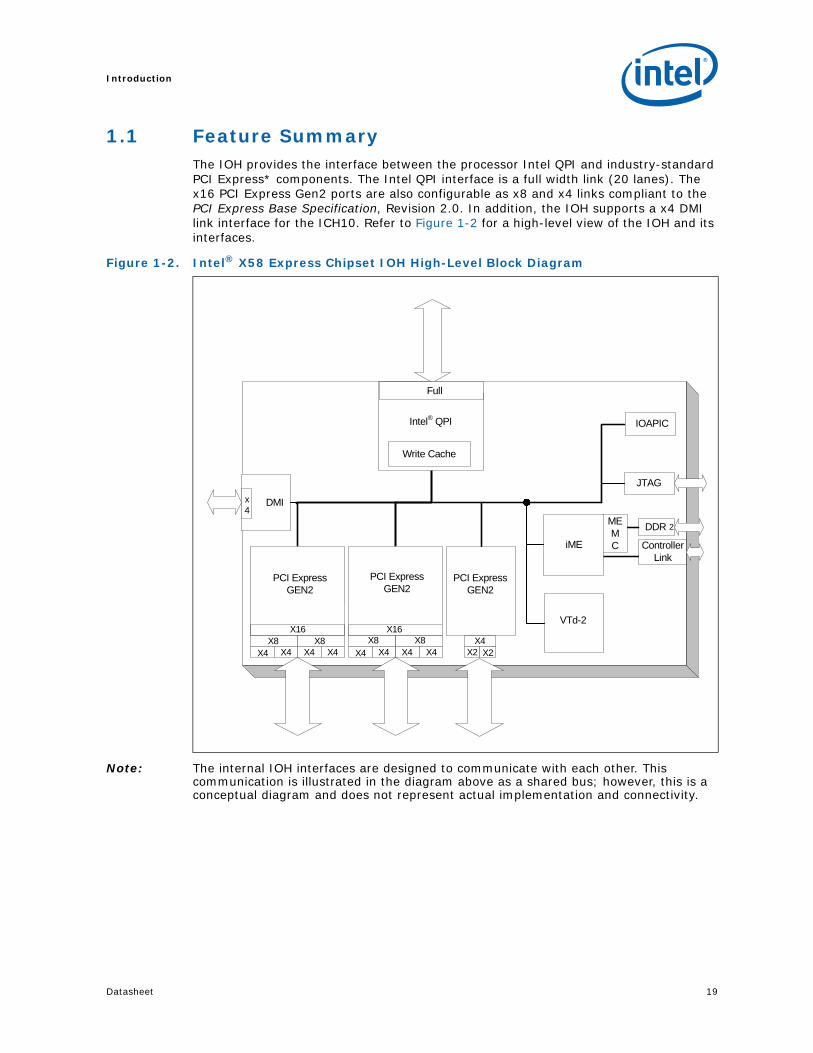
1.1 Feature SummaryThe IOH provides the interface between the processor Intel QPI and industry-standard PCI Express* components. The Intel QPI interface is a full width link (20 lanes). The x16 PCI Express Gen2 ports are also configurable as x8 and x4 links compliant to the PCI Express Base Specification, Revision 2.0. In addition, the IOH supports a x4 DMI link interface for the ICH10. Refer to Figure 1-2 for a high-level view of the IOH and its interfaces.
Note: The internal IOH interfaces are designed to communicate with each other. This communication is illustrated in the diagram above as a shared bus; however, this is a conceptual diagram and does not represent actual implementation and connectivity.
Figure 1-2. Intel® X58 Express Chipset IOH High-Level Block Diagram
PCI Express GEN2
X4
DMIx4
JTAG
Intel® QPI
Write Cache
VTd-2
DDR 2
IOAPIC
MEMC Controller
LinkiME
Full
PCI Express GEN2
PCI Express GEN2
X2X2
X16 X16X8 X8X8X8
X4X4X4 X4 X4 X4 X4 X4

Introduction
20 Datasheet
1.1.1 Features By Segment based on PCI Express Ports
The Intel X58 Express Chipset supports the Intel Core™ i7 processor Extreme Edition, Intel Core™ i7 processor, and Intel Xeon® processor 3500 series, has 36 PCIe lanes, one Intel QPI port, and supports AMT3 manageability.
1.1.2 Features Supported By Platform
Table 1-1 shows the platform feature set supported for Intel X58 Express Chipset-based platforms using the Intel X58 Express Chipset IOH. Unless specifically called out in Table 1-1, it is considered supported in the Intel X58 Express Chipset-based platform.
1.1.3 Intel® QPI Features
• One full width Intel QPI link interface:
• Packetized protocol with 18 data/protocol bits and 2 CRC bits per link per direction
— 4.8 GT/s and 6.4 GT/s supporting different routing lengths.
• Fully-coherent write cache with inbound write combining
• Read Current command support
• Support for 64-byte cacheline size
1.1.4 PCI Express Features
• Two x16 PCI Express Gen2 ports each supporting up to 8 GB/s/direction peak bandwidth
— All ports are configurable as two independent x8 or four independent x4 interfaces
• An additional x4 PCI Express Gen2 port configurable to 2 x 2 interfaces
• Dual unidirectional links
• Supports PCI Express Gen1 and Gen2 transfer rates
• Full peer-to-peer support between PCI Express interfaces
• Support for multiple unordered inbound traffic streams
• Support for Relaxed Ordering attribute
• Full support for software-initiated PCI Express power management
• x8 Server I/O Module (SIOM) support
• Alternative Requester ID (ARI) capability
Table 1-1. Intel® X58 Express Chipset Platform
Platform PCIe Bifurcation Support RAS Support SMBus Support
Intel X58 Express Chipset-based platforms
2x16/1x4 or 4x8/1x4 only
None None

Datasheet 21
Introduction
1.1.5 Direct Media Interface (DMI) Features
• One x4 DMI link interface supporting PCI Express Gen1 (2.5 Gbps) transfer rate
— Dedicated legacy bridge (Intel I/O Controller Hub 10 (ICH10)) interface
• ICH10 Support
1.1.6 Intel® QuickData Technology
Intel® 5520 and Intel® 5500 Chipsets IOH supports this technology in a fashion where
the Intel I/O Adapter can be plugged in below any IOH PCIe port hierarchy or plugged
to a slot below the ICH and use the Intel® QuickData Technology capabilities in the
chipset. There are other non-Intel NICs that support the Intel® QuickData technology.
Please refer to http://www.intel.com/cs/network/connectivity/emea/eng/226276.htm.
1.1.7 Controller Link (CL)
The Controller Link is a private, low pin count, low power, communication interface between the IOH and ICH.
1.1.8 Intel® Virtualization Technology for Directed I/O(Intel® VT-d), Second Revision
• Builds upon first generation of Intel VT-d features
• Improved performance through better invalidation architecture
• Support for end-point Address Translation Caching (ATC) compliant with the PCI-SIG IOV Address Translation Services (ATS), Revision 1.0 specification.
• Interrupt remapping
• Optimized translation of sequential accesses
• IOV support (ARI)
1.1.9 Intel® Trusted Execution Technology (Intel® TXT)
Intel Trusted Execution Technology (Intel TXT) defines platform-level enhancements that provide the building blocks for creating trusted platforms.
The Intel TXT platform helps to provide the authenticity of the controlling environment such that those wishing to rely on the platform can make an appropriate trust decision. The Intel TXT platform determines the identity of the controlling environment by accurately measuring and verifying the controlling software.
Another aspect of the trust decision is the ability of the platform to resist attempts to change the controlling environment. The Intel TXT platform will resist attempts by software processes to change the controlling environment or bypass the bounds set by the controlling environment.
Intel TXT is a set of extensions designed to provide a measured and controlled launch of system software that will then establish a protected environment for itself and any additional software that it may execute.
These extensions enhance two areas:
• The launching of the Measured Launched Environment (MLE).
• The protection of the MLE from potential corruption.

Introduction
22 Datasheet
The enhanced platform provides these launch and control interfaces using Safer Mode Extensions (SMX).
The SMX interface includes the following functions:
• Measured/Verified launch of the MLE.
• Mechanisms to ensure the above measurement is protected and stored in a secure location.
• Protection mechanisms that allow the MLE to control attempts to modify itself.
For more information refer to the Intel® TXT BIOS Writer’s Guide and Intel® TXT Measured Launched Environment Developer’s Guide.
1.1.10 Reliability, Availability, Serviceability (RAS) Features
• Supports an SMBus Specification, Revision 2.0 slave interface for server management with Packet Error Checking:
— SMBus and JTAG access to IOH configuration registers for out-of-band server management
• Improved RAS achieved by protecting internal datapaths through ECC and parity protection mechanisms
• Supports PCI Express Base Specification, Revision 2.0 CRC with link-level retry
• Supports both standard Intel QPI CRC with link level retry
• Advanced Error Reporting capability for PCI Express link interfaces
• Native PCI Express Hot-Plug support
• Error injection capabilities
• Performance monitoring capabilities
1.1.11 Power Management Support
• PCI Express Link states (L0, L1, and L3)
• Intel QPI Link states (L0, L2)
• DMI states (L0, L0s, L1)
• System states (S0, S1, S3, S4, S5)
1.1.12 Security
• Intel VT-d for security
• Intel® Trusted Execution Technology (Intel® TXT). Pls refer to the Intel® X58 Express Chipset Specification Update for information on which steppings support Intel® TXT feature.
1.1.13 Other
• Integrated IOxAPIC
1.2 TerminologyTable 1-2 defines the acronyms, conventions, and terminology used throughout the specification.
Datasheet 23
Introduction
Table 1-2. Terminology (Sheet 1 of 2)
Term Description
APIC Advanced Programmable Interrupt Controller
ASIC Repeater A chip which intercepts the Intel QPI traffic. It repeats the traffic, but also sends appropriate data to the logic analyzer.
BIST Built-In Self Test
Intel® Core™ i7 proccessor / Intel® Xeon® processor 3500 series
Next-generation Intel processor that mates to the IOH to create the Intel X58 Express Chipset-based platforms.
BMC Baseboard Management Controller. A microcontroller used for remote platform management.
CA Completer Abort
Caching Agent Intel QPI coherency agent that participates in the MESIF protocol. Caches copies of the coherent memory space, potentially from multiple home agents. May also support the read-only fowardable cache state F.
CEM Refers to the PCI Express Card Electromechanical specification
CPEI Correctable Platform Event Interrupt
CRC Cyclic Redundancy Code
Intel QPI Intel QuickPath Interconnect
Intel QuickPath Interconnect Link Full Width
Intel QuickPath Interconnect link with 20 physical lanes in each direction
DMA Direct Memory Access
DMI Direct Media Interface is the interface to the I/O legacy bridge component of the Intel ICH10.
EHCI Enhanced Host Controller Interface
FW Firmware; software stored in ROM
Hinted Peer-to-Peer A transaction initiated by an I/O agent destined for an I/O target within the same root port (PCIe port)
Gen1 PCI Express Gen1 is a common reference for 1st generation PCI Express (Base Spec revision 1.x) and speed
Gen2 PCI Express Gen2 is a common reference for 2nd generation PCI Express (Base Spec revision 2.x) and speed
HOA High Order Address
Home Agent Intel QuickPath Interconnect coherency agent that interfaces to the main memory and is responsible for tracking cache-state transitions
ICH10 Intel I/O Controller Hub, Tenth Generation
Inbound Transaction
Transactions initiated on a PCI Express port destined for an Intel QuickPath Interconnect port
Intel® TXT Intel® Trusted Execution Technology (Intel® TXT)
IOH I/O Hub
IRB Inbound Request Buffer
Lane A set of differential signal pairs: one pair for transmission and one pair for reception. A by-N Link is composed of N Lanes
LCI LAN Connect Interface
Legacy ICH The ICH that has legacy features enabled, and is typically where the firmware boot code resides
Legacy IOH The IOH that has the Legacy ICH directly attached
Link A dual-simplex communications path between two components. The collection of two ports and their interconnecting lanes.

Introduction
24 Datasheet
1.3 Related DocumentsThe reader of this document should also be familiar with the components, material, and concepts presented in the documents listed in Table 1-3.
Local Peer-to-Peer A transaction initiated by an I/O agent destined for an I/O target within the same root complex (Intel X58 Express Chipset IOH)
LOM LAN on Motherboard
LPC Low Pin Count
MSI Message Signaled Interrupt
ORB Outgoing Request Buffer
Outbound Transactions
Transactions initiated on an Intel QuickPath Interconnect port destined for a PCI Express or DMI port
PA Physical Address
PCM Pulse Code Modulation
PLC Platform LAN Connect
PME Power Management Event
Port In physical terms, a group of transmitters and receivers physically located on the Intel X58 Express Chipset IOH that define one side of a link
Processor Common reference term for “processor socket”, used throughout this document
RAS Reliability, Availability, Serviceability
Remote Peer-to-Peer
A transaction initiated by an I/O agent destined for an I/O target on a different root complex (Intel X58 Express Chipset IOH)
RID Revision ID of the IOH
RTA Router Table Array
RTC Real Time Clock
SATA Serial ATA
SCMD Sub Command
SEC Single Error Correction
SMBus System Management Bus. A two-wire interface through which various system components can communicate.
Socket Processor (cores + uncore)
SPD Serial Presence Detect
S/PDIF Sony/Phillips Digital Interface
SPI Serial Peripheral Interface. The interface for serial flash components.
STD Suspend To Disk
Intel X58 Express Chipset Based Platform
UP High End Desktop platform using the Intel X58 Express Chipset IOH
TCO Total Cost of Ownership
UHCI Universal Host Controller Interface
UP Uni-processor
UR Unsupported Request
USB Universal Serial Bus
VT-d Intel® Virtualization Technology (Intel® VT) for Directed I/O (Intel® VT-d)
Table 1-2. Terminology (Sheet 2 of 2)
Term Description

Datasheet 25
Introduction
§
Table 1-3. Related Documents
Document Comment1
Intel® X58 Express Chipset Specification Update http://www.intel.com/Assets/PDF/specupdate/
320839.pdf
Intel® X58 Express Chipset Thermal and Mechanical Design Guide http://www.intel.com/Assets/PDF/designguide/
320840.pdf
Intel® Core™ i7 Processor Extreme Edition and Intel® Core™ i7 Processor Datasheet Volume 1
http://download.intel.com/design/processor/datashts/
320834.pdf
Intel® Core™ i7 Processor Extreme Edition and Intel® Core™ i7 Processor Datasheet Volume 2
http://download.intel.com/design/processor/datashts/
320835.pdf
Intel® Core™ i7 Processor Extreme Edition and Intel® Core™ i7 Processor and LGA1366 Socket Thermal and Mechanical Design Guide
http://download.intel.com/design/processor/designex/
320837.pdf
Intel I/O Controller Hub 10 Family Datasheet http://www.intel.com/design/chipsets/
designex/319975.pdf
PCI Express Base Specification, Revision 1.1 www.pcisig.com
PCI Express Base Specification, Revision 2.0 www.pcisig.com
SMBus Specification, Revision 2.0 www.smbus.org
Intel® Trusted Execution Technology (Intel® TXT) Software Development Guide http://download.intel.com/technology/security/
downloads/315168.pdf

Introduction
26 Datasheet
Datasheet 27
Platform Topology
2 Platform Topology
The I/O Hub component (IOH) provides a connection point between various I/O components and Intel QuickPath Interconnect based processors. The IOH supports the Intel Core™ i7 processor Extreme Edition, the Intel Core™ i7 processor, and the Intel® Xeon® processor 3500 series.
The Intel QuickPath Interconnect port is used for processor-to-IOH connections.
2.1 IOH Supported Topologies
Terminology
Legacy Bridge: In Figure 2-1 legacy bridge refers to the ICH component. The legacy bridge contains the legacy functions required for a industry standard operating system. The ICH is connected solely by the DMI port. The IOH has one DMI port capable of connecting to a legacy bridge. Legacy bridge connections are not explicitly illustrated in all figures. Readers should assume that IOH is connected to one legacy bridge at most.
Legacy IOH: One functions as a “Legacy IOH”. The legacy IOH contains the central resources for the system and interfaces to the legacy bridge.
Non-Legacy IOH: IOHs that are not the “Legacy IOH” are referred to as non-legacy IOHs. For non-partitioned systems, the ME is not enabled and they are not connected to a legacy bridge (ICH).
2.1.1 Platform Topology
The IOH has multiple PCI Express ports. Figure 2-1 illustrates an example I/O sub-systems using Intel and other common I/O ingredients. They are meant for reference only since it is platform dependent. This example shows a typical The Intel X58 Express Chipset IOH based platform with dual graphics cards. There are other topologies with different size switches (or none at all) depending on the performance/cost/connectivity requirements.

Platform Topology
28 Datasheet
§
Figure 2-1. Example — Intel® X58 Express Chipset-based Platform Topology (for reference only)
Intel® IOHIntel® ICH10
Processor
QPI
DMI
x 4x 1x 1
FWHTPM
LPC
SPI
PCI
BusMaster
x4x16
PCI Express
port
x16
PCI Express
port
PCI Express
port
Intel® HD Audio
SPI Flash

Datasheet 29
Interfaces
3 Interfaces
This chapter describes the physical properties and protocols for each of the IOH’s major interfaces.
3.1 Intel® QuickPath Interconnect (Intel® QPI)The Intel QuickPath Interconnect (Intel QPI) interface is a proprietary cache-coherent links-based interconnect between processors and the IOH.
The IOH supports the following Intel QPI features:
• 64-byte cache lines
• CRC protection: 8-bit CRC
• L0 and L2 power states
• Virtual Networks VN0 and VNA
• 3-bit NodeID (max)
• 40-bit Physical Addressing (max)
Note: Intel QuickPath Interconnect Port Bifurcation is not supported by the IOH.
3.1.1 Physical Layer
The Intel QPI Physical layer implements a high-speed differential serial signaling technology. The IOH implements the following features associated with this technology:
• Differential signaling
• Forwarded clocking
• 4.8 GT/s and 6.4 GT/s data rate (up to 12.8 GB/s/direction peak bandwidth per port)
• Slow boot speed of 66.66 MT/s
• L0 power state
• Common reference clocking (same clock generator for both sender and receiver)
• Unidirectional data path in each direction supporting full duplex operation
• Intel Interconnect Built-In Self Test (Intel IBIST) for high-speed testability
• Polarity and Lane Reversal
No support is provided for any runtime determinism in the IOH.
Figure 3-1 illustrates the scope of the Physical layer on an Intel QPI packet. The grayed out segment (phits) and CRC is not decoded by the Physical layer. One phit is transmitted per data clock and consists of 20 bits in full-width mode. There are 80 bits for each flit, regardless of port width.

Interfaces
30 Datasheet
3.1.1.1 Supported Frequencies
The frequencies used on the Intel QPI will be common for all ports. Support for normal operating mode of 4.8 GT/s and 6.4 GT/s is provided by the Physical layer. Settings for the operational frequency is done through strapping pins.
The Intel QPI links will come out of reset in slow mode (66.66 MT/s) independent of the operational frequency. This is based purely on the reference clock (133 MHz) divided by four. Firmware will then program the Physical layer to the operational frequency, followed by a soft reset of the Physical layer, at which point the new frequency takes over.
3.1.1.2 Supported Widths
The IOH supports two full-width Intel QPI ports. Bifurcation of one full-width ports into two half-width ports is not supported.
The IOH supports one full-width Intel QPI port.
3.1.1.3 Physical Layer Initialization
The Intel QPI Physical layer initialization establishes:
• Link wellness through test pattern exchange
• Negotiated width of the port for degraded mode (but NOT port splitting from full width to half width)
• Presence of an Intel QPI component
• Frequency is determined using strapping pins. See Section 3.1.1.1 for details.
See Section 3.1.1.5 for references to configuration registers in the Physical layer used in the initialization process.
Figure 3-1. Intel® QPI Packet Visibility By The Physical Layer (Phit)
Full Widthmode: Phit (18b)
20
bits
CRC
Table 3-1. Intel® QuickPath Interconnect Frequency Strapping Options
QPIFreqSel[1:0] Intel® QuickPath Interconnect Operational Frequency Mode
00 4.8 GT/s
01 Reserved
10 6.4 GT/s
11 Reserved

Datasheet 31
Interfaces
3.1.1.4 Clocking
The Intel QPI uses a common (plesiochronous) clock between components to remove the need for “elastic buffers”, such as those used in PCI Express for dealing with the clock frequency differential between sender and receiver. This decreases latency through the Physical layer.
A single clock signal, referred to as the “forwarded” clock, is sent in parallel with the data from every Intel QPI sender. Forwarded clocking is a sideband differential clock sent from each agent. The forwarded clock is not used to directly capture the data as in classical parallel buses, but is used to cancel jitter, noise, and drift that can cause reduced margin at the receiver.
3.1.1.5 Physical Layer Registers
The IOH Intel QPI register details are in Chapter 17, “Configuration Register Space”.
3.1.2 Link Layer
The IOH Link layer supports the following features:
• Virtual Networks VN0 and VNA (Adaptive)
• SNP, HOM, DRS, NDR, NCB, NCS
• 8-bit and CRC
3.1.3 Routing LayerThe Routing layer provides bypassing for each target Intel QPI physical port to allow requests that target other Intel QPI physical ports to bypass under normal traffic patterns.
3.1.3.1 Routing Table
The IOH uses a routing table for selecting the Intel QPI port to send a request to based on the target NodeID. After reset, the routing table is defaulted to disabled. In this mode, all responses are sent on the same port on which they were received. No requests can be sent from the IOH until the routing table is initialized.
3.1.4 Protocol LayerThe protocol layer is responsible for translating requests from the core into the Intel QPI domain, and for maintaining Intel QPI protocol semantics. The IOH is a fully-compatible Intel QPI caching agent. It is also a fully-compliant I/O proxy agent for non-coherent I/O traffic. The IOH Protocol layer supports the following features:
• Intel QPI caching agent
• Intel QPI firmware agent, configuration agent, and I/O proxy agent
• Source Broadcast mode of operation, supporting up to 7 peer caching agents
• Source Issued Snoops
• Source address decoder compatibility with Intel® Core™ i7 and Intel® Xeon®
architecture
• Lock Arbiter
3.1.4.1 Component NodeID Assignment
The processor requires that IOH NodeID bits [2:0] are set to “000”. This platform limits the NodeID size to 3 bits.

Interfaces
32 Datasheet
3.1.4.2 Supported Transactions
This section provides an overview of all the Intel QPI transactions that the IOH supports.
Transactions are divided into four broad categories for the IOH. The direction indication, inbound and outbound, is based on system transaction flow toward main memory, not the Intel QuickPath Interconnect port direction. Inbound is defined as “transactions that IOH sends to the Intel QuickPath Interconnect”, while outbound are “transactions that IOH receives from the Intel QuickPath Interconnect.”
Inbound Coherent are transactions that require snooping of other caching agents.
Inbound Non-Coherent transactions do not snoop other agents.
Outbound Snoops are snoops from peer agents that need to check the IOH write cache.
Outbound Non-coherent transactions target the IOH as the home agent for I/O space. This also includes transactions to the lock arbiter within the IOH.
Notes:1. Forward Response only occurs after an AckConflt was sent.2. IOH takes no action and responds with Cmp.3. IOH takes no action and responds with CmpD.
Table 3-2. Protocol Transactions Supported
Category Intel® QuickPath Interconnect Type Intel® QuickPath Interconnect Transaction
Inbound Coherent + Responses
Home Requests RdCode, InvItoE, WbMtoI, WbIData, WbIDataPtl
Snoop Requests SnpCode, SnpInvItoE
Normal Response Cmp, DataC_[I,F], DataC_[I,F]_Cmp, Gnt_Cmp
Conflict Response FrcAckCnflt, DataC_[I,F]_FrcAckCnflt, Gnt_FrcAckCnflt
Forward Response2 Cmp_FwdCode, Cmp_FwdInvOwn, Cmp_FwdInvItoE
Inbound Non-
Coherent + Responses
Request DRAM NonSnpWr, NonSnpWrData, NonSnpWrDataPtl, NonSnpRd
Request I/O NcP2PS, NcP2PB
Request Special PrefetchHint, IntLogical, IntPhysical, NcMsgB-PMReq, NcMsgB-VLW
Lock & Quiescence Flows
NcMsgS-StopReq1, NcMsgS-StopReq2, NcMsgS-StartReq1, NcMsgB-StartReq2
Response Cmp, DataNC, CmpD, DataC_I_Cmp, DataC_I
Outbound Snoop
Snoop Request SnpCode, SnpData, SnpInvOwn, SnpInvItoE
Response to Home RspI, RspCnflt, RspIWb, WbIData, WBIDataPtl
Response to Requestor
N/A
Outbound Non-
Coherent
Request I/O or internal IOH space
NcWr, NcWrPtl, WcWr, WcWrPtl, NcRd, NcRdPtl, NcIOWr, NcIORd, NcCfgWr, NcCfgRd, NcP2PS, NcP2PB, NcLTRd, NcLTWr
Special Messages IntPhysical3, IntLogical3, IntAck, NcMsgB-EOI, NcMsgS-Shutdown, NcMsgB-GPE, NcMsgB-CPEI, NcMsgB/S-<other>4, IntPrioUpd, DebugData3, FERR
Quiescence <Done through CSR reads and writes to control StopReq*/StartReq* flow>
Lock NcMsgS-ProcLock, NcMsgS-ProcSplitLock, NcMsgS-Quiesce, NcMsgS-Unlock, NcMsgS-StopReq1, NcMsgS-StopReq2, NcMsgS-StartReq1, NcMsgB-StartReq2
Response Cmp, DataNC, CmpD

Datasheet 33
Interfaces
3.1.4.3 Snooping Modes
The IOH supports peer agents that are involved in coherency. When the IOH sends an inbound coherent request, snoops will be sent to all agents in this vector, masking the home agent. Masking of the agent is required normal behavior in the Intel QPI, but a mode to disable masking is also provided in the IOH.
3.1.4.4 Broadcast Support
The IOH supports broadcast to any 3-bit NodeID.
3.1.4.5 Lock Arbiter
The Lock Arbiter is a central Intel QPI system resource used for coordinating lock and quiescence flows on the Intel QPI. There is a single lock arbiter in the IOH which can accommodate a maximum of eight simultaneous issues and 7 peer NodeID targets. For PHold support, the lock arbiter must be assigned to the IOH that has the legacy ICH connected. IOH will not support sending PHold on the Intel QuickPath Interconnect.
The Lock Arbiter uses two different participant lists for issuing the StopReq*/StartReq* broadcasts: one for Lock, and another for quiescence.
3.2 PCI Express InterfacePCI Express offers a high bandwidth-to-pin interface for general-purpose adapters that interface with a wide variety of I/O devices. The PCI Express Base Specification, Revision 2.0 provides the details of the PCI Express protocol.
3.2.1 Gen1/Gen2 Support
The IOH supports both the PCI Express First Generation (Gen1) and the PCI Express Second Generation (Gen2) specifications. The Gen2 ports can be configured to run at Gen1 speeds; however, Gen1 ports cannot be configured to run at Gen2 speeds.
All PCI Express ports are capable of operating at both Gen1 and Gen2 speeds.
3.2.2 PCI Express Link Characteristics - Link Training,Bifurcation, and Lane Reversal Support
3.2.2.1 Port Bifurcation
The IOH supports port bifurcation using PEWIDTH[5:0] hardware straps. The IOH supports the following configuration modes:
• The width of all links are exactly specified by the straps
• The width of all links are programmed by the BIOS using the PCIE_PRTx_BIF_CTRL register (wait on BIOS mode)
3.2.2.2 Link Training
The IOH PCI Express devices support the following link widths: x16, x8, x4, x2, x1, up to the maximum allowed for the device based on the bifurcation settings. Each device will first attempt to train at the highest possible width configured. If there is a failure to train at the maximum width, the IOH will attempt to link at progressively smaller widths until training is successful.

Interfaces
34 Datasheet
For full-width link configurations, lane reversal is supported. Most degraded link widths also support lane reversal, see Table 3-3, “Supported Degraded Modes”.
Figure 3-2. PCI Express Interface Partitioning
4X
4X
8X
4X
4X
8X
Transaction
Link
Physical
4X
4X
8X
4X
4X
8X
Port0Port1
Transaction
Link
Physical
Port0
16
X
16
X

Datasheet 35
Interfaces
3.2.3 Degraded Mode
Degraded mode is supported for x16, x8, x4 and x2 link widths. The IOH supports degraded mode operation at half the original width and quarter of the original width or at x1. This mode allows one half or one quarter of the link to be mapped out if one or more lanes should fail during normal operation. This allows for continued system operation in the event of a lane failure. Without support for degraded mode, a failure on a critical lane such as lane 0 could bring the entire link down in a fatal manner. This can be avoided with support for degraded mode operation. For example, if lane 0 fails on a x8 link, then the lower half of the link will be disabled and the traffic will continue at half the performance on lanes 4-7. Similarly, a x4 link would degrade to a x2 link. This remapping will occur in the physical layer, and the link and transaction layers are unaware of the link width change. The degraded mode widths are automatically attempted every time the PCI Express link is trained. The events that trigger PCI Express link training are documented in the PCI Express Base Specification, Revision 2.0.
IOH-supported degraded modes are shown in Table 3-3. Table 3-3 should be read such that the various modes indicated in the different rows would be tried by IOH, but not necessarily in the order shown in the table. IOH would try a higher width degraded mode before trying any lower width degraded modes. IOH reports entry into or exit from degraded mode to software (see Chapter 17 and also records which lane failed). Software can then report the unexpected or erroneous hardware behavior to the system operator for attention, by generating a system interrupt per Section 13.7, “IOH Error Handling Summary” .
Note:1. This is the native width the link is running at when degraded mode operation kicks-in.
3.2.4 Lane Reversal
The IOH supports lane reversal on all PCI Express ports, regardless of the link width (x16, x8, x4, and x2). The IOH allows a x4 or x8 card to be plugged into a x8 slot that is lane-reversed on the motherboard, and operate at the maximum link width of the card; similarly for a x4 card plugged into a lane-reversed x4 slot, and a x2 card plugged into a lane-reversed x2 slot. Note that for the purpose of this discussion, a “xN slot” refers to a CEM/SIOM slot that is capable of any width greater than or equal to xN but is electrically wired on the board for only a xN width. A x2 card can be plugged into a x8, or x4 slot and work as x2 only if lane-reversal is not done on the motherboard; otherwise, it would operate in x1 mode.
Table 3-3. Supported Degraded Modes
Original Link Width1 Degraded Mode Link width and Lanes Numbers
x16
x8 on either lanes 7-0,0-7,15-8,8-15
x4 on either lanes 3-0,0-3,4-7,7-4,8-11,11-8,12-15,15-12
x2 on either lanes 1-0,0-1,4-5,5-4,8-9,9-8,12-13,13-12
x1 on either lanes 0,1,2,3,4,5,6,7,8,9,10,11,12,13,14,15
x8
x4 on lanes 7-4,4-7,3-0,0-3
x2 on lanes 5-4,4-5, 1-0, 0-1
x1 on lanes 0,1,2,3,4,5,6,7
x4x2 on lanes 1-0,0-1
x1 on lanes 0,1,2,3
x2 x1 on lanes 0,1

Interfaces
36 Datasheet
3.2.5 IOH Performance Policies
Unless otherwise noted, the performance policies noted in this section apply to a standard PCI Express port on the IOH.
3.2.5.1 Max_Payload_Size
The IOH supports a Max_Payload_Size of 256 Bytes on PCI Express ports and 128 Bytes on DMI.
3.2.5.2 Isochronous Support and Virtual Channels
The IOH does not support isochrony.
3.2.5.3 Write Combining
The IOH does not support outbound write combining or write combining on peer-to-peer transactions. Inbound memory writes to system memory could be combined in the IOH write cache.
3.2.5.4 Relaxed Ordering
3.2.5.4.1 Outbound
The IOH does not support relaxed ordering optimizations in the outbound direction.
3.2.5.5 Non-Coherent Transaction Support
3.2.5.5.1 Inbound
Non-coherent transactions are identified by the NoSnoop attribute in the PCI Express request header being set. For writes, the NoSnoop attribute is used in conjunction with the Relaxed Ordering attribute to reduce snoops on the Intel QPI interface. For inbound reads with the NoSnoop attribute set, the IOH does not perform snoops on the Intel QPI. This optimization for reads and writes can be individually disabled.
3.2.5.5.2 Outbound
IOH always clears the NoSnoop attribute bit in the PCI Express header for transactions that it forwards from the processor. For peer-to-peer transactions from other PCI Express ports and DMI, the NoSnoop attribute is passed as-is from the originating port.
3.2.5.6 Completion Policy
The PCI Express Base Specification, Revision 2.0 requires that completions for a specific request must occur in linearly-increasing address order. However, completions for different requests are allowed to complete in any order.
Adhering to this rule, the IOH sends completions on the PCI Express interface in the order received from the Intel QuickPath Interconnect interface and never artificially delays completions received from the Intel QuickPath Interconnect to PCI Express. The IOH always attempts to send completions within a stream in address-order on PCI Express, however, it will not artificially hold back completions that can be sent on PCI Express to achieve this in-orderness.
Datasheet 37
Interfaces
3.2.5.6.1 Read Completion Combining
The PCI Express Base Specification, Revision 2.0 allows that a single request can be satisfied with multiple “sub-completions” as long as they return in linearly-increasing address order. The IOH must split requests into cache line quantities before issue on the Intel QPI, and, therefore will often complete a large request in cache line-sized sub-completions.
As a performance optimization, the IOH implements an opportunistic read completion combining algorithm for all reads towards main memory. When the downstream PCI Express interface is busy with another transaction, and multiple cache lines have returned before completion on PCI Express is possible, the PCI Express interface will combine the cache line sub-completions into larger quantities up to MAX_PAYLOAD.
3.2.5.7 PCI Express Port Arbitration
The IOH provides a weighted round robin scheme for arbitration between the PCI Express ports for both main memory and peer-to-peer accesses, combined. Each PCI Express/DMI port is assigned a weight based on its width and speed.
3.2.5.8 Read Prefetching Policies
The IOH does not perform read prefetching for downstream PCI Express components. The PCI Express component is solely responsible for its own prefetch algorithms as it is best suited to make appropriate trade-offs.
The IOH also does not perform outbound read prefetching.
3.2.6 PCI Express RAS
The IOH supports the PCI Express Advanced Error Reporting (AER) capability. Refer to PCI Express Base Specification, Revision 2.0 for details.
Additionally, the IOH supports:
• PCI Express data poisoning mechanism. This feature can be optionally turned off, in which case the IOH will drop the packet and all subsequent packets.
• The PCI Express completion time-out mechanism for non-posted requests to PCI Express.
• The new role-based error reporting mechanism. Refer to Chapter 5, “PCI Express* and DMI Interfaces” for details.
Note: The IOH does not support the ECRC mechanism; that is, the IOH will not generate ECRC on transmitted packets and will ignore/drop ECRC on received packets.
Refer to Chapter 13, “Reliability, Availability, Serviceability (RAS)” for details on PCI Express hot-plug.
3.2.7 Power Management
The IOH does not support the beacon wake method on PCI Express. IOH supports Active State Power Management (ASPM) transitions into L1 state. Additionally, the IOH supports the D0 and D3hot power management states, per PCI Express port, and also supports a wake event from these states on a PCI Express hot-plug event. In D3hot, the IOH master aborts all configuration transactions targeting the PCI Express link. Refer to Chapter 10, “IOH power management is compatible with the PCI Bus Power Management Interface Specification, Revision 1.1 (referenced as PCI-PM). It is also

Interfaces
38 Datasheet
compatible with the Advanced Configuration and Power Interface (ACPI) Specification, Revision 2.0b. The IOH is designed to operate seamlessly with operating systems employing these specifications.” for details of PCI Express power management support.
3.3 Direct Media Interface (DMI)The Direct Media Interface (DMI) is the chip-to-chip connection between the IOH and ICH10. This high-speed interface integrates advanced priority-based servicing allowing for concurrent traffic capabilities. Base functionality is completely software transparent permitting current and legacy software to operate normally.
The IOH DMI interface supports features that are listed below in addition to the PCI Express specific messages:
• A chip-to-chip connection interface to Intel ICH10
• 2 GB/s point-to-point bandwidth (1 GB/s each direction)
• 100 MHz reference clock
• 62-bit downstream addressing
• APIC and MSI interrupt messaging support. Will send Intel-defined “End of Interrupt” broadcast message when initiated by the processor
• Message Signaled Interrupt (MSI) messages
• SMI, SCI, and SERR error indication
• Legacy support for ISA regime protocol (PHOLD/PHOLDA) required for parallel port
3.3.1 Interface and Speed and Bandwidth
Raw bit-rate on the data pins of 2.5 Gb/s, resulting in a real bandwidth per pair of 250 MB/s. In addition, the maximum theoretical realized bandwidth on the interface is 1 GB/s each direction simultaneously, for an aggregate of 2 GB/s when operating as x4 link.
3.3.2 Supported Widths
The DMI port supports x4 link width; the link width is auto-negotiated at power-on.
3.3.3 Bifurcation, Dynamic Link Width Reduction, and Lane Reversal Support
Port bifurcation is NOT supported on DMI; the DMI port is always negotiated as a single port.
3.3.4 Performance Policies on DMI
3.3.4.1 Completion Policy
Ordering rules for the DMI port is identical to that of the PCI Express interfaces described in Chapter 6, “Ordering.” However, for the case when the ICH10 sends multiple read requests with the same transaction ID, then the read completions must be returned in order. As a consequence, Read completions can be returned out of order only if they have different transaction ID's. But, as a simplification, IOH will always return all completions in original request order on DMI. This includes both peer-to-peer and memory read requests.

Datasheet 39
Interfaces
3.3.4.2 Prefetching Policy
DMI does not perform any speculative read prefetching for inbound or outbound reads.
3.3.5 Error Handling
The same RAS features that exist on a PCI Express port also exist on the DMI port. Refer to Section 3.2.6 for details.
3.3.5.1 PHOLD Support
The IOH supports the PHOLD protocol. This protocol is used for legacy ISA devices which do not allow the possibility for being both a master and a slave device simultaneously. Example devices that use the PHOLD protocol are legacy floppy drives, and LPC bus masters.
3.4 Reduced Media Independent Interface (RMII)The Reduced Media Independent Interface (RMII) is a standard, low pin count, low power interface.
RMII supports connection to another management entity or LAN entity. The interface is designed as a MAC type interface, not a PHY type interface.
3.5 Control Link (CLink) InterfaceThe control link interface is a low pin count, low power interface. This interface is used to connect the Management Engine in IOH to the ICH10. The usage model for this interface requires lower power as it remains powered during even the lower power states. Since Platform Environmental Control Interface (PECI) signals are routed through the ICH10, these signals can also pass to the management engine over the control link interface. Firmware and data stored in the SPI Flash memory connected to the ICH10 are also read over the Control Link interface.
3.6 System Management Bus (SMBus)The IOH includes an SMBus Specification, Revision 2.0 compliant slave port. This SMBus slave port provides server management (SM) visibility into all configuration registers in the IOH. Like JTAG accesses, the IOH’s SMBus interface is capable of both accessing IOH registers and generating inband downstream configuration cycles to other components.
SMBus operations may be split into two upper level protocols: writing information to configuration registers and reading configuration registers. This section describes the required protocol for an SMBus master to access the IOH’s internal configuration registers. Refer to the SMBus Specification, Revision 2.0 for the specific bus protocol, timings, and waveforms.
3.6.1 SMBus Physical Layer
The IOH SMBus operates at 3.3 V and complies with the SMBus SCL frequency of 100 kHz.
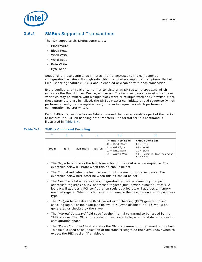
Interfaces
40 Datasheet
3.6.2 SMBus Supported Transactions
The IOH supports six SMBus commands:
• Block Write
• Block Read
• Word Write
• Word Read
• Byte Write
• Byte Read
Sequencing these commands initiates internal accesses to the component’s configuration registers. For high reliability, the interface supports the optional Packet Error Checking feature (CRC-8) and is enabled or disabled with each transaction.
Every configuration read or write first consists of an SMBus write sequence which initializes the Bus Number, Device, and so on. The term sequence is used since these variables may be written with a single block write or multiple word or byte writes. Once these parameters are initialized, the SMBus master can initiate a read sequence (which performs a configuration register read) or a write sequence (which performs a configuration register write).
Each SMBus transaction has an 8-bit command the master sends as part of the packet to instruct the IOH on handling data transfers. The format for this command is illustrated in Table 3-4.
• The Begin bit indicates the first transaction of the read or write sequence. The examples below illustrate when this bit should be set.
• The End bit indicates the last transaction of the read or write sequence. The examples below best describe when this bit should be set.
• The MemTrans bit indicates the configuration request is a memory mapped addressed register or a PCI addressed register (bus, device, function, offset). A logic 0 will address a PCI configuration register. A logic 1 will address a memory mapped register. When this bit is set it will enable the designation memory address type.
• The PEC_en bit enables the 8-bit packet error checking (PEC) generation and checking logic. For the examples below, if PEC was disabled, no PEC would be generated or checked by the slave.
• The Internal Command field specifies the internal command to be issued by the SMBus slave. The IOH supports dword reads and byte, word, and dword writes to configuration space.
• The SMBus Command field specifies the SMBus command to be issued on the bus. This field is used as an indication of the transfer length so the slave knows when to expect the PEC packet (if enabled).
Table 3-4. SMBus Command Encoding
7 6 5 4 3:2 1:0
Begin End MemTrans PEC_en
Internal Command00 = Read DWord01 = Write Byte10 = Write Word11 = Write DWord
SMBus Command00 = Byte01 = Word10 = Block11 = Reserved. Block command is selected.

Datasheet 41
Interfaces
The SMBus interface uses an internal register stack that is filled by the SMBus master before a request to the config master block is made. Shown in Table 3-5 is a list of the bytes in the stack and their descriptions.
3.6.3 Addressing
The slave address each component claims is dependent on the NODEID and SMBUSID pin straps (sampled on the assertion of PWRGOOD). The IOH claims SMBus accesses to address 11X0_XXX. The Xs represent strap pins on the IOH. Refer to Table 3-6 for the mapping of strap pins to the bit positions of the slave address.
Note: The slave address is dependent on strap pins only and cannot be reprogrammed. It is possible for software to change the default NodeID by programming the QPIPC register but this will not affect the SMBus slave address.
If the Mem/Cfg bit is cleared, the address field represents the standard PCI register addressing nomenclature, namely: bus, device, function and offset.
If the Mem/Cfg bit is set, the address field has a new meaning. Bits [23:0] hold a linear memory address and bits[31:24] is a byte to indicate which memory region it is. Table 3-7 describes the selections available. A logic one in a bit position enables that memory region to be accessed. If the destination memory byte is zero, no action is taken (no request is sent to the configuration master).
Table 3-5. Internal SMBus Protocol Stack
SMBus stack Description
Command Command byte
Byte Count The number of bytes for this transaction
Bus Number Bus number
Device/Function Device[4:0] and Function[2:0]
Address High The following fields are further defined.Reserved[3:0]Address[11:8]: This is the high order PCIe address field.
Register Number Register number is the lower order 8 bit register offset
Data3 Data byte 3
Data2 Data byte 2
Data1 Data byte 1
Data0 Data byte 0
Table 3-6. SMBus Slave Address Format
Slave Address Field Bit Position Slave Address Source
[7] 1
[6] 1
[5] SMBUSID strap pin
[4] 0
[3] NODEID[4] strap pin
[2] NODEID[3] strap pin
[1] NODEID[2] strap pin
[0] Read/Write# bit. This bit is in the slave address field to indicate a read or write operation. It is not part of the SMBus slave address.

Interfaces
42 Datasheet
If a memory region address field is set to a reserved space the IOH slave will perform the following:
• The transaction is not executed.
• The slave releases the SCL signal.
• The master abort error status is set.
3.6.4 SMBus Initiated Southbound Configuration Cycles
The platform SMBus master agent that is connected to an IOH slave SMBus agent can request a configuration transaction to a downstream PCI Express device. If the address decoder determines that the request is not intended for this IOH (that is, not the IOH’s bus number), it sends the request to port with the bus address. All requests outside of this range are sent to the legacy DMI port for a master abort condition.
3.6.5 SMBus Error Handling
SMBus Error Handling features:
• Errors are reported in the status byte field.
• Errors in Table 3-8 are also collected in the FERR and NERR registers.
The SMBus slave interface handles two types of errors: internal and PEC. For example, internal errors can occur when the IOH issues a configuration read on the PCI Express port and that read terminates in error. These errors manifest as a Not-Acknowledge (NACK) for the read command (End bit is set). If an internal error occurs during a configuration write, the final write command receives a NACK just before the stop bit. If the master receives a NACK, the entire configuration transaction should be reattempted.
If the master supports packet error checking (PEC) and the PEC_en bit in the command is set, then the PEC byte is checked in the slave interface. If the check indicates a failure, then the slave will NACK the PEC packet.
Each error bit is routed to the FERR and NERR registers for error reporting. The status field encoding is defined in Table 3-8. This field reports if an error occurred. If bits[2:0] are 000b, the transaction was successful only to the extent that the IOH is aware. In other words, a successful indication here does not necessarily mean that the transaction was completed correctly for all components in the system.
The busy bit is set whenever a transaction is accepted by the slave. This is true for reads and writes but the affects may not be observable for writes. This means that since the writes are posted and the communication link is so slow the master should never see a busy condition. A time-out is associated with the transaction in progress. When the time-out expires a time-out error status is asserted.
Table 3-7. Memory Region Address Field
Bit Field Memory Region Address Field
All others Reserved
03h IOAPIC Memory Region
02h Reserved
01h Reserved
00h Intel QuickPath Interconnect CSR Memory Region

Datasheet 43
Interfaces
3.6.6 SMBus Interface Reset
The slave interface state machine can be reset by the master in two ways:
• The master holds SCL low for 25 ms cumulative. Cumulative in this case means that all the “low time” for SCL is counted between the Start and Stop bit. If this totals 25 ms before reaching the Stop bit, the interface is reset.
• The master holds SCL continuously high for 50 us.
Note: Since the configuration registers are affected by the reset pin, SMBus masters will not be able to access the internal registers while the system is reset.
3.6.7 Configuration and Memory Read Protocol
Configuration and memory reads are accomplished through an SMBus write(s) and later followed by an SMBus read. The write sequence is used to initialize the Bus Number, Device, Function, and Register Number for the configuration access. The writing of this information can be accomplished through any combination of the supported SMBus write commands (Block, Word or Byte). The Internal Command field for each write should specify Read DWord.
After all the information is set up, the last write (End bit is set) initiates an internal configuration read. The slave will assert a busy bit in the status register and release the link with an acknowledge (ACK). The master SMBus will perform the transaction sequence for reading the data; however, the master must observe the status bit [7] (busy) to determine if the data is valid. Because the PCIe time-outs may be long the master may have to poll the busy bit to determine when the pervious read transaction has completed.
If an error occurs then the status byte will report the results. This status field indicates abnormal termination and contains status information such as target abort, master abort, and time-outs.
Examples of configuration reads are illustrated below. All of these examples have Packet Error Code (PEC) enabled. If the master does not support PEC, then bit 4 of the command would be cleared and no PEC byte exists in the communication streams. For the definition of the following diagram conventions, refer to the SMBus Specification, Revision 2.0. For SMBus read transactions, the last byte of data (or the PEC byte if enabled) is NACKed by the master to indicate the end of the transaction.
Table 3-8. Status Field Encoding for SMBus Reads
Bit Description
7 Busy
6:3 Reserved
2:0 101–111 = Reserved100 = SMBus time out error. 011 = Master Abort. An error that is reported by the IOH with respect to this transaction.010 = Completer Abort. An error is reported by downstream PCI Express device with respect to this
transaction.001 = Memory Region encoding error. This bit is set if the memory region encoding is not orthogonal
(one-hot encoding violation)000 = Successful

Interfaces
44 Datasheet
3.6.7.1 SMBus Configuration and Memory Block-Size Reads
Figure 3-3. SMBus Block-Size Configuration Register Read
Figure 3-4. SMBus Block-Size Memory Register Read
S 11X0_XXX W A Cmd = 11010010 A Byte cnt = 4 A Bus Num A Dev / Func A
Rsv[3:0] & Addr[11:8] A Regoff [7:0] A PEC A P
Write addressfor a Readsequence
S 11X0_XXX W A Cmd = 11010010 A
Sr 11X0_XXX R A Byte cnt = 5 A Status A Data [31:24] A Data [23:16] A
Data [15:8] A Data [7:0] A PEC N P
Read datasequence
Poll untilStatus[7] = 0
S 11X0_XXX W A Cmd = 11110010 A Byte cnt = 4 A MemRegion A Addr off[23:16] A
Addr off[15:8] A Addr off[7:0] A PEC A P
Write addressfor a Readsequence
S 11X0_XXX W A Cmd = 11110010 A
Sr 11X0_XXX R A Byte cnt = 5 A Status A Data [31:24] A Data [23:16] A
Data [15:8] A Data [7:0] A PEC N P
Read datasequence
Poll untilStatus[7] = 0

Datasheet 45
Interfaces
3.6.7.2 SMBus Configuration and Memory Word-Sized Reads
Figure 3-5. SMBus Word-Size Configuration Register Read
Figure 3-6. SMBus Word-Size Memory Register Read
S 11X0_XXX W A Cmd = 10010001 A Bus Num A Dev / Func A
Write addressfor a Readsequence
S 11X0_XXX W A Cmd = 10010001 A
Sr 11X0_XXX R A Status A Data [31:24] A
Read Sequence
Poll untilStatus[7] = 0
PEC
S 11X0_XXX W A Cmd = 01010001 A Rsv[3:0] & Addr[11:8] A Regoff [7:0]
A P
A PEC A P
PEC N P
S 11X0_XXX W A Cmd = 00010001 A
Sr 11X0_XXX R A Data [23:16] A Data [15:8] AA PEC N P
S 11X0_XXX W A Cmd = 01010000 A
Sr 11X0_XXX R A Data [7:0] A PEC N P
S 11X0_XXX W A Cmd = 10110001 A Mem region A Addr off[23:16] A
Write addressfor a Readsequence
S 11X0_XXX W A Cmd = 10110001 A
Sr 11X0_XXX R A Status A Data [31:24] A
Read Sequence
Poll untilStatus[7] = 0
PEC
S 11X0_XXX W A Cmd = 01110001 A Addr off[15:8] A Addr off[7:0]
A P
A PEC A P
PEC N P
S 11X0_XXX W A Cmd = 00110001 A
Sr 11X0_XXX R A Data [23:16] A Data [15:8] AA PEC N P
S 11X0_XXX W A Cmd = 01110000 A
Sr 11X0_XXX R A Data [7:0] A PEC N P
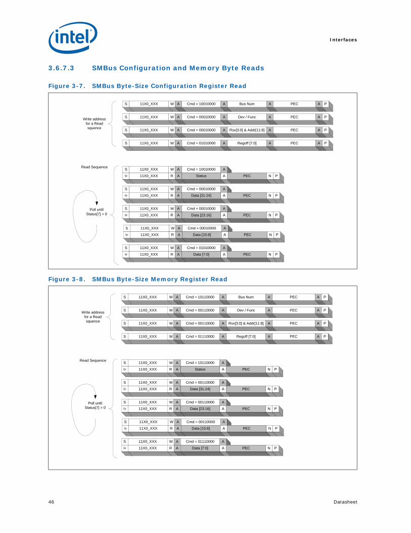
Interfaces
46 Datasheet
3.6.7.3 SMBus Configuration and Memory Byte Reads
Figure 3-7. SMBus Byte-Size Configuration Register Read
Figure 3-8. SMBus Byte-Size Memory Register Read
S 11X0_XXX W A Cmd = 10010000 A Bus Num A
Write addressfor a Readsquence
S 11X0_XXX W A Cmd = 10010000 A
Sr 11X0_XXX R A Status A
Read Sequence
Poll untilStatus[7] = 0
PEC
S 11X0_XXX W A Cmd = 00010000 A
A P
PEC N P
S 11X0_XXX W A Cmd = 00010000 A
Sr 11X0_XXX R A
S 11X0_XXX W A Cmd = 01010000 A
Sr 11X0_XXX R A Data [7:0] A PEC N P
S 11X0_XXX W A Cmd = 00010000 A
S 11X0_XXX W A Cmd = 01010000 A
Rsv[3:0] & Addr[11:8]
Regoff [7:0] A
A PEC A P
PEC A P
Dev / Func A PEC A P
S 11X0_XXX W A Cmd = 00010000 A
Sr 11X0_XXX R A Data [23:16] A PEC N P
S 11X0_XXX W A Cmd = 00010000 A
Sr 11X0_XXX R A
Data [31:24] A PEC N P
Data [15:8] A PEC N P
S 11X0_XXX W A Cmd = 10110000 A Bus Num A
Write addressfor a Readsquence
S 11X0_XXX W A Cmd = 10110000 A
Sr 11X0_XXX R A Status A
Read Sequence
Poll untilStatus[7] = 0
PEC
S 11X0_XXX W A Cmd = 00110000 A
A P
PEC N P
S 11X0_XXX W A Cmd = 00110000 A
Sr 11X0_XXX R A
S 11X0_XXX W A Cmd = 01110000 A
Sr 11X0_XXX R A Data [7:0] A PEC N P
S 11X0_XXX W A Cmd = 00110000 A
S 11X0_XXX W A Cmd = 01110000 A
Rsv[3:0] & Addr[11:8]
Regoff [7:0] A
A PEC A P
PEC A P
Dev / Func A PEC A P
S 11X0_XXX W A Cmd = 00110000 A
Sr 11X0_XXX R A Data [23:16] A PEC N P
S 11X0_XXX W A Cmd = 00110000 A
Sr 11X0_XXX R A
Data [31:24] A PEC N P
Data [15:8] A PEC N P

Datasheet 47
Interfaces
3.6.7.4 Configuration and Memory Write Protocol
Configuration and memory writes are accomplished through a series of SMBus writes. As with configuration reads, a write sequence is first used to initialize the Bus Number, Device, Function, and Register Number for the configuration access. The writing of this information can be accomplished through any combination of the supported SMBus write commands (Block, Word, or Byte).
Note: On SMBus, there is no concept of byte enables. Therefore, the Register Number written to the slave is assumed to be aligned to the length of the Internal Command. In other words, for a Write Byte internal command, the Register Number specifies the byte address. For a Write DWord internal command, the two least-significant bits of the Register Number or Address Offset are ignored. This is different from PCI where the byte enables are used to indicate the byte of interest.
After all the information is set up, the SMBus master initiates one or more writes which sets up the data to be written. The final write (End bit is set) initiates an internal configuration write. The slave interface could potentially clock stretch the last data write until the write completes without error. If an error occurs, the SMBus interface NACKs the last write operation just before the stop bit.
Examples of configuration writes are illustrated in the following figures. For the definition of the diagram conventions in the following sections, refer to the SMBus Specification, Revision 2.0.
3.6.7.5 SMBus Configuration and Memory Block Writes
Figure 3-9. SMBus Block-Size Configuration register Write
Figure 3-10. SMBus Block-Size Memory Register Write
S 11X0_XXX W A Cmd = 11011110 A
Rsv[3:0] & Addr[11:8] A Regoff [7:0] A
Byte cnt = 4 A
Data [31:24] A
Bus Num A Dev / Func A
Data [23:16] A Data [15:8] A
Data [7:0] A PEC A P
S 11X0_XXX W A Cmd = 11111110 A
Addr [15:8] A Addr [7:0] A
Byte cnt = 4 A
Data [31:24] A
Mem Region A Addr [23:16] A
Data [23:16] A Data [15:8] A
Data [7:0] A PEC A P

Interfaces
48 Datasheet
3.6.7.6 SMBus Configuration and Memory Word Writes
3.6.7.7 SMBus Configuration and Memory Byte Writes
Figure 3-11. SMBus Word-Size Configuration Register Write
Figure 3-12. SMBus Word-Size Memory Register Write
Figure 3-13. SMBus Configuration (Byte Write, PEC Enabled)
S 11X0_XXX W A Cmd = 10011001 A Bus Num A Dev / Func A PEC A P
S 11X0_XXX W A Cmd = 00011001 A
S 11X0_XXX W A Cmd = 00011001 A
S 11X0_XXX W A Cmd = 01011001 A
Rsv[3:0] & Addr[11:8] A
Data [15:8]
Data [31:24] A
A
Data [23:16] A PEC A P
Data [7:0] A PEC A P
Regoff [7:0] A PEC A P
S 11X0_XXX W A Cmd = 10111001 A Mem Region A Addr [23:16] A PEC A P
S 11X0_XXX W A Cmd = 00111001 A
S 11X0_XXX W A Cmd = 00111001 A
S 11X0_XXX W A Cmd = 01111001 A
Addr [15:8] A
Data [15:8]
Data [31:24] A
A
Data [23:16] A PEC A P
Data [7:0] A PEC A P
Addr [7:0] A PEC A P
S 11X0_XXX W A Cmd = 10010100 A Bus Num A PEC A P
S 11X0_XXX W A Cmd = 00010100 A
S 11X0_XXX W A Cmd = 00010100 A Rsv[3:0] & Addr[11:8] A
S 11X0_XXX W A Cmd = 00010100 A
S 11X0_XXX W A Cmd = 00010100 A
S 11X0_XXX W A Cmd = 00010100 A
Dev / Func A PEC A P
PEC A P
Regoff [7:0] A PEC A P
Data [31:24] A
Data [23:16] A
S 11X0_XXX W A Cmd = 00010100 A
S 11X0_XXX W A Cmd = 01010100 A
Data [15:8] A
PEC A P
Data [7:0]
PEC A P
A
PEC A P
PEC A P
Datasheet 49
Interfaces
3.7 JTAG Test Access Port InterfaceThe IOH supports the 1149.1 (JTAG) Test Access Port (TAP) for test and debug. The TAP interface is a serial interface comprising five signals: TDI, TDO, TMS, TCK, and TRST_N. The JTAG interface frequency limit is 1/16 of the core frequency.
3.7.1 JTAG Configuration Register Access
The IOH provides a JTAG configuration access mechanism that allows a user to access any register in the IOH and south bridge components connected to the IOH. When the specified instruction is shifted into the IOH TAP, a configuration data chain is connected between TDI and TDO. A JTAG master controller (run control tool) will shift in the appropriate request (read request or write with data). A serial to parallel converter makes a request to the configuration master in the IOH. When the request has been serviced (a read returns data, writes are posted) the request is completed. Data resides in the JTAG buffer waiting for another JTAG shift operation to extract the data.
A general configuration chain is connected to the configuration master in the IOH that is arbitrated for access in the outbound data path address decoder. Based on the results of the decode the transaction is sent to the appropriate PCI Express port. Upon receiving a completion to the transaction, the original request is retired and the busy bit is cleared. Polling can be conducted on the JTAG chain to observe the busy bit, once it is cleared the data is available for reading.
The busy bit is set when a transaction is accepted by the slave. This is true for reads and writes but the affects may not be observable for writes. This means that since the writes are posted and the communication link is so slow the master should never see a busy condition. A time-out is associated with the transaction in progress. When the time-out expires, a time-out error status is asserted.
The region field for a memory addressed CSR access is the same as the destination memory for the SMBus described earlier. Table 3-9 shows which regions are available to JTAG for reading or writing.
Figure 3-14. SMBus Memory (Byte Write, PEC Enabled)
S 11X0_XXX W A Cmd = 10110100 A Mem Region A PEC A P
S 11X0_XXX W A Cmd = 00110100 A
S 11X0_XXX W A Cmd = 00110100 A Rsv[3:0] & Addr[11:8] A
S 11X0_XXX W A Cmd = 00110100 A
S 11X0_XXX W A Cmd = 00110100 A
S 11X0_XXX W A Cmd = 00110100 A
Addr[23:16] A PEC A P
PEC A P
Regoff [7:0] A PEC A P
Data [31:24] A
Data [23:16] A
S 11X0_XXX W A Cmd = 00110100 A
S 11X0_XXX W A Cmd = 01110100 A
Data [15:8] A
PEC A P
Data [7:0]
PEC A P
A
PEC A P
PEC A P

Interfaces
50 Datasheet
If a memory region address field is set to a reserved space the JTAG port will perform the following:
• The transaction is not executed
• The master abort error status is set
Table 3-9. Memory Region Address Field
Bit Field Memory Region Address Selection
All others Reserved
03h IOAPIC memory region
02h Reserved
01h Reserved
00h Intel QuickPath Interconnect CSR memory region
Table 3-10. JTAG Configuration Register Access (Sheet 1 of 2)
Bit DescriptionField Definition
When Transaction Type = 0
Field DefinitionWhen Transaction
Type = 1
71:64 Data Byte 3MSB of the read or write data byte. Data[31:24]
Data3 Data3
63:56 Data Byte 2MSB-1 of the read or write data byte. Data[23:16]
Data2 Data2
55:48 Data Byte 1LSB+1of the read or write data byte. Data[15:8]
Data1 Data1
47:40 Data Byte 0LSB of the read or write data byte. Data[7:0]
Data0 Data0
39:32 Register Address[7:0]Offset to a device on a bus or a memory addressed CSR.
Register[7:0] Memory Address [7:0]
31:29 Function[2:0]PCI equivalent of a function number to obtain access to register banks within a device. Or this field is part of an overall memory addressed CSR.
Function Memory Address [10:8]
28:24 Device ID[4:0] PCI equivalent to uniquely identify a device on a bus.Or this field represents a memory addressed CSR with the Region selection.
Device Memory Address [15:11]
23:16 Bus number[7:0]PCI equivalent of a bus number to recognize devices connected to a bus. Or this field contains the high order bits for the Region selection.
Bus Memory Address [23:16]
15:12 Extended Register Address[11:8]Extended register offset to support PCI Express configuration space.
Extended register offset [11:8]
Memory Region high [7:4]
11:8 Memory Region Low0 Memory Region low
[7:0]

Datasheet 51
Interfaces
3.7.2 JTAG Initiated Southbound Configuration Cycles
The IOH allows register access to I/O components connected to the IOH PCI Express ports.
3.7.3 Error Conditions
If the configuration was targeted towards a southbound PCI Express component and the transaction returned an error the error bit is set.
§
7:5 Error Status Assertion of this bits due to an error condition resulting from an incorrect access. If the bit is logic 0 then the transaction completed successfully.000 =No error001 =Memory Region encoding error. This bit is set if the memory
region encoding is not orthogonal (one-hot encoding violation).
010 =Completer abort011 =Master abort100 =JTAG time-out error. Remote config transaction time out
expired.
4 Transaction TypeDefines the type of transaction JTAG will access either config space registers or memory mapped registers.0: Config type; use Bus/Dev.Func/Offset1 = Memory mapped type
0 1
3 Busy Bit:Set when read or write operation is in progress.
2:0 Command:000: NOP. Used in polling the chain to determine if the unit is busy.001 = write byte010 = write word011 = write dword100 = read dword101 = NOP, reserved110 = NOP, reserved111 = NOP, reserved
Table 3-10. JTAG Configuration Register Access (Sheet 2 of 2)
Bit DescriptionField Definition
When Transaction Type = 0
Field DefinitionWhen Transaction
Type = 1

Interfaces
52 Datasheet

Datasheet 53
Intel® QuickPath Interconnect
4 Intel® QuickPath Interconnect
Intel QuickPath Interconnect (Intel QPI) is the cache-coherent interconnect between the processor and the Intel X58 Express Chipset IOH. Intel QPI is a proprietary interconnect specification for links-based processor and chipset components. The IOH uses a single Intel QPI NodeID.
The IOH implements the Physical, Link, Routing, and Protocol layers of the QPI interface; however, the IOH implements only a subset of the Routing layer functionality. The IOH does not support the route-through capability, and is limited to the routing layer functioning as an Intel QPI end-point.
Note: IOH performance requirements given in this chapter are based on a link speed of 6.4 GT/s.
4.1 Physical LayerFigure 4-1 illustrates the scope of the physical layer on an Intel QPI packet. The grayed out segment (phits) and CRC is not decoded by the Physical layer. The physical layer combines the phits into flits and passes flits to the link layer. Each flit consists of 80 bits.
4.1.1 Supported Frequencies
The frequencies used on the Intel QPI will be common for all ports. Support for the normal operating mode of 6.4 GT/s or 4.8 GT/s data rate is provided by the physical layer.
4.1.2 Initialization
Initialization of the Physical layer can be invoked by any of the following:
• Component Reset (any type). Initialization type is always Default.
• Inband signaling (clock is no longer received). Initialization is always soft.
• Intel QPI register QPIPHCTR.physical layer reset. Initialization type set by QPIPHCTR.Reset Modifier to soft or default.
Initialization will be stalled on a “Default” initialization if QPIPHCTR.PhyInitBegin is not set.
Figure 4-1. Intel® QPI Packet Visibility By The Physical Layer (Phit)
Full Widthmode: Phit (18b)
20
bits
CRC

Intel® QuickPath Interconnect
54 Datasheet
4.2 Link Layer The Link layer provides independent flow control for each message class going to and from the Routing layer. VNA/VN0 differentiation is at the Link layer of the IOH. See Chapter 3, “Interfaces” for supported Link Layer features.
4.2.1 Link Layer Initialization
During initialization, parameters are exchanged by hardware. These parameters are stored by the IOH and the information is used to setup link operation. Parameters can be accessed through the configuration registers outlined in Chapter 17, “Configuration Register Space”. Refer to Table 4-1 for details on these parameter values.
Figure 4-2. Intel QuickPath Interconnect Packet Visibility By Link Layer (Flit)
One Flit( full width mode):
Phit (18b)
Phit (18b)
Phit (18b)
Phit (18b)
CRC
CRC
CRC
CRCPhit = 18b + 2 b CRC
Table 4-1. Link Layer Parameter Values (Sheet 1 of 2)
Parameter Field Value Notes
0
LLR Wrap 7Fh Equal max to LL Retry queue size - 1. Value does not change if LL Retry queue is reduced using configuration bits.
NodeID[9:3] 0000000b NodeID[5:3] value comes from “QPIPCTRL: Intel QuickPath Interconnect Protocol Control” register. NodeID[9:6] will always be 0h for IOH.
#NodeID 0
Port# 0 (port 0) or 1 (port 1)
Corresponds to port# on the IOH. In the UP/DP dual IOH Proxy mode this port) is sent to the CPU port in the legacy IOH and port 1 is sent to the CPUin the non-legacy IOH.
1 Command Insert Interleave 0 Not supported as a receiver or a sender
Scheduled Data Interleave: Send Requested
0 Not supported
Scheduled Data Interleave: Receiver Requested
0 Not supported
CRC Mode: Preferred Send Modes
01
CRC Mode: Receive Modes Supported
01 IOH supports receiving 8b CRC

Datasheet 55
Intel® QuickPath Interconnect
After Parameter exchange is completed, credits are exchanged using normal flow.
4.2.2 Initialization
Three conditions can start the initialization of the Link layer:
• Component reset (any type)
• A CSR configuration write to the re-init bit assigned to each Link layer defined in the Link Control register (QPILCL)
• Receipt of the parameter “ready-for-init” from the Intel QPI interface
4.2.3 Packet Framing
Framing is accomplished through the “Opcode” and “Message Class” encoding in the first flit of every packet. The IOH supports both the Standard Intel QPI header formats, configurable using the Intel QPI Protocol Control register, “QPIPCTRL”.
4.2.4 Sending Credit Counter
The Link Layer supports a number of counters for sending requests and responses. The counters are separated based on VNA and VN0. VN0 has additional separation of counters for each Message Class. The counter for VNA is based on flits, whereas the VN0 counters are based on packets.
VNA will support an 8-bit counter with 0–255 flit credits, across all Message Classes.
VN0 credits, in many systems, are simply available for deadlock prevention, so a minimum of 1 credit will be given. In other receivers, VN0 may be the primary, or only, means of communication, so the IOH will support larger than the minimum size.
VN0 Home, NDR, DRS, NCS, and NCB all support a 4-bit counter, for 0–15 packet credits in each message class.
VN0 Snp message class supports a 6-bit counter for 0–63 packets. The larger counter is due to the need to support higher packet rate on this message class in source broadcast snooping protocol where each request can result in multiple snoops.
4.2.5 Retry Queue Depth
The retry queue depth is 128 flits deep to support round trip latency for a full width port from allocating the retry buffer to de-allocation. This allows for a round trip worst case delay of 512 UI (80 ns at 6.4 GT/s) round trip from retry buffer allocation to the Ack causing the retry buffer to be de-allocated.
2 & 3
Caching Agent 1 Only one section will be filled in corresponding to the NodeID[2:0] definition in QPIPCTRL register.
Firmware Agent status depends on Firmware Strap.
.
Home Agent 0
I/O Proxy Agent 1
Router 0
Firmware Agent 0 or 1
Configuration Agent 1
POC 0,1,2,3
RSVD 0 Reserved
Table 4-1. Link Layer Parameter Values (Sheet 2 of 2)
Parameter Field Value Notes

Intel® QuickPath Interconnect
56 Datasheet
4.2.6 Receiving Queue
The IOH has a receive queue that is 128 flits deep. This queue dynamically receives both VNA and VN0 packets. The number of credits that are sent on initialization to the other side of the link is determined by configuration registers. These registers must be programmed such that the total number of flits represented cannot exceed 128, otherwise overflow of the receive queue can occur. See Table 4-2 for details on Flits per Credit. For VN0, the flits per credit is always the size of the biggest packet.
4.2.7 Link Error Protection
Error detection is done in the Link layer using CRC. Only CRC mode supported is 8 bit. The mode is determined as part of Link Level configuration. The 8-bit mode provides CRC protection per flit.
4.2.7.1 Link Level Retry
Link level retry is supported using a circular FIFO retry queue, where every info or idle flit being sent is put into the queue. It is only removed from the queue when an acknowledgment is returned from the receiver. The acknowledgment indicates that the target Link layer received an info or idle flit error-free. If the target receives a flit with a CRC error, it returns a link level retry indication.
4.2.8 Message Class
The link layer defines eight Message Classes. The IOH supports five of those channels for receiving and six for sending. There is a restriction regarding home channel receive support as noted in the table. Table 4-2 shows the message class details.
Arbitration for sending requests between message classes uses a simple round robin between classes with available credits.
4.2.9 Link Level Credit Return Policy
The credit return policy requires that when a packet is removed from the Link layer receive queue, the credit for that packet/flit be returned to the sender. Credits for VNA are tracked on a flit granularity, while VN0 credits are tracked on a packet granularity.
Table 4-2. Supported Intel® QuickPath Interconnect Message Classes
Message Class VC Description Send
SupportReceive Support
SNP Snoop Channel. Used for snoop commands to caching agents. Yes Yes
HOM Home Channel. Used by coherent home nodes for requests and snoop responses to home. Channel is preallocated and ensured to sink all requests and responses allowed on this channel.
Yes Yes
DRS Response Channel Data. Used for responses with data and for EWB data packets to home nodes. This channel must also be ensured to sink at a receiver without dependence on other VC.
Yes Yes
NDR Response Channel Non-Data. Yes Yes
NCB Non-Coherent Bypass. Yes Yes
NCS Non-Coherent Standard. Yes Yes

Datasheet 57
Intel® QuickPath Interconnect
4.2.10 Ordering Requirements
The Link layer keeps each Message Class ordering independent. Credit management is kept independent on VN0. This ensures that each Message Class may bypass the other in blocking conditions.
Ordering is not assumed within a single Message Class, but is not explicitly disallowed. The Home Message Class is an exception to this rule, because it requires ordering between transactions corresponding to the same cache line address. This requirement is driven from a Protocol layer assumption on this Message Class for resolving cache line conflicts.
VNA and VN0 follow similar ordering to the Message Class. With Home message class requiring ordering across VNA/VN0 for the same cache line. All other message classes have no ordering requirement.
It is up to the Protocol Layer to ensure against starvation between different Message Classes.
4.3 Routing LayerA direct routing table is supported in IOH for requests from IOH. This routing table is 8 entries deep, corresponding to the 3-bit NodeID max. Alternate and Adaptive routing is not supported.
In the IOH, all traffic received on Intel QPI must have Destination NodeID (DNID) equal to the IOH’s NodeID. With one exception, in snoop router broadcast the DNID in snoop packets will be set to the home NodeID, so checking DNID checking will be disabled on snoops in this mode. See Chapter 13 for details on error logging of unexpected transactions.
4.3.1 Routing Table
The IOH uses a flat entry routing table that is indexed by the 3-bit Destination NodeID. The information that comes out of the table lookup indicates which port to route the transaction to. Information is stored in a fixed routing table. The fixed routing information is a 1-bit indication of which Intel QPI port to route a given request to.
After reset, the routing table is defaulted to disabled. When in this mode, all responses are sent back on the same port on which they were received. No request may be sent from the IOH until the routing table is initialized.
See Chapter 17 for details on routing table programming.

Intel® QuickPath Interconnect
58 Datasheet
4.4 Protocol LayerThe Protocol Layer is responsible for translating requests from the core into the Intel QPI domain and for maintaining Intel QPI protocol semantics. The IOH is a fully-compatible Intel QPI caching agent. It is also a fully-compliant firmware agent, configuration agent, and I/O proxy agent for non-coherent I/O traffic. By appropriately programming the PeerAgents list, the IOH will operate in the Intel QPI in-order coherent protocol with source issued snooping of up to 7 peer caching agents (maximum size of local cluster using 3-bit NodeID). By configuring the PeerAgents list to be null, the IOH will operate in system configurations which require home issued snooping, with no inherent limitation to the number of peer caching agents in this mode. The limitation is the source address decoder’s ability to target the home agents.
The Protocol layer supports 64 byte cache lines. There is an assumption in this section that all transactions from PCI Express will be broken up into 64-byte aligned requests to match Intel QPI packet size and alignment requirements. Transactions of less than a cacheline are also supported.
4.4.1 NodeID Assignment
The IOH must have a NodeID assigned before it can begin normal operation. The IOH will be assigned a NodeID by strap pins. The NodeID size is only 3-bits. After Reset, the IOH will use three strapping pins (QPINodeID[2:0]) to assign the NodeID[4:2] which default to zero. The NodeID bits [1:0] default to zero.
IOH will never set or use the upper NodeID[9:5] bits in extended header mode. Those bits will always be set to zero and read as zero.
See Chapter 17 for details on configuration for NodeIDs.
4.4.2 Source Address Decoder (SAD)
Every inbound request and outbound snoop response going to Intel QPI must go through the source address decoder to identify the home NodeID. For inbound requests, the home NodeID is the target of the request. For snoop requests received by the IOH, the home NodeID is not included in the snoop packet, but the home NodeID is required in the snoop response.
The source address decoder is only used for decode of the DRAM address ranges and APIC targets to find the correct home NodeID. Other ranges including any protected memory holes are decoded elsewhere. See Chapter 7 for details on the address map.
The description of the source address decoder requires that some new terms be defined:
• Memory Address – Memory address range used for coherent DRAM, MMIO, CSR.
• Physical Address (PA) – This is the address field seen on the Intel QPI and in the IOH, a distinction from the processor core that operates on the virtual address.
There are two basic spaces that use a source address decoder: Memory Address and PCI Express Bus Number. Each space will be decoded separately based on the transaction type.

Datasheet 59
Intel® QuickPath Interconnect
4.4.2.1 NodeID Generation
This section provides an overview of how the source address decoder generates the NodeID. There are assumed fields for each decoder entry. In the case of some special decoder ranges, the fields in the decoder may be fixed or shifted to match different address ranges, but the basic flow is similar across all ranges.
Table 4-3 defines the fields used per memory source address decoder. The process for using these fields to generate a NodeID is:
1. Match Range
2. Select TargetID from TargetID List using the Interleave Select address bit(s)
3. NodeID[2:0] is directly assigned from the TargetID
4.4.2.2 Memory Decoder
Note: The memory source address decoder in the IOH contains no attributes. All attribute decoding (MMIO, memory) is done with coarse range decoding prior to the request reaching the Source Address Decoder.
See Chapter 17 for detailed CSR register definition for the source address decoder.
4.4.2.3 Interleaving Modes
There are two basic interleave modes supported by the Source Address Decoder: High and Low. High order divides memory coarsely across 8 targets. This is used in systems that are NUMA aware, meaning the OS can associate an address range with socket/core to allow that core/socket to mostly access memory locally. Low order divides memory on cacheline or 2 cacheline granularity across 8-targets. This mode is used in systems that want to evenly distribute accesses across all sockets.
Table 4-3. Memory Address Decoder Fields
Field Name Number of Bits Description
Valid 1 Enables the source address decoder entry.
Attribute 1 Denotes Legal or Illegal memory location.
Address Base 25 Base address of the Range specified as PA[50:26] (64 MB alignment)
Address Limit 2 Value to fill in the lower bits of NodeID depending of OffPos.
TargetID List 48 A list of 8 6-bit TargetID values. The selection into this table is based on either Physical Address bits specified in Target Index field.

Intel® QuickPath Interconnect
60 Datasheet
4.4.2.4 I/O Decoder
The I/O decoder contains a number of specialized regions. Table 4-4 defines the requirements of each special decoder.
4.4.2.4.1 APIC ID Decode
The APIC ID discussed in this section is based on the Intel QPI packet definition for those bits.
APIC ID decode is used to determine the Target NodeID for non-broadcast interrupts. 3 bits of the APIC ID is used to select from 8 targets. Selection of the APIC ID bits is dependent on the processor. Modes exist within the APIC ID decode register to select the appropriate bits. The bits that are used are also dependent on the type of interrupt (physical or extend logical). See Chapter 8 for a detailed description of the bit definitions.
4.4.3 Special Response Status
The Intel QPI includes two response types: normal and failed. Normal is the default; failed response is described below.
On receiving a failed response status the IOH will continue to process the request in the standard manner, but the failed status is forwarded with the completion. This response status should also be logged as an error as described in Chapter 13, “Reliability, Availability, Serviceability (RAS)”.
The IOH will send the failed response to the Intel QPI for some failed response types from PCI Express. See Chapter 13, “Reliability, Availability, Serviceability (RAS)” for error translation requirements. The error logging will take place at the receiving interface.
Table 4-4. I/O Decoder Entries
Field Type Values Size Attr Interleave CSR Register Comments
VGA/CSeg Memory 000A_0000 128 kB MMIO None QPIPVSAD Space can be disabled.
MMIOL Memory 0000_0000 and Masked sub-range of bit[31:26] to find local/remote
4 GB, with enables per 256 MB.
MMIO 16 deep table or use Addr[n-1:n-2] if sub-range enabled
QPIPMLSAD 16 enables, one per 256 MB. This entry is overridden by other enabled I/O Decoder entries.Sub-range mask may enable sub-range supported for hierarchical systems.
LocalxAPIC Memory FEE0_0000 1 MB IPI 8 deep table QPIPISAD Which bits of address select the table entry is variable.
DCA Tag NodeID 0 64 B NodeID Direct Mapping
QPIPDCASA: QPI Protocol DCA Source Address Code
Direct mapping modes for tag to NodeID.

Datasheet 61
Intel® QuickPath Interconnect
4.4.4 Inbound Coherent Transactions
The IOH will only send a subset of the coherent transactions supported by the Intel QPI. This section will describe only the transactions that are considered coherent. The determination of Coherent versus Non-Coherent is made by the address decode. If a transaction is determined coherent by address decode, it may still be changed to non-coherent as a result of its PCI Express attributes (see Table 4-5 for details).
Notes:1. See Section 4.4.6 for details on how snoops are sent out2. Based on RdCur versus RdCode Mode, see Section 4.4.63. State immediately degrades from F to I4. RFO = Request For Ownership
4.4.4.1 Source Issued Snoops
With source issued snoops, the IOH sends a snoop to all peer caching participants when initiating a new coherent request. See Table 4-7 for details on which type of snoop is sent. Which peer caching agents are snooped is determined by the PeerAgents list. The PeerAgents list comprises a list of NodeIDs which must receive snoops for a given coherent request. Support for up to 7 peer caching agents is provided (corresponding to 3 bits of NodeID).
The list is set with an 8-bit vector. Each set bit in this snoop vector translates into NodeID bits [2:0]. This allows the 8-bit vector to translate into a list of 8 different NodeIDs. The IOH’s NodeID is masked from the vector to prevent a snoop from being sent back to the IOH.
Priority is given to send the home request first, before sending snoops. However, fairness is used to ensure forward progress of snoops. See Chapter 17 for details on programing of the broadcast list.
4.4.4.2 RdCode
When the IOH issues a read request to coherent space, it will not cache the data received in the completion, but it does need to have the latest coherent copy available. There is an Intel QPI command that supports this behavior. For RdCode the requestor’s state is always given as F or S, but the IOH can immediately degrade F or S to I. The RdCode mode is set only at boot, and not modified during normal operation. RdCode requires differences in how the IOH responds to conflicting snoops versus the RdCur conflict requirements. See Section 4.9 for details on conflict handling.
Table 4-5. Inbound Coherent Transactions and Responses
Core Request Intel QPI Transaction
Spawned Snoop1
Non-Conflict Responses
Final Cache State
Conflict Response
Coh-Rd RdCur2 SnpCur DataC_I, Cmp, DataC_I_Cmp
I FrcAckCnflt, DataC_I_FrcAckCnflt
Coh-Rd RdCode2 SnpCode DataC_F, Cmp, DataC_F_Cmp
I3 FrcAckCnflt, DataC_[F,S]_FrcAckCnflt
RFO4 InvItoE SnpInvItoE Cmp, Gnt_Cmp E FrcAckCnflt, Gnt_FrcAckCnflt
EWB - Full WbMtoI and WbIData
N/A Cmp I FrcAckCnflt
EWB - Partial WbMtoI and WbIDataPtl
N/A Cmp I FrcAckCnflt

Intel® QuickPath Interconnect
62 Datasheet
4.4.4.3 Directory Update Requirements
Every Request For Ownership (RFO) that is sent to get exclusive ownership of a line (E state) will have a corresponding EWB which will transition the directory and the modified line in the IOH to I-state. Exceptions to this rule can occur when an error is detected in the PCI Express packet that initiated the RFO request. In this case, IOH will send an EWB-partial with none of the Byte Enables set. This allows directories or snoop filters in the processors to be kept in sync with the IOH’s cache.
For coherent memory reads the IOH will use RdCur which results in the cache line in the IOH in I-state and the directory in I-state. If RdCode is used then an inconsistency could occur between the directory and the IOH. The IOH will not support any special Directory Update command for this mode of operation. If RdCode is used with a directory, then additional snooping of the IOH will occur because the directory will show IOH with F/S state. The protocol allows S/F state to be dropped silently, so that coherency is not violated.
4.4.5 Inbound Non-Coherent Transactions
The IOH sends transactions as non-coherent transactions on the Intel QPI as specified in Table 4-6.
Table 4-6. Non-Coherent Inbound Transactions Supported
Core Source Core Type
Intel QuickPath Interconnect Transaction
Intel QuickPath Interconnect Completion
Targets Notes
PCI Express
NC Read NonSnpRd DataC_I_Cmp, DataC_I, Cmp
DRAM Home
PCI Express
NC Write NonSnpWr & NonSnpWrData
Cmp DRAM Home
PCI Express
NC Write NonSnpWr & NonSnpWrDataPtl
Cmp DRAM Home
PCI Express
Peer-to-peer Deferred
N/A Cmp IOH
PCI Express
Peer-to-peer Posted
NcP2PB Cmp IOH
PCI Express
Interrupt IntPhysical, IntLogical
Cmp Processor Interrupt Agent (sometimes Broadcast)
DMI Power Management
NcMsgS-PmReq CmpD Broadcast to all processor agents.
Sleep state power management comes from DMI port.
Lock Arbiter (Intel QPI)
Freeze1, Freeze2, UnFreeze1, UnFreeze2
NcMsgS-StopReq1, NcMsgS-StopReq2, NcMsgS-StopReq1, NcMsgB-StopReq2
CmpD Broadcast to all processor or all IOH agents.
See Section 4.6 for details
PCI Express
DCA Hint PrefetchHint Cmp Processor Caching Agents
Destination NodeID based on PCI Express tag encoding.

Datasheet 63
Intel® QuickPath Interconnect
4.4.5.1 Non-Coherent Broadcast
Support is provided for a non-coherent broadcast list to deal with non-coherent requests that are broadcast to multiple agents. Transaction types that use this flow:
• Broadcast Interrupts
• Power management requests
• Lock flow
• Global SMI
There are three non-coherent broadcast lists:
• The primary list is the “non-coherent broadcast list” which is used for power management, Broadcast Interrupts, and VLW. This list will be programmed to include all processors in the partition.
• The Lock Arbiter list of IOHs
• The Lock Arbiter list of CPUs
The broadcast lists are implemented with an 8-bit vector corresponding to NodeIDs 0-7. Each bit in this vector corresponds to a destination NodeID receiving the broadcast.
The Transaction ID (TID) allocation scheme used by the IOH results in a unique TID for each non-coherent request that is broadcast. See Section 4.8.2 for additional details on the TID allocation.
Broadcasts to the IOH’s local NodeID will only be spawned internally and do not appear on the Intel QPI bus.
4.4.5.2 Lock Arbiter
StopReq1&2 and StartReq1&2 are broadcast to all agents specified in the quiescence list. Details on the lock arbiter are found in Section 4.6.
4.4.5.3 Legacy Messages
Legacy messages are sent to the target NodeID based on address decoder output. See Section 4.4.2, “Source Address Decoder (SAD)” on page 58 for more details.
VLW messages from DMI are broadcast to all processor targets specified in the NC Broadcast list.

Intel® QuickPath Interconnect
64 Datasheet
4.4.6 Outbound Snoops
Outbound clean snoops are critical to system performance when the IOH is included as a broadcast peer (no IOH directory/snoop filter). In this case, the expectation is that a clean response (RspI) will result from the majority of snoops because of the small size of the IOH write cache. Because of this, the IOH must keep the clean snoop latency to a minimum. Snoop conditions that hit in the Write Cache or conflict with pending requests do not have the strict latency requirements.
This section does not address snoop conflict cases, see Section 4.9.2 for details on conflicts.
Note:1. Partial is defined as a line that does not have all bytes modified by inbound writes
4.4.7 Outbound Non-Coherent
The IOH supports a large number of outbound non-coherent transactions (see Table 4-8).
Table 4-7. Snoops Supported and State Transitions
SnoopIOH
Current State
IOH Next State
Response Requestor
Response to Home
NodeNotes
Snp* M-full line I — RspIWb + WbIData
Snp* M-partial1 I — RspIWb + WbIDataPtl
Snp* E/I I — RspIIOH will always degrade to I from E state because no data exists
Table 4-8. Protocol Transactions Supported (Sheet 1 of 2)
Intel QPI Type Core Target Intel QPI Transaction Intel QPI Completion Notes
SpecialLocal Intel QPI Cluster
NcMsgB/S-<other> CmpD
Any NcMsg* that is not explicitly declared in this table will result in a CmpD with no action from the IOH.
IntPrioUpd Cmp
Monitor these requests to find interrupt deliver mode. See Chapter 8, “Interrupts” for details.
Interrupt IntPhysical, IntLogicalCmp
No Action, just send a Cmp
Debug DebugData
IntAck DMI IntAck DataNc
Messages DMI FERR CmpTarget is FERR pin and the completion sent after it is asserted
Messages DMINcMsgS-Shutdown
NcMsgB-GPENcMsgB-CPEI
CmpD
Posted to DMI
ConfigLocal Config, PCI Express,
DMI
NcCfgWr Cmp
NcCfgRd DataNc
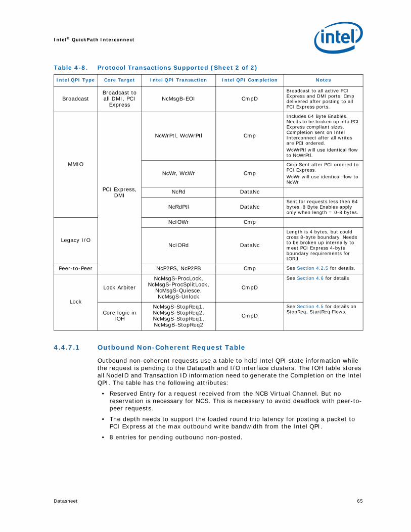
Datasheet 65
Intel® QuickPath Interconnect
4.4.7.1 Outbound Non-Coherent Request Table
Outbound non-coherent requests use a table to hold Intel QPI state information while the request is pending to the Datapath and I/O interface clusters. The IOH table stores all NodeID and Transaction ID information need to generate the Completion on the Intel QPI. The table has the following attributes:
• Reserved Entry for a request received from the NCB Virtual Channel. But no reservation is necessary for NCS. This is necessary to avoid deadlock with peer-to-peer requests.
• The depth needs to support the loaded round trip latency for posting a packet to PCI Express at the max outbound write bandwidth from the Intel QPI.
• 8 entries for pending outbound non-posted.
BroadcastBroadcast to all DMI, PCI
ExpressNcMsgB-EOI CmpD
Broadcast to all active PCI Express and DMI ports. Cmp delivered after posting to all PCI Express ports.
MMIO
PCI Express, DMI
NcWrPtl, WcWrPtl Cmp
Includes 64 Byte Enables. Needs to be broken up into PCI Express compliant sizes. Completion sent on Intel Interconnect after all writes are PCI ordered.WcWrPtl will use identical flow to NcWrPtl.
NcWr, WcWr Cmp
Cmp Sent after PCI ordered to PCI Express.WcWr will use identical flow to NcWr.
NcRd DataNc
NcRdPtl DataNcSent for requests less then 64 bytes. 8 Byte Enables apply only when length = 0-8 bytes.
Legacy I/O
NcIOWr Cmp
NcIORd DataNc
Length is 4 bytes, but could cross 8-byte boundary. Needs to be broken up internally to meet PCI Express 4-byte boundary requirements for IORd.
Peer-to-Peer NcP2PS, NcP2PB Cmp See Section 4.2.5 for details.
Lock
Lock Arbiter
NcMsgS-ProcLock, NcMsgS-ProcSplitLock,
NcMsgS-Quiesce, NcMsgS-Unlock
CmpD
See Section 4.6 for details
Core logic in IOH
NcMsgS-StopReq1, NcMsgS-StopReq2, NcMsgS-StopReq1, NcMsgB-StopReq2
CmpD
See Section 4.5 for details on StopReq, StartReq Flows.
Table 4-8. Protocol Transactions Supported (Sheet 2 of 2)
Intel QPI Type Core Target Intel QPI Transaction Intel QPI Completion Notes

Intel® QuickPath Interconnect
66 Datasheet
4.4.7.2 Peer-to-Peer Across Intel® QuickPath Interconnect
Intel QPI translates some peer-to-peer transactions between IOHs into a special NcP2PS for non-posted or NcP2PB for posted packets on Intel QPI. The IOH only supports MMIO peer-to-peer. The following transactions are not supported: NcIORd/Wr and NcCfgRd/Wr.
4.5 Profile SupportThe IOH can support a variety of small and large system configurations through the use of configuration registers.
Table 4-9 defines the features that are used in setting the profile and the corresponding register requirements.
The default values for these configuration registers are set to the UP system configuration, as noted in Table 4-9.
4.6 Lock ArbiterLock Arbiter is a central system resource used for coordinating lock and quiescence flows on Intel QPI. There is a single lock arbiter in the IOH which can accommodate a maximum of 8 simultaneous issues and 63 NodeID targets. IOH will not support sending PHold on Intel QPI.
The requests from Intel QPI that correspond to a System Lock are: NcMsgS-ProcLock, and NcMsgS-ProcSplitLock. The System Unlock message corresponds to NcMsgS-Unlock.
The lock arbiter also provides quiescence and de-quiescence of the system for OL_* operations using configuration registers defined in Chapter 17. The state of the “lock arbiter” is used by software to identify when each phase is complete and can begin the OL_* operations. This information is exported to the register defined in Chapter 17.
Table 4-9. Profile Control
Feature Register Type Setting Notes
Source Address decoder enable
QPIPCTRL: QPI Protocol Control RO enable
Address bits QPIPMADDATA: Protocol Memory Address Decode Data
RW 41 bits [40:0]
Can be reduced from the max to match processor support.
NodeID width QPIPCTRL:Protocol Control RO 3-bit
Other NodeID bits will be set to zero, and will be interpreted as zero when received.
Poison QPIPCTRL: Protocol Control RW enable
When disabled, any uncorrectable data error will be treated identically to a header parity.
Routing Table QPIRTBL: Routing Table RW enable

Datasheet 67
Intel® QuickPath Interconnect
4.6.1 Lock Arbiter Time-Out
Requests generated to the local IOH by the lock arbiter will use the same time-out hierarchy as requests issued on Intel QPI.
4.7 Write CacheThe IOH write cache is used for pipelining of inbound coherent writes. This is done by obtaining exclusive ownership of the cache line prior to ordering. Then writes are made observable (M-state) in I/O order.
4.7.1 Write Cache Depth
The write cache depth calculation is based on the latency from allocation of the RFO until the EWB causes de-allocation of the entry.
A 128-entry Write Cache meets the bandwidth requirement. This cache size assumes it is only used for inbound writes and any space for inbound read completions or read caching would be independent.
4.7.2 Coherent Write Flow
Inside the IOH, coherent writes follow a flow that starts with a RFO (Request for Ownership) followed by write a promotion to M-state.
IOH will issue an RFO command on the Intel QPI when it finds the write cache in I-state. The command used for the RFO phase depends on the a configuration mode bit that selects between “Normal” or “Invalidating Write” flow. In the “Standard” flow uses the InvItoE request while the “Invalidating Write” flow uses InvWbMtoI command. These requests returns E-state with no data.
4.7.3 Cache State
An RFO is received by the cache and the current state is I, then either InvItoE or InvWbMtoI on the Intel QPI (depending on the mode). These request always returns E-state with no data. Before this request can be issued a data resource is pre-allocated in the write cache to ensure forward progress. When the RFO request completed then E-state is been granted for a write. Once all the I/O ordering requirements have been met, the promotion phase occurs and the state of the line becomes M.
4.8 Outgoing Request Buffer (ORB)When a transaction is issued onto the Intel QPI, an ORB entry is allocated. This list keeps all pertinent information about the transaction header needed to complete the request. It also stores the cacheline address for coherent transactions to allow conflict checking with snoops and other local requests. See Section 4.9 for details. An Intel QPI response may come as multiple phases. The ORB tracks each completion phase (that is, Data* and Cmp) and any conflicts (that is, snoops, FrcAckCnflt Response) in the ORB.
When a request is issued, a tag is assigned based on home NodeID. MaxRequest for UP based system is 48.
The Home NodeID and tag are returned in the responses.

Intel® QuickPath Interconnect
68 Datasheet
4.8.1 ORB Depth
The ORB depth is 24 entries.
4.8.2 Tag Allocation
Tags are used in the Intel QPI to index into the tracker at the home node. The tracker at the home node pre-allocates a limited number of slots for each source in the system. A source is defined by the NodeID assigned to it. The number of tags allocated to each agent depends on the size of the tracker and the number of source agents that can target that home agent. The tags are limited at the IOH by the configuration value MaxRequests. See Chapter 17 for configuration details.
4.8.3 Time-Out Counter
Each entry in the ORB is tagged with a timeout value when it is allocated; the timeout value is dependent on the transaction type. This separation allows for isolation a failing transaction when dependence exists between transactions. Table 4-10 shows the timeout levels of transactions the IOH supports. Levels 2 and 6 are for transactions that the IOH does not send. The levels should be programmed such that they are increasing to allow the isolation of failing requests, and they should be programmed to consistent values across all components in the system.
The ORB implements a 2-bit timeout tag value per entry that starts out being set to 0h. The timeout counter rate value x is programmable per time-out level. It is controllable through configuration in powers of 2. The timeout counter rate x will result in a time-out for a given transaction in that level between 3x-4x based on the 2-bit timeout tag. The configuration values should be programmed to increase as the level increases to support longer timeout values for the higher levels.
On each global timeout counter expiration, every ORB entry with a matching request for that level is checked. If a match is found on a valid transaction and the timeout tag is equal to 2h, then it logged as a timeout, else the timeout tag is incremented. If timeout occurs, a failed response status is then sent to the requesting south agent for non-posted requests, and all Intel QPI structures will be cleared of this request.
A request in the ORB which receives an AbortTO response, results in resetting of the timeout tag for that request. The only usage model for this case corresponds to configuration transactions to PCI Express targets coming out of reset.
Timeout values are specified for each level independently. The values are specified in core clocks which is proportional to Intel QPI operational frequency. See Chapter 17 for register details.
Table 4-10. Time-Out Level Classification for IOH
Level Request Type
1 WbMtoI
2 None
3 NonSnpRd, NonSnpWr, RdCode, InvItoE, NcP2PB, IntPhysical, NcMsgS-StartReq1, NcMsgB-StartReq2
4 NcP2PS, NcMsgB-VLW, NcMsgB-PmReq
5 NcMsgS-StopReq1, NcMsgS-StopReq2
6 None

Datasheet 69
Intel® QuickPath Interconnect
4.9 Conflict HandlingA coherent conflict occurs in the Intel QPI when two requests are trying to access the same cache line. This can occur when a snoop hits a pending outstanding request or ownership grant. This type of conflict is referred to as a Remote-Local Conflict. The other type of conflict is a local-local conflict, where a local read or RFO hits a pending outstanding request on the Intel QPI, or a write cache entry. Local-Local conflicts also apply to non-coherent requests to DRAM (NonSnpRd & NonSnpWr*).
The Intel QPI also has a number of rules to prevent general network deadlock that apply to all transactions. This section refers to this class of resource deadlock.
In this section, “local requests” are requests originating from PCI Express, or DMI coming from the Intel QPI interface, originating from a processor or IOH.
4.9.1 Coherent Local-Local Conflicts
Local-local conflicts occur when a local request finds state for the same cache line in the Write Cache or ORB. There are three possible outcomes of the conflict detection: stall the request until the conflicting transaction completes, eviction of the line from the write cache, or completion of the transaction.
Table 4-11. Local-Local Conflict Actions (Sheet 1 of 2)
Local Request
ORB or Write Cache State Action
Rd or NonSnpRd or NonSnpWr*
Rd or NonSnpRd or NonSnpWr*
• Stall until completed.
RFO• Stall until EWB completed.• Force EWB on Promotion.
EWB • Stall until EWB completed.
E- or MG-state• Stall until EWB completed.• Force EWB on Promotion.
M-state• Stall until EWB completed.• Force EWB.
Non-Coh VT-d table data • Data may be snarfed locally for other Intel VT-d Reads.
RFO
Rd or NonSnpRd or NonSnpWr*
• Stall until completed.
RFO• Stall until Promotion.• If promotion does not evict the line then Complete RFO.• If promotion causes EWB, then send RFO after EWB completed.
EWB • Stall until EWB completed.
E- or MG-state• Stall until Promotion.• If promotion does not evict the line then Complete RFO.• If promotion causes EWB, then send RFO after EWB completed.
M-state • Complete immediately, no stall condition.

Intel® QuickPath Interconnect
70 Datasheet
4.9.1.1 Local Conflict Bypassing
In the condition where the request is stalled, other requests are allowed to bypass from all clusters. Although conflicts are somewhat rare, a single conflict can not block traffic from other streams. The bypass buffer can absorb one stalled conflicting request per active cache line. Upon receiving a second conflict, all Read and RFO requests are blocked. Write promotion will never conflict which is ensured by E/M state. Promotions will not be blocked by conflicted RFO or Read request.
4.9.2 Coherent Remote-Local Conflicts
Because the IOH only supports a sub-set of coherency states and coherent transactions, it requires only a limited subset of full conflict handling.
It is assumed that conflicts occur on less than one percent of total transactions. This implies that performance of these individual transactions are of little importance, however blocking on a single conflict can not be allowed to block forward progress of other “remote requests”.
The AckCnflt phase is completed by a Cmp or Cmp_Fwd*. Table 4-13 shows the responses and final state in the IOH on receiving different Cmp_Fwd* completions. Once the AckCnflt phase is completed, all buffered snoops are cleared.
M-Promote
Rd or NonSnpRd or
NonSnpWr* or RFO or EQB or
M-state
• Impossible. EWB can only be received in E or MG state.
E- or MG-state
• Normal flow to M-state and Eviction.• If M-state does not cause eviction under normal rules then Conflict
queue is checked to see if EWB required or RFO completion required.
• EWB: on EWB completion, next conflict is cleared.• If multiple ownerships are granted simultaneously, then state will
change to MG state.
Table 4-11. Local-Local Conflict Actions (Sheet 2 of 2)
Local Request
ORB or Write Cache State Action
Table 4-12. Remote-Local Conflict Actions
Snoop Request Local Transaction Phase
Local Transaction Pending Snoop Response
SnpCode, SnpData, SnpInvItoE, SnpInvXtoI
Request Rd (RdCode)RFOEWB
RspCnflt
SnpCode, SnpData, SnpInvItoE, SnpInvXtoI
AckCnflt Rd (RdCode)RFOEWB
<Buffer/Block>

Datasheet 71
Intel® QuickPath Interconnect
4.9.3 Resource Conflicts
Resource conflicts are generally not a problem in the Intel QPI because of the independent nature of the message classes. Two cases are explicitly stated here for how resources are managed to prevent resource problems.
The first basic Intel QPI rule is that completions are absorbed at the source, unconditional on any other message classes. This generally requires pre-allocation of completion resources before a request is sent. See Section 4.10.1 for more details on message class ordering details.
The ORB ensures that peer-to-peer non-posted requests do not fill the ORB (per allocation pool). This ensures that posted requests (with respect to PCI Express) will never be blocked by non-posted peer-to-peer requests.
The ORB ensures that Reads are allowed fair access into the ORB.
4.10 Deadlock AvoidanceFollowing sections calls out specific IOH ordering requirements.
4.10.1 Protocol Channel Dependence
Section 4.10.1.1 through Section 4.10.1.3 concentrate on potential deadlock situations between outbound and inbound traffic, and vice versa.
4.10.1.1 Outbound NC Request versus Inbound NC Request
Completions are always allowed to bypass deferred requests in the PCI ordered domain.
4.10.1.2 Inbound Response versus Inbound AckCnflt (Home Channel)
Inbound responses (responses received by the IOH) are never blocked because of blocking on the home channel in the inbound direction.
Table 4-13. Conflict Completions Actions
Local Transaction Pending
Conflict Completion
Response to
Requestor
Send to Home
Final State Notes
Rd (RdCur) Cmp_Fwd N/A RspI I RdCur results in I-state
Rd (RdCode) Cmp_Fwd N/A RspI I RdCode in IOH will always degrade to I state on RdCode Completion.
RFO (Write not at the head of IOQ) Cmp_Fwd N/A RspI I
E-state will always degrade to I-state because data may not exist on E-state.
RFO (Write at the head of IOQ
ready to atomically go M)
Cmp_FwdCodeCmp_FwdInvItoECmp_FwdInvOwn
N/A RspIWb + WbIData I
Write back to home
Cmp_FwdInvOwn DataC_M RspFwdI I
EWB Cmp_Fwd N/A RspI N/A
The Cmp_Fwd message could be avoided by the home agent in this case, but some home agents may not use this optimization.

Intel® QuickPath Interconnect
72 Datasheet
4.10.1.3 Snoop Stall on Hit, E-State
Any snoop that hits a line being promoted to M-state will be stalled while the promotion request for the M-state data is received from the IOQ to the write cache.
The write cache will revoke ownership if a snoop hits a blocked write in E-state and the RFO will be re-issued. See Section 4.9.2 for more details.
§

Datasheet 73
PCI Express* and DMI Interfaces
5 PCI Express* and DMI Interfaces
PCI Express is the next generation I/O interface extending I/O solutions beyond PCI-X. It offers a very high bandwidth to pin interface for general-purpose adapters interfacing a wide variety of I/O devices. The PCI Express Base Specification, Revision 2.0 provides the details of the PCI Express protocol. This chapter is complementary to Chapter 3 and should be used as additional reference.
5.1 PCI Express Link Characteristics — Link Training,Bifurcation, Downgrading and Lane Reversal Support
5.1.1 Link Training
The IOH PCI Express port 0 and port 1 supports the following Link widths: x16, x8, x4, x2 and x1. The IOH PCI Express port 2 supports link widths x4, x2 and x1. During link training, the IOH attempts link negotiation starting from the highest and ramp down to the nearest supported link width that passes negotiation. Each of the widths (x16, x8, x4, x2, x1) are trained in both the non-lane-reversed and lane-reversed modes. For example, x16 link width is trained in both the non-lane-reversed and lane-reversed modes before attempting a dual x8 configuration.
5.1.2 Port Bifurcation
IOH supports port bifurcation using two different means:
• Using the hardware straps. Table 15-13 illustrates the strapping options for ports 0, 1, and 2.
• Using BIOS by appropriately programming the PCIE_PRTx_BIF_CTRL register
5.1.2.1 Port Bifurcation Using BIOS
When BIOS needs to control port bifurcation, the hardware strap needs to be set to “Wait_on_BIOS”. This instructs the LTSSM to not train until BIOS explicitly enables port bifurcation by programming the PCIE_PRTx_BIF_CTRL register. The default of the latter register is such as to halt the LTSSM from training at poweron, provided the strap is set to “Wait_on_BIOS”. When BIOS programs the appropriate bifurcation information into the register, it can initiate port bifurcation by writing to the “Start bifurcation” bit in the register. Once BIOS has started the port bifurcation, it cannot initiate any more bifurcation commands without resetting the IOH. Note that software can initiate link retraining within a sub-port or even change the width of a sub-port (by programming the PCIE_PRTx/DMI_LANE_MSK register) any number of times without resetting the IOH.

PCI Express* and DMI Interfaces
74 Datasheet
Here is a pseudo-code example for how the register and strap work together to control port bifurcation. Note that “strap to ltssm” indicates the IOH internal strap to the LTSSM.
If (PCIE_PRT<0,1>_BIF_CTRL[2:0]/PCIE_PRT2_BIF_CTRL[1:0] == 111/11) {If (<PE0/1CFGSEL[2:0]>, <PE2CFGSEL[1:0]>!= <111>,<11>) {
Strap to ltssm = strap} else {
Wait for “PCIE_PRTx_BIF_CTRL[3]” bit to be setStrap to ltssm = csr
}} else {
Strap to ltssm = csr}
Note that the bifurcation control registers are sticky and BIOS can chose to program the register and cause an IOH reset and the appropriate bifurcation will take effect on exit from that reset.
5.1.3 Degraded Mode
Degraded mode is supported for x16, x8, x4, and x2 link widths. The IOH supports degraded mode operation at half the original width and quarter of the original width or a x1. This mode allows one half or one quarter of the link to be mapped out if one or more lanes should fail during normal operation. This allows for continued system operation in the event of a lane failure. Without support for degraded mode, a failure on a critical lane like lane 0 could bring the entire link down in a fatal manner. This can be avoided with support for degraded mode operation. For example, if lane 0 fails on a x8 link, then the lower half of the link will be disabled and the traffic will continue at half the performance on lanes 4–7. Similarly, a x4 link would degrade to a x2 link. This remapping should occur in the physical layer and the link and transaction layers are transparent to the link width change. The degraded mode widths are automatically attempted every time the PCI Express link is trained. The events that trigger the PCI Express link training are per the PCI Express Base Specification, Revision 2.0. For example, if a packet is retried on the link N times (where N is per the PCI Express Base Specification, Revision 2.0), then a physical layer retraining is automatically initiated. When this retraining happens, IOH starts out with negotiating a link width that it is currently operating at and if that fails, starts out with negotiating a lower link width per the degraded mode operation.
IOH supported degraded modes are shown in Table 5-1. Table 5-1 should be read such that the various modes indicated in the different rows would be tried by the IOH, but not necessarily in the order shown in the table. The IOH would try a higher width degraded mode before trying any lower width degraded modes.

Datasheet 75
PCI Express* and DMI Interfaces
The IOH reports entry into or exit from degraded mode to software (see Section 17.12.5.19 and Section 17.12.5.20) and also records which lane failed.
5.1.4 PCI Express Port Mapping
5.1.5 Lane Reversal
The IOH supports lane reversal on all its PCI Express ports, regardless of the link width that is, lane reversal works in x16, x8, x4, and x2 link widths. Note that the IOH supports logic that allows a x4, x8, or x16 card to be plugged into a x16 slot that is lane-reversed on the motherboard, and operate at the maximum width of the card. Similarly for a x4, x8 card plugged into a x8 lane-reversed slot, x4 card plugged into a lane-reversed x4 slot and a x2 card plugged into a lane-reversed x2 slot. Note that for the purpose of this discussion, a “xN slot” means a CEM/SIOM slot that is capable of any width greater than or equal to xN but is electrically wired on the board for only a xN width. A x2 card can be plugged into a x16, x8, or x4 slot and work as x2 only if lane-reversal is not done on the motherboard; otherwise, it would operate in x1 mode.
5.1.6 PCI Express Gen1/Gen2 Speed Selection
In general, the IOH will negotiate PCI Express Gen1 versus Gen2 link speed inband during link training.
The IOH can also be prevented from negotiating Gen2 speed if the PCIEGEN2EN# strap is set to 1 at reset deassertion. Note that this strap controls all ports together.
Table 5-1. Supported Degraded Modes
Original Link Width1
Notes:1. This is the native width of the link before degraded mode operation
Degraded Mode Link width and Lanes Numbers
x16
x8 on lanes 7-0, 0-7, 15-8, 8-15
x4 on lanes 3-0, 0-3, 4-7, 7-4, 8-11, 11-8, 12-15, 15-12
x2 on lanes 1-0, 0-1, 4-5, 5-4, 8-9, 9-8, 12-13, 13-12
x1 on lanes 0, 1, 2, 3, 4, 5, 6, 7, 8, 9, 10, 11, 12, 13, 14, 15
x8
x4 on lanes 7-4, 4-7, 3-0, 0-3
x2 on lanes 5-4, 4-5, 1-0, 0-1
x1 on lanes 0, 1, 2, 3, 4, 5, 6, 7
x4x2 on lanes 1-0, 0-1
x1 on lanes 0, 1, 2, 3
x2 x1 on lanes 0, 1
Table 5-2. PCI Express Port Translation
Port# 1 2 3 4 5 6 7 8 9 10
x2 x2 x4 x4 x4 x4 x4 x4 x4 x4
x4x8 x8 x8 x8
x16 x16

PCI Express* and DMI Interfaces
76 Datasheet
5.1.7 Form-Factor Support
The IOH supports Cardedge and Server I/O Module (SIOM) form-factors. Form-factor specific differences that exist for hot-plug and power management are captured in their individual sections.
5.2 IOH Performance Policies
5.2.1 Max_Payload_size
The IOH supports a Max_Payload_Size of 256B.
5.2.2 Isochronous Support and Virtual Channels
The IOH supports the default virtual channel (virtual channel 0) and any TC on the PCI Express interfaces.
5.2.3 Non-Coherent Transaction Support
5.2.3.1 Inbound
Non-coherent transactions are identified by the NoSnoop attribute in the PCI Express request header being set. PCI Express ports in IOH must provide support for converting these transactions to Non-coherent read/writes on Intel QPI. For writes, the NoSnoop attribute is used in conjunction with the Relaxed Ordering attribute to reduce snoops on the Intel QPI interface. Refer to Chapter 8, “Interrupts” for more details on this write optimization. For inbound reads with NoSnoop attribute set, the IOH does not snoop on Intel QPI. This optimization for reads and writes can be individually disabled.
5.2.3.2 Outbound
The IOH always clears the NoSnoop attribute bit in the PCI Express header for transactions that it forwards from the processor. For peer-to-peer transactions from other PCI Express ports and DMI, the NoSnoop attribute is passed as is from the originating port.
5.2.4 Completion Policy
The PCI Express Base Specification, Revision 1.1 and post 1.1 Erratas and EC*’s requires that completions for a specific request must occur in linearly-increasing address order. However, completions for different requests are allowed to complete in any order. As long as the above rules are followed, the IOH will send the completions on the PCI Express interface in the order received from the Intel QPI interface and never artificially delay completions received from Intel QPI to PCI Express.

Datasheet 77
PCI Express* and DMI Interfaces
5.2.4.1 Read Completion Combining
The PCI Express Base Specification, Revision 1.1 and post 1.1 Erratas and EC*’s allows that a single request can be satisfied with multiple “sub-completions” as long as they return in linearly-increasing address order. Therefore, since the IOH must split requests into cacheline quantities before issue on Intel QPI, the IOH will often complete a large request in cacheline-sized sub-completions.
As a performance optimization, the IOH implements an opportunistic read completion combining algorithm for all reads towards main memory. When the downstream PCI Express interface is busy (e.g., with another transaction) and multiple cachelines have returned before completion on PCI Express is possible, the PCI Express interface will combine the cacheline sub-completions into larger quantities up to MAX_PAYLOAD.
5.2.5 Read Prefetching Policies
The IOH will not perform any prefetching on behalf of interfacing PCI Express component reads. The PCI Express component is solely responsible for its own prefetch algorithms since those components are best suited to make appropriate trade-offs.
The IOH will not perform any outbound read prefetching.
5.2.6 Error Reporting
PCI Express reports many error conditions through explicit error messages: ERR_COR, ERR_NONFATAL, ERR_FATAL. The IOH can be programmed to do one of the following when it receives one of these error messages:
• Generate MSI
• Assert pins ERR[2:0]
• Forward the messages to the ICH10
Refer to the PCI Express Base Specification, Revision 2.0 for details of the standard status bits that are set when a root complex receives one of these messages.
5.2.7 Intel Chipset-Specific Vendor-Defined Messages
Intel chipset-specific vendor-defined messages (VDMs) are identified with a Vendor ID of 8086 in the message header and a specific message code.
5.2.7.1 ASSERT_GPE / DEASSERT_GPE
General-Purpose-Event (GPE) consists of two messages: Assert_GPE and Deassert_GPE. The IOH forwards both type of messages to ICH10 using DMI upon meeting the following conditions, otherwise they are dropped silently.
• First Assert_GPE among all root ports.
• Last Deassert_GPE among all root ports.
There needs to be a scoreboard for tracking assert/deassert pairs from each root port. Each Assert_GPE should eventually be followed by a Deassert_GPE after the GPE has been serviced. If one or more Assert_GPE messages is received, the IOH will wait until all the matching Deassert_GPE messages are received on its PCI Express ports before it sends the final Deassert_GPE message to the ICH10.

PCI Express* and DMI Interfaces
78 Datasheet
5.3 Inbound TransactionsThis section talks about the IOH behavior towards transactions that originate from PCI Express. Throughout this chapter, inbound refers to the direction towards main memory from I/O.
5.3.1 Inbound Memory, I/O and Configuration Transactions Supported
Table 5-3 lists the memory, I/O, and configuration transactions supported by the IOH, which are expected to be received from the PCI Express.
Table 5-3. Incoming PCI Express Memory, I/O and Configuration Request/Completion Cycles
PCI Express Transaction
Address Space or Message IOH Response
Inbound Write Requests
Memory Forward to Main Memory, PCI Express port (local or remote) or DMI (local or remote) depending on address.
I/O Forward to PCI Express port (local or remote) or DMI (local or remote).
Type 0 Configuration
Forward to the PCI-to-PCI port whose device number matches the device number in the Type 0 transaction, if enabled.
Type 1 Configuration
Forward to peer PCI Express port (local or remote) or DMI (local or remote).
Outbound Write Completions
I/O Forward to processor, PCI Express port (local or remote) or DMI (local or remote). Refer to Section 5.3.2 for handling of Configuration retry completions that target the processor.Configuration
Inbound Read Requests
Memory Forward to Main Memory, PCI Express port (local or remote), DMI (local or remote).
I/O Forward to peer PCI Express port (local or remote), DMI (local or remote).
Type 0 Configuration
Forward to the PCI-to-PCI port whose device number matches the device number in the Type 0 transaction, if enabled.
Type 1 Configuration
Forward to peer PCI Express port (local or remote) or DMI (local or remote).
Outbound Read Completions
MemoryForward to CPU, PCI Express port (local or remote) or DMI (local or remote). Refer to Section 5.3.2 for handling of Configuration retry completions that target the processor.
I/O
Configuration

Datasheet 79
PCI Express* and DMI Interfaces
5.3.2 PCI Express Messages Supported
Table 5-4 lists all inbound messages that the IOH supports receiving on a PCI Express downstream port (does not include DMI messages). In a given system configuration, certain messages are not applicable being received inbound on a PCI Express port. They will be called out as appropriate.
5.3.2.1 Error Reporting
PCI Express reports many error conditions through explicit error messages: ERR_COR, ERR_NONFATAL, ERR_FATAL. IOH can be programmed to do one of the following when it receives one of these error messages:
• Generate MSI
• Assert pins ERR[2:0]
• Forward the messages to ICH
Refer to the PCI Express Base Specification, Revision 1.1 and post 1.1 Erratas and EC*’s for details of the standard status bits that are set when a root complex receives one of these messages.
Table 5-4. Incoming PCI Express Message Cycles
PCI Express Transaction
Address Space or Message IOH Response
Inbound Message
ASSERT_INTADEASSERT_INTAASSERT_INTB
DEASSERT_INTBASSERT_INTC
DEASSERT_INTCASSERT_INTD
DEASSERT_INTD
Inband interrupt assertion/deassertion emulating PCI interrupts. Forward to DMI.
ERR_CORERR_NONFATAL
ERR_FATAL
PCI Express error messages propagate as an interrupt to system or cause the ERR[2:0] pins to toggle.
PM_PME Propagate as an interrupt/general purpose event to the system.
PME_TO_ACK Received PME_TO_ACK bit is set when IOH receives this message.
PM_ENTER_L1 (DLLP)
Block subsequent TLP issue and wait for all pending TLPs to Ack. Then, send PM_REQUEST_ACK. Refer to PCI Express Architecture Specification, Revision 1.0a for details of the L1 entry flow.
ATC Invalidation Complete
When an end point device completes an ATC invalidation, it will send an Invalidate Complete message to the IOH (RC). This message will be tagged with information from the Invalidate message so that the IOH can associate the Invalidate Complete with the Invalidate Request.
Vendor-defined
ASSERT_GPEDEASSERT_GPE(Intel-specific)
Vendor-specific message indicating assertion/deassertion of PCI-X hotplug event in PXH. Message forwarded to DMI port.Refer to Section 5.3.3.1, “ASSERT_GPE / DEASSERT_GPE” on page 80 for further details.
All Other Messages
Silently discard if message type is type 1 and drop and log error if message type is type 0

PCI Express* and DMI Interfaces
80 Datasheet
5.3.3 Intel® Chipset-Specific Vendor-Defined
These Vendor defined messages are identified with a Vendor ID of 8086 in the message header and a specific message code.
5.3.3.1 ASSERT_GPE / DEASSERT_GPE
Upon receipt of an Assert_GPE message from a PCI Express port, the IOH forwards the message to the ICH. When the GPE event has been serviced, the IOH will receive a Deassert_GPE message on the PCI Express port. At this point the IOH can send the deassert_GPE message on DMI. When an IOH does not have its DMI port enabled for legacy, it forwards the messages over the Intel QuickPath Interconnect.
5.4 Outbound TransactionsThis section describes the IOH behavior towards outbound transactions. Throughout the rest of the chapter, outbound refers to the direction from processor towards I/O.
5.4.1 Memory, I/O, and Configuration Transactions Supported
The IOH generates the outbound memory, I/O and configuration transactions listed in Table 5-5.
5.4.2 Lock Support
For legacy PCI functionality, the IOH supports bus locks through an explicit sequence of events. The IOH can receive a locked transaction sequence on the Intel QuickPath Interconnect interface directed to a PCI Express port.
Table 5-5. Outgoing PCI Express Memory, I/O, and Configuration Request/CompletionCycles
PCI Express Transaction
Address Space or Message Reason for Issue
Outbound Write Requests
Memory Memory-mapped I/O write targeting a PCI Express device.
I/O Legacy I/O write targeting a PCI Express device.
Configuration Configuration write targeting a PCI Express device.
Inbound Write Completions
I/O Response for an inbound write to a peer I/O device.
Configuration Response for an inbound write to a peer I/O device or to the originating port.
Outbound Read Requests
Memory Memory-mapped I/O read targeting a PCI Express device.
I/O Legacy I/O read targeting a PCI Express device.
Configuration Configuration read targeting PCI Express device.
Inbound Read Completions
Memory Response for an inbound read to main memory or a peer I/O device.
I/O Response for an inbound read to a peer I/O device.
Configuration Response for an inbound read to a peer I/O device or to the originating port.

Datasheet 81
PCI Express* and DMI Interfaces
5.4.3 Outbound Messages Supported
Table 5-6 provides a list of all the messages supported by the IOH as an initiator on a PCI Express port. Unless explicitly noted, these messages are supported on both the standard PCI Express port. References to “PCI Express port” in Table 5-6 apply to both the standard PCI Express port.
5.4.3.1 Unlock
This message is transmitted by the IOH at the end of a lock sequence. This message is transmitted regardless of whether PCI Express lock was established or whether the lock sequence terminated in an error.
5.4.3.2 EOI
EOI messages will be multicast from the Intel QuickPath Interconnect to all the PCI Express interfaces/DMI ports that have an APIC below them. Presence of an APIC is indicated by the EOI enable bit (refer to Chapter 17). This ensures that the appropriate interrupt controller receives the end-of-interrupt.
5.5 32-/64-Bit AddressingFor inbound and outbound memory reads and writes, the IOH supports the 64-bit address format. If an outbound transaction’s address is less than 4 GB, the IOH will issue the transaction with a 32-bit addressing format on PCI Express. Only when the address is greater than 4 GB will the IOH initiate transactions with 64-bit addressing format. Refer to Chapter 7 for details of addressing limits imposed by the Intel QuickPath Interconnect and the resultant address checks that IOH does on PCI Express packets it receives.
Table 5-6. Outgoing PCI Express Message Cycles
PCI Express Transaction
Address Space or Message Reason for Issue
Outbound Messages Unlock
Releases a locked read or write transaction previously issued on PCI Express.
PME_Turn_Off When PME_TO bit in the MISCCTRLSTS register is set, send this message to the associated PCI Express port.
PM_REQUEST_ACK(DLLP)
Acknowledges that the IOH received a PM_ENTER_L1 message. This message is continuously issued until the receiver link is idle. Refer to the PCI Express Base Specification, Revision 2.0 for details.
PM_Active_State_Nak When the IOH receives a PM_Active_State_Request_L1.
Set_Slot_Power_Limit
Message that is sent to a PCI Express device when software writes to the Slot Capabilities Register or the PCI Express link transitions to DL_Up state. Refer to PCI Express Base Specification, Revision 2.0 for more details.
Intel Chipset-specifc Vendor-
definedEOI
End-of-interrupt cycle received on the Intel QuickPath Interconnect. The IOH broadcasts this message to all downstream PCI Express and DMI ports.

PCI Express* and DMI Interfaces
82 Datasheet
5.6 Transaction DescriptorThe PCI Express Base Specification, Revision 2.0 defines a field in the header called the Transaction Descriptor. This descriptor comprises three sub-fields:
• Transaction ID
• Attributes
• Traffic class
5.6.1 Transaction ID
The Transaction ID uniquely identifies every transaction in the system. The Transaction ID comprises four sub-fields described in Table 5-7. The table provides details on how this field in the PCI Express header is populated by:
Table 5-7. PCI Express Transaction ID Handling
Field Definition IOH as Requester IOH as Completer
Bus Number
Specifies the bus number that the requester resides on.
The IOH preserves this field from the request and copies it into the completion.
Device Number
Specifies the device number of the requester.
For CPU requests, the IOH fills this field in with its Device Number that the PCI Express cluster owns.
Function Number
Specifies the function number of the requester.
The IOH fills this field in with its Function Number that the PCI Express cluster owns (zero).
Tag Denotes a unique identifier for every transaction that requires a completion. Since the PCI Express ordering rules allow read requests to pass other read requests, this field is used to reorder separate completions if they return from the target out-of-order.
Non-Posted (NP) Transaction: The IOH fills this field in with a value such that every pending request carries a unique Tag.NP Tag[7:5] = QPI Source NodeID[4:2]. Note that bits 7:5 can be non-zero only when 8-bit tag usage is enabled. Otherwise, the IOH always zeros out 7:5.NP Tag[4:0] = the IOH ensures uniqueness across all pending NP requests from the port.Posted Transaction: No uniqueness is ensured.Tag[7:0] = QPI Source NodeID[7:0] for processor requests. Note that bits 7:5 can be non-zero only when 8-bit tag usage is enabled. Otherwise, the IOH always zeros out bits 7:5.

Datasheet 83
PCI Express* and DMI Interfaces
5.6.2 Attributes
PCI Express supports two attribute hints described in Table 5-8. This table describes how the IOH populates these attribute fields for requests and completions it generates.
5.6.3 Traffic Class
The IOH does not optimize based on traffic class. The IOH can receive a packet with TC! = 0 and treat the packet as if it were TC = 0 from an ordering perspective. The IOH forwards the TC filed as-is on peer-to-peer requests and also returns the TC field from the original request on the completion packet sent back to the device.
5.7 Completer IDThe CompleterID field is used in PCI Express completion packets to identify the completer of the transaction. The CompleterID comprises three sub-fields described in Table 5-9.
Table 5-8. PCI Express Attribute Handling
Attribute1
Notes:1. Refer to Chapter 3 for how the IOH uses these attributes for performance optimizations.
Definition IOH as Requester IOH as Completer
Relaxed Ordering
Allows the system to relax some of the standard PCI ordering rules.
This bit is not applicable and set to zero.
The IOH preserves this field from the request and copies it into the completion.
Snoop Not Required
This attribute is set when an I/O device controls coherency through software mechanisms. This attribute is an optimization designed to preserve processor snoop bandwidth.
Table 5-9. PCI Express CompleterID Handling
Field Definition IOH as Completer
Bus Number Specifies the bus number that the completer resides on.
The IOH returns 00h as the Bus number
Device Number
Specifies the device number of the completer. The IOH returns 00000b as the Device Number
Function Number
Specifies the function number of the completer.
0

PCI Express* and DMI Interfaces
84 Datasheet
5.8 Miscellaneous
5.8.1 Number of Outbound Non-Posted Requests
Each x4 PCI Express link supports up to two outstanding non-posted outbound transactions issued by the processors. Each x8 link supports up to four and x16 supports up to eight outstanding non-posted transactions.
5.8.2 MSIs Generated from Root Ports and Locks
Once lock has been established on the Intel QuickPath Interconnect, the IOH cannot send any requests on the Intel QuickPath Interconnect, including MSI transactions generated from the root port of the PCI Express port that is locked.
5.8.3 Completions for Locked Read Requests
Both LkRdCmp and RdCmp completion types can terminate a locked or non-locked read request.
5.9 PCI Express RASThe IOH supports the PCI Express Advanced Error Reporting (AER) capability. Refer to PCI Express Base Specification, Revision 2.0 for details.
5.9.1 ECRC Support
The IOH does not support the PCI Express End-to-end CRC (ECRC) feature. The IOH ignores and drops ECRC on all incoming packets and does not generate ECRC on any outgoing packet.
5.9.2 Completion Time-Out
For all non-posted requests that the IOH issues on PCI Express or DMI, the IOH maintains a timer that times the max completion time for that request.
The IOH follows the time-out mechanism ECN that is currently being proposed in the PCI Express Base Specification. The ECN provides a way for the OS to select a coarse range for the timeout value. The IOH then chooses a final value of the timeout within each coarse range. The timeout value is programmable from 50 ms all the way up to 64 seconds. Refer to Chapter 17 for details and additional control that the IOH provides for the 17 second to 64 second timeout range.
Refer to the Chapter 13 for details of responses returned by the IOH to various interfaces on a completion time-out event. AER-required error logging and escalation happen as well. In addition to the AER error logging, the IOH also sets the locked read time-out bit in the Miscellaneous Control and Status Register if the completion time-out happened on a locked read request. See the Chapter 17 for details.

Datasheet 85
PCI Express* and DMI Interfaces
5.9.3 Data Poisoning
The IOH supports forwarding of poisoned data among its interfaces.
The IOH provides an optional mode where poisoned data is never sent out on PCI Express; any packet with poisoned data is dropped by the IOH and generate an error. See the Chapter 13 for details.
5.9.4 Role-Based Error Reporting
The IOH supports the new role-based error reporting feature being amended to the PCI Express Base Specification, Revision 1.1. Details of how the IOH handles various error cases under this role-based error reporting scheme are as follows.
A Poisoned TLP received on peer-to-peer packets is treated as an advisory non-fatal error condition. That is, ERR_COR is signaled and the poisoned information propagated peer-to-peer.
Poisoned TLP on packets destined for internal devices of the IOH are treated, from a PCI Express interface error reporting perspective, as a normal, non-fatal error condition.
Poisoned TLP on packets destined towards DRAM, or poisoned TLP packets that target the interrupt address range, are forwarded to the Intel QuickPath Interconnect with the poison bit set, provided the Intel QuickPath Interconnect interface is enabled to set the poisoned bit using QPIPC[12]. In such a case the received poisoned TLP condition is treated as advisory non-fatal error on the PCI Express interface. If that bit is not set, the IOH treats the received poisoned TLP condition as a normal, non-fatal error. The packet is dropped if it is a posted transaction. A “master abort” response is sent on the Intel QuickPath Interconnect if the poisoned TLP received was for an outstanding non-posted request.
When the IOH times out, or receives a UR/CA response on a request outstanding on PCI Express, it does not attempt recovery in hardware. Also, it would treat the completion time-out condition as a normal, non-fatal error condition. UR/CA received does not cause an error escalation.
5.10 Link Layer Specifics
5.10.1 Ack/Nak
The Data Link layer is responsible for ensuring that TLPs are successfully transmitted between PCI Express agents. PCI Express implements an Ack/Nak protocol to accomplish this. Every TLP is decoded by the Physical layer (8b/10b) and forwarded to the Link layer. The CRC code appended to the TLP is then checked. If this comparison fails, the TLP is retried. Refer to Section 5.10.2 for details.
If the comparison is successful, an Ack is issued back to the transmitter and the packet is forwarded for decoding by the receiver’s Transaction layer. The PCI Express protocol allows that Acks can be combined and the IOH implements this as an efficiency optimization.
Generally, Naks are sent as soon as possible. Acks, however, will be returned based on a timer policy such that when the timer expires, all unacknowledged TLPs to that point are Acked with a single Ack DLLP. The timer is programmable.

PCI Express* and DMI Interfaces
86 Datasheet
5.10.2 Link Level Retry
The PCI Express Base Specification, Revision 2.0 lists all the conditions where a TLP gets Nak’d. One example is on a CRC error. The Link layer in the receiver is responsible for calculating 32 bit CRC (using the polynomial defined in PCI Express Base Specification, Revision 2.0) for incoming TLPs and comparing the calculated CRC with the received CRC. If they do not match, then the TLP is retried by Nak’ing the packet with a Nak DLLP specifying the sequence number of the corrupt TLP. Subsequent TLPs are dropped until the reattempted packet is observed again.
When the transmitter receives the Nak, it is responsible for retransmitting the TLP specified with the Sequence number in the DLLP + 1. Furthermore, any TLPs sent after the corrupt packet will also be resent since the receiver has dropped any TLPs after the corrupt packet.
5.10.2.1 Retry Buffer
The IOH transmitter retry buffer is designed such that under normal conditions there is no performance degradation. Unless there is a CRC error at the receiver, the transmitter will never back up (at Gen2 speeds) due to insufficient room in the retry buffer. The following environment is assumed:
• 3 m of cable + 25” FR4 total
• Two repeaters
• Four connectors
5.10.3 Ack Time-Out
Packets can get “lost” if the packet is corrupted such that the receiver’s Physical layer does not detect the framing symbols properly. Frequently, lost TLPs are detectable with non-linearly incrementing sequence numbers. A time-out mechanism exists to detect (and bound) cases where the last TLP packet sent (over a long period of time) was corrupted. A replay timer bounds the time a retry buffer entry waits for an Ack or Nak. Refer to the PCI Express Base Specification, Revision 2.0 for details on this mechanism.

Datasheet 87
PCI Express* and DMI Interfaces
5.10.4 Flow Control
The PCI Express flow control types are described in the following tables.
Every PCI Express device tracks the above six credit types for both itself and the interfacing device. The rules governing flow control are described in PCI Express Base Specification, Revision 2.0.
Note: The credit advertisement in Table 5-10 does not necessarily imply the number of outstanding requests to memory.
The IOH keeps a pool of credits that are allocated between the ports based on their partitioning. For example, assume the NPRH credit pool is N for the x8 port. If this port is partitioned as two x4 ports, the credits advertised are N/2 per port.
Table 5-10. PCI Express Credit Mapping for Inbound Transactions
Flow Control Type Definition Initial IOHAdvertisement
Inbound Posted Request Header Credits (IPRH)
Tracks the number of posted requests the agent is capable of supporting. Each credit accounts for one posted request.
24(x4)48(x8)96(X16)
Inbound Posted Request Data Credits (IPRD)
Tracks the number of posted data the agent is capable of supporting. Each credit accounts for up to 16 bytes of data.
108(x4)216(x8)432(X16)
Inbound Non-Posted Request Header Credits (INPRH)
Tracks the number of non-posted requests the agent is capable of supporting. Each credit accounts for one non-posted request.
24(x4)48(x8)96(X16)
Inbound Non-Posted Request Data Credits (INPRD)
Tracks the number of non-posted data the agent is capable of supporting. Each credit accounts for up to 16 bytes of data.
4(x4)8(x8)16(X16)
Completion Header Credits (CPH) Tracks the number of completion headers the agent is capable of supporting. infinite
Completion Data Credits (CPD) Tracks the number of completion data the agent is capable of supporting. Each credit accounts for up to 16 bytes of data.
infinite
Table 5-11. PCI Express Credit Mapping for Outbound Transactions
Flow Control Type Definition Initial IOHAdvertisement
Inbound Posted Request Header Credits (OPRH)
Tracks the number of posted requests the agent is capable of supporting. Each credit accounts for one posted request.
4(x4)8(x8)16(X16)
Inbound Posted Request Data Credits (OPRD)
Tracks the number of posted data the agent is capable of supporting. Each credit accounts for up to 16 bytes of data.
8(x4)16(x8)32(X16)
Inbound Non-Posted Request Header Credits (ONPRH)
Tracks the number of non-posted requests the agent is capable of supporting. Each credit accounts for one non-posted request.
14(x4)24(x8)56(X16)
Inbound Non-Posted Request Data Credits (ONPRD)
Tracks the number of non-posted data the agent is capable of supporting. Each credit accounts for up to 16 bytes of data.
12(x4)24(x8)48(X16)
Completion Header Credits (CPH) Tracks the number of completion headers the agent is capable of supporting.
6(x4)12(x8)24(X16)
Completion Data Credits (CPD) Tracks the number of completion data the agent is capable of supporting. Each credit accounts for up to 16 bytes of data.
12(x4)24(x8)48(X16)
PCI Express* and DMI Interfaces
88 Datasheet
5.10.4.1 Flow Control Credit Return by IOH
After reset, credit information is initialized with the values indicated in Table 5-10 by following the flow control initialization protocol defined in the PCI Express Base Specification, Revision 2.0. Since the IOH supports only VC0, only this channel is initialized. As a receiver, the IOH is responsible for updating the transmitter with flow control credits as the packets are accepted by the Transaction Layer. Credits will be returned as follows:
• If infinite credits advertised, there are no flow control updates for that credit class, as per the PCI Express Base Specification, Revision 2.0
• For non-infinite credits advertised, the IOH will send flow control updates if none were sent previously, for example, after 28 usec (to comply with the specification's 30 usec requirement). This 28 us is programmable down to 6 us.
• If, and only when, there are credits to be released, the IOH will wait for a configurable/programmable number of cycles (in the order of 30–70 cycles) before the flow control update is sent. This is done on a per flow-control credit basis. This mechanism ensures that credits updates are not sent when there is no credit to be released.
5.10.4.2 Flow Control Update DLLP Time-Out
The IOH supports the optional flow control update DLLP time-out timer.
5.11 Power Management
IOH does not support the beacon wake method on PCI Express. IOH supports Active State Power Management (ASPM) transitions into L1 state. Also, IOH supports the D0 and D3hot power management states per PCI Express port and also supports a wake event from these states on a PCI Express hot-plug event. In D3hot, IOH will master abort all configuration TX targeting the PCI Express link.
5.12 Direct Media Interface (DMI)
5.12.1 Configuration Retry Completion
The IOH handles configuration retry from DMI similar to configuration retry from PCI Express. Refer to Section 5.3.2 for details of how a PCI Express port handles configuration retry completions.
5.12.2 Outbound Transactions
This section describes outbound transactions supported by the IOH on the DMI link.
5.12.2.1 Outbound Memory, I/O and Configuration Transactions Supported
Table 5-12 lists the outbound memory, I/O and Configuration requests and completions supported by the IOH on DMI.

Datasheet 89
PCI Express* and DMI Interfaces
5.12.2.2 Outbound Messages Supported
Table 5-13 lists all outbound messages supported by the IOH on DMI.
Table 5-12. Outgoing DMI Memory, I/O and Configuration Requests/Completions
DMI Transaction Type Reason for Issue
Outbound Write Requests
Memory Processor or peer memory-mapped I/O write targeting ICH10.
I/O Processor or peer legacy I/O write targeting ICH10.
Configuration Processor or peer Configuration write targeting ICH10.
Outbound Read Requests
Memory Processor or memory-mapped I/O read targeting ICH10.
I/O Processor or PCI Express I/O read targeting ICH10.
Configuration Configuration read targeting ICH10.
Inbound Read Completions Memory
Response for an inbound read to main memory, integrated device or PCI Express.
Table 5-13. Outgoing DMI Messages (Sheet 1 of 2)
DMI Transaction Transaction Type Reason for Issue
Standard PCI Express Messages
Unlock When a locked read or write transaction was previously issued to the DMI, “Unlock” releases the PCI lock.
Assert_INTAAssert_INTBAssert_INTCAssert_INTD
Deassert_INTADeassert_INTBDeassert_INTCDeassert_INTD
Issued by the IOH through the DMI port when a PCI Express interface receives a legacy interrupt message on its standard PCI Express ports or generates them internally. Note that these events are level sensitive at the source and the IOH will send an aggregated message (wired-or) to the DMI for each interrupt level. Refer to the Chapter 8, “Interrupts” for further details of how these messages are handled through the IOH from the receiving PCI Express interface.

PCI Express* and DMI Interfaces
90 Datasheet
5.12.2.3 Lock Support
For legacy PCI functionality, the IOH supports bus locks to the DMI port.
5.12.2.4 PHOLD Support
The IOH supports the PHOLD protocol. This protocol is used for legacy ISA devices which do not allow the possibility for being both a master and a slave device simultaneously. Example devices that use the PHOLD protocol are legacy floppy drives, and so on.
5.12.2.4.1 PHOLD/PHOLDA
A PHOLD regime is established when the IOH issues an Assert_PHLDA message to DMI and is terminated when the IOH receives a Deassert_PHLD message on DMI. The IOH will not send posted or non-posted requests to DMI port during a PHOLD regime and will only allow downstream completions. All non-posted peer-to-peer traffic should be disabled during the PHOLD regime to avoid deadlock situations within the IOH.
5.12.2.4.2 ICH10 Behavior
Once the ICH10 has sent an Assert_PHLD message, it will not send a Deassert_PHLD message until the IOH has sent an Assert_PHLDA message.
Intel Vendor-defined Messages
PM_Active_State_NAK
The IOH will generate the “PM_Active_State_NAK” message to the ICH10 in response to receiving a “PM_Active_State_Request_L1” DLLP because the IOH cannot transition to the L1 state. Refer to PCI Express Base Specification, Revision 2.0 for further details on the L1 ASPM flow.
Rst_Warn_AckThe IOH sends the Acknowledge in response to a prior “Rst_Warn” message. Refer to the Chapter 11, “Reset” for details of the IOH reset flow and how this message is handled.
EOIThe IOH will broadcast an EOI encoded as a TLP Data message with EOI vector embedded in the payload. Refer Section 5.4.3.2 for details of the EOI broadcast.
Assert_GPEDeassert_GPE
The IOH will forward a collapsed version of the Assert_GPE and Deassert_GPE it receives from its PCI Express ports. Refer to Section 5.2.7.1 for further details.
Assert_HPGPEDeassert_HPGPE
The IOH will send a Hot plug GPE message, “Assert_HPGPE” when a hot-plug event is detected (and native OS handling of hot-plug is disabled). The “Deassert_HPGPE” is sent when the hot-plug event has been serviced.
Assert_PMEGPEDeassert_PMEGPE
The IOH will send a “Assert_PMEGPE” when a Power Management event is detected (and native OS handling of hot-plug is disabled). The “Deassert_PMEGPE” is sent when the Power Management event has been completed.
Ack_C0 Refer to the Chapter 10, “IOH power management is compatible with the PCI Bus Power Management Interface Specification, Revision 1.1 (referenced as PCI-PM). It is also compatible with the Advanced Configuration and Power Interface (ACPI) Specification, Revision 2.0b. The IOH is designed to operate seamlessly with operating systems employing these specifications.” for details.
Ack_S3
Ack_C2
CPU_Reset_Done Reset related message. Refer to the Chapter 11, “Reset” for further details.
INTR_Ack
Issued by the IOH when the Processor sends an interrupt acknowledge command on Intel QuickPath Interconnect. This is treated as an outbound posted message and sent to the ICH10. There can be only one INTR_Ack outstanding from the processor at a time.
DO_SCI Needed for Intel QuickPath Interconnect-based ACPI events
Table 5-13. Outgoing DMI Messages (Sheet 2 of 2)
DMI Transaction Transaction Type Reason for Issue

Datasheet 91
PCI Express* and DMI Interfaces
5.12.2.4.3 Intel® QuickPath Interconnect Lock Request
When the IOH receives an Assert_PHLD message on DMI, it will generate a request to lock arbiter.
5.12.2.4.4 Block all sources of transactions
Once the Intel QuickPath Interconnect lock is established, the IOH flushes the queues and sends an Assert_PHLDA message to ICH10 on the DMI.
5.12.3 64-Bit Addressing
For processor and peer-to-peer writes and reads, the IOH supports 64-bit address format on the DMI to and from the ICH10.
5.12.4 Transaction Descriptor
The Transaction Descriptor comprises three sub-fields:
• Transaction ID
• Attributes
• Traffic Class
5.12.4.1 Transaction ID
The Transaction ID uniquely identifies every transaction in the system. The Transaction ID comprises four sub-fields described in Table 5-14.
Table 5-14. DMI Transaction ID Handling
Field Definition IOH as Requester IOH as Completer
Bus Number
Specifies the bus number that the requester resides on.
The IOH fills this field in with its internal Bus Number that the DMI cluster resides on (refer to the Chapter 17, “Configuration Register Space” for details.
The IOH preserves this field from the request and copies it into the completion.Device
NumberSpecifies the device number of the requester.
9
Function Number
Specifies the function number of the requester.
0
Tag
Unlike PCI Express this field is allowed to be non-unique on DMI. IOH as a requester will not use non-unique TID on DMI but as a completer will preserve any original request TID.
Non-Posted (NP) Transaction: The IOH fills this field in with a value such that every pending request carries a unique Tag.NP Tag[7:4] = QPI Source NodeID[4:1]. Note that bits [7:5] can be non-zero only when 8-bit tag usage is enabled (in the peer-to-peer register corresponding to the DMI port). Otherwise, the IOH always zeros out bits [7:5].NP Tag[3:0] = Any algorithm that ensures uniqueness across all pending NP requests from the port.Posted Transaction: No uniqueness ensured.Tag[7:0] = QPI Source NodeID[7:0] for processor requests. Note that bits [7:5] can be non-zero only when 8-bit tag usage is enabled. Otherwise, the IOH always zeros out bits [7:5].1
Notes:1. The IOH never uses non-unique tag as requester on DMI.

PCI Express* and DMI Interfaces
92 Datasheet
5.12.4.2 Attributes
DMI supports two attribute hints described in Table 5-15.
The IOH supports DMI virtual channel 0 (VC0, the default channel) and supports traffic class 0 (TC0) only. If IOH receives any packet with TC!=0, the packet is treated as a malformed packet. For requests the IOH generates as a requester, the IOH sets the TC field to zero.
5.12.5 Completer IDThe CompleterID field is used in DMI completion packets to identify the completer of the transaction. The CompleterID comprises three sub-fields described in Table 5-16. The table provides details on how this field is populated by the IOH for completions it generates to DMI.
5.13 Flow Control Credits Advertised on DMIThe DMI port flow control credits advertised are described in Table 5-17.
§
Table 5-15. DMI Attribute Handling
Attribute Definition IOH as Requester IOH as Completer
Relaxed Ordering
Allows the system to relax some of the standard PCI ordering rules.
For outbound transactions, this bit is not applicable and set to zero. For peer-to-peer requests, preserve this field from the source PCI Express port to the destination port.
The IOH preserves this field from the request and copies it into the completion. Snoop
Not Required
This attribute is set when an I/O device controls coherency through software mechanisms. This attribute is an optimization designed to preserve processor snoop bandwidth.
Table 5-16. DMI CompleterID Handling
Field Definition IOH as Completer
Bus Number Specifies the bus number that the completer resides on.
The IOH fills this field in with its internal Bus Number that the DMI cluster resides on.
Device Number
Specifies the device number of the completer. 9
Function Number
Specifies the function number of the completer.
0
Table 5-17. PCI Express Credit Mapping
Flow Control Type Definition Initial IOHAdvertisement
Posted Request Header Credits (PRH)
Tracks the number of posted requests the agent is capable of supporting. Each credit accounts for one posted request.
24
Posted Request Data Credits (PRD)
Tracks the number of posted data the agent is capable of supporting. Each credit accounts for up to 16 bytes of data.
108
Non-Posted Request Header Credits (NPRH)
Tracks the number of non-posted requests the agent is capable of supporting. Each credit accounts for one non-posted request.
24
Non-Posted Request Data Credits (NPRD)
Tracks the number of non-posted data the agent is capable of supporting. Each credit accounts for up to 16 bytes of data.
4
Completion Header Credits (CPH)
Tracks the number of completion headers the agent is capable of supporting.
4a to infinite
Completion Data Credits (CPD)
Tracks the number of completion data the agent is capable of supporting. Each credit accounts for up to 16 bytes of data.
16a to infinite

Datasheet 93
Ordering
6 Ordering
The IOH spans two different ordering domains: one that adheres to Producer-Consumer ordering (PCI Express) and one that is completely unordered (Intel QuickPath Interconnect). One of the primary functions of the IOH is to ensure that the Producer-Consumer ordering model is maintained in the unordered, Intel QuickPath Interconnect domain.
This section describes the rules that are required to ensure that both PCI Express and Intel QuickPath Interconnect ordering is preserved. Throughout this chapter, the following terms listed in Table 6-1 are used.
Table 6-1. Ordering Term Definitions
Term Definition
Intel QuickPath Interconnect Ordering Domain
The Intel QuickPath Interconnect has a relaxed ordering model allowing reads, writes and completions to flow independent of each other. Intel QuickPath Interconnect implements this through the use of multiple, independent virtual channels. In general, the Intel QuickPath Interconnect ordering domain is considered unordered.
PCI Express Ordering Domain PCI Express (and all other prior PCI generations) have specific ordering rules to enable low cost components to support the Producer-Consumer model. For example, no transaction can pass a write flowing in the same direction. In addition, PCI implements ordering relaxations to avoid deadlocks (for example, completions must pass non-posted requests). The set of these rules are described in PCI-Express Base Specification, Revision 1.0a.
Posted A posted request is a request which can be considered ordered (per PCI rules) upon the issue of the request and therefore completions are unnecessary. The only posted transaction is PCI memory writes. Intel QuickPath Interconnect does not implement posted semantics and so to adhere to the posted semantics of PCI, the rules below are prescribed.
Non-posted A non-posted request is a request which cannot be considered ordered (per PCI rules) until after the completion is received. Non-posted transactions include all reads and some writes (I/O and configuration writes). Since Intel QuickPath Interconnect is largely unordered, all requests are considered to be non-posted until the target responds. Throughout this chapter, the term non-posted applies only to PCI requests.
Outbound Read A read issued toward a PCI Express device. This can be a read issued by a processor, an SMBus master, or a peer IOH (in the context of the target IOH).
Outbound Read Completion The completion for an outbound read. For example, the read data which results in a processor read of a PCI Express device. Note that while the data flows inbound, the completion is still for an outbound read.
Outbound Write A write issued toward a PCI Express device. This can be a write issued by a processor, an SMBus master, or a peer IOH (in the context of the target IOH).
Outbound Write Completion The completion for an outbound write. For example, the completion from a PCI Express device which results in a processor-initiated I/O or configuration write. Note that while the completion flows inbound, the completion is still for an outbound write.
Inbound Read A read issued toward an Intel QuickPath Interconnect component. This can be a read issued by a PCI Express device. An obvious example is a PCI Express device reading main memory.
Inbound Read Completion The completion for an inbound read. For example, the read data which results in a PCI Express device read to main memory. Note that while the data flows outbound, the completion is still for an inbound read.
Inbound Write A write issued toward an Intel QuickPath Interconnect component. This can be a write issued by a PCI Express device. An obvious example is a PCI Express device writing main memory. In the Intel QuickPath Interconnect domain, this write is often fragmented into a request-for-ownership followed by an eventual writeback to memory.
Inbound Write Completion Does not exist. All inbound writes are considered posted (in the PCI Express context) and therefore, this term is never used in this chapter.

Ordering
94 Datasheet
6.1 Inbound Ordering RulesInbound transactions originate from PCI Express and target main memory. In general, the IOH forwards inbound transactions in FIFO order. There are exceptions to this under certain situations. For example, PCI Express requires that read completions are allowed to pass stalled read requests. This forces any read completions to bypass any reads which might be back pressured on the Intel QuickPath Interconnect. Sequential, non-posted requests are not required to be completed in the order they were requested.1
Inbound writes cannot be posted beyond the PCI Express ordering domain. The posting of writes relies on the fact that the system maintains a certain ordering relationship. Since the IOH cannot post inbound writes beyond the PCI Express ordering domain, the IOH must wait for snoop responses before issuing subsequent, order-dependent transactions.
Each of the Intel QuickPath Interconnect ports have no ordering relationship to each other. The IOH relaxes ordering between different PCI Express ports (aside from the peer-to-peer restrictions below).
6.1.1 Inbound Ordering Requirements
In general, there are no ordering requirements between transactions received on different PCI Express interfaces. However, the rules below apply to inbound transactions received on the same interface.
Rule 1. Outbound non-posted read and non-posted write completions must be allowed to progress past stalled inbound non-posted requests.
Rule 2. Inbound posted write requests and messages must be allowed to progress past stalled inbound non-posted requests.
Rule 3. Inbound posted write requests, inbound messages, inbound read requests, outbound non-posted read and outbound non-posted write completions cannot pass enqueued inbound posted write requests.
The Producer - Consumer model prevents read requests, write requests, and non-posted read or non-posted write completions from passing write requests. Refer to PCI Local Bus Specification, Revision 2.3 for details on the Producer - Consumer ordering model.
Rule 4. Outbound non-posted read or outbound non-posted write completions must push ahead all prior inbound posted transactions from that PCI Express port.
Rule 5. The IOH is unaware of which destination I/O bus (for example, PCI-X on the PXH) the read completion comes for outbound transactions. Therefore, the IOH prevents forwarding the read or non-posted write completion to the Intel QuickPath Interconnect until all currently enqueued inbound writes are complete (independent of the VC value).
Rule 6. Inbound, coherent, posted writes will issue requests for ownership (RFO) without waiting for prior ownership requests to complete. Local-local address conflict checking still applies.
Rule 7. Inbound messages follow the same ordering rules as inbound posted writes (FENCE messages have their own rules).
Similarly to inbound posted writes, reads should push these commands ahead.
1. The DMI interface has exceptions to this rule specified in Section 6.1.1.

Datasheet 95
Ordering
Rule 8. If an inbound read completes with multiple sub-completions (for example, a cache line at a time), those sub-completions must be returned on PCI Express in linearly increasing address order.
The previously listed rules apply whether the transaction is coherent or non-coherent. Some regions of memory space are considered non-coherent (for example, the Don’t Snoop attribute is set). The IOH will order all transactions regardless of its destination.
Rule 9. For PCI Express ports, different read requests should be completed without any ordering dependency. For the DMI interface, however, all read requests with the same Tag must be completed in the order that the respective requests were issued.
Different read requests issued on a PCI Express interface should be completed in any order. This attribute is beneficial for the Intel X58 Express Chipset platforms where the Intel QuickPath Interconnect is an unordered, multipath interface. However, the read completion ordering restriction on DMI implies that the IOH must ensure stronger ordering on that interface.
6.1.2 Special Ordering Relaxations
The PCI-Express Base Specification, Revision 1.0a specifies that reads do not have any ordering constraints with other reads. Therefore if one read is blocked (on either Intel QuickPath Interconnect or PCI Express) then subsequent reads will proceed. An example of why a read would be blocked is the case of an Intel QuickPath Interconnect address conflict. Under such a blocking condition, subsequent transactions are allowed to proceed until the blocking condition is cleared.
PCI Express allows inbound write requests to pass outbound read and outbound non-posted write completions. For peer-to-peer traffic, this optimization allows writes to memory to make progress while a PCI Express device is making long read requests to a peer device on the same interface.
6.1.2.1 PCI Express Relaxed Ordering
The relaxed ordering attribute (RO) is a bit in the header of every PCI Express packet and relaxes the ordering rules such that:
• Posted requests with RO set can pass other posted requests.
• Non-posted completions with RO set can pass posted requests.
The IOH relaxes write ordering for non-coherent, DRAM write transactions with this attribute set. The IOH does not relax the ordering between read completions and outbound posted transactions.
With the exception of peer-to-peer requests, the IOH clears the relaxed ordering for outbound transactions received from the Intel QuickPath Interconnect interface. For local transaction, the attribute is preserved for both requests and completions.

Ordering
96 Datasheet
6.2 Outbound Ordering RulesOutbound transactions through the IOH are memory, I/O or configuration read/write transactions originating on an Intel QuickPath Interconnect interface destined for a PCI Express or DMI device. Subsequent outbound transactions with different destinations have no ordering requirements between them. Multiple transactions destined for the same outbound port are ordered according to the ordering rules specified in PCI Express Base Specification, Revision 2.0.
Note: On the Intel QuickPath Interconnect, non-coherent writes are not considered complete until the IOH returns a Cmp for the NcWr transaction. On PCI Express and DMI interfaces, memory writes are posted. The IOH returns this completion once the write is ensured to meet the PCI Express ordering rules and is part of the “ordered domain”. For outbound writes that are non-posted in the PCI Express domain (for example, I/O and configuration writes), the target device will post the completion.
6.2.1 Outbound Ordering Requirements
There are no ordering requirements between outbound transactions targeting different outbound interfaces. For deadlock avoidance, the following rules must be ensured for outbound transactions targeting the same outbound interface:
Rule 1. Inbound non-posted completions must be allowed to progress past stalled outbound non-posted requests.
Rule 2. Outbound posted requests must be allowed to progress past stalled outbound non-posted requests.
Rule 3. Outbound non-posted requests and inbound completions cannot pass enqueued outbound posted requests.
The Producer - Consumer model prevents read requests, write requests, and read completions from passing write requests. Refer to PCI Local Bus Specification, Revision 2.3 for details on the Producer - Consumer ordering model.
Rule 4. If a non-posted inbound request requires multiple sub-completions, those sub-completions must be delivered on PCI Express in linearly addressing order.
This rule is a requirement of the PCI Express protocol. For example, if the IOH receives a request for 4 KB on the PCI Express interface and this request targets the Intel QuickPath Interconnect port (main memory), the IOH splits up the request into multiple 64B requests. Since the Intel QuickPath Interconnect is an unordered domain, it is possible that the IOH receives the second cache line of data before the first. Under such unordered situations, the IOH must buffer the second cache line until the first one is received and forwarded to the PCI Express requester.
Rule 5. If a configuration write transaction targets the IOH, the completion must not be returned to the requester until after the write has actually occurred to the register.
Writes to configuration registers could have side-effects and the requester expects that it has taken effect prior to receiving the completion for that write. The IOH will not respond to the configuration write until after the register is actually written (and all expected side-effects have completed).
6.2.2 Hinted Peer-to-Peer
There are no specific IOH requirements for hinted peer-to-peer since PCI ordering is maintained on each PCI Express port.

Datasheet 97
Ordering
6.2.3 Local Peer-to-Peer
Local peer-to-peer transactions flow through the same inbound ordering logic as inbound memory transactions from the same PCI Express port. This provides a serialization point for proper ordering.
When the inbound ordering logic receives a peer-to-peer transaction, the ordering rules require that it must wait until all prior inbound writes from the same PCI Express port are completed on the Intel QuickPath Interconnect interface. Local peer-to-peer write transactions complete when the outbound ordering logic for the target PCI Express port receives the transaction and returns the completion to the initiating IOH. Local peer-to-peer read transactions are completed by the target device.
6.3 Interrupt Ordering RulesSAPIC and IOxAPIC interrupts are either directed to a single processor or broadcast to multiple processors. The IOH treats interrupts as posted transactions. This enforces that the interrupt will not be observed until after all prior inbound writes are flushed to their destinations. For broadcast interrupts, order-dependent transactions received after the interrupt must wait until all interrupt completions are received by the IOH.
Interrupts are treated as posted transactions; therefore the ordering rule that read completions push interrupts naturally applies. For example:
• An interrupt generated by a PCI Express interface must be ordered with read completions from configuration registers within that same PCI Express root port.
• Read completions from the integrated IOxAPIC’s registers (configuration and memory-mapped I/O space) must push all interrupts generated by the integrated IOxAPIC.
6.3.1 SpcEOI Ordering
When a processor receives an interrupt, it will process the interrupt routine. The processor will then clear the I/O card’s interrupt by writing to that I/O device’s register. The EOI request is treated as an outbound posted transaction with regard to ordering rules.
6.3.2 SpcINTA Ordering
The legacy 8259 controller can interrupt a processor through a virtual INTR pin (virtual legacy wire). The processor responds to the interrupt by sending an interrupt acknowledge transaction reading the interrupt vector from the 8259 controller. After reading the vector, the processor will jump to the interrupt routine.
The Intel QuickPath Interconnect implements an IntAck message to read the interrupt vector from the 8259 controller. With respect to ordering rules, the Intr_Ack message (always outbound) is treated as a posted request. The completion returns to the IOH on DMI as an Intr_Ack_Reply (also posted). The IOH translates this into a completion for the Intel QuickPath Interconnect Intr_Ack message.

Ordering
98 Datasheet
6.4 Configuration Register Ordering RulesThe IOH implements legacy PCI configuration registers. These registers are accessed with NcCfgRd and NcCfgWr transactions (using PCI Bus, Device, Function) received on the Intel QuickPath Interconnect interface.
For PCI configuration space, the ordering requirements are the same as standard, non-posted configuration cycles on PCI. Refer to Section 6.1.1 and Section 6.2.1 for details. Furthermore, on configuration writes to the IOH the completion is returned by the IOH only after the data is actually written into the register.
6.5 Intel® Virtualization Technology (Intel® VT) forDirected I/O (Intel® VT-d) Ordering ExceptionsThe transaction flow to support the address remapping feature of Intel Virtualization Technology (Intel VT) for Directed I/O (Intel VT-d) requires that the IOH reads from an address translation table stored in memory. This table read has the added ordering requirement that it must be able to pass all other inbound non-posted requests (including non-table reads). If not for this bypassing requirement, there would be an ordering dependence on peer-to-peer reads resulting in a deadlock.
§

Datasheet 99
System Address Map
7 System Address Map
This chapter provides a basic overview of the system address map and describes how the IOH comprehends and decodes the various regions in the system address map. This chapter does not provide the full details of the Intel X58 Express Chipset-based platforms system address space as viewed by software and it also does not provide the details of processor address decoding.
The IOH supports the full 51 bits [50:0] of memory addressing on its Intel QPI interface. The IOH also supports receiving and decoding 64 bits of address from PCI Express. Memory transactions received from PCI Express that go above the top of physical address space supported on Intel QPI (which is dependent on the Intel QPI profile but is always less than or equal to 251 for the IOH) are reported as errors by IOH. The IOH as a requester would never generate requests on PCI Express with any of address bits 63 to 51 set. For packets the IOH receives from Intel QPI and for packets the IOH receives from PCI Express that fall below the top of Intel QPI physical address space, the upper address bits from top of Intel QPI physical address space up to bit 63 must be considered as 0s for target address decoding purposes. The IOH always performs full 64-bit target address decoding.
The IOH supports 16 bits of I/O addressing on its Intel QPI interface. The IOH also supports receiving and decoding the full 32 bits of I/O address from PCI Express. I/O requests received from PCI Express that are beyond 64 KB are reported as errors by the IOH. The IOH, as a requester, never generates I/O requests on PCI Express with any of address bits 31 to 16 set.
The IOH supports PCI configuration addressing up to 256 buses, 32 devices per bus and 8 functions per device. A single grouping of 256 buses, 32 devices per bus and 8 functions per device is referred to as a PCI segment. The processor source decoder supports multiple PCI segments in the system. However, all configuration addressing within an IOH and hierarchies below an IOH must be within one segment. The IOH does not support being in multiple PCI segments.
7.1 Memory Address SpaceFigure 7-1 shows the Intel X58 Express Chipset-based platforms system memory address space. There are three basic regions of memory address space in the system: address below 1 MB, address between 1 MB and 4 GB, and address above 4 GB. These regions are described in the following sections.
Throughout this section, there will be references to the subtractive decode port. It refers to the port of the IOH that is attached to a legacy ICH10 or provides a path towards the legacy ICH10. This port is also the recipient of all addresses that are not positively decoded towards any PCI Express device or towards memory.

System Address Map
100 Datasheet
Figure 7-1. System Address Map
16 MB
1 MB
1 MB
1 MB
64 MB –256 MB
1 MB
0
A_0000
C_0000
E_0000
1 MB
Areas are not
drawn to scale.
DOS
E and F
128 KC and DSegments
VGA/SMMMemory
Range
128 K
640 K
128 K
F_FFFF
4 GB
segments
FWH
LocalxAPIC
LegacyLT/TPM
I/OxAPIC
MMIOLIncluding HECI/KT
ranges(relocatable)
FF00_0000
FEE0_0000
FED0_0000
FEC0_0000
TOLM
10_0000
DRAM High
Memory
Compatibility Area
Low Memory
High
Memory
(relocatable)
N X 64 MB
1_0000_0000
TSEG (programmable)
FEB0_0000
FEA0_0000
DRAM Low
Memory
TOHM
TOCM2^51
TOCM
2^41
Misc (CPEI, etc.) 2 MBFE80_0000
MMIOH
MMCFG(relocatable)PCI Express
N X 64 MB
2^462^41
FEF0_0000IntA/Rsvd
LocalCSR/CPUOn-dirROM/Pseg
FC00_0000
FD00_0000CPUCSR
1 MB
Privileged CSR
variable
Reserved
DRAM Low
Memory
512 KB –8 MB
16 MB
variable
variable

Datasheet 101
System Address Map
7.1.1 System DRAM Memory Regions
These address ranges are always mapped to system DRAM memory, regardless of the system configuration. The top of main memory below 4 G is defined by the Top of Low Memory (TOLM). Memory between 4 GB and TOHM is extended system memory. Since the platform may contain multiple processors, the memory space is divided amongst the CPUs. There may be memory holes between each processor’s memory regions. These system memory regions are either coherent or non-coherent. A set of range registers in the IOH define a non-coherent memory region (NcMem.Base/NcMem.Limit) within the system DRAM memory region shown above. System DRAM memory region outside of this range but within the DRAM region shown in table above is considered coherent.
For inbound transactions, the IOH positively decodes these ranges using a couple of software programmable range registers. For outbound transactions, it would be an error for IOH to receive non-coherent accesses to these addresses from Intel QPI. However, the IOH does not explicitly check for this error condition and simply forwards such accesses to the subtractive decode port, if one exists downstream, by virtue of subtractive decoding.
7.1.2 VGA/SMM and Legacy C/D/E/F Regions
Figure 7-2 shows the memory address regions below 1 MB. These regions are legacy access ranges.
Address Region From To
640 KB DOS Memory 000_0000_0000 000_0009_FFFF
1 MB to Top-of-low-memory 000_0010_0000 TOLM
Bottom-of-high-memory to Top-of-high-memory 4 GB TOHM
Figure 7-2. VGA/SMM and Legacy C/D/E/F Regions
BIOS Shadow RAM Accesses controlled at 16K granularity in the
processor source decode
Controlled by VGA Enable and SMM Enable in the
processor
1MB
640
KB
768
KB0C0000
h
0A0000
h
VGA/SMM Regions
0B8000
h
0B0000
h
736
KB
704
KB
Key
=System Memory
(DOS)
= Low BIOS
= VGA/SMM

System Address Map
102 Datasheet
7.1.2.1 VGA/SMM Memory Space
This legacy address range is used by video cards to map a frame buffer or a character-based video buffer. By default, accesses to this region are forwarded to main memory by the processor. However, once firmware figures out where the VGA device is in the system, it sets up the processor’s source address decoders to forward these accesses to the appropriate IOH. If the VGAEN bit is set in the IOH PCI bridge control register (BCR) of a PCI Express port, then transactions within the VGA space (defined above) are forwarded to the associated port, regardless of the settings of the peer-to-peer memory address ranges of that port. If none of the PCI Express ports have the VGAEN bit set (note that per the IOH address map constraints the VGA memory addresses cannot be included as part of the normal peer-to-peer bridge memory apertures in the root ports), then these accesses are forwarded to the subtractive decode port. Also refer to the PCI-PCI Bridge 1.2 Specification for further details on the VGA decoding. Note that only one VGA device may be enabled per system partition. The VGAEN bit in the PCIe bridge control register must be set only in one PCI Express port in a system partition. The IOH does not support the MDA (monochrome display adapter) space independent of the VGA space.
The VGA memory address range can also be mapped to system memory in SMM. The IOH is totally transparent to the workings of this region in the SMM mode. All outbound and inbound accesses to this address range are always forwarded to the VGA device of the partition, by the IOH. Refer to the Table 7-4 and Table 7-5 for further details of inbound and outbound VGA decoding.
7.1.2.2 C/D/E/F Segments
The E/F region could be used to address DRAM from an I/O device (processors have registers to select between addressing bios flash and dram). IOH does not explicitly decode the E/F region in the outbound direction and relies on subtractive decoding to forward accesses to this region to the legacy ICH10. IOH does not explicitly decode inbound accesses to the E/F address region. It is expected that the DRAM low range that IOH decodes will be setup to cover the E/F address range. By virtue of that, the IOH will forward inbound accesses to the E/F segment to system DRAM. If it is necessary to block inbound access to these ranges, the Generic Memory Protection Ranges could be used.
C/D region is used in system DRAM memory for BIOS and option ROM shadowing. The IOH does not explicitly decode these regions for inbound accesses. Software must program one of the system DRAM memory decode ranges that the IOH uses for inbound system memory decoding to include these ranges.
All outbound accesses to the C thorough F regions are first positively decoded against all valid targets’ address ranges and if none match, these address are forwarded to the subtractive decode port of the IOH, if one exists; else it is an error condition.
The IOH will complete locks to this range, but cannot ensure atomicity when writes and reads are mapped to separate destinations.
Address Region From To
VGA 000_000A_0000h 000_000B_FFFFh
Datasheet 103
System Address Map
7.1.3 Address Region Between 1 MB and TOLM
This region is always allocated to system DRAM memory. Software must set up one of the coarse memory decode ranges that the IOH uses for inbound system memory decoding to include this address range. The IOH will forward inbound accesses to this region to system memory (unless any of these access addresses fall within a protected dram ranges protected as described in Chapter 7, “Protected System DRAM Regions”). It would be an error for IOH to receive outbound accesses to an address in this region, other than snoop requests from Intel QPI links. However, the IOH does not explicitly check for this error condition, and simply forwards such accesses to the subtractive decode port.
Any inbound access that decodes within one of the two coarse memory decode windows with no physical DRAM populated for that address will result in a master abort response on PCI Express.
7.1.3.1 Relocatable TSEG
These are system DRAM memory regions that are used for SMM/CMM mode operation. IOH would completer abort all inbound transactions that target these address ranges. IOH should not receive transactions that target these addresses in the outbound direction, but IOH does not explicitly check for this error condition but rather subtractively forwards such transactions to the subtractive decode port of the IOH, if one exists downstream.
The location (1MB aligned) and size (from 512 KB to 8 MB) in IOH can be programmed by software. This range check by IOH can also be disabled by the TSEG_EN bit of Section 17.6.5.1.
7.1.4 Address Region from TOLM to 4 GB
7.1.4.1 PCI Express Memory Mapped Configuration Space
This is the system address region that is allocated for software to access the PCI Express Configuration Space. This region is relocatable below 4 GB by BIOS/firmware; the IOH has no explicit knowledge of this address range. All inbound and outbound accesses to this region are sent to the subtractive decode port of the IOH by virtue of subtractive decoding. It is the responsibility of software to make sure that this system address range is not included in any of the system DRAM memory ranges that the IOH decodes inbound. Otherwise, these addresses could potentially be sent to the processor by the IOH.
Address Region From To
TSEG FE00_0000h (default) FE7F_FFFFh (default)

System Address Map
104 Datasheet
7.1.4.2 MMIOL
This region is used for PCI Express device memory addressing below 4 GB. Each IOH in the system is allocated a portion of this address range; individual PCI Express ports within an IOH use sub-portions within that range. Each IOH has MMIOL address range registers (LMMIOL and GMMIOL) to support local peer-to-peer in the MMIOL address range. Refer to Section 7.5 for details of how these registers are used in the inbound and outbound MMIOL range decoding.
7.1.4.3 CPU CSR Memory Space
This range is used to accommodate the CSR registers in the processors. The IOH should not receive any inbound transactions from its PCI Express ports towards this address range. If such inbound accesses occur, they are aborted and IOH returns a completer abort response. The IOH should not receive any outbound transactions from any Intel QPI link to this address range. However, the IOH does not explicitly check for this error condition, and simply forwards these outbound transactions to the subtractive decode port, if one exists downstream. Refer to Section 7.5.1 for further details.
7.1.4.4 Miscellaneous
This region is used by the processor for miscellaneous functionality including an address range that software can write to generate CPEI messages on Intel QPI, and so on. The IOH aborts all inbound accesses to this region. Outbound accesses to this region is not explicitly decoded by IOH and are forwarded to downstream subtractive decode port, if one exists; it is otherwise master aborted.
7.1.4.5 Processor Local CSR
This region accommodates the processor’s local CSRs. The IOH will block all inbound accesses from PCI Express to this address region and return a completer abort response. Outbound accesses to this address range are not part of the normal programming model and the IOH subtractively sends such accesses to the subtractive decode port of the IOH, if one exists downstream (else, error).
Address Region From To
MMIOL GMMIOL.Base GMMIOL.Limit
Address Region From To
CPU CSRs FC00_0000h FCFF_FFFFh
Address Region From To
Misc FE80_0000h FE9F_FFFFh
Address Region From To
CPU Local CSR FEB0_0000h FEBF_FFFFh
Datasheet 105
System Address Map
7.1.4.6 I/OxAPIC Memory Space
This is a 1 MB range used to map I/OxAPIC Controller registers. The I/OxAPIC spaces are used to communicate with I/OxAPIC interrupt controllers that may be populated in the downstream devices, such as PXH, and the IOH’s integrated I/OxAPIC. The I/OxAPIC space is divided among the IOHs in the system. Each IOH can be associated with an I/OxAPIC range. The range can be further divided by various downstream ports in the IOH and the integrated I/OxAPIC. Each downstream port in the IOH contains a Base/Limit register pair (APICBase/APICLimit) to decode its I/OxAPIC range. Addresses that fall within this range are forwarded to that port. Similarly, the integrated I/OxAPIC decodes its I/OxAPIC base address using the ABAR register (refer to Chapter 17). The range decoded using the ABAR register is a fixed size of 256B. Note that the integrated I/OxAPIC also decodes a standard PCI-style 32-bit BAR (located in the PCI defined BAR region of the PCI header space) that is 4 KB in size, called the MBAR register (refer to Chapter 17). The MBAR register is provided so that the I/OxAPIC can be placed anywhere in the 4 GB memory space.
Only outbound accesses are allowed to this FEC address range and also to the MBAR region. Inbound accesses to this address range return a completer abort response. Outbound accesses to this address range that are not positively decoded towards any one PCI Express port are sent to the subtractive decode port of the IOH. Refer to section Section 7.5.1 and Section 7.5.2 for details of outbound address decoding to the I/OxAPIC space.
Accesses to the I/OxAPIC address region (APIC Base/APIC Limit) of each root port, are decoded by the IOH irrespective of the setting of the MemorySpaceEnable bit in the root port peer-to-peer bridge register.
7.1.4.7 HPET/Others
This region covers the High performance event timers, and so on, in the ICH. All inbound/peer-to-peer accesses to this region are completer aborted by the IOH.
Outbound non-locked Intel QPI accesses (that is, accesses that happen when Intel QPI quiescence is not established) to the FED4_0xxxh region are converted by IOH before forwarding to legacy DMI port. All outbound Intel QPI accesses (that is, accesses that happen after Intel QPI quiescence has been established) to FED4_0xxx range are aborted by non-IOH. Also IOH aborts all locked Intel QPI accesses to the FED4_0xxxh range. Other outbound Intel QPI accesses in the FEDx_xxxxh range, but outside of the FED4_0xxxh range are forwarded to legacy DMI port by virtue of subtractive decoding.
Address Region From To
I/OxAPIC FEC0_0000h FECF_FFFFh
Address Region From To
HPET/Others FED0_0000h FEDF_FFFFh
System Address Map
106 Datasheet
7.1.4.8 Local xAPIC
The processor Interrupt address space is used to deliver interrupts to the CPU. MSI from PCIe devices target this address and are forwarded as SpcInt messages to the CPU. Refer to Chapter 8, “Interrupts” for details of interrupt routing.
7.1.4.9 Firmware
This ranges starts at FF00_0000h and ends at FFFF_FFFFh. It is used for BIOS/Firmware. Outbound accesses within this range are forwarded to the firmware hub devices. During boot initialization, IOH with firmware connected south of it will communicate this on the Intel QPI port so that CPU hardware can configure the path to firmware. The IOH does not support accesses to this address range inbound that is, those inbound transactions are aborted and a completer abort response is sent back.
7.1.5 Address Regions above 4 GB
7.1.5.1 Memory Mapped I/O High (MMIOH)
The high memory mapped I/O range is located above main memory. This region is used to map I/O address requirements above the 4 GB range. IOH in the system is allocated a portion of this system address region and within that portion, each PCI Express port use up a sub-range.
The IOH has MMIOH address range registers (LMMIOH and GMMIOH) to support local and remote peer-to-peer in the MMIOH address range. Refer to Section 7.5.1 and Section 7.5.2 for details of inbound and outbound decoding for accesses to this region.
Address Region From To
Local xAPIC FEE0_0000h FEEF_FFFFh
Address Region From To
HIGHBIO FF00_0000h FFFF_FFFFh
Address Region From To
MMIOH GMMIOH.Base GMMIOH.Limit

Datasheet 107
System Address Map
7.1.5.2 High System Memory
This region is used to describe the address range of system memory above the 4 GB boundary. The IOH forwards all inbound accesses to this region to system memory (unless the requested addresses are also marked as protected. See Chapter 17). A portion of the address range within this high system DRAM region could be marked non-coherent (using NcMem.Base/NcMem.Limit register) and the IOH treats them as non-coherent. All other addresses are treated as coherent (unless modified using the NS attributes on PCI Express). The IOH should not receive outbound accesses to this region. However, the IOH does not explicitly check for this error condition but rather subtractively forwards these accesses to the subtractive decode port of the IOH, if one exists downstream (else, error).
Software must set up this address range such that any recovered DRAM hole from below the 4 GB boundary, that might encompass a protected sub-region, is not included in the range.
7.1.5.3 Privileged CSR Memory Space
This region is used to block inbound access to processor CSRs. This region is located at the top of the Intel QuickPath Interconnect physical memory (TOCM) space which can be either 251, 246, or 241, depending on the Intel QuickPath Interconnect profile. This range is above the IOH’s TOHM register and should not overlap with the MMIOH range; therefore, IOH should not positively decode this range and will abort any inbound accesses. IOH should not see any outbound accesses to this range. Refer to Section 7.5.1.2, “FWH Decoding” for more details of IOH decoding of this privileged CSR region.
7.1.5.4 BIOS Notes on Address Allocation Above 4 GB
Since the IOH supports only a single, contiguous address range for accesses to system memory above 4 GB, BIOS must make sure that there is enough reserved space gap left between the top of high memory (TOHM) and the bottom of the MMIOH region, if memory hot add is required. This gap can be used to address hot added memory in the system and would fit the constraints imposed by IOH decode mechanism.
7.1.6 Protected System DRAM Regions
The IOH supports an address range for protecting various system DRAM regions that carry protected OS code or other proprietary platform information. The ranges are:
• Intel VT-d protected high range
• Intel VT-d protected low range
The IOH provides a 64-bit programmable address window for this purpose. All accesses that hit this address range are completer aborted by the IOH. This address range can be placed anywhere in the system address map and could potentially overlap one of the coarse DRAM decode ranges.
Address Region From To
High System Memory 4 GB TOHM
Address Region From To
Privileged CSR TOCM-64 GB (variable) TOCM

System Address Map
108 Datasheet
7.2 I/O Address SpaceThere are four classes of I/O addresses that are specifically decoded by the IOH:
1. I/O addresses used for VGA controllers.
2. I/O addresses used for ISA aliasing
3. I/O addresses used for the PCI Configuration protocol – CFCh/CF8h
4. I/O addresses used by downstream PCI/PCIe I/O devices, typically legacy devices. The range can be divided by various downstream ports in the IOH. Each downstream port in the IOH contains a BAR to decode its I/O range. Addresses that fall within this range are forwarded to its respective IOH, then subsequently to the downstream port.
7.2.1 VGA I/O Addresses
Legacy VGA device uses up the addresses 3B0h–3BBh, 3C0h–3DFh. Any PCI Express or DMI port in the IOH can be a valid target of these address ranges if the VGAEN bit in the peer-to-peer bridge control register corresponding to that port is set (besides the condition where these regions are positively decoded within the peer-to-peer I/O address range). In the outbound direction, by default, the IOH decodes only the bottom 10 bits of the 16 bit I/O address when decoding this VGA address range with the VGAEN bit set in the peer-to-peer bridge control register. When the VGA16DECEN bit is set in addition to VGAEN being set, the IOH performs a full 16 bit decode for that port when decoding the VGA address range outbound. In general, on outbound accesses to this space, IOH positively decodes the address ranges of all PCIe ports per the peer-to-peer bridge decoding rules (refer to the PCI-PCI Bridge 1.2 Specification for details). When no target is positively identified, the IOH sends it to its subtractive decode port, if one exists. Else, error. For inbound accesses to the VGA address range, IOH always performs full 16 bit I/O decode.
7.2.2 ISA Addresses
The IOH supports ISA addressing per the PCI-PCI Bridge 1.2 Specification. ISA addressing is enabled for a PCI Express port using the Bridge Control Register (BCR). Note that when the VGA Enable bit is set for a PCI Express port without the VGA 16-bit Decode Enable bit being set, the ISA Enable bit must be set in all the peer PCI Express ports in the system.
7.2.3 CFC/CF8 Addresses
The CFC/CF8 addresses are used by legacy operating systems to generate PCI configuration cycles. The IOH does not explicitly decode the CFC/CF8 I/O addresses or take any specific action. These accesses are decoded as part of the normal inbound and outbound I/O transaction flow, and follow the same routing rules. Refer also to Table 7-3 and Table 7-4 for details of I/O address decoding.
7.2.4 PCI Express Device I/O Addresses
These addresses could be anywhere in the 64 KB I/O space and are used to allocate I/O addresses to PCI Express devices. The IOH is allocated a chunk of I/O address space; there are IOH-specific requirements on how the chunk is distributed to support peer-to-peer. The IOH has I/O address range registers (LIO and GIO) to support local peer-to-peer in the I/O address range. Refer to section Section 7.5.1 and Section 7.5.2 for details.

Datasheet 109
System Address Map
7.3 Configuration/CSR SpaceThere are two types of configuration/CSR space in the IOH — PCI Express configuration space and Intel QPI CSR space. PCI Express configuration space is the standard PCI Express configuration space defined in the PCI Express specification. CSR space is memory mapped space used exclusively for special processor registers.
7.3.1 PCI Express Configuration Space
PCI Express configuration space allows for up to 256 buses, 32 devices per bus and 8 functions per device. There could be multiple groups of these configuration spaces and each is called a segment. The IOH can support multiple segments in a system. PCI Express devices are accessed using NcCfgWr/Rd transactions on Intel QPI. Within each segment, bus 0 is always assigned to the internal bus number of the IOH which has the legacy ICH10 attached to it. Refer to Section 7.5.1 and Section 7.5.2 for details.
Each IOH is allocated a chunk of PCIe bus numbers and there are IOH-specific requirements on how these chunks are distributed amongst IOHs to support peer-to-peer. Refer to Section 7.6for details of these restrictions. Each IOH has a set of configuration bus range registers (LCFGBUS and GCFGBUS) to support local and remote peer-to-peer. Refer to Section 7.5.1 and Section 7.5.2 for details of how these registers are used in the inbound and outbound memory/configuration/message decoding.
7.3.2 Processor CSR Space
The processor CSR space is different from the PCI Express configuration space and is accessed using the NcWrPtl and NcRd transactions on Intel QPI. These regions are fixed in memory space between FC00_0000h to FDFF_FFFFh.
The IOH allocates all its Intel QPI and core registers to this space. Refer to Section 7.5.1.2 for details.
7.4 IOH Address Map Notes
7.4.1 Memory Recovery
When software recovers an underlying DRAM memory region that resides below the 4 GB address line that is used for system resources like firmware, localAPIC, and IOAPIC, and so on (the gap below 4 GB address line), it needs to make sure that it does not create system memory holes whereby all the system memory cannot be decoded with two contiguous ranges. It is OK to have unpopulated addresses within these contiguous ranges that are not claimed by any system resource. IOH decodes all inbound accesses to system memory using two contiguous address ranges (0 – TOLM, 4 GB – TOHM) and there cannot be holes created inside of those ranges that are allocated to other system resources in the gap below 4 GB address line. The only exception to this is the hole created in the low system DRAM memory range using the VGA memory address. IOH comprehends this and does not forward these VGA memory regions to system memory.

System Address Map
110 Datasheet
7.4.2 Non-Coherent Address Space
The IOH supports one coarse main memory range which can be treated as non-coherent by the IOH, that is, inbound accesses to this region are treated as non-coherent. This address range has to be a subset of one of the coarse memory ranges that the IOH decodes towards system memory. Inbound accesses to the NC range are not snooped on Intel QPI.
7.5 IOH Address DecodingIn general, software needs to ensure that for a given address there can only be a single target in the system. Otherwise, results are undefined. The one exception is that VGA addresses would fall within the inbound coarse decode memory range. The IOH inbound address decoder forwards VGA addresses to the VGA port in the system only (and not system memory).
7.5.1 Outbound Address Decoding
This section covers address decoding that IOH performs on a transaction from Intel QPI targets one of the downstream ports of the IOH. For the remainder of this section, the term PCI Express generically refers to all I/O ports: standard PCI Express, or DMI, unless noted otherwise.
7.5.1.1 General Overview
• Before any transaction from Intel QPI is validly decoded by IOH, the NodeID in the incoming transaction must match the NodeIDs assigned to the IOH; otherwise, it is an error.
• All target decoding towards PCI Express, firmware, and internal IOH devices, follow address-based routing. Address-based routing follows the standard PCI tree hierarchy routing.
• NodeID based routing is not supported south of the Intel QPI port in the IOH Intel QuickPath Interconnect port.
• The subtractive decode port in an IOH is the port that is a) the recipient of all addresses that are not positively decoded towards any of the valid targets in the IOH and b) the recipient of all message/special cycles that are targeted at the legacy ICH10.
— This can be the DMI or the Intel QPI port. SUBDECEN bit in the IOH Miscellaneous Control Register (IOHMISCCTRL) sets the subtractive port of the IOH.
— Virtual peer-to-peer bridge decoding related registers with their associated control bits (for example, VGAEN bit) and other miscellaneous address ranges (I/OxAPIC) of a DMI port are NOT valid (and ignored by the IOH decoder) when they are set as the subtractive decoding port.
• Unless specified otherwise, all addresses (no distinction made) are first positively decoded against all target address ranges. Valid targets are PCI Express, DMI, and I/OxAPIC devices. A PCI Express or DMI port are invalid targets for positive decode of Memory/IO/Configuration/Message cycles, if the subtractive decoding has been enabled for that port. Besides the standard peer-to-peer decode ranges for PCI Express ports (refer to the PCI-PCI Bridge 1.2 Specification for details), the target addresses for these ports also include the I/OxAPIC address ranges. Software has the responsibility to make sure that only one target can ultimately be the target of a given address and IOH will forward the transaction towards that target.

Datasheet 111
System Address Map
— For outbound transactions, when no target is positively decoded, the transactions are sent to the downstream DMI port if it is indicated as the subtractive decode port. If DMI port is not the subtractive decode port, the transaction is master aborted.
— For inbound transactions, when no target is positively decoded, the transactions are sent to the subtractive decode port which is either Intel QPI or DMI port.
• For positive decoding, the memory decode to each PCI Express target is governed by Memory Space Enable (MSE) bit in the device PCI configuration space and I/O decode is covered by the I/O Space Enable bit in the device PCI configuration space. The exceptions to this rule are the per port (external) I/OxAPIC address range and the internal I/OxAPIC ABAR address range which are decoded irrespective of the setting of the memory space enable bit. There is no decode enable bit for configuration cycle decoding towards either a PCI Express port or the internal configuration space of the IOH.
• The target decoding for internal VTdCSR space is based on whether the incoming CSR address is within the VTdCSR range.
• Each PCI Express/DMI port in the IOH has one special address range – I/OxAPIC.
• No loopback supported; that is, a transaction originating from a port is never sent back to the same port and the decode ranges of originating port are ignored in address decode calculations.
7.5.1.2 FWH Decoding
This section describes access to flash memory that is resident below the IOH.
7.5.1.2.1 Overview
• FWH accesses are allowed only from Intel QPI. Accesses from JTAG, SMBus, and PCI Express are not permitted.
• The IOH does not allow boot from an ICH10 FWH that is not the legacy ICH10 FWH.
• The IOH indicates presence of bootable FWH to CPU if it is the IOH with a FWH that contains the boot code below the legacy ICH connected to it.
• All FWH addresses (4 GB:4 GB–16 MB) and 1 MB:1 MB–128 KB that do not positively decode to the IOH’s PCI Express ports, are subtractively forwarded to its legacy decode port, if one exists (else, error).
• When the IOH receives a transaction from an Intel QPI port within 4 GB:4 GB–16 MB or 1 MB:1 MB–128 KB and there is no positive decode hit against any of the other valid targets (if there is a positive decode hit to any of the other valid targets, the transaction is sent to that target), then the transaction is forwarded to DMI if it is the subtractive decode port; otherwise it is aborted.
7.5.1.3 I/OxAPIC Decoding
I/OxAPIC accesses are allowed only from the Intel QPI port. The IOH provides an I/OxAPIC base/limit register per PCI Express port for decoding to I/OxAPIC in downstream components such as the PXH. The IOH’s integrated I/OxAPIC decodes two separate base address registers, both targeting the same I/OxAPIC memory mapped registers. Decoding flow for transactions targeting I/OxAPIC addresses is the same as for any other memory-mapped I/O registers on PCI Express.
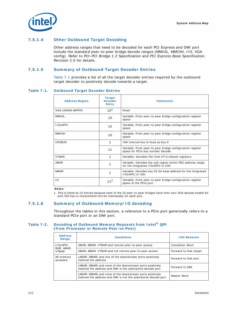
System Address Map
112 Datasheet
7.5.1.4 Other Outbound Target Decoding
Other address ranges that need to be decoded for each PCI Express and DMI port include the standard peer-to-peer bridge decode ranges (MMIOL, MMIOH, I/O, VGA config). Refer to PCI-PCI Bridge 1.2 Specification and PCI Express Base Specification, Revision 2.0 for details.
7.5.1.5 Summary of Outbound Target Decoder Entries
Table 7-1 provides a list of all the target decoder entries required by the outbound target decoder to positively decode towards a target.
7.5.1.6 Summary of Outbound Memory/IO decoding
Throughout the tables in this section, a reference to a PCIe port generically refers to a standard PCIe port or an DMI port.
Table 7-1. Outbound Target Decoder Entries
Address RegionTarget
Decoder Entry
Comments
VGA (A0000-BFFFF) 101
Notes:1. This is listed as 10 entries because each of the 10 peer-to-peer bridges have their own VGA decode enable bit
and IOH has to comprehend this bit individually for each port.
Fixed
MMIOL 10 Variable. From peer-to-peer bridge configuration register space
I/OxAPIC 10 Variable. From peer-to-peer bridge configuration register space
MMIOH 10 Variable. From peer-to-peer bridge configuration register space
CFGBUS 1 IOH internal bus is fixed as bus 0
11 Variable. From peer-to-peer bridge configuration register space for PCIe bus number decode.
VTBAR 1 Variable: Decodes the Intel VT-d chipset registers.
ABAR 1 Variable. Decodes the sub-region within FEC address range for the integrated I/OxAPIC in IOH.
MBAR 1 Variable. Decodes any 32-bit base address for the integrated I/OxAPIC in IOH.
IO 112 Variable. From peer-to-peer bridge configuration register space of the PCIe port.
Table 7-2. Decoding of Outbound Memory Requests from Intel® QPI (from Processor or Remote Peer-to-Peer)
Address Range Conditions IOH Behavior
I/OxAPIC BAR, ABAR, VTBAR
ABAR, MBAR, VTBAR and remote peer-to-peer access Completer Abort
ABAR, MBAR, VTBAR and not remote peer-to-peer access Forward to that target
All memory accesses
(ABAR, MBAR) and one of the downstream ports positively claimed the address Forward to that port
(ABAR, MBAR) and none of the downstream ports positively claimed the address and DMI is the subtractive decode port Forward to DMI
(ABAR, MBAR) and none of the downstream ports positively claimed the address and DMI is not the subtractive decode port Master Abort

Datasheet 113
System Address Map
Table 7-3 details IOH behavior when no target has been positively decoded for an incoming I/O transaction from Intel QPI.
7.5.2 Inbound Address Decoding
This section covers the decoding that is done on any transaction that is received on a PCI Express or DMI port.
7.5.2.1 Overview
• All inbound addresses that fall above the top of Intel QPI physical address limit are flagged as errors by the IOH.
• Inbound decoding towards main memory happens in two steps. The first step involves a ‘coarse decode’ towards main memory using two separate system memory window ranges (0-TOLM, 4 GB-TOHM) that can be setup by software. These ranges are non-overlapping. The second step is the fine source decode towards an individual processor socket using the Intel QPI memory source address decoders.
— A sub-region within one of the two coarse regions can be marked as non-coherent.
— VGA memory address would overlap one of the two main memory ranges and the IOH decodes and forwards these addresses to the VGA device of the system.
• Inbound peer-to-peer decoding also happens in two steps. The first step involves decoding peer-to-peer crossing Intel QPI (remote peer-to-peer) and peer-to-peer not crossing Intel QPI (local peer-to-peer). The second step involves actual target decoding for local peer-to-peer (if transaction targets another device downstream from the IOH) and also involves source decoding using Intel QPI source address decoders for remote peer-to-peer.
— A pair of base/limit registers are provided to positively decode local peer-to-peer transactions. Another pair of base/limit registers are provided that covers the global peer-to-peer address range (that is, peer-to-peer address range of the entire system). Any inbound address that falls outside of the local peer-to-peer address range but that falls within the global peer-to-peer address range is considered as a remote peer-to-peer address.
— Fixed VGA memory addresses (A0000h–BFFFFh) are always peer-to-peer addresses and would reside outside of the global peer-to-peer memory address ranges mentioned above.
— Subtractively decoded inbound addresses are forwarded to the subtractive decode port of the IOH.
Table 7-3. Subtractive Decoding of Outbound I/O Requests from Common SystemInterface
Address Range Conditions IOH Behavior
Any I/O address not positively decoded
No valid target decoded and one of the downstream ports is the subtractive decode port
Forward to downstream subtractive decode port
No valid target decoded and none of the downstream ports is the subtractive decode port Master Abort

System Address Map
114 Datasheet
7.5.2.2 Summary of Inbound Address Decoding
Table 7-4 summarizes the IOH behavior on inbound memory transactions from any PCI Express port. Note that this table is only intended to show the routing of transactions based on the address and is not intended to show the details of several control bits that govern forwarding of memory requests from a given PCI Express port. Refer to the PCI Express Base Specification, Revision 2.0 and Chapter 17 of this document for details of these control bits.
Figure 7-3. Peer-to-Peer Illustration
I O H
L o c a l P e e r-t o - P e e r
P S
P S
P e e r - t o - P e e r I l l u s t r a t i o n
P C I ED 0
P C I ED 1
C P U
Q P I
C P U
Q P I
Q P I

Datasheet 115
System Address Map
Table 7-4. Inbound Memory Address Decoding
Address Range Conditions IOH Behavior
DRAM Address within 0:TOLM or 4 GB:TOHM Forward to Intel QuickPath Interconnect port
InterruptsAddress within FEE00000h–FEEFFFFFh and write Forward to Intel QuickPath
Interconnect port
Address within FEE00000h–FEEFFFFFh and Read Completer Abort
I/OxAPIC, CPUCSR, CPULocalCSR, privileged CSR,INTA/Rsvd, TSeg, Relocated CSeg, On-die ROM, FWH, VTBAR1 (when enabled), Protected VT-d range Low and High, Generic Protected dram range and I/OxAPIC BARs2
Notes:1. Note that VTBAR range would be within the MMIOL range of that IOH. And by that token, VTBAR range can never overlap with
any dram ranges.2. The I/OxAPIC MBAR regions of an IOH overlap with MMIOL/MMIOH ranges of that IOH.
FC00000h–FEDFFFFFh or FEF00000h–FFFFFFFFhTOCM Address TOCM–64 GBVTBARVT-d_Prot_HighVT-d_Prot_LowGeneric_Prot_DRAMI/OxAPIC MBAR
Completer Abort
VGA
Address within 0A0000h–0BFFFFh and main switch SAD is programmed to forward VGA
Forward to Intel QuickPath Interconnect port
Address within 0A0000h–0BFFFFh and main switch SAD is NOT programmed to forward VGA and one of the PCIe has VGAEN bit set
Forward to the PCIe port
Address within 0A0000h–0BFFFFh and main switch SAD is NOT programmed to forward VGA and none of the PCIe has VGAEN bit set and DMI port is the subtractive decoding port
Forward to DMI port
Address within 0A0000h–0BFFFFh and main switch SAD is NOT programmed to forward VGA and none of the PCIe ports have VGAEN bit set and DMI is not the subtractive decode por
In Dual IOH Proxy mode, route to legacy IOH
Other Peer-to-peer
Address within LMMIOL.BASE/LMMIOL.LIMIT or LMMIOH.BASE/LMMIOH.LIMIT and a PCIe port decoded as target
Forward to the PCI Express port
Address within LMMIOL.BASE/LMMIOL.LIMIT or LMMIOH.BASE/LMMIOH.LIMIT and no PCIe port positively decoded as target DMI is the subtractive decoding port
Forward to DMI
Address within LMMIOL.BASE/LMMIOL.LIMIT or LMMIOH.BASE/LMMIOH.LIMIT and no PCIe port decoded as target and DMI is not the subtractive decoding port
Master Abort
Address NOT within LMMIOL.BASE/LMMIOL.LIMIT or LMMIOH.BASE/LIOH.LIMIT, but is within GMMIOL.BASE/GMMIOL.LIMIT or GMMIOH.BASE/GMMIOH.LIMIT
Forward to Intel QuickPath Interconnect
DRAM Memory holes and other non-existent regions
• {4 GB Address TOHM (OR) 0 Address TOLM} AND address does not decode to any socket in Intel QPI source decoder
• Address > TOCM
Master Abort
All ElseForward to subtractive decode port, if enabled using CSRMISCCTRL[1], else Master Abort

System Address Map
116 Datasheet
Table 7-5 summarizes IOH behavior on inbound memory transactions from any PCI Express port.
Table 7-5. Inbound I/O Address Decoding
Address Range Conditions IOH Behavior
Any After disabling Inbound I/O1
Notes:1. Inbound I/O is enabled or disabled using CSRMISCCTRLSTS[30].
Master Abort
VGA
Address within 3B0h-3BBh, 3C0h-3DFh, inbound I/O is enabled and RVGAEN is set
Forward to Intel QuickPath Interconnect
Address within 3B0h-3BBh, 3C0h-3DFh, inbound I/O is enabled and RVGAEN is NOT set and one of the PCIe has VGAEN bit set
Forward to that PCIe port
Address within 3B0h-3BBh, 3C0h-3DFh, inbound I/O is enabled and RVGAEN is NOT set and none of the PCIe has VGAEN bit set but IS within the I/O base/limit range of one of the PCIe ports
Forward to that PCIe port
Address within 3B0h–3BBh, 3C0h–3DFh, inbound I/O is enabled and RVGAEN is NOT set and none of the PCIe has VGAEN bit set and is NOT within the I/O base/limit range of any PCIe ports and DMI port is the subtractive decode port
Forward to DMI port
Address within 03B0h–3BBh, 3C0h–3DFh, inbound I/O is enabled and RVGAEN is NOT set, none of the PCIe has VGAEN bit set and is NOT within base/limit range of any PCIe port, and DMI is not the subtractive decode port
Master abort
Other Peer-to-peer
Address within LIO.BASE/LIO.LIMIT, inbound I/O is enabled and a PCIe port positively decoded as target
Forward to the PCI Express port
Address within LIO.BASE/LIO.LIMIT, inbound I/O is enabled and no PCIe port positively decoded as target and DMI is the subtractive decode port
Forward to DMI
Address within LIO.BASE/LIO.LIMIT, inbound I/O is enabled and no PCIe port decoded as target and DMI is NOT the subtractive decode port
Master Abort
Inbound I/O is enabled and address NOT within LIO.BASE/LIO.LIMIT, inbound I/O is enabled but is within GIO.BASE/GIO.LIMIT
Forward to the Intel QuickPath Interconnect
Non-existent Addresses Address => 64 KB Master Abort
All ElseForward to subtractive decode port, if enabled using CSRMISCCTRL[1], else Master Abort

Datasheet 117
System Address Map
7.6 Intel® V-d Address Map ImplicationsIntel VT-d applies only to inbound memory transactions. Inbound I/O and configuration transactions are not affected by Intel VT-d. Inbound I/O, configuration and message decode and forwarding happens the same whether Intel VT-d is enabled or not. For memory transaction decode, the host address map in Intel VT-d corresponds to the address map discussed earlier in the chapter and all addresses after translation are subject to the same address map rule checking (and error reporting) as in the non Intel VT-d mode. There is not a fixed guest address map that IOH Intel VT-d hardware can rely upon (except that the guest domain addresses cannot go beyond the guest address width specified using the GPA_LIMIT register) that is, it is OS dependent. IOH converts all incoming memory guest addresses to host addresses and then applies the same set of memory address decoding rules as described earlier. In addition to the address map and decoding rules discussed earlier, IOH also supports an additional memory range called the VTBAR range and this range is used to handle accesses to Intel VT-d related chipset registers. Only aligned DWORD/QWORD accesses are allowed to this region. Only outbound and SMBus/JTAG accesses are allowed to this range and also these can only be accesses outbound from Intel QPI. Inbound accesses to this address range are completer aborted by the IOH.
§

System Address Map
118 Datasheet

Datasheet 119
Interrupts
8 Interrupts
The IOH supports both MSI and legacy PCI interrupts from its PCI Express ports. MSI interrupts received from PCI Express are forwarded directly to the processor socket. Legacy interrupt messages received from PCI Express are either converted to MSI interrupts using the integrated I/OxAPIC in the IOH or forwarded to the DMI. When the legacy interrupts are forwarded to DMI, the compatibility bridge either converts the legacy interrupts to MSI writes using its integrated I/OxAPIC or handles them using the legacy 8259 controller. All root port interrupt sources within the IOH (that is, Error and Power management) support MSI mode interrupt delivery. Where noted, these interrupt sources (except the error source) also support the ACPI-based mechanism (using GPE messages) for system driver notification. The IOH does not the support legacy PCI INTx mechanism for internal sources of interrupt. In addition to MSI and ACPI messages, the IOH also supports generation of SMI/NMI interrupts directly from the IOH to the processor (bypassing ICH10), in support of IOH error reporting. For Intel QPI-defined legacy virtual message Virtual Legacy Wires (VLW) signaling, the IOH provides a sideband interface to the legacy bridge and an inband interface on Intel QPI. The IOH logic handles conversion between the two.
8.1 Legacy PCI Interrupt HandlingOn PCI Express, interrupts are represented with either MSI or inbound interrupt messages (Assert_INTx/Deassert_INTx). The integrated I/OxAPIC in the IOH converts the legacy interrupt messages received from PCI Express into MSI interrupts. If the I/OxAPIC is disabled (using the mask bits in the I/OxAPIC table entries), the messages are routed to the legacy ICH10. The subsequent paragraphs describe how the IOH handles the INTx message flow, from its PCI Express ports and internal devices.
The IOH tracks the assert/deassert messages for the four interrupts INTA, INTB, INTC, and INTD from each PCI Express port. Each of these interrupts from each PCI Express root port is routed to a specific I/OxAPIC table entry (see Table 8-2 for the mapping) in that IOH. If the I/OxAPIC entry is masked (using the ‘mask’ bit in the corresponding Redirection Table Entry), then the corresponding PCI Express interrupt(s) is forwarded to the legacy ICH10, provided the ‘Disable PCI INTx Routing to ICH’ bit is clear, Section 17.11.2.21, “QPIPINTRC—Intel® QPI Protocol Interrupt Control Register” .
There is a 1:1 correspondence between message type received from PCI Express and the message type forwarded to the legacy ICH10. For example, if the PCI Express Port 0 INTA message is masked in the integrated I/OxAPIC, it is forwarded to the legacy ICH10 as INTA message (if the ‘Disable Interrupt Routing to ICH’ bit is cleared). The IOH combines legacy interrupts (to be forwarded to the legacy ICH10) from all PCI Express ports and presents a consolidated set of four virtual wire messages. If the I/OxAPIC entry is unmasked, an MSI interrupt message is generated on the Intel QPI.
The IOH does not provide a capability to route inband PCI INTx virtual wire messages to any component other than the legacy ICH.
When a standard downstream PCI Express root port receives an Assert_INTx message, subsequent Assert_INTx messages of the same type (A/B/C/D) will simply keep the virtual wire asserted until the associated Deassert message is received. The first Deassert message received for a given interrupt type will deassert the internal virtual wire of the root port for the interrupt type. Also the internal virtual wire of the root port is de-asserted automatically in hardware if the link goes down when the internal virtual

Interrupts
120 Datasheet
wire is asserted. Deassert messages received for a given interrupt when no corresponding Assert message was received previously for that interrupt, or Deassert messages received when no virtual wire for that interrupt is asserted, will be discarded with no side effect. On an Intel QPI link port, the IOH can receive multiple Assert_INTx messages of the same type before it receives any Deassert_INTx message of that type. In normal operation, it is always ensured that the IOH will receive a Deassert_INTA message for every Assert_INTA message it receives from the Intel QPI.
8.1.1 Summary of PCI Express INTx Message Routing
An IOH is not always ensured to have its DMI port enabled for legacy. When an IOH’s DMI port is disabled, it has to route the INTx messages it receives from its downstream PCI Express ports to its the Intel QPI interface, provided they are not serviced using the integrated I/OxAPIC.
Figure 8-1 illustrates how legacy interrupt messages are routed to the legacy ICH10.
Figure 8-1. Legacy Interrupt Routing Illustration (INTA example)
CPU
csi
IOH
P S
P S
PCIED0
PCIED1
IOAPIC
IOAPIC/8259
MSI write (Converts to Int* on CSI)/INTR pin assertion to
IOH
Legacy IOH Wire-OR’s messages from CSI and its own PCI Express ports and
forwards to ICH
IOAPIC entry unmasked; directly genrerate MSI
Interrupt on CSI
ICH

Datasheet 121
Interrupts
8.1.2 Integrated I/OxAPIC
The integrated I/OxAPIC converts legacy PCI Express interrupt messages into MSI interrupts. The I/OxAPIC appears as a PCI Express endpoint device in the IOH configuration space. The I/OxAPIC provides 24 unique MSI interrupts. This table is programmed using the MBAR memory region or ABAR memory region (Refer to Chapter 17).
In the IOH, there are 49 unique legacy interrupts possible which are mapped to the 24 entries in the I/OxAPIC, as shown in Table 8-2. The distribution is based on ensuring that there is at least one unshared interrupt line (INTA) for each possible source of interrupt. When a legacy interrupt asserts, an MSI interrupt is generated (if the corresponding I/OxAPIC entry is unmasked) based on the information programmed in the corresponding I/OxAPIC table entry.
Table 8-1. Interrupt Sources in I/OxAPIC Table Mapping
Interrupt Source # PCI Express Port/Device INT[A-D] Used / Comment
1 PCIE port 3 A,B,C,D / x16, x8, x4
2 PCIE port 4 A,B,C,D / x4
3 PCIE port 5 A,B,C,D / x8, x4
4 PCIE port 6 A,B,C,D / x4
5 PCIE port 1 A,B,C,D / x4, x2
6 PCIE port 2 A,B,C,D / x2
7 PCIE port 7 A,B,C,D / x16, x8, x4
8 PCIE port 8 A,B,C,D / x4
9 PCIE port 9 A,B,C,D / x8, x4
10 PCIE port 10 A,B,C,D / x4
11
12 CB3 DMA A,B,C,D
13 ME HECI A
14 ME HECI2 D
15 ME IDEr C
16 ME KT B
17 Root Ports/Core A

Interrupts
122 Datasheet
Table 8-2. I/OxAPIC Table Mapping to PCI Express Interrupts1
Notes:1. < >, [ ], and { } associate interrupt from a given device number (as shown in the ‘PCI Express Port) that is
marked thus to the corresponding interrupt wire type (shown in this column) also marked such. For example, I/OxAPIC entry 12 corresponds to the wired-OR of INTD message from source #1 (PCIE port #3), INTC message from source #2 (PCIE port #4), and INTB message from source #3 (PCIE port #5).
I/OxAPIC Table Entry# PCI Express Port PCI Express Virtual Wire Type
0 1 INTA
1 2, <14>. 3 INTA, <INTA>, [INTB]
2 3, <15> INTA, <INTC>
3 4, <16>, {3} INTA, <INTB>, {INTC]
4 5 INTA
5 6, <17>, [3] INTA, <INTA>, [INTD]
6 7 INTA
7 8, <10> INTA, <INTB>
8 9 INTA
9 10 INTA
10 1, <2>, [3] INTB, <INTD>, [INTC]
11 1, <2>, [3] INTC, <INTB>, [INTD]
12 1, <2>, [3] INTD, <INTC>, [INTB]
13 7, <8>, [4] INTB, <INTD>, [INTC]
14 7, <8>, [4] INTD, <INTC>, [INTB]
15 7, <8>, [4] INTC, <INTB>, [INTD]
16 5, <10>, [6], {9} INTB, <INTD>, [INTC], {INTC}
17 5, <10>, [6], {9} INTC, <INTB>, [INTB], {INTD}
18 5, <10>, [6], {9} INTD, <INTC>, [INTD], {INTB}
19 12 INTA
20 12 INTA
21 12, <15>, [17], {10} INTC, <INTC>, [INTA], {INTD}
22 12, <14>, [16], {10} INTD, <INTA>, [INTB], {INTC}
23 13, <5>, [9], {6} INTA, <INTD>, [INTC], {INTB}
Table 8-3. Programmable IOxAPIC Entry Target for Certain Interrupt Sources
Target Table Entries Numbers
Interrupt Source in Table 8-1 INT[A-D] Default Table
Entry (3x8, 3x4)
1, 12 3 INTB 1
3, 10 3 INTC 3
5, 11 3 INTD 5
18, 23 5 INTD 23
17, 23 6 INTB 17
16, 23 9 INTC 23
7, 17 10 INTB 7
18, 22 10 INTC 22
16, 21 10 INTD 21
1, 22 14 INTD 22
2, 21 13 INTA 21
3, 22 16 INTB 22
5, 21 17 INTA 21

Datasheet 123
Interrupts
8.1.2.1 Integrated I/OxAPIC MSI Interrupt Ordering
As with MSI interrupts generated from PCI Express endpoints, MSI interrupts generated from the integrated I/OxAPIC follow the RdC push memory write ordering rule. For example read completions on reads (configuration or memory) to I/OxAPIC registers must push previously posted MSI writes from the I/OxAPIC.
8.1.2.2 Integrated I/OxAPIC EOI Flow
Each I/OxAPIC entry can be setup by software to treat the interrupt inputs as either level or edge triggered. For level triggered interrupts, the I/OxAPIC generates an interrupt when the interrupt input asserts, and stops generating further interrupts until software clears the remote IRR (RIRR) bit in the corresponding redirection table entry with a directed write to the EOI register; or until software generates an EOI message to the I/OxAPIC with the appropriate vector number in the message. When the RIRR bit is cleared, the I/OxAPIC resamples the level interrupt input corresponding to the entry; if it is still asserted, the I/OxAPIC generates a new MSI message.
The EOI message is broadcast to all I/OxAPICs in the system; the integrated I/OxAPIC is also a target for the EOI message. The I/OxAPIC looks at the vector number in the message, and the RIRR bit is cleared in all the I/OxAPIC entries which have a matching vector number.
IOH has capability to NOT broadcast/multicast EOI message to any of the PCI Express/DMI ports/ integrated IOxAPIC and this is controlled using bit 0 in the EOI_CTRL register. When this bit is set, IOH simply drops the EOI message received from QPI and not send it to any south agent. But IOH does send a normal cmp for the message on Intel QPI. This is required in some virtualization usages.
8.1.2.3 Integrated I/OxAPIC Pin Assertion Register (PAR) Writes
I/OxAPIC has a feature where writes to the ‘Pin Assertion Register (PAR)’ in the I/OxAPIC memory space, generates an interrupt. This feature is NOT supported in IOH.
8.1.3 PCI Express INTx Message Ordering
INTx messages on PCI Express are posted transactions and follow the posted ordering rules. For example, if an INTx message is preceded by a memory write A, the INTx message pushes the memory write to a global ordering point before the INTx message is delivered to its destination (which could be the I/OxAPIC, which decides further action). This ensures that any MSI generated from the integrated I/OxAPIC (or from the I/OxAPIC in ICH10, if the integrated I/OxAPIC is disabled) will be ordered behind the memory write A, ensuring producer/consumer sanity.
8.1.4 INTR_Ack/INTR_Ack_Reply Messages
INTR_Ack and INTR_Ack_Reply messages on DMI and IntAck on Intel QPI support legacy 8259-style interrupts required for system boot operations. These messages are routed from the processor socket to the legacy IOH using the IntAck cycle on Intel QPI. The IntAck transaction issued by the processor socket behaves as an I/O Read cycle in that the Completion for the IntAck message contains the Interrupt vector. The IOH converts this cycle to a posted message on the DMI port (no completions).
• IntAck — The IOH forwards the IntAck received on the Intel QPI interface (as an NCS transaction) as a posted INTR_Ack message to the legacy ICH10 over DMI. A completion for IntAck is not sent on Intel QPI just yet.
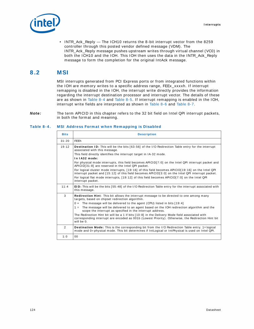
Interrupts
124 Datasheet
• INTR_Ack_Reply — The ICH10 returns the 8-bit interrupt vector from the 8259 controller through this posted vendor defined message (VDM). The INTR_Ack_Reply message pushes upstream writes through virtual channel (VC0) in both the ICH10 and the IOH. This IOH then uses the data in the INTR_Ack_Reply message to form the completion for the original IntAck message.
8.2 MSIMSI interrupts generated from PCI Express ports or from integrated functions within the IOH are memory writes to a specific address range, FEEx_xxxxh. If interrupt remapping is disabled in the IOH, the interrupt write directly provides the information regarding the interrupt destination processor and interrupt vector. The details of these are as shown in Table 8-4 and Table 8-5. If interrupt remapping is enabled in the IOH, interrupt write fields are interpreted as shown in Table 8-6 and Table 8-7.
Note: The term APICID in this chapter refers to the 32 bit field on Intel QPI interrupt packets, in both the format and meaning.
.
Table 8-4. MSI Address Format when Remapping is Disabled
Bits Description
31:20 FEEh
19:12 Destination ID: This will be the bits [63:56] of the I/O Redirection Table entry for the interrupt associated with this message.This field directly identifies the interrupt target in IA-32 mode.In IA32 mode:For physical mode interrupts, this field becomes APICID[7:0] on the Intel QPI interrupt packet and APICID[31:8] are reserved in the Intel QPI packet. For logical cluster mode interrupts, [19:16] of this field becomes APICID[19:16] on the Intel QPI interrupt packet and [15:12] of this field becomes APICID[3:0] on the Intel QPI interrupt packet.For logical flat mode interrupts, [19:12] of this field becomes APICID[7:0] on the Intel QPI interrupt packet.
11:4 EID: This will be the bits [55:48] of the I/O Redirection Table entry for the interrupt associated with this message.
3 Redirection Hint: This bit allows the interrupt message to be directed to one among many targets, based on chipset redirection algorithm.0 = The message will be delivered to the agent (CPU) listed in bits [19:4]1 = The message will be delivered to an agent based on the IOH redirection algorithm and the
scope the interrupt as specified in the interrupt address.The Redirection Hint bit will be a 1 if bits [10:8] in the Delivery Mode field associated with corresponding interrupt are encoded as 001b (Lowest Priority). Otherwise, the Redirection Hint bit will be 0.
2 Destination Mode: This is the corresponding bit from the I/O Redirection Table entry. 1=logical mode and 0=physical mode. This bit determines if IntLogical or IntPhysical is used on Intel QPI.
1:0 00
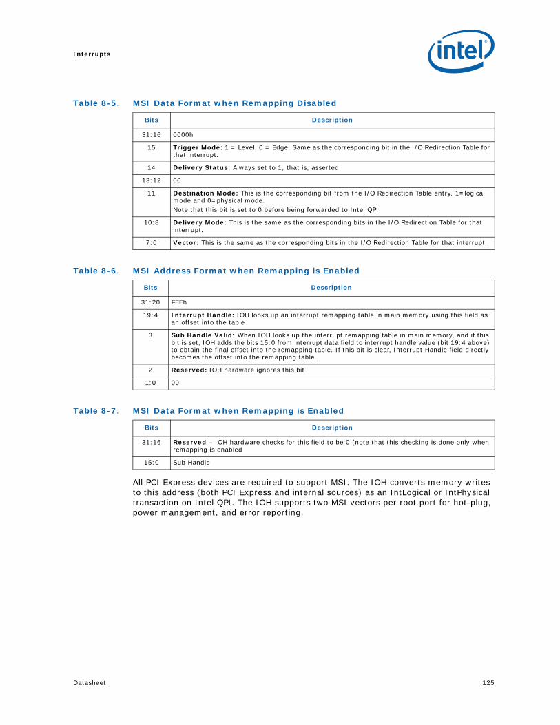
Datasheet 125
Interrupts
All PCI Express devices are required to support MSI. The IOH converts memory writes to this address (both PCI Express and internal sources) as an IntLogical or IntPhysical transaction on Intel QPI. The IOH supports two MSI vectors per root port for hot-plug, power management, and error reporting.
Table 8-5. MSI Data Format when Remapping Disabled
Bits Description
31:16 0000h
15 Trigger Mode: 1 = Level, 0 = Edge. Same as the corresponding bit in the I/O Redirection Table for that interrupt.
14 Delivery Status: Always set to 1, that is, asserted
13:12 00
11 Destination Mode: This is the corresponding bit from the I/O Redirection Table entry. 1=logical mode and 0=physical mode.Note that this bit is set to 0 before being forwarded to Intel QPI.
10:8 Delivery Mode: This is the same as the corresponding bits in the I/O Redirection Table for that interrupt.
7:0 Vector: This is the same as the corresponding bits in the I/O Redirection Table for that interrupt.
Table 8-6. MSI Address Format when Remapping is Enabled
Bits Description
31:20 FEEh
19:4 Interrupt Handle: IOH looks up an interrupt remapping table in main memory using this field as an offset into the table
3 Sub Handle Valid: When IOH looks up the interrupt remapping table in main memory, and if this bit is set, IOH adds the bits 15:0 from interrupt data field to interrupt handle value (bit 19:4 above) to obtain the final offset into the remapping table. If this bit is clear, Interrupt Handle field directly becomes the offset into the remapping table.
2 Reserved: IOH hardware ignores this bit
1:0 00
Table 8-7. MSI Data Format when Remapping is Enabled
Bits Description
31:16 Reserved – IOH hardware checks for this field to be 0 (note that this checking is done only when remapping is enabled
15:0 Sub Handle

Interrupts
126 Datasheet
8.2.1 Interrupt Remapping
Interrupt remapping architecture serves two purposes:
• Provide for interrupt filtering for virtualization/security usages so that an arbitrary device cannot interrupt an arbitrary processor in the system
• Provide for IO devices to target greater than 255 processors as part of extended xAPIC architecture
Software can use interrupt remapping for either or both of the reasons above. When interrupt remapping is enabled in the IOH, IOH looks up a table in main memory to obtain the interrupt target processor and vector number. When the IOH receives an MSI interrupt (where MSI interrupt is any memory write interrupt directly generated by an IO device or generated by an I/OxAPIC like the integrated I/OxAPIC in the IOH/ICH/PXH) and the remapping is turned on, IOH picks up the ‘interrupt handle’ field from the MSI (bits [19:4] of the MSI address) and adds it to the Sub Handle field in the MSI data field if Sub Handle Valid field in MSI address is set, to obtain the final interrupt handle value. The final interrupt handle value is then used as an offset into the table in main memory as:
Memory Offset = Final Interrupt Handle * 16
where Final Interrupt Handle = if (Sub Handle Valid = 1) then {Interrupt Handle + Sub Handle} else Interrupt handle.
The data obtained from the memory lookup is called Interrupt Transformation Table Entry (IRTE) and is as follows.
As can be seen, all the information that used to be obtained directly from the MSI address/data fields are now obtained using the IRTE when remapping is turned on. In addition, the IRTE also provides for a way to authenticate an interrupt using the Requester ID, that is, the IOH needs to compare the Requester ID in the original MSI interrupt packet (that triggered the lookup) with the Requester ID indicated in the IRTE. If it matches, the interrupt is further processed, else the interrupt is dropped and error signaled. Subsequent sections in this chapter describe how the various fields in either the IRTE (when remapping enabled) or MSI address/data (when remapping disabled) are used by the chipset to generate IntPhysical/Logical interrupts on the Intel QPI.

Datasheet 127
Interrupts
The Destination ID shown in the picture above becomes the APICID on the Intel QPI interrupt packet.
Figure 8-2. Interrupt Transformation Table Entry (IRTE)
127
8 8 5 4
8 8 2 1
8 7 0 9
64
63
3 3 2 1
2 2 4 3
1 1 6 5
1 1 2 18 7 5 4 3 2 1 0
SIDSQSVTReserved (0)
PFPDDestination ModeRedirection HintTrigger ModeDelivery ModeAWAILReserved (0)VectorReserved (0)Destination ID

Interrupts
128 Datasheet
8.2.2 MSI Forwarding — IA-32 Processor-based Platform
IA-32 interrupts have two modes – legacy mode and extended mode (selected using bit). Legacy mode has been supported in all Intel chipsets to date. Extended mode is a new mode being introduced in Intel® Core™ i7 processor or the Intel® Xeon® processor 3500 series which allows for scaling beyond 60/255 threads in logical/physical mode operation. Legacy mode has only 8-bit APICID support. Extended mode supports 32-bit APICID (obtained using the IRTE).
Table 8-8 summarizes interrupt delivery for IA-32 processor based platforms. Table 8-9 summarizes how the IOH derives the processor NodeID at which the interrupt is targeted.
8.2.3 External I/OxAPIC Support
I/OxAPICs can also be present in external devices such as the PCI Express-to-PCI-X/PCI bridge (PXH) and ICH10. For example, the PXH has two integrated I/OxAPICs, one per PCI bus, that are used to convert the INTx wire interrupts from PCI slots to local APIC memory writes. These devices require special decoding of a fixed address range FECx_xxxxh in the IOH. The IOH provides these decoding ranges which are outside the normal prefetchable and non-prefetchable windows supported in each root port. Refer to Chapter 7, “System Address Map” for address decoding details.
Table 8-8. Interrupt Delivery
Mode Sub-mode Target APIC NodeID Determined by IOH IOH Behavior
Physical Directed APIC identified in APIC ID:EID fields
NodeID per Table 8-9 Send IntPhysical to selected Intel QuickPath Interconnect NodeIDRedirected APIC identified in APIC
ID:EIDNodeID per Table 8-9
Table 8-9. IA-32 Physical APICID to NodeID Mapping
Size EID1
(MSI Addr 11:4)
Notes:1. These bits must be set to 0 before forwarding to Intel QPI.
APIC ID2
(MSI Addr 19:12)
2. Note that IOH hardware would pass these bits untouched from the interrupt source to Intel QPI.
NodeID[5:0]
1-16S DC abnn300cc4
3. a, b represent the bits that are used to compare against the mask register to identify local versus remoteclusters for interrupt routing. b is optionally included in the mask based on whether 4S clusters or 8S clustersare used for scaleup granularity.
4. cc in the table above refers to the core number in TW and IOH does not do anything with that value.
yyyy5106/<NCNODEID>7
5. yyy is an arbitrary number that is looked up from a table using bits bnn of the APIC ID field. This flexiblemapping is provided for CPU migration and also to prevent software in one partition send interrupts to softwarein another partition.
6. The 10 value in the NodeID field is points to the config agent in the CPU. Note that this value is programmableas well for the table as a whole.
7. When the mask bits match mask register value, the interrupt is considered local and is directed to the socketwith NodeID=yyyy10. Otherwise the interrupt is remote and is routed to the node controller whoseNodeID=NCNODEID, as derived from bits 28:24 of QPIPISAD register.
17-32S DC 0aAbnncc
33-64S DC aaabnncc

Datasheet 129
Interrupts
8.3 Virtual Legacy WiresIn IA-32, IOH can generate VLW messages on Intel QPI. The IOH can generate VLW messages on Intel QPI. The conditions are
• Receiving NMI/SMI#/INTR/INIT#/A20M# signals from the legacy bridge and forwarding to Intel QPI as inband VLW messages. Similarly, the IOH receives the FERR# message from Intel QPI and converts it to a pin output in the legacy IOH.
• Generating SMI/NMI VLW messages for error events the IOH reports directly to the processor.
The rest of this section describes generating VLW messages from the legacy pins only.
The IOH also supports converting the NMI/SMI#/INIT# signals to IntPhysical messages on Intel QPI. Refer to Section 8.4.2 for details. SMI#, NMI and INIT# are treated as edge-sensitive signals and INTR and A20M# are treated as level-sensitive. The IOH generates a message on Intel QPI for SMI#, NMI and INIT# whenever there is an asserting edge on these signals. The IOH creates a message on Intel QPI for INTR and A20M# whenever there is an asserting or a deasserting edge on these signals.
The IOH receives the FERR message from Intel QPI and pulses the FERR# pin output to the legacy ICH10. The IOH ensures that any subsequent transactions to DMI (that is, transactions ordered behind FERR message) are not delivered to DMI till the FERR# pin asserts.
Note: Design should provide as much timing delay as possible between assertion of FERR# pin and delivering subsequent transactions to DMI, to keep the legacy FERR# emulation in Intel QPI platforms, as close as possible to FSB platforms.
All the VLW messages (inbound over Intel QPI) are considered ‘synchronous’. These messages are inserted on Intel QPI ahead of any completions from the DMI port. That is, as soon as the IOH sees an edge on the legacy signals from the IOH and a VLW message is to be scheduled, that VLW message is pushed ahead of any pending completion transactions from the DMI port.
8.4 Platform Interrupts
8.4.1 GPE Events
The IOH generates GPE events for PCI Express Hot-Plug (Assert/Deassert_HPGPE) and PCI Express power management (Assert/Deassert_PMEGPE). PXH components below the IOH could generate Assert/Deassert_GPE messages for PCI-X slot hot-plug events. These GPE events are sent as level-triggered virtual wire messages to the legacy ICH10. Processor generates Intel QPI GPE messages for internal socket events. The Intel QPI GPE events are routed as DO_SCI messages, which are edge triggered, to the legacy ICH10.
The same rules that govern the collection and routing of legacy PCI INTx messages (refer to Section 8.1) through an IOH, also govern the collection and routing of all level-sensitive GPE messages.
Figure 8-3 illustrates how hot-plug and Power Management GPE messages are routed to the legacy ICH10.

Interrupts
130 Datasheet
Figure 8-4 illustrates how GPE messages from the processor are routed to the legacy ICH10. Processors generate GPE for a variety of events. Refer to the appropriate processor specification for details. Since the GPEX messages from the processor are edge-triggered and the DO_SCI message on DMI is also edge-triggered, the IOH transparently converts the Intel QPI GPE message to the DO_SCI message and does not maintain any status bits.
Figure 8-3. Assert/Deassert_(HP, PME) GPE Messages
IO H
C P U
C S I
P S
P S
P C IED 0
P C IED 1
IO A P IC/8 2 5 9
M S I w r i te (C o n v e r ts to In t * o n C S I ) / IN T R p in a s s e r t io n to
IO H
C o n s o l id a te d G P E M e s s a g e (o n e p e r e v e n t
ty p e – H P , P M E
IC H
Figure 8-4. Intel® QPI GPE Messages from Processor and DO_SCI Messages from IOH
I O H
C P U
C S I
P S
P S
P C I ED 0
P C I ED 1
I O A P I C/ 8 2 5 9
M S I w r i t e ( C o n v e r t s t o I n t * o n C S I ) / I N T R p i n a s s e r t i o n t o
I O H
D O _ S C I m e s s a g e ( e d g e ) F o r w a r d e d 1 : 1
I C H
S p c M s g B G P E m e s s a g e ( e d g e f r o m p r o c e s s o r )

Datasheet 131
Interrupts
8.4.2 PMI/SMI/NMI/MCA/INIT
The IOH can directly generate the IntPhysical (PMI/SMI/NMI/MCA) messages on Intel QPI (ICH10 is bypassed) for RAS events such as errors. Also, refer to Section 13.7, “IOH Error Handling Summary” for error event causes of these interrupts. IOH generates an IntPhysical message on Intel QPI for generating these interrupts. Note that the NMI pin input can be controlled to generate either a IntPhysical(NMI) or IntPhysical(MCA) message using the Interrupt Control Register (INTRCTRL). See the Chapter 17, “Configuration Register Space” for details.
Note: Software is responsible for programming the IOH error interrupt registers with the appropriate interrupt address and data when generating any of the interrupts above. Any broadcast requirements (for example, SMI interrupt) is indicated by programming the APICID field of the interrupt address with a value of FFh. The IOH does not make the determination that an interrupt should be broadcasted based on interrupt encoding.
8.4.2.1 INIT#
IOH supports converts the INIT# pin into the corresponding IntPhysical message on Intel QPI. An IntPhysical (INIT) message is sent on Intel QPI whenever there is an asserting edge on INIT signal.
8.4.2.2 Global SMI
Normally, the IOH generates SMI based on some internal event or when it receives an SMI from one of its downstream ports. These SMI events are only sent to the sockets within the specific partition. Global SMI is used during quiescence flows on Intel QPI where the Intel QPI link configuration changes, for quickly bringing the system to a quiesced state. The IOH uses the quiescence broadcast list to send this global SMI.
8.4.2.3 Software Initiated MCA
The IOH provides the capability to programmatically generate an MCA. Software can write to the ‘Trigger MCA’ bit in the MCA Register (MCA) to trigger an MCA to an indicated processor core within the partition.
§

Interrupts
132 Datasheet

Datasheet 133
System Manageability
9 System Manageability
This section combines many different features into one category that aids in platform or system management. Features such as SMBus and JTAG Test Access Port provide the protocol interfaces for access to the configuration registers. These registers are the program interface between the logical feature implementation and the software interface producing or consuming the data. System management uses this data for error diagnosis, system integrity, or work load analysis to optimize the performance of the platform.
Several miscellaneous features that aid in system manageability are presented in this chapter.
9.1 Error Status and LoggingSystem manageability requires that errors and their logs are captured in registers and accessible through the SMBus interface. Error status and logging is defined in Chapter 13. Error counters and a “Stop on Error” feature are provided to support system management functions. An error freeze mechanism, with programmable error severity, is also provided, to halt traffic on the interfaces when an error occurs. Details are described in Section 13.4.3.7.
9.2 Component Stepping InformationComponent stepping information is provided for PCI Express RID assignments. This information is also used in the JTAG ID code field. BIOS can override this value so that old code can execute on a newer stepping of the IOH.
9.3 Intel® Interconnect Built-In Self TestIntel Interconnect Built-In Self Test (Intel IBIST) has features for the IOH’s Intel QPI and PCI Express interfaces. Pattern Generation and checking can be accessed and administered through system management using SMBus, JTAG, and In-Band (using operating system, or BIOS related code). Bus/System margining using Intel IBIST is only available through the JTAG port using an externally enabled third party vendor. Contact them directly for tool availability and features.
9.4 Link Status IndicationEach Intel QPI and PCI Express interface contains status bits to indicate if it is currently active and the frequency of operation (see Table 9-1).

System Manageability
134 Datasheet
9.5 Thermal SensorThe IOH integrates a thermal sensor that allows system management software to monitor and regulate the thermal activity levels in the die.
§
Table 9-1. Status Register Location Table
Interface Register Reference Comments
Intel QPI – Active
Bits [23:16] is for Tx and bits [15:8] is for Rx. These bits indicate which quadrant is active.
Intel QPI – Frequency Indication
Section 17.6.7.19, “CAPTIM—Cap Timer Register”
The register contains the frequency of each port.
PCI Express – Active
Section 17.12.4.19, “LNKSTS—PCI Express Link Status Register”
Bits [9:4] indicates the negotiated width.
PCI Express – Frequency Indication
Section 17.12.4.19, “LNKSTS—PCI Express Link Status Register”
Bits [3:0] will indicate the link speed.

Datasheet 135
Power Management
10 Power Management
IOH power management is compatible with the PCI Bus Power Management Interface Specification, Revision 1.1 (referenced as PCI-PM). It is also compatible with the Advanced Configuration and Power Interface (ACPI) Specification, Revision 2.0b. The IOH is designed to operate seamlessly with operating systems employing these specifications.
Figure 10-1 captures a high level diagram of the basic ACPI System and processor states in working state (G0) and sleeping state (G1) for the IOH and ICH10.
Platforms are expected to incorporate a system management controller, such as the BMC. Numbers of “P”-states cited in Figure 10-1 are examples ONLY. P-states supported by the platform should not be inferred from these examples.
10.1 Supported Processor Power StatesRefer to Table 10-1 for examples. Since no Intel QPI messages are exchanged upon C-state transitions within the processor socket, the IOH is not involved.
Refer to Table 10-2 for further details connected with System (S) states.
Figure 10-1. ACPI Power States in G0 and G1 States for the IOH and ICH10
C States
S0
S1
S4
S5S5
S4
S1
S0
P15P15
P1P1
P0P0
ACPI 2.0
SUSPEND TO DISK
SOFT OFF
IDLE TIME
WAKE EVENT
Processor States
System States
Voltage/Frequency COMBINATIONS
HIGHER POWER
LOWER POWER
POWER-ON SUSPEND

Power Management
136 Datasheet
10.2 Supported System Power StatesThe supported IOH system power states are enumerated in Table 10-1. Note that no device power states are explicitly defined for the IOH. In general, the IOH power state may be directly inferred from the system power state.
The Intel X58 Express Chipset platform supports the S0 (fully active) state since this is required for full operation. The IOH also supports a system level S1 (power-on suspend) state but the S2 is not supported. The IOH supports S3/S4/S5 powered-down idle sleep states. In the S3 state (suspend to RAM), the context is preserved in memory by the OS and the CPU places the memory in self-refresh mode to prevent loss of data. In the S4/S5 states, platform power and clocking are disabled, leaving only one or more auxiliary power domains functional. Exit from the S3, S4, and S5 states requires a full system reset and initialization sequence.
A request to enter the S4/S5 power states are communicated to the IOH by the ICH10 using the “Go_S3” vendor defined message on the DMI interface. In response, the IOH will return an “Ack_S3” vendor defined message to the ICH10. Upon completion of this sequence, the IOH will tolerate the removal of all reference clocks and power sources. A full system initialization and configuration sequence is required upon system exit from the S4/S5 states, as non-AUX internal configuration information is lost throughout the platform. AUX power sources must remain “up.”
10.2.1 Supported Device Power States
The IOH supports all PCI-PMI and PCI Express messaging required to place any subordinate device on any of its PCI Express ports into any of the defined device low power states. Peripherals attached to the PCI segments provided using the ICH10/PXH components may be placed in any of their supported low power states using messaging directed from the IOH through the intervening PCI Express hierarchy.
Any of the standard PCI Express ports and DMI can be placed in D0 or D3hot states by programming the respective PMCSR registers.
Table 10-1. IOH Platform Supported System States
System State Description
S0Full OnNormal operation.
S1
Stop-Grant• No reset or re-enumeration required.• Context preserved in caches and memory.• All processor threads go to the C1 state.• After leaving only one “monarch” thread alive among all threads in all sockets, system
software initiates an I/O write to the SLP_EN bit in the ICH10’s power management control register (PMBase + 04h) and then halts the “monarch”. This will cause the ICH10 to send the GO_C2 DMI message to the IOH. The IOH responds with an ACK_C2 DMI message to the ICH10. (The “monarch” is the thread that executes the S-state entry sequence.)
S3Suspend to RAM (STR) [Supported]CPU and PCI reset. All context can be lost except memory. See text for the IOH sequence. This state is commonly known as “Suspend”. See text for the IOH sequence.
S4
Suspend to Disk (STD) [Supported]CPU, PCI and Memory reset. The S4 state is similar to S3 except that the system context is saved to disk rather that main memory. This state is commonly known as “Hibernate”.The IOH uses the same sequence as S3.
S5Soft off [Supported]Power removed. The IOH supports this mode by following the S3 sequence.

Datasheet 137
Power Management
Directly attached native PCI Express devices are not limited in their available low power states; although, not all available states support the downstream device “wake-up” semantic.
10.2.2 Supported DMI Power States
Transitions to and from the Power Management states shown in Table 10-2 are supported on the DMI Link.
10.3 Device and Slot Power LimitsAll add-in devices must power-on to a state in which they limit their total power dissipation to a default maximum according to their form-factor (10 W for add-in edge-connected cards). When BIOS updates the slot power limit register of the root ports within the IOH, the IOH automatically transmits a Set_Slot_Power_Limit message with corresponding information to the attached device. It is the responsibility of platform BIOS to properly configure the slot power limit registers in the IOH. Failure to do so may result in attached endpoints remaining completely disabled to comply with the default power limitations associated with their form-factors.
10.3.1 DMI Power Management
1. The IOH sends the ACK-Sx for Go-C0, Go-C2, Go-S3 messages.
2. The IOH never sends an ACK-Sx unless it has received a Go-Sx.
10.3.1.1 S0 -> S1 Transition
1. The processor “monarch” thread spins on a barrier
2. The OSPM “monarch” performs the following functions:
— Disables interrupts
— Raises TPR to high
— Sets up the ACPI registers in the ICH
— Sets the fake SLP_EN which triggers a SAL_PMI
— Spins on WAK_STS
3. The SAL PMI handler writes the Sleep Enable (SLP_EN) register in the Legacy Bridge. After this, the last remaining “monarch” thread halts itself.
4. The ICH10 responds to the SLP_EN write by sending the Go_C2 Vendor-Defined message to the IOH.
Table 10-2. System and DMI Link Power States
System State CPU State Description Link State Comments
S0 C0 Fully operational / Opportunistic Link Active-State. L0/L0s Active-State Power
Management
S0 C1 CPU Auto-Halt L0/L0s Active-State Power Management
S1 C2 (S1 same as C1/C2) L0/L0s Active-State Power Management
S3/S4/S5 N/A STR/STD/Off L3 Requires Reset. System context not maintained in S5.

Power Management
138 Datasheet
5. The IOH responds to Go_C2 by multicasting a NcMsgB-PMReq(S1) message to the CPUs.
6. The CPUs respond by acknowledging the NcMsgB-PMReq(S1) message.
7. The IOH responds to the NcMsgB-PMReq(S1)-Ack from the CPUs by sending the Ack_C2 Vendor_Defined message to the Legacy Bridge.
8. The IOH and/or ICH10 may transition the DMI link to L0s autonomously from this sequence when their respective active-state L0s entry timers expire.
10.3.1.2 S1 -> S0 Transition
1. The ICH10 detects a break event, for example, Interrupt, PBE and so on.
2. The ICH10 generates the Go_S0 Vendor_Defined message to the IOH.
3. In response to reception of Go_S0, the IOH multicasts a NcMsgB-PMReq(S0) message to the CPUs.
4. After receiving responses to the NcMsgB-PMReqs, the IOH sends the Ack_C0 Vendor_Defined message to the ICH10.
10.3.1.3 S0 -> S3/S4/S5 Transition
In the S3 sleep state, system context is maintained in memory. In S3-Hot, the power may remain enabled except for the processor cores and Intel QPI (note that the PWRGOOD signal stays active). The IOH/ICH10 DMI link and all standard PCI Express links will transition to L3 Ready prior to power being removed, which then places the link in L3. In S3-Hot, the link will transition to L3 Ready and remain in this state until reset asserts and then de-asserts, since power is not removed. S3/S4/S5 -> S0.
Refer to Figure 10-2 for the general interaction between the IOH and the ICH10 for placing the system in S3.
Figure 10-2. ICH10 Timing Diagram for S3, S4, S5 Transition

Datasheet 139
Power Management
Refer to the Chapter 13, “Reliability, Availability, Serviceability (RAS)” for the normal hard reset sequence that places the system back into S0.
10.4 PCI Express Interface Power Management SupportThe IOH supports the following link states:
• L1 link state
• L3 link state
• MSI or GPE event on power manage events internally generated (on a PCI Express port hot-plug event) or received from PCI Express
• D0 and D3 hot states on a PCI Express port
• Wake from D3hot on a hot-plug event at a PCI Express port
The IOH does not support the following link states:
• ASPM L1 link state
• L1a link state (LA1 is supported on DMI)
• L2 link state (that is, no auxiliary power to the IOH)
• Inband beacon message on PCI Express
10.4.1 Power Management Messages
When the IOH receives PM_PME messages on its PCI Express ports (including any internally generated PM_PME messages on a hot-plug event at a root port), it either propagates it to the ICH10 over the DMI link as an Assert/Deassert_PMEGPE message or generates an MSI interrupt. If ‘Enable ACPI mode for PM’ in the Miscellaneous Control and Status Register (MISCCTRLSTS) is set, GPE messages are used for conveying PM events on PCI Express, else MSI mode is selected.
The rules for GPE messages are the similar to the standard PCI Express rules for Assert_INTx and Deassert_INTx:
• Conceptually, the Assert_PMEGPE and Deassert_PMEGPE message pair constitutes a “virtual wire” conveying the logical state of a PME signal.
• When the logical state of the PME virtual wire changes on a PCI Express port, the IOH communicates this change to the ICH using the appropriate Assert_PMEGPE or Deassert_PMEGPE messages. Note: Duplicate Assert_PMEGPE and Deassert_PMEGPE messages have no affect, but are not errors.
• The IOH tracks the state of the virtual wire on each port independently and present a “collapsed” version (Wire-OR’ed) of the virtual wires to the ICH10.
Note: Refer to Chapter 8, “Interrupts” for details on how these messages are routed to the ICH10 over Intel QPI.

Power Management
140 Datasheet
10.5 Other Power Management Features
10.5.1 Fine-Grained Dynamic Clock Gating
The IOH employs a traditional leaf-level clock-enable to clock-gate re-synthesis scheme.
10.5.2 Coarse Dynamic Clock Gating
Coarse-Grained Dynamic Clock Gating (CGCG) disables (just about) all clocks on the die except for the Management Engine (ME) subsystem. PLLs retain lock. Any non-ME clocks left running are required to detect events which restore clock to the whole die. Transition times in and out of CGCG are on the order of a few core cycles (very fast).
CGCG is engaged when all links are in either L0s, L1, or L1a, in both directions. Normal operation is restored when any link transitions to L0, or the SMBus or JTAG clocks transition.
10.5.3 Core Power Domains
• ME: always “up”
• x16 PCIe link and protocol layers: shut down when fused off for blades or in standby.
• Everything else: shut down in standby.
10.5.4 L1 on PCIe
L1 can also be used to save power during S1. On Intel QuickPath Interconnect, IOH needs to “wake-up-and-train” the link before propagating the S1-exit-to-S0 power-control message.
10.5.5 Static Clock Gating
Turn off clocks to subsystems disabled by fuse, strap, or configuration bit.
§
Datasheet 141
Reset
11 Reset
11.1 IntroductionThis chapter describes IOH-specific aspects of hardware reset. Subsequent I/O initialization procedures requiring configuration register dialogue are not described in this chapter.
11.1.1 Reset Types
• Power-Up ResetPower-up reset is a special case of Power Good reset. It consists of energizing the power rails and involves the assertion of the COREPLLPWRDET signal to the IOH.
• Power Good ResetPower Good reset involves the deassertion of the COREPWRGOOD signal, and is part of Power-up reset. Deassertion of COREPWRGOOD can happen at any time, and is not necessarily associated with Power-up reset. The Power-Good reset spawns Intel QuickPath Interconnect, DMI, PCI Express, SMBus, and JTAG resets. “Surprise” Power-good reset clears the program state, can corrupt memory contents, clears error logs, and so on, and therefore, should only be used as a last resort in extreme lock-up situations.
• Hard ResetHard reset involves the assertion of the CORERST_N signal, and is part of both Power-up and Power-Good reset. Hard reset is the “normal” component reset, with relatively shorter latency than either Power-up or Power-Good, particularly in its preservation of “sticky bits” (for example, error logs and power-on configuration (that is, Intel QuickPath Interconnect link initialization packet “4”s). Hard reset preserves hard partitions, and sets the phase on PLL post-dividers. The hard reset spawns Intel QuickPath Interconnect, DMI, PCI Express, and SMBus resets. “Surprise” hard reset clears the program state, can corrupt memory contents, and so on., and therefore, should only be used as a means to un-hang a system while preserving error logs.
• Intel QuickPath Interconnect PHY Layer Hard and Soft ResetThere are two resets in the Intel QPI PHY layer — hard and soft. Both resets only reset the PHY Layer of the Intel QPI port. There are individual PHY hard and soft resets for each Intel QPI port. PHY layer resets are completely orthogonal to Link layer resets. CSR bits with attribute type “P” and “PP” get reset on hard reset. CSR bits with attribute type “PP” get reset on soft reset. Refer to the Intel QPI Specification for details on the differences and how soft/hard resets are initiated.If an Intel QPI PHY hard or soft reset occurs when the Link Layer is active, the Link Layer will initiate a Link Layer Retry (LLR) to resend any Flits that were dropped during the PHY Layer reset. The Link and higher layer protocols will resume normal operation when the LLR is complete.
• Intel QuickPath Interconnect Link ResetThere are two resets in the Intel QPI Link Layer — hard and soft. Both resets only reset the Link Layer of the Intel QPI port. There are individual link hard and soft resets for each Intel QPI port. Link Layer resets are completely orthogonal to PHY Layer resets (except under special circumstances defined in the Intel QuickPath Interconnect specification section covering Link Layer Initialization). In the event that an Intel QPI Link Layer reset occurs while a protocol layer packet is being

Reset
142 Datasheet
processed by the Link Layer, the Intel QuickPath Interconnect provides no method for the protocol layer to recover. Therefore, in order to avoid data corruption, a Link Layer reset may only be asserted when the Intel QPI port is idle. The difference between the Link Layer hard reset and Link Layer soft reset is the following: 1) Link Layer hard reset is initiated by a write to the Intel QPI specification defined register bit (QPILCL[1]), which takes effect immediately, resulting in link layer re-init which clears all link layer states and resets all CSR bits with attribute type "N"; 2) Link Layer soft reset is initiated by a write to the Intel QPI specification defined register bit (QPILCL[0]), which takes effect after 512 Intel QPI core clock ("16UI") cycles, resulting in link layer re-init, which clears all link layer state and resets all CSR bits with attribute type "NN".
• PCI Express ResetPCI Express reset combines a physical-layer reset and a link-layer reset for a PCI Express port. There are individual PCI Express resets for each PCI Express port. It resets the PCI Express port, for first initialization after power-up, exit from a power-off system-management sleep state, or such as a fault that requires an individual reset to un-hang a particular PCI Express port.
• JTAG ResetJTAG reset resets only the JTAG port. JTAG reset does not reset any state that is observable through any other interface into the component (for example, CSRs, and so on).
• SMBus ResetSMBus Reset resets only the slave SMBus controller. SMBus reset does not reset any state that is observable through any other interface into the component (for example, CSRs, and so on).
• Intel TXT ResetIntel TXT reset is a mechanism that stops the platform due to a security violation. It is a trigger for a HARD reset.
• CPU Warm ResetA CPU can reset the CPUs and only the CPUs by setting the IOH.SYRE.CPURESET bit. System validation uses this feature to quickly initiate tests, averting the aeons of test time required to navigate through an entire HARD reset. Setting the IOH.SYRE.CPURESET has no effect after TXT.SENTER or while TXT.SENTER.STS is set.
11.1.2 Reset Triggers
Possible triggers for reset:
• Energize power supplies
• COREPWRGOOD deassertion
• CORERST_N assertion with IOH.SYRE.RSTMSK = 0
• IOH.QPILCL[0]
• Loss of Received Clock
• Receipt of Link Initialization Packet
• IOH.BCR.SRESETBCR is a standard PCI Express control register
• TRST_N assertion or TCK/TMS protocol
• SMBus protocol
• IOH.SYRE.CPURESET

Datasheet 143
Reset
11.1.3 Trigger and Reset Type Association
Table 11-1 indicates Reset Triggers initiate each Reset Type.
Note: Auxiliary power-up, power good, or Hard reset without an equivalent core reset is not allowed.
11.1.4 Domain Behavior
This is how each of the domains is treated during reset:
• Unaffected by reset:
— PLLs
• Indirectly affected by reset:
— Strap flip-flops:Hold last value sampled before COREPWRGOOD assertion
— Analog I/O compensation:Only triggered by link power-up
• JTAG:
— Asynchronous COREPWRGOOD deassertion, COREPWRGOOD deasserted, asynchronous TRST_N assertion, TRST_N asserted, or synchronous TCK/TMS protocol navigation to reset state: reset.
• SMBus:
— Asynchronous COREPWRGOOD deassertion, COREPWRGOOD deasserted, hard reset assertion, or synchronous SMBus reset protocol: reset.
— Signals are deasserted after hard reset assertion, signals are observable after hard reset deassertion
• Sticky configuration bits:Per port, Intel QPI Link layer bits except QPILCL.1 are sticky when the QPILCL.1 configuration bit is set.Per port, Intel QPI Physical-layer bits except QPIPHCL.1 are sticky with the QPIPHCL.1 configuration bit is set.
— Asynchronous COREPWRGOOD deassertion, COREPWRGOOD deasserted: defaults.
— (synchronized CORERST_N assertion or synchronized CORERST_N asserted) while COREPWRGOOD asserted: no-change.
Table 11-1. Trigger and Reset Type Association
Reset Trigger Reset Type
Energize Power Supplies Power-Up
COREPWRGOOD signal deassertion Power Good
CORERST_N assertion & IOH.SYRE.HARDEN Hard
IOH.QPILCL[0] (Link Layer Hard Reset)Link Intel QPI
Receipt of Link Initialization Packet
IOH.BCR.SRESET PCI Express
TRST_N assertionJTAG
TCK/TMS protocol
SMBus protocol SMBus

Reset
144 Datasheet
• Tri-state-able outputs:
— Asynchronous COREPWRGOOD deassertion, COREPWRGOOD deasserted: tri-state.Place outputs in tri-state or electrical-disable when COREPWRGOOD is deasserted.
• PCI Express:
— Asynchronous COREPWRGOOD deassertion, COREPWRGOOD deasserted: Electrical idle and reset
— COREPWRGOOD asserted, one cycle after synchronized CORERST_N assertion, BCR.SRESET set: link down (one per port)
— CORERST_N deassertion, BCR.SRESET cleared: initialize, train, link up
• Intel QuickPath Interconnect:
— See Section 11.1.6.
• DMI
— Asynchronous COREPWRGOOD deassertion, COREPWRGOOD deasserted: tri-state and reset.
— COREPWRGOOD asserted, one cycle after synchronized CORERST_N assertion: link down
— CORERST_N deassertion: initialize, train, link up
— Processor CORERST_N cycle counter extinguished: send DMI.CPU_Reset_Done
11.1.5 Reset Sequences
Reset sequences are specified by a lexical “grammar”:
• “Trigger = trigger_list:”: one or more items from Section 11.1.2, “Reset Triggers” .
• “{A, B,...}”: Logically “OR”-ed list
• Following the trigger list:“Synchronous” indicates synchronous edge-sensitive trigger synchronized to a clock.“Synchronized” indicates asynchronous edge-sensitive trigger synchronized to a clock.“Asynchronous” indicates level-sensitive trigger asynchronous to any clock.
• “Condition” indicates trigger qualifier.Condition must be valid for trigger to be recognized.
A bulleted list of “actions” follow the trigger and condition specifications:
• “->” within bullet: sequential execution.
11.1.5.1 Power-Up
Trigger = energize power supplies and stabilize master clock inputs with COREPWRGOOD deasserted ->
• -> Toggle clock trees.

Datasheet 145
Reset
11.1.5.2 COREPWRGOOD Deasserted
Trigger = COREPWRGOOD deassertion: asynchronous ->.
Condition = Power and master clocks remain stable.
• -> Tri-state other I/O.
• -> Toggle PLL outputs.
• -> Reset I/O Ports.
11.1.5.3 COREPLLPWRDET Assertion
Trigger = COREPLLPWRDET assertion: asynchronous ->• -> PLLs acquire lock ->.
• -> PCI Express, DMI, and Intel QPI interfaces complete calibration.Calibration is initiated as soon as internal clocks are stable.
11.1.5.4 COREPWRGOOD Assertion
Trigger = COREPWRGOOD assertion: synchronized ->.
Condition = Voltages are within specifications. Master clocks are stable. The TCK signal may be in any state.
• -> Sample straps.
• -> Un-tri-state I/O.
• -> Hold Intel QPI, PCI Express, DMI links down.
11.1.5.5 Hard Reset Asserted
Trigger = CORERST_N assertion: synchronized ->.
Condition = COREPWRGOOD is asserted.
Consequence = All buffered writes may be dropped.
• -> Protect sticky configuration bits.
• -> Synchronously assert internal asynchronous flip-flop initialization inputs.
• -> Private JTAG chains may be reset.
• -> Reset Intel QPI, PCI Express and DMI protocol -> Take PCI Express and DMI links down.
11.1.5.6 Hard Reset Deassertion
Trigger = CORERST_N deassertion: synchronized ->.
Condition = COREPWRGOOD is asserted.
Consequence = Inputs from buses tri-stated during reset are masked until it is ensured that bus values are electrically and logically valid.
• -> Allow normal operation of sticky configuration bits.
• -> Initialize Intel QPI, PCI Express and are links -> Engage Intel QPI, PCI Express and are link training -> Bring Intel QPI, PCI Express and DMI links up.

Reset
146 Datasheet
11.1.5.7 IOH PCI Express Reset Asserted
Trigger = BCR.SRESET set: synchronous ->.
• -> Initialize PCI Express protocol -> Take PCI Express link down.
11.1.5.8 IOH PCI Express Reset Deasserted
Trigger = BCR.SRESET cleared: synchronous ->
• -> Initialize PCI Express link -> Engage PCI Express link training -> Bring PCI Express link up.
11.1.5.9 Intel® QuickPath Interconnect Soft Reset Deassertion
Trigger = {Regain Received Clock}: synchronous ->.
• ->Take Intel QPI channel to QPI.Detect (see Section 11.1.6.1).
11.1.5.10 Intel® QuickPath Interconnect Link Reset Assertion
Triggers = {IOH.QPILCL[0] (Link Layer Hard Reset) set to ‘1’; Receive Link Training Packet}: synchronous ->
->Take Intel QPI link to link initialization
11.1.5.11 Intel® QuickPath Interconnect Link Reset De-Assertion
There are no persistent Intel QPI Link Reset sources. The Intel QPI Link Reset proceeds through link initialization to full Intel QPI protocol operation upon detection of Intel QPI Link Reset Assertion.
11.1.5.12 JTAG Reset Assertion
Triggers ={TRST_N assertion: asynchronous; TMS asserted for five TCK rising edges: synchronous}->.
• -> Initialize JTAG.
11.1.5.13 JTAG Reset Deassertion
Trigger = TRST_N deassertion: asynchronous ->.
• -> Release JTAG port and to operate normally.
11.1.5.14 CLINK Reset Assertion
Triggers =CLRST_N assertion: asynchronous ->• -> Initialize CLINK port.
11.1.5.15 CLINK Reset De-Assertion
Trigger = CLRST_N de-assertion: asynchronous ->
• -> Release CLINK port and to operate normally.

Datasheet 147
Reset
11.1.6 Intel® QuickPath Interconnect Reset
The Link Training and Status State Machine (LTSSM) as well as any self test, BIST, or loopback functions in the Intel QPI link must be built around and compatible with the IOH’s reset protocols, which includes core logic, power supply sequencing, and the calibration of other analog circuits such as PCI Express I/O, DMI I/O, and PLLs. Platform determinism is enforced at the CPU socket.
11.1.6.1 Inband Reset
An inband reset mechanism is used for Intel QPI Soft Reset. The inband reset is initiated by stopping a Forwarded Clock, and detected by observing the absence of an expected Received Clock transition, ultimately resulting in a link failure.
An inband reset is not a power-up link reset. An inband reset is only defined for a link that is up and running. Loss of Forwarded Clock prior to the completion of the first detect state after power-up will not result in an inband reset.
Figure 11-1. Physical Layer Power-Up and Initialization Sequence
idle detectfwd.clock
bitlock
lanedeskew
parameterexchange
link widthnegotiation
set flitboundary
snd/rcvidle flitscalibrate idle
Po
we
r-o
n
Lin
kC
loc
kS
tab
leso
gn
al
RE
SE
T#
de
-ass
ert
ion
Ph
yIn
itC
om
ple
tes
ign
al
Ha
nd
Ov
er
To
Lin
kL
ay
er
1 2 3 4 5 6 7 8
9
T6 T52 T53 T54 T55 T56 T57 T58 T59 T60 T61
Disable/Start Detect Polling Config InitializationState
ApproximateInitialization
Time
7.0125 usminimum
1. Calibrate analog circuitry.2. Detect the presence of an active CSI port or a 50 ohm passive test probe at the other end of the link.3. Activate forwarded clock lane and lock to received clock (when an active CSI port is detected).4. Establish bit lock to align received clock to center of the data eye, on a per-lane basis.5. Perform lane deskew to match delay across all lanes.6. Exchange Physical Layer parameters.7. Negotiated an acceptable Link width in each direction.8. Establish flit boundary.9. Signal to the Link Layer that a configured Link is established.
1.070125 msminimum
Warm Reset
10
10. Transfer of first link-layer packet.
Power-on Reset

Reset
148 Datasheet
Figure 11-2. Inband Reset Sequence Initiated by Port A to Port B
Table 11-2. Intel QPI Inband Reset Events (Sheet 1 of 2)
Port A Port B
A1: Port A is in a clock-active state (a state other than Disable/Active or Detect.1). Forwarded Clock is currently being transmitted and/or Received Clock is being received.
B1: Port B is in a state other than Disable/Active or Detect.1. Forwarded Clock is currently being transmitted and/or Received Clock is being received.
A2: Port A sends an Inband Reset to Port B by stopping forwarded clock. Simultaneously, Port A stops driving data lanes as well, but Port A receivers continue to observe Received Clock and accepts incoming data.
B2: Port B is still in a clock-active state as Inband Reset is in flight. Port B continues to send forwarded clock (and data) to Port A.
A3: This is the same as event A2, as Port A continues to observe Received Clock.
B3: Port B interprets loss of Received Clock as an Inband Reset. Port B immediately stops driving Forwarded Clock and data lanes. Port B enters the Disable/Start state.
A4: Port A loses Received Clock from Port B. Port A interprets this as an acknowledgement to the Inband reset that it initiated in event A2. Port A enters the Disable/Start state.
B4: If Calibration is bypassed, Port B allows a minimum period of TINBAND_RESET_INIT to elapse after event B3 before asserting the PhyInitBegin signal, which advances Port B to the Detect.1 state.If Calibration is forced, Port B allows the minimum period of TINBAND_RESET_INIT to elapse after completion of calibration after event B3 before asserting the PhyInitBegin signal and advancing to the Detect.1 state.Upon entering the Detect.1 state, Port B commences the process of detecting Port A.The TINBAND_RESET_INIT parameter is defined to be much longer than the time of flight, so Port A is ensured to be in the Disable/Start state by the time Port B advances to the Detect.1 state. This time-out avoids any false detection of Port A (by Port B) when Inband Reset is in flight.
(Clock ActiveState)
(Clock ActiveState)
(Clock ActiveState)
(Disable/StartState)
(Detect State)
(Clock ActiveState)
(Clock ActiveState)
(Disable/StartState)
(Detect State)
(Detect State)
A1
A2
A3
A4
A5
B1
B2
B3
B4
B5
Forwarded Clock
Stop Forwarded Clock
Forwarded Clock
Forwarded Clock
Stop Forwarded Clock
Ear liest A detects B
Earliest B detects A
Port A Port B

Datasheet 149
Reset
11.2 Platform Signal Routing Diagram
A5: If Calibration is bypassed, Port A allows a minimum period of TINBAND_RESET_INIT to elapse after event A4 before asserting the PhyInitBegin signal, which advances Port A to the Detect.1 state.If Calibration is forced, Port A allows the minimum period of TINBAND_RESET_INIT to elapse after completion of calibration after event A4 before asserting the PhyInitBegin signal and advancing to the Detect.1 state.Upon entering the Detect.1 state, Port A commences the process of detecting Port B, and resumes driving Forwarded Clock after Port B is detected.
B5: This is the earliest event in which Port B can detect Port A. When Port B detects Port A, Port B resumes driving Forwarded Clock.
Figure 11-3. Basic Power Good Distribution
Figure 11-4. Basic System Reset Distribution
Table 11-2. Intel QPI Inband Reset Events (Sheet 2 of 2)
Port A Port B
Processor
ICH10
Power Good
Logic
PWRGOODPWRGOOD
PWROK
Other Resets
IOH
IOH
ICH10
RST_N
PLTRST#
Processor
RESET#
Processor
RESET#
RS
T_N
RESETO_N
RESETO_N

Reset
150 Datasheet
11.3 Platform Timing DiagramsThe following diagrams represent the platform reset timing sequence.
Figure 11-5. Power-Up
Initi
aliz
atio
n
Initi
aliz
atio
n
Ful
l Ope
ratio
n
IOH
PW
RG
OO
D
Inte
rna
l IO
H
Ev
ents
CS
ICL
K
ICH
PL
TR
ST
#
IOH
CS
I
Pro
ces
sor/
IOH
RS
T_
N
IOH
PL
L
IOH
inte
rnal
ly
syn
ch
ron
ized
RS
T_
N
Ful
l op
erat
ion
T10
T13
T12
DM
I han
dsh
ake
done
PC
I-E
xp
res
sD
MI
Ana
log
calib
ratio
n co
mpl
etedT1
Po
we
r R
ails
T15
Str
aps
inac
tive
T8
T17
IOH
PL
LP
WR
DE
T
ICH
PW
RO
K
PL
L’s
lock
ed
T52
Ca
libra
te
T53
Str
aps
sam
pled
IOH
Rin
g O
scill
ato
r
T4
IOH
Lin
k P
LL
’s
T6

Datasheet 151
Reset
Figure 11-6. PWRGOOD Reset
Initi
aliz
atio
n
Initi
aliz
atio
n
Fu
ll O
pera
tion
IOH
PW
RG
OO
D
Inte
rna
l IO
H
Ev
ents
CS
ICL
K
ICH
PL
TR
ST
#
IOH
CS
I
Pro
ces
sor/
IOH
RS
T_
N
IOH
Co
re P
LL
IOH
inte
rnal
ly
syn
ch
ron
ized
RS
T_
N
Ful
l op
era
tion
T10
T13
T12
DM
I han
dsh
ake
do
ne
PC
I-E
xp
res
sD
MI
T3
T15
Str
aps
ina
ctiv
eT
17S
trap
s sa
mp
led
Str
aps
st
able
T
2
Sti
cky
Bit
sde
faul
t
T8
T4
IOH
CS
I P
LL
’s
T6

Reset
152 Datasheet
Figure 11-7. Hard Reset
Initi
aliz
atio
nFu
ll O
pera
tion
inte
rnal
Eve
nts
CSI
CLK
ich
PLTR
ST#
CSI
CO
RER
ST_N
Cor
e PL
L
inte
rnal
ly s
ynch
roni
zed
RST
_N
Arra
y In
it D
one
T14
T13
T12
PCI-E
xpre
ss DM
I
T15
T17
Stic
ky B
it En
able
SYR
E.SA
VCFG
ioh
CSI
PLL
’s
Initi
aliz
atio
nFu
ll op
era
DM
I han
dsha
ke
done
RES
ETO
_NT7

Datasheet 153
Reset
Table 11-3 specifies the timings drawn in Figure 11-5, Figure 11-6, Figure 11-7, and Figure 11-8. Nominal clock frequencies are described. Specifications still hold for de-rated clock frequencies.
Figure 11-8. IOH CORERST_N Re-Triggering Limitations
RST_N
IncompleteInitialization
Complete Initialization
T16
T5T10
Table 11-3. Core Power-Up, Core POWERGOOD, and Core Hard Reset Platform Timings (Sheet 1 of 2)
Timing Description Min Max Comments
T1
COREPLLPWRDET signal assertion to COREPWRGOOD signal assertion 100 us 15 ms
Min/Max timing applies to PLLPWRDET signal assertion to AUXPWRGOOD signal assertion when ME AUX power uses separate power source.
T2 COREPWRGOOD de-assertion to straps stable 40 ns
T3COREPWRGOOD de-assertion
80 nsMinimum COREPWRGOOD de-assertion time while power and platform clocks are stable.
T4 COREPWRGOOD assertion to straps sampled 0 ns
T5 CORERST_N de-assertion to CORERST_N assertion 50 QPICLKs Minimum CORERST_N re-trigger time.
T6
PLLPWRDET assertion or CORERST_N assertion or stable strap on COREPWRGOOD de-assertion to PLL lock acquisition
960 ns
COREPWRGOOD de-assertion only requires Intel QPI PLL lock re-acquisition because their frequency is determined by a strap. CORERST_N assertion only requires Intel QPI PLL lock re-acquisition when the FREQ register changed.
T7 RESETO_N duration N/A
T8 CORERST_N de-assertion to straps inactive 12 ns 18 ns Strap Hold Time
T9Reference clock stable to PLLPWRDET signal assertion 100 ns
Min/Max timing applies to PLLPWRDET when ME AUX power uses separate power source.
T10 COREPWRGOOD assertion to CORERST_N de-assertion 1 ms During Core Power Cycling
T12
CORERST_N signal de-assertion to completion of PCI Express initialization sequence
12.5 ms
T14 CORERST_N assertion to CORERST_N de-assertion 2.1 us
T15CORERST_N signal de-assertion to completion of reset sequence
100 usICH specification
T16 CORERST_N re-trigger delay T5+T10
T17 SMBus delays w/r/t CORERST_N 3 QPICLKs

Reset
154 Datasheet
§
T52 Intel QPI Calibration 1 ms
T53 Intel QPI Idle between Calibration and Detect N/A Waiting for CORERST_N de-assertion
T54 Intel QPI Detect 20ns Min = processor is ready before IOH
T55 Intel QPI Activate Forwarded Clock 3.9 us
T56 Intel QPI bit lock 1.25 us
T57 Intel QPI bit-lane deskew 98 ns
T58 Intel QPI physical parameter exchange 98 ns
T59 Intel QPI link width negotiation 98 ns
T60 Intel QPI set flit boundary 10 ns
T61
Intel QPI wait for link initialization stall to clear 150 ms
Min = all stall conditions cleared. Starts at de-assertion of CORERST_N. Quote from TWD was 15us, allowing 10,000x guardband for S/W delays.
Table 11-3. Core Power-Up, Core POWERGOOD, and Core Hard Reset Platform Timings (Sheet 2 of 2)
Timing Description Min Max Comments

Datasheet 155
Component Clocking
12 Component Clocking
12.1 Component Specification
12.1.1 Reference Clocks
The QPI{0}CLK reference clock is the core PLL reference clock, operating at 133 MHz; the reference clock frequency is common between all Intel QuickPath Interconnect agents. This mesochronous reference clock requires no phase matching between agents, tolerating zero ppm frequency offset between agents.
The PE{0}CLK is the reference clock supplied to the IOH for PCI Express and interfaces, and operates at 100 MHz.
The Intel QuickPath Interconnect interface’s phit frequency domain is derived from the QPI{0}CLK reference clocks.
When QPIxCLK spectrum spreading is disabled, the PCI Express links can operate mesochronously (zero ppm frequency tolerance between PCI Express agents) or plesiochronously (a few hundred ppm frequency tolerance between PCI Express agents) while the PExCLK and QPIxCLK domains operate mesochronously.
When QPIxCLK spectrum spreading is enabled, a PCI Express link operating plesiochronously (because both ends’ master clocks are derived from the different oscillators) prevents ratioed PExCLK:QPIxCLK domains, necessitating “asynchronous” data transfer between domains.
Asynchronous PExCLK reference clocks may be derived from different oscillators.
12.1.2 JTAG
The JTAG clock, TCK, is asynchronous to core clock. For private TAP register accesses, one TCK cycle is a minimum of 12 core cycles. The TCK high time is a minimum of 6 core cycles in duration. The TCK low time is a minimum of 6 core cycles in duration.
For public TAP register accesses, TCK operates independently of the core clock.
12.1.3 CLINK Bus
The CLINK reference clock frequency is 66 MHz, which is available during standby.
12.1.4 Management Engine Clock
The management engine (ME) can handle a reference clock frequency of 133 MHz or 100 MHz which must be provided for ME operation. The ME's 200 MHz DDRCLK[P/N] clock output is derived from this reference clock. For a non-ME configuration, it is optional to omit the reference clock to the ME with certain restrictions.

Component Clocking
156 Datasheet
12.1.5 Clock Pin Descriptions
Table 12-1. The Clock Options for a non-ME Configuration System
Reference Clock Source
No ME System Notes
133 MHz Support DDRFREQ[3:2] tied to 00
100 MHz Support DDRFREQ[3:2] tied to 01
No CLK Support ME_CLK_SRC must be tied to 0 if no reference clock is provided — allowed for non-ME configurations only.
Table 13-1. Clock Pins
Pin Name Pin Descriptions
QPI0REFCLKP Intel QuickPath Interconnect 0-interface reference clock
QPI0REFCLKN Intel QuickPath Interconnect 0-interface reference clock (complement)
QPI0TPCLK[0] Intel QuickPath Interconnect 0 Transmitter forwarded clock 0
QPI0TPCLK[1] Intel QuickPath Interconnect 0 Transmitter forwarded clock 1
QPI0TNCLK[0] Intel QuickPath Interconnect 0 Transmitter forwarded clock 0 (complement)
QPI0TPCLK[1] Intel QuickPath Interconnect 0 Transmitter forwarded clock 1 (complement)
QPI0RPCLK[0] Intel QuickPath Interconnect 0 Receiver forwarded clock 0
QPI0RPCLK[1] Intel QuickPath Interconnect 0 Receiver forwarded clock 1
QPI0RNCLK[0] Intel QuickPath Interconnect 0 Receiver forwarded clock 0 (complement)
QPI0RPCLK[1] Intel QuickPath Interconnect 0 Receiver forwarded clock 1 (complement)
PE0CLKP PCI Express 0-interface clock
PE0CLKN PCI Express 0-interface clock (complement)
PE1CLKP PCI Express 1-interface clock
PE1CLKN PCI Express 1-interface clock (complement)
XDPSTBP_N Debug Port strobe
XDPSTBN_N Debug Port strobe (complement)
XDPCLK1X 1X XDP clock
TCK TAP clock
PEHPSCL PCI Express hot-plug Virtual Pin Interface clock
SMBSCL SMBus clock
DDR_REFCLK_P Management Engine clock
DDR_REFCLK_N Management Engine clock (complement)
CLCLK CLINK clock
RMII_CLK RMII clock
DDRCLK_P DDR clock
DDRCLK_N DDR clock (complement)
DDRCKE DDR clock enable
DDREDQS DDR data strobe
DDREDQS_N DDR data strobe (complement)

Datasheet 157
Component Clocking
12.1.6 High Frequency Clocking Support
12.1.6.1 Spread Spectrum Support
The IOH supports Spread Spectrum Clocking (SSC). SSC is a frequency modulation technique for EMI reduction. Instead of maintaining a constant frequency, SSC modulates the clock frequency/period along a predetermined path, that is, the modulation profile.The IOH supports a nominal modulation frequency of 30 KHz with a downspread of 0.5%.
12.1.6.2 Stop Clock
PLLs in the IOH cannot be stopped.
12.1.6.3 Jitter
Intel QuickPath Interconnect strongly recommends that QPIxCLK cycle-to-cycle jitter delivered to the package ball should be less than or equal to 50 ps (±25 ps).
PExCLK jitter must be less than 150 ps (±75 ps).
12.1.6.4 Forwarded Clocks
“Forwarded clocks” are not clocks in the normal sense. Instead, they act as constantly-toggling bit-lanes which supply UI phase information to all associated bit-lane receivers in the channel removing the phase error between the transmitter and receiver due to long-term jitter. The Intel QuickPath Interconnect clocks utilize low-speed (133 MHz) reference clocks for the primary input of their I/O PLLs.
12.1.6.5 External Reference
An external crystal oscillator is the preferred source for the PLL reference clock. A spread spectrum frequency synthesizer that meets the jitter input requirements is recommended.
12.1.6.6 PLL Lock Time
The assertion of the PWRGOOD signal initiates the PLL lock process.
12.1.6.7 Analog Power Supply Pins
Each PLL requires an Analog Vcc and Analog Vss pad and external LC filter. The filter is NOT to be connected to the system board Vss. The ground connection of the filter is grounded to on-die Vss.
§

Component Clocking
158 Datasheet

Datasheet 159
Reliability, Availability, Serviceability (RAS)
13 Reliability, Availability, Serviceability (RAS)
13.1 RAS OverviewThis chapter describes the features provided by the IOH for the development of high Reliability, Availability, Serviceability (RAS) systems. RAS refers to three main features associated with system robustness. These features are summarized as follow:
Reliability — Refers to how often errors occur in the system, and whether the system can recover from an error condition.
Availability — Refers to how flexible the system resources can be allocated or redistributed for the system utilizations and system recovery from errors.
Serviceability — Refers to how well the system reports and handles events related to errors, power management, and hot-plug.
The IOH platform RAS features aim to achieve the following:
• Soft, uncorrectable error detection and recovery on PCI Express and Intel QuickPath Interconnect links.
— CRC is used for error detection and error recovered by packet retry.
• Clearly identify non-fatal errors whenever possible and minimize/eliminate fatal errors.
— Synchronous error reporting of the affected transactions by the appropriate completion responses or data poisoning.
— Asynchronous error reporting for non-fatal and fatal errors using inband messages or outband signals.
— Enable software to contain and recover from errors.
— Error logging/reporting to quickly identify failures, contain and recover from errors.
• PCI Express hot plug (add/remove) to provide better serviceability
The IOH RAS features can be categorized into five categories. These features are summarized below and detailed in the subsequent sections:
1. System level RAS
— Platform or system level RAS for inband and outband system management features.
— Dynamic partitioning and on-line hot add/remove for serviceability.
— Memory mirroring and sparing for memory protection.
2. IOH RAS
— IOH RAS features for error protection, logging, detection, and reporting.
3. Intel QuickPath Interconnect RAS
— Standard Intel QuickPath Interconnect RAS features as specified in the Intel QuickPath Interconnect specification.

Reliability, Availability, Serviceability (RAS)
160 Datasheet
4. PCI Express RAS
— Standard PCI Express RAS features as specified in the PCI Express base specification.
5. Hot Plug (Add/Remove)
— PCI Express hot Plug (add/remove) support.
13.2 System Level RASSystem level RAS features include the following:
1. Inband system management by processor in CM/SMM mode.
2. Outband system management from SMBus by Baseboard Management Controller (BMC).
3. On-Line dynamic hard partitioning.
4. System-Level Debug features.
13.2.1 Inband System Management
Inband system management is accomplished by firmware running in high privileged mode. In the event of an error, fault, or hot add/remove, firmware is required to determine the system’s condition and service the event accordingly. Firmware may enter mode for these events, so that it has the privilege to access the OS invisible configuration registers.
13.2.2 Outband System Management
Outband system management relies on the out-of-band agents to access system configuration registers using outband signals. The outband signals (such as, SMBus and JTAG) are assumed to be secured and have the right to access all CSRs within a component. This includes the QPICFG and PCICFG configuration registers; however, SMBus/JTAG accesses outside of QPICFG or PCICFG space are not permitted.
Both SMBus and JTAG are connected globally to the CPU, IOH, and ICH10 – through a shared bus hierarchy for SMBus, or through a serial bit chain for JTAG. By using the outband signals, an outband agent is able to handle events such as hot-plug, partitioning, or error recovery. Outband signals provide the BMC a global path to access the CSRs in the system components, even when the CSRs become inaccessible to processor through the inband mechanisms. Externally, the SMBus is mastered by the BMC and JTAG is controlled by a platform specific mechanism.
To support outband system management, the IOH provides both SMBus and JTAG interfaces. Either interface can access the CSR registers in the IOH (QPICFG and PCICFG) or in the downstream I/O devices (PCICFG).

Datasheet 161
Reliability, Availability, Serviceability (RAS)
13.2.3 Dynamic Partitioning
Dynamic partitioning refers to the addition or removal of system components to/from a partition without shutting down the affected partitions. Dynamic partitioning provides greater RAS features:
• Provides greater availability by dynamically allocating and dividing system resources for partitioning.
• Provides greater serviceability through partition isolation and allowing hot plug (add/remove) of system resources within a partition.
• Provides greater reliability by containing the errors within the partition and not affecting operation of another partition.
Support of dynamic partitioning requires hot add/remove capability. The IOH provides CSR registers for partitioning support.
13.3 IOH RAS SupportThe Intel X58 Express Chipset IOH core RAS features are summarized below and detailed in subsequent sections.
1. Error protection/detection of the IOH internal data path and storage structures.
2. Detection, correction, logging, and reporting of system errors and faults.
13.3.1 IOH Error Detection and Protection
IOH error detection and protection is summarized as follows:
• Write cache data ECC protection.
• Parity error detection on the write cache tag.
• Datapath data ECC protection.
• Parity error detection on headers queues and transaction tables.
• Parity detection on configuration bits.
13.3.2 ECC and Parity Protection
ECC protection is provided for IOH write cache data and the data portion of the internal data path. ECC is computed when the data is written to the IOH storage element, such as a write cache entry. Each write cache entry contains an ECC field that covers the data. The IOH internal data path is also protected by ECC. If a packet arrives at an interface not implementing ECC, single-bit errors will be corrected and multi-bit errors flagged. Intermediate interfaces implementing ECC will not detect or correct single ECC errors. The ECC check bits and parity check bits are always passed along with data internally.
The headers (including write cache tag) in the IOH are protected by parity. The parity is calculated when a header is written to the storage element. The header parity is checked when it is read from the storage element. Structures such as write cache tag is an example of header storage that is protected by parity.
The read/writable CSR bits are protected by parity. When a CSR is written, the parity is calculated for its bits and the parity bit is updated. Once the new parity is updated, it constantly monitors the CSR bits. If any of these bits are flipped, which causes the parity bit to mismatch, the error is detected and reported immediately.

Reliability, Availability, Serviceability (RAS)
162 Datasheet
13.4 IOH Error ReportingThe IOH logs and reports detected errors using “system event” generations. In the context of error reporting, a system event is an event that notifies the system of the error. Two types of system events can be generated - an inband message to the processor, or an outband signal assertion to the platform. In the case of inband messaging, the processor is notified of the error by the inband message (interrupt, failed response, and so on). The processor responds to the inband message and takes the appropriate action to handle the error. Outband signaling (Error Pins and Thermaler_N and Thermtrip_N) informs an external agent of the error events. An external agent such as an SSP, or BMC may collect the errors from the error pins to determine the health of the system, sending interrupts to the processor, accordingly. In some severe error cases, when the system no longer responds to inband messages, the outband signaling provides a way to notify the outband system manager of the error. The system manager can then perform a system reset to recover the system functionality.
The IOH detects errors from the PCI Express link, DMI link, Intel QuickPath Interconnect link, or IOH core itself. The error is first logged and mapped to an error severity, and then mapped to a system event(s) for error reporting.
IOH error reporting features are summarized below and detailed in the following sections:
• Detect and logs Intel QuickPath Interconnect, PCI Express/DMI, and IOH core errors.
• First and Next error detection and logging for fatal and non-fatal errors.
• Allows flexible mapping of the detected errors to different error severities.
• Allows flexible mapping of the error severity to different reporting mechanisms.
• Supports PCI Express error reporting mechanism.
13.4.1 Error Severity Classification
In the IOH, errors are classified into three severities — Correctable, Uncorrectable, and Fatal. This classification separates those errors resulting in functional failures from those errors resulting in degraded performance. Each severity can trigger a system event according to the mapping defined by the error severity register. This mechanism provides software the flexibility to map an error to the suitable error severity. For example, a platform may choose to respond to uncorrectable ECC errors with low priority, while another platform design may require mapping the same error to a higher severity. The mapping of the error is set to the default mapping at power-on, such that it is consistent with default mapping defined in Table 13-2. The software/firmware can choose to alter the default mapping after power on.
13.4.1.1 Correctable Errors (Severity 0 Error)
Hardware correctable errors include those error conditions where the system can recover without any loss of information. Hardware corrects these errors and no software intervention is required. For example, a Link CRC error, which is corrected by Data Link Level Retry, is considered a correctable error.
• Errors corrected by the hardware without software intervention. System operation may be degraded but its functionality is not compromised.
• Correctable errors may be logged and reported in an implementation-specific manner:— Upon the immediate detection of the correctable error, or— Upon the accumulation of errors reaching a threshold.
Datasheet 163
Reliability, Availability, Serviceability (RAS)
13.4.1.2 Recoverable Errors (Severity 1 Error)
Recoverable errors are software correctable or software/hardware uncorrectable errors which cause a particular transaction to be unreliable but the system hardware is otherwise fully functional. Isolating recoverable errors from fatal errors provides system management software the opportunity to recover from the error without reset and disturbing other transactions in progress. Devices not associated with the transaction in error are not impacted by the error. An example of a recoverable error is an ECC Uncorrectable error that affects only the data portion of a transaction.
• Error could not be corrected by hardware and may require software intervention for correction.
• Or error could not be corrected. Data integrity is compromised, but system operation is not compromised.
• Requires immediate logging and reporting of the error to the processor.
• OS/Firmware takes the action to contain the error and begin recovery process on affected partition.
13.4.1.2.1 Software Correctable Errors
Software correctable errors are considered “recoverable” errors. This includes those error conditions where the system can recover without any loss of information. Software intervention is required to correct these errors.
• Requires immediate logging and reporting of the error to the processor.
• Firmware or other system software layers take corrective actions.
• Data integrity is not compromised with such errors.
13.4.1.3 Fatal Errors (Severity 2 Error)
Fatal errors are uncorrectable error conditions which render a related hardware unreliability. For fatal errors, inband reporting to the processor is still possible. A reset of the entire hard partition may be required to return to reliable operation.
• System integrity is compromised and continued operation may not be possible.
• System interface within a hard partition may be compromised.
• Inband reporting is still possible.
• For example, uncorrectable tag error in cache, or permanent PCI Express link failure, or Intel QuickPath Interconnect failure.
• Requires immediate logging and reporting of the error to the processor.

Reliability, Availability, Serviceability (RAS)
164 Datasheet
13.4.2 Inband Error Reporting
Inband error reporting signals the system of a detected error using inband cycles. There are two complementary inband mechanisms in the IOH. The first mechanism is synchronous reporting, along with transaction responses/completions; the second mechanism is asynchronous reporting of an inband error message or interrupt. These mechanisms are summarized as follows:
Synchronous Reporting
• Data Poison bit indication in the header:
— Generally for uncorrectable data errors (for example, uncorrectable data ECC error).
• Response status field in response header:
— Generally for uncorrectable error related to a transaction (for example, failed response due to an error condition).
• No Response
— Generally for uncorrectable error that has corrupted the requester information and returning a response to the requester becomes unreliable. The IOH silently drops the transaction. The requester will eventually time out and report an error.
Asynchronous Reporting
• Reported through inband error or interrupt messages:
— A detected error triggers an inband message to the IOH or processor.
— Errors are mapped to three error severities. Each severity can generate one of the following inband messages (programmable):NMIMCANone (inband message disable)
— Each error severity can also cause an error pin assertion in addition to the above inband message.
— The IOH PCI Express root ports can generate MSI, or forward MSI/INTx messages from downstream devices, per the PCI Express Base Specification, Revision 2.0.
13.4.2.1 Synchronous Error Reporting
Synchronous error reporting is generally received by a component, where the receiver attempts to take corrective action without notifying the system. If the attempt fails, or if corrective action is not possible, synchronous error reporting may eventually trigger a system event using the asynchronous reporting mechanisms. Synchronous reporting methods are described in the following sections.
13.4.2.1.1 Completion/Response Status
A Non-Posted Request requires the return of the completion cycle. This provides an opportunity for the responder to communicate to the requester the success or failure of the request. A status field can be attached to the completion cycle and sent back to the requester. A successful status signifies the request was completed without an error. Conversely, a “failed” status denotes that an error has occurred as the result of processing the request.

Datasheet 165
Reliability, Availability, Serviceability (RAS)
13.4.2.1.2 No Response
For errors that have corrupted the requester’s information (for example, requester/source ID in the header), the IOH will not send a response back to the requester. This will eventually cause the original requester to time-out and trigger an error at the requester.
13.4.2.1.3 Data Poisoning
A Posted Request that does not require a completion cycle needs another form of synchronous error reporting. When a receiver detects an uncorrectable data error, it must forward the data to the target with the “bad data” status indication. This form of error reporting is known as “data poisoning”. The target that receives poisoned data must ignore the data or store it with “poisoned” indication. Both PCI Express and Intel QuickPath Interconnect provide a poison bit field in the transaction packet that indicates the data is poisoned. Data poisoning is not limited to posted requests. Requests that require completion with data can also indicate poisoned data.
Since the IOH can be programmed to signal (interrupt or error pin) the detection of poisoned data, software should ensure the report of the poisoned data should come from one agent, preferably by the original agent that detects the error (that is, the agent that poisoned the data).
In general, the IOH forwards the poisoned indication from one interface to another (for example, Intel QuickPath Interconnect to PCI Express, PCI Express to Intel QuickPath Interconnect, or PCI Express to PCI Express).
13.4.2.1.4 Time-Out
A Time-out error indicates that a transaction failed to complete due to expiration of the Time-out counter. This could be a result of corrupted link packets, I/O interface errors, and so on. In the IOH, transaction time-out is tracked from each PCIe root port or internal source. Intel QuickPath Interconnect’s time-out mechanism is not supported. Tracking of time-out at the source processor or I/O interface.
13.4.2.2 IOH Asynchronous Error Reporting
Asynchronous error reporting is used to signal the system of a detected error. For an error that requires immediate attention, an error that is not associated with a transaction, or an error event that requires system handling, an asynchronous report is used. Asynchronous error reporting is controlled through the IOH error registers. These registers enable the IOH to report various errors using system events (for example, MCA, etc.). In addition, the IOH provides standard sets of error registers specified in the PCI Express Base Specification, Revision 2.0.
The IOH error registers provide software the flexibility to map an error to one of the three error severities. Software can associate each of the error severities with one of the supported inband messages or be disabled for inband messaging. The error pin assertion can also be enabled/disabled for each of the error severities. Upon detection of a given error severity, the associated event(s) is triggered, which conveys the error indication through inband and/or outband signaling. Asynchronous error reporting methods are described in the following sections.

Reliability, Availability, Serviceability (RAS)
166 Datasheet
13.4.2.2.1 Non-Maskable Interrupt (NMI)
The ICH reports a NMI through the assert on of the NMI_N pin. When an error triggers NMI, the IOH will broadcast a NMI virtual legacy wire cycle to the processors using the Intel QPI. The IOH converts NMI pin assertion to the Intel QPI legacy wire cycle on behalf of the ICH. Refer to Chapter 8, “Interrupts” for more IOH interrupt handling.
NMI input to IOH can also be routed to MCA message, refer to Chapter 17, “Configuration Register Space”for register descriptions.
13.4.2.2.2 Machine Check Abort (MCA)
The machine check abort (MCA) message is used to indicate severe error conditions in the system that needs immediate attention. This is typically used by the IOH on detection of a severe but contained error to alert the processor such that error handling software can take appropriate action to either recover or shutdown the system. System architecture provides a machine check abort mechanism that cannot be masked or disabled by other tasks and provides a more robust mechanism for dealing with errors. The machine check abort message on Intel QuickPath Interconnect enables a processor to use this feature. The machine check abort message is delivered on Intel QuickPath Interconnect using the IntPhysical transaction with a machine check delivery mode. This delivery mode is always used with physical destination mode, directed to a single processor context and edge triggered.
When an error triggers a MCA, the IOH will dispatch a SpcInt cycle to the designated processor specified in the MCA CSR. Refer to Chapter 17, “Configuration Register Space”for register descriptions.
13.4.2.2.3 None (Inband Message Disable)
The IOH provides the flexibility to disable inband message on the detection of an error. By disabling the inband messages and enable error pins, the IOH can be configured to report the errors exclusively using error pins.
13.4.2.2.4 Error Pins
The IOH provides three open-drain error pins for the purpose of error reporting – one pin for each error severity. The error pin can be used in a certain class of platforms to indicate various error conditions and can also be used when no other reporting mechanism is appropriate. For example, error signals can be used to indicate error conditions (even hardware correctable error conditions) that may require error pin assertion to notify outband components (such as, BMC) in the system. In some extreme error conditions, when inband error reporting is no longer possible, the error pins provide a way to inform the outband agent of the error. Upon detecting error pin assertion, the outband agent interrogates various components in the system and determines the health state of the system. If the system can be gracefully recovered without reset, the BMC performs the proper steps to put the system back to a functional state. However, if the system is unresponsive, the outband agent can assert reset to force the system back to a functional state.
The IOH allows software to enable/disable error pin assertion upon the detection of the associated error severity (in addition to inband message). When a detected error severity triggers an error pin assertion, the corresponding error pin is asserted. Software must clear the error pin assertion using the Global Error Status register. The error pins can also be configured as general purpose outputs. In this configuration, software can write directly to the error pin register to cause the assertion and deassertion of the error pin.

Datasheet 167
Reliability, Availability, Serviceability (RAS)
There is fourth severity (Severity 3) and an output pin (THERMALERT_N) dedicated for thermal alert event. This fourth error severity should only be mapped for thermal alert events and not be used by any other types of errors.
There is fifth severity (Severity 4) and an output pin (THERMTRIP_N) dedicated for thermal trip event. This fifth error severity should only be mapped for thermal trip events and not be used by any other types of errors.
The error pins are asynchronous signals.
13.4.2.2.5 PCI Express INTx and MSI Interrupt Messages
PCI Express INTx and MSI interrupt messages are supported through the PCI Express standard error reporting. The IOH forwards the MSI and INTx interrupt message generated downstream from I/O devices to the PCI Express ports. The IOH PCI Express ports themselves also generate MSI interrupts for error reporting, if enabled. Refer to Chapter 8, “Interrupts” for details on INTx and MSI interrupts. Also, refer to the PCI Express Base Specification, Revision 2.0 for details on the PCI Express standard and advanced error capabilities.
13.4.2.2.6 PCIe/DMI “Stop and Scream”
There is a enable bit per PCIe port that controls “stop and scream” mode. In this mode the desire is to disallow sending of poisoned data onto PCIe and instead convert disable the PCIe port that was the target of poisoned data. This is done because, in the past, there have been PCIe/DMI devices that have ignored the poison bit, and committed the data which can corrupt the I/O device.
13.4.2.2.7 PCIe “Live Error Recovery”
PCI Express ports support the Live Error Recover (LER) mode. When errors are detected by the PCIe port, the PCIe port goes into a Live Error Recovery mode. When a root port enters the LER mode it brings the associated link down and automatically trains the link up.
13.4.3 IOH Error Registers Overview
The IOH contains an extensive set of error registers to support error reporting. These error registers are assumed to be sticky, unless specified otherwise. Sticky means the values of the registers are retained even after a hard reset – they can only be cleared by software or by power-on reset. There are two levels of hierarchy for the error registers – Local and Global. The local error registers are associated with the IOH local clusters (PCI Express, DMI, Intel QuickPath Interconnect, and IOH core). The global error registers collect the errors reported by the local error registers and map them to system events. Figure 13-1 illustrates the high level view of the IOH error registers. Figure 13-2 to Figure 13-8 illustrate the function of each error register.

Reliability, Availability, Serviceability (RAS)
168 Datasheet
13.4.3.1 Local Error Registers
Each IOH local interface contains a set of local error registers. The PCI Express port (including DMI) local error registers are predefined by the PCI-Express Base Specification, Revision 1.0a.
Since Intel QuickPath Interconnect has not defined a set of standard error registers, the IOH has defined the error registers for the Intel QuickPath Interconnect port using the same error control and report mechanism as the IOH core. This is described as follows. Refer to the Section 17.6.7, “IOH System/Control Status Registers” for the format of these registers.
• IOH Local Error Status Register (IOHERRST, QPIERRST, QPIPERRST)The IOH core provides the local error status register for the errors associated with the IOH component itself. When a specific error occurred in the IOH core, its corresponding bit in the error status register is set. Each error can be individually masked by the error control register.
• IOH Local Error Control (Mask) Register (IOHERRCTL, QPIERRCTL, QPIPERRST)The IOH core provides the local error control/mask register for the errors associated with the IOH component itself. Each error detected by the local error status register can be individually masked by the error control register. If an error is masked, the corresponding status bit will not be set for any subsequent detected error. The error control register is non-sticky and is cleared upon hard reset (all errors are masked). Figure 13-2 illustrates the IOH core Error Control/Status Registers.
Figure 13-1. Error Registers
P C Ie
L o c a l E rro r S ta tu s C o n tro l R e g is te r
L o c a l E rro r S e v e r ity R e g
L o c a l E rro rL o g R e g is te r
G lo b a l E rro r L o g R e g
G lo b a l E rro r
S ta tu s C o n tro l
R e g
S y s te m E v e n t R e g
IO H C o re
P C Ie E r ro r C o n tro l/S ta tu s
P C Ie E rro r
S e v e r ity
Q P IQ P I E rro r C o n tro l/S ta tu s
Q P I E r ro rS e v e r ity
M S I
P e r P C Ie S p e c if ic a t io n
IO H G lo b a l E r ro r
R e g is te rs
IO H L o c a l E r ro r R e g in c lu d in g T h e rm a l,
V T -d lo c a l
Q P I E r ro r R e g
E rro r P in s
N M I
M C A
S M I

Datasheet 169
Reliability, Availability, Serviceability (RAS)
• Local Error Severity Register (QPIERRSV, QPIPERRSV, IOHERRSV, MIERRSV, THRERRSV, PCIERRSV)The IOH core provides local error severity registers for the errors associated with the IOH core. IOH internal errors can be mapped to three error severity levels. Intel QuickPath Interconnect and PCI Express error severities are mapped according to Table 13-3.
• Local Error Log Register (IOH*ERRST, IOH*ERRHD, IOHECCSYN, QPI**ERRST*, QPIP**ERRRST*, QPIP**ERRHD, IOH**ERRST, IOH**ERRHD, IOHERRCNT, QPI*ERRCNT, QPIP*ERRCNT, MI**ERRST, MI**ERRHD, MIERRCNT, THR**ERRST, THRERRCNT)The IOH core provides local error log registers for the errors associated with the IOH component. When an error is detected by the IOH, the information related to the error is stored in the log register. The information includes the header/address, and ECC syndrome of the error. IOH core errors are first separated into Fatal and Non-Fatal (Correctable, Recoverable, and Thermal Alert) categories. Each category contains two sets of log registers: FERR and NERR. The FERR register logs the first occurrence of an error, while the NERR register logs the subsequent occurrences of the errors. NERR does not log header/address or ECC syndrome. Note that FERR/NERR does not log a masked error. The FERR log remains valid and unchanged from the first error detection until the clearing of the corresponding FERR error bit in the error status register by software. The **ERRST registers are only cleared by writing to the corresponding local error status registers.
Figure 13-2. IOH Core Local Error Status, Control, and Severity Registers
Each Error can be mapped to one of 4
Severities by the Error Severity Reg
When IOH detects an error, it is
indicated in the associated errorstatus bit in the error status reg
Error Event From Local
Interface
Error Severity to Global Error
Registers
Error Control Register
Enable N
Enable A
Enable B
Enable C
Enable D
Error StatusRegister
Other IOH Errors
Write Cache UC ECC
Datapath UC ECC
Datapath Correctable ECC
Header Parity Error
Severity A
Severity B
Severity C
Severity D
Severity N
Each Error can be controlled by the associated error control register bit
Error SeverityRegister

Reliability, Availability, Serviceability (RAS)
170 Datasheet
13.4.3.2 Global Error Registers
Global error registers collect the errors reported by the local interfaces and convert the error to system events.
• Global Error Control/Status Register (G*ERRST, GERRCTL)The IOH provides two global error status registers to collect the errors reported by the IOH clusters — Global Fatal Error Status and Global Non-fatal Error Status. Each register has an identical format; each bit in the register represents the fatal or non-fatal error reported by its associated interface — the Intel QuickPath Interconnect port, PCI Express port, or IOH core. Local clusters map the detected errors to three error severities and report them to the global error logic. These errors are sorted into Fatal and Non-fatal, and reported to the respective global error status register, with severity 2 as fatal, severities 0, 1, and 3 (thermal alert) reported as non-fatal. When an error is reported by the local cluster, the corresponding bit in the global fatal or non-fatal error status register is set. Software clears the error bit by writing 1 to the bit. Each error can be individually masked by the global error control registers. If an error is masked, the corresponding status bit will not be set for any subsequent reported error. The global error control register is non-sticky and cleared by reset.
Figure 13-3. Local Error Signaling on Intel® X58 Express Chipset Internal Errors
ERRCTLLocal Error Sources:QPI Link/PHY: QPI[1:0] QPI Protocol: QPIP[1:0] IOH Core: IOH Thermal: THRMisc: MI
ERROR STATUS
ERROR SEVERITY ERRCTLSEL
FF(N)ERRST
NF(N)ERRST
Local FatalErrors
Local Non FatalErrors
ERRCNT
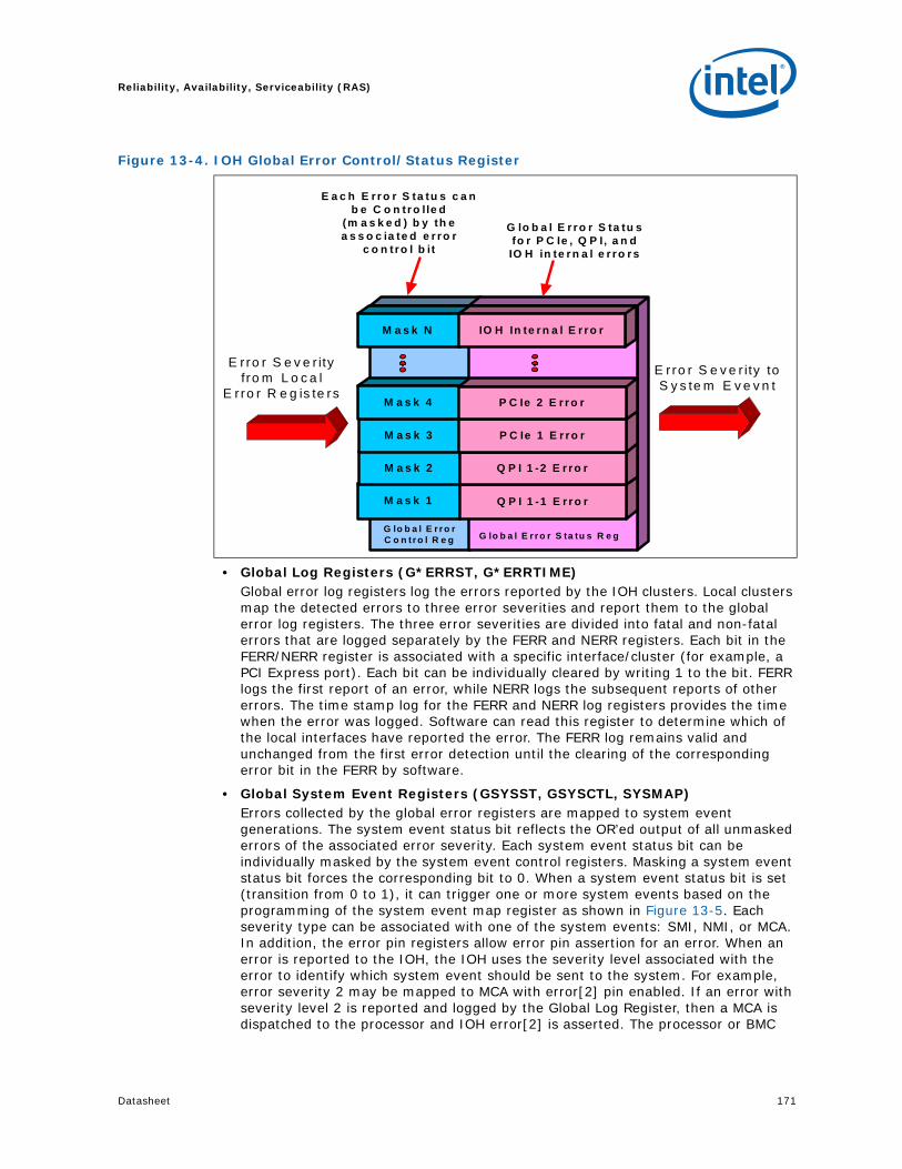
Datasheet 171
Reliability, Availability, Serviceability (RAS)
• Global Log Registers (G*ERRST, G*ERRTIME)Global error log registers log the errors reported by the IOH clusters. Local clusters map the detected errors to three error severities and report them to the global error log registers. The three error severities are divided into fatal and non-fatal errors that are logged separately by the FERR and NERR registers. Each bit in the FERR/NERR register is associated with a specific interface/cluster (for example, a PCI Express port). Each bit can be individually cleared by writing 1 to the bit. FERR logs the first report of an error, while NERR logs the subsequent reports of other errors. The time stamp log for the FERR and NERR log registers provides the time when the error was logged. Software can read this register to determine which of the local interfaces have reported the error. The FERR log remains valid and unchanged from the first error detection until the clearing of the corresponding error bit in the FERR by software.
• Global System Event Registers (GSYSST, GSYSCTL, SYSMAP)Errors collected by the global error registers are mapped to system event generations. The system event status bit reflects the OR’ed output of all unmasked errors of the associated error severity. Each system event status bit can be individually masked by the system event control registers. Masking a system event status bit forces the corresponding bit to 0. When a system event status bit is set (transition from 0 to 1), it can trigger one or more system events based on the programming of the system event map register as shown in Figure 13-5. Each severity type can be associated with one of the system events: SMI, NMI, or MCA. In addition, the error pin registers allow error pin assertion for an error. When an error is reported to the IOH, the IOH uses the severity level associated with the error to identify which system event should be sent to the system. For example, error severity 2 may be mapped to MCA with error[2] pin enabled. If an error with severity level 2 is reported and logged by the Global Log Register, then a MCA is dispatched to the processor and IOH error[2] is asserted. The processor or BMC
Figure 13-4. IOH Global Error Control/Status Register
M a s k N
G lo b a l E r ro r S ta tu s fo r P C Ie , Q P I, a n d IO H in te r n a l e r ro r s
E rro r S e v e r ity f ro m L o c a l
E r ro r R e g is te rs
E r ro r S e v e r ity to S y s te m E v e v n t
G lo b a l E r r o r C o n tr o l R e g
M a s k 1
M a s k 2
M a s k 3
M a s k 4
G lo b a l E r r o r S ta tu s R e g
Q P I 1 -1 E r ro r
Q P I 1 -2 E r ro r
P C Ie 1 E r ro r
P C Ie 2 E r r o r
E a c h E r r o r S ta tu s c a n b e C o n tro lle d
(m a s k e d ) b y th e a s s o c ia te d e r ro r
c o n tro l b it
IO H In te r n a l E r ro r

Reliability, Availability, Serviceability (RAS)
172 Datasheet
can read the Global and Local Error Log register to determine where the error came from, and how it should handle the error. At power-on reset, these registers are initialized to their default values. The default mapping of severity and system event is set to be consistent with Table 13-2. Firmware can choose to use the default values or modify the mapping according to the system requirements.The system event control register is a non-sticky register that is cleared by hard reset.
Figure 13-6 shows an example of how an error is logged and reported to the system by the IOH.
Figure 13-7 shows the logic diagram of the IOH local and global error registers.
Figure 13-5. IOH System Event Register
Each Error Severity can map to:
SMINMIMCANone
and/or Error Pin
Each Error Severity can be masked
Error Severity from Global Error Status System Event
System Event Status Register
Severity 1
Severity 2
Severity 3
Severity 4
System Event Control Register
Enable 1
Enable 2
Enable 3
Enable 4
System Event 1
System Event 2
System Event 3
System Event 4
Errors from the global error registers are
catagorized to 4 error severities
System Event Map Register

Datasheet 173
Reliability, Availability, Serviceability (RAS)
Figure 13-6. IOH Error Logging and Reporting Example
-PCI-E 12 Error
PCI-E 11 Error
-
Intel® QPI 2 Error
IOH Internal Error
Intel® QPI 1 Error
IOH Local Error Register System Control/Status Register
Severity 2
Severity 0
Severity 1
CPEI
NMI
Datapath UC ECC = 1
Datapath Correctable
Header Parity Error
Write Cache UC ECC
Write Cache Corretable
Other Errors
NMI
Error[2]
Error Severity = 1
Error Severity = 1
Error Severity = N
Error Severity = 0
Error Severity = 2
Error Severity = 2
IOH ERROR REPORTING
Global Fatal Error Status RegisterGlobal Non-Fatal Error Status Register
Error IndicatedPCI-E 10 Error
PCIe* 12 Error
Intel® QPI 2 Error
IOH Internal Error
Intel® QPI 2 Error
Local FERR/NERR
Source ID
Target IDHeader
AddressData
Syndrome
Datapath UC ECCDatapath
CorrectableHeader Parity Error
Write Cache UC ECC
Write Cache Corretable
Other Errors
Global FERR/NERRIOH ERROR LOGGING
Severity 2
Severity 0
Severity 1
PCIe 11 Error
PCIe 10 Error
3) When error is detected, the error log latches the error status of the local, global, system registers and error information associated with the error. FERR logs the first error detected and NERR logs the next error. This example shows a Datapath Uncorrectable ECC error detected.
2) Error detected is converted to a system event according to how the error severity is mapped to a system event. In this example,NMI is generated for error severity.
1) Each IOH internal error can beconfigured as one of the 3 severitiesof error. This example configures the Uncorrectable ECC error as Severity 1 Error for IOH
The global error status indicates which interface has reported an error.
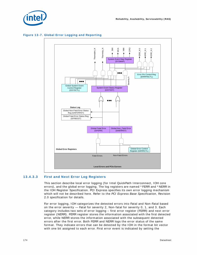
Reliability, Availability, Serviceability (RAS)
174 Datasheet
13.4.3.3 First and Next Error Log Registers
This section describe local error logging (for Intel QuickPath Interconnect, IOH core errors), and the global error logging. The log registers are named *FERR and *NERR in the IOH Register Specification. PCI Express specifies its own error logging mechanism which will not be described here. Refer to the PCI Express Base Specification, Revision 2.0 specification for details.
For error logging, IOH categorizes the detected errors into Fatal and Non-Fatal based on the error severity — Fatal for severity 2, Non-fatal for severity 0, 1, and 3. Each category includes two sets of error logging – first error register (FERR) and next error register (NERR). FERR register stores the information associated with the first detected error, while NERR stores the information associated with the subsequent detected errors after the first error. Both FERR and NERR logs the error status of the same format. They indicate errors that can be detected by the IOH in the format bit vector with one bit assigned to each error. First error event is indicated by setting the
Figure 13-7. Global Error Logging and Reporting
Local Errors and PCIe Eorrors
Fatal Errors Non-Fatal Errors
Global Error Control Register (GERRCTL)
Global Non-Fatal Error Status Reg (GNFERRST)
Global Fatal Error Status Reg (GFNEEST)
Global System Event Control Register
(GSYSCTL)
System Event Map Register (SYSMAP)
Sev
erity
0
System Event Status Register (GSYSST)
MC
A
NM
I
SM
I
CP
EI
The
rmal
ert_
N
The
rmtr
ip_N
Error Pin Control Reg(ERRPINCTL)
ER
R_N
0
ER
R_N
1
ER
R_
N 2
Global Fatal Error (GFERR)
Global Non_Fatal Error (GNERRST)
Status Log
Global Error Registers

Datasheet 175
Reliability, Availability, Serviceability (RAS)
corresponding bit in the FERR status register, a subsequent error(s) is indicated by setting the corresponding bit in the NERR register. In addition, the local FERR register also logs the ECC syndrome, address and header of the erroneous cycle. The FERR register indicates only one error, while the NERR register can indicate multiple errors. Both first error and next errors trigger system events.
Once the first error and the next error have been indicated and logged, the log registers for that error remains valid until either 1) The first error bit is clear in the associated error status register, or 2) a powergood reset occurs. Software clears an error bit by writing 1 to the corresponding bit position in the error status register.
The hardware rules for updating the FERR and NERR registers and error logs are as follows:
1. First error event is indicated by setting the corresponding bit in the FERR status register, a subsequent error is indicated by setting the corresponding bit in the NERR status register.
2. If the same error occurs before the FERR status register bit is cleared, it is not logged in the NERR status register. Note that error logging for Intel QPI link layer and protocol layer, IOH core errors, thermal errors and miscellaneous errors do not adhere to this rule due to an errata. That is, if the first error occurs again, it again gets logged into NERR status register.
3. If multiple error events, sharing the same error log registers, occur simultaneously, then highest error severity has priority over the others for FERR logging. The other errors are indicated in the NERR register.
4. Fatal error is of the highest priority, followed by Recoverable errors and then Correctable errors.
5. Updates to error status and error log registers appear atomic to the software.
6. Once the first error information is logged in the FERR log register, the logging of FERR log registers is disabled until the corresponding FERR error status is cleared by the software.
7. Error control registers are cleared by reset. Error status and log registers are cleared by the power-on reset only. The contents of error log registers are preserved across a reset (while PWRGOOD remains asserted).
13.4.3.4 Error Logging Summary
Figure 13-8 summarizes the error logging flow for the IOH. As illustrated in the flow chart, the left half depicts the local error logging flow, while the right half depicts the global error logging flow. The local and the global error logging are very similar to each other. Note that for simultaneous events, the IOH serializes the events with higher priority on more severe error.

Reliability, Availability, Serviceability (RAS)
176 Datasheet
Figure 13-8. IOH Error Logging Flow
LocalFERR in use?
No
Yes
LocalError Masked
?
Yes
No
First Local Error?
Done
Set Local Error Status Bit
Update Local FERR
Registers
Update Local NERR
Registers
Report Error Severity to
Global Error
GlobalError Masked
?
No
No
Set Global Error Status for
The Error Severity
Yes
Update Global FERR
Registers
Update Gobal NERR
Registers
Local Error
YesDone
FirstGlobalError?
Map Error Severity to Programmed System Event. Separate logging to Global Fatal and Global Non-Fatal
Generate System Event
Map Error to Programmed Severity.
Separate logging to Local Fatal and Local Non-Fatal
Fatal Non-Fatal Non-FatalFatal

Datasheet 177
Reliability, Availability, Serviceability (RAS)
13.4.3.5 Error Registers Flow
1. Upon a detection of an unmasked local error, the corresponding local error status is set if the error is enabled; otherwise the error bit is not set and the error forgotten.
2. The local error is mapped to its associated error severity defined by the error severity map register. Setting of the local error status bit causes the logging of the error – Severity 0, 1, and 3 is logged in the local non-fatal FERR/NERR registers, while severity 2 is logged in the local fatal FERR/NERR registers. PCIe errors are logged according to the PCI Express Base Specification, Revision 1.0a and the associated set of Erratas and EC*’s.
3. The local FERR and NERR logging events are forwarded to the global FERR and NERR registers. The report of local FERR/NERR sets the corresponding global error bit if the global error is enabled; otherwise, the global error bit is not set and the error forgotten. The global FERR logs the first occurrence of local FERR/NERR event in the IOH, while the global NERR logs the subsequent local FERR/NERR events.
4. Severity 0 and 1 are logged in the global non-fatal FERR/NERR registers, while severity 2 is logged in the global fatal FERR/NERR registers.
5. The global error register reports the error with its associated error severity to the system event status register. The system event status is set if the system event reporting is enabled for the error severity; otherwise, the bit is not set and the error is not reported.
6. Setting of the system event bit triggers a system event generation according the mapping defined in the system event map register. The associated system event is generated for the error severity and dispatched to the processor/BMC of the error (interrupt for processor or Error Pin for the BMC).
7. The global log and local log registers provide the information to identify the source of the error. Software can read the log registers and clear the global and local error status bits.
8. Since the error status bits are edge triggered, a 0 to 1 transition is required to set the bit again. While the error status bit (local, global, or system event) is set to 1, all incoming error reporting to the respective error status register will be ignored (no 0 to 1 transition):
a. When a write to clear the local error status bit, the local error register re-evaluate the OR output of its error bits and report it to the global error register; however, if the global error bit is already set, then the report is ignored.
b. When a write to clear the error status bit occurs, the global error register re-evaluates the OR output of its error bits and reports it to the system event status register; however, if the system event status bit is already set, then the report is not generated.
c. Software can optionally mask or unmask system event generation (interrupt or error pin) for an error severity in the system event control register while clearing the local and global error registers.
9. Software has the following options for clearing error status registers:
a. Read global and local log registers to identify the source of the error. Clear local error bits – this does not cause generation of an interrupt with the global bit still set. Then, clear the global error bit and write to the local error register again with all 0s. Writing 0s to the local status does not clear any status bit, but will cause the re-evaluation of the error status bits. An error will be reported if there is any unclear local error bit.

Reliability, Availability, Serviceability (RAS)
178 Datasheet
b. Read global and local log registers to identify the source of the error and mask the error reporting for the error severity. Clear system event and global error status bits – this causes setting of the system event status bit if there are other global bits still set. Then, clear local error status bits – this causes setting of the global error status bit if there are other local error bits still set. Then, unmask system event to cause the IOH to report the error.
10. FERR logs the information of the first error detected by the associated error status register (local or global). FERR log remains unchanged until all bits in the respective error status register are cleared by the software. When all error bits are cleared, the FERR logging is re-enabled.
13.4.3.6 Error Counters
This feature allows the system management controller to monitor the count of correctable errors. The error RAS structure already provides a first error status and a second error status. Because the response time of system management is on the order of milliseconds, it is not possible to detect short bursts of errors. Over an extended period of time, software uses these error counter values to monitor the rate of change in error occurrences and identify potential degradations, especially with respect to the memory interface.
13.4.3.6.1 Feature Requirements
A register with one-hot encoding will select which error types that participate in error counting. It is unlikely that more than one error will occur within a cluster at a given time. Therefore, it is not necessary to count more than one occurrence in one clock cycle. The selection register will OR together all of the selected error types to form a single count enable. This means that only one increment of the counter will occur for one or all types selected. Register attributes are set to write 1 to clear.
Each cluster has one set of error counter/control registers.
• Each Intel QPI port will contain one 7-bit counter (ERRCNT[6:0]).
— Bit[7] is an overflow bit, all bits are sticky with a write logic 1 to clear.
• The IOH cluster (Core) contains one 7-bit counter (ERRCNT[6:0]).
— Bit[7] is an overflow bit, all bits are sticky with a write logic 1 to clear.
• The Miscellaneous cluster (MI) contains one 7-bit counter (ERRCNT[6:0]).
— Bit[7] is an overflow bit, all bits are sticky with a write logic 1 to clear.
• The Thermal Error cluster (THER) contains one 7-bit counter (ERRCNT[6:0]).
— Bit[7] is an overflow bit, all bits are sticky with a write logic 1 to clear.

Datasheet 179
Reliability, Availability, Serviceability (RAS)
13.4.3.7 Stop on Error
The System Event Map register selects the severity levels which activates the Stop on Error (Error Freeze). It requires a reset to clear the event or a configuration write (using JTAG or SMBus) to the stop on error bit in the selection register. Continued operation after Stop on Error is not ensured. See the System Event Map register (SYSMAP) in the Section 17.6.7.7, “SYSMAP—System Error Event Map Register” for details.
13.5 Intel® QuickPath Interconnect Interface RASThe following sections provide an overview of the Intel QuickPath Interconnect RAS features. The Intel QuickPath Interconnect RAS features are summarized as follows:
1. Link Level 8-bit rolling CRC.2. Dynamic link retraining and recovery on link failure.3. Intel QuickPath Interconnect Error detection and logging.4. Intel QuickPath Interconnect Error reporting.
13.5.1 Link Level CRC and Retry
Cyclic redundancy check (CRC) is a mechanism to ensure the data integrity of a serial stream. The sender of the data generates CRC based on the data pattern and a defined polynomial equation. The resulting CRC is a unique encoding for a specific data stream. When the data arrives at the receiver, the receiver performs the same CRC calculation using the same polynomial equation. The CRCs are compared to detect bad data. When a CRC error is detected, the receiver will request the sender to retransmit the data. This action is termed “link level retry”, as it is performed by the Link layer logic. The Protocol layer is unaware of this action.
Intel QuickPath Interconnect uses 8 bit CRC per flit (72+8=80 bits), and 16-bit CRC over 2 flits for Intel QuickPath Interconnect packets. The CRC is capable of detecting 1, 2, 3 and odd number of bits in error and errors of burst length up to 8. Flits are logged in a retry buffer until acknowledgment is received. In case of error, the erroneous flit and all subsequent flits are retransmitted. Recovery from permanent partial link failure is supported through dynamic link width reduction (see Section 13.5.2).
Table 13-1. Error Counter Register Locations
Cluster Register Reference
Intel QuickPath
Interconnect
Intel QuickPath Interconnect Error Counter Selection Register (QPI[1:0]ERRCNTSEL) Intel QuickPath Interconnect Error Counter Register (QPI[1:0]ERRCNT)Intel QuickPath Interconnect Protocol Error Counter Register (QPIP[1:0]ERRCNT)
Core IOH IOH Error Counter Selection Register (IOHERRCNTSEL)
Miscella-neous
Miscellaneous Error Counter Selection Register (MIERRCNTLSEL)
Thermal Error
Thermal Error Counter Selection Register (THRERRCNTSEL)
DMI DMI Error Counter Selection Register (DMIERRCNTSEL) and DMI Error Counter Register (DMI(ERRCNT)

Reliability, Availability, Serviceability (RAS)
180 Datasheet
In addition, the IOH tracks and logs link level retry in the error registers. A successful link level retry and successful link reduction is a correctable error, while repetitive retries without success and a link that cannot be further reduced is a fatal error. The flit that contained the error will be logged with 8-bit CRC.
13.5.2 Intel® QuickPath Interconnect Error Detection, Logging, and Reporting
The IOH implements Intel QuickPath Interconnect error detection and logging that follows the IOH local and global error reporting mechanisms described earlier in this chapter. These registers provide the control and logging of the errors detected on the Intel QuickPath Interconnect interface. The IOH Intel QuickPath Interconnect error detection, logging, and reporting provides the following features:
• Error indication by interrupt (MCA, SMI, NMI).• Error indication by response status field in response packets.• Error indication by data poisoning.• Error indication by Error pin.• Hierarchical Time-out for fault diagnosis and FRU isolation.
13.6 PCI Express RASThe PCI Express Base Specification, Revision 2.0 defines a standard set of error reporting mechanisms; the IOH supports the standard set, including error poisoning and Advanced Error Reporting. Any exceptions are called out where appropriate. PCI Express ports support the following features:
1. Link Level CRC and retry.
2. Dynamic link width reduction on link failure.
3. PCI Express Error detection and logging.
4. PCI Express Error reporting.
13.6.1 PCI Express Link CRC and Retry
PCI Express supports link CRC and link level retry for CRC errors. Refer to the PCI Express Base Specification, Revision 2.0 for details.
13.6.2 Link Retraining and Recovery
The PCI Express interface provides a mechanism to recover from a failed link, and continue operating at a reduced link widths. The IOH supports PCI Express ports can operate in x16, x8, x4, x2, and x1 link widths. In case of a persistent link failure, the PCI Express link can degrade to a smaller link width in an attempt to recover from the error. A PCI Express x16 link can degrade to x8 link, a x8 link can fall back to a x4 link, a x4 to a x2 link, and then to a x1 link. Refer to the PCI Express Base Specification, Revision 2.0 for further details.
13.6.3 PCI Express Error Reporting Mechanism
The IOH supports the standard and advanced PCIe error reporting for its PCIe ports. The IOH PCI Express ports are implemented as root ports. Refer to the PCI Express Base Specification, Revision 2.0 for the details of PCIe error reporting. The following sections highlight the important aspects of the PCI Express error reporting mechanisms.

Datasheet 181
Reliability, Availability, Serviceability (RAS)
13.6.3.1 PCI Express Error Severity Mapping in IOH
Errors reported to the IOH PCI Express root port can optionally signal to the IOH global error logic according to their severities through the programming of the PCI Express root control register (ROOTCON). When system error reporting is enabled for the specific PCI Express error type, the IOH maps the PCI Express error to the IOH error severity and reports it to the global error status register. PCI Express errors can be classified as two types: Uncorrectable errors and Correctable errors. Uncorrectable errors can further be classified as Fatal or Non-Fatal. This classification is compatible and mapped with the IOH’s error classification: Correctable as Correctable, Non-Fatal as Recoverable, and Fatal as Fatal.
13.6.3.2 Unsupported Transactions and Unexpected Completions
If the IOH receives a legal PCI Express defined packet that is not included in PCI Express supported transactions, the IOH treats that packet as an unsupported transaction and follows the PCI Express rules for handling unsupported requests. If the IOH receives a completion with a requester ID set to the root port requester ID and there is no matching request outstanding, it is considered an “Unexpected Completion”. The IOH also detects malformed packets from PCI Express and reports them as errors per the PCI Express Base Specification Revision 1.0a rules.
If the IOH receives a Type 0 Intel Vendor-Defined message that terminates at the root complex and that it does not recognize as a valid Intel-supported message, the message is handled by IOH as an Unsupported Request with appropriate error escalation (as defined in express spec). For Type 1 Vendor-Defined messages which terminate at the root complex, the IOH simply discards the message with no further action.
13.6.3.3 Error Forwarding
PCIe supports Error Forwarding, or Data Poisoning. This feature allows a PCI Express device to forward data errors across an interface without it being interpreted as an error originating on that interface.
The IOH forwards the poison bit from Intel QuickPath Interconnect to PCIe, PCIe to Intel QuickPath Interconnect and between PCIe ports on peer to peer. Poisoning is accomplished by setting the EP bit in the PCIe TLP header.
13.6.3.4 Unconnected Ports
If a transaction targets a PCI Express link that is not connected to any device, or the link is down (DL_Down status), the IOH treats it as a master abort situation. This is required for PCI bus scans to non-existent devices to go through without creating any other side effects. If the transaction is non-posted, IOH synthesizes an Unsupported Request response status (if non-posted) back to any PCIe requester targeting the down link or returns all Fs on reads and a successful completion on writes to any Intel QuickPath Interconnect requester targeting the down link. Note that software accesses to the root port registers corresponding to a down PCIe interface does not generate an error.
13.6.3.5 PCI Express Error Reporting Specifics
Refer to PCI Express Base Specification Rev 1.1, post 1.1 Erratas and EC*’s for details of root complex error reporting. Here is a summary of root port ‘system event’ reporting. Figure 13-9 provides a summary of system event reporting to IOH global

Reliability, Availability, Serviceability (RAS)
182 Datasheet
error an PCI Express interface error. Refer to Section 17.12 for registers and descriptions. Table 13-9 and Table 13-10 illustrate the error logging and report mechanism.
Figure 13-9. Error Signaling to IOH Global Error Logic on a PCI Express Interface Error
Refer to
AE
R M
SI
Gen
eration
Lo
gic
MS
I
Co
rrectable E
rror
Ind
ication
to IO
H
Glo
bal E
rror L
og
ic
No
nfatal E
rror
Ind
ication
to IO
H
Glo
bal E
rror L
og
ic
Fatal E
rror In
dicatio
n
to IO
H G
lob
al Erro
r L
og
ic
Lo
gical O
R o
f all un
masked
fatal errors
in X
P U
nco
rrectable E
rror M
ask Reg
: (X
PU
NC
ER
RM
SK
)
XP
Un
correctab
le Erro
r Detect
Mask R
eg: (X
PU
NC
ED
MA
SK
)
XP
Un
correctab
le E
rrors
XP
Un
correctab
le Erro
r Statu
s R
eg: (X
PU
NC
ER
RS
TS
)
XP
Un
correctab
le Erro
r Severity
Reg
: (XP
UN
CE
RR
SE
V)
Fatal
Lo
gical O
R o
f all no
nfatal erro
rs in
XP
Un
correctab
le Erro
r Mask
Reg
: (XP
UN
CE
RR
MS
K)
No
nfatal
XP
Un
correctab
le Erro
r Po
inter
Reg
: (XP
UN
CE
RR
PT
R)
Lo
gical O
R o
f all correctab
le erro
rs in P
CIe C
orrectab
le Erro
r M
ask Reg
: (XP
CO
RE
RR
MS
K)
XP
Co
rrectable E
rror S
tatus R
eg:
XP
CO
RE
RR
ST
S
XP
Co
rrectable E
rror M
ask Reg
: (X
PC
OR
ER
RM
SK
)
XP
Co
rrectable
Erro
rs
XP
Glo
bal E
rror S
tatus
Reg
: (XP
GL
BE
RR
ST
S)
21
0X
P G
lob
al Erro
r Po
inter
Reg
: (XP
GL
BE
RR
PT
R)
System
Erro
r En
abled
(O
ne p
er error class)
Ro
ot C
on
trol R
eg
Overrid
e System
Erro
r E
nab
les (on
e per erro
r class) M
ISC
CT
RL
ST
SR
eg
Erro
r Messag
es(R
eceived + In
ternal)
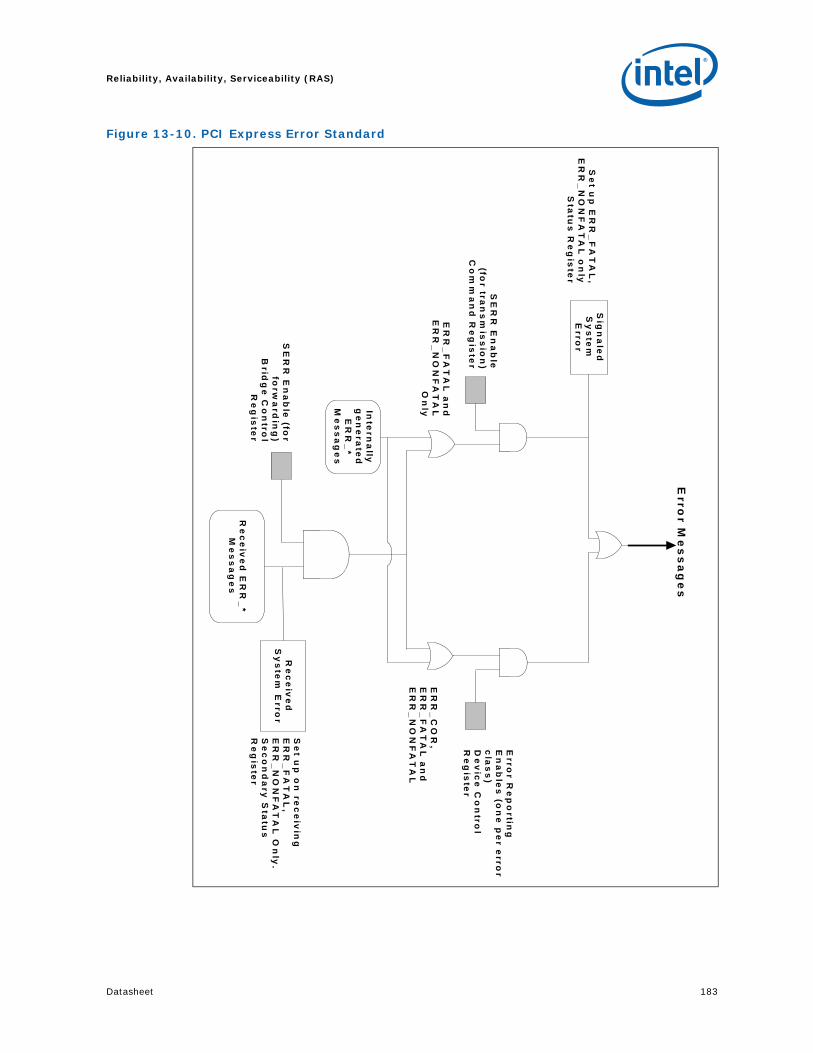
Datasheet 183
Reliability, Availability, Serviceability (RAS)
Figure 13-10. PCI Express Error Standard
Re
ce
ive
d E
RR
_*
Me
ss
ag
es
Re
ce
ive
d
Sy
ste
m E
rror
Inte
rna
lly
ge
ne
rate
d
ER
R_
* M
es
sa
ge
s
Sig
na
led
S
ys
tem
E
rror
Se
t up
on
rec
eiv
ing
E
RR
_F
AT
AL
, E
RR
_N
ON
FA
TA
L O
nly
.S
ec
on
da
ry S
tatu
s
Re
gis
ter
ER
R_
FA
TA
L a
nd
E
RR
_N
ON
FA
TA
L
On
lyE
RR
_C
OR
, E
RR
_F
AT
AL
an
d
ER
R_
NO
NF
AT
AL
SE
RR
En
ab
le (fo
r fo
rwa
rdin
g)
Brid
ge
Co
ntro
l R
eg
iste
r
SE
RR
En
ab
le
(for tra
ns
mis
sio
n)
Co
mm
an
d R
eg
iste
r
Erro
r Re
po
rting
E
na
ble
s (o
ne
pe
r erro
r c
las
s)
De
vic
e C
on
trol
Re
gis
ter
Se
t up
ER
R_
FA
TA
L,
ER
R_
NO
NF
AT
AL
on
lyS
tatu
s R
eg
iste
r
Erro
r Me
ss
ag
es

Reliability, Availability, Serviceability (RAS)
184 Datasheet
13.7 IOH Error Handling SummaryThe following tables provide a summary of the errors that are monitored by the IOH. The IOH provides a flexible mechanism for error reporting. Software can arbitrarily assign an error to an error severity, and associate the error severity with a system event. Depending on which error severity is assigned by software, the error is logged either in fatal or non-fatal error log registers. Each error severity can be mapped to one of the inband report mechanism as shown in Table 13-2, or generate no inband message at all. In addition, each severity can enable/disable the assertion of its associated error pin for outband error report (for example, severity 0 error triggers Error[0], severity 1 triggers Error[1],..., etc). Note that error severity 3 is reserved for the thermal alert; however, the IOH does not prevent mapping of an error to any severity, including severity 3. Software must ensure that only thermal alert is mapped to error severity 3 if thermal alert pin is used by the platform. Table 13-2 shows the default error severity mapping in the IOH and how each error severity is reported, while Table 13-3 summarizes the default logging and responses on the IOH detected errors.
Note: Each error’s severity (and therefore which error registers log the error) is programmable and therefore, the error logging registers used for the error could be different from what is indicated in Table 13-3.
Table 13-2. IOH Default Error Severity Map
Error Severity IOH Intel® QuickPath
Interconnect PCI Express Inband Error Reporting (programmable)
0 Hardware Correctable Error
Hardware Correctable Error
Correctable Error
NMI/SMI/MCA/CPEI
1 Recoverable Error Recoverable Error Non-Fatal Error NMI/SMI/MCA/CPEI
2 Fatal Error Unrecoverable Error
Fatal Error NMI/SMI/MCA/CPEI
3 Thermal Alert N/A N/A

Datasheet 185
Reliability, Availability, Serviceability (RAS)
Table 13-3.IOH Error Summary (Sheet 1 of 10)
ID ErrorDefaultError
SeverityTransaction Response Default Error Logging1
IOH Core Errors
C4Master AbortAddress Error
1 IOH Sends completion with MA status and log the error
FERR/NERR is logged in IOH Core and Global Non-Fatal Error Log Registers:
IOHNFERRSTIOHNFERRHDIOHNNERRST
GNERRSTGNFERRSTGNFERRTIMEGNNERRST
IOH core header is logged
C5
Completor AbortAddress Error
IOH sends completion with CA status and logs the error.
C6
FIFO Overflow/Underflow error
1 IOH logs the Error FERR/NERR is logged in IOH Core and Global Non-Fatal Error Log Registers:
IOHNFERRSTIOHNFERRHDIOHNNERRST
GNERRSTGNFERRSTGNFERRTIMEGNNERRST
IOH core header is not logged
Miscellaneous Errors
20
IOH Configuration Register Parity Error (not including Intel QPI, PCIe registers which are covered elsewhere)
2 No Response – This error is not associated with a cycle. IOH detects and logs the error.
FERR/NERR is logged in IOH Core and Global Fatal Error Log Registers:IOHFFERRSTIOHFNERRST
GFERRSTGFFERRSTGFFERRTIMEGFNERRST
No header is logged.
21 Persistent SMBus retry failure.
2 No Response – This error is not associated with a cycle. IOH detects and logs the error.
FERR/NERR is logged in IOH Core and Global Fatal Error Log Registers:
IOHFFERRSTIOHFFERRHDIOHFNERRST
GFERRSTGFFERRSTGFFERRTIMEGFNERRST
No header is logged for this error
22 Persistent JTAG error.
23
Virtual Pin Port Error. (IOH encountered persistent VPP failure. The VPP is unable to operate.)

Reliability, Availability, Serviceability (RAS)
186 Datasheet
24
DFx Injected Error 2 No Response – This error is not associated with a cycle. IOH detects and logs the error.
FERR/NERR is logged in IOH Core and Global Non-Fatal Error Log Registers:
IOHNFERRSTIOHNNERRST
GFERRSTGFFERRSTGFFERRTIMEGFNERRST
No Header logging for this errors
PCIe Errors
70 PCIe Receiver Error 0 Respond per PCI Express specification Log error per PCI Express AER requirements for these correctable errors/message.
Log in XPGLBERRSTS, XPGLBERRPTR registers
If PCIe correctable error is forwarded to the global error registers, it is logged in global non-fatal log registers – GNERRST, GNFERRST, GNNERRST, GNFERRTIME
71 PCIe Bad TLP
72 PCIe Bad DLLP
73 PCIe Replay Time-out
74 PCIe Replay Number Rollover
75Received ERR_COR message from downstream device
76
PCIe Link Bandwidth changed
No Response – This error is not associated with a cycle. IOH detects and logs the error.
Log per ‘Link bandwidth change notification mechanism’ ECNLog in XPCORERRSTS registerLog in XPGLBERRSTS, XPGLBERRPTR registersIf error is forwarded to the global error registers, it is logged in global non-fatal log registers – GNERRST, GNFERRST, GNNERRST, GNFERRTIME
80
Received ‘Unsupported Request’ completion status from downstream device
1 Intel QPI to PCIe read: IOH returns all ‘1s’ and normal response to Intel QPI to indicate master abortIntel QPI to PCIe NP write: IOH returns normal responsePCIe to PCIe read/NP-write: ‘Unsupported request’ is returned2 to original PCIe requester. SMBus/Jtag accesses: IOH returns ‘UR’ response status on smbus/jtag
Log in XPUNCERRSTS register
If error is forwarded to the global error registers, it is logged in global non-fatal log registers – GNERRST, GNFERRST, GNNERRST, GNFERRTIME
Table 13-3.IOH Error Summary (Sheet 2 of 10)
ID ErrorDefaultError
SeverityTransaction Response Default Error Logging1

Datasheet 187
Reliability, Availability, Serviceability (RAS)
81
IOH encountered a PCIe ‘Unsupported Request’ condition, on inbound address decode, as listed in Table 3-6, with the exception of SAD miss (see C6 for SAD miss), and those covered by entry#11
PCIe read: ‘Unsupported request’ completion is returned on PCIePCIe non-posted write: ‘Unsupported request’ completion is returned on PCIe. The write data is droppedPCIe posted write: IOH drops the write data.
Log error per PCI Express AER requirements for unsupported request.3
All accesses above address 2^51 are logged as UR. In additionMemory reads above 2^51 are consid-ered Advisory when UR severity is set to non-fatal. Memory writes in the range 2^51 to 2^52 are also consid-ered advisory, while Memory writes above 2^52 are considered non-fatal, when UR severity is set to non-fatal.
Log in XPGLBERRSTS, XPGLBERRPTR registersIf PCIe uncorrectable error is forwarded to the global error registers, it is logged in global non-fatal log registers – GNERRST, GNFERRST, GNNERRST, GNFERRTIME
82
Received ‘Completer Abort’ completion status from downstream device
Intel QPI to PCIe read: IOH returns all ‘1s’ and normal response to Intel QPI.Intel QPI to PCIe NP write: IOH returns normal response.PCIe to PCIe read/NP-write: ‘Completer Abort’ is returned4 to original PCIe requester. SMBus/Jtag accesses: IOH returns ‘CA’ response status on smbus/jtag
Log in XPUNCERRSTS register
If error is forwarded to the global error registers, it is logged in global non-fatal log registers – GNERRST, GNFERRST, GNNERRST, GNFERRTIME
83
IOH encountered a PCIe ‘Completer Abort’ condition, on inbound address decode, as listed in Table 3-6.
PCIe read: ‘Completer Abort’ completion is returned on PCIePCIe non-posted write: ‘Completer Abort’ completion is returned on PCIe. The write data is droppedPCIe posted write: IOH drops the write data.
Log error per PCI Express AER requirements for completer abort.5
Log in XPGLBERRSTS, XPGLBERRPTR registersIf PCIe uncorrectable error is forwarded to the global error registers, it is logged in global non-fatal log registers – GNERRST, GNFERRST, GNNERRST, GNFERRTIME
Table 13-3.IOH Error Summary (Sheet 3 of 10)
ID ErrorDefaultError
SeverityTransaction Response Default Error Logging1

Reliability, Availability, Serviceability (RAS)
188 Datasheet
84
Completion time-out on NP transactions outstanding on PCI Express/DMI
1 Intel QPI to PCIe read: IOH returns normal response to Intel QPI and all 1’s for read dataIntel QPI to PCIe non-posted write: IOH returns normal response to Intel QPIPCIe to PCIe read/non-posted write: UR2 is returned on PCIeSMBus/Jtag reads: IOH returns a UR status on SMbus/jtag
Log error per PCI Express AER requirements for the corresponding error. Log in XPGLBERRSTS, XPGLBERRPTR registersIf PCIe uncorrectable error is forwarded to the global error registers, it is logged in global non-fatal log registers – GNERRST, GNFERRST, GNNERRST, GNFERRTIME
Note: a) A poisoned TLP received from PCIe and that needs to be forwarded to Intel QPI, when Intel QPI supports poisoned indication, is treated as advisory-nonfatal error, if the associated severity is set to non-fatal. If Intel QPI does not support poisoned data forwarding, the error is not advisory. Also, received poisoned TLPs that are not forwarded over Intel QPI are always treated as advisory-nonfatal errors, if severity is set to non-fatal.b) When a poisoned TLP is transmitted down a PCIe link, IOH does not log that condition in the AER registers
85
Received PCIe Poisoned TLP
Intel QPI to PCIe read: IOH returns normal response and poisoned data to Intel QPI, if Intel QPI profile supports poisoned data. Otherwise, packet is dropped and no response sent on Intel QPI.PCIe to Intel QPI write: IOH forwards poisoned indication to Intel QPI, if Intel QPI profile supports poisoned data. Otherwise, write is dropped.PCIe to PCIe read: IOH forwards completion with poisoned data to original requester, if the root port in the outbound direction for the completion packet, is not in ‘Stop and Scream’ mode. If the root port is in ‘Stop and scream’ mode, the packet is dropped and the link is brought down immediately (that is, no packets on or after the poisoned data is allowed to go to the link).PCIe to PCIe posted/non-posted write: IOH forwards write with poisoned data to destination link, if the root port of the destination link, is not in ‘Stop and Scream’ mode. If the root port is in ‘Stop and scream’ mode, the packet is dropped and the link is brought down immediately (that is, no packets on or after the poisoned data is allowed to go to the link) and a UR2 response is returned to the original requester, if the request is non-posted.SMBus/Jtag to IOH accesses requests: IOH returns a UR response status on smbus/jtag
86 Received PCIe unexpected Completion
Respond Per PCIe Specification Log error per PCI Express AER requirements for the corresponding error/message. Log in XPGLBERRSTS, XPGLBERRPTR registersIf PCIe uncorrectable error is forwarded to the global error registers, it is logged in global non-fatal log registers – GNERRST, GNFERRST, GNNERRST, GNFERRTIME
87 PCIe Flow Control Protocol Error6
88
Received ERR_NONFATAL Message from downstream device
90 PCIe Malformed TLP6 2 Respond Per PCIe Specification Log error per PCI Express AER requirements for the corresponding error/message. Log in XPGLBERRSTS, XPGLBERRPTR registersIf PCIe uncorrectable error is forwarded to the global error registers, it is logged in global non-fatal log registers – GFERRST, GFFERRST, GFNERRST, GFFERRTIME
91 PCIe Data Link Protocol Error6
92 PCIe Receiver Overflow
93 Surprise Down
94Received ERR_FATAL message from downstream device
Table 13-3.IOH Error Summary (Sheet 4 of 10)
ID ErrorDefaultError
SeverityTransaction Response Default Error Logging1

Datasheet 189
Reliability, Availability, Serviceability (RAS)
98
MSI writes greater than a DWORD
2 Drop the transaction Log in XPUNCERRSTS registerLog in XPGLBERRSTS, XPGLBERRPTR registersIf error is forwarded to the global error registers, it is logged in global non-fatal log registers – GFERRST, GFFERRST, GFNERRST, GFFERRTIME
Intel VT-d
A1
All faults except ATS spec defined CA faults (refer to VT-d spec for complete details)
1 Unsupported Request response for the associated transaction on the PCI Express interface
Error logged in Intel VT-d Fault Record register.Error logged in XPGLBERRSTS and XPGLBERRPTR registers.Error logging also happens (on the GPA address) per the PCI Express AER mechanism (address logged in AER is the GPA). Errors can also be routed to the IOH global error logic and logged in the global non-fatal registers
GNERRSTGNFERRSTGNFERRTIMEGNNERRST
A2
ATS spec defined CA faults (refer to VT-d spec for complete details)
1 Completer Abort response for the associated transaction on the PCI Express interface
Error logged in Intel VT-d fault record registerError also logged in the VTUNCERRSTS and in VTUNCERRPTR registers.Error logging also happens (on the GPA address) per the PCI Express AER mechanism (address logged in AER is the GPA). Errors can also be routed to the IOH global error logic and logged in the global non-fatal registersGFERRSTGFFERRSTGFFERRTIMEGFNERRST
A3
Fault Reason Encoding FFh – Miscellaneous errors that are fatal to Intel VT-d unit operation (for example, parity error in an Intel VT-d cache)
2 Drop the transaction. Continued operation of IOH is not ensured.
Error logged in Intel VT-d fault record registerError also logged in the VTUNCERRSTS and in VTUNCERRPTR registers.
These errors can also be routed to the IOH global error logic and logged in the global fatal registers
GFERRSTGFFERRSTGFFERRTIMEGFNERRST
Table 13-3.IOH Error Summary (Sheet 5 of 10)
ID ErrorDefaultError
SeverityTransaction Response Default Error Logging1

Reliability, Availability, Serviceability (RAS)
190 Datasheet
Intel® QPI Errors
B0
Intel QPI Link Layer detected CRC error – Successful Link Level Retry and Unsuccessful Link Level Retry (entered LLR abort state)
0 IOH processes and responds the cycle as normal.
FERR/NERR is logged in Intel QPI and Global Non-Fatal Error Log Registers:
QPINFERRSTQPINNERRST
GNERRSTGNFERRSTGNFERRTIMEGNNERRST
No header is logged for this error
B1
Intel QPI Link Layer detected CRC error --Successful Link Level Retry after PHY reinit
0 IOH processes and responds the cycle as normal
FERR/NERR is logged in Intel QPI and Global Non-Fatal Error Log Registers:
QPINFERRST QPINNERRST
GNERRSTGNFERRSTGNFERRTIMEGNNERRST
No header is logged for this error
C0
Intel QPI Link Layer Detected CRC error --Unsuccessful Link Level Retry (entered LLR abort state)
1 IOH processes and responds the cycle as normal.
FERR/NERR is logged in Intel QPI and Global Non-Fatal Error Log Registers:
QPINFERRST QPINNERRST
GNERRSTGNFERRSTGNFERRTIMEGNNERRST
No header is logged for this error
B2
Intel QPI Physical Layer Detected an Intel QPI Inband Reset (either received or driven by the IOH) and re-initialization completed successfully
0 No Response – This event is not associated with a cycle. IOH detects and logs the event.
FERR/NERR is logged in Intel QPI and Global Non-Fatal Error Log Registers and Intel QPI Physical layer register:
QPINFERRSTQPINNERRST
GNERRSTGNFERRSTGNFERRTIMEGNNERRST
QPIPHPISQPIPHPPS
Table 13-3.IOH Error Summary (Sheet 6 of 10)
ID ErrorDefaultError
SeverityTransaction Response Default Error Logging1

Datasheet 191
Reliability, Availability, Serviceability (RAS)
B3
Intel QPI Protocol Layer Received CPEI message from Intel QPI (see Chapter 4 for detailed flow).
0 No Response
Note: This is really not an error condition but exists for monitoring by an external management controller.
FERR/NERR is logged in Intel QPI and Global Non-Fatal Error Log Registers and Intel QPI Physical layer register:
QPINFERRSTQPINNERRST
GNERRSTGNFERRSTGNFERRTIMEGNNERRST
QPIPHPISQPIPHPPS
B4
Intel QPI Write Cache Detected ECC Correctable Error
0 IOH processes and responds the cycle as normal
FERR/NERR is logged in Intel QPI and Global Non-Fatal Error Log Registers:
QPIPNFERRST QPIPNNERRST
GNERRSTGNFERRSTGNFERRTIMEGNNERRST
No header is logged for this error
B5
Potential spurious CRC error on L0s/L1 exit
1 In the event CRC errors are detected by link layer during L0s/L1 exit, it will be logged as"Potential spurious CRC error on L0s/L1 exit”. IOH processes and responds the cycle as normal
FERR/NERR is logged in Intel QPI and Global Non-Fatal Error LogRegisters and Intel QPI Link layerregister:
QPINFERRSTQPINNERRST
GNERRSTGNFERRSTGNFERRTIMEGNNERRST
C1
Intel QPI Protocol Layer Received Poisoned packet
1 Intel QPI to PCIe write: IOH returns normal response to Intel QPI and forwards poisoned data to PCIe.Intel QPI to IOH write: IOH returns normal response to Intel QPI and drops the write data.PCIe to Intel QPI read: IOH forwards the poisoned data to PCIeIOH to Intel QPI read: IOH drops the data.IOH to Intel QPI read for RFO: IOH completes the write. If the bad data chunk is not overwritten, IOH corrupts write cache ECC to indicate the stored data chunk (64-bit) is poisoned.
FERR/NERR is logged in Intel QPI and Global Non-Fatal Error Log Registers:
QPIPNFERRSTQPIPNFERRHDQPIPNNERRST
GNERRSTGNFERRSTGNFERRTIMEGNNERRST
Intel QPI header is logged
Table 13-3.IOH Error Summary (Sheet 7 of 10)
ID ErrorDefaultError
SeverityTransaction Response Default Error Logging1

Reliability, Availability, Serviceability (RAS)
192 Datasheet
C2
IOH Write Cache uncorrectable Data ECC error
1 Write back includes poisoned data. FERR/NERR is logged in Intel QPI and Global Fatal Error Log Registers:
QPIPFNFERRSTQPIPFNERRST
GNERRSTGFFERRSTGFFERRTIMEGFNERRST
C3
IOH CSR access crossing 32-bit boundary
1 Intel QPI read: IOH returns all ‘1s’ and normal response to Intel QPI to indicate master abortIntel QPI write: IOH returns normal response and drops the write
FERR/NERR is logged in IOH Core and Global Non-Fatal Error Log Registers:
QPIPNFERRSTQPIPNFERRHDQPIPNNERRST
ERRSTGNFERRSTGNFERRTIMEGNNERRST
Intel QPI header is logged
C7
Intel QPI Physical Layer Detected a Intel QPI Inband Reset (either received or driven by the IOH) and re-initialization completedsuccessfully but width is changed
1 No Response -- This event is notassociated with a cycle. IOHdetects and logs the event.
FERR/NERR is logged in Intel QPI and Global Non-Fatal Error Log Registers and Intel QPI physical layer register:
QPINFERRSTQPINNERRST
GNERRSTGNFERRSTGNFERRTIMEGNNERRST
QPIPHPISQPIPHPPS
D0Intel QPI Physical Layer Detected Drift Buffer Alarm
2 No Response – This error is not associated with a cycle. IOH detects and logs the error.
FERR/NERR is logged in Intel QPI and Global Fatal Error Log Registers, and Intel QPI Physical layer CSRs:
QPIFNFERRSTQPIFNERRST
GFERRSTGFFERRSTGFFERRTIMEGFNERRST
No header logged for this error
D1
Intel QPI Physical Layer Detected Latency Buffer Rollover (Only supported for tester determinism)
D2
Intel QPI Physical Layer Initialization Failure
Table 13-3.IOH Error Summary (Sheet 8 of 10)
ID ErrorDefaultError
SeverityTransaction Response Default Error Logging1

Datasheet 193
Reliability, Availability, Serviceability (RAS)
D3
Intel QPI Link Layer Detected Control Error (Buffer Overflow or underflow, illegal or unsupported LL control encoding, credit underflow)
2 No Response – This error is not associated with a cycle. IOH detects and logs the error.
FERR/NERR is logged in Intel QPI and Global Non-Fatal Error Log Registers:
QPIFFERRSTQPIFNERRST
GFERRSTGFFERRSTGFFERRTIMEGFNERRST
No header logged for this error
D4
Intel QPI Parity Error (Link or Physical layer)
2 No Response – This error is not associated with a cycle. IOH detects and logs the error.
FERR/NERR is logged in Intel QPI and Global Fatal Error Log Registers:
QPIFFERRSTQPIFNERRST
GFERRSTGFFERRSTGFFERRTIMEGFNERRST
D5 Intel QPI Protocol Layer Detected Time-out in ORB
2 Intel QPI read: return completer abort.Intel QPI non-posted write: IOH returns completer abortIntel QPI posted write: no action
FERR/NERR is logged in Intel QPI and Global Non-Fatal Error Log Registers:
QPIPFFERRSTQPIPFFERRHDQPIPFNERRST
GFERRSTGFFERRSTGFFERRTIMEGFNERRST
D6
Intel QPI Protocol Layer Received Failed Response
D7Intel QPI Protocol Layer Received Unexpected Response/Completion
2 Drop Transaction,No Response. This will cause time-out in the requester.
FERR/NERR is logged in Intel QPI and Global Non-Fatal Error Log Registers:
QPIPFFERRSTQPIPFFERRHDQPIPFNERRST
GFERRSTGFFERRSTGFFERRTIMEGFNERRST
D8
Intel QPI Protocol Layer Received illegal packet field or incorrect target Node ID
Table 13-3.IOH Error Summary (Sheet 9 of 10)
ID ErrorDefaultError
SeverityTransaction Response Default Error Logging1

Reliability, Availability, Serviceability (RAS)
194 Datasheet
13.8 IOH Hot Add/Remove Support
DA
Intel QPI Protocol Layer Queue/Table Overflow or Underflow
2 No Response – This error is not associated with a cycle. IOH detects and logs the error.
FERR/NERR is logged in Intel QPI and Global Fatal Error Log Registers:
QPIPFFERRSTQPIPFNERRST
GFERRSTGFFERRSTGFFERRTIMEGFNERRST
No header logged for this error
DB
Intel QPI Protocol Parity Error.
2 No Response – This error is not associated with a cycle. IOH detects and logs the error.
FERR/NERR is logged in Intel QPI and Global Fatal Error Log Registers:
QPIPFFERRSTQPIPFNERRST
GFERRSTGFFERRSTGFFERRTIMEGFNERRST
DCIOH SAD illegal or non-existent memory for outbound snoop
2 Drop Transaction,No Response. This will cause time-out in the requester for non-posted requests. (for example, completion time-out in Intel QPI request agent, or PCIe request agent.)
FERR/NERR is logged in Intel QPI and Global Non-Fatal Error Log Registers:
QPIPFFERRSTQPIPFFERRHDQPIPFNERRST
GFERRSTGFFERRSTGFFERRTIMEGFNERRST
Intel QPI header is logged
DD IOH Write Cache Coherence Violation
DEIOH Routing Table invalid or non-existent entry reference
DF
Illegal inbound request (includes VCp/VC1 request when they are disabled)
Thermal Error
F0 Thermal Alert 1
No Response -- This error is not associated with a cycle. IOH detects and logs the error.
F1 TSMAX Updated 0FERR/NERR is logged in Thermal and Global Non-Fatal Error Log Registers:
CTSTS.PKTRK
F2Catastrophic Thermal Event
2FERR/NERR is logged in Thermal and Global Fatal Error Log Registers:CTSTS.THRMTRIP
Notes:1. This column notes the logging registers used assuming the error severity default remains. The error’s severity dictates the actual
logging registers used upon detecting an error.2. It is possible that when a UR response is returned to the original requester, the error is logged in the AER of the root port
connected to the requester. 3. Note that in some cases, IOH might not be able to log the error/header in AER when it signals UR back to the PCIe device. 4. It is possible that when a CA response is returned to the original requester, the error is logged in the AER of the root port
connected to the requester. 5. Note that in some cases, IOH might not be able to log the error/header in AER when it signals CA back to the PCIe device..6. Not all cases of this error are detected by IOH.
Table 13-3.IOH Error Summary (Sheet 10 of 10)
ID ErrorDefaultError
SeverityTransaction Response Default Error Logging1

Datasheet 195
Reliability, Availability, Serviceability (RAS)
13.8.1 PCI Express Hot-Plug
PCI Express hot-plug is supported through the standard PCI Express native hot-plug mechanism. The IOH supports the sideband hot-plug signals; it does not support inband hot-plug messages. The IOH contains a Virtual Pin Port (VPP) that serially shifts the sideband PCI Express Hot-Plug signals in and out. External platform logic is required to convert the IOH serial stream to parallel. The virtual pin port is implemented using a dedicated SMBus port. The PCI Express Hot-Plug model implies a hot-plug controller per port, which is identified to software as a PCI Express capability of the peer-to-peer Bridge configuration space. Refer to the PCI Express Base Specification, Revision 2.0 for further details.
Summary of IOH PCI Express hot-plug support:
• Support for up to nine hot-plug slots, selectable by BIOS.
• Support for serial mode hot-plug only, using smbus devices such as PCA9555.
• Single SMBus is used to control hot-plug slots.
• Support for CEM/SIOM/Cable form factors.
• Support MSI or ACPI paths for hot-plug interrupts.
• The IOH does not support inband hot-plug messages on PCIe:
— The IOH does not issue these and the IOH discards them silently if received.
• A hot-plug event cannot change the number of ports of the PCIe interface (that is, bifurcation).

Reliability, Availability, Serviceability (RAS)
196 Datasheet
13.8.1.1 PCI Express Hot-Plug Interface
Table 13-4 describes the hot-plug signals supplied by the IOH for each PCI Express port. These signals are controlled and reflected in the PCI Express root port hot-plug registers.
Figure 13-11. IOH PCI Express Hot-Plug Serial Interface
I/ O extender1 I/ O extender3I/ O extender0
VPP
100 KHz SM Bus
Slot 0
PEX Root Port
(Peer-to-peer bridge, HPC)
ICH9/10
MSI
GPE
IOH
CPU
ButtonLED
ButtonLED
ButtonLED
ButtonLED
ButtonLED
ButtonLED
A1 A0
Slot 1 Slot 2 Slot 3 Slot 6 Slot 7
A1 A0
8
Table 13-4. Hot-Plug Interface (Sheet 1 of 2)
Signal Name Description Action
ATNLED This indicator is connected to the Attention LED on the baseboard. For a precise definition refer to PCI Express Base Specification, Revision 1.0a and the associated set of Erratas and EC*’s.
Indicator can be off, on, or blinking. The required state for the indicator is specified with the Attention Indicator Register. The IOH blinks this LED at 1 Hz.
PWRLED This indicator is connected to the Power LED on the baseboard. For a precise definition refer to PCI Express Base Specification, Revision 1.0a and the associated set of Erratas and EC*’s.
Indicator can be off, on, or blinking. The required state for the indicator is specified with the Power Indicator Register. The IOH blinks this LED at 1 Hz.
BUTTON# Input signal per slot which indicates that the user wishes to hot remove or hot add a PCI Express card/module.
If the button is pressed (BUTTON# is asserted), the Attention Button Pressed Event bit is set and either an interrupt or a general-purpose event message Assert/Deassert_HPGPE to the ICH10 is sent.1
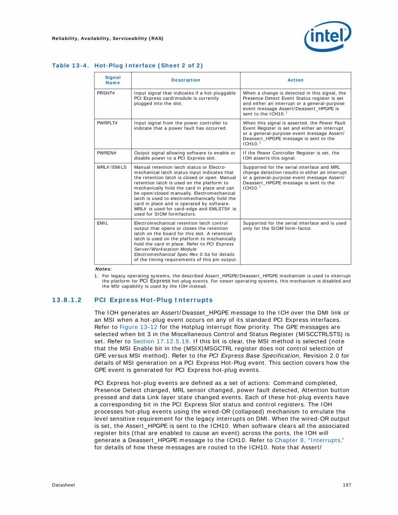
Datasheet 197
Reliability, Availability, Serviceability (RAS)
13.8.1.2 PCI Express Hot-Plug Interrupts
The IOH generates an Assert/Deasset_HPGPE message to the ICH over the DMI link or an MSI when a hot-plug event occurs on any of its standard PCI Express interfaces. Refer to Figure 13-12 for the Hotplug interrupt flow priority. The GPE messages are selected when bit 3 in the Miscellaneous Control and Status Register (MISCCTRLSTS) is set. Refer to Section 17.12.5.19. If this bit is clear, the MSI method is selected (note that the MSI Enable bit in the (MSIX)MSGCTRL register does not control selection of GPE versus MSI method). Refer to the PCI Express Base Specification, Revision 2.0 for details of MSI generation on a PCI Express Hot-Plug event. This section covers how the GPE event is generated for PCI Express hot-plug events.
PCI Express hot-plug events are defined as a set of actions: Command completed, Presence Detect changed, MRL sensor changed, power fault detected, Attention button pressed and data Link layer state changed events. Each of these hot-plug events have a corresponding bit in the PCI Express Slot status and control registers. The IOH processes hot-plug events using the wired-OR (collapsed) mechanism to emulate the level sensitive requirement for the legacy interrupts on DMI. When the wired-OR output is set, the Assert_HPGPE is sent to the ICH10. When software clears all the associated register bits (that are enabled to cause an event) across the ports, the IOH will generate a Deassert_HPGPE message to the ICH10. Refer to Chapter 8, “Interrupts,” for details of how these messages are routed to the ICH10. Note that Assert/
PRSNT# Input signal that indicates if a hot-pluggable PCI Express card/module is currently plugged into the slot.
When a change is detected in this signal, the Presence Detect Event Status register is set and either an interrupt or a general-purpose event message Assert/Deassert_HPGPE is sent to the ICH10.1
PWRFLT# Input signal from the power controller to indicate that a power fault has occurred.
When this signal is asserted, the Power Fault Event Register is set and either an interrupt or a general-purpose event message Assert/Deassert_HPGPE message is sent to the ICH10.1
PWREN# Output signal allowing software to enable or disable power to a PCI Express slot.
If the Power Controller Register is set, the IOH asserts this signal.
MRL#/EMILS Manual retention latch status or Electro-mechanical latch status input indicates that the retention latch is closed or open. Manual retention latch is used on the platform to mechanically hold the card in place and can be open/closed manually. Electromechanical latch is used to electromechanically hold the card in place and is operated by software. MRL# is used for card-edge and EMLSTS# is used for SIOM formfactors.
Supported for the serial interface and MRL change detection results in either an interrupt or a general-purpose event message Assert/Deassert_HPGPE message is sent to the ICH10.1
EMIL Electromechanical retention latch control output that opens or closes the retention latch on the board for this slot. A retention latch is used on the platform to mechanically hold the card in place. Refer to PCI Express Server/Workstation Module Electromechanical Spec Rev 0.5a for details of the timing requirements of this pin output.
Supported for the serial interface and is used only for the SIOM form-factor.
Notes:1. For legacy operating systems, the described Assert_HPGPE/Deassert_HPGPE mechanism is used to interrupt
the platform for PCI Express hot-plug events. For newer operating systems, this mechanism is disabled andthe MSI capability is used by the IOH instead.
Table 13-4. Hot-Plug Interface (Sheet 2 of 2)
Signal Name Description Action

Reliability, Availability, Serviceability (RAS)
198 Datasheet
Deassert_HPGPE messages could be received from downstream of a PCIe port (when that port connects to a downstream IOH) and these messages are collapsed with internally generated PMEGPE virtual wires as well.
Figure 13-12. PCI Express Hotplug Interrupt Flow
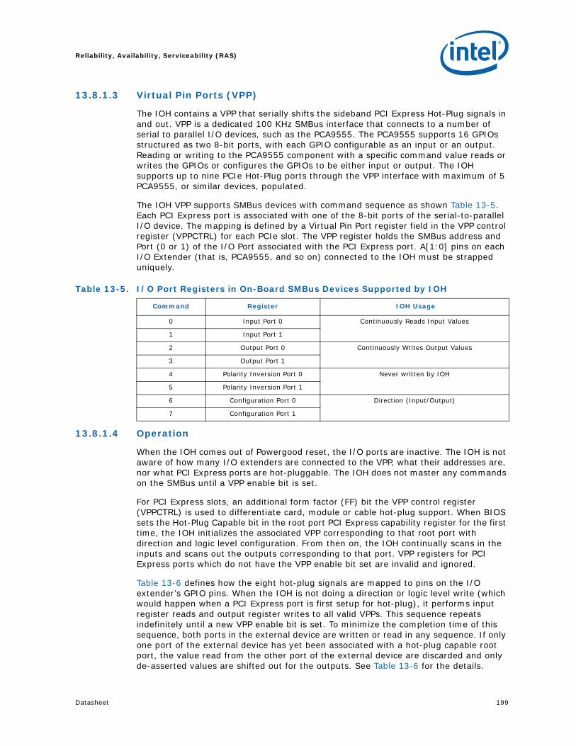
Datasheet 199
Reliability, Availability, Serviceability (RAS)
13.8.1.3 Virtual Pin Ports (VPP)
The IOH contains a VPP that serially shifts the sideband PCI Express Hot-Plug signals in and out. VPP is a dedicated 100 KHz SMBus interface that connects to a number of serial to parallel I/O devices, such as the PCA9555. The PCA9555 supports 16 GPIOs structured as two 8-bit ports, with each GPIO configurable as an input or an output. Reading or writing to the PCA9555 component with a specific command value reads or writes the GPIOs or configures the GPIOs to be either input or output. The IOH supports up to nine PCIe Hot-Plug ports through the VPP interface with maximum of 5 PCA9555, or similar devices, populated.
The IOH VPP supports SMBus devices with command sequence as shown Table 13-5. Each PCI Express port is associated with one of the 8-bit ports of the serial-to-parallel I/O device. The mapping is defined by a Virtual Pin Port register field in the VPP control register (VPPCTRL) for each PCIe slot. The VPP register holds the SMBus address and Port (0 or 1) of the I/O Port associated with the PCI Express port. A[1:0] pins on each I/O Extender (that is, PCA9555, and so on) connected to the IOH must be strapped uniquely.
13.8.1.4 Operation
When the IOH comes out of Powergood reset, the I/O ports are inactive. The IOH is not aware of how many I/O extenders are connected to the VPP, what their addresses are, nor what PCI Express ports are hot-pluggable. The IOH does not master any commands on the SMBus until a VPP enable bit is set.
For PCI Express slots, an additional form factor (FF) bit the VPP control register (VPPCTRL) is used to differentiate card, module or cable hot-plug support. When BIOS sets the Hot-Plug Capable bit in the root port PCI Express capability register for the first time, the IOH initializes the associated VPP corresponding to that root port with direction and logic level configuration. From then on, the IOH continually scans in the inputs and scans out the outputs corresponding to that port. VPP registers for PCI Express ports which do not have the VPP enable bit set are invalid and ignored.
Table 13-6 defines how the eight hot-plug signals are mapped to pins on the I/O extender’s GPIO pins. When the IOH is not doing a direction or logic level write (which would happen when a PCI Express port is first setup for hot-plug), it performs input register reads and output register writes to all valid VPPs. This sequence repeats indefinitely until a new VPP enable bit is set. To minimize the completion time of this sequence, both ports in the external device are written or read in any sequence. If only one port of the external device has yet been associated with a hot-plug capable root port, the value read from the other port of the external device are discarded and only de-asserted values are shifted out for the outputs. See Table 13-6 for the details.
Table 13-5. I/O Port Registers in On-Board SMBus Devices Supported by IOH
Command Register IOH Usage
0 Input Port 0 Continuously Reads Input Values
1 Input Port 1
2 Output Port 0 Continuously Writes Output Values
3 Output Port 1
4 Polarity Inversion Port 0 Never written by IOH
5 Polarity Inversion Port 1
6 Configuration Port 0 Direction (Input/Output)
7 Configuration Port 1

Reliability, Availability, Serviceability (RAS)
200 Datasheet
Table 13-7 describes the sequence generated for a write to an I/O port. Both 8-bit ports are always written. If a VPP is valid for the 8-bit port, the output values are updated as per the PCI Express Slot Control register for the associated PCI Express slot.
The IOH issues Read Commands to update the PCIe Slot Status register from the I/O port. The I/O port requires that a command be sent to sample the inputs, then another command is issued to return the data. The IOH always reads inputs from both 8-bit ports. If the VPP is valid, the IOH updates the associated PEXSLOTSTS (for PCIe)
Table 13-6. Hot-Plug Signals on the Virtual Pin Port
Bit Direction Voltage Logic Table Signal Logic True Meaning Logic
FalseMeaning
Bit 0 Output High_True ATNLED ATTN LED is to be turned ON
ATTN LED is to be turned OFF
Bit 1 Output High_True PWRLED PWR LED is to be turned ON
PWR LED is to be turned OFF
Bit 2 Output Low_True PWREN#Power is to be enabled on the slot
Power is NOT to be enabled on the slot
Bit 3 Input Low_True BUTTON# ATTN Button is pressed
ATTN Button is NOT pressed
Bit 4 Input Low_True PRSNT# Card Present in slot Card NOT Present in slot
Bit 5 Input Low_True PWRFLT# PWR Fault in the VRM NO PWR Fault in the VRM
Bit 6 Input Low_True/High_True MRL#/EMILS
MRL is open/EMILS is disengaged
MRL is closed/EMILS is engaged
Bit 7 Output High_True EMILToggle interlock state -Pulse output 100ms when ‘1’ is written
No effect
Table 13-7. Write Command
Bits IOH Drives I/O Port Drives Comment
1 Start SDL falling followed by SCL falling
7 Address[6:0][6:3] = 0100[2:0] = <Per the VPP Control Register (VPPCTL)>
1 0 indicates write.
1 ACK If NACK is received, IOH completes with stop and sets status bit in the VPP Status Register (VPPSTS).
8 Command Code
Register Address see Table 13-5[7:3]=00000,[2:1] = 01 for Output, 11 for Direction[0] = 0
1 ACK If NACK is received, IOH completes with stop and sets in the VPP Status Register (VPPSTS).
8 Data One bit for each I/O as per Table 13-6.
1 ACK If NACK is received, IOH completes with stop and sets in the VPP Status Register (VPPSTS).
8 Data One bit for each I/O as per Table 13-6
1 ACK If NACK is received, IOH completes with stop and sets in the VPP Status Register (VPPSTS).
1 Stop

Datasheet 201
Reliability, Availability, Serviceability (RAS)
register according to the values of MRL#/EMLSTS#, BUTTON#, PWRFLT# and PRSNT# read from the value register in the I/O port. Results from invalid VPPs are discarded. Table 13-8 defines the read command format.
§
Table 13-8. Read Command
Bits IOH Drives I/O Port Drives Comment
1 Start SDL falling followed by SCL falling.
7 Address[6:0] [6:2] = 01000[1:0] = <per the VPP Control Register (VPPCTL)>
1 0 indicates write.
1 ACK If NACK is received, IOH completes with stop and sets in the VPP Status Register (VPPSTS).
8 Command Code
Register Address [2:0] = 000
1 ACK If NACK is received, IOH completes with stop and sets in the VPP Status Register (VPPSTS).
1 Start SDL falling followed by SCL falling.
7 Address[6:0] [6:2] = 01000[1:0] = per the VPP Control Register (VPPCTL)>
1 1 indicates read.
8 DataOne bit for each I/O as per Table 13-6. The IOH always reads from both ports. Results for invalid VPPs are discarded.
1 ACK
8 DataOne bit for each I/O as per Table 13-6. The IOH always reads from both ports. Results for invalid VPPs are discarded.
1 NACK
1 Stop

Reliability, Availability, Serviceability (RAS)
202 Datasheet
Datasheet 203
Intel® Virtualization Technology
14 Intel® Virtualization Technology
Intel Virtualization Technology (Intel VT) is the technology that makes a single system appear as multiple independent systems to software. This allows for multiple independent operating systems to be running simultaneously on a single system. The first revision of this technology, Intel Virtualization Technology (Intel VT) for IA-32 Intel Architecture (Intel VT-x) added hardware support in the processor to improve the virtualization performance and robustness. The second revision of this specification, Intel Virtualization Technology (Intel VT) for Directed I/O (Intel VT-d), adds chipset hardware implementation to improve I/O performance and robustness.
14.1 Intel® VT-d Features• 48 bit maximum guest address width and 41/46/51 bit max host address width for
non-isoch traffic, in UP profilesNote: In this chapter, the term “isoch” will always be associated with Intel HD Audio. Isoch will not be associated with VCp traffic.
• Support for 4K page sizes only
• Support for register based fault recording only and support for MSI interrupts for faults
— Support for fault collapsing based on Requester ID, OS-visible ME PCI devices
• Support for both leaf and non-leaf caching
• Support for boot protection of default page table
• Support for non-caching of invalid page table entries
14.2 Intel® VT-d2 Features• Support for interrupt remapping
• Intel VT-d Features Not Supported
•No support for advance fault reporting
•No support for super pages
•No support for 1 or 2 level page walks for isoch remap engine, and 1, 2, or 3 level walks for non-isoch remap engine
§

Intel® Virtualization Technology
204 Datasheet

Datasheet 205
Signal List
15 Signal List
This chapter lists all the logical signals that interface to the IOH. This chapter should not be explicitly used to calculate the pin count for Intel X58 Express Chipset IOH. For a specific pin count or a description of the analog signals interfacing the IOH, refer to the Intel® Core™ i7 Processor Extreme Edition and Intel® Core™ i7 Processor Datasheet, and Intel® Xeon® Processor 3500 Series Datasheet.
15.1 ConventionsThe terms assertion and deassertion are used extensively when describing signals, to avoid confusion when working with a mix of active-high and active-low signals. The term assert, or assertion, indicates that the signal is active, independent of whether the active level is represented by a high or low voltage. The term deassert, or deassertion, indicates that the signal is inactive.
Signal names may or may not have a “_N” appended to them. The “_N” symbol at the end of a signal name indicates that the active, or asserted state occurs when the signal is at a low voltage level. When “_N” is not present after the signal name, the signal is asserted when at the high voltage level.
When discussing data values used inside the component, the logical value is used; that is, a data value described as “1101b” would appear as “1101b” on an active-high bus, and as “0010b” on an active-low bus. When discussing the assertion of a value on the actual pin, the physical value is used; that is, asserting an active-low signal produces a “0” value on the pin.
Table 15-1 and Table 15-2 list the reference terminology used later for buffer technology types (for example, HCSL, and so on) used and buffering signal types (for example, input, output, and so on) used.
Table 15-1. Buffer Technology Types
Buffer Type Description
QPI Current-mode 6.4 GT/s forwarded-clock QPI signaling
PCIEX2 Current-mode 5 GHz PCI Express 2nd-generation signaling
PCIEX Current-mode 2.5 GHz PCI Express 1st-generation signaling
HCSL Current-mode differential reference clock input
GPIO (SMBus) 3.3 V 100 KHz SMBus Open Drain output with Schmidt trigger input
CMOS 1.1 V 200 MHz CMOS totem-pole output with Schmidt trigger input
GPIO (JTAG) 1.1 V 20 MHz CMOS open-drain output with Schmidt trigger input
Analog Typically, a voltage reference or specialty power supply
DDR 1.8 V VDDR2 reference
Table 15-2. Buffer Signal Directions
Buffer Direction Description
I Input pin
O Output pin
I/O Bidirectional (input/output) pin
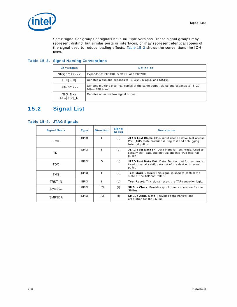
Signal List
206 Datasheet
Some signals or groups of signals have multiple versions. These signal groups may represent distinct but similar ports or interfaces, or may represent identical copies of the signal used to reduce loading effects. Table 15-3 shows the conventions the IOH uses.
15.2 Signal List
Table 15-3. Signal Naming Conventions
Convention Definition
SIG{0/1/2}XX Expands to: SIG0XX, SIG1XX, and SIG2XX
SIG[2:0] Denotes a bus and expands to: SIG[2], SIG[1], and SIG[0].
SIG(0/1/2) Denotes multiple electrical copies of the same output signal and expands to: SIG2, SIG1, and SIG0.
SIG_N or SIG[2:0]_N
Denotes an active low signal or bus.
Table 15-4. JTAG Signals
Signal Name Type Direction Signal Group Description
TCKGPIO I (u) JTAG Test Clock: Clock input used to drive Test Access
Port (TAP) state machine during test and debugging. Internal pullup
TDIGPIO I (u) JTAG Test Data In: Data input for test mode. Used to
serially shift data and instructions into TAP. Internal pullup
TDOGPIO O (u) JTAG Test Data Out: Data: Data output for test mode.
Used to serially shift data out of the device. Internal pullup
TMS GPIO I (u) Test Mode Select: This signal is used to control the state of the TAP controller.
TRST_N GPIO I (u) Test Reset: This signal resets the TAP controller logic.
SMBSCL GPIO I/O (t) SMBus Clock: Provides synchronous operation for the SMBus.
SMBSDA GPIO I/O (t) SMBus Addr/Data: Provides data transfer and arbitration for the SMBus.

Datasheet 207
Signal List
Table 15-5. QPI Signals
Signal Name Type Direction Signal Group Description
QPI{0}R{P/N}DAT[19:0] QPI I (a)
QPI Data Input (Outbound)
QPI{0}R{P/N}CLK QPI I (d) QPI Received Clock (Outbound)
QPI{0}T{P/N}DAT[19:0] QPI O (a)
QPI Data Output (Inbound)
QPI{0}T{P/N}CLK QPI O (d) QPI Forwarded Clock (Inbound)
QPI{0}{R/I}COMP Analog I/O (c) QPI Compensation: Used for the external impedance matching resistors.
QPI{0}RXBG[1:0] Analog I/O QPI external reference voltage signal. This is back-up mode in case of RX band-gap circuit failure
QPI{0}TXBG[1:0] Analog I/O QPI external reference voltage signal. This is back-up mode in case of TX band-gap circuit failure
QPI{0}REFCLK{P/N} HCSL I (d) QPI Reference Clock: Differential reference clock pair input.
QPIFREQSEL{1/0} CMOS I (e) QPI frequency selection: Used for determining the normal QPI operating frequency.
QPI{0}VRMVREFRX0 CMOS I
QPI RX external VRM vref. The IOH does not need this pin to be driven when QPI{0}VRMVREF is being internally generated. The QPI{0}VRMVREF as default is internally generate from IOH. Leave pin as No Connect.
QPI{0}VRMVREFRX1 CMOS I
QPI RX external VRM vref. The IOH does not need this pin to be driven when QPI{0}VRMVREF is being internally generated. The QPI{0}VRMVREF as default is internally generate from IOH. Leave pin as No Connect.
QPI{0}VRMVREFRX2 CMOS I
QPI RX external VRM vref. The IOH does not need this pin to be driven when QPI{0}VRMVREF is being internally generated. The QPI{0}VRMVREF as default is internally generate from IOH. Leave pin as No Connect.
QPI{0}VRMVREFRX3 CMOS I
QPI RX external VRM vref. The IOH does not need this pin to be driven when QPI{0}VRMVREF is being internally generated. The QPI{0}VRMVREF as default is internally generate from IOH. Leave pin as No Connect.
QPI{0}VRMVREFTX CMOS I
QPI TX external VRM vref. The IOH does not need this pin to be driven when QPI{0}VRMVREF is being internally generated. The QPI{0}VRMVREF as default is internally generate from IOH. Leave pin as No Connect.

Signal List
208 Datasheet
Table 15-6. PCI Express Signals
Signal Name Type Direction Signal Group Description
PE1T{P/N}[1:0] PCIEX2 O (g) PCI Express outbound data port1
PE1R{P/N}[1:0] PCIEX2 I (f) PCI Express inbound data port1
PE2T{P/N}[1:0] PCIEX2 O (g) PCI Express outbound data port2
PE2R{P/N}[1:0] PCIEX2 I (f) PCI Express inbound data port2
PE3T{P/N}[3:0] PCIEX2 O (g) PCI Express outbound data por3
PE3R{P/N}[3:0] PCIEX2 I (f) PCI Express inbound data port3
PE4T{P/N}[3:0] PCIEX2 O (g) PCI Express outbound data port4
PE4R{P/N}[3:0] PCIEX2 I (f) PCI Express inbound data port4
PE5T{P/N}[3:0] PCIEX2 O (g) PCI Express outbound data port5
PE5R{P/N}[3:0] PCIEX2 I (f) PCI Express inbound data port5
PE6T{P/N}[3:0] PCIEX2 O (g) PCI Express outbound data port6
PE6R{P/N}[3:0] PCIEX2 I (f) PCI Express inbound data port6
PE7T{P/N}[3:0] PCIEX2 O (g) PCI Express outbound data port7
PE7R{P/N}[3:0] PCIEX2 I (f) PCI Express inbound data port7
PE8T{P/N}[3:0] PCIEX2 O (g) PCI Express outbound data port8
PE8R{P/N}[3:0] PCIEX2 I (f) PCI Express inbound data port8
PE9T{P/N}[3:0] PCIEX2 O (g) PCI Express outbound data port9
PE9R{P/N}[3:0] PCIEX2 I (f) PCI Express inbound data port9
PE10T{P/N}[3:0] PCIEX2 O (g) PCI Express outbound data port10
PE10R{P/N}[3:0] PCIEX2 I (f) PCI Express inbound data port10
PE{0/1}CLK{P/N} HCSL I (j) PCI Express Reference Clock: Differential reference clock pair input.
PE{0/1}JCLK{P/N} HCSL I PCI Express PLL jitter injection clock. Recommend to leave these pins floating on external platforms.
PE{0/1}{RCOMPO/ICOMPO/ICOMPI}
ANALOG I/O (h) PCI Express Compensation: Used for the external impedance matching resistors.
PE{0/1}RBIAS ANALOG I/O h PCI Express clock: External resistance to generate 500uA absolute reference current bias.
PEHPSCL SMBus O PCI Express Hot-Plug SMBus Clock: Provides PCI Express Hot-Plug using dedicated SMBus.
PEHPSDA SMBus I/O PCI Express Hot-Plug SMBus Data: Provides PCI Express Hot-Plug using dedicated SMBus.
Table 15-7. DMI Signals
Signal Name Type Direction Signal Group Description
DMIR{P/N}[3:0] PCIEX I (k) DMI Inbound Data
DMIT{P/N}[3:0] PCIEX O (l) DMI Outbound Data

Datasheet 209
Signal List
Table 15-8. MISC Signals (Sheet 1 of 2)
Signal Type Direction Signal Group Description
XDPDQ[15:0] DDR I/O (y) XDP data bus
XDPCLK1XP DDR O (y) XDP clock. Clock 1x reference for XDP
XDPCLK1XN DDR O (y) XDP clock. Clock 1x reference for XDP complement
XDPRDYACK_N DDR O (y) XDP TO XDP Ready Acknowledge
XDPRDYREQ_N DDR I (y) XDP Ready Acknowledge
XDPDQS{P/N}[1:0] DDR I/O (y) XDP Strobe
VCCXDP18 Analog PWR XDP Power
VCCXDP Analog PWR XDP on-die termination
A20M_N GPIO I (r) A20M: Legacy signal from ICH. Translated to QPI message to CPU: “MASK ADDRESS BIT 20”
BMCINIT GPIO I (r)BMC initialized: QPI ports and IOH-IOH link stall indefinitely on power-up physical initialization until an external agent (BMC) releases them.
CORERST_N GPIO I (q) Reset input: Reset input driven by the system.
COREPWRGOOD GPIO I (q)
Core power good: Clears the IOH. This signal is held low until all power supplies and reference clocks are in specification. This signal is followed by CORERST_N de-assertion
AUXPWRGOOD GPIO I (q)
Auxiliary power good: Clears the IOH. This signal is held low until all power supplies and reference clocks are in specification. This signal is followed by CORERST_N de-assertion.
PLLPWRDET GPIO I (q)Auxiliary PLL power detect: Power and master clocks are stable so PLL’s can commence lock. Asserted prior to AUXPWRGOOD.
COREPLLPWRDET GPIO I (q)Core PLL power detect: Power and master clocks are stable so PLL’s can commence lock. Asserted prior to COREPWRGOOD.
DDRFREQ[3:2] GPIO I (r)
DDRFREQ[3:2] as DDR frequency selection defined as:00 = 133 MHz input, 200 MHz core01 = 100 MHz input, 200 MHz core10 = RSVD11 = RSVD
SINGLE_IOH GPIO I (r)
Used for dual IOH selection:0 = IOH is not connected to another IOH on some QPI
link1 = IOH is connected to another IOH on some QPI
link (default)
ERR_N[2:0] Smbus O (s) Error output signals
EXTSYSTRIG GPIO I/O (u) External System Trigger. Primary input to the on-die debug trigger mechanism.
FERR_N GPIO O (r) FERR: Legacy signal to ICH. Translated into QPI message to CPU: “FLOATING POINT ERROR”
INIT_N GPIO I (r) INIT: Legacy signal from ICH. Translated into QPI message to CPU: “INTERRUPT TO RESET VECTOR”
INTR GPIO I (r) INTR: Legacy signal from ICH. Translated into QPI message to CPU: “INTERRUPT”
LEGACYIOH GPIO I/O (r)Used to determine legacy or non-legacy selection:1 = Legacy IOH0 = Non-legacy IOH

Signal List
210 Datasheet
TXTRESET_N GPIO O (s) TXT reset is a mechanism that stops the platform due to a security violation. It is a trigger for a HARD reset.
NMI CMOS I (r) NMI: Legacy signal from ICH. Translated into QPI message to CPU: “NON-MASKABLE INTERRUPT”
PESBLCSEL GPIO I (i)PESBLCSEL: 0 = PCIE LC PLL (default)1 = PCIE SB PLL (backup)
PEWIDTH[5:0] GPIO I/O (i) PCIE Link Width Select.
CSIQPIFREQSEL[1:0] GPIO I (e)
QPI frequency selection: Used for determining the normal QPI operating frequency. “QPIFREQSEL1 & QPIFREQSEL0” decoded as follows:00 = 4.8 GT/s (300 MHz core frequency)01 = RSVD10 = 6.4 GT/s (400 MHz core frequency)11 = RSVD
QPISBLCSEL GPIO I (e)QPISBLCSEL: 0 = QPI LC PLL (default)1 = QPI SB PLL (backup)
RESETO_N GPIO O (u) RESETO_N: Reset signal to the CPU synchronized to QPICLK
SMBUSID GPIO I (r)SMBus ID: Indicates SMBus ID bits [7:4]. 1 = Indicates an upper-address ID of 1110 (Eh). 0 = Indicates an upper-address ID of 1100 (Ch).
SMI_N CMOS I (r)SMI: Legacy signal from ICH. Translated into QPI message to CPU: “SYSTEM MANAGEMENT INTERRUPT”
TEST[4:0] Analog I/O See Section 15.4.
TESTLO[26-21]; TESTLO[19-1] GPIO I
See Section 15.4
TESTHI[3:1] GPIO I See Section 15.4
VRMEN GPIO I
Voltage regulator module enable0 = QPI PLL uses on-die voltage regulator1 = QPI PLL uses LC-filtered power supplied to the
socket
THERMALERT_N GPIO O (s)
Thermal Alert signal, The THRMALERT_N will go active when the IOH temperature monitoring sensor detected that the IOH has reached its throttle threshold.
THERMTRIP_N GPIO O (s)Assertion of THERMTRIP# (Thermal Trip) indicates the IOH junction temperature has reached a level beyond which permanent silicon damage may occur.
TSIREF Analog I Thermal sensor current reference connected to external; resistor of 2.5 KOhm to GND.
DDRPLLREFCLK{P/N} DDR I/O DDR Reference Clock
Table 15-8. MISC Signals (Sheet 2 of 2)
Signal Type Direction Signal Group Description

Datasheet 211
Signal List
Table 15-9. Controller Link Signals
Signal Name Type Direction Signal Group Description
CLCLK CMOS I/O (m) Clink bi-directional clock
CLDATA CMOS I/O (m) Clink bi-directional data
CLRST_N CMOS I (m) Active low Clink reset
Table 15-10.RMII Signals
Signal Name Type Direction Signal Group Description
RMIITXD[1:0] RMII (GPIO) O (y)
Transmit data
RMIIRXD[1:0] RMII (GPIO) I (y)
Receive data
RMIITXEN RMII (GPIO) O (y)
Transmit enable
RMIICRSDV RMII (GPIO) I (y)
Carrier sense/receive data valid
RMIICLK RMII (GPIO) I (y)
Reference clock
RMIIMDIO RMII (GPIO) I/O (y)
Data signal for PHY management bus
RMIIMDC RMII (GPIO) O (y)
Clock for PHY management bus
RMIICLKREFOUT RMII (GPIO) O (y)
50MHz clock reference output
Table 15-11.Power and Ground (Sheet 1 of 2)
Signal Name Voltage Description
VCCAQPI{0}TX 1.1V QPI analog power supply
VCCAQPI{0}PLL 1.1V QPI analog supply voltage for PLL core
VCCAQPI{0}RX 1.1V QPI analog power supply
VCCQPI{0}VRMTXOP0 1.1V
QPI TX VRM power. When VRMEN pin is set to 0, VCCQPIxVRMRXOPx pins are outputs; when set to 1, VCCQPIxVRMRXOPx are inputs. In normal mode, these are debug/observation signals to measure output of the internal VRMs. In bypass mode, internal VRMs are disabled and these pins supply external VCC 1.1 for TX PLL. They should not be shorted and connected as a power pin.
VCCQPI{0}VRMRXOP0 1.1V
QPI RX VRM power. When VRMEN pin is set to 0, VCCQPIxVRMRXOPx pins are outputs; when set to 1, VCCQPIxVRMRXOPx are inputs. In normal mode, these are debug/observation signals to measure output of the internal VRMs. In bypass mode, internal VRMs are disabled and these pins supply external VCC 1.1 for to 4 sets of RX DLLs. They should not be shorted and connected as a power pin.
VCCQPI{0}VRMRXOP1 1.1V
QPI RX VRM power. When VRMEN pin is set to 0, VCCQPIxVRMRXOPx pins are outputs; when set to 1, VCCQPIxVRMRXOPx are inputs. In normal mode, these are debug/observation signals to measure output of the internal VRMs. In bypass mode, internal VRMs are disabled and these pins supply external VCC 1.1 for to 4 sets of RX DLLs. They should not be shorted and connected as a power pin.

Signal List
212 Datasheet
VCCQPI{0}VRMRXOP2 1.1V
QPI RX VRM power. When VRMEN pin is set to 0, VCCQPIxVRMRXOPx pins are outputs; when set to 1, VCCQPIxVRMRXOPx are inputs. In normal mode, these are debug/observation signals to measure output of the internal VRMs. In bypass mode, internal VRMs are disabled and these pins supply external VCC 1.1 for to 4 sets of RX DLLs. They should not be shorted and connected as a power pin.
VCCQPI{0}VRMRXOP3 1.1V
QPI RX VRM power. When VRMEN pin is set to 0, VCCQPIxVRMRXOPx pins are outputs; when set to 1, VCCQPIxVRMRXOPx are inputs. In normal mode, these are debug/observation signals to measure output of the internal VRMs. In bypass mode, internal VRMs are disabled and these pins supply external VCC 1.1 for to 4 sets of RX DLLs. They should not be shorted and connected as a power pin.
VCCAQPI{0}RXBG 1.1V QPI analog power supply used exclusively by RX band-gap block.
VCCQPI{0}VRMRX0 1.8V QPI external power, connect to 1.8V VRM power bump
VCCQPI{0}VRMRX1 1.8V QPI external power, connect to 1.8V VRM power bump
VCCQPI{0}VRMRX2 1.8V QPI external power, connect to 1.8V VRM power bump
VCCQPI{0}VRMRX3 1.8 V QPI external power, connect to 1.8 V VRM power bump
VCCAPE 1.1 V VCC for DMIPCI Express analog circuits
VCCAPEBG 1.5 V Analog VCC for PCI Express band gap circuit
VCCAPE1BG 1.5 V Analog VCC for PCI Express band gap circuit
VCCAPEPLL 1.1 V Analog VCC for PCI Express PLL analog core
VCCPEVRM 1.5 V PCI Express VRM power supply
VCCAPE1PLL 1.1 VAnalog VCC for PCI Express PLL analog core. Note that the power to this pin is only used when the Internal PCIe VRM is not being used. The Intel X58 Express Chipset POR is not to utilize this signal.
VCCDPE1PLL 1.1 V PCI Express PLL digital power supply
VCCPE1VRM 1.5 VPCI Express VRM power supply. Note that the power to this pin is only used when the Internal PCIe VRM is not being used. The Intel X58 Express Chipset POR is not to utilize this signal.
VCCDDR18 1.8 v 1.8 V FOR DDR2
VTTDDR 0.9 V 1/2 of VCCDDR
VCCDDR18 1.8 V 1.8 V DDR I/O supply
VTTDDR 0.9 V 0.9 V Termination Power for DDR IO
VCCXDP18 1.8 V XDP I/O voltage
VTTXDP 0.9 V 1/2 of XDP
VREFCL 0.33 V 0.3VCC
VCCCLPWRP 1.1 V CLINK I/O power
VCCEPW 1.1 V 1.1 V/1.1 V AUX domain
VCCMISC33 3.3 V GPIO 3.3 V power
VCCMISC33EPW 3.3 V 3.3 V AUX domain
VCCTS 1.5 V Thermal sensor high voltage power supply 1.5 V ±5%
VSS 0 V Ground
Table 15-11.Power and Ground (Sheet 2 of 2)
Signal Name Voltage Description

Datasheet 213
Signal List
Table 15-12.IOH Strapping Signal
CPU Visible
Dual IOH
Visible
QPI Port to
CPU
QPI Port # to Dual
IOHPhysical Straps
Legacy IOH
Node ID[42]
Node ID[42] Port ID Port ID Legacy
IOHTESTHI1
FW_AgentDual IOH
Dual IOH QPI
PRTSEL
TESTLO6/NID2
Normal UP/DP 1 0 0 Actual NA 1 1 0 0 0
Legacy Dual IOH UP/DP
1 0 0 0 1 1 1 1 0 0
Legacy Dual IOH UP/DP
1 0 0 0 1 1 1 1 0 1
Non-Legacy Dual IOH UP/DP
0 0 0 1 0 0 1 1 0 0
Non-Legacy Dual IOH UP/DP
0 0 0 1 0 0 1 1 0 1
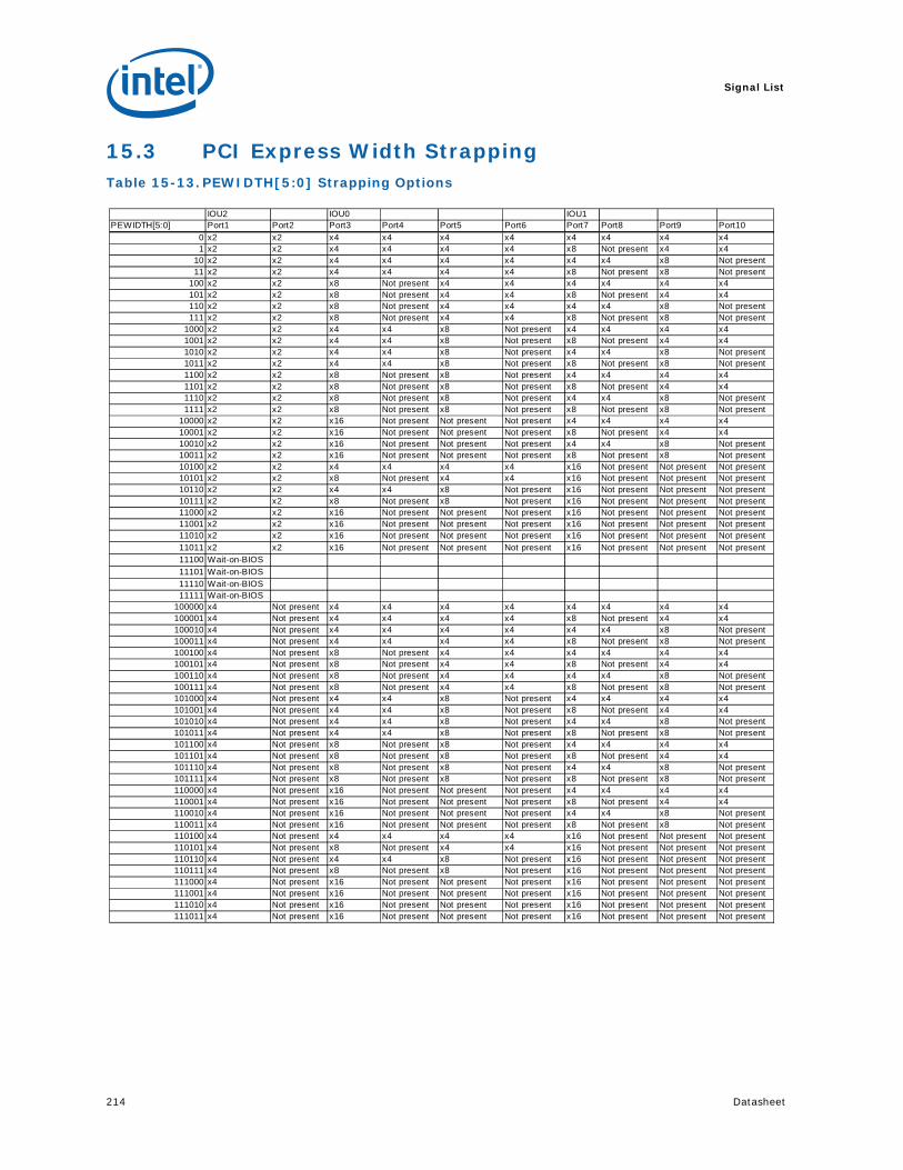
Signal List
214 Datasheet
15.3 PCI Express Width StrappingTable 15-13.PEWIDTH[5:0] Strapping Options
IOU2 IOU0 IOU1PEWIDTH[5:0] Port1 Port2 Port3 Port4 Port5 Port6 Port7 Port8 Port9 Port10
0 x2 x2 x4 x4 x4 x4 x4 x4 x4 x41 x2 x2 x4 x4 x4 x4 x8 Not present x4 x4
10 x2 x2 x4 x4 x4 x4 x4 x4 x8 Not present11 x2 x2 x4 x4 x4 x4 x8 Not present x8 Not present
100 x2 x2 x8 Not present x4 x4 x4 x4 x4 x4101 x2 x2 x8 Not present x4 x4 x8 Not present x4 x4110 x2 x2 x8 Not present x4 x4 x4 x4 x8 Not present111 x2 x2 x8 Not present x4 x4 x8 Not present x8 Not present
1000 x2 x2 x4 x4 x8 Not present x4 x4 x4 x41001 x2 x2 x4 x4 x8 Not present x8 Not present x4 x41010 x2 x2 x4 x4 x8 Not present x4 x4 x8 Not present1011 x2 x2 x4 x4 x8 Not present x8 Not present x8 Not present1100 x2 x2 x8 Not present x8 Not present x4 x4 x4 x41101 x2 x2 x8 Not present x8 Not present x8 Not present x4 x41110 x2 x2 x8 Not present x8 Not present x4 x4 x8 Not present1111 x2 x2 x8 Not present x8 Not present x8 Not present x8 Not present
10000 x2 x2 x16 Not present Not present Not present x4 x4 x4 x410001 x2 x2 x16 Not present Not present Not present x8 Not present x4 x410010 x2 x2 x16 Not present Not present Not present x4 x4 x8 Not present10011 x2 x2 x16 Not present Not present Not present x8 Not present x8 Not present10100 x2 x2 x4 x4 x4 x4 x16 Not present Not present Not present10101 x2 x2 x8 Not present x4 x4 x16 Not present Not present Not present10110 x2 x2 x4 x4 x8 Not present x16 Not present Not present Not present10111 x2 x2 x8 Not present x8 Not present x16 Not present Not present Not present11000 x2 x2 x16 Not present Not present Not present x16 Not present Not present Not present11001 x2 x2 x16 Not present Not present Not present x16 Not present Not present Not present11010 x2 x2 x16 Not present Not present Not present x16 Not present Not present Not present11011 x2 x2 x16 Not present Not present Not present x16 Not present Not present Not present11100 Wait-on-BIOS
11101 Wait-on-BIOS 11110 Wait-on-BIOS 11111 Wait-on-BIOS
100000 x4 Not present x4 x4 x4 x4 x4 x4 x4 x4100001 x4 Not present x4 x4 x4 x4 x8 Not present x4 x4100010 x4 Not present x4 x4 x4 x4 x4 x4 x8 Not present100011 x4 Not present x4 x4 x4 x4 x8 Not present x8 Not present100100 x4 Not present x8 Not present x4 x4 x4 x4 x4 x4100101 x4 Not present x8 Not present x4 x4 x8 Not present x4 x4100110 x4 Not present x8 Not present x4 x4 x4 x4 x8 Not present100111 x4 Not present x8 Not present x4 x4 x8 Not present x8 Not present101000 x4 Not present x4 x4 x8 Not present x4 x4 x4 x4101001 x4 Not present x4 x4 x8 Not present x8 Not present x4 x4101010 x4 Not present x4 x4 x8 Not present x4 x4 x8 Not present101011 x4 Not present x4 x4 x8 Not present x8 Not present x8 Not present101100 x4 Not present x8 Not present x8 Not present x4 x4 x4 x4101101 x4 Not present x8 Not present x8 Not present x8 Not present x4 x4101110 x4 Not present x8 Not present x8 Not present x4 x4 x8 Not present101111 x4 Not present x8 Not present x8 Not present x8 Not present x8 Not present110000 x4 Not present x16 Not present Not present Not present x4 x4 x4 x4110001 x4 Not present x16 Not present Not present Not present x8 Not present x4 x4110010 x4 Not present x16 Not present Not present Not present x4 x4 x8 Not present110011 x4 Not present x16 Not present Not present Not present x8 Not present x8 Not present110100 x4 Not present x4 x4 x4 x4 x16 Not present Not present Not present110101 x4 Not present x8 Not present x4 x4 x16 Not present Not present Not present110110 x4 Not present x4 x4 x8 Not present x16 Not present Not present Not present110111 x4 Not present x8 Not present x8 Not present x16 Not present Not present Not present111000 x4 Not present x16 Not present Not present Not present x16 Not present Not present Not present111001 x4 Not present x16 Not present Not present Not present x16 Not present Not present Not present111010 x4 Not present x16 Not present Not present Not present x16 Not present Not present Not present111011 x4 Not present x16 Not present Not present Not present x16 Not present Not present Not present

Datasheet 215
Signal List
15.4 IOH Signal Strappings
Pin name Location Connection
TEST0 A2
In Circuit Test: This signal should be connected to a test point on the motherbaord. It is internally shorted to the package ground and can be used to determine if the corner ball on the IOH are correctly soldered down to the motherboard. This signal should NOT connect to ground on the motherboard. If TEST0 is not going to be used, it should be left as No Connect.
TEST1 A36
In Circuit Test: This signal should be connected to a test point on the motherbaord. It is internally shorted to the package ground and can be used to determine if the corner ball on the IOH are correctly soldered down to the motherboard. This signal should NOT connect to ground on the motherboard. If TEST1 is not going to be used, it should be left as No Connect.
TEST2 B1
In Circuit Test: This signal should be connected to a test point on the motherbaord. It is internally shorted to the package ground and can be used to determine if the corner ball on the IOH are correctly soldered down to the motherboard. This signal should NOT connect to ground on the motherboard. If TEST2 is not going to be used, it should be left as No Connect.
TEST3 AT1
In Circuit Test: This signal should be connected to a test point on the motherbaord. It is internally shorted to the package ground and can be used to determine if the corner ball on the IOH are correctly soldered down to the motherboard. This signal should NOT connect to ground on the motherboard. If TEST3 is not going to be used, it should be left as No Connect.
TEST4 AT36
In Circuit Test: This signal should be connected to a test point on the motherbaord. It is internally shorted to the package ground and can be used to determine if the corner ball on the IOH are correctly soldered down to the motherboard. This signal should NOT connect to ground on the motherboard. If TEST4 is not going to be used, it should be left as No Connect.
TESTHI1 P29If ME used: Pull up to P1V1_STBY_IOH using a 10K ohm ±5% resistor. If ME not used: Pull up to P1V1_STBY_IOH or P1V1_VCC using a 10K ohm ±5% resistor.
TESTHI2 U28
Connect to debug port XDP. If ME used: Pull up to P1V1_STBY_IOH using a 51 ohm ±1% resistor. If ME not used: Pull up to P1V1_STBY_IOH or P1V1_VCC using a 51 ohm ±1% resistor.
TESTHI3 R29If ME used: Pull up to P1V1_STBY_IOH=VCCEPW using a 10K Ohm ±5% resistor. If ME not used: Pull up to P1V1_STBY_IOH=VCCEPW or P1V1_VCC using a 10K Ohm ±5% resistor.
TESTLO1 AR12 Pull down using 1K ohm ±1% resistor
TESTLO2 AN9 Pull down using 1K ohm ±1% resistor
TESTLO3 AN8 Pull down using 1K ohm ±1% resistor
TESTLO4 AM6 Pull down using 1K ohm ±1% resistor
TESTLO5 AJ34 Pull down using 1K ohm ±1% resistor
TESTLO6 AH34 Pull down using 100 ohm ±1% resistor
TESTLO7 AH33 Pull down using 100 ohm ±1% resistor
TESTLO8 AF35 Pull down using 1K ohm ±1% resistor
TESTLO9 AF34 Pull down using 0 ohm ±5% resistor
TESTLO10 AF32 Pull down using 1K ohm ±1% resistor
TESTLO11 AE34 Pull down using 1K ohm ±1% resistor
TESTLO12 AC32 Pull down using 1K ohm ±1% resistor
TESTLO13 AB30 Pull down using 1K ohm ±1% resistor
TESTLO14 AA29 Pull down using 100 ohm ±1% resistor
TESTLO15 Y28 Pull down using 1K ohm ±1% resistor

Signal List
216 Datasheet
§
TESTLO16 W27 Pull down using 1K ohm ±1% resistor
TESTLO17 V32 Pull down using 1K ohm ±1% resistor
TESTLO18 T27 Pull down using 100 ohm ±1% resistor
TESTLO19 R35 Pull down using 1K ohm ±1% resistor
TESTLO21 AD33 Pull down using 10K ohm ±1% resistor
TESTLO22 C33 Pull down using 10K ohm ±1% resistor
TESTLO23 AC29 Pull down using 10K ohm ±1% resistor
TESTLO24 AA26 Pull down using 10K ohm ±1% resistor
TESETLO26 D36 Pull down using 10K ohm ±1% resistor
XOROUT AE33 Pull down using 10K ohm ±1% resistor
Pin name Location Connection

Datasheet 217
DC Electrical Specifications
16 DC Electrical Specifications
In this chapter each interface is divided into groups of signals that have similar characteristics and buffer types based on the table in the signal list.
This chapter documents the DC characteristics of the IOH. The specifications are split into five sections:
• Clocks
• PCI Express/DMI
• CMOS
• JTAG Interface
• SMBus Interface
Notes:1. Refer to Figure 16-1 Differential Clock Crosspoint Specification and Figure 16-2 Differential Clock
Waveform.2. Crossing voltage is defined as the instantaneous voltage when the rising edge of CORECLKP is equal to the
falling edge of CORECLKN.3. Overshoot is defined as the absolute value of the maximum voltage.
Table 16-1. Clock DC Characteristics
Symbol Signal Group Parameter Min Nom Max Unit Note
s
133 MHz
VIL (d) Input Low Voltage -0.150 0 0.150 V 1
VIH (d) Input High Voltage 0.660 0.700 0.850 V
VCROSS(abs) (d) Absolute Crossing Point 0.250 — 0.550 V 2, 7
VCROSS(rel) (d)Relative Crossing Point 0.250 + 0.5
x (VHavg – 0.700) — 0.550 – 0.5x (0.700 – VHavg)
V 7, 8
VCROSS (d) Range of Crossing Points — — 0.140 V
VOS (d) Overshoot — — VIH + 0.300 V 3
VUS (d) Undershoot -0.300 — — V 4
VRBM (d) Ringback Margin 0.200 — — V 5
VTR (d) Threshold Region VCROSS – 0.100 — VCROSS + 0.100 V 6
100 MHz
VIL (j) Input Low Voltage -0.150 0 — V
VIH (j) Input High Voltage 0.660 0.700 0.850 V
VCROSS(abs) (j) Absolute Crossing Point 0.250 — 0.550 V 2, 7
VCROSS(rel) (j)Relative Crossing Point 0.250 + 0.5
x (VHavg – 0.700) — 0.550 + 0.5x (VHavg – 0.700) V 7, 8
VCROSS (j) Range of Crossing Points — — 0.140 V 1, 2
VOS (j) Overshoot — — VIH + 0.300 V 3
VUS (j) Undershoot -0.300 — — V 4
VRBM (j) Ringback Margin 0.200 — — V 5
VTR (j) Threshold Region VCROSS – 0.100 — VCROSS + 0.100 V 6

DC Electrical Specifications
218 Datasheet
4. Undershoot is defined as the absolute value of the minimum voltage.5. Ringback Margin is defined as the absolute voltage difference between the maximum Rising Edge Ringback
and the maximum Falling Edge Ringback. Both maximum Rising and Falling Ringbacks should not cross the threshold region.
6. Threshold Region is defined as a region centered around the crossing point voltage in which the differential receiver switches. It includes input threshold hysteresis.
7. The crossing point must meet the absolute and relative crossing point specifications simultaneously.8. VHavg (the average of VIH) can be measured directly using “Vtop” on Agilent* scopes and “High” on
Tektronix* scopes.
16.1 PCI Express / DMI Interface DC Characteristics
Notes:1. No test load is necessarily associated with this value.2. Specified at the measurement point into a timing and voltage compliance test load and measured over any 250 consecutive
TX UIs.
Notes:1. No test load is necessarily associated with this value.2. Specified at the measurement point and measured over any 250 consecutive UIs. If the clock to the RX and TX are not
derived from the same reference clock, the TX UI recovered from 3500 consecutive UI must be used as a reference for the eye diagram.
3. A TRX-EYE=0.40UI provides for a total sum of 0.60 UI deterministic and random jitter budget for the Transmitter and interconnect collected any 250 consecutive UIs. The TRX-EYE-MEDIAN-to-MAX-JITTER specification ensures a jitter distribution in which the median and the maximum deusingtion from the median is less than half of the total.6 UI jitter budget collected over any 250 consecutive TX UIs. It should be noted that the median is not the same as the mean. The jitter median describes the point in time where the number of jitter points on either side is approximately equal as opposed to the averaged time value. If the clocks to the RX and TX are not derived from the same reference clock, the TX UI recovered from 3500 consecutive UI must be used as the reference for the eye diagram.
4. The Receiver input impedance shall result in a differential return loss greater than or equal to 15 dB with the D+ line biased to 300mV and the D- line biased to -300 mV and a common mode return loss greater than or equal to 6 dB (no bias required) over a frequency range of 50 MHz to 1.25 GHz. This input impedance requirement applies to all valid input levels. The reference impedance for return loss measurements for is 50 ohms to ground for both the D+ and D- line (i.e., as measured by a Vector Network Analyzer with 50 ohm probes). Note: that the series capacitors CTX is optional for the return loss measurement.
Table 16-2. PCI Express / DMI Differential Transmitter (Tx) Output DC Characteristics
Symbol Signal Group Parameter Min Nom Max Unit Notes
VTX-CM-DC-ACTIVE-IDLE-DELTA
(f) (k) Absolute Delta of DC Common Mode Voltage During L0 and Electrical Idle
0 — 100 mV 2
VTX-CM-DC-LINE-DELTA
(f) (k) Absolute Delta of DC Common Mode Voltage between D+ and D-
0 — 25 mV 2
VTX-IDLE-DIFFp
(f) (k) Electrical Idle Differential Peak Output Voltage — — 20 mV 2
VTX-RCV-DETECT
(f) (k) The amount of voltage change allowed during Receiver Detection
— — 600 mV
VTX-DC-CM (f) (k) The TX DC Common Mode Voltage 0 — 3.6 V 2
ITX-SHORT (f) (k) The Short Circuit Current Limit — — 90 mA
ZTX-DIFF-DC (f) (k) DC Differential TX Impedance 80 100 120
ZTX-DC (f) (k) Transmitter DC Impedance 40 — —
Table 16-3. PCI Express / DMI Differential Receiver (Rx) Input DC Characteristics
Symbol Signal Group Parameter Min Nom Max Unit Notes
ZRX-DIFF-DC (g) (l) DC Differential Input Impedance 80 100 120 5
ZRX-DC (g) (l) DC Input Impedance 40 50 60 2, 3
ZRX-High-Imp-DC (g) (l) Power Down DC Input Common Mode Impedance
200 — — k 6
VRX-IDLE-DET-DIFFp (g) (l) Electrical Idle Detect Threshold 65 — 175 mV

Datasheet 219
DC Electrical Specifications
16.2 Miscellaneous DC Characteristics
Table 16-4. CMOS, JTAG, SMBUS, GPIO3.3V, CMOS3.3V, MISC, and RMII DC Characteristics
Symbol Signal Group Parameter Min Nom Max Unit Notes
GPIO1.1 (CMOS) I/O Signals
VOH_CMOS (r) Output High Voltage 0.75*Vcc1.1V — — V
VOL_CMOS (r) Output Low Voltage — — 0.25*Vcc1.1V V
VIH_CMOS (r) Input High Voltage 0.65*Vcc1.1V — Vcc1.1v+0.2 V
VIL_CMOS (r) Input Low Voltage -0.2 — 0.35*Vcc1.1V V
IOH_CMOS (r) Output High Current 4 — — mA
IOL_CMOS (r) Output Low Current 4 — — mA
ILEAK_CMOS (r) Leakage Current — — 15 A
CPAD_CMOS (r) Pad Capacitance — — 7 pF
CMOS3.3v (CMOS) Signals
VOH_CMOS3.3 (q) Output High Voltage 2.4 — — V
VOL_CMOS3.3 (q) Output Low Voltage — — 0.4 V
VIH_CMOS3.3 (q) Input High Voltage 2.1 — V
VIL_CMOS3.3 (q) Input Low Voltage — — 0.8 V
IOL_CMOS3.3 (q) Output Low Current 4 — — mA
ILEAK_CMOS3.3 (q) Leakage Current — — 15 A
CPAD_CMOS3.3 (q) Pad Capacitance — — 10 pF
GPIO3.3(OD) Signals
VOH_GPIO3.3 (s) Output High Voltage N/A — — V 1
VOL_GPIO3.3 (s) Output Low Voltage — — 0.4 V
VIH_GPIO3.3 (s) Input High Voltage 2.1 — — V
VIL_GPIO3.3 (s) Input Low Voltage — — 0.8 V
IOL_GPIO3.3 (s) Output Low Current 4 — — mA
ILEAK_GPIO3.3 (s) Leakage Current — — 15 A
CPAD_GPIO3.3 (s) Pad Capacitance — — 10 pF
SMBUS Signals
VOH_SMBUS (t) Output High Voltage N/A — — V
VOL_SMBUS (t) Output Low Voltage — — 0.4 V
VIH_SMBUS (t) Input High Voltage 2.1 — — V
VIL_SMBUS (t) Input Low Voltage — — 0.8 V
IOL_SMBUS (t) Output Low Current 4 — — mA
ILEAK_SMBUS (t) Leakage Current — — 10 A
CBUS_SMBUS (t) BUS Capacitance — — 400 pF
JTAG and GPIO1.1(OD) Signals
VOH_JTAG (u) Output High Voltage N/A — N/A V

DC Electrical Specifications
220 Datasheet
Note: N/A for Open Drain pins ERR_N, THREMTRIP_N, THERMALERT_N, LTRESET_N
VOL_JTAG (u) Output Low Voltage — — 0.25*Vcc1.1V V
VIH_JTAG (u) Input High Voltage 0.65*Vcc1.1V — — V
VIL_JTAG (u) Input Low Voltage — — 0.35*Vcc1.1V V
IOL_JTAG (u) Output Low Current 16 — — mA
ILEAK_JTAG (u) Leakage Current — — 15 A
CPAD_JTAG (u) Pad Capacitance — — 7 pF
RMII Signals
VREF (y) Bus high reference 3.0 3.3 3.6 V
VABS (y) Signal voltage range -0.3 — 3.765 V
VIL (y) Input Low Voltage — — 0.8 V
VIH (y) Input High Voltage 2 — — V
VOH (y) Output High Voltage 2.4 — — V
VOL (y) Output Low Voltage 0 — 400 mV
IIH (y) Input High Current 0 — 200 A
IIL (y) Input Low Current -20 — 0 A
ILEAK (y) Leakage Current -20 — 20 A
VCKM (y) Clock Midpoint Ref. Level — — 1.4 V
Table 16-4. CMOS, JTAG, SMBUS, GPIO3.3V, CMOS3.3V, MISC, and RMII DC Characteristics
Symbol Signal Group Parameter Min Nom Max Unit Notes
Figure 16-1. Differential Measurement Point for Rise and Fall Time
VIH = +150 mV
0.0 V
VIL = -150 mV
REFCLK+minus
Rise Edge Ratio Fall Edge Ratio

Datasheet 221
DC Electrical Specifications
§
Figure 16-2. Differential Measurement Point for Ringback
TSTABLE
VIH = +150 mV
VIL = -150 mVVRB = -100 mV
VRB = +100 mV0 mV
TSTABLE
TRB
TRB

DC Electrical Specifications
222 Datasheet

Datasheet 223
Configuration Register Space
17 Configuration Register Space
This chapter describes both the PCI configuration space and CSRCFG configuration space registers.
17.1 Device Mapping—Functions Specially Routed by the IOHAll devices on the IOH reside on Bus 0. The following table describes the devices and functions that the IOH implements or routes specially.
Notes:1. Only supported by UP Intel X58 Express Chipset performance component.
Table 17-1. Functions Specially Handled by the IOH
Register Group DID Device Function Comment
DMI (Device 0 in DMI mode) 0011_0100_0000_0xxxb 0 0
The DMI port will have the last 3 bits of the DID (xxx)IOH = 0
PCI Express Root Port 0 (Device 0 in PCIe mode)
3420hor 3421h
0 0Device 0
PCI Express Root Port 1 3408h 1 0 x4 or x2 max link width
PCI Express Root Port 2 3409h 2 0 x2 max link width
PCI Express Root Port 3 340Ah 3 0 x16, x8, or x4 max link width
PCI Express Root Port 4 340Bh 4 0 x4 max link width1
PCI Express Root Port 5 340Ch 5 0 x8 or x4 max link width1
PCI Express Root Port 6 340Dh 6 0 x4 max link width1
PCI Express Root Port 7 340Eh 7 0 x16, x8, or x4 max link width
PCI Express Root Port 8 340Fh 8 0 x4 max link width
PCI Express Root Port 9 3410h 9 0 x8 or x4 max link width
PCI Express Root Port 10 3411h 10 0 x4 max link width
Intel QuickPath Interconnect Port 0 3425h 16 0
Intel QuickPath Interconnect Port 0 3426h 16 1
Intel QuickPath Interconnect Port 1 3427h 17 0
Intel QuickPath Interconnect Port 1 3428h 17 1
IOxAPIC 342Dh 19 0
Core 342Eh 20 0 Address mapping, VTd, Ctrl/Status, Misc.Registers
Core 3422h 20 1 Scratchpads and GPIO registers
Core 3423h 20 2 IOH control/status and RAS registers
Core 3438h 20 3 Throttling registers

Configuration Register Space
224 Datasheet
17.2 Unimplemented Devices/Functions and RegistersConfiguration reads to unimplemented functions and devices will return all ones emulating a master abort response. There is no asynchronous error reporting when a configuration read master aborts. Configuration writes to unimplemented functions and devices will return a normal response to Intel QuickPath Interconnect.
Software should not attempt or rely on reads or writes to unimplemented registers or register bits. Unimplemented registers return all zeroes when read. Writes to unimplemented registers are ignored. For configuration writes to these registers, the completion is returned with a normal completion status (not master-aborted).
17.2.1 Register Attribute Definition
The bits in the configuration register descriptions will all be assigned attributes. The following table defines all the attributes types. All bits will be set to their default value by any reset that resets the IOH core, except the Sticky bits. Sticky bits are only reset by the PWRGOOD reset.
Table 17-2. Register Attributes Definitions (Sheet 1 of 2)
Attr Description
RO Read Only: These bits can only be read by software, writes have no effect. The value of the bits is determined by the hardware only.
RW Read / Write: These bits can be read and written by software.
RWO Read / Write Once: These bits can be read by software. After reset, these bits can only be written by software once, after which the bits becomes ‘Read Only’.
RWL Read / Write Lock: These bits can be read and written by software. Hardware can make these bits ‘Read Only’ using a separate configuration bit or other logic.
RW1C Read / Write 1 to Clear: These bits can be read and cleared by software. Writing a 1 to a bit clears it, while writing a 0 to a bit has no effect.
RCRead Clear: These bits can only be read by software, but a read causes the bits to be cleared.NOTE: Use of this attribute type is deprecated, as reads with side-effects are harmful for debug.
RCWRead Clear / Write: These bits can be read and written by software, but a read causes the bits to be cleared. NOTE: Use of this attribute type is deprecated, as reads with side-effects are harmful for debug.
ROSRO Sticky: These bits can only be read by software, writes have no effect. The value of the bits is determined by the hardware only. These bits are only re-initialized to their default value by a PWRGOOD reset.
RWS R / W Sticky: These bits can be read and written by software. These bits are only re-initialized to their default value by a PWRGOOD reset.
RW1CSR / W1C Sticky: These bits can be read and cleared by software. Writing a 1 to a bit clears it, while writing a 0 to a bit has no effect. These bits are only re-initialized to their default value by a PWRGOOD reset.
RVReserved: These bits are reserved for future expansion and their value must not be modified by software. When writing these bits, software must preserve the value read. The bits are read-only must return 0 when read.
RWD RW, value written will take effect on the next Link Layer init.
RWDS RW, RW and sticky. Re-initialized to default value only with POWERGOOD reset. Value written will take effect on the next Link layer init.
RWDN Reset to default only after next hard Intel QuickPath Interconnect link layer initialization occurs
RWNN RW, reset to default when soft Intel QuickPath Interconnect link layer initialization occurs
RW1CN RW1C, reset to default when hard Intel QuickPath Interconnect link layer initialization occurs
RONN RO, reset to default when soft Intel QuickPath Interconnect link layer initialization occurs

Datasheet 225
Configuration Register Space
17.3 RID Implementation in IOH
17.3.1 Background
Historically, a new value has been assigned to Revision ID (RID in PCI header space) for every stepping of a chipset. RID provides a way for software to identify a particular component stepping when a driver change or patch unique to that stepping is needed.
Operating systems detect RID during device enumeration to notify the user on the presence of new hardware. This may create problems for OEM when installing OS images on a new stepping of a product that is essentially identical to the previous stepping. In some cases, “New Hardware Found” messages may disrupt end user IT customer software images.
The solution is to implement a mechanism to select one of the two possible values to be read from the RID register. The default power-on value for the RID register will be called the Stepping Revision ID (SRID). When necessary, the BIOS can select a second value, called the Compatible Revision ID (CRID), to be read from the RID register.
Stepping Revision ID (SRID): This is the default power on value for mask/metal steppings
RWP RW, reset to default when hard CSL physical layer initialization occurs
RWDP RW, reset to default only after next hard CSL physical layer initialization occurs
RWPP RW, reset to default when soft CSL physical layer initialization occurs
ROPP RO, reset to default when soft CSL physical layer initialization occurs
RW1CPP RW1C, reset to default when soft CSL physical layer initialization occurs
Modifiers These can be appended to the end of base modifiers. Some of the attributes above include the modifiers
GGeneral modifier: This modifier is applicable to register attribute, for example, RWOG. Registers bits with G modifier are not specific to the Function and so are only reinitialized to their default value by a Conventional Reset (not Function Level Reset).
S Sticky. For example RWS means R/W sticky
N Reset to default when hard Intel QPI link layer initialization occurs
NN Reset to default when soft Intel QPI link layer initialization occurs
P Reset to default when hard Intel QPI physical layer initialization occurs
PP Reset to default when soft Intel QPI physical layer initialization occurs
D Late action on link/phy init. Typically value written will take effect on the next Link/Phy init.
DP Reset to default only after next hard CSL physical layer initialization occurs. This attribute is mainly used by DFx specification.
DS Re-initialized to default value only with POWERGOOD reset. Value written will take effect on the next Link layer init.
1C 1 clear: Writing a 1 to a bit clears it, while writing a 0 to a bit has no effect.
L Lock: Hardware can make these bits ‘Read Only’ using a separate configuration bit or other logic.
Table 17-2. Register Attributes Definitions (Sheet 2 of 2)
Attr Description

Configuration Register Space
226 Datasheet
Compatible Revision ID (CRID): The CRID functionality gives BIOS the flexibility to load OS drivers optimized for a previous revision of the silicon instead of the current revision of the silicon in order to reduce drivers updates and minimize changes to the OS image for minor optimizations to the silicon for yield improvement, or feature enhancement reasons that do not negatively impact the OS driver functionality.
17.3.2 Stepping Revision ID (SRID)
The SRID is a 4-bit hardwired value assigned by Intel, based on product’s stepping. The SRID is not a directly addressable PCI register. The SRID value is reflected through the RID register when appropriately addressed. The 4 bits of the SRID are reflected as the two least significant bits of the major and minor revision field respectively.
17.3.3 Conceptual Description
Following a power-on reset (COREPWRGOOD de-asserted) or hard reset (CORERST_N asserted), the SRID value may be read from the RID register at offset 08h of all devices and functions in the IOH chipset, which reflects the actual product stepping. To select the CRID value, BIOS/configuration software writes a 32-bit key value of 00000069h to Bus 0, Device 0, Function 0 (DMI port) of the IOH’s RID register at offset 08h. Through a comparator, the written value is matched with a key value of “00000069h”. The comparator output is flopped and controls the selection of either CRID or RID. Subsequent reads to RID register at offset 08h will return CRID if the comparator flop is set. Otherwise it will always return the SRID when the comparator flop is reset. The internal RID comparator flop in the DMI port (Bus 0 device 0 Function 0) is a “write-once” register and gets locked after the first write to offset 08h.
The RID values for all devices and functions in IOH are changed together by writing the key value (00000069h) to the RID register in Bus 0, Device 0, Function 0. Writing to the RID register of other devices has no effect. A reset will change the RID selection back to SRID. The CRID values are programmed during manufacture to suit the customer needs and the BIOS can set the comparator as described above for software to read the CRID values.

Datasheet 227
Configuration Register Space
17.4 Standard PCI Configuration Space (0h to 3Fh) —Type 0/1 Common Configuration Space This section covers registers in the 0h to 3Fh region that are common to all the devices 0 to 22. Comments at the top of the table indicate what devices/functions the description applies to. Exceptions that apply to specific functions are noted in the individual bit descriptions.
17.4.1 Configuration Register Map
Table 17-3. PCIe Capability Registers for Devices with PCIe Extended Configuration Space
DID VID 00h PEXCAPH 100h
PCISTS PCICMD 04h
CCR RID 08h
HDR CLS 0Ch
10h
14h
18h
1Ch
20h
24h
28h
SID SVID 2Ch
30h
CAPPTR1
Notes:1. CAPPTR points to the first capability block which is at 40h2. Italics indicates register only present in devices/functions with extended configuration space.3. For the PCI Express port registers, refer to the PCI Express register section.
34h
38h
INTP INTL 3Ch
EXPCAP NXTPTR CAPID 40h
DEVCAP 44h
DEVSTS DEVCON 48h
LNKCAP 4Ch
LNKSTS LNKCON 50h
SLTCAP 54h
SLTSTS SLTCON 58h
ROOTCAP ROOTCON 5Ch
ROOTSTS 60h
DEVCAP2 64h
DEVSTS2 DEVCON2 68h
LNKCAP2 6Ch
LNKSTS2 LNKCON2 70h
SLTCAP2 74h
SLTSTS2 SLTCON2 78h
7Ch

Configuration Register Space
228 Datasheet
17.4.2 Register Definitions — Common
This section describes the common header registers that are present in all PCI express devices. It covers registers from offset 0h to 3Fh. Note that the PCI Express ports and DMA registers are being defined in their own sections and should be used instead of this section.
17.4.2.1 VID—Vendor Identification Register
The Vendor Identification Register contains the Intel identification number.
17.4.2.2 DID—Device Identification Register
Device ID register with IOH-specific device IDs.
Device: 16, 17Function: 0, 1
Device: 20Function: 0–3
Offset: 00h
Bit Attr Default Description
15:0 RO 8086hVendor Identification NumberThe value is assigned by PCI-SIG to Intel.
Device: 16, 17Function: 0, 1
Device: 20Function: 0–3
Offset: 02h
Bit Attr Default Description
15:0 RO See Table 17-1
Device Identification NumberThe value is assigned by Intel to each product. IOH will have a unique device id for each of its single function devices and a unique device id for each function in the multi-function devices. The IOH will also have a unique Device ID for Device 0.

Datasheet 229
Configuration Register Space
17.4.2.3 PCICMD—PCI Command Register
This register defines the PCI 3.0 compatible command register values applicable to PCI Express space.
Device: 16, 17Function: 0, 1
Device: 20Function: 0–3
Offset: 04h
Bit Attr Default Description
15:11 RV 0 Reserved (by PCI SIG)
10 RO 0
Interrupt DisableControls the ability of DMA to generate legacy INTx interrupt (when legacy INTx mode is enabled).This bit does not affect the ability of the Express port to route interrupt messages received at the PCI Express port. 1 = Legacy Interrupt message generation is disabled0 = Legacy Interrupt message generation is enabledIf this bit transitions from 1-to-0 when a previous Assert_INTx message was sent but no corresponding Deassert_INTx message sent yet, a Deassert_INTx message is sent on this bit transition.
9 RO 0Fast Back-to-Back EnableNot applicable to PCI Express and is hardwired to 0
8 RO 0
SERR EnableFor PCI Express/DMI ports, this field enables notifying the internal core error logic of occurrence of an uncorrectable error (fatal or non-fatal) at the port. The internal core error logic of IOH then decides if/how to escalate the error further (pins/message and so on).This bit also controls the propagation of PCI Express ERR_FATAL and ERR_NONFATAL messages received from the port to the internal IOH core error logic.1 = Fatal and Non-fatal error generation and Fatal and Non-fatal error
message forwarding is enabled0 = Fatal and Non-fatal error generation and Fatal and Non-fatal error
message forwarding is disabledRefer to PCI Express Base Specification, Revision 1.1 and post 1.1 Erratas and EC*’s for details of how this bit is used in conjunction with other control bits in the Root Control register for forwarding errors detected on the PCI Express interface to the system core error logic.This bit has no impact on error reporting from the other devices — DMA, I/OxAPIC registers.
7 RO 0 IDSEL Stepping/Wait Cycle ControlNot applicable to internal IOH devices. Hardwired to 0.
6 RO 0
Parity Error ResponseFor PCI Express/DMI ports, IOH ignores this bit and always does ECC/parity checking and signaling for data/address of transactions both to and from IOH. This bit though affects the setting of bit 8 in the PCISTS (see bit 8 in Section 17.4.2.4) register.This bit has no impact on error reporting from the other devices — DMA, I/OxAPIC registers.
5 RO 0VGA palette snoop EnableNot applicable to internal IOH devices. Hardwired to 0.
4 RO 0Memory Write and Invalidate EnableNot applicable to internal IOH devices. Hardwired to 0.
3 RO 0Special Cycle EnableNot applicable to PCI Express. Hardwired to 0.

Configuration Register Space
230 Datasheet
2 RO 0
Bus Master EnableControls the ability of the PCI Express/DMI port in generating/forwarding memory (including MSI writes) or I/O transactions (and not messages) or configuration transactions from the secondary side to the primary side. For DMA and I/OxAPIC, this bit enables them to generate memory write/MSI and memory read transactions (read applies only to DMA).1 = Enables the PCI Express/DMI port, I/OxAPIC or DMA to generate/
forward memory, configuration, or I/O read/write requests.0 = The Bus Master is disabled. When this bit is 0, IOH root ports will treat
upstream PCI Express memory writes/reads, IO writes/reads, and configuration reads and writes as unsupported requests (and follow the rules for handling unsupported requests). This behavior is also true towards transactions that are already pending in the IOH root port’s internal queues when the BME bit is turned off. I/OxAPIC and DMA cannot generate any memory transactions when this bit is 0.
1 RO 0
Memory Space Enable 1 = Enables a PCI Express/DMI port’s memory range registers, internal
I/OxAPIC’s MBAR register (ABAR range decode is not enabled by this bit) or DMA device’s memory BARs to be decoded as valid target addresses for transactions from primary side.
0 = Disables a PCI Express/DMI port’s memory range registers (excluding the IOxAPIC range registers), internal I/OxAPIC’s MBAR register (but not ABAR register) or DMA device’s memory BARs to be decoded as valid target addresses for transactions from primary side.
Note that if a PCI Express/DMI port’s MSE bit is clear, that port can still be target of any memory transaction if subtractive decoding is enabled on that port.
0 RO 0
IO Space EnableApplies only to PCI Express/DMI ports 1 = Enables the I/O address range, defined in the IOBASE and IOLIM
registers of the PCI-to-PCI bridge header, for target decode from primary side.
0 = Disables the I/O address range, defined in the IOBASE and IOLIM registers of the PCI-to-PCI bridge header, for target decode from primary side.
Note that if a PCI Express/DMI port’s IOSE bit is clear, that port can still be target of an I/O transaction if subtractive decoding is enabled on that port.
Device: 16, 17Function: 0, 1
Device: 20Function: 0–3
Offset: 04h
Bit Attr Default Description

Datasheet 231
Configuration Register Space
17.4.2.4 PCISTS—PCI Status Register
The PCI Status register is a 16-bit status register that reports the occurrence of various events associated with the primary side of the “virtual” PCI-PCI bridge embedded in PCI Express ports and also primary side of the other devices on the internal IOH bus.
.
Device: 19Function: 0
Device: 16, 17Function: 0, 1
Device: 20Function: 0–3
Offset: 06h
Bit Attr Default Description
15 RO 0
Detected Parity ErrorThis bit is set by a device when it receives a packet on the primary side with an uncorrectable data error (that is, a packet with poison bit set or an uncorrectable data ECC error was detected at the XP-DP interface when ECC checking is done) or an uncorrectable address/control parity error. The setting of this bit is regardless of the Parity Error Response bit (PERRE) in the PCICMD register.
14 RO 0
Signaled System Error 1 = The device reported fatal/non-fatal (and not correctable) errors it
detected on its PCI Express interface. Software clears this bit by writing a 1 to it. For Express ports, this bit is also set (when SERR enable bit is set) when a FATAL/NON-FATAL message is forwarded from the Express link. Note that IOH internal ‘core’ errors (like parity error in the internal queues) are not reported using this bit.
0 = The device did not report a fatal/non-fatal error
13 RO 0
Received Master AbortThis bit is set when a device experiences a master abort condition on a transaction it mastered on the primary interface (IOH internal bus). Note that certain errors might be detected right at the PCI Express interface and those transactions might not ‘propagate’ to the primary interface before the error is detected (for example, accesses to memory above TOCM in cases where the PCIe interface logic itself might have visibility into TOCM). Such errors do not cause this bit to be set, and are reported using the PCI Express interface error bits (secondary status register). Conditions that cause bit 13 to be set, include:• Device receives a completion on the primary interface (internal bus of
IOH) with Unsupported Request or master abort completion Status. This includes UR status received on the primary side of a PCI Express port on peer-to-peer completions also.
• Device accesses to holes in the main memory address region that are detected by the Intel QuickPath Interconnect source address decoder.
• Other master abort conditions detected on the IOH internal bus amongst those listed in Chapter 7, “System Address Map”.
12 RO 0
Received Target AbortThis bit is set when a device experiences a completer abort condition on a transaction it mastered on the primary interface (IOH internal bus). Note that certain errors might be detected right at the PCI Express interface and those transactions might not ‘propagate’ to the primary interface before the error is detected (for example, accesses to memory above VTCSRBASE). Such errors do not cause this bit to be set, and are reported using the PCI Express interface error bits (secondary status register). Conditions that cause bit 12 to be set, include:• Device receives a completion on the primary interface (internal bus of
IOH) with completer abort completion Status. This includes CA status received on the primary side of a PCI Express port on peer-to-peer completions also.
• Accesses to Intel QuickPath Interconnect that return a failed completion status
• Other completer abort conditions detected on the IOH internal bus amongst those listed in Chapter 7, “System Address Map”.

Configuration Register Space
232 Datasheet
11 RO 0
Signaled Target AbortThis bit is set when a device signals a completer abort completion status on the primary side (internal bus of IOH). This condition includes a PCI Express port forwarding a completer abort status received on a completion from the secondary side and passed to the primary side on a peer-to-peer completion.
10:9 RO 0hDEVSEL# TimingNot applicable to PCI Express. Hardwired to 0.
8 RO 0
Master Data Parity ErrorThis bit is set by a device if the Parity Error Response bit in the PCI Command register is set and it receives a completion with poisoned data from the primary side or if it forwards a packet with data (including MSI writes) to the primary side with poison.
7 RO 0Fast Back-to-BackNot applicable to PCI Express. Hardwired to 0.
6 RO 0 Reserved
5 RO 066MHz capableNot applicable to PCI Express. Hardwired to 0.
4 RO
Dev_fun:def16_1:0h17_1:0h20_3:0h21_0:0helse:1h
Capabilities ListThis bit indicates the presence of a capabilities list structure
3 RO 0
INTx StatusIndicates that a legacy INTx interrupt condition is pending internally in the DMA device. This bit has meaning only in the legacy interrupt mode. This bit is always 0 when MSI-X (see Section 17.12.4.8) has been selected for DMA interrupts. Note that the setting of the INTx status bit is independent of the INTx enable bit in the PCI command register, that is, this bit is set anytime the DMA engine is setup by its driver to generate any interrupt and the condition that triggers the interrupt has occurred, regardless of whether a legacy interrupt message was signaled to the ICH or not. Note that the INTx enable bit has to be set in the PCICMD register for DMA to generate a INTx message to the ICH.This bit is not applicable to PCI Express and DMI ports and this bit does not get set for interrupts forwarded from a PCI Express port to the ICH from downstream devices. This bit also does not apply to Perf Mon, I/OxAPIC and DF register devices.
2:0 RV 0h Reserved
Device: 19Function: 0
Device: 16, 17Function: 0, 1
Device: 20Function: 0–3
Offset: 06h
Bit Attr Default Description

Datasheet 233
Configuration Register Space
17.4.2.5 RID—Revision Identification Register
This register contains the revision number of the IOH. The revision number steps the same across all devices and functions, that is, individual devices do not step their RID independently. Note that the revision id for the JTAG IDCODE register also steps with this register.
The IOH supports the CRID feature where this register’s value can be changed by BIOS.
17.4.2.6 CCR—Class Code Register
This register contains the Class Code for the device.
Device: 19, 21Function: 0
Device: 16, 17Function: 0, 1
Device: 20Function: 0–3
Offset: 08h
Bit Attr Default Description
7:4 O 0
Major RevisionSteppings which require all masks to be regenerated.0: A stepping1: B stepping
3:0 RO 0
Minor RevisionIncremented for each stepping which does not modify all masks. Reset for each major revision.0: x0 stepping1: x1 stepping2: x2 stepping3: x3 stepping
Device: 19Function: 0
Device: 16, 17Function: 0, 1
Device: 20Function: 0–3
Offset: 09h
Bit Attr Default Description
23:16 RO
Dev:def13: 06h14: 06h15: 11h
else: 08h
BaseClassProvides the PCIe base class type. Most common registers will default to 08h. (Base system peripherals.)DF functions related to PCIe and DMI will default to 06h (bridge devices)Performance monitoring (Device 15) will default to 11h, indicating a “Signal Acquisition Device”. DMI, PCIe, and CCRs are defined in their own register sections.

Configuration Register Space
234 Datasheet
17.4.2.7 CLS—Cacheline Size Register
17.4.2.8 HDR—Header Type Register
This register identifies the header layout of the configuration space.
15:8 RO
Dev:def15: 01h
else: 00h
SubClassPCI Express/DMI ports, DMA device are covered in their own sections.For I/OxAPIC device (dev#19), this field is always fixed at 00h to indicate interrupt controller.
7:0 RO
Dev:def19: 20h
else: 00h
RLProgInt: Register-Level Programming InterfaceThis field is hardwired to 20h for I/OxAPIC and is set to 00h for all other devices.
Device: 19Function: 0
Device: 16, 17Function: 0, 1
Device: 20Function: 0–3
Offset: 0Ch
Bit Attr Default Description
7:0 RW 0Cacheline SizeThis register is set as RW for compatibility reasons only. Cacheline size for IOH is always 64B. IOH hardware ignore this setting.
Device: 19Function: 0
Device: 16, 17Function: 0, 1
Device: 20Function: 0–3
Offset: 09h

Datasheet 235
Configuration Register Space
Device: 19Function: 0
Device: 16, 17Function: 0, 1
Device: 20Function: 0–3
Offset: 0Eh
Bit Attr Default Description
7 RO
Dev: def13: 114: 115: 016: 117:119:020:121:0
Multi-function Device: This bit is set for Devices 13, 14, 16, 17, and 20.
6:0 RO 00h
Configuration LayoutThis field identifies the format of the configuration header layout. For devices defined in this section, this is type 0. (Type 1 devices are defined in their own sections)

Configuration Register Space
236 Datasheet
17.4.2.9 SVID—Subsystem Vendor ID Register
Subsystem vendor ID.
17.4.2.10 SID—Subsystem Device ID Register
Subsystem device ID.
17.4.2.11 CAPPTR—Capability Pointer Register
The CAPPTR is used to point to a linked list of additional capabilities implemented by the device. It provides the offset to the first set of capabilities registers located in the PCI compatible space from 40h.
Device: 16, 17Function: 0, 1
Device: 20Function: 0–3
Offset: 2Ch
Bit Attr Default Description
7:0 RWO 0hSubsystem Vendor IDAssigned by PCI-SIG for the subsystem vendor
Device: 16, 17Function: 0, 1
Device: 20Function: 0–3
Offset: 2Eh
Bit Attr Default Description
7:0 RWO 00hSubsystem Device IDAssigned by the subsystem vendor to uniquely identify the subsystem
Device: 19Function: 0
Device: 16, 17Function: 0, 1
Device: 20Function: 0–3
Offset: 34h
Bit Attr Default Description
7:0 RO
Dev_fun: Def
16_0:50h16_1:00h17_0:50h17_1:00h19_0:6Ch20_3:00helse:40h
Capability PointerPoints to the first capability structure for the device.

Datasheet 237
Configuration Register Space
17.4.2.12 INTL—Interrupt Line Register
The Interrupt Line register is used to communicate interrupt line routing information between initialization code and the device driver.
17.4.2.13 INTP—Interrupt Pin Register
This register indicates what INTx message a device generates. This register has no meaning for the IOH devices covered by this section.
Device: 19Function: 0
Device: 16, 17Function: 0, 1
Device: 20Function: 0–3
Offset: 3Ch
Bit Attr Default Description
7:0 RO 0Interrupt LineThis bit is RW for devices that can generate a legacy INTx message and is needed only for compatibility purposes.
Device: 19Function: 0
Device: 16, 17Function: 0, 1
Device: 20Function: 0–3
Offset: 3Dh
Bit Attr Default Description
7:0 RO 0
Interrupt PinOnly DMA and PCIe are capable of generating INTx interrupt (see INTPIN register in the respective sections). These bits have no meaning for the IOH devices covered by this section and are hard coded to ‘0.

Configuration Register Space
238 Datasheet
17.4.3 Register Definitions — Common Extended Configuration Space
The registers in this section are common for devices/functions with extended configuration space. These registers allow software to access the extended space while running under shrink wrapped operating systems. The only exceptions are that the PCI Express ports and DMA registers, which may have additional characteristics are being defined in their own respective sections.
17.4.3.1 CAPID—PCI Express Capability List Register
The PCI Express Capability List register enumerates the PCI Express Capability structure in the PCI 3.0 configuration space.
17.4.3.2 NXTPTR—PCI Express Next Capability List Register
The PCI Express Capability List register enumerates the PCI Express Capability structure in the PCI 3.0 configuration space.
Device: 20Function: 0–2Offset: 40h
Bit Attr Default Description
7:0 RO 10hCapability IDProvides the PCI Express capability ID assigned by PCI-SIG.
Device: 20Function: 0–2
Offset: 41h
Bit Attr Default Description
7:0 RO 0Next PtrThis field is set to the PCI PM capability.

Datasheet 239
Configuration Register Space
17.4.3.3 EXPCAP—PCI Express Capabilities Register
The PCI Express Capabilities register identifies the PCI Express device type and associated capabilities.
Device: 20Function: 0–2
Offset: 42h
Bit Attr Default Description
15:14 RV 0h Reserved
13:9 RO 00h
Interrupt Message NumberApplies (that is, meaningful) only to the root ports and does not apply to the DMA register devices.This field indicates the interrupt message number that is generated for PM/HP/BW-change events. When there are more than one MSI interrupt Number, this register field is required to contain the offset between the base Message Data and the MSI Message that is generated when the associated status bits in this capability register are set. IOH assigns the first vector for PM/HP/BW-change events and so this field is set to 0.
8 RO 0
Slot ImplementedApplies only to the root ports and does not apply to the DMA device.1 = PCI Express link associated with the port is connected to a slot.0 = No slot is connected to this port.This register bit is of type “write once” and is controlled by BIOS/special initialization firmware.
7:4 RO 1001Device/Port TypeThis field identifies the type of device. It is set to 0100 for all the Express ports and 1001 for the DMA register device.
3:0 RO 2h
Capability VersionThis field identifies the version of the PCI Express capability structure. Set to 2h for PCI Express and DMA devices for compliance with the extended base registers.

Configuration Register Space
240 Datasheet
17.4.3.4 DEVCAP—PCI Express Device Capabilities Register
The PCI Express Device Capabilities register identifies device specific information for the device.
17.4.3.5 DEVCON—PCI Express Device Control Register
The PCI Express Device Control register controls PCI Express specific capabilities parameters associated with the device.
Device: 20Function: 0–2
Offset: 44h
Bit Attr Default Description
31:28 RO 0h Reserved
27:26 RO 0hCaptured Slot Power Limit ScaleDoes not apply to root ports or integrated devices
25:18 RO 00hCaptured Slot Power Limit ValueDoes not apply to root ports or integrated devices
17:16 RO 0h Reserved
15 RO 1Role Based Error Reporting: IOH is 1.1 compliant and so supports this feature
14 RO 0Power Indicator Present on DeviceDoes not apply to root ports or integrated devices
13 RO 0Attention Indicator PresentDoes not apply to root ports or integrated devices
12 RO 0Attention Button PresentDoes not apply to root ports or integrated devices
11:9 RO 000Endpoint L1 Acceptable LatencyDoes not apply to IOH
8:6 RO 000Endpoint L0s Acceptable LatencyDoes not apply to IOH
5 RO 0Extended Tag Field SupportedIOH devices support only 5-bit tag field.
4:3 RO 0hPhantom Functions SupportedIOH does not support phantom functions.
2:0 RO 000Max Payload Size SupportedIOH supports 256B payloads on Express port and 128B on the reminder of the devices.
Device: 20Function: 0–2
Offset: 48h
Bit Attr Default Description
15 RO 0h Reserved
14:12 RO 000Max_Read_Request_SizeExpress/DMI/DMA ports in IOH do not generate requests greater than 128B and this field is ignored.
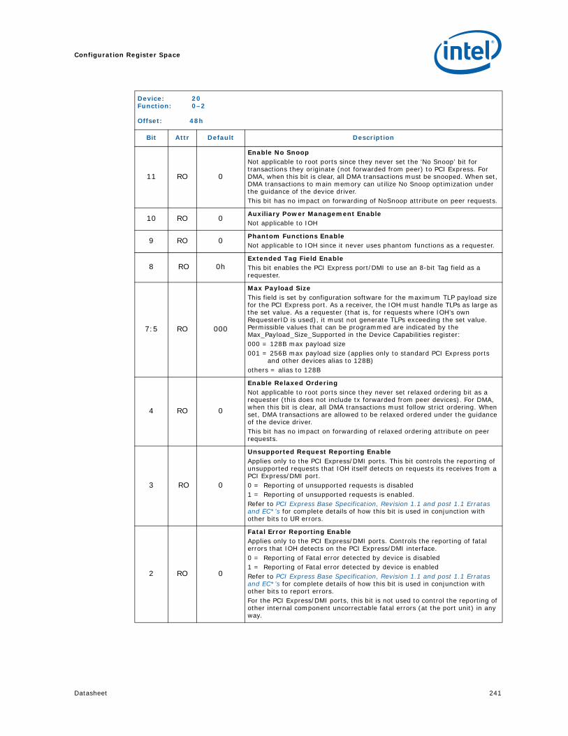
Datasheet 241
Configuration Register Space
11 RO 0
Enable No SnoopNot applicable to root ports since they never set the ‘No Snoop’ bit for transactions they originate (not forwarded from peer) to PCI Express. For DMA, when this bit is clear, all DMA transactions must be snooped. When set, DMA transactions to main memory can utilize No Snoop optimization under the guidance of the device driver.This bit has no impact on forwarding of NoSnoop attribute on peer requests.
10 RO 0Auxiliary Power Management EnableNot applicable to IOH
9 RO 0Phantom Functions EnableNot applicable to IOH since it never uses phantom functions as a requester.
8 RO 0hExtended Tag Field EnableThis bit enables the PCI Express port/DMI to use an 8-bit Tag field as a requester.
7:5 RO 000
Max Payload SizeThis field is set by configuration software for the maximum TLP payload size for the PCI Express port. As a receiver, the IOH must handle TLPs as large as the set value. As a requester (that is, for requests where IOH’s own RequesterID is used), it must not generate TLPs exceeding the set value. Permissible values that can be programmed are indicated by the Max_Payload_Size_Supported in the Device Capabilities register:000 = 128B max payload size001 = 256B max payload size (applies only to standard PCI Express ports
and other devices alias to 128B)others = alias to 128B
4 RO 0
Enable Relaxed OrderingNot applicable to root ports since they never set relaxed ordering bit as a requester (this does not include tx forwarded from peer devices). For DMA, when this bit is clear, all DMA transactions must follow strict ordering. When set, DMA transactions are allowed to be relaxed ordered under the guidance of the device driver.This bit has no impact on forwarding of relaxed ordering attribute on peer requests.
3 RO 0
Unsupported Request Reporting EnableApplies only to the PCI Express/DMI ports. This bit controls the reporting of unsupported requests that IOH itself detects on requests its receives from a PCI Express/DMI port.0 = Reporting of unsupported requests is disabled1 = Reporting of unsupported requests is enabled.Refer to PCI Express Base Specification, Revision 1.1 and post 1.1 Erratas and EC*’s for complete details of how this bit is used in conjunction with other bits to UR errors.
2 RO 0
Fatal Error Reporting EnableApplies only to the PCI Express/DMI ports. Controls the reporting of fatal errors that IOH detects on the PCI Express/DMI interface.0 = Reporting of Fatal error detected by device is disabled1 = Reporting of Fatal error detected by device is enabledRefer to PCI Express Base Specification, Revision 1.1 and post 1.1 Erratas and EC*’s for complete details of how this bit is used in conjunction with other bits to report errors.For the PCI Express/DMI ports, this bit is not used to control the reporting of other internal component uncorrectable fatal errors (at the port unit) in any way.
Device: 20Function: 0–2
Offset: 48h
Bit Attr Default Description

Configuration Register Space
242 Datasheet
1 RO 0
Non Fatal Error Reporting EnableApplies only to the PCI Express/DMI ports. Controls the reporting of non-fatal errors that IOH detects on the PCI Express/DMI interface or any non-fatal errors that DMA detect0 = Reporting of Non Fatal error detected by device is disabled1 = Reporting of Non Fatal error detected by device is enabledRefer to PCI Express Base Specification, Revision 1.1 and post 1.1 Erratas and EC*’s for complete details of how this bit is used in conjunction with other bits to report errors.For the PCI Express/DMI ports, this bit is not used to control the reporting of other internal component uncorrectable non-fatal errors (at the port unit) in any way.
0 RO 0
Correctable Error Reporting EnableApplies only to the PCI Express/DMI ports. Controls the reporting of correctable errors that IOH detects on the PCI Express/DMI interface0 = Reporting of link Correctable error detected by the port is disabled1 = Reporting of link Correctable error detected by port is enabledRefer to PCI Express Base Specification, Revision 1.1 and post 1.1 Erratas and EC*’s for complete details of how this bit is used in conjunction with other bits to report errors.For the PCI Express/DMI ports, this bit is not used to control the reporting of other internal component correctable errors (at the port unit) in any way.
Device: 20Function: 0–2
Offset: 48h
Bit Attr Default Description

Datasheet 243
Configuration Register Space
17.4.3.6 DEVSTS—PCI Express Device Status Register
The PCI Express Device Status register provides information about PCI Express device specific parameters associated with the device.
Device: 20Function: 0–2
Offset: 4Ah
Bit Attr Default Description
15:6 RO 000h Reserved.
5 RO 0h
Transactions PendingDoes not apply to root/DMI ports, I/OxAPIC bit hardwired to 0 for these devices.1 = DMA device has outstanding Non-Posted Request which it has issued
either towards main memory or a peer PCI Express port, which have not been completed.
0 = DMA reports this bit cleared only when all Completions for any outstanding Non-Posted Requests it owns have been received.
4 RO 0AUX Power DetectedDoes not apply to IOH
3 RO 0
Unsupported Request DetectedThis bit applies only to the root/DMI ports and does not apply to DMA, I/OxAPIC devices hardwire this bit to 0. This bit indicates that the root port detected an Unsupported Request. Errors are logged in this register regardless of whether error reporting is enabled or not in the Device Control Register. 1 = Unsupported Request detected at the device/port. These unsupported
requests are NP requests inbound that the root port received and it detected them as unsupported requests (for example, address decoding failures that the root port detected on a packet, receiving inbound lock reads, BME bit is clear, and so on). Note that this bit is not set on peer-to-peer completions with UR status that are forwarded by the root port to the PCIe link.
0 = No unsupported request detected by the root port
2 RO 0
Fatal Error DetectedThis bit applies only to the root/DMI ports and does not apply to DMA, I/OxAPIC devices hardwire this bit to 0. This bit indicates that a fatal (uncorrectable) error is detected by the device. Errors are logged in this register regardless of whether error reporting is enabled or not in the Device Control register. 1 = Fatal errors detected0 = No Fatal errors detected
1 RO 0
Non Fatal Error DetectedThis bit applies only to the root/DMI ports and does not apply to DMA, I/OxAPIC devices hardwire this bit to 0. This bit gets set if a non-fatal uncorrectable error is detected by the device. Errors are logged in this register regardless of whether error reporting is enabled or not in the Device Control register. 1 = Non Fatal errors detected0 = No non-Fatal Errors detected
0 RO 0
Correctable Error DetectedThis bit applies only to the root/DMI ports and does not apply to DMA, I/OxAPIC devices hardwire this bit to 0. This bit gets set if a correctable error is detected by the device. Errors are logged in this register regardless of whether error reporting is enabled or not in the PCI Express Device Control register.1 = Correctable errors detected0 = No correctable errors detected

Configuration Register Space
244 Datasheet
17.4.3.7 LNKCAP—PCI Express Link Capabilities Register
The Link Capabilities register identifies the PCI Express specific link capabilities.
Device: 20Function: 0–2
Offset: 4Ch
Bit Attr Default Description
31:24 RO 0sPort NumberThis field indicates the PCI Express port number for the link and is initialized by software/BIOS.
23:22 RV 00 Reserved
21 RO 1Link Bandwidth Notification CapabilityA value of 1b indicates support for the Link Bandwidth Notification status and interrupt mechanisms.
20 RO 1
Data Link Layer Link Active Reporting CapableIOH supports reporting status of the data link layer so software knows when it can enumerate a device on the link or otherwise know the status of the link.
19 RO 1Surprise Down Error Reporting CapableIOH supports reporting a surprise down error condition.
18 RO 0Clock Power ManagementDoes not apply to IOH.
17:15 RO 7hL1 Exit LatencyIOH does not support L1 ASPM.
14:12 RO 7h Reserved
11:0 RO 7h Reserved
9:4 RO 0s
Maximum Link WidthThis field indicates the maximum width of the given PCI Express Link attached to the port.000001 = x1000010 = x21
000100 = x4001000: x8010000 = x16Others = ReservedThis is left as a RWO register for bIOS to update based on the platform usage of the links.
Notes:1. There are restrictions with routing x2 lanes from IOH to a slot. See Section 5.1 for details.
3:0 RO 0s
Link Speeds SupportedIOH supports both 2.5G bps and 5 Gbps speeds if Gen2_OFF fuse is OFF; otherwise, it supports only Gen1This register is RWO when Gen2_OFF so that BIOS can change the supported speeds field to be 0001b (Gen1 only) if the board routing is not capable of Gen2 (even though IOH silicon itself is capable of Gen2)This bit is RWO if Gen2_OFF fuse is OFF and is RO if Gen2_OFF fuse is ON.

Datasheet 245
Configuration Register Space
17.4.3.8 LNKCON—PCI Express Link Control Register
The PCI Express Link Control register controls the PCI Express Link specific parameters.
Device: 20Function: 0–2
Offset: 50h
Bit Attr Default Description
15:12 RV 0000 Reserved
11 RO 0Link Autonomous Bandwidth Interrupt Enable1 = When set to 1b this bit enables the generation of an interrupt to indicate
that the Link Autonomous Bandwidth Status bit has been set.
10 RO 0Link Bandwidth Management Interrupt Enable1 = When set to 1b this bit enables the generation of an interrupt to indicate
that the Link Bandwidth Management Status bit has been set.
9 RO 0Hardware Autonomous Width DisableIOH never changes a configured link width for reasons other than reliability.
8 RO 0Enable Clock Power ManagementNot applicable to IOH
7 RO 0 Reserved
6 RO 0 Common Clock ConfigurationIOH does nothing with this bit.
5 RO 0
Retrain LinkA write of 1 to this bit initiates link retraining in the given PCI Express port by directing the LTSSM to the recovery state if the current state is [L0 or L1]. If the current state is anything other than L0 L1 then a write to this bit does nothing. This bit always returns 0 when read.If the Target Link Speed field has been set to a non-zero value different than the current operating speed, then the LTSSM will attempt to negotiate to the target link speed.It is permitted to write 1b to this bit while simultaneously writing modified values to other fields in this register. When this is done, all modified values that affect link retraining must be applied in the subsequent retraining.
4 RO 0
Link DisableThis field controls whether the link associated with the PCI Express port is enabled or disabled. When this bit is a 1, a previously configured link (a link that has gone past the polling state) would return to the “disabled” state as defined in the PCI Express Base Specification, Revision 1.1 and post 1.1 Erratas and EC*’s. When this bit is clear, an LTSSM in the “disabled” state goes back to the detect state.0 = Enables the link associated with the PCI Express port1 = Disables the link associated with the PCI Express port
3 RO 0Read Completion BoundarySet to zero to indicate IOH could return read completions at 64B boundaries
2 RV 0 Reserved
1:0 RO 00 Reserved

Configuration Register Space
246 Datasheet
17.4.3.9 LNKSTS—PCI Express Link Status Register
The PCI Express Link Status register provides information on the status of the PCI Express Link such as negotiated width, training, and so on.
Device: 20Function: 0–2
Offset: 52h
Bit Attr Default Description
15 RO 0
Link Autonomous Bandwidth StatusThis bit is set to 1b by hardware to indicate that hardware has autonomously changed link speed or width, without the port transitioning through DL_Down status, for reasons other than to attempt to correct unreliable link operation. IOH sets this bit when it receives eight consecutive TS1 or TS2 ordered sets with the Autonomous Change bit set.Note that if the status bit is set by hardware in the same clock software clears the status bit, the status bit should remain set and if MSI is enabled, the hardware should trigger a new MSI.
14 RO 0
Link Bandwidth Management StatusThis bit is set to 1b by hardware to indicate that either of the following has occurred without the port transitioning through DL_Down status:• A link retraining initiated by a write of 1b to the Retrain Link bit has
completed• Hardware has autonomously changed link speed or width to attempt to
correct unreliable link operationNote that if the status bit is set by hardware in the same clock software clears the status bit, the status bit should remain set and if MSI is enabled, the hardware should trigger a new MSI.
13 RO 0
Data Link Layer Link ActiveSet to 1b when the Data Link Control and Management State Machine is in the DL_Active state, 0b otherwise.On a downstream port or upstream port, when this bit is 0b, the transaction layer associated with the link will abort all transactions that would otherwise be routed to that link.
12 RO 1
Slot Clock ConfigurationThis bit indicates whether IOH receives clock from the same xtal that also provides clock to the device on the other end of the link.1 = Indicates that same xtal provides clocks to devices on both ends of the
link0 = Indicates that different xtals provide clocks to devices on both ends of the
link
11 RO 0
Link TrainingThis field indicates the status of an ongoing link training session in the PCI Express port0 = LTSSM has exited the recovery/configuration state1 = LTSSM is in recovery/configuration state or the Retrain Link was set but
training has not yet begun.The IOH hardware clears this bit once LTSSM has exited the recovery/configuration state. Refer to PCI Express Base Specification, Revision 1.1 and post 1.1 Erratas and EC*’s for details of which states within the LTSSM would set this bit and which states would clear this bit.
10 RO 0 Reserved

Datasheet 247
Configuration Register Space
17.4.3.10 SLTCAP—PCI Express Slot Capabilities Register
The Slot Capabilities register identifies the PCI Express specific slot capabilities. These registers must be ignored by software on the DMI links.
9:4 RO 0s
Negotiated Link WidthThis field indicates the negotiated width of the given PCI Express link after training is completed. Only x1, x2, x4 and x8 link width negotiations are possible in IOH. A value of 01h in this field corresponds to a link width of x1, 02h indicates a link width of x2 and so on, with a value of 8h for a link width of x8.The value in this field is reserved and could show any value when the link is not up. Software determines if the link is up or not by reading bit 13 of this register.
3:0 RO 0h
Current Link SpeedThis field indicates the negotiated Link speed of the given PCI Express Link.0001 = 2.5 Gbps0010 = 5 Gbps (IOH will never set this value when Gen2_OFF fuse is blown)Others = ReservedThe value in this field is not defined and could show any value, when the link is not up. Software determines if the link is up or not by reading bit 13 of this register.
Device: 20Function: 0–2
Offset: 52h
Bit Attr Default Description
Device: 20Function: 0–2
Offset: 54h
Bit Attr Default Description
31:19 RO 0sPhysical Slot NumberThis field indicates the physical slot number of the slot connected to the PCI Express port and is initialized by BIOS.
18 RO 0Command Complete Not Capable: IOH is capable of command complete interrupt.
17 RO 0
Electromechanical Interlock Present This bit when set indicates that an Electromechanical Interlock is implemented on the chassis for this slot and that lock is controlled by bit 11 in Slot Control register. BIOS Note: This capability is not set if the Electromechanical Interlock control is connected to main slot power control.
16:15 RO 00
Slot Power Limit ScaleThis field specifies the scale used for the Slot Power Limit Value and is initialized by BIOS. The IOH uses this field when it sends a Set_Slot_Power_Limit message on PCI Express.00 = 1.0x01 = 0.1x10 = 0.01x11 = 0.001x

Configuration Register Space
248 Datasheet
14:7 RO 0s
Slot Power Limit ValueThis field specifies the upper limit on power supplied by slot in conjunction with the Slot Power Limit Scale value defined previouslyPower limit (in Watts) = SPLS x SPLV.This field is initialized by BIOS. IOH uses this field when it sends a Set_Slot_Power_Limit message on PCI Express.Design Note: IOH can chose to send the Set_Slot_Power_Limit message on the link at first link up condition without regards to whether this register and the Slot Power Limit Scale register are programmed yet by BIOS. IOH must then be designed to discard a received Set_Slot_Power_Limit message without an error.
6 RO 0
Hot-plug CapableThis field defines hot-plug support capabilities for the PCI Express port.0 = Slot is not capable of supporting Hot-plug operations.1 = Slot is capable of supporting Hot-plug operationsThis bit is programed by BIOS based on the system design. This bit must be programmed by BIOS to be consistent with the VPP enable bit for the port.
5 RO 0
Hot-plug SurpriseThis field indicates that a device in this slot may be removed from the system without prior notification (like for instance a PCI Express cable).0 = Hot-plug surprise is not supported1 = Hot-plug surprise is supportedNote that if platform implemented cable solution (either direct or using a SIOM with repeater), on a port, then this could be set. BIOS programs this field with a 0 for CEM/SIOM FFs.This bit is used by IOH hardware to determine if a transition from DL_active to DL_Inactive is to be treated as a surprise down error or not. If a port is associated with a hotpluggable slot and the hotplug surprise bit is set, then any transition to DL_Inactive is not considered an error. Refer to PCI Express Base Specification, Revision 1.1 and post 1.1 Erratas and EC*’s for further details.
4 RO 0
Power Indicator PresentThis bit indicates that a Power Indicator is implemented for this slot and is electrically controlled by the chassis.0 = Power Indicator that is electrically controlled by the chassis is not present1 = Power Indicator that is electrically controlled by the chassis is presentBIOS programs this field with a 1 for CEM/SIOM FFs and a 0 for Express cable.
3 RO 0
Attention Indicator PresentThis bit indicates that an Attention Indicator is implemented for this slot and is electrically controlled by the chassis0 = Attention Indicator that is electrically controlled by the chassis is not
present1 = Attention Indicator that is electrically controlled by the chassis is presentBIOS programs this field with a 1 for CEM/SIOM FFs.
2 RO 0
MRL Sensor PresentThis bit indicates that an MRL Sensor is implemented on the chassis for this slot.0 = MRL Sensor is not present1 = MRL Sensor is presentBIOS programs this field with a 0 for SIOM/Express cable and with either 0 or 1 for CEM depending on system design.
Device: 20Function: 0–2
Offset: 54h
Bit Attr Default Description

Datasheet 249
Configuration Register Space
17.4.3.11 SLTCON—PCI Express Slot Control Register
The Slot Control register identifies the PCI Express specific slot control parameters for operations such as Hot-plug and Power Management.
1 RO 0
Power Controller PresentThis bit indicates that a software controllable power controller is implemented on the chassis for this slot.0 = Software controllable power controller is not present1 = Software controllable power controller is presentBIOS programs this field with a 1 for CEM/SIOM FFs and a 0 for Express cable.
0 RO 0
Attention Button PresentThis bit indicates that the Attention Button event signal is routed (from slot or on-board in the chassis) to the IOH’s hotplug controller.0 = Attention Button signal is routed to IOH1 = Attention Button is not routed to IOHBIOS programs this field with a 1 for CEM/SIOM FFs.
Device: 20Function: 0–2
Offset: 54h
Bit Attr Default Description
Device: 20Function: 0–2Offset: 58h
Bit Attr Default Description
15:13 RV 0h Reserved
12 RO 0Data Link Layer State Changed EnableWhen set to 1, this field enables software notification when Data Link Layer Link Active field is changed
11 RO 0
Electromechanical Interlock Control When software writes either a 1 to this bit, IOH pulses the EMIL pin per PCI Express Server/Workstation Module Electromechanical Spec Rev 0.5a. Write of 0 has no effect. This bit always returns a 0 when read. If electromechanical lock is not implemented, then either a write of 1 or 0 to this register has no effect.
10 RO 1
Power Controller ControlIf a power controller is implemented, when written sets the power state of the slot per the defined encodings. Reads of this field must reflect the value from the latest write, even if the corresponding hot-plug command is not executed yet at the VPP, unless software issues a write without waiting for the previous command to complete in which case the read value is undefined.1 = Power On0 = Power Off
9:8 RO 3h
Power Indicator ControlIf a Power Indicator is implemented, writes to this register set the Power Indicator to the written state. Reads of this field must reflect the value from the latest write, even if the corresponding hot-plug command is not executed yet at the VPP, unless software issues a write without waiting for the previous command to complete in which case the read value is undefined.00 = Reserved.01 = On10 = Blink (IOH drives 1.5 Hz square wave for Chassis mounted LEDs)11 = OffWhen this register is written, the event is signaled using the virtual pins of the IOH over a dedicated SMBus port. IOH does not generated the Power_Indicator_On/Off/Blink messages on PCI Express when this field is written to by software.

Configuration Register Space
250 Datasheet
7:6 RO 3h
Attention Indicator ControlIf an Attention Indicator is implemented, writes to this register set the Attention Indicator to the written state.Reads of this field reflect the value from the latest write, even if the corresponding hot-plug command is not executed yet at the VPP, unless software issues a write without waiting for the previous command to complete in which case the read value is undefined.00 = Reserved.01 = On10 = Blink (The IOH drives 1.5 Hz square wave)11 = OffWhen this register is written, the event is signaled using the virtual pins of the IOH over a dedicated SMBus port. IOH does not generated the Attention_Indicator_On/Off/Blink messages on PCI Express when this field is written to by software.
5 RO 0
Hot-plug Interrupt EnableWhen set to 1b, this bit enables generation of Hot-Plug MSI interrupt (and not wake event) on enabled Hot-Plug events, provided ACPI mode for hotplug is disabled.0 = Disables interrupt generation on Hot-plug events1 = Enables interrupt generation on Hot-plug events
4 RO 0
Command Completed Interrupt EnableThis field enables the generation of Hot-plug interrupts (and not wake event) when a command is completed by the Hot-plug controller connected to the PCI Express port.0 = Disables hot-plug interrupts on a command completion by a hot-plug
Controller1 = Enables hot-plug interrupts on a command completion by a hot-plug
Controller
3 RO 0
Presence Detect Changed EnableThis bit enables the generation of hot-plug interrupts or wake messages using a presence detect changed event.0 = Disables generation of hot-plug interrupts or wake messages when a
presence detect changed event happens.1 = Enables generation of hot-plug interrupts or wake messages when a
presence detect changed event happens.
2 RO 0
MRL Sensor Changed EnableThis bit enables the generation of hot-plug interrupts or wake messages using a MRL Sensor changed event.0 = Disables generation of hot-plug interrupts or wake messages when an
MRL Sensor changed event happens.1 = Enables generation of hot-plug interrupts or wake messages when an
MRL Sensor changed event happens.
1 RO 0
Power Fault Detected EnableThis bit enables the generation of hot-plug interrupts or wake messages using a power fault event.0 = Disables generation of hot-plug interrupts or wake messages when a
power fault event happens.1 = Enables generation of hot-plug interrupts or wake messages when a
power fault event happens.
0 RO 0
Attention Button Pressed EnableThis bit enables the generation of hot-plug interrupts or wake messages using an attention button pressed event.0 = Disables generation of hot-plug interrupts or wake messages when the
attention button is pressed.1 = Enables generation of hot-plug interrupts or wake messages when the
attention button is pressed.
Device: 20Function: 0–2Offset: 58h
Bit Attr Default Description

Datasheet 251
Configuration Register Space
17.4.3.12 SLTSTS—PCI Express Slot Status Register
The PCI Express Slot Status register defines important status information for operations such as Hot-plug and Power Management.
Device: 20Function: 0–2
Offset: 5Ah
Bit Attr Default Description
15:9 RV 0h Reserved
8 RO 0
Data Link Layer State Changed This bit is set (if it is not already set) when the state of the Data Link Layer Link Active bit in the Link Status register changes. Software must read Data Link Layer Active field to determine the link state before initiating configuration cycles to the hot plugged device.
7 RO 0
Electromechanical Latch StatusWhen read this register returns the current state of the Electromechanical Interlock (the EMILS pin) which has the defined encodings as:0 = Electromechanical Interlock Disengaged1 = Electromechanical Interlock Engaged
6 RO 0
Presence Detect StateFor ports with slots (where the Slot Implemented bit of the PCI Express Capabilities Registers is 1b), this field is the logical OR of the Presence Detect status determined using an in-band mechanism and sideband Present Detect pins. Refer to how PCI Express Base Specification, Revision 1.1 and post 1.1 Erratas and EC*’s for how the inband presence detect mechanism works (certain states in the LTSSM constitute “card present” and others don’t). 0 = Card/Module/Cable slot empty or Cable Slot occupied but not powered1 = Card/module Present in slot (powered or unpowered) or cable present
and powered on other endFor ports with no slots, IOH hardwires this bit to 1b.Note: OS could get confused when it sees an empty PCI Express root port that is, “no slots + no presence”, since this is now disallowed in the spec. So BIOS must hide all unused root ports devices in IOH config space, using the DEVHIDE register in Intel QuickPath Interconnect CSR space.
5 RO 0
MRL Sensor StateThis bit reports the status of an MRL sensor if it is implemented.0 = MRL Closed1 = MRL Open
4 RO 0
Command CompletedThis bit is set by the IOH when the hot-plug command has completed and the hot-plug controller is ready to accept a subsequent command. It is subsequently cleared by software after the field has been read and processed. This bit provides no assurance that the action corresponding to the command is complete.
3 RO 0
Presence Detect ChangedThis bit is set by the IOH when a Presence Detect Changed event is detected. It is subsequently cleared by software after the field has been read and processed.On-board logic per slot must set the VPP signal corresponding this bit inactive if the FF/system does not support out-of-band presence detect.
2 RO 0
MRL Sensor ChangedThis bit is set by the IOH when an MRL Sensor Changed event is detected. It is subsequently cleared by software after the field has been read and processed.On-board logic per slot must set the VPP signal corresponding this bit inactive if the FF/system does not support MRL.

Configuration Register Space
252 Datasheet
17.4.3.13 ROOTCON—PCI Express Root Control Register
The PCI Express Root Control register specifies parameters specific to the root complex port.
1 RO 0
Power Fault DetectedThis bit is set by the IOH when a power fault event is detected by the power controller. It is subsequently cleared by software after the field has been read and processed.On-board logic per slot must set the VPP signal corresponding this bit inactive if the FF/system does not support power fault detection.
0 RO 0
Attention Button PressedThis bit is set by the IOH when the attention button is pressed. It is subsequently cleared by software after the field has been read and processed.On-board logic per slot must set the VPP signal corresponding this bit inactive if the FF/system does not support attention button.IOH silently discards the Attention_Button_Pressed message if received from PCI Express link without updating this bit.
Device: 20Function: 0–2
Offset: 5Ah
Bit Attr Default Description
Device: 20Function: 0–2
Offset: 5Ch
Bit Attr Default Description
15:5 RV 0h Reserved
4 RO 0CRS software visibility EnableThis bit, when set, enables the Root Port to return Configuration Request Retry Status (CRS) Completion Status to software.
3 RO 0
PME Interrupt Enable(Applies only to devices 0–8. This bit is a don’t care for device 8)This field controls the generation of MSI interrupts for PME messages.1 = Enables interrupt generation upon receipt of a PME message 0 = Disables interrupt generation for PME messages.
2 RO 0
System Error on Fatal Error EnableThis field enables notifying the internal core error logic of occurrence of an uncorrectable fatal error at the port or below its hierarchy. The internal core error logic of IOH then decides if/how to escalate the error further (pins/message etc). Refer to Section 13.2 for details of how/which system notification is generated for a PCI Express/DMI fatal error.1 = Internal core error logic notification should be generated if a fatal error
(ERR_FATAL) is reported by any of the devices in the hierarchy associated with and including this port.
0 = No internal core error logic notification should be generated on a fatal error (ERR_FATAL) reported by any of the devices in the hierarchy associated with and including this port.
Note that generation of system notification on a PCI Express/DMI fatal error is orthogonal to generation of an MSI interrupt for the same error. Both a system error and MSI can be generated on a fatal error or software can chose one of the two.Refer to PCI Express Base Specification, Revision 1.1 and post 1.1 Erratas and EC*’s for details of how this bit is used in conjunction with other error control bits to generate core logic notification of error events in a PCI Express/DMI port.

Datasheet 253
Configuration Register Space
17.4.3.14 ROOTCAP—PCI Express Root Capabilities Register
The PCI Express Root Status register specifies parameters specific to the root complex port.
1 RO 0
System Error on Non-Fatal Error EnableThis field enables notifying the internal core error logic of occurrence of an uncorrectable non-fatal error at the port or below its hierarchy. The internal core error logic of IOH then decides if/how to escalate the error further (pins/message etc). Refer to Chapter 13 for details of how/which system notification is generated for a PCI Express/DMI non-fatal error.1 = Internal core error logic notification should be generated if a non-fatal
error (ERR_NONFATAL) is reported by any of the devices in the hierarchy associated with and including this port.
0 = No internal core error logic notification should be generated on a non-fatal error (ERR_NONFATAL) reported by any of the devices in the hierarchy associated with and including this port.
Note that generation of system notification on a PCI Express/DMI non-fatal error is orthogonal to generation of an MSI interrupt for the same error. Both a system error and MSI can be generated on a non-fatal error or software can chose one of the two.Refer to the PCI Express Base Specification, Revision 1.1 and post 1.1 Erratas and EC*’s for details of how this bit is used in conjunction with other error control bits to generate core logic notification of error events in a PCI Express/DMI port.
0 RO 0
System Error on Correctable Error EnableThis field controls notifying the internal core error logic of the occurrence of a correctable error in the device or below its hierarchy. The internal core error logic of IOH then decides if/how to escalate the error further (pins/message etc). Refer to Section 13.2 for details of how/which system notification is generated for a PCI Express correctable error.1 = Internal core error logic notification should be generated if a correctable
error (ERR_COR) is reported by any of the devices in the hierarchy associated with and including this port.
0 = No internal core error logic notification should be generated on a correctable error (ERR_COR) reported by any of the devices in the hierarchy associated with and including this port.
Note that generation of system notification on a PCI Express correctable error is orthogonal to generation of an MSI interrupt for the same error. Both a system error and MSI can be generated on a correctable error or software can chose one of the two.Refer to the PCI Express Base Specification, Revision 1.1 and post 1.1 Erratas and EC*’s for details of how this bit is used in conjunction with other error control bits to generate core logic notification of error events in a PCI Express/DMI port.
Device: 20Function: 0–2
Offset: 5Ch
Bit Attr Default Description
Device: 20Function: 0–2
Offset: 5Eh
Bit Attr Default Description
15:1 RV 0s Reserved
0 RO 1
CRS Software Visibility This bit, when set, indicates that the Root Port is capable of returning Configuration Request Retry Status (CRS) Completion Status to software. IOH supports this capability.

Configuration Register Space
254 Datasheet
17.4.3.15 ROOTSTS—PCI Express Root Status Register
The PCI Express Root Status register specifies parameters specific to the root complex port.
17.4.3.16 DEVCAP2—PCI Express Device Capabilities 2 Register
The PCI Express Device Capabilities register identifies device specific information for the device.
Device: 20Function: 0–2
Offset: 60h
Bit Attr Default Description
31:18 RV 0h Reserved
17 RO 0
PME PendingThis field indicates that another PME is pending when the PME Status bit is set. When the PME Status bit is cleared by software; the pending PME is delivered by hardware by setting the PME Status bit again and updating the Requestor ID appropriately. The PME pending bit is cleared by hardware if no more PMEs are pending.
16 RO 0
PME StatusThis field indicates a PM_PME message (either from the link or internally from within that root port) was received at the port.1 = PME was asserted by a requester as indicated by the PMEREQID fieldThis bit is cleared by software by writing a 1. Note that the root port itself could be the source of a PME event when a hotplug event is observed when the port is in D3hot state.
15:0 RO 0
PME Requester IDThis field indicates the PCI requester ID of the last PME requestor. If the root port itself was the source of the (virtual) PME message, then a RequesterID of IOHBUSNO:DevNo:0 is logged in this field.
Device: 20Function: 0–2
Offset: 64h
Bit Attr Default Description
5 RO 0Alternative RID Interpretation (ARI) CapableThis bit is hardwired to 0b indicating not supporting this capability.
4 RO 0Completion Timeout Disable SupportedIOH does not support disabling completion timeout
3:0 RO 0000b
Completion Timeout Values SupportedThis field indicates device support for the optional Completion Timeout programmability mechanism. 0000b = Completions Timeout programming not supported.
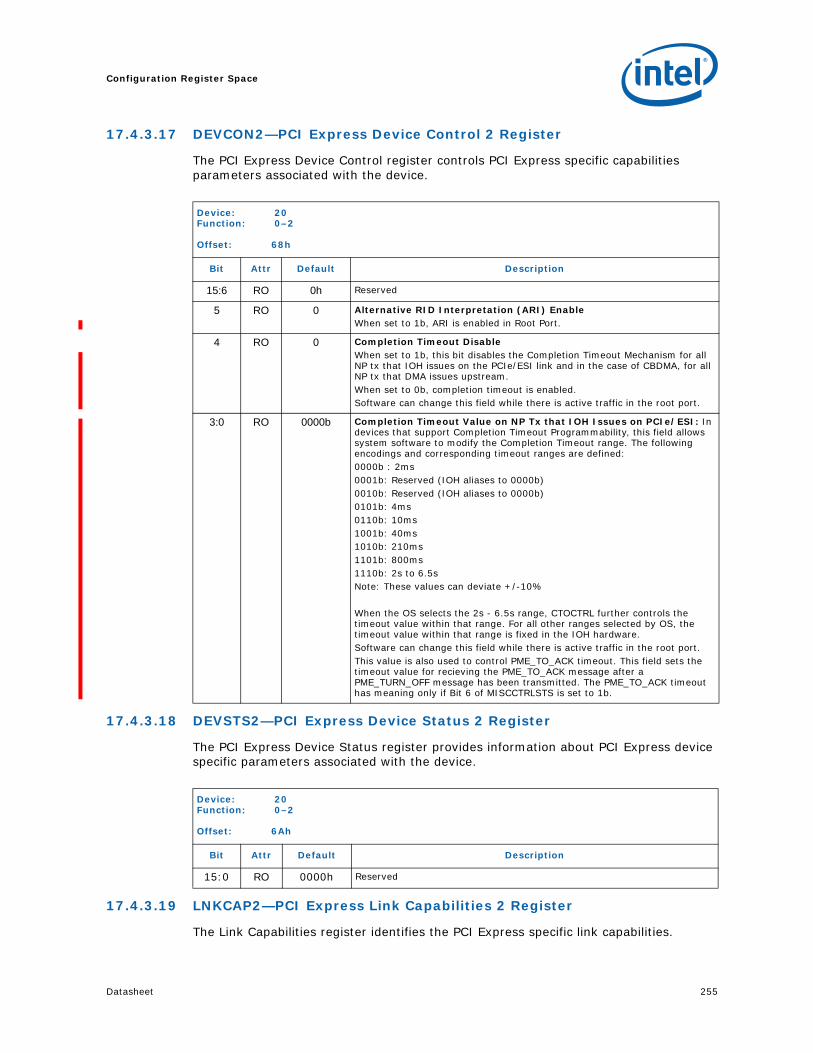
Datasheet 255
Configuration Register Space
17.4.3.17 DEVCON2—PCI Express Device Control 2 Register
The PCI Express Device Control register controls PCI Express specific capabilities parameters associated with the device.
17.4.3.18 DEVSTS2—PCI Express Device Status 2 Register
The PCI Express Device Status register provides information about PCI Express device specific parameters associated with the device.
17.4.3.19 LNKCAP2—PCI Express Link Capabilities 2 Register
The Link Capabilities register identifies the PCI Express specific link capabilities.
Device: 20Function: 0–2
Offset: 68h
Bit Attr Default Description
15:6 RO 0h Reserved
5 RO 0 Alternative RID Interpretation (ARI) Enable When set to 1b, ARI is enabled in Root Port.
4 RO 0 Completion Timeout Disable When set to 1b, this bit disables the Completion Timeout Mechanism for all NP tx that IOH issues on the PCIe/ESI link and in the case of CBDMA, for all NP tx that DMA issues upstream. When set to 0b, completion timeout is enabled.Software can change this field while there is active traffic in the root port.
3:0 RO 0000b Completion Timeout Value on NP Tx that IOH Issues on PCIe/ESI: In devices that support Completion Timeout Programmability, this field allows system software to modify the Completion Timeout range. The following encodings and corresponding timeout ranges are defined:0000b : 2ms0001b: Reserved (IOH aliases to 0000b)0010b: Reserved (IOH aliases to 0000b)0101b: 4ms0110b: 10ms1001b: 40ms1010b: 210ms1101b: 800ms1110b: 2s to 6.5sNote: These values can deviate +/-10%
When the OS selects the 2s - 6.5s range, CTOCTRL further controls the timeout value within that range. For all other ranges selected by OS, the timeout value within that range is fixed in the IOH hardware.Software can change this field while there is active traffic in the root port.This value is also used to control PME_TO_ACK timeout. This field sets the timeout value for recieving the PME_TO_ACK message after a PME_TURN_OFF message has been transmitted. The PME_TO_ACK timeout has meaning only if Bit 6 of MISCCTRLSTS is set to 1b.
Device: 20Function: 0–2
Offset: 6Ah
Bit Attr Default Description
15:0 RO 0000h Reserved

Configuration Register Space
256 Datasheet
17.4.3.20 LNKCON2—PCI Express Link Control 2 Register
The PCI Express Link Control register controls the PCI Express Link specific parameters.
17.4.3.21 LNKSTS2—PCI Express Link Status 2 Register
The PCI Express Link Status register provides information on the status of the PCI Express Link such as negotiated width, training, and so on.
17.4.3.22 SLTCAP2—PCI Express Slot Capabilities 2 Register
The Slot Capabilities register identifies the PCI Express specific slot capabilities. These registers must be ignored by software on the DMI links.
Device: 20Function: 0–2
Offset: 6Ch
Bit Attr Default Description
31:0 RO 0s Reserved
Device: 20Function: 0–2
Offset: 70h
Bit Attr Default Description
15:0 RV 0000h Reserved
Device: 20Function: 0–2
Offset: 72h
Bit Attr Default Description
15:0 RV 0000h Reserved
Device: 20Function: 0–2
Offset: 74h
Bit Attr Default Description
31:0 RV 0s Reserved

Datasheet 257
Configuration Register Space
17.4.3.23 SLTCON2—PCI Express Slot Control 2 Register
The Slot Control register identifies the PCI Express specific slot control parameters for operations such as Hot-plug and Power Management.
17.4.3.24 SLTSTS2—PCI Express Slot Status 2 Register
The PCI Express Slot Status register defines important status information for operations such as Hot-plug and Power Management.
Device: 20Function: 0–2
Offset: 78h
Bit Attr Default Description
15:0 RV 0000h Reserved
Device: 20Function: 0–2
Offset: 7Ah
Bit Attr Default Description
15:0 RV 0000h Reserved

Configuration Register Space
258 Datasheet
17.5 IOxAPIC ControllerTable 17-4. IOH Device 19 I/OxAPIC Configuration Map — Offset 00h–FFh
DID VID 00h RDINDEX 80h
PCISTS PCICMD 04h 84h
CCR RID 08h 88h
HDR CLS 0Ch 8Ch
MBAR 10h RDWINDOW 90h
14h 94h
18h 98h
1Ch 9Ch
20h IOAPICTETPC A0h
24h A4h
28h A8h
SID SVID 2Ch ACh
30h B0h
CAPPTR 34h B4h
38h B8h
3Ch BCh
ABAR 40h C0h
44h C4h
48h C8h
4Ch CCh
50h D0h
54h D4h
58h D8h
5Ch DCh
60h E0h
64h E4h
68h E8h
PMCAPPMCSR
6Ch ECh
70h F0h
74h F4h
78h F8h
7Ch FCh

Datasheet 259
Configuration Register Space
17.5.1 PCICMD—PCI Command Register (Device 19)
This register defines the PCI 3.0 compatible command register values applicable to PCI Express space.
Device: 19Function: 0Offset: 04h
Bit Attr Default Description
15:11 RV 00000 Reserved (by PCI SIG)
10 RO 0
Interrupt DisableControls the ability of DMA to generate legacy INTx interrupt (when legacy INTx mode is enabled).This bit does not affect the ability of the Express port to route interrupt messages received at the PCI Express port. 1 = Legacy Interrupt message generation is disabled0 = Legacy Interrupt message generation is enabledIf this bit transitions from 1->0 when a previous Assert_INTx message was sent but no corresponding Deassert_INTx message sent yet, a Deassert_INTx message is sent on this bit transition.
9 RO 0Fast Back-to-Back EnableNot applicable to PCI Express and is hardwired to 0
8 RO 0
SERR EnableFor PCI Express/DMI ports, this field enables notifying the internal core error logic of occurrence of an uncorrectable error (fatal or non-fatal) at the port. The internal core error logic of IOH then decides if/how to escalate the error further (pins/message etc.). This bit also controls the propagation of PCI Express ERR_FATAL and ERR_NONFATAL messages received from the port to the internal IOH core error logic.1 = Fatal and Non-fatal error generation and Fatal and Non-fatal error
message forwarding is enabled0 = Fatal and Non-fatal error generation and Fatal and Non-fatal error
message forwarding is disabledRefer to PCI Express Base Specification, Revision 1.1 and post 1.1 Erratas and EC*’s for details of how this bit is used in conjunction with other control bits in the Root Control register for forwarding errors detected on the PCI Express interface to the system core error logic.This bit has no impact on error reporting from the other devices — DMA, I/OxAPIC, Perf Mon, and PCI Express DF registers.
7 RO 0 IDSEL Stepping/Wait Cycle ControlNot applicable to internal IOH devices. Hardwired to 0.
6 RO 0
Parity Error ResponseFor PCI Express/DMI ports, IOH ignores this bit and always does ECC/parity checking and signaling for data/address of transactions both to and from IOH. This bit though affects the setting of bit 8 in the PCISTS (see bit 8 in Section 17.4.2.4) register.This bit has no impact on error reporting from the other devices — DMA, I/OxAPIC, Perf Mon, and PCI Express DF registers.
5 RO 0VGA palette snoop EnableNot applicable to internal IOH devices. Hardwired to 0.
4 RO 0Memory Write and Invalidate EnableNot applicable to internal IOH devices. Hardwired to 0.
3 RO 0Special Cycle EnableNot applicable to PCI Express. Hardwired to 0.

Configuration Register Space
260 Datasheet
2 RW 0
Bus Master EnableControls the ability of the PCI Express/DMI port in generating/forwarding memory (including MSI writes) or I/O transactions (and not messages) or configuration transactions from the secondary side to the primary side. For DMA and I/OxAPIC, this bit enables them to generate memory write/MSI and memory read transactions (read applies only to DMA).1 = Enables the PCI Express/DMI port, I/OxAPIC or DMA to generate/
forward memory, config or I/O read/write requests.0 = The Bus Master is disabled. When this bit is 0, IOH root ports will treat
upstream PCI Express memory writes/reads, IO writes/reads, and configuration reads and writes as unsupported requests (and follow the rules for handling unsupported requests). This behavior is also true towards transactions that are already pending in the IOH root port’s internal queues when the BME bit is turned off. I/OxAPIC and DMA cannot generate any memory transactions when this bit is 0.
1 RW 0
Memory Space Enable 1 = Enables a PCI Express/DMI port’s memory range registers, internal
I/OxAPIC’s MBAR register (ABAR range decode is not enabled by this bit) or CB DMA device’s memory BARs to be decoded as valid target addresses for transactions from primary side.
0 = Disables a PCI Express/DMI port’s memory range registers (excluding the IOxAPIC range registers), internal I/OxAPIC’s MBAR register (but not ABAR register) or DMA device’s memory BARs to be decoded as valid target addresses for transactions from primary side.
Note that if a PCI Express/DMI port’s MSE bit is clear, that port can still be target of any memory transaction if subtractive decoding is enabled on that port.
0 RO 0
IO Space EnableApplies only to PCI Express/DMI ports 1 = Enables the I/O address range, defined in the IOBASE and IOLIM
registers of the PCI-to-PCI bridge header, for target decode from primary side
0 = Disables the I/O address range, defined in the IOBASE and IOLIM registers of the PCI-to-PCI bridge header, for target decode from primary side
Note that if a PCI Express/DMI port’s IOSE bit is clear, that port can still be target of an I/O transaction if subtractive decoding is enabled on that port.
Device: 19Function: 0Offset: 04h
Bit Attr Default Description

Datasheet 261
Configuration Register Space
17.5.2 PCISTS—PCI Status Register (Device 19)
The PCI Status register is a 16-bit status register that reports the occurrence of various events associated with the primary side of the “virtual” PCI-PCI bridge embedded in PCI Express ports and also primary side of the other devices on the internal IOH bus.
Register: PCISTSDevice: 19Function: 0Offset: 06h
Bit Attr Default Description
15 RO 0
Detected Parity ErrorThis bit is set by a device when it receives a packet on the primary side with an uncorrectable data error (i.e. a packet with poison bit set or an uncorrectable data ECC error was detected at the XP-DP interface when ECC checking is done) or an uncorrectable address/control parity error. The setting of this bit is regardless of the Parity Error Response bit (PERRE) in the PCICMD register.This bit is RO for these devices.
14 RO 0
Signaled System Error 1 = The device reported fatal/non-fatal (and not correctable) errors it
detected on its PCI Express interface. Software clears this bit by writing a ‘1’ to it. For Express ports, this bit is also set (when SERR enable bit is set) when a FATAL/NON-FATAL message is forwarded from the Express link. Note that IOH internal ‘core’ errors (like parity error in the internal queues) are not reported using this bit.
0 = The device did not report a fatal/non-fatal error
13 RO 0
Received Master AbortThis bit is set when a device experiences a master abort condition on a transaction it mastered on the primary interface (IOH internal bus). Note that certain errors might be detected right at the PCI Express interface and those transactions might not ‘propagate’ to the primary interface before the error is detected (e.g. accesses to memory above TOCM in cases where the PCIe interface logic itself might have visibility into TOCM). Such errors do not cause this bit to be set, and are reported using the PCI Express interface error bits (secondary status register). Conditions that cause bit 13 to be set, include:• Device receives a completion on the primary interface (internal bus of
IOH) with Unsupported Request or master abort completion Status. This includes UR status received on the primary side of a PCI Express port on peer-to-peer completions also.
• Device accesses to holes in the main memory address region that are detected by the QPI source address decoder.
• Other master abort conditions detected on the IOH internal bus.
12 RO 0
Received Target AbortThis bit is set when a device experiences a completer abort condition on a transaction it mastered on the primary interface (IOH internal bus). Note that certain errors might be detected right at the PCI Express interface and those transactions might not ‘propagate’ to the primary interface before the error is detected (e.g., accesses to memory above VTCSRBASE). Such errors do not cause this bit to be set, and are reported using the PCI Express interface error bits (secondary status register). Conditions that cause bit 12 to be set, include:• Device receives a completion on the primary interface (internal bus of
IOH) with completer abort completion Status. This includes CA status received on the primary side of a PCI Express port on peer-to-peer completions also.
• Accesses to QPI that return a failed completion status• Other master abort conditions detected on the IOH internal bus.
11 RWC 0
Signaled Target AbortThis bit is set when a device signals a completer abort completion status on the primary side (internal bus of IOH). This condition includes a PCI Express port forwarding a completer abort status received on a completion from the secondary side and passed to the primary side on a peer-to-peer completion.

Configuration Register Space
262 Datasheet
10:9 RO 00 DEVSEL# TimingNot applicable to PCI Express. Hardwired to 0.
8 RO 0
Master Data Parity ErrorThis bit is set by a device if the Parity Error Response bit in the PCI Command register is set and it receives a completion with poisoned data from the primary side or if it forwards a packet with data (including MSI writes) to the primary side with poison.
7 RO 0 Fast Back-to-BackNot applicable to PCI Express. Hardwired to 0.
6 RO 0 Reserved
5 RO 0 66MHz capableNot applicable to PCI Express. Hardwired to 0.
4 RO 1h Capabilities ListThis bit indicates the presence of a capabilities list structure
3 RO 0
INTx StatusIndicates that a legacy INTx interrupt condition is pending internally in the CB DMA device. This bit has meaning only in the legacy interrupt mode. This bit is always 0 when MSI-X has been selected for DMA interrupts. Note that the setting of the INTx status bit is independent of the INTx enable bit in the PCI command register; that is, this bit is set anytime the DMA engine is setup by its driver to generate any interrupt and the condition that triggers the interrupt has occurred, regardless of whether a legacy interrupt message was signaled to the ICH or not. Note that the INTx enable bit has to be set in the PCICMD register for DMA to generate a INTx message to the ICH.This bit is not applicable to PCI Express and DMI ports and this bit does not get set for interrupts forwarded from a PCI Express port to the ICH from downstream devices. This bit also does not apply to Perf Mon, I/OxAPIC and DF register devices.
2:0 RV 000 Reserved
Register: PCISTSDevice: 19Function: 0Offset: 06h
Bit Attr Default Description

Datasheet 263
Configuration Register Space
17.5.3 MBAR—IOxAPIC Base Address Register
17.5.4 ABAR—I/OxAPIC Alternate BAR Register
Register: MBARDevice: 19Function: 0Offset: 10h
Bit Attr Default Description
63:32 RO 0h Reserved
31:12 RW 0hBAR This marks the 4KB aligned 32-bit base address for memory-mapped registers of I/OxAPIC
11:4 RO 0h Reserved
3 RO 0 PrefetchableThe IOxAPIC registers are not prefetchable.
2:1 RO 00 TypeThe IOAPIC registers can only be placed below 4G system address space.
0 RO 0 Memory SpaceThis Base Address Register indicates memory space.
Register: ABARDevice: 19Function: 0Offset: 40h
Bit Attr Default Description
15 RW 0
ABAR Enable: When set, the range FECX_YZ00 to FECX_YZFF is enabled as an alternate access method to the IOxAPIC registers and these addresses are claimed by the IOH’s internal I/OxAPIC regardless of the setting the MSE bit in the I/OxAPIC configuration space. Bits ‘XYZ’ are defined below.
14:12 RO 0h Reserved
11:8 RW 0h
XBAD: Base Address [19:16]These bits determine the high order bits of the I/O APIC address map. When a memory address is recognized by the IOH which matches FECX_YZ00-to-FECX_YZFF, the IOH will respond to the cycle and access the internal I/O APIC.
7:4 RW 0h
YBAD: Base Address [15:12] These bits determine the low order bits of the I/O APIC address map. When a memory address is recognized by the IOH which matches FECX_YZ00-to-FECX_YZFF, the IOH will respond to the cycle and access the internal I/O APIC.
3:0 RW 0h
ZBAD: Base Address [11:8] These bits determine the low order bits of the I/O APIC address map. When a memory address is recognized by the IOH that matches FECX_YZ00-to-FECX_YZFF, the IOH will respond to the cycle and access the internal I/O APIC.

Configuration Register Space
264 Datasheet
17.5.5 PMCAP—Power Management Capabilities Register
The PM Capabilities Register defines the capability ID, next pointer and other power management related support. The following PM registers /capabilities are added for software compliance.
17.5.6 PMCSR—Power Management Control and Status Register
This register provides status and control information for PM events in the PCI Express port of the IOH.
Register: PMCAPDevice: 19Function: 0Offset: 6Ch
Bit Attr Default Description
31:27 RO 11001b PME SupportBits 31, 30, and 27 must be set to 1 for PCI-to-PCI bridge structures representing ports on root complexes.
26 RO 0D2 SupportIOH does not support power management state D2.
25 RO 0D1 SupportIOH does not support power management state D1.
24:22 RO 0h AUX Current
21 RO 0 Device Specific Initialization
20 RV 0 Reserved
19 RO 0PME ClockThis field is hardwired to 0h as it does not apply to PCI Express.
18:16 RWO 011VersionThis field is set to 3h (PM 1.2 compliant) as version number. Bit is RWO to make the version 2h incase legacy OS’es have any issues.
15:8 RO 00hNext Capability PointerThis is the last capability in the chain and hence set to 0.
7:0 RO 01hCapability IDProvides the PM capability ID assigned by PCI-SIG.
Register: PMCSRDevice: 19Function: 0Offset: 70h
Bit Attr Default Description
31:24 RO 00hDataNot relevant for IOH
23 RO 0hBus Power/Clock Control EnableThis field is hardwired to 0h as it does not apply to PCI Express.
22 RO 0hB2/B3 SupportThis field is hardwired to 0h as it does not apply to PCI Express.
21:16 RO 0h Reserved

Datasheet 265
Configuration Register Space
15 RO 0h
PME StatusApplies only to root portsThis PME Status is a sticky bit. This bit is set, independent of the PMEEN bit defined below, on an enabled PCI Express hotplug event provided the root port was in D3hot state. Software clears this bit by writing a ‘1’ when it has been completed. Refer to PCI Express Base Specification, Revision 1.1 and post 1.1 Erratas and EC*’s for further details on wake event generation at a root port.
14:13 RO 0h Data ScaleNot relevant for IOH
12:9 RO 0h Data SelectNot relevant for IOH
8 RO 0h
PME EnableApplies only to root ports. This field is a sticky bit and when set, enables PMEs generated internally on a PCI Express hotplug event to set the appropriate bits in the ROOTSTS register (which can then trigger an MSI or cause a _PMEGPE event).
7:4 RO 0h Reserved
3 RO 0 Indicates IOH does not reset its registers when transitioning from D3hot to D0.
2 RO 0h Reserved
1:0 RW 0h
Power StateThis 2-bit field is used to determine the current power state of the function and to set a new power state as well. 00 = D001 = D1 (not supported by IOH)10 = D2 (not supported by IOH)11 = D3_hotIf Software tries to write 01 or 10 to this field, the power state does not change from the existing power state (which is either D0 or D3hot) and nor do these bits1:0 change value.All devices will: 1. Respond to only Type 0 configuration transactions targeted at the
device’s configuration space, when in D3hot state 2. Root port will not forward Type 1 or Type 0 transactions to the
downstream PCIe link 3. Will not respond to memory/IO transactions (i.e., D3hot state is
equivalent to MSE/IOSE bits being clear), with one exception noted below, as target
4. Will not generate any memory/IO/configuration transactions as initiator on the primary bus.
Exception to 3 above is that root ports will continue to decode and forward memory transactions that target the IOAPIC address range, even when the root port is in D3hot state. Inbound memory/IO/configuration transactions that happen when the device is in D3hot state are aborted and root ports return a UR response on PCIe. Messages/completions will still pass through in either direction without being aborted.
Register: PMCSRDevice: 19Function: 0Offset: 70h
Bit Attr Default Description

Configuration Register Space
266 Datasheet
17.5.7 RDINDEX—Alternate Index to read Indirect I/OxAPIC Registers
17.5.8 RDWINDOW—Alternate Window to read Indirect I/OxAPIC Registers
17.5.9 IOAPICTETPC—IOxAPIC Table Entry Target ProgrammableControl Register
Register: RDINDEXDevice: 19Function: 0Offset: 80h
Bit Attr Default Description
7:0 RW 00h
IndexWhen bmc/jtag wants to read the indirect RTE registers of I/OxAPIC, this register is used to point to the index of the indirect register, as defined in the I/OxAPIC indirect memory space. Software writes to this register and then does a read of the RDWINDOW register to read the contents at that index.Note that hardware does not preclude software from accessing this register over QPI, but that is not what this register is defined for.
Register: RDWINDOWDevice: 19Function: 0Offset: 90h
Bit Attr Default Description
31:0 RO 0sWindowWhen SMBUS/JTAG reads this register, the data contained in the indirect register pointed to by the RDINDEX register is returned on the read.
Register: IOAPICTETPCDevice: 19Function: 0Offset: A0h
Bit Attr Default Description
31:13 RV 00000h Reserved
12 RW 1SRC17INTA0 = src/int is connected to IOAPIC table entry 51 = src/int is connected to IOAPIC table entry 21
11 RW 1SRC16INTB0 = src/int is connected to IOAPIC table entry 31 = src/int is connected to IOAPIC table entry 22
10 RW 1SRC13INTA0 = src/int is connected to IOAPIC table entry 21 = src/int is connected to IOAPIC table entry 21
9 RW 1SRC14INTD0 = src/int is connected to IOAPIC table entry 11 = src/int is connected to IOAPIC table entry 22

Datasheet 267
Configuration Register Space
17.5.10 MBAR—IOxAPIC Base Address Register
8 RW 1SRC10INTD0 = src/int is connected to IOAPIC table entry 161 = src/int is connected to IOAPIC table entry 21
7 RW 1SRC10INTC0 = src/int is connected to IOAPIC table entry 181 = src/int is connected to IOAPIC table entry 22
6 RW 0SRC10INTB0 = src/int is connected to IOAPIC table entry 71 = src/int is connected to IOAPIC table entry 17
5 RW 1SRC9INTC0 = src/int is connected to IOAPIC table entry 161 = src/int is connected to IOAPIC table entry 23
4 RW 0SRC6INTB0 = src/int is connected to IOAPIC table entry 171 = src/int is connected to IOAPIC table entry 23
3 RW 1SRC5INTD0 = src/int is connected to IOAPIC table entry 181 = src/int is connected to IOAPIC table entry 23
2 RW 0SRC3INTD0 = src/int is connected to IOAPIC table entry 51 = src/int is connected to IOAPIC table entry 11
1 RW 0SRC3INTC0 = src/int is connected to IOAPIC table entry 31 = src/int is connected to IOAPIC table entry 10
0 RW 0SRC3INTB0 = src/int is connected to IOAPIC table entry 11 = src/int is connected to IOAPIC table entry 12
Register: MBARDevice: 19Function: 0Offset: 10h
Bit Attr Default Description
63:32 RO 0s Reserved
31:12 RW 0sBARThis marks the 4KB aligned 32-bit base address for memory-mapped registers of I/OxAPIC
11:4 RO 0s Reserved
3 RO 0PrefetchableThe IOxAPIC registers are not prefetchable.
2:1 RO 00 TypeThe IOAPIC registers can only be placed below 4 GB system address space.
0 RO 0Memory SpaceThis Base Address Register indicates memory space.
Register: IOAPICTETPCDevice: 19Function: 0Offset: A0h
Bit Attr Default Description
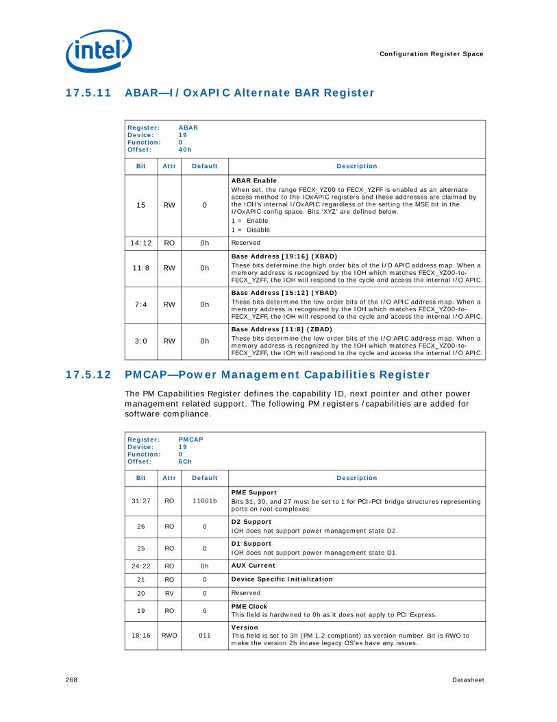
Configuration Register Space
268 Datasheet
17.5.11 ABAR—I/OxAPIC Alternate BAR Register
17.5.12 PMCAP—Power Management Capabilities Register
The PM Capabilities Register defines the capability ID, next pointer and other power management related support. The following PM registers /capabilities are added for software compliance.
Register: ABARDevice: 19Function: 0Offset: 40h
Bit Attr Default Description
15 RW 0
ABAR Enable When set, the range FECX_YZ00 to FECX_YZFF is enabled as an alternate access method to the IOxAPIC registers and these addresses are claimed by the IOH’s internal I/OxAPIC regardless of the setting the MSE bit in the I/OxAPIC config space. Bits ‘XYZ’ are defined below.1 = Enable1 = Disable
14:12 RO 0h Reserved
11:8 RW 0h
Base Address [19:16] (XBAD) These bits determine the high order bits of the I/O APIC address map. When a memory address is recognized by the IOH which matches FECX_YZ00-to-FECX_YZFF, the IOH will respond to the cycle and access the internal I/O APIC.
7:4 RW 0h
Base Address [15:12] (YBAD) These bits determine the low order bits of the I/O APIC address map. When a memory address is recognized by the IOH which matches FECX_YZ00-to-FECX_YZFF, the IOH will respond to the cycle and access the internal I/O APIC.
3:0 RW 0h
Base Address [11:8] (ZBAD) These bits determine the low order bits of the I/O APIC address map. When a memory address is recognized by the IOH which matches FECX_YZ00-to-FECX_YZFF, the IOH will respond to the cycle and access the internal I/O APIC.
Register: PMCAPDevice: 19Function: 0Offset: 6Ch
Bit Attr Default Description
31:27 RO 11001bPME SupportBits 31, 30, and 27 must be set to 1 for PCI-PCI bridge structures representing ports on root complexes.
26 RO 0D2 SupportIOH does not support power management state D2.
25 RO 0D1 SupportIOH does not support power management state D1.
24:22 RO 0h AUX Current
21 RO 0 Device Specific Initialization
20 RV 0 Reserved
19 RO 0PME ClockThis field is hardwired to 0h as it does not apply to PCI Express.
18:16 RWO 011VersionThis field is set to 3h (PM 1.2 compliant) as version number. Bit is RWO to make the version 2h incase legacy OS’es have any issues.

Datasheet 269
Configuration Register Space
17.5.13 PMCSR—Power Management Control and Status Register
This register provides status and control information for PM events in the PCI Express port of the IOH.
15:8 RO 00hNext Capability PointerThis is the last capability in the chain and hence set to 0.
7:0 RO 01hCapability IDProvides the PM capability ID assigned by PCI-SIG.
Register: PMCAPDevice: 19Function: 0Offset: 6Ch
Bit Attr Default Description
Register: PMCSRDevice: 19Function: 0Offset: 70h
Bit Attr Default Description
31:24 RO 00hDataNot relevant for IOH
23 RO 0hBus Power/Clock Control EnableThis field is hardwired to 0h as it does not apply to PCI Express.
22 RO 0hB2/B3 SupportThis field is hardwired to 0h as it does not apply to PCI Express.
21:16 RO 0h Reserved
15 RO 0h
PME StatusApplies only to root portsThis PME Status is a sticky bit. This bit is set, independent of the PMEEN bit defined below, on an enabled PCI Express hotplug event provided the root port was in D3hot state. Software clears this bit by writing a ‘1’ when it has been completed. Refer to PCI Express Base Specification, Revision 1.1 and post 1.1 Erratas and EC*’s for further details on wake event generation at a root port.
14:13 RO 0hData ScaleNot relevant for IOH
12:9 RO 0hData SelectNot relevant for IOH
8 RO 0h
PME EnableApplies only to root ports. This field is a sticky bit and when set, enables PMEs generated internally on a PCI Express hotplug event to set the appropriate bits in the ROOTSTS register (which can then trigger an MSI or cause a _PMEGPE event).
7:4 RO 0h Reserved
3 RO 0 Indicates IOH does not reset its registers when transitioning from D3hot to D0.

Configuration Register Space
270 Datasheet
17.5.14 RDINDEX—Alternate Index to read Indirect I/OxAPIC Registers
2 RO 0h Reserved
1:0 RW 0h
Power StateThis 2-bit field is used to determine the current power state of the function and to set a new power state as well. 00 = D001 = D1 (not supported by IOH)10 = D2 (not supported by IOH)11 = D3_hotIf Software tries to write 01 or 10 to this field, the power state does not change from the existing power state (which is either D0 or D3hot) and nor do these bits1:0 change value.All devices will: 1. Respond to only Type 0 configuration transactions targeted at the
device’s configuration space, when in D3hot state 2. Root port will not forward Type 1 or Type 0 transactions to the
downstream PCIe link 3. Will not respond to memory/IO transactions (that is, D3hot state is
equivalent to MSE/IOSE bits being clear), with one exception noted below, as target
4. Will not generate any memory/IO/configuration transactions as initiator on the primary bus.
Exception to 3 is that root ports will continue to decode and forward memory transactions that target the IOAPIC address range, even when the root port is in D3hot state. Inbound memory/IO/configuration transactions that happen when the device is in D3hot state are aborted and root ports return a UR response on PCIe. Messages/completions will still pass through in either direction without being aborted.
Register: RDINDEXDevice: 19Function: 0Offset: 80h
Bit Attr Default Description
7:0 RW 00h
Index When bmc/jtag wants to read the indirect RTE registers of I/OxAPIC, this register is used to point to the index of the indirect register, as defined in the I/OxAPIC indirect memory space. Software writes to this register and then does a read of the RDWINDOW register to read the contents at that index.Note that hardware does not preclude software from accessing this register over Intel QuickPath Interconnect but that is not what this register is defined for.
Register: PMCSRDevice: 19Function: 0Offset: 70h
Bit Attr Default Description

Datasheet 271
Configuration Register Space
17.5.15 RDWINDOW—Alternate Window to read Indirect I/OxAPIC Registers
17.5.16 IOAPICTETPC—IOxAPIC Table Entry Target ProgrammableControl Register
Register: RDWINDOWDevice: 19Function: 0Offset: 90h
Bit Attr Default Description
31:0 RO 0sWindow When SMBUS/JTAG reads this register, the data contained in the indirect register pointed to by the RDINDEX register is returned on the read.
Register: IOAPICTETPCDevice: 19Function: 0Offset: A0h
Bit Attr Default Description
31:13 RV 00000h Reserved
12 RW 1hSRC17INTA:0 = src/int is connected to IOAPIC table entry 51 = src/int is connected to IOAPIC table entry 21
11 RW 1hSRC16INTB:0 = src/int is connected to IOAPIC table entry 31 = src/int is connected to IOAPIC table entry 22
10 RW 1hSRC13INTA:0 = src/int is connected to IOAPIC table entry 21 = src/int is connected to IOAPIC table entry 21
9 RW 1hSRC14INTA:0 = src/int is connected to IOAPIC table entry 11 = src/int is connected to IOAPIC table entry 22
8 RW 1hSRC10INTD:0 = src/int is connected to IOAPIC table entry 161 = src/int is connected to IOAPIC table entry 21
7 RW 1hSRC10INTC:0 = src/int is connected to IOAPIC table entry 181 = src/int is connected to IOAPIC table entry 22
6 RW 0hSRC10INTB:0 = src/int is connected to IOAPIC table entry 71 = src/int is connected to IOAPIC table entry 17
5 RW 1hSRC9INTC:0 = src/int is connected to IOAPIC table entry 161 = src/int is connected to IOAPIC table entry 23
4 RW 0hSRC6INTB:0 = src/int is connected to IOAPIC table entry 171 = src/int is connected to IOAPIC table entry 23
3 RW 1hSRC5INTD:0 = src/int is connected to IOAPIC table entry 181 = src/int is connected to IOAPIC table entry 23

Configuration Register Space
272 Datasheet
2 RW 0hSRC3INTD:0 = src/int is connected to IOAPIC table entry 51 = src/int is connected to IOAPIC table entry 11
1 RW 0hSRC3INTC:0 = src/int is connected to IOAPIC table entry 31 = src/int is connected to IOAPIC table entry 10
0 RW 0hSRC3INTB:0 = src/int is connected to IOAPIC table entry 11 = src/int is connected to IOAPIC table entry 12
Register: IOAPICTETPCDevice: 19Function: 0Offset: A0h
Bit Attr Default Description

Datasheet 273
Configuration Register Space
17.5.17 I/OxAPIC Memory Mapped Registers
I/OxAPIC has a direct memory mapped space. An index/data register pair is located within the directed memory mapped region and is used to access the redirection table entries. provides the direct memory mapped registers of the I/OxAPIC. The offsets shown in the table are from the base address in either ABAR or MBAR or both. Accesses to addresses beyond 40h return all 0s.
Note that only addresses up to offset FFh can be accessed using the ABAR register whereas offsets up to FFFh can be accessed using MBAR. Only aligned DWORD reads and write are allowed towards the I/OxAPIC memory space. Any other accesses will result in an error.
Table 17-5. I/OxAPIC Direct Memory Mapped Registers
Register Byte Offset
Index 00h
04h
08h
0Ch
Window 10h
14h
18h
1Ch
PAR 20h
24h
28h
2Ch
30h
34h
38h
3Ch
EOI 40h
...
FF
...
FFF

Configuration Register Space
274 Datasheet
17.5.18 Index Register
The Index Register will select which indirect register appears in the window register to be manipulated by software. Software will program this register to select the desired APIC internal register.
17.5.19 Window Register
This is a 32-bit register specifying the data to be read or written to the register pointed to by the index register. This register can be accessed in byte quantities.
17.5.20 PAR Register
17.5.21 EOI Register
Register: IndexBAR: XBAROffset: 00h
Bit Attr Default Description
7:0 RW 00hIndex (IDX)Indirect register to access.
Register: WindowBAR: MBAROffset: 10h
Bit Attr Default Description
31:0 RW 0sWindow (WND)Data to be written to the indirect register on writes, and location of read data from the indirect register on reads.
Register: PARBAR: MBAROffset: 20h
Bit Attr Default Description
7:0 RO 00hAssertion (PAR)IOH does not allow writes to the PAR to cause MSI interrupts.
Register: EOIBAR: MBAROffset: 40h
Bit Attr Default Description
7:0 RW 00h
EOIThe EOI register is present to provide a mechanism to efficiently convert level interrupts to edge triggered MSI interrupts. When a write is issued to this register, the I/O(x)APIC will check the lower 8 bits written to this register, and compare it with the vector field for each entry in the I/O Redirection Table. When a match is found, the Remote_IRR bit for that I/O Redirection Entry will be cleared. Note that if multiple I/O Redirection entries, for any reason, assign the same vector, each of those entries will have the Remote_IRR bit reset to 0. This will cause the corresponding I/OxAPIC entries to resample their level interrupt inputs and if they are still asserted, cause more MSI interrupt(s) (if unmasked) which will again set the Remote_IRR bit.

Datasheet 275
Configuration Register Space
17.5.22 APICID Register
This register uniquely identifies an APIC in the system. While this register is not used by modern operating systems, it is still implemented for legacy purposes.
Table 17-6. I/OxAPIC Indexed Registers (Redirection Table Entries)
Indexed Register Index
APICID 00h
Version 01h
ARBID 02h
BCFG 03h
...
...
RTL0 10h
RTH0 11h
RTL1 12h
RTH1 13h
...
...
...
...
RTL23 3Eh
RTH23 3Fh
40h
...
FFh
Register: APICIDBAR: MBAROffset: 10hIA: 00h
Bit Attr Default Description
31:28 RO 0s Reserved
27:24 RW 0s APICID: Allows for up to 16 unique APIC IDs in the system.
23:0 RO 0s Reserved

Configuration Register Space
276 Datasheet
17.5.23 Version Register
This register uniquely identifies an APIC in the system. While this register is not used by modern operating systems, it is still implemented for legacy purposes.
17.5.24 ARBID Register
This is a legacy register carried over from days of serial bus interrupt delivery. This register has no meaning in IOH. It just tracks the APICID register for compatibility reasons.
17.5.25 BCFG Register
Register: VersionBAR: MBAROffset: 10hIA: 01h
Bit Attr Default Description
31:24 RO 00h Reserved
23:16 RO 17h
Maximum Redirection Entries (MAX) This is the entry number of the highest entry in the redirection table. It is equal to the number of interrupt inputs minus one. This field is hardwired to 17h to indicate 24 interrupts.
15 RO 0
IRQ Assertion Register Supported (PRQ)This bit is set to 0 to indicate that this version of the I/OxAPIC does not implement the IRQ Assertion register and does not allow PCI devices to write to it to cause interrupts.
14:8 RO 0s Reserved
7:0 RO 20hVersion (VS)This identifies the implementation version. This field is hardwired to 20h indicate this is an I/OxAPIC.
Register: ARBUIDBAR: MBAROffset: 10hIA: 02h
Bit Attr Default Description
31:28 RO 0s Reserved
27:24 RO 0s Arbitration ID: Just tracks the APICID register.
23:0 RO 0s Reserved
Register: BCFGBAR: MBAROffset: 10hIA: 03h
Bit Attr Default Description
7:1 RO 0 Reserved
0 RW 1Boot ConfigurationThis bit defaults to 1 to indicate FSB delivery mode. A value of 0 has no effect. It is left as RW for software compatibility reasons.

Datasheet 277
Configuration Register Space
17.5.26 RTL[0:23]—Redirection Table Low DWord Register
The information in this register along with Redirection Table High DWORD register is used to construct the MSI interrupt. There is one of these pairs of registers for every interrupt. The first interrupt has the redirection registers at offset 10h. The second interrupt at 12h, third at 14h, and so on, until the final interrupt (interrupt 23) at 3Eh.
Register: RTL[0:23]BAR: MBAROffset: 10hIA: 10h– 3Eh by 2
Bit Attr Default Description
31:18 RO 0s Reserved
17 RW 0 Disable Flushing\This bit has no meaning in IOH. This bit is R/W for software compatibility reasons only
16 RW 1
Mask (MSK) When cleared, an edge assertion or level (depending on bit 15 in this register) on the corresponding interrupt input results in delivery of an MSI interrupt using the contents of the corresponding redirection table high/low entry. When set, an edge or level on the corresponding interrupt input does not cause MSI Interrupts and no MSI interrupts are held pending as well (that is, if an edge interrupt asserted when the mask bit is set, no MSI interrupt is sent and the hardware does not remember the event to cause an MSI later when the mask is cleared). When set, assertion/deassertion of the corresponding interrupt input causes Assert/Deassert_INTx messages to be sent to the legacy ICH, provided the ‘Disable PCI INTx Routing to ICH’ bit is clear. If the latter is set, Assert/Deassert_INTx messages are not sent to the legacy ICH.When the mask bit goes from 1-to-0 for an entry and the entry is programmed for level input, the input is sampled and if asserted, an MSI is sent. Also, if an Assert_INTx message was previously sent to the legacy ICH/internal-coalescing logic on behalf of the entry, when the mask bit is clear, then a Deassert_INTx event is scheduled on behalf of the entry (whether this event results in a Deassert_INTx message to the legacy ICH depends on whether there were other outstanding Deassert_INTx messages from other sources). When the mask bit goes from 0-to-1, and the corresponding interrupt input is already asserted, an Assert_INTx event is scheduled on behalf of the entry. However, note that if the interrupt is deasserted when the bit transitions from 0-to-1, a Deassert_INTx is not scheduled on behalf of the entry.
15 RW 0Trigger Mode (TM)This field indicates the type of signal on the interrupt input that triggers an interrupt. 0 indicates edge sensitive, 1 indicates level sensitive.
14 RO 0
Remote IRR (RIRR)This bit is used for level triggered interrupts; its meaning is undefined for edge triggered interrupts. For level triggered interrupts, this bit is set when an MSI interrupt has been issued by the I/OxAPIC into the system fabric (noting that if BME bit is clear or when the mask bit is set, no new MSI interrupts cannot be generated and this bit cannot transition from 0 to 1 in those conditions). It is reset (if set) when an EOI message is received from a local APIC with the appropriate vector number, at which time the level interrupt input corresponding to the entry is resampled causing one more MSI interrupt (if other enable bits are set) and causing this bit to be set again.
13 RW 0
Interrupt Input Pin Polarity (IP) 0 = Active high1 = Active low. Strictly, speaking this bit has no meaning in the IOH since the Assert/Deassert_INTx messages are level in-sensitive. But the core I/OxAPIC logic that is reused from PXH might be built to use this bit to determine the correct polarity. Most operating systems today support only active low interrupt inputs for PCI devices. Given that, the operating system is expected to program a 1 into this register and so the “internal” virtual wire signals in the IOH need to be active low, that is, 0=asserted and 1=deasserted.

Configuration Register Space
278 Datasheet
17.5.27 RTH[0:23]—Redirection Table High DWord Register
12 RO 0
Delivery StatusWhen trigger mode is set to level and the entry is unmasked, this bit indicates the state of the level interrupt; that is, 1b if interrupt is asserted; otherwise 0b. When the trigger mode is set to level but the entry is masked, this bit is always 0b. This bit is always 0b when trigger mode is set to edge.
11 RW 0Destination Mode (DSTM) 0 = Physical1 = Logical
10:8 RW 0s
Delivery Mode (DELM)This field specifies how the APICs listed in the destination field should act upon reception of the interrupt. Certain Delivery Modes will only operate as intended when used in conjunction with a specific trigger mode. The encodings are:000 = Fixed: Trigger Mode can be edge or level. Examine TM bit to determine.001 = Lowest Priority: Trigger Mode can be edge or level. Examine TM bit to
determine.010 = SMI/PMI: Trigger mode is always edge and TM bit is ignored.011 = Reserved100 = NMI. Trigger mode is always edge and TM bit is ignored.101 = INIT. Trigger mode is always edge and TM bit is ignored.110 = Reserved111 = ExtINT. Trigger mode is always edge and TM bit is ignored.
7:0 RW 00h Vector (VCT): This field contains the interrupt vector for this interrupt
Register: RTH[0:23]BAR: MBAROffset: 10hIA: 11h – 3h by 2
Bit Attr Default Description
31:24 RW 00hDestination ID (DID)They are bits [19:12] of the MSI address.
23:16 RW 00hExtended Destination ID (EDID)These bits become bits [11:4] of the MSI address.
15:00 RO 0000h Reserved
Register: RTL[0:23]BAR: MBAROffset: 10hIA: 10h– 3Eh by 2
Bit Attr Default Description

Datasheet 279
Configuration Register Space
17.6 Intel® VT, Address Mapping, System Management, Device Hide, MiscellaneousThe offsets shown in Table 17-4 are offsets from the base of the CSR region. Any change to these registers under that event can only happen during an Intel QuickPath Interconnect quiescence flow. Any exceptions will be called out when appropriate.
Table 17-7. Core Registers (Device 20, Function 0) — Offset 00h–FFh (Sheet 1 of 2)
DID VID 00h 80h
PCISTS PCICMD 04h 84h
CCR RID 08h GENPROTRANGE0.BASE 88h
HDR CLS 0Ch 8Ch
10h GENPROTRANGE0.LIMIT 90h
14h 94h
18h IOHMISCCTRL 98h
1Ch IOHMISCSS 9Ch
20h A0h
24h A4h
28h TSEGCTRL A8h
SID SVID 2Ch ACh
30h GENPROTRANGE1.BASE B0h
CAPPTR1
Notes:1. CAPPTR points to the first capability block
34h B4h
38h GENPROTRANGE1.LIMIT B8h
INTP INTL 3Ch BCh
EXPCAPS EXPNPTR EXPCAPID 40h GENPROTRANGE2.BASE C0h
DEVCAP 44h C4h
DEVSTS DEVCTRL 48h GENPROTRANGE2.LIMIT C8h
RESERVED PCIE Header space 4Ch CCh
50h TOLM D0h
54h TOHM D4h
58h D8h
5Ch NCMEM.BASE DCh
60h E0h
64h NCMEM.LIMIT E4h
68h E8h
6Ch ECh
70h DEVHIDE 1 F0h
74h F4h
78h DEVHIDE 2 F8h
7Ch FCh

Configuration Register Space
280 Datasheet
Table 17-8. Core Registers (Device 20, Function 0) — Offset 100h–1FFh (Sheet 2 of 2)
Reserved for PCIe header space 100h VTBAR 180h
104h VTGENCTRL 184h
IOHBUSNO LIO.LIMIT LIO.BASE 108h VTISOCHCTRL 188h
LMMIOL.LIMIT LMMIOL.BASE 10Ch VTGENCTRL2 18Ch
LMMIOH.LIMIT LMMIOH.BASE 110h VTSTS 190h
LMMIOH.BASEU 114h 194h
LMMIOH.LIMITU 118h 198h
LCFGBUS.LIMIT
LCFGBUS.BASE
11Ch 19Ch
GIO.LIMIT GIO.BASE 120h 1A0h
GMMIOL.LIMIT GMMIOL.BASE 124h 1A4h
GMMIOH.LIMIT GMMIOH.BASE 128h VTUNCERRSTS 1A8h
GMMIOH.BASEU 12Ch VTUNCERRMSK 1ACh
GMMIOH.LIMITU 130h VTUNCERRSEV 1B0h
GCFGBUS.LIMIT
GCFGBUS.BASE
134h VTUNCERRPTR 1B4h
138h 1B8h
13Ch 1BCh
140h 1C0h
144h 1C4h
DUALIOAPIC.ABAR LIMIT
DUALIOAPIC.ABAR BASE
148h 1C8h
14Ch 1CCh
150h 1D0h
154h 1D4h
158h 1D8h
15Ch 1DCh
160h 1E0h
164h 1E4h
168h 1E8h
16Ch 1ECh
170h 1F0h
174h 1F4h
178h 1F8h
17Ch 1FCh

Datasheet 281
Configuration Register Space
17.6.1 GENPROTRANGE0.BASE—Generic Protected MemoryRange 0 Base Address Register
17.6.2 GENPROTRANGE0.LIMIT—Generic Protected MemoryRange 0 Limit Address Register
Register: GENPROTRANGE0.BASEDevice: 20Function: 0Offset: 88h
Bit Attr Default Description
63:51 RO 0 Correspond to address A[63:51] of the protected range and is always 0.
50:16 RWLB 7_FFFF_FFFFh
Base address [50:16] of generic memory address range that needs to be protected from inbound dma accesses. The protected memory range can be anywhere in the memory space addressable by the processor. Addresses that fall in this range i.e. GenProtRange.Base[63:16] <= Address [63:16] <= GenProtRange.Limit [63:16], are completer aborted by IOH.Setting the Protected range base address greater than the limit address disables the protected memory region.Note that this range is orthogonal to VT-d spec defined protected address range.This register is programmed once at boot time and does not change after that, including any quiesce flows.
15:0 RV 0 Reserved
Register: GENPROTRANGE0.LIMITDevice: 20Function: 0Offset: 90h
Bit Attr Default Description
63:51 RO 0 This field correspond to address A[63:51] of the protected range and is always 0.
50:16 RWLB 0
Limit address Address bits 50:16 of generic memory address range that needs to be protected from inbound dma accesses. The protected memory range can be anywhere in the memory space addressable by the processor. Addresses that fall in the range of GenProtRange.Base[63:16] Address [63:16] GenProtRange.Limit [63:16], are aborted by IOH.Setting the Protected range base address greater than the limit address disables the protected memory region.Note that this range is orthogonal to VT-d specification defined protected address range.This register is programmed once at boot time and does not change after that, including any quiesce flows.
15:0 RV 0 Reserved

Configuration Register Space
282 Datasheet
17.6.3 IOHMISCCTRL—IOH Miscellaneous Control Register
Register: IOHMISCCTRLDevice: 20Function: 0Offset: 98h
Bit Attr Default Description
31:14 RV 0s Reserved
13 RW 0
CPUCSR_IB_AbortThis bit controls if inbound access to CPUCSR range is aborted.0 = IB access to CPUCSR range is enabled, that is, allowed.1 = IB access to CPUCSR range is disabled, that is, disallowed.
12 RW 0
Lock Thawing ModeThis mode controls how inbound queues in the south agents (PCIe, DMI) thaw when they are target of a locked read.0 = Thaw only posted requests1 = Thaw posted and non-posted requests.
11:10 RW strap
SUBDECENThis field indicates the port that provides the subtractive decode path for inbound and outbound decode.00 = DMI01 = Reserved10 = Reserved11 = Intel QuickPath InterconnectWhen this points to DMI, all address ranges in the peer-to-peer config space of the port are ignored for address decode purposes. When this field is 00, then the IOH is the legacy IOH.
9 RV 0 Reserved
8 RW 0TOCMVALID: This bit is set by software after it has initialized the TOCM register with the right value. IOH decoder uses this bit to determine if bits from 32 to TOCM are to be decoded towards privileged CSR space.
7:3 RW 01001
TOCMIndicates the top of Intel QuickPath Interconnect physical addressability limit.00000–00100 = Reserved00101 = 2^3700110 = 2^38... 10011 = 2^5110100–11111 = ReserveIOH uses this to abort all inbound transactions that cross this limit.
2 RW 0EN1KThis bit when set, enables 1K granularity for I/O space decode in each of the virtual peer-to-peer bridges corresponding to root ports, and DMI ports.
1:0 RV 0 Reserved

Datasheet 283
Configuration Register Space
17.6.4 IOHMISCSS—IOH Miscellaneous Status Register
Register: IOHMISCSSDevice: 20Function: 0Offset: 9Ch
Bit Attr Default Description
31:30 RV 0 Reserved
29 RO strap NodeID2: Node ID 2
28 RO strap
Intel QuickPath Interconnect/NodeID3 For dual node configurations, this bit indicates which Intel QuickPath Interconnect port is connected to the other IOH. For all configurations, this strap indicates NID3 value.
27 RV 0 Reserved
26 RO strapMP This bit indicates whether this is an MP or UP/DP IOH
25 RW strapDUALIOH This bit indicates dual IOH configuration
24:18 RV 0 Reserved
17 RO strap Legacy IOH
16 RO strapFWAGNT Firmware Agent. Legacy IOHs are advertised as a firmware agent.
15:10 RO strap PCIe Link width select
9:8 RO strap DDR Frequency selection
7:6 RV 0 Reserved
5 RO strap PESBLCSEL
4 RO strap QPISBLCSEL
3 RV 0 Reserved
2 RO strap SMBUSID
1:0 RO strap QPIFREQSEL[1:0]

Configuration Register Space
284 Datasheet
17.6.5 IOH System Management Registers
17.6.5.1 TSEGCTRL—TSEG Control Register
The location of the TSeg region, size, and enable/disable control.
17.6.5.2 GENPROTRANGE.BASE1—Generic Protected Memory Range 1 Base Address Register
Register: TSEGCTRLDevice: 20Function: 0Offset: A8h
Bit Attr Default Description
31:20 RWO FE0hTBA: TSeg Base AddressThis field indicates the base address which is aligned to a 1 MB boundary. Bits 31:20 corresponds to A[31:20] address bits.
19:4 RV 0 Reserved
3:1 RWO 100
TSEG_SIZE: Size of TSEG000 = 512 KB001 = 1 MB010 = 2 MB011 = 4 MB100 = 8 MB101–111 = Reserved
0 RWO 1TSEG_EN: TSEG Enabling Control0 = Disabling the TSeg in IOH.1 = Enabling the TSeg in IOH for IB access check.
Register: GENPROTRANGE.BASE1Device: 20Function: 0Offset: B0h
Bit Attr Default Description
63:51 RO 0s This field correspond to address A[63:51] of the protected range and is always 0.
50:16 RW 7_FFFF–FFFFh
Base Address: This field is the base address 50:16 of generic memory address range. The protected memory range can be anywhere in the memory space addressable by the processor. Addresses that fall in this range, that is, GenProtRange.Base[63:16] Address [63:16] GenProtRange.Limit [63:19], are completer aborted by IOH.Setting the Protected range base address greater than the limit address disables the protected memory region.This register is programmed once at boot time and does not change after that, including any quiesce flows.
15:0 RO 0s Reserved
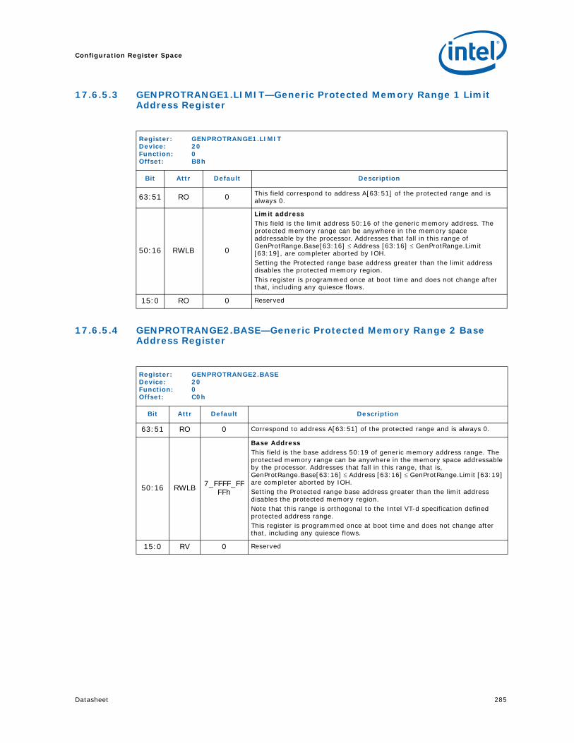
Datasheet 285
Configuration Register Space
17.6.5.3 GENPROTRANGE1.LIMIT—Generic Protected Memory Range 1 Limit Address Register
17.6.5.4 GENPROTRANGE2.BASE—Generic Protected Memory Range 2 Base Address Register
Register: GENPROTRANGE1.LIMITDevice: 20Function: 0Offset: B8h
Bit Attr Default Description
63:51 RO 0 This field correspond to address A[63:51] of the protected range and is always 0.
50:16 RWLB 0
Limit addressThis field is the limit address 50:16 of the generic memory address. The protected memory range can be anywhere in the memory space addressable by the processor. Addresses that fall in this range of GenProtRange.Base[63:16] Address [63:16] GenProtRange.Limit [63:19], are completer aborted by IOH.Setting the Protected range base address greater than the limit address disables the protected memory region.This register is programmed once at boot time and does not change after that, including any quiesce flows.
15:0 RO 0 Reserved
Register: GENPROTRANGE2.BASEDevice: 20Function: 0Offset: C0h
Bit Attr Default Description
63:51 RO 0 Correspond to address A[63:51] of the protected range and is always 0.
50:16 RWLB 7_FFFF_FFFFh
Base AddressThis field is the base address 50:19 of generic memory address range. The protected memory range can be anywhere in the memory space addressable by the processor. Addresses that fall in this range, that is, GenProtRange.Base[63:16] Address [63:16] GenProtRange.Limit [63:19] are completer aborted by IOH.Setting the Protected range base address greater than the limit address disables the protected memory region.Note that this range is orthogonal to the Intel VT-d specification defined protected address range.This register is programmed once at boot time and does not change after that, including any quiesce flows.
15:0 RV 0 Reserved
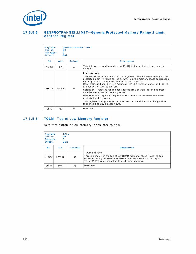
Configuration Register Space
286 Datasheet
17.6.5.5 GENPROTRANGE2.LIMIT—Generic Protected Memory Range 2 Limit Address Register
17.6.5.6 TOLM—Top of Low Memory Register
Note that bottom of low memory is assumed to be 0.
Register: GENPROTRANGE.LIMITDevice: 20Function: 0Offset: C8h
Bit Attr Default Description
63:51 RO 0 This field correspond to address A[63:51] of the protected range and is always 0.
50:16 RWLB 0
Limit AddressThis field is the limit address 50:16 of generic memory address range. The protected memory range can be anywhere in the memory space addressable by the processor. Addresses that fall in this range of GenProtRange.Base[63:16] Address [63:16] GenProtRange.Limit [63:19] are completer aborted by IOH.Setting the Protected range base address greater than the limit address disables the protected memory region.Note that this range is orthogonal to the Intel VT-d specification defined protected address range.This register is programmed once at boot time and does not change after that, including any quiesce flows.
15:0 RV 0 Reserved
Register: TOLMDevice: 20Function: 0Offset: D0h
Bit Attr Default Description
31:26 RWLB 0s
TOLM addressThis field indicates the top of low DRAM memory, which is aligned to a 64 MB boundary. A 32-bit transaction that satisfies 0 A[31:26] TOLM[31:26] is a transaction towards main memory.
25:0 RO 0s Reserved

Datasheet 287
Configuration Register Space
17.6.5.7 TOHM—Top of High Memory Register
Note that bottom of high memory is fixed at 4 GB.
17.6.5.8 NCMEM.BASE—NCMEM Base Register
Base address of Intel QuickPath Interconnect non-coherent memory.
Register: TOHMDevice: 20Function: 0Offset: D4h
Bit Attr Default Description
63:26 RWLB 0s
TOHM AddressThis field indicates the limit of an aligned 64 MB granular region that decodes > 4 GB addresses towards system DRAM memory. A 64-bit transaction that satisfies 4 GB A[63:26] TOHM[63:26]” is a transaction towards main memory.This register is programmed once at boot time and does not change after that, including any quiesce flows.
25:0 RV 0s Reserved
Register: NCMEM.BASEDevice: 20Function: 0Offset: DCh
Bit Attr Default Description
63:26 RWLB 3F_FFFF_FFFFh
Non Coherent memory base addressThis field describes the base address of a 64 MB aligned DRAM memory region on Intel QuickPath Interconnect that is non-coherent. Address bits 63:26 of an inbound address if it satisfies NcMem.Base[63:26] A[63:26] NcMem.Limit[63:26]’ is considered to be towards the non-coherent Intel QuickPath Interconnect memory region. It is expected that the range indicated by the Non-coherent memory base and limit registers is a subset of either the low DRAM or high DRAM memory regions as described using the corresponding base and limit registers.This register is programmed once at boot time and does not change after that, including any quiesce flows.
25:0 RV 0s Reserved

Configuration Register Space
288 Datasheet
17.6.5.9 NCMEM.LIMIT—NCMEM Limit Register
Limit of Intel QuickPath Interconnect non-coherent memory.
Register: NCMEM.LIMITDevice: 20Function: 0Offset: E4h
Bit Attr Default Description
63:26 RW 0
Non Coherent memory limit addressDescribes the limit address of a 64MB aligned dram memory region on Intel QuickPath Interconnect that is non-coherent. Address bits 63:26 of an inbound address if it satisfies ‘NcMem.Base[63:26] A[63:26] NcMem.Limit[63:26]’ is considered to be towards the non-coherent Intel QuickPath Interconnect memory region. Its expected that the range indicated by the Non-coherent memory base and limit registers is a subset of either the low DRAM or high DRAM memory regions as described using the corresponding base and limit registers.This register is programmed once at boot time and does not change after that, including any quiesce flows.
25:0 RV 0 Reserved

Datasheet 289
Configuration Register Space
17.6.5.10 DEVHIDE1—Device Hide 1 Register
This register provides a method to hide the PCI configuration space of devices inside IOH, from the host initiated configuration accesses. This register has no impact on configuration accesses from SMBUS/JTAG ports of IOH. When set, all PCI configuration accesses from Intel QPI targeting the corresponding device’s configuration space inside IOH are master aborted. When clear, configuration accesses targeting the device’s configuration space are allowed.
Register: DEVHIDE1Device: 20Function: 0Offset: F0h
Bit Attr Default Description
31 RWLB 0
Hide_Dev18_fun11 = All PCI configuration accesses from the Intel QuickPath
Interconnect targeting the corresponding device’s configuration space inside IOH are master aborted.
0 = Configuration accesses targeting the device’s configuration space are allowed.
If software hides function 0 in either device 16, or 17, it needs to hide all functions within that device to comply with PCI rules.This bit has no effect on SMBUS and JTAG initiated accesses to corresponding device’s configuration space.The lock bit is lock1 (“TXTLOCK: TXT Lock Register”)
30 RWLB 0
Hide_Dev18_fun01 = All PCI configuration accesses from the Intel QuickPath
Interconnect targeting the corresponding device’s configuration space inside IOH are master aborted.
0 = Configuration accesses targeting the device’s configuration space are allowed.
If software hides function 0 in either device 16, or 17, it needs to hide all functions within that device to comply with PCI rules.This bit has no effect on SMBUS and JTAG initiated accesses to corresponding device’s configuration space.The lock bit is lock1 (“TXTLOCK: TXT Lock Register”)
29 RWLB 0
Hide_Dev17_fun11 = All PCI configuration accesses from the Intel QuickPath
Interconnect targeting the corresponding device’s configuration space inside IOH are master aborted.
0 = Configuration accesses targeting the device’s configuration space are allowed.
If software hides function 0 in either device 16, or 17, it needs to hide all functions within that device to comply with PCI rules.This bit has no effect on SMBUS and JTAG initiated accesses to corresponding device’s configuration space.The lock bit is lock1 (“TXTLOCK: TXT Lock Register”)
28 RWLB 0
Hide_Dev17_fun01 = All PCI configuration accesses from the Intel QuickPath
Interconnect targeting the corresponding device’s configuration space inside IOH are master aborted.
0 = Configuration accesses targeting the device’s configuration space are allowed.
If software hides function 0 in either device 16, or 17, it needs to hide all functions within that device to comply with PCI rules.This bit has no effect on SMBUS and JTAG initiated accesses to corresponding device’s configuration space.The lock bit is lock1 (“TXTLOCK: TXT Lock Register”)

Configuration Register Space
290 Datasheet
27 RWLB 0
Hide_Dev16_fun11 = All PCI configuration accesses from the Intel QuickPath
Interconnect targeting the corresponding device’s configuration space inside IOH are master aborted.
0 = Configuration accesses targeting the device’s configuration space are allowed.
If software hides function 0 in either device 16, or 17, it needs to hide all functions within that device to comply with PCI rules.This bit has no effect on SMBUS and JTAG initiated accesses to corresponding device’s configuration space.The lock bit is lock1 (“TXTLOCK: TXT Lock Register”)
26 RWLB 0
Hide_Dev16_fun01 = All PCI configuration accesses from the Intel QuickPath
Interconnect targeting the corresponding device’s configuration space inside IOH are master aborted.
0 = Configuration accesses targeting the device’s configuration space are allowed.
If software hides function 0 in either device 16, or 17, it needs to hide all functions within that device to comply with PCI rules.This bit has no effect on SMBUS and JTAG initiated accesses to corresponding device’s configuration space.The lock bit is lock1 (“TXTLOCK: TXT Lock Register”)
25 RWLB 0
Hide_Dev15_fun01 = All PCI configuration accesses from the Intel QuickPath
Interconnect targeting the corresponding device’s configuration space inside IOH are master aborted.
0 = Configuration accesses targeting the device’s configuration space are allowed.
If software hides function 0 in either device 16, or 17, it needs to hide all functions within that device to comply with PCI rules.This bit has no effect on SMBUS and JTAG initiated accesses to corresponding device’s configuration space.The lock bit is lock1 (“TXTLOCK: TXT Lock Register”)
24 RWLB 0
Hide_Dev14_fun31 = All PCI configuration accesses from the Intel QuickPath
Interconnect targeting the corresponding device’s configuration space inside IOH are master aborted.
0 = Configuration accesses targeting the device’s configuration space are allowed.
If software hides function 0 in either device 16, or 17, it needs to hide all functions within that device to comply with PCI rules.This bit has no effect on SMBUS and JTAG initiated accesses to corresponding device’s configuration space.The lock bit is lock1 (“TXTLOCK: TXT Lock Register”)
23 RWLB 0
Hide_Dev14_fun21 = All PCI configuration accesses from the Intel QuickPath
Interconnect targeting the corresponding device’s configuration space inside IOH are master aborted.
0 = Configuration accesses targeting the device’s configuration space are allowed.
If software hides function 0 in either device 16, or 17, it needs to hide all functions within that device to comply with PCI rules.This bit has no effect on SMBUS and JTAG initiated accesses to corresponding device’s configuration space.The lock bit is lock1 (“TXTLOCK: TXT Lock Register”)
Register: DEVHIDE1Device: 20Function: 0Offset: F0h
Bit Attr Default Description

Datasheet 291
Configuration Register Space
22 RWLB 0
Hide_Dev14_fun11 = All PCI configuration accesses from the Intel QuickPath
Interconnect targeting the corresponding device’s configuration space inside IOH are master aborted.
0 = Configuration accesses targeting the device’s configuration space are allowed.
If software hides function 0 in either device 16, or 17, it needs to hide all functions within that device to comply with PCI rules.This bit has no effect on SMBUS and JTAG initiated accesses to corresponding device’s configuration space.The lock bit is lock1 (“TXTLOCK: TXT Lock Register”)
21 RWLB 0
Hide_Dev14_fun01 = All PCI configuration accesses from the Intel QuickPath
Interconnect targeting the corresponding device’s configuration space inside IOH are master aborted.
0 = Configuration accesses targeting the device’s configuration space are allowed.
If software hides function#0 in either device 16, or 17, it needs to hide all functions within that device to comply with PCI rules.This bit has no effect on SMBUS and JTAG initiated accesses to corresponding device’s configuration space.The lock bit is lock1 (“TXTLOCK: TXT Lock Register”)
20 RWLB 0
Hide_Dev13_fun71 = All PCI configuration accesses from the Intel QuickPath
Interconnect targeting the corresponding device’s configuration space inside IOH are master aborted.
0 = Configuration accesses targeting the device’s configuration space are allowed.
If software hides function 0 in either device 16, or 17, it needs to hide all functions within that device to comply with PCI rules.This bit has no effect on SMBUS and JTAG initiated accesses to corresponding device’s configuration space.The lock bit is lock1 (“TXTLOCK: TXT Lock Register”)
19 RWLB 0
Hide_Dev13_fun61 = All PCI configuration accesses from the Intel QuickPath
Interconnect targeting the corresponding device’s configuration space inside IOH are master aborted.
0 = Configuration accesses targeting the device’s configuration space are allowed.
If software hides function 0 in either device 16, or 17, it needs to hide all functions within that device to comply with PCI rules.This bit has no effect on SMBUS and JTAG initiated accesses to corresponding device’s configuration space.The lock bit is lock1 (“TXTLOCK: TXT Lock Register”)
18 RWLB 0
Hide_Dev13_fun51 = All PCI configuration accesses from the Intel QuickPath
Interconnect targeting the corresponding device’s configuration space inside IOH are master aborted.
0 = Configuration accesses targeting the device’s configuration space are allowed.
If software hides function 0 in either device 16, or 17, it needs to hide all functions within that device to comply with PCI rules.This bit has no effect on SMBUS and JTAG initiated accesses to corresponding device’s configuration space.The lock bit is lock1 (“TXTLOCK: TXT Lock Register”)
Register: DEVHIDE1Device: 20Function: 0Offset: F0h
Bit Attr Default Description

Configuration Register Space
292 Datasheet
17 RWLB 0
Hide_Dev13_fun41 = All PCI configuration accesses from the Intel QuickPath
Interconnect targeting the corresponding device’s configuration space inside IOH are master aborted.
0 = Configuration accesses targeting the device’s configuration space are allowed.
If software hides function 0 in either device 16, or 17, it needs to hide all functions within that device to comply with PCI rules.This bit has no effect on SMBUS and JTAG initiated accesses to corresponding device’s configuration space.The lock bit is lock1 (“TXTLOCK: TXT Lock Register”)
16 RWLB 0
Hide_Dev13_fun31 = All PCI configuration accesses from the Intel QuickPath
Interconnect targeting the corresponding device’s configuration space inside IOH are master aborted.
0 = Configuration accesses targeting the device’s configuration space are allowed.
If software hides function 0 in either device 16, or 17, it needs to hide all functions within that device to comply with PCI rules.This bit has no effect on SMBUS and JTAG initiated accesses to corresponding device’s configuration space.The lock bit is lock1 (“TXTLOCK: TXT Lock Register”)
15 RWLB 0
Hide_Dev13_fun21 = All PCI configuration accesses from the Intel QuickPath
Interconnect targeting the corresponding device’s configuration space inside IOH are master aborted.
0 = Configuration accesses targeting the device’s configuration space are allowed.
If software hides function 0 in either device 16, or 17, it needs to hide all functions within that device to comply with PCI rules.This bit has no effect on SMBUS and JTAG initiated accesses to corresponding device’s configuration space.The lock bit is lock1 (“TXTLOCK: TXT Lock Register”)
14 RWLB 0
Hide_Dev13_fun11 = All PCI configuration accesses from the Intel QuickPath
Interconnect targeting the corresponding device’s configuration space inside IOH are master aborted.
0 = Configuration accesses targeting the device’s configuration space are allowed.
If software hides function#0 in either device 16, or 17, it needs to hide all functions within that device to comply with PCI rules.This bit has no effect on SMBUS and JTAG initiated accesses to corresponding device’s configuration space.The lock bit is lock1 (“TXTLOCK: TXT Lock Register”)
13 RWLB 0
Hide_Dev13_fun01 = All PCI configuration accesses from the Intel QuickPath
Interconnect targeting the corresponding device’s configuration space inside IOH are master aborted.
0 = Configuration accesses targeting the device’s configuration space are allowed.
If software hides function 0 in either device 16, or 17, it needs to hide all functions within that device to comply with PCI rules.This bit has no effect on SMBUS and JTAG initiated accesses to corresponding device’s configuration space.The lock bit is lock1 (“TXTLOCK: TXT Lock Register”)
Register: DEVHIDE1Device: 20Function: 0Offset: F0h
Bit Attr Default Description

Datasheet 293
Configuration Register Space
12 RWLB 0
Hide_Dev20_fun31 = All PCI configuration accesses from the Intel QuickPath
Interconnect targeting the corresponding device’s configuration space inside IOH are master aborted.
0 = Configuration accesses targeting the device’s configuration space are allowed.
If software hides function 0 in either device 16, or 17, it needs to hide all functions within that device to comply with PCI rules.This bit has no effect on SMBUS and JTAG initiated accesses to corresponding device’s configuration space.The lock bit is lock1 (“TXTLOCK: TXT Lock Register”)
11 RWLB 0
Hide_Dev14_fun41 = All PCI configuration accesses from the Intel QuickPath
Interconnect targeting the corresponding device’s configuration space inside IOH are master aborted.
0 = Configuration accesses targeting the device’s configuration space are allowed.
If software hides function 0 in either device 16, or 17, it needs to hide all functions within that device to comply with PCI rules.This bit has no effect on SMBUS and JTAG initiated accesses to corresponding device’s configuration space.The lock bit is lock1 (“TXTLOCK: TXT Lock Register”)
10 RWLB TBD
Hide_Dev101 = All PCI configuration accesses from the Intel QuickPath
Interconnect targeting the corresponding device’s configuration space inside IOH are master aborted.
0 = Configuration accesses targeting the device’s configuration space are allowed.
If software hides function 0 in either device 16, or 17, it needs to hide all functions within that device to comply with PCI rules.This bit has no effect on SMBUS and JTAG initiated accesses to corresponding device’s configuration space.The lock bit is lock1 (“TXTLOCK: TXT Lock Register”)
9 RWLB TBD
Hide_Dev91 = All PCI configuration accesses from the Intel QuickPath
Interconnect targeting the corresponding device’s configuration space inside IOH are master aborted.
0 = Configuration accesses targeting the device’s configuration space are allowed.
If software hides function 0 in either device 16, or 17, it needs to hide all functions within that device to comply with PCI rules.This bit has no effect on SMBUS and JTAG initiated accesses to corresponding device’s configuration space.The lock bit is lock1 (“TXTLOCK: TXT Lock Register”)
8 RWLB TBD
Hide_Dev81 = All PCI configuration accesses from the Intel QuickPath
Interconnect targeting the corresponding device’s configuration space inside IOH are master aborted.
0 = Configuration accesses targeting the device’s configuration space are allowed.
If software hides function 0 in either device 16, or 17, it needs to hide all functions within that device to comply with PCI rules.This bit has no effect on SMBUS and JTAG initiated accesses to corresponding device’s configuration space.The lock bit is lock1 (“TXTLOCK: TXT Lock Register”)
Register: DEVHIDE1Device: 20Function: 0Offset: F0h
Bit Attr Default Description

Configuration Register Space
294 Datasheet
7 RWLB TBD
Hide_Dev71 = All PCI configuration accesses from the Intel QuickPath
Interconnect targeting the corresponding device’s configuration space inside IOH are master aborted.
0 = Configuration accesses targeting the device’s configuration space are allowed.
If software hides function 0 in either device 16, or 17, it needs to hide all functions within that device to comply with PCI rules.This bit has no effect on SMBUS and JTAG initiated accesses to corresponding device’s configuration space.The lock bit is lock1 (“TXTLOCK: TXT Lock Register”)
6 RWLB TBD
Hide_Dev61 = All PCI configuration accesses from the Intel QuickPath
Interconnect targeting the corresponding device’s configuration space inside IOH are master aborted.
0 = Configuration accesses targeting the device’s configuration space are allowed.
If software hides function#0 in either device 16, or 17, it needs to hide all functions within that device to comply with PCI rules.This bit has no effect on SMBUS and JTAG initiated accesses to corresponding device’s configuration space.The lock bit is lock1 (“TXTLOCK: TXT Lock Register”)
5 RWLB TBD
Hide_Dev51 = All PCI configuration accesses from Intel QuickPath Interconnect
targeting the corresponding device’s configuration space inside IOH are master aborted.
0 = Configuration accesses targeting the device’s configuration space are allowed.
If software hides function#0 in either device 16, or 17, it needs to hide all functions within that device to comply with PCI rules.This bit has no effect on SMBUS and JTAG initiated accesses to corresponding device’s configuration space.The lock bit is lock1 (“TXTLOCK: TXT Lock Register”)
4 RWLB TBD
Hide_Dev81 = All PCI configuration accesses from Intel QuickPath Interconnect
targeting the corresponding device’s configuration space inside IOH are master aborted.
0 = Configuration accesses targeting the device’s configuration space are allowed.
If software hides function 0 in either device 16, or 17, it needs to hide all functions within that device to comply with PCI rules.This bit has no effect on SMBUS and JTAG initiated accesses to corresponding device’s configuration space.The lock bit is lock1 (“TXTLOCK: TXT Lock Register”)
3 RWLB TBD
Hide_Dev31 = All PCI configuration accesses from the Intel QuickPath
Interconnect targeting the corresponding device’s configuration space inside IOH are master aborted.
0 = Configuration accesses targeting the device’s configuration space are allowed.
If software hides function 0 in either device 16, or 17, it needs to hide all functions within that device to comply with PCI rules.This bit has no effect on SMBUS and JTAG initiated accesses to corresponding device’s configuration space.The lock bit is lock1 (“TXTLOCK: TXT Lock Register”)
Register: DEVHIDE1Device: 20Function: 0Offset: F0h
Bit Attr Default Description

Datasheet 295
Configuration Register Space
2 RWLB TBD
Hide_Dev21 = All PCI configuration accesses from the Intel QuickPath
Interconnect targeting the corresponding device’s configuration space inside IOH are master aborted.
0 = Configuration accesses targeting the device’s configuration space are allowed.
If software hides function 0 in either device 16, or 17, it needs to hide all functions within that device to comply with PCI rules.This bit has no effect on SMBUS and JTAG initiated accesses to corresponding device’s configuration space.The lock bit is lock1 (“TXTLOCK: TXT Lock Register”)
1 RWLB TBD
Hide_Dev11 = All PCI configuration accesses from the Intel QuickPath
Interconnect targeting the corresponding device’s configuration space inside IOH are master aborted.
0 = Configuration accesses targeting the device’s configuration space are allowed.
If software hides function 0 in either device 16, or 17, it needs to hide all functions within that device to comply with PCI rules.This bit has no effect on SMBUS and JTAG initiated accesses to corresponding device’s configuration space.The lock bit is lock1 (“TXTLOCK: TXT Lock Register”)
0 RWLB TBD
Hide_Dev01 = All PCI configuration accesses from the Intel QuickPath
Interconnect targeting the corresponding device’s configuration space inside IOH are master aborted.
0 = Configuration accesses targeting the device’s configuration space are allowed.
If software hides function 0 in either device 16, or 17, it needs to hide all functions within that device to comply with PCI rules.This bit has no effect on SMBUS and JTAG initiated accesses to corresponding device’s configuration space.The lock bit is lock1 (“TXTLOCK: TXT Lock Register”)
Register: DEVHIDE1Device: 20Function: 0Offset: F0h
Bit Attr Default Description

Configuration Register Space
296 Datasheet
17.6.5.11 DEVHIDE2—Device Hide 2 Register
This register provides a method to hide the PCI config space of devices inside IOH, from the host initiated configuration accesses. This register has no impact on configuration accesses from SMBus/JTAG ports of an IOH.
Register: DEVHIDE2Device: 20Function: 0Offset: F8h
Bit Attr Default Description
31:15 RV 0s Reserved
14:7 RWLB 0s
Device/Function Hide: Bit 7 corresponds to Device 22/Function 0, bit 8 corresponds to Device 22/Function 1, ..., bit 14 corresponds to Device 22/ Function 7.1 = All PCI configuration accesses from Intel QPI targeting the
corresponding device’s configuration space inside IOH are master aborted.
0 = Configuration accesses targeting the device’s configuration space are allowed.
If software hides function 0 in either device 22, it needs to hide all functions within that device to comply with PCI rules.This bit has no effect on SMBUS and JTAG initiated accesses to corresponding device’s configuration space.
6:0 RWLB 0s
Device/Function Hide: Bit 0 corresponds to Device 18/Function 2, bit 1 corresponds to Device 18/Function 3, bit 2 corresponds to Device 19/Function 0, bit 3 corresponds to Device 20/Function 0, bit 4 corresponds to Device 20/Function 1, bit 5 corresponds to Device 20/Function 2, bit 6corresponds to Device 21/Function0.1 = All PCI configuration accesses from Intel QPI targeting the
corresponding device’s configuration space inside IOH are master aborted.
0 = Configuration accesses targeting the device’s configuration space are allowed.
This bit has no effect on smbus and JTAG initiated accesses to corresponding device’s configuration space.If software hides function 0 in device 20, it needs to hide all functions within that device to comply with PCI rules.This bit has no impact on memory transactions targeting the device (e.g., memory transactions targeting the MBAR/ABAR region of IOAPIC).
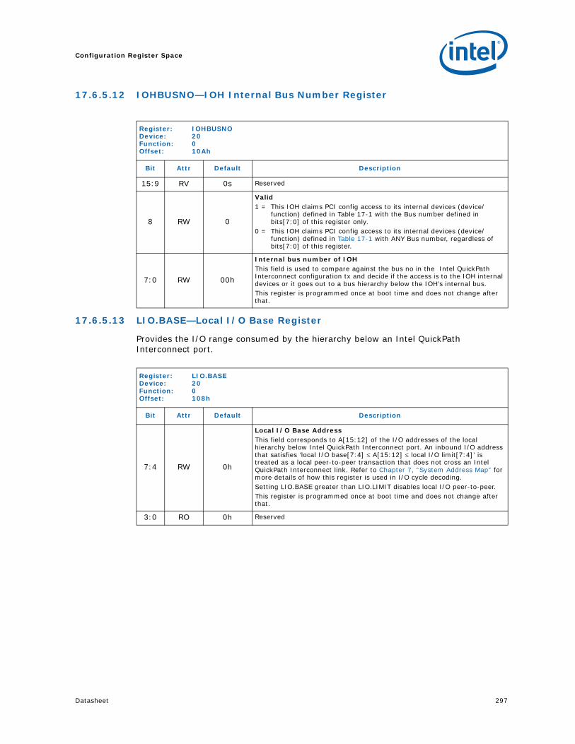
Datasheet 297
Configuration Register Space
17.6.5.12 IOHBUSNO—IOH Internal Bus Number Register
17.6.5.13 LIO.BASE—Local I/O Base Register
Provides the I/O range consumed by the hierarchy below an Intel QuickPath Interconnect port.
.
Register: IOHBUSNODevice: 20Function: 0Offset: 10Ah
Bit Attr Default Description
15:9 RV 0s Reserved
8 RW 0
Valid1 = This IOH claims PCI config access to its internal devices (device/
function) defined in Table 17-1 with the Bus number defined in bits[7:0] of this register only.
0 = This IOH claims PCI config access to its internal devices (device/function) defined in Table 17-1 with ANY Bus number, regardless of bits[7:0] of this register.
7:0 RW 00h
Internal bus number of IOHThis field is used to compare against the bus no in the Intel QuickPath Interconnect configuration tx and decide if the access is to the IOH internal devices or it goes out to a bus hierarchy below the IOH’s internal bus. This register is programmed once at boot time and does not change after that.
Register: LIO.BASEDevice: 20Function: 0Offset: 108h
Bit Attr Default Description
7:4 RW 0h
Local I/O Base AddressThis field corresponds to A[15:12] of the I/O addresses of the local hierarchy below Intel QuickPath Interconnect port. An inbound I/O address that satisfies ‘local I/O base[7:4] A[15:12] local I/O limit[7:4]’ is treated as a local peer-to-peer transaction that does not cross an Intel QuickPath Interconnect link. Refer to Chapter 7, “System Address Map” for more details of how this register is used in I/O cycle decoding.Setting LIO.BASE greater than LIO.LIMIT disables local I/O peer-to-peer.This register is programmed once at boot time and does not change after that.
3:0 RO 0h Reserved
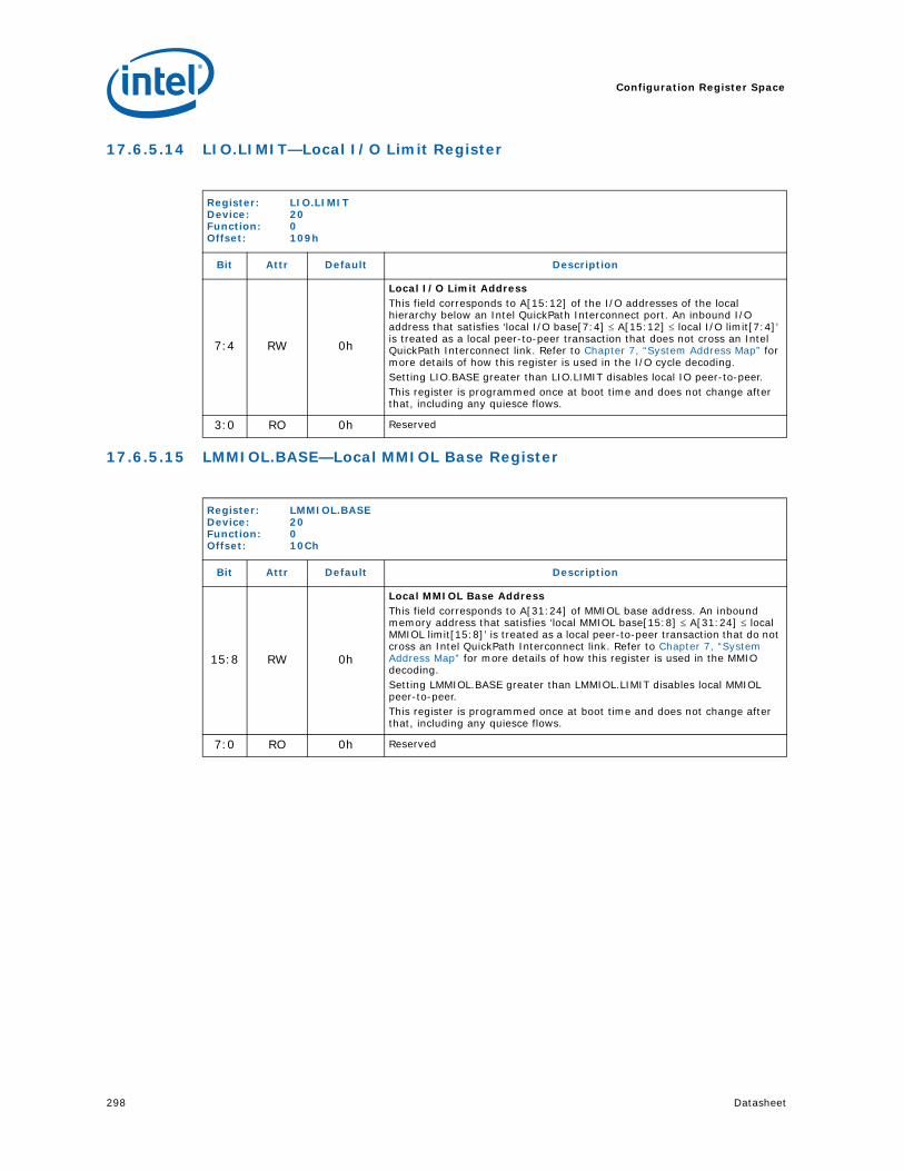
Configuration Register Space
298 Datasheet
17.6.5.14 LIO.LIMIT—Local I/O Limit Register
17.6.5.15 LMMIOL.BASE—Local MMIOL Base Register
Register: LIO.LIMITDevice: 20Function: 0Offset: 109h
Bit Attr Default Description
7:4 RW 0h
Local I/O Limit AddressThis field corresponds to A[15:12] of the I/O addresses of the local hierarchy below an Intel QuickPath Interconnect port. An inbound I/O address that satisfies ‘local I/O base[7:4] A[15:12] local I/O limit[7:4]’ is treated as a local peer-to-peer transaction that does not cross an Intel QuickPath Interconnect link. Refer to Chapter 7, “System Address Map” for more details of how this register is used in the I/O cycle decoding.Setting LIO.BASE greater than LIO.LIMIT disables local IO peer-to-peer.This register is programmed once at boot time and does not change after that, including any quiesce flows.
3:0 RO 0h Reserved
Register: LMMIOL.BASEDevice: 20Function: 0Offset: 10Ch
Bit Attr Default Description
15:8 RW 0h
Local MMIOL Base AddressThis field corresponds to A[31:24] of MMIOL base address. An inbound memory address that satisfies ‘local MMIOL base[15:8] A[31:24] local MMIOL limit[15:8]’ is treated as a local peer-to-peer transaction that do not cross an Intel QuickPath Interconnect link. Refer to Chapter 7, “System Address Map” for more details of how this register is used in the MMIO decoding.Setting LMMIOL.BASE greater than LMMIOL.LIMIT disables local MMIOL peer-to-peer.This register is programmed once at boot time and does not change after that, including any quiesce flows.
7:0 RO 0h Reserved

Datasheet 299
Configuration Register Space
17.6.5.16 LMMIOL.LIMIT—Local MMIOL Limit Register
17.6.5.17 LMMIOH.BASE—Local MMIOH Base Register
Register: LMMIOL.LIMITDevice: 20Function: 0Offset: 10Eh
Bit Attr Default Description
15:8 RW 0h
Local MMIOL Limit AddressThis field corresponds to A[31:24] of MMIOL limit. An inbound memory address that satisfies ‘local MMIOL base[15:8] A[31:24] local MMIOL limit[15:8]’ is treated as a local peer-to-peer transaction that does not cross an Intel QuickPath Interconnect link. Refer to Chapter 7, “System Address Map” for more details of how this register is used in the MMIO decoding.Setting LMMIOL.BASE greater than LMMIOL.LIMIT disables local MMIOL peer-to-peer.This register is programmed once at boot time and does not change after that, including any quiesce flows.
7:0 RO 00h Reserved
Register: LMMIOH.BASEDevice: 20Function: 0Offset: 110h
Bit Attr Default Description
15:10 RW 0h
Local MMIOH Base AddressThis field corresponds to A[31:26] of MMIOH base. An inbound memory address that satisfies ‘local MMIOH base upper[31:0]::local MMIOH base[15:10] A[63:26] local MMIOH limit upper[31:0]::local MMIOH limit[15:10]’ is treated as a local peer-to-peer transaction that does not cross an Intel QuickPath Interconnect link. Refer to Chapter 7, “System Address Map” for more details of how this register is used in the MMIO decoding.Setting LMMIOH.BASEU::LMMIOH.BASE greater than LMMIOH.LIMITU::LMMIOH.LIMIT disables local MMIOH peer-to-peer.This register is programmed once at boot time and does not change after that, including any quiesce flows.
9:0 RO 0s Reserved

Configuration Register Space
300 Datasheet
17.6.5.18 LMMIOH.LIMIT—Local MMIOH Limit Register
17.6.5.19 LMMIOH.BASEU—Local MMIOH Base Upper Register
Register: LMMIOH.LIMITDevice: 20Function: 0Offset: 112h
Bit Attr Default Description
15:10 RW 0h
Local MMIOH Limit AddressThis field corresponds to A[31:26] of MMIOH limit. An inbound memory address that satisfies ‘local MMIOH base upper[31:0]::local MMIOH base[15:10] A[63:26] local MMIOH limit upper[31:0]::local MMIOH limit[15:10]’ is treated as local a peer-to-peer transactions that does not cross an Intel QuickPath Interconnect link. Refer to Chapter 7, “System Address Map” for more details of how this register is used in the MMIO decoding.Setting LMMIOH.BASEU::LMMIOH.BASE greater than LMMIOH.LIMITU::LMMIOH.LIMIT disables local MMIOH peer-to-peer.This register is programmed once at boot time and does not change after that, including any quiesce flows.
8:0 RO 0s Reserved
Register: LMMIOH.BASEUDevice: 20Function: 0Offset: 114h
Bit Attr Default Description
31:19 RO 0s This field correspond to address A[63:51] of the local MMIOH range and is always 0.
18:0 RW 0s
Local MMIOH Base Upper AddressThis field corresponds to A[50:32] of MMIOH base. An inbound memory address that satisfies ‘local MMIOH base upper[31:0]::local MMIOH base[15:10] A[63:26] local MMIOH limit upper[31:0]::local MMIOH limit[15:10]’ is treated as a local peer-to-peer transaction that does not cross an Intel QuickPath Interconnect link. Refer to Chapter 7, “System Address Map” for more details of how this register is used in the MMIO decoding.Setting LMMIOH.BASEU::LMMIOH.BASE greater than LMMIOH.LIMITU::LMMIOH.LIMIT disables local MMIOH peer-to-peer.This register is programmed once at boot time and does not change after that, including any quiesce flows.

Datasheet 301
Configuration Register Space
17.6.5.20 LMMIOH.LIMITU—Local MMIOH Limit Upper Register
17.6.5.21 LCFGBUS.BASE—Local Configuration Bus Number Base Register
Register: LMMIOH.LIMITUDevice: 20Function: 0Offset: 118h
Bit Attr Default Description
31:19 RO 0s This field correspond to address A[63:51] of the local MMIOH range and is always 0.
18:0 RW 0s
Local MMIOH Limit Upper AddressThis field corresponds to A[50:32] of MMIOH limit. An inbound memory address that satisfies ‘local MMIOH base upper[31:0]::local MMIOH base[15:10] A[63:26] local MMIOH limit upper[31:0]::local MMIOH limit[15:10]’ is treated as local a peer-to-peer transactions that does not cross an Intel QuickPath Interconnect link. Refer to Chapter 7, “System Address Map” for more details of how this register is used in the MMIO decoding.Setting LMMIOH.BASEU::LMMIOH.BASE greater than LMMIOH.LIMITU::LMMIOH.LIMIT disables local MMIOH peer-to-peer.This register is programmed once at boot time and does not change after that, including any quiesce flows.
Register: LCFGBUS.BASEDevice: 20Function: 0Offset: 11Ch
Bit Attr Default Description
7:0 RW 00h
Local Configuration Bus Number BaseThis field corresponds to base bus number of bus number range allocated to the hierarchy below the Intel QuickPath Interconnect link. An inbound or outbound configuration tx falls within the local bus number range if ‘Local Bus Number Base [7:0] Bus Number[7:0] Local Bus Number Limit [7:0]’ and such transactions are treated as local peer-to-peer transactions that do not cross an Intel QuickPath Interconnect link. Refer to Chapter 7, “System Address Map” for more details of how this register is used in the configuration cycle decoding.Setting LCFGBUS.BASE greater than LCFGBUS.LIMIT disables local peer-to-peer configuration cycles.This register is programmed once at boot time and does not change after that, including any quiesce flows.

Configuration Register Space
302 Datasheet
17.6.5.22 LCFGBUS.LIMIT—Local Configuration Bus Number Limit Register
17.6.5.23 GIO.BASE—Global I/O Base Register
Register: LCFGBUS.LIMITDevice: 20Function: 0Offset: 11Dh
Bit Attr Default Description
7:0 RW 00h
Local Configuration Bus Number LimitThis field corresponds to Limit bus number of bus number range allocated to the hierarchy below the Intel QuickPath Interconnect link. An inbound configuration falls within the local bus number range if ‘Local Bus Number Base [7:0] Bus Number[7:0] Local Bus Number Limit [7:0]’ and such transactions are treated as local peer-to-peer transactions that do not cross an Intel QuickPath Interconnect link. Refer to Chapter 7, “System Address Map” for more details of how this register is used in the configuration cycle decoding.Setting LCFGBUS.BASE greater than LCFGBUS.LIMIT disables local peer-to-peer configuration cycles.This register is programmed once at boot time and does not change after that, including any quiesce flows.
Register: GIO.BASEDevice: 20Function: 0Offset: 120h
Bit Attr Default Description
7:4 RW 0h
Global I/O Base AddressThis field corresponds to A[15:12] of the I/O addresses of the entire I/O region. An inbound or outbound I/O address that satisfies ‘global I/O base[7:4] A[15:12] global I/O limit[7:4]’ but is outside of the local I/O address range is treated as remote peer I/O over Intel QuickPath Interconnect. Refer to Chapter 7, “System Address Map” for more details of how this register is used in the I/O cycle decoding.This register is programmed once at boot time and does not change after that, including any quiesce flows.
3:0 RO 0h Reserved

Datasheet 303
Configuration Register Space
17.6.5.24 GIO.LIMIT—Global I/O Limit Register
17.6.5.25 GMMIOL.BASE—Global MMIOL Base Register
17.6.5.26 GMMIOL.LIMIT—Global MMIOL Limit Register
Register: GIO.LIMITDevice: 20Function: 0Offset: 121h
Bit Attr Default Description
7:4 RW Fh
Global I/O Limit AddressThis field corresponds to A[15:12] of the I/O addresses of the entire I/O region. An inbound or outbound I/O address that satisfies ‘global I/O base[7:4] A[15:12] global I/O limit[7:4]’ but is outside of the local I/O address range is treated as remote peer I/O over Intel QuickPath Interconnect. Refer to Chapter 7, “System Address Map” for more details of how this register is used in the I/O cycle decoding.This register is programmed once at boot time and does not change after that, including any quiesce flows.
3:0 RO 0h Reserved
Register: GMMIOL.BASEDevice: 20Function: 0Offset: 124h
Bit Attr Default Description
15:8 RW 0h
Global MMIOL Base AddressThis field corresponds to A[31:24] of global MMIOL base. An inbound or outbound memory address that satisfies ‘global MMIOL base[15:8] A[31:24] global MMIOL limit[15:8]’ but is outside of the local MMIOL range is treated as a remote peer memory transaction over Intel QuickPath Interconnect. Refer to Chapter 7, “System Address Map” for more details of how this register is used in MMIO decoding.Setting GMMIOL.BASE greater than GMMIOL.LIMIT disables global MMIOL peer-to-peer.This register is programmed once at boot time and does not change after that, including any quiesce flows.
7:0 RO 0h Reserved
Register: GMMIOL.LIMITDevice: 20Function: 0Offset: 126h
Bit Attr Default Description
15:8 RW 0h
Global MMIOL Limit AddressThis field corresponds to A[31:24] of global MMIOL limit. An inbound or outbound memory address that satisfies ‘global MMIOL base[15:8] A[31:24] global MMIOL limit[15:8]’ but is outside of the local MMIOL range is treated as a remote peer-to-peer transaction over Intel QuickPath Interconnect link. Refer to Chapter 7, “System Address Map” for more details of how this register is used in the MMIO decoding.Setting GMMIOL.BASE greater than GMMIOL.LIMIT disables global MMIOL peer-to-peer.This register is programmed once at boot time and does not change after that, including any quiesce flows.
7:0 RO 0h Reserved

Configuration Register Space
304 Datasheet
17.6.5.27 GMMIOH.BASE—Global MMIOH Base Register
17.6.5.28 GMMIOH.LIMIT—Global MMIOH Limit Register
Register: GMMIOH.BASEDevice: 20Function: 0Offset: 128h
Bit Attr Default Description
15:10 RW 0s
Global MMIOH Base AddressThis field corresponds to A[31:26] of global MMIOH base. An inbound or outbound memory address that satisfies ‘global MMIOH base upper[31:0]::global MMIOH base[15:10] A[63:26] global MMIOH limit upper[31:0]::global MMIOH limit[15:10]’ but is outside of the local MMIOH range is treated as a remote peer-to-peer transaction over Intel QuickPath Interconnect link. Refer to Chapter 7, “System Address Map” for more details of how this register is used in the MMIO decoding.Setting GMMIOH.BASEU::GMMIOH.BASE greater than GMMIOH.LIMITU::GMMIOH.LIMIT disables global MMIOH peer-to-peer.This register is programmed once at boot time and does not change after that, including any quiesce flows.
9:0 RO 0s Reserved
Register: GMMIOH.LIMITDevice: 20Function: 0Offset: 12Ah
Bit Attr Default Description
15:10 RW 0s
Global MMIOH Limit AddressThis field corresponds to A[31:26] of global MMIOH limit. An inbound or outbound memory address that satisfies ‘global MMIOH base upper[31:0]::global MMIOH base[15:10] A[63:26] global MMIOH limit upper[31:0]::global MMIOH limit[15:10]’ but is outside of the local MMIOH range is treated as a remote peer-to-peer transaction over Intel QuickPath Interconnect link. Refer to Chapter 7, “System Address Map” for more details of how this register is used in the MMIO decoding.Setting GMMIOH.BASEU::GMMIOH.BASE greater than GMMIOH.LIMITU::GMMIOH.LIMIT disables global MMIOH peer-to-peer.This register is programmed once at boot time and does not change after that, including any quiesce flows.
9:0 RO 0s Reserved

Datasheet 305
Configuration Register Space
17.6.5.29 GMMIOH.BASEU—Global MMIOH Base Upper Register
17.6.5.30 GMMIOH.LIMITU—Global MMIOH Limit Upper Register
Register: GMMIOH.BASEUDevice: 20Function: 0Offset: 12Ch
Bit Attr Default Description
31:19 RO 0s This field correspond to address A[63:51] of the global MMIOH range and is always 0.
18:0 RW 0s
Global MMIOH Base Upper AddressThis field corresponds to A[50:32] of global MMIOH base. An inbound or outbound memory address that satisfies ‘global MMIOH base upper[31:0]::global MMIOH base[15:10] A[63:26] global MMIOH limit upper[31:0]::global MMIOH limit[15:10]’ but is outside of the local MMIOH range is treated as a remote peer-to-peer transaction over Intel QuickPath Interconnect link. Refer to Chapter 7, “System Address Map” for more details of how this register is used in the MMIO decoding.Setting GMMIOH.BASEU::GMMIOH.BASE greater than GMMIOH.LIMITU::GMMIOH.LIMIT disables global MMIOH peer-to-peer.This register is programmed once at boot time and does not change after that, including any quiesce flows.
Register: GMMIOH.LIMITUDevice: 20Function: 0Offset: 130h
Bit Attr Default Description
31:19 RO 0h This field correspond to address A[63:51] of the global MMIOH range and is always 0.
18:0 RW 0h
Global MMIOH Limit Upper AddressThis field corresponds to A[51:32] of global MMIOH limit. An inbound or outbound memory address that satisfies ‘global MMIOH base upper[31:0]::global MMIOH base[15:10] A[63:26] global MMIOH limit upper[31:0]::global MMIOH limit[15:10]’ but is outside of the local MMIOH range is treated as a remote peer-to-peer transaction over Intel QuickPath Interconnect link. Refer to Chapter 7, “System Address Map” for more details of how this register is used in the MMIO decoding.Setting GMMIOH.BASEU::GMMIOH.BASE greater than GMMIOH.LIMITU::GMMIOH.LIMIT disables global MMIOH peer-to-peer.This register is programmed once at boot time and does not change after that, including any quiesce flows.

Configuration Register Space
306 Datasheet
17.6.5.31 GCFGBUS.BASE—Global Configuration Bus Number Base Register
17.6.5.32 GCFGBUS.LIMIT—Global Configuration Bus Number Limit Register
Register: GCFGBUS.BASEDevice: 20Function: 0Offset: 134h
Bit Attr Default Description
7:0 RW 0h
Global Configuration Bus Number BaseThis field corresponds to base bus number of bus number range that spans all IOHs in a partition. An inbound or outbound configuration tx that satisfies ‘Global Bus Number Base [7:0] Bus Number[7:0] Global Bus Number Limit [7:0]’ but is outside of the local bus number range is treated as a remote peer-to-peer transaction over Intel QuickPath Interconnect link. Refer to Chapter 7, “System Address Map” for more details of how this register is used in the configuration cycle decoding.
Register: GCFGBUS.LIMITDevice: 20Function: 0Offset: 135h
Bit Attr Default Description
7:0 RW FFh
Global Configuration Bus Number LimitThis field corresponds to limit bus number of bus number range allocated across all IOHs in the partition. An inbound or outbound configuration that satisfies ‘Global Bus Number Base [7:0] Bus Number[7:0] Global Bus Number Limit [7:0]’ but is outside of the low bus number range is treated as a remote peer-to-peer transaction over Intel QuickPath Interconnect link. Refer to Chapter 7, “System Address Map” for more details of how this register is used in the configuration cycle decoding.This register is programmed once at boot time and does not change after that, including any quiesce flows.

Datasheet 307
Configuration Register Space
17.6.5.33 DUAL.NL.ABAR.BASE—Dual NonLegacy IOH ABAR Range Base Register
This register and Section 17.6.5.34 are valid only when the IOH is in Dual IOH Proxy mode defined by strapped signals. These registers are programmed by system software and should not be changed in normal run time, including any quiesce flows. Software should program this range to cover all ABAR ranges (including the non-legacy IOH’s internal IOAPIC ABAR range and all ABAR ranges of its PCIe ports) used in the non-legacy IOH.
Register: DUAL.NL.ABAR.BASEDevice: 20Function: 0Offset: 148h
Bit Attr Default Description
15 RW 0
Dual Nonlegacy IOH ABAR Range Enable: 1 = Enable the non-legacy IOH’s ABAR range: An outbound transaction with
memory address within the range from FECX_YZ00h (defined in this register) to FECU_VWFFh (defined in Section 17.6.5.34) is targeted at the non-legacy IOH in DP Dual IOH Proxy mode. The transaction is either:1.Claimed by the receiving non-legacy IOH or 2.Routed to the non-legacy IOH using IOH-IOH link in DP Dual IOH Proxy
mode from the receiving legacy IOH. This range should cover the non-legacy IOH’s internal IOxAPIC ABAR and its ABAR addresses of its PCIe ports. Bits ‘XYZ’ are defined in bits [11:0] of this register and bits “UVW” are defined in bits [11:0] of Section 17.6.5.34. Note that there is one copy of this register in both legacy IOH and non-legacy IOH in Dual IOH Proxy mode. They should be programmed with exact same value. In addition, they should be programmed in a consistent manner with global/local range registers.0 = Disable the non-legacy IOH’s ABAR range. In addition to this enable bit, setting DUAL.NL.ABARL.BASE greater than DUAL.NL.ABAR.LIMIT with this enable bit = 1 disables non-legacy IOH ABAR range.
14:12 RO 0h Reserved
11:8 RW 0h
Base Address [19:16] (XBAD) These bits determine the high order bits of the Non-legacy IOH I/OAPIC ABAR base address. When a transaction with memory address is within the range from FECX_YZ00h to FECU_VWFFh, the transaction is routed to non-legacy IOH.
7:4 RW 0h
Base Address [15:12] (YBAD) These bits determine the middle order bits of the Non-legacy IOH I/OAPIC ABAR base address. When a transaction with memory address is within the range from FECX_YZ00h to FECU_VWFFh, the transaction is routed to non-legacy IOH.
3:0 RW 0h
Base Address [11:8] (ZBAD) These bits determine the low order bits of the Non-legacy IOH I/OAPIC ABAR base address. When a transaction with memory address is within the range from FECX_YZ00h to FECU_VWFFh, the transaction is routed to non-legacy IOH.

Configuration Register Space
308 Datasheet
17.6.5.34 DUAL.NL.ABAR.LIMIT—Dual NonLegacy IOH ABAR Range Limit Register
17.6.5.35 DUAL.NL.MMIOL.BASE—Dual NonLegacy IOH MMIOL Base Register
Register: DUAL.NL.ABAR.LIMITDevice: 20Function: 0Offset: 14Ah
Bit Attr Default Description
15:12 RO 0h Reserved
11:8 RW 0h
Limit Address [19:16] (ULIM) These bits determine the high order bits of the DP Non-legacy IOH I/OAPIC ABAR base address. When a transaction with memory address is within the range from FECX_YZ00h to FECU_VWFFh, the transaction is routed to non-legacy IOH.
7:4 RW 0h
Limit Address [15:12] (VLIM) These bits determine the middle order bits of DP Non-legacy IOH I/OAPIC ABAR base address. When a transaction with memory address is within the range from FECX_YZ00h to FECU_VWFFh, the transaction is routed to non-legacy IOH.
3:0 RW 0h
Limit Address [11:8] (WLIM) These bits determine the lower order bits of the DP Non-legacy IOH I/OAPIC ABAR base address. When a transaction with memory address is within the range from FECX_YZ00h to FECU_VWFFh, the transaction is routed to non-legacy IOH.
Register: DUAL.NL.MMIOL.BASEDevice: 20Function: 0Offset: 14Ch
Bit Attr Default Description
15:8 RW FFh
Dual Nonlegacy IOH MMIOL Base AddressApplicable in Dual IOH Proxy mode only. This field corresponds to A[31:24] of MMIOL base address. An outbound transaction with memory address that satisfies ‘DUAL.NL.MMIOL.BASE[15:8] A[31:24] DUAL.NL.MMIOL.LIMIT[15:8]’ is targeted at the non-legacy IOH in DP Dual IOH Proxy mode. The transaction is either:1. Claimed by the receiving non-legacy IOH or 2. Routed to the non-legacy IOH using IOH-IOH link in DP Dual IOH Proxy
mode from the receiving legacy IOH. Note that there is one copy of this register in both legacy IOH and non-legacy IOH in Dual IOH Proxy mode. They should be programmed with exact same value. In addition, they should be programmed in a consistent manner with global/local range registers.Setting DUAL.NL.MMIOL.BASE greater than DUAL.NL.MMIOL.LIMIT disables non-legacy IOH MMIOL range.This register is programmed by system software and should not be changed in normal run time, including any quiesce flows.
7:0 RO 0h Reserved

Datasheet 309
Configuration Register Space
17.6.5.36 DUAL.NL.MMIOL.LIMIT—Dual NonLegacy IOH MMIOL LIMIT Register
17.6.5.37 DUAL.NL.MMIOH.BASE—Dual NonLegacy IOH MMIOH Base Register
Register: DUAL.NL.MMIOL.LIMITDevice: 20Function: 0Offset: 14Eh
Bit Attr Default Description
15:8 RW 0h
Dual Nonlegacy IOH MMIOL Limit AddressApplicable in Dual IOH Proxy mode only. This field corresponds to A[31:24] of MMIOL limit address. An outbound transaction with memory address that satisfies ‘DUAL.NL.MMIOL.BASE[15:8] A[31:24] DUAL.NL.MMIOL.LIMIT[15:8]’ is targeted at the non-legacy IOH in DP Dual IOH Proxy mode. The transaction is either:1. Claimed by the receiving non-legacy IOH or 2. Routed to the non-legacy IOH using IOH-IOH link in Dual IOH Proxy
mode from the receiving legacy IOH. Note that there is one copy of this register in both legacy IOH and non-legacy IOH in Dual IOH Proxy mode. They should be programmed with exact same value. In addition, they should be programmed in a consistent manner with global/local range registers.Setting DUAL.NL.MMIOL.BASE greater than DUAL.NL.MMIOL.LIMIT disables non-legacy IOH MMIOL range.This register is programmed by system software and should not be changed in normal run time, including any quiesce flows.
7:0 RO 0h Reserved
Register: DUAL.NL.MMIOH.BASEDevice: 20Function: 0Offset: 150h
Bit Attr Default Description
15 RO 0h Reserved
14:0 RW 7FFFh
Dual Nonlegacy IOH MMIOH Base AddressApplicable in Dual IOH Proxy mode only. This field corresponds to A[40:26] of MMIOH base address. An outbound transaction with memory address that satisfies ‘DUAL.NL.MMIOH.BASE[14:0] A[40:26] DUAL.NL.MMIOH.LIMIT[14:0]’ is targeted at the non-legacy IOH in Dual IOH Proxy mode. The transaction is either:1. Claimed by the receiving non-legacy IOH or 2. Routed to the non-legacy IOH using IOH-IOH link in Dual IOH Proxy
mode from the receiving legacy IOH. Note that there is one copy of this register in both legacy IOH and non-legacy IOH in Dual IOH Proxy mode. They should be programmed with exact same value. In addition, they should be programmed in a consistent manner with global/local range registers.Setting DUAL.NL.MMIOH.BASE greater than DUAL.NL.MMIOH.LIMIT disables non-legacy IOH MMIOH range.This register is programmed by system software and should not be changed in normal run time, including any quiesce flows.

Configuration Register Space
310 Datasheet
17.6.5.38 DUAL.NL.MMIOH.LIMIT—Dual NonLegacy IOH MMIOH LIMIT Register
17.6.5.39 DUAL.NL.IO.BASE—Dual NonLegacy IOH I/O Base Register
Register: DUAL.NL.MMIOH.LIMITDevice: 20Function: 0Offset: 152h
Bit Attr Default Description
15 RO 0h Reserved
14:0 RW 0h
Dual Nonlegacy IOH MMIOH Limit AddressApplicable in DP Dual IOH Proxy mode only. This field corresponds to A[31:26] of MMIOH limit address. An outbound transaction with memory address that satisfies ‘DUAL.NL.MMIOH.BASE[14:0] A[40:26] DUAL.NL.MMIOH.LIMIT[14:0]’ is targeted at the non-legacy IOH in Dual IOH Proxy mode. The transaction is either:1. Claimed by the receiving non-legacy IOH or 2. Routed to the non-legacy IOH using IOH-IOH link in DP Dual IOH Proxy
mode from the receiving legacy IOH. Note that there is one copy of this register in both legacy IOH and non-legacy IOH in DP Dual IOH Proxy mode. They should be programmed with exact same value. In addition, they should be programmed in a consistent manner with global/local range registers.Setting DUAL.NL.MMIOH.BASE greater than DUAL.NL.MMIOH.LIMIT disables non-legacy IOH MMIOH range.This register is programmed by system software and should not be changed in normal run time, including any quiesce flows.
Register: DUAL.NL.IO.BASEDevice: 20Function: 0Offset: 15Ch
Bit Attr Default Description
7:4 RW Fh
Dual Nonlegacy IOH I/O Base AddressApplicable in Dual IOH Proxy mode only. This field corresponds to A[15:12] of the I/O addresses base of the I/O region. An outbound transaction with I/O address that satisfies ‘DUAL.NL.IO.BASE[7:4] A[15:12] DUAL.NL.IO.LIMIT[7:4]’ is targeted at the non-legacy IOH in DP Dual IOH Proxy mode. The transaction is either:1. Claimed by the receiving non-legacy IOH or 2. Routed to the non-legacy IOH using IOH-IOH link in DP Dual IOH Proxy
mode from the receiving legacy IOH. Note that there is one copy of this register in both legacy IOH and non-legacy IOH in DP Dual IOH Proxy mode. They should be programmed with exact same value. In addition, they should be programmed in a consistent manner with global/local range registers.Setting DUAL.NL.IO.BASE[7:4] greater than DUAL.NL.IO.LIMIT[7:4] disables non-legacy IOH IO range.This register is programmed by system software and should not be changed in normal run time, including any quiesce flows.
3:0 RO 0h Reserved

Datasheet 311
Configuration Register Space
17.6.5.40 DUAL.NL.IO.LIMIT—Dual NonLegacy IOH I/O Limit Register
17.6.5.41 DUAL.NL.BUS.BASE—Dual NonLegacy IOH Configuration Bus Base Register
Register: DUAL.NL.IO.LIMITDevice: 20Function: 0Offset: 15Dh
Bit Attr Default Description
7:4 RW 0h
Dual Nonlegacy IOH I/O Limit AddressApplicable in DP Dual IOH Proxy mode only. This field corresponds to A[15:12] of the I/O addresses limit of the I/O region. An outbound transaction with I/O address that satisfies ‘DUAL.NL.IO.BASE[7:4] A[15:12] DUAL.NL.IO.LIMIT[7:4]’ is targeted at the non-legacy IOH in DP Dual IOH Proxy mode. The transaction is either:1. Claimed by the receiving non-legacy IOH or 2. Routed to the non-legacy IOH using IOH-IOH link in Dual IOH Proxy
mode from the receiving legacy IOH. Note that there is one copy of this register in both legacy IOH and non-legacy IOH in Dual IOH Proxy mode. They should be programmed with exact same value. In addition, they should be programmed in a consistent manner with global/local range registers.Setting DUAL.NL.IO.BASE[7:4] greater than DUAL.NL.IO.LIMIT[7:4] disables non-legacy IOH IO range.This register is programmed by system software and should not be changed in normal run time, including any quiesce flows.
3:0 RO 0h Reserved
Register: DUAL.NL.BUS.BASEDevice: 20Function: 0Offset: 160h
Bit Attr Default Description
7:0 RW 80h
Dual Nonlegacy IOH Cfg Bus BaseApplicable in Dual IOH Proxy mode only. This field corresponds to base bus number of bus number range allocated to the hierarchy below the Intel QPI link. An outbound configuration transaction that satisfies ‘DUAL.NL.BUS.BASE[7:0] Bus Number[7:0] DUAL.NL.BUS.LIMIT[7:0]’ is targeted at the non-legacy IOH in DP Dual IOH Proxy mode. The transaction is either:1. Claimed by the receiving non-legacy IOH or 2. Routed to the non-legacy IOH using IOH-IOH link in Dual IOH Proxy
mode from the receiving legacy IOH. Note that there is one copy of this register in both legacy IOH and non-legacy IOH in Dual IOH Proxy mode. They should be programmed with exact same value. In addition, they should be programmed in a consistent manner with global/local range registers.Setting DUAL.NL.BUS.BASE[7:0] greater than DUAL.NL.BUS.LIMIT[7:0] disables non-legacy IOH cfg bus range.This register is programmed by system software and should not be changed in normal run time, including any quiesce flows.

Configuration Register Space
312 Datasheet
17.6.5.42 DUAL.NL.BUS.LIMIT—Dual NonLegacy IOH Cfg Bus Limit Register
17.6.5.43 DUAL.VGA.CTRL—DP Dual IOH VGA Control Registerl
Register: DUAL.NL.BUS.LIMITDevice: 20Function: 0Offset: 161h
Bit Attr Default Description
7:0 RW FDh
Dual Nonlegacy IOH Cfg Bus LimitApplicable in Dual IOH Proxy mode only. This field corresponds to limit bus number of bus number range allocated to the hierarchy below the Intel QPI link. An outbound configuration transaction that satisfies ‘DUAL.NL.BUS.BASE[7:0] Bus Number[7:0] DUAL.NL.BUS.LIMIT[7:0]’ is targeted at the non-legacy IOH in Dual IOH Proxy mode. The transaction is either:1. Claimed by the receiving non-legacy IOH or 2. Routed to the non-legacy IOH using IOH-IOH link in DP Dual IOH Proxy
mode from the receiving legacy IOH. Note that there is one copy of this register in both legacy IOH and non-legacy IOH in Dual IOH Proxy mode. They should be programmed with exact same value. In addition, they should be programmed in a consistent manner with global/local range registers.Setting DUAL.NL.BUS.BASE[7:0] greater than DUAL.NL.BUS.LIMIT[7:0] disables non-legacy IOH cfg bus range.This register is programmed by system software and should not be changed in normal run time, including any quiesce flows.
Register: DUAL.VGA.CTRLDevice: 20Function: 0Offset: 164h
Bit Attr Default Description
7:3 RV 0 Reserved
2 RW 0h
DP Dual IOH VGA EnableApplicable in DP Dual IOH Proxy mode only. 0 = If set to 0, an outbound transaction within VGA memory address range
(A_0000h – B_FFFFh) or VGA legacy I/O ranges (3B0h - 3BBh and 3C0h – 3DFh) is routed to substractive decode port in legacy IOH.
1 = If set to 1, then there is one and only one PICIe port in the aggregate of legacy IOH and non-legacy IOH. The transaction’s routing is further determined by bits [1:0] of this register.
Note that there is one copy of this register in both legacy IOH and non-legacy IOH in DP Dual IOH Proxy mode. They should be programmed with exact same value. In addition, they should be programmed in a consistent manner with platform VGA device’s location.This register is programmed by system software and should not be changed in normal run time, including any quiesce flows.

Datasheet 313
Configuration Register Space
17.6.5.44 VTBAR—Base Address Register for Intel® VT-d Chipset Registers
1 RW 0h
DP Dual Nonlegacy IOH VGA Range EnableApplicable in DP Dual IOH Proxy mode only. 1 = If set to 1, an outbound transaction within VGA memory address range
(A_0000h – B_FFFFhh) or VGA legacy I/O ranges (3B0h – 3BBh and 3C0h – 3DFh) is targeted at the non-legacy IOH in DP Dual IOH Proxy mode. The transaction is either:1.Claimed by the receiving non-legacy IOH or 2.Routed to the non-legacy IOH using IOH-IOH link in DP Dual IOH Proxy
mode from the receiving legacy IOH. 0 = If set to 0, the transaction is targeted at legacy IOH.Note that there is one copy of this register in both legacy IOH and non-legacy IOH in DP Dual IOH Proxy mode. They should be programmed with exact same value. In addition, they should be programmed in a consistent manner with platform VGA device’s location.This register is programmed by system software and should not be changed in normal run time, including any quiesce flows.
0 RW 0h
DP Dual Nonlegacy IOH VGA 16-bit Decode EnableApplicable in DP Dual IOH Proxy mode only. 1 = If set to 1, an outbound legacy IO space transaction that is within VGA
legacy I/O range (3B0h – 3BBh and 3C0h – 3DFh) is decoded with 16-bit address decode before routing is determined.
0 = If set to 0, the transaction is decoded with 10-bit address decode. Note that there is one copy of this register in both legacy IOH and non-legacy IOH in DP Dual IOH Proxy mode. They should be programmed with exact same value.This register is programmed by system software and should not be changed in normal run time, including any quiesce flows.
Register: VTBARDevice: 20Function: 0Offset: 180h
Bit Attr Default Description
31:13 RWL 0s
Intel VT-d Chipset Base Address: This field provides an aligned 8K base address for IOH registers relating to Intel VT-d. All inbound accesses to this region are completer aborted by the IOH.This register is programmed once at boot time and does not change after that, including any quiesce flows.
12:1 RO 0s Reserved
0 RWL 0
Intel VT-d Chipset Base Address Enable: Enables the VTBAR register. This bit is RO if “Intel VT-d enable fuse” is OFF. This bit is RO when VTGENCTRL[15] = 1 OR may be locked as RO in Intel TXT mode, else this bit is RW. 0 = Disable1 = Enable
Register: DUAL.VGA.CTRLDevice: 20Function: 0Offset: 164h
Bit Attr Default Description

Configuration Register Space
314 Datasheet
17.6.5.45 VTGENCTRL—Intel VT-d General Control Register
Register: VTGENCTRLDevice: 20Function: 0Offset:184h
Bit Attr Default Description
15 RWO 0b Lock Intel® VT-dWhen this bit is 0, the VTBAR[0] is RWL (where the lock functionality is described in VTBAR register). When this bit is 0, VTBAR[0] is RO.
14:11 RV 0h Reserved
10:8 RWL 111
Isoch GPA_LIMITRepresents the guest virtual addressing limit for the Isoch Intel VT-d engine.000-011: Reserved100: 2^36 (i.e., Bits 35:0)101: 2^37110: 2^38111: 2^39When Intel VT-d translation is enabled on the isoch Intel VT-d engine, all incoming guest addresses from isochronous device, that go beyond the limit specified in this register will be aborted by the IIO and a UR response returned. This register is not used when translation is not enabled. Note that ‘translated’ and ‘pass-through’ addresses are in the ‘host-addressing’ domain and NOT ‘guest-addressing’ domain and hence GPA_LIMIT checking on those accesses are bypassed and instead HPA_LIMIT checking applies.This field may be locked as RO in Intel® TXT mode

Datasheet 315
Configuration Register Space
7:4 RWL 0011
Non-Isoch HPA_LIMIT: This field represents the host processor addressing limit 0000 = 2^36 (that is, bits 35:0)0001 = 2^37 (that is, bits 36:0)0010 = 2^380011 = 2^390100 = 2^40...1111 = 2^51 (that is, bits 50:0)When Intel VT-d translation is enabled on an Intel VT-d engine (non-isoch),all host addresses (during page walks) that go beyond the limit specified inthis register will be aborted by IOH. Note that pass-through and ‘translated’ATS accesses carry the host-address directly in the access and are subjectto this check as well.When VT-d translation is enabled or disabled on a VT-d engine (isoch ornon-isoch), all host addresses (during page walks) that go beyond the limitspecified in this register will be aborted by the IOH. Note that pass-throughand 'translated' ATS accesses carry the host-address directly in the accessand are subject to this check as well.Note that for Error logging due to HPA limits check violations, When VT-d translation is enabled, HPA limit check violations from the following requests will not be logged in the error register.1. Translated request(AT=10)2. Pass-through untranslated request.When VT-d translation is disabled, HPA limit violations from untranslatedrequest will be logged in the IOHERRST register when the HPA limit is set to 2^36. HPA limit check violation with other HPA limit settings will not belogged.Expectation is that this field indicates a value of 2^39 or lower for platforms where Azalia isoch engine is turned on. There is no explicit hardware check for that but that is the general expectation to remain within the spirit of the VT-d spec.
This field is RO when TXT.CMD.LOCKMEMCONFIG (OFFSET 0000h:TXT.STS[6]=1). This bit is RW when TXT.CMD.UNLOCKMEMCONFIG (OFFSET 0000h: TXT.STS[6]=0)This field may be locked as RO in Intel TXT mode.
3:0 RWL 8h
Non-Isoch GPA_LIMIT: This field represents the guest virtual addressing limit for the non-Isoch Intel VT-d engine.0000 = 2^40 (that is, bits 39:0)0001 = 2^41 (that is, bits 40:0)..0111 = 2^471000 = 2^481001–1111 = ReservedWhen Intel VT-d translation is enabled, all incoming guest addresses from PCI Express, associated with the non-isoch Intel VT-d engine, that go beyond the limit specified in this register will be aborted by IOH and a UR response returned. This register is not used when translation is not enabled. Note that ‘translated’ and ‘pass-through’ addresses are in the ‘host-addressing’ domain and NOT ‘guest-addressing’ domain and hence GPA_LIMIT checking on those accesses are bypassed and instead HPA_LIMIT checking applies.This field may be locked as RO in Intel TXT mode.
Register: VTGENCTRLDevice: 20Function: 0Offset:184h
Bit Attr Default Description

Configuration Register Space
316 Datasheet
17.6.5.46 VTISOCHCTRL: Intel VT-d Isoch Related Control Register
17.6.5.47 VTGENCTRL2—Intel VT-d General Control 2 Register
Register: VTISOCHCTRLDevice: 20Function: 0Offset: 188h
Bit Attr Default Description
31:5 RV 0 Reserved
4:2 RWL 0 Number of Isoch cache entries when Isoch Intel® VT-d engine is enabled:000: 0 entries001: 1 entry010: 2 entries011: 4 entries100: 8 entries101: 16 entries110, 111: ReservedThis field is RO when TXT.CMD.LOCKMEMCONFIG (OFFSET 0000h:TXT.STS[6]=1). This bit is RW when TXT.CMD.UNLOCKMEMCONFIG (OFFSET 0000h: TXT.STS[6]=0)
1 RV 0 Reserved
0 RWL 1 Steer isochronous to non-isochronous Intel VT-d engineThis field is RO when TXT.CMD.LOCKMEMCONFIG (OFFSET 0000h:TXT.STS[6]=1). This bit is RW when TXT.CMD.UNLOCKMEMCONFIG (OFFSET 0000h: TXT.STS[6]=0)
Register: VTGENCTRLDevice: 20Function: 0Offset:184h
Bit Attr Default Description
15 RWO 0b Lock Intel® VT-dWhen this bit is 0, the VTBAR[0] is RWL (where the lock functionality is described in VTBAR register). When this bit is 0, VTBAR[0] is RO.
14:11 RV 0h Reserved
10:8 RWL 111
Isoch GPA_LIMITRepresents the guest virtual addressing limit for the Isoch Intel VT-d engine.000-011: Reserved100: 2^36 (i.e., Bits 35:0)101: 2^37110: 2^38111: 2^39When Intel VT-d translation is enabled on the isoch Intel VT-d engine, all incoming guest addresses from isochronous device, that go beyond the limit specified in this register will be aborted by the IIO and a UR response returned. This register is not used when translation is not enabled. Note that ‘translated’ and ‘pass-through’ addresses are in the ‘host-addressing’ domain and NOT ‘guest-addressing’ domain and hence GPA_LIMIT checking on those accesses are bypassed and instead HPA_LIMIT checking applies.This field may be locked as RO in Intel® TXT mode

Datasheet 317
Configuration Register Space
7:4 RWL 0011
Non-Isoch HPA_LIMIT: This field represents the host processor addressing limit 0000 = 2^36 (that is, bits 35:0)0001 = 2^37 (that is, bits 36:0)0010 = 2^380011 = 2^390100 = 2^40...1111 = 2^51 (that is, bits 50:0)When Intel VT-d translation is enabled on an Intel VT-d engine (non-isoch),all host addresses (during page walks) that go beyond the limit specified inthis register will be aborted by IOH. Note that pass-through and ‘translated’ATS accesses carry the host-address directly in the access and are subjectto this check as well.When VT-d translation is enabled or disabled on a VT-d engine (isoch ornon-isoch), all host addresses (during page walks) that go beyond the limitspecified in this register will be aborted by the IOH. Note that pass-throughand 'translated' ATS accesses carry the host-address directly in the accessand are subject to this check as well.Note that for Error logging due to HPA limits check violations, When VT-d translation is enabled, HPA limit check violations from the following requests will not be logged in the error register.1. Translated request(AT=10)2. Pass-through untranslated request.When VT-d translation is disabled, HPA limit violations from untranslatedrequest will be logged in the IOHERRST register when the HPA limit is set to 2^36. HPA limit check violation with other HPA limit settings will not belogged.Expectation is that this field indicates a value of 2^39 or lower for platforms where Azalia isoch engine is turned on. There is no explicit hardware check for that but that is the general expectation to remain within the spirit of the VT-d spec.
This field is RO when TXT.CMD.LOCKMEMCONFIG (OFFSET 0000h:TXT.STS[6]=1). This bit is RW when TXT.CMD.UNLOCKMEMCONFIG (OFFSET 0000h: TXT.STS[6]=0)This field may be locked as RO in Intel TXT mode.
3:0 RWL 8h
Non-Isoch GPA_LIMIT: This field represents the guest virtual addressing limit for the non-Isoch Intel VT-d engine.0000 = 2^40 (that is, bits 39:0)0001 = 2^41 (that is, bits 40:0)..0111 = 2^471000 = 2^481001–1111 = ReservedWhen Intel VT-d translation is enabled, all incoming guest addresses from PCI Express, associated with the non-isoch Intel VT-d engine, that go beyond the limit specified in this register will be aborted by IOH and a UR response returned. This register is not used when translation is not enabled. Note that ‘translated’ and ‘pass-through’ addresses are in the ‘host-addressing’ domain and NOT ‘guest-addressing’ domain and hence GPA_LIMIT checking on those accesses are bypassed and instead HPA_LIMIT checking applies.This field may be locked as RO in Intel TXT mode.
Register: VTGENCTRLDevice: 20Function: 0Offset:184h
Bit Attr Default Description

Configuration Register Space
318 Datasheet
17.6.5.48 VTGENCTRL2—Intel® VT-d General Control 2 Register
17.6.5.49 VTSTS—Intel® VT-d Status Register
Register: VTGENCTRL2Device: 20Function: 0Offset: 18Ch
Bit Attr Default Description
31:11 RO 0 Reserved
10:8 RWL 0 LRU Timer
7:4 RO 0 Reserved
3 RO 0This field is RO when LT.CMD.LOCKMEMCONFIG (OFFSET 0000h:LT.STS[6]=1). This bit is RW when LT.CMD.UNLOCKMEMCONFIG (OFFSET 0000h: LT.STS[6]=0)
2 RO 0This field is RO when LT.CMD.LOCKMEMCONFIG (OFFSET 0000h:LT.STS[6]=1). This bit is RW when LT.CMD.UNLOCKMEMCONFIG (OFFSET 0000h: LT.STS[6]=0)
1 RW 0hThis field is RO when LT.CMD.LOCKMEMCONFIG (OFFSET 0000h:LT.STS[6]=1). This bit is RW when LT.CMD.UNLOCKMEMCONFIG (OFFSET 0000h: LT.STS[6]=0)
0 RO 0This field is RO when LT.CMD.LOCKMEMCONFIG (OFFSET 0000h:LT.STS[6]=1). This bit is RW when LT.CMD.UNLOCKMEMCONFIG (OFFSET 0000h: LT.STS[6]=0)
Register: VTSTSDevice: 20Function: 0Offset: 190h
Bit Attr Default Description
31:2 RO 0 Reserved
1 RW1CS 0 Interrupt transaction seen on VC1/VCp
0 RW1CS 0 ATS command detected toward DMI port

Datasheet 319
Configuration Register Space
17.6.5.50 VTUNCERRSTS—VT Uncorrectable Error Status Register
17.6.5.51 VTUNCERRMSK—VT Uncorrectable Error Mask Register
Register: VTUNCERRSTSDevice: 20Function: 0Offset: 1A8h
Bit Attr Default Description
31 RW1CST 0VT-d Specification Defined Errors 1 = This bit is set when a VT-d specification defined error has been
detected (and logged in the VT-d fault registers).
30:9 RV 0 Reserved
8 RW1CST 0 Protected memory region space violated status
7 RV 0 Reserved
6 RW1CST 0 Unsuccessful status received in Intel QPI read completion status
5 RW1CST 0 TLB1 parity error status
4 RW1CST 0 TLB0 parity error status
3 RW1CST 0 Data parity error while doing a L3 lookup status
2 RW1CST 0 Data parity error while doing a L2 lookup status
1 RW1CST 0 Data parity error while doing a L1 lookup status
0 RW1CST 0 VT-Data parity error while doing a context cache look up status
Register: VTUNCERRMSKDevice: 20Function: 0Offset: 1ACh
Bit Attr Default Description
31 RWS 0 Mask reporting VT-d defined errors to IOH core logic
30:9 RV 0 Reserved
8 RWS 0 Protected memory region space violated mask
7 RV 0 Reserved
6 RWS 0 Unsuccessful status received in Intel QPI read completion mask
5 RWS 0 TLB1 parity error mask
4 RWS 0 TLB0 parity error mask
3 RWS 0 Data parity error while doing a L3 lookup mask
2 RWS 0 Data parity error while doing a L2 lookup mask
1 RWS 0 Data parity error while doing a L1 lookup mask
0 RWS 0 Data parity error while doing a context cache look up mask
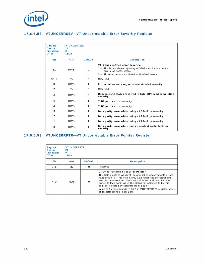
Configuration Register Space
320 Datasheet
17.6.5.52 VTUNCERRSEV—VT Uncorrectable Error Severity Register
17.6.5.53 VTUNCERRPTR—VT Uncorrectable Error Pointer Register
Register: VTUNCERRSEVDevice: 20Function: 0Offset: 1B0h
Bit Attr Default Description
31 RWS 0
VT-d spec defined error severity: 1 = This bit escalates reporting of VT-d specification defined
errors, as FATAL errors. 0 = Those errors are escalated as Nonfatal errors.
30:9 RV 0 Reserved
8 RWS 1 Protected memory region space violated severity
7 RV 0 Reserved
6 RWS 0 Unsuccessful status received in Intel QPI read completion severity
5 RWS 1 TLB1 parity error severity
4 RWS 1 TLB0 parity error severity
3 RWS 1 Data parity error while doing a L3 lookup severity
2 RWS 1 Data parity error while doing a L2 lookup severity
1 RWS 1 Data parity error while doing a L1 lookup severity
0 RWS 1 Data parity error while doing a context cache look up severity
Register: VTUNCERRPTRDevice: 20Function: 0Offset: 1B4h
Bit Attr Default Description
7:5 RV 0 Reserved
4:0 ROS 0
VT Uncorrectable First Error PointerThis field points to which of the unmasked uncorrectable errors happened first. This field is only valid when the corresponding error is unmasked and the status bit is set and this field is re-armed to load again when the status bit indicated to by this pointer is cleared by software from 1 to 0.Value of 0h corresponds to bit 0 in VTUNCERRSTS register, value of 1h corresponds to bit 1 etc.

Datasheet 321
Configuration Register Space
17.6.6 Semaphore and Scratch Pad Registers (Dev20, Function 1)
Table 17-9. Semaphore and Scratch Pad Register Address Map (Device 20, Function 1)(Sheet 1 of 2)
DID VID 000h SR[1] 080h
PCISTS PCICMD 004h SR[2] 084h
CCR RID 008h SR[3] 088h
HDR CLS 00Ch SR[4] 08Ch
010h SR[5] 090h
014h SR[6] 094h
018h SR[7] 098h
01Ch SR[8] 09Ch
020h SR[9] 0A0h
024h SR[10] 0A4h
028h SR[11] 0A8h
SID SVID 02Ch SR[12] 0ACh
030h SR[13] 0B0h
CAPPTR1
Notes:1. CAPPTR points to the first capability block.
034h SR[14] 0B4h
038h SR[15] 0B8h
INTP INTL 03Ch SR[16] 0BCh
EXPCAP NXTPTR CAPID 040h SR[17] 0C0h
DEVCAP 044h SR[18] 0C4h
DEVSTS DEVCON 048h SR[19] 0C8h
RESERVED PCIe Header space 04Ch SR[20] 0CCh
050h SR[21] 0D0h
054h SR[22] 0D4h
058h SR[23] 0D8h
05Ch CWR[0] 0DCh
060h CWR[1] 0E0h
064h CWR[2] 0E4h
068h CWR[3] 0E8h
06Ch CWR[4] 0ECh
070h CWR[5] 0F0h
074h CWR[6] 0F4h
078h CWR[7] 0F8h
SR[0] 07Ch CWR[8] 0FCh

Configuration Register Space
322 Datasheet
Table 17-10. Semaphore and Scratch Pad Register Address Map (Device 20, Function 1)(Sheet 2 of 2)
RESERVED PCIe Header space 100h IR[16] 180h
CWR[9] 104h IR[17] 184h
CWR[10] 108h IR[18] 188h
CWR[11] 10Ch IR[19] 18Ch
CWR[12] 110h IR[20] 190h
CWR[13] 114h IR[21] 194h
CWR[14] 118h IR[22] 198h
CWR[15] 11Ch IR[23] 19Ch
CWR[16] 120h 1A0h
CWR[17] 124h 1A4h
CWR[18] 128h 1A8h
CWR[19] 12Ch 1ACh
CWR[20] 130h 1B0h
CWR[21] 134h 1B4h
CWR[22] 138h 1B8h
CWR[23] 13Ch 1BCh
IR[0] 140h 1C0h
IR[1] 144h 1C4h
IR[2] 148h 1C8h
IR[3] 14Ch 1CCh
IR[4] 150h 1D0h
IR[5] 154h 1D4h
IR[6] 158h 1D8h
IR[7] 15Ch 1DCh
IR[8] 160h 1E0h
IR[9] 164h 1E4h
IR[10] 168h 1E8h
IR[11] 16Ch 1ECh
IR[12] 170h 1F0h
IR[13] 174h 1F4h
IR[14] 178h 1F8h
IR[15] 17Ch 1FCh

Datasheet 323
Configuration Register Space
17.6.6.1 SR[0:3]—Scratch Pad Register 0–3 (Sticky)
17.6.6.2 SR[4:7]—Scratch Pad Register 4–7 (Sticky)
17.6.6.3 SR[8:11]—Scratch Pad Register 8–11 (Non-Sticky)
Register: SR[4:7]Device: 20Function: 1Offset: 07Ch–088h
Bit Attr Default Description
31:0 RWLBS 0s
Scratch Pad – StickySticky scratch pad registers for firmware utilization.The lock bit is lock2 (“TXTLOCK: TXT Lock Register”) and the lock-bypass bits are all bypass/override bits defined in (“TXTLOCKBP: TXT Lock Bypass/Override Enable)
Register: SR[4:7]Device: 20Function: 1Offset: 08Ch–098h
Bit Attr Default Description
31:0 RWSLB 0s
Scratch Pad – StickySticky scratch pad registers for firmware utilization.The lock bit is lock2 (“TXTLOCK: TXT Lock Register”) and the lock-bypass bits are all bypass/override bits defined in (“TXTLOCKBP: TXT Lock Bypass/Override Enable)
Register: SR[8:11]Device: 20Function: 1Offset: 09Ch–0A8h
Bit Attr Default Description
31:0 RWLB 0s
Scratch Pad – Non-StickyNon-sticky scratch pad registers for firmware utilization.The lock bit is lock2 (“TXTLOCK: TXT Lock Register”) and the lock-bypass bits are all bypass/override bits defined in (“TXTLOCKBP: TXT Lock Bypass/Override Enable)

Configuration Register Space
324 Datasheet
17.6.6.4 SR[12:15]—Scratch Pad Register 12–15 (Non-Sticky)
17.6.6.5 SR[16:17]—Scratch Pad Register 16–17 (Non-Sticky)
17.6.6.6 Removed.
17.6.6.7 CWR[4:7]—Conditional Write Registers 4–7
Register: SR[12:15]Device: 20Function: 1Offset: 0ACh–0B8h
Bit Attr Default Description
31:0 RWLB 0s
Scratch Pad – Non-StickyNon-sticky scratch pad registers for firmware utilization.The lock bit is lock2 (“TXTLOCK: TXT Lock Register”) and the lock-bypass bits are all bypass/override bits defined in (“TXTLOCKBP: TXT Lock Bypass/Override Enable)
Register: SR[16:17]Device: 20Function: 1Offset: 0BCh–0C0h
Bit Attr Default Description
31:0 RWLB 0s
Scratch Pad – Non-StickyNon-sticky scratch pad registers for firmware utilization.The lock bit is lock2 (“TXTLOCK: TXT Lock Register”) and the lock-bypass bits are all bypass/override bits defined in (“TXTLOCKBP: TXT Lock Bypass/Override Enable)
Register: CWR[4:7]Device: 20Function: 1Offset: 0ECh–0F8h
Bit Attr Default Description
31:0 RWLBS 0s
Conditional WriteThese registers are physically mapped to scratch pad registers. A read from CWR[n] reads SR[n]. A write to CWR[n] writes SR[n] if SR[n][0] = 0 before the write, and has no effect otherwise. The registers provide firmware with synchronization variables (semaphores) that are overloaded onto the same physical registers as SR.The lock bit is lock2 (“TXTLOCK: TXT Lock Register”) and the lock-bypass bits are all bypass/override bits defined in (“TXTLOCKBP: TXT Lock Bypass/Override Enable)

Datasheet 325
Configuration Register Space
17.6.6.8 CWR[8:11]—Conditional Write Registers 8–11
17.6.6.9 CWR[12:15]—Conditional Write Registers 12–15
17.6.6.10 CWR[16:17]—Conditional Write Registers 16–17
Register: CWR[8:11]Device: 20Function: 1Offset: 0FCh–10Ch
Bit Attr Default Description
31:0 RWLB 0s
Conditional WriteThese registers are physically mapped to scratch pad registers. A read from CWR[n] reads SR[n]. A write to CWR[n] writes SR[n] if SR[n][0] = 0 before the write, and has no effect otherwise. The registers provide firmware with synchronization variables (semaphores) that are overloaded onto the same physical registers as SR.The lock bit is lock2 (“TXTLOCK: TXT Lock Register”) and the lock-bypass bits are all bypass/override bits defined in (“TXTLOCKBP: TXT Lock Bypass/Override Enable)
Register: CWR[0:15]Device: 20Function: 1Offset: 0FCh–10Ch
Bit Attr Default Description
31:0 RWLB 0s
Conditional WriteThese registers are physically mapped to scratch pad registers. A read from CWR[n] reads SR[n]. A write to CWR[n] writes SR[n] if SR[n][0] = 0 before the write, and has no effect otherwise. The registers provide firmware with synchronization variables (semaphores) that are overloaded onto the same physical registers as SR.The lock bit is lock2 (“TXTLOCK: TXT Lock Register”) and the lock-bypass bits are all bypass/override bits defined in (“TXTLOCKBP: TXT Lock Bypass/Override Enable)
Register: CWR[16:17]Device: 20Function: 1Offset: 120h–124h
Bit Attr Default Description
31:0 RWLB 0s
Conditional WriteThese registers are physically mapped to scratch pad registers. A read from CWR[n] reads SR[n]. A write to CWR[n] writes SR[n] if SR[n][0] = 0 before the write, and has no effect otherwise. The registers provide firmware with synchronization variables (semaphores) that are overloaded onto the same physical registers as SR.The lock bit is lock2 (“TXTLOCK: TXT Lock Register”) and the lock-bypass bits are all bypass/override bits defined in (“TXTLOCKBP: TXT Lock Bypass/Override Enable)

Configuration Register Space
326 Datasheet
17.6.6.11 Removed.
17.6.6.12 IR[0:3]—Increment Registers 0–3
17.6.6.13 IR[4:7]—Increment Registers 4–7
17.6.6.14 IR[8:11]—Increment Registers 8–11
Register: IR[0:3]Device: 20Function: 1Offset: 140h–14Ch
Bit Attr Default Description
31:0 RWLBS 0
IncrementThese registers are physically mapped to scratch pad registers. A read from IR[n] reads SR[n] and then increments SR[n]. A write to IR[n] increments SR[n] while the write data is unused. Increments within SR[n] for reads and writes roll over to zero. The read or write and the increment side effect are atomic with respect to other accesses. The registers provide firmware with synchronization variables (semaphores) that are overloaded onto the same physical registers as SR. The lock bit is lock2 (“TXTLOCK: TXT Lock Register”) and the lock-bypass bits are all bypass/override bits defined in (“TXTLOCKBP: TXT Lock Bypass/Override Enable)
Register: IR[4:7]Device: 20Function: 1Offset: 150h–15Ch
Bit Attr Default Description
31:0 RWLBS 0
IncrementThese registers are physically mapped to scratch pad registers. A read from IR[n] reads SR[n] and then increments SR[n]. A write to IR[n] increments SR[n] while the write data is unused. Increments within SR[n] for reads and writes roll over to zero. The read or write and the increment side effect are atomic with respect to other accesses. The registers provide firmware with synchronization variables (semaphores) that are overloaded onto the same physical registers as SR. The lock bit is lock2 (“TXTLOCK: TXT Lock Register”) and the lock-bypass bits are all bypass/override bits defined in (“TXTLOCKBP: TXT Lock Bypass/Override Enable)
Register: IR[8:11]Device: 20Function: 1Offset: 160h–16Ch by 4
Bit Attr Default Description
31:0 RWLB 0s
IncrementThese registers are physically mapped to scratch pad registers. A read from IR[n] reads SR[n] and then increments SR[n]. A write to IR[n] increments SR[n] while the write data is unused. Increments within SR[n] for reads and writes roll over to zero. The read or write and the increment side effect are atomic with respect to other accesses. The registers provide firmware with synchronization variables (semaphores) that are overloaded onto the same physical registers as SR. The lock bit is lock2 (“TXTLOCK: TXT Lock Register”) and the lock-bypass bits are all bypass/override bits defined in (“TXTLOCKBP: TXT Lock Bypass/Override Enable)

Datasheet 327
Configuration Register Space
17.6.6.15 IR[12:15]—Increment Registers 12–15
17.6.6.16 IR[16:17]—Increment Registers 16–17
17.6.6.17 Removed.
17.6.6.18 TXTLOCK: TXT Lock Register
Lock registers for TXT usage.
Register: IR[12:15]Device: 20Function: 1Offset: 170h–17Ch by 4
Bit Attr Default Description
31:0 RWLB 0
IncrementThese registers are physically mapped to scratch pad registers. A read from IR[n] reads SR[n] and then increments SR[n]. A write to IR[n] increments SR[n] while the write data is unused. Increments within SR[n] for reads and writes roll over to zero. The read or write and the increment side effect are atomic with respect to other accesses. The registers provide firmware with synchronization variables (semaphores) that are overloaded onto the same physical registers as SR. The lock bit is lock2 (“TXTLOCK: TXT Lock Register”) and the lock-bypass bits are all bypass/override bits defined in (“TXTLOCKBP: TXT Lock Bypass/Override Enable)
Register: IR[16:17]Device: 20Function: 1Offset: 180h–184h by 4
Bit Attr Default Description
31:0 RWLB 0s
IncrementThese registers are physically mapped to scratch pad registers. A read from IR[n] reads SR[n] and then increments SR[n]. A write to IR[n] increments SR[n] while the write data is unused. Increments within SR[n] for reads and writes roll over to zero. The read or write and the increment side effect are atomic with respect to other accesses. The registers provide firmware with synchronization variables (semaphores) that are overloaded onto the same physical registers as SR. The lock bit is lock2 (“TXTLOCK: TXT Lock Register”) and the lock-bypass bits are all bypass/override bits defined in (“TXTLOCKBP: TXT Lock Bypass/Override Enable)
Register: TXTLOCKDevice: 20Function: 1Offset: 280h
Bit Attr Default Description
7:3 RO 0h Reserved
2:0 RWO 0hTXT LockContains 3 bits lock3-lock1 respectively. All lock bits can be cleared wtih a hard-reset.
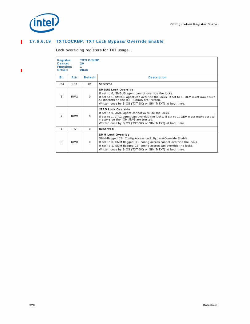
Configuration Register Space
328 Datasheet
17.6.6.19 TXTLOCKBP: TXT Lock Bypass/Override Enable
Lock overriding registers for TXT usage. .
Register: TXTLOCKBPDevice: 20Function: 1Offset: 284h
Bit Attr Default Description
7:4 RO 0h Reserved
3 RWO 0
SMBUS Lock OverrideIf set to 0, SMBUS agent cannot override the locks. If set to 1, SMBUS agent can override the locks. If set to 1, OEM must make sure all masters on the IOH SMBUS are trusted. Written once by BIOS (TXT-SX) or SINIT(TXT) at boot time.
2 RWO 0
JTAG Lock OverrideIf set to 0, JTAG agent cannot override the locks. If set to 1, JTAG agent can override the locks. If set to 1, OEM must make sure all masters on the IOH JTAG are trusted. Written once by BIOS (TXT-SX) or SINIT(TXT) at boot time.
1 RV 0 Reserved
0 RWO 0
SMM Lock OverrideSMM-flagged CSI Config Access Lock Bypass/Override EnableIf set to 0, SMM flagged CSI config access cannot override the locks. If set to 1, SMM flagged CSI config access can override the locks. Written once by BIOS (TXT-SX) or SINIT(TXT) at boot time.

Datasheet 329
Configuration Register Space
17.6.7 IOH System/Control Status Registers
Table 17-11.IOH Control/Status & Global Error Register Map (Device 20, Function 2) (Sheet 1 of 4)
DID VID 000h QPIERRSV 080h
PCISTS PCICMD 004h QPIPERRSV 084h
CCR RID 008h 088h
HDR CLS 00Ch IOHERRSV 08Ch
010h 090h
014h PCIERRSV 094h
018h THRERRSV 098h
01Ch SYSMAP 09Ch
020h VIRAL 0A0h
024h ERRPINCTL 0A4h
028h ERRPINST 0A8h
SID SVID 02Ch ERRPINDAT 0ACh
030h VPPCTL 0B0h
CAPPTR1
Notes:1. CAPPTR points to the first capability block
034h 0B4h
038h VPPSTS 0B8h
INTP INTL 03Ch 0BCh
EXPCAP NXTPTR CAPID 040h PRSTRDY 0C0h
DEVCAP 044h GENMCA 0C4h
DEVSTS DEVCON 048h GENVIRAL 0C8h
RESERVED PCIe Header space 04Ch SYRE 0CCh
050h FREQ 0D0h
054h 0D4h
058h 0D8h
05Ch 0DCh
060h 0E0h
064h 0E4h
068h CAPTIM 0E8h
06Ch 0ECh
070h 0F0h
074h 0F4h
078h 0F8h
07Ch EOI_CTRL 0FCh

Configuration Register Space
330 Datasheet
)
Table 17-12.IOH Control/Status & Global Error Register Map (Device 20, Function 2) (Sheet 2 of 4)
RESERVED PCIe Header space 100h 180h
104h 184h
108h 188h
10Ch 18Ch
110h 190h
114h 194h
118h 198h
11Ch 19Ch
120h 1A0h
124h 1A4h
128h 1A8h
12Ch 1ACh
130h 1B0h
134h 1B4h
138h 1B8h
13Ch 1BCh
140h GNERRST 1C0h
144h GFERRST 1C4h
148h GERRCTL 1C8h
14Ch GSYSST 1CCh
150h GSYSCTL 1D0h
154h GTIME 1D4h
158h 1D8h
15Ch GFFERRST 1DCh
160h GFFERRTIME 1E0h
164h 1E4h
168h GFNERRST 1E8h
16Ch GNFERRST 1ECh
170h GNFERRTIME 1F0h
174h 1F4h
178h GNNERRST 1F8h
17Ch 1FCh

Datasheet 331
Configuration Register Space
Table 17-13.IOH Local Error Map #1 (Device 20, Function 2) (Sheet 3 of 4)
QPI0ERRST 200h 280h
QPI0ERRCTL 204h 284h
QPI0FFERRST 208h 288h
QPI0FNERRST 20Ch 28Ch
QPI0NFERRST 210h 290h
QPI0NNERRST 214h 294h
QPI0ERRCNTSEL 218h 298h
QPI0ERRCNT 21Ch 29Ch
220h 2A0h
224h 2A4h
228h 2A8h
22Ch 2ACh
QPIP0ERRST 230h 2B0h
QPIP0ERRCTL 234h 2B4h
QPIP0FFERRST 238h 2B8h
QPIP0FNERRST 23Ch 2BCh
QPIP0FFERRHD 240h 2C0h
244h 2C4h
248h 2C8h
24Ch 2CCh
QPIP0NFERRST 250h 2D0h
QPIP0NNERRST 254h 2D4h
QPIP0NFERRHD 258h 2D8h
25Ch 2DCh
260h 2E0h
264h 2E4h
QPIP0ERRCNTSEL 268h 2E8h
QPIP0ERRCNT 26Ch 2ECh
270h 2F0h
274h 2F4h
278h 2F8h
27Ch 2FCh

Configuration Register Space
332 Datasheet
Table 17-14.IOH Local Error Map #2 (Device 20, Function 2) (Sheet 4 of 4)
IOHERRST 300h 380h
IOHERRCTL 304h 384h
IOHFFERRST 308h 388h
IOHFFERRHD 30Ch 38Ch
310h 390h
314h 394h
318h 398h
IOHFNERRST 31Ch 39Ch
IOHNFERRST 320h 3A0h
IOHNFERRHD 324h 3A4h
328h 3A8h
32Ch 3ACh
330h 3B0h
IOHNNERRST 334h 3B4h
338h 3B8h
IOHERRCNTSEL 33Ch 3BCh
IOHERRCNT 340h 3C0h
344h 3C4h
348h 3C8h
34Ch 3CCh
350h 3D0h
354h 3D4h
358h 3D8h
35Ch 3DCh
THRERRST 360h 3E0h
THRERRCTL 364h 3E4h
THRFFERRST 368h 3E8h
THRFNERRST 36Ch 3ECh
THRNFERRST 370h 3F0h
THRNNERRST 374h 3F4h
THRERRCNTSEL 378h 3F8h
THRERRCNT 37Ch 3FCh

Datasheet 333
Configuration Register Space
17.6.7.1 QPIERRSV—Intel® QuickPath Interconnect Link/Physical Error Severity Register
This register associates the detected Intel QPI Link and Physical Layer errors to an error severity level. An individual error is reported with the corresponding severity in this register. Software can program the error severity to one of the three severities supported by IOH. This register is sticky and can only be reset by PWRGOOD. The default error severity mapping is defined in IOH Platform Architecture Specification.
Register: QPIERRSVDevice: 20Function: 2Offset: 080h
Bit Attr Default Description
31:26 RO 0 Reserved
25:24 RWS 10
D4 – Intel QPI Link Internal Parity ErrorThis field determines the error severity for the corresponding Severity error. Two-bit encoding as follows:00 = Error Severity Level 0 (Correctable)01 = Error Severity Level 1 (Recoverable)10 = Error Severity Level 2 (Fatal)11 = Reserved
23:22 RWS 10 D3 – Intel QPI Link Layer Control Error
21:20RWS
10C0 – Intel QPI Link Layer detected CRC error Unsuccessful link level retry — entered LLR abort stateSee QPI[1:0]FERRFLIT0 and QPI[1:0]FERRFLIT1 for flit info.
19:18 RWS 00B1 – Intel QPI Link Layer detected CRC error Successful link level retry after PHY reinit
17:16 RWS 00 B0 – Intel QPI Link Layer CRC – successful link level retry
15:14 RWS 10 DG – Intel QPI Link Layer Detected unsupported/undefined msgclass/opcode/vn packet Error
13:12 RWS 00 B5 – Potential Spurious CRC error on L1 Exit
11:10 RWS 00 B6 – Intel QPI Link Layer CRC error
9:8 RWS 10 D2 – Intel QPI Physical Layer Initialization Failure
7:6 RWS 10 D1 – Intel QPI Physical Layer Detected Latency Buffer Rollover
5:4 RWS 10 D0 – Intel QPI Physical Layer Detected Drift Buffer Alarm
3:2 RWS 01 C7 – Intel QPI Physical Layer Reset Successful with Reduced Width
1:0 RWS 00 B2 – Intel QPI Physical Layer Successful Reset at same Width

Configuration Register Space
334 Datasheet
17.6.7.2 QPIPERRSV—Intel® QuickPath Interconnect Protocol Error Severity Register
This register associates the detected Intel QuickPath Interconnect Protocol and Routing layer errors to an error severity level. An individual error is reported with the corresponding severity in this register. Software can program the error severity to one of the three severities supported by IOH. This register is sticky and can only be reset by PWRGOOD. The default error severity mapping is defined in Table 13-2.
Register: QPIPERRSVDevice: 20Function: 2Offset: 084h
Bit Attr Default Description
63:40 RO 0s Reserved
39:38 RWS 10
DH – Intel QPI Protocol Layer Detected unsupported/undefined packet ErrorThis field determines the error severity for the corresponding Severity error. Two-bit encoding as follows:00 = Error Severity Level 0 (Correctable)01 = Error Severity Level 1 (Recoverable)10 = Error Severity Level 2 (Fatal)11 = Reserved
37:36 RWS 10 DF – Illegal Inbound Request
35:34 RWS 10 DE – Routing Table Invalid
33:32 RO 0 Reserved
31:30 RWS 10 DC – Protocol SAD illegal or non-existent memory for outbound snoop
29:28 RWS 10 DB – Protocol Parity Error
27:26 RWS 10 DA – Protocol Queue/Table Overflow or Underflow
25:24 RWS 10 D9 – Protocol Layer Received Viral from Intel QPI
23:22 RWS 10 D8 – Protocol Layer Received Illegal packet field or Incorrect Target NodeID
21:20 RWS 10 D7 – Protocol Layer Received Unexpected Response/Completion
19:18 RWS 10 D6 – Protocol Layer Received Failed Response
17:16 RWS 10 D5 – Protocol Layer Detected Time-Out in ORB
15:10 RO 0s Reserved
9:8 RWS 01 C3 – CSR access crossing 32-bit boundary
7:6 RWS 01 C2 – Write Cache Un-correctable ECC
5:4 RWS 01 C1 – Protocol Layer Received Poisoned Packet.
3:2 RWS 00 B4 – Write Cache Correctable ECC
1:0 RWS 00 B3 – Intel QPI CPEI Error Status

Datasheet 335
Configuration Register Space
17.6.7.3 IOHERRSV—IOH Core Error Severity Register
This register associates the detected IOH internal core errors to an error severity level. An individual error is reported with the corresponding severity in this register. Software can program the error severity to one of the three severities supported by IOH. This register is sticky and can only be reset by PWRGOOD.
Register: IOHERRSVDevice: 20Function: 2Offset: 08Ch
Bit Attr Default Description
31:14 RV 0s Reserved
13:12 RWS 01
C6 – FIFO Overflow/Underflow errorThis field determines the error severity for the corresponding Severity error. Two-bit encoding as follows:00 = Error Severity Level 0 (Correctable)01 = Error Severity Level 1 (Recoverable)10 = Error Severity Level 2 (Fatal)11 =Reserved
11:10 RWS 01
C5 – Completor abort address errorThis field determines the error severity for the corresponding Severity error. Two-bit encoding as follows:00 = Error Severity Level 0 (Correctable)01 = Error Severity Level 1 (Recoverable)10 = Error Severity Level 2 (Fatal)11 =Reserved
9:8 RWS 01
C4 – Master abort address errorThis field determines the error severity for the corresponding Severity error. Two-bit encoding as follows:00 = Error Severity Level 0 (Correctable)01 = Error Severity Level 1 (Recoverable)10 = Error Severity Level 2 (Fatal)11 =Reserved
7:0 RWS 00h Reserved

Configuration Register Space
336 Datasheet
17.6.7.4 MIERRSV—Miscellaneous Error Severity Register
This register associates the detected IOH miscellaneous errors to an error severity level. An individual error is reported with the corresponding severity in this register. Software can program the error severity to one of the three severities supported by IOH. This register is sticky and can only be reset by PWRGOOD.
17.6.7.5 PCIERRSV—PCIe Error Severity Map Register
This register allows remapping of the PCIe errors to the IOH error severity.
Register: MIERRSVDevice: 20Function: 2Offset: 090h
Bit Attr Default Description
31:6 RV 0s Reserved
7:6 RWS 0023 – VPP Error SeverityRefer to bit [1:0] for description
5:4 RWS 0022 – Persistent JTAG Error SeverityRefer to bit[1:0] for description.
3:2 RWS 0021 – Persistent SMBus Retry Status SeverityRefer to bit[1:0] for description.
1:0 RWS 00
20 – IOH Configuration Register Parity error SeverityThis field determines the error severity for the corresponding Severity error. Two-bit encoding as follows:00 = Error Severity Level 0 (Correctable)01 = Error Severity Level 1 (Recoverable)10 = Error Severity Level 2 (Fatal)11 =Reserved
Register: PCIERRSVDevice: 20Function: 2Offset: 094h
Bit Attr Default Description
31:6 RV 0s Reserved
5:4 RWS 10
PCIe Fatal Error Severity Map10 = Map this PCIe error type to Error Severity 201 = Map this PCIe error type to Error Severity 100 = Map this PCIe error type to Error Severity 0
3:2 RWS 01PCIe Non-Fatal Error Severity MapRefer to bits 5:4 for bit encoding.
1:0 RWS 00PCIe Correctable Error Severity MapRefer to bits 5:4 for bit encoding.
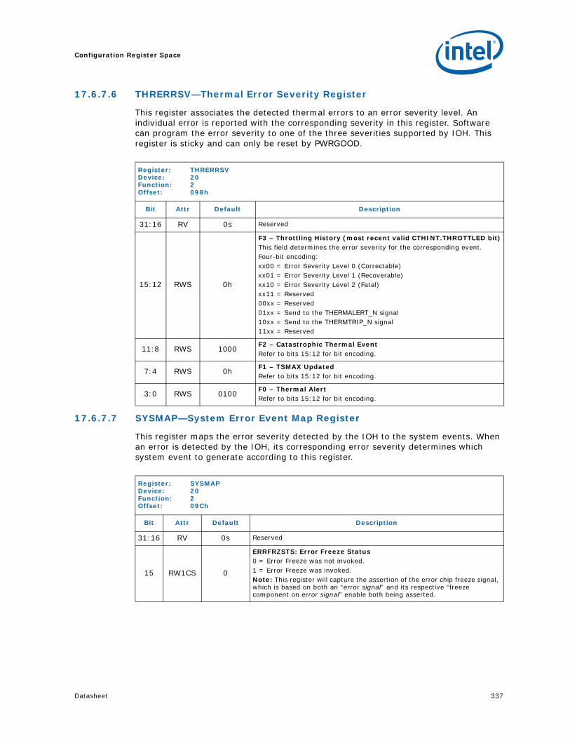
Datasheet 337
Configuration Register Space
17.6.7.6 THRERRSV—Thermal Error Severity Register
This register associates the detected thermal errors to an error severity level. An individual error is reported with the corresponding severity in this register. Software can program the error severity to one of the three severities supported by IOH. This register is sticky and can only be reset by PWRGOOD.
17.6.7.7 SYSMAP—System Error Event Map Register
This register maps the error severity detected by the IOH to the system events. When an error is detected by the IOH, its corresponding error severity determines which system event to generate according to this register.
Register: THRERRSVDevice: 20Function: 2Offset: 098h
Bit Attr Default Description
31:16 RV 0s Reserved
15:12 RWS 0h
F3 – Throttling History (most recent valid CTHINT.THROTTLED bit)This field determines the error severity for the corresponding event.Four-bit encoding:xx00 = Error Severity Level 0 (Correctable)xx01 = Error Severity Level 1 (Recoverable)xx10 = Error Severity Level 2 (Fatal)xx11 = Reserved00xx = Reserved01xx = Send to the THERMALERT_N signal10xx = Send to the THERMTRIP_N signal11xx = Reserved
11:8 RWS 1000F2 – Catastrophic Thermal EventRefer to bits 15:12 for bit encoding.
7:4 RWS 0hF1 – TSMAX UpdatedRefer to bits 15:12 for bit encoding.
3:0 RWS 0100F0 – Thermal AlertRefer to bits 15:12 for bit encoding.
Register: SYSMAPDevice: 20Function: 2Offset: 09Ch
Bit Attr Default Description
31:16 RV 0s Reserved
15 RW1CS 0
ERRFRZSTS: Error Freeze Status 0 = Error Freeze was not invoked.1 = Error Freeze was invoked.Note: This register will capture the assertion of the error chip freeze signal, which is based on both an “error signal” and its respective “freeze component on error signal” enable both being asserted.

Configuration Register Space
338 Datasheet
17.6.7.8 VIRAL—Viral Alert Register
The Viral Alert feature are not available on Intel X58 Express Chipset platforms since the Intel® Core™ i7 processors / Intel® Xeon® processor 3500 series do not support this feature. Intel’s recommendation is to keep this alert as the default (disabled) on the Intel X58 Express Chipset platforms.
14:12 RW 0h
ERRFRZ: Error Chip FreezeThis feature is OR’d with the signal that drives the Chip Freeze DFx signal. A chip freeze prohibits packets from entering or leaving the chip while maintaining protocol correctness. For effective use of this feature the system management software must assume that a measurable amount of time must pass before accessing the registers due to internal activity continuing for some time before coming to a halted state. 000 = Do not freeze component.xx1 = Freeze component on Error 0 Assertion (Correctable)x1x = Freeze component on Error 1 Assertion (Recoverable)1xx = Freeze component on Error 2 Assertion (Fatal)After a freeze event occurs a SMBus software write with 0h will release the freeze condition. Since a reset may be required as a result of an error it may not be necessary to write a freeze release.Any combination of error select bits is possible, for example: A value of b110 enables chip freeze on any error that is not correctable.Note: When this Error Freeze signal is asserted, it has priority over the chip freeze start and stop selections. Chip freeze will remain on regardless of its start and stop, until ERRCHPFRZ returns to a 0 value.
11 RV 0 Reserved
10:8 RWS 000
Severity 2 Error Map110 = Generate MCA101 = Generate CPEI010 = Generate NMI001 = Generate SMI/PMI000 = No inband message
7 RV 0 Reserved
6:4 RWS 0Severity 1 Error MapRefer to bits 10:8 for bit encoding.
3 RV 0 Reserved
2:0 RWS 0Severity 0 Error MapRefer to bits 10:8 for bit encoding.
Register: SYSMAPDevice: 20Function: 2Offset: 09Ch
Bit Attr Default Description
Register: VIRALDevice: 20Function: 2Offset: 0A0h
Bit Attr Default Description
31:3 RV 0 Reserved
2 RWS 0
Fatal Viral Alert EnableEnable viral alert for Fatal Error.0 = Disable Viral Alert for error severity 2.1 = IOH goes viral when error severity 2 is set in the system event status
register.
1:0 RO 0 Reserved

Datasheet 339
Configuration Register Space
17.6.7.9 ERRPINCTL—Error Pin Control Register
This register provides the option to configure an error pin to either as a special purpose error pin which is asserted based on the detected error severity, or as a general purpose output which is asserted based on the value in the ERRPINDAT. The assertion of the error pins can also be completely disabled by this register.
17.6.7.10 ERRPINST—Error Pin Status Register
This register reflects the state of the error pin assertion. The status bit of the corresponding error pin is set upon the deassertion to assertion transition of the error pin. This bit is cleared by the software with writing 1 to the corresponding bit.
Register: ERRPINCTLDevice: 20Function: 2Offset: 0A4h
Bit Attr Default Description
31:6 RV 0s Reserved
5:4 RWS 00
Error[2] Pin Assertion Control11 = Reserved. 10 = Assert Error Pin when error severity 2 is set in the system event
status reg.01 = Assert and Deassert Error pin according to error pin data register00 = Disable Error pin assertion
3:2 RWS 00
Error[1] Pin Assertion Control11 = Reserved. 10 = Assert Error Pin when error severity 1 is set in the system event
status reg.01 = Assert and Deassert Error pin according to error pin data register00 = Disable Error pin assertion
1:0 RWS 00
Error[0] Pin Assertion Control11 = Reserved. 10 = Assert Error Pin when error severity 0 is set in the system event
status reg.01 = Assert and Deassert Error pin according to error pin data register00 = Disable Error pin assertion
Register: ERRPINSTDevice: 20Function: 2Offset: 0A8h
Bit Attr Default Description
31:3 RO 0s Reserved
2 RW1CS 0Error[2] Pin statusThis bit is set upon the transition of deassertion to assertion of the Error pin. Software write 1 to clear the status.
1 RW1CS 0 Error[1] Pin status
0 RW1CS 0 Error[0] Pin status

Configuration Register Space
340 Datasheet
17.6.7.11 ERRPINDAT—Error Pin Data Register
This register provides the data value when the error pin is configured as a general purpose output.
Register: ERRPINDATDevice: 20Function: 2Offset: 0ACh
Bit Attr Default Description
31:3 RO 0s Reserved
2 RW 0
Error[2] Pin Data (applies when ERRPINCTL[5:4]=01; otherwise reserved)This bit acts as the general purpose output for the Error[2] pin. Error [2] pin value will follow the value programmed in Error[2] Pin Data register. This bit applies only when ERRPINCTL[5:4]=01; otherwise it is reserved.0 = Deassert Error[2] pin1 = Assert Error[2] pinThis value only applies to the pin when ERRPINCTL[5:4]=01
1 RW 0 Error[1] Pin Data (applies when ERRPINCTL[3:2]=01; otherwise reserved)
0 RW 0 Error[0] Pin Data (applies when ERRPINCTL[1:0]=01; otherwise reserved)

Datasheet 341
Configuration Register Space
17.6.7.12 VPPCTL—VPP Control Register
This register defines the control/command for PCA9555.
17.6.7.13 VPPSTS—VPP Status Register
This register defines the status from PCA9555.
Register: VPPCTLDevice: 20Function: 2Offset: 0B0h
Bit Attr Default Description
63:56 RO 0s Reserved
55 RWS 0
VPP Reset Mode: 0 = Power good reset will reset the VPP state machines and hard reset will
cause the VPP state machine to terminate at the next ‘logical’ VPP stream boundary and then reset the VPP state machines
1 = Both power good and hard reset will reset the VPP state machines
54:44 RWS 0sVPP Enable: When set, the VPP function for the corresponding root port is enabled.Bits 54:44 corresponds to root port PCI[10:0].
43:0 RWS 0s
VPP AddressAssigns the VPP address of the device on the VPP interface and assigns the port address for the ports within the VPP device. There are more address bits then root ports so assignment must be spread across VPP ports.Addr Port Number Root Port[43:41] [40] PCIE[10][39:37] [36] PCIE[9][35:33] [32] PCIE[8][31:29] [28] PCIE[7][27:25] [24] PCIE[6][23:21] [20] PCIE[5][19:17] [16] PCIE[4][15:13] [12] PCIE[3][11:9] [8] PCIE[2][7:5] [4] PCIE[1][3:1] [0] PCIE[0]
Register: VPPSTSDevice: 20Function: 2Offset: 0B8h
Bit Attr Default Description
31:1 RO 0 Reserved
0 RW1CS 0VPP Port Error HappenedAn unexpected STOP of NACK was seen on the VPP port.
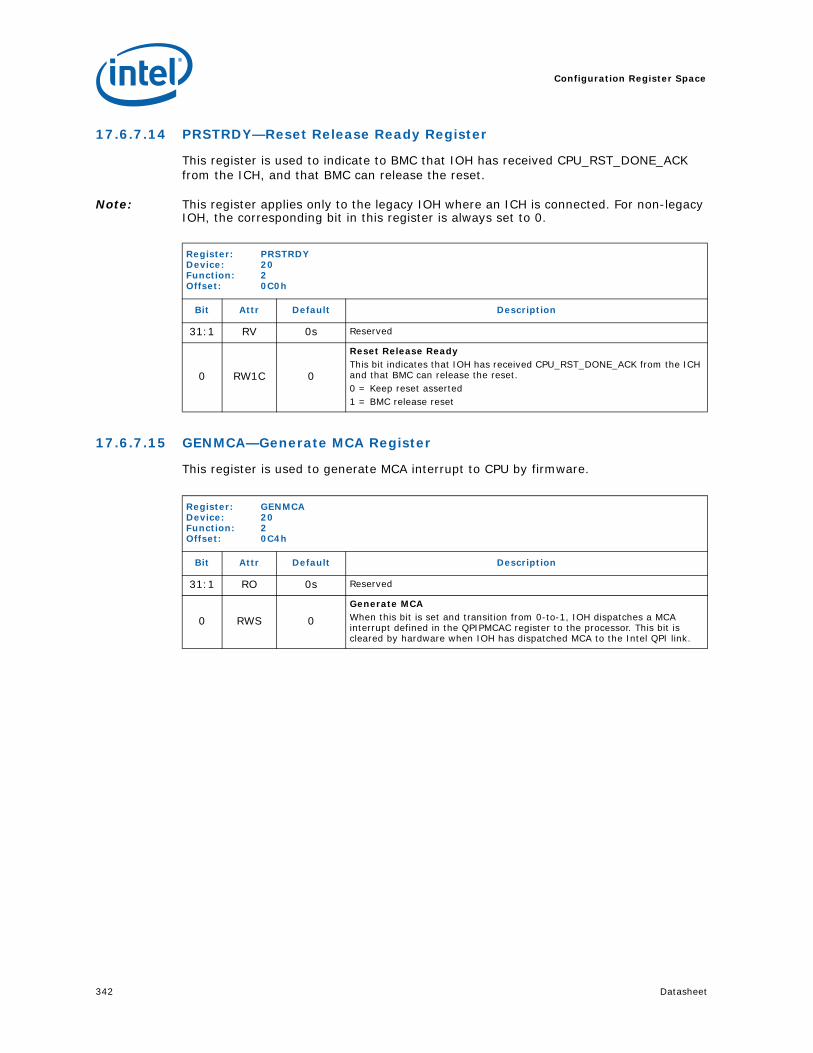
Configuration Register Space
342 Datasheet
17.6.7.14 PRSTRDY—Reset Release Ready Register
This register is used to indicate to BMC that IOH has received CPU_RST_DONE_ACK from the ICH, and that BMC can release the reset.
Note: This register applies only to the legacy IOH where an ICH is connected. For non-legacy IOH, the corresponding bit in this register is always set to 0.
17.6.7.15 GENMCA—Generate MCA Register
This register is used to generate MCA interrupt to CPU by firmware.
Register: PRSTRDYDevice: 20Function: 2Offset: 0C0h
Bit Attr Default Description
31:1 RV 0s Reserved
0 RW1C 0
Reset Release ReadyThis bit indicates that IOH has received CPU_RST_DONE_ACK from the ICH and that BMC can release the reset.0 = Keep reset asserted1 = BMC release reset
Register: GENMCADevice: 20Function: 2Offset: 0C4h
Bit Attr Default Description
31:1 RO 0s Reserved
0 RWS 0
Generate MCAWhen this bit is set and transition from 0-to-1, IOH dispatches a MCA interrupt defined in the QPIPMCAC register to the processor. This bit is cleared by hardware when IOH has dispatched MCA to the Intel QPI link.

Datasheet 343
Configuration Register Space
17.6.7.16 GENVIRAL—Generate Viral Register
This register is used to generate Viral alert to the processor by firmware and clear Viral.
Register: GENVIRALDevice: 20Function: 2Offset: 0C8h
Bit Attr Default Description
31:4 RO 0s Reserved
3 RWO 0
Viral_Clear_disable1 = Disable. This will not allow the clearing of viral alert by setting VIRAL_CLEAR
bit; eventually, the Viral Alert will be cleared once all the Fatal Error and VIRAL_status (RW1CS) is cleared by software.
0 = Enable. This will clear the Viral alert generated in the system (Viral broadcast will be stopped) by setting the VIRAL_CLEAR bit; but still the VIRAL_STATUS will be set until software clears it.
2 RW 0Viral_ClearThis bit is active when VIRAL_CLEAR_DIS = 0; by setting this bit Viral alert generated in the system will be cleared.
1 RW1CS 0Viral_StatusThis bit is set when IOH is in viral mode.
0 RWS 0
hyur65r4njhg9g8huuuWhen this bit is set and transition from 0-to-1, IOH sets Intel QPI cluster(s) to viral. This bit is cleared by hardware when IOH has set viral alert on Intel QPI cluster(s).

Configuration Register Space
344 Datasheet
17.6.7.17 SYRE—System Reset Register
This register controls IOH reset behavior. Any resets produced by a write to this register must be delayed until the configuration write is completed on the PCIe/DMI, Intel QPI, SMBUS, and JTAG interfaces.
There is no “SOFT RESET” bit in this register. That function is invoked through the DMI interface. There are no Intel QPI:PCI Express gear ratio definitions in this register. The Intel QuickPath Interconnect frequencies are specified in the FREQ register. The PCI Express frequencies are automatically negotiated inband.
Register: SYREDevice: 20Function: 2Offset: 0CCh
Bit Attr Default Description
31:15 RV 0s Reserved
14 RV 0S51 = Translate DMI.GO_S3 to QPI.SpcPMReq (S5)0 = Forward DMI.GO_S3 to QPI.SpcPMReq(S3)
13:12 RWSLB 00 Reserved
11 RW 0
RSTMSK0 = The IOH will perform the appropriate internal handshakes on RST_N
signal transitions to progress through the hard reset.1 = IOH ignores RST_N, unaffected by the RST_N assertion
10 RW 0CPURESET1 = IOH asserts RESETO_N0 = The IOH clears this bit when the CPURESET timer elapses.
9:1 RV 0s Reserved
0 RWS 0
Enable CPU BIST1 = Enable CPU BIST0 = Disable CPU BISTThis bit controls whether or not BIST is run in the CPU on reset. Its value will correspond to the BIST value in the POC exchanged from IOH on Intel QPI. This value will only make a difference in CPUs that observe POC (like Intel Core™ i7 processor / Intel Xeon® processor series). By default BIST is disabled. If BIST is desired, then after this bit is set the CPU must be reset to cause the CPU to capture the new value.

Datasheet 345
Configuration Register Space
17.6.7.18 FREQ—Frequencies Register
This register defines the Intel QuickPath Interconnect frequency. The QPIFREQSEL[1:0] straps determines the Intel QuickPath Interconnect link:core frequency ratio. This FREQ register is read-only, and it indicates the PRESENT frequency of the links.
17.6.7.19 CAPTIM—Cap Timer Register
This register sets the cap timer count value.
17.6.7.20 EOI_CTRL—Global EOI Control Register
Register: FREQDevice: 20Function: 2Offset: 0D0h
Bit Attr Default Description
31:2 RV 0s Reserved
1:0 ROSTRAP:
QPIFREQSEL
QPIFREQSEL: Intel QPI High Frequency00 = 4.800 GT/s01 = Reserved10 = 6.400 GT/s11 = ReservedThis is the value of the QPIFREQSEL signals sampled at PWRGOOD.
Register: CAPTIMDevice: 20Function: 2Offset: 0E8h
Bit Attr Default Description
31:14 RV 0s Reserved
13:0 RWS 7FFh
CAPTIM: Cap Timer ValueWhen enabled, a detected outbound DMI transaction will start the timer. The returning read data completion is held in the core until the expiration of the counter. After the transaction is released the counter is re-loaded with this count value (or cleared depending on implementation). The counter is free-running until the CAPTIMEN bit is cleared.
Register: EOI_CTRLDevice: 20Function: 2Offset: FCh
Bit Attr Default Description
7:1 RV 00h Reserved
0 RW 0
Drop_EOI0 = EOI messages from Intel QPI are broadcasted to root/DMI ports and
IOxAPIC per the normal rules for EOI broadcast.1 = EOI messages from Intel QPI are simply dropped and not broadcast to
root/DMI ports or the integrated IOxAPIC.

Configuration Register Space
346 Datasheet
17.7 Global Error Registers
Table 17-15.IOH Control/Status & Global Error Register Map (Device 20, Function 2)
RESERVED PCIE Header space 100h 180h
104h 184h
108h 188h
10Ch 18Ch
110h 190h
114h 194h
118h 198h
11Ch 19Ch
120h 1A0h
124h 1A4h
128h 1A8h
12Ch 1ACh
130h 1B0h
134h 1B4h
138h 1B8h
13Ch 1BCh
140h GNERRST 1C0h
144h GFERRST 1C4h
148h GERRCTL 1C8h
14Ch GSYSST 1CCh
150h GSYSCTL 1D0h
154h GTIME 1D4h
158h 1D8h
15Ch GFFERRST 1DCh
160h GFFERRTIME 1E0h
164h 1E4h
168h GFNERRST 1E8h
MISCPRIVC 16Ch GNFERRST 1ECh
170h GNFERRTIME 1F0h
174h 1F4h
178h GNNERRST 1F8h
17Ch 1FCh

Datasheet 347
Configuration Register Space
17.7.1 MISCPRIVC—Miscellaneous Private VC Register
This is 32-bit unused register.
17.7.2 GNERRST—Global Non-Fatal Error Status Register
This register indicates the status of non-fatal error reported to the IOH global error logic. An individual error status bit that is set indicates that a particular local interface has detected an error.
Register: MISCPRIVCDevice: 20Function: 2Offset: 16Ch
Bit Attr Default Description
31:0 RV 0s Unused
Register: GNERRSTDevice: 20Function: 2Offset: 1C0h
Bit Attr Default Description
31:26 RV 0s Reserved
25 RW1CS 0VT-d Error StatusThis bit indicates that IOH has detected a VT_d related error.
24 RW1CS 0Miscellaneous Error StatusThis bit indicates that IOH has detected a miscellaneous error.
23 RW1CS 0IOH Core Error StatusThis bit indicates that IOH core has detected an error.
22 RW1CS 0DMA Error StatusThis bit indicates that IOH has detected an error in its DMA engine.
21 RW1CS 0Thermal Error StatusThis bit indicates that IOH detected thermal error.
20 RW1CS 0DMI Error StatusThis bit indicates that IOHDMI port 0 has detected an error.
19:16 RV 0s Reserved
15 RW1CS 0PCIe [10] Error StatusPCIe port 10 has detected an error.
14 RW1CS 0PCIe [9] Error StatusPCIe port 9 has detected an error.
13 RW1CS 0PCIe [8] Error StatusPCIe port 8 has detected an error.
12 RW1CS 0PCIe [7] Error StatusPCIe port 7 has detected an error.
11 RW1CS 0PCIe [6] Error StatusPCIe port 6 has detected an error.
10 RW1CS 0PCIe [5] Error StatusPCIe port 5 has detected an error.
9 RW1CS 0PCIe [4] Error StatusPCIe port 4 has detected an error.

Configuration Register Space
348 Datasheet
17.7.2.1 GFERRST—Global Fatal Error Status Register
This register indicates the fatal error reported to the IOH global error logic. An individual error status bit that is set indicates that a particular local interface has detected an error.
8 RW1CS 0PCIe [3] Error StatusPCIe port 3 has detected an error.
7 RW1CS 0PCIe [2] Error StatusPCIe port 2 has detected an error.
6 RW1CS 0PCIe [1] Error StatusPCIe port 1 has detected an error.
5PCIe [0] Error StatusPCIe port 0 has detected an error. PCIe[0] is associated with DMI.
4 RV 0 Reserved
3 RW1CS 0 Reserved
2 RW1CS 0QPI[0] Protocol Error StatusThis bit indicates that the Intel QPI protocol layer port 0 has detected an error
1 RW1CS 0 Reserved
0 RW1CS 0QPI[0] Error StatusThis bit indicates that QPI[0] port has detected an error
Register: GNERRSTDevice: 20Function: 2Offset: 1C0h
Bit Attr Default Description
Register: GFERRSTDevice: 20Function: 2Offset: 1C4h
Bit Attr Default Description
31:26 RV 0s Reserved
25 RW1CS 0VTd Error StatusThis bit indicates that IOH has detected a VTd related error.
24 RW1CS 0Miscellaneous Error StatusThis bit indicates that IOH has detected a miscellaneous error.
23 RW1CS 0IOH Core Error StatusThis bit indicates that IOH core has detected an error.
22 RW1CS 0DMA Error StatusThis bit indicates that IOH has detected an error in its DMA engine.
21 RW1CS 0Thermal Error StatusThis bit indicates that IOH has detected thermal error.
20 RW1CST 0DMI Error StatusThis bit indicates that IOHDMI port 0 has detected an error.
19:16 RV 0s Reserved
15 RW1CS 0PCIe [10] Error StatusPCIe port 10 has detected an error.
14 RW1CS 0PCIe [9] Error StatusPCIe port 9 has detected an error.

Datasheet 349
Configuration Register Space
13 RW1CS 0PCIe [8] Error StatusPCIe port 8 has detected an error.
12 RW1CS 0PCIe [7] Error StatusPCIe port 7 has detected an error.
11 RW1CS 0PCIe [6] Error StatusPCIe port 6 has detected an error.
10 RW1CS 0PCIe [5] Error StatusPCIe port 5 has detected an error.
9 RW1CS 0PCIe [4] Error StatusPCIe port 4 has detected an error.
8 RW1CS 0PCIe [3] Error StatusPCIe port 3 has detected an error.
7 RW1CS 0PCIe [2] Error StatusPCIe port 2 has detected an error.
6 RW1CS 0PCIe [1] Error StatusPCIe port 1 has detected an error.
5PCIe [0] Error StatusPCIe port 0 has detected an error. PCIe[0] is associated with DMI.
4 RW1CST 0 Reserved
3 RW1CS 0 Reserved
2 RW1CS 0QPI[0] Protocol Error StatusThis bit indicates that the Intel protocol layer port 0 has detected an error.
1 RW1CS 0 Reserved
0 RW1CS 0QPI[0] Error StatusThis bit indicates that QPI[0] port has detected an error.
Register: GFERRSTDevice: 20Function: 2Offset: 1C4h
Bit Attr Default Description

Configuration Register Space
350 Datasheet
17.7.2.2 GERRCTL—Global Error Control Register
This register controls the reporting of errors detected by the IOH local interfaces. An individual error control bit that is set to disable (masks) error reporting of the particular local interface. Software may set or clear the control bit. This register is sticky and can only be reset by PWRGOOD.
Note that bit fields in this register can become reserved depending on the port configuration. For example, if the PCIe port is configured as 2X8 ports, then only the corresponding PCIeX8 bit fields are valid; other bits are unused and reserved.
Setting global error control register masks errors reported from the local interface to the global error status register. If the an error reporting is disabled in this register, all errors from the corresponding local interface will not set any of the global error status bits.
Register: GERRCTLDevice: 20Function: 2Offset: 1C8h
Bit Attr Default Description
31:26 RV 0s
Reserved
25 RW 0
VTd Error EnableThis bit controls the VTd related error.0 = Error reporting enabled 1 = Error reporting marked
24 RW 0
Miscellaneous Error EnableThis bit controls the miscellaneous error detected in the IOH.0 = Error reporting enabled 1 = Error reporting marked
23 RW 0
IOH Core Error EnableThis bit controls the error detected in the IOH Core.0 = Error reporting enabled 1 = Error reporting marked
22 RW 0
DMA Error EnableThis bit controls the error detected in the DMA.0 = Error reporting enabled 1 = Error reporting marked
21 RW 0
Thermal Error EnableThis bit controls the detected Thermal error. in the IOH0 = Error reporting enabled 1 = Error reporting marked
20 RW 0
DMI Error EnableThis bit controls the error detected in the DMI Port.0 = Error reporting enabled 1 = Error reporting marked
19:16 RV 0s
Reserved
15 RW 0
PCIe [10] Error EnableThis bit controls the error detected in the PCIe port 10.0 = Error reporting enabled 1 = Error reporting marked
14 RW 0
PCIe [9] Error EnableThis bit controls the error detected in the PCIe port 9.0 = Error reporting enabled 1 = Error reporting marked

Datasheet 351
Configuration Register Space
13 RW 0
PCIe [8] Error EnableThis bit controls the error detected in the PCIe port 8.0 = Error reporting enabled 1 = Error reporting marked
12 RW 0
PCIe [7] Error EnableThis bit controls the error detected in the PCIe port 7.0 = Error reporting enabled 1 = Error reporting marked
11 RW 0
PCIe [6] Error EnableThis bit controls the error detected in the PCIe port 6.0 = Error reporting enabled 1 = Error reporting marked
10 RW 0
PCIe [5] Error EnableThis bit controls the error detected in the PCIe port 5.0 = Error reporting enabled 1 = Error reporting marked
9 RW 0
PCIe [4] Error EnableThis bit controls the error detected in the PCIe port 4.0 = Error reporting enabled 1 = Error reporting marked
8 RW 0
PCIe [3] Error EnableThis bit controls the error detected in the PCIe port 3.0 = Error reporting enabled 1 = Error reporting marked
7 RW 0
PCIe [2] Error EnableThis bit controls the error detected in the PCIe port 2.0 = Error reporting enabled 1 = Error reporting marked
6 RW 0
PCIe [1] Error EnableThis bit controls the error detected in the PCIe port 1.0 = Error reporting enabled 1 = Error reporting marked
5
PCIe [0] Error EnableThis bit controls the error detected in the PCIe port 0.0 = Error reporting enabled 1 = Error reporting marked
4 RV 0 Reserved
3 RW 0 Reserved
2 RW 0
QPI[0] Protocol Error EnableThis bit controls the error detected in the QPI Port 0.0 = Error reporting enabled 1 = Error reporting marked
1 RW 0 Reserved
0 RW 0
QPI[0] Error EnableThis bit controls the error detected in the QPI Port 0.0 = Error reporting enabled 1 = Error reporting marked
Register: GERRCTLDevice: 20Function: 2Offset: 1C8h
Bit Attr Default Description

Configuration Register Space
352 Datasheet
17.7.2.3 GSYSST—Global System Event Status Register
This register indicates the error severity signaled by the IOH global error logic. Setting of an individual error status bit indicates that the corresponding error severity has been detected by the IOH.
17.7.2.4 GSYSCTL—Global System Event Control Register
The system event control register controls the reporting the errors indicated by the system event status register. When cleared, the error severity does not cause the generation of the system event. When set, detection of the error severity generates system event(s) according to system event map register (SYSMAP).
Register: GSYSSTDevice: 20Function: 2Offset: 1CCh
Bit Attr Default Description
31:5 RV 0s Reserved
4 ROS 0Severity 4 Error StatusWhen set, IOH has detected an error of error severity 4
3 ROS 0Severity 3 Error StatusWhen set, IOH has detected an error of error severity 3
2 ROS 0Severity 2 Error StatusWhen set, IOH has detected an error of error severity 2
1 ROS 0Severity 1 Error StatusWhen set, IOH has detected an error of error severity 1
0 ROS 0Severity 0 Error StatusWhen set, IOH has detected an error of error severity 0
Register: GSYSCTLDevice: 20Function: 2Offset: 01D0
Bit Attr Default Description
31:5 RV 0s Reserved
4 RW 0
Severity 4 Error Enable0 = Disable system event reporting of the error severity1 = Enable system event reporting of the error severityNote that setting 0 of this bit does not prevent setting of the system event status register.
3 RW 0
Severity 3 Error Enable0 = Disable system event reporting of the error severity1 = Enable system event reporting of the error severityNote that setting 0 of this bit does not prevent setting of the system event status register.
2 RW 0
Severity 2 Error Enable0 = Disable system event reporting of the error severity1 = Enable system event reporting of the error severityNote that setting 0 of this bit does not prevent setting of the system event status register.

Datasheet 353
Configuration Register Space
17.7.2.5 GTIME—Global Error Timer Register
Global Error Timer register is a free running 64-bit counter and will indicate the current value of the 64-bit counter. This counter is reset to 0 by PWRGOOD. Once out of PWRGOOD reset, the counter begins to run.
17.7.2.6 GFFERRST—Global Fatal FERR Status Register
1 RW 0
Severity 1 Error Enable0 = Disable system event reporting of the error severity1 = Enable system event reporting of the error severityNote that setting 0 of this bit does not prevent setting of the system event status register.
0 RW 0
Severity 0 Error Enable0 = Disable system event reporting of the error severity1 = Enable system event reporting of the error severityNote that setting 0 of this bit does not prevent setting of the system event status register.
Register: GSYSCTLDevice: 20Function: 2Offset: 01D0
Bit Attr Default Description
Register: GTIMEDevice: 20Function: 2Offset: 1D4h
Bit Attr Default Description
63:0 RWS 0Error Log Time StampThis is the 64-bit free running counter with 100 MHz clock.
Register: GFFERRSTDevice: 20Function: 2Offset: 1DCh
Bit Attr Default Description
31:26 RV 0s Reserved
25:0 ROS 0s
Global Error Status LogThis filed logs the global error status register content when the first fatal error is reported. This has the same format as the global error status register (GERRST).Note: If two fatal errors occur in the same cycle, both errors will be logged.

Configuration Register Space
354 Datasheet
17.7.2.7 GFFERRTIME—Global Fatal FERR Time Stamp Register
17.7.2.8 GFNERRST—Global Fatal NERR Status Register
17.7.2.9 GNFERRST—Global Non-Fatal FERR Status Register
Register: GFFERRTIMEDevice: 20Function: 2Offset: 1E0h
Bit Attr Default Description
63:0 ROS 0Global Error Time StampThe time stamp register logs the 64-bit free running counter when the first fatal error was logged.
Register: GFNERRSTDevice: 20Function: 2Offset: 1E8h
Bit Attr Default Description
31:26 RV 0s Reserved
25:0 ROS 0s
Global Error Status LogThis filed logs the global error status register content when the next fatal error is reported. This has the same format as the global error status register (GERRST).Note: Only second error gets logged into GFNERRST (subsequent error does not get logged into GFNERRST.
Register: GNFERRTIMEDevice: 20Function: 2Offset: 1ECh
Bit Attr Default Description
31:26 RV 0s Reserved
25:0 ROS 0s
Global Error Status LogThis filed logs the global error status register content when the first non-fatal error is reported. This has the same format as the global error status register (GERRST).Note: If two non-fatal errors occur in the same cycle, both errors will be logged.

Datasheet 355
Configuration Register Space
17.7.2.10 GNFERRTIME—Global Non-Fatal FERR Time Stamp Register
17.7.2.11 GNNERRST—Global Non-Fatal NERR Status Register
Register: GNFERRTIMEDevice: 20Function: 2Offset: 1F0h
Bit Attr Default Description
63:0 ROS 0sTime StampThe time stamp register logs the 64-bit free running counter when the first non-fatal error was logged.
Register: GNNERRSTDevice: 20Function: 2Offset: 1F8h
Bit Attr Default Description
31:26 RV 0s Reserved
25:0 ROS 0s
Global Error Status LogThis filed logs the global error status register content when the subsequent non-fatal error is reported. This has the same format as the global error status register (GERRST).Note: Only second error gets logged into GFNERRST (subsequent error does not get logged into GFNERRST.

Configuration Register Space
356 Datasheet
17.8 IOH Local Error Registers
Table 17-16.IOH Local Error Map #1 (Device 20, Function 2) (Sheet 1 of 3)
QPI0ERRST 200h 280h
QPI0ERRCTL 204h 284h
QPI0FFERRST 208h 288h
QPI0FNERRST 20Ch 28Ch
QPI0NFERRST 210h 290h
QPI0NNERRST 214h 294h
QPI0ERRCNTSEL 218h 298h
QPI0ERRCNT 21Ch 29Ch
220h 2A0h
224h 2A4h
228h 2A8h
22Ch 2ACh
QPIP0ERRST 230h 2B0h
QPIP0ERRCTL 234h 2B4h
QPIP0FFERRST 238h 2B8h
QPIP0FNERRST 23Ch 2BCh
QPIP0FFERRHD 240h 2C0h
244h 2C4h
248h 2C8h
24Ch 2CCh
QPIP0NFERRST 250h 2D0h
QPIP0NNERRST 254h 2D4h
QPIP0NFERRHD 258h 2D8h
25Ch 2DCh
260h 2E0h
264h 2E4h
QPIP0ERRCNTSEL 268h 2E8h
QPIP0ERRCNT 26Ch 2ECh
270h 2F0h
274h 2F4h
278h 2F8h
27Ch 2FCh

Datasheet 357
Configuration Register Space
Table 17-17.IOH Local Error Map #2 (Device 20, Function 2) (Sheet 2 of 3)
IOHERRST 300h MIERRST 380h
IOHERRCTL 304h MIERRCTL 384h
IOHFFERRST 308h MIFFERRST 388h
IOHFFERRHD 30Ch MIFFERRHD 38Ch
310h 390h
314h 394h
318h 398h
IOHFNERRST 31Ch MIFNERRST 39Ch
IOHNFERRST 320h MINFERRST 3A0h
IOHNFERRHD 324h MINFERRHD 3A4h
328h 3A8h
32Ch 3ACh
330h 3B0h
IOHNNERRST 334h MINNERRST 3B4h
338h 3B8h
IOHERRCNTSEL 33Ch MIERRCNTSEL 3BCh
IOHERRCNT 340h MIERRCNT 3C0h
344h 3C4h
348h 3C8h
34Ch 3CCh
350h 3D0h
354h 3D4h
358h 3D8h
35Ch 3DCh
THRERRST 360h 3E0h
THRERRCTL 364h 3E4h
THRFFERRST 368h 3E8h
THRFNERRST 36Ch 3ECh
THRNFERRST 370h 3F0h
THRNNERRST 374h 3F4h
THRERRCNTSEL 378h 3F8h
THRERRCNT 37Ch 3FCh

Configuration Register Space
358 Datasheet
Table 17-18.IOH Local Error Map #2 (Device 20, Function 2, Page 4 of 4) (Sheet 3 of 3)
QPI0FERRFLIT0400h404h408h
QPI1FERRFLIT0 480h484h488h
QPI0FERRFLIT1 40Ch QPI1FERRFLIT1 48Ch
410h 490h
414h 494h
418h 498h
41Ch 49Ch
420h 4A0h
424h 4A4h
428h 4A8h
42Ch 4ACh
QPI0PFERRLFLIT0 430h QPI1PFERRLFLIT0 4B0h
434h 4B4h
438h 4B8h
QPI0PFERRLFLIT1 43Ch QPI1PFERRLFLIT1 4BCh
440h 4C0h
444h 4C4h
QPI0PFERRLFLIT2 448h QPI1PFERRLFLIT2 4C8h
44Ch 4CCh
450h 4D0h
454h 4D4h
458h 4D8h
45Ch 4DCh
460h 4E0h
464h 4E4h
468h 4E8h
46Ch 4ECh
470h 4F0h
474h 4F4h
478h 4F8h
47Ch 4FCh

Datasheet 359
Configuration Register Space
17.8.1 IOH Local Error Register
17.8.1.1 QPI[0]ERRST—Intel® QPI Error Status Register
This register indicates the error detected by the Intel QuickPath Interconnect local interface.
17.8.1.2 QPI[0]ERRCTL—Intel® QuickPath Interconnect Error Control Register
This register enable the error status bit setting for an Intel QuickPath Interconnect detected error. Setting of the bit enables the setting of the corresponding error status bit in QPIERRST register. If the bit is cleared, the corresponding error status will not be set.
Register: QPI[0]ERRSTDevice: 20Function: 2Offset: 200h
Bit Attr Default Description
31:13 RO 0 Reserved
12 RW1CS 0 D4 – Intel QPI Link Internal Parity Error
11 RW1CS 0 D3 – Intel QPI Link Layer Control Error
10 RW1CS 0C0 – Intel QPI Link Layer Detected CRC Error Unsuccessful link level retry — entered LLR abort state
9 RW1CS 0B1 – Intel QPI Link Layer Detected CRC Error Successful link level retry after PHY reinit
8 RW1CS 0
B0 – Intel QPI Link Layer CRC Successful link level retryThe B0 bit can be set for a successful link level retry following a physical layer reset. So, this bit can get set even if CRC errors are not logged.
7 RW1CS 0 DG – Intel QPI Link Layer Detected unsupported/undefined msgclass/opcode/vn packet Error
6 RW1CS 0 Reserved
5 RW1CS 0 B6 – Intel QPI Link Layer CRC error
4 RW1CS 0 D2 – Intel QPI Physical Layer Initialization Failure
3 RW1CS 0 D1 – Intel QPI Physical Layer Detected Latency Buffer Rollover
2 RW1CS 0 D0 – Intel QPI Physical Layer Detected Drift Buffer Alarm
1 RW1CS 0 C7 – Intel QPI Physical Layer Reset Successful with Reduced Width
0 RW1CS 0 B2 – Intel QPI Physical Layer Successful Reset at same Width
Register: QPI[0]ERRCTLDevice: 20Function: 2Offset: 204h
Bit Attr Default Description
31:13 RO 0s Reserved
12 RWS 0D4 – Intel QPI Link Internal Parity Error Enable0 = Disable error status logging1 = Enable Error status logging

Configuration Register Space
360 Datasheet
11 RWS 0D3 – Intel QPI Link Layer Control Error Enable0 = Disable error status logging1 = Enable Error status logging
10 RWS 0
C0 – Intel QPI Link Layer detected CRC Error Unsuccessful link level retry — entered LLR abort state Enable0 = Disable error status logging1 = Enable Error status logging
9 RWS 0
B1 – Intel QPI Link Layer detected CRC Error Successful link level retry after PHY reinit Enable0 = Disable error status logging1 = Enable Error status logging
8 RWS 0
B0 – Intel QPI Link Layer CRC Successful link level retry Enable0 = Disable error status logging1 = Enable Error status logging
7 RWS 0
DG – Intel QPI Link Layer Detected unsupported/undefined msgclass/opcode/vn packet Error Enable0 = Disable error status logging1 = Enable Error status logging
6 RWS 0 Reserved
5 RWS 0B6 – Intel QPI Link Layer CRC error Enable0 = Disable error status logging1 = Enable Error status logging
4 RWS 0D2 – Intel QPI Physical Layer Initialization Failure Enable0 = Disable error status logging1 = Enable Error status logging
3 RWS 0
D1 – Intel QPI Physical Layer Detected Latency Buffer Rollover Enable0 = Disable error status logging1 = Enable Error status logging
2 RWS 0D0 – Intel QPI Physical Layer Detected Drift Buffer Alarm Enable0 = Disable error status logging1 = Enable Error status logging
1 RWS 0
C7 – Intel QPI Physical Layer Reset Successful with Reduced Width Enable0 = Disable error status logging1 = Enable Error status logging
0 RWS 0
B2 – Intel QPI Physical Layer Successful Reset at same Width Enable0 = Disable error status logging1 = Enable Error status logging
Register: QPI[0]ERRCTLDevice: 20Function: 2Offset: 204h
Bit Attr Default Description

Datasheet 361
Configuration Register Space
17.8.1.3 Intel® QuickPath Interconnect Error Log Register
This register logs the information associated with the reporting of Intel QuickPath Interconnect errors. There are two sets of error log registers of identical format: FERR logs the first occurrence of an error, and NERR logs the next occurrence of the error. An individual error is reported with the corresponding severity in this register. Software can program the error severity to one of the three severities supported by IOH. This register is sticky and can only be reset by PWRGOOD. Clearing of the QPI**ERRST is done by clearing the corresponding QPIERRST bits.
17.8.1.4 QPI[0]FFERRST—Intel® QPI Fatal FERR Status Register
17.8.1.5 QPI[0]FNERRST—Intel® QPI Fatal NERR Status Registers
17.8.1.6 QPI[0]NFERRST—Intel® QPI Non-Fatal FERR Status Registers
Register: QPI[0]FFERRSTDevice: 20Function: 2Offset: 208h
Bit Attr Default Description
31:12 RV 0s Reserved
11:0 ROS 0s
Intel QPI Error Status LogThe error status log indicates which error is causing the report of the first fatal error event. The encoding indicates the corresponding bit position of the error in the QPI[1:0]ERRST error status register.
Register: QPI[0]FNERRSTDevice: 20Function: 2Offset: 20Ch
Bit Attr Default Description
31:13 RV 0s Reserved
12:0 ROS 0s
Intel QPI Error Status LogThe error status log indicates which error is causing the report of the next fatal error events. The encoding indicates the corresponding bit position of the error in the QPI[1:0]ERRST error status register.Note: If the same error occurs before the FERR status register bit is cleared, it is logged again in the NERR status register.
Register: QPI[0]NFERRSTDevice: 20Function: 2Offset: 210h
Bit Attr Default Description
31:13 RV 0s Reserved
12:0 ROS 0s
Intel QPI Error Status LogThe error status log indicates which error is causing the report of the first non-fatal error event. The encoding indicates the corresponding bit position of the error in the QPI[1:0]ERRST error status register.
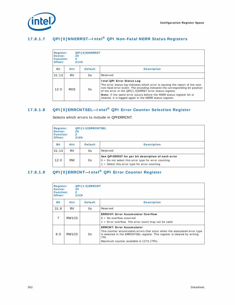
Configuration Register Space
362 Datasheet
17.8.1.7 QPI[0]NNERRST—Intel® QPI Non-Fatal NERR Status Registers
17.8.1.8 QPI[0]ERRCNTSEL—Intel® QPI Error Counter Selection Register
Selects which errors to include in QPIERRCNT.
17.8.1.9 QPI[0]ERRCNT—Intel® QPI Error Counter Register
Register: QPI[0]NNERRSTDevice: 20Function: 2Offset: 214h
Bit Attr Default Description
31:13 RV 0s Reserved
12:0 ROS 0s
Intel QPI Error Status LogThe error status log indicates which error is causing the report of the next non-fatal error event. The encoding indicates the corresponding bit position of the error in the QPI[1:0]ERRST error status register.Note: If the same error occurs before the FERR status register bit is cleared, it is logged again in the NERR status register.
Register: QPI[1:0]ERRCNTSELDevice: 20Function: 2Offset: 218h
Bit Attr Default Description
31:13 RV 0s Reserved
12:0 RW 0sSee QPIERRST for per bit description of each error0 = Do not select this error type for error counting1 = Select this error type for error counting
Register: QPI[1:0]ERRCNTDevice: 20Function: 2Offset: 21Ch
Bit Attr Default Description
31:8 RV 0s Reserved
7 RW1CSERROVF: Error Accumulator Overflow0 = No overflow occurred1 = Error overflow. The error count may not be valid.
6:0 RW1CS 0s
ERRCNT: Error AccumulatorThis counter accumulates errors that occur when the associated error type is selected in the ERRCNTSEL register. This register is cleared by writing 7Fh.Maximum counter available is 127d (7Fh).

Datasheet 363
Configuration Register Space
17.8.1.10 QPIP[0]ERRST—Intel® QPI Protocol Error Status Register
This register indicates the error detected by the Intel QuickPath Interconnect protocol layer. See Section 13.5 for more details on each error type.
Register: QPIP[0]ERRSTDevice: 20Function: 2Offset: 230h
Bit Attr Default Description
31:20 RV 0s Reserved
19 RW1CS 0 DH – Intel QPI Protocol Layer Detected unsupported/undefined packet Error
18 RW1CS 0 DF – Illegal Inbound Request
17 RW1CS 0 DE – Routing Table Invalid
16 RO 0 Reserved
15 RW1CS 0 DC – Protocol SAD illegal or non-existent memory for outbound snoop
14 RW1CS 0 DB – Protocol Parity Error
13 RW1CS 0 DA – Protocol Queue/Table Overflow or Underflow
12 RW1CS 0 D9 – Protocol Layer Received Viral from Intel® QPI
11 RW1CS 0 D8 – Protocol Layer Received Illegal packet field or Incorrect Target NodeID
10 RW1CS 0 D7 – Protocol Layer Received Unexpected Response/Completion
9 RW1CS 0 D6 – Protocol Layer Received Failed Response
8 RW1CS 0 D5 – Protocol Layer Detected Time-Out in ORB
7:5 RV 000 Reserved
4 RW1CS 0 C3 – CSR access crossing 32-bit boundary
3 RW1CS 0 C2 – Write Cache Un-correctable ECC
2 RW1CS 0 C1 – Protocol Layer Received Poisoned Packet.
1 RW1CS 0 B4 – Write Cache Correctable ECC
0 RW1CS 0 B3 – Intel QPI CPEI Error Status
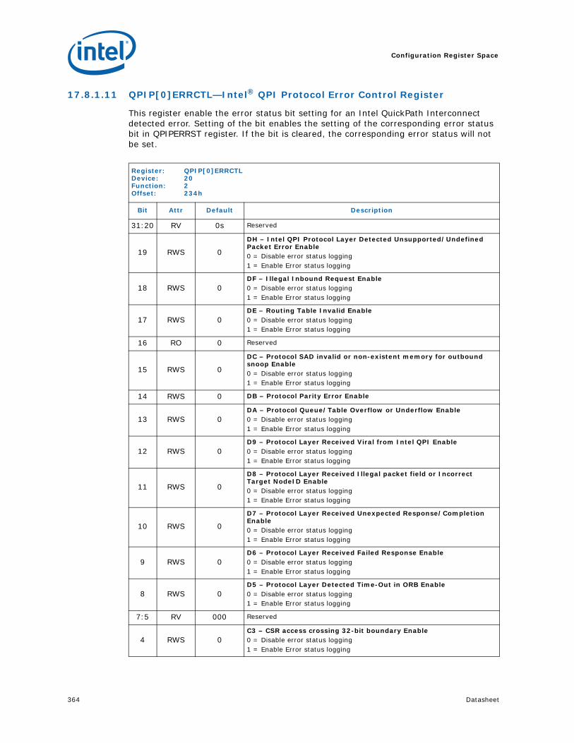
Configuration Register Space
364 Datasheet
17.8.1.11 QPIP[0]ERRCTL—Intel® QPI Protocol Error Control Register
This register enable the error status bit setting for an Intel QuickPath Interconnect detected error. Setting of the bit enables the setting of the corresponding error status bit in QPIPERRST register. If the bit is cleared, the corresponding error status will not be set.
Register: QPIP[0]ERRCTLDevice: 20Function: 2Offset: 234h
Bit Attr Default Description
31:20 RV 0s Reserved
19 RWS 0
DH – Intel QPI Protocol Layer Detected Unsupported/Undefined Packet Error Enable0 = Disable error status logging1 = Enable Error status logging
18 RWS 0DF – Illegal Inbound Request Enable0 = Disable error status logging1 = Enable Error status logging
17 RWS 0DE – Routing Table Invalid Enable0 = Disable error status logging1 = Enable Error status logging
16 RO 0 Reserved
15 RWS 0
DC – Protocol SAD invalid or non-existent memory for outbound snoop Enable0 = Disable error status logging1 = Enable Error status logging
14 RWS 0 DB – Protocol Parity Error Enable
13 RWS 0DA – Protocol Queue/Table Overflow or Underflow Enable0 = Disable error status logging1 = Enable Error status logging
12 RWS 0D9 – Protocol Layer Received Viral from Intel QPI Enable0 = Disable error status logging1 = Enable Error status logging
11 RWS 0
D8 – Protocol Layer Received Illegal packet field or Incorrect Target NodeID Enable0 = Disable error status logging1 = Enable Error status logging
10 RWS 0
D7 – Protocol Layer Received Unexpected Response/Completion Enable0 = Disable error status logging1 = Enable Error status logging
9 RWS 0D6 – Protocol Layer Received Failed Response Enable0 = Disable error status logging1 = Enable Error status logging
8 RWS 0D5 – Protocol Layer Detected Time-Out in ORB Enable0 = Disable error status logging1 = Enable Error status logging
7:5 RV 000 Reserved
4 RWS 0C3 – CSR access crossing 32-bit boundary Enable0 = Disable error status logging1 = Enable Error status logging

Datasheet 365
Configuration Register Space
17.8.1.12 Intel® QuickPath Interconnect Protocol Error Log Register
This register logs the information associated with the reporting of Intel QuickPath Interconnect protocol layer errors. There are two sets of error log registers of identical format: FERR logs the first occurrence of an error, and NERR logs the next occurrence of the error. An individual error is reported with the corresponding severity in this register. Software can program the error severity to one of the three severities supported by IOH. This register is sticky and can only be reset by PWRGOOD. Clearing of the QPIP**ERRST is done by clearing the corresponding QPIPERRST bits.
17.8.1.13 QPIP[0]FFERRST—Intel® QPI Protocol Fatal FERR Status Register
3 RWS 0C2 – Write Cache Un-correctable ECC Enable0 = Disable error status logging1 = Enable Error status logging
2 RWS 0C1 – Protocol Layer Received Poisoned Packet Enable0 = Disable error status logging1 = Enable Error status logging
1 RWS 0B4 – Write Cache Correctable ECC Enable0 = Disable error status logging1 = Enable Error status logging
0 RWS 0B3 – Intel QPI CPEI Error Status Enable0 = Disable error status logging1 = Enable Error status logging
Register: QPIP[0]ERRCTLDevice: 20Function: 2Offset: 234h
Bit Attr Default Description
Register: QPIP[0]FFERRSTDevice: 20Function: 2Offset: 238h
Bit Attr Default Description
31:20 RV 0s Reserved
19:17 ROS 0s
Intel QPI Error Status Log2The error status log indicates which error is causing the report of the first fatal error event. The encoding indicates the corresponding bit position of the error in the Intel QuickPath Interconnect protocol error status register.
16 RO 0 Reserved
15:8 ROS 0s
Intel QPI Error Status Log1The error status log indicates which error is causing the report of the first fatal error event. The encoding indicates the corresponding bit position of the error in the Intel QuickPath Interconnect protocol error status register.
7:5 RO 000 Reserved
4:0 ROS 000000
Intel QPI Error Status Log0The error status log indicates which error is causing the report of the first fatal error event. The encoding indicates the corresponding bit position of the error in the Intel QuickPath Interconnect protocol error status register.

Configuration Register Space
366 Datasheet
17.8.1.14 QPIP[0]FNERRST—Intel® QPI Protocol Fatal NERR Status Registers
17.8.1.15 QPIP[0]FFERRHD—Intel® QPI Protocol Fatal FERR Header Log Register
Register: QPIP[0]FNERRSTDevice: 20Function: 2Offset: 23Ch
Bit Attr Default Description
31:20 RV 0s Reserved
19:17 ROS 000
Intel QPI Error Status Log2The error status log indicates which error is causing the report of the next fatal error event. The encoding indicates the corresponding bit position of the error in the Intel QuickPath Interconnect protocol error status register.Note: If the same error occurs before the FERR status register bit is cleared, it is logged again in the NERR status register.
16 RO 0 Reserved
15:8 ROS 00h
Intel QPI Error Status Log1The error status log indicates which error is causing the report of the next fatal error event. The encoding indicates the corresponding bit position of the error in the Intel QuickPath Interconnect protocol error status register.Note: If the same error occurs before the FERR status register bit is cleared, it is logged again in the NERR status register.
7:5 RO 000 Reserved
4:0 ROS 00000
Intel QPI Error Status Log0The error status log indicates which error is causing the report of the next fatal error event. The encoding indicates the corresponding bit position of the error in the Intel QuickPath Interconnect protocol error status register.Note: If the same error occurs before the FERR status register bit is cleared, it is logged again in the NERR status register.
Register: QPIP[0]FFERRHDDevice: 20Function: 2Offset: 240h
Bit Attr Default Description
127:0 ROS 0s
Intel QPI Error Header logHeader log stores the header information of the associated with the first fatal error. The header stores the Intel QuickPath Interconnect packet fields of the erroneous Intel QPI cycle. Refer to the Intel QPI specification chapter 4 for the header format of each type of Intel QPI cycle.

Datasheet 367
Configuration Register Space
17.8.1.16 QPIP[0]NFERRST—Intel® QPI Protocol Non-Fatal FERR Status Register
17.8.1.17 QPIP[0]NNERRST—Intel® QPI Protocol Non-Fatal NERR Status Register
Register: QPIP[0]NFERRSTDevice: 20Function: 2Offset: 250h
Bit Attr Default Description
31:20 RV 0s Reserved
19:17 ROS 000
Intel QPI Error Status Log2The error status log indicates which error is causing the report of the first non-fatal error event. The encoding indicates the corresponding bit position of the error in the Intel QuickPath Interconnect protocol error status register.
16 RO 0 Reserved
15:8 ROS 00h
Intel QPI Error Status Log1The error status log indicates which error is causing the report of the first non-fatal error event. The encoding indicates the corresponding bit position of the error in the Intel QuickPath Interconnect protocol error status register.
7:5 RO 000 Reserved
4:0 ROS 00000
Intel QPI Error Status Log0The error status log indicates which error is causing the report of the first non-fatal error event. The encoding indicates the corresponding bit position of the error in the Intel QuickPath Interconnect protocol error status register.
Register: QPIP[0]NNERRSTDevice: 20Function: 2Offset: 254h
Bit Attr Default Description
31:20 RV 0s Reserved
19:17 ROS 000
Intel QPI Error Status Log2The error status log indicates which error is causing the report of the next non-fatal error event. The encoding indicates the corresponding bit position of the error in the Intel QuickPath Interconnect protocol error status register.Note: If the same error occurs before the FERR status register bit is cleared, it is logged again in the NERR status register.
16 RO 0 Reserved
15:8 ROS 00h
Intel QPI Error Status Log1The error status log indicates which error is causing the report of the next non-fatal error event. The encoding indicates the corresponding bit position of the error in the Intel QuickPath Interconnect protocol error status register.Note: If the same error occurs before the FERR status register bit is cleared, it is logged again in the NERR status register.
7:5 RO 000 Reserved
4:0 ROS 00000
Intel QPI Error Status Log0The error status log indicates which error is causing the report of the next non-fatal error event. The encoding indicates the corresponding bit position of the error in the Intel QuickPath Interconnect protocol error status register.Note: If the same error occurs before the FERR status register bit is cleared, it is logged again in the NERR status register.

Configuration Register Space
368 Datasheet
17.8.1.18 QPIP[0]NFERRHD—Intel® QPI Protocol Non-Fatal FERR Header Log Register
17.8.1.19 QPIP[0]ERRCNTSEL—Intel® QPI Protocol Error Counter Selection Register
Register: QPIP[0]NFERRHDDevice: 20Function: 2Offset: 258h
Bit Attr Default Description
127:0 ROS 0s
Intel QPI Error Header logHeader log stores the header information of the associated with the first non-fatal error. The header stores the Intel QPI packet fields of the erroneous Intel QPI cycle. Refer to the Intel QPI specification Chapter 4 for the header format of each type of Intel QPI cycle.
Register: QPIP[0]ERRCNTSELDevice: 20Function: 2Offset: 268h
Bit Attr Default Description
31:20 RV 0s Reserved
19:17 RWS 000
QPIPERRCNTSEL19_17See QPIPERRST for per bit description of each error.0 = Do not select this error type for error counting1 = Select this error type for error counting
16 RO 0 Reserved
15:8 RWS 00h
QPIPERRCNTSEL15_8See QPIPERRST for per bit description of each error.0 = Do not select this error type for error counting1 = Select this error type for error counting
7:5 RO 000 Reserved
4:0 RWS 00000
QPIPERRCNTSEL4_0See QPIPERRST for per bit description of each error.0 = Do not select this error type for error counting1 = Select this error type for error counting

Datasheet 369
Configuration Register Space
17.8.1.20 QPIP[0]ERRCNT—Intel® QPI Protocol Error Counter Register
17.8.1.21 IOHERRST—IOH Core Error Status Register
This register indicates the IOH internal core errors detected by the IOH error logic. An individual error status bit that is set indicates that a particular error occurred; software may clear an error status by writing a 1 to the respective bit. This register is sticky and can only be reset by PWRGOOD. Clearing of the IOH**ERRST is done by clearing the corresponding IOHERRST bits.
Register: QPIP[0]ERRCNTSELDevice: 20Function: 2Offset: 26Ch
Bit Attr Default Description
31:8 RV 0s Reserved
7 RW1CSERROVF: Error Accumulator Overflow0 = No overflow occurred1 = Error overflow. The error count may not be valid.
6:0 RW1CS 0s
ERRCNT: Error AccumulatorThis counter accumulates errors that occur when the associated error type is selected in the ERRCNTSEL register. This register is cleared by writing 7Fh.Maximum counter available is 127d (7Fh).
Register: IOHERRSTDevice: 20Function: 2Offset: 300h
Bit Attr Default Description
31:7 RO 0s Reserved
6 RW1CS 0 C6 – FIFO Overflow/Underflow error status
5 RW1CS 0 C5 – Completor abort address error status
4 RW1CS 0 C4 – Master abort address error status
3 RW1CS 0 Unused
2 RW1CS 0 Unused
1 RW1CS 0 Unused
0 RW1CS 0 Unused

Configuration Register Space
370 Datasheet
17.8.1.22 IOHERRCTL—IOH Core Error Control Register
This register enables the error status bit setting for IOH internal core errors detected by the IOH. Setting of the bit enables the setting of the corresponding error status bit in IOHERRST register. If the bit is cleared, the corresponding error status will not be set.
This register is sticky and can only be reset by PWRGOOD.
17.8.1.23 IOHFFERRST—IOH Core Fatal FERR Status Register
Register: IOHERRCTLDevice: 20Function: 2Offset: 304h
Bit Attr Default Description
31:7 RV Reserved
6 RWS 0 C6 – FIFO Overflow/Underflow error Enable
5 RWS 0 C5 – Completor abort address error Enable
4 RWS 0 C4 – Master abort address error Enable
3:0 RWS 0000 Reserved
Register: IOHFFERRSTDevice: 20Function: 2Offset: 308h
Bit Attr Default Description
31:7 RV 0s Reserved
6:4 ROS 000
IOH Core Error Status LogThe error status log indicates which error is causing the report of the first error event. The encoding indicates the corresponding bit position of the error in the IOH Core error status register.
3:0 ROS 0000 Reserved

Datasheet 371
Configuration Register Space
17.8.1.24 IOHFFERRHD—IOH Core Fatal FERR Header Register
17.8.1.25 IOHFNERRST—IOH Core Fatal NERR Status Register
Register: IOHFFERRHDDevice: 20Function: 2Offset: 30Ch
Bit Attr Default Description
127:0 ROS 0s
IOH Core Error Header logHeader log stores the IOH data path header information of the associated IOH core error. The header indicates where the error is originating from and the address of the cycle.[127:90] Reserved[89] Error Type MA/CA[88:81] Message Code [7:0][80:65] MSI Data [15:0][64:58] Internal routing ID [6:0][57:51] TType {Fmt [1:0], Type[4:0]}[50:0] Address [50:0]
Note: For interrupts, Address(50:0) will be logged as follows when Interrupt Remapping is enabled:• Address(50:19) = DW Address = (Dest ID[29:0], Redirect Hint, Mode)• Mode denotes 0 for physical and 1 for logical• Address(18:0) — NA for interrupts and could be zeros or ones.• The two upper bits of the Destination ID (Dest ID[31:30]) will not be
logged when Interrupt Remapping is enabled.
Register: IOHFNERRSTDevice: 20Function: 2Offset: 31Ch
Bit Attr Default Description
31:7 RV 0s Reserved
6:4 ROS 000
IOH Core Error Status LogThe error status log indicates which error is causing the report of the next error event. The encoding indicates the corresponding bit position of the error in the IOH Core error status register.Note: If the same error occurs before the FERR status register bit is cleared, it is logged again in the NERR status register.
3:0 ROS 0000 Unused

Configuration Register Space
372 Datasheet
17.8.1.26 IOHNFERRST—IOH Core Non-Fatal FERR Status Register
17.8.1.27 IOHNFERRHD[0:3]—Local Non-Fatal FERR Header Registers
Register: IOHNFERRSTDevice: 20Function: 2Offset: 320h
Bit Attr Default Description
31:7 RV 0s Reserved
6:4 ROS 000
IOH Core Error Status LogThe error status log indicates which error is causing the report of the first error event. The encoding indicates the corresponding bit position of the error in the IOH Core error status register.
3:0 ROS 0000 Unused
Register: IOHNFERRHDDevice: 20Function: 2Offset: 324h
Bit Attr Default Description
127:0 ROS 0s
IIOH Core Error Header logHeader log stores the IOH data path header information of the associated IOH core error. The header indicates where the error is originating from and the address of the cycle.[127:90] Reserved[89] Error Type MA/CA[88:81] Message Code [7:0][80:65] MSI Data [15:0][64:58] Internal routing ID [6:0][57:51] TType {Fmt [1:0], Type[4:0]}[50:0] Address [50:0]
Note: For interrupts Address (50:0) will be logged as follows when Interrupt Remapping is enabled:• Address(50:19) = DW Address = (Dest ID[29:0], Redirect Hint, Mode)• Mode denotes 0 for physical and 1 for logical• Address(18:0) — NA for interrupts and could be zeros or ones.• The two upper bits of the Destination ID (Dest ID[31:30]) will not be
logged when Interrupt Remapping is enabled.

Datasheet 373
Configuration Register Space
17.8.1.28 IOHNNERRST—IOH Core Non-Fatal NERR Status Register
17.8.1.29 IOHERRCNTSEL—IOH Error Counter Selection Register
Register: IOHNNERRSTDevice: 20Function: 2Offset: 334h
Bit Attr Default Description
31:7 RV 0s Reserved
6:4 ROS 000
IOH Core Error Status LogThe error status log indicates which error is causing the report of the next error event. The encoding indicates the corresponding bit position of the error in the error status register. Note: If the same error occurs before the FERR status register bit is cleared, it is logged again in the NERR status register.
3:0 ROS 0000 Unused
Register: IOHERRCNTSELDevice: 20Function: 2Offset: 33Ch
Bit Attr Default Description
31:7 RV 0s Reserved
6 RW 0C6 – FIFO Overflow/Underflow error Count Select0 = Do not select this error type for error counting1 = Select this error type for error counting
5 RW 0C5 – Completor abort address error Count Select0 = Do not select this error type for error counting1 = Select this error type for error counting
4 RW 0C4 – Master abort address error Count Select0 = Do not select this error type for error counting1 = Select this error type for error counting
3:0 RW 0000 Reserved

Configuration Register Space
374 Datasheet
17.8.1.30 IOHERRCNT—IOH Core Error Counter Registers
17.8.1.31 THRERRST—Thermal Error Status Register
This register indicates the thermal errors detected by the IOH error logic. An individual error status bit that is set indicates that a particular error occurred; software may clear an error status by writing a 1 to the respective bit. This register is sticky and can only be reset by PWRGOOD. Clearing of the THR**ERRST is done by clearing the corresponding THRERRST bits.
Register: IOHERRCNTDevice: 20Function: 2Offset: 340h
Bit Attr Default Description
31:8 RV Reserved
7 RW1CSERROVF: Error Accumulator Overflow0 = No overflow occurred1 = Error overflow. The error count may not be valid.
6:0 RW1CS 0s
ERRCNT: Error AccumulatorThis counter accumulates errors that occur when the associated error type is selected in the ERRCNTSEL register. This register is cleared by writing 7Fh.Maximum counter available is 127d (7Fh).
Register: THRERRSTDevice: 20Function: 2Offset: 360h
Bit Attr Default Description
31:3 RV 0s Reserved
2 RW1CS 0F2 – Catastrophic Thermal EventThis error is generated when the temperature at the thermal sensor reaches the TSTHRCATA threshold.
1 RW1CS 0F1 – TSMAX UpdatedThis error is generated by reading CTHINT after TSMAX was updated.
0 RW1CS 0F0 – Thermal AlertThis error is generated when the temperature at the thermal sensor exceeds the TSTHRHI+TSMAX threshold.
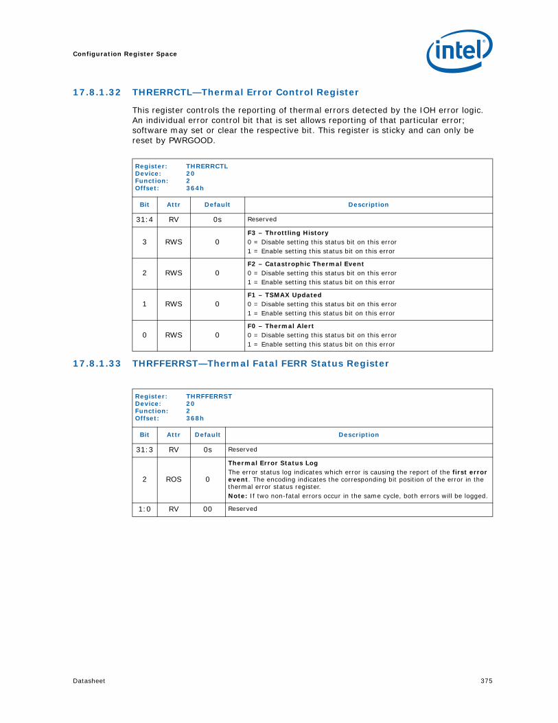
Datasheet 375
Configuration Register Space
17.8.1.32 THRERRCTL—Thermal Error Control Register
This register controls the reporting of thermal errors detected by the IOH error logic. An individual error control bit that is set allows reporting of that particular error; software may set or clear the respective bit. This register is sticky and can only be reset by PWRGOOD.
17.8.1.33 THRFFERRST—Thermal Fatal FERR Status Register
Register: THRERRCTLDevice: 20Function: 2Offset: 364h
Bit Attr Default Description
31:4 RV 0s Reserved
3 RWS 0F3 – Throttling History0 = Disable setting this status bit on this error1 = Enable setting this status bit on this error
2 RWS 0F2 – Catastrophic Thermal Event0 = Disable setting this status bit on this error1 = Enable setting this status bit on this error
1 RWS 0F1 – TSMAX Updated0 = Disable setting this status bit on this error1 = Enable setting this status bit on this error
0 RWS 0F0 – Thermal Alert0 = Disable setting this status bit on this error1 = Enable setting this status bit on this error
Register: THRFFERRSTDevice: 20Function: 2Offset: 368h
Bit Attr Default Description
31:3 RV 0s Reserved
2 ROS 0
Thermal Error Status LogThe error status log indicates which error is causing the report of the first error event. The encoding indicates the corresponding bit position of the error in the thermal error status register.Note: If two non-fatal errors occur in the same cycle, both errors will be logged.
1:0 RV 00 Reserved

Configuration Register Space
376 Datasheet
17.8.1.34 THRFNERRST—Thermal Fatal NERR Status Register
17.8.1.35 THRNFERRST—Thermal Non-Fatal FERR Status Register
Register: THRFNERRSTDevice: 20Function: 2Offset: 36Ch
Bit Attr Default Description
31:3 RV 0s Reserved
2 ROS 0
Thermal Error Status LogThe error status log indicates which error is causing the report of the second error event. The encoding indicates the corresponding bit position of the error in the thermal error status register.Notes: 1. If the same error occurs before the FERR status register bit is cleared, it is
logged again in the NERR status register.2. Only second error gets logged into THRFNERRST (subsequent error does not
get logged into THRFNERRST.
1:0 RV 00 Reserved
Register: THRNNERRSTDevice: 20Function: 2Offset: 370h
Bit Attr Default Description
31:2 RV 0s Reserved
3 ROS 0
Thermal Error Status Log 3The error status log indicates which error is causing the report of the first error event. If two fatal errors occur in the same cycle, then the properties of both errors are logged. The encoding indicates the corresponding bit position of the error in the error status register.
2 RV 0 Reserved
1:0 ROST 00
Thermal Error Status Log 0 and 1The error status log indicates which error is causing the report of the first error event. If two fatal errors occur in the same cycle, then the properties of both errors are logged. The encoding indicates the corresponding bit position of the error in the error status register.

Datasheet 377
Configuration Register Space
17.8.1.36 THRNNERRST—Thermal Non-Fatal NERR Status Register
17.8.1.37 THRERRCNTSEL—Thermal Error Counter Selection Register
Register: THRNNERRSTDevice: 20Function: 2Offset: 374h
Bit Attr Default Description
31:2 RV 0s Reserved
3 ROS 0
Thermal Error Status Log 3The error status log indicates which error is causing the report of the second error event. The encoding indicates the corresponding bit position of the error in the thermal error status register.Notes: 1. If the same error occurs before the FERR status register bit is cleared, it is
logged again in the NERR status register.2. Only second error gets logged into THRFNERRST (subsequent error does not
get logged into THRFNERRST.
2 RV 0 Reserved
1:0 ROST 00
Thermal Error Status Log 0 and 1The error status log indicates which error is causing the report of the second error event. The encoding indicates the corresponding bit position of the error in the thermal error status register.Notes: 1. If the same error occurs before the FERR status register bit is cleared, it is
logged again in the NERR status register.2. Only second error gets logged into THRFNERRST (subsequent error does not
get logged into THRFNERRST.
Register: THRERRCNTSELDevice: 20Function: 2Offset: 378h
Bit Attr Default Description
31:3 RV Reserved
2 RW 0 F2 – Catastrophic Thermal Event
1 RW 0 F1 – TSMAX Updated
0 RW 0 F0 – Thermal Alert

Configuration Register Space
378 Datasheet
17.8.1.38 THRERRCNT—Thermal Error Counter Register
17.8.1.39 MIERRST—Miscellaneous Error Status Register
This register indicates the miscellaneous errors detected by the IOH error logic. An individual error status bit that is set indicates that a particular error occurred; software may clear an error status by writing a 1 to the respective bit. This register is sticky and can only be reset by PWRGOOD. Clearing of the MI**ERRST is done by clearing the corresponding MIERRST bits. For details on usage of local error logging.
Register: THRERRCNTDevice: 20Function: 2Offset: 37Ch
Bit Attr Default Description
31:8 RV Reserved
7 RW1CSERROVF: Error Accumulator Overflow0: No overflow occurred1: Error overflow. The error count may not be valid.
6:0 RW1CS 0s
ERRCNT: Error AccumulatorThis counter accumulates errors that occur when the associated error type is selected in the ERRCNTSEL register. This register is cleared by writing 7Fh.Maximum counter available is 127d (7Fh).
Register: MIERRSTDevice: 20Function: 2Offset: 380h
Bit Attr Default Description
31:5 RO 0s Reserved
4 RW1CS 0 Reserved
3 RW1CS 023 – Virtual Pin Port Error StatusThis bit indicates that VPP Interface has detected an error.This bit is N/A in 0E80h, 0F80h registers
2 RW1CS 022 – JTAG TAP Port StatusThis bit (set to 1) indicates that an error occurred on the JTAG TAP port.This bit is N/A in 0E80h, 0F80h registers
1 RW1CS 021 – SM Bus Port Error StatusThis bit indicates that SMBus Interface has detected an error.This bit is N/A in 0E80h, 0F80h registers
0 RW1CS 0
20 – IOH Configuration Register Parity Error StatusThis bit indicates that IOH configuration registers have detect a parity error on its critical configuration bits.This bit is N/A in 0E80h, 0F80h registers

Datasheet 379
Configuration Register Space
17.8.1.40 MIERRCTL—Miscellaneous Error Control Register
This register controls the reporting of miscellaneous errors detected by the IOH error logic. Setting of the bit enables the setting of the corresponding error status bit in MIERRST register. If the bit is cleared, the corresponding error status will not be set. This register is sticky and can only be reset by PWRGOOD.
17.8.1.41 MIFFERRST—Miscellaneous Fatal FERR Status Register
17.8.1.42 MIFFERRHD—Miscellaneous Fatal FERR Header Register
Register: MIERRCTLDevice: 20Function: 2Offset: 384h
Bit Attr Default Description
31:5 RV 0s Reserved
4 RW1CS 0 Reserved
3 RWS 0 23 – VPP Error Enable
2 RWS 0 22 – Persistent JTAG Error Enable
1 RWS 0 21 – Persistent SMBus Retry Status Enable
0 RWS 0 20 – IOH Configuration Register Parity error Enable
Register: MIFFERRSTDevice: 20Function: 2Offset: 388h
Bit Attr Default Description
31:11 RV 0s Reserved
10:5 ROS 0s Reserved
4:0 ROS 00000
Miscellaneous Error Status LogThe error status log indicates which error is causing the report of the first error event. The encoding indicates the corresponding bit position of the error in the miscellaneous error status register.Note: If two non-fatal errors occur in the same cycle, both errors will be logged.
Register: IOHFFERRHDDevice: 20Function: 2Offset: 38Ch
Bit Attr Default Description
127:0 ROS 0s
Miscellaneous Error Header logHeader log stores the IOH data path header information of the associated IOH miscellaneous error. The header indicates where the error is originating from and the address of the cycle.[127:44] [43:0] Address [43:0]

Configuration Register Space
380 Datasheet
17.8.1.43 MIFNERRST—Miscellaneous Fatal NERR Status Register
17.8.1.44 MINFERRST—Miscellaneous Non-Fatal FERR Status Register
17.8.1.45 MINFERRHD—Miscellaneous Local Non-Fatal FERR Header Register
Register: MIFNERRSTDevice: 20Function: 2Offset: 39Ch
Bit Attr Default Description
31:5 RV 0s Reserved
4:0 ROS 00000
Miscellaneous Error Status LogThe error status log indicates which error is causing the report of the next error event. The encoding indicates the corresponding bit position of the error in the error status register.Note: 1. If the same error occurs before the FERR status register bit is cleared, it is
logged again in the NERR status register.2. Only second error gets logged into MIFNERRST (subsequent error does not
get logged into MIFNERRST
Register: MINFERRSTDevice: 20Function: 2Offset: 3A0h
Bit Attr Default Description
31:11 RV 0s Reserved
10:5 ROS 0s Reserved
4:0 ROS 00000
Miscellaneous Error Status LogThe error status log indicates which error is causing the report of the first error event. The encoding indicates the corresponding bit position of the error in the miscellaneous error status register.Note: If two non-fatal errors occur in the same cycle, both errors will be logged.
Register: MINFERRHDDevice: 20Function: 2Offset: 3A4h
Bit Attr Default Description
127:0 ROS 0s
Miscellaneous Error Header logHeader log stores the IOH data path header information of the associated IOH miscellaneous error. The header indicates where the error is originating from and the address of the cycle.[127:46] [43:0] Address [43:0]

Datasheet 381
Configuration Register Space
17.8.1.46 MINNERRST—Miscellaneous Non-Fatal NERR Status Register
17.8.1.47 MIERRCNTSEL—Miscellaneous Error Counter Selection Register
Register: MINNERRSTDevice: 20Function: 2Offset: 3B4h
Bit Attr Default Description
31:5 RV 0s Reserved
4:0 ROS 00000
Miscellaneous Error Status Log
The error status log indicates which error is causing the report of the next error event. The encoding indicates the corresponding bit position of the error in the miscellaneous error status register.Notes: 1. If the same error occurs before the FERR status register bit is cleared, it is
logged again in the NERR status register.2. Only second error gets logged into MIFNERRST (subsequent error does not
get logged into MIFNERRST
Register: MIERRCNTSELDevice: 20Function: 2Offset: 3BCh
Bit Attr Default Description
31:5 RV 0s Reserved
4 RW 0 Reserved
3 RW 023 – VPP Error CNTSEL0 = Do not select this error type for error counting1 = Select this error type for error counting
2 RW 022 – Persistent JTAG Error CNTSEL0 = Do not select this error type for error counting1 = Select this error type for error counting
1 RW 021 – Persistent SMBus Retry Status CNTSEL0 = Do not select this error type for error counting1 = Select this error type for error counting
0 RW 0
20 – IOH Configuration Register Parity Error StatusThis bit indicates that IOH configuration registers have detect a parity error on its critical configuration bits.This bit is N/A in 0E80h, 0F80h registers

Configuration Register Space
382 Datasheet
17.8.1.48 MIERRCNT—Miscellaneous Error Counter Register
17.8.1.49 QPI[1:0]FERRFLIT0—Intel® QPI FERR FLIT log Register 0
See Section 17.8.1.1 to find out which errors caused the FLIT logging.
17.8.1.50 QPI[1:0]FERRFLIT1—Intel® QPI FERR FLIT log Register 1
See Section 17.8.1.1 to find out which errors caused the FLIT logging.
Register: MIERRCNTDevice: 20Function: 2Offset: 3C0h
Bit Attr Default Description
31:8 RV 0s Reserved
7 RW1CS 0ERROVF: Error Accumulator Overflow0 = No overflow occurred1 = Error overflow. The error count may not be valid.
6:0 RW1CS 0s
ERRCNT: Error AccumulatorThis counter accumulates errors that occur when the associated error type is selected in the ERRCNTSEL register. This register is cleared by writing 7Fh.Maximum counter available is 127d (7Fh).
Register: QPI[1:0]FERRFLIT0Device: 20Function: 2Offset: 480h, 400h
Bit Attr Default Description
95:81 RV 0 Reserved
80 ROS 0 ACTIVE_16B
79:0 ROS 0 FLIT
Register: QPI[1:0]FERRFLIT1Device: 20Function: 2Offset: 48Ch, 40Ch
Bit Attr Default Description
95:81 RV 0 Reserved
80 ROS 0 ACTIVE_16B
79:0 ROS 0 FLIT

Datasheet 383
Configuration Register Space
17.8.1.51 QPIP[1:0]FERRLFLIT0—Intel® QPI Protocol FERR Logical FLIT log Register 0
This register is used to log when Intel QPI Protocol Layer Detects unsupported/undefined packet errors.
17.8.1.52 QPIP[1:0]FERRLFLIT1—Intel® QPI Protocol FERR Logical FLIT log Register 1
This register is used to log when Intel QPI Protocol Layer Detects unsupported/undefined packet errors.
17.8.1.53 QPIP[1:0]FERRLFLIT2—Intel® QPI Protocol FERR Logical FLIT log Register 2
This register is used to log when Intel QPI Protocol Layer Detects unsupported/undefined packet errors.
Register: QPIP[1:0]FERRLFLIT0Device: 20Function: 2Offset: 4B0h, 430h
Bit Attr Default Description
95:72 RV 0 Reserved
71:0 ROS 0LFLIT: Intel QPI Logical FLITFormat is the format of Intel QPI.
Register: QPIP[1:0]FERRLFLIT1Device: 20Function: 2Offset: 4BCh, 43Ch
Bit Attr Default Description
95:72 RV 0 Reserved
71:0 ROS 0LFLIT: Intel QPI Logical FLITFormat is the format of Intel QPI.
Register: QPIP[1:0]FERRLFLIT2Device: 20Function: 2Offset: 4C8h, 448h
Bit Attr Default Description
95:72 RV 0 Reserved
71:0 ROS 0LFLIT: Intel QPI Logical FLITFormat is the format of Intel QPI.

Configuration Register Space
384 Datasheet
17.9 On-Die Throttling Register Map and Coarse-Grained Clock Gating
Table 17-19.Device 20, Function 3—On-Die Throttling and Coarse-Grained Clock Gating
DID VID 00h 80h
PCISTS PCICMD 04h 84h
CCR RID 08h 88h
HDR 0Ch 8Ch
10h 90h
14h 94h
18h 98h
1Ch 9Ch
20h A0h
24h A4h
28h A8h
SID SVID 2Ch ACh
30h B0h
34h B4h
38h B8h
3Ch BCh
CGCTRL 40h C0h
CSR_SAT_MASK_SET CGCTRL2 44h C4h
CGCTRL3 48h C8h
CGCTRL6 4Ch CCh
CGCTRL7 50h D0h
CGSTS 54h D4h
CGCTRL4L CGCTRL5 CGSTACGGER
58h D8h
CGCTRL4U 5Ch DCh
60h TSTHRCATA E0
64h E4h
68h TSTHRRPEX TSCTRL E8h
6Ch TSTHRHI TSTHRLO ECh
70h TSFSC CTHINT F0h
74h CTCTRL TSTHRRQPI CTSTS F4h
78h TSTIMER F8h
7Ch TSTHRNOMC FCh

Datasheet 385
Configuration Register Space
17.9.1 Coarse-Grained Clock Gating Registers
17.9.1.1 CGCTRL—Clock Gating Control Register 1
17.9.1.2 CGCTRL2—Clock Gating Control Register 2
17.9.1.3 CSR_SAT_MASK_SET—Satellite Mask Settings Register
Register: CGCTRLDevice: 20Function: 3Offset: 40h
Bit Attr Default Description
31 RW 0 CGEN: Coarse Grained Clock Gating Enabled
30 RW 0TIME_OUT_EN: Timeout Enable0 = Disable the timeout.1 = Enable the timeout to prevent staying in CG mode forever.
28 RW 0SQLDYEN: Squelch Delay EnableEnable the squelch delay to make the squelch delay the same for cgcg mode and for normal mode.
27:21 RV 00h Reserved
20:16 RW 00hCGDELAY: Coarse Gate DelayIndicates number of clocks from assertion of LocalIsolate to MasterClockGate.
15:10 RV 00h Reserved
9:0 RW 000hDLYTOGATE: Idle To Gate DelayIndicates number of clocks the master controller must see idle from all blocks before attempting to go into clock gated state.
Register: CGCTRL2Device: 20Function: 3Offset: 44h
Bit Attr Default Description
15:12 RW 00h Reserved
11:0 RW 000h
FORCE: Force Gate DisableOne bit per slave.Note: When a bit is set, clock gating will not be forced on that slave. When a bit
is cleared, clock gating will be forced on that slave.
Register: CGCTRL2Device: 20Function: 3Offset: 46h
Bit Attr Default Description
15:0 RW 000hSAT_MASK_SET: Force Clock OffImmediately stops the clock in the specified domain. One bit per slave.

Configuration Register Space
386 Datasheet
17.9.1.4 CGCTRL4L—Clock Gating Control Register 4 Lower
17.9.1.5 CGCTRL4U—Clock Gating Control Register 4 Upper
17.9.1.6 CGCTRL3—Clock Gating Control Register 3
Register: CGCTRL4Device: 20Function: 3Offset: 5Ah
Bit Attr Default Description
15:0 RW 0000hPSTATEDELAY: [15:0] P-State DelayLowest 16 bits of programmed delay to use for LinkPStateExitReq in each slave in order to generate LinkPStateExitReqMod.
Register: CGCTRL4Device: 20Function: 3Offset: 5Ch
Bit Attr Default Description
15:3 RV 0000h Reserved
2:0 RW 0hPSTATEDELAY: [18:16] P-State DelayUpper 3 bits of programmed delay to use for LinkPStateExitReq in each slave in order to generate LinkPStateExitReqMod.
Register: CGCTRL3Device: 20Function: 3Offset: 48h
Bit Attr Default Description
31:0 RW 0h
ALARM: Exit Alarm TimerMaster will start this timer upon entry to gated state, and will exit gated state if this timer expires. This register is not changed by HW – a copy of it is used for the alarm function. 0h means disabled.

Datasheet 387
Configuration Register Space
17.9.1.7 CGCTRL6—Clock Gating Control Register 6
Defines order for applying clock-gating across the chip. Ungating occurs in the reverse order.
17.9.1.8 CGCTRL7—Clock Gating Control Register 7
This register defines order for applying clock-gating across the chip. Ungating occurs in the reverse order.
Register: CGCTRL6Device: 20Function: 3Offset: 4Ch
Bit Attr Default Description
31:28 RW 0h PROGSEQ07: Progression Sequence for Clock Gating Domain 7
27:24 RW 0h PROGSEQ06: Progression Sequence for Clock Gating Domain 6
23:20 RW 0h PROGSEQ05: Progression Sequence for Clock Gating Domain 5
19:16 RW 0h PROGSEQ04: Progression Sequence for Clock Gating Domain 4
15:12 RW 0h PROGSEQ03: Progression Sequence for Clock Gating Domain 3
11:8 RW 0h PROGSEQ02: Progression Sequence for Clock Gating Domain 2
7:4 RW 0h PROGSEQ01: Progression Sequence for Clock Gating Domain 1
3:0 RW 0h PROGSEQ00: Progression Sequence for Clock Gating Domain 0
Register: CGCTRL7Device: 20Function: 3Offset: 50h
Bit Attr Default Description
31:28 RW 0h PROGSEQ15: Progression Sequence for Clock Gating Domain 15
27:24 RW 0h PROGSEQ14: Progression Sequence for Clock Gating Domain 14
23:20 RW 0h PROGSEQ13: Progression Sequence for Clock Gating Domain 13
19:16 RW 0h PROGSEQ12: Progression Sequence for Clock Gating Domain 12
15:12 RW 0h PROGSEQ11: Progression Sequence for Clock Gating Domain 11
11:8 RW 0h PROGSEQ10: Progression Sequence for Clock Gating Domain 10
7:4 RW 0h PROGSEQ09: Progression Sequence for Clock Gating Domain 9
3:0 RW 0h PROGSEQ08: Progression Sequence for Clock Gating Domain 8

Configuration Register Space
388 Datasheet
17.9.1.9 CGSTS—Clock Gating Status Register
17.9.1.10 CGSTAGGER—Clock Gating Stagger Control Register
17.9.1.11 CGCTRL5—Clock Gating Control Register 5
17.9.2 On-Die Throttling Registers
17.9.2.1 TSTHRCATA—On-Die Thermal Sensor Catastrophic Threshold Register
Register: CGSTSDevice: 20Function: 3Offset: 54h
Bit Attr Default Description
31:0 RW 0h
GATED: Gated DurationApproximate number of clocks gated since this value was cleared. SW clears this register, HW increments it for every clock gated. This provides 2^32 clocks worth of monitoring, or approximately 2^32*(1/400MHz) = 10.7 seconds. E.g., this can be used to count L1 durations up to approximately 10 seconds.
Register: CGSTAGGERDevice: 20Function: 3Offset: 58h
Bit Attr Default Description
7:0 RW 0hSTAGGER: Coarse-Grained Stagger DelayThis di/dt filter mechanism defines the number of cycles between assertions and de-assertions of the gating signal from the master into consecutive slaves.
Register: CGCTRL5Device: 20Function: 3Offset: 59h
Bit Attr Default Description
7:4 RV 00h Reserved
3:0 RW 0hNUMSATTELITES: Number of SatellitesThis field defines the number of clock gating nodes minus 1. That is, if there are 9 satellites, the value to be written by BIOS to this field is 8h.
Register: TSTHRCATADevice: 20Function: 3Offset: E2h
Bit Attr Default Description
15:9 RV 0s Reserved
8:0 RWO DCh
TSTHRCATALM: Thermal Sensor Threshold Catastrophic LimitThe field is initialized by software to set the “catastrophic” threshold for the Thermal sensor logic.Resolution of this register is 0.5 o C.Default value is 110 o C (i.e., DCh (220d)).

Datasheet 389
Configuration Register Space
17.9.2.2 TSCTRL—On-Die Thermal Sensor Control Register
17.9.2.3 TSTHRRPEX—PEX Throttling Threshold Ratio Register
This register provides the ability to vary the amount/ratio of port throttling for PEX.
Register: TSCTRLDevice: 20Function: 3Offset: E8h
Bit Attr Default Description
15 RW 0 Reserved
14 RW 0
BGTRIPSELECT: BandGap Trip SelectThis bit selects either the hot or catastrophic trip output of the Sensor.0 = Hot trip1 = Catastrophic trip
13:10 RW 0000 Reserved
9 RW 0SWTHROTTLE: Software Throttle0 = Software throttling is disabled. TSDIS gates throttling.1 = Throttling is forced to all interfaces. THERMALERT_N is asserted.
8 RW 0
TSDIS: Thermal Sensor Throttling Disable0 = The thermal sensor determines closed-loop thermal throttling events when
SWTHROTTLE = 0.1 = Thermal sensor throttling is disabled. SWTHROTTLE controls throttling.
7 RW1CS 0
STSEVHI: Status Event High0 = Thermal sensor event/interrupt is not generated by the sensor logic1 = Thermal sensor event/interrupts is set when the thermal sensor high
threshold trip point is crossed.
6 RW1CS 0
STSEVLO: Status Event Low0 = Thermal sensor event/interrupt is not generated by the sensor logic.1 = Thermal sensor event/interrupts is set when the thermal sensor low
threshold trip point is crossed.
5:0 RV 0s Reserved
Register: TSTHRRPEXDevice: 20Function: 3Offset: EBh
Bit Attr Default Description
7:3 RV 00h Reserved
2:0 RW 000
TTPEXR: PEX Throttle RatioThis register sets the ratio for throttling the PEX’s and DMI. This setting is an approximate percentage of peak theoretical bandwidth for this interface. Value Throttle Level Peak Bandwidth000 00.0% 100% Normal Unthrottled setting001 50.0% 50%010 75.0% 25%011 87.5% 12.5%100 93.8% 6.2%101 96.9% 3.1%110 98.5% 1.5%111 99.3% 0.7% Maximum Throttling enabled

Configuration Register Space
390 Datasheet
17.9.2.4 TSTHRLO—On-Die Thermal Sensor Low Threshold Register
17.9.2.5 TSTHRHI—On-Die Thermal Sensor High Threshold Register
17.9.2.6 CTHINT—On-Die Throttling Hint Register
Register: TSTHRLODevice: 20Function: 3Offset: ECh
Bit Attr Default Description
15:9 RV 0h Reserved
8:0 RW B4h
TSTHRLOLM: Thermal Sensor Threshold Low LimitThe field is initialized by software to set the “low” threshold mark for the thermal sensor logic. (Tsr_lo).Resolution of this register is 0.5 oC. 2’s-complement binary, range of -128o C to 127.5o CDefault value is 90 o C (i.e., B4h (180d))
Register: TSTHRHIDevice: 20Function: 3Offset: EEh
Bit Attr Default Description
15:9 RV 0h Reserved
8:0 RW 0C8h
TSTHRHILM: Thermal Sensor Threshold High LimitThe field is initialized by software to set the “high” threshold for the Thermal sensor logic. (Tsr_hi)Resolution of this register is 0.5o C. 2’s-complement binary, range of -128o C to 127.5o CDefault value is 100 o C (i.e., C8h (200d))
Register: CTHINTDevice: 20Function: 3Offset: F0h
Bit Attr Default Description
23:17 RV 00h Reserved
16 RO 0
OVFLO: Hint Overflow0 = Eight or less THERMALERT windows have elapsed since the last time this
register was read while CTCTRL.HINTEN was set.1 = More than eight THERMALERT windows have elapsed since the last time this
register was read while CTCTRL.HINTEN was set, and THROTTLED hints were lost.
15:8 RO 00hVALID: Maximum CoolingList of valid throttle histories. Each bit corresponds to its “THROTTLED” bit. Cleared on read (but delivered intact to reading agent).
7:0 RO 00h
THROTTLED: Maximum CoolingHistory of on-die throttling during the last eight consecutive “THERMALERT” windows. If on-die throttling occurred during a THERMALERT window, then its throttle history bit is set

Datasheet 391
Configuration Register Space
17.9.2.7 TSFSC—On-Die Thermal Sensor Fan Speed Control Register
This register provides the ability to read a relative thermal sensor indication.
17.9.2.8 CTSTS—On-Die Throttling Status Register
Register: TSFSCDevice: 20Function: 3Offset: F3h
Bit Attr Default Description
7:0 RO 00h
TSFSC: Thermal Sensor Fan Speed ControlThis field contains the difference between the die temperature and the maximum permissible die temperature.This register has a resolution of 0.5 o C. Hence, a register value in the range of 0 to 127 (decimal) refers to a temperature difference of 0 to 63.5 o C, and a value in the range of 128 to 255 (decimal) refers to a temperature difference of -64o C to 0.5o C. Positive values indicate that the die temperature is lower than the maximum permissible die temperature. A negative difference beyond -64o C “floors” at -64 o C. A positive difference beyond 63.5 o C “ceilings” at 63.5 o C.
Register: CTSTSDevice: 20Function: 3Offset: F4h
Bit Attr Default Description
7:3 RV 00h Reserved
2 RW1CS 0 Reserved
1 RW1CS 0 THRMALRT: On-Die Throttling Event
0 RW1CS 0 THRMTRIP: Catastrophic Thermal Event

Configuration Register Space
392 Datasheet
17.9.2.9 TSTHRRQPI—Intel® QuickPath Interconnect Throttling Threshold Ratio Register
This register provides the ability to vary the amount/ratio of port throttling for the Intel QuickPath Interconnect.
17.9.2.10 CTCTRL—On-Die Throttling Control Register
Register: TSTHRRQPIDevice: 20Function: 3Offset: F5h
Bit Attr Default Description
7:3 RV 00h Reserved
2:0 RW 000
TTQPIR: Intel QPI Throttle RatioThis register sets the throttling ratio for the processor buses.This setting is an approximate percentage of peak theoretical request bandwidth for this interface. Value Throttle Level Peak Bandwidth000 00.0% 100.0% Normal Unthrottled setting001 50.0% 50.0%010 75.0% 25.0%011 87.5% 12.5%100 93.8% 6.2%101 96.9% 3.1%110 98.5% 1.5%111 99.3% 0.7% Maximum Throttling enabled
Register: CTCTRLDevice: 20Function: 3Offset: F7h
Bit Attr Default Description
7:4 RV 00h Reserved
3 RW 0
NOBMC: No BMC Mode1 = TSTHRHI and TSTHRLO drive THERMALERT#. TSTHRNOBMC drives
throttling.0 = TSTHRHI and TSTHRLO drive THERMALERT#. TSTHRHI and TSTHRLO also
drive throttling, TSTHRNOBMC is un-used.
2 RW 0h Reserved
1 RW 0hHINTEN: On-Die Throttle Hint EnableWhen this bit is set, on-die throttling hints are enabled.
0 RW 0NOMAX: TSMAX Tracking Mode.Set then clear this bit to initialize the throttling threshold.
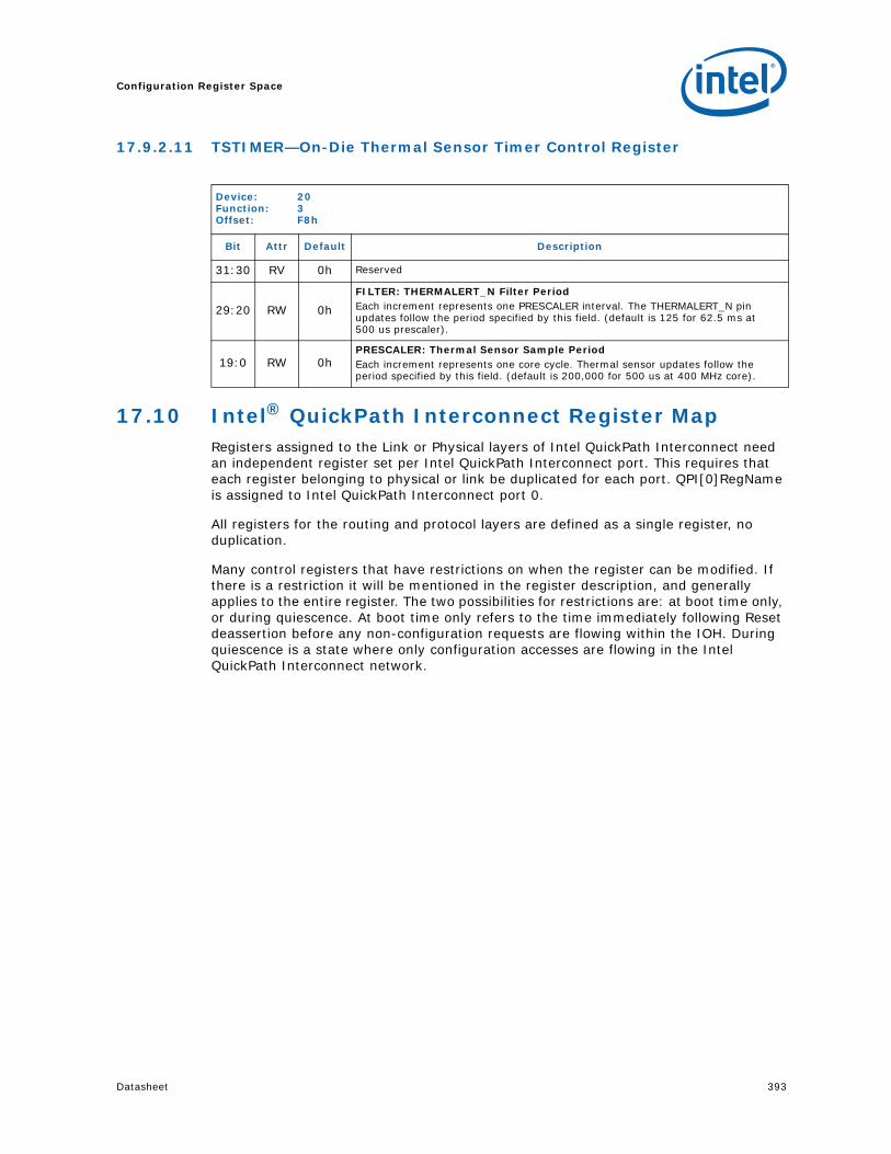
Datasheet 393
Configuration Register Space
17.9.2.11 TSTIMER—On-Die Thermal Sensor Timer Control Register
17.10 Intel® QuickPath Interconnect Register MapRegisters assigned to the Link or Physical layers of Intel QuickPath Interconnect need an independent register set per Intel QuickPath Interconnect port. This requires that each register belonging to physical or link be duplicated for each port. QPI[0]RegName is assigned to Intel QuickPath Interconnect port 0.
All registers for the routing and protocol layers are defined as a single register, no duplication.
Many control registers that have restrictions on when the register can be modified. If there is a restriction it will be mentioned in the register description, and generally applies to the entire register. The two possibilities for restrictions are: at boot time only, or during quiescence. At boot time only refers to the time immediately following Reset deassertion before any non-configuration requests are flowing within the IOH. During quiescence is a state where only configuration accesses are flowing in the Intel QuickPath Interconnect network.
Device: 20Function: 3Offset: F8h
Bit Attr Default Description
31:30 RV 0h Reserved
29:20 RW 0h
FILTER: THERMALERT_N Filter PeriodEach increment represents one PRESCALER interval. The THERMALERT_N pin updates follow the period specified by this field. (default is 125 for 62.5 ms at 500 us prescaler).
19:0 RW 0hPRESCALER: Thermal Sensor Sample PeriodEach increment represents one core cycle. Thermal sensor updates follow the period specified by this field. (default is 200,000 for 500 us at 400 MHz core).

Configuration Register Space
394 Datasheet
17.11 Intel® QuickPath Interconnect Link Layer RegistersThe Link layer registers are defined per Intel QuickPath Interconnect port. There is a special attribute on some link layer registers to handle the Link layer specific reset. The Link layer only hard and soft reset. ‘K’ attribute indicates that the register is reset on a Link layer hard reset. ‘KK’ indicates that the register is reset on any Link layer reset (hard or soft).
Table 17-20.Intel® QuickPath Interconnect Link Map Port 0 (Device 16), Port 1 (Device 17)
DID VID 00h 80h
PCISTS PCICMD 04h 84h
CCR RID 08h 88h
HDR CLS 0Ch 8Ch
10h 90h
14h 94h
18h 98h
1Ch 9Ch
20h A0h
24h A4h
28h A8h
SID SVID 2Ch ACh
30h B0h
CAPPTR1
Notes:1. CAPPTR points to the first capability block
34h B4h
38h B8h
INTP INTL 3Ch BCh
40h QPILCP C0h
44h QPILCL C4h
48h QPILS C8h
4Ch QPILP0 CCh
50h QPILP1 D0h
54h QPILP2 D4h
58h QPILP3 D8h
QPI[1:0]AGTIDEN 5Ch QPILPOC0 DCh
60h QPILPOC1 E0h
64h QPILPOC2 E4h
68h QPILPOC3 E8h
6Ch ECh
70h QPILTC F0h
74h QPILTS F4h
78h QPILCRDC F8h
7Ch FCh

Datasheet 395
Configuration Register Space
17.11.1 Intel® QuickPath Interconnect Link Layer Register Tables
17.11.1.1 QPI[1:0]AGTIDEN—Intel® QPI Agent ID Enable Register
17.11.1.2 QPI[0]LCP—Intel® QPI Link Capability Register
Register per Intel QuickPath Interconnect port.
Register: QPI[1:0]AGTIDENDevice: 17, 16Function: 0Offset: 5Ch
Bit Attr Default Description
31:2 RV 0s Reserved
1 RWS 0TXAGNTIDEN: Enables transmitting Agent ID in the header0 = Normal operation.1 = Enable debug information to be inserted in the address field [42:40]
0 RWS 1
RXAGNTIDEN: Enables receiving Agent ID in the header When this bit is enabled the address bit field [42:40] will be ignored.0 = Normal operation.1 = Enable agent ID debug information to used in place of the address field
[42:40]. When enabled, the IOH does not decode this bit field as address information.
Register: QPI[0]LCPDevice: 16Function: 0Offset: C0h
Bit Attr Default Description
31:30 RV 0s Reserved
29:28 RO 00
VN1 credits per supported Data VC00 = 0 Credits (unsupported)01 = 1 credit10 = 2 to 8 credits11 = 9+ credits
27:26 RO 2h
VN0 credits per supported Data VC00 = 0 credits (unsupported)01 = 1 credit10 = 2 to 8 credits11 = 9+ creditsMaximum value for VN0 is reflected in this register. Actual value is set by a different register.
25:24 RO 00
VN1 credits per supported non-data VC00 = 0 Credits (unsupported)01 = 1 credit10 = 2 to 8 credits11 = 9+ credits
23:22 RO 2h
VN0 credits per supported non-data VC00 = 0 credits (unsupported)01 = 1 credit10 = 2 to 8 credits11 = 9+ creditsMaximum value for VN0 is reflected in this register. Actual value is set by a different register.

Configuration Register Space
396 Datasheet
17.11.1.3 QPI[0]LCL—Intel® QPI Link Control Register
Register per Intel QuickPath Interconnect port. This register is used for control of Link layer.
21:16 RO 16h
VNA CreditsCounted by 8s, rounded up.Maximum value for VNA is reflected in this register. Actual value is set by a different register.
15:12 RV 0 Reserved
11 RO 1CRC Mode supported0 = 8b CRC1 = 8b CRC & 16b Rolling CRC
10 RO 0Scheduled data Interleave0 = Not Support1 = Support
9:8 RO 0
Flit Interleave00 = Idle flit only (default)01 = Command insert interleave in data stream1x = Reserved
7:0 RO 0Intel QPI Version number0h = rev 1.010h = reserved
Register: QPI[0]LCPDevice: 16Function: 0Offset: C0h
Bit Attr Default Description
Register: QPI[0]LCLDevice: 16Function: 0Offset: C4h
Bit Attr Default Description
31:22 RO 0 Reserved
21 RWD 0 Reserved
20 RWD 0 Reserved
19 RO 0L0p EnableL0p not supported by IOH
18 RWD 0 Reserved
17 RWD 0
Link Layer Initialization stall at Ready_For_Normal:Note: this bit is set and cleared only by software (no hardware clearing is supported).0 = disable1 = enable, stall initialization till this bit is cleared.
16 RWD 0
Link Layer Initialization stall at Ready_For_Init: Note: This bit is set and cleared only by software (no hardware clearing is supported).0 = disable1 = enable, stall initialization till this bit is cleared.
15:14 RWD 0
CRC mode (on next initialization)00 = 8b CRC01 = 16b rolling CRC, only enabled if peer agent also supports in Parameter01X = ReservedNote: UP supports only 8b CRC.
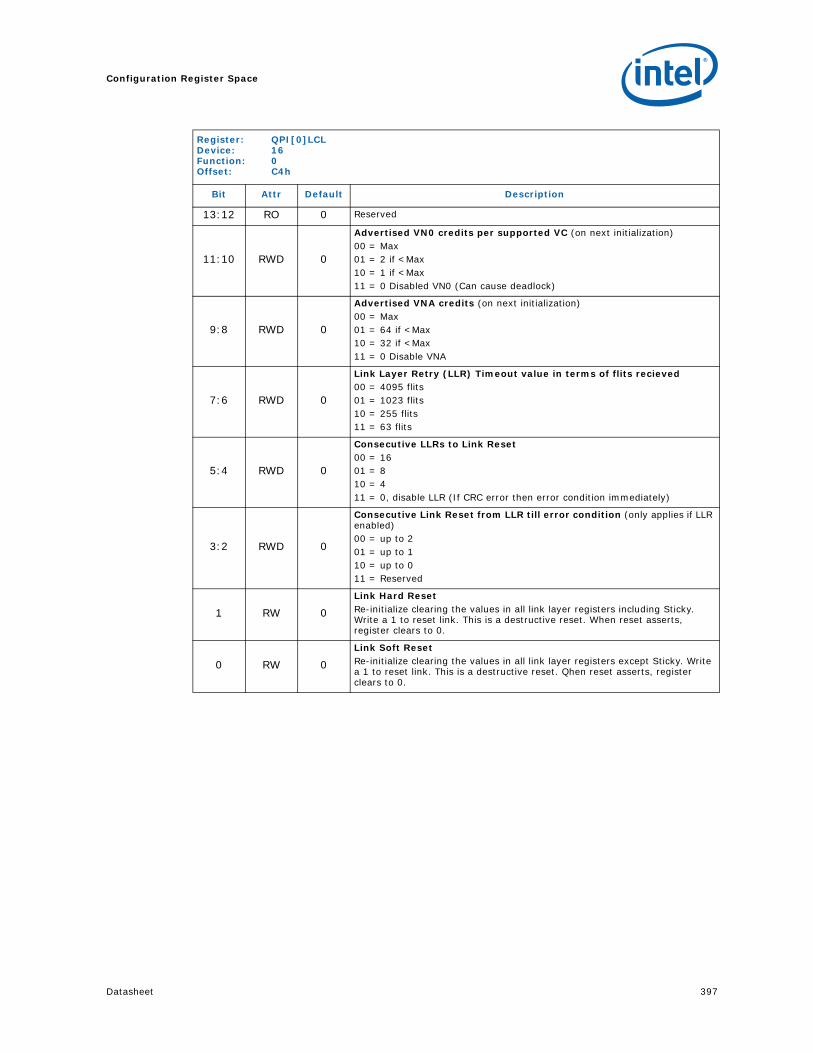
Datasheet 397
Configuration Register Space
13:12 RO 0 Reserved
11:10 RWD 0
Advertised VN0 credits per supported VC (on next initialization)00 = Max01 = 2 if <Max10 = 1 if <Max11 = 0 Disabled VN0 (Can cause deadlock)
9:8 RWD 0
Advertised VNA credits (on next initialization)00 = Max01 = 64 if <Max10 = 32 if <Max11 = 0 Disable VNA
7:6 RWD 0
Link Layer Retry (LLR) Timeout value in terms of flits recieved00 = 4095 flits01 = 1023 flits10 = 255 flits11 = 63 flits
5:4 RWD 0
Consecutive LLRs to Link Reset00 = 1601 = 810 = 411 = 0, disable LLR (If CRC error then error condition immediately)
3:2 RWD 0
Consecutive Link Reset from LLR till error condition (only applies if LLR enabled)00 = up to 201 = up to 110 = up to 011 = Reserved
1 RW 0
Link Hard ResetRe-initialize clearing the values in all link layer registers including Sticky. Write a 1 to reset link. This is a destructive reset. When reset asserts, register clears to 0.
0 RW 0
Link Soft ResetRe-initialize clearing the values in all link layer registers except Sticky. Write a 1 to reset link. This is a destructive reset. Qhen reset asserts, register clears to 0.
Register: QPI[0]LCLDevice: 16Function: 0Offset: C4h
Bit Attr Default Description

Configuration Register Space
398 Datasheet
17.11.1.4 QPI[0]LS—Intel® QPI Link Status Register
Register per Intel QuickPath Interconnect port. This register for holding link status and peer agent info.
Register: QPI[0]LSDevice: 16Function: 0Offset: C8h
Bit Attr Default Description
31 RV 0 Reserved
30:28 RO 0h
Link Layer Retry Queue AllocationFlits allocated000 = 0 to 7001 = 8 to 15010 = 16 to 31011 = 32 to 63100 = 64 to 95101 = 96 to 127110 = 128 to 191111 = 192 to 255
27:24 RO 0h
Link Initialization status0000 = Waiting for Physical Layer Ready0001 = Internal Stall Link Initialization0010 = Sending ReadyForInit0011 = Parameter Exchange0100 = Sending ReadyForNormalOperation0101 = Reserved0110 = Normal Operation0111 = Link Level Retry1000 = Link Error1001 = Parameter Exchange Done1010 = WaitForNormal1011 = LocalLinkReset11XX, 1001, 101X = Reserved
23:22 RO 00
Link initialization Failure Count – Saturates at 011All Link Init state machine arcs going into RDY_FOR_INIT excluding the arcs from NOT_RDY_FOR_INIT and from NORMAL_OPERATION.00 = 001 = 110 = 2–1511 = >15
21 RO 0
Last Link Level Retry NUM_PHY_REINIT – Saturates at 1Number of Phy ReInits since last Link Init0 = 01 = 1+
20:19 RO 00
Last Link Level Retry Count – Saturates at 011Number of Retries since last Link Init or Phy Reinit000 = 0001 = 1010 = 2–15011 = >15

Datasheet 399
Configuration Register Space
18:16 RO 0h
VNA credits at receiverVNA available credits for remote device to use in transmission of packets to IOH.000 = 0 credits001 = 1–7 credits010 = 8–11 credits011 = 12–15 credits100 = 16–31 credits101 = 32–63 credits110 = 64–127 credits111 = 128+ credits
15 RO 0h
VN0 Snp Credits at receiverVNA available credits for remote device to use in transmission of packets to IOH.0 = 0 Credits1 = 1+ Credits
14 RO 0hVN0 Hom Credits at receiver0 = 0 Credits1 = 1+ Credits
13 RO 0h
VN0 NDR Credits at receiverVNA available credits for remote device to use in transmission of packets to IOH.0 = 0 Credits1 = 1+ Credits
12 RO 0h
VN0 DRS Credits at receiverVNA available credits for remote device to use in transmission of packets to IOH.0 = 0 Credits1 = 1+Credits
11 RO 0h
VN0 NCS Credits at receiverVNA available credits for remote device to use in transmission of packets to IOH.0 = 0 Credits1 = 1+ Credits
10 RO 0h
VN0 N Credits at receiverVNA available credits for remote device to use in transmission of packets to IOH.0 = 0 Credits1 = 1+Credits
9:8 RV 0h Reserved
7 RV 0
Reserved. Context shown for other components that support VN1. VN1 Snp Credits at receiver0 = 0 Credits1 = >0 Credits
6 RV 0
Reserved. Context shown for other components that support VN1. VN1 Hom Credits at receiver0 = 0 Credits1 = >0 Credits
5 RV 0
Reserved. Context shown for other components that support VN1. VN1 NDR Credits at receiver0 = 0 Credits1 = >0 Credits
Register: QPI[0]LSDevice: 16Function: 0Offset: C8h
Bit Attr Default Description

Configuration Register Space
400 Datasheet
17.11.1.5 QPI[0]LP0—Intel® QPI Link Parameter 0 Register
Register per Intel QuickPath Interconnect port. Parameter is exchanged as part of link initialization.
17.11.1.6 QPI[0]LP1—Intel® QPI Link Parameter 1 Register
Register per Intel QuickPath Interconnect port. Parameter is exchanged as part of link initialization.
4 RV 0
Reserved. Context shown for other components that support VN1. VN1 DRS Credits at receiver0 = 0 Credits1 = >0 Credits
3 RV 0
Reserved. Context shown for other components that support VN1. VN1 NCS Credits at receiver0 = 0 Credits1 = >0 Credits
2 RV 0
Reserved. Context shown for other components that support VN1. VN1 NCB Credits at receiver0 = 0 Credits1 = >0 Credits
1:0 RV 0 Reserved
Register: QPI[0]LSDevice: 16Function: 0Offset: C8h
Bit Attr Default Description
Register: QPI[0]LP0Device: 16Function: 0Offset: CCh
Bit Attr Default Description
31:0 RONN 0s Parameter 0 from peer agent
Register: QPI[0]LP1Device: 16Function: 0Offset: D0h
Bit Attr Default Description
31:0 RONN 0s Parameter 1 from peer agent
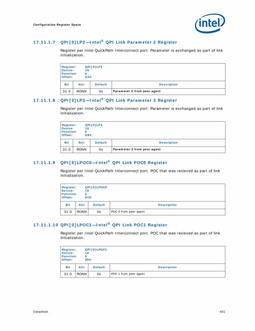
Datasheet 401
Configuration Register Space
17.11.1.7 QPI[0]LP2—Intel® QPI Link Parameter 2 Register
Register per Intel QuickPath Interconnect port. Parameter is exchanged as part of link initialization.
17.11.1.8 QPI[0]LP3—Intel® QPI Link Parameter 3 Register
Register per Intel QuickPath Interconnect port. Parameter is exchanged as part of link initialization.
17.11.1.9 QPI[0]LPOC0—Intel® QPI Link POC0 Register
Register per Intel QuickPath Interconnect port. POC that was recieved as part of link initialization.
17.11.1.10 QPI[0]LPOC1—Intel® QPI Link POC1 Register
Register per Intel QuickPath Interconnect port. POC that was recieved as part of link initialization.
Register: QPI[0]LP2Device: 16Function: 0Offset: D4h
Bit Attr Default Description
31:0 RONN 0s Parameter 2 from peer agent
Register: QPI[0]LP3Device: 16Function: 0Offset: D8h
Bit Attr Default Description
31:0 RONN 0s Parameter 3 from peer agent
Register: QPI[0]LPOC0Device: 16Function: 0Offset: DCh
Bit Attr Default Description
31:0 RONN 0s POC 0 from peer agent
Register: QPI[0]LPOC1Device: 16Function: 0Offset: E0h
Bit Attr Default Description
31:0 RONN 0s POC 1 from peer agent
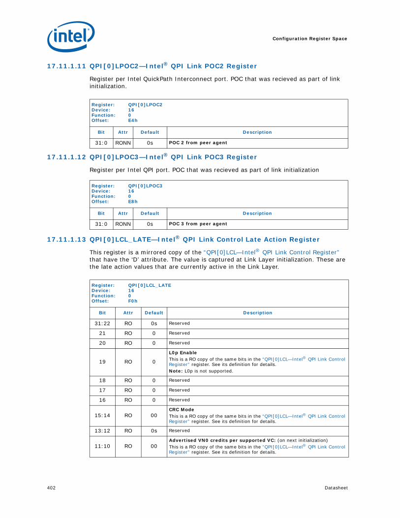
Configuration Register Space
402 Datasheet
17.11.1.11 QPI[0]LPOC2—Intel® QPI Link POC2 Register
Register per Intel QuickPath Interconnect port. POC that was recieved as part of link initialization.
17.11.1.12 QPI[0]LPOC3—Intel® QPI Link POC3 Register
Register per Intel QPI port. POC that was recieved as part of link initialization.
17.11.1.13 QPI[0]LCL_LATE—Intel® QPI Link Control Late Action Register
This register is a mirrored copy of the “QPI[0]LCL—Intel® QPI Link Control Register” that have the ‘D’ attribute. The value is captured at Link Layer initialization. These are the late action values that are currently active in the Link Layer.
Register: QPI[0]LPOC2Device: 16Function: 0Offset: E4h
Bit Attr Default Description
31:0 RONN 0s POC 2 from peer agent
Register: QPI[0]LPOC3Device: 16Function: 0Offset: E8h
Bit Attr Default Description
31:0 RONN 0s POC 3 from peer agent
Register: QPI[0]LCL_LATEDevice: 16Function: 0Offset: F0h
Bit Attr Default Description
31:22 RO 0s Reserved
21 RO 0 Reserved
20 RO 0 Reserved
19 RO 0
L0p EnableThis is a RO copy of the same bits in the “QPI[0]LCL—Intel® QPI Link Control Register” register. See its definition for details.Note: L0p is not supported.
18 RO 0 Reserved
17 RO 0 Reserved
16 RO 0 Reserved
15:14 RO 00CRC ModeThis is a RO copy of the same bits in the “QPI[0]LCL—Intel® QPI Link Control Register” register. See its definition for details.
13:12 RO 0s Reserved
11:10 RO 00Advertised VN0 credits per supported VC: (on next initialization)This is a RO copy of the same bits in the “QPI[0]LCL—Intel® QPI Link Control Register” register. See its definition for details.

Datasheet 403
Configuration Register Space
17.11.1.14 QPI[0]LCRDC—Intel® QPI Link Credit Control Register
The register controls what credits are defined for each message class on VN0 and VNA. These credits are made visible on the Intel QuickPath Interconnect during the initialize phase of in the link layer. The values programmed here must exist within the size limits defined. Incorrect programming can result in overflow of the receive queue. When returning credits on the Intel QuickPath Interconnect this register is used in conjunction with the Intel QuickPath Interconnect standard register “QPI[0]LCL—Intel® QPI Link Control Register” to determine how many credits are returned. In other words, the values specified in QPI[1:0]LCRDC act as the “Max” in the field descriptions for QPILCL[11:10] and QPILCL[9:8].
This value is captured and used by the Link Layer when exiting the parameter exchange. This state is referred to as “Begin Normal Operation” in Common System Interface Specification, Revision 0.75.
9:8 RO 0Advertised VNA credits: (on next initialization)This is a RO copy of the same bits in the “QPI[0]LCL—Intel® QPI Link Control Register” register. See its definition for details.
7:6 RO 0Link Layer Retry (LLR): Timeout value in terms of flits receivedThis is a RO copy of the same bits in the “QPI[0]LCL—Intel® QPI Link Control Register” register. See its definition for details.
5:4 RO 0MAX_NUM_RETRYThis is a RO copy of the same bits in the “QPI[0]LCL—Intel® QPI Link Control Register” register. See its definition for details.
3:2 RO 00MAX_NUM_PHY_REINITThis is a RO copy of the same bits in the “QPI[0]LCL—Intel® QPI Link Control Register” register. See its definition for details.
1:0 RO 00 Reserved0
Register: QPI[0]LCL_LATEDevice: 16Function: 0Offset: F0h
Bit Attr Default Description
Register: QPI[0]LCRDCDevice: 16Function: 0Offset: F8h
Bit Attr Default Description
31 RV 0 Reserved
30:28 RWD 1hVN0 – Hom creditsAllowed values:0–7 credits
27 RV 0 Reserved
26:24 RWD 1hVN0 – NCB creditsAllowed values:0–7 credits
23 RV 0 Reserved
22:20 RWD 1hVN0 – NCS creditsAllowed values:0–7 credits
19 RV 0 Reserved

Configuration Register Space
404 Datasheet
18:16 RWD 1h
VN0 – NDR creditsWith Isoc enabled this value is expected to be set at 4 to ensure QoS with High End Desktop.Allowed values:0–7 credits
15 RV 0 Reserved
14:12 RWD 1h
VN0 – DRS creditsWith Isoc enabled this value is expected to be set at 4 to ensure QoS with High End Desktop.Allowed values:0–7 credits
11 RV 0 Reserved
10:8 RWD 1hVN0 – Snp creditsAllowed values:0–7 credits
7 RV 0 Reserved
6:0 RWD 64hVNA creditsBIOS must set this to 64h for standard header operation.0 – 127 credits
Register: QPI[0]LCRDCDevice: 16Function: 0Offset: F8h
Bit Attr Default Description

Datasheet 405
Configuration Register Space
17.11.1.15 QPI[0]LCRDC_LATE—Intel® QPI Link Credit Control Late Action Regiser
This is a RO copy of the “QPI[0]LCRDC_LATE—Intel® QPI Link Credit Control Late Action Regiser” register. It is needed to hold the currently active value which is loaded on Link Layer Initialization.
Register: QPI[0]LCRDC_LATEDevice: 16Function: 0Offset: FCh
Bit Attr Default Description
31 RV 0 Reserved
30:28 RO 1hVN0 Hom creditsThis is a RO copy of the same bits in the “QPI[0]LCRDC—Intel® QPI Link Credit Control Register” register. See its definition for details.
27 RV 0 Reserved
26:24 RO 1hVN0 NCB creditsThis is a RO copy of the same bits in the “QPI[0]LCRDC—Intel® QPI Link Credit Control Register” register. See its definition for details.
23 RV 0 Reserved
22:20 RO 1hVN0 NCS creditsThis is a RO copy of the same bits in the “QPI[0]LCRDC—Intel® QPI Link Credit Control Register” register. See its definition for details.
19 RV 0 Reserved
18:16 RO 1hVN0 NDR creditsThis is a RO copy of the same bits in the “QPI[0]LCRDC—Intel® QPI Link Credit Control Register” register. See its definition for details.
15 RV 0 Reserved
14:12 RO 1hVN0 DRS creditsThis is a RO copy of the same bits in the “QPI[0]LCRDC—Intel® QPI Link Credit Control Register” register. See its definition for details.
11 RV 0 Reserved
10:8 RO 1hVN0 Snp creditsThis is a RO copy of the same bits in the “QPI[0]LCRDC—Intel® QPI Link Credit Control Register” register. See its definition for details.
7 RV 0 Reserved
6:0 RO 0sVNA creditsThis is a RO copy of the same bits in the “QPI[0]LCRDC—Intel® QPI Link Credit Control Register” register. See its definition for details.

Configuration Register Space
406 Datasheet
17.11.2 Intel® QuickPath Interconnect Routing and Protocol Layer Registers
All Routing layer registers are used to define the routing table functionality. The routing table is used to route packets going out to the Intel QuickPath Interconnect to the correct Intel QuickPath Interconnect port. This is done based on NodeID when the table is enabled. When not enabled completions are routed to the port which their request was received, IB requests will result in an routing layer error.
Table 17-21.CSR Intel QPI Routing Layer, Protocol (Device 16, Function 1)
DID VID 00h QPIPAPICSAD 80h
PCISTS PCICMD 04h QPIPAPICSAD
CCR RID 08h
HDR CLS 0Ch QPIPDCASAD 8Ch
10h 90h
14h QPIPPVGASAD 94h
18h 98h
1Ch QPIPLIOSAD 9Ch
20h A0h
24h QPIPBUSSAD A4h
28h A8h
SID SVID 2Ch QPIPSUBSAD ACh
30h QPI0PORB B0h
CAPPTR1
Notes:1. CAPPTR points to the first capability block
34h B4h
38h QPIPISOCRES B8h
INTP INTL 3Ch QPIPQC BCh
QPIRTCTRL 40h QPIPNCB C0h
QPIRTBL 44h C4h
48h QPIPLKMS C8h
QPIPCTRL 4Ch CCh
50h QPIPQBCPU D0h
QPIPSTS 54h D4h
QPIPSB 58h QPIPQBIOH D8h
5Ch DCh
QPIPRTO 60h E0h
QPIPPOWCTRL 64h E4h
QPIPINT 68h E8h
QPIPRWMAD 6Ch ECh
QPIPMADDATA 70h F0h
74h F4h
78h F8h
7Ch FCh
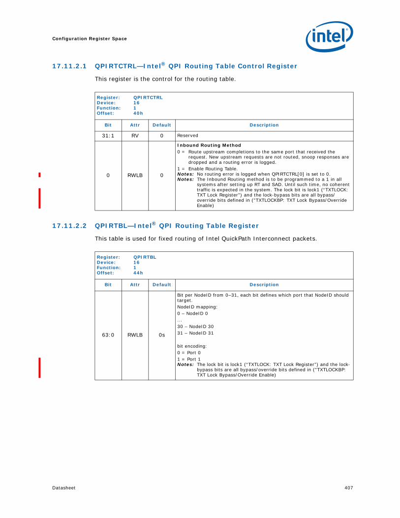
Datasheet 407
Configuration Register Space
17.11.2.1 QPIRTCTRL—Intel® QPI Routing Table Control Register
This register is the control for the routing table.
17.11.2.2 QPIRTBL—Intel® QPI Routing Table Register
This table is used for fixed routing of Intel QuickPath Interconnect packets.
Register: QPIRTCTRLDevice: 16Function: 1Offset: 40h
Bit Attr Default Description
31:1 RV 0 Reserved
0 RWLB 0
Inbound Routing Method0 = Route upstream completions to the same port that received the
request. New upstream requests are not routed, snoop responses are dropped and a routing error is logged.
1 = Enable Routing Table.Notes: No routing error is logged when QPIRTCTRL[0] is set to 0.Notes: The Inbound Routing method is to be programmed to a 1 in all
systems after setting up RT and SAD. Until such time, no coherent traffic is expected in the system. The lock bit is lock1 (“TXTLOCK: TXT Lock Register”) and the lock-bypass bits are all bypass/override bits defined in ("TXTLOCKBP: TXT Lock Bypass/Override Enable)
Register: QPIRTBLDevice: 16Function: 1Offset: 44h
Bit Attr Default Description
63:0 RWLB 0s
Bit per NodeID from 0–31, each bit defines which port that NodeID should target.NodeID mapping:0 – NodeID 0...30 – NodeID 3031 – NodeID 31
bit encoding:0 = Port 01 = Port 1Notes: The lock bit is lock1 (“TXTLOCK: TXT Lock Register”) and the lock-
bypass bits are all bypass/override bits defined in ("TXTLOCKBP: TXT Lock Bypass/Override Enable)

Configuration Register Space
408 Datasheet
17.11.2.3 QPIPCTRL—Intel® QPI Protocol Control Register
Register can only be modified under system quiescence.
Note: For the QPIPCTRL.[44] to work for protecting remote peer to peer accesses to the BAR regions, two additional registers need to be programmed. These are the QPIPQBCPU and QPIPQBIOH. These registers should be programmed to reflect all the node IDs of the CPUs and IOHs in the system in order that the logic correctly distinguish a CPU access from a remote peer to peer access.
Register: QPIPCTRLDevice: 16Function: 1Offset: 4Ch
Bit Attr Default Description
63:52 RV 0 Reserved
51:48 RWL 0011
Configuration Retry TimeoutApplies only to PCI Express/DMI ports. This field controls how long a configuration request is reissued (when enabled using the root control register) whenever a CRS response is received. Reissue applies to all configuration requests when CRS software visibility is disabled (using the root control register) and to all configuration requests except on configuration reads to Vendor/Device ID field at offset 0h, when CRS software visibility is enabled. The timer that is controlled by this field starts when a configuration request is issued the very first time on PCI Express. When this timer expires and following that if either a CRS response is received for the configuration request or a completion time-out occurs on the configuration request, the request is aborted (that is, not reissued anymore) and a UR (/equivalent) response is returned. Note that a configuration request is not immediately aborted when this timer expires. Aborting a configuration request only happens when either a completion timeout condition is reached or when a CRS response is received w/ the retry timeout expired.0000 = 1 ms0001 = 16 ms0010 = 64 ms0011 = 256 ms0100 = 1 s0101 = 2 s0110 = 4 s0111 = 8 s1000 = 16 s1001 = 45 s1010–1111 = Reserved
47 RV 0 Reserved
46 RWL 0Invalid DNID check EnableEnables DNID check.
45 RWL 0Write cache flushFlushes the write cache
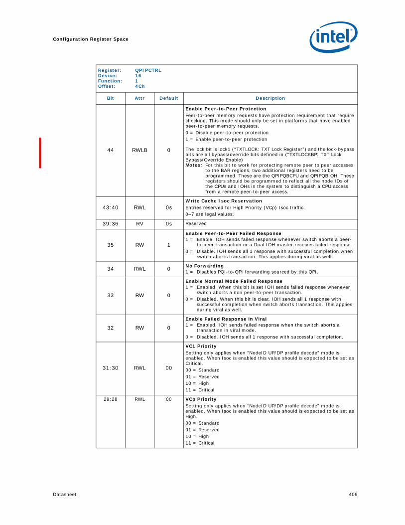
Datasheet 409
Configuration Register Space
44 RWLB 0
Enable Peer-to-Peer ProtectionPeer-to-peer memory requests have protection requirement that require checking. This mode should only be set in platforms that have enabled peer-to-peer memory requests.0 = Disable peer-to-peer protection 1 = Enable peer-to-peer protection
The lock bit is lock1 (“TXTLOCK: TXT Lock Register”) and the lock-bypass bits are all bypass/override bits defined in ("TXTLOCKBP: TXT Lock Bypass/Override Enable)Notes: For this bit to work for protecting remote peer to peer accesses
to the BAR regions, two additional registers need to be programmed. These are the QPIPQBCPU and QPIPQBIOH. These registers should be programmed to reflect all the node IDs of the CPUs and IOHs in the system to distinguish a CPU access from a remote peer-to-peer access.
43:40 RWL 0sWrite Cache Isoc ReservationEntries reserved for High Priority (VCp) Isoc traffic. 0–7 are legal values.
39:36 RV 0s Reserved
35 RW 1
Enable Peer-to-Peer Failed Response1 = Enable. IOH sends failed response whenever switch aborts a peer-
to-peer transaction or a Dual IOH master receives failed response. 0 = Disable. IOH sends all 1 response with successful completion when
switch aborts transaction. This applies during viral as well.
34 RWL 0 No Forwarding1 = Disables PQI-to-QPI forwarding sourced by this QPI.
33 RW 0
Enable Normal Mode Failed Response1 = Enabled. When this bit is set IOH sends failed response whenever
switch aborts a non peer-to-peer transaction. 0 = Disabled. When this bit is clear, IOH sends all 1 response with
successful completion when switch aborts transaction. This applies during viral as well.
32 RW 0
Enable Failed Response in Viral1 = Enabled. IOH sends failed response when the switch aborts a
transaction in viral mode. 0 = Disabled. IOH sends all 1 response with successful completion.
31:30 RWL 00
VC1 PrioritySetting only applies when “NodeID UP/DP profile decode” mode is enabled. When Isoc is enabled this value should is expected to be set as Critical.00 = Standard01 = Reserved10 = High11 = Critical
29:28 RWL 00 VCp PrioritySetting only applies when “NodeID UP/DP profile decode” mode is enabled. When Isoc is enabled this value should is expected to be set as High.00 = Standard01 = Reserved10 = High11 = Critical
Register: QPIPCTRLDevice: 16Function: 1Offset: 4Ch
Bit Attr Default Description

Configuration Register Space
410 Datasheet
27:26 RWL 00 VC0 PrioritySetting only applies when “NodeID UP/DP profile decode” mode is enabled. Setting VC0 to critical or high may cause deadlocks.00 = Low01 = Medium10 = Reserved11 = Reserved
25 RWL 0 Inbound Reading SnoopingEnabling this mode causes IOH to send SnpInvItoE on Inbound Reads. This is used to force peer caching agent to update the home agent if the snoop hits in there cache rather then allow a cache-to-cache transfer directly to the IOH. This mode is required for Dual IOH proxy systems. 0 = Standard Snoop1 = Force SnpInvItoE
24:22 RWL 000 Default SAD NodeID: [2:0]Used to specify the default home/target NodeID when the SAD is disabled. Only used in UP profile systems, so only 3-bits of NodeID is needed.
21:20 RWL 0NodeID[5:4]This is the NodeID that is assigned to the IOH. It should only be changed using SMBus prior to QPI initialization.
19 RWLStrap: QPI/
NodeID3
NodeID[3]This is the NodeID that is assigned to the IOH. It should only be changed using SMBus prior to QPI initialization.
18 RWL Strap: NodeID2
NodeID[2]This is the NodeID that is assigned to the IOH. It should only be changed using SMBus prior to QPI initialization.
17:16 RWL 0NodeID[1:0]This is the NodeID that is assigned to the IOH. It should only be changed using SMBus prior to Intel QPI initialization.
15 RV 0 Reserved
14:13 RWL 0
Snooping ModeThis field defines how snooping is done from the IOH.00 = Broadcast Snoops based on Participant List. Home Node Broadcast
will use this mode with the Participant List empty, and the Home agent will take care of snooping.
01 = Broadcast Snoop based on Participant List, but remove the Home NodeID from the list based on match of NodeID[5:0]
10 = Broadcast Snoop based on Participant List, but remove the Home NodeID from the list based on match of NodeID[5:2,0]. Used for a processor that can send snoop from home agent to any caching agent on that socket.
11 = Router Broadcast. Send Snoop to Home NodeID only.
12 RWL 0
Disable PoisonThis bit Disables poison bit from being sent on Intel QPI. Any uncorrectable data error will be treated in the same way as a header error.0 = Enabled1 = Disabled
Register: QPIPCTRLDevice: 16Function: 1Offset: 4Ch
Bit Attr Default Description

Datasheet 411
Configuration Register Space
11:10 RWL 00
Abort Time-out ModeThis field control how AbortTO is sent on Intel QPI. AbortTO response will be sent for outbound CfgRd/Wr when it is pending within the IOH longer then the threshold value. This threshold will deusingte by up to +100% of the value specified.00 = Disable AbortTO01 = 2^11 core clocks (5 us @ 400 MHz)10 = 2^17 core clocks (327 us @ 400 MHz)11 = 2^24 core clocks (41 ms @ 400 MHz)
9 RWL 0
Disable ViralThis bit disables viral bit from being sent on Intel QPI or detected from Intel QPI. 0 = Enabled1 = Disabled
8 RWL 0
Disable Data Forwarding Before CompletionDefault behavior is to forward data immediately to PCI Express when the data phase is received on Intel QPI. When this bit is set the data will not be forwarded until both data and completion phases have been received.0 = Enable1 = Disable
7 RWL 0
Address Mask: [45:41] – DP Profile DecodeThis bit causes Address[45:41] to be decoded as defined in Intel QPI DP Profile. This causes those bits to never be sent on Intel QPI, and to be considered reserved when received on Intel QPI.0 = Disable1 = Enable
6 RWL 0
NodeID DP Profile decodeThis bit causes NodeID to be decoded as defined in Intel QPI DP Profile. This will also insure that PE[1:0] and PH[1:0] (that replace the NodeID bits from SMP and EMP profiles) are always cleared for sending and recieving.0 = Disable1 = Enable
5 RWL 0
Extended headerThis bit extends addressing beyond 46 bits to 51 bits (only allowed in EMP profile). IOH only supports extending of NodeID to 6-bits with extended headers. When set all headers will use extended format. 0 = Disable1 = Enable Lock bit is connected to fuse DISMPPRO
4 RV 0 Reserved
3 RWL 0
Disable write combiningThis bit causes all writes to send a EWB request as soon as M-state is acquired. See Section 4.7 for details.0 = Enable Write Combining1 = Disable Write Combining
2 RWL 0
RdCur/RdCode modeOn Inbound Coherent Reads selection of RdCur or RdCode is done based on this configuration bit.0 = RdCur1 = RdCode
Register: QPIPCTRLDevice: 16Function: 1Offset: 4Ch
Bit Attr Default Description
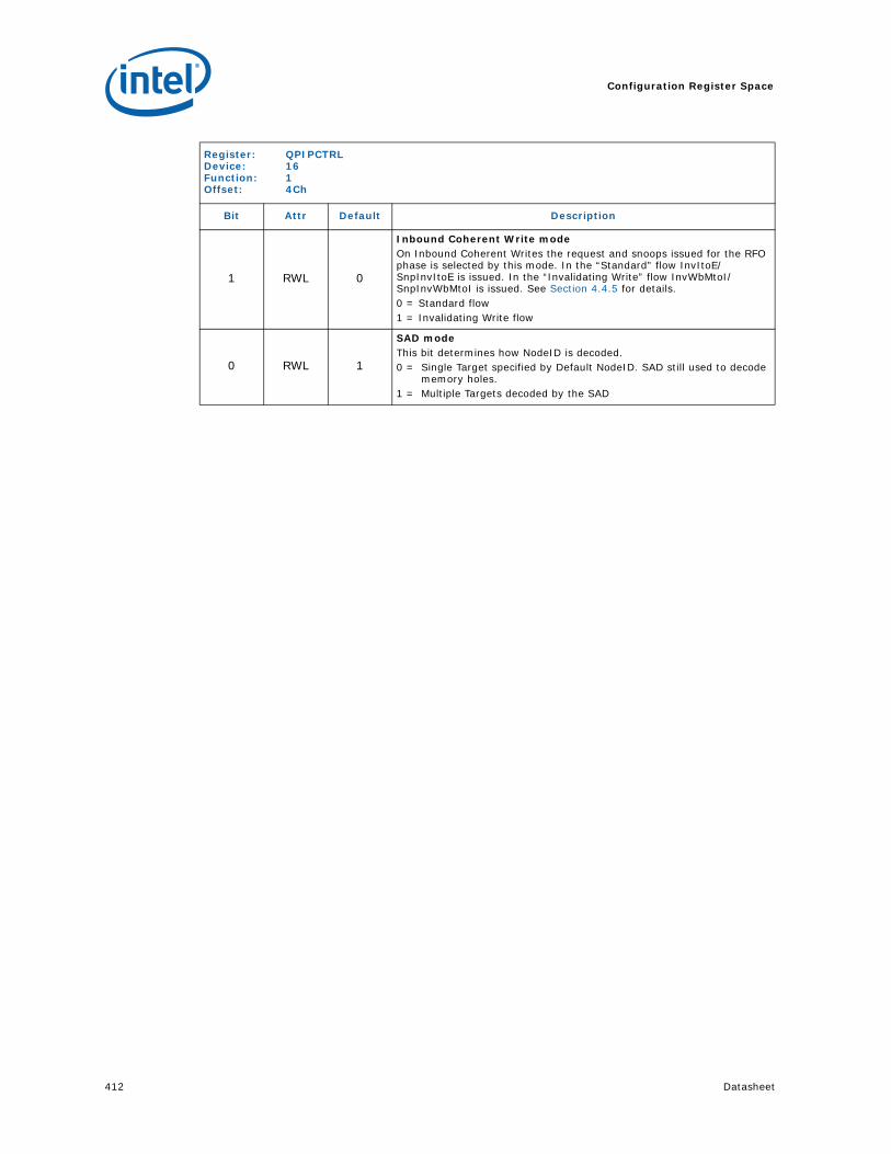
Configuration Register Space
412 Datasheet
1 RWL 0
Inbound Coherent Write modeOn Inbound Coherent Writes the request and snoops issued for the RFO phase is selected by this mode. In the “Standard” flow InvItoE/SnpInvItoE is issued. In the “Invalidating Write” flow InvWbMtoI/SnpInvWbMtoI is issued. See Section 4.4.5 for details.0 = Standard flow1 = Invalidating Write flow
0 RWL 1
SAD modeThis bit determines how NodeID is decoded.0 = Single Target specified by Default NodeID. SAD still used to decode
memory holes.1 = Multiple Targets decoded by the SAD
Register: QPIPCTRLDevice: 16Function: 1Offset: 4Ch
Bit Attr Default Description

Datasheet 413
Configuration Register Space
17.11.2.4 QPIPSTS—Intel® QPI Protocol Status Register
Note: This register gives status for DRS TX and NDR TX explicitly while gross status for NCB/NCS/SNP TX and HOM TX can be inferred from Bit 2 "ORB Not Empty". If ORB is empty, then the IOH does not have pending NCS/NCB/SNP in TX.
17.11.2.5 QPIPSB—Intel® QPI Protocol Snoop Broadcast
Used in Broadcast of snoops for coherent traffic to main memory.
Register can only be modified under system quiescence.
Register: QPIPSTSDevice: 16Function: 1Offset: 54h
Bit Attr Default Description
31:5 RV 0 Reserved
4 RO 0
TX DRS Queue NOT EmptyThis bit indicates that the Protocol TX DRS Queue is not empty.1 = Pending DRS packets to be transmitted0 = No DRS packets pending
3 RO 0
TX NDR Queue NOT EmptyThis bit indicates that the Protocol TX NDR Queue is not empty.1 = Pending NDR packets to be transmitted0 = No NDR packets pending
2 RO 0
ORB non-lock_arb Not EmptyThis bit indicates that there are no pending requests in the ORB with the exception of StopReq*/StartReq* messages from the lock arbiter.1 = Pending ORB requests0 = ORB Empty (except StopReq*/StartReq*)
1 RO 0
ORB EmptyThis bit indicates that there are no pending requests in the ORB.0 = Pending ORB requests1 = ORB Empty
0 RO 0
Write Cache EmptyThis bit indicates that no E,M state lines exist within the write cache.0 = Write Cache has current E or M state lines.1 = Write Cache is empty of E or M state lines.
Register: QPIPSBDevice: 16Function: 1Offset: 58h
Bit Attr Default Description
63:0 RW 0
Snoop vectorEach set bit in the vector corrresponds to a NodeID.Bit NodeID[5:0]0 0000001 0000012 000010...7 000111...63 111111

Configuration Register Space
414 Datasheet
17.11.2.6 QPIPRTO—Intel® QPI Protocol Request Time-Out
The register defines the Intel QPI protocol layer timeout values for each timeout level.
Register: QPIPRTODevice: 16Function: 1Offset: 60h
Bit Attr Default Description
31:24 RV 00h Reserved
23:20 RW 0hTime-out class 5Same definition as “Time-out class 1”
19:16 RW 0hTime-out class 4Same definition as “Time-out class 1”
15:12 RW 0hTime-out class 3Same definition as “Time-out class 1”
11:8 RV 0h Reserved, IOH doesn’t support sending requests in Time-out class 2
7:4 RW 0h
Time-out class 1This field controls the timeout value for the request designated to this level. The mode here specifies the timeout counter rate. The actual timeout value will be between 3x and 4x of the rate.0h = Timeout disable1h = 2 ^ 82h = 2 ^ 103h = 2 ^ 124h = 2 ^ 145h = 2 ^ 166h = 2 ^ 187h = 2 ^ 208h = 2 ^ 229h = 2 ^ 24Ah = 2 ^ 26Bh = 2 ^ 28Ch = 2 ^ 30Dh = 2 ^ 32Eh = 2 ^ 34Fh = 2 ^ 36Note: The 2 ^ x mathematical term is used below defined as “2 to the power of x”.
3:0 RV 0h Reserved

Datasheet 415
Configuration Register Space
17.11.2.7 QPIPPOWCTRL—Intel® QPI Protocol Power Control Register
This register is used to control the PMReq response type. IOH will give only a static response to all PMReq message that can be modified with this register’s settings.
This register can only be modified under system quiescence.
17.11.2.8 QPIPINT—Intel® QPI Protocol Interleave Mask Register
This register controls the system interleave determination used by the source address decoder for memory. This is a system wide parameter for interleave of DRAM. It is used to select from the target list, but exactly how it is used depends on the interleave mode of the SAD entry. Its primary usage model is to interleave between two DRAM home agents within an socket in a MP processor. The function that is expected to be used in the MP processors is parity of PA[19,13,10,6].
Register: QPIPPOWCTRLDevice: 16Function: 1Offset: 64h
Bit Attr Default Description
31:20 RV 0s Reserved
19:16 RW 0h
State TypeSets the State type in the PMReq response0000 = C0001 = P0010 = S0011 = Tothers = Reserved
15:0 RW 0040h
State LevelSets the State_Level[15:0] in the CmpD response to a PMReq message. The value is priority encoded (similar to one-hot). Default is a state_level of 7. It is required that at least one bit be set in this field.Bit State Level0 11 2..15 16
Register: QPIQPIPINTDevice: 16Function: 1Offset: 68h
Bit Attr Default Description
31:16 RV 0000h Reserved
15:0 RW 0000h
System Interleave Bit Mask for PA[21:6]Any bit that is enabled will be included in the even parity calculation on an address being processed by the SAD. This output of this parity calculation may be used in the selection of the Target NodeID.

Configuration Register Space
416 Datasheet
17.11.2.9 QPIPMADCTRL—Intel® QPI Protocol Memory Address Decoder Control Register
This register controls reads and writes to the Memory Address Decoder. Given the nature of this register, software must ensure that only a single producer is modifying this register.
17.11.2.10 QPIPMADDATA—Intel® QPI Protocol Memory Address Decode Data Register
This register defines Source Address Decode for memory space. There are 16 decoder entries exist but which one is being accessed depends on the setting in “QPIPMADCTRL—Intel® QPI Protocol Memory Address Decoder Control Register”. Both reads and write to this register use the offset defined in that register. This means that software must ensure that only a single producer can be modifying these registers.
Register: QPIPMADCTRLDevice: 16Function: 1Offset: 6Ch
Bit Attr Default Description
31:4 RV 0s Reserved
3:0 RW 0h
MAD offsetSelects the Memory Address Decoder to access on a read or write to “QPIPMADDATA—Intel® QPI Protocol Memory Address Decode Data Register”Valid offsets are 0–15The lock bit is lock1 (“TXTLOCK: TXT Lock Register”) and the lock-bypass bits are all bypass/override bits defined in ("TXTLOCKBP: TXT Lock Bypass/Override Enable)
Register: QPIPMADDATADevice: 16Function: 1Offset: 70h
Bit Attr Default Description
127:121 RV 0 Reserved
120:96 RW 0
Limit Address[50:26]Address is 64 MB aligned.The lock bit is lock1 (“TXTLOCK: TXT Lock Register”) and the lock-bypass bits are all bypass/override bits defined in ("TXTLOCKBP: TXT Lock Bypass/Override Enable)
95:89 RV 0 Reserved
88:64 RWLB 0
Base Address[50:26]Address is 64 MB aligned.The lock bit is lock1 (“TXTLOCK: TXT Lock Register”) and the lock-bypass bits are all bypass/override bits defined in ("TXTLOCKBP: TXT Lock Bypass/Override Enable)

Datasheet 417
Configuration Register Space
17.11.2.11 QPIPAPICSAD—Intel® QPI Protocol APIC Source Address Decode Register
This register defines SAD address decode function for inbound interrupts that are not broadcast.
63:16 RWL 0
Target ListBits [xx:nn] = Target NodeID[5:0]Bits [63:58] = Target NodeID7Bits [57:52] = Target NodeID6Bits [51:46] = Target NodeID5Bits [45:40] = Target NodeID4Bits [39:34] = Target NodeID3Bits [33:28] = Target NodeID2Bits [27:22] = Target NodeID1Bits [21:16] = Target NodeID0The lock bit is lock1 (“TXTLOCK: TXT Lock Register”) and the lock-bypass bits are all bypass/override bits defined in ("TXTLOCKBP: TXT Lock Bypass/Override Enable)
15:4 RV 0 Reserved
3:1 RWL 0
Interleave Select0h = Addr[8:6]1h = Addr[8:7], Sys_Interleave2h = Addr[9:8], Sys_Interleave3h = Addr[8:6] XOR Addr[18:16] 4h = (Addr[8:7] XOR Addr[18:17]), Sys_Interleave>4h = ReservedThe lock bit is lock1 (“TXTLOCK: TXT Lock Register”) and the lock-bypass bits are all bypass/override bits defined in ("TXTLOCKBP: TXT Lock Bypass/Override Enable)
0 RW 0
Valid0 = Not Valid1 = ValidThe lock bit is lock1 (“TXTLOCK: TXT Lock Register”) and the lock-bypass bits are all bypass/override bits defined in ("TXTLOCKBP: TXT Lock Bypass/Override Enable)
Register: QPIPMADDATADevice: 16Function: 1Offset: 70h
Bit Attr Default Description
Register: QPIPSAPICDDevice: 16Function: 1Offset: 80h
Bit Attr Default Description
95:81 RV 0s Reserved
80:72 RWL 0s
Physical Mode Local Cluster ID[8:0] Cluster ID is used in hierarchical systems to determine if interrupt go to the local cluster or to the remote. APIC ID bits used to determine cluster are the ones immediately above the interleave mode bits.See Physical Mode Interleave for which bits are matched.The lock bit is lock1 (“TXTLOCK: TXT Lock Register”) and the lock-bypass bits are all bypass/override bits defined in ("TXTLOCKBP: TXT Lock Bypass/Override Enable)
71:68 RV 0s Reserved

Configuration Register Space
418 Datasheet
67:64 RWL 0s
Extended Logical Mode Local Cluster ID[3:0] Cluster ID is used in hierarchical systems to determine if interrupt go to the local cluster or to the remote. APIC ID bits used to determine cluster are the ones immediately above the interleave mode bits.See Extended Logical Mode Interleave for which bits are matched.The lock bit is lock1 (“TXTLOCK: TXT Lock Register”) and the lock-bypass bits are all bypass/override bits defined in ("TXTLOCKBP: TXT Lock Bypass/Override Enable)
63:16 RWLB 0s
Target ListBits [xx:nn] = Target NodeID[5:0]Bits [63:58] = Target NodeID7Bits [57:52] = Target NodeID6Bits [51:46] = Target NodeID5Bits [45:40] = Target NodeID4Bits [39:34] = Target NodeID3Bits [33:28] = Target NodeID2Bits [27:22] = Target NodeID1Bits [21:16] = Target NodeID0The lock bit is lock1 (“TXTLOCK: TXT Lock Register”) and the lock-bypass bits are all bypass/override bits defined in ("TXTLOCKBP: TXT Lock Bypass/Override Enable)
15:14 RV 0s Reserved
13:8 RWLB 0s
Remote NodeID[5:0]This field is used to indicate the Node Controller in hierarchical systems. The field works in conjunction with the Cluster ID fields.The lock bit is lock1 (“TXTLOCK: TXT Lock Register”) and the lock-bypass bits are all bypass/override bits defined in ("TXTLOCKBP: TXT Lock Bypass/Override Enable)
7 RV 0 Reserved
6:4 RWLB 0
Physical Mode InterleaveMode Interleave Local/remote Cluster ID0h APIC ID[5:3] APIC ID[14:6]1h APIC ID[7:5] 0, APIC ID[15:8]2h APIC ID[8:6] 00 & APIC ID[15:9]3h APIC ID[14:12] APIC ID[7:0] & APIC ID[15] (Needed for
Itanium processor based platforms)>3h ReservedThe lock bit is lock1 (“TXTLOCK: TXT Lock Register”) and the lock-bypass bits are all bypass/override bits defined in ("TXTLOCKBP: TXT Lock Bypass/Override Enable)
3:1 RWLB 0
Extended Logical Mode InterleaveMode Interleave Local/remote Cluster ID0h APIC ID[18:16] APIC ID[22:19]1h APIC ID[19:17] APIC ID[23:20]>1h ReservedThe lock bit is lock1 (“TXTLOCK: TXT Lock Register”) and the lock-bypass bits are all bypass/override bits defined in ("TXTLOCKBP: TXT Lock Bypass/Override Enable)
0 RWLB 0Valid0 = Not Valid1 = Valid
Register: QPIPSAPICDDevice: 16Function: 1Offset: 80h
Bit Attr Default Description

Datasheet 419
Configuration Register Space
17.11.2.12 QPIPDCASAD—Intel® QPI Protocol DCA Source Address Decode Register
Sets mode for NodeID generation for the DCA hint. The NodeID is generated based on the PCI Express tag, this register includes the modes for how this NodeID is generated.
17.11.2.13 QPIPSUBSAD—Intel® QPI Protocol Subtractive Source Address Decode Register
Subtractive Decode NodeID. If current IOH is Legacy this should not be used.
Register: QPIPDCASADDevice: 16Function: 1Offset: 8Ch
Bit Attr Default Description
31:8 RV 0 Reserved
7:6 RW 0
Cache Target Translation ModeCache target is a bit in the Intel QPI PrefetchHint message that indicates which target cache in the CPU should get the DCA data. The tag used is from the PCI Express memory write.00 = 0001 = 0 & Tag[0]10 = Tag[1:0]11 = Reserved
5:4 RW 0IDBase[1:0]Base NodeID bits used in some translation modes
3:1 RW 0
NodeID Translation ModeThe Target NodeID[2:0] for the PrefetchHint on Intel QPI is generated from based on these modes.000 = Tag[4:1] & IDBase[1:0]001 = 0 & Tag[4:2] & IDBase[1:0]010 = 0 & Tag[4:1] & IDBase[0]011 = 0 & Tag[4:0]100 = 00 & Tag[4:1]101 = 000 & Tag[4:2]>101 = Reserved
0 RWL 0
Enable DCAWhen disabled, PrefetchHint will not be sent on Intel QPI. The inbound write will just follow the standard flow.0 = Disable1 = Enable
Register: QPIPSUBSADDevice: 16Function: 1Offset: ACh
Bit Attr Default Description
31:14 RV 0s Reserved
13:8 RW 0s Legacy IOH NodeID[5:0]
7:1 RV 0s Reserved
0 RW 0Valid0 = Not Valid1 = Valid
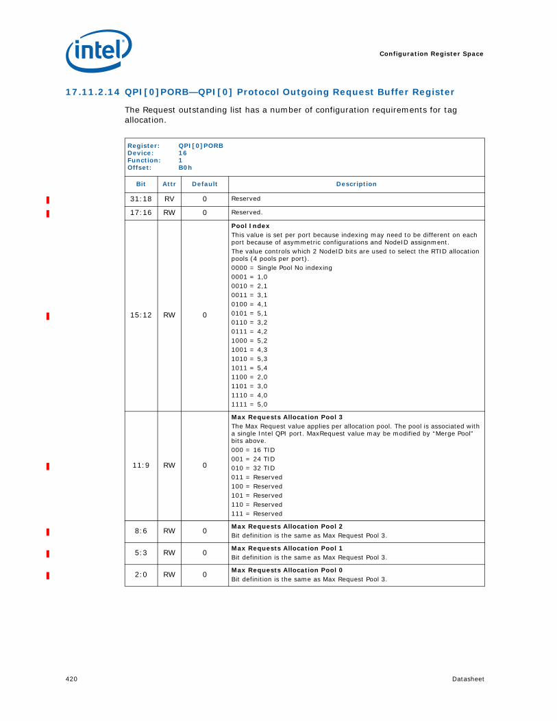
Configuration Register Space
420 Datasheet
17.11.2.14 QPI[0]PORB—QPI[0] Protocol Outgoing Request Buffer Register
The Request outstanding list has a number of configuration requirements for tag allocation.
Register: QPI[0]PORBDevice: 16Function: 1Offset: B0h
Bit Attr Default Description
31:18 RV 0 Reserved
17:16 RW 0 Reserved.
15:12 RW 0
Pool IndexThis value is set per port because indexing may need to be different on each port because of asymmetric configurations and NodeID assignment.The value controls which 2 NodeID bits are used to select the RTID allocation pools (4 pools per port).0000 = Single Pool No indexing0001 = 1,00010 = 2,10011 = 3,10100 = 4,10101 = 5,10110 = 3,20111 = 4,21000 = 5,21001 = 4,31010 = 5,31011 = 5,41100 = 2,01101 = 3,01110 = 4,01111 = 5,0
11:9 RW 0
Max Requests Allocation Pool 3The Max Request value applies per allocation pool. The pool is associated with a single Intel QPI port. MaxRequest value may be modified by “Merge Pool” bits above.000 = 16 TID001 = 24 TID010 = 32 TID011 = Reserved100 = Reserved101 = Reserved110 = Reserved111 = Reserved
8:6 RW 0Max Requests Allocation Pool 2Bit definition is the same as Max Request Pool 3.
5:3 RW 0Max Requests Allocation Pool 1Bit definition is the same as Max Request Pool 3.
2:0 RW 0Max Requests Allocation Pool 0Bit definition is the same as Max Request Pool 3.

Datasheet 421
Configuration Register Space
17.11.2.15 QPIPQC—Intel® QPI Protocol Quiescence Control Register
Used for initiating Quiescence and De-Quiescence of the system. See Section 4.6, “Lock Arbiter” for more information.
Note: The start of the quiesce operation is signaled by setting of bit 0 of this register, whether or not the stop request needs to be sent to the CPU.
Register: QPIPQCDevice: 16Function: 1Offset: BCh
Bit Attr Default Description
31:9 RV 0s Reserved
8 RWL 0
Block PHoldWhen set the Lock Arbiter must block any PHold request received until this bit is cleared. The usage model will be to set this bit prior to quiesce. Then, verify the Lock Arbiter is idle. Then, follow on to the rest of the quiesce flow. These extra steps are only necessary when PHold is allowed in the platform.0 = PHold proceeds normally1 = PHold is blockedLocked by lock1 bit.
7:6 RV 00 Reserved
5:3 RWLB 0
De-Quiescence Software modifying these bits must clear them when corresponding phases are complete.xx1 = StartReq1 (IOH only)x1x = StartReq2 (IOH only)1xx = StartReq2 (CPU only)The lock bit is lock1 (“TXTLOCK: TXT Lock Register”) and the lock-bypass bits are all bypass/override bits defined in ("TXTLOCKBP: TXT Lock Bypass/Override Enable)
2:0 RWLB 0
Quiescence Software modifying these bits must clear them when corresponding phases are complete.xx1 = StopReq1 (CPU only)x1x = StopReq1 (IOH only)1xx = Stop Req2 (IOH only)The lock bit is lock1 (“TXTLOCK: TXT Lock Register”) and the lock-bypass bits are all bypass/override bits defined in ("TXTLOCKBP: TXT Lock Bypass/Override Enable)

Configuration Register Space
422 Datasheet
17.11.2.16 QPIPLKMC—Intel® QPI Protocol Lock Master Control Register
Control for Lock Master. This register is modified only under system quiescence.
17.11.2.17 QPIPNCB—Intel® QPI Protocol Non-coherent Broadcast Register
List should contain all valid CPU caching agents. This broadcast list is used for some interrupts, Inbound VLW, and Power Management broadcasts on Intel QuickPath Interconnect.
Register: QPIPLKMCDevice: 16Function: 1Offset: C0h
Bit Attr Default Description
31:4 RV 0 Reserved
3:1 RW 0
Delay between SysLockIn Core Clocks, which are assumed to be at 400 MHz.This may be used to prevent starvation on frequent Lock usage.000 = 0h 001 = 200h (1.2 us)010 = 1000h (10 us)011 = 2000h (20 us)100 = 4000h (40 us)101 = 8000h (80 us)110 = 10000h (160 us)111 = 20000h (320 us)
0 RWLB 0
Disable LockThis bit causes NcMsgS-[ProcLock, ProcSplitLock, Quiesce, Unlock] to return immediate Cmp without going through StartReq*/StopReq* sequence.The lock bit is lock1 (“TXTLOCK: TXT Lock Register”) and the lock-bypass bits are all bypass/override bits defined in ("TXTLOCKBP: TXT Lock Bypass/Override Enable)
Register: QPIPNCBDevice: 16Function: 1Offset: C4h
Bit Attr Default Description
63:0 RW 0
Participant ListEach set bit in the vector corrresponds to a NodeID.Bit NodeID[5:0]0 0000001 0000012 000010...7 000111...63 111111

Datasheet 423
Configuration Register Space
17.11.2.18 QPIPLKMS—Intel® QPI Protocol Lock Master Status Register
This register contains status of the lock arbiter.
17.11.2.19 QPIPQBCPU—Intel® QPI Protocol Quiesce Broadcast CPU Register
This register controls what processors receive StopReq*/StartReq* messages from the lock arbiter.
Register: QPIPLKMSDevice: 16Function: 1Offset: CCh
Bit Attr Default Description
31:5 RV 0 Reserved
4:0 RO 0 Lock Arbiter Current State00000 - Idle00001 - Send_Stop_Req1_CPU00010 - Sent_Stop_Req1_CPU00011 - Cmpl_Stop_Req1_CPU00100 - Cmpl_Stop_Req1_CPU100101 - Send_IOH_Stop_Req100110 - Stop_Req1_IOH00111 - Wait_MyIOH_Stop_Req101000 - Stopped_Req1_IOH01001 - Send_Stop_Req201010 - Send_Stop_Req2_201011 - MyIOH_Stop_Req201100 - MyIOH_QUSC_P01101 - MyIOH_QUSC_All01110 - MyIOH_Pre_QUSC_QPI01111 - MyIOH_QUSC_QPI10000 - Stop_Req2_Send_Cmpl10001 - Stopped_Req210010 - Start_Req110011 - Send_Unlock_PCIe10100 - Send_Start_Req1_IOH10101 - Sent_Start_Req1_IOH10110 - Send_Start_Req1_CPU10111 - Sent_Start_Req1_CPU11000 - Start_Req1_Done11001 - Start_Req2_Send_IOH11010 - Start_Req2_Sent_IOH11011 - Start_Req2_Cmpl_IOH11100 - Start_Req2_Send_CPU11101 - Start_Req2_Sent_CPU11110 - Send_Unlock_Cmpl_Done11111 - Complete

Configuration Register Space
424 Datasheet
Register: QPIPSBDevice: 16Function: 1Offset: D0h
Bit Attr Default Description
63:0 RWLB 0s
Participant ListEach set bit in the vector corrresponds to a NodeID.Bit NodeID[5:0]0 0000001 0000012 000010...7 000111...63 111111The lock bit is lock1 (“TXTLOCK: TXT Lock Register”) and the lock-bypass bits are all bypass/override bits defined in ("TXTLOCKBP: TXT Lock Bypass/Override Enable)

Datasheet 425
Configuration Register Space
17.11.2.20 QPIPQBIOH—Intel® QPI Protocol Quiesce Broadcast CPU Register
This register controls which IOHs receive StopReq*/StartReq* messages from the lock arbiter. Register can only be modified under system quiescence. In a multi-IOH configuration, the QPIPQBIOH register is also used to determine if an outbound access received by the Intel QPI protocol layer originated in a CPU or a remote IOH. This determination is to support dropping of remote peer-to-peer accesses in the system if necessary. This register must be programmed to indicate node IDs of all IOHs populated in the system.
17.11.2.21 QPIPINTRC—Intel® QPI Protocol Interrupt Control Register
Register: QPIPQBIOHDevice: 16Function: 1Offset: D8h
Bit Attr Default Description
63:0 RWLB 0
Snoop vectorEach set bit in the vector corrresponds to a NodeID.Bit NodeID[5:0]0 0000001 0000012 000010...7 000111...63 111111The lock bit is lock1 (“TXTLOCK: TXT Lock Register”) and the lock-bypass bits are all bypass/override bits defined in ("TXTLOCKBP: TXT Lock Bypass/Override Enable)Note: In a multi-IOH configuration, the QPIPQBIOH register is also used to determine whether a particular outbound access received by the Intel QPI protocol layer originated in a CPU or a remote IOH. This register must therefore be programmed to indicate node IDs of all IOHs populated in the system
Register: QPIPINTRCDevice: 17Function: 1Offset: E0h
Bit Attr Default Description
63:45 RV 0 Reserved
44:40 RW 18h
Legacy Signal Edge/Level: When set, the corresponding legacy wire from ICH is considered as a edge sensitive signal by IOH. When clear, the corresponding legacy wire from ICH is considered as a level sensitive signal by IOH.
40: NMI41: INIT42: SMI43: INTR44: A20M45-47: Reserved
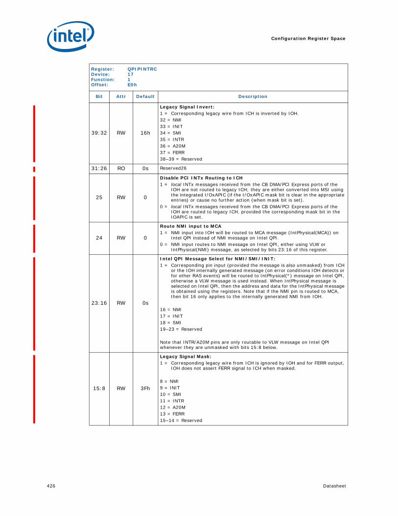
Configuration Register Space
426 Datasheet
39:32 RW 16h
Legacy Signal Invert: 1 = Corresponding legacy wire from ICH is inverted by IOH.32 = NMI33 = INIT34 = SMI35 = INTR36 = A20M37 = FERR38–39 = Reserved
31:26 RO 0s Reserved26
25 RW 0
Disable PCI INTx Routing to ICH 1 = local INTx messages received from the CB DMA/PCI Express ports of the
IOH are not routed to legacy ICH; they are either converted into MSI using the integrated I/OxAPIC (if the I/OxAPIC mask bit is clear in the appropriate entries) or cause no further action (when mask bit is set).
0 = local INTx messages received from the CB DMA/PCI Express ports of the IOH are routed to legacy ICH, provided the corresponding mask bit in the IOAPIC is set.
24 RW 0
Route NMI input to MCA 1 = NMI input into IOH will be routed to MCA message (IntPhysical(MCA)) on
Intel QPI instead of NMI message on Intel QPI. 0 = NMI input routes to NMI message on Intel QPI, either using VLW or
IntPhysical(NMI) message, as selected by bits 23:16 of this register.
23:16 RW 0s
Intel QPI Message Select for NMI/SMI/INIT: 1 = Corresponding pin input (provided the message is also unmasked) from ICH
or the IOH internally generated message (on error conditions IOH detects or for other RAS events) will be routed to IntPhysical(*) message on Intel QPI, otherwise a VLW message is used instead. When IntPhysical message is selected on Intel QPI, then the address and data for the IntPhysical message is obtained using the registers. Note that if the NMI pin is routed to MCA, then bit 16 only applies to the internally generated NMI from IOH.
16 = NMI17 = INIT18 = SMI19–23 = Reserved
Note that INTR/A20M pins are only routable to VLW message on Intel QPI whenever they are unmasked with bits 15:8 below.
15:8 RW 3Fh
Legacy Signal Mask: 1 = Corresponding legacy wire from ICH is ignored by IOH and for FERR output,
IOH does not assert FERR signal to ICH when masked.
8 = NMI9 = INIT10 = SMI11 = INTR12 = A20M13 = FERR15–14 = Reserved
Register: QPIPINTRCDevice: 17Function: 1Offset: E0h
Bit Attr Default Description

Datasheet 427
Configuration Register Space
7 RW 0
IA32 or IPFThis bit indicates if IOH is in an IA32 system or IPF system. This is needed by a) the IOH interrupt redirection logic to know how to interpret an interrupt with APICID set to FFh, that is, to broadcast that interrupt or direct to a single processor b) treat logical mode interrupts as illegal in the IPF mode0 = IA321 = IPF
6 RW 0
Physical Mode Interrupt & Extended Logical Interrupt Route/BroadcastShould be set to Route mode when firmware is able to set up a map of APIC ID to NodeID in the Intel QPI SAD (Source Address Decoder).0 = Route physical/extended logical mode interrupts to a single target. If
redirection is performed by IOH, the RH (Redirection Hint) bit will be cleared. If redirection is not performed by IOH, the RH bit is preserved.
1 = Broadcast physical/extended logical mode interrupts using interrupt broadcast list. In this setting, RH bit is cleared for all physical mode interrupts (legacy or extended). But the RH is still preserved (from the original interrupt or from the interrupt table) for extended logical mode interrupts.
Note: This field is expected to be programmed to 0 (default) by BIOS for most platforms. For custom configurations where broadcast of physical and extended logical mode interrupts are required, the BIOS should also set bit [5] of this register to force round robin redirection.
5 RW 0
Select Round robin redirection for logical mode1 = Selects a simple round robin redirection for logical flat and non-broadcast
cluster mode interrupts in IA32. 0 = Vector number based redirection is selected. Note that cluster mode
redirected broadcast interrupts are illegal.
4:3 RW 0
Vector based interrupt redirection control00 = Select bits 6:4/5:4 for vector cluster/flat algorithm01 = Select bits 5:3/4:310 = Select bits 3:1/2:111 = Select bits 2:0/1:0
2 RW 0
Disable extended cluster mode interrupt redirection:1 = IOH does not perform any redirection of extended cluster mode interrupts.
These interrupts are simply forwarded (either routed or broadcast based on bit 6 in this register) as is to the processor for redirection in the uncore
0 = IOH performs redirection of extended cluster mode interrupts as explained in Chapter 8. These interrupts are then forwarded (either routed or broadcast based on bit 6 in this register) to the processor with only the selected processor thread indicated in the interrupt mask field of the interrupt packet on Intel QPI
1 RW 0
IA32 Logical Flat or Cluster ModeSet by BIOS to indicate if the OS is running logical flat or logical cluster mode. This bit can also be updated by IntPrioUpd messages.0 = flat1 = cluster
0 RW 0
Cluster Check Sampling Mode0 = Disable checking for Logical_APICID[31:0] being non-zero when sampling
flat/cluster mode bit in the IntPrioUpd message as part of setting bit 1 in this register
1 = Enable the above checkingSee Section 8 for more details.
Register: QPIPINTRCDevice: 17Function: 1Offset: E0h
Bit Attr Default Description

Configuration Register Space
428 Datasheet
17.11.2.22 QPIPINTRS—Intel® QPI Protocol Interrupt Status Register
This register is to be polled by BIOS to determine if internal pending system interrupts are drained out of IOH. General usage model is for software to quiesce the source (for example, IOH global error logic) of a system event like SMI, then poll this register till this register indicates that the event is not pending inside IOH. One additional read is required from software, after the register first reads 0 for the associated event.
Register: QPIPINTRSDevice: 17Function: 1Offset: E8h
Bit Attr Default Description
31:8 RV 0 Reserved
7 RO 0 MCA RAS event pending
6 RO 0 NMI RAS event pending
5 RO 0 SMI RAS event pending
4 RO 0 INTR# event (either VLW or IntPhysical) pending
3 RO 0 A20M# pin event pending
2 RO 0 INIT# pin event (either VLW or IntPhysical) pending
1 RO 0 NMI pin event (either VLW or IntPhysical) pending
0 RO 0 SMI# pin event (either VLW or IntPhysical) pending

Datasheet 429
Configuration Register Space
17.11.3 Intel® QuickPath Interconnect Physical Layer Registers
The Physical layer has an internal reset, hard and soft, that result in special register requirements unique to the physical layer. There are two attributes, ‘P’ and ‘PP’, which indicate the register is affect by a physical layer reset. ‘P’ indicates the register is reset on a hard physical layer reset. ‘PP’ indicates the register is reset on any physical layer reset (hard or soft).
The following state encoding are used in Table 17-12 are used in a number of register encoding below.
Table 17-22.QPIPH-Intel® QuickPath Interconnect Tracking State Table
Bits State Name
0 0000 Reset.Soft & Reset.Default
0 0001 Reset.Calibrate
0 0010 Detect.ClkTerm
0 0011 Detect.FwdClk
0 0100 Detect.DCPattern
0 0101 Polling.BitLock
0 0110 Polling.LaneDeskew
0 0111 Polling.Param
0 1000 Config.LinkWidth
0 1001 Config.FlitLock
0 1010 Reserved
0 1100 Reserved
0 1101 Reserved
0 1110 L0R (Periodic Retraining in process)
0 1111 L0
1 0010 Loopback.Marker Master
1 0011 Loopback.Marker Slave
1 0000 Loopback.Pattern Master
1 0001 Loopback.Pattern Slave
1 1111 Compliance
Others Reserved.

Configuration Register Space
430 Datasheet
17.11.3.1 QPI[0]PH_CPR—Intel® QPI Physical Layer Capability Register
Register: QPI[0]PH_CPRDevice: 13Function: 1–0Offset: 828h
Bit Attr Default Description
31:29 RV 0 Reserved
28:24 RO 10hNumTxLanes: Number of Lanes Intel QPI lanes supported in full width mode.
23 RO 1BitlockRetrainPatt: Bit-lock and Retrain with patternIf set, the implementation supports using a specified pattern in bit-lock/retraining.
22 RO 0DatScrambleLFSR: Data Scramble with LFSRIntel QPI Link Behavior If set, implementation capable of data scrambling/descrambling with LFSR
21:20 RO 0RASCap: RAS capability 00 = Intel QPI clock failover not supported
19:18 RV 0 Reserved
17:16 RO 1Determinism Support: Determinism capability — not supported
15 RV 0 Reserved
14:12 RO 1h
PwrMgmtCap: Power management CapabilityNote: Intel QPI Specific Field Bit 12 =ReservedBit 13 = LWM capable.Bit 14 = Reserved
10:8 RO 7hLinkWidthCap: Link Width CapabilityXX1 = Full Width All others = Reserved
7:5 RO 0
DebugCap: Debug Capability1XX = Not capable of extracting slave electrical parameter from TS.Loopback
and apply during testX1X = Not capable of running in compliance slave mode as well as
transitioning to Loopback.pattern from Compliance stateXX1 = Not capable of doing Loopback.Stall
4 RO 0RetrainDurationGranulariity: Retraining duration granularity0 = No support for retraining on a 16UI granularity1 = Support for retraining on a 16UI granularity
3:0 RO 0PhyVersion: Intel QPI physical layer version0 = Rev0all other encoding are reserved.

Datasheet 431
Configuration Register Space
17.11.3.2 QPI[0]PH_CTR—Intel® QPI Physical Layer Control Register
Register: QPI[1:0]PH_CTRDevice: 13Function: 1–0Offset: 82Ch
Bit Attr Default Description
31:24 RV 0 Reserved
23 RWS 0
EnableBitlockRetrainwithPatt: Enable Bit-Lock and Retraining with Pattern0 = Use clock pattern for bitlock/retraining1 = Use pattern in bitlock/retraining
22 RWS 0
EnableScrambleLFSR: Enable Scrambling with LFSRIntel QPI Behavior 0 = Data not scrambled/descrambled1 = Data scrambled/descrambled with LFSR
21 RWS 0 Reserved
20:16 RV 0 Reserved
15:14 RWS 0 Reserved
13 RWS 0DisableAutocompliance: Disable Auto-Compliance0 = Path from Detect.Clkterm to compliance is allowed.1 = Path from Detect.Clkterm to compliance is disabled.
12:8 RWS 0 Reserved
7 RWDPP 0LinkSpeed: Full Speed Initialization0 = Slow speed initialization.1 = Force direct operational speed initialization.
6 RV 0 Reserved
5 RWSStrap:NOT
(BMCInit)
PhyInitBegin — Strap dependenceIf BMCinit = 0 then default = 1If BMCinit = 1 then default = 0
4 RWDS 0Single Step Mode — Intel QPI Link Behavior0 = Link behaves as defined by initialization mode.1 = Physical layer is in single step mode.
3:1 RV 0 Reserved
0 RW1S 0
PhyLayerReset: Physical Layer Reset (re-initialization)This bit is used to Reset the Physical Layer, and is Link Type dependent in it usage and definition.Intel QPI BehaviorPhysical Layer Reset is RW1S type for Intel QPI.If # of links supported is greater than 0 then Link Select must always be used to display the current read value for this field. There is a write dependency for this field based on the value of Can Transmit or Receive on Multiple Links?If Can Transmit or Receive on Multiple Links? = 0, then Link Select must be used to only write to the selected Link.If Can Transmit or Receive on Multiple Links? = 1, then every Link selected in Link Control will receive the written value.Setting Physical Layer Reset to 1 initiates an inband Reset by transitioning to either Reset.Soft or Reset.Default depending on the value of Reset Modifier.If Reset Modifier = 0, the setting Physical Layer Rest to 1 will cause a transition to Reset.Soft.If Reset Modifier = 1, the setting Physical Layer Rest to 1 will cause a transition to Reset.Default.Physical Layer Reset will be cleared to 0 in Reset.Calibrate state.

Configuration Register Space
432 Datasheet
17.11.3.3 QPI[0]PH_PIS—Intel® QPI Physical Layer Initialization Status Register
.
Register: QPI[1:0]PH_PISDevice: 13Function: 1–0Offset: 840h
Bit Attr Default Description
31:28 RO 0s Reserved
27 RW1C P 0
StateMachineHold: State Machine HoldIntel QPI Link BehaviorState Machine Hold is only used when Single Step Mode is set to 1.When State Machine Hold is set to 1, this indicates that Physical layer state machine is holding at the end of a particular initialization state (indicated by RX State Tracker).Initialization Mode is also important to poll when State Machine Tracker is set because if Initialization Mode may indicate and Initialization Failure has occurred.Clearing the State Machine Hold bit once it is set to 1 will cause state machine to advance to whatever next state would normally occur.
26 RO 0
InitializeSpeed: Init SpeedNote: Intel QPI Specific Field0 = Slow Speed Initialization.1 = Operational Speed Initialization.
25:24 RO 00 Reserved
23:21 RO 00 Reserved
20:16 RO 0s
RxStateTracker: Rx State TrackerIntel QPI BehaviorIndicates the current state of local Rx. State tracker encoding is given in Table 17-23.
15:13 RO 0s Reserved
12:8 RO 0s
TxStateTracker: Tx State TrackerIntel QPI BehaviorIndicates the current state of local Tx. State tracker encoding is given in Table 17-23
7:2 RO 0s Reserved
1 RW1CP 0 Reserved
0 RW1CP 0
LinkupIdentifier: Linkup IdentifierIntel QPI BehaviorSet to 0 during Reset.DefaultSet to 1 when initialization completes and link enters L0.Note: The attribute is ROS when retraining is enabled.
Table 17-23.QPIPH-Intel® QuickPath Interconnect Tracking State Table (Sheet 1 of 2)
Bits State Name
0 0000 Reset.Soft & Reset.Default
0 0001 Reset.Calibrate
0 0010 Detect.ClkTerm
0 0011 Detect.FwdClk
0 0100 Detect.DCPattern

Datasheet 433
Configuration Register Space
17.11.3.4 QPI[0]PH_PTV—Intel® QPI Physical Primary Time-Out Value Register
0 0101 Polling.BitLock
0 0110 Polling.LaneDeskew
0 0111 Polling.Param
0 1000 Config.LinkWidth
0 1001 Config.FlitLock
0 1010 Reserved
0 1100 Reserved
0 1101 Reserved
0 1110 L0R (Periodic Retraining in process)
0 1111 L0
1 0010 Loopback.Marker Master
1 0011 Loopback.Marker Slave
1 0000 Loopback.Pattern Master
1 0001 Loopback.Pattern Slave
1 1111 Compliance
Others Reserved.
Register: QPI[1:0]PH_PTVDevice: 13Function: 1–0Offset: 854h
Bit Attr Default Description
31:20 RV 0s Reserved
19:16 RWDS 1h
ETPollingBitlock: Exponential Time Polling Bit LockIntel QPI BehaviorExponential count for TPOLLING.BitLockTime-out value is 2^(value) * 128 TSL (Training Sequence Length)
15:12 RV 0s Reserved
11:8 RWDS 1hETInbandRstInit: Exponential Time Inband Reset until InitializationTime-out value is 2^(value) * 128 TSL (Training Sequence Length)
7:4 RV 0s Reserved
3:0 RWDS 2h Reserved
Table 17-23.QPIPH-Intel® QuickPath Interconnect Tracking State Table (Sheet 2 of 2)
Bits State Name

Configuration Register Space
434 Datasheet
17.11.3.5 QPI[0]PH_PRT—Intel® QPI Physical Periodic Retraining Register
17.11.3.6 QPI[0]EP_SR—Electrical Parameter Select Register
Register: QPI[1:0]PH_PRTDevice: 13Function: 1–0Offset: 864h
Bit Attr Default Description
31:23 RO 0s Reserved
22 RWDP 0DurationGranularity: Duration Granularity0 = Indicates agent is using 64 UI granularity1 = Indicates agent is using 16 UI granularity
21:14 RWDP 0sRetrainPacketCnt: Retraining Packet CountThis field provides the retraining packet count; used for retraining duration calculation.
13:10 RWDP 0h
ExpCntRetrainInterval: Exponential Retraining IntervalExponential count for Retraining Interval. Interval value is multiplied by 2^(count in this field). Although these values are specified in exponential form, counting still needs to be accurate to single UI.
9:8 RO 00 Reserved
7:0 RWDP 00h
RetrainInterval: Periodic Retraining IntervalA value of 0 indicates periodic retraining is disabled.Value to be programmed by firmware. Each count represents 1024 UI (16 TSL)
Register: QPI[0]EP_SRDevice: 13Function: 1–0Offset: 8A0h
Bits Attr Default Description
31:24 RV 0 Reserved
23:16 RWS 0 Must be set to 5h
15:0 RV 0 Reserved

Datasheet 435
Configuration Register Space
17.11.3.7 QPI[0]EP_MCTR—Electrical Parameter Miscellaneous Control Register
This register is defined for use by Electrical Parameter ID requiring additional control bits for operation.
Register: QPI[0]EP_MCTRDevice: 13Function: 1–0Offset: 8B4h
Bits Attr Default Description
31:21 RV 0MiscEPCtrl: Miscellaneous electrical parameter.The electrical parameter defined in EParamSel is written here
20 RWS 0TAPDIS: No tap select0: Tx EQ is enabled1: TXEQ is disabled
19:16 RWS 2h EQCPRE1: Equalization pre-cursor 1 upper[3:0]
15:13 RV 0 Reverved
12 RWS 0 SGNPOST2: Sign bit for 2nd post upper
11:8 RWS 0 EQPOST2: Equalization Coefficient 2nd post cursor upper[3:0]
7:5 RV 0 Reserved
4:0 RWS 10h EQPOST1: Equalization Coefficient 1st post cursor upper[4:0]
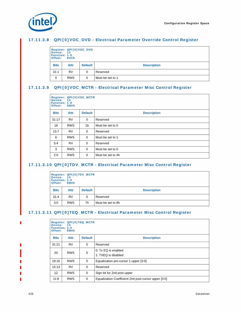
Configuration Register Space
436 Datasheet
17.11.3.8 QPI[0]VOC_OVD - Electrical Parameter Override Control Register
17.11.3.9 QPI[0]VOC_MCTR - Electrical Parameter Misc Control Register
17.11.3.10 QPI[0]TDV_MCTR - Electrical Parameter Misc Control Register
17.11.3.11 QPI[0]TEQ_MCTR - Electrical Parameter Misc Control Register
Register: QPI[0]VOC_OVDDevice: 13Function: 1-0Offset: 8ACh
Bits Attr Default Description
31:1 RV 0 Reserved
0 RWS 0 Must be set to 1
Register: QPI[0]VOC_MCTRDevice: 13Function: 1-0Offset: 8B4h
Bits Attr Default Description
31:17 RV 0 Reserved
16 RWS 1b Must be set to 0
15:7 RV 0 Reserved
6 RWS 0 Must be set to 1
5:4 RV 0 Reserved
3 RWS 0 Must be set to 0
2:0 RWS 0 Must be set to 4h
Register: QPI[0]TDV_MCTR Device: 13Function: 1-0Offset: 8B4h
Bits Attr Default Description
31:4 RV 0 Reserved
3:0 RWS 7h Must be set to 8h
Register: QPI[0]TEQ_MCTRDevice: 13Function: 1-0Offset: 8B4h
Bits Attr Default Description
31:21 RV 0 Reserved
20 RWS 00: Tx EQ is enabled
1: TXEQ is disabled
19:16 RWS 0 Equalization pre-cursor 1 upper [3:0]
15:13 RV 0 Reserved
12 RWS 0 Sign bit for 2nd post upper
11:8 RWS 0 Equalization Coefficient 2nd post cursor upper [3:0]

Datasheet 437
Configuration Register Space
17.11.3.12 QPI[0]RXVRMCTL0 - RX VRM Control Register
17.11.3.13 QPI[0]CURSEL0 - Current Select Register
17.11.3.14 QPI[0]RXCTL0 - RX Buffer Control Register
7:5 RV 0 Reserved
4:0 RWS 10h Equalization Coefficient 1st post cursor upper [4:0]
Register: QPI[0]RXVRMCTL0Device: 13Function: 1-0Offset: 900h
Bit Attr Default Description
31:26 RV 0 Reserved
25:24 RWS 0hProgram in three steps : Read, set to 01b; read, set to 10b; read, set to 11b
23:0 RV 0 Reserved
Register: QPI[0]CURSEL0Device: 13Function: 1-0Offset: 984h
Bit Attr Default Description
31:20 RV 0 Reserved
19:16 RWS Dh Must be set to Ch
15:0 RV Dh Reserved
Register: QPI[0]RXCTL0Device: 13Function: 1-0Offset: A00h
Bit Attr Default Description
31:24 RV 0 Reserved
23 RWS 0 Must be set to 1
22:16 RV 0 Reserved
15:8 RWS 54h Must be set to 74h
7:0 RV 0 Reserved
Register: QPI[0]TEQ_MCTRDevice: 13Function: 1-0Offset: 8B4h
Bits Attr Default Description

Configuration Register Space
438 Datasheet
17.12 PCI Express, DMI Configuration Space RegistersThis section covers the configuration space registers for PCI Express and DMI. See Section 17.10 for Intel QuickPath Interconnect configuration registers.
The next PCIe sections will cover register definitions for devices 0–10 and this description will be divided into three parts. One part that describes the standard PCI header space from 0h to 3Fh. The second part describes the device specific region from 40h to FFh. The third part describes the PCI Express enhanced configuration region.
Note: Notes on following register descriptions:
• Note that in the following sections, PCI Express has been generically used to indicate either a standard PCI Express port or an DMI port and any exceptions to this are called out where applicable.
• When N/A is used in any of the “Device” number rows that indicates the register does not apply to the indicated devices and the register descriptor in the reminder of the table hence will not apply to those devices. There could be other registers defined at the same offset for these device numbers or the offset could be reserved.
17.12.1 Other Register Notes
Note that, in general, all register bits in the standard PCI header space (offset 0–3Fh) or in any OS visible capability registers, which control the address decode like MSE, IOSE, VGAEN or otherwise control transaction forwarding must be treated as dynamic bits in the sense that these register bits could be changed by the OS when there is traffic flowing through the IOH. Note that the address register themselves can be treated as static in the sense that they will not be changed without the decode control bits being clear. Registers outside of this standard space will be noted as dynamic when appropriate.

Datasheet 439
Configuration Register Space
Figure 17-1 illustrates how each PCI Express port’s configuration space appears to software. Each PCI Express configuration space has three regions:
• Standard PCI Header — This region is the standard PCI-to-PCI bridge header providing legacy OS compatibility and resource management.
• PCI Device Dependent Region — This region is also part of standard PCI configuration space and contains the PCI capability structures and other port specific registers. For the IOH, the supported capabilities are:
— SVID/SDID Capability
— Message Signalled Interrupts
— Power Management
— PCI Express Capability
• PCI Express Extended Configuration Space — This space is an enhancement beyond standard PCI and only accessible with PCI Express aware software. The IOH supports the Advanced Error Reporting Capability in this configuration space.
Figure 17-1. PCI Express Root Port (Devices 1–10), DMI Port (Device 0) Type1Configuration Space
0x00
0x40
0x100
0xFFF
PCIE Advanced ErrorReporting
MSI Capability
P2P'CAP_PTR
PCIE Capability
Ext
ende
dC
onfig
urat
ion
Spa
ceP
CI
Dev
ice
Dep
ende
ntP
CIH
eade
r
PM Capability
SVID/SDID Capability

Configuration Register Space
440 Datasheet
Not all the capabilities listed above for a PCI Express port are required for a DMI port. Through the rest of the chapter, as each register elaborated upon, it will be mentioned which registers are applicable to the PCI Express port and which are applicable to the DMI port.
Table 17-24.IOH Device 0 (DMI mode) Configuration Address Map (Sheet 1 of 3)
DID VID 00h 80h
PCISTS PCICMD 04h 84h
CCR RID 08h 88h
BIST HDR PLAT CLSR 0Ch 8Ch
10h PXPCAP PXPNXTPTR PXPCAPID 90h
14h DEVCAP 94h
18h DEVSTS DEVCON 98h
1Ch LNKCAP 9Ch
20h LNKSTS LNKCON A0h
24h SLTCAP A4h
28h SLTSTS SLTCON A8h
SID SVID 2Ch ROOTCAP ROOTCON ACh
30h ROOTSTS B0h
CAPPTR 34h DEVCAP2 B4h
38h DEVCON2 B8h
INTPIN INTL 3Ch BCh
40h LNKSTS2 LNKCON2 C0h
44h C4h
48h C8h
4Ch CCh
50h D0h
54h D4h
58h D8h
5Ch DCh
MSIMSGCTL MSINXTPTR MSICAPID 60h PMCAP E0h
MSGADR 64h PMCSR E4h
MSGDAT 68h E8h
MSIMSK 6Ch ECh
MSIPENDING 70h F0h
74h F4h
78h F8h
7Ch FCh

Datasheet 441
Configuration Register Space
Note: 1: Applicable onlyto devices #1, 3, 7.
Table 17-25.IOH Device 0 (DMI mode) Extended Configuration Register Address Map (Sheet 2 of 3)
ERRCAPHDR 100h PERFCTRL 180h
UNCERRSTS 104h 184h
UNCERRMSK 108h MISCCTRLSTS 188h
UNCERRSEV 10Ch
COERRSTS 110h PCIE_IOU_BIF_CTRL1 190h
CORERRMSK 114h
ERRCAP 118h
HDRLOG 11Ch
120h
124h
128h
RPERRCMD 12Ch
RPERRSTS 130h
ERRSID CORSRCID 134h
138h
13Ch
APICLIMIT APICBASE 140h
144h
148h
14Ch
ACSCAPHDR 150h
ACSCTRL ACSCAP 154h
158h
15Ch 1DCh
160h CTOCTRL 1E0h
164h PCI_SS_CTRLSTS 1E4h
168h 1E8h
16Ch
170h
174h
178h
17Ch 1FCh

Configuration Register Space
442 Datasheet
Table 17-26.IOH Devices 0(DMI Mode) Configuration Register Address Map (Sheet 3 of 3)
XPCORERRSTS 200h
XPCORERRMSK 204h
XPUNCERRSTS 208h
XPUNCERRMSK 20Ch
XPUNCERRSEV 210h
XPUNCERRPTR
214h
218h
21Ch
220h
224h
228h
22Ch
XPGLBERRPTR XPGLBERRSTS 230h
234h
238h
23Ch
240h
244h
248h
24Ch
250h
254h
258h
25Ch
260h
264h
268h
26Ch
270h
274h
278h
27Ch

Datasheet 443
Configuration Register Space
Table 17-27.IOH Devices 0 (PCIe Mode) – 10 Legacy Configuration Map (PCI Express Registers)
DID VID 00h 80h
PCISTS PCICMD 04h 84h
CCR RID 08h 88h
BIST HDR PLAT CLSR 0Ch 8Ch
10h PXPCAP PXPNXTPTR PXPCAPID 90h
14h DEVCAP 94h
SUBBUS SECBUS PBUS 18h DEVSTS DEVCON 98h
SSTS IOLIM IOBAS 1Ch LNKCAP 9Ch
MLIM MBAS 20h LNKSTS LNKCON A0h
PLIM PBAS 24h SLTCAP A4h
PBASU 28h SLTSTS SLTCON A8h
PLIMU 2Ch ROOTCAP ROOTCON ACh
30h ROOTSTS B0h
CAPPTR 34h DEVCAP2 B4h
38h DEVCTRL2 B8h
BCR INTPIN INTL 3Ch BCh
SNXTPTR SCAPID 40h LNKSTS2 LNKCON2 C0h
SID SVID 44h C4h
48h C8h
4Ch CCh
50h D0h
54h D4h
58h D8h
5Ch DCh
MSIMSGCTL MSINXTPTR MSICAPID 60h PMCAP E0h
MSGADR 64h PMCSR E4h
MSGDAT 68h E8h
6Ch ECh
70h F0h
74h F4h
78h F8h
7Ch FCh

Configuration Register Space
444 Datasheet
Table 17-28.IOH Devices 0 (PCIe Mode) – 10 Extended Configuration Register Address Map (PCI Express Registers) (Sheet 1 of 2)
ERRCAPHDR 100h PERFCTRLSTS 180h
UNCERRSTS 104h 184h
UNCERRMSK 108h MISCCTRLSTS 188h
UNCERRSEV 10Ch 18Ch
CORERRSTS 110h
CORERRMSK 114h
ERRCAP 118h
HDRLOG 11Ch
120h
124h
128h
RPERRCMD 12Ch
RPERRSTS 130h
ERRSID CORSRCID 134h
SSMSK 138h
13Ch
APICLIMIT APICBASE 140h ADDPCIECTRL 1C0h
144h
148h
14Ch
ACSCAPHDR 150h
ACSCTRL ACSCAP 154h
158h
15Ch
160h CTOCTRL 1E0h
164h PCIELERCTRL 1E4h
168h
16Ch
170h
174h
178h
17Ch 1FCh

Datasheet 445
Configuration Register Space
Table 17-29.IOH Devices 0–10 Extended Configuration Register Address Map (PCI Express Registers) (Sheet 2 of 2)
XPCORERRSTS 200h
XPCORERRMSK 204h
XPUNCERRSTS 208h
XPUNCERRMSK 20Ch
XPUNCERRSEV 210h
XPUNCERRPTR
214h
UNCEMASK 218h
COREDMSK 21Ch
PREDMSK 220h
XPUNCEDMASK 224h
XPCOREDMASK 228h
22Ch
XPGLBERRPTR XPGLBERRSTS 230h
234h
238h
23Ch
240h
244h
248h
24Ch
250h
254h
258h
25Ch
260h
264h
268h
26Ch
270h
274h
278h
27Ch

Configuration Register Space
446 Datasheet
17.12.2 Standard PCI Configuration Space (0h to 3Fh) —Type 0/1 Common Configuration Space
This section covers registers in the 0h to 3Fh region that are common to all the devices 0 through 11. Comments at the top of the table indicate what devices/functions the description applies to. Exceptions that apply to specific functions are noted in the individual bit descriptions.
17.12.2.1 VID—Vendor Identification Register
17.12.2.2 DID—Device Identification Register
17.12.2.3 DID—Device Identification Register
Register: VIDDevice: 0–10Function: 0Offset: 00h
Bit Attr Default Description
15:0 RO 8086hVendor Identification NumberThe value is assigned by PCI-SIG to Intel.
Register: DIDDevice: 0Function: 0Offset: 02h
Bit Attr Default Description
15:0
RO (Device 10), RO (Others)
3400–3407h
Device Identification NumberThe value is assigned by Intel to each product. IOH will have a unique device id for each device.
Register: DIDDevice: 1–10Function: 0Offset: 02h
Bit Attr Default Description
15:0
RO (Device 10), RO (Others)
Dev: Def1: 3408h2: 3409h3: 340Ah4: 340Bh5: 340Ch6: 340Dh7: 340Eh8: 340Fh9: 3410h10: 3411h
Device Identification NumberThe value is assigned by Intel to each product. IOH will have a unique device ID for each device.

Datasheet 447
Configuration Register Space
17.12.2.4 PCICMD—PCI Command Register
This register defines the PCI 3.0 compatible command register values applicable to PCI Express space.
Register: PCICMDDevice: 0–10Function: 0Offset: 04h
Bit Attr Default Description
15:11 RV 00h Reserved. (by PCI SIG)
10 RO 0 Not applicable to PCI Express
9 RO 0Fast Back-to-Back EnableNot applicable to PCI Express and is hardwired to 0
8 RW 0
SERR EnableFor PCI Express/DMI ports, this field enables notifying the internal core error logic of occurrence of an uncorrectable error (fatal or non-fatal) at the port. The internal core error logic of IOH then decides if/how to escalate the error further (pins/message, and so on). This bit also controls the propagation of PCI Express ERR_FATAL and ERR_NONFATAL messages received from the port to the internal IOH core error logic.1 = Fatal and Non-fatal error generation and Fatal and Non-fatal error
message forwarding is enabled0 = Fatal and Non-fatal error generation and Fatal and Non-fatal error
message forwarding is disabledRefer to PCI Express Base Specification, Revision 1.1 and post 1.1 Erratas and EC*’s for details of how this bit is used in conjunction with other control bits in the Root Control register for forwarding errors detected on the PCI Express interface to the system core error logic.This bit has no impact on error reporting from the other device — I/OxAPIC.
7 RO 0IDSEL Stepping/Wait Cycle ControlNot applicable to internal IOH devices. Hardwired to 0.
6 RW 0
Parity Error ResponseFor PCI Express/DMI ports, IOH ignores this bit and always does ECC/parity checking and signaling for data/address of transactions both to and from IOH. This bit though affects the setting of bit 8 in the PCISTS (see bit 8 in Section 17.12.2.5) register.
5 RO 0VGA palette snoop EnableNot applicable to internal IOH devices. Hardwired to 0.
4 RO 0Memory Write and Invalidate EnableNot applicable to internal IOH devices. Hardwired to 0.
3 RO 0Special Cycle EnableNot applicable to PCI Express. Hardwired to 0.
2 RW 0
Bus Master EnableThis bit controls the ability of the PCI Express/DMI port in generating/forwarding memory (including MSI writes) or I/O transactions (and not messages) or configuration transactions from the secondary side to the primary side. For I/OxAPIC, this bit enables them to generate memory write/MSI.1 = Enables the PCI Express/DMI port or I/OxAPIC to generate/forward
memory, configuration, or I/O read/write requests.0 = The Bus Master is disabled. When this bit is 0, IOH root ports will treat
upstream PCI Express memory writes/reads, IO writes/reads, and configuration reads and writes as unsupported requests (and follow the rules for handling unsupported requests). This behavior is also true towards transactions that are already pending in the IOH root port’s internal queues when the BME bit is turned off. I/OxAPIC cannot generate any memory transactions when this bit is 0.

Configuration Register Space
448 Datasheet
17.12.2.5 PCISTS—PCI Status Register
The PCI Status register is a 16-bit status register which reports the occurrence of various events associated with the primary side of the “virtual” PCI-PCI bridge embedded in PCI Express ports and also primary side of the other devices on the internal IOH bus.
1 RW 0
Memory Space Enable 1 = Enables a PCI Express/DMI port’s memory range registers and internal
I/OxAPIC’s MBAR register (ABAR range decode is not enabled by this bit) to be decoded as valid target addresses for transactions from primary side.
0 = Disables a PCI Express/DMI port’s memory range registers (including the CSR range registers) to be decoded as valid target addresses for transactions from primary side
Note that if a PCI Express/DMI port’s MSE bit is clear, that port can still be target of any memory transaction if subtractive decoding is enabled on that port.
0 RW 0
IO Space EnableApplies only to PCI Express/DMI ports. 1 = Enables the I/O address range, defined in the IOBASE and IOLIM
registers of the PCI-to-PCI bridge header, for target decode from primary side.
0 = Disables the I/O address range, defined in the IOBASE and IOLIM registers of the PCI-to-PCI bridge header, for target decode from primary side.
Note that if a PCI Express/DMI port’s IOSE bit is clear, that port can still be target of an I/O transaction if subtractive decoding is enabled on that port.
Register: PCICMDDevice: 0–10Function: 0Offset: 04h
Bit Attr Default Description
Register: PCISTSDevice: 0–10Function: 0Offset: 06h
Bit Attr Default Description
15 RW1C 0
Detected Parity ErrorThis bit is set by a device when it receives a packet on the primary side with an uncorrectable data error (that is, a packet with poison bit set or an uncorrectable data ECC error was detected at the XP-DP interface when ECC checking is done) or an uncorrectable address/control parity error. The setting of this bit is regardless of the Parity Error Response bit (PERRE) in the PCICMD register.
14RW1C
(Device 0–10)
0
Signaled System Error 1 = The device reported fatal/non-fatal (and not correctable) errors it
detected on its PCI Express interface. Software clears this bit by writing a ‘1’ to it. For Express ports this bit is also set (when SERR enable bit is set) when a FATAL/NON-FATAL message is forwarded from the Express link to the ERR[2:0] pins or to ICH using a message. Note that IOH internal ‘core’ errors (like parity error in the internal queues) are not reported using this bit.
0 = The device did not report a fatal/non-fatal error
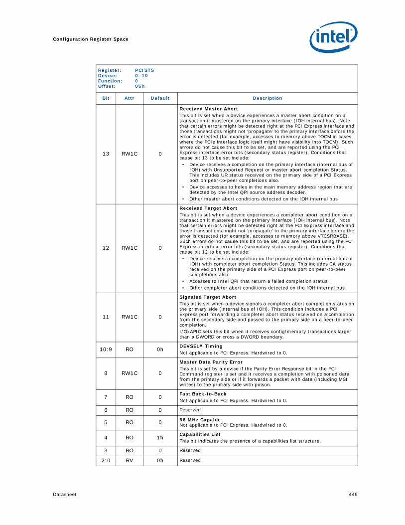
Datasheet 449
Configuration Register Space
13 RW1C 0
Received Master AbortThis bit is set when a device experiences a master abort condition on a transaction it mastered on the primary interface (IOH internal bus). Note that certain errors might be detected right at the PCI Express interface and those transactions might not ‘propagate’ to the primary interface before the error is detected (for example, accesses to memory above TOCM in cases where the PCIe interface logic itself might have visibility into TOCM). Such errors do not cause this bit to be set, and are reported using the PCI Express interface error bits (secondary status register). Conditions that cause bit 13 to be set include:• Device receives a completion on the primary interface (internal bus of
IOH) with Unsupported Request or master abort completion Status. This includes UR status received on the primary side of a PCI Express port on peer-to-peer completions also.
• Device accesses to holes in the main memory address region that are detected by the Intel QPI source address decoder.
• Other master abort conditions detected on the IOH internal bus
12 RW1C 0
Received Target AbortThis bit is set when a device experiences a completer abort condition on a transaction it mastered on the primary interface (IOH internal bus). Note that certain errors might be detected right at the PCI Express interface and those transactions might not ‘propagate’ to the primary interface before the error is detected (for example, accesses to memory above VTCSRBASE). Such errors do not cause this bit to be set, and are reported using the PCI Express interface error bits (secondary status register). Conditions that cause bit 12 to be set include:• Device receives a completion on the primary interface (internal bus of
IOH) with completer abort completion Status. This includes CA status received on the primary side of a PCI Express port on peer-to-peer completions also.
• Accesses to Intel QPI that return a failed completion status• Other completer abort conditions detected on the IOH internal bus
11 RW1C 0
Signaled Target AbortThis bit is set when a device signals a completer abort completion status on the primary side (internal bus of IOH). This condition includes a PCI Express port forwarding a completer abort status received on a completion from the secondary side and passed to the primary side on a peer-to-peer completion.I/OxAPIC sets this bit when it receives config/memory transactions larger than a DWORD or cross a DWORD boundary.
10:9 RO 0hDEVSEL# TimingNot applicable to PCI Express. Hardwired to 0.
8 RW1C 0
Master Data Parity ErrorThis bit is set by a device if the Parity Error Response bit in the PCI Command register is set and it receives a completion with poisoned data from the primary side or if it forwards a packet with data (including MSI writes) to the primary side with poison.
7 RO 0Fast Back-to-BackNot applicable to PCI Express. Hardwired to 0.
6 RO 0 Reserved
5 RO 0 66 MHz CapableNot applicable to PCI Express. Hardwired to 0.
4 RO 1hCapabilities ListThis bit indicates the presence of a capabilities list structure.
3 RO 0 Reserved
2:0 RV 0h Reserved
Register: PCISTSDevice: 0–10Function: 0Offset: 06h
Bit Attr Default Description

Configuration Register Space
450 Datasheet
17.12.2.6 RID—Revision Identification Register
This register contains the revision number of the IOH. The revision number steps the same across all devices and functions, that is, individual devices do not step their RID independently. Note that the revision id for the JTAG IDCODE register also steps with this register.
The IOH supports the CRID feature where in this register’s value can be changed by BIOS.
17.12.2.7 CCR—Class Code Register
This register contains the Class Code for the device.
17.12.2.8 CLSR—Cache Line Size Register
Register: RIDDevice: 0–10Function: 0Offset: 08h
Bit Attr Default Description
7:4 RO 0 Major RevisionSteppings which require all masks to be regenerated.
3:0 RO 0 Minor RevisionIncremented for each stepping which does not modify all masks. Reset for each major revision.
Register: CCRDevice: 0–10Function: 0Offset: 09h
Bit Attr Default Description
23:16 RO 06h
Base ClassFor PCI Express/DMI ports, this field is hardwired to 06h, indicating it is a “Bridge Device”. For I/OxAPIC devices, this field defaults to 08h, indicating it is a “Generic System Peripherals”.
15:8 RO 04h
Sub-ClassFor PCI Express/DMI ports, this field defaults to 04h indicating “PCI-PCI bridge”. This register changes to the sub class of 00h to indicate “Host Bridge”, when bit 0 in Section 17.6.3, “IOHMISCCTRL—IOH Miscellaneous Control Register” on page 282 is set.
7:0 RO 00h Register-Level Programming InterfaceThis field is hardwired to 00h for PCI Express/DMI ports.
Register: CLSRDevice: 0–10Function: 0Offset: 0Ch
Bit Attr Default Description
7:0 RW 0Cache line SizeThis register is set as RW for compatibility reasons only. Cache line size for IOH is always 64B. IOH hardware ignore this setting.
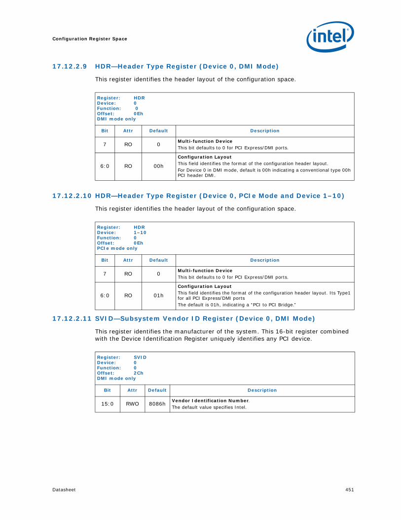
Datasheet 451
Configuration Register Space
17.12.2.9 HDR—Header Type Register (Device 0, DMI Mode)
This register identifies the header layout of the configuration space.
17.12.2.10 HDR—Header Type Register (Device 0, PCIe Mode and Device 1–10)
This register identifies the header layout of the configuration space.
17.12.2.11 SVID—Subsystem Vendor ID Register (Device 0, DMI Mode)
This register identifies the manufacturer of the system. This 16-bit register combined with the Device Identification Register uniquely identifies any PCI device.
Register: HDRDevice: 0Function: 0Offset: 0EhDMI mode only
Bit Attr Default Description
7 RO 0Multi-function DeviceThis bit defaults to 0 for PCI Express/DMI ports.
6:0 RO 00h
Configuration LayoutThis field identifies the format of the configuration header layout. For Device 0 in DMI mode, default is 00h indicating a conventional type 00h PCI header DMI.
Register: HDRDevice: 1–10Function: 0Offset: 0EhPCIe mode only
Bit Attr Default Description
7 RO 0Multi-function DeviceThis bit defaults to 0 for PCI Express/DMI ports.
6:0 RO 01h
Configuration LayoutThis field identifies the format of the configuration header layout. Its Type1 for all PCI Express/DMI portsThe default is 01h, indicating a “PCI to PCI Bridge.”
Register: SVIDDevice: 0Function: 0Offset: 2ChDMI mode only
Bit Attr Default Description
15:0 RWO 8086hVendor Identification Number. The default value specifies Intel.

Configuration Register Space
452 Datasheet
17.12.2.12 SID—Subsystem Identity Register (Device 0, DMI Mode)
This register identifies the system.
17.12.2.13 CAP—Capability Pointer Register
The CAPPTR is used to point to a linked list of additional capabilities implemented by the device. It provides the offset to the first set of capabilities registers located in the PCI compatible space from 40h.
17.12.2.14 INTL—Interrupt Line Register
The Interrupt Line register is used to communicate interrupt line routing information between initialization code and the device driver. This register is not used in newer operating systems and is just kept.
Register: SIDDevice: 0Function: 0Offset: 2EhDMI mode only
Bit Attr Default Description
15:0 RWO 00hSubsystem Identification NumberAssigned by the subsystem vendor to uniquely identify the subsystem.
Register: CAPDevice: 0–10Function: 0Offset: 34h
Bit Attr Default Description
7:0 RWO 40hCapability Pointer
Points to the first capability structure for the device.
Register: INTLDevice: 0–10Function: 0Offset: 3Ch
Bit Attr Default Description
7:0 RWO 00hInterrupt LineThis bit is RO for PCI Express/DMI ports.

Datasheet 453
Configuration Register Space
17.12.2.15 INTPIN—Interrupt Pin Register
The INTPIN register identifies legacy interrupts for INTA, INTB, INTC, and INTD as determined by BIOS/firmware. These are emulated over the DMI port using the appropriate Assert_Intx commands.
17.12.3 Standard PCI Configuration Space (0h to 3Fh) — Type 1 – Only Common Configuration Space
This section covers registers that are applicable only to PCI express/DMI ports.
17.12.3.1 PBUS—Primary Bus Number Register
This register identifies the bus number on the on the primary side of the PCI Express port.
Register: INTPINDevice: 0–10Function: 0Offset: 3Dh
Bit Attr Default Description
7:0 RWO 01h
Interrupt PinThis field defines the type of interrupt to generate for the PCI express port.001 = Generate INTA010 = Generate INTB011 = Generate INTC100 = Generate INTDOthers = ReservedBIOS/configuration Software has the ability to program this register once during boot to set up the correct interrupt for the port.
Register: PBUSDevice: 0–10Function: 0Offset: 18h
Bit Attr Default Description
7:0 RW 00h
Primary Bus NumberConfiguration software programs this field with the number of the bus on the primary side of the bridge. This register has to be kept consistent with the IOHBUSNO0/1 register (see Section 17.6.5.12) in the CSRCFG space. BIOS (and OS if internal bus number gets moved) must program this register to the correct value since IOH hardware would depend on this register for inbound decode purposes.

Configuration Register Space
454 Datasheet
17.12.3.2 SECBUS—Secondary Bus Number
This register identifies the bus number assigned to the secondary side (PCI Express) of the “virtual” PCI-PCI bridge. This number is programmed by the PCI configuration software to allow mapping of configuration cycles to devices connected to PCI Express.
17.12.3.3 SUBBUS—Subordinate Bus Number Register
This register identifies the subordinate bus (if any) that resides at the level below the secondary bus of the PCI Express interface. This number is programmed by the PCI configuration software to allow mapping of configuration cycles to devices subordinate to the secondary PCI Express port.
Register: SECBUSDevice: 0–10Function: 0Offset: 19h
Bit Attr Default Description
7:0 RW 00h
Secondary Bus NumberThis field is programmed by configuration software to assign a bus number to the secondary bus of the virtual peer-to-peer bridge. IOH uses this register to forward a configuration transaction as either a Type 1 or Type 0 to PCI Express.
Register: SUBBUSDevice: 0–10Function: 0Offset: 1Ah
Bit Attr Default Description
7:0 RW 00h
Subordinate Bus NumberThis register is programmed by configuration software with the number of the highest subordinate bus that is behind the PCI Express port. Any transaction that falls between the secondary and subordinate bus number (both inclusive) of an Express port is forwarded to the express port.

Datasheet 455
Configuration Register Space
17.12.3.4 IOBAS—I/O Base Register
The I/O Base and I/O Limit registers define an address range that is used by the PCI Express port to determine when to forward I/O transactions from one interface to the other using the following formula:
IO_BASE A[15:12] IO_LIMIT
The bottom of the defined I/O address range will be aligned to a 4 KB (1KB if EN1K bit is set) boundary while the top of the region specified by IO_LIMIT will be one less than a 4 KB (1KB if EN1K bit is set) multiple. Setting the I/O limit less than I/O base disables the I/O range altogether.
Note that in general the I/O base and limit registers won’t be programmed by software without clearing the IOSE bit first.
17.12.3.5 IOLIM—I/O Limit Register
Register: IOBASDevice: 0–10Function: 0Offset: 1Ch
Bit Attr Default Description
7:4 RW 0hI/O Base AddressThis field corresponds to A[15:12] of the I/O addresses at the PCI Express port.
3:2 RWL 0hWhen EN1K is set (Refer to Section 17.6.5.6 for definition of EN1K bit), these bits become RW and allow for 1K granularity of I/O addressing, otherwise these are RO.
1:0 RO 0hI/O Address capabilityIOH supports only 16 bit addressing.
Register: IOLIMDevice: 0–10Function: 0Offset: 1Dh
Bit Attr Default Description
7:4 RW 0hI/O Address LimitThis field corresponds to A[15:12] of the I/O addresses at the PCI Express port.
3:2 RWL 0h When EN1K is set, these bits become RW and allow for 1K granularity of I/O addressing, otherwise these bits are RO.
1:0 RO 0hI/O Address Limit CapabilityIOH only supports 16 bit addressing.

Configuration Register Space
456 Datasheet
17.12.3.6 SECSTS—Secondary Status Register
Secondary Status register is a 16-bit status register that reports the occurrence of various events associated with the secondary side (that is, PCI Express/DMI side) of the “virtual” PCI-PCI bridge.
Register: SECSTSDevice: 0–10Function: 0Offset: 1Eh
Bit Attr Default Description
15 RW1C 0
Detected Parity ErrorThis bit is set by the IOH whenever it receives a poisoned TLP in the PCI Express port. This bit is set regardless of the state the Parity Error Response Enable bit in the Bridge Control register.
14 RW1C 0Received System ErrorThis bit is set by the IOH when it receives a ERR_FATAL or ERR_NONFATAL message.
13 RW1C 0
Received Master Abort StatusThis bit is set when the PCI Express port receives a Completion with “Unsupported Request Completion” Status or when IOH master aborts a Type0 configuration packet that has a non-zero device number.
12 RW1C 0Received Target Abort StatusThis bit is set when the PCI Express port receives a Completion with “Completer Abort” Status.
11 RW1C 0
Signaled Target Abort StatusThis bit is set when the PCI Express port sends a completion packet with a “Completer Abort” Status (including peer-to-peer completions that are forwarded from one port to another).
10:9 RO 00DEVSEL# TimingNot applicable to PCI Express. Hardwired to 0.
8 RW1C 0
Master Data Parity Error StatusThis bit is set by the PCI Express port on the secondary side (PCI Express link) if the Parity Error Response Enable bit (PERRE) is set in Bridge Control register and either of the following two conditions occurs:• The PCI Express port receives a Completion from PCI Express marked
poisoned• The PCI Express port poisons a packet with data
If the Parity Error Response Enable bit in Bridge Control Register is cleared, this bit is never set.
7 RO 0Fast Back-to-Back Transactions Capable StatusNot applicable to PCI Express. Hardwired to 0.
6 RO 0 Reserved
5 RO 066 MHz capability StatusNot applicable to PCI Express. Hardwired to 0.
4:0 RO 0h Reserved

Datasheet 457
Configuration Register Space
17.12.3.7 MBAS—Memory Base
The Memory Base and Memory Limit registers define a memory mapped I/O non-prefetchable address range (32-bit addresses) and the IOH directs accesses in this range to the PCI Express port based on the following formula:
MEMORY_BASE A[31:20] MEMORY_LIMIT
The upper 12 bits of both the Memory Base and Memory Limit registers are read/write and corresponds to the upper 12 address bits, A[31:20] of 32-bit addresses. Thus, the bottom of the defined memory address range will be aligned to a 1 MB boundary and the top of the defined memory address range will be one less than a 1 MB boundary. Refer to Chapter 7, “System Address Map” for further details on decoding.
Setting the memory limit less than memory base disables the 32-bit memory range altogether.
Note: In general the memory base and limit registers won’t be programmed by software without clearing the MSE bit first.
17.12.3.8 MLIM—Memory Limit
Register: MBASDevice: 0–10Function: 0Offset: 20h
Bit Attr Default Description
15:4 RW 0hMemory Base AddressThis field corresponds to A[31:20] of the memory address on the PCI Express port.
3:0 RO 0h Reserved
Register: MLIMDevice: 0–10Function: 0Offset: 22h
Bit Attr Default Description
15:4 RW 0s
Memory Limit AddressThis field corresponds to A[31:20] of the memory address that corresponds to the upper limit of the range of memory accesses that will be passed by the PCI Express bridge
3:0 RO 0h Reserved. (by PCI SIG)

Configuration Register Space
458 Datasheet
17.12.3.9 PBAS—Prefetchable Memory Base Register
The Prefetchable Memory Base and Memory Limit registers define a memory mapped I/O prefetchable address range (64-bit addresses) which is used by the PCI Express bridge to determine when to forward memory transactions based on the following Formula:
PREFETCH_MEMORY_BASE_UPPER::PREFETCH_MEMORY_BASE A[63:20] PREFETCH_MEMORY_LIMIT_UPPER::PREFETCH_MEMORY_LIMIT
The upper 12 bits of both the Prefetchable Memory Base and Memory Limit registers are read/write and corresponds to the upper 12 address bits, A[31:20] of 32-bit addresses. The bottom of the defined memory address range will be aligned to a 1 MB boundary and the top of the defined memory address range will be one less than a 1 MB boundary.
The bottom 4 bits of both the Prefetchable Memory Base and Prefetchable Memory Limit registers are read-only, contain the same value, and encode whether or not the bridge supports 64-bit addresses. If these four bits have the value 0h, then the bridge supports only 32 bit addresses. If these four bits have the value 01h, then the bridge supports 64-bit addresses and the Prefetchable Base Upper 32 Bits and Prefetchable Limit Upper 32 Bits registers hold the rest of the 64-bit prefetchable base and limit addresses respectively.
Setting the prefetchable memory limit less than prefetchable memory base disables the 64-bit prefetchable memory range altogether.
Note that in general the memory base and limit registers will not be programmed by software without clearing the MSE bit first.
17.12.3.10 PLIM—Prefetchable Memory Limit
Register: PBASDevice: 0–10Function: 0Offset: 24h
Bit Attr Default Description
15:4 RW 0sPrefetchable Memory Base AddressThis field corresponds to A[31:20] of the prefetchable memory address on the PCI Express port.
3:0 RO 1hPrefetchable Memory Base Address CapabilityIOH sets this bit to 01h to indicate 64 bit capability.
Register: PLIMDevice: 0–10Function: 0Offset: 26h
Bit Attr Default Description
15:4 RW 0sPrefetchable Memory Limit AddressThis field corresponds to A[31:20] of the memory address on the PCI Express bridge.
3:0 RO 1hPrefetchable Memory Limit Address CapabilityIOH sets this field to 01h to indicate 64bit capability.

Datasheet 459
Configuration Register Space
17.12.3.11 PBASU—Prefetchable Memory Base (Upper 32 Bits) Registers
The Prefetchable Base Upper 32 Bits and Prefetchable Limit Upper 32 Bits registers are extensions to the Prefetchable Memory Base and Prefetchable Memory Limit registers to support a 64-bit prefetchable memory address range.
17.12.3.12 PLIMU—Prefetchable Memory Limit (Upper 32 Bits) Register
17.12.3.13 BCR—Bridge Control Register
The Bridge Control register provides additional control for the secondary interface (that is, PCI Express) as well as some bits that affect the overall behavior of the “virtual” PCI-PCI bridge embedded within the IOH, for example, VGA compatible address range mapping.
Register: PBASUDevice: 0–10Function: 0Offset: 28h
Bit Attr Default Description
31:0 RW 0s
Prefetchable Upper 32-bit Memory Base AddressThis field corresponds to A[63:32] of the memory address that maps to the upper base of the prefetchable range of memory accesses that will be passed by the PCI Express bridge. The OS should program these bits based on the available physical limits of the system.
Register: PLIMUDevice: 0–10Function: 0Offset: 2Ch
Bit Attr Default Description
31:0 RW 0s
Prefetchable Upper 32-bit Memory Limit AddressThis field corresponds to A[63:32] of the memory address that maps to the upper limit of the prefetchable range of memory accesses that will be passed by the PCI Express bridge. The OS should program these bits based on the available physical limits of the system.
Register: BCRDevice: 0–10Function: 0Offset: 3Eh
Bit Attr Default Description
15:12 RO 0s Reserved
11 RO 0Discard Timer SERR StatusNot applicable to PCI Express. This bit is hardwired to 0.
10 RO 0Discard Timer StatusNot applicable to PCI Express. This bit is hardwired to 0.
9 RO 0Secondary Discard Timer StatusNot applicable to PCI Express. This bit is hardwired to 0.
8 RO 0Primary Discard TimerNot applicable to PCI Express. This bit is hardwired to 0.
7 RO 0Fast Back-to-Back EnableNot applicable to PCI Express. This bit is hardwired to 0.

Configuration Register Space
460 Datasheet
6 RW 0
Secondary Bus Reset1 = Setting this bit triggers a hot reset on the link for the corresponding
PCI Express port and the PCI Express hierarchy domain subordinate to the port. This sends the LTSSM into the Training (or Link) Control Reset state, which necessarily implies a reset to the downstream device and all subordinate devices. The transaction layer corresponding to port will be emptied by IOH when this bit is set. This means that in the outbound direction, all posted transactions are dropped and non-posted transactions are sent a UR response. In the inbound direction, completions for inbound NP requests are dropped when they arrive. Inbound posted writes are required to be flushed as well either by dropping the packets are by retiring them normally.
Note also that a secondary bus reset will not reset the virtual PCI-to-PCI bridge configuration registers of the targeted PCI Express port.
0 = No reset happens on the PCI Express port
5 RO 0Master Abort ModeNot applicable to PCI Express. This bit is hardwired to 0.
4 RW 0
VGA 16-bit decodeThis bit enables the virtual PCI-to-PCI bridge to provide 16-bit decoding of VGA I/O address precluding the decoding of alias addresses every 1 KB.0 = execute 10-bit address decodes on VGA I/O accesses.1 = execute 16-bit address decodes on VGA I/O accesses.This bit only has meaning if bit 3 of this register is also set to 1, enabling VGA I/O decoding and forwarding by the bridge.Refer to PCI-PCI Bridge Specification Revision 1.2 for further details of this bit behavior.
3 RW 0
VGA EnableThis bit controls the routing of CPU initiated transactions targeting VGA compatible I/O and memory address ranges. This bit must only be set for one PCI Express port.1 = Enable0 = Disable
2 RW 0
ISA EnableThis bit modifies the response by the IOH to an I/O access issued by the CPU that target ISA I/O addresses. This applies only to I/O addresses that are enabled by the IOBASE and IOLIM registers. 1 = The IOH will not forward to PCI Express any I/O transactions
addressing the last 768 bytes in each 1KB block even if the addresses are within the range defined by the IOBASE and IOLIM registers.
0 = All addresses defined by the IOBASE and IOLIM for CPU I/O transactions will be mapped to PCI Express.
1 RW 0
SERR EnableThis bit controls forwarding of ERR_COR, ERR_NONFATAL and ERR_FATAL messages from the PCI Express port to the primary side.1 = Enables forwarding of ERR_COR, ERR_NONFATAL and ERR_FATAL
messages.0 = Disables forwarding of ERR_COR, ERR_NONFATAL and ERR_FATAL
0 RW 0Parity Error Response EnableIOH ignores this bit. This bit though affects the setting of bit 8 in the SECSTS register.
Register: BCRDevice: 0–10Function: 0Offset: 3Eh
Bit Attr Default Description

Datasheet 461
Configuration Register Space
17.12.4 Device-Specific PCI Configuration Space — 40h to FFh
17.12.4.1 SCAPID—Subsystem Capability ID Register
17.12.4.2 SNXTPTR—Subsystem ID Next Pointer Register
17.12.4.3 SVID—Subsystem Vendor ID Register
17.12.4.4 SID—Subsystem Identity Register (Device 0, PCIe mode and Device 1–10)
Register: CAPIDDevice: 0–10Function: 0Offset: 40h
Bit Attr Default Description
7:0 RO 0DhCapability IDAssigned by PCI-SIG for subsystem capability ID
Register: NXTPTRDevice: 0–10Function: 0Offset: 41h
Bit Attr Default Description
7:0 RO 60hNext PtrThis field is set to 60h for the next capability list (MSI capability structure) in the chain.
Register: SVIDDevice: 0–10Function: 0Offset: 44h
Bit Attr Default Description
7:0 RWO 8086h Assigned by PCI-SIG for the subsystem vendor
Register: SDIDDevice: 0–10Function: 0Offset: 46h
Bit Attr Default Description
7:0 RWO 00h Assigned by the subsystem vendor to uniquely identify the subsystem

Configuration Register Space
462 Datasheet
17.12.4.5 DMIRCBAR: DMI Root Complex Register Block Base Address Register
This is the base address for the root complex configuration space. This window of addresses contains the Root complex Register set for the PCI Express hierarchy associated with the processor. On Reset, the Root complex configuration space is disabled and must be enabled by writing a 1 to DMIRCBAREN [Dev 0, offset 50h, bit0]. All the bits in this register are locked in Intel TXT-enabled mode.
17.12.4.6 MSICAPID—MSI Capability ID Register
17.12.4.7 MSINXTPTR—MSI Next Pointer Register
Register: DMIRCBARDevice: 0 (DMI)Function: 0Offset: 50h
Bit Attr Default Description
31:12 RWO 00000h DMI Base Address (DMIRCBAR): This field corresponds to Bits 32 to 12 of the base address DMI Root Complex register space. BIOS will program this register resulting in a base address for a 4-KB block of contiguous memory address space. This register ensures that a naturally aligned 4-KB space is allocated within the first 64 GB of addressable memory space. System Software uses this base address to program the DMI Root Complex register set. All the Bits in this register are locked in Intel® TXT enabled mode.
11:1 RV 00h Reserved
0 RW 0 DMIRCBAR Enable (DMIRCBAREN):0 = DMIRCBAR is disabled and does not claim any memory.1 = DMIRCBAR memory mapped accesses are claimed and decoded.
Register: (MSIX) CAPIDDevice: 1–10; N/A for 0Function: 0Offset: 60h
Bit Attr Default Description
7:0 RO 05hCapability IDAssigned by PCI-SIG for MSI (root ports).
Register: MSINXTPTRDevice: 1–10; N/A for 0Function: 0Offset: 61h
Bit Attr Default Description
7:0 RO 90hNext PtrThis field is set to 90h for the next capability list (PCI Express capability structure) in the chain.

Datasheet 463
Configuration Register Space
17.12.4.8 MSIMSGCTL—MSI Message Control Register
17.12.4.9 MSIAR—MSI Address Register
The MSI Address Register (MSIAR) contains the system specific address information to route MSI interrupts from the root ports and is breaks into their constituent fields where interrupts are located.
Register: MSIMSGCTLDevice: 1–10; N/A for 0Function: 0Offset: 62h
Bit Attr Default Description
15:9 RV 00h Reserved
8 RO 1Per-vector masking capableThis bit indicates that PCI Express ports support MSI per-vector masking.
7 RO 064-bit Address CapableThis field is hardwired to 0h since the message addresses are only 32-bit addresses (for example, FEEx_xxxxh).
6:4 RW 000
Multiple Message EnableApplicable only to PCI Express ports. Software writes to this field to indicate the number of allocated messages which is aligned to a power of two. When MSI is enabled, the software will allocate at least one message to the device. A value of 000 indicates 1 message. Any value greater than or equal to 001 indicates a message of 2.
3:1 RO 001Multiple Message CapableThe IOH’s Express ports support two messages for all their internal events.
0 RW 0
MSI EnableThe software sets this bit to select platform-specific interrupts or transmit MSI messages.0 = Disables MSI from being generated.0 = Enables the Express port to use MSI messages for RAS, provided bit 4
in Section 17.6.3, “IOHMISCCTRL—IOH Miscellaneous Control Register” on page 282 is clear and also enables the Express port to use MSI messages for PM and HP events at the root port provided these individual events are not enabled for ACPI handling (see Section 17.6.3, “IOHMISCCTRL—IOH Miscellaneous Control Register” on page 282 for details).
Register: MSIARDevice: 1–10Function: 0Offset: 64h
Bit Attr Default Description
31:20 RW 0000hAddress MSBThis field specifies the 12 most significant bits of the 32-bit MSI address. This field is RW for compatibility reasons only.
19:12 RW 00hAddress Destination IDThis field is initialized by software for routing the interrupts to the appropriate destination.
11:4 RW 00hAddress Extended Destination IDThis field is not used by IA-32 processor.
3 RW 0hAddress Redirection Hint0 = Directed1 = Redirectable

Configuration Register Space
464 Datasheet
17.12.4.10 MSIDR—MSI Data Register
The MSI Data Register contains all the data (interrupt vector) related to MSI interrupts from the root ports.
2 RW 0hAddress Destination Mode0 = Physical1 = Logical
1:0 RO 0h Reserved
Register: MSIARDevice: 1–10Function: 0Offset: 64h
Bit Attr Default Description
Register: MSIDRDevice: 1–10Function: 0Offset: 68h
Bit Attr Default Description
31:16 RO 0000h Reserved
15 RW 0h
Trigger Mode 0 = Edge Triggered1 = Level TriggeredThe IOH does nothing with this bit other than passing it along to Intel QPI.
14 RW 0h
Level 0 = Deassert1 = AssertThe IOH does nothing with this bit other than passing it along to Intel QPI.
13:12 RW 0h Reserved
11:8 RW 0h
Delivery Mode0000 = Fixed: Trigger Mode can be edge or level0001 = Lowest Priority: Trigger Mode can be edge or level0010 = SMI/PMI/MCA – Not supported using MSI of root port0011 = Reserved – Not supported using MSI of root port0100 = NMI – Not supported using MSI of root port0101 = INIT – Not supported using MSI of root port0110 = Reserved0111 = ExtINT – Not supported using MSI of root port1000–1111 = Reserved
7:0 RW 0h
Interrupt VectorThe interrupt vector (LSB) will be modified by the IOH to provide context sensitive interrupt information for different events that require attention from the processor, for example, Hot plug, Power Management and RAS error events.Depending on the number of Messages enabled by the processor, Table 17-2 illustrates how IOH distributes these vectors

Datasheet 465
Configuration Register Space
17.12.4.11 PXPCAPID—PCI Express Capability List Register
The PCI Express Capability List register enumerates the PCI Express Capability structure in the PCI 3.0 configuration space.
Table 17-30.MSI Vector Handling and Processing by IOH
Number of Messages enabled by Software Events IV[7:0]
1 All xxxxxxxx1
Notes:1. The term “xxxxxx” in the Interrupt vector denotes that software initializes them and
IOH will not modify any of the “x” bits except the LSB as indicated in the table as afunction of MMEN.
2 HP, PM xxxxxxx0
AER xxxxxxx1
Register: PXPCAPIDDevice: 0–10Function: 0Offset: 90h
Bit Attr Default Description
7:0 RO 10hCapability IDProvides the PCI Express capability ID assigned by PCI-SIG.

Configuration Register Space
466 Datasheet
17.12.4.12 PXPNXTPTR—PCI Express Next Capability List Register
The PCI Express Capability List register enumerates the PCI Express Capability structure in the PCI 3.0 configuration space.
17.12.4.13 PXPCAP—PCI Express Capabilities Register
The PCI Express Capabilities register identifies the PCI Express device type and associated capabilities.
Register: PXPNXTPTRDevice: 0–10Function: 0Offset: 91h
Bit Attr Default Description
7:0 RO E0hNext PtrThis field is set to the PCI PM capability.
Register: PXPCAPDevice: 0–10Function: 0Offset: 92h
Bit Attr Default Description
15:14 RO 0h Reserved
13:9 RO 00h
Interrupt Message NumberThis field indicates the interrupt message number that is generated for PM/HP events. When there are more than one MSI interrupt Number, this register field is required to contain the offset between the base Message Data and the MSI Message that is generated when the status bits in the slot status register or root port status registers are set. IOH assigns the first vector for PM/HP events and so this field is set to 0.
8 RWO 0
Slot ImplementedApplies only to the root ports:1 = PCI Express link associated with the port is connected to a slot.0 = No slot is connected to this port.This register bit is of type “write once” and is controlled by BIOS/special initialization firmware.
7:4 RO 0100Device/Port TypeThis field identifies the type of device. It is set to 0100 for all the PCI Express ports.
3:0 RO 2hCapability VersionThis field identifies the version of the PCI Express capability structure. Set to 2h for PCI Express for compliance with the extended base registers.

Datasheet 467
Configuration Register Space
17.12.4.14 DEVCAP—PCI Express Device Capabilities Register
The PCI Express Device Capabilities register identifies device specific information for the device.
Register: DEVCAPDevice: 0–10Function: 0Offset: 94h
Bit Attr Default Description
31:28 RO 0h Reserved
27:26 RO 0hCaptured Slot Power Limit ScaleDoes not apply to root ports or integrated devices.
25:18 RO 00hCaptured Slot Power Limit ValueDoes not apply to root ports or integrated devices.
17:16 RO 0h Reserved
15 RO 1Role Based Error Reporting IOH is 1.1 compliant; thus it supports this feature.
14 RO 0Power Indicator Present on DeviceDoes not apply to root ports or integrated devices.
13 RO 0Attention Indicator PresentDoes not apply to root ports or integrated devices.
12 RO 0Attention Button PresentDoes not apply to root ports or integrated devices.
11:9 RO 000Endpoint L1 Acceptable LatencyDoes not apply to IOH.
8:6 RO 000 Reserved
5 RO 1Extended Tag Field SupportedIOH devices support 8-bit tag
4:3 RO 0hPhantom Functions SupportedIOH does not support phantom functions.
2:0 RO001 (Device 1–10), 000 (Device 0)
Max Payload Size SupportedIOH supports 256B payloads on Express port and 128B on the remainder of the devices.

Configuration Register Space
468 Datasheet
17.12.4.15 DEVCTRL—PCI Express Device Control Register
The PCI Express Device Control register controls PCI Express specific capabilities parameters associated with the device.
Register: DEVCTRLDevice: 0–10Function: 0Offset: 98h
Bit Attr Default Description
15 RO 0h Reserved
14:12 RO 000Max_Read_Request_SizeExpress/DMI ports in IOH do not generate requests greater than 128B and this field is ignored.
11 RO 0
Enable No SnoopNot applicable to root ports since they never set the ‘No Snoop’ bit for transactions they originate (not forwarded from peer) to PCI Express.This bit has no impact on forwarding of NoSnoop attribute on peer requests.
10 RO 0Auxiliary Power Management EnableNot applicable to IOH.
9 RO 0Phantom Functions EnableNot applicable to IOH since it never uses phantom functions as a requester.
8 RW 0hExtended Tag Field EnableThis bit enables the PCI Express port/DMI to use an 8-bit Tag field as a requester.
7:5
RW (Device 1–10)
RO (Device
0)
000
Max Payload SizeThis field is set by configuration software for the maximum TLP payload size for the PCI Express port. As a receiver, the IOH must handle TLPs as large as the set value. As a requester (that is, for requests where IOH’s own RequesterID is used), it must not generate TLPs exceeding the set value. Permissible values that can be programmed are indicated by the Max_Payload_Size_Supported in the Device Capabilities register:000 = 128B max payload size001 = 256B max payload size (applies only to standard PCI Express ports
and other devices alias to 128B)others = alias to 128B
4 RO 0
Enable Relaxed OrderingNot applicable to root ports since they never set relaxed ordering bit as a requester (this does not include tx forwarded from peer devices).This bit has no impact on forwarding of relaxed ordering attribute on peer requests.
3 RW 0
Unsupported Request Reporting EnableThis bit applies only to the PCI Express/DMI ports. This bit controls the reporting of unsupported requests that IOH itself detects on requests its receives from a PCI Express/DMI port.0 = Reporting of unsupported requests is disabled1 = Reporting of unsupported requests is enabled.Refer to PCI Express Base Specification, Revision 1.1 and post 1.1 Erratas and EC*’s for complete details of how this bit is used in conjunction with other bits to UR errors.

Datasheet 469
Configuration Register Space
2 RW 0
Fatal Error Reporting EnableThis bit applies only to the PCI Express/DMI ports. Controls the reporting of fatal errors that IOH detects on the PCI Express/DMI interface.0 = Reporting of Fatal error detected by device is disabled1 = Reporting of Fatal error detected by device is enabledRefer to PCI Express Base Specification, Revision 1.1 and post 1.1 Erratas and EC*’s for complete details of how this bit is used in conjunction with other bits to report errors.For the PCI Express/DMI ports, this bit is not used to control the reporting of other internal component uncorrectable fatal errors (at the port unit) in any way.
1 RW 0
Non Fatal Error Reporting EnableThis bit applies only to the PCI Express/DMI ports. Controls the reporting of non-fatal errors that IOH detects on the PCI Express/DMI interface.0 = Reporting of Non Fatal error detected by device is disabled1 = Reporting of Non Fatal error detected by device is enabledRefer to PCI Express Base Specification, Revision 1.1 and post 1.1 Erratas and EC*’s for complete details of how this bit is used in conjunction with other bits to report errors.For the PCI Express/DMI ports, this bit is not used to control the reporting of other internal component uncorrectable non-fatal errors (at the port unit) in any way.
0 RW 0
Correctable Error Reporting EnableThis bit applies only to the PCI Express/DMI ports. Controls the reporting of correctable errors that IOH detects on the PCI Express/DMI interface0 = Reporting of link Correctable error detected by the port is disabled1 = Reporting of link Correctable error detected by port is enabledRefer to PCI Express Base Specification, Revision 1.1 and post 1.1 Erratas and EC*’s for complete details of how this bit is used in conjunction with other bits to report errors.For the PCI Express/DMI ports, this bit is not used to control the reporting of other internal component correctable errors (at the port unit) in any way.
Register: DEVCTRLDevice: 0–10Function: 0Offset: 98h
Bit Attr Default Description

Configuration Register Space
470 Datasheet
17.12.4.16 DEVSTS—PCI Express Device Status Register
The PCI Express Device Status register provides information about PCI Express device specific parameters associated with the device.
Register: DEVSTSDevice: 0–10Function: 0Offset: 9Ah
Bit Attr Default Description
15:6 RO 000h Reserved
5 RO 0h Transactions Pending: This bit does not apply to root/DMI ports or I/OxAPIC devices, that is, bit hardwired to 0 for these devices.
4 RO 0AUX Power DetectedDoes not apply to IOH
3 RW1C 0
Unsupported Request DetectedThis bit applies only to the root/DMI ports and does not apply to I/OxAPIC device. This bit indicates that the root port detected an Unsupported Request. Errors are logged in this register regardless of whether error reporting is enabled or not in the Device Control Register. 1 = Unsupported Request detected at the device/port. These unsupported
requests are NP requests inbound that the root port received and it detected them as unsupported requests (for example, address decoding failures that the root port detected on a packet, receiving inbound lock reads, BME bit is clear, and so on). Note that this bit is not set on peer-to-peer completions with UR status that are forwarded by the root port to the PCIe link.
0 = No unsupported request detected by the root port
2 RW1C 0
Fatal Error DetectedThis bit indicates that a fatal (uncorrectable) error is detected by the device. Errors are logged in this register regardless of whether error reporting is enabled or not in the Device Control register. 1 = Fatal errors detected0 = No Fatal errors detected
1 RW1C 0
Non Fatal Error DetectedThis bit gets set if a non-fatal uncorrectable error is detected by the device. Errors are logged in this register regardless of whether error reporting is enabled or not in the Device Control register. 1 = Non Fatal errors detected0 = No non-Fatal Errors detected
0 RW1C 0
Correctable Error DetectedThis bit gets set if a correctable error is detected by the device. Errors are logged in this register regardless of whether error reporting is enabled or not in the PCI Express Device Control register.1 = correctable errors detected0 = No correctable errors detected

Datasheet 471
Configuration Register Space
17.12.4.17 LNKCAP—PCI Express Link Capabilities Register
The Link Capabilities register identifies the PCI Express specific link capabilities.
Register: LNKCAPDevice: 0–10Function: 0Offset: 9Ch
Bit Attr Default Description
31:24 RWO 0Port NumberThis field indicates the PCI Express port number for the link and is initialized by software/BIOS.
23:22 RO 0h Reserved
21 RO 1Link Bandwidth Notification Capability A value of 1b indicates support for the Link Bandwidth Notification status and interrupt mechanisms.
20 RO 1Data Link Layer Link Active Reporting Capable The IOH supports reporting status of the data link layer so software knows when it can enumerate a device on the link or otherwise know the status of the link.
19 RO 1Surprise Down Error Reporting Capable The IOH supports reporting a surprise down error condition.
18 RO 0 Clock Power Management: Does not apply to IOH.
17:15 RWO 010h
L1 Exit LatencyThis field indicates the L1 exit latency for the given PCI Express port. It indicates the length of time this port requires to complete transition from L1 to L0.000 = Less than 1001 = 1 ìs to less than 2010 = 2 ìs to less than 4011 = 4 ìs to less than 8100 = 8 ìs to less than 16101 = 16 ìs to less than 32110 = 32 ìs to 64111 = More than 64 us
14:12 RWO 011
11:10 RO 11
9:4 RWO 000100b
Maximum Link WidthThis field indicates the maximum width of the given PCI Express Link attached to the port.000001 = x1000010 = x21
000100 = x4001000 = x8010000 = x16Others = ReservedThis is a RWO register for BIOS to update based on the platform usage of the links.
Notes:1. There are restrictions with routing x2 lanes from IOH to a slot. See Chapter 5, “PCI Express* and DMI
Interfaces” for details.
3:0 RO 0001b
Link Speeds SupportedIOH supports both 2.5 Gbps and 5 Gbps speeds if Gen2_OFF is OFF else it supports only Gen1This register is RWO when Gen2_OFF is OFF, so that BIOS can change the supported speeds field to be 0001b (Gen1 only) if the board routing is not capable of Gen2 (even though IOH silicon itself is capable of Gen2).

Configuration Register Space
472 Datasheet
17.12.4.18 LNKCON—PCI Express Link Control Register
The PCI Express Link Control register controls the PCI Express Link specific parameters.
Register: LNKCONDevice: 0–10Function: 0Offset: A0h
Bit Attr Default Description
15:12 RO 0 Reserved
11 RO 0
Link Autonomous Bandwidth Interrupt Enable 1 = Enables the generation of an interrupt to indicate that the Link
Autonomous Bandwidth Status bit has been set.0 = Disable
10 RO 0
Link Bandwidth Management Interrupt Enable 1 = Enables the generation of an interrupt to indicate that the Link
Bandwidth Management Status bit has been set.0 = Disable
9 RO 0Hardware Autonomous Width Disable IOH never changes a configured link width for reasons other than reliability.
8 RO 0Enable Clock Power Management N/A to IOH
7 RO 0 Reserved
6 RO 0Common Clock ConfigurationIOH does nothing with this bit
5 WO 0
Retrain LinkA write of 1 to this bit initiates link retraining in the given PCI Express port by directing the LTSSM to the recovery state if the current state is [L0 or L1]. If the current state is anything other than L0, L1, then a write to this bit does nothing. This bit always returns 0 when read.If the Target Link Speed field has been set to a non-zero value different than the current operating speed, then the LTSSM will attempt to negotiate to the target link speed.It is permitted to write 1b to this bit while simultaneously writing modified values to other fields in this register. When this is done, all modified values that affect link retraining must be applied in the subsequent retraining.
4 RO 0
Link DisableThis field controls whether the link associated with the PCI Express port is enabled or disabled. When this bit is a 1, a previously configured link (a link that has gone past the polling state) would return to the “disabled” state as defined in the PCI Express Base Specification, Revision 1.1 and post 1.1 Erratas and EC*’s. When this bit is clear, an LTSSM in the “disabled” state goes back to the detect state.0 = Enables the link associated with the PCI Express port1 = Disables the link associated with the PCI Express port
3 RO 0Read Completion BoundarySet to zero to indicate IOH could return read completions at 64B boundaries.
2 RV 0 Reserved
1:0 RW 00 Reserved

Datasheet 473
Configuration Register Space
17.12.4.19 LNKSTS—PCI Express Link Status Register
The PCI Express Link Status register provides information on the status of the PCI Express Link such as negotiated width, training, and so on.
Register: LNKSTSDevice: 0–10Function: 0Offset: A2h
Bit Attr Default Description
15 RO 0
Link Autonomous Bandwidth Status This bit is set to 1b by hardware to indicate that hardware has autonomously changed link speed or width, without the port transitioning through DL_Down status, for reasons other than to attempt to correct unreliable link operation. IOH sets this bit when it receives eight consecutive TS1 or TS2 ordered sets with the Autonomous Change bit set.Note that if the status bit is set by hardware in the same clock software clears the status bit, the status bit should remain set and if MSI is enabled, the hardware should trigger a new MSI.
14 RO 0
Link Bandwidth Management Status This bit is set to 1b by hardware to indicate that either of the following has occurred without the port transitioning through DL_Down status:• A link retraining initiated by a write of 1b to the Retrain Link bit has
completed• Hardware has autonomously changed link speed or width to attempt to
correct unreliable link operationNote that if the status bit is set by hardware in the same clock software clears the status bit, the status bit should remain set and if MSI is enabled, the hardware should trigger a new MSI.
13 RO 0
Data Link Layer Link ActiveSet to 1b when the Data Link Control and Management State Machine is in the DL_Active state, 0b otherwise.On a downstream port or upstream port, when this bit is 0b, the transaction layer associated with the link will abort all transactions that would otherwise be routed to that link.
12 RO 1
Slot Clock ConfigurationThis bit indicates whether IOH receives clock from the same xtal that also provides clock to the device on the other end of the link.1 = Indicates that same xtal provides clocks to devices on both ends of the
link0 = Indicates that different xtals provide clocks to devices on both ends of
the link
11 RO 0
Link TrainingThis field indicates the status of an ongoing link training session in the PCI Express port0 = LTSSM has exited the recovery/configuration state1 = LTSSM is in recovery/configuration state or the Retrain Link was set
but training has not yet begun.The IOH hardware clears this bit once LTSSM has exited the recovery/configuration state. Refer to PCI Express Base Specification, Revision 1.1 and post 1.1 Erratas and EC*’s for details of which states within the LTSSM would set this bit and which states would clear this bit.
10 RO 0 Reserved

Configuration Register Space
474 Datasheet
17.12.4.20 SLTCAP—PCI Express Slot Capabilities Register
The Slot Capabilities register identifies the PCI Express specific slot capabilities. These registers must be ignored by software on the DMI links.
9:4 RO 0x0
Negotiated Link WidthThis field indicates the negotiated width of the given PCI Express link after training is completed. Only x1, x2, x4, x8 and x16 link width negotiations are possible in IOH. A value of 01h in this field corresponds to a link width of x1, 02h indicates a link width of x2 and so on, with a value of 8h for a link width of x8.The value in this field is reserved and could show any value when the link is not up. Software determines if the link is up or not by reading bit 13 of this register.
3:0 RO 0x0
Current Link SpeedThis field indicates the negotiated Link speed of the given PCI Express Link.0001 = 2.5 Gbps0010 = 5 Gbps Others = ReservedThe value in this field is not defined and could show any value, when the link is not up. Software determines if the link is up or not by reading bit 13 of this register.
Register: LNKSTSDevice: 0–10Function: 0Offset: A2h
Bit Attr Default Description
Register: SLTCAPDevice: 0–10Function: 0Offset: A4h
Bit Attr Default Description
31:19 RO 0h Physical Slot NumberThis field indicates the physical slot number of the slot connected to the PCI Express port and is initialized by bios.
18 RO 0h Command Complete Not Capable: IOH is capable of command complete interrupt.
17 RO 0h Electromechanical Interlock Present This bit when set indicates that an Electromechanical Interlock is implemented on the chassis for this slot and that lock is controlled by bit 11 in Slot Control register. Bios note: this capability is not set if the Electromechanical Interlock control is connected to main slot power control.
16:15 RO 0h Slot Power Limit ScaleThis field specifies the scale used for the Slot Power Limit Value and is initialized by bios. IOH uses this field when it sends a Set_Slot_Power_Limit message on PCI Express.Range of Values:00: 1.0x01: 0.1x10: 0.01x11: 0.001x

Datasheet 475
Configuration Register Space
14:7 RWO 00h
Slot Power Limit ValueThis field specifies the upper limit on power supplied by slot in conjunction with the Slot Power Limit Scale value defined previouslyPower limit (in Watts) = SPLS x SPLV.This field is initialized by BIOS. The IOH uses this field when it sends a Set_Slot_Power_Limit message on PCI Express.Design Note: The IOH can chose to send the Set_Slot_Power_Limit message on the link at first link up condition without regards to whether this register and the Slot Power Limit Scale register are programmed yet by BIOS. The IOH must then be designed to discard a received Set_Slot_Power_Limit message without an error.
6 RWO 0h
Hot-plug CapableThis field defines hot-plug support capabilities for the PCI Express port.0 = Indicates that this slot is not capable of supporting Hot-plug
operations.1 = Indicates that this slot is capable of supporting Hot-plug operations.This bit is programed by BIOS based on the system design. This bit must be programmed by BIOS to be consistent with the VPP enable bit for the port.
5 RWO 0h
Hot-plug SurpriseThis field indicates that a device in this slot may be removed from the system without prior notification (like for instance a PCI Express cable).0 = Hot-plug surprise is not supported1 = Hot-plug surprise is supportedNote that if platform implemented cable solution (either direct or using a SIOM with repeater), on a port, then this could be set. BIOS programs this field with a 0 for CEM/SIOM FFs.This bit is used by IOH hardware to determine if a transition from DL_active to DL_Inactive is to be treated as a surprise down error or not. If a port is associated with a hotpluggable slot and the hotplug surprise bit is set, then any transition to DL_Inactive is not considered an error. Refer to PCI Express Base Specification, Revision 1.1 and post 1.1 Erratas and EC*’s for further details.
4 RWO 0h
Power Indicator PresentThis bit indicates that a Power Indicator is implemented for this slot and is electrically controlled by the chassis.0 = Power Indicator, which is electrically controlled by the chassis is not
present1 = Power Indicator, which is electrically controlled by the chassis is
presentBIOS programs this field with a 1 for CEM/SIOM FFs and a 0 for Express cable.
3 RWO 0h
Attention Indicator PresentThis bit indicates that an Attention Indicator is implemented for this slot and is electrically controlled by the chassis.0 = Attention Indicator, which is electrically controlled by the chassis is not
present1 = Attention Indicator, which is electrically controlled by the chassis is
presentBIOS programs this field with a 1 for CEM/SIOM FFs.
2 RWO 0h
MRL Sensor PresentThis bit indicates that an MRL Sensor is implemented on the chassis for this slot.0 = MRL Sensor is not present1 = MRL Sensor is presentBIOS programs this field with a 0 for SIOM/Express cable and with either 0 or 1 for CEM depending on system design.
Register: SLTCAPDevice: 0–10Function: 0Offset: A4h
Bit Attr Default Description

Configuration Register Space
476 Datasheet
17.12.4.21 SLTCON—PCI Express Slot Control Register
The Slot Control register identifies the PCI Express specific slot control parameters for operations such as Hot-plug and Power Management.
1 RWO 0h
Power Controller PresentThis bit indicates that a software controllable power controller is implemented on the chassis for this slot.0 = Software controllable power controller is not present1 = Software controllable power controller is presentBIOS programs this field with a 1 for CEM/SIOM FFs and a 0 for Express cable.
0 RWO 0h
Attention Button PresentThis bit indicates that the Attention Button event signal is routed (from slot or on-board in the chassis) to the IOH’s hotplug controller.0 = Attention Button signal is routed to IOH1 = Attention Button is not routed to IOH
Register: SLTCAPDevice: 0–10Function: 0Offset: A4h
Bit Attr Default Description
Register: SLTCONDevice: 1–10Function: 0Offset: A8h
Bit Attr Default Description
15:13 RO 0h Reserved
12 RO 0
Data Link Layer State Changed Enable 1 = Enables software notification when Data Link Layer Link Active field is
changed.Note: This bit should be RO for DMI. However this bit is implemented as a RW bit and hence software should not write to this bit.
11 RO 0
Electromechanical Interlock Control When software writes either a 1 to this bit, IOH pulses the EMIL pin per PCI Express Server/Workstation Module Electromechanical Spec Rev 0.5a. Write of 0 has no effect. This bit always returns a 0 when read. If electromechanical lock is not implemented, then either a write of 1 or 0 to this register has no effect.Note: This bit should be RO for DMI. However this bit is implemented as a RW bit and hence software should not write to this bit.
10 RO 1
Power Controller ControlIf a power controller is implemented, when written sets the power state of the slot per the defined encodings. Reads of this field must reflect the value from the latest write, even if the corresponding hot-plug command is not executed yet at the VPP, unless software issues a write without waiting for the previous command to complete in which case the read value is undefined.0 = Power Off1 = Power OnNote: This bit should be RO for DMI. However this bit is implemented as a RW bit and hence software should not write to this bit.

Datasheet 477
Configuration Register Space
9:8 RO 3h
Power Indicator ControlIf a Power Indicator is implemented, writes to this register set the Power Indicator to the written state. Reads of this field must reflect the value from the latest write, even if the corresponding hot-plug command is not executed yet at the VPP, unless software issues a write without waiting for the previous command to complete in which case the read value is undefined.00 = Reserved01 = On10 = Blink (IOH drives 1.5 Hz square wave for Chassis mounted LEDs)11 = OffWhen this register is written, the event is signaled using the virtual pins1 of the IOH over a dedicated SMBus port. IOH does not generate the Power_Indicator_On/Off/Blink messages on PCI Express when this field is written to by software.Note: This bit should be RO for DMI. However this bit is implemented as a RW bit and hence software should not write to this bit.
7:6 RO 3h
Attention Indicator ControlIf an Attention Indicator is implemented, writes to this register set the Attention Indicator to the written state.Reads of this field reflect the value from the latest write, even if the corresponding hot-plug command is not executed yet at the VPP, unless software issues a write without waiting for the previous command to complete in which case the read value is undefined.00 = Reserved01 = On10 = Blink (The IOH drives 1.5 Hz square wave)11 = OffWhen this register is written, the event is signaled using the virtual pins1 of the IOH over a dedicated SMBus port. IOH does not generated the Attention_Indicator_On/Off/Blink messages on PCI Express when this field is written to by software.Note: This bit should be RO for DMI. However this bit is implemented as a RW bit and hence SW should not write to this bit.
5 RO 0h
Hot-plug Interrupt EnableWhen set to 1b, this bit enables generation of Hot-Plug MSI interrupt (and not wake event) on enabled Hot-Plug events, provided ACPI mode for hotplug is disabled.0 = Disables interrupt generation on Hot-plug events1 = Enables interrupt generation on Hot-plug events
4 RO 0h
Command Completed Interrupt EnableThis field enables the generation of Hot-plug interrupts (and not wake event) when a command is completed by the Hot-plug controller connected to the PCI Express port.0 = Disables hot-plug interrupts on a command completion by a hot-plug
Controller1 = Enables hot-plug interrupts on a command completion by a hot-plug
ControllerNote: This bit should be RO for DMI. However this bit is implemented as a RW bit and hence SW should not write to this bit.
3 RO 0h
Presence Detect Changed EnableThis bit enables the generation of hot-plug interrupts or wake messages using a presence detect changed event.0 = Disables generation of hot-plug interrupts or wake messages when a
presence detect changed event happens.1 = Enables generation of hot-plug interrupts or wake messages when a
presence detect changed event happens.
Register: SLTCONDevice: 1–10Function: 0Offset: A8h
Bit Attr Default Description

Configuration Register Space
478 Datasheet
17.12.4.22 SLTSTS—PCI Express Slot Status Register
The PCI Express Slot Status register defines important status information for operations such as Hot-plug and Power Management.
2 RO 0h
MRL Sensor Changed EnableThis bit enables the generation of hot-plug interrupts or wake messages using a MRL Sensor changed event.0 = Disables generation of hot-plug interrupts or wake messages when an
MRL Sensor changed event happens.1 = Enables generation of hot-plug interrupts or wake messages when an
MRL Sensor changed event happens.Note: This bit should be RO for DMI. However this bit is implemented as a RW bit and hence SW should not write to this bit.
1 RO 0h
Power Fault Detected EnableThis bit enables the generation of hot-plug interrupts or wake messages using a power fault event.0 = Disables generation of hot-plug interrupts or wake messages when a
power fault event happens.1 = Enables generation of hot-plug interrupts or wake messages when a
power fault event happens.Note: This bit should be RO for DMI. However this bit is implemented as a RW bit and hence SW should not write to this bit.
0 RO 0h
Attention Button Pressed EnableThis bit enables the generation of hot-plug interrupts or wake messages using an attention button pressed event.0 = Disables generation of hot-plug interrupts or wake messages when the
attention button is pressed.1 = Enables generation of hot-plug interrupts or wake messages when the
attention button is pressed.Note: This bit should be RO for DMI. However this bit is implemented as a RW bit and hence SW should not write to this bit.
Notes:1. More information on Virtual pins can be found in Section 13.8.1.
Register: SLTCONDevice: 1–10Function: 0Offset: A8h
Bit Attr Default Description
Register: SLTSTSDevice: 1–10Function: 0Offset: AAh
Bit Attr Default Description
15:9 RO 0h Reserved
8 RO 0h
Data Link Layer State Changed This bit is set (if it is not already set) when the state of the Data Link Layer Link Active bit in the Link Status register changes. Software must read Data Link Layer Active field to determine the link state before initiating configuration cycles to the hot plugged device.
7 RO 0h
Electromechanical Latch StatusWhen read this register returns the current state of the Electromechanical Interlock (the EMILS pin) which has the defined encodings as:0 = Electromechanical Interlock Disengaged1 = Electromechanical Interlock Engaged

Datasheet 479
Configuration Register Space
6 RO 0h
Presence Detect StateFor ports with slots (where the Slot Implemented bit of the PCI Express Capabilities Registers is 1b), this field is the logical OR of the Presence Detect status determined using an in-band mechanism and sideband Present Detect pins. Refer to how PCI Express Base Specification, Revision 1.1 and post 1.1 Erratas and EC*’s for how the inband presence detect mechanism works (certain states in the LTSSM constitute “card present” and others don’t). 0 = Card/Module/Cable slot empty or Cable Slot occupied but not powered1 = Card/module Present in slot (powered or unpowered) or cable present
and powered on other endFor ports with no slots, IOH hardwires this bit to 1b.Note: The operating system could get confused when it sees an empty PCI Express root port that is, “no slots + no presence”, since this is now disallowed in the spec. So BIOS must hide all unused root ports devices in IOH config space, using the DEVHIDE register in Intel QPI CSR space.
5 RO 0h
MRL Sensor StateThis bit reports the status of an MRL sensor if it is implemented.0 = MRL Closed1 = MRL Open
4 RO 0h
Command CompletedThis bit is set by the IOH when the hot-plug command has completed and the hot-plug controller is ready to accept a subsequent command. It is subsequently cleared by software after the field has been read and processed. This bit provides no assurance that the action corresponding to the command is complete.
3 RO 0h
Presence Detect ChangedThis bit is set by the IOH when a Presence Detect Changed event is detected. It is subsequently cleared by software after the field has been read and processed.On-board logic per slot must set the VPP signal corresponding this bit inactive if the FF/system does not support out-of-band presence detect.
2 RO 0h
MRL Sensor ChangedThis bit is set by the IOH when an MRL Sensor Changed event is detected. It is subsequently cleared by software after the field has been read and processed.On-board logic per slot must set the VPP signal corresponding this bit inactive if the FF/system does not support MRL.
1 RO 0h
Power Fault DetectedThis bit is set by the IOH when a power fault event is detected by the power controller. It is subsequently cleared by software after the field has been read and processed.On-board logic per slot must set the VPP signal corresponding this bit inactive if the FF/system does not support power fault detection.
0 RO 0h
Attention Button PressedThis bit is set by the IOH when the attention button is pressed. It is subsequently cleared by software after the field has been read and processed.On-board logic per slot must set the VPP signal corresponding this bit inactive if the FF/system does not support attention button.The IOH silently discards the Attention_Button_Pressed message if received from PCI Express link without updating this bit.
Register: SLTSTSDevice: 1–10Function: 0Offset: AAh
Bit Attr Default Description

Configuration Register Space
480 Datasheet
17.12.4.23 ROOTCON—PCI Express Root Control Register
The PCI Express Root Control register specifies parameters specific to the root complex port.
Register: ROOTCONDevice: 0–10Function: 0Offset: ACh
Bit Attr Default Description
15:5 RO 0h Reserved
4 RW 0h
CRS software visibility Enable1 = Enables the Root Port to return Configuration Request Retry Status
(CRS) Completion Status to software. 0 = Retry status cannot be returned to software.
3 RW 0h
PME Interrupt Enable (Applies only to devices 0–7. This bit is a don’t care for device 8)This field controls the generation of MSI interrupts for PME messages.1 = Enables interrupt generation upon receipt of a PME message 0 = Disables interrupt generation for PME messages.
2 RW 0h
System Error on Fatal Error EnableThis field enables notifying the internal core error logic of occurrence of an uncorrectable fatal error at the port or below its hierarchy. The internal core error logic of IOH then decides if/how to escalate the error further (pins/message etc). Refer to Chapter 13, “Reliability, Availability, Serviceability (RAS)” for details of how/which system notification is generated for a PCI Express/DMI fatal error.1 = Internal core error logic notification should be generated if a fatal error
(ERR_FATAL) is reported by any of the devices in the hierarchy associated with and including this port.
0 = No internal core error logic notification should be generated on a fatal error (ERR_FATAL) reported by any of the devices in the hierarchy associated with and including this port.
Note that generation of system notification on a PCI Express/DMI fatal error is orthogonal to generation of an MSI interrupt for the same error. Both a system error and MSI can be generated on a fatal error or software can chose one of the two.Refer to PCI Express Base Specification, Revision 1.1 and post 1.1 Erratas and EC*’s for details of how this bit is used in conjunction with other error control bits to generate core logic notification of error events in a PCI Express/DMI port.
1 RW 0h
System Error on Non-Fatal Error EnableThis field enables notifying the internal core error logic of occurrence of an uncorrectable non-fatal error at the port or below its hierarchy. The internal core error logic of IOH then decides if/how to escalate the error further (pins/message etc). Refer to Chapter 13 for details of how/which system notification is generated for a PCI Express/DMI non-fatal error.1 = Internal core error logic notification should be generated if a non-fatal
error (ERR_NONFATAL) is reported by any of the devices in the hierarchy associated with and including this port.
0 = No internal core error logic notification should be generated on a non-fatal error (ERR_NONFATAL) reported by any of the devices in the hierarchy associated with and including this port.
Note that generation of system notification on a PCI Express/DMI non-fatal error is orthogonal to generation of an MSI interrupt for the same error. Both a system error and MSI can be generated on a non-fatal error or software can chose one of the two.Refer to PCI Express Base Specification, Revision 1.1 and post 1.1 Erratas and EC*’s for details of how this bit is used in conjunction with other error control bits to generate core logic notification of error events in a PCI Express/DMI port.

Datasheet 481
Configuration Register Space
17.12.4.24 ROOTCAP—PCI Express Root Capabilities Register
The PCI Express Root Status register specifies parameters specific to the root complex port.
0 RW 0h
System Error on Correctable Error EnableThis field controls notifying the internal core error logic of the occurrence of a correctable error in the device or below its hierarchy. The internal core error logic of IOH then decides if/how to escalate the error further (pins/message etc). Refer to Chapter 13 for details of how/which system notification is generated for a PCI Express correctable error.1 = Internal core error logic notification should be generated if a
correctable error (ERR_COR) is reported by any of the devices in the hierarchy associated with and including this port.
0 = No internal core error logic notification should be generated on a correctable error (ERR_COR) reported by any of the devices in the hierarchy associated with and including this port.
Note that generation of system notification on a PCI Express correctable error is orthogonal to generation of an MSI interrupt for the same error. Both a system error and MSI can be generated on a correctable error or software can chose one of the two.Refer to PCI Express Base Specification, Revision 1.1 and post 1.1 Erratas and EC*’s for details of how this bit is used in conjunction with other error control bits to generate core logic notification of error events in a PCI Express/DMI port.
Register: ROOTCONDevice: 0–10Function: 0Offset: ACh
Bit Attr Default Description
Register: ROOTCAPDevice: 0–8; N/A for othersFunction: 0Offset: AEh
Bit Attr Default Description
15:1 RO 0h Reserved
0 RO 1
CRS Software Visibility This bit, when set, indicates that the Root Port is capable of returning Configuration Request Retry Status (CRS) Completion Status to software. IOH supports this capability.

Configuration Register Space
482 Datasheet
17.12.4.25 ROOTSTS—PCI Express Root Status Register
The PCI Express Root Status register specifies parameters specific to the root complex port.
17.12.4.26 DEVCAP2—PCI Express Device Capabilities Register 2
Register: ROOTSTSDevice: 1–10Function: 0Offset: B0h
Bit Attr Default Description
31:18 RO 0h Reserved
17 RO 0h
PME PendingThis field indicates that another PME is pending when the PME Status bit is set. When the PME Status bit is cleared by software; the pending PME is delivered by hardware by setting the PME Status bit again and updating the Requestor ID appropriately. The PME pending bit is cleared by hardware if no more PMEs are pending.
16 RW1C 0h PME StatusThis field indicates a PM_PME message (either from the link or internally from within that root port) was received at the port.1 = PME was asserted by a requester as indicated by the PMEREQID fieldThis bit is cleared by software writing a 1. Note that the root port itself could be the source of a PME event when a hotplug event is observed when the port is in D3hot state.
15:0 RO 0000h PME Requester IDThis field indicates the PCI requester ID of the last PME requestor. If the root port itself was the source of the (virtual) PME message, then a RequesterID of IOHBUSNO:DevNo:0 is logged in this field.
Register: DEVCAP2Device: 0–10Function: 0Offset: B4h
Bit Attr Default Description
31:6 RO 0h Reserved
5 RO 1 Alternative RID Interpretation (ARI) Capable: This bit is set to 1b indicating Root Port supports this capability

Datasheet 483
Configuration Register Space
17.12.4.27 DEVCON2—PCI Express Device Control Register 2
4 RO 1 Completion Timeout Disable Supported: IOH supports disabling Completion Timeout
3:0 RO 1110b Completion Time-Out Values Supported – This field indicates device support for the optional Completion Time-Out programmability mechanism. This mechanism allows system software to modify the Completion Time-Out range. Bits are one-hot encoded and set according to the table below to show time-out value ranges supported. A device that supports the optional capability of Completion Time-Out Programmability must set at least two bits.Four time value ranges are supported:Range A: 50 us to 10msRange B: 10ms to 250msRange C: 250ms to 4 sRange D: 4s to 64s
Bits are set according to the table below to show timeout values supported.0000b: Completion Timeout programming not supported. Value is fixed by implementation in the range 50us to 50 ms0001b: Range A0010b: Range B0011b: Range A & Range B0110b: Range B & Range C0111b: Range A,B & C1111b: Range A,B,C & DAll other values are Reserved
IOH supports time-out values up to 2.5ms to 6s. The values specified above are required by PCIe 2.1 Specification.
Register: DEVCON2Device: 0–10Function: 0Offset: B8h
Bit Attr Default Description
15:6 RO 0h Reserved
5 RW 0 Alternative RID Interpretation (ARI) Enable - When set to 1b, ARI is enabled for the Root Port.
Register: DEVCAP2Device: 0–10Function: 0Offset: B4h
Bit Attr Default Description

Configuration Register Space
484 Datasheet
17.12.4.28 LNKCON2—PCI Express Link Control Register 2
4 RW 0
Completion Time-Out Disable 1 = Disables the Completion Time-Out mechanism for all NP tx that IOH
issues on the PCIe/DMI link.0 = Completion time-out is enabled.Software can change this field while there is active traffic in the root port.
3:0 RW 0000b
Completion Time-Out Values Supported – This field indicates device support for the optional Completion Time-Out programmability mechanism. This mechanism allows system software to modify the Completion Time-Out range. Bits are one-hot encoded and set according to the table below to show time-out value ranges supported. A device that supports the optional capability of Completion Time-Out Programmability must set at least two bits.Four time value ranges are supported:Range A: 50 us to 10msRange B: 10ms to 250msRange C: 250ms to 4 sRange D: 4s to 64s
Bits are set according to the table below to show timeout values supported.0000b: Completion Timeout programming not supported. Value is fixed by implementation in the range 50us to 50 ms0001b: Range A0010b: Range B0011b: Range A & Range B0110b: Range B & Range C0111b: Range A,B & C1111b: Range A,B,C & DAll other values are Reserved
IOH supports time-out values up to 2.5ms to 6s. The values specified above are required by PCIe 2.1 Specification.
Register: LNKCON2Device: 1–10Function: 0Offset: C0h
Bit Attr Default Description
15:13 RO 0 Reserved
12 RWS 0
Compliance De-emphasis This bit sets the de-emphasis level in Polling.Compliance state if the entry occurred due to the Enter Compliance bit being 1b.1 = 3.5 dB0 = 6 dB
11 RWS 0Compliance SOS When set to 1, the LTSSM is required to send SKP Ordered Sets periodically in between the (modified) compliance patterns.
10 RWS 0Enter Modified Compliance 1 = When this bit is set to 1b, the device transmits Modified Compliance
Pattern if the LTSSM enters Polling.Compliance substate.
Register: DEVCON2Device: 0–10Function: 0Offset: B8h
Bit Attr Default Description

Datasheet 485
Configuration Register Space
9:7 RWS 0Transmit Margin This field controls the value of the nondeemphasized voltage level at the Transmitter pins.
6 RWO 0
Selectable De-emphasis When the Link is operating at 5.0 GT/s speed, this bit selects the level of de-emphasis for an Upstream component.1b = 3.5 dB0b = 6 dBWhen the Link is operating at 2.5 GT/s speed, the setting of this bit has no effect.
5 RW 0Hardware Autonomous Speed Disable The IOH does not change link speed autonomously other than for reliability reasons.
4 RWS 0
Enter Compliance Software is permitted to force a link to enter Compliance mode at the speed indicated in the Target Link Speed field by setting this bit to 1b in both components on a link and then initiating a hot reset on the link.
3:0 RWS See Description
Target Link Speed This field sets an upper limit on link operational speed by restricting the values advertised by the upstream component in its training sequences. 0001 = 2.5Gb/s Target Link Speed0010 = 5 Gb/s Target Link SpeedAll other encodings are reserved. If a value is written to this field that does not correspond to a speed included in the Supported Link Speeds field, IOH will default to Gen1 speed.This field is also used to set the target compliance mode speed when software is using the Enter Compliance bit to force a link into compliance mode.
Register: LNKCON2Device: 1–10Function: 0Offset: C0h
Bit Attr Default Description

Configuration Register Space
486 Datasheet
17.12.4.29 PMCAP—Power Management Capabilities Register
The PM Capabilities Register defines the capability ID, next pointer and other power management related support. The following PM registers /capabilities are added for software compliance.
Register: PMCAPDevice: 1–10Function: 0Offset: E0h
Bit Attr Default Description
31:27 RO 11001PME SupportBits 31, 30, and 27 must be set to 1 for PCI-PCI bridge structures representing ports on root complexes.
26 RO 0D2 SupportIOH does not support power management state D2.
25 RO 0D1 SupportIOH does not support power management state D1.
24:22 RO 0h AUX Current
21 RO 0 Device Specific Initialization
20 RV 0 Reserved
19 RO 0PME ClockThis field is hardwired to 0h as it does not apply to PCI Express.
18:16 RWO 011 VersionThis field is set to 3h (PM 1.2 compliant) as version number. The bit is RWO to make the version 2h incase legacy OS’es have any issues.
15:8 RO 00h Next Capability PointerThis is the last capability in the chain and hence set to 0.
7:0 RO 01h Capability IDProvides the PM capability ID assigned by PCI-SIG.

Datasheet 487
Configuration Register Space
17.12.4.30 PMCSR—Power Management Control and Status Register
This register provides status and control information for PM events in the PCI Express port of the IOH.
Register: PMCSRDevice: 1–10Function: 0Offset: E4h
Bit Attr Default Description
31:24 RO 00hDataNot relevant for IOH
23 RO 0hBus Power/Clock Control EnableThis field is hardwired to 0h as it does not apply to PCI Express.
22 RO 0hB2/B3 SupportThis field is hardwired to 0h as it does not apply to PCI Express.
21:16 RO 0h Reserved
15 RW1CST 0h
PME StatusApplies only to root ports.This PME Status is a sticky bit. This bit is set, independent of the PMEEN bit defined below, on an enabled PCI Express hotplug event provided the root port was in D3hot state. Software clears this bit by writing a ‘1’ when it has been completed. Refer to PCI Express Base Specification, Revision 1.1 and post 1.1 Erratas and EC*’s for further details on wake event generation at a root port.
14:13 RO 0hData ScaleNot relevant for IOH
12:9 RO 0hData SelectNot relevant for IOH
8 RWS 0h
PME EnableApplies only to root ports. This field is a sticky bit and when set, enables PMEs generated internally on a PCI Express hotplug event to set the appropriate bits in the ROOTSTS register (which can then trigger an MSI or cause a _PMEGPE event).
7:4 RO 0h Reserved
3 RWO 1No Soft ResetIndicates IOH does not reset its registers when transitioning from D3hot to D0.
2 RO 0h Reserved
1:0 RW 0h
Power StateThis 2-bit field is used to determine the current power state of the function and to set a new power state as well. 00 = D001 = D1 (not supported by IOH)10 = D2 (not supported by IOH)11 = D3_hotSoftware should only write values supported in PMCAP (00 and 11).If Software tries to write 01 or 10 to this field, the power state does not change from the existing power state (which is either D0 or D3hot) and nor do these bits 1:0 change value.

Configuration Register Space
488 Datasheet
17.12.5 PCI Express Enhanced Configuration Space
17.12.5.1 ERRCAPHDR—PCI Express Enhanced Capability Header Register
This register identifies the capability structure and points to the next structure.
17.12.5.2 UNCERRSTS—Uncorrectable Error Status Register
This register identifies uncorrectable errors detected for PCI Express/DMI port.
Register: ERRCAPHDRDevice: 0–10Function: 0Offset: 100h
Bit Attr Default Description
31:20 RO 00h 150hNext Capability OffsetThis field points to the next Capability in extended configuration space.
19:16 RO 1hCapability VersionSet to 1h for this version of the PCI Express logic
15:0 RO 0001hPCI Express Extended CAP_IDAssigned for advanced error reporting
Register: UNCERRSTSDevice: 0–10Function: 0Offset: 104h
Bit Attr Default Description
31:22 RO 0h Reserved
21 RW1CS 0 ACS Violation Status
20 RW1CS 0 Received an Unsupported Request
19 RO 0 Reserved
18 RW1CS 0 Malformed TLP Status
17 RW1CS 0 Receiver Buffer Overflow Status
16 RW1CS 0 Unexpected Completion Status
15 RW1CS 0 Completer Abort Status
14 RW1CS 0 Completion Time-out Status
13 RW1CS 0 Flow Control Protocol Error Status
12 RW1CS 0 Poisoned TLP Status
11:6 RO 0h Reserved
5 RW1CS 0Surprise Down Error StatusNote: For non hot-plug removals, this will be logged only when SLTCON[10] is set to 0.
4 RW1CS 0 Data Link Protocol Error Status
3:0 RO 0h Reserved

Datasheet 489
Configuration Register Space
17.12.5.3 UNCERRMSK—Uncorrectable Error Mask Register
This register masks uncorrectable errors from being signaled.
17.12.5.4 UNCERRSEV—Uncorrectable Error Severity
This register indicates the severity of the uncorrectable errors.
Register: UNCERRMSKDevice: 0–10Function: 0Offset: 108h
Bit Attr Default Description
31:21 RV 0h Reserved
21 RWS 0 ACS Violation Mask
20 RWS 0 Unsupported Request Error Mask
19 RV 0 Reserved
18 RWS 0 Malformed TLP Mask
17 RWS 0 Receiver Buffer Overflow Mask
16 RWS 0 Unexpected Completion Mask
15 RWS 0 Completer Abort Mask
14 RWS 0 Completion Time-out Mask
13 RWS 0 Flow Control Protocol Error Mask
12 RWS 0 Poisoned TLP Mask
11:6 RV 0h Reserved
5 RWS 0 Surprise Down Error Mask
4 RWS 0 Data Link Layer Protocol Error Mask
3:0 RV 000 Reserved
Register: UNCERRSEVDevice: 0–10Function: 0Offset: 10Ch
Bit Attr Default Description
31:22 RV 0h Reserved
21 RWS 0 ACS Violation Severity
20 RWST 0 Unsupported Request Error Severity
19 RV 0 Reserved
18 RWS 1 Malformed TLP Severity
17 RWS 1 Receiver Buffer Overflow Severity
16 RWS 0 Unexpected Completion Severity
15 RWS 0 Completer Abort Severity
14 RWS 0 Completion Time-out Severity
13 RWS 1 Flow Control Protocol Error Severity
12 RWS 0 Poisoned TLP Severity
11:6 RV 0 Reserved
5 RWS 1 Surprise Down Error Severity
4 RWS 1 Data Link Protocol Error Severity
3:1 RV 000 Reserved
0 RO 0 Reserved

Configuration Register Space
490 Datasheet
17.12.5.5 CORERRSTS—Correctable Error Status Register
This register identifies the status of the correctable errors that have been detected by the Express port.
17.12.5.6 CORERRMSK—Correctable Error Mask Register
This register masks correctable errors from being not signalled.
Register: CORERRSTSDevice: 0–10Function: 0Offset: 110h
Bit Attr Default Description
31:14 RV 0h
Reserved
13 RW1CS 0
Advisory Non-fatal Error StatusNote: inbound memory writes within address range of 2^51 to 2^52–1 are considered Advisory non-fatal instead of non-fatal. If severity of UR is set to Non-Fatal and if Advisory reporting is enabled then if a 64-bit Memory write with address in range of 8_0000_0000_0000h to F_FFFF_FFFF_FFFFh is encountered, then it is logged as Advisory non-Fatal error. That is, CORERRSTS[13] is set, instead of just non-fatal. Memory writes above 2^52 (upto 2^63) are correctly logged as non-Fatal under similar conditions. No issues if UR severity is set to Fatal or Advisory reporting is not enabled. No issues for Memory reads in the same address range.
12 RW1CS 0 Replay Timer Time-out Status
11:9 RV 0h Reserved
8 RW1CS 0 Replay_Num Rollover Status
7 RW1CS 0 Bad DLLP Status
6 RW1CS 0 Bad TLP Status
5:1 RV 0h Reserved
0 RW1CS 0 Receiver Error Status
Register: CORERRMSKDevice: 0–10Function: 0Offset: 114h
Bit Attr Default Description
31:14 RV 0h Reserved
13 RWS 1 Advisory Non-fatal Error Mask
12 RWS 0 Replay Timer Time-out Mask
11:9 RV 0h Reserved
8 RWS 0 Replay_Num Rollover Mask
7 RWS 0 Bad DLLP Mask
6 RWS 0 Bad TLP Mask
5:1 RV 0h Reserved
0 RWS 0 Receiver Error Mask

Datasheet 491
Configuration Register Space
17.12.5.7 ERRCAP—Advanced Error Capabilities and Control Register
17.12.5.8 HDRLOG—Header Log Register
This register contains the header log when the first error occurs. Headers of the subsequent errors are not logged.
17.12.5.9 ERRCMD—Root Port Error Command Register
This register controls behavior upon detection of errors. Refere to Section 13.6.3.5, “PCI Express Error Reporting Specifics” for details of MSI generation for PCIe error events.
Register: ERRCAPDevice: 0–10Function: 0Offset: 118h
Bit Attr Default Description
31:9 RV 0h Reserved
8 RO 0 ECRC Check Enable: N/A to IOH
7 RO 0 ECRC Check Capable: N/A to IOH
6 RO 0 ECRC Generation Enable: N/A to IOH
5 RO 0 ECRC Generation Capable: N/A to IOH
4:0 ROS 0h
First error pointerThe First Error Pointer is a read-only register that identifies the bit position of the first unmasked error reported in the Uncorrectable Error register. In case of two errors happening at the same time, fatal error gets precedence over non-fatal, in terms of being reported as first error. This field is rearmed to capture new errors when the status bit indicated by this field is cleared by software.
Register: HDRLOGDevice: 0–10Function: 0Offset: 11Ch
Bit Attr Default Description
127:0 ROS 0h Header of TLP associated with error
Register: ERRCMDDevice: 0–10Function: 0Offset: 12Ch
Bit Attr Default Description
31:3 RV 0s Reserved
2 RW 0FATAL Error Reporting EnableEnable MSI interrupt on fatal errors when set.
1 RW 0Non-FATAL Error Reporting EnableEnable interrupt on a non-fatal error when set.
0 RW 0Correctable Error Reporting Enable Enable interrupt on correctable error when it set.

Configuration Register Space
492 Datasheet
17.12.5.10 RPERRSTS—Root Error Status Register
The Root Error Status register reports status of error Messages (ERR_COR), ERR_NONFATAL, and ERR_FATAL) received by the Root Complex in IOH, and errors detected by the Root Port itself (which are treated conceptually as if the Root Port had sent an error Message to itself). The ERR_NONFATAL and ERR_FATAL Messages are grouped together as uncorrectable. Each correctable and uncorrectable (non-fatal and fatal) error source has a first error bit and a next error bit associated with it respectively. When an error is received by a Root Complex, the respective first error bit is set and the Requestor ID is logged in the Error Source Identification register. A set individual error status bit indicates that a particular error category occurred; software may clear an error status by writing a 1 to the respective bit. If software does not clear the first reported error before another error Message is received of the same category (correctable or uncorrectable), the corresponding next error status bit will be set but the Requestor ID of the subsequent error Message is discarded. The next error status bits may be cleared by software by writing a 1 to the respective bit as well.
Register: RPERRSTSDevice: 0–10Function: 0Offset: 130h
Bit Attr Default Description
31:27 RO 0h
Advanced Error Interrupt Message NumberAdvanced Error Interrupt Message Number offset between base message data an the MSI message if assigned more than one message number. IOH hardware automatically updates this register to 1h if the number of messages allocated to the root port is 2. See bit 6:4 for details of the number of messages allocated to a root port.
26:7 RO 0 Reserved
6 RW1CS 0Fatal Error Messages ReceivedSet when one or more Fatal Uncorrectable error Messages have been received.
5 RW1CS 0Non-Fatal Error Messages ReceivedSet when one or more Non-Fatal Uncorrectable error Messages have been received.
4 RW1CS 0First Uncorrectable FatalSet when bit 2 is set (from being clear) and the message causing bit 2 to be set is an ERR_FATAL message.
3 RW1CS 0
Multiple Error Fatal/Nonfatal ReceivedSet when either a fatal or a non-fatal error message is received and Error Fatal/Nonfatal Received is already set, that is, log from the 2nd Fatal or No fatal error message onwards
2 RW1CS 0
Error Fatal/Nonfatal ReceivedSet when either a fatal or a non-fatal error message is received and this bit is already not set, that is, log the first error message. Note that when this bit is set bit 3 could be either set or clear.
1 RW1CS 0
Multiple Correctable Error ReceivedSet when either a correctable error message is received and Correctable Error Received bit is already set, that is, log from the 2nd Correctable error message onwards.
0 RW1CS 0Correctable Error ReceivedSet when a correctable error message is received and this bit is already not set, that is, log the first error message.

Datasheet 493
Configuration Register Space
17.12.5.11 ERRSID—Error Source Identification Register
17.12.5.12 SSMSK—Stop and Scream Mask Register
This register masks uncorrectable errors from being signaled as Stop and Scream events. Whenever the uncorrectable status bit is set and stop and scream mask is not set for that bit, it will trigger a Stop and Scream event.
Register: ERRSIDDevice: 0–10Function: 0Offset: 134h
Bit Attr Default Description
31:16 ROS 0000h
Fatal Non Fatal Error Source IDRequestor ID of the source when a Fatal or Non Fatal error message is received and the Error Fatal/Nonfatal Received bit is not already set, that is, log ID of the first Fatal or Non Fatal error message. Note that when the root port itself is the cause of the received message (virtual message), then a Source ID of IOHBUSNO:DevNo:0 is logged into this register.
15:0 ROS 0000h
Correctable Error Source IDRequestor ID of the source when a correctable error message is received and the Correctable Error Received bit is not already set, that is, log ID of the first correctable error message. Note that when the root port itself is the cause of the received message (virtual message), then a Source ID of IOHBUSNO:DevNo:0 is logged into this register.
Register: SSMSKDevice: 0–10Function: 0Offset: 138
Bit Attr Default Description
31:22 RV 0h Reserved
21 RWS 0 ACS Violation Mask
20 RWS 0 Unsupported Request Error Mask
19 RV 0 Reserved
18 RWS 0 Malformed TLP Mask
17 RWS 0 Receiver Buffer Overflow Mask
16 RWS 0 Unexpected Completion Mask
15 RWS 0 Completer Abort Mask
14 RWS 0 Completion Time-out Mask
13 RWS 0 Flow Control Protocol Error Mask
12 RWS 0 Poisoned TLP Mask
11:6 RV 0h Reserved
5 RWS 0 Surprise Down Error Mask
4 RWS 0 Data Link Layer Protocol Error Mask
3:1 RV 000 Reserved
0 RO 0 Reserved

Configuration Register Space
494 Datasheet
17.12.5.13 APICBASE—APIC Base Register
17.12.5.14 APICLIMIT—APIC Limit Register
17.12.5.15 ACSCAPHDR—Access Control Services Extended Capability Header Register
This register identifies the Access Control Services (ACS) capability structure and points to the next structure.
Register: APICBASEDevice: 0–10Function: 0Offset: 140h
Bit Attr Default Description
15:12 RO 0h Reserved
11:1 RW 0h
Bits 19:9 of the APIC BaseBits 31:20 are assumed to be FECh. Bits 8:0 are a don’t care for address decode. Address decoding to the APIC range is done as:APIC_BASE[31:8] A[31:8] APIC_LIMIT[31:8].
0 RW 0hAPIC Range Enable Enables the decode of the APIC window.
Register: APICLIMITDevice: 0–10Function: 0Offset: 142h
Bit Attr Default Description
15:12 RO 0h Reserved
11:1 RW 0h
Bits 19:9 of the APIC LimitBits 31:20 are assumed to be FECh. Bits 8:0 are a don’t care for address decode. Address decoding to the APIC range is done as: APIC_BASE[31:8] A[31:8] APIC_LIMIT[31:8].
0 RO 0h Reserved
Register: ACSCAPHDRDevice: 0–10Function: 0Offset: 150h
Bit Attr Default Description
31:20 RO
Dev:def0: 160h1: 160h3: 160h7: 160h
else: 00h
Next Capability OffsetThis field points to the next Capability configuration space.This is set to 160h for Device 0, 1, 3, and 7. For other PCI Express devices this is set to 00h indicating that this is the last capability.
19:16 RO 1hCapability VersionSet to 1h for this version of the PCI Express logic.
15:0 RO 000DhPCI Express Extended CAP_IDAssigned for Access Control Cervices capabilities.

Datasheet 495
Configuration Register Space
17.12.5.16 ACSCAP—Access Control Services Capability Register
This register identifies the Access Control Services (ACS) capabilities.
Register: ACSCAPDevice: 0–10Function: 0Offset: 154h
Bit Attr Default Description
15:8 RO 00hEgress Control Vector SizeIndicates the number of bits in the Egress Control Vector. This is set to 00h as ACS Peer-to-Peer Egress Control (E) bit in this register is 0b.
7 RO 0 Reserved.
6 RO 0ACS Direct Translated Peer-to-Peer (T)Indicates that the component does not implement ACS Direct Translated Peer-to-Peer.
5 RO 0ACS Peer-to-Peer Egress Control (E)Indicates that the component does not implement ACS Peer-to-Peer Egress Control.
4 RO 1ACS Upstream Forwarding (U)Indicates that the component implements ACS Upstream Forwarding.
3 RO 1ACS Peer-to-Peer Completion Redirect (C)Indicates that the component implements ACS Peer-to-Peer Completion Redirect.
2 RO 1ACS Peer-to-Peer Request Redirect (R)Indicates that the component implements ACS Peer-to-Peer Request Redirect.
1 RO 1ACS Translation Blocking (B)Indicates that the component implements ACS Translation Blocking.
0 RO 1ACS Source Validation (V)Indicates that the component implements ACS Source Validation.

Configuration Register Space
496 Datasheet
17.12.5.17 ACSCTRL—Access Control Services Control Register
This register identifies the Access Control Services (ACS) control bits.
Register: ACSCTRLDevice: 0–10Function: 0Offset: 156h
Bit Attr Default Description
15:7 RO 0 Reserved.
6 RO 0ACS Direct Translated Peer-to-Peer Enable (T)This is hardwired to 0b as the component does not implement ACS Direct Translated Peer-to-Peer.
5 RW 0ACS Peer-to-Peer Egress Control Enable (E)This is hardwired to 0b as the component does not implement ACS Peer-to-Peer Egress Control.
4 RW 0
ACS Upstream Forwarding Enable (U)When set, the component forwards upstream any Request or Completion TLPs it receives that were redirected upstream by a component lower in the hierarchy. Note that the U bit only applies to upstream TLPs arriving at a Downstream Port, and whose normal routing targets the same Downstream Port.
3 RW 0
ACS Peer-to-Peer Completion Redirect Enable (C)This bit determines when the component redirects peer-to-peer Completions upstream; applicable only to Read Completions whose Relaxed Ordering Attribute is clear.
2 RW 0ACS Peer-to-Peer Request Redirect Enable (R)This bit determines when the component redirects peer-to-peer Requests upstream.
1 RW 0ACS Translation Blocking Enable (B)When this bit is set, the component blocks all upstream Memory Requests whose Address Translation (AT) field is not set to the default value.
0 RW 0
ACS Source Validation Enable (V)When this bit is set, the component validates the Bus Number from the Requester ID of upstream Requests against the secondary / subordinate Bus Numbers.

Datasheet 497
Configuration Register Space
17.12.5.18 PERFCTRLSTS—Performance Control and Status Register
Register: PERFCTRLSTSDevice: 0–10Function: 0Offset: 180h
Bit Attr Default Description
63:42 RO 0 Reserved
41 RO 0 Reserved
40 RW 0
DCA Requester ID override:When this CSR bit is set, it indicates that there is no match for DCA Req ID authentication and eventually disables DCA all together so no prefetch hints will be sent. This is independent of how the tag field is programmed.
39:21 RV 0 Reserved
20:16 RW 18h
Number of outstanding RFOs/pre-allocated non-posted requests for PCI Express Gen1This register controls the number of outstanding inbound non-posted requests (I/O, configuration, memory) that a Gen1 PCI Express downstream port can have, for all non-posted requests (peer-to-peer or to main memory) it pre-allocates buffer space for. This register provides the value for the port when it is operating in Gen1 mode and for a link width of x4. The value of this parameter for the port when operating in Gen1 x8 width is obtained by multiplying this register by 2 and 4 respectively. Software programs this register based on the read/RFO latency to main memory. This register also specifies the number of RFOs that can be kept outstanding on Intel QPI from a given port.The link speed of the port can change during a PCI Express hotplug event and the port must use this register or the Gen2 register (see bits 12:8) based on the link speed.A value of 1 indicates one outstanding pre-allocated request, 2 indicates 2 outstanding pre-allocated requests and so on.Software can change this register at runtime (in preparation for Intel QPI quiesce) and hardware should be tolerant of that.
15:14 RV 0 Reserved
13:8 RW 30h
Number of outstanding pre-allocated non-posted requests for PCI Express Gen2This register controls the number of outstanding inbound non-posted requests — I/O, configuration, memory - (maximum length of these requests is a CL) — that a Gen1 PCI Express downstream port can have, for all non-posted requests (peer-to-peer or to main-memory) it pre-allocates buffer space for. This register provides the value for the port when it is operating in Gen1 mode and for a link width of x4. The value of this parameter for the port when operating in Gen2 width is obtained by multiplying this register by 2 and 4 respectively. Software programs this register based on the read/RFO latency to main memory.This register also specifies the number of RFOs that can be kept outstanding on Intel QPI for a given port.The link speed of the port can change during a PCI Express hotplug event and the port must use this register or the Gen1 register (see bits 20:16) based on the link speed.A value of 1 indicates one outstanding pre-allocated request, 2 indicates 2 outstanding pre-allocated requests and so on.Software can change this register at runtime (in preparation for Intel QPI quiesce) and hardware should be tolerant of that.
7:4 RO 0 Reserved
3 RW 0hEnable No-Snoop Optimization on WritesWhen set, memory reads with NS=1 will not be snooped on Intel QuickPath Interconnect.

Configuration Register Space
498 Datasheet
17.12.5.19 MISCCTRLSTS—Miscellaneous Control and Status Register (Device 0)
2 RW 0hEnable No-Snoop Optimization on ReadsWhen set, memory reads with NS=1 will not be snooped on Intel QuickPath Interconnect.
0 RW 1 Reserved
Register: MISCCTRLSTSDevice: 0Function: 0Offset: 188h
Bit Attr Default Description
63:50 RO 0 Reserved
49 RV 0 Reserved
48 RW1C 0Received PME_TO_ACK:Indicates that IOH received a PME turn off ack packet or it timed out waiting for the packet
47:37 RO 0 Reserved
36 RWS 0
Form FactorIndicates what form factor a particular root port controls.0 = CEM/Cable1 = SIOMThis bit is used to interpret bit 6 in the VPP serial stream for the port as either MRL# (CEM/Cable) input or EMLSTS# (SIOM) input. In case of cable form factor.
35 RWST 0
Override System Error on PCIe Fatal Error Enable 1 = Fatal errors on PCI Express (that have been successfully propagated
to the primary interface of the port) are sent to the IOH core error logic (for further escalation) regardless of the setting of the equivalent bit in the ROOTCTRL register.
0 = Fatal errors are only propagated to the IOH core error logic if the equivalent bit in ROOTCTRL register is set.
34 RWST 0
Override System Error on PCIe Non-fatal Error Enable 1 = Non-fatal errors on PCI Express (that have been successfully
propagated to the primary interface of the port) are sent to the IOH core error logic (for further escalation) regardless of the setting of the equivalent bit in the ROOTCTRL register.
0 = Non-fatal errors are only propagated to the IOH core error logic if the equivalent bit in ROOTCTRL register is set.
33 RW 0
Override System Error on PCIe Correctable Error Enable 1 = Correctable errors on PCI Express (that have been successfully
propagated to the primary interface of the port) are sent to the IOH core error logic (for further escalation) regardless of the setting of the equivalent bit in the ROOTCTRL register.
0 = Correctable errors are only propagated to the IOH core error logic if the equivalent bit in ROOTCTRL register is set.
32 RW 0
ACPI PME Interrupt Enable 1 = When set, Assert/Deassert_PMEGPE messages are enabled to be
generated when ACPI mode is enabled for handling PME messages from PCI Express.
0 = When this bit is cleared (from a 1), a Deassert_PMEGPE message is scheduled on behalf of the root port if an Assert_PMEGPE message was sent earlier from the root port.
Register: PERFCTRLSTSDevice: 0–10Function: 0Offset: 180h
Bit Attr Default Description

Datasheet 499
Configuration Register Space
31 RW 0 Reserved
30 RW 0Inbound I/O Disable 1 = When set, all inbound I/O are aborted and treated as UR.
29 RW 1cfg_to_en1 = Disables0 = Enables configuration timeouts, independently of other timeouts.
28 RO 0 Disables Timeouts Completely when set.
27 RWST 0
System Interrupt Only on Link BW/Management Status1 = This bit, when set, will disable generating MSI interrupt on link
bandwidth (speed and/or width) and management changes, even if MSI is enabled; that is, will disable generating MSI when LNKSTS bits 15 and 14 are set. Whether or not this condition results in a system event like SMI/PMI/CPEI is dependent is masked or not in the XPCORERRMSK register.
26 RW 0Disable EOI broadcast to this PCIe link 1 = EOI message will not be broadcast down this PCIe link. 0 = Port is a valid target for EOI broadcast.
25 RWST 0 Peer-to-Peer Memory Write Disable
24 RW 0 Peer-to-Peer Memory Read Disable
23 RW 0PHOLD Disable when set (IOH responds with Unsupported Request on receiving assert_phold message from ICH and results in generating a fatal error.
22 RWS 0 check_cpl_tc
21 RWST 0 zero_ob_tc
20 RWST 0 cause_compl_to_err
19 RWST 0 cause_rec_err
18 RWS 0 turn_off_coalesce
17 RWS 0 force_data_perr
16 RWS 0 force_ep_bit_err
15 RWS 0 dis_hdr_storage
14 RWS 0 allow_one_np_os
13 RWS 0 tip_on_any_lane
12 RWS 1 disable_op_parity_check
11:10 RV 0 Reserved
9 RWS 0 Disables Gen2 if timeout occurs in Polling.cfg.
8:7 RW 0 PME_TO_ACK Timeout Control:
6 RWST 0Enable timeout for receiving PME_TO_ACK: 1 = IOH enables the timeout to receiving the PME_TO_ACK0 = Disable
5 RW 0
Send PME_TURN_OFF Message1 = When set, IOH sends a PME_TURN_OFF message to the PCIe link. 0 = Hardware clears this bit when the message has been sent on the
link.
Register: MISCCTRLSTSDevice: 0Function: 0Offset: 188h
Bit Attr Default Description
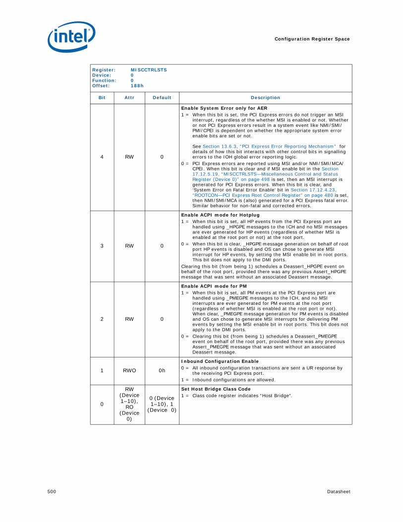
Configuration Register Space
500 Datasheet
4 RW 0
Enable System Error only for AER1 = When this bit is set, the PCI Express errors do not trigger an MSI
interrupt, regardless of the whether MSI is enabled or not. Whether or not PCI Express errors result in a system event like NMI/SMI/PMI/CPEI is dependent on whether the appropriate system error enable bits are set or not.
See Section 13.6.3, “PCI Express Error Reporting Mechanism” for details of how this bit interacts with other control bits in signalling errors to the IOH global error reporting logic.
0 = PCI Express errors are reported using MSI and/or NMI/SMI/MCA/CPEI. When this bit is clear and if MSI enable bit in the Section 17.12.5.19, “MISCCTRLSTS—Miscellaneous Control and Status Register (Device 0)” on page 498 is set, then an MSI interrupt is generated for PCI Express errors. When this bit is clear, and ‘System Error on Fatal Error Enable’ bit in Section 17.12.4.23, “ROOTCON—PCI Express Root Control Register” on page 480 is set, then NMI/SMI/MCA is (also) generated for a PCI Express fatal error. Similar behavior for non-fatal and corrected errors.
3 RW 0
Enable ACPI mode for Hotplug1 = When this bit is set, all HP events from the PCI Express port are
handled using _HPGPE messages to the ICH and no MSI messages are ever generated for HP events (regardless of whether MSI is enabled at the root port or not) at the root port.
0 = When this bit is clear, _HPGPE message generation on behalf of root port HP events is disabled and OS can chose to generate MSI interrupt for HP events, by setting the MSI enable bit in root ports. This bit does not apply to the DMI ports.
Clearing this bit (from being 1) schedules a Deassert_HPGPE event on behalf of the root port, provided there was any previous Assert_HPGPE message that was sent without an associated Deassert message.
2 RW 0
Enable ACPI mode for PM1 = When this bit is set, all PM events at the PCI Express port are
handled using _PMEGPE messages to the ICH, and no MSI interrupts are ever generated for PM events at the root port (regardless of whether MSI is enabled at the root port or not). When clear, _PMEGPE message generation for PM events is disabled and OS can chose to generate MSI interrupts for delivering PM events by setting the MSI enable bit in root ports. This bit does not apply to the DMI ports.
0 = Clearing this bit (from being 1) schedules a Deassert_PMEGPE event on behalf of the root port, provided there was any previous Assert_PMEGPE message that was sent without an associated Deassert message.
1 RWO 0h
Inbound Configuration Enable0 = All inbound configuration transactions are sent a UR response by
the receiving PCI Express port. 1 = Inbound configurations are allowed.
0
RW (Device 1–10),
RO (Device
0)
0 (Device 1–10), 1
(Device 0)
Set Host Bridge Class Code1 = Class code register indicates “Host Bridge”.
Register: MISCCTRLSTSDevice: 0Function: 0Offset: 188h
Bit Attr Default Description

Datasheet 501
Configuration Register Space
17.12.5.20 MISCCTRLSTS—Miscellaneous Control and Status Register (Device 1–10)
Register: MISCCTRLSTSDevice: 1–10Function: 0Offset: 188h
Bit Attr Default Description
63:50 RO 0 Reserved
49 RV 0 Reserved
48 RW1C 0Received PME_TO_ACKIndicates that IOH received a PME turn off ack packet or it timed out waiting for the packet
47:38 RO 0 Reserved
37 RV 0 Reserved
36 RWST 0
Form FactorIndicates what form factor a particular root port controls0 = CEM/Cable1 = SIOMThis bit is used to interpret bit 6 in the VPP serial stream for the port as either MRL# (CEM/Cable) input or EMLSTS# (SIOM) input. In case of cable form factor.
35 RWST 0
Override System Error on PCIe Fatal Error Enable: 1 = Fatal errors on PCI Express (that have been successfully
propagated to the primary interface of the port) are sent to the IOH core error logic (for further escalation) regardless of the setting of the equivalent bit in the ROOTCTRL register.
0 = Fatal errors are only propagated to the IOH core error logic if the equivalent bit in ROOTCTRL register is set.
34 RWST 0
Override System Error on PCIe Non-fatal Error Enable 1 = Non-fatal errors on PCI Express (that have been successfully
propagated to the primary interface of the port) are sent to the IOH core error logic (for further escalation) regardless of the setting of the equivalent bit in the ROOTCTRL register.
0 = Non-fatal errors are only propagated to the IOH core error logic if the equivalent bit in ROOTCTRL register is set.
33 RWST 0
Override System Error on PCIe Correctable Error Enable 1 = Correctable errors on PCI Express (that have been successfully
propagated to the primary interface of the port) are sent to the IOH core error logic (for further escalation) regardless of the setting of the equivalent bit in the ROOTCTRL register.
0 = Correctable errors are only propagated to the IOH core error logic if the equivalent bit in ROOTCTRL register is set.
32 RW 0
ACPI PME Interrupt Enable 1 = When set, Assert/Deassert_PMEGPE messages are enabled to be
generated when ACPI mode is enabled for handling PME messages from PCI Express.
0 = When this bit is cleared (from a 1), a Deassert_PMEGPE message is scheduled on behalf of the root port if an Assert_PMEGPE message was sent earlier from the root port.
31 RWST 0 Reserved
30 RW 0Inbound I/O Disable 1 = All inbound I/O are aborted and treated as UR.
29 RWST 1
cfg_to_enDisables/enables configuration timeouts, independently of other timeouts.0 = Disable1 = Enable

Configuration Register Space
502 Datasheet
28 RWST 0to_dis Disables timeouts completely.
27 RWST 0
System Interrupt Only on Link BW/Management Status1 = This bit, when set, will disable generating MSI interrupt on link
bandwidth (speed and/or width) and management changes, even if MSI is enabled; that is, will disable generating MSI when LNKSTS bits 15 and 14 are set. Whether or not this condition results in a system event like SMI/PMI/CPEI is dependent is masked or not in the XPCORERRMSK register.
26 RW 0Disable EOI broadcast to this PCIe link 1 = EOI message will not be broadcast down this PCIe link. 0 = Port is a valid target for EOI broadcast.
25 RWST 0Peer-to-peer Memory Write Disable 1 = Peer-to-peer memory writes are master aborted0 = They are allowed to progress per the peer-to-peer decoding rules.
24 RW 0Peer-to-peer Memory Read Disable 1 = Peer-to-peer memory reads are master aborted 0 = They are allowed to progress per the peer-to-peer decoding rules
23 RW 0 Reserved
22:10 RV 606h Reserved
9 RV 0 Reserved
8:7 RW 0 PME2ACKTOCTRL
6 RWST 0Enable Timeout for Receiving PME_TO_ACK 1 = IOH enables the timeout to receiving the PME_TO_ACK
5 RW 0
Send PME_TURN_OFF message1 = When this bit is written with a b, IOH sends a PME_TURN_OFF
message to the PCIe link. 0 = Hardware clears this bit when the message has been sent on the
link.
4 RW 0
Enable System Error only for AER1 = When this bit is set, the PCI Express errors do not trigger an MSI
interrupt, regardless of the whether MSI is enabled or not. Whether or not PCI Express errors result in a system event like NMI/SMI/PMI/CPEI is dependent on whether the appropriate system error enable bits are set or not.
See Section 13.6.3.5, “PCI Express Error Reporting Specifics” for details of how this bit interacts with other control bits in signalling errors to the IOH global error reporting logic.
0 = When this bit is clear, PCI Express errors are reported using MSI and/or NMI/SMI/MCA/CPEI. When this bit is clear and if MSI enable bit in the Section 17.12.5.19, “MISCCTRLSTS—Miscellaneous Control and Status Register (Device 0)” on page 498 is set, then an MSI interrupt is generated for PCI Express errors. When this bit is clear, and ‘System Error on Fatal Error Enable’ bit in Section 17.12.4.23, “ROOTCON—PCI Express Root Control Register” on page 480 is set, then NMI/SMI/MCA is (also) generated for a PCI Express fatal error. Similar behavior for non-fatal and corrected errors.
Register: MISCCTRLSTSDevice: 1–10Function: 0Offset: 188h
Bit Attr Default Description

Datasheet 503
Configuration Register Space
3 RW 0
Enable ACPI Mode for Hotplug1 = When this bit is set, all HP events from the PCI Express port are
handled using _HPGPE messages to the ICH and no MSI messages are ever generated for HP events (regardless of whether MSI is enabled at the root port or not) at the root port.
0 = When this bit is clear, _HPGPE message generation on behalf of root port HP events is disabled and OS can chose to generate MSI interrupt for HP events, by setting the MSI enable bit in root ports. This bit does not apply to the DMI ports.
Clearing this bit (from being 1) schedules a Deassert_HPGPE event on behalf of the root port, provided there was any previous Assert_HPGPE message that was sent without an associated Deassert message.
2 RW 0
Enable ACPI Mode for PM1 = When this bit is set, all PM events at the PCI Express port are
handled using _PMEGPE messages to the ICH, and no MSI interrupts are ever generated for PM events at the root port (regardless of whether MSI is enabled at the root port or not).
0 = When clear, _PMEGPE message generation for PM events is disabled and OS can chose to generate MSI interrupts for delivering PM events by setting the MSI enable bit in root ports. This bit does not apply to the DMI ports.
Clearing this bit (from being 1) schedules a Deassert_PMEGPE event on behalf of the root port, provided there was any previous Assert_PMEGPE message that was sent without an associated Deassert message.
1 RWO 0h
Inbound Configuration Enable0 = All inbound configuration transactions are sent a UR response by
the receiving PCI Express port. 1 = Inbound configurations are allowed.
0
RW (Device 1–10),
RO (Device 0)
0 (Device 1–10),
1 (Device 0)
Set Host Bridge Class Code1 = Class code register indicates “Host Bridge”.
Register: MISCCTRLSTSDevice: 1–10Function: 0Offset: 188h
Bit Attr Default Description

Configuration Register Space
504 Datasheet
17.12.5.21 PCIE_IOU0_BIF_CTRL—PCIe IO Unit (IOU)0 Bifurcation Control Register
This control register holds bifurcation control information pertaining to the PCI Express I/O Unit 0.
Register: PCIE_IOU0_BIF_CTRLDevice: 3Function: 0Offset: 190h
Bit Attr Default Description
15:4 RO 0h Reserved
3 WO 0
IOU0 Start Bifurcation When software writes a 1 to this bit, IOH starts the port 0 bifurcation process. After writing to this bit, software can poll the Data Link Layer link active bit in the LNKSTS register to determine if a port is up and running. Once a port bifurcation has been initiated by writing a 1 to this bit, software cannot initiate any more writes of 1 to this bit (write of 0 is ok).Note that this bit can be written to a 1 in the same write that changes values for bits 2:0 in this register and in that case, the new value from the write to bits 2:0 take effect.This bit always reads a 0b.
2:0 RWS 000b
IOU0 Bifurcation Control111 = Use strap settings to determine port bifurcation (default)110 = Reserved101 = Reserved100 = x16011 = x8x8 (15:8 operate as x8, 7:0 operate as x8)010 = x8x4x4 (15:8 operate as x8, 7:4 operate as x4 and 3:0 operate as x4)001 = x4x4x8 (15:12 operate as x4, 11:8 operate as x4 and 7:0 operate as
x8)000 = x4x4x4x4 (15:12 operate as x4, 11:8 operate as x4, 7:4 operate as x4
and 3:0 operate as x4)To select a port 0 bifurcation, software sets this field and then either: a) sets bit 3 in this register to initiate training OR b) resets the entire IOH and on exit from that reset, IOH will bifurcate the ports per the setting in this field.Refer to Chapter 5 for further description of the port bifurcation under BIOS feature.

Datasheet 505
Configuration Register Space
17.12.5.22 PCIE_IOU1_BIF_CTRL—PCIe IO Unit (IOU)1 Bifurcation Control Register
This control register holds bifurcation control information pertaining to the PCI Express I/O Unit 1.
.
Register: PCIE_IOU1_BIF_CTRLDevice: 7Function: 0Offset: 190h
Bit Attr Default Description
15:4 RO 0h Reserved
3 WO 0
IOU1 Start Bifurcation When software writes a 1 to this bit, IOH starts the port 1 bifurcation process. After writing to this bit, software can poll the Data Link Layer link active bit in the LNKSTS register to determine if a port is up and running. Once a port bifurcation has been initiated by writing a 1 to this bit, software cannot initiate any more writes of 1 to this bit (write of 0 is ok).Note that this bit can be written to a 1 in the same write that changes values for bits 2:0 in this register and in that case, the new value from the write to bits 2:0 take effect.This bit always reads a 0b.
2:0 RWS 000b
IOU1 Bifurcation Control111 = Use strap settings to determine port bifurcation (default)110 = Reserved101 = Reserved100 = x16011 = x8x8 (15:8 operate as x8, 7:0 operate as x8)010 = x8x4x4 (15:8 operate as x8, 7:4 operate as x4 and 3:0 operate as x4)001 = x4x4x8 (15:12 operate as x4, 11:8 operate as x4 and 7:0 operate as
x8)000 = x4x4x4x4 (15:12 operate as x4, 11:8 operate as x4, 7:4 operate as x4
and 3:0 operate as x4)To select a port 1 bifurcation, software sets this field and then either: a) sets bit 3 in this register to initiate training OR b) resets the entire IOH and on exit from that reset, IOH will bifurcate the ports per the setting in this field.Refer to Chapter 5 for further description of the port bifurcation under BIOS feature.
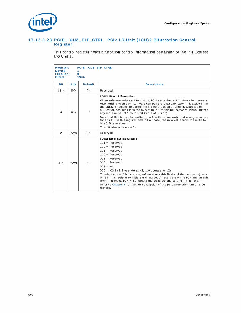
Configuration Register Space
506 Datasheet
17.12.5.23 PCIE_IOU2_BIF_CTRL—PCIe IO Unit (IOU)2 Bifurcation Control Register
This control register holds bifurcation control information pertaining to the PCI Express I/O Unit 2.
Register: PCIE_IOU2_BIF_CTRLDevice: 1Function: 0Offset: 190h
Bit Attr Default Description
15:4 RO 0h Reserved
3 WO 0
IOU2 Start Bifurcation When software writes a 1 to this bit, IOH starts the port 2 bifurcation process. After writing to this bit, software can poll the Data Link Layer link active bit in the LNKSTS register to determine if a port is up and running. Once a port bifurcation has been initiated by writing a 1 to this bit, software cannot initiate any more writes of 1 to this bit (write of 0 is ok).Note that this bit can be written to a 1 in the same write that changes values for bits 1:0 in this register and in that case, the new value from the write to bits 1:0 take effect.This bit always reads a 0b.
2 RWS 0h Reserved
1:0 RWS 0b
IOU2 Bifurcation Control111 = Reserved110 = Reserved101 = Reserved100 = Reserved011 = Reserved010 = Reserved001 = x4000 = x2x2 (3:2 operate as x2, 1:0 operate as x2)To select a port 2 bifurcation, software sets this field and then either: a) sets bit 3 in this register to initiate training OR b) resets the entire IOH and on exit from that reset, IOH will bifurcate the ports per the setting in this field.Refer to Chapter 5 for further description of the port bifurcation under BIOS feature.

Datasheet 507
Configuration Register Space
17.13 IOH Defined PCI Express Error RegistersThis seciton provides the contents of the next set of registers: XPCORERRSTS, XPCORERRMSK, XPUNCERRSTS, XPUNCERRMSK, XPUNCERRSEV, XPUNCERRPTR. The architecture model for error logging and escalation of internal errors is similar to that of PCI Express AER, except that these internal errors never trigger an MSI and are always reported to the system software. Mask bits mask the reporting of an error and severity bit controls escalation to either fatal or non-fatal error to the internal core error logic. Note that internal errors detected in the PCI Express cluster are not dependent on any other control bits for error escalation other than the mask bit defined in these registers. All these registers are sticky. Refer to Figure 13-9.
17.13.1 XPCORERRSTS—XP Correctable Error Status Register
17.13.2 XPCORERRMSK—XP Correctable Error Mask Register
Register: XPCORERRSTSDevice: 0–10Function: 0Offset: 200h
Bit Attr Default Description
31:1 RV 0 Reserved
0 RW1CS 0
PCI link bandwidth changed statusNote: This bit is implemented as an OR of LNKSTS[15] (LABS) and LNKSTS[14] (LBMS). The mask for XPCORERRSTS[0] is set to 1 by default. Thus, in order to log bandwidth changes, LNKSTS[15:14], XPCORERRSTS[0] and XPCOREDMASK[0] need to be cleared.Once the xpcorerrsts[0] is unmasked and then set to 1 due to a bandwidth change, LNKSTS[15:14] need to be cleared before clearing XPCORERRSTS[0].
Register: XPCORERRMSKDevice: 0–10Function: 0Offset: 204h
Bit Attr Default Description
31:1 RV 0 Reserved
0 RWST 0 PCI link bandwidth Changed Mask

Configuration Register Space
508 Datasheet
17.13.3 XPUNCERRSTS—XP Uncorrectable Error Status Register
17.13.4 XPUNCERRMSK—XP Uncorrectable Error Mask Register
Register: XPUNCERRSTSDevice: 0–10Function: 0Offset: 208h
Bit Attr Default Description
31:10 RV 0s Reserved
9 RWS 0Outbound Poisoned Data Set when outbound poisoned data (from QPI or peer, write or read completion) is received by this port
8 RW1CS 0 Received MSI writes greater than a DWORD Data
7 RW1CS 0 Reserved
6 RW1CS 0 Received PCIe completion with UR Status
5 RW1CS 0 Received PCIe completion with CA Status
4 RW1CS 0 Sent completion with Unsupported Request
3 RW1CS 0 Sent completion with completion Abort
2 RW1CS 0 Reserved
1 RW1CS 0 Outbound Switch FIFO data parity error detected
0 RW1CS 0 Reserved
Register: XPUNCERRMSKDevice: 0–10Function: 0Offset: 20Ch
Bit Attr Default Description
31:10 RV 0s Reserved
9 RV 0Outbound Poisoned Data Mask Masks signaling of stop and scream condition to the core error logic
8 RWS 0 Received MSI writes greater than a DWORD data Mask
7 RWS 0 Reserved
6 RWS 0 Received PCIe completion with UR status Mask
5 RWS 0 Received PCIe completion with CA status Mask
4 RWS 0 Sent completion with Unsupported Request Mask
3 RWS 0 Sent completion with Completer Abort mask
2 RWS 0 Reserved
1 RWS 0 Outbound Switch FIFO data parity error detected mMasksk
0 RWS 0 Reserved

Datasheet 509
Configuration Register Space
17.13.5 XPUNCERRSEV—XP Uncorrectable Error Severity Register
17.13.5.1 XPUNCERRPTR—XP Uncorrectable Error Pointer Register
Register: XPUNCERRSEVDevice: 0–10Function: 0Offset: 210h
Bit Attr Default Description
31:10 RV 0s Reserved
9 RWS 0 Outbound Poisoned Data Severity
8 RWS 0 Received MSI writes greater than a DWORD data Severity
7 RWS 1 Reserved
6 RWS 0 Received PCIe completion with UR status Severity
5 RWS 0 Received PCIe completion with CA status Severity
4 RWS 0 Sent completion with Unsupported Request Severity
3 RWS 1 Sent completion with Completer Abort Severity
2 RV 0 Reserved
1 RWS 1 Outbound Switch FIFO data parity error detected Severity
0 RWS 1 Reserved
Register: XPUNCERRPTRDevice: 0–10Function: 0Offset: 214h
Bit Attr Default Description
7:5 RV 0 Reserved
4:0 ROS 0
XP Uncorrectable First Error Pointer This field points to which of the unmasked uncorrectable errors happened first. This field is only valid when the corresponding error is unmasked and the status bit is set and this field is rearmed to load again when the status bit indicated to by this pointer is cleared by software from 1-to-0.Value of 0h corresponds to bit 0 in XPUNCERRSTS register, value of 1h corresponds to bit 1, and so on.

Configuration Register Space
510 Datasheet
17.13.5.2 UNCEDMASK—Uncorrectable Error Detect Status Mask Register
This register masks uncorrectable errors from causing the associated AER status bit to be set.
Register: UNCEDMASKDevice: 0–10Function: 0Offset: 218h
Bit Attr Default Description
31:22 RV 0h Reserved
21 RWST 1 ACS Violation Detect Mask
20 RWST 1 Received an Unsupported Request Detect Mask
19 RV 0 Reserved
18 RWST 1 Malformed TLP Detect Mask
17 RWST 1 Receiver Buffer Overflow Detect Mask
16 RWST 1 Unexpected Completion Detect Mask
15 RWST 1 Completer Abort Detect Mask
14 RWST 1 Completion Time-out Detect Mask
13 RWST 1 Flow Control Protocol Error Detect Mask
12 RWST 1 Poisoned TLP Detect Mask
11:6 RV 0h Reserved
5 RWST 1 Surprise Down Error Detect Mask
4 RWST 1 Data Link Layer Protocol Error Detect Mask
3:1 RV 000 Reserved
0 RO 0 Reserved

Datasheet 511
Configuration Register Space
17.13.5.3 COREDMASK—Correctable Error Detect Status Mask Register
This register masks correctable errors from causing the associated status bit in AER status register to be set.
17.13.5.4 RPEDMASK—Root Port Error Detect Status Mask Register
This register masks the associated error messages (received from PCIE link and NOT the virtual ones generated internally), from causing the associated status bits in AER to be set.
Register: COREDMASKDevice: 0–10Function: 0Offset: 21Ch
Bit Attr Default Description
31:14 RV 0h Reserved
13 RWST 1 Advisory Non-fatal Error Detect Mask
12 RWST 1 Replay Timer Time-out Detect Mask
11:9 RV 0h Reserved
8 RWST 1 Replay_Num Rollover Detect Mask
7 RWST 1 Bad DLLP Detect Mask
6 RWST 1 Bad TLP Detect Mask
5:1 RV 0h Reserved
0 RWST 1 Receiver Error Detect Mask
Register: RPEDMASKDevice: 0–10Function: 0Offset: 220h
Bit Attr Default Description
31:3 RV 0h Reserved
2 RWST 1 Fatal error detect Detect Mask
1 RWST 1 Non-Fatal error detect Detect Mask
0 RWST 1 Correctable error detect status Mask

Configuration Register Space
512 Datasheet
17.13.5.5 XPUNCEDMASK—XP Uncorrectable Error Detect Mask Register
17.13.5.6 XPCOREDMASK—XP Correctable Error Detect Mask Register
Register: XPUNCEDMASKDevice: 0–10Function: 0Offset: 224h
Bit Attr Default Description
31:10 RV 0s Reserved
9 RWS 1 Outbound Poisoned Data Detect Mask
8 RWS 1 Received MSI writes greater than a DWORD data Detect Mask
7 RWS 0 Reserved
6 RWS 1 Received PCIE completion with UR Detect Mask
5 RWS 1 Received PCIE completion with CA Detect Mask
4 RWS 1 Sent completion with Unsupported Request Detect Mask
3 RWS 1 Sent completion with Completer Abort Detect Mask
2 RWS 0 Reserved
1 RWS 1 Outbound Switch FIFO data parity error Detect Mask
0 RWS 0 Reserved
Register: XPCOREDMASKDevice: 0–10Function: 0Offset: 228h
Bit Attr Default Description
31:29 RV 0 Reserved
28:1 RV 0 Reserved
0 RWS 1 PCI link bandwidth changed Detect Mask

Datasheet 513
Configuration Register Space
17.13.6 XPGLBERRSTS—XP Global Error Status Register
This register captures if an error is logged in any of two buckets of errors within XP, XP internal core logic, and PCI Express AER.
17.13.7 XPGLBERRPTR—XP Global Error Pointer Register
This register captures if an error is logged in any of three buckets of errors within XP — XP internal and PCI Express AER.
Register: XPGLBERRSTSDevice: 0–10Function: 0Offset: 230h
Bit Attr Default Description
15:3 RV 0s Reserved
2 RW1CS 0
PCIe AER Correctable Error A PCIe correctable error (either internally detected by IOH or a FATAL message received) was detected anew. Note that if that error was masked in the PCIe AER, it is not reported in this field. Software clears this bit by writing a 1 and at that stage, only “subsequent” PCIe unmasked correctable errors will set this bit.Conceptually, per the flow of PCI Express Base Specification 1.1 defined Error message control, this bit is set by the ERR_COR message that is enabled to cause a System Error notification.Refer to Section 13.6.3, “PCI Express Error Reporting Mechanism” for details of how this bit interacts with other control/status bits in signalling errors to the IOH global error reporting logic.
1 RW1CS 0
PCIe AER Non-fatal Error A PCIe non-fatal error (either internally detected by IOH or a FATAL message received) was detected anew. Note that if that error was masked in the PCIe AER, it is not reported in this field. Software clears this bit by writing a 1 and at that stage only “subsequent” PCIe unmasked non-fatal errors will set this bit again.Refer to Section 13.6.3, “PCI Express Error Reporting Mechanism” for details of how this bit interacts with other control/status bits in signalling errors to the IOH global error reporting logic.
0 RW1CS 0
PCIe AER Fatal Error A PCIe fatal error (either internally detected by IOH or a FATAL message received) was detected anew. Note that if that error was masked in the PCIe AER, it is not reported in this field. Software clears this bit by writing a 1 and at that stage, only “subsequent” PCIe unmasked fatal errors will set this bit.Refer to Section 13.6.3, “PCI Express Error Reporting Mechanism” for details of how this bit interacts with other control/status bits in signalling errors to the IOH global error reporting logic.
Register: XPGLBERRPTRDevice: 0–7,9Function: 0Offset: 232h
Bit Attr Default Description
15:3 RV 0s Reserved
2:0 ROS 000
XP Cluster Global First Error Pointer This field points to which of the 4 errors indicated in the XPGLBERRSTS register happened first. This field is only valid when the corresponding status bit is set and this field is rearmed to load again when the status bit indicated to by this pointer is cleared by software from 1-to-0.Value of 0h corresponds to bit 0 in XPGLBERRSTS register, value of 1h corresponds to bit 1, and so on.

Configuration Register Space
514 Datasheet
17.13.8 CTOCTRL—Completion Time-Out Control Register
17.13.9 PCIE_SS_CTRLSTS—PCI Express Stop and Stream Control and Status Register
Register: CTOCTRLDevice: 0–10Function: 0Offset: 1E0h
Bit Attr Default Description
31:10 RV 0 Reserved
9:8 RW 00
XP-to-PCIe time-out select within 2s to 6.5s range:When OS selects a time-out range of 2s to 6.5s for XP (that affect NP tx issued to the PCIe/ESI) using the root port’s DEVCTRL2 register, this field selects the sub-range within that larger range, for additional controllability.00: 2s01: 4s10: 6.5s11: ReservedNote: These values can deviate +/- 10%
7:6 RV 00 Reserved
5 RO 0 Reserved
4:0 RV 0 Reserved
Register: PCIE_SSDevice: 0–10Function: 0Offset: 1E4h
Bit Attr Default Description
31 RO 0
SS Status Indicates that an error was detected which caused the PCIe port to go into a stop and scream mode. This bit remains set till all the associated unmasked status bits are cleared.
30:8 RO 0 Reserved
7 RWS 1
XPUNCERRSTS_Received PCIe Completion With URStatus MaskWhen clear, when the Received PCIe Completion With UR status bit in the XPUNCERRSTS register is 1b, the SS Status bit in this register will be set. When set, the register Received PCIe Completion With UR status bit in the XPUNCERRSTS has no impact on the SS Status bit in this register.
6 RWS 0
XPUNCERRSTS_Received PCIe Completion With CAStatus Mask When clear, when the Received PCIe Completion With CA status bit in the XPUNCERRSTS register is 1b, the SS Status bit in this register will be set. When set, the register Received PCIe Completion With CA status bit in the XPUNCERRSTS has no impact on the SS Status bit in this register LRU Timer.
5 RWS 0
XPUNCERRSTS_Outbound Poisoned Data: MaskWhen clear, when the Outbound Poisoned Data bit in the XPUNCERRSTS register is 1b, the SS Status bit in this register will be set. When set, the register Outbound Poisoned Data bit in the XPUNCERRSTS has no impact on the SS Status bit in this register.
4 RO 0 Reserved

Datasheet 515
Configuration Register Space
17.13.10 XP[10:0]ERRCNTSEL—Error Counter Selection Register
3 RWS 0
ERRSTS_Fatal Error Messages Received MaskWhen clear, when the Fatal Error Messages Received status bit in the RPERRSTS register is 1b, the SS Status bit in this register will be set. When set, the Fatal Error Messages Received status bit in the RPERRSTS register has no impact on the SS Status bit in this register
2 RWS 0
ERRSTS_Non-Fatal Error Messages Received MaskWhen clear, when the Non-Fatal Error Messages Received status bit in the RPERRSTS register is 1b, the SS Status bit in this register will be set. When set, the Non-Fatal Error Messages Received status bit in the RPERRSTS register has no impact on the SS Status bit in this register
1 RO 0 Reserved
0 RWS 0
SS EnableWhen set, as long as the SS Status bit in this register is set, the associated root port will go into Stop and Scream mode. When clear, the root port can never go into Stop and Scream mode. The SSMSK register contains additional mask bits that has an impact on whether on not the SS Status bit will be set when SS Enable is set.When a root port enters the SS mode, it automatically brings the associated PCIE link down and the port behaves per the rules states in the PCI Express base spec for link down condition. Also, if the port enters SS mode because of the stop and scream status bit being set (in the XPUNCERRSTS register), the associated outbound data should never be sent to the device south i.e. the link should go down before the poisoned data escapes to the PCIE link. SW can later clear the associated status bits and thus cause the SS status bit in this register to clear and that would bring the port out of the SS mode, and the port continues working normally i.e. the PCIE link starts training again and normal operation follows. It is up to software to provide sufficient time for the transactions pending in the inbound and outbound queues of the associated root port to have drained using the normal transaction flows, before causing the SS status bit to clear.Once SS_Status is set all bits in UNCERRSTS register of the associated root port must be cleared before disabling SS_Enable.Also, note that error logging/escalation as defined in the PCI Express spec, using AER registers and MSI mechanism remain unaffected by this bit.Recommendation is not to enable for the DMI port, as a reboot might be required to exit.
Register: XP[10:0]ERRCNTSELDevice: 0–10Function: 0Offset: 400h
Bit Attr Default Description
31:0 RV 0h Reserved
Register: PCIE_SSDevice: 0–10Function: 0Offset: 1E4h
Bit Attr Default Description

Configuration Register Space
516 Datasheet
17.13.11 XP[10:0]ERRCNT—Error Counter Register
Register: XP[10:0]ERRCNTDevice: 0–10Function: 0Offset: 404h
Bit Attr Default Description
7:0 RW1CS Reserved

Datasheet 517
Configuration Register Space
17.14 Intel® VT-d Memory Mapped Register
Table 17-31.Intel® VT-d Memory Mapped Registers (00h–FFh, 1000h–10FFh) (Sheet 1 of 3)
VTD_VERSION 00h INV_QUEUE_HEAD 80h
04h NV_QUEUE_HEAD 84h
VTD_CAP 08h INV_QUEUE_TAIL 88h
0Ch 8Ch
EX_VTD_CAP 10h INV_QUEUE_ADD 90h
14h 94h
GLBCMD 18h 98h
GLBSTS 1Ch INV_COMP_STATUS 9Ch
ROOTENTRYADD 20h INV_COMP_EVT_CTL A0h
24h INV_COMP_EVT_DATA A4h
CTXCMD 28h INV_COMP_EVT_ADDR A8h
2Ch ACh
30h B0h
FLTSTS 34h B4h
FLTEVTCTRL 38h INTR_REMAP_TABLE_BASE B8h
FLTEVTDATA 3Ch BCh
FLTEVTADDR 40h C0h
FLTEVTUPRADDR 44h C4h
48h C8h
4Ch CCh
50h D0h
54h D4h
58h D8h
5Ch DCh
60h E0h
PMEN 64h E4h
PROT_LOW_MEM_BASE 68h E8h
PROT_LOW_MEM_LIMIT 6Ch ECh
PROT_HIGH_MEM_BASE 70h F0h
74h F4h
PROT_HIGH_MEM_LIMIT 78h F8h
7Ch FCh

Configuration Register Space
518 Datasheet
Table 17-32.Intel® VT-d Memory Mapped Registers (100h–1FFh, 1100h–11FFh) (Sheet 2 of 3)
FLTREC0 100h 180h
104h 184h
108h 188h
10Ch 18Ch
FLTREC1 110h 190h
114h 194h
118h 198h
11Ch 19Ch
FLTREC2 120h 1A0h
124h 1A4h
128h 1A8h
12Ch 1ACh
FLTREC3 130h 1B0h
134h 1B4h
138h 1B8h
13Ch 1BCh
FLTREC4 140h 1C0h
144h 1C4h
148h 1C8h
14Ch 1CCh
FLTREC5 150h 1D0h
154h 1D4h
158h 1D8h
15Ch 1DCh
FLTREC6 160h 1E0h
164h 1E4h
168h 1E8h
16Ch 1ECh
FLTREC7 170h 1F0h
174h 1F4h
178h 1F8h
17Ch 1FCh

Datasheet 519
Configuration Register Space
Table 17-33.Intel® VT-d Memory Mapped Registers (200h–2FFh, 1200h–12FFh) (Sheet 3 of 3)
IOTLBINV 200h 280h
204h 284h
INVADDRREG 208h 288h
20Ch 28Ch
210h 290h
214h 294h
218h 298h
21Ch 29Ch
220h 2A0h
224h 2A4h
228h 2A8h
22Ch 2ACh
230h 2B0h
234h 2B4h
238h 2B8h
23Ch 2BCh
240h 2C0h
244h 2C4h
248h 2C8h
24Ch 2CCh
250h 2D0h
254h 2D4h
258h 2D8h
25Ch 2DCh
260h 2E0h
264h 2E4h
268h 2E8h
26Ch 2ECh
270h 2F0h
274h 2F4h
278h 2F8h
27Ch 2FCh

Configuration Register Space
520 Datasheet
17.14.1 Intel VT-d Memory Mapped Registers
The Intel VT-d registers are all addressed using aligned DWORD or aligned QWORD accesses. Any combination of BEs is allowed within a DWORD or QWORD access. The Intel VT-d remap engine registers corresponding to the non-Isoch port represented by Device 0 , occupy the first 4K of offset starting from the base address defined by VTBAR register.
17.14.1.1 VTD_VERSION—Version Number Register
17.14.1.2 VTD_CAP[0:1]—Intel VT-d Capability Register
Figure 17-2. Base Address of Intel VT-D Remap Engines
Register: VTD_VERSIONAddr: MMIOBAR: VTBAROffset: 00h, 1000h
Bit Attr Default Description
31:8 RV 0h Reserved
7:4 RO 1h Major Revision
3:0 RO 0h Minor Revision
Register: EXT_VTD_CAP[0:1]Addr: MMIOBAR: VTBAROffset: 08h, 1008h
Bit Attr Default Description
63:56 RV 0h Reserved
55 RO 1h DMA Read Draining: Supported in IOH
54 RO 1h DMA Write Draining:Supported in IOH
53:48 RO 09h MAMV: IOH support MAMV value of 9h.
47:40 RO 8h Number of Fault Recording Registers: IOH supports 8 fault recording registers.
39 RO 1 Page Selective Invalidation: Supported in IOH
38 RV 0 Reserved
37:34 RV 0h Reserved
33:24 RO 10h Fault Recording Register Offset: Fault registers are at offset 0xC0h 100h
23 RWO 0 (Offset 08h)
Reserved
22 RWO 0 ZLR: Zero length DMA requests to write-only pages supported.
Non- Isoch VT-d
VT_BAR
VT_ BAR + 4KB

Datasheet 521
Configuration Register Space
21:16 RO 2Fh (Offset 08h)
MGAW: For non-Azalia VT-d engine, this register is set by TB based on the settting of the Non-Isoch GPA_LIMIT field in the VTGENCTRL register. Similarly for isoch VT-d engine, this register is set by the Isoch GPA_LIMIT field of the VTGENCTRL register.
15:13 RV 0h Reserved
12:8 RO 2h (Offset 08h)
SAGAW: IOH supports only 4 level walks on the VT-d engine
7 RO 0 TCM: IOHTB does not cache invalid pages
6 RO 1 PHMR Support: IOH supports protected high memory range
5 RO 1 PLMR Support: IOH supports protected low memory range
4 RV 0 Reserved
3 RO 0 Advanced Fault Logging: IOHTB does not support advanced fault logging
2:0 RO 010b Number of Domains Supported: IOH supports 256 domains with 8 bit domain ID
Register: EXT_VTD_CAP[0:1]Addr: MMIOBAR: VTBAROffset: 08h, 1008h
Bit Attr Default Description

Configuration Register Space
522 Datasheet
17.14.1.3 EXT_VTD_CAP[0:1]—Extended Intel VT-d Capability Register
Register: EXT_VTD_CAP[0:1]Addr: MMIOBAR: VTBAROffset: 10h, 1010h
Bit Attr Default Description
63:24 RV 0h Reserved
23:20 RO Fh
Maximum Handle Mask Value IOH supports all 16 bits of handle being masked. Note that the IOH always performs global interrupt entry invalidation on any interrupt cache invalidation command and h/w never really looks at the mask value.
19:18 RV 0 Reserved
17:8 RO 20hInvalidation Unit Offset IOH has the invalidation registers at offset 200h.
7 RWO
1 (Offset 10h), 0 (Offset 1010h)
0 = Hardware does not support 1-setting of the SNP field in the page table entries.1 = Hardware supports the 1-setting of the SNP field in the page table entries.IOH supports snoop override only for the non-isoch Intel VT-d engine
6 RWO 1
IOH Supports Pass Through Note that when this bit is set to 0, Intel VT-d specification requires error checking on the “type” field; that is, “type” field cannot have an encoding of 10b. If software set an encoding of 10b, hardware has to cause a fault.
5 RO 1 IOH supports caching hints
4 RO See Desc
IA32 Extended Interrupt Mode: Default is 1 if DISAPICEXT = 0, else default = 0
3 RO 1Interrupt Remapping Support IOH supports this
2 RWO
1 (Offset 10h), 0 (Offset 1010h)
Device TLB support: IOH supports ATS for the non-isoch Intel VT-d engine. This bit is RWO for non-isoch engine in case we might have to defeature ATS post-si. Note that when this bit is set to 0, Intel VT-d specification requires error checking on the “type” field; that is, “type” field cannot have an encoding of 01b. If software sets an encoding of 01b, hardware has to cause a fault.
1 RWO 1Queued Invalidation support: IOH supports this.
0 RWO 0Coherency Support: BIOS can write to this bit to indicate to hardware to either snoop or not-snoop the Interrupt table structures in memory (root/context/pd/pt/irt).

Datasheet 523
Configuration Register Space
17.14.1.4 GLBCMD[0:1]—Global Command Register
Register: GLBCMD[0:1]Addr: MMIOBAR: VTBAROffset: 18h, 1018h
Bit Attr Default Description
31 RW 0hTransalation Enable: This bit is used by software to disable (0) DMA-remapping in hardware or enable(1) in software.
30 RW 0h
Set Root Table PointerSoftware sets this field to set/update the root-entry table pointer used by hardware. The root-entry table pointer is specified through the Root-entry Table Address register.Hardware reports the status of the root table pointer set operation through the RTPS field in the Global Status register.
29 RO 0 Set Fault Log Pointer: N/A to IOH
28 RO 0 Enable Advanced Fault Logging: N/A to IOH
27 RO 0 Write Buffer Flush: N/A to IOH
26 RW 0
Queued Invalidation EnableSoftware writes to this field to enable queued invalidations.0 = Disable queued invalidations. In this case, invalidations must be performed
through the Context Command and IOTLB Invalidation Unit registers.1 = Enable use of queued invalidations. Once enabled, all invalidations must be
submitted through the invalidation queue and the invalidation registers can no longer be used without going through an IOH reset. The invalidation queue address register must be initialized before enabling queued invalidations. Also software must make sure that all invalidations submitted prior using the register interface are all completed before enabling the queued invalidation interface.
25 RW 0
Interrupt Remapping Enable0 = Disable Interrupt Remapping Hardware1 = Enable Interrupt Remapping HardwareHardware reports the status of the interrupt remap enable operation through the IRES field in the Global Status register.
24 RW 0 Set Interrupt Remap Table Pointer:
Software sets this field to set/update the Interrupt Remap Table Pointer used by hardware. The interrupt remapping Table Pointer is specified through the interrupt Remapping Table Address Register.
23 RW 0 Compatibility Format Interrupt: Software writes to this field to enable /disable Compatibility Format Interrupt.The value reported in this field is reported only when interrupt-remapping is enabled and Legacy interrupt mode is active0: Compatibilty Format Interrupts Blocked1: Compatibilty Format Interrupts Processed as bypassing interrupt remapping.
22:0 RO 0 Reserved

Configuration Register Space
524 Datasheet
17.14.1.5 GLBSTS[0:1]—Global Status Register
17.14.1.6 ROOTENTRYADD[0:1]—Root Entry Table Address Register
Register: GLBSTS[0:1]Addr: MMIOBAR: VTBAROffset: 1Ch, 101Ch
Bit Attr Default Description
31 RO 0 Translation Enable Status: When set, indicates that translation hardware is enabled and when clear indicates the translation hardware is not enabled.
30 RO 0 Set Root Table Pointer Status: This field indicates the status of the root- table pointer in hardware.
29 RO 0 Set Fault Log Pointer: N/A to IOH
28 RO 0 Advanced Fault Logging Status: N/A to IOH
27 RO 0 Write Buffer Flush: N/A to IOH
26 RO 0 Queued Invalidation Interface Status: IOH sets this bit once it has completed the software command to enable the queued invalidation interface. Until then this bit is 0.
25 RO 0 Interrupt Remapping Enable Status: IOH sets this bit once it has completed the software command to enable the interrupt remapping interface. Till then this bit is 0
24 RO 0 Interrupt Remapping Table Pointer Status:This field indicates the status of the interrupt remapping table pointer in hardware. This field is cleared by hardware when software sets the SIRTP field in the Global Command register. This field is set by hardware when hardware completes the set interrupt remap table pointer operation using the value provided in the Interrupt Remapping Table Address register
23 RO 0 Compatibility Format Interrupt Status:The value reported in this field is reported only when interrupt-remapping is enabled and Legacy interrupt mode is active0: Compatibilty Format Interrupts Blocked1: Compatibilty Format Interrupts Processed as bypassing interrupt remapping.
22:0 RO 0 Reserved
Register: ROOTENTRYADD[0:1]Addr: MMIOBAR: VTBAROffset: 20h, 1020h
Bit Attr Default Description
63:12 RW 0
Root Entry Table Base Address4K aligned base address for the root entry table. IOH does not use bits 63:43 and checks for them to be 0. Software specifies the base address of the root entry table through this register, and enables it in hardware through the SRTP field in the Global Command register. Reads of this register returns value that was last programmed to it.
11:0 RO 0 Reserved

Datasheet 525
Configuration Register Space
17.14.1.7 CTXCMD[0:1]—Context Command Register
Register: CTXCMD[0:1]Addr: MMIOBAR: VTBAROffset: 28h, 1028
Bit Attr Default Description
63 RW 0
Invalidate Context Entry Cache (ICC) Software requests invalidation of context cache by setting this field. Software must also set the requested invalidation granularity by programming the CIRG field. Software must read back and check the ICC field to be clear to confirm the invalidation is complete. Software must not update this register when this field is set. Hardware clears the ICC field to indicate the invalidation request is complete. Hardware also indicates the granularity at which the invalidation operation was performed through the CAIG field. Software must not submit another invalidation request through this register while the ICC field is set.Since information from the context cache may be used by hardware to tag IOTLB entries, software must perform domain selective (or global) invalidation of IOTLB after the context cache invalidation has completed
62:61 RW 0
Context Invalidation Request Granularity (CIRG) When requesting hardware to invalidate the context entry cache (by setting the ICC field), software writes the requested invalidation granularity through this field.Following are the encoding for the 2-bit IRG field.00 = Reserved01 = Global Invalidation request. IOH supports this.10 = Domain selective invalidation request. The target domain ID must be specified
in the DID field. The IOH supports this.11 = Device selective invalidation request. The target SID must be specified in the
SID field, and the domain ID (programmed in the context entry for this device) must be provided in the DID field. IOH does not support this and alias this request to a domain selective invalidation request. IOH supports this.
Hardware indicates completion of the invalidation request by clearing the ICC field. At this time, hardware also indicates the granularity at which the actual invalidation was performed through the CAIG field.
60:59 RO 0
Context Actual Invalidation Granularity (CAIG) Hardware reports the granularity at which an invalidation request was processed through the CAIG field at the time of reporting invalidation completion (by clearing the ICC field). The following are the encoding for the 2-bit CAIG field. 00 = Reserved. This is the value on reset.01 = Global Invalidation performed. IOH sets this in response to a global
invalidation request.10 = Domain selective invalidation performed using the domain ID that was
specified by software in the DID field. IOH sets this in response to a domain selective or device selective invalidation request. IOH set this in response to a domain selective invalidation request.
11 = Device selective invalidation performed.
58:34 RV 0 Reserved
33:32 RW 0Function Mask Since IOH does not perform any device selective invalidation, this field is a don’t care. It is used by the IOH when performing device selective invalidation
31:16 RW 0Source ID IOH ignores this field. It is used by IOH when performing device selective context cache invalidation.
15:0 RW 0
Domain ID This field indicates the ID of the domain whose context entries needs to be selectively invalidated. Software needs to program this for both domain and device selective invalidates. The IOH ignores bits 15:8 since it supports only a 8 bit Domain ID.

Configuration Register Space
526 Datasheet
17.14.1.8 FLTSTS[0:1]—Fault Status Register
Register: FLTSTS[0:1]Addr: MMIOBAR: VTBAROffset: 34h, 1034h
Bit Attr Default Description
31:16 RO 0 Reserved
15:8 ROS 0
Fault Record Index This field is valid only when the Primary Fault Pending field is set. This field indicates the index (from base) of the fault recording register to which the first pending fault was recorded when the Primary Fault pending field was set by hardware.
7 RO 0 Reserved
6 RW1CS 0
Invalidation Timeout Error Hardware detected a Device IOTLB invalidation completion time-out. At this time, a fault event may be generated based on the programming of the Fault Event Control register.Hardware implementations not supporting Device IOTLBs may implement this bit as RO.
5 RW1CS 0
Invalidation Completion Timeout Hardware received no ATS invalidation completions during an invalidation completion timeout period, while there are one or more pending ATS invalidation requests waiting for invalidation completions. At this time, a fault event is generated based on the programming of the Fault Event Control register.
4 RW1CS 0
Invalidation Queue Error Hardware detected an error associated with the invalidation queue. For example, hardware detected an erroneous or un-supported Invalidation Descriptor in the Invalidation Queue. At this time, a fault event is generated based on the programming of the Fault Event Control register.
3:2 RO 0 Reserved
1 ROS 0
Primary Fault Pending This field indicates if there are one or more pending faults logged in the fault recording registers. 0 = No pending faults in any of the fault recording registers1 = One or more fault recording registers has pending faults. The fault
recording index field is updated by hardware whenever this field is set by hardware. Also, depending on the programming of fault event control register, a fault event is generated when hardware sets this field.
0 RW1CS 0Primary Fault Overflow Hardware sets this bit to indicate overflow of fault recording registers.

Datasheet 527
Configuration Register Space
17.14.1.9 FLTEVTCTRL[0:1]—Fault Event Control Register
17.14.1.10 FLTEVTDATA[0:1]—Fault Event Data Register
Register: FLTEVTCTRL[0:1]Addr: MMIOBAR: VTBAROffset: 38h, 1038h
Bit Attr Default Description
31 RW 1
Interrupt Message Mask: 1 = Hardware is prohibited from issuing interrupt message requests.0 = Software has cleared this bit to indicate interrupt service is available. When
a faulting condition is detected, hardware may issue an interrupt request (using the fault event data and fault event address register values) depending on the state of the interrupt mask and interrupt pending bits.
30 RO 0
Interrupt Pending: Hardware sets the IP field whenever it detects an interrupt condition. Interrupt condition is defined as when an interrupt condition occurs when hardware records a fault through one of the Fault Recording registers and sets the PPF field in Fault Status register. • Hardware detected error associated with the Invalidation Queue, setting the
IQE field in the Fault Status register.• Hardware detected invalidation completion timeout error, setting the ICT field
in the Fault Status register.• If any of the above status fields in the Fault Status register was already set at
the time of setting any of these fields, it is not treated as a new interrupt condition.
The IP field is kept set by hardware while the interrupt message is held pending. The interrupt message could be held pending due to interrupt mask (IM field) being set, or due to other transient hardware conditions.The IP field is cleared by hardware as soon as the interrupt message pending condition is serviced. This could be due to either:• Hardware issuing the interrupt message due to either change in the transient
hardware condition that caused interrupt message to be held pending or due to software clearing the IM field.
• Software servicing all the pending interrupt status fields in the Fault Status register.
— PPF field is cleared by hardware when it detects all the Fault Recording registers have Fault (F) field clear.
— Other status fields in the Fault Status register is cleared by software writing back the value read from the respective fields.
29:0 RO 0 Reserved
Register: FLTEVTDATA[0:1]Addr: MMIOBAR: VTBAROffset: 3Ch, 103Ch
Bit Attr Default Description
31:16 RO 0 Reserved
15:0 RW 0 Interrupt Data
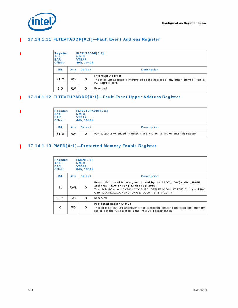
Configuration Register Space
528 Datasheet
17.14.1.11 FLTEVTADDR[0:1]—Fault Event Address Register
17.14.1.12 FLTEVTUPADDR[0:1]—Fault Event Upper Address Register
17.14.1.13 PMEN[0:1]—Protected Memory Enable Register
Register: FLTEVTADDR[0:1]Addr: MMIOBAR: VTBAROffset: 40h, 1040h
Bit Attr Default Description
31:2 RO 0Interrupt Address The interrupt address is interpreted as the address of any other interrupt from a PCI Express port.
1:0 RW 0 Reserved
Register: FLTEVTUPADDR[0:1]Addr: MMIOBAR: VTBAROffset: 44h, 1044h
Bit Attr Default Description
31:0 RW 0 IOH supports extended interrupt mode and hence implements this register
Register: PMEN[0:1]Addr: MMIOBAR: VTBAROffset: 64h, 1064h
Bit Attr Default Description
31 RWL 0
Enable Protected Memory as defined by the PROT_LOW(HIGH)_BASE and PROT_LOW(HIGH)_LIMIT registersThis bit is RO when LT.CMD.LOCK.PMRC (OFFSET 0000h: LT.STS[12]=1) and RW when LT.CMD.LOCK.PMRC (OFFSET 0000h: LT.STS[12]=0
30:1 RO 0 Reserved
0 RO 0Protected Region Status This bit is set by IOH whenever it has completed enabling the protected memory region per the rules stated in the Intel VT-d specificaiton.

Datasheet 529
Configuration Register Space
17.14.1.14 PROT_LOW_MEM_BASE[0:1]—Protected Memory Low Base Register[0:1][0:1]
17.14.1.15 PROT_LOW_MEM_LIMIT[0:1]—Protected Memory Low Limit Register
17.14.1.16 PROT_HIGH_MEM_BASE[0:1]—Protected Memory High Base Register
Register: PROT_LOW_MEM_BASE[0:1]Addr: MMIOBAR: VTBAROffset: 68h, 1068h
Bit Attr Default Description
31:21 RWL 0
2 MB aligned base address of the low protected DRAM regionThis bit is RO when LT.CMD.LOCK.PMRC (OFFSET 0000h: LT.STS[12]=1) and RW when LT.CMD.LOCK.PMRC (OFFSET 0000h: LT.STS[12]=0)Note that Intel VT-d engine generated reads/writes (page walk, interrupt queue, invalidation queue read, invalidation status) themselves are allowed toward this region
20:0 RV 0 Reserved
Register: PROT_LOW_MEM_LIMIT[0:1]Addr: MMIOBAR: VTBAROffset: 6Ch, 106Ch
Bit Attr Default Description
31:24 RWL 02 MB aligned limit address of the low protected DRAM regionThis bit is RO when TXT.CMD.LOCK.PMRC (OFFSET 0000h: TXT.STS[12]=1) and RW when TXT.CMD.LOCK.PMRC (OFFSET 0000h: TXT.STS[12]=0)
23:0 RV 0 Reserved
Register: PROT_HIGH_MEM_BASE[0:1]Addr: MMIOBAR: VTBAROffset: 70h, 1070h
Bit Attr Default Description
63:24 RWL 0
2 MB aligned base address of the high protected DRAM regionThis bit is RO when TXT.CMD.LOCK.PMRC (OFFSET 0000h: TXT.STS[12]=1) and RW when TXT.CMD.LOCK.PMRC (OFFSET 0000h: TXT.STS[12]=0)Note that Intel VT-d engine generated reads/writes (page walk, interrupt queue, invalidation queue read, invalidation status) themselves are allowed toward this region
23:0 RO 0 Reserved

Configuration Register Space
530 Datasheet
17.14.1.17 PROT_HIGH_MEM_LIMIT[0:1]—Protected Memory Limit Base Register
17.14.1.18 INV_QUEUE_HEAD[0:1]—Invalidation Queue Header Pointer Register
17.14.1.19 INV_QUEUE_TAIL[0:1]—Invalidation Queue Tail Pointer Register
Register: PROT_HIGH_MEM_LIMIT[0:1]Addr: MMIOBAR: VTBAROffset: 78h, 1078h
Bit Attr Default Description
63:21 RWL 0
2 MB aligned limit address of the high protected DRAM regionThis bit is RO when TXT.CMD.LOCK.PMRC (OFFSET 0000h: TXT.STS[12]=1) and RW when TXT.CMD.LOCK.PMRC (OFFSET 0000h: TXT.STS[12]=0)Note that Intel VT-d engine generated reads/writes (page walk, interrupt queue, invalidation queue read, invalidation status) themselves are allowed toward this region
20:0 RV 0 Reserved
Register: INV_QUEUE_HEAD[0:1]Addr: MMIOBAR: VTBAROffset: 80h, 1080h
Bit Attr Default Description
63:19 RV 0 Reserved
18:4 RO 0
Queue Head This field specifies the offset (128-bit aligned) to the invalidation queue for the command that will be fetched next by hardware. This field is incremented after the command has been fetched successfully and has been verified to be a valid/supported command.
3:0 RV 0 Reserved
Register: INV_QUEUE_TAIL[0:1]Addr: MMIOBAR: VTBAROffset: 88h, 1088h
Bit Attr Default Description
63:19 RO 0 Reserved
18:4 RW 0 Queue Tail: This field specifies the offset (128-bit aligned) to the invalidation queue for the command that will be written next by software.
3:0 RO 0 Reserved

Datasheet 531
Configuration Register Space
17.14.1.20 INV_QUEUE_ADD[0:1]—Invalidation Queue Address Register
17.14.1.21 INV_COMP_STATUS[0:1]—Invalidation Completion Status Register
Register: INV_QUEUE_ADD[0:1]Addr: MMIOBAR: VTBAROffset: 90h, 1090h
Bit Attr Default Description
63:12 RW 0 This field points to the base of size-aligned invalidation request queue.
11:3 RV 0 Reserved
2:0 RW 0
Queue Size This field specifies the length of the invalidation request queue. The number of entries in the invalidation queue is defined as 2^(X + 8) , where X is the value programmed in this field.
Register; INV_COMP_STATUS[0:1]Addr: MMIOBAR: VTBAROffset: 9Ch, 109Ch
Bit Attr Default Description
31:1 RO 0 Reserved
0 RW1CS 0Invalidation Wait Descriptor CompleteThis bit indicates completion of Invalidation Wait Descriptor with Interrupt Flag (IF) field set
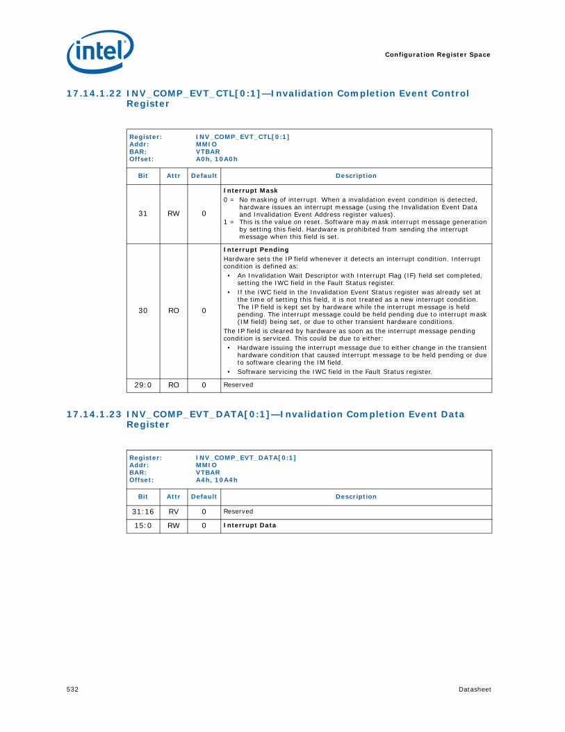
Configuration Register Space
532 Datasheet
17.14.1.22 INV_COMP_EVT_CTL[0:1]—Invalidation Completion Event Control Register
17.14.1.23 INV_COMP_EVT_DATA[0:1]—Invalidation Completion Event Data Register
Register: INV_COMP_EVT_CTL[0:1]Addr: MMIOBAR: VTBAROffset: A0h, 10A0h
Bit Attr Default Description
31 RW 0
Interrupt Mask 0 = No masking of interrupt. When a invalidation event condition is detected,
hardware issues an interrupt message (using the Invalidation Event Data and Invalidation Event Address register values).
1 = This is the value on reset. Software may mask interrupt message generation by setting this field. Hardware is prohibited from sending the interrupt message when this field is set.
30 RO 0
Interrupt Pending Hardware sets the IP field whenever it detects an interrupt condition. Interrupt condition is defined as:• An Invalidation Wait Descriptor with Interrupt Flag (IF) field set completed,
setting the IWC field in the Fault Status register.• If the IWC field in the Invalidation Event Status register was already set at
the time of setting this field, it is not treated as a new interrupt condition. The IP field is kept set by hardware while the interrupt message is held pending. The interrupt message could be held pending due to interrupt mask (IM field) being set, or due to other transient hardware conditions.
The IP field is cleared by hardware as soon as the interrupt message pending condition is serviced. This could be due to either:• Hardware issuing the interrupt message due to either change in the transient
hardware condition that caused interrupt message to be held pending or due to software clearing the IM field.
• Software servicing the IWC field in the Fault Status register.
29:0 RO 0 Reserved
Register: INV_COMP_EVT_DATA[0:1]Addr: MMIOBAR: VTBAROffset: A4h, 10A4h
Bit Attr Default Description
31:16 RV 0 Reserved
15:0 RW 0 Interrupt Data

Datasheet 533
Configuration Register Space
17.14.1.24 INV_COMP_EVT_ADDR[0:1]—Invalidation Completion Event Address Register
17.14.1.25 INTR_REMAP_TABLE_BASE[0:1]—Interrupt Remapping Table Base Address Register
17.14.1.26 FLTREC[7:0]—Fault Record Register
Register: INV_COMP_EVT_ADDR[0:1]Addr: MMIOBAR: VTBAROffset: A8h, 10A8h
Bit Attr Default Description
31:2 RW 0 Interrupt Address
1:0 RV 0 Reserved
RegisteR: INTR_REMAP_TABLE_BASE[0:1]Addr: MMIOBAR: VTBAROffset: B8h, 10B8h
Bit Attr Default Description
63:12 RW 0
Intr Remap Base This field points to the base of page-aligned interrupt remapping table. If the Interrupt Remapping Table is larger than 4KB in size, it must be size-aligned.Reads of this field returns value that was last programmed to it.
11 RWL 0
IA32 Extended Interrupt Enable0 = IA32 system is operating in legacy IA32 interrupt mode. Hardware
interprets only 8-bit APICID in the Interrupt Remapping Table entries.1 = IA32 system is operating in extended IA32 interrupt mode. Hardware
interprets 32-bit APICID in the Interrupt Remapping Table entries.
10:4 RV 0 Reserved
3:0 RW 0
Size This field specifies the size of the interrupt remapping table. The number of entries in the interrupt remapping table is 2^(X+1), where X is the value programmed in this field.
Register: FLTREC[7:0]Addr: MMIOBAR: VTBAROffset: [170h:100h], [1170:1100h]
Bit Attr Default Description
127 RW1CS 0
Fault (F) Hardware sets this field to indicate a fault is logged in this fault recording register. The F field is set by hardware after the details of the fault is recorded in the PADDR, SID, FR and T fields.When this field is set, hardware may collapse additional faults from the same requestor (SID).Software writes the value read from this field to clear it.
126 ROS 0
Type:Type of the first faulted DMA Request0: DMA Write1: DMA Read RequestField valid only when F bit is set

Configuration Register Space
534 Datasheet
17.14.1.27 IOTLBINV[0:1]—IOTLB Invalidate Register
125:124 ROS 0 Address Type: This field captures the AT field from the faulted DMA request. Field valid only when F bit is set
123:104 RV 0 Reserved
103:96 ROS 0Fault ReasonReason for the first translation fault. See Intel VT-d specification for details.This field is only valid when Fault bit is set.
95:80 RV 0 Reserved
79:64 ROS 0Source Identifier Requester ID that faulted. Valid only when F bit is set
63:12 ROS 0GPA 4k aligned GPA for the faulting transaction. Valid only when F field is set
11:0 RV 0 Reserved
Register: IOTLBINV[0:1]Addr: MMIOBAR: VTBAROffset: 200h, 1200h
Bit Attr Default Description
63 RW 0 Invalidate IOTLB cache (IVT)Software requests IOTLB invalidation by setting this field. Software must also set the requested invalidation granularity by programming the IIRG field.Hardware clears the IVT field to indicate the invalidation request is complete. Hardware also indicates the granularity at which the invalidation operation was performed through the IAIG field. Software must read back and check the IVT field to be clear to confirm the invalidation is complete.When IVT field is set, software must not update the contents of this register (and Invalidate Address register, i if it is being used), nor submit new IOTLB invalidation requests.
62 RV 0 Reserved
61:60 RW 0
IOTLB Invalidation Request Granularity (IIRG)When requesting hardware to invalidate the I/OTLB (by setting the IVT field), software writes the requested invalidation granularity through this IIRG field. Following are the encoding for te 2-bit IIRG field.000 = Reserved. 001 = Global Invalidation request. IOH supports this.010 = Domain-selective invalidation request. The target domain-id must be
specified in the DID field. IOH supports this.011 = Page-selective invalidation request. The target address, mask and
invalidation hint must be specified in the Invalidate Address register, the domain-id must be provided in the DID field. IOH aliases this to 011; that is, it performs a domain-page-selective invalidation on this request as well. IOH supports this.
101–111 = Reserved.
59 RV 0 Reserved
Register: FLTREC[7:0]Addr: MMIOBAR: VTBAROffset: [170h:100h], [1170:1100h]
Bit Attr Default Description

Datasheet 535
Configuration Register Space
17.14.1.28 INVADDRREG[0:1]—Invalidate Address Register
58:57 RO 0
IOTLB Actual Invalidation Granularity (IAIG)Hardware reports the granularity at which an invalidation request was proceed through the AIG field at the time of reporting invalidation completion (by clearing the IVT field).Following are the encoding for te 2-bit IIRG field.000 = Reserved. 001 = Global Invalidation performed. IOHTB sets this in response to a global
IOTLB invalidation request.010 = Domain-selective invalidation performed using the domain-id that was
specified by software in the DID field. IOH sets this in response to a domain-specific or page-specific IOTLB invalidation request. IOH sets this in response to a domain selective IOTLB invalidation request.
011 = IOH sets this in response to a page-selective invalidation requests.
56:50 RV 0 Reserved
49 RW 0Drain Reads IOH does not support this feature. IOH uses this to drain or not drain reads on an invalidation request.
48 RW 0Drain Writes IOH does not support this feature. IOH uses this to drain or not drain writes on an invalidation request.
47:32 RW 0
Domain ID Domain to be invalidated and is programmed by software for both page and domain selective invalidation requests. IOH ignores the bits 47:40 since it supports only an 8 bit Domain ID.
31:0 RV 0 Reserved
Register: INVADDRREG[0:1]Addr: MMIOBAR: VTBAROffset: 208h, 1208h
Bit Attr Default Description
63:12 RW 0
AddressTo request a page-specific invalidation request to hardware, software must first write the corresponding guest physical address to this register, and then issue a page-specific invalidate command through the IOTLB_REG.
11:7 RV 0 Reserved
6 RW 0
Invalidation Hint The field provides hint to hardware to preserve or flush the respective non-leaf page-table entries that may be cached in hardware.0 = Software may have modified both leaf and non-leaf page-table entries
corresponding to mappings specified in the ADDR and AM fields. On a page-selective invalidation request, IOH must flush both the cached leaf and nonleaf page-table entries corresponding to mappings specified by ADDR and AM fields. IOH performs a domain-level invalidation on non-leaf entries and page-selective-domain-level invalidation at the leaf level.
1 = Software has not modified any non-leaf page-table entries corresponding to mappings specified in the ADDR and AM fields. On a page-selective invalidation request, IOH preserves the cached non-leaf page-table entries corresponding to mappings specified by ADDR and AM fields and performs only a page-selective invalidation at the leaf level.
5:0 RW 0Address Mask IOH supports values of 0–9. All other values result in undefined results.
Register: IOTLBINV[0:1]Addr: MMIOBAR: VTBAROffset: 200h, 1200h
Bit Attr Default Description

Configuration Register Space
536 Datasheet
17.15 DMI Root Complex Register Block (RCRB)The DMI Root Complex Register Block describes the behavior of internal DMI link. This block is mapped into memory space, using register DMIRCBAR in “DMIRCBAR: DMI Root Complex Register Block Base Address Register” of the DMI device (D0:F0).
17.15.1 DMI RCRB Register Map
Table 17-34.DMI RCRB Registers
DMIVCH 00h DMIRCILCTRLH 80h
DMIVCCAP1 04h DMILCAP 84h
DMIVCCAP2 08h DMILSTS DMILCTRL 88h
DMIVCCTL 0Ch DMIOLCTRL 8Ch
DMIVC0RCAP 10h 90h
DMIVC0RCTL 14h 94h
DMIVC0RSTS 18h 98h
DMIVC1RCAP 1Ch 9Ch
DMIVC1RCTL 20h A0h
DMIVC1RSTS 24h A4h
DMIVCPRCAP 28h A8h
DMIVCPRCTL 2Ch ACh
DMIVCPRSTS 30h B0h
34h B4h
38h B8h
3Ch BCh
DMIRCLDECH 40h C0h
DMIESD 44h C4h
48h C8h
4Ch CCh
DMILED 50h D0h
54h D4h
DMILEBA 58h D8h
5Ch DCh
60h E0h
64h E4h
68h E8h
6Ch ECh
70h F0h
74h F4h
78h F8h
7Ch FCh

Datasheet 537
Configuration Register Space
17.15.2 Virtual Channel Configuration
17.15.2.1 DMIVCH: DMI Virtual Channel Capability Header
This register Indicates DMI Virtual Channel capabilities.
17.15.2.2 DMIVCCAP1: DMI Port VC Capability Register 1
This register describes the configuration of PCI Express Virtual Channels associated with the DMI port.
17.15.2.3 DMIVCCAP2: DMI Port VC Capability Register 2
This register Describes the configuration of PCI Express Virtual Channels associated with this port.
Register: DMIVCHBAR: DMIRCBAROffset: 0000h
Bit Attr Default Description
31:20 RO 040hPointer to Next Capability (PNC): This field contains the offset to the next PCI Express capability structure in the linked list of capabilities (Link Declaration Capability).
19:16 RO 1hPCI Express Virtual Channel Capability Version (PCIEVCCV): Hardwired to 1 to indicate compliances with the 1.1 version of the PCI Express specification.
15:0 RO 0002hExtended Capability ID (ECID): Value of 0002 h identifies this linked list item (capability structure) as being for PCI Express Virtual Channel registers.
Register: DMIVCCAP1BAR: DMIRCBAROffset: 0004h
Bit Attr Default Description
31:7 RV 0 Reserved
6:4 RO 0
Low Priority Extended VC Count (LPEVCC): Indicates the number of (extended) Virtual Channels in addition to the default VC belonging to the low-priority VC (LPVC) group that has the lowest priority with respect to other VC resources in a strict-priority VC Arbitration.
The value of 0 in this field implies strict VC arbitration.
3 RO 0 Reserved
2:0 RWO 001bExtended VC Count (EVCC): Indicates the number of (extended) Virtual Channels in addition to the default VC supported by the device.
The Private Virtual Channel is not included in this count.
Register: DMIVCCAP2BAR: DMIRCBAROffset: 0008h
Bit Attr Default Description
31:24 RO 0h Reserved for VC Arbitration Table Offset.
23:8 RO 0h Reserved
7:0 RO 0h Reserved for VC Arbitration Capability (VCAC):

Configuration Register Space
538 Datasheet
17.15.2.4 DMIVCCTL: DMI Port VC Control
17.15.2.5 DMIVC0RCAP - DMI VC0 Resource Capability
Register: DMIVCCTLBAR: DMIRCBAROffset: 000Ch
Bit Attr Default Description
15:4 RO 0h Reserved
3:1 RW 0h
VC Arbitration Select (VCAS): This field will be programmed by software to the
only possible value as indicated in the VC Arbitration Capability field.
The value 000b when written to this field will indicate the VC arbitration scheme is hardware fixed (in the root complex). This field cannot be modified when more than one VC in the LPVC group is enabled.
000: Hardware fixed arbitration scheme. E.G. Round Robin
Others: Reserved
See the PCI express specification for more details
0 RO 0h Reserved for Load VC Arbitration Table.
Register: DMIVC0RCAPBAR: DMIRCBAROffset: 0010h
Bit Attr Default Description
31:24 RO 0h Port Arbitration Table Offset (PATOFF):.
23 RO 0 Reserved
22:16 RO 0h Maximum Time Slots (MAXTIMESLOTS):
15 RO 0h
Reject Snoop Transactions (REJSNPT):
0: Transactions with or without the No Snoop bit set within the TLP header are
allowed on this VC.
1: Any transaction without the No Snoop bit set within the TLP header will be
rejected as an Unsupported Request.
14:8 RO 0h Reserved
7:0 RO 01hPort Arbitration Capability (PAC): Having only bit 0 set indicates that the only
supported arbitration scheme for this VC is non-configurable hardware-fixed.

Datasheet 539
Configuration Register Space
17.15.2.6 DMIVC0RCTL: DMI VC0 Resource Control
Controls the resources associated with PCI Express Virtual Channel 0.
Register: DMIVC0RCTLBAR: DMIRCBAROffset: 0014h
Bit Attr Default Description
31 WO 1
Virtual Channel 0 Enable (VC0E): For VC0 this is hardwired to 1 and read only as VC0 can never be disabled.
Note: This bit should always be enabled and hence writes are illegal to this bit 7.
30:27 RO 0h Reserved
26:24 RO 0hVirtual Channel 0 ID (VC0ID): Assigns a VC ID to the VC resource. For VC0 this is hardwired to 0 and read only.
23:20 RO 0h Reserved
19:17 RW 1h
Port Arbitration Select (PAS): Configures the VC resource to provide a particular Port Arbitration service. Valid value for this field is a number corresponding to one of the asserted bits in the Port Arbitration Capability field of the VC resource. Because only bit 0 of that field is asserted.
This field will always be programmed to '1'.
16:8 RO 0h Reserved
7:1 RW 7Fh
Traffic Class / Virtual Channel 0 Map (TCVC0M): Indicates the TCs (Traffic Classes) that are mapped to the VC resource. Bit locations within this field correspond to TC values.
For example, when bit 7 is set in this field, TC7 is mapped to this VC resource. When more than one bit in this field is set, it indicates that multiple TCs are mapped to the VC resource. In order to remove one or more TCs from the TC/VC Map of an enabled VC, software must ensure that no new or outstanding transactions with the TC labels are targeted at the given Link.
0 RO 1Traffic Class 0 / Virtual Channel 0 Map (TC0VC0M): Traffic Class 0 is always
routed to VC0.

Configuration Register Space
540 Datasheet
17.15.2.7 DMIVC0RSTS: DMI VC0 Resource Status
Reports the Virtual Channel specific status.
17.15.2.8 DMIVC1RCAP - DMI VC1 Resource Capability
Register: DMIVC0RSTSBAR: DMIRCBAROffset: 001Ah
Bit Attr Default Description
15:2 RO 0hReserved
Software must use 0 for writes to these bits.
1 RO 1
Virtual Channel 0 Negotiation Pending (VC0NP):
0: The VC negotiation is complete.
1: The VC resource is still in the process of negotiation (initialization or
disabling).
This bit indicates the status of the process of Flow Control initialization. It is set by default on Reset, as well as whenever the corresponding Virtual Channel is Disabled or the Link is in the DL_Down state.
It is cleared when the link successfully exits the FC_INIT2 state.
BIOS Requirement: Before using a Virtual Channel, software must check whether the VC Negotiation Pending fields for that Virtual Channel are cleared in both Components on a Link.
0 RO 0 Reserved
Register: DMIVC1RCAPBAR: DMIRCBAROffset: 001Ch
Bit Attr Default Description
31:24 RO 0h Reserved
23 RO 0 Reserved
22:16 RO 0h Reserved
15 RO 0h
Reject Snoop Transactions (REJSNPT):
0: Transactions with or without the No Snoop bit set within the TLP header are
allowed on this VC.
1: Any transaction without the No Snoop bit set within the TLP header will be
rejected as an Unsupported Request.
14:8 RO 0h Reserved
7:0 RO 01hPort Arbitration Capability (PAC): Having only bit 0 set indicates that the only
supported arbitration scheme for this VC is non-configurable hardware-fixed.

Datasheet 541
Configuration Register Space
17.15.2.9 DMIVC1RCTL: DMI VC1 Resource Control
Controls the resources associated with PCI Express Virtual Channel 1.
Register: DMIVC1RCTLBAR: DMIRCBAROffset: 0020h
Bit Attr Default Description
31 RW 0
Virtual Channel 1 Enable (VC1E):
0: Virtual Channel is disabled.
1: Virtual Channel is enabled. See exceptions below.
Software must use the VC Negotiation Pending bit to check whether the VC negotiation is complete. When VC Negotiation Pending bit is cleared, a 1 read from this VC Enable bit indicates that the VC is enabled (Flow Control Initialization is completed for the PCI Express port). A 0 read from this bit indicates that the Virtual Channel is currently disabled.
BIOS Requirement:
1. To enable a Virtual Channel, the VC Enable bits for that Virtual Channel must be set in both Components on a Link.
2. To disable a Virtual Channel, the VC Enable bits for that Virtual Channel must be cleared in both Components on a Link.
3. Software must ensure that no traffic is using a Virtual Channel at the time it is disabled.
4. Software must fully disable a Virtual Channel in both Components on a Link before re-enabling the Virtual Channel.
30:27 RO 0h Reserved
26:24 RW 001bVirtual Channel 1 ID (VC1ID): Assigns a VC ID to the VC resource. Assigned value must be non-zero. This field can not be modified when the VC is already enabled.
23:20 RO 0h Reserved
19:17 RW 0h
Port Arbitration Select (PAS): Configures the VC resource to provide a particular Port Arbitration service. Valid value for this field is a number corresponding to one of the asserted bits in the Port Arbitration Capability field of the VC resource.
16:8 RO 0h Reserved
7:1 RW 00h
Traffic Class / Virtual Channel 1 Map (TCVC1M): Indicates the TCs (Traffic Classes) that are mapped to the VC resource. Bit locations within this field correspond to TC values.
For example, when bit 7 is set in this field, TC7 is mapped to this VC resource. When more than one bit in this field is set, it indicates that multiple TCs are mapped to the VC resource. In order to remove one or more TCs from the TC/VC Map of an enabled VC, software must ensure that no new or outstanding transactions with the TC labels are targeted at the given Link.
0 RO 0Traffic Class 0 / Virtual Channel 0 Map (TC0VC0M): Traffic Class 0 is always
routed to VC0.

Configuration Register Space
542 Datasheet
17.15.2.10 DMIVC1RSTS: DMI VC1 Resource Status
Reports the Virtual Channel specific status.
17.15.2.11 DMIVCPRCAP - DMI VCP Resource Capability
Register: DMIVC1RSTSBAR: DMIRCBAROffset: 0026h
Bit Attr Default Description
15:2 RO 0hReserved
Software must use 0 for writes to these bits.
1 RO 1
Virtual Channel 1 Negotiation Pending (VC1NP):
0: The VC negotiation is complete.
1: The VC resource is still in the process of negotiation (initialization or
disabling).
This bit indicates the status of the process of Flow Control initialization. It is set by default on Reset, as well as whenever the corresponding Virtual Channel is Disabled or the Link is in the DL_Down state.
It is cleared when the link successfully exits the FC_INIT2 state.
BIOS Requirement: Before using a Virtual Channel, software must check whether the VC Negotiation Pending fields for that Virtual Channel are cleared in both Components on a Link.
0 RO 0 Reserved
Register: DMIVCPRCAPBAR: DMIRCBAROffset: 0028h
Bit Attr Default Description
31:24 RO 0h Port Arbitration Table Offset (PATOFF).
23 RO 0 Reserved
22:16 RO 0h Maximum Time Slots (MAXTIMESLOTS)
15 RO 0h
Reject Snoop Transactions (REJSNPT):
0: Transactions with or without the No Snoop bit set within the TLP header are
allowed on this VC.
1: Any transaction without the No Snoop bit set within the TLP header will be
rejected as an Unsupported Request.
14:8 RO 0h Reserved
7:0 RO 01hPort Arbitration Capability (PAC): Having only bit 0 set indicates that the only
supported arbitration scheme for this VC is non-configurable hardware-fixed.

Datasheet 543
Configuration Register Space
17.15.2.12 DMIVCPRCTL: DMI VCP Resource Control
Controls the resources associated with the DMI Private Channel (VCp).
Register: DMIVCPRCTLBAR: DMIRCBAROffset: 002Ch
Bit Attr Default Description
31 RW 0
Virtual Channel Private Enable (VCPE):
0: Virtual Channel is disabled.
1: Virtual Channel is enabled. See exceptions below.
Software must use the VC Negotiation Pending bit to check whether the VC negotiation is complete. When VC Negotiation Pending bit is cleared, a 1 read from this VC Enable bit indicates that the VC is enabled (Flow Control Initialization is completed for the PCI Express port). A 0 read from this bit indicates that the Virtual Channel is currently disabled.
BIOS Requirement:
1. To enable a Virtual Channel, the VC Enable bits for that Virtual Channel must be set in both Components on a Link.
2. To disable a Virtual Channel, the VC Enable bits for that Virtual Channel must be cleared in both Components on a Link.
3. Software must ensure that no traffic is using a Virtual Channel at the time it is disabled.
4. Software must fully disable a Virtual Channel in both Components on a Link before re-enabling the Virtual Channel.
30:27 RO 0h Reserved
26:24 RW 000b
Virtual Channel Private 1 ID (VCPID): Assigns a VC ID to the VC resource. This field can not be modified when the VC is already enabled. No private VCs are precluded by hardware and private VC handling is implemented the same way as non-private VC handling.
However, to limit validation permutations the only private VC that is being validated is private VC6 (110b) and is the only value that should be programmed into this field.

Configuration Register Space
544 Datasheet
17.15.2.13 DMIVCPRSTS: DMI VCP Resource Status
Reports the Virtual Channel specific status.
17.15.2.14 Root Complex Topology Configuration
17.15.2.15 DMIRCLDECH: DMI Root Complex Link Declaration Capability Header
This capability declares links from the respective element to other elements of the root complex component to which it belongs and to an element in another root complex
23:20 RO 0h Reserved
19:17 RW 0h
Port Arbitration Select (PAS): Configures the VC resource to provide a particular Port Arbitration service. Valid value for this field is a number corresponding to one of the asserted bits in the Port Arbitration Capability field of the VC resource.
16:8 RO 0h Reserved
7:0 RW 00h
Traffic Class / Virtual Channel private Map (TCVCPM): Any TLP transmitted for a Private Traffic Class will have Reserved bit 7 in byte 1 of the TLP header set implicitly. Any TLP received with this bit set is interpreted as a Private Traffic Class, where the Traffic Class field (bits 6:4 of byte 1) determine the actual Private Traffic Class number. No TC/VCp mappings are precluded by hardware and the private TC/VC mapping behaves the same way as for all other VCs (including unmapped TCs being dropped).
However, it is recommended that private TC6 (01000000b) is the only value that should be programmed into this field. This strategy can simplify debug and limit validation permutations.
Register: DMIVCPRCTLBAR: DMIRCBAROffset: 002Ch
Bit Attr Default Description
Register: DMIVCPRSTSBAR: DMIRCBAROffset: 0032h
Bit Attr Default Description
15:2 RO 0hReserved
Software must use 0 for writes to these bits.
1 RO 1
Virtual Channel Private Negotiation Pending (VCPNP):
0: The VC negotiation is complete.
1: The VC resource is still in the process of negotiation (initialization or
disabling).
This bit indicates the status of the process of Flow Control initialization. It is set by default on Reset, as well as whenever the corresponding Virtual Channel is Disabled or the Link is in the DL_Down state.
It is cleared when the link successfully exits the FC_INIT2 state.
BIOS Requirement: Before using a Virtual Channel, software must check whether the VC Negotiation Pending fields for that Virtual Channel are cleared in both Components on a Link.
0 RO 0 Reserved

Datasheet 545
Configuration Register Space
component. See PCIExpress specification for link/topology declaration requirements.
17.15.2.16 DMIESD: DMI Element Self Description
Provides information about the root complex element containing this Link Declaration Capability.
Register: DMIRCLDECHBAR: DMIRCBAROffset: 0040h
Bit Attr Default Description
31:20 RO 080hPointer to Next Capability (PNC): This field contains the offset to the next PCI
Express capability structure in the linked list of capabilities (Internal Link Control Capability).
19:16 RO 1hLink Declaration Capability Version (LDCV): Hardwired to 1 to indicate compli-
ances with the 1.1 version of the PCI Express specification.
15:0 RO 0005hExtended Capability ID (ECID): Value of 0005 h identifies this linked list item
(capability structure) as being for PCI Express Link Declaration Capability.
Register: DMIESDBAR: DMIRCBAROffset: 0044h
Bit Attr Default Description
31:24 RO 01h
Port Number (PORTNUM): Specifies the port number associated with this element with respect to the component that contains this element. This port number value is utilized by the egress port of the component to provide arbitration to this Root Complex Element.
23:16 RWO 00h
Component ID (CID): Identifies the physical component that contains this Root
Complex Element. BIOS Requirement: Must be initialized according to guidelines in the PCI Express* Isochronous/Virtual Channel Support Hardware Programming Specification (HPS).
15:8 RO 01hNumber of Link Entries (NLE): Indicates the number of link entries following the Element Self Description. This field reports 1 (one to egress port belonging to ICH on other side of internal link).
7:4 RO 0h Reserved
3:0 RO 2hElement Type (ETYP): Indicates the type of the Root Complex Element.
Value of 2 h represents an Internal Root Complex Link (DMI).

Configuration Register Space
546 Datasheet
17.15.2.17 DMILED - DMI Link Entry Description
Link Entry which declares an internal link to another Root Complex Element.
17.15.2.18 DMILEBA - DMI Link Entry Base Address
Link Entry which declares an internal link to another Root Complex Element.
Register: DMILEDBAR: DMIRCBAROffset: 0050h
Bit Attr Default Description
31:24 RWO 0h
Target Port Number (TPN): Specifies the port number associated with the element targeted by this link entry (egress port of ICH). The target port number is with respect to the component that contains this element as specified by the target component ID.
This can be programmed by BIOS, but the default value will likely be correct
because the DMI RCRB in the ICH will likely be associated with the default egress port for the ICH meaning it will be assigned port number 0.
23:16 RWO 0h
Target Component ID (TCID): Identifies the physical component that is targeted by this link entry.
BIOS Requirement: Must be initialized according to guidelines in the PCI Express* Isochronous/Virtual Channel Support Hardware Programming Specification (HPS).
15:2 RO 0h Reserved
1 RO 0
Link Type (LTYP): Indicates that the link points to memory-mapped space (for
RCRB).
The link address specifies the 64-bit base address of the target RCRB.
0 RWO 0
Link Valid (LV):
0: Link Entry is not valid and will be ignored.
1: Link Entry specifies a valid link.
Register: DMILEBABAR: DMIRCBAROffset: 0058h
Bit Attr Default Description
63:32 RO 0h Reserved
31:12 RWO 0hLink Address (LA): Memory mapped base address of the RCRB that is the target element (egress port of ICH) for this link entry.
11:0 RO 0h Reserved

Datasheet 547
Configuration Register Space
17.15.2.19 DMIVC1CDTTHROTTLE - DMI VC1 Credit Throttle register
This register contains credit withhold registers for DMI VC1.
17.15.2.20 DMIVCPCDTTHROTTLE - DMI VCp Credit Throttle register
This register contains credit withhold registers for DMI VCp.
17.15.2.21 DMI Root Complex Internal Link Configuration
17.15.2.22 DMIRCILCTRLH - DMI Root Complex Internal Link Control Header
This capability contains controls for the Root Complex Internal Link known as DMI.
Register: DMIVC1CDTTHROTTLEBAR: DMIRCBAROffset: 0060h
Bit Attr Default Description
31:24 RWS 0h PRD[7:0]
23:22 RO 0h Reserved
21:16 RWS 0h PRH[5:0]
15:8 RWS 0h NPRD[7:0]
7:6 RO 0h Reserved
5:0 RWS 0h NPRH[5:0]
Register: DMIVCPCDTTHROTTLEBAR: DMIRCBAROffset: 0064h
Bit Attr Default Description
31:24 RWS 0h PRD[7:0]
23:22 RO 0h Reserved
21:16 RWS 0h PRH[5:0]
15:8 RWS 0h NPRD[7:0]
7:6 RO 0h Reserved
5:0 RWS 0h NPRH[5:0]
Register: DMIRCILCTRLHBAR: DMIRCBAROffset: 0080h
Bit Attr Default Description
31:20 RO 0hPointer to Next Capability (PNC): This value terminates the PCI Express extended capabilities list associated with this RCRB.
19:16 RO 1hLink Declaration Capability Version (LDCV): Hardwired to 1 to indicate
compliances with the 1.1 version of the PCI Express specification.
15:0 RO 0006hExtended Capability ID (ECID): Value of 0006 h identifies this linked list item
(capability structure) as being for PCI Express Internal Link Control Capability.

Configuration Register Space
548 Datasheet
17.15.2.23 DMILCAP: DMI Link Capabilities
Indicates DMI specific capabilities.
17.15.2.24 DMILCTRL: DMI Link Control
Allows control of DMI.
Register: DMILCAPBAR: DMIRCBAROffset: 0084h
Bit Attr Default Description
31:18 RO 0h Reserved
17:15 RWO 010 L1 Exit Latency (EL1): Indicates that the exit latency is 2us to 4us.
14:12 RWO 7h L0s Exit Latency
11:10 RO 11b Active State Link PM Support (ASLPMS): L0s & L1 entry supported.
9:4 RO 04hMax Link Width (MLW): Indicates the maximum number of lanes supported for this link.
3:0 RO 1h Max Link Speed (MLS): Hardwired to indicate 2.5 Gb/s.
Register: DMILCTRLBAR: DMIRCBAROffset: 0088h
Bit Attr Default Description
15:8 RO 0h Reserved
7 RW 0
Extended Synch (EXTSYNC): 0: Standard Fast Training Sequence (FTS).
1: Forces the transmission of additional ordered sets when exiting the L0s state and when in the Recovery state.
This mode provides external devices (e.g., logic analyzers) monitoring the Link time to achieve bit and symbol lock before the link enters L0 and resumes
communication.
This is a test mode only and may cause other undesired side effects such as buffer overflows or underruns.
6:2 RO 0h Reserved
1:0 RW 00b
Active State Power Management Support (ASPMS): Controls the level of active state power management supported on the given link.
00: Disabled
01: L0s Entry Supported
10: Reserved
11: L0s and L1 Entry Supported

Datasheet 549
Configuration Register Space
17.15.2.25 DMILSTS - DMI Link Status
Indicates DMI status.
17.15.2.26 DMIOLCTRL: DMI Other Link Control Register
Register: DMILSTSBAR: DMIRCBAROffset: 008Ah
Bit Attr Default Description
15:10 RO 0h Reserved
9:4 RO 0h
Negotiated Width (NWID): Indicates negotiated link width. This field is valid only when the link is in the L0, L0s, or L1 states (after link width negotiation is
successfully completed).
00h: Reserved
01h: X1
02h: X2
04h: X4
All other encodings are reserved.
3:0 RO 1h
Negotiated Speed (NSPD): Indicates negotiated link speed.
1h: 2.5 Gb/s
All other encodings are reserved.
Register: DMIOLCTRLBAR: DMIRCBAROffset: 008Ch
Bit Attr Default Description
15:2 RO 0h Reserved
1 WO 0
Retrain Link (RL):
0: Normal operation
1: Full Link retraining is initiated by directing the Physical Layer LTSSM from L0,
L0s, or L1 states to the Recovery state.
This bit always returns 0 when read.
0 RW 0
Link Disable (LD):
0: Normal operation
1: Link is disabled. Forces the LTSSM to transition to the Disabled state (via
Recovery) from L0, L0s, or L1 states.
Link retraining happens automatically on 0 to 1 transition, just like when coming out of reset. Writes to this bit are immediately reflected in the value read from the bit, regardless of actual Link state. Intended for debug only.
When the DMI link goes down in a real system it is a fatal, non-recoverable
condition.
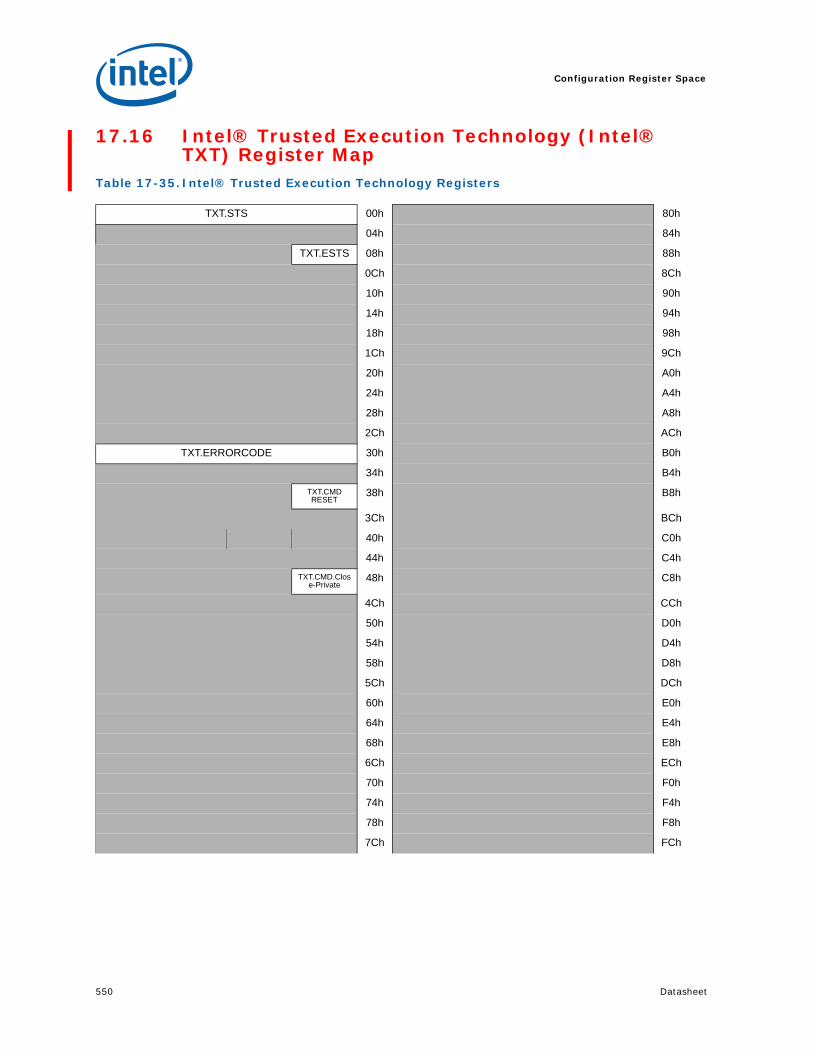
Configuration Register Space
550 Datasheet
17.16 Intel® Trusted Execution Technology (Intel® TXT) Register Map
Table 17-35.Intel® Trusted Execution Technology Registers
TXT.STS 00h 80h
04h 84h
TXT.ESTS 08h 88h
0Ch 8Ch
10h 90h
14h 94h
18h 98h
1Ch 9Ch
20h A0h
24h A4h
28h A8h
2Ch ACh
TXT.ERRORCODE 30h B0h
34h B4h
TXT.CMDRESET
38h B8h
3Ch BCh
40h C0h
44h C4h
TXT.CMD.Close-Private
48h C8h
4Ch CCh
50h D0h
54h D4h
58h D8h
5Ch DCh
60h E0h
64h E4h
68h E8h
6Ch ECh
70h F0h
74h F4h
78h F8h
7Ch FCh

Datasheet 551
Configuration Register Space
100h 180h
104h 184h
108h 188h
10Ch 18Ch
TXT.DIDVID110h 190h
114h 194h
118h 198h
11Ch 19Ch
120h 1A0h
124h 1A4h
128h 1A8h
12Ch 1ACh
130h 1B0h
134h 1B4h
138h 1B8h
13Ch 1BCh
140h 1C0h
144h 1C4h
148h 1C8h
14Ch 1CCh
150h 1D0h
154h 1D4h
158h 1D8h
15Ch 1DCh
160h 1E0h
164h 1E4h
168h 1E8h
16Ch 1ECh
170h 1F0h
174h 1F4h
178h 1F8h
17Ch 1FCh

Configuration Register Space
552 Datasheet
Table 17-36.Intel® Trusted Execution Technology Registers
200h 280h
204h 284h
208h 288h
20Ch 28Ch
210hTXT.MLE.JOIN
290h
214h 294h
TXT.CMD.Unlock.Mem-Config 218h 298h
21Ch 29Ch
220h 2A0h
224h 2A4h
228h 2A8h
22Ch 2ACh
230h 2B0h
234h 2B4h
238h 2B8h
23Ch 2BCh
240h 2C0h
244h 2C4h
248h 2C8h
24Ch 2CCh
250h 2D0h
254h 2D4h
258h 2D8h
25Ch 2DCh
260h 2E0h
264h 2E4h
268h 2E8h
26Ch 2ECh
TXT.SINIT.BASE270h 2F0h
274h 2F4h
TXT.SINIT.SIZE278h 2F8h
27Ch 2FCh

Datasheet 553
Configuration Register Space
Table 17-37.Intel® Trusted Execution Technology Registers
17.16.1 TXT Space Registers
The TXT registers adhere to the public and private attributes described in xref.
As described previously, each TXT register may have up to three ways to access it. These are given the following symbolic names. TXT_TXT is the memory region starting at FED2_0000h when it is accessed using the special TXT read or write commands. TXT_PR is the memory region starting at FED2_0000h when it is accessed using normal
TXT.HEAP.Base300h TXT.CMD.
Open.Locality1 380h
304h 384h
TXT.HEAP.Size 308h TXT.CMD.Close.Locality1 388h
30Ch 38Ch
310h TXT.Cmd.Open.Locality2 390h
314h 394h
318h 398h
31Ch 39Ch
320h 3A0h
324h 3A4h
328h 3A8h
32Ch 3ACh
330h 3B0h
334h 3B4h
338h 3B8h
33Ch 3BCh
340h 3C0h
344h 3C4h
348h 3C8h
34Ch 3CCh
350h 3D0h
354h 3D4h
358h 3D8h
35Ch 3DCh
360h 3E0h
364h 3E4h
368h 3E8h
36Ch 3ECh
370h 3F0h
374h 3F4h
378h 3F8h
37Ch 3FCh

Configuration Register Space
554 Datasheet
read or write commands. TXT_PB is the memory region starting at FED3_0000h accessed using any read or write command. TXT_PB_noWR is similar to TXT_PB but write accesses have no affect.
The register tables below sometimes list more than one base for a register. Normally this would indicate that there is more than one register. However in the current section it indicates that there is a single register which can be accessed in more than one way.
17.16.1.1 TXT.STS: TXT Status Register
This register is used to read the status of the TXT Command/Status Engine functional block in the IOH.
General Behavioral Rules:
• This is a read-only register, so writes to this register will be ignored.
• This register is available in both the Public and Private TXT config spaces.
Base: TXT_TXT Offset: 0000hBase: TXT_PR Offset: 0000hBase: TXT_PB Offset: 0000h
Bit Attr Default Description
31:18 RV 0h Reserved
17 RO 0
TXT.SEQ.IN.PROGRESS: This bit is set when the TXT.SEQUENCE.START msg is received from a cpu.
This bit is cleared when the TXT.SEQUENCE.DONE msg is received from a cpu.
If this bit is set and the chipset receives another TXT.SEQUENCE.START message, then the chipset treats this as a rogue attack and does TXT_RESET# and sets Rogue status bit.
16 RO 0
TXT.LOCALITY2.OPEN.STS: This bit is set when either the TXT.CMD.OPEN.LOCALITY2 command or the TXT.CMD.OPEN.PRIVATE is seen by the chipset. It is cleared on reset or when either TXT.CMD.CLOSE.LOCALITY2 or TXT.CMD.CLOSE.PRIVATE is seen. This bit can be used by sw as a positive indication that the command has taken effect. Note that HW should not set or clear this bit until the internal hardware will guarantee that incoming cycles will be decoded based on the state change caused by the OPEN or CLOSE command.
15 RO 0
TXT.LOCALITY1.OPEN.STS: This bit is set when the TXT.CMD.OPEN.LOCALITY1: command is seen by the chipset. It is cleared on reset or when TXT.CMD.CLOSE.LOCALITY1 is seen. This bit can be used by sw as a positive indication that the command has taken effect. Note that HW should not set or clear this bit until the internal hardware will guarantee that incoming cycles will be decoded based on the state change caused by the OPEN or CLOSE command.
14 RO 0
TXT.LOCALITY3.OPEN.STS: This bit is set when the TXT.CMD.OPEN.LOCALITY3 command is seen by the chipset. It is cleared on reset or when TXT.CMD.CLOSE.LOCALITY3 is seen.
This bit can be used by sw as a positive indication that the command has taken effect. Note that HW should not set or clear this bit until the internal hardware will guarantee that incoming cycles will be decoded based on the state change caused by the OPEN or CLOSE command.
13 RV 0 Reserved

Datasheet 555
Configuration Register Space
17.16.1.2 TXT.ESTS: TXT Error Status Register
This register is used to read the status associated with various errors that might be detected.
12 RO 0
TXT.PMRC.LOCK.STS: This bit will be set to 1 when the chipset has locked the protected memory con-figuration in response to the TXT.CMD.LOCK.PMRC command.
This bit is cleared by TXT.CMD.UNLOCK.PMRC or by a system reset.
This field is valid only on implementations that support the DMA remapping protected memory configuration (reported by setting TXT.MIF.PMR.CAP in register TXT.VER.MIF.
When this bit is set, VT memory mapped registers PROT_LOW_MEM_LIMIT, PROT_HIGH_MEM_LIMIT, PROT_LOW_MEM_BASE, PROT_HIGH_MEM_BASE, PMEN will be locked. And these registers will be unlocked when this bit is clear.
11 RO 0
MEM-CONFIG-OK.STS: (TXTMCONFOKSTS): This bit indicates whether the chipset has received and accepted the TXT.CMD.MEM-CONFIG-CHECKED TXT command. This bit is cleared by PCI reset or by the TXT.CMD.UNLOCK-MEMCONFIG command.
0: Indicates that memory configuration checking has not been performed. This is the default state after PCI reset. This bit is also set to 0 after the chipset has
accepted the TXT.CMD.UNLOCK-MEM-CONFIG command.
1: Indicates that memory configuration checking has been performed. This bit is set to one when the chipset accepts the TXT.CMD.MEM-CONFIG-CHECKED TXT command.
10:8 RV 0 Reserved
7 RO 0PRIVATE-OPEN.STS: This bit will be set to 1 when the TXT.CMD.OPEN-PRIVATE is performed.This bit cleared by the TXT.CMD.CLOSE-PRIVATE or by a system reset.
6 RO 0
MEM-CONFIG-LOCK.STS: This bit will be set to 1 when the memory configuration has been locked.This bit is cleared by TXT.CMD.UNLOCK.MEMCONFIG or by a system reset.
When this bit is set registers VTCTRL (D20:F0:7Ch) and VTBAR (D20:F0:78h) will be locked. And these registers will be unlocked when this bit is clear.
5 RO 0
BASE.LOCKED.STS: This bit will be set to '1' when the TXT.LOCK.BASE command is issued.
This bit is cleared by TXT.UNLOCK.BASE or by a system reset.
When this bit is set, TXT space registers TXT_HEAP_BASE, TXT_HEAP_SIZE, TXT_MSEG_BASE, TXT_MSEG_SIZE, TXT_SCRATCHPAD0 and TXT_SCRATCHPAD1 will be locked. And these registers will be unlocked when this bit is clear.
4:2 RV 0h Reserved
1 RO 1
SEXIT.DONE.STS: This bit is set when all of the bits in the TXT.THREADS.JOIN register are clear 0 (via TXT_JOINS_CLEAR command). Thus, this bit will be set immediately after reset (since the bits are all 0).
0 RO 0
SENTER.DONE.STS: The chipset sets this bit when TXT.THREADS.JOIN = TXT.THREAD.EXISTS and TXT.THREADS.JOIN != 0.
When any of the threads does the TXT.JOINS.CLEAR to clear the set bit in TXT.THREADS.JOIN register, the TXT.THREADS.JOIN and TXT.THREADS.EXISTS registers will not be equal, so the chipset will clear this bit.
Base: TXT_TXT Offset: 0000hBase: TXT_PR Offset: 0000hBase: TXT_PB Offset: 0000h
Bit Attr Default Description

Configuration Register Space
556 Datasheet
General Behavioral Rules:
• This register is available for read-only access from the Public config space.
• This register is available for read and write access from the Private config space. Each status bit is cleared by writing to this register with a 1 in the corresponding bit position.
• The bits in this register are cleared by writing a 1 to the corresponding bit positions. These bits are not cleared by a standard system reset.
17.16.1.3 TXT.ERRORCODE: TXT Error Code Register
General Description: When software discovers an error, it can write this scratch-pad register. How-ever, the register is sticky and reset only by a power-good reset, and so allows diagnostic software (after the hard reset) to determine why the SENTER sequence failed (by examining various status bits).
General Behavioral Rules:
• This is a read-only register in the public TXT config space.
• This register is for read and write in the private TXT config space.
• Accesses to this register are done with 1, 2, or 4B writes and reads.
• The default value of this register is 00000000h.
Access to this register has no other effect on the chipset other than reading or writing the contents of this register.
Base: TXT_TXT Offset: 0008hBase: TXT_PR Offset: 0008hBase: TXT_PB_noWROffset: 0008h
Bit Attr Default Description
7 RV 0 Reserved
6 RW1C 0 WAKE-ERROR.STS: The chipset sets this bit when it detects that there might have been secrets in memory and a reset or power failure occurred.If this bit is set after a system reset, the chipset will prevent memory accesses until specifically enabled. The software that is authorized to enable the memory accesses will also be responsible for clearing the secrets from memory.Software can read chipset-specific registers to determine the specific cause of the error. The location of those bits is beyond the scope of this specification. On a reset, if NOP_ACK_WITH_SECRETS is received, then this bit is set to ‘1’. On a reset, if NOP_ACK_WITHOUT_SECRETS is received, then this bit is cleared to ‘0’.This bit must be cleared if a read to 0xFED4_0000 returns a 1 in bit 0.
5:1 RV 0 Reserved
0 ROS 0 TXT_RESET.STS: The chipset sets this bit to indicate that the TXT.RESET cycle has been received. Note that this bit is sticky and is only cleared by a power cycle. The effect of TXT.RESET is also held active through reset. The only way to clear this bit is to do a power cycle.
Base: TXT_TXT Offset: 0030hBase: TXT_PR Offset: 0030hBase: TXT_PB_noWROffset: 0030h
Bit Attr Default Description
31:00 RWS 0h TXT_ERRORCODE: [31:0]: This register is a scratch pad register and is defined by the software usage model.

Datasheet 557
Configuration Register Space
17.16.1.4 TXT.CMD.RESET: TXT System Reset Command Register
General Description: When this command is invoked, the chipset resets the entire platform.
General Behavioral Rules:
• This is a write-only register.
• This register is only available in the private TXT config space.
• Accesses to this register are done with 1B writes.
• The data bits associated with this command are undefined and have no specific meaning
17.16.1.5 TXT.CMD.CLOSE_PRIVATE: TXT Close Private Command Register
General Description: The CPU that authenticates the SEXIT code does this to prevent the TXT Private config space from being accessed using standard memory read/write cycles.
General Behavioral Rules:
• This is a write-only register.
• This register is only available in the Private TXT config space.
• Accesses to this register are done with 1B writes.
• The data bits associated with this command are undefined and have no specific meaning.
Base: TXT_TXT Offset: 0038hBase: TXT_PR Offset: 0038h
Bit Attr Default Description
7:0 WO 0h N/A
Base: TXT_TXT Offset: 0048hBase: TXT_PR Offset: 0048h
Bit Attr Default Description
7:0 WO 0h N/A

Configuration Register Space
558 Datasheet
17.16.1.6 TXT.DIDVID: TXT Identifier Register
General Description: This register holds TXT ID for the IOH.
General Behavioral Rules:
• This register is available in both the Public and Private TXT config spaces.
17.16.1.7 TXT.CMD.UNLOCK.MEM_CONFIG: TXT UnLock Memory Config Command Register
General Description: When this command is invoked, the chipset unlocks all memory configuration registers. Software might unlock the memory config if taking down the secure environment
General Behavioral Rules:
• This is a write-only register.
• This register is only available in the private TXT config space.
• Accesses to this register are done with 1B writes.
• The data bits associated with this command are undefined and have no specific meaning.
• This command clears the TXT.MEM-CONFIG-LOCK.STS bit
17.16.1.8 TXT.SINIT.BASE: TXT SINIT Code Base Register
General Description: This register holds a pointer to the base address of the SINIT code.
General Behavioral Rules:
• This is a read/write register.
• This register is available for reads or writes in the Public TXT config space.
Base: TXT_TXT Offset: 0110hBase: TXT_PR Offset: 0110hBase: TXT_PB Offset: 0110h
Bit Attr Default Description
63:48 RWLBS 0h TXT.ID.EXT: This is an Extension onto the other ID fields.This register will be locked for access via TXT public space when the TXT.CMD.LOCK.BASE is issued. When locked this register is updated by private or TXT writes, but not public writes.
47:32 RO See Description
TXT.RID: Revision IDThis field is revision dependent.000Fh: B3 stepping003Fh: C2 stepping
31:16 RO C000h TXT.DID: Device ID C000h for IOH.
15:0 RO 8086h TXT.VID: Vendor ID: 8086 for Intel corporation.
Base: TXT_TXT Offset: 0218hBase: TXT_PR Offset: 0218h
Bit Attr Default Description
7:0 WO 0h N/A

Datasheet 559
Configuration Register Space
• This register is available for read or write in the Private TXT config space.
17.16.1.9 TXT.SINIT.SIZE: TXT SINIT Memory Size Register
General Description: This register indicates the size of the SINIT memory space.
General Behavioral Rules:
• This is a read/write register.
• This register is available for read or write in the Private TXT config space.
17.16.1.10 TXT.MLE.JOIN: TXT MLE Join Base Register
General Description: Holds a pointer to the base address of the MLE join code used by the RLPs.
General Behavioral Rules:
• This is a read/write register.
• This register is available for read or write in the Public TXT config space.
• This register is available for read or write in the Private TXT config space.
17.16.1.11 TXT.HEAP.BASE: TXT HEAP Code Base Register
General Description: This register holds a pointer to the base address for the TXT Heap.
General Behavioral Rules:
• This is a read/write register.
Base: TXT_TXT Offset: 0270hBase: TXT_PR Offset: 0270hBase: TXT_PB Offset: 0270h
Bit Attr Default Description
63:40 RO 0h Reserved63
39:12 RW 0h TXT.SINIT.BASE[39:12] - Base address of the SINIT code.Note: Only bits 39:12 are implemented because the SINIT code must be aligned to a 4K page boundary.
11:00 RO 0h Reserved11
Base: TXT_TXT Offset: 0278hBase: TXT_PR Offset: 0278hBase: TXT_PB Offset: 0278h
Bit Attr Default Description
63:00 RW 0h TXT.SINIT.SIZE[63:0] - Hardware does not use the information contained in this register. It is used as a mailbox between two pieces of software. The TXT BIOS Specification describes the format of this register.
Base: TXT_TXT Offset: 0290hBase: TXT_PR Offset: 0290hBase: TXT_PB Offset: 0290h
Bit Attr Default Description
63:40 RO 0h Reserved
39:00 RW 0h TXT.MLE.JOIN[39:0] - Base address of the MLE join code.

Configuration Register Space
560 Datasheet
• This register is locked by TXT.CMD.LOCK.BASE. When locked this register is updated by private or TXT writes, but not public writes.
• This register is available for read or write in the Public TXT config space.
• This register is available for read or write in the Private TXT config space.
17.16.1.12 TXT.HEAP.SIZE: TXT HEAP Size Register
General Description: This register indicates the size of the TXT Heap.
General Behavioral Rules:
• This is a read/write register.
• This register is locked by TXT.CMD.LOCK.BASE. When locked this register is updated by private or TXT writes, but not public writes.
• This register is available for read or write in the Public TXT config space.
• This register is available for read or write in the Private TXT config space.
17.16.1.13 TXT.CMD.OPEN.LOCALITY1: TXT Open Locality 1 Command
General Description: Enables Locality 1 decoding in chipset.
General Behavioral Rules:
• This is a write-only register.
• This register is only available in the private TXT config space.
• Accesses to this register are done with 1B writes.
• The data bits associated with this command are undefined and have no specific meaning..
Base: TXT_TXT Offset: 0300hBase: TXT_PR Offset: 0300hBase: TXT_PB Offset: 0300h
Bit Attr Default Description
63:00 RWLB 0h TXT.HEAP.BASE[63:0] - Base address of the heap.This register will be locked for access via TXT public space when the TXT.CMD.LOCK.BASE is issued. When locked this register is updated by private or TXT writes, but not public writes.
Base: TXT_TXT Offset: 0308hBase: TXT_PR Offset: 0308hBase: TXT_PB Offset: 0308h
Bit Attr Default Description
63:00 RWLB 0h TXT.HEAP.SIZE[63:0] - Size of the total device space in bytes.This register will be locked for access via TXT public space when the TXT.CMD.LOCK.BASE is issued. When locked this register is updated by private or TXT writes, but not public writes.
Base: TXT_TXT Offset: 0380h
Bit Attr Default Description
7:0 WO 0h N/A

Datasheet 561
Configuration Register Space
17.16.1.14 TXT.CMD.CLOSE.LOCALITY1: TXT Close Locality 1 Command
General Description: Disables Locality 1 decoding in chipset.
General Behavioral Rules:
• This is a write-only register.
• This register is only available in the private TXT config space.
• Accesses to this register are done with 1B writes.
• The data bits associated with this command are undefined and have no specific meaning..
17.16.1.15 TXT.CMD.OPEN.LOCALITY2: TXT Open Locality 2 Command
General Description: Enables Locality 2 decoding in chipset. This command will open Locality2 for decode as an TXT space by the chipset. This command is either an TXTMW or a private write when private is open.
Note: OPEN.PRIVATE will open locality 2 and CLOSE.PRIVATE will close locality2 without requiring an explicit OPEN/CLOSE.CMD.LOCALITY3 cycle.
The OPEN/CLOSE locality2 commands are to be used in the window while PRIVATE is open, but the VMM wants to close or re-open the locality 2 space while still leaving PRIVATE open.
If the locality is closed, then cycles to the locality 2 address range are not decoded as TXT cycles.
Note: PRIVATE space must also be Open for Locality 2 to be decoded as TXT space.
General Behavioral Rules:
• This is a write-only register.
• This register is only available in the private TXT config space.
• Accesses to this register are done with 1B writes.
• The data bits associated with this command are undefined and have no specific meaning..
Base: TXT_TXT Offset: 0388hBase: TXT_PR Offset: 0388h
Bit Attr Default Description
7:0 WO 0h N/A
Base: TXT_TXT Offset: 0390hBase: TXT_PR Offset: 0390h
Bit Attr Default Description
7:0 WO 0h N/A

Configuration Register Space
562 Datasheet
17.16.1.16 TXT.CMD.CLOSE.LOCALITY2: TXT Close Locality 2 Command
General Description: Disables Locality 2 decoding in chipset. When closed, the chipset may decode this range as normal memory space, or it may abort cycles to this range. This command is either an TXTMW or a private write when private is open.
General Behavioral Rules:
• This is a write-only register.
• Accesses to this register are done with 1B writes.
• The data bits associated with this command are undefined and have no specific meaning.
.
§
Base: TXT_TXT Offset: 0398hBase: TXT_PR Offset: 0398h
Bit Attr Default Description
7:0 WO 0h N/A

Datasheet 563
Package and Ballout Information
18 Package and Ballout Information
This chapter provides the IOH ballout assignment and package drawings.
18.1 IOH BalloutThis section presents ballout information for the IOH. Figure 18-2, Figure 18-3, and Figure 18-4 show the ballout as viewed from the top of the package. Table 18-1 provides the ballout assignment arranged numerically by ball number.
Figure 18-1. IOH Quadrant Map
CSI1 (X20)
CSI0 (X20)
PXP3 (4L)
VCC CORE
RMII & MISC
MLINK & MISC
DDRII
PXP2(4L)
PXP1(4L)
PXP0(4L)
ESI0(4L)
PXP9(2L)
PXP8(2L)
PXP7(4L)
PXP6(4L)
PXP5(4L)PXP4(4L)

Package and Ballout Information
564Datasheet
Figure 18-2. IOH Ballout Left Side (Top View)36 35 34 33 32 31 30 29 28 27 26 25 24
AT TEST_4 VSS VSS VSS PE10TN_0 PE10TP_0 VSS PE9TN_1 PE9TP_1 PE8TN_3 PE8TP_3 VSS RSVD AT
AR VSS VSS VCCPE1VRM PE10TP_2 VSS PE10TN_1 PE9TN_2 PE9TP_2 PE7TN_0 VSS PE8TN_2 PE8TN_1 PE8TP_1 AR
AP VSS PE1RCOMPO VSS PE10TN_2 PE10TP_3 PE10TP_1 PE9TP_3 VSS PE7TP_0 PE7TP_1 PE8TP_2 PE7TN_2 VSS AP
AN PE1ICOMPO
PE1ICOMPI PE1RBIAS RSVD PE10TN_3 VSS PE9TN_3 PE9TN_0 PE9TP_0 PE7TN_1 VSS PE7TP_2 PE8TP_0 AN
AM VSS RSVD PE10RP_1 VSS VSS RSVD RSVD RSVD VSS RSVD PE8RN_0 RSVD RSVD AM
AL FERR_N VSS PE10RN_1 PE10RP_0 PE9RP_2 PE9RN_2 VSS PE9RN_0 PE8RP_2 PE8RN_2 PE8RP_0 VSS PE7RP_2 AL
AK EXTSYSTRIG
PESBLCSEL VSS PE10RN_0 PE10RN_2 PE9RP_1 PE9RN_1 PE9RP_0 PE9RN_3 VSS VSS PE7RP_3 PE7RN_3 AK
AJ VSS QPISBLCSEL TESTLO5 VSS PE10RP_2 VSS PE10RP_3 VSS PE9RP_3 PE8RP_1 PE8RN_1 PE8RP_3 VSS AJ
AH XDPCLK1XP VSS TESTLO6 TESTLO7 VSS RSVD PE10RN_3 RSVD RSVD VSS RSVD PE8RN_3 PE7RN_0 AH
AG XDPCLK1XN
QPIFREQSEL0 VSS RSVD SMI_N VSS RSVD PE1CLKN VSS RSVD RSVD VSS VSS AG
AF VSS TESTLO8 TESTLO9 VSS TESTLO10 RSVD VSS PE1CLKP ERR_N_1 VSS RSVD VSS VSS AF
AE XDPDQ_12 VSS TESTLO11 TESTLO25 VSS SMBUSID INIT_N VSS ERR_N_2 LTRESET_
N VSS VCCAPE1 VCCAPE1 AE
AD XDPDQ_8 XDPDQSP_1 VSS TESTLO21 NMI VSS PEHPSDA SMBSDA VSS ERR_N_0 THERMALE
RT_N VCCAPE1 VCCAPE1 AD
AC VSS XDPDQSN_1
XDPDQ_13 VSS TESTLO12 A20M_N VSS TESTLO23 COREPLLP
WRDET VSS THERMTRIP_N RSVD VSS AC
AB XDPDQ_14 VSS XDPDQ_1
5 XDPDQ_9 VSS INTR TESTLO13 VSS PEHPSCL SMBSCL VSS VCCMISC33
VCCMISC33 AB
AA XDPDQ_10
XDPDQSP_0 VSS XDPDQ_1
1 RSVD VSS QPIFREQSEL1 TESTLO14 VSS RSVD TESTLO24 VSS VCC AA
Y VSS XDPDQSN_0 XDPDQ_4 VSS RSVD XDPRDYA
CK_N VSS VRMEN TESTLO15 VSS VCC VCC VSS Y
W XDPDQ_1 VSS XDPDQ_6 XDPDQ_0 VSS XDPRDYREQ_N RSVD VSS RSVD TESTLO16 VSS VSS VCC W
V XDPDQ_3 XDPDQ_5 VSS XDPDQ_2 TESTLO17 VSS TDO VCCFHVCORE VSS RSVD TDI VSS VCC V
U VSS XDPDQ_7 CL_CLK VSS CLRST_N TMS VSS RSVD_D TESTHI2 VSS VCCXDP18 VTTXDP VSS U
T VREFCL VSS CL_DATA TCK VSS RSVD_D PEWIDTH_1 VSS PEWIDTH_
4 TESTLO18 VSS VCCXDP18 VCC_CL T
R PEWIDTH_2 TESTLO19 VSS PEWIDTH_
0LEGACYIO
H VSS TRST_N TESTHI3 VSS VCC_CL VCC_CL VSS VTTDDR R
P VSS RSVD_D RSVD_D VSS RSVD_D SINGLE_IOH VSS TESTHI1 PEWIDTH_
5 VSS VCCDDR_CL_18
VCCDDR_CL_18 VSS P
N VCCADDRPLL VSS RSVD_D RSVD_D VSS RSVD_D RSVD_D VSS PEWIDTH_
3CL_CLK_S
RC VSS VCCDDR_CL_18
VCCDDR_CL_18 N
M RSVD_D RSVD_D VSS RSVD_D RSVD_D VSS RSVD_D RSVD_D VSS RSVD_D VCCDDR_CL_18 VSS VCCDDR_
CL_18 M
L VSS RSVD RSVD VSS RSVD RSVD VSS RSVD_D RSVD_D VSS RSVD VCCDDR_CL_18 VSS L
K RSVD_D VSS RSVD_D RSVD_D VSS RSVD_D RSVD_D VSS RSVD_D RSVD VSS RSVD RSVD K
J RSVD_D RSVD_D VSS RSVD_D RSVD_D VSS RSVD_D RSVD_D VSS RMIITXD[1]
RMIICLKREFOUT VSS RSVD J
H VSS RSVD RSVD VSS RSVD_D RSVD_D VSS RSVD_D RSVD_D VSS QPI0VRMVREF1_2 VSS VSS H
G RSVD_D VSS DDRPLL-REFCLKN
DDRPLL-REFCLKP VSS RSVD_D RSVD_D VSS RMIICLK RMIITXEN VSS VSS VCCAQPI0
_2 G
F RSVD_D RSVD_D VSS RSVD_D RSVD_D VSS RSVD_D RSVD_D VSS VSS VSS VCCAQPI0_2 VSS F
E VSS RSVD_D RSVD_D VSS RSVD_D RMIITXD[0] VSS RMIIRXD[
1] VSS VSS VCCAQPI0_2 VSS VCCAQPI0
_2 E
D TESTLO26 VSS COREPWRGOOD
CORERST_N VSS RMIIMDIO RMIIMDC VSS VCCAQPI0
_2 VSS VSS VSS VCCAQPI0_2 D
C VSS PLLPWRDET VSS TESTLO22 AUXPWRG
OOD VSS VSS VCCQPI0VRMRX1_2
VCCQPI0VRMRX2_2 VSS VCCAQPI0
_2 VSS VSS C
B VSS VSS VSS VSS RMIIRXD[0] VSS VCCQPI0V
RMRX0_2VCCQPI0VRMRX3_2 VSS VCCAQPI0
_2 VSS VSS RSVD B
A TEST_1 VSS VSS VSS VSS RMIICRSDV
VCCAQPI0RXBG_2 VSS VCCAQPI0
_2 VSS VSS VCCAQPI0_2 VSS A
36 35 34 33 32 31 30 29 28 27 26 25 24

Datasheet 565
Package and Ballout Information
Figure 18-3. IOH Ballout Center (Top View)
23 22 21 20 19 18 17 16 15 14 13 12
AT RSVD VCCDPE1PLL VSS VCCAPE1PL
LVCCAPE1B
G VCCPEVRM PE2TP_1 VSS PE6TN_1 PE6TP_1 RSVD RSVD AT
AR PE7TP_3 VSS DMITP_2 DMITN_2 DMITN_0 VSS PE2TN_1 PE1TN_1 PE1TP_1 PE6TN_2 VSS TESTLO1 AR
AP PE7TN_3 VSS RSVD VSS DMITP_0 PE2TN_0 PE2TP_0 PE1TN_0 VSS PE6TP_2 PE5TN_3 PE5TP_3 AP
AN PE8TN_0 VSS DMITN_3 DMITN_1 DMITP_1 RSVD VSS PE1TP_0 PE6TN_0 PE6TP_0 PE0RBIAS VSS AN
AM VSS RSVD DMITP_3 RSVD VSS PE2RP_1 PE2RN_1 PE6TN_3 PE6TP_3 VSS PE5RN_2 PE5RP_2 AM
AL PE7RN_2 VSS VSS DMIRN_1 DMIRP_0 DMIRN_0 PE2RN_0 VSS PE6RN_1 PE5RP_3 PE5RN_3 PE6RP_0 AL
AK PE7RP_1 VSS DMIRN_2 DMIRP_1 DMIRP_3 VSS PE2RP_0 PE1RP_0 PE6RP_1 PE6RP_2 VSS PE6RN_0 AK
AJ PE7RN_1 VSS DMIRP_2 VSS DMIRN_3 PE1RN_1 PE1RP_1 PE1RN_0 VSS PE6RN_2 PE6RP_3 PE6RN_3 AJ
AH PE7RP_0 VSS RSVD RSVD RSVD RSVD VSS RSVD RSVD RSVD RSVD VSS AH
AG VSS VSS VSS VSS VSS VSS VSS VSS VSS VSS VSS VSS AG
AF VCCAPE1 VCCAPE1 VCCAPE1 VCCAPE1 VCCAPE VSS VCCAPE VSS VCCAPE VSS VCCAPE VCCAPE AF
AE VCCAPE1 VCCAPE1 VCCAPE1 VCCAPE1 VCCAPE VCCAPE VCCAPE VCCAPE VCCAPE VCCAPE VCCAPE VCCAPE AE
AD VCCAPE1 VCCAPE1 VCCAPE1 VCCAPE1 VCCAPE VCCAPE VCCAPE VCCAPE VCCAPE VCCAPE VCCAPE VCCAPE AD
AC VSS VCC VSS VCC VCCAPE VSS VCCAPE VSS VCCAPE VSS VCCAPE VCCAPE AC
AB VCC VSS VCC VSS VCC VSS VCC VSS VCC VSS VSS VSS AB
AA VSS VCC VSS VCC VSS VCC VSS VCC VCCAQPI0 VCCAQPI0 VCCAQPI0 VCCAQPI0 AA
Y VCC VSS VCC VSS VCC VSS VCC VSS VCCAQPI0 VCCAQPI0 VSS VSS Y
W VSS VCC VSS VCC VSS VCC VSS VCC VCCAQPI0 VCCAQPI0 VCCAQPI0 VCCAQPI0 W
V VCC VSS VCC VSS VCC VSS VCC VSS VCCAQPI0 VCCAQPI0 VSS VSS V
U VSS VCC VSS VCC VSS VCC VSS VCC VCCAQPI0 VCCAQPI0 VCCAQPI0 VCCAQPI0 U
T VCC_CL VSS VCC_CL VSS VCC VSS VCC VSS VCCAQPI0 VCCAQPI0 VSS VSS T
R VSS VCC_CL VSS VCC VSS VCC VSS VCC VSS VCCAQPI0 VCCAQPI0 VCCAQPI0 R
P VCCDDR_CL_18 VSS VCC_CL VSS VCC VSS VCC VSS VCC VSS VCCAQPI0 VCCAQPI0 P
N VSS VCC_CL VSS VSS VCCAQPI0 VCCAQPI0 VCCAQPI0 VCCAQPI0 VCCAQPI0 VCCAQPI0 VCCAQPI0 VCCAQPI0 N
M VCCDDR_CL_18 VSS VCCMISC3
3_CL VCCAQPI0 VCCAQPI0 VCCAQPI0 VCCAQPI0 VCCAQPI0 VCCAQPI0 VCCAQPI0 VCCAQPI0 VCCAQPI0 M
L VSS VCC_CL VSS VCCAQPI0 VCCAQPI0 VSS VCCAQPI0 VSS VCCAQPI0 VSS VCCAQPI0 VSS L
K VCC_CL VCC_CL VCCMISC33_CL
VCCMISC33_CL VCCAQPI0 VSS VCCAQPI0 VSS VCCAQPI0 VSS RSVD RSVD K
J QPI0VRMVREF0_2 VSS RSVD VSS RSVD RSVD_SP RSVD_SP RSVD RSVD_SP RSVD RSVD RSVD_SP J
H VCCAQPI0_2 VSS RSVD RSVD VSS RSVD RSVD RSVD RSVD RSVD_SP RSVD RSVD H
G VSS RSVD RSVD VSS VSS VCCAQPI0_2 RSVD_SP RSVD_SP RSVD RSVD RSVD_SP RSVD G
F RSVDVCCQPI0VRMRXOP1_
2VSS VSS VCCAQPI0_
2 VSS RSVD RSVD RSVD_SP RSVD RSVD RSVD_SP F
E VSS VSS VCCAQPI0_2 VSS VSS VSS VCCAQPI0_
2 RSVD RSVD RSVD_SP RSVD RSVD E
D VSS RSVDVCCQPI0VRMRXOP0_
2VSS VSS VCCAQPI0_
2 RSVD_SP RSVD_SP RSVD RSVD RSVD_SP RSVD D
C VSS VCCAQPI0_2 VSS VSS VCCAQPI0_
2 RSVD_SP QPI0VRMVREF3_2
VCCQPI0VRMRXOP3_
2RSVD_SP RSVD RSVD RSVD_SP C
B RSVD VSS VSS VCCAQPI0_2 VSS QPI0VRMV
REF2_2VCCAQPI0T
XBG_2 RSVD RSVD RSVD_SP RSVD RSVD B
A RSVD_SP VCCAQPI0_2 VSS RSVD_SP VCCAQPI0_
2 VSS RSVD_SP RSVD_SP RSVD RSVD RSVD_SP RSVD A
23 22 21 20 19 18 17 16 15 14 13 12

Package and Ballout Information
566Datasheet
Figure 18-4. IOH Ballout Right Side (Top View)11 10 9 8 7 6 5 4 3 2 1
AT VSS PE5TN_1 PE4TN_3 PE4TP_3 PE4TP_1 VSS PE3TN_3 PE3TP_3 VSS VSS TEST_3 AT
AR PE5TP_2 PE5TP_1 PE5TN_0 VSS PE4TN_1 PE4TP_0 PE4TN_0 PE3TN_1 VSS VSS VSS AR
AP PE5TN_2 VSS PE5TP_0 PE4TP_2 PE4TN_2 PE3TN_2 VSS PE3TP_1 PE0ICOMPI VCCDPEPLL VSS AP
AN PE0CLKP PE0CLKN TESTLO2 TESTLO3 VSS PE3TP_2 PE3TP_0 PE3TN_0 VSS VCCAPEBG VCCAPEPLL AN
AM RSVD RSVD VSS PE4RP_1 PE4RN_1 TESTLO4 RSVD VSS RSVD TSDA PE0RCOMPO AM
AL VSS PE5RP_0 PE4RP_2 PE4RN_2 PE3RP_3 VSS PE3RN_2 PE3RN_1 PE3RP_1 RESETO_N PE0ICOMPO AL
AK PE5RN_1 PE5RN_0 PE4RP_3 VSS PE3RN_3 PE3RP_0 PE3RP_2 VSS TSDC VCCTS VSS AK
AJ PE5RP_1 VSS PE4RN_3 PE4RP_0 PE4RN_0 PE3RN_0 VSS QPI0TNDAT_2 TSIREF VSS QPI0TNDAT_
4 AJ
AH RSVD RSVD RSVD RSVD VSS VSS QPI0TPDAT_1
QPI0TPDAT_2 VSS QPI0TNDAT_
5QPI0TPDAT_
4 AH
AG VSS VSS RSVD RSVD VSS QPI0TNDAT_0
QPI0TNDAT_1 VSS QPI0TNDAT_
3QPI0TPDAT_
5 VSS AG
AF VSS RSVD RSVD VSS RSVD QPI0TPDAT_0 VSS QPI0TNDAT_
6QPI0TPDAT_
3 VSS QPI0TNDAT_7 AF
AE VSS RSVD VSS RSVD RSVD VSS VCCQPI0VRMTX_1
QPI0TPDAT_6 VSS QPI0TNDAT_
8QPI0TPDAT_
7 AE
AD VSS RSVD RSVD RSVD VSS VCCQPI0VRMRXOP2_1
VCCAQPI0PLL_1 VSS QPI0TNDAT_
9QPI0TPDAT_
8 VSS AD
AC VSS VCCQPI0VRMTXOP0_1 RSVD VSS QPI0REFCLK
N RSVD VSS RSVD QPI0TPDAT_9 VSS QPI0TNCLK_
0 AC
AB VSS QPI0VRMVREF4_1 VSS RSVD QPI0REFCLK
P VSS QPI0TPDAT_19 RSVD VSS QPI0TPDAT_
10QPI0TPCLK_
0 AB
AA VSS VSS QPI0RCOMP RSVD VSS QPI0TPDAT_18
QPI0TNDAT_19 VSS QPI0TPDAT_
13QPI0TNDAT_
10 VSS AA
Y VSS RSVD QPI0ICOMP VSS QPI0TPDAT_17
QPI0TNDAT_18 VSS QPI0TPDAT_
14QPI0TNDAT_
13 VSS QPI0TNDAT_11 Y
W VCCAQPI0 RSVD VSS QPI0TNDAT_16
QPI0TNDAT_17 VSS QPI0TNDAT_
15QPI0TNDAT_
14 VSS QPI0TNDAT_12
QPI0TPDAT_11 W
V VSS VSS RSVD QPI0TPDAT_16 VSS QPI0TPDAT_
15 RSVD VSS VCCQPI0VRMRXOP3_1
QPI0TPDAT_12 VSS V
U VCCAQPI0 RSVD RSVD RSVD VSS RSVD QPI0RPDAT_16 VSS QPI0VRMVR
EF3_1VCCAQPI0TX
BG_1 VSS U
T VSS RSVD VSS RSVD QPI0RPDAT_18 VSS QPI0RNDAT_
16QPI0RPDAT_
15 VSS QPI0VRMVREF2_1
QPI0RNDAT_13 T
R VSS VSS RSVD VSS QPI0RNDAT_18
QPI0RPDAT_19 VSS QPI0RNDAT_
15QPI0RPDAT_
14 VSS QPI0RPDAT_13 R
P VSS RSVD RSVD RSVD VSS QPI0RNDAT_19
QPI0RNDAT_17 VSS QPI0RNDAT_
14QPI0RPDAT_
12 VSS P
N RSVD VSS VSS RSVD RSVD VSS QPI0RPDAT_17
VCCQPI0VRMRXOP0_1 VSS QPI0RNDAT_
12QPI0RNDAT_
10 N
M QPI0VRMVREF1_1 VSS RSVD VSS RSVD VCCQPI0VR
MRXOP1_1 VSS RSVD QPI0RPDAT_11 VSS QPI0RPDAT_
10 M
L VSS QPI0VRMVREF0_1 RSVD QPI0RPDAT_
0 VSS RSVD QPI0RNCLK_0 VSS QPI0RNDAT_
11 RSVD VSS L
K QPI0VRMVREF4_2
VCCQPI0VRMTXOP0_2 VSS QPI0RNDAT_
0QPI0RPDAT_
1 VSS QPI0RPCLK_0
QPI0RPDAT_4 VSS RSVD QPI0RNDAT_
9 K
J RSVD RSVD VSS VSS QPI0RNDAT_1
QPI0RPDAT_2 VSS QPI0RNDAT_
4QPI0RNDAT_
8 VSS QPI0RPDAT_9 J
H VSS RSVD RSVD VSS VSS QPI0RNDAT_2
QPI0RPDAT_3 VSS QPI0RPDAT_
8QPI0RNDAT_
7 VSS H
G RSVD VSS RSVD RSVD VSS VSS QPI0RNDAT_3
QPI0RNDAT_5 VSS QPI0RPDAT_
7QPI0RNDAT_
6 G
F RSVD VCCQPI0VRMRXOP2_2 VSS RSVD RSVD VSS VSS QPI0RPDAT_
5VCCQPI0VR
MRX2_1 VSS QPI0RPDAT_6 F
E VSS VCCAQPI0PLL_2
VCCQPI0VRMTX_2 VSS RSVD RSVD VSS VSS VCCQPI0VR
MRX1_1VCCQPI0VR
MRX3_1 VSS E
D RSVD VSS RSVD RSVD VSS RSVD RSVD VSS VSS VCCQPI0VRMRX0_1
VCCAQPI0RXBG_1 D
C RSVD RSVD VSS RSVD RSVD VSS RSVD RSVD VSS VSS VSS C
B VSS RSVD RSVD VSS RSVD RSVD VSS RSVD VSS VSS TEST_2 B
A RSVD VSS RSVD RSVD VSS RSVD RSVD VSS VSS TEST_0 A
11 10 9 8 7 6 5 4 3 2 1

Package and Ballout Information
Datasheet 567
Table 18-1. IOH Signals (by Ball Number) (Sheet 1 of 32)
Pin # Signal Name Signal Buffer Type Direction
A2 TEST_0 No Connect I/O
A3 VSS Analog GND
A4 VSS Analog GND
A5 RSVD No Connect
A6 RSVD No Connect
A7 VSS Analog GND
A8 RSVD No Connect
A9 RSVD No Connect
A10 VSS Analog GND
A11 RSVD No Connect
A12 RSVD No Connect
A13 RSVD_SP Analog GND
A14 RSVD No Connect
A15 RSVD No Connect
A16 RSVD_SP Analog GND
A17 RSVD_SP Analog GND
A18 VSS Analog GND
A19 VCCAQPI0_2 Analog PWR
A20 RSVD_SP Analog GND
A21 VSS Analog GND
A22 VCCAQPI0_2 Analog PWR
A23 RSVD_SP Analog GND
A24 VSS Analog GND
A25 VCCAQPI0_2 Analog PWR
A26 VSS Analog GND
A27 VSS Analog GND
A28 VCCAQPI0_2 Analog PWR
A29 VSS Analog GND
A30 VCCAQPI0RXBG_2 Analog I/O
A31 RMIICRSDV GPIO I
A32 VSS Analog GND
A33 VSS Analog GND
A34 VSS Analog GND
A35 VSS Analog GND
A36 TEST_1 No Connect I/O
B1 TEST_2 No Connect I/O
B2 VSS Analog GND
B3 VSS Analog GND
B4 RSVD No Connect
B5 VSS Analog GND
B6 RSVD No Connect
B7 RSVD No Connect
B8 VSS Analog GND
B9 RSVD No Connect
B10 RSVD No Connect
B11 VSS Analog GND
B12 RSVD No Connect
B13 RSVD No Connect
B14 RSVD_SP Analog GND
B15 RSVD No Connect
B16 RSVD No Connect
B17 VCCAQPI0TXBG_2 Analog I/O
B18 QPI0VRMVREF2_2 Cmos I
B19 VSS Analog GND
B20 VCCAQPI0_2 Analog PWR
B21 VSS Analog GND
B22 VSS Analog GND
B23 RSVD No Connect
B24 RSVD No Connect
B25 VSS Analog GND
B26 VSS Analog GND
B27 VCCAQPI0_2 Analog PWR
B28 VSS Analog GND
B29 VCCQPI0VRMRX3_2 Analog I/O
B30 VCCQPI0VRMRX0_2 Analog I/O
B31 VSS Analog GND
B32 RMIIRXD[0] GPIO I
B33 VSS Analog GND
B34 VSS Analog PWR
B35 VSS Analog GND
B36 VSS Analog GND
C1 VSS Analog GND
C2 VSS Analog GND
C3 VSS Analog GND
C4 RSVD No Connect
C5 RSVD No Connect
C6 VSS Analog GND
C7 RSVD No Connect
C8 RSVD No Connect
C9 VSS Analog GND
C10 RSVD No Connect
C11 RSVD No Connect
C12 RSVD_SP Analog GND
C13 RSVD No Connect
Table 18-1. IOH Signals (by Ball Number) (Sheet 2 of 32)
Pin # Signal Name Signal Buffer Type Direction
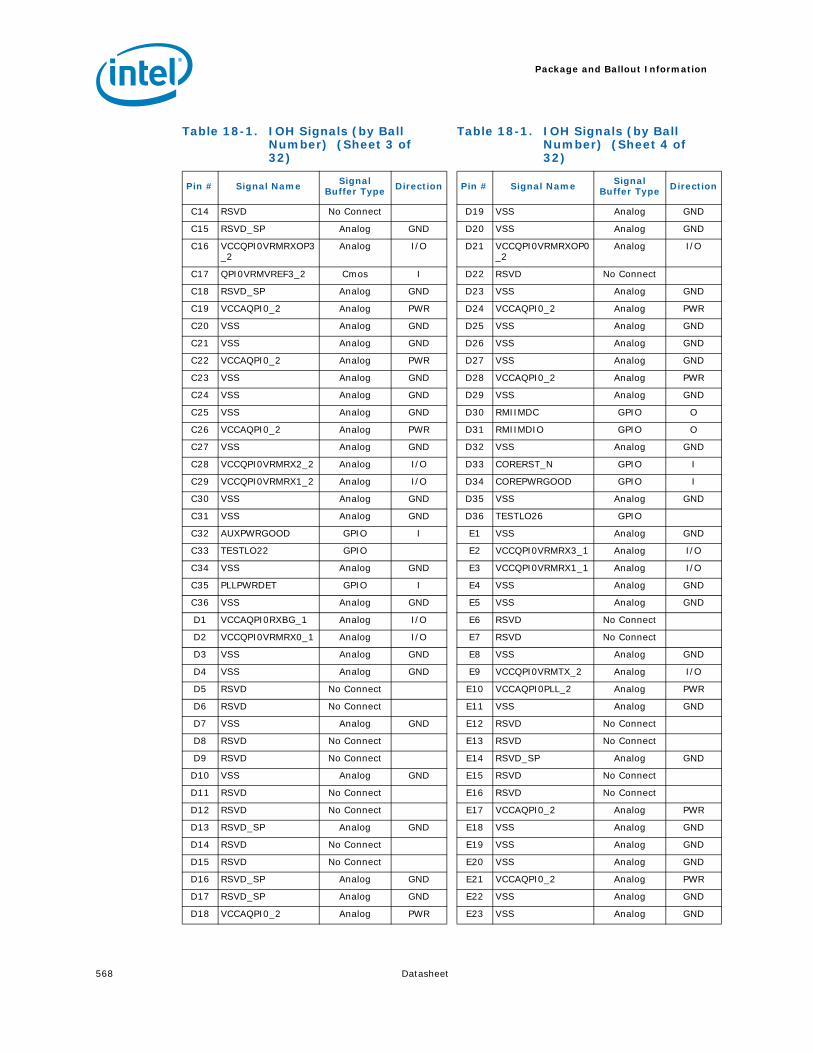
Package and Ballout Information
568 Datasheet
C14 RSVD No Connect
C15 RSVD_SP Analog GND
C16 VCCQPI0VRMRXOP3_2
Analog I/O
C17 QPI0VRMVREF3_2 Cmos I
C18 RSVD_SP Analog GND
C19 VCCAQPI0_2 Analog PWR
C20 VSS Analog GND
C21 VSS Analog GND
C22 VCCAQPI0_2 Analog PWR
C23 VSS Analog GND
C24 VSS Analog GND
C25 VSS Analog GND
C26 VCCAQPI0_2 Analog PWR
C27 VSS Analog GND
C28 VCCQPI0VRMRX2_2 Analog I/O
C29 VCCQPI0VRMRX1_2 Analog I/O
C30 VSS Analog GND
C31 VSS Analog GND
C32 AUXPWRGOOD GPIO I
C33 TESTLO22 GPIO
C34 VSS Analog GND
C35 PLLPWRDET GPIO I
C36 VSS Analog GND
D1 VCCAQPI0RXBG_1 Analog I/O
D2 VCCQPI0VRMRX0_1 Analog I/O
D3 VSS Analog GND
D4 VSS Analog GND
D5 RSVD No Connect
D6 RSVD No Connect
D7 VSS Analog GND
D8 RSVD No Connect
D9 RSVD No Connect
D10 VSS Analog GND
D11 RSVD No Connect
D12 RSVD No Connect
D13 RSVD_SP Analog GND
D14 RSVD No Connect
D15 RSVD No Connect
D16 RSVD_SP Analog GND
D17 RSVD_SP Analog GND
D18 VCCAQPI0_2 Analog PWR
Table 18-1. IOH Signals (by Ball Number) (Sheet 3 of 32)
Pin # Signal Name Signal Buffer Type Direction
D19 VSS Analog GND
D20 VSS Analog GND
D21 VCCQPI0VRMRXOP0_2
Analog I/O
D22 RSVD No Connect
D23 VSS Analog GND
D24 VCCAQPI0_2 Analog PWR
D25 VSS Analog GND
D26 VSS Analog GND
D27 VSS Analog GND
D28 VCCAQPI0_2 Analog PWR
D29 VSS Analog GND
D30 RMIIMDC GPIO O
D31 RMIIMDIO GPIO O
D32 VSS Analog GND
D33 CORERST_N GPIO I
D34 COREPWRGOOD GPIO I
D35 VSS Analog GND
D36 TESTLO26 GPIO
E1 VSS Analog GND
E2 VCCQPI0VRMRX3_1 Analog I/O
E3 VCCQPI0VRMRX1_1 Analog I/O
E4 VSS Analog GND
E5 VSS Analog GND
E6 RSVD No Connect
E7 RSVD No Connect
E8 VSS Analog GND
E9 VCCQPI0VRMTX_2 Analog I/O
E10 VCCAQPI0PLL_2 Analog PWR
E11 VSS Analog GND
E12 RSVD No Connect
E13 RSVD No Connect
E14 RSVD_SP Analog GND
E15 RSVD No Connect
E16 RSVD No Connect
E17 VCCAQPI0_2 Analog PWR
E18 VSS Analog GND
E19 VSS Analog GND
E20 VSS Analog GND
E21 VCCAQPI0_2 Analog PWR
E22 VSS Analog GND
E23 VSS Analog GND
Table 18-1. IOH Signals (by Ball Number) (Sheet 4 of 32)
Pin # Signal Name Signal Buffer Type Direction

Package and Ballout Information
Datasheet 569
E24 VCCAQPI0_2 Analog PWR
E25 VSS Analog GND
E26 VCCAQPI0_2 Analog PWR
E27 VSS Analog GND
E28 VSS Analog GND
E29 RMIIRXD[1] GPIO I
E30 VSS Analog GND
E31 RMIITXD[0] GPIO O
E32 RSVD_D No Connect
E33 VSS Analog GND
E34 RSVD_D No Connect
E35 RSVD_D No Connect
E36 VSS Analog GND
F1 QPI0RPDAT_6 QPI I
F2 VSS Analog GND
F3 VCCQPI0VRMRX2_1 Analog I/O
F4 QPI0RPDAT_5 QPI I
F5 VSS Analog GND
F6 VSS Analog GND
F7 RSVD No Connect
F8 RSVD No Connect
F9 VSS Analog GND
F10 VCCQPI0VRMRXOP2_2
Analog I/O
F11 RSVD No Connect
F12 RSVD_SP Analog GND
F13 RSVD No Connect
F14 RSVD No Connect
F15 RSVD_SP Analog GND
F16 RSVD No Connect
F17 RSVD No Connect
F18 VSS Analog GND
F19 VCCAQPI0_2 Analog PWR
F20 VSS Analog GND
F21 VSS Analog GND
F22 VCCQPI0VRMRXOP1_2
Analog I/O
F23 RSVD No Connect
F24 VSS Analog GND
F25 VCCAQPI0_2 Analog PWR
F26 VSS Analog GND
F27 VSS Analog GND
Table 18-1. IOH Signals (by Ball Number) (Sheet 5 of 32)
Pin # Signal Name Signal Buffer Type Direction
F28 VSS Analog GND
F29 RSVD_D No Connect
F30 RSVD_D No Connect
F31 VSS Analog GND
F32 RSVD_D No Connect
F33 RSVD_D No Connect
F34 VSS Analog GND
F35 RSVD_D No Connect
F36 RSVD_D No Connect
G1 QPI0RNDAT_6 QPI I
G2 QPI0RPDAT_7 QPI I
G3 VSS Analog GND
G4 QPI0RNDAT_5 QPI I
G5 QPI0RNDAT_3 QPI I
G6 VSS Analog GND
G7 VSS Analog GND
G8 RSVD No Connect
G9 RSVD No Connect
G10 VSS Analog GND
G11 RSVD No Connect
G12 RSVD No Connect
G13 RSVD_SP Analog GND
G14 RSVD No Connect
G15 RSVD No Connect
G16 RSVD_SP Analog GND
G17 RSVD_SP Analog GND
G18 VCCAQPI0_2 Analog PWR
G19 VSS Analog GND
G20 VSS Analog GND
G21 RSVD No Connect
G22 RSVD No Connect
G23 VSS Analog GND
G24 VCCAQPI0_2 Analog PWR
G25 VSS Analog GND
G26 VSS Analog GND
G27 RMIITXEN GPIO O
G28 RMIICLK GPIO I
G29 VSS Analog GND
G30 RSVD_D No Connect
G31 RSVD_D No Connect
G32 VSS Analog GND
G33 DDRPLLREFCLKP Connect ME Clk
Table 18-1. IOH Signals (by Ball Number) (Sheet 6 of 32)
Pin # Signal Name Signal Buffer Type Direction

Package and Ballout Information
570 Datasheet
G34 DDRPLLREFCLKN Connect ME Clk
G35 VSS Analog GND
G36 RSVD_D No Connect
H1 VSS Analog GND
H2 QPI0RNDAT_7 QPI I
H3 QPI0RPDAT_8 QPI I
H4 VSS Analog GND
H5 QPI0RPDAT_3 QPI I
H6 QPI0RNDAT_2 QPI I
H7 VSS Analog GND
H8 VSS Analog GND
H9 RSVD No Connect
H10 RSVD No Connect
H11 VSS Analog GND
H12 RSVD No Connect
H13 RSVD No Connect
H14 RSVD_SP Analog GND
H15 RSVD No Connect
H16 RSVD No Connect
H17 RSVD No Connect
H18 RSVD No Connect
H19 VSS Analog GND
H20 RSVD No Connect
H21 RSVD No Connect
H22 VSS Analog GND
H23 VCCAQPI0_2 Analog PWR
H24 VSS Analog GND
H25 VSS Analog GND
H26 QPI0VRMVREF1_2 Cmos I
H27 VSS Analog GND
H28 RSVD_D No Connect
H29 RSVD_D No Connect
H30 VSS Analog GND
H31 RSVD_D No Connect
H32 RSVD_D No Connect
H33 VSS Analog GND
H34 RSVD No Connect
H35 RSVD No Connect
H36 VSS Analog GND
J1 QPI0RPDAT_9 QPI I
J2 VSS Analog GND
J3 QPI0RNDAT_8 QPI I
Table 18-1. IOH Signals (by Ball Number) (Sheet 7 of 32)
Pin # Signal Name Signal Buffer Type Direction
J4 QPI0RNDAT_4 QPI I
J5 VSS Analog GND
J6 QPI0RPDAT_2 QPI I
J7 QPI0RNDAT_1 QPI I
J8 VSS Analog GND
J9 VSS Analog GND
J10 RSVD No Connect
J11 RSVD No Connect
J12 RSVD_SP Analog GND
J13 RSVD No Connect
J14 RSVD No Connect
J15 RSVD_SP Analog GND
J16 RSVD No Connect
J17 RSVD_SP Analog GND
J18 RSVD_SP Analog GND
J19 RSVD No Connect
J20 VSS Analog GND
J21 RSVD No Connect
J22 VSS Analog GND
J23 QPI0VRMVREF0_2 Cmos I
J24 RSVD No Connect
J25 VSS Analog GND
J26 RMIICLKREFOUT GPIO O
J27 RMIITXD[1] GPIO O
J28 VSS Analog GND
J29 RSVD_D No Connect
J30 RSVD_D No Connect
J31 VSS Analog GND
J32 RSVD_D No Connect
J33 RSVD_D No Connect
J34 VSS Analog GND
J35 RSVD_D No Connect
J36 RSVD_D No Connect
K1 QPI0RNDAT_9 QPI I
K2 RSVD No Connect
K3 VSS Analog GND
K4 QPI0RPDAT_4 QPI I
K5 QPI0RPCLK_0 QPI I
K6 VSS Analog GND
K7 QPI0RPDAT_1 QPI I
K8 QPI0RNDAT_0 QPI I
K9 VSS Analog GND
Table 18-1. IOH Signals (by Ball Number) (Sheet 8 of 32)
Pin # Signal Name Signal Buffer Type Direction

Package and Ballout Information
Datasheet 571
K10 VCCQPI0VRMTXOP0_2
Analog I/O
K11 QPI0VRMVREF4_2 Cmos I
K12 RSVD No Connect
K13 RSVD No Connect
K14 VSS Analog GND
K15 VCCAQPI0 Analog PWR
K16 VSS Analog GND
K17 VCCAQPI0 Analog PWR
K18 VSS Analog GND
K19 VCCAQPI0 Analog PWR
K20 VCCMISC33_CL Analog PWR
K21 VCCMISC33_CL Analog PWR
K22 VCC_CL Analog PWR
K23 VCC_CL Analog PWR
K24 RSVD No Connect
K25 RSVD No Connect
K26 VSS Analog GND
K27 RSVD No Connect
K28 RSVD_D No Connect
K29 VSS Analog GND
K30 RSVD_D No Connect
K31 RSVD_D No Connect
K32 VSS Analog GND
K33 RSVD_D No Connect
K34 RSVD_D No Connect
K35 VSS Analog GND
K36 RSVD_D No Connect
L1 VSS Analog GND
L2 RSVD No Connect
L3 QPI0RNDAT_11 QPI I
L4 VSS Analog GND
L5 QPI0RNCLK_0 QPI I
L6 RSVD No Connect
L7 VSS Analog GND
L8 QPI0RPDAT_0 QPI I
L9 RSVD No Connect
L10 QPI0VRMVREF0_1 Cmos I
L11 VSS Analog GND
L12 VSS Analog GND
L13 VCCAQPI0 Analog PWR
L14 VSS Analog GND
Table 18-1. IOH Signals (by Ball Number) (Sheet 9 of 32)
Pin # Signal Name Signal Buffer Type Direction
L15 VCCAQPI0 Analog PWR
L16 VSS Analog GND
L17 VCCAQPI0 Analog PWR
L18 VSS Analog GND
L19 VCCAQPI0 Analog PWR
L20 VCCAQPI0 Analog PWR
L21 VSS Analog GND
L22 VCC_CL Analog PWR
L23 VSS Analog GND
L24 VSS Analog GND
L25 VCCDDR_CL_18 Analog PWR
L26 RSVD No Connect
L27 VSS Analog GND
L28 RSVD_D No Connect
L29 RSVD_D No Connect
L30 VSS Analog GND
L31 RSVD No Connect
L32 RSVD No Connect
L33 VSS Analog GND
L34 RSVD No Connect
L35 RSVD No Connect
L36 VSS Analog GND
M1 QPI0RPDAT_10 QPI I
M2 VSS Analog GND
M3 QPI0RPDAT_11 QPI I
M4 RSVD No Connect
M5 VSS Analog GND
M6 VCCQPI0VRMRXOP1_1
Analog I/O
M7 RSVD No Connect
M8 VSS Analog GND
M9 RSVD No Connect
M10 VSS Analog GND
M11 QPI0VRMVREF1_1 Cmos I
M12 VCCAQPI0 Analog PWR
M13 VCCAQPI0 Analog PWR
M14 VCCAQPI0 Analog PWR
M15 VCCAQPI0 Analog PWR
M16 VCCAQPI0 Analog PWR
M17 VCCAQPI0 Analog PWR
M18 VCCAQPI0 Analog PWR
M19 VCCAQPI0 Analog PWR
Table 18-1. IOH Signals (by Ball Number) (Sheet 10 of 32)
Pin # Signal Name Signal Buffer Type Direction

Package and Ballout Information
Datasheet 572
M20 VCCAQPI0 Analog PWR
M21 VCCMISC33_CL Analog PWR
M22 VSS Analog GND
M23 VCCDDR_CL_18 Analog PWR
M24 VCCDDR_CL_18 Analog PWR
M25 VSS Analog GND
M26 VCCDDR_CL_18 Analog PWR
M27 RSVD_D No Connect
M28 VSS Analog GND
M29 RSVD_D No Connect
M30 RSVD_D No Connect
M31 VSS Analog GND
M32 RSVD_D No Connect
M33 RSVD_D No Connect
M34 VSS Analog GND
M35 RSVD_D No Connect
M36 RSVD_D No Connect
N1 QPI0RNDAT_10 QPI I
N2 QPI0RNDAT_12 QPI I
N3 VSS Analog GND
N4 VCCQPI0VRMRXOP0_1
Analog I/O
N5 QPI0RPDAT_17 QPI I
N6 VSS Analog GND
N7 RSVD No Connect
N8 RSVD No Connect
N9 VSS Analog GND
N10 VSS Analog GND
N11 RSVD No Connect
N12 VCCAQPI0 Analog PWR
N13 VCCAQPI0 Analog PWR
N14 VCCAQPI0 Analog PWR
N15 VCCAQPI0 Analog PWR
N16 VCCAQPI0 Analog PWR
N17 VCCAQPI0 Analog PWR
N18 VCCAQPI0 Analog PWR
N19 VCCAQPI0 Analog PWR
N20 VSS Analog GND
N21 VSS Analog GND
N22 VCC_CL Analog PWR
N23 VSS Analog GND
N24 VCCDDR_CL_18 Analog PWR
Table 18-1. IOH Signals (by Ball Number) (Sheet 11 of 32)
Pin # Signal Name Signal Buffer Type Direction
N25 VCCDDR_CL_18 Analog PWR
N26 VSS Analog GND
N27 CL_CLK_SRC GPIO I
N28 PEWIDTH_3 GPIO I/O
N29 VSS Analog GND
N30 RSVD_D No Connect
N31 RSVD_D No Connect
N32 VSS Analog GND
N33 RSVD_D No Connect
N34 RSVD_D No Connect
N35 VSS Analog GND
N36 VCCADDRPLL Analog PWR
P1 VSS Analog GND
P2 QPI0RPDAT_12 QPI I
P3 QPI0RNDAT_14 QPI I
P4 VSS Analog GND
P5 QPI0RNDAT_17 QPI I
P6 QPI0RNDAT_19 QPI I
P7 VSS Analog GND
P8 RSVD No Connect
P9 RSVD No Connect
P10 RSVD No Connect
P11 VSS Analog GND
P12 VCCAQPI0 Analog PWR
P13 VCCAQPI0 Analog PWR
P14 VSS Analog GND
P15 VCC Analog PWR
P16 VSS Analog GND
P17 VCC Analog PWR
P18 VSS Analog GND
P19 VCC Analog PWR
P20 VSS Analog GND
P21 VCC_CL Analog PWR
P22 VSS Analog GND
P23 VCCDDR_CL_18 Analog PWR
P24 VSS Analog GND
P25 VCCDDR_CL_18 Analog PWR
P26 VCCDDR_CL_18 Analog PWR
P27 VSS Analog GND
P28 PEWIDTH_5 GPIO I/O
P29 TESTHI1 GPIO I/O
P30 VSS Analog GND
Table 18-1. IOH Signals (by Ball Number) (Sheet 12 of 32)
Pin # Signal Name Signal Buffer Type Direction

Package and Ballout Information
Datasheet 573
P31 SINGLE_IOH No Connect
P32 RSVD_D No Connect
P33 VSS Analog GND
P34 RSVD_D No Connect
P35 RSVD_D No Connect
P36 VSS Analog GND
R1 QPI0RPDAT_13 QPI I
R2 VSS Analog GND
R3 QPI0RPDAT_14 QPI I
R4 QPI0RNDAT_15 QPI I
R5 VSS Analog GND
R6 QPI0RPDAT_19 QPI I
R7 QPI0RNDAT_18 QPI I
R8 VSS Analog GND
R9 RSVD No Connect
R10 VSS Analog GND
R11 VSS Analog GND
R12 VCCAQPI0 Analog PWR
R13 VCCAQPI0 Analog PWR
R14 VCCAQPI0 Analog PWR
R15 VSS Analog GND
R16 VCC Analog PWR
R17 VSS Analog GND
R18 VCC Analog PWR
R19 VSS Analog GND
R20 VCC Analog PWR
R21 VSS Analog GND
R22 VCC_CL Analog PWR
R23 VSS Analog GND
R24 VTTDDR Analog PWR
R25 VSS Analog GND
R26 VCC_CL Analog PWR
R27 VCC_CL Analog PWR
R28 VSS Analog GND
R29 TESTHI3 GPIO I/O
R30 TRST_N GPIO I
R31 VSS Analog GND
R32 LEGACYIOH GPIO I
R33 PEWIDTH_0 GPIO I/O
R34 VSS Analog GND
R35 TESTLO19 GPIO I/O
R36 PEWIDTH_2 GPIO I/O
Table 18-1. IOH Signals (by Ball Number) (Sheet 13 of 32)
Pin # Signal Name Signal Buffer Type Direction
T1 QPI0RNDAT_13 QPI I
T2 QPI0VRMVREF2_1 Cmos I
T3 VSS Analog GND
T4 QPI0RPDAT_15 QPI I
T5 QPI0RNDAT_16 QPI I
T6 VSS Analog GND
T7 QPI0RPDAT_18 QPI I
T8 RSVD No Connect
T9 VSS Analog GND
T10 RSVD No Connect
T11 VSS Analog GND
T12 VSS Analog GND
T13 VSS Analog GND
T14 VCCAQPI0 Analog PWR
T15 VCCAQPI0 Analog PWR
T16 VSS Analog GND
T17 VCC Analog PWR
T18 VSS Analog GND
T19 VCC Analog PWR
T20 VSS Analog GND
T21 VCC_CL Analog PWR
T22 VSS Analog GND
T23 VCC_CL Analog PWR
T24 VCC_CL Analog PWR
T25 VCCXDP18 Analog PWR
T26 VSS Analog GND
T27 TESTLO18 GPIO I
T28 PEWIDTH_4 GPIO I/O
T29 VSS Analog GND
T30 PEWIDTH_1 GPIO I/O
T31 RSVD_D No Connect
T32 VSS Analog GND
T33 TCK GPIO I
T34 CL_DATA Cmos I/O
T35 VSS Analog GND
T36 VREFCL Cmos I/O
U1 VSS Analog GND
U2 VCCAQPI0TXBG_1 Analog I/O
U3 QPI0VRMVREF3_1 Cmos I
U4 VSS Analog GND
U5 QPI0RPDAT_16 QPI I
U6 RSVD No Connect
Table 18-1. IOH Signals (by Ball Number) (Sheet 14 of 32)
Pin # Signal Name Signal Buffer Type Direction

Package and Ballout Information
574 Datasheet
U7 VSS Analog GND
U8 RSVD No Connect
U9 RSVD No Connect
U10 RSVD No Connect
U11 VCCAQPI0 Analog PWR
U12 VCCAQPI0 Analog PWR
U13 VCCAQPI0 Analog PWR
U14 VCCAQPI0 Analog PWR
U15 VCCAQPI0 Analog PWR
U16 VCC Analog PWR
U17 VSS Analog GND
U18 VCC Analog PWR
U19 VSS Analog GND
U20 VCC Analog PWR
U21 VSS Analog GND
U22 VCC Analog PWR
U23 VSS Analog GND
U24 VSS Analog GND
U25 VTTXDP Analog PWR
U26 VCCXDP18 Analog PWR
U27 VSS Analog GND
U28 TESTHI2 GPIO I
U29 RSVD_D No Connect
U30 VSS Analog GND
U31 TMS GPIO I
U32 CLRST_N Cmos I
U33 VSS Analog GND
U34 CL_CLK Cmos I/O
U35 XDPDQ_7 DDR I/O
U36 VSS Analog GND
V1 VSS Analog GND
V2 QPI0TPDAT_12 QPI O
V3 VCCQPI0VRMRXOP3_1
Analog I/O
V4 VSS Analog GND
V5 RSVD No Connect
V6 QPI0TPDAT_15 QPI O
V7 VSS Analog GND
V8 QPI0TPDAT_16 QPI O
V9 RSVD No Connect
V10 VSS Analog GND
V11 VSS Analog GND
Table 18-1. IOH Signals (by Ball Number) (Sheet 15 of 32)
Pin # Signal Name Signal Buffer Type Direction
V12 VSS Analog GND
V13 VSS Analog GND
V14 VCCAQPI0 Analog PWR
V15 VCCAQPI0 Analog PWR
V16 VSS Analog GND
V17 VCC Analog PWR
V18 VSS Analog GND
V19 VCC Analog PWR
V20 VSS Analog GND
V21 VCC Analog PWR
V22 VSS Analog GND
V23 VCC Analog PWR
V24 VCC Analog PWR
V25 VSS Analog GND
V26 TDI GPIO I
V27 RSVD No Connect
V28 VSS Analog GND
V29 VCCFHVCORE Analog PWR
V30 TDO GPIO O
V31 VSS Analog GND
V32 TESTLO17 GPIO I
V33 XDPDQ_2 DDR I/O
V34 VSS Analog GND
V35 XDPDQ_5 DDR I/O
V36 XDPDQ_3 DDR I/O
W1 QPI0TPDAT_11 QPI O
W2 QPI0TNDAT_12 QPI O
W3 VSS Analog GND
W4 QPI0TNDAT_14 QPI O
W5 QPI0TNDAT_15 QPI O
W6 VSS Analog GND
W7 QPI0TNDAT_17 QPI O
W8 QPI0TNDAT_16 QPI O
W9 VSS Analog GND
W10 RSVD No Connect
W11 VCCAQPI0 Analog PWR
W12 VCCAQPI0 Analog PWR
W13 VCCAQPI0 Analog PWR
W14 VCCAQPI0 Analog PWR
W15 VCCAQPI0 Analog PWR
W16 VCC Analog PWR
W17 VSS Analog GND
Table 18-1. IOH Signals (by Ball Number) (Sheet 16 of 32)
Pin # Signal Name Signal Buffer Type Direction

Package and Ballout Information
Datasheet 575
W18 VCC Analog PWR
W19 VSS Analog GND
W20 VCC Analog PWR
W21 VSS Analog GND
W22 VCC Analog PWR
W23 VSS Analog GND
W24 VCC Analog PWR
W25 VSS Analog GND
W26 VSS Analog GND
W27 TESTLO16 GPIO I
W28 RSVD No Connect
W29 VSS Analog GND
W30 RSVD No Connect
W31 XDPRDYREQ_N DDR I
W32 VSS Analog GND
W33 XDPDQ_0 DDR I/O
W34 XDPDQ_6 DDR I/O
W35 VSS Analog GND
W36 XDPDQ_1 DDR I/O
Y1 QPI0TNDAT_11 QPI O
Y2 VSS Analog GND
Y3 QPI0TNDAT_13 QPI O
Y4 QPI0TPDAT_14 QPI O
Y5 VSS Analog GND
Y6 QPI0TNDAT_18 QPI O
Y7 QPI0TPDAT_17 QPI O
Y8 VSS Analog GND
Y9 QPI0ICOMP Analog I/O
Y10 RSVD No Connect
Y11 VSS Analog GND
Y12 VSS Analog GND
Y13 VSS Analog GND
Y14 VCCAQPI0 Analog PWR
Y15 VCCAQPI0 Analog PWR
Y16 VSS Analog GND
Y17 VCC Analog PWR
Y18 VSS Analog GND
Y19 VCC Analog PWR
Y20 VSS Analog GND
Y21 VCC Analog PWR
Y22 VSS Analog GND
Y23 VCC Analog PWR
Table 18-1. IOH Signals (by Ball Number) (Sheet 17 of 32)
Pin # Signal Name Signal Buffer Type Direction
Y24 VSS Analog GND
Y25 VCC Analog PWR
Y26 VCC Analog PWR
Y27 VSS Analog GND
Y28 TESTLO15 GPIO I
Y29 VRMEN GPIO I
Y30 VSS Analog GND
Y31 XDPRDYACK_N DDR O
Y32 RSVD No Connect
Y33 VSS Analog GND
Y34 XDPDQ_4 DDR I/O
Y35 XDPDQSN_0 DDR I/O
Y36 VSS Analog GND
AA1 VSS Analog GND
AA2 QPI0TNDAT_10 QPI O
AA3 QPI0TPDAT_13 QPI O
AA4 VSS Analog GND
AA5 QPI0TNDAT_19 QPI O
AA6 QPI0TPDAT_18 QPI O
AA7 VSS Analog GND
AA8 RSVD No Connect
AA9 QPI0RCOMP Analog I/O
AA10 VSS Analog GND
AA11 VSS Analog GND
AA12 VCCAQPI0 Analog PWR
AA13 VCCAQPI0 Analog PWR
AA14 VCCAQPI0 Analog PWR
AA15 VCCAQPI0 Analog PWR
AA16 VCC Analog PWR
AA17 VSS Analog GND
AA18 VCC Analog PWR
AA19 VSS Analog GND
AA20 VCC Analog PWR
AA21 VSS Analog GND
AA22 VCC Analog PWR
AA23 VSS Analog GND
AA24 VCC Analog PWR
AA25 VSS Analog GND
AA26 TESTLO24 GPIO
AA27 RSVD No Connect
AA28 VSS Analog GND
AA29 TESTLO14 GPIO I
Table 18-1. IOH Signals (by Ball Number) (Sheet 18 of 32)
Pin # Signal Name Signal Buffer Type Direction

Package and Ballout Information
576 Datasheet
AA30 QPIFREQSEL1 GPIO I
AA31 VSS Analog GND
AA32 RSVD No Connect
AA33 XDPDQ_11 DDR I/O
AA34 VSS Analog GND
AA35 XDPDQSP_0 DDR I/O
AA36 XDPDQ_10 DDR I/O
AB1 QPI0TPCLK_0 QPI O
AB2 QPI0TPDAT_10 QPI O
AB3 VSS Analog GND
AB4 RSVD No Connect
AB5 QPI0TPDAT_19 QPI O
AB6 VSS Analog GND
AB7 QPI0REFCLKP HCSL I
AB8 RSVD No Connect
AB9 VSS Analog GND
AB10 QPI0VRMVREF4_1 Cmos I
AB11 VSS Analog GND
AB12 VSS Analog GND
AB13 VSS Analog GND
AB14 VSS Analog GND
AB15 VCC Analog PWR
AB16 VSS Analog GND
AB17 VCC Analog PWR
AB18 VSS Analog GND
AB19 VCC Analog PWR
AB20 VSS Analog GND
AB21 VCC Analog PWR
AB22 VSS Analog GND
AB23 VCC Analog PWR
AB24 VCCMISC33 Analog PWR
AB25 VCCMISC33 Analog PWR
AB26 VSS Analog GND
AB27 SMBSCL No Connect
AB28 PEHPSCL GPIO O
AB29 VSS Analog GND
AB30 TESTLO13 GPIO I
AB31 INTR GPIO I
AB32 VSS Analog GND
AB33 XDPDQ_9 DDR I/O
AB34 XDPDQ_15 DDR I/O
AB35 VSS Analog GND
Table 18-1. IOH Signals (by Ball Number) (Sheet 19 of 32)
Pin # Signal Name Signal Buffer Type Direction
AB36 XDPDQ_14 DDR I/O
AC1 QPI0TNCLK_0 QPI O
AC2 VSS Analog GND
AC3 QPI0TPDAT_9 QPI O
AC4 RSVD No Connect
AC5 VSS Analog GND
AC6 RSVD No Connect
AC7 QPI0REFCLKN HCSL I
AC8 VSS Analog GND
AC9 RSVD No Connect
AC10 VCCQPI0VRMTXOP0_1
Analog I/O
AC11 VSS Analog GND
AC12 VCCAPE Analog PWR
AC13 VCCAPE Analog PWR
AC14 VSS Analog GND
AC15 VCCAPE Analog PWR
AC16 VSS Analog GND
AC17 VCCAPE Analog PWR
AC18 VSS Analog GND
AC19 VCCAPE Analog PWR
AC20 VCC Analog PWR
AC21 VSS Analog GND
AC22 VCC Analog PWR
AC23 VSS Analog GND
AC24 VSS Analog GND
AC25 RSVD No Connect
AC26 THERMTRIP_N GPIO O
AC27 VSS Analog GND
AC28 COREPLLPWRDET GPIO I
AC29 TESTLO23 GPIO
AC30 VSS Analog GND
AC31 A20M_N GPIO I
AC32 TESTLO12 GPIO I
AC33 VSS Analog GND
AC34 XDPDQ_13 DDR I/O
AC35 XDPDQSN_1 DDR I/O
AC36 VSS Analog GND
AD1 VSS Analog GND
AD2 QPI0TPDAT_8 QPI O
AD3 QPI0TNDAT_9 QPI O
AD4 VSS Analog GND
Table 18-1. IOH Signals (by Ball Number) (Sheet 20 of 32)
Pin # Signal Name Signal Buffer Type Direction

Package and Ballout Information
Datasheet 577
AD5 VCCAQPI0PLL_1 Analog PWR
AD6 VCCQPI0VRMRXOP2_1
Analog I/O
AD7 VSS Analog GND
AD8 RSVD No Connect
AD9 RSVD No Connect
AD10 RSVD No Connect
AD11 VSS Analog GND
AD12 VCCAPE Analog PWR
AD13 VCCAPE Analog PWR
AD14 VCCAPE Analog PWR
AD15 VCCAPE Analog PWR
AD16 VCCAPE Analog PWR
AD17 VCCAPE Analog PWR
AD18 VCCAPE Analog PWR
AD19 VCCAPE Analog PWR
AD20 VCCAPE1 Analog PWR
AD21 VCCAPE1 Analog PWR
AD22 VCCAPE1 Analog PWR
AD23 VCCAPE1 Analog PWR
AD24 VCCAPE1 Analog PWR
AD25 VCCAPE1 Analog PWR
AD26 THERMALERT_N GPIO O
AD27 ERR_N_0 GPIO O
AD28 VSS Analog GND
AD29 SMBSDA No Connect
AD30 PEHPSDA GPIO I/O
AD31 VSS Analog GND
AD32 NMI GPIO I/O
AD33 TESTLO21 GPIO
AD34 VSS Analog GND
AD35 XDPDQSP_1 DDR I/O
AD36 XDPDQ_8 DDR O
AE1 QPI0TPDAT_7 QPI O
AE2 QPI0TNDAT_8 QPI O
AE3 VSS Analog GND
AE4 QPI0TPDAT_6 QPI O
AE5 VCCQPI0VRMTX_1 Analog I/O
AE6 VSS Analog GND
AE7 RSVD No Connect
AE8 RSVD No Connect
AE9 VSS Analog GND
Table 18-1. IOH Signals (by Ball Number) (Sheet 21 of 32)
Pin # Signal Name Signal Buffer Type Direction
AE10 RSVD No Connect
AE11 VSS Analog GND
AE12 VCCAPE Analog PWR
AE13 VCCAPE Analog PWR
AE14 VCCAPE Analog PWR
AE15 VCCAPE Analog PWR
AE16 VCCAPE Analog PWR
AE17 VCCAPE Analog PWR
AE18 VCCAPE Analog PWR
AE19 VCCAPE Analog PWR
AE20 VCCAPE1 Analog PWR
AE21 VCCAPE1 Analog PWR
AE22 VCCAPE1 Analog PWR
AE23 VCCAPE1 Analog PWR
AE24 VCCAPE1 Analog PWR
AE25 VCCAPE1 Analog PWR
AE26 VSS Analog GND
AE27 LTRESET_N GPIO O
AE28 ERR_N_2 GPIO O
AE29 VSS Analog GND
AE30 INIT_N GPIO I
AE31 SMBUSID No Connect
AE32 VSS Analog GND
AE33 TESTLO25 GPIO
AE34 TESTLO11 GPIO I/O
AE35 VSS Analog GND
AE36 XDPDQ_12 DDR I/O
AF1 QPI0TNDAT_7 QPI O
AF2 VSS Analog GND
AF3 QPI0TPDAT_3 QPI O
AF4 QPI0TNDAT_6 QPI O
AF5 VSS Analog GND
AF6 QPI0TPDAT_0 QPI O
AF7 RSVD No Connect
AF8 VSS Analog GND
AF9 RSVD No Connect
AF10 RSVD No Connect
AF11 VSS Analog GND
AF12 VCCAPE Analog PWR
AF13 VCCAPE Analog PWR
AF14 VSS Analog GND
AF15 VCCAPE Analog PWR
Table 18-1. IOH Signals (by Ball Number) (Sheet 22 of 32)
Pin # Signal Name Signal Buffer Type Direction

Package and Ballout Information
578 Datasheet
AF16 VSS Analog GND
AF17 VCCAPE Analog PWR
AF18 VSS Analog GND
AF19 VCCAPE Analog PWR
AF20 VCCAPE1 Analog PWR
AF21 VCCAPE1 Analog PWR
AF22 VCCAPE1 Analog PWR
AF23 VCCAPE1 Analog PWR
AF24 VSS Analog GND
AF25 VSS Analog GND
AF26 RSVD No Connect
AF27 VSS Analog GND
AF28 ERR_N_1 GPIO O
AF29 PE1CLKP HCSL I
AF30 VSS Analog GND
AF31 RSVD No Connect
AF32 TESTLO10 GPIO I
AF33 VSS Analog GND
AF34 TESTLO9 GPIO I
AF35 TESTLO8 GPIO I
AF36 VSS Analog GND
AG1 VSS Analog GND
AG2 QPI0TPDAT_5 QPI O
AG3 QPI0TNDAT_3 QPI O
AG4 VSS Analog GND
AG5 QPI0TNDAT_1 QPI O
AG6 QPI0TNDAT_0 QPI O
AG7 VSS Analog GND
AG8 RSVD No Connect
AG9 RSVD No Connect
AG10 VSS Analog GND
AG11 VSS Analog GND
AG12 VSS Analog GND
AG13 VSS Analog GND
AG14 VSS Analog GND
AG15 VSS Analog GND
AG16 VSS Analog GND
AG17 VSS Analog GND
AG18 VSS Analog GND
AG19 VSS Analog GND
AG20 VSS Analog GND
AG21 VSS Analog GND
Table 18-1. IOH Signals (by Ball Number) (Sheet 23 of 32)
Pin # Signal Name Signal Buffer Type Direction
AG22 VSS Analog GND
AG23 VSS Analog GND
AG24 VSS Analog GND
AG25 VSS Analog GND
AG26 RSVD No Connect
AG27 RSVD No Connect
AG28 VSS Analog GND
AG29 PE1CLKN HCSL I
AG30 RSVD No Connect
AG31 VSS Analog GND
AG32 SMI_N No Connect
AG33 RSVD No Connect
AG34 VSS Analog GND
AG35 QPIFREQSEL0 GPIO I
AG36 XDPCLK1XN DDR O
AH1 QPI0TPDAT_4 QPI O
AH2 QPI0TNDAT_5 QPI O
AH3 VSS Analog GND
AH4 QPI0TPDAT_2 QPI O
AH5 QPI0TPDAT_1 QPI O
AH6 VSS Analog GND
AH7 VSS Analog GND
AH8 RSVD No Connect
AH9 RSVD No Connect
AH10 RSVD No Connect
AH11 RSVD No Connect
AH12 VSS Analog GND
AH13 RSVD No Connect
AH14 RSVD No Connect
AH15 RSVD No Connect
AH16 RSVD No Connect
AH17 VSS Analog GND
AH18 RSVD No Connect
AH19 RSVD No Connect
AH20 RSVD No Connect
AH21 RSVD No Connect
AH22 VSS Analog GND
AH23 PE7RP_0 PCIEX2 I
AH24 PE7RN_0 PCIEX2 I
AH25 PE8RN_3 PCIEX2 I
AH26 RSVD No Connect
AH27 VSS Analog GND
Table 18-1. IOH Signals (by Ball Number) (Sheet 24 of 32)
Pin # Signal Name Signal Buffer Type Direction

Package and Ballout Information
Datasheet 579
AH28 RSVD No Connect
AH29 RSVD No Connect
AH30 PE10RN_3 PCIEX2 I
AH31 RSVD No Connect
AH32 VSS Analog GND
AH33 TESTLO7 GPIO I
AH34 TESTLO6 GPIO I
AH35 VSS Analog GND
AH36 XDPCLK1XP DDR O
AJ1 QPI0TNDAT_4 QPI O
AJ2 VSS Analog GND
AJ3 TSIREF Analog I
AJ4 QPI0TNDAT_2 QPI O
AJ5 VSS Analog GND
AJ6 PE3RN_0 PCIEX2 I
AJ7 PE4RN_0 PCIEX2 I
AJ8 PE4RP_0 PCIEX2 I
AJ9 PE4RN_3 PCIEX2 I
AJ10 VSS Analog GND
AJ11 PE5RP_1 PCIEX2 I
AJ12 PE6RN_3 PCIEX2 I
AJ13 PE6RP_3 PCIEX2 I
AJ14 PE6RN_2 PCIEX2 I
AJ15 VSS Analog GND
AJ16 PE1RN_0 PCIEX2 I
AJ17 PE1RP_1 PCIEX2 I
AJ18 PE1RN_1 PCIEX2 I
AJ19 DMIRN_3 PCIEX I
AJ20 VSS Analog GND
AJ21 DMIRP_2 PCIEX I
AJ22 VSS Analog GND
AJ23 PE7RN_1 PCIEX2 I
AJ24 VSS Analog GND
AJ25 PE8RP_3 PCIEX2 I
AJ26 PE8RN_1 PCIEX2 I
AJ27 PE8RP_1 PCIEX2 I
AJ28 PE9RP_3 PCIEX2 I
AJ29 VSS Analog GND
AJ30 PE10RP_3 PCIEX2 I
AJ31 VSS Analog GND
AJ32 PE10RP_2 PCIEX2 I
AJ33 VSS Analog GND
Table 18-1. IOH Signals (by Ball Number) (Sheet 25 of 32)
Pin # Signal Name Signal Buffer Type Direction
AJ34 TESTLO5 GPIO I
AJ35 QPISBLCSEL Power
AJ36 VSS Analog GND
AK1 VSS Analog GND
AK2 VCCTS Analog PWR
AK3 TSDC GPIO
AK4 VSS Analog GND
AK5 PE3RP_2 PCIEX2 I
AK6 PE3RP_0 PCIEX2 I
AK7 PE3RN_3 PCIEX2 I
AK8 VSS Analog GND
AK9 PE4RP_3 PCIEX2 I
AK10 PE5RN_0 PCIEX2 I
AK11 PE5RN_1 PCIEX2 I
AK12 PE6RN_0 PCIEX2 I
AK13 VSS Analog GND
AK14 PE6RP_2 PCIEX2 I
AK15 PE6RP_1 PCIEX2 I
AK16 PE1RP_0 PCIEX2 I
AK17 PE2RP_0 PCIEX2 I
AK18 VSS Analog GND
AK19 DMIRP_3 PCIEX I
AK20 DMIRP_1 PCIEX I
AK21 DMIRN_2 PCIEX I
AK22 VSS Analog GND
AK23 PE7RP_1 PCIEX2 I
AK24 PE7RN_3 PCIEX2 I
AK25 PE7RP_3 PCIEX2 I
AK26 VSS Analog GND
AK27 VSS Analog GND
AK28 PE9RN_3 PCIEX2 I
AK29 PE9RP_0 PCIEX2 I
AK30 PE9RN_1 PCIEX2 I
AK31 PE9RP_1 PCIEX2 I
AK32 PE10RN_2 PCIEX2 I
AK33 PE10RN_0 PCIEX2 I
AK34 VSS Analog GND
AK35 PESBLCSEL GPIO I
AK36 EXTSYSTRIG GPIO I/O
AL1 PE0ICOMPO Analog I/O
AL2 RESETO_N GPIO O
AL3 PE3RP_1 PCIEX2 I
Table 18-1. IOH Signals (by Ball Number) (Sheet 26 of 32)
Pin # Signal Name Signal Buffer Type Direction

Package and Ballout Information
580 Datasheet
AL4 PE3RN_1 PCIEX2 I
AL5 PE3RN_2 PCIEX2 I
AL6 VSS Analog GND
AL7 PE3RP_3 PCIEX2 I
AL8 PE4RN_2 PCIEX2 I
AL9 PE4RP_2 PCIEX2 I
AL10 PE5RP_0 PCIEX2 I
AL11 VSS Analog GND
AL12 PE6RP_0 PCIEX2 I
AL13 PE5RN_3 PCIEX2 I
AL14 PE5RP_3 PCIEX2 I
AL15 PE6RN_1 PCIEX2 I
AL16 VSS Analog GND
AL17 PE2RN_0 PCIEX I
AL18 DMIRN_0 PCIEX I
AL19 DMIRP_0 PCIEX I
AL20 DMIRN_1 PCIEX I
AL21 VSS Analog GND
AL22 VSS Analog GND
AL23 PE7RN_2 PCIEX2 I
AL24 PE7RP_2 PCIEX2 I
AL25 VSS Analog GND
AL26 PE8RP_0 PCIEX2 I
AL27 PE8RN_2 PCIEX2 I
AL28 PE8RP_2 PCIEX2 I
AL29 PE9RN_0 PCIEX2 I
AL30 VSS Analog GND
AL31 PE9RN_2 PCIEX2 I
AL32 PE9RP_2 PCIEX2 I
AL33 PE10RP_0 PCIEX2 I
AL34 PE10RN_1 PCIEX2 I
AL35 VSS Analog GND
AL36 FERR_N GPIO O
AM1 PE0RCOMPO Analog I/O
AM2 TSDA GPIO
AM3 RSVD No Connect
AM4 VSS Analog GND
AM5 RSVD No Connect
AM6 TESTLO4 Analog I/O
AM7 PE4RN_1 PCIEX2 I
AM8 PE4RP_1 PCIEX2 I
AM9 VSS Analog GND
Table 18-1. IOH Signals (by Ball Number) (Sheet 27 of 32)
Pin # Signal Name Signal Buffer Type Direction
AM10 RSVD No Connect
AM11 RSVD No Connect
AM12 PE5RP_2 PCIEX2 I
AM13 PE5RN_2 PCIEX2 I
AM14 VSS Analog GND
AM15 PE6TP_3 HCSL O
AM16 PE6TN_3 HCSL O
AM17 PE2RN_1 PCIEX2 I
AM18 PE2RP_1 PCIEX2 I
AM19 VSS Analog GND
AM20 RSVD No Connect
AM21 DMITP_3 PCIEX O
AM22 RSVD No Connect
AM23 VSS Analog GND
AM24 RSVD No Connect
AM25 RSVD No Connect
AM26 PE8RN_0 PCIEX2 I
AM27 RSVD No Connect
AM28 VSS Analog GND
AM29 RSVD No Connect
AM30 RSVD No Connect
AM31 RSVD No Connect
AM32 VSS Analog GND
AM33 VSS Analog GND
AM34 PE10RP_1 PCIEX2 I
AM35 RSVD No Connect
AM36 VSS Analog GND
AN1 VCCAPEPLL Analog PWR
AN2 VCCAPEBG Analog PWR
AN3 VSS Analog GND
AN4 PE3TN_0 PCIEX2 O
AN5 PE3TP_0 PCIEX2 O
AN6 PE3TP_2 PCIEX2 O
AN7 VSS Analog GND
AN8 TESTLO3 Analog I/O
AN9 TESTLO2 Analog I/O
AN10 PE0CLKN HCSL I
AN11 PE0CLKP HCSL I
AN12 VSS Analog GND
AN13 PE0RBIAS Analog I/O
AN14 PE6TP_0 PCIEX2 O
AN15 PE6TN_0 PCIEX2 O
Table 18-1. IOH Signals (by Ball Number) (Sheet 28 of 32)
Pin # Signal Name Signal Buffer Type Direction

Package and Ballout Information
Datasheet 581
AN16 PE1TP_0 PCIEX2 O
AN17 VSS Analog GND
AN18 RSVD No Connect
AN19 DMITP_1 PCIEX O
AN20 DMITN_1 PCIEX O
AN21 DMITN_3 PCIEX O
AN22 VSS Analog GND
AN23 PE8TN_0 PCIEX2 O
AN24 PE8TP_0 PCIEX2 O
AN25 PE7TP_2 PCIEX2 O
AN26 VSS Analog GND
AN27 PE7TN_1 PCIEX2 O
AN28 PE9TP_0 PCIEX2 O
AN29 PE9TN_0 PCIEX2 O
AN30 PE9TN_3 PCIEX2 O
AN31 VSS Analog GND
AN32 PE10TN_3 PCIEX2 O
AN33 RSVD No Connect
AN34 PE1RBIAS Analog I/O
AN35 PE1ICOMPI Analog I/O
AN36 PE1ICOMPO Analog I/O
AP1 VSS Analog GND
AP2 VCCDPEPLL Analog PWR
AP3 PE0ICOMPI Analog I/O
AP4 PE3TP_1 PCIEX2 O
AP5 VSS Analog GND
AP6 PE3TN_2 PCIEX2 O
AP7 PE4TN_2 PCIEX2 O
AP8 PE4TP_2 PCIEX2 O
AP9 PE5TP_0 PCIEX2 O
AP10 VSS Analog GND
AP11 PE5TN_2 PCIEX2 O
AP12 PE5TP_3 PCIEX2 O
AP13 PE5TN_3 PCIEX2 O
AP14 PE6TP_2 PCIEX2 O
AP15 VSS Analog GND
AP16 PE1TN_0 PCIEX2 O
AP17 PE2TP_0 PCIEX2 O
AP18 PE2TN_0 PCIEX2 O
AP19 DMITP_0 PCIEX O
AP20 VSS Analog GND
AP21 RSVD No Connect
Table 18-1. IOH Signals (by Ball Number) (Sheet 29 of 32)
Pin # Signal Name Signal Buffer Type Direction
AP22 VSS Analog GND
AP23 PE7TN_3 PCIEX2 O
AP24 VSS Analog GND
AP25 PE7TN_2 PCIEX2 O
AP26 PE8TP_2 PCIEX2 O
AP27 PE7TP_1 PCIEX2 O
AP28 PE7TP_0 PCIEX2 O
AP29 VSS Analog GND
AP30 PE9TP_3 PCIEX2 O
AP31 PE10TP_1 PCIEX2 O
AP32 PE10TP_3 PCIEX2 O
AP33 PE10TN_2 PCIEX2 O
AP34 VSS Analog GND
AP35 PE1RCOMPO Analog I/O
AP36 VSS Analog GND
AR1 VSS Analog GND
AR2 VSS Analog GND
AR3 VSS Analog GND
AR4 PE3TN_1 PCIEX2 O
AR5 PE4TN_0 PCIEX2 O
AR6 PE4TP_0 PCIEX2 O
AR7 PE4TN_1 PCIEX2 O
AR8 VSS Analog GND
AR9 PE5TN_0 PCIEX2 O
AR10 PE5TP_1 PCIEX2 O
AR11 PE5TP_2 PCIEX2 O
AR12 TESTLO1 Analog I/O
AR13 VSS Analog GND
AR14 PE6TN_2 PCIEX2 O
AR15 PE1TP_1 PCIEX2 O
AR16 PE1TN_1 PCIEX2 O
AR17 PE2TN_1 PCIEX2 O
AR18 VSS Analog GND
AR19 DMITN_0 PCIEX O
AR20 DMITN_2 PCIEX O
AR21 DMITP_2 PCIEX O
AR22 VSS Analog GND
AR23 PE7TP_3 PCIEX2 O
AR24 PE8TP_1 PCIEX2 O
AR25 PE8TN_1 PCIEX2 O
AR26 PE8TN_2 PCIEX2 O
AR27 VSS Analog GND
Table 18-1. IOH Signals (by Ball Number) (Sheet 30 of 32)
Pin # Signal Name Signal Buffer Type Direction

Package and Ballout Information
582Datasheet
AR28 PE7TN_0 PCIEX2 O
AR29 PE9TP_2 PCIEX2 O
AR30 PE9TN_2 PCIEX2 O
AR31 PE10TN_1 PCIEX2 O
AR32 VSS Analog GND
AR33 PE10TP_2 PCIEX2 O
AR34 VCCPE1VRM Analog PWR
AR35 VSS Analog GND
AR36 VSS Analog GND
AT1 TEST_3 GND I/O
AT2 VSS Analog GND
AT3 VSS Analog GND
AT4 PE3TP_3 PCIEX2 O
AT5 PE3TN_3 PCIEX2 O
AT6 VSS Analog GND
AT7 PE4TP_1 PCIEX2 O
AT8 PE4TP_3 PCIEX2 O
AT9 PE4TN_3 PCIEX2 O
AT10 PE5TN_1 PCIEX2 O
AT11 VSS Analog GND
AT12 RSVD HCSL I
AT13 RSVD HCSL I
AT14 PE6TP_1 PCIEX2 O
AT15 PE6TN_1 PCIEX2 O
AT16 VSS Analog GND
AT17 PE2TP_1 PCIEX2 O
AT18 VCCPEVRM Analog PWR
AT19 VCCAPE1BG Analog PWR
AT20 VCCAPE1PLL Analog PWR
AT21 VSS Analog GND
AT22 VCCDPE1PLL Analog PWR
AT23 RSVD No Connect
AT24 RSVD No Connect
AT25 VSS Analog GND
AT26 PE8TP_3 PCIEX2 O
AT27 PE8TN_3 PCIEX2 O
AT28 PE9TP_1 PCIEX2 O
AT29 PE9TN_1 PCIEX2 O
AT30 VSS Analog GND
AT31 PE10TP_0 PCIEX2 O
AT32 PE10TN_0 PCIEX2 O
AT33 VSS Analog GND
Table 18-1. IOH Signals (by Ball Number) (Sheet 31 of 32)
Pin # Signal Name Signal Buffer Type Direction

Datasheet 583
Package and Ballout Information
18.2 Package InformationFor additional information on the IOH package, refer to the Intel® X58 Express Chipset Thermal and Mechanical Design Guide.
AT34 VSS Analog GND
AT35 VSS Analog GND
AT36 TEST_4 No Connect I/O
Table 18-1. IOH Signals (by Ball Number) (Sheet 32 of 32)
Pin # Signal Name Signal Buffer Type Direction

Package and Ballout Information
584Datasheet
Figure 18-5. Package Diagram

Datasheet 585
Package and Ballout Information
§
Figure 18-6. Package Stackup

Package and Ballout Information
586Datasheet