intel xeon processor 7500 series - intel | data center ... · 2 intel® xeon® processor 7500...
TRANSCRIPT

Order Number: 323341-001
Intel® Xeon® Processor 7500 Series Datasheet, Volume 2
March 2010

2 Intel® Xeon® Processor 7500 Series Datasheet, Volume 2
Legal Lines and DisclaimersINFORMATION IN THIS DOCUMENT IS PROVIDED IN CONNECTION WITH INTEL® PRODUCTS. NO LICENSE, EXPRESS OR IMPLIED, BY ESTOPPEL OR OTHERWISE, TO ANY INTELLECTUAL PROPERTY RIGHTS IS GRANTED BY THIS DOCUMENT. EXCEPT AS PROVIDED IN INTEL'S TERMS AND CONDITIONS OF SALE FOR SUCH PRODUCTS, INTEL ASSUMES NO LIABILITY WHATSOEVER, AND INTEL DISCLAIMS ANY EXPRESS OR IMPLIED WARRANTY, RELATING TO SALE AND/OR USE OF INTEL PRODUCTS INCLUDING LIABILITY OR WARRANTIES RELATING TO FITNESS FOR A PARTICULAR PURPOSE, MERCHANTABILITY, OR INFRINGEMENT OF ANY PATENT, COPYRIGHT OR OTHER INTELLECTUAL PROPERTY RIGHT. Intel products are not intended for use in medical, life saving, life sustaining, critical control or safety systems, or in nuclear facility applications.
Intel may make changes to specifications and product descriptions at any time, without notice.
Intel® 64 architecture 64-bit computing on Intel architecture requires a computer system with a processor, chipset, BIOS, operating system, device drivers and applications enabled for Intel® 64 architecture. Performance will vary depending on your hardware and software configurations. Consult with your system vendor for more information.
Intel® Virtualization Technology requires a computer system with an enabled Intel® processor, BIOS, virtual machine monitor (VMM) and, for some uses, certain computer system software enabled for it. Functionality, performance or other benefits will vary depending on hardware and software configurations and may require a BIOS update. Software applications may not be compatible with all operating systems. Please check with your application vendor.
Contact your local Intel sales office or your distributor to obtain the latest specifications and before placing your product order.
Copies of documents which have an order number and are referenced in this document, or other Intel literature may be obtained by calling 1-800-548-4725 or by visiting Intel's website at http://www.intel.com.
Intel, Xeon, Intel SpeedStep Technology, and the Intel logo are trademarks or registered trademarks of Intel Corporation or its subsidiaries in the United States and other countries.
*Other names and brands may be claimed as the property of others.
Copyright ©2010, Intel Corporation. All Rights Reserved.

Intel® Xeon® Processor 7500 Series Datasheet, Volume 2 3
Contents
1 Introduction ............................................................................................................ 111.1 Key Features .................................................................................................... 111.2 Terminology and Conventions ............................................................................. 13
1.2.1 Abbreviations ........................................................................................ 131.3 Notational Conventions ...................................................................................... 14
1.3.1 Hexadecimal and Binary Numbers ............................................................ 141.4 References ....................................................................................................... 15
2 Intel® Xeon® Processor 7500 Series Architecture................................................... 172.1 Introduction ..................................................................................................... 17
2.1.1 Intel® Xeon® Processor 7500 Series-based Platform Overview .................... 182.2 Intel® Xeon® Processor 7500 Series Components (Boxes) ..................................... 18
2.2.1 Intel® Xeon® Processor 7500 Series Core................................................. 202.2.2 Intel QuickPath Interconnect.................................................................... 20
2.3 Cbox: Last Level Cache Coherency Engine ............................................................ 212.3.1 Sbox: Intel QuickPath Interconnect Caching Agent Bridge............................ 212.3.2 Rbox: Intel QuickPath Interconnect Router ................................................ 212.3.3 Bbox: Intel QuickPath Interconnect Home Agent......................................... 212.3.4 Mbox: On-Chip Memory Controller ............................................................ 222.3.5 Ubox: System Configuration Agent ........................................................... 222.3.6 Wbox: Power Controller .......................................................................... 22
3 Supported System Configurations............................................................................ 253.1 Introduction ..................................................................................................... 25
3.1.1 Four-Socket Processor and Two Intel® 7500 Chipsets ................................. 253.1.2 Two-Socket Processor and One Intel® 7500 Chipset ................................... 263.1.3 Eight-Socket Processor and Four Intel® 7500 Chipsets................................ 263.1.4 Scalable Systems, Intel® Xeon® Processor 7500 Series
MP, and External Node Controller ............................................................. 273.1.5 Four Sockets and External Node Controller ................................................ 28
3.2 Intel® Xeon® Processor 7500 Series – XNC Interface ............................................ 28
4 Address Map and Memory Configuration .................................................................. 294.1 Introduction ..................................................................................................... 294.2 Address Map Regions ......................................................................................... 29
4.2.1 Legacy Region: 0..1 M ............................................................................ 304.2.2 OS Region 1M..4G–64M .......................................................................... 324.2.3 Special Region 4G–64M..4G..................................................................... 344.2.4 Extended Region .................................................................................... 354.2.5 IO Address Regions ................................................................................ 364.2.6 IO Decoder Region Summary................................................................... 37
4.3 Configuring Regions........................................................................................... 384.3.1 Configuring DRAM .................................................................................. 384.3.2 Configuring MMIOH ................................................................................ 384.3.3 Configuring MMConfig ............................................................................. 38
4.4 Source Address Decoder..................................................................................... 384.4.1 Target Address Decoder Configuration....................................................... 40
4.5 Address Interleaving.......................................................................................... 414.5.1 Overall Structure.................................................................................... 414.5.2 DRAM Decoder....................................................................................... 424.5.3 I/O Decoders ......................................................................................... 464.5.4 NodeID Generation................................................................................. 52

4 Intel® Xeon® Processor 7500 Series Datasheet, Volume 2
5 LLC Coherence Engine (Cbox) and Caching Agent (Sbox) .........................................555.1 Global Cache Coherence .....................................................................................56
5.1.1 Last Level Cache.....................................................................................565.1.2 Coherence .............................................................................................56
5.2 Performance Monitoring Counting Station (PMCS) ..................................................57
6 Home Agent and Global Coherence Engine (Bbox) ...................................................596.1 Supported Intel QuickPath Interconnect
Transactions by Snoopy Caching Agent.................................................................596.2 Supported Messages from Bbox to CA ..................................................................60
6.2.1 Target Address Decoder...........................................................................616.2.2 Tracker Allocation Modes .........................................................................656.2.3 NonSnoop Message Support .....................................................................66
6.3 Error Handling...................................................................................................676.3.1 Parity Errors ..........................................................................................676.3.2 Time-outs..............................................................................................68
7 Intel QuickPath Interconnect Router (Rbox)............................................................697.1 Rbox Overview ..................................................................................................69
7.1.1 Rbox Block Diagram................................................................................697.1.2 Router Port Connection............................................................................70
7.2 Functional Overview...........................................................................................707.3 Router Table Addressing .....................................................................................71
7.3.1 Entry Build.............................................................................................727.3.2 RTA ......................................................................................................72
7.4 Rbox MC Bank...................................................................................................737.4.1 BIOS Error CSRs.....................................................................................737.4.2 Performance Monitor ...............................................................................747.4.3 External Reset Inputs ..............................................................................74
8 System Configuration Controller (Ubox) ..................................................................758.1 Introduction......................................................................................................75
8.1.1 Feature List ...........................................................................................758.1.2 Out-of-Band Requests .............................................................................768.1.3 Intel® QuickPath Interconnect Port Sharing with Bbox.................................768.1.4 PECI Interface........................................................................................76
8.2 Intel QuickPath Interconnect Transactions.............................................................778.2.1 Incoming Intel QuickPath Interconnect Requests.........................................778.2.2 Outgoing Intel QuickPath Interconnect Requests/Responses .........................77
8.3 Platform Setup for Broadcast Transactions ............................................................788.4 Firmware Region ...............................................................................................788.5 Off-Chip ROM Interface.......................................................................................78
8.5.1 FLASHROM_CFG .....................................................................................798.5.2 Interface Sequences ...............................................................................808.5.3 Interface Clock .......................................................................................818.5.4 Firmware Region Reads ...........................................................................838.5.5 Firmware Region Writes...........................................................................83
8.6 Exception Utility (EXU) .......................................................................................858.6.1 Functional Overview................................................................................858.6.2 Exceptions .............................................................................................85
8.7 BIOS Exception Signaling....................................................................................868.7.1 Non-Maskable Interrupt (NMI) pin and Intel® QPI VLW(NMI) .......................868.7.2 OS Exception Logging..............................................................................868.7.3 OS Exception Signaling............................................................................868.7.4 Poison Events and Handling .....................................................................868.7.5 Viral Events and Handling ........................................................................87
8.8 Performance Monitoring......................................................................................878.9 Firmware Interval Timer (ITR) .............................................................................87

Intel® Xeon® Processor 7500 Series Datasheet, Volume 2 5
8.10 SysInt Management Utilities ............................................................................... 888.10.1 Socket ID Registers ................................................................................ 88
9 Memory Controller (Mbox)....................................................................................... 899.1 Memory Controller (Mbox) Support ...................................................................... 89
9.1.1 RAS Features......................................................................................... 899.1.2 Pin-based Memory Throttle ...................................................................... 909.1.3 CKE Low Support ................................................................................... 91
9.2 Memory Controller (Mbox) Functional Details ........................................................ 929.2.1 Memory Address Space ........................................................................... 939.2.2 Mapping Criteria..................................................................................... 939.2.3 Page Hit Mode ....................................................................................... 949.2.4 Closed Page Mode .................................................................................. 949.2.5 Other Considerations .............................................................................. 949.2.6 Device Address Field Variability ................................................................ 949.2.7 Mapper Operation................................................................................... 95
9.3 Power-Related Features ..................................................................................... 979.3.1 Power-Saving Features Provided to Firmware ............................................. 989.3.2 Architectural Features to Mitigate High Temperature ................................... 98
9.4 RAS Support..................................................................................................... 999.4.1 Memory ECC.......................................................................................... 999.4.2 Address Protection ................................................................................. 999.4.3 Transient Electrical Intel® SMI Errors ....................................................... 999.4.4 Intel® SMI Lane Fail-over ....................................................................... 999.4.5 Mbox Internal Errors............................................................................... 999.4.6 Scrubbing ........................................................................................... 1009.4.7 DIMM Sparing...................................................................................... 100
9.5 Population Requirements for Memory RAS Modes................................................. 1019.5.1 Intel® SMI Lock Stepped Channels Requirement....................................... 1029.5.2 Hemisphere Mode Requirement .............................................................. 1029.5.3 Memory Sparing................................................................................... 1039.5.4 Memory Mirroring................................................................................. 103
9.6 Errors ............................................................................................................ 1049.6.1 Interrupts ........................................................................................... 1049.6.2 Mbox Parity Error ................................................................................. 1059.6.3 Finite State Machine Error ..................................................................... 1059.6.4 Error Flow State Machine Success and Failure .......................................... 1059.6.5 Intel® SMI Link CRC Error..................................................................... 1059.6.6 Intel SMI Link Alert Frame Error ............................................................. 106
10 Power Management Architecture ........................................................................... 10710.1 Active State Power Management ....................................................................... 107
10.1.1 Overview ............................................................................................ 10710.1.2 Frequency/Voltage Target Management................................................... 108
10.2 Turbo Mode .................................................................................................... 11010.2.1 ''Legacy'' Turbo Mode............................................................................ 11110.2.2 Turbo Mode Policies .............................................................................. 11110.2.3 Intel Thermal Monitor ........................................................................... 11210.2.4 External PROCHOT# Pin Assertion .......................................................... 11210.2.5 External ForcePR# Pin Assertion............................................................. 11210.2.6 Core Clock Modulation........................................................................... 113
10.3 Thermal Management ...................................................................................... 11710.3.1 Overview ............................................................................................ 11710.3.2 Digital Thermal Sensor.......................................................................... 117
10.4 Idle State Power Management........................................................................... 12110.4.1 Overview ............................................................................................ 12110.4.2 C-State Support ................................................................................... 121
6 Intel® Xeon® Processor 7500 Series Datasheet, Volume 2
10.4.3 S-State Support ...................................................................................12510.5 CPUID............................................................................................................125
11 Power Controller (Wbox) .......................................................................................12711.1 Intel Thermal Monitor 1 / T-State State Machine ..................................................127
11.1.1 Requesting T-State Throttling.................................................................12811.1.2 Intel Thermal Monitor 1 .........................................................................12811.1.3 MSR....................................................................................................12811.1.4 ICH Emulation......................................................................................12811.1.5 Thread C-States ...................................................................................12911.1.6 Core C-States ......................................................................................12911.1.7 S-States..............................................................................................12911.1.8 Platform Environment Control Interface ...................................................129
12 Configuration and RAS Features.............................................................................13312.1 CPU NodeID Assignments .................................................................................133
12.1.1 NodeID Restrictions ..............................................................................13412.2 Credit Configurations........................................................................................134
12.2.1 Protocol Credits ....................................................................................13412.2.2 Link Credits .........................................................................................136
12.3 Protocol Configurations.....................................................................................13612.3.1 Snoop Modes .......................................................................................13612.3.2 Snoopy + IOH Directory ........................................................................13712.3.3 Unsupported Modes ..............................................................................137
12.4 Routing Configurations .....................................................................................13812.4.1 Route Table Entries...............................................................................13812.4.2 Virtual Networks...................................................................................138
12.5 Physical Layer Configuration..............................................................................13912.5.1 Intel® QuickPath Interconnect data failover .............................................140
12.6 Power Configurations .......................................................................................14012.7 Miscellaneous and Special Message Broadcast......................................................14012.8 DRAM Configurations........................................................................................141
12.8.1 DIMM Configurations .............................................................................14112.8.2 DIMM Restrictions.................................................................................142
12.9 Boot Modes.....................................................................................................14212.9.1 Direct Connect Flash Boot ......................................................................14212.9.2 Service Processor Boot ..........................................................................14212.9.3 Intel® QuickPath Interconnect Link Init ...................................................14212.9.4 Intel QuickPath Interconnect Link Boot ....................................................143
12.10 Memory Mirroring Configuration and Constraints ..................................................14312.10.1Mirroring Configuration..........................................................................14312.10.2Mirroring Reconfiguration Flow ...............................................................14412.10.3Mirroring Constraints.............................................................................145
12.11 Memory Migration............................................................................................14512.11.1Memory Migration Configuration .............................................................14512.11.2Memory Migration Constraints ................................................................145
12.12 DIMM Sparing Configuration and Constraints .......................................................14612.12.1DIMM/Rank Sparing Configuration...........................................................14612.12.2DIMM/Rank Sparing Flow.......................................................................14612.12.3DIMM/Rank Sparing Constraints .............................................................147
12.13 IOH Directory Configuration and Constraints........................................................14712.13.1IOH Directory Configuration ...................................................................14712.13.2IOH Directory Constraints ......................................................................14712.13.3Misc Constraints ...................................................................................147
Intel® Xeon® Processor 7500 Series Datasheet, Volume 2 7
13 Firmware............................................................................................................... 14913.1 General Firmware Architecture .......................................................................... 149
13.1.1 Overview of Intel® Xeon® Processor 7500 Uncore ControlRegister Architecture ............................................................................ 149
13.1.2 CPUID Changes on Intel® Xeon® Processor 7500 .................................... 14913.1.3 CPUID.1: Leaf 1 ................................................................................... 15013.1.4 CPUID.2: Leaf 2 ................................................................................... 15013.1.5 CPUID.4: Leaf 4 ................................................................................... 15013.1.6 CPUID.5: Leaf 5 ................................................................................... 15113.1.7 CPUID.6: Leaf 6 ................................................................................... 15113.1.8 CPUID.A: Leaf 10 ................................................................................. 15213.1.9 Memory/Addressing Related Features...................................................... 15313.1.10Interrupts ........................................................................................... 15313.1.11Power Related Features......................................................................... 154
13.2 Firmware and Reset......................................................................................... 15513.2.1 Initializing the Intel QuickPath Interconnect Links ..................................... 15513.2.2 Boot Modes ......................................................................................... 15813.2.3 Selecting the Package BSP..................................................................... 158
14 Intel® Xeon® Processor 7500 Series Errors ......................................................... 15914.1 Error Containment and S/W Error Recovery Overview .......................................... 15914.2 Firmware Support ........................................................................................... 15914.3 New Resources ............................................................................................... 159
14.3.1 MCG_CAP[10]: Interrupt on Corrected Error ............................................ 15914.3.2 New LVT Entry ..................................................................................... 16014.3.3 MCi_STATUS[52:38]: Corrected Error Count ............................................ 16014.3.4 MCi_MISC_2........................................................................................ 16014.3.5 Logging MSR Addresses ........................................................................ 16014.3.6 Core Error Severities ............................................................................ 16114.3.7 Core Behavior on a Machine Check ......................................................... 161
14.4 Uncore Error Severities .................................................................................... 16214.5 Error Signaling................................................................................................ 162
14.5.1 Signals and Messages ........................................................................... 16214.5.2 Signaling Behavior................................................................................ 163
14.6 Data Poison Handling....................................................................................... 16514.6.1 Tracking Poisoned Data in Memory ......................................................... 16614.6.2 Error Recovery..................................................................................... 16614.6.3 Poison Mode and System Management Interrupt ...................................... 167
14.7 Viral Handling ................................................................................................. 167

8 Intel® Xeon® Processor 7500 Series Datasheet, Volume 2
Figures2-1 Platform Block Diagram, Four-socket Two-IOH Configuration ...................................182-2 Intel® Xeon® Processor 7500 Series Block Diagram ..............................................193-1 Four-Socket Fully Connected with Two IO Hubs......................................................253-2 Two-Socket Fully Connected with One IO Hub........................................................263-3 Eight-Socket Glueless configuration......................................................................273-4 Scalable MP System, Clumps of Two Intel® Xeon® Processor 7500 Series
and Two Intel® 7500 Chipsets ............................................................................273-5 Scalable Four-Socket Fully Connected Clump with External Node Controllers..............284-1 Intel® Xeon® Processor 7500 Series Address Map.................................................304-2 Source Address Decoder Block Diagram................................................................395-1 Intel® Xeon® Processor 7500 Block Diagram........................................................556-1 Intel® Xeon® Processor 7500 Block Diagram........................................................596-2 Fine Granularity and Large Granularity Interleaving of the System Address Space ......616-3 Target Address Decoder......................................................................................626-4 TAD’s Environment ............................................................................................636-5 System Address Space Interleave Example ...........................................................646-6 Intel QuickPath Interconnect NonSnp Flows in Bbox ...............................................677-1 Intel® Xeon® Processor 7500 Block Diagram........................................................697-2 Rbox Block Diagram...........................................................................................708-1 Intel® Xeon® Processor 7500 Block Diagram........................................................758-2 Flash ROMs Connected to Intel® Xeon® Processor 7500 Series ...............................798-3 Generalized Interface Sequence...........................................................................809-1 Logical View on Page Table .................................................................................969-2 Intel® SMI Channel-Pair Lock-Step Requirement..................................................1029-3 Hemisphere Mode ............................................................................................1039-4 Memory DIMM and Rank Sparing .......................................................................1039-5 Memory Mirroring (Intra-Socket) .......................................................................10410-1 IA32_PERF_CTRL MSR (0x199)..........................................................................10810-2 P_STATE_Thread .............................................................................................10810-3 IA32_PERF_STATUS MSR (0x198)......................................................................10910-4 C_STATE_Thread.............................................................................................10910-5 IA32_CLOCK_MODULATION MSR (0x19A) ...........................................................11410-6 ACPI P_CNT I/O Register (Located at P_BLK+0)...................................................11510-7 PMG_IO_CAPTURE MSR (0x0E4) ........................................................................11510-8 ICH_THROT Control Register .............................................................................11510-9 T-STATE_PERIOD MSR (0x276) .........................................................................11610-10 APCI _TMP Algorithm .......................................................................................11810-11 IA32_THERM_INTERRUPT MSR (0x19B) ..............................................................11910-12 Valid Thread/Core Architectural C-State Transitions..............................................12210-13 CPUID Power Management Leaf .........................................................................12511-1 T-State Throttling Control Register Format ..........................................................128

Intel® Xeon® Processor 7500 Series Datasheet, Volume 2 9
Tables1-1 Abbreviation Summary....................................................................................... 131-2 References ....................................................................................................... 152-1 Intel® Xeon® Processor 7500 Series Key Features................................................ 172-2 System Interface Functional Blocks...................................................................... 194-1 SMM Control Bits............................................................................................... 314-2 Truth Table for Mapping Address to PAM Segment ................................................. 324-3 PAM Region Handling ......................................................................................... 324-4 IO Decoder Regions........................................................................................... 374-5 DRAM Decoder Fields ......................................................................................... 434-6 Intel® QuickPath Interconnect Memory Attributes ................................................. 434-7 Example Target Interleaving ............................................................................... 454-8 I/O Decoder Entries ........................................................................................... 464-9 I/O Decoder Entries with Target Lists ................................................................... 484-10 IOS Decoder Entries .......................................................................................... 484-11 VGA/CSEG........................................................................................................ 504-12 BIOS Entry Segments ........................................................................................ 514-13 Target List Index............................................................................................... 534-14 NodeID Formation ............................................................................................. 536-1 Home Channel Requests..................................................................................... 596-2 Home Channel Responses................................................................................... 606-3 Response Channel Data...................................................................................... 606-4 Snoop Channel Messages ................................................................................... 606-5 Data Response Channel...................................................................................... 606-6 Response Channel Non Data (Ordered per Address) ............................................... 606-7 Programming of TAD at home2 ........................................................................... 656-8 TAD Reset Values .............................................................................................. 656-9 Tracker Allocation Modes.................................................................................... 666-10 TID Assignment Restrictions ............................................................................... 666-11 Time-out Range and Granularity.......................................................................... 686-12 Intel® Xeon® Processor 7500 Transaction Time-out Levels .................................... 687-1 Router Table Addressing..................................................................................... 717-2 SBU Route Table ............................................................................................... 727-3 Router Table Entry ............................................................................................ 727-4 RTA CSR Write Format ....................................................................................... 728-1 PECI / TAP CSR Rd/Wt Format ............................................................................ 768-2 Intel® Xeon® Processor 7500 Series Flash ROM Interface Pins ............................... 808-3 Initial Flash ROM Mapping .................................................................................. 828-4 Ubox Exceptions................................................................................................ 858-5 MCI_Summary.................................................................................................. 869-1 Supported Bit Combinations for Highest Capacity DRAMs ........................................ 9510-1 Turbo Mode Policy ........................................................................................... 11110-2 IA32_CLOCK_MODULATION MSR Duty Cycle....................................................... 11410-3 Core Clock Modulation Duty Cycle Selection ........................................................ 11610-4 Core C-State Resolution ................................................................................... 12310-5 Package C-State Resolution .............................................................................. 12311-1 Clock Modulation Duty Cycle Encoding................................................................ 12812-1 NodeID Usage................................................................................................. 13312-2 Tracker Modes ................................................................................................ 13512-3 RTID Generation 8 LLC (last level cache) slices.................................................... 13512-4 RTID Generation 6 LLC (last level cache) slices.................................................... 135

10 Intel® Xeon® Processor 7500 Series Datasheet, Volume 2
12-5 RTID Generation 4 LLC (last level cache) slices ....................................................13613-1 Intel® Xeon® Processor 7500 LLC SKUs.............................................................15013-2 Threads Sharing Each Cache Level .....................................................................15113-3 Fields Providing Numbers of C Sub-states ...........................................................15113-4 Intel® Xeon® Processor 7500 Leaf 6 Values .......................................................15213-5 Intel® Xeon® Processor 7500 Output Values for CPUID Leaf 11 ............................152

Intel® Xeon® Processor 7500 Series Datasheet, Volume 2 11
Revision History
§
Document Number
Revision Number Description Date
323341 001 • Public release March 2010

12 Intel® Xeon® Processor 7500 Series Datasheet, Volume 2

Intel® Xeon® Processor 7500 Series Datasheet, Volume 2 11
Introduction
1 Introduction
The Intel® Xeon® Processor 7500 Series (formerly code named Nehalem-EX) is the first-generation chip multiprocessor (CMP) offering Intel® QuickPath Interconnect (Intel® QPI) Technology in the Intel® Xeon® MP processor family of processors. The Intel® Xeon® processor 7500 series implements up to eight multi-threaded (two thread) cores based upon the Intel® Xeon® processor 7500 series core design. A large, up to 24-MB, last-level cache (level 3), has been implemented to be shared across all active cores. The Intel® Xeon® processor 7500 series implements Intel® QuickPath Interconnect Technology to replace the traditionally-implemented front-side bus. The Intel® Xeon® processor 7500 series provides four full width Intel QuickPath Interconnect links, sufficient to implement a glue-less (direct connect) four processor socket and two IOH solutions, as well as scalable solutions based on OEM-developed external node controllers (referred to as XNC). The Intel® Xeon® processor 7500 series also integrates two memory controllers supporting DDR3 memory technology to further enhance memory latency at higher memory capacity. The Intel® Xeon® processor 7500 series will be implemented on Intel 45-nm process technology and will be binary-compatible with applications running on previous members of Intel's IA-32/IA-64 microprocessors.
Note: Unless specifically required for clarity, this document will use ‘processor’ in place of the specific product name. The component described in this document include Intel® Xeon® processor 7500 series.
1.1 Key FeaturesSome high-level key features of the Intel® Xeon® Processor 7500 Series include:
• Chip multiprocessor architecture with up to eight cores per socket
• Hyper-threaded cores, two threads
• New low-power, high-performance core architecture
• Supports 48-bit virtual addressing and 44-bit physical addressing
• 32 KB Level 1 instruction cache with single bit error correction, and L1 Data cache: 32-KB Level 1 data cache with parity protection, or 16KB Level 1 with ECC error correction and detection on data and on TAG
• 256 kB L2 instruction/data cache, ECC protected (SECDED)
• 24-MB LLC, instruction/data cache, ECC protected (Double Bit Error Correction, Triple bit Error Detection(DECTED), and SECDEC on TAG)
• High-bandwidth point-to-point Intel QuickPath Interconnect link interface enabling glueless 4-socket MP platforms:
— Four full width Intel QuickPath Interconnect links targeted at 4.8–6.4 GT/s
— Aggregate bandwidth of 25.6 GB/s per Intel QuickPath Interconnect link(at 6.4 GT/s)
• Two on-chip memory controllers provide ample memory bandwidth and memory capacity for demanding enterprise applications:
— Each memory controller manages two Intel® Scalable Memory Interconnect (Intel® SMI) channels, operated in lockstep, and an Intel® 7500 Scalable Memory Buffer, an Intel SMI-DDR3 bridge, on each Intel® SMI channel.

Introduction
12 Intel® Xeon® Processor 7500 Series Datasheet, Volume 2
— Total of four Intel SMI channels
— Support for up to 16 DDR3 DIMMs per socket. Four DIMMs per Intel® 7500 Scalable Memory Buffer
— Support for DDR III 800, 978, 1067MHz memory speeds
— Support for 1, 2 and 4 Gigabit DRAM technology
— Support for up to 16 GB Quad Rank DIMM
• Memory RAS features including:
— Memory ECC support including correction of x4 and x8 chip-fail
— Failover mode to operate with a single lane failure per channel per direction
— Support for memory mirroring and resilvering, Demand and Patrol Scrubbing
— Support for memory migration
• Intel QuickPath Interconnect RAS features including:
— Self-healing via link width reduction
— Link-level retry mechanism provides hardware retry on link transmission errors
— 8-bit CRC or 16-bit rolling CRC
— Error reporting mechanisms including Data Poisoning indication and Viral bit
— Support for lane reversal as well as polarity reversal at the Intel QuickPath Interconnect links
— Support for Platform-level RAS features: Hot Add/Remove, dynamic reconfiguration
— High-bandwidth ECC protected Crossbar Router with route-through capability
• New power management technology to best manage power across eight cores, including support for Enhanced Intel SpeedStep® Technology, Intel® Thermal Monitor, and Intel Thermal Monitor 2
— Dynamic monitoring of die temperature via digital thermal sensors
• Sideband read/write access to un-core logic via PECI and JTAG
• System management mode (SMM)
• Supports an SMBus Specification, Revision 2.0 slave interface for server management components, that is, PIROM
• Manageability Components including an EEPROM/Processor Information ROM accessed through SMBus interface
• Machine Check Architecture
• Support for Intel® Virtualization Technology (Intel® VT) for IA-32 Intel® Architecture 2 (Intel® VT-x 2)
— Allows a platform to run multiple Operating systems and applications in independent partitions or “containers”. One physical compute system can function as multiple “virtual” systems.
• Execute Disable Bit capability
• Direct-attach firmware to processor socket via serial flash interface
— Supports commodity 1-, 4-, 8-MB SPI Flash ROM devices

Intel® Xeon® Processor 7500 Series Datasheet, Volume 2 13
Introduction
1.2 Terminology and ConventionsThis section defines the abbreviations, terminology, and other conventions used throughout this document.
1.2.1 Abbreviations
Table 1-1. Abbreviation Summary (Sheet 1 of 2)
Term Description
<sz> Region Size in System Address Map
RMW Read Modify Write
SIPI Start IPI
IPI Interprocessor Interrupt
Intel® 7500 Scalable Memory Buffer
Advanced Memory Buffer
APIC Advanced Programmable Interrupt Controller
BBox Home Agent or Global Coherence Engine
Intel® IBIST Intel® Interconnect Built-In Self Test
BMC Baseboard Management Controller
BSP/SBSP (System) Boot Strap Processor: A processor responsible for system initialization.
Clump A collection of processors
CMP Chip Multi-Processing
COH Coherent
Core(s) A Processing Unit
Core/System Interface/SPIS
Interface Logic block present in processor, for interfacing the processor core clusters with Uncore block.
CRC Cyclic Redundancy Code
DC-SFROM Direct Connect Serial Flash ROM
DDR Double Data Rate
DIMM Dual In Line Memory Module. A packaging arrangement of memory devices on a socketable substrate.
ECC Error Correction Code
EOI End of Interrupt
FBD Fully Buffered DIMM
FLIT Smallest unit of flow control for the Link layer.
FW Firmware
HAR Hot Add/Remove
IMC Integrated Memory Controller
Intel® QPI Intel® QuickPath Interconnect (formerly “CSI” or “Common System Interface”). A Cache Coherent, Link-based interconnect specification for Intel processor, chipset, and IO bridge components.
Intel® SMI Intel® Scalable Memory Interconnect (formerly “FBD2” or “Fully Buffered DIMM 2 interface”)
IOH Input/Output Hub. An Intel® QuickPath Interconnect agent that handles IO requests for processors.
IPI Inter-processor interrupt
L1 Cache First-level cache
L2 Cache Second-level cache
LLC Last Level Cache
LVT Local Vector Table
Mapper Address mapper in memory controller is a combinational function which translates the coherency controller address (Local address) into DIMM specific row, column, bank addresses.
MC Machine Check
MCA Machine Check Architecture
NB North Bound

Introduction
14 Intel® Xeon® Processor 7500 Series Datasheet, Volume 2
1.3 Notational Conventions
1.3.1 Hexadecimal and Binary Numbers
Base 16 numbers are represented by a string of hexadecimal digits followed by the character H (for example, F82EH). A hexadecimal digit is a character from the following set: 0, 1, 2, 3, 4, 5, 6, 7, 8, 9, A, B, C, D, E, and F.
Base 2 (binary) numbers are represented by a string of 1s and 0s, sometimes followed by the character B (for example, 101B). The “B” designation is only used in situations where confusion as to the type of the number might arise.
Base 10 numbers are represented by a store of decimal digits followed by the character D (for example, 23D). The “D” designation is only used in situations where confusion as to the type of the number might arise.
NBSP Node Boot Strap Processor (Core). A core within a CPU that is responsible to execute code to initialize the CPU.
Node Controller Chipset component that enables hierarchical scaling of computing segments by abstracting them and acting as proxy to those computing segments to build scalable multi-processor systems.
NodeID 5-bit address field located with in an Intel QuickPath Interconnect packet. Intel® QuickPath Interconnect agents can be uniquely identified through NodeIDs.
NUMA Non Uniform Memory Access
Parity Even parity (even number of ones in data).
PBox Port Physical Interface
PIC Programmable Interrupt Controller
PLL Phase Locked Loop
RAS Row Address Select
RBox Crossbar Router
RTA Router Table Array
SB Southbound
SBox Caching Agent or System Interface Controller
SCMD Sub command
SECDED Single Error Correction Double Error Detection
SMBus System Management Bus. Mastered by a system management controller to read and write configuration registers. Limited to 100 KHz.
SMM System Management Mode
Socket Processor, CPU (cores + uncore)
SPCL Special
SPI Serial Peripheral Interface
SSP System Service Processor
TLB Translational Lookaside Buffer, present in each core, handles linear to physical address mapping.
TOCM Top of Intel QuickPath Interconnect Physical Memory
UBox Configuration Agent or System utilities/management controller.
UI Unit Interval, Average time interval between voltage transition of the signals.
Uncore System interface logic
VLW Virtual Legacy Wire
WFS Wait for Startup Inter-Processor Interrupt (SIPI)
XTPR External Task Priority
MBox Integrated Memory Controller
Table 1-1. Abbreviation Summary (Sheet 2 of 2)
Term Description

Intel® Xeon® Processor 7500 Series Datasheet, Volume 2 15
Introduction
1.4 ReferencesMaterial and concepts available in the following documents may be beneficial when reading this document:
Notes:1. Document is available publicly at http://www.intel.com.2. Document available on www.ssiforum.org.3. Document available at www.acpi.info.4. Contact your Intel representative for the latest release.
§
Table 1-2. References
Document Location Notes
AP-485, Intel® Processor Identification and the CPUID Instruction 241618 1
Intel® 64 and IA-32 Architecture Software Developer's Manual Volume 1: Basic ArchitectureVolume 2A: Instruction Set Reference, A-MVolume 2B: Instruction Set Reference, N-ZVolume 3A: System Programming Guide, Part 1Volume 3B: Systems Programming Guide, Part 2
253665253666253667253668253669
1
Intel® 64 and IA-32 Architectures Optimization Reference Manual 248966 1
Intel® Virtualization Technology Specification for Directed I/O Architecture Specification
D51397-001 1
Intel® Xeon® Processor 7500 Series Datasheet, Volume 1 323340 1
Intel® Xeon® Processor 7500 Series Thermal and Mechanical Design Guide 323342 1
Intel® Xeon® Processor 7500 Series Specification Update 323344 1
Entry-Level Electronics-Bay Specifications: A Server System Infrastructure (SSI) Specification for Entry Pedestal Servers and Workstations
www.ssiforum.org 2
ACPI Specifications www.acpi.info 3

Introduction
16 Intel® Xeon® Processor 7500 Series Datasheet, Volume 2
Intel® Xeon® Processor 7500 Series Datasheet, Volume 2 17
Intel® Xeon® Processor 7500 Series Architecture
2 Intel® Xeon® Processor 7500 Series Architecture
2.1 IntroductionThe Intel® Xeon® processor 7500 series supports up to eight-cores with up to 24-MB shared last-level cache (LLC) and two on-chip memory controllers. It is designed primarily for glueless four- or eight-socket multiprocessor systems, and features four Intel QuickPath Interconnects and four Intel SMI channels.
The Intel® Xeon® processor 7500 series-based platform supports four fully-connected Intel® Xeon® processor 7500 series sockets, where each Intel® Xeon® processor 7500 series uses three Intel QuickPath Interconnects to connect to the other sockets and a fourth Intel QuickPath Interconnect can be connected to an IO Hub (IOH) or an eXternal Node Controller (XNC) to expand beyond a four-socket configuration. The Intel® Xeon® processor 7500 series maintains cache coherence at the platform level by supporting the Intel QuickPath Interconnect source broadcast snoopy protocol.
The Intel® Xeon® processor 7500 series is designed to support Intel QuickPath Interconnects at speeds of 4.8, 5.86 and 6.4 GT/s and DDR3-800, 978 and 1067 MHz memory speeds. It uses a power-through-the-pins power delivery system and LS socket.
Some key features of the Intel® Xeon® processor 7500 series are listed in Table 2-1.
Table 2-1. Intel® Xeon® Processor 7500 Series Key Features
Features Intel® Xeon® Processor 7500 Comments
Number of cores/threads per core 8/2 Total of 16 threads
Lowest-Level Cache (LLC) 24 MB Inclusive shared cache
Physical Address 44 bits
Intel® QuickPath Interconnect speeds
4.8/5.86/6.4 GT/s Two high-performance connectors, plus maximum of 17" FR4 trace length
Memory Speed DDR3-800, DDR3-978, DDR3-1067MHz
Power Delivery PTP Power-Through-the-Pins
Power TDP 130W, 105W, 95W
ACPI states C0/C1,e/C3, P-StateS0/S1/S4
C1: halt, All cores halted; V/f scale to min. voltage, C3
Caching agents per socket 2 Each caching agent handles 1/2 of the address space
LLC error protection DECTED on Data SECDED on Tags
Node ID bits supported 5
Node IDs used per socket 3 Home/Caching agent 01, 11, and Ubox 10
Bbox tracker entries 256 Maximum HA tracker entries
DCA yes Direct cache access via PrefetchHint
SCA yes Standard Configuration Architecture
OOB interface PECI Out-of-Band Interface

Intel® Xeon® Processor 7500 Series Architecture
18 Intel® Xeon® Processor 7500 Series Datasheet, Volume 2
2.1.1 Intel® Xeon® Processor 7500 Series-based Platform Overview
Figure 2-1 provides an Intel® Xeon® processor 7500 series-based platform overview of a fully connected four-socket, two-IOH configuration. Each Intel® Xeon® processor 7500 series is connected to every other Intel® Xeon® processor 7500 series socket using three of the Intel QuickPath Interconnects. This enables each Intel® Xeon® processor 7500 series to be one link hop from each other and enables the support of a two-hop snoop protocol. The fourth Intel QuickPath Interconnect is used to connect to an IO Hub (IOH).
.
2.2 Intel® Xeon® Processor 7500 Series Components (Boxes)The Intel® Xeon® processor 7500 series consists of eight cores connected to a shared, 24-MB inclusive, 24-way set-associative Last-Level Cache (LLC) by a high-bandwidth interconnect. The cores and shared LLC are connected via caching agents (Cbox) and system interface (Sbox) to the Intel QuickPath Interconnect router (Rbox), the on-chip Intel QuickPath Interconnect home agents and memory controllers (Bboxes + Mboxes), and the system configuration agent (Ubox). The Rbox is a general-purpose Intel QuickPath Interconnect router that connects cores to the Bboxes, the four external Intel QuickPath Interconnects (through the pad controllers, or Pboxes), and the system configuration agent (Ubox), through the Sboxes. The Ubox shares an Rbox port with one of the Bboxes.
With respect to the Intel QuickPath Interconnect specification, Sboxes and Bboxes collectively implement the Intel QuickPath Interconnect Protocol layer (caching agent and home agent sides, respectively). The Rbox functions as both an Intel QuickPath Interconnect Layer agent and an Intel QuickPath Interconnect Routing agent. The Ubox is used as the Intel® Xeon® processor 7500 series Intel QuickPath Interconnect
Figure 2-1. Platform Block Diagram, Four-socket Two-IOH Configuration
Intel® Xeon® processor 7500
series
Intel® Xeon® processor 7500
series
Intel® Xeon® processor 7500
series
Intel® Xeon® processor 7500
series
Intel® 7500 Chipset Intel® 7500 Chipset
Intel® Xeon® Processor 7500 Series Datasheet, Volume 2 19
Intel® Xeon® Processor 7500 Series Architecture
Configuration Agent and participates in many of the non-coherent Intel QuickPath Interconnect Protocol flows. The Intel QuickPath Interconnect Physical layer is implemented by the Pbox.
Each core is connected to the un-core interconnect through a corresponding Caching agent. The Cbox is both the interface to the core interconnect and a last-level cache bank. The Cboxes can operate in parallel, processing core requests (reads, writes, writebacks) and external snoops, and returning cached data and responses to the cores and Intel QuickPath Interconnect system agents. The Intel® Xeon® processor 7500 series implements a bypass path from the Sbox to the corresponding Bbox to reduce the memory latency for requests targeting memory addresses mapped by that Bbox. When configured in “hemisphere” mode, the Bbox will only map addresses corresponding to the corresponding Sbox in this and other sockets. If the system or applications are NUMA (non-uniform memory access) optimized, the cores on this socket will mostly access the memory on this socket. Combining NUMA optimizations and hemisphering results in most memory requests accessing the Bbox that is directly connected to the requesting Sbox, minimizing memory latency.
Figure 2-2 provides an Intel® Xeon® processor 7500 series block diagram.
Figure 2-2. Intel® Xeon® Processor 7500 Series Block Diagram
Table 2-2. System Interface Functional Blocks
Name Function
Core core architecture processing unit
Bbox Home Agent
Cbox Last Level Cache Coherency Engine
Mbox Integrated Memory Controller
Pbox Physical Layer (PHY) for the Intel® QPI Interconnect and Intel® SMI Interconnect memory controller
Core 2
Core 1
Core 3
Core 4
Core 5
Core 6
Core 7
Core 8
Cbox (LLC Coherence Engine)
Rbox (Router)
24M Last Level Cache (L3 Cache)
Sbox (Caching Agent 2)
Bbox (Home
Agent 1)
Bbox (Home
Agent 2)
Mbox (Memory
Controller)
Mbox (Memory
Controller)
Pbox (Physical
Layer)
Pbox (Physical
Layer)
Sbox (Caching Agent 1)
Pbox (Physical
Layer)
Pbox (Physical
Layer)
Pbox (Physical
Layer)
Pbox (Physical
Layer)
4 Intel® QPI links
Dual Intel® SMI Channels
Dual Intel® SMI Channels
Wbox (Power Controller)
Ubox (System Config
Controller)

Intel® Xeon® Processor 7500 Series Architecture
20 Intel® Xeon® Processor 7500 Series Datasheet, Volume 2
2.2.1 Intel® Xeon® Processor 7500 Series Core
The Intel® Xeon® processor 7500 series is based on Intel® Xeon® Processor 5500 core architecture, which is based on the evolution of the P6 micro-architecture, with many performance and power enhancements. It is a 4-wide, out-of-order issue x86 CPU. It makes several enhancements to the Merom core. Some of these include:
• Dual-thread hyper-threading
• Second-level TLB
• 256-KB mid-level cache
• Error detection and correction on the first-level cache
The Intel® Xeon® Processor 5500 core also makes several ISA enhancements with support for new instruction sets, namely SNI and STTNI.
2.2.2 Intel QuickPath Interconnect
Intel QuickPath Interconnect is the Intel® proprietary point-to-point coherence interface. Intel QuickPath Interconnect is a flexible interconnect that supports several different profiles optimized for the needs of different CPU segments, and support several different protocol variants including source snoopy and home snoopy protocols. The Intel QuickPath Interconnect protocol comprehends several distinct agents. The caching agent is a requesting agent (core or cores) and the associated cache that can store a copy of the line. The Home agent is the owner of a portion of the memory and responsible for satisfying the caching agent requests and the final arbiter in case of conflicts between multiple requests to the same block. The configuration agent is the miscellaneous agent that is involved in non-coherent and special message flows.
Intel QuickPath Interconnect comprehends a distributed but coherent NUMA (Non Uniform Memory Access) setup. Coherency is managed through distributed or directed snoop messages. In the snoopy variant of the protocol, each caching agent broadcasts snoop messages for each request to each peer snoopy caching agent. The peer agents send snoop responses to the home agent targeted by the original request. The home agent resolves the final data return, based on the snoop responses and the data fetched by the memory controller associated with the home agent. The source snoopy variant is also called as the two-hop protocol, as the snoop processing is performed in the shadow of memory/directory lookup. The memory fetch and the cache-to-cache data-forward both involve a maximum of two hops in a fully-connected system. Intel® Xeon® processor 7500 series implements the source-snoopy variant of the Intel QuickPath Interconnect protocol.
Rbox Crossbar Router
Sbox Caching Agent
Ubox System Configuration Agent
Wbox Power Controller
Intel® SMI Intel® Scalable Memory Interconnect (formerly “FBD2” or “Fully Buffered DIMM 2 interface”)
Intel® QPI Intel® Quick Path Interconnect
LLC Last Level Cache (Level 3)
Table 2-2. System Interface Functional Blocks
Name Function
Intel® Xeon® Processor 7500 Series Datasheet, Volume 2 21
Intel® Xeon® Processor 7500 Series Architecture
2.3 Cbox: Last Level Cache Coherency EngineThe Cbox is a bank of the inclusive LLC (3 MB data with associated tags). The Cbox controller serves both as the local coherence agent amongst cores on die, and the Intel QuickPath Interconnect caching agent for Intel QuickPath Interconnect global coherence.
2.3.1 Sbox: Intel QuickPath Interconnect Caching Agent Bridge
The Sbox is a caching agent proxy for Intel QuickPath Interconnect-layer endpoints. It takes Intel QuickPath Interconnect messages as 80-bit flits from the Rbox and converts them into Intel QuickPath Interconnect snoops, data, and complete messages to the cores, and takes core requests and snoop responses and transmits them on the Intel QuickPath Interconnect fabric to the Rbox.
The Sbox also implements a bypass to its corresponding Bbox, transmitting home requests for local memory references, and accepting data fills from local memory so that they do not need to go through the router. When configured in hemisphere address mode, the Sbox will map the same half of memory that the connected Bbox does.
2.3.2 Rbox: Intel QuickPath Interconnect Router
The Intel® Xeon® processor 7500 series Rbox is an eight-port router, where each port is an 80-bit, single-flit-wide Intel QuickPath Interconnect port. Of the eight ports, four are connected to external Intel QuickPath Interconnect ports. The external ports are 20-bit lanes nominally running at 6.4 GT/s. The external Intel QuickPath Interconnects transmit via the pads and cross a clock domain into the uncore clock frequency.
Two of the Rbox Intel QuickPath Interconnect ports are connected directly to the home memory agents (Bboxes), and the other two are connected to the Sboxes. One of the Intel QuickPath Interconnect ports connecting to a Bbox is shared by the Ubox.
The Rbox manages Intel QuickPath Interconnect-layer credits for the six Intel QuickPath Interconnect message channels (HOM, DRS, NCB, NCS, NDR, and SNP) and provides three virtual networks, of which two (Vn0 and Vn1) are minimally buffered networks used to prevent network deadlocks. A shared network (Vna) is also supported for performance and allows messages of different types to dynamically compete for common buffer pools in the Rbox input ports. Credits are supplied to all agents connected to the Intel QuickPath Interconnect ports, and the agents also supply credit to the Rbox.
The Rbox provides link-level retry on the output ports for the Intel QuickPath Interconnects going out of the socket. This improves the reliability of the system by providing a capability to fix transient errors on flits sent over the external links. The messages destined for another socket are buffered in the output port, ready to be replayed, until the associated flits have been checked for errors and found clean.
2.3.3 Bbox: Intel QuickPath Interconnect Home Agent
The Bbox is the Intel QuickPath Interconnect home coherence agent for the address space mapped to the FBD memory of its partner Mbox (memory controller). Home messages (read and write requests, data write-backs from LLC replacement victims or from data associated with snoop responses from the peer nodes, and snoop responses) are sent to the Bbox. The Bbox contains a tracker, consisting of pre-allocated buffers

Intel® Xeon® Processor 7500 Series Architecture
22 Intel® Xeon® Processor 7500 Series Datasheet, Volume 2
for tracking system requests. The buffers have associated state machines which manage the state of outstanding transactions, and are used to generate messages to the requesting caching agents.
The Bbox receives home requests from an Intel QuickPath Interconnect caching agent (RNID) with a requestor tracker ID (RTID), which tells it where to put the incoming request in the tracker. In a source snoopy protocol, the requesting socket will send snoops to the peer nodes, and the snoop responses are returned (with the referencing RTID) to the home Bbox. The Bbox will collect all the snoop responses before sending an Intel QuickPath Interconnect complete message to the requesting caching agent, either without data (NDR) if a peer caching agent returned the data from the requestor, or with data from its partner Mbox (DRS).
2.3.4 Mbox: On-Chip Memory Controller
The Intel® Xeon® processor 7500 series supports two integrated memory controllers that each operate on a pair of interlocked memory channels. Requests to the Mbox to read and write the DDR DIMMs are forwarded read and write requests received from the Bbox.
The memory controller implements a scheduler that optimizes for high bandwidth and low latency. It supports an adaptive open and close page policy to reduce latency and required bandwidth. The memory controller can operate on up to 32 simultaneous requests (reads and writes).
The memory controller supports several advanced RAS features. It implements both X4 and X8 Intel SDDC (single device data correction) and recovery from multiple bit failures. It performs replays on errors to recover from transient errors and supports lane failover and spare lanes to recover from single FBD channel lane failures. The memory controller can be programmed to perform patrol scrubbing (in addition to demand scrubbing) and in collaboration with Bbox, it enables memory mirroring across home agents. It also supports sparing of memory within DIMMs in a memory controller. The memory controller allows significant flexibility in supporting memory by allowing multiple DIMM types to be connected and supports DIMM sizes spanning from 1 GB up to 16GB. The memory controller supports a minimum granularity of 2 GB (across the memory controller) and can support up to 1 TB of memory. It supports a maximum of eight DIMMs and 16 Ranks per channel. It supports single-, dual- and quad-rank DIMMS within the 16-Rank restrictions. It supports DDR3 devices of speeds 800 to 1067 MHz.
2.3.5 Ubox: System Configuration Agent
The Ubox is a system configuration agent organized as a number of modular utilities. Some of the different utilities include serial IO interfaces (PECI service processor interface, SMBus System Management interface, internal and external Flash ROM interfaces, CSR bridge), scratch registers and semaphores, interval timer, noncoherent message broadcast utility (for VLW, Lock, IPI and exception messages), and exception configuration logic. It receives and sends Intel QuickPath Interconnect transactions between the local socket agents and any other remote Intel® Xeon® 7500 Processors through the Rbox port shared with a Bbox.
2.3.6 Wbox: Power Controller
The Wbox contains the power control unit (PCU). The Wbox is responsible for power management functions including managing transitions between power states and voltage / frequency operating points.

Intel® Xeon® Processor 7500 Series Datasheet, Volume 2 23
Intel® Xeon® Processor 7500 Series Architecture
§
Intel® Xeon® Processor 7500 Series Architecture
24 Intel® Xeon® Processor 7500 Series Datasheet, Volume 2

Intel® Xeon® Processor 7500 Series Datasheet, Volume 2 25
Supported System Configurations
3 Supported System Configurations
3.1 IntroductionThe Intel® Xeon® processor 7500 series is designed to operate in a variety of system configurations and workloads. In order to operate correctly, many operating parameters must be configured by system BIOS/firmware prior to full system operation.
All supported system configurations consist of one to eight CPU sockets, IO bridge(s), legacy ICH, as well as the IO devices. Large scalable systems can be architected using up to four processor sockets (also called four socket clump) and external node controller to increase the processor socket count to 64 in a given system partition. All supported configurations have the CPUs fully interconnected, or are a proper subset of four fully interconnected CPUs.
Some supported system configuration examples are outlined in the following sections.
3.1.1 Four-Socket Processor and Two Intel® 7500 Chipsets
Figure 3-1 displays a four-way multiprocessor system where all processor components have direct connections to every other processor socket and to an Intel® 7500 chipset component. Intel® Xeon® processor 7500 series Intel QuickPath Interconnect interfaces are all identical, not requiring specific Intel QuickPath Interconnect connection to the legacy Intel® 7500 chipset.
Figure 3-1. Four-Socket Fully Connected with Two IO Hubs
CPU 0 C PU 1
C PU 2 C PU 3
Ch ipse t 0
Ch ip se t 1
Supported System Configurations
26 Intel® Xeon® Processor 7500 Series Datasheet, Volume 2
3.1.2 Two-Socket Processor and One Intel® 7500 Chipset
Figure 3-2 displays a two socket multiprocessor system. Two direct connect Intel QuickPath Interconnect between processor sockets load balances the inter-processor communication by providing parallel paths for the traffic. The Intel QuickPath Interconnect traffic can be statically partitioned, via the processor router and the Source Address Decoder (SAD), such that the outbound traffic from each processor caching and home agents is assigned to each one of two links.
3.1.3 Eight-Socket Processor and Four Intel® 7500 Chipsets
Figure 3-2 displays an 8-socket glueless configuration with a topology that minimizes the distance (in link hops) between components. The 8-socket topologically is equivalent to a pinwheel and requires both VN0 and VN1 to avoid routing deadlocks
VN0: A, C, E, G VN1: B, D, F, H.
Figure 3-2. Two-Socket Fully Connected with One IO Hub
C P U 0 C P U 1
C h ipse t 0

Intel® Xeon® Processor 7500 Series Datasheet, Volume 2 27
Supported System Configurations
3.1.4 Scalable Systems, Intel® Xeon® Processor 7500 SeriesMP, and External Node Controller
This is a scalable system based on two socket clumps, where processors are connected via two Intel® QuickPath Interconnect interfaces, and each has direct connect to the XNC and Intel® 7500 chipset for the optimum latency.
Figure 3-3. Eight-Socket Glueless configuration
CPU 0
CPU 1
CPU 2
CPU 3
Chipset 1
Chipset 0
CPU 4
CPU 5
CPU 6
CPU 7
Chipset 3
Chipset 2
Figure 3-4. Scalable MP System, Clumps of Two Intel® Xeon® Processor 7500 Series and Two Intel® 7500 Chipsets
C P U 2 C P U 3
X N C
C h i p s e t

Supported System Configurations
28 Intel® Xeon® Processor 7500 Series Datasheet, Volume 2
3.1.5 Four Sockets and External Node Controller
This is a scalable, four-way multiprocessor clump, where all CPU components have direct connections to every other CPU socket and to one node controller component that is used to connect this clump with other clumps.
3.2 Intel® Xeon® Processor 7500 Series – XNC InterfaceEach Intel® Xeon® processor 7500 series in a clump views XNC, with x number of caching agents, home agents, and configuration agent, to proxy all processors and Intel® 7500 chipsets that are not part of the local clump. Intel® Xeon® processor 7500 series supports XNC only as a sourced snoopy, caching agent. Intel® Xeon® processor 7500 series implements Intel QuickPath Interconnect protocol specific to the Intel® Xeon® processor 7500 series-based platform, and protocol compatibility can only be achieved with Intel® Xeon® processor 7500 series protocol implementation, represented by the Intel® Xeon® processor 7500 series protocol tables.
Note: XNCs may choose to act as a routing layer switch in configurations where the Intel® 7500 chipset is physically disconnected from the processors on the clump it is part of. In such configurations, the Intel® 7500 chipset can continue to operate under the directory tracker of the processor home agent.
§
Figure 3-5. Scalable Four-Socket Fully Connected Clump with External Node Controllers
C P U 0 C P U 1
C P U 2 C P U 3
X N C

Intel® Xeon® Processor 7500 Series Datasheet, Volume 2 29
Address Map and Memory Configuration
4 Address Map and Memory Configuration
4.1 IntroductionThe Intel® Xeon® processor 7500 series address map defines special regions of memory or IO address space that are used to access particular targets in the system. In the Intel QuickPath Interconnect, the Source Address Decoder (SAD) contains logic to direct requests to the proper target. The last level cache coherence engine (Cbox) contains the SAD.
The DRAM decoder defines up to 20 region boundaries with minimum granularity of 256 MB. Therefore, all have variable sizes and base locations (except the first, which is based at zero). All regions divided into eight sub-regions (interleaves), which use the low order offset bits to index into a table of targets. Note that the DRAM decoder entries can also be used to define MMIO and PCI-CFG spaces. No interleave is allowed in these cases.
In contrast, the I/O decoder defines various special predefined regions and handles non-DRAM address spaces and special cycles. The predefined regions are generally small with fixed size and location (with limited exceptions). Some of these regions have a single target, while others are divided into eight equally-sized regions, but using the high order offset bits to index into a table of targets (with one exception).
I/O decoder regions may overlap DRAM decoder regions; when they do, the I/O decoder region takes precedent.
All entries can be individually enabled, with the exception of the local CPU-CSR entry, which is always enabled. All entries are disabled at reset, with the exception of the local CPU CSR entry (which can’t be disabled) and the BIOS entry.
4.2 Address Map RegionsThe Intel® Xeon® processor 7500 series address map consists of several predefined entries for IO regions, (in the IO decoder), and BIOS/firmware configured regions usable for both DRAM and extended IO regions (in the DRAM decoder). DRAM regions can overlap the IO regions, in which case, the IO region will override the DRAM region. The address map is split into five regions:
• Legacy 0-1 MB
• OS 1MB – (4 GB-64 MB)
• Special (4 GB-64 MB) – 4 GB
• Extended > 4 GB
• IO (separate 64 k address space)
The Intel® Xeon® processor 7500 series address map ranges from 0 to 2^44-1. Address bits 45:44 will always be zero, except in agentID debug mode.
Address Map and Memory Configuration
30 Intel® Xeon® Processor 7500 Series Datasheet, Volume 2
4.2.1 Legacy Region: 0..1 M
4.2.1.1 DOS Region 0..640 k
This is the basic unprotected, low-memory DRAM region. There is no special support for this region; it is mapped by the first DRAM decoder entry (which has fixed base=0).
4.2.1.2 VGA/CSEG
VGA is a legacy graphics area in MMIO. It is overlaid with DRAM used as CSEG, the compatibility segment, which is also sometimes called ASEG, the A_0000 segment. CSEG is an uncacheable low segment of system DRAM for 16b code for System Management Mode (SMM).
Figure 4-1. Intel® Xeon® Processor 7500 Series Address Map
TOHM
BOHM
4G
0
PCIE (TOLM)
VGA .PAM .
16,384G
MMIOH
1M
DRAM_LO
FC00_0000
000C _ 0000
000A _ 0000
0010 _ 0000
Global CPU
CSRs
_
DRAMLEGACY
MMIO
FD00_0000
Global Chipset
CSRs
FE00_0000
FF00_0000
1_0000_0000
Flash
ICHIOAPIC
Local CFG
PCI Express
PCIE+256M
4G-64M
MMIOL
FEB0_0000
FED0_0000FEC0_0000
FEE0_0000
Add’l PCIE segs
Special
Protected Cfg
DRAM_HI
16,384G -64G
NodeID 00010NodeID 00110NodeID 01010
.
.
.NodeID 11110
PCIE+Clump#+8MPCIE+Clump#+7MPCIE+Clump#+6MPCIE+Clump#+5M
.
.
.PCIE+Clump# .
Clum
p#
(BIOS)
Lcl CSRs Lcl CSRsLcl CSRs Abort
Rsvd
64k stripes
NoneXistentMemory
PCI
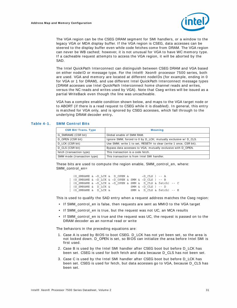
Intel® Xeon® Processor 7500 Series Datasheet, Volume 2 31
Address Map and Memory Configuration
The VGA region can be the CSEG DRAM segment for SMI handlers, or a window to the legacy VGA or MDA display buffer. If the VGA region is CSEG, data accesses can be steered to the display buffer even while code fetches come from DRAM. The VGA region can never be WB cached; however, it is not unusual for VGA to have WC memory type. If a cacheable request attempts to access the VGA region, it will be aborted by the SAD.
The Intel QuickPath Interconnect can distinguish between CSEG DRAM and VGA based on either nodeID or message type. For the Intel® Xeon® processor 7500 series, both are used. VGA and memory are located at different nodeIDs (for example, ending in 0 for VGA or 1 for DRAM), and use different Intel QuickPath Interconnect message types (DRAM accesses use Intel QuickPath Interconnect home channel reads and writes, versus the NC reads and writes used by VGA). Note that Cseg writes will be issued as a partial WriteBack even though the line was uncacheable.
VGA has a complex enable condition shown below, and maps to the VGA target node or to ABORT (if there is a read request to CSEG while it is disabled). In general, this entry is matched for VGA only, and is ignored by CSEG accesses, which fall through to the underlying DRAM decoder entry.
These bits are used to compute the region enable, SMM_control_en, where: SMM_control_en=
(G_SMRAME & ~D_LCK & D_OPEN & ~D_CLS ) -- A | (G_SMRAME & ~D_LCK & ~D_OPEN & SMM & ~D_CLS ) -- B | (G_SMRAME & ~D_LCK & ~D_OPEN & SMM & D_CLS & fetch) -- C | (G_SMRAME & D_LCK & SMM & ~D_CLS ) -- D | (G_SMRAME & D_LCK & SMM & D_CLS & fetch) -- E
This is used to qualify the SAD entry when a request address matches the Cseg region:
• If SMM_control_en is false, then requests are sent as MMIO to the VGA target
• If SMM_control_en is true, but the request was not UC, an MCA results
• If SMM_control_en is true and the request was UC, the request is passed on to the DRAM decoder as an normal read or write
The behaviors in the preceding equations are:
1. Case A is used by BIOS to boot CSEG. D_LCK has not yet been set, so the area is not locked down. D_OPEN is set, so BIOS can initialize the area before Intel SMI is first used.
2. Case B is used by the Intel SMI handler after CSEG boot but before D_LCK has been set. CSEG is used for both fetch and data because D_CLS has not been set.
3. Case C is used by the Intel SMI handler after CSEG boot but before D_LCK has been set. CSEG is used for fetch, but data accesses go to VGA, because D_CLS has been set.
Table 4-1. SMM Control Bits
CSR Bit/Trans. Type Meaning
G_SMRAME (CSR bit) Global enable of SMM RAM.
D_OPEN (CSR bit) Ignore SMM; forced to 0 by D_LCK; mutually exclusive w/ D_CLS.
D_LCK (CSR bit) Use SMM; write 1 to set, RESET# to clear (write 1 once, CSR bit).
D_CLS (CSR bit) Bypass data accesses to VGA; mutually exclusive with D_OPEN.
fetch (transaction type) This transaction is a code fetch.
SMM mode (transaction type) This transaction is from Intel SMI handler.

Address Map and Memory Configuration
32 Intel® Xeon® Processor 7500 Series Datasheet, Volume 2
4. Case D is used by the Intel SMI handler after CSEG boot after D_LCK has been set. CSEG is used for both fetch and data because D_CLS has not been set.
5. Case E is used by the Intel SMI handler after CSEG boot after D_LCK has been set. CSEG is used for fetch, but data accesses go to VGA, because D_CLS has been set.
4.2.1.3 Programmable Attribute Map (PAM) – 768k..1M
PAM is a legacy BIOS ROM area in MMIO. It is overlaid with DRAM used as a faster ROM storage area.
The Intel® Xeon® processor 7500 series supports seven BIOS regions, which can be independently configured to program reads or writes to either DRAM or BIOS ROM. The seven regions are not split into Hi/Lo sub-regions
Each PAM segment has two configuration bits to determine if the request maps to the PAM target, or falls through to the DRAM decoder, depending on whether the request is considered a read or a write. Cacheable requests are allowed to match the MMIO BIOS ROM entry and they are subject to the write to non-coherent error condition.
PAM region accesses create a special case for LOCK transaction flows, where the read can be to one channel and the write can be to a different channel.
4.2.1.4 BIOS– 768k..1M
During early boot, if the CPU is in real mode, the region targets the BIOS flash ROM device. This region must be disabled before the PAM region (which it shadows) is enabled. This region is enabled at reset.
4.2.2 OS Region 1M..4G–64M
This is the remainder of space available to protected mode in 32-bit OSes. Note that unlike client class processors, the ISA hole is not implemented.
Table 4-2. Truth Table for Mapping Address to PAM Segment
Address PAM Segment
17 16 15 14
0 0 0 x 1
0 0 1 x 2
0 1 0 x 3
0 1 1 x 4
1 0 0 x 5
1 0 1 x 6
1 1 x x 0
Table 4-3. PAM Region Handling
WB Access Write PAM Config bit[xx] Abort
1 x xx Ubox (NXM)
0 0 x0 Legacy Intel® 7500 chipset
0 0 x1 fall-thru (DRAM)
0 1 0x Legacy Intel® 7500 chipset
0 1 1x fall-thru (DRAM)
Intel® Xeon® Processor 7500 Series Datasheet, Volume 2 33
Address Map and Memory Configuration
4.2.2.1 OS Memory
This region is typically mapped by the same DRAM decoder entry that maps the DOS DRAM region, although it can be split into multiple regions.
4.2.2.1.1 TSEG
This is a protected memory space (typically) located in OS memory. It can only be accessed by code in SMMode, just as Cseg is. Unlike Cseg, the address is configurable, defined by the core, and access is enforced by core SMRRs. There is no explicit support in the SAD for Tseg.
4.2.2.2 PCIe*
PCI Express defines a configuration register space for 256 busses, each with 32 devices, each with 8 functions, each with 4 kB configuration registers. The first 256 bytes of each function’s configuration space can also be reached through the CFC/CF8 method.
There are separate enables for the memory mapped and IO CF8/CFC-mapped regions. If enabled, and a DRAM entry is configured that covers this address range, then the PCIe entry overrides, and the DRAM which would have been accessed at those address ranges must be recovered at another address range using the Target Address Map to map the new address range to the recovered DRAM range.
The resulting configuration space occupies 256 MB of memory address space. In the processor, this region may be disabled, or located at any 256-MB boundary below 4 G that does not overlap any other enabled region. Typically, this prohibits the 0..256 MB region (where VGA and PAM regions are located) and the 4G–256 M..4G region (where flash memory, local configuration is located). Addresses that match this region are issued as NcCfgRd or NcCfgWr transactions, and the target is selected from a list of targets indexed by PA<27:25>.
If an access to this region is made while the requestor is in SMMode, the protected access will be indicated in the Configuration_Request_type field of the Intel QuickPath Interconnect packet. The attribute to this space is MMCFG.
4.2.2.2.1 SCA_PCIE
SCA_PCIE is a subset of the PCIe space dedicated to CPU and chipset configuration registers. It occupies a (configurable) naturally aligned 8-MB sub-region in the 256-MB PCIe space. It defaults to the top 8-MB sub-region at reset (sca_clump = 5’b11111).
When the access is within the PCIE region and the local clump address range is matched (sca_clump==PA<27:23>), then the normal PCIE region is overridden, and the destination nodeID is set to (~(PA<22:20> OR MASK),10). MASK is used to allow 1-, 2-, 4-, or 8-socket clumps to be used while maintaining a contiguous usage of buses, and should be configured to 8 - max#sockets/clump.
If an access to this region is made while the requestor is in SMMode, the protected access will be indicated in the Configuration_Request_type field of the Intel QuickPath Interconnect packet.
The subregion uses the same enable bits as the enclosing segment.
To prevent errant accesses to non-existent nodeIDs, there are separate enable bits for each 1-MB bus.

Address Map and Memory Configuration
34 Intel® Xeon® Processor 7500 Series Datasheet, Volume 2
4.2.2.3 MMIOL(L/U) (PCIE..4G–64M)
This region is dedicated to MMIO, and covers the region immediately adjacent to the configured PCIe segment (regardless of whether that region is disabled) to 4 G–64 M. This is the only variable length region in the IO decoder. There is a single enable for this region, but two separate target lists: one for lower addresses (PA<31>==0), and one higher addresses (PA<31>==1) indexed by PA<30:28>. The attribute for this region is MMIO.
4.2.3 Special Region 4G–64M..4G
This is a region with several fixed dedicated regions hardwired in the IO decoder.
4.2.3.1 Global CPU CSRs 4G–64M..4G–48M
This region is used to access CPU uncore CSRs via MMIO (versus PCIE). The destination nodeID is determined by lookup into a target list using PA<23:21> as an index. Each destination is allocated 64 kB of CSR space (so the space is sparse). The attribute to this space is MMIO. This address range is deprecated and should be avoided. Use PCIe requests instead.
4.2.3.1.1 Local Clump CPU CSRs
Like SCA_PCIE, the local clump CPU CSR region is a subset of the Global CPU CSR region. It occupies a (configurable) discontiguous 0.5 MB sub-region (defined by PA<23,19:16>) in the 16 MB PCIe CPU CSR space. It defaults to the top of the global region at reset (sca_clump = 5’b11111). When the access is within the Global CPU CSR region and the local clump address range is matched (sca_clump==PA<23,19:16>), then the normal CPU CSR range is overridden, and the destination nodeID is set to (~(PA<22:20> OR MASK),10). MASK is used to allow 1, 2, 4, or 8 socket clumps to be used while maintaining contiguous usage of buses, and should be configured to 8 -max#sockets/clump.
To prevent errant accesses to non-existent nodeIDs, there are separate enable bits for each 64-kB sub-region, shared with the SCA PCIe region.
4.2.3.2 Global Intel® 7500 Chipset CSRs 4G–48M..4G–32M
This region is used to access Intel® 7500 chipset uncore CSRs via MMIO (versus PCIE). The destination nodeID is determined by lookup into a target list using PA<23:21> as an index. Each destination is allocated 64kb of CSR space (so the space is sparse).
4.2.3.3 Local Configuration 4G–21M..4G–20M
This is an alias to the Global CPU CSRs that corresponds to the local socket only. This entry cannot be disabled. The target is always the local socket configuration agent. The attribute for this space is MMIO.
4.2.3.3.1 Abort – FEB0_xxxx
This subregion of the local configuration region is a master abort region; accesses to this region will return all 1s on reads, and complete with no side effects on a write. It is the first 64k subregion of the 1MB local configuration region.

Intel® Xeon® Processor 7500 Series Datasheet, Volume 2 35
Address Map and Memory Configuration
4.2.3.3.2 Local CSRs FEB(1-3)_xxxx
This accesses the local socket CSRs. It is accessed at any of the even three stripes (PA<18>==0) above the abort subregion in the local configuration region. Only the FEB2_xxxx should be used. This region is always enabled, and will never be seen outside the socket.
4.2.3.4 ICH 4G–19M..4G–18M
This region covers the High Performance Event Timers (HPETs), in the legacy bridge. The accesses are sent to the legacy Intel® 7500 chipset / ICH. The attribute to this region is MMIO.
4.2.3.5 IOAPIC 4G–19M..4G–18M
This is a 1-MB range used to map the IOxAPIC Controller registers. The IOxAPIC space is used to communicate with IOxAPIC interrupt controllers that may be populated in the downstream devices. The target nodeIDs are selected from an eight-entry target list indexed by PA<15:13>. The attribute to this space is MMIO. Note that the index is not the most significant bits of the region offset, because of legacy address limitations in IOAPICs.
4.2.3.6 Flash 4G–16M..4G
This region is used for BIOS/firmware. The accesses to this region are forwarded to the Intel® 7500 chipset if flash is attached to an Intel® 7500 chipset (Intel® 7500 chipset can be attached to same socket or neighboring socket) or to the UBox if the FWH is local to the socket. The firmware can be split between local and global targets, and the target nodeIDs are selected from an eight-entry target list indexed by PA<23:21>. The attribute to this space is MMIO.
4.2.4 Extended Region
4.2.4.1 OS Memory
This is DRAM which is mapped above the 32-bit 4-GB boundary in the DRAM decoder.
4.2.4.1.1 Recovered DRAM
DRAM which would have been located at addresses just below 4 GB (Global CPU and Intel® 7500 chipset CSRs, and the special region) will be relocated in an address region above the 4-GB boundary.
4.2.4.2 MMIOH
If more MMIO space is required than is available below 4 G, then DRAM decoder entries are used to configure it above the top of DRAM. Note that unlike the normal MMIO entry below 4 G, these entries should not be interleaved, so multiple targets will require multiple SAD entries. The attribute to this space would be configured to MMIO and must not target DRAM.
Address Map and Memory Configuration
36 Intel® Xeon® Processor 7500 Series Datasheet, Volume 2
4.2.4.3 Additional PCIe* Segments
If more than one PCIe segment is required, DRAM decoder entries are used to configure it above the top of DRAM. Note that unlike the normal PCIe entry below 4 G, these entries should not be interleaved, so multiple targets will require multiple SAD entries. The attribute to this space would be configured to MMCFG and must not target DRAM.
4.2.4.4 Protected Region 2^44–64G..2^44
This region partially aliases the special region at 4G–64M..4G but can only be accessed by code running in SMMode enabled. This address range is deprecated and should be avoided. Use protected PCIe requests instead.
4.2.4.4.1 Protected Global CPU CSRs (2^44–64G)+(4G–64M..4G–48M)
This is an alias of the Global_CPU_CSR region which can only be accessed if the requesting thread is in SMMode. If the thread is not in SMMode, then the request will not match in the IO Decoder and will be treated as a master abort (noop) unless a memory decoder region has also been configured at this address. It shares the enables, target list, and type as the normal Global CPU CSR region. There is also a Protected LocalClump CPU CSR subregion, that shares the same configuration bits as the unprotected sub-region.
4.2.4.4.2 Protected Global Intel® 7500 Chipset CSRs (2^44-64G)+(4G-48M..4G–32M)
This is an alias of the Global_IOH_CSR region which can only be accessed if the requesting thread is in SMMode. If the thread is not in SMMode, then the request will not match in the IO Decoder and will be treated as a master abort unless a memory decoder region has also been configured at this address. It shares the enables, target list, and type as the normal Global Intel® 7500 chipset CSR region.
4.2.4.4.3 Protected Local CSRs (2^44-64G)+(4G-21M..4G-20M)
This is an alias of the Local_CSR region which can only be accessed if the requesting thread is in SMMode. If the thread is not in SMMode, the request will not match in the IO Decoder and will be treated as a master abort (noop) unless a memory decoder region has also been configured at this address. The target is always the local socket.
4.2.5 IO Address Regions
There are two types of accesses made by cores that use legacy IO requests types from the core:
• Legacy IO
• PCI Configuration
4.2.5.1 Legacy IO
The traditional IA-32 IO address space is 64 k. Accesses are sent to a chipset component as NcIoRd and NcIoWr (IO). The destination nodeID is determined by looking up a target list entry using IO_Addr<15:13> as an index.
Note that the traditional IO address space is 64 k, not 64 k+3. The old practice of allowing a 4-byte IO instruction to 0000_FFFF to continue incrementing to 0001_0000..3 has not been supported in chipsets or downstream IO buses for a long time.

Intel® Xeon® Processor 7500 Series Datasheet, Volume 2 37
Address Map and Memory Configuration
4.2.5.2 IOCFG_PCIE
The IOCFG_PCIE address range is used as a target for emulation of CFC/CF8 configuration accesses. The first 256 bytes of each PCI Express function is accessible via IN/OUT to IO addresses CF8/CFC.
The format of the NcCfgRd and NcCfgWr address is slightly different from the format of CONFIG_ADDRESS. PCI allowed a 256-byte configuration space per function. PCI Express and Intel QuickPath Interconnect allow a 4-k byte configuration space per function. Four bits of zero are inserted into the address <11:8> generated from CONFIG_ADDRESS to expand this address space. The two least-significant bits of the CONFIG_DATA access become the two least-significant bits of the NcCfgRd or NcCfgWr.
This region shares enables, and target lists with the PCIe entry. The attribute to this space is MMCFG.
4.2.5.2.1 IOCFG_SCA_PCIE
If the upper five bits of the bus number in the emulated PCIe access matches the configured clump number for the SCA_PCIE entry (sca_clump==IO_ADDR<27:23>), then the SCA_PCIE target(s) will be used.
4.2.5.3 IOCFG_NXM
Other IO address ranges generated by CPU (for example, IO offset 0x1000..1002) will be sent to the legacy Intel® 7500 chipset.
4.2.6 IO Decoder Region Summary
The following table summarizes all the IO decoder entries that have addresses (that is, do not include non-address cycles).
Table 4-4. IO Decoder Regions (Sheet 1 of 2)
Addr 43.. 32 31.. 28 27.. 24 23.. 20 19.. 16 15.. 12 11.. 00 Targets Comments
SCA 000 =yyyy mmmm m ena X X XXX ~ena&mask, 100
indiv ena.s1 NcCgRd/Wr
PCIE 000 =yyyy zzz x X X X XXX PCI[zzz] NcCgRd/Wr
MMIOl-hi 000 1,>yyy X X X X XXX MIOu[yyy]
MMIOl-lo 000 0,>yyy X X X X XXX MIOl[yyy]
NOGO 000 F C-F X X X XXX Ubox default
FWH 000 F F yyy x X X XXX FWH[yyy]
ICH 000 F E D X X XXX Legacy IOH
IOAPIC 000 F E C X yyy x XXX APIC[yyy]
No-Op, LclCSRs
000 / FF0*
F E B 0 1..3 4..7
X XXX Ubox 2
Glb IOH CSRs 000 / FF0*
F D yyy x X X XXX IOH[yyy]
Glbl CPU CSRs 000 / FF0*
F C yyy x X X XXX CPU[yyy]
lcl clump CSRs 000 / FF0*
F C m ena mmmm X XXX ~ena&msk,10
PAM 000 0 0 0 C-F en en xx XXX Legacy IOH 3
BIOS 000 0 0 0 C-F X XXX Ubox
Cseg Hole 000 0 0 0 A-B X XXX Ubox 4
VGA 000 0 0 0 A-B X XXX VGA IOH 5

Address Map and Memory Configuration
38 Intel® Xeon® Processor 7500 Series Datasheet, Volume 2
4.3 Configuring Regions
4.3.1 Configuring DRAM
There are two basic DRAM configurations: Interleaved and Non-interleaved. Interleaved regions can use low or low-middle order interleave mode. Each of these configurations can also be simultaneously hemisphere interleaved. Address regions can be mixed, for example, a region that is interleaved across CPUs, and other regions dedicated to each CPU individually (non-interleaved or interleaved with the CPU only) or together in any combination.
4.3.2 Configuring MMIOH
MMIOH cannot be interleaved. If multiple Intel® 7500 chipsets are targeted, a separate decoder entry is required for each. It is recommended that MMIOH be located adjacent-to and above the Top of High Memory.
4.3.3 Configuring MMConfig
MMConfig cannot be interleaved. If multiple Intel® 7500 chipsets are targeted, a separate decoder entry is required for each. Each entry must have a fixed size of 256 M. The recommended location is adjacent-to and above MMIOH.
4.4 Source Address Decoder The Intel® Xeon® processor 7500 series source address decoder is responsible for directing regions’ accesses to a specific IO or memory controller (or a set of controllers in the case of interleaved regions).
The source address decoder is made up of two parts, one of which (IO decoder) is used for predefined non-DRAM regions and special non-address cycles. The other (DRAM decoder) handles DRAM regions, and extended MMIO regions and MMCFG segments.
Each of these sections responds to a request by address-matching a range of addresses along with the particular access type. In the case of simultaneous matches between the two sections, the IO decoder overrides the DRAM decoder.
IO-SCA 000 PCIe XBAR
mmmm m ena X X xXX ~ena&msk.10 from IO CF8/CFC, NcCgRd/Wr
IO PCIE 000 PCIe XBAR
zzz x X X X xXX PCI[zzz] from IO CF8/CFC, NcCgRd/Wr
IO 000 0 0 0 0 yyy x XXX IO[yyy] NcIORd/Wr
Notes:1. Set "Protected" bit in SMMode (SCA overrides PCIe)2. Match FF0 only in SMMode3. Has individual read/write enables for subregions4. Match if WT& SMM_Ctl_En & Glbl_SMMRam_En & ~UC5. Match if Wt&~SMM_Ctl_En & ~Glbl_SMMRam_En
Table 4-4. IO Decoder Regions (Sheet 2 of 2)
Addr 43.. 32 31.. 28 27.. 24 23.. 20 19.. 16 15.. 12 11.. 00 Targets Comments

Intel® Xeon® Processor 7500 Series Datasheet, Volume 2 39
Address Map and Memory Configuration
The IO decoder gives very little control over the addresses that are matched, but does give control over whether the match is enabled, and the target nodeIDs of the match. The type of access must be configured to be MMIO, except for PCI config regions, which must be configured to be MMCFG. With one exception, all ranges in the IO decoder are naturally aligned, fixed power-of-two sizes. The targets of each range is either a single nodeID (which may be shared with another range in some instances) or is one nodeID selected from a list of eight target indexed by three (not always the most) significant bits of the region offset. These lists, likewise, may be shared with other regions.
The DRAM decoder consists of 20 address range limits, where the beginning address of one range is always just above the ending range of the previous. (The first entry is special case, with a single CSR bit indicating whether it is address above the “previous” range’s end).
Ranges are always multiples of 256 MB. Each range has a configurable type (Coherent, MMIO, MMCFG, or NXM), and an eight-entry target list selected by either the low three address bits (PA<8:6>) or an exclusive-or hash of the three low address bits with PA<18:16>. In addition, target NodeID<1> can be inverted with an exclusive-or hash of PA<19,13,10,6>, which matches the caching agent interleave mode. Only coherent regions can configure target list entries to be different, or use the exclusive-or hash (that is, non-coherent regions cannot be interleaved, and all target list entries must be identical).
Unused entries should set the upper limit and lower limit to equal. Unused regions must have memory type NXM.
Figure 4-2. Source Address Decoder Block Diagram

Address Map and Memory Configuration
40 Intel® Xeon® Processor 7500 Series Datasheet, Volume 2
Entry N+1 should never be less than Entry N. To ensure this, unused entries must be the higher numbered entries and must always be equal to the last entry. Furthermore, entries should be programmed from the highest down to the lowest with the top address, then again filling in the real address so there is no temporary case where a higher entry is less than a lower numbered entry.
Note that although target lists have eight entries, the actual interleave can be made smaller by replicating entries. When entries are replicated, the high order index bits must be distinct. Specifically Interleave_Index<2:3-N> must be unique for every entry which is replicated, where N = ceiling(log2(# of repetitions)).The DRAM configuration is expected to be configured as either interleaved, or non-interleaved. An interleaved region can be interleaved, at most, eight ways, correspond-ing to a four socket clump with two memory controllers per socket, or eight sockets with a hemisphere interleave. A typical system might use one decoder entry for inter-leaving across four sockets, and one decoder entry non-interleaved for each memory controller on a socket (or for each socket, but only interleaved within the socket). In large multi-clump systems, additional entries would be needed:
• DRAM at lower addresses than this clump
• DRAM at higher addresses than this clump
• More MMIO on this clump than can fit below 4 G
• MMIO in other clumps at both higher, and lower addresses
• Additional PCI configuration segments in this and other clumps (at both lower and higher addresses)
It may also be desirable to reserve entries for hot-add of more memory.
Note that some scaled systems may even require two entries for MMIO or PCI-CFG segments at lower (or higher) addresses if they are split across two node controllers. OEMs building large systems must take care to configure systems such that they fit into the 20-region limit, either by limiting the variability of DRAM allocation in each clump (for example, making it uniform across controllers), or by designing all IO to be non-local, or by allowing IO to be accessible by either node controller.
4.4.1 Target Address Decoder Configuration
The target address decoder is responsible for mapping discontiguous address regions and interleaves into a contiguous DRAM address range, and for indicating to the DRAM controller which type of DIMMs is in each address range. The decoder does this in a manner similar to the Source Address Decoder; it has 10 range registers which are matched as upper and lower limits with 256-MB granularity. When a range is matched, payload is read that specifies:
• The number of lower address bits that were used to interleave the region and should be removed (as they are constants in the controller).
• A relocation amount that is added to the address to remove gaps, and
• An enable bit that indicates if the range was used at all
In parallel with this is a separate set of range registers which determine the type of DIMM used in each range.
For more information on the Target Address Decoder please refer to Section 6.3.1 in the Home Agent and Global Coherence Engine (Bbox) chapter.

Intel® Xeon® Processor 7500 Series Datasheet, Volume 2 41
Address Map and Memory Configuration
4.5 Address InterleavingAddress interleaving refers to subdividing address regions such that each subdivision can be sent to a different target. Interleaving is used to distribute bandwidth load across multiple agents, which reduces hot-spotting, and to reduce the number of SAD resources used. Any region that can target more than one nodeID is an interleaved region.
The subdivision is determined by selecting and combining various bit fields to generate an interleave number. Note that this process results in a power-of-two number of subdivisions that are equal in size.
This interleave number is used as an index into a table of eight nodeIDs, which is combined with a nodeID base to generate a destination nodeID. Generally, each interleaved region has its own configurable target list, though some in the IO decoder are shared. Note that it is not required that the contents of each table entry be unique; two-way, four-way, or irregular interleaves can be configured by repeating entries (with some restrictions for DRAM). In general, each address region has its own list, though there are some exceptions as some of the predefined regions do not allow interleaving.
The processor SAD implements four different methods of interleaving:
1. High-order interleave: Three high-order address bits of the region are used. The position of the high-order bits is dependent on the size of the region.
2. Low-order interleave: Three low-order address bits (PA<8:6> are) used as the interleave number.
3. Low/Mid-Hash interleave: The exclusive-or of PA<8:6> and PA<18:16> are used as the interleave number. This variation of low-order interleave is used to spread accesses that hit the same interleave between different DRAM banks.
4. Hemisphere interleave: In the processor, this is a single bit formed by exclusive-or of PA<19>, PA<13>, PA<10> and PA<6>. Hemisphere interleave must be combined with either Low or Low/Mid Hash interleave modes, and is different in that it just replaces target nodeID<1>.
Note: DRAM regions cannot use High-order interleave; it must be simulated using multiple non-interleaved entries. The pre-defined regions can only be high-order interleaved.
4.5.1 Overall Structure
4.5.1.1 Decoders
The address decoder is able to map memory from the eight home agents (Bboxes) in the four Intel® Xeon® processor 7500 series sockets of the local clump, plus additional home agents in external node controllers (XNCs), each with varying amounts of DRAM, into contiguous regions with no holes. To enable this, most address decoder entries use a level of indirection (target list) to generate a NodeID. To help reduce the number of decoder entries required for the varying DRAM capacities, the address decoder has several interleave options and is divided into decoders with a fixed priority for multiple matches as follows (highest to lowest).
• I/O small (IOS) decoder
• I/O large (IOL) decoder
• DRAM decoder

Address Map and Memory Configuration
42 Intel® Xeon® Processor 7500 Series Datasheet, Volume 2
Each of these decoders is presented with an address and accessed in parallel. Addresses that match an entry in one of the decoders cause the decoder to lookup and generate the Intel QuickPath Interconnect memory attribute and NodeID. Only one match is allowed per decoder. Address matches in a higher-priority decoder will override simultaneous matches in lower-priority decoders.
4.5.1.2 Address Matching
For the DRAM decoder, the address is matched by comparing it with a region limit in each entry. If the address is less than or equal to the limit for a given entry, but not less than or equal to the limit of the previous entry, then it matches the given entry. Region limits have a granularity of 256 MB. For the I/O decoders, the address is matched by comparing it with a base address in each entry, under a fixed address mask in each entry. The effect of this is to match a naturally-aligned power-of-two sized address range. Most I/O decoder entries have a fixed or minimally variable base addresses as well. The unmasked bits are limited to a contiguous bit field starting at the high order address bit.
The I/O decoders have many entries in the region from 4 GB – 64 MB to 4 GB. All but one entry have individual enable bits which disable the address matching if cleared. In order to simplify the implementation, these enable bits are ignored and assumed to be set for the purpose of overriding the DRAM decoder. Therefore, any reference to this range will disable the DRAM decoder. If the enable bit for the corresponding I/O decoder entry is clear, then no address match occurs, and the access is treated as a non-existent memory access.
Note that it is possible that a memory region will not be fully populated, and it is the responsibility of the target decoder at the home (Bbox or XNC) to recognize that an address is not implemented, either via explicit match of a target decoder entry configured as an illegal type, or by recognizing that no entry matches. When this occurs, the target can return either an error indication or return data of all ones for reads, and prevent data update for writes.
4.5.1.3 Non-Existent Memory (NXM)
If an address is not matched by any range, or matches an address hole (non-existent memory attribute), the target defaults to the socket's Ubox NodeID, and the message is encoded as Intel QuickPath Interconnect NcRdPtl or NcWrPtl opcode with zero length or all zero byte enables, respectively. The router will direct this to the local configuration agent (Ubox), which treats the message as an error. Errors in the configuration agent can be configured to return an error response, or normal completion (returning data of all ones for reads or preventing data update for writes), with or without an MCA. This mechanism is used to prevent any illegal access from being routed externally during some initialization sequences.
The Intel® Xeon® processor 7500 series caching agent will not issue a Machine Check Abort on access to a source address decoder address region marked as Non Existent Memory (NXM), unless the access is a store with write-back (WB) memory attribute, in which case the caching agent will issue an MCA on accesses that hit the NXM regions. There is no other configurability available for this operation.
4.5.2 DRAM Decoder
There is one 20-entry DRAM decoder. A match in either I/O decoder overrides the DRAM decoder. Multiple matches within a decoder are forbidden. All entries in the decoder are identical except that entry 0 has its own enable bit, rather than using the result of the previous entry's comparison to enable itself.

Intel® Xeon® Processor 7500 Series Datasheet, Volume 2 43
Address Map and Memory Configuration
4.5.2.1 DRAM Decoder Usage
The DRAM Decoder maps all available DRAM in the system. Non-power-of-two region sizes can be easily configured due to the region-limit style of the decoder, as long as the region size is a multiple of 256 MB.
DRAM regions are assumed to use contiguous address space starting at address zero. Entries must be programmed with increasing address limits from entry 0 to entry 19. If there are any holes in the address space, they can be programmed in an entry using the NXM attribute.
4.5.2.2 Data Structure
The smallest region that can be defined by a DRAM decoder entry is 256 MB. Note that a 256 MB region interleaved among several targets will have less than 256 MB at each target. Specifically, if the maximum number of NodeIDs were used in the target list (8), along with the minimum region size (256 MB), then each target decoder would control 32 MB. However, the target decoder does not support controlling less than 256 MB, so this must be avoided.
The DRAM decoder is composed of two arrays, a CAM array and a payload array. The DRAM decoder has 20 entries in each array. The CAM array has special compare logic to compute whether an address is less than or equal to the region limit of each entry, to allow for any region size that is a multiple of 256 MB. The region limit address bits [43:28] are stored in each entry. The payload array has 42 bits per entry.
There is one valid bit for the DRAM decoder, which is reset to zero. It is used in the entry 0 match logic in place of the "not less than or equal to the limit of the previous entry" condition, since there is no previous entry for entry 0. All region limits will also be reset to zero.
Table 4-5 describes the fields of each DRAM decoder entry.
Table 4-5. DRAM Decoder Fields
Name Description
limit[43:28] Address bits [43:28] of the region limit. Stored in flops.
tgtlist[31:0] NodeID[4:1] for each of eight targets. Bits [4:1] for each target are stored adjacently, with target 0 in bits [3:0] and target 7 in bits [31:28].
ppar[1:0] Parity for the payload array (tgtlist, hit, mca, idbase, hemi, tgtsel, attr fields), interleaved.
hit Used to signal a debug or performance monitoring event when the entry is accessed.
mca Used to signal a machine check event when the entry is accessed.
idbase NodeID[0] for all eight targets.
hemi If set, XOR the hemisphere bit (CboxID[2]) with NodeID[1] from the selected target list entry.
tgtsel If set, indicates that the low order address bits [8:6] are used to index the target list; otherwise, the result of (addr[18:16] ^ addr[8:6]) is used.
attr[2:0] Intel® QuickPath Interconnect memory attribute of the region.
Table 4-6. Intel® QuickPath Interconnect Memory Attributes (Sheet 1 of 2)
Name Value Description Request Opcodes
COH 000 Coherent memory RdCode, RdData, RdInvOwn, InvItoE, WbMtoI, WbMtoE
MMIO 001 Memory-mapped I/O NcRd, NcRdPtl, NcWr, WcWr, NcWrPtl, WcWrPtl
IO 010 Legacy I/O NcIORd, NcIOWr
RSVD 011 Reserved N/A
CFG 100 PCI/PCIE configuration NcCfgRd, NcCfgWr
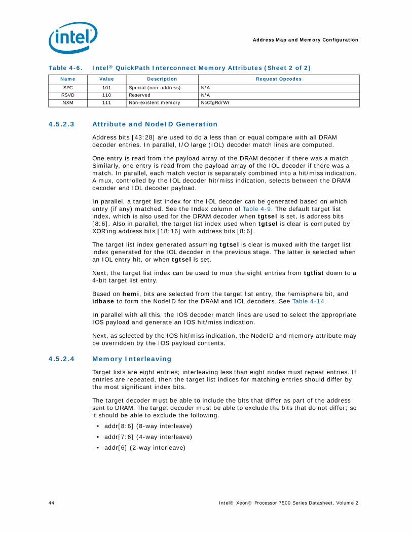
Address Map and Memory Configuration
44 Intel® Xeon® Processor 7500 Series Datasheet, Volume 2
4.5.2.3 Attribute and NodeID Generation
Address bits [43:28] are used to do a less than or equal compare with all DRAM decoder entries. In parallel, I/O large (IOL) decoder match lines are computed.
One entry is read from the payload array of the DRAM decoder if there was a match. Similarly, one entry is read from the payload array of the IOL decoder if there was a match. In parallel, each match vector is separately combined into a hit/miss indication. A mux, controlled by the IOL decoder hit/miss indication, selects between the DRAM decoder and IOL decoder payload.
In parallel, a target list index for the IOL decoder can be generated based on which entry (if any) matched. See the Index column of Table 4-9. The default target list index, which is also used for the DRAM decoder when tgtsel is set, is address bits [8:6]. Also in parallel, the target list index used when tgtsel is clear is computed by XOR'ing address bits [18:16] with address bits [8:6].
The target list index generated assuming tgtsel is clear is muxed with the target list index generated for the IOL decoder in the previous stage. The latter is selected when an IOL entry hit, or when tgtsel is set.
Next, the target list index can be used to mux the eight entries from tgtlist down to a 4-bit target list entry.
Based on hemi, bits are selected from the target list entry, the hemisphere bit, and idbase to form the NodeID for the DRAM and IOL decoders. See Table 4-14.
In parallel with all this, the IOS decoder match lines are used to select the appropriate IOS payload and generate an IOS hit/miss indication.
Next, as selected by the IOS hit/miss indication, the NodeID and memory attribute may be overridden by the IOS payload contents.
4.5.2.4 Memory Interleaving
Target lists are eight entries; interleaving less than eight nodes must repeat entries. If entries are repeated, then the target list indices for matching entries should differ by the most significant index bits.
The target decoder must be able to include the bits that differ as part of the address sent to DRAM. The target decoder must be able to exclude the bits that do not differ; so it should be able to exclude the following.
• addr[8:6] (8-way interleave)
• addr[7:6] (4-way interleave)
• addr[6] (2-way interleave)
SPC 101 Special (non-address) N/A
RSVD 110 Reserved N/A
NXM 111 Non-existent memory NcCfgRd/Wr
Table 4-6. Intel® QuickPath Interconnect Memory Attributes (Sheet 2 of 2)
Name Value Description Request Opcodes

Intel® Xeon® Processor 7500 Series Datasheet, Volume 2 45
Address Map and Memory Configuration
In hemisphere mode, the interleave is doubled relative to the number of targets in one target list. Address bit [6] must be excluded by the target decoder to account for this. Table 4-7 provides an example of how target interleaving should be done for various modes.
It is not necessary for entries to be repeated a power-of-two number of times, though it may require additional target decoder entries to ensure that all DRAM is still accessible if this is not done.
4.5.2.5 Recovering Memory Behind I/O Decoder Entries
While the physical address space may be contiguous, the use of the DRAM space behind it is not. For example, if the bottom 4 GB of address space is mapped contiguously to 4 GB of DRAM, the top 64 MB of DRAM cannot be accessed as it is forced to miss the DRAM decoder. Similarly, several 256-MB regions below 4 GB cannot be accessed as they are overridden by MMIOL and CFG entries.
In order to recover the physical memory that is located at addresses that are overridden by an I/O decoder entry, the DRAM decoder must be configured to:
• Add another DRAM decoder entry at some unused address range whose size is at least as large as the range being recovered.
• Add corresponding target address decoder entry(s) that will relocate requests to the new source address decoder entry to the DRAM addresses being recovered.
The DRAM can then be accessed via this new physical address aperture. The effective interleave of the recovery region should match that of the original region in both granularity and destinations. That is, the recovery region could have finer granularity, but must replicate target list entries to match the original granularity if it does.
The smallest region that can be recovered using this methodology is 256 MB. If the new region is larger than the DRAM region being recovered, then aliasing may occur.
If it is permissible to alias the other memory in the original range, no further hardware or configuration support is required. The OS must be notified that the region in the other address range that overlaps real DRAM in the original range is unavailable. If the OS does access this DRAM through the other range, coherency may be lost, but there is no security violation.
4.5.2.5.1 Example: Recovering Memory Behind MMIOL/CFG Entries
The MMIOL/CFG regions are located at physical addresses below 4 GB. The 64 MB just below 4 GB is allocated by various I/O decoder entries, but in addition there are a variable number of 256 MB subregions that can be allocated to MMIOL and CFG.
Table 4-7. Example Target Interleaving
Targets Hemi Target List [0:7] Excluded Bits
1 No { 0, 0, 0, 0, 0, 0, 0, 0 } N/A
2 Yes { 0, 0, 0, 0, 0, 0, 0, 0 } [6]
2 No { 0, 1, 0, 1, 0, 1, 0, 1 } [6]
4 Yes { 0, 0, 2, 2, 0, 0, 2, 2 } [7:6]
4 No { 0, 1, 2, 3, 0, 1, 2, 3 } [7:6]
8 Yes { 0, 0, 2, 2, 4, 4, 6, 6 } [8:6]
8 No { 0, 1, 2, 3, 4, 5, 6, 7 } [8:6]

Address Map and Memory Configuration
46 Intel® Xeon® Processor 7500 Series Datasheet, Volume 2
The subregions below 4 GB that are mapped to MMIOL or CFG can be recovered by configuring a decoder entry for an address range above the top of physical DRAM with the same size, interleave mode, and target list as the entry that maps the first 4 GB of DRAM.
The target list entry of each recovered 256 MB MMIOL or CFG subregion should point to the same NodeID as the corresponding target list entry for the first 4 GB of DRAM. Note that the TSEG region should not be placed underneath MMIOL/CFG entries, as it will not be accessible in that region, and will not be protected in a recovered region at a different address.
4.5.3 I/O Decoders
While the DRAM decoder contains memory regions which can be relocated or sized only in multiples of 256 MB, the I/O decoders have regions which are much more irregular in both starting address and size (from KB to GB).
Most of the I/O regions are located in the low address range of the address map and hence address bits [43:32] are zero. Most of these regions are located either in the 64 MB immediately below 4 GB or in the compatibility region below 1 MB.
4.5.3.1 Operation
I/O decoder operation is identical to the DRAM decoder operation with the following exceptions:
• Some of the decoder entry fields are not configurable.
• The unmasked address field can extend down to address bit [14] (so regions can be as small as 16 KB in size).
• Some entries have a single programmable target list entry
• Some entries have multiple subregion enables.
Almost all entries will match address bits [43:32] equal to zero. A hit in any I/O decoder entry will override a hit in the DRAM decoder.
4.5.3.2 I/O Decoder Map
Table 4-8 shows the I/O decoder address map. Given for each region are the name, the pattern for address bits [31:14], the size in bytes, the memory attribute, the number of targets in the target list, the address bits used to index the target list (if any), which CSR is used to enable the entry, and the location (decoder and entry number). For all regions which specify an address pattern, address bits [43:32] must be zero to match, except those marked with "*". Also, any address in the 4 GB – 64 MB...4 GB range will be forced to mismatch any region, except for those fixed to that range. In other words, any address in this range which would otherwise match the MMIOL1 entry or a DRAM decoder entry is forced to mismatch. The CFG entries are not allowed to overlap the 4 GB – 64 MB...4 GB range.
Table 4-8. I/O Decoder Entries (Sheet 1 of 2)
Name Addr[31:14] Size Attr Tgts Index Enable Entry
CFG aaaa_xxxx_xxxx_xxxx_xx 256 MB CFG 8 [27:25] IOMMEN IOL0
CFG-SCA aaaa_bbbb_bccc_xxxx_xx 8 MB CFG 8 [22:20] IOMMEN IOS0
MMIOL0 dddd_xxxx_xxxx_xxxx_xx 2 GB MMIO 8 [30:28] IOMMEN IOL1
MMIOL1 eeee_xxxx_xxxx_xxxx_xx 2 GB MMIO 8 [30:28] IOMMEN IOL2
VGA 0000_0000_0000_101x_xx 128 KB MMIO 1 N/A CSEGEN IOS1

Intel® Xeon® Processor 7500 Series Datasheet, Volume 2 47
Address Map and Memory Configuration
In the Addr field, letters have the following meaning:
• "x...x": match any value
• "aaaa": match if equal to IOMMEN cfg_base field
• "bbbbb": match if equal to IOMMEN sca_clump field
• "ccc": match if corresponding IOMMEN sca_ena bit is set
• "dddd": match if greater than IOMMEN cfg_base and Addr[31] = 0
• "eeee": match if greater than IOMMEN cfg_base and Addr[31] = 1; prevent match when Addr[31:26] = 111111
• "ffff": match if the BIOSEN r/w enable bit is set for the corresponding segment, for reads and writes, respectively
• "*" means that Addr[43:32] = 0x000 always matches, and Addr[43:32] = 0xFF0 matches in SMM mode
• "+" means that the address is in the I/O address space, separate from the memory address space
Target lists are needed for the CFG, MMIOL0/1, CPU/IOH Cfg, IOAPIC, FWH, and Legacy I/O regions. These entries make up the I/O Large (IOL) Decoder. The reasons for the existence of target lists for these regions are described in the following table.
BIOS 0000_0000_0000_11ff_ff 256 KB MMIO 1 N/A BIOSEN IOS8
CPU Cfg 1111_1100_xxxx_xxxx_xx * 16 MB MMIO 8 [23:21] IOVLD IOL3
Local clump CPU Cfg
1111_1100_bccc_bbbb_xx * 512KB1 MMIO 8 [22:20] IOMMEN IOVLD
IOS9
IOH Cfg 1111_1101_xxxx_xxxx _xx * 16 MB MMIO 8 [23:21] IOVLD IOL4
Local Config. 1111_1110_1011_xxxx_xx * 1 MB MMIO 1 N/A always IOS3
IOAPIC 1111_1110_1100_xxxx_xx 1 MB MMIO 8 [15:13] IOVLD IOL5
ICH 1111_1110_1101_xxxx_xx 1 MB MMIO 1 N/A IOVLD IOS2
FWH 1111_1111_xxxx_xxxx_xx 16 MB MMIO 8 [23:21] IOVLD IOL6
Legacy I/O 0000_0000_0000_0000_xx + 64 KB IO 8 [15:13] IOVLD IOL7
CFG 1000_xxxx_xxxx_xxxx_xx + 256 MB CFG 8 [27:25] IOVLD IOL0
CFG-SCA 1000_bbbb_bccc_xxxx_xx + 8 MB CFG 8 [22:20] IOMMEN IOS0
RSVD 1111_1110_1101_xxxx_xx + 1 MB -- 1 N/A always IOS10
IntA N/A N/A N/A 1 N/A always IOS5
Lock N/A N/A N/A 1 N/A always IOS6
SplitLock N/A N/A N/A 1 N/A always IOS6
Unlock N/A N/A N/A 1 N/A always IOS6
Shutdown N/A N/A N/A 1 N/A always IOS5
Invd_Ack N/A N/A N/A 1 N/A always IOS6
WbInvd_Ack N/A N/A N/A 1 N/A always IOS6
RSVD_Debug N/A N/A N/A 1 N/A always IOS7
DbgWr N/A N/A N/A 1 N/A always IOS7
IntPriUp N/A N/A N/A 1 N/A always IOS6
IntLog N/A N/A N/A 1 N/A always IOS6
IntPhy N/A N/A N/A 1 N/A always IOS6
EOI N/A N/A N/A 1 N/A always IOS6
FERR N/A N/A N/A 1 N/A always IOS5
Notes:1. Non-contiguous
Table 4-8. I/O Decoder Entries (Sheet 2 of 2)
Name Addr[31:14] Size Attr Tgts Index Enable Entry

Address Map and Memory Configuration
48 Intel® Xeon® Processor 7500 Series Datasheet, Volume 2
Core issued requests which can match decoder entries by opcode are:
• IntA, Lock, SplitLock, Unlock, SpCyc(Shutdown), SpCyc(Invd_Ack), SpCyc(WbInvd_Ack), DbgWr, IntPriUp, IntLog, IntPhy, EOI, FERR, Quiesce
IOS decoder entries have a hard-coded Intel QuickPath Interconnect memory attribute, and obtain their target from the address or from one of several programmable CSRs, according to Table 4-10.
4.5.3.3 I/O Decoder Programming
For IOL entries, Table 4-8 gives the recommended attribute for each entry. Software is responsible for programming the payload to match this table. The target lists for IOL entries point exclusively at Intel® 7500 chipsets or at XNC NIDs which service NCB/NCS traffic. Therefore, idbase should be set to zero. Also, hemi should be set to zero, and tgtlist will be ignored (treated as if set). The target and attribute for each IOS entry in Table 4-8 is given by Table 4-10.
4.5.3.4 Protected Accesses
A protected (SMM) access to a CFG entry will set the Configuration Request Type field to Protected in the generated NcCfgWr or NcCfgRd message. A protected access to an MMIO entry which has a separate aperture for protected accesses (CPU Cfg, IOH Cfg, Local CSR) can be distinguished by addr[43:32] being 0xFF0.
4.5.3.5 AgentID Mode
There is an AgentID defeature mode in which all outgoing requests have the AgentID inserted to more easily correlate Intel QuickPath Interconnect messages back to the requesting core and thread. Cbox will insert the AgentID for all outgoing HOM, NCB, and NCS requests while in this mode. More specifically, it is inserted in the following message types: EIC, SA, EA, NCM, SDW, EBDW. The Intel® Xeon® processor 7500 series replaces Intel QuickPath Interconnect PA <43:40> with the Agent ID bits matching in the Cbox. Non-core generated messages (that is, error signaling from Ubox) will set PA<45:40> to all ones.
Table 4-9. I/O Decoder Entries with Target Lists
Region Reason for Target List
CFG, MMIOL0/1, IOAPIC, Legacy I/O Allows flexible distribution of I/O among sockets.
CPU/IOH Cfg Enable protection on socket basis for domain partitioning.
FWH Enables flexible mapping of Intel® 7500 chipset versus direct attach firmware
Table 4-10. IOS Decoder Entries
Entry Target Attr
IOS0 { (~Addr[22:20] | IOMMEN.sca_mask), 2'b10 } CFG
IOS1 VGA IOH MMIO
IOS2 Legacy IOH MMIO
IOS3 Local Ubox --
IOS4 Local Ubox --
IOS5 Legacy IOH SPC
IOS6 Local Ubox --
IOS7 Debug NID SPC
IOS8 BIOS NID MMIO
IOS9 { (~Addr[22:20] | IOMMEN.sca_mask), 2'b10 } MMIO
Intel® Xeon® Processor 7500 Series Datasheet, Volume 2 49
Address Map and Memory Configuration
4.5.3.6 Entry Details
The following explains each entry in the I/O decoder, and the values in its payload field.
4.5.3.6.1 CFG Entry
This entry is relocatable to any one of the 16 256 MB regions below 4 GB, and is used for PCI Express configuration. Addr[31:28] is matched against the IOMMEN cfg_base field to select the region. Matching is enabled by IOVLD bit 16. The IOMMEN cfg_base field should not be set to 0x0 or 0xF, to avoid overlap with other I/O decoder entries (though it can be set to 0x0 if the VGA, and BIOS entries are disabled).
There is an 8-entry target list associated with this entry. The target list index is Addr[27:25]. Targets are typically Intel® 7500 chipsets. The attribute should be CFG.
The Intel® Xeon® processor 7500 series emulates CF8/CFC accesses to CFG space. For these accesses, the CFG entry is fixed to a particular 256 MB region in the legacy I/O address space, and matching is enabled by IOVLD bit 17.
4.5.3.6.2 CFG-SCA Entry
This entry redirects some CFG accesses to support SCA. Addr[27:23] is matched against the C_PCSR_IOMMEN sca_clump field to recognize the region that should be redirected for the local clump. Similar to the CFG entry, matching is enabled by C_PCSR_IOVLD.cfg_sca_mem or C_PCSR_IOVLD.cfg_sca_io, for memory and I/O space respectively. Matching is further qualified by a bit in the C_PCSR_IOMMEN sca_ena field, based on Addr[22:20].
When this entry matches, the target is computed as {~(Addr[22:20] | sca_mask), 10}and has an attribute of CFG.
A few notes on programming the SCA match:
• The sca_mask should be computed as 8 - ( Number of sockets per clump).
• The number of bits set in the sca_ena field should match the number sockets in the clump.
• The number of bits set in sca_ena should not exceed the value of sca_mask to prevent aliasing.
• The sca_clump fields should be populated in decreasing order starting from 0x3f. This field is reset to 0x3f on a cold reset.
• Having non-fully populated clumps will result in a discontiguous address space.
• The sca_clump can be shared by multiple clumps with less than 8 sockets per clump to provide a contiguous address space. In this case, the sca_ena/sca_mask needs to differentiate clumps.
SCA Examples:
4S per Clump Example:
• Clump0:— sca_mask=100, sca_ena=11110000, sca_clump=11111— PA[22:20]={111,110,101,100}, NID={00010,00110,01010,01110}
• Clump1:— sca_mask=100, sca_ena=00001111, sca_clump=11111— PA[22:20]={011,010,001,000}, NID={00010,00110,01010,01110}

Address Map and Memory Configuration
50 Intel® Xeon® Processor 7500 Series Datasheet, Volume 2
• Clump2:— sca_mask=100, sca_ena=11110000, sca_clump=11110— PA[22:20]={111,110,101,100}, NID={00010,00110,01010,01110}
• Clump3:— sca_mask=100, sca_ena=00001111, sca_clump=11110— PA[22:20]={011,010,001,000}, NID={00010,00110,01010,01110}
4.5.3.6.3 MMIOL Entries
These entries allow the contiguous 256 MB regions immediately below 4 GB and above the CFG entry to be used for MMIO. Addr[31:28] is compared against the IOMMEN cfg_base field; it must be greater than this value in order to match. Matching is enabled by IOVLD bit 18. For the highest 256 MB region, the 64 MB region immediately below 4 GB is forced to mismatch since it is used by other I/O decoder entries.
There is an 8-entry target list associated with each of these entries. The target list index is Addr[30:28], and Addr[31] is used to select between the two target lists, providing 16-way interleave, and more importantly, a granularity of 256 MB. Targets are typically Intel® 7500 chipsets. The attribute should be MMIO.
4.5.3.6.4 VGA Entry
This entry decodes legacy VGA interface space, and is also known as ASEG. Matching is enabled by IOVLD bit 0. There is one programmable 5-bit NodeID target, which is set to the VGA IOH. The attribute should be MMIO. If matching is not enabled, the region is typically backed by a DRAM decoder entry which also covers the DOS region (below 640 KB).
The VGA entry has a complex enable condition, since some requests must miss this entry in order to fall through to the DRAM decoder and access CSEG memory. Table 4-11 shows whether the target should be VGA or CSEG based on values from the CSEGEN CSR, whether the request is made in SMM mode.
4.5.3.6.5 BIOS Entry
This is also known as the CDEF region, compatibility region, or PAM region. Matching is enabled for each segment specified by Addr[17:14], based on the corresponding read and write enables in BIOSEN (see Table 4-12). No IOVLD bit is used for matching.
Table 4-11. VGA/CSEG
Enable Lock Open Closed SMM CRd Target
0 X X X X X VGA (All)
1 0 1 0 X X CSEG (All)
1 0 0 0 0 X VGA (Non-SMM)
1 0 0 0 1 X CSEG (SMM)
1 0 0 1 0 X VGA (Non-SMM)
1 0 0 1 1 0 VGA (SMM Data)
1 0 0 1 1 1 CSEG (SMM Code)
1 1 X 0 0 X VGA (Non-SMM)
1 1 X 0 1 X CSEG (SMM)
1 1 X 1 0 X VGA (Non-SMM)
1 1 X 1 1 0 VGA (SMM Data)
1 1 X 1 1 1 VGA (SMM Code)
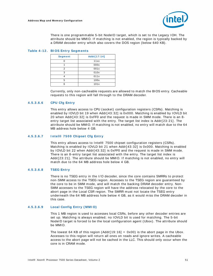
Intel® Xeon® Processor 7500 Series Datasheet, Volume 2 51
Address Map and Memory Configuration
There is one programmable 5-bit NodeID target, which is set to the Legacy IOH. The attribute should be MMIO. If matching is not enabled, the region is typically backed by a DRAM decoder entry which also covers the DOS region (below 640 KB).
Currently, only non-cacheable requests are allowed to match the BIOS entry. Cacheable requests to this region will fall through to the DRAM decoder.
4.5.3.6.6 CPU Cfg Entry
This entry allows access to CPU (socket) configuration registers (CSRs). Matching is enabled by IOVLD bit 19 when Addr[43:32] is 0x000. Matching is enabled by IOVLD bit 20 when Addr[43:32] is 0xFF0 and the request is made in SMM mode. There is an 8-entry target list associated with the entry. The target list index is Addr[23:21]. The attribute should be MMIO. If matching is not enabled, no entry will match due to the 64 MB address hole below 4 GB.
4.5.3.6.7 Intel® 7500 Chipset Cfg Entry
This entry allows access to Intel® 7500 chipset configuration registers (CSRs). Matching is enabled by IOVLD bit 21 when Addr[43:32] is 0x000. Matching is enabled by IOVLD bit 22 when Addr[43:32] is 0xFF0 and the request is made in SMM mode. There is an 8-entry target list associated with the entry. The target list index is Addr[23:21]. The attribute should be MMIO. If matching is not enabled, no entry will match due to the 64 MB address hole below 4 GB.
4.5.3.6.8 TSEG Entry
There is no TSEG entry in the I/O decoder, since the core contains SMRRs to protect non-SMM access to the TSEG region. Accesses to the TSEG region are guaranteed by the core to be in SMM mode, and will match the backing DRAM decoder entry. Non-SMM accesses to the TSEG region will have the address relocated by the core to the abort page in the Local CSR region. The SMRR must not locate the TSEG entry underneath the 64 MB address hole below 4 GB, as it would miss the DRAM decoder in this case.
4.5.3.6.9 Local Config Entry (MMIO)
This 1 MB region is used to accesses local CSRs, before any other decoder entries are set up. Matching is always enabled; no IOVLD bit is used for matching. The 5-bit NodeID target is forced to be the local configuration agent (Ubox). The attribute should be MMIO.
The lowest 64 KB of this region (Addr[19:16] = 0x00) is the abort page in the Ubox. Accesses to this region will return all ones on reads and ignore writes. A cacheable access to the abort page will not be cached in the LLC. This should only occur when the core is in CRAM mode.
Table 4-12. BIOS Entry Segments
Segment Addr[17:14]
0 11xx
1 000x
2 001x
3 010x
4 011x
5 100x
6 101x

Address Map and Memory Configuration
52 Intel® Xeon® Processor 7500 Series Datasheet, Volume 2
The local CSRs can be accessed in any of the three 64KB regions above the Abort region (PA[31:16] = 0xfeb[1-3]).
4.5.3.6.10 IOAPIC Entry
This 1 MB region maps to various IOAPICs on different Intel® 7500 chipsets. Matching is enabled by IOVLD bit 23. There is an 8-entry target list associated with the entry. The target list index is Addr[15:13]. The attribute should be MMIO. If matching is not enabled, no entry will match due to the 64 MB address hole below 4 GB.
4.5.3.6.11 ICH Entry
Accesses to this 1 MB region should be routed to the Legacy Intel® 7500 chipset. Matching is enabled by IOVLD bit 1. There is one programmable 5-bit NodeID target, typically set to the Legacy Intel® 7500 chipset. The attribute should be MMIO. If matching is not enabled, no entry will match due to the 64 MB address hole below 4 GB.
4.5.3.6.12 FWH Entry
This 16 MB region provides access to firmware. Matching is enabled by IOVLD bit 24. There is a 8-entry target list associated with the entry. The target list index is Addr[23:21]. The attribute should be MMIO. Targets are either Uboxes or Intel® 7500 chipsets (or a mix), depending on whether different pieces of firmware are direct-attach or not. If matching is not enabled, no entry will match due to the 64 MB address hole below 4 GB.
4.5.3.6.13 Legacy I/O Entry
This entry handles accesses to the Legacy I/O address space (separate from the normal address space). Only Legacy I/O accesses match this entry.
4.5.3.7 I/O Decoder Reset Values
All bits in the IOVLD CSR are cleared at reset, except bit 2. All bits in the IOMMEN, BIOSEN, and CSEGEN CSRs are also cleared.
The programmable payload fields for each I/O Decoder entry should be written by software before enabling the entry. No default values for those fields should be assumed.
4.5.4 NodeID Generation
The Intel® Xeon® processor 7500 series system addresses are made up of a socket and a device within the socket. With a 5-bit NodeID in the Intel QuickPath Interconnect SMP profile, The Intel® Xeon® processor 7500 series can support up to four sockets (chosen by NID[3:2] when NID[4] is zero). Within each socket are four devices (NID[1:0]): Intel® 7500 chipset (00), B0/S0 (01), Ubox (10), B1/S1 (11). B0/S0 and B1/S1 are two sets of home agents (Bboxes) and caching agents (Sboxes); the Ubox is the configuration agent.
For the Intel® Xeon® Processor 6500 Series (2-socket processor only), the CPU sockets can only have NodeID of 000xx and 001xx. The Intel® 7500 chipset NodeID’s are expected to be 00000 and 00100 (assuming there are two). If there is an XNC, the NodeID is restricted to be 110xx.

Intel® Xeon® Processor 7500 Series Datasheet, Volume 2 53
Address Map and Memory Configuration
4.5.4.1 DRAM Decoder
There are four node assignment methods implemented for the DRAM Decoder. In each method, three target list index bits are used to look up NID bits [4:1] from an 8-entry 4-bit target list. Two modes use mixed address bits (when tgtsel is 0). Two modes use low-order address bits (when tgtsel is 1). Table 4-13 shows which address bits are used for the target list index, based on the value of tgtsel.
Based on the value of tgtidx[2:0], a four bit value listnid[4:1] is selected from tgtlist[31:0] as follows:
• listnid[4] = tgtlist[{tgtidx[2:0], 2b'11}]
• listnid[3] = tgtlist[{tgtidx[2:0], 2b'10}]
• listnid[2] = tgtlist[{tgtidx[2:0], 2b'01}]
• listnid[1] = tgtlist[{tgtidx[2:0], 2b'00}]
The value of listnid[4:1] is used in conjunction with the hemisphere bit (cboxid[2]), and idbase (from the array payload) to form NID[4:0] according to Table 4-14. Note that cboxid[2] is logically XOR'ed into this calculation in the implementation, so if listnid[1] is not used in a particular mode, it should be set to zero in the payload.
Using socket-level interleaving is known as "hemisphere mode". This requires that Bboxes on the same socket have identical memory configurations. In this model, the number of CAs which talk to a particular Bbox is reduced from 32 (in a four-socket system) to 16. This allows each CAs to use up 48 tracker entries in each Bbox. In order to use this model, external agents (that is, Intel® 7500 chipsets and XNCs) must understand how the interleaving between "even" and "odd" Bboxes is done, which is generated from the address by the processor hash function.
4.5.4.2 I/O Decoder Entries
The I/O Decoder entries which have a target list (IOL entries) have a similar mechanism for generating the NodeID to the DRAM Decoder mechanism. Instead of using Table 4-13 to determine the target list index, the values from the Index column of Table 4-8 are used. The tgtsel field is ignored and is treated as set for IOL entries.
Also, the hemi field should always be clear for IOL entries.
I/O Decoder entries which do not have a target list (IOS entries) get their NodeID from the request address, or from CSRs, according to Table 4-10.
§
Table 4-13. Target List Index
Mode tgtsel tgtidx[2] tgtidx[1] tgtidx[0]
Mixed 0 addr[8] ^ addr[18] addr[7] ^ addr[17] addr[6] ^ addr[16]
Low-order 1 addr[8] addr[7] addr[6]
Table 4-14. NodeID Formation
Mode hemi NID[4] NID[3] NID[2] NID[1] NID[0]
Home 0 listnid[4] listnid[3] listnid[2] listnid[1] idbase
Socket 1 listnid[4] listnid[3] listnid[2] listnid[1] ^cboxid[2] idbase

Address Map and Memory Configuration
54 Intel® Xeon® Processor 7500 Series Datasheet, Volume 2

Intel® Xeon® Processor 7500 Series Datasheet, Volume 2 55
LLC Coherence Engine (Cbox) and Caching Agent (Sbox)
5 LLC Coherence Engine (Cbox) and Caching Agent (Sbox)
The Intel® Xeon® processor 7500 core to the last level cache (LLC) interface is managed by the LLC coherence engine (Cbox). All Intel® Xeon® processor 7500 core to Intel QuickPath Interconnect messages are handled through the Cbox and system interface logic. The processor contains eight instances of the Cbox, each managing 3 MB of the 24 MB LLC. Four instances of the Cbox, C0-C3, are associated with the Sbox 0, and C4-C7 are associated with Sbox 1.
Figure 5-1 provides an Intel® Xeon® processor 7500 block diagram including Cbox and Sbox.
The Sbox maintains the Intel QuickPath Interconnect caching agent behavior in the global system, and is responsible for:
• Intel QuickPath Interconnect caching agent functionality. The Sbox and the associated Cboxes form one Intel QuickPath Interconnect caching agent.
• Forwarding and converting of the Cbox messages to Intel QuickPath Interconnect and vice versa
• Managing the flow control with the Cboxes, the router (Rbox) and home agent (Bbox)
• Spawn of Intel QuickPath Interconnect messages from Cboxes:
— Generates snoop from home request and broadcast to peer caching agents.
Figure 5-1. Intel® Xeon® Processor 7500 Block Diagram
Core 2
Core 1
Core 3
Core 4
Core 5
Core 6
Core 7
Core 8
Cbox (LLC Coherence Engine)
Rbox (Router)
24M Last Level Cache (L3 Cache)
Sbox (Caching Agent 2)
Bbox (Home
Agent 1)
Bbox (Home
Agent 2)
Mbox (Memory
Controller)
Mbox (Memory
Controller)
Pbox (Physical
Layer)
Pbox (Physical
Layer)
Sbox (Caching Agent 1)
Pbox (Physical
Layer)
Pbox (Physical
Layer)
Pbox (Physical
Layer)
Pbox (Physical
Layer)
4 Intel® QPI links
Dual Intel® SMI Channels
Dual Intel® SMI Channels
Wbox (Power Controller)
Ubox (System Config
Controller)

LLC Coherence Engine (Cbox) and Caching Agent (Sbox)
56 Intel® Xeon® Processor 7500 Series Datasheet, Volume 2
— Generates DRS message from snoop response
— Generates DRS message from writeback marker
— Duplicates DRS message in the case where data is sent to requesting peer and to home.
• Delivering fill data to requesting core
5.1 Global Cache CoherenceThe LLC coherence engine behaves as the Intel QuickPath Interconnect caching agent. It generates coherent requests, snoop messages, writeback transactions, and responds to the incoming snoops and prefetch hints.
In the processor, each of the two Sboxes on a socket is an Intel QuickPath Interconnect caching agent. Each Sbox owns half of the address space (a hemisphere).
5.1.1 Last Level Cache
The 24 MB Last Level Cache (LLC) consists of eight 3 MB slices and are addressed via an address hash function. This function is designed to evenly distribute accesses among the cache slices, even if the access pattern is a regular stride. It is also designed to evenly distribute accesses among the sets (indexes) of each slice.
5.1.1.1 LLC Major Features:
• Cache size:
— 24 MB for eight core topologies
• Organization:
— Associativity: 24 ways
— Line Size: 64 Bytes
• Protection:
— DECTED ECC for the data array
— SECDED ECC correct for the tag array
— SECDED ECC protection for the core valid array
— SECDED ECC protection for the LRU array
5.1.2 Coherence
Each cache line in the LLC maintains an Intel QuickPath Interconnect global coherence state; one of Modified, Exclusive, Shared, Invalid, or Forward (MESIF).
In general, the LLC is inclusive of the cores' caches. If a core makes a cacheable request, upon the response that cache line is guaranteed to be cached in the LLC. All cache lines evicted from the LLC are first snooped out of the cores' caches before being victimized.

Intel® Xeon® Processor 7500 Series Datasheet, Volume 2 57
LLC Coherence Engine (Cbox) and Caching Agent (Sbox)
5.2 Performance Monitoring Counting Station (PMCS)The responsibility of the Performance monitoring logic (PerfMon) is to identify and count selected events which in some way predict and/or impact the performance of the Sbox. Sbox Performance monitoring event definitions include; Sbox incoming and/or outgoing transactions meeting multiple programmed criteria, Sbox Queue occupancy and/or Queue latency events and a variety of static events.
The Performance monitoring Counting Station (PMCS) provides a centralized location for the Sbox PerfMon infrastructure as well as a collection point for event signalling from the various sections of the Sbox. It is composed of (4) 48-bit General Counter MSRs, (4) PMON Control MSRs, a PMON Global Control MSR, a PMON Global Status MSR, a PMON Global Overflow Control MSR and a PMON Summary (uncore PMI collection) MSR.
Each of the General Counters is designed to increment from 1- to 7-bits in each Uncore clock cycle depending on which event is programmed and enabled for that particular counter in the associated PMON Event Select MSR. Each counter can be written and/or read via MSR access and can be initialized to a value other than the reset value (’0) by an explicit MSR write. The count value of these registers is then updated whenever a fully enabled and qualified event is detected. The input of each counter can be selected from the many event signal inputs to the Counting Station generated in the various FUBs of the Sbox, as described in the following sections.

LLC Coherence Engine (Cbox) and Caching Agent (Sbox)
58 Intel® Xeon® Processor 7500 Series Datasheet, Volume 2

Intel® Xeon® Processor 7500 Series Datasheet, Volume 2 59
Home Agent and Global Coherence Engine (Bbox)
6 Home Agent and Global Coherence Engine (Bbox)
Each Intel® Xeon® processor 7500 home agent integrates a global coherence engine that is the center of the coherency activity for the cache lines owned by that home agent. The Bboxes receive Home channel request and snoop responses from caching agents, and provides data response and completion to the system via Bbox to Router connection. Read and write commands to memory go out of the Bbox to the Memory Controller (MBox).
Figure 6-1 provides an Intel® Xeon® processor 7500 block diagram including the Bbox.
6.1 Supported Intel QuickPath InterconnectTransactions by Snoopy Caching Agent
Figure 6-1. Intel® Xeon® Processor 7500 Block Diagram
Table 6-1. Home Channel Requests (Sheet 1 of 2)
Messages: Home Request Function
RdCode Request data in F/S states
RdData Request data in E/F/S states
NonSnpRd Node controller must have the option to demote to Coherent read
RdInvOwn Request data in E/M states
Core 2
Core 1
Core 3
Core 4
Core 5
Core 6
Core 7
Core 8
Cbox (LLC Coherence Engine)
Rbox (Router)
24M Last Level Cache (L3 Cache)
Sbox (Caching Agent 2)
Bbox (Home
Agent 1)
Bbox (Home
Agent 2)
Mbox (Memory
Controller)
Mbox (Memory
Controller)
Pbox (Physical
Layer)
Pbox (Physical
Layer)
Sbox (Caching Agent 1)
Pbox (Physical
Layer)
Pbox (Physical
Layer)
Pbox (Physical
Layer)
Pbox (Physical
Layer)
4 Intel® QPI links
Dual Intel® SMI Channels
Dual Intel® SMI Channels
Wbox (Power Controller)
Ubox (System Config
Controller)
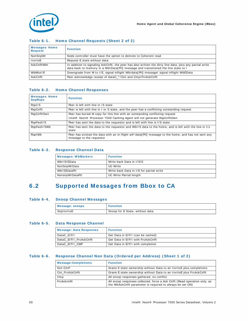
Home Agent and Global Coherence Engine (Bbox)
60 Intel® Xeon® Processor 7500 Series Datasheet, Volume 2
6.2 Supported Messages from Bbox to CA
NonSnpWr Node controller must have the option to demote to Coherent read
InvItoE Request E state without data
AckCnfltWbI In addition to signaling AckCnflt, the peer has also written the dirty line data, plus any partial write data back to memory in a WbIData[Ptl] message and transitioned the line state to I
WbMtoI/E Downgrade from M to I/E, signal inflight WbIdata[Ptl] message/ signal inflight WbEData
AckCnflt Peer acknowledge receipt of dataC_*/Gnt and Cmp/FrcAckCnflt
Table 6-2. Home Channel Responses
Messages: Home SnpRsps Function
RspI/S Peer is left with line in /S state
RspCnflt Peer is left with line in I or S state, and the peer has a conflicting outstanding request
RspCnfltOwn Peer has buried M copy for this line with an outstanding conflicting requestIntel® Xeon® Processor 7500 Caching Agent will not generate RspCnfltOwn
RspFwdI/S Peer has sent the data to the requestor and is left with line is I/S state
RspFwdI/SWb Peer has sent the data to the requestor and WbI/S data to the home, and is left with the line in I/s state
RspIWb Peer has evicted the data with an in-flight wb*data[Ptl] message to the home, and has not sent any message to the requestor
Table 6-3. Response Channel Data
Messages: WbMarkers Function
WbI/S/EData Write back Data in I/S/E
NonSnpWrData UC Write
WbI/EDataPtl Write back Data in I/E for partial write
NonsnpWrDataPtl UC Write Partial length
Table 6-4. Snoop Channel Messages
Message: snoops Function
SnpInvItoE Snoop for E State, without data
Table 6-5. Data Response Channel
Message: Data Responses Function
DataC_E/F/I Get Data in E/F/I (can be cached)
DataC_E/F/I_FrcAckCnflt Get Data in E/F/I with FrcAckCnflt
DataC_E/F/I_CMP Get Data in E/F/I with completion
Table 6-6. Response Channel Non Data (Ordered per Address) (Sheet 1 of 2)
Message:Completions Function
Gnt-CmP Grane E state ownership without Data to an InvItoE plus completions
Cnt_FrcAckCnflt Grane E state ownership without Data to an InvItoE plus FrcAckCnflt
Cmp All snoop responses gathered, no conflict
FrcAckcnflt All snoop responses collected, force a Ack Cnflt (Read operation only, as the WbAckCnflt parameter is required to always be set ON)
Table 6-1. Home Channel Requests (Sheet 2 of 2)
Messages: Home Request Function

Intel® Xeon® Processor 7500 Series Datasheet, Volume 2 61
Home Agent and Global Coherence Engine (Bbox)
6.2.1 Target Address Decoder
6.2.1.1 TAD Introduction
The Source Address Decoders (SADs) in the Cbox interleaves the system address space across the Bboxes. Because of this interleaving, the set of addresses entering a particular Bbox define an address space with holes. However, the local memory address space as viewed by the Mbox is one contiguous address space, so leaving the holes in the address space would result in lots of unused physical memory. It is the function of the Target Address Decoder (TAD) to glue the interleaved addresses from the CBox targeting a particular Bbox together into a contiguous address space. The main function of the TAD is to squeeze out the interleave bits which were actually used to determine the home node.
The interleaving across the Bboxes can be fine granular i.e. based on lower order address bits, large granular i.e. high order bits based, or even a combination of the two where fine granularity interleaving is enabled within a contiguous large granular address area (see Figure 6-2). Fine granular interleaving is limited to powers of two interleaving; this simplifies squeezing out the interleave bits out to a simple shift operation. Large granular interleaving is required for uneven memory configurations across Bboxes (e.g. 1 GB at one Bbox and 3 GB at the Bbox on another socket) or to expose a local address space to the OS. Local address accesses have lower latency.
Cmp_FwdCode Complete Request, forward the line in F
Cmp_fwdInvOwn Complete Request, forward the line in E/M, invalidate local copy
Cmp_FwdInvItoE Complete Request, Invalidate local copy, don’t forward any data
Table 6-6. Response Channel Non Data (Ordered per Address) (Sheet 2 of 2)
Message:Completions Function
Figure 6-2. Fine Granularity and Large Granularity Interleaving of the System Address Space

Home Agent and Global Coherence Engine (Bbox)
62 Intel® Xeon® Processor 7500 Series Datasheet, Volume 2
6.2.1.2 TAD Architecture
Figure 6-3 shows the TAD’s architecture. First a lookup is performed of the region the address belongs too. Then a base address is added to glue all the large granular regions into one contiguous local address space. If there is fine granular interleaving, the shifter will take care of gluing those addresses together into a contiguous address space. Note that eight large, granular regions are supported and each can have its own interleaving: no, 2-way, 4-way or 8-way interleave.
An access to non existing memory will cause an MCA, an error is logged in an error logging CSR. The Base Address Table contains (i) the base address to add (subtract) for each region, (ii) the shift amount to determine the number of interleave ways within each region. The region boundaries as well as the Base Address Table are CSR programmable.
The right hand side of Figure 6-3 supports the Mbox mapper. The memory controller (Mbox) mapper is what takes care of translating the local address into a memory address (row, column, bank, stacked rank, DIMM). The three programmable entries divide the global address space up in four other regions. This is required to simultaneously support four different DIMM organizations connected to the same Mbox. For each DIMM organization — for example, a single rank 1-GB DIMM, a dual rank 1-GB DIMM and a 2-GB DIMM are all different DIMM organizations — a separate map in Mbox is set up. Which map to use is determined by the TAD logic that generates the map_select signal. The map_select signal activates a certain map, in other words, maps a memory region to a particular set of DIMMs of the same organization. As shown, system address bits [43:30] determine the interleave, hence only large granular interleaving is supported across groups of different DIMM organizations.
Figure 6-3. Target Address Decoder

Intel® Xeon® Processor 7500 Series Datasheet, Volume 2 63
Home Agent and Global Coherence Engine (Bbox)
Figure 6-4. TAD’s Environment

Home Agent and Global Coherence Engine (Bbox)
64 Intel® Xeon® Processor 7500 Series Datasheet, Volume 2
How the TAD interfaces with Mbox is shown in Figure 6-4. The map_select is delivered one cycle ahead of the local address to the Mbox address mapper. This allows the Mbox mapper to be set up one cycle ahead of the local address arriving at Mbox. Delivery of the map_select signal one cycle ahead of the address enables pull in of the logical-dimm-to-physical-dimm mapping into the previous cycle.
6.2.1.3 TAD Programming Example
A system address interleave across four homes (Bboxes) is illustrated in Figure 6-5. In the example, the lower part of the system address space is large granular interleaved across the homes while the upper part is fine granular interleaved across the homes. The TAD mapping is shown for home2. All system addresses to other homes are squeezed out at home2 to generate the contiguous local address space. That contiguous local address space is then mapped by the Mbox map across the physical DIMMS present at home2. Which Mbox map to use is determined by the mapsel signal from the TAD. Given our latency optimized TAD implementation, the limits for the mapsel in the TAD refer to the system address space and not the local address space.
In the example (Figure 6-5), Mbox map0 maps the DIMM in physical DIMM position 2 to the lower local address space. Mbox map1 interleaves the two DIMMS in physical positions 1 and 0 to the upper local address space. Interleaving in general is good to prevent hot-spotting to one particular resource. The Mbox can interleave within a map and all DIMMS within a map should have the same organization (same number of row,
Figure 6-5. System Address Space Interleave Example

Intel® Xeon® Processor 7500 Series Datasheet, Volume 2 65
Home Agent and Global Coherence Engine (Bbox)
column, bank, rank bits). The dimm position referred to here is roughly the dimm slot on the system board. In some cases, a dimm slot might not contain a dimm and contain a repeater or logic analyzer module instead; in this case the dimm position is no longer equivalent to a slot number on the board; only DIMMS should be counted to determine the physical dimm position on the FBD chain of repeaters.
The TAD settings for the example of Figure 6-5 are shown in Table 6-7. The programming shown is for home2. DC stands for don’t care. The TAD table should be programmed starting at entry 0 and working one’s way up through consecutive entries. All limits that are programmed need to form a set of increasing (or equal) numbers. Access no non-existence memory will flag the illegal accesses exceeding the DIMM capacity at that home by logging the error in an errors CSR and generating an MCA. The 2’s complement of limit0’ means that the 2s complement of limit0 will be added to the system address, effectively subtracting limit0 from the system address.
Following check is a good control for whether the TAD accommodates all memory. For each entry x with NXM bit equal 0, calculate (limit(x)-limit(x-1))>>(interleave(x)-1). Add all these numbers up over all entries for which NXM equals 0. That total should be equal to the total dimm capacity at that home. If the total is larger than the dimm capacity then some part of the system address space is mapped to non-existent memory. It the total is less than the dimm capacity at that home then some dimm storage will go unused.
TAD reset values are chosen (see Table 6-8) such that firmware/bootware initially can use local memory without having to set up the TAD.
6.2.2 Tracker Allocation Modes
The tracker table keeps track of coherency state at the home node for each transaction in-flight in the system (that has touched the home node). For each transaction that a caching agent injects into the system a tracker entry was statically preallocated at the home. The tracker allocation mode determines the particular preallocation during
Table 6-7. Programming of TAD at home2
Table 6-8. TAD Reset Values
Entry Limit Base Address Interleave Shift NXM
0...7 all 1s 0 0 0

Home Agent and Global Coherence Engine (Bbox)
66 Intel® Xeon® Processor 7500 Series Datasheet, Volume 2
system initialization. The tracker allocation mode determines this statical partitioning of the tracker entries across the caching agents (Sboxes, IOHs, XNCs). There is a one-to-one correspondence between a Transaction ID (TID) originating from a particular caching agent (Node ID=NID) and a tracker entry. In effect, each of the 256 tracker entries is statically mapped to a Transaction ID (TID), Node ID (NID) couple and vice-versa.
6.2.2.1 The Tracker Modes
The tracker modes (0..3) are specifically chosen to support systems consisting of 4 gluelessly connected Intel® Xeon® processor 7500 sockets and 2, 4 IOH/XNC nodes (IOH = I/O Hub, XNC = eXternal Node Controller). Minimal support is also provided for 8 IOH/XNCs. Mode 5 has been added to support glueless 8 processor sockets and 4 IOH nodes. In general, 32 entries per IOH/XNC are supplied to mitigate bandwidth restrictions for the long latency operations typically associated with these nodes (except for the 8 IOH/XNCs configuration).
The supported tracker modes are listed in Table 6-9.
Note that some NID bits have to be zero or one.
Note: XNC NID assignment follows IOH’s NID, with NID<4> set 1.
6.2.3 NonSnoop Message Support
NonSnoop messages are supported by NonSnp* Intel QuickPath Interconnect encodings. NonSnp* is supported from caching agents.
Note: Intel® Xeon® Processor 7500 caching agents do not generate NonSnp* messages.
Each caching agent that relies on NonSnp* traffic to/from Bbox needs to be defeaturable such that it does not use NonSnp* transactions but promotes them to coherent ones instead. Hence NonSnp* support becomes a defeaturable performance optimization. In the following couple of sections, non-coherent is synonymous to NonSnp*.
Table 6-9. Tracker Allocation Modes
Mode Purpose Sboxes x #Entries IOH/XNCs x #Entries
0 4S HemiSphere + 4 IOH/XNC 4 x 32 4 x 32
1 4S HemiSphere + 2 IOH/XNC 4 x 48 2 x 32
2 4S Non-HemiSphere + 2 IOH/XNC 8 x 24 2 x 32
3 4S Non-HemiSphere + 4 IOH/XNC 8 x 16 4 x 32
4 8S HemiSphere + 4IOH/XNC 8 x 24 4x16
5 8S HemiSphere + 4IOH/XNC 4x32+4x16 4x16
Table 6-10. TID Assignment Restrictions
Mode Configuration Sboxes IOH/XNCs
0 4S HemiSphere + 4 IOH/XNC TID [0...31]
1 4S HemiSphere + 2 IOH/XNC TID [0...47] TID [0...31]
2 4S Non-HemiSphere + 2 IOH/XNC TID [0...23] TID [0...31]
3 4S Non-HemiSphere + 4 IOH/XNC TID [0...15] TID [0...31]
5 8S HemiSphere + 4 IOH/XNC TID [0...31] + TID[0..15] TID [0...31]

Intel® Xeon® Processor 7500 Series Datasheet, Volume 2 67
Home Agent and Global Coherence Engine (Bbox)
The NonSnp* travel on the same virtual channels the snoopy traffic travels on (NonSnpRd and NonSnpWr on HOM, NonSnpWrDat and NonSnpWrDataPtl on DRS) as opposed to the Nc* Intel QuickPath Interconnect transactions which used separate NCB/NCS virtual channel. Hence buffering for the latter is no longer required in Bbox.
The NonSnp flows are illustrated in Figure 6-6. Partial-writes flows are not shown.
6.3 Error Handling
6.3.1 Parity Errors
Parity error from internal structures is logged in the Error Status Register.
Parity errors do not change any other behavior in the Bbox except for the fact that all outgoing packets from the Bbox, whether related to the error or not, will have their viral bits set.
Figure 6-6. Intel QuickPath Interconnect NonSnp Flows in Bbox
CA0 CA1 HA
mem rd
mem ack
NonSnpRd
DataC_I_Cmp
Bbox Non-Snoop Read Flows
mem rd
mem ack
NonSnpRd
DataC_I
Cmp
CA0 CA1 HA
Bbox Non-Snoop Write -Back Flows
mem wr
mem ack
NonSnpWrData
Cmp
NonSnpWr
vic2vic
v2v ack
NonSnpWr
Cmp
mem wr
mem ack
NonSnpWrData

Home Agent and Global Coherence Engine (Bbox)
68 Intel® Xeon® Processor 7500 Series Datasheet, Volume 2
6.3.2 Time-outs
A timer in each Tracker File entry is used to track in-flight messages in the network. At the beginning of each transaction initializes the timer with a value taken from a list of events. The time-out value for each event type is programmable through the Time-out Register.
A free running time-out counter requests a timer sweep at programmable intervals. If the timer value decrements to zero then a time-out has occurred.
The list of time-out values is programmable (by CSR), and contains eight 8-bit values. This allows different time-out values for different transactions, with the decision of which time-out value to use being set. At the receipt of the message being timed, the NSL writes the entry to be invalid.
The free running 30-bit counter increments every SysInt tick. The tctl field of the CONFIG register selects whether bit 30,27,24 or 21 is used to initiate a scan of the TOF. The following table indicates the Range and Granularity of the 8-bit time-out value based on the selection of tctl in CONFIG. The number of cycles must be scaled by the SysIntClk frequency to derive absolute times.
Notes:1. This includes all NcMsgS messages except NcMsgSLock, NcMsgSStopReq1, and NcMsgSStopReq2.2. The Intel® Xeon® Processor 7500 CA supports time-out levels 1,3, and 4. 3. The Intel® Xeon® Processor 7500 HA supports time-out levels 2.4. Time-out level 5,6 are used for Lock operations.
§
Table 6-11. Time-out Range and Granularity
tctl=11 tctl=10 tclt=01 tctl=00
Range 25.6G-1G cycles 3.2G-128M cycles 4096M-16M cycles 512M-2M cycles
Granularity 1G cycles 128M cycle 16M cycles 2M cycles
Table 6-12. Intel® Xeon® Processor 7500 Transaction Time-out Levels
Transaction Time-Out
LevelIntel® QuickPath Interconnect Request Message Class
1 WbMto*, Wb*Data*, NonSnp*, *FrcAckCnflt, Cmp_Fwd* HOM, DRS, NDR
2 Rd*, Snp*, and InvItoE at home HOM, SNP
3 Rd*and InvItoE at requestor, NcWr, WcWr, NcP2PB, NcMsgB, IntPrioUpd, IntPhysical, IntLogical
HOM, NCB
4 NcRd*, NcP2PS, NcCfg*, NcIO*, IntAck, NcMsgSa NCS
5 NcMsgSStopReq1, NcMsgSStopReq2 NCS
6 NcMsgSLock NCS

Intel® Xeon® Processor 7500 Series Datasheet, Volume 2 69
Intel QuickPath Interconnect Router (Rbox)
7 Intel QuickPath Interconnect Router (Rbox)
Each Intel® Xeon® processor 7500 series has a Rbox router that implements the Intel QuickPath Interconnect and Routing layers.
Figure 7-1 provides an Intel® Xeon® Processor 7500 block diagram including the Rbox.
7.1 Rbox OverviewThe Rbox is a 8-port switch/router implementing the Intel QuickPath Interconnect and Routing layers. The Rbox facilitates Intel QuickPath Interconnect communication with both the on-die and off-die agents. The internal Intel QuickPath Interconnect agents include the Bbox0/1 (ports 4/7), Ubox (shared port with Bbox1 - port 7) and Sbox0/1 (ports 2/6). The ports 0,1,4,5 are connected to external Intel QuickPath Interconnect agents. The Rbox consists of eight identical ports and a crossbar that connects the ports together.
7.1.1 Rbox Block Diagram
Figure 7-2 shows the Rbox Block Diagram.
Figure 7-1. Intel® Xeon® Processor 7500 Block Diagram
Core 2
Core 1
Core 3
Core 4
Core 5
Core 6
Core 7
Core 8
Cbox (LLC Coherence Engine)
Rbox (Router)
24M Last Level Cache (L3 Cache)
Sbox (Caching Agent 2)
Bbox (Home
Agent 1)
Bbox (Home
Agent 2)
Mbox (Memory
Controller)
Mbox (Memory
Controller)
Pbox (Physical
Layer)
Pbox (Physical
Layer)
Sbox (Caching Agent 1)
Pbox (Physical
Layer)
Pbox (Physical
Layer)
Pbox (Physical
Layer)
Pbox (Physical
Layer)
4 Intel® QPI links
Dual Intel® SMI Channels
Dual Intel® SMI Channels
Wbox (Power Controller)
Ubox (System Config
Controller)

Intel QuickPath Interconnect Router (Rbox)
70 Intel® Xeon® Processor 7500 Series Datasheet, Volume 2
7.1.2 Router Port Connection
The router ports connect to internal and package physical ports via following connections:
Router Port 0 <- > Processor package Intel QuickPath Interconnect port 1
Router Port 1<- > Processor package Intel QuickPath Interconnect port 0
Router Port 2<- > Processor CA/Sbox 0
Router Port 3<- > Processor HA/Bbox 0
Router Port 4<- > Processor package Intel QuickPath Interconnect port 2
Router Port 5<- > Processor package Intel QuickPath Interconnect port 3
Router Port 6<- > Processor CA/Sbox 1
Router Port 7<- > Processor Ubox, HA/Bbox 1
7.2 Functional OverviewThe following is a high-level description of a packet traveling through the Rbox:
• Input Port (IPR): An Intel QuickPath Interconnect packet is received at the Input Port. As the packet arrives CRC is checked and ECC is generated. Packet Destination Node ID (DNID) is used to index into a routing table to determine the VN(s) and Output Port(s) the packet can be forwarded to, towards the final destination.
• Arbitration Logic: Selects from queued packets, single winner from all queue arbitrations will be selected to the output Port.
• CrossBar: The crossBar can be viewed as a 7:1 Mux.
Figure 7-2. Rbox Block Diagram
Input/Output Port0(Pbox0)
Left X B
ar (H
alf)
DE
BU
G
P0 Global Arb
Input/Output Port1(Pbox1)
Input/Output Port2(Sbox0)
Input/Output Port3(Bbox0)
Port0 Local Arb
Port1Local Arb
Port2 Local Arb
Port3 Local Arb
P1 Global Arb
P2 Global Arb
P3 Global Arb
P4 Global Arb
P5 Global Arb
P6 Global Arb
P7 Global Arb
Performance Monitor
MC_BANK
DEBUG
Port4 Local Arb
Port5Local Arb
Port6 Local Arb
Port7 Local Arb
Right X
Bar
(Half)
Input/Output Port4(Pbox4)
Input/Output Port5(Pbox5)
Input/Output Port6(Sbox1)
Input/Output Port7(U/Bbox1)
DE
BU
G
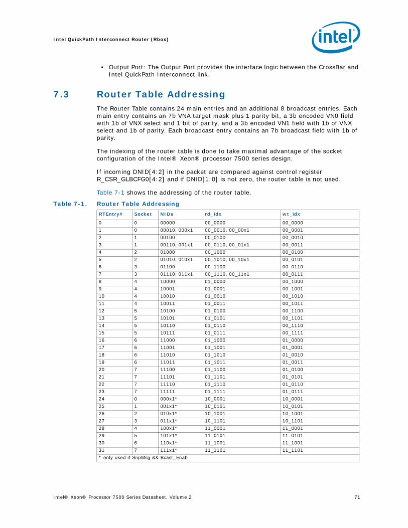
Intel® Xeon® Processor 7500 Series Datasheet, Volume 2 71
Intel QuickPath Interconnect Router (Rbox)
• Output Port: The Output Port provides the interface logic between the CrossBar and Intel QuickPath Interconnect link.
7.3 Router Table AddressingThe Router Table contains 24 main entries and an additional 8 broadcast entries. Each main entry contains an 7b VNA target mask plus 1 parity bit, a 3b encoded VN0 field with 1b of VNX select and 1 bit of parity, and a 3b encoded VN1 field with 1b of VNX select and 1b of parity. Each broadcast entry contains an 7b broadcast field with 1b of parity.
The indexing of the router table is done to take maximal advantage of the socket configuration of the Intel® Xeon® processor 7500 series design.
If incoming DNID[4:2] in the packet are compared against control register R_CSR_GLBCFG0[4:2] and if DNID[1:0] is not zero, the router table is not used.
Table 7-1 shows the addressing of the router table.
Table 7-1. Router Table Addressing
RTEntry# Socket NIDs rd_idx wt_idx
0 0 00000 00_0000 00_0000
1 0 00010, 000x1 00_0010, 00_00x1 00_0001
2 1 00100 00_0100 00_0010
3 1 00110, 001x1 00_0110, 00_01x1 00_0011
4 2 01000 00_1000 00_0100
5 2 01010, 010x1 00_1010, 00_10x1 00_0101
6 3 01100 00_1100 00_0110
7 3 01110, 011x1 00_1110, 00_11x1 00_0111
8 4 10000 01_0000 00_1000
9 4 10001 01_0001 00_1001
10 4 10010 01_0010 00_1010
11 4 10011 01_0011 00_1011
12 5 10100 01_0100 00_1100
13 5 10101 01_0101 00_1101
14 5 10110 01_0110 00_1110
15 5 10111 01_0111 00_1111
16 6 11000 01_1000 01_0000
17 6 11001 01_1001 01_0001
18 6 11010 01_1010 01_0010
19 6 11011 01_1011 01_0011
20 7 11100 01_1100 01_0100
21 7 11101 01_1101 01_0101
22 7 11110 01_1110 01_0110
23 7 11111 01_1111 01_0111
24 0 000x1* 10_0001 10_0001
25 1 001x1* 10_0101 10_0101
26 2 010x1* 10_1001 10_1001
27 3 011x1* 10_1101 10_1101
28 4 100x1* 11_0001 11_0001
29 5 101x1* 11_0101 11_0101
30 6 110x1* 11_1001 11_1001
31 7 111x1* 11_1101 11_1101
* only used if SnpMsg && Bcast_Enab

Intel QuickPath Interconnect Router (Rbox)
72 Intel® Xeon® Processor 7500 Series Datasheet, Volume 2
7.3.1 Entry Build
Broadcast (BC). A snoop packet with DNID(0) = 1 and broadcast_ena = 1 will cause the RTA to read from the broadcast entries. Broadcast can be done both on VNA and VNN.
SB Routing Table. The value from this table is fetched by examining the message class, opcode, DNID[1:0], RTID[0]. The output is one-hot 9b mask that targets one of the Sbox/Bbox/Ubox. It is used when global/local node IDs match, and the DNID [1:0] is not 0b00:
Table 7-2 shows the SBU route table.
7.3.2 RTA
The router table array (RTA) holds information that will inform the arbiter about which way a particular packet may route. The RTA is generally set up before operation begins, and not changed during run time. There are 24(plus 8 broadcast) entries in the router table, each entry being 15b of data and 3b of parity protection. The RTA contains one read port and one write port.
Packets may hop between two non-adaptive virtual networks. With 8 total Rbox ports, any one port may route to the other remaining 7 ports.
The entry data is 15b: 7 + (1+3) + (1+3)
Table 7-3 shows the Router Table Entry.
Each subsection may be written independently or in any permutation into the RTA using a write to a CSR with the following format:
Table 7-2. SBU Route Table
DNID[1:0] Target on Global/Local NID Match
0b00 IOH, route using RTA data
0b01 S/B 0, use SB table
0b10 Ubox use SB table
0b11 S/B 1, Use SB table
Table 7-3. Router Table Entry
Subsection Bit Range Use
VNA Parity 17 Even Parity for VNA route mask (bits 16:10)
VNA 16:10 Adaptive route bit mask. One bit per output port. Multiple bits can be set.
VN1 Parity 9 Even Parity bit for 8:5 (VN1 encoded port and output VN for packet incoming on VN1)
VN1 8 Output VN for incoming packet on VN1
7:5 Encoded deadlock free output port for packet incoming on VN1
VN0 Parity 4 Even Parity bit for 3:0 (VNO encoded port and output VN for packet incoming on VNO)
VN0 3 Output VN for incoming packet on VN0
2:0 Encoded deadlock free output port for packet incoming on VN0
Table 7-4. RTA CSR Write Format (Sheet 1 of 2)
Bit Format
20 VN1_Write_En[0]
19 VN0_Write_En[0]
18 VNA_Write_En[0]
17 VN1_Parity[0]

Intel® Xeon® Processor 7500 Series Datasheet, Volume 2 73
Intel QuickPath Interconnect Router (Rbox)
7.4 Rbox MC BankThe processor Rbox includes two sets of MC bank registers. One set of the registers handles errors from ports 0, 1, 2 and 3(Left). Another set handles error from ports 4, 5, 6 and 7 (Right). Each port drives the error event signals (MCA error event bundle) and ORs the port specific error event. MCA error event bundle contains 12 bits individual error events and 4 bits (ERR_SRC) indicating the source port signaling one of 12 error events. Rbox MC bank register supports MC_MISC to indicate source port signaling error.
The R-box has two OS specific error signals – uncorrectable/CMCI errors and three BIOS specific error indications – fatal, uncorrectable and correctable. The R-box has no recoverable errors.
Single bit ECC error at OPR is the only correctable ECC error and OS CMCI. Rbox doesn’t have any recoverable errors, the MCA signal for recoverable error is just passed through to Sbox. Poison bit detection at OPR is an un-correctable error. Fatal error are all types of errors except for single bit ECC and poison at OPR. OS hard MCA condition is true for all events except for single bit ECC at OPR.
R-box left MCA bank hooks into the S0 MCA bank and the right MCA bank hooks into the S1 MCA bank. S0, S1, W and U boxes MCA errors are all ORed in the Ubox global MCA logic and reported to the OS/BIOS.
7.4.1 BIOS Error CSRs
In addition to the MCA banks which generate OS required error flags and BIOS flags for four different classes of errors as described in the section above, The R-box also has four CSRs that log several of these errors for interrupt generation through BIOS. These sets of CSRs are instantiated per port and are named *IPER0/1 and *OPER0/1 as described in the CSR section of the R-box. The details of each bit, the corresponding error and their set/clear functionality is explained in the CSR section. Note that The MCA/BIOS error-flag signalling is independent of these CSRs in that these CSR values
16 VN0_Parity[0]
15 VNA_Parity[0]
14 VN0_VN_Sel[0]
13 VN0_Encoded[2]
12 VNA_BitMask[6]
11 VN0_Encoded[1]
10 VNA_BitMask[5]
9 VN0_Encoded[0]
8 VNA_BitMask[4]
7 VN1_VN_Sel[0]
6 VNA_BitMask[3]
5 VNA_BitMask[2]
4 VN1_Encoded[2]
3 VNA_BitMask[1]
2 VN1_Encoded[1]
1 VNA_BitMask[0]
0 VN1_Encoded[0]
Table 7-4. RTA CSR Write Format (Sheet 2 of 2)
Bit Format

Intel QuickPath Interconnect Router (Rbox)
74 Intel® Xeon® Processor 7500 Series Datasheet, Volume 2
are directly set by the R-box and read by BIOS while the error-flags are propagated to the U-box where a specific MCA-control/IDR MSR for each type of flag will control the signalling of an OS action or BIOS interrupt.
7.4.2 Performance Monitor
Rbox implements sixteen sets of performance (PMON) counters. Half of the counter sets (control and counter registers) – 0,1,2,3,4,5,6,7 – are dedicated events from for ports 0,1,2,3(Left) and the other half set of the counter sets – 8,9,10,11,12,13,14,15 – are for events from ports 4,5,6,7 (Right).
There are 2 CSRs/port – *IPERF0 and IPERF1 that set RIX performance counter event selection configuration. and control the selection of events for counting in the IPR and OPR sections of the design. Setting a particular field in the IPERFn CSR causes the associated event to be propagated through the event OR tree to the performance Counters. General usage would be to have only one field set and hence only one event being allowed to propagate. Thus 2 events can be finally selected across these 2 CSRs/port for RIX.
7.4.3 External Reset Inputs
The processor resets (cold, warm) are directly driven to Rbox. The warm reset clears internal states. The full reset (cold reset) is applied to all reset-able elements.
§

Intel® Xeon® Processor 7500 Series Datasheet, Volume 2 75
System Configuration Controller (Ubox)
8 System Configuration Controller (Ubox)
The Intel® Xeon® processor 7500 series contains a system configuration controller (Ubox).
Figure 8-1 provides an Intel® Xeon® Processor 7500 block diagram including the Ubox.
8.1 IntroductionThe Ubox is a system configuration agent organized as a number of modular utilities. Some of the different utilities include Intel System Management interface (Intel SMI), scratch registers, test and set registers, Flash ROM interface, CSR bridge, interval timer, VLW, Lock, exception, and interrupts. It receives and sends Intel QuickPath Interconnect transactions to the rest of the local processor and through the Rbox port shared with a Bbox.
8.1.1 Feature List
The processor Ubox provides the following System Configuration and Management features:
• Processes incoming requests from any on- or off-chip Intel QuickPath Interconnect agent targeted for one of the Ubox Utilities.
Figure 8-1. Intel® Xeon® Processor 7500 Block Diagram
Core 2
Core 1
Core 3
Core 4
Core 5
Core 6
Core 7
Core 8
Cbox (LLC Coherence Engine)
Rbox (Router)
24M Last Level Cache (L3 Cache)
Sbox (Caching Agent 2)
Bbox (Home
Agent 1)
Bbox (Home
Agent 2)
Mbox (Memory
Controller)
Mbox (Memory
Controller)
Pbox (Physical
Layer)
Pbox (Physical
Layer)
Sbox (Caching Agent 1)
Pbox (Physical
Layer)
Pbox (Physical
Layer)
Pbox (Physical
Layer)
Pbox (Physical
Layer)
4 Intel® QPI links
Dual Intel® SMI Channels
Dual Intel® SMI Channels
Wbox (Power Controller)
Ubox (System Config
Controller)

System Configuration Controller (Ubox)
76 Intel® Xeon® Processor 7500 Series Datasheet, Volume 2
• Facilitates Master access to Uncore CSRs via JTAG and PECI
• SMBus Master for access to memory registers.
• Uncore, Firmware Semaphore and Scratch Registers.
• Protection Architecture features for Uncore CSR accesses.
• Overall System Configuration support via Uncore CSR accesses.
• Firmware time based interrupt generation mechanism.
• Broadcasting of Interrupts, Special Cycles, VLW and Lock messages to both internal cores and external sockets
• Chip Interrupt Management (collection, prioritization and redirection from/to on-die cores)
• IA-32 Bus Lock flow management.
• Off-Chip Flash ROM Interface
• MCA Support
• System exception logging and interrupt signalling
8.1.2 Out-of-Band Requests
System management controllers can read and write CSRs through the PECI or JTAG ports in the Ubox System Management Interface. Accesses made through this mechanism are referred to as out-of-band. Although this mechanism does not give system management controllers direct access to the MSRs in the cores, it does give them the ability to signal SMIs to a core, and an Intel SMI handler could be written to move data between core registers and CSRs that are directly accessible via out-of-band accesses. Some uncore MSRs (perfMon and MCBank) are accessible by PECI but are read only.
8.1.3 Intel® QuickPath Interconnect Port Sharing with Bbox
UBox and BBox share the same router port and BBox is the arbitration master. When UBox has something to send, it requests a slot (NDR, DRS, OTHER, NONE).
8.1.4 PECI Interface
PECI requests are sent to Wbox to Ubox to access the uncore CSRs through a bit serial interface between them. Wbox asserts a SHIFT signal when it is ready to send in a new transaction. The shift signal is immediately followed by 61 bits of data that is shifted into the primary register in Ubox. The shift signal is deasserted after 61 bits of data is shifted in. Wbox then asserts the start signal to inform the Ubox that a new transaction is ready and processing can begin, and the Ubox captures the 61 bits of data in the shift register and begins processing the transaction. See PECI / TAP register format in Table 8-1.
Table 8-1. PECI / TAP CSR Rd/Wt Format (Sheet 1 of 2)
Bit# Description
60 RW (0=Write, 1=Read)
59:40 Addr<19:0>
39:36 Byte_enable <3:0>
35:04 Data <31:0>
03 Rsvd

Intel® Xeon® Processor 7500 Series Datasheet, Volume 2 77
System Configuration Controller (Ubox)
8.2 Intel QuickPath Interconnect Transactions
8.2.1 Incoming Intel QuickPath Interconnect Requests
Any on-chip or off-chip agent including the processor core can send Intel QuickPath Interconnect requests to the Ubox.
The Ubox supports the following incoming Intel QuickPath Interconnect requests:
• NcRd, NcRdPtl (full, partial cache-line non-coherent read)
• NcWrPtl (partial cache-line non-coherent write)
• NcMsgS (Special Cycles (Invd_Ack, WbInvd_Ack), Stop Req1, Stop Req2, Start Req1, ProcLock, ProcSplitLock, Quiesce, Unlock)
• NcMsgB (VLW, EOI, Start Req2)
• IntPhysical, IntLogical, IntPrioUpd
• NcCfgRd, NcCfgWr (new SCA CFG read and write)
These requests access and control the Utilities. The Utility to which the backbone delivers an NcRd, NcRdPtl, NcWrPtl, NcCfgRd, NcCfgWr, and incoming request depends on the packet address which is compared to the Ubox Target Address Map (TAM). Non-Intel QuickPath Interconnect requests are treated as NcCfgRd/Wr.
Other incoming messages target specific utilities depending on the request message type. Some messages are treated differently depending on whether the source was an local core or a remote socket. Requests that are broadcast to other CPU sockets will broadcast only to local cores if the source is remote; requests that are sent from local cores but not broadcast to other CPUs (that is, are sent only to IO agents) are just completed.
8.2.2 Outgoing Intel QuickPath Interconnect Requests/Responses
The Ubox is able to generate the following Intel QuickPath Interconnect request or response transactions:
• NcMsgS (StopReq1, ProcLock, ProcSplitLock, Quiesce, InvAck, WB_InvAck, Unlock)
• NcMsgB (VLW, EOI, StartReq2)
• IntPhysical
• IntLogical
• IntPrioUpd
• Cmp
• CmpD
• DataNc
02 Rsvd
01 Blocked
00 Polling Bit (1=done)
Table 8-1. PECI / TAP CSR Rd/Wt Format (Sheet 2 of 2)
Bit# Description
System Configuration Controller (Ubox)
78 Intel® Xeon® Processor 7500 Series Datasheet, Volume 2
Some of these transactions are spawned, broadcast transactions, and use the following broadcast lists when broadcasting to external sockets:
• InvAck, WB_InvAck, SpcCyc target list (STLR)
• IntPhysical, IntLogical – IPI target list (ITLR)
• EOI target list (ETLR)
• IntPrioUpd – XTPR target list (XTLR)
• ProcLock/ProcsplitLock/Quiesce/Unlock – Lock target list (LTLR) – this must have only a single bit set, corresponding to the Quiesce Master
Each of these lists (except Lock) has an accompanying target count that must match the number of bits set in the target list. The lock target count is fixed at 1.
8.3 Platform Setup for Broadcast TransactionsThis section describes how the platform target registers are programmed for broadcast transactions. For each type of broadcast message, two registers need to be configured. The first register is a Target List Register that is specific to each message type. Each is programmed as a multi-hot 32-bit vector where each bit position refers to the node-id of a target (except the Lock Target Register must have only one bit set, corresponding to the nodeID of the Quiesce Master). The UBox broadcasts to a target only if the corresponding target bit in this register is set to 1.
The second register that needs to be programmed is the Target Count Register. For each Target List Register (except for Lock), there is a corresponding 6-bit field in the Target Count Register that specifies the number of targets. It’s important for software to maintain consistency between each Target List Register and the corresponding field in Target Count Register; a hang may occur if a broadcast of that type is made while they are inconsistent. The order of programming should be Target List Register first followed by Target Count Register. Both have reset values equal to 0.
8.4 Firmware RegionThe Firmware Region provides address space for reading the off-chip flash ROMs. The region consists of multiple 16 MB that provide equivalent, aliased access to the ROMs. One of these stripes begins at 4 GB – 16 MB and coincides with the Firmware Region defined by the IA-32 architecture. The standard Intel QuickPath Interconnect address map allows any Intel QuickPath Interconnect component to map the IA-32 Firmware Region to the Ubox of any processor component in the system and thus to the flash ROMs directly connected to it.
8.5 Off-Chip ROM InterfaceThe Off-Chip Flash ROM Interface allows the processor to be connected to as many as 4 SPI Flash ROMs. These non-volatile ROMs are intended to be used to store firmware code and error logs. The ROMs can be read via reads to the Firmware Region of the Ubox target address space and accessed in other ways via the interface CSRs. The interface provides a bridge between the system/utilities management controller and the ROMs.

Intel® Xeon® Processor 7500 Series Datasheet, Volume 2 79
System Configuration Controller (Ubox)
8.5.1 FLASHROM_CFG
The FLASHROM_CFG pins are input pins to the processor used when a flash ROM is connected directly to the processor. The strapping pins identify what type of flash ROM configuration is used.
FLASHROM_CFG[1:0] describes the size of the device(s) attached. If multiple devices are attached then they are assumed to all be of equal size.
• 00: 1 MB
• 01: 2 MB
• 10: 4 MB
• 11: 8 MB
FLASHROM_CFG[2] selects between two address mappings for each specific ROM capacity, specifically, the pin swaps the mapping of devices 0/1 with 2/3.
• 0: devices 0/1 map to highest addresses
• 1: devices 2/3 map to highest addresses
These pins are ignored after reset removal.
The Intel® Xeon® processor 7500 series process technology does not support the ROM voltage levels. An off-package buffering solution is needed between the processor and SPI Flash ROM pins. Table 8-2 shows the processor flash ROM interface pins.
Figure 8-2. Flash ROMs Connected to Intel® Xeon® Processor 7500 Series
BMP FRCS[0] FRCS[1]FRCS[2]FRCS[3]
FRCFRDOFRWP
FRDI
Buffers
ROM 0
ROM 1
ROM 2
ROM 3
System Configuration Controller (Ubox)
80 Intel® Xeon® Processor 7500 Series Datasheet, Volume 2
For convenience in the discussions below, ROM k will be defined as the ROM connected to chip select k, FLASHROM_CS[k]_N. The initial configuration pins, FLASHROM_CFG[2:0], are not connected to the ROMs and specify an initial mapping of the ROMs to the Firmware Region as discussed below.
8.5.2 Interface Sequences
The Flash ROM Interface accesses one device at a time. When it accesses a device it executes an interface sequence using pins FLASHROM_CS[3:0]_N, FLASHROM_CLK, FLASHROM_DATO, and FLASHROM_DATI. The waveforms of a generalized sequence is illustrated in Figure 8-3.
Table 8-2. Intel® Xeon® Processor 7500 Series Flash ROM Interface Pins
Pin Name(s) Number Type Function
FLASHROM_CFG[2:0] 3 In-Only Initial configuration
FLASHROM_CS[3:0]_N 4 Out-Only Active-low ROM chip selects
FLASHROM_CLK 1 Out-Only Clock
FLASHROM_DATO 1 Out-Only Serial data from processor to ROMs
FLASHROM_DATI 1 In-Only Serial data from ROMs to processor
FLASHROM_WP_N 1 Out-Only ROM write protect
Figure 8-3. Generalized Interface Sequence
Shaded blocks indicated input or output data bits. Xsindicate undefined, ignored levels.
FRCS#[k ]
FRC
FRDO
FRDI
Last Output Data Bit
Last Input data Bit
First Output Data Bit
First Input data Bit
X
X X
Intel® Xeon® Processor 7500 Series Datasheet, Volume 2 81
System Configuration Controller (Ubox)
When idle, FRCS[3:0] and FRC are inactive-high, FRDO is driven, but undefined, and no ROM drives FRDI. When a sequence is executed to access device k, the interface first drives FRCS[k], the chip select for the device, active-low to enable the device. At that time, the device starts driving FRDI with an undefined level. Then, the interface drives N low-going pulses on FRC, the clock line, producing a temporary clock waveform. The value of N depends on the particular sequence, but is always a multiple of 8. The interface drives an output data bit on FRDO off of each falling transition of the clock. N output data bits are driven, one for each low-going clock pulse. The selected device follows suit and drives an input data bit on FRDI off of each falling edge of the clock as well. The interface samples the incoming data bits at the next falling edge, because the round-trip latency is too long to allow sampling at the rising edge. See Figure 8-3 for more detailed timing. N input data bits are sampled. Depending on the particular sequence, not all of the output or input data bits are used by the receiving device. Finally, the interface drives FRCS[k] inactive-high to disable the ROM. This transition causes the ROM to stop driving FRDI with the last input data bit.
Note that bits are driven and received MSB first, but from low to high byte addresses. Therefore, data in the SDRx registers from indirect reads will be aligned such that data at the address sent in the command will be at the higher end of SDR1 or SDR0 register, and the last byte read (at the higher address) will be in the lowest byte of SDR0. Likewise, indirect writes must re-order bytes being sent such that lower addresses (and the opcode, if appropriate) are at higher byte positions in SDR1 (and SDR0, for longer writes). For example, a fast read command would have 0x0B,AH,AM,AL in SDR1, and zeroes in SDR0. If 4 bytes were returned, they would be shifted into SDR0 so that its contents contained A,A+1, A+2, A+3, which would need to be byte reversed before being used.
Direct reads will always read 8 bytes at a time, and will reverse the bytes when read, so will always be aligned correctly for the flit format.
8.5.3 Interface Clock
When a sequence is executed, the clock is cycled for a number of times as required by the particular sequence. The clock is cycled at a frequency fixed by the same physical fuse that controls the BRI interface (default is 33.33 Mhz, defeature to 16.67 Mhz).
Table 8-3 lists the initial flash ROM mapping.

System Configuration Controller (Ubox)
82 Intel® Xeon® Processor 7500 Series Datasheet, Volume 2
Pins FRCFG[1:0] imply the total ROM capacity, while FRCFG[2] selects between two mappings for each specific ROM capacity (specifically, FRCFG[1:0] selects which two contiguous address bits are used to decode chip select, ranging from PA<23> to PA<20>, and FRCFG[2] swaps the mapping of devices 0/1 with 2/3). The device select address bits, and any above them, are ignored by the flash devices of the implied size, which creates multiple copy aliasing in smaller devices. Note that if the 8Mbyte size is selected, only two flash devices can be addressed at a time, selected by PA<23>; another two can be swapped in by changing FRCFG[2].
This initial mapping always points to device 0 for the inital BIOS boot vector. The mapping need only be valid for the ROMs that need to be accessed for this purpose. Two mappings are provided for each ROM capacity to allow the platform to select between two copies of firmware (so firmware can execute from either of two devices while programming another). The platform is responsible for dynamically selecting which of the two copies to use (based on where in the flash update flow the platform is). There is no checking for accesses to non-existent flash devices; the behavior is unpredictable.
Pins FRCFG[2:0] are ignored after reset removal.
Table 8-3. Initial Flash ROM Mapping
FLASHROM_CFG[2:0] at reset removal (binary) 000 001 010 011 100 101 110 111
Implied ROM capacity (MB) 1 2 4 8 1 2 4 8
Offset range inside Firmware Region to flash device mapping (hex)
Fxxxxx 0 0 0 0 2 2 2 2
Exxxxx 1 0 0 0 3 2 2 2
Dxxxxx 2 1 0 0 0 3 2 2
Cxxxxx 3 1 0 0 1 3 2 2
Bxxxxx 0 2 1 0 2 0 3 2
Axxxxx 1 2 1 0 3 0 3 2
9xxxxx 2 3 1 0 0 1 3 2
8xxxxx 3 3 1 0 1 1 3 2
7xxxxx 0 0 2 1 2 2 0 3
6xxxxx 1 0 2 1 3 2 0 3
5xxxxx 2 1 2 1 0 3 0 3
4xxxxx 3 1 2 1 1 3 0 3
3xxxxx 0 2 3 1 2 0 1 3
2xxxxx 1 2 3 1 3 0 1 3
1xxxxx 2 3 3 1 0 1 1 3
0xxxxx 3 3 3 1 1 1 1 3

Intel® Xeon® Processor 7500 Series Datasheet, Volume 2 83
System Configuration Controller (Ubox)
8.5.4 Firmware Region Reads
Reads to the Firmware Region of the Ubox target address space are serviced by this interface. Naturally aligned 8-byte, and 64-byte reads are supported. If 8, 16 or 64 bytes are requested, then the requested number of bytes are read from a ROM and returned. Reads of less than 8-byte can be made, but the interface ignores the length and will read and return the aligned 8 bytes. 32-byte reads are not supported. The ROM accessed is determined by:
~((1,PA<23:20>) >> FRCFG<1:0> ) XOR (FRCFG<2>,0) AND 3
Address bits 23:0 of the request are delivered to the ROM to specify the initial byte to be read. The ROMs discard high-order address bits that are not needed to specify a byte address within the ROM. Sequences that extend beyond a device will wrap around on the currently selected device. For each read, the interface executes a single interface sequence to the ROM accessed as defined above. The number of low-going clock pulses driven for the sequence is N = 32 + 8 + N_dat, where 8 is the number of dummy bits required for a fast read and N_dat is 8 times the number of data bytes requested by the read. In the case of a masked 8-byte read, N_dat = 64 regardless of the byte mask. The first 8 data bits driven out in the sequence is the fast read opcode (specified by FRCR.roc[7:0]). These bits are driven out starting with bit 7 and working down to bit 0. The next 24 data bits driven out are bits 23:0 of the request address (bits 2:0 are always 0). These bits are driven out starting with bit 23 and working down to bit 0. The remaining 8 + Ndat data bits driven out are 0. The first 32 + 8 data bits sampled are ignored (corresponding to command, address, and dummy bytes). The remaining N_dat data bits sampled are used for the data to be returned in the response for the request. The data is sampled byte by byte starting with the low byte and working up to the high byte. Within each byte, the bits are sampled starting with bit 7 and working down to bit 0.
In order to successfully boot from the Firmware Region, the flash ROMs employed must support the 0x0B FastRead opcode, with a single dummy byte at least 33.33 Mhz.
8.5.5 Firmware Region Writes
Writes to the Firmware Region of the Ubox target address space are handled by the Ubox TAM. For each of these requests, the interface returns a successful completion without taking any other action. The write data is ignored and no sequence is executed on the interface pins.
8.5.5.1 Programmed SPI Sequences
Other interface sequences can be delivered to the flash ROMs using six CSRs in the interface—
• Flash ROM Programmed Sequence Interface Register (FRPSIR)
• Flash ROM Programmed Sequence Execution Register (FRPSER)
• Flash ROM Programmed Sequence Data Registers 0 and 1 (FRSDR[1:0])
• Flash ROM Programmed Device Select Register (FRDSR)
• Flash ROM Programmed Control Register (FRPCR)

System Configuration Controller (Ubox)
84 Intel® Xeon® Processor 7500 Series Datasheet, Volume 2
Sequences delivered using these CSRs will be called programmed sequences. These sequences can be used to:
• Read a manufacturer ID, part ID and other device information from the ROM
• Read and write a status register in the ROM.
• Erase all or part of the ROM.
• Program (write) all or part of the ROM (once erased).
To execute a programmed sequence, the FRPSIR.a must first be written to select the ROM to be accessed. The value written to FRPSIR.a[23:20] together with FRCFG selects the ROM. FRCFG<1:0> selects 2 contiguous bits from (1,FRPSIR.a[23:20]) that identify the device number, and FRCFG<2> will invert the MSB of that selected two bit field. Thus, the ROM selected is determined by:
~((1,FRPSIR.a<23:20>) >> FRCFG<1:0> ) XOR (FRCFG<2>,0) AND 3
To execute a single programmed sequence, the FRPSER must be written one or more times. Each time the register is written, the interface executes a portion of the programmed sequence in part by driving some of the low-going clock pulses on the clock pin, FRC, required for the sequence.
• The first time FRPSER is written for a given sequence, (FRPSER.f=1) the interface asserts the chip select pin, FRCS[k], for the selected device before driving the first clock pulse.
• The last time the register is written for the sequence,(FRPSER.l=1) the interface de-asserts the chip select after driving the last clock pulse.
• If multiple register writes are used for a given sequence, the chip select remains asserted from the time it is asserted for the first register write to the time it is de-asserted for the last register write.
The portion of a programmed sequence executed by a single write to the FRPSER is called a subsequence. When the FRPSER is written, the value written to FRPSER.f indicates whether or not the register write is the first for the sequence, and will cause chip select to be asserted prior to shifting the command out. The value written must be 1 for the first write and 0 for all subsequent writes. Similarly, the value written to FRPSER.l indicates whether or not the register write is the last for the sequence, and will cause chip select to be deasserted after the last data or command bits has been shifted out. The value written must be 1 for the last write and 0 for all prior writes. Failure to properly write FRPSER.f and .l results in undefined behavior.
The number of pulses driven for each write to the FRPSER is equal to 8 times the value written to FRPSER.bc[3:0]. Thus, the value written to FRPSER.bc[3:0] equals the number of data bytes driven to and sampled from the ROMs in the sub-sequence. This value can be from 0 to 13 (corresponding to command, 3 address, a dummy, and eight data bytes). Values above 13 are not allowed and result in undefined behavior. Thus, the number of clock pulses in a sub-sequence can be any multiple of 8 from 0 to 104. If 104 or fewer clock pulses are required for the desired sequence, then the FRPSER need only be written once, but if more clock pulses are required, then multiple writes to the register are needed. A write operation should not set .bc larger than 8, since the FRPSDR registers total 8 bytes; setting it larger will result in undefined data being written. The value of FRPSIR.a[23:20], which selects the ROM to be accessed, must be left unmodified between the first and last writes to the FRPSER for a given sequence. Modification of FRPSIR. a[23:20] between writes to the FRPSER for a given sequence results in undefined behavior. For each write to the FRPSER, both command and data bits driven out in the sub-sequence are taken from the FRPSDRs. The FRPSDRs must be written with the desired data to be driven before writing to the FRPSER. Data bytes are

Intel® Xeon® Processor 7500 Series Datasheet, Volume 2 85
System Configuration Controller (Ubox)
are placed in reversed order (low addresses at more significant byte positions) and left justified in the register. If 32 or fewer bits are driven, then the bits are taken from FRPSDR[1].d[31:N-32] where N is the number of low-going clock pulses. If more than 32 bits are driven, then the first 32 bits are taken from FRPSDR[1], and the remaining N - 32 bits are taken from FRPSDR[0].d[31:N-64]. Within each register, bits are taken from the higher-ordered bit positions first.
Note: Bytes are written lower addresses first, and come from the MSBytes of the SDRs; code that reads and writes via the CSR must be cognizant of this and re-order the bytes appropriately.
Code that reads bytes directly from the firmware region does not have to re-order bytes.The data bits sampled in the sub-sequence are loaded into the FRPSDRs, shifting into FRPSDR[0] from the LSB, and then from the MSB of FRPSDR[0] into the LSB of FRPSDR[1]. The FRPSDRs can be read after the FRPSER write to obtain the data. If 32 or fewer bits are sampled, then the bits are loaded into FRPSDR[0].d[N-1:0]. If more than 32 bits are sampled, then the first (lower address) N – 32 bits are loaded into FRPSDR[1][N-64:0] and the last (higher address) 32 bits are loaded into FRPSDR[0].d]. Within each register, lower-ordered bit positions are loaded with earlier arriving data. Portions of FRPSDR[1:0] that are not loaded with sampled bits are undefined after a write to the FRPSER.
8.6 Exception Utility (EXU)
8.6.1 Functional Overview
The Exception Utility provides CSRs for logging exceptions detected within the Ubox and for error testing in the Ubox to facilitate validation of error flows. The Exception Utility also signals interrupts to the cores for certain exceptions, and contains performance monitoring counters event selects, and global performance monitoring overflow logs.
8.6.2 Exceptions
The Ubox Utilities section can detect and log the following exceptions.
Table 8-4. Ubox Exceptions
ID# Error Name Reason
0 CFA_ECC_FATAL Ubox has encountered an uncorrectable ECC error
1 ERR_PIN_FATAL Error pin#1 was asserted
2 CREDIT_FATAL A credit error was encountered on the Ubox Intel® QuickPath Interconnect
3 PBOX_FATAL A Pbox has detected a fatal error
4 MAIN_TIMEOUT_FATAL A Ubox Intel® QuickPath Interconnect request did not receive a CMP within the time-out interval
5 ILL_OP_FATAL An illegal opcode was detected on an incoming packet
6 POISON_FATAL Poisoned packet was consumed by Ubox
7 RSVD
8 ERR_PIN0_UNCORR Error pin#0 was asserted
9 RSP_FAIL_UNCORR A response had the ‘response-fail’ field set
10 SCR_PAR_UNCORR A scratch pad parity error was detected
11 MISALIGN_UNCORR A misaligned request was made
12 RSVD
13 CFA_ECC_CORR Ubox has encountered a correctable ECC error
System Configuration Controller (Ubox)
86 Intel® Xeon® Processor 7500 Series Datasheet, Volume 2
When an exception is detected, it is logged and in certain cases, a interrupt will be signaled.
8.7 BIOS Exception SignalingErrors detected by the Ubox can be logged, which sets status bits in various CSRs or MSRs. Errors that are logged can be signaled to cores. Errors can be signaled to the OS via MCE or CMCI, and can be signalled to BIOS via SMI. Errors are signaled to local cores via event sideband, and to remote cores via either Intel QuickPath Interconnect packets, or via the ERR0 pin (for uncorrected errors) or ERR1 pin (for fatal errors).
8.7.1 Non-Maskable Interrupt (NMI) pin and Intel® QPI VLW(NMI)
The Intel® Xeon® processor 7500 series supports functionality of both NMI pin and Intel QuickPath Interconnect VLW(NMI) messages. The NMI pin functionality is enabled with a cold or warm reset, where as the functionality of the Intel QuickPath Interconnect VLW(INIT) message is dependent on the following states:
8.7.2 OS Exception Logging
Logging exceptions to the OS use the architecturally defined MCBank MSRs.
8.7.3 OS Exception Signaling
Signaling exceptions to the OS use the architecturally defined MCBank MSRs.
8.7.4 Poison Events and Handling
If Ubox receives a poisoned packet and it is the final consumer, (i.e. a CSR write) it will flag a fatal error.
LINT1 is masked or the APIC is disabled LINT1 is Unmasked and APIC is enabled
Thread is in WFS Thread is active Thread is in WFS Thread is active
NMI PinNMI is pended until the thread is waken, then it will be taken
NMI is taken NMI is pended until the thread is waken, then it will be taken
NMI is taken
Intel® QPI VLW(NMI)
NMI is dropped NMI is dropped NMI is pended until the thread is waken, then it will be taken
NMI is taken
Table 8-5. MCI_Summary
Bits Field Name Access Mode
Reset Value Function
0 Ubox_Err RO 0 Error was detected and reported in Ubox MC Bank
1 Wbox_Err RO 0 Error was detected and reported in Wbox MC Bank
2 S0box_Err RO 0 Error was detected and reported in S0, C0, C1, C2, or C3 box MC Bank
3 S1box_Err RO 0 Error was detected and reported in S0, C4, C5, C6, or C7 box MC Bank

Intel® Xeon® Processor 7500 Series Datasheet, Volume 2 87
System Configuration Controller (Ubox)
If Ubox receives poison error and it is not the final consumer, such as IPI, it will forward the poison bit to the final consumer.
Ubox generates a poisoned packet whenever an uncorrectable data error is encountered whose address is known, and Poison mode is enabled.
Poison can be signalled with a recoverable error by the Bbox if patrol scrub encounters an uncorrectable error, or if a writeback is seen with uncorrectable errors. In both these cases, poison is stored in memory.
Note that in general, MCBank does not distinguish between uncorrected and fatal errors. In poison mode however, MCBank treats uncorrected and fatal errors differently.
8.7.5 Viral Events and Handling
The Ubox enters a viral state in three cases:
• Explicit in-band: it receives an NCS or NCB class Intel QuickPath Interconnect packet with the viral bit set.
• Implicit in-band: it receives an NCS or NCB class Intel QuickPath Interconnect packet without viral bit set, but that raises an exception capable of signaling a Platform Fatal Error Interruption.
• Internal: it receives a Platform fatal OR-Tree interrupt.
• Internal: Anytime a core asserts an IERR or MCERR (i.e. the core consumes poisoned data) then the processor socket will also go viral.
If one of these events occurs, CER.viral is set to 1, indicating that the Ubox is in the viral state.
When the Ubox is in the viral state, and viral mode is enabled, the Utility Output Logic sets the viral bit to1 in all responses sent out of the Ubox. The viral bit is set for the response of the request that put the Ubox into the viral state as well as the responses for all requests subsequently serviced by the Ubox until the viral is reset. A Ubox reset forces the Ubox to the non-viral state.
8.8 Performance Monitoring Performance monitoring register definitions are the standard architecture EMON MSRs, incorporating a counter control, a counter, global control, global status, overflow control, and a global overflow summary status register. Ubox only has a single counter and counter control.
8.9 Firmware Interval Timer (ITR)The Firmware Interval Timer is a Ubox Utility that can be programmed to signal future interrupts based on the passage of time. It can be configured to simply log that a match has occurred, or cause an Intel SMI to be signaled. There is a single 48 bit free running counter (cleared at cold reset), two independent match registers, and a capture register to enable atomic reads and writes using 32 bit accesses. The counter is incriminated at 133 Mhz intervals.
System Configuration Controller (Ubox)
88 Intel® Xeon® Processor 7500 Series Datasheet, Volume 2
8.10 SysInt Management Utilities
8.10.1 Socket ID Registers
The CSRs at offset 0x07FC on chains 0x1 through 0x11 contain an 3-bit socket ID for the chip. These CSRs are located in Cboxes, Sbox, and Rbox. The socket ID determines bits 4:2 of the 5-bit Intel QuickPath Interconnect node IDs used by the chip.
The socket ID values stored in these registers must be kept equal for proper routing of Intel QuickPath Interconnect packets including routing between the on-chip Cboxes and the Ubox.
Reads to offset 0x7FC in any box will return the socket ID in bits<4:2>. Note that other boxes may also require explicitly setting the node ID for proper operation (that is, Bbox needs it for mirroring), but this can be configured by firmware once the path to the Ubox is set up.
§

Intel® Xeon® Processor 7500 Series Datasheet, Volume 2 89
Memory Controller (Mbox)
9 Memory Controller (Mbox)
The Intel® Xeon® processor 7500 consists of two integrated memory controllers. The memory controller (Mbox) contains the interface logic to Intel® 7500 Scalable Memory Buffer via Intel® SMI interface (formerly “Fully Buffered DIMM 2 interface”). Mbox issues memory read and write commands per Intel® SMI protocol and schedules them with respect to DDR III timing. The other main function of the memory controller (Mbox) is the generating and checking of advanced ECC.
Each memory controller (Mbox) supports two Intel® SMI channels, for a total of 4 Intel SMI channels per socket. One Mbox supports a pair of channels operating in lock-step. This minimizes latency and more importantly enables x8 Intel® SDDC (Single Device Data Correction). Minimum transfer burst of four ticks in DDR3 support for burst length 4 mode (BL4).
Along with each 64 bytes of cache line stored in memory, there are 16 bits available to be used for directory support. Along with each 64 bytes of cache line stored in memory, there are 16 bits are used for CRC.
9.1 Memory Controller (Mbox) Support• DDR3 protocol, with operating DDR frequency of 800-1067
• 4 ticks burst mode (8 ticks burst mode not supported)
• 1 GB to 16 GB DIMM
• 1-Gb, 2-Gb (x4 and x8) devices
• Single, dual and Quad-rank DIMM support
• Minimum size of 2 GB per Mbox (2 channels, 1 DIMM per channel, 1 Gb x8 devices, single rank DIMMs=1 GB DIMMs)
• Support for four and eight banks
• Supports two Intel SMI channel channels operating in lockstep. Each Intel® SMI channel is connected to an Intel® 7500 Scalable Memory Buffer (Intel SMI-DDR3 bridge).
• A maximum of 32 ranks per locked-step pair of Intel SMI links. (16 ranks per Intel SMI channel).
• Mixing of DIMM types is allowed (with a maximum of four types per channel) as long as each of the two lock-stepped channels are populated identically.
— No variable latency access within an Intel® SMI channel is supported. The latency of all DIMMs is equalized to the latency of the last DIMM.
• Maximum eight DIMMs per memory controller. (Four DIMMS per Intel® 7500 Scalable Memory Buffer.)
• Support for x4 and x8 devices with Intel® x4 Single Device Data Correction (Intel® x4 SDDC)
9.1.1 RAS Features
• Memory ECC provides extensive error correction and detection:
— Correction of single bit errors (=single strike)
Memory Controller (Mbox)
90 Intel® Xeon® Processor 7500 Series Datasheet, Volume 2
— Correction of group of errors with up to 8b distance between outermost error bits (=single strike)
— Corrects a x8 or an Intel x4 SDDC combined with a single-strike single-bit error
— Correction of double-strike with two single-bit error
• Address protection on reads, writes and on reading back corrupted writes by lock stepped channels pairs.
• Intel SMI link-level CRC protection: 22b Southbound CRC and 13 lane mode (CRC6) Northbound CRC.
• Intel SMI fail-over wire support. A northbound and a southbound bit-lane can fail per channel and be recovered from.
• A command is retried on CRC or memory error to minimize impact of transient errors
• Fill and victim data buffers: single and double bit error detection
• Demand scrubbing
• Patrol scrubbing. Prevents accumulation of errors within a memory block which would result in uncorrectable errors. The entire flow is handled in hardware.
• Error logging
• Rank sparring, confined to each memory controller
• Mirroring across Mboxes
9.1.2 Pin-based Memory Throttle
The pin based memory throttle feature is used to force the memory controller (Mbox) to throttle based on input from VRM that supplies power to the memory DIMMs. Two pins are provided at the package, one pin per memory controller. The assertion of the pin causes memory controller to force NOP frames on the Intel SMI interface.
When the throttle pin is asserted, the Mbox uses the value specified by MIN_CTL as the target number of NOPS. It blocks normal command frames and starts to issue NOP frames. It does not interleave NOP frames with the regular commands. NOP frames are simply issued until the target number of frames have been issued. Regular command frames can be issued only when the target number of NOPs are issued. Next, regular command frames are issued until the number of frames specified by WINDOW_CTL is reached. If the throttle pin is still asserted, then the target number of NOPs is increased by a programmed value. If the throttle pin is de-asserted, then the target number of NOPs is decremented by a programmed value. The window count is reset and the issue logic again blocks regular commands and starts to issue NOP frames. The target number of NOPs cannot drop below MIN_CTL count or exceed MAX_CTL count. Only SYNC frames have a higher priority over throttle NOP frames. Note that the logic will count the SYNC frame as if a throttle NOP frame has been issued.
9.1.2.1 Quad-rank Support
A maximum of 4 Quad rank DIMMs are supported per Intel SMI channel. This is defined by the maximum limit of 16 ranks per Intel SMI channel. Additionally, Single Rank, Dual Rank and Quad Rank DIMMs can also be mixed as long as the total number of ranks does not exceed 16. The mapper needs to programmed with the additional rank

Intel® Xeon® Processor 7500 Series Datasheet, Volume 2 91
Memory Controller (Mbox)
bit incase Quad Rank DIMMs are used. DIMMs can be mixed as long as the number of different DIMM types does not exceed 4 per Mbox. DIMM types are distinguished by number of ranks, device size, x4/x8.
9.1.2.2 Rank Sparing
The intel® xeon® processor 7500 supports DIMM sparing and rank sparing. Sparing is confined to each memory controller (Mbox), that is, no sparing can be done between the two memory controllers on a socket. Incase of DIMM sparing, the spare DIMM must be a super set of all other DIMMs (number of ranks, capacity). In spare rank mode, the capacity of the spare rank must be greater than that of any other rank on the channel. In DIMM sparing mode, contents of the entire failing DIMM are transferred to the spare DIMM. In rank sparing mode, contents of the rank defined by the {FailingDIMM,FailingRank} tuple are transferred to the spare rank defined by the {Spare DIMM, Spare rank}tuple.
9.1.3 CKE Low Support
A 9-bit slow timer and a time stamp per (rank) keep track of how long a rank has not been accessed (no RAS or CAS). Bit corresponding to the particular rank is set in the 'to cke low' vector. The timer is reset when the corresponding rank has new access (RAS or CAS). A walker walks the 'to cke low' bit vector and on encountering a set bit and when the rank is not already in CKE Low state, injects a 'Enter Power Down' command to put this rank in CKE Low state. When the 'Enter Power Down' command is sent, a bit in a 'in cke low' vector is set for the corresponding rank. The type of power down entered depends on if any page is open in the particular rank. There is no algorithm to actively close page that is open.
If a command needs to be sent to a rank that is in CKE Low state, the corresponding rank is brought out of CKE Low. This clears the corresponding bit in 'in cke low' vector. If this command is a read/write command, the corresponding bit in 'to cke low' vector is reset and this rank is not going into CKE Low until the timer expires again. If this command is a refresh command (including PREALL commands in the front), the corresponding bit in 'to cke low' vector is not cleared. After refresh command is sent, this rank is put back to CKE Low state.
The time period (without access) that results in CKE Low entry is determined adaptive by CSR idle time values and threshold values. There are two idle time values (assume idle time 1 is larger than idle time 2) and two threshold values (assume threshold 1 is larger than threshold 2). During a given time period, is the number of times of CKE Low entry is equal to or above threshold 1, idle time 1 is used. If the number of times of CKE Low entry is below threshold 2, idle time 2 is used. Otherwise, the previous value is kept unchanged.
After CKE Low entry, commands to this rank are blocked for a period of time (equal to tCKE). Incoming commands are retried during this period. After this time period, any incoming command is replaced by a Power Down Exit command (to bring this rank to CKE High) and the incoming command is again retired. After the Power Down Exit command, incoming commands to this rank are blocked (and retired for a period of time (equal tXP or tXPDLL, depending on type of power down). The time period for blocking is programmed via CSR.
The CKE Low feature can be disabled on the fly. When this happens, an 'Exit Power Down' command is issued for each rank that is in CKE Low state (with a walker that walks 'in cke low' vector). A status bit is set when any of the ranks is in CKE Low state and is cleared when all ranks exit CKE Low state.
Memory Controller (Mbox)
92 Intel® Xeon® Processor 7500 Series Datasheet, Volume 2
9.2 Memory Controller (Mbox) Functional DetailsThe main functions of the Mbox are (i) buffering of data, (ii) advanced memory ECC support, like x8 Intel® SDDC (Single Device Data Correction), and (iii) memory command scheduling. Other functions consist of data extraction from and data insertion into Intel QuickPath Interconnect packets and Intel SMI framing/deframing. A very specific function is the storing of directory information in every memory block.
The address/command path contains a mapper and a scheduler. The mapper translates local physical addresses presented by the Bbox to DRAM memory addresses (rank, bank, row, column). The scheduler translates memory read and write commands into combinations of PRE (precharge), RAS (row address select), CAS (column address select) and CAS-autoPRE memory subcommands. A page table in the scheduler keeps track of the page state (open, empty)—a page is a set of memory blocks cached in a DRAM buffer and addressed by a (bank,rank,row) triple—and determines what subcommands need to be issued for an access to a particular page.
In the case of a read operation, a predetermined time after a CASrd sub-command (column address select) is sent out, the read data returns in Intel SMI frames to MD, where it is depacketized, checked for errors, and put into a fill buffer entry. If there are no errors, an acknowledgment is sent to the Bbox that read data is available.
In the case of a write, victim data arrives in Intel QuickPath Interconnect packets through the Rbox and Bbox and finally into the Mbox. The data is taken in by the MD and stored into a victim buffer entry (allocated by the Bbox). Some time later the Bbox will generate a memory write command that is translated into memory subcommands by the MA. After the RAS sub-command (row address select) is scheduled, a write Trickle sub-command is scheduled which transfers the data from the victim buffer entry onto the Intel SMI bus and into the write fifo on the Intel® 7500 Scalable Memory Buffer. If the Intel® 7500 Scalable Memory Buffer didn't generate an error indication, the write's success is acknowledged back to Bbox which will subsequently deallocate the victim buffer for reuse.
The Mbox schedules commands to Intel® 7500 Scalable Memory Buffer as if scheduling to an Intel SMI channel that has a maximum two DIMMs, each DIMM with a maximum of two ranks. Independent of the scheduler, Mbox uses 3 DS (DIMM select) bits and 1 RS (Rank select) bit. Mbox correctly fills DS[2:0] and RS0 bits in SB frames. This allows Mbox to address a total of 16 ranks (8 ranks per DDR bus) using DS[2:0] and RS0 bits. The scheduler views each DDR bus as a single DIMM. Each rank present on a DDR bus is treated as one of two ranks The scheduler has 4 trackers (slots) used to schedule DRAM commands. A rank is assigned to one of the 4 slots using bits [DS0:RS0]. Slot 0 and Slot 1 schedule operations for DDR Bus 0. Mbox views all ranks assigned to Slot 0 as Rank0 on DIMM0. Similarly, all ranks assigned to Slot 1 are viewed as Rank1 on DIMM0. Slot 2 and Slot 3 schedule operations for DDR Bus 1 or DIMM1. Slots 2 and 3 are unused if DDR Bus 1 is not populated. The Mbox mapper must be programmed such that DS bits are consistent with the bus populated by a DIMM.
An advanced ECC code is supported by storing a 48b ECC code (more particularly a 32b parity code and a 16b CRC code) with every 64B memory block. The ECC is generated in the victim path, on a write. The ECC is checked in the fill path, on a read. ECC corrections are trial-and-error based and are performed in parallel, during empty available cycles on the fill path.
The 48b ECC over 64B of data enables strong protection and frees up 16b to be used for in-memory storage of a directory entry per memory block (=per cache line)). This directory entry will be used by the Bbox to register IOH sharers.

Intel® Xeon® Processor 7500 Series Datasheet, Volume 2 93
Memory Controller (Mbox)
The out-of-order scheduler tries to optimize either latency or bandwidth adaptively.
• Out-of-order latency-bandwidth adaptive scheduler: optimizes for write bandwidth when sufficient write commands stack up in the memory scheduler. Normally read latency/bandwidth is optimized.
9.2.1 Memory Address Space
The memory controller (Mbox) receives only the most significant bits (34) of 40 bit local address from the Bbox since the Intel® Xeon® Processor 7500 cache line size is 64 bytes. Since there are two memory controllers in an Intel® Xeon® Processor 7500 socket, each memory controller (Mbox) mapper supports up to 33 bits of mapping, or 512 GB per Mbox. The smallest DRAM device size the Mbox supports is 1 Gb, and the largest is 2 Gb. The Mbox supports both x4 and x8 DRAM devices.
Note: When the patrol widget is enabled, the local physical address space (as defined by the Bbox mappings) must be contiguous (without holes) since the patrol widget generates scrubbing addresses sequentially.
9.2.2 Mapping Criteria
The memory mapper is responsible for mapping the 33 bits of local address into rank, bank, row and column bits. Since there is a single pair of lock-stepped channels connected to a Mbox, channel selection bits are not needed. The criteria used to optimize the Mbox mapper are:
1. Mappings that to maximize open page hits (for open page mode).
2. Mappings that minimize rank conflicts in order to maximize command bandwidth and simultaneous read/write bandwidth
3. Mappings that spread power dissipation over different DIMMs to prevent thermal hot-spotting
Creating the required mappings entails assigning the resultant fields (rank, bank, row, col) to the local physical address based on the slowest changing bits and the fastest changing bits. The first criterion (bullet (1) above) would require the fastest changing bits into the column bits and the slowest changing ones into the row bits. The second and third criteria (bullets (2 and 3) above) would require the fastest changing bits into the rank bits. It is worth noting that in situations of thermally limited Intel SMI performance, that the penalty for not spreading traffic is double, since: (i) if most traffic goes to the same rank, there will be collisions limiting the bandwidth and (ii) if that rank also becomes a thermal hot spot, its activity has to be reduced even more, thus further limiting bandwidth.
Below is the mapping for the first criterion (slowest changing bits (left), to fastest changing bits (right)). The fastest changing bits (low or right) portray locality typically present in applications:
| row bits | other bits | col bits |
Below is the mapping for the second and third criteria which is opposite to the mapping shown above.
| other bits | rank bits |
The second and third criteria strives to randomize the traffic over different ranks/channel as much as possible, while the first criterion wants to direct all traffic to the same open page to exploit locality of accesses. Thus the two mappings results in
Memory Controller (Mbox)
94 Intel® Xeon® Processor 7500 Series Datasheet, Volume 2
conflicting criteria. Both optimizations are accommodated separately and it is left to the OEM to determine (through CSR) which mode will work best for their application (that is, localizing or spreading).
9.2.3 Page Hit Mode
In page hit mode, the mapper optimizes address translation for open page hits and directs the traffic as much as possible to the same (open) page. Taking into account the second and third criteria as a second order requirement the mapping is as follows (slowest changing bits to fastest changing bits):
| row bits | bank bits | rank bits | col bits |
In this mode it is best to keep the workload's regularity of memory accesses and not randomize them. This mode is important for applications with few threads.
9.2.4 Closed Page Mode
In closed page mode, the second and third criteria are the most important, so the mapper attempts to map slowest changing bits to fastest changing bits:
| row bits | col bits | bank bits | rank bits |
In closed page mode it is best to randomize the channel bits, rank bits and possibly bank bits in order to distribute traffic over them.
9.2.5 Other Considerations
To further optimize performance, extra randomization can be applied by XORing the slower changing upper bits into the rank bits (this helps power dissipation and performance) and bank bits (for performance reasons). Another reason to perform this XOR is to spread L2 cache conflicts and L2 replacement traffic over banks and ranks in open page mode thus reducing DRAM-page conflicts.
To support a non-power-of-2 number of ranks on a DRAM bus, one should allow for the possibility of having some rank bits be derived from the highest order local address bits. This exposes a contiguous memory local address space that is not a power of 2. The drawback is that the storage capacity in the ranks exceeding the non-power-of-2 number is not as finely interleaved, resulting in lower performance. For optimal performance, the user should make sure that the number of DIMMs on a channel as well as the memory capacity is a power of 2.
The Mbox supports up to four different DIMM types on a channel. In support of this, the lock-stepped channels require that corresponding slots in the two channels be populated in the same manner.
Interleaving across different DIMM types generally takes place on high order (slowly changing) bits. For optimal performance, it is desired to interleave at a finer granularity, which requires the same type of DIMMs on a channel.
9.2.6 Device Address Field Variability
The Mbox mapper supports the following ranges for the various bits it maps:
• 14b – 16b row
• 10b – 14b column, two lsbs tied to zero

Intel® Xeon® Processor 7500 Series Datasheet, Volume 2 95
Memory Controller (Mbox)
• 2b – 4b bank
• 0b – 4b rank, three bits of which indicate the DIMM number. For a single rank DIMM no rank bit is required.
And although not enforced by the mapper, but related, the Mbox determines the value of the following bits when packetizing an Intel® SMI frame:
• 1b Auto Precharge Bit
• 1b Burst Length Bit
The Mbox supports the following combinations of DRAM addresses to enable use of the highest capacity DRAMs:
As previously stated, in order to program the Mbox mapper effectively, the user needs to know which bits (fastest or slowest) should be assigned to the various DRAM address fields (that is, row, col, rank, bank). In general, for a streaming workload (that is, a workload with good locality), the least significant bits will be changing more often then the most significant bits.
9.2.7 Mapper Operation
The Bbox sends 2 bits along with each address indicating which of the 4 possible DIMM types the address belongs to. The mapper uses these DIMM type select bits to select the map that ultimately translate the address bits into DIMM, rank, bank, row and column. The DIMM position bits coming out of the selected map indicate which position, relative to other DIMMs of that same type, the particular address maps to. This is known as the logical DIMM number. M_PCSR_MAP_PHYS_DIMM[1:0] maps the logical DIMM number, in combination with the 2 bits from the Bbox, to the physical DIMM position in the channel. XORing of the upper bits (4b) is selectable through M_CSR_XORing, thus causing traffic to spread over banks or ranks.
The patrol scrub widget injects patrol read commands into the address/command path in a similar manner to that of the Bbox interface. It consists of a programmable timer which tells the patrol scrub widget to increment the address and inject a patrol read at regular intervals. M_PCSR_PATROL_SCRUB_CTL and M_PCSR_PTRL_REGION should be programmed with the time periods and the maximum physical local address on that Mbox. Note that all injected patrol reads will traverse the mapper logic first. On a patrol read error the patrol read is retried at least once to ensure that a transient Intel® SMI link error is not the cause of the patrol read error. If the patrol scrub write back fails a firmware interrupt is generated. When patrol is enabled, FVID 31 will be reserved for patrol transactions, and Bbox needs to be programmed correctly so as not to use this FVID.
9.2.7.1 Memory Address Page Table
The memory address page table contains logic to for the following operations:
• Keeping track of page states, Open/closed.
• Translate rd/wr commands into memory command combinations (PRE, RAS, CAS).
Table 9-1. Supported Bit Combinations for Highest Capacity DRAMs
# Bits for Largest DRAM Device (16Gb of x4) Supported
#row bits 16 15 16 14 15
#column bits 12 13 13 14 14
#bank bits 4 4 3 4 3

Memory Controller (Mbox)
96 Intel® Xeon® Processor 7500 Series Datasheet, Volume 2
• Adaptively choose open/close page policy.
• Close an already opened page after being idle for a certain time (i.e. no access for long time).
• Detect conflict with commands in the dispatchQ (same rank,bank).
The primary function of the page table is to keep track of the DRAM page state. The page table is mainly designed to support open page mode (in closed page mode there is no need to know the page state since the page table will always convert the rd/wr cmd into a RAS-CASpre cmd).
The page table keeps track of whether a page is open or empty. After the dispatchQ executes a PRE subcommand, that page state will be set to empty. After the dispatchQ executes a RAS subcommand the page state will change to open, and the row address will be placed into the page table. A new incoming memory command compares its row address to the open page row addresses stored in page table to decide whether there is a page hit or page miss when the page is open. A CAS-only command will be generated in the case of an open page hit. A RAS-CAS command combination is generated on an empty page state. On a page miss, the penalty of a PRE subcommand will have to be taken to close the page first, therefore a PRE-RAS-CAS command combination will be generated.
The page table used to also support the adaptive open-close page policy. A row hit counter keeps track of number of open pages. A hit increments the counter, and a miss decrements it. If the number of page misses is low (i.e. the number of page hits is high) with respect to a programmable CSR open threshold value, the decision logic will decide to go to or stay in the 'page open mode'. On the other hand, if the row hit count is low and falls below the CSR close threshold value, the decision logic will switch to
Figure 9-1. Logical View on Page Table
(rank,bank)
0
127
1...
126
1bpagestate:
em ptyor
open
page info16browaddr
3bpageidletim e
stam p
auto page close1b
closethe
page
open/closedecision
1bcm d
in dispQ
cm d in dsp(rank,bank)0
255
1...
254row hits counter
row m atch+1
adaptive open /close page policy
row m iss-1

Intel® Xeon® Processor 7500 Series Datasheet, Volume 2 97
Memory Controller (Mbox)
'page close mode'. The page hit counter is a saturating counter with programmable saturation limit. Setting the saturation limit low will let the policy adapt quickly to phase changes in the running programs, however if the policy is adapted too quickly it will likely be the wrong choice.
In open page mode, a slow timer (which is enabled by a clock divider) and a time stamp per (rank, bank) keep track of how long a page has been left open without being accessed. After a certain time, when the page is untouched for too long, a timer will hit the time stamp to close the page. This 'auto page close' support in the page table takes care of keeping track of when a page was open too long and needs to be closed. The number of PRE's in progress is not allowed to go above a certain CSR set limit so that the dispatchQ entries are not hogged by PRE commands. Note that this is a performance feature and not a critical functionality feature.
In the case of many page misses (i.e. few page hits), an aggressive page close policy will be supported. This means that as soon as data is read/written to/from the page, the page will be closed, and the page data in the DRAM buffers will become invalid. The advantage of an aggressive page close is that only two subcommands need to be issued: a RAS and a CASpre (that is an implicit PRE in the CAS subcommand), instead of the standard three RAS, CAS, PRE subcommands.
The page table also keeps track of whether a command to a particular (rank,bank) is already in the dispatchQ. If that is the case then it is considered a conflict (since only one cmd per (rank,bank) is allowed in the dispatchQ to prevent (rank,bank) conflicts) and the cmd is diverted to the retryQ to be retried later on. When there are more than 4 DIMMs per channel, closed page policy needs to be enforced through programming the CSRs.
9.2.7.2 Refresh Architecture
The refresh logic has to take care of issuing the PREALL-RFR (pre all-refresh) command combination while cycling through the entire DRAM array, that is touching every row, within a specified time limit (typical 32 ms). The refresh command itself implies a DRAM device internal row read and rewrite to compensate for the gradual leakage of charge from the DRAM memory cells. A RFR command, just like a PREALL cmd is broadcast to all banks within a device, which means that these commands are issued on a per rank basis.
Mbox is designed to support 16b of row address maximally, hence the highest refresh rate, tRFC, supported would be 390 ns. The total time needed to issue a single refresh command is given by the following equation:
tRFR = tRAS + tRP + tRFC
Where:
• tRFR = Time required for the completion of a single refresh command (390 ns)
• tRAS = Active to precharge command time
• tRP = Precharge command period
• tRFC = Auto refresh command time
9.3 Power-Related FeaturesThis section describes architectural power saving features (features provided to firmware) implemented to reduce power. Furthermore, this section discusses how to reduce overheating and enhance the stability of overheated DIMMs.
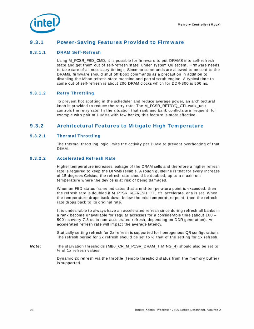
Memory Controller (Mbox)
98 Intel® Xeon® Processor 7500 Series Datasheet, Volume 2
9.3.1 Power-Saving Features Provided to Firmware
9.3.1.1 DRAM Self-Refresh
Using M_PCSR_FBD_CMD, it is possible for firmware to put DRAMS into self-refresh state and get them out of self-refresh state, under system Quiescent. Firmware needs to take care of all necessary timings. Since no commands are allowed to be sent to the DRAMs, firmware should shut off Bbox commands as a precaution in addition to disabling the Mbox refresh state machine and patrol scrub engine. A typical time to come out of self-refresh is about 200 DRAM clocks which for DDR-800 is 500 ns.
9.3.1.2 Retry Throttling
To prevent hot spotting in the scheduler and reduce average power, an architectural knob is provided to reduce the retry rate. The M_PCSR_RETRYQ_CTL.walk_unit controls the retry rate. In the situation that rank and bank conflicts are frequent, for example with pair of DIMMs with few banks, this feature is most effective.
9.3.2 Architectural Features to Mitigate High Temperature
9.3.2.1 Thermal Throttling
The thermal throttling logic limits the activity per DIMM to prevent overheating of that DIMM.
9.3.2.2 Accelerated Refresh Rate
Higher temperature increases leakage of the DRAM cells and therefore a higher refresh rate is required to keep the DIMMs reliable. A rough guideline is that for every increase of 15 degrees Celsius, the refresh rate should be doubled, up to a maximum temperature where the device is at risk of being damaged.
When an FBD status frame indicates that a mid-temperature point is exceeded, then the refresh rate is doubled if M_PCSR_REFRESH_CTL.rfr_accelerate_ena is set. When the temperature drops back down below the mid-temperature point, then the refresh rate drops back to its original rate.
It is undesirable to always have an accelerated refresh since during refresh all banks in a rank become unavailable for regular accesses for a considerable time (about 100 – 500 ns every 7.8 us in non-accelerated refresh, depending on DDR generation). An accelerated refresh rate will impact the average latency.
Statically setting refresh for 2x refresh is supported for homogenous QR configurations. The refresh period for 2x refresh should be set to ½ that of the setting for 1x refresh.
Note: The starvation thresholds (MB0_CR_M_PCSR_DRAM_TIMING_4) should also be set to ½ of 1x refresh values.
Dynamic 2x refresh via the throttle (templo threshold status from the memory buffer) is supported.

Intel® Xeon® Processor 7500 Series Datasheet, Volume 2 99
Memory Controller (Mbox)
9.4 RAS Support
9.4.1 Memory ECC
The Mbox contains extensive ECC support highlighted by correction of x8 device fail, correction of up to two single errors, and correction of a x8 device fail combined with a single strike error that flips a single bit.
The memory ECC logic, implemented as a combined parity and CRC code with trial-and-error based corrections, provides very strong correction properties.
Note that with maximum correctability enabled, one or at most a few severe failing transactions could be incorrectly corrected. Basically this means that a trial was run that satisfies the ECC scheme but wasn't the right correction for the error that occurred. In the case of a persistent severe failure (persistence very likely is a property of severe failures), then one of the next erroneous transactions will be caught. So if the first error does not need to be contained, one can set the correctability settings to maximum correction. If, on the other hand, the error needs to be contained, then one needs to set correction conservatively.
9.4.2 Address Protection
Lock-stepped channels automatically provide corrupted address detection. In the case that a write or read address is corrupted on one channel, and will appear uncorrupted on the other channel, the data at the two addresses (the intended and unintended one) will be ECC mismatched and appear corrupted (which will be detected on a later read).
9.4.3 Transient Electrical Intel® SMI Errors
The most prevalent errors are expected to be transient electrical Intel® SMI channel failures. Memory reads are retried to cope with this highly probable error mode before assuming a strike or other more persistent memory error. In the case that the Intel® SMI channel is operating in bit lane fail-over then there is no link-level CRC, so correction trials are started on the first read of the cache line from memory while a reread of the same cache line from memory is scheduled.
Transient northbound Intel® SMI errors are easily coped with by retrying them. Southbound transient Intel® SMI errors on the other hand will induce 'alert frames' being sent from an Intel® SMI northbound to the host.
9.4.4 Intel® SMI Lane Fail-over
Intel® SMI Lane Fail-over (LFO) mode of operation ensures continued channel availability in the event that a lane fails. If a single lane fails in either southbound or northbound direction a spare lane is invoked allowing continued operation with full CRC coverage. Lane 10 is the spare lane for the southbound direction and lane 13 is used for northbound direction on the Intel® SMI interface.
9.4.5 Mbox Internal Errors
A significant part of the data path is protected by the advanced memory ECC so that errors can be detected and corrected. Victim buffers are parity protected.
Memory Controller (Mbox)
100 Intel® Xeon® Processor 7500 Series Datasheet, Volume 2
9.4.6 Scrubbing
Scrubbing is a process that involves reading data from memory and, if an ECC error is detected, the data is written back corrected, or written back poisoned if the data is uncorrectable. The Mbox supports both demand and patrol scrubbing.
The demand scrubbing process is invoked, in real time, after the Bbox receives a CORRECTED or UNCORRECTABLE response for a read transaction.The Bbox may schedule a write back of the corrected or poisoned data back to memory.
The patrol scrub flow is as follows:
• Patrol counter generates periodic patrol requests.
• On receiving a patrol request, the patrol state-machine starts and issues a patrol read. If there is no data error on the read, the state-machine increments the patrol address and waits for next patrol request.
• If there is an error, subsequent patrol reads are issued in order to make sure the error in the first patrol read was not due to an Intel® SMI link transient error. If error free data is obtained, the patrol address is incremented and the state-machine waits for the next patrol request.
• If the Intel® SMI link consistently gives erroneous data, the corrected data is collected from the ECC engine (after correction trials have completed successfully). The corrected data is transferred to the victim buffer and then written back to the memory.
Between the beginning of the patrol reads and the patrol write, no processor (Bbox) issued write may go to the same address to ensure correctness of data.
9.4.6.1 Normal Access Optimization
Patrol reads and write are only issued when there are no conflicts. This is required to ensure that no requests to the same address are pending in the dispatch queue before the patrol activity starts.
during patrol activity, all incoming Bbox requests to the same address as the patrol address are sent to the retryQ. This is to ensure that no Bbox writes go in between patrol reads and patrol writes.
9.4.6.2 Starvation Condition
The patrol scrubber contains a timer which is implemented as a free running counter that gives out a one clock wide pulse. On this pulse, the patrol state machine transitions out of the idle.
This counter also gives out another pulse when the count reaches half way (called halftime). While the patrol scrub state machine is waiting for a free request slot to inject its patrol transaction, back pressure is applied to the Bbox when the counter reaches halftime.
9.4.7 DIMM Sparing
An unused spare DIMM (or Rank) on a channel can be used to copy the contents of a failing DIMM on that same channel. If firmware detects that a DIMM's operation has become marginal, then pre-emptively (before the DIMM fails), the DIMMs contents will be transferred to a spare DIMM (and the unreliable DIMM should no longer be used). With a spare DIMM available per channel, the system can keep on going even when a

Intel® Xeon® Processor 7500 Series Datasheet, Volume 2 101
Memory Controller (Mbox)
DIMM starts to fail on the particular channel. The implementation only supports pairs of spare DIMMs or spare ranks (one for each channel) due to the Mbox’s lock-stepping of the Intel® SMI channels.
To support DIMM sparing or rank sparing, firmware is expected to:
• Detect that a single DIMM (or rank) has started failing and that the failure is not a larger part of the channel (based on error logs).
• Program the spare DIMM number (and rank number) in M_PCSR_FBD_sparing. Firmware will also have to ensure that a spare DIMM (or rank) exists that is same type as that of the failing DIMM (at least has as many row bits, column bits and banks bits as the failing DIMM) so that the same Mbox map (in the mapper) can still be used.
• Disable patrol scrub and program the patrol scrub registers in memcopy mode.
• Firmware puts the Mbox into spare-copying mode by programming the M_PCSR_FBD_sparing register. Once all copying is done, firmware puts the Mbox into sparing mode
• In ‘sparing mode’ the failing DIMM is no longer used and every read and write are serviced by the spare DIMM.
9.5 Population Requirements for Memory RAS ModesEach memory controller manages two Intel® SMI channels operating in lockstep operation, with each Intel® SMI channel connecting to a single Intel® 7500 Scalable Memory Buffer (an Intel® SMI-DDR3 bridge, on each Intel® SMI channel).
The Intel® Xeon® Processor 7500 memory RAS features include:
1. memory ECC support including correction of x4 and x8 chip-fail
2. Intel® SMI link-level CRC protection
3. Intel® SMI data-failover mode to operate Intel® SMI even with a single data-lane failure per channel per direction
4. Intel® SMI clock-failover mode to operate Intel® SMI with any primary forwarded clock failover
5. Hemisphere mode
6. memory (intra-socket or inter-socket) mirroring
7. memory (rank or DIMM) sparing
8. memory migration
9. demand and patrol scrubbing
The rules on channel population and channel matching vary by the RAS mode (Rank/DIMM sparing and Inter/Intra socket mirroring) used. Regardless of RAS mode, the requirements for populating within a channel must be met at all times. For RAS modes that require matching populations, the same slot positions across channels must hold the same DIMM type with regards to size and organization. DIMM timings do not have to match but timings will be set to support all DIMMs populated (that is DIMMs with slower timings will force faster DIMMs to operate at the slower common timing models). Intel recommends checking the correct DIMM matching, if applicable to the RAS mode, during BIOS initialization.
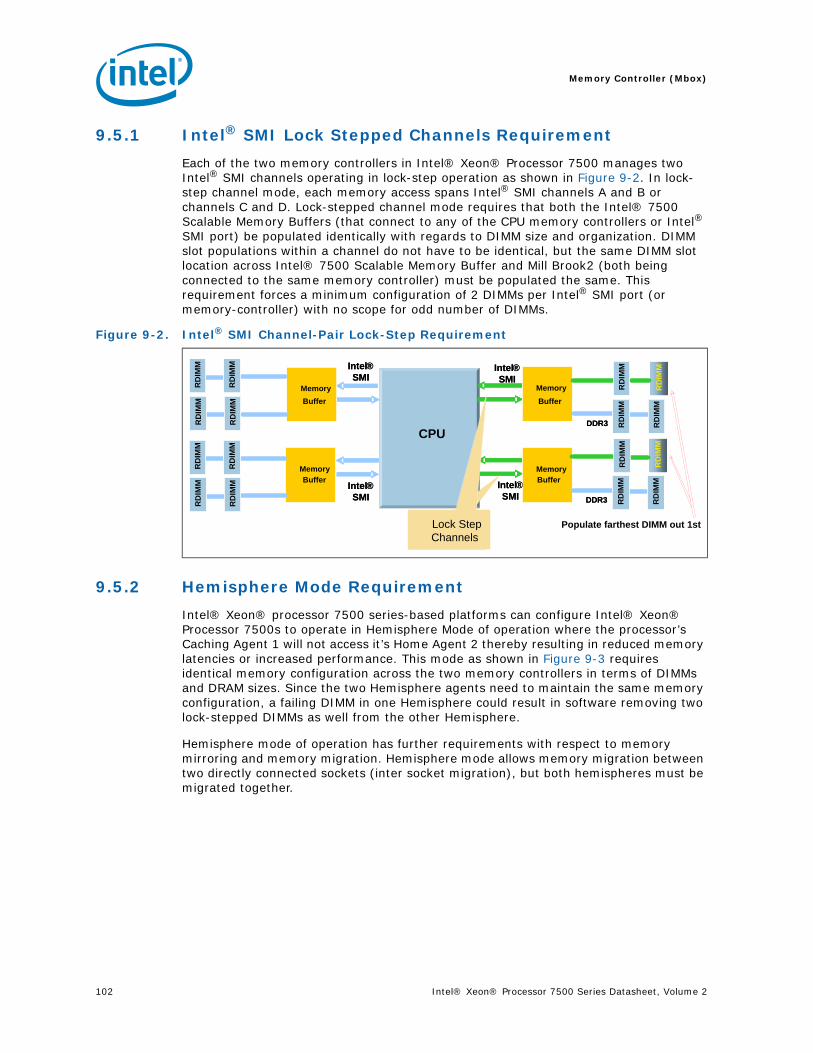
Memory Controller (Mbox)
102 Intel® Xeon® Processor 7500 Series Datasheet, Volume 2
9.5.1 Intel® SMI Lock Stepped Channels Requirement
Each of the two memory controllers in Intel® Xeon® Processor 7500 manages two Intel® SMI channels operating in lock-step operation as shown in Figure 9-2. In lock-step channel mode, each memory access spans Intel® SMI channels A and B or channels C and D. Lock-stepped channel mode requires that both the Intel® 7500 Scalable Memory Buffers (that connect to any of the CPU memory controllers or Intel®
SMI port) be populated identically with regards to DIMM size and organization. DIMM slot populations within a channel do not have to be identical, but the same DIMM slot location across Intel® 7500 Scalable Memory Buffer and Mill Brook2 (both being connected to the same memory controller) must be populated the same. This requirement forces a minimum configuration of 2 DIMMs per Intel® SMI port (or memory-controller) with no scope for odd number of DIMMs.
9.5.2 Hemisphere Mode Requirement
Intel® Xeon® processor 7500 series-based platforms can configure Intel® Xeon® Processor 7500s to operate in Hemisphere Mode of operation where the processor’s Caching Agent 1 will not access it’s Home Agent 2 thereby resulting in reduced memory latencies or increased performance. This mode as shown in Figure 9-3 requires identical memory configuration across the two memory controllers in terms of DIMMs and DRAM sizes. Since the two Hemisphere agents need to maintain the same memory configuration, a failing DIMM in one Hemisphere could result in software removing two lock-stepped DIMMs as well from the other Hemisphere.
Hemisphere mode of operation has further requirements with respect to memory mirroring and memory migration. Hemisphere mode allows memory migration between two directly connected sockets (inter socket migration), but both hemispheres must be migrated together.
Figure 9-2. Intel® SMI Channel-Pair Lock-Step Requirement
Mill Brook
Memory
Buffer
RD
IMMIntel®
SMI
Intel®SMI
Intel®SMI
Intel®SMI
DDR3Nehalem-EX
RD
IMM
RD
IMM
RD
IMM
DDR3 RD
IMM
RD
IMM
RD
IMM
RD
IMM
Mill Brook
Mill Brook
RD
IMM
RD
IMM
RD
IMM
RD
IMM
RD
IMM
RD
IMM
RD
IMM
RD
IMM
1- 4 RDIMMs per FBD channel
Lock Step Channels
Memory Buffer
Memory Buffer
RD
IMMIntel®
SMI
Intel®SMI
Intel®SMI
Intel®SMI
DDR3CPU
RD
IMM
RD
IMM
RD
IMM
DDR3 RD
IMM
RD
IMM
RD
IMM
RD
IMM
Memory Buffer
Memory Buffer
RD
IMM
RD
IMM
RD
IMM
RD
IMM
RD
IMM
RD
IMM
RD
IMM
RD
IMM
1- 4 RDIMMs per FBD channel
Lock Step Channels
Populate farthest DIMM out 1st

Intel® Xeon® Processor 7500 Series Datasheet, Volume 2 103
Memory Controller (Mbox)
9.5.3 Memory Sparing
The Intel® Xeon® processor 7500 supports DIMM and Rank sparing. Sparing is confined to each memory controller, that is, no sparing can be done between the two memory controllers on a socket. In case of DIMM sparing, the spare DIMM must be a super set of all other DIMMs (number of ranks, capacity). In Rank sparing the capacity of the spare rank must be greater than that of any other rank on the channel. In DIMM sparing mode, contents of the entire failing DIMM are transferred to the spare DIMM. In rank sparing mode, contents of the rank defined by the {Failing DIMM, Failing Rank} tuple are transferred to the spare rank defined by the {Spare DIMM, Spare rank} tuple.
The spare DIMM/Rank is held in reserve and is not available as system memory. In lock-stepped mode, sparing is at a channel pair granularity, as shown in Figure 9-4. Memory Sparing cannot be enabled with either memory mirroring or memory migration.
9.5.4 Memory Mirroring
The Intel® Xeon® processor 7500 supports memory mirroring at the Intra-socket level (between 2 memory controllers of a single processor, as shown in Figure 9-5) or at the Inter-socket level (between 2 memory controllers of two different sockets that are directly connected). This requires the two Intel® SMI ports be populated identically with regards to DIMM size and organization.
Figure 9-3. Hemisphere Mode
Memory
Buffer
Memory Buffer
RD
IMMIntel®
SMI
Intel®SMI
Intel®SMI
Intel®SMI DDR3
CPU
RD
IMM
DDR3
Memory Buffer
Memory
Buffer
RD
IMM
RD
IMM
RD
IMM
RD
IMM
RD
IMM
RD
IMM
RD
IMM
RD
IMM
RD
IMM
RD
IMM
RD
IMM
RD
IMM
RD
IMM
RD
IMM
DDR3
DDR3
Hemisphere A Hemisphere B
Figure 9-4. Memory DIMM and Rank Sparing
MB MB MB MB
CPU
Spare DIMM pairs Spare DIMM pairs

Memory Controller (Mbox)
104 Intel® Xeon® Processor 7500 Series Datasheet, Volume 2
In hemisphere mode of operation, intersocket mirroring is a unidirectional mirroring, i.e., SocktA.Port0 --> SocketB.Port0, SocketA.Port1 --> SocketB.Port1. If any memory is mirrored, then all memory within the partition is mirrored identically. Mirroring within a lock-stepped channel pair is not supported.
9.6 Errors The Mbox detects many types of errors. It attempts to correct some types, while others are left to firmware to handle. In general, all Mbox error handling is done in cooperation with the Bbox, since in many cases, the Mbox does not have enough information to determine the correct course of action.
9.6.1 Interrupts
For each error bit in the Mbox's master error log (M_PCSR_ERR_LOG), there is an interrupt mask in the M_PCSR_ERR_CTL[1:0] register. The mask values in this CSR determine the type of interrupt generated by each error. This CSR can be used to re-program the interrupt level associated with each error, or to disable interrupt generation for an error type. The default reset values of each interrupt in M_PCSR_ERR_CTL registers is applicable to a mirroring-off and poison mode off configuration. The severity of the interrupt must be changed by BIOS for configurations of mirroring and poison mode configurations.
All four interrupt signals assert for one cycle every time a new error condition is seen. The only exception to this are for the Thermal Throttle Event and the Status Frame Alert Error; which, in order to prevent a long series of interrupt assertions due to a single event, these errors will cause the interrupt signal to only assert the first time their error bits are set in M_PCSR_ERR_LOG. Firmware must clear these bits in order to see any future interrupts from these types of errors.
Once a fatal event has been detected, no attempt is made by hardware to keep the Mbox in a functional state. The Mbox pulses the fatal signal to Bbox and then does a forced ACK for all subsequent transactions. Firmware must issue a reset in order for the Mbox to resume normal operation. For handleable and non-critical events, the Mbox assumes that firmware will examine the Mbox error logs and perform some operation in response to the interrupt. There may be some adverse effects if firmware does not
Figure 9-5. Memory Mirroring (Intra-Socket)
MB MB MB MB
CPU
Mirrored Memory
Mirrored Memory

Intel® Xeon® Processor 7500 Series Datasheet, Volume 2 105
Memory Controller (Mbox)
service the interrupt in a timely manner; such effects will be listed below, in the description of each error. There are no time requirements when servicing a performance monitor interrupt.
9.6.2 Mbox Parity Error
The Mbox contains several internal parity checkers which check parity on data stored in various internal queues. Any such error is considered unhandleable. Correct Mbox operation is not guaranteed after an internal parity error; firmware must reset the Mbox in order to resume normal operation.
9.6.3 Finite State Machine Error
Many of the internal Mbox state machines contain logic which checks for illegal transitions. In the event of such a transition, a Finite State Machine Error is logged. The design of the Mbox assumes that this type of error is unhandleable and the Mbox will not function correctly after such an error is detected. Firmware must reset the Mbox in order to proceed normally after a Finite State Machine Error.
The following state machines detect transition errors: 1. Frame Type FSM2. Write Dispatch Queue FSM3. Read Dispatch Queue FSM
9.6.4 Error Flow State Machine Success and Failure
The Mbox contains an error flow state machine which attempts to correct certain types of errors. This approach is taken rather than interrupting directly to firmware in the hope that the error may be transient, and that the actions of the error flow state machine may resolve the error without significant loss in the performance of the program.
10.
The following types of errors are handled by the Error Flow State Machine:
1. FB-DIMM Link CRC Error detected (''Northbound Error'')
2. FB-DIMM Alert Frame detected (''Southbound Error'')
9.6.5 Intel® SMI Link CRC Error
The Intel® SMI Link CRC Error, also known as the ''Northbound'' error, occurs when an error is detected on the link CRC coming from the Intel® 7500 Scalable Memory Buffer. This error may be considered transient, persistent, or uncorrectable, depending on how many of these errors have been seen.
On detection of the first Northbound error, the Northbound Transient Flow is invoked, and the Bbox is requested to replay the failing transaction. If the replay executes without error, normal operation is resumed. If not, the Northbound Persistent flow is invoked.

Memory Controller (Mbox)
106 Intel® Xeon® Processor 7500 Series Datasheet, Volume 2
9.6.6 Intel SMI Link Alert Frame Error
The Intel SMI link Alert Frame Error, also known as the ''Southbound'' error, occurs when an alert frame is sent from the Intel® 7500 Scalable Memory Buffer. This error may be considered transient, persistent, or uncorrectable, depending on how many of these errors have been seen.
On detection of the first southbound error, the Southbound Transient Flow is invoked. All Mbox commands are drained, and a soft reset is issued to the Intel SMI channel.
The Southbound Persistent Flow drains all Mbox commands and issues a fast reset to the Intel® SMI channel.
Note that whenever an Intel® 7500 Scalable Memory Buffer sends an alert frame, it sets an internal alert status bit. This bit will remain set within the AMB until firmware clears it.
§
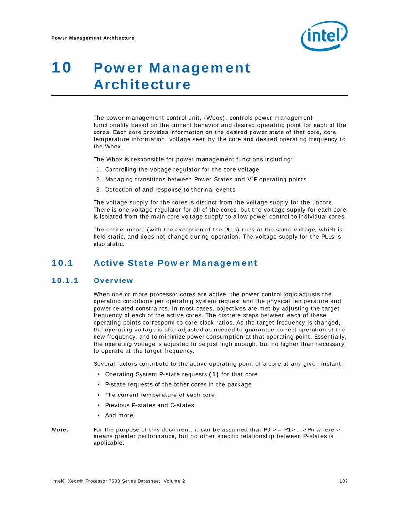
Intel® Xeon® Processor 7500 Series Datasheet, Volume 2 107
Power Management Architecture
10 Power Management Architecture
The power management control unit, (Wbox), controls power management functionality based on the current behavior and desired operating point for each of the cores. Each core provides information on the desired power state of that core, core temperature information, voltage seen by the core and desired operating frequency to the Wbox.
The Wbox is responsible for power management functions including:
1. Controlling the voltage regulator for the core voltage
2. Managing transitions between Power States and V/F operating points
3. Detection of and response to thermal events
The voltage supply for the cores is distinct from the voltage supply for the uncore. There is one voltage regulator for all of the cores, but the voltage supply for each core is isolated from the main core voltage supply to allow power control to individual cores.
The entire uncore (with the exception of the PLLs) runs at the same voltage, which is held static, and does not change during operation. The voltage supply for the PLLs is also static.
10.1 Active State Power Management
10.1.1 Overview
When one or more processor cores are active, the power control logic adjusts the operating conditions per operating system request and the physical temperature and power related constraints. In most cases, objectives are met by adjusting the target frequency of each of the active cores. The discrete steps between each of these operating points correspond to core clock ratios. As the target frequency is changed, the operating voltage is also adjusted as needed to guarantee correct operation at the new frequency, and to minimize power consumption at that operating point. Essentially, the operating voltage is adjusted to be just high enough, but no higher than necessary, to operate at the target frequency.
Several factors contribute to the active operating point of a core at any given instant:
• Operating System P-state requests (1) for that core
• P-state requests of the other cores in the package
• The current temperature of each core
• Previous P-states and C-states
• And more
Note: For the purpose of this document, it can be assumed that P0 >= P1>...>Pn where > means greater performance, but no other specific relationship between P-states is applicable.

Power Management Architecture
108 Intel® Xeon® Processor 7500 Series Datasheet, Volume 2
Based on a snapshot of these factors, the ratio resolution algorithm determines a target ratio and associated voltage for each core, as well as a final, aggregate package target. The resolved package operating point is the highest requested operating point of any of the cores, after all factors are taken into account. The resolved core operating point will be the same as the package operating point when the core is active.
10.1.2 Frequency/Voltage Target Management
10.1.2.1 Software P-State Requests
In ACPI terminology, a P-state is a software visible power/performance operating point. The OS or BIOS has the permissions to make P-state change requests. Requests are made by writing the IA32_PERF_CTRL MSR (0x199), which is defined per-thread.
Any write to this MSR triggers an update to the thread-specific copy of the MSR, and the maximum P-state (P0 > P1..PN) of both thread requests is pushed to a per-Thread Wbox register, P_STATE_CORE[0-7], for firmware handling. Note that the P_STATE_Thread control register has a Turbo Mode ''Enable'' bit and IA32_PERF_CTRL has a ''Disable'' bit.
The P-state requests are handled as a max function in that the maximum P-state request always takes priority. This policy is necessitated primarily by the processor multi-core topology. The OS requires that when a particular P-state request is made on a core, the delivered performance is greater than or equal to the requested performance (the OS expects that the Intel Thermal Monitor activation and other similar hardware responses to environmental conditions are rare events). Since all cores have to share the same maximum voltage, the Wbox normalizes all core P-state requests to the maximum request.The actual operating point of each thread is conveyed via the IA32_PERF_STATUS MSR, as shown in Figure 10-3. This MSR is replicated for each thread.
Figure 10-1. IA32_PERF_CTRL MSR (0x199)
Reserved31 1615 0
OS P-state Target
Turbo Disabled
Reserved
63 32
Figure 10-2. P_STATE_Thread
Reserved
31 4 03
Turbo EnabledP-State Target

Intel® Xeon® Processor 7500 Series Datasheet, Volume 2 109
Power Management Architecture
Note that both the IA32_PERF_CTRL MSR and the IA32_PERF_STATUS MSR convey operating point information as an encoded value, not a specific voltage and frequency.
10.1.2.1.1 P-State Voting Rights
Applied to the per-thread P-state requests is the notion of ‘voting rights’. Up to 16 threads can register a vote for their desired P-state. A core’s P-state vote is the maximum of the P-state votes from each thread. Voting rights are managed at the core level only and may be suspended or renewed due to the following:
• A thread has recently entered C3 (a non-coherent C-state)
• A thread has recently exited C3 (a non-coherent C-state)
Voting rights are suspended on a per-thread basis immediately upon entry into a non-coherent C-state, including C3, and explicitly excluding C1 and C1E. The last write to the IA32_PERF_CTRL_MSR has priority and controls the package P-state target, which implies that the P-state voting rights are only lost when the last thread enters a non-coherent C-state. Please refer to section 10.4.2 for details on the C-state request and resolution protocol.
C-state requests are made at a thread level by executing a HALT, MWAIT, or specific I/O instruction, and specifying the desired target C-state.
Note: I/O reads from specific P_LVLx addresses can also trigger C-state transitions.
A normal C-state exit requires that an event (external or internal) is driven to a core. If the event results in one of the core threads returning to the C0 state, the core active bit for that core will get set, and core returns to the C0 state. When core services this event, it will always update C_STATE_CORE with a target C-state of C0.
10.1.2.1.2 ACNT/MCNT
The actual core P-state is dependent on the requested P-states of the other threads in the package. As a result, there will be times when the actual P-state, and therefore performance, on a given thread is higher than the performance expected for the requested P-state.
Figure 10-3. IA32_PERF_STATUS MSR (0x198)
Reserved Current Operating Point
Reserved Max Operating Point
63 4847
31 1615
Figure 10-4. C_STATE_Thread
Reserved
31 4 0
C-State
3

Power Management Architecture
110 Intel® Xeon® Processor 7500 Series Datasheet, Volume 2
For each time slice, the operating system uses thread idle time over the last time slice to determine the target operating point for the next time slice. If actual performance was higher than requested over the last time slice, the operating system algorithm for choosing the operating point may occasionally calculate the target operating point incorrectly. To prevent this from occurring, each logical thread includes a pair of registers that can be used by the operating system to determine actual delivered performance over some previous time window. MCNT continuously increments at the advertised maximum frequency of the processor. ACNT increments at the actual operating frequency of the processor.
The actual operating frequency can be higher than the requested frequency as a result of the processor resolving to a higher than requested P-state or as a result of Turbo Mode operation. The actual operating frequency can be lower than the requested frequency as a result of Intel Thermal Monitor activation or system assertion of the ForcePR signal. Both ACNT and MCNT only increment while the processor is in the C0 state. MCNT continues to increment during the ''off'' times of core clock modulation but ACNT stops during the ''off'' times of core clock modulation. By comparing the ratio of ACNT and MCNT, the operating system can calculate the actual delivered performance.
10.2 Turbo ModeThe frequency of a processor is set to correspond to the power specs for the part, and assumes that all cores are active and executing the relevant code for that particular processor specification – Icc_max, TDP, etc. When all cores are executing a TDP workload, the power of the processor will be less than or equal to the TDP spec at the nominal frequency and associated voltage. There are many operating conditions under which one or more cores in the processor would be capable of running at much higher frequency without exceeding the power related constraints for the part. For example, if only one of the cores is running a TDP workload and the other 7 cores are in a low power C-state, the one active core could run at substantially higher frequency without exceeding the TDP spec for the processor.
The Intel® Xeon® processor 7500 series Turbo Mode is designed to take advantage of this opportunity. In a processor context, Turbo Mode refers to the ability to operate at a frequency that is higher than the nominal frequency of the processor. The processor is designed such that it never operates at a point where its power consumption exceeds any of the power related constraints associated with that processor.
In ACPI terminology, the nominal or advertised frequency of the processor is associated with the ACPI P1 state. Note that in processors without Turbo Mode support, the advertised frequency of the processor corresponds to the ACPI P0 state. On Intel® Xeon® processor 7500 series (and other processors that support Turbo Mode operation), the P0 state is generally associated with Turbo Mode, and the OS only requests operation at this point when it values absolute performance above all else – Turbo Mode is typically not a power/performance efficient operating point. Note that on an Intel® Xeon® processor 7500 series, the P0 operating point doesn't necessarily correspond to a specific operating frequency – in P0, the operating frequency moves up and down as dictated by the power constraints of the system. The only guarantee is that the P0 frequency is >= the P1 frequency. In other words, in the worst case, P0 frequency = P1 frequency. In the best case, P0 operating frequency can be multiple frequency steps above the P1 frequency. The exact delta between maximum and minimum P0 frequencies varies from processor to processor and is determined by the power related constraints on processor operation. The key difference between P0 and P1 is that the P1 frequency is essentially guaranteed (in the absence of Intel Thermal

Intel® Xeon® Processor 7500 Series Datasheet, Volume 2 111
Power Management Architecture
Monitor activation) and can be sustained indefinitely, while P0 frequency varies according to exact operating conditions and processor constraints, and may not be sustainable indefinitely.
On Intel® Xeon® processor 7500 series, the available Turbo Mode frequency upside is the result of several processor features, described in the next three sections.
10.2.1 ''Legacy'' Turbo Mode
“Legacy” Turbo Mode makes the fundamental assumption that an active core is executing at or near TDP. Therefore, the additional frequency benefit is based entirely on the number of active cores, and this execution state can be sustained indefinitely (or until a core changes its activity state). The “Legacy” Turbo Mode benefit for any number of active cores is also a statement of the minimum turbo benefit for that configuration of cores.
10.2.2 Turbo Mode Policies
In the event that one or more cores have headroom to the power related constraints, there is an opportunity to achieve higher performance via Turbo Mode. However, it's possible that increasing the voltage supply shared by the cores may not provide the desired trade-off. Furthermore, the impact of increasing the core voltage supply may be different based on the platform under which the processor is running. In order to support a variety of potential usage models, a 'turbo mode policy' parameter is added, and is defined in Table 10-1.
The preferred Intel® Xeon® processor 7500 series default Turbo Mode policy is ‘01’. This Turbo Mode policy is selected in order to make the P-state resolution algorithm consistent (priority on performance) for all P-state requests.
Turbo mode availability is enumerated in the power management leaf of CPUID (leaf 6). If Turbo Mode is available on a particular part, it will always be disabled by default, and may be explicitly enabled by the BIOS and/or OS. The IA32_MISC_ENABLES MSR has priority control and may disable Turbo mode at the package level with the Turbo Model Disable bit (38). The Turbo Mode Disable bit defaults to ‘1’ in MISC_ENABLES after reset, and software may optionally set it to ‘0’.
Software may control Turbo Mode enable/disable policies at a logical processor level by selecting the values which it writes to IA32_PERF_CTL. Turbo mode may be disabled by setting the Turbo Mode Disable bit (32) in the IA32_PERF_CTL or by requesting a P-state lower than P0.
Table 10-1. Turbo Mode Policy
Value Turbo Resolution
00 Enable only when all voting cores are in P0
01 Enable when any voting core is in P0
10 RSVD
11 Never enable

Power Management Architecture
112 Intel® Xeon® Processor 7500 Series Datasheet, Volume 2
10.2.3 Intel Thermal Monitor
10.2.3.1 Stimuli
It is possible for the processor to occasionally operate at a point that results in either the processor die or other system components approaching their maximum allowable operating temperatures. The time constants with which the processor can cross a thermal limit are orders of magnitude faster than the response time of external thermal controls (like fan speed RPMs), and thus the processor or external device must protect itself from thermal failure. When a thermal limit is crossed, mechanisms exist to force the processor to reduce its power consumption, thereby clamping the temperature of the critical components. This hardware power reduction mechanism can be initiated by two different stimuli. An internal thermal sensor measuring a temperature greater than its Intel Thermal Monitor trip temperature is referred to as Intel Thermal Monitor activation. Additionally, external components can force a power reduction by asserting the FORCEPR# pin.
10.2.3.2 Internal Intel Thermal Monitor Trip
In an Intel® Xeon® processor 7500 series, there are a number of thermal sensors per core. The Wbox collects each of these temperatures once per millisecond and updates the respective per-core digital thermometer registers with the latest temperature. During a single Wbox loop iteration, if a core temperature makes an upward crossing of the Intel Thermal Monitor trip point, that core will initiate a package-wide Intel Thermal Monitor response. As long as any core remains above the Intel Thermal Monitor trip temperature, the processor will remain in this reduced power mode.
10.2.4 External PROCHOT# Pin Assertion
The PROCHOT# package pin is an output pin. It reflects the current state of the hottest temperature sensor on the package (if any core is higher than its Intel Thermal Monitor temperature threshold, PROCHOT# will assert).
10.2.5 External ForcePR# Pin Assertion
The FORCEPR# package pin is an input pin. When FORCEPR# is asserted, the Wbox immediately reduces the voltage and frequency to the lowest allowable operating points and initiates Intel Thermal Monitor 1.
10.2.5.1 Intel Thermal Monitor Response
The Wbox responds to Intel Thermal Monitor activation by scaling down to lower voltage and frequency operating points. This response is frequently referred to as Intel Thermal Monitor 2. With this policy, there is a single 'thermally constrained' frequency target which reflects the maximum valid ratio given thermal and reliability constraints (and explicitly ignoring the OS P-state request). This frequency target is one of the inputs that resolves to the actual processor operating point. When an Intel Thermal Monitor activation event is recognized, the 'thermally constrained' target is adjusted according to the adaptive policy described below.
The Intel® Xeon® processor 7500 series uses an adaptive Intel Thermal Monitor response policy which is designed to slowly respond to thermally constrained conditions resulting from an internal Intel Thermal Monitor trip. In the event that the processor reaches the lowest allowable operating voltage and associated frequency and the thermal condition persists, a final, aggressive ''clock modulation'' feature is applied to further reduce power.

Intel® Xeon® Processor 7500 Series Datasheet, Volume 2 113
Power Management Architecture
10.2.6 Core Clock Modulation
The ability to modulate the core clock is the basis for two specific power management features. In this context, core clock modulation refers to the ability to run the clock at its normal frequency for some time period, and then stop that clock completely for a time period. The duty cycle is the ratio between clock on time to total time. This capability is used both for core temperature control via Intel Thermal Monitor 1 and software invoked power reduction via ACPI T-states. In the Intel® Xeon® processor 7500 series, ACPI T-states are supported through two distinct interfaces – an MSR based mechanism on each logical processor, and emulation of the legacy ICH based mechanism, which applies to all cores simultaneously. Both Intel Thermal Monitor 1 and ACPI T-state support are means for reducing average processor power consumption over time scales of 10s of microseconds or longer. Neither mechanism impacts the max power consumption of the processor over time periods of microseconds or less. Both mechanisms use the same underlying hardware functionality, with the difference between the mechanisms solely in the configuration settings and enables.
10.2.6.1 Intel Thermal Monitor 1 Overview
On the processor, Intel Thermal Monitor 1 is engaged on all cores simultaneously as a result of a die temperature condition or FORCEPR# assertion. The processor does not provide the ability to activate Intel Thermal Monitor 1 on a single core, even if only one core is at the Intel Thermal Monitor activation temperature. This is because Intel Thermal Monitor 1 is essentially the last temperature fail safe mechanism, and if it ever activates, the objective is to drive processor power consumption as low as possible, irrespective of the temperature of any individual core.
On the Intel® Xeon® processor 7500, Intel Thermal Monitor 1 is initiated when the Intel Thermal Monitor 2 is fully engaged at the lowest supported voltage and associated frequency for at least one voltage/ratio change lockout cycle, and the die temperature remains at or above the Intel Thermal Monitor trip point.
When the Intel Thermal Monitor 1 inducing condition is resolved, Intel Thermal Monitor 1 is disengaged. Neither the OS nor system BIOS has the ability to disable or configure the Intel Thermal Monitor 1 response to a thermal condition.
10.2.6.2 ACPI T-State Overview
ACPI and ICH-based clock modulation are based off the same concepts as Intel Thermal Monitor 1, but instead of being tied to the Intel Thermal Monitor trip temperature, their enabling, disabling, and duty cycles are managed entirely by the OS.
10.2.6.2.1 MSR Based ACPI T-State Support
When using the processor MSR based mechanism for supporting ACPI T-states, transition to a reduced power T-state is initiated by writing the IA32_CLOCK_MODULATION MSR (0x19A). This MSR is duplicated for each thread, and contains both an enable bit and a duty cycle setting. Hardware coordinates between thread T-state requests. The processor will not transition to a lower power T-state until the enable bit is set on both threads. The resolved core duty cycle is always the maximum of both thread values (indicating maximum performance) and is only re-evaluated during the T-state FSM 'idle' state.
The T-state duty cycle setting controls the OS performance when T-state clock modulation is enabled. If the duty cycle setting is targeted at 37.5%, then software can expect to get 37.5% instruction throughput relative to execution speed with clock

Power Management Architecture
114 Intel® Xeon® Processor 7500 Series Datasheet, Volume 2
modulation disabled. Duty cycles are always encoded in 12.5% increments and are always encoded as numbers between 0 and 7. A duty cycle setting of '0' is reserved, and will result in selection of a 50% duty cycle setting. An increment in duty cycle corresponds to a 12.5% increment in total application execution time (for example, DutyCycle = 3 implies 12.5% * 3 or 37.5%).
The IA32_CLOCK_MODULATION MSR bit positions are shown in Figure 10-5, and the duty cycle encodings are shown in Table 10-2. Note that the duty cycle encodings apply to both MSR-based and legacy ICH-based T-state support.
10.2.6.2.2 ICH Emulation Based T-State Support
In legacy systems, a write to the ACPI defined P_CNT I/O address would trigger what was called ''ICH-based throttling''. This term was used because the ICH managed the P_CNT I/O register, and would toggle the STOPCLK# pin to the CPU according to the duty cycle programmed into P_CNT. On the Intel® Xeon® Processor 7500, this ICH functionality is now subsumed into the Uncore and the STOPCLK# pin no longer exists. For these reasons, the processor will trap on all I/O writes to and reads from the P_CNT I/O address, and redirect them to an ICH_THROT register managed in the Wbox. Enabling ICH-based clock modulation T-state support has the same impact as MSR based T-state support or Intel Thermal Monitor 1 – the T-state clock modulation FSM is triggered.
P_CNT I/O is trapped and redirected according to the following rules:
1. Any dword I/O read or write instruction (IN, INS, OUT, OUTS, including REP prefixes).
2. I/O address matches PMG_IO_CAPTURE_BASE[15:0] – 4.
Redirection is managed by core and results in writing the output to the Uncore Package_Throttle_Command register. The format of this register is identical to Figure 10-6. There is only one register per-package and there are no ordering rules applied to this register so whatever core writes it last owns the duty cycle and enable.
Figure 10-5. IA32_CLOCK_MODULATION MSR (0x19A)
Table 10-2. IA32_CLOCK_MODULATION MSR Duty Cycle
Bit 3 Bit 2 Bit 1 Duty Cycle (Nominal% of Time Executing User Instructions)
0 0 0 Reserved
0 0 1 12.5%
0 1 0 25.0%
0 1 1 37.5%
1 0 0 50.0%
1 0 1 62.5%
1 1 0 75.0%
1 1 1 87.5%
31
Reserved
Enable
Duty Cycle
Reserved
5 1 04 3

Intel® Xeon® Processor 7500 Series Datasheet, Volume 2 115
Power Management Architecture
Note that while processor MSR based T-state support results in the application of the desired duty cycles only to the specific cores that request it, the emulation of ICH based T-state support results in the duty cycle being applied to all cores in the package.
The trapped P_CNT I/O address is calculated from the PMG_IO_CAPTURE MSR (0x0E4), Figure 10-7. This MSR points to the ACPI defined ''P_LVL2'' I/O address, which is the address used to request a C2 transition in legacy operating systems. By definition, the P_LVL2 I/O address is equivalent to P_CNT + 4 (refer to the ACPI spec for more details). Intel® Xeon® processor 7500 will trap on all double word aligned reads or writes (IN, OUT, INS, OUTS) to the P_CNT I/O address and redirect the data to the corresponding fields in the ''ICH_THROT'' register, maintained in the Wbox. Misaligned or partial accesses to the P_CNT address are ignored.
Because the ICH-based T-state support was pulled into the package, the feature is no longer shared among all processors in an MP platform.
10.2.6.3 Core Clock Modulation Configuration and Control
T-state duty cycle is controlled via system software. At any particular duty cycle, the power efficiency of the T-state is dependent on the period over which this duty cycle is applied. Increasing the clock on and clock off times increases the efficiency, since less total time is spent on the overhead of turning the clocks on and off. Historically, the processor MSR based T-state mechanism has used shorter periods than the ICH based T-state mechanism. On the Intel® Xeon® Processor 7500, the period over which the duty cycle applies is programmable. The total T-state period is encoded in bits 2:0 of the T-STATE_PERIOD_MSR; see Figure 10-9.
Figure 10-6. ACPI P_CNT I/O Register (Located at P_BLK+0)
31
Reserved
Enable
Duty Cycle
Reserved
5 1 04 3
Figure 10-7. PMG_IO_CAPTURE MSR (0x0E4)
Figure 10-8. ICH_THROT Control Register
31
P_LVL2 I/ O AddressReserved
2223 16 15 0
C- State Range
31
Reserved
Enable
Duty Cycle
Reserved
5 1 04 3

Power Management Architecture
116 Intel® Xeon® Processor 7500 Series Datasheet, Volume 2
)
The ''T-State Period'' field is an encoded value indicating the total period in microseconds for a complete T-state duty cycle, where 2**(T-state Period) is the T-state duty cycle period. Thus, T-state periods are implemented in powers of 2 only, and encompass 2, 4, 8, 16, 32, 64, and 128. The T-state period default is 32.
With a given T-STATE_PERIOD value, the clock on and clock off time slices can easily be calculated using the following equations:
• ClockOnTime = 2**(T-state Period) >> DutyCycle
• ClockOffTime = 2**(T-state Period) >> (8-DutyCycle)
The duty cycle is configurable by the OS for both MSR based and ICH based T-state support. The Intel Thermal Monitor 1 duty cycle is hard-coded by the design to 37.5%.
10.2.6.4 Core Clock Modulation Priorities and Enables
If Intel Thermal Monitor 1, MSR T-state support, and ICH T-state support are all engaged simultaneously, then the duty cycle selected is based on the following priority:
1. Intel Thermal Monitor 1 duty cycle is the highest priority
2. ICH emulation T-state support is the second highest priority
3. MSR based T-state support has the lowest priority.
The duty cycle is loaded at the beginning of a T-state period and is re-loaded after each period. If enables or duty cycles change in the middle of a clock on or off period, they are ignored until that period is completed.
The duty cycle selected for the various active feature possibilities is shown in Table 10-3.
Figure 10-9. T-STATE_PERIOD MSR (0x276)
Reserved
T- State Period
2 031 3
Table 10-3. Core Clock Modulation Duty Cycle Selection
T0/CoreX MSR T-state Enable
T1/CoreX MSR T-state Enable
ICH Emulation T-state Enable
“TM1” Active
Clock Modulation
Engaged
Selected Clock Modulation Duty Cycle
X X X 1 1 Intel Thermal Monitor 1
X X 1 0 1 ICH Emulation Target
1 1 0 0 1 P_CNT MSR Target
1 0 0 0 0 N/A
0 1 0 0 0 N/A
0 0 0 0 0 N/A

Intel® Xeon® Processor 7500 Series Datasheet, Volume 2 117
Power Management Architecture
10.3 Thermal Management
10.3.1 Overview
The Intel® Xeon® processor 7500 provides mechanisms to prevent the processor from operating above its maximum safe operating temperature. This is accomplished by continually monitoring the temperature of the die, and taking appropriate power reduction actions when the die temperature reaches a pre-determined limit. Temperature is monitored via the on die digital thermal sensor. The Intel® Xeon® processor 7500 also implements a feature to provide more extreme temperature protection for cases where the normal mechanisms appear to be unable to control die temperature as expected.
10.3.2 Digital Thermal Sensor
10.3.2.1 Introduction
The digital thermal sensor feature on the Intel® Xeon® processor 7500 gives software direct access to an approximate die temperature with an interface to the integrated thermal sensor present on each core. By simply interpreting values contained in the existing IA32_THERM_STATUS (0x19C) MSR, thermal/power management software can determine the temperature of each core relative to the Intel Thermal Monitor trip point for that core. Note that all cores in the processor have the same Intel Thermal Monitor trip temperature.
In addition to providing readable die temperature information, the digital thermal sensor supports up to two programmable temperature thresholds for use by software. Each of these thresholds can be used to generate interrupts and provide temperature event logging. The reporting of the thermal sensor temperature and the new thermal interrupt generated by each new threshold temperature will work in conjunction with the existing Intel Thermal Monitor logic. These new capabilities have no impact on the behavior of Intel Thermal Monitor 1 and Intel Thermal Monitor 2.
For the Intel® Xeon® processor 7500, BIOS can choose to expose only one programmable temperature threshold to software, and make use of the second programmable threshold in conjunction with the THERMALERTxx pin. BIOS signals this intent through the WBOX_CR_THERMALERT_CFG register at boot, sets the Threshold #2 Temperature in the IA32_THERM_INTERRUPT MSR to the desired threshold temperature at which THERMALERTxx will be asserted, and disables the Threshold #2 Interrupt; the Intel® Xeon® processor 7500 responds by only reporting one programmable thermal threshold to the OS in CPUID.
10.3.2.2 Architectural Feature Definition
The digital thermal sensor was designed as a means to support OS visibility into accurate processor temperature information, as well as providing a means for generating interrupts for software temperature management purposes. Additionally, the digital thermal sensor provides an 'out-of-spec' feature that gives an early warning to the OS regarding a serious thermal condition.
The current temperature, log bit, and status bit information can be accessed via reads from the IA32_THERM_STATUS MSR. Programmable temperature threshold specification and the associated interrupts can be programmed in the IA32_THERM_INTERRUPT MSR. The digital thermal sensor feature set is enumerated in CPUID leaf 6. Both MSRs are thread specific.

Power Management Architecture
118 Intel® Xeon® Processor 7500 Series Datasheet, Volume 2
10.3.2.2.1 Digital Thermal Sensor Threshold and Interrupt Enable Management
The following algorithm should be used in programming the thermal thresholds, per-thread:
1. Determine the availability of the digital thermal sensor based on CPUID.6 output (per-package).
2. Determine the number of valid temperature thresholds based on CPUID.6 output (per-package).
3. Program the available offsets based on the number of thresholds supported (CPUID.6 output) and the resolution.
4. Install IDT/GDT descriptors for the thermal interrupt vector.
5. Initialize and unmask the Thermal LVT entry.
6. Enable individual threshold interrupt bits should be via the IA32_THERM_INTERRUPT MSR.
When disabling thermal interrupts, they should first be disabled at the IA32_THERM_INTERRUPT MSR. Note that updates to thermal interrupt enables or thresholds may not intercept in-flight thermal interrupt delivery. Changes to the thermal thresholds automatically update the associated thermal status bits, but have no impact on the associated and log bits. The thermal log bits should be explicitly cleared by software when updating the thermal thresholds.
The digital thermal sensor feature was originally designed to support an ACPI usage model. The ACPI interface to the thermal sensor uses a set of interrupt thresholds and temperature reading capability. At a given time the high and low thresholds are set above and below the actual temperature, respectively. When either of these thresholds is exceeded, a thermal interrupt is generated and the ACPI modules reevaluate the thresholds according to the new temperature.
Figure 10-10.APCI _TMP Algorithm
Disable all Therm int.
Get _TMP (Temperature)
Wait for Interrupt
HT = HT(n+1)LT = HT(n) - e
LT = LT(n+1)HT = LT(n) + e
Yes
No
_TMP > HT(n)
HT: High threshold value set in the MSR registerLT: Low threshold value set in the MSR registerHT(n): Current High Threshold being usedHL(n): Current Low Threshold being usedHT(n+1): Next threshold, 1 step higher then the current _TMPLT(n+1): Next threshold, 1 step lower then the current _TMPe = Small hysteresis value
_TMP within new range?
Get _TMP (Temperature)
No
Yes
Enable thermal interrupts

Intel® Xeon® Processor 7500 Series Datasheet, Volume 2 119
Power Management Architecture
Thermal threshold updates may be made at any time, but the processor will not acknowledge or act upon those updates until the next IA32_THERM_STATUS.TEMP update, which means up to ~1 ms of delay between threshold changes and respective status bit changes. Furthermore, it is possible that a re-programmed thermal threshold will equal the current temperature or the current temperature – 1. While normally these conditions cause thermal interrupts, a re-programming has no directional indication, and thus interrupts will be ignored on this event. However, if a threshold is reprogrammed, and in that ~1 ms window in which it was programmed the digital thermal sensor crosses the new threshold, an interrupt will be triggered on the next digital thermal sensor update window.
IA32_THERM_INTERRUPT MSR (0x19B)
The IA32_THERM_INTERUPT MSR, which is thread specific, is extended to implement digital thermometer interrupt functionality.
1. Two seven bit fields (one for each programmable threshold) are defined to hold each threshold offset temperature.
2. Two interrupt enable bits (one for each programmable threshold) are defined.
3. One interrupt enable bit to flag out-of-specification operating conditions.
4. All defined bits in the IA32_THERM_INTERRUPT MSR are read/write.
Note that updates to the threshold temperatures will not be acknowledged until the next IA32_THERM_STATUS update cycle, which means up to ~1 ms of delay between update and actual processor acknowledgement. Since digital thermometer temperatures are not evaluated any more frequently than this window, this latency should not create any software problems.
10.3.2.2.2 Temperature Hysteresis Function
The Wbox applies a hysteresis function on the input temperature by using 'hot' and 'cold' thresholds above and below the Intel Thermal Monitor trip temperature before it will recognize a transition from cold to hot and vice-versa.
Figure 10-11.IA32_THERM_INTERRUPT MSR (0x19B)
Threshold #2 Interrupt Enable
Threshold #2 Temperature
Threshold #1 Interrupt Enable
Threshold #1 Temperature
Reserved
Out Of Spec Interrupt Enable
Reserved
PROCHOT# Interrupt Enable
Cold Hot Thermal Monitor Interrupt Enable
HotCold Thermal Monitor Interrupt Enable
31 24 2322 1615 14 10 9 8 7 5 4 3 2 1 0
Reserved
Power Management Architecture
120 Intel® Xeon® Processor 7500 Series Datasheet, Volume 2
10.3.2.2.3 Programmable Temperature Thresholds
Legacy architectures include support for thermal interrupts when the temperature crosses the Intel Thermal Monitor trip point in any direction. These were referred to as the ''not to hot'' and ''hot to not'' interrupts. The digital thermometer provides support for two new programmable thermal threshold interrupts. The threshold temperatures are specified in the IA32_THERM_INTERRUPT (0x19B) MSR, and thresholds are programmed in ºC as implied negative offsets (numbers are actually positive) from the Intel Thermal Monitor trip set point. When the thermal sensor crosses the actual threshold temperature, the threshold interrupt is enabled, and thermal interrupts are unmasked in the LVT thermal interrupt entry, an interrupt is generated. Threshold interrupts will be triggered by temperature movement in any direction across the threshold. The interrupt service routine associated with the LVT thermal interrupt entry will be responsible for reading the log/status information out of the IA32_THERM_STATUS MSR to determine within which temperature range the processor is currently operating.
10.3.2.2.4 THERMTRIP#
All thermal sensors, including the uncore thermal sensor, have a catastrophic trip output. These signals are all asynchronously or'd together onto the THERMTRIP# pin. THERMTRIP# is functional at any time after cold reset and as long as power remains good.
10.3.2.2.5 IA32_THERM_STATUS.TEMP Response Time
The IA32_THERM_STATUS.TEMP will be updated no more frequently than once every 1ms. In a single period, it is possible that the temperature could jump more than one degree C. This could happen due to a dramatic change in workload.
Thermal interrupts and PROCHOT# assertions/de-assertions will happen no more frequently than IA32_THERM_STATUS.TEMP updates.
10.3.2.2.6 Out-of-Specification Operating Conditions
The digital thermal sensor supports a notion of out-of-spec operating (OOS) conditions. This feature is designed to allow operating system or system management software to detect a condition where the processor is running too hot, and thus is ''out of spec''. This can help the system or manageability engine determine that there is a potential problem and generate an immediate (and likely ungraceful) shutdown in response. The OOS condition is considered fatal, and if the OS does not shut down immediately, more drastic measures like Machine Check may be taken. The OOS state is sticky and cannot be corrected (thus, the log and status bits cannot be cleared without a reset).
For the Intel® Xeon® processor 7500, the OOS assertion policy is as follows: OOS is asserted on all cores after the max temperature among all core/uncore thermal sensors has been running at a temperature > Intel Thermal Monitor trip while the adaptive Intel Thermal Monitor mechanism has settled to the lowest supported voltage and associated frequency for a continuous period of 10 ms. Time spent at the lowest supported operating voltage due to an external ForcePR assertion does not impact the OOS timer. Due to the adaptive nature of the Intel® Xeon® processor 7500 Intel Thermal Monitor implementation, it is possible that the OOS timer will not start until several microseconds after the Intel Thermal Monitor trip is acknowledged in the package – it will only start after the package arrives at its lowest power reduction state. The timer is always cleared on a temperature change below the Intel Thermal Monitor trip set point. In addition to timer-based trip mechanisms, OOS is asserted when the processor arrives at a temperature delta under the THERMTRIP# temperature.

Intel® Xeon® Processor 7500 Series Datasheet, Volume 2 121
Power Management Architecture
10.4 Idle State Power Management
10.4.1 Overview
The power consumption of the processor is an important consideration in the design of any modern platform. In addition to the power consumed when the processor is active, there are constraints involving the power consumption when the processor is idle.
In order to minimize the idle power consumption of the processor, multiple low power idle states are typically implemented. There tends to be an inverse relationship between the time it takes to enter and exit one of these low power states and the power consumption while in that state. Idle states with very low power consumption tend to have longer entry and exit latencies than states with higher power consumption. The specific low power state to be used is chosen dynamically by the operating system, based on the usage characteristics of the processor over recent history.
The interface describing the low power states provided on the processor and how they are used by the operating system is described via the ACPI (Advanced Configuration and Power Interface) specification. In ACPI terminology, processor execution states are referred to as ''C'' states. C0 refers to the processor active state, and all other C-states are idle states. Higher numbered C-states are lower power, but longer latency. C3 is lower power than C1, and so on.
States C0, C1 require that processor caches maintain coherence – in other words, they must ensure that any memory requests from other system agents receive the latest copy of the data if it is stored in the processors cache. The ACPI spec states that cache coherency in states C3 and lower is the responsibility of the OS to maintain. However, the entry flow of the Intel® Xeon® processor 7500 core into C3 state includes flushing of the core’s first level and mid-level caches into the large last level cache. The last level cache remains available, snoopable, and coherent even if all cores enter C3 state.
ACPI also provides for power management of the system. ACPI S-states refer to the execution state of the system. S0 is the system active state, and all other S-states are system idle states. Within the S0 state, a given processor can be active (C0 state) or idle (C1 or lower states). In all other S-states, the processor is inactive. Note that here ''inactive'' doesn't mean that the processor is any specific C-state – C-states are only applicable while the system is in S0. As with processor C-states, the latency to enter and exit an S-state and the power consumed in that state are inversely proportional. S1 is the highest power system idle state, S3 is lower system power than S1, and so on. The Intel® Xeon® processor 7500 does not support S3 state.
The Intel® Xeon® processor 7500 does not support S1 as a stand alone state. The processor only supports S1 as a transition state.
10.4.2 C-State Support
The Intel® Xeon® processor 7500 will provide support for C0, C1, C1E, and C3. Note that the behavior in a particular C-state on Intel® Xeon® processor 7500 may be different than states referred to with the same number on previous products. The platform change, including the move to an Intel QuickPath Interconnect bus interface, results in the elimination of the STPCLK#, SLP# signals, and as a result there is no need to support C2 type states on the Intel® Xeon® processor 7500.

Power Management Architecture
122 Intel® Xeon® Processor 7500 Series Datasheet, Volume 2
10.4.2.0.1 Valid C-State Transitions
At an architectural level, a logical processor can only make direct transitions to and from the C0 state. It cannot transition directly between any other C-states. For example, a logical processor cannot transition directly from C1 to C3; it must go through C0.
Valid thread/core C-state transitions are shown in Figure 10-12. Note that the resolved core C-state is the highest power (lowest numerical) C-state requested by any of the threads present in that core.
10.4.2.0.2 Thread C-States
Each thread in a core can request a transition to a C-state independent of the state of the other threads in that core. The core will handle coordination of these thread specific requests; there is no functional need for software to understand the dependencies between the threads in a core, or the cores in a package, for any given C-state.
10.4.2.0.3 Core C-State Resolution
Any enabled thread in the core is capable of requesting a different C-state. The core must resolve the C-state requests of each enabled thread, and convey the resolved request to the Wbox in the uncore on entry to a core C-state. In order to resolve these requests, the Intel® Xeon® processor 7500 must have access to the current C-state of all threads on the core.
Figure 10-12.Valid Thread/Core Architectural C-State Transitions
MWAIT C1,HLT (C1E disabled)
MWAIT C1E,HLT (C1E enabled)
MWAIT C3,I/O C3
C0
C1E1C11 C3
Access to MonitoredAddress2,or Interrupt
Access to MonitoredAddress2,or Interrupt
Access to MonitoredAddress2,or Interrupt
1. Snoops are serviced in the normal manner when a core is in the C1 or C1E states, and no transition to C0 is needed in order to service a snoop2. Access to a monitored address is only an exit condition when entered via MWAIT .

Intel® Xeon® Processor 7500 Series Datasheet, Volume 2 123
Power Management Architecture
The C-state request is resolved by the core to the lowest numbered C-state requested by any of the enabled threads on that core. If either thread is in C0, the resolved C-state is C0. If neither thread is in C0, and 1 thread is in C1, then C1 is the resolved state, and so on.
10.4.2.1 Package C-State Resolution
The package must resolve the C-state requests of each core in order to determine the proper package C-state. The C-state request is resolved by the Wbox to the lowest numbered C-state requested by any of the enabled cores. If any core is in C0, the resolved package C-state is C0. If no cores are in C0, and at least one core is in C1, then C1 is the resolved package C-state, and so on. See the following table.
10.4.2.2 Thread/Core C1/C1E Entry
C1/C1E entry can occur on execution of a HLT instruction or execution of an MWAIT instruction with a C1 (or C1E) argument.
10.4.2.2.1 Thread/Core C1/C1E Exit
A thread in the C1/C1E state will wake up when an interrupt directed to that core arrives at the local APIC. The APIC will send the wakeup event to the thread if the event is not masked in the APIC LVT or EFLAGS.IF. When the thread wakes up, hardware will set the active bit for that core in the Wbox.
10.4.2.2.2 C1E Specific Details
A C1 request will be interpreted as a C1E request in two cases. First, the MWAIT instruction can be invoked with an argument that specifically requests a C1E transition. Additionally, IA32_MISC_ENABLES MSR, is used to indicate that all C1 transitions should be converted to C1E requests.
10.4.2.2.3 Package C1/C1E
If all enabled cores in the package have requested a C1E transition, then the Wbox will initiate a voltage and frequency change to the minimum operating V/f point. When any thread exits C1E, the woken thread will begin execution at this minimum operating V/f point as soon as the event reaches the core.
Table 10-4. Core C-State Resolution
If Either Thread Is In Then Core Resolved C-State Is
C0 C0
C1, and no threads are in C0 C1
C1E, and no threads are in C0 or C1 C1E
C3, and no threads are in C0, C1, or C1E C3
Table 10-5. Package C-State Resolution
If Any Core Is In Then Package Resolved C-State Is
C0 C0
C1, and no cores are in C0 C1
C3, and no cores are in C0, C1, or C1E C3

Power Management Architecture
124 Intel® Xeon® Processor 7500 Series Datasheet, Volume 2
10.4.2.3 C3
10.4.2.3.1 Thread/Core C3 Entry
C3 entry can occur on execution of an MWAIT instruction with a C3 argument, or via an I/O read to the P_LVL3 address. The request will result in the execution of a flow, which will clean up the state of the machine, write the C-state target control register in the uncore (Wbox) with the core specific request (if this is the last thread to run the C-state flow), and then put the thread to sleep. If this is the first thread to leave C0 on an SMT enabled part, the partitioned resources will be re-partitioned on C1/C1E entry. When all enabled threads are sleeping, core hardware will clear the core active bit in the C-state target control register in the Wbox.
If this is the last enabled thread to enter the C3 or lower state, the Intel® Xeon® processor 7500 flushes the I cache, D cache, and MLC before putting the thread to sleep. Note that these flush operations are atomic – if a break event to either thread occurs after the flush of a cache is begun, the flush will complete.
10.4.2.3.2 Thread/Core C3 Exit
When the core wakes up, the core active bit in the Wbox is set by core hardware. The core resumes operation at the latest P-state target.
10.4.2.4 Package C3
The package will attempt to enter the package C3 state when all cores have transitioned to the C3 state. Once all cores have entered the C3 state, the Wbox will take further power reduction actions in the uncore. The core voltage will be reduced to a minimum retention voltage designed to minimize leakage power while retaining all state values.
Once the package has entered the package C3 state, it will be woken when it receives a core break event. Break events can be forwarded from the system across the Intel® QuickPath Interconnect bus, or can be the result of internally generated events (probe mode, thermal threshold interrupts, and so forth).
When a core break event is received, the Wbox will first raise the core voltage to the minimum active Vcc, re-lock the core PLL(s) to the corresponding frequency and forward the break event message. If the break event is not masked in the core, the core will return to the C0 state. If the break event is masked in the core, the Wbox will re-enter the package C3 state.
10.4.2.5 I/O Support for C-State Requests
Software may make C-state requests by using a legacy method involving I/O reads from the ACPI-defined processor clock control registers, referred to as P_LVLx. This feature is designed to provide legacy support for operating systems that initiate C-state transitions via access to pre-defined ICH registers. The base P_LVLx register is P_LVL2, corresponding to a C2 request. P_LVL3 is C3, and so on. Only 'IN' instructions to the supported P_LVLx addresses will trap and redirect to the MWAIT C-state flow. ''REP INS'', for example, does not redirect. P_LVL2 is defined in the PMG_IO_CAPTURE MSR. P_LVLx is limited to a subset of C-states. For example, P_LVL8 is not supported and will not cause an I/O redirection to a C8 request. Instead, it will fall through like a normal I/O instruction. The range of I/O addresses that may be converted into C-state requests is also defined in the PMG_IO_CAPTURE MSR, in the 'C-state Range' field.

Intel® Xeon® Processor 7500 Series Datasheet, Volume 2 125
Power Management Architecture
10.4.2.6 C-State Auto-Demote
10.4.2.6.1 Core C3 Auto-Demote
The operating system requests entry to a specific C-state by supplying the appropriate hint with the MWAIT instruction. If the hint supplied is not supported by the processor, the thread will request a transition to the next higher power C-state. For example, if the OS executed MWAIT with a C9 hint on the Intel® Xeon® processor 7500, this would be translated to a C3 request on that specific thread.
10.4.2.6.2 MWAIT SMI
Previous processors have supported the ability to generate an SMI on execution of an MWAIT instruction that caused a C-state transition. This capability has been provided as a means for invoking SMM for correcting platform specific C-state transition bugs.
The Intel® Xeon® processor 7500 does not support this capability.
10.4.3 S-State Support
10.4.3.1 Overview
In ACPI terminology, S-states refer to system sleeping states. The Intel® Xeon® Processor 7500 supports S0, S1, S4 and S15.
10.5 CPUIDThe Intel® Xeon® processor 7500 includes a new power management CPUID leaf. Leaf 6 is currently used to identify the existence of a digital thermometer, the number of programmable thermal thresholds, the ACNT/MCNT feature, and a Turbo Mode flag. Access to the power management feature leaf of the CPUID instruction is accomplished by moving the constant 6 into EAX prior to executing CPUID. The results of this instruction include the feature flags in EAX and extended feature information in EBX and ECX.
§
Figure 10-13.CPUID Power Management Leaf
311Reserved
Turbo Mode Support
Digital Thermometer Support
EAX:
0Reserved
# Thresholds Supported
EBX: 0 0 1
1
1Reserved
ACNT / MCNT MSR Support
ECX:
3
12
31
31 1
2 0
0
0
14

Power Management Architecture
126 Intel® Xeon® Processor 7500 Series Datasheet, Volume 2

Intel® Xeon® Processor 7500 Series Datasheet, Volume 2 127
Power Controller (Wbox)
11 Power Controller (Wbox)
The Wbox consolidates information and controls power management functionality based on the current behavior and desired operating point for each of the cores.
The Wbox is responsible for power management functions including:
1. Controlling the voltage regulator for the core voltage
2. Managing transitions between Power States and V/F operating points
3. Detection of and response to thermal events
The voltage supply for the cores is distinct from the voltage supply for the uncore. There is one voltage regulator for all of the cores, but the voltage supply for each core is isolated from the main core voltage supply to allow power control to individual cores.
The entire uncore (with the exception of the PLLs) runs at the same voltage, which is held static, and does not change during operation. The voltage supply for the PLLs is also static.
11.1 Intel Thermal Monitor 1 / T-State State MachineT-state throttling is clock "on"/off modulation based throttling. This method of throttling is inherently inefficient, and therefore it is utilized as the final throttle solution to a thermal event when Intel Thermal Monitor 2 is determined to be insufficient. There are three forms of T-state throttling: Intel Thermal Monitor 1, MSR, and ICH. A single state machine services all of these requests at the core level. This state machine prioritizes the requests and then walks through the requested "off" clocks followed by the requested "on" clocks in order to deliver the on/off duty cycle requested. The total on and off time should sum up to 32 μs and is referred to as the T-state Throttle Period.
The priorities of the various clock modulation throttling are as follows, from highest to lowest:
1. Intel Thermal Monitor 1
2. Chipset (ICH)-based
3. MSR-based
The duty cycle is encoded as a 3-bit field that indicates the percent time that the core/package should be executing meaningful instructions (referred to as "on" time).
Power Controller (Wbox)
128 Intel® Xeon® Processor 7500 Series Datasheet, Volume 2
11.1.1 Requesting T-State Throttling
The OS has control over ICH and MSR-based throttling. Intel Thermal Monitor 1 is initiated only by firmware. Each control has two inputs, an enable and a duty cycle. The control registers generally look like this:
11.1.2 Intel Thermal Monitor 1
Intel Thermal Monitor 1 is unique in that its duty cycle is hard-coded to 37.5% and firmware is responsible for enabling and disabling Intel Thermal Monitor 1.
11.1.3 MSR
MSR-based throttling can be requested by writing the IA32_CLOCK_MODULATION MSR (0x19A). This MSR is defined per-thread, but clock modulation throttling is managed per-core. The rules for management are as follows:
1. Per-thread duty cycles are only considered valid if that thread’s enable bit is set.
2. The core duty cycle is always the maximum of the enabled per-thread duty cycles, where maximum is a numerical maximum that guarantees the highest performance.
3. Thread C-states are not considered when applying the enables.
11.1.4 ICH Emulation
ICH emulation-based throttling can be requested by writing the P_CNT I/O address in the chipset. In legacy platforms, this address and functionality was managed in the ICH. For the Intel® Xeon® processor 7500, the core is responsible for trapping on I/O writes to the P_CNT address and redirecting them to a package-level T-state throttling request.
Table 11-1. Clock Modulation Duty Cycle Encoding
Duty Cycle % On % Off
0001
Notes:1. The 000 encoding is illegal, but a 50% default is used if it is used.
50 50
001 12.5 87.5
010 25 75
011 37.5 62.5
100 50 50
101 62.5 37.5
110 75 25
111 87.5 12.5
Figure 11-1. T-State Throttling Control Register Format
Reserved
31 4 1 03
T-state Throttle EnableT-state Throttle Duty Cycle
Intel® Xeon® Processor 7500 Series Datasheet, Volume 2 129
Power Controller (Wbox)
P_CNT I/O is trapped and redirected according to the following rules:
1. Any dword I/O read or write instruction (IN, INS, OUT, OUTS, including REP prefixes).
2. I/O address matches PMG_IO_CAPTURE_BASE[15:0] – 4.
Redirection is managed by core and results in writing the output to the Uncore Package_Throttle_Command register. There is only one register per-package and there are no ordering rules applied to this register so whatever core writes it last owns the duty cycle and enable.
11.1.5 Thread C-States
A TPD_Enter/TPD_Exit event may be received by a thread at any time, regardless of the thread C-state.
11.1.6 Core C-States
11.1.6.1 C0, C1
A TPD_Enter/TPD_Exit event may be received by all threads in a core at any time that is in C0 or C1 state.
11.1.6.2 C3
A TPD_Enter request may be received by a core during C3 entry (technically counted as C0 time). A TPD_Exit request may be received by a core during C3 entry (technically counted as C0 time) if the entry latency is longer than the clock "off" time.
Firmware always resets the T-state FSM when a core completes C3 entry. Threads are always guaranteed at least one block of clock "on" time after a C3 exit. This "on" time starts as soon as core arrives at C0 and clears the T-state FSM reset.
It is possible that both a TPD_Enter and TPD_Exit event will be pended but unserviced at the core APIC on a core C3 exit. Under this condition, the PIC clears both events since this only occurs when they were aborted.
11.1.7 S-States
T-state interaction with S-states is very similar to deeper core C-states. The two conditions are mutually exclusive. Firmware enforces this by resetting the T-state FSM on all cores as part of S-state entry and removes the reset on S-state exit.
11.1.8 Platform Environment Control Interface
The Platform Environment Control Interface, or PECI, is a simple serial bus that allows for up to 2 Mbps of data transfer. The interface is entirely side-band and allows external management engines and fan speed controllers access to CPU data like temperature. The PECI is largely based on an Intel and ADI defined, industry-wide standard, SST (Simple Serial Transport).
Please refer to the global PECI specification for details on the physical, data link and network layers of the PECI. The Intel® Xeon® processor 7500 PECI Client is, in most respects, identical to the PECI Client. The primary areas in which the Intel® Xeon® processor 7500 PECI Client differs from the PECI Client are in 8-socket support and 8-core support.

Power Controller (Wbox)
130 Intel® Xeon® Processor 7500 Series Datasheet, Volume 2
11.1.8.1 Extended Socket Support
The Intel® Xeon® processor 7500 PECI Client is designed to support up to 8 sockets. The default PECI addresses are extended to cover the range from 0x30 to 0x37, with the low 3 bits supplied by the Socket ID power-on configuration pins. (These pins also supply bits [4:2] of the Intel QuickPath Interconnect Node ID.)
11.1.8.2 Supported PECI Commands
The Intel® Xeon® processor 7500 PECI Client supports the following PECI commands:
• Ping(): used to enumerate devices on the PECI bus
• GetDIB(): returns an 8-byte response providing info about client revision number and the number of supported PECI domains inside the processor (for Intel® Xeon® processor 7500, only 1 domain ever).
• GetTemp() : returns the temperature, formatted as a negative value representing the number of degrees centigrade below the "thermal control circuit activation" temperature. The value is expressed as a 16-bit, 2's complement value, with the LSB = 1/64 degree centigrade. The "temperature" returned is the average of the maximum of the per-core temperatures; every 1 mS, the PCU firmware figures out what core is hottest, and plugs that temp into a low-pass filter for averaging. The formula used is:
— AVGT = (AVGT-1 * (1 - 1/(2N)) + (TEMP(T) * 1/(2N))where N is configurable through a PECI mailbox command, and defaults to 8 (256 mS window)
• PCIConfigRd() : returns 32-bit value read from PCI Configuration space of the processor
• PCIConfigWr() : writes 32-bit value to PCI Configuration space of the processor
• MbxSend: sends 8 bit request and 32-bit data value to PCU µcontroller. See mailbox commands below.
• MbxGet: returns 32-bit response to last MbxSend() command (provided that the transaction ID of the MbxGet() matches the transaction ID of the MbxSend().
11.1.8.3 Mailbox Commands
The set of mailbox commands that Intel® Xeon® processor 7500 currently supports includes:
• Thermal Status Read/Write: A read returns a word populated with the package level copy of IO_THERM_COMMAND (an OR of all per-core bits. A write uses the write data as a mask to clear PECI thermal status log bits for Thermal Monitor, PROCHOT, and OOS.
• Get Core Temps Select: A read-only command with an input value of either 0 or 1 that returns a packed 32-bit response with Core3 temp in the most significant byte, then core2 temp, then core1 temp, and Core0 temp in the least significant byte (with an input value of 0) or a packed 32-bit response with Core7 temp in the most significant byte, then core6 temp, then core5 temp, then core4 temp in the least significant byte. This command is disabled by default; the TAP must be used to enable it.
• CounterSnapshot: A "write" that causes firmware to snapshot all PECI counters: TotalTime and ThrottleTime counts. The data is deposited in firmware memory for later retrieval. See "CounterRead".

Intel® Xeon® Processor 7500 Series Datasheet, Volume 2 131
Power Controller (Wbox)
• CounterRead: A read that reads one of the snapshotted PECI counters. Counter0 is "TotalTime", and is subset of the Uncore Time Stamp Counter bits, with a resolution of ~1 used. Counter1 is "ThrottleTime", and is the total time that the package is thermally limited. It is possible for the package to be thermally limited and no cores are exceeding the thermal monitor trip point – this time is included in the count.
• T-State Read/Write. A write is used to force T-state throttling to 12.5% duty cycle (12.5% on, 87.5% off); this overrides any other Intel Thermal Monitor 1 throttling requests. A read is used to return the sideband T-state limit value.
• Icc-TDC Read. Read the one-byte package TDC.
• Thermal Data Config Read/Write. A write defines the thermal average constant "N", and a formatting bit for temp>prochot. A read returns the thermal average constant and the temp format bit.
• Tcontrol Read. Firmware calculates the Tcontrol temperature in PECI 2-byte, 2's complement format.
§
Power Controller (Wbox)
132 Intel® Xeon® Processor 7500 Series Datasheet, Volume 2

Intel® Xeon® Processor 7500 Series Datasheet, Volume 2 133
Configuration and RAS Features
12 Configuration and RAS Features
The Intel® Xeon® processor 7500 is designed to operate in a variety of configurations and workloads. In order to operate correctly, many operating parameters must be configured by system firmware or software prior to full system operation. These parameters configure links for correct operation (for example, routing tables, credit limits to avoid overrunning buffers) to operate in modes that are best suited for the expect system workload (snoop broadcast, IOH directory), and to set up various RAS operating parameters (memory mirroring, migration, patrol scrubbing). These parameters include credits at both link and protocol levels of Intel QuickPath Interconnect, nodeIDs of various components, the mapping of addresses to home agents and to memory components at the home agents, and various mode options for snooping, mirroring, and booting.
This section describes the parameters that can be configured, as well as system constraints that must be observed by both CPUs and by chipset components.
12.1 CPU NodeID AssignmentsAn Intel® Xeon® processor 7500 system is made up of several kinds of agents, each with their own nodeIDs that are used to route requests and to keep track of protocol level transaction credits. An Intel® Xeon® processor 7500 has three NodeIDs that correspond to two caching agents, two home agents, and a configuration agent. In general, the home and caching agents share nodeIDs, and messages that target them are routed to the correct agent on the basis of message class. In one case (memory mirroring from the home agent), the master home agent and configuration agent requestors share the configuration agent nodeID, and responses that target them are routed to the correct agent type on the basis of the transaction ID. In the case that both home agents are being used as memory mirroring requestors, the responses that target them are routed to the correct home agent by using responder NodeID<1>, because of a configuration restriction that ensures it will be unique for each mirror slave agent.
Node controllers should have nodeIDs that resemble a combination of IOH and CPUs (although an XNC may implement only one nodeID for caching and home agents).They act as proxies for clumps of CPUs and IOHs beyond them with many more nodeIDs which will overlap the nodeID assignment is in the local clump.
Table 12-1. NodeID Usage
If agent is type
then the Source RHNID
is set to: If agent is type
then the Destination DNID
is set to:
Agent Type Request Snoop Response Request Snoop Response
CacheAgent y xxxy1 xxxy1 xxxy1 xxxy1 xxxy1 xxxy1
Home Agent y xxxxx1
Notes:1. Mirroring Master to Slave cases only; source NodeID is NodeID of original requestor
N/A 0xxy1, 0xxx12
2. Mirroring Slave read failover data return; source NodeID is NodeID of original requestor
xxxy1 N/A xxxy1, xxx103
3. Mirroring Slave write completion only; destination NodeID is NodeID of configuration agent on mirror master home socket.RSNID in this case is set to original requestor nodeID. Which home on the socket is determined by RSNID<1> XORed with aCSR bit in the incoming mirroring master router port. Note that the TID used in this case will not be the same as the originalrequestor TID, but will be mapped to the range 48..63.
Config Agent 0xx10 N/A 0xx10 0xx10 N/A 0xx10
IOH Agent 0xx00 0xx00 0xx00 0xx00 0xx00 0xx00

Configuration and RAS Features
134 Intel® Xeon® Processor 7500 Series Datasheet, Volume 2
12.1.1 NodeID Restrictions
• If both home agents are configured as mirror masters, then their mirror slave target NodeID<1>s must differ in order to distinguish which home agent a response should be routed to.
• Sockets can implement no more than 8 consecutive, naturally aligned NodeIDs as seen by a link.
12.2 Credit Configurations
12.2.1 Protocol Credits
12.2.1.1 Protocol Credits at Requestor
Coherent (home channel) requests are required to be sunk at the source, or a protocol deadlock will inevitably ensue. This requires requestors to guarantee they will never send more requests than the target tracker has preallocated entries.
Non home channel requests do not have this requirement, and can be blocked at the target, backing up into the network.
The ‘maxRequest’ parameter (for coherent and non-coherent requests) must be configured to match the minimum of the tracker entries of each possible target in the respective credit pool. MaxRequest can be configured even smaller than the maximum for debug and performance measurement purposes.
12.2.1.1.1 Coherent
Coherent requests have eight credit pools, indexed by the request address home {NID[3:2], NID[1] ^ NID[4]}. The credit pool index is used to generation the transaction nodeID for the request.
The initialization code must set the request limit (applies to all coherent request) to be less than or equal to the maximum allowed at the tracker in each home, but more than the minimum which is:
• BitCount(enabled_core_mask) * 2 (1 ea. for victim and non-victim),
• where BitCount() is a function that counts the number of bit set when a mask of enabled cores is ORed with a mask of enabled cache banks for that Sbox (applying to core/cbox 0-3 and core/cbox 4-7 for Sbox 0/1 respectively).
Note that it is possible that this credit pool will be shared among more than one home agent (for example, if there are XNCs in addition to CPUs which share NodeID<3,2,1^4>).
12.2.1.1.2 Non-Coherent
Non-coherent requests have a single credit pool, targeting all nodeIDs. As with coherent credits, these credit pools are replicated at each Cbox, and must (statically) divide the possible NC credits between each Cbox sharing a nodeID.
The initialization code must set the request limit (applies to all NC requests) to be less than or equal to the maximum allowed at the tracker in each NC target, but more than the minimum which is:
• BitCount(enabled_core_mask | enabled_cachebank_mask)*3 (1 ea. for victim non-victim, and lock),

Intel® Xeon® Processor 7500 Series Datasheet, Volume 2 135
Configuration and RAS Features
• where BitCount() is a function that counts the number of bits set when a mask of enabled cores is ORed with a mask of enabled cache banks for that Sbox (applying to core/cbox 0-3 and core/cbox 4-7 for Sbox 0/1 respectively).
Note that since the NC credit pool is separate from the Coherent pools, it is possible that transaction IDs will overlap. For this reason, targets of NC transaction targets must have NIDs that are separate from those of coherent transaction targets.
12.2.1.2 Protocol Credits at Home
The tracker at the home agent can be configured in one of these six modes:
* H corresponds to the co-located Sbox.
In Hemisphere mode, nodeID<1> must be zero in the SAD target list.
Changes to the tracker mode should only be made when the system is quiesced.
The Cboxes associated with one Sbox have either 16, 24, 32, or 48 RTIDs to divide among themselves for HOM requests. In order to do this, each Cbox will have a particular length for all freelists, and one base RTID to add to the priority-encoded value from the selected freelist. Depending on the configuration (8 LLC, 6 LLC, or 4 LLC cache slices), Table 12-3, Table 12-4, and Table 12-5 specify how the freelist lengths and base RTIDs are programmed for the 4, 3, or 2 Cboxes associated with each Sbox respectively.
Table 12-2. Tracker Modes
Mode Configuration C.A.s #Entries, NID Assignment
IOH/XNCs #Entries, NID Assignment
0 4S HemiSphere + 4 IOH/XNC 4 x 32, 0YZH1* 4 x 32, 0/1YZ00
1 4S HemiSphere + 2 IOH/XNC 4 x 48, 0YZH1 2 x 32, 0/10Z00
2 4S Non-HemiSphere + 2 IOH/XNC 8 x 24, 0YZH1 2 x 32, 00Z00
3 4S Non-HemiSphere + 4 IOH/XNC 8 x 16, 0YZH1 4 x 32, 0YZH1
4 8S HemiSphere + 4 IOH/XNC 8 x 24, XYZH1 4 x 16, 0YZ00
5 8S HemiSphere + 4 IOH/XNC 4 x 32 + 4 x 16, XYZH1 4 x 16, 0YZ00
Table 12-3. RTID Generation 8 LLC (last level cache) slices
Sbox RTIDs Freelist Lengths Base RTIDs
16 4, 4, 4, 4 0, 4, 8, 12
24 6, 6, 6, 6 0, 6, 12, 18
32 8, 8, 8, 8 0, 8, 16, 24
48 12, 12, 12, 12 0, 12, 24, 36
Table 12-4. RTID Generation 6 LLC (last level cache) slices
Sbox RTIDs Freelist Lengths Base RTIDs
16 6, 5, 5 0, 6, 11
24 8, 8, 8 0, 8, 16
32 11, 11, 10 0, 11, 22
48 12, 12, 12 0, 12, 24

Configuration and RAS Features
136 Intel® Xeon® Processor 7500 Series Datasheet, Volume 2
12.2.1.3 Hemisphere Mode
When hemisphere mode is set in the SAD, the home nodeID<1> is XORed with the caching agent nodeID<1>, which is set from the function PA<19>^<13>^<10>^<6>. In this mode, only caching agents whose nodeID<1> matches the home nodeID<1> will ever make a request to the home agent. Since each home agent will only see half of the possible requestors, each requestor gets twice the number of tracker entries for each home.
In this mode, it is required that each pair of home nodes be configured with identical DRAM size, and that all home agents are in a hemisphere mode, and that all SAD DRAM entries that target DRAM be in hemisphere mode.
Note: SAD entries that target XNCs which have only a single home nodeID are allowed, but must be able to accept as many requests as a pair of home agents.
12.2.2 Link Credits
Each link layer endpoint has buffering that must not be overrun. A credit mechanism, like the protocol layer, is used to prevent buffer overrun. The number of credits is configured into each endpoint before link initialization. The credits are in message size granularity for each virtual channel in VN0 and VN1, and in flit granularity shared across all virtual channels for VNA0/1.
When the link is initialized, each end returns credits to the other end, up to the limit that it can accept. It is possible to effectively disable a virtual network or channel simply by returning no credits at initialization time, which prevents the other end from ever sending messages on that VN.
Several endpoint agents in Intel® Xeon® processor 7500 do not accept messages on VN1 or VNA1, and so do not initially give out credits for the VN1 network. Others do not implement the VNA virtual network, and give out no VNA credits.
12.3 Protocol Configurations
12.3.1 Snoop Modes
Intel® Xeon® processor 7500 can be configured using three major snooping variants:
• Caching Agent Multicast
• Router Snoop Broadcast
• Router Snoop Broadcast with IOH directory
Table 12-5. RTID Generation 4 LLC (last level cache) slices
Sbox RTIDs Freelist Lengths Base RTIDs
16 8, 8 0, 8
24 12, 12 0, 12
32 12, 12 0, 12
48 12, 12 0, 12
Intel® Xeon® Processor 7500 Series Datasheet, Volume 2 137
Configuration and RAS Features
12.3.1.1 Caching Agent Multicast
In this snoop mode, the requestor will send a separate snoop message to every caching agent that could contain the line. Note that with a socket that has hashed caching agents, where a caching agent can cache only a portion of the address space, a single snoop is directed to the socket, and its the sockets responsibility to direct the snoop to the appropriate caching agent in the socket. In Intel® Xeon® processor 7500, the router will calculated the hash value and direct snoops appropriately.
12.3.1.2 Router Snoop Broadcast
Also known as Router Fanout, Router Broadcast is a mechanism that enables the caching agent to send a single snoop (using its own NodeID as a DNID), and lets the router fan out the snoops to the peer caching agents. The router uses a modification of its adaptive route capability so that it sends snoop messages to all possible output ports configured, instead of any one possible output.
The router uses a separate set of route table entries to do this, and those entries must be carefully configured to avoid loops, avoid deadlocks, and to avoid sending snoops back to the requestor or any directory caching agents. The eight dedicated fanout entries are indexed at each port (and each hop) using the upper 3 bits of the nodeID (which will be the nodeID of the original requestor). When a home agent issues snoops on behalf of the IOH, it will use its own nodeID, and not IOH’s NodeID.
12.3.2 Snoopy + IOH Directory
It is unusual for a processor to request a line that is currently being transferred by an IOH. Thus, almost all snoops to IOH will return RspI. In order to avoid the high snoop bandwidth to the IOH in this unlikely case, Intel® Xeon® processor 7500 implements an exclusive-only IOH directory. This works by recording the nodeID of any IOH (directory agent) in some spare DRAM bits of each line.
Snoopy agents will snoop and either find the line in another snoopy agent’s cache, or be forced to read the line from memory. At that time, the directory stored with that line is checked to see if it is owned by a directory agent. If it isn’t, the data is simply returned to the requestor. If it is, then a snoop is sent to the directory owner, and the directory bits are reset.
Because of ordering issues, directory agents cannot themselves send out snoops. Instead, they send just requests to the home node. The home node keeps a list of which requestors are under directory control, and send out snoops on behalf of the requestor to the snoopy agents. The home will also write set the directory bits to point to the new owner either after the line is read from memory, or when a snoop response is returned indicating it was found in another cache. Note that it is possible for one IOH to snoop a line held by another, in which case the directory entry is rewritten to point from the old to the new owner.
The home agent has no multicast capability, so the router broadcast mode must be enabled in order to use the directory.
12.3.3 Unsupported Modes
Intel® Xeon® processor 7500 supports neither Intel QuickPath Interconnect local snoop, nor home-alias router broadcast. Therefore, the Sbox mode that forces the home nodeID to be deleted from the snoop broadcast list (SNP_BCAST_CFG..snp_skt_dis) must be cleared, the snoop list must always be used

Configuration and RAS Features
138 Intel® Xeon® Processor 7500 Series Datasheet, Volume 2
and local snoop mode in the home agent must be disabled (_PCSR_MODE_REG.localProbeEnable=0). In all the snoop modes that follow, direct snoop home is assumed, and router broadcast assumes requestor-alias.
12.4 Routing ConfigurationsThe router configuration determines the path that a message takes from source to destination. It uses the destination nodeID to lookup the link(s) on which to send a message, and the virtual network to send it on. At each hop (whenever a message enters a router input port, which includes messages arriving from off-chip, and messages originating from on-chip agents) a route table entry is selected based on the DNID of the message (and the message type, in the case of Snoops).
Note: An exception to this is when the DNID of the incoming (non-snoop) message matches a NodeID on the socket. In this case, a hardwired route table will direct the message to the appropriate on-chip agent, based on message type and some TID bits.
12.4.1 Route Table Entries
Generally, the router will choose just one of all possible paths, but in the specific case of a snoop message with router broadcast enabled it will send the message on all selected paths.
Messages arrive on either virtual network VNA, or deadlock-free virtual networks VN0, VN1 will get put into the corresponding buffers. Messages on VNA are further divided into which of the two deadlock free networks will be used if no VNA buffers are available on the next hop (called VNA0 and VNA1).
The route table entry has three fields: one for VN0, one for VN1, and one for VNA. Non-home channel messages will always be sent on VNA if possible. The VN0 and VN1 ports indicate which port, and which VN, the outgoing message should be sent on. If a VNA message can’t be sent on VNA because no VNA buffers are available on any output, then the router tries to send the message on VN and port# indicated by its sub-classification (VN0 for VNA0, and VN1 for VNA1)
The VNA field is a bitmap with a bit for every port except the incoming port. Intel® Xeon® processor 7500 does not support adaptive routing, and the VN port number is always forced in the port bitmask, so the bitmask should always be configured to 0 for normal entries (but not for broadcast entries).
12.4.2 Virtual Networks
The primary virtual network should be VNA0 or VNA1 for best performance. There are specific cases (noted below) that require the deadlock free VN0 or VN1 virtual networks to be configured (primarily internal hops between end or beginning agent). VNA0 is designated as the primary adaptive VN, while VNA1 is designated as the alternate adaptive VN. Likewise, VN0 and VN1 are designated as primary and alternate deadlock-free VN. Some reconfiguration flows will cause the primary and alternate VN roles to be reversed. Note that if VNA buffers on any configured route (including the selected VN port) are available, they will be used before any VN buffers are used.
The alternate VN has two primary uses:
1. Fast routing reconfiguration, where the post-reconfiguration routes are configured prior to system quiesce, and then quickly switched over during the system quiesce period.

Intel® Xeon® Processor 7500 Series Datasheet, Volume 2 139
Configuration and RAS Features
2. Deadlock prevention where there are message dependencies between messages on the same virtual channel. This occurs in memory mirroring (where the primary request spawns the mirror request, and in special message re-broadcasting (for example, interrupts) where this also occurs.
Note that it is not possible to use the alternative VNs on any particular link segment for more than one of these purposes at a time. This means that if the alternate VN is used for deadlock prevention, then the fast reconfiguration flow cannot be used.
Also note that these uses only apply for routes that are not endpoints; internal destinations require VN0 only, and the first router hop must be configured to switch if necessary.
12.4.2.1 Routing Considerations
The following rules should be used to configure the routing tables:
• If alternative paths are possible, it must have the same number of intermediate hops as the primary path
• When an alternate paths are possible, the primary path should be the one that has the smallest number of routes already configured through it (the sum of both directions), or which passes through the node with the smallest node ID if the number of routes are equal (or zero).
• Router fanout paths are configured by programming the fanout table entry at each port to include the union of all primary routes from the requestor to each valid caching agent that passes through this port.
Note: These rules will NOT work with 8S twisted cube/pinwheel topologies. For 8-socket glueless routes for normal message traffic between two nodes, and the snoop traffic between the same pair of nodes may differ. In addition, other legal routes are possible if both VNA0 and VNA1 are used.These rules may not result in the best performance (for example, links on the lower NodeIDs may have more traffic than others).
Route tables should not be programmed when arbitrary traffic is flowing through the system, else deadlock may occur. When node C is configuring a route from node A to node B, the order in which routes table entries are programmed is extremely sensitive:
• Each node on the path between C and every other node on the path from A to B must be programmed from closest node to furthest node.
• The route table entry that configures the route from the configuration agent on the socket being configured back to node C must be the first route table entry programmed.
12.5 Physical Layer ConfigurationThe primary configuration parameters of the physical layer are:
• Link enables
• Speed: 4.8, 5.86 or 6.4, slow mode, or disabled
• Data Failover 20->10->5 lanes
• Clock failover
• Retraining times and intervals
• Filter coefficients
• Error handling and reporting modes
Configuration and RAS Features
140 Intel® Xeon® Processor 7500 Series Datasheet, Volume 2
There are also a number of parameters automatically set via training and retraining:
• End-to-end swap
• Lane inversion
• Phase interpolation
12.5.1 Intel® QuickPath Interconnect data failover
If platform is running QPI in full-width mode (20 lanes) and error occurs then QPI link may reduce to half width mode (10 lanes) or quarter width mode (5 lanes) depending upon the number of failed lanes.
12.6 Power ConfigurationsWbox configures gross power properties, such as: Thermal limits, number of active cores, and core frequencies. BIOS must configure the following interrupt enables:
Thermal Interrupts (2), along with Rising/falling selection and threshold temperatures
• PROCHOT, and
• OOS (Out of spec) event
BIOS may configure these to take affect after next reset:
• #Cores enabled
• Multi-thread enable
• Run Intel® Interconnect BIST (Intel® IBIST) enable
BIOS may configure these to take effect immediately:
• Thermalert_N pin Enable/Disable
• P-state Policy
— Enable/disable turbo modes
— Enable/disable single P-CTL mode (make P-state chg req affect all cores)
• Lock thermal interrupt injection (thermal ints delivered to all cores)
• "Adaptive throttling” enable/disable (BIOS must set EMTTM tables)
• GV3 Enable/disable
12.7 Miscellaneous and Special Message BroadcastSpecial requests that are broadcast must have their broadcast lists configured in the Ubox.
Each of the following has a bitmask for which nodeIDs are broadcast targets, and a broadcast count:
• IPI – all other CPUs (would include XNC NIDs proxying for CPUs)
• SpcCyc – all CPUs+IOHs (would include XNCs NIDs proxying for CPUs+IOHs)
• EOI – all IOHs (would include XNCs NIDs proxying for IOHs)
• XTPR – all IOHs (would include XNCs NIDs proxying for IOHs)
Intel® Xeon® Processor 7500 Series Datasheet, Volume 2 141
Configuration and RAS Features
• PMreq – The Intel® Xeon® Processor 7500 is never the source of a PMReq message. However, the Intel® Xeon® Processor 7500 can receive PMReq messages from the platform.
There is also a CSR broadcast mask (for broadcast CSRs only) which only needs to be altered for debug and specific mirroring configurations (hemisphere cross socket mirroring) where Cbox0-3 configs differ from Cbox4-7 config.
The Ubox has error configuration CSRs and MSRs to determine if/how error reporting is done. BIOS sets policy of how these CSRs and MSRs get set.
12.8 DRAM ConfigurationsThere is a large amount of configurability in the DRAM controller to handle different types and numbers of DRAM, and how each is mapped into the processor address space.
12.8.1 DIMM Configurations
Intel® Xeon® Processor 7500 supports DIMM sizes from 1 GByte to 16 GBbyte DIMMs using 1-2 Gbit x4 or x8 devices with 1 to 4 ranks. It supports up to 16 lock stepped ranks per channel pair.
The mapper in the DRAM controller configures the number of DIMMs, their size (1->16 GByte) (1-2 Gbit DRAMs only), and which memory address bits are used for DIMM#, Rank#, Bank#, Row#, Column#. It also determines which DIMM# maps to which physical DIMM socket. (there are no placement restrictions).
In addition to address mapping, the controller sets DRAM page policy (page open/close/hybrid), scheduling policy (bunching up reads/write, how many commands can be scheduled), error correction and reporting policies, and thermal throttling policies.
DRAM speeds are not set here, but are programmed in the Pbox (4.8, 5.86 or 6.4 GT)
12.8.1.1 DRAM Address Configuration
The Bbox maps the physical address sent from the requestor to a contiguous DRAM address, after which the DRMA controller will map it to DIMM/rank/bank/row/column on the physical device.
The TAD does this by matching region ranges, just as the SAD does, and then for each range it deletes bits that were used to select the interleave, and then adds an offset to relocate the range to be adjacent to some other range. The TAD figure shows a TAD block diagram, and how it communicates to the mapper.
12.8.1.2 TAD Restrictions
• Address regions must contain full DIMMs.
• Mapper regions must contain full address regions
• Mapper regions that contain multiple DIMMs or ranks must have all identical configurations in those DIMMs and ranks.
• Bits in an interleave that are not stripped out must be unique

Configuration and RAS Features
142 Intel® Xeon® Processor 7500 Series Datasheet, Volume 2
12.8.2 DIMM Restrictions
• DIMM configurations must be identical in corresponding DIMMs on a lockstepped channel pair
• Odd number of DIMMs is not supported due to lockstep requirement
• Up to quad rank DIMMs are supported
• Up to four different DIMM types are supported per DRAM controller
• In hemisphere Mode, the capacity of the upper vs. lower lockstepped channel pairs must be the same
• When the DRAM mapping policy interleaves contiguous addresses across ranks and DIMMs, the rank/DIMM configuration must be identical for each interleave.
12.9 Boot ModesThe Intel® Xeon® Processor 7500 can boot in a variety of modes. The boot sequences are implemented via code located in-package ROM which executes prior to the architected boot ROM flow. All sockets should be strapped to the identical boot modes.
12.9.1 Direct Connect Flash Boot
In this mode, (bootmode straps = 0b00) the flash SAD entry is configured to be the direct connect flash interface, by setting the target NID to be the local Ubox, and enabling the entry. All segments of the BIOS region are enabled and the core is halted. The core only reset will cause the alias bit to be cleared, so the next instruction executed will be in the direct-connect flash.
In Local Flash boot mode, a socket must have a local flash connected using CS0 pin. Note that local flash can be connected in other boots modes, but will not be used for the initial BIOS code fetch. If no local flash is connected, the Din pin on the package must be grounded.
12.9.2 Service Processor Boot
In this mode, (bootmode straps ==0b01), the core is halted. The service processor takes control by writing the HALT message (0x01) into byte 1 of firmware scratchpad 0. Before continuing, the external agent must wait for core boot code to report its status as "About to Halt" (0xF8) via firmware scratchpad byte 0, indicating that core’s boot code is now inactive. This protocol prevents a register access collision. A service processor may then configure CSRs in the socket. The service processor then initiates a core-only reset causing the alias bit to be cleared, so the next instruction executed will be from wherever the service processor has configured flash to be.
12.9.3 Intel® QuickPath Interconnect Link Init
In this mode, (bootmode straps = 0b10) the booting thread conducts a discovery process by checking that some Intel QuickPath Interconnect link has not reached L0 state. If some link hasn’t, then:
• If (control register (FW SCP 0 byte 1) == "HALT") then report status = "About to halt" via FW SCP byte 0 and go immediately to halt
• For each Intel QuickPath Interconnect link that hasn’t reached L0 state:

Intel® Xeon® Processor 7500 Series Datasheet, Volume 2 143
Configuration and RAS Features
— If the link is now at L0 state then configure return routes from each local Sbox to each active agent on the link in router.
• If all links have reached L0 state, then report status = "About to halt" via FW SCP byte 0 and halt.
In this mode, the remote processor takes control and configures CSRs in the socket, and then initiate a core-only reset. The next instruction executed will be from where ever the remote processor has configured flash to be.
Because of timing uncertainties, when a monarch socket configures the return route to a neighboring socket, we cannot guarantee that the neighboring socket has configured a return route to the monarch socket. Therefore, the first message sent to a neighboring socket after a link enters L0 state, it must be a write to the route table entry on the Ubox port that corresponds to the monarch socket, in order to guarantee that the completion to that write is returned correctly.
12.9.4 Intel QuickPath Interconnect Link Boot
In this mode, (bootmode straps = 0b11) the booting thread conducts a discovery process by checking that some Intel QuickPath Interconnect link has not reached L0 state. If some link hasn’t, then:
• If (control register (FW SCP 0 byte 1) == "HALT") go immediately to halt
• For each Intel QuickPath Interconnect link that hasn’t reached L0 state (as indicated by:
CSILS.lk_init.q.state > 0x03) then:
— If the link is now at L0 state then configure return routes from each local Sbox and Ubox to each active agent on the link in router.
— If the link has a FW+IO agent then
— configure FW, BIOS, and ICH region in SAD to the NID of the FW agent on that link and enable the FW region
— Initiate a core-only reset (stop processing other links) by writing WBOX_CR_SOFTWARE_RESET.Reset_type to 0b001.
If all links have reached L0 state, then it will halt. This means that no bootable links were found.
12.10 Memory Mirroring Configuration and Constraints
12.10.1 Mirroring Configuration
Memory mirroring requires the following parameters to be configured:
• Response Hemisphere flip bit (RTCFG.MEM_MIRR_LC in each router port must be clear if the NodeID<1> of the master and slave don’t match (intra-socket mirroring only).
• Slave home agent tracker mode must be set (ModeReg.nid2trk) to the same mode as the slave.
• Route tables must be configured to route mirror traffic on alternate VN on all intermediate links, and VN(A)1 on endpoint links in each direction in addition to the primary VN.

Configuration and RAS Features
144 Intel® Xeon® Processor 7500 Series Datasheet, Volume 2
• The slave DRAM should be configured to support the same address ranges as the master.
• NodeID of the mirror slave (MirrorReg.mnid) in the master.
• NodeID of the mirror master (MirrorReg.mnid) in the slave.
• Mirror master mode must be enabled (MirrorReg.mir=10, MirrorReg.TarAgEn=0) in the master.
• Mirror slave mode must be enabled (MirrorReg.mir=10, MirrorReg.TarAgEn=1) in the slave.
• The response vector and directory enables must be cleared in the slave (Rsp_Vec, Dir_en).
• The directory enable register (Dir_En).
12.10.2 Mirroring Reconfiguration Flow
1. Quiescence the system; Quiescent the memory traffic so Mbox will not send any memory read/write commands to Intel® 7500 Scalable Memory Buffer
2. Turn off the mirroring on the failing pair
3. Swap master and slave - Reprogram SAD, RT and Bbox config CSR, including migration target
4. De-Quiescence the system
5. Software issues a CSR write to clear PZ0_CR_P_PCSR_PBOXFCTL1.start_init
6. Software issues a channel reset to Pbox by writing PZ0_CR_P_PCSR_PBOXFCTL1.fbd_phy_reset
7. Upon receiving channel reset, Pbox is put in DISABLE_A state. All data lanes are in electrical idle and clock lanes are driving DC 1 to the memory buffer
8. Power off Intel SMI interface to riser card
9. Insert or remove riser card
10. Start cold power up sequence for Intel SMI interface
11. Write bit to start Pbox initialization
12. After initialization is done Software writes PZ0_CR_P_PCSR_PBOXFCTL1.start_init, the connection between Mbox and Pbox is established. Mbox can resume traffic
13. BIOS does memory init (in BIOS Intel SMI)
14. Quiescence the system
15. Clear failover bit
16. Turn on the migration (re-silvering)
17. De-Quiescence the system
18. Migrate the memory
19. Quiescence the system
20. Turn off migration
21. [optional] Swap master / slave
22. Reprogram Bbox mirroring target
23. Turn on the mirroring
24. De-Quiescence the system

Intel® Xeon® Processor 7500 Series Datasheet, Volume 2 145
Configuration and RAS Features
12.10.3 Mirroring Constraints
• Only three configurations are supported:
— Hemisphere, unidirectional mirroring (SktA.0/1-> SktB.0/1). Upon reconfiguration, both hemisphere masters and slaved are swapped.
— non-Hemisphere, within a socket (sktA.0->sktA.1).
— non-Hemisphere, across sockets (either unidirectional, or bidirectional (sktA.0->sktB.0, SktB.1->SktA.1)).
• Only one configuration is supported in a system at a time
• Mirroring is to directly connected sockets only
• Mirroring targets must have different NID<1> if two mirror sources are configured on the same socket
• Mirroring uses non-conforming Intel QuickPath Interconnect messages (for example, modifying TID, using opcode to indicate final cache state to slave) between master and slave, therefore mirroring should not occur across any agents that may act upon or change Opcode, TID, RHNID or RSNID (for example, XNCs).
• Mirroring requires DRS mirroring messages between mirror master and mirror slave to be routed on the alternate VN. The mirroring masters and slaves will only send messages on VNA1, and so may need to be rerouted onto the alternate VN at the first and last hop if it is different than VNA1.
• In mirroring mode, it is possible to configure the SAD so each hemisphere targets a different nodeID. This is referred to as cross-mirroring (for example, when home agent 0 on socket A mirrors to home agent 0 on Socket B, and home agent 1 on socket B mirrors to home agent 1 on socket 0). This is supported only for intra-socket mirroring.
• Mirroring and sparing cannot be simultaneously enabled
12.11 Memory Migration
12.11.1 Memory Migration Configuration
Memory migration is basically an explicit block copy operation from an address range to itself under mirroring. A read/modify (without change)/write copy operation could interfere with simultaneous accesses to the same address slipping between the read and the write. Therefore, the copy operation should either be performed as a single thread operation (for example, all other threads and IO traffic to the address range are quiesced) or the copy operation can be guaranteed to be atomic, or a mixture of the two. Atomicity can be guaranteed with a Ld, Lck_CmpXchg sequence. Note that this sequence will have severe performance effects if the underlying memory is UC, therefore it is recommended that those regions be migrated under quiesce.
• NonSnp requests must be disabled in IO agents.
• Memory mirroring must be configured, as above, except Migration mode must be enabled (MirrorReg.mir=01) in the master and slave.
12.11.2 Memory Migration Constraints
The constraints are the same as mirroring.
• Socket migration must include associated memory migration flows.

Configuration and RAS Features
146 Intel® Xeon® Processor 7500 Series Datasheet, Volume 2
• Migration should not occur across any agents that may act upon or change opcode, TID, RHNID or RSNID.
• Migration and sparing cannot be simultaneously enabled.
12.12 DIMM Sparing Configuration and Constraints
12.12.1 DIMM/Rank Sparing Configuration
DIMM sparing copies the contents of a DIMM or DIMM Rank in use that is suspected of failing into an unused DIMM/Rank on the same channel, and remaps further accesses from the failing DIMM/Rank to the new DIMM/Rank. The copy operation is handled by hardware, which also handles conflicting accesses during the copy. The following parameters must be set in order to enable DIMM/Rank sparing:
• Save Patrol Scrub configuration.
• Optionally, the start and stop addresses are saved, as well as the interrupted address, (Patrol_scrub_addr_0/1, INTERRUPTED_PTLADDR0/1).
• Set the DIMM/Rank slot number to be copied from (FBD_Sparing.failing_dimm, fail_rank)
• Set the DIMM/Rank slot number to be copied to (FBD_Sparing.failing_dimm, spare_rank).
12.12.2 DIMM/Rank Sparing Flow
The sparing flow has these phases:
• Startup
— Quiesce
— Turn off write posting (MODE_REG.diswrposting=1)
— Turn off patrol scrub (Patrol_scrub_ctl.enable_patrol=0) and wait until idle (PATROL_SCRUB_STS.fsm_idle=0)
— Set scrub pointer/limit (patrol_scrub_addr_0.scrub_end/start_addr) to the beginning/end of memory region to be spared
— Optionally save and enable SMI signalling M_PCSR_ERR_CTL_0.disable_smi_patrol_memcopy_done) upon patrol/sparing completion
— Un-quiesce
• Copy
— Set sparing mode (FBD_sparing.spare_mode) to "copy" in Mbox.
— Hardware will do the copy operation in the background.
• Completion (after either receiving SMI signal, or polling detects sparing is complete in Pscrub_ctl.done)
— Quiesce
— Set spare_remap mode (FBD_sparing.spare_mode) to "redirect" in the Mbox
— Restore patrol/spare completion SMI enable
— Restore write posting
— Restore patrol scrub start/limit (adjusting start point to the closest possible address as reported in INTERRUPTED_PTLADDR0/1), and turn patrol scrub back on.

Intel® Xeon® Processor 7500 Series Datasheet, Volume 2 147
Configuration and RAS Features
— Un-quiesce
12.12.3 DIMM/Rank Sparing Constraints
• The spare DIMM must have the same organization as the failing DIMM
• Sparing and mirroring cannot be simultaneously enabled (though mirroring and spare_remapping can be)
12.13 IOH Directory Configuration and Constraints
12.13.1 IOH Directory Configuration
The following parameters must be set in order to enable IOH directory:
• List of directory agents must be configured in each home node
• IOH Directory Enable must be set in each home node
• Router Fanout mode be configured in Sboxes and Rboxes
• Directory mode must be set in each IOH directory agent
• The local socket configuration agent route table entry must be configured to fanout to all snoopy agents (including local socket) at each router port connected to a home agent
• The route table entries to each directory agent must be configured
12.13.2 IOH Directory Constraints
• If IOH directory is enabled, then snoop fanout mode is required
• Agents under directory control must have nodeID<0>==0
• Agents under directory control cannot have buried HitM flows
12.13.3 Misc Constraints
• Snoop responses may be returned from either caching agent nodeID on the socket, but not both. Home agents should expect snoop response RNIDs to match the hemisphere of the requestor agent, and not the hemisphere of the home.
• The Intel® Xeon® processor 7500 is limited to caching agents total including 2/CPU, and 1/IOH
• Memory sparing and memory mirroring or migration cannot be enabled simultaneously.
• Memory sparing and write posting cannot be enabled simultaneously.
• Memory sparing and patrol scrubbing cannot be enabled simultaneously.
§

Configuration and RAS Features
148 Intel® Xeon® Processor 7500 Series Datasheet, Volume 2
Intel® Xeon® Processor 7500 Series Datasheet, Volume 2 149
Firmware
13 Firmware
This chapter provides an overview of the various types of firmware that may run on the Intel® Xeon® processor 7500-based systems, including the infrastructure that supports them.
The Intel® Xeon® processor 7500 series-based platform BIOS Writer’s Guide has full and detailed information about the firmware interface.
13.1 General Firmware Architecture
13.1.1 Overview of Intel® Xeon® Processor 7500 Uncore ControlRegister Architecture
13.1.1.1 Intel® Xeon® Processor 7500 CR Terminology
CR (Control Register) is a blanket term for essentially any kind of CPU register used for control and configuration; it usually consists of privileged, non-renamed state. The Intel® Xeon® processor 7500 uncore includes the following varieties of CR:
• MSR (Model Specific Register): architecturally-visible CR accessed using move macroinstructions, primarily RDMSR/WRMSR
• CSR (Control and Status Register): architecturally-visible CR accessed using UC load/store instructions
These flavors are technically only mappings; they do not necessarily imply distinct types or instances of hardware. The same physical register may be available by more than one type of mapping.
13.1.1.2 Legacy I/O (CFC/CF8) Emulation
In IA-32 legacy systems, PCI configuration (for example, for device/address range discovery) is achieved via I/O port in/out instructions to addresses 0xCFC and 0xCF8. The core intercepts these operations when they are performed by software and converted them into transactions in an address range specifically devoted to PCI Express* emulation of legacy I/O configuration operations. These transactions are intercepted by the MMCFG entry in the Sbox SAD, which maintains a target list of IOHs; this ultimately results in NcCfgRd/NcCfgWr transactions being sent over the Intel QuickPath Interconnect to the chipset. Beyond the SAD, there is no specific support for legacy I/O configuration in the Intel® Xeon® processor 7500 uncore.
13.1.2 CPUID Changes on Intel® Xeon® Processor 7500
The CPUID instruction returns processor information in EAX-EDX depending on the value passed in the EAX registers as input. The various values in input EAX are called "leaves," of which there are two types:
• 12 regular leaves, 0-B
• 9 extended leaves, 80000000-80000008
Firmware
150 Intel® Xeon® Processor 7500 Series Datasheet, Volume 2
13.1.3 CPUID.1: Leaf 1
13.1.3.1 Processor Signature: EAX[31:0]
The Intel® Xeon® processor 7500 will use extended model number “2”, family code “6”, model “E” and x is stepping ID. For the Intel® Xeon® processor 7500, the EAX value returned for this instruction will be 0x0000206Ex.
13.1.3.2 xAPICID: EBX[31:24]
EBX[31:24] reflects initial APIC values. These are the values written for every logical processor at power on (initialization) to facilitate the identification of the processor topology and enable system software assign cluster IDs.
Intel® Xeon® processor 7500 will support a 12-bit extended local APIC physical ID, in addition to the legacy local APIC physical ID, where the lower 8-bits of the extended ID match the legacy ID.
13.1.3.3 Maximum Logical Processor per Package (MLPP): EBX[23:16]
EBX[23:16] represents the maximum number of threads in Intel® Xeon® processor 7500 package. The actual number of enabled threads may be different. BIOS/OS reads this field to derive a mask for deciphering the APIC ID of each logical processor. For Intel® Xeon® processor 7500, this value will be reported as 32.
13.1.3.4 Feature Flags: ECX, EDX
The ECX and EDX registers provides feature capabilities for the processor package.
13.1.4 CPUID.2: Leaf 2
Leaf 2 provides information about the processor’s internal caches and TLBs using a series of 1-byte descriptor values returned in the EAX, EBX, ECX, and EDX registers. Initial Intel® Xeon® processor 7500 LLC SKUs, and their corresponding descriptor values (assigned by CART) are described in the following table.
This leaf does not provide any indication of LLC BIST failures.
13.1.5 CPUID.4: Leaf 4
13.1.5.1 (Maximum Logical Processors (Threads) Sharing Cache Level – 1) – EAX[25:14]
This field provides information regarding how many threads will share a particular cache level. The cache level in question is deciphered by reading the ECX value as an input parameter. The number of threads sharing each cache level on Intel® Xeon® processor 7500 is described in Table 13-2.
Table 13-1. Intel® Xeon® Processor 7500 LLC SKUs
LLC Size Ways Sets Descriptor Value
24MB 24 16384 0xEC
18MB 24 12288 0xEB
12MB 24 8192 0xEA

Intel® Xeon® Processor 7500 Series Datasheet, Volume 2 151
Firmware
13.1.5.2 Number of Processor Cores per Package – EAX[31:26]
This field provides the maximum number of cores in an Intel® Xeon® processor 7500 package. The actual number of enabled cores, similar to the maximum number of logical processors per package returned by CPUID.1, may be different. BIOS/OS uses this field to decompose the legacy physical APIC ID into its component bit fields for the purpose of detecting processor topology. For Intel® Xeon® processor 7500 this value will be 15.
13.1.5.3 Ways of Associativity – EBX[31:22]
This field provides the ways of associativity for the particular cache level specified by the value passed in ECX as an input parameter.
13.1.5.4 Number of Sets – ECX[31:0]
This field provides the number of enabled sets in a particular cache level as specified by the value passed in ECX as an input parameter.
13.1.6 CPUID.5: Leaf 5
13.1.6.1 Number of ACPI Power Sub-states – EDX[31:0]
Various fields in EDX represent the number of sub-states implemented for each supported ACPI processor power state (C-State). On Intel® Xeon® processor 7500, the maximum core C-state supported is C3. Intel® Xeon® processor 7500 also supports C1 and C1E low power states. Intel® Xeon® processor 7500 values for the number of sub-states for each supported C-state are given by the EDX fields described in Table 13-3.
13.1.7 CPUID.6: Leaf 6
This leaf provides values regarding digital sensors and other power management feature enumeration.
Intel® Xeon® processor 7500 will report either 1 or 2 thermal interrupt thresholds depending on a bit set by BIOS in the THERMALERT_CFG CSR. This bit specifies whether or not the platform supports the Thermalert_N feature (which if enabled, uses one of the thermal interrupts, thus leaving only one thermal interrupt available).
Table 13-2. Threads Sharing Each Cache Level
Cache Type EAX[4:0] Cache Level EAX[7:5] ECX[31:0] Threads Sharing this Level
Data Cache 1 0 1..2
Instruction Cache 1 1 1..2
Unified (I/D) L2 Cache 2 2 1..2
Unified L3 Cache 3 3 1..16
Table 13-3. Fields Providing Numbers of C Sub-states
Field Value Description
EDX[3:0] 0 Number of C0 sub-states
EDX[7:4] 2 Number of C1 sub-states
EDX[11:8] 1 Number of C3 sub-states
EDX[31:12] 0 Reserved

Firmware
152 Intel® Xeon® Processor 7500 Series Datasheet, Volume 2
EBX[3:0] will report either one (indicating the current platform is using the Thermalert_N feature) or two (indicating the platform is not using the Thermalert_N feature) available thermal interrupt thresholds.
Intel® Xeon® processor 7500 values reported for this leaf are as described in Table 13-4.
13.1.8 CPUID.A: Leaf 10
This leaf provides information regarding architectural performance monitoring.
13.1.8.1 CPUID.B: Leaf 11
This leaf provides information regarding the xAPIC and processor topology.
The Intel® Xeon® processor 7500 output values returned in the EAX, EBX, ECX, and EDX registers for each level of topology, as specified by the value passed in ECX as an input parameter, are as described in Table 13-5.
13.1.8.2 CPUID.80000002-4: Extended Leaves 2-4
These extended leaves provide information regarding the CPU’s brand score.
13.1.8.3 CPUID.80000008: Extended Leaf 8
This extended leaf provides the user with information regarding Virtual/Physical Address size supported by the processor. Since Intel® Xeon® processor 7500 is extending the PA size by 4 bits to a total of 44 bits, the EAX[7:0] field for this leaf needs to be read as 0x2C (decimal 44).
Table 13-4. Intel® Xeon® Processor 7500 Leaf 6 Values
Field Value Description
EAX[0] 1 Digital thermal sensor capability supported
EAX[1] 0/1 Turbo mode support.
EAX[31:2] 0 Reserved
EBX[3:0] 2 or 1 Number of thermal interrupt thresholds
EBX[31:4] 0 Reserved
ECX[0] 1 ACNT/MCNT supported
ECX[31:0] 0 Reserved
Table 13-5. Intel® Xeon® Processor 7500 Output Values for CPUID Leaf 11
Outputs ECX=0 ECX=1 ECX>=2 Description
EAX[4:0] 1 5 0 # of bits to shift APIC ID by to get to next level
EBX[15:0] 1..2 1..16 0 # of enabled logical processors at this level.
ECX[7:0] 0 1 ECX Level number (same value as input)
ECX[15:8] 1 2 0 Level type: 1 – SMT 2 – Core
EDX[31:0] ID ID ID Physical APIC ID. Based on CR_PIC_EXTENDED_LOCAL_APIC_ID[31:20]

Intel® Xeon® Processor 7500 Series Datasheet, Volume 2 153
Firmware
13.1.9 Memory/Addressing Related Features
13.1.9.1 SMRR Support
Intel Xeon processor 7500 has added core level protection to disallow accesses to TSEG region outside of SMM through addition of System Management Range Registers (SMRRs). The chipset will have similar set of registers to disallow DMA accesses to TSEG region.
13.1.9.2 Standard Configuration Architecture (SCA)
Intel® Xeon® processor 7500 will support the SCA, also known as the PCI Configuration Standard. The purpose of SCA is to make on-die devices look exactly like any other PCI device and allow for manipulation (discovery, enumeration, and so on) in exactly the same way by the OS and/or BIOS.
13.1.10 Interrupts
13.1.10.1 Extended xAPIC
In extended APIC mode, the processor implements 12 bits of physical APIC ID. The lower 8 bits of the extended physical APIC ID are identical to the 8-bit legacy local APIC ID. The upper four bits of the extended physical APIC ID are an extension to the bits in the legacy APIC ID that represent the top most level of the processor topology. In a three level hierarchy, these bits correspond to the sub-field of the APIC ID that is used by software to distinguish different physical packages, or sockets. In both extended and legacy modes, these upper bits of the physical APIC ID are writable by software on the processor via the SOCKET_ID MSR.
The processor also implements 16 bits of logical APIC ID in extended mode. The upper 8 bits of the logical APIC ID are derived from bits [11:4] of the physical APIC ID, and are used to specify up to 255 logical clusters in a system. The lower 8 bits of the logical APIC ID is a mask, derived from bits [2:0] of the physical APIC ID, which specifies up to eight logical processors per cluster.
In legacy APIC mode, two formats of logical APIC ID are supported. The first format, known as logical flat mode, uses the 8 bit logical APIC ID as a bit mask that can specify up to eight logical processors in the system. In the second format, known as logical cluster mode, the upper nibble of the logical APIC ID is used by software to specify up to 15 logical clusters per system. The lower nibble of the logical APIC ID, in legacy logical cluster mode, is used by software to specify up to four logical processors per cluster. For Intel® Xeon® processor 7500 this means that in legacy logical mode, the APIC implementation will be limited to a maximum of only eight logical processors per package.
13.1.10.2 Interrupt Filtering
This feature directs the uncore to deliver interrupts to a sleeping core only if the interrupt’s target APIC ID, Logical Destination Register, and Destination Format Values value matches that thread. The Ubox will ask Wbox (PCU) to wake up the sleeping core before delivering the interrupt.
13.1.10.2.1 Virtual Legacy Wires (VLW)
VLW comprises messages used to signal things that, on older systems, were previously signaled by pins. In general, they are incoming. The outgoing FERR message is often thought of as an outgoing VLW type message as well.

Firmware
154 Intel® Xeon® Processor 7500 Series Datasheet, Volume 2
Intel QuickPath Interconnect VLW messages coming into the package are received by the Ubox, which sends messages to the core.
FERR messages are sent from the core. The co-located Sbox receives these, and sends a FERR message to the target package.
13.1.11 Power Related Features
13.1.11.1 Processor Performance States (P-States)
ACPI performance states (P-states) adjust the processor’s target frequency and voltage to a distinct operating point. The processor’s operating point is influenced by a number of factors that include, but are not limited to, a software P-state request for a particular logical processor (thread), the P-state requests of other logical processors in the package, the die temperature or assertion of PROCHOT#, and so forth.
Software can request a P-state change by writing the architectural MSR, IA32_PERF_CTRL (0x199). If the P-state request exceeds the maximum turbo mode ratio, processor will clip the request to the maximum non-turbo ratio. This ratio is set at reset time and never changes. Processor will also check the P-state request against the minimum design ratio (a defined constant) and adjust the request if necessary. The processor resolves a core-level P-state based on the maximum P-state request of both threads. Software requires that when a P-state request is made to a particular core, the delivered performance must be greater than or equal to the requested level of performance.
A single, package-level P-state feature is also supported that allows the last write of the IA32_PERF_CTRL MSR to become the ratio for all cores in the package.
For additional details, please see Chapter 10, “Power Management Architecture”.
13.1.11.2 Clock Modulation for Processor Throttling Control (T-States)
ACPI throttle states (T-states) are implemented by modulating the clock on/off time. A series of uncore CRs specify the clock period and duty cycle for the clock modulation mechanism requested by software or the on-chip thermal protection mechanism.
Software writes to the architectural MSR, IA32_CLOCK_MODULATION (0x19A to initiate T-state transitions using an MSR-based mechanism. This MSR is duplicated per thread and contains both an enable bit and the duty cycle setting. The processor coordinates the T-state requests between its threads. A T-state transition will not occur until the enable bit is set for both threads.
Software writes to the P_CNT I/O port, located in the ACPI-defined Processor Register Block (P_BLK) to trigger the ICH-based throttling mechanism. The P_CNT I/O port has traditionally been managed by the ICH, and writes to this address would toggle the CPU’s STPCLK# pin according to the duty cycle programmed by software. Since the STPCLK# pin no longer exists on Intel® Xeon® processor 7500, this mechanism is now emulated by the uncore.
The duty cycle programmed by software is expressed as a 3-bit value (that is, from 0 to 7) that represents the percentage of the core operating frequency that is available in 12.5% increments (100 / 8 = 12.5). The MSR-based throttling mechanism results in the application of the desired duty cycle to a specific core. The ICH-based throttling mechanism results in the duty cycle being applied to all cores in the package.

Intel® Xeon® Processor 7500 Series Datasheet, Volume 2 155
Firmware
The throttle period, over which the duty cycle applies, is initialized by hardware and is not writable by software.
For additional details, please see Chapter 10, “Power Management Architecture” and Chapter 11, “Power Controller (Wbox)”.
13.1.11.3 Processor Power States (C-States)
Intel® Xeon® processor 7500 will support the C1, C1E, and C3 processor power states.
Thread-level requests to enter a C-state higher than the maximum supported core-level C-state are demoted to the next supported highest power (lower numerical) state, as specified by the C-state limit cached in SCP_CR_POWER_MISC. On Intel® Xeon® processor 7500, any thread-level request to enter a power state higher than C3 will be demoted to C3.
13.2 Firmware and Reset
13.2.1 Initializing the Intel QuickPath Interconnect Links
The initialization of the Intel QuickPath Interconnect links is a multi-step process. Because a link should not be brought up to normal operating mode before the router table routes associated with that link are properly configured, it is necessary to first bring each link up "half-way", so that its initialization stalls at the parameter exchange state. At that point, the processor may examine the links link parameter registers and use the information contained within them to configure the necessary routes. After the routes are configured, the link is released and allowed to complete its initialization and enter normal operating mode. The detailed steps involved in Intel QuickPath Interconnect initialization are as follows:
• Set the LL_INIT_STALL_2 bit in the QPILCL register for each of the Rbox ports connected to an external Intel QuickPath Interconnect (that is, Ports 0, 1, 4 and 5). The setting of this bit causes the link layer initialization process to stall at the parameter exchange state.
• Set the PHY_INIT_BEGIN bit in the QPIPHCTR register for each physical Intel QuickPath Interconnect. This write starts the Intel QuickPath Interconnect physical layer initialization process. When the Intel QuickPath Interconnect physical layer initialization is complete, the Intel QuickPath Interconnect layer initialization is automatically started.
• Poll the state of each link by reading the QPILS register of the associated Rbox port and examining the LK_INIT_Q_STATE field. When this field contains a value of 0b0001 (1), the link has reached internal stall.
• As each link reaches parameter exchange, conduct the system discovery process to determine whether any active agents exist on the link and what their Intel QuickPath Interconnect Node IDs are.
• For each active agent found, configure a return route (that is, write to the Rbox RTA) for the Intel QuickPath Interconnect Node ID of the discovered agent, going from each local Sbox to the port associated with the discovered agent.
• After the return routes are configured for a specific link, the LL_INIT_STALL_2 bit in the appropriate QPILCL register is cleared, allowing the link to complete its initialization and enter normal operating mode (at slow speed).
• If it is necessary to confirm that the link has entered normal operating mode before proceeding (as it is in the case of the Intel QuickPath Interconnect Link Boot boot

Firmware
156 Intel® Xeon® Processor 7500 Series Datasheet, Volume 2
mode when the bootable link is configured), the appropriate QPILS register may be polled until its LC_INIT_Q_STATE field assumes a value of 0b0110 (6), indicating normal operating mode.
13.2.1.1 System Discovery
System discovering is the process by which the information about the active agents on the far end of an Intel QuickPath Interconnect, including their Intel QuickPath Interconnect Node IDs, is obtained. The objectives of the system discovery process are twofold:
• In the case of both Intel QuickPath Interconnect Link Init and Intel QuickPath Interconnect Link Boot, to determine Intel QuickPath Interconnect Node IDs of all active agents at the far end of the link, so that return routes in the local router table may be configured.
• In the case of Intel QuickPath Interconnect Link Boot, to determine whether there is a bootable agent on the link. A "bootable agent" is defined as an agent that advertises itself as both a firmware hub (FWH) and an I/O proxy agent.
In the event that more that one bootable agent exists in a system, the following rules are used to resolve the conflicts:
• If more than one link has a bootable agent, the first link to have entered parameter exchange at the time it is polled (see below) is chosen as the booting link. Given the round-robin nature of the polling operation, it is possible that the link chosen to be the booting link might not actually have been the first one to complete parameter exchange.
• In the unlikely event that more than one agent on a single link is bootable, the agent with the lower agent ID (and, therefore, the lower Intel QuickPath Interconnect Node ID) is chosen as the booting agent.
For each link, the steps involved in the system discovery process are as follows:
• Poll the associated link status register (QPILS) until the LK_INIT_Q_STATE field indicates that the link has reached the parameter exchange state.
• Read the associated link parameter registers (QPILP2/QPILP3). Examine the bits for each agent in order from the lowest agent ID (0b000) to the highest (0b111) to determine whether any active agents exist on the link.
• Extract the global node ID offset from the G_NODE_ID field in the associated QPILP0 register. Because the Rbox router table is designed to handle Intel QuickPath Interconnect Node IDs exactly 5 bits in size, all but the 2 LSBs of the global node ID offset are discarded (they are assumed to be 0).
• For each active agent found in step (2), assemble its complete Intel QuickPath Interconnect Node ID by concatenating the 2 LSBs of the global node ID offset extracted in step (3) with the agent in 3-bit ID. Use this Intel QuickPath Interconnect Node ID to configure return routes from each local Sbox to the discovered agent.
• If the boot mode is Intel QuickPath Interconnect Link Boot, examine the agent type bits in the parameter exchange register once again (in order from lowest agent ID to highest), to determine if any of the agents is bootable (that is, if it is both a FWH agent an I/O proxy agent). If a bootable agent is found, exit the discovery process and proceed immediately to configure the path to firmware, relax the platform CSR protection levels, and boot.

Intel® Xeon® Processor 7500 Series Datasheet, Volume 2 157
Firmware
13.2.1.2 Configuring the Path to Firmware (SAD Programming)
When the boot mode is Direct Connect or Intel QuickPath Interconnect Link Boot (and a bootable agent is found), the core boot code is responsible for configuring the path to firmware. This process involves configuring several regions in the Source Address Decoder (SAD). This configuration step requires the Intel QuickPath Interconnect Node ID of the bootable firmware agent, the "FW DNID", which is determined as follows:
• Direct Connect: The FW DNID is the Intel QuickPath Interconnect Node ID of the local Ubox
• Intel QuickPath Interconnect Link Boot: The FW DNID is the Intel QuickPath Interconnect Node ID of the bootable agent found during the discovery process.
There are three primary tasks involved in configuring the path to firmware:
• Disable the Boot ROM region. This step is accomplished by clearing the BOOT_ROM bit in the SAD IOVLD register. The BOOT_ROM bit is set by default upon reset (in fact, it is the only bit within IOVLD that is set at reset time).
• Enable and map the firmware (FWH) region. The FWH region is enabled by setting the FWH bit in the IOVLD register. The mapping of the FWH region is a two-step process, with all 8 entries in the FWH region target list being set to the FW DNID. First, all entries in the target list of the FWH entry in the IOL decoder (IOL6) are written with bits 4:1 of FW DNID. Next, bit 0 of the FW DNID must be written to the IDBASE field of the appropriate entry in the SAD parameter array. These two steps are achieved by writing the SADPLDARY register with the 8-entry target list and then immediately following that write with a write to the SADPRMARY register, causing the contents of both the SADPLDARY and the SADPRMARY to be latched into the SAD entry specified by the DID and EID field. The SADPRMARY register fields should be set as follows:
— DID: decoder ID (must be set to 1 to indicate the IOL decoder, rather than the primary DRAM decoder).
— EID: entry ID (must be set to 0b00110 = 6 to indicate IOL6).
— IDBASE: Intel QuickPath Interconnect Node ID base (must be set to bit 0 of the FW DNID).
— PPAR: payload parity ñ the parity of the odd and even bits of SADPLDARY[31:0] and SADPRMARY[7:0]) (must be computed by software).
— All other fields: write as 0.
• Enable and map the BIOS region. This region is also known as the CDEF, compatibility, or PAM region. The BIOS region is enabled by setting the write enable and read enable bits for all BIOS region segments via a write to the SAD BIOSEN register. It is mapped by writing bits 4:1 of the FW DNID to bits 4:1 of the SAD LEGIOHNID register. Bit 0 of the FW DNID is ignored in this case, since it must always be 0 for an IOH.
In addition, whenever the boot mode is Intel QuickPath Interconnect Link Boot and a bootable agent is found, the following entry must be configured:
• Configure the path to the ICH. The ICH region is enable by setting the ICH bit in the IOVLD register. It is mapped via the LEGIOHNID register, which is shared with the BIOS region.
13.2.1.3 Forced Halt
An external entity (such as, the service processor) may abort the Intel QuickPath Interconnect link initialization process by writing a value of 0x01 to byte 1 of firmware scratchpad register 0 (that is, to the byte located at MMIO address

Firmware
158 Intel® Xeon® Processor 7500 Series Datasheet, Volume 2
UU_CR_U_PCSR_FW_SCRATCH_0_MMIO_ADDR + 1). Processor boot code polls this register once per iteration of the discovery loop. If a service processor is taking control, it MUST issue this scratchpad write and then wait until the processor indicates that it is about to halt by polling firmware scratchpad register byte 0 until its value is equal to 0xF8.
13.2.2 Boot Modes
Intel® Xeon® processor 7500 will support the four boot modes.
• 00:Direct Connectthe processor points to the SPI Flash on the processor.
• 01: Service Processor The processor waits for a service processor to configure it.
• 10: Intel QuickPath Interconnect Link Init The processor brings up links and waits to be configured via Intel QuickPath Interconnect
• 11: Intel QuickPath Interconnect Link Boot The processor brings up links until it finds SPI Flash on ICH10, and points to it.
For booting modes (Direct Connect and Intel QuickPath Interconnect Link Boot when firmware is actually found), the boot code initiates a core-only reset via a write to WBOX_CR_SOFTWARE_RESET, the software reset register. This type of reset preserves the uncore configuration performed by the processor boot code, but causes the cores to run through their reset flows again. during this second pass through the reset, the BST transfer to the architectural reset vector is directed to the real system firmware.
For the non-booting boot modes (Service Processor, Intel QuickPath Interconnect Link Init, and Intel QuickPath Interconnect Link Boot when firmware is not found), the Bootstrap Code halts, leaving the BST in a halted state. It is expected that an external agent will initiate a reset via a write to the software reset register.
The service processor or external agent must ensure that processor has halted before proceeding with any configuration operation. It is sufficient for the service processor or external agent to wait until after the processor has reported its status as "About to Halt" via firmware scratchpad register 0.
13.2.3 Selecting the Package BSP
On Intel® Xeon® processor 7500, the primary thread in the lowest enabled core becomes the Package BSP and fetches the reset vector. The secondary thread and all the other threads on package go into Wait-For-Sipi (WFS) state. The Package BSP’s APIC_BASE.BSP bit indicates that it is the selected BSP on the package.
§

Intel® Xeon® Processor 7500 Series Datasheet, Volume 2 159
Intel® Xeon® Processor 7500 Series Errors
14 Intel® Xeon® Processor 7500 Series Errors
The Intel® Xeon® processor 7500 supports a new error reporting mechanism that improves on previous generation products in proactive error reporting of hardware corrected errors, uniform reporting approach for core and uncore generated errors to the OS, an improved error containment capability via poisoning/viral method and a new software error recovery feature.
On IA-32 processors prior to Intel® Xeon® Processor 5500, corrected errors are logged but not signaled. Only Machine Check signaling, for uncorrected errors, is available. Such errors are broadcasted to all logical processors in the partition, and OS respond with a system reset is required.
The Intel® Xeon® processor 7500 improves on corrected error signaling by adding corrected error interrupt option CMCI. This takes the form of a new LVT interruption: An LVT entry has been added to the XAPIC. It is expected that the vector number in this entry would be programmed for the CMCI vector.
In addition, resources have been defined to threshold corrected errors. A structure (or set of structures served by a logging register bank) signals a corrected error after a certain number of corrected errors has occurred. The threshold is set by software.
14.1 Error Containment and S/W Error Recovery OverviewTo achieve good error containment, Intel® Xeon® processor 7500 uncore provides poison/viral along with packet to indicate the packet is corrupted. This feature enables the s/w recovery capability in Intel® Xeon® processor 7500. Intel® Xeon® processor 7500 architecturally defined a mechanism to provide s/w information, such as physical address, to recover the errors. Two supported uncorrected recoverable errors in Intel® Xeon® processor 7500 are memory scrubbing errors and the capacity eviction error on the last level cache.
14.2 Firmware SupportThe Intel® Xeon® processor 7500 provides CSR error logs for firmware error handling. For the uncore corrected, RAS recoverable, uncorrected and fatal errors, SMI can be programmed to signal error to all cores/sockets in the partition.
14.3 New Resources
14.3.1 MCG_CAP[10]: Interrupt on Corrected Error
Bit 10 of MSR MCG_CAP indicates whether corrected error thresholding and signaling features are supported on the processor.

Intel® Xeon® Processor 7500 Series Errors
160 Intel® Xeon® Processor 7500 Series Datasheet, Volume 2
14.3.2 New LVT Entry
A new LVT entry has been defined in the XAPIC for corrected errors. Valid fields in this entry are Vector, Delivery Mode, Delivery Status, and Mask (same as the Performance Monitor Counters and Thermal Sensor entries).
14.3.3 MCi_STATUS[52:38]: Corrected Error Count
The Corrected Error Count in each logging register bank is incremented each time a corrected error is detected (detected by a structure served by the particular bank). The most significant bit, 52, is a sticky count overflow bit. Software is responsible for clearing this field when a corrected error is signaled.
14.3.4 MCi_MISC_2
Corrected Error Count Threshold, Bits 0 through 15
The value in this field, initialized by software, is compared with the Corrected Error Count field in MCi_STATUS, and a corrected error event is signaled to the APIC when the count value is equal to the threshold.
Corrected Error Interrupt Enable/Disable, Bit 30
This bit is set by software to enable the generation of corrected error interrupts. If this bit cannot be written to a 1, this MCA bank does not support corrected error interrupt generation.
14.3.4.1 Special Thresholding Features for LLC Data
The Intel® Xeon® processor 7500 LLC data array is protected by DECTED ECC. The logging logic features a second-level thresholding algorithm that does not allow all corrected errors to increment the Corrected Error Count in MCi_STATUS[52:38].
• Single bit errors are not logged or signaled. They are, however, counted in a single bit error count register.
• Double bit errors: On a first double bit error on a line, the line address in the cache is recorded in a CAM structure, referred to as the DBF (Double Bit Failure) array. Also, a corrected error is logged in the LLC logging bank, and the Corrected Error Count in that bank is incremented. If the corrected error threshold is reached, a corrected error is signaled.On subsequent double bit error to the same cache line, line is corrected silently: No logging occurs, and the Corrected Error Count is not incremented.When all entries are full in the DBF array, a double bit errors on a line whose address is not found in the DBF is treated: The error is logged; the Corrected Error Count is incremented; a corrected error is signaled if the Corrected Error Count reaches the threshold.
• Triple bit errors are treated as is any other uncorrected error: A machine check is raised.
14.3.5 Logging MSR Addresses
The legacy four logging MSRs per bank (MCi_CTL, MCi_STATUS, MCi_ADDR, MCi_MISC) are allocated in groups of four beginning at address 0x400, the architected base address for the logging MSR banks.

Intel® Xeon® Processor 7500 Series Datasheet, Volume 2 161
Intel® Xeon® Processor 7500 Series Errors
The new MCi_MISC2 registers are addressed in a separate, contiguous MSR block starting at address 0x280.
The MCi_MISC[8:0] and MCi_ADDR becomes architectural defined for two Intel® Xeon® processor 7500 support software recoverable errors.
14.3.5.1 MCi_MISC[5:0]
Under poison with s/w recovery, six architecturally defined bits, MCi_MISC[5:0] indicates Lowest Valid Recoverable address bit logged in the MCi_ADDR. For example, Intel® Xeon® processor 7500 logs memory scrubbing address [43:9]. The LSB field in the MCi_MISC is 9. Bits [8:0] of the address logged in the MCi_ADDR should be ignored.
14.3.5.2 MCi_MISC[8:6]
Under poison with s/w recovery, 3 architecturally defined bits, MCi_MISC[8:6] indicates address modes, such as physical address, linear address and memory address logged in the MCi_ADDR.
14.3.5.3 MCi_ADDR
Under poison with s/w recovery, the address logged in the MCi_ADDR is architecturally defined based on the configuration setting in the MCi_MISC[8:0] described above. For example, Intel® Xeon® processor 7500 logs memory scrubbing address [43:9]. MCi_ADDR[8:0]=0, MCi_ADDR[43:9] = PA[43:9] and MCi[63:44] =0.
14.3.6 Core Error Severities
The Intel® Xeon® processor 7500 core comprehends three error severities:
• Corrected. If corrected error features are enabled in a structure, and a corrected error occurs, and the corrected error threshold has been reached, an LVT corrected error interruption is taken. A corrected core error is not signaled to the uncore.
• Uncorrected. On an uncorrected error, the core signals MCERR to the uncore, and enters its machine check handler. It is expected that the machine check would be broadcast to all other cores in the socket and a machine check exception broadcast outside the socket, and that software would reset the partition.
• Catastrophic. On a catastrophic event – for example, expiration of the core time-out counter – the core signals CATERR to the uncore. The core enters a halted state that can only be exited by a reset. It is expected that the ERROR#1 pin on the socket would be asserted, and the platform would respond by asserting RESET#.
14.3.7 Core Behavior on a Machine Check
On an uncorrected error, the core enters the machine check handler. The handler basically performs the following:
• Issues a fence instruction to drain itself of in-flight transactions.
• Sets the MCIP (Machine Check in Progress) bit
• If machine check exceptions are enabled (CR4.MCE = 1), the handler hands off to the OS machine check handler. Otherwise, the handler incurs assertion of ERROR#1.
If another machine check is encountered while the MCIP bit is being set, the processor enters the same halted state as on a catastrophic error. Machine will be shutting down.

Intel® Xeon® Processor 7500 Series Errors
162 Intel® Xeon® Processor 7500 Series Datasheet, Volume 2
14.4 Uncore Error SeveritiesIntel® Xeon® processor 7500 uncore comprehends four error severities:
• Corrected. The error has been corrected by the hardware. If corrected error OS reporting features are enabled in a structure, and a corrected error occurs, error occurs, and the corrected error threshold has been reached, the corrected error LVT interruption is broadcast to all cores. The cores respond in the same manner as to an internal corrected error.
• RAS Recoverable. This is an error that was corrected in hardware via a RAS feature, such as a failover mechanism. The processor's performance or reliability may be compromised as a result. It is expected that, on a recoverable error, the an SMI would be broadcast to all cores in the socket and to all sockets.
• Uncorrected. This is an uncorrected error usually related to the data error. Under poison mode, the uncorrected data error can be contained by setting a poison bit associated with corrupted data. The error can be signaled to the platform through ERR#0 pin.
• Fatal. This is an uncorrectable error related to the control error. Under viral mode, a viral bit will be attached to all packets which are infected by the error to achieve error containment. The error can be signaled to the platform through ERR#1 pin.
14.5 Error Signaling
14.5.1 Signals and Messages
14.5.1.1 Core Error Signaling
Core does signal to uncore if the core has taken a machine check due to uncorrectable error, and catastrophic error.
14.5.1.2 Uncore(Ubox) Error Signaling
There are six error types reported out from the uncore logic. Four of them are used to signal to BIOS/platform and two for error reporting to the OS. Four BIOS/platform error types include -corrected, -uncorrected, – RAS recoverable and fatal error wires. Two OS error wires are MCE and CMCI wires.
Ubox receives and re-issues the error events to the cores and/or other sockets through Intel QuickPath Interconnect MCA message, IPI (Intel SMI) or error pins.
14.5.1.3 Uncore(Ubox) to Core Signaling
• Uncore can be configured to signal cores about corrected and uncorrected/fatal errors that occurred in the uncore.
• Intel SMI messages. This signals an SMI to the core.
14.5.1.4 Signaling Between Uncore(Ubox) and Platform
• Intel SMI Intel QuickPath Interconnect message, vector#=00h. This is an Intel SMI message.Outgoing, this signals an Intel SMI to the other sockets.Incoming, this signals that a platform component has sent an Intel SMI. When a socket receives an Intel SMI, an Intel SMI is broadcast to all the cores.

Intel® Xeon® Processor 7500 Series Datasheet, Volume 2 163
Intel® Xeon® Processor 7500 Series Errors
• Intel SMI Intel QuickPath Interconnect message, vector#=FFh. This is an MCE (Machine Check Exception) message.Outgoing, this signals to the other sockets that this socket has experienced a uncorrected/fatal error.Incoming, this signals that another socket has experienced an uncorrected or fatal error. When a socket receives an MCE, MCUncorrected is signaled to all the cores.
• ERR0# pin The ERR0# is an input/output pin. As an output pin, ERRO# can be configured to be asserted when the core signals MCERR to the uncore, or when the uncore encounters an uncorrected error, such as data parity error. The ERR#0 package signal (pin) indicates a socket uncorrected error to the platform. As an input pin, ERRO# assertion can be programmed to send Intel SMI/MCE to the cores.
• ERR1# pin (Catastrophic/Fatal error)The ERR1# pin is an input/output pin. As an output pin, ERR1# can be configured to be asserted when the core signals CATERR to the uncore, or when the uncore encounters a fatal error, such as address parity error of the packet. The ERROR#1 package signal (pin) indicates a socket fatal error to the platform. As an input pin, ERR1# assertion can be programmed to send SMI/MCE to the cores.
14.5.2 Signaling Behavior
While some programmability is provided in the Ubox and in the error detecting structures, expected behaviors are outlined below. The Ubox and error detecting structures must at least support these behaviors.
The Ubox can merge error signals. That is, if error signals arrive at the Ubox in close proximity, they can be treated as a single signal. That is, there is no need for any credit mechanism, buffering, and so on.
14.5.2.1 Corrected Errors
14.5.2.1.1 Core
Core corrected errors are handled entirely within the core. The core takes a corrected error LVT interruption.
14.5.2.1.2 Uncore
Uncore structures that detect and signal corrected errors have a corrected error reporting support, routed to the Ubox via a corrected error OR tree. On receiving a corrected error signal, the Ubox checks the configuration CSR (IDR0) to see if the error needs to be reported to BIOS via Intel SMI. If Ubox also receives the CMCI OR tree signal, it will signal CMCI to all cores inside the socket to the OS.
14.5.2.2 RAS Recoverable Errors (Uncore Only)
Uncore structures that detect recoverable errors have a RAS recoverable error wire, routed to the Ubox via a RAS recoverable error OR tree. On receiving a recoverable error signal, the Ubox checks the configuration CSR (IDR1) to see if the error needs to be reported to BIOS via Intel SMI. If Ubox also receives the CMCI OR tree signal, it will signal CMCI to all cores to OS.
Intel® Xeon® Processor 7500 Series Errors
164 Intel® Xeon® Processor 7500 Series Datasheet, Volume 2
14.5.2.3 Uncorrected Errors
14.5.2.3.1 Core/Uncore
Core structures that detect uncorrected errors signal the error to the uncore through core-uncore sideband path. Uncore structures that detect uncorrected errors have an uncorrected error wire, routed to the Ubox via an uncorrected error OR tree. On receiving an uncorrected error signal form core or uncore, the Ubox checks the configuration CSR (IDR2) to see if the error needs to be reported to BIOS via Intel SMI. For the core error, Ubox will signal MCE to all cores and all sockets to the OS. For the uncore error, if Ubox also receives an uncore MCE OR tree signal, it will signal MCE to all cores and all sockets to the OS.
If the packet based signaling is configured, MCE (Intel SMI with vector#=FFh) will be broadcast to other sockets. It is expected that, a socket receiving an MCE Intel QuickPath Interconnect packet, MCE would be signaled to all the cores. If the pin based signaling is configured, the ERR#0 pin will be asserted.
14.5.2.4 Core IERR (Catastrophic Error) / Uncore Fatal Errors
Core structures that detect catastrophic errors signal the error to the uncore through core-uncore sideband path. Uncore structures that detect fatal errors have a fatal error wire, routed to the Ubox via a fatal error OR tree. On receiving a catastrophic error/fatal error signal form core or uncore, the Ubox checks the configuration CSR (IDR2) to see if the error needs to be reported to BIOS via Intel SMI. For the core error, Ubox will signal MCE to all cores to OS. For the uncore error, if Ubox also receives an uncore MCE OR tree signal, it will signal MCE to all cores to OS.
If the packet based signaling is configured, MCE (SMI with vector#=FFh) will be broadcast to other sockets. It is expected that, a socket receiving an MCE Intel QuickPath Interconnect packet, MCE would be signaled to all the cores. If the pin based signaling is configured, the ERR#1 pin will be asserted.
14.5.2.5 Error 0 Pin Functionality
The Intel® Xeon® processor 7500 Error 0 pin, when enabled, will be driven active (pulsed) when a software recoverable or uncorrected error occurs
• For example:
— upon detection of uncorrected data error at the mirror master or in poison mode
— upon detection of an uncorrected data error during an Explicit Write Back from the Last Level Cache (LLC) or during memory patrol scrubs
The platform must ensure the Error 0 assertion by itself does not initiate a “reset” cycle to the processor as the software may be in the recovery process.
14.5.2.6 Error 1 Pin Behavior
If the Intel® Xeon® processor 7500 detects an internal fatal error condition during the cold power up sequence, the ERROR1_N pin is asserted. In this scenario the socket should be considered dead; since it did not get to configure itself for valid operation, the error logs are invalid. For this type of error, the ERROR1_N signal gets cleared only with PWRGOOD Reset.
The time window for this particular error condition to occur is after the PWRGOOD input has reached its active logic state, and the processor socket RESET_N pin is asserted.

Intel® Xeon® Processor 7500 Series Datasheet, Volume 2 165
Intel® Xeon® Processor 7500 Series Errors
The baseboard can choose to sample the ERROR1_N input pin prior to de-asserting the RESET_N input pin.
• If ERROR1_N is sampled active (an internal error was detected), then the PWRGOOD needs to be de-asserted, and RESET_N kept asserted.
• If ERROR1_N is sampled inactive (no internal errors), then the socket can continue with the boot process, by de-asserting the RESET_N input.
Once the socket has completed the initial cold reset/power up sequence, the system firmware/BIOS must configure the processor socket to enable pin-based error reporting, at which time warm reset can be used to clear/de-assert ERROR1_N conditions.
Note: Cold reset = PWRGOOD is not asserted when RESET_N is asserted.
Warm reset = PWRGOOD is asserted when RESET_N is asserted.
PWRGOOD Reset = Cold Reset sequence that has power rails are a valid state throughout the sequence.
After Cold Reset or PWRGOOD Reset, and when no internal errors are detected by sampling an asserted ERROR1_N pin on RESET_N pin de-assertion, but prior to OS boot, the Intel® Xeon® processor 7500 may encounter various types of fatal errors, e.g. internal core uncorrectable error conditions or incorrect programming of configuration registers. For these conditions, the Intel® Xeon® processor 7500 may issue any of the following:
• Shutdown cycle to ICH10, and assertion of Error1_N
• Shutdown cycle to ICH10 only
• Assert ERROR1_N only
The ICH10 provides a programming option to assert the “INIT” or “PLTRST#” pin. Assertion of “PLTRST#” is like a Warm Reset to the processor, and is the preferred response type for SHUTDOWN cycles.
Since the platform has a connection from the ICH10's INIT pin to the Intel® 7500 chipset IOH's INIT pin, this triggers the legacy Intel® 7500 chipset IOH to issue a VLW-INIT message to the targets of the VLW broadcast list.
Platform designers need to make a note that the Intel® 7500 chipset IOH's default setting for VLW messages is OFF. If such an error condition occurs before this CSR is enabled, then the ICH10 issued INIT will never be issued to the processor and the system will hang.
14.6 Data Poison HandlingThe poison mode will be enabled by setting bit 1 of the VPE (viral/poison enable) MSR.
Under poison mode, the internal unit which detects the uncorrected data error can be programmed to signal the error as a corrected error/CMCI; it also poisons the data to the down stream units. If the data is sent to the Intel QuickPath Interconnect fabric, the poison bit in the packet will be set. It is the responsibility of the consumer, that is, core, I/O device, to decide how to handle the poisoned data.
Intel® Xeon® Processor 7500 Series Errors
166 Intel® Xeon® Processor 7500 Series Datasheet, Volume 2
Under poison mode, when an uncorrected data is detected, the error will be logged as a poison error.
OS signaling: At the point where error was first detected, if the error is not a software recoverable error (i.e., memory scrubbing error and LLC explicit write back data error), and CMCI signaling is turned on (MCi_MISC2[30] is set), CMCI will be sent to OS. (Refer to error recovery section for s/W recoverable errors.)
BIOS signaling: The error can be signaled to the BIOS through SMI if the BIOS turned on the corrected error signaling.
Error logging: At the initial error detection point, the error will be logged as a poison error with MCI_status.UC set and MCi_status. PCC cleared.
The box/agent which is in the middle of the poison propagation path will neither log the error nor signal the error. It just passed the poison data to the next box/agent. If the data is sent to the Intel QuickPath Interconnect fabric, the poison bit in the packet will be set.
The poison data consumer, such as core or IO devices, will decide how to handle the poisoned data. The consumer can raise MCErr, drop the data or retry the request.
14.6.1 Tracking Poisoned Data in Memory
The memory controller in an Intel® Xeon® processor 7500 based system will store the poison info per cache line in the memory. When the line is read out of memory, if the poison bit of the line in the memory is set and poison mode is turned on by the VPE MSR, the poison bit will be set in the QuickPath Interconnect packet.
14.6.2 Error Recovery
Intel® Xeon® processor 7500 uncore supports software error recovery feature on some types of uncorrectable data errors. Before the corrupted data have is consumed by a core, and if the error containment is guaranteed, software has a chance to recover the error. Poison is one of the methods to provide error containment when an uncorrected data error is detected. Intel® Xeon® processor 7500 error recovery scheme will work only under poison mode.
When Intel® Xeon® processor 7500 detects data error by DECTED, ECC, CRC or parity, if the error can not be corrected by the hardware, under poison mode, the data packet will be poisoned and error is logged in the IA32_MCi_STATUS MSR with UC bit (uncorrected error) = 1 and PCC (processor context corrupt) bit = 0.
Although all the MCi_status.UC=1 and MCi_status.PCC=0 data errors might have a chance to be recovered if the corrupted data have not been consumed, Intel® Xeon® processor 7500 only supports s/w error recovery feature on two specific data errors, LLC (last level cache) explicit write back (EWB) data recovery and memory scrubbing error recovery by providing more information to software, such as physical address
For the two supported s/w recoverable errors (LLC EWB and memory scrubbing errors), to inform the error may be recoverable to the software, the PCC bit in the MCi_Status has to be cleared, the MCi_status.overflow bit should not be set and the MCG_status.RIPV has to be set. The ADDR[n:0] will be logged into MCi_ADDR[n:0]. The MCi_MISC[5:0] is used to indicate the LSB position in the MCi_ADDR and the MCi_MISC[10:8] is used to indicate the address logged in the MCi_ADDR is physical address, linear address, memory address or the offset of the segment. For example, if an uncorrected error with MCi_status.PCC=0 is logged and MCi_status.ADDRV and
Intel® Xeon® Processor 7500 Series Datasheet, Volume 2 167
Intel® Xeon® Processor 7500 Series Errors
MCi_status.MISCV is set, the value in the MCi_MISC[5:0] is 'A' and the value in the MCi_MISC[10:8] indicates physical address, the address in the MCi_ADDR[n:A] is the physical address[n:A] of the error. The 'n' here is the maximum address this processor supported which can be gotten through CPUID. For Intel® Xeon® processor 7500 PA, the 'n' will be 43. For the LLC EWB error, the logged address is physical address PA[43:6] but, for memory scrubbing error, the logged address is physical address PA[43:9]. When these two software recoverable errors are detected, MCErr s raised to the core.
If the poison error is a non-supported recoverable error, it will follow the poison error rule to signal a corrected error/CMCI (refer to data poison handling section)
14.6.3 Poison Mode and System Management Interrupt
Signaling System Management Interrupt (SMI) upon detection of an uncorrected error, at the source or detector of error, may create a race condition between the delivery of an SMI and the core consuming the poisoned data, and invoking the processor Machine Check Architecture (MCA). If SMI is delivered first, the system will have a spontaneous system shutdown, vs. potential for a graceful shutdown.
14.7 Viral HandlingTo achieve good error containment, Intel® Xeon® processor 7500 supports viral feature. Intel® Xeon® processor 7500 does not support viral "only" mode. Viral only can be turned on with poison in GCM (good containment mode). To enable GCM mode, both VPE MSR[1] and VPE MSR[2] need to be set. Under GCM, all the uncore fatal errors, core MCERR and core Catastrophic errors result in the socket becoming viral. As soon as the error is detected or the Intel QuickPath Interconnect viral packet is received, the viral indication is sent to Intel QuickPath Interconnect interface boxes, U, S and B. These boxes will start to set viral bit in any outgoing packet to the Intel QuickPath Interconnect fabric to prevent corrupted data from writing to the storage devices. The box internal viral bit can only be cleared by warm reset. If the S/W(OS) wants to do memory dump before warm reset, it has to reset the IOH viral mode CSR.
Outgoing traffic, viral signals to other sockets and to the chipset that a fatal error has been encountered, and the packet carrying the Viral indication may be affected by the error. The IOH is expected to drop Viral Intel QuickPath Interconnect packets. Incoming traffic, viral signals to the socket that a fatal error occurred in the system that may affect the packet carrying the Viral indication.
The Ubox, Sbox, and Bbox are capable of generating Viral packets. When one of these boxes receives a Viral packet, all future packets sent by the affected box carry the Viral indication. Other boxes ignore the Viral indication, and may or may not propagate it, as appropriate.
MCUncorr is not sent to the cores on receiving a Viral packet. Presumably, the initiation of Viral behavior in the system would have been initiated by a fatal machine check event that would have initiated MCE propagation separately from (that is, in addition to) initiation of Viral behavior.
§

Intel® Xeon® Processor 7500 Series Errors
168 Intel® Xeon® Processor 7500 Series Datasheet, Volume 2