interaction effects on electric and thermoelectric
TRANSCRIPT

Interaction Effects on Electric andThermoelectric Transport in Graphene
Fereshte Ghahari Kermani
Submitted in partial fulfillment of the
requirements for the degree
of Doctor of Philosophy
in the Graduate School of Arts and Sciences
COLUMBIA UNIVERSITY
2014

c©2014
Fereshte Ghahari Kermani
All Rights Reserved

ABSTRACT
Interaction Effects on Electric andThermoelectric Transport in Graphene
Fereshte Ghahari Kermani
Electron-electron (e-e) interactions in 2-dimensional electron gases (2DEGs) can lead
to many-body correlated states such as the the fractional quantum Hall effect (FQHE),
where the Hall conductance quantization appears at fractional filling factors. The ex-
perimental discovery of an anomalous integer quantum Hall effect in graphene has
faciliated the study of the interacting electrons which behave like massless chiral
fermions. However, the observation of correlated electron physics in graphene is
mostly hindered by strong electron scattering caused by charge impurities. We fab-
ricate devices, in which, electrically contacted and electrostatically gated graphene
samples are either suspended over a SiO2 substrate or deposited on a hexagonal boron
nitride layer, so that a drastic suppression of disorder is achieved. The mobility of
our graphene samples exceeds 100,000 cm2/Vs. This very high mobility allows us to
observe previously inaccessible quantum limited transport phenomena.
In this thesis, we first present the transport measurements of ultraclean, suspended
two-terminal graphene (chapter 3), where we observe the Fractional quantum Hall ef-
fect (FQHE) corresponding to filling fraction ν = 1/3 FQHE state, hereby supporting
the existence of interaction induced correlated electron states. In addition, we show
that at low carrier densities graphene becomes an insulator with a magnetic-field-
tunable energy gap. These newly discovered quantum states offer the opportunity to
study correlated Dirac fermions in graphene in the presence of large magnetic fields.
Since the quantitative characterization of the observed FQHE states such as the

FQHE energy gap is not straight-forward in a two-terminal measurement, we have
employed the four-probe measuremt in chapter 4. We report on the multi-terminal
measurement of integer quantum Hall effect(IQHE) and fractional quantum Hall ef-
fect (FQHE) states in ultraclean suspended graphene samples in low density regime.
Filling factors corresponding to fully developed IQHE states, including the ν = ±1
broken-symmetry states and the ν = 1/3 FQHE state are observed. The energy gap
of the 1/3 FQHE, measured by its temperature-dependent activation, is found to be
much larger than the corresponding state found in the 2DEGs of high-quality GaAs
heterostructures, indicating that stronger e-e interactions are present in graphene rel-
ative to 2DEGs.
In chapter 5, we investigate the e-e correlations in graphene deposited on hexago-
nal boron nitride using the thermopower measurements. Our results show that at
high temperatures the measured thermopower deviates from the generally accepted
Mott’s formula and that this deviation increases for samples with higher mobility. We
quantify this deviation using the Boltzmann transport theory. We consider different
scattering mechanisms in the system, including the electron-electron scattering.
In the last chapter, we present the magnetothermopower measurements of high quality
graphene on hexagonal boron nitride, where we observe the quantized thermopower
at intermediate fields. We also see deviations from the Mott’s formula for sam-
ples with low disorder, where the interaction effects come into play . In addition,
the symmetry broken quantum Hall states due to strong electron-electron interac-
tions appear at higher fields, whose effect are clearly observed in the measured in
mangeto-thermopower. We discuss the predicted peak values of the thermopower
corresponding to these states by thermodynamic arguments and compare it with our
experimental results.
We also present the sample fabrication methods in chapter 2. Here, we first explain
the fabrication of the two-terminal and multi-terminal suspended graphene and the
current annealing technique used to clean these samples. Then, we illustrate the
fabrication of graphene on hexagonal boron nitride as well as encapsulated graphene
samples with edge contacts. In addition, the thermopower measurement technique is
presented in Appendix A, in which, we explain the temperature calibration, DC and
AC measurement techniques.
Contents
Contents i
List of Figures iv
1 Introduction 1
Introduction 1
1.1 Band structure of Graphene . . . . . . . . . . . . . . . . . . . . . . . 2
1.2 Quantum Hall effect . . . . . . . . . . . . . . . . . . . . . . . . . . . 7
1.3 Quantum Hall effect in graphene . . . . . . . . . . . . . . . . . . . . 11
1.4 Fractional Quantum Hall effect . . . . . . . . . . . . . . . . . . . . . 12
1.5 Quantum Hall ferromagnetism . . . . . . . . . . . . . . . . . . . . . 14
1.6 Thermoelectric effect . . . . . . . . . . . . . . . . . . . . . . . . . . . 14
1.7 Diffusion thermopower in the semiclassical formalism . . . . . . . . . 16
1.8 Hydrodynamic TEP . . . . . . . . . . . . . . . . . . . . . . . . . . . 19
1.9 Graphene in the hydrodynamic regime . . . . . . . . . . . . . . . . . 21
1.10 Diffusion thermopower in high magnetic field . . . . . . . . . . . . . 24
2 Sample fabrication 29
2.1 Basic device fabrication using exfoliated graphene . . . . . . . . . . . 29
2.2 Fabrication and measurement of suspended two-terminal devices . . 31
2.3 Multi-terminal suspended devices . . . . . . . . . . . . . . . . . . . . 36
i

2.4 Fabrication of graphene on boron nitride substrates . . . . . . . . . . 40
3 Observation of the Fractional Quantum Hall Effect in Graphene 46
3.1 Introduction . . . . . . . . . . . . . . . . . . . . . . . . . . . . . . . . 47
3.1.1 Quantum conductance of two terminal devices . . . . . . . . . 48
3.2 Electrical properties of suspended graphene . . . . . . . . . . . . . . . 49
3.3 Suspended graphene in low magnetic field . . . . . . . . . . . . . . . 51
3.4 Symmetry broken and FQHE states in suspended two terminal graphene 52
3.5 Insulating state at the charge netrality point . . . . . . . . . . . . . . 56
3.6 Methods . . . . . . . . . . . . . . . . . . . . . . . . . . . . . . . . . . 60
3.6.1 Measurements . . . . . . . . . . . . . . . . . . . . . . . . . . . 60
3.6.2 Device statistics . . . . . . . . . . . . . . . . . . . . . . . . . . 60
4 Measurement of the ν = 1/3 fractional quantum Hall energy gap in
suspended graphene 64
4.1 Introduction . . . . . . . . . . . . . . . . . . . . . . . . . . . . . . . . 64
4.2 Experiment . . . . . . . . . . . . . . . . . . . . . . . . . . . . . . . . 66
4.3 Quantum Hall effect in suspended multi-terminal graphene . . . . . . 67
4.4 Fractional Quantum Hall effect in suspended multi-terminal graphene 70
4.5 Energy gap of the Fractional Quantum Hall states . . . . . . . . . . . 72
4.6 Magnetic field dependence of the 1/3 FQHE state . . . . . . . . . . . 73
5 Thermoelectric power of graphene and the validity of Mott’s for-
mula 76
5.1 Introduction . . . . . . . . . . . . . . . . . . . . . . . . . . . . . . . . 76
5.2 Experiment . . . . . . . . . . . . . . . . . . . . . . . . . . . . . . . . 78
6 Thermoelectric power of graphene in the presence of a magnetic
field 91
6.1 Introduction . . . . . . . . . . . . . . . . . . . . . . . . . . . . . . . . 91
ii

6.2 Experiment . . . . . . . . . . . . . . . . . . . . . . . . . . . . . . . . 96
6.3 Thermoelectric properties of graphene in the a single particle quantum
Hall regime . . . . . . . . . . . . . . . . . . . . . . . . . . . . . . . . 99
6.4 Effect of Landau level splitting on the thermopower of graphene at
high magnetic fields . . . . . . . . . . . . . . . . . . . . . . . . . . . 103
6.5 Thermopower of graphene in the FQHE regime . . . . . . . . . . . . 109
Bibliography 112
A Thermopower measurement technique 123
A.1 Temperature gradient calibration . . . . . . . . . . . . . . . . . . . . 125
A.2 DC method . . . . . . . . . . . . . . . . . . . . . . . . . . . . . . . . 127
A.3 AC method . . . . . . . . . . . . . . . . . . . . . . . . . . . . . . . . 128
iii

List of Figures
1.1 Hexagonal lattice of graphene and it’s reciprocal space . . . . . . . . 3
1.2 Graphene’s band structure . . . . . . . . . . . . . . . . . . . . . . . . 5
1.3 Density of states . . . . . . . . . . . . . . . . . . . . . . . . . . . . . 10
1.4 Graphene under the magnetic field . . . . . . . . . . . . . . . . . . . 12
1.5 Seebeck and Peltier effects . . . . . . . . . . . . . . . . . . . . . . . . 15
1.6 TEP at high magnetic field . . . . . . . . . . . . . . . . . . . . . . . 26
1.7 TEP at high magnetic field with disorder . . . . . . . . . . . . . . . . 27
1.8 Effects of spin splitting on TEP . . . . . . . . . . . . . . . . . . . . . 28
2.1 Optical images of an exfoliated graphene and a device with contacts . 30
2.2 Image of a two terminal suspended device . . . . . . . . . . . . . . . 33
2.3 Current annealing of a suspended two terminal device . . . . . . . . . 34
2.4 suspended two terminal graphene in the magnetic field . . . . . . . . 35
2.5 AFM image of a suspended multi-terminal graphene . . . . . . . . . . 37
2.6 Current annealing of a suspended multi terminal device . . . . . . . . 39
2.7 suspended multi terminal graphene devices in the magnetic field . . . 40
2.8 graphene on h-BN . . . . . . . . . . . . . . . . . . . . . . . . . . . . . 43
2.9 Device fabrication using polymer free encapsulated graphene . . . . . 45
3.1 Shape dependent two terminal conductance of graphene in the mag-
netic field . . . . . . . . . . . . . . . . . . . . . . . . . . . . . . . . . 49
3.2 Electrical properties of suspended graphene . . . . . . . . . . . . . . . 50
iv

3.3 Electrical properties of suspended graphene in low magnetic fields . . 51
3.4 Magnetotransport at high magnetic fields . . . . . . . . . . . . . . . . 54
3.5 Identifying additional fractional quantum Hall states . . . . . . . . . 57
3.6 The insulating state in graphene near zero density . . . . . . . . . . . 58
3.7 I−V characteristics of the insulating state in graphene near zero density 59
3.8 Two terminal conductivity from low to high the magnetic field . . . . 61
3.9 Appearance of FQHE for holes after additional currenet annealing . . 62
3.10 Identifying the FQH states in the Device B . . . . . . . . . . . . . . . 63
4.1 Electrical properties of suspended multiterminal graphene . . . . . . . 68
4.2 Suspended multiterminal graphene at low magnetic fields . . . . . . . 69
4.3 Suspendedc multiterminal graphene at high magnetic fields . . . . . . 71
4.4 Energy gap of the 1/3 FQHE state . . . . . . . . . . . . . . . . . . . 74
5.1 Temperature and density dependence of the conductivity and ther-
mopower in graphene . . . . . . . . . . . . . . . . . . . . . . . . . . . 80
5.2 Comparison of the measured thermopower with the Mott’s formula . 84
5.3 Temperature dependent resistivity . . . . . . . . . . . . . . . . . . . . 85
5.4 Comparison of different scattering rates at high temperatures . . . . . 86
5.5 Comparison of the measured thermopower with the hydrodynamic model 90
6.1 Thermopower in the magnetic field . . . . . . . . . . . . . . . . . . . 98
6.2 Thermopower in the IQHE regime . . . . . . . . . . . . . . . . . . . . 100
6.3 Magneto TEP in the non interacting regime. Comparison with the
Girvin and Johnson’s theory . . . . . . . . . . . . . . . . . . . . . . . 101
6.4 Comparison of the magneto TEP with the generalized Mott’s formula 103
6.5 Magneto TEP in the presence of the Landau level splitting . . . . . . 105
6.6 The Seebeck coefficient at N = 0 Landau level . . . . . . . . . . . . . 107
6.7 The Nernst signal at the charge neutrality point . . . . . . . . . . . . 108
6.8 Thermoelectric conductivity at N = 0 Landau level . . . . . . . . . . 109
v

6.9 Magneto TEP in the FQHE regime . . . . . . . . . . . . . . . . . . . 112
A.1 Optical image of a graphene TEP device . . . . . . . . . . . . . . . . 124
A.2 Temperature calibration . . . . . . . . . . . . . . . . . . . . . . . . . 127
A.3 DC TEP . . . . . . . . . . . . . . . . . . . . . . . . . . . . . . . . . . 128
A.4 AC TEP . . . . . . . . . . . . . . . . . . . . . . . . . . . . . . . . . . 129
vi

Acknowledgments
First and foremost, I would like to sincerely thank my advisor and mentor, Philip
Kim, who has overseen my progress as a physicist during the last six years. The
combination of your profound knowledge of physics, excellent experimental intuition
and extraordinarily patience has been crucial for completing this thesis. Thank you
for providing the opportunity to be involved in the leading research topics and also
a compelling environment which has been a joy to work in. You taught me how to
develop my methods of scientific thinking and guided me to grow into a confident
researcher. Thanks for your belief in me and giving the freedom to work on my ideas.
You taught me to pursue what is important not what is fashionable. I learned a lot
during our weekly discussions, where we tried to understand our complicated experi-
mental results. Your insights and big ideas has been contagious. To you, I am truly
indebted for the full support and your impressive kindness during the tough times of
my Ph.D as well as your dedication and enthusiastic support of my scientific career.
It was certainly a privilege to be your student.
I would like to thank my creative and unique group mates during the last six years
working with them has been thrilling. Thanks (in no particular order) to Melinda
Han, Paul Cadden-Zimansky, Juliana Brant, Yuri Zuev, Young-Jun Yu, Kirill Bolotin,
Kenneth Sikes, Vikram Deshpande, Andrea Young, Yue Zhao, Mitsuhide Takekoshi,
Patrick Maher, Kin Chung Fong, Jean-Damien Pillet, Jayakanth Ravichandran, Adam
Wei Tsen, Austin Cheng, Carlos Forsythe and Frank Zhao. Also thanks to Changyao
Chen, Lei Wang and Christopher Gutirrez.
I have been many times in the the National High Magnetic Field Laboratory in Tal-
vii

lahassee (NHMFL), Florida. I am thankful to the people who have helped me over
there. Special thanks goes to Ju-Hyun Park, Timothy Murphy and Alice Hobbs.
I would also like to thank my friends and colleagues in physics department. I was
lucky to have Gunes Demet Senturk as a good friend and colleague. Thanks to Rei-
haneh Shahrokhshahi and Mina Fazlollahi for being supportive.
I am thankful to the faculty at Columbia including Abhay Pasupathy, Tony Heinz,
Aaron Pinzuk and Igor Alenier. Also thanks to staff members of physics department
including Lalla Grimes, Lydia Argote, Giuseppina Cambareri, Yasmin Yabyabin,
Randy Torres, Michael Adam and John T Carr. And thanks to Committee members
of my defense including Aaron Pinzuk, Igor Alenier, Tanya Zelevinsky and James C.
Hone.
At last but not least, I am mostly grateful to my parents, Mahnaz Razavi and Seyed
Abbas Ghahari, for their everlasting love and support. I truly believe the love, sup-
port and friendship of my mother and the integrity that my father has instilled in
me have been always the main driving forces throughout my life. Also thanks to my
dear sisters: Mahdieh, Farideh, Faranak and Farrokhroo for the joy, comfort and love
that I have received from them.
viii

Dedicated to my family
ix

Chapter 1. Introduction 1
Chapter 1
Introduction
The element carbon is the chemical basis for all known life. The physical properties
of carbon vary widely with the allotropic form. Among these allotropes, the two-
dimensional (2D) graphene, which is one atom thick, is the most important one, since
it provides understanding of the electronic properties of other allotropes. For example,
the zero dimensional fullerenes [Andreoni, 2000] can be thought of as wrapped-up
graphene. Carbon nanotubes [Saito et al., 1998; Charlier et al., 2007], which are
considered as one dimensional (1D) objects, can be obtained by rolling graphene
along a given direction. Finally, three-dimensional graphite is made of stacks of
graphene layers that are weakly coupled by van der Waals forces. Although graphene
is the basis for all these materials, it has been only isolated [Novoselov et al., 2004]
very recently, more than 400 years after it’s invention. The first reason is that the
2D materials are rarely found in the nature because of their instability. According
to Landau and Peierls [Peierls, 1935; Landau, 1937], strictly two-dimensional (2D)
crystals are thermodynamically unstable and could not exist. Their theory pointed
out that a divergent contribution of thermal fluctuations in low-dimensional crystal
lattices should lead to such displacements of atoms that they become comparable
to interatomic distances at any finite temperature. Indeed, the melting temperature
of thin films rapidly decreases with decreasing thickness and they become unstable

Chapter 1. Introduction 2
(decompose) at a typical thickness of dozens of atomic layers. As a result, atomic
monolayers had so far been known only as an integral part of larger 3D structures.
Secondly, there was no experimental method to search for one-atom-thick flakes of
graphene. In the seminal paper in 2004 [Novoselov et al., 2004], it was reported
that graphene could be obtained by simply scratching a piece of crystalline graphite
against almost any smooth surface, a process referred to as mechanical exfoliation.
Around the same time, a unique micromechanical method also was developed which
could extract extremely thin graphite samples down to 10 nm by an atomic force
microscope (AFM) tip [Zhang et al., 2005b].
After exfoliating graphene on the thin silicon dioxide over silicon, it can be easily
identified in an optical microscope owing to the interference effects [Abergel et al.,
2007; Blake et al., 2007; Casiraghi et al., 2007].
Graphene has extremely promising properties as an electronic material. It has been
shown that Graphene is an extraordinary conductor with an intrinsic charge carrier
mobility of 200,000 cm−2/Vs at room temperature, higher than any other known
material [Chen et al., 2008a; Morozov et al., 2008]. Its thermal conductivity is even
higher than that of diamond at room temperature [Balandin et al., 2008] and it has a
breaking strength 200 times that of steel [Lee et al., 2008] . Even a simple inventory
of graphene’s unparalleled qualities would require several pages, which makes this
material a promising candidate for new electronic technologies.
1.1 Band structure of Graphene
Graphene is made of carbon atoms arranged in a hexagonal structure as shown in Fig-
ure 1.1a. The electronic configuration of an isolated carbon atom is (1s)2(2s)2(2p)4.
While the 1s electrons remain more or less inert, the 2s and 2p electrons hybridize
in a solid state environment. One possibility is to form a sp2 chemical bonding with
three σ orbitals forming strong covalent bonding, leaving over a pure p-orbital for π

Chapter 1. Introduction 3
bonding. In this scenario, the σ orbitals naturally arrange themselves in a plane at
120 angles and the lattice which is formed is the honeycomb lattice.
A B
Γ
′
() ()
Figure 1.1: (a) 2D real space of carbon atoms arranged in a hexagonal lattice, with
carbon atoms labeled A and B belonging to different sublattices and the primitive
vectors ~a1 and ~a2 defining the unit cell. (b) Reciprocal hexagonal lattice with the
reciprocal lattice vectors ~b1 and ~b2 and high symmetry points.
We first note that there are two inequivalent sublattices labeled as A and B. In
this structure, it is convenient to choose the Bravais lattice to have primitive lattice
vectors a1 and a2 given by
a1 =a
2(3,√
3), a2 =a
2(3,−
√3) (1.1)
where a = 1.42 A is the nearest-neighbor carbon-carbon spacing. The reciprocal
lattice vectors b1 and b2, which are defined by the condition ai.bj = 2πδij, can be
written as
b1 =2π
3a(1,√
3), b2 =2π
3a(1,−
√3) (1.2)

Chapter 1. Introduction 4
It can be shown that the first Brillouin zone (FBZ) of the reciprocal lattice has the
same form as the original hexagons of the honeycomb lattice, but rotated by π/2. The
six points at the corners of the FBZ fall into two groups of three, which are equivalent
(Figure 1.1b). So we need to consider only two inequivalent corners labeled as K and
K’. The position of the so called Dirac points in momentum space is given by
K =2π
3a(1,
1√3
), K ′ =2π
3a(1,− 1√
3) (1.3)
It is easy to see that for an A-sublattice atom the three nearest-neighbor vectors in
real space are given by
δ1 =a
2(1,√
3), δ2 =a
2(1,−
√3), δ3 = −a(1, 0) (1.4)
and those for the B-sublattice have the negative sign respect to these ones. The tight
binding Hamiltonian in the nearest neighbors approximation is given by
H0 = −t∑n,δi
(a†nbn+δi + b†n+δian) (1.5)
where t is the nearest neighbor hopping parameter and an, bn+δ are annihilation
operators which correspond to the A and B sublattices, respectively. The above
Hamiltonian can be written as
H0 = −t∑n,δi
(a†n, b†n+δi
)
0 1
1 0
an
bn+δi
(1.6)
This Hamiltonian matrix can be easily diagonalized by performing a fourier transform
to find it’s eigenvectors. The resulting Hamiltonian in the k-space is purely off-
diagonal:
H0 = −t
0 φ∗(k)
φ(k) 0
, φ(k) = [eikxa/√
3 + 2e−ikxa/2√
3 cos (kya2
)] (1.7)
Note that the diagonalization of H0(k) also diagonalizes H0. As a result, the energy
bands are given by the eigenvalues
ε(k) = ±t|φ(k)| = ±t
√1 + 4 cos2(
kya
2) + 4 cos (
kya2
) cos (
√3kya2
) (1.8)

Chapter 1. Introduction 5
where the plus sign applies to the upper π and the minus sign to the lower π∗ band.
The peculiar feature of the above result is that the spectrum is symmetric around
the zero energy. This condition does not hold considering the next nearest-neighbor
hoping, in which, the electron-hole symmetry is broken and the two bands become
asymmetric. In Figure 1.2, the full band structure of graphene is displayed considering
both the nearest-neighbor and the next nearest-neighbor hopping.
Figure 1.2: Graphene’s band structure determined using the tight binding model;
right inset: A zoom-in around K point, showing the linear dispersion relation.
In the absence of doping, graphene has exactly one electron per spin per atom
(two per unit cell), which means that the band is indeed exactly half filled. Thus,
undoped graphene is a perfect semi-metal in this simple picture!
Now, let’s find the expression for energy around the Dirac points. By defining p =
k −K and expanding the expression for φ(k) around p = 0, one obtains
φ(q) ' −3ta
2e−iKxa(ipx − py) (1.9)

Chapter 1. Introduction 6
By extracting the factor e−iKxa, the dispersion can be expressed as
ε(p) ≈ ±hvF |p|+O[(p/K)2)], vF = 3ta/2h ∼== 106m/sec (1.10)
where vF is the Fermi velocity. This result was first obtained by P. R. Wallace in
1947 [Wallace, 1947], who first wrote on the band structure of graphene.
The energy dispersion (1.10) features the energy of ultrarelativistic particles, which
are described by the massless Dirac equation. Thus, electrons in graphene behave
like photons or other ultra-relativistic particles (such as neutrinos) with an energy-
independent velocity vF which is approximately 300 times smaller than the speed
of light. Now, if we also express the Hamiltonian in the vicinity of Dirac points,
it is easy to see that H0 = vFσ.p, where σ is the Pauli spin matric acting on the
honeycomb sublattice degrees of freedom. It is striking that the later expression is
the Dirac equation for massless relativistic particles. If we consider the sublattice
degree of freedom as an effective spin (a pseudospin), the pseudospin is parallel to
the momentum in the conduction band, while it is antiparallel to the momentum in
the valence band. This correspondence between the momentum and pseudospin is
precisely akin to the correlation between the momentum and real spin in the Dirac
equation. Thus, there is a tremendous amount of excitement of finding analogs to
many relativistic quantum mechanical phenomena predicted to occur in a solid-state
context.
We note that the eigenstates around K point are
|±, ~p > 1√2
=
e−iθp/2
±eiθp/2
(1.11)
where θp = tan−1(py/px) and ± labels the conduction (π∗) band and the valence (π)
band, repectively. The interesting feature is that the eigenstates change sign if the
phase θ is rotated by 2π, which is due to the Berry phase π.

Chapter 1. Introduction 7
1.2 Quantum Hall effect
The quantum Hall effect is a miraculous phenomena experimentally discovered by
von Klitzing in 1980 [Klitzing et al., 1980]. In this effect, the Hall conductivity of a
two dimensional system of electrons is found to have plateaus, whose values are an
integral multiple of e2/h.
Before understanding what von Klitzing actually observed, it would be useful to first
discuss the motion of classical particles in a magnetic field [MacDonald, 1994]. In
our discussion, the complex numbers z = x + iy and v = vx + ivy represent the
two-dimensional position and velocity vectors, respectively. The classical equations
of motion in the presence of a perpendicular magnetic field, B, are as follows
mx = −eBcy my =
eB
cx (1.12)
Now, employing the complex number notation, these equations take the following
compact form
z = −iωcz (1.13)
If we integrate this equation we get
z = v0eiωct z = C − iv0e
iωct
ωc(1.14)
where v0 is the initial velocity in the complex notation. In the presence of a perpen-
dicular magnetic field, classical particles moving in two dimensions execute circular
(cyclotron) motion with an angular frequency ωc = eB/mc . The tangential velocity
vc and the radius for the cyclotron orbits are related by Rc = vc/ωc. In equation
(1.14), C is a complex integration constant, which specifies the position vector for the
center of the cyclotron orbit.
In the quantum mechanical picture, the Hamiltonian which describes the motion of
an electron in two dimensions under a perpendicular magnetic field has the form
H =~π2
2m(1.15)
Chapter 1. Introduction 8
where the kinetic momentum is given by
~π = −ih~∇+e ~A
c(1.16)
The perpendicular field is given by B = z.(~∇× ~A). It turns out that H is a generalized
harmonic oscillator Hamiltonian, which is quadratic in both the spatial coordinates
and in the canonical momentum p = ih~∇. We can see that the x and y components
of the kinetic momentum are canonically conjugate coordinates:
[πx, πy] = −ihecz.(~∇× ~A) = −ih
2
l2(1.17)
where l2 = hc/eB. l is known as the magnetic length and is the natural length unit
in the quantum Hall regime. We can define a set of ladder operators as
a ≡ l√2h
(πx − iπy), a† ≡ l√2h
(πx + iπy) (1.18)
so that [a, a†] = 1. In this presentation, the Hamiltonian is simplified as
H =hωc2
(aa† + a†a) (1.19)
From (1.18), the energy spectrum of a free particle is given by
En = hωc(n+ 1/2) (1.20)
However, we might expect that each of these quantum eigen energies will be
degenerate just as the classical kinetic energy is independent of the center coordinate
of the cyclotron orbit. The degeneracy is revealed by constructing the ladder operators
from the quantum orbit-center operators:
C = z +iπ
mωc(1.21)
where [Cx, Cy] = il2. Now we can designate a ladder operator by
b ≡ 1√2l
(Cx + iCy) (1.22)

Chapter 1. Introduction 9
where
[b, b†] = 1 [a, b] = [a†, b] = [H, b] = 0 (1.23)
The cyclotron-orbit-center ladder operators introduce a set of degenerate eigenstates
of the one-body kinetic energy operator. Now, a Landau level is defined as the set of
all eigenstates with a given allowed kinetic energy. The full set of eigenstates can be
generated by using raising operators starting from the bottom of the ladder:
|n,m >=a†nb†m
√n!m!
|0, 0 > (1.24)
To keep track of the number of filled Landau levels, the filling factor ν is introduced
as
ν =nh
eB(1.25)
where n is the electron density. When the filling factor is an integer i, the i lowest
Landau levels are completely filled, while the higher Landau levels are all empty. We
can also define the density of states as
D(E,B) =eB
h
∑n
δ(E − (n+ 1/2)eBh
m) (1.26)
The sharp delta function in the density of states, shown in Figure 1.3a, is only valid
for pure systems. In a disordered sample, the elastic scattering processes broaden the
Landau levels as it is displayed in Figure 1.3b.

Chapter 1. Introduction 10
()
()
cωh
()
()
cωh
()
Figure 1.3: (a) Density of states of electrons in a magnetic field without disorder (b)
with disorder. In (b), the states around half filling factors are extended, while the
states around integer filling factor are localized. (c) Deformation of Landau levels at
the sample edges.
From a semiclassical consideration, when no edge effects are considered, electrons
in the energy area between two Landau levels are trapped in the vicinity of an im-
purity. Thus, these states are strongly localized in the space. However, the states
with energies around the Landau levels are extended. The importance of edge ef-
fects in the description of the integer quantum Hall effect was shown by Halperin in
1982 [Halperin, 1982]. This can be demonstrated by adding a potential energy to
the Hamiltonian. Due to this confinement potential, Landau levels are lifted as they
approach to the sample boundary (Figure 1.3c). When the Fermi energy lies in a
gap between Landau levels, the only states at the Fermi energy are chiral edge states
which can carry current without dissipation, causing the longitudinal resistance to fall
toward zero. When n Landau levels are filled, each Landau level gives rise to a gapless
edge state branch. Because these n channels carry current in parallel, σxy = ne2/h.
Each time the chemical potential crosses a Landau level, there is an extra contribution
from a new gapless edge state channel and the Hall conductivity jumps by e2/h.

Chapter 1. Introduction 11
1.3 Quantum Hall effect in graphene
The formation of Landau levels in graphene leads to an unexpected quantum Hall
effect, in which, the Hall conductivity is quantized at half-odd-integer multiples of
e2/h [Gusynin and Sharapov, 2005]. The discovery of the quantum Hall effect in
graphene [Novoselov et al., 2005; Zhang et al., 2005a] was an important proof that
the quantum Hall systems behaved nearly ideally as expected. Including spin and
valley degrees of freedom, Landau level formation in graphene leads (Figure 1.4b)
to the quantized Hall conductivity plateaus with values σxy = νe2/h, where ν =
±4(n+ 1/2) = ±2,±6,±10, ....
To understand the origin of the half-integer quantum Hall effect in graphene, we first
study the Landau level dispersion. In the presence of a magnetic field, the momentum
operator would modify to ~p+ e ~A/c. Now, by choosing a gauge such that
Ax = −By, Ay = 0 (1.27)
Hamiltonian in (1.7) around K and K’ would become
HK,K′ =√hv2
F eB
0 ±∂y + (y − y0)
±∂y + (y − y0) 0
(1.28)
where y0 = −px. Note that y and px are measured in units of lB and h/lB. The
dispersion of this Hamiltonian is obtained as
En = ±√hv2
F eBn n = 0, 1, 2, ... (1.29)
In contrast to the ordinary 2DEG, the Landau levels in (1.29) are not equally spaced.
Due to the linear band dispersion in the absence of a magnetic field, the energies of
Landau levels are proportional to√n (see Figure 1.4a). This leads to the Landau
levels which are more widely spaced close to the Dirac point, allowing the quantum
Hall effect at ν = 2 to persist to the room temperatures at very strong magnetic fields
[Novoselov et al., 2007].
Chapter 1. Introduction 12
()
-20 0
0
2
0.0
0.5
(
)Ω
(ℎ/)
(V)
()()
Figure 1.4: (a) The density of states of electrons in graphene at zero magnetic field
(dashed) and in a magnetic field (b) The longitudinal (red) and Hall (blue) resistivities
measured in graphene at B = 5 T and T = 2 K.
In addition, the particle-hole symmetry of this spectrum with the n = 0 Landau
level exactly at zero filling, propose that the QHE should appear at filling factors
ν = ±4(n + 1/2) = ±2,±6, ..., where the factor of 4 is coming from the spin and
valley degeneracy of each Landau level. This leads to the half-integer quantum Hall
effect in graphene.
1.4 Fractional Quantum Hall effect
The Fractional quantum Hall effect (FQHE), which was discovered by D.C. Tsui, H.L.
Stormer and A.C. Gossard [Tsui et al., 1982], is a phenomenon, in which, the Hall
conductivity is quantized as σxy = νe2/h , where ν is a fraction. In order to describe
the fractional quantum Hall effect, the Coulomb interactions between electrons have

Chapter 1. Introduction 13
to be taken into account. If one includes the electron-electron interaction term in the
Hamiltonian, the problem changes from a single-body to a many-body problem.
Soon after the discovery of FQHE at ν = 1/3, Laughlin proposed a ground state wave
function [Laughlin, 1983] which turned out to describe the interacting electrons at
the filling factor ν = 1/m very well. This wave function has the form
Ψ1/mLaughlin =
∏j<k
(zj − zk)me−14
∑i |zi|2 (1.30)
The antisymmetry desires m to be an odd integer, making this wave function pertinent
to ν = 1/3, 1/5, etc., but not to other fractions.
Another perceptive model which can help to understand the FQHE is the composite
fermion theory [Jain, 1989]. In this theory, there is this supposition that the IQHE
and FQHE can be unified. The FQHE then would be understood as the IQHE of
certain weakly interacting emergent fermions which are called composite fermions,
defined as
a composite fermion = an electron+ an even number of flux quanta
In the composite fermion mean field construction, each electron swallows 2p flux
quanta from the magnetic field to convert into a composite fermion, where it experi-
ences a residual magnetic field B∗ given by
B∗ = B − 2pnφ0, (1.31)
Note that at filling factor ν = 1/2p, CFs experience no magnetic field. Composite
fermions in a magnetic field also form Landau levels and their filling factor can also
change by changing the density or the magnetic field. The FQHE of electrons can be
realized to emerge from IQHE of composite fermions, such that, the corresponding
filling factor of the electron system at the fractional fillings is expressed as
ν =n
2pn± 1(1.32)
where ν∗ = n is the filling factor of composite fermions.

Chapter 1. Introduction 14
1.5 Quantum Hall ferromagnetism
In addition to FQHE states, there is another important class of quantum Hall states
which are also driven by interactions. The examples for such states are the incom-
pressible states appearing at odd integer filling factors. Compared with the Zeeman
gap from the single particle picture, the gaps associated with these interaction in-
duced states are much larger and often persist to zero magnetic field [Teran et al.,
2010]. The energy gap arises from the exchange interactions between electrons, which
due to the Pauli principle lead to a spontaneous spin polarization, the effect called
the quantum Hall ferromagnetism.
In graphene, the gaps which appear at filling factor ν 6= 4(n + 1/2), can happen in
any possible polarization in the SU(4) spin and valley space. These states are usually
referred to symmetry broken states. Experimentally, after the first discovery of the
anomalous IQHE, additional states at ν = 0,±1,±4 were revealed in graphene on
SiO2 at very high magnetic fields (B > 20T ) [Zhang et al., 2006]. The spin or valley
origin of these states was also characterized by the tilted field measurements [Zhang
et al., 2006; Jiang et al., 2007; Zhao et al., 2012]. Recently, in cleaner samples on
boron nitride substrates [Young et al., 2012], all sequences of the quantum Hall ferro-
magnetic states have been observed and they have been classified according to their
spin structure.
1.6 Thermoelectric effect
Since an enormous number of electrons are at thermal equilibrium in solids, in ad-
dition to the electric current, they can also carry heat and entropy. Thus, in the
presence of a temperature gradient, they can flow from the hot side to the cold side
causing a potential difference. This implies a coupling between thermal and electrical
phenomena, which is called thermoelectric (TE) effects.
We would start our discussion about TE effects with one of elementary phenomena,

Chapter 1. Introduction 15
the Seebeck effect [Morelli, 1997; Chaiken, 1990].
Conductor A Conductor B
Ammeter
or current
source
Heat source or thermometer
Figure 1.5: Experimental design for detecting the Seebeck and Peltier effects.
In 1821, Seebeck realized if two wires from different conductors would be connected
and the junctions are being held at two different temperatures (T and T + ∆T ), a
voltage difference ∆V would be produced (Figure 1.5). This can be understood simply
in a sense that applying a temperature gradient across a material would cause the
more energetic electrons to migrate to a lower potential until an electric field is settled,
blocking further flow of electrons. This electric field is related to an inherent property
of the materials, called the Seebeck coefficient (S) or the thermopower (TEP) as
~E = S~∇T (1.33)
Thirteen years after the Seebeck’s discovery, Peltier observed if an electrical current
is passed through the junction of two different conductors, a small heating or cooling
effect is produced, which depends on the direction of the current. This effect that is

Chapter 1. Introduction 16
termed the Peltier effect is due largely to the difference in the Fermi energies of the
two materials (Figure 1.5 ).
In 1855, the interdependency of the Seebeck and Peltier phenomena was first recog-
nised by W. Thomson (who later became Lord Kelvin). By applying the theory of
thermodynamics to the problem, he was able to establish a relationship between the
coefficients that describe the Seebeck and Peltier effects. One of the Kelvin relations
is given by
Π = ST (1.34)
This relation is useful since it is often much easier to measure the Seebeck coefficient
than the Peltier coefficient. Thus, it would be preferable if only one of them had
to be stated, although both quantities enter into the theory of thermoelectric energy
conversion.
The thermoelectric coefficients emerge from two specific processes: The diffusion
thermopower Sd which comes from the diffusive motion of electrons in the thermal
gradient and the phonon drag thermopower Sg arising from the net momentum trans-
fer from phonons to carriers. In the low temperatures or when the electron-phonon
coupling is week, these two processes are distinct and we have
S = Sd + Sg (1.35)
This is not valid when the diffusion coefficients are changed by phonon scattering.
1.7 Diffusion thermopower in the semiclassical for-
malism
To find an expression for the diffusion thermopower, we will begin with the Boltzmann
equation which describes the approach to the equilibrium state reached in time for an
electron system in a non equilibrium state. In the semiclassical picture, the evolution

Chapter 1. Introduction 17
of the distribution function f is described by the so called Boltzmann equation as :
∂f
∂t+ ~v.
∂f
∂~r+~F
h.∂f
∂~k= (
∂f
∂t)coll (1.36)
where ~F is the external field force. The terms on the left side are often referred to
as drift terms and the term on the right as the collision term. The celebrated non
linear Boltzmann equation is a mathematical model of the phenomenological kinetic
theory which describes the evolution in time and space of the one particle distribution
function. This equation turns out to be particularly difficult to solve even for very
simple non equilibrium situations.
The Boltzmann equation can be simplified to a linear partial differential equation
using the relaxation time approximation, which assumes that the form of the non
equilibrium electronic distribution function has no impact on the rate of collisions
that an electron involves or on the distribution of electrons produced after collisions.
Although this assumption might not be accurate in many realistic situations, it is
exact for energy conserving (elastic) collisions. Using the relaxation time approxima-
tion, the collision term in (1.36) simplifies to
(∂f
∂t)coll = −f − f
0
τ(1.37)
where τ is the relaxation time and f 0 = 1/[e(ε−µ)/kBT + 1] is the equilibrium Fermi
Dirac distribution function.
Now, plugging (1.37) into (1.36) and solving for f , a solution to the Boltzmann
equation in the presence of a uniform static electric field and a temperature gradient
is derived as
f(k) = f 0(k) + τ(ε(k))(−∂f∂ε
)v(k).[e∇V +ε(k)− µ
T(−∇T )] (1.38)
Now we can obtain the electric and thermal current densities according to
j = −e∑n
∫dk
4π3vn(k)fn(k), (1.39)

Chapter 1. Introduction 18
jq =∑n
∫dk
4π3[εn(k)− µ]vn(k)fn(k), (1.40)
In the linear response approximation for the electrical current density j and the heat
current density jq, we have
j = −L11∇V + L12∇T, (1.41)
jq = −L21∇V + L22∇T, (1.42)
If there is no temperature gradient, ∇T = 0, j = L11∇V , then L11 = σ, where
σ is the electrical conductivity. If j = 0, we have L11∇V = −L12∇T , which means
S = −∇V/∇T = −L12/L11. Using the Onsager relation, L21 = −L12T = SσT = Πσ.
Finally, if ∇V = 0 in equation (1.41), we arrive at L22 = ke, that is the electronic
contribution to the thermal conductivity.
Now, using equations (1.38-1.42), the transport coefficients Lij can be defined in terms
of integrals Iα :: L11 = I(0), L12 = − 1eTI(1),L21 = −1
eI(1), L12 = − 1
e2TI(2), with
Iα =
∫ ∞−∞
dε(−∂f 0/∂ε)(ε− µ)ασ(ε) (1.43)
where the energy dependent conductivity σ(ε) is given by
σ(ε) = e2τ(ε)
∫dk
4π3δ(ε− ε(k))v(k)v(k) (1.44)
Then, the thermopower, S = −L12/L11 ia expressed as
S = −L12
L11=
1
eT
∫∞−∞ dε(−∂f
0/∂ε)(ε− µ)σ(ε)∫∞−∞ dε(−∂f 0/∂ε)σ(ε)
(1.45)
where µ = εF in our temperature range. Now, let’s consider the low temperature
behavior of S(T ). If εF >> kBT , meaning the electron (hole) system is degenerate,
we obtain the well known Mott’s formula for the thermopower as
S = −π2
3e
k2BT
σ(µ)
∂σ(ε)
∂ε|ε=µ (1.46)
According to the Mott’s formula, the thermopower is proportional to the energy
derivative of the conductivity evaluated at the Fermi energy. This means that the

Chapter 1. Introduction 19
thermopower is a more sensitive tool relative to the resistivity measurements and can
provide important information about the electronic structure as well as scattering
mechanisms in the system. The sign of the thermopower is determined by wether the
carriers are electrons or holes.
It is critical to note that in deriving the Mott’s formula (1.46), we have used equation
(1.37), the so called relaxation time approximation, which is just valid for energy
conserving elastic scattering events, like electron-impurity collisions. The crucial
requirement is that the change in the energy of each electron in a collision should be
small compared with kBT . In the temperature range where inelastic collisions like
electron-electron or electron-phonon scattering mechanisms are frequent and efficient
in producing energy losses of order kBT , one should expect failures of the Mott’s
formula.
1.8 Hydrodynamic TEP
It has been shown that from Boltzmann equation one can drive the hydrodynamic
equations which describe the conservation laws of mass, momentum and energy [Uh-
lenbeck et al., 1960]. In the presence of collision integral solving hydrodynamic equa-
tions is as difficult as the original Boltzmann equation. However, when the system is
in equilibrium, meaning the distribution function is a local Maxwellian function for a
gas or a Dirac distribution function for electrons, the Boltzmann equation reduces to
the ideal, Euler hydrodynamical equations. In this section we calculate thermopower
for both an ideal fluid and a Fermi liquid when zeroth order hydrodynamic equations
govern.
To compute the TEP for an ideal fluid [Foster, 2011], we start with the Euler equation
for a single component ideal fluid
ρm[∂
∂t+ v.∇]v = ρE−∇P (1.47)

Chapter 1. Introduction 20
where the mass density ρm(t, x) = mn(t, x) is given by the particle mass m and
density n. Here, v is the hydrodynamic velocity, E is the electric field and P is the
pressure.
Now, if we use the Gibbs-Duhem relation as dP = ndµ + sdT , with µ the chemical
potential and s the entropy, the Euler equation becomes:
ρm[∂
∂t+ v.∇.v] = ρ[E−∇µ/q]− s∇T (1.48)
In the steady state, ∇µ in the left hand side would be zero and the thermopower
becomes
S =s
ρ(1.49)
It is remarkable that the entropy for a charged, ideal fluid is the entropy per charge,
owing to the equity of forces in an ideal fluid.
It would be interesting to compute the hydrodynamic TEP for a Fermi liquid. The
entropy for a Fermi liquid is given by
s = k2BT
∫ ∞−βµ
dyν(kBTy)yF (y)− log[1− F (y)] (1.50)
where ν is the density of states in d dimensions and F (y) = 1/[ey + 1]. In the
degenerate regime, the entropy can be approximated by
s =π2
3k2BTν0 (1.51)
Now, using (1.49) the thermopower can be expressed as
S =s
ρ=π2
3k2BT
ν0
ρ(1.52)
It can be shown that in d dimensions ν0/ρ = d/(qv(kF )hkF ). As a result,
S =s
ρ=dπ2
3
k2BT
q
1
v(kF )hkF(1.53)
This finding is interesting in the sense that it just depends on the dispersion relation
εk and d.

Chapter 1. Introduction 21
1.9 Graphene in the hydrodynamic regime
The proper Hamiltonian for relativistic interacting fermions in graphene [Sheehy and
Schmalian, 2007] is written as
H =∑i
vFpi.σ +1
2
∑l 6=
l′e2
ε|rl − rl′ |(1.54)
where pi = −ih∇rl is the momentum operator and σ = (σx, σy) is the pauli matric
acting on the sublattices A and B. For the 2DEG, the kinetic energy which is re-
placed by∑
l pi2l /2m dominates at high densities, while at low densities the Coulomb
interaction term is larger. However, in the relativistic case, the potential and kinetic
terms have equal relevance for all densities. In fact, these energies are controlled
by the fine structure constant α = e2/(4εvF h). If α 1, the Coulomb interaction
becomes unimportant. Fine structure constant is α ∼ 0.55/ε = 0.55 for freestanding
graphene, which means that the interaction effects can be influential in graphene.
In sufficiently clean samples with low disorders, we are interested in the thermal
and electrical transport properties of Dirac fermions in the presence of interactions.
The electron-electron interactions lead to an inelastic scattering rate which in the
non-degenerate regime, (µ > kBT ) is given by
τ−1ee ∼ α2kBT
h(1.55)
This scattering rate is set by the temperature, implying the undoped graphene in the
absence of the impurities can be a quantum critical system [Sheehy and Schmalian,
2007; Fritz et al., 2007]. However, at higher doping, where µ < kBT , the inelastic
scattering rate for screened interactions is given by
τ−1ee ∼ α2T
2
µ(1.56)
which is the usual Fermi liquid result.
Now, let’s consider transport properties of Dirac fermions in the hydrodynamic regime [Fos-
ter and Aleiner, 2009; Muller et al., 2008]. This regime exists at high temperatures

Chapter 1. Introduction 22
and is defined by the condition that the vast majority of the collisions emerge from
electron-electron interactions meaning, τ−1ee τ−1
el , where τ−1el is the elastic scattering
rate due to the impurities. This satisfies local equilibration before the scattering from
the impurities occurs.
In the hydrodynamic approach [Foster and Aleiner, 2009; Muller et al., 2008], the
conservation laws for the relativistic motion of the carriers in graphene in covariant
notation read
∂iJi = 0 (1.57)
∂jTij = F ikJk (1.58)
The energy-momentum tensor and the current vector of the fluid are expressed as
T ij = (ε+ P )uiuj + Pgij + τ ij (1.59)
J i = ρui + vi (1.60)
where ε is the energy, P is the pressure, ρ is the density, F ik is the electromagnetic field
tensor, ui is the velocity field and gij is the Lorentz metrics. It is noted that vi and τ ij
denote the dissipative contributions to the current and stress tensor, respectively. In
the regime of weak disorder and zero magnetic field, by solving equations (1.57-1.58)
and using relations (1.41-1.42) for the electric and heat current [Foster and Aleiner,
2009; Muller et al., 2008], one obtains the following expressions for the conductivity
σ and the thermopower S as
σ = σQ +vF lelρ
2
3P(1.61)
S =vF lelρ
Tσ− µ
T(1.62)
where lel denotes the elastic mean free path. The parameter σQ has the unites of the
electrical conductivity and describes part of the dc conductivity which is independent
of the impurities, coming merely from interactions. This coefficient can not be fully

Chapter 1. Introduction 23
resolved by thermodynamics and hydrodynamics alone. It is interesting to note that
relations (1.61) and (1.62) can be derived from the microscopic Boltzmann formal-
ism (1.36), which is carried out in Reference [Muller et al., 2008](by computing the
collision integral due to the electron-electron interactions), according to which, σQ
is a scaling function of µ/T , coinciding with the minimum conductivity σmin at the
particle-hole symmetry.
In the clean limit where lel → ∞, the thermopower in equation (1.62) reduces to
S = s/ρ, that is entropy per charge. Note that this is the same result which was
obtained previously for an ideal, Eulerian fluid.
In the degenerate regime (µ kBT ), the equilibrium thermodynamic quantities for
the quantum relativistic gas (electrons here) are given by
3pe =µ
π(µ
hvF)2[1 + π2(
kBT
µ)2] (1.63)
ne =1
π(µ
hvF)2[1 +
π2
3(kBT
µ)2] (1.64)
µ = hvF√neπ[1− π
6ne(kBT
hvF)2] (1.65)
Here, the subscript for p and n designates the contribution from the electrons. In
the non-degenerate regime we consider, there is similar contribution from the holes,
which we can designate as subscript h in the above equation. As a result, the entropy
s is
s =3(Pe + Ph)− µ(ne − nh)
T=
2π2
3
k2BT
µne (1.66)
Then, the thermopower has the form
S =s
ρ=
2π2
3e
k2BT
µ(1.67)
which is the universal hydrodynamic result for the thermopower [Foster, 2011]. This
relation is only valid in the degenerate regime and in the limit of very low disorder
(lel → ∞). Interestingly, the thermopower in (1.67) is the same result obtained in
equation (1.53), when replacing d by 2 and using the relativistic dispersion relation,
where v(kF )hkF = vF hkF = µ.

Chapter 1. Introduction 24
1.10 Diffusion thermopower in high magnetic field
In this section we discuss the thermoelecric properties in the presence of a magnetic
field. Thermopower in this regime is a tensor and For 2D systems in the presence of a
perpendicular magnetic field it has two independent component as Sxx = Syy (Seebeck
coefficient)and Sxy = −Syx (Nernst signal). In 1982, Johnson and Girvin presented a
calculation of the thermopower for the inversion layer at high magnetic fields [Girvin
and Jonson, 1982; Jonson and Girvin, 1984]. In particular, they considered the effect
of the temperature gradient on the edge current in the quantum Hall regime. In their
calculations, the 2DEG has been designed to be infinite along y and confined along x,
as −L/2 < x < L/2. As it was pointed out previously, in the presence of a magnetic
field, the kinetic momentum is given by equation (1.16). Thus, the particle current
operator is
J = − 1
mL(p +
eA
e) (1.68)
Assuming the Hamiltonian in equation (1.15) together with the confinement potential
V , the expectation value of this current for the state kN , where k is the wave vector
and N is the Landau level (LL) index, is given by
< kN |Jx|kN >= 0 (1.69)
< kN |Jy|kN >=1
hL
∂εkN∂k
. (1.70)
This simply shows that the current depends on the group velocity. Now, the electric
current can be determined as
< Ix >= 0 (1.71)
< Iy >=L
2π
∫dk
∑N
(−ehL
)∂εkN∂k
f 0(εkN) (1.72)
Phenomenologically, the temperature dependence of the edge currents gives rise to
the thermoelectric response. Applying a temperature difference δT between the two
edges at the boundary leads to
< Ix >= 0 (1.73)

Chapter 1. Introduction 25
< Iy >= − eh
δT
T
∑N
∫ ∞hωN
dε(ε− µ)∂f 0
∂ε(1.74)
By evaluating the response functions, one arrive at an expression for the thermopower
as
Sij = − Q
eTδij (1.75)
where Q is the so-called heat of transport given by
Q = −∑
N
∫∞hωN
dε(ε− µ)∂f0
∂ε∑N f
0(hωN)(1.76)
As it is presented in reference [Jonson and Girvin, 1984], the above relation can be
also obtained using the Kubo formula by taking into account the extra ”diathermal”
current.
We first note that the thermopower is diagonal for free electrons in the absence of the
disorder and interaction effects. As it is plotted in Figure 1.6 , the thermopower as a
function of chemical potential has a series of peaks at the center of each Landau level.
At low temperatures, the height of these peaks reaches the universal value given by
Smaxxx =kB ln 2
e(N + 1/2)(1.77)
However, the thermopower between the Landau levels, where there is no diffusive
current, goes to zero.
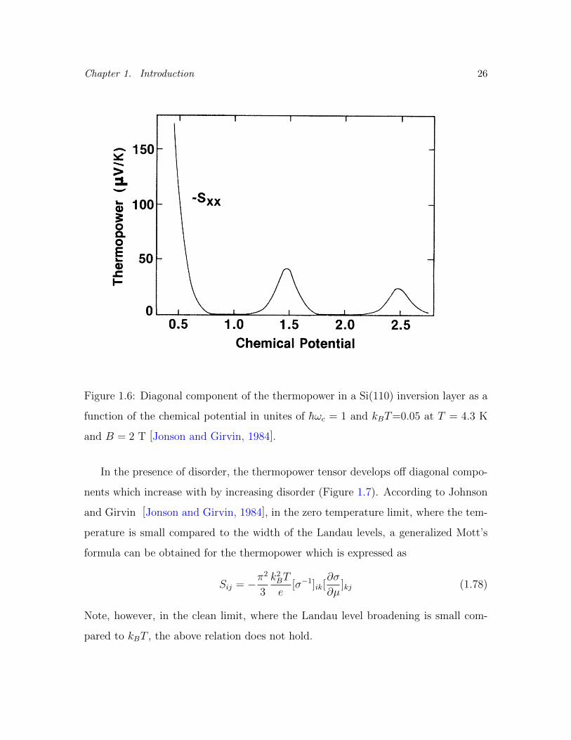
Chapter 1. Introduction 26
Figure 1.6: Diagonal component of the thermopower in a Si(110) inversion layer as a
function of the chemical potential in unites of hωc = 1 and kBT=0.05 at T = 4.3 K
and B = 2 T [Jonson and Girvin, 1984].
In the presence of disorder, the thermopower tensor develops off diagonal compo-
nents which increase with by increasing disorder (Figure 1.7). According to Johnson
and Girvin [Jonson and Girvin, 1984], in the zero temperature limit, where the tem-
perature is small compared to the width of the Landau levels, a generalized Mott’s
formula can be obtained for the thermopower which is expressed as
Sij = −π2
3
k2BT
e[σ−1]ik[
∂σ
∂µ]kj (1.78)
Note, however, in the clean limit, where the Landau level broadening is small com-
pared to kBT , the above relation does not hold.
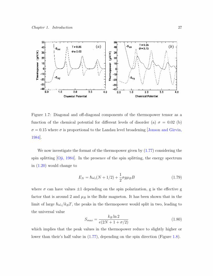
Chapter 1. Introduction 27
() ()
Figure 1.7: Diagonal and off-diagonal components of the thermopower tensor as a
function of the chemical potential for different levels of disorder (a) σ = 0.02 (b)
σ = 0.15 where σ is proportional to the Landau level broadening [Jonson and Girvin,
1984].
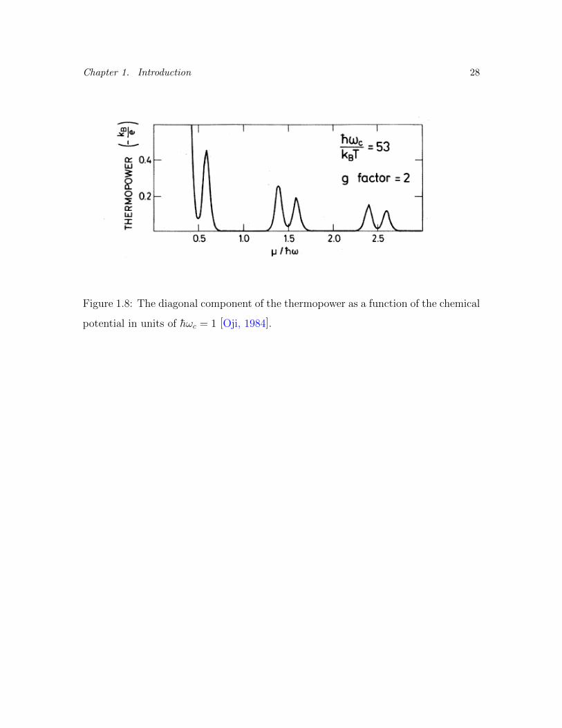
We now investigate the format of the thermopower given by (1.77) considering the
spin splitting [Oji, 1984]. In the presence of the spin splitting, the energy spectrum
in (1.20) would change to
EN = hωc(N + 1/2) +1
2σgµBB (1.79)
where σ can have values ±1 depending on the spin polarization, g is the effective g
factor that is around 2 and µB is the Bohr magneton. It has been shown that in the
limit of large hωc/kBT , the peaks in the thermopower would split in two, leading to
the universal value
Smax =kB ln 2
e(2N + 1 + σ/2)(1.80)
which implies that the peak values in the thermopower reduce to slightly higher or
lower than their’s half value in (1.77), depending on the spin direction (Figure 1.8).
Chapter 1. Introduction 28
Figure 1.8: The diagonal component of the thermopower as a function of the chemical
potential in units of hωc = 1 [Oji, 1984].

Chapter 2. Sample fabrication 29
Chapter 2
Sample fabrication
2.1 Basic device fabrication using exfoliated graphene
The fabrication of graphene devices starts by a process called ”mechanical exfolia-
tion” which first was reported by [Novoselov et al., 2004]. This method is simple and
not time consuming. A small flake of graphite (Kish graphite, Toshiba Ceramics) is
placed on the sticky side of a scotch tape. Then, the tape is folded into itself and
peeled off gently. This way, the graphene is cleaved onto two pieces on the tape. This
folding is repeated several times until an area with not shiny flakes of graphite which
are spread homogenously is obtained. Then, this area of the tape is pressed on a
clean chip of Si wafer with ∼300 nm SiO2. Prior to this, the SiO2/Si substrates are
cleaned in Piranha (3:1 sulfuric acid to hydrogen peroxide solution), rinsed in deion-
ized (DI) water and blow dried with nitrogen gas. After pressing on the substrate,
the tape is rubbed by a teflon tweezer or the round end of a pen. With peeling of
the tape gently, which should take more than 30 s, graphite pieces make contact with
the substrate at a few places due to the van der waals forces. When the cleaving
is done, one can simply locate graphene flakes using an optical microscope. Special
thickness of the SiO2 substrate would lead to the interference effects which make
the single layer graphene to be visible (Figure 2.1a) and contrasted from multilayer
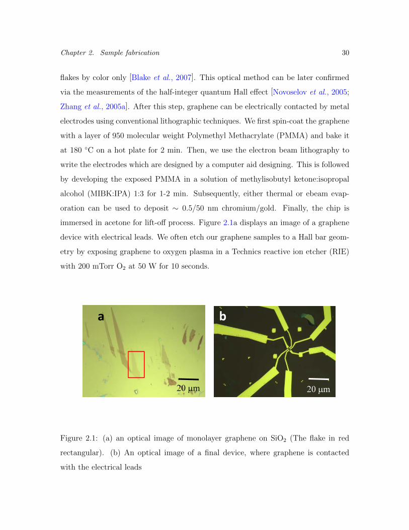
Chapter 2. Sample fabrication 30
flakes by color only [Blake et al., 2007]. This optical method can be later confirmed
via the measurements of the half-integer quantum Hall effect [Novoselov et al., 2005;
Zhang et al., 2005a]. After this step, graphene can be electrically contacted by metal
electrodes using conventional lithographic techniques. We first spin-coat the graphene
with a layer of 950 molecular weight Polymethyl Methacrylate (PMMA) and bake it
at 180 C on a hot plate for 2 min. Then, we use the electron beam lithography to
write the electrodes which are designed by a computer aid designing. This is followed
by developing the exposed PMMA in a solution of methylisobutyl ketone:isopropal
alcohol (MIBK:IPA) 1:3 for 1-2 min. Subsequently, either thermal or ebeam evap-
oration can be used to deposit ∼ 0.5/50 nm chromium/gold. Finally, the chip is
immersed in acetone for lift-off process. Figure 2.1a displays an image of a graphene
device with electrical leads. We often etch our graphene samples to a Hall bar geom-
etry by exposing graphene to oxygen plasma in a Technics reactive ion etcher (RIE)
with 200 mTorr O2 at 50 W for 10 seconds.
ba
20 µm 20 µm
Figure 2.1: (a) an optical image of monolayer graphene on SiO2 (The flake in red
rectangular). (b) An optical image of a final device, where graphene is contacted
with the electrical leads

Chapter 2. Sample fabrication 31
The resistivity of the final devices (Figure 2.1b) can be measured either using
a standard low-frequency lock-in techniques or a DC voltage source. The silicon
underneath the graphene can be served as a backgate to tune the charge density in
the graphene samples, where SiO2 is a dielectric with the capacitance coupling of
Cg = ne/(Vg −VNP ) . The position of the charge neutrality point is denoted by VNP ,
which might be different from zero owing to the presence of ionized charge impurities.
2.2 Fabrication and measurement of suspended two-
terminal devices
For fabrication of suspended samples, the methods described in [Bolotin et al., 2008b;
Du et al., 2008] are mainly employed. We first start by the basic fabrication method
described previously with some modifications: First, we select natural flakes of graphene
which are approximately rectangular shape convenient for fabrication into Hall bars
without patterning graphene flakes using oxygen plasma etching as it might induce
defects as well as dangling bonds on the graphene edges [Han et al., 2007]. Second,
the appropriate size of graphene flakes should be limited to 1-3 µm to avoid collaps-
ing after suspension. Third, the width and thickness of the electrodes contacted to
graphene should be around 0.5-1 µm and 75-100 nm, respectively, to enhance the
mechanical rigidity of suspended samples. Lastly, the end of graphene stripes should
be all covered by metal electrodes to avoid collapsing due to the mechanical tension
which is induced by other collapsed areas of the flake.
The suspended samples are obtained by immersing the device in to 1:20 buffered
oxide etch (BOE) for 12-15 min, which removes ∼150-200 nm of the SiO2 substrate.
Previously [Bolotin et al., 2008b], 1:6 buffered oxide etch (BOE) was used for 90s
to remove the SiO2 layer. However, using 1:20 buffered oxide etch (BOE) for 12-15
min would leads to a more controlled process and enhances the uniformity of etching
underneath graphene. Surprisingly, the etching rate underneath graphene was found

Chapter 2. Sample fabrication 32
to be faster than other parts. This might be due to the rapid propagation of BOE
along the SiO2/graphene interface in the presence of moisture [Bolotin, 2008]. The
important point to note is that the SiO2 layer under the electrodes is not etched as
the covering gold electrode acts as a mask. This indicates the size and the thickness
of electrodes matter for the mechanical rigidity of the device. After etching was fin-
ished, the device is transferred from BOE to DI water and subsequently placed in
acetone. DI water is considered as the best solution to remove the chemical BOE
residues. Transferring from DI water to acetone should be done through a series
of water/acetone mixtures with gradually increasing the ratio of acetone relative to
water, since the abrupt change in surface tension of graphene’s environment might
cause the sample collapse. In the next step, the acetone would be heated up on a
hot plate at ∼ 70 C for 10-15 min to further dissolve the chemical residues from the
etching process. Finally, the device is transferred from acetone to IPA again by a
series of acetone/IPA mixtures and blow dried gently by nitrogen gas. The important
difference between our method and one described in [Bolotin et al., 2008b] is that
we do not use the critical point dryer which is crucial for achieving large suspended
samples with cleanly exposed surfaces. The samples dried via the critical point drier
often exhibit a low sample quality even after annealing process.
Chapter 2. Sample fabrication 33
a b
c
1 µm20 µm
Figure 2.2: (a) optical and (b) AFM image of a suspended two terminal graphene
device
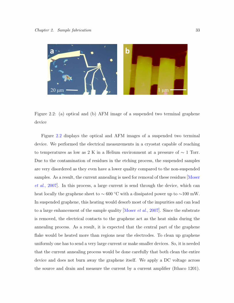
Figure 2.2 displays the optical and AFM images of a suspended two terminal
device. We performed the electrical measurements in a cryostat capable of reaching
to temperatures as low as 2 K in a Helium environment at a pressure of ∼ 1 Torr.
Due to the contamination of residues in the etching process, the suspended samples
are very disordered as they even have a lower quality compared to the non-suspended
samples. As a result, the current annealing is used for removal of these residues [Moser
et al., 2007]. In this process, a large current is send through the device, which can
heat locally the graphene sheet to ∼ 600 C with a dissipated power up to ∼100 mW.
In suspended graphene, this heating would desorb most of the impurities and can lead
to a large enhancement of the sample quality [Moser et al., 2007]. Since the substrate
is removed, the electrical contacts to the graphene act as the heat sinks during the
annealing process. As a result, it is expected that the central part of the graphene
flake would be heated more than regions near the electrodes. To clean up graphene
uniformly one has to send a very large current or make smaller devices. So, it is needed
that the current annealing process would be done carefully that both clean the entire
device and does not burn away the graphene itself. We apply a DC voltage across
the source and drain and measure the current by a current amplifier (Ithaco 1201).

Chapter 2. Sample fabrication 34
Initially, we ramp up the bias voltage to a set point very slowly ∼ 0.02 V/s, while
recording the current (Figure 2.3a). After reaching the set current point, the voltage
is ramped down very fast ∼ 0.1 V/s to zero. Then, we measure the gate dependence
of the conductivity by a small bias voltage ∼ 1 mV to check the changes caused
by annealing (Since applying a gate voltage leads to an attractive force between the
suspended sample an the plate, the gate voltage is limited between ±10 V to avoid
collapsing due to the electrostatic forces). If there were no improvements, we repeat
the current annealing again by increasing the set point in steps of 0.1 V. Figure 2.3
displays I − Vsd curves with different setpoints and the resulting conductance versus
back gate voltage at each step. By increasing the source drain voltage to above 2 V
(sending a larger current), the sample quality improves as the width of the Dirac peak
is becoming smaller. Note that the I − Vsd is not linear in this regime, which is due
to the heating of graphene.
0 3
0
1
-10 0 10
0
25 V
s=0.8V
Vs=1.25V
Vs=1.75V
Vs=2.45V
Vs=3V
(V)
b
(m
A)
(V)
a
(/ℎ)
Figure 2.3: (a) I−Vsd curves during current annealing with different setpoints (b) The
conductivity versus back gate voltage at different annealing steps define by different
setpoints. Experiment was performed at 2 K in helium gas environment
The measured mobility in our annealed devices reaches 200,000 cm−2/Vs, which
is an order of magnitude larger than the graphene samples on SiO2. At this stage, we

Chapter 2. Sample fabrication 35
have ramped up the voltage at least 30 times, manually. From Figure 2.3b, a shift of
the Dirac peak toward negative values of the gate voltage (p-doped) is observed at
the beginning, but by further annealing the Dirac point is shifted toward positive gate
voltages (n-doped). Most of the devices show a similar trend and as a matter of fact
when the device is becoming n-doped during the final steps of annealing, the quality
of the QHE in our devices is becoming better as depicted in Figure 2.4a, although
the width of the Dirac peak is larger and the sample mobility is lower relative to the
initially p-doped device.
-10 -5 0 5 10
0
5
10
15
20
25
before anealing
Vs =1.75V
Vs =2.35V
Vs =3V
1T
(
/ℎ)
(V)
-10 -5 0 5 10
0
1
2
Vs=2.35V
Vs=3V
14T
(
/ℎ)
(V)
“ν=1/3”
ba
Figure 2.4: (a) QHE in a suspended two terminal device at different steps of current
annealing at 2 T. (b) High field behavior of a suspended device at different current
annealing steps. When the device is annealed more (Vs=3 V) the insulating state and
the ν = 1/3 FQHE state would appear.
Figure 2.4b also displays the high field conductivity data at two annealing steps.
The insulating state appearing at the charge neutrality point is a signature of the high
quality of a monolayer graphene, as it would be explained later in this thesis [Bolotin
et al., 2009]. We see that this state just develops at the final step of annealing in our
suspended samples. We would discuss the observed FQHE and the insulating state
coming from strong interactions in our annealed two-terminal graphene samples in

Chapter 2. Sample fabrication 36
the next chapter.
2.3 Multi-terminal suspended devices
As it was discussed in the previous section, by making suspended two-terminal high
quality samples, we can access to many body correlated states in the presence of the
magnetic field. However, due to the inherent mixing between longitudinal and trans-
verse resistivities in these two-terminal measurements [Abanin and Levitov, 2008],
quantitative characterization of the observed states is only possible in an indirect
analysis [Abanin et al., 2010]. Multi-terminal measurements are needed to be per-
formed for more direct quantitative analysis. Although multi-terminal measurements
on suspended graphene samples have been reported previously [Bolotin et al., 2008b;
Du et al., 2008], the mechanical [Prada et al., 2010] and thermal instability [Skachko
et al., 2010] of these samples have prevented even the observation of the IQH effect.
To make suspended multi-terminal samples, we mainly follow the fabrication method
described for the two-terminal devices. Since we do not use the critical point dryer,
the size of our samples is limited to 2-3 µm. Figure 2.5 displays AFM images of a
few four-terminal suspended samples.

Chapter 2. Sample fabrication 37
2 µm
3 µm
2 µm
a
b c
Figure 2.5: (a),(b)and (c) AFM images of 3 suspended four terminal devices.
The size of the leads is between 0.5 − 1 µm to ensure the mechanical rigidity
of our samples. However, this makes our contacts more invasive and less ideal for
performing multi-terminal measurements. Similar to the two-terminal devices, we
employ the current annealing to remove the residues left from the etching process.
Since we have more contacts and a larger sample size, the current annealing processes
are more challenging than that of the two-terminal devices. Figure 2.6a shows the
repeated annealing process for a multi-terminal device, in which, the current is sent
from source (contact 2) to drain (contact 4) by changing the set point successively
in at least 40 steps. Figure 2.6b also presents the resulting conductivity curve versus
back gate voltage for a few set points. At the final steps, the sample is p-doped and
has a double peak structure due to the sample inhomogeneity. To remove this feature,
we send the current between contacts 1 and 3. Figure 2.6c displays the conductiv-
ity between source and drain at different stages of the annealing process between
the side contacts. As we send more current between the side contacts, the double
peak structure disappears. Note that, in our experience, annealing evenly between

Chapter 2. Sample fabrication 38
all contacts does not necessarily remove the sample inhomogeneity. We find that
if we first current anneal aggressively between source and drain contacts and, then,
perform a slight annealing between the side contacts and the corners ones we have
a better quality sample with more uniformity. Figure 2.6d shows the four-terminal
resistance of a current annealed device using the van der pauw method. We first send
an excitation current ∼ 10 nA between contacts 1 and 2 and measure the resulting
voltage between contacts 3 and 4, using the Lock-in amplifier. Then, we send the
current between contacts 1 and 4 and measure the voltage between 2 and 3. The
obtained resistance curves from these measurements give a Dirac point located at
the same gate voltage, which is an indication of low sample inhomogeneity after the
annealing process. However, the magnitude of the resistance between different pairs
is different. This can be explained by the difference of the effective sample length
between different contacts.

Chapter 2. Sample fabrication 39
-10 0 10
0.0
0.4
I12
-V34
I41
-V23
0 5
0.0
1.5
-10 0 10
0
30
V24
=1V
V24
=2V
V24
=3V
V24
=4V
V24
=5V
-10 0 10
0
30
V13
=0
V13
=1.2
V13
=1.3
V13
=1.45
(m
A)
(kΩ)
(V)
(V)(V)
(V)
(
/ℎ)
1
2
3
4
(
/ℎ)
a b
c d
Figure 2.6: (a) I−Vsd curves during current annealing between contacts 2 and 4 with
different setpoints (b) The two terminal conductivity between contacts 2 and 4 versus
back gate voltage at different annealing steps between contacts 2 and 4. (c) The two
terminal conductivity between contacts 2 and 4 versus back gate voltage at different
annealing steps between contacts 1 and 3. (d) Four terminal resistance by sending
current between contacts 1 , 2 and measuring the resulting voltage between contacts
3 and 4 (black)or sending current between contacts 1 , 4 and measuring the resulting
voltage between contacts 2 and 3.
Figure 2.7a displays the longitudinal and Hall rsistivities of a multi-terminal sus-
pended sample versus the back gate voltage before (dotted lines) and after annealing

Chapter 2. Sample fabrication 40
(solid line) at 2 T. The longitudinal resistance (Rxx) and transverse resistance (Rxy)
were measured by van der Pauw method in positive and negative field for symmetriz-
ing/ anti-symmetrizing process. Before annealing we do not observe see any feature
corresponding to the IQHE, like the minima in Rxx and the quantized plateaus in
Rxy as the contacts and the sample are very disordered. But, after annealing we see
very well developed QHE states at filling factors ν = 2 and ν = 6, in both Rxx and
Rxy. In addition, we observe symmetry broken states (Figure 2.7b) as well as FQHE
states at higher fields [Ghahari et al., 2011], which would be discussed in chapter 4.
-10 0 10
0
8
-0.5
0.0
0.5
2T
(kΩ)
0 14
0.0
0.5
1.0
ν=1
ν=2
ν=6
ν=10
ν=3
0
3
Vg=-7.30V
(ℎ/)
(kΩ)
= −2
= −6
(V)(T)
ba
Figure 2.7: (a) The measured Rxx and Rxy versus back gate voltage for a suspended
multi terminal device at 2 T, before (dotted lines) and after (solid line) annealing.
(b) Rxx and Rxy versus magnetic field at a fixed back gate voltage. In addition to
the QHE states , we observe the symmetry broken states at ν = 1 and ν = 3.
2.4 Fabrication of graphene on boron nitride sub-
strates
As it was stated earlier, the quality of suspended annealed graphene devices is an or-
der of magnitude higher than graphene on a SiO2 substrate. However, these samples
Chapter 2. Sample fabrication 41
have a few disadvantages which makes them difficult to work with. First, suspended
samples are very fragile as they change over each thermal cycling. Second, one needs
to perform current annealing to improve the sample mobility, otherwise they are very
disordered. This annealing process is very time consuming as it might take a few
days for proper optimization. Lastly, the achievable density range in these samples is
limited as the special care has to be taken to avoid collapsing due to the electrostatic
forces. For these reasons, working with suspended samples is technically challenging.
One way to improve the sample quality would be to engineer a different substrate
for graphene. It has been demonstrated that hexagonal boron nitride (h-BN) can be
used as a promising substrate for graphene-based devices [Dean et al., 2010], leading
to a large enhancement in the sample quality. h-BN is an insulating material, where
boron and nitrogen atoms fill the inequivalent A and B sublattices in the Bernal struc-
ture. It has a large band gap (5.97 eV) [Watanabe et al., 2008] and a small lattice
mismatch with graphite [Giovannetti et al., 2007]. In contrast to SiO2, h-BN is ex-
pected to be free of dangling bonds and surface charge traps. In addition, the surface
optical phonon modes of h-BN have higher energies, which would offer an improved
high-temperature performance of graphene/h-BN heterostructures [Meric et al., 2008;
Schwierz, 2008].
To fabricate graphene/BN stacks, we first exfoliate h-BN single crystals [Taniguchi
and Watanabe, 2008] on a SiO2 substrate. We can identify h-BN flakes with different
thicknesses using an optical microscope similar to the exfoliated graphene on SiO2.
The selected exfoliated flakes would be scanned by an AFM to check the surface
roughness and to make sure it is free from the tape residues and other contamina-
tions. We normally use h-BN flakes which are around ∼ 20 nm in thickness. Then,
we exfoliate graphene on PMMA/PVA/Si wafers, where the thickness of PMMA is
tuned, such that, the single layer graphene is visible. Note that the thickness of PVA
(polyvinyl alcohol) is very small as it is used as a water soluble layer. After identify-
ing graphene flakes, we place PMMA/PVA/Si wafer in a water bath, where PVA is
Chapter 2. Sample fabrication 42
dissolved and PMMA membrane with graphene would float on the top of DI water.
Then, this membrane would be transferred using a micro manipulators placed in the
transfer station (a microscope which is fixed on an air table) on top of the target
h-BN flake. The temperature of the substrate during the transfer should be between
70-80 C.
After transferring, the device is placed in acetone to remove the PMMA layer and
then would be annealed in a 5% H2/95%Ar atmosphere to at 350 C for several hours
to remove the processing residues. We would scan the surface of graphene/h-BN by
an AFM to make sure it is clean and there is no rippling (Figure 2.8a). Electri-
cal contacts were made of a Cr/Pd/Au metal stack are deposited using the standard
electron-beam lithography as it was described in the basic fabrication section. Finally,
the device would be etched into a Hall bar using oxygen plasma. Figure 2.8b displays
an image of a thermopower device made from a graphene/h-BN stack. The mobility
of the samples on h-BN can be as high as 60,000 cm−2/Vs. This relatively higher
mobility relative to graphene on SiO2 has made it possible to observe the FQHE in
graphene on substrate at high magnetic fields [Dean et al., 2011](Figure 2.8d). In ad-
dition, the Hofstadters butterfly has been observed very recently [Dean et al., 2013;
Ponomarenko et al., 2013](Figure 2.8c [Ghahari, 2012]) due to the Moire pattern that
develops when the graphene lattice is oriented with near zero-angle mismatch to the
h-BN lattice.
In the method which was described here, the graphene is in a direct contact with
a polymer like PMMA, which could not be avoided during the transfer process. As
a result, the device needs to be annealed to remove all the residues. We also tried
to employ the polymer free technique described in [Wang et al., 2013] to make
graphene h-BN superstructures, in which, the graphene and the interfaces are not
exposed to polymers. We first start by spin coating a bare silicon chip with 1 µm
of poly-propylene carbonate (PPC). The PPC would be peeled off using a piece of
scotch tape with a hole at the middle and would be placed on top of PDMS (poly
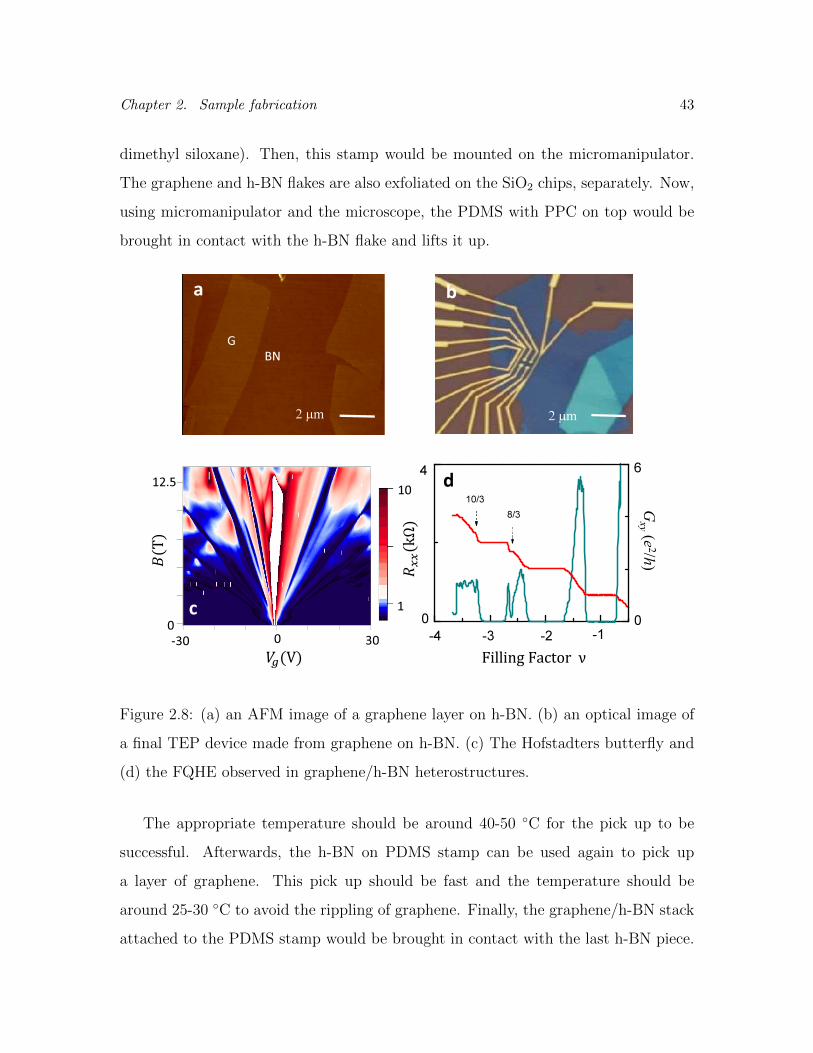
Chapter 2. Sample fabrication 43
dimethyl siloxane). Then, this stamp would be mounted on the micromanipulator.
The graphene and h-BN flakes are also exfoliated on the SiO2 chips, separately. Now,
using micromanipulator and the microscope, the PDMS with PPC on top would be
brought in contact with the h-BN flake and lifts it up.
-30 -20 -10 0 10 20 30
12.5
10.0
7.5
5.0
2.5
0.0
2 µm
BN
G
2 µm
bba b
10/3
8/3
-1
FillingFactorν
-2-3-4
0
6
0
4
(kΩ)
Gxy(e
2/h)
0
12.5
(T
)
0-30 30
(V)
c
d10
1
Figure 2.8: (a) an AFM image of a graphene layer on h-BN. (b) an optical image of
a final TEP device made from graphene on h-BN. (c) The Hofstadters butterfly and
(d) the FQHE observed in graphene/h-BN heterostructures.
The appropriate temperature should be around 40-50 C for the pick up to be
successful. Afterwards, the h-BN on PDMS stamp can be used again to pick up
a layer of graphene. This pick up should be fast and the temperature should be
around 25-30 C to avoid the rippling of graphene. Finally, the graphene/h-BN stack
attached to the PDMS stamp would be brought in contact with the last h-BN piece.

Chapter 2. Sample fabrication 44
Afterwards, by increasing the temperature to higher than 70 C and lifting the PDMS
stamp, the BN/graphene/BN stack would be left on the SiO2 substrate. To remove
the PPC layer, the sample is left in acetone or chloroform. Figure 2.9a displays an
optical image of a BN/graphene/BN stack.
To make a device from the final stack, we first spin coat the chip with a double layer
resist composed of a thin layer of PMMA A2 and a layer of hydrogen-silsesquioxane
(HSQ) on top. Then, a hard mask is defined on top of the stack with the desired
shape and size using electron-beam lithography. After developing, the HSQ would
be left just where the mask is defined and the PMMA layer would etched using
an Oxygen plasma. We use ICP with the plasma produced from O2 and CHF3
gases to etch the BN out side the defined mask. Then, the device would be left in
acetone to remove the PMMA/HSQ layer on top of the stack. Finally, the metal
leads (1 nm Cr/15 nm Pd/60 nm Au) are deposited with the electrical contacts just
along the edges of graphene which is the only area exposed (Figure 2.9b). It is shown
that the edge contacts lead to a smaller contact resistance compared to the normal
ones [Wang et al., 2013]. In addition, since with the pick up technique the graphene
is not exposed to any polymer, the mobility is very high and the ballistic transport
is observed at low temperatures. As it is displayed in Figure 2.9c, the four-terminal
conductivity measured in the finite size samples exhibit very high conductivity with
not-well defined conductivity values near the Dirac point, suggesting possible ballistic
conduction at low temperatures. In such devices, the mean free path in these devices
is just limited by the sample size (Figure 2.9d). The room-temperature mobility is
also comparable to the theoretical predictions, in which, it is just limited by the
phonon scattering [Bennett et al., 2005; Orr et al., 2008].

Chapter 2. Sample fabrication 45
-40 0 40
0.00
0.04
10 100
105
Mo
bility
(cm-2/V
s)
(K)
ba
10 µm
bc
d
BN
G
BN
4 µm
(kΩ)
(V)
Figure 2.9: (a) an optical image of a BN/graphene/BN heterostructure. (b) an
optical image of a TEP device made from graphene sandwiched between top and
bottom layers of h-BN. (c) The conductivity measured from a 3 µm encapsulated
graphene device with edge contacts (d) Temperature dependent mobility on a log-log
scale at fixed back gate voltage ∼ 40 V. The mobility at low temperatures is limited
by the sample size due to the ballistic transport.
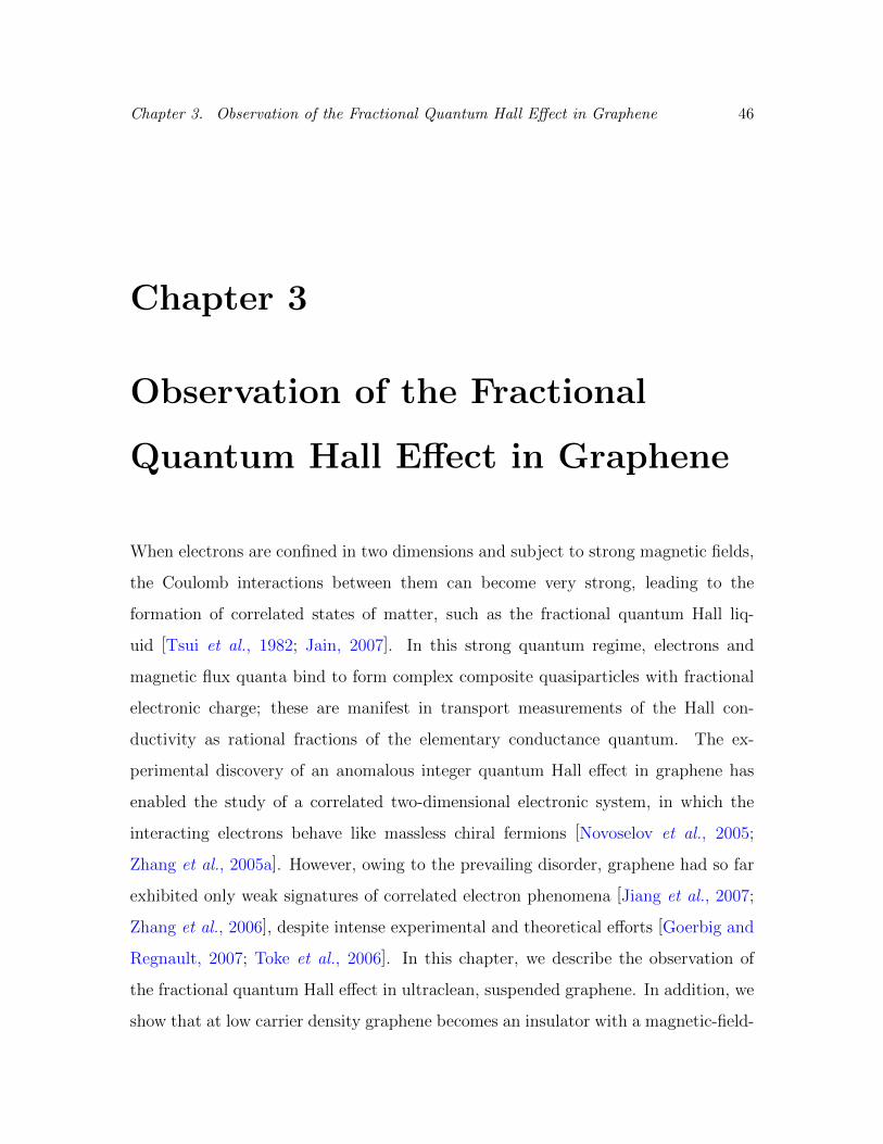
Chapter 3. Observation of the Fractional Quantum Hall Effect in Graphene 46
Chapter 3
Observation of the Fractional
Quantum Hall Effect in Graphene
When electrons are confined in two dimensions and subject to strong magnetic fields,
the Coulomb interactions between them can become very strong, leading to the
formation of correlated states of matter, such as the fractional quantum Hall liq-
uid [Tsui et al., 1982; Jain, 2007]. In this strong quantum regime, electrons and
magnetic flux quanta bind to form complex composite quasiparticles with fractional
electronic charge; these are manifest in transport measurements of the Hall con-
ductivity as rational fractions of the elementary conductance quantum. The ex-
perimental discovery of an anomalous integer quantum Hall effect in graphene has
enabled the study of a correlated two-dimensional electronic system, in which the
interacting electrons behave like massless chiral fermions [Novoselov et al., 2005;
Zhang et al., 2005a]. However, owing to the prevailing disorder, graphene had so far
exhibited only weak signatures of correlated electron phenomena [Jiang et al., 2007;
Zhang et al., 2006], despite intense experimental and theoretical efforts [Goerbig and
Regnault, 2007; Toke et al., 2006]. In this chapter, we describe the observation of
the fractional quantum Hall effect in ultraclean, suspended graphene. In addition, we
show that at low carrier density graphene becomes an insulator with a magnetic-field-

Chapter 3. Observation of the Fractional Quantum Hall Effect in Graphene 47
tunable energy gap. These newly discovered quantum states offer the opportunity to
study correlated Dirac fermions in graphene in the presence of large magnetic fields.
3.1 Introduction
In a perpendicular magnetic field, the energy spectrum of a clean two-dimensional
electron system (2DES) splits into a fan of Landau levels. When the Fermi energy is
tuned to lie between the Landau levels, the system enters the integer quantum Hall
regime, in which current is carried by states at the edge of the sample and the overall
conductance (G) is quantized as G = νe2/h, where ν is a Landau level filling factor
which takes on integer values in the case of the integer quantum Hall effect (IQHE), e
is the elementary charge, and h is Plancks constant. The first observation of the IQHE
in graphene demonstrated an unusual sequence of filling factors, ν = ±2,±6,±10, ...
which differs from previously studied 2DESs [Jain, 2007]. This sequence originates
from two peculiar features of graphene: the fourfold spin and pseudo-spin (valley)
degeneracy of Landau levels and the existence of a non-trivial Berry phase associated
with the pseudo-spin of Dirac quasiparticles [Neto et al., 2009].
In clean samples and under very strong magnetic fields, additional integer quan-
tum Hall states emerge at filling factors ν = 0,±1. These fragile states are con-
jectured to result from electron-electron (e-e) interactions lifting the pseudospin and
spin degeneracy of the zeroth Landau level [Yang, 2007]. The nature of these states,
and in particular the unusual ν = 0 state, responsible for the divergent resistivity
of graphene at high magnetic fields [Checkelsky et al., 2009], has raised considerable
interest in the effect of e-e interactions among Dirac quasiparticles. In conventional
semiconductor heterojunctions, such correlation effects are spectacularly manifested
in the fractional quantum Hall effect (FQHE), where new electronic ground states
are formed in which the elementary excitations are composite particles with frac-
tional charge [Sarma and Pinczuk, 1997]. The possibility of the FQHE in graphene
Chapter 3. Observation of the Fractional Quantum Hall Effect in Graphene 48
and the interplay between many-body correlations and the SU(4) symmetry of quasi-
particles have ignited considerable theoretical interest [Goerbig and Regnault, 2007;
Toke et al., 2006; Peres et al., 2006; Apalkov and Chakraborty, 2006; Yang et al., 2006;
Khveshchenko, 2007; Khveshchenko, 2008; Toke and Jain, 2008].
3.1.1 Quantum conductance of two terminal devices
Although a two-terminal measurement is not as straight forward as a four probe
measurement, it might be the only possible measurement which can be done for
small samples. The conductance for a square sample with the longitudinal and Hall
conductivities σxx and σxy, respectively, and ideal contacts on opposite sides is given
by GL=W =√σ2xx + σ2
xy which is derived from a duality relation for 2-dimensional
(2d) transport. However, for a sample with arbitrary shape the formalism is more
complicated. In particular, this problem for a rectangular sample with an arbitrary
shape has been treated using conformal mapping technique [Abanin and Levitov,
2008]. These numerical results for a monolayer graphene sample with different aspect
ratios L/W , are plotted in Figure 3.1 . The conductance strongly depends on the
sample aspect ratio L/W . As it is displayed in Figure 3.1, the conductance for a
square sample, L = W , is a monotonic function of the filling factor ν . In contrast,
the conductance shows a nonmonotonic behavior as a function of density for L 6= W
where the QHE plateaus are less definite compared with the L = W case. In detail,
for L < W , the conductance has minima at the center of the QHE plateau, But, for
L > W , it shows maxima. In another words, the conductance for the later is smaller
than the former and we have : GL>W < GL=W < GL<W .
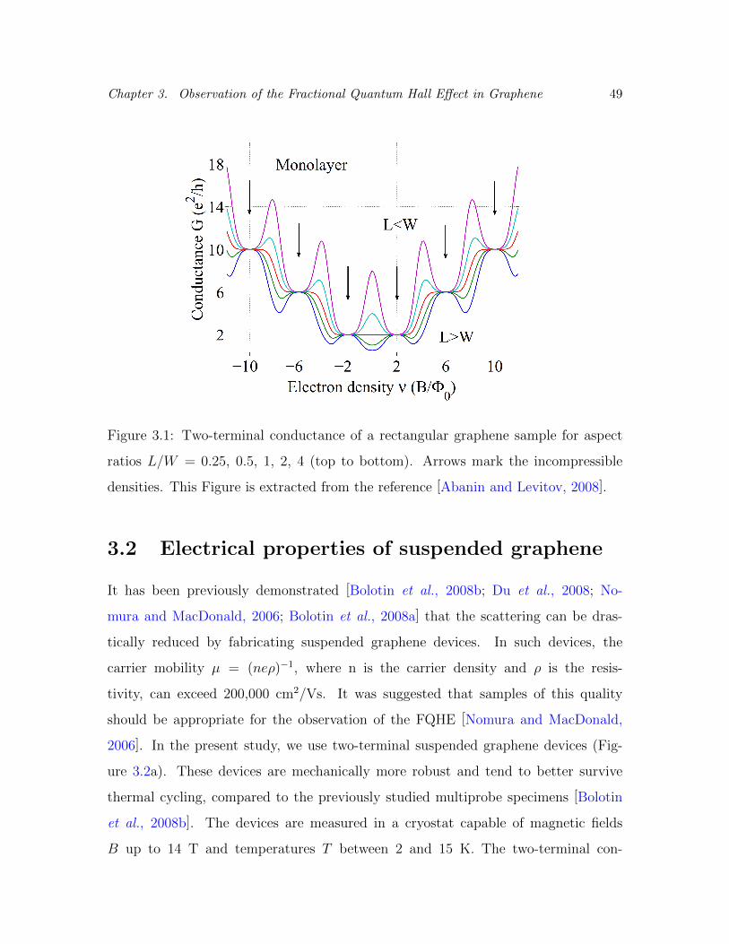
Chapter 3. Observation of the Fractional Quantum Hall Effect in Graphene 49
Figure 3.1: Two-terminal conductance of a rectangular graphene sample for aspect
ratios L/W = 0.25, 0.5, 1, 2, 4 (top to bottom). Arrows mark the incompressible
densities. This Figure is extracted from the reference [Abanin and Levitov, 2008].
3.2 Electrical properties of suspended graphene
It has been previously demonstrated [Bolotin et al., 2008b; Du et al., 2008; No-
mura and MacDonald, 2006; Bolotin et al., 2008a] that the scattering can be dras-
tically reduced by fabricating suspended graphene devices. In such devices, the
carrier mobility µ = (neρ)−1, where n is the carrier density and ρ is the resis-
tivity, can exceed 200,000 cm2/Vs. It was suggested that samples of this quality
should be appropriate for the observation of the FQHE [Nomura and MacDonald,
2006]. In the present study, we use two-terminal suspended graphene devices (Fig-
ure 3.2a). These devices are mechanically more robust and tend to better survive
thermal cycling, compared to the previously studied multiprobe specimens [Bolotin
et al., 2008b]. The devices are measured in a cryostat capable of magnetic fields
B up to 14 T and temperatures T between 2 and 15 K. The two-terminal con-
Chapter 3. Observation of the Fractional Quantum Hall Effect in Graphene 50
ductance G is recorded as a function of B, T and n, which is tuned by adjust-
ing the voltage VG between the graphene and the back gate electrode. We limit
|VG| < 10 V in order to avoid collapse of the graphene due to electrostatic attrac-
tion, limiting the accessible carrier densities to |n| < 3.5 × 1011 cm−2. At T = 2 K,
a sharp peak in resistance R = 1/G is evident around the Dirac point VD < 2 V;
at this gate voltage, graphene is charge neutral (Figure 3.2b). From the observed
full-width at half-maximum of R(VG), we estimate the density inhomogeneity of
the suspended graphene to be less than 1 × 1010 cm−2 (refs [Bolotin et al., 2008b;
Bolotin et al., 2008a]).
Figure 3.2: (a) False-colour scanning electron micrograph of a typical device. Single
layer graphene (red) is suspended ,150 nm above SiO2/Si substrate (grey) and sup-
ported by two gold electrodes (yellow). To ensure mechanical stability of the devices,
we use a two-terminal configuration in this study. (b) Resistivity ρ of graphene as
a function of gate voltage VG applied between the graphene and the substrate, mea-
sured at T = 2 K and B = 0 T. The resistivity is calculated from the resistance R
via ρ = RW/L, where W and L are sample width and length, respectively.

Chapter 3. Observation of the Fractional Quantum Hall Effect in Graphene 51
3.3 Suspended graphene in low magnetic field
We first confirm the high quality of the suspended graphene devices by studying
them at low magnetic fields. Remarkably, even at B = 0.3 T we observe a developing
plateau in G at 2e2/h associated with the IQHE at ν = 2. At B = 1 T, fully developed
plateaus are evident at ν = ±2,±6,±10(Figure 3.3a). It is convenient to visualize
the IQHE by means of a Landau fan diagram, where the derivative |dG/dn(B, n)| is
plotted as a function of B and n (Figure 3.3b).
b
a
Figure 3.3: (a) Conductance G as a function of back gate voltage at different magnetic
fields B = 0.3, 0.5, 1 T.(b) Colour rendition of |dG/dn(B, n)| in the low magnetic
field regime B = 0 − 1 T . Dark colour corresponds to quantum Hall plateau region
G(n) = νe2/h = const. The gate capacitance Cg ≈ 50 aFµm−2 used in calculating
the carrier density n = Cg(Vg − VD) is obtained from the shift of the quantum Hall
plateaus with magnetic field. The contact resistance ∼ 200 Ω is estimated from the
deviation of the conductance from the expected quantized value G = νe2/h.
At a quantum Hall plateau corresponding to filling factor ν, the conductance
remains constant G(VG) = νe2/h, and the electron density is given by n(B) = Bν/φ0,
where φ0 = h/e is the magnetic flux quantum. Therefore, quantum Hall plateaus

Chapter 3. Observation of the Fractional Quantum Hall Effect in Graphene 52
dG/dn = 0 appear as stripes fanning out from point B = 0, VG = VD and with slope
dn/dB = ν/φ0. We observe such stripes down to B < 0.1 T, indicating that the
quantum Hall effect survives to very low fields. Assuming µB < 1 for the IQHE to
exist [Bolotin et al., 2008b], this observation implies a lower bound for the mobility
of ∼200,000 cm2/Vs.
3.4 Symmetry broken and FQHE states in sus-
pended two terminal graphene
In such ultraclean graphene samples, the extreme quantum limit can be reached at
relatively low magnetic field. In the intermediate field regime B < 10 T (Figure 3.4a),
we observe an integer quantum Hall plateau corresponding to ν = 1 at a field as low as
B = 2 T, in addition to the well-resolved ν = 2 integer quantum Hall plateau already
mentioned. Similarly, a G = 0 plateau appears around the region of zero density
(VG = VD) for B > 5 T, indicating the onset of an insulating state at low density.
In the multi-terminal Hall bar samples, this insulating behaviour is considered a
signature of the ν = 0 IQHE, as it accompanies a plateau of Hall conductivity σxy = 0.
In samples on a substrate [Jiang et al., 2007; Zhang et al., 2006], such ν = 0,±1
integer quantum Hall plateaus could only be observed for B > 20 T. These plateaus
are believed to arise from a magnetic field induced spontaneous symmetry breaking
mediated by e-e interactions [Yang, 2007]. This suggests that e-e correlations in
ultraclean suspended graphene can be sustained at much lower fields, compared to
graphene on substrates. The strength of e-e interactions in a filled Landau level
can be estimated to be proportional to e2/lb [Sarma and Pinczuk, 1997], where
lb = (h/eB)1/2 is the magnetic length, and thus increases with B. We therefore
expect stronger interaction effects to occur at higher magnetic fields. Indeed, two
notable features emerge in the high magnetic field regime, B > 10 T: a peak-like
structure and a plateau-like structure, marked by D and A, respectively (Figure 3.4).

Chapter 3. Observation of the Fractional Quantum Hall Effect in Graphene 53
While the position of the peak-like feature D remains unchanged, feature A moves
to higher densities with increasing B, developing into a well-defined plateau. As the
density n corresponding to D does not change with B, this feature is probably due
to B-independent rapid threshold fluctuations, associated with hopping or resonant
tunnelling through localized states [Cobden et al., 1999]. On the other hand, the
electron density corresponding to the plateau-like structure A changes with increasing
B, suggesting that A is related to a quantum Hall state with ν > 0. A consistent
picture emerges when we plot G as a function of filling factor estimated as ν = nφ0/B
(Figure 3.4b, inset). The traces G(n) acquired at different magnetic fields collapse
onto a single universal curve around the feature A. The associated plateau has a value
of G = 0.32 ± 0.02e2/h and is positioned around ν = 0.30 ± .02. In contrast, the
region around D does not collapse onto a universal curve, and is therefore of different
origin. We assign the observed plateau A to the hitherto unobserved [Goerbig and
Regnault, 2007; Toke et al., 2006; Peres et al., 2006; Apalkov and Chakraborty, 2006;
Yang et al., 2006; Khveshchenko, 2007; Khveshchenko, 2008; Toke and Jain, 2008]
fractional quantum Hall state at ν = 1/3. We note that at our highest field, B = 14 T,
we observe the ν = 1/3 plateau at n ≈ 1011cm−2, more than an order of magnitude
higher than the estimated density inhomogeneity in our device. This establishes that
our observation of fractional quantization is not caused by the addition of quantum
resistance observed in graphene pnp junctions [ozyilmaz et al., 2007; Williams et al.,
2007].

Chapter 3. Observation of the Fractional Quantum Hall Effect in Graphene 54
0.2 0.40.0
0.5
0.5 1.0 1.5
0.0
0.3
0.6
(a)
14T
12T13T
A
a
n (1011 cm-2) n (1011 cm-2)
G(e
2/h)
G(e
2/h)
G(e
2/h)
b
v
A
D
0.3
0.3
0 1 2
0
1
2
2T
5T9T
A
D
Figure 3.4: (a) G(n) at B = 2, 5, 9 T. Quantum Hall state ν = 1 develops at B = 2 T,
features with ν < 1 form at 9 T.(b)G(n) forB = 12, 13, 14 T. The data are acquired at
T = 6 K to suppress resistance fluctuations associated with quantum interference. A
plateau A with G ≈ 0.3e2/h and at a density dependent on B emerges when B > 11 T.
Another feature, B, appears at constant n at different fields. Inset, G is replotted as
a function of filling factor ν = nφ0/B for B = 12, 13, 14 T. At different fields, the
G(n) curves around A collapse onto a single universal trace, allowing identification
of feature A as the fractional quantum Hall state ν = 1/3.
Figure 3.5a shows our analysis of the entire data set in terms of a Landau fan
diagram over the whole experimentally accessible range of 0 < B < 14 T and |n| <
3.5 × 1011 cm−2. While features stemming from localized states change between
thermal cycles, the familiar integer quantum Hall states at n = ±1,±2,±6, appear
consistently as the blue fan stripes with slope dB/dn = φ0/ν. In addition to the
ν = 1/3 fractional quantum Hall state A, we find features fanning out with distinctly
different slopes corresponding to ν < 1. These features, marked B and C, appear only

Chapter 3. Observation of the Fractional Quantum Hall Effect in Graphene 55
at low density and at high fields, yielding kink-like structures in G(n) (Figure 3.5b).
We extract ν = 0.46 ± .02, and ν = 0.68 ± .05 for the states B and C, respectively,
from the slopes of the corresponding lines in Fig. 3.5a. As before, G(n) collapses
onto a universal curve around B and C at different fields, allowing the extraction
of G = 0.54 ± 0.02e2/h and G = 0.94 ± 0.02e2/h where the value of conductance
is taken at the centre of each feature. These features, observed in multiple samples
both on electron and hole sides (see Supplementary Information for more details),
suggest additional fractional quantum Hall states, despite being less developed than
the plateau at ν = 1/3 (feature A). As the conductance values of each features are
20− 40% larger than the expected νe2/h with ν = 0.46 (feature B) and 0.68 (feature
C), it is difficult to assign them to particular fractional quantum Hall states with
certainty. We note however, that features B and C occur near ν = 1/2 and ν = 2/3.
It is likely that the feature C is related to the ν = 2/3 fractional quantum Hall state,
which is expected to be one of the strongest such states in graphene [Toke et al.,
2006]. In that case, the deviation of the conductance from the expected value can
be ascribed to a sample-specific effect of the two terminal measurement, namely, the
mixing of longitudinal and transverse conductivity, which can yield G values higher
than those of traditional four-probe measurements [Abanin and Levitov, 2008]. The
origin of feature B is even more unclear. Judging from FQHEs in traditional 2DESs,
the next state to expect is ν = 2/5. Yet its position around ν = 1/2 rather suggests
it might be the two-probe signature of a broad minimum in ρxx often observed in
traditional 2DESs in the vicinity of ν = 1/2, and not a fractional quantum Hall
state [Willett et al., 1997]. The features A, B, and C persist as the temperature is
increased. While most other features associated with localized states disappear at
T ≈ 6 K, the plateau corresponding to ν = 1/3 survives up to T ≈ 10 K (Figure
3.5c). This energy scale is higher than the energy scale of the FQHE observed in
typical semiconductor heterojunctions with similar mobility, where the 1/3 plateau
disappears for T > 10 K at B = 15 T ([Tsui et al., 1982]). This remarkable resilience

Chapter 3. Observation of the Fractional Quantum Hall Effect in Graphene 56
of the FQHE in graphene can be ascribed to the enhanced ee interaction in suspended
graphene due to a reduced dielectric screening. The dielectric constant ε enters the
characteristic energy scale of e-e interaction as Ee−e = e2/εlb. In suspended graphene
ε ≈ 1, as compared to ε = 13.6 in AlGaAs/ GaAs [Sarma and Pinczuk, 1997],
leading to much stronger e-e interactions in graphene, and correspondingly, to larger
energy gaps and more robust FQHEs. In fact, the theoretical expectation for the
excitation energy of ν = 1/3 FQHE in graphene is 0.017e2/εlb ≈ 20 K , which agrees
with our observations. Despite the lack of experimental observation so far, many
theorists have addressed the possibility of the FQHE in graphene. When only SU(2)
symmetry is assumed [Toke et al., 2006; Apalkov and Chakraborty, 2006] (which is
appropriate for the case of high Zeeman energy), it was found that the FQHE in
graphene maps on to the well-studied problem of the FQHE in GaAs 2DESs [Jain,
2007]. Indeed, the fractional quantum Hall states observed in the present work,
ν = 1/3 and possibly ν = 2/3, are in fact the strongest states in the GaAs FQHE.
When, however, the full SU(4) symmetry is considered, novel fractional quantum
Hall states without GaAs analogues were predicted [Goerbig and Regnault, 2007;
Khveshchenko, 2008; Toke and Jain, 2008]. We expect that better quality specimens
will allow exploration of these currently inaccessible exotic possibilities.
3.5 Insulating state at the charge netrality point
Finally, we consider the insulating state that appears in the low density regime at
|ν| < 1/3. The device is fully insulating (R >10 GΩ) at magnetic fields B =0.5 T and
at filling factors ν < 0.15. In the Landau fan diagram (Figure 3.4a) this insulating
state is apparent as a region of zero conductance dG/dn = 0 near the charge neutrality
point.

Chapter 3. Observation of the Fractional Quantum Hall Effect in Graphene 57
Figure 3.5: (a) Landau fan diagram |dG/dn(B, n)| at T = 6 K. Dark blue colour
corresponds to G(n) = νe2/h = const. At high fields, features B and C, with ν =
0.46, 0.68 respectively, emerge in addition to feature A (ν = 1/3). Insulating G = 0
state is evident around n = 0 at B > 5 T. The data are acquired from the same
sample as Fig. 2, but in a different thermal cycle, where disorder related feature D
is absent. For clarity, only the electron part of the data set n > 0 is shown, the data
for the hole side is shown in Supplementary Information. (b) G as a function of both
n (bottom axis) and filling factor n (top axis) at B = 12, 13, 14 T. Features A, B and
C in curves at different fields collapse onto a single universal curve G(n).(c) G(n) at
different temperatures T = 6, 10, 15 K. Feature A (ν = 1/3) survives up to T = 10 K
Inset, filling factors n and conductance G values corresponding to features A, B and
C.
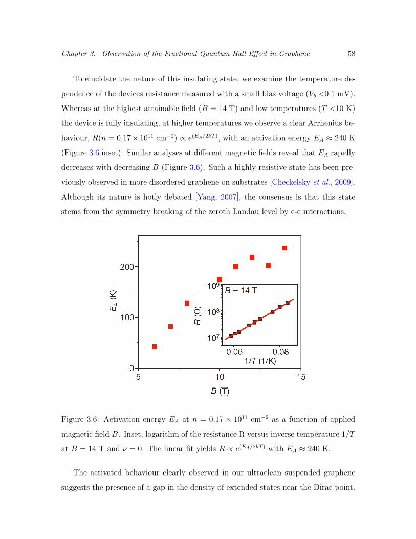
Chapter 3. Observation of the Fractional Quantum Hall Effect in Graphene 58
To elucidate the nature of this insulating state, we examine the temperature de-
pendence of the devices resistance measured with a small bias voltage (Vb <0.1 mV).
Whereas at the highest attainable field (B = 14 T) and low temperatures (T <10 K)
the device is fully insulating, at higher temperatures we observe a clear Arrhenius be-
haviour, R(n = 0.17× 1011 cm−2) ∝ e(EA/2kT ), with an activation energy EA ≈ 240 K
(Figure 3.6 inset). Similar analyses at different magnetic fields reveal that EA rapidly
decreases with decreasing B (Figure 3.6). Such a highly resistive state has been pre-
viously observed in more disordered graphene on substrates [Checkelsky et al., 2009].
Although its nature is hotly debated [Yang, 2007], the consensus is that this state
stems from the symmetry breaking of the zeroth Landau level by e-e interactions.
Figure 3.6: Activation energy EA at n = 0.17 × 1011 cm−2 as a function of applied
magnetic field B. Inset, logarithm of the resistance R versus inverse temperature 1/T
at B = 14 T and ν = 0. The linear fit yields R ∝ e(EA/2kT ) with EA ≈ 240 K.
The activated behaviour clearly observed in our ultraclean suspended graphene
suggests the presence of a gap in the density of extended states near the Dirac point.

Chapter 3. Observation of the Fractional Quantum Hall Effect in Graphene 59
Such a gap opening can also be probed by measuring the current I as a function of the
sourcedrain bias voltage, VB. Figure 3.7a shows log |I| as a function of both VB and
VG. A dark region in the central portion of this plot near VG5VD indicates a region
with near-zero conductance. Several representative I−VB curves at different densities
(Figure 3.7b) exhibit distinctly nonlinear behaviour. In particular, near the charge
neutrality point VG = VD, I remains close to zero over a wide bias range |Vb| <
50 mV. This is much larger than the energy scale corresponding to the activation
energy, 4 meV, suggesting that at large bias the charge transport occurs across weakly
connected insulating regions.
Figure 3.7: (a) Colour rendition of logarithm of the absolute value of current I across
the device as a function of bias voltage VB at B = 14 T and T = 2 K. The insulating
state I = 0 is evident as a dark blue region near VB = 0.(b) I(VB) at n = 0 (red),
0.17× 1011 cm−2 (blue) and 1× 1011 cm−2 (black).
Chapter 3. Observation of the Fractional Quantum Hall Effect in Graphene 60
3.6 Methods
3.6.1 Measurements
To measure the two terminal conductance of the devices we apply a small (VB <
0.1 mV) AC voltage excitation and measure the current across the device using a
low-frequency lock-in technique. The condition eVB < kBT is always satisfied in our
experiments. At high magnetic fields (B > 5 T) and at low temperatures (T < 15 K)
graphene becomes very resistive. This high resistance R is measured by applying
DC voltage bias less than 1 mV and recording the current using Ithaco 1211 current
amplifier. We find thatR < 10G Ω can be reliably measured this way.
3.6.2 Device statistics
We fabricated 17 suspended two-probe graphene devices. Of these, 7 samples ex-
hibited clean ν = 1 QH effect at low magnetic field B > 2 T and insulating state
at B > 1.5 T (Figure 3.8). Three samples were of high enough quality to exhibit
clean FQH plateaus. The plateau corresponding to ν = 1/3 FQH is reliably observed
during multiple thermal cycles, while spurious features associated with conductance
fluctuation changed between the thermal cycles. The ν = 1/3 was also observed at
both electron and hole sides in different devices during different thermal cycles. In
the main text, we show ν = 1/3 FQH plateau and other features in the electron side
(Vg > VD) for the Device A. In Figure 3.9, we display the data set obtained during
a different thermal cycle of the same device. Note that in this data set we observe a
clear feature corresponding to the ν = −1/3 hole FQH state but no FQH features on
the electron side.

Chapter 3. Observation of the Fractional Quantum Hall Effect in Graphene 61
-3 -2 -1 0 1
0
1
2
G(e
2
/h)
n(1011
cm-2
)
1.5T
5T
9T
14T
Figure 3.8: Two probe conductance G vs. n at magnetic fields B = 1.5, 5, 9, 14 T for
the device B. Note the QH plateaus at ν == 1, 2, 6, the insulating state G = 0 near
n = 0, and the emergence of the FQH at low densities.
In a different device (Device B), we observe similar FQH states on the hole side
(Figure 3.10). A clean ν = −1/3 FQH state (A− ) and features near ν = −2/3(C− )
and ν ≈ −1/2(B − ) on the hole side (i.e. Vg < VD) are evident. Although as
before these states, C − and B − , exhibit less developed plateaus compared to the
ν = −1/3 FQH state, this new data supports our assignment of features B and C as
universal features associated with additional FQH states. We also note that there is
a developing plateau-like feature between B − and A− (marked X − in the Figure

Chapter 3. Observation of the Fractional Quantum Hall Effect in Graphene 62
3.10d), whose corresponding trace can also be observed in Figure 3.10b. This feature
suggests an additional FQH state which is hard to identify at this point. Electronhole
asymmetry observed in our experimental data is quite common in electron transport
in graphene [Chen et al., 2008b], since the scattering strength (and the corresponding
mobility) can be very different between electrons and holes [Novikov, 2007]. While
there is no theoretical consensus as to the reason of the asymmetry, we note that it
was observed in most of the previous experiments on two-terminal devices [Huard et
al., 2008].
Figure 3.9: (a) Conductance G vs. filling factor ν at magnetic fields B = 10, 12, 13 T
for the device A, but after the device was thermally annealed to an estimated T ≈
600 C. Note that the FQHE state ν = 1/3 is clearly visible on the hole side ν < 0.(b)
Color rendition of dG/dVG vs. B and VG. Note lines corresponding to ν = φ0dn/dB =
±1, 0.33.

Chapter 3. Observation of the Fractional Quantum Hall Effect in Graphene 63
n (cm-2)
-4 -2 0 2
B (
T)
-2 -1
A-
dG/dn (a.u.)-1 0 1
14
10
6
2
14
10
8
B-C-
ν G (e2/h)
A- -0.33±0.05 0.34±0.02
B- -0.45±0.05 0.51±0.02
C- -0.64±0.05 0.78±0.05
ν=-2
ν =-1
ν=+1
ν=+1
G = 0
ab
c d
-2 -1
0.0
0.5
1.0
G (e2/h
)
n (1011cm-2)
A-B-
C-
-0.6 -0.3
0.0
0.5
1.0
ν
G(e
2/h
)
A-
B-
C-
X-
Figure 3.10: (a) Landau fan diagram |dG/dn(B, n)| at T=2 K. Light blue colour
corresponds to G(n) = νe2/h = const.(b) A detailed image of the low density regime
where FQH plateaus are observed. A plateau corresponding to the ν = −1/3 FQH
state (A − ) and other features, near ν = −1/2 (B−) and near ν = −2/3 (C−) are
identified by black arrows.(c) G as a function of n at B = 12 (blue), 13 (gray), 14 T
(red). Features A−, B− , and C− are marked by arrows.(d) G plotted as a function
of ν. Curves at different fields collapse onto a single universal curve G(ν). The same
colour codes are used as in c to represent different B. Beside the prominent features
A−, B − , and C − , there is an additional strong feature X − between A − and
B − . Table, The conductance values as well as the values of the filling factor for the
features A−, B − , and C − .

Chapter 4. Measurement of the ν = 1/3 fractional quantum Hall energy gap in suspendedgraphene 64
Chapter 4
Measurement of the ν = 1/3
fractional quantum Hall energy
gap in suspended graphene
In this chapter we report on magnetotransport measurements of multi-terminal sus-
pended graphene devices. Fully developed integer quantum Hall states appear in
magnetic fields as low as 2 T. At higher fields the formation of longitudinal resis-
tance minima and transverse resistance plateaus are seen corresponding to fractional
quantum Hall states, most strongly for ν = 1/3. By measuring the temperature de-
pendence of these resistance minima, the energy gap for the 1/3 fractional state in
graphene is determined to be at ∼20 K at 14 T. This gap is at least 3 times larger
than the observed gaps for the corresponding state in the best quality semiconductor
heterostructures.
4.1 Introduction
The anomalous integer quantum Hall effect (IQHE) observed in graphene is a man-
ifestation of the unique electronic properties of this material [Novoselov et al., 2005;

Chapter 4. Measurement of the ν = 1/3 fractional quantum Hall energy gap in suspendedgraphene 65
Zhang et al., 2005a]. At low magnetic fields, the IQHE of graphene is marked by
the quantized half-integer Hall conductivity σxy = gs(n + 1/2)e2/h, where n is an
integer and gs = 4 is the Landau level (LL) degeneracy resulting from the degenerate
spin and valley isospin degrees of freedom. In this regime, the degenerate single-
particle LLs [Neto et al., 2009] lead to the observation of the filling factor sequence
ν = ±2,±6,±10. Subsequently, new broken-symmetry IQHE states, corresponding
to filling factors ν = 0,±1,±4 have been resolved in magnetic fields of B > 20 T,
indicating the lifting of the fourfold degeneracy of the LLs [Zhang et al., 2005a;
Jiang et al., 2007]. These filling factors have been suggested to be the result of var-
ious novel correlated states mediated by electron-electron (e-e) interactions [reviews
of recent theoretical work can be found in K. Yang, 2007].
In the strong quantum limit, e-e interactions in 2-dimensional electron gasses
(2DEGs)can lead to the fractional quantum Hall effect (FQHE) [Tsui et al., 1982],
many-body correlated states where the Hall conductance quantization appears at
fractional filling factors. In recent investigations of transport properties in two-
terminal high-mobility suspended graphene devices [Bolotin et al., 2009; Du et al.,
2009], a quantized conductance corresponding to the ν = 1/3 FQHE state has been
observed, suggesting the presence of strong e-e interactions in this system. How-
ever, due to the inherent mixing between longitudinal and transverse resistivities in
this two-terminal measurement [Abanin and Levitov, 2008], quantitative character-
ization of the observed FQHE states such as the FQHE energy gap is only possible
in an indirect way [Abanin et al., 2010]. Although multi-terminal measurements on
suspended graphene samples have been reported previously [Bolotin et al., 2008b;
Du et al., 2008], the mechanical [Prada et al., 2010; Fogler et al., 2010] or thermal
instability [Skachko et al., 2010] of these samples has precluded even the observa-
tion of a fully-quantized IQHE. Recently, the improvement of graphene mobility up
to 8 m2/Vsec has been reported for substrate-supported graphene devices fabricated
on a single-crystal hexagonal boron nitride substrates [Dean et al., 2010]. Multi-
Chapter 4. Measurement of the ν = 1/3 fractional quantum Hall energy gap in suspendedgraphene 66
terminal transport measurements performed on such devices in magnetic fields up to
35 T reveal several FQHE states whose filling factors are mostly integer multiples of
1/3. The energy gaps of these states have been measured only for ν > 1 [Dean et
al., 2011], while the characterization of FQHE states with ν < 1 could not be reli-
ably conducted due to inhomogeneous broadening near the charge neutrality point in
these samples. As stronger e-e correlations are expected for this lower density regime,
further experiments on cleaner samples are required.
In this chapter, we report on the measurement of multi-terminal IQHE and FQHE
states in ultraclean suspended graphene samples in this low density regime. Filling
factors corresponding to fully developed IQHE states, including the ν = ±1 broken-
symmetry states and the ν = 1/3 FQHE state are observed. The energy gap of
the 1/3 FQHE, measured by its temperature-dependent activation, is found to be
much larger than the corresponding state found in the 2DEGs of high-quality GaAs
heterostructures, indicating that stronger e-e interactions are present in graphene.
4.2 Experiment
Our suspended graphene devices are fabricated using the method described in refer-
ences [Bolotin et al., 2009; ?]: A mechanically exfoliated graphene flake is pressed onto
a SiO2/Si substrate. Electrical contacts are made using electron-beam lithography
followed by the thermal evaporation of Cr/Au electrodes. The SiO2 under the flake
is subsequently removed via a chemical etch in buffered hydrofluoric acid. A typical
multi-terminal graphene device with a lateral size ∼3 µm, suspended 150-200 nm
above the SiO2/Si substrate, is shown in the inset of Figure 4.1a.
We studied a total of three 4-terminal and one 6-terminal devices where better
quality results were obtained in three of the samples, labeled S1, S2 and S3, re-
spectively. The longitudinal resistance Rxx and transverse Hall resistance Rxy were
measured as a function of the applied gate voltage Vg on the doped Si back-gate,
Chapter 4. Measurement of the ν = 1/3 fractional quantum Hall energy gap in suspendedgraphene 67
which tunes the carrier density n in the graphene. The carrier density is determined
using Hall measurements and n(Vg) = B/eRxy(Vg, B), where B is the applied mag-
netic field. The gate voltage is limited to less than 10 V to avoid electrostatic collapse
of the suspended devices. The initial mobility of as-fabricated devices is typically less
than 1.5 m2/Vs, comparable to samples on substrate, reflecting the fact that electron
mobility is limited by residual impurities absorbed on the graphene surface. Sending
a large current density (∼0.5 mA/µm) through a device heats up the graphene sam-
ples up to ∼ 400 C [Berciaud et al., 2010], which typically removes many of these
adsorbed impurities, resulting in an extremely sharp peak in resistivity ρ as n changes
from electrons to holes (Figure 4.1a).
4.3 Quantum Hall effect in suspended multi-terminal
graphene
In our study, the samples exhibit mobilities ranging from 8-15 m2/Vs at the temper-
ature T = 1.7 K, where most of our data was taken. In these ultraclean suspended
samples, the Shubnikov de Haas (SdH) oscillations, resulting from the quantized cy-
clotron orbits are observable at relatively low magnetic fields. Figure 4.1b displays
a Landau fan diagram where Rxx is plotted as a function of n and B in the low
magnetic field regime (|B| < 1 T). In this diagram the SdH oscillation minima (later
developing to the quantum Hall minima) appear as strips fanning out from the origin
point B = 0, n = 0 with the slope dn/dB = νe/h. These strips survive in fields down
to 0.1 T in our samples, in accordance with the mobility of ∼10 m2/Vs calculated
from conductivity measurements.

Chapter 4. Measurement of the ν = 1/3 fractional quantum Hall energy gap in suspendedgraphene 68
101010
1
0
-10 2
ρ(Ω
)
1000
-4 4
10
0
100
(a)
2µm
B (
T )
2
0.5
-0.5
(b)
2
Rxx
(kΩ
)
0
6 10
4
n (10 11 cm-2)n (1011 cm-2)
2 µm
2-2
Figure 4.1: (a) Resistivity of a suspended graphene sample (S1) versus carrier density
induced by back gate (resistivity is displayed on a log scale). Inset: Atomic force
microscope image of a typical suspended device. (b) Landau fan diagram Rxx(Vg, B)
at T=7 K measured in sample S3. The dark blue lines indicate minima in Rxx. The
dashed lines with integers indicate the corresponding filling factors.
As B increases, the observed SdH oscillations fully develop into the IQHE. Figure
4.2a shows Rxx and Rxy of device S1 as a function of filling factor ν = ne/hB (tuned
by Vg) at a fixed magnetic field B =2 T. A series of quantum Hall states, i.e., zeroes
in Rxx and plateaus in Rxy, quantized to values h/νe2 with integer filling factors
ν = ±2,±6, are observed within the gate bias window. More IQHE states can be
observed using a field sweep at fixed gate voltage. Figure 4.2b shows Rxx and Rxy
measured as a function of magnetic field at a fixed hole density of 3.2 × 1011 cm−2
for S1 and S2. At least two well-defined plateaus with values (h/6e2) and (h/2e2)
are observed, while the ν = 1 broken-symmetry IQHE state is being reached (h/e2)
at 14 T. We note that the development of this Rxy Hall plateau is not complete,
measuring only ∼95 % of the full quantization value.

Chapter 4. Measurement of the ν = 1/3 fractional quantum Hall energy gap in suspendedgraphene 69
-6 0 60
2
Filling Factor
6
2
−6
2T−2
0 4 8 120
3
0
1
S1 S2
106
2
1(b)
(a)
2µm
Rxx
(kΩ
)R
xx(kΩ
)
Rxy
(h /e
2 )
Rxy
(h /e
2 )
B ( T )
0
0.5
Figure 4.2: (a) Rxx and Rxy measured as a function of filling factor ν at B =2 T
and T = 1.7 K for sample S1. -Rxy is plotted for ν > 0. Numbers above the
horizontal lines indicate the corresponding filling factors. (b) Rxx and Rxy measured
as a function of magnetic field B at the hole density of n = 3.2×1011cm−2 in samples
S1 (solid line) and S2 (dashed line). Numbers above horizontal lines indicate the
corresponding filling factors.
This deviation of the Hall resistivity from the expected quantization value may

Chapter 4. Measurement of the ν = 1/3 fractional quantum Hall energy gap in suspendedgraphene 70
be attributable to the presence of non-ideal disordered contacts which can introduce
a non-equilibrium population of edge states that perturbs the quantization for the
small samples used here [Buttiker, 1988]. It has also been suggested that the proximity
between the current leads and the voltage probes could short-circuit the hall voltage
in such small samples [Skachko et al., 2010].
4.4 Fractional Quantum Hall effect in suspended
multi-terminal graphene
As we move to the low-density regime corresponding to ν < 1, the FQHE starts to
be detected for B >10 T in all three samples (S1, S2 and S3). Figure 4.3a displays
Rxx and Rxy plotted as a function of B at a fixed density of 1.9×1011 cm−2 (dotted
line) and 0.96×1011 cm−2 (solid line) respectively. At higher density, we notice that
Rxy increases further and Rxx shows an additional dip at the field corresponding
to ν ≈ 2/3. Upon further decreasing the density, lower filling fractions come into
the observable window set by the maximum probing magnetic field (14 T), and Rxx
develops even deeper local minimum at the field corresponding to ν ≈ 1/3 with a
plateau-like feature in Rxy. However, similar to the ν = 1 broken-symmetry IQHE,
the corresponding features in Rxy are not fully quantized in this low density and high
Hall voltage regime. In sample S3 (Figure 4.3b), in addition to minimum around
ν ≈ 1/3, another minimum is visible around ν ≈ 1/2, but there is no feature close to
a 2/3 filling fraction.

Chapter 4. Measurement of the ν = 1/3 fractional quantum Hall energy gap in suspendedgraphene 71
1 2 T 1 3 T 1 4 T
1 2 T 1 3 T 1 4 T
0
0
12
Rxx
(kΩ
)
Rxy
(h /e
2 )
21
~ 1/ 2
1/ 3
n = 0.8 x 1011 cm-2
(b)
5 10
3
B ( T )
2 / 3
n = 1.9 x 1011 cm-2
16
Rxy
(h /e
2 )
2
11
(a)
Rxx
(kΩ
) 1/ 3
0
3
n = 0.96 x 1011 cm-2
0 5 10
(e)
(c) 1/ 3
~1/ 2
1
Rxx
(kΩ
)
0
1.5
0.3 0.6
50
Rxx
(kΩ
)
0
B (
T )
10
V G ( V )0-10.0
14
ABC
A
BC
(d)
Rxx
(kΩ
)
0
20
-1Filling factor
B ( T )
Filling factor
S1
S3
S2
S1
-0.5
Figure 4.3: (a) Rxx and Rxy measured in sample S1 as a function of B at fixed
density of 1.9×1011 cm−2 (dotted line) and 0.96×1011 cm−2 (solid line). (b)Rxx and
Rxy measured in sample S3 as a function of magnetic field B at fixed density of
0.8×1011 cm−2 . Numbers with vertical lines indicate the corresponding filling factors.
The straight horizontal lines indicates the expected Rxy value for the 1/3 FQHE state.
(c) Rxx as a function of filling factor at B = 12−14 T measured in sample S2. Vertical
lines indicate the corresponding filling factors. (d) Rxx as a function of filling factor
at B = 12 − 14 T measured in sample S1. The letters A, B and C with vertical
lines indicate minima corresponding to filling factors 1, 2/3 and 1/3 respectively. (e)
Landau fan diagram Rxx(Vg, B) at T=1.7 K measured in sample S1. The dark blue
lines indicate minima in Rxx. Features A and B appear at high fields with filling
factors ν = 0.31 and 0.66, respectively.

Chapter 4. Measurement of the ν = 1/3 fractional quantum Hall energy gap in suspendedgraphene 72
We note that, when scaled by the filling factor, these local minima of Rxx are
robust features at different magnetic fields and densities. Figure 4.3c and Figure 4.3d
show the Rxx of S1 and S2 as a function of filling fraction ν at different B and n. The
Rxx traces exhibit local minima corresponding to filling fractions ν ∼ 1/3, 1/2, 2/3
and 1. For all three samples, we observe strong minimum for ν = 1 and 1/3. But ν ∼
1/2 only shows up clearly for two samples S2 and S3 while ν ∼ 2/3 emerges only in
S1, indicating that these features are rather fragile and are more sample dependent
compared to ν =1/3. For example, in Figure 4.3d, in addition to the IQHE state
at ν = −1 (feature C) two other notable features emerge as relatively deep minima
in Rxx (A and B), located at filling factors ν = −0.34 and ν = −0.64 respectively.
Further confirmation on the nature of these states can be provided by means of a
Landau fan diagram where Rxx is plotted as a function of Vg and B (Figure 4.3e).
From the slopes of the lines in marked A and B we estimate that features A and B
follow ν = 0.31±0.02 and ν = 0.66±0.02 lines, respectively. We thus assign features
A and B to be the minima corresponding to the 1/3 and 2/3 FQHE states.
4.5 Energy gap of the Fractional Quantum Hall
states
The strongly developed minima in Rxx for the 1/3 state now allows us to probe the
energy gap associated with it. To quantify the energy of this FQHE state, we measure
the temperature dependence of Rxx. Figure 4.4a and 4.4c display Rxx(Vg) measured at
a sequence of different temperatures at 14 T for S1 and S2, respectively. The minimum
corresponding to the 1/3 FQHE state, Rminxx , increases as T increases. An Arrhenius
plot for the Rminxx (Figure 4.4b) shows an activation behavior indicated by log(Rmin
xx ) ∼
T−1 in the temperature range between 9-22 K for S1. At lower temperatures (2-8 K)
log(Rminxx ) deviates from a simple activation behaviors ∼ T−1, turning into the slower
temperature dependence expected for variable-range hopping behavior. Similar trends

Chapter 4. Measurement of the ν = 1/3 fractional quantum Hall energy gap in suspendedgraphene 73
were observed in early experiments on GaAs 2DEGs [Boebinger et al., 1985]. It is also
notable that the slope of this low temperature regime does not change dramatically
with magnetic field.
From the high-temperature activation behavior, the transport gap ∆E of the 1/3
FQHE state can be obtained using Rminxx ∼ exp(−∆E/2kBT ) at a fixed magnetic
field. Figure 4.4d shows ∆E as a function of B determined from the line fits in
Figure 4.4b for sample S1. A similarly determined activation energy gap for the 1/3
FQHE state of sample S2 is also included in this figure (For this sample the Rminxx
shows an activation behavior in the temprature range between 4-13 K). For both
samples, The gap value is remarkably large ≈ 20 − 25 K at 14 T , increasing with
increasing B, as is expected.
4.6 Magnetic field dependence of the 1/3 FQHE
state
Naively, the magnetic field dependence of energy gap of 1/3 FQHE state would be
expected to increase with ∼√B, considering the e-e interaction energy scales with the
Coulomb energy scale e2/εlb, where ε is the dielectric constant and lb is the magnetic
length proportional to 1/√B. As an alternative scenario, however, the activation
energy gap could be linear in B, if the nature of charged quasiparticle excitations
of this FQHE state are associated with spin-flips in skyrmion-like excitations of a
spin-polarized FQHE ground state [Dethlefsen et al., 2006]. The linear-fit (dashed
line) to the data yields a negative y-intercept ∼ 20 K in the energy axis which can
be interpreted as the broadening Γ of the fractional state.But,the√B-fit (dotted
lines) yields Γ ≈ 60 K which is an order of magnitude larger than the expected
LL broadening estimated from the scattering time τ obtained from the mobility of
the sample(h/τ ∼ 4 K). As a result, the linear dependence of the energy gap and
consequently the spin flip excitations seem to be more relevant in our experiment.How

Chapter 4. Measurement of the ν = 1/3 fractional quantum Hall energy gap in suspendedgraphene 74
ever,tilted field measurements need to be done to further elucidate the nature of
excitations and the g factor of composite fermions.
2K 6K 9K 11K 13K 17K 20K
14T
S1
2 K 4 K 6 K 8 K 10 K
14 T
S2
S2
S1
-10
B ( T )0 10
20
-20E
gap(
K)
7T8T9T10T11T14T
2.7
3.3(b)
0.05 0.2
1 / T(K-1)
Log(
Rxx
min)
1/ 3
(a)2
1
00
Rxx
(kΩ
)
VG(V)
(c)
VG(V)6 12
Rxx
(kΩ
)
0
1(d)
5
1/ 3
~1/ 20
-5
9
Figure 4.4: (a) Rxx measured at different temperatures at 14 T for sample S1. (b)
Arrhenius plots of Rminxx versus 1/T at different fields at ν = 1/3 FQHE state for
sample S1. The straight lines are linear fits to the data at the high-temperature
activation range. (c) Rxx measured at different temperatures at 14 T for sample S2.
(d) The activation gap as a function of field for two samples: S1 and S2. The dashed
lines are fits to B and the dotted lines are fits to√B.

Chapter 4. Measurement of the ν = 1/3 fractional quantum Hall energy gap in suspendedgraphene 75
Considering the LL broadening Γ ∼20 K obtained from the linear fit, the intrinsic
energy gap for ν =1/3 is estimated to be ∆1/3 = ∆E + Γ ≈ 40-45 K at B =14 T. It
has been predicted that the 1/3 state is both spin and valley-isospin polarized in the
SU(4) configuration space [Apalkov and Chakraborty, 2006], and calculations for this
fully polarized 1/3 state have given a gap value of C e2/εlB, with the numerical con-
stant C ≈0.05-0.1 [Apalkov and Chakraborty, 2006; Toke et al., 2006]. For graphene
in vacuum, the dielectric constant from in-plane dynamic screening is estimated to be
ε =5.24 [Gonzlez et al., 1999]. The predicted gap is then in the range ∆1/3 =26-50 K
at B =14 T, in reasonable agreement with the gap measured in our experiment. For
comparison, the observed ∆1/3 in graphene is at least 3 times larger than that of the
2DEGs in the best quality GaAs heterojunctions in a similar field range [Dethlefsen
et al., 2006]. The larger gap size of this 1/3 FQHE state is also evident in the fact
that the Rxx minimum persists at temperatures up to 22 K. We further remark that
∆1/3 obtained in this experiment is much larger than the gaps obtained for FQHE
states associated to ν > 1 considering those gaps are obtained at B =35 T [Dean et
al., 2011]. This comparison thus suggests an unusual robustness of the 1/3 state in
graphene, inviting further investigation to elucidate its microscopic nature. Further-
more, our measured gap is comparable to the one obtained by measuring the local
electronic compressibility of suspended graphene at ν = 1/3, which gives a gap value
of 1.4 to 1.8 meV at 12 T [Feldman et al., 2012].

Chapter 5. Thermoelectric power of graphene and the validity of Mott’s formula 76
Chapter 5
Thermoelectric power of graphene
and the validity of Mott’s formula
5.1 Introduction
Graphene has invited a lot of interest due to its phenomenal electronic properties.
For explaining the electronic transport properties of graphene, it is crucial to resolve
the mechanisms causing the scattering of its charge carriers. Often, the resistivity
measurements alone do not provide enough information for understanding details of
the electronic structure of this material. In chapter 1, we demonstrated that the mea-
surement of the thermoelectric properties of graphene offer a different direct access
to it’s fundamental thermodynamic properties, such as transport entropy. Recently,
the thermoelectric properties of graphene have been probed experimentally, in which,
it has been shown that the carrier density dependent forms of the conductivity and
the thermopower are well correlated with each other through the semiclassical Mott’s
formula [Zuev et al., 2009; Wei et al., 2009]. This relation derived from a single
particle formalism as it was presented in Chapter 1 is usually an analysis means in
order to verify the adequacy of the semiclassical description of transport in many
materials. However, the presence of electron-electron interactions in a material could

Chapter 5. Thermoelectric power of graphene and the validity of Mott’s formula 77
affect the thermoelectric response in a way different from what is predicted by the
Mott relation [Muller et al., 2008; Foster and Aleiner, 2009].
It has been shown theoretically [Muller et al., 2008; Foster and Aleiner, 2009] that
the inter-particle collisions can relax the system in to an equilibrium state which can
be specified by the zeroth order hydrodynamic equations in the absence of dissipa-
tions. In graphene, at low doping, where (µ < T ), the inter-particle scattering rate
is proportional to the temperature. This leads to an interacting electron-hole plasma
of Dirac fermions at higher temperatures in the limit of low disorder, where the
non-Fermi liquid behavior is expected [Fritz et al., 2007; Muller and Sachdev, 2008;
Muller et al., 2008]. At higher doping the strong electron-electron interactions are
essential to achieve the non-fermi liquid hydrodynamic regime. Experimentally, these
regimes have not yet been explored due to the presence of impurity and electron hole
puddles in experimentally available graphene samples.
Recently as we described in Chapter 2, the fabrication of high quality samples has
become possible. In such high quality samples, the importance of interactions in
graphene has been demonstrated [Bolotin et al., 2009; Du et al., 2009; Dean et al.,
2011]. In this chapter, we explore the effect of electron-electron interactions on the
thermoelectric power probed in high mobility graphene samples on hBN. Our results
show that at high temperatures the measured thermopower departs from the Mott
relation and these deviations are greater as the sample mobility increases. In this
chapter, we analyze quantitatively the deviations in the degenerate regime using the
Boltzmann transport theory as well as the hydrodynamic formalism, taking differ-
ent scattering mechanisms in to account. The non degenerate regime still remains
uncharted due to the presence of electron-hole puddles coming from the residual dis-
orders in the samples.

Chapter 5. Thermoelectric power of graphene and the validity of Mott’s formula 78
5.2 Experiment
In our experiment, we studied a total of 30 working TEP device which were pre-
pared using two different methods. For the first set of devices we used the fabrication
method described in reference [Dean et al., 2010] to transfer graphene on hexagonal-
Boron Nitride (h-BN) substrates. Electrical leads consisting of a Cr/Au metal stack
were deposited using standard electron-beam lithography after which the sample was
etched into an approximately square Hall bar using oxygen plasma. Typical sample
sizes are 2 µm×5 µm. All samples were annealed in a 5% H2/95%Ar atmosphere to
350 C for 3 hours to remove the processing residues. For the second set of devices we
fabricated graphene encapsulated in hexagonal boron nitride layers using the recently
developed van der Waals transfer technique [Wang et al., 2013], where the improved
electronic performance and higher room temperature mobility is achieved (a typical
device image is displayed in the inset of Figure 5.1a). The TEP measurement tech-
nique has been explained in Appendix A. In short, a controlled temperature gradient
δT is applied to the sample by a micro-fabricated heater which is usually an elec-
trode made of gold, while the resulting thermally induced voltage δV is measured
by the voltage probes (the thermometer contacts at the same time) to evaluate the
thermopower, TEP = S = −δV/δT . Temperature calibration and local temperature
variations are measured with two metal four-probe thermometers. We measure the
four-terminal conductivity σ employing the Hall bar geometry. To measure the ther-
mopower, we apply a low frequency ac signal to the heater electrode and detect the
resulting 2ω thermal voltage from the outer electrodes as we change the graphene
carrier density with the back gate.
Figure 5.1a presents an example of the measured conductivity of device D3 as a func-
tion of the temperature and back gate voltage in a color plot. Black curves display
conductivity at different temperatures of 20 K, 130 K and 250 K from the bottom to
the top, respectively. The estimated mobility for this device is around 50,000 cm2/Vs
at room temperature, increasing with decreasing the sample temperature. The mo-
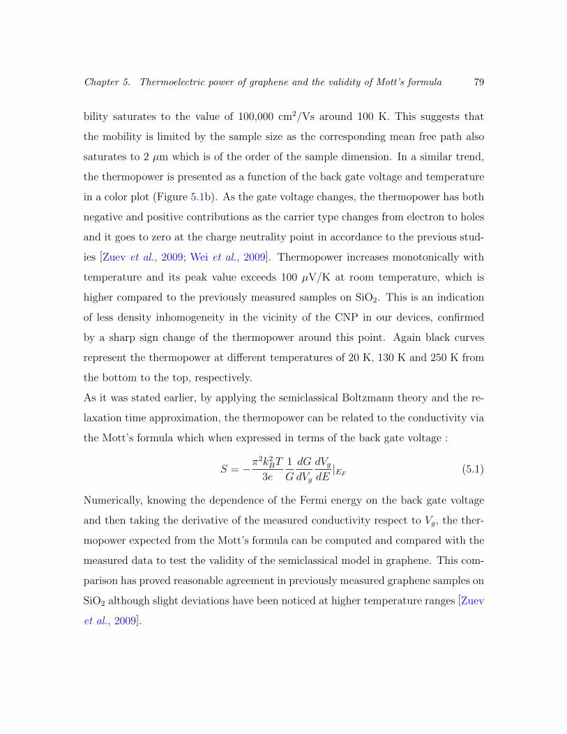
Chapter 5. Thermoelectric power of graphene and the validity of Mott’s formula 79
bility saturates to the value of 100,000 cm2/Vs around 100 K. This suggests that
the mobility is limited by the sample size as the corresponding mean free path also
saturates to 2 µm which is of the order of the sample dimension. In a similar trend,
the thermopower is presented as a function of the back gate voltage and temperature
in a color plot (Figure 5.1b). As the gate voltage changes, the thermopower has both
negative and positive contributions as the carrier type changes from electron to holes
and it goes to zero at the charge neutrality point in accordance to the previous stud-
ies [Zuev et al., 2009; Wei et al., 2009]. Thermopower increases monotonically with
temperature and its peak value exceeds 100 µV/K at room temperature, which is
higher compared to the previously measured samples on SiO2. This is an indication
of less density inhomogeneity in the vicinity of the CNP in our devices, confirmed
by a sharp sign change of the thermopower around this point. Again black curves
represent the thermopower at different temperatures of 20 K, 130 K and 250 K from
the bottom to the top, respectively.
As it was stated earlier, by applying the semiclassical Boltzmann theory and the re-
laxation time approximation, the thermopower can be related to the conductivity via
the Mott’s formula which when expressed in terms of the back gate voltage :
S = −π2k2BT
3e
1
G
dG
dVg
dVgdE|EF
(5.1)
Numerically, knowing the dependence of the Fermi energy on the back gate voltage
and then taking the derivative of the measured conductivity respect to Vg, the ther-
mopower expected from the Mott’s formula can be computed and compared with the
measured data to test the validity of the semiclassical model in graphene. This com-
parison has proved reasonable agreement in previously measured graphene samples on
SiO2 although slight deviations have been noticed at higher temperature ranges [Zuev
et al., 2009].

Chapter 5. Thermoelectric power of graphene and the validity of Mott’s formula 80
5
40
Co
nd
uct
ance
(m
S)
-30 -15 0 15 30
350
250
150
50 500
50
350 K
130
-130
S(µ
V/K
)
-30 -15 0 15 30
350
250
150
5050
350
-30 -15 15 30 0
50/
K
Vg
(V)
b
a
Figure 5.1: (a) The measured conductivity as a function of the temperature and back
gate voltage. Several traces at constant temperatures are shown in overlaid graphs.
Black curves show conductivity at different temperatures of 20 K, 130 K and 250 K
from the bottom to the top, respectively. The upper inset shows a typical device
image. (b) Thermopower as a function of the back gate voltage and temperature in a
color plot. Black curves display the thermopower at different temperatures of 20 K,
130 K and 250 K from the bottom to the top, respectively.
The Mott’s formula derived from the Boltzmann equation by employing the relax-

Chapter 5. Thermoelectric power of graphene and the validity of Mott’s formula 81
ation time approximation is just valid for the degenerate electron system, when T is
far below the Fermi temperature TF . In the low mobility graphene devices, we expect
the Mott’s formula to be applicable in all density regimes including the vicinity of the
CNP due to the presence of electron-hole puddles and residual charge fluctuations
[Zuev et al., 2009]. However, for the high quality samples with less inhomogeneity
the Mott relation is violated as Vg approaches the CNP [Wang and Shi, 2011]. To
calculate thermopower in the low density regime where the electron system is non-
degenerate, it is needed to use the general solution of the Boltzmann equation which
is valid in both the degenerate and non-degenerate regimes. In the linear response
regime, this solution is given by:
S = − 1
eT
∫∞0
(ε− µ)σ(ε)∂f0
∂εdε∫∞
0σ(ε)∂f
0
∂εdε
(5.2)
where f 0 = 1/(e(ε−µ)/kBT +1) is the equilibrium Fermi-Dirac distribution function and
σ(ε) is the energy dependent conductivity of graphene given by the Einstein relation:
σ(ε) = e2v2FD(ε)τ(ε)/2 (5.3)
where D(ε) = 2|ε|/πh2v2F is the density of states in graphene and τ is the relaxation
time (Note that σ(ε) can not be measured experimentally ). By using the temper-
ature dependent chemical potential µ(T ) and the measured conductivity σ(Vg, T ),
thermopower can be evaluated at each temperature in a similar method in refer-
ence [Wang and Shi, 2011].
Figure 5.2a-c display the measured thermopower versus back gate voltage at high
temperature regime for samples D1 ,D2 and D3 with mobilities of 19,000, 30,000 and
130,000 cm2/Vs, respectively. Although the measured TEP for sample D1 matches
well with the formula in Equation (5.2), deviations are observed in degenerate regime
for samples D2 and D3 which have higher mobilities. Figure 5.2d shows the tem-
perature dependent thermopower for these 3 samples at a fixed carrier density of
n = 1× 1012 cm−2. The magnitude of thermopower increases linearly with the tem-

Chapter 5. Thermoelectric power of graphene and the validity of Mott’s formula 82
perature, which suggests that the diffusive component of the thermopower is domi-
nant. Substrate or graphene acoustic phonons can induce a phonon-drag component
for the thermopower, which will produce a TEP with a superlinear temperature de-
pendence [Zavaritskii, 1984; Gallagher et al., 1987; Gallagher et al., 1990]. Thus,
linearity of thermopower with temperature strongly indicates no appreciable pres-
ence of the phonon-drag component and further confirms the weak electron-phonon
coupling in graphene. Overall, comparing different samples, our data confirms that
thermopower does not change dramatically in samples with different mobilities; i.e.,
the magnitude of TEP remains in similar range while the mobility changes almost an
order of magnitude.
For a quantitative comparison, we plot the measured thermopower and the calcu-
lated one using Equation (5.2) in Figure 5.2d. For sample D1 with lower mobility,
a quantitative agreement is present at all temperatures up to 300 K. However, for
the higher quality graphene devices D2 and D3, the measured thermopower starts to
deviate from the Mott’s formula as the temperature increases. These deviations are
much larger for sample D3 which has the highest mobility. This observation proves
further the failure of the semiclassical formalism in the degenerate regime and at
high temperatures. Previously, deviations from Mott’s formula had been observed
in GaAs samples at low temperatures, but it was contributed to either the phonon-
drag contribution to the thermopower which is absent in graphene [Basu et al., 1988;
Nicholas, 1985; Cantrell and Butcher, 1986] or the energy-dependent scattering mech-
anisms [Ruf et al., 1987].
To understand the break down of the semiclassical formalism here, we checked the
temperature dependence of resistivity ρ in our devices. Figure 5.3 displays the resistiv-
ity as a function of temperature at different densities for device D3. This dependence
can be subdivided into 3 different regimes: (i) The low temperature T indepen-
dent regime for T < 100 K; (ii) The intermediate temperature linear T regime for
100 K< T <200 K; (iii) The high temperature nonlinear T regime for T > 200 K.

Chapter 5. Thermoelectric power of graphene and the validity of Mott’s formula 83
This trend is observed almost in all of our measured devices regardless of the mobility
and other sample specific parameters.
In regime (i), ρ(T ) at the high density limit indeed shows temperature independent
resistivity, expected from the elastic scattering from static disorders. The low temper-
ature resistivity is dominated by the scattering of electrons from long range Coulomb
impurities and short range defects. However, at lower carrier densities, the resistivity
shows slight up turn as T decreases in the regime (i) above. Although we do not
completely understand the origin of this upturn, several scenarios such as localization
or Kondo effect [Chen et al., 2011; Chao and Aji, 2011] can be a possible cause.
In regime (ii), the ρ(T ) exhibits a linear in T behavior, since the electron-acoustic
phonon scattering starts to be appreciable [Hwang and Sarma, 2007; Efetov and
Kim, 2010]. The lower bound temperature of this regime can be defined by the
Bloch Gruneisen temperature TBG = 2vphkF/kB, where vph is the acoustic phonon
sound velocity. In this regime, the temperature dependent part of resistivity is given
by [Hwang and Sarma, 2007]
∆ρ =πD2
AkBT
4e2hρmv2sv
2F
(5.4)
where ρs = 6.5×10⁻⁷kg/m2 is the 2D mass density of graphene, vs = 2.1×10⁴ m/s is
the sound velocity and DA is the acoustic deformation potential. Then, the measured
resistivity of this regime can be expressed by ρ(T ) = ρ0 + ∆ρ(T ), where ρ0 is the
temperature independent resistivity to connect to the resistivity in regime (i) above.
Experimentally, we obtained ρ0 by extrapolating linear T dependence of ρ in regime
(ii): i.e, by performing a linear fit to this regime, we can extract the slope and the
intercept gives the residual resistivity ρ0(Figure 5.3, inset). In addition, from the
residual resistivity, we can estimate the electron-impurity scattering rate as τ−1ei =
ρ0e2EF/πh
2, where we have used the Einstein relation for the conductivity. The
energy dependent electron-acoustic phonon scattering rate can be also calculated

Chapter 5. Thermoelectric power of graphene and the validity of Mott’s formula 84
using equation (8) in reference [Hwang and Sarma, 2007] which is given by
τ−1ep =
1
h3
EF4v2
F
D2A
ρmv2ph
kBT (5.5)
We now discuss the behavior of ρ(T ) in regime (iii). In contrast to the lower tem-
perature regimes, the resistivity at high temperature regime is highly nonlinear in
T .
230 K
S(µV/K)
D1
D2
D3
200 3001000
60
0
n= -2 *1012 cm-2
T (K)Vg
(V)
S(µV/K
)S(µV/K
)S(µV/K
)
80
-80
80
-80
80
-80
0
0
0
D2
D1
D3
0 20-20
237 K
250 K
b
a d
c
Figure 5.2: The measured thermopower versus back gate voltage at high temperatures
for different samples (a) D1 ,(b) D2 and (c) D3 with mobilities of 30,000, 45,000 and
100,000 cm2/V s, respectively. (d) Temperature dependent thermopower for these 3
samples for carrier density of n = 1×1012cm−2. The dotted, dash-dotted and dashed
lines are the calculated thermopower from the Mott’s formula for samples D1,D2 and
D3, respectively.
The observed superlinear trend in the resistivity has been contributed to either

Chapter 5. Thermoelectric power of graphene and the validity of Mott’s formula 85
extrinsic scattering of electrons by the surface polar optical phonons of the sub-
strate [Chen et al., 2008b] or thermal fluctuations of the mechanical ripples present
in graphene [Morozov et al., 2008]. Recently, it has been speculated that this behav-
ior is due to the optical phonons of graphene itself [Park et al., 2014].
(K)
25
150
0 300
0
100
n (1012 cm-2)
0.8
1
1.3
1.7
2
(Ω)
~T
(K)
0 100 200 300
∆
Figure 5.3: The resistivity as a function of the temperature at different densities
for device D3. The inset shows ρ − ρ0 where ρ0 is the residual resistivity at low
temperatures. All curves at different densities collapse into one graph for T < 200 K
which is linearly proportional to T .
While we do not know the exact origin of the high temperature activated behavior
in regime (iii), it is clear that it can be linked to the inelastic scattering caused by
the optical phonons which are coming either from the substrate or graphene.
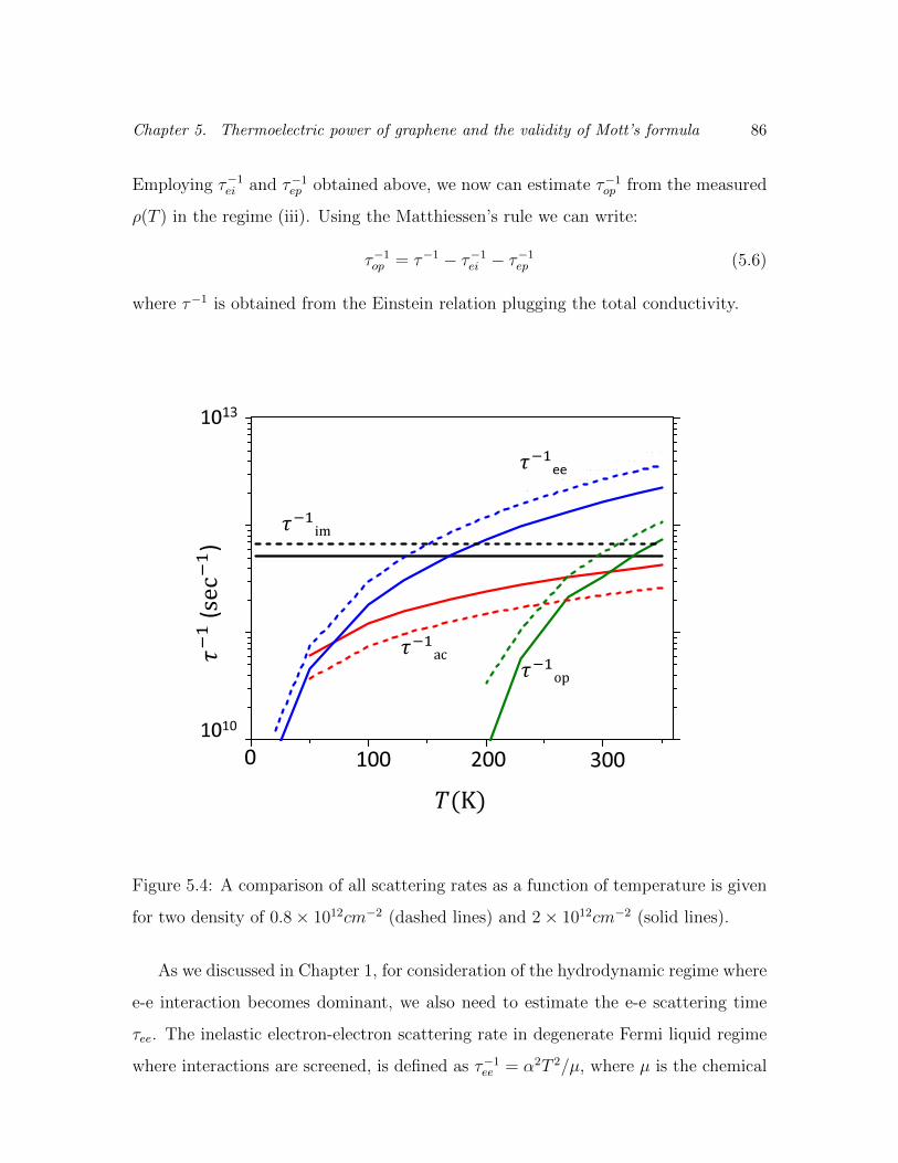
Chapter 5. Thermoelectric power of graphene and the validity of Mott’s formula 86
Employing τ−1ei and τ−1
ep obtained above, we now can estimate τ−1op from the measured
ρ(T ) in the regime (iii). Using the Matthiessen’s rule we can write:
τ−1op = τ−1 − τ−1
ei − τ−1ep (5.6)
where τ−1 is obtained from the Einstein relation plugging the total conductivity.
0 100 200 300
1010
(sec)
(K)
ee
im
ac
op
1013
Figure 5.4: A comparison of all scattering rates as a function of temperature is given
for two density of 0.8× 1012cm−2 (dashed lines) and 2× 1012cm−2 (solid lines).
As we discussed in Chapter 1, for consideration of the hydrodynamic regime where
e-e interaction becomes dominant, we also need to estimate the e-e scattering time
τee. The inelastic electron-electron scattering rate in degenerate Fermi liquid regime
where interactions are screened, is defined as τ−1ee = α2T 2/µ, where µ is the chemical

Chapter 5. Thermoelectric power of graphene and the validity of Mott’s formula 87
potential and α = e2/khvF is the fine stricture constant with k the dielectric constant
of the substrate. In contrast, in the non-degenerate regime we have τ−1ee = α2kBT/h.
Note that the electron-electron scattering does not relax the momentum unless there
are Umklapp processes, which is unlikely in graphene due to the small Fermi surface
compared to the size of the Brillouin zone. Thus, electron-electron scattering rate
does not contribute to the measured conductivity.
In Figure 5.4, a comparison of all scattering rates as a function of temperature is
given for two density of 0.8 × 1012 cm−2 (dashed lines) and 2 × 1012 cm−2 (solid
lines). Except for the temperature independent impurity scattering rate, τei, all other
scattering rates increase with increasing T , as expected. Interestingly, in our high
quality samples, at high temperature limit (T ∼150 K), the electron-electron scatter-
ing rate becomes comparable to the electron-impurity scattering rate and dominates
at higher temperatures. Simultaneously, the electron-acoustic phonon and electron-
optical phonon scattering rates are activated at higher temperatures, but they are
much smaller than the electron-electron scattering rate.
The electron-impurity and electron-acoustic phonon scattering mechanisms are con-
sidered to be elastic and quasi-elastic, respectively. In contrast, the electron-electron
and electron-optical phonon scattering events are inelastic, implying the energy is
not conserved in these mechanisms. As it was pointed out earlier, equations (5.1)
and (5.2) are derived by solving the Boltzmann equation, using the relaxation time
approximation(RTA). The important fact to note is that RTA is just valid for elastic
scattering events and is not a good approximation when inelastic scattering mech-
anisms which are discussed above, are involved. As a result, the violation of the
semiclassical formalism including the Mott formula can be associated to the presence
of the electron-electron and electron-optical phonon interactions in our devices.
Since the electron-electron scattering is the dominant scattering event here, we first
investigate its effect. As we discussed in Chapter 1, in the clean limit of sample at high
temperatures, where the inelastic scattering rate due to electron-electron interactions

Chapter 5. Thermoelectric power of graphene and the validity of Mott’s formula 88
is much higher than the elastic scattering rate, τ−1ee >> τ−1
el , the electron system is
in the interaction dominated hydrodynamic regime where the inter-particle collisions
can relax the system into equilibrium at all times. The thermodynamic quantities in
this regime can be described by the Euler equations. In the case of graphene, this
result is obtained in the degenerate limit µ >> kBT , while still keeping τ−1ee >> τ−1
el .
Thus, the universal hydrodynamic thermopower is given by:
S =3P − µnqnT
=2π2
3
k2BT
qµ(5.7)
where P and n are pressure and density, respectively. The thermopower is linear in
temperature and just inversely depends on the chemical potential. This is under-
standable in the sense that the entropy in the interacting regime is just affected by
the scattering of electrons between themselves and does not depend on the disorder.
Figure 5.5 displays the measured thermopower divided by T as a function of the
carrier density at different temperatures. We note that away from the Dirac point
curves overlap to each other reasonably at this high temperature regime, suggesting
a universal behaviors of S/T . As expected from the Mott relation (5.1) and from the
hydrodynamic relation (5.7), the temperature independent S/T has been expected.
In order to make a quantitative comparison with these theories, we also plot the ex-
pected S/T from Eq (5.1) and (5.7) as a function of carrier density in this figure. Note
that the TEP in the hydrodymic regime is larger than that of the Mott prediction as
we described in Chapter 1. Indeed, our measured S/T is consistently larger than the
Mott prediction in the non-degenerate limit, but does not reach the universal hydro-
dynamic TEP expected from Equation (5.7). The latter suggests that the condition
τ−1ee >> τ−1
el is not fully satisfied in our samples and we need to take disorder effects
in to account as well.
Consideration of effect of weak disorder in the hydrodynamic regime in graphene
has been carried out in the seminal work in references [Foster and Aleiner, 2009;
Muller et al., 2008]. Here, considering the weak disorder and viscous effects in the
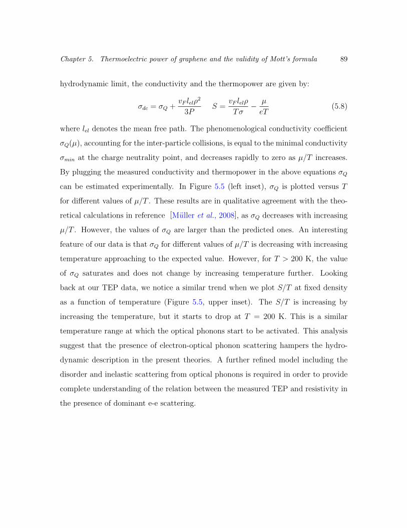
Chapter 5. Thermoelectric power of graphene and the validity of Mott’s formula 89
hydrodynamic limit, the conductivity and the thermopower are given by:
σdc = σQ +vF lelρ
2
3PS =
vF lelρ
Tσ− µ
eT(5.8)
where lel denotes the mean free path. The phenomenological conductivity coefficient
σQ(µ), accounting for the inter-particle collisions, is equal to the minimal conductivity
σmin at the charge neutrality point, and decreases rapidly to zero as µ/T increases.
By plugging the measured conductivity and thermopower in the above equations σQ
can be estimated experimentally. In Figure 5.5 (left inset), σQ is plotted versus T
for different values of µ/T . These results are in qualitative agreement with the theo-
retical calculations in reference [Muller et al., 2008], as σQ decreases with increasing
µ/T . However, the values of σQ are larger than the predicted ones. An interesting
feature of our data is that σQ for different values of µ/T is decreasing with increasing
temperature approaching to the expected value. However, for T > 200 K, the value
of σQ saturates and does not change by increasing temperature further. Looking
back at our TEP data, we notice a similar trend when we plot S/T at fixed density
as a function of temperature (Figure 5.5, upper inset). The S/T is increasing by
increasing the temperature, but it starts to drop at T = 200 K. This is a similar
temperature range at which the optical phonons start to be activated. This analysis
suggest that the presence of electron-optical phonon scattering hampers the hydro-
dynamic description in the present theories. A further refined model including the
disorder and inelastic scattering from optical phonons is required in order to provide
complete understanding of the relation between the measured TEP and resistivity in
the presence of dominant e-e scattering.

Chapter 5. Thermoelectric power of graphene and the validity of Mott’s formula 90
S /
T (µV/K
2)
n (1012 cm-2)
1
-1
-2 20
0
130 K
170 K
200 K
230 K
270 K
300 K300
µ/Τ=6
µ/Τ=7
µ/Τ=8
σQ
(µ) /σQ
(0)
100 T (K)
0.6
1.5
S /
T(µV/K
2)
T (K)
/
0.14
0.18
100 300
n (1012 cm-2)
2.7
2
0
1
Figure 5.5: The measured thermopower divided by T as a function of the carrier
density at different temperatures. The thermopower calculated using the Mott’s
formula (dashed) as well as the hydrodynamic thermopower(dotted) are also plotted
on the same graph. (Left inset) σQ is plotted as a function of T for different values of
µ/T . (Right inset) S/T and the electron-optical phonon scattering rate at two fixed
densities are plotted as a function of temperature.

Chapter 6. Thermoelectric power of graphene in the presence of a magnetic field 91
Chapter 6
Thermoelectric power of graphene
in the presence of a magnetic field
6.1 Introduction
The 2-dimensional electronic systems in the presence of a strong magnetic field display
the quantum Hall effect (QHE) as a result of the quantization of the energy spectrum
into sharpened Landau levels(LLs) [Klitzing et al., 1980; Tsui et al., 1982]. While
the electrical conductivity measurements have been considered the primary tool to
explore the QHE, measurements of other thermodynamic properties, such as magne-
tization [Haavasoja et al., 1984], specific heat [Gornik et al., 1985], and thermopower
also have provided important information about the structure of the energy spectrum
associated with discrete LLs. Specifically, it has been theoretically predicted and
experimentally shown that the thermopower tensor, in the presence of a quantizing
magnetic field, is diagonal and is proportional to the transport entropy of the 2D
electron gas. [Zawadski and Lassnig, 1984; Oji, 1984; Obloh and von Klitzing, 1984;
Smith et al., 1984; Vuong et al., 1985; Fletcher et al., 1985; Streda, 1984; Jonson and
Girvin, 1984].

Chapter 6. Thermoelectric power of graphene in the presence of a magnetic field 92
Here we first sketch the derivation of chemical potential dependant magneto-
thermpower, fully described by Johnson and Girvin [Jonson and Girvin, 1984; Girvin
and Jonson, 1982] in a simple single particle picture without consideration of the e-e
interaction. In the presence of a magnetic field, the response functions are tensor
quantities and the ith component of the non-equilibrium particle-current density, Ji,
affected by the temperature (T ) and potential (ϕ) gradients is expressed as
Ji = L11ij (e/T )∂jϕ+ L12
ij ∂j(1/T ), (6.1)
The transport coefficients above are related to the conductivity, σij and thermoelectric
conductivity, αij as L11ij = (T/e2)σij and L12
ij = (T 2/e)αij, respectively. In the zero
current condition, the thermopower is given by
Sij = −∂ϕ∂T
= − 1
eT(L11)−1
ik L12kj (6.2)
As a result, Sxx and Syx can be expressed as
Sxx = ρxxαxx + ρxyαxy (6.3)
Syx = ρxxαxy − ρyxαxx (6.4)
Initially, Johnson and Girvin calculated the thermopower of the 2DEG restricted in
one direction and continued in other directions, in the absence of disorder [Girvin and
Jonson, 1982]. In their derivation, based on the importance of the edge currents, it was
demonstrated that the thermopower is a universal function of a reduced temperature
(kBT/hωc) and has a series of peaks positioned at the center of each Landau level.
In particular, at a half filled Landau level, the diagonal part of thermopower Sxx has
universal peak values only depending on the Landau level index N whose form can
be expressed as
Smaxxx =kB ln 2
e(N + 1/2)=gskBe
ln 2
ν(6.5)
. where ν is the filling factor specified as the ratio of the number of electrons
to the number of orbital states available in a single Landau level and gs = 2 is
Chapter 6. Thermoelectric power of graphene in the presence of a magnetic field 93
the spin degeneracy. Note that for 2DEGs in GaAs heterostructures considered
above, ν = gs(N + 1/2) = 1, 3, 5, ... for the half-filled spin degenerated LLs, where
N = 0, 1, 2, .... Although these predictions were initially derived from the Boltzmann
approach, similar results have been obtained using the Kubo formula [Jonson and
Girvin, 1984] and also in a corbino disk employing the edge formalism [Oji, 1984].
This earlier work which led to the universal value in Equation (6.5) was obtained only
for the disorder free system. In the presence of disorder, the thermopower becomes
a tensor quantity, developing the off-diagonal components which become larger with
the disorder strength. Jonson and Girvin (JG) utilized [Jonson and Girvin, 1984] the
self consistent Born approximation to evaluate the tensor components of the conduc-
tivity tensor at zero temperature in the presence of disorder. In a disordered 2DEG,
the width of an individual LL, Γ, is proportional to the strength of disorder in the
system. For particular case where kBT < Γ and the chemical potential dependant
conductivity σij(µ) is a slow varying function on the energy scale of ∼ kBT , JG
showed that
Sij = −(π2/3)(kB/e)(kBT )[σ−1]ik[∂σ/∂µ]kj (6.6)
which is called the generalized Mott’s formula. Note that in this low temperature limit
(kBT < Γ < hwc) only the intralevel excitations due to the broadening of the Landau
level are important and the thermopower is linearly proportional to the temperature.
In particular, Equation (6.6) indicates that slowly varying nature of σ(µ) produces the
peak values much smaller than the universal ones (6.5). The magneto thermopower
at the high temperature limit (i.e., kBT > Γ) has been only recently computed
by Shirazaki et al [Shirazaki et al., 2012]. In this work, it has been shown that
the thermopower deviates from Equation (6.6) as the interlevel contributions become
important and Sxx eventually approaches to the quantized value described by equation
(6.5).
The quantized diffusion thermopower described by Equation (6.5) has been ob-
served in one of the first experiments in GaAs heterostructures by [Obloh and von

Chapter 6. Thermoelectric power of graphene in the presence of a magnetic field 94
Klitzing, 1984]. However, in subsequent experiments these results have been difficult
to realize. In most experiments, it was observed that the phonon-drag thermopower
becomes dominant above 1 K, where the first results were obtained. Later experi-
ments performed at lower temperatures [Fletcher et al., 1985; Ruf et al., 1987] showed
that the diffusive thermopower below 0.6 K had the desired form, however the peak
values of Sxx were much higher than the expected quantization values. While these
measurements were performed in the low temperature limit (kBT < Γ), the temper-
ature dependent measurement to confirm the expected cross over between Equation
(6.6) and (6.5) has not been possible due to the prevailing phonon-drag term at high
temperatures.
Similar to the case of GaAs heterostructures and MOSFETs, the quantized magneto-
thermopower is also predicted for graphene. As it has been demonstrated experimen-
tally [Novoselov et al., 2005; Zhang et al., 2005a], graphene shows the unconventional
IQHE which is manifested as the half integer Hall conductivity σxy = gs(N+1/2)e2/h,
where N is the highest filled LL index and gs = 4 is the Landau level degeneracy re-
sulting from the degenerate spin and valley-isospin degrees of freedom. Here, the 12
term in the parenthesis is due to the Berry phase effects, stemming from the rela-
tivistic nature of the particles in graphene. Note that N > (<) 0 refers to electron
(hole) LLs and N = 0 corresponds to the LL at the CNT. Contrarily to σxy, Sxx has
a peak in between the plateaus of σxy, where the corresponding LL is half-filled. For
the half-filled Nth LL (N 6= 0) with full spin and iso-spin degeneracy, the peak values
are given by
Smaxxx =kBe
ln 2
N=gskBe
ln 2
ν(6.7)
where gs = 4 is the spin and the valley degeneracy of graphene Landau level in a
single particle picture.
Note that the quantized Smaxxx for graphene described in Equation (6.7) is just
shift N by a half-integer from the conventional 2DEG in semiconductors expressed
by Equation (6.5). This difference could be understood considering that the N = 0

Chapter 6. Thermoelectric power of graphene in the presence of a magnetic field 95
Landau level in graphene is half filled for either electrons or holes, in contrast to
the 2DEG whose filled LL is fully filled by single sign carriers. We also remark that
the half-filled N = 0 is special, and we expect Sxx = 0 considering the electron-hole
symmetry. Summarizing, one expects a series of quantized peaks of Sxx in graphene
with peak values decreasing as ±59.6, ±29.8, ±19.86 µV/K,... when the N =±1, ±2,
±3,.. LLs are filled up, respectively. In fact, the relativistic effects in graphene lead
to the thermopower peaks which are larger than what is expected for electrons with
a parabolic dispersion relation.
As described in Equation (6.6), disorder induced broadening of Landau levels
tends to broaden Smaxxx leading to the peak values smaller than the quantized value
described in Equation (6.7). This has been the case in the previously measured
thermopower of graphene devices on SiO2 substrates, where disorder effects were
dominant [Zuev et al., 2009; Checkelsky and Ong, 2009]. In these experimental works,
the Sxx peaks appeared at the half-filled LLs, but they were smaller than expected
quantized values. Interestingly, the recent theoretical work of [Zhu et al., 2010] based
on the generalized Mott formula suggests the asymptotic behavior of the thermopower
toward the quantized values as temperature increases to the high temperature limit.
In another theoretical work [Bergman and Oganesyan, 2010], it has been claimed that
the thermopower at low temperatures is still quantized irrespective of the Landau
level broadening. According to this work, the Mott’s formula predicts values which
slightly overestimate the peak values of thermopwer and underestimate it away in the
activated regime. The early experimental results of the thermopower measurements
in graphene [Zuev et al., 2009; Checkelsky and Ong, 2009] are in agreement with
those in the reference [Zhu et al., 2010].
In this chapter, we present the magneto-thermopower (MTEP) measurements of
high quality graphene on boron nitride substrates, where we observe the thermopower
peaks reach values in very close agreement with the universal trend in Equation
(6.7). We do observe, however, deviations from the generalized Mott’s formula in
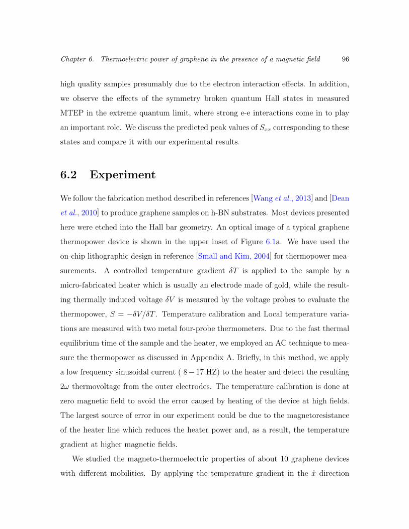
Chapter 6. Thermoelectric power of graphene in the presence of a magnetic field 96
high quality samples presumably due to the electron interaction effects. In addition,
we observe the effects of the symmetry broken quantum Hall states in measured
MTEP in the extreme quantum limit, where strong e-e interactions come in to play
an important role. We discuss the predicted peak values of Sxx corresponding to these
states and compare it with our experimental results.
6.2 Experiment
We follow the fabrication method described in references [Wang et al., 2013] and [Dean
et al., 2010] to produce graphene samples on h-BN substrates. Most devices presented
here were etched into the Hall bar geometry. An optical image of a typical graphene
thermopower device is shown in the upper inset of Figure 6.1a. We have used the
on-chip lithographic design in reference [Small and Kim, 2004] for thermopower mea-
surements. A controlled temperature gradient δT is applied to the sample by a
micro-fabricated heater which is usually an electrode made of gold, while the result-
ing thermally induced voltage δV is measured by the voltage probes to evaluate the
thermopower, S = −δV/δT . Temperature calibration and Local temperature varia-
tions are measured with two metal four-probe thermometers. Due to the fast thermal
equilibrium time of the sample and the heater, we employed an AC technique to mea-
sure the thermopower as discussed in Appendix A. Briefly, in this method, we apply
a low frequency sinusoidal current ( 8− 17 HZ) to the heater and detect the resulting
2ω thermovoltage from the outer electrodes. The temperature calibration is done at
zero magnetic field to avoid the error caused by heating of the device at high fields.
The largest source of error in our experiment could be due to the magnetoresistance
of the heater line which reduces the heater power and, as a result, the temperature
gradient at higher magnetic fields.
We studied the magneto-thermoelectric properties of about 10 graphene devices
with different mobilities. By applying the temperature gradient in the x direction

Chapter 6. Thermoelectric power of graphene in the presence of a magnetic field 97
which is parallel to the length of the Hall bar, the electric field E = −∇ϕ has the
components Ex = Sxx∇T and Ey = Syx∇T . Consequently, the Seebeck coefficient
and the Nernst signal are defined as:
Sxx = − Ex∇T
=
√2Vxx(2ω)
∆T, Syx = − Ey
∇T=
√2Vyx(2ω) l
w
∆T
The thermoelectric conductivity tensor is also expressed as α = S.σ, where S and σ
are the thermopower and conductivity tensors, respectively. To resolve all features
in Sxx and Syx, we also measured resistivity tensor components, ρxx and ρxy at the
same temperature for different samples.
Figure 6.1a displays the Landau fan diagram of Sxx versus carrier density and
magnetic field B, measured for device D2 with a mobility of 47,000 cm2/Vs . Dashed
lines positioned between Landau levels where the thermopower vanishes represent
different IQHE states developing with the field at filling factors ν = 2, 6, 10, 14, where
the filling factor ν is nh/eB when expressed versus density n and the magnetic field B.
From this diagram one can see the IQHE states already appear at very low magnetic
fields around 1 T owing to the high quality of our graphene sample.
At higher fields, in addition to the states corresponding to the above mentioned
filling factors, we also observe other QH states at ν = 1, 3, 4, 5, 7, 8 due to the breaking
of the 4-fold degeneracy of each Landau level. Previously, these states have been
observed in resistivity measurements and the nature of them have been analyzed in
detail [Young et al., 2012]. However, this is the first time these states have been
revealed in the thermopower signal. Figure 6.1b and 6.1c show Sxx and Sxy versus
density at 14 T perpendicular magnetic field. For comparison, the corresponding Rxx
and σxy are plotted on the same graphs. Minima in Sxx associated with different
QHE states are well aligned with those in Rxx and the quantized plateaus in σxy.
The Nernst signal Syx is very small compared with the Seebeck coefficient Sxx, which
is in agreement with the GJ theory, which predicts the Nernst signal increases with
disorder strength and vanishes in the clean limit. We observe that, for the N = 0
Landau level, Syx shows a negative large peak in contrast to N 6= 0. We will discuss
Chapter 6. Thermoelectric power of graphene in the presence of a magnetic field 98
the origin of this enhancement at the end of this chapter.
-30 -15 0 15 30
0.0
-6.3
-12.5
-2-6 2
6
0
12.5
(T
)
30
-10
µV/K
Rxx(kΩ) S
xx(µv/K
)
0
4
0
-14
14
0
(V)
-15-30 150
-8
Gxy(e
2/h)
-20
208
0
Sxx
= 14T
Sxy(µv/K
)
30
ν = 2
ν = −2
ν = −6
a
b
c
Figure 6.1: (a) Landau fan diagram of Sxx at T = 2 K. Dark blue color corresponds
to Sxx = 0. The orange and black dashed lines display IQHE states at filling factor
ν = ±2,±6 for electrons and holes, respectively. The upper inset shows a typical
device image. (b) Rxx and Sxx measured at 14 T. (c) Rxy and Sxy measured at 14 T.
Chapter 6. Thermoelectric power of graphene in the presence of a magnetic field 99
6.3 Thermoelectric properties of graphene in the
a single particle quantum Hall regime
We first discuss the nature of the thermoelectric coefficients in a single particle quan-
tum Hall regime where LL splitting is not present. Figure 6.2a and 6.2b display the
measured diagonal (Seebeck) component Sxx and the off-diagonal (Nernst) compo-
nent Syx of the thermopower tensor for device D1 as a function of Landau level filling
factor. The data is taken at different magnetic fields ranging from 1-12 T and at a
temperature of 6.25 K. Both of these components vanish in between Landau levels,
while they take finite values when the Fermi energy crosses the disorder-broadened
Landau levels. The Seebeck coefficient is antisymmetric relative to the charge neu-
trality point and exhibits a single peak at the center of each Landau level, while the
Nernst signal is symmetric for the electrons respect to the holes and has negative or
positive values depending on whether the Fermi energy is below or above the center
of the Landau level.
An important feature of our data is that both Sxx and Syx change only slightly
with the magnetic field, following the prediction by the GJ theory [Girvin and Jonson,
1982]. As it is depicted in Figure 6.3a and 6.3b, we see that the thermoelectric
coefficients are rather insensitive to temperature as well in the range of 2-10 K. In
Figure 6.3c, the peak values of Sxx are plotted as a function of B for different Landau
level index N=1, 2 and 3, respectively. For a comparison, we also plot the expected
quantized peak value of Sxx, given by Equation (6.7). For the N = 1 Landau level,
there is a quantitative good agreement between theory and experiment up to 90%,
although the discrepancy is higher for higher Landau levels. This is a quite large
improvement relative to previously measured disordered samples, in which, the peak
values have been around 10 times smaller than the predicted ones [Zuev et al., 2009].
We also note that Sxx displays several peaks at the N = 0 Landau level. These peaks
correspond to the breaking of the N = 0 Landau level, which will be discussed in the

Chapter 6. Thermoelectric power of graphene in the presence of a magnetic field 100
next section.
FillingFactorν
(μV/K)
(μV/K)
100
-100
50
-50
-15-30 15 30
0
0
0
1T
5T
8T
12T
b
a
Figure 6.2: (a) The diagonal component Sxx and (b) the off-diagonal component Syx
of the thermopower tensor as a function of filling factor measured at 1 T, 5 T, 8 T
and 12 T , respectively.

Chapter 6. Thermoelectric power of graphene in the presence of a magnetic field 101
(T)
(μV/K)
2.6K
6.25K
-15 150
(μV/K)
(μV/K)
-150
150
0
-50
50
0
FillingFactorν
0 12
0
60
6
b
a c
Figure 6.3: (a) The diagonal component Sxx and (b) the off-diagonal component Syx
of the thermopower tensor as a function of filling factor measured at 2.7 K and 6.3 K,
respectively. (c) The peak values of Sxx plotted as a function of B for different Landau
level index N=1, 2 and 3, respectively. The dashed, dotted and dash-dotted lines are
the predicted values given by Equation (6.7) for Landau level index N=1, 2 and 3,
respectively.
We also compare the measured thermopower peaks for samples with different
mobilities. In Figure 6.4, we plot, as a function of filling factor at a fixed magnetic
field of 5 T, the measured diagonal component of thermopower for devices D1 and D3
with mobilities 100,000 cm2/Vs and 25,000 cm2/Vs, respectively. We find that indeed
the peak heights of higher mobility samples matches better with the universal values
predicted by Equation (6.7), while the lower quality samples exhibits far smaller
peak values as in accordance with the prior work [Zuev et al., 2009]. This is also in

Chapter 6. Thermoelectric power of graphene in the presence of a magnetic field 102
agreement with the original prediction made by the GJ theory [Girvin and Jonson,
1982], according to which the presence of disorder tends to decrease the peak heights
at the center of each Landau level.
It is interesting to compare the measured thermopower with the values from the
generalized Mott formula (Equation (6.6)), which can be computed separately from
measured σxx and σxy. The inset of Figure 6.4 displays a direct comparison for the
generalized Mott formula with the measured value for the samples D1 and D3. Quite
interestingly, we do observe a largely underestimated thermopowers from the gener-
alized Mott formula. The discrepancy grows with increasing mobility of the samples:
In the highest quality sample where the quantized Smaxxx was observed, the Mott
prediction predicts almost 100 times smaller values. This is in contrast with the the-
oretical expectations as well as earlier experiments on disordered samples [Bergman
and Oganesyan, 2010; Zhu et al., 2010; Zuev et al., 2009], in which, the agreement
between the measured thermopower and the Mott’s formula has been achieved. We
do not understand the reason for such stark failure of the generalized Mott formalism
for the high quality samples at this point, and leave this for a topic for future studies.

Chapter 6. Thermoelectric power of graphene in the presence of a magnetic field 103
D3
D1
-20 -10 0
0.1
1
10
100
(μV/K)
100
-100
0
(μV/K)
0 10-10-20 20
FillingFactorν
FillingFactorν
2 K
Figure 6.4: (a) The diagonal component of thermopower, Sxx, measured for devices
D1 and D3 with mobilities 100,000 cm2/Vs and 25,000 cm2/Vs, respectively. The
inset shows the measured thermopower (solid lines) and the thermopower expected
by the Mott’s formula (dashed lines) for devices D1 and D3.
6.4 Effect of Landau level splitting on the ther-
mopower of graphene at high magnetic fields
Now, we turn our discussion to the high field behavior of the thermopower tensor
components. In the case of the 2DEG, the proper equation instead of Equation (6.5)

Chapter 6. Thermoelectric power of graphene in the presence of a magnetic field 104
which describes the maxima in thermopower if spin splitting is resolved has the form
Smax =kB ln 2
e(2N + 1± 1/2)=kBe
ln 2
ν(6.8)
[Oji, 1984]. The above relation can be derived using thermodynamic arguments and
does not depend on the mechanisms by which these states appear [Obraztsov, 1965].
As it was pointed out earlier, the thermopower Sxx represents the entropy per unit
charge. At the center of each Landau level, half of the available states will be occupied
and the chance of occupation of each state is a half, where the entropy takes the
maximum value of kB ln 2. Therefore, the entropy per charge would be kB ln 2 divided
by the number of channels. For a half-filled spin split LL in semiconductors, the
number of conducting channels is equal to ν = (2N + 1 ± 1/2) where N is the LL
index and ± corresponds to spin up or spin down split LL. This consideration provides
the exact expression above.
In graphene, we utilized a similar argument to derive the relation which describes
the values of the thermopower maxima when spin and valley-isospin degeneracies
within each Landau level are resolved. This relation can be expressed as
Smax =kB ln 2
e(4N ± 1± 1/2)=kBe
ln 2
ν(6.9)
where the filling fraction that the peak appears span over ν = ±12, ±3
2, ±5
2,.... In Fig-
ure 6.5, we have plotted the Seebeck coefficient Sxx for holes (lined cuts of Figure 6.1a
at different fields) at different magnetic fields ranging from 5-14 T on the same graph,
where we can see the peak at half field N = 1 Landau level resolves into four other
peaks emerging from the interaction induced symmetry broken states between ν = −2
and ν = −6. These peaks are located at filling factors ν = −5/2,−7/2,−9/2,−11/2.
The height of these peaks is decreasing with increasing the magnetic field as the
symmetry broken states are becoming stronger at higher fields.

Chapter 6. Thermoelectric power of graphene in the presence of a magnetic field 105
5T
7T
9T
11T
14T
(μV/K)
-2-6-10
0
60
FillingFactorν
Figure 6.5: The Seebeck coefficient Sxx measured for holes at different magnetic fields
ranging from 5-14 T. The dashed and dotted lines display the thermopower predicted
from Equations (6.7) and (6.9), respectively.
For comparison, the thermopower expected from Equation (6.7) and Equation
(6.9) are also plotted on the same graph. Interestingly, the peak values are much
smaller than the values given by Equation (6.7) which is valid in the absence of
splitting. In contrast, our measured maxima of thermopower are in good proximity
to the predicted peak values by Equation (6.9) which is the case when the degeneracy
is resolved. At lower fields, the peak values do not quite follow the trend expected
as the maxima do not decrease with increasing the filling factor (The peak value at
Chapter 6. Thermoelectric power of graphene in the presence of a magnetic field 106
ν = 7/2 is higher than all other peaks). This might be due to the fact that spin
splitting happens first and the degeneracy is not fully resolved at lower fields.
We now analyze the thermoelectric response of the N = 0 Landau level. Due to
the disorder effects present in sample D2, the symmetry broken states were not well
resolved in the vicinity of the charge neutrality point. Thus, we have plotted the
data from sample D1 in Figure 6.6. We observe the single peak at N = 0 Landau
level for electrons and holes splits into two peaks around ν = ±1/2 and ν = ±3/2
by increasing the magnetic field. Note that the position of the peak at ν = ±1/2
changes toward lower filling factors by increasing the magnetic field and it is not
symmetric relative to the Dirac point. The peak value at ν = ±3/2, originated from
the presence of the symmetry broken ν = ±1 state, is around ±39 µV/K, which is
in a good agreement with the expected value from the Equation (6.9). However, the
peak at ν = ±1/2 (ν = 0 state) reaches to a value twice as high as the predicted one
for ν = ±1/2 (∼ 250 µV/K instead of 119.2 µV/K for holes) at 12 T. The inset of
Figure 6.6 presents the peak value at ν = 0 for holes as a function of the magnetic
field B. This value increases with field, but changes only slightly with temperature.
Although this is in agreement with the GJ theory, considering this theory is only valid
for non-interacting electron picture, more refined theoretical model including the e-
e interaction is needed to understand the observed magneto TEP near the charge
neutrality at the extreme quantum limit.

Chapter 6. Thermoelectric power of graphene in the presence of a magnetic field 107
-200
0
200
0-1-2
(μV/K) 0 12
102
103
2.6K
6.25K
N=0
(μV/K)
(T)
FillingFactorν
1T
2T
9T
12T
5T
1 2
Figure 6.6: The Seebeck coefficient Sxx measured in the vicinity of the Dirac point
at different magnetic fields. The inset displays the measured thermopower peak at
ν = 0 for holes as a function of magnetic field B and at two temperatures of 2.7 K
and 6.3 K.
Another interesting feature of the N = 0 Landau level is its Nernst signal with a
negative sign. In Figure 6.7, Syx is plotted as a function of Filling factor ν measured
for two different devices D2 and D4. The Nernst signal has a negative peak at the
Dirac point whose magnitude is much larger in Device D4 than that of D2. As it is
displayed in the lower inset of Figure 6.7, the value of these peaks increases with the
magnetic field and the rate of this growth is larger for Device D4.

Chapter 6. Thermoelectric power of graphene in the presence of a magnetic field 108
D2
D4
0
-100
0-5 5
(μV/K)
FillingFactorν
D2
D4
-200
0 14
0
(μV/K)
(T)
14 T
Figure 6.7: Syx measured for devices D2 and D4 as a function of Filling factor ν at
14 T. The inset shows the magnetic field dependence of Nernst signal at the Dirac
point.
According to Equation (6.4), Syx can be represented by difference between the two
product terms: ρxxαxy and ρyxαxx . However, in N = 0 Landau level, the second term
goes to zero as one approaches the charge neutrality point, since ρxy vanishes at this
point. Thus, Syx is solely determined by the form of ρxxαxy. It is shown [Bergman
and Oganesyan, 2010] that αxy can be expressed as the form
αxy = gkBe
h
∞∑n=0
[fn log fn + (1− fn) log (1− fn)] (6.10)
where fn = f(hωn − µ) is the Fermi distribution function, hωn is the nth Landau
level energy, and µ is chemical potential. Ideally, at the center of each Landau level,

Chapter 6. Thermoelectric power of graphene in the presence of a magnetic field 109
αxy exhibits a peak with the value of gskB log 2 eh
and vanishes between the Landau
levels. The disorder broadening of LLs and more importantly, the e-e interaction,
likely reduce the measured value of αxy from this ideal upper limit. Experimentally,
αxy can be obtained from measured resistivity and thermopower tensors employing
Equation (6.4). The measured αxy for two different samples D2 and D4 is depicted in
Figure 6.8a. As expected, the peak values of αxy is smaller but in the same order of
magnitude as the single particle quantization value, gskBe/h log 2, changing slightly
at the CNP for different samples D2 and D4. However, as shown in Figure 6.8b, the
resistivity in the vicinity of the Dirac point is much larger for D4 than D2 due to the
interaction effects, explaining the observed large Nernst signal in D4 than D2..
0-5 5
0
Rxx(kΩ)
FillingFactorν0-5 5
FillingFactorν
0
10
(nA/K)
50ba
Figure 6.8: (a) αxy as a function of filling factor for devices D2 (in green) and D4
(in red) at 14 T. (b) The measured resistivity Rxx as a function of filling factor for
devices D2(in green) and D4 (in red) at 14 T.
6.5 Thermopower of graphene in the FQHE regime
As mentioned before, the thermopower of a non-interacting electron gas is sharply
linked to the entropy per particle. A similar relation was later proved to hold for

Chapter 6. Thermoelectric power of graphene in the presence of a magnetic field 110
strongly correlated electrons at high magnetic fields in the clean limit [Cooper et
al., 1997]. Therefore, the thermopower has been considered a useful tool to probe
the non-Abelian quasiparticles of certain FQHE states like ν = 5/2 in GaAs. In
particular, the ground state degeneracy for the non-Abelian statistic grows expo-
nentially with the quasiparticle number, producing excess entropy associated to the
thermopower [Moore and Read, 1991; Yang and Halperin, 2009; Bishara et al., 2008;
Cooper and Stern, 2009]. Here the excess entropy can be expressed as
Sd ≈kBeNq log d (6.11)
where d and Nq are the quantum dimension and the quasiparticle number, respec-
tively.
The quantum dimension d is equal to√
2 for Pfaffian or anti-Pfaffian states. In
principle, for an Abelian state one would expect the linear dependence of thermopower
on temperature, but for a non-Abelain state the thermopower in a temperature range
of T0 < T < T1 is constant and dominated by the entropy arising from the anomalous
ground state degeneracy of this state [Chickering et al., 2010]. Apart from this, the
thermopower measured at FQHE states can be utilized to test the predictions of the
composite fermion (CF) formalism. For example, it has been shown [Ying et al.,
1994; Bayot et al., 1995] that the temperature dependence and the magnitude of the
diagonal component of thermopower at ν = 1/2 and ν = 3/2 are consistent with the
composite-fermion picture.
Motivated by previous experiments in GaAs, we tried to investigate the FQHE
in graphene by means of the thermopower measurements. As it was mentioned in
the explanation of Figure 6.5, additional minima between different symmetry broken
states started to appear at the highest fields accessible in the lab. We repeated
our experiment in very high magnetic fields ∼ 35 T, where you expect to observe
the FQHE in addition to other QHE states at lower fields [Bolotin et al., 2009;
Du et al., 2009; Dean et al., 2011]. Figure 6.9a displays the longitudinal resistance
Rxx and the Hall conductance Gxy = 1/Rxy versus filling factor at a magnetic field of

Chapter 6. Thermoelectric power of graphene in the presence of a magnetic field 111
35 T. All symmetry broken states at ν = −1,−2,−3 are well developed as quantized
plateaus in Gxy and zeros in Rxx. Further, we observe additional plateaus in Gxy and
minima in Rxx corresponding to the fractional quantum Hall states at filling factors
ν = 8/3 and ν = 10/3. Thermopower measurement at this field is also presented
in Figure 6.9b, in which, the thermal voltage Vth is plotted versus the filling factor
ν. Note that due to the large uncertainty in determining the temperature gradient
at high fields and very low temperatures, the calibration to provide the temperature
difference has been challenging this experiment. We thus have presented the thermal
voltage instead of the thermoelectric signal here. The data show strong oscillations
relevant to the IQHE and FQHE. We observe developing FQHE states at filling
fractions ν = 7/3, 8/3, 10/3 and ν = 11/3 consistent with the sequence of the 1/3
states observed in the resistivity measurements [Dean et al., 2011]. It would be very
interesting to measure the temperature dependence of the thermopower to test both
the Abelian characteristics and the CF formalism for these states. However, higher
quality samples are needed to perform this experiment at lower magnetic fields where
the technical problems due to the temperature calibration can be solved.

Chapter 6. Thermoelectric power of graphene in the presence of a magnetic field 112
11/3
10/3 7/3
11/3
8/3
10/3
8/3
-1
FillingFactorν-2-3-4 -1
FillingFactorν-2-3-4
0.0
0.8
0
6
0
4
(kΩ) G
xy(e
2/h)
(μV)
ba
Figure 6.9: (a) The longitudinal resistance Rxx and the Hall conductance Gxy =
1/Rxy versus filling factor measured at a magnetic field of 35 T. (b) The thermal
voltage Vth versus the filling factor ν at 35 T.

Bibliography 113
Bibliography
D. A. Abanin and L. S. Levitov. Phys. Rev. B, 78:035416, 2008.
D.A. Abanin, I. Skachko, X. Du, E.Y. Andrei, and L.S. Levitov. Phys. Rev. B.,
81:115410, 2010.
D. S. L. Abergel, A. Russell, and V. I. Falko. Appl. Phys. Lett., 91:063125, 2007.
W. Andreoni. springer, Berlin, 2000.
V. M. Apalkov and T. Chakraborty. Phys. Rev. Lett., 97:126801, 2006.
A. A. Balandin, S. Ghosh, W. Bao, I. Calizo, D. Teweldebrhan, F. Miao, and C. N.
La. Nano Lett., 8:902, 2008.
P. K. Basu, C. K. Sarkar, and S. Kundu. Surface Science, 196:700–706, 1988.
V. Bayot, E. Grivei, H. C. Manoharan, X. Ying, and M. Shayegan. Phys. Rev. B,
52:R8621(R), 1995.
B. R. Bennett, R. Magno, J. B. Boos, W. Kruppa, and M. G. Ancona. Sol. Stat.
Elec., 49:18751895, 2005.
Stphane Berciaud, Melinda Y. Han, Kin Fai Mak, Louis E. Brus, Philip Kim, and
Tony F. Heinz. Phys. Rev. Lett., 104:227401, 2010.
Doron Bergman and Vadim Oganesyan. Phys. Rev. Lett., 104:066601, 2010.

Bibliography 114
W. Bishara, G. A. Fiete, and C. Nayak. Phys. Rev. B, 77:241306, 2008.
P. Blake, K. S. Novoselov, A. H. Castro Neto, R. Yang D. Jiang, T. J. Booth, A. K.
Geim, and E. W. Hill. Appl. Phys. Lett., 91:063124, 2007.
G.S. Boebinger, A.M.Chang, H.L.Stormer, and D.C.Tsui. Phys. Rev. Lett., 55:1606,
1985.
K. I. Bolotin, K. J. Sikes, J. Hone, H. L. Stormer, and P. Kim. Phys. Rev. Lett.,
101:096802, 2008.
K. I. Bolotin, K. J. Sikes, Z. Jiang, G. Fundenberg, J. Hone, P. Kim, and H. L.
Stormer. Solid State Commun., 146:351355, 2008.
K. I. Bolotin, F. Ghahari, M. D. Shulman, H. L. Stormer, and P.Kim. Nature,
462:196, 2009.
K.I. Bolotin. (unpublished), 2008.
M. Buttiker. Phys. Rev. B, 38:9375–9389, 1988.
D. G. Cantrell and P. N. Butcher. J. Phys. C, 19:L429, 1986.
C. Casiraghi, A. Hartschuh, E. Lidorikis, H. Qian, H. Harutyunyan, T. Gokus, K. S.
Novoselov, , and A. C. Ferrari. Nano Lett., 7:2711, 2007.
PM. Chaiken. In Organic Superconductors, page 10115, 1990.
Sung-Po Chao and Vivek Aji. Phys. Rev. B, 83:165449, 2011.
J. C. Charlier, X. Blase, and S. Roche. Rev. Mod. Phys., 79:677, 2007.
Joseph G. Checkelsky and N. P. Ong. Phys. Rev. B, 80:081413(R), 2009.
J. G. Checkelsky, L. Li, and N. P. Ong. Phys. Rev. B, 79:115434, 2009.

Bibliography 115
J.-H. Chen, C. Jang, S. Adam, M. S. Fuhrer, E. D. Williams, and M. Ishigami.
Nature Physics, 4:377, 2008.
J. H. Chen, C. Jang, S. D. Xiao, M. Ishigami, and M. S. Fuhrer. Nat. Nanotechnol.,
3:206, 2008.
Ian-Hao Chen, Liang Li, William G. Cullen, Ellen D. Williams, and Michael S.
Fuhrer. Nature Physics, 7:535538, 2011.
W. E. Chickering, J. P. Eisenstein, L. N. Pfeiffer, and K. W. West. Phys. Rev. B,
81:245319, 2010.
D. H. Cobden, C. H. W. Barnes, and C. J. B. Ford. Phys. Rev. Lett., 82:46954698,
1999.
N. R. Cooper and A. Stern. Phys. Rev. Lett., 102:176807, 2009.
N. R. Cooper, B. I. Halperin, and I. M. Ruzin. Phys. Rev. B, 55:2344, 1997.
Barbaros ozyilmaz, Pablo Jarillo-Herrero, Dmitri Efetov, Dmitri A. Abanin,
Leonid S. Levitov, and Philip Kim. Phys. Rev. Lett., 99:166804, 2007.
C.R. Dean, A.F. Young, I. Meric, C.Lee, L.Wang, S.Sorgenfrei, K. Watanabe,
T. Taniguchi, P. Kim, K.L. Shepard, and J. Hone. Nature Nanotechnology, 5:722–
726, 2010.
C. R. Dean, A. F. Young, P. Cadden-Zimansky, L. Wang, H. Ren, K. Watanabe,
T. Taniguchi, P. Kim, J. Hone, and K.L. Shepard. Nature Physics, 7:693, 2011.
C. R. Dean, L. Wang, P. Maher, C. Forsythe, F. Ghahari, Y. Gao, J. Katoch,
M. Ishigami, P. Moon, M. Koshino, T. Taniguchi, K. Watanabe, K. L. Shepard,
J. Hone, and P. Kim. Nature, 497:598602, 2013.
A. F. Dethlefsen, E. Mariani, H.P. Tranitz, W. Wegscheider, , and R. J. Haug. Phys.
Rev. B, 74:165325, 2006.

Bibliography 116
X. Du, I. Skachko, A. Barker, and E. Y. Andrei. Nature Nanotechnol., 3:491495,
2008.
X. Du, I. Skachko, F. Duerr, A. Luican, and E. Y. Andrei. Nature, 462:192, 2009.
Dmitri K. Efetov and P. Kim. Phys. Rev. Lett., 105:256805, 2010.
B. E. Feldman, B. Krauss, J. H. Smet, and A. Yacoby. Science, 337:1196–1199, 2012.
R. Fletcher, J. C. Maan, and G. Weimann. Phys. Rev. B, 32:8477, 1985.
M. M. Fogler, A. H. Castro Neto, and F. Guinea. Phys. Rev. B., 81:161408(R), 2010.
M. S. Foster and I. L. Aleiner. Phys. Rev. B, 77:195413, 2009.
M. S. Foster. unpublished, 2011.
L. Fritz, J. Schmalian, M. Mller, and S. Sachdev. Phys. Rev. B, 78:085416, 2007.
B. L. Gallagher, C. J. Gibbings, M. Pepper, and D. G. Cantrell. Semicond. Sci.
Technol., 2:456, 1987.
B. L. Gallagher, J. P. Oxley, T. Galloway, M. J. Smith, and P. N. Butcher. J. Phys.
C, 2:755, 1990.
F. Ghahari, Y. Zhao, P. Cadden-Zimansky, K. Bolotin, and P. Kim. Phys. Rev.
Lett., 106 (4):046801, 2011.
F. Ghahari. unpublished, 2012.
G. Giovannetti, P. Khomyakov, G. Brocks, P. Kelly, and J. V. D. Brink. Phys. Rev.
B, 76:073103, 2007.
S. M. Girvin and M. Jonson. J. Phys. C, 15:L1147, 1982.
M. O. Goerbig and N. Regnault. Phys. Rev. B, 75:241405, 2007.

Bibliography 117
J. Gonzlez, F. Guinea, and M. A. H. Vozmediano. Phys. Rev. B, 59:R2474, 1999.
E. Gornik, R. Lassnig, G. Strasser, H. L. Stormer, A. C. Gossard, and W. Wiegmann.
Phys. Rev. Lett., S4:1820, 1985.
V. P. Gusynin and S. G. Sharapov. Phys. Rev. Lett., 95:146801, 2005.
T. Haavasoja, H. L. Stormer, D. J. Bishop, V. Narayanamurti, A. C. Gossard, and
W. Wiegmann. Surf. Sci., 142:294, 1984.
B. I. Halperin. Phys. Rev. B., 25:21852190, 1982.
M.Y. Han, B. Oezyilmaz, Y. Zhang, and P. Kim. Phys. Rev. Lett., 98:206805, 2007.
B. Huard, N. Stander, J. A. Sulpizio, and D. Goldhaber-Gordon. Phys.Rev.B,
78:121402, 2008.
E. H. Hwang and S. Das Sarma. Phys. Rev. B, 77:115449, 2007.
J. K. Jain. Phys. Rev. Lett., 63:199, 1989.
J. Jain. Cambridge Univ. Press, 2007.
Z. Jiang, Y. Zhang, H. L. Stormer, and P. Kim. Phys. Rev. Lett., 99:106802, 2007.
Insun Jo, Michael Thompson Pettes, Jaehyun Kim, Kenji Watanabe, Takashi
Taniguchi, Zhen Yao, and Li Shi. Nano Lett., 13:550554, 2013.
M. Jonson and S. M. Girvin. Phys. Rev. B, 29:1939, 1984.
D. V. Khveshchenko. Phys. Rev. B, 75:153405, 2007.
D. V. Khveshchenko. Phys. Rev. B, 77:235426, 2008.
K. v. Klitzing, G. Dorda, and M. Pepper. Phys. Rev. Lett., 45:494, 1980.
L. D. Landau. Phys. Z. Sowjetunion, 11:26–35, 1937.

Bibliography 118
R. B. Laughlin. Phys. Rev. Lett., 51:605, 1983.
Changgu Lee, Xiaoding Wei1, Jeffrey W. Kysar, and James Hone. Science, 321
(5887):385–388, 2008.
A. H. MacDonald. arXiv:cond-mat, 9410047, 1994.
Markus Muller and Subir Sachdev. arXiv:, page 0801.2970, 2008.
M. Muller, L. Fritz, and S. Sachdev. Phys. Rev. B, 78:115406, 2008.
Inanc Meric, Melinda Y. Han, Andrea F. Young, Barbaros Ozyilmaz, Philip Kim,
and Kenneth L. Shepard. Nature Nanotech., 3:654659, 2008.
Moore and N. Read. Nucl. Phys. B, 360:362, 1991.
DT. Morelli. Encycl. Appl. Phys., 21:33954, 1997.
S. V. Morozov, K. S. Novoselov, M. I. Katsnelson, F. Schedin, D. C. Elias, J. A.
Jaszczak, and A. K. Geim. Phys. Rev. Lett., 100:016602, 2008.
J. Moser, A. Barreiro, and A. Bachtold. Appl. Phys. Lett., 91:163513, 2007.
A. H. C. Neto, F. Guinea, N. M. R. Peres, K. S. Novoselov, and A. K Geim. Rev.
Mod. Phys., 81:109163, 2009.
R. J. Nicholas. J. Phys. C, 18:L695, 1985.
K. Nomura and A. H. MacDonald. Phys. Rev. Lett., 96:256602, 2006.
D.S. Novikov. Appl.Phys.Lett., 91:102102, 2007.
K. S. Novoselov, A. K. Geim, S. V. Morozov, D. Jiang, Y. Zhang, S. V. Dubonos,
I. V. Gregorieva, , and A. A. Firsov. Science, 306:666, 2004.
K. S. Novoselov, A. K. Geim, S. V. Morozov, D. Jiang, M. I. Katsnelson, I. V.
Grigorieva, S. V. Dubonos, and A. A. Firsov. Nature, 438:197, 2005.
Bibliography 119
K. S. Novoselov, Z. Jiang, Y. Zhang, S. V. Morozov, H. L. Stormer, U. Zeitler, J. C.
Maan, G. S. Boebinger, P. Kim, and A. K. Geim. Science, 315:1379, 2007.
H. Obloh and K. von Klitzing. Surf. Sci., 142:236, 1984.
Yu. Obraztsov. Fiz. Tverd. Tela(Leningrad), 7:573, 1965.
Helbert Oji. Phys. Rev. B, 29:3148, 1984.
J. Orr, A. Gilbertson, M. Fearn, O. Croad, C. Storey, L. Buckle, M. Emeny,
P. Buckle, and T. Ashley. Phys. Rev. B, 77:165334, 2008.
Cheol-Hwan Park, Nicola Bonini, Thibault Sohier, Georgy Samsonidze, Boris
Kozinsky, Matteo Calandra, Francesco Mauri, and Nicola Marzari. Nano Lett.,
14(3):11131119, 2014.
R. E. Peierls. Ann. I. H. Poincare, 5:177–222, 1935.
N. M. R. Peres, F. Guinea, and A. H. C. Neto. Phys. Rev. B, 73:125411, 2006.
L. A. Ponomarenko, R. V. Gorbachev, G. L. Yu, D. C. Elias, R. Jalil, A. A. Patel,
A. Mishchenko, A. S. Mayorov, C. R. Woods, J. R. Wallbank, M. Mucha-Kruczynski
B. A. Piot, M. Potemski, I. V. Grigorieva, K. S. Novoselov, F. Guinea, V. I. Falko,
and A. K. Geim. Nature, 497:594597, 2013.
E. Prada, P. San-Jose, G. Len, M. M. Fogler, and F. Guinea. Phys. Rev. B.,
81:161402(R), 2010.
Some reviews of recent theoretical work can be found in K. Yang. Solid State Com-
mun., 143:27, 2007.
C. Ruf, H. Obloh, B. Junge, E. Gmelin, and K. Ploog. Phys. Rev. B, 37:6377, 1987.
R. Saito, G. Dresselhaus, and M. S. Dresselhaus. Imperial College Press, London,
1998.

Bibliography 120
S. D. Sarma and A. Pinczuk. Wiley, 1997.
F. Schwierz. Nature Nanotech., 5:487496, 2008.
D. E. Sheehy and J. Schmalian. Phys. Rev. Lett., 99:226803, 2007.
Ryoen Shirazaki, Naomichi Hatano Akira Endo, and Hiroaki Nakamura. Journal of
ELECTRONIC MATERIALS, 41:6, 2012.
I. Skachko, X. Du, F. Duerr, A. Luican, D. A. Abanin, L. S. Levitov, and E.Y.Andrei.
Phil. Trans. R. Soc., A 368:5403, 2010.
J. Small and P. Kim. Microscale Thermophysical Engineering, 8:1, 2004.
J. P. Small, K. M. Perez, and P. Kim. Phys. Rev. Lett., 91:256801, 2003.
R. P. Smith, H. Closs, and P. J. Stiles. Surf. Sci., 142:246, 1984.
P. Streda. Phys. Status Solidi, b125:849, 1984.
T. Taniguchi and K. Watanabe. J. Cryst. Growth, 303:525529, 2008.
F. J. Teran, M. Potemski, D. K. Maude, T. Andrearczyk, J. Jaroszynski, T. Woj-
towicz, and G. Karczewski. Phys. Rev. B., 82:245150, 2010.
C. Toke and Jain. Phys. Rev. B, 75:245440, 2008.
C. Toke, P. E. Lammert, V. H. Crespi, and J. K. Jain. Phys. Rev. B, 75:235417,
2006.
D. C. Tsui, H. L. Stormer, and A. C. Gossard. Phys. Rev. Lett., 48:1559, 1982.
G. W. Uhlenbeck, G. W. Ford, and E. W. Montroll. Proceedings of the summer
seminar, Boulder, Colorado, 1960.

Bibliography 121
H. H. Vuong, R.J.Nicholas, M. A. Brummell, J. C. Portal, M. Razeghi, F. Alexandre,
J. M. Masson, Cheng K. Y, and A. Y. Cho. Proceedings of Yamada Conference XIII,
Kyoto, 1985.
P. R. Wallace. Phys. Rev., 71:622, 1947.
Deqi Wang and Jing Shi. Phys. Rev. B, 83:113403, 2011.
L. Wang, I. Meric1, P. Y. Huang, Q. Gao, Y. Gao, H. Tran, T. Taniguchi, K. Watan-
abe, L. M. Campos, D. A. Muller, J. Guo, P. Kim, J. Hone, K. L. Shepard, and
C. R. Dean. Science, 342:614, 2013.
K. Watanabe, T. Taniguchi, and H. Kanda. Nature Mater., 3:404409, 2008.
P. Wei, W. Bao, Y. Pu, C. N. Lau, and J. Shi. Phys. Rev. Lett., 102:166808, 2009.
R. L. Willett, West, K. W., and L. N. Pfeiffer. Phys. Rev. Lett., 78:44784481, 1997.
J. R. Williams, L. DiCarlo, and C. M. Marcus. Science, 317:638641, 2007.
K. Yang and B. I. Halperin. Phys. Rev. B, 79:115317, 2009.
K. Yang, S. D. Sarma, and A. H. MacDonald. Phys. Rev. B, 74:075423, 2006.
K. Yang. Solid State Commun., 143:2732, 2007.
X. Ying, V. Bayot, M. B.Santos, and M. Shayegan. Phys. Rev. B, 50:4969, 1994.
A. F. Young, C. R. Dean, L. Wang, H. Ren, P. Cadden-Zimansky, K. Watanabe,
T. Taniguchi, J. Hone, K.L. Shepard, , and P. Kim. Nature Physics, 8:553–556,
2012.
N.V. Zavaritskii. Physica B, 126:396, 1984.
W. Zawadski and R. Lassnig. Surf. Sci., 142:225, 1984.
Bibliography 122
Y. B. Zhang, Yan-Wen Tan, Horst L. Stormer, and Philip Kim. Nature, 438:201,
2005.
Yuanbo Zhang, Joshua P. Small, William V. Pontius, and Philip Kim. Appl. Phys.
Lett., 86:073104, 2005.
Y. Zhang, Z. Jiang, J. P. Small, M. S. Purewal, Y.-W. Tan, M. Fazlollahi, J. D.
Chudow, J. A. Jaszczak, H. L. Stormer, and P. Kim. Phys. Rev. Lett., 96:136806,
2006.
Y. Zhao, P. Cadden-Zimansky, F. Ghahari, and P. Kim. Phys. Rev. Lett., 108:106804,
2012.
Lijun Zhu, Rong Ma, Li Sheng, Mei Liu, and Dong-Ning Sheng. Phys. Rev. Lett.,
104:076804, 2010.
Y. M. Zuev, W. Chang, and P. Kim. Phys. Rev. Lett., 102:096807, 2009.

Appendix A. Thermopower measurement technique 123
Appendix A
Thermopower measurement
technique
The mesoscopic scale thermopwer measurement requires techniques to generate a local
temperature gradient across the samples and calibrating the temperature difference
across the samples. A simple metal wire near the samples can be employed for a
heater by generating joule heating across it. However, the measurement of the thermal
gradient can be challenging, since the temperature must be known accurately at the
sample boundaries. In this work, we employ the metal resistance thermometry, which
is suitable for the nano-scale devices. Semiconductor thermometers like Si diodes, are
usually big in size (∼ 1mm), which makes them un proper for the length scales we
are interested in (∼ 1 µm). In metal resistance thermometers, the dependence of
the electrical resistance on temperature is used as the thermometric property. These
thermometers can be found as wire couples or thin films of conducting metals or alloys.
As the temperature raises, the electron-phonon scattering rate increases, which leads
to an increase in the electrical resistivity. Many metals like platinum, nickel, copper,
ruthenium oxide and rhodium-iron can be used for thermometry. In our experiment,
we used gold as the metal thermometer since it can be used as the electrical lead
for our graphene samples with low contact resistance. The resistance of a metal as a

Appendix A. Thermopower measurement technique 124
function of temperature changes as:
R = R0 +R1T +R2T2 + ... (A.1)
where higher order terms like T 2 are just important for the measurements with a res-
olution of millikelvins. For the temperature range of our experiment, only the term
which is linear in temperature is important since the linear term is most dominant
term for small temperature difference in the range of our experiment (1< T < 400 K)..
Figure A.1 displays an image of a device used for measurements of the local temper-
ature variations, in which, the electrodes are composed of Cr/Pd/Au. The two probe
electrode is used as the heater line, while the two four probe electrodes are being used
as thermometers as well as electrical contacts to graphehe.
heater
Thermometers
2 µm
Figure A.1: An optical image of a typical TEP device. The red rectangular shows
the approximate graphene boundaries.
We measure the four probe resistance of the thermometers, since the two terminal
resistance does not show sensitivity to the small local temperature variations. Other
electrodes between thermometer lines are designed to measure the four probe resistiv-
ity of graphene itself. The width of the heater and thermometer lines are 0.5 µm and
Appendix A. Thermopower measurement technique 125
0.2 µm, respectively. The heater is separated from the near thermometer by 0.5 µm
distance to produce a measurable temperature gradient on the length scale of 2-3 µm.
In previously measured samples on SiO2/Si [Small et al., 2003; Zuev et al., 2009], the
Si wafer underneath has been considered as the heat sink due to it’s large thermal
conductivity compared to SiO2. In fact, the thickness of the SiO2 layer can control
the temperature gradient as it prevents the heat to flow quickly to the Silicon wafer.
In graphene on h-BN, the situation is more complicated as the h-BN itself has a very
high thermal conductivity [Jo et al., 2013], which might preclude any measurable
temperature gradient across graphene layer. However, as we have shown experimen-
tally, with a proper design of devices, we could achieve the local temperature gradient
across a few µm sized samples using the local heater and pairs of resistive thermome-
ters located at the both ends of the encapsulated graphene samples. This facilitates
the mesoscopic TEP measurement laterally across the high quality hBN encapsulated
graphene samples described in the previous chapter.
A.1 Temperature gradient calibration
To induce a temperature gradient across graphene, we supply a current through
the heater electrode using a DC voltage source in series with a current limiting
resistor whose resistance value is Rh = 1 kΩ. The four terminal resistance of
the near and far thermometers is measured by the lock-in amplifier, model SR830
as an AC current source. This can be accomplished by adding a large resistor,
R0 = 100 kΩ >> Rthermometer, in series with the lock-in. For example, applying
a voltage of VAC = 1V would lead to an excitation current of 10 µA. At very low
temperatures or when the resistance of the thermometer line is very small (when
the signal-to-noise ratio is small), a larger excitation current can be used to increase
the signal strength and the experimental accuracy in determining the temperature

Appendix A. Thermopower measurement technique 126
variations. However, special care has to be taken that this current does not lead to
the undesired thermometer self-heating effects. The resistance measurements for two
thermometers can be done separately or simultaneously using two lock in amplifier
at two different frequencies which are not harmonics of each other. We sweep the
DC Voltage, Vh, applied to the heater and record the resistance of the near and far
thermometers. Figure A.2 shows the typical resistance versus Vh curves for the near
and far electrodes. In order to increase the sensitivity in measuring the changes in
resistance due to the temperature gradient, the ”Offset” and ”Expand” functions on
the lock-in amplifier should be used.
The resistance’s changes caused by the temperature can be described by ∆R =
R0α∆T , where α is the temperature coefficient of the metal. In order to determine
∆T , we have to first find α by measuring the resistance at a different temperature.
It is noted that since the change in temperature is proportional to the heater power
P ∝ V 2h , we would also have ∆R ∝ V 2
h . As a result, the resistance plot versus Vh is fit-
ted to a second order polynomial function at each temperature. Then, by subtracting
the resistance curves at two near temperatures for each thermometer, the coefficient
α and the temperature variations due to the thermal gradient can be obtained.

Appendix A. Thermopower measurement technique 127
-6 0 6
3.35
3.36
3.37
near
far
100K
(V)
(Ω
)
Figure A.2: The resistance of near and far thermometers versus the heater voltage at
100 K.
A.2 DC method
To measure the thermopower using the DC method, we first create a thermal gradient
across graphene by sweeping the heater voltage, Vh, as it was described in the calibra-
tion section. The thermometer lines would be used as the voltage probes here. Then,
a differential voltage preamplifier (SR560 or Ithaco 1201) is employed to measure the
thermally induced voltage. The circuit diagram for measuring the DC TEP and a typ-
ical plot of Vth versus Vh are displayed in Figure A.3. Since Vth ∝ ∆T ∝ V 2h , the curve
is polynomial versus the heater voltage. The difference between the thermal voltage

Appendix A. Thermopower measurement technique 128
at each value of Vh and the lowest point of the second order fit gives the thermoelec-
tric voltage. Dividing this voltage by the corresponding thermal gradient obtained
from the temperature calibration would produces the thermopower as S = −∆V/∆T
for a fixed Vg. To measure the thermopower as a function of Vg, the heater voltage
is needed to be swept over the entire range at every gate voltage. During this kind
of measurement which might take a few hours, the temperature fluctuations in the
sample environment and drift might lead to the experimental errors and unreliable
data. These problems can be solved by using the AC method described in the next
section.
-3 0 3
90
135
200Kba
Rh
VDC
Vth
V
V
Figure A.3: (a) Circuit diagram of the DC method used to measure TEP (b) The
measure DC thermal voltage as a function of applied heater bias voltage at 200 K.
A.3 AC method
In the AC technique, both conductance G and TEP can be measured simultaneously
employing two lock-in amplifiers. The diagram explaining the AC method is plotted
in Figure A.4. We start by applying an AC voltage with frequency ω to the heater
using one of the lock-in amplifiers. The actual amplitude of the signal produced with

Appendix A. Thermopower measurement technique 129
the sine output is related to the root-mean-squared (RMS) value of Lock-in amplifier’s
diplayed value Vlock as
V ′ =√
2Vlock cos(ωt) (A.2)
where ω is the frequency of the AC voltage.
Rh
Vh()
Vth
(2)
R0
VSD
(1)
Vgraphene(1)
Lock-in 1
Lock-in 2
Figure A.4: (a) Circut diagram of the AC method used to measure conductance G
and TEP , simultaneously.
Now, the temperature gradient can be written as
∆TAC = βV ′2
Rh
= 2β
Rh
V 2lock cos2(ωt) =
β
Rh
V 2lock cos(2ωt) +
β
Rh
V 2lock (A.3)
where the first term is the second harmonic AC part and the second term is the
DC component. From the above relation we note that applying an AC voltage
Appendix A. Thermopower measurement technique 130
at frequency ω induces a thermal gradient at frequency 2ω with the amplitude
∆TAC = βRhV 2lock, where β/Rh is determined experimentally during the calibration
measurement.
The thermopower can then be measured by reading the 2ω signal which gives
SAC =
√2∆V (2ω)
∆T(A.4)
The factor of√
2 is due to the fact that the lock-in amplifier detects the RMS value of
the signal of the second harmonics. It is noted that the 2ω signal is π/2 out of phase
and the thermal voltage V (2ω) should be measured on the Y channel of the lock-in
amplifier which is 90 degree from the phase of the original modulation component.
With the AC method, the gate dependence of TEP can be measured much faster
than the DC method. The thermopower obtained using the AC method should be
compared to the one produced by the DC method as we should have SAC ≈ SDC .
This way, one can check for any possible source of error during the experiment.