introduction ee1411 switch logic. ee1412 what is a transistor? an mos transistor a switch
TRANSCRIPT

EE141 1
Introduction
Switch Logic

EE141 2
What is a transistor?
An MOS Transistor A SwitchAn MOS Transistor A SwitchAn MOS Transistor A SwitchAn MOS Transistor A SwitchAn MOS Transistor A SwitchAn MOS Transistor A SwitchAn MOS Transistor A SwitchAn MOS Transistor A Switch
EE141 3
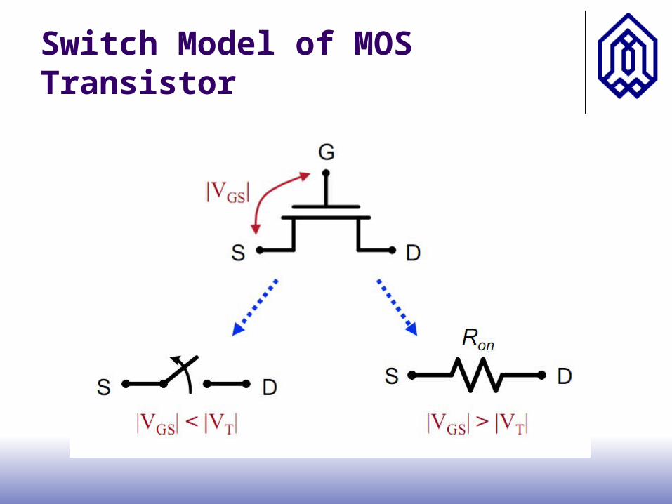
Switch Model of MOS Transistor
EE141 4
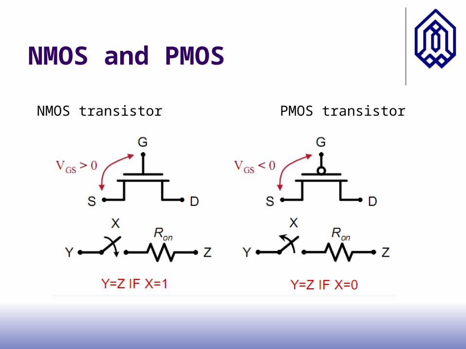
NMOS and PMOS
NMOS transistor PMOS transistor

EE141 5
The CMOS Inverter: A First Glance
V in Vout
CL
VDD

EE141 6
CMOS Inverter
Polysilicon
In Out
VDD
GND
PMOS 2
Metal 1
NMOS
OutIn
VDD
PMOS
NMOS
Contacts
N Well
EE141 7
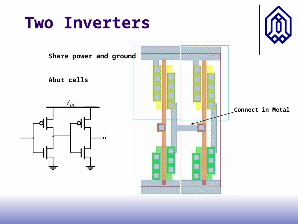
Two Inverters
Connect in Metal
Share power and ground
Abut cells
VDD

EE141 8
CMOS InverterFirst-Order DC Analysis
VOL = 0VOH = VDD
VM = f(Rn, Rp)
VDD VDD
Vin 5 VDD Vin 5 0
VoutVout
Rn
Rp

EE141 9
CMOS Inverter: Transient Response
tpHL = f(Ron.CL)
= 0.69 RonCL
VoutVout
Rn
Rp
VDDVDD
Vin 5 VDDVin 5 0
(a) Low-to-high (b) High-to-low
CLCL
EE141 10
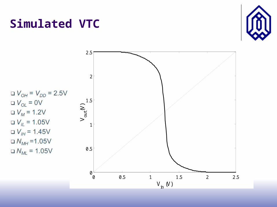
Simulated VTC
0 0.5 1 1.5 2 2.50
0.5
1
1.5
2
2.5
Vin
(V)
Vou
t(V)

EE141 11
Inverter Chain
CL
If CL is given:- How many stages are needed to minimize the delay?- How to size the inverters?
May need some additional constraints.
In Out

EE141 12
Inverter Delay
• Minimum length devices, L=0.25m• Assume that for WP = 2WN =2W
• same pull-up and pull-down currents• approx. equal resistances RN = RP
• approx. equal rise tpLH and fall tpHL delays• Analyze as an RC network
WNunit
Nunit
unit
PunitP RR
W
WR
W
WRR
11
tpHL = (ln 2) RNCL tpLH = (ln 2) RPCLDelay (D):
2W
W
unitunit
gin CW
WC 3Load for the next stage:

EE141 13
Inverter with Load
Load (CL)
Delay
Assumptions: no load -> zero delay
CL
tp = k RWCL
RW
RW
Wunit = 1
k is a constant, equal to 0.69

EE141 14
Inverter with Load
Load
Delay
Cint CL
Delay = kRW(Cint + CL) = kRWCint + kRWCL = kRW Cint(1+ CL /Cint)= Delay (Internal) + Delay (Load)
CN = Cunit
CP = 2Cunit
2W
W

EE141 15
Delay Formula
/1/1
~
0int ftCCCkRt
CCRDelay
pintLWp
LintW
Cint = Cgin with 1f = CL/Cgin - effective fanoutR = Runit/W ; Cint =WCunit
tp0 = 0.69RunitCunit

EE141 16
Apply to Inverter Chain
CL
In Out
1 2 N
tp = tp1 + tp2 + …+ tpN
jgin
jginunitunitpj C
CCRt
,
1,1~
LNgin
N
i jgin
jginp
N
jjpp CC
C
Cttt
1,
1 ,
1,0
1, ,1
EE141 17
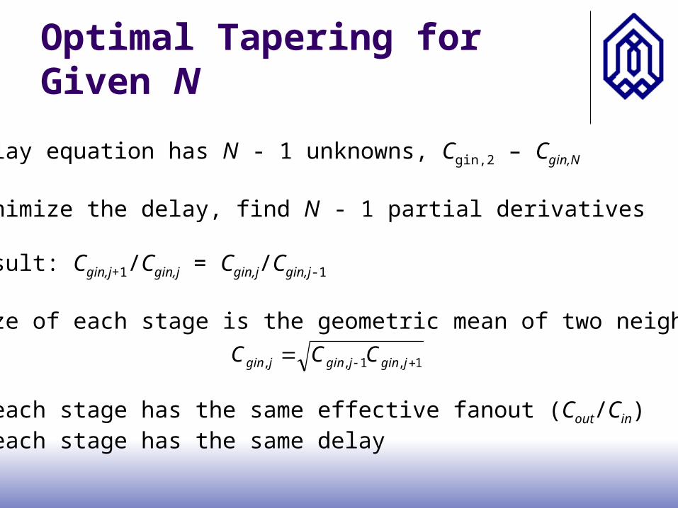
Optimal Tapering for Given N
Delay equation has N - 1 unknowns, Cgin,2 – Cgin,N
Minimize the delay, find N - 1 partial derivatives
Result: Cgin,j+1/Cgin,j = Cgin,j/Cgin,j-1
Size of each stage is the geometric mean of two neighbors
- each stage has the same effective fanout (Cout/Cin)- each stage has the same delay
1,1,, jginjginjgin CCC
EE141 18
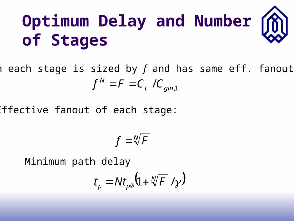
Optimum Delay and Number of Stages
1,/ ginLN CCFf
When each stage is sized by f and has same eff. fanout f:
N Ff
/10N
pp FNtt
Minimum path delay
Effective fanout of each stage:
EE141 19
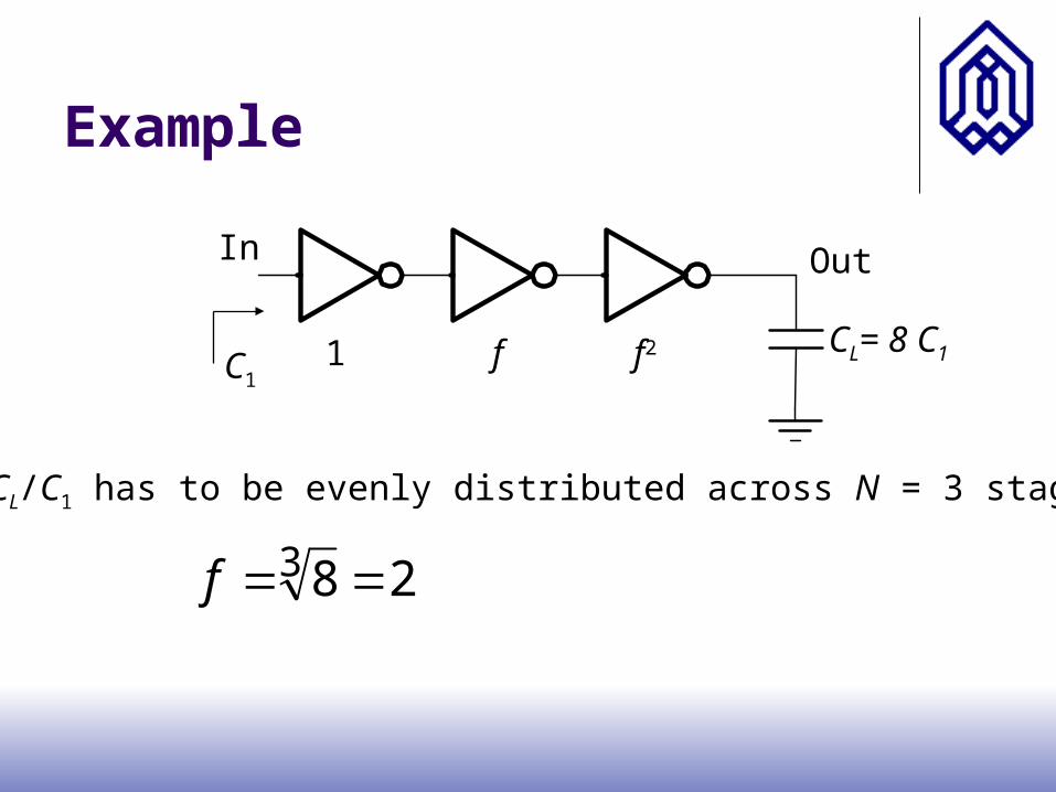
Example
CL= 8 C1
In Out
C11 f f2
283 f
CL/C1 has to be evenly distributed across N = 3 stages:

EE141 20
Optimum Number of Stages
For a given load, CL and given input capacitance Cin
Find optimal sizing f
ff
fFtFNtt pN
pp lnln
ln1/ 0/1
0
0ln
1lnln2
0
f
ffFt
f
t pp
For = 0, f = e, N = lnF
f
FNCfCFC in
NinL ln
ln with
ff 1exp

EE141 21
Optimum Effective Fanout f
Optimum f for given process defined by ff 1exp
fopt = 3.6for =1

EE141 22
Buffer Design
1
1
1
1
8
64
64
64
64
4
2.8 8
16
22.6
N f tp
1 64 65
2 8 18
3 4 15
4 2.8 15.3
/10N
pp FNtt