introduction introduction - omronomronfs.omron.com/en_us/ecb/products/pdf/pcb_precautions.pdf · 25...
TRANSCRIPT

25
IntroductionIntroduction
Reset Time (Applicable to Latching Relays Only)The time that elapses from the moment a relay coil is de-ener-gized until the NC contacts have closed, at an ambient tempera-ture of 23°C. (With a relay having SPST-NO contacts, this is the time that elapses until the NO contacts have operated under the same condition.) Bounce time is not included. For the relays hav-ing a reset time of less than 10 ms, the mean (reference) value of
its reset time is specified as follows:
Set TimeThe time that elapses after power is applied to a relay coil until the NO contacts have closed, at an ambient temperature of 23°C. Bounce time is not included. For the relays having a set time of less than 10 ms, the mean (reference) value of its set time is
specified as follows:
Shock ResistanceThe shock resistance of a relay is divided into two categories: “Destruction” which quantifies the characteristic change of, or damage to, the relay due to considerably large shocks which may develop during the transportation or mounting of the relay, and “Malfunction” which quantifies the malfunction of the relay while it is in operation.Stray CapacitanceThe capacitance measured between terminals at an ambient tem-perature of 23°C and a frequency of 1 kHz.VSWR (Applicable to High-frequency Relays Only)Stands for voltage standing-wave ratio. The degree of reflected wave that is generated in the transmission line.Vibration ResistanceThe vibration resistance of a relay is divided into two categories: “Destruction” which quantifies the characteristic changes of, or damage to, the relay due to considerably large vibrations which may develop during the transportation or mounting of the relay, and “Malfunction” which quantifies the malfunction of the relay due to vibrations while it is in operation.a = 0.002f2Awhere,a: Acceleration of vibrationf: FrequencyA: Double amplitude
Precautions Basic InformationBefore actually committing any component to a mass-production situation, OMRON strongly recommends situational testing, in as close to actual production situations as possible. One reason is to confirm that the product will still perform as expected after surviv-ing the many handling and mounting processes in involved in mass production. Also, even though OMRON relays are individu-ally tested a number of times, and each meets strict require-ments, a certain testing tolerance is permissible. When a high-precision product uses many components, each depends upon the rated performance thresholds of the other components. Thus, the overall performance tolerance may accumulate into undesir-able levels. To avoid problems, always conduct tests under the actual application conditions.
GeneralTo maintain the initial characteristics of a relay, exercise care that it is not dropped or mishandled. For the same reason, do not remove the case of the relay; otherwise, the characteristics may degrade. Avoid using the relay in an atmosphere containing sulfu-ric acid (SO2), hydrogen sulfide (H2S), or other corrosive gases. Do not continuously apply a voltage higher than the rated maxi-mum voltage to the relay. Never try to operate the relay at a volt-age and a current other than those rated.If the relay is intended for DC operation, the coil has polarity. Con-nect the power source to the coil in the correct direction. Do not use the relay at temperatures higher than that specified in the cat-alog or data sheet.The storage for the relay should be in room temperature and humidity.
Coil1) AC-switching RelaysGenerally, the coil temperature of the AC-switching relay rises higher than that of the DC-switching relay. This is because of resistance losses in the shading coil, eddy current losses in the magnetic circuit, and hysteresis losses. Moreover, a phenomenon known as “beat” may take place when the AC-switching relay operates on a voltage lower than that rated. For example, beat may occur if the relay’s supply voltage drops. This often happens when a motor (which is to be controlled by the relay) is activated. This results in damage to the relay contacts by burning, contact weld, or disconnection of the self–holding circuit. Therefore, coun-termeasures must be taken to prevent fluctuation in the supply voltage.One other point that requires attention is the “inrush current.” When the relay operates, and the armature of the relay is released from the magnet, the impedance drops. As a result, a current much higher than that rated flows through the coil. This current is known as the inrush current. (When the armature is attracted to the magnet, however, the impedance rises, decreas-ing the inrush current to the rated level.) Adequate consideration must be given to the inrush current, along with the power con-sumption, especially when connecting several relays in parallel.
Reset time 5 ms max. (mean value: approx. 2.3 ms)
Reset time 5 ms max. (mean value: approx. 2.3 ms)
Double-winding latching
Single-winding latching
Contact
Magnetic circuit
Min. set pulse width
Min. reset pulse width
Set coil
Set
Reset
Set time Reset time
Reset coil
26
IntroductionIntroduction
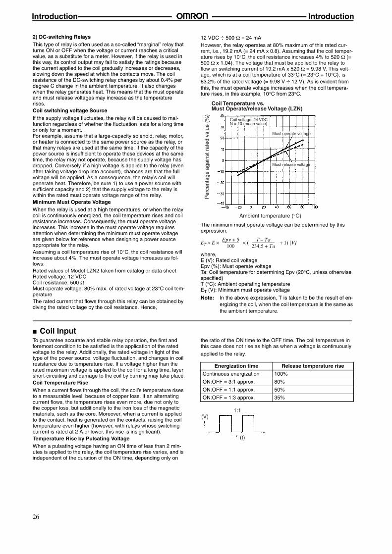
2) DC-switching RelaysThis type of relay is often used as a so-called “marginal” relay that turns ON or OFF when the voltage or current reaches a critical value, as a substitute for a meter. However, if the relay is used in this way, its control output may fail to satisfy the ratings because the current applied to the coil gradually increases or decreases, slowing down the speed at which the contacts move. The coil resistance of the DC-switching relay changes by about 0.4% per degree C change in the ambient temperature. It also changes when the relay generates heat. This means that the must operate and must release voltages may increase as the temperature rises.Coil switching voltage SourceIf the supply voltage fluctuates, the relay will be caused to mal-function regardless of whether the fluctuation lasts for a long time or only for a moment. For example, assume that a large-capacity solenoid, relay, motor, or heater is connected to the same power source as the relay, or that many relays are used at the same time. If the capacity of the power source is insufficient to operate these devices at the same time, the relay may not operate, because the supply voltage has dropped. Conversely, if a high voltage is applied to the relay (even after taking voltage drop into account), chances are that the full voltage will be applied. As a consequence, the relay’s coil will generate heat. Therefore, be sure 1) to use a power source with sufficient capacity and 2) that the supply voltage to the relay is within the rated must operate voltage range of the relay.Minimum Must Operate VoltageWhen the relay is used at a high temperatures, or when the relay coil is continuously energized, the coil temperature rises and coil resistance increases. Consequently, the must operate voltage increases. This increase in the must operate voltage requires attention when determining the minimum must operate voltage are given below for reference when designing a power source appropriate for the relay.Assuming a coil temperature rise of 10°C, the coil resistance will increase about 4%. The must operate voltage increases as fol-lows:Rated values of Model LZN2 taken from catalog or data sheetRated voltage: 12 VDCCoil resistance: 500 ΩMust operate voltage: 80% max. of rated voltage at 23°C coil tem-peratureThe rated current that flows through this relay can be obtained by diving the rated voltage by the coil resistance. Hence,
12 VDC ÷ 500 Ω = 24 mAHowever, the relay operates at 80% maximum of this rated cur-rent, i.e., 19.2 mA (= 24 mA x 0.8). Assuming that the coil temper-ature rises by 10°C, the coil resistance increases 4% to 520 Ω (= 500 Ω x 1.04). The voltage that must be applied to the relay to flow an switching current of 19.2 mA x 520 Ω = 9.98 V. This volt-age, which is at a coil temperature of 33°C (= 23°C + 10°C), is 83.2% of the rated voltage (= 9.98 V ÷ 12 V). As is evident from this, the must operate voltage increases when the coil tempera-ture rises, in this example, 10°C from 23°C.
The minimum must operate voltage can be determined by this expression.
ET > E × × ( + 1) [V]
where,E (V): Rated coil voltageEpv (%): Must operate voltageTa: Coil temperature for determining Epv (20°C, unless otherwise specified)T (°C): Ambient operating temperatureET (V): Minimum must operate voltage
Note: In the above expression, T is taken to be the result of en-ergizing the coil, when the coil temperature is the same asthe ambient temperature.
Coil InputTo guarantee accurate and stable relay operation, the first and foremost condition to be satisfied is the application of the rated voltage to the relay. Additionally, the rated voltage in light of the type of the power source, voltage fluctuation, and changes in coil resistance due to temperature rise. If a voltage higher than the rated maximum voltage is applied to the coil for a long time, layer short-circuiting and damage to the coil by burning may take place.Coil Temperature RiseWhen a current flows through the coil, the coil’s temperature rises to a measurable level, because of copper loss. If an alternating current flows, the temperature rises even more, due not only to the copper loss, but additionally to the iron loss of the magnetic materials, such as the core. Moreover, when a current is applied to the contact, heat is generated on the contacts, raising the coil temperature even higher (however, with relays whose switching current is rated at 2 A or lower, this rise is insignificant).Temperature Rise by Pulsating VoltageWhen a pulsating voltage having an ON time of less than 2 min-utes is applied to the relay, the coil temperature rise varies, and is independent of the duration of the ON time, depending only on
the ratio of the ON time to the OFF time. The coil temperature in this case does not rise as high as when a voltage is continuously
applied to the relay.
Coil Temperature vs.Must Operate/release Voltage (LZN)
Ambient temperature (°C)
Per
cent
age
agai
nst r
ated
val
ue (
%)
Must operate voltage
Must release voltage
Coil voltage: 24 VDCN = 10 (mean value)
Epv 5+100
------------------- T Ta–234.5 Ta+--------------------------
Energization time Release temperature rise
Continuous energization 100%
ON:OFF = 3:1 approx. 80%
ON:OFF = 1:1 approx. 50%
ON:OFF = 1:3 approx. 35%
(V)1:1
(t)

27
IntroductionIntroduction
Changes in Must Operate Voltage by Coil Temperature RiseThe coil resistance of a DC-switching relay increases (as the coil temperature rises) when the coil has been continuously ener-gized, de-energized once, and then immediately energized again. This increase in the coil resistance raises the voltage value at which the relay operates. Additionally, the coil resistance rises when the relay is used at a high ambient temperature.Maximum Must Operate VoltageThe maximum voltage applicable to a relay is determined in accordance with the coil temperature rise and the coil insulation materials’ heat resistivity, electrical as well as mechanical life, general characteristics, and other factors.If a voltage exceeding the maximum voltage is applied to the relay, it may cause the insulation materials to degrade, the coil to be burnt, and the relay to not operate at normal levels. Actually, however, there are occasions when the maximum voltage is exceeded to compensate for fluctuation in the supply voltage. In this event, pay attention to the following points.The coil temperature must not exceed the temperature that the spool and wound wire constituting the coil can withstand. The fol-lowing table shows the wires often used for a coil. In this table, the coil temperature is measured through calculation of the coil resis-
tance.
How to Calculate Coil Temperature
(234.5+T1) + T1 [°C]
where,R1 (Ω): coil resistance before energizationR2 (Ω): coil resistance after energizationT1 (°C): coil temperature (ambient) before energizationt (°C): coil temperature after energizationBefore using the relay confirm that there are no problems.DC Input Power SourcePay attention to the coil polarity of the DC-switching relay. Power sources for DC-operated relays are usually a battery or a DC power supply, either with a maximum ripple of 5%. If power is sup-plied to the relay via a rectifier, the must operate and must release voltages vary with the ripple percentage. Therefore, check the voltages before actually using the relay. If the ripple component is extremely large, beat may occur. If this happens, it is recom-mended that a smoothing capacitor be inserted as shown in the following diagram.
If the voltage applied to the DC-operated coil increases or decreases slowly, each contact of a multi-pole contact relay may not operate at the same time. It is also possible for this situation to result in the must operate voltage varying each time the relay operates. Either way, circuit sequencing will not be correct. In crit-ical applications, the use of a Schmitt circuit is recommended, reshape the DC waveform to trigger all contacts of the relay at the same time.Relay Driving Signal WaveformA long rise time and/or fall time of the signal driving the relay may prolong the operate time and/or release time of the relay. This sit-uation may shorten the life of the contacts. If this situation cannot be avoided, providing a Schmitt trigger circuit at the circuit stage preceding the relay circuit will shape a waveform with sharp tran-sitions, as shown in the following diagram:
If the Schmitt trigger circuit is configured of transistors, a residual voltage may exist in the output of the circuit. Therefore, confirm that the rated voltage is present across the relay coil, or that the residual voltage drops to zero when the relay releases. When an IC (e.g., TC74HC132P) is used, this value is close to zero.Cyclic Switching of AC Load
If the relay operates in synchronization with the supply voltage, the life of the relay may be shortened. When designing the control system in which the relay is used, estimate the life of the relay and thus the reliability of the overall system under actual operat-ing conditions. Moreover, construct the circuit so that the relay operates in a random phase or in the vicinity of the zero point.
Wire material Maximum coil temperature
Polyurethane (UEW) 120°C
Polyester (PEW) 130°C
t =R2 R1–R1
--------------------
Smoothing capacitorRipple component
DC component
Relay
E min.E max. E mean
where,E max.: maximum value of ripple componentE min.: minimum value of ripple componentE mean: mean value of DC component
Ripple percentage = Emax. - Emin.Emean
100
Waveform shaping circuit
(Schmittcircuit with inverter)
Driver circuit
Vin Vout
Contact
Vin
Vout
IC
IB
TE
Vin
EAC
Vin
EAC
LOAD
28
IntroductionIntroduction
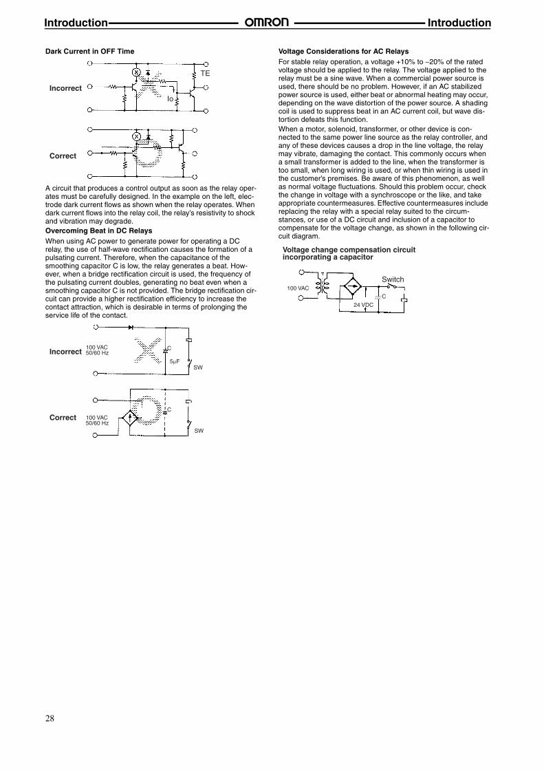
Dark Current in OFF Time
A circuit that produces a control output as soon as the relay oper-ates must be carefully designed. In the example on the left, elec-trode dark current flows as shown when the relay operates. When dark current flows into the relay coil, the relay’s resistivity to shock and vibration may degrade.Overcoming Beat in DC RelaysWhen using AC power to generate power for operating a DC relay, the use of half-wave rectification causes the formation of a pulsating current. Therefore, when the capacitance of the smoothing capacitor C is low, the relay generates a beat. How-ever, when a bridge rectification circuit is used, the frequency of the pulsating current doubles, generating no beat even when a smoothing capacitor C is not provided. The bridge rectification cir-cuit can provide a higher rectification efficiency to increase the contact attraction, which is desirable in terms of prolonging the service life of the contact.
Voltage Considerations for AC RelaysFor stable relay operation, a voltage +10% to −20% of the rated voltage should be applied to the relay. The voltage applied to the relay must be a sine wave. When a commercial power source is used, there should be no problem. However, if an AC stabilized power source is used, either beat or abnormal heating may occur, depending on the wave distortion of the power source. A shading coil is used to suppress beat in an AC current coil, but wave dis-tortion defeats this function.When a motor, solenoid, transformer, or other device is con-nected to the same power line source as the relay controller, and any of these devices causes a drop in the line voltage, the relay may vibrate, damaging the contact. This commonly occurs when a small transformer is added to the line, when the transformer is too small, when long wiring is used, or when thin wiring is used in the customer’s premises. Be aware of this phenomenon, as well as normal voltage fluctuations. Should this problem occur, check the change in voltage with a synchroscope or the like, and take appropriate countermeasures. Effective countermeasures include replacing the relay with a special relay suited to the circum-stances, or use of a DC circuit and inclusion of a capacitor to compensate for the voltage change, as shown in the following cir-cuit diagram.
Incorrect
Correct
TE
Io
Incorrect
Correct
100 VAC 50/60 Hz
100 VAC 50/60 Hz
C
C
5µFSW
SW
Voltage change compensation circuit incorporating a capacitor
Switch
24 VDC
100 VACC

29
IntroductionIntroduction
ContactsThe contacts are the most important constituent of a relay. Their characteristics are significantly affected by factors such as the material of the contacts, voltage and current values applied to them (especially, the voltage and current waveforms when ener-gizing and de-energizing the contacts), the type of load, operating frequency, atmosphere, contact arrangement, and bounce. If any of these factors fail to satisfy predetermined values, problems such as metal deposition between contacts, contact welding, wear, or rapid increase in the contact resistance may occur.Switching voltage (AC, DC)When a relay breaks an inductive load, a fairly high counterelec-tromotive force (counter emf) is generated in the relay’s contact circuit. The higher the counter emf, the greater the damage to the contacts. This may result in a significant decrease in the switching power of DC-switching relays. This is because, unlike the AC-switching relay, the DC-switching relay does not have a zero-cross point. Once arc has been generated, it does not easily diminish, prolonging the arc time. Moreover, the unidirectional flow of the current in a DC circuit may cause metal deposition to occur between contacts and the contacts to wear rapidly (this is discussed later).Despite the information a catalog or data sheet sets forth as the approximate switching power of the relay, always confirm the actual switching power by performing a test with the actual load.Switching CurrentThe quantity of electrical current which flows through the contact directly influences the contact’ characteristics. For example, when the relay is used to control an inductive load such as a motor or a lamp, the contacts will wear more quickly, and metal deposition between the mating contacts will occur more often as the inrush current to the contacts increases. Consequently, at some point the contacts may not be able to open. Contact MaterialsSelection of an appropriate contact material according to the load to be opened or closed is important. Several contact materials and their properties are listed below.
Contact Materials and Features
Contact Protection CircuitA contact protection circuit, designed to prolong the life of the relay, is recommended. This protection will have the additional advantages of suppressing noise, as well as preventing the gen-eration of carbide and nitric acid, which otherwise would be gen-erated at the contact surface when the relay contact is opened. However, unless designed correctly, the protection circuit may produce adverse effects, such as prolonging the release time of the relay.The following table lists examples of contact protection circuits.
P. G. S. Alloy
This material has excellent corrosion resistance and is suitable for very small current circuits.(Au : Ag : Pt = 69 : 25 : 6)
AgPd This material exhibits good corrosion and sulfur re-sistance. In a dry circuit, it attracts organic gas to generate a polymer, therefore it is usually plated with gold or other material.
Ag This material has the highest electric and heat con-ductivities among all metals. It exhibits low contact resistance, but easily forms sulfide film in a sulfide gas environment. This may result in defective con-tact performance at a low-voltage small-current op-eration.
AgNi This material exhibits the same high electric conduc-tivity as silver and excellent arc resistance.
AgSnIn This material exhibits excellent deposition resis-tance and exhaustion resistance.
AgSnO2 This material exhibits excellent deposition resis-tance. It easily forms sulfide film in a sulfide gas en-vironment same as Ag contact material.
AgW This material exhibits a high hardness and melting point. It also exhibits excellent arc resistance and superior resistance to deposition and transfer. How-ever, it shows high contact resistance and inferior environmental resistance.

30
IntroductionIntroduction
Avoid use of a surge suppressor in the manner shown below.
Although it is considered that switching a DC inductive load is more difficult than a resistive load, an appropriate contact protection circuit can achieve almost the same characteristics.
Circuit example Applicability Features and remarks Element selection
AC DC
CR Fair Good Load impedance must be much smaller than the RC circuit when the relay operates on an AC voltage.
Optimum C and R values are:C: 1 to 0.5 µF for 1–A switching currentR: 0.5 to 1 Ω for 1–V switching voltage
Good Good The release time of the contacts will be delayed when a relay solenoid is used as a load. This circuit is effective if connected across the load when the supply voltage is 24 to 48 V. When the supply voltage is 100 to 240 V, connect the circuit across the contacts.
These values do not always agree with the optimum values due to the nature of the load and the dispersion in the relay characteristics. Confirm optimum values experimentally. Capacitor C suppresses discharge when the contacts are opened, while resistor R limits the current applied when the contacts are closed the next time. Generally, employ a capacitor C whose dielectric strength is 200 to 300 V. If the circuit is powered by an AC power source, employ an AC capacitor (non–po-larized).
Diode Poor Good The energy stored in a coil (inductive load) reaches the coil as current via the diode connected in parallel with the coil, and is dissipated as Joule (measurable) heat by the resistance of the inductive load. This type of cir-cuit delays the release time more than the RC type.
Employ a diode having a reverse break-down voltage of more than 10 times the circuit voltage and a forward current rat-ing greater than the load current. A diode having a reverse breakdown voltage two to three times that of the supply voltage can be used in an electronic circuit where the circuit voltage is not particularly high.
Diode + Zener di-ode
Poor Good This circuit effectively shortens re-lease time in applications where the release time of a diode protection cir-cuit proves to be too slow.
The zener diode breakdown voltage should be about the same as the supply voltage.
Varistor Good Good By utilizing the constant–voltage characteristic of a varistor, this circuit prevents high voltages from being applied across the contacts. This cir-cuit also somewhat delays the re-lease time. This circuit, if connected across the load, is effective when the supply voltage is 24 to 48 V. If the supply voltage is 100 to 240 V, con-nect the circuit across the contacts.
---
Power source
Inductive load
Inductive load
Power source
Inductive load
Power source
Inductive load
Power source
Inductive load
Power source
This circuit arrangement is very effective for diminishing spark-ing (arcing) at the contacts, when breaking the circuit. However, since electrical energy is stored in C (capacitor) when the con-tacts are open, the current from C flows into the contacts when they close. Therefore, metal deposition is likely to occur be-tween mating contacts.
This circuit arrangement is very useful for diminishing sparking (arcing) at the contacts when breaking the circuit. However, since the charging current to C flows into the contacts when they are closed, metal deposi-tion is likely to occur between the mating contacts.
Power supply Load
Power supply Load
31
IntroductionIntroduction
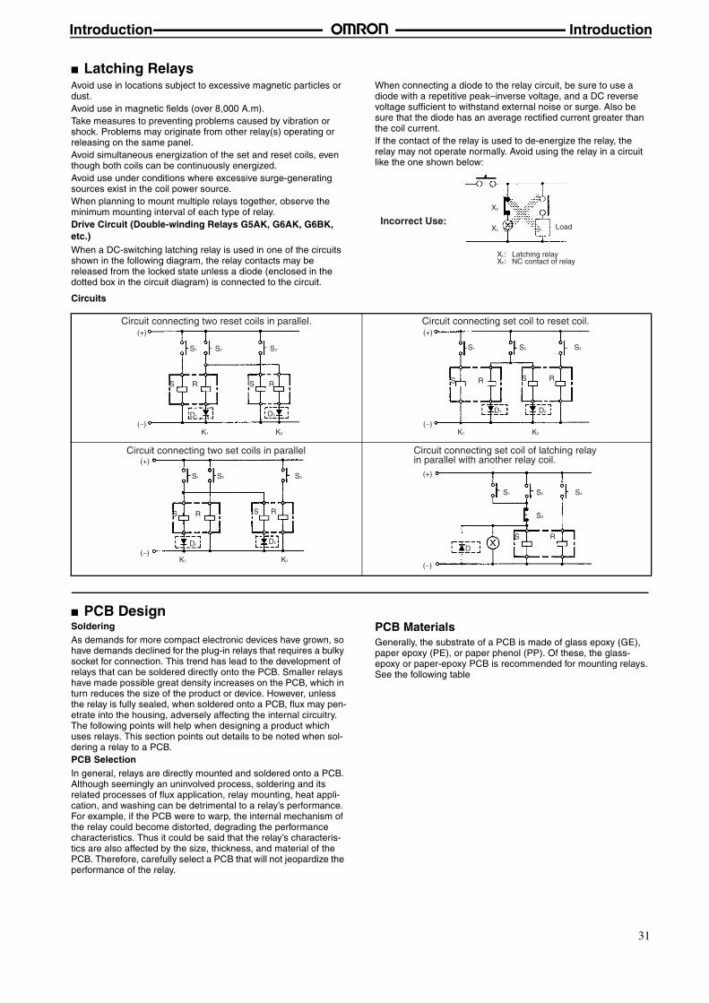
Latching RelaysAvoid use in locations subject to excessive magnetic particles or dust.Avoid use in magnetic fields (over 8,000 A.m).Take measures to preventing problems caused by vibration or shock. Problems may originate from other relay(s) operating or releasing on the same panel.Avoid simultaneous energization of the set and reset coils, even though both coils can be continuously energized.Avoid use under conditions where excessive surge-generating sources exist in the coil power source.When planning to mount multiple relays together, observe the minimum mounting interval of each type of relay.Drive Circuit (Double-winding Relays G5AK, G6AK, G6BK, etc.)When a DC-switching latching relay is used in one of the circuits shown in the following diagram, the relay contacts may be released from the locked state unless a diode (enclosed in the dotted box in the circuit diagram) is connected to the circuit.
When connecting a diode to the relay circuit, be sure to use a diode with a repetitive peak–inverse voltage, and a DC reverse voltage sufficient to withstand external noise or surge. Also be sure that the diode has an average rectified current greater than the coil current.If the contact of the relay is used to de-energize the relay, the relay may not operate normally. Avoid using the relay in a circuit like the one shown below:
Circuits
PCB DesignSolderingAs demands for more compact electronic devices have grown, so have demands declined for the plug-in relays that requires a bulky socket for connection. This trend has lead to the development of relays that can be soldered directly onto the PCB. Smaller relays have made possible great density increases on the PCB, which in turn reduces the size of the product or device. However, unless the relay is fully sealed, when soldered onto a PCB, flux may pen-etrate into the housing, adversely affecting the internal circuitry.The following points will help when designing a product which uses relays. This section points out details to be noted when sol-dering a relay to a PCB.PCB SelectionIn general, relays are directly mounted and soldered onto a PCB. Although seemingly an uninvolved process, soldering and its related processes of flux application, relay mounting, heat appli-cation, and washing can be detrimental to a relay’s performance. For example, if the PCB were to warp, the internal mechanism of the relay could become distorted, degrading the performance characteristics. Thus it could be said that the relay’s characteris-tics are also affected by the size, thickness, and material of the PCB. Therefore, carefully select a PCB that will not jeopardize the performance of the relay.
PCB MaterialsGenerally, the substrate of a PCB is made of glass epoxy (GE), paper epoxy (PE), or paper phenol (PP). Of these, the glass-epoxy or paper-epoxy PCB is recommended for mounting relays. See the following table
XL: Latching relay Xb: NC contact of relay
LoadIncorrect Use:
Xb
XL
Circuit connecting two reset coils in parallel.(+)
(−)
S1 S2 S3
S R S R
D2D1
K1 K2
Circuit connecting set coil to reset coil.(+)
(−)K1 K2
S1 S2 S3
S R S R
D2D1
Circuit connecting two set coils in parallel(+)
(−)
S1 S2 S3
S R S R
D1
K1 K2
D2
Circuit connecting set coil of latching relay in parallel with another relay coil.
(+)
(−)
S1 S2 S4
S R
D
S3

32
IntroductionIntroduction
PCB ThicknessPCBs having a thickness of 0.8, 1.2, 1.6, or 2.0 mm are generally used. A PCB that is 1.6 mm thick is best for mounting a PCB relay, considering the weight of the relay and the length of the ter-minals. (The terminal length of OMRON relays is 3, 3.5, or 4.0 to 5.0 mm.)
Terminal Hole Diameter and Land DiameterSelect the appropriate terminal hole and land diameters from the following table, based on the PCB mounting hole drawing. Land diameters may be reduced to less than those listed below if the through-hole connection process is to be employed.
Terminal Hole and Land Diameters
Shape of LandsThe land section should be on the center line of the copper-foil pattern, so that the soldered fillets become uniform.
A break in the circular land area will prevent molten solder from filling holes reserved for components which must be soldered manually after the automatic soldering of the PCB is complete.
Conductor Width and ThicknessThe following thickness of copper foil are standard: 35 µm and 70 µm. The conductor width is determined by the current flow and allowable temperature rise. Refer to the chart below.
Conductor PitchThe conductor pitch on a PCB is determined according to the insulation resistance between conductors and the environmental conditions under which the PCB is to be placed. The following graph shows the general relationship between the voltage between conductors and the conductor pitch on a PCB. However, if the PCB must conform to safety organization standards (such as UL, CSA, VDE, etc.), priority must be given to fulfilling their requirements.
Item Epoxy-based Phenol-based
Glass epoxy (GE) Paper epoxy (PE) Paper phenol (PP)
Electrical characteristics High insulation resistance. Insula-tion resistance hardly affected by humidity.
Fair Insulation resistance degraded by humidity.
Mechanical characteristics Little expansions/shrinkage caused by change in temperature or humidity.Suitable for through-hole PCBs and multi-layered PCBs.
Fair Much expansion/shrinkage caused by changes in temperature or hu-midity.Not suitable for through-hole PCB.
Cost effectiveness Expensive Fair Inexpensive
Terminal hole diameter Minumum land diamter
Normal Tolerance
0.6 mm0.8 mm1.0 mm1.2 mm1.3 mm1.5 mm1.6 mm2.0 mm
±0.1 mm 1.5 mm1.8 mm2.0 mm2.5 mm2.5 mm3.0 mm3.0 mm3.0 mm
Correct
Incorrect
3.5
Break in land
0.2 to 0.5 mm
Conductor Width and Carry Current(according to IEC Pub326-3)
Sectional area (mm )
Allo
wab
le c
urre
nt (
A)
Con
duct
or w
idth
(m
m)
Tem
pera
ture
ris
e va
lue
100°C75°C50°C40°C30°C20°C10°C
0.03 0.05 0.07 0.1 0.3 0.5 0.7
610 g/m 70 mm
305 g/m35 mm
2
2
2

33
IntroductionIntroduction
Temperature and HumidityPCBs expand or contract with changes in temperature. Should expansion occur with a relay mounted on the PCB, the internal components of the relay may be shifted out of operational toler-ance. As a result, the relay may not be able to operate with its normal characteristics.PCB materials have “directionality,” which means that a PCB gen-erally has expansion and contraction coefficients 1/10 to 1/2 higher in the vertical direction than in the horizontal direction. Conversely, its warp in the vertical direction is 1/10 to 1/2 less than in the horizontal direction. Therefore, take adequate counter-measures against humidity by coating the PCB. Should heat or humidity be entirely too high, the relay’s physical characteristics will likewise be affected. For example, as the heat rises the PCB’s insulation resistance degrades. Mechanically, PCB parts will con-tinue to expand as heat is applied, eventually passing the elastic limit, which will permanently warp components. Moreover, if the relay is used in an extremely humid environment, silver migration may take place.GasExposure to gases containing substances such as sulfuric acid, nitric acid, or ammonia can cause malfunctions such as faulty contacting in relays. They can also cause the copper film of a PCB to corrode, or prevent positive contacts between the PCB’s connectors. Of the gases mentioned, nitric acid is particularly damaging as it tends to accelerate the silver migration. As a coun-termeasures against gas exposure damage, the following pro-
cesses on the relay and PCB have proved useful.
Vibration and ShockAlthough the PCB itself is not usually a source of vibration or shock, it may simplify or prolong the vibration by resonate with external vibrations or shocks. Securely fix the PCB, paying atten-tion to the following points.
Mounting PositionDepending on where the relay is mounted, the function of the relay (and the performance of the circuit which includes the relay) may be adversely affected.The relay may malfunction if it is mounted near a transformer or other device that generates a large magnetic field, or much heat. Provide an adequate distance between the relay and such devices.Also, keep the relay away from semiconductor devices, if they are to be mounted on the same PCB.
Mounting DirectionTo allow a relay to operate to its full capability, adequate consider-ation must be given to the mounting direction of the relay. Relay characteristics that are considerably influenced by mounting direction are shock resistance, life, and contact reliability.Shock ResistanceIdeally, the relay must be mounted so that any shock or vibration is applied to the relay at right angles to the operating direction of the armature of the relay. Especially when a relay’s coil is not energized, the shock resistance and noise immunity are signifi-cantly affected by the mounting direction of the relay.LifeWhen switching a heavy load that generates arc (generally, hav-ing a greater impedance than that of the relay coil), substances spattered from the contact may accumulate in the vicinity, result-ing in degradation of the insulation resistance of the circuit. Mounting the relay in the correct direction is also important in pre-venting this kind of degradation of the insulation resistance. Contact ReliabilitySwitching both a heavy and a minute load with a single relay con-tact is not recommended. The reason for this is that the sub-stances scattered from the contact when the heavy load is switched degrade the contact when switching the minute load. For example, when using a multi-pole contact relay, avoid the mount-ing direction or terminal connections in which the minute load switching contact is located below the heavy load switching con-tact.
Item Process
Outer casing, housing Sealed construction by using packing, etc.
Relay Use of simplified hermetically sealed type relay, DIP relay, reed relay
PCB, copper firm Coating
Connector Gold-plating, rhodium-plating process
Voltage between Conductors vs. Conductor Pitch
Rat
ed v
olta
ge c
ondu
ctor
s (V
DC
)
Conductor pitch (mm)
A = w/o coating at altitude of 3,000 m max.B = w/o coating at altitude of 3,000 m
or higher but lower than 15,000 mC = w/coating at altitude of 3,000 m max.D = w/coating at altitude of 3,000 m or higher
C
A
DB
Mounting method Process
Rack mounting No gap between rack’s guide and PCB
Screw mounting Securely tighten screw.Place heavy components such as relays on part of PCB near where screws are to be used.Attach rubber washers to screws when mounting components that are affected by shock (such as audio devices.)
Correct
Incorrect

34
IntroductionIntroduction
Mounting IntervalWhen mounting multiple relays side by side on a PCB, pay atten-tion to the following points:When many relays are mounted together, they may generate an abnormally high heat due to the thermal interference between the relays. Therefore, provide an adequate distance between the relays to dissipate the heat. When using a relay, be sure to check the minimum mounting interval.Also, if multiple PCBs with relays are mounted to a rack, the tem-perature may rise. In this case, preventive measures must be taken so that the ambient temperature falls within the rated value.
Pattern LayoutCountermeasures Against NoiseThe relay can be a noise source when viewed from a semicon-ductor circuit. This must be taken into consideration when design-ing the layout positioning of the relay and other semiconductor components on the PCB.Keep the relay away from semiconductor components as far away as possible.Locate the surge suppressor for the relay coil as close to the relay as possible.Do not route wiring for signals such as audio signals that are likely to be affected by noise below the relay.Design the shortest possible pattern.One method for separating the power source and relay from other electronic components is to use shielded patterns.
CoatingAs is also the case in humid environments, coating the PCB is recommended to prevent the insulation of its pattern form being degraded by gases containing harmful substances. When coating the PCB, however, care must be exercised not to allow the coat-ing agent to penetrate into the relays mounted on the PCB; other-wise, faulty contact of the relay may occur due to sticking or coating. Moreover, some coating agents may degrade or adversely affect the relay. Select the coating agent carefully.
Type of Coating
Automatic Mounting of Relay on PCBThough-hole MountingThe following tables list the processes required for mounting a relay onto a PCB and the points to be noted in each process.Process 1: PlacementDo not bend any terminal of the relay to use it as a self–clinching relay or the relay may malfunction.It is recommended to use magazine-packaged self–clinching relays for placement onto the PCB.
Possibility of Automatic Placement
Process 2: Flux ApplicationTo apply flux to a flux protection or fully sealed relay, a sponge soaked with flux can be used. Place the relay in the holes drilled in the PCB and press the PCB (with the relay still mounted) firmly against the sponge. The flux will be pushed up the relay’s contact legs, and through the PCB holes. This method must never be applied with an unsealed relay because the flux will penetrate into the relay.The flux used with the sponge must be a non-corrosive resin-type flux.For the flux solvent, use an alcohol–based solvent, which tends to be less chemically reactive.Apply the flux sparingly and evenly to prevent penetration into the relay. When dipping the relay terminals into liquid flux, be sure to adjust the flux level, so that the upper surface of the PCB is not flooded with flux.
Possibility of Dipping Method
Process 3: TransportationWhen the PCB is transported, the relay mounted on the PCB may be lifted from the board surface due to vibration. This can be prevented if the relay mounted on the PCB has self-clinching terminals.
Item Applicability to PCB with relays
mounted
Feature
Epoxy Good Good insulation. Performing this coating is a little difficult, but has no effect on relay con-tact.
Urethane Good Good insulation and easy to coat. Be careful not to allow the coating on the relay itself, as thinner-based solvents are of-ten used with this coating.
Silicon Poor Good insulation and easy to coat. However, silicon gas may cause faulty contact of relay.
Construction Unsealed Flux protection Fully sealed
Magazine-packaged relay NO YES YES
Self-clinching relays
Unsealed Flux protection Fully sealed
NO YES YES

35
IntroductionIntroduction
Process 4: PreheatingPreheat the PCB at a temperature of 110°C maximum within a period of approximately 40 s for smooth soldering. The characteristics of the relay may change if it is heated at a high temperature for a long time.
Possibility of Preheating
Process 5: SolderingFlow soldering is recommended to assure a uniform solder joint.• Solder temperature and soldering time: 260°C, 5 s max.• Adjust the level of the molten solder so that the PCB is not flooded with solder.
Possibility of Automatic Soldering
Process 6: CoolingUpon completion of automatic soldering, use a fan or other device to forcibly cool the PCB. This helps prevent the relay and other compo-nents from deteriorating from the residual heat of soldering.Fully sealed relays are washable. Do not, however, put fully sealed relays in a cold cleaning solvent immediately after soldering or the
seals may be damaged.
Process 7: CleaningAvoid cleaning the soldered terminals whenever possible. When a resin-type flux is used, no cleaning is necessary. If cleaning cannot be avoided, exercise care in selecting an appropriate cleaning solvent.
Cleaning Method
100°C
Heater
Unsealed Flux protection Fully sealed
NO YES YES
Unsealed Flux protection Fully sealed
NO YES YES
Complete the soldering operation quickly. Use the correct wattage of soldering iron. Do not overheat while smoothing the applied solder with the tip of the iron.• Soldering iron: rated at 30 to 60 W• Tip temperature: 280°C to 300°C• Soldering time: 3 s max.• The following table contains recommended solders:
Type Sparkle solderApplicable solder diameter 0.8 to 1.6 mmSpread rate 90%Storage 3 months max.
Solder
Flux
The solder in the illustration shown above is provided with a cut section to prevent the flux from splattering.
Possibility of Manual Soldering
Unsealed Flux protection Fully sealedYES YES YES
Manual Soldering
Fluxprotection Fully sealed
Necessary Necessary
Unsealed Fluxprotection Fully sealed
Boiling cleaning and immersion cleaning are not possible. Clean only the back of the PCB with a brush.
Boiling cleaning and immersion cleaning are possible. Ultrasonic cleaning will have an adverse effect on the performance of relays not specifically manufactured for ultrasonic cleaning.The washing temperature is 40°C max..

36
IntroductionIntroduction
List of Cleaning Solvents
Note: 1. Consult your OMRON representative before using any other cleaning solvent. Do not use Freon-TMC-based, thinner-based, orgasoline-based cleaning solvents.
2. Worldwide efforts are being made at discontinuing the use of CFC-113-based (fluorochlorocarbon-based) and trichloroethylene-based cleaning solvents. The user is requested to refrain from using these cleaning solvents
3. It may be difficult to clean the space between the relay and PCB using hydrogen-based or alcohol-based cleaning solvent. It isrecommended the stand-off-type be used G6A-@-ST when using hydrogen-based or alcohol-based cleaning solvents.
4. Ultrasonic cleaning may have an adverse effect on the performance of relays not specifically manufactured for ultrasonic clean-ing. Please refer to the model number to determine if your relay is intended to be cleaned ultrasonically.
Process 8: CoatingDo not apply a coating agent to any flux-resistant relay or relay with a case because the coating agent will penetrate into the relay and the contacts may be damaged.Some coating agents may damage the case of the relay. Be sure to use a proper coating agent.
Do not fix the position of relay with resin or the characteristics of the relay will change.
Surface MountingThe following tables list the processes required for mounting a relay onto a PCB and the points to be noted in each process.Process 1: Cream Solder PrintingDo not use a cream solder that contains a flux with a large amount of chlorine or the terminals of the relay may be corroded.Process 2: Relay MountingThe holding force of the relay holder must be the same as or more than the minimum holding force value required by the relay.
Process 3: TransportationThe relay may be dismounted by vibration during transportation. To prevent this, it is recommended an adhesive agent be applied to the relay’s gluing part (protruding part) to tack the relay.
Adhesive Agent Application Methods
Solvent Fully sealed
Chlorine-based • Perochlene• Chlorosolder• Trichloroethylene
YES
Water-based • Indusco• Holys
YES
Alcohol-based • IPA• Ethanol
YES
Others • Thinner• Gasoline
NO
Cleaning method Automatic cleaningUltrasonic cleaning (See note 4.)
Resin Fully sealed
Epoxy YES
Urethane YES
Silicone NO
Fluorine YES
Direction ADirection BDirection C
Direction G6H G6S
A 200 g max. 200 g max.
B 500 g max. 500 g max.
C 200 g max. 200 g max.
Dispenser method Screen-printing method
YES YES
37
IntroductionIntroduction
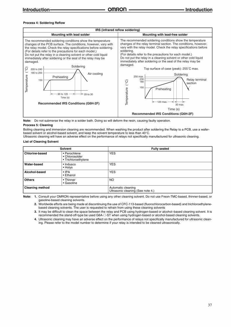
Process 4: Soldering Reflow
Note: Do not submerse the relay in a solder bath. Doing so will deform the resin, causing faulty operation.Process 5: CleaningBoiling cleaning and immersion cleaning are recommended. When washing the product after soldering the Relay to a PCB, use a wafer-based solvent or alcohol-based solvent, and keep the solvent temperature to less than 40°C.Ultrasonic cleaning will have an adverse effect on the performance of relays not specifically manufactured for ultrasonic cleaning.
List of Cleaning Solvent
Note: 1. Consult your OMRON representative before using any other cleaning solvent. Do not use Freon-TMC-based, thinner-based, orgasoline-based cleaning solvents.
2. Worldwide efforts are being made at discontinuing the use of CFC-113-based (fluorochlorocarbon-based) and trichloroethylene-based cleaning solvents. The user is requested to refrain from using these cleaning solvents
3. It may be difficult to clean the space between the relay and PCB using hydrogen-based or alcohol–based cleaning solvent. It isrecommended the stand-off-type be used G6A-@-ST when using hydrogen-based or alcohol-based cleaning solvents.
4. Ultrasonic cleaning may have an adverse effect on the performance of relays not specifically manufactured for ultrasonic clean-ing. Please refer to the model number to determine if your relay is intended to be cleaned ultrasonically.
IRS (infrared reflow soldering)
Mounting with lead solder Mounting with lead-free solder
Recommended IRS Conditions (G6H-2F)
220 to 240
180 to 200
150
Soldering
Preheating
Time (s)
Tem
pera
ture
( C
)°
90 to 120
Air cooling
20 to 30
The recommended soldering conditions show the temperature changes of the PCB surface. The conditions, however, vary with the relay model. Check the relay specifications before soldering.(For details refer to the precautions for each model.) Do not put the relay in a cleaning solvent or other cold liquid immediately after soldering or the seal of the relay may be damaged.
Recommended IRS Conditions (G6H-2F)
Soldering
Preheating
120 max.
250 max.
180
150
30 max.
Time (s)
Tem
pera
ture
( C
)°
The recommended soldering conditions show the temperature changes of the relay terminal section. The conditions, however, vary with the relay model. Check the relay specifications before soldering.(For details refer to the precautions for each model.) Do not put the relay in a cleaning solvent or other cold liquid immediately after soldering or the seal of the relay may be damaged.
230 Relay terminal section
Top surface of case (peak): 255˚C max.
Solvent Fully sealed
Chlorine-based • Perochlene• Chlorosolder• Trichloroethylene
YES
Water-based • Indusco• Holys
YES
Alcohol-based • IPA• Ethanol
YES
Others • Thinner• Gasoline
NO
Cleaning method Automatic cleaningUltrasonic cleaning (See note 4.)
38
IntroductionIntroduction
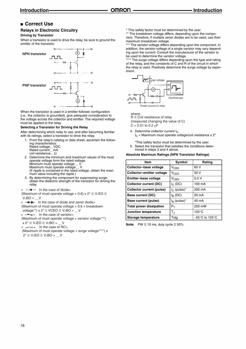
Correct UseRelays in Electronic CircuitryDriving by TransistorWhen a transistor is used to drive the relay, be sure to ground the emitter of the transistor.
When the transistor is used in a emitter-follower configuration (i.e., the collector is grounded), give adequate consideration to the voltage across the collector and emitter. The required voltage must be applied to the relay.Selecting a Transistor for Driving the RelayAfter determining which relay to use, and after becoming familiar with its ratings, select a transistor to drive the relay.
1. From the relay’s catalog or data sheet, ascertain the follow-ing characteristics:Rated voltage:_ VDCRated current:_ mAcoil resistance:_ Ω
2. Determine the minimum and maximum values of the must operate voltage form the rated voltage.Minimum must operate voltage: _ VMaximum must operate voltage: _ V(If ripple is contained in the rated voltage, obtain the maxi-mum value including the ripple.)
3. By determining the component for suppressing surge, obtain the dielectric strength of the transistor for driving the relay.
* This safety factor must be determined by the user.** The breakdown voltage differs, depending upon the compo-nent. Therefore, if multiple zener diodes are to be used, use their maximum breakdown voltage.*** The varistor voltage differs depending upon the component. In addition, the varistor voltage of a single varistor may vary depend-ing upon the current. Consult the manufacturer of the varistor to be used to determine the varistor voltage.**** The surge voltage differs depending upon the type and rating of the relay, and the constants of C and R of the circuit in which the relay is used. Positively determine the surge voltage by exper-iment.
4. Determine collector current IC.IC = Maximum must operate voltage/coil resistance x 2*
*This safety factor must be determined by the user.5. Select the transistor that satisfies the conditions deter-
mined in steps 3 and 4 above.
Absolute Maximum Ratings (NPN Transistor Ratings)
Note: PW ≤ 10 ms, duty cycle ≤ 50%
NPN transistor
PNP transistor
< In the case of diode>(Maximum of must operate voltage + 0.6) x 2* ≅ VCEO ≅ VCBO = __V
< In the case of diode and zener diode>(Maximum of must operate voltage + 0.6 + breakdown voltage**) x 2* ≅ VCEO ≅ VCBO = __V
< In the case of varistor>(Maximum of must operate voltage + varistor voltage***) x 2* ≅ VCEO ≅ VCBO = __V
< In the case of RC>(Maximum of must operate voltage + surge voltage****) x 2* ≅ VCEO ≅ VCBO = __V
Item Symbol Rating
Collector–base voltage VCBO 60 V
Collector–emitter voltage VCEO 50 V
Emitter–base voltage VCBO 5.0 V
Collector current (DC) IC (DC) 100 mA
Collector current (pulse) IC (pulse)* 200 mA
Base current (DC) IB (DC) 20 mA
Base current (pulse) IB (pulse)* 40 mA
Total power dissipation PT 250 mW
Junction temperature TJ 125°C
Storage temperature Tstg −55°C to 125°C
where,R ≅ Coil resistance of relay(measured changing the value of C)C = 0.01 to 0.2 µF
Surge voltage
Oscilloscope
Power source to relay
39
IntroductionIntroduction
6. After selecting the transistor, examine the IC vs. VCE char-acteristics of the transistor indicated in its ratings.
This characteristic curve illustrates the relation between collector current IC and collector-emitter voltage VCE at base current IB. From this graph, obtain collector-emitter voltage VCE where,
IC = (Maximum value of must operate voltage)
coil resistanceIB = Base current of the switching transistor which is determined by the driver stageThus,Collector-emitter voltage VCE = _ V
Use the transistor in its switching (saturation) area. Therefore, an adequate base current is required.
7. Using the following formula, calculate the power dissipated by the transistor to confirm that it is within the range of per-missible power dissipation of the transistor.
Total power dissipation PT = Collector dissipation PC + Base dissi-pation PB where,
PC = (Maximum value of must operate voltage)
coil resistance x VCE (VCE is determined in step 6.)PB = IB x 0.6 to 1(For details on IB, refer to step 6.)
Confirm that PT obtained by the above formula is within the curve representing the total power dissipation vs. ambient temperature characteristics.
In case the total dissipation exceeds the permissible power dissi-pation, either attach a radiator plate to the transistor, or replace the transistor.
8. Determine the supply voltage to the relay.The maximum and minimum values of the supply voltage to the relay are determined by the following expressions using the maximum and minimum values of the must operate volt-age VCE obtained in step 6.
Maximum supply voltage Maximum must operate voltage + VCE
Minimum supply voltage Minimum must operate voltage + VCE
9. Refer to the table indicating the absolute maximum ratings of the transistor again to check whether these conditions are satisfied.
VCEO > (Maximum supply voltage + surge voltage) x safety factor*VCBO > (Maximum supply voltage + surge voltage) x safety factor*
*Determine the safety factor giving consideration to external surge (such as lightning and surge from other devises.)
10.Check the following items during actual use of the relay.• Is the maximum value of the must operate voltage equal to or
less than the rated value when the maximum supply voltage isapplied?
• Is the minimum value of the must operate voltage equal to ormore than the rated value when the minimum supply voltage isapplied?
• Are the above conditions satisfied within the operating tempera-ture range?
• Is there any abnormality found in test run?In addition to the above checking items, take into considerationthe items listed in this table.
*Inversely proportional to voltage**Often used VCED: 35 to 60 V
From the above discussion, the best relay coil should be rated at 12 VDC or 24 VDC when the relay is driven by a transistor.Driving by Darlington-connected TransistorTo reduce the current of the transistor to drive the relay (i.e., base current of the transistor), two transistors may be used, via Dar-lington connection. Darlington-connected transistors are available enclosed in a single package.
When the Darlington-connected transistors are used, however, the required value of VCE is higher than when using a single tran-sistor. For this reason, consideration must be given to designing the total power dissipation and supply voltage for the second tran-sistor, Tr2.
IC vs. VCE Characteristics
Col
lect
or c
urre
nt Ic
(m
A)
Collector-emitter voltage VCE (V)
IB = 0.1 mA
÷
Total Power Dissipation vs. Ambient Temperature
Tota
l pow
er d
isip
atio
n P
Ambient temperature Ta (°C)
Air
T(m
W)
Rated voltage of relay Low High
Coil current* High Low
IC of switching transistor High Low
VECO, VCEO of switching transistor** High Low
Driving current of transistor High Low
Voltage drop VCE in transistor High Low
Voltage drop VBE in transistor High Low
Total power dissipation PT of transistor High Low
≤
≥
Supply voltage
Must operate voltage
VCE
NPN-NPN Darlington Connection
Tr2Tr1
VCE ≅ VCE of Tr1 +
VBE of Tr2
40
IntroductionIntroduction
Driving by ICRecently, an IC on which multiple driving transistors are inte-grated has become available. On some occasions, the designing process of the circuit or PCB to drive multiple relays, a small-size solenoid, or a small-size lamp can be simplified by using such an IC. Consult the manufacturer of the IC to be used for details. For VCE, refer to the description to the rated voltage and surge sup-pressor.
Driving by MOS ICAt present, no C MOS, N MOS, or P MOS that can directly drive relays is available. Use a transistor or IC to drive relay.Driving by TTLTTLs can be divided into two types by classification of the output: totem-pole and open-collector outputs. Connection of each type of TTL is described next.
1. To drive a relay by the totem-pole output of a TTL, these conditions must be satisfied.
IOL (low-level output current) > Maximum supply voltage/coil resistanceIOH (high-level output current) < Rated current x must operate voltage (%)/200Minimum supply voltage (4.75 V) – Maximum VOL (low-level out-put voltage) > minimum value of must operate voltage (Refer to driving by transistor in Hints on Correct Use: Relays in Electronic Circuitry.)Use a diode as surge suppressor.In the specifications of some ICs, such a phrase as “fan-out. 10” may be used in place of the legend IOL. This denotes that 10 stan-dard TTLs can be connected in parallel. In terms of current, a fan-out of 1 equals 1.6 mA.Hence,Fan-out n = 1.6 x n (mA)
2. To drive a relay with open-collector output type TTL, a degree of freedom is allowed in the ratings of the relay coil. However, these conditions must be satisfied:
IOL > Maximum supply voltage to the relay coil/Coil resistance
IOH < Rated current x must operate voltage (%)/200
VO = Dielectric strength of the output transistor (Refer to Driving by transistor in Correct Use: Relays in Electronic Circuitry.)VOL = Collector-emitter voltage VCE of the output transistor (Refer to Driving by transistor in Correct Use: Relays in Electronic Circuitry.)The above description of the standard TTL is applicable when using S, H, and LS type TTLs. The following table shows the TTLs of various marks.
Dimensions Connection (Top View)
Equivalent Circuit
I: Input (Base)O: Output (Collector)GND (Common emitter)
Totem-pole Output
VCC
Output
GND
Inpu
t ABCD
Y
Ic a
nd p
ower
sou
rce
to r
elay
:4.
75 to
5.2
5 V
DC
Open-collector Output
Inpu
t
Power source to relay Ic
pow
er s
ourc
e:4.
75 to
5.2
5 V
DC
A
VCC
Output
GND
Y

41
IntroductionIntroduction
Examples of Various TTLs
Note: Asterisk-marked models are open-collector models.A value of 20 mA is for Motorola’s MC54F04 and MC74F04.
Driving by Other Switching DeviceConsult the manufacturer of the switching device intended for use. In this case also, the maximum and minimum values of the must operate voltage can be determined in the same manner as described in Maximum Must Operate Voltage and Minimum Must Operate Voltage.
Designing Power CircuitsSince many documents and reference books on the power circuit are available, a detailed description is omitted here.
*In the above circuit, varistors B1 to B4 are used to protect the power circuit elements, as well as elements related to the power circuit, in case the voltage on the power line experiences surges (due to lightning or the surge voltage generation in other devices connected to the power circuit). Connect an appropriate surge suppressor across the output terminals of the power circuit to pre-vent a surge voltage from being generated and to prevent the surge voltage, if generated, from exceeding the breakdown volt-age of each element in the power circuit.**Resistor R protects diode bridge D from the inrush current that flows through the power circuit upon power application. Although the resistance of R is determined according to the resistance of the load coil and the rating of the diodes, the use of a resistor hav-ing a resistance of 0.1 to 100 Ω is recommended.***C1 is a smoothing capacitor. Its capacitance must be as large as possible to reduce the ripple percentage.
Note: This graph is plotted by measuring the surge voltage in theline of low-tension overhead wiring (cable length: 200 to500 m).
Connection of Surge SuppressorWhen connecting a surge suppressor, pay attention to the follow-ing points:
1. Place the surge suppressor near the device to be pro-tected. For example, to protect a device from external surge, set the surge suppressor at the inlet of the device’s power cable. To suppress an internal surge, the suppressor must be placed near the surge generating source.
Classification Texas Instruments
Motorola Mitsubishi Electric
Corporation
Hitachi, Ltd. Matsushita Characteristics
Hex inverter buffer/driver
SN54ALS1004SN74ALS1004
MC54F04MC74F04
M74ALS1004P --- --- 5 VCC 5.5 VOH 0.5 VOL 24/ 20 IOL (See note.)
SN54ALS1005SN74ALS1005(See note.)
--- M74ALS1005P(See note.)
--- --- 5 VCC 5.5 VOH 0.5 VOL 24 IOL
Positive NAND buffer
SN74LS37SN74LS37A
MC74LS37 M74LS37PM74ALS37AP
HD74LS37 DN74LS37 5 VCC --- 0.5 VOL 24 IOL
SN74LS38SN74LS38A(See note.)
MC74LS38(See note.)
M74LS38PM74ALS38AP(See note.)
HD74LS38 DN74LS38(See note.)
5 VCC --- 0.5 VOL 24 IOL
BC-to-decimal decoder/driver
SN74LS145(See note.)
MC74LS145(See note.)
M74LS145P(See note.)
HD74LS145(See note.)
--- 5 VCC --- 0.5 VOL 24 IOL
Example of Driving by SCR
ON signal
SCR
+E
100 VAC
FR** +E
C1***
0 VD
TrB1*
B3*
B2* B4
No.
of t
imes
sur
ge v
olta
geis
gen
erat
ed
Surge voltage (kV)
External Surge
Internal Surge B: Varistor
Dev
ice
to b
epr
otec
ted
L: Inductive load (relay, solenoid, etc.)

42
IntroductionIntroduction
2. The cable for connecting the surge suppressor must be as short as possible in length, and thick enough in diameter, so that it can sufficiently withstand the surge current. The short length and thick diameter are important to reduce the inductance and generated voltage, and to protect the device from heat damage.
3. When using a surge suppressor between cable and ground, the lower the ground resistance of the surge sup-pressor, the better the protective effect of the surge sup-pressor. Ground at a resistance of 10 Ω or less.
Note: 1. As much as possible, use a smoothing capacitor with alarge capacitance to improve the ripple percentage.
2. Also, use a power transformer with sufficient capacity,lessen voltage fluctuation.
3. The voltage applied across the relay when Tr is ONmust satisfy the conditions described in Coil switchingvoltage.
Countermeasures Against Supply Voltage FluctuationIn case the supply voltage fluctuates heavily, insert a regulated voltage circuit or constant–voltage circuit in the application circuit as shown below.
Relays consume more power than semiconductor elements. Therefore, the following circuit configuration is recommended to improve characteristics.
Countermeasures Against Inrush Current
If a load such as a capacitor or lamp through which an inrush cur-rent flows is connected to the power source and contact of the relay, the supply voltage may drop when the contact is closed, causing the relay to abnormally release.Increasing the capacity of the transformer or providing an addi-tional smoothing circuit can be used as a preventive measure against this drop in the supply voltage. On some occasions, employment of the following circuit may also prevent voltage drop.
This same circuit also applies when the relay is driven by a bat-tery.
Coil Power Circuit with Small Transformer
: Varistor (supply voltage 100 VAC x /2 + a @ varistor voltage 200 V, for cutting the noise from the power cable)
: 0.1 to 100 W (for protection of rectification diode from surge current)
: Smoothing capacitor (Aluminum electrolytic capacitor)
: Surge suppressor
: Transistor for driving relay (Refer to Driving by transistor in Correct Use: Relays in Electronic Circuitry.)
: Relay coil
100 VAC
ON/OFF signal
P.SW FR
T
D
CTr
S
B
+
S
C+
R
X
Regulated voltage circuit
Constant voltage IC
ON/OFF signal
R
IN OUT
X ST
Power source to relay
Semi-conductor circuit
Reg
ulat
ed p
ower
supp
ly
Reg
ulat
ed o
fco
nsta
nt-v
olta
gepo
wer
sup
plyT
R
Circuit resistance
ON/OFF signal
Lamp
SC +
Lamp
B
T
R
C1+
D Tr
S X
Battery (12 VDC)
Motor, etc.M
S X
+

43
IntroductionIntroduction
Power Consumption
This circuit is useful in reducing the power consumption at the transformer or saving overall power consumption. The resis-tances of r1 and r2 must be determined through experiment. When transistor Tr1 turns OFF, capacitor C2 is charged via r1 to the supply voltage. When Tr1 turns ON, the sum of the current dis-charged by C1 and the current from the power supply via r1 flows through relay coil X1. When this current flows through the relay coil, exceeding the switching current of the relay for a specific period of time, the relay operates. Therefore, the power consump-tion of the relay can be reduced by selecting appropriate values for r1 and C2. However, the relay cannot operate while C2 is being charged after Tr1 has once turned OFF.
To Use Relay as Interface InputTo use a relay at the input stage of an interface, configure the fol-lowing circuit to prevent the relay contacts from chattering and bouncing.
In Combination with Thyristor or Triac
When the relay is used in combination with a thyristor or triac, the switching power of the relay can be improved. Moreover, arc and noise are suppressed, prolonging the relay’s life.
Designing Power-conserving Driver Circuit with Single-winding Latching Relay (PAT. 1239293)
This section introduces a patented drive circuit for the single-winding latching relay that can be driven on several milliwatts. This drive circuit not only allows the relay to be used in the same manner as semiconductor devices but also offers a wide range of applications.
Set
When a specified voltage is applied across E, the current flows through the circuit in the sequence of diode Di1, capacitor C, relay Ry, and diode Di2. C is then changed, setting the relay.EnergizationWhen C has been fully charged, the relay is biased by the current flow from Di1 to Rb. C does not discharge. The power consump-tion at this time is very small, several milliwatts at best, and its value can be calculated as follows:
P =
where,P:power consumptionVF:voltage drop across diode Di1The current that is to flow through Rb at this time is dependent on the transfer ratio of transistor TR which is required for TR to turn ON.ResetWhen the voltage placed across E is removed, the electrical charge in C is discharged, causing the current to flow through the circuit in the sequence of Rb, the base, and the emitter of TR. In this way, the relay is reset by the current flow in the direction opposite to that when the relay is set.The following equivalent circuits illustrate the current flows when the relay is set, energized, and reset.
Circuit DesignFundamentalGenerally, the latching relay is set and reset when a pulse having a square waveform is applied to it for a short time. The minimum pulse width required to set and reset the relay is predetermined.
The charging current shown in the above equivalent circuit dia-grams, however, has a sawtooth waveform that can be expressed by the following formula, because it is the primary circuit of C and R.
If applied voltage E and the rated coil voltage of the relay are the same, the current to the relay falls short by the quantity indicated by the shaded portion in the following figure.
R
T
DB
C1
Tr1
r1
C2Tr2
r2 X2SX1 S
Output signal
Flip-flopX
X
Load
Operating Principle
Power source
Coil current
Contact
ON OFF
E
Di1Rb
TRC
RyX
Di2
E VF–( )2Rb
-------------------------
Energization
Set
Reset
C
Ry
Rb
Ry
X
X
Minimum pulse width
Set
Reset
Vol
tage
Time
44
IntroductionIntroduction
Therefore, the current must be applied to the relay as follows when designing this driver circuit.
Time ConstantWhen the rated voltage is applied to the relay, time A in the follow-ing timing chart is required to turn ON the contacts. After this time has elapsed, time B is required until the armature has completely been attracted to the magnet.
Therefore, it is apparent that time constant T obtained as the product of C and R must be equal to or longer than the sum of A and B. Actually, however, T should not be equal to the sum of A and B but must be longer than that to ensure the stable operation of the circuit. Thus,T = A + B + Xwhere X is a time margin.The set time A of OMRON’s moving-loop relays (with a pickup power of 200 mV) is rated at about 3 milliseconds. Time constant T for them should be about three times that of A. The following graph illustrates this. This graph indicates that, if C is completely charged (I peak), it takes 4.6T to discharge to 1%. Note that time constant T is broken down into three segments. The first 1/3T is the time margin expressed as X in the above equation. As is evi-dent from this, T is three times A.
Voltage drop E1 across the total resistance of the capacitance C’s resistance and relay coil’s internal resistance is the difference between the supply voltage E and voltage drops across two diodes: Di1 and Di2. Hence,E1 = E - 2VFAssuming the supply voltage to be 5 V and VF to be 0.6 V,E1 = 5 - 2 x -0.6 = 3.8 VFrom E1 and the above graph, the required coil voltage of a relay can be obtained. Again assuming the E, i.e., the supply voltage of a single-winding latching relay is 5 V, the coil voltage is as follows:3.8 x 7.2 = 2.7 VAt this time, the capacitance of C is 246.9 µF, according to the equation shown in the graph.Coil Ratings and Capacitance of CIn the above example, the coil voltage obtained by calculation is 2.7 V, which is 0.3 V less than the value at which the coil voltage of commercially available standard latching relay is rated. The standard coil voltage of relays at a supply voltage of 6, 9. 12, and
24 V can be calculated in the same way. The following table com-pares the results of the calculation and the coil voltages of stan-
dard relays.
As is evident, the calculate coil voltages significantly deviates from the standard values. It is therefore necessary to determine the time constant of the relay by adjusting the capacitance of C when the relay coil is to operate at the standard voltage.As an example, calculate the capacitance of C and time constant T of a relay with a rated supply voltage of 5 V. The coil voltage E, has been already calculated above (3.8 V). But to determine how much current I flows through the coil at 3.8 V from the above table, note that the coil resistance is 45 Ω. So,I = 3.8/45 = 84.4 mATherefore, the peak current of capacitor C to be used must be 84.4 mA.Remember that time A of OMRON relays is 3 ms. Capacitance C must be a value that allows 66.6 mA to flow through 3 ms after 5 V is applied to the relay. Thus,
From this,C = 280 µFAt this time, time constant T is:
280 x 10-6 x 45 = 12.6 msBy calculating the C of each of the relays listed in the above table,
the following values are obtained.
Again, these calculated capacitance deviate from the commer-cially available standard capacitors. There is no problem in using standard capacitors but, if the cost and circuit space permit, it is recommended to use two or more capacitors so that a capaci-tance as close to the calculated value as possible is obtained. At this time, pay attention to the following point:Confirm that the relay operates normally even when the supply voltage is brought to 80% to 120% of the rated value.Even if a voltage of two or three times the rated voltage is applied to this driver circuit, the coil wire will not sever. That is why, for example, when the driver circuit is mounted in an automobile where a supply voltage of 12 VDC is available from the battery, it is recommended to use a relay whose coil voltage is rate at 6 VDC, taking a voltage fluctuation of 8 to 16 VDC into consider-ation.Determining RbThe current flows into Rb should be enough to turn ON TR when the relay is reset. When determining value of Rb, the following points must be noted.TR must be turned ON even when T equals the time constant.Given as it its, the driver circuit introduced here can efficiently control the relay and consumes only a tiny amount power. An experiment reveals that the relay sufficiently operates with a capacitance of 100 µF + 47 µF where the relay is rated at a supply voltage of 5 VDC and a coil voltage of 3 VDC. It can therefore be
Pulse width and current necessary for setting relay
2VF
E
Coil voltage
2VF
E
Time required to set relay completely
Applied voltage
Contact ON
Attraction of armature Set timeA
B
Supply voltage
Coil voltage (calculated)
Standard voltage
Coil resistance
5 V 2.7 V 3 V 45 Ω6 V 3.5 V 3 V 45 Ω9 V 5.6 V 5 V 125 Ω12 V 7.8 V 9 V 405 Ω24 V 16.4 V 12 V 720 Ω
Supply voltage
Coil voltage (calculated)
Coil resistance
Standard voltage
5 V 2.7 V 45 Ω 280 µF
6 V 3.5 V 45 Ω 142 µF
9 V 5.6 V 125 Ω 54 µF
12 V 7.8 V 405 Ω 40 µF
24 V 16.4 V 720 Ω 6.5 µF
45
IntroductionIntroduction
said that the capacitance can be lower than the calculated value. This is because the time constant is determined with a relatively wide margin. So it is recommended to perform experiments to determine the time constant.
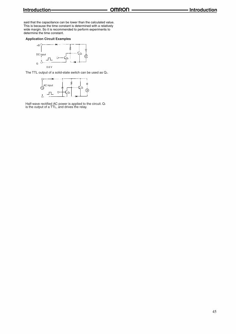
Application Circuit Examples
The TTL output of a solid-state switch can be used as Q2.
Half-wave rectified AC power is applied to the circuit. Q1 is the output of a TTL, and drives the relay.
DC input
+B
G0.6 V
Q2
Q1
X
XQ1
Q2
AC input