introduction to the discussion – fermilab's 3d future and exploiting our results
TRANSCRIPT
Introduction to
The discussion – Fermilab's 3D Future
and Exploiting our Results

recapitulation
2 3D Workshop, Nov. 15, 2013
Through presentations, shown earlier today, we get overviews of :
• the background of the 3D technologies and an overview of what the Fermilab team could do,
• Fermilab developments for selected direction,
• applications benefiting from 3D technologies (where Fermilab can have an important role to play),
• realistic approaches to continue 3D efforts seen by the industrial partner
We are hoping for recommendations and decisions:
• can we afford to continue developments exploiting 3D technologies?
• can we afford NOT to continue developments exploiting 3D technologies?
• or maybe the results are sufficient for assessments of 3D technologies and we should move on and do something else?
• If the choice is to continue, then:
• how to get the appropriate funds to support next steps (Fermilab LDRD included)?,
• what kind of help can come from internal programs, and from external applications?
• What is the environment for joint applications with other entities (other labs) and crossing the boundaries between domains of funding agencies, e.g. HEP-BES, etc..

background
3
Environment of integrated circuits technology for radiation detector readout systems is:
• Competitive
• Investment-hungry
• Characterized by long experience curves for the ASIC groups
• Challenging due to restrictions in access to the cutting edge technologies, legalities and bureaucratic burden associated with it
Groups tend to focus on one or a few particular detector technologies, families of design blocs, design methodologies or assembly works and excel offering complementary sets of skills and tools to the community
Fermilab advanced 3D-IC technology
gaining the World leading position!
3D Workshop, Nov. 15, 2013

uniqueness
4
How competitive it is becoming now:
multiple groups ( WGs in RD53) to cut a
relatively small pie (design of an analog
bloc of the Phase 2 CMS Pixel Tracking
System).
Eventually great ideas and an added
value are needed to succeed. 3D?
3D Workshop, Nov. 15, 2013
RD53 (CERN) based formed to promote a
65 nm process and coordinate work
towards HL-LHC upgrades; develops
dynamically despite of high costs

3D chip is composed of two or more layers of active electronic components and features horizontal intra-tier and vertical inter-tier connectivity,
Distinguishing features of 3D technologies: 4Through Silicon Vias (TSV)5Bonding5Wafer thinning5Back-side processing3
Transformational change: 4Finer pitch pixels 5Less mass 5Higher localized “on detector” functionality 5Bump bond alternative 5Non dead space arrays 3
Support: glass or
Si interposer
5
target
Strategic goal: 4 side buttable, dead-area-free detectors for uses ranging from X-ray, visible, IR imaging to classical tracking
3D ASIC with TSVs
threading connections
Large-area seam-
less sensor
Long-term goal:
3D Workshop, Nov. 15, 2013

6
additional opportunities - 1
Developments that are motivated (although not HEP):
3D Workshop, Nov. 15, 2013
Continuation of the VIPIC project: Time of Arrival capable camera for X-ray Correlation Spectroscopy together with the Photon Science Division BNL (BES)

7
Large-area, large DR, direct detection (Si), soft – X-ray camera for the Dynamic Compression Sector at the APS at the ANL
3D Workshop, Nov. 15, 2013
additional opportunities - 2

8
Large-area, indirect detection (fast scintillator), hard – X-ray camera for future X-ray Light Sources (BESAC recommendation 07/25/2013)
3D Workshop, Nov. 15, 2013
Detector with counting
capabilities >100MHz/pixel
material l Dt yield
RbF >200nm 1.3ns 1.7ph
CsF 390nm 2.9ns 2ph
HfO2 480nm 9.5ns 31
Examples of scintillating materials
http://scintillator.lbl.gov
additional opportunities - 3
9
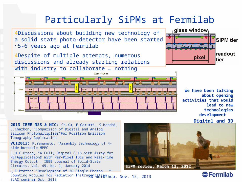
2013 IEEE NSS & MIC: Ch.Xu, E.Garutti, S.Mandai, E.Charbon, “Comparison of Digital and Analog Silicon Photomultiplier For Positron Emission Tomography Application”
VCI2013: K.Yamamoto, “Assembly technology of 4-side buttable MPPC”
L.H.C.Braga, “A Fully Digital 8 16 SiPM Array for PETApplications With Per-Pixel TDCs and Real-Time Energy Output”, IEEE Journal of Solid-State Circuits, Vol. 49, No. 1, January 2014
J.F.Pratte: “Development of 3D Single Photon Counting Modules for Radiation Instrumentation”, SLAC seminar Oct. 2013
3D Workshop, Nov. 15, 2013
We have been talking about opening activities that
would lead to new technologies development
Digital and 3D Digital SiPM
Particularly SiPMs at Fermilab4Discussions about building new technology of a solid state photo-detector have been started ~5-6 years ago at Fermilab
4Despite of multiple attempts, numerous discussions and already starting relations with industry to collaborate … nothing actually happened … no funding
SiPM review, March 13, 2012
SiPM review, March 13, 2012
10
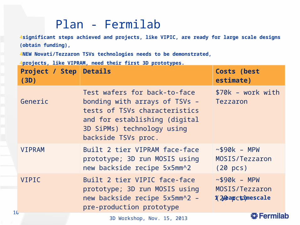
Plan - Fermilab
3D Workshop, Nov. 15, 2013
Project / Step (3D)
Details Costs (best estimate)
GenericTest wafers for back-to-face bonding with arrays of TSVs – tests of TSVs characteristics and for establishing (digital 3D SiPMs) technology using backside TSVs proc.
$70k – work with Tezzaron
VIPRAM Built 2 tier VIPRAM face-face prototype; 3D run MOSIS using new backside recipe 5x5mm^2
~$90k – MPW MOSIS/Tezzaron(20 pcs)
VIPIC Built 2 tier VIPIC face-face prototype; 3D run MOSIS using new backside recipe 5x5mm^2 – pre-production prototype
~$90k – MPW MOSIS/Tezzaron(20 pcs)
4significant steps achieved and projects, like VIPIC, are ready for large scale designs (obtain funding),
4NEW Novati/Tezzaron TSVs technologies needs to be demonstrated,
4projects, like VIPRAM, need their first 3D prototypes.
1 year timescale

11
Plan - Fermilab
3D Workshop, Nov. 15, 2013
Project / Step (3D)
Details Costs (best estimate)
VIPRAM‘production’
Built 3 tier VIPRAM; 3D engineering run 15x15 mm^2 (1control and 2 CAMs)2 sets of wafer masks
$850k (1000pcs)‘Foundry’/Tezzaron
Option 1: VIPIC130nm
Built 2 tier ROIC with sensor on one side and bump-bonding on second side to a substrate (PCB, interposer) 20x20 mm^22 sets of wafer masks
$850k (with bonding to sensors, excluding sensor)‘Foundry’/Tezzaron
Option 2: VIPIC 65nm with 3D features
Built 1 tier ROIC with sensor on one side and TSV for bump bonding to a substrate (PCB, interposer)
$1400k (with bonding to sensors, excluding sensor) - $1100k just 65nm run
4Follow up funds required to run developments of ‘production’ devices need to be sufficient

12
Discussion
3D Workshop, Nov. 15, 2013
Some questions:
• Is 3D matured enough to base projects with planned deliverables on it?
• Is there enough discussion to get detector R&D for experiments interested in 3D?
• What is required to handle 3D projects at the required scale and momentum?
• Do we have enough resources to handle 3D challenges? (of course we cannot start too many projects)
• How to handle projects for applications outside of HEP – synergies – involvement in shorter term and well defined (specifications) projects?