introduction to vlsi design - vlsi-eda laboratory
TRANSCRIPT
CMOS Digital Integrated Circuits
Introduction to VLSI DesignIntroduction to VLSI Design
Yu-Min LeeAssistant Professor
Department of Communication EngineeringNational Chiao Tung University
CMOS Digital Integrated Circuits
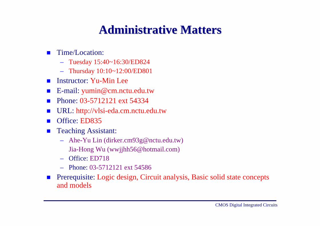
Administrative MattersAdministrative Matters
 Time/Location: – Tuesday 15:40~16:30/ED824– Thursday 10:10~12:00/ED801
 Instructor: Yu-Min Lee E-mail: [email protected] Phone: 03-5712121 ext 54334 URL: http://vlsi-eda.cm.nctu.edu.tw Office: ED835 Teaching Assistant:
– Ahe-Yu Lin ([email protected]) Jia-Hong Wu ([email protected])
– Office: ED718– Phone: 03-5712121 ext 54586
 Prerequisite: Logic design, Circuit analysis, Basic solid state concepts and models
CMOS Digital Integrated Circuits
Administrative MattersAdministrative Matters
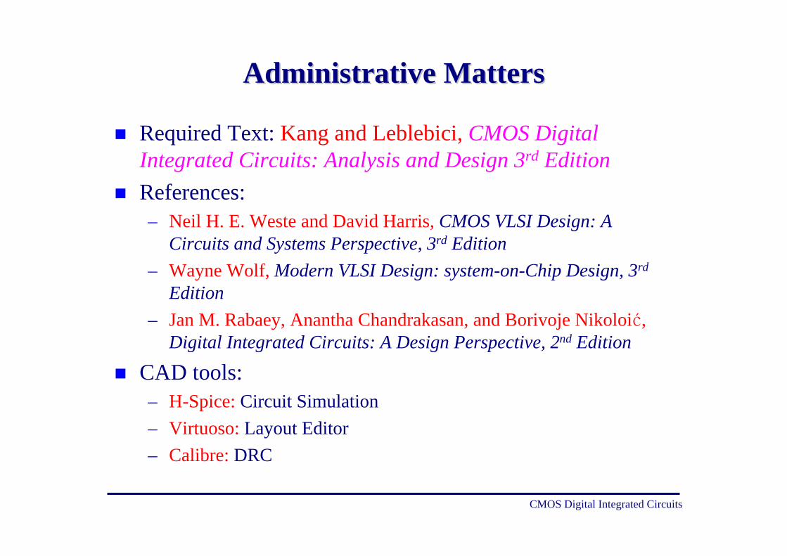
 Required Text: Kang and Leblebici, CMOS Digital Integrated Circuits: Analysis and Design 3rd Edition
 References: – Neil H. E. Weste and David Harris, CMOS VLSI Design: A
Circuits and Systems Perspective, 3rd Edition– Wayne Wolf, Modern VLSI Design: system-on-Chip Design, 3rd
Edition– Jan M. Rabaey, Anantha Chandrakasan, and Borivoje Nikoloić,
Digital Integrated Circuits: A Design Perspective, 2nd Edition
 CAD tools:– H-Spice: Circuit Simulation– Virtuoso: Layout Editor– Calibre: DRC
CMOS Digital Integrated Circuits
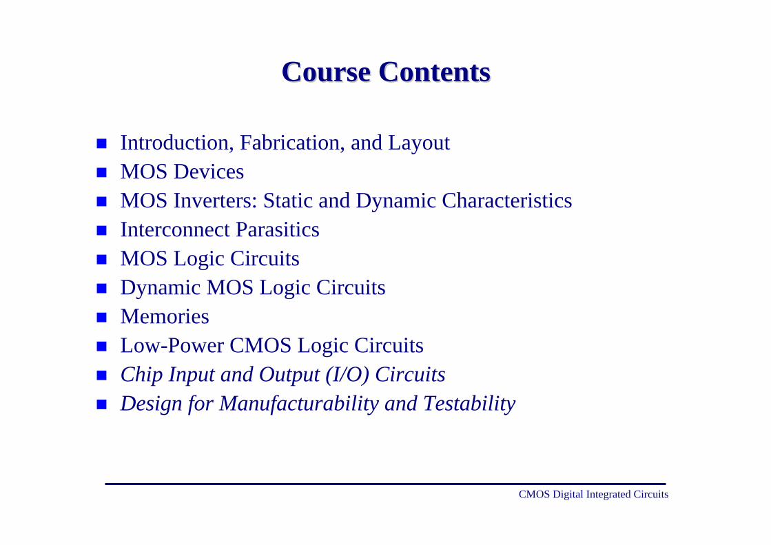
Course ContentsCourse Contents
 Introduction, Fabrication, and Layout MOS Devices MOS Inverters: Static and Dynamic Characteristics Interconnect Parasitics MOS Logic Circuits Dynamic MOS Logic Circuits Memories Low-Power CMOS Logic Circuits Chip Input and Output (I/O) Circuits Design for Manufacturability and Testability
CMOS Digital Integrated Circuits
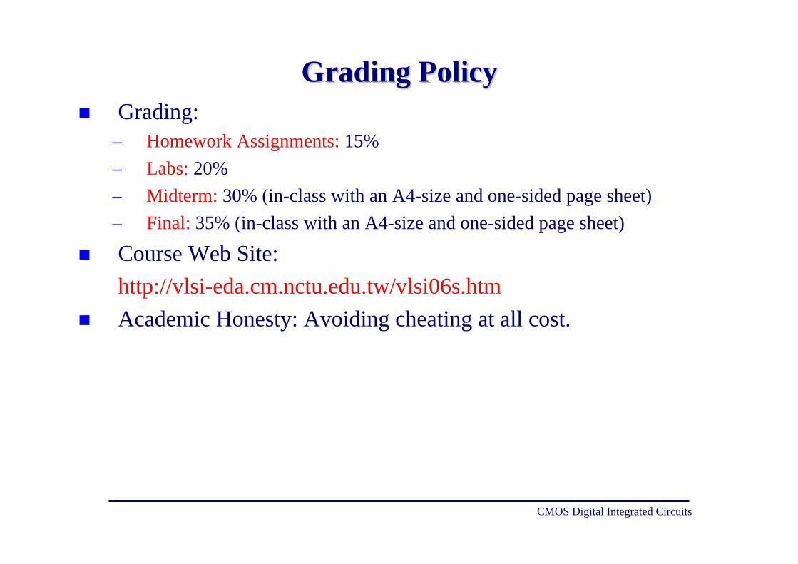
Grading PolicyGrading Policy Grading:
– Homework Assignments: 15%– Labs: 20%– Midterm: 30% (in-class with an A4-size and one-sided page sheet)– Final: 35% (in-class with an A4-size and one-sided page sheet)
 Course Web Site: http://vlsi-eda.cm.nctu.edu.tw/vlsi06s.htm
 Academic Honesty: Avoiding cheating at all cost.
1 © CMOS Digital Integrated Circuits – 3rd Edition
CMOS Digital Integrated Circuits
Lec 1 Introduction
2 © CMOS Digital Integrated Circuits – 3rd Edition
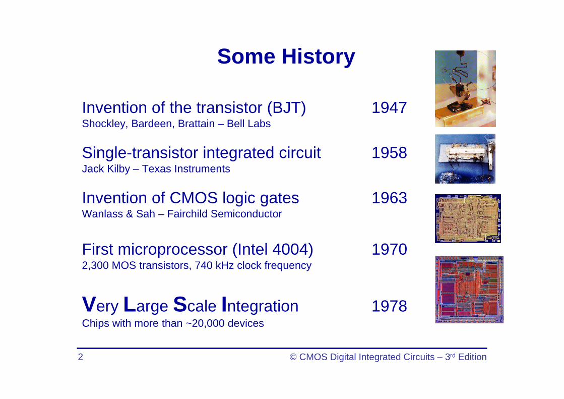
Some History
Invention of the transistor (BJT) 1947Shockley, Bardeen, Brattain – Bell Labs
Single-transistor integrated circuit 1958Jack Kilby – Texas Instruments
Invention of CMOS logic gates 1963Wanlass & Sah – Fairchild Semiconductor
First microprocessor (Intel 4004) 19702,300 MOS transistors, 740 kHz clock frequency
Very Large Scale Integration 1978Chips with more than ~20,000 devices
3 © CMOS Digital Integrated Circuits – 3rd Edition
More Recently
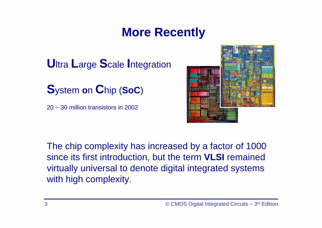
Ultra Large Scale Integration
System on Chip (SoC)
20 ~ 30 million transistors in 2002
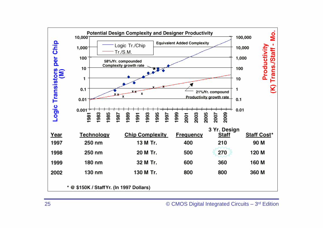
The chip complexity has increased by a factor of 1000 since its first introduction, but the term VLSI remained virtually universal to denote digital integrated systems with high complexity.
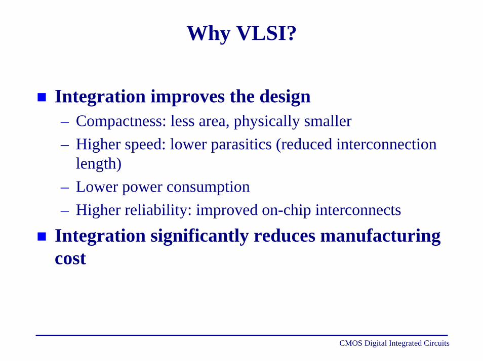
Why VLSI?
 Integration improves the design– Compactness: less area, physically smaller– Higher speed: lower parasitics (reduced interconnection
length)– Lower power consumption– Higher reliability: improved on-chip interconnects
 Integration significantly reduces manufacturing cost
CMOS Digital Integrated Circuits

4 © CMOS Digital Integrated Circuits – 3rd Edition
As a result of the continuously increasing integration density and decreasing unit costs, the semiconductor industry has been one of the fastest growing sectors in the worldwide economy.
Economic Impact
5 © CMOS Digital Integrated Circuits – 3rd Edition
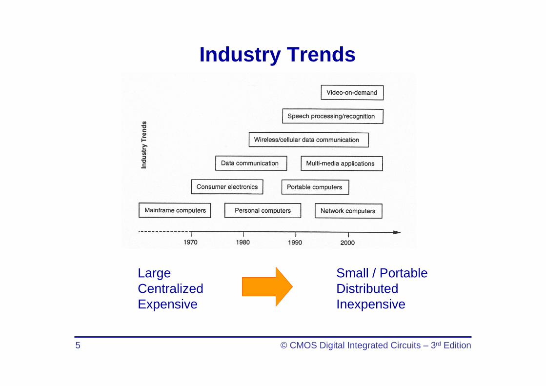
LargeCentralizedExpensive
Industry Trends
Small / PortableDistributedInexpensive
6 © CMOS Digital Integrated Circuits – 3rd Edition
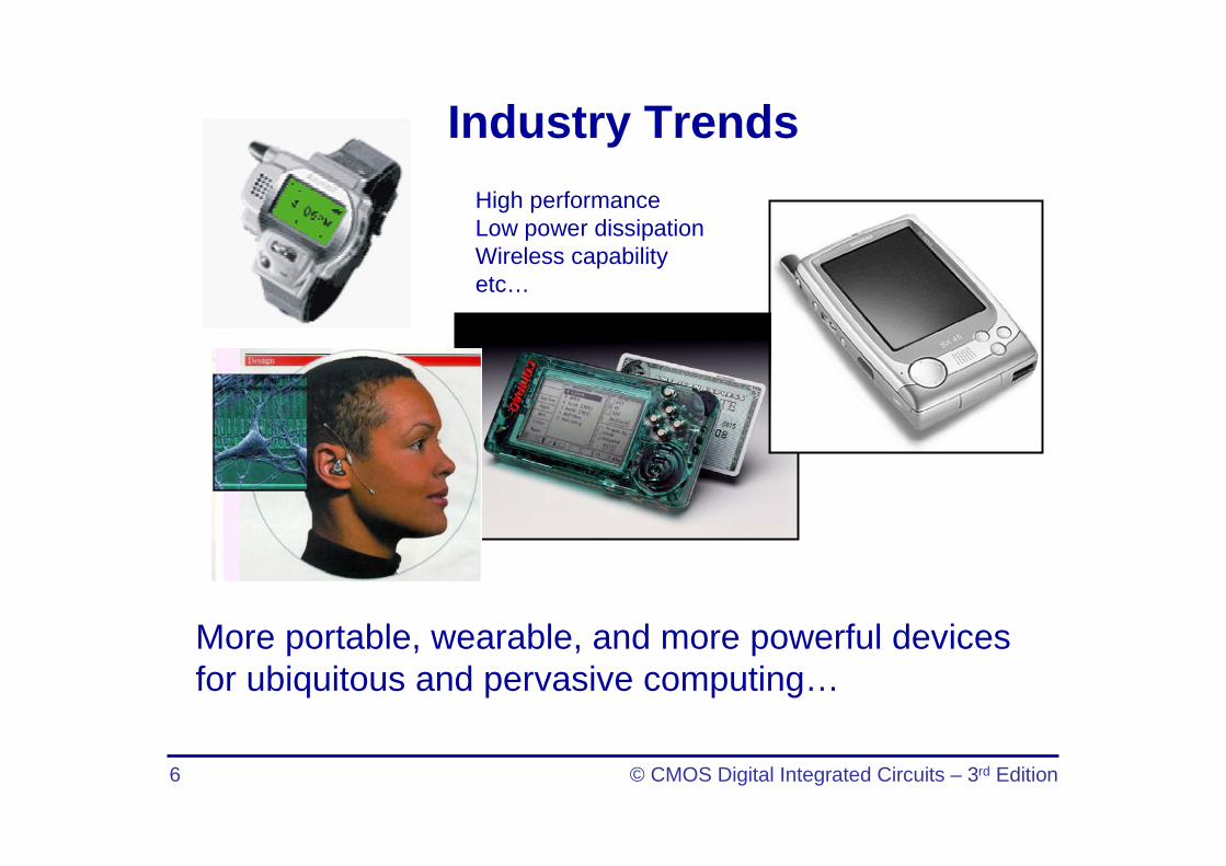
More portable, wearable, and more powerful devices for ubiquitous and pervasive computing…
Industry Trends
High performanceLow power dissipationWireless capabilityetc…
7 © CMOS Digital Integrated Circuits – 3rd Edition
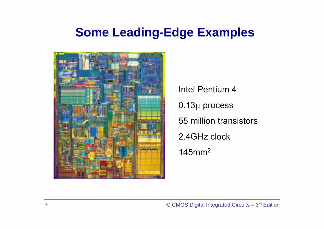
Some Leading-Edge Examples
8 © CMOS Digital Integrated Circuits – 3rd Edition
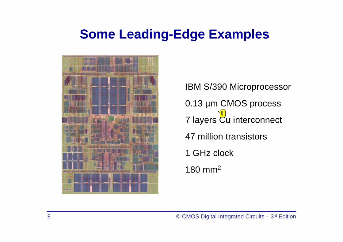
Some Leading-Edge Examples
IBM S/390 Microprocessor
0.13 µm CMOS process
7 layers Cu interconnect
47 million transistors
1 GHz clock
180 mm2
9 © CMOS Digital Integrated Circuits – 3rd Edition
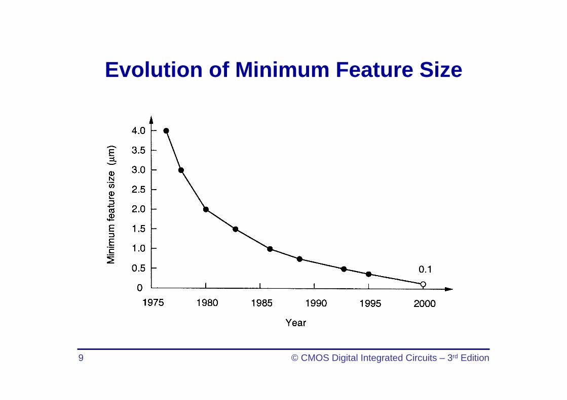
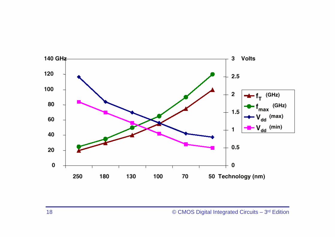
Evolution of Minimum Feature Size
10 © CMOS Digital Integrated Circuits – 3rd Edition
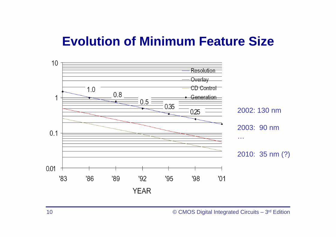
Evolution of Minimum Feature Size
2002: 130 nm
2003: 90 nm…
2010: 35 nm (?)
11 © CMOS Digital Integrated Circuits – 3rd Edition
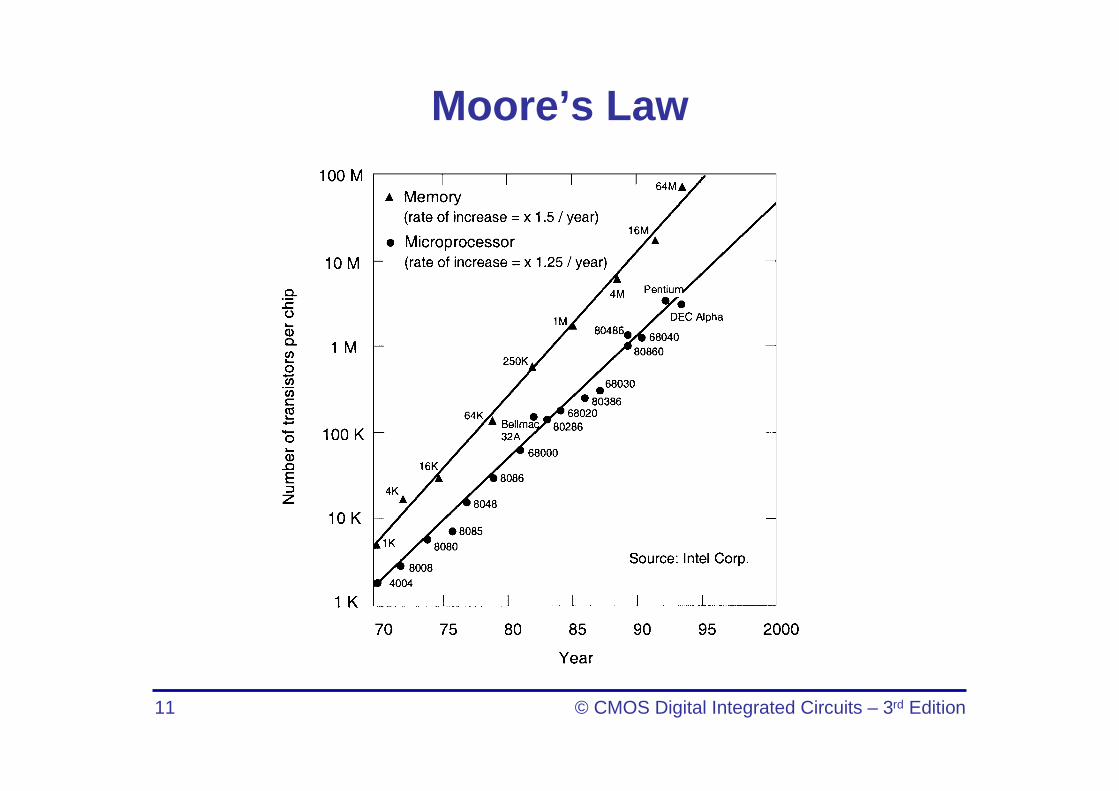
Moore’s Law
12 © CMOS Digital Integrated Circuits – 3rd Edition
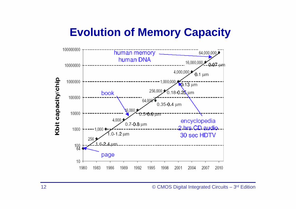
Evolution of Memory Capacity
13 © CMOS Digital Integrated Circuits – 3rd Edition
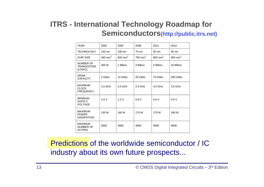
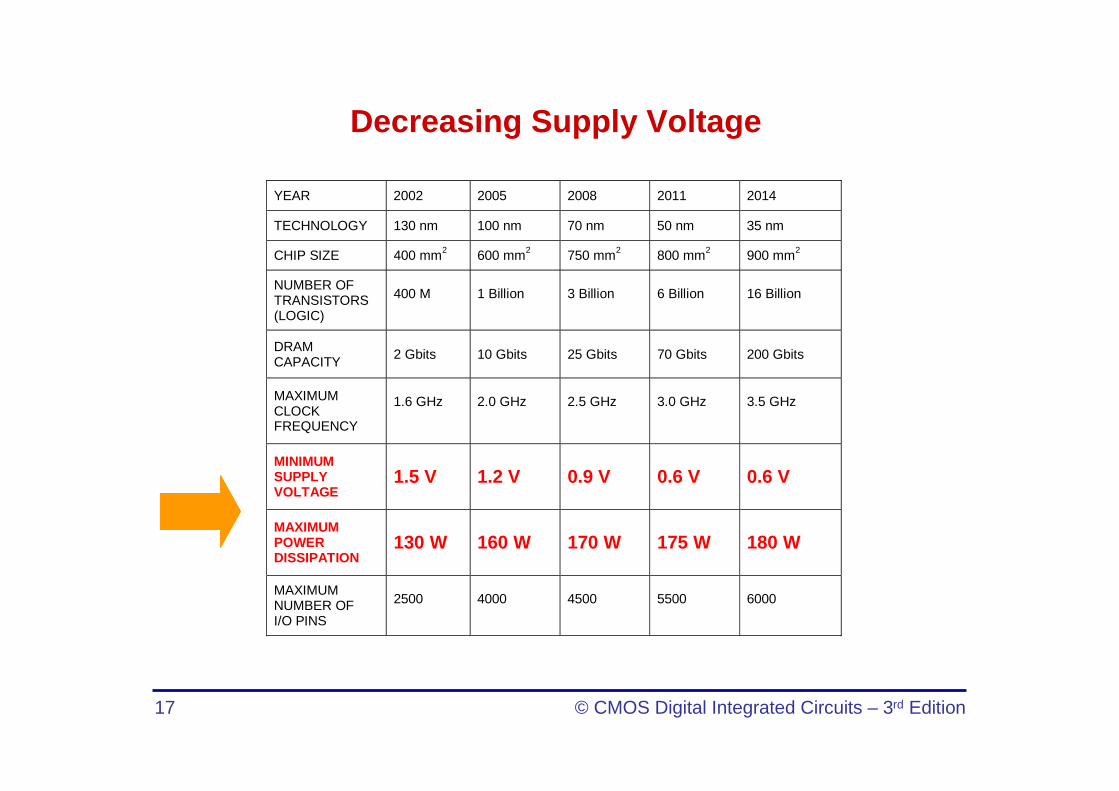
YEAR 2002 2005 2008 2011 2014
TECHNOLOGY 130 nm 100 nm 70 nm 50 nm 35 nm
CHIP SIZE 400 mm2 600 mm2 750 mm2 800 mm2 900 mm2
NUMBER OFTRANSISTORS(LOGIC)
400 M 1 Billion 3 Billion 6 Billion 16 Billion
DRAMCAPACITY 2 Gbits 10 Gbits 25 Gbits 70 Gbits 200 Gbits
MAXIMUMCLOCKFREQUENCY
1.6 GHz 2.0 GHz 2.5 GHz 3.0 GHz 3.5 GHz
MINIMUMSUPPLYVOLTAGE
1.5 V 1.2 V 0.9 V 0.6 V 0.6 V
MAXIMUMPOWERDISSIPATION
130 W 160 W 170 W 175 W 180 W
MAXIMUMNUMBER OFI/O PINS
2500 4000 4500 5500 6000
ITRS - International Technology Roadmap for Semiconductors(http://public.itrs.net)
Predictions of the worldwide semiconductor / IC industry about its own future prospects...

14 © CMOS Digital Integrated Circuits – 3rd Edition
YEAR 2002 2005 2008 2011 2014
TECHNOLOGY 130 nm 100 nm 70 nm 50 nm 35 nm
CHIP SIZE 400 mm2 600 mm2 750 mm2 800 mm2 900 mm2
NUMBER OFTRANSISTORS(LOGIC)
400 M 1 Billion 3 Billion 6 Billion 16 Billion
DRAMCAPACITY 2 Gbits 10 Gbits 25 Gbits 70 Gbits 200 Gbits
MAXIMUMCLOCKFREQUENCY
1.6 GHz 2.0 GHz 2.5 GHz 3.0 GHz 3.5 GHz
MINIMUMSUPPLYVOLTAGE
1.5 V 1.2 V 0.9 V 0.6 V 0.6 V
MAXIMUMPOWERDISSIPATION
130 W 160 W 170 W 175 W 180 W
MAXIMUMNUMBER OFI/O PINS
2500 4000 4500 5500 6000
Shrinking Device Dimensions
15 © CMOS Digital Integrated Circuits – 3rd Edition
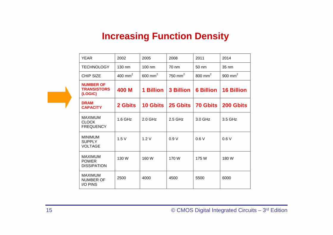
YEAR 2002 2005 2008 2011 2014
TECHNOLOGY 130 nm 100 nm 70 nm 50 nm 35 nm
CHIP SIZE 400 mm2 600 mm2 750 mm2 800 mm2 900 mm2
NUMBER OFTRANSISTORS(LOGIC)
400 M 1 Billion 3 Billion 6 Billion 16 Billion
DRAMCAPACITY 2 Gbits 10 Gbits 25 Gbits 70 Gbits 200 Gbits
MAXIMUMCLOCKFREQUENCY
1.6 GHz 2.0 GHz 2.5 GHz 3.0 GHz 3.5 GHz
MINIMUMSUPPLYVOLTAGE
1.5 V 1.2 V 0.9 V 0.6 V 0.6 V
MAXIMUMPOWERDISSIPATION
130 W 160 W 170 W 175 W 180 W
MAXIMUMNUMBER OFI/O PINS
2500 4000 4500 5500 6000
Increasing Function Density
16 © CMOS Digital Integrated Circuits – 3rd Edition
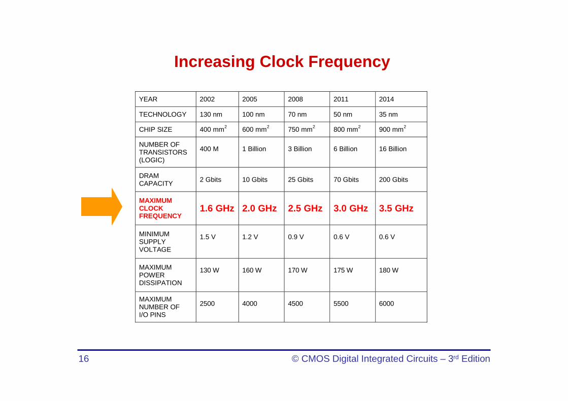
YEAR 2002 2005 2008 2011 2014
TECHNOLOGY 130 nm 100 nm 70 nm 50 nm 35 nm
CHIP SIZE 400 mm2 600 mm2 750 mm2 800 mm2 900 mm2
NUMBER OFTRANSISTORS(LOGIC)
400 M 1 Billion 3 Billion 6 Billion 16 Billion
DRAMCAPACITY 2 Gbits 10 Gbits 25 Gbits 70 Gbits 200 Gbits
MAXIMUMCLOCKFREQUENCY
1.6 GHz 2.0 GHz 2.5 GHz 3.0 GHz 3.5 GHz
MINIMUMSUPPLYVOLTAGE
1.5 V 1.2 V 0.9 V 0.6 V 0.6 V
MAXIMUMPOWERDISSIPATION
130 W 160 W 170 W 175 W 180 W
MAXIMUMNUMBER OFI/O PINS
2500 4000 4500 5500 6000
Increasing Clock Frequency
17 © CMOS Digital Integrated Circuits – 3rd Edition
YEAR 2002 2005 2008 2011 2014
TECHNOLOGY 130 nm 100 nm 70 nm 50 nm 35 nm
CHIP SIZE 400 mm2 600 mm2 750 mm2 800 mm2 900 mm2
NUMBER OFTRANSISTORS(LOGIC)
400 M 1 Billion 3 Billion 6 Billion 16 Billion
DRAMCAPACITY 2 Gbits 10 Gbits 25 Gbits 70 Gbits 200 Gbits
MAXIMUMCLOCKFREQUENCY
1.6 GHz 2.0 GHz 2.5 GHz 3.0 GHz 3.5 GHz
MINIMUMSUPPLYVOLTAGE
1.5 V 1.2 V 0.9 V 0.6 V 0.6 V
MAXIMUMPOWERDISSIPATION
130 W 160 W 170 W 175 W 180 W
MAXIMUMNUMBER OFI/O PINS
2500 4000 4500 5500 6000
Decreasing Supply Voltage

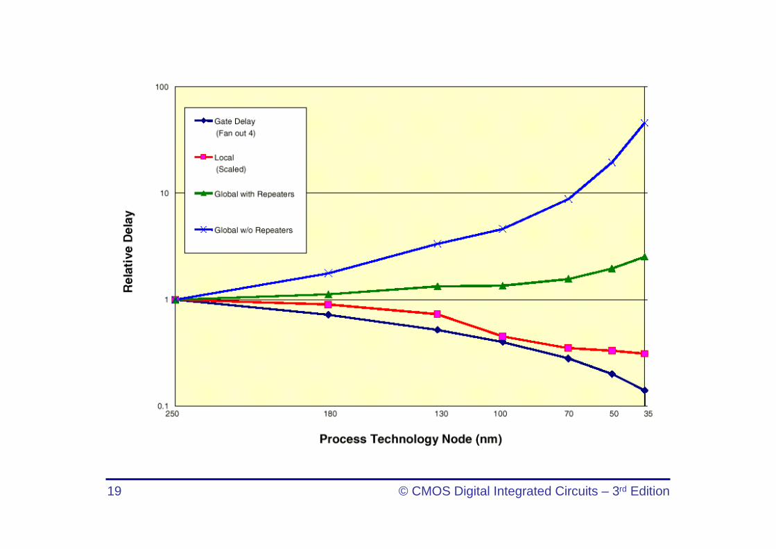
Evolution in Power DensityEvolution in Power Density
1
10
100
1000
10000
1970 1980 1990 2000 2010
40044004
80088008
80808080
80858085
80868086
286286386386
486486
P6P6
PentiumPentium®® procproc
Hot Hot PlatePlate
Nuclear ReactorNuclear Reactor
Rocket Rocket NozzleNozzleSunSun‘‘s s surface?surface?
Po
wer
Den
sity
[W
/cm
²]
CMOS Digital Integrated CircuitsSourceSource: : adaptedadapted fromfrom IntelIntel
17-1
18 © CMOS Digital Integrated Circuits – 3rd Edition
19 © CMOS Digital Integrated Circuits – 3rd Edition

20 © CMOS Digital Integrated Circuits – 3rd Edition
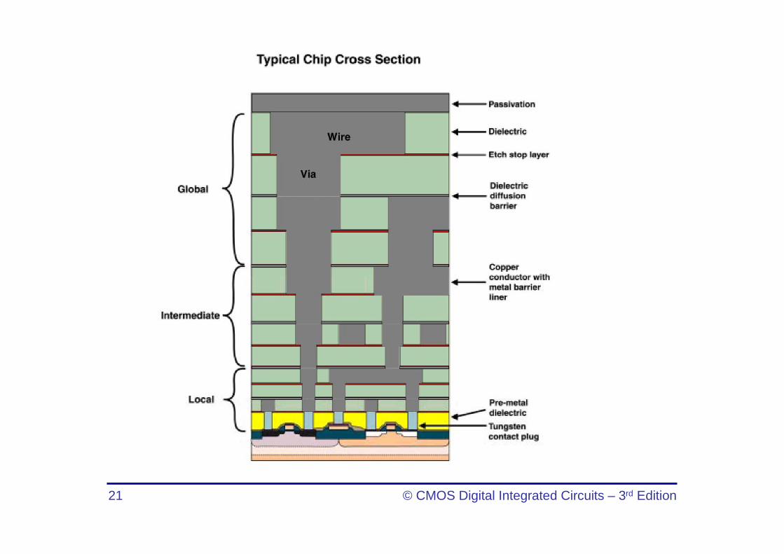
5-layer cross-section of chip
21 © CMOS Digital Integrated Circuits – 3rd Edition
22 © CMOS Digital Integrated Circuits – 3rd Edition
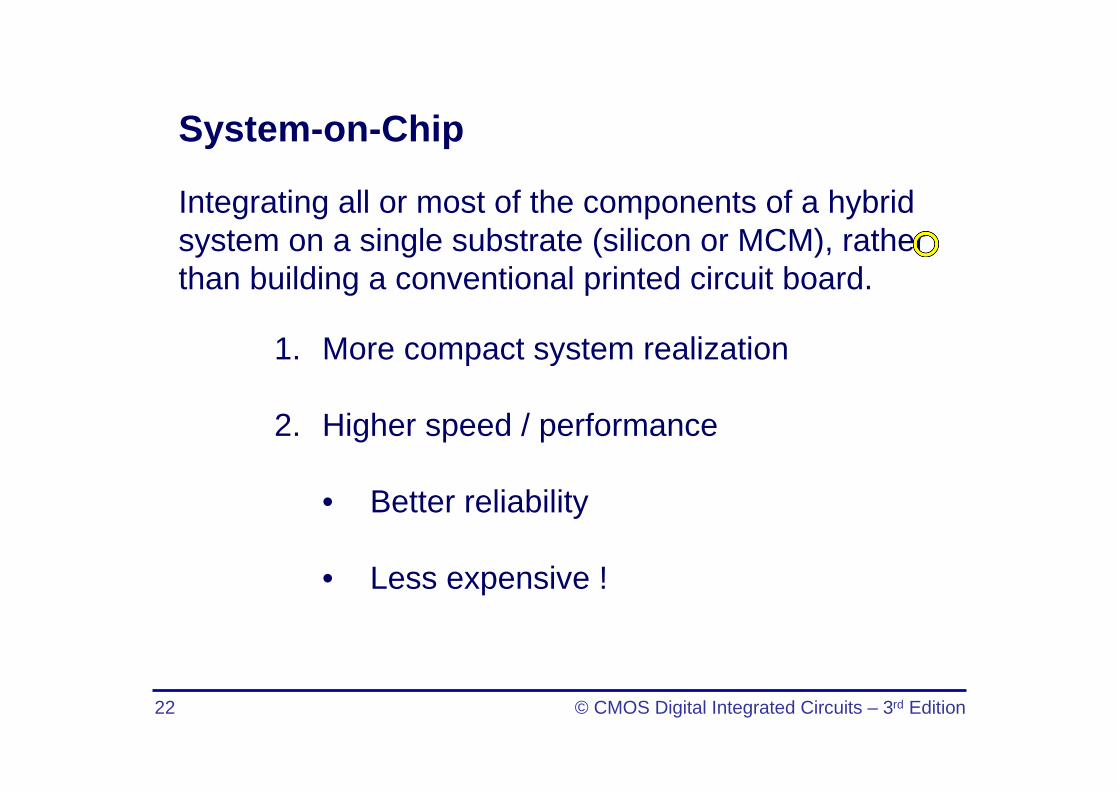
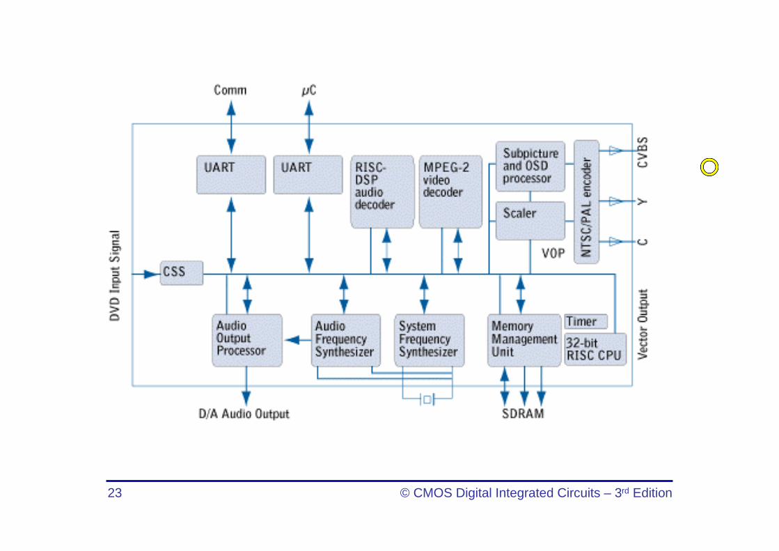
System-on-Chip
Integrating all or most of the components of a hybrid system on a single substrate (silicon or MCM), rather than building a conventional printed circuit board.
1. More compact system realization
2. Higher speed / performance
• Better reliability
• Less expensive !
23 © CMOS Digital Integrated Circuits – 3rd Edition
24 © CMOS Digital Integrated Circuits – 3rd Edition
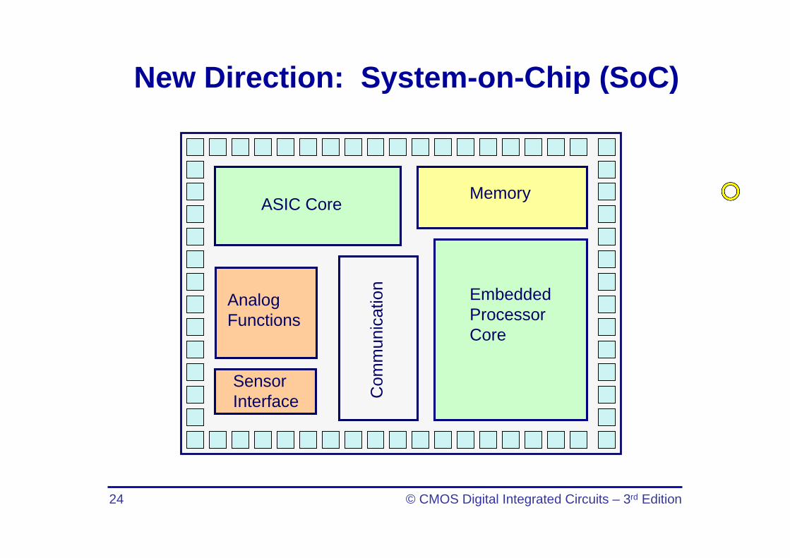
New Direction: System-on-Chip (SoC)
ASIC CoreMemory
Embedded ProcessorCore
AnalogFunctions
Com
mun
icat
ion
SensorInterface
25 © CMOS Digital Integrated Circuits – 3rd Edition
26 © CMOS Digital Integrated Circuits – 3rd Edition
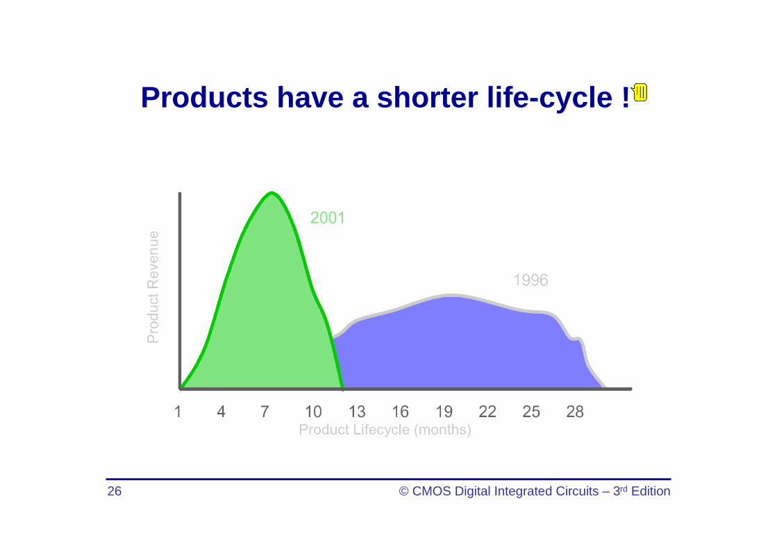
Products have a shorter life-cycle !
27 © CMOS Digital Integrated Circuits – 3rd Edition
28 © CMOS Digital Integrated Circuits – 3rd Edition
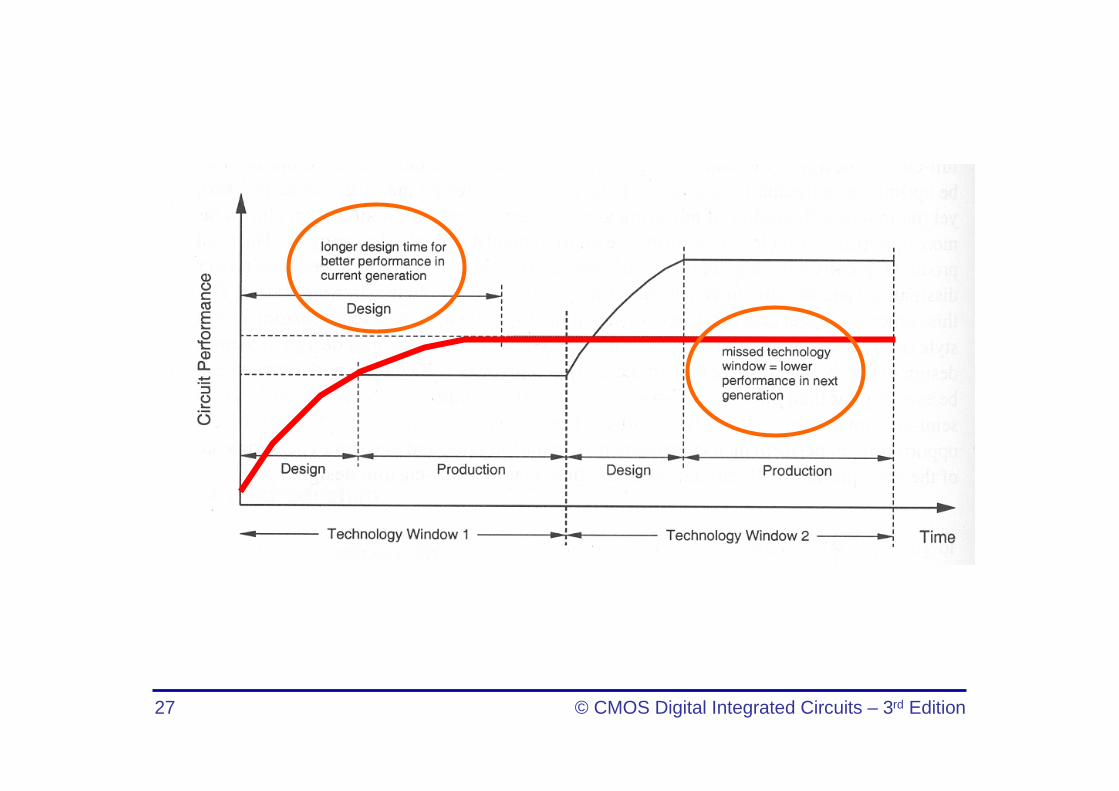
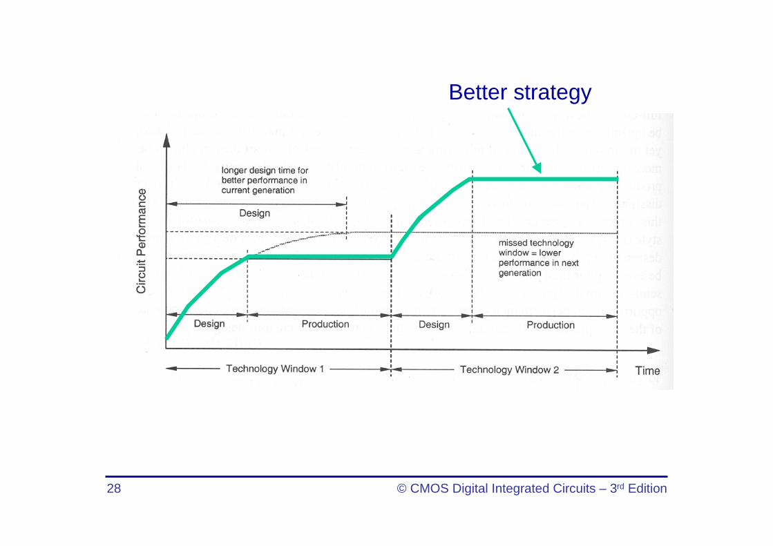
Better strategy
29 © CMOS Digital Integrated Circuits – 3rd Edition
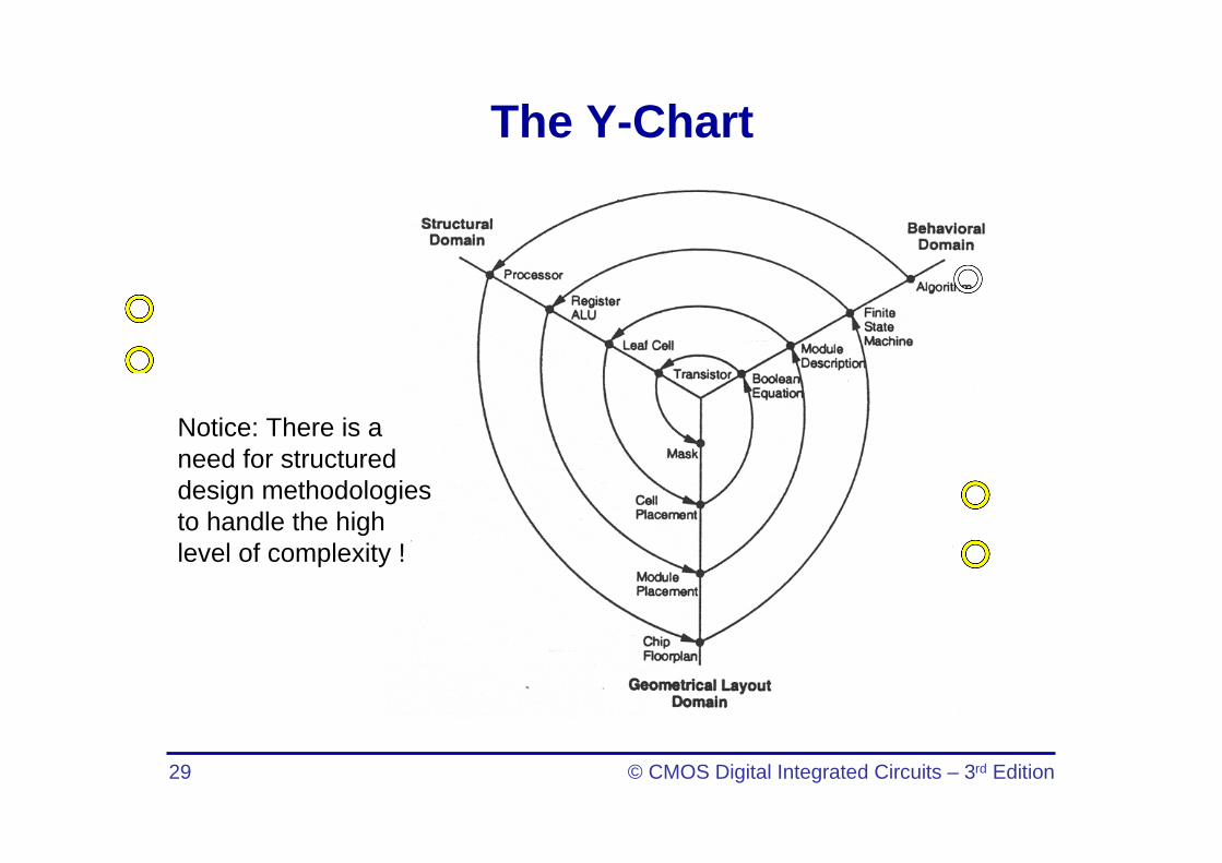
The Y-Chart
Notice: There is a need for structured design methodologies to handle the high level of complexity !
30 © CMOS Digital Integrated Circuits – 3rd Edition
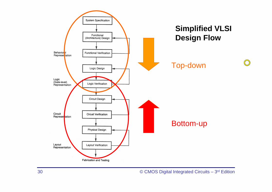
Simplified VLSI Design Flow
Top-down
Bottom-up
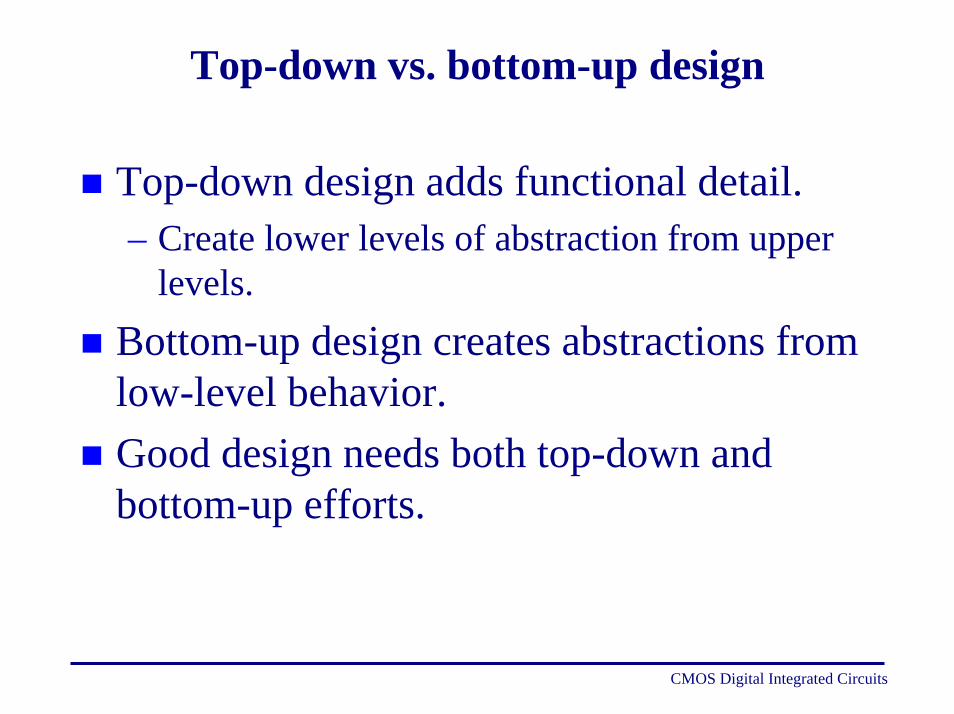
Top-down vs. bottom-up design
 Top-down design adds functional detail.– Create lower levels of abstraction from upper
levels. Bottom-up design creates abstractions from
low-level behavior. Good design needs both top-down and
bottom-up efforts.
CMOS Digital Integrated Circuits
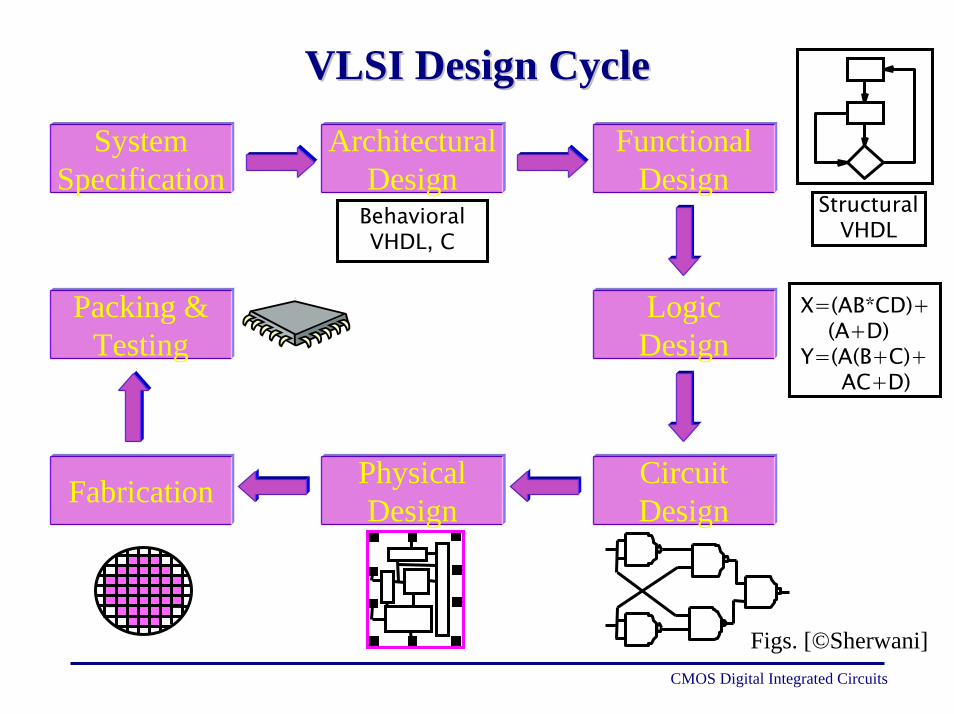
VLSI Design CycleVLSI Design Cycle
CMOS Digital Integrated Circuits
SystemSpecification
ArchitecturalDesign
FunctionalDesign
StructuralVHDLBehavioral
VHDL, C
Packing &Testing
LogicDesign
X=(AB*CD)+(A+D)
Y=(A(B+C)+AC+D)
PhysicalDesign
CircuitDesignFabrication
Figs. [©Sherwani]
VLSI Design CycleVLSI Design Cycle
 System Specification– A high level representation of the system– Considered factors
» Performance» Functionality» Physical dimensions (die size)
– Result Specs – size, speed, power, and functionality
Fabrication Technology
Design Techniques
CMOS Digital Integrated Circuits
VLSI Design CycleVLSI Design Cycle
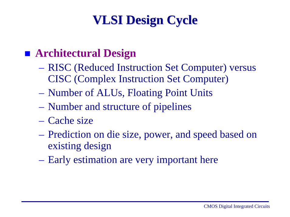
 Architectural Design– RISC (Reduced Instruction Set Computer) versus
CISC (Complex Instruction Set Computer)– Number of ALUs, Floating Point Units– Number and structure of pipelines– Cache size– Prediction on die size, power, and speed based on
existing design– Early estimation are very important here
CMOS Digital Integrated Circuits
VLSI Design CycleVLSI Design Cycle
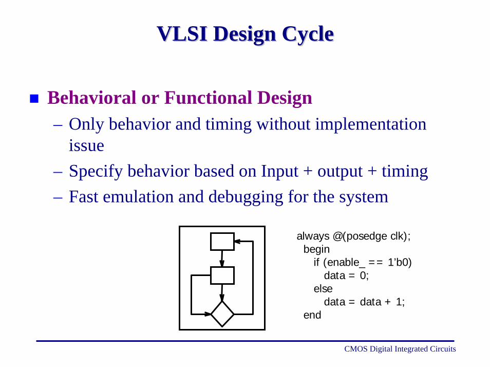
 Behavioral or Functional Design– Only behavior and timing without implementation
issue– Specify behavior based on Input + output + timing– Fast emulation and debugging for the system
always @(posedge clk);begin
if (enable_ == 1’b0)data = 0;
elsedata = data + 1;
end
CMOS Digital Integrated Circuits
VLSI Design CycleVLSI Design Cycle
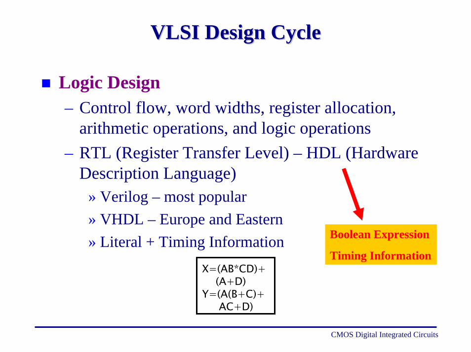
 Logic Design– Control flow, word widths, register allocation,
arithmetic operations, and logic operations– RTL (Register Transfer Level) – HDL (Hardware
Description Language)» Verilog – most popular» VHDL – Europe and Eastern» Literal + Timing Information Boolean Expression
Timing InformationX=(AB*CD)+
(A+D)Y=(A(B+C)+
AC+D)
CMOS Digital Integrated Circuits
VLSI Design CycleVLSI Design Cycle
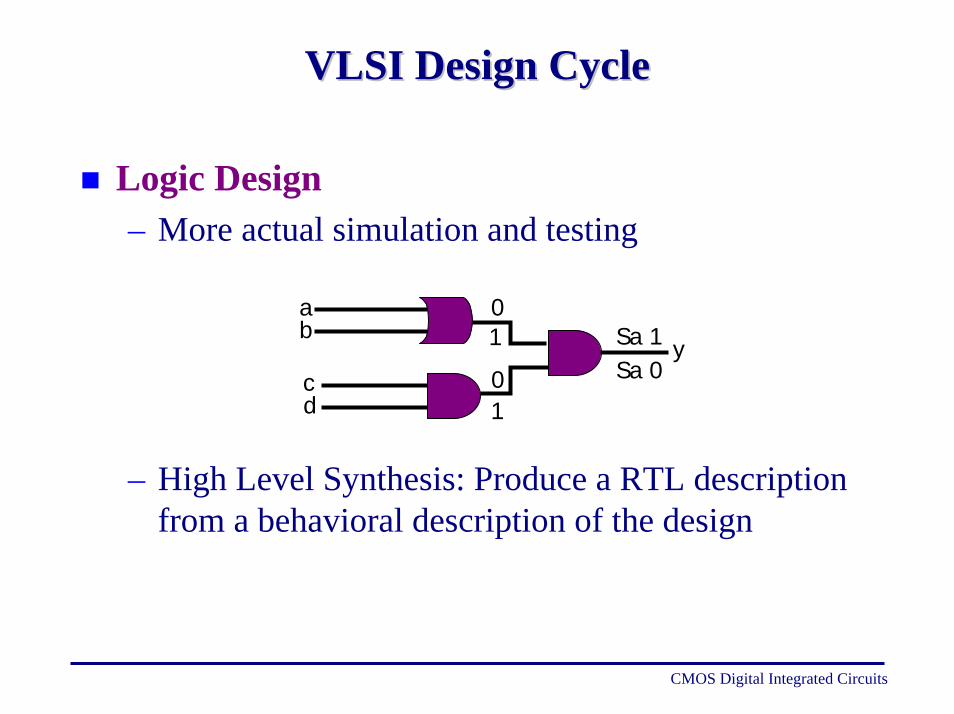
 Logic Design– More actual simulation and testing
– High Level Synthesis: Produce a RTL description from a behavioral description of the design
ab
cd
ySa 1Sa 0
0
0
1
1
CMOS Digital Integrated Circuits
VLSI Design CycleVLSI Design Cycle
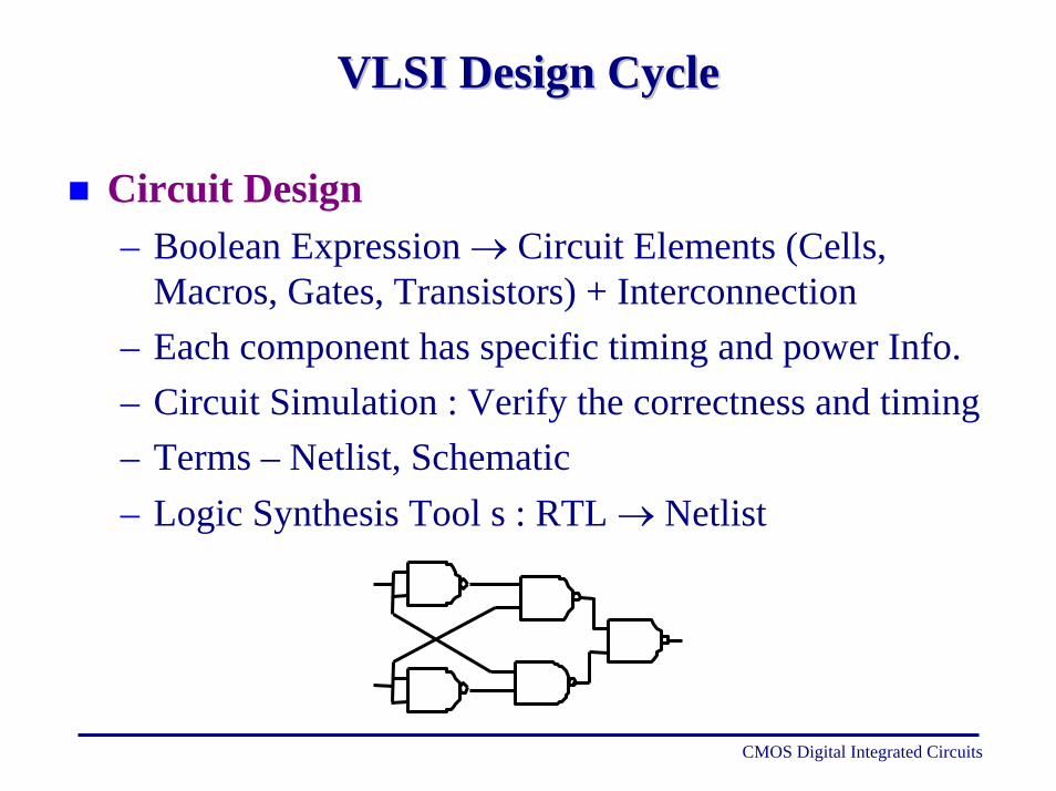
 Circuit Design– Boolean Expression → Circuit Elements (Cells,
Macros, Gates, Transistors) + Interconnection– Each component has specific timing and power Info.– Circuit Simulation : Verify the correctness and timing– Terms – Netlist, Schematic– Logic Synthesis Tool s : RTL → Netlist
CMOS Digital Integrated Circuits
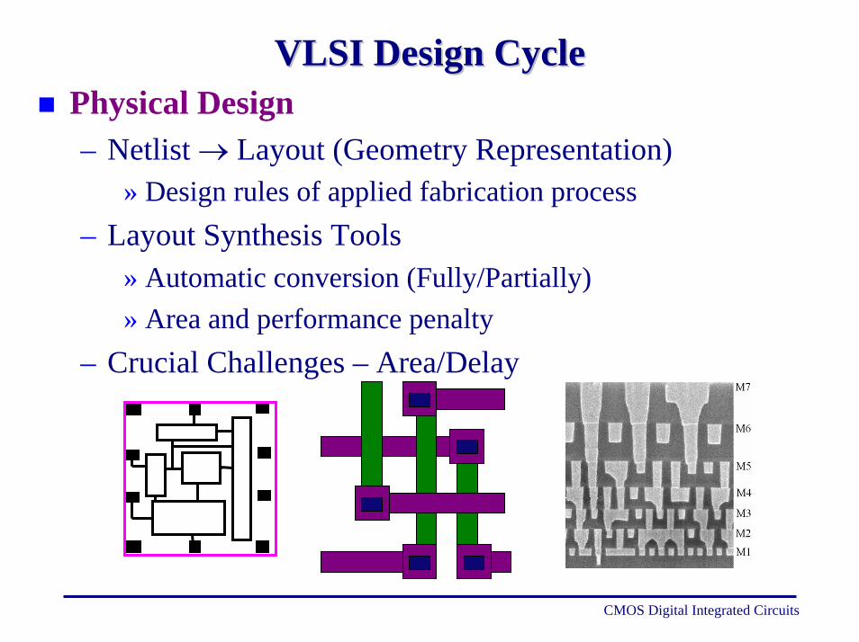
VLSI Design CycleVLSI Design Cycle Physical Design
– Netlist → Layout (Geometry Representation)» Design rules of applied fabrication process
– Layout Synthesis Tools» Automatic conversion (Fully/Partially)» Area and performance penalty
– Crucial Challenges – Area/Delay
CMOS Digital Integrated Circuits
VLSI Design CycleVLSI Design Cycle
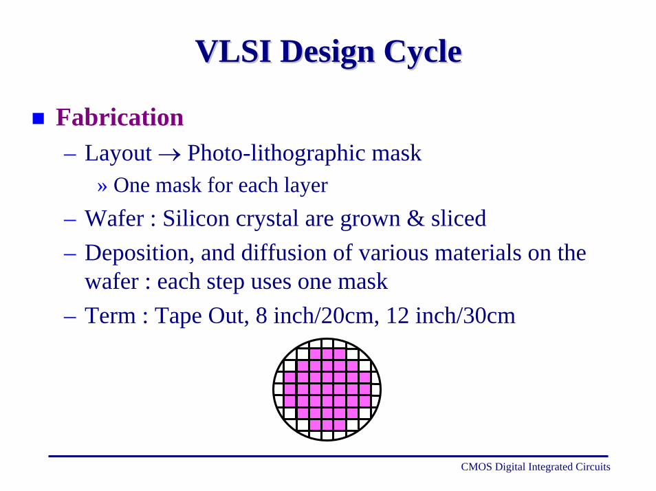
 Fabrication– Layout → Photo-lithographic mask
» One mask for each layer– Wafer : Silicon crystal are grown & sliced– Deposition, and diffusion of various materials on the
wafer : each step uses one mask– Term : Tape Out, 8 inch/20cm, 12 inch/30cm
CMOS Digital Integrated Circuits
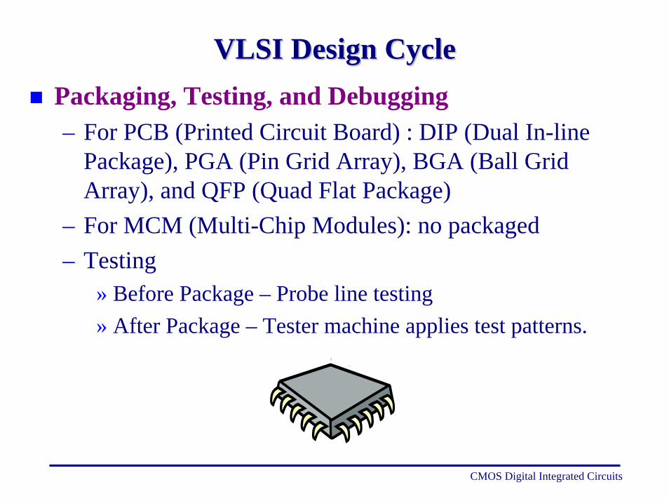
VLSI Design CycleVLSI Design Cycle Packaging, Testing, and Debugging
– For PCB (Printed Circuit Board) : DIP (Dual In-line Package), PGA (Pin Grid Array), BGA (Ball Grid Array), and QFP (Quad Flat Package)
– For MCM (Multi-Chip Modules): no packaged– Testing
» Before Package – Probe line testing» After Package – Tester machine applies test patterns.
CMOS Digital Integrated Circuits
31 © CMOS Digital Integrated Circuits – 3rd Edition
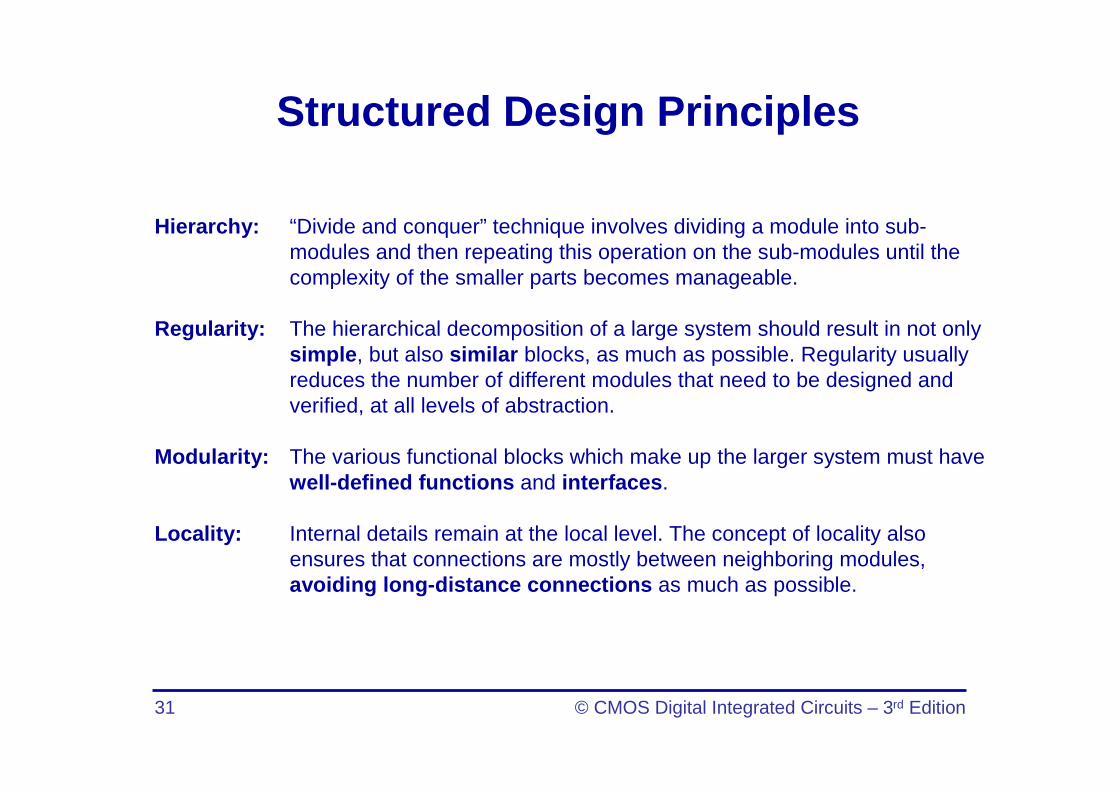
Structured Design Principles
Hierarchy: “Divide and conquer” technique involves dividing a module into sub-modules and then repeating this operation on the sub-modules until the complexity of the smaller parts becomes manageable.
Regularity: The hierarchical decomposition of a large system should result in not only simple, but also similar blocks, as much as possible. Regularity usually reduces the number of different modules that need to be designed and verified, at all levels of abstraction.
Modularity: The various functional blocks which make up the larger system must have well-defined functions and interfaces.
Locality: Internal details remain at the local level. The concept of locality also ensures that connections are mostly between neighboring modules,avoiding long-distance connections as much as possible.
32 © CMOS Digital Integrated Circuits – 3rd Edition
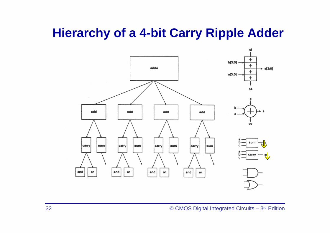
Hierarchy of a 4-bit Carry Ripple Adder
33 © CMOS Digital Integrated Circuits – 3rd Edition
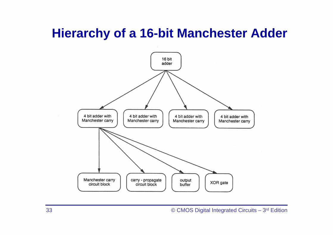
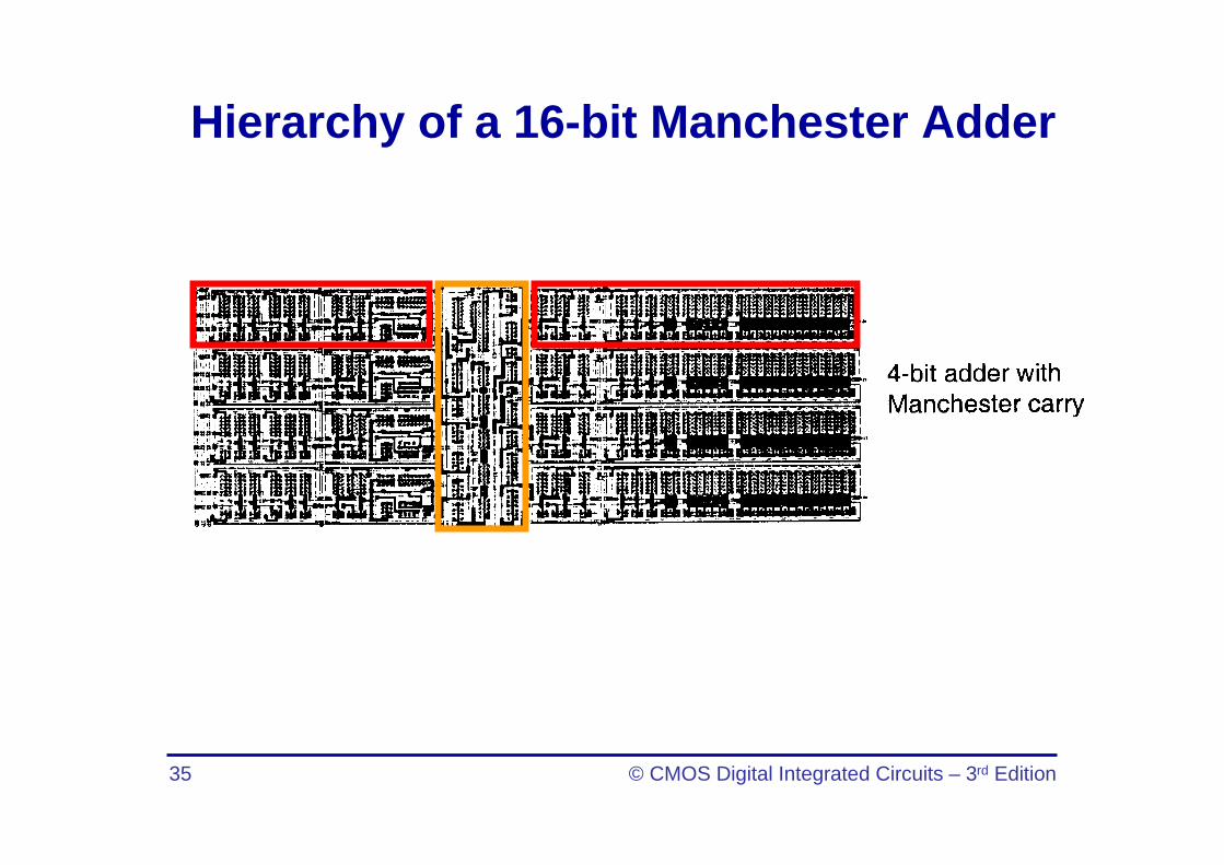
Hierarchy of a 16-bit Manchester Adder
34 © CMOS Digital Integrated Circuits – 3rd Edition
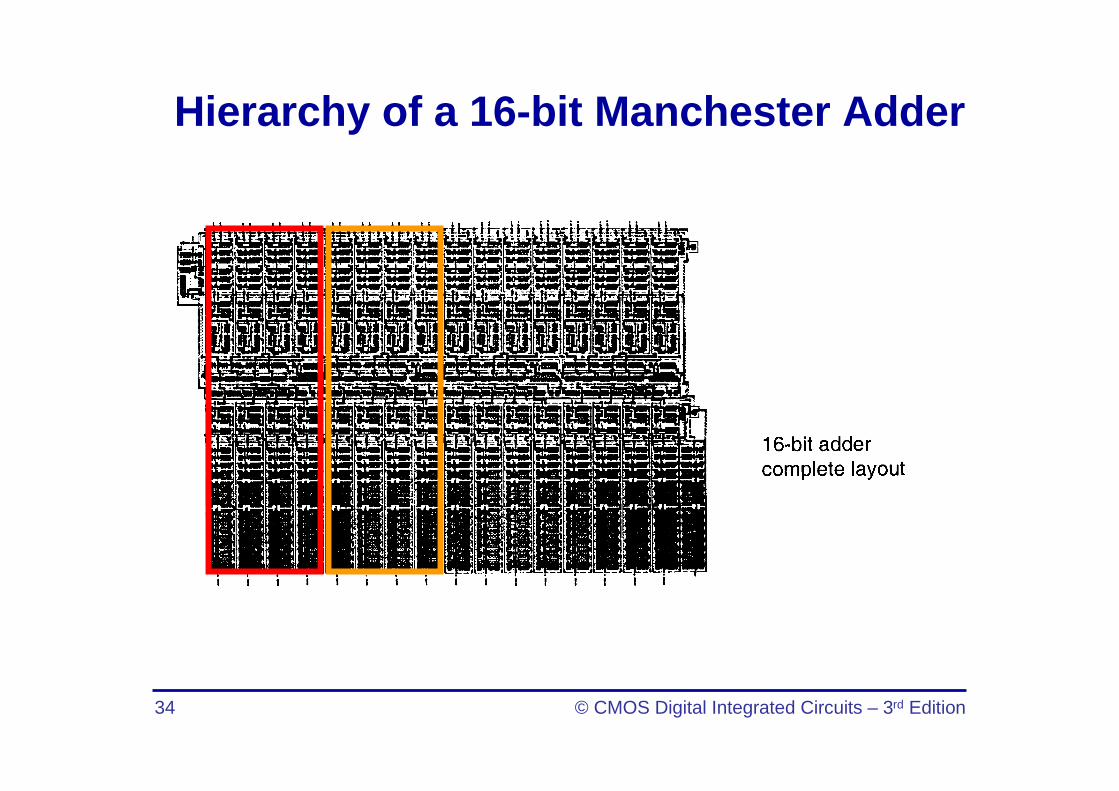
Hierarchy of a 16-bit Manchester Adder
35 © CMOS Digital Integrated Circuits – 3rd Edition
Hierarchy of a 16-bit Manchester Adder
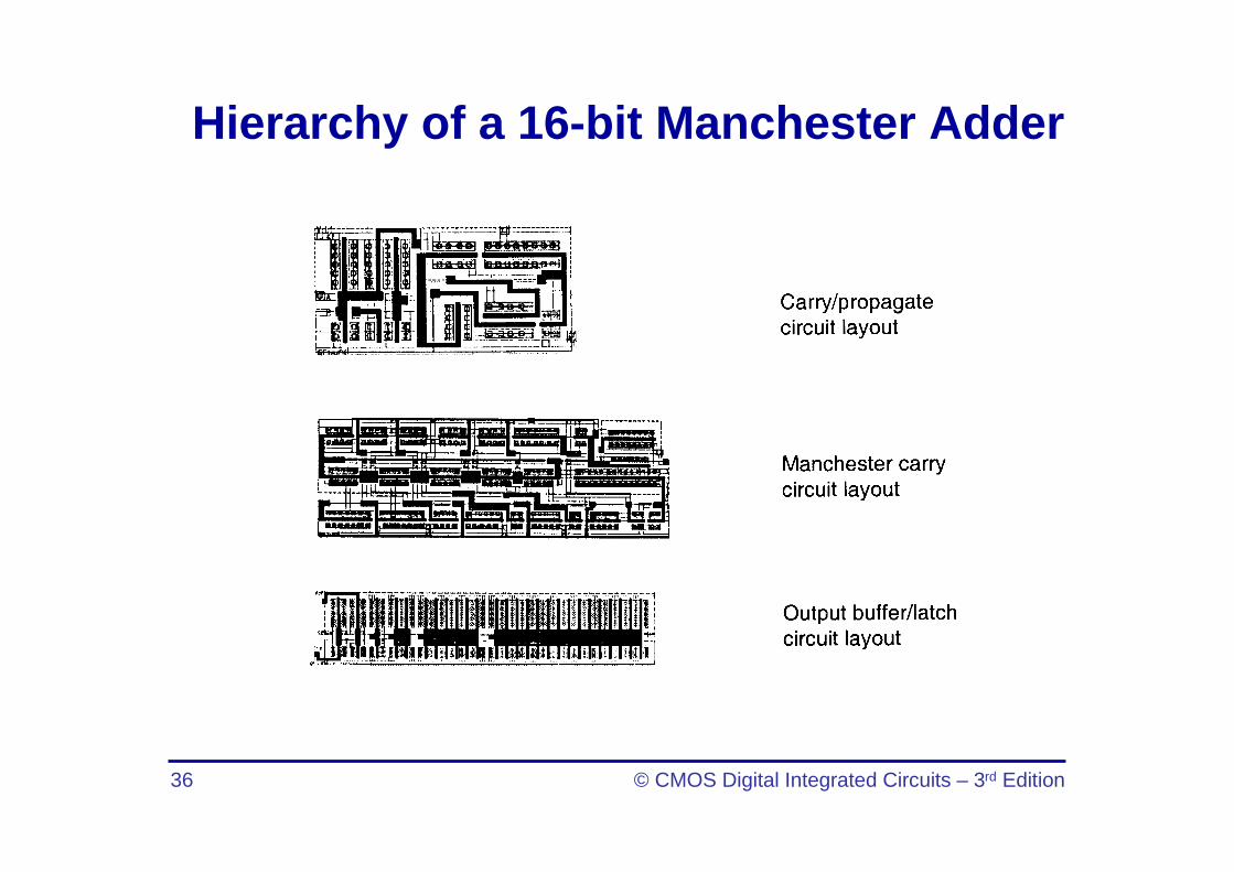
36 © CMOS Digital Integrated Circuits – 3rd Edition
Hierarchy of a 16-bit Manchester Adder
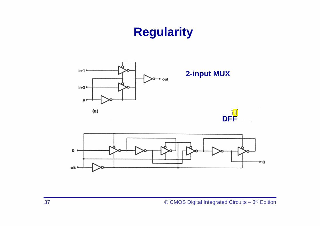
37 © CMOS Digital Integrated Circuits – 3rd Edition
Regularity
2-input MUX
DFF
38 © CMOS Digital Integrated Circuits – 3rd Edition
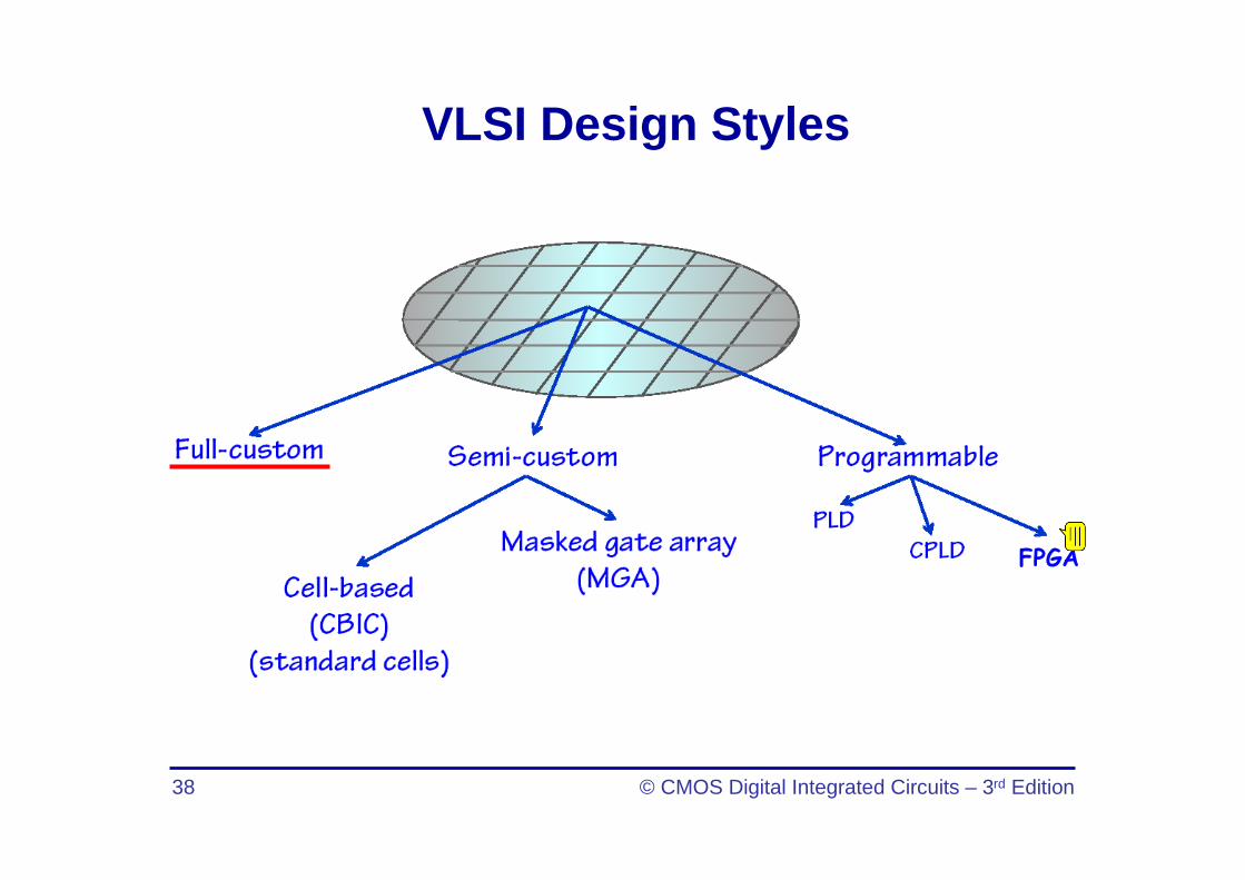
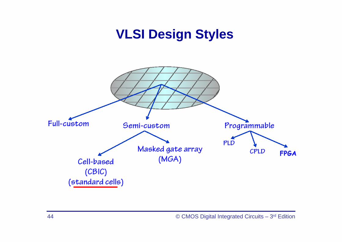
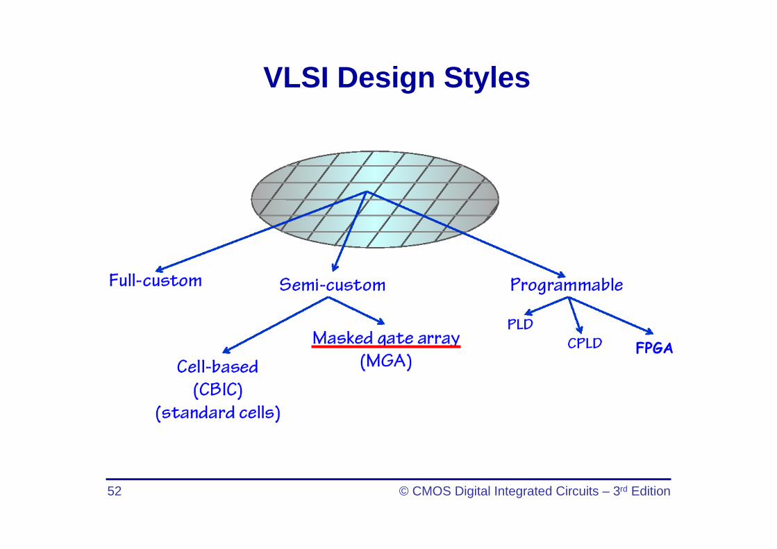
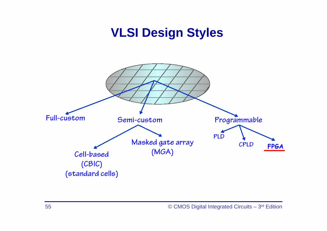
VLSI Design Styles
FPGA
39 © CMOS Digital Integrated Circuits – 3rd Edition
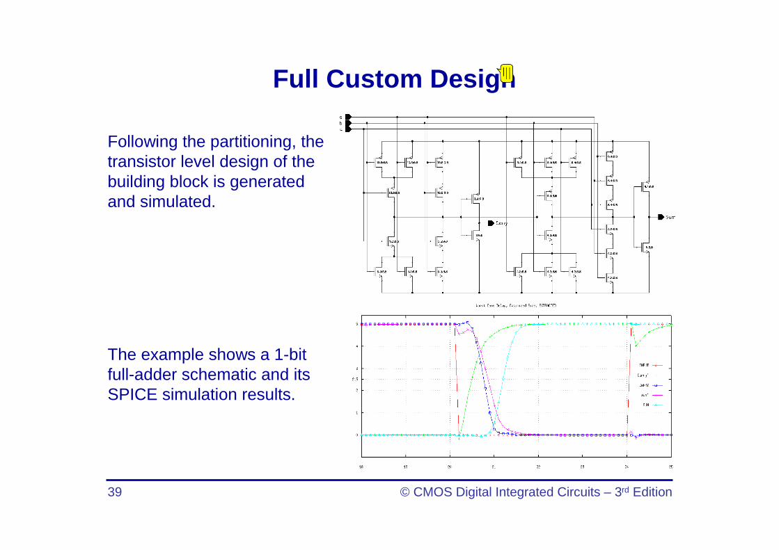
Full Custom Design
Following the partitioning, the transistor level design of the building block is generated and simulated.
The example shows a 1-bit full-adder schematic and its SPICE simulation results.
40 © CMOS Digital Integrated Circuits – 3rd Edition
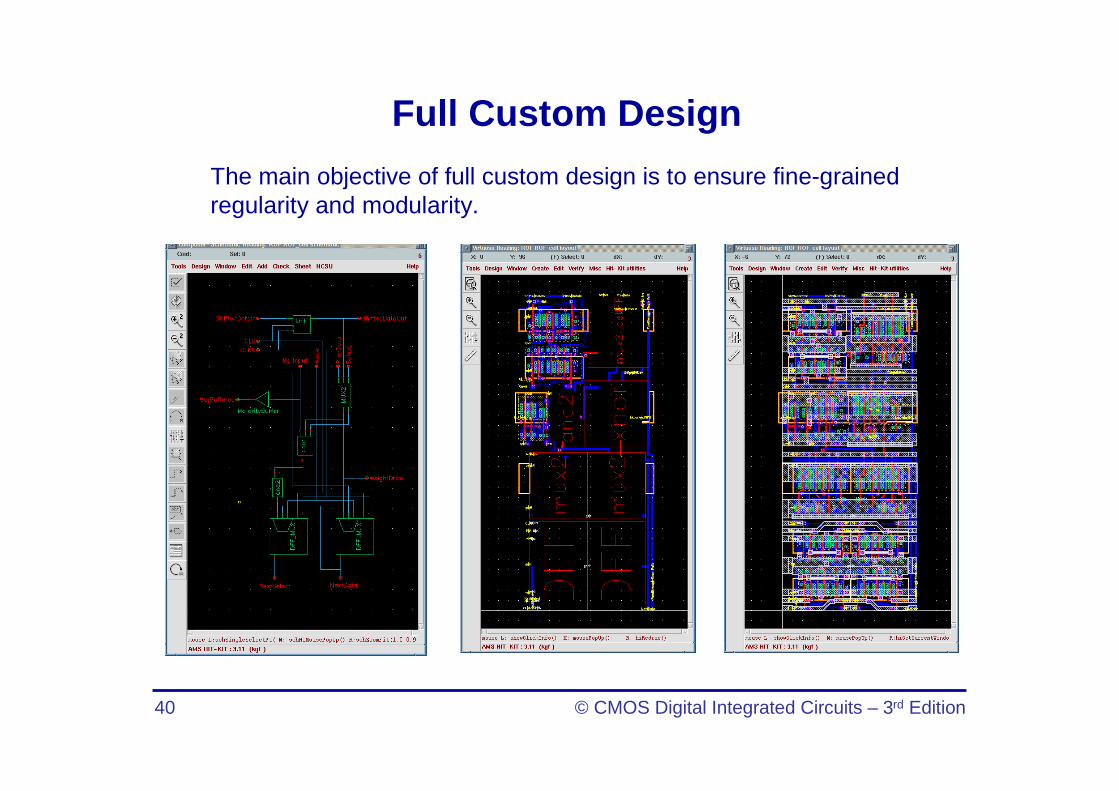
Full Custom Design
The main objective of full custom design is to ensure fine-grained regularity and modularity.
41 © CMOS Digital Integrated Circuits – 3rd Edition
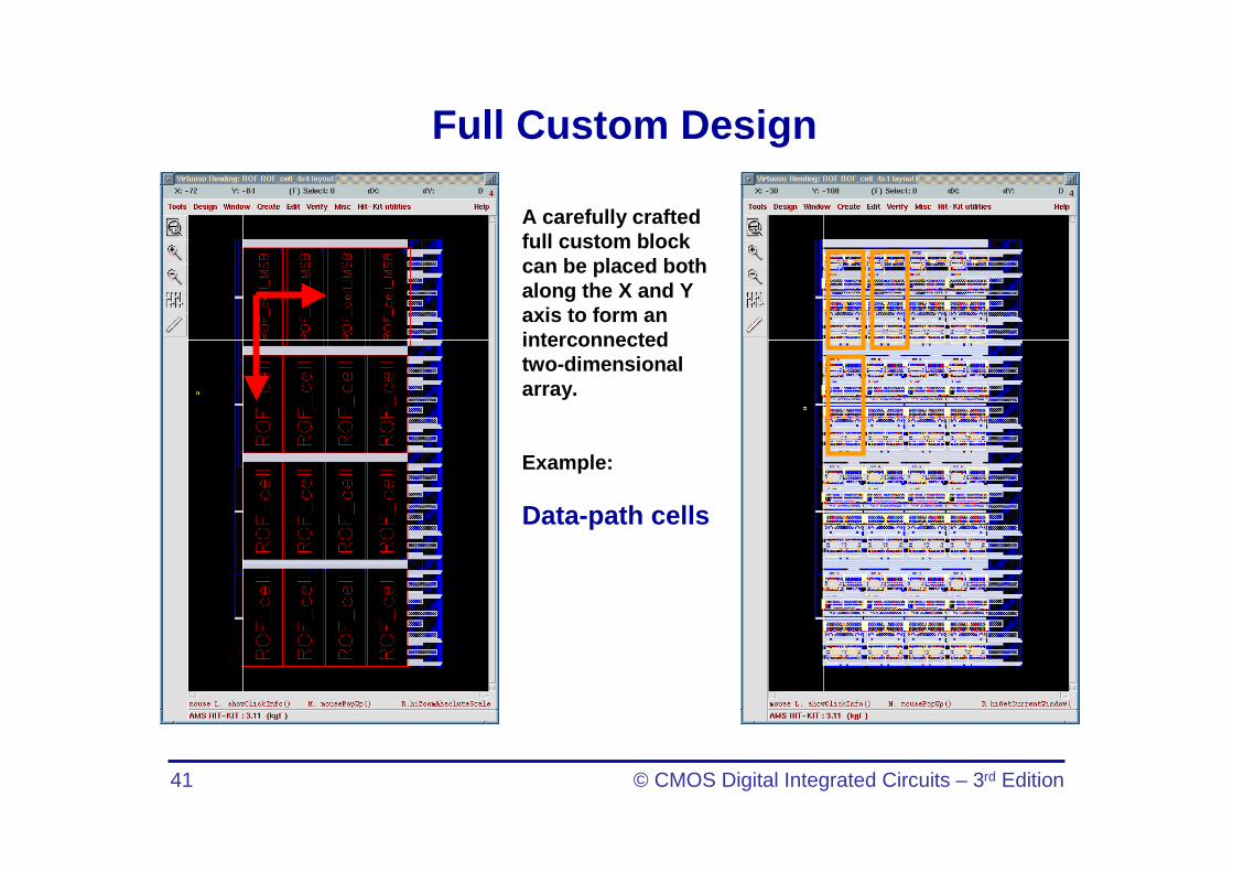
Full Custom Design
A carefully crafted full custom block can be placed both along the X and Y axis to form an interconnected two-dimensional array.
Example:
Data-path cells
42 © CMOS Digital Integrated Circuits – 3rd Edition
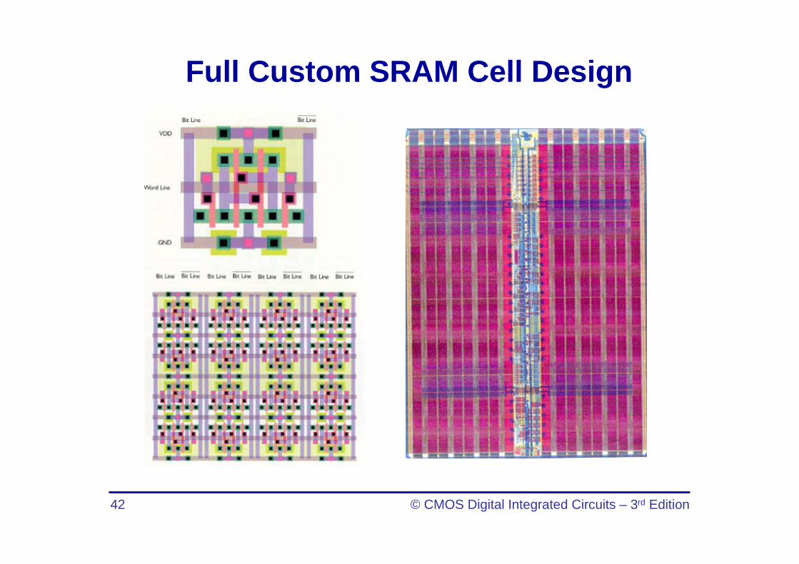
Full Custom SRAM Cell Design
43 © CMOS Digital Integrated Circuits – 3rd Edition
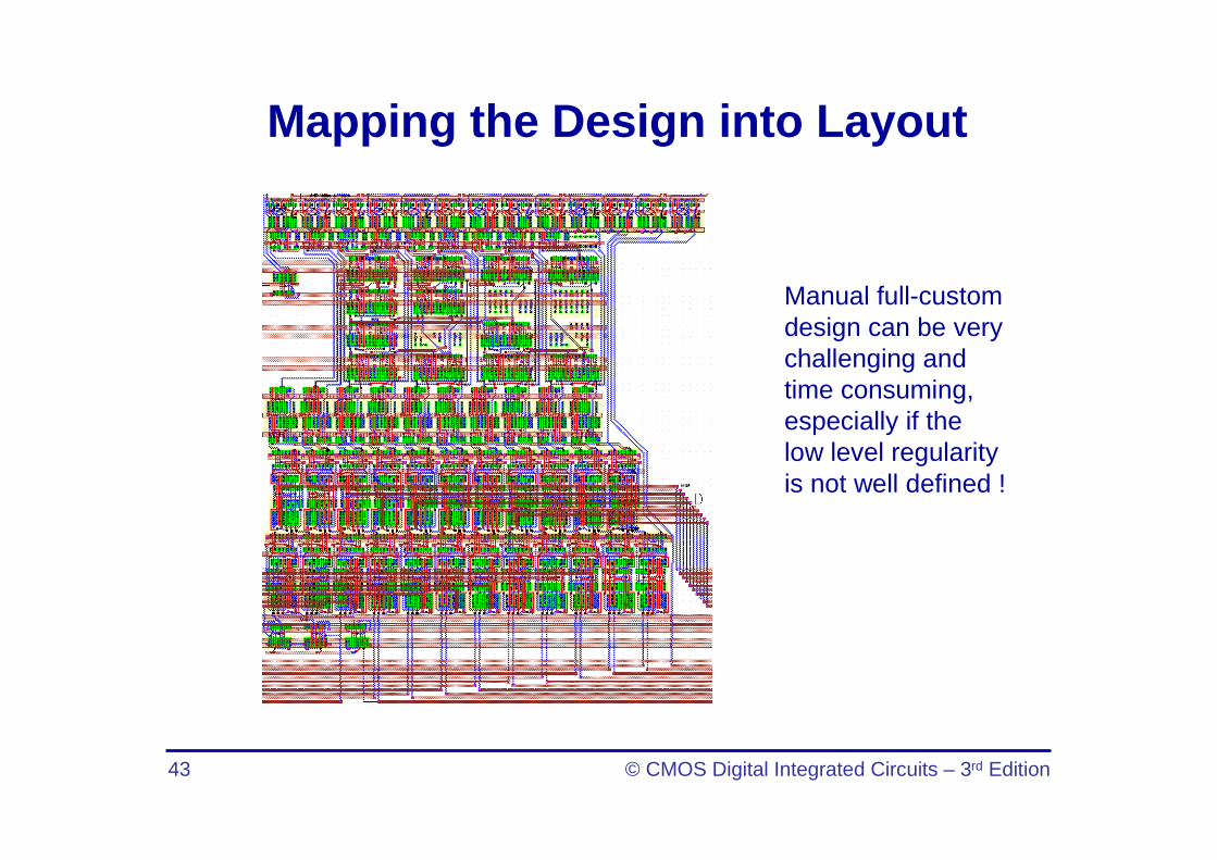
Mapping the Design into Layout
Manual full-custom design can be very challenging and time consuming, especially if the low level regularity is not well defined !
44 © CMOS Digital Integrated Circuits – 3rd Edition
VLSI Design Styles
FPGA
45 © CMOS Digital Integrated Circuits – 3rd Edition
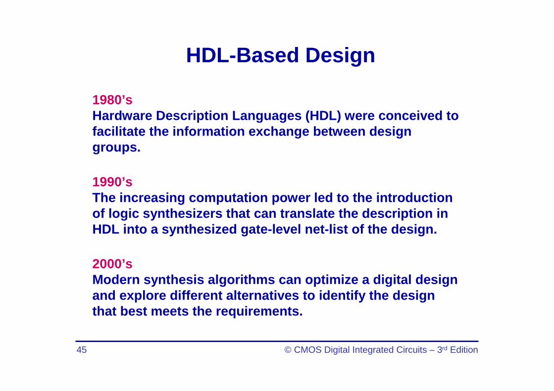
HDL-Based Design
1980’sHardware Description Languages (HDL) were conceived to facilitate the information exchange between design groups.
1990’sThe increasing computation power led to the introduction of logic synthesizers that can translate the description in HDL into a synthesized gate-level net-list of the design.
2000’sModern synthesis algorithms can optimize a digital design and explore different alternatives to identify the design that best meets the requirements.
46 © CMOS Digital Integrated Circuits – 3rd Edition
HDL-Based Design
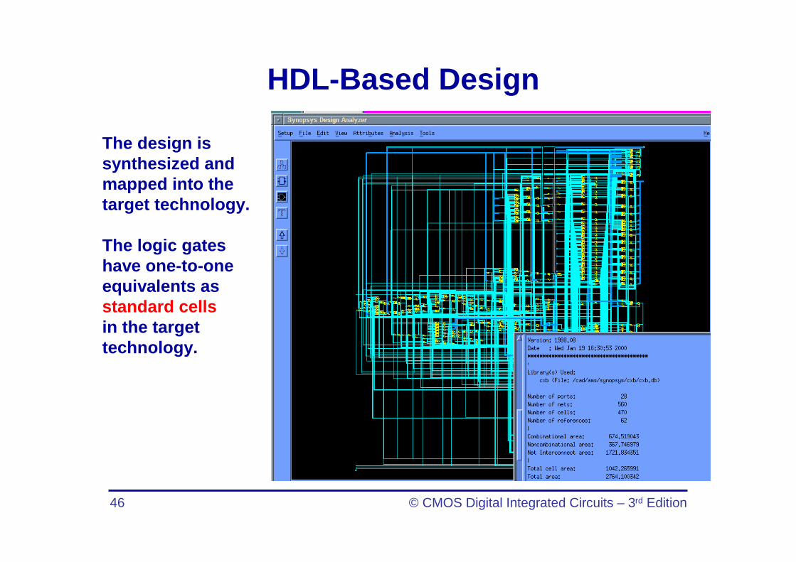
The design is synthesized and mapped into the target technology.
The logic gates have one-to-one equivalents as standard cellsin the target technology.
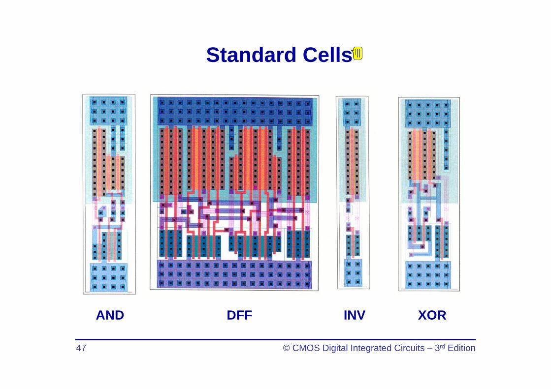
CMOS Digital Integrated Circuits
Standard CellsStandard CellsLibrary Construction
– To enable automated placement of the cells and routing of inter-cell connections, each cell layout is designed with a fixed height, so that a number of cells can be abutted side-by-side to form rows.
47
48 © CMOS Digital Integrated Circuits – 3rd Edition
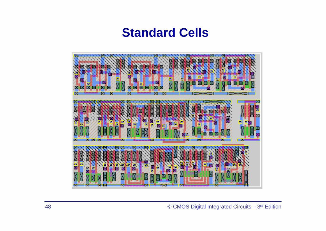
Standard Cells
CMOS Digital Integrated Circuits
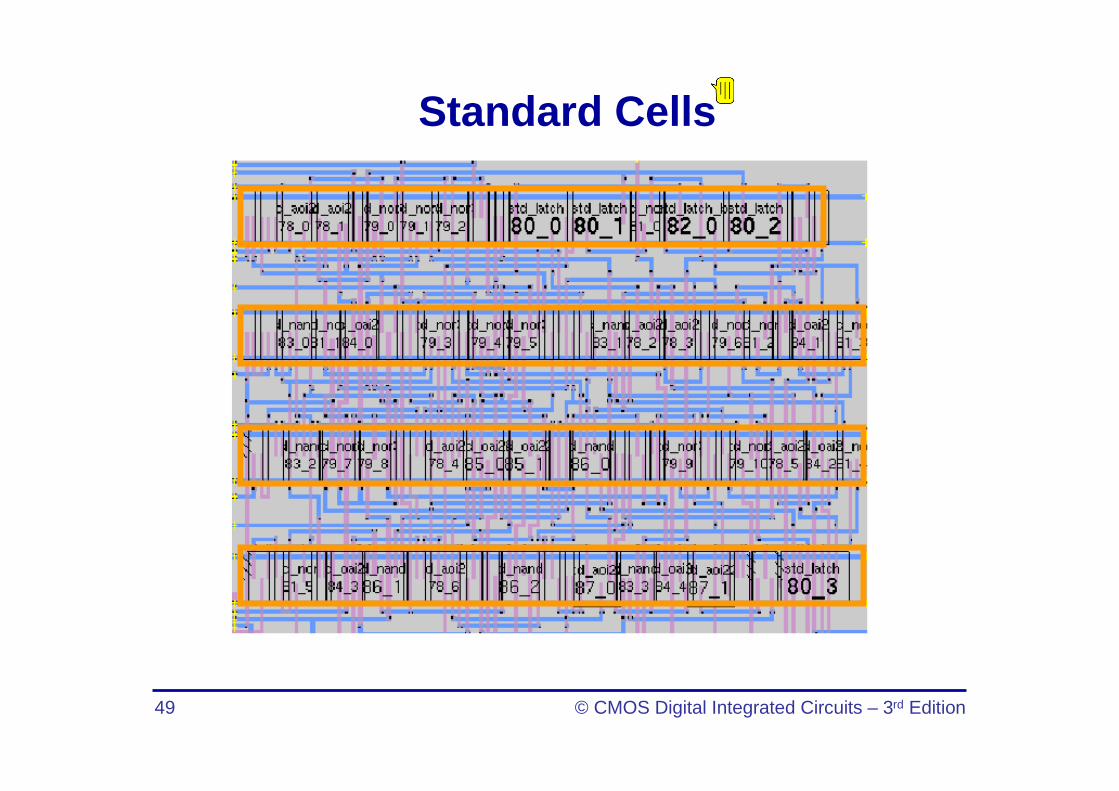
Standard CellsStandard CellsAfter chip logic design being done by using standard
cells from the library– Place the individual cells into rows– Interconnect them that meets the design goal in circuit
speed, chip area and power consumption.
49
50 © CMOS Digital Integrated Circuits – 3rd Edition
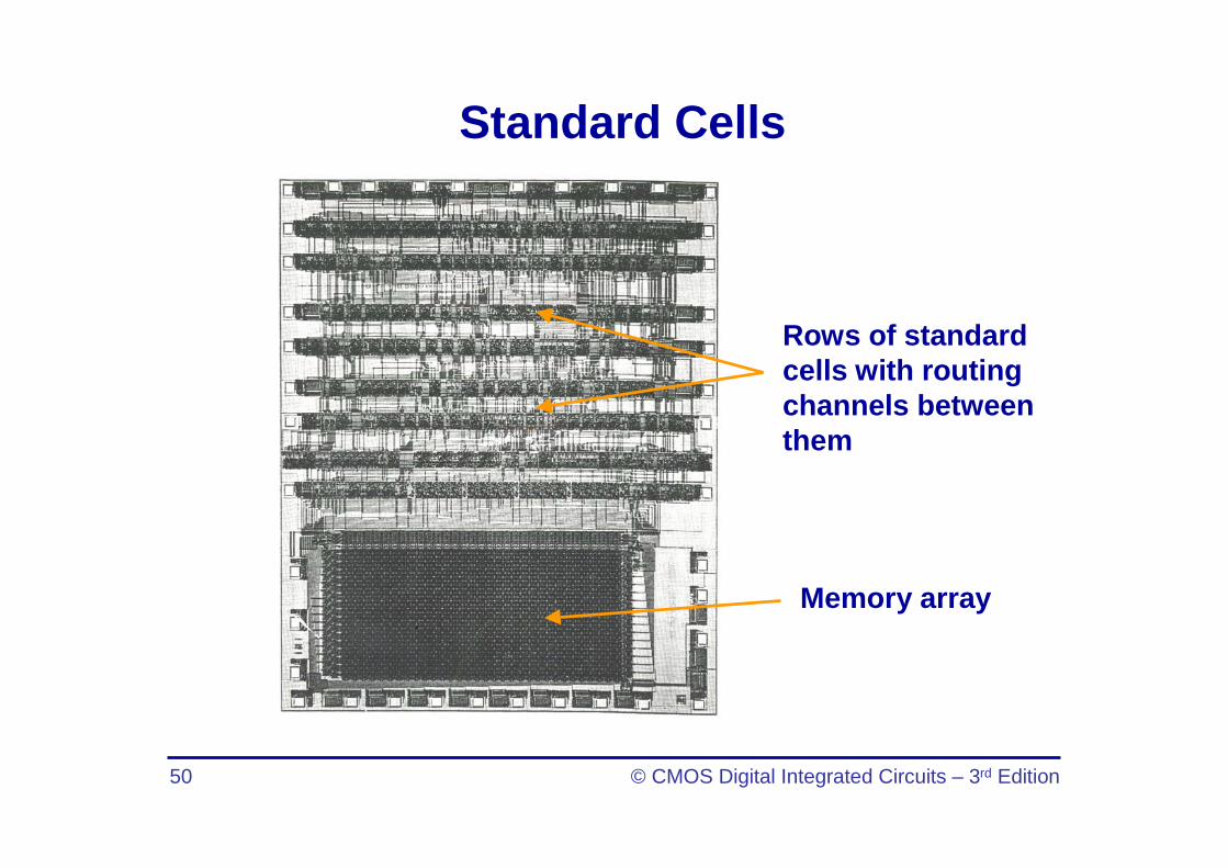
Standard Cells
Rows of standard cells with routing channels between them
Memory array
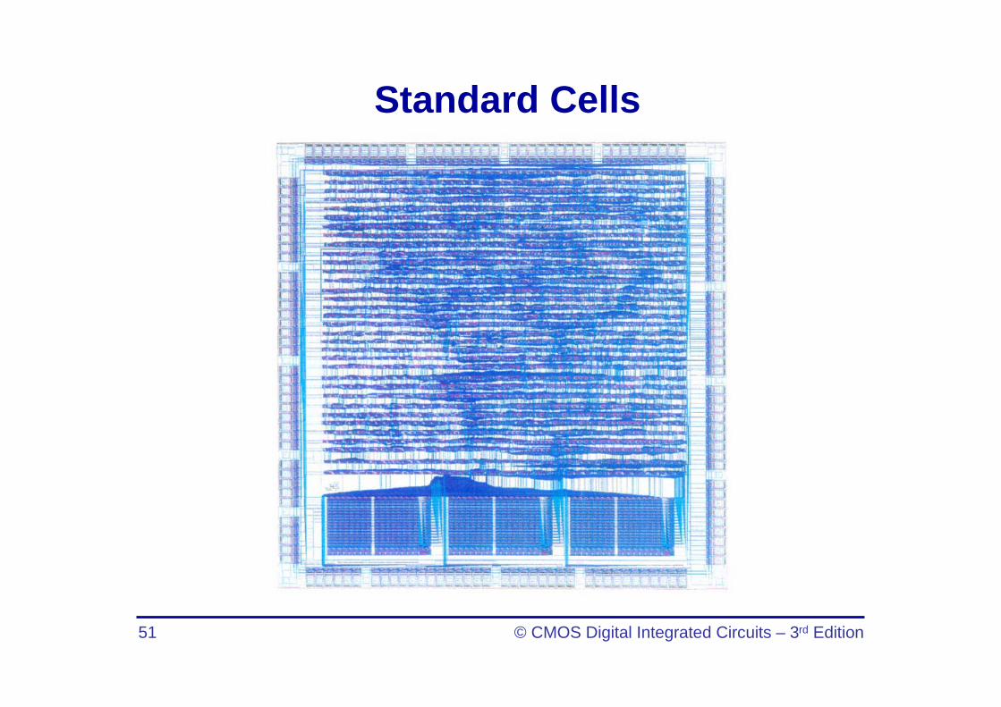
51 © CMOS Digital Integrated Circuits – 3rd Edition
Standard Cells
52 © CMOS Digital Integrated Circuits – 3rd Edition
VLSI Design Styles
FPGA
CMOS Digital Integrated Circuits
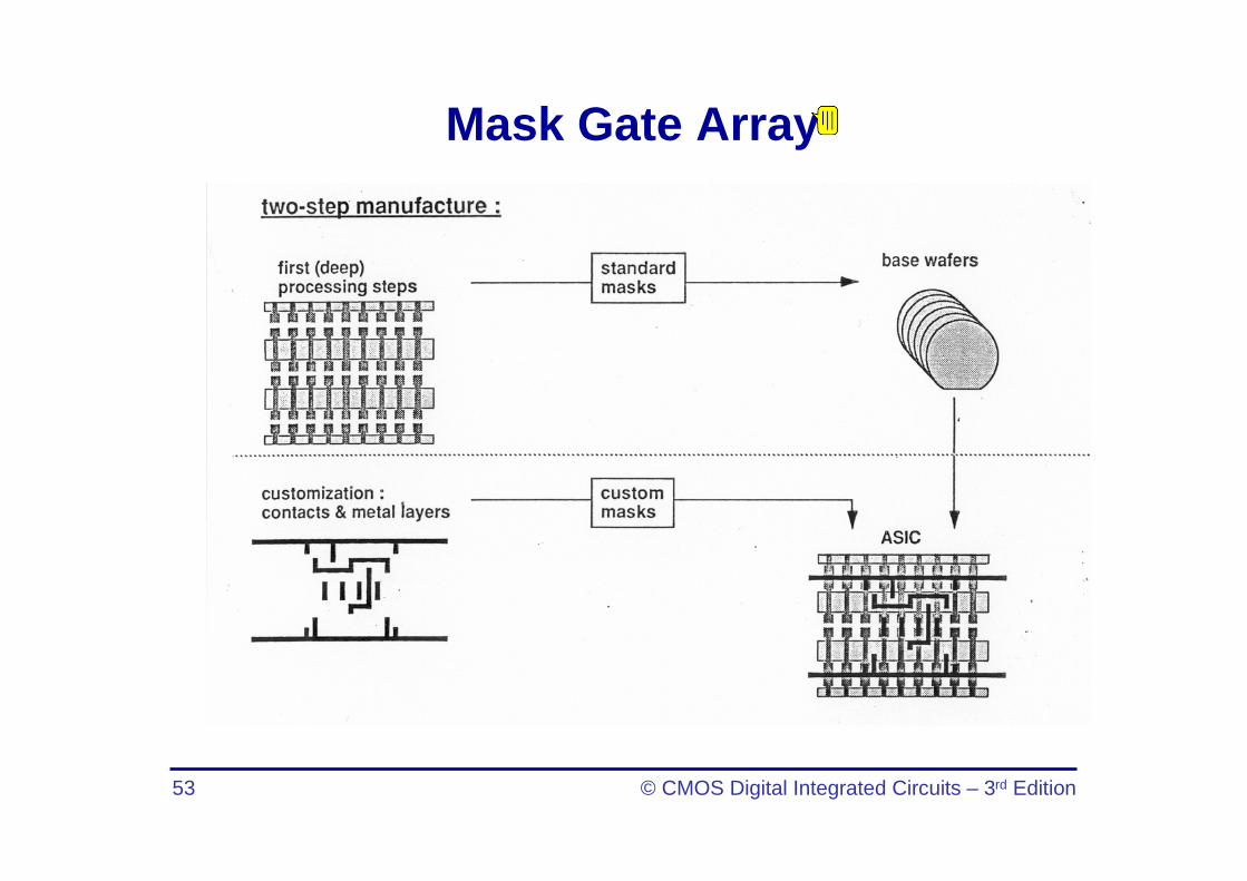
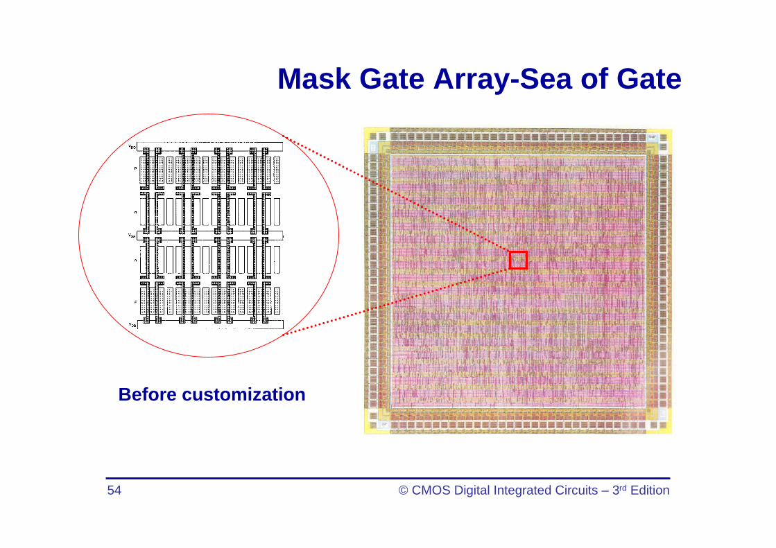
Mask Gate ArrayMask Gate Array Metal mask design and processing Chip utilization factor is higher than the FPGA and so is speed. Number of gates: hundreds of thousands of logic gates
53
54 © CMOS Digital Integrated Circuits – 3rd Edition
Mask Gate Array-Sea of Gate
Before customization
55 © CMOS Digital Integrated Circuits – 3rd Edition
VLSI Design Styles
FPGA
CMOS Digital Integrated Circuits
Field Programmable Gate Array: FPGAField Programmable Gate Array: FPGA User programming Very short turn around time Price is higher than standard cell and mask gate array. Number of gates: 25,000 ~ 20,000 gates
56
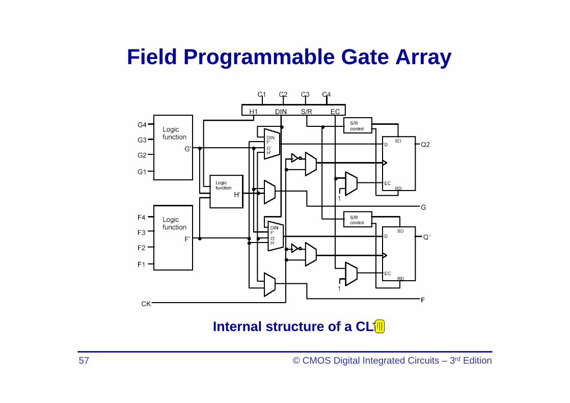
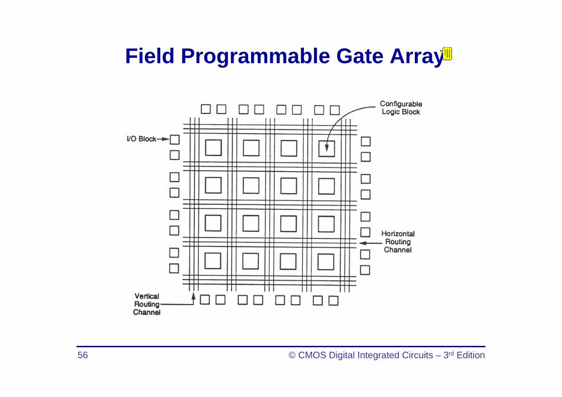
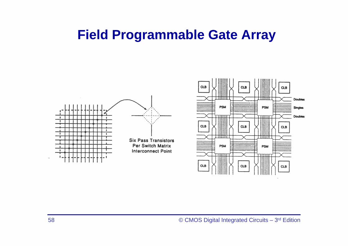
57 © CMOS Digital Integrated Circuits – 3rd Edition
Field Programmable Gate Array
Internal structure of a CLB
58 © CMOS Digital Integrated Circuits – 3rd Edition
Field Programmable Gate Array
Lec 1 1Yu-Min Lee
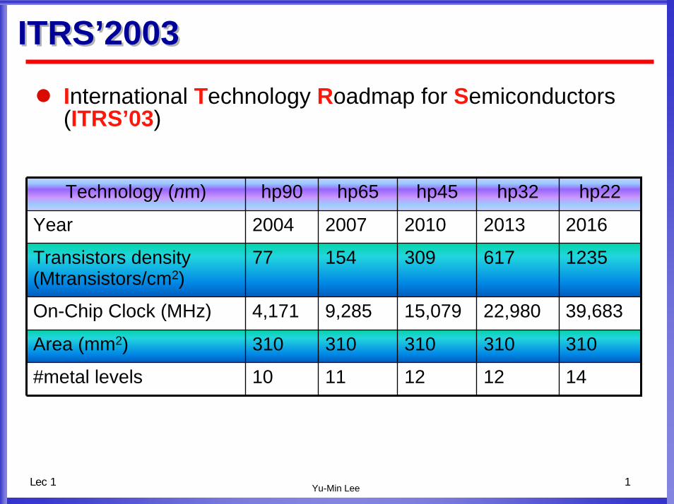
ITRS’2003ITRS’2003
¸ International Technology Roadmap for Semiconductors (ITRS’03)
Technology (nm) hp90 hp65 hp45 hp32 hp22
Year 2004 2007 2010 2013 2016
Transistors density (Mtransistors/cm2)
77 154 309 617 1235
On-Chip Clock (MHz) 4,171 9,285 15,079 22,980 39,683
Area (mm2) 310 310 310 310 310
#metal levels 10 11 12 12 14