iodine chemistry determines the defect tolerance of lead ... · 1 iodine chemistry determines the...
TRANSCRIPT

1
Iodine chemistry determines the defect tolerance of lead-
halide perovskites
Daniele Meggiolaro,a,b Silvia G. Motti,c,d Edoardo Mosconi,a,b , Alex Barkerc, James Ball,c Carlo
Andrea Riccardo Perini,c Felix Deschler,e Annamaria Petrozza,c Filippo De Angelisa,b
a Computational Laboratory for Hybrid/Organic Photovoltaics (CLHYO), CNR-ISTM, Via Elce di
Sotto 8, 06123, Perugia, Italy.
b CompuNet, Istituto Italiano di Tecnologia, Via Morego 30, 16163 Genova, Italy.
c Center for Nano Science and Technology @Polimi, Istituto Italiano di Tecnologia, via Giovanni
Pascoli 70/3, 20133, Milan, Italy.
d Dipartimento di Fisica, Politecnico di Milano, Piazza Leonardo da Vinci, 32, 20133 Milano, Italy.
eCavendish Laboratory, University of Cambridge, JJ Thomson Avenue, Cambridge, CB3 0HE, UK
Supplementary Information
1.1 SHR theory:
Trapping at defects induces non-radiative recombination, whose rate (R) is defined as:
𝑅 =𝑛𝑝 ‒ 𝑛2
𝑖
𝜏𝑝(𝑛 + 𝑛1) + 𝜏𝑛(𝑝 + 𝑝1) (1)
where n, p, and ni are the electron/hole carrier densities and intrinsic carriers density, respectively;
τp,n are the holes and electrons lifetimes; and ; 𝑛1 = 𝑁𝐶𝑒𝑥𝑝( ‒
𝐸𝑐 ‒ 𝐸𝑇
𝑘𝑇) 𝑝1 = 𝑁𝑉𝑒𝑥𝑝( ‒
𝐸𝑇 ‒ 𝐸𝑉
𝑘𝑇)
and ET is the energy of the considered trap (EC and EV are the conduction and valence band
energies, with related NC and NV density of states).
1.2 Accuracy of calculated DFEs
Electronic Supplementary Material (ESI) for Energy & Environmental Science.This journal is © The Royal Society of Chemistry 2018

2
The DFEs have been calculated by using the equation
𝐷𝐹𝐸(𝑋𝑞) = 𝐸(𝑋𝑞) ‒ 𝐸(𝑝𝑒𝑟𝑓) ‒ ∑𝑖
𝑛𝑖𝜇𝑖 + 𝑞(𝐸𝐹 + 𝑉 + ∆𝑉) + 𝐸𝑞(𝑐𝑜𝑟𝑟) (2)
where E(Xq) is the energy of the defect supercell, E(perf) the energy of the pristine supercell, n and
µ are the number and the chemical potentials of the species added or subtracted to the perfect bulk
in order to form the defect. The last term represents the energy associated to the exchange of
electrons with the electrons reservoir (the Fermi level of the system), referenced to the valence band
maximum (VBM) of the pristine crystal and corrected for the electrostatic potential shift and the
charged defects images interactions. The chemical potentials of the atomic species have been set in
order to simulate three different chemical conditions, namely I-rich, I-medium and I-poor
conditions, under the constraint of the thermodynamic stability of the MAPbI3 phase. The chemical
potentials of MAPbI3 constituents, i.e. Pb, I and MA, in thermodynamic equilibriums with the PbI2
and MAI phases, have been evaluated by imposing the following relations among the chemical
potentials
𝜇(𝑀𝐴) + 𝜇(𝑃𝑏) + 3𝜇(𝐼) = Δ𝑓𝐻(𝑀𝐴𝑃𝑏𝐼3) (3)
𝜇(𝑀𝐴) + 𝜇(𝐼) < Δ𝑓𝐻(𝑀𝐴𝐼) (4)
𝜇(𝑃𝑏) + 2𝜇(𝐼) = Δ𝑓𝐻(𝑃𝑏𝐼2) (5)
where the chemical potentials of the species I and Pb has been referenced to the value of the I2
molecule and Pb bulk metal, respectively.
A preliminary analysis carried out at different levels of theory confirms that for an accurate
estimate of the DFEs in MAPbI3 inclusion of both spin-orbit coupling and exact exchange are
essential. These affect two main terms of the DFEs energies (Equation 2 above), namely the lattice
energy due to the relaxation of the ions upon the formation of the defect and the electronic energy
due to the charge exchange with the Fermi level. While the Perdew-Burke-Ernzerhof (PBE)1
exchange-correlation functional provides good geometries and lattice energies, the electronic
3
structure of the perovskite obtained by this approximation is not sufficiently accurate for a correct
estimate of the DFEs.
The equilibrium geometries of the defects supercells and simple phases, i.e. PbI2, MAI and
I2, have been found by using the PBE exchange-correlation functional. US pseudopotentials with a
cutoff on the plane waves of 40 Ryd (320 Ryd on the charge density) and converged uniform k-
points grids in the Brillouin zone (BZ) have been used. For defective supercells, with lattice
constants of a=b=17.698 Å, c=12.642 Å, calculations have been performed by using the 1x1x2
kpoint grids in the Brillouin Zone (BZ). Pseudopotentials with 7, 4, 5 and 1 valence electrons have
been used for I, C, N and H, while a 14 valence electrons pseudopotential for the Pb element has
been used by including semi-core Pb 5d states. The band edges of MAPbI3 are characterized by
large contributions of the I 5p orbitals to the top of the valence band (VB), with minor contributions
of the Pb s states, while the bottom of the conduction band is dominated by the Pb 6p orbitals. The
inclusion of spin orbit coupling (SOC) with the same converged parameters of above leads to a
remarkable decrease of the band gap to a value of 0.55 eV. As expected, the inclusion of SOC at the
PBE level leads to a large stabilization of the unoccupied 6p state of Pb of about 0.8 eV and to a
destabilization of the occupied 5p states of I ions of about 0.19 eV. 2
Heats of formation of the MAPbI3 phase starting from the PbI2 and MAI have been obtained
of -0.15 and -0.18 eV at the PBE and PBE-SOC levels of theory, highlighting a limited stability of
the MAPbI3 perovskite. The self-interaction error responsible of the strong underestimate of the
band gap has been corrected by introducing a fraction of exact exchange through the HSE06
functional 3 (α=0.43), following the approach of Du.4 Hybrid calculations, spin orbit coupling
included, have been carried out at the relaxed PBE geometries and by using norm-conserving (NC)
pseudopotentials. A norm conserving pseudopotential with 22 valence electrons for Pb has been
used, by including the Pb 5s and 5p states, which ensures an accurate reproduction of MAPbI3 band
gap and band edges against GW calculations.5 For the other elements, pseudopotentials with the
same number of valence electrons as in the US case have been used. To reduce the computational
4
effort, hybrid SOC calculations have been performed by using a plane wave cutoff of 40 Ryd,
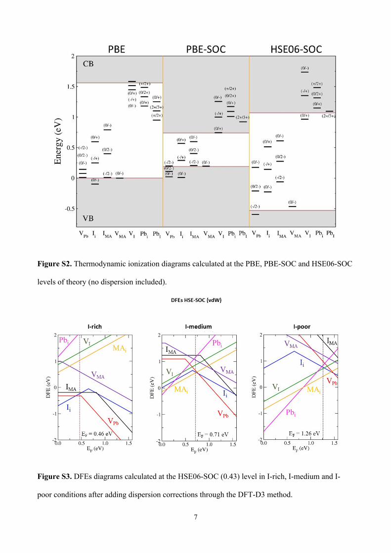
without affecting the accuracy of the calculations. In table S1 and S2 a comparison of calculated
DFEs at the PBE-SOC level with 14 electrons Pb US pseudopotentials (cutoff on the plane waves
of 40 Ryd, 320 Ryd on the charge density) and NC pseudopotentials with the 22 electrons Pb
pseudopotential (cutoff on the plane waves 40 Ryd) is reported. Two hybrid benchmark calculations
have been also performed for Ii and VPb2- defects by using a cutoff on plane waves of 70 Ryd. The
calculated DFEs for these two defects in I-rich conditions are 0.88 and 0.84 eV for Ii and VPb2-
respectively, to be compared with results obtained with a cutoff of 40 Ryd of 0.93 and 0.83 eV. As
it can be seen, only limited deviations in the results are reported, confirming the good convergence
of our calculations.
By using the HSE06 functional and including the SOC a band gap of 1.58 eV has been
obtained for MAPbI3, in good agreement with experiments and previous calculations.2,4 The
calculated electronic band edges at the HSE06-SOC level reports a large downshift of the VB and
CB of 0.53 eV and 0.5 eV compared to the PBE level of theory, see Figure S2. The shift of the band
edges obtained by using the HSE06 functional are also in agreement with results of a benchmark
G0W0 calculation,5 confirming the reliability of our approach.
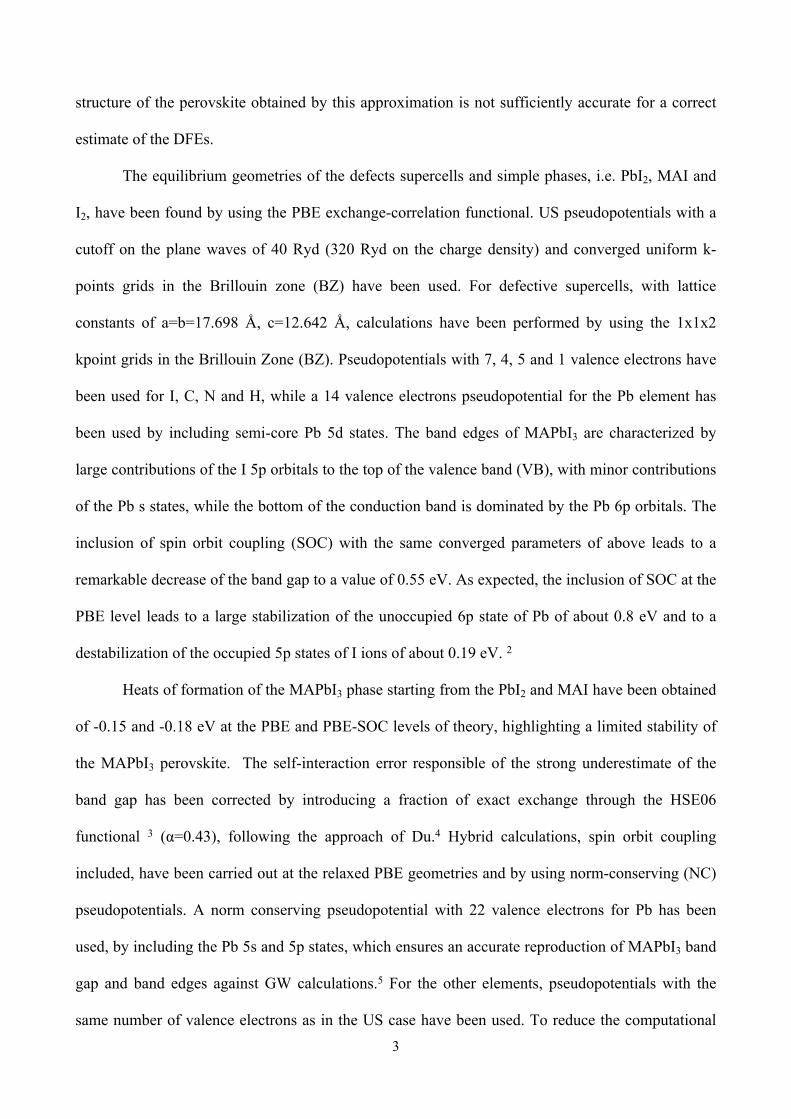
The DFEs calculated by the PBE, PBE-SOC and HSE06-SOC levels of theory are reported
in Figure S1, for I-rich, I-medium and I-poor conditions, without including dispersion corrections
for a direct comparison of electronic energies. Furthermore, the values of the calculated DFEs at
EF=0 (VBM) for neutral and charged defects have been reported in Table S1 and S2. As it can be
seen the calculated DFEs show strong deviations among the different levels of theory. The inclusion
of SOC at the PBE level leads to the overall stabilization of neutral defects (see Table S1), while
regarding charged defects a stabilization of negative charged species and a destabilization of
positive species, proportionally to the charge of the defect, is seen (Table S2). The opposite occurs
at the HSE06-SOC level.

5
The inclusion of SOC and exact exchange in the HSE06-SOC calculations clearly points out
the emergence of new deep levels in the band gap compared to the PBE approach, as in the case of
the (0/-) and (-/2-) transitions of Ii and IMA defects (Figure S2). These results are in good agreement
with previous results by Du.4 Furthermore, higher native Fermi levels calculated at the HSE06-SOC
levels, compared to PBE calculations are found (Figure S1).

6
Figure S1. DFE diagrams calculated at the PBE, PBE-SOC and HSE06 levels of theory for I-rich,
I-medium and I-poor conditions of growth (dispersions corrections not included).
7
Figure S2. Thermodynamic ionization diagrams calculated at the PBE, PBE-SOC and HSE06-SOC
levels of theory (no dispersion included).
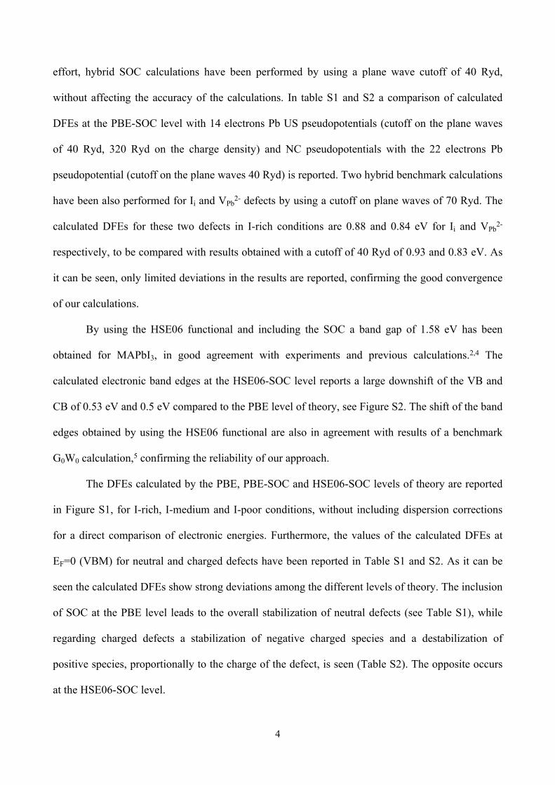
Figure S3. DFEs diagrams calculated at the HSE06-SOC (0.43) level in I-rich, I-medium and I-
poor conditions after adding dispersion corrections through the DFT-D3 method.
8
Table S1. Influence of the spin-orbit coupling and the electronic exchange on the DFEs of neutral
defects in I-rich conditions. US calculations have been carried out by using US pseudopotentials
(Pb 14 electrons) and a cutoff on PWs of 40 Ryd (320 Ryd for the charge density). NC*
calculations have been carried out by using the 22 electrons Pb pseudo and a cutoff of 40 Ryd on
the PWs.
Table S2. Influence of the spin-orbit coupling and the electronic exchange on the DFEs of charged
defects calculated at EF=0 in I-rich conditions. Values are in eV. US calculations have been carried
out by using US pseudopotentials (Pb 14 electrons) and a cutoff on PWs of 40 Ryd (320 Ryd for the
charge density). NC* calculations have been carried out by using the 22 electrons Pb pseudo and a
cutoff of 40 Ryd on the PWs.
Acceptors VPb2- Ii
- VMA- IMA
2-
PBE (US) 0.21 0.70 0.11 0.83
(eV) VI Ii VPb Pbi IMA VMA
PBE (US) 2.11 0.80 0.01 4.02 -0.04 0.11
PBE-SOC (US) 1.17 0.71 -0.06 3.36 -0.08 -0.06
PBE-SOC (NC*) 1.19 0.77 -0.04 3.39 -0.10 -0.08
HSE06-SOC (NC*) 1.87 0.93 0.19 4.19 0.20 0.67
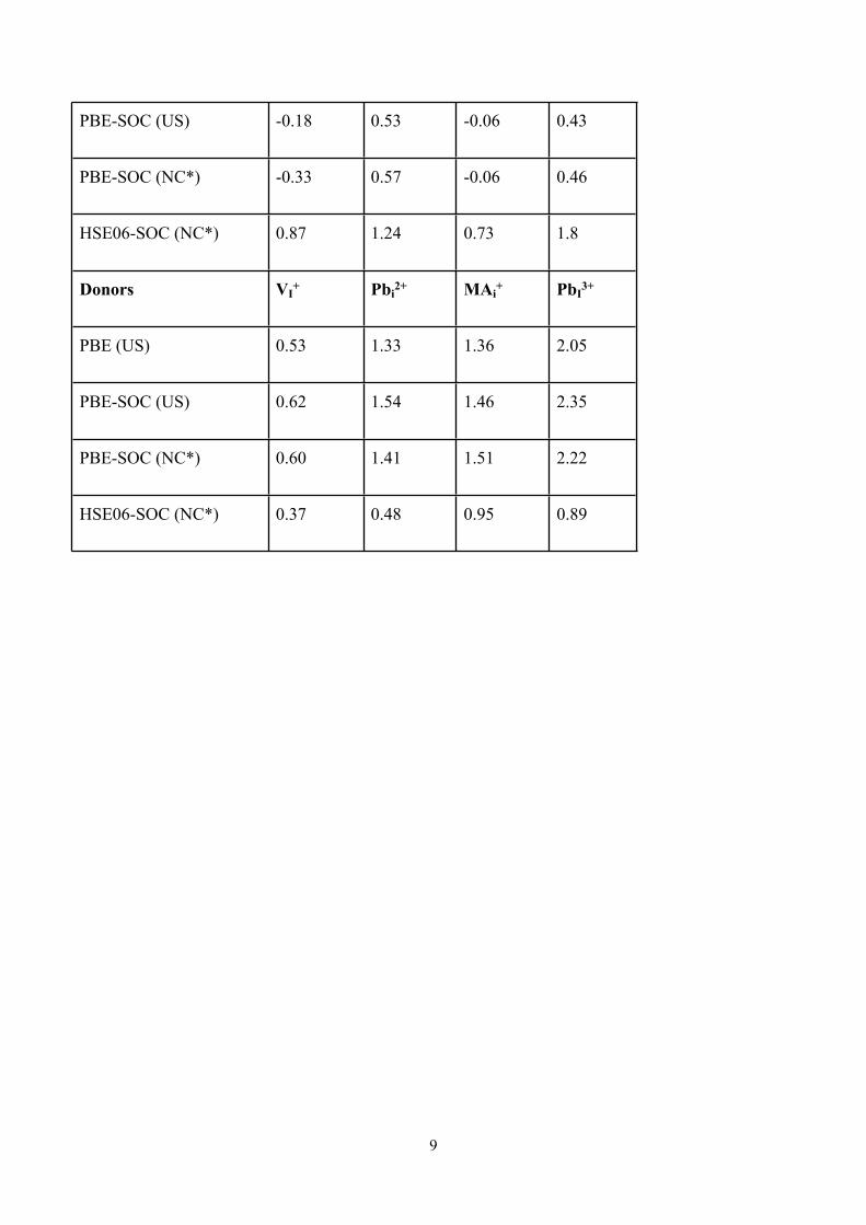
9
PBE-SOC (US) -0.18 0.53 -0.06 0.43
PBE-SOC (NC*) -0.33 0.57 -0.06 0.46
HSE06-SOC (NC*) 0.87 1.24 0.73 1.8
Donors VI+ Pbi
2+ MAi+ PbI
3+
PBE (US) 0.53 1.33 1.36 2.05
PBE-SOC (US) 0.62 1.54 1.46 2.35
PBE-SOC (NC*) 0.60 1.41 1.51 2.22
HSE06-SOC (NC*) 0.37 0.48 0.95 0.89

10
Table S3. Stable states of charge, DFEs and defect densities calculated at the native Fermi level in
iodine-medium conditions.
Defect Charge DFE (eV) Density (cm-3)
VPb 2- 0.66 1010
MAi + 0.57 1012
Ii + / - 0.72/0.60 1010/1012
VI+ + 0.87 107
Pbi2+ 2+ 1.16 102
VMA - 1.06 104
IMA 2- 1.44 0
11
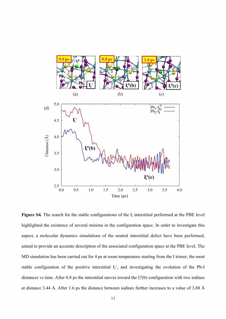
Figure S4. The search for the stable configurations of the Ii interstitial performed at the PBE level
highlighted the existence of several minima in the configuration space. In order to investigate this
aspect, a molecular dynamics simulations of the neutral interstitial defect have been performed,
aimed to provide an accurate description of the associated configuration space at the PBE level. The
MD simulation has been carried out for 4 ps at room temperature starting from the I trimer, the most
stable configuration of the positive interstitial Ii+, and investigating the evolution of the Pb-I
distances vs time. After 0.8 ps the interstitial moves toward the Ii0(b) configuration with two iodines
at distance 3.44 Å. After 1.6 ps the distance between iodines further increases to a value of 3.88 Å
12
in a rhombus in the ab plane, here called Ii0(c). Both the Ii
0(b) and the Ii0(c) configurations are less
stable than the Ii0(a) configuration at the HSE06-SOC level of 0.18 and 0.44 eV, respectively.
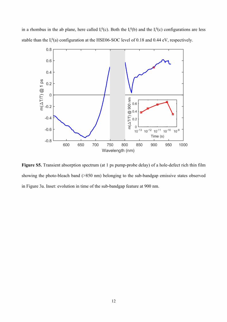
Figure S5. Transient absorption spectrum (at 1 ps pump-probe delay) of a hole-defect rich thin film
showing the photo-bleach band (>850 nm) belonging to the sub-bandgap emissive states observed
in Figure 3a. Inset: evolution in time of the sub-bandgap feature at 900 nm.

13
Figure S6. Transient absorption spectra of MAPbI3 at various delay times.
Figure S7. MAPbI3: Temperature dependent transient absorption shows fast recombination due to
emissive band-to-band recombination at early times (up to ~30 ns), followed by extremely slow
recombination of trapped electrons. With increasing temperature, we see faster band-to-band
recombination, and a higher number of long-lived trapped electrons.

14
15
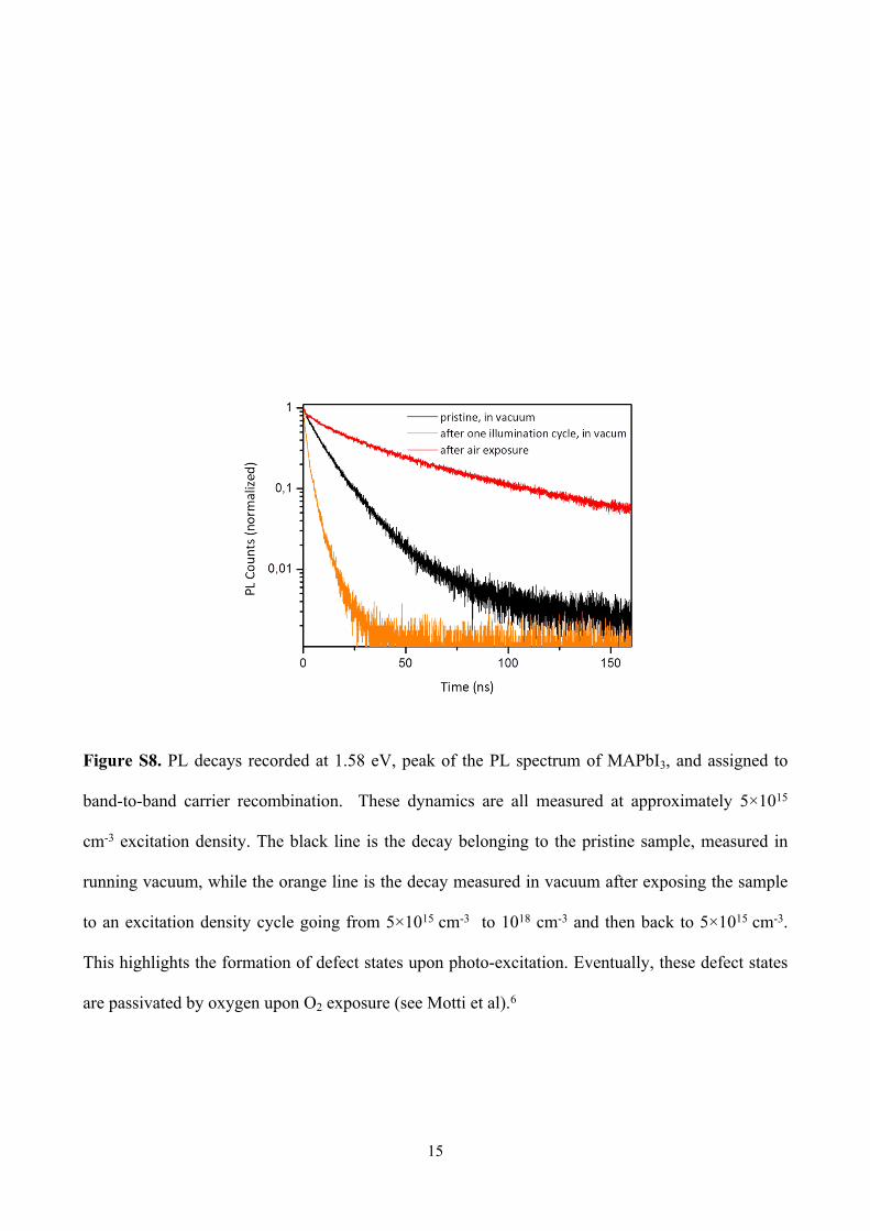
Figure S8. PL decays recorded at 1.58 eV, peak of the PL spectrum of MAPbI3, and assigned to
band-to-band carrier recombination. These dynamics are all measured at approximately 5×10¹⁵
cm-3 excitation density. The black line is the decay belonging to the pristine sample, measured in
running vacuum, while the orange line is the decay measured in vacuum after exposing the sample
to an excitation density cycle going from 5×1015 cm-3 to 1018 cm-3 and then back to 5×1015 cm-3.
This highlights the formation of defect states upon photo-excitation. Eventually, these defect states
are passivated by oxygen upon O2 exposure (see Motti et al).6

16
Figure S9. a-d) Equilibrium structures of the positive, neutral, negative Br interstitials and of the
negative I interstitial with a substitutional BrI, respectively. e-h) Equilibrium structures of the
positive, neutral, negative Cl interstitials, and of the negative I interstitial with a substitutional ClI,
respectively.

17
Table S4. Defects formation energies of substitutional and interstitials iodine, bromine and chlorine
in the lowest doping limits at the native Fermi level of the MAPbI3 in I-medium conditions. The
DFEs have been calculated for the different states of charge at the HSE-SOC (0.43) level of theory,
by including dispersions. A direct comparison of the energies calculated for a supercell with iodine
interstitial and a substitutional Br (Cl) on the I site and a supercell with Br (Cl) interstitials, both in
the negative states, shows that the substitution of I interstitial by a Br (Cl) ion is favoured by 0.07
eV (0.07 eV), as calculated at the HSE-SOC (0.43) level.
DFEs (eV) (+) 0 (-)
Ii 0.66 1.02 0.66
Bri
BrI
0.74
0.02
1.12
0.02
0.50
0.02
Cli
ClI
0.81
0.01
1.02
0.01
0.37
0.01
18
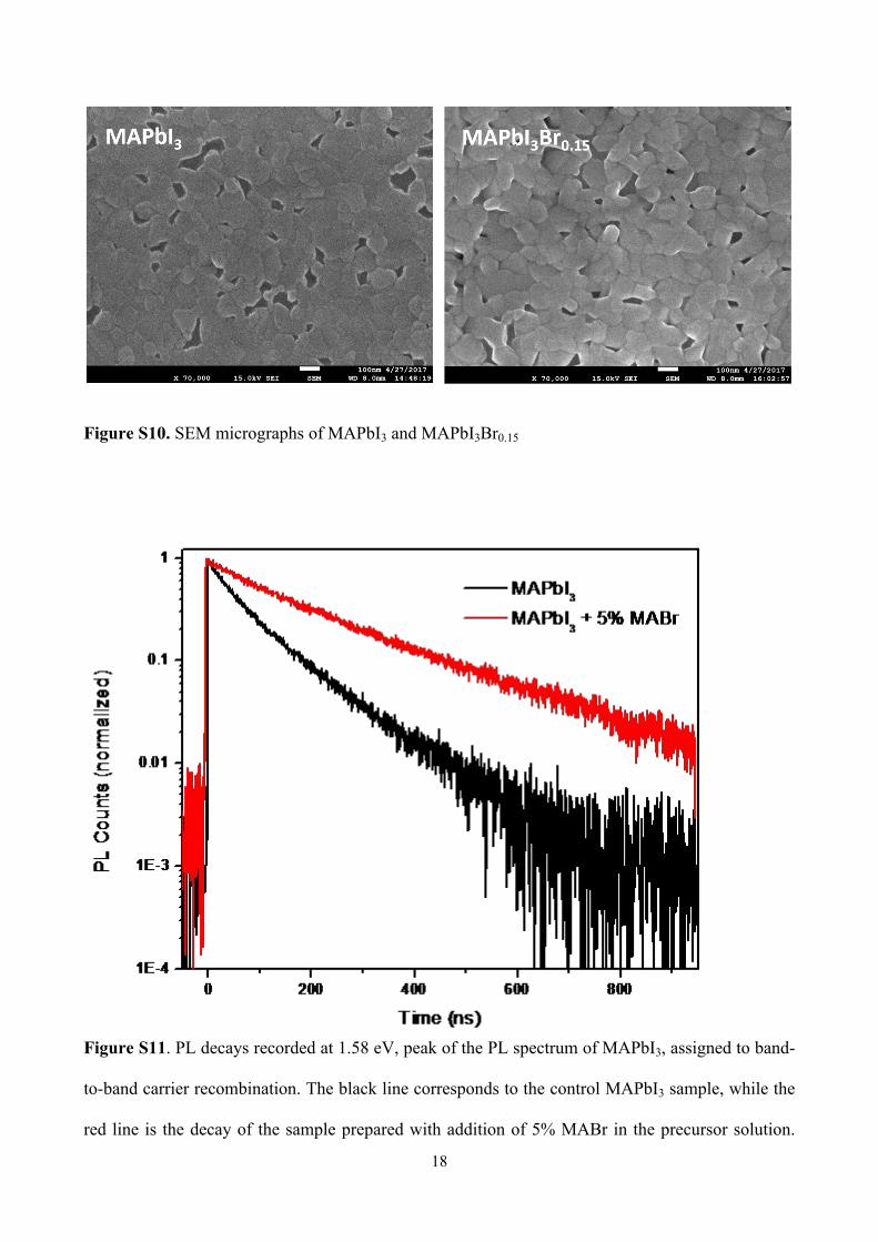
Figure S10. SEM micrographs of MAPbI3 and MAPbI3Br0.15
Figure S11. PL decays recorded at 1.58 eV, peak of the PL spectrum of MAPbI3, assigned to band-
to-band carrier recombination. The black line corresponds to the control MAPbI3 sample, while the
red line is the decay of the sample prepared with addition of 5% MABr in the precursor solution.

19
Both dynamics were measured at approximately 2×1014 cm-3 excitation density and under active
vacuum.
Figure S12. TA dynamics probed at the photo-bleach band at 1.61 eV of the transient absorption
spectrum of MAPbI3 (red line) and MAPbI3Br0.15 (blue line).
20
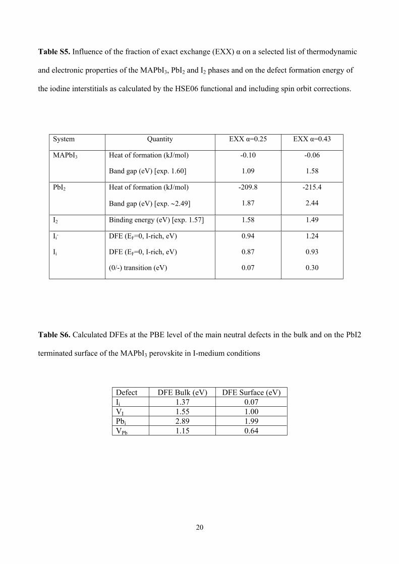
Table S5. Influence of the fraction of exact exchange (EXX) α on a selected list of thermodynamic
and electronic properties of the MAPbI3, PbI2 and I2 phases and on the defect formation energy of
the iodine interstitials as calculated by the HSE06 functional and including spin orbit corrections.
System Quantity EXX α=0.25 EXX α=0.43
MAPbI3 Heat of formation (kJ/mol)
Band gap (eV) [exp. 1.60]
-0.10
1.09
-0.06
1.58
PbI2 Heat of formation (kJ/mol)
Band gap (eV) [exp. 2.49]
-209.8
1.87
-215.4
2.44
I2 Binding energy (eV) [exp. 1.57] 1.58 1.49
Ii-
Ii
DFE (EF=0, I-rich, eV)
DFE (EF=0, I-rich, eV)
(0/-) transition (eV)
0.94
0.87
0.07
1.24
0.93
0.30
Table S6. Calculated DFEs at the PBE level of the main neutral defects in the bulk and on the PbI2
terminated surface of the MAPbI3 perovskite in I-medium conditions
Defect DFE Bulk (eV) DFE Surface (eV)Ii 1.37 0.07VI 1.55 1.00Pbi 2.89 1.99VPb 1.15 0.64

21

22
References
1. Perdew, J. P.; Burke, K.; Ernzerhof, M., Generalized Gradient Approximation Made Simple. Phys. Rev. Lett. 1996, 77, 3865-3868.2. Mosconi, E.; Amat, A.; Nazeeruddin, M. K.; Graetzel, M.; De Angelis, F., First-Principles Modeling of Mixed Halide Organometal Perovskites for Photovoltaic Applications. Journal of Physical Chemistry C 2013, 117, 13902−13913.3. Heyd, J.; Scuseria, G. E.; Ernzerhof, M., Hybrid functionals based on a screened Coulomb potential. The Journal of Chemical Physics 2003, 118, 8207-8215.4. Du, M.-H., Density Functional Calculations of Native Defects in CH3NH3PbI3: Effects of Spin–Orbit Coupling and Self-Interaction Error. J. Phys. Chem. Lett. 2015, 6, 1461-1466.5. Umari, P.; Mosconi, E.; De Angelis, F., Relativistic GW calculations on CH3NH3PbI3 and CH3NH3SnI3 Perovskites for Solar Cell Applications. Sci. Rep. 2014, 4, 4467.6. Motti, S. G.; Gandini, M.; Barker, A. J.; Ball, J. M.; Srimath Kandada, A. R.; Petrozza, A., Photoinduced Emissive Trap States in Lead Halide Perovskite Semiconductors. ACS Energy Letters 2016, 1, 726-730.