iot se nsor hub dat asheet - main -...
TRANSCRIPT

IoT Sensor Hub Datasheet
Part Number: SH100
rev 003
Zenseio LLC
Updated: August 2016
Copyright 2016 Zenseio LLC. Zenseio name and logo are trademarks of Zenseio LLC.

Preliminary information Subject to change.
Table of Contents
Table of Contents Functional description
ZENSEIO IOT PLATFORM OVERVIEW SENSOR HUB OVERVIEW FEATURES BLOCK DIAGRAM
Interfaces POWER MANAGEMENT ARCHITECTURE PERIPHERALS PINOUT DEFINITION
Module Socket pinout 20pin Expansion header pinout: Debug Interface
HEADERS POSITIONING PIN DESCRIPTIONS
Technical specification ABSOLUTE MAXIMUM RATINGS RECOMMENDED OPERATING CONDITIONS Notes:
Mechanical specifications DIMENSIONS AND WEIGHT PCB LAND PATTERN MATING CONNECTORS
USB VIN Terminal Block VPRIM and VSBAT Expansion Header Mounting Holes
Glossary Revision history
Copyright 2016 Zenseio LLC. Zenseio name and logo are trademarks of Zenseio LLC. 2

Preliminary information Subject to change.
Functional description ZENSEIO IOT PLATFORM OVERVIEW Zenseio IoT Platform is a versatile and cost effective hardware platform for Industrial IoT/M2M sensor devices. It is based on modular design to quickly and easily create customized IoT Sensors to fit diverse application needs. It consists of a Sensor Hub chassis and three types of modules:
1. Sensor or sensor interface 2. Communication channel 3. Power supply
The modules plug into the Sensor Hub sockets to form a fully functional IoT sensor device with specific functionality defined by the choice of modules used. This system is reusable across different applications by varying functionality of populated modules. The hardware is built to industrial specs and contains hardware security features. This enables quick prototyping as well as rapid, secure deployment in variety of industrial use cases.
Figure 1: Zenseio modular system
Copyright 2016 Zenseio LLC. Zenseio name and logo are trademarks of Zenseio LLC. 3

Preliminary information Subject to change.
Figure 2: Example of sensor node configured with radio, sensor, and power supply modules
SENSOR HUB OVERVIEW Sensor Hub is the main chassis board that physically, electrically, and logically connects the whole system into a fully functional IoT sensor device. It has a compact footprint and allows to securely attach up to four modules of arbitrary functionality. It manages interaction and data trafficking among all system components through simple userprogrammable scripts. Among many important features, it includes builtin, efficient power supply, nonvolatile Flash memory for scripts and OTA firmware updates, nonvolatile EEPROM for storing sensor data, as well as tamperproof cryptographic vault. It meets extended temperature specs for industrial deployments.
Copyright 2016 Zenseio LLC. Zenseio name and logo are trademarks of Zenseio LLC. 4

Preliminary information Subject to change.
Figure 3: Sensor Hub chassis board
FEATURES 32bit lowpower ARM Cortex M0 Application Processor
256KB Flash 32KB SRAM 48MHz clock
Hardware security features tamperproof crypto private key vault and manager hardwareaccelerated AES128 encryption/decryption
Additional, fast 512KB Flash memory for OTA firmware updates Highreliability 256KB EEPROM memory for sensor and state data Four universal Sockets for up to four independent Function Modules Easytouse Arduino programming IDE
Arduino programming IDE Arduinocompatible (Wiring) API
Builtin efficient 3.3V SMPS voltage regulator 85% efficiency
Multiprotocol Module socket bus with softwaredefined pin functions: Digital GPIO’s UART
Copyright 2016 Zenseio LLC. Zenseio name and logo are trademarks of Zenseio LLC. 5

Preliminary information Subject to change.
SPI I2C Analog input PWM output
Precision analog voltage reference for builtin multichannel ADC Realtime Clock (RTC) for ultra low power sleep modes MicroUSB for programming interface and power input Piezo buzzer for audible notifications Two userdefinable LED's Userdefinable push button Expansion connector for additional features Power and battery connectors ARM SWD debug connector Industrial temperature range: 40 to +85 °C Compact size: 3.78” x 2.16” x 0.6” (96mm x 55mm x 15mm)
Copyright 2016 Zenseio LLC. Zenseio name and logo are trademarks of Zenseio LLC. 6

Preliminary information Subject to change.
BLOCK DIAGRAM
Figure 4: Sensor Hub block diagram
Copyright 2016 Zenseio LLC. Zenseio name and logo are trademarks of Zenseio LLC. 7

Preliminary information Subject to change.
Interfaces
POWER MANAGEMENT ARCHITECTURE Sensor Hub supports much flexibility in the power management schemes to allow adaptability to various use case applications. The power management design targets ultra lowpower consumption optimizations enabling selfpowered system even from energyharvested environmental sources. The power can be supplied from multiple ports/connectors:
Power Source Referred Name
USB (5V) VUSB
5V Input terminal block VIN
Primary Input JSTPH connector (nominal 3.5V) VPRIM
5V pin on any Module Socket connector (Socket 1~4) V5V
VDD (nominal 3.3V) pin on any Module Socket connector (Socket 1~4)
VDD
5V pin on Expansion connector V5V
VDD (nominal 3.3V) pin on Expansion connector VDD
Some power input sources are diodeprotected against inflow current due to supply from simultaneous multiple power sources or due to accidentally reversed polarity:
USB (5V) VUSB 5V Input terminal block VIN Primary Input JSTPH connector (nominal 3.5V) VPRIM
Other power sources may or may not have diode protection outside of Sensor Hub board (for example on Power Supply Modules), depending on their implementation and a use case system requirements. Sensor Hub contains a builtin, high efficiency SMPS voltage regulator. The nominal 5V power sources (VUSB, VIN, V5V) are routed to the voltage regulator input which generates 3.3V for the system (VDD). The nominal 5V power inputs are optional, as the system can also be directly powered from nominal 3.3V power sources (VPRIM, VDD), such as a battery, bypassing this voltage regulator. In case of direct nominal 3.3V supply, the voltage regulator does not draw any power from VIN or USB. The nominal 5V and 3.3V power sources have relaxed voltage range requirements to allow supply from loosely regulated power sources, for example from voltage decaying energy sources, such as batteries or supercapacitors.
Copyright 2016 Zenseio LLC. Zenseio name and logo are trademarks of Zenseio LLC. 8

Preliminary information Subject to change.
Figure 5: Sensor Hub power management functional diagram
The builtin 3.3V voltage regulator can be disabled using shunt jumper in the bottom left corner of PCB. This can be very useful in certain use cases where power is supplied externally or regulated from within addon power modules. However, for normal operation, the jumper should connect the middle pin with EN pin (bottom position) or the system will not power up.
Copyright 2016 Zenseio LLC. Zenseio name and logo are trademarks of Zenseio LLC. 9

Preliminary information Subject to change.
PERIPHERALS The Sensor Hub packs a lot of capability in a small footprint, providing analog, digital, and communication interfaces to the onboard application processor. Peripherals:
Four Module Sockets, each with independent digital pin functions Some digital pins are multifunctional and have softwaredefined functionality to
adapt to different types of Modules Crypto vault for tamperproof cryptographic private keys storage and management as
well as hardwareaccelerated AES128 encryption/decryption Highreliability 256KB EEPROM for caching sensor data and configuration settings
> 1,000,000 Program/Erase Cycles 100 Year Data Retention On−Chip ECC (Error Correction Code)
Additional 512KB Flash for OTA firmware updates and/or longterm sensor data storage Usercontrollable LEDs (red and green) Usercontrollable piezoelectric buzzer (82 dBA SPL @ 10cm) Userreadable push button Precision analog voltage reference (2.048V) for builtin 12bit ADC RTC for ultralow power, longterm sleep and hibernation as well as for clock/date
keeping 20pin expansion header with system SPI, system I2C, and 7 dedicated GPIOs
Note: All digital pins are 3.3V only the processor will be damaged if 5V applied to digital pins.
Copyright 2016 Zenseio LLC. Zenseio name and logo are trademarks of Zenseio LLC. 10
Preliminary information Subject to change.
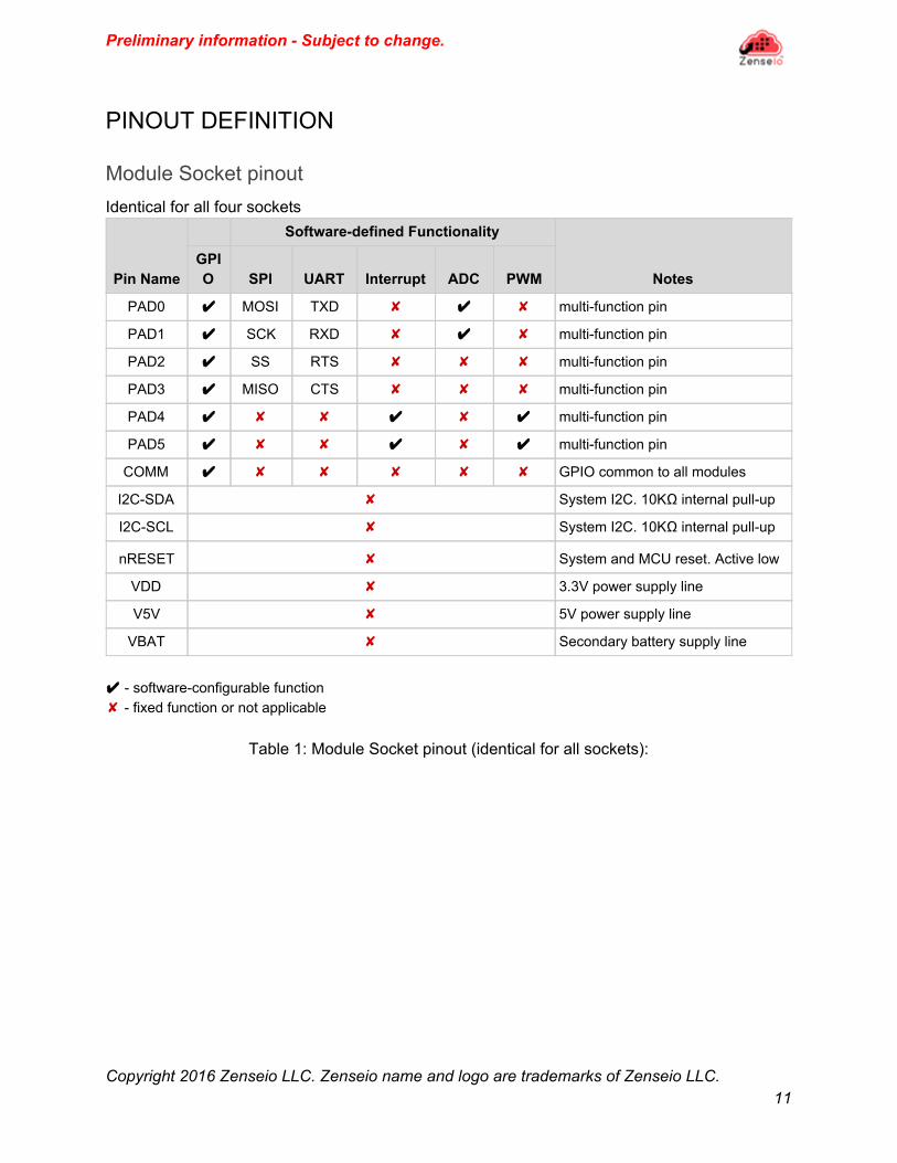
PINOUT DEFINITION
Module Socket pinout Identical for all four sockets
Pin Name
Softwaredefined Functionality
Notes
GPIO SPI UART Interrupt ADC PWM
PAD0 MOSI TXD multifunction pin
PAD1 SCK RXD multifunction pin
PAD2 SS RTS multifunction pin
PAD3 MISO CTS multifunction pin
PAD4 multifunction pin
PAD5 multifunction pin
COMM GPIO common to all modules
I2CSDA System I2C. 10KΩ internal pullup
I2CSCL System I2C. 10KΩ internal pullup
nRESET System and MCU reset. Active low
VDD 3.3V power supply line
V5V 5V power supply line
VBAT Secondary battery supply line
softwareconfigurable function fixed function or not applicable
Table 1: Module Socket pinout (identical for all sockets):
Copyright 2016 Zenseio LLC. Zenseio name and logo are trademarks of Zenseio LLC. 11

Preliminary information Subject to change.
20pin Expansion header pinout:
Pin number
Pin name
Softwaredefined Functionality
Notes GPIO Interrupt PWM ADC DAC
1 VDD Power 3.3V
2 VDD Power 3.3V
3 GND Power ground
4 GND Power ground
5 V5V Power 5V
6 V5V Power 5V
7 nRESET System and MCU reset. Active low
8 I2CSCL System I2C. 10KΩ internal pullup
9 I2CSDA System I2C. 10KΩ internal pullup
10 GPIO1 multifunction pin
11 GPIO2 multifunction pin
12 GPIO3 multifunction pin
13 GPIO4 multifunction pin
14 GPIO5 multifunction pin
15 GPIO6 multifunction pin
16 GPIO7 multifunction pin
17 MISO System SPI
18 MOSI System SPI
19 SCK System SPI
20 GND Power ground
softwareconfigurable function fixed function or not applicable
Table 2: 20pin Expansion header pinout
Copyright 2016 Zenseio LLC. Zenseio name and logo are trademarks of Zenseio LLC. 12

Preliminary information Subject to change.
Debug Interface
Sensor Hub includes a standard 10pin ARM CortexM SWD debug header. It can be used to reprogram the processor bootloader or download user firmware image with standard JTAG tools such as the Atmel ICE or Segger JLink, RLink debuggers. The connector is keyed to force the correct orientation with compatible cables.
Note: Pin 1 of the header is marked on board with a dot
Figure 6: Pinout of ARM Cortex SWD debug header
HEADERS POSITIONING The position of the main physical features and pins on the top side of the Sensor Hub board as shown in the figure below.
Figure 7: Description and position of pin markings on Sensor Hub
Copyright 2016 Zenseio LLC. Zenseio name and logo are trademarks of Zenseio LLC. 13

Preliminary information Subject to change.
PIN DESCRIPTIONS Module Socket pins:
Pin Description
VIN Input supply from a header block. Supply 3.6 to 6.0VDC to power up the
system. Reverse polarity protection is builtin on Sensor Hub. This supply
is regulated to VDD. Max current draw from this pin is 0.9A, but no
current limiting is enforced. If the source needs to be protected from
current overdraw, a suitable current limiting circuit needs to be provided
outside of Sensor Hub.
VUSB 5V nominal input supply from an USB source. Reverse polarity and
500mA current limit (via resettable fuse) are builtin on Sensor Hub.
V5V This pin is a power input or output on Module sockets and Expansion
connector. As an input, supply 3.6 to 6.0VDC to power up the system.
When the Sensor Hub is powered via the USB port, this pin will output a
voltage of approximately 4.8VDC due to a reverse polarity protection
diode between VUSB and V5V. When the the system is powered via the
VIN port, this pin will output a voltage of VIN minus a diode forward
voltage (between 0.1V 0.4V) due to a reverse polarity protection diode
between VIN and V5V. When used as an output, the max load is below
1A minus the current budgeted for Sensor Hub and any installed
Modules using this voltage.
nRESET Activelow reset input. Onboard circuitry contains a 10K Ohm pullup
resistor between RST and VDD. Can be input or output. If used as input,
it will trigger system reset. When used as output, it will indicate if there
was a system reset event.
VDD Regulated nominal 3.3V power supply line. Can be used as input or
output
VPRIM Primary (nonrechargeable) battery supply input header. The
externallysupplied input voltage should be slightly (0.1V 0.4V) above
the required VDD due to builtin reverse polarity protection diode on
Sensor Hub board. Max load draw current depends on the application
Copyright 2016 Zenseio LLC. Zenseio name and logo are trademarks of Zenseio LLC. 14
Preliminary information Subject to change.
and should be budgeted as such to balance the the battery capacity as
well as application load and duty cycle with the battery life.
VSBAT Header for connecting a secondary (rechargeable) battery. Some power
supply modules (such as the energy harvester) provide capability of
charging and using a secondary battery which can be connected to this
pin. Without an appropriate power supply module plugged into Sensor Hub, this pin has no effect.
RESERVED Reserved for future use
PAD0~PAD1 Multipurpose analog input or digital inputoutput GPIO or serial interface
pins.
PAD2~PAD3 Multipurpose digitalonly GPIO or serial interface pins (in combination
with PAD0 and PAD1).
PAD4~PAD5 Digitalonly GPIO pin. Can also act as MCU interrupt signal or PWM
output
COMM Digital “common” signal connected to MCU GPIO pin and shared among
all module sockets. GPIO input or output functionality is defined by an
application
I2CSCL System I2C/TWI clock line. Includes 10K Ohm internal pullup.
I2CSDA System I2C/TWI data line. Includes 10K Ohm internal pullup.
Copyright 2016 Zenseio LLC. Zenseio name and logo are trademarks of Zenseio LLC. 15

Preliminary information Subject to change.
Technical specification ABSOLUTE MAXIMUM RATINGS
Symbol Parameter Min Max Units
VIN 5V Unregulated Supply Input Voltage
6.5 V
V5V 5V Unregulated Supply Input Voltage
6.5 V
VDD 3.3V Regulated Supply Input Voltage
3.8 V
IVDD Max current draw from 3.3V voltage regulator
1000 mA
VPIN Pin voltage with respect to GND and VDD
GND0.3V VDD+0.3V V
VESD ESD Susceptibility HBM (Human Body Mode)
2 kV
TSTORAGE Storage temperature 55 125 °C
Table 3: Absolute Maximum Ratings
Copyright 2016 Zenseio LLC. Zenseio name and logo are trademarks of Zenseio LLC. 16

Preliminary information Subject to change.
RECOMMENDED OPERATING CONDITIONS
Symbol Parameter Condition Min Nom Max Units
VIN Nominal 5V Unregulated Supply Input Voltage
3.6 5.0 6.0 V
VPRIMIN Nominal 3.3V Regulated Supply Input Voltage (at Primary battery connector)
2.9* 3.5 3.6 V
VDDOUT VDD Regulated Supply Output Voltage (from onboard regulator)
2.8* 3.3 3.4 V
VDDIN VDD (nominal 3.3V) Supply External Input Voltage
2.8 3.3 3.6 V
IVINUSB Load current from USB port
500 mA
IVDDUSB VDD output current when source supplied by USB port
With max 100mA internal budget
360 mA
IO(PIN) Max output current that can be sourced by an output pin
2 mA
ISLEEP Sleep current consumption
With RTC running @ 3.3V and 25 °C
14 uA
IACTIVE Current consumption during processor activity (running a Fibonacci algorithm)
@ 3.3V and 25 °C 5.9 mA
TA Temperature range Industrial Temperature Range
40 25 85 °C
Table 4: Recommended Operating Conditions
Copyright 2016 Zenseio LLC. Zenseio name and logo are trademarks of Zenseio LLC. 17

Preliminary information Subject to change.
Notes: * Unregulated below 3.5V input and 3.3V output
Mechanical specifications DIMENSIONS AND WEIGHT
Module Spacers H x W x D Dimensions in inches (mm) Weight in oz (gr)
With 3.78 x 2.16 x 0.6 (96 x 55 x 15) 1.0 (30)
Table 5: Dimensions and Size
PCB LAND PATTERN
Figure 8: PCB land pattern and dimensions
Copyright 2016 Zenseio LLC. Zenseio name and logo are trademarks of Zenseio LLC. 18
Preliminary information Subject to change.
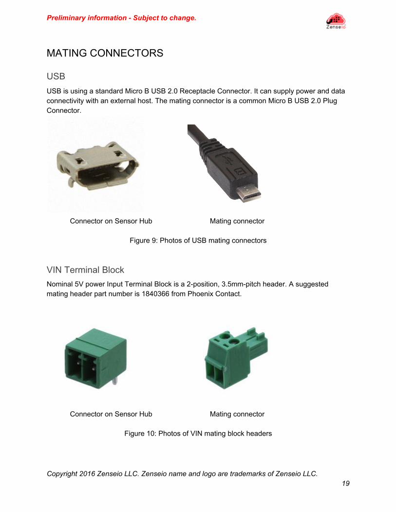
MATING CONNECTORS
USB USB is using a standard Micro B USB 2.0 Receptacle Connector. It can supply power and data connectivity with an external host. The mating connector is a common Micro B USB 2.0 Plug Connector.
Connector on Sensor Hub Mating connector
Figure 9: Photos of USB mating connectors
VIN Terminal Block Nominal 5V power Input Terminal Block is a 2position, 3.5mmpitch header. A suggested mating header part number is 1840366 from Phoenix Contact.
Connector on Sensor Hub Mating connector
Figure 10: Photos of VIN mating block headers
Copyright 2016 Zenseio LLC. Zenseio name and logo are trademarks of Zenseio LLC. 19

Preliminary information Subject to change.
VPRIM and VSBAT Primary and Secondary power headers use male 2position, 2mmpitch JSTPH connectors [part number: B2BPHKS(LF)(SN)]. The suggested mating connector housing part number is PHR2 from JST.
Connector on Sensor Hub Mating connector
Figure 11: Photos of JSTPH mating connectors (for batteries and power)
Expansion Header Expansion Header uses 20position, 0.5 mm (0.020") pitch ribbon jumper cable. These are available from many manufacturers (such as Molex) with varying length, according to your application needs. Suggested Molex part number: 0152660215 for 6” long version, available from DigiKey.
Connector on Sensor Hub Mating connector
Figure 12: Photos of 20pin Expansion Header mating connectors
Copyright 2016 Zenseio LLC. Zenseio name and logo are trademarks of Zenseio LLC. 20

Preliminary information Subject to change.
Mounting Holes Modules can be secured to the Sensor Hub with four M2x4mm screws. Sensor Hub can be attached to an enclosure with four M3 screws or spacer posts.
Glossary AES Advanced Encryption Standard
GPIO General Programmable Input/Output
UART Universal Asynchronous Receiver/Transmitter
SPI Serial Protocol Interface
I2C InterIntegrated Circuit (interface)
PWM Pulse Width Modulation
SWD Serial Wire Debugger
SRAM Static randomaccess memory
EEPROM Electrically Erasable Programmable ReadOnly Memory
SMPS SwitchedMode Power Supply
OTA OverTheAir (firmware update)
RF Radio Frequency
LED LightEmitting Diode
ADC AnalogtoDigital Converter
USB Universal Serial Bus
Quiescent current Current consumed in the deepest sleep state
RTC Real Time Clock
IDE Integrated Development Environment
Copyright 2016 Zenseio LLC. Zenseio name and logo are trademarks of Zenseio LLC. 21
Preliminary information Subject to change.
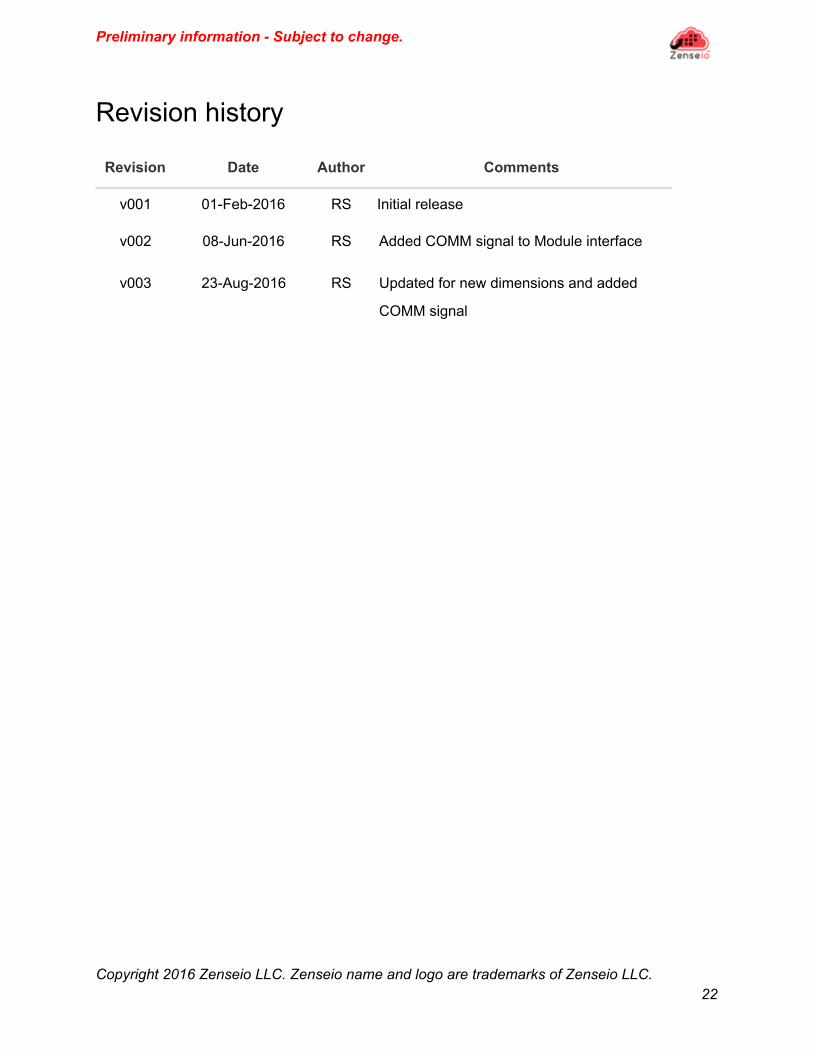
Revision history
Revision Date Author Comments
v001 01Feb2016 RS Initial release
v002 08Jun2016 RS Added COMM signal to Module interface
v003 23Aug2016 RS Updated for new dimensions and added
COMM signal
Copyright 2016 Zenseio LLC. Zenseio name and logo are trademarks of Zenseio LLC. 22