iqs624 datasheet - strawberry-linux.com
TRANSCRIPT
IQ Switch®
ProxFusion™ Series
Copyright © Azoteq 2017 IQS624 Datasheet v1.19 Page 1 of 67
All rights reserved May 2017
IQS624 Datasheet Combination sensor including: Hall-effect rotation sensing, along with dual-channel
capactive proximity/touch sensing, or single-channel inductive sensing.
The IQS624 ProxFusion™ IC is a multifunctional capacitive and Hall-effect sensor designed for applications where any or all of the technologies may be required. The two Hall-effect sensors calculate the angle of a magnet rotating parallel with the sensor. The sensor is fully I2C compatible and on-chip calculations enable the IC to stream the current angle of the magnet without extra calculations.
Features Hall effect angle sensor:
o On-chip Hall plates
o 360° Output
o 1° Resolution, calculated on chip
o Relative rotation angle.
o Detect movement and the direction of movement.
o Raw data: can be used to calculate degrees on external processor.
o Wide operational range
o No external components required
Partial auto calibration:
o Continuous auto-calibration, compensation for wear or small displacements of the sensor or magnet.
o Flexible gain control
o Automatic Tuning Implementation (ATI) – Performance enhancement (10 bit).
Capacitive sensing o Full auto-tuning with adjustable
sensitivity o 2pF to 200pF external capacitive load
capability
Inductive sensing o Only external sense
coil required (PCB trace)
Multiple integrated UI
o Proximity / Touch
o Proximity wake-up
o Event mode
o Wake Hall sensing on proximity
Minimal external components
Standard I2C interface
Optional RDY indication for event mode operation
Low power consumption:
240uA (100Hz response, Hall),
55uA (100Hz response, capacitive),
65uA (20Hz response, Hall)
15uA (20Hz response, capacitive)
5uA (5Hz response, capacitive)
Supply Voltage: 2.0V to 3.6V* *5V solution available on demand.
Applications
Anemometer
Dial or Selector knob
Mouse wheel
Measuring wheel
Digital angle gauge
Speedometer for bicycle
Available Packages
TA DFN(3x3)-10
-20°C to 85°C IQS624-xyy
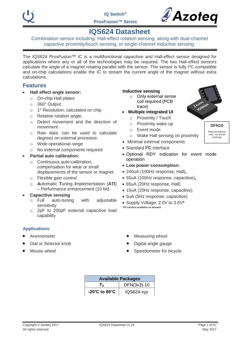
DFN10
Representations only, not actual
markings
IQ Switch®
ProxFusion™ Series
Copyright © Azoteq 2017 IQS624 Datasheet v1.19 Page 2 of 67
All rights reserved May 2017
Contents
LIST OF ABBREVIATIONS ............................................................................................................................................. 6
1 INTRODUCTION .................................................................................................................................................. 7
1.1 PROXFUSION ...................................................................................................................................................... 7 1.2 PACKAGING AND PIN-OUT ....................................................................................................................................... 7 FIGURE 1.1 PIN OUT OF IQS624 DFN (3X3)-10 PACKAGE. .................................................................................................. 7 TABLE 1.1 IQS624 PIN-OUT .......................................................................................................................................... 7 1.3 REFERENCE SCHEMATIC ........................................................................................................................................... 7 FIGURE 1.2 IQS624 REFERENCE SCHEMATIC ....................................................................................................................... 7 1.4 SENSOR CHANNEL COMBINATIONS ............................................................................................................................. 8 TABLE 1.2 SENSOR - CHANNEL ALLOCATION ....................................................................................................................... 8
2 CAPACITIVE SENSING ......................................................................................................................................... 9
2.1 INTRODUCTION ...................................................................................................................................................... 9 2.2 CHANNEL SPECIFICATIONS ........................................................................................................................................ 9 TABLE 2.1 CAPACITIVE SENSING - CHANNEL ALLOCATION ...................................................................................................... 9 2.3 HARDWARE CONFIGURATION .................................................................................................................................. 10 TABLE 2.2 CAPACITIVE HARDWARE DESCRIPTION .............................................................................................................. 10 2.4 REGISTER CONFIGURATION ..................................................................................................................................... 10
2.4.1 Registers to configure for the capacitive sensing: ...................................................................................... 10 TABLE 2.3 CAPACITIVE SENSING SETTINGS REGISTERS ........................................................................................................ 10
2.4.2 Proximity Thresholds ................................................................................................................................... 11 2.4.3 Touch Thresholds ........................................................................................................................................ 11 2.4.4 Example code: ............................................................................................................................................. 11
2.5 SENSOR DATA OUTPUT AND FLAGS ........................................................................................................................... 11
3 INDUCTIVE SENSING ..........................................................................................................................................12
3.1 INTRODUCTION TO INDUCTIVE SENSING ..................................................................................................................... 12 3.2 CHANNEL SPECIFICATIONS ...................................................................................................................................... 12
Table 3.1 Mutual inductive sensor – channel allocation .................................................................................... 12 3.3 HARDWARE CONFIGURATION .................................................................................................................................. 12
Table 3.2 Mutual inductive hardware description ............................................................................................. 12 3.4 REGISTER CONFIGURATION ..................................................................................................................................... 13 TABLE 3.3 INDUCTIVE SENSING SETTINGS REGISTERS. ......................................................................................................... 13
3.4.2 Example code: ............................................................................................................................................. 13 3.5 SENSOR DATA OUTPUT AND FLAGS ........................................................................................................................... 13
4 HALL-EFFECT SENSING .......................................................................................................................................14
4.1 INTRODUCTION TO HALL-EFFECT SENSING ................................................................................................................. 14 4.2 CHANNEL SPECIFICATIONS ...................................................................................................................................... 14 TABLE 4.1 HALL-EFFECT SENSOR – CHANNEL ALLOCATION .................................................................................................. 14 4.3 HARDWARE CONFIGURATION .................................................................................................................................. 15 4.4 REGISTER CONFIGURATION ..................................................................................................................................... 15 TABLE 4.2 HALL SENSING SETTINGS REGISTERS ................................................................................................................. 15
4.4.2 Example code: ............................................................................................................................................. 16 4.5 SENSOR DATA OUTPUT AND FLAGS ........................................................................................................................... 16
5 DEVICE CLOCK, POWER MANAGEMENT AND MODE OPERATION ......................................................................17
5.1 DEVICE MAIN OSCILLATOR ...................................................................................................................................... 17 5.2 DEVICE MODES .................................................................................................................................................... 17
5.2.1 Normal mode .............................................................................................................................................. 17 5.2.2 Low power mode ......................................................................................................................................... 17 5.2.3 Ultra-low power mode ................................................................................................................................ 17 5.2.4 Halt mode ................................................................................................................................................... 18 5.2.5 Mode time ................................................................................................................................................... 18
5.3 STREAMING AND EVENT MODE: ............................................................................................................................... 18
IQ Switch®
ProxFusion™ Series
Copyright © Azoteq 2017 IQS624 Datasheet v1.19 Page 3 of 67
All rights reserved May 2017
5.3.1 Streaming mode .......................................................................................................................................... 18 5.3.2 Event mode ................................................................................................................................................. 18
5.4 REPORT RATES ..................................................................................................................................................... 19 5.4.1 Normal Power Maximum Report rate ......................................................................................................... 19
5.5 SYSTEM RESET ..................................................................................................................................................... 20
6 COMMUNICATION ............................................................................................................................................21
6.1 CONTROL BYTE .................................................................................................................................................... 21 FIGURE 6.1 IQS624 CONTROL BYTE ............................................................................................................................... 21 6.2 I2C READ ............................................................................................................................................................ 21 FIGURE 6.2 CURRENT ADDRESS READ .............................................................................................................................. 21 FIGURE 6.3 RANDOM READ ........................................................................................................................................... 21 6.3 I2C WRITE .......................................................................................................................................................... 22 FIGURE 6.4 I2C WRITE .................................................................................................................................................. 22 6.4 END OF COMMUNICATION SESSION / WINDOW ......................................................................................................... 22 6.5 DEVICE ADDRESS AND SUB-ADDRESSES ..................................................................................................................... 22 6.6 ADDITIONAL OTP OPTIONS .................................................................................................................................... 23 6.7 RDY HAND-SHAKE ROUTINE .................................................................................................................................. 23 6.8 I2C SPECIFIC COMMANDS ...................................................................................................................................... 23
6.8.1 Show Reset .................................................................................................................................................. 23 6.8.2 I2C Timeout ................................................................................................................................................. 23
6.9 I2C I/O CHARACTERISTICS ...................................................................................................................................... 23 TABLE 6.1 IQS624 I2C INPUT VOLTAGE ......................................................................................................................... 24 TABLE 6.2 IQS624 I2C OUTPUT VOLTAGE ...................................................................................................................... 24 6.10 RECOMMENDED COMMUNICATION AND RUNTIME FLOW DIAGRAM ................................................................................ 24 FIGURE 6.5 MASTER COMMAND STRUCTURE AND RUNTIME EVENT HANDLING FLOW DIAGRAM ................................................... 25
7 IQS624 MEMORY MAP ......................................................................................................................................26
TABLE 7.1 IQS624 REGISTER MAP ................................................................................................................................ 26 7.2 DEVICE INFORMATION ........................................................................................................................................... 28
7.2.1 Product Number .......................................................................................................................................... 28 7.2.2 Software Number ........................................................................................................................................ 28 7.2.3 Hardware Number ...................................................................................................................................... 28
7.3 DEVICE SPECIFIC DATA .......................................................................................................................................... 29 7.3.1 System Flags................................................................................................................................................ 29 7.3.2 UI Flags ....................................................................................................................................................... 29 7.3.3 Proximity/Touch UI Flags ............................................................................................................................ 30 7.3.4 Hall UI Flags ................................................................................................................................................ 30 7.3.5 Hall Ratio Flags ........................................................................................................................................... 31
7.4 COUNT DATA ...................................................................................................................................................... 31 7.4.1 Count CS Values .......................................................................................................................................... 31 7.4.2 LTA Values ................................................................................................................................................... 31
7.5 PROXFUSION SENSOR SETTINGS ............................................................................................................................... 32 7.5.1 Ch0/1 ProxFusion Settings 0 ....................................................................................................................... 32 7.5.2 Ch0&1 ProxFusion Settings 1 ...................................................................................................................... 33 7.5.3 Ch0/1 ProxFusion Settings 2 ....................................................................................................................... 33 7.5.4 Ch0&1 ProxFusion Settings 3 ...................................................................................................................... 34 7.5.5 Ch0/Ch1 Compensation .............................................................................................................................. 34 7.5.6 Ch0/Ch1 Multipliers values ......................................................................................................................... 35
7.6 TOUCH / PROXIMITY UI SETTINGS............................................................................................................................ 35 7.6.1 Ch0/1 Proximity/touch threshold ................................................................................................................ 35 7.6.2 UI Halt period .............................................................................................................................................. 35
7.7 HALL SENSOR SETTINGS........................................................................................................................................ 36 7.7.1 Hall Rotation UI Settings ............................................................................................................................. 36 7.7.2 Hall Sensor Settings ..................................................................................................................................... 36 7.7.3 Ch2/3, Ch4/5 Hall ATI Settings .................................................................................................................... 37 7.7.4 Ch2/3, Ch4/5 Hall Compensation ................................................................................................................ 37 7.7.5 Ch2/3, Ch4/5 Hall Multipliers ...................................................................................................................... 37
IQ Switch®
ProxFusion™ Series
Copyright © Azoteq 2017 IQS624 Datasheet v1.19 Page 4 of 67
All rights reserved May 2017
7.7.6 Hall Ratio Settings ....................................................................................................................................... 38 7.7.7 Sin Constant ................................................................................................................................................ 38 7.7.8 Cos Constant ............................................................................................................................................... 38
7.8 HALL WHEEL OUTPUT .......................................................................................................................................... 39 7.8.1 Degree Output ............................................................................................................................................ 39 7.8.2 Ratio Output ............................................................................................................................................... 39 7.8.3 Numerator .................................................................................................................................................. 39 7.8.4 Denominator ............................................................................................................................................... 39 7.8.5 Rotation Correction factor .......................................................................................................................... 39 7.8.6 Max Numerator .......................................................................................................................................... 40 7.8.7 Max Denominator ....................................................................................................................................... 40 7.8.8 Relative Rotation Angle .............................................................................................................................. 40 7.8.9 Movement counter/timer ........................................................................................................................... 40
7.9 DEVICE AND POWER MODE SETTINGS ...................................................................................................................... 41 7.9.1 General System Settings ............................................................................................................................. 41 7.9.2 Active Channels Mask ................................................................................................................................. 42 7.9.3 Power Mode Settings .................................................................................................................................. 43 7.9.4 Normal/Low/Ultra-Low power mode report rate ....................................................................................... 43 7.9.5 Auto Mode Time ......................................................................................................................................... 44
8 ELECTRICAL CHARACTERISTICS ..........................................................................................................................45
8.1 ABSOLUTE MAXIMUM SPECIFICATIONS ..................................................................................................................... 45 TABLE 8.1 ABSOLUTE MAXIMUM SPECIFICATION .............................................................................................................. 45 8.2 POWER ON-RESET/BROWN OUT ............................................................................................................................. 45 TABLE 8.2 POWER ON-RESET AND BROWN OUT DETECTION SPECIFICATIONS .......................................................................... 45 8.3 CURRENT CONSUMPTIONS ..................................................................................................................................... 46
8.3.1 IC subsystems .............................................................................................................................................. 46 TABLE 8.3 IC SUBSYSTEM CURRENT CONSUMPTION ........................................................................................................... 46 TABLE 8.4 IC SUBSYSTEM TYPICAL TIMING ....................................................................................................................... 46
8.3.2 Capacitive sensing alone ............................................................................................................................. 46 TABLE 8.5 CAPACITIVE SENSING CURRENT CONSUMPTION .................................................................................................. 46
8.3.3 Hall-effect sensing alone ............................................................................................................................. 47 TABLE 8.6 HALL-EFFECT CURRENT CONSUMPTION ............................................................................................................ 47
8.3.4 Halt mode ................................................................................................................................................... 47 TABLE 8.7 HALT MODE CURRENT CONSUMPTION .............................................................................................................. 47 8.4 CAPACITIVE LOADING LIMITS ................................................................................................................................... 47 8.5 HALL-EFFECT MEASUREMENT LIMITS ........................................................................................................................ 47
9 PACKAGE INFORMATION ..................................................................................................................................48
9.1 DFN10 PACKAGE AND FOOTPRINT SPECIFICATIONS ..................................................................................................... 48 TABLE 9.1 DFN-10 PACKAGE DIMENSIONS (BOTTOM) ...................................................................................................... 48 TABLE 9.2 DFN-10 PACKAGE DIMENSIONS (SIDE) ............................................................................................................ 48 TABLE 9.3 DFN-10 LANDING DIMENSIONS ..................................................................................................................... 48 FIGURE 9.1 DFN-10 PACKAGE DIMENSIONS (BOTTOM). NOTE THAT THE SADDLE NEED TO BE CONNECTED TO GND ON THE PCB. .... 48 FIGURE 9.2 DFN-10 PACKAGE DIMENSIONS (SIDE) ............................................................................................................ 48 FIGURE 9.3 DFN-10 LANDING DIMENSION....................................................................................................................... 48 9.2 DEVICE MARKING AND ORDERING INFORMATION ........................................................................................................ 49
9.2.1 Device marking: .......................................................................................................................................... 49 9.2.2 Ordering Information: ................................................................................................................................. 49
9.3 TAPE AND REEL SPECIFICATION ................................................................................................................................ 50 9.4 MSL LEVEL ......................................................................................................................................................... 51
10 DATASHEET REVISIONS .....................................................................................................................................52
10.1 REVISION HISTORY ................................................................................................................................................ 52 10.2 ERRATA .............................................................................................................................................................. 53
10.2.1 Hall ATI values ........................................................................................................................................ 53
11 CONTACT INFORMATION ..................................................................................................................................54
IQ Switch®
ProxFusion™ Series
Copyright © Azoteq 2017 IQS624 Datasheet v1.19 Page 5 of 67
All rights reserved May 2017
12 APPENDICES ......................................................................................................................................................55
12.1 APPENDIX A: MAGNET ORIENTATION ....................................................................................................................... 55 FIGURE 12.1 TYPICAL RECOMMENDED MAGNET .............................................................................................................. 55
12.1.2 Absolute or relative applications ............................................................................................................ 57 12.1.3 Preferred magnet orientation ................................................................................................................. 57 12.1.4 Evaluation kit magnet orientation .......................................................................................................... 58 12.1.5 Alternative orientation ........................................................................................................................... 60
12.2 APPENDIX B: MAGNET CALIBRATION ........................................................................................................................ 61 12.2.1 How to calculate the calibration constants using the IQS624 GUI ......................................................... 61 12.2.2 How to calculate the calibration constants using the raw data ............................................................. 64
12.3 APPENDIX C: HALL ATI ......................................................................................................................................... 66 12.3.1 Hall reference value: ............................................................................................................................... 66 12.3.2 ATI parameters: ...................................................................................................................................... 66 12.3.3 Coarse and Fine multipliers: ................................................................................................................... 66 12.3.4 ATI-Compensation: ................................................................................................................................. 66 12.3.5 Recommended parameters: ................................................................................................................... 67

IQ Switch®
ProxFusion™ Series
Copyright © Azoteq 2017 IQS624 Datasheet v1.19 Page 6 of 67
All rights reserved May 2017
List of abbreviations
PXS – ProxSense®
ATI – Automatic Tuning Implementation
LTA – Long term average
Thr – Threshold
UI – User interface
AC – Alternating current
DSP – Digital signal processing
RX – Receiving electrode
TX – Transmitting electrode
CS – Sampling capacitor
C – Capacitive
NP – Normal power
LP – Low power
ULP – Ultra low power
ACK – I2C Acknowledge condition
NACK – I2C Not Acknowledge condition
FG – Floating gate
IQ Switch®
ProxFusion™ Series
Copyright © Azoteq 2017 IQS624 Datasheet v1.19 Page 7 of 67
All rights reserved May 2017
1 Introduction
1.1 ProxFusion
The ProxFusion sensor series provide all the proven ProxSense® engine capabilities with additional sensors types. A combined sensor solution is available within a single platform.
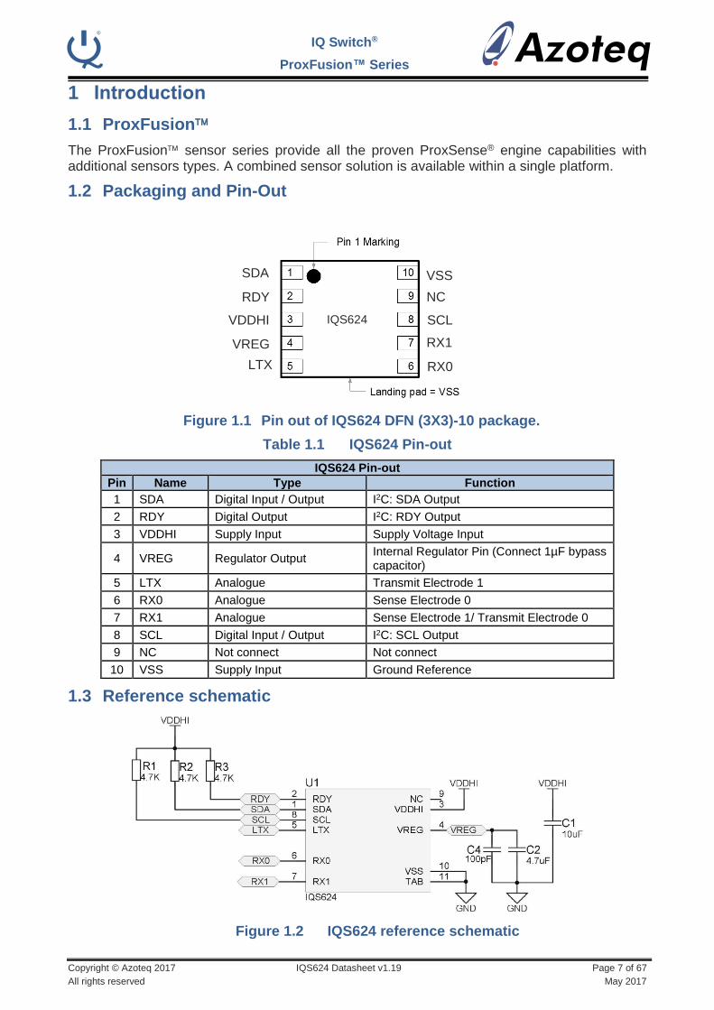
1.2 Packaging and Pin-Out
Figure 1.1 Pin out of IQS624 DFN (3X3)-10 package.
Table 1.1 IQS624 Pin-out
IQS624 Pin-out
Pin Name Type Function
1 SDA Digital Input / Output I2C: SDA Output
2 RDY Digital Output I2C: RDY Output
3 VDDHI Supply Input Supply Voltage Input
4 VREG Regulator Output Internal Regulator Pin (Connect 1µF bypass capacitor)
5 LTX Analogue Transmit Electrode 1
6 RX0 Analogue Sense Electrode 0
7 RX1 Analogue Sense Electrode 1/ Transmit Electrode 0
8 SCL Digital Input / Output I2C: SCL Output
9 NC Not connect Not connect
10 VSS Supply Input Ground Reference
1.3 Reference schematic
Figure 1.2 IQS624 reference schematic
SDA
RDY
VDDHI
VREG
LTX RX0
RX1
SCL
VSS
NC
IQS624
IQ Switch®
ProxFusion™ Series
Copyright © Azoteq 2017 IQS624 Datasheet v1.19 Page 8 of 67
All rights reserved May 2017
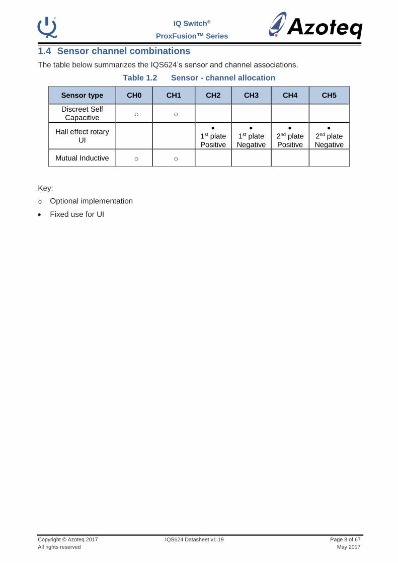
1.4 Sensor channel combinations
The table below summarizes the IQS624’s sensor and channel associations.
Table 1.2 Sensor - channel allocation
Sensor type CH0 CH1 CH2 CH3 CH4 CH5
Discreet Self Capacitive
o o
Hall effect rotary UI
1st plate Positive
1st plate Negative
2nd plate Positive
2nd plate Negative
Mutual Inductive o o
Key:
o Optional implementation
Fixed use for UI
IQ Switch®
ProxFusion™ Series
Copyright © Azoteq 2017 IQS624 Datasheet v1.19 Page 9 of 67
All rights reserved May 2017
2 Capacitive sensing
2.1 Introduction
Building on the previous successes from the ProxSense® range of capacitive sensors, the same
fundamental sensor engine has been implemented in the ProxFusion series.
The capacitive sensing capabilities of the IQS624 include:
Maximum of 2 capacitive channels to be individually configured. o Prox and touch adjustable thresholds o Individual sensitivity setups o Alternative ATI modes
Discreet button UI: o Fully configurable 2 level threshold setup – traditional prox & touch activation levels. o Customizable filter halt time
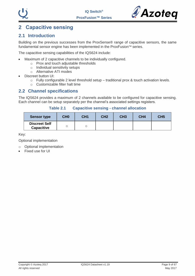
2.2 Channel specifications
The IQS624 provides a maximum of 2 channels available to be configured for capacitive sensing. Each channel can be setup separately per the channel’s associated settings registers.
Table 2.1 Capacitive sensing - channel allocation
Sensor type CH0 CH1 CH2 CH3 CH4 CH5
Discreet Self Capacitive
o o
Key:
Optional implementation
o Optional implementation
Fixed use for UI
IQ Switch®
ProxFusion™ Series
Copyright © Azoteq 2017 IQS624 Datasheet v1.19 Page 10 of 67
All rights reserved May 2017
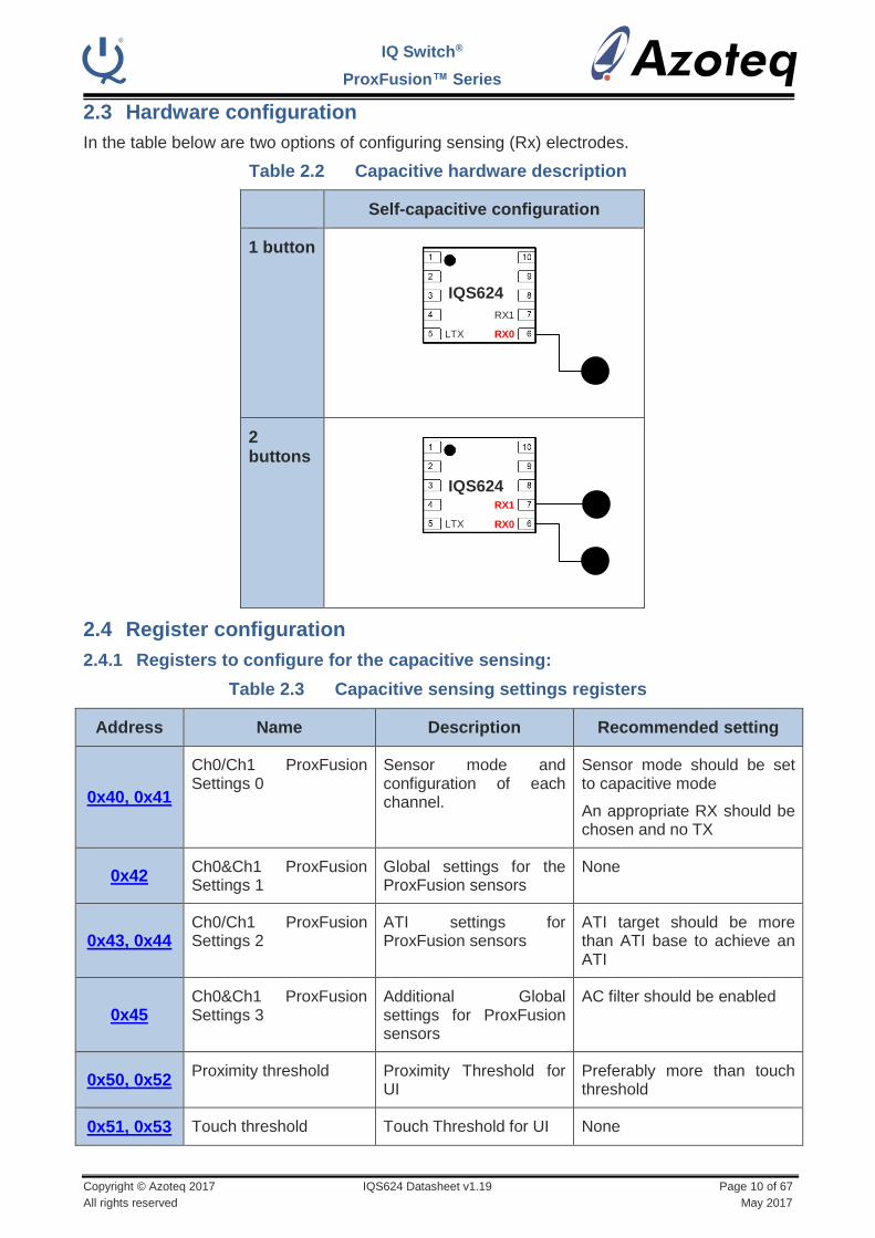
2.3 Hardware configuration
In the table below are two options of configuring sensing (Rx) electrodes.
Table 2.2 Capacitive hardware description
Self-capacitive configuration
1 button
2 buttons
2.4 Register configuration
2.4.1 Registers to configure for the capacitive sensing:
Table 2.3 Capacitive sensing settings registers
Address Name Description Recommended setting
0x40, 0x41
Ch0/Ch1 ProxFusion Settings 0
Sensor mode and configuration of each channel.
Sensor mode should be set to capacitive mode
An appropriate RX should be chosen and no TX
0x42 Ch0&Ch1 ProxFusion Settings 1
Global settings for the ProxFusion sensors
None
0x43, 0x44 Ch0/Ch1 ProxFusion Settings 2
ATI settings for ProxFusion sensors
ATI target should be more than ATI base to achieve an ATI
0x45 Ch0&Ch1 ProxFusion Settings 3
Additional Global settings for ProxFusion sensors
AC filter should be enabled
0x50, 0x52 Proximity threshold Proximity Threshold for
UI Preferably more than touch threshold
0x51, 0x53 Touch threshold Touch Threshold for UI None
RX0
RX1 LTX
RX0
RX1 LTX
IQS624
IQS624
IQ Switch®
ProxFusion™ Series
Copyright © Azoteq 2017 IQS624 Datasheet v1.19 Page 11 of 67
All rights reserved May 2017
2.4.2 Proximity Thresholds
A proximity threshold for both channels can be selected for the application, to obtain the desired
proximity trigger level. The proximity threshold is selectable between 1 (most sensitive) and 255
(least sensitive) counts. These threshold values (i.e. 1-255) are specified in Counts (CS) in the
Ch0 Proximity threshold (0x50) and Ch1 Proximity threshold (0x51) registers for the discreet button
UI.
2.4.3 Touch Thresholds
A touch threshold for each channel can be selected by the designer to obtain the desired
touch sensitivity and is selectable between 1/256 (most sensitive) to 255/256 (least sensitive).
The touch threshold is calculated as a fraction of the Long-Term Average (LTA) given by,
𝑇𝑇𝐻𝑅 = 𝑥256⁄ × 𝐿𝑇𝐴
With lower target values (therefore lower LTA’s) the touch threshold will be lower and vice
versa.
Individual touch thresholds can be set for each channel, by writing to the Ch0 Touch threshold
(0x51) and Ch1 Touch threshold (0x53) for the discreet button UI.
2.4.4 Example code:
Example code for an Arduino Uno can be downloaded at:
www.azoteq.com//images/stories/software/IQS62x_Demo.zip
2.5 Sensor data output and flags
The following registers should be monitored by the master to detect capacitive sensor output.
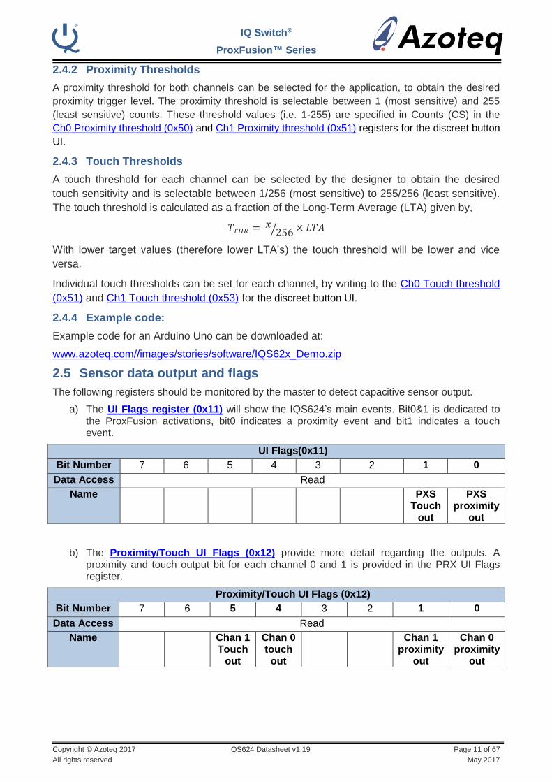
a) The UI Flags register (0x11) will show the IQS624’s main events. Bit0&1 is dedicated to the ProxFusion activations, bit0 indicates a proximity event and bit1 indicates a touch event.
UI Flags(0x11)
Bit Number 7 6 5 4 3 2 1 0
Data Access Read
Name PXS Touch
out
PXS proximity
out
b) The Proximity/Touch UI Flags (0x12) provide more detail regarding the outputs. A proximity and touch output bit for each channel 0 and 1 is provided in the PRX UI Flags register.
Proximity/Touch UI Flags (0x12)
Bit Number 7 6 5 4 3 2 1 0
Data Access Read
Name Chan 1 Touch
out
Chan 0 touch
out
Chan 1 proximity
out
Chan 0 proximity
out
IQ Switch®
ProxFusion™ Series
Copyright © Azoteq 2017 IQS624 Datasheet v1.19 Page 12 of 67
All rights reserved May 2017
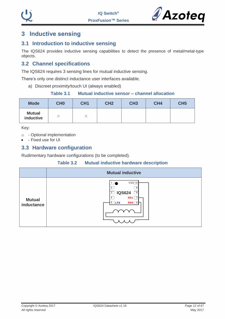
3 Inductive sensing
3.1 Introduction to inductive sensing
The IQS624 provides inductive sensing capabilities to detect the presence of metal/metal-type objects.
3.2 Channel specifications
The IQS624 requires 3 sensing lines for mutual inductive sensing.
There’s only one distinct inductance user interfaces available.
a) Discreet proximity/touch UI (always enabled)
Table 3.1 Mutual inductive sensor – channel allocation
Mode CH0 CH1 CH2 CH3 CH4 CH5
Mutual inductive
o o
Key:
o - Optional implementation
- Fixed use for UI
3.3 Hardware configuration
Rudimentary hardware configurations (to be completed).
Table 3.2 Mutual inductive hardware description
Mutual inductive
Mutual inductance
RX0
RX1
LTX
VSS
IQS624

IQ Switch®
ProxFusion™ Series
Copyright © Azoteq 2017 IQS624 Datasheet v1.19 Page 13 of 67
All rights reserved May 2017
3.4 Register configuration
Table 3.3 Inductive sensing settings registers.
Address Name Description Recommended setting
0x40, 0x41
Ch0/Ch1 ProxFusion Settings 0
Sensor mode and configuration of each channel.
Sensor mode should be set to Inductive mode
Choose one channel and deactivate the other channel
Enable both RX for the activated channel
0x42 Ch0&Ch1 ProxFusion Settings 1
Global settings for the ProxSense sensors
CS divider should be enabled
0x43, 0x44 Ch0/Ch1 ProxFusion Settings 2
ATI settings for ProxSense sensors
ATI target should be more than ATI base to achieve an ATI
0x45 Ch0&Ch1 ProxFusion Settings 3
Additional Global settings for ProxSense sensors
None
0x50, 0x52 Proximity threshold Proximity Threshold for
UI Less than touch threshold
0x51, 0x53 Touch threshold Touch Threshold for UI None
3.4.2 Example code:
Example code for an Arduino Uno can be downloaded at:
www.azoteq.com//images/stories/software/IQS62x_Demo.zip
3.5 Sensor data output and flags
The following registers should be monitored by the master to detect inductive sensor output.
a) The UI Flags register (0x11) provides the classic prox/touch two level activation outputs which can be used for inductive sensing.
UI Flags(0x11)
Bit Number 7 6 5 4 3 2 1 0
Data Access Read
Name PXS Touch
out
PXS proximity
out
IQ Switch®
ProxFusion™ Series
Copyright © Azoteq 2017 IQS624 Datasheet v1.19 Page 14 of 67
All rights reserved May 2017
4 Hall-effect sensing
4.1 Introduction to Hall-effect sensing
The IQS624 has two internal Hall-effect sensing plates (on die). No external sensing hardware is
required for Hall-effect sensing.
The Hall-effect measurement is essentially a current measurement of the induced current through the Hall-effect-sensor plates produced by the magnetic field passing perpendicular through each plate.
Advanced digital signal processing is performed to provide sensible output data.
Hall output is linearized by inverting signals.
Calculates absolute position in degrees.
Auto calibration attempts to linearize degrees output on the fly
Differential Hall-Effect sensing:
o Removes common mode disturbances
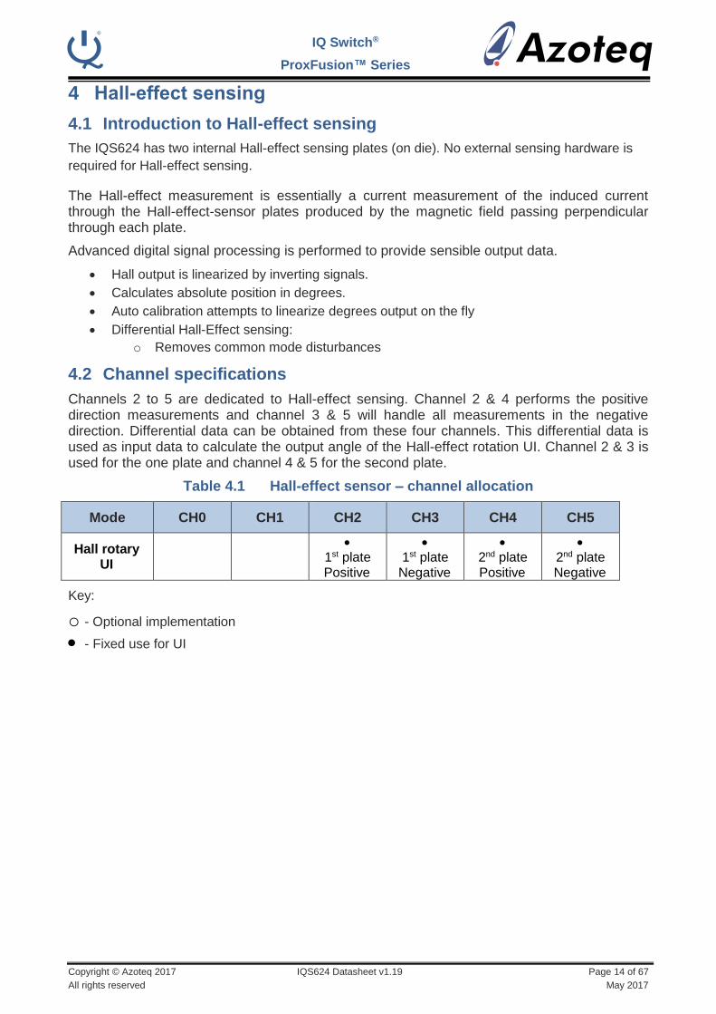
4.2 Channel specifications
Channels 2 to 5 are dedicated to Hall-effect sensing. Channel 2 & 4 performs the positive direction measurements and channel 3 & 5 will handle all measurements in the negative direction. Differential data can be obtained from these four channels. This differential data is used as input data to calculate the output angle of the Hall-effect rotation UI. Channel 2 & 3 is used for the one plate and channel 4 & 5 for the second plate.
Table 4.1 Hall-effect sensor – channel allocation
Mode CH0 CH1 CH2 CH3 CH4 CH5
Hall rotary UI
1st plate Positive
1st plate
Negative
2nd plate Positive
2nd plate Negative
Key:
o - Optional implementation - Fixed use for UI
IQ Switch®
ProxFusion™ Series
Copyright © Azoteq 2017 IQS624 Datasheet v1.19 Page 15 of 67
All rights reserved May 2017
4.3 Hardware configuration
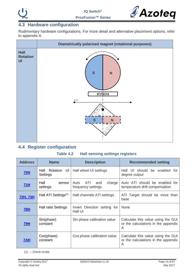
Rudimentary hardware configurations. For more detail and alternative placement options, refer to appendix A.
Diametrically polarized magnet (rotational purposes)
Hall Rotation UI
4.4 Register configuration
Table 4.2 Hall sensing settings registers
Address Name Description Recommended setting
70H Hall Rotation UI Settings
Hall wheel UI settings Hall UI should be enabled for degree output
71H Hall sensor settings
Auto ATI and charge frequency settings
Auto ATI should be enabled for temperature drift compensation
72H, 73H Hall ATI Settings(1) Hall channels ATI settings ATI Target should be more than
base
78H Hall ratio Settings Invert Direction setting for
Hall UI None
79H Sin(phase) constant
Sin phase calibration value Calculate this value using the GUI or the calculations in the appendix A
7AH Cos(phase) constant
Cos phase calibration value Calculate this value using the GUI or the calculations in the appendix A
(1) – Check errata
N S
N S
X-Y
IQS624

IQ Switch®
ProxFusion™ Series
Copyright © Azoteq 2017 IQS624 Datasheet v1.19 Page 16 of 67
All rights reserved May 2017
4.4.2 Example code:
Example code for an Arduino Uno can be downloaded at:
www.azoteq.com//images/stories/software/IQS62x_Demo.zip
4.5 Sensor data output and flags
a) The Hall UI Flags (0x14) register. Bit7 is dedicated to indicating a movement of the
magnet. Bit6 indicates the direction of the movement. Bit 1 is set when the movement counts are negative and bit 0 is set when the relative angle is negative. Bit 1 & 0 is used for on-chip angle calculation, bit 6 can be used to determine the magnet direction.
Hall UI Flags (0x14)
Bit Number 7 6 5 4 3 2 1 0
Data Access Read
Name Wheel movement
Movement direction
Count sign
Difference sign
b) The Degree Output (0x81-0x80). A 16-bit value for the degrees can be read from these registers. (0-360 degrees)
Degree Output (0x81-0x80)
Bit Number 15 14 13 12 11 10 9 8 7 6 5 4 3 2 1 0
Data Access Read/Write
Name Degrees High Byte Degrees Low Byte
c) The Relative Rotation Angle (0x8E). The delta in degrees from the previous cycle to the current cycle can be read from this register. (0-180 degrees)
Relative Rotation Angle (0x8E)
Bit Number 7 6 5 4 3 2 1 0
Data Access Read/Write
Name Relative degrees

IQ Switch®
ProxFusion™ Series
Copyright © Azoteq 2017 IQS624 Datasheet v1.19 Page 17 of 67
All rights reserved May 2017
5 Device clock, power management and mode operation
5.1 Device main oscillator
The IQS624 has a 16MHz main oscillator (default enabled) to clock all system functionality.
An option exists to reduce the main oscillator to 8MHz. This will result in charge transfers to be slower by half of the default implementations.
To set this option this:
o As a software setting – Set the General System Settings (0xD0): bit4 = 1, via an I2C command.
o As a permanent setting – Set the OTP option in FG Bank 0: bit2 = 1, using Azoteq USBProg program.
The ProxFusion channels charges at half of the main oscillator frequency. Therefore the frequency multiplier selected in Ch0&1 ProxFusion Settings 1 (0x42; bit 4-5) and Hall sensor settings (0x71; bit 4-5) is multiplied by half of the main oscillator frequency.
5.2 Device modes
The IQS624 supports the following modes of operation;
Normal mode (Fixed report rate)
Low Power mode (Reduced report rate, no UI execution)
Ultra-Low Power mode (Only channel 0 is sensed for a prox)
Halt Mode (Suspended/disabled)
Note: Auto modes must be disabled to enter or exit halt mode.
The device will automatically switch between the different operating modes by default. However, this Auto mode feature may be disabled by setting the Disable Auto Modes bit (Power Mode Settings 0xD2; bit 5) to confine device operation to a specific power mode. The Power Mode bits (Power Mode Settings 0xD2; bit 3-4) can then be used to specify the desired mode of operation.
5.2.1 Normal mode
Normal mode is the fully active sensing mode to function at a fixed report rate specified in the Normal Mode report rate (0xD3) register. This 8-bit value is adjustable from 0ms – 255ms in intervals of 1ms.
Note: The device’s low power oscillator has an accuracy as specified in section 9.
5.2.2 Low power mode
Low power mode is a reduced sensing mode where all channels are sensed but no UI code are executed. The sample rate can be specified in the Low Power Mode report rate (0xD4) register. The 8-bit value is adjustable from 0ms – 255ms in intervals of 1ms. Reduced report rates also reduce the current consumed by the sensor.
Note: The device’s low power oscillator has an accuracy as specified in section 9.
5.2.3 Ultra-low power mode
Ultra-low power mode is a reduced sensing mode where only channel 0 is sensed and no other channels or UI code are executed. Set the Enable ULP Mode bit (Power Mode Settings 0xD2; bit 6) to enable use of the ultra-low power mode. The sample rate can be specified in the Low Power Mode report rate (0xD5) register. The 8-bit value is adjustable from 0ms – 4sec in intervals of 16ms.
IQ Switch®
ProxFusion™ Series
Copyright © Azoteq 2017 IQS624 Datasheet v1.19 Page 18 of 67
All rights reserved May 2017
When in Ultra-low power mode the IQS624 can be configured to update all channels at a specific rate defined in Power Mode Settings (0xD2) register. A flag will be set in the System flags (0x10; bit 0) register when a normal power update is performed. Wake up will occur on proximity detection on channel 0.
5.2.4 Halt mode
Halt mode will suspend all sensing and will place the device in a dormant or sleep state. The device requires an I2C command from a master to explicitly change the power mode out of the halt state before any sensor functionality can continue.
5.2.5 Mode time
The mode time is specified in the Auto Mode Timer (0xD6) register. The 8-bit value is adjustable from 0ms – 2 min in intervals of 500ms.
5.3 Streaming and event mode:
Streaming mode is the default. Event mode is enabled by setting bit 5 in the General System Settings (0xD0) register.
5.3.1 Streaming mode
The ready is triggered every cycle and per the report rate.
5.3.2 Event mode
The ready is triggered only when an event has occurred.
The events which trigger the ready:
Hall wheel movement (If the hall UI is enabled)
Touch or proximity events on channel 0 or 1
Note: Both these events have built in hysteresis which filters out very slow changes

IQ Switch®
ProxFusion™ Series
Copyright © Azoteq 2017 IQS624 Datasheet v1.19 Page 19 of 67
All rights reserved May 2017
5.4 Report rates
5.4.1 Normal Power Maximum Report rate
Note: Assuming normal mode report rate set to 0 (maximum speed) and Auto Power Modes turned off.
Hall UI State
Channels Register Address Bytes Functionality1 Report Rate2
On 2 x Prox
4 x Hall
0x02 (PXS Flags)
0x80-0x81 (Degrees) 3
On-chip calculation of rotation angle and prox channels.
4.87 ms
On 4 x Hall 0x80-0x81 (Degrees) 2 On-chip calculation of rotation angle.
3.29 ms
Off 2 x Prox
4 x Hall
0x02 (PXS Flags)
0x24-0x2B (Counts) 9
Off-chip calculation of rotation angle and on-chip prox channels.
3.93 ms
Off 4 x Hall 0x24-0x2B (Counts) 8 Off-chip calculation of
rotation angle. 2.94 ms
Off 1 x Hall
2 x Prox
0x24 (CH2 Counts)
0x02 (PXS Flags)
3 Off-chip RPM-calculation and 2 Prox channels on-chip
2.25 ms
Off 1 x Hall
1 x Prox
0x24 (CH2 Counts)
0x02 (PXS Flags) 3
Off-chip RPM-calculation and 1 Prox channels on-
chip
1.63 ms
Off 1 x Hall 0x24 (CH2 Counts) 2 Off-chip RPM-calculation. 0.82 ms
- Report rates are not necessarily an accurate indication of maximum observable rotation rate. On-chip calculations are only accurate at low rotation rates.
(1) Contact Azoteq for further information on functionality. (2) These values were calculated by design and not by testing.
Normal Power Segment rate
To be completed.
Auto modes change rates
To be completed.
Streaming/event mode rates
To be completed.

IQ Switch®
ProxFusion™ Series
Copyright © Azoteq 2017 IQS624 Datasheet v1.19 Page 20 of 67
All rights reserved May 2017
5.5 System reset
The IQS624 device monitor’s system resets and events.
a) Every device power-on and reset event will set the Show Reset bit in the System Flags (0x10; bit 7) register and the master should explicitly clear this bit by setting the Ack Reset bit in the General System Settings (0xD0; bit 6) register.
b) The system events will also be indicated with the Event bit in the System Flags (0x10; bit 1) register if any system event occur such as a reset. This event will continuously trigger until the reset has been acknowledged.

IQ Switch®
ProxFusion™ Series
Copyright © Azoteq 2017 IQS624 Datasheet v1.19 Page 21 of 67
All rights reserved May 2017
6 Communication
The IQS624 device interfaces to a master controller via a 3-wire (SDA, SCL and RDY) serial interface bus that is I2CTM compatible. The communications interface of the IQS624 supports the following:
Streaming data as well as event mode.
The master may address the device at any time. If the IQS624 is not in a communication
window, the device returns an ACK after which clock stretching is induced until a
communication window is entered. Additional communication checks are included in the
main loop in order to reduce the average clock stretching time.
The provided interrupt line (RDY) is open-drain active low implementation and indicates a
communication window.
6.1 Control Byte
The Control byte indicates the 7-bit device address (44H default) and the Read/Write indicator bit. The structure of the control byte is shown in Figure 6.1.
R/W 1 0 0 0 1 MSB LSB
7 bit address
I2C Group Sub- addresses
0 0
Figure 6.1 IQS624 Control Byte
The I2C device has a 7 bit Slave Address (default 0x44H) in the control byte as shown in Figure 6.1. To confirm the address, the software compares the received address with the device address. Sub-address values can be set by OTP programming options.
6.2 I2C Read
To read from the device a current address read can be performed. This assumes that the address-command is already setup as desired.
S
Start Control Byte
ACK
Data n
ACK
Data n+1
Current Address Read
S
Stop
NACK
Figure 6.2 Current Address Read
If the address-command must first be specified, then a random read must be performed. In this case a WRITE is initially performed to setup the address-command, and then a repeated start is used to initiate the READ section.
S
Start Control Byte
ACK
Data n
Random Read
S
Stop
NACKAdr + READS
Start Control Byte
ACK
Address-
command
ACKAdr + WRITE
Figure 6.3 Random Read
IQ Switch®
ProxFusion™ Series
Copyright © Azoteq 2017 IQS624 Datasheet v1.19 Page 22 of 67
All rights reserved May 2017
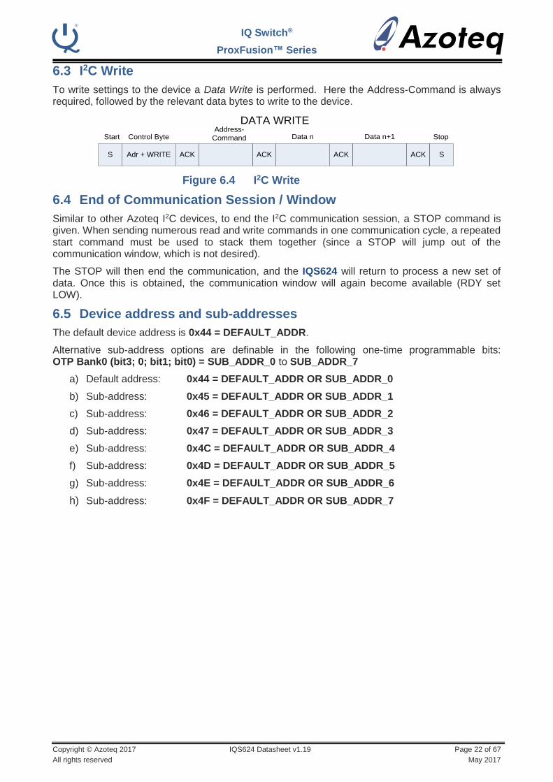
6.3 I2C Write
To write settings to the device a Data Write is performed. Here the Address-Command is always required, followed by the relevant data bytes to write to the device.
DATA WRITE
S
Start
Adr + WRITE
Control Byte
ACK
Address-
Command
ACK
Data n
ACK S
Stop
ACK
Data n+1
Figure 6.4 I2C Write
6.4 End of Communication Session / Window
Similar to other Azoteq I2C devices, to end the I2C communication session, a STOP command is given. When sending numerous read and write commands in one communication cycle, a repeated start command must be used to stack them together (since a STOP will jump out of the communication window, which is not desired).
The STOP will then end the communication, and the IQS624 will return to process a new set of data. Once this is obtained, the communication window will again become available (RDY set LOW).
6.5 Device address and sub-addresses
The default device address is 0x44 = DEFAULT_ADDR.
Alternative sub-address options are definable in the following one-time programmable bits: OTP Bank0 (bit3; 0; bit1; bit0) = SUB_ADDR_0 to SUB_ADDR_7
a) Default address: 0x44 = DEFAULT_ADDR OR SUB_ADDR_0
b) Sub-address: 0x45 = DEFAULT_ADDR OR SUB_ADDR_1
c) Sub-address: 0x46 = DEFAULT_ADDR OR SUB_ADDR_2
d) Sub-address: 0x47 = DEFAULT_ADDR OR SUB_ADDR_3
e) Sub-address: 0x4C = DEFAULT_ADDR OR SUB_ADDR_4
f) Sub-address: 0x4D = DEFAULT_ADDR OR SUB_ADDR_5
g) Sub-address: 0x4E = DEFAULT_ADDR OR SUB_ADDR_6
h) Sub-address: 0x4F = DEFAULT_ADDR OR SUB_ADDR_7

IQ Switch®
ProxFusion™ Series
Copyright © Azoteq 2017 IQS624 Datasheet v1.19 Page 23 of 67
All rights reserved May 2017
6.6 Additional OTP options
All one-time-programmable device options are located in FG bank 0.
Floating Gate Bank0
Bit Number 7 6 5 4 3 2 1 0
Name - Comms ATI
- Rdy active high
Sub address 2
8MHz Sub address 0-1
Default - 1 - 0 0 0 0 0
Bit definitions:
Bit 0,1,3: I2C sub-address
o I2C address = 0x44
Bit 2: Main Clock frequency selection
o 0: Run FOSC at 16MHz
o 1: Run FOSC at 8MHz
Bit 4: Rdy active high
o 0: Rdy active low enabled
o 1: Rdy active high enabled
Bit 6: Comms mode during ATI
o 0: No streaming events are generated during ATI
o 1: Comms continue as setup regardless of ATI state.
6.7 RDY Hand-Shake Routine
The master or host MCU has the capability to request a communication window at any time, by
pulling the RDY line low. The communication window will open directly following the current
conversion cycle. The RDY line can be configured as active high by setting the additional OTP bits
(bit 4). For more details please refer to the communication interface guide.
6.8 I2C Specific Commands
6.8.1 Show Reset
After start-up, and after every reset event, the “Show Reset” flag will be set in the System Flags register (0x10H; bit 7).
The “Show Reset” bit can be read to determine whether a reset has occurred on the device (it is
recommended to be continuously monitored). This bit will be set ’1’ after a reset.
The “Show Reset” flag will be cleared (set to ’0’) by writing a ’1’ into the “Ack reset” bit in the
General system settings register (0xD0; bit 6) . A reset will typically take place if a timeout during
communication occurs.
6.8.2 I2C Timeout
If no communication is initiated from the master/host MCU within the first tCOMMS (tCOMMS = 2.038 ms
default) of the RDY line indicating that data is available (i.e. RDY = low), the device will resume
with the next cycle of charge transfers and the data from the previous conversions will be lost.
There is also a timeout (tI2C) that cannot be disabled, for when communication has started but not
been completed, for example when the bus is being held by another device (tI2C = 33 ms).
6.9 I2C I/O Characteristics
The IQS624 requires the input voltages given in Table 6.1, for detecting high (“1”) and low (“0”)
input conditions on the I2C communication lines (SDA, SCL and RDY).
IQ Switch®
ProxFusion™ Series
Copyright © Azoteq 2017 IQS624 Datasheet v1.19 Page 24 of 67
All rights reserved May 2017
Table 6.1 IQS624 I2C Input voltage
Input Voltage (V)
VinLOW 0.3*VDDHI
VinHIGH 0.7*VDDHI
Table 6.2 provides the output voltage levels of the IQS624 device during I2C communication.
Table 6.2 IQS624 I2C Output voltage
Output Voltage (V)
VoutLOW GND +0.2 (max.)
VoutHIGH VDDHI – 0.2 (min.)
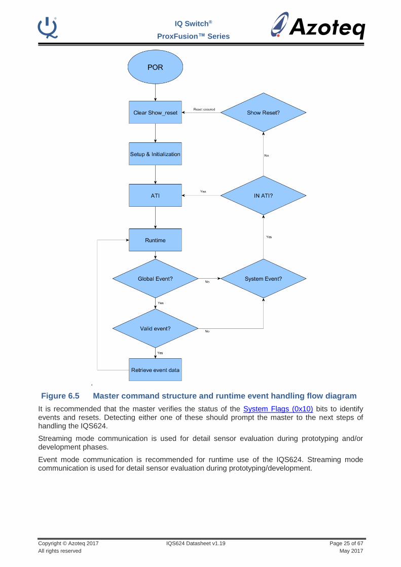
6.10 Recommended communication and runtime flow diagram
The following is a basic master program flow diagram to communicate and handle the device. It addresses possible device events such as output events, ATI and system events (resets).
IQ Switch®
ProxFusion™ Series
Copyright © Azoteq 2017 IQS624 Datasheet v1.19 Page 25 of 67
All rights reserved May 2017
.
Figure 6.5 Master command structure and runtime event handling flow diagram
It is recommended that the master verifies the status of the System Flags (0x10) bits to identify events and resets. Detecting either one of these should prompt the master to the next steps of handling the IQS624.
Streaming mode communication is used for detail sensor evaluation during prototyping and/or development phases.
Event mode communication is recommended for runtime use of the IQS624. Streaming mode communication is used for detail sensor evaluation during prototyping/development.
IQ Switch®
ProxFusion™ Series
Copyright © Azoteq 2017 IQS624 Datasheet v1.19 Page 26 of 67
All rights reserved May 2017
7 IQS624 Memory map
Table 7.1 IQS624 Register map
Register Address Group Register Name
00H
Device Information
Product Number
01H Software Number
02H Hardware Number
10H
Device Specific Data
System Flags
11H UI Flags
12H Proximity/Touch UI Flags
14H HALL UI Flags
15H Hall Ratio Flags
20H
Count Data
CH0 CS Low
21H CH0 CS High
22H CH1 CS Low
23H CH1 CS High
24H CH2 CS Low
25H CH2 CS High
26H CH3 CS Low
27H CH3 CS High
28H CH4 CS Low
29H CH4 CS High
2AH CH5 CS Low
2BH CH5 CS High
30H CH0 LTA Low
31H CH0 LTA High
32H CH1 LTA Low
33H CH1 LTA High
40H
ProxFusion sensor settings
Ch0 ProxFusion Settings 0
41H Ch1 ProxFusion Settings 0
42H Ch0&1 ProxFusion Settings 1
43H Ch0 ProxFusion Settings 2
44H Ch1 ProxFusion Settings 2
45H Ch0&1 ProxFusion Settings 3
46H Ch0 Compensation
47H Ch1 Compensation
48H Ch0 Multipliers
49H Ch1 Multipliers
50H
Touch / Proximity UI settings
Ch0 Proximity threshold
51H Ch0 Touch threshold
52H Ch1 Proximity threshold
53H Ch1 Touch threshold
54H UI Halt period
IQ Switch®
ProxFusion™ Series
Copyright © Azoteq 2017 IQS624 Datasheet v1.19 Page 27 of 67
All rights reserved May 2017
Register Address Register Name
70H
HALL Sensor Settings
Hall Rotation UI Settings
71H Hall Sensor Settings
72H Ch2&3 Hall ATI Settings
73H Ch4&5 Hall ATI Settings
74H Ch2&3 Compensation
75H Ch4&5 Compensation
76H Ch2&3 Multipliers
77H Ch4&5 Multipliers
78H Hall Ratio Settings
79H Sin Constant
7AH Cos Constant
80H
HALL Wheel Output
Degree Output (Low byte)
81H Degree Output (High byte)
82H Ratio Output (Low byte)
83H Ratio Output (High byte)
84H Numerator of Ratio (Low byte)
85H Numerator of Ratio (High byte)
86H Denominator of Ratio (Low byte)
87H Denominator of Ratio (High byte)
88H Rotation Correction factor (Low byte)
89H Rotation Correction factor (High byte)
8AH Max Numerator of Ratio (Low byte)
8BH Max Numerator of Ratio (High byte)
8CH Max Denominator of Ratio (Low byte)
8DH Max Denominator of Ratio (High byte)
8EH Relative Rotation Angle
8FH Movement counter/timer
D0H
Device and Power mode Settings
General System Settings
D1H Active Channels
D2H Power Mode Settings
D3H Normal mode report rate
D4H Low power mode report rate
D5H Ultra-low power mode report rate
D6H Auto Mode time
IQ Switch®
ProxFusion™ Series
Copyright © Azoteq 2017 IQS624 Datasheet v1.19 Page 28 of 67
All rights reserved May 2017
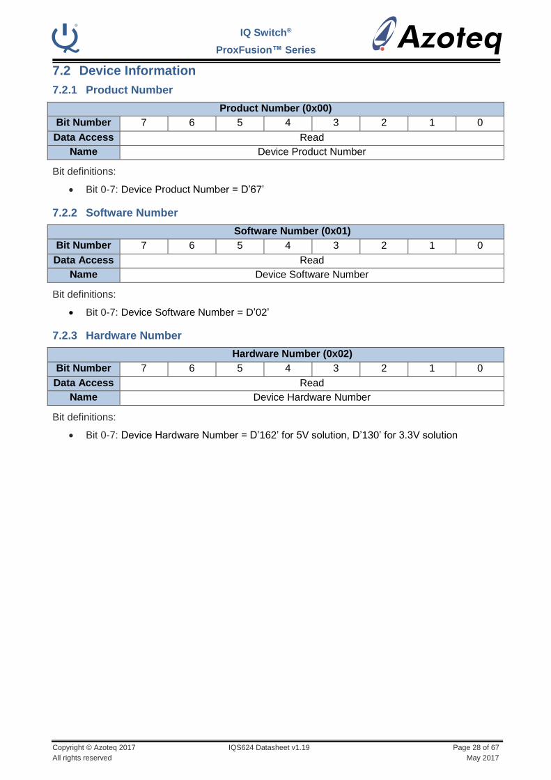
7.2 Device Information
7.2.1 Product Number
Product Number (0x00)
Bit Number 7 6 5 4 3 2 1 0
Data Access Read
Name Device Product Number
Bit definitions:
Bit 0-7: Device Product Number = D’67’
7.2.2 Software Number
Software Number (0x01)
Bit Number 7 6 5 4 3 2 1 0
Data Access Read
Name Device Software Number
Bit definitions:
Bit 0-7: Device Software Number = D’02’
7.2.3 Hardware Number
Hardware Number (0x02)
Bit Number 7 6 5 4 3 2 1 0
Data Access Read
Name Device Hardware Number
Bit definitions:
Bit 0-7: Device Hardware Number = D’162’ for 5V solution, D’130’ for 3.3V solution
IQ Switch®
ProxFusion™ Series
Copyright © Azoteq 2017 IQS624 Datasheet v1.19 Page 29 of 67
All rights reserved May 2017
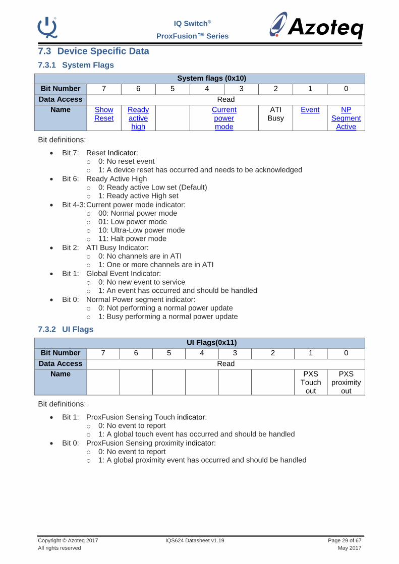
7.3 Device Specific Data
7.3.1 System Flags
System flags (0x10)
Bit Number 7 6 5 4 3 2 1 0
Data Access Read
Name Show Reset
Ready active high
Current power mode
ATI Busy
Event NP Segment
Active
Bit definitions:
Bit 7: Reset Indicator: o 0: No reset event o 1: A device reset has occurred and needs to be acknowledged
Bit 6: Ready Active High o 0: Ready active Low set (Default) o 1: Ready active High set
Bit 4-3: Current power mode indicator: o 00: Normal power mode o 01: Low power mode o 10: Ultra-Low power mode o 11: Halt power mode
Bit 2: ATI Busy Indicator: o 0: No channels are in ATI o 1: One or more channels are in ATI
Bit 1: Global Event Indicator: o 0: No new event to service o 1: An event has occurred and should be handled
Bit 0: Normal Power segment indicator: o 0: Not performing a normal power update o 1: Busy performing a normal power update
7.3.2 UI Flags
UI Flags(0x11)
Bit Number 7 6 5 4 3 2 1 0
Data Access Read
Name PXS Touch
out
PXS proximity
out
Bit definitions:
Bit 1: ProxFusion Sensing Touch indicator: o 0: No event to report o 1: A global touch event has occurred and should be handled
Bit 0: ProxFusion Sensing proximity indicator: o 0: No event to report o 1: A global proximity event has occurred and should be handled
IQ Switch®
ProxFusion™ Series
Copyright © Azoteq 2017 IQS624 Datasheet v1.19 Page 30 of 67
All rights reserved May 2017
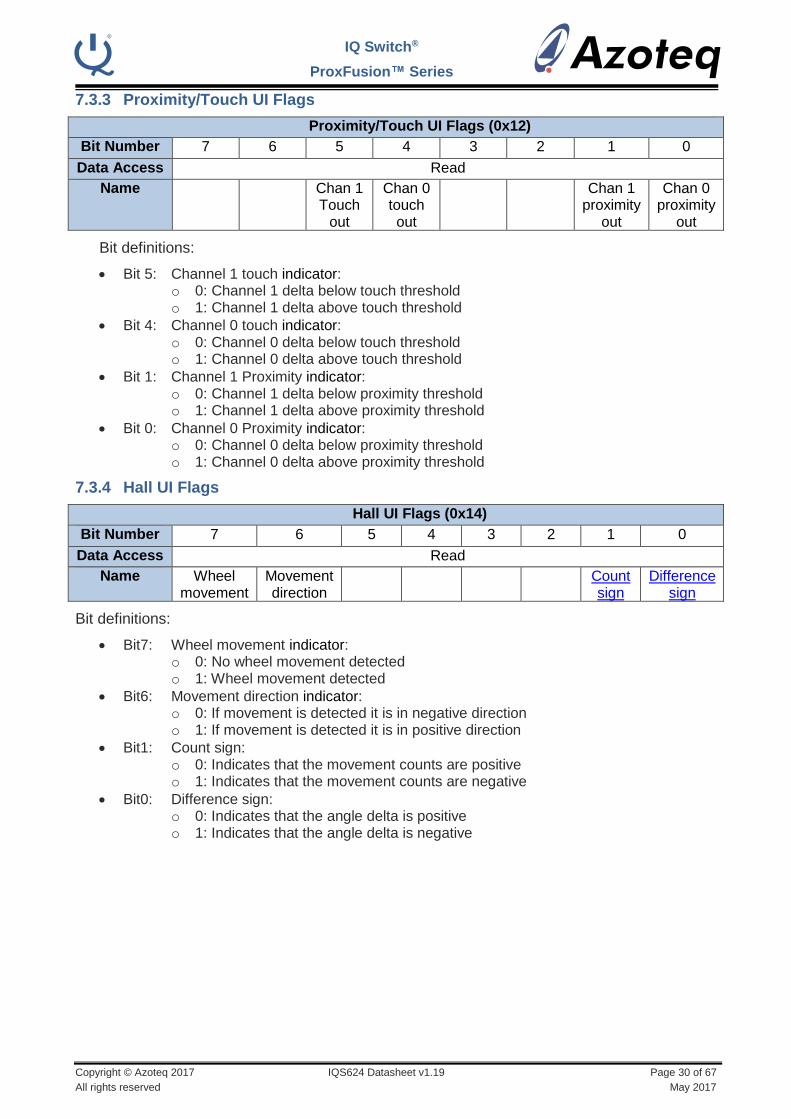
7.3.3 Proximity/Touch UI Flags
Proximity/Touch UI Flags (0x12)
Bit Number 7 6 5 4 3 2 1 0
Data Access Read
Name Chan 1 Touch
out
Chan 0 touch out
Chan 1 proximity
out
Chan 0 proximity
out
Bit definitions:
Bit 5: Channel 1 touch indicator: o 0: Channel 1 delta below touch threshold o 1: Channel 1 delta above touch threshold
Bit 4: Channel 0 touch indicator: o 0: Channel 0 delta below touch threshold o 1: Channel 0 delta above touch threshold
Bit 1: Channel 1 Proximity indicator: o 0: Channel 1 delta below proximity threshold o 1: Channel 1 delta above proximity threshold
Bit 0: Channel 0 Proximity indicator: o 0: Channel 0 delta below proximity threshold o 1: Channel 0 delta above proximity threshold
7.3.4 Hall UI Flags
Hall UI Flags (0x14)
Bit Number 7 6 5 4 3 2 1 0
Data Access Read
Name Wheel movement
Movement direction
Count sign
Difference sign
Bit definitions:
Bit7: Wheel movement indicator: o 0: No wheel movement detected o 1: Wheel movement detected
Bit6: Movement direction indicator: o 0: If movement is detected it is in negative direction o 1: If movement is detected it is in positive direction
Bit1: Count sign: o 0: Indicates that the movement counts are positive o 1: Indicates that the movement counts are negative
Bit0: Difference sign: o 0: Indicates that the angle delta is positive o 1: Indicates that the angle delta is negative

IQ Switch®
ProxFusion™ Series
Copyright © Azoteq 2017 IQS624 Datasheet v1.19 Page 31 of 67
All rights reserved May 2017
7.3.5 Hall Ratio Flags
Hall Ratio Flags (0x15)
Bit Number 7 6 5 4 3 2 1 0
Data Access Read
Name Move counter
full
Max Denominator
set
Max Numerator
set
Bit definitions:
Bit 2: Move counter full indicator: o 0: Movement counter is not full o 1: Movement counter is full
Bit 1: Max Denominator set indicator: o 0: Max denominator has not changed o 1: Max denominator has changed (used for auto calibration)
Bit 0: Max Numerator set indicator: o 0: Max Numerator has not changed o 1: Max Numerator has changed (used for auto calibration)
7.4 Count Data
7.4.1 Count CS Values
Count CS values (0x20/0x21-0x2A/0x2B)
Bit Number 15 14 13 12 11 10 9 8 7 6 5 4 3 2 1 0
Data Access Read
Name Count High Byte Count Low Byte
Bit definitions:
Bit 15-0: Counts
o AC filter or raw value
7.4.2 LTA Values
LTA values (0x30/0x31-0x32/0x33)
Bit Number 15 14 13 12 11 10 9 8 7 6 5 4 3 2 1 0
Data Access Read
Name LTA High Byte LTA Low Byte
Bit definitions:
Bit 15-0: LTA Values o LTA filter value
IQ Switch®
ProxFusion™ Series
Copyright © Azoteq 2017 IQS624 Datasheet v1.19 Page 32 of 67
All rights reserved May 2017
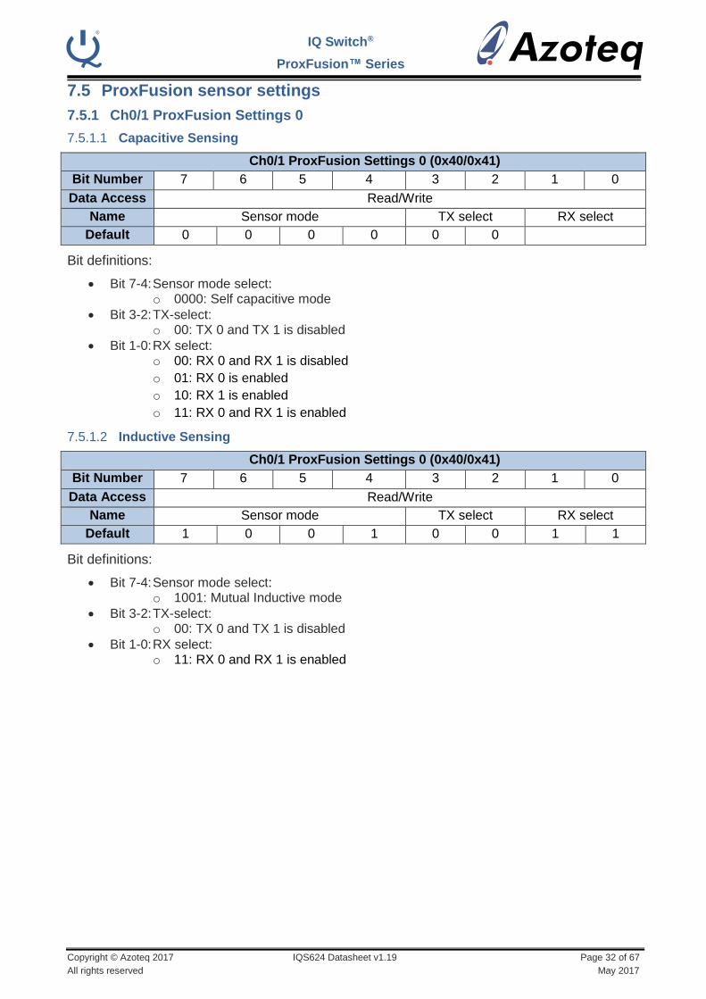
7.5 ProxFusion sensor settings
7.5.1 Ch0/1 ProxFusion Settings 0
7.5.1.1 Capacitive Sensing
Ch0/1 ProxFusion Settings 0 (0x40/0x41)
Bit Number 7 6 5 4 3 2 1 0
Data Access Read/Write
Name Sensor mode TX select RX select
Default 0 0 0 0 0 0
Bit definitions:
Bit 7-4: Sensor mode select: o 0000: Self capacitive mode
Bit 3-2: TX-select: o 00: TX 0 and TX 1 is disabled
Bit 1-0: RX select: o 00: RX 0 and RX 1 is disabled
o 01: RX 0 is enabled
o 10: RX 1 is enabled
o 11: RX 0 and RX 1 is enabled
7.5.1.2 Inductive Sensing
Ch0/1 ProxFusion Settings 0 (0x40/0x41)
Bit Number 7 6 5 4 3 2 1 0
Data Access Read/Write
Name Sensor mode TX select RX select
Default 1 0 0 1 0 0 1 1
Bit definitions:
Bit 7-4: Sensor mode select: o 1001: Mutual Inductive mode
Bit 3-2: TX-select: o 00: TX 0 and TX 1 is disabled
Bit 1-0: RX select: o 11: RX 0 and RX 1 is enabled
IQ Switch®
ProxFusion™ Series
Copyright © Azoteq 2017 IQS624 Datasheet v1.19 Page 33 of 67
All rights reserved May 2017
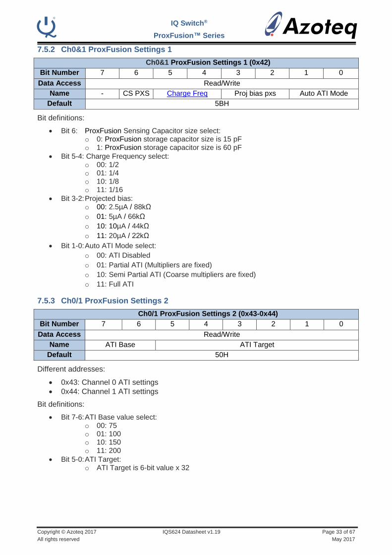
7.5.2 Ch0&1 ProxFusion Settings 1
Ch0&1 ProxFusion Settings 1 (0x42)
Bit Number 7 6 5 4 3 2 1 0
Data Access Read/Write
Name - CS PXS Charge Freq Proj bias pxs Auto ATI Mode
Default 5BH
Bit definitions:
Bit 6: ProxFusion Sensing Capacitor size select: o 0: ProxFusion storage capacitor size is 15 pF o 1: ProxFusion storage capacitor size is 60 pF
Bit 5-4: Charge Frequency select: o 00: 1/2 o 01: 1/4 o 10: 1/8 o 11: 1/16
Bit 3-2: Projected bias: o 00: 2.5µA / 88kΩ
o 01: 5µA / 66kΩ
o 10: 10µA / 44kΩ
o 11: 20µA / 22kΩ
Bit 1-0: Auto ATI Mode select:
o 00: ATI Disabled
o 01: Partial ATI (Multipliers are fixed)
o 10: Semi Partial ATI (Coarse multipliers are fixed)
o 11: Full ATI
7.5.3 Ch0/1 ProxFusion Settings 2
Ch0/1 ProxFusion Settings 2 (0x43-0x44)
Bit Number 7 6 5 4 3 2 1 0
Data Access Read/Write
Name ATI Base ATI Target
Default 50H
Different addresses:
0x43: Channel 0 ATI settings
0x44: Channel 1 ATI settings
Bit definitions:
Bit 7-6: ATI Base value select: o 00: 75 o 01: 100 o 10: 150 o 11: 200
Bit 5-0: ATI Target: o ATI Target is 6-bit value x 32
IQ Switch®
ProxFusion™ Series
Copyright © Azoteq 2017 IQS624 Datasheet v1.19 Page 34 of 67
All rights reserved May 2017
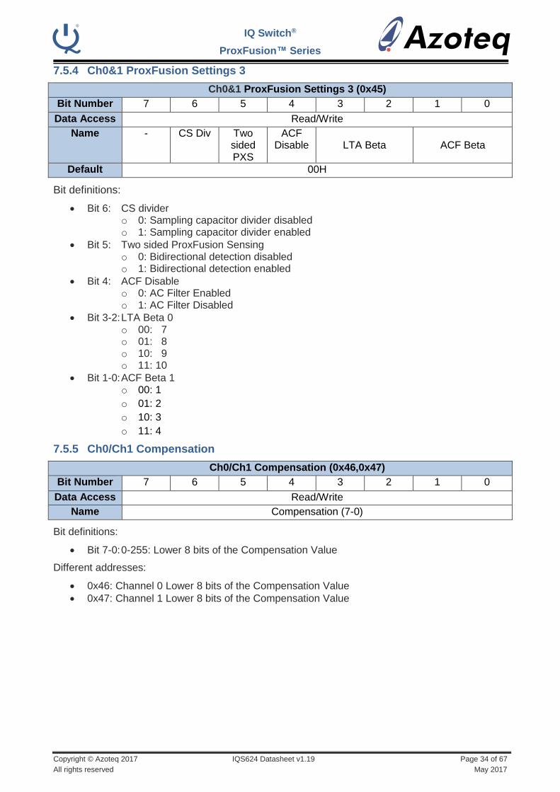
7.5.4 Ch0&1 ProxFusion Settings 3
Ch0&1 ProxFusion Settings 3 (0x45)
Bit Number 7 6 5 4 3 2 1 0
Data Access Read/Write
Name - CS Div Two sided PXS
ACF Disable LTA Beta ACF Beta
Default 00H
Bit definitions:
Bit 6: CS divider o 0: Sampling capacitor divider disabled o 1: Sampling capacitor divider enabled
Bit 5: Two sided ProxFusion Sensing o 0: Bidirectional detection disabled o 1: Bidirectional detection enabled
Bit 4: ACF Disable o 0: AC Filter Enabled o 1: AC Filter Disabled
Bit 3-2: LTA Beta 0 o 00: 7 o 01: 8 o 10: 9 o 11: 10
Bit 1-0: ACF Beta 1 o 00: 1
o 01: 2
o 10: 3
o 11: 4
7.5.5 Ch0/Ch1 Compensation
Ch0/Ch1 Compensation (0x46,0x47)
Bit Number 7 6 5 4 3 2 1 0
Data Access Read/Write
Name Compensation (7-0)
Bit definitions:
Bit 7-0: 0-255: Lower 8 bits of the Compensation Value
Different addresses:
0x46: Channel 0 Lower 8 bits of the Compensation Value
0x47: Channel 1 Lower 8 bits of the Compensation Value
IQ Switch®
ProxFusion™ Series
Copyright © Azoteq 2017 IQS624 Datasheet v1.19 Page 35 of 67
All rights reserved May 2017
7.5.6 Ch0/Ch1 Multipliers values
Ch0/1 Multipliers values(0x48/0x49)
Bit Number 7 6 5 4 3 2 1 0
Data Access Read/Write
Name Compensation (9-8) Coarse multiplier Fine multiplier
Bit definitions:
Bit 7-6: Compensation upper two bits o 0-3: Upper 2-bits of the Compensation value.
Bit 5-4: Coarse multiplier Selection: o 0-3: Coarse multiplier selection
Bit 3-0: Fine Multiplier Selection: o 0-15: Fine Multiplier selection
7.6 Touch / Proximity UI settings
7.6.1 Ch0/1 Proximity/touch threshold
Proximity/touch threshold Ch0,1(0x50-0x53)
Bit Number 7 6 5 4 3 2 1 0
Data Access Read/Write
Name Threshold
Bit 7-0: Proximity and touch thresholds: If a difference between the LTA and counts value would exceed this threshold the appropriate event would be flagged (either Touch or Proximity Event).
Different addresses:
0x50 Ch0 Proximity Threshold Value
0x51 Ch0 Touch Threshold Value
0x52 Ch1 Proximity Threshold Value
0x53 Ch1 Touch Threshold Value
7.6.2 UI Halt period
UI Halt period (0x54)
Bit Number 7 6 5 4 3 2 1 0
Data Access Read/Write
Name UI Halt period
Default 28H = 20 sec
Bit definitions:
Bit 7-0: Halt time in 500 ms ticks
IQ Switch®
ProxFusion™ Series
Copyright © Azoteq 2017 IQS624 Datasheet v1.19 Page 36 of 67
All rights reserved May 2017
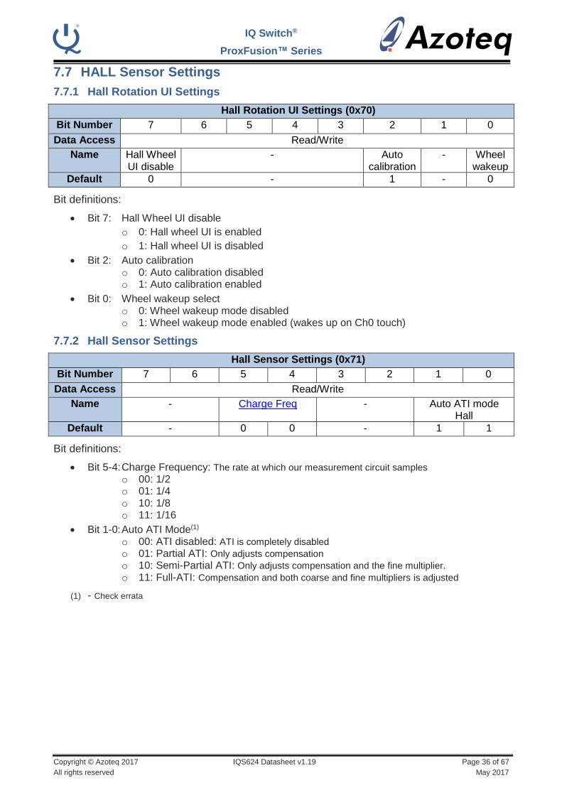
7.7 HALL Sensor Settings
7.7.1 Hall Rotation UI Settings
Hall Rotation UI Settings (0x70)
Bit Number 7 6 5 4 3 2 1 0
Data Access Read/Write
Name Hall Wheel UI disable
- Auto calibration
- Wheel wakeup
Default 0 - 1 - 0
Bit definitions:
Bit 7: Hall Wheel UI disable
o 0: Hall wheel UI is enabled
o 1: Hall wheel UI is disabled
Bit 2: Auto calibration o 0: Auto calibration disabled o 1: Auto calibration enabled
Bit 0: Wheel wakeup select o 0: Wheel wakeup mode disabled o 1: Wheel wakeup mode enabled (wakes up on Ch0 touch)
7.7.2 Hall Sensor Settings
Hall Sensor Settings (0x71)
Bit Number 7 6 5 4 3 2 1 0
Data Access Read/Write
Name - Charge Freq - Auto ATI mode Hall
Default - 0 0 - 1 1
Bit definitions:
Bit 5-4: Charge Frequency: The rate at which our measurement circuit samples o 00: 1/2 o 01: 1/4 o 10: 1/8 o 11: 1/16
Bit 1-0: Auto ATI Mode(1) o 00: ATI disabled: ATI is completely disabled o 01: Partial ATI: Only adjusts compensation o 10: Semi-Partial ATI: Only adjusts compensation and the fine multiplier. o 11: Full-ATI: Compensation and both coarse and fine multipliers is adjusted
(1) - Check errata

IQ Switch®
ProxFusion™ Series
Copyright © Azoteq 2017 IQS624 Datasheet v1.19 Page 37 of 67
All rights reserved May 2017
7.7.3 Ch2/3, Ch4/5 Hall ATI Settings
Ch2/3, Ch4/5 Hall ATI Settings (0x72/0x73)
Bit Number 7 6 5 4 3 2 1 0
Data Access Read/Write
Name ATI Base ATI Target
Default 73H
Different addresses:
0x72: Channel 2 & 3 ATI settings
0x73: Channel 4 & 5 ATI settings Bit definitions:
Bit 7-6: ATI Base value select: o 00: 75 o 01: 100 o 10: 150 o 11: 200
Bit 5-0: ATI Target: o ATI Target is 6-bit value x 32
7.7.4 Ch2/3, Ch4/5 Hall Compensation
Ch2/3, Ch4/5 Hall Compensation (0x74,0x75)
Bit Number 7 6 5 4 3 2 1 0
Data Access Read/Write
Name Compensation (7-0)
Bit definitions:
Bit 7-0: 0-255: Lower 8 bits of the compensation value Different addresses:
0x74: Channel 2/3 Lower 8 bits of the compensation Value
0x75: Channel 4/5 Lower 8 bits of the compensation Value
7.7.5 Ch2/3, Ch4/5 Hall Multipliers Ch2/3, Ch4/5 Hall Multipliers (0x76-0x77)
Bit Number 7 6 5 4 3 2 1 0
Data Access Read/Write
Name Compensation 9-8 Coarse Multiplier Fine Multiplier
Different addresses:
0x76 – Channel 2/3 Multipliers selection
0x77 – Channel 4/5 Multipliers selection
Bit definitions:
Bit 7-6: Compensation 9-8: o 0-3: Upper 2-bits of the compensation value
Bit 5-4: Coarse multiplier selection o 0-3: Coarse multiplier selection
Bit 3-0: Fine multiplier selection o 0-15: Fine multiplier selection
IQ Switch®
ProxFusion™ Series
Copyright © Azoteq 2017 IQS624 Datasheet v1.19 Page 38 of 67
All rights reserved May 2017
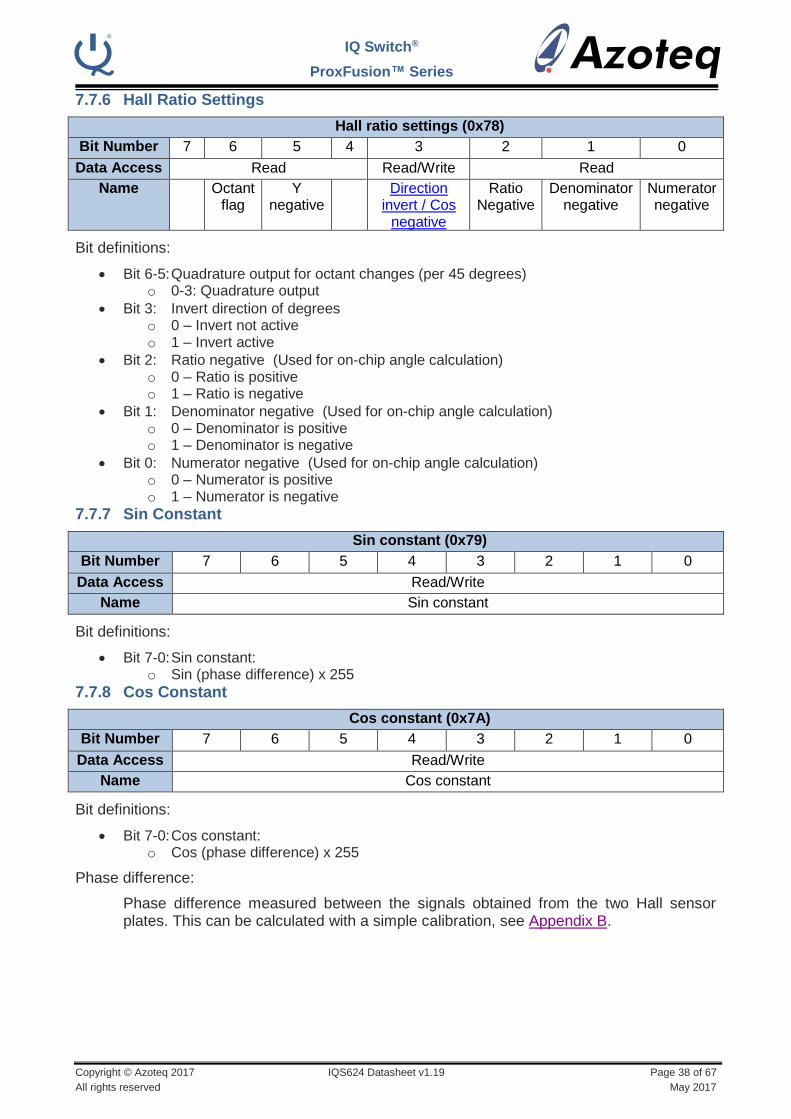
7.7.6 Hall Ratio Settings
Hall ratio settings (0x78)
Bit Number 7 6 5 4 3 2 1 0
Data Access Read Read/Write Read
Name Octant flag
Y negative
Direction invert / Cos
negative
Ratio Negative
Denominator negative
Numerator negative
Bit definitions:
Bit 6-5: Quadrature output for octant changes (per 45 degrees) o 0-3: Quadrature output
Bit 3: Invert direction of degrees o 0 – Invert not active o 1 – Invert active
Bit 2: Ratio negative (Used for on-chip angle calculation) o 0 – Ratio is positive o 1 – Ratio is negative
Bit 1: Denominator negative (Used for on-chip angle calculation) o 0 – Denominator is positive o 1 – Denominator is negative
Bit 0: Numerator negative (Used for on-chip angle calculation) o 0 – Numerator is positive o 1 – Numerator is negative
7.7.7 Sin Constant
Sin constant (0x79)
Bit Number 7 6 5 4 3 2 1 0
Data Access Read/Write
Name Sin constant
Bit definitions:
Bit 7-0: Sin constant: o Sin (phase difference) x 255
7.7.8 Cos Constant
Cos constant (0x7A)
Bit Number 7 6 5 4 3 2 1 0
Data Access Read/Write
Name Cos constant
Bit definitions:
Bit 7-0: Cos constant: o Cos (phase difference) x 255
Phase difference:
Phase difference measured between the signals obtained from the two Hall sensor plates. This can be calculated with a simple calibration, see Appendix B.
IQ Switch®
ProxFusion™ Series
Copyright © Azoteq 2017 IQS624 Datasheet v1.19 Page 39 of 67
All rights reserved May 2017
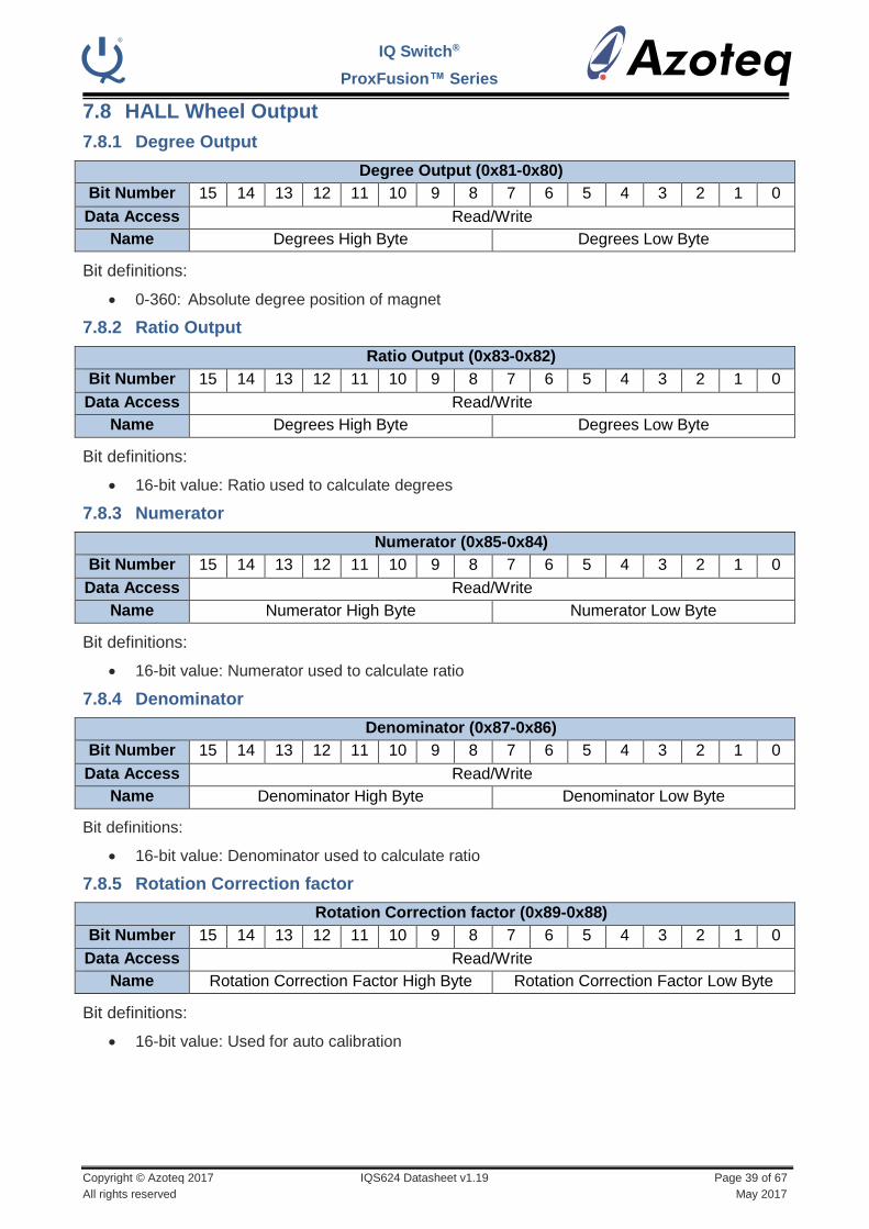
7.8 HALL Wheel Output
7.8.1 Degree Output
Degree Output (0x81-0x80)
Bit Number 15 14 13 12 11 10 9 8 7 6 5 4 3 2 1 0
Data Access Read/Write
Name Degrees High Byte Degrees Low Byte
Bit definitions:
0-360: Absolute degree position of magnet
7.8.2 Ratio Output
Ratio Output (0x83-0x82)
Bit Number 15 14 13 12 11 10 9 8 7 6 5 4 3 2 1 0
Data Access Read/Write
Name Degrees High Byte Degrees Low Byte
Bit definitions:
16-bit value: Ratio used to calculate degrees
7.8.3 Numerator
Numerator (0x85-0x84)
Bit Number 15 14 13 12 11 10 9 8 7 6 5 4 3 2 1 0
Data Access Read/Write
Name Numerator High Byte Numerator Low Byte
Bit definitions:
16-bit value: Numerator used to calculate ratio
7.8.4 Denominator
Denominator (0x87-0x86)
Bit Number 15 14 13 12 11 10 9 8 7 6 5 4 3 2 1 0
Data Access Read/Write
Name Denominator High Byte Denominator Low Byte
Bit definitions:
16-bit value: Denominator used to calculate ratio
7.8.5 Rotation Correction factor
Rotation Correction factor (0x89-0x88)
Bit Number 15 14 13 12 11 10 9 8 7 6 5 4 3 2 1 0
Data Access Read/Write
Name Rotation Correction Factor High Byte Rotation Correction Factor Low Byte
Bit definitions:
16-bit value: Used for auto calibration
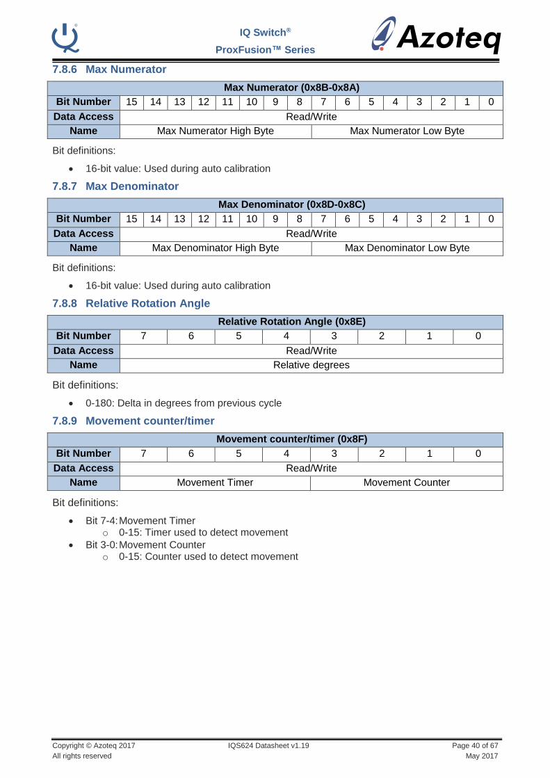
IQ Switch®
ProxFusion™ Series
Copyright © Azoteq 2017 IQS624 Datasheet v1.19 Page 40 of 67
All rights reserved May 2017
7.8.6 Max Numerator
Max Numerator (0x8B-0x8A)
Bit Number 15 14 13 12 11 10 9 8 7 6 5 4 3 2 1 0
Data Access Read/Write
Name Max Numerator High Byte Max Numerator Low Byte
Bit definitions:
16-bit value: Used during auto calibration
7.8.7 Max Denominator
Max Denominator (0x8D-0x8C)
Bit Number 15 14 13 12 11 10 9 8 7 6 5 4 3 2 1 0
Data Access Read/Write
Name Max Denominator High Byte Max Denominator Low Byte
Bit definitions:
16-bit value: Used during auto calibration
7.8.8 Relative Rotation Angle
Relative Rotation Angle (0x8E)
Bit Number 7 6 5 4 3 2 1 0
Data Access Read/Write
Name Relative degrees
Bit definitions:
0-180: Delta in degrees from previous cycle
7.8.9 Movement counter/timer
Movement counter/timer (0x8F)
Bit Number 7 6 5 4 3 2 1 0
Data Access Read/Write
Name Movement Timer Movement Counter
Bit definitions:
Bit 7-4: Movement Timer o 0-15: Timer used to detect movement
Bit 3-0: Movement Counter o 0-15: Counter used to detect movement
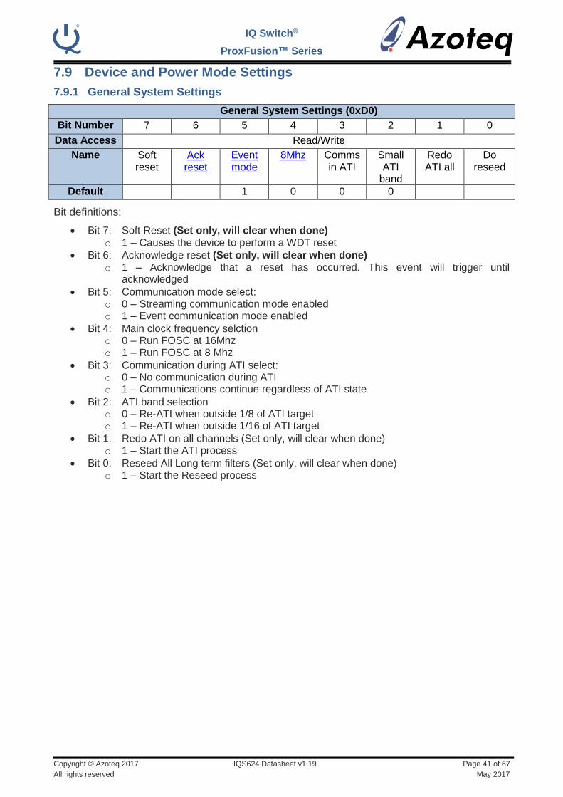
IQ Switch®
ProxFusion™ Series
Copyright © Azoteq 2017 IQS624 Datasheet v1.19 Page 41 of 67
All rights reserved May 2017
7.9 Device and Power Mode Settings
7.9.1 General System Settings
General System Settings (0xD0)
Bit Number 7 6 5 4 3 2 1 0
Data Access Read/Write
Name Soft reset
Ack reset
Event mode
8Mhz Comms in ATI
Small ATI
band
Redo ATI all
Do reseed
Default 1 0 0 0
Bit definitions:
Bit 7: Soft Reset (Set only, will clear when done) o 1 – Causes the device to perform a WDT reset
Bit 6: Acknowledge reset (Set only, will clear when done) o 1 – Acknowledge that a reset has occurred. This event will trigger until
acknowledged
Bit 5: Communication mode select: o 0 – Streaming communication mode enabled o 1 – Event communication mode enabled
Bit 4: Main clock frequency selction o 0 – Run FOSC at 16Mhz o 1 – Run FOSC at 8 Mhz
Bit 3: Communication during ATI select: o 0 – No communication during ATI o 1 – Communications continue regardless of ATI state
Bit 2: ATI band selection o 0 – Re-ATI when outside 1/8 of ATI target o 1 – Re-ATI when outside 1/16 of ATI target
Bit 1: Redo ATI on all channels (Set only, will clear when done) o 1 – Start the ATI process
Bit 0: Reseed All Long term filters (Set only, will clear when done) o 1 – Start the Reseed process

IQ Switch®
ProxFusion™ Series
Copyright © Azoteq 2017 IQS624 Datasheet v1.19 Page 42 of 67
All rights reserved May 2017
7.9.2 Active Channels Mask
Active Channels Mask (0xD1)
Bit Number 7 6 5 4 3 2 1 0
Data Access Read/Write
Name CH5 CH4 CH3 CH2 CH1 CH0
Default 3FH
Bit definitions:
Bit 5: CH5 (note: Ch2, Ch3, Ch4 and Ch5 must all be enabled for Hall effect rotation UI to be functional)
o 0: Channel is disabled o 1: Channel is enabled
Bit 4: CH4 (note: Ch2, Ch3, Ch4 and Ch5 must all be enabled for Hall effect rotation UI to be functional)
o 0: Channel is disabled o 1: Channel is enabled
Bit 3: CH3 (note: Ch2, Ch3, Ch4 and Ch5 must all be enabled for Hall effect rotation UI to be functional)
o 0: Channel is disabled o 1: Channel is enabled
Bit 2: CH2 (note: Ch2, Ch3, Ch4 and Ch5 must all be enabled for Hall effect rotation UI to be functional)
o 0: Channel is disabled o 1: Channel is enabled
Bit 1: CH1 o 0: Channel is disabled o 1: Channel is enabled
Bit 0: CH0 o 0: Channel is disabled o 1: Channel is enabled
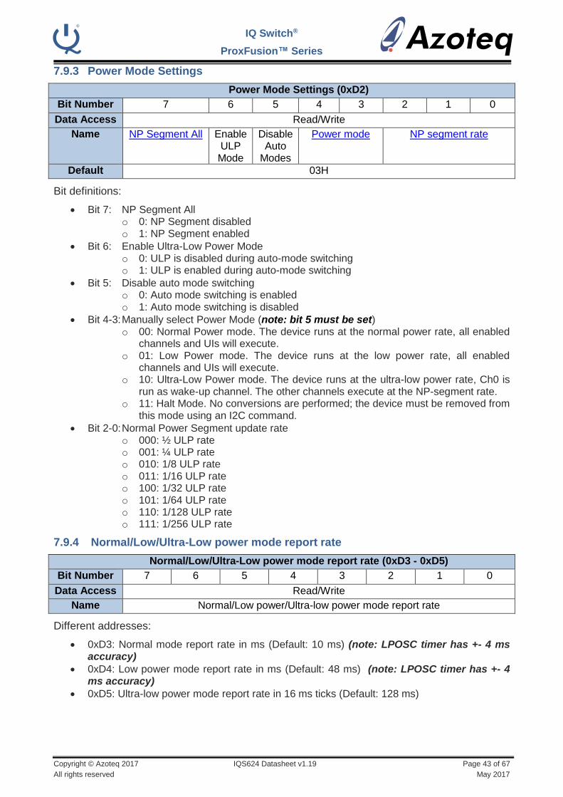
IQ Switch®
ProxFusion™ Series
Copyright © Azoteq 2017 IQS624 Datasheet v1.19 Page 43 of 67
All rights reserved May 2017
7.9.3 Power Mode Settings
Power Mode Settings (0xD2)
Bit Number 7 6 5 4 3 2 1 0
Data Access Read/Write
Name NP Segment All Enable ULP Mode
Disable Auto
Modes
Power mode NP segment rate
Default 03H
Bit definitions:
Bit 7: NP Segment All o 0: NP Segment disabled o 1: NP Segment enabled
Bit 6: Enable Ultra-Low Power Mode o 0: ULP is disabled during auto-mode switching o 1: ULP is enabled during auto-mode switching
Bit 5: Disable auto mode switching o 0: Auto mode switching is enabled o 1: Auto mode switching is disabled
Bit 4-3: Manually select Power Mode (note: bit 5 must be set) o 00: Normal Power mode. The device runs at the normal power rate, all enabled
channels and UIs will execute. o 01: Low Power mode. The device runs at the low power rate, all enabled
channels and UIs will execute. o 10: Ultra-Low Power mode. The device runs at the ultra-low power rate, Ch0 is
run as wake-up channel. The other channels execute at the NP-segment rate. o 11: Halt Mode. No conversions are performed; the device must be removed from
this mode using an I2C command.
Bit 2-0: Normal Power Segment update rate o 000: ½ ULP rate o 001: ¼ ULP rate o 010: 1/8 ULP rate o 011: 1/16 ULP rate o 100: 1/32 ULP rate o 101: 1/64 ULP rate o 110: 1/128 ULP rate o 111: 1/256 ULP rate
7.9.4 Normal/Low/Ultra-Low power mode report rate
Normal/Low/Ultra-Low power mode report rate (0xD3 - 0xD5)
Bit Number 7 6 5 4 3 2 1 0
Data Access Read/Write
Name Normal/Low power/Ultra-low power mode report rate
Different addresses:
0xD3: Normal mode report rate in ms (Default: 10 ms) (note: LPOSC timer has +- 4 ms accuracy)
0xD4: Low power mode report rate in ms (Default: 48 ms) (note: LPOSC timer has +- 4 ms accuracy)
0xD5: Ultra-low power mode report rate in 16 ms ticks (Default: 128 ms)

IQ Switch®
ProxFusion™ Series
Copyright © Azoteq 2017 IQS624 Datasheet v1.19 Page 44 of 67
All rights reserved May 2017
7.9.5 Auto Mode Time
Auto Mode Time (0xD6)
Bit Number 7 6 5 4 3 2 1 0
Data Access Read/Write
Name Mode time
Default 14H = 10 sec
Bit definitions:
Bit 7-0: Auto modes switching time in 500 ms ticks
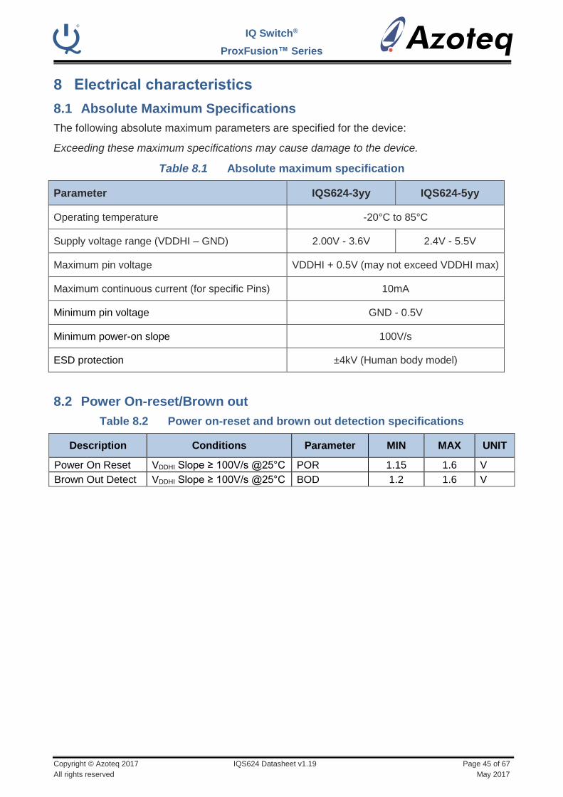
IQ Switch®
ProxFusion™ Series
Copyright © Azoteq 2017 IQS624 Datasheet v1.19 Page 45 of 67
All rights reserved May 2017
8 Electrical characteristics
8.1 Absolute Maximum Specifications
The following absolute maximum parameters are specified for the device:
Exceeding these maximum specifications may cause damage to the device.
Table 8.1 Absolute maximum specification
Parameter IQS624-3yy IQS624-5yy
Operating temperature -20°C to 85°C
Supply voltage range (VDDHI – GND) 2.00V - 3.6V 2.4V - 5.5V
Maximum pin voltage VDDHI + 0.5V (may not exceed VDDHI max)
Maximum continuous current (for specific Pins) 10mA
Minimum pin voltage GND - 0.5V
Minimum power-on slope 100V/s
ESD protection ±4kV (Human body model)
8.2 Power On-reset/Brown out
Table 8.2 Power on-reset and brown out detection specifications
Description Conditions Parameter MIN MAX UNIT
Power On Reset VDDHI Slope ≥ 100V/s @25°C POR 1.15 1.6 V
Brown Out Detect VDDHI Slope ≥ 100V/s @25°C BOD 1.2 1.6 V
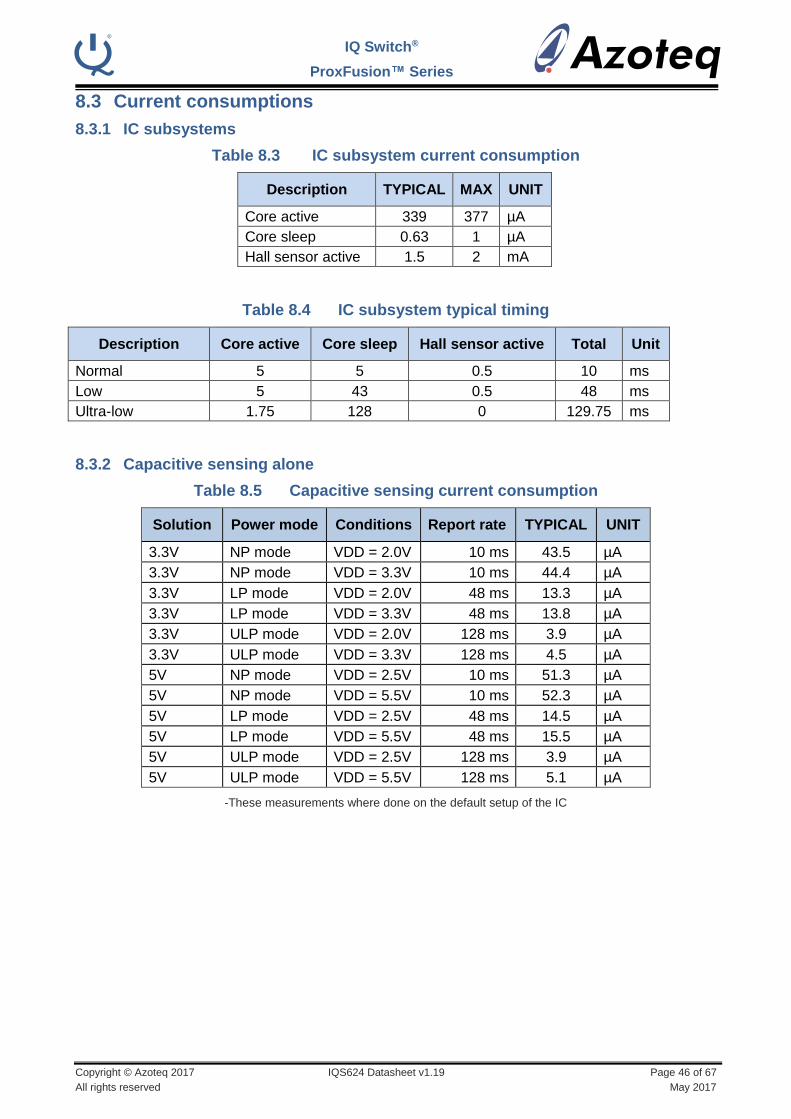
IQ Switch®
ProxFusion™ Series
Copyright © Azoteq 2017 IQS624 Datasheet v1.19 Page 46 of 67
All rights reserved May 2017
8.3 Current consumptions
8.3.1 IC subsystems
Table 8.3 IC subsystem current consumption
Description TYPICAL MAX UNIT
Core active 339 377 µA
Core sleep 0.63 1 µA
Hall sensor active 1.5 2 mA
Table 8.4 IC subsystem typical timing
Description Core active Core sleep Hall sensor active Total Unit
Normal 5 5 0.5 10 ms
Low 5 43 0.5 48 ms
Ultra-low 1.75 128 0 129.75 ms
8.3.2 Capacitive sensing alone
Table 8.5 Capacitive sensing current consumption
Solution Power mode Conditions Report rate TYPICAL UNIT
3.3V NP mode VDD = 2.0V 10 ms 43.5 µA
3.3V NP mode VDD = 3.3V 10 ms 44.4 µA
3.3V LP mode VDD = 2.0V 48 ms 13.3 µA
3.3V LP mode VDD = 3.3V 48 ms 13.8 µA
3.3V ULP mode VDD = 2.0V 128 ms 3.9 µA
3.3V ULP mode VDD = 3.3V 128 ms 4.5 µA
5V NP mode VDD = 2.5V 10 ms 51.3 µA
5V NP mode VDD = 5.5V 10 ms 52.3 µA
5V LP mode VDD = 2.5V 48 ms 14.5 µA
5V LP mode VDD = 5.5V 48 ms 15.5 µA
5V ULP mode VDD = 2.5V 128 ms 3.9 µA
5V ULP mode VDD = 5.5V 128 ms 5.1 µA
-These measurements where done on the default setup of the IC

IQ Switch®
ProxFusion™ Series
Copyright © Azoteq 2017 IQS624 Datasheet v1.19 Page 47 of 67
All rights reserved May 2017
8.3.3 Hall-effect sensing alone
Table 8.6 Hall-effect current consumption
Solution Power mode Conditions Report rate TYPICAL UNIT
3.3V NP mode VDD = 2.0V 10 ms 215.2 µA
3.3V NP mode VDD = 3.3V 10 ms 212.6 µA
3.3V LP mode VDD = 2.0V 48 ms 58.3 µA
3.3V LP mode VDD = 3.3V 48 ms 55.1 µA
3.3V ULP mode VDD = 2.0V 128 ms N/A (1) µA
3.3V ULP mode VDD = 3.3V 128 ms N/A (1) µA
5V NP mode VDD = 2.5V 10 ms 240.0 µA
5V NP mode VDD = 5.5V 10 ms 239.3 µA
5V LP mode VDD = 2.5V 48 ms 64.1 µA
5V LP mode VDD = 5.5V 48 ms 64.8 µA
5V ULP mode VDD = 2.5V 128 ms N/A (1) µA
5V ULP mode VDD = 5.5V 128 ms N/A (1) µA
-These measurements where done on the default setup of the IC
(1) –It is not advised to use the IQS624 in ULP without capacitive sensing. This is due to the Hall-effect sensor being disabled in ULP.
8.3.4 Halt mode
Table 8.7 Halt mode current consumption
Solution Power mode Conditions TYPICAL UNIT
3.3V Halt mode VDD = 2.0V 1.6 µA
3.3V Halt mode VDD = 3.3V 1.9 µA
5V Halt mode VDD = 2.5V 1.1 µA
5V Halt mode VDD = 5.5V 2.2 µA
8.4 Capacitive loading limits
To be completed.
8.5 Hall-effect measurement limits
To be completed.
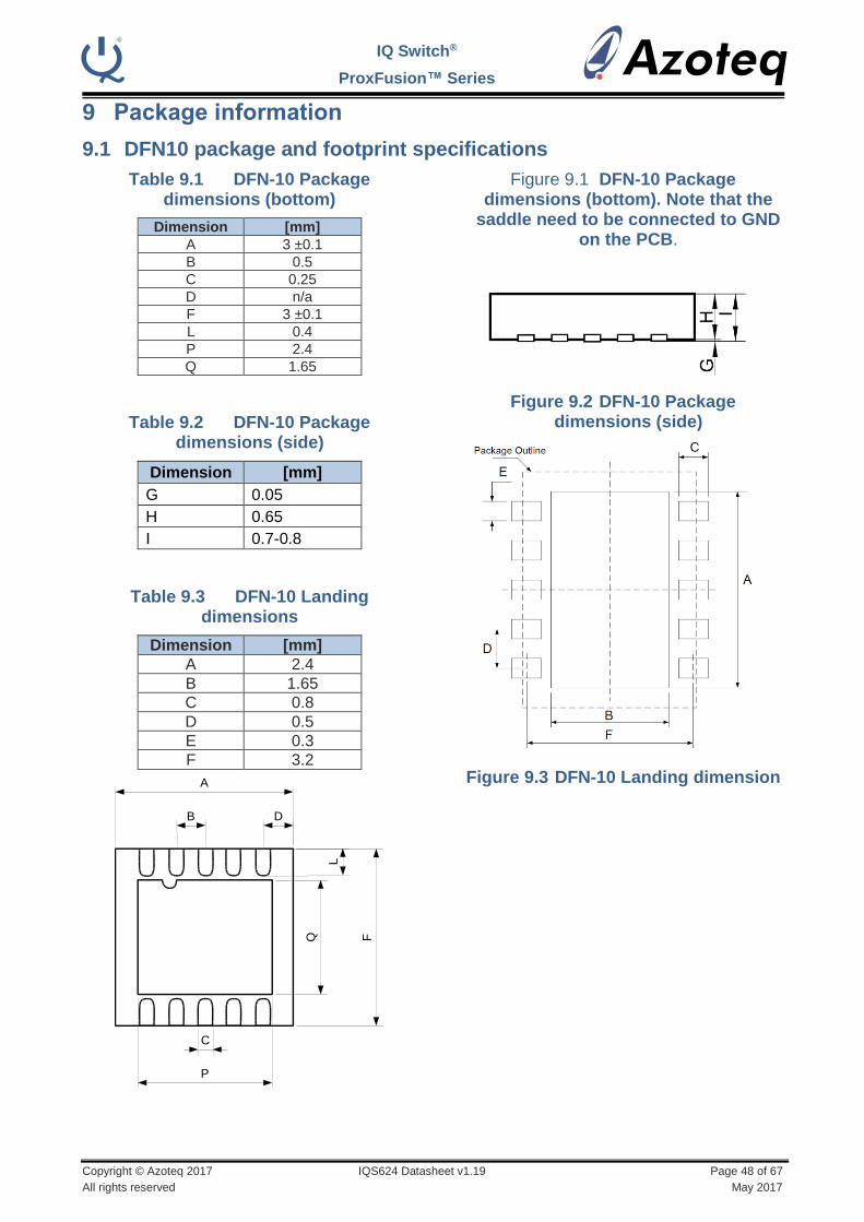
IQ Switch®
ProxFusion™ Series
Copyright © Azoteq 2017 IQS624 Datasheet v1.19 Page 48 of 67
All rights reserved May 2017
9 Package information
9.1 DFN10 package and footprint specifications
Table 9.1 DFN-10 Package dimensions (bottom)
Dimension [mm]
A 3 ±0.1
B 0.5
C 0.25
D n/a
F 3 ±0.1
L 0.4
P 2.4
Q 1.65
Table 9.2 DFN-10 Package dimensions (side)
Dimension [mm]
G 0.05
H 0.65
I 0.7-0.8
Table 9.3 DFN-10 Landing dimensions
Dimension [mm]
A 2.4
B 1.65
C 0.8
D 0.5
E 0.3
F 3.2
Figure 9.1 DFN-10 Package dimensions (bottom). Note that the
saddle need to be connected to GND on the PCB.
Figure 9.2 DFN-10 Package dimensions (side)
Figure 9.3 DFN-10 Landing dimension
A
DB
L
Q F
P
C
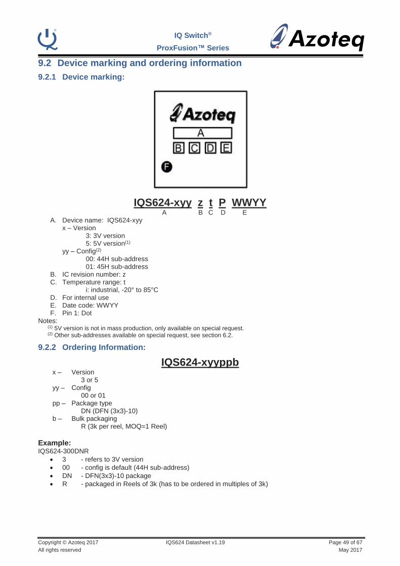
IQ Switch®
ProxFusion™ Series
Copyright © Azoteq 2017 IQS624 Datasheet v1.19 Page 49 of 67
All rights reserved May 2017
9.2 Device marking and ordering information
9.2.1 Device marking:
IQS624-xyy z t P WWYY A B C D E
A. Device name: IQS624-xyy x – Version
3: 3V version 5: 5V version(1)
yy – Config(2)
00: 44H sub-address 01: 45H sub-address
B. IC revision number: z C. Temperature range: t
i: industrial, -20° to 85°C D. For internal use E. Date code: WWYY F. Pin 1: Dot
Notes: (1) 5V version is not in mass production, only available on special request. (2) Other sub-addresses available on special request, see section 6.2.
9.2.2 Ordering Information:
IQS624-xyyppb x – Version 3 or 5 yy – Config 00 or 01 pp – Package type DN (DFN (3x3)-10) b – Bulk packaging R (3k per reel, MOQ=1 Reel)
Example: IQS624-300DNR
3 - refers to 3V version
00 - config is default (44H sub-address)
DN - DFN(3x3)-10 package
R - packaged in Reels of 3k (has to be ordered in multiples of 3k)
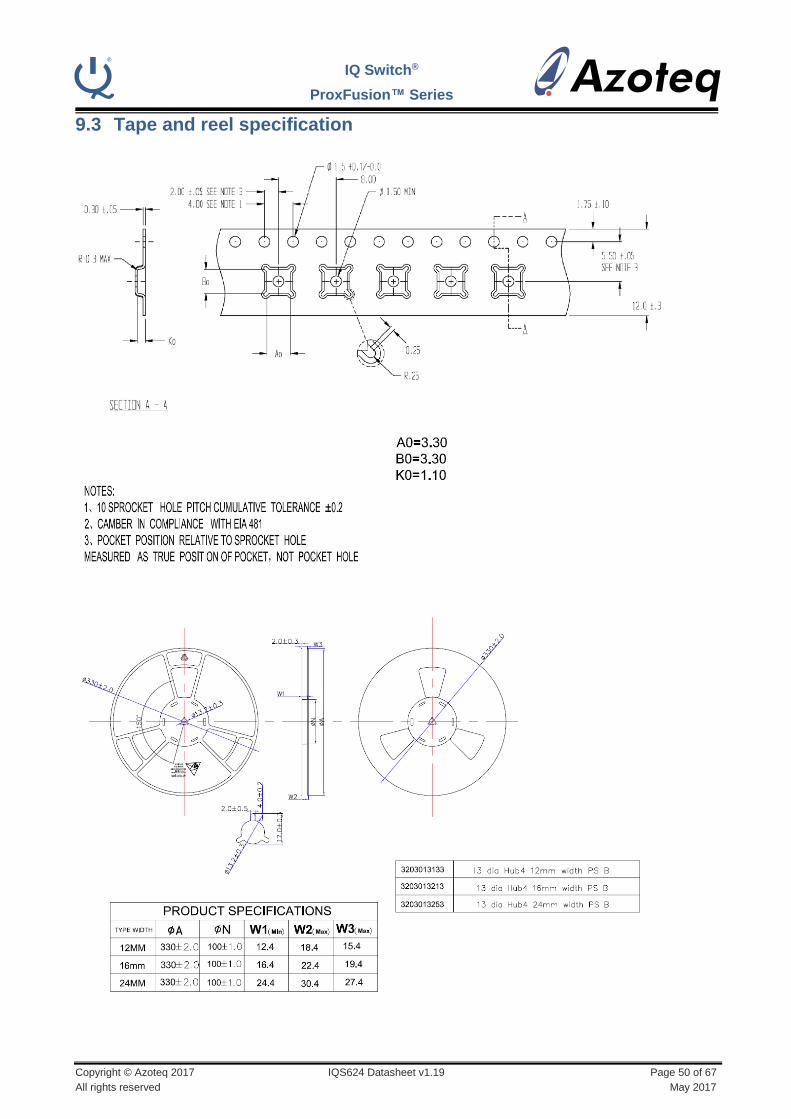
IQ Switch®
ProxFusion™ Series
Copyright © Azoteq 2017 IQS624 Datasheet v1.19 Page 50 of 67
All rights reserved May 2017
9.3 Tape and reel specification
IQ Switch®
ProxFusion™ Series
Copyright © Azoteq 2017 IQS624 Datasheet v1.19 Page 51 of 67
All rights reserved May 2017
9.4 MSL Level
Moisture Sensitivity Level (MSL) relates to the packaging and handling precautions for some semiconductors. The MSL is an electronic standard for the time period in which a moisture sensitive device can be exposed to ambient room conditions (approximately 30°C/85%RH see J-STD033C for more info) before reflow occur.
Package Level (duration)
DFN(3x3)-10 MSL 2 (1 year @ < 30/60% RH)
Reflow profile peak temperature < 260 °C for < 30 seconds
IQ Switch®
ProxFusion™ Series
Copyright © Azoteq 2017 IQS624 Datasheet v1.19 Page 52 of 67
All rights reserved May 2017
10 Datasheet revisions
10.1 Revision history
V0.1 – Preliminary structure V1.03a – Preliminary datasheet V1.04a – Corrected the following: Updated 0x43-0x44 registers: ATI base is [7:6] and not [7:5] Added 0x72 and 0x73 registers: ATI settings for CH 2-5 Added Streaming and event mode chapters Added 5V and 3.3V solution V1.05a - Corrected the following: Changed ESD rating Added calibration and magnet orientation appendix Added induction to summary page Updated schematic Updated disclaimer Updated software and hardware number V1.10 – Changed from preliminary to production datasheet
Added: Hall ATI Explanation Current measurements for power modes Register Configuration Updated: Calibration calculations Current consumption on overview Appendices Pinout update, pin 9 - NC V1.11 – Updated datasheet
Added: Device markings, order information Relative/ absolution summary to appendix Updated:
Supply voltage range Reference schematic Updated MSL data V1.12 – Minor updates
Updated: Title Images
V1.14 – Minor updates: Updated Corrected low and high byte order in Register table
V1.15 – Minor Spec corrections: Corrected minimum temperature and voltage spec
V1.16 – Magnet spec update Corrected magnet specification V1.17 – Appendix Update Updated magnet spec in appendix V.1.18 – Normal Power Maximum report rate added V1.19 – Added:
Errata: Hall ATI values I2C Protocol
Updated: IQS624 Memory Map
Removed: Small User Interaction Detection UI

IQ Switch®
ProxFusion™ Series
Copyright © Azoteq 2017 IQS624 Datasheet v1.19 Page 53 of 67
All rights reserved May 2017
10.2 Errata
10.2.1 Hall ATI values
A software setup change is required for the hall ATI compensation values. During setup of the IQS624, wait for the ATI busy flag to clear in the System flags (10H) register. The following sequence should be followed after the ATI busy flag is cleared:
1. I2C Start
2. Write 0xD5, 0x01 to 0xF0 register
3. I2C Stop
This setup change will fix errors regarding the hall ATI algorithm that may occur under certain conditions.

IQ Switch®
ProxFusion™ Series
Copyright © Azoteq 2017 IQS624 Datasheet v1.19 Page 54 of 67
All rights reserved May 2017
11 Contact Information
USA Asia South Africa
Physical
Address
6507 Jester Blvd Bldg 5, suite 510G Austin TX 78750 USA
Rm2125, Glittery City
Shennan Rd
Futian District
Shenzhen, 518033
China
109 Main Street
Paarl
7646
South Africa
Postal
Address
6507 Jester Blvd Bldg 5, suite 510G Austin TX 78750 USA
Rm2125, Glittery City
Shennan Rd
Futian District
Shenzhen, 518033
China
PO Box 3534
Paarl
7620
South Africa
Tel +1 512 538 1995 +86 755 8303 5294
ext 808
+27 21 863 0033
Fax +1 512 672 8442 +27 21 863 1512
Email [email protected] [email protected] [email protected]
Please visit www.azoteq.com for a list of distributors and worldwide representation.
The following patents relate to the device or usage of the device: US 6,249,089; US 6,952,084; US 6,984,900; US
7,084,526; US 7,084,531; US 8,395,395; US 8,531,120; US 8,659,306; US 8,823,273; US 9,209,803; US 9,360,510; EP
2,351,220; EP 2,559,164; EP 2,656,189; HK 1,156,120; HK 1,157,080; SA 2001/2151; SA 2006/05363; SA 2014/01541; SA
2015/023634
IQ Switch®, SwipeSwitch™, ProxSense®, LightSense™, AirButtonTM, ProxFusion™, Crystal Driver™ and the
logo are trademarks of Azoteq.
The information in this Datasheet is believed to be accurate at the time of publication. Azoteq uses reasonable effort to maintain the information up-to-date and accurate, but does not warrant the accuracy, completeness or reliability of the information contained herein. All content and information are provided on an “as is” basis only, without any representations or warranties, express or implied, of any kind, including representations about the suitability of these products or information for any purpose. Values in the datasheet is subject to change without notice, please ensure to always use the latest version of this document. Application specific operating conditions should be taken into account during design and verified before mass production. Azoteq disclaims all warranties and conditions with regard to these products and information, including but not limited to all implied warranties and conditions of merchantability, fitness for a particular purpose, title and non-infringement of any third party intellectual property rights. Azoteq assumes no liability for any damages or injury arising from any use of the information or the product or caused by, without limitation, failure of performance, error, omission, interruption, defect, delay in operation or transmission, even if Azoteq has been advised of the possibility of such damages. The applications mentioned herein are used solely for the purpose of illustration and Azoteq makes no warranty or representation that such applications will be suitable without further modification, nor recommends the use of its products for application that may present a risk to human life due to malfunction or otherwise. Azoteq products are not authorized for use as critical components in life support devices or systems. No licenses to patents are granted, implicitly, express or implied, by estoppel or otherwise, under any intellectual property rights. In the event that any of the abovementioned limitations or exclusions does not apply, it is agreed that Azoteq’s total liability for all losses, damages and causes of action (in contract, tort (including without limitation, negligence) or otherwise) will not exceed the amount already paid by the customer for the products. Azoteq reserves the right to alter its products, to make corrections, deletions, modifications, enhancements, improvements and other changes to the content and information, its products, programs and services at any time or to move or discontinue any contents, products, programs or services without prior notification. For the most up-to-date information and binding Terms and Conditions please refer to www.azoteq.com
www.azoteq.com/ip
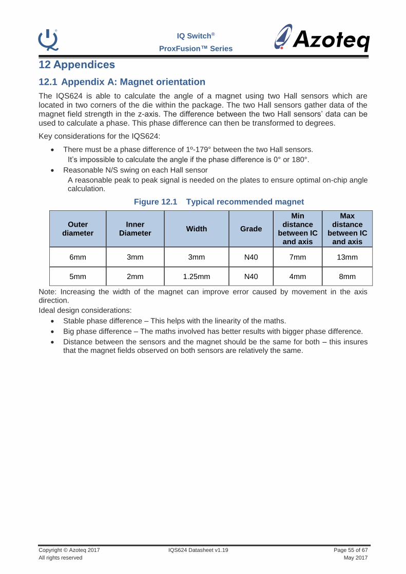
IQ Switch®
ProxFusion™ Series
Copyright © Azoteq 2017 IQS624 Datasheet v1.19 Page 55 of 67
All rights reserved May 2017
12 Appendices
12.1 Appendix A: Magnet orientation
The IQS624 is able to calculate the angle of a magnet using two Hall sensors which are located in two corners of the die within the package. The two Hall sensors gather data of the magnet field strength in the z-axis. The difference between the two Hall sensors’ data can be used to calculate a phase. This phase difference can then be transformed to degrees.
Key considerations for the IQS624:
There must be a phase difference of 1º-179° between the two Hall sensors.
It’s impossible to calculate the angle if the phase difference is 0° or 180°.
Reasonable N/S swing on each Hall sensor
A reasonable peak to peak signal is needed on the plates to ensure optimal on-chip angle calculation.
Figure 12.1 Typical recommended magnet
Outer diameter
Inner Diameter
Width Grade
Min distance
between IC and axis
Max distance
between IC and axis
6mm 3mm 3mm N40 7mm 13mm
5mm 2mm 1.25mm N40 4mm 8mm
Note: Increasing the width of the magnet can improve error caused by movement in the axis direction.
Ideal design considerations:
Stable phase difference – This helps with the linearity of the maths.
Big phase difference – The maths involved has better results with bigger phase difference.
Distance between the sensors and the magnet should be the same for both – this insures that the magnet fields observed on both sensors are relatively the same.
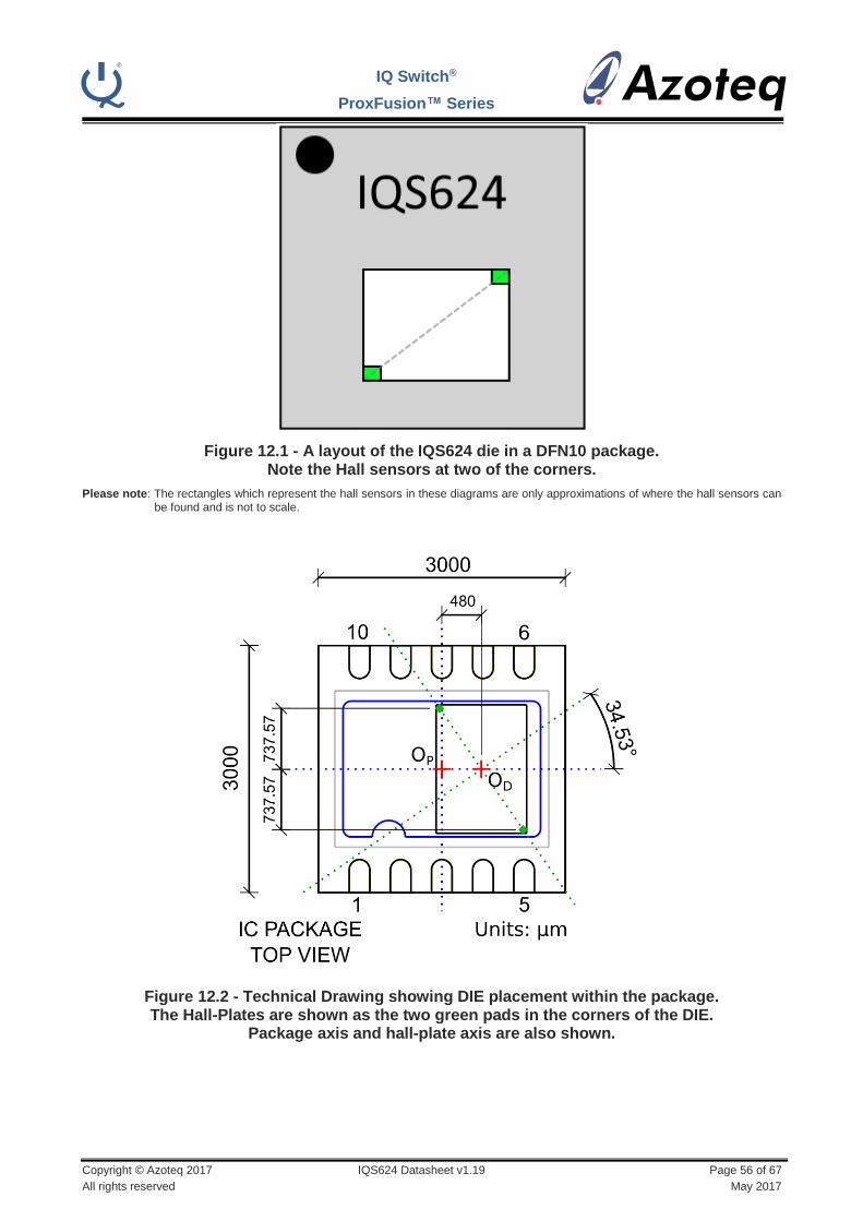
IQ Switch®
ProxFusion™ Series
Copyright © Azoteq 2017 IQS624 Datasheet v1.19 Page 56 of 67
All rights reserved May 2017
Figure 12.1 - A layout of the IQS624 die in a DFN10 package. Note the Hall sensors at two of the corners.
Please note: The rectangles which represent the hall sensors in these diagrams are only approximations of where the hall sensors can be found and is not to scale.
Figure 12.2 - Technical Drawing showing DIE placement within the package. The Hall-Plates are shown as the two green pads in the corners of the DIE.
Package axis and hall-plate axis are also shown.
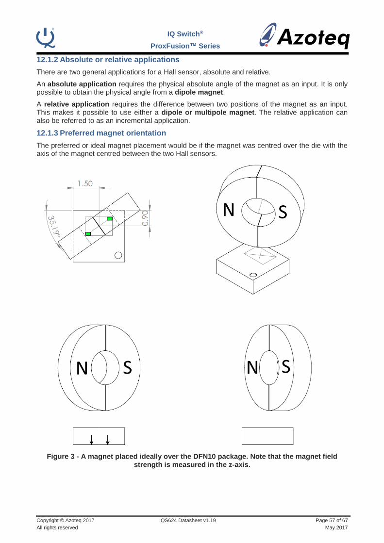
IQ Switch®
ProxFusion™ Series
Copyright © Azoteq 2017 IQS624 Datasheet v1.19 Page 57 of 67
All rights reserved May 2017
12.1.2 Absolute or relative applications
There are two general applications for a Hall sensor, absolute and relative.
An absolute application requires the physical absolute angle of the magnet as an input. It is only possible to obtain the physical angle from a dipole magnet.
A relative application requires the difference between two positions of the magnet as an input. This makes it possible to use either a dipole or multipole magnet. The relative application can also be referred to as an incremental application.
12.1.3 Preferred magnet orientation
The preferred or ideal magnet placement would be if the magnet was centred over the die with the axis of the magnet centred between the two Hall sensors.
Figure 3 - A magnet placed ideally over the DFN10 package. Note that the magnet field strength is measured in the z-axis.
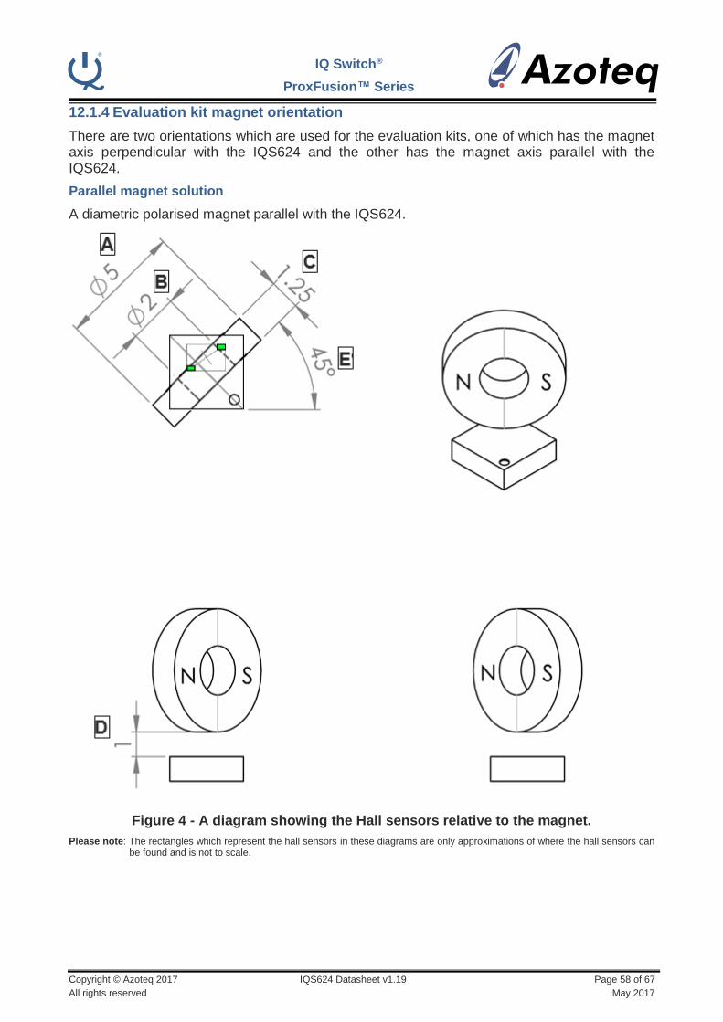
IQ Switch®
ProxFusion™ Series
Copyright © Azoteq 2017 IQS624 Datasheet v1.19 Page 58 of 67
All rights reserved May 2017
12.1.4 Evaluation kit magnet orientation
There are two orientations which are used for the evaluation kits, one of which has the magnet axis perpendicular with the IQS624 and the other has the magnet axis parallel with the IQS624.
Parallel magnet solution
A diametric polarised magnet parallel with the IQS624.
Figure 4 - A diagram showing the Hall sensors relative to the magnet.
Please note: The rectangles which represent the hall sensors in these diagrams are only approximations of where the hall sensors can be found and is not to scale.
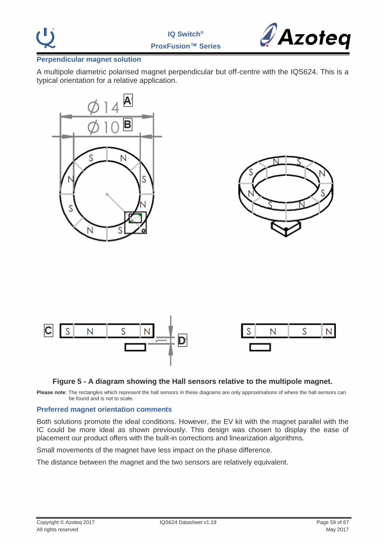
IQ Switch®
ProxFusion™ Series
Copyright © Azoteq 2017 IQS624 Datasheet v1.19 Page 59 of 67
All rights reserved May 2017
Perpendicular magnet solution
A multipole diametric polarised magnet perpendicular but off-centre with the IQS624. This is a typical orientation for a relative application.
Figure 5 - A diagram showing the Hall sensors relative to the multipole magnet.
Please note: The rectangles which represent the hall sensors in these diagrams are only approximations of where the hall sensors can be found and is not to scale.
Preferred magnet orientation comments
Both solutions promote the ideal conditions. However, the EV kit with the magnet parallel with the IC could be more ideal as shown previously. This design was chosen to display the ease of placement our product offers with the built-in corrections and linearization algorithms.
Small movements of the magnet have less impact on the phase difference.
The distance between the magnet and the two sensors are relatively equivalent.
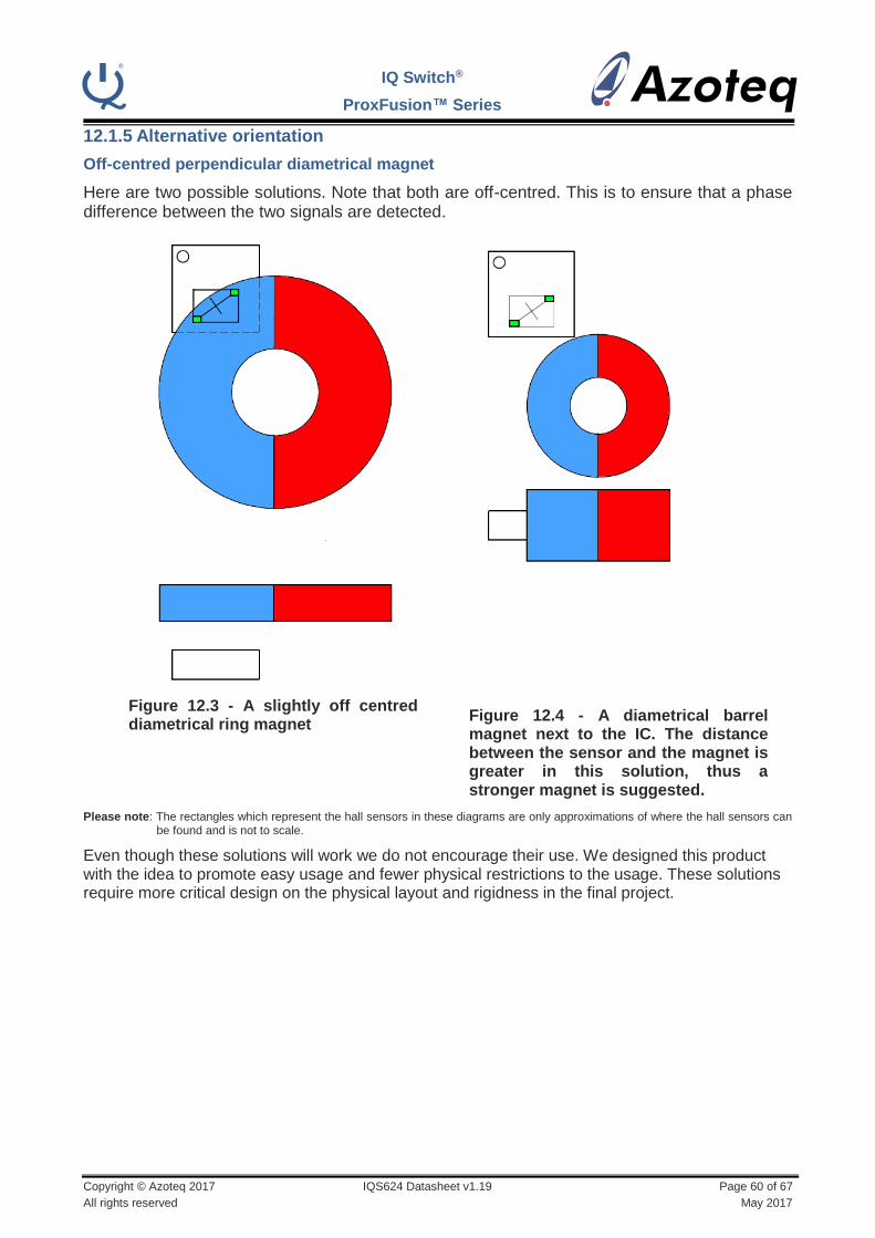
IQ Switch®
ProxFusion™ Series
Copyright © Azoteq 2017 IQS624 Datasheet v1.19 Page 60 of 67
All rights reserved May 2017
12.1.5 Alternative orientation
Off-centred perpendicular diametrical magnet
Here are two possible solutions. Note that both are off-centred. This is to ensure that a phase difference between the two signals are detected.
Please note: The rectangles which represent the hall sensors in these diagrams are only approximations of where the hall sensors can be found and is not to scale.
Even though these solutions will work we do not encourage their use. We designed this product with the idea to promote easy usage and fewer physical restrictions to the usage. These solutions require more critical design on the physical layout and rigidness in the final project.
Figure 12.3 - A slightly off centred diametrical ring magnet
Figure 12.4 - A diametrical barrel magnet next to the IC. The distance between the sensor and the magnet is greater in this solution, thus a stronger magnet is suggested.
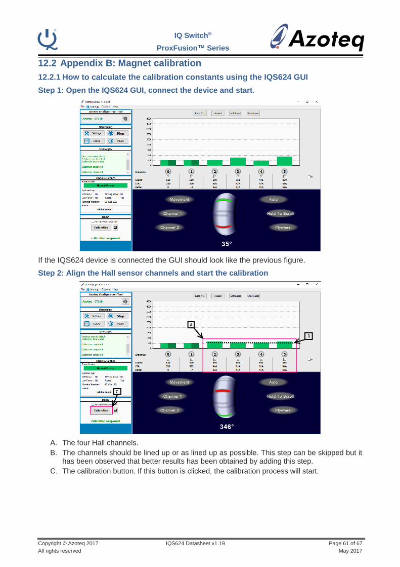
IQ Switch®
ProxFusion™ Series
Copyright © Azoteq 2017 IQS624 Datasheet v1.19 Page 61 of 67
All rights reserved May 2017
12.2 Appendix B: Magnet calibration
12.2.1 How to calculate the calibration constants using the IQS624 GUI
Step 1: Open the IQS624 GUI, connect the device and start.
If the IQS624 device is connected the GUI should look like the previous figure.
Step 2: Align the Hall sensor channels and start the calibration
A. The four Hall channels.
B. The channels should be lined up or as lined up as possible. This step can be skipped but it has been observed that better results has been obtained by adding this step.
C. The calibration button. If this button is clicked, the calibration process will start.
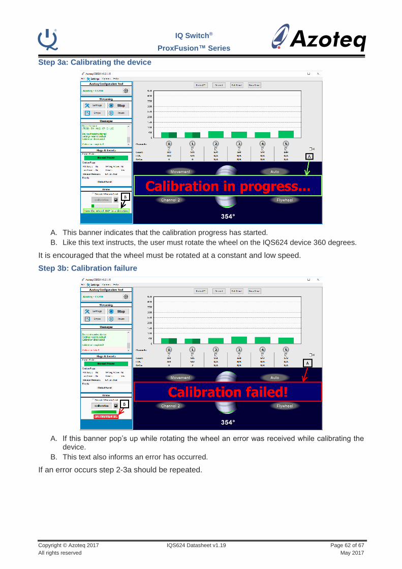
IQ Switch®
ProxFusion™ Series
Copyright © Azoteq 2017 IQS624 Datasheet v1.19 Page 62 of 67
All rights reserved May 2017
Step 3a: Calibrating the device
A. This banner indicates that the calibration progress has started.
B. Like this text instructs, the user must rotate the wheel on the IQS624 device 360 degrees.
It is encouraged that the wheel must be rotated at a constant and low speed.
Step 3b: Calibration failure
A. If this banner pop’s up while rotating the wheel an error was received while calibrating the device.
B. This text also informs an error has occurred.
If an error occurs step 2-3a should be repeated.
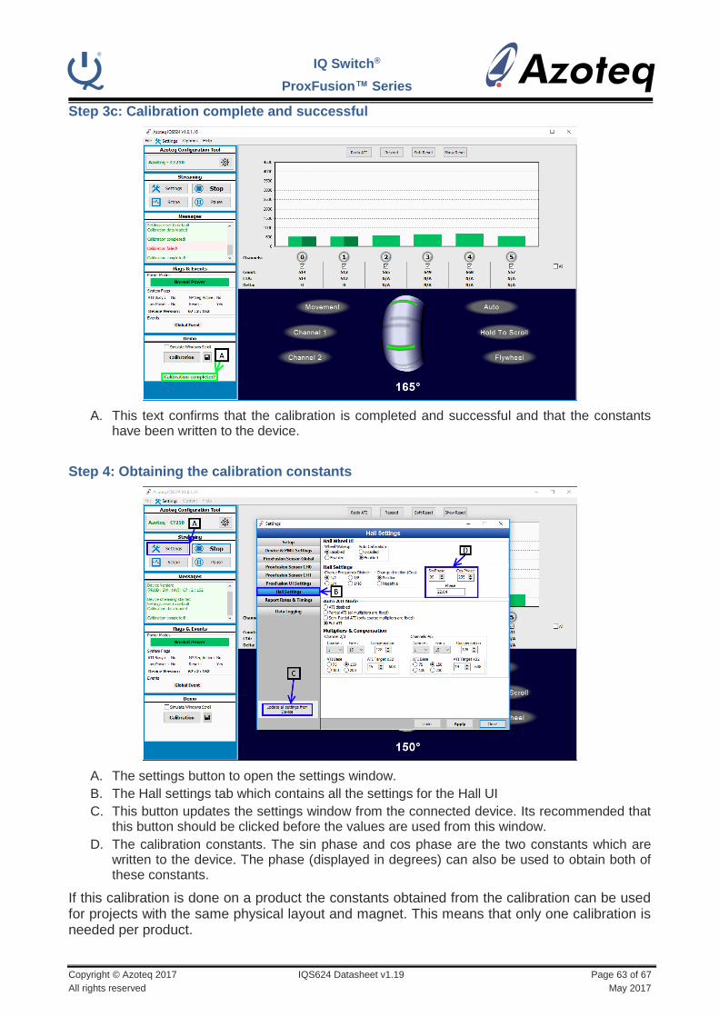
IQ Switch®
ProxFusion™ Series
Copyright © Azoteq 2017 IQS624 Datasheet v1.19 Page 63 of 67
All rights reserved May 2017
Step 3c: Calibration complete and successful
A. This text confirms that the calibration is completed and successful and that the constants have been written to the device.
Step 4: Obtaining the calibration constants
A. The settings button to open the settings window.
B. The Hall settings tab which contains all the settings for the Hall UI
C. This button updates the settings window from the connected device. Its recommended that this button should be clicked before the values are used from this window.
D. The calibration constants. The sin phase and cos phase are the two constants which are written to the device. The phase (displayed in degrees) can also be used to obtain both of these constants.
If this calibration is done on a product the constants obtained from the calibration can be used for projects with the same physical layout and magnet. This means that only one calibration is needed per product.

IQ Switch®
ProxFusion™ Series
Copyright © Azoteq 2017 IQS624 Datasheet v1.19 Page 64 of 67
All rights reserved May 2017
12.2.2 How to calculate the calibration constants using the raw data
There are two Hall Plates that make up the sensor, separated by a fixed distanced in the IC package, as described previously. These plates, designated Plate 1 & Plate 2, each have two associated data channels that sense the North-South magnetic field coincident on the plates.
For Plate 1: CH2 is the non-inverted channel, and CH3 is the inverted channel.
For Plate 2: CH4 is the non-inverted channel, and CH5 is the inverted channel.
E.g. on Plate 1, if CH2 increases in value in the presence of an increasing North field, then CH3 decreases in value in the presence of an increasing North field.
The phase delta observed between the plates can be calculated from either the non-inverted, or the inverted channel pairs.
To calculate the phase delta:
Symbols
𝑃𝑛 Non-inverted channel of Plate n: 𝑤ℎ𝑒𝑟𝑒 𝑃1 = 𝐶𝐻2, 𝑎𝑛𝑑 𝑃2 = 𝐶𝐻4
𝑃𝑛′ Inverted channel of Plate n: 𝑃1
′ = 𝐶𝐻3, 𝑎𝑛𝑑 𝑃2′ = 𝐶𝐻5
𝑃𝑛|𝑚𝑎𝑥 Max value of the channel
𝑃𝑛|𝑚𝑖𝑛 Min value of the channel
𝜃∆ Phase observed between the plates
Calculations
To calculate the phase, for at least one full rotation of the magnet, capturing all four channels:
First normalize the data for each channel, to obtain.
𝑁(𝐶𝐻𝑛) =
𝐶𝐻𝑛|𝑚𝑎𝑥 − 𝐶𝐻𝑛
𝐶𝐻𝑛
𝐶𝐻𝑛|𝑚𝑎𝑥 − 𝐶𝐻𝑛|𝑚𝑖𝑛
𝐶𝐻𝑛|𝑚𝑖𝑛
(1)
The data will now range between 0 – 1.
For the non-inverted pair: {𝑃2, 𝑃1} = {𝐶𝐻4, 𝐶𝐻2} sample both channels where 𝑁(𝐶𝐻4) ≈ 0.5. With these values, the phase delta can be calculated:
𝜃∆ = 𝑠𝑖𝑛−1(|𝑁(𝐶𝐻4) − 𝑁(𝐶𝐻2)| ∙ 2) (2)
Likewise, the phase delta can be calculated from the inverted pair: {𝑃2′ , 𝑃1
′} = {𝐶𝐻5, 𝐶𝐻3} sample both channels where 𝑁(𝐶𝐻5) ≈ 0.5.
𝜃∆′ = 𝑠𝑖𝑛−1(|𝑁(𝐶𝐻5) − 𝑁(𝐶𝐻3)| ∙ 2) (3)
And, while the phase angles are theoretically equal, due to misalignments, 𝜃∆ ≈ 𝜃∆′ .
To increase accuracy of the observed phase, the two calculated phases can be averaged, leading the final Observed phase as:
𝜃∆ =𝑠𝑖𝑛−1(|𝑁(𝐶𝐻4) − 𝑁(𝐶𝐻2)| ∙ 2) + 𝑠𝑖𝑛−1(|𝑁(𝐶𝐻5) − 𝑁(𝐶𝐻3)| ∙ 2)
2 (4)
NB: Remember that {𝐶𝐻4, 𝐶𝐻2} are evaluated at 𝑁(𝐶𝐻4) ≈ 0.5. While separately, {𝐶𝐻5, 𝐶𝐻3} are evaluated at 𝑁(𝐶𝐻5) ≈ 0.5. Even when used together in Equation (4).
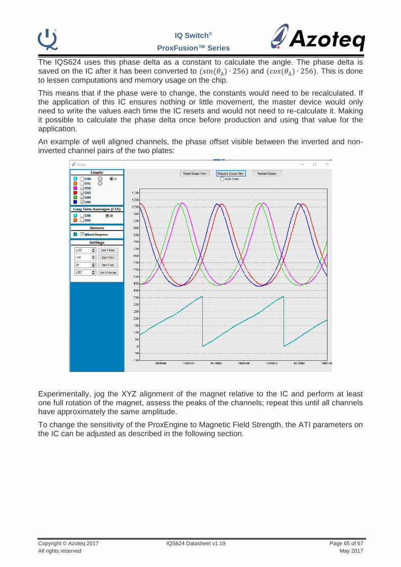
IQ Switch®
ProxFusion™ Series
Copyright © Azoteq 2017 IQS624 Datasheet v1.19 Page 65 of 67
All rights reserved May 2017
The IQS624 uses this phase delta as a constant to calculate the angle. The phase delta is saved on the IC after it has been converted to (𝑠𝑖𝑛(𝜃∆) ∙ 256) and (𝑐𝑜𝑠(𝜃∆) ∙ 256). This is done to lessen computations and memory usage on the chip.
This means that if the phase were to change, the constants would need to be recalculated. If the application of this IC ensures nothing or little movement, the master device would only need to write the values each time the IC resets and would not need to re-calculate it. Making it possible to calculate the phase delta once before production and using that value for the application.
An example of well aligned channels, the phase offset visible between the inverted and non-inverted channel pairs of the two plates:
Experimentally, jog the XYZ alignment of the magnet relative to the IC and perform at least one full rotation of the magnet, assess the peaks of the channels; repeat this until all channels have approximately the same amplitude.
To change the sensitivity of the ProxEngine to Magnetic Field Strength, the ATI parameters on the IC can be adjusted as described in the following section.
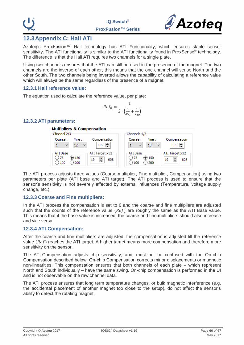
IQ Switch®
ProxFusion™ Series
Copyright © Azoteq 2017 IQS624 Datasheet v1.19 Page 66 of 67
All rights reserved May 2017
12.3 Appendix C: Hall ATI
Azoteq’s ProxFusion™ Hall technology has ATI Functionality; which ensures stable sensor sensitivity. The ATI functionality is similar to the ATI functionality found in ProxSense® technology. The difference is that the Hall ATI requires two channels for a single plate.
Using two channels ensures that the ATI can still be used in the presence of the magnet. The two channels are the inverse of each other, this means that the one channel will sense North and the other South. The two channels being inverted allows the capability of calculating a reference value which will always be the same regardless of the presence of a magnet.
12.3.1 Hall reference value:
The equation used to calculate the reference value, per plate:
𝑅𝑒𝑓𝑛 =1
2 ∙ (1
𝑃𝑛+
1
𝑃𝑛′ )
12.3.2 ATI parameters:
The ATI process adjusts three values (Coarse multiplier, Fine multiplier, Compensation) using two parameters per plate (ATI base and ATI target). The ATI process is used to ensure that the sensor’s sensitivity is not severely affected by external influences (Temperature, voltage supply change, etc.).
12.3.3 Coarse and Fine multipliers:
In the ATI process the compensation is set to 0 and the coarse and fine multipliers are adjusted such that the counts of the reference value (𝑅𝑒𝑓) are roughly the same as the ATI Base value. This means that if the base value is increased, the coarse and fine multipliers should also increase and vice versa.
12.3.4 ATI-Compensation:
After the coarse and fine multipliers are adjusted, the compensation is adjusted till the reference value (𝑅𝑒𝑓) reaches the ATI target. A higher target means more compensation and therefore more sensitivity on the sensor.
The ATI-Compensation adjusts chip sensitivity; and, must not be confused with the On-chip Compensation described below. On-chip Compensation corrects minor displacements or magnetic non-linearities. This compensation ensures that both channels of each plate – which represent North and South individually – have the same swing. On-chip compensation is performed in the UI and is not observable on the raw channel data.
The ATI process ensures that long term temperature changes, or bulk magnetic interference (e.g. the accidental placement of another magnet too close to the setup), do not affect the sensor’s ability to detect the rotating magnet.

IQ Switch®
ProxFusion™ Series
Copyright © Azoteq 2017 IQS624 Datasheet v1.19 Page 67 of 67
All rights reserved May 2017
12.3.5 Recommended parameters:
There are recommended parameters to ensure optimal use. Optimally the settings would be set up to have a max swing of 1000 from peak to peak and a reference value below 1000 counts.
The recommended parameters are:
ATI Base: 100 or 150
ATI Target: 500 – 1000
It is not assured that these settings will always set up the channels in the optimal region but it is recommended to rather adjust the magnet’s position a little as this also influences the signal received. If the magnet is too close to the IC the swing will be too large, and thus it is recommended to increase the distance between the IC and the Magnet.