irps slides_kaj4
TRANSCRIPT

© 2008 IBM Corporation
The Impact of Hot Carrier Injection on Voltage Control Oscillator Lifetime Prediction
Chih-Hsiang Ho (Purdue University)Keith Jenkins, Herschel Ainspan, Emily Ray and Peilin Song (T. J. Watson Research Center, IBM)
© 2014 IBM Corporation
1
IRPS 2014

IBM Research
© 2008 IBM Corporation
Introduction– Reliability tests– Degradation mechanisms: NBTI (negative-bias temperature instability) &
HCI (hot-carrier injection)– LC voltage-controlled oscillator
Effect of ramped voltage stress (RVS) Effect of constant voltage stress (CVS) Analysis of degradation by simulation
– Simulation flow– RelXpert results
Conclusion
© 2014 IBM Corporation
Overview
2

IBM Research
© 2008 IBM Corporation
Unlike single devices, circuit reliability involves multiple degradation mechanisms, such as positive- and negative-bias temperature (PBTI and NBTI) and hot-carrier injection (HCI)
Since each reliability mechanism has different time and voltage exponents, accelerated aging in reliability tests may shift the dominant degradation mechanisms leading to erroneous reliability prediction
Accelerating conditions should be limited to a regime which allows correct extrapolation to real-use conditions.
Analog circuit degradation may differ from digital circuit degradation.
Introduction
© 2014 IBM Corporation 3

IBM Research
© 2008 IBM Corporation
Accelerated aging
Constant Voltage Stress (CVS)
© 2014 IBM Corporation
Measure
Stress
Ramped Voltage Stress (RVS)
4
Stress
Measure
Accelerated voltage can be applied two ways:

IBM Research
© 2008 IBM Corporation
Reliability tests for lifetime prediction – CVS & RVS
Constant Voltage Stress (CVS)
Stress using constant voltage Repeat measurement with different time
(stress voltage) to determine n (m) Extrapolate to operating conditions
© 2014 IBM Corporation
Measure
Stress
5
If BTI is the only degradation mechanism:
Log (VStress)
Log
(D
egra
dat
ion
)
Slope = m
Log (tStress)
Log
(D
egra
dat
ion
)
Slope = n
IBM Research
© 2008 IBM Corporation
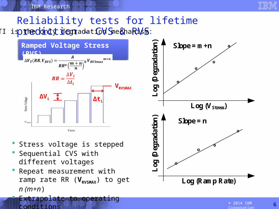
Reliability tests for lifetime prediction – CVS & RVS
Ramped Voltage Stress (RVS)
Stress voltage is stepped Sequential CVS with different
voltages Repeat measurement with ramp rate
RR (VRVSMAX) to get n (m+n) Extrapolate to operating conditions
© 2014 IBM Corporation
Log (VStress)
Log
(D
egra
dat
ion
)
Slope = m+n
Log (Ramp Rate)
Log
(D
egra
dat
ion
)
Slope = n
ΔtiΔVi
VRVSMAX
6
If BTI is the only degradation mechanism:

IBM Research
© 2008 IBM Corporation
Vout
Vin
V
t (s)
BTI Stress
BTI Stress
HCI Stress
© 2014 IBM Corporation
Reliability tests in device and circuit Levels
Stress conditions can be properly controlled for a specific mechanism in device level
Multiple degradation mechanisms occur in circuit level test (especially under accelerated aging conditions) due to dynamic stress
GND
GND
Vstress NBTIStress
Device Level Circuit Level
Vin Vout
*NBTI: Negative Bias Temperature Instability*HCI: Hot Carrier Injection
7

IBM Research
© 2008 IBM Corporation© 2014 IBM Corporation
Negative bias temperature instability & hot carrier Injection
Accumulated holes in silicon/oxide interface result in breaking of Si-H bonds
The higher temperature, the greater the degradation
Time exponent n ~ 0.2 Independent of switching frequency
NBTI
VGS,GD <0
S D
G
HCI
Hot carriers due to high electric field in the drain side cause breaking of Si-H bonds and traps oxide bulk
Degradation decreases if temperature is too high
Time exponent n ~ 0.5 Linear frequency dependence Strong voltage dependence
VDS >0
S D
G
8
IBM Research
© 2008 IBM Corporation
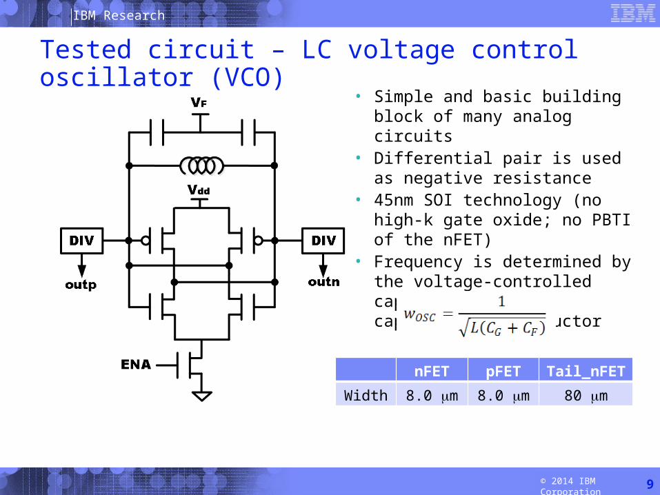
• Simple and basic building block of many analog circuits
• Differential pair is used as negative resistance
• 45nm SOI technology (no high-k gate oxide; no PBTI of the nFET)
• Frequency is determined by the voltage-controlled capacitors, gate capacitors and inductor
© 2014 IBM Corporation
Tested circuit – LC voltage control oscillator (VCO)
nFET pFET Tail_nFET
Width 8.0 mm 8.0 mm 80 mm
9

IBM Research
© 2008 IBM Corporation© 2014 IBM Corporation
Tested circuit – LC voltage control oscillator VCO)
• Start-up voltage: governed by gain of the cross-coupled pair
• Large signal but requires slow iterative measurement
Internal swing amplitude degrades, but is masked by dividers
• Center frequency: effective capacitance of the pFETs changes as voltage amplitude is reduced
• Small signal but quick measurement
• Phase noise probably sensitive, but measurement time is too long
10
Determining parameters to monitor to detect aging
IBM Research
© 2008 IBM Corporation
Introduction– Reliability tests– Degradation mechanisms: NBTI (negative-bias temperature instability) &
HCI (hot-carrier injection)– LC voltage-controlled oscillator
Effect of ramped voltage stress (RVS) Effect of constant voltage stress (CVS) Analysis of degradation by simulation
– Simulation flow– RelXpert results
Conclusion
© 2014 IBM Corporation
Overview
11

IBM Research
© 2008 IBM Corporation
1.0 1.5 2.0 2.5 3.00.01
0.1
stress time=5000 sec
T=60 oC
f
(%)
stress voltage (V)
1.0 1.5 2.0 2.5 3.0
1
10
stress time=5000 sec
T=60 oC
V
sta
rtu
p (
%)
stress voltage (V)
Ramped voltage stress - voltage dependence
Startup Voltage Degradation Frequency Degradation
Different slopes shown in high and low stress voltage regimes
n+m is not constant so more than one mechanism is involved
*Startup Voltage is the minimum supply voltage required for oscillation
© 2014 IBM Corporation12
IBM Research
© 2008 IBM Corporation
1.0 1.5 2.0 2.5 3.0
0.1
1
10
V
sta
rtu
p (
%)
4.4 GHz VCO
6 GHzVCO
8 GHz VCO
stress voltage (V)
4 5 6 7 8 94
5
6
7
8
9
10
11 at 2.6 V stress voltage
V
sta
rtu
p (
%)
oscillator frequency (GHz)
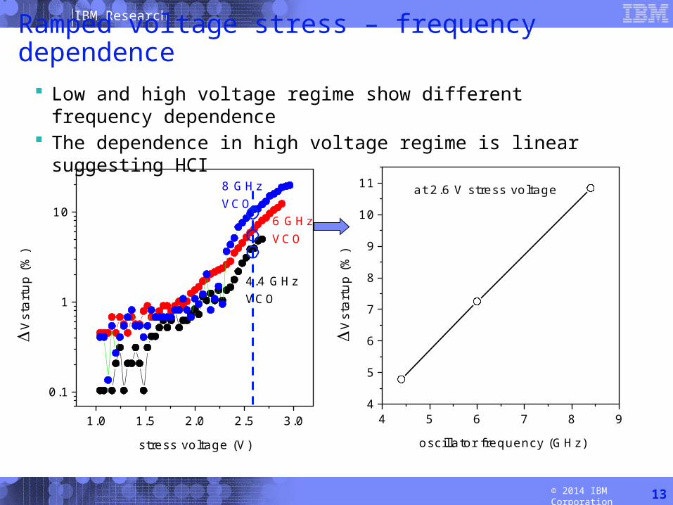
Ramped voltage stress – frequency dependence Low and high voltage regime show different frequency dependence The dependence in high voltage regime is linear suggesting HCI
© 2014 IBM Corporation13
IBM Research
© 2008 IBM Corporation
Introduction– Reliability tests– Degradation mechanisms: NBTI (negative-bias temperature instability) &
HCI (hot-carrier injection)– LC voltage-controlled oscillator
Effect of ramped voltage stress (RVS) Effect of constant voltage stress (CVS) Analysis of degradation by simulation
– Simulation flow– RelXpert results
Conclusion
© 2014 IBM Corporation
Overview
14
IBM Research
© 2008 IBM Corporation
1.6 1.8 2.0 2.2 2.4
0.2
0.3
0.4
0.5
0.6
frequency
startup voltage
po
we
r la
w s
lop
e,
n
stress voltage (V)
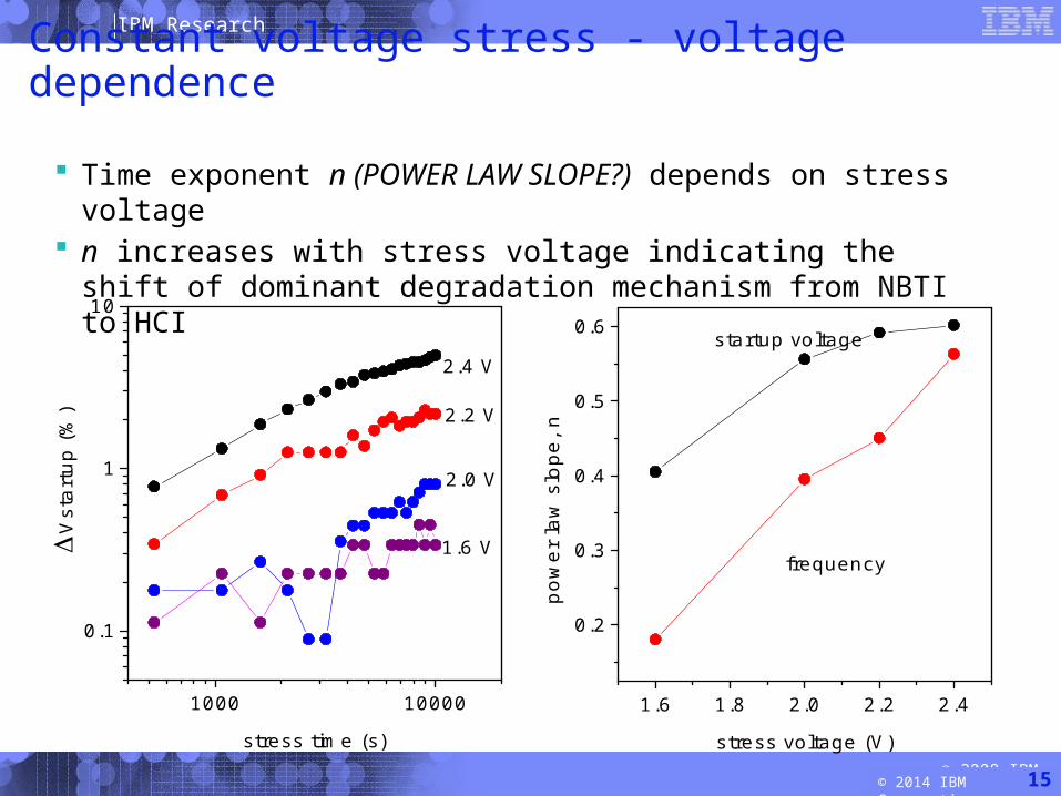
Constant voltage stress - voltage dependence
© 2014 IBM Corporation
Time exponent n (POWER LAW SLOPE?) depends on stress voltage n increases with stress voltage indicating the shift of dominant
degradation mechanism from NBTI to HCI
15
1000 10000
0.1
1
10
V
sta
rtu
p (
%) 2.2 V
2.4 V
1.6 V
2.0 V
stress time (s)
IBM Research
© 2008 IBM Corporation
1.6 1.8 2.0 2.2 2.4
0.4
0.5
0.6
0.7 8.4 GHz oscillator
6.0 GHz oscillator
po
we
r la
w s
lop
e,
n
stress voltage (V)
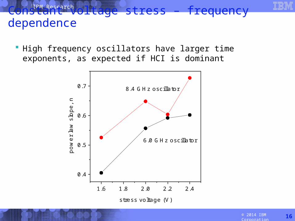
Constant voltage stress – frequency dependence
© 2014 IBM Corporation
High frequency oscillators have larger time exponents, as expected if HCI is dominant
16

IBM Research
© 2008 IBM Corporation
Introduction– Reliability tests– Degradation mechanisms: NBTI (negative-bias temperature instability) &
HCI (hot-carrier injection)– LC voltage-controlled oscillator
Effect of ramped voltage stress (RVS) Effect of constant voltage stress (CVS) Analysis of degradation by simulation
– Simulation flow– RelXpert results
Conclusion
© 2014 IBM Corporation
Overview
17

IBM Research
© 2008 IBM Corporation
RelXpert integrated reliability analysis
The generated sub-circuit model for degraded transistorHCI and NBTI/PBTI Analysis Flow
© 2014 IBM Corporation18
Courtesy of Cadence Design Systems,Inc.
IBM Research
© 2008 IBM Corporation
1.0 1.5 2.0 2.5 3.0
0.0
0.1
0.2
0.3
0.4
0.5
f (%
)
RelExpert
measured
stress voltage (V)
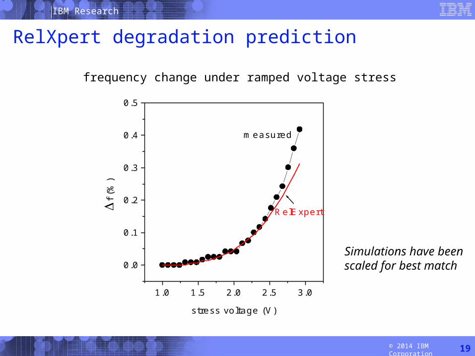
RelXpert degradation prediction
© 2014 IBM Corporation19
Simulations have been scaled for best match
frequency change under ramped voltage stress

IBM Research
© 2008 IBM Corporation
1.0 1.5 2.0 2.5 3.00.00
0.05
0.10
0.15
0.20
0.25
NBTI
HCI
total
V
th (
V)
stress voltage (V)
RelXpert analysis nFET (IBM 45nm) is insensitive to HCI and BTI degradation VCO Degradation is mainly from pFET NBTI dominates in low voltage regime while HCI dominates in high
voltage regime
© 2014 IBM Corporation
pFET Degradation
20

IBM Research
© 2008 IBM Corporation© 2014 IBM Corporation
Conclusions
The voltage dependence of n in constant voltage stress and n+m in ramped voltage stress is due to the impact of HCI
The dominant degradation mechanism shifts from NBTI to HCI as the stress voltage increases
Degradation of VCO is mainly contributed by the pFETs in the differential pair
The break point observed in RVS test can served as a guideline to define the proper range of stress voltage for suppressing HCI effect and better lifetime prediction
Failure to identify the role of HCI in total stress degradation can lead to large errors in predicting lifetime by extrapolating to real-use conditions
21
IBM Research
© 2008 IBM Corporation© 2014 IBM Corporation
Acknowledgements
The authors would like to thank Kevin Stawiasz, who initiated the idea of this work, and Barry Linder and Michael Hauser for technical discussions and encouragement.
This work was supported by the Defense Advanced Research Projects Agency (DARPA) under SSC Pacific contract HR0011-0060. Any opinions, findings, and conclusions or recommendations expressed in this publication are those of the authors and do not necessarily reflect the views of the DARPA or U.S. Government.
22