is31lt3948 - issi integrated silicon solution, inc. – rev. d, 01/21/2015 2 pin configurations...
TRANSCRIPT

IS31LT3948
Integrated Silicon Solution, Inc. – www.issi.com Rev. D, 01/21/2015
1
PFM MODE BOOST LED DRIVER WITH THE EXTERNAL NMOS
February 2015 GENERAL DESCRIPTION
The IS31LT3948 is a PFM step-up DC-DC converter designed for driving the white LED arrays for large size LCD panel backlighting applications. It can deliver stable constant output current from a few milliamps up to 2A, programmed via an external resistor.
The IS31LT3948 utilizes a control scheme in which the output is automatically adjusted to the optimum output voltage for the system, maximizing the efficiency. Furthermore, the control scheme is inherently stable removing the need to provide additional loop compensation.
The device features external PWM dimming, which allows the flexible control of the back-lighting luminance.
The IS31LT3948 has a wide input voltage range from 5V to 100V (Note). An integrated OVP circuit protects the chip and the system even under no-load conditions.
The chip is assembled in SOP-8 package. It operates from 5V to 100V over two temperature ranges of -40°C to +85°C and -40°C to +125°C.
Note: The IS31LT3948 has an internal 5V shunt regulator connected to the VCC pin. A dropping resistor must be connected between the VCC pin and VIN to limit current flow. VIN voltages above 100V are allowed but care must be taken to ensure that the output voltage remains greater than VIN, and that the NMOS voltage rating is sufficiently large.
FEATURES
Wide input voltage range: 5V~100V Constant current output limited only by external
component selection (Note) No loop compensation required Internal over-voltage protection Internal over-temperature protection Operating temperature range -40C to +85C
(IS31LT3948-GRLS2-TR) Operating temperature range -40C to +125C
(IS31LT3948-GRLS4-TR) SOP-8 package
Note: The maximum output current is determined by VOUT/VIN ratio as well as the external components. If output current and VOUT/VIN ratio is high, high current components of inductor and NMOS are needed. APPLICATIONS
TV monitor backlighting Notebook Automotive Street lamp LED lighting
TYPICAL APPLICATION CIRCUIT
Figure 1 Typical Application Circuit

IS31LT3948
Integrated Silicon Solution, Inc. – www.issi.com Rev. D, 01/21/2015
2
PIN CONFIGURATIONS
Package Pin Configuration (Top View)
SOP-8
PIN DESCRIPTIONS
No. Pin Description
1 VCC Positive power supply input pin. Internally clamped at 5V (Typ.).
2 TOFF Off time setting pin. An external resistor connected to this pin forms an RC discharge path to generate a constant minimum off time of the NMOS.
3 ADJ
Enable and input peak current control pin. Pulled up to 4.5V internally to set VCS_TH =0.24V when ADJ is floating. If VADJ<0.5V, NMOS will always shutdown. If 0.5≤VADJ≤2.4V, VCS_TH = VADJ/10. If VADJ>2.4V, VCS_TH =0.24V. Note: During the start up (VCC voltage is rising), ADJ must not be connected to low (recommended floating).
4 GND Ground.
5 GATE Driver’s output for the gate of the external NMOS.
6 CS Current sense input for the boost, peak current control loop.
7 FB Feedback voltage input pin. Used to regulate the current of LEDs by keeping VFB=0.3V.
8 OVP Overvoltage protection input pin, if the voltage of OVP exceed 1V, gate will always shutdown.

IS31LT3948
Integrated Silicon Solution, Inc. – www.issi.com Rev. D, 01/21/2015
3
ORDERING INFORMATION Industrial Range: -40°C to +85°C
Order Part No. Package QTY/Reel
IS31LT3948-GRLS2-TR SOP-8, Lead-free 2500
Part No. Rules IS (ISSI Prefix) 31 (Product Family) - Analog and mix signal LT (Product Type) - Lighting LED driver 3948 (Part Number) - 3948 GR (Package Code) - SOP L (Solder Type) - Lead-free (RoHS compliant) S2 (Temperature Grade) - Industrial temperature (-40°C ~ +85°C) TR (Packing Option) - Tape & Reel
Industrial Range: -40°C to +125°C
Order Part No. Package QTY/Reel
IS31LT3948-GRLS4-TR SOP-8, Lead-free 2500
Part No. Rules IS (ISSI Prefix) 31 (Product Family) - Analog and mix signal LT (Product Type) - Lighting LED driver 3948 (Part Number) - 3948 GR (Package Code) - SOP L (Solder Type) - Lead-free (RoHS compliant) S4 (Temperature Grade) - Industrial temperature (-40°C ~ +125°C) TR (Packing Option) - Tape & Reel
Copyright © 2015 Integrated Silicon Solution, Inc. All rights reserved. ISSI reserves the right to make changes to this specification and its products at any time without notice. ISSI assumes no liability arising out of the application or use of any information, products or services described herein. Customers are advised to obtain the latest version of this device specification before relying on any published information and before placing orders for products. Integrated Silicon Solution, Inc. does not recommend the use of any of its products in life support applications where the failure or malfunction of the product can reasonably be expected to cause failure of the life support system or to significantly affect its safety or effectiveness. Products are not authorized for use in such applications unless Integrated Silicon Solution, Inc. receives written assurance to its satisfaction, that: a.) the risk of injury or damage has been minimized; b.) the user assume all such risks; and c.) potential liability of Integrated Silicon Solution, Inc is adequately protected under the circumstances

IS31LT3948
Integrated Silicon Solution, Inc. – www.issi.com Rev. D, 01/21/2015
4
ABSOLUTE MAXIMUM RATINGS VCC to GND -0.3V to 6.0V CS, ADJ,GATE,TOFF,OVP,FB -0.3V to 6.0V VCC Max. input current 10mA Maximum operating junction temperature, TJMAX 150°C Storage temperature range, TSTG -65°C ~ +150°C
Operating temperature, TA = TJ -40°C ~ +85°C, IS31LT3948-GRLS2-TR -40°C ~ +125°C, IS31LT3948-GRLS4-TR
ESD (HBM) ESD (CDM)
2kV 1kV
Note: Stresses beyond those listed under “Absolute Maximum Ratings” may cause permanent damage to the device. These are stress ratings only and functional operation of the device at these or any other condition beyond those indicated in the operational sections of the specifications is not implied. Exposure to absolute maximum rating conditions for extended periods may affect device reliability. ELECTRICAL CHARACTERISTICS Unless otherwise specified, VIN=10V, RIN=10k, ADJ floating, TA=25°C. Parameter range based on TA = -40°C ~ +125°C (Note 1) The symbol in the table means these parameters are only available in the above temperature range.
Symbol Parameter Conditions Tem. Min. Typ. Max. Unit
VIN Input voltage
Supply voltage connected to VCC via a appropriate resistor (Note 2)
5 100 V
VCC VCC clamp voltage RIN=10k 4.3 5 5.6
V 4.1 5 5.8
VUVLO Undervoltage threshold VCC rising 2.2 2.7 3.0
V 2.0 2.7 3.2
VUVLO_HYS Undervoltage threshold hysteresis 300 mV
ICC
Quiescent supply current VCC= VCC clamp voltage 400 500
µA 400 700
Quiescent supply current when VCC undervoltage
VCC=2.5V 50 75
µA 50 145
VCS_TH Peak current sense threshold VADJ=5V 215 240 265
mV 202 240 275
tBLANK Peak current sense blank interval VCS=VCS_TH+50mV 500 ns
tOFF Fixed turn-off interval REXT=250k 10 µs

IS31LT3948
Integrated Silicon Solution, Inc. – www.issi.com Rev. D, 01/21/2015
5
ELECTRICAL CHARACTERISTICS (CONTINUE) Unless otherwise specified, VIN=10V, RIN=10k, ADJ floating, TA=25°C. Parameter range based on TA = -40°C ~ +125°C (Note 1) The symbol in the table means these parameters are only available in the above temperature range.
Symbol Parameter Conditions Tem. Min. Typ. Max. Unit
VADJ
Peak current control low threshold 0.5 V
Peak current control high threshold
2.4 V
TSD Thermal shutdown threshold 150 °C
TSD_HYS Thermal shutdown hysteresis 20 °C
VFB_TH Feedback voltage threshold
IS31LT3948-GRLS2-TR 290 300 310
mV IS31LT3948-GRLS4-TR
292 300 310
285 300 315
VOVP_TH Overvoltage input threshold 0.9 1.0 1.1 V
Note 1: Production testing of the device is performed at 25°C. Functional operation of the device and parameters specified over temperature range, are guaranteed by design, characterization and process control.
Note 2: VIN is the input voltage. When VIN≤5V, connect input voltage directly to VCC. When VIN>5V, input voltage should be connected to VCC pin via an appropriately valued resistor.

IS31LT3948
Integrated Silicon Solution, Inc. – www.issi.com Rev. D, 01/21/2015
6
TYPICAL PERFORMANCE CHARACTERISTICS
Out
put C
urre
nt (
mA
)
Supply Voltage (V)
600
625
650
675
700
725
750
10 12 14 16 18 20 22 24 26 28 30
VOUT = 40VRCS = 0.06ΩRFB = 0.425Ω
Figure 2 Supply Voltage vs. Output Current
Eff
icie
ncy
(%)
Supply Voltage (V)
10 12 14 16 18 20 22 24 26 28 3070
75
80
85
90
95
100
VOUT = 40VRCS = 0.06ΩRFB = 0.425Ω
Figure 4 Supply Voltage vs. Efficiency
Out
put C
urre
nt (
mA
)
Output Voltage (V)
20 25 30 35 40 45600
625
650
675
700
725
750
VIN = 12VRCS = 0.06ΩRFB = 0.425Ω
Figure 6 Output Voltage vs. Output Current
Out
put C
urre
nt (
mA
)
Supply Voltage (V)
10 12 14 16 18 20 22 24 26 28 30300
310
320
330
340
350
360
370
380
390
400
VOUT = 40VRCS = 0.12ΩRFB = 0.857Ω
Figure 3 Supply Voltage vs. Output Current
Eff
icie
ncy
(%)
Supply Voltage (V)
10 12 14 16 18 20 22 24 26 28 3070
75
80
85
90
95
100
VOUT = 40VRCS = 0.12ΩRFB = 0.857Ω
Figure 5 Supply Voltage vs. Efficiency
Out
put C
urre
nt (
mA
)
Output Voltage (V)
20 25 30 35 40 45300
310
320
330
340
350
360
370
380
390
400
VIN = 12VRCS = 0.12ΩRFB = 0.857Ω
Figure 7 Output Voltage vs. Output Current

IS31LT3948
Integrated Silicon Solution, Inc. – www.issi.com Rev. D, 01/21/2015
7
Eff
icie
ncy
(%)
Output Voltage (V)
20 25 30 35 40 4570
75
80
85
90
95
100
VIN = 12VRCS = 0.06ΩRFB = 0.425Ω
Figure 8 Output Voltage vs. Efficiency
Out
put C
urre
nt(m
A)
PWM Duty Cycle(%)
0 10 20 30 40 50 60 70 80 90 1000
100
200
300
400
500
600
700
800
VIN = 12VRCS = 0.06ΩRFB = 0.68ΩfPWM = 200Hz,500Hz,1kHzWith external NMOS PWM Dimming
Figure 10 PWM Duty Cycle vs. Output Current
Temperature (°C)
Sup
ply
Cur
rent
(µ
A)
-40 -25 -10 5 20 35 50 65 80 95 110 1250
50
100
150
200
250
300
350
400
450
500
VIN = 5VRIN = 0Ω
Figure 12 Temperature vs. Supply Current
Eff
icie
ncy
(%)
Output Voltage (V)
20 25 30 35 40 4570
75
80
85
90
95
100
VIN = 12VRCS = 0.12ΩRFB = 0.857Ω
Figure 9 Output Voltage vs. Efficiency
Out
put C
urre
nt(m
A)
PWM Duty Cycle(%)
0
50
100
150
200
250
300
350
400
0 10 20 30 40 50 60 70 80 90 100
VIN = 12VRCS = 0.12ΩRFB = 0.32ΩfPWM = 200Hz,500Hz,1kHzWith external NMOS PWM Dimming
Figure 11 PWM Duty Cycle vs. Output Current
Temperature (°C)
VC
CV
olta
ge (
V)
-40 -25 -10 5 20 35 50 65 80 95 110 1254.5
4.6
4.7
4.8
4.9
5
5.1
5.2
5.3
5.4
5.5
VIN = 12VRIN = 12kΩ
Figure 13 Temperature vs. VCC

IS31LT3948
Integrated Silicon Solution, Inc. – www.issi.com Rev. D, 01/21/2015
8
Temperature (°C)
VF
BV
olta
ge (
mV
)
-40 -25 -10 5 20 35 50 65 80 95 110 125270
280
290
300
310
320
330
VIN = 24V
Figure 14 Temperature vs. VFB
Time (10µs/Div)
VPWM
2V/Div
ILED
200mA/Div
fPWM = 500HzILED = 450mAWith external NMOS PWM dimming
Figure 16 Output Current vs. VPWM on Falling Time
Time (10µs/Div)
VPWM
2V/Div
ILED
200mA/Div
fPWM = 500HzILED = 450mAWith external NMOS PWM dimming
Figure 15 Output Current vs. VPWM on Rising Time

IS31LT3948
Integrated Silicon Solution, Inc. – www.issi.com Rev. D, 01/21/2015
9
FUNCTIONAL BLOCK DIAGRAM

IS31LT3948
Integrated Silicon Solution, Inc. – www.issi.com Rev. D, 01/21/2015
10
APPLICATION INFORMATION INTERNAL 5V REGULATOR
The IS31LT3948 includes an internal shunt regulator of 5V (Typ.) connected to the VCC pin. When the input voltage is higher than 5V, connect VCC to VIN using an appropriately valued, current limiting resistor. The regulator maintains a 5V power supply for the internal NMOS switch gate driver and the internal control circuitry. In applications where the input voltage is 5V, connect the input voltage directly to VCC. When VCC is connected directly to VIN, VIN may not exceed 5V. Bypass the VCC pin using a low ESR capacitor (recommended 10µF ceramic capacitor) to provide a high frequency path to GND.
The current required by IS31LT3948 is 0.4mA (Typ.) plus the switching current of the external switch. The switching frequency of the external NMOS affects the amount of current required, as does the NMOS’s gate charge requirement (found on the NMOS data sheet).
SGIN fQmA.I 40 (1)
Where fS is the switching frequency and QG is the external NMOS gate charge.
UNDER VOLTAGE LOCKOUT
IS31LT3948 features an under voltage lockout threshold of 2.7V (Typ.) with a hysteresis of 300mV. The chip is disabled when VCC is lower than 2.4V and enabled when VCC exceeds 2.7V.
STEP-UP CONVERTER
IS31LT3948’s step-up converter uses a peak current mode topology wherein the CS pin voltage determines the peak current in the inductor of the converter and hence the duty cycle of the GATE switching waveform. The basic loop uses a pulse from an internal oscillator to set an RS flip-flop and turn on the external power NMOS. After the blanking time, the inductor current is sensed during the GATE on period by a sense resistor, RCS, in the source of the external power NMOS. The current increases in the NMOS and inductor until the voltage across the sense resistor reaches the CS threshold, at which time NMOS is turned off. Once the NMOS is turned off, the inductor reverses polarity, providing the voltage boost, and the current of inductor will decrease until the FB pin voltage drops below internal reference voltage and the NMOS is then turned on again. This operation repeats each cycle.
Note, in the case where the FB pin voltage does not exceed the FB reference voltage of 0.3V, such as at start-up, the NMOS will remain off for the programmed minimum tOFF time, then the NMOS is switched on again.
LED CURRENT CONTROL
IS31LT3948 regulates the LED current by sensing the voltage across an external sense resistor in series with the LEDs. The voltage is sensed via the FB pin where the internal feedback reference voltage is 0.3V (Typ.). The LED current can be set from following equation easily.
FBOUT R
I3.0
(2)
In order to have an accurate LED current, precision resistors are required (1% is recommended).
SETTING THE OVER VOLTAGE PROTECTION
The open string protection is achieved through the over voltage protection (OVP). In some cases, an LED string failure results in a feedback voltage that is always zero. If this happens, the part then keeps boosting the output voltage higher and higher. If the output voltage reaches the programmed OVP threshold, the protection will be triggered and stop the switching action. To make sure that the circuit functions properly, the OVP setting resistor divider must be set with an appropriate value. The recommended VOVP point is about 1.2 times or 5V (choose the larger one) higher than the output voltage for normal operation.
5
54_ R
RRVV THOVPOVP
(3)
Where, VOVP_TH is 1V, and VOVP is the output voltage OVP level.
DIMMING CONTROL
There are two methods for dimming.
1) External NMOS PWM dimming:
Figure 17 External PWM Dimming
When the PWM input is high (VH>2.4V), M2 is on and IS31LT3948 operates normally to regulate the output current. When PWM is low logic (VL<0.5V), M2 is off and IS31LT3948 is shutdown. Using a fixed frequency PWM signal and changing the duty cycle adjusts the average output current. The

IS31LT3948
Integrated Silicon Solution, Inc. – www.issi.com Rev. D, 01/21/2015
11
recommended 5V PWM frequency is between 200Hz and 1kHz. M2 is recommended to use AP2306. The rising time depends on external component. The minimum on time of PWM signal is recommended to be over the rising time to achieve better dimming rate.
2) RC filter PWM dimming:
Figure 18 RC PWM Dimming
A filtered PWM signal can be used as an adjustable DC voltage for LED dimming control. The filtered PWM signal becomes DC voltage which is summed together with the FB voltage to regulate the output current. Fix the frequency of the PWM signal and change the duty cycle to adjust the LED current. The LED current can be calculated by the following equation:
FB
THFBPWMTHFBOUT R
RRVDutyVRVI
)/()( 87_6_ (4)
The PWM duty cycle is inversely proportional to the LED current. That is, when the PWM signal is 100% duty cycle, the output current is minimum, ideally zero, and when the PWM signal is 0% duty cycle, the output current is maximum.
See details value in the Example section.
Note: When the VOUT/VIN ratio is less than 2, careful consideration must be given to ensure that VOUT remains greater than VIN at the minimum dimming level.
INPUT PEAK CURRENT CONTROL
IS31LT3948 limits the peak inductor current, and thus peak input current through the feedback of R3 connected from source of NMOS to ground. The required average input current is based on the boost ratio, VOUT/VIN, and the designed value for average LED current. The required average input current can be calculated as:
IN
OUTOUTINAVG V
IVI _ (5)
: assumed power conversion efficiency (the recommended value is 0.9)
Generally, setting the peak inductor current to 1.5 times the average input current is sufficient to maintain a good regulation of the output current.
CS
THCSINAVGINPEAK R
VII _
__ 5.1 (6)
VCS_TH: If 0.5<VADJ<2.4V, VCS_TH = VADJ/10. If VADJ>2.4V, VCS_TH =0.24V. ADJ floating, VCS_TH=0.24V.
INPUT CAPACITOR
The input capacitor of the IS31LT3948 will supply the transient input current of the power inductor. Value of 100μF or higher is recommended to prevent excessive input voltage ripple.
SETTING tOFF_MIN
IS31LT3948 operates in a pulsed frequency modulation mode. The boost control loop is a constant off-time architecture. The off time is programmable and set by an external resistor connected between the tOFF pin and GND. In most application, the recommended tOFF_MIN is 1µs. The governing equation for the off time is:
EXTMINOFF Rt 12_ 1040 (7)
REXT (kΩ)
tOF
F_M
IN (
µs)
0
2
4
6
8
10
0 50 100 150 200 250
Figure 19 REXT vs. tOFF_MIN
Note, the minimum tOFF_MIN is 1µs.
INDUCTOR SELECTION
Inductor value directly determines the switching frequency of the converter. To the fixed condition and the larger inductor value the lower switching frequency. The higher frequency will reduce the value of inductor, but will increase the switching loss on NMOS.
The switching frequency can be calculated blow.
Switching frequency:
OFFON ttf /1 (8)

IS31LT3948
Integrated Silicon Solution, Inc. – www.issi.com Rev. D, 01/21/2015
12
The current ripple in the inductor:
INAVGINPEAKRIPPLE III __2 (9)
NMOS on time:
)( __ CSONDSLINAVGIN
RIPPLEON RRRIV
LIt
(10)
NMOS off time:
LINAVGINDOUT
RIPPLEOFF RIVVV
LIt
_
(11)
Note, the selection of inductor must ensure that the tOFF larger than the tOFF_MIN, or else the converter can not output the required current.
Where:
VIN: Input voltage (V)
VOUT: Output voltage (V)
IRIPPLE: Current ripple in the inductor (A)
L: inductor value (H)
IPEAK_IN: Input peak current (A)
IAVG_IN: Input average current (A)
RL: Inductor DCR ()
RDS_ON: NMOS on resistance ()
VD: diode forward voltage at the required load current (V)
The recommended switching frequency: 20kHz < f < 200kHz (Lower than 20kHz will cause audio noice of the inductor and too high frequency will increase the switching loss on NMOS).
To the fixed VIN, VOUT, IAVG_IN, IPEAK_IN and the switching frequency is inversely proportional to the inductor value.
Select an inductor with a rating current over input average current and the saturation current over the calculated peak current. To calculate the worst case inductor peak current, use the minimum input voltage, maximum output voltage, and maximum total LED current. Also ensure that the inductor has a low DCR (copper wire resistance) to minimize I2R power loss.
OUTPUT CAPACITOR
The output capacitor holds the output current during NMOS on. The capacitor directly impacts the line regulation and the loading regulation.
Low ESR capacitors using at the IS31LT3948 converter output can minimize output ripple voltage and improve output current regulation. For most applications, a 220μF low ESR capacitor will be
sufficient. Proportionally lower ripple can be achieved with higher capacitor values.
SCHOTTKY RECTIFIER
The external diode for the IS31LT3948 must be a Schottky diode, with low forward voltage drop and fast switching speed. The diode’s average current rating must exceed the application’s average output current. The diode’s maximum reverse voltage rating must exceed the over voltage protection of the application. For PWM dimming applications, be aware of the reverse leakage of the Schottky diode. Lower leakage current will drain the output capacitor less during PWM low periods, allowing for higher PWM dimming ratios.
Power NMOS Selection
The power NMOS selected should have a VDS rating which exceeds the maximum over voltage protection (OVP) level programmed for the application. The VGS_TH of NMOS should be not higher than 4V. The RDS_ON of the NMOS will determine DC power loss. The DC power loss can be calculated by:
ONDSIN
OUTOUT
ONDSMloss
RV
DutyIV
RIP
_
2
_2
1
(12)
The recommended NMOS rating current is 5 times (or higher) to the input peak current (IPEAK_IN). Be aware of the power dissipation within the NMOS and deciding if the thermal resistance of the NMOS package causes the junction temperature to exceed maximum ratings.
PCB LAYOUT CONSIDERATION
As for all switching power supplies, especially those providing high current and using high switching frequencies, layout is an important design step. If layout is not carefully done, the regulator could show instability as well as EMI problems.
Wide traces should be used for connection of the high current loop to minimize the EMI and unnecessary loss.
The external components ground should be connected to IS31LT3948 ground as short as possible. Especially the RFB ground to IS31LT3948 ground connection should be as short and wide as possible to have an accurate LED current.
The capacitor C1, C2, C3 should be placed as close as possible to IS31LT3948 for good filtering. Especially the output capacitor C3 connection should be as short and wide as possible.
NMOS drain is a fast switching node. The inductor and Schottky diode should be placed as close as possible to the drain and the connection

IS31LT3948
Integrated Silicon Solution, Inc. – www.issi.com Rev. D, 01/21/2015
13
should be kept as short and wide as possible. Avoid other traces crossing and routing too long in parallel with this node to minimize the noise coupling into these traces. The feedback pin (e.g. CS, FB, OVP) should be as short as possible and routed away from the inductor, the Schottky diode and NMOS. The feedback pin and feedback network should be shielded with a ground plane or trace to minimize noise coupling into this circuit.
The thermal pad on the back of NMOS package must be soldered to the large ground plane for ideal power dissipation.
Figure 20 External NMOS PWM Dimming
IS31LT3948
FB
VIN
5V ~ 100V
VCC1 5
7
2TOFF
3ADJ
R1
D1L1
4GND
GATE
6
OVP8
CS
R2
C1 C2
R3
C3M1
R4
R5
LED+
RFB
LED-
R6
R7
R8
C4
For dimming
PWM
Figure 21 RC Filter PWM Dimming

IS31LT3948
Integrated Silicon Solution, Inc. – www.issi.com Rev. D, 01/21/2015
14
EXAMPLE:
Input: VIN=12V~24V
Output: IOUT=350mA, VOUT≈30V~40V (9~12LEDs,
VFB=3.3V)
To calculate the worst case parameter, use the minimum input voltage, the maximum output voltage, and maximum output current. So choose: VIN=12V,
IOUT=350mA, VOUT≈40V (12LEDs, VFB=3.3V)
1. R1, C1 and C2
Assume IIN = 2.5mA,
kkI
VVR
IN
CCMININ 38.25.2
512_1
Note: The maximum VCC input current at highest input voltage must not exceed 10mA.
IIN = (VIN_MAX-VCC)/R1 <10mA
Choose C1 as 220µF/35V, C2 as 10µF/16V.
2. R2 to Set tOFF_MIN
The recommended value is 1µs,
sRt EXTMINOFF 11040 12_
Choose R2=24kΩ.
3. RFB to Set Output Current and C3
86.0_
OUT
THFBFB I
VR
Choose C3 as 220µF/63V (Low ESR electrolytic capacitor).
4. R6, R7, R8 and C4
R6, R7 and R8 can be calculated by:
FB
THFBPWMTHFBOUT R
RRVDutyVRVI
)/()( 87_6_
Take Duty=100%, VPWM=5V and IOUT=0A into the equation, then we have:
86.0
)/()3.0%1005(3.00 876 RRR
Which simplifies to: 876R15.66 RR
The low-pass filter formed by R8 and C4 must have a corner frequency much lower than the PWM frequency. As the corner frequency of the filter decreases, the response time of the LED current to changes in PWM increases. Choose a corner frequency 50 times lower than fPWM.
PWMfCR
2
5048
Assuming fPWM is 200Hz (or higher), and choosing C4=0.1µF, we find R8≥400kΩ.
Choose C4=0.1µF, R8=400kΩ.
Choose a nominal value for R7, then compute R6.
Choose R7=10kΩ, then R6=26.2kΩ
Take Duty=0, VPWM = 5V and IOUT=350mA into the equation, then we have:
AR
R
RRVDutyVRVI
FB
FB
THFBPWMTHFBOUT
35.0)10400/()3.0%05(2.263.0
)/()( 87_6_
So RFB=0.91 (With the RC filter PWM dimming, the RFB will be different from the no dimming application.)
4. R3 to Set Input Peak Current
Assume INAVGINPEAK II __ 5.1
A
V
IVII
IN
OUTOUTINAVGINPEAK
95.19.012
35.0405.1
5.15.1 __
: assumed power conversion efficiency (the recommended value is 0.9).
123.0_
_
INPEAK
THCSCS I
VR
Choose R3=0.123Ω, IPEAK=1.95A
5. L1 to Set Frequency
Input average current is
AV
IVI
IN
OUTOUTINAVG 3.1_
The current ripple in the inductor:
AIII INAVGINPEAKRIPPLY 3.12 __
According to tOFF >tOFF_MIN:
sRIVVV
LIt
LINAVGINDOUT
RIPPLEOFF 1
_
This gives L>22µH.
Assuming L=22µH and
4.0_ CSONDSL RRR .

IS31LT3948
Integrated Silicon Solution, Inc. – www.issi.com Rev. D, 01/21/2015
15
sRRRIV
LIt
CSONDSLINAVGIN
RIPPLEON 5.2
)( __
Then the assumed switching frequency:
kHzttf OFFON 285/1'
The recommended switching frequency:
20kHz<f<200kHz, according to the switching frequency is inversely proportional to the inductor value, choose L=100µH. Therefore:
kHzff 63100
22'
The saturation current of the inductor must exceed the input peak current (IPEAK_IN).
6. R4, R5 to Set OVP
Set VVVV OUTOVP 455
5
54_ R
RRVV THOVPOVP
Choose R5=10kΩ, then R4 = 470kΩ.
7. NMOS M1 and Diode D1
I1(NMOS) >IPEAK_IN
V1(NMOS) >VOVP
Lower RDS_ON NMOS can improve the converter efficiency. The recommended NMOS rating current is 5 times (or higher) to the input peak current (IPEAK_IN).
Choose 13N10L as M1.
The average and peak current of diode must exceed the output average current and input peak current. The diode’s maximum reverse voltage rating must exceed the over voltage protection of the application.
Choose SS310 as D1.
IS31LT3948
Integrated Silicon Solution, Inc. – www.issi.com Rev. D, 01/21/2015
16
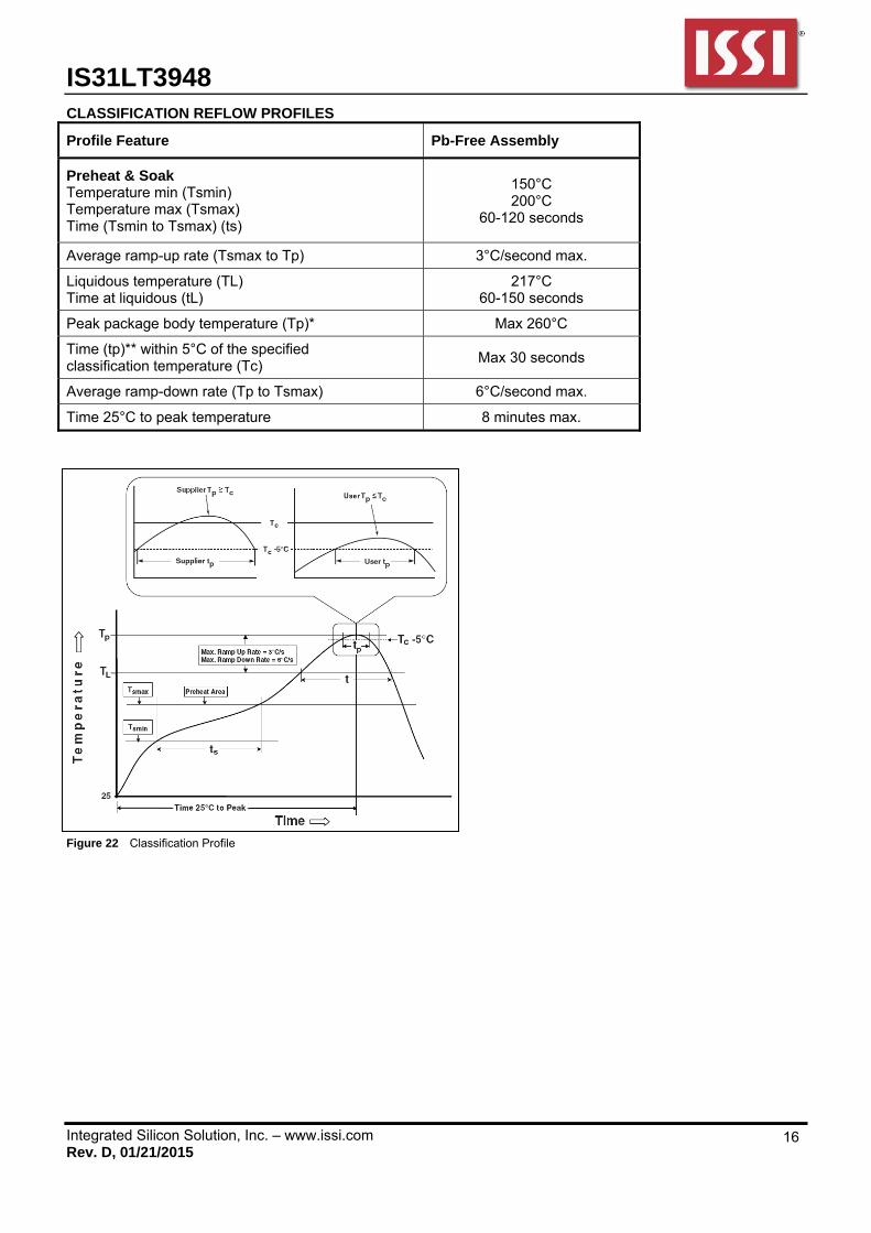
CLASSIFICATION REFLOW PROFILES
Profile Feature Pb-Free Assembly
Preheat & Soak Temperature min (Tsmin) Temperature max (Tsmax) Time (Tsmin to Tsmax) (ts)
150°C 200°C
60-120 seconds
Average ramp-up rate (Tsmax to Tp) 3°C/second max.
Liquidous temperature (TL) Time at liquidous (tL)
217°C 60-150 seconds
Peak package body temperature (Tp)* Max 260°C
Time (tp)** within 5°C of the specified classification temperature (Tc)
Max 30 seconds
Average ramp-down rate (Tp to Tsmax) 6°C/second max.
Time 25°C to peak temperature 8 minutes max.
Figure 22 Classification Profile

IS31LT3948
Integrated Silicon Solution, Inc. – www.issi.com Rev. D, 01/21/2015
17
PACKAGE INFORMATION SOP-8

IS31LT3948
Integrated Silicon Solution, Inc. – www.issi.com Rev. D, 01/21/2015
18
LAND PATTERN
Note:
1. Land pattern complies to IPC-7351.
2. All dimensions in MM.