is42s83200b is42s16160b - issi is42s16160b integrated silicon solution, inc. — 3 rev. d 07/28/08...
TRANSCRIPT
IS42S83200BIS42S16160B
Integrated Silicon Solution, Inc. — www.issi.com 1Rev. D07/28/08
Copyright © 2006 Integrated Silicon Solution, Inc. All rights reserved. ISSI reserves the right to make changes to this specification and its products at anytime without notice. ISSI assumes no liability arising out of the application or use of any information, products or services described herein. Customers areadvised to obtain the latest version of this device specification before relying on any published information and before placing orders for products.
FEATURES• Clock frequency: 166, 143, 133 MHz
• Fully synchronous; all signals referenced to apositive clock edge
• Internal bank for hiding row access/precharge
• Power supply
VDD VDDQ
IS42S83200B 3.3V 3.3V
IS42S16160B 3.3V 3.3V
• LVTTL interface
• Programmable burst length– (1, 2, 4, 8, full page)
• Programmable burst sequence:Sequential/Interleave
• Auto Refresh (CBR)
• Self Refresh
• 8K refresh cycles every 64 ms
• Random column address every clock cycle
• Programmable CAS latency (2, 3 clocks)
• Burst read/write and burst read/single writeoperations capability
• Burst termination by burst stop and prechargecommand
• Available in Industrial Temperature
• Available in 54-pin TSOP-II and 54-ball BGA(x16 only)
• Available in Lead-free
OVERVIEWISSI's 256Mb Synchronous DRAM achieves high-speeddata transfer using pipeline architecture. All inputs andoutputs signals refer to the rising edge of the clock input.The 256Mb SDRAM is organized as follows.
32Meg x 8, 16Meg x16256-MBIT SYNCHRONOUS DRAM
SEPTEMBER 2008
KEY TIMING PARAMETERS
Parameter -6 -7 Unit
Clk Cycle TimeCAS Latency = 3 6 7 nsCAS Latency = 2 8 10 ns
Clk FrequencyCAS Latency = 3 166 143 MhzCAS Latency = 2 125 100 Mhz
Access Time from ClockCAS Latency = 3 5.4 5.4 nsCAS Latency = 2 6.5 6.5 ns
IS42S83200B IS42S16160B
8M x 8 x 4 Banks 4M x16x4 Banks
54-pin TSOPII 54-pin TSOPII
54-ball BGA

2 Integrated Silicon Solution, Inc. — www.issi.comRev. D
07/28/08
IS42S83200B, IS42S16160B
DEVICE OVERVIEWThe 256Mb SDRAM is a high speed CMOS, dynamicrandom-access memory designed to operate in 3.3V VDD
and 3.3V VDDQ memory systems containing 268,435,456bits. Internally configured as a quad-bank DRAM with asynchronous interface. Each 67,108,864-bit bank is orga-nized as 8,192 rows by 512 columns by 16 bits or 8,192 rowsby 1,024 columns by 8 bits.
The 256Mb SDRAM includes an AUTO REFRESH MODE,and a power-saving, power-down mode. All signals areregistered on the positive edge of the clock signal, CLK. Allinputs and outputs are LVTTL compatible.
The 256Mb SDRAM has the ability to synchronously burstdata at a high data rate with automatic column-addressgeneration, the ability to interleave between internal banksto hide precharge time and the capability to randomlychange column addresses on each clock cycle during burstaccess.
A self-timed row precharge initiated at the end of the burstsequence is available with the AUTO PRECHARGE func-tion enabled. Precharge one bank while accessing one of theother three banks will hide the precharge cycles and provideseamless, high-speed, random-access operation.
SDRAM read and write accesses are burst oriented starting ata selected location and continuing for a programmed num-ber of locations in a programmed sequence. The registra-tion of an ACTIVE command begins accesses, followed bya READ or WRITE command. The ACTIVE command inconjunction with address bits registered are used to selectthe bank and row to be accessed (BA0, BA1 select thebank; A0-A12 select the row). The READ or WRITEcommands in conjunction with address bits registered areused to select the starting column location for the burstaccess.
Programmable READ or WRITE burst lengths consist of 1,2, 4 and 8 locations or full page, with a burst terminateoption.
CLKCKE
CSRASCASWE
A9A8A7A6A5A4A3A2A1A0
BA0BA1
A10A12
COMMANDDECODER
&CLOCK
GENERATOR MODEREGISTER
REFRESHCONTROLLER
REFRESHCOUNTER
SELF
REFRESH
CONTROLLER
ROWADDRESS
LATCH MU
LTIP
LEX
ER
COLUMNADDRESS LATCH
BURST COUNTER
COLUMNADDRESS BUFFER
COLUMN DECODER
DATA INBUFFER
DATA OUTBUFFER
DQML DQMH
DQ 0-15
VDD/VDDQ
Vss/VssQ
13
13
9
13
13
9
16
16 16
16
512(x 16)
8192
8192
8192
RO
W D
EC
OD
ER 8192
MEMORY CELLARRAY
BANK 0
SENSE AMP I/O GATE
BANK CONTROL LOGIC
ROWADDRESSBUFFER
A11
2
FUNCTIONAL BLOCK DIAGRAM (FOR 4MX16X4 BANKS SHOWN)

IS42S83200B, IS42S16160B
Integrated Silicon Solution, Inc. — www.issi.com 3Rev. D07/28/08
VDD
DQ0
VDDQ
NC
DQ1
VSSQ
NC
DQ2
VDDQ
NC
DQ3
VSSQ
NC
VDD
NC
WE
CAS
RAS
CS
BA0
BA1
A10
A0
A1
A2
A3
VDD
1
2
3
4
5
6
7
8
9
10
11
12
13
14
15
16
17
18
19
20
21
22
23
24
25
26
27
54
53
52
51
50
49
48
47
46
45
44
43
42
41
40
39
38
37
36
35
34
33
32
31
30
29
28
VSS
DQ7
VSSQ
NC
DQ6
VDDQ
NC
DQ5
VSSQ
NC
DQ4
VDDQ
NC
VSS
NC
DQM
CLK
CKE
A12
A11
A9
A8
A7
A6
A5
A4
VSS
PIN CONFIGURATIONS54 pin TSOP - Type II for x8
PIN DESCRIPTIONS
A0-A12 Row Address Input
A0-A9 Column Address Input
BA0, BA1 Bank Select Address
DQ0 to DQ7 Data I/O
CLK System Clock Input
CKE Clock Enable
CS Chip Select
RAS Row Address Strobe Command
CAS Column Address Strobe Command
WE Write Enable
DQM Data Input/Output Mask
VDD Power
Vss Ground
VDDQ Power Supply for I/O Pin
VssQ Ground for I/O Pin
NC No Connection

4 Integrated Silicon Solution, Inc. — www.issi.comRev. D
07/28/08
IS42S83200B, IS42S16160B
PIN CONFIGURATIONS54 pin TSOP - Type II for x16
PIN DESCRIPTIONS
A0-A12 Row Address Input
A0-A8 Column Address Input
BA0, BA1 Bank Select Address
DQ0 to DQ15 Data I/O
CLK System Clock Input
CKE Clock Enable
CS Chip Select
RAS Row Address Strobe Command
CAS Column Address Strobe Command
VDD
DQ0
VDDQ
DQ1
DQ2
VSSQ
DQ3
DQ4
VDDQ
DQ5
DQ6
VSSQ
DQ7
VDD
DQML
WE
CAS
RAS
CS
BA0
BA1
A10
A0
A1
A2
A3
VDD
1
2
3
4
5
6
7
8
9
10
11
12
13
14
15
16
17
18
19
20
21
22
23
24
25
26
27
54
53
52
51
50
49
48
47
46
45
44
43
42
41
40
39
38
37
36
35
34
33
32
31
30
29
28
VSS
DQ15
VSSQ
DQ14
DQ13
VDDQ
DQ12
DQ11
VSSQ
DQ10
DQ9
VDDQ
DQ8
VSS
NC
DQMH
CLK
CKE
A12
A11
A9
A8
A7
A6
A5
A4
VSS
WE Write Enable
DQML x16 Lower Byte, Input/Output Mask
DQMH x16 Upper Byte, Input/Output Mask
VDD Power
Vss Ground
VDDQ Power Supply for I/O Pin
VssQ Ground for I/O Pin
NC No Connection

IS42S83200B, IS42S16160B
Integrated Silicon Solution, Inc. — www.issi.com 5Rev. D07/28/08
PIN CONFIGURATION
54-ball fBGA for x16 (Top View) (8.00 mm x 13.00 mm Body, 0.8 mm Ball Pitch)PACKAGE CODE: B
1 2 3 4 5 6 7 8 9
A
B
C
D
E
F
G
H
J
VSS
DQ14
DQ12
DQ10
DQ8
DQMH
A12
A8
VSS
DQ15
DQ13
DQ11
DQ9
NC
CLK
A11
A7
A5
VSSQ
VDDQ
VSSQ
VDDQ
VSS
CKE
A9
A6
A4
VDDQ
VSSQ
VDDQ
VSSQ
VDD
CAS
BA0
A0
A3
DQ0
DQ2
DQ4
DQ6
DQML
RAS
BA1
A1
A2
VDD
DQ1
DQ3
DQ5
DQ7
WE
CS
A10
VDD
PIN DESCRIPTIONS
A0-A12 Row Address Input
A0-A8 Column Address Input
BA0, BA1 Bank Select Address
DQ0 to DQ15 Data I/O
CLK System Clock Input
CKE Clock Enable
CS Chip Select
RAS Row Address Strobe Command
CAS Column Address Strobe Command
WE Write Enable
DQML x16 Lower Byte Input/Output Mask
DQMH x16 Upper Byte Input/Output Mask
VDD Power
Vss Ground
VDDQ Power Supply for I/O Pin
VssQ Ground for I/O Pin
NC No Connection
6 Integrated Silicon Solution, Inc. — www.issi.comRev. D
07/28/08
IS42S83200B, IS42S16160B
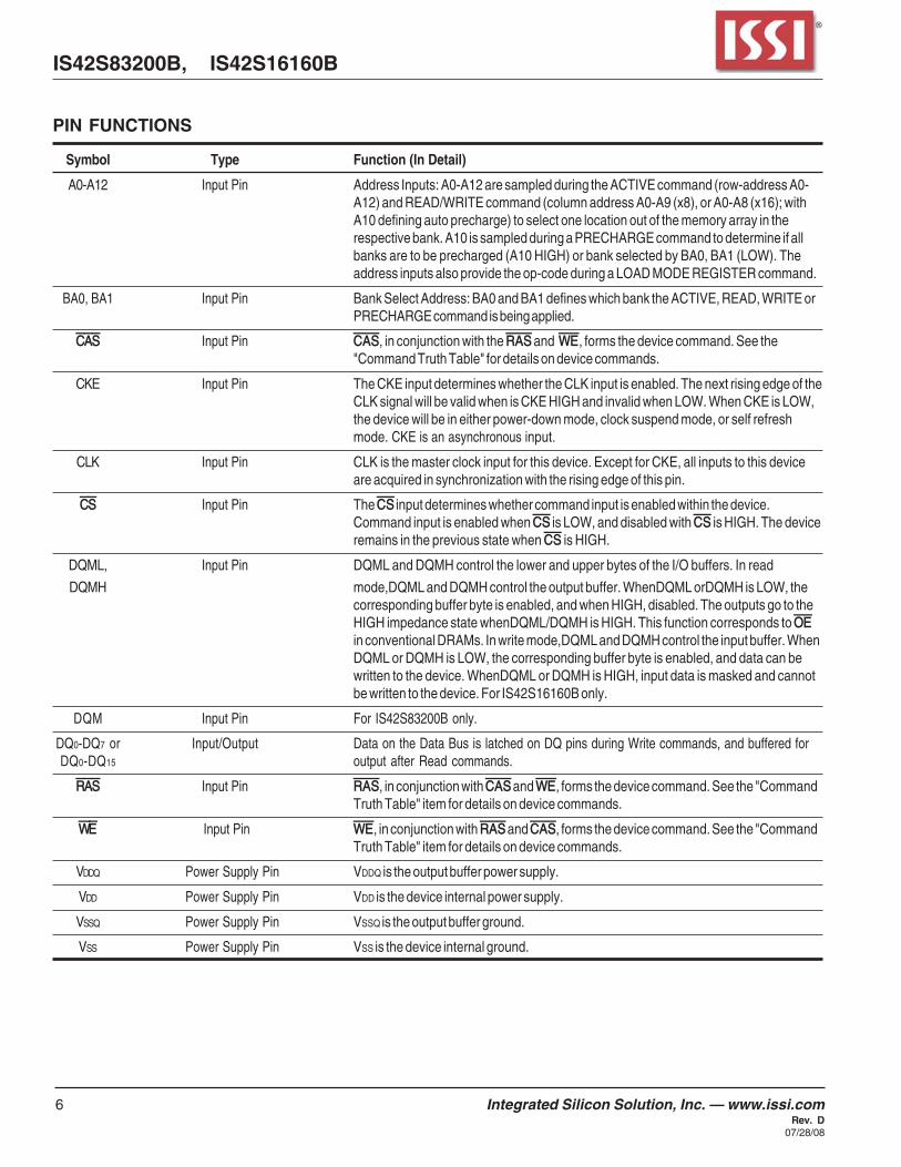
PIN FUNCTIONS
Symbol Type Function (In Detail)
A0-A12 Input Pin Address Inputs: A0-A12 are sampled during the ACTIVE command (row-address A0-A12) and READ/WRITE command (column address A0-A9 (x8), or A0-A8 (x16); withA10 defining auto precharge) to select one location out of the memory array in therespective bank. A10 is sampled during a PRECHARGE command to determine if allbanks are to be precharged (A10 HIGH) or bank selected by BA0, BA1 (LOW). Theaddress inputs also provide the op-code during a LOAD MODE REGISTER command.
BA0, BA1 Input Pin Bank Select Address: BA0 and BA1 defines which bank the ACTIVE, READ, WRITE orPRECHARGE command is being applied.
CAS Input Pin CAS, in conjunction with the RAS and WE, forms the device command. See the"Command Truth Table" for details on device commands.
CKE Input Pin The CKE input determines whether the CLK input is enabled. The next rising edge of theCLK signal will be valid when is CKE HIGH and invalid when LOW. When CKE is LOW,the device will be in either power-down mode, clock suspend mode, or self refreshmode. CKE is an asynchronous input.
CLK Input Pin CLK is the master clock input for this device. Except for CKE, all inputs to this deviceare acquired in synchronization with the rising edge of this pin.
CS Input Pin The CS input determines whether command input is enabled within the device.Command input is enabled when CS is LOW, and disabled with CS is HIGH. The deviceremains in the previous state when CS is HIGH.
DQML, Input Pin DQML and DQMH control the lower and upper bytes of the I/O buffers. In read
DQMH mode,DQML and DQMH control the output buffer. WhenDQML orDQMH is LOW, thecorresponding buffer byte is enabled, and when HIGH, disabled. The outputs go to theHIGH impedance state whenDQML/DQMH is HIGH. This function corresponds to OEin conventional DRAMs. In write mode,DQML and DQMH control the input buffer. WhenDQML or DQMH is LOW, the corresponding buffer byte is enabled, and data can bewritten to the device. WhenDQML or DQMH is HIGH, input data is masked and cannotbe written to the device. For IS42S16160B only.
DQM Input Pin For IS42S83200B only.
DQ0-DQ7 or Input/Output Data on the Data Bus is latched on DQ pins during Write commands, and buffered forDQ0-DQ15 output after Read commands.
RAS Input Pin RAS, in conjunction with CAS and WE, forms the device command. See the "CommandTruth Table" item for details on device commands.
WE Input Pin WE, in conjunction with RAS and CAS, forms the device command. See the "CommandTruth Table" item for details on device commands.
VDDQ Power Supply Pin VDDQ is the output buffer power supply.
VDD Power Supply Pin VDD is the device internal power supply.
VSSQ Power Supply Pin VSSQ is the output buffer ground.
VSS Power Supply Pin VSS is the device internal ground.

IS42S83200B, IS42S16160B
Integrated Silicon Solution, Inc. — www.issi.com 7Rev. D07/28/08
GENERAL DESCRIPTION
READThe READ command selects the bank from BA0, BA1inputs and starts a burst read access to an active row.Inputs A0-A9 (x8); A0-A8 (x16) provides the starting columnlocation. When A10 is HIGH, this command functions as anAUTO PRECHARGE command. When the auto prechargeis selected, the row being accessed will be precharged atthe end of the READ burst. The row will remain open forsubsequent accesses when AUTO PRECHARGE is notselected. DQ’s read data is subject to the logic level on theDQM inputs two clocks earlier. When a given DQM signalwas registered HIGH, the corresponding DQ’s will be High-Z two clocks later. DQ’s will provide valid data when theDQM signal was registered LOW.
WRITEA burst write access to an active row is initiated with theWRITE command. BA0, BA1 inputs selects the bank, andthe starting column location is provided by inputs A0-A9(x8); A0-A8 (x16). Whether or not AUTO-PRECHARGE isused is determined by A10.
The row being accessed will be precharged at the end of theWRITE burst, if AUTO PRECHARGE is selected. If AUTOPRECHARGE is not selected, the row will remain open forsubsequent accesses.
A memory array is written with corresponding input data onDQ’s and DQM input logic level appearing at the same time.Data will be written to memory when DQM signal is LOW.When DQM is HIGH, the corresponding data inputs will beignored, and a WRITE will not be executed to that byte/column location.
PRECHARGEThe PRECHARGE command is used to deactivate the openrow in a particular bank or the open row in all banks. BA0,BA1 can be used to select which bank is precharged or theyare treated as “Don’t Care”. A10 determined whether one orall banks are precharged. After executing this command,the next command for the selected bank(s) is executed afterpassage of the period t
RP, which is the period required for
bank precharging. Once a bank has been precharged, it isin the idle state and must be activated prior to any READ orWRITE commands being issued to that bank.
AUTO PRECHARGEThe AUTO PRECHARGE function ensures that the prechargeis initiated at the earliest valid stage within a burst. Thisfunction allows for individual-bank precharge without requir-ing an explicit command. A10 to enable the AUTO
PRECHARGE function in conjunction with a specific READor WRITE command. For each individual READ or WRITEcommand, auto precharge is either enabled or disabled.AUTO PRECHARGE does not apply except in full-pageburst mode. Upon completion of the READ or WRITE burst,a precharge of the bank/row that is addressed is automati-cally performed.
AUTO REFRESH COMMANDThis command executes the AUTO REFRESH operation.The row address and bank to be refreshed are automaticallygenerated during this operation. The stipulated period (tRC) isrequired for a single refresh operation, and no other com-mands can be executed during this period. This command isexecuted at least 8192 times for every 64ms. During anAUTO REFRESH command, address bits are “Don’t Care”.This command corresponds to CBR Auto-refresh.
BURST TERMINATEThe BURST TERMINATE command forcibly terminates theburst read and write operations by truncating either fixed-length or full-page bursts and the most recently registeredREAD or WRITE command prior to the BURST TERMI-NATE.
COMMAND INHIBITCOMMAND INHIBIT prevents new commands from beingexecuted. Operations in progress are not affected, apartfrom whether the CLK signal is enabled
NO OPERATIONWhen CS is low, the NOP command prevents unwantedcommands from being registered during idle or wait states.
LOAD MODE REGISTERDuring the LOAD MODE REGISTER command the moderegister is loaded from A0-A12. This command can only beissued when all banks are idle.
ACTIVE COMMANDWhen the ACTIVE COMMAND is activated, BA0, BA1inputs selects a bank to be accessed, and the addressinputs on A0-A12 selects the row. Until a PRECHARGEcommand is issued to the bank, the row remains open foraccesses.

8 Integrated Silicon Solution, Inc. — www.issi.comRev. D
07/28/08
IS42S83200B, IS42S16160B
CKE
Function n-1 n DQMH DQML
Data write / output enable H × L L
Data mask / output disable H × H H
Upper byte write enable / output enable H × L ×
Lower byte write enable / output enable H × × L
Upper byte write inhibit / output disable H × H ×
Lower byte write inhibit / output disable H × × H
CKE A12, A11
Function n – 1 n CSCSCSCSCS RASRASRASRASRAS CASCASCASCASCAS WEWEWEWEWE BA1 BA0 A10 A9 - A0
Device deselect (DESL) H × H × × × × × × ×
No operation (NOP) H × L H H H × × × ×
Burst stop (BST) H × L H H L × × × ×
Read H × L H L H V V L V
Read with auto precharge H × L H L H V V H V
Write H × L H L L V V L V
Write with auto precharge H × L H L L V V H V
Bank activate (ACT) H × L L H H V V V V
Precharge select bank (PRE) H × L L H L V V L ×
Precharge all banks (PALL) H × L L H L × × H ×
CBR Auto-Refresh (REF) H H L L L H × × × ×
Self-Refresh (SELF) H L L L L H × × × ×
Mode register set (MRS) H × L L L L L L L V
COMMAND TRUTH TABLE
DQM TRUTH TABLE
Note: H=VIH, L=VIL x= VIH or VIL, V = Valid Data.
Note: H=VIH, L=VIL x= VIH or VIL, V = Valid Data.

IS42S83200B, IS42S16160B
Integrated Silicon Solution, Inc. — www.issi.com 9Rev. D07/28/08
CKE
Current State /Function n – 1 n CS RAS CAS WE Address
Activating Clock suspend mode entry H L × × × × ×
Any Clock suspend mode L L × × × × ×
Clock suspend mode exit L H × × × × ×
Auto refresh command Idle (REF) H H L L L H ×
Self refresh entry Idle (SELF) H L L L L H ×
Power down entry Idle H L × × × × ×
Self refresh exit L H L H H H ×L H H × × × ×
Power down exit L H × × × × ×
Note: H=VIH, L=VIL x= VIH or VIL, V = Valid Data.
CKE TRUTH TABLE

10 Integrated Silicon Solution, Inc. — www.issi.comRev. D
07/28/08
IS42S83200B, IS42S16160B
Current State CSCSCSCSCS RAS RAS RAS RAS RAS CASCASCASCASCAS WEWEWEWEWE Address Command Action
Idle H X X X X DESL Nop or Power Down(2)
L H H H X NOP Nop or Power Down(2)
L H H L X BST Nop or Power Down
L H L H BA, CA, A10 READ/READA ILLEGAL (3)
L H L L A, CA, A10 WRIT/ WRITA ILLEGAL(3)
L L H H BA, RA ACT Row activating
L L H L BA, A10 PRE/PALL Nop
L L L H X REF/SELF Auto refresh or Self-refresh(4)
L L L L OC, BA1=L MRS Mode register set
Row Active H X X X X DESL Nop
L H H H X NOP Nop
L H H L X BST Nop
L H L H BA, CA, A10 READ/READA Begin read (5)
L H L L BA, CA, A10 WRIT/ WRITA Begin write (5)
L L H H BA, RA ACT ILLEGAL (3)
L L H L BA, A10 PRE/PALL PrechargePrecharge all banks(6)
L L L H X REF/SELF ILLEGAL
L L L L OC, BA MRS ILLEGAL
Read H X X X X DESL Continue burst to end toRow active
L H H H X NOP Continue burst to end RowRow active
L H H L X BST Burst stop, Row active
L H L H BA, CA, A10 READ/READA Terminate burst,begin new read (7)
L H L L BA, CA, A10 WRIT/WRITA Terminate burst,begin write (7,8)
L L H H BA, RA ACT ILLEGAL (3)
L L H L BA, A10 PRE/PALL Terminate burstPrecharging
L L L H X REF/SELF ILLEGAL
L L L L OC, BA MRS ILLEGAL
Write H X X X X DESL Continue burst to endWrite recovering
L H H H X NOP Continue burst to endWrite recovering
L H H L X BST Burst stop, Row active
L H L H BA, CA, A10 READ/READA Terminate burst, start read :Determine AP (7,8)
L H L L BA, CA, A10 WRIT/WRITA Terminate burst, new write :Determine AP (7)
L L H H BA, RA RA ACT ILLEGAL (3)
L L H L BA, A10 PRE/PALL Terminate burst Precharging (9)
L L L H X REF/SELF ILLEGAL
L L L L OC, BA MRS ILLEGAL
FUNCTIONAL TRUTH TABLE
Note: H=VIH, L=VIL x= VIH or VIL, V = Valid Data, BA= Bank Address, CA+Column Address, RA=Row Address, OC= Op-Code

IS42S83200B, IS42S16160B
Integrated Silicon Solution, Inc. — www.issi.com 11Rev. D07/28/08
Current State CSCSCSCSCS RAS RAS RAS RAS RAS CASCASCASCASCAS WE WE WE WE WE Address Command Action
Read with auto H × × × × DESL Continue burst to end, PrechargePrecharging
L H H H x NOP Continue burst to end, Precharge
L H H L × BST ILLEGAL
L H L H BA, CA, A10 READ/READA ILLEGAL (11)
L H L L BA, CA, A10 WRIT/ WRITA ILLEGAL (11)
L L H H BA, RA ACT ILLEGAL (3)
L L H L BA, A10 PRE/PALL ILLEGAL (11)
L L L H × REF/SELF ILLEGAL
L L L L OC, BA MRS ILLEGAL
Write with Auto H × × × × DESL Continue burst to end, WritePrecharge recovering with auto precharge
L H H H × NOP Continue burst to end, Writerecovering with auto precharge
L H H L × BST ILLEGAL
L H L H BA, CA, A10 READ/READA ILLEGAL(11)
L H L L BA, CA, A10 WRIT/ WRITA ILLEGAL (11)
L L H H BA, RA ACT ILLEGAL (3,11)
L L H L BA, A10 PRE/PALL ILLEGAL (3,11)
L L L H × REF/SELF ILLEGAL
L L L L OC, BA MRS ILLEGAL
Precharging H × × × × DESL Nop, Enter idle after tRP
L H H H × NOP Nop, Enter idle after tRP
L H H L × BST Nop, Enter idle after tRP
L H L H BA, CA, A10 READ/READA ILLEGAL (3)
L H L L BA, CA, A10 WRIT/WRITA ILLEGAL (3)
L L H H BA, RA ACT ILLEGAL(3)
L L H L BA, A10 PRE/PALL Nop Enter idle after tRP
L L L H × REF/SELF ILLEGAL
L L L L OC, BA MRS ILLEGAL
Row Activating H × × × × DESL Nop, Enter bank active after tRCD
L H H H × NOP Nop, Enter bank active after tRCD
L H H L × BST Nop, Enter bank active after tRCD
L H L H BA, CA, A10 READ/READA ILLEGAL (3)
L H L L BA, CA, A10 WRIT/WRITA ILLEGAL (3)
L L H H BA, RA ACT ILLEGAL (3,9)
L L H L BA, A10 PRE/PALL ILLEGAL (3)
L L L H × REF/SELF ILLEGAL
L L L L OC, BA MRS ILLEGAL
FUNCTIONAL TRUTH TABLE Continued:
Note: H=VIH, L=VIL x= VIH or VIL, V = Valid Data, BA= Bank Address, CA+Column Address, RA=Row Address, OC= Op-Code

12 Integrated Silicon Solution, Inc. — www.issi.comRev. D
07/28/08
IS42S83200B, IS42S16160B
Current State CSCSCSCSCS RAS RAS RAS RAS RAS CASCASCASCASCAS WE WE WE WE WE Address Command Action
Write Recovering H × × × × DESL Nop, Enter row active after tDPL
L H H H × NOP Nop, Enter row active after tDPL
L H H L × BST Nop, Enter row active after tDPL
L H L H BA, CA, A10 READ/READA Begin read (8)
L H L L BA, CA, A10 WRIT/ WRITA Begin new write
L L H H BA, RA ACT ILLEGAL (3)
L L H L BA, A10 PRE/PALL ILLEGAL (3)
L L L H × REF/SELF ILLEGAL
L L L L OC, BA MRS ILLEGAL
Write Recovering H × × × × DESL Nop, Enter precharge after tDPL
with Auto L H H H × NOP Nop, Enter precharge after tDPL
Precharge L H H L × BST Nop, Enter row active after tDPL
L H L H BA, CA, A10 READ/READA ILLEGAL(3,8,11)
L H L L BA, CA, A10 WRIT/WRITA ILLEGAL (3,11)
L L H H BA, RA ACT ILLEGAL (3,11)
L L H L BA, A10 PRE/PALL ILLEGAL (3,11)
L L L H × REF/SELF ILLEGAL
L L L L OC, BA MRS ILLEGAL
Refresh H × × × × DESL Nop, Enter idle after tRC
L H H × × NOP/BST Nop, Enter idle after tRC
L H L H BA, CA, A10 READ/READA ILLEGAL
L H L L BA, CA, A10 WRIT/WRITA ILLEGAL
L L H H BA, RA ACT ILLEGAL
L L H L BA, A10 PRE/PALL ILLEGAL
L L L H × REF/SELF ILLEGAL
L L L L OC, BA MRS ILLEGAL
Mode Register H × × × × DESL Nop, Enter idle after 2 clocks
Accessing L H H H × NOP Nop, Enter idle after 2 clocks
L H H L × BST ILLEGAL
L H L × BA, CA, A10 READ/WRITE ILLEGAL
L L × × BA, RA ACT/PRE/PALL ILLEGALREF/MRS
FUNCTIONAL TRUTH TABLE Continued:
Note: H=VIH, L=VIL x= VIH or VIL, V = Valid Data, BA= Bank Address, CA+Column Address, RA=Row Address, OC= Op-Code
Notes:1. All entries assume that CKE is active (CKEn-1=CKEn=H).2. If both banks are idle, and CKE is inactive (Low), the device will enter Power Down mode. All input buffers except CKE will
be disabled.3. Illegal to bank in specified states; Function may be legal in the bank indicated by Bank Address (BA), depending on the
state of that bank.4. If both banks are idle, and CKE is inactive (Low), the device will enter Self-Refresh mode. All input buffers except CKE will
be disabled.5. Illegal if tRCD is not satisfied.6. Illegal if tRAS is not satisfied.7. Must satisfy burst interrupt condition.8. Must satisfy bus contention, bus turn around, and/or write recovery requirements.9. Must mask preceding data which don’t satisfy tDPL.10. Illegal if tRRD is not satisfied.11. Illegal for single bank, but legal for other banks.

IS42S83200B, IS42S16160B
Integrated Silicon Solution, Inc. — www.issi.com 13Rev. D07/28/08
CKE RELATED COMMAND TRUTH TABLE(1)
CKECurrent State Operation n-1 n CS RAS CAS WE AddressSelf-Refresh (S.R.) INVALID, CLK (n - 1) would exit S.R. H X X X X X X
Self-Refresh Recovery(2) L H H X X X XSelf-Refresh Recovery(2) L H L H H X XIllegal L H L H L X XIllegal L H L L X X XMaintain S.R. L L X X X X X
Self-Refresh Recovery Idle After tRC H H H X X X XIdle After tRC H H L H H X XIllegal H H L H L X XIllegal H H L L X X XBegin clock suspend next cycle(5) H L H X X X XBegin clock suspend next cycle(5) H L L H H X XIllegal H L L H L X XIllegal H L L L X X XExit clock suspend next cycle(2) L H X X X X XMaintain clock suspend L L X X X X X
Power-Down (P.D.) INVALID, CLK (n - 1) would exit P.D. H X X X X X —EXIT P.D. --> Idle(2) L H X X X X XMaintain power down mode L L X X X X X
All Banks Idle Refer to operations in Operative Command Table H H H X X X —Refer to operations in Operative Command Table H H L H X X —Refer to operations in Operative Command Table H H L L H X —Auto-Refresh H H L L L H XRefer to operations in Operative Command Table H H L L L L Op - CodeRefer to operations in Operative Command Table H L H X X X —Refer to operations in Operative Command Table H L L H X X —Refer to operations in Operative Command Table H L L L H X —Self-Refresh(3) H L L L L H XRefer to operations in Operative Command Table H L L L L L Op - CodePower-Down(3) L X X X X X X
Any state Refer to operations in Operative Command Table H H X X X X Xother than Begin clock suspend next cycle(4) H L X X X X Xlisted above Exit clock suspend next cycle L H X X X X X
Maintain clock suspend L L X X X X X
Notes:1. H : High level, L : low level, X : High or low level (Don’t care).2. CKE Low to High transition will re-enable CLK and other inputs asynchronously. A minimum setup
time must be satisfied before any command other than EXIT.3. Power down and Self refresh can be entered only from the both banks idle state.4. Must be legal command as defined in Operative Command Table.5. Illegal if tXSR is not satisfied.

14 Integrated Silicon Solution, Inc. — www.issi.comRev. D
07/28/08
IS42S83200B, IS42S16160B
ModeRegister
SetIDLE
SelfRefresh
CBR (Auto)Refresh
RowActive
ActivePowerDown
PowerDown
WRITEWRITE
SUSPENDREAD
READSUSPEND
WRITEASUSPEND
WRITEA READAREADA
SUSPEND
POWERON
Precharge
Automatic sequence
Manual Input
SELF
SELF exit
REFMRS
ACT
CKE
CKE
CKE
CKE
BST
Read
Write
Write
Precharge
RR
E (Precharge termination) PR
E (P
rech
arge
term
inat
ion)
Writ
e w
ithA
uto
Pre
char
ge Read w
ith
Auto P
recharge
Read
Write
BST
CKE
CKECKE
CKE
CKE
CKECKE
CKE
Read
STATE DIAGRAM

IS42S83200B, IS42S16160B
Integrated Silicon Solution, Inc. — www.issi.com 15Rev. D07/28/08
ABSOLUTE MAXIMUM RATINGS(1)
Symbol Parameters Rating Unit
VDD MAX Maximum Supply Voltage –0.5 to +4.6 VVDDQ
MAX Maximum Supply Voltage for Output Buffer –0.5 to +4.6 V
VIN Input Voltage –0.5 to VDD + 0.5 VVOUT Output Voltage –1.0 to VDDQ + 0.5 VPD MAX Allowable Power Dissipation 1 WICS Output Shorted Current 50 mATOPR Operating Temperature Com. 0 to +70 °C
Ind. –40 to +85TSTG Storage Temperature –65 to +150 °C
DC RECOMMENDED OPERATING CONDITIONS
Symbol Parameter Min. Typ. Max. Unit
VDD Supply Voltage 3.0 3.3 3.6 VVDDQ I/O Supply Voltage 3.0 3.3 3.6 VVIH(1) Input High Voltage 2.0 — VDDQ + 0.3 VVIL(2) Input Low Voltage -0.3 — +0.8 V
CAPACITANCE CHARACTERISTICS (At TA = 0 to +25°C, VDD = VDDQ = 3.3 ± 0.3V)
Symbol Parameter Min. Max. Unit
CIN1 Input Capacitance: CLK 2.5 3.5 pFCIN2 Input Capacitance:All other input pins 2.5 3.8 pFCI/O Data Input/Output Capacitance: DQS 4.0 6.0 pF
Note:
1. VIH (overshoot): VIH (max) = VDDQ +2V (PULSE WIDTH < 3ns).
2. VIL (undershoot): VIH (min) = -2V (PULSE WIDTH < 3ns).3. All voltages are referenced to Vss.
Notes:1. Stress greater than those listed under ABSOLUTE MAXIMUM RATINGS may cause permanent damage to
the device. This is a stress rating only and functional operation of the device at these or any other condi-tions above those indicated in the operational sections of this specification is not implied. Exposure toabsolute maximum rating conditions for extended periods may affect reliability.
2. All voltages are referenced to Vss.

16 Integrated Silicon Solution, Inc. — www.issi.comRev. D
07/28/08
IS42S83200B, IS42S16160B
DC ELECTRICAL CHARACTERISTICS 1 (Recommended Operation Conditions unless otherwise noted.)
Symbol Parameter Test Condition -6 -7 Unit
IDD1 (1) Operating Current One bank active, CL = 3, BL = 1, x8 120 100 mA
tCLK = tCLK (min), tRC = tRC (min) x16 140 120 mA
IDD2P Precharge Standby Current CKE ≤ VIL (MAX), tCK = 15ns x8 / x16 2 2 mA(In Power-Down Mode)
IDD2PS Precharge Standby Current CKE ≤ VIL (MAX), CLK ≤ VIL (MAX) x8 / x16 1 1 mA(In Power-Down Mode)
IDD2N (2) Precharge Standby Current CS ≥ Vcc - 0.2V, CKE ≥ VIH (MIN) x8 / x16 25 25 mA
(In Non Power-Down Mode) tCK = 15ns
IDD2NS Precharge Standby Current CS ≥ Vcc - 0.2V, CKE ≥ VIH (MIN) or x8 / x16 15 15 mA
(In Non Power-Down Mode) CKE ≤ VIL (MAX), All inputs stable
IDD3N (2) Active Standby Current CS ≥ Vcc - 0.2V, CKE ≥ VIH (MIN) x8 / x16 30 30 mA
(In Non Power-Down Mode) tCK = 15ns
IDD3NS Active Standby Current CS ≥ Vcc - 0.2V, CKE ≥ VIH (MIN) or x8 / x16 20 20 mA
(In Non Power-Down Mode) CKE ≤ VIL (MAX), All inputs stable
IDD4 Operating Current All banks active, BL = 4, CL = 3, x8 170 120 mA
tCK = tCK (min) x16 180 130 mA
IDD5 Auto-Refresh Current tRC = tRC (min), tCLK = tCLK (min) x8/ x16 180 160 mA
IDD6 Self-Refresh Current CKE ≤ 0.2V x8 / x16 1.5 1.5 mA
Notes:
1. IDD (MAX) is specified at the output open condition.2. Input signals are changed one time during 30ns.
DC ELECTRICAL CHARACTERISTICS 2 (Recommended Operation Conditions unless otherwise noted.)
Symbol Parameter Test Condition Min Max Unit
IIL Input Leakage Current 0V ≤ Vin ≤ Vcc, with pins other than -10 10 μA
the tested pin at 0V
IOL Output Leakage Current Output is disabled, 0V ≤ Vout ≤ Vcc, -5 5 μA
VOH Output High Voltage Level IOH = -2mA 2.4 — V
VOL Output Low Voltage Level IOL = 2mA — 0.4 V

IS42S83200B, IS42S16160B
Integrated Silicon Solution, Inc. — www.issi.com 17Rev. D07/28/08
AC ELECTRICAL CHARACTERISTICS (1,2,3)
-6 -7Symbol Parameter Min. Max. Min. Max. Units
tCK3 Clock Cycle Time CAS Latency = 3 6 — 7 — nstCK2 CAS Latency = 2 8 — 10 — ns
tAC3 Access Time From CLK CAS Latency = 3 — 5.4 — 5.4 nstAC2 CAS Latency = 2 — 6.5 — 6.5 ns
tCHI CLK HIGH Level Width 2.5 — 2.5 — ns
tCL CLK LOW Level Width 2.5 — 2.5 — ns
tOH3 Output Data Hold Time CAS Latency = 3 2.7 — 2.7 — nstOH2 CAS Latency = 2 2.7 — 2.7 — ns
tLZ Output LOW Impedance Time 0 — 0 — ns
tHZ Output HIGH Impedance Time 2.7 5.4 2.7 5.4 ns
tDS Input Data Setup Time(2) 2.0 — 2.0 — ns
tDH Input Data Hold Time(2) 1.0 — 1.0 — ns
tAS Address Setup Time(2) 2.0 — 2.0 — ns
tAH Address Hold Time(2) 1.0 — 1.0 — ns
tCKS CKE Setup Time(2) 2.0 — 2.0 — ns
tCKH CKE Hold Time(2) 1.0 — 1.0 — ns
tCS Command Setup Time (CS, RAS, CAS, WE, DQM)(2) 2.0 — 2.0 — ns
tCH Command Hold Time (CS, RAS, CAS, WE, DQM)(2) 1.0 — 1.0 — ns
tRC Command Period (REF to REF / ACT to ACT) 60 — 67.5 — ns
tRAS Command Period (ACT to PRE) 42 120K 45 120K ns
tRP Command Period (PRE to ACT) 18 — 20 — ns
tRCD Active Command To Read / Write Command Delay Time 18 — 20 — ns
tRRD Command Period (ACT [0] to ACT[1]) 12 — 14 — ns
tDPL Input Data To Precharge 12 — 14 — nsCommand Delay time
tDAL Input Data To Active / Refresh 27 — 35 — nsCommand Delay time (During Auto-Precharge)
tMRD Mode Register Program Time 12 — 15 — ns
tDDE Power Down Exit Setup Time 6 — 7.5 — ns
tXSR Self-Refresh Exit Time 66 — 70 — ns
tT Transition Time 0.5 5 0.5 5 ns
tREF Refresh Cycle Time (8192) — 64 — 64 ms
Notes:1. The power-on sequence must be executed before starting memory operation.2. Measured with tT = 1 ns. If clock rising time is longer than 1ns, (tR /2 - 0.5) ns should be added to the parameter.3. The reference level is 1.4V when measuring input signal timing. Rise and fall times are measured between VIH(min.) and VIL (max).

18 Integrated Silicon Solution, Inc. — www.issi.comRev. D
07/28/08
IS42S83200B, IS42S16160B
OPERATING FREQUENCY / LATENCY RELATIONSHIPS
SYMBOL PARAMETER UNITS
— Clock Cycle Time 6 7 10 ns
— Operating Frequency (CAS Latency = 3) 166 143 100 MHz
tCAC CAS Latency 3 3 2 cycle
tRCD Active Command To Read/Write Command Delay Time 3 3 2 cycle
tRAC RAS Latency (tRCD + tCAC) CAS Latency = 3 6 6 5 cycleCAS Latency = 2 — — 4
tRC Command Period (REF to REF / ACT to ACT) 10 10 7 cycle
tRAS Command Period (ACT to PRE) 7 7 5 cycle
tRP Command Period (PRE to ACT) 3 3 2 cycle
tRRD Command Period (ACT[0] to ACT [1]) 2 2 2 cycle
tCCD Column Command Delay Time 1 1 1 cycle(READ, READA, WRIT, WRITA)
tDPL Input Data To Precharge Command Delay Time 2 2 2 cycle
tDAL Input Data To Active/Refresh Command Delay Time 5 5 4 cycle(During Auto-Precharge)
tRBD Burst Stop Command To Output in HIGH-Z Delay Time CAS Latency = 3 3 3 3 cycle(Read) CAS Latency = 2 — — 2
tWBD Burst Stop Command To Input in Invalid Delay Time 0 0 0 cycle(Write)
tRQL Precharge Command To Output in HIGH-Z Delay Time CAS Latency = 3 3 3 3 cycle(Read) CAS Latency = 2 — — 2
tWDL Precharge Command To Input in Invalid Delay Time 0 0 0 cycle(Write)
tPQL Last Output To Auto-Precharge Start Time (Read) CAS Latency = 3 -2 –2 -2 cycleCAS Latency = 2 — — -1
tQMD DQM To Output Delay Time (Read) 2 2 2 cycle
tDMD DQM To Input Delay Time (Write) 0 0 0 cycle
tMRD Mode Register Set To Command Delay Time 2 2 2 cycle

IS42S83200B, IS42S16160B
Integrated Silicon Solution, Inc. — www.issi.com 19Rev. D07/28/08
AC TEST CONDITIONS
Input Load Output Load
Output Z = 50Ω
50 pF
1.4V
50Ω
3.0V
1.4V
0V
CLK
INPUT
OUTPUT
tCHI
tCH
tACtOH
tCS
tCK
tCL
3.0V
1.4V
1.4V 1.4V
0V
AC TEST CONDITIONS
Parameter RatingAC Input Levels 0V to 3.0VInput Rise and Fall Times 1 nsInput Timing Reference Level 1.4VOutput Timing Measurement Reference Level 1.4V

20 Integrated Silicon Solution, Inc. — www.issi.comRev. D
07/28/08
IS42S83200B, IS42S16160B
FUNCTIONAL DESCRIPTIONThe 256Mb SDRAMs are quad-bank DRAMs which operateat 3.3V and include a synchronous interface (all signals areregistered on the positive edge of the clock signal, CLK).Each of the 67,108,864-bit banks is organized as 8,192rows by 512 columns by 16 bits or 8,192 rows by 1,024columns by 8 bits.
Read and write accesses to the SDRAM are burst oriented;accesses start at a selected location and continue for aprogrammed number of locations in a programmedsequence. Accesses begin with the registration of an AC-TIVE command which is then followed by a READ or WRITEcommand. The address bits registered coincident with theACTIVE command are used to select the bank and row tobe accessed (BA0 and BA1 select the bank, A0-A12 select the row).The address bits A0-A9 (x8); A0-A8 (x16) registered coincidentwith the READ or WRITE command are used to select thestarting column location for the burst access.
Prior to normal operation, the SDRAM must be initialized.The following sections provide detailed information coveringdevice initialization, register definition, commanddescriptions and device operation.
InitializationSDRAMs must be powered up and initialized in apredefined manner.
The 256Mb SDRAM is initialized after the power is appliedto VDD and VDDQ (simultaneously) and the clock is stablewith DQM High and CKE High.
A 200µs delay is required prior to issuing any commandother than a COMMAND INHIBIT or a NOP. The COMMANDINHIBIT or NOP may be applied during the 200us period andshould continue at least through the end of the period.
With at least one COMMAND INHIBIT or NOP commandhaving been applied, a PRECHARGE command should beapplied once the 200µs delay has been satisfied. All banksmust be precharged. This will leave all banks in an idle stateafter which at least eight AUTO REFRESH cycles must beperformed. After the AUTO REFRESH cycles are complete,the SDRAM is then ready for mode register programming.
The mode register should be loaded prior to applying anyoperational command because it will power up in an un-known state.

IS42S83200B, IS42S16160B
Integrated Silicon Solution, Inc. — www.issi.com 21Rev. D07/28/08
INITIALIZE AND LOAD MODE REGISTER(1)
DON'T CARE
CLK
CKE
COMMAND
DQM/DQML, DQMH
A0-A9, A11, A12
A10
BA0, BA1
DQ
tCH tCLtCK
tCMH tCMS tCMH tCMS tCMH tCMS
tCKS tCKH
T0 T1 Tn+1 To+1 Tp+1 Tp+2 Tp+3
tMRDtRCtRCtRP
ROW
ROW
BANK
tAS tAH
tAS tAH
CODE
CODEALL BANKS
SINGLE BANK
ALL BANKS
AUTOREFRESH
AUTOREFRESH
Load MODEREGISTER
T = 200µs Min.
Power-up: VCC
and CLK stablePrechargeall banks
AUTO REFRESH Program MODE REGISTER
NOP PRECHARGE NOP NOP NOP ACTIVE
T
(2, 3, 4)AUTO REFRESH
At least 8 Auto-Refresh Commands
CODE
tAS tAH
Notes:1. If CS is High at clock High time, all commands applied are NOP.2. The Mode register may be loaded prior to the Auto-Refresh cycles if desired.3. JEDEC and PC100 specify three clocks.4. Outputs are guaranteed High-Z after the command is issued.

22 Integrated Silicon Solution, Inc. — www.issi.comRev. D
07/28/08
IS42S83200B, IS42S16160B
AUTO-REFRESH CYCLE
Notes:1. CAS latency = 2, 3
tRP tRC tRC
DON'T CARE
CLK
CKE
COMMAND
DQM/DQML, DQMH
A0-A9, A11, A12
A10
BA0, BA1
DQ
tAS tAH
tCHtCLtCK
tCMS tCMH
tCKS tCKH
T0 T1 T2 Tn+1 To+1
ALL BANKS
SINGLE BANK
BANK(s)
ROW
ROW
BANK
High-Z
PRECHARGE NOP NOP NOP ACTIVEAutoRefresh
AutoRefresh

IS42S83200B, IS42S16160B
Integrated Silicon Solution, Inc. — www.issi.com 23Rev. D07/28/08
SELF-REFRESH CYCLE
CLK
CKE
COMMAND
DQM/DQML, DQMH
A0-A9, A11, A12
A10
BA0, BA1
DQ
tAS tAH
BANK
tCLtCHtCK
tCMS tCMH
tCKS tCKH
ALL BANKS
SINGLE BANK
tCKS
Precharge allactive banks
CLK stable prior to exitingself refresh mode
Enter selfrefresh mode
Exit self refresh mode(Restart refresh time base)
T0 T1 T2 Tn+1 To+1 To+2
High-Z
AutoRefresh
AutoRefreshPRECHARGE NOP NOP NOP
tCKS
≥ tRAS
tRP tXSR
DON'T CARE

24 Integrated Silicon Solution, Inc. — www.issi.comRev. D
07/28/08
IS42S83200B, IS42S16160B
REGISTER DEFINITION
Mode RegisterThe mode register is used to define the specific mode ofoperation of the SDRAM. This definition includes theselection of a burst length, a burst type, a CAS latency, anoperating mode and a write burst mode, as shown in MODEREGISTER DEFINITION.
The mode register is programmed via the LOAD MODEREGISTER command and will retain the stored informationuntil it is programmed again or the device loses power.
Mode register bits M0-M2 specify the burst length, M3specifies the type of burst (sequential or interleaved), M4- M6specify the CAS latency, M7 and M8 specify the operatingmode, M9 specifies the WRITE burst mode, and M10, M11,and M12 are reserved for future use.
The mode register must be loaded when all banks are idle,and the controller must wait the specified time beforeinitiating the subsequent operation. Violating either of theserequirements will result in unspecified operation.
MODE REGISTER DEFINITION
Latency Mode
M6 M5 M4 CAS Latency
0 0 0 Reserved 0 0 1 Reserved 0 1 0 2 0 1 1 3 1 0 0 Reserved 1 0 1 Reserved 1 1 0 Reserved 1 1 1 Reserved
1. To ensure compatibility with future devices,should program BA1, BA0, A12, A11, A10 = "0"
Write Burst Mode
M9 Mode
0 Programmed Burst Length
1 Single Location Access
Operating Mode
M8 M7 M6-M0 Mode
0 0 Defined Standard Operation — — — All Other States Reserved
Burst Type
M3 Type
0 Sequential 1 Interleaved
Burst Length
M2 M1 M0 M3=0 M3=1
0 0 0 1 1 0 0 1 2 2 0 1 0 4 4 0 1 1 8 8 1 0 0 Reserved Reserved 1 0 1 Reserved Reserved 1 1 0 Reserved Reserved 1 1 1 Full Page Reserved
Reserved
Address Bus (Ax)
Mode Register (Mx)
(1)
BA1 BA0 A12 A11 A10 A9 A8 A7 A6 A5 A4 A3 A2 A1 A0

IS42S83200B, IS42S16160B
Integrated Silicon Solution, Inc. — www.issi.com 25Rev. D07/28/08
BURST DEFINITION
Burst Starting Column Order of Accesses Within a Burst
Length Address Type = Sequential Type = Interleaved
A 0
2 0 0-1 0-1
1 1-0 1-0
A 1 A 0
0 0 0-1-2-3 0-1-2-3
4 0 1 1-2-3-0 1-0-3-2
1 0 2-3-0-1 2-3-0-1
1 1 3-0-1-2 3-2-1-0
A 2 A 1 A 0
0 0 0 0-1-2-3-4-5-6-7 0-1-2-3-4-5-6-7
0 0 1 1-2-3-4-5-6-7-0 1-0-3-2-5-4-7-6
0 1 0 2-3-4-5-6-7-0-1 2-3-0-1-6-7-4-5
8 0 1 1 3-4-5-6-7-0-1-2 3-2-1-0-7-6-5-4
1 0 0 4-5-6-7-0-1-2-3 4-5-6-7-0-1-2-3
1 0 1 5-6-7-0-1-2-3-4 5-4-7-6-1-0-3-2
1 1 0 6-7-0-1-2-3-4-5 6-7-4-5-2-3-0-1
1 1 1 7-0-1-2-3-4-5-6 7-6-5-4-3-2-1-0
Full n = A0-A8 (x16) Cn, Cn + 1, Cn + 2 Not SupportedPage n = A0-A9 (x8) Cn + 3, Cn + 4...(y) (location 0-y) …Cn - 1,
Cn…
BURST LENGTHRead and write accesses to the SDRAM are burst oriented,with the burst length being programmable, as shown inMODE REGISTER DEFINITION. The burst length deter-mines the maximum number of column locations that canbe accessed for a given READ or WRITE command. Burstlengths of 1, 2, 4 or 8 locations are available for both thesequential and the interleaved burst types, and a full-pageburst is available for the sequential type. The full-page burstis used in conjunction with the BURST TERMINATE com-mand to generate arbitrary burst lengths.
Reserved states should not be used, as unknown operationor incompatibility with future versions may result.
When a READ or WRITE command is issued, a block ofcolumns equal to the burst length is effectively selected. Allaccesses for that burst take place within this block, mean-
ing that the burst will wrap within the block if a boundary isreached. The block is uniquely selected by A1-A8 (x16) orA1-A9 (x8) when the burst length is set to two; by A2-A8(x16) or A2-A9 (x8) when the burst length is set to four; andby A3-A8 (x16) or A3-A9 (x8) when the burst length is set toeight. The remaining (least significant) address bit(s) is (are)used to select the starting location within the block. Full-page bursts wrap within the page if the boundary is reached.
Burst TypeAccesses within a given burst may be programmed to beeither sequential or interleaved; this is referred to as theburst type and is selected via bit M3.
The ordering of accesses within a burst is determined by theburst length, the burst type and the starting column address,as shown in BURST DEFINITION table.

26 Integrated Silicon Solution, Inc. — www.issi.comRev. D
07/28/08
IS42S83200B, IS42S16160B
DON'T CARE
UNDEFINED
CLK
COMMAND
DQ
READ NOP NOP NOP
CAS Latency - 3
tAC
tOH
DOUT
T0 T1 T2 T3 T4
tLZ
CLK
COMMAND
DQ
READ NOP NOP
CAS Latency - 2
tAC
tOH
DOUT
T0 T1 T2 T3
tLZ
CAS LATENCY
CAS LatencyThe CAS latency is the delay, in clock cycles, between theregistration of a READ command and the availability of thefirst piece of output data. The latency can be set to two orthree clocks.
If a READ command is registered at clock edge n, and thelatency is m clocks, the data will be available by clock edgen + m. The DQs will start driving as a result of the clock edgeone cycle earlier (n + m - 1), and provided that the relevantaccess times are met, the data will be valid by clock edgen + m. For example, assuming that the clock cycle time issuch that all relevant access times are met, if a READcommand is registered at T0 and the latency is programmedto two clocks, the DQs will start driving after T1 and the datawill be valid by T2, as shown in CAS Latency diagrams. TheAllowable Operating Frequency table indicates the operat-ing frequencies at which each CAS latency setting can beused.
Reserved states should not be used as unknown operation orincompatibility with future versions may result.
CAS LatencyAllowable Operating Frequency (MHz)
Speed CAS Latency = 2 CAS Latency = 3
-6 125 166
-7 100 143
Operating ModeThe normal operating mode is selected by setting M7 and M8to zero; the other combinations of values for M7 and M8 arereserved for future use and/or test modes. The programmedburst length applies to both READ and WRITE bursts.
Test modes and reserved states should not be usedbecause unknown operation or incompatibility with futureversions may result.
Write Burst ModeWhen M9 = 0, the burst length programmed via M0-M2applies to both READ and WRITE bursts; when M9 = 1, theprogrammed burst length applies to READ bursts, but writeaccesses are single-location (nonburst) accesses.

IS42S83200B, IS42S16160B
Integrated Silicon Solution, Inc. — www.issi.com 27Rev. D07/28/08
CLK
CKE
ROW ADDRESS
BANK ADDRESS
CS
RAS
CAS
WE
A0-A12
BA0, BA1
HIGH
ACTIVATING SPECIFIC ROW WITHIN SPE-CIFIC BANK
DON'T CARE
CLK
COMMAND ACTIVE NOP NOP
tRCD
T0 T1 T2 T3 T4
READ orWRITE
CHIP OPERATION
BANK/ROW ACTIVATIONBefore any READ or WRITE commands can be issued to abank within the SDRAM, a row in that bank must be “opened.”This is accomplished via the ACTIVE command, whichselects both the bank and the row to be activated (seeActivating Specific Row Within Specific Bank).
After opening a row (issuing an ACTIVE command), aREAD or WRITE command may be issued to that row,subject to the tRCD specification. Minimum tRCD should bedivided by the clock period and rounded up to the next wholenumber to determine the earliest clock edge after theACTIVE command on which a READ or WRITE commandcan be entered. For example, a tRCD specification of 15nswith a 143 MHz clock (7ns period) results in 2.14 clocks,rounded to 3. This is reflected in the following example,which covers any case where 2 < [tRCD (MIN)/tCK] ≤ 3. (Thesame procedure is used to convert other specification limitsfrom time units to clock cycles).
A subsequent ACTIVE command to a different row in thesame bank can only be issued after the previous active rowhas been “closed” (precharged). The minimum time intervalbetween successive ACTIVE commands to the same bankis defined by tRC.
A subsequent ACTIVE command to another bank can beissued while the first bank is being accessed, which resultsin a reduction of total row-access overhead. The minimumtime interval between successive ACTIVE commands todifferent banks is defined by tRRD.
EXAMPLE: MEETING TRCD (MIN) WHEN 2 <<<<< [TRCD (MIN)/TCK] ≤≤≤≤≤ 3

28 Integrated Silicon Solution, Inc. — www.issi.comRev. D
07/28/08
IS42S83200B, IS42S16160B
CLK
CKEHIGH
COLUMN ADDRESS
AUTO PRECHARGE
NO PRECHARGE
CS
RAS
CAS
WE
A0-A9
A10
BA0, BA1 BANK ADDRESS
A11, A12
READ COMMANDREADSREAD bursts are initiated with a READ command, as shownin the READ COMMAND diagram.
The starting column and bank addresses are provided with theREAD command, and auto precharge is either enabled ordisabled for that burst access. If auto precharge is enabled, therow being accessed is precharged at the completion of theburst. For the generic READ commands used in the followingillustrations, auto precharge is disabled.
During READ bursts, the valid data-out element from thestarting column address will be available following the CASlatency after the READ command. Each subsequent data-out element will be valid by the next positive clock edge. TheCAS Latency diagram shows general timingfor each possible CAS latency setting.
Upon completion of a burst, assuming no other commandshave been initiated, the DQs will go High-Z. A full-page burstwill continue until terminated. (At the end of the page, it willwrap to column 0 and continue.)
Data from any READ burst may be truncated with a subse-quent READ command, and data from a fixed-length READburst may be immediately followed by data from a READcommand. In either case, a continuous flow of data can bemaintained. The first data element from the new burst followseither the last element of a completed burst or the last desireddata element of a longer burst which is being truncated.
The new READ command should be issued x cycles beforethe clock edge at which the last desired data element isvalid, where x equals the CAS latency minus one. This isshown in Consecutive READ Bursts for CAS latencies oftwo and three; data element n + 3 is either the last of a burstof four or the last desired of a longer burst. The 256MbSDRAM uses a pipelined architecture and therefore doesnot require the 2n rule associated with a prefetch architec-ture. A READ command can be initiated on any clock cyclefollowing a previous READ command. Full-speed randomread accesses can be performed to the same bank, as shownin Random READ Accesses, or each subsequent READmay be performed to a different bank.
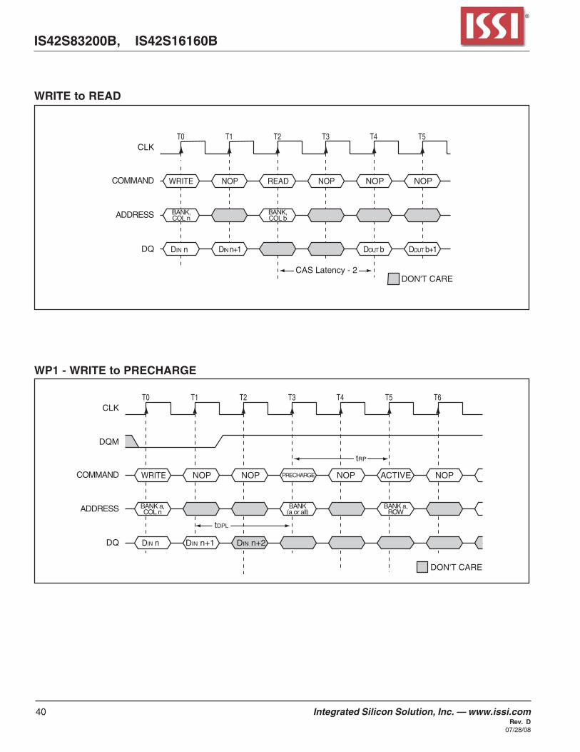
Data from any READ burst may be truncated with asubsequent WRITE command, and data from a fixed-lengthREAD burst may be immediately followed by data from aWRITE command (subject to bus turnaround limitations).The WRITE burst may be initiated on the clock edgeimmediately following the last (or last desired) data elementfrom the READ burst, provided that I/O contention can beavoided. In a given system design, there may be a possi-bility that the device driving the input data will go Low-Zbefore the SDRAM DQs go High-Z. In this case, at least asingle-cycle delay should occur between the last read dataand the WRITE command.
The DQM input is used to avoid I/O contention, as shownin Figures RW1 and RW2. The DQM signal must beasserted (HIGH) at least three clocks prior to the WRITEcommand (DQM latency is two clocks for output buffers) tosuppress data-out from the READ. Once the WRITE com-mand is registered, the DQs will go High-Z (or remain High-Z), regardless of the state of the DQM signal, provided theDQM was active on the clock just prior to the WRITEcommand that truncated the READ command. If not, thesecond WRITE will be an invalid WRITE. For example, ifDQM was LOW during T4 in Figure RW2, then the WRITEsat T5 and T7 would be valid, while the WRITE at T6 wouldbe invalid.
The DQM signal must be de-asserted prior to the WRITEcommand (DQM latency is zero clocks for input buffers) toensure that the written data is not masked.
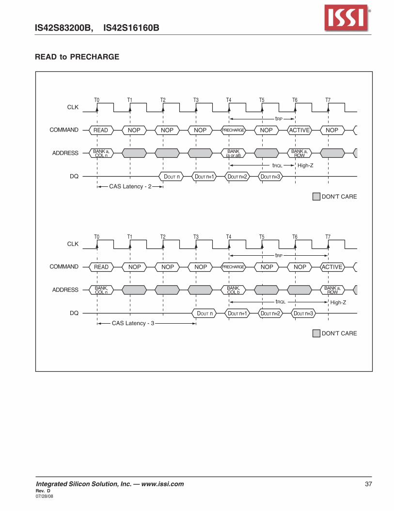
A fixed-length READ burst may be followed by, or truncatedwith, a PRECHARGE command to the same bank (providedthat auto precharge was not activated), and a full-page burstmay be truncated with a PRECHARGE command to thesame bank. The PRECHARGE command should be issuedx cycles before the clock edge at which the last desired dataelement is valid, where x equals the CAS latency minus one.This is shown in the READ to PRECHARGE diagram for each
Note: A9 is "Don't Care" for x16.

IS42S83200B, IS42S16160B
Integrated Silicon Solution, Inc. — www.issi.com 29Rev. D07/28/08
possible CAS latency; data element n + 3 is either the last ofa burst of four or the last desired of a longer burst. Followingthe PRECHARGE command, a subsequent command to thesame bank cannot be issued until tRP is met. Note that partof the row precharge time is hidden during the access of thelast data element(s).
In the case of a fixed-length burst being executed tocompletion, a PRECHARGE command issued at the opti-mum time (as described above) provides the same opera-tion that would result from the same fixed-length burst withauto precharge. The disadvantage of the PRECHARGEcommand is that it requires that the command and addressbuses be available at the appropriate time to issue thecommand; the advantage of the PRECHARGE command isthat it can be used to truncate fixed-length or full-pagebursts.
Full-page READ bursts can be truncated with the BURSTTERMINATE command, and fixed-length READ burstsmay be truncated with a BURST TERMINATE command,provided that auto precharge was not activated. The BURSTTERMINATE command should be issued x cycles beforethe clock edge at which the last desired data element isvalid, where x equals the CAS latency minus one. This isshown in the READ Burst Termination diagram for eachpossible CAS latency; data element n + 3 is the last desireddata element of a longer burst.

30 Integrated Silicon Solution, Inc. — www.issi.comRev. D
07/28/08
IS42S83200B, IS42S16160B
DON'T CARE
CLK
DQM
COMMAND
ADDRESS
DQ
T0 T1 T2 T3 T4 T5
READ NOP NOP NOP NOP WRITE
BANK,COL n
BANK,COL b
DOUT n DIN b
tDS
tHZ
CAS Latency - 3
RW1 - READ to WRITE
RW2 - READ to WRITE
DON'T CARE
CLK
DQM
COMMAND
ADDRESS
DQ
T0 T1 T2 T3 T4 T5 T6
READ NOP NOP NOP NOP NOP WRITE
BANK,COL n
DIN b
tDS
tHZ
BANK,COL b
CAS Latency - 2
DOUT n DOUT n+1 DOUT n+2

IS42S83200B, IS42S16160B
Integrated Silicon Solution, Inc. — www.issi.com 31Rev. D07/28/08
DON'T CARE
CLK
COMMAND
ADDRESS
DQ
T0 T1 T2 T3 T4 T5 T6
READ NOP NOP NOP READ NOP NOP
DOUT n DOUT n+1 DOUT n+2 DOUT n+3 DOUT b
BANK,COL n
BANK,COL b
CAS Latency - 2
DON'T CARE
CLK
COMMAND
ADDRESS
DQ
T0 T1 T2 T3 T4 T5 T6 T7
READ NOP NOP NOP READ NOP NOP NOP
DOUT n DOUT n+1 DOUT n+2 DOUT n+3 DOUT b
BANK,COL n
BANK,COL b
CAS Latency - 3
CONSECUTIVE READ BURSTS

32 Integrated Silicon Solution, Inc. — www.issi.comRev. D
07/28/08
IS42S83200B, IS42S16160B
DON'T CARE
CLK
COMMAND
ADDRESS
DQ
T0 T1 T2 T3 T4 T5
READ READ READ READ NOP NOP
DOUT n DOUT b DOUT m DOUT x
BANK,COL n
BANK,COL b
CAS Latency - 2
BANK,COL m
BANK,COL x
DON'T CARE
CLK
COMMAND
ADDRESS
DQ
T0 T1 T2 T3 T4 T5 T6
READ READ READ READ NOP NOP NOP
DOUT n DOUT b DOUT m DOUT x
BANK,COL n
BANK,COL b
CAS Latency - 3
BANK,COL m
BANK,COL x
RANDOM READ ACCESSES

IS42S83200B, IS42S16160B
Integrated Silicon Solution, Inc. — www.issi.com 33Rev. D07/28/08
DON'T CARE
CLK
COMMAND
ADDRESS
DQ
T0 T1 T2 T3 T4 T5 T6
READ NOP NOP NOP NOP NOP
DOUT n DOUT n+1 DOUT n+2 DOUT n+3
BANK a,COL n
CAS Latency - 2
x = 1 cycle
BURSTTERMINATE
DON'T CARE
CLK
COMMAND
ADDRESS
DQ
T0 T1 T2 T3 T4 T5 T6 T7
READ NOP NOP NOP NOP NOP NOP
DOUT n DOUT n+1 DOUT n+2 DOUT n+3
BANK,COL n
CAS Latency - 3
x = 2 cycles
BURSTTERMINATE
READ BURST TERMINATION

34 Integrated Silicon Solution, Inc. — www.issi.comRev. D
07/28/08
IS42S83200B, IS42S16160B
ALTERNATING BANK READ ACCESSES
BANK 0 BANK 3 BANK 3 BANK 0
DON'T CARE
CLK
CKE
COMMAND
DQM/DQML, DQMH
A0-A9, A11, A12
A10
BA0, BA1
DQ
tCMS tCMH
tAS tAH
tAS tAH
tAS tAH
tRCD - BANK 0 CAS Latency - BANK 0 tRCD - BANK 0
tRAS - BANK 0
tRC - BANK 0
tCHtCLtCK
tCMS tCMH
tCKS tCKH
ACTIVE NOP READ NOP ACTIVE NOP READ NOP ACTIVE
ROW
ROW
BANK 0
ROW ROW
tRRD tRCD - BANK 3
tRP - BANK 0
COLUMN m(2) ROW COLUMN b(2) ROW
ENABLE AUTO PRECHARGE ENABLE AUTO PRECHARGE
T0 T1 T2 T3 T4 T5 T6 T7 T8
tAC
tOH tOH tOH tOH tOH
DOUT m DOUT m+1 DOUT m+2 DOUT m+3 DOUT b
tAC tAC tAC tAC tAC
tLZ
CAS Latency - BANK 3
Notes:1) CAS latency = 2, Burst Length = 42) x16: A9, A11, and A12 = "Don't Care" x8: A11 and A12 = "Don't Care"

IS42S83200B, IS42S16160B
Integrated Silicon Solution, Inc. — www.issi.com 35Rev. D07/28/08
READ - FULL-PAGE BURST
DON'T CARE
UNDEFINED
CLK
CKE
COMMAND
DQM/DQML, DQMH
A0-A9, A11, A12
A10
BA0, BA1
DQ
tCMS tCMH
ACTIVE NOP READ NOP NOP NOP NOP NOP BURST TERM NOP NOP
tAS tAH
tAS tAH
tAS tAH
ROW
ROW
BANK
COLUMN m(2)
tCHtCLtCK
tCMS tCMH
tCKS tCKH
BANK
tRCD CAS Latency
tAC tACtAC tACtAC tHZ
tLZ
tAC
tOH tOH tOH tOH tOH tOH
DOUT m DOUT m+1 DOUT m+2 DOUT m-1 DOUT m DOUT m+1
each row (x16) has512 locations(3)
Full pagecompletion
Full-page burst not self-terminating.Use BURST TERMINATE command.
T0 T1 T2 T3 T4 T5 T6 Tn+1 Tn+2 Tn+3 Tn+4
Notes:1) CAS latency = 2, Burst Length = Full Page2) x16: A9, A11, and A12 = "Don't Care" x8: A11 and A12 = "Don't Care"3) x8: Each row has 1,024 locations.

36 Integrated Silicon Solution, Inc. — www.issi.comRev. D
07/28/08
IS42S83200B, IS42S16160B
READ - DQM OPERATION
DON'T CARE
UNDEFINED
CLK
CKE
COMMAND
DQM/DQML, DQMH
A0-A9, A11, A12
A10
BA0, BA1
DQ
tCMS tCMH
ACTIVE NOP READ NOP NOP NOP NOP NOP NOP
tAS tAH
tAS tAH
tAS tAH
ENABLE AUTO PRECHARGE
DISABLE AUTO PRECHARGE
ROW
ROW
BANK
tRCD CAS Latency
DOUT m DOUT m+2 DOUT m+3
COLUMN m(2)
BANK
tCHtCLtCK
tCMS tCMH
tCKS tCKH
tOHtOHtOH tACtAC
tACtHZ tHZtLZ tLZ
T0 T1 T2 T3 T4 T5 T6 T7 T8
Notes:1) CAS latency = 2, Burst Length = 42) x16: A9, A11, and A12 = "Don't Care" x8: A11 and A12 = "Don't Care"
IS42S83200B, IS42S16160B
Integrated Silicon Solution, Inc. — www.issi.com 37Rev. D07/28/08
DON'T CARE
CLK
COMMAND
ADDRESS
DQ
T0 T1 T2 T3 T4 T5 T6 T7
READ NOP NOP NOP NOP ACTIVE NOP
DOUT n DOUT n+1 DOUT n+2 DOUT n+3
BANK a,COL n
BANK a,ROW
BANK(a or all)
CAS Latency - 2
tRP
PRECHARGE
tRQL High-Z
DON'T CARE
CLK
COMMAND
ADDRESS
DQ
T0 T1 T2 T3 T4 T5 T6 T7
READ NOP NOP NOP NOP NOP ACTIVE
DOUT n DOUT n+1 DOUT n+2 DOUT n+3
BANK,COL n
BANK,COL b
CAS Latency - 3
tRP
tRQL
BANK a,ROW
PRECHARGE
High-Z
READ to PRECHARGE

38 Integrated Silicon Solution, Inc. — www.issi.comRev. D
07/28/08
IS42S83200B, IS42S16160B
CLK
CKEHIGH
COLUMN ADDRESS
AUTO PRECHARGE
BANK ADDRESS
CS
RAS
CAS
WE
A0-A9
A10
BA0, BA1
NO PRECHARGE
A11, A12
WRITE COMMAND
The starting column and bank addresses are provided withthe WRITE command, and auto precharge is either enabledor disabled for that access. If auto precharge is enabled, therow being accessed is precharged at the completion of theburst. For the generic WRITE commands used in thefollowing illustrations, auto precharge is disabled.
During WRITE bursts, the first valid data-in element will beregistered coincident with the WRITE command. Subsequentdata elements will be registered on each successive positiveclock edge. Upon completion of a fixed-length burst, assum-ing no other commands have been initiated, the DQs willremain High-Z and any additional input data will be ignored(see WRITE Burst). A full-page burst will continue untilterminated. (At the end of the page, it will wrap to column 0and continue.)
Data for any WRITE burst may be truncated with a subse-quent WRITE command, and data for a fixed-length WRITEburst may be immediately followed by data for a WRITEcommand. The new WRITE command can be issued on anyclock following the previous WRITE command, and the dataprovided coincident with the new command applies to the newcommand.
An example is shown in WRITE to WRITE diagram. Data n+ 1 is either the last of a burst of two or the last desired ofa longer burst. The 256Mb SDRAM uses a pipelinedarchitecture and therefore does not require the 2n ruleassociated with a prefetch architecture. A WRITE commandcan be initiated on any clock cycle following a previousWRITE command. Full-speed random write accesses withina page can be performed to the same bank, as shown inRandom WRITE Cycles, or each subsequent WRITE maybe performed to a different bank.
Data for any WRITE burst may be truncated with a subse-quent READ command, and data for a fixed-length WRITEburst may be immediately followed by a subsequent READcommand. Once the READ com mand is registered, thedata inputs will be ignored, and WRITEs will not be ex-ecuted. An example is shown in WRITE to READ. Data n +1 is either the last of a burst of two or the last desired of alonger burst.
Data for a fixed-length WRITE burst may be followed by, ortruncated with, a PRECHARGE command to the same bank(provided that auto precharge was not activated), and a full-page WRITE burst may be truncated with a PRECHARGEcommand to the same bank. The PRECHARGE commandshould be issued tDPL after the clock edge at which the lastdesired input data element is registered. The auto prechargemode requires a tDPL of at least one clock plus time,regardless of frequency. In addition, when truncating aWRITE burst, the DQM signal must be used to mask inputdata for the clock edge prior to, and the clock edge coincidentwith, the PRECHARGE command. An example is shown in theWRITE to PRECHARGE diagram. Data n+1 is either the lastof a burst of two or the last desired of a longer burst. Followingthe PRECHARGE command, a subsequent command to thesame bank cannot be issued until tRP is met.
In the case of a fixed-length burst being executed to comple-tion, a PRECHARGE command issued at the optimum time (asdescribed above) provides the same operation that would resultfrom the same fixed-length burst with auto precharge. Thedisadvantage of the PRECHARGE command is that it requiresthat the command and address buses be available at theappropriate time to issue the command; the advantage of thePRECHARGE command is that it can be used to truncatefixed-length or full-page bursts.
Fixed-length or full-page WRITE bursts can be truncatedwith the BURST TERMINATE command. When truncatinga WRITE burst, the input data applied coincident with theBURST TERMINATE command will be ignored. The lastdata written (provided that DQM is LOW at that time) will bethe input data applied one clock previous to the BURSTTERMINATE command. This is shown in WRITE BurstTermination, where data n is the last desired data elementof a longer burst.
WRITESWRITE bursts are initiated with a WRITE command, asshown in WRITE Command diagram.
Note: A9 is "Don't Care" for x16.

IS42S83200B, IS42S16160B
Integrated Silicon Solution, Inc. — www.issi.com 39Rev. D07/28/08
CLK
COMMAND
ADDRESS
DQ
T0 T1 T2 T3
WRITE NOP NOP NOP
DIN n DIN n+1
BANK,COL n
DON'T CARE
CLK
COMMAND
ADDRESS
DQ
T0 T1 T2
WRITE NOP WRITE
DIN n DIN n+1 DIN b
BANK,COL n
BANK,COL b
DON'T CARE
WRITE BURST
WRITE TO WRITE
CLK
COMMAND
ADDRESS
DQ
T0 T1 T2 T3
WRITE WRITE WRITE WRITE
DIN n DIN b DIN m DIN x
BANK,COL n
BANK,COL b
BANK,COL m
BANK,COL x
RANDOM WRITE CYCLES
40 Integrated Silicon Solution, Inc. — www.issi.comRev. D
07/28/08
IS42S83200B, IS42S16160B
DON'T CARE
CLK
COMMAND
ADDRESS
DQ
T0 T1 T2 T3 T4 T5
WRITE NOP READ NOP NOP NOP
DIN n DIN n+1 DOUT b DOUT b+1
BANK,COL n
BANK,COL b
CAS Latency - 2
WRITE to READ
WP1 - WRITE to PRECHARGE
DON'T CARE
CLK
DQM
COMMAND
ADDRESS
DQ
T0 T1 T2 T3 T4 T5 T6
WRITE NOP NOP NOP ACTIVE NOP
BANK a,COL n
BANK a,ROW
BANK(a or all)
tDPL
tRP
PRECHARGE
DIN n DIN n+1 DIN n+2

IS42S83200B, IS42S16160B
Integrated Silicon Solution, Inc. — www.issi.com 41Rev. D07/28/08
CLK
COMMAND
ADDRESS
DQ
T0 T1 T2
WRITE
DIN n (DATA)
BANK,COL n
DON'T CARE
(ADDRESS)
BURSTTERMINATE
NEXTCOMMAND
WRITE Burst Termination
DON'T CARE
CLK
DQM
COMMAND
ADDRESS
DQ
T0 T1 T2 T3 T4 T5 T6
WRITE NOP NOP NOP NOP ACTIVE
BANK a,COL n
BANK a,ROW
BANK(a or all)
tDPL
tRP
PRECHARGE
DIN n DIN n+1
WP2 - WRITE to PRECHARGE

42 Integrated Silicon Solution, Inc. — www.issi.comRev. D
07/28/08
IS42S83200B, IS42S16160B
DON'T CARE
CLK
CKE
COMMAND
DQM/DQMLDQMH
A0-A9, A11, A12
A10
BA0, BA1
DQ
tCMS tCMH
ACTIVE NOP WRITE NOP NOP NOP NOP BURST TERM NOP
tAS tAH
tAS tAH
tAS tAH
tDS tDH tDS tDH tDS tDH
ROW
ROW
BANK
tRCD
DIN m DIN m+1 DIN m+2 DIN m+3 DIN m-1
COLUMN m(2)
tCHtCLtCK
tDS tDH tDS tDH tDS tDH
tCMS tCMH
tCKS tCKH
BANK
Full page completed
T0 T1 T2 T3 T4 T5 Tn+1 Tn+2
WRITE - FULL PAGE BURST
Notes:1) Burst Length = Full Page2) x16: A9, A11, and A12 = "Don't Care" x8: A11 and A12 = "Don't Care"

IS42S83200B, IS42S16160B
Integrated Silicon Solution, Inc. — www.issi.com 43Rev. D07/28/08
DON'T CARE
CLK
CKE
COMMAND
DQM/DQMLDQMH
A0-A9, A11, A12
A10
BA0, BA1
DQ
tCMS tCMH
ACTIVE NOP WRITE NOP NOP NOP NOP NOP
tAS tAH
tAS tAH
tAS tAH
tDS tDH tDS tDH tDS tDH
ENABLE AUTO PRECHARGE
DISABLE AUTO PRECHARGE
ROW
ROW
BANK
tRCD
DIN m DIN m+2 DIN m+3
COLUMN m(2)
BANK
tCHtCLtCK
tCMS tCMH
tCKS tCKH
T0 T1 T2 T3 T4 T5 T6 T7
WRITE - DQM OPERATION
Notes:1) Burst Length = 42) x16: A9, A11, and A12 = "Don't Care" x8: A11 and A12 = "Don't Care"

44 Integrated Silicon Solution, Inc. — www.issi.comRev. D
07/28/08
IS42S83200B, IS42S16160B
ALTERNATING BANK WRITE ACCESSES
BANK 0 BANK 1 BANK 1 BANK 0
DON'T CARE
CLK
CKE
COMMAND
DQM/DQMLDQMH
A0-A9, A11, A12
A10
BA0, BA1
DQ
tCMS tCMH
tAS tAH
tAS tAH
tAS tAH
tDS tDH tDS tDH tDS tDH
tRCD - BANK 0 tRCD - BANK 0tDPL - BANK 1
tRAS - BANK 0tRC - BANK 0
tCHtCLtCK
tDS tDH tDS tDH tDS tDH tDS tDH tDS tDH
tCMS tCMH
tCKS tCKH
ACTIVE NOP WRITE NOP ACTIVE NOP WRITE NOP NOP ACTIVE
DIN m DIN m+1 DIN m+2 DIN m+3 DIN b DIN b+1 DIN b+2 DIN b+3
ROW
ROW
BANK 0
ROW ROW
tRRD tRCD - BANK 1
tDPL - BANK 0 tRP - BANK 0
COLUMN m(2) ROW COLUMN b(2) ROW
ENABLE AUTO PRECHARGE ENABLE AUTO PRECHARGE
T0 T1 T2 T3 T4 T5 T6 T7 T8 T9
Notes:1) Burst Length = 42) x16: A9, A11, and A12 = "Don't Care" x8: A11 and A12 = "Don't Care"
IS42S83200B, IS42S16160B
Integrated Silicon Solution, Inc. — www.issi.com 45Rev. D07/28/08
DON'T CARE
CLK
CKE
COMMAND
ADDRESS
DQ
T0 T1 T2 T3 T4 T5
NOP WRITE NOP NOP
BANK a,COL n
DIN n DIN n+1 DIN n+2
INTERNALCLOCK
DON'T CARE
CLK
CKE
COMMAND
ADDRESS
DQ
T0 T1 T2 T3 T4 T5 T6
READ NOP NOP NOP NOP NOP
BANK a,COL n
DOUT n DOUT n+1 DOUT n+2 DOUT n+3
INTERNALCLOCK
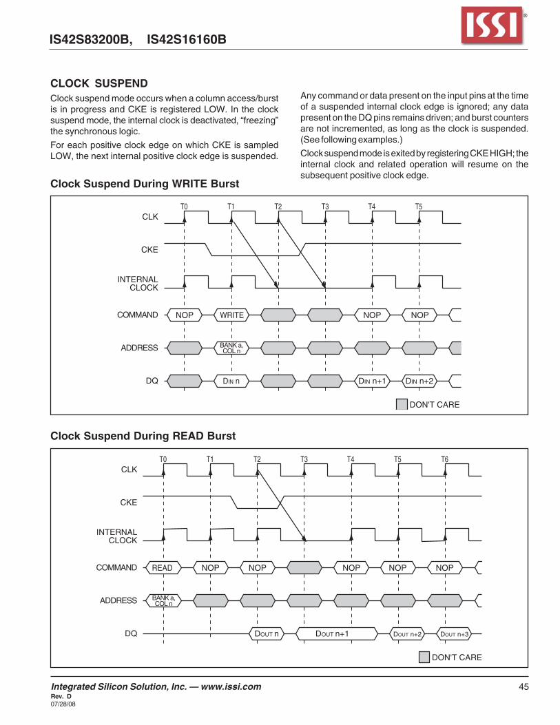
CLOCK SUSPENDClock suspend mode occurs when a column access/burstis in progress and CKE is registered LOW. In the clocksuspend mode, the internal clock is deactivated, “freezing”the synchronous logic.
For each positive clock edge on which CKE is sampledLOW, the next internal positive clock edge is suspended.
Any command or data present on the input pins at the timeof a suspended internal clock edge is ignored; any datapresent on the DQ pins remains driven; and burst countersare not incremented, as long as the clock is suspended.(See following examples.)
Clock suspend mode is exited by registering CKE HIGH; theinternal clock and related operation will resume on thesubsequent positive clock edge.
Clock Suspend During WRITE Burst
Clock Suspend During READ Burst

46 Integrated Silicon Solution, Inc. — www.issi.comRev. D
07/28/08
IS42S83200B, IS42S16160B
CLOCK SUSPEND MODE
Notes:1) CAS latency = 3, Burst Length = 2, Auto Precharge is disabled.2) X16: A9, A11, and A12 = "Don't Care" X8: A11 and A12 = "Don't Care"
DON'T CARE
CLK
CKE
COMMAND
DQM/DQMLDQMH
A0-A9, A11, A12
A10
BA0, BA1
DQ
tCMS tCMH
tAS tAH
tAS tAH
tAS tAH
tCHtCLtCK
tCMS tCMH
tCKS tCKH
COLUMN m(2)
T0 T1 T2 T3 T4 T5 T6 T7 T8 T9
READ NOP NOP NOP NOP NOP WRITE NOP
tCKS tCKH
BANK BANK
COLUMN n(2)
tAC tAC
tOH
tHZ
DOUT m DOUT m+1
tLZ
UNDEFINED
DIN e+1
tDS tDH
DIN e

IS42S83200B, IS42S16160B
Integrated Silicon Solution, Inc. — www.issi.com 47Rev. D07/28/08
CLK
CKEHIGH
ALL BANKS
BANK SELECT
BANK ADDRESS
CS
RAS
CAS
WE
A0-A9, A11, A12
A10
BA0, BA1
DON'T CARE
CLK
CKE
COMMAND NOP NOP ACTIVE
≥ tCKStCKS
All banks idle
Enter power-down mode Exit power-down mode
tRCD
tRAS
tRC
Input buffers gated off
less than 64ms
PRECHARGE Command
POWER-DOWN
POWER-DOWNPower-down occurs if CKE is registered LOW coincidentwith a NOP or COMMAND INHIBIT when no accesses arein progress. If power-down occurs when all banks are idle,this mode is referred to as precharge power-down; if power-down occurs when there is a row active in either bank, thismode is referred to as active power-down. Entering power-down deactivates the input and output buffers, excludingCKE, for maximum power savings while in standby. Thedevice may not remain in the power-down state longer thanthe refresh period (64ms) since no refresh operations areperformed in this mode.
The power-down state is exited by registering a NOP orCOMMAND INHIBIT and CKE HIGH at the desired clockedge (meeting tCKS). See figure below.
PRECHARGEThe PRECHARGE command (see figure) is used to deac-tivate the open row in a particular bank or the open row in allbanks. The bank(s) will be available for a subsequent rowaccess some specified time (tRP) after the PRECHARGEcommand is issued. Input A10 determines whether one orall banks are to be precharged, and in the case where onlyone bank is to be precharged, inputs BA0, BA1 select thebank. When all banks are to be precharged, inputs BA0,BA1 are treated as “Don’t Care.” Once a bank has beenprecharged, it is in the idle state and must be activated priorto any READ or WRITE commands being issued to thatbank.

48 Integrated Silicon Solution, Inc. — www.issi.comRev. D
07/28/08
IS42S83200B, IS42S16160B
POWER-DOWN MODE CYCLE
DON'T CARE
CLK
CKE
COMMAND
DQM/DQMLDQMH
A0-A9, A11, A12
A10
BA0, BA1
DQ
tAS tAH
BANK
tCHtCLtCK
tCMS tCMH
tCKS tCKH
PRECHARGE NOP NOP NOP ACTIVE
ALL BANKS
SINGLE BANK
ROW
ROW
BANK
tCKStCKS
Precharge allactive banks
All banks idleTwo clock cycles Input buffers gatedoff while in
power-down modeAll banks idle, enterpower-down mode Exit power-down mode
T0 T1 T2 Tn+1 Tn+2
High-Z

IS42S83200B, IS42S16160B
Integrated Silicon Solution, Inc. — www.issi.com 49Rev. D07/28/08
DON'T CARE
CLK
COMMAND
BANK n
BANK m
ADDRESS
DQ
T0 T1 T2 T3 T4 T5 T6 T7
NOP NOP NOP NOP NOP NOP
DOUT a DOUT a+1 DOUT b DOUT b+1
BANK n,COL a
CAS Latency - 3 (BANK n)
CAS Latency - 3 (BANK m)
tRP - BANK n tRP - BANK m
READ - APBANK n
READ - APBANK m
Page Active READ with Burst of 4 Interrupt Burst, Precharge Idle
Page Active READ with Burst of 4 Precharge
Internal States
BANK n,COL b
DON'T CARE
CLK
COMMAND
BANK n
BANK m
ADDRESS
DQM
DQ
T0 T1 T2 T3 T4 T5 T6 T7
NOP NOP NOP NOP NOP NOP
DOUT a DIN b DIN b+1 DIN b+2 DIN b+3
BANK n,COL a
BANK m,COL b
CAS Latency - 3 (BANK n)
tRP - BANK n tDPL - BANK m
READ - APBANK n
WRITE - APBANK m
READ with Burst of 4 Interrupt Burst, Precharge Idle
Page Active WRITE with Burst of 4 Write-Back
Internal States Page Active
BURST READ/SINGLE WRITEThe burst read/single write mode is entered by programmingthe write burst mode bit (M9) in the mode register to a logic 1.In this mode, all WRITE commands result in the access of asingle column location (burst of one), regardless of theprogrammed burst length. READ commands accesscolumns according to the programmed burst length andsequence, just as in the normal mode of operation (M9 = 0).
CONCURRENT AUTO PRECHARGEAn access command (READ or WRITE) to another bankwhile an access command with auto precharge enabled isexecuting is not allowed by SDRAMs, unless the SDRAMsupports CONCURRENT AUTO PRECHARGE. ISSISDRAMs support CONCURRENT AUTO PRECHARGE.
Four cases where CONCURRENT AUTO PRECHARGEoccurs are defined below.
READ with Auto Precharge1. Interrupted by a READ (with or without auto precharge):
A READ to bank m will interrupt a READ on bank n, CASlatency later. The PRECHARGE to bank n will beginwhen the READ to bank m is registered.
2. Interrupted by a WRITE (with or without auto precharge):A WRITE to bank m will interrupt a READ on bank n whenregistered. DQM should be used three clocks prior to theWRITE command to prevent bus contention. ThePRECHARGE to bank n will begin when the WRITE tobank m is registered.
READ With Auto Precharge interrupted by a READ
READ With Auto Precharge interrupted by a WRITE

50 Integrated Silicon Solution, Inc. — www.issi.comRev. D
07/28/08
IS42S83200B, IS42S16160B
DON'T CARE
CLK
COMMAND
BANK n
BANK m
ADDRESS
DQ
T0 T1 T2 T3 T4 T5 T6 T7
NOP NOP NOP NOP NOP NOP
DIN a DIN a+1 DOUT b DOUT b+1
BANK n,COL a
BANK m,COL b
CAS Latency - 3 (BANK m)
tRP - BANK ntRP - BANK m
WRITE - APBANK n
READ - APBANK m
Page Active WRITE with Burst of 4 Interrupt Burst, Write-Back Precharge
Page Active READ with Burst of 4 Precharge
Internal States tDPL - BANK n
DON'T CARE
CLK
COMMAND
BANK n
BANK m
ADDRESS
DQ
T0 T1 T2 T3 T4 T5 T6 T7
NOP NOP NOP NOP NOP NOP
BANK n,COL a
BANK m,COL b
tRP - BANK ntDPL - BANK m
WRITE - APBANK n
WRITE - APBANK m
Page Active WRITE with Burst of 4 Interrupt Burst, Write-Back Precharge
Page Active WRITE with Burst of 4 Write-Back
Internal States tDPL - BANK n
DIN a DIN a+1 DIN a+2 DIN b DIN b+1 DIN b+2 DIN b+3
WRITE with Auto Precharge3. Interrupted by a READ (with or without auto precharge):
A READ to bank m will interrupt a WRITE on bank n whenregistered, with the data-out appearing (CAS latency) later.The PRECHARGE to bank n will begin after tDPL is met,where tDPL begins when the READ to bank m is registered.The last valid WRITE to bank n will be data-in registered oneclock prior to the READ to bank m.
4. Interrupted by a WRITE (with or without auto precharge):AWRITE to bank m will interrupt a WRITE on bank n whenregistered. The PRECHARGE to bank n will begin aftertDPL is met, where tDPL begins when the WRITE to bank mis registered. The last valid data WRITE to bank n will bedata registered one clock prior to a WRITE to bank m.
WRITE With Auto Precharge interrupted by a READ
WRITE With Auto Precharge interrupted by a WRITE

IS42S83200B, IS42S16160B
Integrated Silicon Solution, Inc. — www.issi.com 51Rev. D07/28/08
SINGLE READ WITH AUTO PRECHARGE
DON'T CARE
UNDEFINED
CLK
CKE
COMMAND
DQM/DQMLDQMH
A0-A9, A11, A12
A10
BA0, BA1
DQ
tCMS tCMH
ACTIVE NOP NOP NOP READ NOP NOP ACTIVE NOP
tAS tAH
tAS tAH
tAS tAH
ROW
ROW
BANK
COLUMN m(2)
tCHtCLtCK
tCMS tCMH
tCKS tCKH
BANK
tRCD
tRAS
tRC
CAS Latency
tAC
tHZ
tOH
DOUT m
T0 T1 T2 T3 T4 T5 T6 T7 T8
tRP
ENABLE AUTO PRECHARGE
ROW
ROW
BANK
Notes:1) CAS latency = 2, Burst Length = 12) x16: A9, A11, and A12 = "Don't Care" x8: A11 and A12 = "Don't Care"

52 Integrated Silicon Solution, Inc. — www.issi.comRev. D
07/28/08
IS42S83200B, IS42S16160B
SINGLE READ WITHOUT AUTO PRECHARGE
DON'T CARE
UNDEFINED
CLK
CKE
COMMAND
DQM/DQMLDQMH
A0-A9, A11, A12
A10
BA0, BA1
DQ
tCMS tCMH
ACTIVE NOP READ NOP NOP PRECHARGE NOP ACTIVE NOP
tAS tAH
tAS tAH
tAS tAH
ROW
ROW
BANK
COLUMN m(2)
tCHtCLtCK
tCMS tCMH
tCKS tCKH
BANK
tRCD
tRAS
tRC
CAS Latency
tAC
tHZ
tOH
DOUT m
T0 T1 T2 T3 T4 T5 T6 T7 T8
tRP
DISABLE AUTO PRECHARGE
ROW
ROW
BANK
tLZ
ALL BANKS
SINGLE BANK
BANK
Notes:1) CAS latency = 2, Burst Length = 12) x16: A9, A11, and A12 = "Don't Care" x8: A11 and A12 = "Don't Care"

IS42S83200B, IS42S16160B
Integrated Silicon Solution, Inc. — www.issi.com 53Rev. D07/28/08
READ WITH AUTO PRECHARGE
DON'T CARE
UNDEFINED
CLK
CKE
COMMAND
DQM/DQMLDQMH
A0-A9, A11, A12
A10
BA0, BA1
DQ
tCMS tCMH
ACTIVE NOP READ NOP NOP NOP NOP NOP ACTIVE
tAS tAH
tAS tAH
tAS tAH
ROW
ROW
BANK
COLUMN m(2)
tCHtCLtCK
tCMS tCMH
tCKS tCKH
BANK
tRCD
tRAS
tRC
CAS Latency
tAC tAC tAC tAC
tOH
tHZ
tOH
DOUT m
tOH
DOUT m+1
tOH
DOUT m+2 DOUT m+3
T0 T1 T2 T3 T4 T5 T6 T7 T8
tRP
ENABLE AUTO PRECHARGE
ROW
ROW
BANK
tLZ
Notes:1) CAS latency = 2, Burst Length = 42) x16: A9, A11, and A12 = "Don't Care" x8: A11 and A12 = "Don't Care"

54 Integrated Silicon Solution, Inc. — www.issi.comRev. D
07/28/08
IS42S83200B, IS42S16160B
READ WITHOUT AUTO PRECHARGE
DON'T CARE
UNDEFINED
CLK
CKE
COMMAND
DQM/DQMLDQMH
A0-A9, A11, A12
A10
BA0, BA1
DQ
tCMS tCMH
ACTIVE NOP READ NOP NOP NOP PRECHARGE NOP ACTIVE
tAS tAH
tAS tAH
tAS tAH
ROW
ROW
BANK
COLUMN m(2)
tCHtCLtCK
tCMS tCMH
tCKS tCKH
BANK
tRCD CAS Latency
tAC tAC tAC tAC
tOH
tHZ
tOH
DOUT m
tOH
DOUT m+1
tOH
DOUT m+2 DOUT m+3
T0 T1 T2 T3 T4 T5 T6 T7 T8
DISABLE AUTO PRECHARGE
ROW
ROW
BANK
tLZ
tRAS
tRC
tRP
ALL BANKS
SINGLE BANK
BANK
Notes:1) CAS latency = 2, Burst Length = 42) x16: A9, A11, A12 = "Don't Care" x8: A11 and A12 = "Don't Care"

IS42S83200B, IS42S16160B
Integrated Silicon Solution, Inc. — www.issi.com 55Rev. D07/28/08
SINGLE WRITE WITH AUTO PRECHARGE
Notes:1) Burst Length = 12) x16: A9, A11, and A12 = "Don't Care" x8: A11 and A12 = "Don't Care"
DON'T CARE
CLK
CKE
COMMAND
DQM/DQML, DQMH
A0-A9, A11, A12
A10
BA0, BA1
DQ
tCMS tCMH
tAS tAH
tAS tAH
tAS tAH
tDS tDH
tRCD
tRAS
tRC
tCHtCLtCK
tCMS tCMH
tCKS tCKH
ACTIVE NOP NOP NOP WRITE NOP NOP NOP ACTIVE NOP
tDPL tRP
COLUMN m(2) ROW
BANK BANK
ENABLE AUTO PRECHARGE
ROW
ROW
ROW
BANK
DIN m
T0 T1 T2 T3 T4 T5 T6 T7 T8 T9

56 Integrated Silicon Solution, Inc. — www.issi.comRev. D
07/28/08
IS42S83200B, IS42S16160B
SINGLE WRITE - WITHOUT AUTO PRECHARGE
DON'T CARE
CLK
CKE
COMMAND
DQM/DQMLDQMH
A0-A9, A11, A12
A10
BA0, BA1
DQ
tCMS tCMH
tAS tAH
tAS tAH
tAS tAH
tDS tDH
tRCD
tRAS
tRC
tCHtCLtCK
tCMS tCMH
tCKS tCKH
ACTIVE NOP WRITE NOP NOP PRECHARGE NOP ACTIVE NOP
tDPL(3) tRP
ROW
ROW
ROW
BANK
DIN m
COLUMN m(2) ROW
BANK BANK BANK
ALL BANKS
SINGLE BANK
T0 T1 T2 T3 T4 T5 T6 T7 T8
DISABLE AUTO PRECHARGE
Notes:1) Burst Length = 12) x16: A9, A11, and A12 = "Don't Care" x8: A11 and A12 = "Don't Care"3) tRAS must not be violated.

IS42S83200B, IS42S16160B
Integrated Silicon Solution, Inc. — www.issi.com 57Rev. D07/28/08
WRITE - WITH AUTO PRECHARGE
DON'T CARE
CLK
CKE
COMMAND
DQM/DQMLDQMH
A0-A9, A11, A12
A10
BA0, BA1
DQ
tCMS tCMH
tAS tAH
tAS tAH
tAS tAH
tRCD
tRAS
tRC
tCHtCLtCK
tCMS tCMH
tCKS tCKH
ACTIVE NOP WRITE NOP NOP NOP NOP NOP NOP ACTIVE
tDPL tRP
COLUMN m(2) ROW
BANK BANK
ENABLE AUTO PRECHARGEROW
ROW
ROW
BANK
tDS tDH tDS tDH tDS tDHtDS tDH
DIN m DIN m+1 DIN m+2 DIN m+3
T0 T1 T2 T3 T4 T5 T6 T7 T8 T9
Notes:1) Burst Length = 42) x16: A9, A11, and A12 = "Don't Care" x8: A11 and A12 = "Don't Care"

58 Integrated Silicon Solution, Inc. — www.issi.comRev. D
07/28/08
IS42S83200B, IS42S16160B
WRITE - WITHOUT AUTO PRECHARGE
DON'T CARE
CLK
CKE
COMMAND
DQM/DQMLDQMH
A0-A9, A11, A12
A10
BA0, BA1
DQ
tCMS tCMH
tAS tAH
tAS tAH
tAS tAH
tRCD
tRAS
tRC
tCHtCLtCK
tCMS tCMH
tCKS tCKH
ACTIVE NOP WRITE NOP NOP NOP PRECHARGE NOP ACTIVE
tDPL(3) tRP
COLUMN m(2) ROW
DISABLE AUTO PRECHARGEROW
ROW
ROW
BANK
tDS tDH tDS tDH tDS tDHtDS tDH
DIN m DIN m+1 DIN m+2 DIN m+3
BANK BANK BANK
ALL BANKS
SINGLE BANK
T0 T1 T2 T3 T4 T5 T6 T7 T8
Notes:1) Burst Length = 42) x16: A9, A11, and A12 = "Don't Care" x8: A11 and A12 = "Don't Care"3) tRAS must not be violated.

IS42S83200B, IS42S16160B
Integrated Silicon Solution, Inc. — www.issi.com 59Rev. D07/28/08
ORDERING INFORMATION - VDD = 3.3V
Commercial Range: 0°°°°°C to 70°°°°°C
Frequency Speed (ns) Order Part No. Package
166 MHz 6 IS42S83200B-6T 54-Pin TSOPII
143 MHz 7 IS42S83200B-7T 54-Pin TSOPII
Frequency Speed (ns) Order Part No. Package
166 MHz 6 IS42S16160B-6T 54-Pin TSOPII
143 MHz 7 IS42S16160B-7T 54-Pin TSOPII
143 MHz 7 IS42S16160B-7B 54-ball BGA
ORDERING INFORMATION - VDD = 3.3V
Industrial Range: -40°°°°°C to 85°°°°°C
Frequency Speed (ns) Order Part No. Package
143 MHz 7 IS42S83200B-7TI 54-Pin TSOPII
Frequency Speed (ns) Order Part No. Package
143 MHz 7 IS42S16160B-7TI 54-Pin TSOPII
143 MHz 7 IS42S16160B-7BI 54-ball BGA
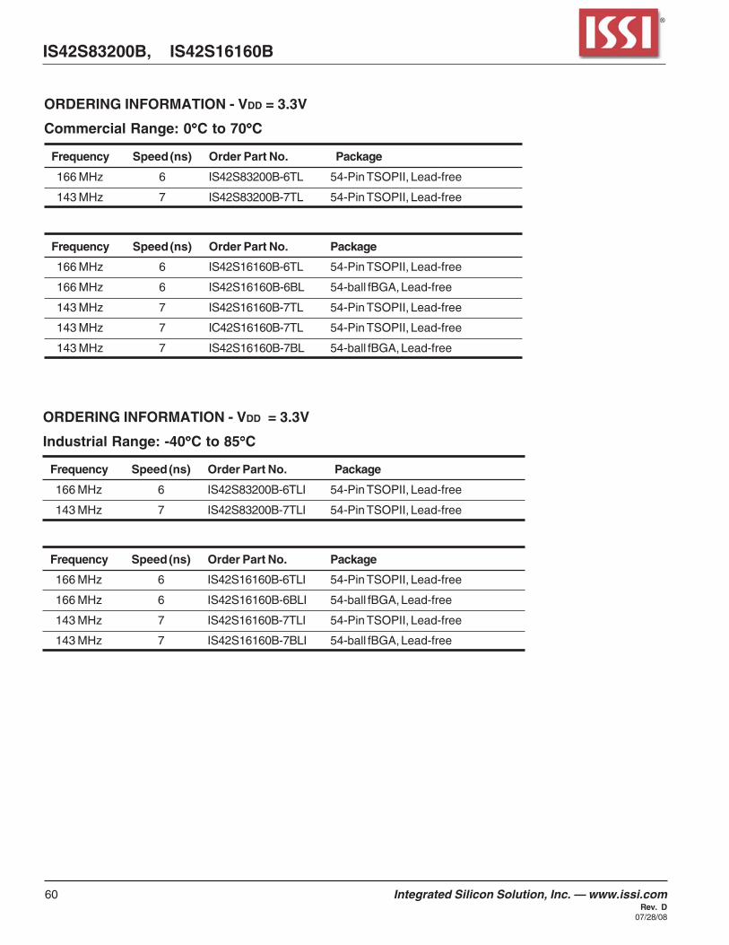
60 Integrated Silicon Solution, Inc. — www.issi.comRev. D
07/28/08
IS42S83200B, IS42S16160B
ORDERING INFORMATION - VDD = 3.3V
Commercial Range: 0°°°°°C to 70°°°°°C
Frequency Speed (ns) Order Part No. Package
166 MHz 6 IS42S83200B-6TL 54-Pin TSOPII, Lead-free
143 MHz 7 IS42S83200B-7TL 54-Pin TSOPII, Lead-free
Frequency Speed (ns) Order Part No. Package
166 MHz 6 IS42S16160B-6TL 54-Pin TSOPII, Lead-free
166 MHz 6 IS42S16160B-6BL 54-ball fBGA, Lead-free
143 MHz 7 IS42S16160B-7TL 54-Pin TSOPII, Lead-free
143 MHz 7 IC42S16160B-7TL 54-Pin TSOPII, Lead-free
143 MHz 7 IS42S16160B-7BL 54-ball fBGA, Lead-free
ORDERING INFORMATION - VDD = 3.3V
Industrial Range: -40°°°°°C to 85°°°°°C
Frequency Speed (ns) Order Part No. Package
166 MHz 6 IS42S83200B-6TLI 54-Pin TSOPII, Lead-free
143 MHz 7 IS42S83200B-7TLI 54-Pin TSOPII, Lead-free
Frequency Speed (ns) Order Part No. Package
166 MHz 6 IS42S16160B-6TLI 54-Pin TSOPII, Lead-free
166 MHz 6 IS42S16160B-6BLI 54-ball fBGA, Lead-free
143 MHz 7 IS42S16160B-7TLI 54-Pin TSOPII, Lead-free
143 MHz 7 IS42S16160B-7BLI 54-ball fBGA, Lead-free

2. R
efer
ence
doc
umen
t : J
ED
EC
MO
-207
1. C
ON
TR
OLL
ING
DIM
EN
SIO
N :
MM
.
NO
TE
:
Pack
age
Out
line
08/1
4/20
08

PACKAGING INFORMATION
Integrated Silicon Solution, Inc. 1Rev. D03/13/07
Plastic TSOP 54–Pin, 86-PinPackage Code: T (Type II)
Plastic TSOP (T - Type II)Millimeters Inches
Symbol Min Max Min MaxRef. Std.
No. Leads (N) 54
A — 1.20 — 0.047A1 0.05 0.15 0.002 0.006A2 — — — —b 0.30 0.45 0.012 0.018C 0.12 0.21 0.005 0.0083D 22.02 22.42 0.867 0.8827E1 10.03 10.29 0.395 0.405E 11.56 11.96 0.455 0.471e 0.80 BSC 0.031 BSCL 0.40 0.60 0.016 0.024
L1 — — — — ZD 0.71 REF
α 0° 8° 0° 8°
D
SEATING PLANE
be C
1 N/2
N/2+1N
E1
A1
A
E
L α
ZD
Notes:1. Controlling dimension: millimieters,
unless otherwise specified.2. BSC = Basic lead spacing between
centers.3. Dimensions D and E1 do not include
mold flash protrusions and should bemeasured from the bottom of thepackage.
4. Formed leads shall be planar withrespect to one another within 0.004inches at the seating plane.
Plastic TSOP (T - Type II)Millimeters Inches
Symbol Min Max Min MaxRef. Std.
No. Leads (N) 86
A — 1.20 — 0.047A1 0.05 0.15 0.002 0.006A2 0.95 1.05 0.037 0.041b 0.17 0.27 0.007 0.011C 0.12 0.21 0.005 0.008D 22.02 22.42 0.867 0.8827E1 10.03 10.29 0.395 0.405E 11.56 11.96 0.455 0.471e 0.50 BSC 0.020 BSCL 0.40 0.60 0.016 0.024
L1 0.80 REF 0.031 REF ZD 0.61 REF 0.024 BSC
α 0° 8° 0° 8°