isd8101 data sheet rev1.8 - nuvoton · isd8101 isd8101 datasheet rev. 1.8 - 2 - nov, 2012 1 general...
TRANSCRIPT

ISD8101
ISD8101 Datasheet Rev. 1.8 - 1 - Nov, 2012
ISD8101
1.5W Audio Amplifier
with Chip Enable

ISD8101
ISD8101 Datasheet Rev. 1.8 - 2 - Nov, 2012
1 GENERAL DESCRIPTION
The ISD8100 is a general purpose analog audio amplifier capable of driving an 8-ohm load with up to 1.5Wrms output power. This device includes current limiting and a chip enable pin with low standby current and excellent pop-and-click performance.
Also included is the ability for the inputs to be configured as either single-ended or differential. Internal resistors set the device gain at 20dB in the single ended output configuration. With external resistors, any gain less than 20dB can be achieved. The device is unity gain stable, including when used with external input resistors and external capacitors as may be optionally used for implementing simple filtering functions.
2 FEATURES
• Wide power supply range and excellent standby current o 2.4Vdc - 6.8Vdc operation o <1uA standby current
• High output power (capless BTL configuration) o Up to 1.5-W output into 8-ohm load
(<10% distortion) with 6.8Vdc supply voltage
o < 0.1% distortion at 500mW into 8-ohms with 5Vdc supply voltage
• Excellent pop-and-click performance o Low to inaudible pop/click using Chip
Enable
• Single-Ended or Differential signal inputs o > 40dB common mode rejection in
differential mode o > 40dB power supply noise rejection
• Very fast start-up time o Less than 1msec when using Chip
Enable
Applications:
• Toys
• Mobile Phones
• Current limiting for over-current conditions • Greeting Cards
• Package options: Pb-free SOP-8, SOP-8 (Ex-Pad), PDIP-8
• Portable Speakers
• Boom Box
• Temperature Range: -40°C to +85°C • White Goods

ISD8101
ISD8101 Datasheet Rev. 1.8 - 3 - Nov, 2012
3 BLOCK DIAGRAM
Figure 3-1 ISD8101 Block Diagram
ISD8101
ISD8101 Datasheet Rev. 1.8 - 4 - Nov, 2012
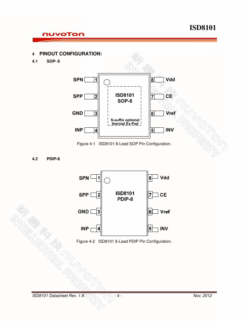
4 PINOUT CONFIGURATION:
4.1 SOP- 8
SPN
SPP
GND
INP INV
Vref
CE
Vdd
ISD8101
SOP-8
S-suffix optionalthermal Ex-Pad
2
1
3
4 5
6
7
8
Figure 4-1 ISD8101 8-Lead SOP Pin Configuration.
4.2 PDIP-8
Figure 4-2 ISD8101 8-Lead PDIP Pin Configuration.

ISD8101
ISD8101 Datasheet Rev. 1.8 - 5 - Nov, 2012
5 PIN DESCRIPTION
Pin Number
Pin Name I/O Function
1 SPN O Non-Inverting Speaker Output
2 SPP O Inverting Speaker Output
3 GND I Ground
4 INP I Non-Inverting Signal Input
5 INV I Inverting Signal Input
6 Vref O Internal Reference Voltage (1/2 Vdd)
7 CE I Chip Enable
8 Vdd I Supply Voltage
9 Ex-Pad I Thermal Tab (must be connected to Vss, SOP-8 package, only)

ISD8101
ISD8101 Datasheet Rev. 1.8 - 6 - Nov, 2012
6 ELECTRICAL CHARACTERISTICS
6.1 OPERATING CONDITIONS
OPERATING CONDITIONS (DIE)
CONDITIONS VALUES
Operating temperature range 1 0°C to +50°C
Supply voltage (VDD) +2.4V to +6.8V
Ground voltage (VSS) 0V
Input voltage (VDD) Vss to VDD
Voltage applied to any pins (VSS –0.3V) to (VDD +0.3V)
OPERATING CONDITIONS (INDUSTRIAL PACKAGED PARTS)
CONDITIONS VALUES
Operating temperature range (Case temperature) 1 -40°C to +85°C
Supply voltage (VDD) +2.4V to +6.8V
Ground voltage (VSS) 0V
Input voltage (VDD) Vss to VDD
Voltage applied to any pins (VSS –0.3V) to (VDD +0.3V)
Notes: [1]
Conditions VDD=3.3V, TA=25°C unless otherwise stated. Die temperature must at all times be kept less than 125°C by appropriate thermal design of the system.
6.2 DC PARAMETERS
PARAMETER SYMBOL MIN TYP [1]
MAX UNITS CONDITIONS
Supply Voltage VDD 2.4 6.8 V
Operating Current IDD 2.4 mA VDD = 5V, no load
Standby Current ISB 0.1 1 µA VDD = 5V
CE input resistance 20k Ω Internal pull-down
CE input current 120 µA CE = 2.3V, VDD= 5V
CE threshold enabled VENL 0.9 V All supply voltages
CE threshold standby VENH 1.5 V All supply voltages
Vref Reference Voltage VDD/2 V
Notes: [1]
Conditions VDD = 3.3V, TA = 25°C unless otherwise stated. Die temperature must at all times be kept less than 125°C by appropriate thermal design of the system.
ISD8101
ISD8101 Datasheet Rev. 1.8 - 7 - Nov, 2012
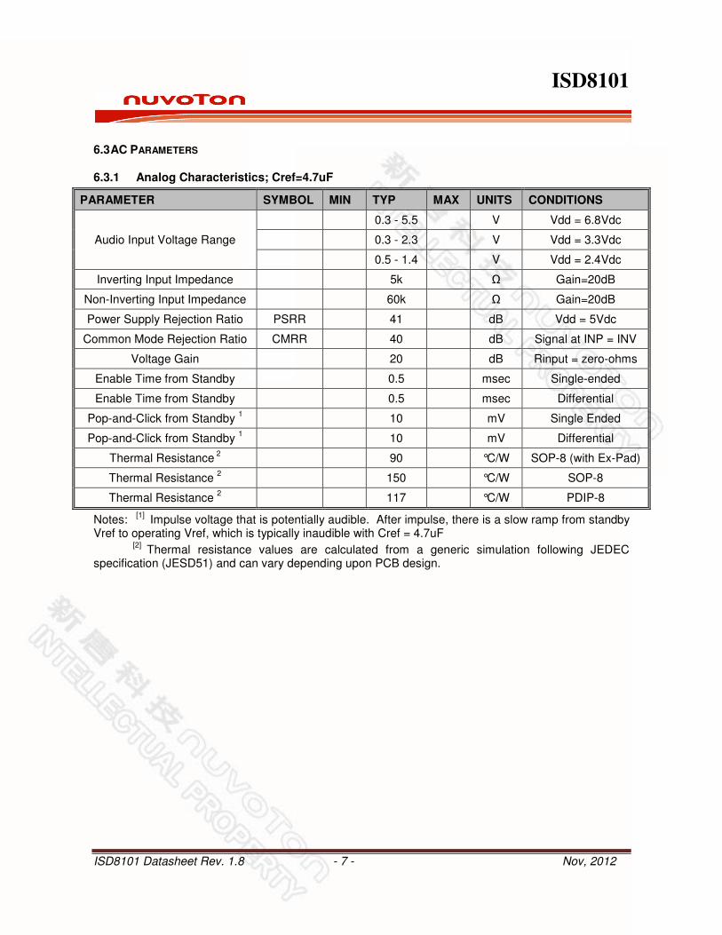
6.3 AC PARAMETERS
6.3.1 Analog Characteristics; Cref=4.7uF
PARAMETER SYMBOL MIN TYP MAX UNITS CONDITIONS
Audio Input Voltage Range
0.3 - 5.5 V Vdd = 6.8Vdc
0.3 - 2.3 V Vdd = 3.3Vdc
0.5 - 1.4 V Vdd = 2.4Vdc
Inverting Input Impedance 5k Ω Gain=20dB
Non-Inverting Input Impedance 60k Ω Gain=20dB
Power Supply Rejection Ratio PSRR 41 dB Vdd = 5Vdc
Common Mode Rejection Ratio CMRR 40 dB Signal at INP = INV
Voltage Gain 20 dB Rinput = zero-ohms
Enable Time from Standby 0.5 msec Single-ended
Enable Time from Standby 0.5 msec Differential
Pop-and-Click from Standby 1 10 mV Single Ended
Pop-and-Click from Standby 1 10 mV Differential
Thermal Resistance 2
90 °C/W SOP-8 (with Ex-Pad)
Thermal Resistance 2
150 °C/W SOP-8
Thermal Resistance 2
117 °C/W PDIP-8
Notes: [1]
Impulse voltage that is potentially audible. After impulse, there is a slow ramp from standby Vref to operating Vref, which is typically inaudible with Cref = 4.7uF
[2]
Thermal resistance values are calculated from a generic simulation following JEDEC specification (JESD51) and can vary depending upon PCB design.
ISD8101
ISD8101 Datasheet Rev. 1.8 - 8 - Nov, 2012
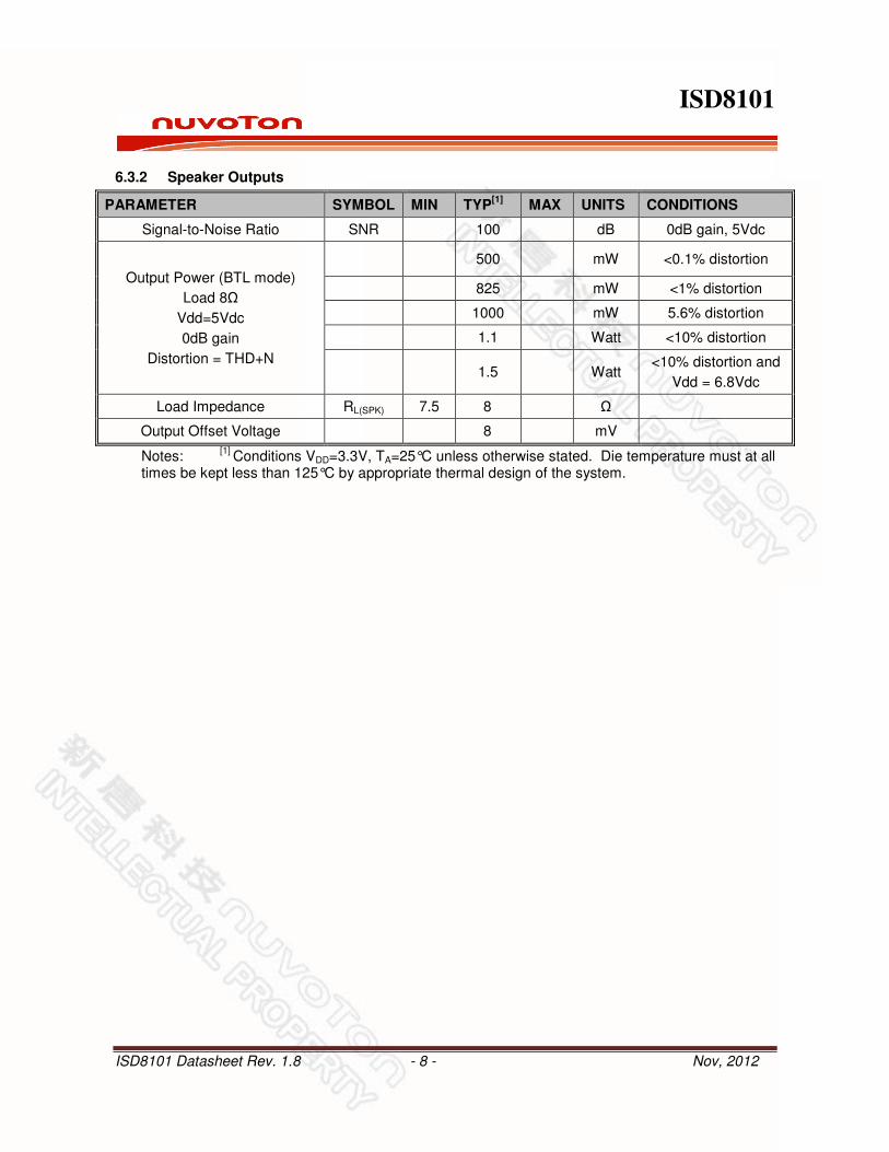
6.3.2 Speaker Outputs
PARAMETER SYMBOL MIN TYP[1]
MAX UNITS CONDITIONS
Signal-to-Noise Ratio SNR 100 dB 0dB gain, 5Vdc
Output Power (BTL mode)
Load 8Ω
Vdd=5Vdc
0dB gain
Distortion = THD+N
500 mW <0.1% distortion
825 mW <1% distortion
1000 mW 5.6% distortion
1.1 Watt <10% distortion
1.5 Watt <10% distortion and
Vdd = 6.8Vdc
Load Impedance RL(SPK) 7.5 8 Ω
Output Offset Voltage 8 mV
Notes: [1]
Conditions VDD=3.3V, TA=25°C unless otherwise stated. Die temperature must at all times be kept less than 125°C by appropriate thermal design of the system.
ISD8101
ISD8101 Datasheet Rev. 1.8 - 9 - Nov, 2012
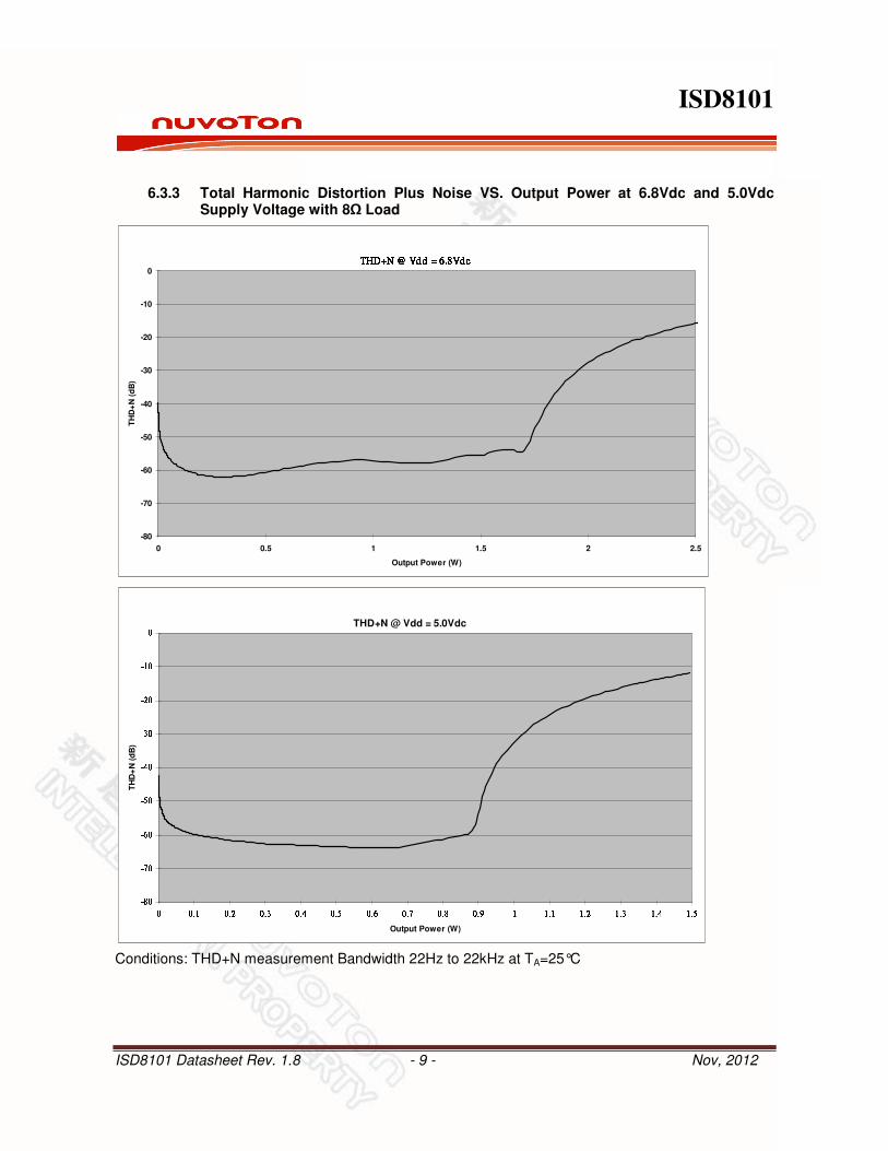
6.3.3 Total Harmonic Distortion Plus Noise VS. Output Power at 6.8Vdc and 5.0Vdc Supply Voltage with 8Ω Load
Conditions: THD+N measurement Bandwidth 22Hz to 22kHz at TA=25°C
THD+N @ Vdd = 6.8VdcTHD+N @ Vdd = 6.8VdcTHD+N @ Vdd = 6.8VdcTHD+N @ Vdd = 6.8Vdc
-80
-70
-60
-50
-40
-30
-20
-10
0
0 0.5 1 1.5 2 2.5
Output Power (W)
TH
D+
N (
dB
)
THD+N @ Vdd = 5.0Vdc
-80-80-80-80-70-70-70-70-60-60-60-60-50-50-50-50-40-40-40-40-30-30-30-30-20-20-20-20-10-10-10-100000
0000 0.10.10.10.1 0.20.20.20.2 0.30.30.30.3 0.40.40.40.4 0.50.50.50.5 0.60.60.60.6 0.70.70.70.7 0.80.80.80.8 0.90.90.90.9 1111 1.11.11.11.1 1.21.21.21.2 1.31.31.31.3 1.41.41.41.4 1.51.51.51.5Output Power (W)
TH
D+
N (
dB
)
ISD8101
ISD8101 Datasheet Rev. 1.8 - 10 - Nov, 2012
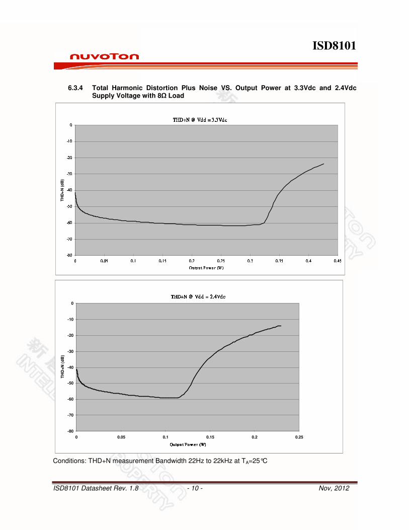
6.3.4 Total Harmonic Distortion Plus Noise VS. Output Power at 3.3Vdc and 2.4Vdc Supply Voltage with 8Ω Load
Conditions: THD+N measurement Bandwidth 22Hz to 22kHz at TA=25°C
THD+N @ Vdd = 3.3VdcTHD+N @ Vdd = 3.3VdcTHD+N @ Vdd = 3.3VdcTHD+N @ Vdd = 3.3Vdc
-80-80-80-80-70-70-70-70-60-60-60-60-50-50-50-50-40-40-40-40-30-30-30-30-20-20-20-20-10-10-10-100000
0000 0.050.050.050.05 0.10.10.10.1 0.150.150.150.15 0.20.20.20.2 0.250.250.250.25 0.30.30.30.3 0.350.350.350.35 0.40.40.40.4 0.450.450.450.45Outpu t Powe r (W)Outpu t Powe r (W)Outpu t Powe r (W)Outpu t Powe r (W)
TH
D+
N (
dB
)
THD+N @ Vdd = 2.4VdcTHD+N @ Vdd = 2.4VdcTHD+N @ Vdd = 2.4VdcTHD+N @ Vdd = 2.4Vdc
-80
-70
-60
-50
-40
-30
-20
-10
0
0 0.05 0.1 0.15 0.2 0.25Ou tpu t Pow e r (W)Ou tpu t Pow e r (W)Ou tpu t Pow e r (W)Ou tpu t Pow e r (W)
TH
D+N
(d
B)

ISD8101
ISD8101 Datasheet Rev. 1.8 - 11 - Nov, 2012
6.3.5 Typical Peak Output Power
Note: Peak output power becomes reduced as device becomes heated. Sustained medium duration heating typical for audio limits maximum useable output to approximately 1.5Wrms at less than 10% distortion.
6.3.6 Chip Enable Threshold Voltage
Conditions: TA=25°C
Peak Output vs. Supply Voltage @ THD = 1%
0
0.2
0.4
0.6
0.8
1
1.2
1.4
1.6
1.8
0 1 2 3 4 5 6 7 8
Vdc Supply Voltage
Peak O
utp
ut
Po
wer
(Watt
s)
Chip Enable Threshold vs. Supply Voltage
0
0.2
0.4
0.6
0.8
1
1.2
1.4
1.6
0 1 2 3 4 5 6 7 8
Vdc Supply Voltage (V)
Th
resh
old
Vo
ltag
e (
V)

ISD8101
ISD8101 Datasheet Rev. 1.8 - 12 - Nov, 2012
6.3.7 Output Noise Spectrum
Noise spectrum at Vdd = 5.0Vdc, Gain = 0dB, BW<22kHz
Noise Spectrum at Vdd = 5.0Vdc, Gain = 20dB, BW<22kHz

ISD8101
ISD8101 Datasheet Rev. 1.8 - 13 - Nov, 2012
7 APPLICATION DIAGRAMS
7.1 SIMPLE GAIN SETTING
SPN5
VREF
Cref
RL
ISD8101CE
INP
SPP
Vdd
GND
RgCinVin
+5Vdc
100uF0.1µF
Device=Enabled
If CE left as
no-connect
INV
4
6
7 3
2
1
8
gRk
kxSPNSPPGainOutputalDifferenti
+=−
5
502)(
By default: Rg = 0Ω,
ISD8101 Differential Output Gain = 20
ISD8101 Differential Output Gain (in dB) = 20 x log (20) = 26dB
Example: Rg = 45kΩ
ISD8101 Differential Output Gain = 2
ISD8101 Differential Output Gain (in dB) = 20 x log (2) = 6dB
Device=Power Down, if CE left as no-connect
ISD8101
ISD8101 Datasheet Rev. 1.8 - 14 - Nov, 2012
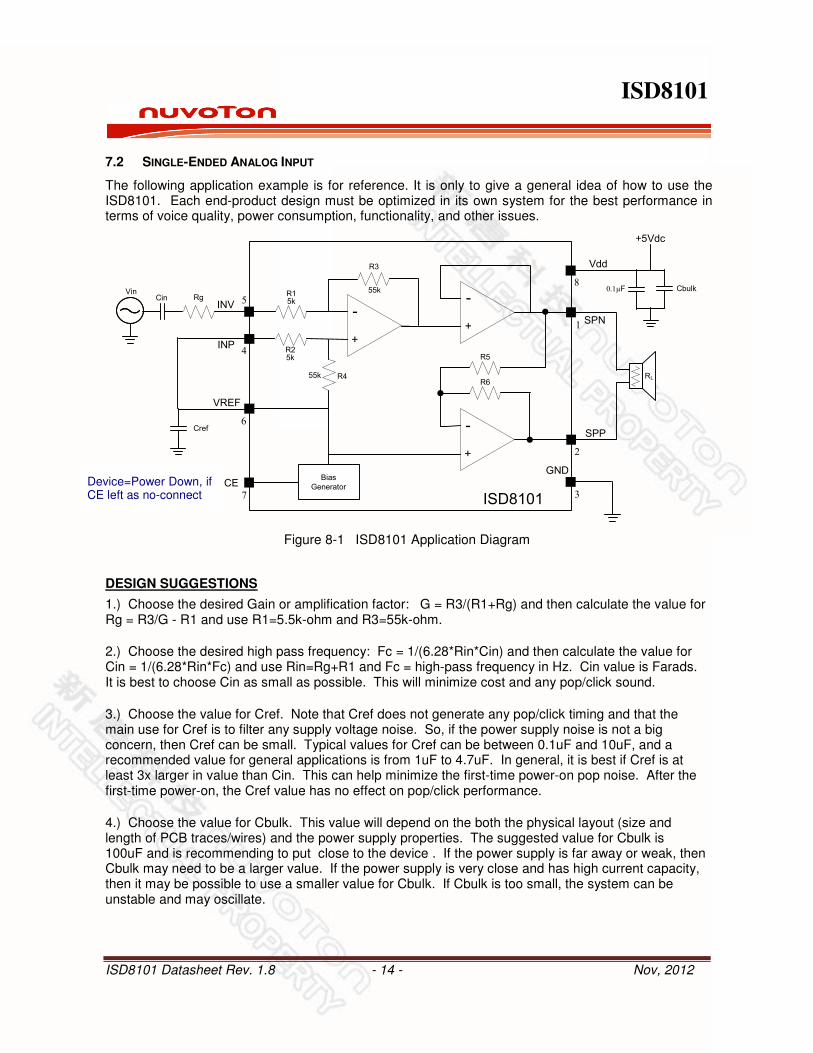
7.2 SINGLE-ENDED ANALOG INPUT
The following application example is for reference. It is only to give a general idea of how to use the ISD8101. Each end-product design must be optimized in its own system for the best performance in terms of voice quality, power consumption, functionality, and other issues.
SPN
INV 5
VREF
Cref
RL
ISD8101
R15k
R4R6
R3
R5R25k
-
+
-
+
-
+
Bias
GeneratorCE
4INP
SPP
Vdd
GND
6
7
8
1
2
3
RgCinVin
+5Vdc
Cbulk0.1µF
55k
55k
Device=Enabled
If CE left as
no-connect
Figure 8-1 ISD8101 Application Diagram
DESIGN SUGGESTIONS
1.) Choose the desired Gain or amplification factor: G = R3/(R1+Rg) and then calculate the value for Rg = R3/G - R1 and use R1=5.5k-ohm and R3=55k-ohm.
2.) Choose the desired high pass frequency: Fc = 1/(6.28*Rin*Cin) and then calculate the value for Cin = 1/(6.28*Rin*Fc) and use Rin=Rg+R1 and Fc = high-pass frequency in Hz. Cin value is Farads. It is best to choose Cin as small as possible. This will minimize cost and any pop/click sound.
3.) Choose the value for Cref. Note that Cref does not generate any pop/click timing and that the main use for Cref is to filter any supply voltage noise. So, if the power supply noise is not a big concern, then Cref can be small. Typical values for Cref can be between 0.1uF and 10uF, and a recommended value for general applications is from 1uF to 4.7uF. In general, it is best if Cref is at least 3x larger in value than Cin. This can help minimize the first-time power-on pop noise. After the first-time power-on, the Cref value has no effect on pop/click performance.
4.) Choose the value for Cbulk. This value will depend on the both the physical layout (size and length of PCB traces/wires) and the power supply properties. The suggested value for Cbulk is 100uF and is recommending to put close to the device . If the power supply is far away or weak, then Cbulk may need to be a larger value. If the power supply is very close and has high current capacity, then it may be possible to use a smaller value for Cbulk. If Cbulk is too small, the system can be unstable and may oscillate.
Device=Power Down, if CE left as no-connect
ISD8101
ISD8101 Datasheet Rev. 1.8 - 15 - Nov, 2012
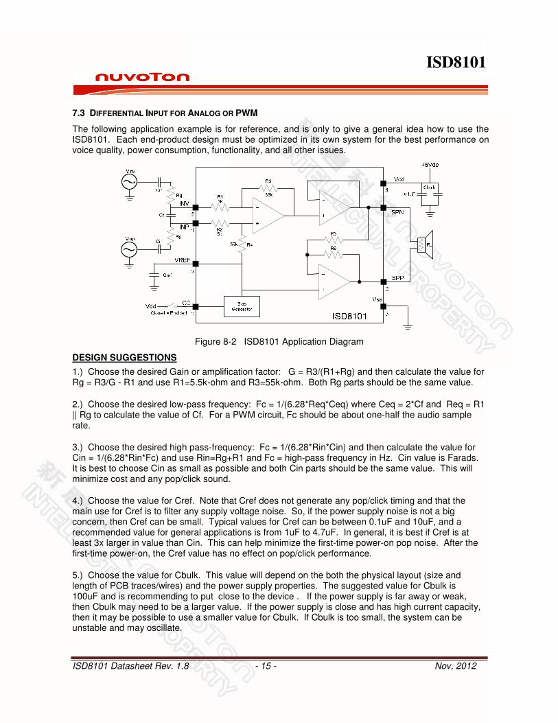
7.3 DIFFERENTIAL INPUT FOR ANALOG OR PWM
The following application example is for reference, and is only to give a general idea how to use the ISD8101. Each end-product design must be optimized in its own system for the best performance on voice quality, power consumption, functionality, and all other issues.
Figure 8-2 ISD8101 Application Diagram
DESIGN SUGGESTIONS
1.) Choose the desired Gain or amplification factor: G = R3/(R1+Rg) and then calculate the value for Rg = R3/G - R1 and use R1=5.5k-ohm and R3=55k-ohm. Both Rg parts should be the same value.
2.) Choose the desired low-pass frequency: Fc = 1/(6.28*Req*Ceq) where Ceq = 2*Cf and Req = R1 || Rg to calculate the value of Cf. For a PWM circuit, Fc should be about one-half the audio sample rate.
3.) Choose the desired high pass-frequency: Fc = 1/(6.28*Rin*Cin) and then calculate the value for Cin = 1/(6.28*Rin*Fc) and use Rin=Rg+R1 and Fc = high-pass frequency in Hz. Cin value is Farads. It is best to choose Cin as small as possible and both Cin parts should be the same value. This will minimize cost and any pop/click sound.
4.) Choose the value for Cref. Note that Cref does not generate any pop/click timing and that the main use for Cref is to filter any supply voltage noise. So, if the power supply noise is not a big concern, then Cref can be small. Typical values for Cref can be between 0.1uF and 10uF, and a recommended value for general applications is from 1uF to 4.7uF. In general, it is best if Cref is at least 3x larger in value than Cin. This can help minimize the first-time power-on pop noise. After the first-time power-on, the Cref value has no effect on pop/click performance.
5.) Choose the value for Cbulk. This value will depend on the both the physical layout (size and length of PCB traces/wires) and the power supply properties. The suggested value for Cbulk is 100uF and is recommending to put close to the device . If the power supply is far away or weak, then Cbulk may need to be a larger value. If the power supply is close and has high current capacity, then it may be possible to use a smaller value for Cbulk. If Cbulk is too small, the system can be unstable and may oscillate.
ISD8101
ISD8101 Datasheet Rev. 1.8 - 16 - Nov, 2012
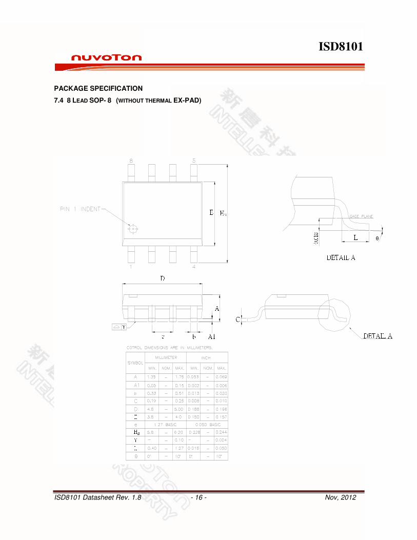
PACKAGE SPECIFICATION
7.4 8 LEAD SOP- 8 (WITHOUT THERMAL EX-PAD)
DETAIL A
LE H EY
0.010 LY Cb AA1
De
H EEDETAIL A θ
ISD8101
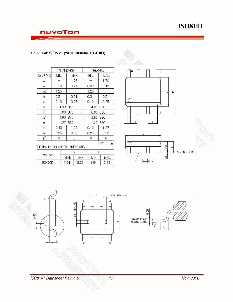
ISD8101 Datasheet Rev. 1.8 - 17 - Nov, 2012
7.5 8 LEAD SOP- 8 (WITH THERMAL EX-PAD)

ISD8101
ISD8101 Datasheet Rev. 1.8 - 18 - Nov, 2012
7.6 PDIP-8
1.631.470.0640.058
SymbolMin Nom Max MaxNomMin
Dimension in inch Dimension in mm
A
B
c
D
e
A
L
S
AA
1
2
E
0.060 1.52
0.175 4.45
0.010
0.125
0.016
0.130
0.018
0.135
0.022
3.18
0.41
0.25
3.30
0.46
3.43
0.56
0.008
0.120
0.375
0.010
0.130
0.014
0.140
0.20
3.05
0.25
3.30
0.36
3.56
0.2550.2500.245 6.486.356.22
9.53
7.627.37 7.870.3000.290 0.310
2.29 2.54 2.790.090 0.100 0.110
B 1
1
e
E 1
0.360 0.380 9.14 9.65
0 15
0.045 1.14
0.3550.335 8.51 9.02
150
Seating Plane
e A
2A
c
E
Base Plane1A
1e
L
A
S
1E
D
1B
B
8 5
1 4
αααααααα
ISD8101
ISD8101 Datasheet Rev. 1.8 - 19 - Nov, 2012
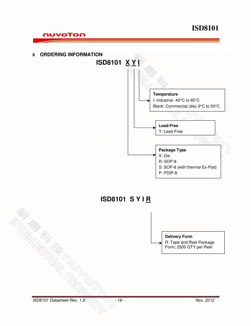
8 ORDERING INFORMATION
ISD8101 X Y I
ISD8101 S Y I R
Delivery Form
R: Tape and Reel Package Form; 2500 QTY per Reel
Package Type
X: Die
R: SOP-8
S: SOP-8 (with thermal Ex-Pad)
P: PDIP-8
Lead-Free
Y: Lead-Free
Temperature
I: Industrial -40°C to 85°C
Blank: Commercial (die) 0°C to 50°C
ISD8101
ISD8101 Datasheet Rev. 1.8 - 20 - Nov, 2012
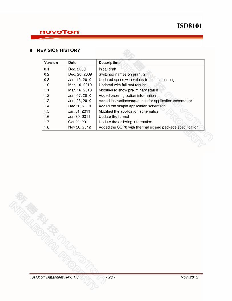
9 REVISION HISTORY
Version Date Description
0.1
0.2
0.3
1.0
1.1
1.2
1.3
1.4
1.5
1.6
1.7
1.8
Dec, 2009
Dec. 20, 2009
Jan. 15, 2010
Mar. 10, 2010
Mar. 16, 2010
Jun. 07, 2010
Jun. 28, 2010
Dec 30, 2010
Jan 31, 2011
Jun 30, 2011
Oct 20, 2011
Nov 30, 2012
Initial draft
Switched names on pin 1, 2
Updated specs with values from initial testing
Updated with full test results
Modified to show preliminary status
Added ordering option information
Added instructions/equations for application schematics
Added the simple application schematic
Modified the application schematics
Update the format
Update the ordering information
Added the SOP8 with thermal ex pad package specification
ISD8101
ISD8101 Datasheet Rev. 1.8 - 21 - Nov, 2012
Nuvoton products are not designed, intended, authorized or warranted for use as components in systems or equipment intended for surgical implantation, atomic energy control instruments, airplane or spaceship instruments, transportation instruments, traffic signal instruments, combustion control instruments, or for other applications intended to support or sustain life. Furthermore, Nuvoton products are not intended for applications wherein failure of Nuvoton products could result or lead to a situation wherein personal injury, death or severe property or environmental damage could occur. Nuvoton customers using or selling these products for use in such applications do so at their own risk and agree to fully indemnify Nuvoton for any damages resulting from such improper use or sales.
The contents of this document are provided only as a guide for the applications of Nuvoton products. Nuvoton makes no representation or warranties with respect to the accuracy or completeness of the contents of this publication and reserves the right to discontinue or make changes to specifications and product descriptions at any time without notice. No license, whether express or implied, to any intellectual property or other right of Nuvoton or others is granted by this publication. Except as set forth in Nuvoton's Standard Terms and Conditions of Sale, Nuvoton assumes no liability whatsoever and disclaims any express or implied warranty of merchantability, fitness for a particular purpose or infringement of any Intellectual property.
The contents of this document are provided “AS IS”, and Nuvoton assumes no liability whatsoever and disclaims any express or implied warranty of merchantability, fitness for a particular purpose or infringement of any Intellectual property. In no event, shall Nuvoton be liable for any damages whatsoever (including, without limitation, damages for loss of profits, business interruption, loss of information) arising out of the use of or inability to use the contents of this documents, even if Nuvoton has been advised of the possibility of such damages.
Application examples and alternative uses of any integrated circuit contained in this publication are for illustration only and Nuvoton makes no representation or warranty that such applications shall be suitable for the use specified.
This datasheet and any future addendum to this datasheet is(are) the complete and controlling ISD® ChipCorder® product specifications. In the event any inconsistencies exist between the information in this and other product documentation, or in the event that other product documentation contains information in addition to the information in this, the information contained herein supersedes and governs such other information in its entirety. This datasheet is subject to change without notice.
Copyright© 2005, Nuvoton Technology Corporation. All rights reserved. ChipCorder® and ISD® are trademarks of Nuvoton Technology Corporation. All other trademarks are properties of their respective owners.
Headquarters Nuvoton Technology Corporation America Nuvoton Technology (Shanghai) Ltd.
No. 4, Creation Rd. III 2727 North First Street, San Jose, 27F, 299 Yan An W. Rd. Shanghai, Science-Based Industrial Park, CA 95134, U.S.A. 200336 China Hsinchu, Taiwan TEL: 1-408-9436666 TEL: 86-21-62365999 TEL: 886-3-5770066 FAX: 1-408-5441797 FAX: 86-21-62356998 FAX: 886-3-5665577 http://www.Nuvoton-usa.com/ http://www.Nuvoton.com.tw/
Taipei Office Nuvoton Technology Corporation Japan Nuvoton Technology (H.K.) Ltd.
9F, No. 480, Pueiguang Rd. 7F Daini-ueno BLDG. 3-7-18 Unit 9-15, 22F, Millennium City, Neihu District Shinyokohama Kohokuku, No. 378 Kwun Tong Rd., Taipei, 114 Taiwan Yokohama, 222-0033 Kowloon, Hong Kong TEL: 886-2-81777168 TEL: 81-45-4781881 TEL: 852-27513100 FAX: 886-2-87153579 FAX: 81-45-4781800 FAX: 852-27552064
Please note that all data and specifications are subject to change without notice. All the trademarks of products and companies mentioned in this datasheet belong to their respective owners.