isl62883ceval2z user guide - intersil.com · vin + _ tp35 tp36 vccsense vsssense ... • j1: set...
TRANSCRIPT

USER’S MANUAL
AN1557Rev 0.00
Apr 1, 2010
ISL62883CEVAL2ZEvaluation Board
IntroductionThe ISL62883CEVAL2Z evaluation board demonstrates the performance of the ISL62883 multiphase synchronous-buck PWM VCORE controller implementing Intel IMVP-6.5 protocol. The ISL62883 features Intersil's Robust Ripple Regulator (R3) technology. An on-board dynamic-load generator is included for evaluating the transient-load response. It applies a 300µs pulse of approximately 25m load across VO and PGND.
Contents of this document include:
• Design Criteria• Recommended Test Equipment• Interface Connections• Switch Descriptions• DIP Switch Descriptions• Jumper Descriptions• Test Point Descriptions• Evaluation Board Documentation
- Bill of materials- Schematic- Silk-screen plots- Board layer plots
Recommended Equipment• (QTY 1) Adjustable 25V, 10A Power Supply• (QTY 1) Fixed 5V, 100mA Power Supply• (QTY 1) Fixed 12V, 100mA Power Supply• (QTY 1) Adjustable Constant Current Electronic Load• (QTY 1) Digital Voltmeter• (QTY 1) Four-Channel Oscilloscope
Interface Connections• VIN: Input Voltage to the Power Stage
- J5: VIN Positive Power Input- TP31: VIN Positive Voltage Sense- J6: VIN Return Power Input- TP32: VIN Return Voltage Sense
• VO: Regulated Output Voltage- J11 and J12: VO Positive Power Output- J13 and J14: VO Return Power Output
• +5V: +5V Input Voltage- TP29: +5V Positive Input- TP30: +5V Return Input
• +12V: Input Voltage for the Dynamic-load Generator- TP3: 12V Positive Input- TP2: 12V Return Input
Test Set-up
FIGURE 1. TEST SET-UP
Switch Descriptions• S3: Enable
- OFF: Short the VR_ON pin to GND (disable PWM)- ON: Allow the VR_ON pin to pull-up to +5V (enable
PWM)
• S5: Dynamic Load- OFF: On-board dynamic load disabled- ON: On-board dynamic load enabled
TABLE 1. DC/DC DESIGN CRITERIA
PARAMETER VALUE UNITS
VIN 4.5 to 20 VDC
VO 0 to 1.5 VDC
Full-load 75 ADC
PWM Frequency 300 kHz
10 U2
ISL62883CEVAL2Z
ON
OFF
0
1
TP37
TP29
TP30J9J8J7
VID0VID1VID2VID3VID4VID5VID6
VIN
+
_
TP35 TP36
PHASE1 PHASE2 PHASE3VSSSENSEVCCSENSE
J10VCORE
ON
OFF
S3
S2
TP3
TP2
5V
+
_
J12VCORE
J11VCORE
J14PGND
J13PGND
J1J2
J3
J4
S1
PS
I#D
PRSL
PVR
+3.3V
+5V
PGND
J6PGND
J5VIN
D1
J16
AN1557 Rev 0.00 Page 1 of 21Apr 1, 2010
ISL62883CEVAL2Z
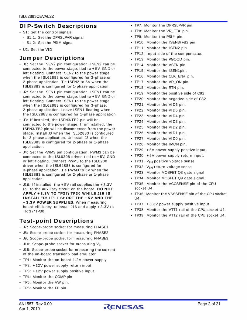
DIP-Switch Descriptions• S1: Set the control signals
- S1.1: Set the DPRSLPVR signal- S1.2: Set the PSI# signal
• U2: Set the VID
Jumper Descriptions• J1: Set the ISEN2 pin configuration. ISEN2 can be
connected to the power stage, tied to +5V, GND or left floating. Connect ISEN2 to the power stage when the ISL62883 is configured for 3-phase or 2-phase application. Tie ISEN2 to 5V when the ISL62883 is configured for 1-phase application.
• J2: Set the ISEN1 pin configuration. ISEN1 can be connected to the power stage, tied to +5V, GND or left floating. Connect ISEN1 to the power stage when the ISL62883 is configured for 3-phase, 2-phase application. Leave ISEN1 floating when the ISL62883 is configured for 1-phase application
• J3: If installed, the ISEN3/FB2 pin will be connected to the power stage. If uninstalled, the ISEN3/FB2 pin will be disconnected from the power stage. Install J3 when the ISL62883 is configured for 3-phase application. Uninstall J3 when the ISL62883 is configured for 2-phase or 1-phase application.
• J4: Set the PWM3 pin configuration. PWM3 can be connected to the ISL6208 driver, tied to +5V, GND or left floating. Connect PWM3 to the ISL6208 driver when the ISL62883 is configured for 3-phase application. Tie PWM3 to 5V when the ISL62883 is configured for 2-phase or 1-phase application.
• J16: If installed, the +5V rail supplies the +3.3V rail to the auxiliary circuit on the board. DO NOT APPLY +3.3V TO TP37/TP30 WHILE J16 IS INSTALLED! IT’LL SHORT THE +5V AND THE +3.3V POWER SUPPLIES. When measuring board efficiency, uninstall J16 and apply +3.3V to TP/37/TP30.
Test-point Descriptions• J7: Scope-probe socket for measuring PHASE1• J8: Scope-probe socket for measuring PHASE2• J9: Scope-probe socket for measuring PHASE3• J10: Scope-probe socket for measuring VO• J15: Scope-probe socket for measuring the current
of the on-board transient-load emulator• TP1: Monitor the on-board 1.2V power supply• TP2: +12V power supply return input.• TP3: +12V power supply positive input.• TP4: Monitor the COMP pin• TP5: Monitor the VW pin.• TP6: Monitor the FB pin.
• TP7: Monitor the DPRSLPVR pin.• TP8: Monitor the VR_TT# pin.• TP9: Monitor the PSI# pin.• TP10: Monitor the ISEN3/FB2 pin.• TP11: Monitor the ISEN2 pin.• TP12: Input side of the compensator. • TP13: Monitor the PGOOD pin.• TP14: Monitor the VSEN pin.• TP15: Monitor the ISEN1pin.• TP16: Monitor the CLK_EN# pin.• TP17: Monitor the VR_ON pin• TP18: Monitor the RTN pin.• TP19: Monitor the positive side of C82.• TP20: Monitor the negative side of C82.• TP21: Monitor the VID6 pin.• TP22: Monitor the VID5 pin.• TP23: Monitor the VID4 pin.• TP24: Monitor the VID3 pin.• TP25: Monitor the VID2 pin.• TP26: Monitor the VID1 pin.• TP27: Monitor the VID0 pin.• TP28: Monitor the IMON pin.• TP29: +5V power supply positive input.• TP30: +5V power supply return input.• TP31: VIN positive voltage sense• TP32: VIN return voltage sense• TP33: Monitor MOSFET Q3 gate signal• TP34: Monitor MOSFET Q9 gate signal.• TP35: Monitor the VCCSENSE pin of the CPU
socket U4.• TP36: Monitor the VSSSENSE pin of the CPU socket
U4.• TP37: +3.3V power supply positive input. • TP38: Monitor the VTT1 rail of the CPU socket U4.• TP39: Monitor the VTT2 rail of the CPU socket U4.
AN1557 Rev 0.00 Page 2 of 21Apr 1, 2010

ISL62883CEVAL2Z
Bill of MaterialsREFERENCE QTY VALUE PART NUMBER DESCRIPTION PACKAGE VENDOR
C1 1 0.01µF H1045-00103-16V10 Multilayer Cap, 16V, 10% SM0603 Generic
C11 1 390pF H1045-00391-16V10 Multilayer Cap, 16V, 10% SM0603 Generic
C12, C14 2 330pF H1045-00331-16V10 Multilayer Cap, 16V, 10% SM0603 Generic
C13 1 1000pF H1045-00102-16V10 Multilayer Cap, 16V, 10% SM0603 Generic
C15 DNP
C16, C2, C22, C23, C26, C79
6 1µF H1045-00105-16V20 Multilayer Cap, 16V, 20% SM0603 Generic
C18 1 0.47µF H1045-00474-16V10 Multilayer Cap, 16V, 10% SM0603 Generic
C19 DNP
C36, C37, C38, C8, C83 5 DNP
C20, C45, C58 3 0.1µF H1045-00104-16V10 Multilayer Cap, 16V, 10% SM0603 Generic
C21 1 0.22µF H1045-00224-16V10 Multilayer Cap, 16V, 10% SM0603 Generic
C24, C25 2 56µF 25SP56M Radial SP Series Cap, 25V, 20% CASE-CC Sanyo
C27, C28, C29, C33, C34, C35, C80
7 10µF H1065-00106-25V20 Multilayer Cap, 25V, 20% SM1206 Generic
C3 1 150pF H1045-00151-16V10 Multilayer Cap, 16V, 10% SM0603 Generic
C39, C44, C52, C57 4 270µF EEFSX0D271E4 POSCAP, 2V, 4.5m Panasonic
C4 1 1000pF H1045-00102-16V10 Multilayer Cap, 16V, 10% SM0603 Generic
C40 to C43, C47 to C50, C54 to C56, C59 to C61, C63 to C68,
C71 to C74
24 10µF GRM21BR61C106KE15L Multilayer Cap, 6.3V, 20% SM0805 Murata
C5, C53, C62, C69, C70, C75 to C78
9 DNP
C6 1 39pF H1045-00390-16V10 Multilayer Cap, 16V, 10% SM0603 Generic
C7, C9, C10, C17, C30, C31, C32
7 0.22µF H1045-00224-16V10 Multilayer Cap, 16V, 10% SM0603 Generic
C81 1 820pF H1045-00821-16V10 Multilayer Cap, 16V, 10% SM0603 Generic
C82 1 0.039µF H1045-00393-16V10 Multilayer Cap, 16V, 10% SM0603 Generic
D1 1 SSL-LXA3025IGC 3mmx2.5mm Surface Mount Red/Green LED
LED_3x2_5MM Lumex
J1, J2, J4 3 67996-272 2x3 Header, 2.54mm(0.100) Pitch
CONN2x3 Berg/FCI
J10 1 131-4353-00 Scope Probe Test Point PCB Mount
TEK131-4353-00
Tektronix
J15, J7, J8, J9 0 DNP
J11 to J14 4 KPA8CTP Wire Connector Lug KPA8CTP Burndy
J3, J16 2 69190-202 2 Pin Header 2.54mm (0.100) Pitch
CONN2 Berg/FCI
J5 1 111-0702-001 Binding Post Red 111-07XX-001 Johnson-Comp
J6 1 111-0703-001 Binding Post Black 111-07XX-001 Johnson-Comp
L1, L2, L3 3 0.36µH MPCH1040LR36 Inductor, Inductance 20%, DCR 7%
NEC-Tokin
AN1557 Rev 0.00 Page 3 of 21Apr 1, 2010
ISL62883CEVAL2Z
Q1, Q14 2 2N7002-7-F N-Channel EMF Effect Transistor (Pb-Free)
SOT23 Fairchild
Q15 1 SUD50N03-07 N-Channel 30V (D-S) MOSFET TO-252AA Vishay
Q2, Q4, Q6, Q8, Q10, Q12
6 IRF7821 N-Channel Power MOSFET Power Switching
PWRPAK_SO8 IR
Q3, Q5, Q7, Q9, Q11, Q13
6 IRF7832 N-Channel Power MOSFET Power Switching
PWRPAK_SO8 IR
R1 1 49.9 H2511-049R9-1/16W1 Thick Film Chip Resistor, 1% SM0603 Generic
R10 1 536 H2511-05360-1/16W1 Thick Film Chip Resistor, 1% SM0603 Generic
R102 1 49.9k H2511-04992-1/16W1 Thick Film Chip Resistor, 1% SM0603 Generic
R104, R105 2 249 H2511-02490-1/16W1 Thick Film Chip Resistor, 1% SM0603 Generic
R106, R107 2 0.05 H2515-00R05-1W1-T Thick Film Chip Resistor, 1% SM2512 Generic
R108 1 0 H2511-00R00-1/16W1 Thick Film Chip Resistor, 1% SM0603 Generic
R109 1 100 H2511-01000-1/16W1 Thick Film Chip Resistor, 1% SM0603 Generic
R11 1 2.37k H2511-02371-1/16W1 Thick Film Chip Resistor, 1% SM0603 Generic
R12, R13, R15, R103 4 499 H2511-04990-1/16W1 Thick Film Chip Resistor, 1% SM0603 Generic
R16 1 147k H2511-01473-1/16W1 Thick Film Chip Resistor, 1% SM0603 Generic
R17, R18 2 10 H2511-00100-1/16W1 Thick Film Chip Resistor, 1% SM0603 Generic
R19, R23 2 1.91k H2511-01911-1/16W1 Thick Film Chip Resistor, 1% SM0603 Generic
R21, R28, R31, R36, R39, R43, R45, R46, R49, R51, R71, R72,
R73
13 10k H2511-01002-1/16W1 Thick Film Chip Resistor, 1% SM0603 Generic
R2, R8, R9, R26, R55, R74, R75, R76, R78, R81, R83, R84, R85,
R86, R110
16 DNP
R14, R112, R20, R22, R24, R25, R27, R29, R32, R33, R34, R40, R52, R53, R54, R56,
R57, R58
18 0 H2511-00R00-1/16W1 Thick Film Chip Resistor, 1% SM0603 Generic
R30 1 604 H2511-06040-1/16W1 Thick Film Chip Resistor, 1% SM0603 Generic
R35 1 0 H2511-00R00-1/16W1 Thick Film Chip Resistor, 1% SM0603 Generic
R37, R88, R90, R92 4 1 H2511-01R00-1/16W1 Thick Film Chip Resistor, 1% SM0603 Generic
R38 1 11k H2511-01102-1/16W1 Thick Film Chip Resistor, 1% SM0603 Generic
R4 1 DNP
R41 1 2.61k H2511-02611-1/16W1 Thick Film Chip Resistor, 1% SM0603 Generic
R42 1 10k NTC
ERT-J1VR103J Thermistor, 10k NTC SM0603 Panasonic
R44 1 DNP
R47 1 0 H2511-00R00-1/16W1 Thick Film Chip Resistor, 1% SM0603 Generic
R48 1 DNP
R5, R80 2 100 H2511-01000-1/16W1 Thick Film Chip Resistor, 1% SM0603 Generic
R50 1 8.25k H2511-08251-1/16W1 Thick Film Chip Resistor, 1% SM0603 Generic
Bill of Materials (Continued)
REFERENCE QTY VALUE PART NUMBER DESCRIPTION PACKAGE VENDOR
AN1557 Rev 0.00 Page 4 of 21Apr 1, 2010

ISL62883CEVAL2Z
R59,R60,R61 3 Solder Joint (Heavy Duty)
R6 1 8.66k H2511-08661-1/16W1 Thick Film Chip Resistor, 1% SM0603 Generic
R62, R64, R66, R87, R89, R91
6 0 H2511-00R00-1/16W1 Thick Film Chip Resistor, 1% SM0603 Generic
R63, R65, R67 3 3.65k H2512-03651-1/16W1 Thick Film Chip Resistor, 1% SM0805 Generic
R68, R69, R70, R77, R79, R82
6 DNP
R7 1 324k H2511-03243-1/16W1 Thick Film Chip Resistor, 1% SM0603 Generic
R93, R94, R95, R99, R100, R101, R111,
R113
8 DNP
R96, R97, R98 3 Solder Joint (Heavy Duty)
S1 1 SD02H0SK SD Series Low Profile Dip Switch
DIPSWSMT-4 C&K
S2, S3 2 GT11MSCKE SPDT On-None-On SMT Ultraminiture Toggle Switch
GT13MSCKE C&K
S4 1 BAT54S Schottky Barrier (Double) Diode
SOT23 Diodes
T2, T3, T29, T30 4 1514-2 Test Point Turret 0.15 Pad 0.1 Thole
TP-150C100P Keystone
TP1, TP4 to TP28, TP31 to TP37
33 5002 Miniature White Test Point 0.100 Pad 0.040 Thole
MTP500X Keystone
TP38, TP39 2 DNP
U1 1 TLV431ASNT1 Low Volt Precision Adjustable Shunt Regulator
TSOP-5 On-Semi
U2 1 SD07H0SK SD Series Low Profile Dip Switch
DIPSWSMT-14 C&K
U3 1 ISL6208CBZ Synchronous Rectified MOSFET Driver
SOIC8 Intersil
U4 1 rPGA989M rPGA989 CPU Socket Foxconn
U5 1 HIP2100IBZ 100V/2A Peak High Freq Half Bridge Driver (Pb-Free)
SOIC8 Intersil
U6 1 ISL62883HRZ IMVP-6.5 PWM Controller QFN-40 Intersil
Bill of Materials (Continued)
REFERENCE QTY VALUE PART NUMBER DESCRIPTION PACKAGE VENDOR
AN1557 Rev 0.00 Page 5 of 21Apr 1, 2010
ISL62883CEVAL2Z
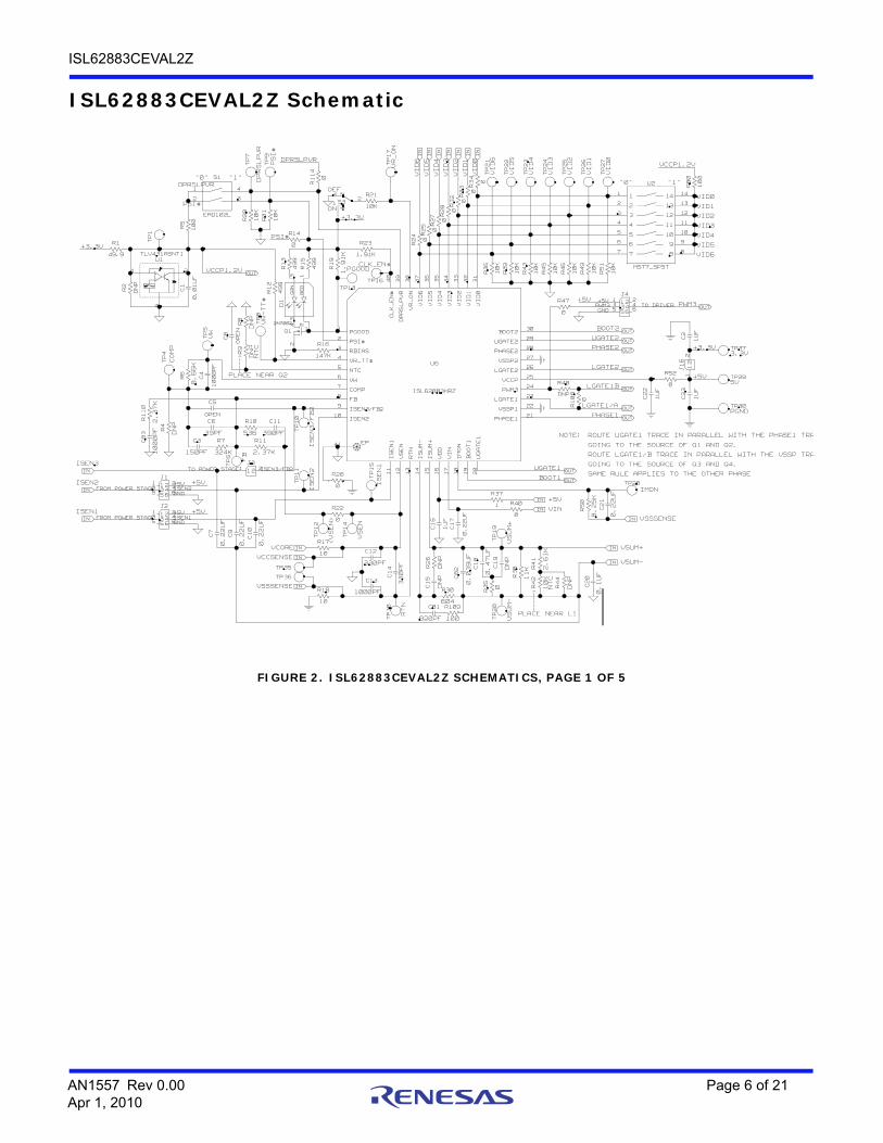
ISL62883CEVAL2Z Schematic
FIGURE 2. ISL62883CEVAL2Z SCHEMATICS, PAGE 1 OF 5
100
FROM POWER STAGE
ROUTE LGATE1/B TRACE IN PARALLEL WITH THE VSSP TRACE
SAME RULE APPLIES TO THE OTHER PHASE
ROUTE UGATE1 TRACE IN PARALLEL WITH THE PHASE1 TRACE
GOING TO THE SOURCE OF Q3 AND Q4.
PGOOD
2.37K
COMP
8.66K
1000PF
150PF 324K
39PFDNP
TO POWER STAGE
ISEN3/FB2
ISEN1
"0"DPRSLPVR
"1"
ON
DNP
NTC
DPRSLPVR
0.22UF
8.25K
VSUM+
330PF
-----> 10K11K
NTC
0.1UF
PSI#VID0
"1"
VID2
VID3
VID6
VID5
VID4
"0"
VID4
VID5
VID3
VID2
VID1
VID0
PWM3
5V
+5V
NOTE:
VR_ON
GND
ISEN2GND
GND
ISEN1
3.3V
PGND
GOING TO THE SOURCE OF Q1 AND Q2.
TO DRIVER
VID1
VID6
OFF
330PF
VR-TT#
+5VFROM POWER STAGE
---->
+5V
0.22UF
<VSEN>
2.61K
0
0.22UF
0.22UF
0.47UF
DNP
FB 2.37K
536
DNP
DNP
VW
1.91K
0.039UF
ISEN2
0
PSI#
0
RTN
CLK_EN#
ISEN3/FB2
390PF
PLACE NEAR Q2
/FB2
VSEN
1000PF
820PF
604
VSUM-
PLACE NEAR L1TP18 C81
C15
R109
TP14
TP15
R13
R12
TP8
R11
499
R15
PHASE2
UGATE2
10
R18
R22
2
ISL62883HRZ
10K
VSSSENSE
22
TP28
14
1.91KTLV431ASNT1
TP4
R6
R114
TP36
TP35
C83
R110
C18
21
J16
C16
TP37
C2
R108
R14
R24 R25 R27 R29 R32 R33 R34
TP12
21
J3
R8
R5
4
32
1
S1
654321
J1
C23
654321
J2
654321
J4
21
R20
41
9
8
7
6
5
40
4
39
38
37
36
35
34
33
32
31
30
3
29
28
27
26
25
24
23
21
20
19
18
17
16
15
13
12
11
10
1
U6
R2
43
5
U1
R1
C1
TP1
R50
C21
C10
C9
C7
TP11
TP10
R4
R23
R48
R47
R26
R30 R35
R21
TP6
C13
C12
1
32
S3
C19
R80
TP20
TP27
TP26
TP25
TP24
TP23
TP22
TP21
C22
R40
TP13
TP19C17
R37
C14
R17
TP5
TP9
TP16
TP7
TP17
R52
TP30
TP29
R9
C8
R16
R42C82
C20
C5
R38 R41
R44
C4
C6
C3
C11
R7
R10
2
1
3
Q1R19
R31
R28
4 2
3 1
D1
R45
R43
R39
R49
R51
R36
R46
9
87
6
5
4
3
2
14
13
12
11
10
1
U2
ISEN2
ISEN3
499
PSI#
1
EAD102L
499
10K
10K
DPRSLPVR
+3.3V
0.22UF
2N7002
OPEN
VCORE
VCCSENSE
00
10
1000PF
OPEN
49.9+3.3V
0.01UF
VCCP1.2V
0
DNP
BOOT1
UGATE1
100
ISEN1
+5V
147K
DNP
LGATE1/A
PHASE1
10K
LGATE1B
100
0
MST7_SPST
0
0
0
VID5
VID6
IMON
VSSSENSE
0
0
0
PWM30
1UF
1UF
10K
10K
10K
1UF
VIN
10K
+5V
BOOT2
10K
10K
+5V
0
LGATE2
+5V
+3.3V
0
VID4
VID0
VCCP1.2V
VID1
VID2
VID3
VSUM+
VSUM-
1UF
+5V
IN
OUT
IN
OUT
IN
OUT
IN
IN
OUT
IN
OUT
OUT
IN
IN
IN
IN
IN
IN
OUT
IN
IN
IN
OUT
IN
IN
IN
OUT
OUT
OUT
1
2
3
4
5
6
7
13
12
11
10
9
8
14
12
1 2
6421
53
6421
53
6421
53
EP
CLK_EN#
PGOOD
PSI#
RBIAS
VR_TT#
NTC
COMP
VW
FB
ISEN3
VID3
VID4
VID5
VID6
VR_ON
DPRSLPVR
UGATE2
BOOT2
PHASE2
VSSP2
LGATE2
VCCP
PWM3
LGATE1
UGATE1
BOOT1
IMON
VDD
VIN
ISUM+
ISUM-
RTN
VSEN
ISEN1
PHASE1
VSSP1
VID0
VID1
VID2
ISEN2
-
REFV1.24
+
RED
GRN
P1
P2
AN1557 Rev 0.00 Page 6 of 21Apr 1, 2010
ISL62883CEVAL2Z
T
T
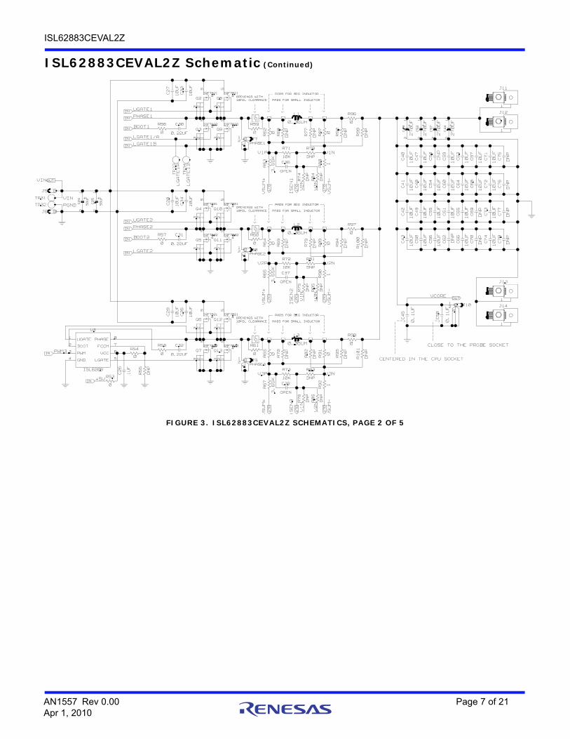
FIGURE 3. ISL62883CEVAL2Z SCHEMATICS, PAGE 2 OF 5
ISL62883CEVAL2Z Schematic (Continued)
270UF
270UF
270UF
270UF
----------
DNP
----->
-->
PADS FOR SMALL INDUCTOR
PADS FOR SMALL INDUCTOR
DNP
IRF7832IRF7832
IRF7821IRF7821
IRF7832IRF7832
IRF7821IRF7821
-->
----->
-->
PHASE1
DNP
0
0.1UF
OPENINGS WITH10MIL CLEARANCE
DNP
DNP
DNP
DNP
PHASE3
0
-->
0
----->
1
-->
0
__
0.1UF
->------
PGND
0
3.65K
__----->
CLOSE TO THE PROBE SOCKET
00
1
0
PHASE2
3.65K
__
VIN
DNP
DNP
-->
0
OPENINGS WITH10MIL CLEARANCE
-->
0
10UF
10UF
10UF
10UF
10UF
10UF
10UF
DNP
PADS FOR SMALL INDUCTOR
PADS FOR BIG INDUCTOR__
LGATE1B
DNP
10UF
-->
10UF
10UF
10UF
10UF
10UF
10UF
10UF
10UF
10UF
10UF
10UF
DNP
DNP
IRF7832
10MIL CLEARANCE
IRF7821OPENINGS WITH
0.36UH
0.36UH
DNP
DNP
DNP
DNP
10UF
10UF
10UF
10UF
10UF
DNP
3.65K
PADS FOR BIG INDUCTOR __
0.36UH
-->
LGATE1A
PADS FOR BIG INDUCTOR __----->
IRF7832
IRF7821
DNP
DNP
----->
1
-->
CENTERED IN THE CPU SOCKET
DNP
C30
R90
R98
DNP
R75
3
L2
DNP
VSUM-
R101
R74
R84
R76
R86
14
3
2 J8
R53
TP34
R55
R54
C26
21
C24
21
C25
R61
R60
R59
14
3
2 J10
C58
C45
1
J14
1
J13
1
J12
1
J11
21
C44
21
C57
21
C39
21
C52
C43
C50
C42
C49
C56
C62
C66
C55
C61
C65
C70
C74
C69
C73
C78
C77
C41
C48
C54
C60
C64
C68
C72
C76
C75
C71
C67
C63
C59
C53
C47
C40
R58 C32
C29
C35
3 2 1
4
5
Q7
3 2 1
4
5
Q6
3 2 1
4
5
Q13
3 2 1
4
5
Q12
14
3
2 J9
R67
C38
R92
R73
R66
R70
L3
R83
R82
R91
R95
3 2 1
4
5
Q5
3 2 1
4
5
142 J7
R65
C37
R72
R64
R69
R81
R79
R89
R94
R100
C31R57
C28
C34
3 2 1
45
Q4
3 2 1
4
5
Q10
R97
C36
R78R71
R99
R93
R87
R77
R68
L1
6
1
3
8
54
72
U3
3 2 1
4
5
3 2 1
4
5
Q3
3 2 15
Q2
P32
P31
R96
R62
J5
J6
C27
C33
3 2 1
4
5
Q8
VCORE
VSUM-
UGATE2
10K
OPEN
0.22UF0
BOOT2
0.22UF
LGATE2
10K
OPEN
V2N
V2N
OPEN
V1P
56UF
56UF
VIN
0.22UF
10UF
10UF
10UF
10K
0
PHASE2
1UF
0
+5V
ISL6208
PWM3
10UF
V3P
10UF
V1N
V1N
V2N
DNP
V3N
V3N
DNP
DNP
V3N
V1NDNP
PHASE1
BOOT1
V2P
0
0
0
DNP
R85
ISEN2
VSUM+
10UF
Q11
R88
LGATE1B
TP33
LGATE1/A0
R56
UGATE1
VSUM+
ISEN1
Q9
4
R63
DNP
DNP
OUT
OUT
IN
OUT
IN
IN
OUT
OUT
IN
OUT
IN
OUT
OUT
IN
IN
IN
OUT
IN
OUT
OUT
IN
IN
PHASE
GND LGATE
UGATE
VCCPWM
FCCMBOOT
AN1557 Rev 0.00 Page 7 of 21Apr 1, 2010

ISL62883CEVAL2Z
FIGURE 4. ISL62883CEVAL2Z SCHEMATICS, PAGE 3 OF 5
ISL62883CEVAL2Z Schematic (Continued)
EVALUATION BOARD
DNP
VTT1 VTT2
DNP 0
DNP DNP
H19
C84
TP38AH29
AH30
AH31
AH14
AM5
AM8
AM14
AM17
VCCP1.2V
./MODELS
RPGA989
VCORE
RPGA989
VSSSENSE
IMON
DPRSLPVR
VCCSENSE
VID2
VID5
VID1
VID4
VID3
PSI#
VID6
VID0
VCCP1.2V
U4
A23
A27
A29
A35
A9
AB27
AB28
AB29
AB30
AB31
AB32
AB33
AB34
AB35
AB6
AC2
AC4
AC8
AD10
AE26
AE27
AE28
AE29
AE30
AE31
AE32
AE33
AE34
AE35
AE6
AF2
AF4
AF8
AG10
AH13
AH17
AH20
AH26
AH27
AH28
AH3
AH32
AH33
AH34
AH35
AH6
AH9
AJ11
AJ14
AJ17
AJ2
AJ20
AJ23
AJ5
AJ8
AK17
AK20
AK25
AK28
AK31
AL12
AL17
AL20
AL23
AL3
AL34
AL6
AL9
AM11
AM2
AM20
AM26
AM28
AM31
AN17
AN20
AN23
AN34
AP10
AP13
AP17
AP2
AP20
AP34
AP4
AP7
AR12
AR15
AR17
AR20
AR23
AR24
AR26
AR28
AR3
AR31
AR34
AR6
AR9
AT1
AT17
AT20
AT35
B1
B11
B13
B17
B18
B2
B21
B25
B31
B34
B4
B6
B8
C16
C19
C20
C22
C24
C28
C29
C32
C34
D26
D3
D30
D33
D6
D9
E11
E13
E18
E2
E21
E24
E29
E32
E35
E5
E8
F16
F19
F22
F25
F27
F30
G20
G3
G31
G34
G6
G9
H11
H13
H15
H18
H2
H22
H24
H26
H28
H32
H35
H5
H8
J19
J21
J30
J32
K27
K3
K30
K33
K34
K6
K9
L2
L29
L32
L35
L5
L8
M10
N26
N27
N28
N29
N30
N31
N32
N33
N34
N35
N6
P2
P4
P8
R10
T26
T27
T28
T29
T30
T31
T32
T33
T34
T35
T6
U2
U4
U8
V10
W26
W27
W28
W29
W30
W31
W32
W33
W34
W35
W6
Y2
Y4
Y8
U4
AT25
AM24
AM22
AP22
AP23
AM23
AP24
AN24
AR25
AM34
AN35
AN33
AA26
AA27
AA28
AA29
AA30
AA31
AA32
AA33
AA34
AA35
AC26
AC27
AC28
AC29
AC30
AC31
AC32AC33AC34AC35AD26AD27AD28AD29AD30AD31AD32AD33AD34AD35AF26AF27AF28
AF29
AF30
AF31
AF32
AF33
AF34
AF35
AG26
AG27
AG28
AG29
AG30
AG31
AG32
AG33
AG34
AG35
P26
P27
P28
P29
P30
P31
P32
P33
P34
P35
R26
R27
R28
R29
R30
R31
R32
R33
R34
R35
AJ34
U26
U27
U28
U29
U30
U31
U32
U33
U34
U35
V26
V27
V28
V29
V30
V31
V32
V33
V34
V35
Y26
Y27
Y28
Y29
Y30
Y31
Y32
Y33
Y34
Y35
AH16AH18AH19AH21AJ16AJ18AJ19AJ21AK16AK18AK19AK21AL16AL18AL19AL21AM16AM18AM19AM21AN16AN18AN19AN21AP16AP18AP19AP21AR16AR18AR19AR21AT16AT18AT19AT21
AR22
AB4
AB7
AC1
AE4
AE7
AF1
AJ1
H1
L1N4
N7
P1T4
T7
U1W4
W7
Y1
AK35
AK33
AK34
AL35
AL33
AM33
AM35
AJ35
AT22
E25
E26
F26
G26
G27
G28
H20
H21
H25
H27
J18
J20
J22
J23
J24
J25
J26
J27
K26
A11
A12
A13
A14
AB10
AC10
AE10
AF10
AH10
AH11
AH12
B12
B14
C11
C12
C13
C14
D11
D12
D13
E12
E14
F11
F12
F13
F14
G11
G12
G13
G14
H12
H14
J11
J12
J13
J14
K10
L10
N10
P10
T10
U10
W10
Y10
C85
TP39
R111 R112
D14
AB26
AA10
AN22
R113
IN
OUT
OUT
OUT
IN
OUT
OUT
IN
OUT
IN
OUT
OUT
OUT
OUT
OUT
VCCVCC
VTT2
VTT2
VTT2
VTT2
VTT2
VCC
VCC
VCC
VTT2
VCC
VCC
VCC
VCC
VCC
VCCVCCVCCVCCVCCVCC
VTT1
VTT1
VCCDDR_DQ
VCC
VCC
VCC
VCCAXGVCCAXGVCCAXGVCCAXGVCCAXGVCCAXGVCCAXGVCCAXGVCCAXGVCCAXGVCCAXGVCCAXGVCCAXGVCCAXGVCCAXGVCCAXGVCCAXG
VCCAXG
VCCAXGVCCAXGVCCAXGVCCAXG
VCCAXGVCCAXGVCCAXGVCCAXGVCCAXGVCCAXGVCCAXGVCCAXGVCCAXGVCCAXGVCCAXGVCCAXGVCCAXGVCCAXG
VCC
VCCVCC
VCCVCC
VCC
VCC
VCC
VCC
VCC
VCC
VCC
VCC
VCC
VCC
VCC
VCC
VCC
VCC
VCC
VCC
VTT2
VTT2
VTT2
VTT2
VTT2
VTT2
VTT2
VTT2
VTT2
VTT2
VTT2
VTT2
VTT2
VTT2
VTT2
VTT2
VTT2
VTT2
VTT2
VTT2
VCC
VCC
VCC
VCC
VCC
VCC
VCC
VCC
VCC
VCC
VCC
VCC
VCC
VCC
VCC
VCC
VCC
VCC
VCC
VCC
VCC
VCC
VCC
VCC
VCC
VCC
VCC
VCC
VCC
VCC
VCC
VCC
VCC
VCC
VCC
VCC
VCC
VCC
VCC
VCC
VCC
VCC
VCC
VCC
VCC
VCC
VCC
VCC
VCC
VCC
VCC
VCC
VCC
VCC
VCC
VCC
VCC
VCC
VCC
VCC
VCC
VCC
VCC
VCC
VCC
VCC
VCC
VCC
VCC
VCC
VCC
VCC
PSI_B
VCC
VID6
VID5
VID4
VID2
VID1
VID0
DFGT_VID0
DFGT_VID1
DFGT_VID2
DFGT_DPRSLPVR
DFGT_VR_EN
VTT2
VTT2
VCC
VCC
VCC
VID3
DPRSLPVR
VTT2
VTT2
VTT2
VTT2
VTT2
VTT2
VTT2
VTT2
VTT2
VTT2
VTT2
VTT2
VTT2
VTT2
VTT2
VTT2
VTT2
VTT1
VTT1
VTT1
VTT1
VTT1
VTT1
VTT1
VTT1
VTT1
VTT1
VTT1
VTT1
VTT1
VTT1
VTT1
VTT1
VTT1
VCCDDR_DQ
VCCDDR_DQ
VCCDDR_DQ
VCCDDR_DQ
VCCDDR_DQ
VCCDDR_DQ
VCCDDR_DQ
VCCDDR_DQ
VCCDDR_DQ
VCCDDR_DQ
VCCDDR_DQ
VCCDDR_DQ
VCCDDR_DQ
VCCDDR_DQ
VCCDDR_DQ
VCC_SENSE
DFGT_IMON
DFGT_VID6
DFGT_VID5
DFGT_VID4
DFGT_VID3
VSSAXG_SENSE
VCCAXG_SENSE
VSS_SENSE
ISENSE_DP
VTT1
VCCDDR_DQ
VCCDDR_DQ
VTT2
VCC
VCC
VSS
VSS
VSS
VSS
VSS
VSS
VSS
VSS
VSS
VSS
VSS
VSS
VSS
VSS
VSS
VSS
VSS
VSS
VSS
VSS
VSS
VSS
VSS
VSS
VSS
VSS
VSS
VSS
VSS
VSS
VSS
VSS
VSS
VSS
VSS
VSS
VSS
VSS
VSS
VSS
VSS
VSS
VSS
VSS
VSS
VSS
VSS
VSS
VSS
VSS
VSS
VSS
VSS
VSS
VSS
VSS
VSS
VSS
VSS
VSS
VSS
VSS
VSS
VSS
VSS
VSS
VSS
VSS
VSS
VSS
VSS
VSS
VSS
VSS
VSS
VSS
VSS
VSS
VSS
VSS
VSS
VSS
VSS
VSS
VSS
VSS
VSS
VSS
VSS
VSS
VSS
VSS
VSS
VSS
VSS
VSS
VSS
VSS
VSS
VSS
VSS
VSS
VSS
VSS
VSS
VSS
VSS
VSS
VSS
VSS
VSS
VSS
VSS
VSS
VSS
VSS
VSS
VSS
VSS
VSS
VSS
VSS
VSS
VSS
VSS
VSS
VSS
VSS
VSS
VSS
VSS
VSS
VSS
VSS
VSS
VSS
VSS
VSS
VSS
VSS
VSS
VSS
VSS
VSS
VSS
VSS
VSS
VSS
VSS
VSS
VSS
VSS
VSS
VSS
VSS
VSS
VSS
VSS
VSS
VSS
VSS
VSS
VSS
VSS
VSS
VSS
VSS
VSS
VSS
VSS
VSS
VSS
VSS
VSS
VSS
VSS
VSS
VSS
VSS
VSS
VSS
VSS
VSS
VSS
VSS
VSS
VSS
VSS
VSS
VSS
VSS
VSS
VSS
VSS
VSS
VSS
VSS
VSS
VSS
VSS
VSS
VSS
VSS
VSS
VSS
VSS
VSS
VSS
VSS
VSS
VSS
VSS
VSS
VSS
VSS
VSS
VSS
VSS
VSS
VSS
VSS
VSS
VSS
VSS
VSS
VSS
VSS
VSS
VSS
VSS
VSS
VSS
VSS
VSS
VSS
VSS
VSS
VSS
AN1557 Rev 0.00 Page 8 of 21Apr 1, 2010

ISL62883CEVAL2Z
FIGURE 5. ISL62883CEVAL2Z SCHEMATICS, PAGE 4 OF 5
ISL62883CEVAL2Z Schematic (Continued)
ON
OFF
0.05
0.05
1
4
3
2 J15
R107
R106
3
1
2
Q15
TP2
1
32
S2
21
C80
R103
R105
R104
23
1
S4
R102
TP3
C79
2
1
3
Q14
7
1 8
6
4
3
5
2
U5+12V
SUD50N03_07
BAV99
2N7002 499
249
249
1UF
VCORE
10UF
49.9K
HIP2100
IN
P1
P2
HI
LO
HS
HO LI
VSS
VDD
HB
AN1557 Rev 0.00 Page 9 of 21Apr 1, 2010

ISL62883CEVAL2Z
FIGURE 6. ISL62883CEVAL2Z SCHEMATICS, PAGE 5 OF 5
ISL62883CEVAL2Z Schematic (Continued)
D24
D19
C27C26
D31
D27D25
AH7
AN29
E7
D16
AK32
AL10
AK30
E23
M35
M33M34
J9
Y9Y7Y6Y5Y3
AT9AT8
AT7
AT6AT5AT4
AT34AT33AT32AT31AT30
AT3
AT29AT28AT27AT26AT24AT23
AT2
AT15AT14AT13AT12AT11AT10
AR8AR7AR5AR4
AR35AR33AR32AR30AR29AR27
AR2
AR14AR13AR11AR10
AR1
AP9AP8AP6AP5
AP35
AP33AP32AP31AP30
AP3
AP29AP28AP27AP26AP25AP15AP14AP12AP11
AP1
AN9AN8AN7AN6AN5AN4
AN32AN31AN30
AN3
AN28AN27AN26AN25
AN2
AN15AN14AN13AN12AN11AN10
AN1
AM9AM7AM6AM4
AM32AM30
AM3
AM29AM27AM25AM15AM13AM12AM10
AM1
AL8AL7AL5AL4
AL32AL31AL30AL29AL28AL27AL26AL25AL24AL22
AL2
AL15AL14AL13AL11
AL1
AK9AK8AK7AK6AK5AK4AK3
AK29AK27AK26AK24AK23AK22
AK2
AK15AK14AK13AK12AK11AK10
AK1
AJ9AJ7AJ6AJ4
AJ33AJ32AJ31AJ30
AJ3
AJ29AJ28AJ27AJ26AJ25AJ24AJ22AJ15AJ13AJ12AJ10
AH8
AH5AH4
AH25AH24AH23AH22
AH2
AH15
AH1AG9AG8AG7AG6AG5AG4AG3AG2AG1AF9AF7AF6AF5AF3AE9AE8AE5AE3AE2AE1AD9AD8AD7AD6AD5AD4AD3AD2AD1AC9AC7AC6AC5AC3AB9AB8AB5AB3AB2AB1AA9AA8AA7AA6AA5AA4AA3AA2AA1
U4W9W8W5W3W2W1V9V8V7V6V5V4V3V2V1U9U7U6U5U3T9T8T5T3T2T1R9R8R7R6R5R4R3R2R1P9P7P6P5P3N9N8N5N3N2N1
M9M8M7M6M5M4
M32M31M30
M3
M29M28M27M26
M2M1
L9L7L6L4
L34L33L31L30
L3
L28L27L26
K8K7K5K4
K35K32K31K29K28
K2K1
J8J7J6J5J4
J35J34J33J31
J3
J29J28
J2
J17
J16J15
J10
J1
H9H7H6H4
H34H33H31H30
H3
H29H23H17H16H10
G8G7G5G4
G35G33G32G30G29G25G24G23G22G21
G2
G19G18G17G16G15G10
G1
F9F8F7F6F5F4
F35F34F33F32F31
F3
F29F28F24F23F21F20
F2
F18F17F15F10
F1
E9
E6E4
E34E33E31E30
E3
E28E27
E22E20E19E17E16E15E10
E1
D8D7D5D4
D35D34D32
D29D28
D23D22D21D20
D2
D18D17
D15D10
D1
C9C8C7C6C5C4
C35C33C31C30
C3
C25C23C21
C2
C18C17C15C10
C1
B9B7B5
B35B33B32B30
B3
B29B28B27B26B24B23B22B20B19B16B15B10
A8A7A6A5A4
A34A33A32A31A30
A3
A28A26A25A24A22A21A20
A2
A19A18A17A16A15A10
U4
RPGA989./MODELS
RPGA989RPGA989
./MODELSRPGA989
RSVDRSVDRSVDRSVDRSVD
RSVDRSVDRSVDRSVDRSVD
RSVDRSVDRSVDRSVDRSVDRSVDRSVDRSVDRSVDRSVDRSVDRSVDRSVDRSVDRSVDRSVDRSVDRSVDRSVDRSVDRSVD
RSVDRSVDRSVDRSVDRSVDRSVDRSVDRSVDRSVDRSVDRSVDRSVDRSVDRSVDRSVDRSVDRSVD
RSVD
RSVD
RSVD
RSVDRSVD
RSVD
RSVDRSVDRSVDRSVDRSVDRSVDRSVDRSVDRSVDRSVDRSVDRSVDRSVDRSVDRSVDRSVDRSVDRSVDRSVDRSVDRSVDRSVDRSVDRSVD
RSVDRSVDRSVDRSVDRSVDRSVD
RSVDRSVDRSVDRSVDRSVDRSVDRSVDRSVDRSVDRSVDRSVDRSVDRSVDRSVDRSVDRSVDRSVD
RSVDRSVDRSVDRSVDRSVDRSVDRSVDRSVD
RSVDRSVDRSVDRSVDRSVDRSVDRSVDRSVDRSVDRSVDRSVDRSVDRSVDRSVDRSVDRSVD
RSVD
RSVDRSVDRSVD
RSVDRSVD
RSVDRSVDRSVDRSVDRSVD
RSVDRSVDRSVD
RSVDRSVDRSVDRSVDRSVDRSVDRSVD
RSVDRSVDRSVD
RSVDRSVDRSVDRSVDRSVDRSVD
RSVDRSVD
RSVDRSVDRSVD
RSVD
RSVDRSVDRSVDRSVDRSVDRSVDRSVDRSVDRSVDRSVDRSVDRSVDRSVDRSVDRSVDRSVDRSVDRSVDRSVDRSVD
RSVDRSVD
RSVD
RSVD
RSVD
RSVD
RSVD
RSVDRSVDRSVD
RSVD
RSVDRSVDRSVD
RSVDRSVDRSVDRSVDRSVDRSVD
RSVD
RSVDRSVDRSVDRSVDRSVD
RSVDRSVDRSVDRSVDRSVD
RSVD
RSVDRSVDRSVD
RSVDRSVD
RSVD
RSVD
RSVD
RSVD
RSVDRSVDRSVD
RSVDRSVD
RSVD
RSVDRSVDRSVDRSVD
RSVDRSVDRSVDRSVDRSVDRSVD
RSVDRSVDRSVDRSVDRSVDRSVD
RSVDRSVDRSVDRSVDRSVDRSVDRSVDRSVDRSVDRSVDRSVDRSVDRSVDRSVDRSVDRSVDRSVDRSVDRSVDRSVDRSVDRSVDRSVDRSVDRSVDRSVD
RSVDRSVD
RSVDRSVDRSVDRSVDRSVD
RSVDRSVD
RSVD
RSVDRSVD
RSVDRSVD
RSVDRSVD
RSVDRSVD
RSVDRSVD
RSVDRSVDRSVD
RSVDRSVDRSVDRSVD
RSVDRSVDRSVDRSVDRSVDRSVDRSVDRSVD
RSVDRSVDRSVDRSVDRSVD
RSVDRSVDRSVDRSVDRSVD
RSVD
RSVDRSVDRSVDRSVDRSVDRSVD
RSVDRSVDRSVDRSVDRSVDRSVDRSVD
RSVDRSVDRSVDRSVD
RSVDRSVDRSVDRSVDRSVDRSVDRSVDRSVD
RSVD
RSVDRSVDRSVDRSVDRSVD
RSVDRSVDRSVD
RSVDRSVDRSVD
RSVDRSVD
RSVDRSVDRSVDRSVDRSVD
RSVDRSVDRSVDRSVDRSVDRSVD
RSVD
RSVDRSVDRSVDRSVDRSVDRSVDRSVDRSVDRSVDRSVDRSVD
RSVDRSVDRSVDRSVDRSVDRSVDRSVDRSVD
RSVDRSVDRSVDRSVDRSVDRSVDRSVDRSVDRSVDRSVDRSVD
RSVDRSVDRSVD
RSVD
RSVDRSVDRSVDRSVDRSVDRSVDRSVDRSVD
RSVDRSVD
RSVDRSVDRSVD
RSVDRSVD
RSVD
RSVDRSVDRSVDRSVDRSVDRSVDRSVDRSVDRSVDRSVDRSVDRSVDRSVDRSVDRSVDRSVDRSVDRSVDRSVDRSVD
RSVDRSVDRSVD
RSVDRSVDRSVDRSVDRSVDRSVDRSVDRSVDRSVDRSVDRSVDRSVDRSVDRSVDRSVD
RSVDRSVDRSVD
RSVDRSVDRSVDRSVDRSVDRSVD
RSVDRSVD
RSVDRSVDRSVDRSVDRSVD
RSVDRSVD
RSVD
RSVD
RSVD
RSVDRSVDRSVD
RSVDRSVD
RSVD
RSVDRSVD
RSVDRSVDRSVDRSVD
RSVDRSVD
RSVD
RSVDRSVD
RSVD
RSVD
RSVD
RSVD
RSVD
RSVD
RSVD
RSVD
RSVD
RSVDRSVD
RSVDRSVDRSVD
AN1557 Rev 0.00 Page 10 of 21Apr 1, 2010

ISL62883CEVAL2Z
ISL62883CEVAL2Z Evaluation Board Layout
FIGURE 7. TOP SILKSCREEN
ISL62883CEVAL2Z
AN1557 Rev 0.00 Page 11 of 21Apr 1, 2010

ISL62883CEVAL2Z
FIGURE 8. BOTTOM SILKSCREEN
ISL62883CEVAL2Z Evaluation Board Layout (Continued)
AN1557 Rev 0.00 Page 12 of 21Apr 1, 2010

ISL62883CEVAL2Z
FIGURE 9. LAYER 1
ISL62883CEVAL2Z Evaluation Board Layout (Continued)
AN1557 Rev 0.00 Page 13 of 21Apr 1, 2010

ISL62883CEVAL2Z
FIGURE 10. LAYER 2
ISL62883CEVAL2Z Evaluation Board Layout (Continued)
AN1557 Rev 0.00 Page 14 of 21Apr 1, 2010
ISL62883CEVAL2Z
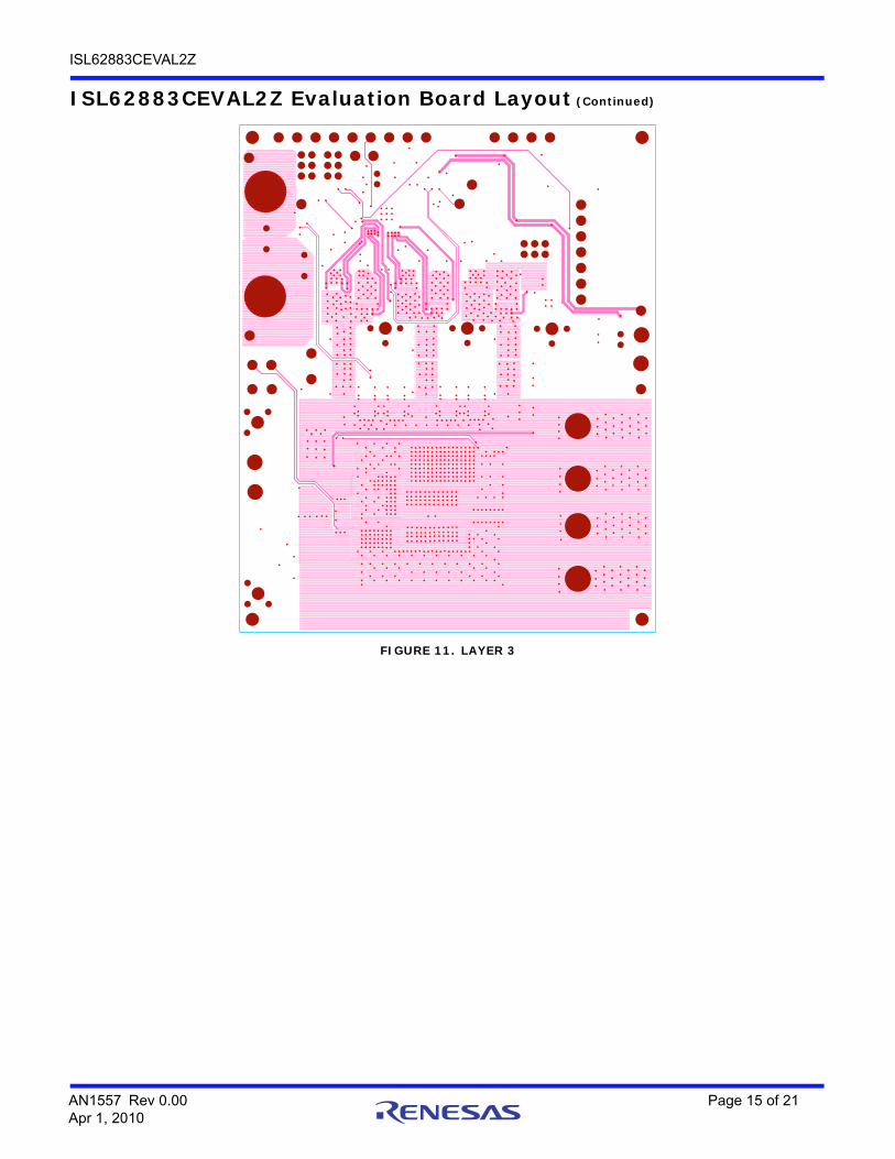
FIGURE 11. LAYER 3
ISL62883CEVAL2Z Evaluation Board Layout (Continued)
AN1557 Rev 0.00 Page 15 of 21Apr 1, 2010
ISL62883CEVAL2Z
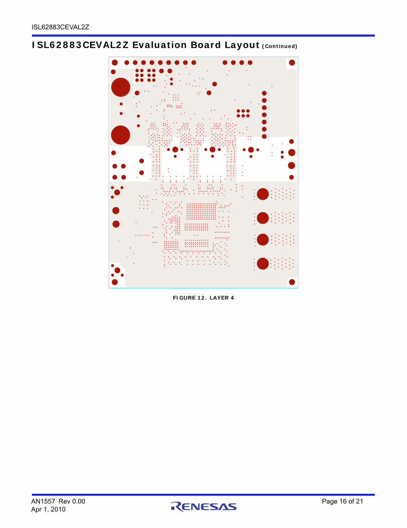
FIGURE 12. LAYER 4
ISL62883CEVAL2Z Evaluation Board Layout (Continued)
AN1557 Rev 0.00 Page 16 of 21Apr 1, 2010
ISL62883CEVAL2Z
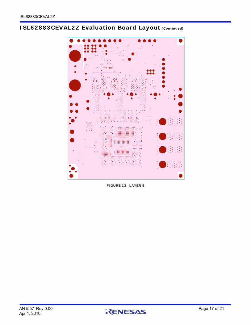
FIGURE 13. LAYER 5
ISL62883CEVAL2Z Evaluation Board Layout (Continued)
AN1557 Rev 0.00 Page 17 of 21Apr 1, 2010

ISL62883CEVAL2Z
FIGURE 14. LAYER 6
ISL62883CEVAL2Z Evaluation Board Layout (Continued)
AN1557 Rev 0.00 Page 18 of 21Apr 1, 2010

ISL62883CEVAL2Z
FIGURE 15. LAYER 7
ISL62883CEVAL2Z Evaluation Board Layout (Continued)
AN1557 Rev 0.00 Page 19 of 21Apr 1, 2010

ISL62883CEVAL2Z
FIGURE 16. LAYER 8
ISL62883CEVAL2Z Evaluation Board Layout (Continued)
AN1557 Rev 0.00 Page 20 of 21Apr 1, 2010

http://www.renesas.comRefer to "http://www.renesas.com/" for the latest and detailed information.
Renesas Electronics America Inc.1001 Murphy Ranch Road, Milpitas, CA 95035, U.S.A.Tel: +1-408-432-8888, Fax: +1-408-434-5351Renesas Electronics Canada Limited9251 Yonge Street, Suite 8309 Richmond Hill, Ontario Canada L4C 9T3Tel: +1-905-237-2004Renesas Electronics Europe LimitedDukes Meadow, Millboard Road, Bourne End, Buckinghamshire, SL8 5FH, U.KTel: +44-1628-651-700, Fax: +44-1628-651-804Renesas Electronics Europe GmbHArcadiastrasse 10, 40472 Düsseldorf, Germany Tel: +49-211-6503-0, Fax: +49-211-6503-1327Renesas Electronics (China) Co., Ltd.Room 1709 Quantum Plaza, No.27 ZhichunLu, Haidian District, Beijing, 100191 P. R. ChinaTel: +86-10-8235-1155, Fax: +86-10-8235-7679Renesas Electronics (Shanghai) Co., Ltd.Unit 301, Tower A, Central Towers, 555 Langao Road, Putuo District, Shanghai, 200333 P. R. China Tel: +86-21-2226-0888, Fax: +86-21-2226-0999Renesas Electronics Hong Kong LimitedUnit 1601-1611, 16/F., Tower 2, Grand Century Place, 193 Prince Edward Road West, Mongkok, Kowloon, Hong KongTel: +852-2265-6688, Fax: +852 2886-9022Renesas Electronics Taiwan Co., Ltd.13F, No. 363, Fu Shing North Road, Taipei 10543, TaiwanTel: +886-2-8175-9600, Fax: +886 2-8175-9670Renesas Electronics Singapore Pte. Ltd.80 Bendemeer Road, Unit #06-02 Hyflux Innovation Centre, Singapore 339949Tel: +65-6213-0200, Fax: +65-6213-0300Renesas Electronics Malaysia Sdn.Bhd.Unit 1207, Block B, Menara Amcorp, Amcorp Trade Centre, No. 18, Jln Persiaran Barat, 46050 Petaling Jaya, Selangor Darul Ehsan, MalaysiaTel: +60-3-7955-9390, Fax: +60-3-7955-9510Renesas Electronics India Pvt. Ltd.No.777C, 100 Feet Road, HAL 2nd Stage, Indiranagar, Bangalore 560 038, IndiaTel: +91-80-67208700, Fax: +91-80-67208777Renesas Electronics Korea Co., Ltd.17F, KAMCO Yangjae Tower, 262, Gangnam-daero, Gangnam-gu, Seoul, 06265 KoreaTel: +82-2-558-3737, Fax: +82-2-558-5338
SALES OFFICES
© 2018 Renesas Electronics Corporation. All rights reserved.Colophon 7.0
(Rev.4.0-1 November 2017)
Notice
1. Descriptions of circuits, software and other related information in this document are provided only to illustrate the operation of semiconductor products and application examples. You are fully responsible for
the incorporation or any other use of the circuits, software, and information in the design of your product or system. Renesas Electronics disclaims any and all liability for any losses and damages incurred by
you or third parties arising from the use of these circuits, software, or information.
2. Renesas Electronics hereby expressly disclaims any warranties against and liability for infringement or any other claims involving patents, copyrights, or other intellectual property rights of third parties, by or
arising from the use of Renesas Electronics products or technical information described in this document, including but not limited to, the product data, drawings, charts, programs, algorithms, and application
examples.
3. No license, express, implied or otherwise, is granted hereby under any patents, copyrights or other intellectual property rights of Renesas Electronics or others.
4. You shall not alter, modify, copy, or reverse engineer any Renesas Electronics product, whether in whole or in part. Renesas Electronics disclaims any and all liability for any losses or damages incurred by
you or third parties arising from such alteration, modification, copying or reverse engineering.
5. Renesas Electronics products are classified according to the following two quality grades: “Standard” and “High Quality”. The intended applications for each Renesas Electronics product depends on the
product’s quality grade, as indicated below.
"Standard": Computers; office equipment; communications equipment; test and measurement equipment; audio and visual equipment; home electronic appliances; machine tools; personal electronic
equipment; industrial robots; etc.
"High Quality": Transportation equipment (automobiles, trains, ships, etc.); traffic control (traffic lights); large-scale communication equipment; key financial terminal systems; safety control equipment; etc.
Unless expressly designated as a high reliability product or a product for harsh environments in a Renesas Electronics data sheet or other Renesas Electronics document, Renesas Electronics products are
not intended or authorized for use in products or systems that may pose a direct threat to human life or bodily injury (artificial life support devices or systems; surgical implantations; etc.), or may cause
serious property damage (space system; undersea repeaters; nuclear power control systems; aircraft control systems; key plant systems; military equipment; etc.). Renesas Electronics disclaims any and all
liability for any damages or losses incurred by you or any third parties arising from the use of any Renesas Electronics product that is inconsistent with any Renesas Electronics data sheet, user’s manual or
other Renesas Electronics document.
6. When using Renesas Electronics products, refer to the latest product information (data sheets, user’s manuals, application notes, “General Notes for Handling and Using Semiconductor Devices” in the
reliability handbook, etc.), and ensure that usage conditions are within the ranges specified by Renesas Electronics with respect to maximum ratings, operating power supply voltage range, heat dissipation
characteristics, installation, etc. Renesas Electronics disclaims any and all liability for any malfunctions, failure or accident arising out of the use of Renesas Electronics products outside of such specified
ranges.
7. Although Renesas Electronics endeavors to improve the quality and reliability of Renesas Electronics products, semiconductor products have specific characteristics, such as the occurrence of failure at a
certain rate and malfunctions under certain use conditions. Unless designated as a high reliability product or a product for harsh environments in a Renesas Electronics data sheet or other Renesas
Electronics document, Renesas Electronics products are not subject to radiation resistance design. You are responsible for implementing safety measures to guard against the possibility of bodily injury, injury
or damage caused by fire, and/or danger to the public in the event of a failure or malfunction of Renesas Electronics products, such as safety design for hardware and software, including but not limited to
redundancy, fire control and malfunction prevention, appropriate treatment for aging degradation or any other appropriate measures. Because the evaluation of microcomputer software alone is very difficult
and impractical, you are responsible for evaluating the safety of the final products or systems manufactured by you.
8. Please contact a Renesas Electronics sales office for details as to environmental matters such as the environmental compatibility of each Renesas Electronics product. You are responsible for carefully and
sufficiently investigating applicable laws and regulations that regulate the inclusion or use of controlled substances, including without limitation, the EU RoHS Directive, and using Renesas Electronics
products in compliance with all these applicable laws and regulations. Renesas Electronics disclaims any and all liability for damages or losses occurring as a result of your noncompliance with applicable
laws and regulations.
9. Renesas Electronics products and technologies shall not be used for or incorporated into any products or systems whose manufacture, use, or sale is prohibited under any applicable domestic or foreign laws
or regulations. You shall comply with any applicable export control laws and regulations promulgated and administered by the governments of any countries asserting jurisdiction over the parties or
transactions.
10. It is the responsibility of the buyer or distributor of Renesas Electronics products, or any other party who distributes, disposes of, or otherwise sells or transfers the product to a third party, to notify such third
party in advance of the contents and conditions set forth in this document.
11. This document shall not be reprinted, reproduced or duplicated in any form, in whole or in part, without prior written consent of Renesas Electronics.
12. Please contact a Renesas Electronics sales office if you have any questions regarding the information contained in this document or Renesas Electronics products.
(Note 1) “Renesas Electronics” as used in this document means Renesas Electronics Corporation and also includes its directly or indirectly controlled subsidiaries.
(Note 2) “Renesas Electronics product(s)” means any product developed or manufactured by or for Renesas Electronics.