isl71091sehxx total dose test report - renesas.com
TRANSCRIPT

TEST REPORT
AN1939Rev 0.00
June 4, 2014
ISL71091SEHxxTotal Dose Testing
Introduction and Executive SummaryThis report discusses the results of total dose testing of four variants of the ISL71091SEHxx voltage reference. These tests were conducted to provide an assessment of the total dose hardness of the parts and their dose rate and bias sensitivity; the tests also added a biased high temperature anneal to look at the part’s accelerated aging response. Samples (see Table 2) were irradiated under bias and with all pins grounded at low dose rate and at high dose rate. The ISL71091SEHxx variants are acceptance tested on a wafer-by-wafer basis to 100krad(Si) at high dose rate (50 to 300rad(Si)/s) and to 50krad(Si) at low dose rate (0.01rad(Si)/s), insuring hardness to the specified level for both dose rates.
The variants of the ISL71091SEHxx reported on include the ISL71091SEH20 (2.048V nominal output voltage), the ISL71091SEH33 (3.3V nominal output voltage), the ISL71091SEH40 (4.096V nominal output voltage) and the ISL71091SEH10 (10.0V nominal output voltage). These variants use the same base die, with the output voltage selected by several masking levels during wafer fabrication and then finally adjusted by trimming (programming fuses) at the probe and package levels to obtain the specified output voltage. The package contains only the silicon die, and there are no separate internal or external passive components (i.e., resistors or capacitors) used to set the output voltage.
The ISL71091SEHxx showed good performance over low and high dose rate irradiation. All samples passed the post-irradiation specifications at the total dose levels specified in the SMD. We observed some dose rate sensitivity and bias sensitivity in the critical output voltage parameter (see “Discussion and Conclusion” on page 18) and the part is considered moderately low dose rate sensitive. We also saw interesting biased high temperature anneal responses in the parts subjected to that procedure, and these responses will be discussed as well.
Reference Documents• MIL-STD-883 test method 1019
• ISL71091SEHxx data sheets- ISL71091SEH20- ISL71091SEH33- ISL71091SEH40- ISL71091SEH10
• Standard Microcircuit Drawing (SMD) 5962-14208
Part DescriptionThe ISL71091SEHxx is a low noise precision voltage reference with a wide supply voltage range from 4.6V to 30V (3.3V variant), with four output voltage options selected through different masking levels and on-chip trimming. The ISL71091SEHxx is built on the Intersil PR40 bonded-wafer
process, which uses dielectric isolation for important electrical and SEE performance improvements. The ISL71091SEHxx offers four output voltage options including 2.048V, 3.3V, 4.096V and 10.0V and features a 6ppm/°C temperature coefficient and excellent line and load regulation. The part achieves sub 5.2μV peak-to-peak (0.1Hz to 10Hz, 3.3V variant) noise with an initial voltage accuracy of ±0.05% at +25°C and ±0.25% over radiation. The device is offered in an 8 lead hermetic flatpack and in die form. Applications include instrumentation, data acquisition systems and strain and pressure sensing for space applications. Key features and specifications are shown in Table 1.
TABLE 1. KEY FEATURES AND SPECIFICATIONS
FEATURE SPECIFICATION
DLA Standard Microcircuit Drawing 5962-14208
Output voltage options 2.048V, 3.3V, 4.096V and 10.0V
Initial accuracy ±0.05%
Accuracy over radiation ±0.25%
Output voltage noise, 2.048V option 3.8μVP-P typical (0.1Hz to 10Hz)
Output voltage noise, 3.3V option 5.2μVP-P typical (0.1Hz to 10Hz)
Output voltage noise, 4.096V option 6.2μVP-P typical (0.1Hz to 10Hz)
Output voltage noise, 10.0V option 14.8μVP-P typical (0.1Hz to 10Hz)
Supply current 500µA maximum
Output voltage temperature coefficient
6ppm/°C maximum
Line regulation 5ppm/V maximum (2.048V)
Line regulation 5ppm/V maximum (3.3V)
Line regulation 5ppm/V maximum (4.096V)
Line regulation 5ppm/V maximum (10.0V)
Load regulation, sourcing (10mA) 40 ppm/mA maximum (2.048V)
Load regulation, sourcing (10mA) 25ppm/mA maximum (3.3)
Load regulation, sourcing (10mA) 20ppm/mA maximum (4.096V)
Load regulation, sourcing (10mA) 15ppm/mA maximum (10.0)
Load regulation, sinking (5mA) 80ppm/mA maximum (2.048V)
Load regulation, sinking (5mA) 60ppm/mA maximum (3.3V)
Load regulation, sinking (5mA) 50ppm/mA maximum (4.096V)
Load regulation, sinking (5mA) 40ppm/mA maximum (10.0V)
Operating temperature range -55°C to +125°C
Radiation Environments:
High dose rate(50 to 300rad(Si)/s)
100krad(Si) maximum
Low dose rate (0.01rad(Si)/s) 50krad(Si) maximum
SET/SEL/SEB 86MeV•cm2/mg
AN1939 Rev 0.00 Page 1 of 20June 4, 2014

ISL71091SEHxx Total Dose Testing
Test DescriptionIrradiation FacilitiesHigh dose rate testing was performed at a nominal dose rate of 68rad(Si)/s using a Gammacell 220™ 60Co irradiator located in the Palm Bay, Florida Intersil facility. Low dose rate testing was performed at 0.01rad(Si)/s using the Intersil Palm Bay N40 panoramic low dose rate 60Co irradiator. Post-irradiation high temperature biased anneals were performed using a small temperature chamber set at +100°C.
Test FixturingFigure 1 shows the configuration used for biased irradiation. The grounded irradiations were performed in the same fixture type but with all pins hardwired to ground. Post-irradiation high temperature biased anneals were performed using this configuration as well.
Characterization Equipment and ProceduresAll electrical testing was performed outside the irradiator using the production automated test equipment (ATE) with datalogging at each downpoint. All downpoint electrical testing was performed at room temperature. Three or four control units were used for each variant to verify repeatability.
Experimental MatrixThe experimental matrix is shown in Table 2. Samples of all four variants of the ISL71091SEHxx were drawn from preproduction PR40 lot WXM8X and were packaged in hermetic 8-pin ceramic flatpacks (package code K8.A). Samples were processed through the standard burnin cycle before irradiation, as required by MIL-STD-883, and were screened to the ATE limits at room temperature prior to the test.
A biased post-irradiation high temperature anneal at +100°C for 168 hours was performed on all samples following completion of the maximum 150krad(Si) irradiation. The anneal results to date are included in Table 2 and the figures starting on page 6. Several of the low dose rate tests are still in progress and the anneal will be performed on these samples following completion of the 150krad(Si) irradiation.
DownpointsDownpoints and pass/fail statistics are shown in the attributes data table (Table 2).
NOTE:VIN = +36V, ±10%RL = 10kΩ, 1%, 1/4W (per socket)C1 = 0.1µF, 50V, 10% (per socket)C2 = 1nF, 20V, 10% (per socket)C3 = 1µF, 20V, 10% (per socket)
FIGURE 1. BIASED IRRADIATION CONFIGURATION FOR THE ISL71091SEHxx
U1
8
7
6
5C3
1
2
3
4
NC
NC
VOUT
TRIM
NC
VIN
COMP
GND
RL
VIN
C2
C1
AN1939 Rev 0.00 Page 2 of 20June 4, 2014

ISL71091SEHxx Total Dose Testing
ResultsAttributes Data
TABLE 2. ISL71091SEHxx TOTAL DOSE TEST ATTRIBUTES DATA
PARTVARIANT
(V)DOSE RATE
(Note 1) BIASSAMPLE
SIZE DOWNPOINTPASS
(Note 2) REJECTS
ISL71091SEH20 2.048 HDR Biased 8 Pre-irradiation 8 8
30krad(Si) 8 0
50krad(Si) 8 0
100krad(Si) 8 0
150krad(Si) 8 0
Anneal 8 0
ISL71091SEH20 2.048 HDR Grounded 8 Pre-irradiation 8
30krad(Si) 8 0
50krad(Si) 8 0
100krad(Si) 8 0
150krad(Si) 8 0
Anneal 8 0
ISL71091SEH20 2.048 LDR Biased 5 Pre-irradiation 5
30krad(Si) 5 0
50krad(Si) 5 0
100krad(Si) TBD TBD
150krad(Si) TBD TBD
Anneal TBD TBD
ISL71091SEH20 2.048 LDR Grounded 5 Pre-irradiation 5
30krad(Si) 5 0
50krad(Si) 5 0
100krad(Si) TBD TBD
150krad(Si) TBD TBD
Anneal TBD TBD
ISL71091SEH33 3.3 HDR Biased 8 Pre-irradiation 8
30krad(Si) 8 0
50krad(Si) 8 0
100krad(Si) 8 0
150krad(Si) 8 0
Anneal 8 0
ISL71091SEH33 3.3 HDR Grounded 8 Pre-irradiation 8
30krad(Si) 8 0
50krad(Si) 8 0
100krad(Si) 8 0
150krad(Si) 8 0
Anneal 8 0
AN1939 Rev 0.00 Page 3 of 20June 4, 2014

ISL71091SEHxx Total Dose Testing
ISL71091SEH33 3.3 LDR Biased 5 Pre-irradiation 5
42krad(Si) 5 0
54krad(Si) 5 0
81krad(Si) 5 0
107krad(Si) 5 0
150krad(Si) 0 5
Anneal 0 5
ISL71091SEH33 3.3 LDR Grounded 5 Pre-irradiation 5
42krad(Si) 5 0
54krad(Si) 5 0
81krad(Si) 5 0
107krad(Si) 5 0
150krad(Si) 5 0
Anneal 5 0
ISL71091SEH40 4.096 HDR Biased 8 Pre-irradiation 8
30krad(Si) 8 0
50krad(Si) 8 0
100krad(Si) 8 0
150krad(Si) 8 0
Anneal 8 0
ISL71091SEH40 4.096 HDR Grounded 8 Pre-irradiation 8
30krad(Si) 8 0
50krad(Si) 8 0
100krad(Si) 8 0
150krad(Si) 8 0
Anneal 8 0
ISL71091SEH40 4.096 LDR Biased 5 Pre-irradiation 5
30krad(Si) 5 0
50krad(Si) 5 0
100krad(Si) TBD TBD
150krad(Si) TBD TBD
Anneal TBD TBD
ISL71091SEH40 4.096 LDR Grounded 5 Pre-irradiation 5
30krad(Si) 5 0
50krad(Si) 5 0
100krad(Si) TBD TBD
150krad(Si) TBD TBD
Anneal TBD TBD
TABLE 2. ISL71091SEHxx TOTAL DOSE TEST ATTRIBUTES DATA (Continued)
PARTVARIANT
(V)DOSE RATE
(Note 1) BIASSAMPLE
SIZE DOWNPOINTPASS
(Note 2) REJECTS
AN1939 Rev 0.00 Page 4 of 20June 4, 2014

ISL71091SEHxx Total Dose Testing
Variables DataThe plots in Figures 2 through 25 show data for six key parameters at all downpoints. Figures 2 through 7 report the response of the ISL71091SEH20 samples; Figures 8 through 13 report the results for the ISL71091SEH33; Figures 14 through 19 report the results for the ISL71091SEH40; and Figures 20 through 25 report the results for the ISL71091SEH10. The plots show the response to total dose irradiation at low dose rate for the biased (per Figure 1) and unbiased (all pins grounded) cases and at high dose rate for the biased (Figure 1) and unbiased cases. The plots also show the responses to the biased 168-hour
+100°C high temperature anneal when performed, realizing that some of the low dose rate tests are still running. Anneals are complete on all high dose rate samples and on the ISL71091SEH33 low dose rate samples. We chose to plot the median for these parameters and show the minimum and maximum values for each datapoint as well. “Discussion and Conclusion” on page 18 will provide individual discussion of the figures.
ISL71091SEH10 10.0 HDR Biased 8 Pre-irradiation 8
30krad(Si) 8 0
50krad(Si) 8 0
100krad(Si) 8 0
150krad(Si) 8 0
Anneal 8 0
ISL71091SEH10 10.0 HDR Grounded 8 Pre-irradiation 8
30krad(Si) 8 0
50krad(Si) 8 0
100krad(Si) 8 0
150krad(Si) 8 0
Anneal 8 0
ISL71091SEH10 10.0 LDR Biased 5 Pre-irradiation 5 0
30krad(Si) 5 0
50krad(Si) 5 0
100krad(Si) TBD TBD
150krad(Si) TBD TBD
Anneal TBD TBD
ISL71091SEH10 10.0 LDR Grounded 5 Pre-irradiation 5 0
30krad(Si) 5 0
50krad(Si) 5 0
100krad(Si) TBD TBD
150krad(Si) TBD TBD
Anneal TBD TBD
NOTES:
1. ‘HDR’ indicates high dose rate (50 to 300rad(Si)/s) as specified in MIL-STD-883 TM1019; the actual dose rate for these tests was 68rad(Si)/s. ‘LDR’ indicates low dose rate (0.01rad(Si)/s), also as specified in TM1019.
2. ‘Pass indicates a sample that passes all post-irradiation SMD limits.
TABLE 2. ISL71091SEHxx TOTAL DOSE TEST ATTRIBUTES DATA (Continued)
PARTVARIANT
(V)DOSE RATE
(Note 1) BIASSAMPLE
SIZE DOWNPOINTPASS
(Note 2) REJECTS
AN1939 Rev 0.00 Page 5 of 20June 4, 2014

ISL71091SEHxx Total Dose Testing
Variables Data Plots
FIGURE 2. ISL71091SEH20 output voltage as a function of total dose irradiation at low and high dose rate for the biased (per Figure 1) and unbiased (all pins grounded) cases. The dose rate was 0.01rad(Si)/s for low dose rate irradiation and 68rad(Si)/s for high dose rate irradiation. The high dose rate irradiations were followed by a biased anneal at +100°C for 168 hours. Sample sizes were 8 at high dose rate under bias, 8 at high dose rate with all pins grounded, 5 samples at low dose rate under bias and 5 samples at low dose rate with all pins grounded. The SMD post-irradiation specification limits are 2.042880V to 2.053120V (±0.25%).
FIGURE 3. ISL71091SEH20 power supply current as a function of total dose irradiation at low and high dose rate for the biased (per Figure 1) and unbiased (all pins grounded) cases. The dose rate was 0.01rad(Si)/s for low dose rate irradiation and 68rad(Si)/s for high dose rate irradiation. The high dose rate irradiations were followed by a biased anneal at +100°C for 168 hours. Sample sizes were 8 at high dose rate under bias, 8 at high dose rate with all pins grounded, 5 samples at low dose rate under bias and 5 samples at low dose rate with all pins grounded. The SMD post-irradiation specification limits are 0.2mA to 0.5mA.
2.042
2.044
2.046
2.048
2.050
2.052
2.054
0 50 100 150
OU
TP
UT
VO
LT
AG
E (
V)
TOTAL DOSE (krad(Si))
ANNEAL
LDR BIAS MEDIAN LDR BIAS MIN
LDR BIAS MAX LDR GND MEDIAN
LDR GND MIN LDR GND MAX
HDR BIAS MEDIAN HDR BIAS MIN
HDR BIAS MAX HDR GND MEDIAN
HDR GND MIN HDR GND MAX
SPEC LIMIT SPEC LIMIT
0
0.1
0.2
0.3
0.4
0.5
0.6
0 50 100 150
PO
WE
R S
UP
PL
Y C
UR
RE
NT
(m
A)
ANNEAL
TOTAL DOSE (krad(Si))
LDR BIAS MEDIAN LDR BIAS MIN
LDR BIAS MAX LDR GND MEDIAN
LDR GND MIN LDR GND MAX
HDR BIAS MEDIAN HDR BIAS MIN
HDR BIAS MAX HDR GND MEDIAN
HDR GND MIN HDR GND MAX
SPEC LIMIT SPEC LIMIT
AN1939 Rev 0.00 Page 6 of 20June 4, 2014

ISL71091SEHxx Total Dose Testing
FIGURE 4. ISL71091SEH20 line regulation as a function of total dose irradiation at low and high dose rate for the biased (per Figure 1) and unbiased (all pins grounded) cases. The dose rate was 0.01rad(Si)/s for low dose rate irradiation and 68rad(Si)/s for high dose rate irradiation. The high dose rate irradiations were followed by a biased anneal at +100°C for 168 hours. Sample sizes were 8 at high dose rate under bias, 8 at high dose rate with all pins grounded, 5 samples at low dose rate under bias and 5 samples at low dose rate with all pins grounded. The SMD post-irradiation specification limits are -5ppm/V to +5ppm/V.
FIGURE 5. ISL71091SEH20 load regulation, sourcing 10mA, as a function of total dose irradiation at low and high dose rate for the biased (per Figure 1) and unbiased (all pins grounded) cases. The dose rate was 0.01rad(Si)/s for low dose rate irradiation and 68rad(Si)/s for high dose rate irradiation. The high dose rate irradiations were followed by a biased anneal at +100°C for 168 hours. Sample sizes were 8 at high dose rate under bias, 8 at high dose rate with all pins grounded, 5 samples at low dose rate under bias and 5 samples at low dose rate with all pins grounded. The SMD post-irradiation specification limits are -40ppm/mA to 40ppm/mA.
Variables Data Plots (Continued)
-6
-4
-2
0
2
4
6
0 50 100 150
LIN
E R
EG
UL
AT
ION
(p
pm
/V)
TOTAL DOSE (krad(Si))
ANNEA
LDR BIAS MEDIAN LDR BIAS MIN
LDR BIAS MAX LDR GND MEDIAN
LDR GND MIN LDR GND MAX
HDR BIAS MEDIAN HDR BIAS MIN
HDR BIAS MAX HDR GND MEDIAN
HDR GND MIN HDR GND MAX
SPEC LIMIT SPEC LIMIT
-50
-40
-30
-20
-10
0
10
20
30
40
50
0 50 100 150
LO
AD
RE
GU
LA
TIO
N (
pp
m/m
A)
ANNEAL
+10mA
LDR BIAS MEDIAN LDR BIAS MIN
LDR BIAS MAX LDR GND MEDIAN
LDR GND MIN LDR GND MAX
HDR BIAS MEDIAN HDR BIAS MIN
HDR BIAS MAX HDR GND MEDIAN
HDR GND MIN HDR GND MAX
SPEC LIMIT SPEC LIMIT
TOTAL DOSE (krad(Si))
AN1939 Rev 0.00 Page 7 of 20June 4, 2014

ISL71091SEHxx Total Dose Testing
FIGURE 6. ISL71091SEH20 load regulation, sinking 5mA, as a function of total dose irradiation at low and high dose rate for the biased (per Figure 1) and unbiased (all pins grounded) cases. The dose rate was 0.01rad(Si)/s for low dose rate irradiation and 68rad(Si)/s for high dose rate irradiation. The high dose rate irradiations were followed by a biased anneal at +100°C for 168 hours. Sample sizes were 8 at high dose rate under bias, 8 at high dose rate with all pins grounded, 5 samples at low dose rate under bias and 5 samples at low dose rate with all pins grounded. The SMD post-irradiation specification limits are -80.0ppm/mA to 80ppm/mA.
FIGURE 7. ISL71091SEH20 dropout voltage as a function of total dose irradiation at low and high dose rate for the biased (per Figure 1) and unbiased (all pins grounded) cases. The dose rate was 0.01rad(Si)/s for low dose rate irradiation and 68rad(Si)/s for high dose rate irradiation. The high dose rate irradiations were followed by a biased anneal at +100°C for 168 hours. Sample sizes were 8 at high dose rate under bias, 8 at high dose rate with all pins grounded, 5 samples at low dose rate under bias and 5 samples at low dose rate with all pins grounded. The SMD post-irradiation specification limit is 2.5V maximum.
Variables Data Plots (Continued)
-100
-80
-60
-40
-20
0
20
40
60
80
100
0 50 100 150
LO
AD
RE
GU
LA
TIO
N (
pp
m/m
A)
TOTAL DOSE (krad(Si))
ANNEAL
-5mA
LDR BIAS MEDIAN LDR BIAS MIN
LDR BIAS MAX LDR GND MEDIAN
LDR GND MIN LDR GND MAX
HDR BIAS MEDIAN HDR BIAS MIN
HDR BIAS MAX HDR GND MEDIAN
HDR GND MIN HDR GND MAX
SPEC LIMIT SPEC LIMIT
1.5
1.7
1.9
2.1
2.3
2.5
2.7
0 50 100 150
DR
OP
OU
T V
OL
TA
GE
(V
)
TOTAL DOSE (krad(Si))
ANNEAL
LDR BIAS MEDIAN LDR BIAS MIN
LDR BIAS MAX LDR GND MEDIAN
LDR GND MIN LDR GND MAX
HDR BIAS MEDIAN HDR BIAS MIN
HDR BIAS MAX HDR GND MEDIAN
HDR GND MIN HDR GND MAX
SPEC LIMIT
AN1939 Rev 0.00 Page 8 of 20June 4, 2014

ISL71091SEHxx Total Dose Testing
FIGURE 8. ISL71091SEH33 output voltage as a function of total dose irradiation at low and high dose rate for the biased (per Figure 1) and unbiased (all pins grounded) cases. The dose rate was 0.01rad(Si)/s for low dose rate irradiation and 68rad(Si)/s for high dose rate irradiation. All irradiations were followed by a biased anneal at +100°C for 168 hours. Sample sizes were 8 at high dose rate under bias, 8 at high dose rate with all pins grounded, 5 samples at low dose rate under bias and 5 samples at low dose rate with all pins grounded. The SMD post-irradiation specification limits are 3.291750V to 3.308250V (±0.25%).
FIGURE 9. ISL71091SEH33 power supply current as a function of total dose irradiation at low and high dose rate for the biased (per Figure 1) and unbiased (all pins grounded) cases. The dose rate was 0.01rad(Si)/s for low dose rate irradiation and 68rad(Si)/s for high dose rate irradiation. All irradiations were followed by a biased anneal at +100°C for 168 hours. Sample sizes were 8 at high dose rate under bias, 8 at high dose rate with all pins grounded, 5 samples at low dose rate under bias and 5 samples at low dose rate with all pins grounded. The SMD post-irradiation specification limits are 0.2mA to 0.5mA.
Variables Data Plots (Continued)
3.285
3.290
3.295
3.300
3.305
3.310
0 50 100 150
OU
TP
UT
VO
LT
AG
E (
V)
TOTAL DOSE (krad(Si))
ANNEAL
LDR BIAS MEDIAN LDR BIAS MIN
LDR BIAS MAX LDR GND MEDIAN
LDR GND MIN LDR GND MAX
HDR BIAS MEDIAN HDR BIAS MIN
HDR BIAS MAX HDR GND MEDIAN
HDR GND MIN HDR GND MAX
SPEC LIMIT SPEC LIMIT
0
0.1
0.2
0.3
0.4
0.5
0.6
0 50 100 150
PO
WE
R S
UP
PL
Y C
UR
RE
NT
(m
A)
TOTAL DOSE (krad(Si))
ANNEAL
LDR BIAS MEDIAN LDR BIAS MIN
LDR BIAS MAX LDR GND MEDIAN
LDR GND MIN LDR GND MAX
HDR BIAS MEDIAN HDR BIAS MIN
HDR BIAS MAX HDR GND MEDIAN
HDR GND MIN HDR GND MAX
SPEC LIMIT
AN1939 Rev 0.00 Page 9 of 20June 4, 2014

ISL71091SEHxx Total Dose Testing
FIGURE 10. ISL71091SEH33 line regulation as a function of total dose irradiation at low and high dose rate for the biased (per Figure 1) and unbiased (all pins grounded) cases. The dose rate was 0.01rad(Si)/s for low dose rate irradiation and 68rad(Si)/s for high dose rate irradiation. All irradiations were followed by a biased anneal at +100°C for 168 hours. Sample sizes were 8 at high dose rate under bias, 8 at high dose rate with all pins grounded, 5 samples at low dose rate under bias and 5 samples at low dose rate with all pins grounded. The post-irradiation specification limits are -5ppm/V to +5ppm/V.
FIGURE 11. ISL71091SEH33 load regulation, sourcing 10mA, as a function of total dose irradiation at low and high dose rate for the biased (per Figure 1) and unbiased (all pins grounded) cases. The dose rate was 0.01rad(Si)/s for low dose rate irradiation and 68rad(Si)/s for high dose rate irradiation. All irradiations were followed by a biased anneal at +100°C for 168 hours. Sample sizes were 8 at high dose rate under bias, 8 at high dose rate with all pins grounded, 5 samples at low dose rate under bias and 5 samples at low dose rate with all pins grounded. The post-irradiation specification limits are -25ppm/mA to +25ppm/mA.
Variables Data Plots (Continued)
-6
-4
-2
0
2
4
6
0 50 100 150
LIN
E R
EG
UL
AT
ION
(p
pm
/V)
TOTAL DOSE (krad(Si))
ANNEAL
LDR BIAS MEDIAN LDR BIAS MIN
LDR BIAS MAX LDR GND MEDIAN
LDR GND MIN LDR GND MAX
HDR BIAS MEDIAN HDR BIAS MIN
HDR BIAS MAX HDR GND MEDIAN
HDR GND MIN HDR GND MAX
SPEC LIMIT SPEC LIMIT
-30
-20
-10
0
10
20
30
0 50 100 150
LO
AD
RE
GU
LA
TIO
N (
pp
m/m
A)
TOTAL DOSE (krad(Si))
ANNEAL
+10mA
LDR BIAS MEDIAN LDR BIAS MIN
LDR BIAS MAX LDR GND MEDIAN
LDR GND MIN LDR GND MAX
HDR BIAS MEDIAN HDR BIAS MIN
HDR BIAS MAX HDR GND MEDIAN
HDR GND MIN HDR GND MAX
SPEC LIMIT SPEC LIMIT
AN1939 Rev 0.00 Page 10 of 20June 4, 2014

ISL71091SEHxx Total Dose Testing
FIGURE 12. ISL71091SEH33 load regulation, sinking 5mA, as a function of total dose irradiation at low and high dose rate for the biased (per Figure 1) and unbiased (all pins grounded) cases. The dose rate was 0.01rad(Si)/s for low dose rate irradiation and 68rad(Si)/s for high dose rate irradiation. All irradiations were followed by a biased anneal at +100°C for 168 hours. Sample sizes were 8 at high dose rate under bias, 8 at high dose rate with all pins grounded, 5 samples at low dose rate under bias and 5 samples at low dose rate with all pins grounded. The post-irradiation specification limits are -60ppm/mA to +60ppm/mA.
FIGURE 13. ISL71091SEH33 dropout voltage as a function of total dose irradiation at low and high dose rate for the biased (per Figure 1) and unbiased (all pins grounded) cases. The dose rate was 0.01rad(Si)/s for low dose rate irradiation and 68rad(Si)/s for high dose rate irradiation. All irradiations were followed by a biased anneal at +100°C for 168 hours. Sample sizes were 8 at high dose rate under bias, 8 at high dose rate with all pins grounded, 5 samples at low dose rate under bias and 5 samples at low dose rate with all pins grounded. The post-irradiation specification limit is 1.6V maximum.
Variables Data Plots (Continued)
-80
-60
-40
-20
0
20
40
60
80
0 50 100 150
LO
AD
RE
GU
LA
TIO
N (
pp
m/m
A)
TOTAL DOSE (krad(Si))
ANNEAL
-5mA
LDR BIAS MEDIAN LDR BIAS MIN
LDR BIAS MAX LDR GND MEDIAN
LDR GND MIN LDR GND MAX
HDR BIAS MEDIAN HDR BIAS MIN
HDR BIAS MAX HDR GND MEDIAN
HDR GND MIN HDR GND MAX
SPEC LIMIT SPEC LIMIT
0
0.2
0.4
0.6
0.8
1.0
1.2
1.4
1.6
1.8
0 50 100 150
DR
OP
OU
T V
OL
TA
GE
(V
)
TOTAL DOSE (krad(Si))
ANNEAL
LDR BIAS MEDIAN LDR BIAS MIN
LDR BIAS MAX LDR GND MEDIAN
LDR GND MIN LDR GND MAX
HDR BIAS MEDIAN HDR BIAS MIN
HDR BIAS MAX HDR GND MEDIAN
HDR GND MIN HDR GND MAX
SPEC LIMIT
AN1939 Rev 0.00 Page 11 of 20June 4, 2014

ISL71091SEHxx Total Dose Testing
FIGURE 14. ISL71091SEH40 output voltage as a function of total dose irradiation at low and high dose rate for the biased (per Figure 1) and unbiased (all pins grounded) cases. The dose rate was 0.01rad(Si)/s for low dose rate irradiation and 68rad(Si)/s for high dose rate irradiation. The high dose rate irradiations were followed by a biased anneal at +100°C for 168 hours. Sample sizes were 8 at high dose rate under bias, 8 at high dose rate with all pins grounded, 5 samples at low dose rate under bias and 5 samples at low dose rate with all pins grounded. The SMD post-irradiation specification limits are 4.085760V to 4.106240V (±0.25%).
FIGURE 15. ISL71091SEH40 power supply current as a function of total dose irradiation at low and high dose rate for the biased (per Figure 1) and unbiased (all pins grounded) cases. The dose rate was 0.01rad(Si)/s for low dose rate irradiation and 68rad(Si)/s for high dose rate irradiation. The high dose rate irradiations were followed by a biased anneal at +100°C for 168 hours. Sample sizes were 8 at high dose rate under bias, 8 at high dose rate with all pins grounded, 5 samples at low dose rate under bias and 5 samples at low dose rate with all pins grounded. The SMD post-irradiation specification limits are 0.2mA to 0.5mA.
Variables Data Plots (Continued)
4.080
4.085
4.090
4.095
4.100
4.105
4.110
0 50 100 150
OU
TP
UT
VO
LT
AG
E (
V)
TOTAL DOSE (krad(Si))
ANNEAL
LDR BIAS MEDIAN LDR BIAS MIN
LDR BIAS MAX LDR GND MEDIAN
LDR GND MIN LDR GND MAX
HDR BIAS MEDIAN HDR BIAS MIN
HDR BIAS MAX HDR GND MEDIAN
HDR GND MIN HDR GND MAX
SPEC LIMIT SPEC LIMIT
PO
WE
R S
UP
PL
Y C
UR
RE
NT
(m
A)
0.15
0.20
0.25
0.30
0.35
0.40
0.45
0.50
0.55
0 50 100 150
TOTAL DOSE (krad(Si))
ANNEAL
LDR BIAS MEDIAN LDR BIAS MIN
LDR BIAS MAX LDR GND MEDIAN
LDR GND MIN LDR GND MAX
HDR BIAS MEDIAN HDR BIAS MIN
HDR BIAS MAX HDR GND MEDIAN
HDR GND MIN HDR GND MAX
SPEC LIMIT SPEC LIMIT
AN1939 Rev 0.00 Page 12 of 20June 4, 2014

ISL71091SEHxx Total Dose Testing
FIGURE 16. ISL71091SEH40 line regulation as a function of total dose irradiation at low and high dose rate for the biased (per Figure 1) and unbiased (all pins grounded) cases. The dose rate was 0.01rad(Si)/s for low dose rate irradiation and 68rad(Si)/s for high dose rate irradiation. The high dose rate irradiations were followed by a biased anneal at +100°C for 168 hours. Sample sizes were 8 at high dose rate under bias, 8 at high dose rate with all pins grounded, 5 samples at low dose rate under bias and 5 samples at low dose rate with all pins grounded. The SMD post-irradiation specification limits are -5ppm/V to 5ppm/V.
FIGURE 17. ISL71091SEH40 load regulation, sourcing 10mA, as a function of total dose irradiation at low and high dose rate for the biased (per Figure 1) and unbiased (all pins grounded) cases. The dose rate was 0.01rad(Si)/s for low dose rate irradiation and 68rad(Si)/s for high dose rate irradiation. The high dose rate irradiations were followed by a biased anneal at +100°C for 168 hours. Sample sizes were 8 at high dose rate under bias, 8 at high dose rate with all pins grounded, 5 samples at low dose rate under bias and 5 samples at low dose rate with all pins grounded. The SMD post-irradiation specification limits are -20ppm/mA to 20ppm/mA.
Variables Data Plots (Continued)
TOTAL DOSE (krad(Si))
-6
-4
-2
0
2
4
6
0 50 100 150
LIN
E R
EG
UL
AT
ION
(p
pm
/V)
ANNEAL
LDR BIAS MEDIAN LDR BIAS MIN
LDR BIAS MAX LDR GND MEDIAN
LDR GND MIN LDR GND MAX
HDR BIAS MEDIAN HDR BIAS MIN
HDR BIAS MAX HDR GND MEDIAN
HDR GND MIN HDR GND MAX
SPEC LIMIT SPEC LIMIT
TOTAL DOSE (krad(Si))
-25
-20
-15
-10
-5
0
5
10
15
20
25
0 50 100 150
LO
AD
RE
GU
LA
TIO
N (
pp
m/m
A)
ANNEAL
+10mA
LDR BIAS MEDIAN LDR BIAS MIN
LDR BIAS MAX LDR GND MEDIAN
LDR GND MIN LDR GND MAX
HDR BIAS MEDIAN HDR BIAS MIN
HDR BIAS MAX HDR GND MEDIAN
HDR GND MIN HDR GND MAX
SPEC LIMIT SPEC LIMIT
AN1939 Rev 0.00 Page 13 of 20June 4, 2014

ISL71091SEHxx Total Dose Testing
FIGURE 18. ISL71091SEH40 load regulation, sinking 5mA, as a function of total dose irradiation at low and high dose rate for the biased (per Figure 1) and unbiased (all pins grounded) cases. The dose rate was 0.01rad(Si)/s for low dose rate irradiation and 68rad(Si)/s for high dose rate irradiation. The high dose rate irradiations were followed by a biased anneal at +100°C for 168 hours. Sample sizes were 8 at high dose rate under bias, 8 at high dose rate with all pins grounded, 5 samples at low dose rate under bias and 5 samples at low dose rate with all pins grounded. The SMD post-irradiation specification limits are -50ppm/mA to 50ppm/mA.
FIGURE 19. ISL71091SEH40 dropout voltage as a function of total dose irradiation at low and high dose rate for the biased (per Figure 1) and unbiased (all pins grounded) cases. The dose rate was 0.01rad(Si)/s for low dose rate irradiation and 68rad(Si)/s for high dose rate irradiation. The high dose rate irradiations were followed by a biased anneal at +100°C for 168 hours. Sample sizes were 8 at high dose rate under bias, 8 at high dose rate with all pins grounded, 5 samples at low dose rate under bias and 5 samples at low dose rate with all pins grounded. The SMD post-irradiation specification limit is 1.6V maximum.
Variables Data Plots (Continued)
LDR BIAS MEDIAN LDR BIAS MIN
LDR BIAS MAX LDR GND MEDIAN
LDR GND MIN LDR GND MAX
HDR BIAS MEDIAN HDR BIAS MIN
HDR BIAS MAX HDR GND MEDIAN
HDR GND MIN HDR GND MAX
SPEC LIMIT SPEC LIMIT
-60
-40
-20
0
20
40
60
0 50 100 150
LO
AD
RE
GU
LA
TIO
N (
pp
m/m
A)
TOTAL DOSE (krad(Si))
ANNEAL
-5mA
0
0.2
0.4
0.6
0.8
1.0
1.2
1.4
1.6
1.8
0 50 100 150
DR
OP
OU
T V
OL
TA
GE
(V
)
TOTAL DOSE (krad(Si))
ANNEAL
LDR BIAS MEDIAN LDR BIAS MIN
LDR BIAS MAX LDR GND MEDIAN
LDR GND MIN LDR GND MAX
HDR BIAS MEDIAN HDR BIAS MIN
HDR BIAS MAX HDR GND MEDIAN
HDR GND MIN HDR GND MAX
SPEC LIMIT
AN1939 Rev 0.00 Page 14 of 20June 4, 2014

ISL71091SEHxx Total Dose Testing
FIGURE 20. ISL71091SEH10 output voltage as a function of total dose irradiation at low and high dose rate for the biased (per Figure 1) and unbiased (all pins grounded) cases. The dose rate was 0.01rad(Si)/s for low dose rate irradiation and 68rad(Si)/s for high dose rate irradiation, with a post-irradiation anneal performed on the high dose rate samples. Sample sizes were 8 at high dose rate under bias, 8 at high dose rate with all pins grounded, 5 samples at low dose rate under bias and 5 samples at low dose rate with all pins grounded. The SMD post-irradiation specification limits are 9.975000V to 10.025000V (±0.25%).
FIGURE 21. ISL71091SEH10 power supply current as a function of total dose irradiation at low and high dose rate for the biased (per Figure 1) and unbiased (all pins grounded) cases. The dose rate was 0.01rad(Si)/s for low dose rate irradiation and 68rad(Si)/s for high dose rate irradiation, with a post-irradiation anneal performed on the high dose rate samples. Sample sizes were 8 at high dose rate under bias, 8 at high dose rate with all pins grounded, 5 samples at low dose rate under bias and 5 samples at low dose rate with all pins grounded. The SMD post-irradiation specification limits are 0.2mA to 0.5mA.
Variables Data Plots (Continued)
TOTAL DOSE (krad(Si))
9.97
9.98
9.99
10.00
10.01
10.02
10.03
0 50 100 150
OU
TP
UT
VO
LT
AG
E (
V)
ANNEAL
LDR BIAS MEDIAN LDR BIAS MIN
LDR BIAS MAX LDR GND MEDIAN
LDR GND MIN LDR GND MAX
HDR BIAS MEDIAN HDR BIAS MIN
HDR BIAS MAX HDR GND MEDIAN
HDR GND MIN HDR GND MAX
SPEC LIMIT SPEC LIMIT
0
0.1
0.2
0.3
0.4
0.5
0.6
0 50 100 150
PO
WE
R S
UP
PL
Y C
UR
RE
NT
(m
A)
TOTAL DOSE (krad(Si))
ANNEAL
LDR BIAS MEDIAN LDR BIAS MIN
LDR BIAS MAX LDR GND MEDIAN
LDR GND MIN LDR GND MAX
HDR BIAS MEDIAN HDR BIAS MIN
HDR BIAS MAX HDR GND MEDIAN
HDR GND MIN HDR GND MAX
SPEC LIMIT SPEC LIMIT
AN1939 Rev 0.00 Page 15 of 20June 4, 2014
ISL71091SEHxx Total Dose Testing
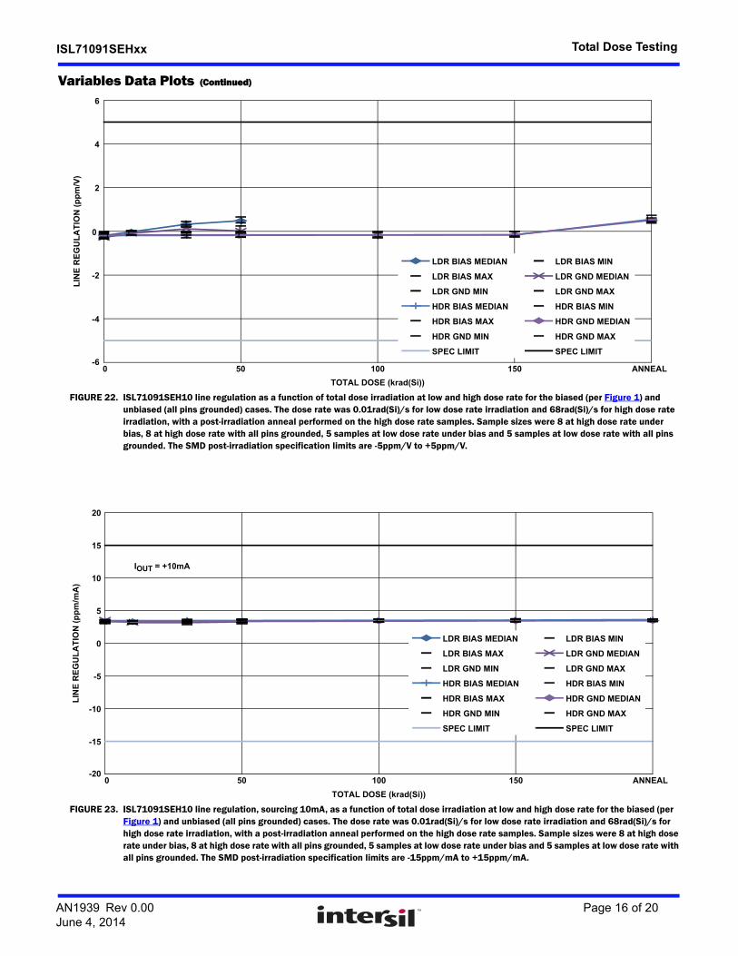
FIGURE 22. ISL71091SEH10 line regulation as a function of total dose irradiation at low and high dose rate for the biased (per Figure 1) and unbiased (all pins grounded) cases. The dose rate was 0.01rad(Si)/s for low dose rate irradiation and 68rad(Si)/s for high dose rate irradiation, with a post-irradiation anneal performed on the high dose rate samples. Sample sizes were 8 at high dose rate under bias, 8 at high dose rate with all pins grounded, 5 samples at low dose rate under bias and 5 samples at low dose rate with all pins grounded. The SMD post-irradiation specification limits are -5ppm/V to +5ppm/V.
FIGURE 23. ISL71091SEH10 line regulation, sourcing 10mA, as a function of total dose irradiation at low and high dose rate for the biased (per Figure 1) and unbiased (all pins grounded) cases. The dose rate was 0.01rad(Si)/s for low dose rate irradiation and 68rad(Si)/s for high dose rate irradiation, with a post-irradiation anneal performed on the high dose rate samples. Sample sizes were 8 at high dose rate under bias, 8 at high dose rate with all pins grounded, 5 samples at low dose rate under bias and 5 samples at low dose rate with all pins grounded. The SMD post-irradiation specification limits are -15ppm/mA to +15ppm/mA.
Variables Data Plots (Continued)
-6
-4
-2
0
2
4
6
0 50 100 150
LIN
E R
EG
UL
AT
ION
(p
pm
/V)
TOTAL DOSE (krad(Si))
ANNEAL
LDR BIAS MEDIAN LDR BIAS MIN
LDR BIAS MAX LDR GND MEDIAN
LDR GND MIN LDR GND MAX
HDR BIAS MEDIAN HDR BIAS MIN
HDR BIAS MAX HDR GND MEDIAN
HDR GND MIN HDR GND MAX
SPEC LIMIT SPEC LIMIT
-20
-15
-10
-5
0
5
10
15
20
0 50 100 150
LIN
E R
EG
UL
AT
ION
(p
pm
/mA
)
TOTAL DOSE (krad(Si))
IOUT = +10mA
ANNEAL
LDR BIAS MEDIAN LDR BIAS MIN
LDR BIAS MAX LDR GND MEDIAN
LDR GND MIN LDR GND MAX
HDR BIAS MEDIAN HDR BIAS MIN
HDR BIAS MAX HDR GND MEDIAN
HDR GND MIN HDR GND MAX
SPEC LIMIT SPEC LIMIT
AN1939 Rev 0.00 Page 16 of 20June 4, 2014

ISL71091SEHxx Total Dose Testing
FIGURE 24. ISL71091SEH10 load regulation, sinking 5mA, as a function of total dose irradiation at low and high dose rate for the biased (per Figure 1) and unbiased (all pins grounded) cases. The dose rate was 0.01rad(Si)/s for low dose rate irradiation and 68rad(Si)/s for high dose rate irradiation, with a post-irradiation anneal performed on the high dose rate samples. Sample sizes were 8 at high dose rate under bias, 8 at high dose rate with all pins grounded, 5 samples at low dose rate under bias and 5 samples at low dose rate with all pins grounded. The SMD post-irradiation specification limits are -40ppm/mA to +40ppm/mA.
FIGURE 25. ISL71091SEH10 dropout voltage as a function of total dose irradiation at low and high dose rate for the biased (per Figure 1) and unbiased (all pins grounded) cases. The dose rate was 0.01rad(Si)/s for low dose rate irradiation and 68rad(Si)/s for high dose rate irradiation, with a post-irradiation anneal performed on the high dose rate samples. Sample sizes were 8 at high dose rate under bias, 8 at high dose rate with all pins grounded, 5 samples at low dose rate under bias and 5 samples at low dose rate with all pins grounded. The SMD post-irradiation specification limit is 1.6V maximum.
Variables Data Plots (Continued)
-50
-40
-30
-20
-10
0
10
20
30
40
50
0 50 100 150
LO
AD
RE
GU
LA
TIO
N (
pp
m/m
A)
TOTAL DOSE (krad(Si))
IOUT = -5mA
ANNEAL
LDR BIAS MEDIAN LDR BIAS MIN
LDR BIAS MAX LDR GND MEDIAN
LDR GND MIN LDR GND MAX
HDR BIAS MEDIAN HDR BIAS MIN
HDR BIAS MAX HDR GND MEDIAN
HDR GND MIN HDR GND MAX
SPEC LIMIT SPEC LIMIT
0
0.2
0.4
0.6
0.8
1.0
1.2
1.4
1.6
1.8
0 50 100 150
DR
OP
OU
T V
OL
TA
GE
(V
)
TOTAL DOSE (krad(Si))
ANNEAL
LDR BIAS MEDIAN LDR BIAS MIN
LDR BIAS MAX LDR GND MEDIAN
LDR GND MIN LDR GND MAX
HDR BIAS MEDIAN HDR BIAS MIN
HDR BIAS MAX HDR GND MEDIAN
HDR GND MIN HDR GND MAX
SPEC LIMIT
AN1939 Rev 0.00 Page 17 of 20June 4, 2014

ISL71091SEHxx Total Dose Testing
Discussion and ConclusionThis document reports the results of low and high dose rate testing of four variants of the ISL71091SEHxx voltage reference. Samples were irradiated under bias and with all pins grounded at low and high dose rate in accordance with the MIL-STD-883 Test Method 1019.7 dose rate sensitivity protocol, at 0.01rad(Si)/s and 68rad(Si)/s respectively. The high dose rate irradiations for all four variants and the low dose rate irradiations for the 3.3V variant were followed by a biased anneal at +100°C for 168 hours; the remaining three low dose rate tests are still running and will be annealed upon completion.
The downpoints, sample sizes and attributes data for each test are given in Table 2. This is a simple part, at least functionally, and we have summarized the results in a table of attributes data (Table 2 on page 3) followed by curves of interest (Figures 2 through 25 starting on page 6). We will discuss each of the figures separately, grouped by parameter.
The output voltage is clearly the key parameter for a precision voltage reference. The 2.048V variant showed good stability (Figure 2) through 150krad(Si) at high dose rate, with some further shift over the post-irradiation anneal; the part remained well within the SMD limits. The low dose rate test is through 50krad(Si); the unbiased (grounded) samples showed the same response as the high dose rate samples. The biased low dose rate samples showed a more rapid decrease at that level while remaining well within the SMD limit.
The 3.3V variant is through 150krad(Si) and subsequent anneal for both dose rates. The high dose rate samples showed (Figure 8) good stability through 150krad(Si) at high dose rate, with very little shift over the post-irradiation anneal for both bias conditions. The unbiased (grounded) low dose rate samples showed similar stability over irradiation but then showed a pronounced anneal response, bringing the samples close to the SMD limit. The biased low dose rate samples showed a monotonic shift over irradiation; the parts were well within the SMD specification at 50krad(Si) but were near this limit at 100krad(Si) and outside it at 150krad(Si). The anneal response was moderate and shifted the output voltage slightly in the positive direction.
The 4.096V variant showed (Figure 14) good stability through 150krad(Si) at high dose rate for the biased and grounded configurations and at low dose rate for the grounded configuration, with a moderate anneal response for all three of these cases. The biased low dose rate samples showed a negative shift in the output voltage but remained well within the SMD limits.
The 10.0V variant showed (Figure 20) good stability through 150krad(Si) at high dose rate for both bias configurations, with some shift over the post-irradiation anneal; the part remained well within the SMD limits. The low dose rate test is through 50krad(Si); the biased samples showed a negative shift, while the unbiased samples showed a similar but considerably smaller shift.
The 3.3V variant is the only one for which we have full total dose and anneal data at the time of this writing for both the low and high dose rate groups. The response of the output voltage (Figure 8) to the 168-hour biased anneal at +100°C was
interesting. The high dose rate samples and the unbiased (grounded) low dose rate samples responded virtually identically to irradiation, but the unbiased low dose rate samples showed a significant anneal response in the direction (here negative) of further output voltage degradation. The biased low dose rate samples on the other hand showed a nearly linear degradation with dose followed by a slight recovery over the anneal operation. These annealing responses disagree with conventional total dose testing wisdom. First, post-irradiation annealing is assumed to have an effect in CMOS devices only, and the ISL71091SEHxx is an all-bipolar design. Also, anneals are assumed to lead to full or partial recovery of the affected parameter rather than further degradation. Finally, anneals following low dose rate irradiation have been assumed to be unnecessary as they will not produce any parametric change. The unconventional responses reported here have been observed in PR40 designs before, but a detailed understanding of the physics will likely require more testing, with anneals after intermediate downpoints; this drives up the sample size requirements drastically.
The remaining five monitored parameters showed very little change. Figures 3, 9, 15 and 21 show the total dose response of the power supply current for each of the variants. The parameter was very stable at all downpoints and showed no dose rate sensitivity, bias sensitivity or annealing response. The parameter remained well within the SMD post-irradiation limits at all downpoints.
Figures 4, 10, 16 and 22 show the total dose response of the line regulation for each of the variants. The parameter was very stable at all downpoints and showed no dose rate sensitivity, bias sensitivity or annealing response. The parameter remained well within the SMD post-irradiation limits at all downpoints.
Figures 5, 11, 17 and 23 show the total dose response of the load regulation, with the part sourcing 10mA, for each of the variants. The parameter was very stable; it remained well within the SMD post-irradiation limits at all downpoints and showed no dose rate sensitivity or bias sensitivity.
Figures 6, 12, 18 and 24 show the total dose response of the load regulation, in this case with the part sinking 5mA, for each of the variants. As in the 10mA sourcing load regulation case the parameter was very stable; it remained well within the SMD post-irradiation limits at all downpoints and showed no dose rate sensitivity or bias sensitivity.
Finally, Figures 7, 13, 19 and 25 show the total dose response of the dropout voltage. The parameter was very stable at all downpoints and showed no dose rate sensitivity, bias sensitivity or annealing response for any of the four variants. The parameter remained well within the SMD post-irradiation limits at all downpoints.
To summarize, all four variants of the ISL71091SEHxx showed good performance over low and high dose rate irradiation. All samples passed the post-irradiation after the specified levels of 100krad(Si) at high dose rate (50 to 300rad(Si)/s) and of 50krad(Si) at low dose rate (0.01rad(Si)/s). Rejects were encountered after biased low dose rate irradiation to 150krad(Si) of the 3.3V samples, which represents a 2x overtest with respect to the rated SMD value of 50krad(Si). The part is acceptance tested on a wafer-by-wafer basis to these levels, insuring hardness to the specified level at both dose rates.
AN1939 Rev 0.00 Page 18 of 20June 4, 2014

ISL71091SEHxx Total Dose Testing
The output voltage data showed a substantial difference between the high and low dose rate responses for all four variants, and the ISL71091SEHxx should be considered low dose rate sensitive. This change in the output voltage is believed to be caused by radiation-induced change in the bandgap voltage, which provides the basic reference for the part. The output voltage data also showed biased irradiation to be worst case, in all four cases, which represents a change from conventional radiation testing wisdom but has been seen before for this process. No measurable differences in the total dose response
were noted between biased and grounded irradiation for the other parameters.
The post-irradiation high temperature biased anneals produced some interesting responses; further testing will be required to assess the effects of anneals carried out after irradiation to the SMD level, rather than after substantial overtest levels as in this work. It should be noted that these anneals are not required for these all-bipolar parts and the results are presented for information only.
AppendicesTABLE 3. REPORTED PARAMETERS AND THEIR POST-IRRADIATION LIMITS
FIGURE PARAMETER VARIANT LIMIT, LOW LIMIT, HIGH UNITS NOTES
2 Output voltage 2.048V 2.042880 2.053120 V
3 Power supply current 2.048V 0.2 0.5 mA
4 Line regulation 2.048V -5.0 5.0 ppm/V
5 Load regulation, sourcing 2.048V -40.0 40.0 ppm/mA +10.0mA
6 Load regulation, sinking 2.048V -80.0 80.0 ppm/mA -5.0mA
7 Dropout voltage 2.048V - 2.5 V
8 Output voltage 3.3V 3.291750 3.308250 V
9 Power supply current 3.3V 0.2 0.5 mA
10 Line regulation 3.3V -5.0 5.0 ppm/V
11 Load regulation, sourcing 3.3V -25.0 25.0 ppm/mA +10.0mA
12 Load regulation, sinking 3.3V -60.0 60.0 ppm/mA -5.0mA
13 Dropout voltage 3.3V - 1.6 V
14 Output voltage 4.096V 4.085760 4.106240 V
15 Power supply current 4.096V 0.2 0.5 mA
16 Line regulation 4.096V -5.0 5.0 ppm/V
17 Load regulation, sourcing 4.096V -20.0 20.0 ppm/mA +10.0mA
18 Load regulation, sinking 4.096V -50.0 50.0 ppm/mA -5.0mA
19 Dropout voltage 4.096V - 1.6 V
20 Output voltage 10.0V 9.975000 10.025000 V
21 Power supply current 10.0V 0.2 0.5 mA
22 Line regulation 10.0V -5.0 5.0 ppm/V
23 Load regulation, sourcing 10.0V -15.0 15.0 ppm/mA +10.0mA
24 Load regulation, sinking 10.0V -40.0 40.0 ppm/mA -5.0mA
25 Dropout voltage 10.0V - 1.6 V
Revision HistoryThe revision history provided is for informational purposes only and is believed to be accurate, but not warranted. Please go to the web to make sure that you have the latest revision.
DATE REVISION CHANGE
June 4, 2014 AN1939.0 Initial release.
AN1939 Rev 0.00 Page 19 of 20June 4, 2014

http://www.renesas.comRefer to "http://www.renesas.com/" for the latest and detailed information.
Renesas Electronics America Inc.1001 Murphy Ranch Road, Milpitas, CA 95035, U.S.A.Tel: +1-408-432-8888, Fax: +1-408-434-5351Renesas Electronics Canada Limited9251 Yonge Street, Suite 8309 Richmond Hill, Ontario Canada L4C 9T3Tel: +1-905-237-2004Renesas Electronics Europe LimitedDukes Meadow, Millboard Road, Bourne End, Buckinghamshire, SL8 5FH, U.KTel: +44-1628-651-700, Fax: +44-1628-651-804Renesas Electronics Europe GmbHArcadiastrasse 10, 40472 Düsseldorf, Germany Tel: +49-211-6503-0, Fax: +49-211-6503-1327Renesas Electronics (China) Co., Ltd.Room 1709 Quantum Plaza, No.27 ZhichunLu, Haidian District, Beijing, 100191 P. R. ChinaTel: +86-10-8235-1155, Fax: +86-10-8235-7679Renesas Electronics (Shanghai) Co., Ltd.Unit 301, Tower A, Central Towers, 555 Langao Road, Putuo District, Shanghai, 200333 P. R. China Tel: +86-21-2226-0888, Fax: +86-21-2226-0999Renesas Electronics Hong Kong LimitedUnit 1601-1611, 16/F., Tower 2, Grand Century Place, 193 Prince Edward Road West, Mongkok, Kowloon, Hong KongTel: +852-2265-6688, Fax: +852 2886-9022Renesas Electronics Taiwan Co., Ltd.13F, No. 363, Fu Shing North Road, Taipei 10543, TaiwanTel: +886-2-8175-9600, Fax: +886 2-8175-9670Renesas Electronics Singapore Pte. Ltd.80 Bendemeer Road, Unit #06-02 Hyflux Innovation Centre, Singapore 339949Tel: +65-6213-0200, Fax: +65-6213-0300Renesas Electronics Malaysia Sdn.Bhd.Unit 1207, Block B, Menara Amcorp, Amcorp Trade Centre, No. 18, Jln Persiaran Barat, 46050 Petaling Jaya, Selangor Darul Ehsan, MalaysiaTel: +60-3-7955-9390, Fax: +60-3-7955-9510Renesas Electronics India Pvt. Ltd.No.777C, 100 Feet Road, HAL 2nd Stage, Indiranagar, Bangalore 560 038, IndiaTel: +91-80-67208700, Fax: +91-80-67208777Renesas Electronics Korea Co., Ltd.17F, KAMCO Yangjae Tower, 262, Gangnam-daero, Gangnam-gu, Seoul, 06265 KoreaTel: +82-2-558-3737, Fax: +82-2-558-5338
SALES OFFICES
© 2018 Renesas Electronics Corporation. All rights reserved.Colophon 7.0
(Rev.4.0-1 November 2017)
Notice
1. Descriptions of circuits, software and other related information in this document are provided only to illustrate the operation of semiconductor products and application examples. You are fully responsible for
the incorporation or any other use of the circuits, software, and information in the design of your product or system. Renesas Electronics disclaims any and all liability for any losses and damages incurred by
you or third parties arising from the use of these circuits, software, or information.
2. Renesas Electronics hereby expressly disclaims any warranties against and liability for infringement or any other claims involving patents, copyrights, or other intellectual property rights of third parties, by or
arising from the use of Renesas Electronics products or technical information described in this document, including but not limited to, the product data, drawings, charts, programs, algorithms, and application
examples.
3. No license, express, implied or otherwise, is granted hereby under any patents, copyrights or other intellectual property rights of Renesas Electronics or others.
4. You shall not alter, modify, copy, or reverse engineer any Renesas Electronics product, whether in whole or in part. Renesas Electronics disclaims any and all liability for any losses or damages incurred by
you or third parties arising from such alteration, modification, copying or reverse engineering.
5. Renesas Electronics products are classified according to the following two quality grades: “Standard” and “High Quality”. The intended applications for each Renesas Electronics product depends on the
product’s quality grade, as indicated below.
"Standard": Computers; office equipment; communications equipment; test and measurement equipment; audio and visual equipment; home electronic appliances; machine tools; personal electronic
equipment; industrial robots; etc.
"High Quality": Transportation equipment (automobiles, trains, ships, etc.); traffic control (traffic lights); large-scale communication equipment; key financial terminal systems; safety control equipment; etc.
Unless expressly designated as a high reliability product or a product for harsh environments in a Renesas Electronics data sheet or other Renesas Electronics document, Renesas Electronics products are
not intended or authorized for use in products or systems that may pose a direct threat to human life or bodily injury (artificial life support devices or systems; surgical implantations; etc.), or may cause
serious property damage (space system; undersea repeaters; nuclear power control systems; aircraft control systems; key plant systems; military equipment; etc.). Renesas Electronics disclaims any and all
liability for any damages or losses incurred by you or any third parties arising from the use of any Renesas Electronics product that is inconsistent with any Renesas Electronics data sheet, user’s manual or
other Renesas Electronics document.
6. When using Renesas Electronics products, refer to the latest product information (data sheets, user’s manuals, application notes, “General Notes for Handling and Using Semiconductor Devices” in the
reliability handbook, etc.), and ensure that usage conditions are within the ranges specified by Renesas Electronics with respect to maximum ratings, operating power supply voltage range, heat dissipation
characteristics, installation, etc. Renesas Electronics disclaims any and all liability for any malfunctions, failure or accident arising out of the use of Renesas Electronics products outside of such specified
ranges.
7. Although Renesas Electronics endeavors to improve the quality and reliability of Renesas Electronics products, semiconductor products have specific characteristics, such as the occurrence of failure at a
certain rate and malfunctions under certain use conditions. Unless designated as a high reliability product or a product for harsh environments in a Renesas Electronics data sheet or other Renesas
Electronics document, Renesas Electronics products are not subject to radiation resistance design. You are responsible for implementing safety measures to guard against the possibility of bodily injury, injury
or damage caused by fire, and/or danger to the public in the event of a failure or malfunction of Renesas Electronics products, such as safety design for hardware and software, including but not limited to
redundancy, fire control and malfunction prevention, appropriate treatment for aging degradation or any other appropriate measures. Because the evaluation of microcomputer software alone is very difficult
and impractical, you are responsible for evaluating the safety of the final products or systems manufactured by you.
8. Please contact a Renesas Electronics sales office for details as to environmental matters such as the environmental compatibility of each Renesas Electronics product. You are responsible for carefully and
sufficiently investigating applicable laws and regulations that regulate the inclusion or use of controlled substances, including without limitation, the EU RoHS Directive, and using Renesas Electronics
products in compliance with all these applicable laws and regulations. Renesas Electronics disclaims any and all liability for damages or losses occurring as a result of your noncompliance with applicable
laws and regulations.
9. Renesas Electronics products and technologies shall not be used for or incorporated into any products or systems whose manufacture, use, or sale is prohibited under any applicable domestic or foreign laws
or regulations. You shall comply with any applicable export control laws and regulations promulgated and administered by the governments of any countries asserting jurisdiction over the parties or
transactions.
10. It is the responsibility of the buyer or distributor of Renesas Electronics products, or any other party who distributes, disposes of, or otherwise sells or transfers the product to a third party, to notify such third
party in advance of the contents and conditions set forth in this document.
11. This document shall not be reprinted, reproduced or duplicated in any form, in whole or in part, without prior written consent of Renesas Electronics.
12. Please contact a Renesas Electronics sales office if you have any questions regarding the information contained in this document or Renesas Electronics products.
(Note 1) “Renesas Electronics” as used in this document means Renesas Electronics Corporation and also includes its directly or indirectly controlled subsidiaries.
(Note 2) “Renesas Electronics product(s)” means any product developed or manufactured by or for Renesas Electronics.