isl8280m r16ds0012eu0200 10a high efficiency …...feb 15, 2019 r16ds0012eu0200 rev.2.00 feb 15,...
TRANSCRIPT

R16DS0012EU0200 Rev.2.00 Page 1 of 51Feb 15, 2019
R16DS0012EU0200Rev.2.00
Feb 15, 2019
ISL8280M10A High Efficiency Hybrid Digital Step-Down Power Module
DATASHEET
The ISL8280M is a PMBus enabled DC/DC single channel step-down power supply featuring the proprietary Renesas R4™ Technology. The module supports a wide 4.5V to 16.5V input voltage range and a wide 0.5V to 5V output range capable of delivering up to 10A of continuous current. The ISL8280M achieves up to 95% conversion efficiency and is optimized for high power density. Integrated LDOs provide module bias voltage allowing for single supply operation. The ISL8280M includes a SMBus/PMBus/I2C interface for device configuration, telemetry (VIN, VOUT, IOUT, and temperature), and fault reporting.
The proprietary Renesas R4 control scheme has extremely fast transient performance, accurately regulated frequency control, and all internal compensation. An efficiency enhancing PFM mode greatly improves light-load efficiency. The ISL8280M’s serial bus allows for easy R4 loop optimization that results in fast transient performance across a wide range of applications including all ceramic output filters.
The ISL8280M has four 8-bit configuration pins that provide very flexible configuration options (such as frequency, VOUT, and AV gain) without the need for built-in NVM memory. As a result, the design flow closely matches traditional analog modules while still offering the design flexibility and feature set of a digital SMBus/PMBus/I2C interface. The ISL8280M features remote voltage sensing, completely eliminates any potential difference between remote and local ground, and improves regulation and protection accuracy. A precision enable input coordinates the startup of the ISL8280M with other voltage rails and is especially useful for power sequencing.
The ISL8280M integrates all power and most passive components to minimize the external components and significantly reduce design complexity and board space. The ISL8280M is available in a low-profile, thermally enhanced, compact 12mmx11mmx5.3mm fully encapsulated HDA package.
Applications• Servers, telecom, storage, and datacom
• Industrial/ATE and networking equipment
• Graphics cards
• General purpose power for ASIC, FPGA, DSP, and memory
Features• Proprietary Renesas R4 Technology
• Linear control loop for optimal transient response
• Variable frequency and duty cycle control during load transient for fastest possible response
• Inherent voltage feed-forward for wide range input
• Input voltage range: 4.5V to 16.5V
• Output voltage range: 0.5V to 5V
• ±1.5% load/line/temperature regulation with remote sense
• Supports all ceramic solutions
• Integrated LDOs for single input rail solution
• SMBus/PMBus/I2C compatible up to 1.25MHz
• 256 boot-up voltage levels with a configuration pin
• Seven switching frequency options from 300kHz to 1MHz
• PFM operation option for improved light-load efficiency
• Startup into precharged load
• Power-good monitor for soft-start and fault detection
• Comprehensive fault protection for high system reliability
• Over-temperature protection
• Output overcurrent and short-circuit protection
• Output overvoltage and undervoltage protection
• Open remote sense protection
• Input UVLO and power sequence, fault reset
• Compatible with Renesas PowerNavigator™ software
• Thermally enhanced 12mmx11mmx5.3mm HDA package
Related LiteratureFor a full list of related documents, visit our website:
• ISL8280M device page

R16DS0012EU0200 Rev.2.00 Page 2 of 51Feb 15, 2019
ISL8280M
Contents
1. Overview. . . . . . . . . . . . . . . . . . . . . . . . . . . . . . . . . . . . . . . . . . . . . . . . . . . . . . . . . . . . . . . . . . . . . 4
1.1 Typical Application Circuit . . . . . . . . . . . . . . . . . . . . . . . . . . . . . . . . . . . . . . . . . . . . . . . . . . . . . 4
1.2 Block Diagram . . . . . . . . . . . . . . . . . . . . . . . . . . . . . . . . . . . . . . . . . . . . . . . . . . . . . . . . . . . . . . 5
1.3 Ordering Information . . . . . . . . . . . . . . . . . . . . . . . . . . . . . . . . . . . . . . . . . . . . . . . . . . . . . . . . . 5
1.4 Pin Configuration . . . . . . . . . . . . . . . . . . . . . . . . . . . . . . . . . . . . . . . . . . . . . . . . . . . . . . . . . . . . 7
1.5 Functional Pin Descriptions . . . . . . . . . . . . . . . . . . . . . . . . . . . . . . . . . . . . . . . . . . . . . . . . . . . . 8
2. Specifications. . . . . . . . . . . . . . . . . . . . . . . . . . . . . . . . . . . . . . . . . . . . . . . . . . . . . . . . . . . . . . . . 11
2.1 Absolute Maximum Ratings . . . . . . . . . . . . . . . . . . . . . . . . . . . . . . . . . . . . . . . . . . . . . . . . . . . 11
2.2 Thermal Information. . . . . . . . . . . . . . . . . . . . . . . . . . . . . . . . . . . . . . . . . . . . . . . . . . . . . . . . . 11
2.3 Recommended Operating Conditions . . . . . . . . . . . . . . . . . . . . . . . . . . . . . . . . . . . . . . . . . . . 12
2.4 Electrical Specifications . . . . . . . . . . . . . . . . . . . . . . . . . . . . . . . . . . . . . . . . . . . . . . . . . . . . . . 12
3. Typical Performance Curves. . . . . . . . . . . . . . . . . . . . . . . . . . . . . . . . . . . . . . . . . . . . . . . . . . . . 16
3.1 Efficiency Performance . . . . . . . . . . . . . . . . . . . . . . . . . . . . . . . . . . . . . . . . . . . . . . . . . . . . . . 16
3.2 Output Voltage Ripple . . . . . . . . . . . . . . . . . . . . . . . . . . . . . . . . . . . . . . . . . . . . . . . . . . . . . . . 17
3.3 Load Transient Response Performance . . . . . . . . . . . . . . . . . . . . . . . . . . . . . . . . . . . . . . . . . 19
3.4 Startup and Shutdown . . . . . . . . . . . . . . . . . . . . . . . . . . . . . . . . . . . . . . . . . . . . . . . . . . . . . . . 20
3.5 Derating Curves. . . . . . . . . . . . . . . . . . . . . . . . . . . . . . . . . . . . . . . . . . . . . . . . . . . . . . . . . . . . 21
4. Functional Description . . . . . . . . . . . . . . . . . . . . . . . . . . . . . . . . . . . . . . . . . . . . . . . . . . . . . . . . 23
4.1 Configuring Internal Bias and LDO . . . . . . . . . . . . . . . . . . . . . . . . . . . . . . . . . . . . . . . . . . . . . 23
4.2 Enabling and Disabling the ISL8280M. . . . . . . . . . . . . . . . . . . . . . . . . . . . . . . . . . . . . . . . . . . 23
4.3 Programming the Resistor Reader . . . . . . . . . . . . . . . . . . . . . . . . . . . . . . . . . . . . . . . . . . . . . 24
4.4 Soft-Starting . . . . . . . . . . . . . . . . . . . . . . . . . . . . . . . . . . . . . . . . . . . . . . . . . . . . . . . . . . . . . . . 27
4.5 Boot-Up Voltage Programming . . . . . . . . . . . . . . . . . . . . . . . . . . . . . . . . . . . . . . . . . . . . . . . . 28
4.6 Thermal Monitoring and Compensation. . . . . . . . . . . . . . . . . . . . . . . . . . . . . . . . . . . . . . . . . . 35
4.7 Fault Protection . . . . . . . . . . . . . . . . . . . . . . . . . . . . . . . . . . . . . . . . . . . . . . . . . . . . . . . . . . . . 36
4.8 PGOOD Monitor . . . . . . . . . . . . . . . . . . . . . . . . . . . . . . . . . . . . . . . . . . . . . . . . . . . . . . . . . . . 38
4.9 PFM Mode Operation . . . . . . . . . . . . . . . . . . . . . . . . . . . . . . . . . . . . . . . . . . . . . . . . . . . . . . . 38
4.10 SMBus, PMBus, and I2C Operation. . . . . . . . . . . . . . . . . . . . . . . . . . . . . . . . . . . . . . . . . . . . . 38
5. Layout Guidelines . . . . . . . . . . . . . . . . . . . . . . . . . . . . . . . . . . . . . . . . . . . . . . . . . . . . . . . . . . . . 45
6. Thermal Considerations . . . . . . . . . . . . . . . . . . . . . . . . . . . . . . . . . . . . . . . . . . . . . . . . . . . . . . . 46
R16DS0012EU0200 Rev.2.00 Page 3 of 51Feb 15, 2019
ISL8280M
7. Package Description . . . . . . . . . . . . . . . . . . . . . . . . . . . . . . . . . . . . . . . . . . . . . . . . . . . . . . . . . . 47
7.1 PCB Layout Pattern Design. . . . . . . . . . . . . . . . . . . . . . . . . . . . . . . . . . . . . . . . . . . . . . . . . . . 47
7.2 Thermal Vias . . . . . . . . . . . . . . . . . . . . . . . . . . . . . . . . . . . . . . . . . . . . . . . . . . . . . . . . . . . . . . 47
7.3 Stencil Pattern Design . . . . . . . . . . . . . . . . . . . . . . . . . . . . . . . . . . . . . . . . . . . . . . . . . . . . . . . 47
7.4 Reflow Parameters . . . . . . . . . . . . . . . . . . . . . . . . . . . . . . . . . . . . . . . . . . . . . . . . . . . . . . . . . 48
8. Revision History. . . . . . . . . . . . . . . . . . . . . . . . . . . . . . . . . . . . . . . . . . . . . . . . . . . . . . . . . . . . . . 49
9. Package Outline Drawing . . . . . . . . . . . . . . . . . . . . . . . . . . . . . . . . . . . . . . . . . . . . . . . . . . . . . . 50

R16DS0012EU0200 Rev.2.00 Page 4 of 51Feb 15, 2019
ISL8280M 1. Overview
1. Overview
1.1 Typical Application Circuit
Figure 1. Wide Range Input and Output Application
Figure 2. Small Package for High Power Density
• For VOUT = 3.3V, minimum VIN is 5.5V; for VOUT = 5V, minimum VIN is 8V.
• R35: see Table 2 on page 9.
• R2 and R3: to program output voltage, see Table 4 on page 25 for typical VOUT.
• R10 and R11: to program PFM/PWM mode, temperature compensation, and PMBus address, see Table 5 on page 25 for
typical applications.
• R8 and R9: to program fSW, AV gain, OCP retry/latch off, and ultrasonic PFM enable, see Table 6 on page 26 for typical
applications.
• R5 and R6: to program soft-start ramp rate, RR impedance, and AV gain multiplier (1x or 2x), see Table 7 on page 27 for
typical applications.
• R14: IOUT pull-up resistor. See Table 2 on page 9.
12mm11mm
5.3mm

R16DS0012EU0200 Rev.2.00 Page 5 of 51Feb 15, 2019
ISL8280M 1. Overview
1.2 Block Diagram
1.3 Ordering Information
Part Number(Notes 2, 3) Part Marking Temp Range (°C)
Tape and Reel (Units) (Note 1) Package (RoHS Compliant) Pkg. Dwg. #
ISL8280MFRZ ISL8280M -40 to +125 - 83 Ld 12x11 HDA Module Y83.12x11
ISL8280MFRZ-T ISL8280M -40 to +125 720 83 Ld 12x11 HDA Module Y83.12x11
ISL8280MFRZ-T1 ISL8280M -40 to +125 100 83 Ld 12x11 HDA Module Y83.12x11
ISL8280MEVAL1Z Evaluation Board
Notes:1. See TB347 for details about reel specifications.2. These plastic packaged products are RoHS compliant by EU exemption 7C-I and employ special Pb-free material sets; molding
compounds/die attach materials and NiPdAu plate - e4 termination finish which is compatible with both SnPb and Pbfree soldering operations. RoHS compliant products are MSL classified at Pb-free peak reflow temperatures that meet or exceed the Pb-free requirements of IPC/JEDEC J STD-020.
3. For Moisture Sensitivity Level (MSL), see the ISL8280M device page. For more information about MSL, see TB363.

R16DS0012EU0200 Rev.2.00 Page 6 of 51Feb 15, 2019
ISL8280M 1. Overview
Table 1. Key Differences Between Family of Parts
Parameters ISL8280M ISL8282M ISL8212M ISL8210M
Load Current (A) 15 10 15 10
Minimum VIN (V) 4.5 4.5 4.5 4.5
Maximum VIN (V) 16.5 16.5 16.5 16.5
Minimum VOUT (min) (V) 0.5 0.5 0.5 0.5
Maximum VOUT (V) 5 5 5 5
Peak Efficiency (%) 95.2 95.2 95.2 95.2
POR Yes Yes Yes Yes
Minimum Switching Frequency (kHz)
255 255 255 255
Maximum Switching Frequency (kHz)
1130 1130 1130 1130
Control Type R4 R4 R4 R4
Sync Capability No No No No
Load Sharing No No No No
PMBus Yes Yes No No

R16DS0012EU0200 Rev.2.00 Page 7 of 51Feb 15, 2019
ISL8280M 1. Overview
1.4 Pin Configuration83 Ld 12x11 HDA
Top View
PROG1
PROG2
PROG3
PROG4
PGOOD
CSRTN
PGND2 PGND2 PGND2 PGND2
PGND2 PGND2 PGND2 PGND2
7VLDO
PGND1
PGND1
PGND1
PGND1
PGND1
PGND1
PGND1
PGND1
PGND1
PHASE
PHASE
PHASE
PHASE
PHASE
PHASE
PHASE
PHASE
PHASE
PHASE
PHASE
PHASE
PHASE
PHASE
SALERT

R16DS0012EU0200 Rev.2.00 Page 8 of 51Feb 15, 2019
ISL8280M 1. Overview
1.5 Functional Pin Descriptions
Pin Number Symbol Description
A5, A6, A7 NC No connection pads. The pads dissipate the inductor heat and provide good thermal performance. Do not connect to any other circuits.
A9, A10, A11, A12,B9, B10, B11, B12
PGND2 Power ground. The pads are connected to the source of the low-side MOSFET inside the module.
F7, F9,G7, G8, G9,H7, H8, H9,J7, J8, J9
VIN Power input. Connect the pads directly to an input rail in the range of 4.5V to 16.5V. Connect the input ceramic capacitors between VIN and PGND1 as close as possible to the module.
F10, G10,H10, J10,
K7, K8, K9, K10, K11,L7, L8, L9, L10, L11
PHASE Phase node connection. The pads are connected to the junction of the high-side MOSFET’s source, output filter inductor, low-side MOSFET’s drain, and return path for the UGATE high-side MOSFET driver.
F12,G11, G12,H11, H12,J11, J12,K12, L12
PGND1 Power ground. The pads are the sources of the lower MOSFET inside the module and should be connected to the (-) terminals of the external input capacitors and output capacitors.
K1, K2, K3, K4, K5,L1, L2, L3, L4, L5
VOUT Regulated power module output. Apply the output load between VOUT and PGND1.
A1 SCLK SMBus/PMBus/I2C synchronous clock signal input. A pull-up resistor is required for this application.
A2 VDD Logic bias supply. Connect the pin externally to the PVCC rail.
A3, A4 EN Precision enable input. Pulling EN above the rising threshold voltage initiates the soft-start sequence. Pulling EN below the failing threshold voltage suspends module operation.
B1 SALERT Output pin for transferring the active low signal driven asynchronously from the module to SMBus/PMBus. A pull-up resistor is required for this application.
C1 SDA I/O pin for transferring data signals between the SMBus/PMBus/I2C host and the module. A pull-up resistor is required for this application.
C4 7VLDO 7V LDO used to bias the current sensing amplifier.
C5 VIN1 Input voltage pin for the R4 loop (5V) and LDO (7V). Place a high quality low ESR ceramic capacitor (1.0μF, X7R) in close proximity to the pin.
C6 PVCC Output of the 5V LDO to bias internal control circuits and MOSFETs drivers of ISL8280M. Place a high quality low ESR ceramic capacitor (4.7μF, X7R) in close proximity to the pin.
C7 TP1 Test pad. Leave this pin open.
D1 RGND Monitors the negative rail of the module output. Connect to ground at the point of regulation.
E1 VSEN Monitors the positive rail of the module output. Connect to the point of regulation.
E2 PGOOD Open-drain indicator output. The PGOOD signal is asserted when the output voltage is within ±12.5% of the nominal set output voltage and is deasserted when the output voltage is outside of the stated range or the EN pin is pulled low.
E3, E4, E5,F3, F4, F5
SGND Signal ground pads. The small-signal ground is common to all control circuitry and all voltage levels are measured with respect to this pin. Tie SGND to a solid low noise GND plane.
F2 CSRTN Monitors the negative flow of output current for overcurrent protection and telemetry.
F11 TP2 Test pad. Leave this pin open.
G2 CSEN Monitors the positive flow of output current for overcurrent protection and telemetry.
G4 IOUT Output current monitor pin. An internal resistor sets the gain and an internal capacitor provides the averaging function; an external pull-up resistor to VDD is recommended to calibrate the no load offset.
G5 PROG3 Programming pin for ultrasonic PFM operation, fault behavior, switching frequency, and R4 (AV) control loop gain.

R16DS0012EU0200 Rev.2.00 Page 9 of 51Feb 15, 2019
ISL8280M 1. Overview
G6 PROG1 Programming pin for boot-up voltage.
H2 NTC Input pin for temperature measurement. An NTC thermistor and a decoupling capacitor inside the module are connected between this pin and SGND. Connect this pin through a resistor (1.54kΩ)to a VDD pad externally. The voltage at this pin is inversely proportional to the module temperature.
H5 PROG4 Programming pin for modulator (R4) RR impedance and output slew rate during soft-start (SS). This pin also sets the AV gain multiplier to 1x or 2x and determines the AV gain on PROG3.
H6 PROG2 Programming pin for PWM/PFM mode, temperature compensation, and serial bus (SMBus/PMBus/I2C) address.
Table 2. ISL8280M Design Guide Matrix of Typical Applications
VOUT (V) VIN (V)Frequency
(kHz) AV Gain RR (Ω) TCOMP (°C) R14 (MΩ) R35 (Ω)
0.5 5 400 49 200k 5 1.2 0
10 2
12 2
15 3
0.6 5 400 49 200k 5 1.2 0
10 2
12 2
15 3
0.75 5 400 49 200k 5 1.2 0
10 3
12 3
15 open
0.9 5 400 49 200k 5 1.2 0
10 3
12 open
15 open
1 5 400 49 200k 5 1.2 0
10 3
12 open
15 open
1.2 5 400 26 200k 5 1.2 0
10 3
12 open
15 open
1.5 5 500 26 200k 5 1.2 0
10 3
12 open
15 open
1.8 5 500 26 200k 5 1.2 0
10 3
12 open
15 open
Pin Number Symbol Description

R16DS0012EU0200 Rev.2.00 Page 10 of 51Feb 15, 2019
ISL8280M 1. Overview
2.5 5 600 26 200k 5 1.2 0
10 3
12 open
15 open
3.3 5.5 700 26 200k 5 1.2 0
10 3
12 open
15 open 121 (Note 4)
5 8 850 26 200k 5 0.909 0
10 1.2
12 4.02 121 (Note 4)
15 open
Note:4. A 121Ω resistor is needed only when OCP behavior is set to Retry. When a 121Ω resistor is connected between VIN and VIN1, the
READ_VIN command in PowerNavigator reads back the VIN1 voltage.
Table 2. ISL8280M Design Guide Matrix of Typical Applications (Continued)
VOUT (V) VIN (V)Frequency
(kHz) AV Gain RR (Ω) TCOMP (°C) R14 (MΩ) R35 (Ω)

R16DS0012EU0200 Rev.2.00 Page 11 of 51Feb 15, 2019
ISL8280M 2. Specifications
2. Specifications
2.1 Absolute Maximum Ratings
2.2 Thermal Information
Parameter Minimum Maximum Unit
VDD, PVCC, VSEN -0.3 +7 V
Module Input Voltage, VIN -0.3 +20 V
Module Input Voltage, VIN1 -0.3 +20 V
7VLDO -0.3 +7.75 V
Output Voltage, VOUT -0.3 +5.5 V
BOOT Voltage (VBOOT-GND) -0.3 +30 V
BOOT to PHASE Voltage (VBOOT-PHASE) (DC) -0.3 +7 V
BOOT to PHASE Voltage (VBOOT-PHASE) (<10ns) -0.3 +9 V
PHASE Voltage -0.3 +25 V
PHASE Voltage (<20ns Pulse Width, 10µJ) -9 +25 V
All Other Pins -0.3 to GND VDD + 0.3 V
ESD Rating Value Unit
Machine Model (Tested per JESD22-A115C) 200 V
Charged Device Model (Tested per JS-002-2014) 750 V
Human Body Model (Tested per JS-001-2017) 2 kV
Latch-Up (Tested per JESD78E; Class 2, Level A) 100 at +125°C mA
CAUTION: Do not operate at or near the maximum ratings listed for extended periods of time. Exposure to such conditions can adversely impact product reliability and result in failures not covered by warranty.
Thermal Resistance (Typical) JA (°C/W) JC (°C/W)
83 Ld HDA Module (Notes 5, 6) 16.8 5.6
Notes:5. JA is measured in free air with the module mounted on a 6-layer thermal test board 3 x 3.4 inches in size with significant coverage
of 2oz Cu on all layers, with numerous vias.6. For JC, the “case temp” location is the center of the package underside.
Parameter Minimum Maximum Unit
Junction Temperature Range -55 +150 °C
Storage Temperature Range -65 +150 °C
Pb-Free Reflow Profile See Figure 52 on page 48

R16DS0012EU0200 Rev.2.00 Page 12 of 51Feb 15, 2019
ISL8280M 2. Specifications
2.3 Recommended Operating Conditions
2.4 Electrical Specifications
Parameter Minimum Maximum Unit
Junction Temperature Range -40 +125 °C
Wide Range Input Voltage, VIN, Figure 1 4.5 16.5 V
Output Voltage, VOUT, Figure 1 0.5 5 V
Output Current, IOUT, Figure 1 0 10 A
All typical specifications TA = +25°C, VIN = 12V, VIN1 = 12V, VOUT = 1V. Boldface limits apply across the junction temperature range, -40°C to +125°C (Note 7), unless otherwise stated.
Parameter Symbol Test ConditionsMin
(Note 8) TypMax
(Note 8) Unit
VIN and VIN1 Supply
Input Voltage Range VIN 4.5 16.5 V
VIN1 4.5 16.5 V
Input Voltage Read Back Resolution VIN_READ_RES (Note 4) 62.5 mV
VIN Supply Current
Input Supply Current in PFM mode Operation
IS(PFM) PFM mode, VIN = 12V, VOUT = 1V, IOUT = 0A
0.2 mA
Input Supply Current in PWM mode Operation
IS(PWM) PWM mode, VIN = 12V, VOUT = 1V, IOUT = 0A
35 mA
Input Supply Current in PWM mode Operation
IS(PWM) PWM mode, VIN = 12V, VOUT = 1V, IOUT = 10A
0.98 A
Input Supply Current in Shutdown IS(SHUTDOWN) Shutdown 0.05 µA
VIN1 Supply Current
Shutdown Current IVIN1Q EN = 0, PGOOD is floating, VIN1 = 12V
14.5 17 mA
Operating Current IVIN1OP PGOOD is floating, VIN1 = 12V 19 25 mA
VDD and VIN POR Threshold
VDD, PVCC Rising POR Threshold Voltage
4.2 4.35 V
VDD, PVCC Falling POR Threshold Voltage
3.8 3.95 4.15 V
VIN, 7VLDO Rising POR Threshold Voltage
4.2 4.35 V
VIN, 7VLDO Falling POR Threshold Voltage
3.8 3.95 4.15 V
Output Regulation
Output Continuous Current Range IOUT (Note 9) 0 10 A
Output Current Read Back Resolution
IOUT_READ_RES 0.125 A
Output Current Read Back Total Error IOUT_READ_ERR READ_IOUT, VIN from 4.5V to 16.5V, VOUT from 0.5V to 5V (Note 10)
±0.875 A
Output Voltage Range VOUT_RANGE 0.5 5 V
Output Voltage Read Back Resolution
VOUT_READ_RES (Note 11) 7.8125 mV

R16DS0012EU0200 Rev.2.00 Page 13 of 51Feb 15, 2019
ISL8280M 2. Specifications
Output Voltage Set-Point Accuracy 0.5V ≤ VOUT ≤ 0.75V, total variation with line, load, and temperature (-40°C ≤ TJ ≤ +125°C)
-12.5 +12.5 mV
0.75V ≤ VOUT ≤ 0.9V, total variation with line, load, and temperature (-40°C ≤ TJ ≤ +125°C)
-15 +15 mV
0.9V ≤ VOUT ≤ 5V, total variation with line, load, and temperature (-40°C ≤ TJ ≤ +125°C)
-1.5 +1.5 %
Line Regulation ∆VOUT/VOUT_SET
VOUT = 1V, VIN from 4.5V to 16.5V, IL = 0A
-1.2 +1.2 %
VOUT = 1.8V, VIN from 4.5V to 16.5V, IL = 0A
-1.2 +1.2 %
Load Regulation ∆VOUT/VOUT_SET
From 0A to 10A, VIN = 5V/12V, VOUT = 1V
-1.2 +1.2 %
From 0A to 10A, VIN = 5V/12V, VOUT = 1.8V
-1.2 +1.2
Output Ripple Voltage VOUT(AC) VIN = 12V, VOUT = 1V, IOUT = 10A, 4x220µF ceramic capacitor
8 mVP-P
Dynamic Characteristics
Voltage Change of Positive Load Step
VOUT_DP Current slew rate = 2.5A/µs, VIN = 12V, 4x220µF ceramic capacitorVOUT = 1V, IOUT from 0A to 5A
10 mV
Voltage Change of Negative Load Step
VOUT_DN Current slew rate = 2.5A/µs, VIN = 12V, 4x220µF ceramic capacitorVOUT = 1V, IOUT from 5A to 0A
10 mV
Enable Input
EN High Threshold Voltage VENTHR 0.81 0.84 0.87 V
EN Low Threshold Voltage VENTHF 0.71 0.76 0.81 V
Channel Frequency
300kHz Configuration PWM mode 255 300 340 kHz
400kHz Configuration 340 400 455 kHz
500kHz Configuration 425 500 565 kHz
600kHz Configuration 510 600 680 kHz
700kHz Configuration 600 700 790 kHz
850kHz Configuration 720 850 960 kHz
1000kHz Configuration 855 1000 1130 kHz
All typical specifications TA = +25°C, VIN = 12V, VIN1 = 12V, VOUT = 1V. Boldface limits apply across the junction temperature range, -40°C to +125°C (Note 7), unless otherwise stated. (Continued)
Parameter Symbol Test ConditionsMin
(Note 8) TypMax
(Note 8) Unit

R16DS0012EU0200 Rev.2.00 Page 14 of 51Feb 15, 2019
ISL8280M 2. Specifications
Soft-Start
Soft-Start Slew Rate 0.125 0.157 0.18 mV/µs
0.25 0.315 0.37 mV/µs
0.52 0.625 0.7 mV/µs
1 1.25 1.4 mV/µs
2 2.5 2.8 mV/µs
4.1 5 5.6 mV/µs
8.4 10 10.9 mV/µs
Soft-Start Delay from Enable High Excluding 5.5ms POR timeout. See Figures 47 and 48 on page 39
140 200 260 µs
Remote Sense
Bias Current of VSEN and RGND Pins
250 µA
Maximum Differential Input Voltage 5.8 V
Power-Good
PGOOD Pull-Down Impedance RPG PGOOD = 5mA sink 10 50 Ω
PGOOD Leakage Current IPG PGOOD = 5V 1 µA
LDOs
5V LDO Regulation VIN = 12V, load = 50mA 4.8 5 5.15 V
5V LDO Regulation VIN = 4.75V, load = 50mA 4.15 V
5V LDO Maximum Current Capability 100 mA
7V LDO Regulation 250uA load 7.15 7.4 7.5
7V Dropout VIN = 4.75V, 250µA load 4.3 V
7V LDO Current Capability Not recommended for external use 2 mA
Current Sense
OCP IOCP VIN = 12V, VOUT = 1V 10 14.3 A
Maximum Common-Mode Input Voltage
7VLDO = 7.4V 5.7 V
VDD = PVCC = 7VLDO = 4.5V 2.8 V
Fault Protection
UVP Threshold Voltage 0.5V ≤ VOUT ≤ 0.7V 67 74 88 %VOUT
0.7V ≤ VOUT < 1V 68 74 85 %VOUT
1V ≤ VOUT < 1.5V 68 74 82 %VOUT
1.5V ≤ VOUT ≤ 5V 68 74 80 %VOUT
Startup OVP Threshold Voltage 0V ≤ VOUT ≤ 1.08V 1.1 1.15 1.25 V
1.08V < VOUT ≤ 1.55V 1.58 1.65 1.75 V
1.55V < VOUT ≤ 1.85V 1.88 1.95 2.05 V
1.85V < VOUT ≤ 2.08V 2.09 2.15 2.25 V
2.08V < VOUT ≤ 2.53V 2.56 2.65 2.75 V
2.53V < VOUT ≤ 3.33V 3.36 3.45 3.6 V
3.33V < VOUT≤ 5V 5.52 5.65 5.85 V
All typical specifications TA = +25°C, VIN = 12V, VIN1 = 12V, VOUT = 1V. Boldface limits apply across the junction temperature range, -40°C to +125°C (Note 7), unless otherwise stated. (Continued)
Parameter Symbol Test ConditionsMin
(Note 8) TypMax
(Note 8) Unit

R16DS0012EU0200 Rev.2.00 Page 15 of 51Feb 15, 2019
ISL8280M 2. Specifications
Startup OVP Hysteresis 100 mV
OVP Rising Threshold Voltage VOVRTH 0.5V ≤ VOUT ≤ 0.7V 111 120 136 % VOUT
0.7V ≤ VOUT < 1V 113 120 132 %VOUT
1V ≤ VOUT < 1.5V 114 120 128 %VOUT
1.5V ≤ VOUT ≤ 5V 114 120 127 %VOUT
OVP Falling Threshold Voltage VOVFTH 0.5V ≤ VOUT ≤ 0.7V 93 100 115 % VOUT
0.7V ≤ VOUT < 1V 95 100 111 %VOUT
1V ≤ VOUT < 1.5V 96 100 109 %VOUT
1.5V ≤ VOUT ≤ 5V 96 100 108 %VOUT
Over-Temperature Shutdown Threshold
22.31%VDD (~+136°C) 20 22.31 26 % VDD
Over-Temperature Shutdown Reset Threshold
27.79%VDD (~+122°C) 25 27.79 30 % VDD
SMBus/PMBus/I2C (Note 12)
Signal Input Low Voltage 1 V
Signal Input High Voltage 1.6 V
Signal Output Low Voltage 4mA pull-up current 0.4 V
DATE, ALERT # Pull-Down Impedance
11 50 Ω
CLOCK Maximum Speed 1.25 MHz
CLOCK Minimum Speed 0.05 MHz
Telemetry Update Rate 108 µs
Timeout 25 30 35 ms
PMBus Accessible Timeout from All Rails’ POR
See Figure 47 on page 39 5.5 6.5 ms
Notes:7. The ISL8280M is tested under pulsed-load conditions such that TJ ≈ TA.8. Compliance to datasheet limits is assured by one or more methods: production test, characterization, and/or design.9. See output current derating curves for different VOUT and TA located “Derating Curves” on page 21.
10. See Table 2 on page 9.11. When 0.5V ≤ VOUT ≤ 1.8V, the output voltage read back resolution is 7.8125mV. When VOUT > 1.8V, the resolution can be higher
than that from adjacent codes. However, the resolution is always 7.8125mV around typical VOUT, as in Table 8 on page 28.12. Limits apply across the junction temperature range of -40°C to +85°C.
All typical specifications TA = +25°C, VIN = 12V, VIN1 = 12V, VOUT = 1V. Boldface limits apply across the junction temperature range, -40°C to +125°C (Note 7), unless otherwise stated. (Continued)
Parameter Symbol Test ConditionsMin
(Note 8) TypMax
(Note 8) Unit

R16DS0012EU0200 Rev.2.00 Page 16 of 51Feb 15, 2019
ISL8280M 3. Typical Performance Curves
3. Typical Performance Curves
3.1 Efficiency PerformanceOperating conditions: TA=25°C, no air flow, PWM mode. Typical values are used unless otherwise noted. The efficiency curves were measured on the evaluation board. For the test conditions, see Table 2 on page 9.
Figure 3. Efficiency vs Load Current at 5VIN (PWM) Figure 4. Efficiency vs Load Current at 8VIN (PWM)
Figure 5. Efficiency vs Load Current at 12VIN (PWM) Figure 6. Efficiency vs Load Current at 12VIN (PFM)
70
75
80
85
90
95
1 2 3 4 5 6 7 8 9 10
Effic
ienc
y (%
)
Load Current (A)
0.5VOUT, 400kHz 0.6VOUT, 400kHz0.75VOUT, 400kHz 0.9VOUT, 400kHz1VOUT, 400kHz 1.2VOUT, 400kHz1.5VOUT, 500kHz 1.8VOUT, 500kHz2.5VOUT, 600kHz
65
70
75
80
85
90
95
100
1 2 3 4 5 6 7 8 9 10Ef
ficie
ncy
(%)
Load Current (A)
0.5VOUT, 400kHz 0.6VOUT, 400kHz0.75VOUT, 400kHz 0.9VOUT, 400kHz1VOUT, 400kHz 1.2VOUT, 400kHz1.5VOUT, 500kHz 1.8VOUT, 500kHz2.5VOUT, 600kHz 3.3VOUT, 700kHz5VOUT, 850kHz
55
60
65
70
75
80
85
90
95
1 2 3 4 5 6 7 8 9 10
Effic
ienc
y (%
)
Load Current (A)
0.5VOUT, 400kHz 0.6VOUT, 400kHz0.75VOUT, 400kHz 0.9VOUT, 400kHz1VOUT, 400kHz 1.2VOUT, 400kHz1.5VOUT, 500kHz 1.8VOUT, 500kHz2.5VOUT, 600kHz 3.3VOUT, 700kHz5VOUT, 850kHz
40
50
60
70
80
90
0 1 2 3 4 5 6 7 8 9 10
Effic
ienc
y (%
)
Load Current (A)
0.5VOUT, 400kHz 0.6VOUT, 400kHz0.75VOUT, 400kHz 0.9VOUT, 400kHz1VOUT, 400kHz 1.2VOUT, 400kHz1.5VOUT, 500kHz 1.8VOUT, 500kHz2.5VOUT, 600kHz 3.3VOUT, 700kHz5VOUT, 850kHz

R16DS0012EU0200 Rev.2.00 Page 17 of 51Feb 15, 2019
ISL8280M 3. Typical Performance Curves
3.2 Output Voltage RippleOperating conditions: TA = +25°C, no air flow, PWM mode, COUT = 4 x 220µF Ceramic, RR = 200kΩ. Typical values are used unless otherwise noted. For the test conditions, see Table 2 on page 9.
Figure 7. Output Ripple at 5VIN and 0.75VOUT Figure 8. Output Ripple at 5VIN and 1VOUT
Figure 9. Output Ripple at 5VIN and 1.2VOUT Figure 10. Output Ripple at 5VIN and 1.8VOUT
Figure 11. Output Ripple at 12VIN and 0.75VOUT Figure 12. Output Ripple at 12VIN and 1VOUT
IOUT = 0A VOUT = 10mV/Div
VOUT = 10mV/DivIOUT = 10A
2µs/Div
AV Gain = 49
IOUT = 0A VOUT = 10mV/Div
VOUT = 10mV/DivIOUT = 10A
2µs/Div
AV Gain = 49
2µs/Div
IOUT = 0A VOUT = 10mV/Div
VOUT = 10mV/DivIOUT = 10A
AV Gain = 26
IOUT = 0A VOUT = 10mV/Div
VOUT = 10mV/DivIOUT = 10A
2µs/Div
AV Gain = 26
IOUT = 0A VOUT = 20mV/Div
VOUT = 20mV/DivIOUT = 10A
2µs/Div
AV Gain = 49
IOUT = 0A VOUT = 20mV/Div
VOUT = 20mV/DivIOUT = 10A
2µs/Div
AV Gain = 49

R16DS0012EU0200 Rev.2.00 Page 18 of 51Feb 15, 2019
ISL8280M 3. Typical Performance Curves
Figure 13. Output Ripple at 12VIN and 1.2VOUT Figure 14. Output Ripple at 12VIN and 1.5VOUT
Figure 15. Output Ripple at 12VIN and 1.8VOUT Figure 16. Output Ripple at 12VIN and 2.5VOUT
Figure 17. Output Ripple at 12VIN and 3.3VOUT Figure 18. Output Ripple at 12VIN and 5VOUT
Operating conditions: TA = +25°C, no air flow, PWM mode, COUT = 4 x 220µF Ceramic, RR = 200kΩ. Typical values are used unless otherwise noted. For the test conditions, see Table 2 on page 9. (Continued)
IOUT = 0A VOUT = 20mV/Div
VOUT = 20mV/DivIOUT = 10A
2µs/Div
AV Gain = 26
IOUT = 0A VOUT = 20mV/Div
VOUT = 20mV/DivIOUT = 10A
2µs/Div
AV Gain = 26
IOUT = 0A VOUT = 20mV/Div
VOUT = 20mV/DivIOUT = 10A
2µs/Div
AV Gain = 26
IOUT = 0A VOUT = 20mV/Div
VOUT = 20mV/DivIOUT = 10A
2µs/Div
AV Gain = 26
IOUT = 0A VOUT = 20mV/Div
VOUT = 20mV/DivIOUT = 10A
1µs/Div
AV Gain = 26
IOUT = 0A VOUT = 20mV/Div
VOUT = 20mV/DivIOUT = 10A
1µs/Div
AV Gain = 26

R16DS0012EU0200 Rev.2.00 Page 19 of 51Feb 15, 2019
ISL8280M 3. Typical Performance Curves
3.3 Load Transient Response PerformanceOperating conditions: TA = +25°C, no air flow, VIN = 12V, PWM mode, COUT = 4 x 220µF Ceramic, 0A to 5A step load at 5A/µs slew rate, RR = 200kΩ. Typical values are used unless otherwise noted. For the test conditions, see Table 2 on page 9.
Figure 19. Load Transient Response at 0.75VOUT Figure 20. Load Transient Response at 1VOUT
Figure 21. Load Transient Response at 1.8VOUT Figure 22. Load Transient Response at 2.5VOUT
Figure 23. Load Transient Response at 3.3VOUT Figure 24. Load Transient Response at 5VOUT
VOUT = 20mV/Div
IOUT = 5A/Div
100µs/Div
AV Gain = 49
100µs/Div
VOUT = 20mV/Div
IOUT = 5A/Div
AV Gain = 49
VOUT = 20mV/Div
IOUT = 5A/Div
100µs/Div
AV Gain = 26
VOUT = 20mV/Div
IOUT = 5A/Div
100µs/Div
AV Gain = 26
VOUT = 20mV/Div
IOUT = 5A/Div
100µs/Div
AV Gain = 26
VOUT = 20mV/Div
IOUT = 5A/Div
100µs/Div
AV Gain = 26

R16DS0012EU0200 Rev.2.00 Page 20 of 51Feb 15, 2019
ISL8280M 3. Typical Performance Curves
3.4 Startup and ShutdownOperating conditions: TA = +25°C, no air flow, VIN = 12V, VOUT = 1V, PWM mode. Typical values are used unless otherwise noted. For the test conditions, see Table 2 on page 9.
Figure 25. Startup Waveform at IOUT = 0A Figure 26. Startup Waveform at IOUT = 10A
Figure 27. Shutdown Waveform at IOUT = 0A Figure 28. Shutdown Waveform at IOUT = 10A
Figure 29. OCP Response; Output Short-Circuited from No Load to Ground and Released at IOUT = 0A
Figure 30. OCP Response; Output Short-Circuited from No Load to Ground and Released at IOUT = 10A
2ms/Div
EN = 2V/Div
PGOOD = 2V/Div
VOUT = 0.5V/Div
2ms/Div
EN = 2V/Div
PGOOD = 5V/Div
VOUT = 0.5V/Div
IOUT = 10A/Div
EN = 2V/Div
PGOOD = 2V/Div
VOUT = 0.5V/Div
2ms/Div
EN = 2V/Div
PGOOD = 5V/Div
IOUT = 10A/Div
VOUT = 0.5V/Div
100µs/Div
VOUT = 1V/Div
PGOOD = 5V/Div
IOUT = 10A/Div
10ms/Div
VOUT = 1V/Div
PGOOD = 5V/Div
IOUT = 10A/Div
10ms/Div

R16DS0012EU0200 Rev.2.00 Page 21 of 51Feb 15, 2019
ISL8280M 3. Typical Performance Curves
3.5 Derating CurvesOperating conditions: VIN = 12V, PWM mode. All of the following curves were plotted at TJ = +125°C. The derating curves were measured on the evaluation board. For the test conditions, see Table 2 on page 9.
Figure 31. 0.6VOUT Figure 32. 0.8VOUT
Figure 33. 1VOUT Figure 34. 1.2VOUT
Figure 35. 1.8VOUT Figure 36. 2.5VOUT
0
2
4
6
8
10
12
25 35 45 55 65 75 85 95 105
Load
Cur
rent
(A)
Ambient Temperature (°C)
0LFM200LFM400LFM
0
2
4
6
8
10
12
25 35 45 55 65 75 85 95 105
Load
Cur
rent
(A)
Ambient Temperature (°C)
0LFM
200LFM
400LFM
0
2
4
6
8
10
12
25 35 45 55 65 75 85 95 105
Load
Cur
rent
(A)
Ambient Temperature (°C)
0LFM
200LFM
400LFM0
2
4
6
8
10
12
25 35 45 55 65 75 85 95 105
Load
Cur
rent
(A)
Ambient Temperature (°C)
0LFM
200LFM
400LFM
0
2
4
6
8
10
12
25 35 45 55 65 75 85 95 105
Load
Cur
rent
(A)
Ambient Temperature (°C)
0LFM
200LFM
400LFM0
2
4
6
8
10
12
25 35 45 55 65 75 85 95 105
Load
Cur
rent
(A)
Ambient Temperature (°C)
0LFM
200LFM
400LFM

R16DS0012EU0200 Rev.2.00 Page 22 of 51Feb 15, 2019
ISL8280M 3. Typical Performance Curves
Figure 37. 3.3VOUT Figure 38. 5VOUT
Operating conditions: VIN = 12V, PWM mode. All of the following curves were plotted at TJ = +125°C. The derating curves were measured on the evaluation board. For the test conditions, see Table 2 on page 9. (Continued)
0
2
4
6
8
10
12
25 35 45 55 65 75 85 95 105
Load
Cur
rent
(A)
Ambient Temperature (°C)
0LFM
200LFM
400LFM
0
2
4
6
8
10
12
25 35 45 55 65 75 85 95 105
Load
Cur
rent
(A)
Ambient Temperature (°C)
0LFM
200LFM
400LFM

R16DS0012EU0200 Rev.2.00 Page 23 of 51Feb 15, 2019
ISL8280M 4. Functional Description
4. Functional DescriptionThe following sections describe the operation of the ISL8280M.
4.1 Configuring Internal Bias and LDOThe ISL8280M has four bias pins: VIN1, 7VLDO, PVCC, and VDD. The PVCC voltage rail is 5V LDO and supplied by VIN1. The 7VLDO voltage rail is 7V LDO supplied by VIN1. The VDD pin must connect to the PVCC rail externally to be biased.
4.2 Enabling and Disabling the ISL8280MThe module is enabled until the 7VLDO, PVCC, VDD, VIN1, and EN pins increase above their respective rising threshold voltages and the typical 5.5ms timeout (worst case = 6.5ms) expires, as shown in Figures 47 and 48 on page 39. The module is disabled when the 7VLDO, PVCC, VDD, VIN1, or EN pins drop below their respective falling POR threshold voltages.
The precision threshold EN pin allows you to set a precision input UVLO level with an external resistor divider as shown in Figure 39.
Figure 39. Input UVP Configuration
For 5V input applications or wide range input applications, the EN pin can directly connect to VDD as shown in Figure 40. If an external enable control signal is available and is an open-drain signal, use a 100k or higher pull-up impedance to connect the pull-up resistor to VDD.
I
Figure 40. 5V Input or Wide Range Input Configuration
The module can be enabled or disabled by the serial bus command “OPERATION [01h]” based on the ON_OFF_CONFIG [02h] setting and/or the EN pin. See Table 12 on page 42 for more details.
External CircuitISL8280M
100k
9.09k
VIN
EN
VIN UVLO = 10.08V/9.12V
Soft-Start
External CircuitISL8280M VDD
Soft-Start EN
REN is needed only when controlling the
REN
module with an external enable signal
Optional
VIN UVLO = 4.20/3.95V

R16DS0012EU0200 Rev.2.00 Page 24 of 51Feb 15, 2019
ISL8280M 4. Functional Description
4.3 Programming the Resistor ReaderThis section contains information about operating the resistors reader with the ISL8280M’s four programming pins (PROG1, PROG2, PROG3, and PROG4) to customize module specifications. Table 3 contains information about the pins and resistor reader operation.
Renesas has developed a high resolution ADC using a patented technique with a simple 1%, 100ppm/K or better temperature coefficient resistor divider. Renesas recommends using the same type of resistor in the design so the ADC has similar change over temperature. The divider is compared to the internal divider off the VDD and SGND nodes; therefore, the divider must refer to the VDD and SGND pins and not through any RC decoupling network as shown in Figure 41.
Figure 41. Simplified Resistor Divider ADC
Tables 4 through 7 show the RUP and RDW values of each pin for a specific system design with some tie-high and tie-low options that enable easy programming with reduced resistors. You can use the tie-high and tie-low options to validate the module operation during In-Circuit Test (ICT) for 0V boot-up voltage. Additional options are described in the ISL8280MEVAL1Z User’s Manual and PowerNavigator. Data for corresponding registers can be read out through the serial bus commands (DC[7:0] to DF[7:0]). The AV gain multiplier (AVMLTI) in PROG4 of Table 3 can be set by external RUP and RDW only. Note: the 10kΩ tie-high or tie-low is equivalent to the 0Ω tie-high or tie-low.
Table 3. Programming Pin Descriptions
Pin Bit Name Description
PROG1 [7:0] BOOT-UP VOLTAGE Sets the 256 output boot-up voltage options: 0V, 0.5V to 5V (see Table 8)
PROG2 [7:7] PWM/PFM Enables PFM mode or forced PWM
[6:5] Temperature Compensation Adjusts NTC temperature compensation: OFF, +5°C, +15°C, +30°C
[4:0] ADDR Sets the 32 serial bus addresses (see Table 11)
PROG3 [7:7] uSPFM Ultrasonic (25kHz clamp) PFM enable
[6:6] Fault Behavior OCP fault behavior: Latch, infinite 9ms retry
[5:3] FSW Sets the switching frequency (fSW)
[2:0] AV Gain Sets the error amplifier gain (AV)
PROG4 [7:5] RAMP_RATE Sets the soft-start ramp rate
[4:3] R4 RR Selects the RR impedance for R4 loop
[2:2] AVMLTI Selects the AV gain multiplier (1x or 2x)
[1:0] Not Used Not used
External CircuitISL8280M
RUP
RDW
VDD
ADC
RegisterTable
PROGx

R16DS0012EU0200 Rev.2.00 Page 25 of 51Feb 15, 2019
ISL8280M 4. Functional Description
Table 4. PROG 1 Resistor Reader Example
PROG1 (DC) RUP (kΩ) RDW (kΩ) VOUT(V)
01h 49.9 12.4 0.500
0Dh 23.2 17.8 0.594
0Eh 22.1 18.2 0.602
22h 97.6 27.4 0.742
23h 90.9 28.7 0.750
24h 82.5 28.7 0.758
40h Open 34.8 0.898
37h 34 57.6 0.906
44h 133 46.4 0.992
80h Open 75 1.000
46h 118 49.9 1.008
5Eh 45.3 150 1.195
E0h Open 499 1.203
88h 221 113 1.492
3Fh 21.5 Open 1.500
8Ah 200 121 1.508
5Fh 34.8 Open 1.797
B2h 196 226 1.805
C4h 576 200 2.492
7Fh 52.3 Open 2.500
C6h 499 210 2.508
BFh 105 Open 3.297
D5h 249 357 3.305
F2h 374 422 4.992
DFh 147 Open 5.000
F4h 348 464 5.008
FFh 499 Open 0.000
Table 5. PROG 2 Resistor Reader Example
PROG2 (DD) RUP (kΩ) RDW (kΩ) PFM Temp Comp (°C) PM_ADDR(7-Bit)
00h Open 10 Enabled +30 60
20h Open 21.5 Enabled +15 60
40h Open 34.8 Enabled +5 60
60h Open 52.3 Enabled OFF 60
80h Open 75 Disabled +30 60
A0h Open 105 Disabled +15 60
C0h Open 147 Disabled +5 60
E0h Open 499 Disabled OFF 60
1Fh 10 Open Enabled +30 7F
3Fh 21.5 Open Enabled +15 7F

R16DS0012EU0200 Rev.2.00 Page 26 of 51Feb 15, 2019
ISL8280M 4. Functional Description
5Fh 34.8 Open Enabled +5 7F
7Fh 52.3 Open Enabled OFF 7F
9Fh 75 Open Disabled +30 7F
BFh 105 Open Disabled +15 7F
DFh 147 Open Disabled +5 7F
FFh 499 Open Disabled OFF 7F
Table 6. PROG 3 Resistor Reader Example
PROG3 (DE) RUP (kΩ) RDW (kΩ) Ultrasonic PFM Fault Behavior fSW (kHz)
AV Gain
1x 2x
0Bh 25.5 16.5 Disabled Retry 400 24.5 49
4Bh 88.7 57.6 Disabled Latch 400 24.5 49
8Bh 191 124 Enabled Retry 400 24.5 49
CBh 374 243 Enabled Latch 400 24.5 49
0Dh 23.2 17.8 Disabled Retry 400 13 26
4Dh 80.6 61.9 Disabled Latch 400 13 26
8Dh 174 133 Enabled Retry 400 13 26
CDh 340 261 Enabled Latch 400 13 26
15h 16.9 24.3 Disabled Retry 500 13 26
1Dh 13.3 39.2 Disabled Retry 600 13 26
55h 59 84.5 Disabled Latch 500 13 26
5Dh 46.4 137 Disabled Latch 600 13 26
95h 127 182 Enabled Retry 500 13 26
9Dh 100 294 Enabled Retry 600 13 26
D5h 249 357 Enabled Latch 500 13 26
DDh 196 576 Enabled Latch 600 13 26
25h 76.8 29.4 Disabled Retry 700 13 26
2Dh 49.9 38.3 Disabled Retry 850 13 26
65h 187 71.5 Disabled Latch 700 13 26
6Dh 121 93.1 Disabled Latch 850 13 26
A5h 374 143 Enabled Retry 700 13 26
ADh 243 187 Enabled Retry 850 13 26
E5h 715 274 Enabled Latch 700 13 26
EDh 464 357 Enabled Latch 850 13 26
Table 5. PROG 2 Resistor Reader Example (Continued)
PROG2 (DD) RUP (kΩ) RDW (kΩ) PFM Temp Comp (°C) PM_ADDR(7-Bit)

R16DS0012EU0200 Rev.2.00 Page 27 of 51Feb 15, 2019
ISL8280M 4. Functional Description
4.4 Soft-StartingThe ISL8280M has four periods during soft-start as shown in Figure 42.
The ISL8280M begins the first soft-start ramp after a fixed soft-start delay period of tD1 and a 5.5ms timeout (worst case = 6.5ms) of bias supplies when the EN pin reaches above its enable threshold as shown in Figures 47 and 48 on page 39. The output voltage reaches the boot-up voltage (VBOOT) at a fixed slew rate in period tD2. The ISL8280M regulates the output voltage at VBOOT for another period tD3 until the SMBus/PMBus/ I2C sends a new VOUT command. If the VOUT command is valid, the ISL8280M initiates the ramp until the voltage reaches the new VOUT command voltage in period tD4. The soft-start time is the sum of the four periods as shown in Equation 1.
tD1 is a fixed delay with a typical value of 200µs. tD3 is determined by the time to obtain a new valid VOUT command voltage from the SMBus/PMBus/I2C bus. If the VOUT command is valid before the output reaches the boot-up voltage, the output turns around to respond to the new VOUT command code.
Table 7. PROG 4 Resistor Reader Example
PROG4 (DF) RUP (kΩ) RDW (kΩ) SS Rate (mV/µs) RR (Ω) AVMLTI
07h 31.6 14.7 1.25 200k 2
27h 68.1 31.6 2.5 200k 2
47h 110 51.1 5 200k 2
67h 165 76.8 10 200k 2
A7h 332 154 0.157 200k 2
C7h 464 215 0.315 200k 2
E7h 634 294 0.625 200k 2
18h 15.4 28.7 1.25 800k 1
38h 33.2 61.9 2.5 800k 1
58h 53.6 100 5 800k 1
78h 80.6 150 10 800k 1
B8h 162 301 0.157 800k 1
D8h 226 422 0.315 800k 1
F8h 309 576 0.625 800k 1
Figure 42. Soft-Start Waveforms
EN
tD3 tD4
PGOOD
tD1 tD2
0V
VOUT
Precharged < VBOOT
VBOOT
VBOOT < Precharged < OVP
tSS tD1 tD2 tD3 tD4+ + +=(EQ. 1)
R16DS0012EU0200 Rev.2.00 Page 28 of 51Feb 15, 2019
ISL8280M 4. Functional Description
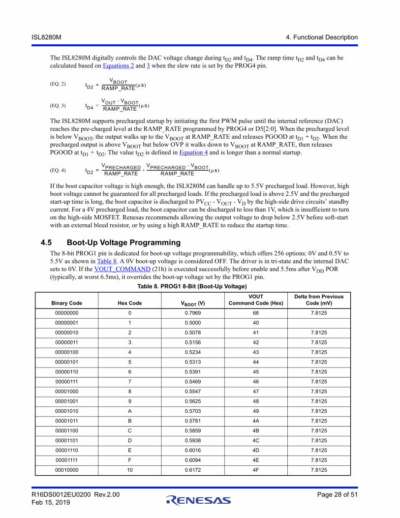
The ISL8280M digitally controls the DAC voltage change during tD2 and tD4. The ramp time tD2 and tD4 can be calculated based on Equations 2 and 3 when the slew rate is set by the PROG4 pin.
The ISL8280M supports precharged startup by initiating the first PWM pulse until the internal reference (DAC) reaches the pre-charged level at the RAMP_RATE programmed by PROG4 or D5[2:0]. When the precharged level is below VBOOT, the output walks up to the VBOOT at RAMP_RATE and releases PGOOD at tD1 + tD2. When the precharged output is above VBOOT but below OVP it walks down to VBOOT at RAMP_RATE, then releases PGOOD at tD1 + tD2. The value tD2 is defined in Equation 4 and is longer than a normal startup.
If the boot capacitor voltage is high enough, the ISL8280M can handle up to 5.5V precharged load. However, high boot voltage cannot be guaranteed for all precharged loads. If the precharged load is above 2.5V and the precharged start-up time is long, the boot capacitor is discharged to PVCC - VOUT - VD by the high-side drive circuits’ standby current. For a 4V precharged load, the boot capacitor can be discharged to less than 1V, which is insufficient to turn on the high-side MOSFET. Renesas recommends allowing the output voltage to drop below 2.5V before soft-start with an external bleed resistor, or by using a high RAMP_RATE to reduce the startup time.
4.5 Boot-Up Voltage ProgrammingThe 8-bit PROG1 pin is dedicated for boot-up voltage programmability, which offers 256 options: 0V and 0.5V to 5.5V as shown in Table 8. A 0V boot-up voltage is considered OFF. The driver is in tri-state and the internal DAC sets to 0V. If the VOUT_COMMAND (21h) is executed successfully before enable and 5.5ms after VDD POR (typically, at worst 6.5ms), it overrides the boot-up voltage set by the PROG1 pin.
Table 8. PROG1 8-Bit (Boot-Up Voltage)
Binary Code Hex Code VBOOT (V)VOUT
Command Code (Hex)Delta from Previous
Code (mV)
00000000 0 0.7969 66 7.8125
00000001 1 0.5000 40
00000010 2 0.5078 41 7.8125
00000011 3 0.5156 42 7.8125
00000100 4 0.5234 43 7.8125
00000101 5 0.5313 44 7.8125
00000110 6 0.5391 45 7.8125
00000111 7 0.5469 46 7.8125
00001000 8 0.5547 47 7.8125
00001001 9 0.5625 48 7.8125
00001010 A 0.5703 49 7.8125
00001011 B 0.5781 4A 7.8125
00001100 C 0.5859 4B 7.8125
00001101 D 0.5938 4C 7.8125
00001110 E 0.6016 4D 7.8125
00001111 F 0.6094 4E 7.8125
00010000 10 0.6172 4F 7.8125
tD2
VBOOTRAMP_RATE-------------------------------------- s =(EQ. 2)
tD4
VOUT VBOOT–
RAMP_RATE------------------------------------------ s =(EQ. 3)
tD2
VPRECHARGEDRAMP_RATE
--------------------------------------------VPRECHARGED VBOOT–
RAMP_RATE----------------------------------------------------------------------- s +=(EQ. 4)

R16DS0012EU0200 Rev.2.00 Page 29 of 51Feb 15, 2019
ISL8280M 4. Functional Description
00010001 11 0.6250 50 7.8125
00010010 12 0.6328 51 7.8125
00010011 13 0.6406 52 7.8125
00010100 14 0.6484 53 7.8125
00010101 15 0.6563 54 7.8125
00010110 16 0.6641 55 7.8125
00010111 17 0.6719 56 7.8125
00011000 18 0.6797 57 7.8125
00011001 19 0.6875 58 7.8125
00011010 1A 0.6953 59 7.8125
00011011 1B 0.7031 5A 7.8125
00011100 1C 0.7109 5B 7.8125
00011101 1D 0.7188 5C 7.8125
00011110 1E 0.7266 5D 7.8125
00011111 1F 1.3516 AD 7.8125
00100000 20 0.8516 6D 7.8125
00100001 21 0.7344 5E 7.8125
00100010 22 0.7422 5F 7.8125
00100011 23 0.7500 60 7.8125
00100100 24 0.7578 61 7.8125
00100101 25 0.7656 62 7.8125
00100110 26 0.7734 63 7.8125
00100111 27 0.7813 64 7.8125
00101000 28 0.7891 65 7.8125
00101001 29 0.7969 66 7.8125
00101010 2A 0.8047 67 7.8125
00101011 2B 0.8125 68 7.8125
00101100 2C 0.8203 69 7.8125
00101101 2D 0.8281 6A 7.8125
00101110 2E 0.8359 6B 7.8125
00101111 2F 0.8438 6C 7.8125
00110001 31 0.8594 6E 7.8125
00110010 32 0.8672 6F 7.8125
00110011 33 0.8750 70 7.8125
00110100 34 0.8828 71 7.8125
00110101 35 0.8906 72 7.8125
00110111 37 0.9063 74 7.8125
00111000 38 0.9141 75 7.8125
00111001 39 0.9219 76 7.8125
00111010 3A 0.9297 77 7.8125
Table 8. PROG1 8-Bit (Boot-Up Voltage) (Continued)
Binary Code Hex Code VBOOT (V)VOUT
Command Code (Hex)Delta from Previous
Code (mV)

R16DS0012EU0200 Rev.2.00 Page 30 of 51Feb 15, 2019
ISL8280M 4. Functional Description
00111011 3B 0.9375 78 7.8125
00111100 3C 0.9453 79 7.8125
00111110 3E 0.9609 7B 7.8125
00111111 3F 1.5000 C0 7.8125
01000000 40 0.8984 73 7.8125
01000001 41 0.9688 7C 7.8125
01000010 42 0.9766 7D 7.8125
01000011 43 0.9844 7E 7.8125
01000100 44 0.9922 7F 7.8125
01000110 46 1.0078 81 7.8125
01000111 47 1.0156 82 7.8125
01001000 48 1.0234 83 7.8125
01001001 49 1.0313 84 7.8125
01001010 4A 1.0391 85 7.8125
01001100 4C 1.0547 87 7.8125
01001101 4D 1.0625 88 7.8125
01001110 4E 1.0703 89 7.8125
01001111 4F 1.0781 8A 7.8125
01010000 50 1.0859 8B 7.8125
01010001 51 1.0938 8C 7.8125
01010011 53 1.1094 8E 7.8125
01010100 54 1.1172 8F 7.8125
01010101 55 1.1250 90 7.8125
01010110 56 1.1328 91 7.8125
01010111 57 1.1406 92 7.8125
01011000 58 1.1484 93 7.8125
01011001 59 1.1563 94 7.8125
01011010 5A 1.1641 95 7.8125
01011011 5B 1.1719 96 7.8125
01011100 5C 1.1797 97 7.8125
01011101 5D 1.1875 98 7.8125
01011110 5E 1.1953 99 7.8125
01011111 5F 1.7969 E6 7.8125
01100000 60 0.9531 7A 7.8125
01100010 62 1.2109 9B 7.8125
01100011 63 1.2188 9C 7.8125
01100100 64 1.2266 9D 7.8125
01100101 65 1.2344 9E 7.8125
01100110 66 1.2422 9F 7.8125
01100111 67 1.2500 A0 7.8125
Table 8. PROG1 8-Bit (Boot-Up Voltage) (Continued)
Binary Code Hex Code VBOOT (V)VOUT
Command Code (Hex)Delta from Previous
Code (mV)

R16DS0012EU0200 Rev.2.00 Page 31 of 51Feb 15, 2019
ISL8280M 4. Functional Description
01101000 68 1.2578 A1 7.8125
01101001 69 1.2656 A2 7.8125
01101010 6A 1.2734 A3 7.8125
01101011 6B 1.2813 A4 7.8125
01101100 6C 1.2891 A5 7.8125
01101101 6D 1.2969 A6 7.8125
01101110 6E 1.3047 A7 7.8125
01101111 6F 1.3125 A8 7.8125
01110000 70 1.3203 A9 7.8125
01110001 71 1.3281 AA 7.8125
01110010 72 1.3359 AB 7.8125
01110011 73 1.3438 AC 7.8125
01110101 75 1.3594 AE 7.8125
01110110 76 1.3672 AF 7.8125
01110111 77 1.3750 B0 7.8125
01111000 78 1.3828 B1 7.8125
01111001 79 1.3906 B2 7.8125
01111010 7A 1.3984 B3 7.8125
01111011 7B 1.4063 B4 7.8125
01111100 7C 1.4141 B5 7.8125
01111101 7D 1.4219 B6 7.8125
01111110 7E 1.4297 B7 7.8125
01111111 7F 2.5000 140 7.8125
10000000 80 1.0000 80 7.8125
10000001 81 1.4375 B8 7.8125
10000010 82 1.4453 B9 7.8125
10000011 83 1.4531 BA 7.8125
10000100 84 1.4609 BB 7.8125
10000101 85 1.4688 BC 7.8125
10000110 86 1.4766 BD 7.8125
10000111 87 1.4844 BE 7.8125
10001000 88 1.4922 BF 7.8125
10001010 8A 1.5078 C1 7.8125
10001011 8B 1.5156 C2 7.8125
10001100 8C 1.5234 C3 7.8125
10001101 8D 1.5313 C4 7.8125
10001110 8E 1.5391 C5 7.8125
10001111 8F 1.5469 C6 7.8125
10010000 90 1.5547 C7 7.8125
10010001 91 1.5625 C8 7.8125
Table 8. PROG1 8-Bit (Boot-Up Voltage) (Continued)
Binary Code Hex Code VBOOT (V)VOUT
Command Code (Hex)Delta from Previous
Code (mV)

R16DS0012EU0200 Rev.2.00 Page 32 of 51Feb 15, 2019
ISL8280M 4. Functional Description
10010010 92 1.5703 C9 7.8125
10010011 93 1.5781 CA 7.8125
10010100 94 1.5859 CB 7.8125
10010101 95 1.5938 CC 7.8125
10010110 96 1.6016 CD 7.8125
10010111 97 1.6094 CE 7.8125
10011000 98 1.6172 CF 7.8125
10011001 99 1.6250 D0 7.8125
10011010 9A 1.6328 D1 7.8125
10011011 9B 1.6406 D2 7.8125
10011100 9C 1.6484 D3 7.8125
10011101 9D 1.6563 D4 7.8125
10011110 9E 1.6641 D5 7.8125
10011111 9F 3.0000 180 7.8125
10100000 A0 1.0469 86 7.8125
10100001 A1 1.6719 D6 7.8125
10100010 A2 1.6797 D7 7.8125
10100011 A3 1.6875 D8 7.8125
10100100 A4 1.6953 D9 7.8125
10100101 A5 1.7031 DA 7.8125
10100110 A6 1.7109 DB 7.8125
10100111 A7 1.7188 DC 7.8125
10101000 A8 1.7266 DD 7.8125
10101001 A9 1.7344 DE 7.8125
10101010 AA 1.7422 DF 7.8125
10101011 AB 1.7500 E0 7.8125
10101100 AC 1.7578 E1 7.8125
10101101 AD 1.7656 E2 7.8125
10101110 AE 1.7734 E3 7.8125
10101111 AF 1.7813 E4 7.8125
10110000 B0 1.7891 E5 7.8125
10110010 B2 1.8047 E7 7.8125
10110011 B3 1.8125 E8 7.8125
10110100 B4 1.8203 E9 7.8125
10110101 B5 1.8281 EA 7.8125
10110110 B6 1.8359 EB 7.8125
10110111 B7 1.9141 F5 78.125
10111000 B8 1.9922 FF 78.125
10111001 B9 2.0703 109 78.125
10111010 BA 2.1484 113 78.125
Table 8. PROG1 8-Bit (Boot-Up Voltage) (Continued)
Binary Code Hex Code VBOOT (V)VOUT
Command Code (Hex)Delta from Previous
Code (mV)

R16DS0012EU0200 Rev.2.00 Page 33 of 51Feb 15, 2019
ISL8280M 4. Functional Description
10111011 BB 2.2266 11D 78.125
10111100 BC 2.3047 127 78.125
10111101 BD 2.3828 131 78.125
10111110 BE 2.4609 13B 78.125
10111111 BF 3.2969 1A6 7.8125
11000000 C0 1.1016 8D 7.8125
11000001 C1 2.4688 13C 7.8125
11000010 C2 2.4766 13D 7.8125
11000011 C3 2.4844 13E 7.8125
11000100 C4 2.4922 13F 7.8125
11000110 C6 2.5078 141 7.8125
11000111 C7 2.5156 142 7.8125
11001000 C8 2.5234 143 7.8125
11001001 C9 2.6016 14D 78.125
11001010 CA 2.6797 157 78.125
11001011 CB 2.7578 161 78.125
11001100 CC 2.8359 16B 78.125
11001101 CD 2.9141 175 78.125
11001110 CE 2.9922 17F 78.125
11001111 CF 3.0703 189 78.125
11010000 D0 3.1484 193 78.125
11010001 D1 3.2266 19D 78.125
11010010 D2 3.2813 1A4 54.6875
11010011 D3 3.2891 1A5 7.8125
11010101 D5 3.3047 1A7 7.8125
11010110 D6 3.3125 1A8 7.8125
11010111 D7 3.3203 1A9 7.8125
11011000 D8 3.3281 1AA 7.8125
11011001 D9 3.4063 1B4 78.125
11011010 DA 3.4844 1BE 78.125
11011011 DB 3.5625 1C8 78.125
11011100 DC 3.6406 1D2 78.125
11011101 DD 3.7188 1DC 78.125
11011110 DE 3.7969 1E6 78.125
11011111 DF 5.0000 280 7.8125
11100000 E0 1.2031 9A 7.8125
11100001 E1 3.8750 1F0 78.125
11100010 E2 3.9531 1FA 78.125
11100011 E3 4.0313 204 78.125
11100100 E4 4.1094 20E 78.125
Table 8. PROG1 8-Bit (Boot-Up Voltage) (Continued)
Binary Code Hex Code VBOOT (V)VOUT
Command Code (Hex)Delta from Previous
Code (mV)

R16DS0012EU0200 Rev.2.00 Page 34 of 51Feb 15, 2019
ISL8280M 4. Functional Description
As shown in Table 8, one step is 2-7 = 7.8125mV; some selections are higher than one step from adjacent codes. However, the resolution is ±7.8125mV around the popular voltage regulation points, as shown in Table 4 on page 25, for fine-tuning. For finer than 7.8125mV tuning, place a large ratio resistor divider on the VSEN pin between the output (VOUT) and either RGND for positive offset or VDD for negative offset as shown in Figure 43.
11100101 E5 4.1875 218 78.125
11100110 E6 4.2656 222 78.125
11100111 E7 4.3438 22C 78.125
11101000 E8 4.4219 236 78.125
11101001 E9 4.5000 240 78.125
11101010 EA 4.5781 24A 78.125
11101011 EB 4.6563 254 78.125
11101100 EC 4.7344 25E 78.125
11101101 ED 4.8125 268 78.125
11101110 EE 4.8906 272 78.125
11101111 EF 4.9688 27C 78.125
11110000 F0 4.9766 27D 7.8125
11110001 F1 4.9844 27E 7.8125
11110010 F2 4.9922 27F 7.8125
11110100 F4 5.0078 281 7.8125
11110101 F5 5.0156 282 7.8125
11110110 F6 5.0234 283 7.8125
11110111 F7 5.0313 284 7.8125
11111000 F8 5.1094 28E 78.125
11111001 F9 5.1875 298 78.125
11111010 FA 5.2656 2A2 78.125
11111011 FB 5.3438 2AC 78.125
11111100 FC 5.4219 2B6 78.125
11111101 FD 5.4922 2BF 70.3125
11111110 FE 5.5000 2C0 7.8125
11111111 FF 0 0
Table 8. PROG1 8-Bit (Boot-Up Voltage) (Continued)
Binary Code Hex Code VBOOT (V)VOUT
Command Code (Hex)Delta from Previous
Code (mV)
Figure 43. External Programmable Regulation
-
+VSEN
VDD
VOUT
-
+VSENVOUT
A. VOUT Higher than DAC B. VOUT Lower than DAC
RGND

R16DS0012EU0200 Rev.2.00 Page 35 of 51Feb 15, 2019
ISL8280M 4. Functional Description
4.6 Thermal Monitoring and CompensationThe thermal monitoring function block diagram is shown in Figure 44. A 10kΩ NTC resistor (P/N: NCP15XH103J03RC from Murata, β = 3380) inside the module is placed close to the output rail of the inductor to sense the operational temperature of the current sense component. An external 1.54kΩ pull-up resistor, RTM, forms the voltage divider for the NTC pin. Because the NTC pin voltage can pick up noise from the phase node, an internal 0.1µF ceramic capacitor is placed in close proximity to the NTC pin. As the temperature of the inductor increases, the resistance of the NTC decreases resulting in reduced voltage at the NTC pin.
Figure 45 shows the TM voltage over the temperature. Renesas recommends using a 1.54kΩ resistor for accurate temperate compensation because the internal thermal digital code is based on it.
Because the voltage across the inductor is sensed for the output current information, the sensed current has the same positive temperature coefficient as the inductor DCR, which is about +0.385%/°C. To obtain the correct current information, the ISL8280M uses the voltage at the NTC pin and “TCOMP” register values to compensate the temperature impact on the sensed current. The block diagram of this function is shown in Figure 46 on page 36.
Figure 44. Thermal Monitoring and Protection Block Diagram
Figure 45. Ratio of TM Voltage to NTC Temperature with Recommended Parts
20
30
40
50
60
70
80
90
100
0 20 40 60 80 100 120 140
Temperature (°C)
VT
M/V
DD
(%
)

R16DS0012EU0200 Rev.2.00 Page 36 of 51Feb 15, 2019
ISL8280M 4. Functional Description
Based on the VDD voltage, the ISL8280M converts the NTC pin voltage to a digital signal for temperature compensation. With the ISL8280M nonlinear A/D converter, the NTC digital signal is linearly proportional to the NTC temperature. Because the NTC is not directly attached to the current sense component, it inherits high thermal impedance between the NTC and the current sense component. The temperature difference between them can be corrected by the TCOMP register values, which include four different TCOMP options that can be set by the PROG2 pin. The ISL8280M multiplexes the TCOMP register values with the NTC digital signal to obtain the adjustment gain to compensate the temperature impact on the sensed current. The compensated current signal is used for both IOUT and OCP functions. Renesas recommends using +5°C as the TCOMP.
4.7 Fault ProtectionThe ISL8280M provides high system reliability with many fault protections, as summarized in Table 10.
Figure 46. Integrated Temperature Compensation Block Diagram
Table 9. TCOMP Values
D1h TCOMP (°C) D1h TCOMP (°C)
0h +30 2h +5
1h +15 3h OFF
Table 10. Fault Protection Summary
Fault Description Fault Action
Input UVLO VIN pin UVLO; or set by the EN pin with an external divider for higher level. See Figures 39 and 40.
Shut down and recover when VIN > UVLO
Bias UVLO VDD, PVCC, 7VLDO UVLO Shut down and recover when Bias > UVLO
Startup OVP Higher than VBOOT. See “Electrical Specifications” on page 12.
Latch OFF, reset by VDD or toggling Enable (including the EN pin and/or OPERATION command based on the ON_OFF_CONFIG setting)
Output OVP Rising = 116%; Falling = 100%
Output UVP 74% of VOUT, Latch OFF
Short-Circuit and OCP Protection
Peak load current = 14.3A typical Latch OFF, reset by VDD or toggling Enable (including the EN pin and/or OPERATION command based on the ON_OFF_CONFIG setting), or retry every 9ms; option is programmable by PROG3 or D3[0]
OTP Rising = 22.31%VDD (~+136°C)Falling = 27.79%VDD (~+122°C)
Shut down above +136°C and recover when temperature drops below +122°C
oC
RTM
R NTC
NTC
TCOMP
Non-Linear A/D
A/D IOUT Monitor and Overcurrent Protection
IPH
k iD/A
Channel Current Sense
CSSEN
CSRTN
V DD ISL8280M

R16DS0012EU0200 Rev.2.00 Page 37 of 51Feb 15, 2019
ISL8280M 4. Functional Description
Input UVLO and OTP faults respond to the current state with hysteresis. Output OVP and output UVP faults are latch events. Output OCP and output short-circuit faults can be latch or retry events depending on the PROG3 or D3[0] setting. All fault latch events can be reset by VDD cycling, toggling the EN pin, or with the serial bus OPERATION command based on the ON_OFF_CONFIG setting. The OCP retry event has a hiccup time of 9ms and the module can be recovered when the fault is removed.
4.7.1 Overvoltage ProtectionThe Overvoltage Protection (OVP) fault detection circuit triggers when the voltage between VSEN+ and VSEN- is above the rising overvoltage threshold. When an OVP fault is declared, the module latches off and the PGOOD pin is asserted low. The fault remains latched and can be reset by VDD cycling, toggling the EN pin, and/or the serial bus OPERATION command based on the ON_OFF_CONFIG setting.
Although the module latches off in response to an OVP fault, the Low-Side Gate Driver (LGATE) retains the ability to toggle the low-side MOSFET on and off in response to the output voltage transversing the OVP rising and falling thresholds. The LGATE turns on the low-side MOSFET to discharge the output voltage, protecting the load. The LGATE turns off the low-side MOSFET when the sensed output voltage is lower than the falling overvoltage threshold (typically 100%). If the output voltage rises again, the LGATE turns on the low-side MOSFET when the output voltage is above the rising overvoltage threshold (typically 120%). This process protects the load when there is a consistent overvoltage condition.
In addition to normal OVP operation, the startup OVP circuits are enabled to protect against OVP events 5.5ms (typical, worst 6.5ms) after all rails (VDD, PVCC, 7VLDO, VIN) POR and before the end of soft-start while the OVP level is set higher than VBOOT. See “Electrical Specifications” on page 12.
4.7.2 Undervoltage ProtectionThe Undervoltage Protection (UVP) fault detection circuit triggers if the output voltage is below the undervoltage threshold (typically 74% of DAC). When an UVP fault is declared, the module latches off, forcing the LGATE and High-Side Gate Driver (UGATE) outputs low, and the PGOOD pin is asserted low. The fault remains latched and can be reset by VDD cycling, toggling the EN pin, and/or with the serial bus OPERATION command based on the ON_OFF_CONFIG setting.
4.7.3 Overcurrent and Short-Circuit ProtectionInductor DCR sensing is used for current sense and senses current continuously for fast response. The current sense amplifier uses the CSEN and CSRTN inputs to reproduce a signal proportional to the inductor current, IL. The reproduced signal is used for current reporting and overcurrent protection.
The Overcurrent Protection (OCP) is triggered when the load current is typically 14.3A. OCP protects inductor saturation from short-circuit events and provides a more robust power train and system protection. When an OCP or short-circuit fault is declared, the module latches off, forcing the both the high-side and low-side gate driver outputs low, or it retries with a hiccup time of 9ms. The fault response is programmable by PROG3 or D3[0]. However, the latched off event can be reset by VDD cycling, toggling the EN pin, and/or with the serial bus OPERATION command based on the ON_OFF_CONFIG setting.
4.7.4 Over-Temperature ProtectionAn NTC inside the module senses the inductor temperature for both over-temperature and current sense temperature compensation. The NTC is connected to the NTC pin and SGND pad and results in lower NTC pin voltage at higher temperatures. A comparator with hysteresis compares the NTC pin voltage to the threshold set. At +136°C (typical), Over-Temperature Protection (OTP) is triggered and the ISL8280M operation is disabled. When the sensed temperature is around +122.4°C, the ISL8280M resumes normal operation. When an OTP fault is declared, the module forces the LGATE and UGATE outputs low.

R16DS0012EU0200 Rev.2.00 Page 38 of 51Feb 15, 2019
ISL8280M 4. Functional Description
4.8 PGOOD MonitorThe PGOOD pin indicates when the module is capable of supplying regulated voltage. PGOOD is asserted low if there is a fault condition of a rail’s (VDD, PVCC, 7VLDO, or VIN) UVLO, output Overcurrent (OCP), output Overvoltage (OVP), output Undervoltage (UVP), or Over-Temperature (OTP). Note: the PGOOD pin is an undefined impedance with insufficient VDD (typically <2.5V).
4.9 PFM Mode OperationIn PFM mode, programmable by the PROG2 pin, the switching frequency is dramatically reduced to minimize the switching loss and significantly improve light-load efficiency. The ISL8280M can achieve seamless transition between PFM mode and PWM mode as load changes. For high VOUT applications, the LGATE might not turn on long enough to charge the boot capacitor in PFM mode with 0A load. Renesas recommends enabling the ISL8280M’s ultrasonic PFM feature, programmable by the PROG3 pin, which maintains the LGATE switching frequency above 20kHz and keeps the boot capacitor charged for immediate load apply events. Alternatively, maintaining a minimum load can enhance the boot capacitor charge.
4.10 SMBus, PMBus, and I2C OperationThe ISL8280M features SMBus, PMBus, and I2C with 32 programmable addresses through the PROG2 pin. The SMBus/PMBus includes an Alert# line (SALERT) and Packet Error Check (PEC) to ensure data is properly transmitted. The telemetry update rate is typically 108µs. The supported SMBus/PMBus/I2C addresses are summarized in Table 11 on page 38. The 7-bit format address does not include the last bit (write and read): 40-47h, 60-67h, and 70-7Fh.
SMBus/PMBus/I2C allows the user to program the registers, as shown in Table 12 on page 42, except for SMBus/PMBus/I2C addresses, 5.5ms (typical, worst 6.6ms) after all rails (VDD, PVCC, 7VLDO, and VIN) are above POR. Figures 47 and 48 on page 39 show the initialization timing diagram for the serial bus with different EN (Enable) pin states.
For proper operation, follow the SMBus, PMBus, and I2C protocol shown in Figure 49 on page 41. Note: the STOP (P) bit is NOT allowed before the repeated START condition when reading the contents of a register.
When the device’s serial bus is not used, ground the device’s SCL, SDA, and SALERT pins and do not connect them to the bus.
Table 11. SMBus/PMBus/I2C 7-Bit Format Address (Hex)
7-Bit Address 7-Bit Address 7-Bit Address
40 63 76
41 64 77
42 65 78
43 66 79
44 67 7A
45 70 7B
46 71 7C
47 72 7D
60 73 7E
61 74 7F
62 75

R16DS0012EU0200 Rev.2.00 Page 39 of 51Feb 15, 2019
ISL8280M 4. Functional Description
Figure 47. Simplified SMBus/PMBus/I2C Initialization Timing Diagram with Enable Low
Figure 48. Simplified SMBus/PMBus/I2C Initialization Timing Diagram with Enable High
VIN, PVCC, 7VLDO, VDD
Enable
5m s 0.5m s
VDD POR Tim eout
Reader Done
0m s to Infinity
VOUT
W rite and ReadConfiguration
W rite and ReadConfiguration
W rite and ReadConfiguration
V BOOT
0V
0m s to Infinity
PM Bus Com m and
PM Bus Com m and
PM Bus Com m and
PM Bus Com m and
PM Bus Com m unication Not Activated
W rite and ReadConfiguration
200µs SS delay
VDD POR Tim eout
Reader Done
VOUT
W rite and ReadConfiguration
W rite and ReadConfiguration
VBO OT
0V
0m s to Infinity
PM Bus Com m and
PM Bus Com m and
PMBus Com m and
PM Bus Com m unicationNot Activated
W rite and ReadConfiguration
5m s 0.5m s
Enable
200 µs SS Delay
VIN, PVCC, 7VLDO, VDD

R16DS0012EU0200 Rev.2.00 Page 40 of 51Feb 15, 2019
ISL8280M 4. Functional Description
S Slave Address_0
1 7 + 1
Command Code
1 8
Low Data Byte High Data Byte PECA
1 8
A
1 8
A
1 8
A
1
A
1
P
S Slave Address_0
1 7 + 1
Command Code
1 8
A
1
A PEC
8 1
A
1
P
Optional 9 Bits for SMBus/PMBus
1. Send Byte Protocol
2. Write Byte/Word Protocol
S Slave Address_0
1 7 + 1
Command Code
1 8
A
1
8
A
1 8
A
1 8
A
1
N
1
P
3. Read Byte/Word Protocol
RS Slave Address_1
1 7 + 1
Example command: 03h Clear Faults
Example command: D0h ENABLE_PFM (one word, High Data Byte, and ACK are not used)
NOT used in I2C
Optional 9 bits for SMBus/PMBus
NOT used in I2C
Optional 9 bits for SMBus/PMBus
NOT used in I2C
S: Start Condition
A: Acknowledge (“0”)
N: Not Acknowledge (“1”)
RS: Repeated Start Condition
P: Stop Condition
PEC: Packet Error Checking
R: Read (“1”)
W: Write (“0”)
1
A
Not Used for One Byte Word Read
Not Used for One Byte Word
Low Data Byte High Data Byte PEC
(This clears all of the bits in Status Byte for the selected Rail)Acknowledge or DATA from Slave,
ISL8280M
S Slave Address_0
1 7 + 1
Command Code
1 8
Byte Count = N Lowest Data Byte Data Byte 2A
1 8
A
1 8
A
1 8
A
1
A
4. Block Write Protocol
Example command: ADh IC_DEVICE_ID (2 Data Byte)
Data Byte N PEC
1 8
A
1 8
A
1
A
1
P
Optional 9 Bits for SMBus/PMBus
NOT used in I2C
Example command: 8B READ_VOUT (two words, read voltage of the selected rail).
NOTE: All Writable commands are read with one byte word protocol.
The STOP (P) bit is NOT allowed before the repeated START condition when “reading” contents of a register.

R16DS0012EU0200 Rev.2.00 Page 41 of 51Feb 15, 2019
ISL8280M 4. Functional Description
Figure 49. SMBus/PMBus/I2C Command Protocol
S Slave Address_0
1 7 + 1
Command Code
1 8
A
1
8
A
1 8
A
1 8
A
1
N
1
P
5. Block Read Protocol
RS Slave Address_1
1 7 + 1
Optional 9 bits for SMBus/PMBus
NOT used in I2C
1
A
Data Byte PEC
8 1 8
A
1
A
6. Group Command Protocol - No more than one command can be sent to the same Address
RS Slave ADDR2_0
1 7 + 1 1
A
S Slave ADDR1_0
1 7 + 1
Command Code
1 8
Low Data Byte High Data Byte PECA
1 8
A
1 8
A
1 8
A
1
A
Low Data Byte High Data Byte PEC
8 1 8
A
1 8
A
1
A
1
PRS Slave ADDR3_0
1 7 + 1
Optional 9 bits for SMBus/PMBus
1
A
NOT used in I2C
Data Byte 2 Data Byte N PEC
Command Code
8 1
A
Command Code
8 1
A
81
A Byte Count = N
81
A Lowest Data Byte
Example command: 8B READ_VOUT (two words, read voltage of the selected rail).
NOTE: All Writable commands are read with one byte word protocol.
The STOP (P) bit is NOT allowed before the repeated START condition when “reading” contents of a register.
R16DS0012EU0200 Rev.2.00 Page 42 of 51Feb 15, 2019
ISL8280M 4. Functional Description
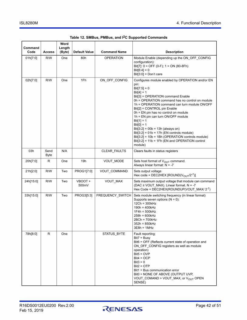
Table 12. SMBus, PMBus, and I2C Supported Commands
Command Code Access
Word Length (Byte) Default Value Command Name Description
01h[7:0] R/W One 80h OPERATION Module Enable (depending up the ON_OFF_CONFIG configuration):Bit[7]: 0 = OFF (0-F); 1 = ON (80-8Fh)Bit[6:4] = 0 Bit[3:0] = Don’t care
02h[7:0] R/W One 1Fh ON_OFF_CONFIG Configures module enabled by OPERATION and/or EN pin:Bit[7:5] = 0Bit[4] = 1 Bit[3] = OPERATION command Enable0h = OPERATION command has no control on module1h = OPERATION command can turn module ON/OFFBit[2] = CONTROL pin Enable0h = EN pin has no control on module 1h = EN pin can turn ON/OFF moduleBit[1] = 1Bit[0] = 1Bit[3:2] = 00b = 13h (always on) Bit[3:2] = 01b = 17h (EN controls module) Bit[3:2] = 10b = 1Bh (OPERATION controls module) Bit[3:2] = 11b = 1Fh (EN and OPERATION control module)
03h Send Byte
N/A CLEAR_FAULTS Clears faults in status registers
20h[7:0] R One 19h VOUT_MODE Sets host format of VOUT command. Always linear format: N = -7
21h[2:0] R/W Two PROG1[7:0] VOUT_COMMAND Sets output voltageHex code = DEC2HEX [ROUND(VOUT/2-7)]
24h[15:0] R/W Two VBOOT + 500mV
VOUT_MAX Sets maximum output voltage that module can command (DAC ≤ VOUT_MAX). Linear format. N = -7Hex Code = DEC2HEX(ROUNDUP(VOUT_MAX/ 2-7)
33h[15:0] R/W Two PROG3[5:3] FREQUENCY_SWITCH Sets module switching frequency (in linear format)Supports seven options (N = 0): 12Ch = 300kHz190h = 400kHz1F4h = 500kHz 258h = 600kHz2BCh = 700kHz352h = 850kHz 3E8h = 1MHz
78h[8:0] R One STATUS_BYTE Fault reporting;Bit7 = BusyBit6 = OFF (Reflects current state of operation and ON_OFF_CONFIG registers as well as module operation)Bit5 = OVPBit4 = OCP Bit3 = 0Bit2 = OTPBit1 = Bus communication errorBit0 = NONE OF ABOVE (OUTPUT UVP, VOUT_COMAND > VOUT_MAX, or VOUT OPEN SENSE)

R16DS0012EU0200 Rev.2.00 Page 43 of 51Feb 15, 2019
ISL8280M 4. Functional Description
88h[15:0] R Two READ_VIN Input voltage (N = - 4, Max = 31.9375V)VIN (V) = HEX2DEC(88 hex data - E000h) x 0.0625V
8Bh[15:0] R Two READ_VOUT Module output voltage, resolution = 7.8125mV = 2-7
VOUT (V) = HEX2DEC(8B hex data) x 2-7
8Ch[15:0] R Two READ_IOUT Module output current (N = -3, IMAX = 63.875A)IOUT (A) = HEX2DEC(8C hex data-E800) x 0.125A when IOUT pin voltage = 2.5V at 63.875A load.
8Dh[15:0] R Two READ_TEMP Module temperature
98h[7:0] R One 02h PMBUS_REVISION Indicates PMBus revision 1.2
AD[15:0] Block R Two 0xD000 IC_DEVICE_ID ISL8280M device ID
AE[15:0] Block R Two 0x000A IC_DEVICE_REVISION ISL8280M device revision
D0[0:0] R/W One PROG2[7:7] ENABLE_PFM PFM OPERATION0h = PFM Enabled1h = PFM Disabled (always CCM mode)
D1[1:0] R/W One PROG2[6:5] TEMP_COMP Thermal compensation:0h = +30°C01h = +15°C02h = +5°C03h = OFF
D2[0:0] R/W One PROG3[7:7] ENABLE_ULTRASONIC Ultrasonic PFM enable0h = 25kHz clamp disabled1h = 25kHz clamp enabled
D3[0:0] R/W One PROG3[6:6] OCP_BEHAVIOR Set latch or infinite retry for OCP fault:0h = Retry every 9ms01 = Latch-OFF
D4[2:0] R/W One PROG3[2:0] AV_GAIN R4 AV GAIN (PROG4, AV Gain Multiplier = 2x) 0h = 841h = 732h = 613h = 49 4h = 385h = 266h = 147h = 2R4 AV GAIN (PROG4, AV Gain Multiplier = 1x)0h = 421h = 36.52h = 30.53h = 29.5 4h = 195h = 136h = 77h = 1
D5{2:0] R/W One PROG4[7:5] RAMP_RATE Soft-start rate (mV/µs)0h = 1.251h = 2.52h = 53h = 105h = 0.1576h = 0.3157h = 0.625;
Table 12. SMBus, PMBus, and I2C Supported Commands (Continued)
Command Code Access
Word Length (Byte) Default Value Command Name Description

R16DS0012EU0200 Rev.2.00 Page 44 of 51Feb 15, 2019
ISL8280M 4. Functional Description
D6[1:0] R/W One PROG4[4:3] SET_RR Sets RR 0h = 200k01h = 400k02h = 600k03h = 800k
DC[7:0] R One READ_PROG1 Reads PROG1
DD{7:0] R One READ_PROG2 Reads PROG2
DE[7:0] R One READ_PROG3 Reads PROG3
DF[7:0] R One READ_PROG4 Reads PROG4
Note: Serial bus communication is valid 5.5ms (typical, worst 6.5ms) after VDD, VIN, 7VLDO, and PVCC above POR. The telemetryupdate rate is 108µs.
Table 12. SMBus, PMBus, and I2C Supported Commands (Continued)
Command Code Access
Word Length (Byte) Default Value Command Name Description

R16DS0012EU0200 Rev.2.00 Page 45 of 51Feb 15, 2019
ISL8280M 5. Layout Guidelines
5. Layout GuidelinesCareful attention to layout requirements is necessary for successful implementation of the ISL8280M power module. The ISL8280M switches at a very high frequency. Therefore, the switching times are very short. At these switching frequencies, even the shortest trace has significant impedance. The peak gate drive current also rises significantly in an extremely short time. Current transition from one MOSFET to another causes voltage spikes across the interconnecting impedances and parasitic circuit elements. The voltage spikes can degrade efficiency, generate EMI, and increase MOSFET voltage stress and ringing. Careful component selection and proper PCB layout minimize the magnitude of these voltage spikes. Use the ISL8280MEVAL1Z as a example and reference for the PCB layout.
(1) Renesas recommends using a six-layer PCB board. Use the top and bottom layer to route VIN and VOUT. Use a full ground plane in the internal layers (underneath the module) with shared SGND and PGND to simplify the layout design. Use another full ground plane directly above the bottom layer. Use the other internal layers to route the remote sense, PGOOD, SCL, SDA, and SALERT signals.
(2) Place the input capacitors and high frequency decoupling ceramic capacitors between VIN and PGND as close to the module as possible. The loop formed by the input capacitors, VIN, and PGND must be as small as possible to minimize high frequency noise. Place the output ceramic capacitors close to VOUT. Use a copper plane to connect the output ceramic capacitors to the load to avoid any parasitic inductances and resistances. An example layout is illustrated in Figures 50 and 51.
(3) Use large copper planes for power paths (VIN, VOUT, and PGND) to minimize conduction loss and thermal stress. Also, use multiple vias to connect the power planes in different layers.
(4) Do not oversize the copper planes for the PHASE planes. Because the PHASE planes are subjected to very high dv/dt, the parasitic capacitor formed between these planes and the surrounding circuitry tends to couple the switching noise. Ensure that none of the sensitive signal traces are routed close to the PHASE plane.
(5) Place the PVCC and VIN1 bypass capacitors underneath the PVCC and VIN1 pins and connect their grounds to the SGND. For the external pin-strap resistor dividers connected to PROG1, PROG2, PROG3, and PROG4, connect the low side dividers’ ground to the SGND. If a local decoupling capacitor is used to bias these resistor dividers, place the decoupling capacitor close to the dividers, and connect the capacitor’s ground to the SGND. An example layout is illustrated in Figure 51.
(6) Connect remote sensing traces to the regulation point to achieve a tight output voltage regulation. Route the remote sensing traces in parallel underneath the PGND layer and avoid routing the sensing trace near noisy planes such as PHASE. Place 2Ω resistors close to VSEN and RGND, respectively, to dampen the noise on the traces.
Figure 50. Layout Example - Top Layer Figure 51. Layout Example - Bottom Layer

R16DS0012EU0200 Rev.2.00 Page 46 of 51Feb 15, 2019
ISL8280M 6. Thermal Considerations
6. Thermal ConsiderationsUse the experimental power loss and θJA from thermal modeling analysis to evaluate the thermal consideration for the module. The derating curves are derived from the maximum power allowed while maintaining the temperature below the maximum junction temperature of +125°C. The derating curves are derived based on tests of the ISL8280M evaluation board, which is a 6-layer board 3 x 3.4 inches in size with 2oz Cu on all layers and multiple via interconnects. In the actual application, other heat sources and design margins should be considered.

R16DS0012EU0200 Rev.2.00 Page 47 of 51Feb 15, 2019
ISL8280M 7. Package Description
7. Package DescriptionThe structure of the ISL8280M belongs to the High Density Array no-lead package (HDA). The HDA package has good thermal and electrical conductivity, low weight, and small size and is applicable for surface mounting technology that is being more readily used in the industry. The ISL8280M contains several types of devices, including resistors, capacitors, inductors, MOSFETs, and control ICs. The ISL8280M is a copper leadframe-based package with exposed copper thermal pads that have good electrical and thermal conductivity. The copper leadframe and multicomponent assembly is overmolded with a polymer mold compound to protect these devices.
The package outline, typical Printed Circuit Board (PCB) layout pattern design, and typical stencil pattern design are shown in the “Package Outline Drawing” on page 50. The module has a small size of 12mmx11mmx5.3mm.
7.1 PCB Layout Pattern DesignThe bottom of the ISL8280M is a leadframe footprint attached to the PCB by a surface mounting process. The PCB layout pattern is shown in the “Package Outline Drawing” on page 50. The PCB layout pattern is an array of solder mask defined PCB lands that align with the perimeters of the HDA exposed pads and I/O termination dimensions. The thermal lands on the PCB layout also feature an array of solder mask defined lands and should match 1:1 with the package exposed die pad perimeters. The exposed solder mask defined PCB land area should be 50-80% of the available module I/O area.
7.2 Thermal ViasA grid of 1.0mm to 1.2mm pitch thermal vias drops down and connects to buried copper plane(s). Place the grid under the thermal land. The vias should be about 0.3mm to 0.33mm in diameter with the barrel plated to about 1.0 oz. of copper. Although adding more vias (by decreasing via pitch) improves the thermal performance, increasing the number of vias eventually yields diminishing returns. Use as many vias as practical for the thermal land size allowed by your board design rules.
7.3 Stencil Pattern DesignReflowed solder joints on the perimeter I/O lands should have about a 50µm to 75µm (2mil to 3mil) standoff height. The solder paste stencil design is the first step in developing optimized, reliable solder joints. The stencil aperture size to solder mask defined PCB land size ratio should typically be 1:1. The aperture width can be reduced slightly to help prevent solder bridging between adjacent I/O lands. A typical solder stencil pattern is shown in the “Package Outline Drawing” on page 50. Consider the symmetry of the whole stencil pattern when designing its pads. A laser cut, stainless steel stencil with electropolished trapezoidal walls is recommended. Electropolishing “smooths” the aperture walls resulting in reduced surface friction and better paste release, which reduces voids. Using a Trapezoidal Section Aperture (TSA) also promotes paste release and forms a brick-like paste deposit that assists in firm component placement. A 0.1mm to 0.15mm stencil thickness is recommended for this large pitch HDA.

R16DS0012EU0200 Rev.2.00 Page 48 of 51Feb 15, 2019
ISL8280M 7. Package Description
7.4 Reflow ParametersDue to the low mount height of the HDA, “No-Clean” Type 3 solder paste per ANSI/J-STD-005 is recommended. A nitrogen purge is also recommended during reflow. A system board reflow profile depends on the thermal mass of the entire populated board, so it is not practical to define a specific soldering profile just for the HDA. The profile given in Figure 52 is a guideline that can be adapted for varying manufacturing practices and applications.
Figure 52. Typical Reflow Profile
0 300100 150 200 250 3500
50
100
150
200
250
300
Tem
per
atu
re (
°C)
Duration (s)
Slow Ramp (3°C/s Max)and Soak from +150°Cto +200°C for 60s~180s
Ramp Rate 1.5°C from +70°C to +90°C
Peak Temperature ~+245°C; Typically 60s-150s Above +217°CKeep Less Than 30s Within 5°C of Peak Temp.

R16DS0012EU0200 Rev.2.00 Page 49 of 51Feb 15, 2019
ISL8280M 8. Revision History
8. Revision History
Rev. Date Description
2.00 Feb 15, 2019 Updated Title on page 1.Updated VOUT, SALERT, and SDA pin descriptions on page 8.Updated Figure 26 and 28 labels on page 20.Updated Figure 41 on page 24.Updated the ENABLE_PFM command description on page 43.Removed subheading on page 45.Updated Disclaimer.
1.00 Dec 14, 2018 Initial release.

R1
6DS
001
2EU
020
0R
ev.2.00P
age
50 of 5
1F
eb 1
5, 2
019
ISL
828
0M9. P
acka
ge O
utline
Dra
win
g9. Package Outline DrawingY83.12x1183 I/O 12mmx11mmx5.3mm HDA ModuleRev 0, 3/18
For the most recent package outline drawing, see Y83.12x11.
Corporate HeadquartersTOYOSU FORESIA, 3-2-24 Toyosu,Koto-ku, Tokyo 135-0061, Japanwww.renesas.com
Contact InformationFor further information on a product, technology, the most up-to-date version of a document, or your nearest sales office, please visit:
www.renesas.com/contact/
TrademarksRenesas and the Renesas logo are trademarks of Renesas Electronics Corporation. All trademarks and registered trademarks are the property of their respective owners.