isolated igbt gate-drive push-pull power supply with 4 ... · pdf filephase inverter using six...
TRANSCRIPT
LM5030
LP2954A
TPS7A3001
LP2954A
TPS7A3001
TPS27082L
VCC_T
VLDO_T
REF_T
VEE_T
VCC_B
VLDO_B
REF_B
VEE_B
Shutdownsignal
VINCSD19533QSA × 2
ForTOPdevice
ForBOTTOMdevice
+±
Copyright © 2016, Texas Instruments Incorporated
1TIDU355A–June 2014–Revised June 2016Submit Documentation Feedback
Copyright © 2014–2016, Texas Instruments Incorporated
Isolated IGBT Gate-Drive Push-Pull Power Supply with 4 Outputs
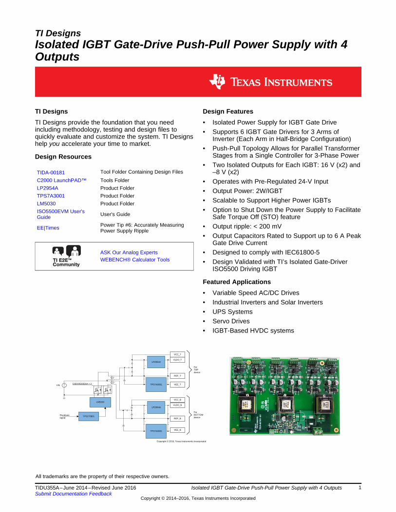
TI DesignsIsolated IGBT Gate-Drive Push-Pull Power Supply with 4Outputs
All trademarks are the property of their respective owners.
TI DesignsTI Designs provide the foundation that you needincluding methodology, testing and design files toquickly evaluate and customize the system. TI Designshelp you accelerate your time to market.
Design Resources
TIDA-00181 Tool Folder Containing Design FilesC2000 LaunchPAD™ Tools FolderLP2954A Product FolderTPS7A3001 Product FolderLM5030 Product FolderISO5500EVM User'sGuide User's Guide
EE|Times Power Tip #6: Accurately MeasuringPower Supply Ripple
ASK Our Analog ExpertsWEBENCH® Calculator Tools
Design Features• Isolated Power Supply for IGBT Gate Drive• Supports 6 IGBT Gate Drivers for 3 Arms of
Inverter (Each Arm in Half-Bridge Configuration)• Push-Pull Topology Allows for Parallel Transformer
Stages from a Single Controller for 3-Phase Power• Two Isolated Outputs for Each IGBT: 16 V (x2) and
–8 V (x2)• Operates with Pre-Regulated 24-V Input• Output Power: 2W/IGBT• Scalable to Support Higher Power IGBTs• Option to Shut Down the Power Supply to Facilitate
Safe Torque Off (STO) feature• Output ripple: < 200 mV• Output Capacitors Rated to Support up to 6 A Peak
Gate Drive Current• Designed to comply with IEC61800-5• Design Validated with TI’s Isolated Gate-Driver
ISO5500 Driving IGBT
Featured Applications• Variable Speed AC/DC Drives• Industrial Inverters and Solar Inverters• UPS Systems• Servo Drives• IGBT-Based HVDC systems

FromController
FromController
FromController
FromController
FromController
FromController
ISO
LAT
ION
ISO
LAT
ION
ISO
LAT
ION
ISO
LAT
ION
ISO
LAT
ION
ISO
LAT
ION
VBUS VBUS VBUS
VGND VGND VGND
+16 V +16 V +16 V
+16 V+16 V +16 V
+5 V
+5 V
± 8 V ± 8 V ± 8 V
To ADC or Controller
± 8 V ± 8 V ± 8 V
+
+
TI'DYH¶V
ControlCenter
System Description www.ti.com
2 TIDU355A–June 2014–Revised June 2016Submit Documentation Feedback
Copyright © 2014–2016, Texas Instruments Incorporated
Isolated IGBT Gate-Drive Push-Pull Power Supply with 4 Outputs
An IMPORTANT NOTICE at the end of this TI reference design addresses authorized use, intellectual property matters and otherimportant disclaimers and information.
1 System DescriptionThis reference design provides isolated positive and negative voltage rails required for Insulated GateBipolar Transistor (IGBT) gate drivers from a single 24-volt DC input supply. IGBTs are used in three-phase inverters for variable-frequency drives to control the speed of AC motors. This reference designuses a push-pull isolated-control topology and provides isolation compliant to IEC61800-5. This referencedesign is intended to operate from a pre-regulated 24-V DC input. With a regulated (within 5%) inputsource, a simple open-loop, free-running oscillator can be implemented with a push-pull PWM controller.
The topology is essentially a forward converter with two primary windings used to create a dual-drivewinding. This topology fully utilizes the transformer core's magnetizing current more efficiently than flybackor forward topologies. Another advantage this configuration has over flyback and forward configurations isthat the supply output can be scaled up for higher power drives.
This reference design also takes advantage of another benefit of the push-pull topology in that multipletransformers can be controlled in parallel from a single controller to generate all the isolated voltage railsrequired for 3-phase IGBT inverters. Finally, larger IGBTs for higher power drives sometimes require moregate drive current than what is provided by a typical IGBT gate driver. For larger IGBTs, designers oftenuse additional transistors for gate current boosting. This reference design provides 16 V on the positiveoutputs and –8 V on the negative outputs to compensate for the added voltage drop in these additionaltransistors.
Three-phase inverters are used for variable-frequency drives that control the speed of AC motors, and forhigh-power applications like high-voltage DC (HVDC) power transmission. A typical application of a three-phase inverter using six isolated gate drivers is shown in Figure 1. Note that each phase uses a high-sideand a low-side IGBT switch to apply positive and negative high-voltage DC pulses to the motor coils in analternating mode.
High-Power IGBTs require isolated gate drivers to control their operations. A single, isolated gate driverdrives each IGBT that galvanically isolates the high-voltage output from the low-voltage controlled inputs.The emitter of the top IGBT floats, which requires use of an isolated gate-driver. In order to isolate thehigh-voltage circuit with a low-voltage control circuit, isolated gate-drivers are used to control the bottomIGBTs.
Figure 1. 3-Phase Inverter with Isolated Gate-Drive
2
gate sw swPgate = Pdriver +(Q × f ×ΔVgate)+(Cge× f ×ΔVgate )
+ 15 V
± 10 V
AC
±
+
RG
RGE
CGE
www.ti.com System Description
3TIDU355A–June 2014–Revised June 2016Submit Documentation Feedback
Copyright © 2014–2016, Texas Instruments Incorporated
Isolated IGBT Gate-Drive Push-Pull Power Supply with 4 Outputs
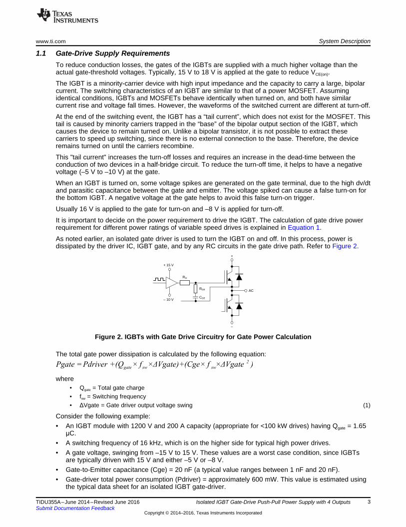
1.1 Gate-Drive Supply RequirementsTo reduce conduction losses, the gates of the IGBTs are supplied with a much higher voltage than theactual gate-threshold voltages. Typically, 15 V to 18 V is applied at the gate to reduce VCE(on).
The IGBT is a minority-carrier device with high input impedance and the capacity to carry a large, bipolarcurrent. The switching characteristics of an IGBT are similar to that of a power MOSFET. Assumingidentical conditions, IGBTs and MOSFETs behave identically when turned on, and both have similarcurrent rise and voltage fall times. However, the waveforms of the switched current are different at turn-off.
At the end of the switching event, the IGBT has a “tail current”, which does not exist for the MOSFET. Thistail is caused by minority carriers trapped in the “base” of the bipolar output section of the IGBT, whichcauses the device to remain turned on. Unlike a bipolar transistor, it is not possible to extract thesecarriers to speed up switching, since there is no external connection to the base. Therefore, the deviceremains turned on until the carriers recombine.
This "tail current" increases the turn-off losses and requires an increase in the dead-time between theconduction of two devices in a half-bridge circuit. To reduce the turn-off time, it helps to have a negativevoltage (–5 V to –10 V) at the gate.
When an IGBT is turned on, some voltage spikes are generated on the gate terminal, due to the high dv/dtand parasitic capacitance between the gate and emitter. The voltage spiked can cause a false turn-on forthe bottom IGBT. A negative voltage at the gate helps to avoid this false turn-on trigger.
Usually 16 V is applied to the gate for turn-on and –8 V is applied for turn-off.
It is important to decide on the power requirement to drive the IGBT. The calculation of gate drive powerrequirement for different power ratings of variable speed drives is explained in Equation 1.
As noted earlier, an isolated gate driver is used to turn the IGBT on and off. In this process, power isdissipated by the driver IC, IGBT gate, and by any RC circuits in the gate drive path. Refer to Figure 2.
Figure 2. IGBTs with Gate Drive Circuitry for Gate Power Calculation
The total gate power dissipation is calculated by the following equation:
where• Qgate = Total gate charge• fsw = Switching frequency• ΔVgate = Gate driver output voltage swing (1)
Consider the following example:• An IGBT module with 1200 V and 200 A capacity (appropriate for <100 kW drives) having Qgate = 1.65
μC.• A switching frequency of 16 kHz, which is on the higher side for typical high power drives.• A gate voltage, swinging from –15 V to 15 V. These values are a worst case condition, since IGBTs
are typically driven with 15 V and either –5 V or –8 V.• Gate-to-Emitter capacitance (Cge) = 20 nF (a typical value ranges between 1 nF and 20 nF).• Gate-driver total power consumption (Pdriver) = approximately 600 mW. This value is estimated using
the typical data sheet for an isolated IGBT gate-driver.

Pgate = 0.6W +0.792W +0.288W = 1.68W
Design Features www.ti.com
4 TIDU355A–June 2014–Revised June 2016Submit Documentation Feedback
Copyright © 2014–2016, Texas Instruments Incorporated
Isolated IGBT Gate-Drive Push-Pull Power Supply with 4 Outputs
Using the values above:
(2)
With de-rating, Equation 2 comes to 2W/IGBT.
The current output of a gate driver may or may not be sufficient to drive the IGBT, so designers usetransistors for current boosting. This reference design is designed for 16 V on positive output and –8 V onthe negative output, which takes care of the approximately 1 V drop in the transistors.
2 Design FeaturesThe primary objective of this design is to replace the discrete components used in a power supply designwith that of a PWM-controller-based, gate-drive power supply. Replacing these components leads to areduced bill of materials (BOM) and increased reliability and performance.
2.1 Design RequirementsThe system-level requirements for this design include:• A PWM controller and a topology that helps scale the output power, while also driving high-power
IGBTs.• Isolated positive and negative rails should be 16 V and –8 V to power the isolated gate driver, the
gates of the IGBTs, and the power-related sense circuitry (for isolated, current-measurement circuits).• Continuous output power of 2 W to drive each IGBT.• Support up to 6-A peak current, with an output voltage ripple of less than 200 mV.• Ability to shut down the power supply to support Safe Torque Off (STO) feature to comply with
standard IEC61800-5-1 and achieve other safety related compliances.
2.2 Topology Selection:This reference design is intended to operate with a pre-regulated 24-V input. The open-loop, free-runningoscillator of the PWM controller can be used, since it is a tightly regulated (within 5%) input source. Thepush-pull topology is basically a forward converter with two primary windings, which are used to create adual-drive winding. This push-pull topology allows for more efficient use of the transformer core than theflyback or forward converters.
The advantage of push-pull converters over flyback and forward converters is that push-pull converterscan be scaled up to higher powers. Further, both of the MOSFETs are connected to the low-side (unlike ahalf-bridge converter, which has one MOSFET connected to the high-side). The push-pull topology doesnot require gate drivers for the MOSFETs. Another advantage of using push-pull topology is that multipletransformers can be connected in parallel to generate the voltage rails required to power other IGBTs inthe inverter. To translate the above requirements to the sub-system level, the requirements of the PWMcontroller, MOSFETs, transformer, and LDOs are listed as follows:
PWM Controller• Should support push-pull topology• Current control mode• Shutdown feature to incorporate STO functionality (IEC61800-5-1 compliant)• Operate from 24-V supply• Defined dead time to avoid cross conduction
Power MOSFETs• Should have a rated VDS ≥ 100 V to support a 24-V input supply• Should support 1 A (min) drain current

www.ti.com Design Features
5TIDU355A–June 2014–Revised June 2016Submit Documentation Feedback
Copyright © 2014–2016, Texas Instruments Incorporated
Isolated IGBT Gate-Drive Push-Pull Power Supply with 4 Outputs
Transformer Specifications (as per IEC61800-5-1)• Two isolated outputs with Vout1 = 8.7 V at 250 mA and Vout2 = 8.7 V at 250 mA• Switching frequency = 100 kHz• Primary to secondary isolation = 7.4 kV for 1.2/50 us impulse voltage• Type test voltage:
– Primary to Secondary = 3.6 kVrms– Secondary1 to Secondary2 = 1.8 kVrms
• Spacings:– Primary to Secondary clearance = 8 mm– Secondary1 to Secondary2 clearance = 5.5 mm– Creepage distance = 9.2 mm
• Functional Isolation Primary and secondaries : 1.5k-V DC• DC Isolation between secondaries: 1.5-kV DC
Figure 3. Push-Pull Transformer Symbol
Positive output LDO• Adjustable output voltage• Supports continuous output current up to 100 mA
Negative output LDO• Adjustable output voltage• Supports continuous output current up to 100 mA
LM5030
LP2954A
TPS7A3001
LP2954A
TPS7A3001
TPS27082L
VCC_T
VLDO_T
REF_T
VEE_T
VCC_B
VLDO_B
REF_B
VEE_B
Shutdownsignal
VINCSD19533QSA × 2
ForTOPdevice
ForBOTTOMdevice
+±
Copyright © 2016, Texas Instruments Incorporated
Block Diagram www.ti.com
6 TIDU355A–June 2014–Revised June 2016Submit Documentation Feedback
Copyright © 2014–2016, Texas Instruments Incorporated
Isolated IGBT Gate-Drive Push-Pull Power Supply with 4 Outputs
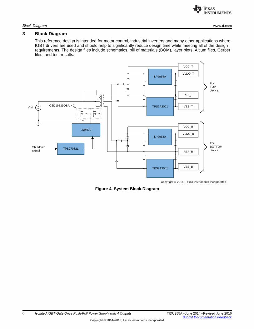
3 Block DiagramThis reference design is intended for motor control, industrial inverters and many other applications whereIGBT drivers are used and should help to significantly reduce design time while meeting all of the designrequirements. The design files include schematics, bill of materials (BOM), layer plots, Altium files, Gerberfiles, and test results.
Figure 4. System Block Diagram
www.ti.com Highlighted Products
7TIDU355A–June 2014–Revised June 2016Submit Documentation Feedback
Copyright © 2014–2016, Texas Instruments Incorporated
Isolated IGBT Gate-Drive Push-Pull Power Supply with 4 Outputs
4 Highlighted ProductsThis reference design features the following devices, which were selected based on their specifications:• LM5030 PWM controller• CSD19533 NexFET™ power MOSFET• TPS27082 high-side load switch• LP2954A micro power voltage regulator• TPS7A3001 linear regulator
For more information on each of these devices, see the respective product folders at www.ti.com or clickon the links for the product folders on the first page of this reference design.
4.1 Component Selection
4.1.1 LM5030The LM5030 high-voltage PWM controller contains all of the features needed to implement the push-pulltopology, using current-mode control in a small 10-pin package. This device provides two alternating gatedriver outputs. The LM5030 PWM controller includes a high-voltage, start-up regulator that operates overa wide input range of 14 V to 100 V.
Features include:• Error amplifier• Precision reference• Dual mode current limit• Slope compensation• Soft start• Sync capability• Thermal shutdown
This high speed IC has a defined dead time of 135 ns and a 1 MHz-capable, single-resistor-adjustableoscillator.
4.1.2 CSD19533This 100 V, 7.8 mΩ, SON 5 mm x 6 mm NexFET™ power MOSFET is designed to minimize losses inpower-conversion applications. The maximum drain current capability is much higher than the 1A designrequirement.
4.1.3 TPS27082LThe TPS27082L is a high side load switch that integrates a Power PFET and a control circuit in a tinyTSOT-23 package. The ON/OFF logic interface features hysteresis, which provides a robust logicinterface even under very noisy operating conditions. The ON/OFF interface supports direct interfacing tolow voltage GPIOs down to 1 V. The TPS27082L level shifts the ON/OFF logic signal to VIN levels withoutrequiring an external level shifter.
4.1.4 LP2954AThe LP2954A is a micropower voltage regulator with very low quiescent current (90 μA typical at 1 mAload) and very low dropout voltage (typically 60 mV at light loads and 470 mV at 250 mA load current).The adjustable LP2954A is provided in an 8-lead surface mount, small outline package. The adjustableversion also provides a resistor network which can be pin strapped to set the output to 5 V. The tight lineand load regulation (0.04% typical), as well as very low output temperature coefficient, make the LP2954Awell suited for use as a low-power voltage reference.
RT9
SS10
OUT26
VFB2
COMP3
VIN1
VCC4
GND7
OUT15
CS8
U1
LM5030MM/NOPB
D1
A2
C1
DNP
D2
A2
C1
DNP
D3
DNP
L1
GND
GND
GND
GND
GND
GND
GND
GND
GND
CS
GND
Vcc
2
17
,8
DNP
Q1ACSD88539ND
DNP
C21uF/63V
C3
22uF/16V
0.022µFC4
Vc
GD
2
GD
1
1
2
CONN1
0DNP
R1
0
R3
0R9
1000pFC5
0DNP
R10
0R11
0DNP
R13
0DNP
R15
22
R12
22
R14
47µFDNP
C1
0
R80
1.00kR2
12V
Z1MMSZ5242B-TP
26.7kR4
Highlighted Products www.ti.com
8 TIDU355A–June 2014–Revised June 2016Submit Documentation Feedback
Copyright © 2014–2016, Texas Instruments Incorporated
Isolated IGBT Gate-Drive Push-Pull Power Supply with 4 Outputs
4.1.5 TPS7A3001The TPS7A3001, is a negative, high-voltage (–36 V), ultralow-noise (15.1 μVRMS, 72 dB PSRR) linearregulator capable of sourcing a maximum load of 200 mA. This linear regulator includes a CMOS logic-level-compatible enable pin and capacitor-programmable soft-start function that allows for customizedpower–management schemes.
4.2 Circuit Design
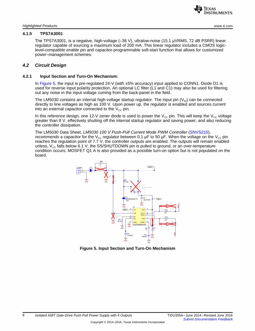
4.2.1 Input Section and Turn-On Mechanism:In Figure 5, the input is pre-regulated 24-V (with ±5% accuracy) input applied to CONN1. Diode D1 isused for reverse input polarity protection. An optional LC filter (L1 and C1) may also be used for filteringout any noise in the input voltage coming from the back-panel in the field.
The LM5030 contains an internal high-voltage startup regulator. The input pin (VIN) can be connecteddirectly to line voltages as high as 100 V. Upon power up, the regulator is enabled and sources currentinto an external capacitor connected to the VCC pin.
In this reference design, one 12-V zener diode is used to power the VCC pin. This will keep the VCC voltagegreater than 8 V, effectively shutting off the internal startup regulator and saving power, and also reducingthe controller dissipation.
The LM5030 Data Sheet, LM5030 100 V Push-Pull Current Mode PWM Controller (SNVS215),recommends a capacitor for the VCC regulator between 0.1 μF to 50 μF. When the voltage on the VCC pinreaches the regulation point of 7.7 V, the controller outputs are enabled. The outputs will remain enabledunless, VCC falls below 6.1 V, the SS/SHUTDOWN pin is pulled to ground, or an over-temperaturecondition occurs. MOSFET Q1 A is also provided as a possible turn-on option but is not populated on theboard.
Figure 5. Input Section and Turn-On Mechanism
dVI =C×
dt
100
1000
RT (K )Ω
OS
CIL
LA
TO
R F
RE
QU
EN
CY
(kH
z)
1 10 100
Oscillator Frequency vs RT
´
´
-9
-12
(1/f)-172 10RT =
182 10
www.ti.com Highlighted Products
9TIDU355A–June 2014–Revised June 2016Submit Documentation Feedback
Copyright © 2014–2016, Texas Instruments Incorporated
Isolated IGBT Gate-Drive Push-Pull Power Supply with 4 Outputs
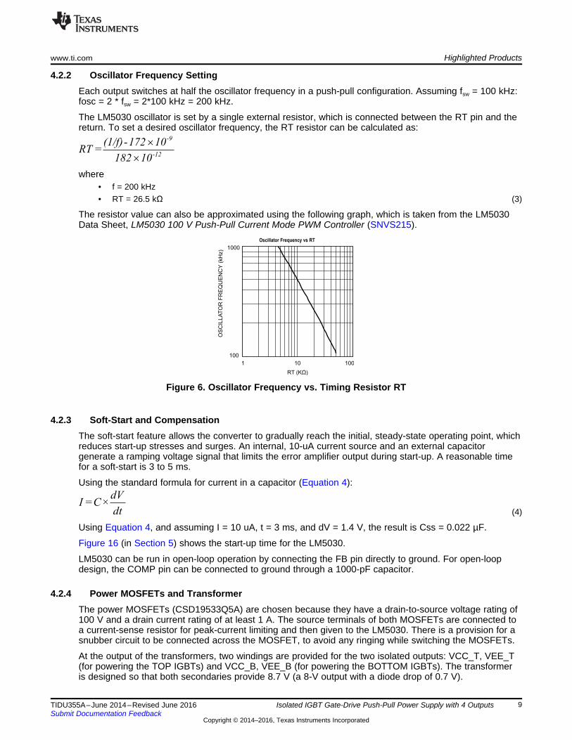
4.2.2 Oscillator Frequency SettingEach output switches at half the oscillator frequency in a push-pull configuration. Assuming fsw = 100 kHz:fosc = 2 * fsw = 2*100 kHz = 200 kHz.
The LM5030 oscillator is set by a single external resistor, which is connected between the RT pin and thereturn. To set a desired oscillator frequency, the RT resistor can be calculated as:
where• f = 200 kHz• RT = 26.5 kΩ (3)
The resistor value can also be approximated using the following graph, which is taken from the LM5030Data Sheet, LM5030 100 V Push-Pull Current Mode PWM Controller (SNVS215).
Figure 6. Oscillator Frequency vs. Timing Resistor RT
4.2.3 Soft-Start and CompensationThe soft-start feature allows the converter to gradually reach the initial, steady-state operating point, whichreduces start-up stresses and surges. An internal, 10-uA current source and an external capacitorgenerate a ramping voltage signal that limits the error amplifier output during start-up. A reasonable timefor a soft-start is 3 to 5 ms.
Using the standard formula for current in a capacitor (Equation 4):
(4)
Using Equation 4, and assuming I = 10 uA, t = 3 ms, and dV = 1.4 V, the result is Css = 0.022 µF.
Figure 16 (in Section 5) shows the start-up time for the LM5030.
LM5030 can be run in open-loop operation by connecting the FB pin directly to ground. For open-loopdesign, the COMP pin can be connected to ground through a 1000-pF capacitor.
4.2.4 Power MOSFETs and TransformerThe power MOSFETs (CSD19533Q5A) are chosen because they have a drain-to-source voltage rating of100 V and a drain current rating of at least 1 A. The source terminals of both MOSFETs are connected toa current-sense resistor for peak-current limiting and then given to the LM5030. There is a provision for asnubber circuit to be connected across the MOSFET, to avoid any ringing while switching the MOSFETs.
At the output of the transformers, two windings are provided for the two isolated outputs: VCC_T, VEE_T(for powering the TOP IGBTs) and VCC_B, VEE_B (for powering the BOTTOM IGBTs). The transformeris designed so that both secondaries provide 8.7 V (a 8-V output with a diode drop of 0.7 V).

D7
D9
D5
D4
D6
D8
GND
GND
CS
GND GND
REF_U_T
REF_U_T
REF_U_B
VCC_U_T
VEE_U_T
REF_U_T
REF_U_B
GND
Vcc
SW1
SW2
4
7,8
1,2
,3
5,6
,
Q2CSD19533Q5A
47
,81
,2,3
5,6
,Q3
CSD19533Q5A
1
3
5
7
8
13
14
T1
750342312
C10
10uF/50V
C1110uF/50V
C1210uF/50V
C22
10uF/50V
C2310uF/50V
C2410uF/50V
C922uF/35V
REF_U_T
REF_U_B
VCC_U_B
VEE_U_B
Green
A2
C1
LD1
Green
A2
C1
LD5
47µFC13
47µFDNP
C14
47µF
C2547µFDNP
C26
GD2
GD
1
DNPC7
DNPC8
0DNP
R18
0DNP
R19
10kR20
10kR30
REF_U_B
REF_U_B
1.15k
R16
0.22R17
0.1µFC84
0.1µFC86
470pFC6
Highlighted Products www.ti.com
10 TIDU355A–June 2014–Revised June 2016Submit Documentation Feedback
Copyright © 2014–2016, Texas Instruments Incorporated
Isolated IGBT Gate-Drive Push-Pull Power Supply with 4 Outputs
While the negative output voltages (VEE_T and VEE_B) are generated directly, to generate the positiveoutput voltages (VCC_T and VEE_B), the design uses cascaded voltage doublers (also called Greinachervoltage doublers). These doubler circuits generate 16 V at the VCC terminals.
Figure 7. MOSFETs and Transformer
Turning an IGBT on and off amounts to charging and discharging large capacitive loads, so the peakcharge current needs to be within the capability of the drive circuit. At the same time, the driver will haveto draw this peak charge current from its power supply in a short period of time, so it is important to useproper by-pass capacitors for the power supply.
To achieve the minimum output ripple with high-current load transients, we use a 47-µF capacitor (withone more 47-µF capacitor in parallel, which is not populated) at each output.
RT9
SS10
OUT26
VFB2
COMP3
VIN1
VCC4
GND7
OUT15
CS8
U1
LM5030MM/NOPBGND
GND
GND
GNDR2
1
VOUT2
VOUT3
VIN4
ON/OFF5
R1/C16
U2
TPS27082LDDC
GND
SDGND
0.022µFC4
Vc
GND
1
2
CONN2
100k
R5
10.0k
R6
0DNP
R7
24.9kR8
www.ti.com Highlighted Products
11TIDU355A–June 2014–Revised June 2016Submit Documentation Feedback
Copyright © 2014–2016, Texas Instruments Incorporated
Isolated IGBT Gate-Drive Push-Pull Power Supply with 4 Outputs
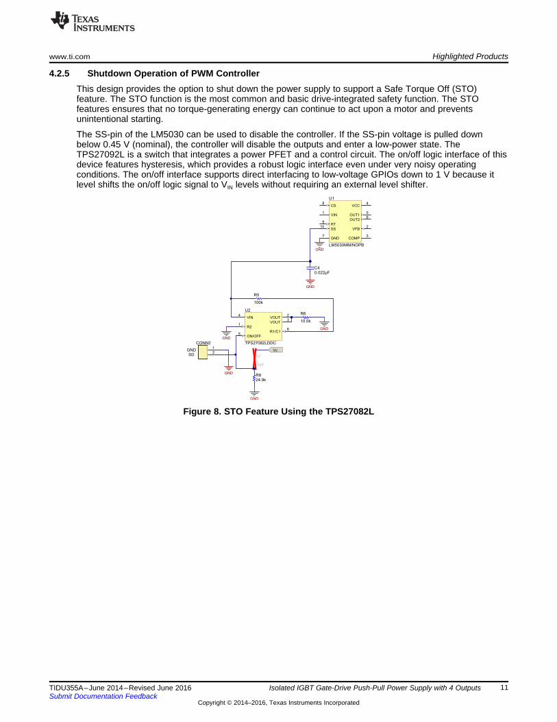
4.2.5 Shutdown Operation of PWM ControllerThis design provides the option to shut down the power supply to support a Safe Torque Off (STO)feature. The STO function is the most common and basic drive-integrated safety function. The STOfeatures ensures that no torque-generating energy can continue to act upon a motor and preventsunintentional starting.
The SS-pin of the LM5030 can be used to disable the controller. If the SS-pin voltage is pulled downbelow 0.45 V (nominal), the controller will disable the outputs and enter a low-power state. TheTPS27092L is a switch that integrates a power PFET and a control circuit. The on/off logic interface of thisdevice features hysteresis, which provides a robust logic interface even under very noisy operatingconditions. The on/off interface supports direct interfacing to low-voltage GPIOs down to 1 V because itlevel shifts the on/off logic signal to VIN levels without requiring an external level shifter.
Figure 8. STO Feature Using the TPS27082L

JAθ [ (Tj(max)-TA)/PD(max)]
[(115-60)/0.31]
177.4°C/W
£
£
£
= - = =in out outPD(max) (V V )* I 12.4V * 25 mA 310 mW
REF_U_T
REF_U_T
REF_U_T
REF_U_T
VCC_U_T
C15100pF
C164.7uF/25V
VLDO_U_T
REF_U_T
REF_U_T
Green
A2
C1
LD1
Green
A2
C1
LD2
OUT1
SNS2
SD3
GND4
ERR5
5V TAP6
FB7
IN8
U3
LP2954AIM/NOPB
47µFC13
47µFDNP
C14
10kR20
0R21
0R22
1.2MegDNP
R23
100kDNP
R24
10kR25
0.1µFC84
´ ´R1
OUT REF FBR2V = V ( 1+ )+(I R1)
Highlighted Products www.ti.com
12 TIDU355A–June 2014–Revised June 2016Submit Documentation Feedback
Copyright © 2014–2016, Texas Instruments Incorporated
Isolated IGBT Gate-Drive Push-Pull Power Supply with 4 Outputs
4.2.6 Positive and Negative Output Regulators
4.2.6.1 Positive Regulator (LP2954A)From the voltage doubler, the LP2954A is used as a post-regulator. The regulator can be programmed forany voltage between the 1.23 V reference and the 30 V maximum rating by using an external pair ofresistors.
The complete equation for the output voltage is:
where• VREF = 1.23 V reference• IFB = Feedback pin bias current (–20 nA typ.) (5)
The regulator can also be pin-strapped for 5-V operation, using the regulator's internal resistive divider bytying the OUT and SNS pins together, and then also tying the FB and 5-V TAP pins together. There is anoption in the design to generate a 5-V output by populating the 0Ω-resistors (R21 and R22 in Figure 9).This 5-V output voltage is also provided at the output connector (VLDO_T and VLDO_B) for each phase.
Figure 9. Positive Regulator (Set at 5 V)
As of now, the output of each LP2954A regulator is set to 5 V and the presence of VCC as well as theVLDO outputs is indicated, using the respective green LEDs. For 16 to 5 V conversion, it is important tocalculate the power dissipation and check whether the LP2954A resistor is suitable for the conversion.
Equation 6 shows the power calculations for the LP2954A resistor:
where• Vin = 17.4 V (worst case)• Vout = 5 V• Iout = 25 mA (max)• and assuming TA = 60ºC (6)
Referring to the LP2954A Data Sheet, LP2954/LP2954A 5 V and Adjustable Micropower Low-DropoutVoltage Regulators (SNVS096), Tj(max) = 125ºC, and a derating of 10ºC gives Tj(max) = 115ºC
(7)
Referring to the LP2954A Data Sheet, LP2954/LP2954A 5 V and Adjustable Micropower Low-DropoutVoltage Regulators, page 2, (SNVS096), it is clear that LP2954A can handle the power for this condition,as the LP2954A Data Sheet lists θJA = 160°C/W.

REF_U_T
REF_U_T
REF_U_T
REF_U_T
REF_U_T
REF_U_T
VEE_U_T1 2
J1
C2110uF/16V
REF_U_T
REF_U_T
GreenA2
C1
LD4
Green
A2
C1
LD3
OUT1
SNS/FB2
NC3
GND4
EN5
SS/NR6
DNC7
IN8
PW
PD
9
U4
TPS7A3001DGN
47µFDNP
C1847µFC17
0.01µFC19
0.01µFC20
10kR29
10k
R26
102kR28
0.1µFC85
330kR27
From transformer
OUT
1 2
V5 A
R RPt
�
OUT
REF
VR1 R2( 1)
V= -
www.ti.com Highlighted Products
13TIDU355A–June 2014–Revised June 2016Submit Documentation Feedback
Copyright © 2014–2016, Texas Instruments Incorporated
Isolated IGBT Gate-Drive Push-Pull Power Supply with 4 Outputs
4.2.6.2 Negative Regulator (TPS7A3001)The output coming from the transformer after diode rectification is given to the TPS7A3001, the negativeregulator. The TPS7A3001 has an output voltage range of –1.174 V to –33 V. The nominal output voltageof the regulator is set by two external resistors. To ensure stability under no-load conditions, this resistivenetwork must provide a current equal to or greater than 5 μA.
R1 and R2 can be calculated for any output voltage, using Equation 8:
where
•• VREF = –1.179 V reference (8)
Using Equation 8, and considering R2 = 102 kΩ to get the output voltage of –5 V, R1 is calculated as330 kΩ.
Figure 10. Negative Regulator (Set at –5 V)
As of now, the output of each TPS7A3001 resistor is set to -5 V and the presence of the VEE output isindicated by a green LED. If it is not necessary to use the negative regulator, and the output of thetransformer is directly required, there is an option to bypass the regulator by using a jumper (J1 inFigure 10).
For –8.7 V to –5 V conversion, it is important to calculate the power dissipation and to check whetherTPS7A3001 is able to do the conversion.
Equation 9 shows the power calculations for TPS7A3001:PD(max) = (Vin – Vout) × Iout = 3.7 V × 25 mA = 92.5 mW
where• Vin = –8.7 V• Vout = –5 V• Iout = –25 mA (max)• and assuming TA = 60°C (9)
Referring to the TPS7A3001 Data Sheet, TPS7A3001 –36 V, –200 mA, Ultralow-Noise, Negative LinearRegulator,(SBVS125), Tj(max) = 125°C, and a derating of 10°C results in Tj(max) = 115°C.
θJA ≤ [ (Tj(max) – TA) / PD(max) ]
≤ [ (115 – 60) / 0.0925]
≤ 594.59°C/W
Referring to the TPS7A3001 Data Sheet, TPS7A3001 –36 V, –200 mA, Ultralow-Noise, Negative LinearRegulator, (SBVS125), it is clear that the resistor can handle the required power for this condition, as theTPS7A3001 Data Sheet shows θJA = 55.09°C/W.

Highlighted Products www.ti.com
14 TIDU355A–June 2014–Revised June 2016Submit Documentation Feedback
Copyright © 2014–2016, Texas Instruments Incorporated
Isolated IGBT Gate-Drive Push-Pull Power Supply with 4 Outputs
4.2.7 Three Transformers to Power All Three IGBT Arms of 3-phase InverterThe push-pull topology allows connection of transformers in parallel, which allows the IGBTs in all threearms (U, V, and W) to be powered using a single controller..
The outputs are as shown in Table 1:
(1) This table shows outputs for all three arms.
Table 1. Outputs for Top and Bottom IGBTs (1)
Phase For TOP IGBT For BOTTOM IGBT
U
VCC_U_T VCC_U_BVEE_U_T VEE_U_B
VLDO_U_T VLDO_U_BREF_U_T REF_U_B
V
VCC_V_T VCC_V_BVEE_V_T VEE_V_B
VLDO_V_T VLDO_V_BREF_V_T REF_V_B
W
VCC_W_T VCC_W_BVEE_W_T VEE_W_B
VLDO_W_T VLDO_W_BREF_W_T REF_W_B
4.2.8 Scalability Option for Higher-Power Industrial Drives:This design is intended to be used with IGBT modules with ratings of 1200 V/200 A. If higher power IGBTmodules are to be powered, the same reference design can be scaled up to for higher power by changingthe transformer design. The existing transformers have secondary, output current ratings of 250 mA each.This rating can be increased to meet the requirement for higher-power Industrial drives.

www.ti.com Test Data
15TIDU355A–June 2014–Revised June 2016Submit Documentation Feedback
Copyright © 2014–2016, Texas Instruments Incorporated
Isolated IGBT Gate-Drive Push-Pull Power Supply with 4 Outputs
5 Test Data
5.1 Section 1: Functional Test Results for the LM5030Figure 11, Figure 12, and Figure 13 show the MOSFET gate drive signals and the dead-time between thetwo output pins of the LM5030. It can be seen from Figure 12 and Figure 13 that the dead-time betweenthe two gate drive signals is 130.8 ns and 134 ns respectively. The typical value of dead time from theLM5030 datasheet is 135 ns.
Figure 11. Gate Drive Signals for Both MOSFETs (Q2and Q3 in Figure 7)
Figure 12. Dead-Time Between Gate-Drive Signals(Rising Edge of GATE1 Shown)
Figure 13. Dead-Time Between Gate-Drive Signals (Falling Edge of GATE1 Shown)

Test Data www.ti.com
16 TIDU355A–June 2014–Revised June 2016Submit Documentation Feedback
Copyright © 2014–2016, Texas Instruments Incorporated
Isolated IGBT Gate-Drive Push-Pull Power Supply with 4 Outputs
Figure 14 and Figure 15 show the MOSFET gate versus the MOSFET drain signals for Q2 and Q3 (inFigure 7). The duty cycle is currently set to the maximum (by connecting the COMP pin to ground througha 1000-pF capacitor shown in Section 4.2.1)
Figure 14. Gate Drive versus Drain Voltage for Q2 Figure 15. Gate Drive versus Drain Voltage for Q3
Figure 16 shows the soft-start operation of the PWM controller LM5030. As per the calculations, the SStime is set to 3 ms and the test waveform also shows the same start-up time for LM5030.
Figure 16. Soft-Start for LM5030 Figure 17. Zoomed Waveform Showing tss = 3 ms

www.ti.com Test Data
17TIDU355A–June 2014–Revised June 2016Submit Documentation Feedback
Copyright © 2014–2016, Texas Instruments Incorporated
Isolated IGBT Gate-Drive Push-Pull Power Supply with 4 Outputs
TPS27082L is used as a switch to facilitate the STO feature for the industrial drives. The LM5030 SS-pinhas dual functions. The LM5030-SS pin is used for soft-start operation and also for shutdown during STO.The soft-start operation and shutdown has been tested, and the waveform in Figure 18 shows theshutdown signal along with the outputs going to zero.
Figure 18. Shutting Down the LM5030 Using an External Signal
LM5030 is a current mode-control device. It contains two levels of overcurrent protection. Therefore, if thevoltage on the current-sense comparator exceeds 0.5 V, the present cycle is terminated (cycle-by-cyclecurrent limit). If the voltage on the current sense comparator exceeds 0.625 V, the controller will terminatethe present cycle and discharge the soft-start capacitor.
The LM5030 CS and PWM comparators are fast, so they will respond to short-duration noise pulses. Thesecond level threshold is intended to protect the power converter by initiating a low-duty, cycle hiccupmode when any abnormally high, fast-rising currents occur. During excessive loading, the first-levelthreshold will always be reached. The output characteristic of the converter will be that of current source.However, this sustained current level can cause excessive temperatures in the power train, especially inthe output rectifiers.
If the second-level threshold is reached, the soft-start capacitor will be fully discharged. A retry willcommence following discharge detection. The second-level threshold will only be reached when a highdV/dt is present at the current-sense pin. The signal must be fast enough to reach the second-levelthreshold before the first-threshold detector turns off the driver. This can usually happen for a saturatedpower inductor, or for a shorted load. Excessive filtering on the CS pin, an extremely low-value, current-sense resistor, or an inductor that does not saturate with excessive loading may prevent the second-levelthreshold from ever being reached.
Test Data www.ti.com
18 TIDU355A–June 2014–Revised June 2016Submit Documentation Feedback
Copyright © 2014–2016, Texas Instruments Incorporated
Isolated IGBT Gate-Drive Push-Pull Power Supply with 4 Outputs
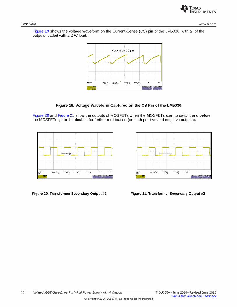
Figure 19 shows the voltage waveform on the Current-Sense (CS) pin of the LM5030, with all of theoutputs loaded with a 2 W load.
Figure 19. Voltage Waveform Captured on the CS Pin of the LM5030
Figure 20 and Figure 21 show the outputs of MOSFETs when the MOSFETs start to switch, and beforethe MOSFETs go to the doubler for further rectification (on both positive and negative outputs).
Figure 20. Transformer Secondary Output #1 Figure 21. Transformer Secondary Output #2

www.ti.com Test Data
19TIDU355A–June 2014–Revised June 2016Submit Documentation Feedback
Copyright © 2014–2016, Texas Instruments Incorporated
Isolated IGBT Gate-Drive Push-Pull Power Supply with 4 Outputs
5.2 Section 2: Output Ripple Under Different Test ConditionsWith all of the outputs loaded with 2 W of output power, the ripple at the 16-V output and –8 V outputs arecaptured. On the 16-V output, the peak-to-peak ripple voltage is 59 mV and on the –8 V output, the peak-to-peak ripple voltage is 50 mV. Figure 22 and Figure 23 show the waveforms for the same.
Figure 22. Ripple Voltage on 16 V Output Figure 23. Ripple Voltage on –8 V Output
Both the linear regulators (LP2954A and TPS7A3001) are tested for ripple at the output with load of 25mA on each. Figure 24 and Figure 25 show the ripple waveforms on the same.
Figure 24. Ripple on 5 V Output (LP2954A) Figure 25. Ripple on –5 V Output (TPS7A3001)

±8
±7
±6
±5
±4
±3
±2
±1
0
0.00 0.01 0.02 0.03 0.04 0.05 0.06 0.07 0.08 0.09 0.10 0.11
Reg
ulat
ion
(%)
Load Current (A)
+16V Regulation
+16V Cross Regulation (-8V loaded)
-8V Cross Regulation (+16V loaded)
-8V Regulation
C001
0
10
20
30
40
50
60
70
80
90
0 0.5 1 1.5 2 2.5
Effi
cenc
y (%
)
Pout (W)
Vin = 22.8V
Vin = 24V
Vin = 25.2V
C004
Test Data www.ti.com
20 TIDU355A–June 2014–Revised June 2016Submit Documentation Feedback
Copyright © 2014–2016, Texas Instruments Incorporated
Isolated IGBT Gate-Drive Push-Pull Power Supply with 4 Outputs
5.3 Section 3: Regulation and EfficiencyThe efficiency is measured with all six outputs loaded with equal loads. When all the outputs were loadedwith 2 W load each, the efficiency is around 78% as shown in Figure 26.
Figure 26. Efficiency at Different Vin Values
The regulation and cross-regulation data is captured at different Vin values as shown in Figure 27,Figure 28, and Figure 29. While measuring the regulation and cross-regulation, five (out of six) outputs areloaded with 2 W load each and one output is varied from 0% to 100%. The cross regulation is included soas to show that there is not much interference when TOP IGBT is powered and Bottom IGBT is notpowered (or TOP IBGT is not powered and Bottom IGBT is powered).
Figure 27. Regulation and Cross Regulation (Vin = 22.8 V)
Figure 28. Regulation and Cross Regulation (Vin = 24 V)
PiccoloLaunchPADTM
ISO5500-EVM
ISO5500-EVM
TIDA-00181
VCC_U_T VEE_U_T REF_U_T
VCC_U_B VEE_U_B REF_U_B
VCC_U_T
VEE_U_T
VCC_U_B
VEE_U_B
NPN
PNP
4 �
4 �
G
G
C
E
C
E
IGBT 1
IGBT 2
1k �load
600 V
NPN
PNP
0.0
1.0
2.0
3.0
4.0
5.0
6.0
7.0
8.0
9.0
0.00 0.01 0.02 0.03 0.04 0.05 0.06 0.07 0.08 0.09 0.10 0.11
Reg
ulat
ion
(%)
Load Current (A)
+16V Regulation
+16V Cross Regulation
-8V Cross Regulation
-8V Regulation
C003
www.ti.com Test Data
21TIDU355A–June 2014–Revised June 2016Submit Documentation Feedback
Copyright © 2014–2016, Texas Instruments Incorporated
Isolated IGBT Gate-Drive Push-Pull Power Supply with 4 Outputs
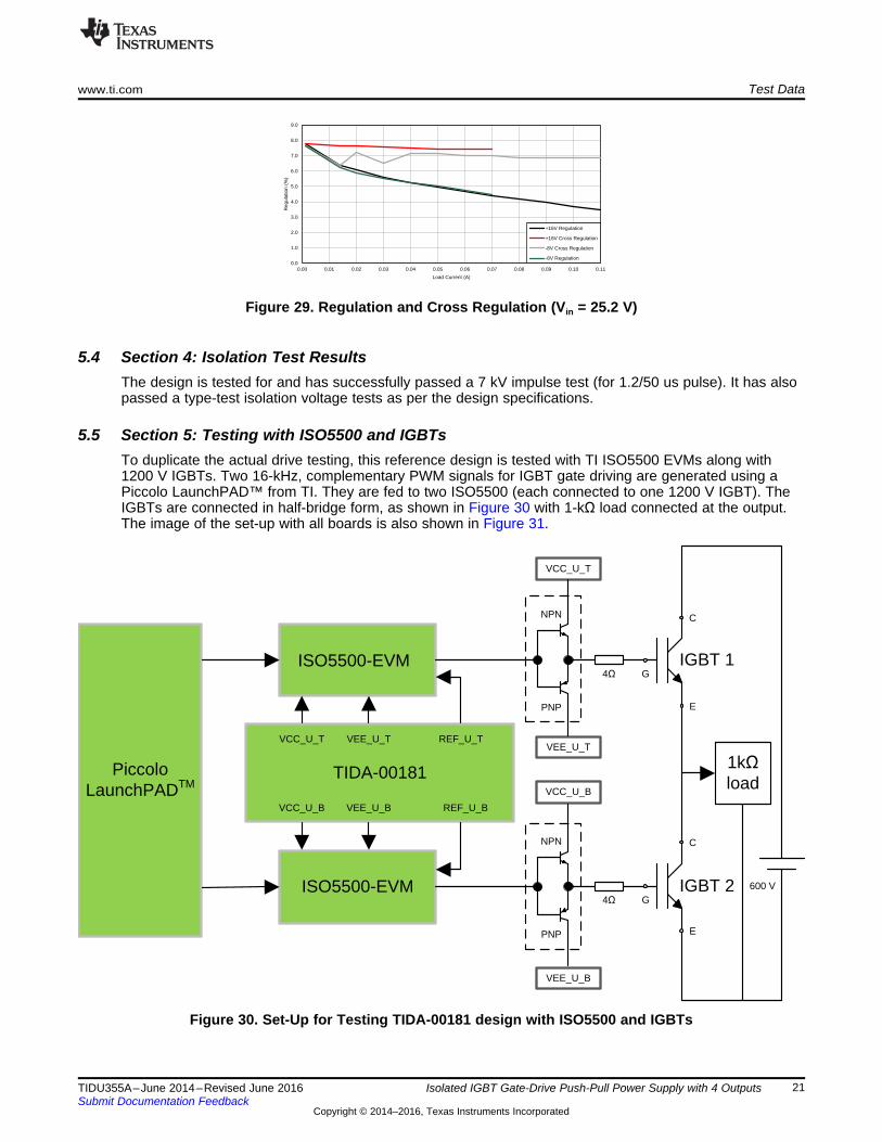
Figure 29. Regulation and Cross Regulation (Vin = 25.2 V)
5.4 Section 4: Isolation Test ResultsThe design is tested for and has successfully passed a 7 kV impulse test (for 1.2/50 us pulse). It has alsopassed a type-test isolation voltage tests as per the design specifications.
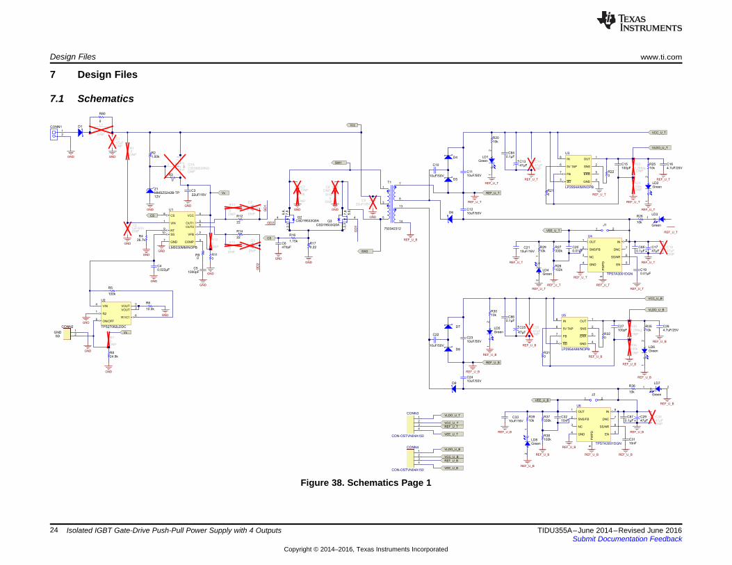
5.5 Section 5: Testing with ISO5500 and IGBTsTo duplicate the actual drive testing, this reference design is tested with TI ISO5500 EVMs along with1200 V IGBTs. Two 16-kHz, complementary PWM signals for IGBT gate driving are generated using aPiccolo LaunchPAD™ from TI. They are fed to two ISO5500 (each connected to one 1200 V IGBT). TheIGBTs are connected in half-bridge form, as shown in Figure 30 with 1-kΩ load connected at the output.The image of the set-up with all boards is also shown in Figure 31.
Figure 30. Set-Up for Testing TIDA-00181 design with ISO5500 and IGBTs

TIDA-00181Board
3LFFROR�/DXQFK3$'��
Two ISO5500EVMs
Test Data www.ti.com
22 TIDU355A–June 2014–Revised June 2016Submit Documentation Feedback
Copyright © 2014–2016, Texas Instruments Incorporated
Isolated IGBT Gate-Drive Push-Pull Power Supply with 4 Outputs
Figure 31. Set-Up
To measure the ripple, both ISO5500s are applied with the TIDA-00181 power supply and the IGBT arm isapplied with a 600 V supply. Figure 32 and Figure 33 show the 200 mV ripple which meets thespecification of the reference design.
Figure 32. Ripple on 16 V output (For dv/dt = 11.9*E9 onthe Output Load)
Figure 33. Ripple on –8 V Output (for dv/dt = 11.9*E9 onthe Output Load)
The current boost transistors (NPN and PNP) are used to boost the output current of the ISO5500 in orderto drive the IGBTs. With 6-A peak current while charging the internal capacitance of IGBTs, the ripple onthe VCC and VEE outputs of power supply are also measured. Figure 34 and Figure 35 show the ripplevoltage along with the IGBT gate capacitor charging current spikes.

www.ti.com Layout Guidelines for LM5030
23TIDU355A–June 2014–Revised June 2016Submit Documentation Feedback
Copyright © 2014–2016, Texas Instruments Incorporated
Isolated IGBT Gate-Drive Push-Pull Power Supply with 4 Outputs
Figure 34. Ripple on 16-V output (for 6 A peak loadcurrent with IGBTs)
Figure 35. Zoomed Waveforms
Figure 36. Ripple on –8 V output for 6-A peak loadcurrent with IGBTs
Figure 37. Zoomed Waveforms
6 Layout Guidelines for LM5030The LM5030 contains two levels of over-current protection. If the voltage on the current sense comparatorexceeds 0.5 Volts, the present cycle is terminated (cycle by cycle current limit). If the voltage on thecurrent sense comparator exceeds 0.625 Volts, the controller will terminate the present cycle anddischarge the soft-start capacitor.
A small RC filter, located near the controller, is recommended for the CS pin. An internal MOSFETdischarges the current sense filter capacitor at the conclusion of every cycle, to improve dynamicperformance. The LM5030 CS and PWM comparators are very fast, and therefore will respond to shortduration noise pulses. Layout considerations are critical for the current sense filter and sense resistor. Thecapacitor associated with the CS filter must be placed very close to the device and connected directly tothe pins of the IC (CS and RTN).
If a current sense resistor located in the drive transistor sources is used, for current sense, a lowinductance resistor should be chosen. In this case, all of the noise sensitive low power grounds should becommoned together around the IC. Then a single connection should be made to the power ground(sense-resistor ground point). The RT resistor should also be located very close to the device andconnected directly to the pins of the IC (RT and GND).
RT9
SS10
OUT26
VFB2
COMP3
VIN1
VCC4
GND7
OUT15
CS8
U1
LM5030MM/NOPB
D1
D7
D9
D5
D4
D6
D8
A2
C1
DNP
D2
A2
C1
DNP
D3
DNP
L1
GND
GND
GND
GND
GND
GND
GND
GND
GND
GND
GND
GND
GND
CS
CS
GND GND
REF_U_T
REF_U_T
REF_U_T
REF_U_T
REF_U_T
REF_U_T
REF_U_T
REF_U_T
REF_U_T
REF_U_T
REF_U_T
REF_U_B
VCC_U_T
VEE_U_T
GND
REF_U_T
REF_U_B
GND
Vcc
SW1
SW2
R21
VOUT2
VOUT3
VIN4
ON/OFF5
R1/C16
U2
TPS27082LDDC
2
17
,8
DNP
Q1ACSD88539ND
4
7,8
1,2
,3
5,6
,
Q2CSD19533Q5A
4
7,8
1,2
,3
5,6
,
Q3CSD19533Q5A
1 2
J1
1
3
5
7
8
13
14
T1
750342312DNP
C21uF/63V
C10
10uF/50V
C1110uF/50V
C1210uF/50V
C22
10uF/50V
C2310uF/50V
C2410uF/50V
C15100pF
C164.7uF/25V
C2110uF/16V
C922uF/35V
C3
22uF/16V
GND
SDGND
0.022µFC4
Vc
Vc
GND
VLDO_U_T
REF_U_T
REF_U_T
REF_U_T
REF_U_T
REF_U_B
REF_U_B
REF_U_B
REF_U_B
VCC_U_B
C27100pF
C284.7uF/25V
VLDO_U_B
REF_U_B
REF_U_B
REF_U_BREF_U_B
REF_U_B
REF_U_B
REF_U_B
VEE_U_B1 2
J2
C3310uF/16V
C3210nF
C3110nF
REF_U_B
1
2
3
4
CONN3
CON-OSTVN04A150
VCC_U_T
VLDO_U_T
REF_U_T
VEE_U_T
Green
A2
C1
LD1
Green
A2
C1
LD2
GreenA2
C1
LD4
Green
AC1
LD3
1
2
3
4
CONN4
CON-OSTVN04A150
VCC_U_B
VLDO_U_B
REF_U_B
VEE_U_B
OUT1
SNS2
SD3
GND4
ERR5
5V TAP6
FB7
IN8
U3
LP2954AIM/NOPB
OUT1
SNS/FB2
NC3
GND4
EN5
SS/NR6
DNC7
IN8
PW
PD
9
U4
TPS7A3001DGN
OUT1
SNS2
SD3
GND4
ERR5
5V TAP6
FB7
IN8
U5
LP2954AIM/NOPB
OUT1
SNS/FB2
NC3
GND4
EN5
SS/NR6
DNC7
IN8
PW
PD
9
U6
TPS7A3001DGN
Green
A2
C1
LD5
Green
A2
C1
LD6
Green
A2
C1
LD7
Green
A2
C1
LD8
REF_U_B
47µFC13
47µFDNP
C14
47µF
C2547µFDNP
C26
47µFDNP
C1847µFC17
47µFDNP
C3047µFC29
GD
2
GD2
GD
1
GD
1
1
2
CONN2
0.01µFC19
0.01µFC20
1
2
CONN1
0DNP
R1
0
R3
100k
R5
10.0k
R6
0DNP
R7
0R9
1000pFC5
0DNP
R10
0R11
0DNP
R13
0DNP
R15
22
R12
22
R14
DNPC7
DNPC8
0DNP
R18
0DNP
R19
10kR20
0R21
0R22
1.2MegDNP
R23
100kDNP
R24
10kR25
10kR29
10k
R26
102kR28
10kR30
0R31
0R32
1.2Meg
DNP
R33
100k
DNP
R34
10kR35
10kR39
102kR38
10k
R36
REF_U_B
REF_U_B
47µFDNP
C1
0
R80
1.15k
R16
0.22R17
1.00kR2
0.1µFC84
0.1µFC85
0.1µFC86
0.1µFC87
470pFC6
12V
Z1MMSZ5242B-TP
26.7kR4
330kR27
330kR37
24.9kR8
Design Files www.ti.com
24 TIDU355A–June 2014–Revised June 2016Submit Documentation Feedback
Copyright © 2014–2016, Texas Instruments Incorporated
Isolated IGBT Gate-Drive Push-Pull Power Supply with 4 Outputs
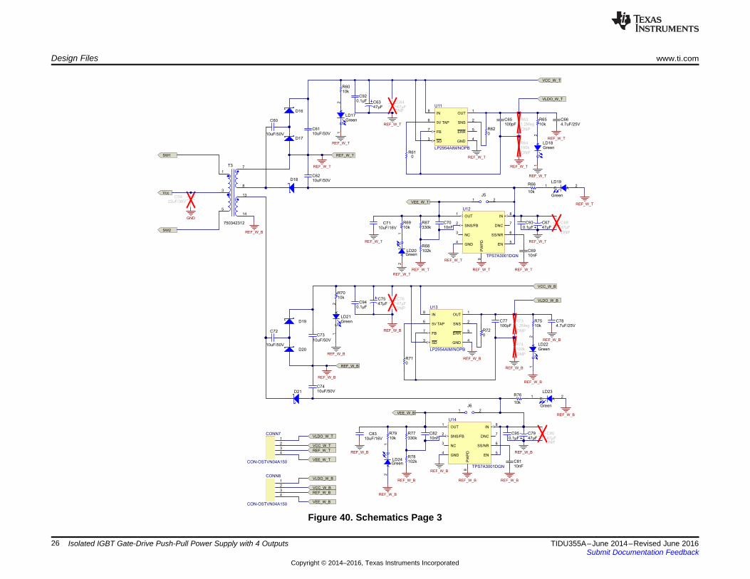
7 Design Files
7.1 Schematics
Figure 38. Schematics Page 1

GND
Vcc
SW1
SW2
1
3
5
7
8
13
14
T2
750342312
D13
D15
D11
D10
D12
D14
REF_V_T
REF_V_T
REF_V_T
REF_V_T
REF_V_T
REF_V_TREF_V_T
REF_V_T
REF_V_T
REF_V_T
REF_V_T
REF_V_B
VCC_V_T
VEE_V_T
REF_V_T
REF_V_B
1 2
J3
C35
10uF/50V
C3610uF/50V
C3710uF/50V
C47
10uF/50V
C4810uF/50V
C4910uF/50V
C40100pF
C414.7uF/25V
C4610uF/16V
C4510nF
C4410nF
VLDO_V_T
REF_V_T
REF_V_T
REF_V_T
REF_V_T
REF_V_B
REF_V_B
REF_V_B
VCC_V_B
C52100pF
C534.7uF/25V
VLDO_V_B
REF_V_B
REF_V_B
REF_V_BREF_V_B
REF_V_B
REF_V_B
REF_V_B
VEE_V_B1 2
J4
C5810uF/16V
C5710nF
C5610nF
REF_V_B
REF_V_B
1
2
3
4
CONN5
CON-OSTVN04A150
1
2
3
4
CONN6
CON-OSTVN04A150
REF_V_T
VEE_V_T
VEE_V_B
REF_V_B
VCC_V_B
VCC_V_T
VLDO_V_T
VLDO_V_B
Green
A2
C1
LD9
Green
A2
C1
LD10
Green
A2
C1
LD11
Green
A2
C1
LD12
OUT1
SNS2
SD3
GND4
ERR5
5V TAP6
FB7
IN8
U7
LP2954AIM/NOPB
OUT1
SNS/FB2
NC3
GND4
EN5
SS/NR6
DNC7
IN8
PW
PD
9
U8
TPS7A3001DGN
Green
A2
C1
LD13
Green
A2
C1
LD14
REF_V_B
Green
A2
C1
LD15
GreenA2
C1
LD16
OUT1
SNS2
SD3
GND4
ERR5
5V TAP6
FB7
IN8
U9
LP2954AIM/NOPB
OUT1
SNS/FB2
NC3
GND4
EN5
SS/NR6
DNC7
IN8
PW
PD
9
U10
TPS7A3001DGN
47µFC38
47µFDNP
C39
47µFC42
47µFDNP
C43
47µFC54
47µFDNP
C55
47µFC50
47µF
DNP
C51
22µFC34
10kR40
0DNP
R41
0DNP
R421.2MegR43
100kR44
10kR45
10kR49
102kR48
10k
R46
10kR50
0DNP
R51
0DNP
R521.2MegR53
100kR54
10kR55
10k
R56
102kR58
10kR59
REF_V_B
REF_V_B
0.1µFC88
0.1µFC89
0.1µFC90
0.1µFC91
330kR47
330kR57
www.ti.com Design Files
25TIDU355A–June 2014–Revised June 2016Submit Documentation Feedback
Copyright © 2014–2016, Texas Instruments Incorporated
Isolated IGBT Gate-Drive Push-Pull Power Supply with 4 Outputs
Figure 39. Schematics Page 2
GND
Vcc
SW1
SW2
1
3
5
7
8
13
14
T3
750342312
C5922uF/35V
D19
D21
D17
D16
D18
D20
REF_W_T
REF_W_T
REF_W_T
REF_W_T
REF_W_T
REF_W_TREF_W_T
REF_W_T
REF_W_T
REF_W_T
REF_W_T
REF_W_B
VCC_W_T
VEE_W_T
REF_W_T
REF_W_B
1 2
J5
C60
10uF/50V
C6110uF/50V
C6210uF/50V
C72
10uF/50V
C73
10uF/50V
C7410uF/50V
C65100pF
C664.7uF/25V
C7110uF/16V
C7010nF
C6910nF
VLDO_W_T
REF_W_T
REF_W_T
REF_W_T
REF_W_T
REF_W_B
REF_W_B
REF_W_B
VCC_W_B
C77100pF
C784.7uF/25V
VLDO_W_B
REF_W_B
REF_W_B
REF_W_BREF_W_B
REF_W_B
REF_W_B
REF_W_B
VEE_W_B1 2
J6
C8310uF/16V
C8210nF
C8110nF
REF_W_B
REF_W_B
1
2
3
4
CONN7
CON-OSTVN04A150
1
2
3
4
CONN8
CON-OSTVN04A150
VLDO_W_T
VCC_W_T
REF_W_T
VEE_W_T
VLDO_W_B
VCC_W_B
REF_W_B
VEE_W_B
Green
A2
C1
LD17
Green
A2
C1
LD18
Green
A2
C1
LD19
GreenA2
C1
LD20
Green
A2
C1
LD21
Green
A2
C1
LD22
Green
A2
C1
LD23
Green
A2
C1
LD24
OUT1
SNS2
SD3
GND4
ERR5
5V TAP6
FB7
IN8
U11
LP2954AIM/NOPB
OUT1
SNS/FB2
NC3
GND4
EN5
SS/NR6
DNC7
IN8
PW
PD
9
U12
TPS7A3001DGN
OUT1
SNS/FB2
NC3
GND4
EN5
SS/NR6
DNC7
IN8
PW
PD
9
U14
TPS7A3001DGN
OUT1
SNS2
SD3
GND4
ERR5
5V TAP6
FB7
IN8
U13
LP2954AIM/NOPB
47µFC63
47µFDNP
C64
47µF
DNP
C6847µFC67
47µFC75
47µFDNP
C76
47µFDNP
C8047µFC79
10kR60
0R61
0R62
1.2Meg
DNP
R63
100k
DNP
R64
10kR65
10k
R66
102kR68
10kR69
10kR70
0R71
0R72
1.2Meg
DNP
R73
100k
DNP
R74
10kR75
10kR79
102kR78
10k
R76
REF_W_B
REF_W_B
REF_W_B
0.1µFC92
0.1µFC94
0.1µFC95
0.1µFC93
330kR67
330kR77
Design Files www.ti.com
26 TIDU355A–June 2014–Revised June 2016Submit Documentation Feedback
Copyright © 2014–2016, Texas Instruments Incorporated
Isolated IGBT Gate-Drive Push-Pull Power Supply with 4 Outputs
Figure 40. Schematics Page 3

www.ti.com Design Files
27TIDU355A–June 2014–Revised June 2016Submit Documentation Feedback
Copyright © 2014–2016, Texas Instruments Incorporated
Isolated IGBT Gate-Drive Push-Pull Power Supply with 4 Outputs
Design Files www.ti.com
28 TIDU355A–June 2014–Revised June 2016Submit Documentation Feedback
Copyright © 2014–2016, Texas Instruments Incorporated
Isolated IGBT Gate-Drive Push-Pull Power Supply with 4 Outputs
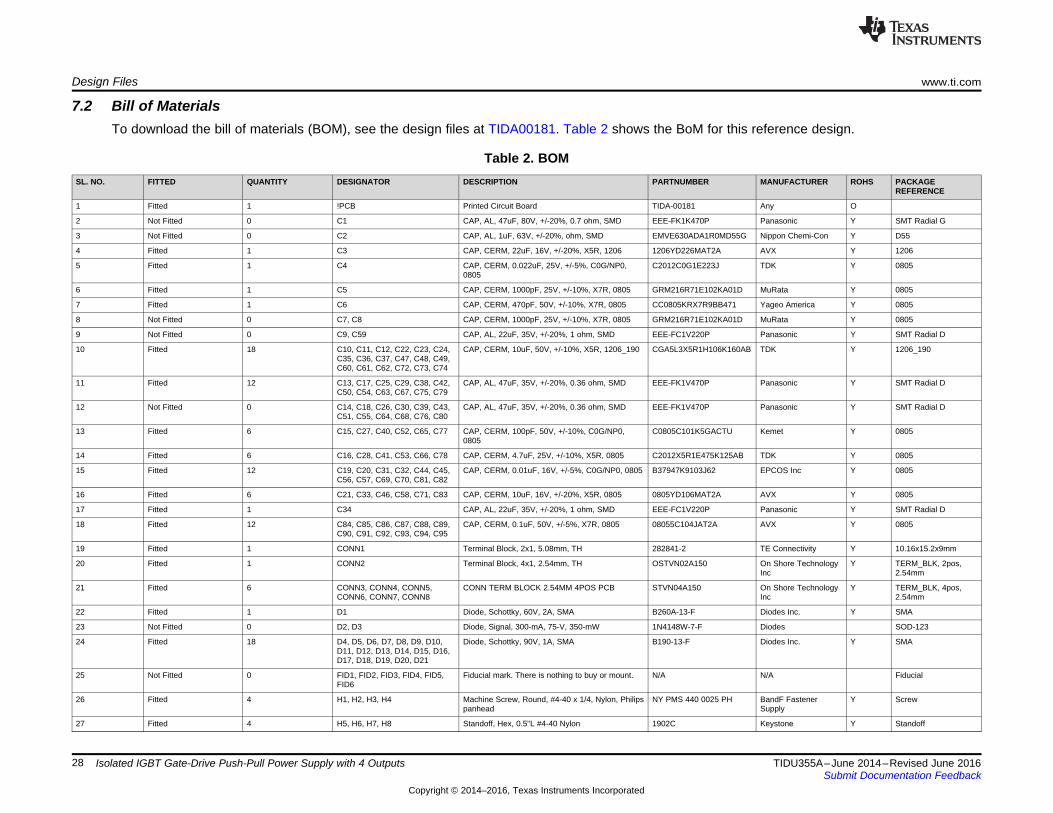
7.2 Bill of MaterialsTo download the bill of materials (BOM), see the design files at TIDA00181. Table 2 shows the BoM for this reference design.
Table 2. BOMSL. NO. FITTED QUANTITY DESIGNATOR DESCRIPTION PARTNUMBER MANUFACTURER ROHS PACKAGE
REFERENCE
1 Fitted 1 !PCB Printed Circuit Board TIDA-00181 Any O
2 Not Fitted 0 C1 CAP, AL, 47uF, 80V, +/-20%, 0.7 ohm, SMD EEE-FK1K470P Panasonic Y SMT Radial G
3 Not Fitted 0 C2 CAP, AL, 1uF, 63V, +/-20%, ohm, SMD EMVE630ADA1R0MD55G Nippon Chemi-Con Y D55
4 Fitted 1 C3 CAP, CERM, 22uF, 16V, +/-20%, X5R, 1206 1206YD226MAT2A AVX Y 1206
5 Fitted 1 C4 CAP, CERM, 0.022uF, 25V, +/-5%, C0G/NP0,0805
C2012C0G1E223J TDK Y 0805
6 Fitted 1 C5 CAP, CERM, 1000pF, 25V, +/-10%, X7R, 0805 GRM216R71E102KA01D MuRata Y 0805
7 Fitted 1 C6 CAP, CERM, 470pF, 50V, +/-10%, X7R, 0805 CC0805KRX7R9BB471 Yageo America Y 0805
8 Not Fitted 0 C7, C8 CAP, CERM, 1000pF, 25V, +/-10%, X7R, 0805 GRM216R71E102KA01D MuRata Y 0805
9 Not Fitted 0 C9, C59 CAP, AL, 22uF, 35V, +/-20%, 1 ohm, SMD EEE-FC1V220P Panasonic Y SMT Radial D
10 Fitted 18 C10, C11, C12, C22, C23, C24,C35, C36, C37, C47, C48, C49,C60, C61, C62, C72, C73, C74
CAP, CERM, 10uF, 50V, +/-10%, X5R, 1206_190 CGA5L3X5R1H106K160AB TDK Y 1206_190
11 Fitted 12 C13, C17, C25, C29, C38, C42,C50, C54, C63, C67, C75, C79
CAP, AL, 47uF, 35V, +/-20%, 0.36 ohm, SMD EEE-FK1V470P Panasonic Y SMT Radial D
12 Not Fitted 0 C14, C18, C26, C30, C39, C43,C51, C55, C64, C68, C76, C80
CAP, AL, 47uF, 35V, +/-20%, 0.36 ohm, SMD EEE-FK1V470P Panasonic Y SMT Radial D
13 Fitted 6 C15, C27, C40, C52, C65, C77 CAP, CERM, 100pF, 50V, +/-10%, C0G/NP0,0805
C0805C101K5GACTU Kemet Y 0805
14 Fitted 6 C16, C28, C41, C53, C66, C78 CAP, CERM, 4.7uF, 25V, +/-10%, X5R, 0805 C2012X5R1E475K125AB TDK Y 0805
15 Fitted 12 C19, C20, C31, C32, C44, C45,C56, C57, C69, C70, C81, C82
CAP, CERM, 0.01uF, 16V, +/-5%, C0G/NP0, 0805 B37947K9103J62 EPCOS Inc Y 0805
16 Fitted 6 C21, C33, C46, C58, C71, C83 CAP, CERM, 10uF, 16V, +/-20%, X5R, 0805 0805YD106MAT2A AVX Y 0805
17 Fitted 1 C34 CAP, AL, 22uF, 35V, +/-20%, 1 ohm, SMD EEE-FC1V220P Panasonic Y SMT Radial D
18 Fitted 12 C84, C85, C86, C87, C88, C89,C90, C91, C92, C93, C94, C95
CAP, CERM, 0.1uF, 50V, +/-5%, X7R, 0805 08055C104JAT2A AVX Y 0805
19 Fitted 1 CONN1 Terminal Block, 2x1, 5.08mm, TH 282841-2 TE Connectivity Y 10.16x15.2x9mm
20 Fitted 1 CONN2 Terminal Block, 4x1, 2.54mm, TH OSTVN02A150 On Shore TechnologyInc
Y TERM_BLK, 2pos,2.54mm
21 Fitted 6 CONN3, CONN4, CONN5,CONN6, CONN7, CONN8
CONN TERM BLOCK 2.54MM 4POS PCB STVN04A150 On Shore TechnologyInc
Y TERM_BLK, 4pos,2.54mm
22 Fitted 1 D1 Diode, Schottky, 60V, 2A, SMA B260A-13-F Diodes Inc. Y SMA
23 Not Fitted 0 D2, D3 Diode, Signal, 300-mA, 75-V, 350-mW 1N4148W-7-F Diodes SOD-123
24 Fitted 18 D4, D5, D6, D7, D8, D9, D10,D11, D12, D13, D14, D15, D16,D17, D18, D19, D20, D21
Diode, Schottky, 90V, 1A, SMA B190-13-F Diodes Inc. Y SMA
25 Not Fitted 0 FID1, FID2, FID3, FID4, FID5,FID6
Fiducial mark. There is nothing to buy or mount. N/A N/A Fiducial
26 Fitted 4 H1, H2, H3, H4 Machine Screw, Round, #4-40 x 1/4, Nylon, Philipspanhead
NY PMS 440 0025 PH BandF FastenerSupply
Y Screw
27 Fitted 4 H5, H6, H7, H8 Standoff, Hex, 0.5"L #4-40 Nylon 1902C Keystone Y Standoff

www.ti.com Design Files
29TIDU355A–June 2014–Revised June 2016Submit Documentation Feedback
Copyright © 2014–2016, Texas Instruments Incorporated
Isolated IGBT Gate-Drive Push-Pull Power Supply with 4 Outputs
Table 2. BOM (continued)SL. NO. FITTED QUANTITY DESIGNATOR DESCRIPTION PARTNUMBER MANUFACTURER ROHS PACKAGE
REFERENCE
28 Fitted 6 J1, J2, J3, J4, J5, J6 Header, Male 2-pin, 100mil spacing, PEC02SAAN Sullins 0.100 inch x 2
29 Not Fitted 0 L1 Inductor, Shielded, Ferrite, 2.2mH, 0.65A, 1.94ohm, SMD
MSS1210-225KE Coilcraft Y Inductor,12.3x10x12.3mm
30 Fitted 1 LBL1 Thermal Transfer Printable Labels, 0.650" W x0.200" H - 10,000 per roll
THT-14-423-10 Brady Y PCB Label 0.650"H x0.200"W
31 Fitted 24 LD1, LD2, LD3, LD4, LD5, LD6,LD7, LD8, LD9, LD10, LD11,LD12, LD13, LD14, LD15, LD16,LD17, LD18, LD19, LD20, LD21,LD22, LD23, LD24
LED SmartLED Green 570NM LG L29K-G2J1-24-Z OSRAM 0603
32 Not Fitted 0 Q1 MOSFET, N-CH, 60V, 6.3A, SO-8 CSD88539ND Texas Instruments Y SO-8
33 Fitted 2 Q2, Q3 MOSFET, N-CH, 100V, 13A, SON 5x6mm CSD19533Q5A Texas Instruments Y SON 5x6mm
34 Not Fitted 0 R1, R7, R10, R13, R15, R18,R19, R41, R42, R51, R52
RES, 0 ohm, 5%, 0.125W, 0805 CRCW08050000Z0EA Vishay-Dale Y 0805
35 Fitted 1 R2 RES, 1.00k ohm, 1%, 0.125W, 0805 CRCW08051K00FKEA Vishay-Dale Y 0805
36 Fitted 11 R3, R9, R11, R21, R22, R31,R32, R61, R62, R71, R72
RES, 0 ohm, 5%, 0.125W, 0805 CRCW08050000Z0EA Vishay-Dale Y 0805
37 Fitted 1 R4 RES 26.7K OHM 1/8W 1% 0805 SMD RC0805FR-0726K7L Yageo Y 0805
38 Fitted 3 R5, R44, R54 RES, 100k ohm, 1%, 0.125W, 0805 ERJ-6ENF1003V Panasonic Y 0805
39 Fitted 1 R6 RES, 10.0k ohm, 1%, 0.125W, 0805 CRCW080510K0FKEA Vishay-Dale Y 0805
40 Fitted 1 R8 RES, 24.9k ohm, 1%, 0.125W, 0805 ERJ-6ENF2492V Panasonic Y 0805
41 Fitted 2 R12, R14 RES, 22 ohm, 5%, 0.125W, 0805 CRCW080522R0JNEA Vishay-Dale Y 0805
42 Fitted 1 R16 RES, 1.15k ohm, 1%, 0.125W, 0805 CRCW08051K15FKEA Vishay-Dale Y 0805
43 Fitted 1 R17 RES, 0.22 ohm, 1%, 0.25W, 1206 ERJ-8RQFR22V Panasonic Y 1206
44 Fitted 24 R20, R25, R26, R29, R30, R35,R36, R39, R40, R45, R46, R49,R50, R55, R56, R59, R60, R65,R66, R69, R70, R75, R76, R79
RES, 10k ohm, 5%, 0.125W, 0805 CRCW080510K0JNEA Vishay-Dale Y 0805
45 Not Fitted 0 R23, R33, R63, R73 RES, 1.2Meg ohm, 5%, 0.125W, 0805 ERJ-6GEYJ125V Panasonic Y 0805
46 Not Fitted 0 R24, R34, R64, R74 RES, 100k ohm, 1%, 0.125W, 0805 ERJ-6ENF1003V Panasonic Y 0805
47 Fitted 6 R27, R37, R47, R57, R67, R77 RES, 330k ohm, 0.5%, 0.1W, 0805 RR1220P-334-D Susumu Co Ltd Y 0805
48 Fitted 6 R28, R38, R48, R58, R68, R78 RES, 102k ohm, 1%, 0.125W, 0805 CRCW0805102KFKEA Vishay-Dale Y 0805
49 Fitted 2 R43, R53 RES, 1.2Meg ohm, 5%, 0.125W, 0805 ERJ-6GEYJ125V Panasonic Y 0805
50 Fitted 1 R80 RES, 0 ohm, 5%, 0.25W, 1206 ERJ-8GEY0R00V Panasonic Y 1206
51 Fitted 3 T1, T2, T3 Transformer, Push-Pull, 12.8uH, TH 750342312 Wurth Elektronik eiSos Y Transformer,25x16x22.2mm
52 Fitted 1 U1 100V Push-Pull Current Mode PWM Controller,10-pin MSOP, Pb-Free
LM5030MM/NOPB Texas Instruments(was NationalSemiconductor)
Y MUB10A
53 Fitted 1 U2 1.2V - 8V, 3A PFET Load Switch with ConfigurableSlew Rate, Fast Transient Isolation and HystereticControl, DDC0006A
TPS27082LDDC Texas Instruments Y DDC0006A
54 Fitted 6 U3, U5, U7, U9, U11, U13 5V Micropower Low-Dropout Voltage Regulator, 8-pin Narrow SOIC, Pb-Free
LP2954AIM/NOPB Texas Instruments(was NationalSemiconductor)
Y M08A
Design Files www.ti.com
30 TIDU355A–June 2014–Revised June 2016Submit Documentation Feedback
Copyright © 2014–2016, Texas Instruments Incorporated
Isolated IGBT Gate-Drive Push-Pull Power Supply with 4 Outputs
Table 2. BOM (continued)SL. NO. FITTED QUANTITY DESIGNATOR DESCRIPTION PARTNUMBER MANUFACTURER ROHS PACKAGE
REFERENCE
55 Fitted 6 U4, U6, U8, U10, U12, U14 IC, -3V to -36V, -200mA, Ultralow Noise, High-PSRR LDO Negative Linear Regulator
TPS7A30xxDGN TI MSOP-8
56 Fitted 1 Z1 Diode, Zener, 12V, 500mW, SOD-123 MMSZ5242B-TP Micro Commercial Co Y SOD-123

www.ti.com Design Files
31TIDU355A–June 2014–Revised June 2016Submit Documentation Feedback
Copyright © 2014–2016, Texas Instruments Incorporated
Isolated IGBT Gate-Drive Push-Pull Power Supply with 4 Outputs
7.3 PCB LayoutNote that the total dimension of the board (including all power supply for all three arms of the inverter) is120 mm x 100 mm.
Figure 41. Top Overlay Figure 42. Top Solder Mask

Design Files www.ti.com
32 TIDU355A–June 2014–Revised June 2016Submit Documentation Feedback
Copyright © 2014–2016, Texas Instruments Incorporated
Isolated IGBT Gate-Drive Push-Pull Power Supply with 4 Outputs
Figure 43. Top Layer Figure 44. MidLayer1
www.ti.com Design Files
33TIDU355A–June 2014–Revised June 2016Submit Documentation Feedback
Copyright © 2014–2016, Texas Instruments Incorporated
Isolated IGBT Gate-Drive Push-Pull Power Supply with 4 Outputs
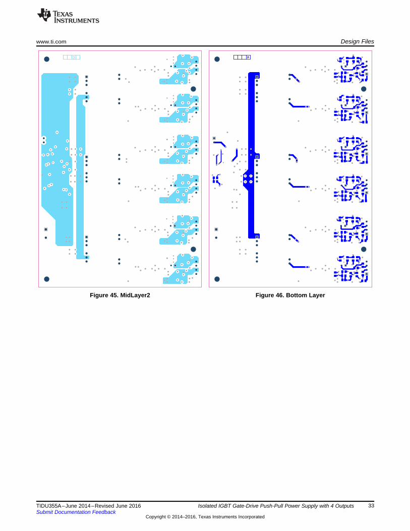
Figure 45. MidLayer2 Figure 46. Bottom Layer
Design Files www.ti.com
34 TIDU355A–June 2014–Revised June 2016Submit Documentation Feedback
Copyright © 2014–2016, Texas Instruments Incorporated
Isolated IGBT Gate-Drive Push-Pull Power Supply with 4 Outputs
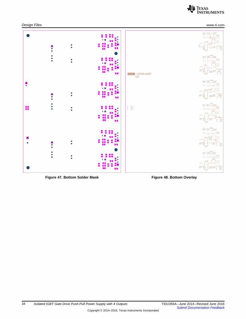
Figure 47. Bottom Solder Mask Figure 48. Bottom Overlay

www.ti.com Design Files
35TIDU355A–June 2014–Revised June 2016Submit Documentation Feedback
Copyright © 2014–2016, Texas Instruments Incorporated
Isolated IGBT Gate-Drive Push-Pull Power Supply with 4 Outputs
Figure 49. Board Dimensions

Design Files www.ti.com
36 TIDU355A–June 2014–Revised June 2016Submit Documentation Feedback
Copyright © 2014–2016, Texas Instruments Incorporated
Isolated IGBT Gate-Drive Push-Pull Power Supply with 4 Outputs
7.4 Altium ProjectTo download the Altium files, see the design files at TIDA-00181.
Figure 50. Altium All Layers Figure 51. Altium Bottom Layer
www.ti.com Design Files
37TIDU355A–June 2014–Revised June 2016Submit Documentation Feedback
Copyright © 2014–2016, Texas Instruments Incorporated
Isolated IGBT Gate-Drive Push-Pull Power Supply with 4 Outputs
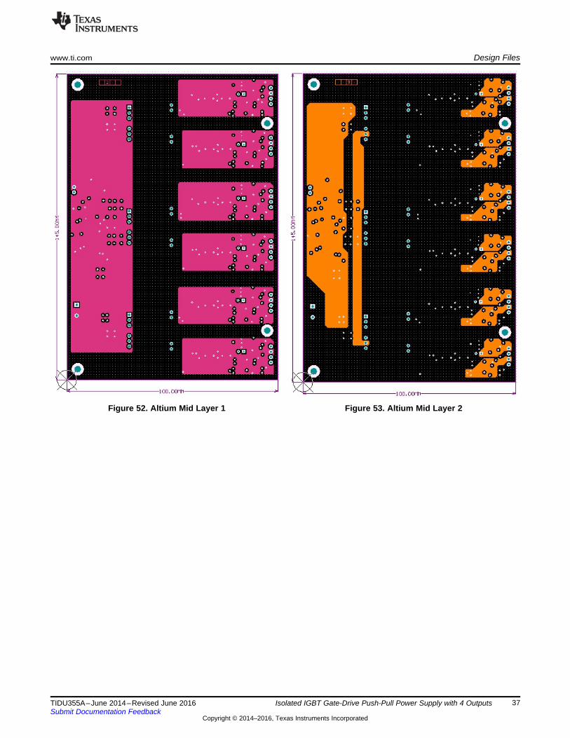
Figure 52. Altium Mid Layer 1 Figure 53. Altium Mid Layer 2

Design Files www.ti.com
38 TIDU355A–June 2014–Revised June 2016Submit Documentation Feedback
Copyright © 2014–2016, Texas Instruments Incorporated
Isolated IGBT Gate-Drive Push-Pull Power Supply with 4 Outputs
Figure 54. Altium Top Layer

www.ti.com Design Files
39TIDU355A–June 2014–Revised June 2016Submit Documentation Feedback
Copyright © 2014–2016, Texas Instruments Incorporated
Isolated IGBT Gate-Drive Push-Pull Power Supply with 4 Outputs
7.5 Gerber FilesTo download the Gerber files, see the design files at TIDA-00181.
Figure 55. Fabrication Drawing

Design Files www.ti.com
40 TIDU355A–June 2014–Revised June 2016Submit Documentation Feedback
Copyright © 2014–2016, Texas Instruments Incorporated
Isolated IGBT Gate-Drive Push-Pull Power Supply with 4 Outputs
7.6 Assembly Drawings
Figure 56. Top Assembly Drawing Figure 57. Bottom Assembly Drawing

www.ti.com References
41TIDU355A–June 2014–Revised June 2016Submit Documentation Feedback
Copyright © 2014–2016, Texas Instruments Incorporated
Isolated IGBT Gate-Drive Push-Pull Power Supply with 4 Outputs
8 References1. LM5030 Data Sheet, LM5030 100 V Push-Pull Current Mode PWM Controller (SNVS215).2. LP2954/LP2954A Data Sheet, LP2954/LP2954A 5 V and Adjustable Micropower Low-Dropout Voltage
Regulators (SNVS096).3. TPS7A3001 Data Sheet, TPS7A3001 –36 V, –200 mA, Ultralow-Noise, Negative Linear Regulator
(SBVS125).
9 About the AuthorSANJAY PITHADIA is a Systems Engineer at Texas Instruments where he is responsible for developingsubsystem design solutions for the Industrial Motor Drive segment. Sanjay has been with TI since 2008and has been involved in designing products related to Energy and Smart Grid. Sanjay brings to this rolehis experience in analog design, mixed signal design, industrial interfaces and power supplies. Sanjayearned his Bachelor of Technology in Electronics Engineering at VJTI, Mumbai.
N. NAVANEETH KUMAR is a Systems Architect at Texas Instruments, where he is responsible fordeveloping subsystem solutions for motor controls within Industrial Systems. N. Navaneeth brings to thisrole his extensive experience in power electronics, EMC, analog, and mixed signal designs. He hassystem-level product design experience in drives, solar inverters, UPS, and protection relays. N.Navaneeth earned his Bachelor of Electronics and Communication Engineering from BharathiarUniversity, India and his Master of Science in Electronic Product Development from Bolton University, UK.

Revision A History www.ti.com
42 TIDU355A–June 2014–Revised June 2016Submit Documentation Feedback
Copyright © 2014–2016, Texas Instruments Incorporated
Revision History
Revision A HistoryNOTE: Page numbers for previous revisions may differ from page numbers in the current version.
Changes from Original (June 2014) to A Revision ......................................................................................................... Page
• Changed the bottom winding of the transformer secondary side .................................................................. 1• Changed the bottom winding of the transformer secondary side .................................................................. 6

IMPORTANT NOTICE FOR TI REFERENCE DESIGNS
Texas Instruments Incorporated (‘TI”) reference designs are solely intended to assist designers (“Designer(s)”) who are developing systemsthat incorporate TI products. TI has not conducted any testing other than that specifically described in the published documentation for aparticular reference design.TI’s provision of reference designs and any other technical, applications or design advice, quality characterization, reliability data or otherinformation or services does not expand or otherwise alter TI’s applicable published warranties or warranty disclaimers for TI products, andno additional obligations or liabilities arise from TI providing such reference designs or other items.TI reserves the right to make corrections, enhancements, improvements and other changes to its reference designs and other items.Designer understands and agrees that Designer remains responsible for using its independent analysis, evaluation and judgment indesigning Designer’s systems and products, and has full and exclusive responsibility to assure the safety of its products and compliance ofits products (and of all TI products used in or for such Designer’s products) with all applicable regulations, laws and other applicablerequirements. Designer represents that, with respect to its applications, it has all the necessary expertise to create and implementsafeguards that (1) anticipate dangerous consequences of failures, (2) monitor failures and their consequences, and (3) lessen thelikelihood of failures that might cause harm and take appropriate actions. Designer agrees that prior to using or distributing any systemsthat include TI products, Designer will thoroughly test such systems and the functionality of such TI products as used in such systems.Designer may not use any TI products in life-critical medical equipment unless authorized officers of the parties have executed a specialcontract specifically governing such use. Life-critical medical equipment is medical equipment where failure of such equipment would causeserious bodily injury or death (e.g., life support, pacemakers, defibrillators, heart pumps, neurostimulators, and implantables). Suchequipment includes, without limitation, all medical devices identified by the U.S. Food and Drug Administration as Class III devices andequivalent classifications outside the U.S.Designers are authorized to use, copy and modify any individual TI reference design only in connection with the development of endproducts that include the TI product(s) identified in that reference design. HOWEVER, NO OTHER LICENSE, EXPRESS OR IMPLIED, BYESTOPPEL OR OTHERWISE TO ANY OTHER TI INTELLECTUAL PROPERTY RIGHT, AND NO LICENSE TO ANY TECHNOLOGY ORINTELLECTUAL PROPERTY RIGHT OF TI OR ANY THIRD PARTY IS GRANTED HEREIN, including but not limited to any patent right,copyright, mask work right, or other intellectual property right relating to any combination, machine, or process in which TI products orservices are used. Information published by TI regarding third-party products or services does not constitute a license to use such productsor services, or a warranty or endorsement thereof. Use of the reference design or other items described above may require a license from athird party under the patents or other intellectual property of the third party, or a license from TI under the patents or other intellectualproperty of TI.TI REFERENCE DESIGNS AND OTHER ITEMS DESCRIBED ABOVE ARE PROVIDED “AS IS” AND WITH ALL FAULTS. TI DISCLAIMSALL OTHER WARRANTIES OR REPRESENTATIONS, EXPRESS OR IMPLIED, REGARDING THE REFERENCE DESIGNS OR USE OFTHE REFERENCE DESIGNS, INCLUDING BUT NOT LIMITED TO ACCURACY OR COMPLETENESS, TITLE, ANY EPIDEMIC FAILUREWARRANTY AND ANY IMPLIED WARRANTIES OF MERCHANTABILITY, FITNESS FOR A PARTICULAR PURPOSE, AND NON-INFRINGEMENT OF ANY THIRD PARTY INTELLECTUAL PROPERTY RIGHTS.TI SHALL NOT BE LIABLE FOR AND SHALL NOT DEFEND OR INDEMNIFY DESIGNERS AGAINST ANY CLAIM, INCLUDING BUT NOTLIMITED TO ANY INFRINGEMENT CLAIM THAT RELATES TO OR IS BASED ON ANY COMBINATION OF PRODUCTS ASDESCRIBED IN A TI REFERENCE DESIGN OR OTHERWISE. IN NO EVENT SHALL TI BE LIABLE FOR ANY ACTUAL, DIRECT,SPECIAL, COLLATERAL, INDIRECT, PUNITIVE, INCIDENTAL, CONSEQUENTIAL OR EXEMPLARY DAMAGES IN CONNECTION WITHOR ARISING OUT OF THE REFERENCE DESIGNS OR USE OF THE REFERENCE DESIGNS, AND REGARDLESS OF WHETHER TIHAS BEEN ADVISED OF THE POSSIBILITY OF SUCH DAMAGES.TI’s standard terms of sale for semiconductor products (http://www.ti.com/sc/docs/stdterms.htm) apply to the sale of packaged integratedcircuit products. Additional terms may apply to the use or sale of other types of TI products and services.Designer will fully indemnify TI and its representatives against any damages, costs, losses, and/or liabilities arising out of Designer’s non-compliance with the terms and provisions of this Notice.IMPORTANT NOTICE
Mailing Address: Texas Instruments, Post Office Box 655303, Dallas, Texas 75265Copyright © 2016, Texas Instruments Incorporated