is/qc 750111 (1994): semiconductor devices - discrete
TRANSCRIPT

Disclosure to Promote the Right To Information
Whereas the Parliament of India has set out to provide a practical regime of right to information for citizens to secure access to information under the control of public authorities, in order to promote transparency and accountability in the working of every public authority, and whereas the attached publication of the Bureau of Indian Standards is of particular interest to the public, particularly disadvantaged communities and those engaged in the pursuit of education and knowledge, the attached public safety standard is made available to promote the timely dissemination of this information in an accurate manner to the public.
इंटरनेट मानक
“!ान $ एक न' भारत का +नम-ण”Satyanarayan Gangaram Pitroda
“Invent a New India Using Knowledge”
“प0रा1 को छोड न' 5 तरफ”Jawaharlal Nehru
“Step Out From the Old to the New”
“जान1 का अ+धकार, जी1 का अ+धकार”Mazdoor Kisan Shakti Sangathan
“The Right to Information, The Right to Live”
“!ान एक ऐसा खजाना > जो कभी च0राया नहB जा सकता है”Bhartṛhari—Nītiśatakam
“Knowledge is such a treasure which cannot be stolen”
“Invent a New India Using Knowledge”
है”ह”ह
IS/QC 750111 (1994): Semiconductor Devices - DiscreteDevices, Part 6: Thyristors, Section 2: Blank DetailBidirectional Triode Thyristors (Triacs), Ambient orCase-Rated, Up To 100 A [LITD 5: Semiconductor and OtherElectronic Components and Devices]


IS QC 750111 : lB94 IEC QC 750111 : 1991
Indian Standard
SEMICONDUCTOR DEVICES - DISCRETE DEVICES
PART 6 THYRISTORS
Section 2 Blank Detail Specification for Bidirectional Triode Thyristors
( Triacs ), Ambient or Case-Rated, Up To 100 A
NATIONAL FOREWORD
This Indian Standard, which is identical with IEC Pub 747-6-2/ QC 750111 ( 1991-05 > ‘Semi- conductor devices - Discrete devices - Part 6 : Thyristors, Section Two - Blank detail specification for bidirectional triode thyristors ( triacs ), ambient or case-rated, up to 100 A’, issued by the International Electrotechnical Commission ( IEC ), was adopted by the Bureau of Indian Standards on the recommendation of the Semiconductor Devices and Integrated Circuits Sectional Committee ( LT 10 ) and approval of the Electronics and Telecommunication Division Council.
The text of the IEC standard has been approved as suitable for publication as Indian Standard without deviations. Certain conventions are, however, not identical to those used in Indian Standards. Attention is particularly drawn to the following:
a) Wherever the words ‘International Standard’ appear referring to this standard, they should be read as ‘Indian Standard’.
b) Comma ( , ) has been used as a decimal marker while in Indian Sttindards, the current practice is to use a point ( . ) as the decimal marker.
In the adopted standard, reference appears to certain International Standards for which Indian Standards also exist. The corresponding Indian Standards which are to be substituted in their place are listed below along with their degree of equivalence for the editions indicated:
International Standards Corresponding Indian Standard Degree of Equivalence
IEC Pub 747-l O/QC 700000 ( 1984 ) IS QC 700000 : 1989 Semiconductor identical Semiconductor devices - discrete devices - Generic specification for devices - Part 10 : Generic specifi- discrete devices and integrated cation for discrete devices and circuits integrated circuits
IEC Pub 747-ll/QC 750100 ( 1985 ) IS QC 750000 : 1989 Semiconductor Identical Semiconductor devices -- Part 11 : devices - Sectional specification for Sectional specification for discrete discrete devices devices
The concerned technical committee has reviewed the provisions of the IEC Pub 68-2-17, IEC Pub 191-2, IEC Pub 747-6 and IEC Pub 749, referred in this adopted standard and has decided that they are acceptable for use in conjunction with this standard.
This standard is intended primarily for use under the IECQ system. A regular Indian Standard for this component could be different, identical or similar to this standard.
Only the English language text in the International Standard has been retained while adopting it in this Indian Standard.

As in the Original Standard, this Page is Intentionally Left Blank

ISQC 750111 :1994 IECQC 750111:1991
INTRODUCTION
The IEC QuaMy Assessment System for Electronic Components is operated in conformance wtth the statutes of the IEC and under the authority of the IEC. The object of this system is to define quality assessment procedures in such a manner that electronic components released by one participating country as conforming with the requirements of an applicable specification are equally acceptable in all other participating countries without the need for further testing.
This blank detail specification is one of a series of blank detail specifications for semiconductor devtces’and should be used with the following IEC publications:
747-10/W 766900 (1964): Semiconductor devices, Part 10: Generic specification for discrete devices and integrated circuits.
747-l l/W 7!5OOOO (1966): Semiconductor devices, Part 11: Sectional specification for discrete devices.
Required Information
Numbers shown in brackets on this and the following pages correspond to the following items of required information, which should be entered in the spaces provided.
Identification of the detail specification
[l] The name of the National Standards Organization under whose authority the detail specifi- cation is issued.
(21 The IECQ number of the detail specification.
[3] The numbers and issue numbers of the generic and sectional specifications.
[4] The national number of the detail specification, date of issue and any further information required by the national system.
Identification of the component
[!5l Type of component.
[S] Information on typical construction and applications. lf a device is designed to satisfy several applications, this should be stated in the detail specification. Characteristics, limits and inspection requirements for these applications shall be met. If a device is electrostatic sensitive, a caution statement should be added in the detail specification.
3

ISQC 750111 : 1994 IECQC 750111 : 1991
m Outline drawing and/or reference to the relevant document for outlines.
[S] Category of assessed quality.
[9] Reference data on the most important properties to permit comparison between component
types.
rhroughout this standard, the texts given in square brackets are intended for guidance to the speciftcation wrfter and should not be inciuded in the detail specification.]
Froughout this standard, when a characteristic or rating applies, “x” denotes that a value shall be inserted in the detail specification.]
4

I
I ,
,
I
I
I I
I
I
I ,
I
]Name (address) of respcnsible NAI
(and possibly of body from which specifiiation
is available).]
111
ELECTRONIC COMPONENT OF ASSESSED QUAUTY IN ACCORDANCE WITH:
Generic specffication: Publication 747-l O/CC 700000
Sectional specification: Publication 747-l l/QC 750000
[and national references if different].
[31
DETAIL SPECIFICATION FOR:
[Type number(s) of the relevant device(s).]
Ordering information: see clause 7 of this standard.
1 Mechanical description
Outline references:
IEC 191’2... [mandatory if available] and/or
national [i there is no IEC outline].
m
Outline draw&J [may be transferred to or given with more details in
clause 10 of thii standard].
Terminal identification
[Drawing showing pin assignments, including graphical
symbols.]
Making: [letters and figures. or colour code].
(The detail specification shall prescribe the information to be
marked on the device, if any.]
[See subclause 2.5 of generic specification and/or clause 6
of this standard.]
[Polarity indication, if special method is used.]
t
ISQC 750111 : 1994 IECQC 750111 : 1991
CC750111-xxx
(Number of IECQ detail specification
plus issue number an&or date.]
PI
[National number of detail specifkation.]
[This box nead not be used if national number
repeats IECO number.]
]41
I51
2 Short description
Bidirectional tricde thyristors
(triacs). ambknt or case-rated, up to 100 A. iSI
Semiconductor material: [Si]
Encapsulation: [cavity or non-cavity].
3 Categories of assessed quality
[From sllbcbuse 2.6 of the generic specification.] I61
Reference data PI
Information about manufacturers who have ccrnponents qualiiied to this detail specification is available in the current
Qualiied Products List.
5

ISQC 750111 :1994 IECQC 750111:1991
4 Limiting values (absolute maximum rating system)
These values apply over the operating temperature range, unless otherwise specified.
[Repeat only subclause numbers used, with the title. Any additional values should be given at the appropriate place, but without subclause number(s).]
[Curves should preferably be given under clause 10 of this standard.]
SuWause Parameters SYmbd
4.1 Operating ambient or case temperature T &mbkwa
Value
min. max.
X X
42 Storage temperatures
Virtual junction temperature, if required
T .Q
X X
%I) X
4.3
4.3.1
4.32
4.33
Vokager [Any condition such as time, frequency, temperature,
mounting method, etc., shaff be stated.]
(See note 1 of dause 5.)
Crest working off-state voltage V DWM
X
Ftepetitiie peak off-state voltage V DRM X
Non-repetitive peak off-state voltage V DSM X
4.4 Currents: [Any condiion such as time, frequency. temperature,
mounting method, etc., shall be stated.]
(Seenotel ofdause5.)
4.4.1 R.M.S. on-state current at the break-point temperature
(see figure 1). $RMS) X
4.4.2
4.4.3
4.4.4
In singlephase circuits sinusoidal 180’ conduction angle wfth
resistive load.
Repetitive Peak on-state current where appkabfe
Surge on-state current: ?
X
SM X
The surge on-state current ccrres~onds to the maximum current
applied after continuous operation at the maximum vafue of the
r.m.s. on-state current. ft is assumed that a bss of gate control
may occur. The fofbwing current ratings correspond to the
maximum current pemksibfe for a haff sinewave (10 ms at
50 Hz or 8.3 ms at 60 Hz), wfthout reappfication of off-state
voftage.
Crfticaf’rate of rise of on-state current. where epPricabla di’dt X
4.4s For case-rated devices only:
/2t value, sfnusoidal waveform, for 10 ms (50 Hz) or
8.3 ms (60 Hz):
a) without reappfication d the reverse voftage, initiil
jundon temperature T,,, = 7+nax.
b) wfth reappfiitfon d the reverse voltage VowMmax.,
idial junction temperature Tv,, = 25 “C.
/2t
X
X
4.5 Gate raring: [Any condftfon such as time, frequency, temperature
mounting method, etc., shall be stated.]
4.5.1
4.52
4.6
Peak gate Power dks&xtion.
Average gate power diiipation
Mechanical ratings
Mounting torque (if applicable).
P GM X
%(A,) X
X
6

ISQC 750111 : 1994 IECQC 750111 : 1991
T l nbl c...
w
T br = Tbr..k T br T ambl ea.0 lrnax.)
Figure 1 - Current derating curve for a triac (r.m.s. on-state current versus temperature)
7
ISQC 750111 : 1994 IECQC 750111 : 1991
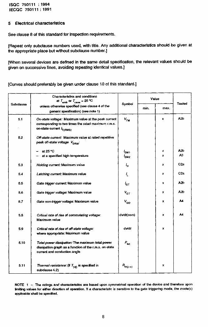
5 Electrical characteristics
See clause 8 of this standard for inspection requirements.
[Repeat only subclause numbers used, with title. Any additional characteristics should be given at the appropriate place but without subclause number.]
[When several devices are defined in the same detail specification, the relevant values should be given on successive lines, avoiding repeating identical values.]
[Curves should preferably be given under clause 10 of this standard.]
Subclause
Charaderisks and condiions
at Lb OT L.. = 25 OC unless otherwise specified (see dause 4 of the
generic spcifiition) (see note 1)
value
SYM Tested
min. max.
5.1 On-state voitage: MaXimum value at the peak current VTM X A2b
corresponding to two times the rated maximum r.m.s.
on-state current $,,,)
52 OfMate current: Maximum vale at rated repetitive
peak off-state voltage VDRM:
5.3
5.4
5.5
5.6
5.7
- at25”C I Oh41
X A&
- at a specified hiih temperature I DM2 X A3
Hokling current: Maximum value ‘Ii X C2a
Latch@ current: Maximum value ‘L X C2a
Gate trjgger currwt: Maximum value I GT
X A2b
Gate tr&gger vo/tager Maximum value V GT X A2b
Gate norMgger w&age: Maximum value V QD X A4
5.8 Critica rate of rise of commutati~ voltage:
Maximum value
dWdt(com) X A4
5.9 Critica/ fate d rise cd On-state wttage:
where appropriate: Maximum value
dtidt X
5.10 Totalpcwer db+ath: The maximum total power P bat dissipation graph as a function of the r.m.s. on-state
current and conduction angle
5.11 77wrnal resistance: (if 7&, is specified in
s&clause 42) q W-c)
X
NOTE 1 - The ratings and characteristics are based upon symmetrical operation of the devica and therefore qxm iimii w&es for either direction of operation. If a characteristic is sensitive to the gate triggering mode, the mode(s) appliife‘shall be specified.

6 Marking
ISQC 750111 :1994 IECQC 750111 : 1991
[Any particular information other than that given in box m (ciause 1) and/or subclause 2.5 of the generic specification shall be given here.]
7 Ordering information
rhe following minimum information is necessary to order a specific device, unless otherwise
specified:
- precise type reference (and nominal voltage value if required);
- IECQ reference of detail specification with issue number and/or date when relevant;
- category of assessed quality as defined in subclause 3.7 of the sectional specification and, if required, screening sequence as defined in subciause 3.6 of the sectional specification;
- any other particulars.]
8 Teat conditions and inspection requirements
[They are given in the following tables, where the values and exact test conditions to be used shall
be specified as required for a given type, and as required by the relevant test in the relevant pubii- cation.]
rhe choice between alternative tests and test methods shall be made when a detail specification is written.]
[When several devices are included in the same detail specification, the relevant conditions and/or values should be given on successive lines, avoiding, where possible, repetition of identical
conditions and/or values.]
Throughout the following text, reference to‘subclause numbers is made with respect to the generic specitication unless otherwise stated and test methods are quoted from clause 4 of the sectional specification.
[FOR SAMPLlNG REQUIREMENTS, EITHER REFER TO, OR REPRODUCE, VALUES OF SUB-
CLAUSE 3.7 OF THE SECTIONAL SPECIFICATION, ACCORDING TO THE APPLICABLE
CATEGORY(iES) OF ASSESSED QUALITY.]
[FOR GROUP A, THE CHOICE BETWEEN THE AQL AND THE LTPD SYSTEM SHALL BE
MADE IN THE DETAIL SPECIFICATION.]

L-.... __ _... _____-_.. ._
ISQC 750111 : 1994
IFCQC 750111 : 1991
GROUP A
Lot-by-lot
AlI tests are nondestructive (3.6.6)
Conditiins at Tmb or T,,,, = 25 OC Inspection requirement
lnspectiin or test SYW Refe1mce unless Mherwise specified limits
(see clause 4 d the genelic
specifiihIl) min. max.
Sub-grocgAf External visual examination 42.1.1
SAgrvtp A2a
Inoperative devices inverted polarity
V,, > [lo VrMmax.]
or
IDM > (100 &max.]
(unless otherwise spec !fied)
Subgtvcg A26
Peak on-state voltage
(Pulse method)
V TM
T-101
[See note 2]
Peak current = [corresponding to
*times the rated maximum
r.m.s. on-state arrrent
+(RMs)max+]
X
Peak off-state current I DMl T-103 V DAM = htdl X
Gate tr@ger current I QT T-109 Peak off -state voltage
VD = [12 V. unless otherwise
stated]
X
Gate trQger voltage V QT
T-109 [Gate circuit conditions] X
-J-P4J~
Peak dktate current IDM2 T-103 [See note 21
VoRM = MM X
T= K... max. or Tmb max.]
SMmwM
Critical rate of rise of d rfdt(com) T-116 [See note 2) X
onnmubting voltage Peak on-state current = [cows-
pending to *times the rated
maximum r.m.s. on-state current
ppmax.1 - C..e max. or Tunb max.1 .+
Gate non-trigger voltage VGD
T-110 V DRM = irated] X
[Gate circuit condiions]
T= L, max. or Tmb max.]
NOTE 2 - For sbgroups A2. A3 and A4. ths polarities d the 9ate and main terminal 2 shall be specified. If a
dwacte&tic is sensitive to the gate triggering mode, the mode(s) applicable shall be s~ec%ed.
10

- .--.--- - ..-...- .-
ISQC 750111 : 1994 IECQC 750111 : 1991
GROUP B LOt-by-lOt
(in the case of category 1, see the generic specifiition, subdause 2.6)
LSL = lower specification limit from group A
USL = upper specifiition limit
Only tests marked (D) are destructive (36.6)
Conditions at Tamb or Tc_ = 25 “C Inspection requirement
Inspection or test Symbol Reference unless otherwise specified limits
(see clause 4 of the generic
spedfication) min. max.
Subgroq El
Dimensions 4.2.2 [SWclauSelof
Appendfa B this standard]
Sub-gn~up 83
Bending (D). where applicable 749 Force = [see 749, II. 1.21 No damage
(depending on encapsulation) II. 1.2
Sub-group 84
Solderability. 749 [As specified] Good wetting
where applicable II. 2.1
Subgrvlg, 85
Rapid change of temperature 749 TA = 78 = number of cycles
Ill. 1
Mowed by: w specified] a) Fornon-cavity
devices
- Damp heat, cydic (D) 749 Test Db. variant 2.
Ill. 4 seventy = 55 “C. number of cycles =
with final measurements:
- peak on-state voltage V TM
As in A2b 1,lUSL
- peak off-state current I DMl
As in A2b 2USL
b) For cavity devices
- Sealing
with final measurwmentsr
- peak on-state voltage
- peak off-state current
749 Subclauses 7.2, 7.3 or 7.4
Ill, 7 combined with test OC. 682-17
V TM
As in A2b l.lUSL
I CM1 As in A2b 2USL
sub-glvqo B8
Electrical endurance (168 h) 7476, V VoWM = [rated], [at 50 Hz or 60 Hz],
temperature = [maximum rated],
[A.C. blocking or operatrng life with
+ (AMS) = 20 % or
50 96 of 4 (nMS) max.]
with final measurements:
- peak on-state voltage V TM
As in A2b 1,lUSL
- peak off-state current loM, As in A2b 2USL
subgroq CRRL Attributes information for 83. EM. B5 and B8.
-
11

ISQC 750111 : 1994 IECQC 750111 : 1991
GROUP C Periodic
LSL = Iowerspecificatian limit
USL = up&specifktionlimit from group A
Only tests marked (D) are destru&e (3.6.6)
ll-lq&onortest
Subgrv~ Cl
Dimensions
Subglv~ c2a
Holdii current
[set3 note41
Cor~IIlons at Tamb or T,,, = 25 “c lnspectbn requirement
SYM R&rence unless otherwise specifii limits
(see dause 4 of the generic
spec#ication) min. max.
422 [SeedelJSSld
AppendiiB this standatq
‘II T-l 07 Off-state voltage V. = 112 V, X
unless otherwise stated]
Gate circuit condiins
Latching current
Iseenote41
T-166 Off-state voltage V. I [ 12 V, X
unless otherwise stated]
Gate circuit condiins
T-103 Peak off-state voltage X
VD - [12 v. unless otherwise stated]
Gate tf&wr volta9e var T-109 [Gate circuit conditions] X
lE a‘ 0
Peak c&state current I DY2
T-l 03 (See note 21
VcjRM = @ted) X
T = (T,,,, max. or T,, max.]
Rating verbaWl:
Non-repewhrepeak off-state vottage
OrI
Gate rmMigpr volta9e
V DSY
T-166 VosM = [ratedj
T P [T =.*. max. or T,, max.] X
%D T-l 10 AsinA4
surge on-state current IT8M
T-164 frsu = [raw
[One single pulse of half-sine wave,
without reapplication of off-state
voltage.]
T = [T =... max. or Tamb max.]
NOTE4- This test is to be perfom& for each of the pohritiis of the gate and main terminal 2 specifii for I#,,
in subgroup A2b.
12
ISQC 750111 : 1994 IECQC 750111 : 1991
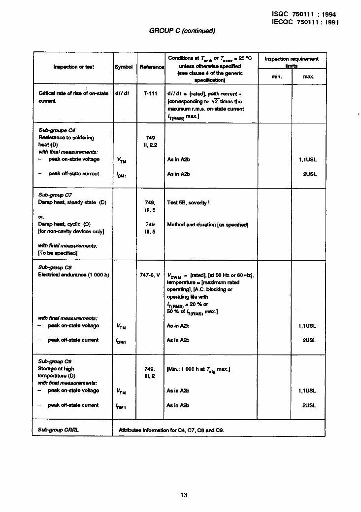
GROUP c (WntiMKi)
. . (hlldhm at Tati or Te,*, = 25 oc
I~ortes! symbol Raference u\l@=-spedfied (seedause4ofthegeneric
spedfication)
Wticefrateofrkeofon-state di/dt T-111 dildt I [rated]. peak awent =
culmnt [con~ngto Etimesthe
mfaximum r.m.8. on-state current
r&aM,) -.I
S-a Ftesiatancetosoldering 749
heat (D) II, 22
wifh finaltnem~enfs:
- peakon-statevoltage YTM As in Mb
- peek off-state current lDM, As in A2b
lnspedion requiremenl limits
min. max.
l.lUSL
2uSL
SufFgnnp c7
Damp heat, steady state (0)
olY
Damp heat, cydic (0)
[for non-cavity devices only]
with finnI meawmmwfs:
Fobcgecifiedl
749, Test 58, severity I Ill. 5
749 Method and duration [as specSed]
Ill. 5
SufW=PCJ3 Ebctrid emham (1000 h)
with final mtmsummmts: - peakon-sWevo&age v,M
- peakoff-statecurrent fOM1
SW- Storage at hiih
temperatue (D) with final masUwmMfs:
- peakon-statevoltage “TM
- peakoff-statecurrent lnM,
747-5.v VowM I [ratq. [at 50 Hz or 50 Hz].
temperatwe = [maximum rated
m%~l, [AC. Wckhg or opefatinglifewith
+mw =209bw
5o x Of 4(RMs) -4
As in A&
As in A2b
749,
Ill. 2
[Min.: 1 000 h at rew max.]
As in A2b
As in A2b
1,lUSL
2USL
1,lUSL
2uSL
sub-pip CURL
13

ISQC 750111 : 1994 IECQC 750111 : 1991
9 GroupD- Qualification approval teats
USL = upperspedfiition limit
Inspection or test
Sub-pq Dl
Ektrical endurance (for
ambient-rated devices only)
with final measurements:
- peak on-state voltage
- peak off-statecurrent
Conditiins at Tmb or T,,, = 25 OC lnspecdion n3quirement
symbol Reference unless othelwise spdfied lifts
(see dause 4 of the generfc
spedfiiion) min. max.
747-6. V 1 000 h. operating fife
[ff this test is perfarmed in
Subgroup C8, it is not required here]
Temperature = [maximum rated
Ope~W
v,M As in A2b 1,lUSL
IDM, As in A2b 2uSL
Sus-groylD2
Thennal cyding load test
(for case-rated devices only)
747-6, Number of cycles = [to be spedfii]
N,4
with final measurements:
- peak on-state voltage
- peak off-state current
“TM As in A2b 1,luSL
I DMl
Aa in AZ% LJSL
SlrbsrorpW Accderatbn steady-state [for
cavity devices only]
with final measwements:
- peak an-state voltage V TM
- peakuff-statecurrent loM,
749,
II. 5
AsinA2b USL
AsinAZb USL
I
10 Additional information (not for inspection purposes)
vo be given only as far as necessary for the specification and use of the device, for instance:
- temperature derating curves referred to in the limiting values;
- complete definition of a circuit for measurement, or of an additional method;
- detailed ouline drawing.]
14