isscc 2003 / session 1 / plenary / 1 2003 / session 1 / plenary / 1.1 ... transistors in a single...
TRANSCRIPT
• 2003 IEEE International Solid-State Circuits Conference 0-7803-7707-9/03/$17.00 ©2003 IEEE
ISSCC 2003 / SESSION 1 / PLENARY / 1.1
1.1 No Exponential is Forever: But “Forever” Can Be Delayed!
Gordon E. Moore
Intel Corporation
Over the last fifty years, the solid-state-circuits industry hasgrown from infancy to become one of the largest industries in theworld. Beyond the circuits themselves, solid-state circuits havebecome the basic building blocks of the trillion-dollar electronicsindustry, and have found their way into virtually all the productsof modern civilization, ranging from automobiles to greetingcards. Looking back, it is hard to realize that early projections,based on the best industrial-engineering calculations of the time,suggested that transistors might eventually approach a fifty-cent manufacturing cost. That projection did not contemplatethe invention of the integrated circuit and its subsequent evolu-tion that now allows us to incorporate hundreds of millions oftransistors in a single integrated structure.
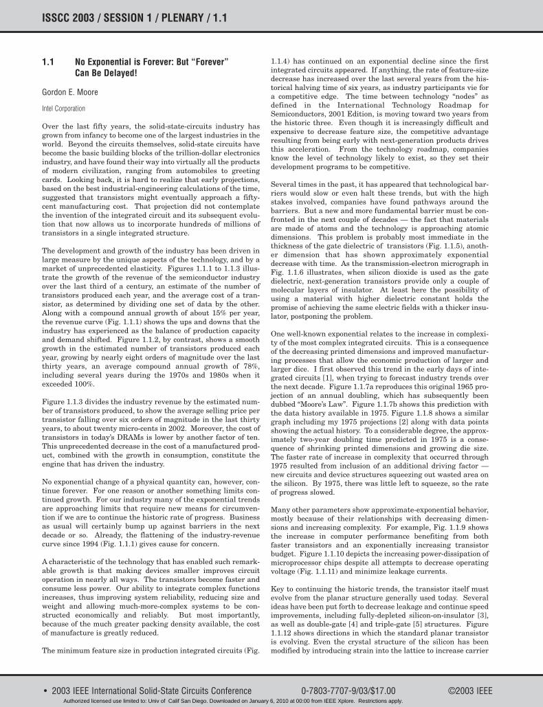
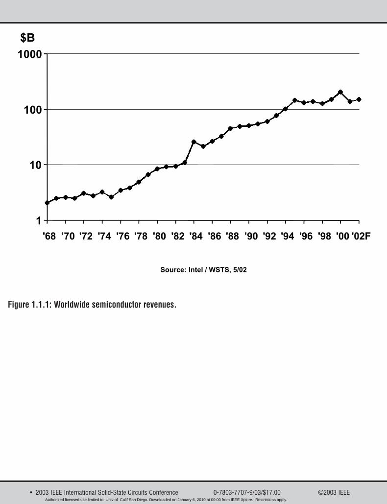
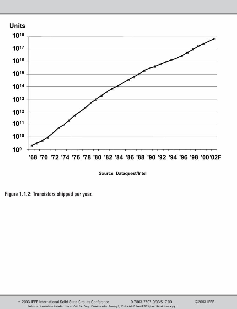
The development and growth of the industry has been driven inlarge measure by the unique aspects of the technology, and by amarket of unprecedented elasticity. Figures 1.1.1 to 1.1.3 illus-trate the growth of the revenue of the semiconductor industryover the last third of a century, an estimate of the number oftransistors produced each year, and the average cost of a tran-sistor, as determined by dividing one set of data by the other.Along with a compound annual growth of about 15% per year,the revenue curve (Fig. 1.1.1) shows the ups and downs that theindustry has experienced as the balance of production capacityand demand shifted. Figure 1.1.2, by contrast, shows a smoothgrowth in the estimated number of transistors produced eachyear, growing by nearly eight orders of magnitude over the lastthirty years, an average compound annual growth of 78%,including several years during the 1970s and 1980s when itexceeded 100%.
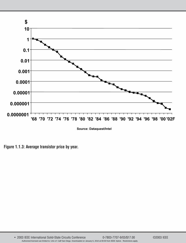
Figure 1.1.3 divides the industry revenue by the estimated num-ber of transistors produced, to show the average selling price pertransistor falling over six orders of magnitude in the last thirtyyears, to about twenty micro-cents in 2002. Moreover, the cost oftransistors in today’s DRAMs is lower by another factor of ten.This unprecedented decrease in the cost of a manufactured prod-uct, combined with the growth in consumption, constitute theengine that has driven the industry.
No exponential change of a physical quantity can, however, con-tinue forever. For one reason or another something limits con-tinued growth. For our industry many of the exponential trendsare approaching limits that require new means for circumven-tion if we are to continue the historic rate of progress. Businessas usual will certainly bump up against barriers in the nextdecade or so. Already, the flattening of the industry-revenuecurve since 1994 (Fig. 1.1.1) gives cause for concern.
A characteristic of the technology that has enabled such remark-able growth is that making devices smaller improves circuitoperation in nearly all ways. The transistors become faster andconsume less power. Our ability to integrate complex functionsincreases, thus improving system reliability, reducing size andweight and allowing much-more-complex systems to be con-structed economically and reliably. But most importantly,because of the much greater packing density available, the costof manufacture is greatly reduced.
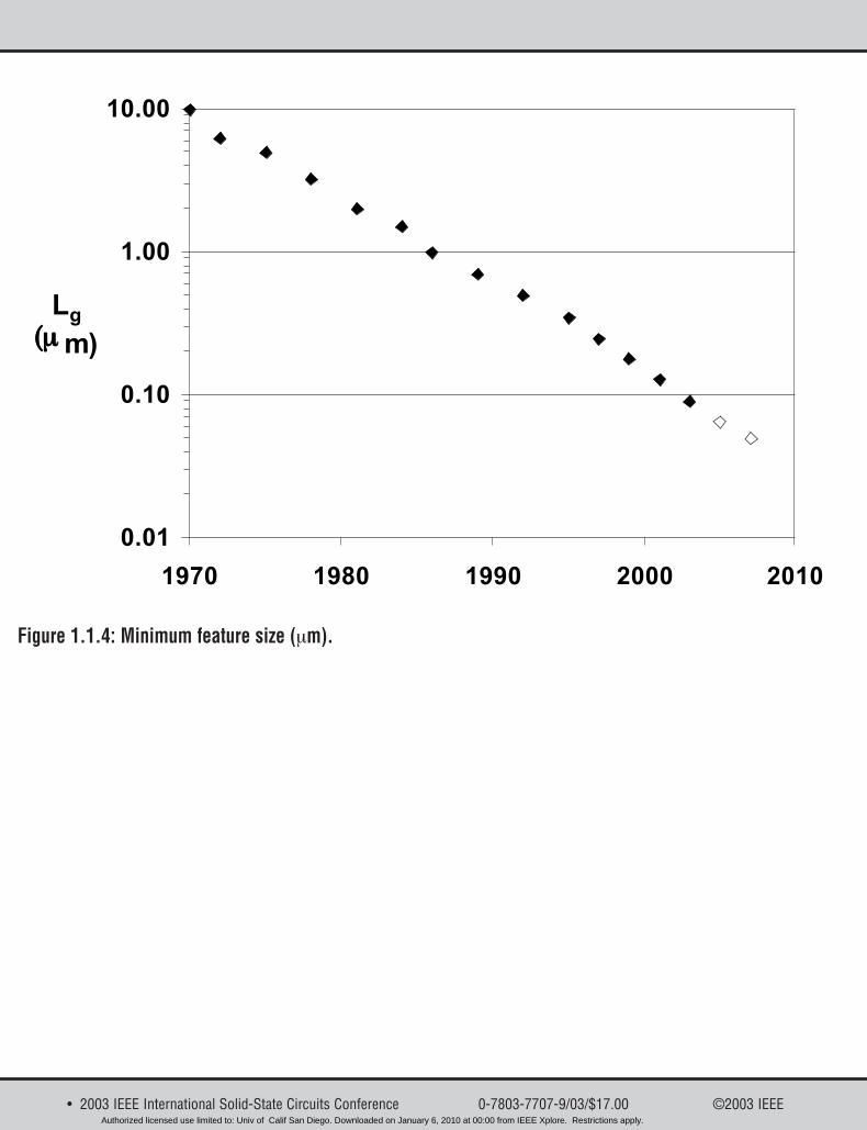
The minimum feature size in production integrated circuits (Fig.
1.1.4) has continued on an exponential decline since the firstintegrated circuits appeared. If anything, the rate of feature-sizedecrease has increased over the last several years from the his-torical halving time of six years, as industry participants vie fora competitive edge. The time between technology “nodes” asdefined in the International Technology Roadmap forSemiconductors, 2001 Edition, is moving toward two years fromthe historic three. Even though it is increasingly difficult andexpensive to decrease feature size, the competitive advantageresulting from being early with next-generation products drivesthis acceleration. From the technology roadmap, companiesknow the level of technology likely to exist, so they set theirdevelopment programs to be competitive.
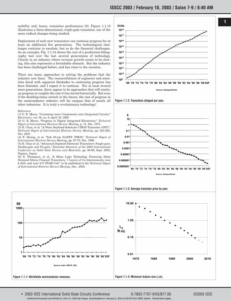
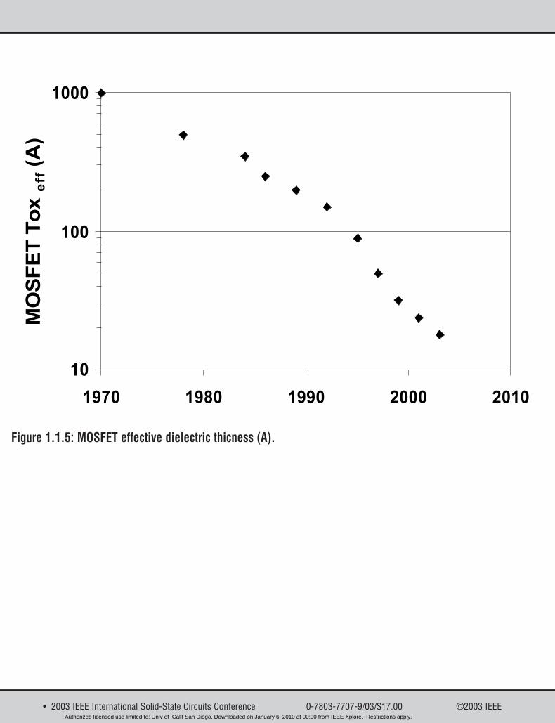
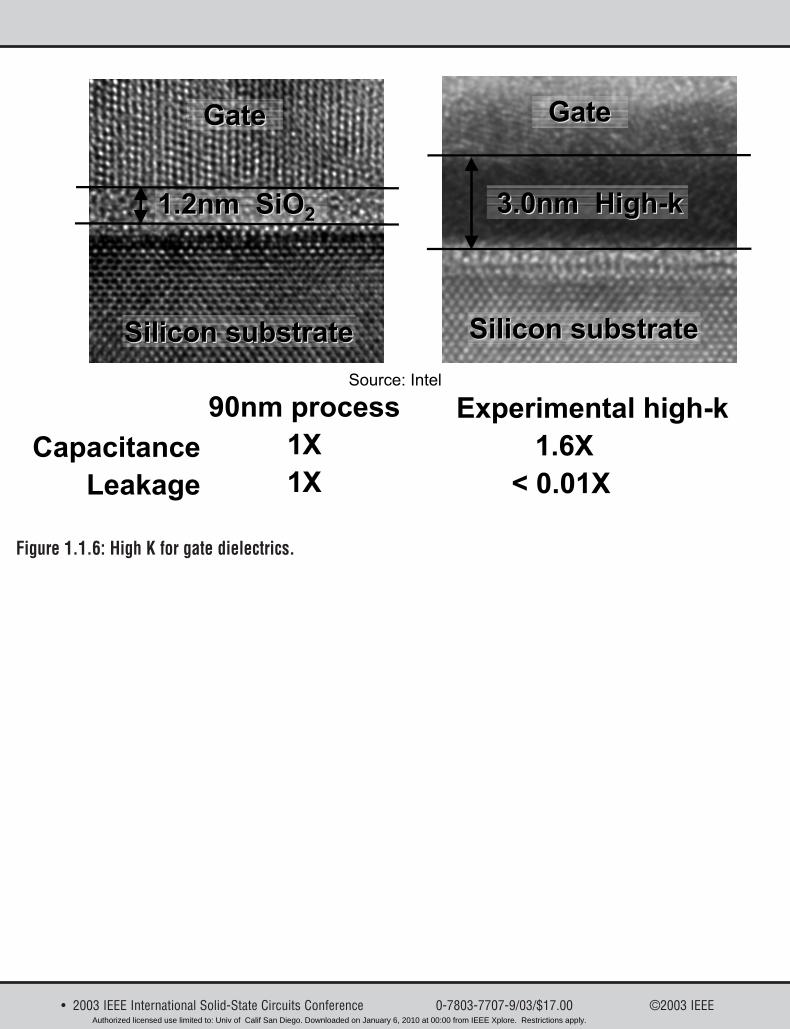
Several times in the past, it has appeared that technological bar-riers would slow or even halt these trends, but with the highstakes involved, companies have found pathways around thebarriers. But a new and more fundamental barrier must be con-fronted in the next couple of decades — the fact that materialsare made of atoms and the technology is approaching atomicdimensions. This problem is probably most immediate in thethickness of the gate dielectric of transistors (Fig. 1.1.5), anoth-er dimension that has shown approximately exponentialdecrease with time. As the transmission-electron micrograph inFig. 1.1.6 illustrates, when silicon dioxide is used as the gatedielectric, next-generation transistors provide only a couple ofmolecular layers of insulator. At least here the possibility ofusing a material with higher dielectric constant holds thepromise of achieving the same electric fields with a thicker insu-lator, postponing the problem.
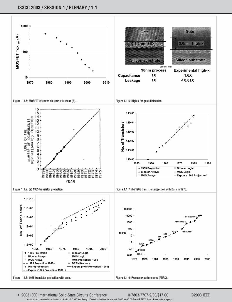
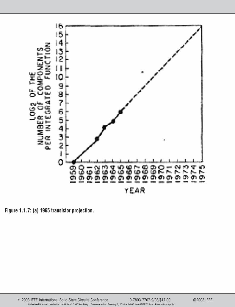
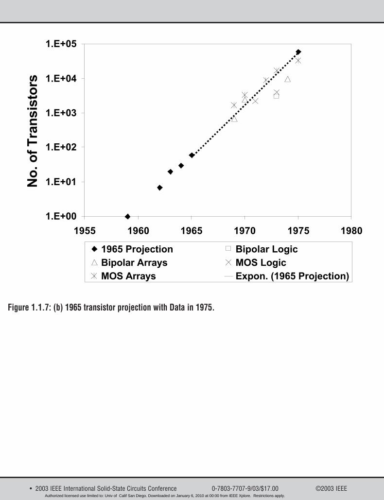
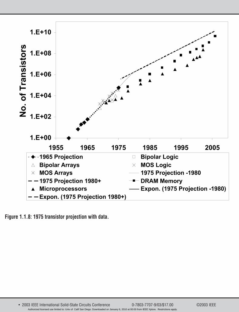
One well-known exponential relates to the increase in complexi-ty of the most complex integrated circuits. This is a consequenceof the decreasing printed dimensions and improved manufactur-ing processes that allow the economic production of larger andlarger dice. I first observed this trend in the early days of inte-grated circuits [1], when trying to forecast industry trends overthe next decade. Figure 1.1.7a reproduces this original 1965 pro-jection of an annual doubling, which has subsequently beendubbed “Moore’s Law”. Figure 1.1.7b shows this prediction withthe data history available in 1975. Figure 1.1.8 shows a similargraph including my 1975 projections [2] along with data pointsshowing the actual history. To a considerable degree, the approx-imately two-year doubling time predicted in 1975 is a conse-quence of shrinking printed dimensions and growing die size.The faster rate of increase in complexity that occurred through1975 resulted from inclusion of an additional driving factor —new circuits and device structures squeezing out wasted area onthe silicon. By 1975, there was little left to squeeze, so the rateof progress slowed.
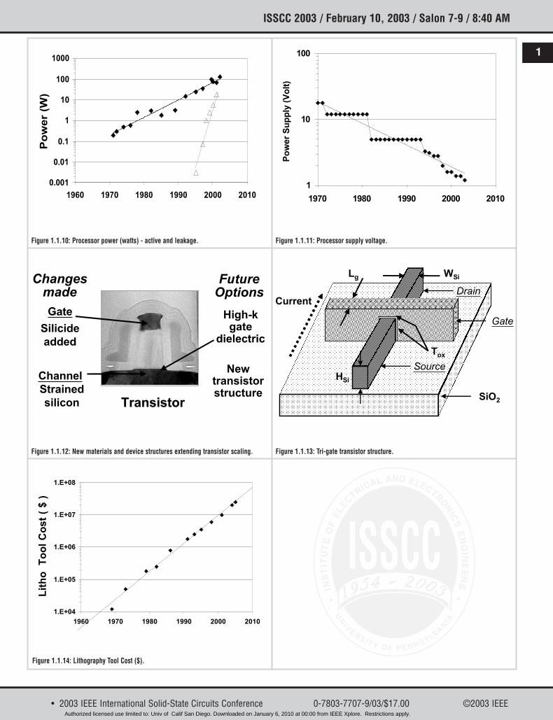
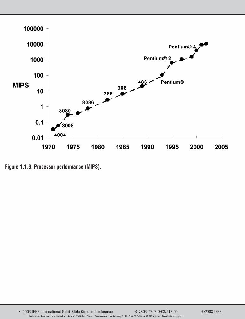
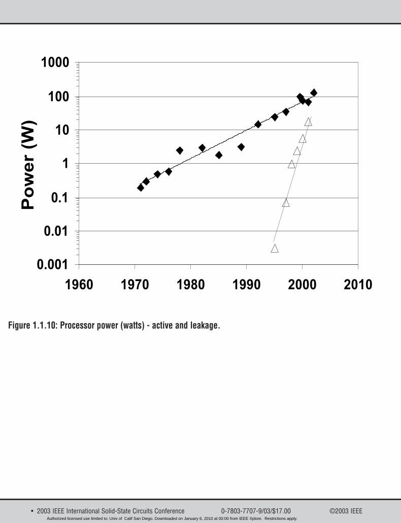
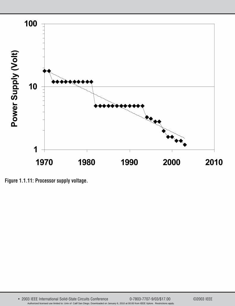
Many other parameters show approximate-exponential behavior,mostly because of their relationships with decreasing dimen-sions and increasing complexity. For example, Fig. 1.1.9 showsthe increase in computer performance benefiting from bothfaster transistors and an exponentially increasing transistorbudget. Figure 1.1.10 depicts the increasing power-dissipation ofmicroprocessor chips despite all attempts to decrease operatingvoltage (Fig. 1.1.11) and minimize leakage currents.
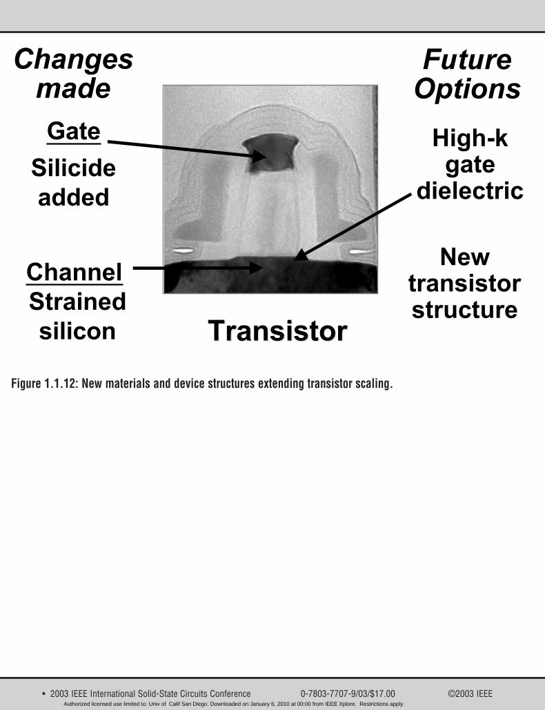
Key to continuing the historic trends, the transistor itself mustevolve from the planar structure generally used today. Severalideas have been put forth to decrease leakage and continue speedimprovements, including fully-depleted silicon-on-insulator [3],as well as double-gate [4] and triple-gate [5] structures. Figure1.1.12 shows directions in which the standard planar transistoris evolving. Even the crystal structure of the silicon has beenmodified by introducing strain into the lattice to increase carrier
Authorized licensed use limited to: Univ of Calif San Diego. Downloaded on January 6, 2010 at 00:00 from IEEE Xplore. Restrictions apply.
ISSCC 2003 / February 10, 2003 / Salon 7-9 / 8:40 AM
1
�
��
���
����
��� ��� ��� ��� ��� ��� ��� ��� ��� ��� ��� ��� ��� ��� ��� ��� ��� ����
!
������"�#�����$��%�&�'$��
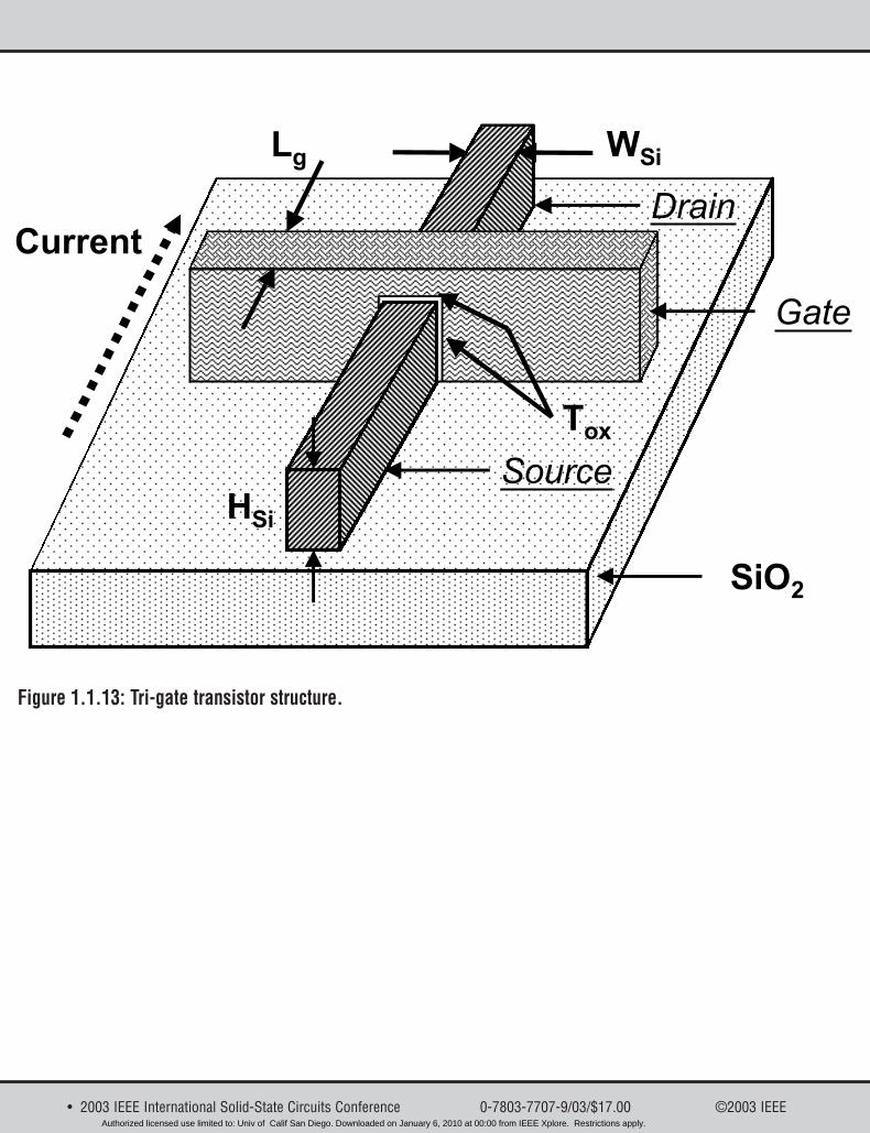
mobility and, hence, transistor performance [6]. Figure 1.1.13illustrates a three-dimensional, triple-gate transistor, one of themore radical changes being studied.
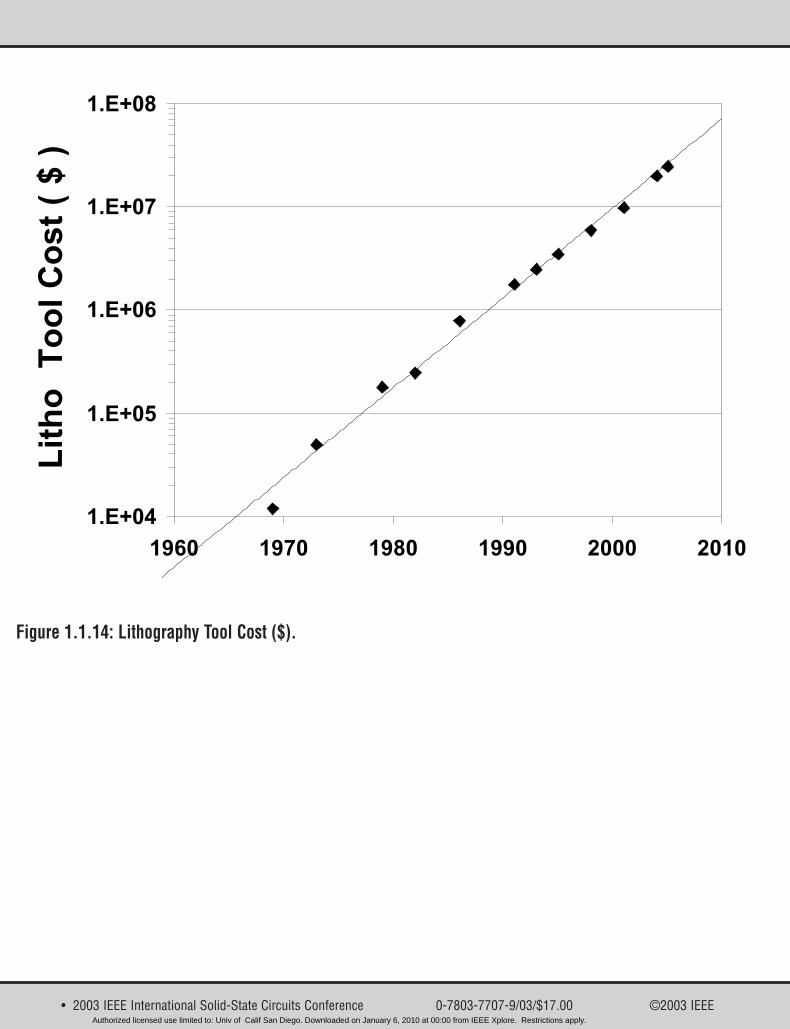
Deployment of such new transistors can continue progress for atleast an additional few generations. The technological chal-lenges continue to escalate, but so do the financial challenges.As an example, Fig. 1.1.14 shows the cost of a production-lithog-raphy tool over the last several generations of technology.Clearly in an industry where revenue growth seems to be slow-ing, this also represents a formidable obstacle. But the industryhas been challenged before, and has risen to the occasion.
There are many approaches to solving the problems that theindustry now faces. The resourcefulness of engineers and scien-tists faced with apparent blockades to continuing progress hasbeen fantastic, and I expect it to continue. For at least severalmore generations, there appear to be approaches that will contin-ue progress at roughly the rate it has moved historically. But evenif the doubling-times stretch in the future, the rate of progress inthe semiconductor industry will far surpass that of nearly allother industries. It is truly a revolutionary technology!
References[1] G. E. Moore, “Cramming more Components onto Integrated Circuits,”Electronics, vol. 38, no. 8, April 19, 1965.[2] G. E. Moore, “Progress in Digital Integrated Electronics,” TechnicalDigest of International Electron Devices Meeting, p. 11, Dec. 1975.[3] R. Chau, et al, “A 50nm Depleted-Substrate CMOS Transistor (DST),”Technical Digest of International Electron Devices Meeting, pp. 621-624,Dec. 2001. [4] X. Huang, et al. “Sub 50-nm FinFET: PMOS,” Technical Digest ofInternational Electron Devices Meeting, pp. 67-70, Dec. 1999.[5] R. Chau et al, “Advanced Depleted Substrate Transistors: Single-gate,Double-gate and Tri-gate,” Extended Abstracts of the 2002 InternationalConference on Solid State Devices and Materials, pp. 68-69, Sept. 2002,Nagoya, Japan.[6] S. Thompson, et al, “A 90nm Logic Technology Featuring 50nmStrained Silicon Channel Transistors, 7 Layers of Cu Interconnects, Lowk ILD, and 1µm2 6-T STAM Cell,” to be published in the Technical Digestof International Electron Devices Meeting, Dec., 2002.
Figure 1.1.2: Transistors shipped per year.
Figure 1.1.1: Worldwide semiconductor revenues.
Figure 1.1.3: Average transistor price by year.
������"�-(�(.����$#����
��� ��� ��� ��� ��� ��� ��� ��� ��� ��� ��� ��� ��� ��� ��� ��� �������
����
����
���'
����
���/
����
����
����
���
����
0����
������"�-(�(.����$#����
��������
�������
������
�����
����
���
��
�
��
��� ��� ��� ��� ��� ��� ��� ��� ��� ��� ��� ��� ��� ��� ��� ��� ��� ����
���
���
���
����
���� ���� ���� ���� ����
4�
���������5
Figure 1.1.4: Minimum feature size (µm).
• 2003 IEEE International Solid-State Circuits Conference 0-7803-7707-9/03/$17.00 ©2003 IEEEAuthorized licensed use limited to: Univ of Calif San Diego. Downloaded on January 6, 2010 at 00:00 from IEEE Xplore. Restrictions apply.
ISSCC 2003 / SESSION 1 / PLENARY / 1.1
Figure 1.1.5: MOSFET effective dielectric thicness (A). Figure 1.1.6: High K for gate dielectrics.
Figure 1.1.7: (a) 1965 transistor projection.
Figure 1.1.8: 1975 transistor projection with data. Figure 1.1.9: Processor performance (MIPS).
Figure 1.1.7: (b) 1965 transistor projection with Data in 1975.
��
���
����
���� ���� ���� ���� ����
69��:%�%�;
�<<�815
����������2���(������������2���(��
@(��@(��
/�����>��)A=/�����>��)A=
�����������
�����*������
�B
�B
:;*�������(��)��)A=
������������B
�������C����B
D(*(���(���
4�(=(��
����������2���(������������2���(��
��������9��������9��
@(��@(��
�:F��
�:F��
�:F��
�:F�/
�:F��
�:F�'
��'' ���� ���' ���� ���' ����
G���<�%�(��������
���'�+��E������ !�*��(��4����
!�*��(��1��(3� 69��4����
69��1��(3� :;*���8���'�+��E������5
�:F��
�:F��
�:F��
�:F��
�:F��
�:F��
��'' ���' ���' ���' ���' ���'
G���<�%�(��������
���'�+��E������ !�*��(��4����
!�*��(��1��(3� 69��4����
69��1��(3� ���'�+��E�������A����
���'�+��E�����������F -�16�6����3
6����*��������� :;*���8���'�+��E�������A����5
:;*���8���'�+��E�����������F5
���
��
�
��
���
����
�����
������
���� ���' ���� ���' ���� ���' ���� ���'
6#+� /��
����
����
���
+������H
+������H��
����
����
���
+������H��
• 2003 IEEE International Solid-State Circuits Conference 0-7803-7707-9/03/$17.00 ©2003 IEEEAuthorized licensed use limited to: Univ of Calif San Diego. Downloaded on January 6, 2010 at 00:00 from IEEE Xplore. Restrictions apply.
ISSCC 2003 / February 10, 2003 / Salon 7-9 / 8:40 AM
1
Figure 1.1.14: Lithography Tool Cost ($).
Figure 1.1.10: Processor power (watts) - active and leakage. Figure 1.1.11: Processor supply voltage.
Figure 1.1.12: New materials and device structures extending transistor scaling. Figure 1.1.13: Tri-gate transistor structure.
����
���
��
�
��
���
����
���� ���� ���� ���� ���� ����
+�����8
5
�
��
���
���� ���� ���� ���� ����
+�������**�3�8J���5
@(��
������ �( �
D)(��������(��� �������
����������
��� ��������
>��)A=�(��
���������
%�(�������%�(�������
G����(����������������
D������
4� ��
������
���
����
%�;
��9�
>��
�:F��
�:F�'
�:F��
�:F��
�:F��
���� ���� ���� ���� ���� ����
4��)���%����D����8� �5
• 2003 IEEE International Solid-State Circuits Conference 0-7803-7707-9/03/$17.00 ©2003 IEEEAuthorized licensed use limited to: Univ of Calif San Diego. Downloaded on January 6, 2010 at 00:00 from IEEE Xplore. Restrictions apply.
• 2003 IEEE International Solid-State Circuits Conference 0-7803-7707-9/03/$17.00 ©2003 IEEE
�
��
���
����
��� ��� ��� ��� ��� ��� ��� ��� ��� ��� ��� ��� ��� ��� ��� ��� ��� ����
!
������"�#�����$��%�&�'$��
Figure 1.1.1: Worldwide semiconductor revenues.
Authorized licensed use limited to: Univ of Calif San Diego. Downloaded on January 6, 2010 at 00:00 from IEEE Xplore. Restrictions apply.
• 2003 IEEE International Solid-State Circuits Conference 0-7803-7707-9/03/$17.00 ©2003 IEEE
Figure 1.1.2: Transistors shipped per year.
������"�-(�(.����$#����
��� ��� ��� ��� ��� ��� ��� ��� ��� ��� ��� ��� ��� ��� ��� ��� �������
����
����
���'
����
���/
����
����
����
���
����
0����
Authorized licensed use limited to: Univ of Calif San Diego. Downloaded on January 6, 2010 at 00:00 from IEEE Xplore. Restrictions apply.
• 2003 IEEE International Solid-State Circuits Conference 0-7803-7707-9/03/$17.00 ©2003 IEEE
Figure 1.1.3: Average transistor price by year.
������"�-(�(.����$#����
��������
�������
������
�����
����
���
��
�
��
��� ��� ��� ��� ��� ��� ��� ��� ��� ��� ��� ��� ��� ��� ��� ��� ��� ����
Authorized licensed use limited to: Univ of Calif San Diego. Downloaded on January 6, 2010 at 00:00 from IEEE Xplore. Restrictions apply.
• 2003 IEEE International Solid-State Circuits Conference 0-7803-7707-9/03/$17.00 ©2003 IEEE
���
���
���
����
���� ���� ���� ���� ����
4�
���������5
Figure 1.1.4: Minimum feature size (µm).
Authorized licensed use limited to: Univ of Calif San Diego. Downloaded on January 6, 2010 at 00:00 from IEEE Xplore. Restrictions apply.
• 2003 IEEE International Solid-State Circuits Conference 0-7803-7707-9/03/$17.00 ©2003 IEEE
Figure 1.1.5: MOSFET effective dielectric thicness (A).
��
���
����
���� ���� ���� ���� ����
69��:%�%�;
�<<�815
Authorized licensed use limited to: Univ of Calif San Diego. Downloaded on January 6, 2010 at 00:00 from IEEE Xplore. Restrictions apply.
• 2003 IEEE International Solid-State Circuits Conference 0-7803-7707-9/03/$17.00 ©2003 IEEE
Figure 1.1.6: High K for gate dielectrics.
����������2���(������������2���(��
@(��@(��
/�����>��)A=/�����>��)A=
�����������
�����*������
�B
�B
:;*�������(��)��)A=
������������B
�������C����B
D(*(���(���
4�(=(��
����������2���(������������2���(��
��������9��������9��
@(��@(��
Authorized licensed use limited to: Univ of Calif San Diego. Downloaded on January 6, 2010 at 00:00 from IEEE Xplore. Restrictions apply.
• 2003 IEEE International Solid-State Circuits Conference 0-7803-7707-9/03/$17.00 ©2003 IEEE
Figure 1.1.7: (a) 1965 transistor projection.
Authorized licensed use limited to: Univ of Calif San Diego. Downloaded on January 6, 2010 at 00:00 from IEEE Xplore. Restrictions apply.
• 2003 IEEE International Solid-State Circuits Conference 0-7803-7707-9/03/$17.00 ©2003 IEEE
Figure 1.1.7: (b) 1965 transistor projection with Data in 1975.
�:F��
�:F��
�:F��
�:F�/
�:F��
�:F�'
��'' ���� ���' ���� ���' ����
G���<�%�(��������
���'�+��E������ !�*��(��4����
!�*��(��1��(3� 69��4����
69��1��(3� :;*���8���'�+��E������5
Authorized licensed use limited to: Univ of Calif San Diego. Downloaded on January 6, 2010 at 00:00 from IEEE Xplore. Restrictions apply.
• 2003 IEEE International Solid-State Circuits Conference 0-7803-7707-9/03/$17.00 ©2003 IEEE
�:F��
�:F��
�:F��
�:F��
�:F��
�:F��
��'' ���' ���' ���' ���' ���'
G���<�%�(��������
���'�+��E������ !�*��(��4����
!�*��(��1��(3� 69��4����
69��1��(3� ���'�+��E�������A����
���'�+��E�����������F -�16�6����3
6����*��������� :;*���8���'�+��E�������A����5
:;*���8���'�+��E�����������F5
Figure 1.1.8: 1975 transistor projection with data.
Authorized licensed use limited to: Univ of Calif San Diego. Downloaded on January 6, 2010 at 00:00 from IEEE Xplore. Restrictions apply.
• 2003 IEEE International Solid-State Circuits Conference 0-7803-7707-9/03/$17.00 ©2003 IEEE
Figure 1.1.9: Processor performance (MIPS).
���
��
�
��
���
����
�����
������
���� ���' ���� ���' ���� ���' ���� ���'
6#+� /��
����
����
���
+������H
+������H��
����
����
���
+������H��
Authorized licensed use limited to: Univ of Calif San Diego. Downloaded on January 6, 2010 at 00:00 from IEEE Xplore. Restrictions apply.
• 2003 IEEE International Solid-State Circuits Conference 0-7803-7707-9/03/$17.00 ©2003 IEEE
Figure 1.1.10: Processor power (watts) - active and leakage.
����
���
��
�
��
���
����
���� ���� ���� ���� ���� ����
+�����8
5
Authorized licensed use limited to: Univ of Calif San Diego. Downloaded on January 6, 2010 at 00:00 from IEEE Xplore. Restrictions apply.
• 2003 IEEE International Solid-State Circuits Conference 0-7803-7707-9/03/$17.00 ©2003 IEEE
Figure 1.1.11: Processor supply voltage.
�
��
���
���� ���� ���� ���� ����
+�������**�3�8J���5
Authorized licensed use limited to: Univ of Calif San Diego. Downloaded on January 6, 2010 at 00:00 from IEEE Xplore. Restrictions apply.
• 2003 IEEE International Solid-State Circuits Conference 0-7803-7707-9/03/$17.00 ©2003 IEEE
Figure 1.1.12: New materials and device structures extending transistor scaling.
@(��
������ �( �
D)(��������(��� �������
����������
��� ��������
>��)A=�(��
���������
%�(�������%�(�������
G����(����������������
Authorized licensed use limited to: Univ of Calif San Diego. Downloaded on January 6, 2010 at 00:00 from IEEE Xplore. Restrictions apply.
• 2003 IEEE International Solid-State Circuits Conference 0-7803-7707-9/03/$17.00 ©2003 IEEE
Figure 1.1.13: Tri-gate transistor structure.
D������
4� ��
������
���
����
%�;
��9�
>��
Authorized licensed use limited to: Univ of Calif San Diego. Downloaded on January 6, 2010 at 00:00 from IEEE Xplore. Restrictions apply.
• 2003 IEEE International Solid-State Circuits Conference 0-7803-7707-9/03/$17.00 ©2003 IEEE
Figure 1.1.14: Lithography Tool Cost ($).
�:F��
�:F�'
�:F��
�:F��
�:F��
���� ���� ���� ���� ���� ����
4��)���%����D����8� �5
Authorized licensed use limited to: Univ of Calif San Diego. Downloaded on January 6, 2010 at 00:00 from IEEE Xplore. Restrictions apply.