issue date: april. 28, 2011 ml7066 - lapis-semi.com · issue date: april. 28, 2011 ml7066 ... value...
TRANSCRIPT

FEDL7066-01Issue Date: April. 28, 2011
ML7066 400MHz Transceiver IC for Specified Low-Power Station
1/29
ZigBee® is a registered trademark of ZigBee Alliance, Inc. Other names are trademarks or registered trademarks of developers and manufacturers. The information contained herein can change without notice owing to product and/or technical improvements.
General Description The ML7066 is an transceiver IC that can be used for specified low-power statiom , where the RF section, IF section, modem section and HOST interface section are integrated into one chip. It supports the 400MHz radio communication and complies with RCR STD-30 (426MHz) and ARIB STD-T67 (429MHz). The ML7066 is suitable for auto meter reading, home securithy systems, wireless fire alarm system, and industorial monitoring and control. Features
• Complies with RCR STD-30 (low-power radio security system) and ATIB STD-T67 (specified low-power radio statiion) • Operating Frequency 426.0250 MHz to 426.8375 MHz
429.1750 MHz to 429.9250 MHz Note: Including the frequency range that are not defined in the standards.
• Data transfer speed 1200 bps, 2400 bps and 4800 bps with NRZ coding 600 bps, 1200 bps and 2400 bps with Manchester coding • 2-FSK modulation • Voltage regulator installed • 19.2 MHz oscillator circuit installed • Synchronous communication interface (SCI) installed • Up to 8 oeration channel set function installed • Carrier (0perating frequency) detect function installed • Up to 16 bytes preamble generator and detecor installed • Up to 18 bytes start-of-frame delimiter generator and detector installed • Intermittent operation function installed (periodic transmition and receiving) • PLL adjustment function availble to use 60ppm crystal • Test pattern generatot installed (CW, PN9, PN15, all “0”, all”1”) • Power supply voltage 2.1V to 3.6V • Current consumption in the following states (typical);
Stop mode: 0.7 uA Sleep mode: 4 uA Idle mode: 2 mA At transmission (@10mW) 29.5 mA At reception: 15.5 mA
• Package
48-pin VQFN P-VQFN48-0707-0.50-T6 Product name: ML7066GDZ0AB • Package
Lead-free package conforming to RoHS

FEDL7066-01
ML7066
2/29
Block Diagram
RESETN SRESETN EXTCLK POWOFF MODE1 MODE2
SDIN SDO SCLK SINT SCEN DIO DCLK
RF_IN_N
IF1_OUT IF1_IN
RF_IN_P
RF_OUT
PLL_LP PLL_BG VREG_OUT VREG_IN
LC Filter
RSSI
429MHz
455kHz21.4MHz
SynthesizerFractional-N PLL
1st IF
1st Mixer
2nd IF
LNA
PA
SAW Filter
429MHz
Limiter
Modulator
S C
I &
D
ata
I/F
MD
OEM
Con
trol
Demodulator
Control
Regulator
TANK1 TANK2
SW_CTRL
VREG_CORE(Monitor pin)
ADC
IF2_OUT IF2_IN
19.2MHz
VBG
IF frequency conversion
FEDL7066-01
ML7066
3/29
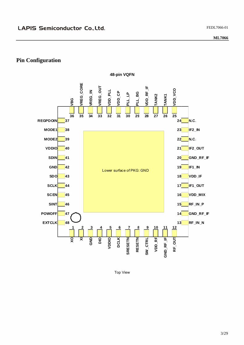
Pin Configuration
48-pin VQFN
VBG
VR
EG
_CO
RE
VREG
_IN
VR
EG
_OU
T VD
D_P
LL
VDD_
CP
PLL_
LP
PLL_
BG
VD
D_R
F_I
F TA
NK2
TA
NK1
VD
D_V
CO
36 35 34 33 32 31 30 29 28 27 26 25 REGPDOIN 37 24 N.C.
MODE1 38 23 IF2_IN
MODE2 39 22 N.C.
VDDIO 40 21 IF2_OUT
SDIN 41 20 GND_RF_IF
GND 42 19 IF1_IN
SDO 43 18 VDD_IF
SCLK 44 17 IF1_OUT
SCEN 45 16 VDD_MIX
SINT 46 15 RF_IN_P
POWOFF 47 14 GND_RF_IF
EXTCLK 48 13 RF_IN_N
1 2 3 4 5 6 7 8 9 10 11 12
XO XI
GND DIO
VDD
IO
DC
LK
SRE
SETN
RESE
TN
SW_C
TRL
VDD
_RF
GN
D_R
F_I
F
RF_
OU
T
Lower surface of PKG: GND
Top View
FEDL7066-01
ML7066
4/29
Description of Pins
I/O definition IRF : RF input pin IA : Analog input pin I : Digital input pin IS : Schmitt trigger input pin IU : Input pin with pull-up register ID : Input pin with pull-down register IOS : Input pin for 24MHz oscillation circuit ORF : RF control output pin OA : Analog output pin O : Digital output pin OOS : Output pin for 24MHz oscillation circuit OD : Open drain output pin
RF Related Pins
Pin No. Pin Name Attribute/
value at reset I/O
ActiveLevel
Description
12 RF_OUT O ORF – RF output pin
13 RF_IN_N I IRF – Positive RF input pin (differential) 15 RF_IN_P I IRF – Negative RF input pin (differential)
17 IF1_OUT O OA – 1st IF filter pin (output to filter)
19 IF1_IN I IA – 1st IF filter pin (input from filter) 21 IF2_OUT O OA – 2nd IF filter pin (output to filter)
23 IF2_IN I IA – 2nd IF filter pin (input from filter) 29 PLL_BG O OA – Loop filter related pin
30 PLL_LP O OA – Loop filter pin 26 TANK1 I IA – VCO tank inductor pin 1
27 TANK2 I IA – VCO tank inductor pin 2 Host Interface Pins
Pin No. Pin Name Attribute/
value at reset I/O
ActiveLevel
Description
41 SDIN I I H or L Synchronous communication interface data input pin
43 SDO L O H or L Synchronous communication interface data output pin 44 SCLK I I P or N Synchronous communication interface clock input pin
46 SINTN H O L Synchronous communication interface interrupt output pin 45 SCEN I IU L Synchronous communication interface chip select input pin

FEDL7066-01
ML7066
5/29
TX/RX Data Related Pins
Pin No. Pin Name Attribute/ value at reset I/O Active
Level Description
4 DIO I IO H or LData input/output pin (Initial value is Low when switch the state from input to output)
6 DCLK L O P or N Data clock output pin Regulator Related Pins
Pin No. Pin Name Attribute/
value at reset I/O
ActiveLevel
Description
33 VREG_OUT – – – Power supply output pin for the RF block (Typ. 2.2V) Do not use this pin for purposes other than RF power supply.
35 VREG_CORE – – – Power supply monitor pin for the core (Typ. 2.2V) Do not use this pin for purposes other than monitoring purpose. Decuple this pin to ground with capacitor. (*1)
36 VBG – – – Back bias pin (Capacitance connection) Decuple this pin to ground with capacitor. (*1)
37 REGPDIN L ID – Regulator power down pin Always fix this pin to “L” input in normal operation.
*1: Please refer reference circuit.
FEDL7066-01
ML7066
6/29
Power Supply Pins
Pin No. Pin Name Attribute/
value at reset I/O Active
LevelDescription
34 VREG_IN – – – Power supply pin for regulator. (Typ. 3.0 V)
10 VDD_RF – – – Power supply pin for PA and LNA. Connect to VREG_OUT. (Typ. 2.2V).
25 VDD_VCO – – – Power supply pin for VCO. Connect to VREG_OUT. (Typ. 2.2V)
16 VDD_MIX – – – Power supply pin for mixer 1. Connect to VREG_OUT. (Typ. 2.2V)
31 VDD_CP – – – Power supply pin for charge pump. Connect to VREG_OUT. (Typ. 2.2V)
32 VDD_PLL – – – Power supply pin for PLL. Connect to VREG_OUT. (Typ. 2.2V)
18 VDD_IF – – – Power supply pin for IF, Limiter and RSSI. Connect to VREG_OUT. (Typ. 2.2V)
5, 40 VDDIO – – – Power supply pins for the digital I/O block and internal voltage regulator. (Typ. 3.0 V).
11, 14 20,28
GND_RF_IF – – – Ground pin for RF and IF block.
3,42 GND – – – Ground pin for digital block.
EL (*2) – – – – Ground pin (*2) EL is the lower surface of the LSI.
FEDL7066-01
ML7066
7/29
Other Pins
Pin No. Pin Name Attribute/
value at reset I/O
ActiveLevel
Description
8 RESETN I IS L Hardware reset pin
7 SRESETN I IU L Software reset pin Wake up pin when in sleep mode. This pin is active when RESETN=1.
2 XI I IOS P or N19.2 MHz crystal connection pin 1 External clock input pin.
1 XO O OOS – 19.2 MHz crystal connection pin 2 Leave open when XI (pin #2) is configured as an external clock input pin.
9 SW_CTRL O OD L Antenna switch control pin L: In transmitting mode HiZ: In receiving mode
47 POWOFF L O H External component power on/off control pin Active level polarity is changeable by register setting.
48 EXTCLK I I P or N External 32.768 kHz clock input pin (*3)
38 MODE1 I IO H or LBit order on SCI Data setting pin L: LSB first H: MSB first
39 MODE2 I I H or L
Operation mode setting pin L: Normal mode H: Test mode Always fix this pin to “L” input in normal operation.
22,24 NC O OA – Unused. (Open) (*3) Always EXTCLK input is required for ML7066 operation.
Recommended Handling of Unused Pins
LAPIS Semiconductor recommends handling unused pins as shown below so that the basic operation of the ML7275 is unimpaired.
Pin No. Pin Name Recommended pin handling
1 XO Open (when XI is configured as an external clock input pin.)
7 SRESETN Connect to VDDIO
47 POWOFF Open
NOTE
If any input pins are left open, the current consumption may increase. Therefore, it is recommended that the unused input ports and I/O ports be always fixed with “L” or “H” input.

FEDL7066-01
ML7066
8/29
List of Command/Event The following table shows the command/event specifications of ML7066. Command is send from MCU to the ML7066. Event is send from the ML7066 to MCU.
Command/event name Type code Function
SET_TRX_STATE.request Command 0x02 Requests the RF state change SET_TRX_STATE.confirm Event 0x03 Reports the result of RF state change request SET_CHANNEL.request Command 0x04 Sets the operating channel SET_CHANNEL.confirm Event 0x05 Reports the channel setting result SET_CMP_DATA.request Command 0x06 Sets the preamble or start-of-frame delimiter (SFD) pattern
for generation (TX) and comparison (RX) SET_CMP_DATA.confirm Event 0x07 Reports the preamble/SFD pattern setting result SET_RSSI_SETTING.request Command 0x08 Sets the carrier detect condition SET_RSSI_SEETING.confirm Event 0x09 Reports the carrier detect condition setting result SET_TX_POW.request Command 0x0a Sets the transmitting power SET_TX_POW.confirm Event 0x0b Reports the transmitting power setting result SET_TIMER.request Command 0x0c Sets the intermitting operation timing SET_TIMER.confirm Event 0x0d Reports the intermittent operation setting result SET_PLL_FIT.request Command 0x0e Adjusts the operating channel center frequency SET_PLL_FIT.confirm Event 0x0f Reports the result of frequency adjustment request SET_TEST.request Command 0x10 Sets the test pattern SET_TEST.confirm Event 0x11 Reports the result of test pattern setting results SET_CLK.request Command 0x12 Requests the sleep mode operation and POWOFF pin
polarity change. SET_CLK.confirm Event 0x13 Reports the result of sleep and POWOFF pin polarity
request SET_RESET.request Command 0x14 Request the reset operation SET_RESET.confirm Event 0x15 Reports the result of reset request SET_CONFIRM.request Command 0x16 Requests the interrupt masking SET_CONFIRM.confirm Event 0x17 Reports the interrupt mask requests SET_INT.request Command 0x18 Requests the .confirm event masking SET_INT.confirm Event 0x19 Reports the result of .confirm event mask requests SET_SPD.request Command 0x18 Sets the data rate SET_SPD.confirm Event 0x19 Reports the data rate setting request SET_CMP_DURATION.request Command 0x0e Sets the comparing receive data period SET_CMP_DURATION.confirm Event 0x0f Reports the comparing period setting result RX_DATA.indication Event 0x20 Notices existing receive data RSSI.indication Event 0x21 Notices RSSI result GET_TRX_STATE.request Command 0x22 Reads the RF state report GET_TRX_STATE.confirm Event 0x23 Reports the current RF state GET_CHANNEL.request Command 0x24 Reads the channel setting GET_CHANNEL.confirm Event 0x25 Reports the setting operation channel(s) GET_CMP_DATA.request Command 0x26 Reads the setting of the preamble or SFD pattern GET_CMP_DATA.confirm Event 0x27 Reports the setting pattern of preamble or SFD GET_RSSI_SETTING.request Command 0x28 Reads the carrier detect setting or current RSSI GET_RSSI_SEETING.confirm Event 0x29 Reports the carrier detect setting or current RSSI GET_TX_POW.request Command 0x2a Reads the transmitting power setting GET_TX_POW.confirm Event 0x2b Reports the setting value of transmitting power GET_TIMER.request Command 0x2c Reads the intermitting operation timing GET_TIMER.confirm Event 0x2d Reports the setting value of intermittent operation GET_PLL_FIT.request Command 0x2e Reads the PLL adjust value GET_PLL_FIT.confirm Event 0x2f Reports the setting value for PLL adjustment

FEDL7066-01
ML7066
9/29
Command/event name Type code Function
GET_TEST.request Command 0x30 Reads the test pattern setting GET_TEST.confirm Event 0x31 Reports the setting of test pattern GET_CLK.request Command 0x32 Reads the POWOFF pin polarity setting GET_CLK.confirm Event 0x33 Reports the setting polarity of POWOFF pin GET_INT.request Command 0x34 Reads the .confirm event mask setting GET_INT.confirm Event 0x35 Reports the setting of .confirm event mask GET_CONFIRM.request Command 0x36 Reads the interrupt mask setting GET_CONFIRM.confirm Event 0x37 Reports the setting of interrupt mask INT.indication Event 0x38 Notices interrupt occurs GET_SPD.request Command 0x3a Reads the data rate GET_SPD.confirm Event 0x3b Reports the data rate setting GET_CMP_DURATION.request Command 0x0e Reads the comparing period setting GET_CMP_DURATION.confirm Event 0x0f Reports the setting value of comparing period GET_ERRR_COUNTER.request 0x3e Reads the receiving error status of operating channels GET_ERR_COUNTER.confirm 0x3f Reports the receiving data status of operating channels List of Confirm
Code Function Note 0x05 INVALID_PARAMETER INVALID_PARAMETER 0x06 RX_ON RX_ON request when in RX_ON state 0x07 SUCCESS Request accepted 0x08 TRX_OFF TRX_OFF request when in TRX_OFF state 0x09 TX_ON TX_ON request when in TX_ON state 0x0a UNSPOORTED_STTRIBUTE Data overrun or shortage
FEDL7066-01
ML7066
10/29
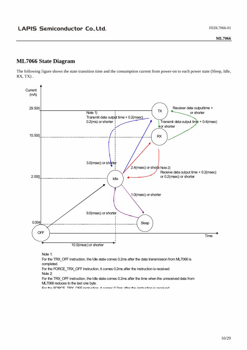
ML7066 State Diagram
The following figure shows the state transition time and the consumption current from power-on to each power state (Sleep, Idle, RX, TX) .
Current(mA)
29.500Note 1) or shorterTransmit data output time + 0.2(msec)0.2(ms) or shorter Transmit data output time + 0.4(msec)
or shorter
15.500
3.0(msec) or shorter2.4(msec) or shorteNote 2)
Receive data output time + 0.2(msec)2.000 or 0.2(msec) or shorter
1.0(msec) or shorter
9.0(msec) or shorter
0.004
Time
10.0(msec) or shorter
Note 1:For the TRX_OFF instruction, the Idle state comes 0.2ms after the data transmission from ML7066 iscompleted.For the FORCE_TRX_OFF instruction, it comes 0.2ms after the instruction is received.Note 2:For the TRX_OFF instruction, the Idle state comes 0.2ms after the time when the unreceived data fromML7066 reduces to the last one byte.For the FORCE TRX OFF instruction it comes 0 2ms after the instruction is received
Sleep
OFF
RX
TX
Idle
Receiver data outputtime +
FEDL7066-01
ML7066
11/29
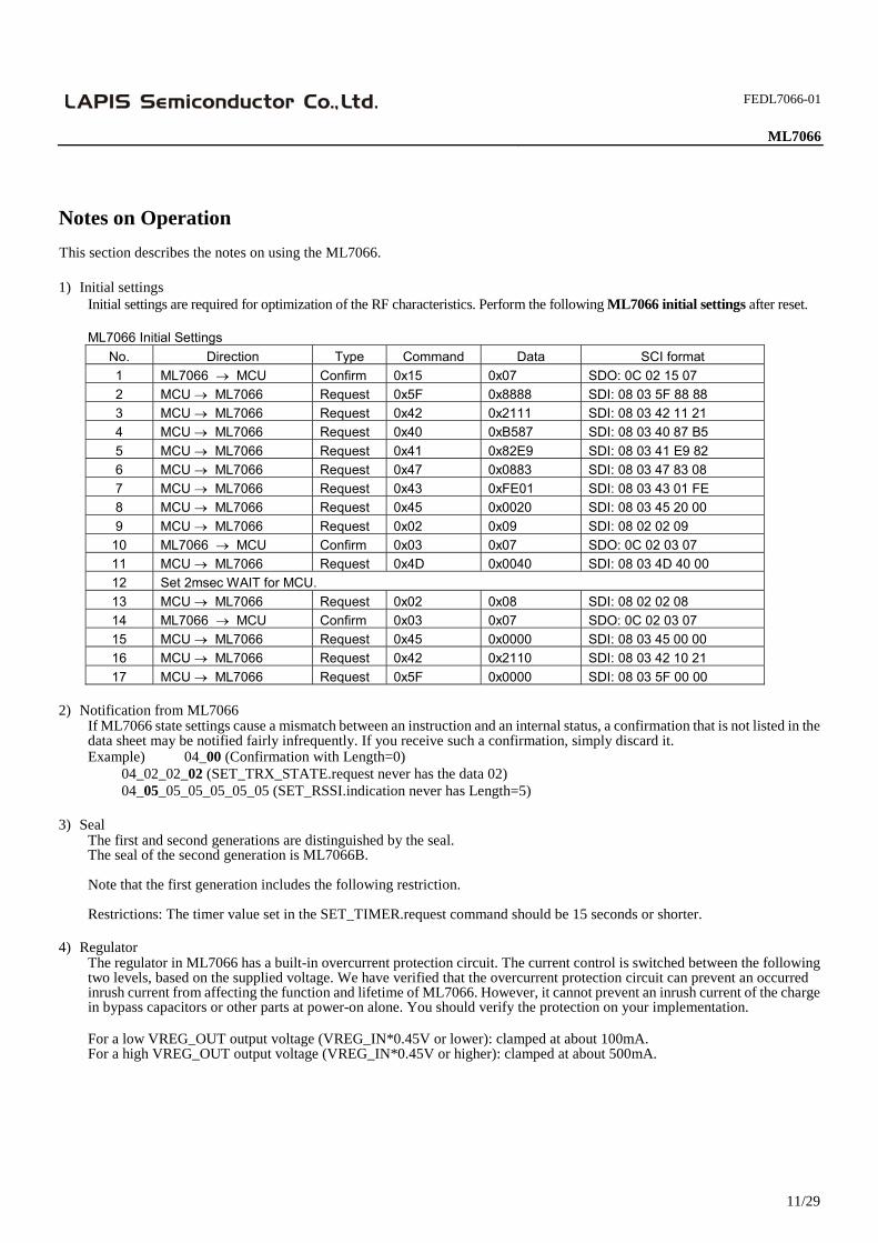
Notes on Operation This section describes the notes on using the ML7066. 1) Initial settings
Initial settings are required for optimization of the RF characteristics. Perform the following ML7066 initial settings after reset. ML7066 Initial Settings
No. Direction Type Command Data SCI format 1 ML7066 → MCU Confirm 0x15 0x07 SDO: 0C 02 15 07 2 MCU → ML7066 Request 0x5F 0x8888 SDI: 08 03 5F 88 88 3 MCU → ML7066 Request 0x42 0x2111 SDI: 08 03 42 11 21 4 MCU → ML7066 Request 0x40 0xB587 SDI: 08 03 40 87 B5 5 MCU → ML7066 Request 0x41 0x82E9 SDI: 08 03 41 E9 82 6 MCU → ML7066 Request 0x47 0x0883 SDI: 08 03 47 83 08 7 MCU → ML7066 Request 0x43 0xFE01 SDI: 08 03 43 01 FE 8 MCU → ML7066 Request 0x45 0x0020 SDI: 08 03 45 20 00 9 MCU → ML7066 Request 0x02 0x09 SDI: 08 02 02 09
10 ML7066 → MCU Confirm 0x03 0x07 SDO: 0C 02 03 07 11 MCU → ML7066 Request 0x4D 0x0040 SDI: 08 03 4D 40 00 12 Set 2msec WAIT for MCU. 13 MCU → ML7066 Request 0x02 0x08 SDI: 08 02 02 08 14 ML7066 → MCU Confirm 0x03 0x07 SDO: 0C 02 03 07 15 MCU → ML7066 Request 0x45 0x0000 SDI: 08 03 45 00 00 16 MCU → ML7066 Request 0x42 0x2110 SDI: 08 03 42 10 21 17 MCU → ML7066 Request 0x5F 0x0000 SDI: 08 03 5F 00 00
2) Notification from ML7066
If ML7066 state settings cause a mismatch between an instruction and an internal status, a confirmation that is not listed in the data sheet may be notified fairly infrequently. If you receive such a confirmation, simply discard it. Example) 04_00 (Confirmation with Length=0)
04_02_02_02 (SET_TRX_STATE.request never has the data 02) 04_05_05_05_05_05_05 (SET_RSSI.indication never has Length=5)
3) Seal
The first and second generations are distinguished by the seal. The seal of the second generation is ML7066B. Note that the first generation includes the following restriction. Restrictions: The timer value set in the SET_TIMER.request command should be 15 seconds or shorter.
4) Regulator
The regulator in ML7066 has a built-in overcurrent protection circuit. The current control is switched between the following two levels, based on the supplied voltage. We have verified that the overcurrent protection circuit can prevent an occurred inrush current from affecting the function and lifetime of ML7066. However, it cannot prevent an inrush current of the charge in bypass capacitors or other parts at power-on alone. You should verify the protection on your implementation.
For a low VREG_OUT output voltage (VREG_IN*0.45V or lower): clamped at about 100mA. For a high VREG_OUT output voltage (VREG_IN*0.45V or higher): clamped at about 500mA.

FEDL7066-01
ML7066
12/29
5) Fractional spurious
ML7066 maintains the accuracy of the RF clock frequency by fine-tuning the PLL oscillation frequency, which helps lower the component cost for generating the master clock. The Fractional-N PLL type is used to realize the fine tuning of the PLL oscillation frequency. We found that this PLL type could cause the fractional spurious depending on the combination of the reference clock, integer dividing ratio, and fractional dividing ratio. So, depending on the combination of the used frequencies (channels), a false detection of the RSSI value can occur. The following matrixes show the channel combinations with a possible false detection.
426MHz Band Channel False Detection Matrix
symbol indicates the combination of the transmission and reception channels by the normal setting. ×symbol indicates the channel combination with a possible false detection.
1 2 3 4 5 6 7 8 9 10 11 12 13 14 15 16 17 18 19 20 21 22 23 24 25 26 27 28 29 30 31 32 33 34 35 36 37 38 39 40 41 42 43 44 45 46 47 48 49 50 51 52 53 54 55 56 57 58 59 60 61 62 63 64 65 66
1 426.0250
2 426.0375 3 426.0500 4 426.0625
5 426.0750 6 426.0875 7 426.1000 8 426.1125
9 426.1250 10 426.1375 11 426.1500
12 426.1625
13 426.1750
14 426.1875
15 426.2000
16 426.2125
17 426.2250
18 426.2375
19 426.2500 × 20 426.2625 ×
21 426.2750 × 22 426.2875 × 23 426.3000 × 24 426.3125 ×
25 426.3250 × 26 426.3375 × 27 426.3500 × 28 426.3625 ×
29 426.3750 × 30 426.3875 × 31 426.4000 × 32 426.4125 ×
33 426.4250 × 34 426.4375 × 35 426.4500 × 36 426.4625 ×
37 426.4750 × 38 426.4875 × 39 426.5000 × 40 426.5125 ×
41 426.5250 × 42 426.5375 × × ×43 426.5500 × × ×44 426.5625 × × ×
45 426.5750 × × ×46 426.5875 × × ×47 426.6000 × 48 426.6125 × × ×49 426.6250 × × ×50 426.6375 × × ×
51 426.6500 × × ×52 426.6625 × × 53 426.6750 × 54 426.6875 ×
55 426.7000 × 56 426.7125 × 57 426.7250 × 58 426.7375 ×
59 426.7500 × 60 426.7625 × 61 426.7750 × 62 426.7875 ×
63 426.8000 × 64 426.8125 × 65 426.8250 ×
66 426.8375 ×
RXch
RX freq.(MHz)
Signal frequency

FEDL7066-01
ML7066
13/29
429MHz Band Channel False Detection Matrix
symbol indicates the combination of the transmission and reception channels by the normal setting. ×symbol indicates the channel combination with a possible false detection.
1 2 3 4 5 6 7 8 9 10 11 12 13 14 15 16 17 18 19 20 21 22 23 24 25 26 27 28 29 30 31 32 33 34 35 36 37 38 39 40 41 42 43 44 45 46 47 48 49 50 51 52 53 54 55 56 57 58 59 60 61
1 429.1750
2 429.1875
3 429.2000 4 429.2125
5 429.2250 6 429.2375
7 429.2500 8 429.2625
9 429.2750 10 429.2875 11 429.3000
12 429.3125 13 429.3250
14 429.3375 15 429.3500
16 429.3625 17 429.3750
18 429.3875 19 429.4000
20 429.4125 21 429.4250
22 429.4375 23 429.4500
24 429.4625 25 429.4750
26 429.4875 27 429.5000
28 429.5125 29 429.5250
30 429.5375 31 429.5500
32 429.5625 33 429.5750
34 429.5875 × 35 429.6000 × ×
36 429.6125 × ×37 429.6250 × ×
38 429.6375 × ×39 429.6500 × ×40 429.6625 × ×41 429.6750 × ×42 429.6875 × ×
43 429.7000 × ×44 429.7125 × × × ×
45 429.7250 × × × ×46 429.7375 × × × ×
47 429.750048 429.7625
49 429.7750
50 429.7875
51 429.8000
52 429.8125 ×
53 429.8250 × ×54 429.8375 × × ×55 429.8500 × × ×56 429.8625 × × ×57 429.8750 × ×
58 429.8875 × × 59 429.9000 ×
60 429.9125 ×
61 429.9250 ×
RXch
RX freq.(MHz)
Signal frequency
FEDL7066-01
ML7066
14/29
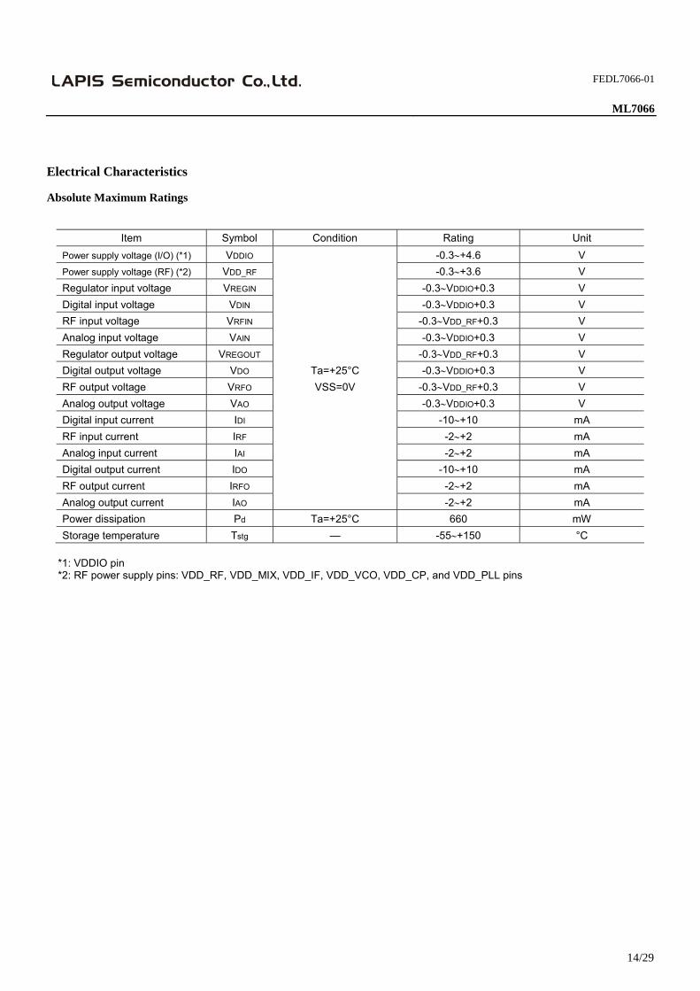
Electrical Characteristics
Absolute Maximum Ratings
Item Symbol Condition Rating Unit
Power supply voltage (I/O) (*1) VDDIO -0.3∼+4.6 V Power supply voltage (RF) (*2) VDD_RF -0.3∼+3.6 V Regulator input voltage VREGIN -0.3∼VDDIO+0.3 V Digital input voltage VDIN -0.3∼VDDIO+0.3 V RF input voltage VRFIN -0.3∼VDD_RF+0.3 V Analog input voltage VAIN -0.3∼VDDIO+0.3 V Regulator output voltage VREGOUT -0.3∼VDD_RF+0.3 V Digital output voltage VDO Ta=+25°C -0.3∼VDDIO+0.3 V RF output voltage VRFO VSS=0V -0.3∼VDD_RF+0.3 V Analog output voltage VAO -0.3∼VDDIO+0.3 V Digital input current IDI -10∼+10 mA RF input current IRF -2∼+2 mA Analog input current IAI -2∼+2 mA Digital output current IDO -10∼+10 mA RF output current IRFO -2∼+2 mA Analog output current IAO -2∼+2 mA Power dissipation Pd Ta=+25°C 660 mW Storage temperature Tstg — -55∼+150 °C
*1: VDDIO pin *2: RF power supply pins: VDD_RF, VDD_MIX, VDD_IF, VDD_VCO, VDD_CP, and VDD_PLL pins
FEDL7066-01
ML7066
15/29
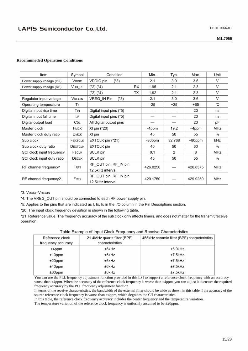
Recommneded Operation Conditions
Item Symbol Condition Min. Typ. Max. Unit
Power supply voltage (I/O) VDDIO VDDIO pin (*3) 2.1 3.0 3.6 V Power supply voltage (RF) VDD_RF (*2) (*4) RX 1.95 2.1 2.3 V (*2) (*4) TX 1.92 2.1 2.3 V Regulator input voltage VREGIN VREG_IN Pin (*3) 2.1 3.0 3.6 V Operating temperature Ta — -25 +25 +65 Digital input rise time TIR Digital input pins (*5) — — 20 ns Digital input fall time tIF Digital input pins (*5) — — 20 ns Digital output load CDL All digital output pins — — 20 pF Master clock FMCK XI pin (*20) -4ppm 19.2 +4ppm MHz Master clock duty ratio DMCK XI pin 45 50 55 % Sub clock FEXTCLK EXTCLK pin (*21) -80ppm 32.768 +80ppm kHz Sub clock duty ratio DEXTCLK EXTCLK pin 40 50 60 % SCI clock input frequency FSCLK SCLK pin 0.1 2 8 MHz SCI clock input duty ratio DSCLK SCLK pin 45 50 55 %
RF channel frequency1 FRF1 RF_OUT pin, RF_IN pin 12.5kHz interval
426.0250 — 426.8375 MHz
RF channel frequency2 FRF2 RF_OUT pin, RF_IN pin 12.5kHz interval
429.1750 — 429.9250 MHz
*3: VDDIO=VREGIN *4: The VREG_OUT pin should be connected to each RF power supply pin. *5: Applies to the pins that are indicated as I, IS, IU in the I/O column in the Pin Descriptions section. *20: The input clock frequency deviation is shown in the following table. *21: Reference value. The frequency accuracy of the sub clock only affects timers, and does not matter for the transmit/receive operation.
Table:Example of Input Clock Frequency and Receive Characteristics
Reference clock frequency accuracy
21.4MHz quartz filter (BPF) characteristics
455kHz ceramic filter (BPF) characteristics
±4ppm ±10ppm ±20ppm ±40ppm ±60ppm
±6kHz ±6kHz ±6kHz ±6kHz ±6kHz
±6.0kHz ±7.5kHz ±7.5kHz ±7.5kHz ±7.5kHz
You can use the PLL frequency adjustment function provided in this LSI to support a reference clock frequency with an accuracy worse than ±4ppm. When the accuracy of the reference clock frequency is worse than ±4ppm, you can adjust it to ensure the required frequency accuracy by the PLL frequency adjustment function. In terms of the receive characteristics, the bandwidth of the external filter should be wide as shown in this table if the accuracy of the source reference clock frequency is worse than ±4ppm, which degrades the C/I characteristics. In this table, the reference clock frequency accuracy includes the center frequency and the temperature variation. The temperature variation of the reference clock frequency is uniformly assumed to be ±20ppm.

FEDL7066-01
ML7066
16/29
Current Consumption Specifications
(Operation power supply voltage: VDDIO=VREGIN=2.1V - 3.6V, Ta=-25 - +65°C) Item Symbol Condition Min. Typ. (*7) Max. Unit
IDDS Total-stop state — 0.7 — µA IDD1 Sleep state — 4 — µA IDD3 Idle state — 2 — mA IDD4 Receiving state
(*8) — 15.5 — mA
Current consumption (*6)
IDD5 Transmitting state (*8)
— 29.5 — mA
*6: The current consumption is the total current of the RF power supply pins (VDD_RF, VDD_MIX, VDD_IF, VDD_VCO,
VDD_CP, and VDD_PLL pins) and the digital power supply pins (VDDIO and VREG_IN pins). *7: The “Typ.” condition is VDDIO = VREGIN =3.0V, 25°C. *8: The value applies to the following conditions (a higher value may occur depending on the MCU operation):
SCI interface clock is 2MHz; data transfer rate is 4800bps.
FEDL7066-01
ML7066
17/29
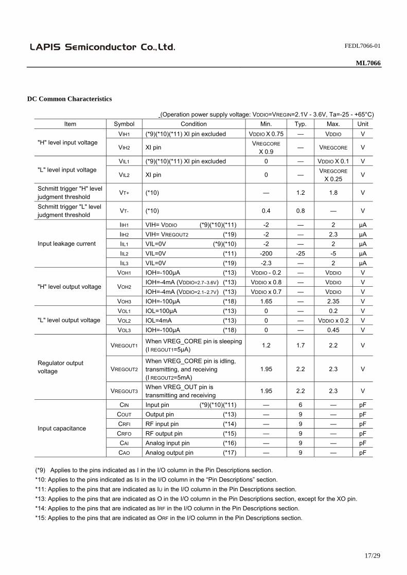
DC Common Characteristics
(Operation power supply voltage: VDDIO=VREGIN=2.1V - 3.6V, Ta=-25 - +65°C) Item Symbol Condition Min. Typ. Max. Unit
VIH1 (*9)(*10)(*11) XI pin excluded VDDIO X 0.75 — VDDIO V "H" level input voltage
VIH2 XI pin VREGCORE
X 0.9 — VREGCORE V
VIL1 (*9)(*10)(*11) XI pin excluded 0 — VDDIO X 0.1 V "L" level input voltage
VIL2 XI pin 0 — VREGCORE
X 0.25 V
Schmitt trigger "H" level judgment threshold
VT+ (*10) — 1.2 1.8 V
Schmitt trigger "L" level judgment threshold
VT- (*10) 0.4 0.8 — V
IIH1 VIH= VDDIO (*9)(*10)(*11) -2 — 2 µA IIH2 VIH= VREGOUT2 (*19) -2 — 2.3 µA IIL1 VIL=0V (*9)(*10) -2 — 2 µA IIL2 VIL=0V (*11) -200 -25 -5 µA
Input leakage current
IIL3 VIL=0V (*19) -2.3 — 2 µA VOH1 IOH=-100µA (*13) VDDIO - 0.2 — VDDIO V
IOH=-4mA (VDDIO=2.7∼3.6V) (*13) VDDIO x 0.8 — VDDIO V VOH2
IOH=-4mA (VDDIO=2.1∼2.7V) (*13) VDDIO x 0.7 — VDDIO V "H" level output voltage
VOH3 IOH=-100µA (*18) 1.65 — 2.35 V VOL1 IOL=100µA (*13) 0 — 0.2 V VOL2 IOL=4mA (*13) 0 — VDDIO x 0.2 V "L" level output voltage VOL3 IOH=-100µA (*18) 0 — 0.45 V
VREGOUT1 When VREG_CORE pin is sleeping(I REGOUT1=5µA)
1.2 1.7 2.2 V
VREGOUT2 When VREG_CORE pin is idling, transmitting, and receiving (I REGOUT2=5mA)
1.95 2.2 2.3 V Regulator output voltage
VREGOUT3 When VREG_OUT pin is transmitting and receiving
1.95 2.2 2.3 V
CIN Input pin (*9)(*10)(*11) — 6 — pF COUT Output pin (*13) — 9 — pF CRFI RF input pin (*14) — 9 — pF CRFO RF output pin (*15) — 9 — pF CAI Analog input pin (*16) — 9 — pF
Input capacitance
CAO Analog output pin (*17) — 9 — pF
(*9) Applies to the pins indicated as I in the I/O column in the Pin Descriptions section. *10: Applies to the pins indicated as IS in the I/O column in the “Pin Descriptions” section. *11: Applies to the pins that are indicated as IU in the I/O column in the Pin Descriptions section. *13: Applies to the pins that are indicated as O in the I/O column in the Pin Descriptions section, except for the XO pin. *14: Applies to the pins that are indicated as IRF in the I/O column in the Pin Descriptions section. *15: Applies to the pins that are indicated as ORF in the I/O column in the Pin Descriptions section.

FEDL7066-01
ML7066
18/29
*16: Applies to the pins that are indicated as IA in the I/O column in the Pin Descriptions section. *17: Applies to the pins that are indicated as OA in the I/O column in the Pin Descriptions section. *18: XO pin. *19: XI pin.
FEDL7066-01
ML7066
19/29
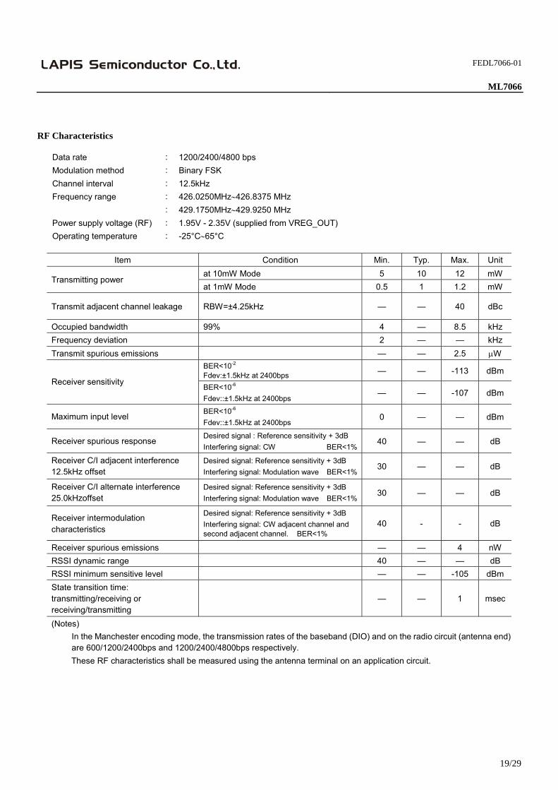
RF Characteristics
Data rate : 1200/2400/4800 bps Modulation method : Binary FSK Channel interval : 12.5kHz Frequency range : 426.0250MHz∼426.8375 MHz : 429.1750MHz∼429.9250 MHz Power supply voltage (RF) : 1.95V - 2.35V (supplied from VREG_OUT) Operating temperature : -25°C∼65°C
Item Condition Min. Typ. Max. Unit
at 10mW Mode 5 10 12 mW Transmitting power
at 1mW Mode 0.5 1 1.2 mW
Transmit adjacent channel leakage RBW=±4.25kHz — — 40 dBc
Occupied bandwidth 99% 4 — 8.5 kHz Frequency deviation 2 — — kHz Transmit spurious emissions — — 2.5 μW
BER<10-2 Fdev:±1.5kHz at 2400bps — — -113 dBm
Receiver sensitivity BER<10-6 Fdev::±1.5kHz at 2400bps
— — -107 dBm
Maximum input level BER<10-6 Fdev::±1.5kHz at 2400bps
0 — — dBm
Receiver spurious response Desired signal : Reference sensitivity + 3dB Interfering signal: CW BER<1%
40 — — dB
Receiver C/I adjacent interference 12.5kHz offset
Desired signal: Reference sensitivity + 3dB Interfering signal: Modulation wave BER<1%
30 — — dB
Receiver C/I alternate interference 25.0kHzoffset
Desired signal: Reference sensitivity + 3dB Interfering signal: Modulation wave BER<1%
30 — — dB
Receiver intermodulation characteristics
Desired signal: Reference sensitivity + 3dB Interfering signal: CW adjacent channel and second adjacent channel. BER<1%
40 - - dB
Receiver spurious emissions — — 4 nW RSSI dynamic range 40 — — dB RSSI minimum sensitive level — — -105 dBmState transition time: transmitting/receiving or receiving/transmitting
— — 1 msec
(Notes) In the Manchester encoding mode, the transmission rates of the baseband (DIO) and on the radio circuit (antenna end)
are 600/1200/2400bps and 1200/2400/4800bps respectively. These RF characteristics shall be measured using the antenna terminal on an application circuit.

FEDL7066-01
ML7066
20/29
Synchronous Communication Interface (SCI) Characteristics
(Operation power supply voltage: 2.1V - 3.6V, Ta=—25 - +65°C) Item Symbol Condition Min. Typ. Max. Unit
SCLK clock frequency FSCLK except suspend 0.1 2 8 MHz SCEN input setup time TCESU 125 — — ns SCEN input hold time TCEH 125 — — ns SCLK "H" pulse width TWCKH 50 — — ns SCLK "L" pulse width TWCKL 50 — — ns SDIN input setup time TDISU 5 — — ns SDIN input hold time TDIH 15 — — ns
TCEEN0 Positive Clock 0 — 40 ns SCEN output enable time
TCEEN1 Negative Clock 0 — 20 ns SCEN assertion interval TCEITVL 1 — — us SCEN output disable time TCEDIS — — 25 ns
TCKOD — — 100 ns SCLK output delay time
TCKODF — — 40 ns SDO output hold time TDOH
Load capacita
nce CL=
50pF
50 — — ns
(Notes) All the timings are measured at the 20% and 80% levels of VDDIO.
Measurement points
All the following measurement points are equivalent to the above ones.
When SCLK is a positive clock
Measurement points
0.8VDDIO
0.2VDDIO
0.8VDDIO
0.2VDDIO
SCEN
SCLK
SDO
SDIN MSB IN BITS6-1 LSB IN
TCEEN0
FSCLK
TWCKH
TDISU
TWCKL
MSB OUT BITS6-1 LSB OUT (**)
TCEH
TCEDIS TDOH TCKOD
TDIH
TDOH
TCESU

FEDL7066-01
ML7066
21/29
When SCLK is a negative clock
(Notes) The SINT pin signal occurs at the timing independent of the signals of other clock synchronous
serial interface related pins. The above diagrams show the case of input/output from the MSB. It can be changed to
input/output from the LSB through the MODE pin setting. **: Although the output value is not specified, MSB data is output in the case of input/output from
the MSB indicated above. For input/output from the LSB, LSB data is output.
SCEN
SCLK
SDO
SDIN MSB IN BITS6-1 LSB IN
TCEEN1
TWCKH
MSB OUT BITS6-1 LSB OUT (**)
TCEH
TCEDIS TCKOD TDOH
TWCKL
FSCLK
TCKODF
TDISU TDIH
TCESU
SCEN TCEITVL

FEDL7066-01
ML7066
22/29
Transmit/Receive Data Interface Characteristics
(Operation power supply voltage: 2.1V - 3.6V, Ta=-25 - +65°C) Item Symbol Condition Min. Typ. Max. Unit
DIO input setup time TDISU At transmission 20 — — ns DIO input hold time TDIH At transmission 20 — — ns DCLK output delay time TDCKOD At reception — — 40 ns DIO output hold time TDOH At reception
Load capacitance
CL= 50pF 15 — — ns
(Notes)
All the timings are measured at the 20% and 80% levels of VDDIO. The DCLK clock frequency FDCLK is 600Hz / 1200Hz / 2400Hz / 4800Hz.
Reset Characteristics
(Operation power supply voltage: 2.1V - 3.6V, Ta=—25 - +65°C) Item Symbol Condition Min. Typ. Max. Unit
RESETN delay time (at power on) TRDL After all power supply pins are powered on 1 — — ms
SRESETN pulse time TRPLS RESETN=1 200 — — ns SRESETN delay time (when operating) TRDOP 1 — — ms RESETN-SRESETN setup time (when operating)
TRSU 10 — — ns
(Notes)
All the timings are measured at the 20% and 80% levels of VDDIO.
VDD VDD voltage level GND level
RESETN
SRESETN
TRDO
TRDL
TRPL
TRSU
DCL
DIO (At reception)
DIO (At transmission)
VALID VALID VALID
VALID VALID
TDCKOD TDOH
FDCLK
TDIS TDI
VALID
TDCKOD
FDCLK

FEDL7066-01
ML7066
23/29
Power ON and Power Down Characteristics
(Operation power supply voltage: 2.1V - 3.6V, Ta=—25 - +65°C) Item Symbol Condition Min. Typ. Max. Unit
Power-on time difference
TPWON At power on between VDDIO - VREG_IN pins
— 1 5 ms
Power-off time difference
TPWOFF At power off between VDDIO - VREG_IN pins
— 1 5 ms
(Notes) No specification for the power-on order. However, each reset time after power on regulated by the RESETN pin must
be satisfied. Timings are measured at the 20% and 80% levels of the minimum value of the power supply voltage of each power
supply pin. Regulator Characteristics
(Operation power supply voltage: 2.1V - 3.6V, Ta=—25 - +65°C) Item Symbol Condition Min. Typ. Max. Unit
Regulator power-on output response time
TREGON At power on VREG_OUT pin
— 5 10 µs
Regulator power-off output response time
TREGOFF At power off VREG_OUT pin
— 5 10 µs
Regulator voltage input time TREGIN — 5 - - ms
(Notes)
TREGON is the time from when the VREG_IN pin reaches 2.2V to when the 2.1V voltage is output from the VREG_OUT pin at power-on. TREGOFF is the time from when the VREG_IN pin reaches 2.2V to when the output level of the VREG_OUT pin begins falling at power-off. Any required voltage output from the regulator should not be used after this time elapsed. TREGIN is the rise time (0V→VDD level) of the voltage applied to the VREG_IN pin at power-on.

FEDL7066-01
ML7066
24/29
Application Circuit
The following shows the typical application circuit. This circuit may vary depending on the shipment time or other factor. This This circuit and componet list are used for ML066 evaluation board. LAPIS Semiconductor recommended that choosing and finalize the best component valuse by evaluationg on the target board. ML7066 Evaluation Board Circuit

FEDL7066-01
ML7066
25/29
Component List of ML7066 Evaluation Board
Parts No. Type No. Vendors Remarks IC1 ML7066 LAPIS Semiconductor IC2 µPD5710TK NEC CMOS SPDT SW
SAW1 NSVA398 Japan Radio 426MHz band SAW Filter NSVA399 429MHz band SAW Filter
MCF1 21412AD Daishinku Quartz filter 21.4MHz CF1 CFUKG455KF4A-R0 Murata Manufacturing Ceramic filter 455kHz X1 DSX530GA Daishinku Crystal oscillator 19.2MHz C1 1000pF Murata Manufacturing GRM1882 or equivalent C2 1000pF Murata Manufacturing GRM1882 or equivalent C3 4pF Murata Manufacturing GRM1882 or equivalent C4 4pF Murata Manufacturing GRM1882 or equivalent C5 1000pF Murata Manufacturing GRM1882 or equivalent C6 5pF Murata Manufacturing GRM1882 or equivalent C7 1.5pF Murata Manufacturing GRM1884 or equivalent C8 7pF Murata Manufacturing GRM1882 or equivalent C9 100pF Murata Manufacturing GRM1882 or equivalent C10 1000pF Murata Manufacturing GRM1882 or equivalent C11 1000pF Murata Manufacturing GRM1882 or equivalent C12 1000pF Murata Manufacturing GRM1882 or equivalent C13 1000pF Murata Manufacturing GRM1882 or equivalent C14 15pF Murata Manufacturing GRM1882 or equivalent C15 1000pF Murata Manufacturing GRM1882 or equivalent C16 0.1µF Murata Manufacturing GRM1882 or equivalent C17 15pF Murata Manufacturing GRM1882 or equivalent C18 15pF Murata Manufacturing GRM1882 or equivalent C19 3300pF Murata Manufacturing GRM1882 or equivalent C20 10µF NEC E/SV line-up or equivalent C21 4.7µF NEC E/SV line-up or equivalent C22 10pF Murata Manufacturing GRM1882 or equivalent C23 1000pF Murata Manufacturing GRM1882 or equivalent C24 10pF Murata Manufacturing GRM1882 or equivalent C25 1000pF Murata Manufacturing GRM1882 or equivalent C26 10µF Murata Manufacturing GRM188 or equivalent C27 10pF Murata Manufacturing GRM1882 or equivalent C28 1000pF Murata Manufacturing GRM1882 or equivalent C29 1µF Murata Manufacturing GRM1882 or equivalent C30 1µF Murata Manufacturing GRM1882 or equivalent C31 10µF NEC E/SV line-up or equivalent C32 1µF Murata Manufacturing GRM1882 or equivalent C33 10µF NEC E/SV line-up or equivalent C34 1000pF Murata Manufacturing GRM1882 or equivalent C35 1000pF Murata Manufacturing GRM1882 or equivalent L1 27nH Murata Manufacturing LQG18 or equivalent L2 15nH Murata Manufacturing LQG18 or equivalent L3 6.2nH Murata Manufacturing LQW18AN6N2D00 L4 3.9nH Murata Manufacturing LQW18AN3N9D10 L5 18nH Murata Manufacturing LQG18 or equivalent L6 18nH Murata Manufacturing LQG18 or equivalent L7 15nH Murata Manufacturing LQW18AN15NJ10 R1 2kΩ KOA RK73B 1J or equivalent R2 2kΩ KOA RK73B 1J or equivalent R3 1.5kΩ KOA RK73B 1J or equivalent R4 1.5kΩ KOA RK73B 1J or equivalent R5 16kΩ KOA RK73B 1J or equivalent R6 200Ω KOA RK73B 1J or equivalent R7 10kΩ KOA RK73B 1J or equivalent R8 10Ω KOA RK73B 1J or equivalent R9 47kΩ KOA RK73B 1J or equivalent
R10 (* 1) 10kΩ KOA RK73B 1J or equivalent (* 1): This resistor can be inserted anywhere in the connected power line, but mandatory. In some past cases, ML7066 could not start up successfully without this resistor.
FEDL7066-01
ML7066
26/29
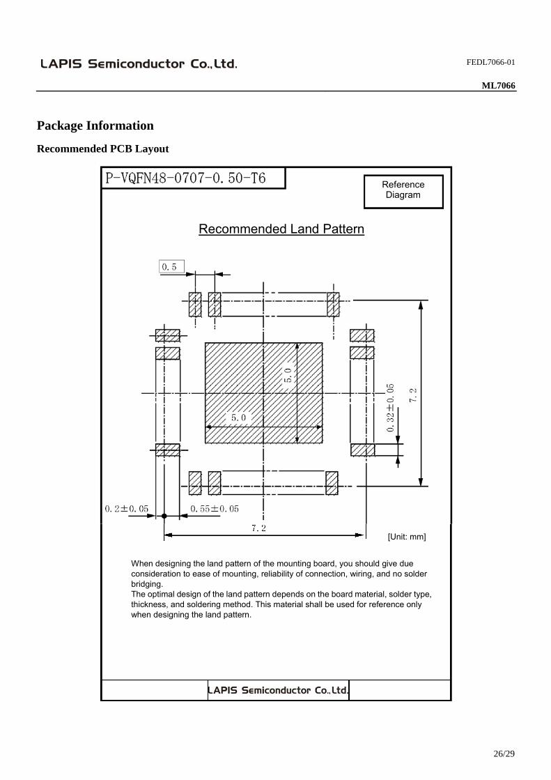
Package Information
Recommended PCB Layout
Reference Diagram
Recommended Land Pattern
[Unit: mm]
When designing the land pattern of the mounting board, you should give due consideration to ease of mounting, reliability of connection, wiring, and no solder bridging. The optimal design of the land pattern depends on the board material, solder type, thickness, and soldering method. This material shall be used for reference only when designing the land pattern.

FEDL7066-01
ML7066
27/29
Package Dimensions
48 Pin VQFN
Notes for Mounting the Surface Mount Type Package The surface mount type packages are very susceptible to heat in reflow mounting and humidity absorbed in storage. Therefore, before you perform reflow mounting, contact ROHM's responsible sales person on the product name, package name, pin number, package code and desired mounting conditions (reflow method, temperature and times).
(Unit: mm)
FEDL7066-01
ML7066
28/29
Revision History
Page Document No. Date Previous
Edition CurrentEdition
Description
FEDL7066-01 Apr.28, 2011 – – Edition 1
NOTE
Any editorial changes are not listed up.

FEDL7066-01
ML7066
29/29
NOTICE
No copying or reproduction of this document, in part or in whole, is permitted without the consent of LAPIS Semiconductor Co., Ltd.
The content specified herein is subject to change for improvement without notice.
The content specified herein is for the purpose of introducing LAPIS Semiconductor's products (hereinafter "Products"). If you wish to use any such Product, please be sure to refer to the specifications, which can be obtained from LAPIS Semiconductor upon request.
Examples of application circuits, circuit constants and any other information contained herein illustrate the standard usage and operations of the Products. The peripheral conditions must be taken into account when designing circuits for mass production.
Great care was taken in ensuring the accuracy of the information specified in this document. However, should you incur any damage arising from any inaccuracy or misprint of such information, LAPIS Semiconductor shall bear no responsibility for such damage.
The technical information specified herein is intended only to show the typical functions of and examples of application circuits for the Products. LAPIS Semiconductor does not grant you, explicitly or implicitly, any license to use or exercise intellectual property or other rights held by LAPIS Semiconductor and other parties. LAPIS Semiconductor shall bear no responsibility whatsoever for any dispute arising from the use of such technical information.
The Products specified in this document are intended to be used with general-use electronic equipment or devices (such as audio visual equipment, office-automation equipment, communication devices, electronic appliances and amusement devices).
The Products specified in this document are not designed to be radiation tolerant.
While LAPIS Semiconductor always makes efforts to enhance the quality and reliability of its Products, a Product may fail or malfunction for a variety of reasons.
Please be sure to implement in your equipment using the Products safety measures to guard against the possibility of physical injury, fire or any other damage caused in the event of the failure of any Product, such as derating, redundancy, fire control and fail-safe designs. LAPIS Semiconductor shall bear no responsibility whatsoever for your use of any Product outside of the prescribed scope or not in accordance with the instruction manual.
The Products are not designed or manufactured to be used with any equipment, device or system which requires an extremely high level of reliability the failure or malfunction of which may result in a direct threat to human life or create a risk of human injury (such as a medical instrument, transportation equipment, aerospace machinery, nuclear-reactor controller, fuel-controller or other safety device). LAPIS Semiconductor shall bear no responsibility in any way for use of any of the Products for the above special purposes. If a Product is intended to be used for any such special purpose, please contact a ROHM sales representative before purchasing.
If you intend to export or ship overseas any Product or technology specified herein that may be controlled under the Foreign Exchange and the Foreign Trade Law, you will be required to obtain a license or permit under the Law.
Copyright 2011 LAPIS Semiconductor Co., Ltd.
2-4-8 Shinyokohama, Kouhoku-ku, Yokohama 222-8575, Japan http://www.lapis-semi.com/en/