itu-t rec. g.703 (11/2001) physical/electrical characteristics of
TRANSCRIPT

INTERNATIONAL TELECOMMUNICATION UNION
ITU-T G.703TELECOMMUNICATION STANDARDIZATION SECTOR OF ITU
(11/2001)
SERIES G: TRANSMISSION SYSTEMS AND MEDIA, DIGITAL SYSTEMS AND NETWORKS Digital terminal equipments – General
Physical/electrical characteristics of hierarchical digital interfaces
ITU-T Recommendation G.703

ITU-T G-SERIES RECOMMENDATIONS TRANSMISSION SYSTEMS AND MEDIA, DIGITAL SYSTEMS AND NETWORKS
INTERNATIONAL TELEPHONE CONNECTIONS AND CIRCUITS G.100–G.199 GENERAL CHARACTERISTICS COMMON TO ALL ANALOGUE CARRIER-TRANSMISSION SYSTEMS
G.200–G.299
INDIVIDUAL CHARACTERISTICS OF INTERNATIONAL CARRIER TELEPHONE SYSTEMS ON METALLIC LINES
G.300–G.399
GENERAL CHARACTERISTICS OF INTERNATIONAL CARRIER TELEPHONE SYSTEMS ON RADIO-RELAY OR SATELLITE LINKS AND INTERCONNECTION WITH METALLIC LINES
G.400–G.449
COORDINATION OF RADIOTELEPHONY AND LINE TELEPHONY G.450–G.499 TESTING EQUIPMENTS G.500–G.599 TRANSMISSION MEDIA CHARACTERISTICS G.600–G.699 DIGITAL TERMINAL EQUIPMENTS G.700–G.799
General G.700–G.709 Coding of analogue signals by pulse code modulation G.710–G.719 Coding of analogue signals by methods other than PCM G.720–G.729 Principal characteristics of primary multiplex equipment G.730–G.739 Principal characteristics of second order multiplex equipment G.740–G.749 Principal characteristics of higher order multiplex equipment G.750–G.759 Principal characteristics of transcoder and digital multiplication equipment G.760–G.769 Operations, administration and maintenance features of transmission equipment G.770–G.779 Principal characteristics of multiplexing equipment for the synchronous digital hierarchy G.780–G.789 Other terminal equipment G.790–G.799
DIGITAL NETWORKS G.800–G.899 DIGITAL SECTIONS AND DIGITAL LINE SYSTEM G.900–G.999 QUALITY OF SERVICE AND PERFORMANCE G.1000–G.1999 TRANSMISSION MEDIA CHARACTERISTICS G.6000–G.6999 DIGITAL TERMINAL EQUIPMENTS G.7000–G.7999 DIGITAL NETWORKS G.8000–G.8999
For further details, please refer to the list of ITU-T Recommendations.

ITU-T Rec. G.703 (11/2001) i
ITU-T Recommendation G.703
Physical/electrical characteristics of hierarchical digital interfaces
Summary This Recommendation specifies the recommended physical and electrical characteristics of the interfaces at hierarchical bit rates as described in ITU-T Recs. G.702 (PDH) and G.707 (SDH). The interfaces are defined in terms of general characteristics, specifications at the output ports and input ports and/or cross-connect points, earthing of outer conductor or screen and coding rules.
Source ITU-T Recommendation G.703 was prepared by ITU-T Study Group 15 (2001-2004) and approved under the WTSA Resolution 1 procedure on 29 November 2001.
History
Issue Notes
10/2001 This revision contains the following modifications:
– Addition of clause 16 on 51 840 kbit/s (STM-0) interface.
– Addition of Appendix III on 3152 kbit/s interface (from G.931/Annex A).
– Amendments to clause 13 on 2048 kbit/s synchronization interface.
– Amendments of clauses 4, 9, 10, 11 with the inclusion of output return loss requirements for the 64 kbit/s (codirectional), 2048, 8448, 34 368 kbit/s interfaces.
– Insertion of names of hierarchical interfaces (E0, E11, E21 etc.) into the headings of the corresponding clauses.
– Giving of references to ITU-T Rec. G.824 (2000) with jitter parameters for the 1544 kbit/s hierarchy.
Some editorial corrections were made including changes of references to the last versions of G.823, G.825 (2000).
10/98 This revision includes a correction to the specification of the 1544 and 44 736 kbit/s interfaces and the addition of Appendix I. Appendix I contains a previous version of the 1544 kbit/s interface specification. The overvoltage protection requirements have been deleted and replaced with a reference to Recommendation K.41 "Resistibility of internal interfaces of telecommunication centres to surge overvoltages". The grounding requirements for the screen (if existing) of a symmetrical pair, or the outer conductor of a coaxial cable have been enhanced. Editorial modifications are included to comply with Recommendation A.3. Clauses 1 to 12 in the 1991 revision are as a consequence renumbered into clauses 4 to 15. Appendix II on 64 and 6312 synchronization interfaces for use in Japan has been added.
1991 Previous revision
1972 Initial version
ii ITU-T Rec. G.703 (11/2001)
FOREWORD
The International Telecommunication Union (ITU) is the United Nations specialized agency in the field of telecommunications. The ITU Telecommunication Standardization Sector (ITU-T) is a permanent organ of ITU. ITU-T is responsible for studying technical, operating and tariff questions and issuing Recommendations on them with a view to standardizing telecommunications on a worldwide basis.
The World Telecommunication Standardization Assembly (WTSA), which meets every four years, establishes the topics for study by the ITU-T study groups which, in turn, produce Recommendations on these topics.
The approval of ITU-T Recommendations is covered by the procedure laid down in WTSA Resolution 1.
In some areas of information technology which fall within ITU-T's purview, the necessary standards are prepared on a collaborative basis with ISO and IEC.
NOTE
In this Recommendation, the expression "Administration" is used for conciseness to indicate both a telecommunication administration and a recognized operating agency.
INTELLECTUAL PROPERTY RIGHTS
ITU draws attention to the possibility that the practice or implementation of this Recommendation may involve the use of a claimed Intellectual Property Right. ITU takes no position concerning the evidence, validity or applicability of claimed Intellectual Property Rights, whether asserted by ITU members or others outside of the Recommendation development process.
As of the date of approval of this Recommendation, ITU had not received notice of intellectual property, protected by patents, which may be required to implement this Recommendation. However, implementors are cautioned that this may not represent the latest information and are therefore strongly urged to consult the TSB patent database.
ITU 2002
All rights reserved. No part of this publication may be reproduced, by any means whatsoever, without the prior written permission of ITU.

ITU-T Rec. G.703 (11/2001) iii
CONTENTS Page
1 Scope ............................................................................................................................ 1
2 References..................................................................................................................... 1
3 Abbreviations................................................................................................................ 2
4 Interface at 64 kbit/s (E0) ............................................................................................. 3 4.1 Functional requirements ................................................................................. 3 4.1.1 Three types of envisaged interfaces ............................................................... 3 4.2 Electrical characteristics................................................................................. 5 4.2.1 Electrical characteristics of 64 kbit/s codirectional interface......................... 5 4.2.2 Electrical characteristics of the 64 kbit/s centralized clock interface............. 8 4.2.3 Electrical characteristics of 64 kbit/s contradirectional interface................... 10
5 Interface at 1544 kbit/s (E11) ....................................................................................... 13 5.1 General characteristics.................................................................................... 13 5.2 Pulse specification .......................................................................................... 16 5.3 Eye diagrams .................................................................................................. 16
6 Interface at 6312 kbit/s (E21) ....................................................................................... 16
7 Interface at 32 064 kbit/s .............................................................................................. 19
8 Interface at 44 736 kbit/s (E32) .................................................................................... 21
9 Interface at 2048 kbit/s (E12) ....................................................................................... 23 9.1 General characteristics.................................................................................... 23 9.2 Specifications at the output ports ................................................................... 24 9.3 Specifications at the input ports ..................................................................... 25 9.4 Grounding of outer conductor or screen......................................................... 26
10 Interface at 8448 kbit/s (E22) ....................................................................................... 26 10.1 General characteristics.................................................................................... 26 10.2 Specification at the output ports ..................................................................... 26 10.3 Specifications at the input ports ..................................................................... 28 10.4 Grounding of outer conductor ........................................................................ 28
11 Interface at 34 368 kbit/s (E31) .................................................................................... 28 11.1 General characteristics.................................................................................... 28 11.2 Specification at the output ports ..................................................................... 28 11.3 Specifications at the input ports ..................................................................... 30 11.4 Grounding of outer conductor ........................................................................ 30
12 Interface at 139 264 kbit/s (E4) .................................................................................... 30

iv ITU-T Rec. G.703 (11/2001)
Page 12.1 General characteristics.................................................................................... 30 12.2 Specifications at the output ports ................................................................... 31 12.3 Specifications at the input ports ..................................................................... 34 12.4 Grounding of outer conductor ........................................................................ 34
13 2048 kHz synchronization interface (T12) ................................................................... 34 13.1 General characteristics.................................................................................... 34 13.2 Specifications at the output ports ................................................................... 34 13.3 Specifications at the input ports ..................................................................... 35 13.4 Grounding of outer conductor or screen......................................................... 36
14 Interface at 97 728 kbit/s .............................................................................................. 36
15 Interface at 155 520 kbit/s – STM-1 interface (ES1) ................................................... 37 15.1 General characteristics.................................................................................... 37 15.2 Specifications at the output ports ................................................................... 37 15.3 Specifications at the input ports ..................................................................... 38 15.4 Specifications at the cross-connect points...................................................... 38 15.5 Grounding of outer conductor ........................................................................ 41
16 Interface at 51 840 kbit/s (STM-0 interface) ................................................................ 41 16.1 General characteristics.................................................................................... 41 16.2 Specifications at the output ports ................................................................... 42 16.3 Specifications at the input ports ..................................................................... 46 16.4 Specifications at the cross-connect points...................................................... 47 16.5 Grounding of outer conductor ........................................................................ 48
Annex A – Definition of codes ................................................................................................ 48 A.1 Definition of B3ZS (also designated HDB2) and HDB3 ............................... 48 A.2 Definition of B6ZS and B8ZS........................................................................ 48 A.3 Definition of CMI........................................................................................... 48
Appendix I – 1544 kbit/s specification in the 1991 version of this Recommendation ............ 49 I.1 General ........................................................................................................... 49 I.2 Interface specification .................................................................................... 49 I.3 Pulse mask ...................................................................................................... 49
Appendix II – 64 and 6312 kHz synchronization interface specification for use in Japan...... 51 II.1 64 kHz synchronization interface................................................................... 51 II.2 6312 kHz synchronization interface............................................................... 52
Appendix III – 3152 kbit/s interface specification for use in North America ......................... 53
ITU-T Rec. G.703 (11/2001) 1
ITU-T Recommendation G.703
Physical/electrical characteristics of hierarchical digital interfaces
1 Scope This Recommendation provides the recommended physical and electrical characteristics of the interfaces at hierarchical bit rates as described in ITU-T Recs. G.702 (PDH) and G.707 (SDH), to enable the interconnection of digital network components (digital sections, multiplex equipment, exchanges) to form an international digital link or connection. The characteristics given in this Recommendation should be applied to new equipment (component) designs. NOTE 1 – The characteristics of interfaces at non-hierarchical bit rates, except n × 64 kbit/s interfaces conveyed by 1544 kbit/s or 2048 kbit/s interfaces and 3152 kbit/s interface in North American hierarchy, are specified in the respective equipment Recommendations. NOTE 2 – The jitter specifications contained in this Recommendation are intended to be imposed at international interconnection points. NOTE 3 – The interfaces described in clauses 5 to 12 correspond to the ports T (output port) and T′ (input port) as recommended for interconnection in ITU-R Rec. F.596-1 (Interconnection of digital radio-relay systems). NOTE 4 – For signals with bit rates of n × 64 kbit/s (n = 2 to 31) which are routed through multiplexing equipment specified for the 2048 kbit/s hierarchy, the interface shall have the same physical/electrical characteristics as those for the 2048 kbit/s interface specified in clause 9. For signals with bit rates of n × 64 kbit/s (n = 2 to 23) which are routed through multiplexing equipment specified for the 1544 kbit/s hierarchy, the interface shall have the same physical/electrical characteristics as those for the 1544 kbit/s interface specified in clause 5. NOTE 5 – The specifications contained in this Recommendation are related to the physical interface only (i.e. to characterize the line codes and input/output equipment interfaces); in particular, the required frequency tolerances do not imply overall equipment performances which may be driven by tighter requirements in Recommendations for specific network/equipment applications (e.g. ITU-T Recs. G.813 and G.783).
2 References The following ITU-T Recommendations and other references contain provisions which, through reference in this text, constitute provisions of this Recommendation. At the time of publication, the editions indicated were valid. All Recommendations and other references are subject to revision; all users of this Recommendation are therefore encouraged to investigate the possibility of applying the most recent edition of the Recommendations and other references listed below. A list of the currently valid ITU-T Recommendations is regularly published.
– ITU-T Recommendation G.701 (1993), Vocabulary of digital transmission and multiplexing, and pulse code modulation (PCM) terms.
– ITU-T Recommendation G.702 (1988), Digital hierarchy bit rates.
– ITU-T Recommendation G.704 (1998), Synchronous frame structures used at 1544, 6312, 2048, 8448 and 44 736 kbit/s hierarchical levels.
– ITU-T Recommendation G.707/Y.1322 (2000), Network node interface for the synchronous digital hierarchy (SDH).
– ITU-T Recommendation G.742 (1988), Second order digital multiplex equipment operating at 8448 kbit/s and using positive justification.

2 ITU-T Rec. G.703 (11/2001)
– ITU-T Recommendation G.747 (1988), Second order digital multiplex equipment operating at 6312 kbit/s and multiplexing three tributaries at 2048 kbit/s.
– ITU-T Recommendation G.751 (1988), Digital multiplex equipments operating at the third order bit rate of 34 368 kbit/s and the fourth order bit rate of 139 264 kbit/s and using positive justification.
– ITU-T Recommendation G.752 (1988), Characteristics of digital multiplex equipment based on a second order bit rate of 6312 kbit/s and using positive justification.
– ITU-T Recommendation G.753 (1988), Third order digital multiplex equipment operating at 34 368 kbit/s and using positive/zero/ negative justification.
– ITU-T Recommendation G.755 (1988), Digital multiplex equipment operating at 139 264 kbit/s and multiplexing three tributaries at 44 736 kbit/s.
– ITU-T Recommendation G.811 (1997), Timing characteristics of primary reference clocks.
– ITU-T Recommendation G.812 (1998), Timing requirements of slave clocks suitable for use as node clocks in synchronization networks.
– ITU-T Recommendation G.813 (1996), Timing characteristics of SDH equipment slave clocks (SEC).
– ITU-T Recommendation G.823 (2000), The control of jitter and wander within digital networks which are based on the 2048 kbit/s hierarchy.
– ITU-T Recommendation G.824 (2000), The control of jitter and wander within digital networks which are based on the 1544 kbit/s hierarchy.
– ITU-T Recommendation G.825 (2000), The control of jitter and wander within digital networks which are based on the synchronous digital hierarchy (SDH).
– ITU-T Recommendation K.27 (1996), Bonding configurations and earthing inside a telecommunication building.
– ITU-T Recommendation K.41 (1998), Resistibility of internal interfaces of telecommunication centres to surge overvoltages.
– ITU-T Recommendation O.151 (1992), Error performance measuring equipment operating at the primary rate and above.
– ITU-T Recommendation O.172 (2001), Jitter and wander measuring equipment for digital systems which are based on the synchronous digital hierarchy (SDH).
– CCITT Handbook (1976), Earthing of Telecommunication Installations.
– ITU-R Recommendation F.750-3 (2000), Architectures and functional aspects of radio-relay systems for synchronous digital hierarchy (SDH)-based networks.
– IEC 60469-2 (1987), Pulse techniques and apparatus. Part 2: Pulse measurement and analysis, general considerations.
– ETSI ETS 300 166 (1993), Transmission and Multiplexing (ТМ); Physical and electrical characteristics of hierarchical digital interfaces for equipment using the 2048 kbit/s-based plesiochronous or synchronous digital hierarchies.
3 Abbreviations This Recommendation uses the following abbreviations:
AIS Alarm Indication Signal
AMI Alternate Mark Inversion
ITU-T Rec. G.703 (11/2001) 3
B3ZS Bipolar with three-Zero Substitution
B8ZS Bipolar with eight-Zero Substitution
CMI Coded Mark Inversion
DC Direct Current
DSN Digital Switching Network
EMC Electromagnetic Compatibility
HDB2 High Density Bipolar of order 2 code
HDB3 High Density Bipolar of order 3 code
PCM Pulse Code Modulation
PRBS Pseudo Random Bit Sequence
PDH Plesiochronous Digital Hierarchy
SDH Synchronous Digital Hierarchy
STM Synchronous Transport Module
ZBTSI Zero Byte Time Slot Interchange
4 Interface at 64 kbit/s (E0)
4.1 Functional requirements The following basic requirements for the design of the interface are recommended:
In both directions of transmission, three signals can be carried across the interface: – 64 kbit/s information signal; – 64 kHz timing signal; – 8 kHz timing signal. NOTE 1 – The 64 kbit/s information signal and the 64 kHz timing signal are mandatory. However, although an 8 kHz timing must be generated by the controlling equipment (e.g. PCM multiplex or time slot access equipment), it should not be mandatory for the subordinate equipment on the other side of the interface to either utilize the 8 kHz timing signal from the controlling equipment or to supply an 8 kHz timing signal. NOTE 2 – The detection of an upstream fault can be transmitted across the 64 kbit/s interface by transmitting an alarm indication signal (AIS) towards the subordinate equipment.
The interface should be bit sequence independent at 64 kbit/s. NOTE 3 – An unrestricted 64 kbit/s signal can be transmitted across the interface. However, this does not imply that unrestricted 64 kbit/s paths are realizable on a global basis. This is because some Administrations presently have or are continuing to install extensive networks composed of digital line sections whose characteristics do not permit the transmission of long sequences of 0s. (ITU-T Rec. G.733 provides for PCM multiplexes with characteristics appropriate for such digital line sections.) Specifically, for octet timed sources in 1544 kbit/s digital networks, it is required that at least one binary 1 should be contained in any octet of a 64 kbit/s digital signal. For a bit stream which is not octet-timed, no more than 7 consecutive 0s should appear in the 64 kbit/s signal. NOTE 4 – Although the interface is bit sequence independent, the use of the AIS (all 1s bit pattern) may result in some minor restrictions for the 64 kbit/s source. For example, an all 1s alignment signal could result in problems.

4 ITU-T Rec. G.703 (11/2001)
4.1.1 Three types of envisaged interfaces
4.1.1.1 Codirectional interface The term "codirectional" is used to describe an interface across which the information and its associated timing signal are transmitted in the same direction (see Figure 1).
T1818700-02
Information signalTiming signal
EquipmentEquipment
Figure 1/G.703 – Codirectional interface
4.1.1.2 Centralized clock interface The term "centralized clock" is used to describe an interface wherein for both directions of transmission of the information signal, the associated timing signals are supplied from a centralized clock, which may be derived for example from certain incoming line signals (see Figure 2). NOTE – The codirectional interface or centralized clock interface should be used for synchronized networks and for plesiochronous networks having clocks of the stability required (see ITU-T Rec. G.811) to ensure an adequate interval between the occurrence of slips.
T1818710-02
Information signalTiming signal
EquipmentEquipment
Central clock
Figure 2/G.703 – Centralized clock interface
4.1.1.3 Contradirectional interface The term "contradirectional" is used to describe an interface across which the timing signals associated with both directions of transmission are directed towards the subordinate equipment (see Figure 3).
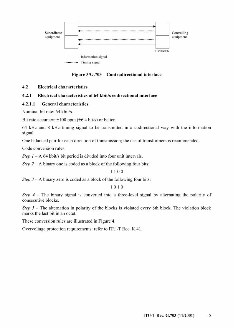
ITU-T Rec. G.703 (11/2001) 5
T1818720-02
Information signalTiming signal
Controllingequipment
Subordinateequipment
Figure 3/G.703 – Contradirectional interface
4.2 Electrical characteristics
4.2.1 Electrical characteristics of 64 kbit/s codirectional interface
4.2.1.1 General characteristics Nominal bit rate: 64 kbit/s.
Bit rate accuracy: ±100 ppm (±6.4 bit/s) or better.
64 kHz and 8 kHz timing signal to be transmitted in a codirectional way with the information signal.
One balanced pair for each direction of transmission; the use of transformers is recommended.
Code conversion rules:
Step 1 – A 64 kbit/s bit period is divided into four unit intervals.
Step 2 – A binary one is coded as a block of the following four bits:
1 1 0 0
Step 3 – A binary zero is coded as a block of the following four bits:
1 0 1 0
Step 4 – The binary signal is converted into a three-level signal by alternating the polarity of consecutive blocks.
Step 5 – The alternation in polarity of the blocks is violated every 8th block. The violation block marks the last bit in an octet.
These conversion rules are illustrated in Figure 4.
Overvoltage protection requirements: refer to ITU-T Rec. K.41.

6 ITU-T Rec. G.703 (11/2001)
7
1
8
0 1
3 4 5
1
6
1
7
1
8
0 10
1
0
2
0
1
T1818730-02Octet timing
Step 5
Step 4
Steps 1-3
64 kbit/s data
Bit number
Violation Violation
Figure 4/G.703 – Illustration of the conversion rules
4.2.1.2 Specifications at the output ports See Table 1.
Table 1/G.703 – Digital 64 kbit/s codirectional interface
Symbol rate 256 kBauds
Pulse shape (nominally rectangular) All pulses of a valid signal must conform to the masks in Figure 5, irrespective of the polarity
Pair for each direction One symmetric pair Test load impedance 120 ohms resistive Nominal peak voltage of a "mark" (pulse) 1.0 V Peak voltage of a "space" (no pulse) 0 V ± 0.10 V Nominal pulse width 3.9 µs Ratio of the amplitudes of positive and negative pulses at the centre of the pulses interval
0.95 to 1.05
Ratio of the widths of positive and negative pulses at the nominal half amplitude
0.95 to 1.05
Maximum peak-to-peak jitter at the output port (Note)
Refer to 5.1/G.823
NOTE – For the time being these values are valid only for equipments of the 2 Mbit/s hierarchy.

ITU-T Rec. G.703 (11/2001) 7
V
0
V
0
T1818740-02b) Mask for double pulse
a) Mask for single pulse
NOTE – The limits apply to pulses of either polarity.
0.2
(3.9 – 0.78)
(3.9 – 0.39)
(3.9 + 2.6)
(3.9 + 0.39)
(3.9 + 3.9)
0.5
1.0 0.1
0.1
0.2
0.2
0.1
0.1
(7.8 – 0.78)
(7.8 – 0.39)
(7.8 + 2.6)
(7.8 + 0.39)
(7.8 + 3.9)
0.1
0.2
0.2
0.1
0.1
0.20.
1
1.0
0.5
3.12 µs
3.51 µs
3.9 µs
4.29 µs
6.5 µs
7.8 µs
7.02 µs
7.42 µs
7.8 µs
8.19 µs
10.4 µs
11.7 µs

8 ITU-T Rec. G.703 (11/2001)
Figure 5/G.703 – Pulse masks of the 64 kbit/s codirectional interface
The return loss at the output port should have the following minimum values:
Frequency range
(kHz) Return loss
(dB)
6.4 to 13 13 to 384
6 8
4.2.1.3 Specifications at the input ports The digital signal presented at the input port shall be as defined above but modified by the characteristics of the interconnecting pairs. The attenuation of these pairs at a frequency of 128 kHz should be in the range 0 to 3 dB. This attenuation should take into account any losses incurred by the presence of a digital distribution frame between the equipments.
For the jitter to be tolerated at the input port, refer to 7.1.1/G.823.
The return loss at the input ports should have the following minimum values:
Frequency range (kHz)
Return loss (dB)
4 to 13 13 to 256
256 to 384
12 18 14
To provide nominal immunity against interference, input ports are required to meet the following requirements:
A nominal aggregate signal, encoded as a 64 kbit/s codirectional signal and having a pulse shape as defined in the pulse mask, shall have added to it an interfering signal with the same pulse shape as the wanted signal. The interfering signal should have a bit rate within the limits specified in this Recommendation, but should not be synchronous with the wanted signal. The interfering signal shall be combined with the wanted signal in a combining network, with an overall zero loss in the signal path and with the nominal impedance 120 ohms to give a signal-to-interference ratio of 20 dB. The binary content of the interfering signal should comply with ITU-T Rec. O.152 (211 – 1 bit period). No errors shall result when the combined signal, attenuated by up to the maximum specified interconnecting cable loss, is applied to the input port.
4.2.1.4 Grounding of screen If the symmetrical pair is screened, the screen shall be connected to the bonding network both at the input port and output port. NOTE 1 – The cable routing is important if leaving the system block. Consult ITU-T Rec. K.27 for guidance. NOTE 2 – The use of isolation to the bonding network is for further study.
4.2.2 Electrical characteristics of the 64 kbit/s centralized clock interface
4.2.2.1 General characteristics Nominal bit rate: 64 kbit/s. The tolerance is determined by the network clock stability (see ITU-T Rec. G.811).
For each direction of transmission, there should be one symmetrical pair carrying the data signal. In addition, there should be symmetrical pairs carrying the composite timing signal (64 kHz and
ITU-T Rec. G.703 (11/2001) 9
8 kHz) from the central clock source to the office terminal equipment. The use of transformers is recommended.
Overvoltage protection requirements: refer to ITU-T Rec. K.41.
Code conversion rules:
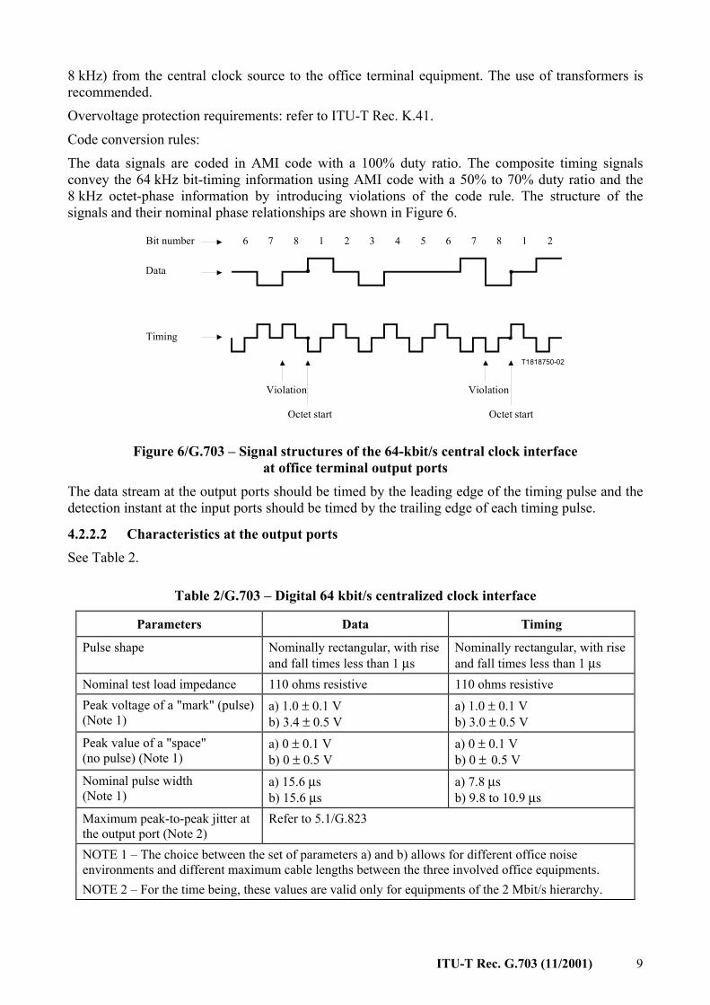
The data signals are coded in AMI code with a 100% duty ratio. The composite timing signals convey the 64 kHz bit-timing information using AMI code with a 50% to 70% duty ratio and the 8 kHz octet-phase information by introducing violations of the code rule. The structure of the signals and their nominal phase relationships are shown in Figure 6.
6 7 8 1 2 3 4 5 6 7 8 1 2
T1818750-02
Violation Violation
Octet start Octet start
Bit number
Data
Timing
Figure 6/G.703 – Signal structures of the 64-kbit/s central clock interface at office terminal output ports
The data stream at the output ports should be timed by the leading edge of the timing pulse and the detection instant at the input ports should be timed by the trailing edge of each timing pulse.
4.2.2.2 Characteristics at the output ports See Table 2.
Table 2/G.703 – Digital 64 kbit/s centralized clock interface
Parameters Data Timing
Pulse shape Nominally rectangular, with rise and fall times less than 1 µs
Nominally rectangular, with rise and fall times less than 1 µs
Nominal test load impedance 110 ohms resistive 110 ohms resistive Peak voltage of a "mark" (pulse) (Note 1)
a) 1.0 ± 0.1 V b) 3.4 ± 0.5 V
a) 1.0 ± 0.1 V b) 3.0 ± 0.5 V
Peak value of a "space" (no pulse) (Note 1)
a) 0 ± 0.1 V b) 0 ± 0.5 V
a) 0 ± 0.1 V b) 0 ± 0.5 V
Nominal pulse width (Note 1)
a) 15.6 µs b) 15.6 µs
a) 7.8 µs b) 9.8 to 10.9 µs
Maximum peak-to-peak jitter at the output port (Note 2)
Refer to 5.1/G.823
NOTE 1 – The choice between the set of parameters a) and b) allows for different office noise environments and different maximum cable lengths between the three involved office equipments. NOTE 2 – For the time being, these values are valid only for equipments of the 2 Mbit/s hierarchy.

10 ITU-T Rec. G.703 (11/2001)
4.2.2.3 Characteristics at the input ports The digital signals presented at the input ports should be as defined above but modified by the characteristics of the interconnecting pairs. The varying parameters in Table 2 will allow typical maximum interconnecting distances of 350 to 450 m.
4.2.2.4 Cable characteristics The transmission characteristics of the cable to be used are subject to further study.
4.2.3 Electrical characteristics of 64 kbit/s contradirectional interface
4.2.3.1 General characteristics Nominal bit rate: 64 kbit/s.
Bit rate accuracy: ±100 ppm (±6.4 bit/s) or better.
For each direction of transmission there should be two symmetrical pairs of wires, one pair carrying the data signal and the other carrying a composite timing signal (64 kHz and 8 kHz). The use of transformers is recommended. NOTE – If there is a national requirement to provide a separate alarm signal across the interface, this can be done by cutting the 8 kHz timing signal for the transmission direction concerned, i.e. by inhibiting the code violations introduced in the corresponding composite timing signal (see below).
Code conversion rules:
The data signals are coded in AMI code with a 100% duty ratio. The composite timing signals convey the 64 kHz bit-timing information using AMI code with a 50% duty ratio and the 8 kHz octet-phase information by introducing violations of the code rule. The structures of the signals and their phase relationships at data output ports are shown in Figure 7.
6 7 8 1 2 3 4 5 6 7 8 1 2
T1818760-02
Violation Violation
Octet start Octet start
Bit number
Data
Timing
Figure 7/G.703 – Signal structures of the 64-kbit/s contradirectional interface at data output ports
The data pulses received from the service (e.g. data or signalling) side of the interface will be somewhat delayed in relation to the corresponding timing pulses. The detection instant for a received data pulse on the line side (e.g. PCM) of the interface should therefore be at the leading edge of the next timing pulse.
Overvoltage protection requirements: refer to ITU-T Rec. K.41.
4.2.3.2 Specifications at the output ports See Table 3.

ITU-T Rec. G.703 (11/2001) 11
Table 3/G.703 – Digital 64 kbit/s contradirectional interface
Parameters Data Timing
Pulse shape (nominally rectangular)
All pulses of a valid signal must conform to the mask in Figure 8 irrespective of the polarity
All pulses of a valid signal must conform to the mask in Figure 9 irrespective of the polarity
Pairs in each direction of transmission
One symmetric pair One symmetric pair
Test load impedance 120 ohms resistive 120 ohms resistive Nominal peak voltage of a "mark" (pulse)
1.0 V 1.0 V
Peak voltage of a "space" (no pulse)
0 V ± 0.1 V 0 V ± 0.1 V
Nominal pulse width 15.6 µs 7.8 µs Ratio of the amplitudes of positive and negative pulses at the centre of the pulse interval
0.95 to 1.05 0.95 to 1.05
Ratio of the widths of positive and negative pulses at the nominal half amplitude
0.95 to 1.05 0.95 to 1.05
Maximum peak-to-peak jitter at the output port (Note)
Refer to 5.1/G.823
NOTE – For the time being these values are valid only for equipments of the 2 Mbit/s hierarchy.

12 ITU-T Rec. G.703 (11/2001)
V
0
T1818770-02
NOTE 1 – When one pulse is immediately followed by another pulse of the opposite polarity, the time limits at the zero-crossingbetween the pulses should be ±0.8 µs.
NOTE 2 – The time instants at which a transition from one state to another in the data signal may occur are determined by the timingsignal. On the service (e.g. data or signalling) side of the interface, it is essential that these transitions are not initiated in advance ofthe timing instants given by the received timing signal.
Nominal pulse12.4 µs
(15.6 – 3.2)
14.0 µs
(15.6 – 1.6)15.6 µs
17.2 µs
(15.6 + 3.2)
(15.6 + 1.6)
(15.6 + 15.6)
0.2
0.1
0.1
0.2
0.21.0
0.50.
10.
1
18.8 µs
31.2 µs
Figure 8/G.703 – Mask of the data pulse of the 64-kbit/s contradirectional interface
V
0
T1818780-02
6.2 µs (7.8 – 1.6)
7.0 µs
7.8 µs
8.6 µs
(7.8 + 1.6)15.6 µs
(7.8 + 7.8)
0.1
0.1
0.5
1.0
0.1
0.1
0.2
0.2 Nominal pulse
0.2
9.4 µs
(7.8 + 0.8)
(7.8 – 0.8)
Figure 9/G.703 – Mask of the timing pulse of the 64-kbit/s contradirectional interface

ITU-T Rec. G.703 (11/2001) 13
4.2.3.3 Specifications at the input ports The digital signals presented at the input ports should be as defined above but modified by the characteristics of the interconnecting pairs. The attenuation of these pairs at a frequency of 32 kHz should be in the range 0 to 3 dB. This attenuation should take into account any losses incurred by the presence of a digital distribution frame between the equipments.
The return loss at the input ports should have the following minimum values:
Frequency range (kHz)
Data signal Composite timing signal
Return loss (dB)
1.6 to 3.2 3.2 to 64 64 to 96
3.2 to 6.4 6.4 to 128 128 to 192
12 18 14
To provide nominal immunity against interference, input ports are required to meet the following requirement:
A nominal aggregate signal, encoded as a 64 kbit/s contradirectional signal and having a pulse shape as defined in the pulse mask, shall have added to it an interfering signal with the same pulse shape as the wanted signal. The interfering signal should have a bit rate within the limits specified in this Recommendation, but should not be synchronous with the wanted signal. The interfering signal shall be combined with the wanted signal in a combining network, with an overall zero loss in the signal path and with the nominal impedance 120 ohms to give a signal-to-interference ratio of 20 dB. The binary content of the interfering signal should comply with ITU-T Rec. O.152 (211 – 1 bit period). No errors shall result when the combined signal, attenuated by up to the maximum specified interconnecting cable loss, is applied to the input port. NOTE – The return loss specification applies for both the data signal and the composite timing signal input ports.
4.2.3.4 Grounding of screen If the symmetrical pairs are screened, the screens shall be connected to the bonding network both at the input port and the output port. NOTE 1 – The cable routing is important if leaving the system block. Consult ITU-T Rec. K.27 for guidance. NOTE 2 – The use of isolation to the bonding network is for further study.
5 Interface at 1544 kbit/s (E11)
5.1 General characteristics The digital interface signal has a nominal bit rate of 1544 kbit/s.
The 1544 kbit/s interface specification is defined in Table 4. All signals appearing at the 1544 kbit/s interface shall satisfy each requirement listed.

14 ITU-T Rec. G.703 (11/2001)
Table 4/G.703 –Digital interface at 1544 kbit/s
Parameter Specification
Nominal bit rate 1544 kbit/s Line rate accuracy In a self-timed, free running mode, the bit rate accuracy shall be ±50 bits/s
(±32 ppm) or better. Line code Either 1) AMI with no more than 15 consecutive zeros, and at least N ones in each
and every time window of 8(N + 1) digit time slots (where N can range from 1 to 23), or 2) B8ZS (Note 1).
Frame structure No frame structure is required for 1544 kbit/s transmission or higher level multiplexing to higher level DSN signals.
Medium One balanced twisted pair shall be used for each direction of transmission. Test load impedance
A resistive test load of 100 ohms ±5% shall be used at the interface for the evaluation of pulse shape and the electrical parameters specified below.
Pulse amplitude The amplitude (Note 2) of an isolated pulse shall be between 2.4 V and 3.6 V. Pulse shape The shape of every pulse that approximates an isolated pulse (is preceded by four
zeros and followed by one or more zeros) shall conform to the mask in Figure 10. See 5.2 for allowable procedures to be followed in checking conformance.
Power level For an all-one signal, the power in a 3 kHz ± 1 kHz band centered at 772 kHz shall be between 12.6 dBm and 17.9 dBm. The power in a 3 kHz ± 1 kHz band centered at 1544 kHz shall be at least 29 dB below that at 772 kHz.
Pulse imbalance In any window of seventeen consecutive bits, the maximum variation in pulse amplitudes shall be less than 200 mV, and the maximum variation in pulse widths (half amplitude) shall be less than 20 ns.
DC power There shall be no DC power applied at the interface. Verification access Access to the signal at the interface shall be provided for verification of these signal
specifications. NOTE 1 – B8ZS is one method of providing bit sequence independence. Bit sequence independence in turn allows unconstrained clear channel capability. Zero Byte Time Slot Interchange (ZBTSI) is another method of providing clear channel transmission. NOTE 2 – While both voltage and power requirements are given to assist in qualification of signals at the interface, the values are not equivalent. Voltage specifications are given for isolated pulses, while power levels are specified for all-ones signal.
Jitter requirements: – for the maximum peak-to-peak jitter at the output port, refer to 5.1/G.824; – for the jitter to be tolerated at the input port, refer to 7.2.1/G.824.
Overvoltage protection requirements: refer to ITU-T Rec. K.41.
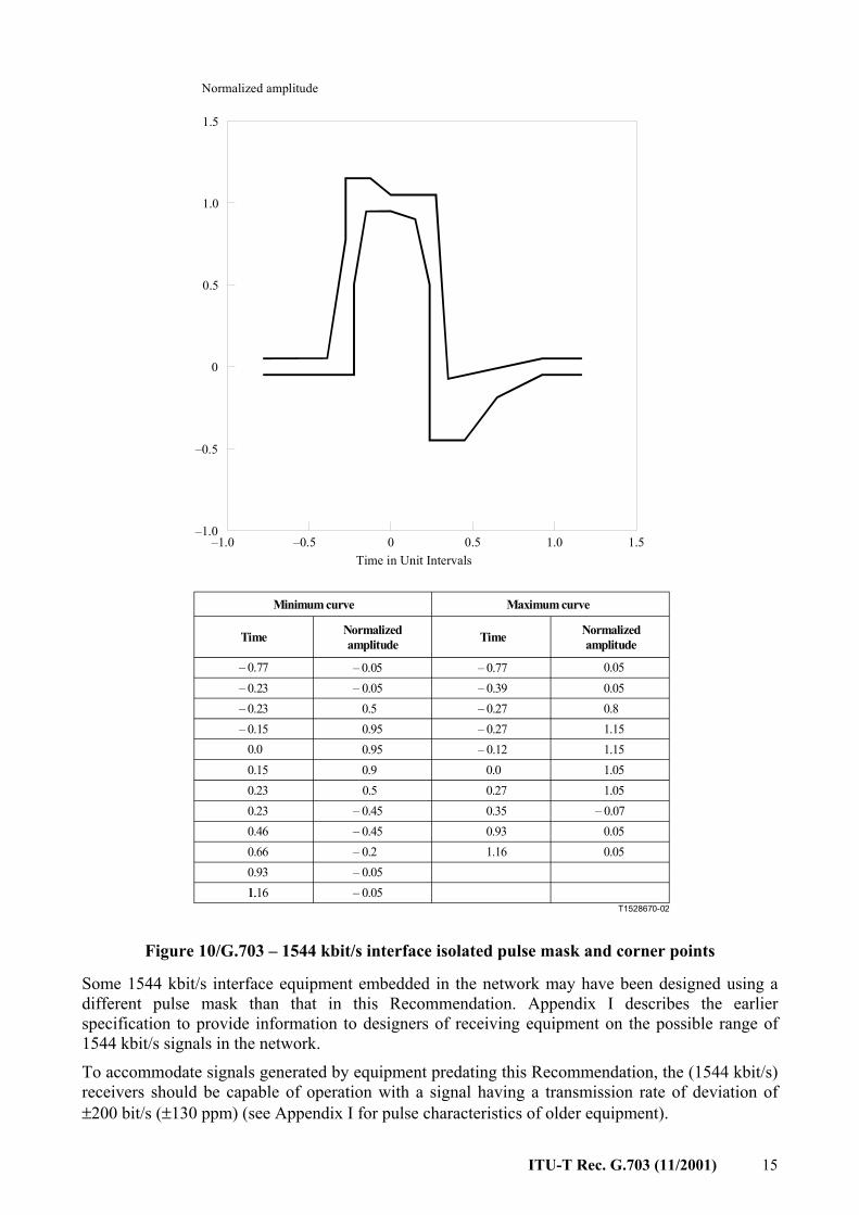
An isolated pulse at the 1544 kbit/s interface shall fit within the mask shown in Figure 10. The corner points for this mask are shown below the figure. In this figure, the y axis shows normalized pulse amplitude. The x axis is time measured in unit intervals. For 1544 kbit/s, the unit interval is 648 ns.
ITU-T Rec. G.703 (11/2001) 15
T1528670-02
1.5
1.0
0.5
0
–0.5
–1.01.51.00.50–0.5–1.0
Minimum curve Maximum curve
Time TimeNormalizedamplitude
Normalizedamplitude
– 0.77 – 0.05 – 0.77 0.05– 0.23 – 0.05 – 0.39 0.05– 0.23 0.5 – 0.27 0.8– 0.15 0.95 – 0.27 1.15
0.0 0.95 – 0.12 1.150.15 0.9 0.0 1.050.23 0.5 0.27 1.050.23 – 0.45 0.35 – 0.070.46 – 0.45 0.93 0.050.66 – 0.2 1.16 0.050.93 – 0.051.1.16 – 0.05
Time in Unit Intervals
Normalized amplitude
Figure 10/G.703 – 1544 kbit/s interface isolated pulse mask and corner points
Some 1544 kbit/s interface equipment embedded in the network may have been designed using a different pulse mask than that in this Recommendation. Appendix I describes the earlier specification to provide information to designers of receiving equipment on the possible range of 1544 kbit/s signals in the network.
To accommodate signals generated by equipment predating this Recommendation, the (1544 kbit/s) receivers should be capable of operation with a signal having a transmission rate of deviation of ±200 bit/s (±130 ppm) (see Appendix I for pulse characteristics of older equipment).
16 ITU-T Rec. G.703 (11/2001)
5.2 Pulse specification For Alternate Mark Inversion (AMI) coding, a pulse mask describing an isolated pulse appearing at the interface is used. In most cases, an ideal isolated pulse can only be approximated due to line coding constraints.
Pulse masks are shown in normalized form, with the nominal pulse amplitude shown as 1.0. In judging conformance of an isolated pulse to the mask, it is only permissible to: a) position the mask horizontally as needed to encompass the pulse; and b) uniformly scale the amplitude of the isolated pulse to fit the mask.
The baseline of the signal shall coincide with the zero point of the baseline of the mask. (The determination of the signal baseline is described in IEC 60469-2). Judging the conformance of negative-going pulses shall be performed after determining the conformance of positive-going pulses in order to maintain the signal baseline reference.
When viewing inverted negative-going pulses for 1544 kbit/s, only the horizontal positioning of the mask to encompass the pulse is permitted. Note that pulse streams with any significant DC component will not meet the requirements of this clause.
5.3 Eye diagrams For signals not amenable to the use of pulse masks, another means of specifying the quality of pulses at the interface is an eye diagram, which is formed by superimposing the waveforms of all possible pulse sequences, including the effects of intersymbol interference. Eye diagrams are presented in normalized form with the peak pulse amplitudes normalized to 1.0 on the vertical scale and the time scale shown in terms of the unit interval. In judging the shape of an eye diagram, it is permissible to: a) position the mask horizontally as needed to encompass the eye diagram; and b) uniformly scale the amplitude of the mask as needed to encompass the eye diagram.
The baseline of the mask shall coincide with the signal baseline. The determination of signal baseline is described in IEC 60469-2.
6 Interface at 6312 kbit/s (E21) Interconnection of 6312 kbit/s signals for transmission purposes is accomplished at a digital distribution frame.
Nominal bit rate: 6312 kbit/s.
Bit rate accuracy: ±30 ppm (189.4 bit/s) or better.
A pseudo-ternary code shall be used as indicated in Table 5.
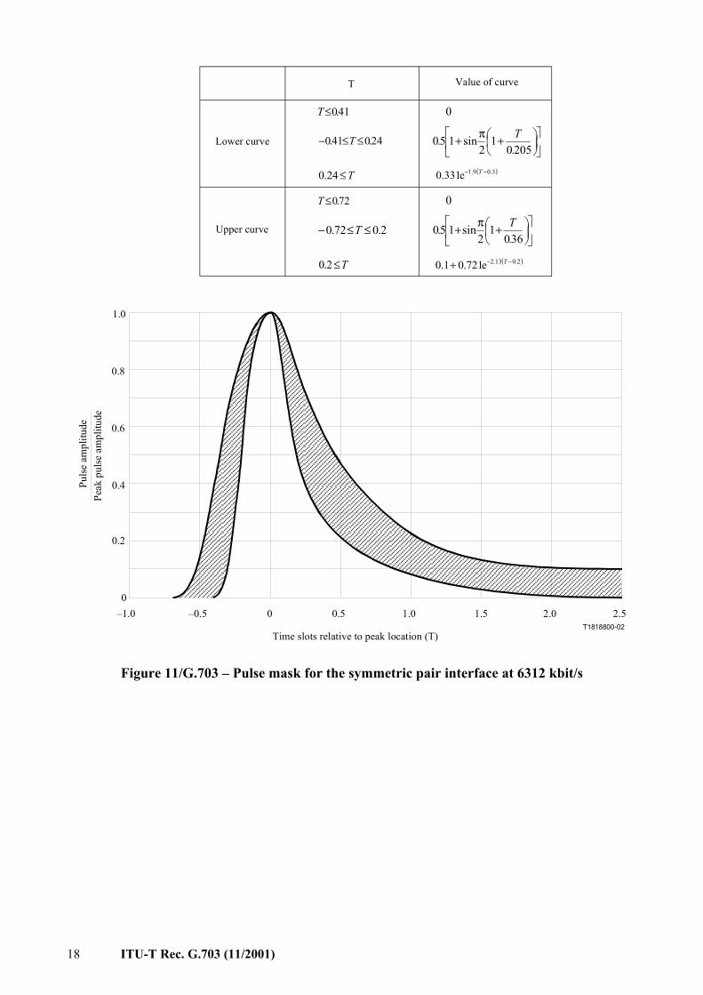
The shape for an isolated pulse measured at the distribution frame shall fall within the mask either of Figure 11 or of Figure 12 and meet the other requirements of Table 5.

ITU-T Rec. G.703 (11/2001) 17
Table 5/G.703 – Digital interface at 6312 kbit/s (Note 1)
Parameter Specification
Bit rate 6312 kbit/s Pair(s) in each direction of transmission
One symmetric pair One coaxial pair
Code B6ZS (Note 2) B8ZS (Note 2) Test load impedance 110 ohms ± 5% resistive 75 ohms ± 5% resistive Nominal pulse shape (Note 1) Rectangular, shaped by cable loss
(see Figure 11) Rectangular (see Figure 12)
Signal level For an all 1s pattern transmitted, the power measured in a 3 kHz bandwidth should be as follows:
3156 kHz: 0.2 to 7.3 dBm 6312 kHz: −20 dBm or less
3156 kHz: 6.2 to 13.3 dBm 6312 kHz: −14 dBm or less
NOTE 1 – The pulse mask for 2nd order digital interface is shown in Figures 11 and 12.
NOTE 2 – See Annex A.
The voltage within a time slot containing a zero (space) shall be no greater than either the value produced in that time slot by other pulses (marks) within the mask of Figure 11, or ±0.1 of the peak pulse (mark) amplitude, whichever is greater in magnitude.
Jitter requirements: – for the maximum peak-to-peak jitter at the output port, refer to 5.1/G.824; – for the jitter to be tolerated at the input port, refer to 7.2.2/G.824.
Overvoltage protection requirements: refer to ITU-T Rec. K.41.
18 ITU-T Rec. G.703 (11/2001)
T1818800-02
Pulse
am
plitu
dePe
ak p
ulse
am
plitu
de
–1.0 –0.5 0.5 1.0 1.5 2.0 2.5
0.2
0.4
0.6
0.8
1.0
Time slots relative to peak location (T)
Lower curve
Upper curve
Value of curve
00
T
+π+
20501
2sin150
.T.
+π+
3601
2sin150
.T.
( )3.09.1e331.0 −− T
( )2.013.2e721.01.0 −−+ T
T≤24.0
0
72.0≤T
41.0≤T
24.041.0 ≤≤− T
T≤2.0
0
2.072.0 ≤≤− T
Figure 11/G.703 – Pulse mask for the symmetric pair interface at 6312 kbit/s

ITU-T Rec. G.703 (11/2001) 19
0
V—2
V
T– —4
T—40T—2 3T
V 10
V 10
V 6V 6
T1818810-02
T8
Pulse
am
plitu
de
T Time-slot widthTime
Figure 12/G.703 – Pulse mask for the coaxial pair interface at 6312 kbit/s
7 Interface at 32 064 kbit/s Interconnection of 32 064 kbit/s signals for transmission purposes is accomplished at a digital distribution frame.
Nominal bit rate: 32 064 kbit/s.
Bit rate accuracy: ±10 ppm (±320.6 bit/s).
One coaxial pair shall be used for each direction of transmission.
The test load impedance shall be 75 ohms ± 5% resistive and the test method shall be direct.
A scrambled AMI code shall be used.
The shape for an isolated pulse measured at the point where the signal arrives at the distribution frame shall fall within the mask in Figure 13.
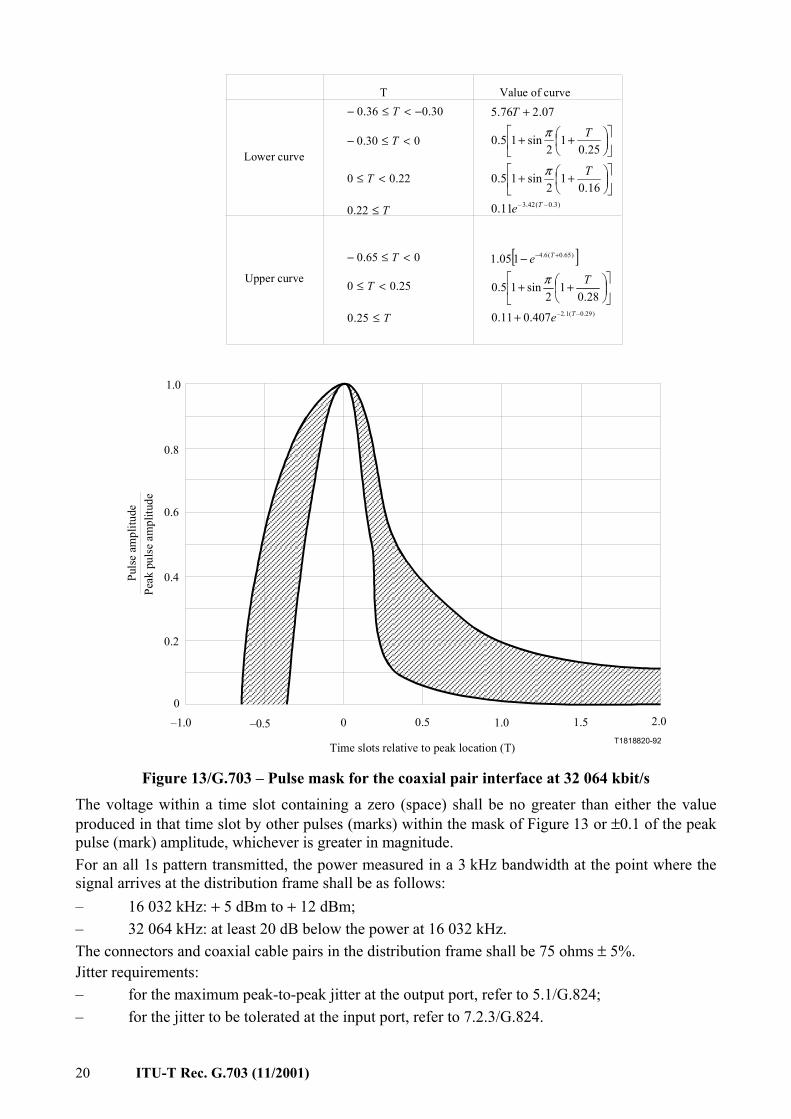
20 ITU-T Rec. G.703 (11/2001)
T1818820-92Time slots relative to peak location (T)
Puls
e am
plitu
dePe
ak p
ulse
am
plitu
de
–1.00
0.2
0.4
0.6
0.8
1.0
–0.5 0 0.5 1.0 1.5 2.0
T
Lower curve
Upper curve
Value of curve
065.0 <≤− T
30.036.0 −<≤− T
)3.0–(42.3–11.0
16.01
2sin15.0
25.01
2sin15.0
07.276.5
Te
T
T
T
++
++
+
π
π
[ ]
)29.0–(1.2–
)65.0(6.4
407.011.0
28.01
2sin15.0
105.1
T
T
e
T
e
+
++
− +−
π
T≤22.0
030.0 <≤− T
22.00 <≤ T
T≤25.0
25.00 <≤ T
Figure 13/G.703 – Pulse mask for the coaxial pair interface at 32 064 kbit/s The voltage within a time slot containing a zero (space) shall be no greater than either the value produced in that time slot by other pulses (marks) within the mask of Figure 13 or ±0.1 of the peak pulse (mark) amplitude, whichever is greater in magnitude. For an all 1s pattern transmitted, the power measured in a 3 kHz bandwidth at the point where the signal arrives at the distribution frame shall be as follows: – 16 032 kHz: + 5 dBm to + 12 dBm; – 32 064 kHz: at least 20 dB below the power at 16 032 kHz. The connectors and coaxial cable pairs in the distribution frame shall be 75 ohms ± 5%. Jitter requirements: – for the maximum peak-to-peak jitter at the output port, refer to 5.1/G.824; – for the jitter to be tolerated at the input port, refer to 7.2.3/G.824.
ITU-T Rec. G.703 (11/2001) 21
Overvoltage protection requirements: refer to ITU-T Rec. K.41.
8 Interface at 44 736 kbit/s (E32) 44 736 kbit/s interface specification is defined in Table 6.
Table 6/G.703 – Digital interface at 44 736 kbit/s
Parameter Specification
Nominal bit rate 44 736 kbit/s Bit rate accuracy In a self-timed, free-running mode, the bit rate accuracy shall be ±895 bits/s
(±20 ppm) or better. Line code B3ZS (bipolar with three-zero substitutions) Frame structure The signal shall have the frame structure defined in ITU-T Rec. G.752 to ensure
transmission through all types of 44 736 kbit/s transport equipment. The frame structure is not required for multiplexing to higher level DSN signals.
Medium One unbalanced coaxial line shall be used for each direction of transmission. Test load impedance
A resistive test load of 75 ohms ± 5% shall be used at the interface for the evaluation of pulse shape and the electrical parameters specified below.
Pulse amplitude The amplitude (Note 1) of an isolated pulse shall be between 0.36 V and 0.85 V peak.
Pulse shape The shape of every pulse that approximates an isolated pulse (is preceded by two zeros and followed by one or more zeros) shall conform to the mask in Figure 14. See 5.2 for allowable procedures to be followed in checking conformance. This mask includes an allowance of ±3% of the peak pulse amplitude at any point on the mask relative to the pulse mask in the earlier version. Equations defining the various line segments making up the mask are listed below the figure.
Power level A wideband power measurement of an AIS signal (as defined in ITU-T Rec. G.704) using a power level sensor with a working frequency range of 200 MHz shall be between −4.7 dBm and +3.6 dBm, including the effects of a range of connecting cable lengths between 68.6 meters (225 feet) and 137.2 meters (450 feet). A low-pass filter having a flat passband and cutoff frequency of 200 MHz shall be used. The rolloff characteristics of this filter are not important; or an alternate power level specification of the power of an all-ones signal (Note 2) is useful for some equipment qualifications. It requires that the power in a 3 kHz ± 1 kHz band centered at 22 368 kHz be between −1.8 dBm and +5.7 dBm. It further requires that the power in a 3 kHz ± 1 kHz band centered at 44 736 kHz be at least 20 dB below that at 22 368 kHz.
Pulse imbalance 1) The ratio of amplitudes of positive and negative isolated pulses shall be between 0.90 and 1.10.
2) Positive and negative isolated pulses shall both conform to the mask of Figure 14.
DC power There shall be no DC power applied at the interface. Verification access
Access to the signal at the interface shall be provided for verification of these signal specifications.

22 ITU-T Rec. G.703 (11/2001)
Parameter Specification
NOTE 1 – While both voltage and power requirements are given to assist in qualification of signals at the interface, the values are not equivalent. Voltage specifications are given for isolated pulses, while power levels are specified for an AIS signal, or alternatively an all-ones signal. NOTE 2 – The all-ones signal is not realizable within the frame structure specified in Recommendation G.752, and is not encountered in North American telecommunication networks.
All signals appearing at the 44 736 kbit/s interface shall satisfy each requirement listed.
An isolated pulse (see pulse shape in Table 6) at the 44 736 kbit/s interface shall fit within the mask shown in Figure 14. Equations defining the various line segments making up the mask are listed below the figure. In this figure, the y axis shows normalized pulse amplitude. The x axis is time measured in unit intervals. For 44 736 kbit/s, the unit interval is 22.4 ns.
To assure proper operation of transmission facilities and higher order multiplex equipment, all 44 736 kbit/s sources shall use the frame structured defined in ITU-T Rec. G.752.
Jitter requirements: – for the maximum peak-to-peak jitter at the output port, refer to 5.1/G.824; – for the jitter to be tolerated at the input port, refer to 7.2.4/G.824.
Overvoltage protection requirements: refer to ITU-T Rec. K.41.

ITU-T Rec. G.703 (11/2001) 23
T1528680-02
1.5
1.0
0.5
0
–0.5
–1.01.51.00.50–0.5–1.0
Normalized amplitude equation
Upper curve
Lower curve
Normalized amplitude
Time, in Unit Intervals
− ≤ ≤ −0 85 0 68. .T 0 03.
0 36 14. .≤ ≤T
− ≤ ≤0 68 0 36. .T
0 08 0 407 184 0 36. . . ( . )+ − −e T
− ≤ ≤ −0 85 0 36. .T −0 03.
− ≤ ≤0 36 0 36. .T
0 36 14. .≤ ≤T −0 03.
03.034.0
12
sin15.0 +
+π+ T
03.018.0
12
sin15.0 −
+π+ T
Time axis range(Unit Intervals)
Figure 14/G.703 – 44 736 kbit/s interface isolated pulse mask and equations
9 Interface at 2048 kbit/s (E12)
9.1 General characteristics Nominal bit rate: 2048 kbit/s.
Bit rate accuracy: ±50 ppm (±102.4 bit/s).
Code: High density bipolar of order 3 (HDB3) (a description of this code can be found in Annex A).

24 ITU-T Rec. G.703 (11/2001)
Overvoltage protection requirements: refer to ITU-T Rec. K.41.
9.2 Specifications at the output ports See Table 7.
Table 7/G.703 – Digital interface at 2048 kbit/s
Pulse shape (nominally rectangular)
All marks of a valid signal must conform with the mask (see Figure 15) irrespective of the sign. The value V corresponds to the nominal peak value.
Pair(s) in each direction One coaxial pair (see 9.4)
One symmetrical pair (see 9.4)
Test load impedance 75 ohms resistive 120 ohms resistive Nominal peak voltage of a mark (pulse) 2.37 V 3 V Peak voltage of a space (no pulse) 0 ± 0.237 V 0 ± 0.3 V Nominal pulse width 244 ns Ratio of the amplitudes of positive and negative pulses at the centre of the pulse interval
0.95 to 1.05
Ratio of the widths of positive and negative pulses at the nominal half amplitude
0.95 to 1.05
Maximum peak-to-peak jitter at an output port Refer to 5.1/G.823
The return loss at the output port should have the following minimum values:
Frequency range
(kHz) Return loss
(dB)
51 to 102 102 to 3072
6 8

ITU-T Rec. G.703 (11/2001) 25
269 ns(244 + 25)
194 ns(244 – 50)
244 ns
219 ns(244 – 25)
488 ns(244 + 244)
10%
10%
10%
10%
0%
50%10
%10
%
20%
20%
V = 100%
T1818840-02
20%
Nominal pulse
NOTE – V corresponds to the nominal peak value.
Figure 15/G.703 – Mask of the pulse at the 2048 kbit/s interface
9.3 Specifications at the input ports The digital signal presented at the input port shall be as defined above but modified by the characteristic of the interconnecting pair. The attenuation of this pair shall be assumed to follow a
f law and the loss at a frequency of 1024 kHz shall be in the range 0 to 6 dB. This attenuation should take into account any losses incurred by the presence of a digital distribution frame between the equipments.
For the jitter to be tolerated at the input port, refer to 7.1.2/G.823.
The return loss at the input port should have the following provisional minimum values:
Frequency range
(kHz) Return loss
(dB)
51 to 102 102 to 2048
2048 to 3072
12 18 14
To ensure adequate immunity against signal reflections that can arise at the interface due to impedance irregularities at digital distribution frames and at digital output ports, input ports should meet the following requirement:

26 ITU-T Rec. G.703 (11/2001)
A nominal aggregate signal, encoded into HDB3 and having a pulse shape as defined in the pulse mask, shall have added to it an interfering signal with the same pulse shape as the wanted signal. The interfering signal should have a bit rate within the limits specified in this Recommendation, but should not be synchronous with the wanted signal. The interfering signal shall be combined with the wanted signal in a combining network, with an overall zero loss in the signal path and with the nominal impedance 75 ohms (in the case of coaxial-pair interface) or 120 Ohms (in the case of symmetrical-pair interface), to give a signal-to-interference ratio of 18 dB. The binary content of the interfering signal should comply with ITU-T Rec. O.151 (215 – 1 bit period). No errors shall result when the combined signal, attenuated by up to the maximum specified interconnecting cable loss, is applied to the input port. NOTE – A receiver implementation providing an adaptive rather than a fixed threshold is considered to be more robust against reflections and should therefore be preferred.
9.4 Grounding of outer conductor or screen The outer conductor of the coaxial pair or the screen of the symmetrical pair shall be connected to the bonding network both at the input port and the output port. NOTE 1 – The cable routing is important if leaving the system block. Consult ITU-T Rec. K.27 for guidance. NOTE 2 – The direct connection of the outer conductors of coaxial cables to the bonding network at the transmit and receive interfaces may, because of differences in earth potential at each end of the cable, result in unwanted current flowing in the outer conductor, through connectors and through the receiver input circuitry. This may result in errors or even permanent damage. To prevent this problem, DC isolation may be introduced between the outer conductor and bonding network at the receive interface. The method of DC isolation must not compromise the EMC compliance of the equipment and the overall installation. NOTE 3 – The use of isolation to the bonding network is for further study.
10 Interface at 8448 kbit/s (E22)
10.1 General characteristics Nominal bit rate: 8448 kbit/s.
Bit rate accuracy: ±30 ppm (±253.4 bit/s).
Code: High density bipolar of order 3 HDB3 (a description of this code can be found in Annex A).
Overvoltage protection requirements: refer to ITU-T Rec. K.41.
10.2 Specification at the output ports See Table 8.

ITU-T Rec. G.703 (11/2001) 27
Table 8/G.703 – Digital interface at 8448 kbit/s
Pulse shape (nominally rectangular)
All marks of a valid signal must conform with the mask (Figure 16) irrespective of the sign.
Pair(s) in each direction One coaxial pair (see 10.4) Test load impedance 75 ohms resistive Nominal peak voltage of a mark (pulse) 2.37 V Peak voltage of a space (no pulse) 0 V ± 0.237 V Nominal pulse width 59 ns Ratio of the amplitudes of positive and negative pulses at the centre of the pulse interval
0.95 to 1.05
Ratio of widths of positive and negative pulses at the nominal half amplitude
0.95 to 1.05
Maximum peak-to-peak jitter at an output port Refer to 5.1/G.823
69 ns(59 + 10)
35 ns(59 – 24)
59 ns
49 ns(59 – 10)
118 ns(59 + 59)
0
T1818850-02
100 ns(59 + 41)
V
Nominal pulse
1.185
2.370
0.23
70.
237
0.47
4
0.23
70.
237
0.23
70.
237
0.47
40.
474
Figure 16/G.703 – Pulse mask at the 8448 kbit/s interface
The return loss at the output port should have the following minimum values:
Frequency range (kHz)
Return loss (dB)
211 to 422 422 to 12 672
6 8

28 ITU-T Rec. G.703 (11/2001)
10.3 Specifications at the input ports The digital signal presented at the input port shall be as defined above but modified by the characteristics of the interconnecting pairs. The attenuation of this pair shall be assumed to follow a
f law and the loss at a frequency of 4224 kHz shall be in the range 0 to 6 dB. This attenuation should take into account any losses incurred by the presence of a digital distribution frame between the equipments.
For the jitter to be tolerated at the input port, refer to 7.1.3/G.823.
The return loss at the input port should have the following provisional minimum values:
Frequency range (kHz)
Return loss (dB)
211 to 422 422 to 8448
8448 to 12 672
12 18 14
To ensure adequate immunity against signal reflections that can arise at the interface due to impedance irregularities at digital distribution frames and at digital output ports, input ports should meet the following requirement:
A nominal aggregate signal, encoded into HDB3 and having a pulse shape as defined in the pulse mask shall have added to it an interfering signal with the same pulse shape as the wanted signal. The interfering signal should have a bit rate within the limits specified in this Recommendation, but should not be synchronous with the wanted signal. The interfering signal shall be combined with the wanted signal in a combining network, with an overall zero loss in the signal path and with the nominal impedance 75 ohms to give a signal-to-interference ratio of 20 dB. The binary content of the interfering signal should comply with ITU-T Rec. O.151 (215 – 1 bit period). No errors shall result when the combined signal, attenuated by up to the maximum specified interconnecting cable loss, is applied to the input port.
10.4 Grounding of outer conductor The outer conductor of the coaxial pair shall be connected to the bonding network at the input port and the output port. NOTE 1 – The cable routing is important if leaving the system block. Consult ITU-T Rec. K.27 for guidance. NOTE 2 – The use of isolation to the bonding network is for further study.
11 Interface at 34 368 kbit/s (E31)
11.1 General characteristics Nominal bit rate: 34 368 kbit/s.
Bit rate accuracy: ±20 ppm (±688 bit/s).
Code: HDB3 (a description of this code can be found in Annex A).
Overvoltage protection requirements: refer to ITU-T Rec. K.41.
11.2 Specification at the output ports See Table 9.

ITU-T Rec. G.703 (11/2001) 29
Table 9/G.703 – Digital interface at 34 368 kbit/s
Pulse shape (nominally rectangular) All marks of a valid signal must conform with the mask (see Figure 17), irrespective of the sign.
Pair(s) in each direction One coaxial pair (see 11.4) Test load impedance 75 ohms resistive Nominal peak voltage of a mark (pulse) 1.0 V Peak voltage of a space (no pulse) 0 V ± 0.1 V Nominal pulse width 14.55 ns Ratio of the amplitudes of positive and negative pulses at the center of a pulse interval
0.95 to 1.05
Ratio of the widths of positive and negative pulses at the nominal half amplitude
0.95 to 1.05
Maximum peak-to-peak jitter at an output port Refer to 5.1/G.823
17 ns
0
T1818860-02
V
Nominal pulse
(14.55 + 2.45)
8.65 ns(14.55 – 5.90)
14.55 ns
12.1 ns(14.55 – 2.45)
24.5 ns(14.55 + 9.95)
0.1
0.1
0.2
0.2
0.1
0.1
0.1
0.1
0.2
29.1 ns(14.55 + 14.55)
0.5
1.0
Figure 17/G.703 – Pulse mask at the 34 368 kbit/s interface

30 ITU-T Rec. G.703 (11/2001)
The return loss at the output port should have the following minimum values:
Frequency range (kHz)
Return loss (dB)
860 to 1720 1720 to 51 550
6 8
11.3 Specifications at the input ports The digital signal presented at the input port shall be as defined above but modified by the characteristics of the interconnecting pair. The attenuation of this cable shall be assumed to follow approximately a f law and the loss at a frequency of 17 184 kHz shall be in the range 0 to 12 dB.
For the jitter to be tolerated at the input port, refer to 7.1.4/G.823.
The return loss at the input port should have the following provisional minimum values:
Frequency range (kHz)
Return loss (dB)
860 to 1720 1720 to 34 368
34 368 to 51 550
12 18 14
To ensure adequate immunity against signal reflections that can arise at the interface due to impedance irregularities at digital distribution frames and at digital output ports, input ports are required to meet the following requirement:
A nominal aggregate signal, encoded into HDB3 and having a pulse shape as defined in the pulse mask shall have added to it an interfering signal with the same pulse shape as the wanted signal. The interfering signal should have a bit rate within limits specified in this Recommendation, but should not be synchronous with the wanted signal. The interfering signal shall be combined with the wanted signal in a combining network, with an overall zero loss in the signal path and with the nominal impedance 75 ohms to give a signal-to-interference ratio of 20 dB. The binary content of the interfering signal should comply with ITU-T Rec. O.151 (223 – 1 bit period). No errors shall result when the combined signal, attenuated by up to the maximum specified interconnecting cable loss, is applied to the input port.
11.4 Grounding of outer conductor The outer conductor of the coaxial pair shall be connected to the bonding network both at the input port and the output port. NOTE 1 – The cable routing is important if leaving the system block. Consult ITU-T Rec. K.27 for guidance. NOTE 2 – The use of isolation to the bonding network is for further study.
12 Interface at 139 264 kbit/s (E4)
12.1 General characteristics Nominal bit rate: 139 264 kbit/s.
Bit rate accuracy: ±15 ppm (±2089 bit/s).
Code: Coded Mark Inversion (CMI) (a description of this code can be found in Annex A)

ITU-T Rec. G.703 (11/2001) 31
Overvoltage protection requirements: refer to ITU-T Rec. K.41.
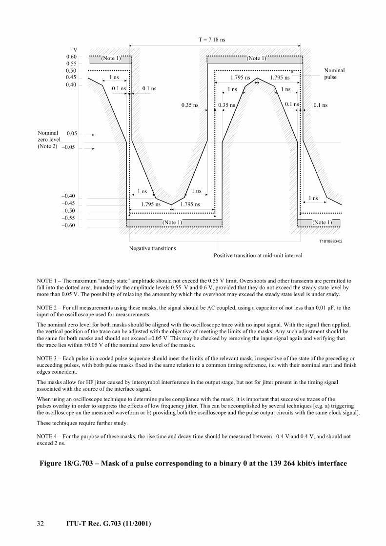
12.2 Specifications at the output ports The specifications at the output ports are given in Table 10 and Figures 18 and 19. NOTE – A method based on the measurement of the levels of the fundamental frequency component, the second (and possibly the third) harmonic of a signal corresponding to binary all 0s and binary all 1s, is considered to be a perfectly adequate method of checking that the requirements of Table 10 have been met. The relevant values of the harmonic components are under study.
Table 10/G.703 – Digital interface at 139 264 kbit/s
Pulse shape Nominally rectangular and conforming to the masks shown in Figures 18 and 19
Pair(s) in each direction One coaxial pair Test load impedance 75 ohms resistive Peak-to-peak voltage 1 ± 0.1 V Rise time between 10% and 90% amplitudes of the measured steady state amplitude
≤2 ns
Transition timing tolerance (referred to the mean value of the 50% amplitude points of negative transitions)
Negative transitions: ±0.1 ns Positive transitions at unit interval boundaries: ±0.5 ns Positive transitions at mid-interval: ±0.35 ns
Return loss ≥15 dB over frequency range 7 MHz to 210 MHz Maximum peak-to-peak jitter at an output port Refer to 5.1/G.823
32 ITU-T Rec. G.703 (11/2001)
1 ns
V
1 ns 1 ns1 ns
1 ns1 ns
T1818880-02
NOTE 1 – The maximum "steady state" amplitude should not exceed the 0.55 V limit. Overshoots and other transients are permitted to fall into the dotted area, bounded by the amplitude levels 0.55 V and 0.6 V, provided that they do not exceed the steady state level by more than 0.05 V. The possibility of relaxing the amount by which the overshoot may exceed the steady state level is under study.
NOTE 2 – For all measurements using these masks, the signal should be AC coupled, using a capacitor of not less than 0.01 µF, to the input of the oscilloscope used for measurements.
The nominal zero level for both masks should be aligned with the oscilloscope trace with no input signal. With the signal then applied, the vertical position of the trace can be adjusted with the objective of meeting the limits of the masks. Any such adjustment should be the same for both masks and should not exceed ±0.05 V. This may be checked by removing the input signal again and verifying that the trace lies within ±0.05 V of the nominal zero level of the masks.
NOTE 3 – Each pulse in a coded pulse sequence should meet the limits of the relevant mask, irrespective of the state of the preceding orsucceeding pulses, with both pulse masks fixed in the same relation to a common timing reference, i.e. with their nominal start and finishedges coincident.
The masks allow for HF jitter caused by intersymbol interference in the output stage, but not for jitter present in the timing signal associated with the source of the interface signal.
When using an oscilloscope technique to determine pulse compliance with the mask, it is important that successive traces of the pulses overlay in order to suppress the effects of low frequency jitter. This can be accomplished by several techniques [e.g. a) triggering the oscilloscope on the measured waveform or b) providing both the oscilloscope and the pulse output circuits with the same clock signal].
These techniques require further study.
NOTE 4 – For the purpose of these masks, the rise time and decay time should be measured between –0.4 V and 0.4 V, and should notexceed 2 ns.
Positive transition at mid-unit intervalNegative transitions
(Note 1) (Note 1)
(Note 1)(Note 1)
Nominalpulse
Nominalzero level(Note 2)
0.600.550.500.450.40
0.05
–0.05
–0.40–0.45
–0.55–0.60
–0.50
T = 7.18 ns
0.1 ns 0.1 ns
1.795 ns 1.795 ns
0.35 ns 0.35 ns 0.1 ns 0.1 ns
1.795 ns 1.795 ns
Figure 18/G.703 – Mask of a pulse corresponding to a binary 0 at the 139 264 kbit/s interface

ITU-T Rec. G.703 (11/2001) 33
1 ns
V
1 ns
1 ns
T1818890-02
1 ns
NOTE 1 – The maximum "steady state" amplitude should not exceed the 0.55 V limit. Overshoots and other transients are permitted to fall into the dotted area, bounded by the amplitude levels 0.55 V and 0.6 V, provided that they do not exceed the steady state level by more than 0.05 V. The possibility of relaxing the amount by which the overshoot may exceed the steady state level is under study.
NOTE 2 – For all measurements using these masks, the signal should be AC coupled, using a capacitor of not less than 0.01 µF, to the input of the oscilloscope used for measurements.
The nominal zero level for both masks should be aligned with the oscilloscope trace with no input signal. With the signal then applied,the vertical position of the trace can be adjusted with the objective of meeting the limits of the masks. Any such adjustment should be the same for both masks and should not exceed ±0.05 V. This may be checked by removing the input signal again and verifying thatthe trace lies within ±0.05 V of the nominal zero level of the masks.
NOTE 3 – Each pulse in a coded sequence should meet the limits of the relevant mask, irrespective of the state of the preceding orsucceeding pulses, with both pulse masks fixed in the same relation to a common timing reference, i.e. with their nominal start and finish edges coincident.
The masks allow for HF jitter caused by intersymbol interference in the output stage, but not for jitter present in the timing signal associated with the source of the interface signal.
When using an oscilloscope technique to determine pulse compliance with the mask, it is important that successive traces of the pulses overlay in order to suppress the effects of low frequency jitter. This can be accomplished by several techniques [e.g. a) triggering the oscilloscope on the measured waveform or b) providing both the oscilloscope and the pulse output circuits with the same clock signal].
These techniques require further study.
NOTE 4 – For the purpose of these masks, the rise time and decay time should be measured between –0.4 V and 0.4 V, and should notexceed 2 ns.
NOTE 5 – The inverse pulse will have the same characteristics, noting that the timing tolerance at the level of the negative and positivetransitions are ±0.1 ns and ±0.5 ns respectively.
Positive transitionNegative transition
(Note 1)
(Note 1)(Note 1)
Nominalpulse
Nominalzero level(Note 2)
0.1 ns 0.1 ns
0.5 ns 0.5 ns
3.59 ns 3.59 ns
1.35 ns 1.35 ns
1.795 ns1.795 ns
0.600.550.500.450.40
0.05
–0.05
–0.40–0.45
–0.55–0.60
–0.50
T = 7.18 ns
Figure 19/G.703 – Mask of a pulse corresponding to a binary 1 at the 139 264 kbit/s interface

34 ITU-T Rec. G.703 (11/2001)
12.3 Specifications at the input ports The digital signal presented at the input port should conform to Table 10 and Figures 18 and 19 modified by the characteristics of the interconnecting coaxial pair.
The attenuation of the coaxial pair should be assumed to follow an approximate f law and to have a maximum insertion loss of 12 dB at a frequency of 70 MHz.
For the jitter to be tolerated at the input port, refer to 7.1.5/G.823.
The return loss characteristics should be the same as that specified for the output port.
12.4 Grounding of outer conductor The outer conductor of the coaxial pair shall be connected to the bonding network both at the input port and the output port. NOTE 1 – The cable routing is important if leaving the system block. Consult ITU-T Rec. K.27 for guidance. NOTE 2 – The use of isolation to the bonding network is for further study.
13 2048 kHz synchronization interface (T12)
13.1 General characteristics The use of this interface is recommended for all applications where it is required to synchronize a digital equipment by an external 2048 kHz synchronization signal.
Overvoltage protection requirements: refer to ITU-T Rec. K.41.
13.2 Specifications at the output ports For general characteristics, see Table 11; for frequency accuracy requirements, see Table 11a.
Table 11/G.703 – Digital 2048 kHz clock interface
Pulse shape The signal must conform with the mask (Figure 20). The value V corresponds to the maximum peak value. The value V1 corresponds to the minimum peak value.
Type of pair Coaxial pair (see Note in 13.4)
Symmetrical pair (see Note in 13.4)
Test load impedance 75 ohms resistive 120 ohms resistive
Maximum peak voltage (Vop) 1.5 1.9
Minimum peak voltage (Vop) 0.75 1.0
Maximum jitter at an output port Refer to Table 5/G.823 (Note) NOTE – This value is valid for network timing synchronization equipments. Other values may be specified for timing output ports of digital links carrying the network timing.

ITU-T Rec. G.703 (11/2001) 35
T30
T4
T4
T4
T4
T
+V
+V1
–V
0
T1818900-02
–V1
T30
T30
T30
T30
T30
Shaded area in whichsignal should bemonotonic
T Average period of synchronizing signal
Figure 20/G.703 – Wave shape at an output port of the 2048 kHz synchronization interface
Table 11a/G.703 – Digital 2048 kHz clock – Frequency accuracy at output ports
Output interface Required accuracy
Primary reference clock – PRC Refer to ITU-T Rec. G.811 Synchronization supply unit – SSU Refer to ITU-T Rec. G.812 SDH equipment clock – SEC 4.6 ppm; refer also to ITU-T Rec. G.813 Others (Note) ±50 ppm NOTE – Synchronization interfaces defined in the 1998 version of this Recommendation.
13.3 Specifications at the input ports The signal presented at the input ports should be as defined above but modified by the characteristics of the interconnecting pair.

36 ITU-T Rec. G.703 (11/2001)
The attenuation of this pair shall be assumed to follow a f law and the loss at a frequency of 2048 kHz should be in the range 0 to 6 dB (minimum value). This attenuation should take into account any losses incurred by the presence of a digital distribution frame between the equipments.
The input port shall be able to tolerate a digital signal with these electrical characteristics but modulated by jitter. See Table 11b.
The return loss at 2048 kHz should be ≥15 dB.
Table 11b/G.703 – Digital 2048 kHz clock – Noise tolerance at input ports
Input interface Jitter tolerance
Primary reference clock – PRC Not applicable Synchronization supply unit – SSU Refer to ITU-T Rec. G.812 SDH equipment clock – SEC Refer to ITU-T Rec. G.813 Others (Note) For further study NOTE – Synchronization interfaces defined in the 1998 version of this Recommendation.
13.4 Grounding of outer conductor or screen The outer conductor of the coaxial pair or the screen of the symmetrical pair shall be connected to the bonding network both at the input port and the output port. NOTE 1 – The cable routing is important if leaving the system block. Consult ITU-T Rec. K.27 for guidance. NOTE 2 – The use of isolation to the bonding network is for further study.
14 Interface at 97 728 kbit/s Interconnection of 97 728 kbit/s signals for transmission purposes is accomplished at a digital distribution frame.
Nominal bit rate: 97 728 kbit/s.
Bit rate accuracy: ±10 ppm (±978 bit/s).
One coaxial pair shall be used for each direction of transmission.
The test load impedance shall be 75 ohms ± 5% resistive.
A scrambled AMI code1 shall be used.
The shape for the 97 728 kbit/s output port shall fall within the mask in Figure 21. The shape at the point where the signal arrives at the distribution frame will be modified by the characteristics of the interconnecting cable.
____________________ 1 An AMI code is scrambled by a five-stage reset-type scrambler with the primitive polynomial of
x5 + x3 + 1.

ITU-T Rec. G.703 (11/2001) 37
10 ns
V
0
T1818910-02
Nominal pulse
2.3
1.7
1.00.9
5.12 ns
4.0 ns
9.0 ns
10.0 ns
6.2 ns
Figure 21/G.703 – Pulse mask at the 97 728 kbit/s output port
The connectors and cable pairs in the distribution frame shall be 75 ohms ± 5%.
Jitter requirements: – for the maximum peak-to-peak jitter at the output port, refer to 5.1/G.824; – for the jitter to be tolerated at the input port, refer to 7.2.5/G.824.
Overvoltage protection requirements: refer to ITU-T Rec. K.41.
15 Interface at 155 520 kbit/s – STM-1 interface (ES1)
15.1 General characteristics Nominal bit rate: 155 520 kbit/s.
Bit rate accuracy: ±20 ppm (±3111 bit/s).
Code: Coded Mark Inversion (CMI) (a description of this code can be found in Annex A).
Overvoltage protection requirements: refer to ITU-T Rec. K.41.
15.2 Specifications at the output ports The specifications at the output ports are given in Table 12 and in Figures 22 and 23. NOTE – A method based on the measurement of the levels of the fundamental frequency component, the second (and possibly the third) harmonic of a signal corresponding to the binary all 0s and binary all 1s, is considered to be a perfectly adequate method of checking that the requirements of Table 12 have been met. The relevant values of the harmonic components are under study.

38 ITU-T Rec. G.703 (11/2001)
Table 12/G.703 – Digital interface at 155 520 kbit/s
Pulse shape Nominally rectangular and conforming to the masks shown in Figures 22 and 23
Pair(s) in each direction One coaxial pair Test load impedance 75 ohms resistive Peak-to-peak voltage 1 ± 0.1 V Rise time between 10% and 90% amplitudes of the measured steady state amplitude
≤2 ns
Transition timing tolerance referred to the mean value of the 50% amplitude points of negative transitions
Negative transitions: ±0.1 ns Positive transitions at unit interval boundaries: ±0.5 ns Positive transitions at mid-unit intervals: ±0.35 ns
Return loss ≥15 dB over frequency range 8 MHz to 240 MHz Maximum peak-to-peak jitter at an output port Refer to 5.1/G.825
15.3 Specifications at the input ports The digital signal presented at the input port should conform to Table 12 and Figures 22 and 23 modified by the characteristics of the interconnecting coaxial pair.
The attenuation of the coaxial pair should be assumed to follow an approximate f law and to have a maximum insertion loss of 12.7 dB at a frequency of 78 MHz.
For the jitter to be tolerated at the input port, refer to 6.1.2.1/G.825.
The return loss characteristics should be the same as that specified for the output port.
15.4 Specifications at the cross-connect points – Signal power level: A wideband power measurement using a power level sensor with a
working frequency range of at least 300 MHz shall be between −2.5 and +4.3 dBm. There shall be no DC power transmitted across the interface.
– Eye diagram: An eye diagram mask based on the maximum and minimum power levels given above is shown in Figure 24 where the voltage amplitude has been normalized to one, and the time scale is specified in terms of the pulse repetition period T. The corner points of the eye diagram are shown in Figure 24.
– Termination: One coaxial cable shall be used for each direction of transmission. – Impedance: A resistive test load of 75 ohms ±5% shall be used at the interface for the
evaluation of the eye diagram and the electrical parameters of the signal.
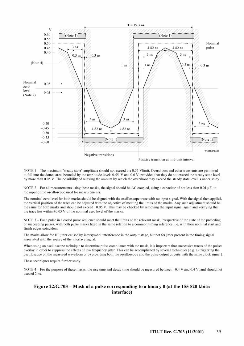
ITU-T Rec. G.703 (11/2001) 39
3 ns
V
3 ns 3 ns3 ns
3 ns3 ns
T1818930-02
1 ns 1 ns
NOTE 1 – The maximum "steady state" amplitude should not exceed the 0.55 Vlimit. Overshoots and other transients are permitted to fall into the dotted area, bounded by the amplitude levels 0.55 V and 0.6 V, provided that they do not exceed the steady state level by more than 0.05 V. The possibility of relaxing the amount by which the overshoot may exceed the steady state level is under study.
NOTE 2 – For all measurements using these masks, the signal should be AC coupled, using a capacitor of not less than 0.01 µF, to the input of the oscilloscope used for measurements.
The nominal zero level for both masks should be aligned with the oscilloscope trace with no input signal. With the signal then applied, the vertical position of the trace can be adjusted with the objective of meeting the limits of the masks. Any such adjustment should be the same for both masks and should not exceed ±0.05 V. This may be checked by removing the input signal again and verifying that the trace lies within ±0.05 V of the nominal zero level of the masks.
NOTE 3 – Each pulse in a coded pulse sequence should meet the limits of the relevant mask, irrespective of the state of the preceding or succeeding pulses, with both pulse masks fixed in the same relation to a common timing reference, i.e. with their nominal start and finish edges coincident.
The masks allow for HF jitter caused by intersymbol interference in the output stage, but not for jitter present in the timing signal associated with the source of the interface signal.
When using an oscilloscope technique to determine pulse compliance with the mask, it is important that successive traces of the pulses overlay in order to suppress the effects of low frequency jitter. This can be accomplished by several techniques [e.g. a) triggering the oscilloscope on the measured waveform or b) providing both the oscilloscope and the pulse output circuits with the same clock signal].
These techniques require further study.
NOTE 4 – For the purpose of these masks, the rise time and decay time should be measured between –0.4 V and 0.4 V, and should notexceed 2 ns.
Positive transition at mid-unit intervalNegative transitions
(Note 1)
(Note 1)(Note 1)
Nominalpulse
Nominalzerolevel(Note 2)
(Note 1)
(Note 4)
0.600.550.500.450.40
0.05
–0.05
–0.40–0.45
–0.55–0.60
–0.50
0.3 ns 0.3 ns
0.3 ns
4.82 ns 4.82 ns
0.3 ns
T = 19.3 ns
4.82 ns4.82 ns
Figure 22/G.703 – Mask of a pulse corresponding to a binary 0 (at the 155 520 kbit/s interface)
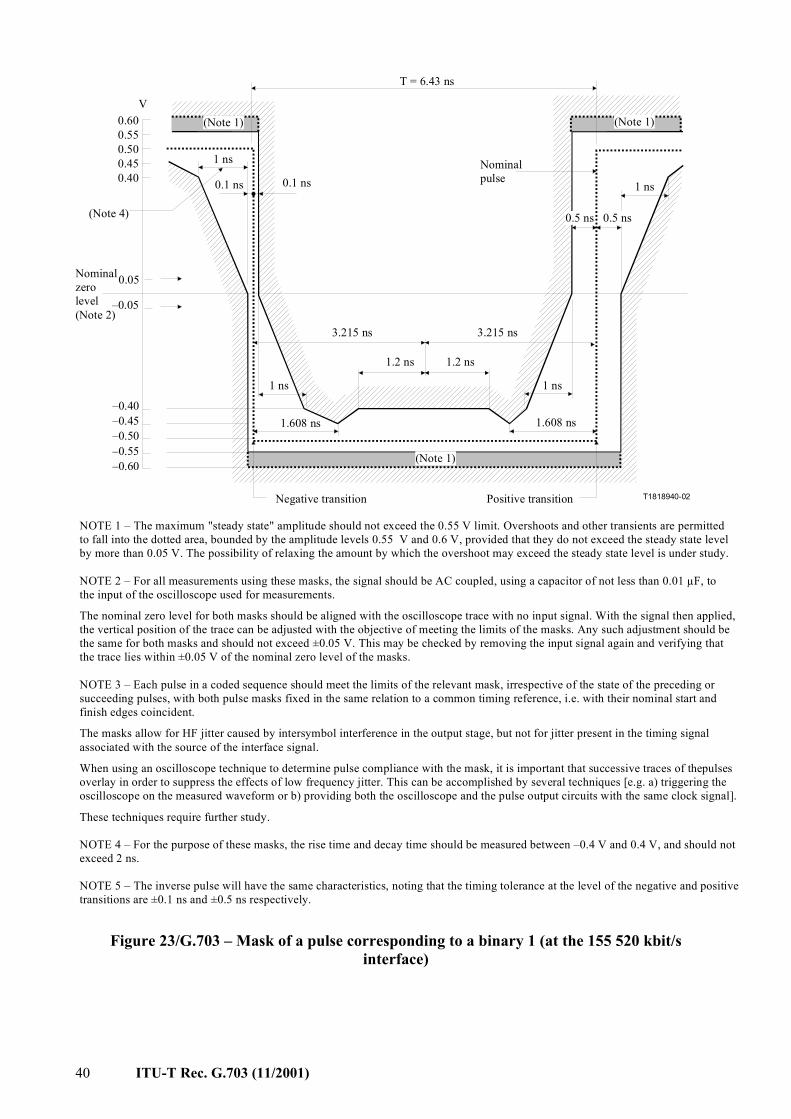
40 ITU-T Rec. G.703 (11/2001)
1 ns
V
1 ns
1 ns
T1818940-02
1 ns
NOTE 1 – The maximum "steady state" amplitude should not exceed the 0.55 V limit. Overshoots and other transients are permitted to fall into the dotted area, bounded by the amplitude levels 0.55 V and 0.6 V, provided that they do not exceed the steady state level by more than 0.05 V. The possibility of relaxing the amount by which the overshoot may exceed the steady state level is under study.
NOTE 2 – For all measurements using these masks, the signal should be AC coupled, using a capacitor of not less than 0.01 µF, to the input of the oscilloscope used for measurements.
The nominal zero level for both masks should be aligned with the oscilloscope trace with no input signal. With the signal then applied, the vertical position of the trace can be adjusted with the objective of meeting the limits of the masks. Any such adjustment should be the same for both masks and should not exceed ±0.05 V. This may be checked by removing the input signal again and verifying that the trace lies within ±0.05 V of the nominal zero level of the masks.
NOTE 3 – Each pulse in a coded sequence should meet the limits of the relevant mask, irrespective of the state of the preceding orsucceeding pulses, with both pulse masks fixed in the same relation to a common timing reference, i.e. with their nominal start and finish edges coincident.
The masks allow for HF jitter caused by intersymbol interference in the output stage, but not for jitter present in the timing signal associated with the source of the interface signal.
When using an oscilloscope technique to determine pulse compliance with the mask, it is important that successive traces of thepulses overlay in order to suppress the effects of low frequency jitter. This can be accomplished by several techniques [e.g. a) triggering the oscilloscope on the measured waveform or b) providing both the oscilloscope and the pulse output circuits with the same clock signal].
These techniques require further study.
NOTE 4 – For the purpose of these masks, the rise time and decay time should be measured between –0.4 V and 0.4 V, and should notexceed 2 ns.
NOTE 5 – The inverse pulse will have the same characteristics, noting that the timing tolerance at the level of the negative and positivetransitions are ±0.1 ns and ±0.5 ns respectively.
Positive transitionNegative transition
(Note 1)
(Note 1)(Note 1)
Nominalpulse
Nominalzerolevel(Note 2)
(Note 4)
0.600.550.500.450.40
0.05
–0.05
–0.40–0.45
–0.55–0.60
–0.50
0.1 ns0.1 ns
3.215 ns 3.215 ns
1.2 ns 1.2 ns
1.608 ns 1.608 ns
0.5 ns 0.5 ns
T = 6.43 ns
Figure 23/G.703 – Mask of a pulse corresponding to a binary 1 (at the 155 520 kbit/s interface)

ITU-T Rec. G.703 (11/2001) 41
0–1
0
+1
a
b c
d
ef
T1818950-02
a
b
c
d
e
f
–0.5 –0.4 –0.3 –0.2 –0.1 0.1 0.2 0.3 0.4 0.5
Point Time Amplitude
− 0 052
.T
− 0 052
.T
0.00
+0.25
+0.25
0.00
–0.25
–0.25
− 0 252
.T
205.0 T+
220.0 T+
205.0 T+
Figure 24/G.703 – STM-1 interface eye diagram
15.5 Grounding of outer conductor The outer conductor of the coaxial pair shall be connected to the bonding network both at the input port and the output port. NOTE 1 – The cable routing is important if leaving the system block. Consult ITU-T Rec. K.27 for guidance. NOTE 2 – The use of isolation to the bonding network is for further study.
16 Interface at 51 840 kbit/s (STM-0 interface)
16.1 General characteristics Nominal bit rate: 51 840 kbit/s.
Bit rate accuracy: ±20 ppm (±1037 bit/s).
Code: Three line codes may be used: a) Coded mark inversion (CMI); b) High density bipolar of order 2 (HDB2) code; c) High density bipolar of order 3 (HDB3) code. A description of these codes can be found in Annex A

42 ITU-T Rec. G.703 (11/2001)
Overvoltage protection requirements: refer to ITU-T Rec. K.41.
16.2 Specifications at the output ports The specifications at the output ports are given in Table 13.
Table 13/G.703 – Digital interface at 51 840 kbit/s
Pair(s) in each direction One coaxial pair Test load impedance 75 ohms resistive Maximum peak-to-peak jitter at an output port 1.5 UIpp in the bandwidth from 100 Hz to 400 kHz
0.15 UIpp in the bandwidth from 20 kHz to 400 kHz NOTE 1 – The high-pass measurement filters have a first-order characteristic and a roll-off of –20 dB/decade. The low-pass measurement filters have a maximally flat, Butterworth characteristic and a roll-off of –60 dB/decade. NOTE 2 –The values of jitter for CMI coded STM-0 signals are provisional and should be studied.
If HDB2 or HDB3 codes are used: Pulse shape Nominally rectangular and conforming to the mask
(Figure 25) irrespective of the sign. The value V corresponds to the nominal peak value.
Nominal peak voltage of a mark (pulse) 1.0 V Peak voltage of a space (no pulse) 0 V ± 0.1 V Nominal pulse width 9.65 ns Ratio of the amplitudes of positive and negative pulses at the center of a pulse interval
0.95 to 1.05
Ratio of the widths of positive and negative pulses at the nominal half amplitude
0.95 to 1.05
If CMI code is used: Pulse shape Nominally rectangular and conforming to the masks
shown in Figures 26 and 27 Peak-to-peak voltage 1 ± 0.1 V Rise time between 10% and 90% amplitudes of the measured steady state amplitude
≤6 ns
Transition timing tolerance referred to the mean value of the 50% amplitude points of negative transitions
Negative transitions: ±0.3 ns Positive transitions at unit interval boundaries: ±1.5 ns Positive transitions at mid-unit intervals: ±1 ns

ITU-T Rec. G.703 (11/2001) 43
0
T1820750-02
V
Nominal pulse
(9.65 + 1.64)
5.69 ns(9.65 – 3.96)
9.65 ns
8.01 ns(9.65 – 1.64)
16.31 ns(9.65 + 6.66)
0.1
0.1
0.2
0.2
0.1
0.1
0.1
0.1
0.2
19.3 ns(9.65 + 9.65)
0.5
1.0
11.29 ns
Figure 25/G.703 – Pulse mask at the 51 840 kbit/s interface (if HDB2 or HDB3 codes are used)

44 ITU-T Rec. G.703 (11/2001)
3 ns
V
3 ns 3 ns3 ns
3 ns3 ns
T1818930-02
1 ns 1 ns
NOTE 1 – The maximum "steady state" amplitude should not exceed the 0.55 V limit. Overshoots and other transients are permitted to fall into the dotted area, bounded by the amplitude levels 0.55 V and 0.6 V, provided that they do not exceed the steady state level by more than 0.05 V. The possibility of relaxing the amount by which the overshoot may exceed the steady state level is under study.
NOTE 2 – For all measurements using these masks, the signal should be AC coupled, using a capacitor of not less than 0.01 µF, to the input of the oscilloscope used for measurements.
The nominal zero level for both masks should be aligned with the oscilloscope trace with no input signal. With the signal then applied, the vertical position of the trace can be adjusted with the objective of meeting the limits of the masks. Any such adjustment should be the same for both masks and should not exceed ±0.05 V. This may be checked by removing the input signal again and verifying that the trace lies within ±0.05 V of the nominal zero level of the masks.
NOTE 3 – Each pulse in a coded pulse sequence should meet the limits of the relevant mask, irrespective of the state of the preceding or succeeding pulses, with both pulse masks fixed in the same relation to a common timing reference, i.e. with their nominal start and finish edges coincident.
The masks allow for HF jitter caused by intersymbol interference in the output stage, but not for jitter present in the timing signal associated with the source of the interface signal.
When using an oscilloscope technique to determine pulse compliance with the mask, it is important that successive traces of the pulses overlay in order to suppress the effects of low frequency jitter. This can be accomplished by several techniques [e.g. a) triggering the oscilloscope on the measured waveform or b) providing both the oscilloscope and the pulse output circuits with the same clock signal].
These techniques require further study.
NOTE 4 – For the purpose of these masks, the rise time and decay time should be measured between –0.4 V and 0.4 V, and should notexceed 2 ns.
Positive transition at mid-unit intervalNegative transitions
(Note 1)
(Note 1)(Note 1)
Nominalpulse
Nominalzerolevel(Note 2)
(Note 1)
(Note 4)
0.600.550.500.450.40
0.05
–0.05
–0.40–0.45
–0.55–0.60
–0.50
0.3 ns 0.3 ns
0.3 ns
4.82 ns 4.82 ns
0.3 ns
T = 19.3 ns
4.82 ns4.82 ns
Figure 26/G.703 – Mask of a pulse corresponding to a binary 0 (at the 51 840 kbit/s interface)

ITU-T Rec. G.703 (11/2001) 45
3 ns
V
3 ns
3 ns
T1820770-02
3 ns
NOTE 1 – The maximum "steady state" amplitude should not exceed the 0.55 V limit. Overshoots and other transients are permitted to fall into the dotted area, bounded by the amplitude levels 0.55 V and 0.6 V, provided that they do not exceed the steady state level by more than 0.05 V. The possibility of relaxing the amount by which the overshoot may exceed the steady state level is under study.
NOTE 2 – For all measurements using these masks, the signal should be AC coupled, using a capacitor of not less than 0.01 µF, to the input of the oscilloscope used for measurements.
The nominal zero level for both masks should be aligned with the oscilloscope trace with no input signal. With the signal then applied, the vertical position of the trace can be adjusted with the objective of meeting the limits of the masks. Any such adjustment should be the same for both masks and should not exceed ±0.05 V. This may be checked by removing the input signal again and verifying that the trace lies within ±0.05 V of the nominal zero level of the masks.
NOTE 3 – Each pulse in a coded sequence should meet the limits of the relevant mask, irrespective of the state of the preceding orsucceeding pulses, with both pulse masks fixed in the same relation to a common timing reference, i.e. with their nominal start and finish edges coincident.
The masks allow for HF jitter caused by intersymbol interference in the output stage, but not for jitter present in the timing signal associated with the source of the interface signal.
When using an oscilloscope technique to determine pulse compliance with the mask, it is important that successive traces of thepulses overlay in order to suppress the effects of low frequency jitter. This can be accomplished by several techniques [e.g. a) triggering the oscilloscope on the measured waveform or b) providing both the oscilloscope and the pulse output circuits with the same clock signal].
These techniques require further study.
NOTE 4 – For the purpose of these masks, the rise time and decay time should be measured between –0.4 V and 0.4 V, and should notexceed 6 ns.
NOTE 5 – The inverse pulse will have the same characteristics, noting that the timing tolerance at the level of the negative and positivetransitions are ±0.3 ns and ±1.5 ns respectively.
Positive transitionNegative transition
(Note 1)
(Note 1)(Note 1)
Nominalpulse
Nominalzerolevel(Note 2)
(Note 4)
0.600.550.500.450.40
0.05
–0.05
–0.40–0.45
–0.55–0.60
–0.50
0.3 ns0.3ns
9.65 ns 9.65 ns
3.67 ns
4.82 ns
1.5 ns 1.5 ns
T = 19.3 ns
3.67 ns
4.82 ns
Figure 27/G.703 – Mask of a pulse corresponding to a binary 1 (at the 51 840 kbit/s interface)

46 ITU-T Rec. G.703 (11/2001)
The return loss at the output port should have the following minimum values:
Frequency range (kHz)
Return loss (dB)
1296 to 2592 2592 to 77 760
6 8
16.3 Specifications at the input ports The digital signal presented at the input port shall be as defined above but modified by the characteristics of the interconnecting pair. The attenuation of this cable shall be assumed to follow approximately a f law and the loss at a frequency of 25 920 kHz shall be in the range from 0 to 12 dB.
The return loss at the input port should have the following provisional minimum values:
Frequency range
(kHz) Return loss
(dB)
1296 to 2592 2592 to 51 840
51 840 to 77 760
12 18 14
The jitter to be tolerated at the input port expressed in peak-to-peak sinusoidal phase amplitude, shall exceed the values shown in Figure 28:
T1820780-02
400k 20k 2k 100 10
Peak-to-peak jitter amplitude, UIpp
Jitter frequency, Hz
0.15
3.63
1.5
41.3
Figure 28/G.703 – 51 840 kbit/s input jitter tolerance limit
NOTE – The values of jitter for CMI coded STM-0 signals are provisional and should be studied.

ITU-T Rec. G.703 (11/2001) 47
16.4 Specifications at the cross-connect points – Signal power level A wideband power measurement using a power level sensor with a working frequency
range of at least four times the bit rate frequency shall be between –2.7 and +4.7 dBm, accounting for both transmitter variations and a range of connecting cable lengths between 68.6 m and 137 m. A filter with a characteristic equivalent to a Butterworth low pass filter with a cut-off frequency of 207.360 MHz shall be used.
There shall be no DC power transmitted across the interface. – Eye diagram An eye diagram mask based on the maximum and minimum power levels and cable lengths
given above is shown in Figure 29 where the voltage amplitude has been normalized to one, and the time scale is specified in terms of the unit interval T. Exclusionary regions are shown as shaded areas on the figure. The corner points of these regions are listed below the figure.
T1820790-02
B
C D
A EH
FG
K
I J
FGHIJK
ABCDE
Time (unit interval)
Normalizedamplitude
0
1
0
–1
0.75
0.25
–0.25
–0.50
–0.75
0.50
–0.50 –0.25 0.25 0.50
Outer region corner points Inner region corner points
Point Time Amplitude Point Time Amplitude
NOTE – Both inner and outer regions are symmetric about the zero amplitude axis.
0.280.00
–0.25 –0.04
0.040.11
0.120.160.240.800.800.22
–0.50 –0.44 –0.18
0.080.50
0.370.801.001.000.37
Figure 29/G.703 – STM-0 interface eye diagram

48 ITU-T Rec. G.703 (11/2001)
16.5 Grounding of outer conductor The outer conductor of the coaxial pair shall be connected to the bonding network both at the input port and the output port. NOTE 1 – The cable routing is important if leaving the system block. Consult ITU-T Rec. K.27 for guidance. NOTE 2 – The use of isolation to the bonding network is for further study.
Annex A
Definition of codes
This annex defines the modified alternate mark inversion codes (see ITU-T Rec. G.701, item 9005) whose use is specified in this Recommendation.
In these codes, binary 1 bits are generally represented by alternate positive and negative pulses, and binary 0 bits by spaces. Exceptions, as specified for the individual codes, are made when strings of successive 0 bits occur in the binary signal.
In the definitions below, B represents an inserted pulse conforming to the AMI rule (ITU-T Rec. G.701, item 9004), and V represents an AMI violation (ITU-T Rec. G.701, item 9007).
The encoding of binary signals in accordance with the rules given in this annex includes frame alignment bits, etc.
A.1 Definition of B3ZS (also designated HDB2) and HDB3 Each block of 3 (or 4) successive zeros is replaced by 00V (or 000V respectively) or B0V (B00V). The choice of 00V (000V) or B0V (B00V) is made so that the number of B pulses between consecutive V pulses is odd. In other words, successive V pulses are of alternate polarity so that no DC component is introduced.
A.2 Definition of B6ZS and B8ZS Each block of 6 (or 8) successive zeros is replaced by 0VB0VB (or 000VB0VB respectively).
A.3 Definition of CMI CMI is a 2-level non-return-to-zero code in which binary 0 is coded so that both amplitude levels, A1 and A2, are attained consecutively, each for half a unit time interval (T/2).
Binary 1 is coded by either of the amplitude levels A1 or A2, for one full unit time interval (T), in such a way that the level alternates for successive binary 1s.
An example is given in Figure A.1. NOTE 1 – For binary 0, there is always a positive transition at the midpoint of the binary unit time interval. NOTE 2 – For binary 1: a) there is a positive transition at the start of the binary unit time interval if in the preceeding time
interval the level was A1; b) there is a negative transition at the start of the binary unit time interval if the last binary 1 was
encoded by level A2.

ITU-T Rec. G.703 (11/2001) 49
0 0 01 1 1 1
T T
2T
2T T1818870-02
Binary
Level A2
Level A1
Figure A.1/G.783 – Example of CMI coded binary signal
Appendix I
1544 kbit/s specification in the 1991 version of this Recommendation
I.1 General This appendix describes an earlier 1544 kbit/s interface that included a pulse mask with substantially greater allowance for overshoot on the trailing edge of the pulse than the current standard. While the current pulse mask has been socialized in a number of network compatibility publications since the late 1970s, equipment designed to the earlier specification may be widespread in the network. Hence, designers of equipment need to be aware of the nature of signals that may be delivered to that equipment.
I.2 Interface specification Most of the interface parameters in Table 4, including power levels and pulse amplitudes, apply to the older interface. One major difference is in the line rate tolerance. The older specification calls for a ±130 ppm tolerance, reflecting an earlier, now obsolete, technology for line driver circuitry.
I.3 Pulse mask Figure I.1 is the 1544 kbit/s pulse mask corresponding to the earlier interface specification. It is based on equipment generating pulses with considerably more overshoot on the trailing edge that is currently allowed in the standard.

50 ITU-T Rec. G.703 (11/2001)
T1528690-02
1.5
1.0
0.5
0
–0.5
–1.01.51.00.50–0.5–1.0
Normalized amplitude
Time, in Unit Intervals
– 0.77– 0.23– 0.23– 0.15
0.150.230.230.420.660.931.16
– 0.04
– 0.05– 0.05
0.50.950.950.90.5
– 0.62– 0.62– 0.2
– 0.05– 0.05
– 0.77– 0.39– 0.27– 0.27– 0.12
0.00.270.340.581.16
0.050.050.8
1.221.221.051.05
0.080.050.05
Minimum curve
Time Normalizedamplitude
Minimum curve
Time Normalizedamplitude
Figure I.1/G.703 – Obsolete 1544 kbit/s interface isolated pulse mask and corner points

ITU-T Rec. G.703 (11/2001) 51
Appendix II
64 and 6312 kHz synchronization interface specification for use in Japan
II.1 64 kHz synchronization interface The 64 kHz clock signals from the clock supply equipment have the frequencies of: a) 64 kHz + 8 kHz or b) 64 kHz + 8 kHz + 400 Hz.
Those signals consist of AMI code with: a) an 8 kHz bipolar violation, or b) an 8 kHz bipolar violation removed at every 400 Hz.
The signal structures of 64 kHz clock signals are illustrated in Figures II.1 and II.2.
1 2 3 4 5 6 7 8 1 2 3 4 5 6 7 8 1 2 3 4 5 6 7 8
T1531560-02
8 kHz (125 µs) 8 kHz (125 µs) 8 kHz (125 µs)
Violation
Violation
Violation
Figure II.1/G.703 – Signal structure of 64 kHz clock interface with a frequency of 64 kHz + 8 kHz
1 2 3 4 5 6 7 8
T1531570-02
8 kHz (125 µs) 8 kHz (125 µs) 8 kHz (125 µs)8 kHz (125 µs)
1 2 3 4 5 6 7 81 2 3 4 5 6 7 81 2 3 4 5 6 7 8 1
ViolationViolationViolation
0.4 kHz (2.5 ms)
Violation
Figure II.2/G.703 – Signal structure of 64 kHz clock interface with a frequency of 64 kHz + 8 kHz + 400 Hz
The specifications of 64 kHz clock signals at input port and output port are shown in Tables II.1 and II.2, respectively.

52 ITU-T Rec. G.703 (11/2001)
Table II.1/G.703 – Specification of 64 kHz clock signal at input port
Frequency a) 64 kHz + 8 kHz or b) 64 kHz + 8 kHz + 400 Hz
a) AMI with 8 kHz bipolar violation; b) AMI with 8 kHz bipolar violation removed at every 400 Hz
Alarm condition Alarm should not be occurred against the amplitude ranged 0.63-1.1 V0-P
Table II.2/G.703 – Specification of 64 kHz clock signal at output port
Frequency a) 64 kHz + 8 kHz or b) 64 kHz + 8 kHz + 400 Hz
Load impedance 110 ohms resistive Transmission media Symmetric pair cable Pulse width (FWHM) ≤7.8 ± 0.78 µs Amplitude ≤1 V0-P ± 0.1 V
II.2 6312 kHz synchronization interface Figure II.3 shows the waveform of 6312 kHz clock signal. The specifications of 6312 kHz clock signals at input port and output port are shown in Tables II.3 and II.4, respectively.
T1531580-02
6312 kHz
Figure II.3/G.703 – Waveform of 6312 kHz clock signal
Table II.3/G.703 – Specification of 6312 kHz clock signal at input port
Frequency 6312 kHz Signal format Sinusoidal wave Alarm condition Alarm should not be occurred against the amplitude ranged
−16 dBm to +3 dBm
Table II.4/G.703 – Specification of 6312 kHz clock signal at output port
Frequency 6312 kHz Load impedance 75 ohms resistive Transmission media Coaxial pair cable Amplitude 0 dBm ± 3 dB

ITU-T Rec. G.703 (11/2001) 53
Appendix III
3152 kbit/s interface specification for use in North America (from Annex A/G.931)
Nominal bit rate: 3152 kbit/s.
Bit rate accuracy: ±30 ppm (±95 bit/s).
For specifications at the ports, see Table III.1.
Table III.1/G.703 – Digital interface at 3152 kbit/s
Parameter Specification
Nominal bit rate 3152 kbit/s Bit rate accuracy ±30 ppm (±95 bit/s) Test load impedance 100 ohms ± 5% resistive Line code AMI (Notes 1 and 2) Pulse shape Nominal rectangular Pair(s) in each direction of transmission
One balanced twisted pair (Note 3)
Nominal amplitude 3.0 V (Note 4) Width (at 50% amplitude) 159 ± 30 ns Rise and fall times (20-80% of amplitude)
≤50 ns (difference between rise and fall times shall be 0 ± 20 ns)
Signal power (all is signal, measured over 10 MHz bandwidth)
16.53 ± 2 dBm [ratio of (power in + pulses) to (power in – pulses) shall be 0 ± 0.5 dB]
NOTE 1 – An AMI code shall be used. For definitions of AMI code; see Annex A/G.703. NOTE 2 – In order to guarantee adequate timing information, the minimum pulse density taken over any 130 consecutive time slots must be 1 in 8. The design intent is that the long-term pulse density be equal to 0.5. In order to provide adequate jitter performance for systems, timing extracting circuits should have a Q of 1200 ± 200 that is representable by a single tuned network. NOTE 3 – One balanced twisted pair shall be used for each direction of transmission. The distribution frame jack connected to a pair bringing signals to the distribution frame is termed the in-jack. The distribution frame jack connected to a pair carrying signals away from the distribution frame is termed the out-jack. NOTE 4 – The peak-to-peak voltage within a time slot containing a zero (space) produced by other pulses meeting the specifications of Table III.1 should not exceed 0.1 of the peak pulse amplitude.
Requirements for the maximum peak-to-peak jitter at the output port and the jitter to be tolerated at the input port are for further study.
Overvoltage protection requirements: refer to ITU-T Rec. K.41.


Printed in Switzerland Geneva, 2002
SERIES OF ITU-T RECOMMENDATIONS
Series A Organization of the work of ITU-T
Series B Means of expression: definitions, symbols, classification
Series C General telecommunication statistics
Series D General tariff principles
Series E Overall network operation, telephone service, service operation and human factors
Series F Non-telephone telecommunication services
Series G Transmission systems and media, digital systems and networks
Series H Audiovisual and multimedia systems
Series I Integrated services digital network
Series J Cable networks and transmission of television, sound programme and other multimedia signals
Series K Protection against interference
Series L Construction, installation and protection of cables and other elements of outside plant
Series M TMN and network maintenance: international transmission systems, telephone circuits, telegraphy, facsimile and leased circuits
Series N Maintenance: international sound programme and television transmission circuits
Series O Specifications of measuring equipment
Series P Telephone transmission quality, telephone installations, local line networks
Series Q Switching and signalling
Series R Telegraph transmission
Series S Telegraph services terminal equipment
Series T Terminals for telematic services
Series U Telegraph switching
Series V Data communication over the telephone network
Series X Data networks and open system communications
Series Y Global information infrastructure and Internet protocol aspects
Series Z Languages and general software aspects for telecommunication systems
*22057*