jedec standard no. 21-c page 4.1.2.12.3 – 1 annex l ...€¦ · release 25 jedec standard no....
TRANSCRIPT

Release 25
JEDEC Standard No. 21-CPage 4.1.2.12.3 – 1
Annex L: Serial Presence Detect (SPD) for DDR4 SDRAM Modules DDR4 SPD Document Release 3
UDIMM Revision 1.1RDIMM Revision 1.1LRDIMM Revision 1.1NVDIMM Revision 1.0
1.0 IntroductionThis annex describes the serial presence detect (SPD) values for all DDR4 modules. The SPD data provides critical information about all modules on the memory channel and is intended to be used by the system's BIOS in order to properly initialize and optimize the system memory channels. The storage capacity of the SPD EEPROMs is limited, so a number of techniques are employed to optimize the use of these bytes, including overlays and run length limited coding.
All unused entries will be coded as 0x00. All unused bits in defined bytes will be coded as 0 except where noted.
Timing parameters in the SPD represent the operation of the module including all DRAMs and support devices at the lowest supported supply voltage (see SPD byte 11), and are valid from tCKAVGmin to tCKAVGmax (see SPD bytes 18 and 19).
To allow for maximum flexibility as devices evolve, SPD fields described in this document may support device configuration and timing options that are not included in the JEDEC DDR4 SDRAM data sheet (JESD79-4). Please refer to DRAM supplier data sheets or JESD79-4 to determine the compatibility of components.
2.0 HistoryComputer main memory buses have traditionally been defined by the generation of memory attached to the bus, e.g., EDO, SDRAM, DDR1, etc. The bus interface protocol and characteristics have largely been defined by the memory type. Clock frequency, CAS latencies, refresh recovery times and similar parameters defined the timing of signals between memory controller and the memory, and parameters such as number of ranks installed and device widths allowed system software to determine the memory capacity and similar high level characteristics of each module.
Over time, the memory bus has been extended to include additional features for application specific requirements. Registered DIMMs, for example, increased total capacity by buffering the loading of the address bus signals, allowing more DRAM to be installed. Similarly, Load Reduced DIMMs buffered the data bus as well, allowing even more ranks of memory to be supported. As each new extension to the function of the memory bus was introduced, system software combined knowledge of those extensions with information programmed into the EEPROM in the SPD to determine how to use and optimize the new features. Using the RDIMM as an example, systems understood than an additional clock of latency needed to be added to the DRAM latency to accommodate propagation delay through the register.In later generations, the DRAM to host interface is completely virtualized. A memory module may have no DRAM at all, yet may use the DRAM bus to communicate with the host by emulating the DRAM channel interface. These virtual interfaces must appear to the system as one of the base module types, i.e., UDIMM, RDIMM, or LRDIMM. Modules that incorporate at least one non-DRAM media type for the purpose of main memory data storage are called “hybrid”; they act like a DRAM but on the other side of the interface protocol are some other memory type(s).
3.0 SPD ArchitectureThe SPD contents architecture must support the many variations of module types while remaining efficient. A system of overlay information selected through the use of “key bytes”, or selectors for the type of information to load has been implemented. The following DDR4 module SPD address map describes where the individual lookup table entries will be held in the serial EEPROM.

Release 25
JEDEC Standard No. 21-CPage 4.1.2.12.3 – 2
Consistent with the definition of DDR4 generation SPD devices (EE1004 and TSE2004), which have four individual write protection blocks of 128 bytes in length each, the SPD contents are aligned with these blocks as follows:
Operating parameters for the different module types are defined in the following Annexes and will reside in the appropriate address ranges of the EEPROM address map depending on the module type. Please see Overlay Schema for further detail.
1. Annex L.1 - Standard Module Parameter - Overlay Bytes 128-191
• Annex L.1.1 - UDIMMs
• Annex L.1.2 - RDIMM
• Annex L.1.3 - LRDIMM
2. Annex L.2 - Hybrid Module Parameters - Overlay Bytes 192 - 255
• Annex L.2.1 NVDIMM
3. Annex L3 - Hybrid Module Extended Function Parameters - Overlay Bytes 256-319
• Annex L.3.1 - Energy Backed Byte Addressable NVDIMM
• Annex L.3.2 - Energy Backed Block Addressable NVDIMM
• Annex L.3.3 - Non-Energy Backed Byte Addressable NVDIMM
4.0 Overlay SchemaThe following Schema exemplify the manner in which the base configuration information along with the Annexes are to be overlaid onto the appropriate address spaces in order to provide a complete definition of the module.
4.1 UDIMM Overlay SchemaKey Byte 2 contains value 0x0C or 0x0EKey Byte 3 contains any of the following values:
• 0x02, UDIMM
• 0x03, SO-DIMM
• 0x06, Mini-UDIMM
• 0x09, 72b-SO-UDIMM
• 0x0C, 16b-SO-DIMM
• 0x0D, 32b-SO-DIMM
Block Range Description
0 0~127 0x000~0x07F Base Configuration and DRAM Parameters
1128~191 0x080~0x0BF Standard Module Parameters -- See Annex L.1 for details
192~255 0x0C0~0x0FF Hybrid Module Parameters -- See Annex L.2 for details
2256~319 0x100~0x13F Hybrid Module Extended Function Parameters - See Annex L.3 for details320~383 0x140~0x17F Manufacturing Information
3 384~511 0x180~0x1FF End User Programmable
Block Range Description
0 0~127 Base Configuration and DRAM Parameters
1128~191 Insert Annex L.1.1: Unbuffered Memory Module Types
192~255 Unused

Release 25
JEDEC Standard No. 21-CPage 4.1.2.12.3 – 3
4.2 RDIMM Overlay SchemaKey Byte 2 contains value 0x0C or 0x0EKey Byte 3 contains any of the following values:
• 0x01, RDIMM
• 0x05, Mini-RDIMM
• 0x08, 72b-SO-RDIMM
4.3 LRDIMM Overlay SchemaKey Byte 2 contains value 0x0C or 0x0EKey Byte 3 contains any of the following values:
• 0x04, LRDIMM
4.4 Hybrid DIMM Overlay SchemaKey Byte 2 contains value 0x0C or 0x0EKey Byte 3 contains any of the following values:
• 0x9M, NVDIMM - Non-volatile DIMM; M defines base architecture
2256~319 Reserved320~383 Module Supplier’s Data
3 384~511 End User Programmable
Block Range Description
0 0~127 Base Configuration and DRAM Parameters
1128~191 Insert Annex L.1.2: RDIMM Memory Module Types
192~255 Unused
2256~319 Reserved320~383 Module Supplier’s Data
3 384~511 End User Programmable
Block Range Description
0 0~127 Base Configuration and DRAM Parameters
1128~191 Insert Annex L.1.3: LRDIMM Memory Module Types
192~255 Unused
2256~319 Reserved320~383 Module Supplier’s Data
3 384~511 End User Programmable
Block Range Description
0 0~127 Base Configuration and DRAM Parameters
1128~191 Insert Base Module Type Annex L.1.x
192~255 Insert Hybrid Memory Parameter Annex L.2.x
2256~319 Insert Extended Function Parameter Block Annex L.3.x320~383 Module Supplier’s Data
3 384~511 End User Programmable
Block Range Description

Release 25
JEDEC Standard No. 21-CPage 4.1.2.12.3 – 4
After programming the SPD contents, suppliers of JEDEC compliant modules must set the write protect bits for SPD device blocks 0 and 1 and must not set the write protect bit for block 3. Write protection of block 2 is required for modules using the Extended Function Parameter Block, such as NVDIMMs. See the EE1004-v/TSE2004av Device Specification for details on the SWPn command protocol.

Release 25
JEDEC Standard No. 21-CPage 4.1.2.12.3 – 5
5.0 Parsing the SPD
The system BIOS will acquire information from the SPD in order to properly configure the system’s memory controller. It is assumed that the BIOS will parse the SPD data in the order listed below.
Step 1: Parse Byte 2 - Verify that the installed DRAM type is supported.The first step in parsing the SPD is to verify that the DRAM type installed is supported by looking at DRAM device type byte 2. While it is usually not possible to physically plug in the wrong memory type—for example a DDR3 module size or key location should prevent insertion into a DDR4 system—there are cases where byte 2 is used to prevent accidental use of an incompatible memory type such as DDR4E modules in a DDR4-only system.
Step 2: Parse Byte 1 - Verify SPD compatibility. See Section 6 - SPD Revision ProgressionThe SPD revision byte 1 “encoding” nibble may be used to force legacy systems to reject newer modules. This would typically only occur if a critical error were found in SPD encoding that would require a “fix.” In this case, as in the case of an unsupported DRAM type, system initialization must be halted immediately.
The SPD revision stored in Byte 1 applies to all information for the module, including base information, module specific information, and hybrid information. Each SPD revision exactly defines how many bytes are valid in all other SPD blocks. The number of supported bytes (or bits) may increase from one SPD revision to another within each block as indicated by the “additions” nibble of the SPD revision. For example, an SPD revision 1.3 has more bytes or bits defined than SPD revision 1.2.
This progression of SPD contents is important for the BIOS-to-DIMM compatibility model. An older system may have a BIOS that only understands SPD revision 1.2 encoding, so if a module is installed that contains revision 1.3 information, the system can accurately interpret all of the historical revision 1.2 information retained in the module that is the subset of the revision 1.3 specification. Similarly, if a module with SPD revision 1.1 information is installed, that same BIOS can interpret all information that was current at the time that SPD 1.1 was defined. Therefore, BIOSs must maintain a knowledge of the active information for each historical SPD revision in order to support older modules.
Some Relevant SPD Bytes for Parsing
SPD Byte(s) Definition1 SPD revision for this memory module
2 DRAM interface type presented or emulated
3 Memory module interface type
0~127 Base configuration and DRAM parameters
128~191 Module specific parameters
192~255 Hybrid memory parameters
204~219 NVDIMM function interface descriptors
256~319 Extended function parameter block

Release 25
JEDEC Standard No. 21-CPage 4.1.2.12.3 – 6
Step 3: Parse Byte 3 - Determine module type and appropriate overlays.Key byte 3 for module type determines the subsequent use of overlay information. Byte 3 bits 3~0 define the host to module interface style: unbuffered, registered, or load reduced. Standard module types are defined in Annexes L.1.x.
Key byte 3 also determines the presence of hybrid module types. Byte 3, bit 7 asserts if the module is hybrid, and Byte 3, bits 6~4 define the type of hybrid module. A hybrid module may appear to the system as a superset of any of the base module types. For example, an NVDIMM may present a UDIMM, RDIMM, or LRDIMM compatible interface to the system. Because of this unique second overlay for hybrid information on top of the base module type, the SPD revision for Hybrid modules must include all relevant information for any of the base module types if applicable. Refer to SPD revision progression in Section 6.0 for more information.
If Byte 3, bits 7~4 indicate the presence of a Hybrid module type, the BIOS must parse two more overlays. Annex L.2, Hybrid Module Parameters (Bytes 192~255) and Annex L.3 Hybrid Modules Extended Function Parameters (Bytes 256~319). As with the module specific parameters, both of the Hybrid Module parameter sets may increase from SPD revision to revision.
Step 4: Parse Bytes 0-127 - Make base configuration settings to memory interface based on these bytes.All module types are required to read and interpret this block of data to set up the DRAM type, maximum operating frequency, the number of row, column, bank bits, write recovery time, etc. While these bytes primarily describe the timing of the DRAMs, timing represents the capabilities of the module and it may be necessary to downgrade the timing based on other factors including layout or support components on the module, such as registers.
Step 5: Parse Bytes 128-191 - Configure Standard module memory interface.These bytes will be referenced and used by the system as needed based on the Standard module type that was determined after Byte 3 was parsed as indicated in Step 2. Bytes 128~191 are coded differently for each standard module type as defined in Annex L.1.
Step 6: Parse Bytes 192-255 (If Hybrid) - Read Hybrid Module parameters settings.These bytes will be referenced and used by the system as needed based on the Hybrid module type that was determined after Byte 3 was parsed as indicated in Step 2. Function Format Interface Descriptors defined in bytes 204~205 through 218~219 will be read and utilized as indicated in Step 7. Bytes 192~255 are coded differently for each Hybrid module type and defined in Annex L.2.
Step 7: Parse Bytes 256-319 (If Hybrid Extended Functions are specified). These bytes will be referenced and used by the system as needed based on the Function Format interface descriptors read previously during Step 6 from SPD bytes 204~205 through 218~219. Support for up to 8 functions per Hybrid module can be defined within Bytes 256~319 and are coded based on Annex L.3.
For NVDIMM hybrid modules, parsing the two data blocks of hybrid memory parameters in SPD bytes 192~255 and the extended function parameters in SPD bytes 256~319 is intimately related. Each function descriptor contains a 4-bit field in bits 13~10 that creates an address pointer into the extended function parameter block. The formula is: 256 + 4 * function descriptor bits 13~10.
The extended function parameter blocks are run length limited, meaning that when one function parameter set stops the next set starts (with a granularity of 4 bytes). For example, imagine an NVDIMM with two functions. The first function is a byte addressable energy backed memory which requires 14 bytes of extended parameters and the second function is block addressed requiring 23 bytes of extended parameters. The resulting encoding for that NVDIMM would be:

Release 25
JEDEC Standard No. 21-CPage 4.1.2.12.3 – 7
The above example assumes a certain SPD revision in order for the BIOS to know how many bytes are defined in the extended function parameter fields. If the above example were for SPD revision 1.2, then when SPD revision 1.3 is released with 18 bytes for the first function and 26 bytes for the second function, the coding would change to:
When an NVDIMM with SPD revision 1.3 is plugged into a legacy system written for SPD 1.2 or less, the BIOS would interpret the first 14 bytes of extended parameters for the byte addressed energy backed function (256~269) and the first 23 bytes of the block addressed function (276~294). The rest of the parameter bytes are ignored.
A newer system that supports SPD revisions up through 1.3 would interpret all bytes on either NVDIMM type in the correct SPD byte addresses, knowing that an NVDIMM with SPD revision 1.2 would have parameters in 256~269 and 272~294, and an NVDIMM with SPD revision 1.3 would have parameters in bytes 256~273 and 276~301.
Example with Imaginary SPD Revision 1.2
SPD Bytes Coding (binary) Definition
204~205 1000 0000 0000 0001 Implemented; byte addressable energy backedJEDEC byte addressable energy backed protocolOffset of extended function parameters = 256 + 4 * 0 = 256
206~207 1001 0000 0100 0001 Implemented; block addressedJEDEC block addressed protocolOffset of extended function parameters = 256 + 4 * 4 = 272
256~269 <valid> Extended parameters for byte addressed energy backed function
272~294 <valid> Extended parameters for block addressed function
Example with Imaginary SPD Revision 1.3
SPD Bytes Coding (binary) Definition
204~205 1000 0000 0000 0001 Implemented; byte addressable energy backedJEDEC byte addressable energy backed protocolOffset of extended function parameters = 256 +4 * 0 = 256
206~207 1001 0100 0100 0001 Implemented; block addressedJEDEC block addressed protocolOffset of extended function parameters = 256 + 4 * 5 = 276
256~273 <valid> Extended parameters for byte addressed energy backed function
276~301 <valid> Extended parameters for block addressed function

Release 25
JEDEC Standard No. 21-CPage 4.1.2.12.3 – 8
6.0 SPD Revision ProgressionThe use of indexing for functional overlays creates a set of dependencies that affect how SPD revisions must be defined. All module types are dependent on the definition of the general DRAM section bytes 0~127, therefore any change in the general DRAM section requires an increase in the SPD revision for all module types UDIMM, RDIMM, LRDIMM and Hybrid DIMM.
A change in the indexed overlay information for specific module types does not require that the SPD revision for the other module types change. For example, adding information to an RDIMM 1.1 SPD specification would require increasing the RDIMM SPD specification to 1.2, however it would not affect UDIMM, LRDIMM or Hybrid DIMM SPD revisions.
Since hybrid modules may be implemented emulating any module type interface, any change in the general DRAM section 0~127 or any change in any module type specific information 128~191 does require an increase in the NVDIMM SPD revision level. Since all NVDIMM types share a single overlay 192~255 and 256~319, a change in any NVDIMM SPD revision changes the revision for all NVDIMM types even if nothing changes for a specific NVDIMM type. The following table shows a hypothetical sequence starting from all module types at revision 1.0, then showing how SPD revisions would change based on certain actions.
Hypothetical SPD Revision Progression Showing Revision Relationships
Event UDIMM RDIMM LRDIMM NVDIMMInitial SPD release 1.0 1.0 1.0 1.0
Addition in RDIMM Annex 1.0 1.1 1.0 1.1
Addition in LRDIMM Annex 1.0 1.1 1.1 1.2
Addition in LRDIMM Annex 1.0 1.1 1.2 1.3
Addition in General Section 1.1 1.2 1.3 1.4
Addition in UDIMM Annex 1.2 1.2 1.3 1.5
Addition in NVDIMM Annex 1.2 1.2 1.3 1.6
Addition in RDIMM and UDIMM Annexes 1.3 1.3 1.3 1.7
Encoding change in LRDIMM Annex 1.3 1.3 2.3 2.7
Addition in LRDIMM Annex 1.3 1.3 2.4 2.8
Encoding change in General Section 2.3 2.3 3.4 3.8
Addition in RDIMM Annex 2.3 2.4 3.4 3.9

Release 25
JEDEC Standard No. 21-CPage 4.1.2.12.3 – 9
7.0 Address mapThe following is the SPD address map for all DDR4 modules. It describes where the individual lookup table entries will be held in the serial EEPROM. Consistent with the definition of DDR4 generation SPD devices which have four individual write protection blocks of 128 bytes in length each, the SPD contents are aligned with these blocks as follows:
After programming the SPD contents, suppliers of JEDEC compliant modules must set the write protect bits for SPD device blocks 0 and 1 and must not set the write protect bit for block 3. Write protection of block 2 is required for modules using the Extended Function Parameter Block, such as NVDIMMs. See the EE1004-v/TSE2004av Device Specification for details on the SWPn command protocol.
Block 0: Base Configuration and DRAM ParametersThe following table details the location of each byte in this block.
Block Range Description
0 0~127 0x000~0x07F Base Configuration and DRAM Parameters
1128~191 0x080~0x0BF Module Specific Parameters -- See annexes for details
192~255 0x0C0~0x0FF Hybrid Memory Parameters -- See annexes for details
2256~319 0x100~0x13F Extended Function Parameter Block320~383 0x140~0x17F Manufacturing Information
3 384~511 0x180~0x1FF End User Programmable
Byte Number Function Described Notes
0 0x000 Number of Serial PD Bytes Written / SPD Device Size 1, 2
1 0x001 SPD Revision
2 0x002 Key Byte / DRAM Device Type
3 0x003 Key Byte / Module Type
4 0x004 SDRAM Density and Banks 3
5 0x005 SDRAM Addressing 3
6 0x006 Primary SDRAM Package Type 3
7 0x007 SDRAM Optional Features 3
8 0x008 SDRAM Thermal and Refresh Options 3
9 0x009 Other SDRAM Optional Features 3
10 0x00A Secondary SDRAM Package Type 3
11 0x00B Module Nominal Voltage, VDD 3
12 0x00C Module Organization
13 0x00D Module Memory Bus Width
14 0x00E Module Thermal Sensor
15 0x00F Extended module type
16 0x010 Reserved -- must be coded as 0x00
17 0x011 Timebases
18 0x012 SDRAM Minimum Cycle Time (tCKAVGmin) 3
19 0x013 SDRAM Maximum Cycle Time (tCKAVGmax) 3
20 0x014 CAS Latencies Supported, First Byte 3
21 0x015 CAS Latencies Supported, Second Byte 3
Note 1 Number of SPD bytes written will typically be programmed as 384 bytes.Note 2 Size of SPD device will typically be programmed as 512 bytes.Note 3 From DDR4 SDRAM datasheet.

Release 25
JEDEC Standard No. 21-CPage 4.1.2.12.3 – 10
22 0x016 CAS Latencies Supported, Third Byte 3
23 0x017 CAS Latencies Supported, Fourth Byte 3
24 0x018 Minimum CAS Latency Time (tAAmin) 3
25 0x019 Minimum RAS to CAS Delay Time (tRCDmin) 3
26 0x01A Minimum Row Precharge Delay Time (tRPmin) 3
27 0x01B Upper Nibbles for tRASmin and tRCmin 3
28 0x01C Minimum Active to Precharge Delay Time (tRASmin), Least Significant Byte 3
29 0x01D Minimum Active to Active/Refresh Delay Time (tRCmin), Least Significant Byte 3
30 0x01E Minimum Refresh Recovery Delay Time (tRFC1min), LSB 3
31 0x01F Minimum Refresh Recovery Delay Time (tRFC1min), MSB 3
32 0x020 Minimum Refresh Recovery Delay Time (tRFC2min), LSB 3
33 0x021 Minimum Refresh Recovery Delay Time (tRFC2min), MSB 3
34 0x022 Minimum Refresh Recovery Delay Time (tRFC4min), LSB 3
35 0x023 Minimum Refresh Recovery Delay Time (tRFC4min), MSB 3
36 0x024 Minimum Four Activate Window Time (tFAWmin), Most Significant Nibble 3
37 0x025 Minimum Four Activate Window Time (tFAWmin), Least Significant Byte 3
38 0x026 Minimum Activate to Activate Delay Time (tRRD_Smin), different bank group 3
39 0x027 Minimum Activate to Activate Delay Time (tRRD_Lmin), same bank group 3
40 0x28 Minimum CAS to CAS Delay Time (tCCD_Lmin), same bank group 3
41 0x29 Upper Nibble for tWRmin 3
42 0x2A Minimum Write Recovery Time (tWRmin) 3
43 0x2B Upper nibbles for tWTRmin 3
44 0x02C Minimum Write to Read Time (tWTR_Smin), different bank group 3
45 0x02D Minimum Write to Read Time (tWTR_Lmin), same bank group 3
46~59 0x02E~0x03B Reserved -- must be coded as 0x00
60~77 0x03C~0x04D Connector to SDRAM Bit Mapping
78~116 0x04E~0x074 Reserved -- must be coded as 0x00
117 0x75 Fine Offset for Minimum CAS to CAS Delay Time (tCCD_Lmin), same bank group
118 0x76 Fine Offset for Minimum Activate to Activate Delay Time (tRRD_Lmin), same bank group 3
119 0x77 Fine Offset for Minimum Activate to Activate Delay Time (tRRD_Smin), different bank group 3
120 0x078 Fine Offset for Minimum Activate to Activate/Refresh Delay Time (tRCmin) 3
121 0x079 Fine Offset for Minimum Row Precharge Delay Time (tRPmin) 3
122 0x07A Fine Offset for Minimum RAS to CAS Delay Time (tRCDmin) 3
123 0x07B Fine Offset for Minimum CAS Latency Time (tAAmin) 3
124 0x07C Fine Offset for SDRAM Maximum Cycle Time (tCKAVGmax) 3
125 0x07D Fine Offset for SDRAM Minimum Cycle Time (tCKAVGmin) 3
126 0x07E CRC for Base Configuration Section, Least Significant Byte
127 0x07F CRC for Base Configuration Section, Most Significant Byte
Byte Number Function Described Notes
Note 1 Number of SPD bytes written will typically be programmed as 384 bytes.Note 2 Size of SPD device will typically be programmed as 512 bytes.Note 3 From DDR4 SDRAM datasheet.

Release 25
JEDEC Standard No. 21-CPage 4.1.2.12.3 – 11
Block 1, lower half: Module Specific ParametersBytes 128~191 (0x080~0x0BF) Parameters in this block are specific to the module type as selected by the contents of SPD Key Byte 3 bits 3~0. Refer to the appropriate annex for detailed byte descriptions.
Block 1, upper half: Hybrid Memory ParametersBytes 192~255 (0x0C0~0x0FF) Parameters in this block are specific to the hybrid memory type as selected by the contents of SPD Key Byte 3 bits 7~4. Refer to the appropriate annex for detailed byte descriptions. The CRC field in bytes 254~255 covers all of block 1, bytes 128~255.
Block 2, lower half: Extended Function ParametersBytes 256~319 (0x100~0x13F). Parameters in this block are used to define the extended functions available on Hybrid modules. Values in this block are based on indices in the NVDIMM annex, and the size of each function parameter block is unique to that function type.
Block 2, upper half: Manufacturing InformationBytes 320~383 (0x140~0x17F). The following table details the location of each byte in this block.
Block 3: End User ProgrammableBytes 384~511 (0x180~0x1FF). Bytes in this block are reserved for use by end users.
Byte Number Function Described Notes
320 0x140 Module Manufacturer’s ID Code, Least Significant Byte
321 0x141 Module Manufacturer’s ID Code, Most Significant Byte
322 0x142 Module Manufacturing Location
323~324 0x143~0x144 Module Manufacturing Date
325~328 0x145~0x148 Module Serial Number
329~348 0x149~0x15C Module Part Number
349 0x15D Module Revision Code
350 0x15E DRAM Manufacturer’s ID Code, Least Significant Byte
351 0x15F DRAM Manufacturer’s ID Code, Most Significant Byte
352 0x160 DRAM Stepping
353~381 0x161~0x17D Module Manufacturer’s Specific Data
382~383 0x17E~0x17F Reserved; must be coded as 0x00

Release 25
JEDEC Standard No. 21-CPage 4.1.2.12.3 – 12
8.0 Details of each byte
8.1 General Configuration Section: Bytes 0~127 (0x000~0x07F)This section defines parameters that are common to all DDR4 module types.
Byte 0 (0x000): Number of Bytes Used / Number of Bytes in SPD DeviceThe least significant nibble of this byte describes the total number of bytes used by the module manufacturer for the SPD data and any (optional) specific supplier information. The byte count includes the fields for all required and optional data. Bits 6~4 describe the total size of the serial memory used to hold the Serial Presence Detect data.
Byte 1 (0x001): SPD Revision This byte describes the compatibility level of the encoding of the bytes contained in the SPD EEPROM, and the current collection of valid defined bytes. Software should examine the upper nibble (Encoding Level) to determine if it can correctly interpret the contents of the module SPD. The lower nibble (Additions Level) can optionally be used to determine which additional bytes or attribute bits have been defined; however, since any undefined additional byte must be encoded as 0x00, and any undefined attribute bit must be defined as 0, software can safely detect additional bytes and use safe defaults if a zero encoding is read for these bytes.
The Additions Level is never reduced even after an increment of the Encoding Level. For example, if the current SPD revision level were 1.2 and a change in Encoding Level were approved, the next revision level would be 2.2. If additions to revision 2.2 were approved, the next revision would be 2.3. Changes in the Encoding Level are extremely rare, however, since they can create incompatibilities with older systems.
The exceptions to the above rule are the SPD revision levels used during development prior to the Revision 1.0 release. Revisions 0.0 through 0.9 are used to indicate sequential pre-production SPD revision levels, however the first production release will be Revision 1.0.
This document defines the SPD contents for multiple families of DDR4 memory modules, with a separate annex for each family that defines the bytes in SPD locations 128~255 (0x080~0x0FF). These module families and their respective
Bit 7 Bits 6~4 Bits 3~0
Reserved SPD Bytes Total SPD Bytes Used
Reserved; must be coded as 0 Bit [6, 5, 4] : 000 = Undefined 001 = 256 010 = 512 All others reserved
Bit [3, 2, 1, 0] : 0000 = Undefined 0001 = 128 0010 = 256 0011 = 384 0100 = 512 All others reserved
Note Typical programming of bits 3~0 will be 0011 (384 bytes).
Production Status SPD Revision
Encoding Level Additions Level
HexBit 7
Bit 6
Bit 5
Bit 4
Bit 3
Bit 2
Bit 1
Bit 0
Pre-production
Revision 0.0 0 0 0 0 0 0 0 0 00
Revision 0.1 0 0 0 0 0 0 0 1 01
... . . . . . . . . .
Revision 0.9 0 0 0 0 1 0 0 1 09
Production
Revision 1.0 0 0 0 1 0 0 0 0 10
Revision 1.1 0 0 0 1 0 0 0 1 11
... . . . . . . . . ...
Undefined Undefined 1 1 1 1 1 1 1 1 FF

Release 25
JEDEC Standard No. 21-CPage 4.1.2.12.3 – 13
appendices are:
• Annex L.1.1: Unbuffered Memory Modules
• Annex L.1.2: Registered Memory Modules
• Annex L.1.3: Load Reduced Memory Modules
• Annex L.2.1: Non-Volatile Memory Modules
The SPD revision level for each module family type is independent. This allows changes to be made to the Registered DIMM annex, for example, without necessarily changing the revision of Unbuffered DIMMs. In this context, the SPD revision value corresponds to all SPD bytes for that DIMM type. It also means that over time, the revisions for each module type may vary. Note that changes to a DIMM specific annex does not affect the revisions of other module types, but changes in the General Section of the SPD affect all DIMM types. The following example suggests a possible historical progression:
Byte 2 (0x002): Key Byte / DRAM Device TypeThis byte is the key byte used by the system BIOS to determine how to interpret all other bytes in the SPD EEPROM. The BIOS must check this byte first to ensure that the EEPROM data is interpreted correctly. Any DRAM or Module type that requires significant changes to the SPD format (beyond defining previously undefined bytes or bits) also requires a new entry in the key byte table below.
Table 1 — Hypothetical Historic Progression of SPD Revisions by DIMM Type
Event UDIMM RDIMM LRDIMMInitial SPD release 1.0 1.0 1.0
Addition in RDIMM Annex 1.0 1.1 1.0
Addition in LRDIMM Annex 1.0 1.1 1.1
Addition in LRDIMM Annex 1.0 1.1 1.2
Addition in General Section 1.1 1.2 1.3
Addition in UDIMM Annex 1.2 1.2 1.3
Encoding change in LRDIMM Annex 1.2 1.2 2.3
Addition in LRDIMM Annex 1.2 1.2 2.4
Encoding change in General Section 2.2 2.2 3.4
Addition in RDIMM Annex 2.2 2.3 3.4
Line # Hex SDRAM / Module Type Corresponding to Key Byte
0 00 Reserved
1 01 Fast Page Mode
2 02 EDO
3 03 Pipelined Nibble
4 04 SDRAM
5 05 ROM
6 06 DDR SGRAM
7 07 DDR SDRAM
8 08 DDR2 SDRAM
9 09 DDR2 SDRAM FB-DIMM
10 0A DDR2 SDRAM FB-DIMM PROBE
11 0B DDR3 SDRAM
12 0C DDR4 SDRAM

Release 25
JEDEC Standard No. 21-CPage 4.1.2.12.3 – 14
The DRAM Device Type byte defines an interface compatibility family more than it identifies a specific memory device. For example, where an unbuffered memory module may expose the devices directly to the edge connector contacts, a load reduced memory module presents the interfaces of registering clock drivers and data buffers to the edge connector contacts. There may be memory modules with completely different devices, such as non-volatile memories, however these may define themselves as a base memory type such as DDR4 SDRAM for interface compatibility with the memory controller. The memory controller must be aware of its capabilities when parsing the SPD.
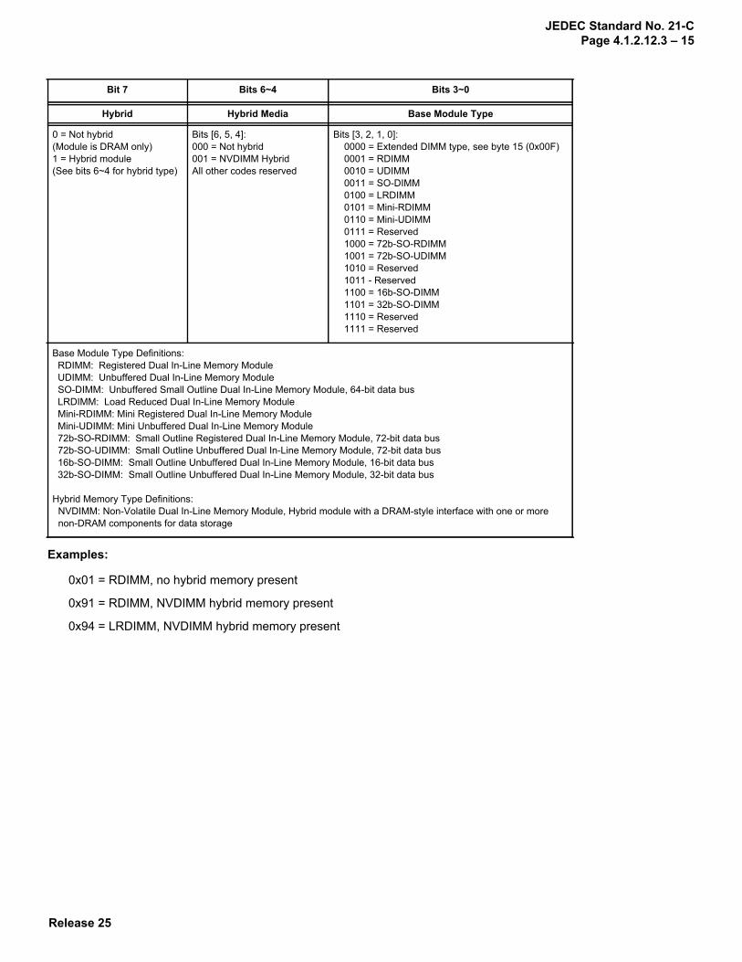
Byte 3 (0x003): Key Byte / Module TypeThis byte is a Key Byte used to index the module specific section of the SPD from bytes 128~191 and bytes 192~255. Byte 3 bits 3~0 identifies the SDRAM memory module type.
Bits 7~4 identifies the architecture of the secondary memory type, if any, present on the module in addition to the base DRAM. These secondary hybrid architectures may apply to any Base Module Type. The index in bits 7~4 are used to index the hybrid memory architecture specific section of the SPD from bytes 192~255.
System software supporting hybrid memory modules should parse the DRAM attributes per the Base Module Type and combine the indexed information per the Hybrid Memory Type to determine the combined memory module capabilities.
Some modules may have no base memory, but will have only a secondary memory type. For example, a Flash-only memory module. These are classified as “hybrid” for the purposes of interpreting the SPD. Where base memory parameters apply to this class of hybrid module, these will be documented with those bytes in the base section. Extended parameters are encoded in SPD bytes 192~255.
13 0D Reserved
14 0E DDR4E SDRAM
15 0F LPDDR3 SDRAM
16 10 LPDDR4 SDRAM
- - -
253 FD Reserved
254 FE Reserved
255 FF Reserved
Line # Hex SDRAM / Module Type Corresponding to Key Byte
Release 25
JEDEC Standard No. 21-CPage 4.1.2.12.3 – 15
Examples:
0x01 = RDIMM, no hybrid memory present
0x91 = RDIMM, NVDIMM hybrid memory present
0x94 = LRDIMM, NVDIMM hybrid memory present
Bit 7 Bits 6~4 Bits 3~0
Hybrid Hybrid Media Base Module Type
0 = Not hybrid(Module is DRAM only)1 = Hybrid module(See bits 6~4 for hybrid type)
Bits [6, 5, 4]:000 = Not hybrid001 = NVDIMM HybridAll other codes reserved
Bits [3, 2, 1, 0]: 0000 = Extended DIMM type, see byte 15 (0x00F) 0001 = RDIMM 0010 = UDIMM 0011 = SO-DIMM 0100 = LRDIMM 0101 = Mini-RDIMM 0110 = Mini-UDIMM 0111 = Reserved 1000 = 72b-SO-RDIMM 1001 = 72b-SO-UDIMM 1010 = Reserved 1011 - Reserved 1100 = 16b-SO-DIMM 1101 = 32b-SO-DIMM 1110 = Reserved 1111 = Reserved
Base Module Type Definitions: RDIMM: Registered Dual In-Line Memory Module UDIMM: Unbuffered Dual In-Line Memory Module SO-DIMM: Unbuffered Small Outline Dual In-Line Memory Module, 64-bit data bus LRDIMM: Load Reduced Dual In-Line Memory Module Mini-RDIMM: Mini Registered Dual In-Line Memory Module Mini-UDIMM: Mini Unbuffered Dual In-Line Memory Module 72b-SO-RDIMM: Small Outline Registered Dual In-Line Memory Module, 72-bit data bus 72b-SO-UDIMM: Small Outline Unbuffered Dual In-Line Memory Module, 72-bit data bus 16b-SO-DIMM: Small Outline Unbuffered Dual In-Line Memory Module, 16-bit data bus 32b-SO-DIMM: Small Outline Unbuffered Dual In-Line Memory Module, 32-bit data bus
Hybrid Memory Type Definitions:NVDIMM: Non-Volatile Dual In-Line Memory Module, Hybrid module with a DRAM-style interface with one or morenon-DRAM components for data storage

Release 25
JEDEC Standard No. 21-CPage 4.1.2.12.3 – 16
Byte 4 (0x004): SDRAM Density and BanksThis byte defines the total density of the DDR4 SDRAM, in bits, and the number of internal banks and bank groups into which the memory array is divided. For multi-die stacks (DDP, QDP, or 3DS), this represents the capacity of each DRAM die in the stack. These values come from the DDR4 SDRAM data sheet.
Byte 5 (0x005): SDRAM AddressingThis byte describes the row addressing and the column addressing in the SDRAM device. Bits 2~0 encode the number of column address bits, and bits 5~3 encode the number of row address bits. These values come from the DDR4 SDRAM data sheet.
Bits 7~6 Bits 5~4 Bits 3~0
Bank Group Bits Bank Address Bits1 Total SDRAM capacity per die,in megabits
Bits [7, 6]: 00 = 0 (no bank groups) 01 = 1 (2 bank groups) 10 = 2 (4 bank groups) 11 = reserved
Bit [5, 4] : 00 = 2 (4 banks) 01 = 3 (8 banks) All others reserved
Bit [3, 2, 1, 0] : 0000 = 256 Mb 0001 = 512 Mb 0010 = 1 Gb 0011 = 2 Gb 0100 = 4 Gb 0101 = 8 Gb 0110 = 16 Gb 0111 = 32 Gb 1000 = 12 Gb 1001 = 24 Gb All others reserved
Note 1 Bank Address Bits determine the number of banks in each Bank Group.
Bits 7~6 Bits 5~3 Bits 2~0
Reserved Row Address Bits Column Address Bits
Reserved; must be coded as 00 Bit [5, 4, 3] : 000 = 12 001 = 13 010 = 14 011 = 15 100 = 16 101 = 17 110 = 18 All others reserved
Bit [2, 1, 0] : 000 = 9 001 = 10 010 = 11 011 = 12 All others reserved

Release 25
JEDEC Standard No. 21-CPage 4.1.2.12.3 – 17
Byte 6 (0x006): Primary SDRAM Package TypeThis byte describes the type of SDRAM devices on the module. For modules having asymmetrical assembly of multiple SDRAM package types, this byte defines the primary set of SDRAMs; Byte 10 defines the secondary set.
Terminology:
Bit 7 Bits 6~4 Bits 3~2 Bit 1~0
Primary SDRAM Package Type Die Count Reserved Signal Loading2
0 = Monolithic DRAM Device1 = Non-Monolithic Device1
000 = Single die001 = 2 die010 = 3 die011 = 4 die100 = 5 die101 = 6 die110 = 7 die111 = 8 die
00 00 = Not specified3
01 = Multi load stack10 = Single load stack (3DS)11 = Reserved
Note 1 This includes Dual Die, Quad Die, Multi-Die, 3DS, or physically stacked devices - anything that is outside the standard monolithic device.
Note 2 Refers to loading on signals at the SDRAM balls. Loading on certain signals (CKE, ODT, etc.) per specification of device stacking as defined in JESD79-4.
Note 3 Monolithic DRAM device coded as 00 in bits 1~0.
SDRAM Package
Type
Abbre-viation Description
# Electrical Loads ...
... On data, mask, and
strobe signals
... On address and command
signals
... On control signals
except CKE
... On CKE signals
Monolithic SDP Single die package 1 1 1 1
Multi-loadstack
DDP Dual Die Package 2 2 1 1
QDP Quad Die Package 4 4 1 2
Single loadstack
2H 3DS Two SDRAM diesingle load stack 1 1 1 1
3H 3DS Three SDRAM diesingle load stack 1 1 1 1
4H 3DS Four SDRAM diesingle load stack 1 1 1 1
5H 3DS Five SDRAM diesingle load stack 1 1 1 1
6H 3DS Six SDRAM diesingle load stack 1 1 1 1
7H 3DS Seven SDRAM diesingle load stack 1 1 1 1
8H 3DS Eight SDRAM diesingle load stack 1 1 1 1

Release 25
JEDEC Standard No. 21-CPage 4.1.2.12.3 – 18
Byte 7 (0x007): SDRAM Optional FeaturesThis byte defines support for certain SDRAM features. This value comes from the DDR4 SDRAM data sheet.
Byte 8 (0x008): SDRAM Thermal and Refresh OptionsThis byte describes the module’s supported operating temperature ranges and refresh options. These values come from the DDR4 SDRAM data sheet. Please refer to the DDR4 SDRAM data sheet (JESD79-4 or supplier data sheet) for a complete description of these options.
Byte 9 (0x009): Other SDRAM Optional FeaturesThis byte defines support for certain SDRAM features. This value comes from the DDR4 SDRAM data sheet.
Bits 7~6 Bits 5~4 Bits 3~0
Reserved Maximum ActivateWindow (tMAW) Maximum Activate Count (MAC)
Reserved; must be coded as 00 Bits [5, 4]: 00 = 8192 * tREFI 01 = 4096 * tREFI 10 = 2048 * tREFI 11 = Reserved
Bits [3, 2, 1, 0] : 0000 = Untested MAC1
0001 = 700 K 0010 = 600 K 0011 = 500 K 0100 = 400 K 0101 = 300 K 0110 = 200 K 0111 = Reserved 1000 = Unlimited MAC2
All others reserved
Note 1 Untested MAC means the device is not tested for tMAW and/or MAC; no particular value should be assumed.Note 2 Unlimited MAC means there is no restriction to the number of activates to a given row in a refresh period
providing DRAM timing requirements such as tRCmin and refresh requirements are not violated.
Bits 7~0
Reserved
Reserved; must be coded as 0x00
Bits 7~6 Bit 5 Bits 4~0
Post Package Repair (PPR) Soft PPR Reserved
00: PPR not supported01: Post package repair supported, one row per bank group10: Reserved11: Reserved
0 = Soft PPR not supported1 = Soft PPR supported
Reserved; must be coded as 00000
Note If PPR is supported, Hard PPR is always supported by the device. Optional additional support for Soft PPR is indicated in bit 5.

Release 25
JEDEC Standard No. 21-CPage 4.1.2.12.3 – 19
Byte 10 (0x00A): Secondary SDRAM Package TypeFor modules having asymmetrical assembly of multiple SDRAM package types, this byte defines the secondary set of SDRAMs. For modules with symmetrical assembly, this byte must be coded as 0x00.
DRAM Density Ratio Settings:
Byte 11 (0x00B): Module Nominal Voltage, VDDThis byte describes the Voltage Level for DRAM and other components on the module such as the register or memory buffer, if applicable. Note that SPDs or thermal sensor components are on the VDDSPD supply and are not affected by this byte.
'Operable' is defined as the VDD voltage at which module operation is allowed using the performance values programmed in the SPD.
'Endurant' is defined as the VDD voltage at which the module may be powered without adversely affecting the life expectancy or reliability. Operation is not supported at this voltage.
Bit 7 Bits 6~4 Bits 3~2 Bits 1~0
SDRAM Package Type Die Count DRAM Density Ratio2 Signal Loading
0 = Monolithic DRAM Device1 = Non-Monolithic Device1
000 = Single die001 = 2 die010 = 3 die011 = 4 die100 = 5 die101 = 6 die110 = 7 die111 = 8 die
00 = Rank 1 and 3 device densities are the same as rank 0 and 2 densities01 = Rank 1 and 3 are one standard device density smaller than rank 0 and 210 = Rank 1 and 3 are two standard device densities smaller than rank 0 and 211 = Reserved
00 = Not specified01 = Multi load stack10 = Single load stack (3DS)11 = Reserved
Note 1 See Byte 6 for packaging notes.Note 2 When DRAM Density Ratio (bits 3~2) is non-zero, all SPD settings except timing parameters are specified for the
higher density devices in rank 0 (e.g., density, row, column, etc.). SPD timing parameters are specified for the slowest device timings of any rank (e.g., tCK, tAA, tRFC, etc.).
SPD Byte 4,Bits 3~0
Ranks 0, 2 Device Density
SPD Byte 10,Bits 3~2
Ranks 1, 3Device Density
SPD Byte 10,Bits 3~2
Ranks 1, 3Device Density
0000 256 Mb 01 Not Defined 10 Not Defined
0001 512 Mb 01 256 Mb 10 Not Defined
0010 1 Gb 01 512 Mb 10 256 Mb
0011 2 Gb 01 1 Gb 10 512 Mb
0100 4 Gb 01 2 Gb 10 1 Gb
0101 8 Gb 01 4 Gb 10 2 Gb
0110 16 Gb 01 12 Gb 10 8 Gb
0111 32 Gb 01 24 Gb 10 16 Gb
1000 12 Gb 01 8 Gb 10 4 Gb
1001 24 Gb 01 16 Gb 10 12 Gb

Release 25
JEDEC Standard No. 21-CPage 4.1.2.12.3 – 20
Examples:A value on bits 1~0 of 11 defines DRAM support of a nominal operable voltage of 1.2 V only.
Byte 12 (0x00C): Module OrganizationThis byte describes the organization of the SDRAM module. Bits 2~0 encode the device width of the SDRAM devices. Bits 5~3 encode the number of package ranks on the module.
“Package ranks per DIMM” refers to the collections of devices on the module sharing common chip select signals (across the data width of the DIMM), either from the edge connector for unbuffered modules or from the outputs of a registering clock driver for RDIMMs and LRDIMMs.
“Logical rank” refers the individually addressable die in a 3DS stack and has no meaning for monolithic or multi-load stacked SDRAMs; however, for the purposes of calculating the capacity of the module, one should treat monolithic and multi-load stack SDRAMs as having one logical rank per package rank.
Byte 12 Bit 6 = 0 defines a memory module as being “symmetrical” where all DRAM devices on the module are the same type as described in Byte 6.
Byte 11: Module Nominal Voltage, VDD
Reserved DRAM VDD 1.2 V
Bits 7~2 Bit 1 Bit 0
Reserved;must be coded as 000000
0 = not endurant1 = endurant
0 = not operable1 = operable
Bit 7 Bit 6 Bits 5~3 Bits 2~0
Reserved Rank MixNumber of Package Ranks per
DIMM SDRAM Device Width
Reserved; must be coded as 0
0 = Symmetrical1 = Asymmetrical
Bit [5, 4, 3] : 000 = 1 Package Rank 001 = 2 Package Ranks 010 = 3 Package Ranks 011 = 4 Package Ranks 100 = 5 Package Ranks 101 = 6 Package Ranks 110 = 7 Package Ranks 111 = 8 Package Ranks
Bit [2, 1, 0] : 000 = 4 bits 001 = 8 bits 010 = 16 bits 011 = 32 bits All others reserved

Release 25
JEDEC Standard No. 21-CPage 4.1.2.12.3 – 21
Rank Matrix for Symmetrical Modules (Byte 12 Bit 6 = 0)
SDRAM PackageType(s) (Byte 6)
# Package Ranksper DIMM
# Logical Ranksper Package Rank
(for calculation only)
# Logical Ranksper DIMM
SDP
1
1
1
2 2
3 3
4 4
DDP2
12
4 4
2H 3DS1
22
2 4
3H 3DS1
33
2 6
4H 3DS1
44
2 8
5H 3DS1
55
2 10
6H 3DS1
66
2 12
CS0_n
Controller/RegisteringClock Driver
DRAMs
CS1_n
CS0_n
Controller/RegisteringClock Driver
DRAMs
DRAMs
CS2_n
CS1_n
CS0_n
Controller/RegisteringClock Driver
DRAMs
DRAMs
DRAMs
CS3_n
CS2_n
CS1_n
CS0_n
Controller/RegisteringClock Driver
DRAMs
DRAMs
DRAMs
DRAMs
Symmetrical Configurations Using SDP or 3DS (byte 12 Bit 6 = 0)
Controller/RegisteringClock Driver
CS3_nCS1_n
CS2_n
CS0_n
Controller/RegisteringClock Driver
DDPDRAMs
Symmetrical Configurations Using DDP (byte 12 Bit 6 = 0)
DDPDRAMs
CS1_n
CS0_nDDPDRAMs
All DRAMSPrimary, Byte 6

Release 25
JEDEC Standard No. 21-CPage 4.1.2.12.3 – 22
Byte 12 Bit 6 = 1 describes support for modules having a asymmetrical DRAM capacities, for example a 3 package rank module comprised of a combination of SDP and DDP devices, or 3DS-based designs having different numbers of logical ranks in each package rank. When Byte 12 Bit 6 = 1, Byte 6 indicates the package type for the first collection of devices on the module and Byte 10 indicates the package type for the second collection of devices on the module.
7H 3DS1
77
2 14
8H 3DS1
88
2 16
Logical Ranks per DIMM = # Package Ranks per DIMM * # Logical Ranks per Package RankByte 10 coded as 0x00 for all symmetrical configurations
Rank Matrix for Symmetrical Modules (Byte 12 Bit 6 = 0)
SDRAM PackageType(s) (Byte 6)
# Package Ranksper DIMM
# Logical Ranksper Package Rank
(for calculation only)
# Logical Ranksper DIMM
CS1_n
CS0_n
Controller/RegisteringClock Driver
DRAMs
DRAMs
Asymmetrical Configurations Using 3DS (byte 12 Bit 6 = 1)
Controller/RegisteringClock Driver
CS1_n
CS2_n
CS0_n
Controller/RegisteringClock Driver
SDPDRAMs
Asymmetrical Configurations Using DDP (byte 12 Bit 6 = 1)
DDPDRAMsCS0_n
SDPDRAMs
CS3_nCS1_n
DDPDRAMs
Primary, Byte 6
Secondary, Byte 10
Byte 6
Byte 10
Byte 6
Byte 10

Release 25
JEDEC Standard No. 21-CPage 4.1.2.12.3 – 23
Examples:
Byte 13 (0x00D): Module Memory Bus WidthThis byte describes the width of the SDRAM memory bus on the module. Bits 2~0 encode the primary bus width. Bits 4~3 encode the bus extensions such as parity or ECC.
Examples:• 64 bit primary bus, no parity or ECC (64 bits total width): xxx 000 011
• 64 bit primary bus, with 8 bit ECC (72 bits total width): xxx 001 011
Rank Mix for Asymmetrical Modules (Byte 12 Bit 6 = 1)
First SDRAM PackageType(s) (Byte 6) and Chip
Select Alignment
Second SDRAM PackageType(s) (Byte 10) and Chip Select
Alignment
# Package Ranksper DIMM
# Logical Ranksper DIMM
Non-3DS Asymmetrical Configurations
SDP CS0_n DDP CS1_n, CS3_n 3 3
DDP CS0_n, CS2_n SDP CS1_n 3 3
3DS Asymmetrical Configurations
2H 3DS CS0_n 3H 3DS CS1_n 2 5
2H 3DS CS0_n 4H 3DS CS1_n 2 6
... ... ... ...
7H 3DS CS0_n 8H 3DS CS1_n 2 15
Note Logical Ranks per DIMM = # Logical Ranks in Primary SDRAM type + # Logical Ranks in Secondary SDRAM type
Byte 12, Bit 6 Byte 6 Byte 10 Byte 12,Bits 5~3, 2~0 Logical
Ranks per DIMM
Module Configuration
Symmetry Primary Secondary Ranks, Width
0 = Sym. 0x00 0x00 001, 001 2 2 Package Ranks x8, Monolithic
0 = Sym. 0x91 0x00 001, 000 2 2 Package Ranks x4, DDP
0 = Sym. 0xB2 0x00 000, 000 4 1 Package Rank x4, 4H 3DS
1 = Asym. 0x00 0x91 010, 000 3 3 Package Ranks x4, SDP + DDP
1 = Asym. 0xF2 0xE2 001, 000 15 2 Package Ranks x4, 8H 3DS + 7H 3DS
Bits 7~5 Bits 4~3 Bits 2~0
Reserved Bus width extension, in bits Primary bus width, in bits
Reserved; must be coded as 000
Bit [4, 3] : 000 = 0 bits (no extension) 001 = 8 bits All others reserved
Bit [2, 1, 0] : 000 = 8 bits 001 = 16 bits 010 = 32 bits 011 = 64 bits All others reserved
Release 25
JEDEC Standard No. 21-CPage 4.1.2.12.3 – 24
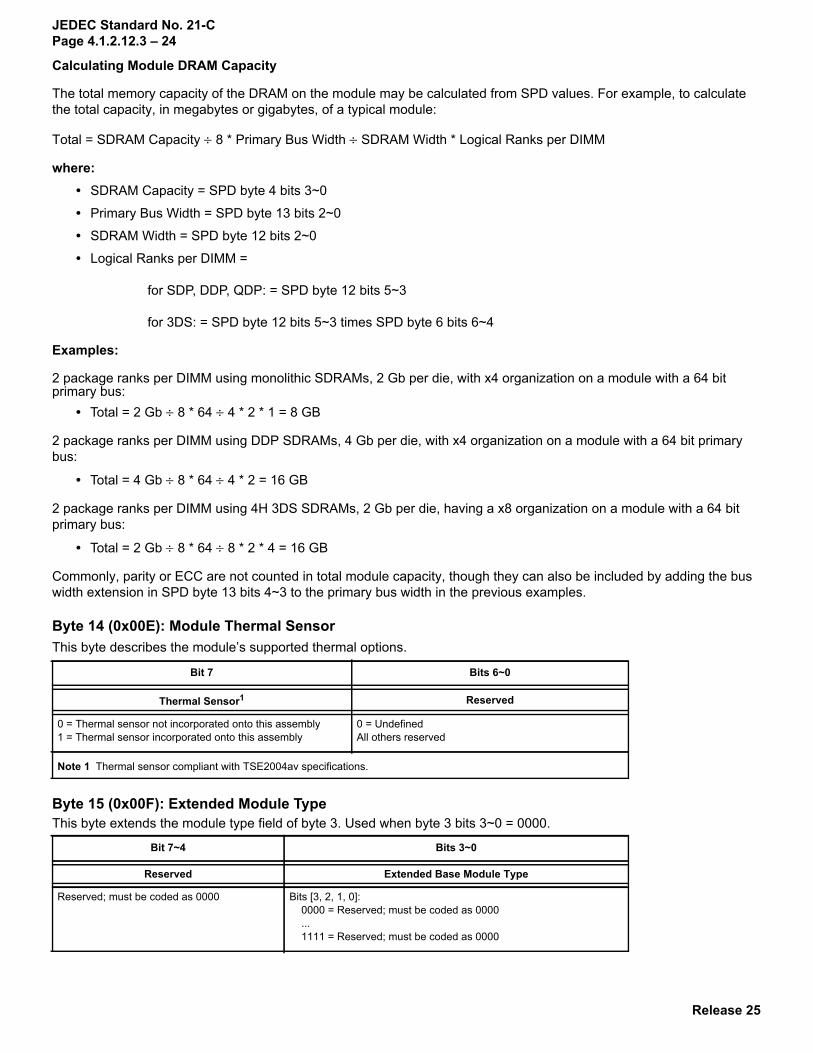
Calculating Module DRAM Capacity
The total memory capacity of the DRAM on the module may be calculated from SPD values. For example, to calculate the total capacity, in megabytes or gigabytes, of a typical module:
Total = SDRAM Capacity 8 * Primary Bus Width SDRAM Width * Logical Ranks per DIMM
where:• SDRAM Capacity = SPD byte 4 bits 3~0
• Primary Bus Width = SPD byte 13 bits 2~0
• SDRAM Width = SPD byte 12 bits 2~0
• Logical Ranks per DIMM =
for SDP, DDP, QDP: = SPD byte 12 bits 5~3
for 3DS: = SPD byte 12 bits 5~3 times SPD byte 6 bits 6~4
Examples:
2 package ranks per DIMM using monolithic SDRAMs, 2 Gb per die, with x4 organization on a module with a 64 bit primary bus:
• Total = 2 Gb 8 * 64 4 * 2 * 1 = 8 GB
2 package ranks per DIMM using DDP SDRAMs, 4 Gb per die, with x4 organization on a module with a 64 bit primary bus:
• Total = 4 Gb 8 * 64 4 * 2 = 16 GB
2 package ranks per DIMM using 4H 3DS SDRAMs, 2 Gb per die, having a x8 organization on a module with a 64 bit primary bus:
• Total = 2 Gb 8 * 64 8 * 2 * 4 = 16 GB
Commonly, parity or ECC are not counted in total module capacity, though they can also be included by adding the bus width extension in SPD byte 13 bits 4~3 to the primary bus width in the previous examples.
Byte 14 (0x00E): Module Thermal SensorThis byte describes the module’s supported thermal options.
Byte 15 (0x00F): Extended Module TypeThis byte extends the module type field of byte 3. Used when byte 3 bits 3~0 = 0000.
Bit 7 Bits 6~0
Thermal Sensor1 Reserved
0 = Thermal sensor not incorporated onto this assembly1 = Thermal sensor incorporated onto this assembly
0 = UndefinedAll others reserved
Note 1 Thermal sensor compliant with TSE2004av specifications.
Bit 7~4 Bits 3~0
Reserved Extended Base Module Type
Reserved; must be coded as 0000 Bits [3, 2, 1, 0]: 0000 = Reserved; must be coded as 0000 ... 1111 = Reserved; must be coded as 0000

Release 25
JEDEC Standard No. 21-CPage 4.1.2.12.3 – 25
Byte 16 (0x010):Reserved, must be coded as 0x00
Byte 17 (0x011): TimebasesThis byte defines a value in picoseconds that represents the fundamental timebase for fine grain and medium grain timing calculations. These values are used as a multiplier for formulating subsequent timing parameters.
Relating the MTB and FTBWhen a timing value tXX cannot be expressed by an integer number of MTB units, the SPD must be encoded using both the MTB and FTB. The Fine Offsets are encoded using a two’s complement value which, when multiplied by the FTB yields a positive or negative correction factor. Typically, for safety and for legacy compatibility, the MTB portion is rounded UP and the FTB correction is a negative value. The general algorithm for programming SPD values is:
Temp_val = tXX / MTB // Calculate as real numberRemainder = Temp_val modulo 1 // Determine if integer # MTBsFine_Correction = 1 - Remainder // If needed, what correctionif (Remainder == 0) then // Integer # MTBs?
tXX(MTB) = Temp_val // Convert to integertXX(FTB) = 0 // No correction needed
else // Needs correctiontXX(MTB) = ceiling (Temp_val) // Round up for safety in legacy systemstXX(FTB) = Fine_Correction * MTB / FTB // Correction is negative offset
endif
To recalculate the value of tXX from the SPD values, a general formula BIOSs may use is:
tXX = tXX(MTB) * MTB + tXX(FTB) * FTB
Example:
Timing parameters using both MTB and FTB are:
Bits 7~4 Bits 3~2 Bits 1~0
Reserved Medium Timebase (MTB) Fine Timebase (FTB)
Reserved; must be coded as 0000
Bits [3, 2]: 00 = 125 ps All others reserved
Bits [0, 1]: 00 = 1 ps All others reserved
tCKAVGmin SPD Calculations Using MTB and FTB
Speed Bin tCKAVGmin ValueDecimal
SPD byte 18Decimal
(Hexadecimal)
SPD byte 125Decimal
(Hexadecimal)
DDR4-18661.071 ns
9(0x09)
-54(0xCA)
= (9 * 0.125) + (-54 * 0.001)
Note 1 Examples assume MTB of 0.125 ns and FTB of 0.001 ns
Parameter MTB Byte(s) FTB BytetCKAVGmin 18 (0x012) 125 (0x07D)
tCKAVGmax 19 (0x013) 124 (0x07C)
tAAmin 24 (0x018) 123 (0x07B)
tRCDmin 25 (0x019) 122 (0x07A)
tRPmin 26 (0x01A) 121 (0x079)

Release 25
JEDEC Standard No. 21-CPage 4.1.2.12.3 – 26
The encoding of two’s complement fine timebase offsets:
Rounding AlgorithmsSoftware algorithms for calculation of timing parameters are subject to rounding errors from many sources. For example, a system may use a memory clock with a nominal frequency of 933.33... MHz, or a clock period of 1.0714... ns. Similarly, a system with a memory clock frequency of 1066.66... MHz yields mathematically a clock period of 0.9375... ns. In most cases, it is impossible to express all digits after the decimal point exactly, and rounding must be done because the SPD establishes a minimum granularity for timing parameters of 1 ps.
Rules for rounding must be defined to allow optimization of memory module performance without violating device parameters. These algorithms rely on results that are within guardbands on device testing and specification to avoid losing performance due to rounding errors.
These rules are:
1. Clock periods such as tCKAVGmin are rounded to the nearest picosecond of accuracy; for example, 0.9375... ns is rounded to 938 ps and 1.0714... ns is rounded to 1071 ps.
2. Parameters programmed in systems in numbers of clocks (nCK) but expressed in the SPD in units of time (ns or ps) are divided by the clock period, a guardband factor of 0.01 clocks is subtracted, then the result is rounded up to the nearest integer number of clocks. Examples:
tRCmin 27, 29 (0x01B, 0x01D) 120 (0x078)
tRRD_Smin 39 (0x027) 119 (0x077)
tRRD_Lmin 40 (0x028) 118 (0x076)
Coding Value(Dec)
Value(Hex)
FTB Timebase
Bit 7 Bits 6~0 1 ps0 1111111 +127 7F +127 ps
0 1111110 +126 7E +126 ps
... ... ... ...
0 0000001 +1 01 +1 ps
0 0000000 0 00 0
1 1111111 -1 FF -1 ps
1 1111110 -2 FE -2 ps
... ... ... ...
1 0000000 -128 80 -128 ps
DDR4 Bin ParameterValue @ tCKAVG-
minTemp Result - Guardband Rounding Result
ps ps nCK nCK nCK
1600 tRRD_Lmin 7500 1250 6.000 5.990 6
1600 tRRD_Lmin 7500 1071 7.002 6.992 7
2133 tRRD_Lmin 6400 1250 5.120 5.110 6
1866 tRRD_Lmin 5300 1071 4.948 4.938 5
Parameter MTB Byte(s) FTB Byte

Release 25
JEDEC Standard No. 21-CPage 4.1.2.12.3 – 27
Byte 18 (0x012): SDRAM Minimum Cycle Time (tCKAVGmin)This byte defines the minimum cycle time for the SDRAM module, in medium timebase (MTB) units. This number applies to all applicable components on the module. This byte applies to SDRAM and support components as well as the overall capability of the DIMM. This value comes from the DDR4 SDRAM and support component data sheets.
If tCKAVGmin cannot be divided evenly by the MTB, this byte must be rounded up to the next larger integer and the Fine Offset for tCKAVGmin (SPD byte 125) used for correction to get the actual value.
Examples:
Byte 19 (0x013): SDRAM Maximum Cycle Time (tCKAVGmax)This word defines the maximum cycle time for the SDRAM module, in medium timebase (MTB) units This number applies to all applicable components on the module. This byte applies to SDRAM and support components as well as the overall capability of the DIMM. This value comes from the DDR4 SDRAM and support component data sheets.
If tCKAVGmax cannot be divided evenly by the MTB, this byte must be rounded up to the next larger integer and the Fine Offset for tCKAVGmax (SPD byte 124) used for correction to get the actual value.
Examples:
Byte 20 (0x014): CAS Latencies Supported, First ByteByte 21 (0x015): CAS Latencies Supported, Second ByteByte 22 (0x016): CAS Latencies Supported, Third ByteByte 23 (0x017): CAS Latencies Supported, Fourth ByteThese bytes define which CAS Latency (CL) values are supported with one bit per possible CAS Latency. A 1 in a bit position means that CL is supported, a 0 in that bit position means it is not supported. Bit 7 of byte 23 selects the range of
Bits 7~0
Minimum SDRAM Cycle Time (tCKAVGmin)MTB Units
Values defined from 1 to 255
tCKAVGmin(MTB units)
MTB(ns)
tCKAVGmin Offset(FTB units)1
FTB(ns)
tCKAVGmin Result(ns) Use
10 0x0A 0.125 0 0 0.001 1.25 DDR4-1600 (800 MHz clock)9 0x09 0.125 -54 0xCA 0.001 1.071 DDR4-1866 (933 MHz clock)8 0x08 0.125 -63 0xC1 0.001 0.938 DDR4-2133 (1067 MHz clock)7 0x07 0.125 -42 0xD6 0.001 0.833 DDR4-2400 (1200 MHz clock)6 0x06 0.125 0 0 0.001 0.750 DDR4-2666 (1333 MHz clock)5 0x05 0.125 0 0 0.001 0.625 DDR4-3200 (1600 MHz clock)
Note 1 See SPD byte 125.
Bits 7~0
Minimum SDRAM Cycle Time (tCKAVGmax)MTB Units
Values defined from 1 to 255
tCKAVGmax(MTB units)
MTB(ns)
tCKAVGmax Offset(FTB units)1
FTB(ns)
tCKAVGmaxResult
(ns)Use
12 0x0C 0.125 0 0 0.001 1.500 DDR4-1600 (800 MHz clock)12 0x0C 0.125 0 0 0.001 1.500 DDR4-1866 (933 MHz clock)12 0x0C 0.125 0 0 0.001 1.500 DDR4-2133 (1067 MHz clock)12 0x0C 0.125 0 0 0.001 1.500 DDR4-2400 (1200 MHz clock)
0.125 0.001 tbd DDR4-2666 (1333 MHz clock)0.125 0.001 tbd DDR4-3200 (1600 MHz clock)
Note 1 See SPD byte 124.

Release 25
JEDEC Standard No. 21-CPage 4.1.2.12.3 – 28
CL values, 7~36 or 23~52. Byte 23 bit 6 is reserved for future use and must be coded as 0. These values come from the DDR4 SDRAM data sheet, JESD79-4.
CAS Latencies, Low Range (Byte 23 Bit 7 = 0)
Byte 20Bit 7 Bit 6 Bit 5 Bit 4 Bit 3 Bit 2 Bit 1 Bit 0
CL = 14 CL = 13 CL = 12 CL = 11 CL = 10 CL = 9 CL = 8 CL = 7
Byte 21Bit 7 Bit 6 Bit 5 Bit 4 Bit 3 Bit 2 Bit 1 Bit 0
CL = 22 CL = 21 CL = 20 CL = 19 CL = 18 CL = 17 CL = 16 CL = 15
Byte 22Bit 7 Bit 6 Bit 5 Bit 4 Bit 3 Bit 2 Bit 1 Bit 0
CL = 30 CL = 29 CL = 28 CL = 27 CL = 26 CL = 25 CL = 24 CL = 23
Byte 23Bit 7 Bit 6 Bit 5 Bit 4 Bit 3 Bit 2 Bit 1 Bit 0
0 = Low CL range Rsvd CL = 36 CL = 35 CL = 34 CL = 33 CL = 32 CL = 31
Byte 23 bit 7 selects the possible CAS Latency range.Byte 23 bit 6 is reserved and must be coded as 0.For each other bit position, 0 means this CAS Latency is not supported, 1 means this CAS Latency is supported.
CAS Latencies, High Range (Byte 23 Bit 7 = 1)
Byte 20Bit 7 Bit 6 Bit 5 Bit 4 Bit 3 Bit 2 Bit 1 Bit 0
CL = 30 CL = 29 CL = 28 CL = 27 CL = 26 CL = 25 CL = 24 CL = 23
Byte 21Bit 7 Bit 6 Bit 5 Bit 4 Bit 3 Bit 2 Bit 1 Bit 0
CL = 38 CL = 37 CL = 36 CL = 35 CL = 34 CL = 33 CL = 32 CL = 31
Byte 22Bit 7 Bit 6 Bit 5 Bit 4 Bit 3 Bit 2 Bit 1 Bit 0
CL = 46 CL = 45 CL = 44 CL = 43 CL = 42 CL = 41 CL = 40 CL = 39
Byte 23Bit 7 Bit 6 Bit 5 Bit 4 Bit 3 Bit 2 Bit 1 Bit 0
1 = High CL range Rsvd CL = 52 CL = 51 CL = 50 CL = 49 CL = 48 CL = 47
Byte 23 bit 7 selects the possible CAS Latency range.Byte 23 bit 6 is reserved and must be coded as 0.For each other bit position, 0 means this CAS Latency is not supported, 1 means this CAS Latency is supported.

Release 25
JEDEC Standard No. 21-CPage 4.1.2.12.3 – 29
Example 1: Byte 23 bit 7 = 0 (Low CL Range)Byte 20 = 0xB4 (= 1011 0100) -- first byteByte 21 = 0x05 (= 0000 0101) -- second byteByte 22 = 0x00 (= 0000 0000) -- third byteByte 23 = 0x00 (= 0000 0000) -- fourth byte
Results: Actual CAS Latencies supported = 9, 11, 12, 14, 15, 17
Example 2: Byte 23 bit 7 = 1 (High CL Range)Byte 20 = 0x00 (= 0000 0000) -- first byteByte 21 = 0x78 (= 0111 1000) -- second byteByte 22 = 0x01 (= 0000 0001) -- third byteByte 23 = 0x80 (= 1000 0000) -- fourth byte
Results: Actual CAS Latencies supported = 34, 35, 36, 37, 39
CAS Latencies 22 21 20 19 18 17 16 15 14 13 12 11 10 9 8 7
CL Mask 0 0 0 0 0 1 0 1 1 0 1 1 0 1 0 0
CAS Latencies R X 36 35 34 33 32 31 30 29 28 27 26 25 24 23
CL Mask 0 0 0 0 0 0 0 0 0 0 0 0 0 0 0 0
CAS Latencies 38 37 36 35 34 33 32 31 30 29 28 27 26 25 24 23
CL Mask 0 1 1 1 1 0 0 0 0 0 0 0 0 0 0 0
CAS Latencies R X 52 51 50 49 48 47 46 45 44 43 42 41 40 39
CL Mask 1 0 0 0 0 0 0 0 0 0 0 0 0 0 0 1

Release 25
JEDEC Standard No. 21-CPage 4.1.2.12.3 – 30
Byte 24 (0x018): Minimum CAS Latency Time (tAAmin)This word defines the minimum CAS Latency in medium timebase (MTB) units. This value comes from the DDR4 SDRAM data sheet.
If tAAmin cannot be divided evenly by the MTB, this byte must be rounded up to the next larger integer and the Fine Offset for tAAmin (SPD byte 123) used for correction to get the actual value.
Examples:
Bits 7~0
Minimum SDRAM CAS Latency Time (tAAmin)MTB Units
Values defined from 1 to 255
tAAmin(MTB units)
MTB(ns)
tAAmin Offset
(FTB units)1FTB(ns)
tAAmin Result
(ns)Use
100 0x64 0.125 0 0 0.001 12.50 DDR4-1600J (800 MHz clock)
110 0x6E 0.125 0 0 0.001 13.75 DDR4-1600K (800 MHz clock)
108 0x6C 0.125 0 0 0.001 13.50 DDR4-1600K (800 MHz clock) downbin2
120 0x78 0.125 0 0 0.001 15.00 DDR4-1600L (800 MHz clock)
103 0x67 0.125 -26 0xE6 0.001 12.85 DDR4-1866L (933 MHz clock)
112 0x70 0.125 -81 0xAF 0.001 13.92 DDR4-1866M (933 MHz clock)
108 0x6C 0.125 0 0 0.001 13.50 DDR4-1866M (933 MHz clock) downbin2
120 0x78 0.125 0 0 0.001 15.00 DDR4-1866N (933 MHz clock)
106 0x6A 0.125 -120 0x88 0.001 13.13 DDR4-2133N (1066 MHz clock)
113 0x71 0.125 -65 0xBF 0.001 14.06 DDR4-2133P (1066 MHz clock)
108 0x6C 0.125 0 0 0.001 13.50 DDR4-2133P (1066 MHz clock) downbin2
120 0x78 0.125 0 0 0.001 15.00 DDR4-2133R (1066 MHz clock)
100 0x64 0.125 0 0 0.001 12.50 DDR4-2400P (1200 MHz clock)
107 0x6B 0.125 -55 0xC9 0.001 13.32 DDR4-2400R (1200 MHz clock)
120 0x78 0.125 0 0 0.001 15.00 DDR4-2400U (1200 MHz clock)
0.125 0.001 tbd DDR4-2666 (1333 MHz clock)
0.125 0.001 tbd DDR4-3200 (1600 MHz clock)
120 0x78 0.125 0 0 0.001 15.00 DDR4-1600J-3DS2B
130 0x82 0.125 0 0 0.001 16.25 DDR4-1600K-3DS2B
140 0x8C 0.125 0 0 0.001 17.50 DDR4-1600L-3DS2B
120 0x78 0.125 0 0 0.001 15.00 DDR4-1866L-3DS2B
129 0x81 0.125 -55 0xC9 0.001 16.07 DDR4-1866M-3DS2B
129 0x81 0.125 -55 0xC9 0.001 16.07 DDR4-1866M-3DS2B (downbin)
138 0x8A 0.125 -110 0x92 0.001 17.14 DDR4-1866N-3DS2B
120 0x78 0.125 0 0 0.001 15.00 DDR4-2133N-3DS2B
120 0x78 0.125 0 0 0.001 15.00 DDR4-2133N-3DS2B (downbin)
136 0x88 0.125 -121 0x87 0.001 16.88 DDR4-2133R-3DS2A
151 0x97 0.125 -115 0x8D 0.001 18.76 DDR4-2133R-3DS4A
138 0x8A 0.125 -110 0x92 0.001 17.14 DDR4-2133R-3DS4A (downbin)
120 0x78 0.125 0 0 0.001 15.00 DDR4-2400N-3DS3B
134 0x86 0.125 -80 0xB0 0.001 16.67 DDR4-2400U-3DS2A
147 0x93 0.125 -46 0xD2 0.001 18.33 DDR4-2400U-3DS4A
138 0x8A 0.125 -110 0x92 0.001 17.14 DDR4-2400U-3DS4A (downbin)
Note 1 See SPD byte 123Note 2 Refer to device data sheet for downbin support details.

Release 25
JEDEC Standard No. 21-CPage 4.1.2.12.3 – 31
Byte 25 (0x019): Minimum RAS to CAS Delay Time (tRCDmin)This word defines the minimum SDRAM RAS to CAS Delay Time in medium timebase (MTB) units. This value comes from the DDR4 SDRAM data sheet.
If tRCDmin cannot be divided evenly by the MTB, this byte must be rounded up to the next larger integer and the Fine Offset for tRCDmin (SPD byte 122) used for correction to get the actual value
Examples:
Bits 7~0
Byte 25: Minimum SDRAM RAS to CAS Delay Time (tRCDmin)MTB Units
Values defined from 1 to 255
tRCDmin(MTB units)
MTB(ns)
tRCDmin Offset
(FTB units)1FTB(ns)
tRCDmin Result
(ns)Use
100 0x64 0.125 0 0 0.001 12.50 DDR4-1600J (800 MHz clock)
110 0x6E 0.125 0 0 0.001 13.75 DDR4-1600K (800 MHz clock)
108 0x6C 0.125 0 0 0.001 13.50 DDR4-1600K (800 MHz clock) downbin2
120 0x78 0.125 0 0 0.001 15.00 DDR4-1600L (800 MHz clock)
103 0x67 0.125 -26 0xE6 0.001 12.85 DDR4-1866L (933 MHz clock)
112 0x70 0.125 -81 0xAF 0.001 13.92 DDR4-1866M (933 MHz clock)
108 0x6C 0.125 0 0 0.001 13.50 DDR4-1866M (933 MHz clock) downbin2
120 0x78 0.125 0 0 0.001 15.00 DDR4-1866N (933 MHz clock)
106 0x6A 0.125 -120 0x88 0.001 13.13 DDR4-2133N (1066 MHz clock)
113 0x71 0.125 -65 0xBF 0.001 14.06 DDR4-2133P (1066 MHz clock)
108 0x6C 0.125 0 0 0.001 13.50 DDR4-2133P (1066 MHz clock) downbin2
120 0x78 0.125 0 0 0.001 15.00 DDR4-2133R (1066 MHz clock)
100 0x64 0.125 0 0 0.001 12.50 DDR4-2400P (1200 MHz clock)
107 0x6B 0.125 -55 0xC9 0.001 13.32 DDR4-2400R (1200 MHz clock)
120 0x78 0.125 0 0 0.001 15.00 DDR4-2400U (1200 MHz clock)
0.125 0.001 tbd DDR4-2666 (1333 MHz clock)
0.125 0.001 tbd DDR4-3200 (1600 MHz clock)
110 0x6E 0.125 0 0 0.001 13.75 DDR4-1600J-3DS2B
120 0x78 0.125 0 0 0.001 15.00 DDR4-1600K-3DS2B
130 0x82 0.125 0 0 0.001 16.25 DDR4-1600L-3DS2B
112 0x70 0.125 -81 0xAF 0.001 13.92 DDR4-1866L-3DS2B
120 0x78 0.125 0 0 0.001 15.00 DDR4-1866M-3DS2B
120 0x78 0.125 0 0 0.001 15.00 DDR4-1866M-3DS2B (downbin)
129 0x81 0.125 -55 0xC9 0.001 16.07 DDR4-1866N-3DS2B
113 0x71 0.125 -65 0xBF 0.001 14.06 DDR4-2133N-3DS2B
112 0x70 0.125 -81 0xAF 0.001 13.92 DDR4-2133N-3DS2B (downbin)
120 0x78 0.125 0 0 0.001 15.00 DDR4-2133R-3DS2A
120 0x78 0.125 0 0 0.001 15.00 DDR4-2133R-3DS4A
120 0x78 0.125 0 0 0.001 15.00 DDR4-2133R-3DS4A (downbin)
107 0x6B 0.125 -45 0xD3 0.001 13.33 DDR4-2400N-3DS3B
120 0x78 0.125 0 0 0.001 15.00 DDR4-2400U-3DS2A
120 0x78 0.125 0 0 0.001 15.00 DDR4-2400U-3DS4A
120 0x78 0.125 0 0 0.001 15.00 DDR4-2400U-3DS4A (downbin)
Note 1 See SPD byte 122Note 2 Refer to device data sheet for downbin support details.

Release 25
JEDEC Standard No. 21-CPage 4.1.2.12.3 – 32
Byte 26 (0x01A): Minimum Row Precharge Delay Time (tRPmin)This word defines the minimum SDRAM Row Precharge Delay Time in medium timebase (MTB) units. This value comes from the DDR4 SDRAM data sheet.
If tRPmin cannot be divided evenly by the MTB, this byte must be rounded up to the next larger integer and the Fine Offset for tRPmin (SPD byte 121) used for correction to get the actual value.
Examples:
Bits 7~0
Minimum Row Precharge Time (tRPmin)MTB Units
Values defined from 1 to 255
tRPmin(MTB units)
MTB(ns)
tRPmin Offset
(FTB units)1FTB(ns)
tRPmin Result
(ns)Use
100 0x64 0.125 0 0 0.001 12.50 DDR4-1600J (800 MHz clock)
110 0x6E 0.125 0 0 0.001 13.75 DDR4-1600K (800 MHz clock)
108 0x6C 0.125 0 0 0.001 13.50 DDR4-1600K (800 MHz clock) downbin2
120 0x78 0.125 0 0 0.001 15.00 DDR4-1600L (800 MHz clock)
103 0x67 0.125 -26 0xE6 0.001 12.85 DDR4-1866L (933 MHz clock)
112 0x70 0.125 -81 0xAF 0.001 13.92 DDR4-1866M (933 MHz clock)
108 0x6C 0.125 0 0 0.001 13.50 DDR4-1866M (933 MHz clock) downbin2
120 0x78 0.125 0 0 0.001 15.00 DDR4-1866N (933 MHz clock)
106 0x6A 0.125 -120 0x88 0.001 13.13 DDR4-2133N (1066 MHz clock)
113 0x71 0.125 -65 0xBF 0.001 14.06 DDR4-2133P (1066 MHz clock)
108 0x6C 0.125 0 0 0.001 13.50 DDR4-2133P (1066 MHz clock) downbin2
120 0x78 0.125 0 0 0.001 15.00 DDR4-2133R (1066 MHz clock)
100 0x64 0.125 0 0 0.001 12.50 DDR4-2400P (1200 MHz clock)
107 0x6B 0.125 -55 0xC9 0.001 13.32 DDR4-2400R (1200 MHz clock)
120 0x78 0.125 0 0 0.001 15.00 DDR4-2400U (1200 MHz clock)
0.125 0.001 tbd DDR4-2666 (1333 MHz clock)
0.125 0.001 tbd DDR4-3200 (1600 MHz clock)
100 0x64 0.125 0 0 0.001 12.50 DDR4-1600J-3DS2B
110 0x6E 0.125 0 0 0.001 13.75 DDR4-1600K-3DS2B
120 0x78 0.125 0 0 0.001 15.00 DDR4-1600L-3DS2B
103 0x67 0.125 -26 0xE6 0.001 12.85 DDR4-1866L-3DS2B
112 0x70 0.125 -81 0xAF 0.001 13.92 DDR4-1866M-3DS2B
110 0x6E 0.125 0 0 0.001 13.75 DDR4-1866M-3DS2B (downbin)
120 0x78 0.125 0 0 0.001 15.00 DDR4-1866N-3DS2B
106 0x6A 0.125 -120 0x88 0.001 13.13 DDR4-2133N-3DS2B
103 0x67 0.125 -26 0xE6 0.001 12.85 DDR4-2133N-3DS2B (downbin)
120 0x78 0.125 0 0 0.001 15.00 DDR4-2133R-3DS2A
120 0x78 0.125 0 0 0.001 15.00 DDR4-2133R-3DS4A
120 0x78 0.125 0 0 0.001 15.00 DDR4-2133R-3DS4A (downbin)
100 0x64 0.125 0 0 0.001 12.50 DDR4-2400N-3DS3B
120 0x78 0.125 0 0 0.001 15.00 DDR4-2400U-3DS2A
120 0x78 0.125 0 0 0.001 15.00 DDR4-2400U-3DS4A
120 0x78 0.125 0 0 0.001 15.00 DDR4-2400U-3DS4A (downbin)
Note 1 See SPD byte 121Note 2 Device supports downbinning in lower frequency applications; see supplier data sheet

Release 25
JEDEC Standard No. 21-CPage 4.1.2.12.3 – 33
Byte 27 (0x01B): Upper Nibbles for tRASmin and tRCminThis byte defines the most significant nibbles for the values of tRASmin (byte 28) and tRCmin (byte 29). These values come from the DDR4 SDRAM data sheet.
Byte 28 (0x01C): Minimum Active to Precharge Delay Time (tRASmin), Least Significant ByteThe lower nibble of Byte 27 and the contents of Byte 28 combined create a 12-bit value which defines the minimum SDRAM Active to Precharge Delay Time in medium timebase (MTB) units. The most significant bit is Bit 3 of Byte 27, and the least significant bit is Bit 0 of Byte 28. This value comes from the DDR4 SDRAM data sheet.
Examples:
Bits 7~4 Bits 3~0
tRCmin Most Significant Nibble tRASmin Most Significant Nibble
See Byte 28 description See Byte 29 description
Byte 27 Bits 3~0, Byte 28 Bits 7~0
Minimum Active to Precharge Time (tRASmin)MTB Units
Values defined from 1 to 4095
tRASmin(MTB units)
MTB(ns)
tRASmin Result (ns)
Use
280 0x118 0.125 35 DDR4-1600 (800 MHz clock)
272 0x110 0.125 34 DDR4-1866 (933 MHz clock)
264 0x108 0.125 33 DDR4-2133 (1066 MHz clock)
256 0x100 0.125 32 DDR4-2400 (1200 MHz clock)
0.125 TBD DDR4-2666 (1333 MHz clock)
0.125 TBD DDR4-3200 (1600 MHz clock)
Release 25
JEDEC Standard No. 21-CPage 4.1.2.12.3 – 34
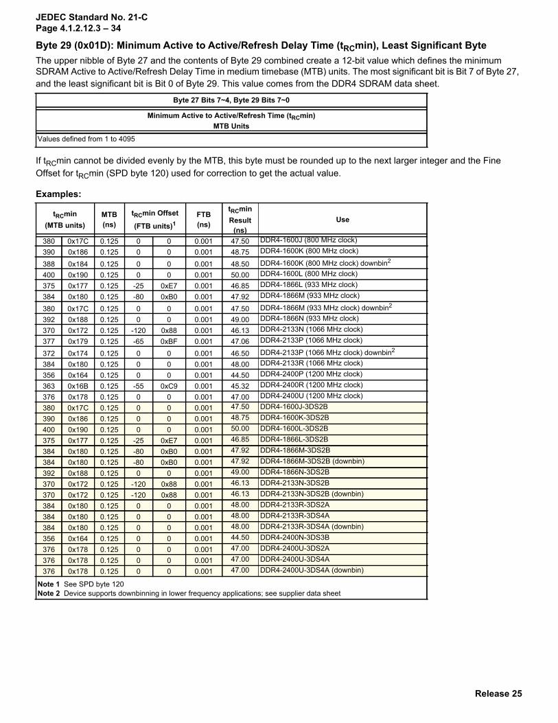
Byte 29 (0x01D): Minimum Active to Active/Refresh Delay Time (tRCmin), Least Significant ByteThe upper nibble of Byte 27 and the contents of Byte 29 combined create a 12-bit value which defines the minimum SDRAM Active to Active/Refresh Delay Time in medium timebase (MTB) units. The most significant bit is Bit 7 of Byte 27, and the least significant bit is Bit 0 of Byte 29. This value comes from the DDR4 SDRAM data sheet.
If tRCmin cannot be divided evenly by the MTB, this byte must be rounded up to the next larger integer and the Fine Offset for tRCmin (SPD byte 120) used for correction to get the actual value.
Examples:
Byte 27 Bits 7~4, Byte 29 Bits 7~0
Minimum Active to Active/Refresh Time (tRCmin)MTB Units
Values defined from 1 to 4095
tRCmin(MTB units)
MTB(ns)
tRCmin Offset
(FTB units)1FTB(ns)
tRCmin Result
(ns)Use
380 0x17C 0.125 0 0 0.001 47.50 DDR4-1600J (800 MHz clock)
390 0x186 0.125 0 0 0.001 48.75 DDR4-1600K (800 MHz clock)
388 0x184 0.125 0 0 0.001 48.50 DDR4-1600K (800 MHz clock) downbin2
400 0x190 0.125 0 0 0.001 50.00 DDR4-1600L (800 MHz clock)
375 0x177 0.125 -25 0xE7 0.001 46.85 DDR4-1866L (933 MHz clock)
384 0x180 0.125 -80 0xB0 0.001 47.92 DDR4-1866M (933 MHz clock)
380 0x17C 0.125 0 0 0.001 47.50 DDR4-1866M (933 MHz clock) downbin2
392 0x188 0.125 0 0 0.001 49.00 DDR4-1866N (933 MHz clock)
370 0x172 0.125 -120 0x88 0.001 46.13 DDR4-2133N (1066 MHz clock)
377 0x179 0.125 -65 0xBF 0.001 47.06 DDR4-2133P (1066 MHz clock)
372 0x174 0.125 0 0 0.001 46.50 DDR4-2133P (1066 MHz clock) downbin2
384 0x180 0.125 0 0 0.001 48.00 DDR4-2133R (1066 MHz clock)
356 0x164 0.125 0 0 0.001 44.50 DDR4-2400P (1200 MHz clock)
363 0x16B 0.125 -55 0xC9 0.001 45.32 DDR4-2400R (1200 MHz clock)
376 0x178 0.125 0 0 0.001 47.00 DDR4-2400U (1200 MHz clock)
380 0x17C 0.125 0 0 0.001 47.50 DDR4-1600J-3DS2B
390 0x186 0.125 0 0 0.001 48.75 DDR4-1600K-3DS2B
400 0x190 0.125 0 0 0.001 50.00 DDR4-1600L-3DS2B
375 0x177 0.125 -25 0xE7 0.001 46.85 DDR4-1866L-3DS2B
384 0x180 0.125 -80 0xB0 0.001 47.92 DDR4-1866M-3DS2B
384 0x180 0.125 -80 0xB0 0.001 47.92 DDR4-1866M-3DS2B (downbin)
392 0x188 0.125 0 0 0.001 49.00 DDR4-1866N-3DS2B
370 0x172 0.125 -120 0x88 0.001 46.13 DDR4-2133N-3DS2B
370 0x172 0.125 -120 0x88 0.001 46.13 DDR4-2133N-3DS2B (downbin)
384 0x180 0.125 0 0 0.001 48.00 DDR4-2133R-3DS2A
384 0x180 0.125 0 0 0.001 48.00 DDR4-2133R-3DS4A
384 0x180 0.125 0 0 0.001 48.00 DDR4-2133R-3DS4A (downbin)
356 0x164 0.125 0 0 0.001 44.50 DDR4-2400N-3DS3B
376 0x178 0.125 0 0 0.001 47.00 DDR4-2400U-3DS2A
376 0x178 0.125 0 0 0.001 47.00 DDR4-2400U-3DS4A
376 0x178 0.125 0 0 0.001 47.00 DDR4-2400U-3DS4A (downbin)
Note 1 See SPD byte 120Note 2 Device supports downbinning in lower frequency applications; see supplier data sheet

Release 25
JEDEC Standard No. 21-CPage 4.1.2.12.3 – 35
Byte 30 (0x01E): Minimum Refresh Recovery Delay Time (tRFC1min), LSBByte 31 (0x01F): Minimum Refresh Recovery Delay Time (tRFC1min), MSBThis word defines the minimum SDRAM Refresh Recovery Time Delay in medium timebase (MTB) units. These values come from the DDR4 SDRAM data sheet.
Examples:
Byte 32 (0x020): Minimum Refresh Recovery Delay Time (tRFC2min), LSBByte 33 (0x021): Minimum Refresh Recovery Delay Time (tRFC2min), MSBThis word defines the minimum SDRAM Refresh Recovery Time Delay in medium timebase (MTB) units. These values come from the DDR4 SDRAM data sheet.
Examples:
Minimum SDRAM Refresh Recovery Delay Time (tRFC1min)MTB Units
Byte 31 Byte 30
Bits 15~8 Bits 7~0
Values defined from 1 to 65535
tRFC1min(MTB units)
MTB(ns)
tRFC1min Result(ns)
Use
1280 0x0500 0.125 160 2 Gb DDR4 SDRAM
2080 0x0820 0.125 260 4 Gb DDR4 SDRAM
2800 0x0AF0 0.125 350 8 Gb DDR4 SDRAM
0.125 TBD 16 Gb DDR4 SDRAM
Minimum SDRAM Refresh Recovery Delay Time (tRFC2min)MTB Units
Byte 33 Byte 32
Bits 15~8 Bits 7~0
Values defined from 1 to 65535
tRFC2min(MTB units)
MTB(ns)
tRFC2min Result(ns)
Use
880 0x0370 0.125 110 2 Gb DDR4 SDRAM
1280 0x0500 0.125 160 4 Gb DDR4 SDRAM
2080 0x0820 0.125 260 8 Gb DDR4 SDRAM
0.125 TBD 16 Gb DDR4 SDRAM

Release 25
JEDEC Standard No. 21-CPage 4.1.2.12.3 – 36
Byte 34 (0x022): Minimum Refresh Recovery Delay Time (tRFC4min), LSBByte 35 (0x023): Minimum Refresh Recovery Delay Time (tRFC4min), MSBThis word defines the minimum SDRAM Refresh Recovery Time Delay in medium timebase (MTB) units. These values come from the DDR4 SDRAM data sheet.
Examples:
Byte 36 (0x024): Upper Nibble for tFAWThis byte defines the most significant nibble for the value of tFAW (SPD byte 37). This value comes from the DDR4 SDRAM data sheet.
Byte 37 (0x025): Minimum Four Activate Window Delay Time (tFAWmin), Least Significant ByteThe lower nibble of Byte 36 and the contents of Byte 37 combined create a 12-bit value which defines the minimum SDRAM Four Activate Window Delay Time in medium timebase (MTB) units. This value comes from the DDR4 SDRAM data sheet. The value of this number may be dependent on the SDRAM page size; please refer to the DDR4 SDRAM data sheet section on Addressing to determine the page size for these devices.
Examples:
Minimum SDRAM Refresh Recovery Delay Time (tRFC4min)MTB Units
Byte 35 Byte 34
Bits 15~8 Bits 7~0
Values defined from 1 to 65535
tRFC4min(MTB units)
MTB(ns)
tRFC4min Result(ns)
Use
720 0x02D0 0.125 90 2 Gb DDR4 SDRAM
880 0x0370 0.125 110 4 Gb DDR4 SDRAM
1280 0x0500 0.125 160 8 Gb DDR4 SDRAM
0.125 TBD 16 Gb DDR4 SDRAM
Bits 7 ~ 4 Bits 3 ~ 0
Reserved tFAW Most Significant Nibble
Reserved; most be coded as 0000 See Byte 37 description
Byte 36 Bits 3 ~ 0, Byte 37 Bits 7 ~ 0
Minimum Four Activate Window Delay Time (tFAW)MTB Units
Values defined from 1 to 4095
tFAW(MTB units)
Timebase(ns)
tFAW Result(ns) Use
280 0x118 0.125 35 Example: DDR4-1600, 2 KB page size200 0x0C8 0.125 25 Example: DDR4-1600, 1 KB page size160 0x0A0 0.125 20 Example: DDR4-1600, 1/2 KB page size240 0x0F0 0.125 30 Example: DDR4-1866, 2 KB page size184 0x0B8 0.125 23 Example: DDR4-1866, 1 KB page size136 0x088 0.125 17 Example: DDR4-1866, 1/2 KB page size240 0x0F0 0.125 30 Example: DDR4-2133, 2 KB page size168 0x0A8 0.125 21 Example: DDR4-2133, 1 KB page size120 0x078 0.125 15 Example: DDR4-2133, 1/2 KB page size240 0x0F0 0.125 30 Example: DDR4-2400, 2 KB page size168 0x0A8 0.125 21 Example: DDR4-2400, 1 KB page size

Release 25
JEDEC Standard No. 21-CPage 4.1.2.12.3 – 37
Byte 38 (0x026): Minimum Activate to Activate Delay Time (tRRD_Smin), different bank groupThis byte defines the minimum SDRAM Activate to Activate Delay Time to different bank groups in medium timebase (MTB) units. This value comes from the DDR4 SDRAM data sheet. Controller designers must also note that at some frequencies, a minimum number of clocks may be required resulting in a larger tRRD_Smin value than indicated in the SPD. For example, tRRD_Smin for DDR4-1600 must be 4 clocks.
If tRRD_Smin cannot be divided evenly by the MTB, this byte must be rounded up to the next larger integer and the Fine Offset for tRRD_Smin (SPD byte 119) used for correction to get the actual value.
Examples:
Byte 39 (0x027): Minimum Activate to Activate Delay Time (tRRD_Lmin), same bank groupThis byte defines the minimum SDRAM Activate to Activate Delay Time to the same bank group in medium timebase (MTB) units. This value comes from the DDR4 SDRAM data sheet. Controller designers must also note that at some frequencies, a minimum number of clocks may be required resulting in a larger tRRD_Lmin value than indicated in the SPD. For example, tRRD_Lmin for DDR4-1600 must be 4 clocks.
104 0x068 0.125 13 Example: DDR4-2400, 1/2 KB page size0.125 TBD Example: DDR4-2666, 2 KB page size0.125 TBD Example: DDR4-2666, 1 KB page size0.125 TBD Example: DDR4-2666, 1/2 KB page size0.125 TBD Example: DDR4-3200, 2 KB page size0.125 TBD Example: DDR4-3200, 1 KB page size0.125 TBD Example: DDR4-3200, 1/2 KB page size
Bits 7~0
Minimum Active to Active/Refresh Time (tRRD_Smin)MTB Units
Values defined from 1 to 255
tRRD_Smin(MTB units)
MTB(ns)
tRRD_Smin Offset
(FTB units)1
FTB(ns)
tRRD_Smin
Result (ns)
Use
48 0x30 0.125 0 0 0.001 6.00 DDR4-1600 (800 MHz clock), 2 KB page size
40 0x28 0.125 0 0 0.001 5.00 DDR4-1600 (800 MHz clock), 1 KB page size
40 0x28 0.125 0 0 0.001 5.00 DDR4-1600 (800 MHz clock), 1/2 KB page size
43 0x2B 0.125 -76 0xB4 0.001 5.30 DDR4-1866 (933 MHz clock), 2 KB page size
34 0x22 0.125 -50 0xCE 0.001 4.20 DDR4-1866 (933 MHz clock), 1 KB page size
34 0x22 0.125 -50 0xCE 0.001 4.20 DDR4-1866 (933 MHz clock), 1/2 KB page size
43 0x2B 0.125 -76 0xB4 0.001 5.30 DDR4-2133 (1066 MHz clock), 2 KB page size
30 0x1E 0.125 -50 0xCE 0.001 3.70 DDR4-2133 (1066 MHz clock), 1 KB page size
30 0x1E 0.125 -50 0xCE 0.001 3.70 DDR4-2133 (1066 MHz clock), 1/2 KB page size
43 0x2B 0.125 -76 0xB4 0.001 5.30 DDR4-2400 (1200 MHz clock), 2 KB page size
27 0x1B 0.125 -76 0xB4 0.001 3.30 DDR4-2400 (1200 MHz clock), 1 KB page size
27 0x1B 0.125 -76 0xB4 0.001 3.30 DDR4-2400 (1200 MHz clock), 1/2 KB page size
0.125 0.001 TBD DDR4-2666 (1333 MHz clock)
0.125 0.001 TBD DDR4-3200 (1600 MHz clock)
Note 1 See SPD byte 119
Bits 7~0
Minimum Active to Active/Refresh Time (tRRD_Lmin)MTB Units
Values defined from 1 to 255
tFAW(MTB units)
Timebase(ns)
tFAW Result(ns) Use

Release 25
JEDEC Standard No. 21-CPage 4.1.2.12.3 – 38
If tRRD_Lmin cannot be divided evenly by the MTB, this byte must be rounded up to the next larger integer and the Fine Offset for tRRD_Lmin (SPD byte 118) used for correction to get the actual value.
Examples:
Byte 40 (0x028): Minimum CAS to CAS Delay Time (tCCD_Lmin), same bank groupThis byte defines the minimum SDRAM CAS to CAS Delay Time to the same bank group in medium timebase (MTB) units. This value comes from the DDR4 SDRAM data sheet. Controller designers must also note that at some frequencies, a minimum number of clocks may be required resulting in a larger tCCD_Lmin value than indicated in the SPD. For example, tCCD_Lmin for DDR4-2133 must be 6 clocks.
If tCCD_Lmin cannot be divided evenly by the MTB, this byte must be rounded up to the next larger integer and the Fine Offset for tCCD_Lmin (SPD byte 117) used for correction to get the actual value.
Examples:
tRRD_Lmin(MTB units)
MTB(ns)
tRRD_Lmin Offset
(FTB units)1
FTB(ns)
tRRD_Lmin
Result (ns)
Use
60 0x3C 0.125 0 0 0.001 7.50 DDR4-1600 (800 MHz clock), 2 KB page size
48 0x30 0.125 0 0 0.001 6.00 DDR4-1600 (800 MHz clock), 1 KB page size
48 0x30 0.125 0 0 0.001 6.00 DDR4-1600 (800 MHz clock), 1/2 KB page size
52 0x34 0.125 -100 0x9C 0.001 6.40 DDR4-1866 (933 MHz clock), 2 KB page size
43 0x2B 0.125 -76 0xB4 0.001 5.30 DDR4-1866 (933 MHz clock), 1 KB page size
43 0x2B 0.125 -76 0xB4 0.001 5.30 DDR4-1866 (933 MHz clock), 1/2 KB page size
52 0x34 0.125 -100 0x9C 0.001 6.40 DDR4-2133 (1066 MHz clock), 2 KB page size
43 0x2B 0.125 -76 0xB4 0.001 5.30 DDR4-2133 (1066 MHz clock), 1 KB page size
43 0x2B 0.125 -76 0xB4 0.001 5.30 DDR4-2133 (1066 MHz clock), 1/2 KB page size
52 0x34 0.125 -100 0x9C 0.001 6.40 DDR4-2400 (1200 MHz clock), 2 KB page size
40 0x28 0.125 -100 0x9C 0.001 4.90 DDR4-2400 (1200 MHz clock), 1 KB page size
40 0x28 0.125 -100 0x9C 0.001 4.90 DDR4-2400 (1200 MHz clock), 1/2 KB page size
0.125 0.001 TBD DDR4-2666 (1333 MHz clock)
0.125 0.001 TBD DDR4-3200 (1600 MHz clock)
Note 1 See SPD byte 118
Bits 7~0
Minimum CAS to CAS Time (tCCD_Lmin)MTB Units
Values defined from 1 to 255
tCCD_Lmin(MTB units)
MTB(ns)
tCCD_Lmin Offset
(FTB units)1
FTB(ns)
tCCD_Lmin
Result (ns)
Use
50 0x32 0.125 0 0 0.001 6.250 DDR4-1600 (800 MHz clock)
43 0x2B 0.125 -20 0xEC 0.001 5.355 DDR4-1866 (933 MHz clock)
43 0x2B 0.125 -20 0xEC 0.001 5.355 DDR4-2133 (1066 MHz clock)
40 0x28 0.125 0 0 0.001 5.000 DDR4-2400 (1200 MHz clock)
0.125 0.001 TBD DDR4-2666 (1333 MHz clock)
0.125 0.001 TBD DDR4-3200 (1600 MHz clock)
Note 1 See SPD byte 117

Release 25
JEDEC Standard No. 21-CPage 4.1.2.12.3 – 39
Byte 41 (0x029): Upper Nibble for tWRminThis byte defines the most significant nibble for the value of tWRmin (byte 42). This value comes from the DDR4 SDRAM data sheet.
Byte 42 (0x02A): Minimum Write Recovery Time (tWRmin)The lower nibble of Byte 41 and the contents of Byte 42 combined create a 12-bit value which defines the minimum SDRAM Write Recovery Time in medium timebase (MTB) units. The most significant bit is Bit 3 of Byte 41, and the least significant bit is Bit 0 of Byte 42. This value comes from the DDR4 SDRAM data sheet.
Examples:
Byte 43 (0x029): Upper Nibbles for tWTRminThis byte defines the most significant nibbles for the values of tWTR_Smin (byte 44) and tWTR_Lmin (byte 45). This value comes from the DDR4 SDRAM data sheet.
Byte 44 (0x02C): Minimum Write to Read Time (tWTR_Smin), different bank groupThe lower nibble of Byte 43 and the contents of Byte 44 combined create a 12-bit value which defines the minimum SDRAM Write to Read Time to different bank groups in medium timebase (MTB) units. The most significant bit is Bit 3 of Byte 43, and the least significant bit is Bit 0 of Byte 44. This value comes from the DDR4 SDRAM data sheet. Controller designers must also note that at some frequencies, a minimum number of clocks may be required resulting in a larger tWTR_Smin value than indicated in the SPD. For example, tWTR_Smin must be at least 2 clocks.
Examples:
Bits 7~4 Bits 3~0
Reserved tWRmin Most Significant Nibble
Reserved; must be coded as 0000 See Byte 42 description
Byte 41 Bits 3~0, Byte 42 Bits 7~0
Minimum Write Recovery Time (tWRmin)MTB Units
Values defined from 1 to 4095
tWRmin(MTB units)
MTB(ns)
tWRmin Result (ns)
Use
120 0x78 0.125 15 All DDR4 bins
360 0x168 0.125 45 All DDR4E bins
Bits 7~4 Bits 3~0
tWTR_Lmin Most Significant Nibble tWTR_Smin Most Significant Nibble
See Byte 45 description See Byte 44 description
Byte 43 Bits 3~0, Byte 44 Bits 7~0
Minimum Write Recovery Time (tWTR_Smin), different bank groupMTB Units
Values defined from 1 to 4095
tWTRmin(MTB units)
MTB(ns)
tWTR_Smin Result (ns)
Use
20 0x14 0.125 2.5 All DDR4 bins
TBD All DDR4E bins

Release 25
JEDEC Standard No. 21-CPage 4.1.2.12.3 – 40
Byte 45 (0x02D): Minimum Write to Read Time (tWTR_Lmin), same bank groupThe upper nibble of Byte 43 and the contents of Byte 45 combined create a 12-bit value which defines the minimum SDRAM Write to Read Time for access to the same bank group in medium timebase (MTB) units. The most significant bit is Bit 7 of Byte 43, and the least significant bit is Bit 0 of Byte 45. This value comes from the DDR4 SDRAM data sheet. Controller designers must also note that at some frequencies, a minimum number of clocks may be required resulting in a larger tWTR_Lmin value than indicated in the SPD. For example, tWTR_Lmin must be at least 4 clocks.
Examples:
Byte 46~59 (0x02E~0x03B): Reserved, Base Configuration SectionMust be coded as 0x00
Bytes 60~77 (0x03C~0x04D): Connector to SDRAM Bit MappingThese bytes document the connection between data signals at the edge connector of a module to the DDR4 SDRAM inputs pins for package rank 0 of the module. This information is used by the controller to route data onto the correct bit lines for CRC transmission as described in the DDR4 SDRAM data sheet JESD79-4. Each byte describes the mapping for one nibble (four bits) of data. In addition, each SPD byte describes the mapping between package rank 0 bits and equivalent bits in other ranks.
The mapping rules are as follows:• All bits within a nibble at the edge connector must be wired to the same SDRAM.• All bits within a byte at the edge connector must be wired to the same SDRAM for x8 and wider SDRAMs.• Bits within a nibble may be swapped in any order.• Nibbles may be swapped within a byte.• Bytes may be wired in any order within the SDRAM width for x16 and wider SDRAMs.
Each SPD byte in the Bit Mapping array is encoded as follows. If the nibble at the edge connector is wired to the lower nibble of a byte at the SDRAM (x8 and wider), then bit 5 is coded as 0. If the nibble at the edge connector is wired to the upper nibble of a byte at the SDRAM, then bit 5 is coded as 1. Bit 5 = 0 for all x4 based modules. Bits 6~7 define the connectivity between bits in different package ranks.
Package Rank Map: Bits 7~6 in each SPD byte define the mapping between bits in Package Rank 0 and other package ranks on the module. The mapping rules are defined in the following table:
Byte 43 Bits 7~4, Byte 45 Bits 7~0
Minimum Write Recovery Time (tWTR_Lmin), same bank groupMTB Units
Values defined from 1 to 4095
tWTRmin(MTB units)
MTB(ns)
tWTR_Lmin Result (ns)
Use
60 0x3C 0.125 7.5 All DDR4 bins
TBD All DDR4E bins
SPD Byte Connector Bits SPD Byte Connector Bits SPD Byte Connector Bits60 0x03C DQ0-3 66 0x042 DQ24-27 72 0x048 DQ40-43
61 0x03D DQ4-7 67 0x043 DQ28-31 73 0x049 DQ44-47
62 0x03E DQ8-11 68 0x044 CB0-3 74 0x04A DQ48-51
63 0x03F DQ12-15 69 0x045 CB4-7 75 0x04B DQ52-55
64 0x040 DQ16-19 70 0x046 DQ32-35 76 0x04C DQ56-59
65 0x041 DQ20-23 71 0x047 DQ36-39 77 0x04D DQ60-63
Bits 7 ~ 6 Bit 5 Bits 4 ~ 0
Package Rank Map Wired to Upper/Lower Nibble Bit Order at SDRAM
See Package Rank Map table 0 = lower nibble at SDRAM1 = upper nibble at SDRAM See Nibble Map table

Release 25
JEDEC Standard No. 21-CPage 4.1.2.12.3 – 41
The Nibble Map is coded as follows:
Package Rank MapBits 7 ~ 6 Bit Order at SDRAM
00
Even package ranks (0, 2, etc.) have the same mappingOdd package ranks (1, 3, etc) map SDRAM data bits relative to Package Rank 0 as follows:
DQ0 → DQ1
DQ1 → DQ0
DQ2 → DQ3
DQ3 → DQ2
DQ4 → DQ5
DQ5 → DQ4
DQ6 → DQ7
DQ7 → DQ6
DQ8 → tbd
DQ9 → tbd
DQ10 → tbd
DQ11 → tbd
DQ12 → tbd
DQ13 → tbd
DQ14 → tbd
DQ15 → tbd
DQ16 → tbd
DQ17 → tbd
DQ18 → tbd
DQ19 → tbd
DQ20 → tbd
DQ21 → tbd
DQ22 → tbd
DQ23 → tbd
DQ24 → tbd
DQ25 → tbd
DQ26 → tbd
DQ27 → tbd
DQ28 → tbd
DQ29 → tbd
DQ30 → tbd
DQ31 → tbd
011011
Reserved
Nibble Map
Nibble Bit Order
at ConnectorBit Map Index
Bits 4 ~ 0Bit 5 = 0: Wired to Lower Nibble
Bit Order within SDRAM ByteBit 5 = 1: Wired to Upper NibbleBit Order within SDRAM Byte
00000 0x00 Bit Map not specified 0x20 Bit Map not specified
0, 1, 2, 3(4, 5, 6, 7)
...
00001 0x01 0, 1, 2, 3 0x21 4, 5, 6, 7
00010 0x02 0, 1, 3, 2 0x22 4, 5, 7, 6
00011 0x03 0, 2, 1, 3 0x23 4, 6, 5, 7
00100 0x04 0, 2, 3, 1 0x24 4, 6, 7, 5
00101 0x05 0, 3, 1, 2 0x25 4, 7, 5, 6
00110 0x06 0, 3, 2, 1 0x26 4, 7, 6, 5
00111 0x07 1, 0, 2, 3 0x27 5, 4, 6, 7
0, 1, 2, 3(4, 5, 6, 7)
...
01000 0x08 1, 0, 3, 2 0x28 5, 4, 7, 6
01001 0x09 1, 2, 0, 3 0x29 5, 6, 4, 7
01010 0x0A 1, 2, 3, 0 0x2A 5, 6, 7, 4
01011 0x0B 1, 3, 0, 2 0x2B 5, 7, 4, 6
01100 0x0C 1, 3, 2, 0 0x2C 5, 7, 6, 4
01101 0x0D 2, 0, 1, 3 0x2D 6, 4, 5, 7
01110 0x0E 2, 0, 3, 1 0x2E 6, 4, 7, 5
01111 0x0F 2, 1, 0, 3 0x2F 6, 5, 4, 7
0, 1, 2, 3(4, 5, 6, 7)
...
10000 0x10 2, 1, 3, 0 0x30 6, 5, 7, 4
10001 0x11 2, 3, 0, 1 0x31 6, 7, 4, 5
10010 0x12 2, 3, 1, 0 0x32 6, 7, 5, 4
10011 0x13 3, 0, 1, 2 0x33 7, 4, 5, 6
10100 0x14 3, 0, 2, 1 0x34 7, 4, 6, 5
10101 0x15 3, 1, 0, 2 0x35 7, 5, 4, 6
10110 0x16 3, 1, 2, 0 0x36 7, 5, 6, 4
10111 0x17 3, 2, 0, 1 0x37 7, 6, 4, 5
11000 0x18 3, 2, 1, 0 0x38 7, 6, 5, 4
All other codes Reserved Reserved
Note Hex codes shown in this table are for bits 5~0 only and must be added to bits 7~6 (Package Rank Map bits) for the SPD byte entry

Release 25
JEDEC Standard No. 21-CPage 4.1.2.12.3 – 42
Example: Two Package Rank x8 Module (example only; may not represent a specific design)
Bytes 78~116 (0x04E~0x074): Reserved, Base Configuration SectionMust be coded as 0x00
Byte 117 (0x075): Fine Offset for Minimum CAS to CAS Delay Time (tCCD_Lmin), same bank groupThis byte modifies the calculation of SPD Byte 40 with a fine correction using FTB units. The value of tCCD_Lmin comes from the SDRAM data sheet. This value is a two’s complement multiplier for FTB units, ranging from +127 to -128.
Examples: See SPD byte 40. For Two’s Complement encoding, see Relating the MTB and FTB, in Byte 17.
Byte 118 (0x076): Fine Offset for Minimum Activate to Activate Delay Time (tRRD_Lmin), same bank groupThis byte modifies the calculation of SPD Byte 39 with a fine correction using FTB units. The value of tRRD_Lmin comes from the SDRAM data sheet. This value is a two’s complement multiplier for FTB units, ranging from +127 to -128.
Examples: See SPD byte 39. For Two’s Complement encoding, see Relating the MTB and FTB, in Byte 17.
DQ bit at DIMM Connector
0 1 2 3 4 5 6 7 8 9 10 11 12 13 14 15 16 17 18 19
First SDRAM
5 7 4 6 Nibble wired to upper nibble of SDRAM byte (bit 5 = 1) using Nibble Map 01011 (bits 4~0)
4 6 5 7 Code 0x2B stored in the SPD table for the first nibble
3 1 0 2 Nibble wired to lower nibble of SDRAM byte (bit 5 = 0) using Nibble
2 0 1 3 Map 1010 (bits 4~0). Code 0x15 stored for the second nibble
Second SDRAM
1 3 2 0 Code 0x0C for the 3rd nibble
Package Rank Map 00 0 2 3 1
Even Package Ranks
Odd Package Ranks 7 5 4 6 Code 0x35 for the fourth nibble6 4 5 7
DQ0 (0)DQ1 (1)DQ2 (2)DQ3 (3)DQ4 (0)DQ5 (1)DQ6 (2)DQ7 (3)DQ8 (0)DQ9 (1)
DQ10 (2)DQ11 (3)DQ12 (0)DQ13 (1)DQ14 (2)DQ15 (3)
DIMMConnector
Nibbles swap
Index 0x2B
Index 0x15
Index 0x0C
Index 0x35
Package Rank 0SDRAMs
DQ1DQ0DQ3DQ2DQ5DQ4DQ7DQ6
DQ1DQ0DQ3DQ2DQ5DQ4DQ7DQ6
Package Rank 1SDRAMs
Nibbles do not swap
Package Rankmapping 00
SwapsDQ0-1DQ2-3DQ4-5DQ6-7
Package Rankmapping 00
SwapsDQ0-1DQ2-3DQ4-5DQ6-7
DQ0DQ1DQ2DQ3DQ4DQ5DQ6DQ7
DQ0DQ1DQ2DQ3DQ4DQ5DQ6DQ7

Release 25
JEDEC Standard No. 21-CPage 4.1.2.12.3 – 43
Byte 119 (0x077): Fine Offset for Minimum Activate to Activate Delay Time (tRRD_Smin), different bank groupThis byte modifies the calculation of SPD Byte 38 (MTB units) with a fine correction using FTB units. The value of tRRD_Smin comes from the SDRAM data sheet. This value is a two’s complement multiplier for FTB units, ranging from +127 to -128.
Examples: See SPD byte 38. For Two’s Complement encoding, see Relating the MTB and FTB, in Byte 17.
Byte 120 (0x078): Fine Offset for Minimum Active to Active/Refresh Delay Time (tRCmin)This byte modifies the calculation of SPD Bytes 27 and 29 (MTB units) with a fine correction using FTB units. The value of tRCmin comes from the SDRAM data sheet. This value is a two’s complement multiplier for FTB units, ranging from +127 to -128.
Examples: See SPD bytes 27 and 29. For Two’s Complement encoding, see Relating the MTB and FTB, in Byte 17.
Byte 121 (0x079): Fine Offset for Minimum Row Precharge Delay Time (tRPmin)This byte modifies the calculation of SPD Byte 26 (MTB units) with a fine correction using FTB units. The value of tRPmin comes from the SDRAM data sheet. This value is a two’s complement multiplier for FTB units, ranging from +127 to -128.
Examples: See SPD byte 26. For Two’s Complement encoding, see Relating the MTB and FTB, in Byte 17.
Byte 122 (0x07A): Fine Offset for Minimum RAS to CAS Delay Time (tRCDmin)This byte modifies the calculation of SPD Byte 25 (MTB units) with a fine correction using FTB units. The value of tRCDmin comes from the SDRAM data sheet. This value is a two’s complement multiplier for FTB units, ranging from +127 to -128.
Examples: See SPD byte 25. For Two’s Complement encoding, see Relating the MTB and FTB, in Byte 17.
Byte 123 (0x07B): Fine Offset for Minimum CAS Latency Time (tAAmin)This byte modifies the calculation of SPD Byte 24 (MTB units) with a fine correction using FTB units. The value of tAAmin comes from the SDRAM data sheet. This value is a two’s complement multiplier for FTB units, ranging from +127 to -128.
Examples: See SPD Byte 24. For Two’s Complement encoding, see Relating the MTB and FTB, in Byte 17.
Byte 124 (0x07C): Fine Offset for SDRAM Maximum Cycle Time (tCKAVGmax)This byte modifies the calculation of SPD Byte 19 (MTB units) with a fine correction using FTB units. The value of tCKAVGmax comes from the SDRAM data sheet. This value is a two’s complement multiplier for FTB units, ranging from +127 to -128.
Examples: See SPD byte 19. For Two’s Complement encoding, see Relating the MTB and FTB, in Byte 17.
Byte 125 (0x07D): Fine Offset for SDRAM Minimum Cycle Time (tCKAVGmin)This byte modifies the calculation of SPD Byte 18 (MTB units) with a fine correction using FTB units. The value of tCKAVGmin comes from the SDRAM data sheet. This value is a two’s complement multiplier for FTB units, ranging from +127 to -128.
Examples: See SPD byte 18. For Two’s Complement encoding, see Relating the MTB and FTB, in Byte 17.
Byte 126 (0x07E): Cyclical Redundancy Code (CRC) for Base Configuration Section, LSBByte 127 (0x07F): Cyclical Redundancy Code (CRC) for Base Configuration Section, MSBThis two-byte field contains the calculated CRC for bytes 0~125 (0x000~0x07D) in the SPD. The following algorithm and data structures (shown in C) are to be followed in calculating and checking the code.

Release 25
JEDEC Standard No. 21-CPage 4.1.2.12.3 – 44
int Crc16 (char *ptr, int count){ int crc, i;
crc = 0; while (--count >= 0) { crc = crc ^ (int)*ptr++ << 8; for (i = 0; i < 8; ++i) if (crc & 0x8000) crc = crc << 1 ^ 0x1021; else crc = crc << 1; } return (crc & 0xFFFF);} char spdBytes[] = { SPD_byte_0, SPD_byte_1, ..., SPD_byte_N-1 };int data16; data16 = Crc16 (spdBytes, sizeof(spdBytes));SPD_byte_126 = (char) (data16 & 0xFF);SPD_byte_127 = (char) (data16 >> 8);
9.0 Module-Specific Section: Bytes 128~191 (0x080~0x0BF)This section contains SPD bytes which are specific to families DDR4 module families. Module Type Key Byte 3 is used as an index for the encoding of bytes 128~191. The content of bytes 128~191 are described in multiple annexes, one for each memory module family.
Annex L.1 - Standard Module Parameter - Overlay Bytes 128-191
• Annex L.1.1 - UDIMMs
• Annex L.1.2 - RDIMM
• Annex L.1.3 - LRDIMM
10.0 Hybrid Memory Architecture Specific Parameters: Bytes 192~255 (0x0C0~0x0FF)This section contains SPD bytes which are specific to hybrid memory module families. Module Type Key Byte 3 bits 7~4 are used as an index for the encoding of bytes 192~255. The content of bytes 192~255 are described in multiple annexes, one for each hybrid module family.
Annex L.2 - Hybrid Module Parameters - Overlay Bytes 192 - 255
• Annex L.2.1 NVDIMM

Release 25
JEDEC Standard No. 21-CPage 4.1.2.12.3 – 45
11.0 Extended Function Parameters Block: Bytes 256~319 (0x100~0x13F)This section contains zero or more blocks of extended function and interface protocol parameter sets for Hybrid memory modules. The content of bytes 256~319 are described in multiple annexes, one for each hybrid module function type.
Annex L3 - Hybrid Module Extended Function Parameters - Overlay Bytes 256-319
• Annex L.3.1 - Energy Backed Byte Addressable NVDIMM
• Annex L.3.2 - Energy Backed Block Addressable NVDIMM
• Annex L.3.3 - Non-Energy Backed Byte Addressable NVDIMM
12.0 Module Supplier’s Data: Bytes 320~383 (0x140~0x17F)Byte 320 (0x140): Module Manufacturer ID Code, LSBByte 321 (0x141): Module Manufacturer ID Code, MSBThis two-byte field indicates the manufacturer of the module, encoded as follows: the first byte is the number of continuation bytes indicated in JEP-106; the second byte is the last non-zero byte of the manufacturer’s ID code, again as indicated in JEP-106.
Examples:
Byte 322 (0x142): Module Manufacturing LocationThe module manufacturer includes an identifier that uniquely defines the manufacturing location of the memory module. While the SPD specification will not attempt to present a decode table for manufacturing sites, the individual manufacturer may keep track of manufacturing location and its appropriate decode represented in this byte.
Bytes 323~324 (0x143~0x144): Module Manufacturing DateThe module manufacturer includes a date code for the module. The JEDEC definitions for bytes 323 and 324 are year and week respectively. These bytes must be represented in Binary Coded Decimal (BCD). For example, week 47 in year 2014 would be coded as 0x14 (0001 0100) in byte 323 and 0x47 (0100 0111) in byte 324.
Bytes 325~328 (0x145~0x148): Module Serial NumberThe supplier must include a unique serial number for the module. The supplier may use whatever decode method desired to maintain a unique serial number for each module.
One method of achieving this is by assigning a byte in the field from 325~328 as a tester ID byte and using the remaining bytes as a sequential serial number. Bytes 320~328 will then result in a nine-byte unique module identifier. Note that the part number is not included in this identifier: the supplier may not give the same value for Bytes 320~328 to more than one DIMM even if the DIMMs have different part numbers.
Byte 321, Bits 7~0 Byte 320, Bit 7 Byte 320, Bits 6~0
Last non-zero byte,Module Manufacturer
Odd Parity for Byte 320, bits 6~0 Number of continuation codes,Module Manufacturer
See JEP-106 See JEP-106
CompanyJEP-106 # continuation
codesSPD
Bank Code Byte 320 Byte 321Fujitsu 1 04 0 0x80 0x04
US Modular 5 A8 4 0x04 0xA8
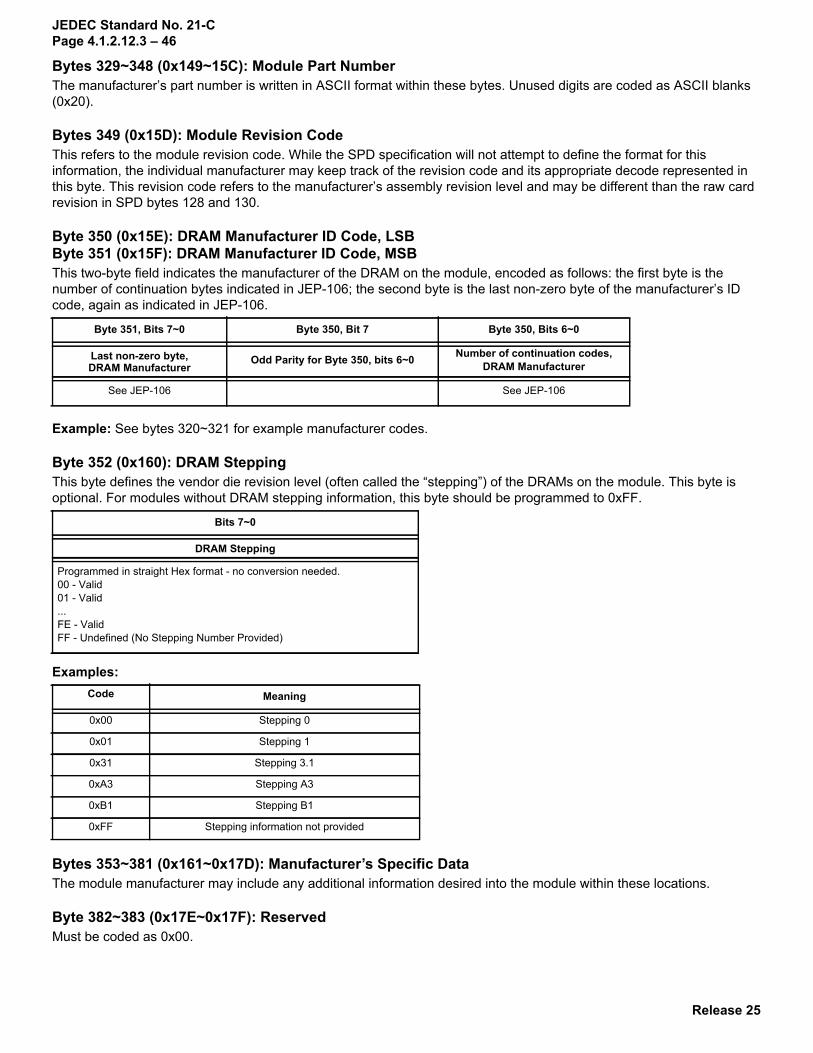
Release 25
JEDEC Standard No. 21-CPage 4.1.2.12.3 – 46
Bytes 329~348 (0x149~15C): Module Part NumberThe manufacturer’s part number is written in ASCII format within these bytes. Unused digits are coded as ASCII blanks (0x20).
Bytes 349 (0x15D): Module Revision CodeThis refers to the module revision code. While the SPD specification will not attempt to define the format for this information, the individual manufacturer may keep track of the revision code and its appropriate decode represented in this byte. This revision code refers to the manufacturer’s assembly revision level and may be different than the raw card revision in SPD bytes 128 and 130.
Byte 350 (0x15E): DRAM Manufacturer ID Code, LSBByte 351 (0x15F): DRAM Manufacturer ID Code, MSBThis two-byte field indicates the manufacturer of the DRAM on the module, encoded as follows: the first byte is the number of continuation bytes indicated in JEP-106; the second byte is the last non-zero byte of the manufacturer’s ID code, again as indicated in JEP-106.
Example: See bytes 320~321 for example manufacturer codes.
Byte 352 (0x160): DRAM SteppingThis byte defines the vendor die revision level (often called the “stepping”) of the DRAMs on the module. This byte is optional. For modules without DRAM stepping information, this byte should be programmed to 0xFF.
Examples:
Bytes 353~381 (0x161~0x17D): Manufacturer’s Specific DataThe module manufacturer may include any additional information desired into the module within these locations.
Byte 382~383 (0x17E~0x17F): ReservedMust be coded as 0x00.
Byte 351, Bits 7~0 Byte 350, Bit 7 Byte 350, Bits 6~0
Last non-zero byte,DRAM Manufacturer
Odd Parity for Byte 350, bits 6~0 Number of continuation codes, DRAM Manufacturer
See JEP-106 See JEP-106
Bits 7~0
DRAM Stepping
Programmed in straight Hex format - no conversion needed. 00 - Valid01 - Valid...FE - ValidFF - Undefined (No Stepping Number Provided)
Code Meaning
0x00 Stepping 0
0x01 Stepping 1
0x31 Stepping 3.1
0xA3 Stepping A3
0xB1 Stepping B1
0xFF Stepping information not provided

Release 25
JEDEC Standard No. 21-CPage 4.1.2.12.3 – 47
ASCII Decode Matrix for SPDsThe following table is a subset of the full ASCII standard which is used for coding bytes in the Serial Presence Detect EEPROM that require ASCII characters:
Examples:0x20 = Blank Space0x34 = ‘4’0x41 = ‘A’
Second Hex Digit in PairFirst Hex
Digit in Pair 0 1 2 3 4 5 6 7 8 9 A B C D E F
2 BlankSpace ( ) -
Dash.
Period
3 0 1 2 3 4 5 6 7 8 9
4 A B C D E F G H I J K L M N O
5 P Q R S T U V W X Y Z
6 a b c d e f g h i j k l m n o
7 p q r s t u v w x y z
SPD Bytes 329~348
Manufacturer’s PN Coded in ASCII
13M32734BCD-260Y 31334D33323733344243442D323630592020

Release 25
JEDEC Standard No. 21-CPage 4.1.2.12.3 – 48
Annex L.1.0: Standard Module Parameters - Overlay Bytes 128~191 (0x080~0x0BF)
Annex L.1.1: Module Specific Bytes for Unbuffered Memory Module Types(Bytes 128~191, 0x080~0x0BF)This section defines the encoding of SPD bytes 128~191 when Memory Technology Key Byte 2 contains the value 0x0C and Module Type Key Byte 3 contains any of the following:
• 0xH2, UDIMM
• 0xH3, SO-DIMM
• 0xH6, Mini-UDIMM
• 0xH9, 72b-SO-UDIMM
• 0xHC, 16b-SO-DIMM
• 0xHD, 32b-SO-DIMM
• where H refers to the hybrid memory architecture, if any present on the module
The following is the SPD address map for the module specific section, bytes 128~255, of the SPD for Unbuffered Module Types.
Byte 128 (0x080) (Unbuffered): Raw Card Extension, Module Nominal HeightThe upper 3 bits of this byte define extensions to the Raw Card Revision in Byte 130. The lower 5 bits of this byte define the nominal height (A dimension) in millimeters of the fully assembled module including heat spreaders or other added components. Refer to the relevant JEDEC JC-11 module outline (MO) documents for dimension definitions.
Module Specific SPD Bytes for Unbuffered Module Types
Byte Number Function Described Notes
128 0x080 Raw Card Extension, Module Nominal Height
129 0x081 Module Maximum Thickness
130 0x082 Reference Raw Card Used
131 0x083 Address Mapping from Edge Connector to DRAM
132~191 0x084~0x0BF Reserved -- Must be coded as 0x00
254 0x0FE CRC for SPD Block 1, Least Significant Byte 1
255 0x0FF CRC for SPD Block 1, Most Significant Byte 1
Note 1 CRC in bytes 254~255 covers all of SPD Block 1, bytes 128~255 (0x080~0x0FF)

Release 25
JEDEC Standard No. 21-CPage 4.1.2.12.3 – 49
Examples:
Byte 129 (0x081) (Unbuffered): Module Maximum ThicknessThis byte defines the maximum thickness (E dimension) in millimeters of the fully assembled module including heat spreaders or other added components above the module circuit board surface. Thickness of the front of the module is calculated as the E1 dimension minus the PCB thickness. Thickness of the back of the module is calculated as the E dimension minus the E1 dimension, rounding up to the next integer. Refer to the relevant JEDEC JC-11 module outline (MO) documents for dimension definitions.
Byte 130 (0x082) (Unbuffered): Reference Raw Card UsedThis byte indicates which JEDEC reference design raw card was used as the basis for the module assembly, if any. Bits 4~0 describe the raw card and bits 6~5 describe the revision level of that raw card. Special reference raw card indicator, ZZ, is used when no JEDEC standard raw card reference design was used as the basis for the module design. Pre-production modules should be encoded as revision 0 in bits 6~5.
Bits 7~5 Bits 4~0
Raw Card Extension Module Nominal Height max, in mm(baseline height = 15 mm)
000 = raw card revisions 0 to 3; see byte 130001 = raw card revision 4010 = raw card revision 5011 = raw card revision 6100 = raw card revision 7101 = raw card revision 8110 = raw card revision 9111 = raw card revision 10
00000 = height 15 mm00001 = 15 < height 16 mm00010 = 16 < height 17 mm00011 = 17 < height 18 mm00100 = 18 < height 19 mm...01010 = 24 < height 25 mm01011 = 25 < height 26 mm...01111 = 29 < height 30 mm10000 = 30 < height 31 mm10001 = 31 < height 32 mm...11111 = 45 mm < height
Nominal Module Height Coding, bits 4~0 Meaning
mm Binary mm18.75 00100 18 < height 19 mm
25.40 01011 25 < height 26 mm
30.00 01111 29 < height 30 mm
30.25 10000 30 < height 31 mm
31.25 10001 30 < height 31 mm
Bits 7~4 Bits 3~0
Module Maximum Thickness max, Back, in mm(baseline thickness = 1 mm)
Module Maximum Thickness max, Front, in mm(baseline thickness = 1 mm)
0000 = thickness 1 mm0001 = 1 < thickness 2 mm0010 = 2 < thickness 3 mm0011 = 3 < thickness 4 mm...1110 = 14 < thickness 15 mm1111 = 15 < thickness
0000 = thickness 1 mm0001 = 1 < thickness 2 mm0010 = 2 < thickness 3 mm0011 = 3 < thickness 4 mm...1110 = 14 < thickness 15 mm1111 = 15 < thickness
Note Thickness = E - E1 Note Thickness = E1 - PCB

Release 25
JEDEC Standard No. 21-CPage 4.1.2.12.3 – 50
Bit 7 Bits 6~5 Bits 4~0
Reference Raw Card Extension Reference Raw Card Revision Reference Raw Card
0 = Reference raw cards A through AL 00 = revision 001 = revision 110 = revision 211 = revision 3
See byte 128 for extensions beyond revision 3; these bits must be coded as 11 for all revisions greater than 3
When bit 7 = 0,00000 = Reference raw card A00001 = Reference raw card B00010 = Reference raw card C00011 = Reference raw card D00100 = Reference raw card E00101 = Reference raw card F00110 = Reference raw card G00111 = Reference raw card H01000 = Reference raw card J01001 = Reference raw card K01010 = Reference raw card L01011 = Reference raw card M01100 = Reference raw card N01101 = Reference raw card P01110 = Reference raw card R01111 = Reference raw card T10000 = Reference raw card U10001 = Reference raw card V10010 = Reference raw card W10011 = Reference raw card Y10100 = Reference raw card AA10101 = Reference raw card AB10110 = Reference raw card AC10111 = Reference raw card AD11000 = Reference raw card AE11001 = Reference raw card AF11010 = Reference raw card AG11011 = Reference raw card AH11100 = Reference raw card AJ11101 = Reference raw card AK11110 = Reference raw card AL11111 = ZZ (no JEDEC reference raw card design used)
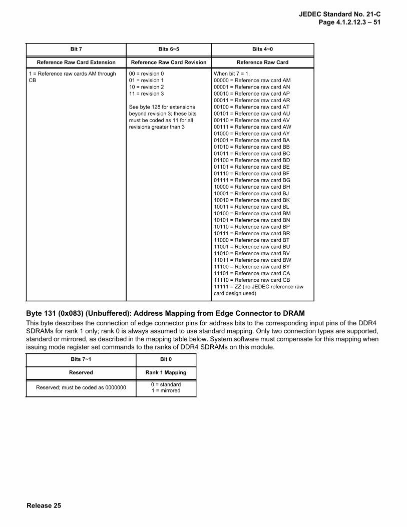
Release 25
JEDEC Standard No. 21-CPage 4.1.2.12.3 – 51
Byte 131 (0x083) (Unbuffered): Address Mapping from Edge Connector to DRAMThis byte describes the connection of edge connector pins for address bits to the corresponding input pins of the DDR4 SDRAMs for rank 1 only; rank 0 is always assumed to use standard mapping. Only two connection types are supported, standard or mirrored, as described in the mapping table below. System software must compensate for this mapping when issuing mode register set commands to the ranks of DDR4 SDRAMs on this module.
Bit 7 Bits 6~5 Bits 4~0
Reference Raw Card Extension Reference Raw Card Revision Reference Raw Card
1 = Reference raw cards AM through CB
00 = revision 001 = revision 110 = revision 211 = revision 3
See byte 128 for extensions beyond revision 3; these bits must be coded as 11 for all revisions greater than 3
When bit 7 = 1,00000 = Reference raw card AM00001 = Reference raw card AN00010 = Reference raw card AP00011 = Reference raw card AR00100 = Reference raw card AT00101 = Reference raw card AU00110 = Reference raw card AV00111 = Reference raw card AW01000 = Reference raw card AY01001 = Reference raw card BA01010 = Reference raw card BB01011 = Reference raw card BC01100 = Reference raw card BD01101 = Reference raw card BE01110 = Reference raw card BF01111 = Reference raw card BG10000 = Reference raw card BH10001 = Reference raw card BJ10010 = Reference raw card BK10011 = Reference raw card BL10100 = Reference raw card BM10101 = Reference raw card BN10110 = Reference raw card BP10111 = Reference raw card BR11000 = Reference raw card BT11001 = Reference raw card BU11010 = Reference raw card BV11011 = Reference raw card BW11100 = Reference raw card BY11101 = Reference raw card CA11110 = Reference raw card CB11111 = ZZ (no JEDEC reference raw card design used)
Bits 7~1 Bit 0
Reserved Rank 1 Mapping
Reserved; must be coded as 0000000 0 = standard1 = mirrored

Release 25
JEDEC Standard No. 21-CPage 4.1.2.12.3 – 52
The definition of standard and mirrored address connection mapping is detailed below; highlighted rows in the table indicate which signals change between mappings.
Bytes 132~191 (0x084~0x0BF) (Unbuffered):Reserved — must be coded as 0x00
Byte 254 (0x0FE) (Unbuffered): Cyclical Redundancy Code (CRC) for SPD Block 1, LSBByte 255 (0x0FF) (Unbuffered): Cyclical Redundancy Code (CRC) for SPD Block 1, MSBThis two-byte field contains the calculated CRC for bytes 128~253 (0x080~0x0FD) in the SPD. See bytes 126~127 for a coding example.
Edge Connector Pin
DRAM Pin,Non-mirrored
DRAM Pin,Mirrored
A0 A0 A0A1 A1 A1A2 A2 A2A3 A3 A4A4 A4 A3A5 A5 A6A6 A6 A5A7 A7 A8A8 A8 A7A9 A9 A9A10 A10 A10A11 A11 A13A13 A13 A11A12 A12 A12A14 A14 A14A15 A15 A15A16 A16 A16A17 A17 A17BA0 BA0 BA1BA1 BA1 BA0BG0 BG0 BG1BG1 BG1 BG0

Release 25
JEDEC Standard No. 21-CPage 4.1.2.12.3 – 53
Annex L.1.2: Module Specific Bytes for Registered Memory Module Types(Bytes 128~191, 0x080~0x0BF)This section defines the encoding of SPD bytes 128~191 when Memory Technology Key Byte 2 contains the value 0x0C and Module Type Key Byte 3 contains any of the following:
• 0xH1, RDIMM
• 0xH5, Mini-RDIMM
• 0xH8, 72b-SO-RDIMM
• where H refers to the hybrid memory architecture, if any present on the module
The following is the SPD address map for the module specific section, bytes 128~191, of the SPD for Registered Module Types.
Byte 128 (0x080) (Registered): Raw Card Extension, Module Nominal HeightThe upper 3 bits of this byte define extensions to the Raw Card Revision in Byte 130. The lower 5 bits of this byte define the nominal height (A dimension) in millimeters of the fully assembled module including heat spreaders or other added components. Refer to the relevant JEDEC JC-11 module outline (MO) documents for dimension definitions.
Module Specific SPD Bytes for Registered Module Types
Byte Number Function Described Notes
128 0x080 Raw Card Extension, Module Nominal Height
129 0x081 Module Maximum Thickness
130 0x082 Reference Raw Card Used
131 0x083 DIMM Attributes
132 0x084 RDIMM Thermal Heat Spreader Solution
133 0x085 Register Manufacturer ID Code, Least Significant Byte
134 0x086 Register Manufacturer ID Code, Most Significant Byte
135 0x087 Register Revision Number
136 0x088 Address Mapping from Register to DRAM
137 0x89 Register Output Drive Strength for Control and Command/Address
138 0x8A Register Output Drive Strength for Clock
139~191 0x089~0x0BF Reserved -- must be coded as 0x00
254 0x0FE CRC for SPD Block 1, Least Significant Byte 1
255 0x0FF CRC for SPD Block 1, Most Significant Byte 1Note 1 CRC in bytes 254~255 covers all of SPD Block 1, bytes 128~255 (0x080~0x0FF)

Release 25
JEDEC Standard No. 21-CPage 4.1.2.12.3 – 54
Examples:
Byte 129 (0x081) (Registered): Module Maximum ThicknessThis byte defines the maximum thickness (E dimension) in millimeters of the fully assembled module including heat spreaders or other added components above the module circuit board surface, rounding up to the next integer. Thickness of the front of the module is calculated as the E1 dimension minus the PCB thickness. Thickness of the back of the module is calculated as the E dimension minus the E1 dimension. Refer to the relevant JEDEC JC-11 module outline (MO) documents for dimension definitions.
Byte 130 (0x082) (Registered): Reference Raw Card UsedThis byte indicates which JEDEC reference design raw card was used as the basis for the module assembly, if any. Bits 4~0 describe the raw card and bits 6~5 describe the revision level of that raw card. Special raw card indicator, ZZ, is used when no JEDEC standard raw card was used as the basis for the design. Pre-production modules should be encoded as revision 0 in bits 6~5.
Bits 7~5 Bits 4~0
Raw Card Extension Module Nominal Height max, in mm(baseline height = 15 mm)
000 = raw card revisions 0 to 3; see byte 130001 = raw card revision 4010 = raw card revision 5011 = raw card revision 6100 = raw card revision 7101 = raw card revision 8110 = raw card revision 9111 = raw card revision 10
00000 = height 15 mm00001 = 15 < height 16 mm00010 = 16 < height 17 mm00011 = 17 < height 18 mm00100 = 18 < height 19 mm...01010 = 24 < height 25 mm01011 = 25 < height 26 mm...01111 = 29 < height 30 mm10000 = 30 < height 31 mm10001 = 31 < height 32 mm...11111 = 45 mm < height
Nominal Module Height Coding, bits 4~0 Meaning
mm Binary mm18.75 00100 18 < height 19 mm
25.40 01011 25 < height 26 mm
30.00 01111 29 < height 30 mm
30.25 10000 30 < height 31 mm
31.25 10001 31 < height 32 mm
Bits 7~4 Bits 3~0
Module Maximum Thickness max, Back, in mm(baseline thickness = 1 mm)
Module Maximum Thickness max, Front, in mm(baseline thickness = 1 mm)
0000 = thickness 1 mm0001 = 1 < thickness 2 mm0010 = 2 < thickness 3 mm0011 = 3 < thickness 4 mm...1110 = 14 < thickness 15 mm1111 = 15 < thickness
0000 = thickness 1 mm0001 = 1 < thickness 2 mm0010 = 2 < thickness 3 mm0011 = 3 < thickness 4 mm...1110 = 14 < thickness 15 mm1111 = 15 < thickness
Note Thickness = E - E1 Note Thickness = E1 - PCB

Release 25
JEDEC Standard No. 21-CPage 4.1.2.12.3 – 55
Bit 7 Bits 6~5 Bits 4~0
Reference Raw Card Extension Reference Raw Card Revision Reference Raw Card
0 = Reference raw cards A through AL 00 = revision 001 = revision 110 = revision 211 = revision 3
See byte 128 for extensions beyond revision 3; these bits must be coded as 11 for all revisions greater than 3
When bit 7 = 0,00000 = Reference raw card A00001 = Reference raw card B00010 = Reference raw card C00011 = Reference raw card D00100 = Reference raw card E00101 = Reference raw card F00110 = Reference raw card G00111 = Reference raw card H01000 = Reference raw card J01001 = Reference raw card K01010 = Reference raw card L01011 = Reference raw card M01100 = Reference raw card N01101 = Reference raw card P01110 = Reference raw card R01111 = Reference raw card T10000 = Reference raw card U10001 = Reference raw card V10010 = Reference raw card W10011 = Reference raw card Y10100 = Reference raw card AA10101 = Reference raw card AB10110 = Reference raw card AC10111 = Reference raw card AD11000 = Reference raw card AE11001 = Reference raw card AF11010 = Reference raw card AG11011 = Reference raw card AH11100 = Reference raw card AJ11101 = Reference raw card AK11110 = Reference raw card AL11111 = ZZ (no JEDEC reference raw card design used)

Release 25
JEDEC Standard No. 21-CPage 4.1.2.12.3 – 56
Byte 131 (0x083) (Registered): DIMM AttributesThis byte indicates number of registers used on a module, and the register type. Further it indicates number of rows of DRAM packages (monolithic, DDP or other stacked) parallel to edge connector (independent of DRAM orientation) on each side of the printed circuit board.
Byte 132 (0x084) (Registered): RDIMM Thermal Heat Spreader SolutionThis byte describes the module’s supported thermal heat spreader solution.
Bit 7 Bits 6~5 Bits 4~0
Reference Raw Card Extension Reference Raw Card Revision Reference Raw Card
1 = Reference raw cards AM through CB
00 = revision 001 = revision 110 = revision 211 = revision 3
See byte 128 for extensions beyond revision 3; these bits must be coded as 11 for all revisions greater than 3
When bit 7 = 1,00000 = Reference raw card AM00001 = Reference raw card AN00010 = Reference raw card AP00011 = Reference raw card AR00100 = Reference raw card AT00101 = Reference raw card AU00110 = Reference raw card AV00111 = Reference raw card AW01000 = Reference raw card AY01001 = Reference raw card BA01010 = Reference raw card BB01011 = Reference raw card BC01100 = Reference raw card BD01101 = Reference raw card BE01110 = Reference raw card BF01111 = Reference raw card BG10000 = Reference raw card BH10001 = Reference raw card BJ10010 = Reference raw card BK10011 = Reference raw card BL10100 = Reference raw card BM10101 = Reference raw card BN10110 = Reference raw card BP10111 = Reference raw card BR11000 = Reference raw card BT11001 = Reference raw card BU11010 = Reference raw card BV11011 = Reference raw card BW11100 = Reference raw card BY11101 = Reference raw card CA11110 = Reference raw card CB11111 = ZZ (no JEDEC reference raw card design used)
Bits 7~4 Bits 3~2 Bits 1~0
Register Type # of rows of DRAMs on RDIMM
# of Registers used on RDIMM
0000 = DDR4RCD010001 = DDR4RCD02All other values reserved
00 = Undefined01 = 1 row10 = 2 rows11 = 4 rows
00 = Undefined01 = 1 register10 = 2 registers11 = 4 registers
Bit 7 Bits 6~0
Heat Spreader Solution Heat Spreader Thermal Characteristics
0 = Heat spreader solution is not incorporated onto this assembly1 = Heat spreader solution is incorporated onto this assembly
0 = UndefinedAll other settings to be defined

Release 25
JEDEC Standard No. 21-CPage 4.1.2.12.3 – 57
Byte 133 (0x085) (Registered): Register Manufacturer ID Code, LSBByte 134 (0x086) (Registered): Register Manufacturer ID Code, MSBThis two-byte field indicates the manufacturer of the register used on the module, encoded as follows: the first byte is the number of continuation bytes indicated in JEP-106; the second byte is the last non-zero byte of the manufacturer’s ID code, again as indicated in JEP-106. These bytes are optional. For modules without the Register Manufacturer ID Code information both bytes should be programmed to 0x00.
Example: See SPD bytes 320~321 for example manufacturer codes.
Byte 135 (0x087) (Registered): Register Revision NumberThis byte defines the vendor die revision level of the registering clock driver component. This byte is optional. For modules without the Register Revision Number information, this byte should be programmed to 0xFF. See byte 131 for the register type.
Examples:
Byte 136 (0x088) (Registered): Address Mapping from Register to DRAMThis byte describes the connection of register output pins for address bits to the corresponding input pins of the DDR4 SDRAMs for rank 1 and rank 3 only; rank 0 and rank 2 are always assumed to use standard mapping. Only two connection types are supported, standard or mirrored, as described in the mapping table below. System software must compensate for this mapping when issuing mode register set commands to the ranks of DDR4 SDRAMs on this module.
The definition of standard and mirrored address connection mapping is detailed below; highlighted rows in the table
Byte 134, Bits 7~0 Byte 133, Bit 7 Byte 133 Bits 6~0
Last non-zero byte,Register Manufacturer
Odd parityfor Byte 133, bits 6~0
Number of continuation codes,Register Manufacturer
See JEP-106 See JEP-106
Bits 7~0
Register Revision Number
Programmed in straight Hex format - no conversion needed. 00 - Valid01 - Valid...FE - ValidFF - Undefined (No Revision Number Provided)
Code Meaning
0x00 Revision 0
0x01 Revision 1
0x31 Revision 3.1
0xA3 Revision A3
0xB1 Revision B1
0xFF Revision information not supplied
Bits 7~1 Bit 0
Reserved Rank 1 Mapping
Reserved; must be coded as 0000000 0 = standard1 = mirrored

Release 25
JEDEC Standard No. 21-CPage 4.1.2.12.3 – 58
indicate which signals change between mappings.
Byte 137 (0x089) (Registered): Register Output Drive Strength for Control and Command/AddressThis byte defines the drive strength for the registering clock driver outputs for control and address/command signals.
Byte 138 (0x08A) (Registered): Register Output Drive Strength for ClockThis byte defines the drive strength for the registering clock driver outputs.
Bytes 139~191 (0x08B~0x0BF) (Registered):Reserved — must be coded as 0x00
Edge Connector Pin
DRAM Pin,Non-mirrored
DRAM Pin,Mirrored
A0 A0 A0A1 A1 A1A2 A2 A2A3 A3 A4A4 A4 A3A5 A5 A6A6 A6 A5A7 A7 A8A8 A8 A7A9 A9 A9A10 A10 A10A11 A11 A13A13 A13 A11A12 A12 A12A14 A14 A14A15 A15 A15A16 A16 A16A17 A17 A17BA0 BA0 BA1BA1 BA1 BA0BG0 BG0 BG1BG1 BG1 BG0
Register Output Drive Strength, Control and Command/Address
Chip Select Command/Address ODT CKE
Bit 7 Bit 6 Bit 5 Bit 4 Bit 3 Bit 2 Bit 1 Bit 0
00 = Light Drive01 = Moderate Drive10 = Strong Drive11 = Very Strong Drive
00 = Light Drive01 = Moderate Drive10 = Strong Drive11 = Very Strong Drive
00 = Light Drive01 = Moderate Drive10 = Strong Drive11 = Very Strong Drive
00 = Light Drive01 = Moderate Drive10 = Strong Drive11 = Very Strong Drive
Note Standard values for drive strength are defined in the DDR4 Registered DIMM Reference Design Specification for JEDEC standard module reference designs.
Register Output Drive Strength, Clock
Reserved Y1, Y3 Y0, Y2
Bit 7 Bit 6 Bit 5 Bit 4 Bit 3 Bit 2 Bit 1 Bit 0
Reserved; must be coded as 0000 00 = Light Drive01 = Moderate Drive10 = Strong Drive11 = Very Strong Drive
00 = Light Drive01 = Moderate Drive10 = Strong Drive11 = Very Strong Drive
Note Standard values for drive strength are defined in the DDR4 Registered DIMM Reference Design Specification for JEDEC standard module reference designs.

Release 25
JEDEC Standard No. 21-CPage 4.1.2.12.3 – 59
Byte 254 (0x0FE) (Registered): Cyclical Redundancy Code (CRC) for SPD Block 1, LSBByte 255 (0x0FF) (Registered): Cyclical Redundancy Code (CRC) for SPD Block 1, MSBThis two-byte field contains the calculated CRC for bytes 128~253 (0x080~0x0FD) in the SPD. See bytes 126~127 for a coding example.

Release 25
JEDEC Standard No. 21-CPage 4.1.2.12.3 – 60
Annex L.1.3: Module Specific Bytes for Load Reduced Memory Module Types (Bytes 128~191, 0x080~0x0BF)This section defines the encoding of SPD bytes 128~191 when Memory Technology Key Byte 2 contains the value 0x0C and Module Type Key Byte 3 contains any of the following:
• 0xH4, LRDIMM
• where H refers to the hybrid memory architecture, if any present on the moduleThe following is the SPD address map for the module specific section, bytes 128~ 255, of the SPD for Load Reduced Module Types.
Module Specific SPD Bytes for Load Reduced Module Types
Byte Number Function Described Notes
128 0x080 Raw Card Extension, Module Nominal Height
129 0x081 Module Maximum Thickness
130 0x082 Reference Raw Card Used
131 0x083 DIMM Module Attributes
132 0x084 LRDIMM Thermal Heat Spreader Solution
133 0x085 Register and Data Buffer Manufacturer ID Code, Least Significant Byte
134 0x086 Register and Data Buffer Manufacturer ID Code, Most Significant Byte
135 0x087 Register Revision Number
136 0x088 Address Mapping from Register to DRAM
137 0x089 Register Output Drive Strength for Control and Command/Address
138 0x08A Register Output Drive Strength for Clock and Data Buffer Control
139 0x08B Data Buffer Revision Number
140 0x08C DRAM VrefDQ for Package Rank 0
141 0x08D DRAM VrefDQ for Package Rank 1
142 0x08E DRAM VrefDQ for Package Rank 2
143 0x08F DRAM VrefDQ for Package Rank 3
144 0x090 Data Buffer VrefDQ for DRAM Interface
145 0x091 Data Buffer MDQ Drive Strength and RTT for data rate < 1866
146 0x092 Data Buffer MDQ Drive Strength and RTT for 1866 < data rate < 2400
147 0x093 Data Buffer MDQ Drive Strength and RTT for 2400 < data rate < 3200
148 0x094 DRAM Drive Strength (for data rates < 1866, 1866 < data rate < 2400, and 2400 < data rate < 3200)
149 0x095 DRAM ODT (RTT_WR, RTT_NOM) for data rate < 1866
150 0x096 DRAM ODT (RTT_WR, RTT_NOM) for 1866 < data rate < 2400
151 0x097 DRAM ODT (RTT_WR, RTT_NOM) for 2400 < data rate < 3200
152 0x098 DRAM ODT (RTT_PARK) for data rate < 1866
153 0x099 DRAM ODT (RTT_PARK) for 1866 < data rate < 2400
154 0x09A DRAM ODT (RTT_PARK) for 2400 < data rate < 3200
155~191 0x09B~0x0BF Reserved -- must be coded as 0x00
254 0x0FE CRC for SPD Block 1, Least Significant Byte 1
255 0x0FF CRC for SPD Block 1, Most Significant Byte 1
Note 1 CRC in bytes 254~255 covers all of SPD Block 1, bytes 128~255 (0x080~0x0FF)

Release 25
JEDEC Standard No. 21-CPage 4.1.2.12.3 – 61
Byte 128 (0x080) (Load Reduced): Raw Card Extension, Module Nominal HeightThe upper 3 bits of this byte define extensions to the Raw Card Revision in Byte 130. The lower 5 bits of this byte define the nominal height (A dimension) in millimeters of the fully assembled module including heat spreaders or other added components. Refer to the relevant JEDEC JC-11 module outline (MO309A) documents for dimension definitions.
Examples:
Byte 129 (0x081) (Load Reduced): Module Maximum ThicknessThis byte defines the maximum thickness (E dimension) in millimeters of the fully assembled module including heat spreaders or other added components above the module circuit board surface, rounding up to the next integer. Thickness of the front of the module is calculated as the E1 dimension minus the PCB thickness. Thickness of the back of the module is calculated as the E dimension minus the E1 dimension. Refer to the relevant JEDEC JC-11 module outline (MO) documents for dimension definitions.
Bits 7 ~ 5 Bits 4 ~ 0
Raw Card Extension Module Nominal Height max, in mm(baseline height = 15 mm)
000 = raw card revisions 0 to 3; see byte 130001 = raw card revision 4010 = raw card revision 5011 = raw card revision 6100 = raw card revision 7101 = raw card revision 8110 = raw card revision 9111 = raw card revision 10
00000 = height 15 mm00001 = 15 < height 16 mm00010 = 16 < height 17 mm00011 = 17 < height 18 mm00100 = 18 < height 19 mm...01010 = 24 < height 25 mm01011 = 25 < height 26 mm...01111 = 29 < height 30 mm10000 = 30 < height 31 mm...11111 = 45 mm < height
Nominal Module Height Coding, bits 4 ~ 0 Meaning
mm Binary mm18.75 00100 18 < height 19 mm
25.40 01011 25 < height 26 mm
30.00 01111 29 < height 30 mm
30.25 10000 30 < height 31 mm
31.25 10001 31 < height 32 mm
Bits 7 ~ 4 Bits 3 ~ 0
Module Maximum Thickness max, Back, in mm(baseline thickness = 1 mm)
Module Maximum Thickness max, Front, in mm(baseline thickness = 1 mm)
0000 = thickness 1 mm0001 = 1 < thickness 2 mm0010 = 2 < thickness 3 mm0011 = 3 < thickness 4 mm...1110 = 14 < thickness 15 mm1111 = 15 < thickness
0000 = thickness 1 mm0001 = 1 < thickness 2 mm0010 = 2 < thickness 3 mm0011 = 3 < thickness 4 mm...1110 = 14 < thickness 15 mm1111 = 15 < thickness
Note Thickness = E - E1 Note Thickness = E1 - PCB
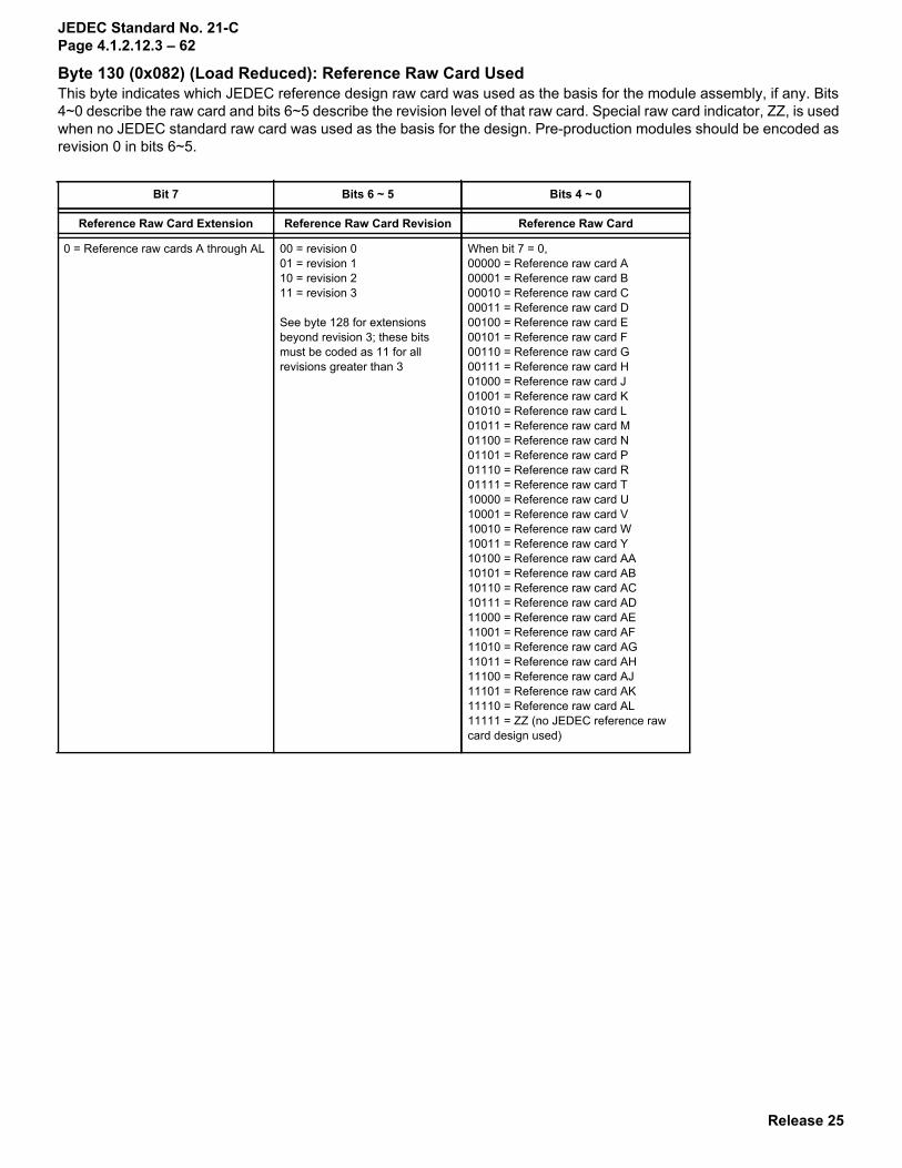
Release 25
JEDEC Standard No. 21-CPage 4.1.2.12.3 – 62
Byte 130 (0x082) (Load Reduced): Reference Raw Card UsedThis byte indicates which JEDEC reference design raw card was used as the basis for the module assembly, if any. Bits 4~0 describe the raw card and bits 6~5 describe the revision level of that raw card. Special raw card indicator, ZZ, is used when no JEDEC standard raw card was used as the basis for the design. Pre-production modules should be encoded as revision 0 in bits 6~5.
Bit 7 Bits 6 ~ 5 Bits 4 ~ 0
Reference Raw Card Extension Reference Raw Card Revision Reference Raw Card
0 = Reference raw cards A through AL 00 = revision 001 = revision 110 = revision 211 = revision 3
See byte 128 for extensions beyond revision 3; these bits must be coded as 11 for all revisions greater than 3
When bit 7 = 0,00000 = Reference raw card A00001 = Reference raw card B00010 = Reference raw card C00011 = Reference raw card D00100 = Reference raw card E00101 = Reference raw card F00110 = Reference raw card G00111 = Reference raw card H01000 = Reference raw card J01001 = Reference raw card K01010 = Reference raw card L01011 = Reference raw card M01100 = Reference raw card N01101 = Reference raw card P01110 = Reference raw card R01111 = Reference raw card T10000 = Reference raw card U10001 = Reference raw card V10010 = Reference raw card W10011 = Reference raw card Y10100 = Reference raw card AA10101 = Reference raw card AB10110 = Reference raw card AC10111 = Reference raw card AD11000 = Reference raw card AE11001 = Reference raw card AF11010 = Reference raw card AG11011 = Reference raw card AH11100 = Reference raw card AJ11101 = Reference raw card AK11110 = Reference raw card AL11111 = ZZ (no JEDEC reference raw card design used)

Release 25
JEDEC Standard No. 21-CPage 4.1.2.12.3 – 63
Byte 131 (0x083) (Load Reduced): DIMM AttributesThis byte indicates number of registers used on a module, and the type of the registers and data buffers. Further, it indicates number of rows of DRAM packages (monolithic, DDP or 3D stacked) parallel to the edge connector (independent of DRAM orientation) on each side of the printed circuit board.
Bit 7 Bits 6 ~ 5 Bits 4 ~ 0
Reference Raw Card Extension Reference Raw Card Revision Reference Raw Card
1 = Reference raw cards AM through CB
00 = revision 001 = revision 110 = revision 211 = revision 3
See byte 128 for extensions beyond revision 3; these bits must be coded as 11 for all revisions greater than 3
When bit 7 = 1,00000 = Reference raw card AM00001 = Reference raw card AN00010 = Reference raw card AP00011 = Reference raw card AR00100 = Reference raw card AT00101 = Reference raw card AU00110 = Reference raw card AV00111 = Reference raw card AW01000 = Reference raw card AY01001 = Reference raw card BA01010 = Reference raw card BB01011 = Reference raw card BC01100 = Reference raw card BD01101 = Reference raw card BE01110 = Reference raw card BF01111 = Reference raw card BG10000 = Reference raw card BH10001 = Reference raw card BJ10010 = Reference raw card BK10011 = Reference raw card BL10100 = Reference raw card BM10101 = Reference raw card BN10110 = Reference raw card BP10111 = Reference raw card BR11000 = Reference raw card BT11001 = Reference raw card BU11010 = Reference raw card BV11011 = Reference raw card BW11100 = Reference raw card BY11101 = Reference raw card CA11110 = Reference raw card CB11111 = ZZ (no JEDEC reference raw card design used)
Bits 7~4 Bits 3~2 Bits 1~0
Register and Data Buffer Types # of rows of DRAMs on LRDIMM# of Registers used
on LRDIMM
0000 = DDR4RCD01 and DDR4DB010001 = DDR4RCD02 and DDR4DB02All other codes reserved
00 = Undefined01 = 1 row10 = 2 rows11 = Reserved
00 = Undefined01 = 1 register10 = Reserved11 = Reserved

Release 25
JEDEC Standard No. 21-CPage 4.1.2.12.3 – 64
Byte 132 (0x084) (Load Reduced): LRDIMM Thermal Heat Spreader SolutionThis byte describes if the module assembly incorporates a heat spreader.
Byte 133 (0x085) (Load Reduced): Register and Data Buffer Manufacturer ID Code, LSBByte 134 (0x086) (Load Reduced): Register and Data Buffer Manufacturer ID Code, MSBThis two-byte field indicates the manufacturer of the memory buffer used on the module, encoded as follows: the first byte is the number of continuation bytes indicated in JEP-106; the second byte is the last non-zero byte of the manufacturer’s ID code, again as indicated in JEP-106.
Example: See SPD byte 320~321 for example manufacturer codes.
Byte 135 (0x087) (Load Reduced): Register Revision NumberThis byte defines the vendor die revision level of the registering clock driver component. See byte 131 for the register type.
Examples:
Byte 136 (0x088) (Load Reduced): Address Mapping from Register to DRAMThis byte describes the connection of register output pins for address bits to the corresponding input pins of the DDR4 SDRAMs for odd ranks only; even ranks are always assumed to use standard mapping. Only two connection types are currently supported, all rank non-mirrored or odd ranks mirrored, as described in the mapping table below. System
Bit 7 Bit 6~0
Heat Spreader Heat Spreader Thermal Characteristics
0 = Heat spreader solution is not incorporated onto this assembly1 = Heat spreader solution is incorporated onto this assembly Undefined; must be coded as 0000000
Byte 134, Bits 7 ~ 0 Byte 133, Bit 7 Byte 133 Bits 6 ~ 0
Last non-zero byte,Memory Buffer Manufacturer
Odd parityfor Byte 133, bits 6 ~ 0
Number of continuation codes,Memory Buffer Manufacturer
See JEP-106 See JEP-106
Bits 7 ~ 0
Register Revision Number
Programmed in straight Hex format - no conversion needed. 00 - Valid01 - Valid...FE - ValidFF - Undefined
Code Meaning
0x00 Revision 0
0x01 Revision 1
0x31 Revision 3.1
0xA3 Revision A3
0xB1 Revision B1

Release 25
JEDEC Standard No. 21-CPage 4.1.2.12.3 – 65
software must compensate for this mapping when issuing mode register set commands to the ranks of DDR4 SDRAMs on this module.
The definition of standard and mirrored address connection mapping is detailed below; highlighted rows in the table indicate which signals change between mappings.
Byte 137 (0x089) (Load Reduced): Register Output Drive Strength for Control and Command/AddressThis byte defines the drive strength for control and command/address outputs of the registering clock driver component.
Bits 7 ~ 1 Bits 0
Reserved Odd Rank Mapping
Reserved; must be coded as 0000000 0 = standard1 = mirrored
Edge Connector Pin
DRAM Pin,Non-mirrored
DRAM Pin,Mirrored
A0 A0 A0A1 A1 A1A2 A2 A2A3 A3 A4A4 A4 A3A5 A5 A6A6 A6 A5A7 A7 A8A8 A8 A7A9 A9 A9
A10 A10 A10A11 A11 A13A13 A13 A11A12 A12 A12A14 A14 A14A15 A15 A15A16 A16 A16A17 A17 A17BA0 BA0 BA1BA1 BA1 BA0BG0 BG0 BG1BG1 BG1 BG0
Register Output Drive Strength for Control and Command/Address
Chip Select Command/Address ODT CKE
Bit 7 Bit 6 Bit 5 Bit 4 Bit 3 Bit 2 Bit 1 Bit 0
00 = Light Drive01 = Moderate Drive10 = Strong Drive11 = Very Strong Drive
00 = Light Drive01 = Moderate Drive10 = Strong Drive11 = Very Strong Drive
00 = Light Drive01 = Moderate Drive10 = Strong Drive11 = Very Strong Drive
00 = Light Drive01 = Moderate Drive10 = Strong Drive11 = Very Strong Drive
Note Standard values are defined in the DDR4 LRDIMM Reference Design Specification for JEDEC standard module reference designs.
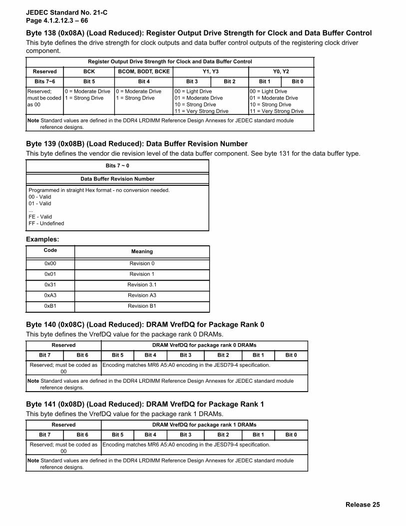
Release 25
JEDEC Standard No. 21-CPage 4.1.2.12.3 – 66
Byte 138 (0x08A) (Load Reduced): Register Output Drive Strength for Clock and Data Buffer ControlThis byte defines the drive strength for clock outputs and data buffer control outputs of the registering clock driver component.
Byte 139 (0x08B) (Load Reduced): Data Buffer Revision NumberThis byte defines the vendor die revision level of the data buffer component. See byte 131 for the data buffer type.
Examples:
Byte 140 (0x08C) (Load Reduced): DRAM VrefDQ for Package Rank 0This byte defines the VrefDQ value for the package rank 0 DRAMs.
Byte 141 (0x08D) (Load Reduced): DRAM VrefDQ for Package Rank 1This byte defines the VrefDQ value for the package rank 1 DRAMs.
Register Output Drive Strength for Clock and Data Buffer Control
Reserved BCK BCOM, BODT, BCKE Y1, Y3 Y0, Y2
Bits 7~6 Bit 5 Bit 4 Bit 3 Bit 2 Bit 1 Bit 0
Reserved; must be coded as 00
0 = Moderate Drive1 = Strong Drive
0 = Moderate Drive1 = Strong Drive
00 = Light Drive01 = Moderate Drive10 = Strong Drive11 = Very Strong Drive
00 = Light Drive01 = Moderate Drive10 = Strong Drive11 = Very Strong Drive
Note Standard values are defined in the DDR4 LRDIMM Reference Design Annexes for JEDEC standard module reference designs.
Bits 7 ~ 0
Data Buffer Revision Number
Programmed in straight Hex format - no conversion needed. 00 - Valid01 - Valid...FE - ValidFF - Undefined
Code Meaning
0x00 Revision 0
0x01 Revision 1
0x31 Revision 3.1
0xA3 Revision A3
0xB1 Revision B1
Reserved DRAM VrefDQ for package rank 0 DRAMs
Bit 7 Bit 6 Bit 5 Bit 4 Bit 3 Bit 2 Bit 1 Bit 0
Reserved; must be coded as 00
Encoding matches MR6 A5:A0 encoding in the JESD79-4 specification.
Note Standard values are defined in the DDR4 LRDIMM Reference Design Annexes for JEDEC standard module reference designs.
Reserved DRAM VrefDQ for package rank 1 DRAMs
Bit 7 Bit 6 Bit 5 Bit 4 Bit 3 Bit 2 Bit 1 Bit 0
Reserved; must be coded as 00
Encoding matches MR6 A5:A0 encoding in the JESD79-4 specification.
Note Standard values are defined in the DDR4 LRDIMM Reference Design Annexes for JEDEC standard module reference designs.

Release 25
JEDEC Standard No. 21-CPage 4.1.2.12.3 – 67
Byte 142 (0x08E) (Load Reduced): DRAM VrefDQ for Package Rank 2This byte defines the VrefDQ value for the package rank 2 DRAMs.
Byte 143 (0x08F) (Load Reduced): DRAM VrefDQ for Package Rank 3This byte defines the VrefDQ value for the package rank 3 DRAMs.
Byte 144 (0x090) (Load Reduced): Data Buffer VrefDQ for DRAM InterfaceThis byte defines the DRAM interface VrefDQ value for the data buffer component.
Byte 145 (0x091) (Load Reduced): Data Buffer MDQ Drive Strength and RTT for data rate < 1866This byte defines the drive strength for MDQ/MDQS outputs and the Read RTT termination strength of the data buffer component.
Reserved DRAM VrefDQ for package rank 2 DRAMs
Bit 7 Bit 6 Bit 5 Bit 4 Bit 3 Bit 2 Bit 1 Bit 0
Reserved; must be coded as 00
Encoding matches MR6 A5:A0 encoding in the JESD79-4 specification.
Note Standard values are defined in the DDR4 LRDIMM Reference Design Annexes for JEDEC standard module reference designs.
Reserved DRAM VrefDQ for package rank 3 DRAMs
Bit 7 Bit 6 Bit 5 Bit 4 Bit 3 Bit 2 Bit 1 Bit 0
Reserved; must be coded as 00
Encoding matches MR6 A5:A0 encoding in the JESD79-4 specification.
Note Standard values are defined in the DDR4 LRDIMM Reference Design Annexes for JEDEC standard module reference designs.
Data Buffer VrefDQ for DRAM Interface
Bit 7 Bit 6 Bit 5 Bit 4 Bit 3 Bit 2 Bit 1 Bit 0
For encoding see definition of F5BC6x (DRAM Interface VREF Control word) in the DDR4DB01 specification.
Note Standard values are defined in the DDR4 LRDIMM Reference Design Annexes for JEDEC standard module reference designs.
Data Buffer MDQ Drive Strength and RTT
DRAM Interface MDQ Drive Strength DRAM Interface MDQ Read Termination Strength
Bit 7 Bit 6 Bit 5 Bit 4 Bit 3 Bit 2 Bit 1 Bit 0
Reserved; must be coded as 0
000 = RZQ/6 (40 001 = RZQ/7 (34 010 = RZQ/5 (40 011 = Reserved100 = Reserved101 = RZQ/4 (60 110 = Reserved111 = Reserved
Reserved; must be coded as 0
000 = Disabled001 = RZQ/4 (60 010 = RZQ/2 (120 011 = RZQ/6 (40 100 = RZQ (240 101 = RZQ/5 (40 110 = RZQ/3 (80 111 = RZQ/7 (34
Note Standard values are defined in the DDR4 LRDIMM Reference Design Annexes for JEDEC standard module reference designs.

Release 25
JEDEC Standard No. 21-CPage 4.1.2.12.3 – 68
Byte 146 (0x092) (Load Reduced): Data Buffer MDQ Drive Strength and RTT for 1866 < data rate < 2400This byte defines the drive strength for MDQ/MDQS outputs and the Read RTT termination strength of the data buffer component.
Byte 147 (0x093) (Load Reduced): Data Buffer MDQ Drive Strength and RTT for 2400 < data rate < 3200This byte defines the drive strength for MDQ/MDQS outputs and the Read RTT termination strength of the data buffer component.
Byte 148 (0x094) (Load Reduced): DRAM Drive Strength (for data rates < 1866, 1866 < data rate < 2400, and 2400 < data rate < 3200)This byte defines the output buffer drive strength for the DRAMs.
Data Buffer MDQ Drive Strength and RTT
DRAM Interface MDQ Drive Strength DRAM Interface MDQ Read Termination Strength
Bit 7 Bit 6 Bit 5 Bit 4 Bit 3 Bit 2 Bit 1 Bit 0
Reserved; must be coded as 0
000 = RZQ/6 (40 001 = RZQ/7 (34 010 = RZQ/5 (40 011 = Reserved100 = Reserved101 = RZQ/4 (60 110 = Reserved111 = Reserved
Reserved; must be coded as 0
000 = Disabled001 = RZQ/4 (60 010 = RZQ/2 (120 011 = RZQ/6 (40 100 = RZQ (240 101 = RZQ/5 (40 110 = RZQ/3 (80 111 = RZQ/7 (34
Note Standard values are defined in the DDR4 LRDIMM Reference Design Annexes for JEDEC standard module reference designs.
Data Buffer MDQ Drive Strength and RTT
DRAM Interface MDQ Drive Strength DRAM Interface MDQ Read Termination Strength
Bit 7 Bit 6 Bit 5 Bit 4 Bit 3 Bit 2 Bit 1 Bit 0
Reserved; must be coded as 0
000 = RZQ/6 (40 )001 = RZQ/7 (34 )010 = RZQ/5 (40 )011 = Reserved100 = Reserved101 = RZQ/4 (60 )110 = Reserved111 = Reserved
Reserved; must be coded as 0
000 = Disabled001 = RZQ/6 (60 )010 = RZQ/2 (120 )011 = RZQ/4 (40 )100 = RZQ (240 )101 = RZQ/5 (40 )110 = RZQ/3 (80 )111 = RZQ/7 (34 )
Note Standard values are defined in the DDR4 LRDIMM Reference Design Annexes for JEDEC standard module reference designs.
DRAM Drive Strength
Reserved 2400 < Data rate < 3200 1866 < Data rate < 2400 Data rate < 1866
Bit 7 Bit 6 Bit 5 Bit 4 Bit 3 Bit 2 Bit 1 Bit 0
Reserved; must be coded as 00
00 = RZQ/7 (34 )01 = RZQ/5 (40 )10 = Reserved11 = Reserved
00 = RZQ/7 (34 )01 = RZQ/5 (40 )10 = Reserved11 = Reserved
00 = RZQ/7 (34 )01 = RZQ/5 (40 )10 = Reserved11 = Reserved
Note Standard values are defined in the DDR4 LRDIMM Reference Design Annexes for JEDEC standard module reference designs.

Release 25
JEDEC Standard No. 21-CPage 4.1.2.12.3 – 69
Byte 149 (0x095) (Load Reduced): DRAM ODT (RTT_WR and RTT_NOM) for data rate < 1866This byte defines the ODT termination strength for the DRAMs.
Byte 150 (0x096) (Load Reduced): DRAM ODT (RTT_WR and RTT_NOM) for 1866 < data rate < 2400This byte defines the ODT termination strength for the DRAMs.
Byte 151 (0x097) (Load Reduced): DRAM ODT (RTT_WR and RTT_NOM) for 2400 < data rate < 3200This byte defines the ODT termination strength for the DRAMs.
DRAM ODT Strength
Reserved RTT_WR RTT_NOM
Bit 7 Bit 6 Bit 5 Bit 4 Bit 3 Bit 2 Bit 1 Bit 0
Reserved; must be coded as 00
000 = Dynamic ODT Off001 = RZQ/2 (120 010 = RZQ (240 011 = Hi-Impedance100 = RZQ/3 (80 )101 = Reserved110 = Reserved111 = Reserved
000 = Disabled001 = RZQ/4 (60 010 = RZQ/2 (120 011 = RZQ/6 (40 )100 = RZQ (240 )101 = RZQ/5 (40 )110 = RZQ/3 (80 )111 = RZQ/7 (34 )
Note Standard values are defined in the DDR4 LRDIMM Reference Design Annexes for JEDEC standard module reference designs.
DRAM ODT Strength
Reserved RTT_WR RTT_NOM
Bit 7 Bit 6 Bit 5 Bit 4 Bit 3 Bit 2 Bit 1 Bit 0
Reserved; must be coded as 00
000 = Dynamic ODT Off001 = RZQ/2 (120010 = RZQ (240 011 = Hi-Impedance100 = RZQ/3 (80 )101 = Reserved110 = Reserved111 = Reserved
000 = Disabled001 = RZQ/4 (60 010 = RZQ/2 (120 011 = RZQ/6 (40 )100 = RZQ (240 )101 = RZQ/5 (40 )110 = RZQ/3 (80 )111 = RZQ/7 (34 )
Note Standard values are defined in the DDR4 LRDIMM Reference Design Annexes for JEDEC standard module reference designs.

Release 25
JEDEC Standard No. 21-CPage 4.1.2.12.3 – 70
Byte 152 (0x098) (Load Reduced): DRAM ODT (RTT_PARK) for data rate < 1866This byte defines the ODT termination strength for the DRAMs.
Byte 153 (0x099) (Load Reduced): DRAM ODT (RTT_PARK) for 1866 < data rate < 2400This byte defines the ODT termination strength for the DRAMs.
Byte 154 (0x09A) (Load Reduced): DRAM ODT (RTT_PARK) for 2400 < data rate < 3200This byte defines the ODT termination strength for the DRAMs.
Bytes 155~191 (0x09B~0x0BF) (Load Reduced):Reserved -- must be coded as 0x00
Bytes 254 (0x0FE) (Load Reduced): Cyclical Redundancy Code (CRC) for SPD Block 1, LSBBytes 255 (0x0FF) (Load Reduced): Cyclical Redundancy Code (CRC) for SPD Block 1, MSBThis two-byte field contains the calculated CRC for bytes 128~253 (0x080~0x0FD) in the SPD. See bytes 126~127 for coding example.
DRAM ODT Strength
Reserved RTT_PARK, Package Ranks 2 & 3 RTT_PARK, Package Ranks 0 & 1
Bit 7 Bit 6 Bit 5 Bit 4 Bit 3 Bit 2 Bit 1 Bit 0
Reserved; must be coded as 00
000 = Disabled001 = RZQ/4 (60 010 = RZQ/2 (120 011 = RZQ/6 (40 )100 = RZQ (240 )101 = RZQ/5 (40 )110 = RZQ/3 (80 )111 = RZQ/7 (34 )
000 = Disabled001 = RZQ/4 (60 010 = RZQ/2 (120 011 = RZQ/6 (40 )100 = RZQ (240 )101 = RZQ/5 (40 )110 = RZQ/3 (80 )111 = RZQ/7 (34 )
Note Standard values are defined in the DDR4 LRDIMM Reference Design Annexes for JEDEC standard module reference designs.

Release 25
JEDEC Standard No. 21-CPage 4.1.2.12.3 – 71
Annex L.2.0: Hybrid Module Parameters - Overlay Bytes 192~253 (0x0C0~0x1FD)
Annex L.2.1: Non-Volatile (NVDIMM-N) Hybrid Memory Parameters:Bytes 192~253 (0x0C0~0x1FD)This section defines the encoding of SPD bytes 192~255 when Module Type Key Byte 3 contains the following:
• 0x9M, NVDIMM
• where M refers to the base memory architectureNVDIMM types defined at this time are:
The following is the SPD address map for the hybrid module specific section, bytes 192~255, of the SPD for Non-Volatile (NVDIMM) Module Types. Note that most NVDIMM types will also have extended function parameters in block 2, bytes 256~319 specific to each type.
Byte 192 (0x0C0) (NVDIMM): Module Product Identifier, LSBByte 193 (0x0C1) (NVDIMM): Module Product Identifier, MSBThese bytes are defined and controlled by the memory module manufacturer to distinguish a specific product among their product offerings. Combined with the Module Manufacturer’s ID Code in bytes 320~321 (0x14D~0x14E), creates a unique 32-bit code for each product type.
NVDIMM-N Persistent DRAM using NAND flash
NVDIMM-F NAND Flash accessed as a block oriented device
NVDIMM-P Combined persistent DRAM and block accessed NAND Flash
Byte Number Function Described Notes
192 0x0C0 Module Product Identifier, LSB
193 0x0C1 Module Product Identifier, MSB
194 0x0C2 Non-Volatile Memory Subsystem Controller Manufacturer’s ID Code, LSB
195 0x0C3 Non-Volatile Memory Subsystem Controller Manufacturer’s ID Code, MSB
196 0x0C4 Non-Volatile Memory Subsystem Controller Product Identifier, LSB
197 0x0C5 Non-Volatile Memory Subsystem Controller Product Identifier, MSB
198 0x0C6 Non-Volatile Memory Subsystem Controller Revision Code
199 0x0C7 Reference Raw Card Used
200 0x0C8 Module Characteristics
201~202 0x0C9~0x0CA Hybrid Module Media Types
203 0x0CB Maximum Non-Volatile Memory Initialization Time
204~205 0x0CC~0x0CD Function 0 Format Interface Descriptor
206~207 0x0CE~0x0CF Function 1 Format Interface Descriptor
208~209 0x0D0~0x0D1 Function 2 Format Interface Descriptor
210~211 0x0D2~0x0D3 Function 3 Format Interface Descriptor
212~213 0x0D4~0x0D5 Function 4 Format Interface Descriptor
214~215 0x0D6~0x0D7 Function 5 Format Interface Descriptor
216~217 0x0D8~0x0D9 Function 6 Format Interface Descriptor
218~219 0x0DA~0x0DB Function 7 Format Interface Descriptor
220~253 0x0DC~0x0FD Reserved
254 0x0FE CRC for SPD Block 1, Least Significant Byte 1
255 0x0FF CRC for SPD Block 1, Most Significant Byte 1
Note 1 CRC in bytes 254~255 covers all of SPD Block 1, bytes 128~255 (0x080~0x0FF)

Release 25
JEDEC Standard No. 21-CPage 4.1.2.12.3 – 72
Byte 194 (0x0C2) (NVDIMM): Non-Volatile Memory Subsystem Controller Manufacturer’s ID Code, LSBByte 195 (0x0C3) (NVDIMM): Non-Volatile Memory Subsystem Controller Manufacturer’s ID Code, MSBThis two-byte field indicates the manufacturer of the Non-Volatile Memory Subsystem controller, encoded as follows: the first byte is the number of continuation bytes indicated in JEP-106; the second byte is the last non-zero byte of the manufacturer’s ID code, again as indicated in JEP-106.
Example: See SPD bytes 320~321 for example manufacturer codes.
Byte 196 (0x0C4) (NVDIMM): Non-Volatile Memory Subsystem Controller Identifier, LSBByte 197 (0x0C5) (NVDIMM): Non-Volatile Memory Subsystem Controller Identifier, MSBThese bytes are defined and controlled by the non-volatile memory subsystem controller manufacturer to distinguish a specific product among their product offerings. Combined with the Non-Volatile Subsystem controller Manufacturer’s ID Code in bytes 194~195 (0x0C2~0x0C3), creates a unique 32-bit code for each product type.
Byte 198 (0x0C6) (NVDIMM): Non-Volatile Memory Subsystem Controller Revision CodeThis refers to the non-volatile subsystem controller revision code. While the SPD specification will not attempt to define the format for this information, the individual non-volatile subsystem controller manufacturer may keep track of the revision code and its appropriate decode represented in this byte.
Byte 199 (0x0C7) (NVDIMM): Reference Raw Card UsedThis byte indicates which JEDEC reference design raw card was used as the basis for the module assembly, if any. Bits 4~0 describe the raw card and bits 6~5 describe the revision level of that raw card. Special raw card indicator, ZZ, is used when no JEDEC standard raw card was used as the basis for the design. Pre-production modules should be encoded as revision 0 in bits 6~5.
Byte 195, Bits 7~0 Byte 194, Bit 7 Byte 194, Bits 6~0
Last non-zero byte,Flash Manufacturer
Odd Parity for Byte 194, bits 6~0 Number of continuation codes,Flash Manufacturer
See JEP-106 See JEP-106

Release 25
JEDEC Standard No. 21-CPage 4.1.2.12.3 – 73
Bit 7 Bits 6~5 Bits 4~0
Reference Raw Card Extension Reference Raw Card Revision Reference Raw Card
0 = Reference raw cards A through AL 00 = revision 001 = revision 110 = revision 211 = revision 3
See byte 200 for extensions beyond revision 3; these bits must be coded as 11 for all revisions greater than 3
When bit 7 = 0,00000 = Reference raw card A00001 = Reference raw card B00010 = Reference raw card C00011 = Reference raw card D00100 = Reference raw card E00101 = Reference raw card F00110 = Reference raw card G00111 = Reference raw card H01000 = Reference raw card J01001 = Reference raw card K01010 = Reference raw card L01011 = Reference raw card M01100 = Reference raw card N01101 = Reference raw card P01110 = Reference raw card R01111 = Reference raw card T10000 = Reference raw card U10001 = Reference raw card V10010 = Reference raw card W10011 = Reference raw card Y10100 = Reference raw card AA10101 = Reference raw card AB10110 = Reference raw card AC10111 = Reference raw card AD11000 = Reference raw card AE11001 = Reference raw card AF11010 = Reference raw card AG11011 = Reference raw card AH11100 = Reference raw card AJ11101 = Reference raw card AK11110 = Reference raw card AL11111 = ZZ (no JEDEC reference raw card design used)

Release 25
JEDEC Standard No. 21-CPage 4.1.2.12.3 – 74
Byte 200 (0x0C8) (NVDIMM): Module CharacteristicsThis byte contains additional information about the module characteristics. Bits 7~5 allow for extended raw card revision levels.
Bit 7 Bits 6~5 Bits 4~0
Reference Raw Card Extension Reference Raw Card Revision Reference Raw Card
1 = Reference raw cards AM through CB
00 = revision 001 = revision 110 = revision 211 = revision 3
See byte 200 for extensions beyond revision 3; these bits must be coded as 11 for all revisions greater than 3
When bit 7 = 1,00000 = Reference raw card AM00001 = Reference raw card AN00010 = Reference raw card AP00011 = Reference raw card AR00100 = Reference raw card AT00101 = Reference raw card AU00110 = Reference raw card AV00111 = Reference raw card AW01000 = Reference raw card AY01001 = Reference raw card BA01010 = Reference raw card BB01011 = Reference raw card BC01100 = Reference raw card BD01101 = Reference raw card BE01110 = Reference raw card BF01111 = Reference raw card BG10000 = Reference raw card BH10001 = Reference raw card BJ10010 = Reference raw card BK10011 = Reference raw card BL10100 = Reference raw card BM10101 = Reference raw card BN10110 = Reference raw card BP10111 = Reference raw card BR11000 = Reference raw card BT11001 = Reference raw card BU11010 = Reference raw card BV11011 = Reference raw card BW11100 = Reference raw card BY11101 = Reference raw card CA11110 = Reference raw card CB11111 = ZZ (no JEDEC reference raw card design used)
Bits 7~5 Bits 4~0
Raw Card Extension Reserved
000 = raw card revisions 0 to 3; see byte 199001 = raw card revision 4010 = raw card revision 5011 = raw card revision 6100 = raw card revision 7101 = raw card revision 8110 = raw card revision 9111 = raw card revision 10
Reserved; must be coded as 00000

Release 25
JEDEC Standard No. 21-CPage 4.1.2.12.3 – 75
Bytes 201~202 (0x0C9~0x0CA) (NVDIMM): Hybrid Module Media TypesThese bytes define a media bit mask for all media types on the module. A setting of 1 in each bit position indicates the presence of that memory type on the module. The SPD is not considered as a media type in this context.
Examples:
Byte 203 (0x0CB) (NVDIMM): Maximum Non-Volatile Memory Initialization TimeThis byte defines the maximum time required for all subsystem(s) to complete initialization from release of RESET or initialization programming of all subsystems present on the module, whichever is later, in seconds. If the initialization time is not known, this byte must be coded as 255 (0xFF).
Examples:
Byte 201 Byte 202
Bit Media Type Bit Media Type0 Unknown/undefined 0 Reserved
1 SDRAM 1 Reserved
2 NAND Flash 2 Reserved
3 Reserved 3 Reserved
4 Reserved 4 Reserved
5 Reserved 5 Reserved
6 Reserved 6 Reserved
7 Reserved 7 Reserved
Module Type Media Types Byte 201 Byte 202NVDIMM-N SDRAM, NAND Flash 0000 0110 0000 0000
NVDIMM-F NAND Flash 0000 0100 0000 0000
NVDIMM-P SDRAM, NAND Flash 0000 0110 0000 0000
Minimum Non-Volatile Memory Initialization TimeSeconds
Values defined from 0 to 254
Byte 203 Hex Use
0 0x00 No initialization time required
1 0x01 1 second
2 0x02 2 seconds
... ...
255 0xFF Initialization time not known or specified

Release 25
JEDEC Standard No. 21-CPage 4.1.2.12.3 – 76
Bytes 204~219 (0x0CC~0x0DB) (NVDIMM): Function Interface DescriptorsThese sets of 2 bytes define the functions available on this module plus the location in the SPD Extended Function Parameters block of the information specific to each function.
Each descriptor encodes the following information:
The Function Class and Function Interface are related as follows:
Descriptor LSB MSB
Function 0 Interface Descriptor 204 0x0CC 205 0x0CD
Function 1 Interface Descriptor 206 0x0CE 207 0x0CF
Function 2 Interface Descriptor 208 0x0D0 209 0x0D1
Function 3 Interface Descriptor 210 0x0D2 211 0x0D3
Function 4 Interface Descriptor 212 0x0D4 213 0x0D5
Function 5 Interface Descriptor 214 0x0D6 215 0x0D7
Function 6 Interface Descriptor 216 0x0D8 217 0x0D9
Function 7 Interface Descriptor 218 0x0DA 219 0x0DB
Function Interface Descriptor
MSB LSB
Bit 15 Bit 14 Bits 13~10 Bits 9~5 Bits 4~0Implemented Reserved Block Offset Function Class Function Interface
Bit 15 0 = Not implemented1 = Implemented
Bit 14 Reserved; must be coded as 0
Bits 13~10 Offset of additional information in Extended Function Parameter Block.Calculate as: 256 + (Block Offset * 4). Field shall have value of 0000 if there isno additional information in the Extended Function Parameter Block.
Block Offset values shall be contiguous from one Function Interface Descriptorto the next. If a Function Interface Descriptor N has information in theExtended Function Parameter Block, size of Extended Function ParameterBlock for Function Interface Descriptor N is ((Block Offset Function InterfaceDescriptor N+1 – Block Offset Function Interface Descriptor N) * 4) whereBlock Offset Function Interface Descriptor N+1 is next Function InterfaceDescriptor that has a non-zero Block Offset value.
Bits 9~5 00 000 = Function Undefined00 001 = Byte addressable energy backed00 010 = Block addressed00 011 = Byte addressable, no energy backedAll other codes reserved
Bits 4~0 0 0000 = Proprietary interface0 0001 = Standard interface 1All other codes reserved; see Definitions of Functions
Note When bit 15 = 0, all other bits in the descriptor must also be coded as 0, Block Offset granularity of 4 bytes may require rounding up to the next available byte in the Extended Function Parameter Block; unused bytes must be coded as 0x00
Function Classes and Function Interfaces
Function Class
Bits 9~5Function Definition Function Interface
Bits 4~0
00 000 Undefined function Undefined 0 0000 = Proprietary interfaceAll other codes reserved
00 001 Byte addressable energy backed
A function containing byte address-able persistent memory whose per-sistence is achieved through the use of DRAM, nonvolatile memory (e.g., Flash) and an energy source. Only the DRAM portion is address-able by the system.
0 0000 = Proprietary interface0 0001 = Byte Addressable Energy Backed Function Interface 1All other codes reserved

Release 25
JEDEC Standard No. 21-CPage 4.1.2.12.3 – 77
Example 1:
NVDIMM with two functions:Function Interface Descriptor 0 = A byte addressable energy backed function class using the byte addressable energy backed function with standard interface 1. This function class defines 14 bytes in the SPD Extended Function Parameters block.
Function Interface Descriptor 1 = A block addressed function class using the block addressed function interface 1. This function class requires 23 bytes in the SPD Extended Function Parameters block.
Example 2:
NVDIMM with three functions:Function Interface Descriptor 0 = a byte addressable no energy backed function using a proprietary interface. This function class defines 14 bytes in the SPD Extended Function Parameters block.
Function Interface Descriptor 1 = a block addressed function (2) using a proprietary interface. This function class does not have any bytes in the SPD Extended Function Parameter block.
Function Interface Descriptor 2 = an undefined function using a proprietary interface. This function class defines 23 bytes in the SPD Extended Function Parameters block.
00 010 Block addressed A function containing persistent memory that requires block-ori-ented access.
0 0000 = Proprietary interface0 0001 = Block Addressed Function Interface 1All other codes reserved
00 011 Byte addressable, no energy backed
A function containing byte address-able persistent memory. All of the persistent memory is addressable by the system. No external energy source is required.
0 0000 = Proprietary interface0 0001 = Byte Addressable No Energy Backed Function Interface 1All other codes reserved
Function 0 Interface Descriptor
Byte 205 Byte 204 Meaning
1000 0000 0010 0001 Bit 15 = 1: ImplementedBits 9~5 = 00001: Function Class is Byte addressable energy backedBits 4~0 = 00001: Function Interface is Byte addressable energy backed Interface 1Bits 13~10 = 0000: Offset of Extended Function Parameters = 256 + 0 * 4 = 256 (0x100)
Implied by the example (i.e., 14 bytes used): Extended Function block from 256 through 269 (0x100~0x10D) is defined Extended Function block bytes 270, 271 not used (coded as 0x00)
Function 1 Interface Descriptor
Byte 207 Byte 206 Meaning
1001 0000 0100 0001 Bit 15 = 1: ImplementedBits 9~5 = 00010: Function Class is Block addressedBits 4~0 = 00001: Function Interface is Block Addressed Function Interface 1Bits 13~10 = 0100: Offset of Extended Function Parameters = 256 + 4 * 4 = 272 (0x110)
Implied by the example (i.e., 23 bytes used): Extended Function block from 272 through 294 (0x110~0x126) is defined Extended Function block byte 295 not used (coded as 0x00)
Functions 2~7 Interface Descriptors
Byte n+1 Byte n Meaning
0000 0000 0000 0000 Bit 15 = 0: Not Implemented; all other bits must be coded as 0
Function 0 Interface Descriptor
Byte 205 Byte 204 Meaning

Release 25
JEDEC Standard No. 21-CPage 4.1.2.12.3 – 78
Bytes 220~253 (0x0DC~0x0FD) (NVDIMM):Reserved, must be coded as 0x00
Bytes 254 (0x0FE) (NVDIMM): Cyclical Redundancy Code (CRC) for SPD Block 1, LSBBytes 255 (0x0FF) (NVDIMM): Cyclical Redundancy Code (CRC) for SPD Block 1, MSBThis two-byte field contains the calculated CRC for bytes 128~253 (0x080~0x0FD) in the SPD. See bytes 126~127 for coding example.
1000 0000 0110 0000 Bit 15 = 1: ImplementedBits 9~5 = 00011: Function Class is Byte addressable no energy backed Bits 4~0 = 00000: Function Interface is Proprietary interface Bits 13~10 = 0000: Offset of Extended Function Parameters = 256 + 0 * 4 = 256 (0x100)
Implied by the example (i.e., 14 bytes used): Extended Function block from 256 through 269 (0x100~0x10D) is defined Extended Function block bytes 270, 271 not used (coded as 0x00)
Function 1 Interface Descriptor
Byte 207 Byte 206 Meaning
1000 0000 0100 0000 Bit 15 = 1: ImplementedBits 9~5 = 00010: Function Class is Block addressed Bits 4~0 = 00000: Function Interface is Proprietary interface
Implied by the example (i.e., no bytes used): No changes to Extended Function block Bits 13~10 coded as 0000
Function 2 Interface Descriptor
Byte 209 Byte 208 Meaning
1001 0000 0000 0000 Bit 15 = 1: ImplementedBits 9~5 = 00000: Function Class is Undefined Bits 4~0 = 00000: Function Interface is Proprietary interface Offset of Extended Function Parameters = 256 + 4 * 4 = 272 (0x110)
Implied by the example (i.e., 23 bytes used): Extended Function block from 272 through 294 (0x110~0x126) is used Extended Function block byte 295 not used (coded as 0x00)
Functions 3~7 Interface Descriptors
Byte n+1 Byte n Meaning
0000 0000 0000 0000 Bit 15 = 0: Not Implemented; all other bits must be coded as 0

Release 25
JEDEC Standard No. 21-CPage 4.1.2.12.3 – 79
Annex L.3.0: Extended Function Parameter Block (EXFUNC): Bytes 256~319 (0x100~0x13F)This section contains zero or more blocks of extended function and interface protocol parameter sets for Hybrid memory modules. The blocks of parameters are contiguous in storage, and the index into this block is stored in the Offset descriptor field for each function type. Granularity of extended parameter blocks is a multiple 4 bytes; unused bytes in a block must be coded as 0x00.
The definition of each parameter block is shown here based on relative addressing within this SPD parameter block, i.e., the beginning address of the parameter block is calculated as:
256 + (4 * Extended Parameter Block Offset for that function)
Example:Function 0 offset = 0, length = 14: byte n = 256, n+1 = 257, ... bytes 268, 269 = 0x00Function 1 offset = 16, length = 23: byte n = 270, n+1 = 271, ... byte 293 = 0x00Function 2 offset = 40, length = 9: byte n = 296, n+1 = 297, ... bytes 305~307 = 0x00Functions 3~7 = not implemented
Annex L.3.1: Extended Function Parameter Block for Byte Addressable Energy Backed NVDIMM (BYTE-E)This section defines the encoding of Extended Function Parameter SPD bytes when a Function Interface Descriptor Function Class bits 9~5 contain 00001.
Byte n (BYTE-E)Byte n + 1 (BYTE-E)Byte n + 2 (BYTE-E)
Annex L.3.2: Extended Function Parameter Block for Block Addressed NVDIMM (BLOCK)This section defines the encoding of Extended Function Parameter SPD bytes when a Function Interface Descriptor Function Class bits 9~5 contain 00010.
Byte n (BLOCK): Module Characteristics
This byte contains additional information about the module characteristics including the interleave capability and energy backup of the NVDIMM. The interleave stride indicates either the NVDIMM cannot be interleaved and must be placed in a contiguous address space or it can be interleaved with other DIMMs on a stride greater than or equal to the encoded value.

Release 25
JEDEC Standard No. 21-CPage 4.1.2.12.3 – 80
Examples:
Byte n + 1 ~ n + 2 (BLOCK): Module Storage CapacityThese 2 bytes define the offered capacity of the block storage on the NVDIMM. The capacity is encoded as follows:
Examples:
Byte n: Module Characteristics
Bit 7 Bit 6 Bits 5~0
Energy Backed Interleave Capable Interleave Stride ≥ 2n
0 = DIMM does not have energy backup1 = DIMM has energy backup
0 = DIMM cannot be interleaved1 = DIMM can be interleaved on a stride greater than or equal to 2Stride
000000 = 20 : Stride ≥ 1 byte000001 = 21 : Stride ≥ 2 bytes...001111 = 215 : Stride ≥ 32 KB010000 = 216 : Stride ≥ 64 KB010001 = 217 : Stride ≥ 128 KB...111111 = 263 : Stride ≥ 263 bytes
Byte n: Module Characteristics
Code Hex Meaning
11 010000 0xD0Energy backup is availableDIMM can be interleaved ≥ 216 (64 KB) boundaries
00 000000 0x00Energy backup is not availableDIMM interleaving not supported
Bytes n+2, n+1: Module Storage Capacity
Byte n+2 (MSB) Byte n+1 (LSB)
Bits 15~14 Bits 13~4 Bits 3~0
Capacity Base Capacity Digits Capacity, Tenths
00 = Mega Bytes01 = Giga Bytes10 = Tera Bytes11 = Peta Bytes
Values from 0 to 999All other values reserved
0000 = 00001 = 0.10010 = 0.20011 = 0.30100 = 0.40101 = 0.50110 = 0.60111 = 0.71000 = 0.81001 = 0.9All other codes reserved
Bytes n+2, n+1: Module Storage Capacity
Code Hex Meaning
01 00 1000 0000 0000 0x2800 Module storage capacity = 128 GB
10 00 0000 0001 0000 0x8010 Module storage capacity = 1 TB
10 00 0000 0001 0101 0x8015 Module storage capacity = 1.5 TB
00 11 0010 0000 0000 0x3200 Module storage capacity = 800 MB

Release 25
JEDEC Standard No. 21-CPage 4.1.2.12.3 – 81
Annex L.3.3: Extended Function Parameter Block for Byte Addressable No Energy Backed NVDIMM (BYTE-NOE)This section defines the encoding of Extended Function Parameter SPD bytes when a Function Interface Descriptor Function Class bits 9~5 contain 00011.
Byte n (BYTE-NOE)Byte n + 1 (BYTE-NOE)Byte n + 2 (BYTE-NOE)
Bytes 318 (0x13E) (EXFUNC): Cyclical Redundancy Code (CRC) for SPD Block 2 lower half, LSBBytes 319 (0x13F) (EXFUNC): Cyclical Redundancy Code (CRC) for SPD Block 2 lower half, MSBThis two-byte field contains the calculated CRC for bytes 256~318 (0x100~0x13D) in the SPD. See bytes 126~127 for coding example.