jinwang product specification - adafruit industries · 7 pol o polarity select for line inversion....
TRANSCRIPT

JINWANG
JINWANG Confidential 1/18
PRODUCT SPECIFICATION
MODEL: JW035PD01VERSION: 1.0
ISSUED DATE: 10/26/2006
CUSTOMER’S APPROVAL JING WANG OPTOELECTRONICS CO., LTD. BY PREPARED BY DATE
DATE
APPROVED BY DATE
Note:
1. JINWANG OPTOELECTRONICS CO., LTD reserves the right to make changes without further notice to any
products herein to improve reliability, function or design.
2. All rights are reserved. No one is permitted to reproduce or duplicate the whole or part of this document
without permission of JINWANG OPTOELECTRONICS CO., LTD.

JINWANG
JINWANG Confidential 2/18
Record of Revisions Rev. Date Description of change 1.0 Oct.26, 2006 JW035PD01 specification was first issued.

JINWANG
JINWANG Confidential 3/18
1. OVERVIEW CLAA035QVA01 is 3.5" (8.76cm) color TFT-LCD (Thin Film Transistor Liquid Crystal
Display) module composed of LCD panel, driver ICs , control circuit , and backlight. The 3.5" screen produces 320 ×RGB×240 resolution image. By applying 8 bits digital data,
16.7 million color images are displayed on the 3.5" diagonal screen. The Driver for LED backlight is not included in this module.
General specifications are summarized in the following table:
ITEM ECIFICATION
Display Area (mm) 70.08(W) x 52.56(H)
Number of Pixels 320 ×3(H) ×240(V)
Pixel Pitch (mm) 0.219(H) ×0.219(V)
Color Pixel Arrangement RGB vertical strip
Display Mode Normally White
Number of color 16.7M
Viewing Direction 6 o'clock
Brightness(cd/m^2) 250(typ)
Viewing Angle CR 10≧ 120 degree (H),100 degree (V) Electrical Interface Digital 24bits RGB
Power Consumption(W) 0.43 (Typ.)
Outline Dimension (mm) 76.9(H) × 63.9(V) × 3.3(D)
weight(g) 34g
BL unit 6pcs LED
Surface Treatment Anti-Glare,Surface hardness: 3H

JINWANG
JINWANG Confidential 4/18
2. ABSOLUTE MAXIMUM RATINGS The following values are maximum operation conditions. If exceeded, it may cause faulty
operation or damage. (GND=AVSS=0V)
ITEM SYMBOL MIN. MAX. UNIT NOTE Power Supply Voltage for Digital VCC -0.3 4 V
Power Supply Voltage for Analog AVDD -0.3 7 V
Gate On Voltage VGH -0.3 25 V
Gate Off Voltage VGL -15 0.3 V
VESDc -200 200 V Static Electricity
VESDm -15 15 KV Note1
LED forward current If 30 mA
LED pulse forward current Ip 100 mA
LED reverse voltage Vr 5 V
Note2
Operation Temperature Top -30 75
Storage Temperature Tstg -40 85 Note1:To test conditions is to stand on IEC 61000-4-2。
VESDc:To contact discharge for Input Connector。 VESDm:To contact discharge for module。
Note2:condition: 1 pcs LED、1/10 duty、0.1msec width。
JINWANG
JINWANG Confidential 5/18
3. ELECTRICAL CHARACTERISTICS
3.1. TFT LCD (Power Supply Voltage) (GND=AVSS=0V)
Parameter SYMBOL Min Typ Max Unit Remarks
Power Supply Voltage for Digital VCC 3 3.3 3.6 V
Power Supply Voltage for Analog AVDD 4.5 5 5.5 V
Gate On Voltage VGH 17 18 19 V Gate Off Voltage VGL -6.6 -6 -5.4 V
VCAC 4.8 5.2 6 Vp-p [Note1] Common Voltage
VCDC 1.5 1.6 1.7 V [Note2]
VIH 0.7VCC - VCC V Input Signal Voltage
VIL 0 - 0.3VCC V
[Note1]:Brightness level is adjusted by varying this amplitude VCAC [Note2]:Please adjust VCDC to make the flicker level be minimum.
3.2. TFT-LCD (consumption Current) (GND=AVSS=0V)
Parameter SYMBOL Condition Min Typ Max Unit Remarks
Gate on Current IVGH VGH =18V - 0.05 0.1 mA [Note1]
Gate off Current IVGL VGL= -6V - 0.05 0.1 mA [Note1]
Digital Current IVCC VCC = 3.3V - 1.5 2 mA [Note1]
Analog Current IAVDD AVDD = 5V - 4 4.5 mA [Note1]
Total Power Consumption PC - 26.2 31.5 mW [Note1]
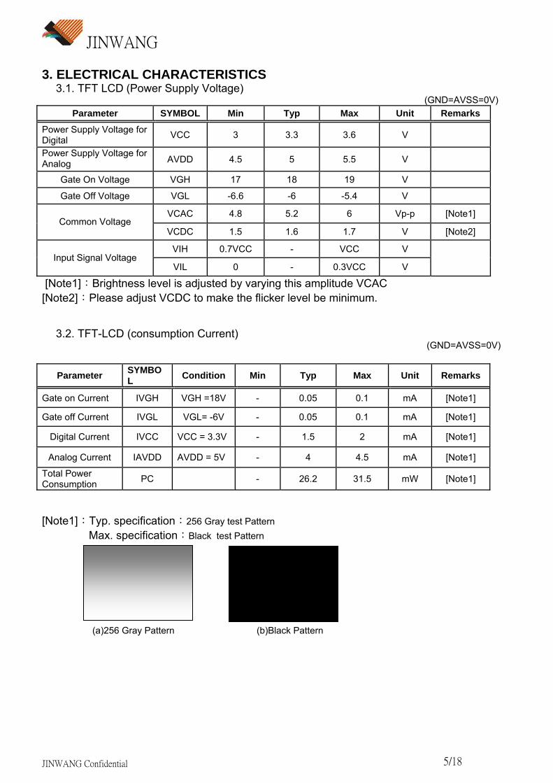
[Note1]:Typ. specification:256 Gray test Pattern Max. specification:Black test Pattern
(a)256 Gray Pattern (b)Black Pattern
JINWANG
JINWANG Confidential 6/18
3.3. Backlight system
ITEM SYMBOL MIN TYP MAX UNIT NOTE
LED Voltage VL 18 20.4 22.8 V
LED Current IL 20 mA
Power consumption WL 408 mW
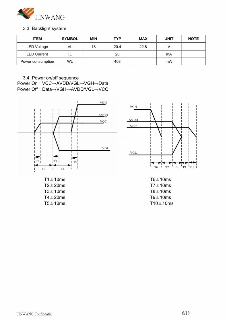
3.4. Power on/off sequence Power On:VCC→AVDD/VGL→VGH→Data Power Off:Data→VGH→AVDD/VGL→VCC
VGH
AVDD
VCC
VGL
T6 T7 T8 T9 T10
T1≦10ms T6≦10ms T2≦20ms T7≦10ms T3≦10ms T8≦10ms T4≦20ms T9≦10ms T5≦10ms T10≦10ms

JINWANG
JINWANG Confidential 7/18
4. INPUT SIGNAL TIMING 4.1. Timing Specification
characteristics SYMBOL MIN TYP MAX UNIT NOTE
Period TOSC 125 160 197 ns DCLK
Dot Clock FOSC 5.08 6.25 8 MHz Data setup time TSU 12 - - ns Data hold time THD 12 - - ns Horizontal Period TH 370 400 440 TOSC Horizontal Valid THV 320 Horizontal Blank THBK 50 80 120
Vertical Period TVP 250 260 280 TH Vertical Valid TVV 240 Vertical Blank TVBK 10 20 40
DE MODE
Vertical Frequency FV 55 60 65 Hz Horizontal Period TH 370 400 440 Horizontal Pulse Width THS 5 20 30 Horizontal Pulse Width + Back Proch THPWB 25 45 75
Horizontal Front Proch THFP 25 35 45
TOSC
Horizontal Valid THV 320 Horizontal pulse width THS 5 30 - TOSC Horizontal rising time TCr - - 700 ns Horizontal falling time TCf - - 300 ns Vertical Period TVP 250 260 280 Vertical Pulse Width TVS 1 3 5 Vertical Pulse Width + Back Proch TVPWB 5 10 15
Vertical Front Proch TVFP 5 10 25
TH
Vertical Valid TVV 240 Vertical Frequency FV 55 60 65 Hz Vertical pulse width TVS 1 3 5 TH Vertical rising time TVr - - 700 ns
SYNC MODE
Vertical falling time TVf - - 1.5 us Note:This module must operate for DE and SYNC mode.

JINWANG
JINWANG Confidential 8/18
4.2. Timing Chart (1) CLK, DATA, DEN waveform timing
(2) HIS, IVS waveform timing
TH
Tvr

JINWANG
JINWANG Confidential 9/18
(3) Color data definition COLOR INPUT R DATA G DATA B DATA
DATA R7 R6 R5 R4 R3 R2 R1 R0 G7 G6 G5 G4 G3 G2 G1 G0 B7 B6 B5 B4 B3 B2 B1 B0
MSB LSB MSB LSB MSB LSB
BLACK 0 0 0 0 0 0 0 0 0 0 0 0 0 0 0 0 0 0 0 0 0 0 0 0RED(255) 1 1 1 1 1 1 1 1 0 0 0 0 0 0 0 0 0 0 0 0 0 0 0 0
BASIC GREEN(255) 0 0 0 0 0 0 0 0 1 1 1 1 1 1 1 1 0 0 0 0 0 0 0 0COLOR BLUE(255) 0 0 0 0 0 0 0 0 0 0 0 0 0 0 0 0 1 1 1 1 1 1 1 1
CYAN 0 0 0 0 0 0 0 0 1 1 1 1 1 1 1 1 1 1 1 1 1 1 1 1MAGENTA 1 1 1 1 1 1 1 1 0 0 0 0 0 0 0 0 1 1 1 1 1 1 1 1YELLOW 1 1 1 1 1 1 1 1 1 1 1 1 1 1 1 1 0 0 0 0 0 0 0 0WHITE 1 1 1 1 1 1 1 1 1 1 1 1 1 1 1 1 1 1 1 1 1 1 1 1RED(0) 0 0 0 0 0 0 0 0 0 0 0 0 0 0 0 0 0 0 0 0 0 0 0 0RED(1) 0 0 0 0 0 0 0 1 0 0 0 0 0 0 0 0 0 0 0 0 0 0 0 0RED(2) 0 0 0 0 0 0 1 0 0 0 0 0 0 0 0 0 0 0 0 0 0 0 0 0
RED
RED(254) 1 1 1 1 1 1 1 0 0 0 0 0 0 0 0 0 0 0 0 0 0 0 0 0RED(255) 1 1 1 1 1 1 1 1 0 0 0 0 0 0 0 0 0 0 0 0 0 0 0 0GREEN(0) 0 0 0 0 0 0 0 0 0 0 0 0 0 0 0 0 0 0 0 0 0 0 0 0GREEN(1) 0 0 0 0 0 0 0 0 0 0 0 0 0 0 0 1 0 0 0 0 0 0 0 0GREEN(2) 0 0 0 0 0 0 0 0 0 0 0 0 0 0 1 0 0 0 0 0 0 0 0 0
GREEN
GREEN(254) 0 0 0 0 0 0 0 0 1 1 1 1 1 1 1 0 0 0 0 0 0 0 0 0GREEN(255) 0 0 0 0 0 0 0 0 1 1 1 1 1 1 1 1 0 0 0 0 0 0 0 0BLUE(0) 0 0 0 0 0 0 0 0 0 0 0 0 0 0 0 0 0 0 0 0 0 0 0 0BLUE(1) 0 0 0 0 0 0 0 0 0 0 0 0 0 0 0 0 0 0 0 0 0 0 0 1BLUE(2) 0 0 0 0 0 0 0 0 0 0 0 0 0 0 0 0 0 0 0 0 0 0 1 0
BLUE
BLUE(254) 0 0 0 0 0 0 0 0 0 0 0 0 0 0 0 0 1 1 1 1 1 1 1 0BLUE(255) 0 0 0 0 0 0 0 0 0 0 0 0 0 0 0 0 1 1 1 1 1 1 1 1
[Remark]:
*1) Definition of gray scale: Color (n): n means level of gray scale. Larger n means brighter level. *2) Data: 1= High, 0 = Low
JINWANG
JINWANG Confidential 10/18
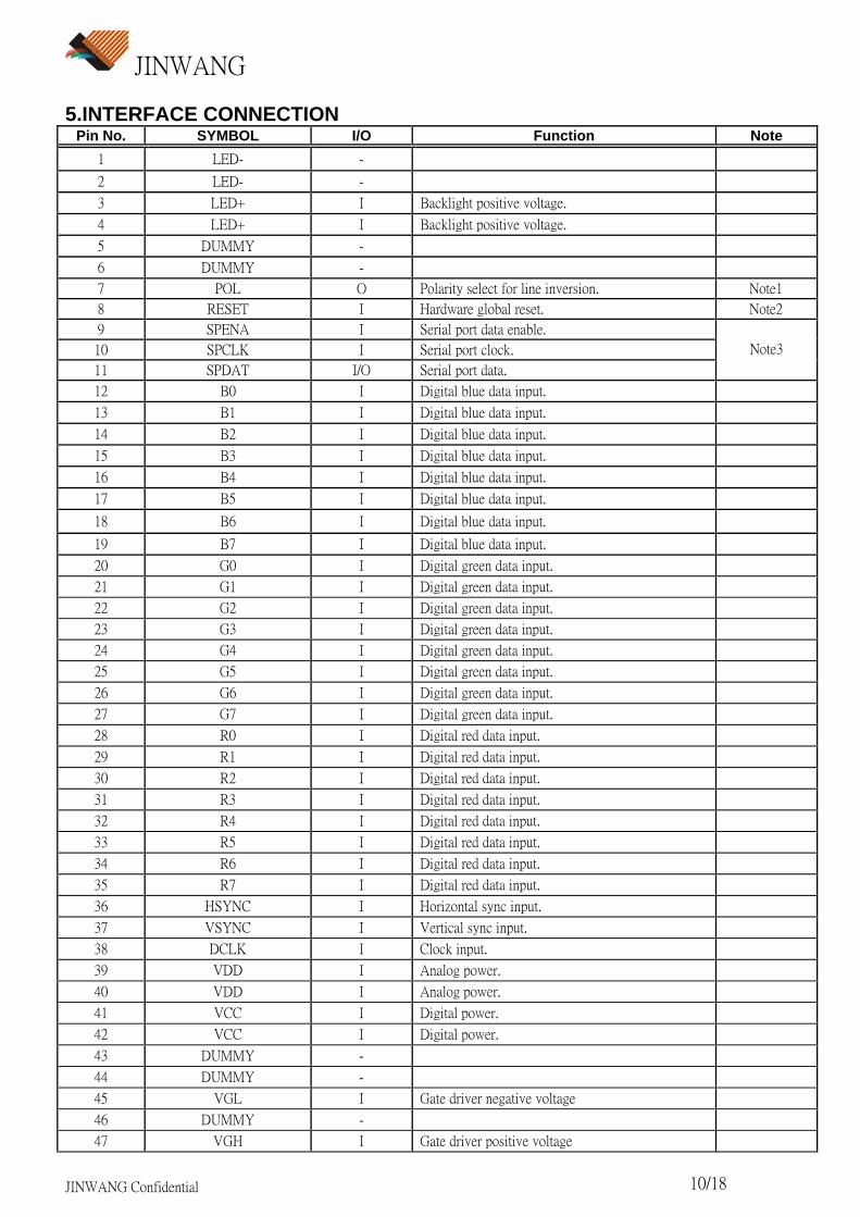
5.INTERFACE CONNECTION Pin No. SYMBOL I/O Function Note
1 LED- - 2 LED- - 3 LED+ I Backlight positive voltage. 4 LED+ I Backlight positive voltage. 5 DUMMY - 6 DUMMY - 7 POL O Polarity select for line inversion. Note1
8 RESET I Hardware global reset. Note2
9 SPENA I Serial port data enable.
10 SPCLK I Serial port clock.
11 SPDAT I/O Serial port data.
Note3
12 B0 I Digital blue data input. 13 B1 I Digital blue data input. 14 B2 I Digital blue data input. 15 B3 I Digital blue data input. 16 B4 I Digital blue data input. 17 B5 I Digital blue data input. 18 B6 I Digital blue data input. 19 B7 I Digital blue data input. 20 G0 I Digital green data input. 21 G1 I Digital green data input. 22 G2 I Digital green data input. 23 G3 I Digital green data input. 24 G4 I Digital green data input. 25 G5 I Digital green data input. 26 G6 I Digital green data input. 27 G7 I Digital green data input. 28 R0 I Digital red data input. 29 R1 I Digital red data input. 30 R2 I Digital red data input. 31 R3 I Digital red data input. 32 R4 I Digital red data input. 33 R5 I Digital red data input. 34 R6 I Digital red data input. 35 R7 I Digital red data input. 36 HSYNC I Horizontal sync input. 37 VSYNC I Vertical sync input. 38 DCLK I Clock input. 39 VDD I Analog power. 40 VDD I Analog power. 41 VCC I Digital power. 42 VCC I Digital power. 43 DUMMY - 44 DUMMY - 45 VGL I Gate driver negative voltage 46 DUMMY - 47 VGH I Gate driver positive voltage

JINWANG
JINWANG Confidential 11/18
48 DUMMY - 49 DUMMY - 50 DUMMY -
51 VCOM I Voltage applied to color filter substrate. Note4
52 ENB I Data enable control.
53 GND -
54 VSS -
Note1:The function of POL is polarity select for line inversion control signal. POL H L
Output voltage polarity positive negative
Note2:RESETB pin normally pull high. Hardware global reset. Low active.
Note3:SPCLK for serial port clock. Normally pull high. SPDAT for serial port Data input/output. SPENA for serial port Data Enable signal. Normally pull high.
Note4:Suggestion VCOM circuit

JINWANG
JINWANG Confidential 12/18
6. MECHANICAL DIMENSION 6.1. Front Side
Unit:mm

JINWANG
JINWANG Confidential 13/18
6.2.Rear Side

JINWANG
JINWANG Confidential 14/18
7. OPTICAL CHARACTERISTICS Ta=25
ITEM SYMBOL CONDITION MIN. TYP. MAX. UNIT RemarksContrast Ratio (center) CR Point-5 240 300 -- -- *1)
center Luminance L 200 250 -- cd/m2 *2)
Luminance Uniformity ΔL 80 -- -- % *2)
Response Time tr+tf -- 25 -- ms *3)
Horizontal 110 120 -- ° *4) Viewing Angle Vertical
CR≧10 Point-5 90 100 -- ° *4)
Red Rx Ry
0.561
0.286 0.601
0.326 0.641
0.366
Green Gx Gy
0.289
0.531 0.329
0.571 0.369
0.611
Blue Bx By
0.107
0.060 0.147
0.100 0.187
0.140
White Wx Wy
Point-5
0.267
0.280 0.307
0.320 0.347
0.360
-- *2)*3) Color
Coordinate
Gamut -- 54.6% --
[Note]:These items are measured by BM-5A (TOPCON) in the dark room. IL= 20.0mA ; View Cone:1° *1 Definition of contrast ratio:
1) Contrast Ratio (CR) = (White) Luminance of ON ÷ (Black) Luminance of OFF
Fig.1 Measuring point

JINWANG
JINWANG Confidential 15/18
*2 Definition of Center Luminance & Luminance Uniformity:
1) Center Luminance (L) = Measure the luminance on the center point as figure 7-1 #5 point 2) Measure maximum luminance and minimum luminance on the 9 points as figure 7-1 (#1~#9 point).Luminance Uniformity is calculated with the following formula:
L = [L (MIN) / L (MAX)] ×100%
*3 Definition of Response Time. (White - Black) The response time is defined as the time interval between the 10% and 90% amplitudes.
Luminance
90%90%
10%t f t r
White(63th)
Black(0) 10%
Fig.2 Definition of Response Time (White - Black)
*4 Definition of Viewing Angle(θ,ψ):(by EZ-CONTRAST (ELDIM) in the dark room.)
Fig.3 Definition of Viewing Angle

JINWANG
JINWANG Confidential 16/18
8. RELIABILITY TEST CONDITIONS (1) Temperature and Humidity
TEST ITEMS CONDITIONS
HIGH TEMPERATURE OPERATION 75°C;240Hrs
HIGH TEMPERATURE STORAGE 85°C;240Hrs
HIGH TEMPERATURE AND HIGH HUMIDITY OPERATION 60°C;90%RH;240Hrs
LOW TEMPERATURE OPERATION -30°C;240Hrs
LOW TEMPERATURE STORAGE -40°C;240Hrs
THERMAL SHOCK (No operation) -30°C(0.5Hr)~85°C(0.5Hr) 200 CYCLE
(2) Shock & Vibration
TEST ITEMS CONDITIONS
SHOCK (NON-OPERATION)
Shock level: 980m/s2(equal to 100G). Waveform: half sinusoidal wave,6ms. Number of shocks: one shock input in each direction of three mutually perpendicular axes for a total of three shock inputs.
VIBRATION (NON-OPERATION)
Frequency range:8~33.3Hz Stoke:1.3 mm Vibration: sinusoidal wave, perpendicular axis(both x,z axis: 2Hrs , and y axis: 4Hrs ).
Sweep: 2.9G,33.3 Hz -400 Hz Cycle: 15 min
(3) ESD
TEST ITEM CONDITIONS Note
150pF,330Ω,±8Kv & ±15kV air & contact test (1) ESD 200pF,0Ω,±200V contact test (2)
[NOTE]:Measure point :(1)LCD glass and metal bezel (2)IF connector pins (4) Judgment standard
The judgment of the above test should be made as follow: Pass:Normal display image with no obvious non-uniformity and no line defect. Partial transformation of the module parts should be ignored. Fail:No display image, obvious non-uniformity, or line defects.

JINWANG
JINWANG Confidential 17/18
9. HANDLING PRECAUTIONS FOR TFT-LCD MODULE Please pay attention to the followings in handling- TFT-LCD products:
(A) ASSEMBLY PRECAUTION
(1) Please use the mounting hole on the module side in installing and do not beading or wrenching LCD in assembling. And please do not drop, bend or twist LCD module in handling.
(2) Please design display housing in accordance with the following guide lines. (2.1) Housing case must be destined carefully so as not to put stresses on LCD all sides
and not to wrench module. The stresses may cause non-uniformity even if there is no non-uniformity statically.
(2.2) Keep sufficient clearance between LCD module back surface and housing when the LCD module is mounted. Approximately 1.0 mm of the clearance in the design is recommended taking into account the tolerance of LCD module thickness and mounting structure height on the housing.
(2.3) When some parts, such as, FPC cable and ferrite plate, are installed underneath the LCD module, still sufficient clearance is required, such as 0.5mm. This clearance is, especially, to be reconsidered when the additional parts are implemented for EMI countermeasure.
(2.4) Design the inverter location and connector position carefully so as not to give stress to lamp cable, or not to interface the LCD module by the lamp cable.
(2.5) Keep sufficient clearance between LCD module and the others parts, such as inverter and speaker so as not to interface the LCD module. Approximately 1.0mm of the clearance in the design is recommended.
(3) Please do not push or scratch LCD panel surface with any-thing hard. And do not soil LCD panel surface by touching with bare hands. (Polarizer film, surface of LCD panel is easy to be flawed.)
(4) Please do not press any parts on the rear side such as source TCP, gate TCP, control circuit board and FPCs during handling LCD module. If pressing rear part is unavoidable, handle the LCD module with care not to damage them.
(5) Please wipe out LCD panel surface with absorbent cotton or soft cloth in case of it being soiled.
(6) Please wipe out drops of adhesives like saliva and water on LCD panel surface immediately. They might damage to cause panel surface variation and color change.
(7) Please do not take a LCD module to pieces and reconstruct it. Resolving and reconstructing modules may cause them not to work well.
(8) Please do not touch metal frames with bare hands and soiled gloves. A color change of the metal frames can happen during a long preservation of soiled LCD modules.
(9) Please pay attention to handling lead wire of backlight so that it is not tugged in connecting wit inverter.
(B) OPERATING PRECAUTIONS
(1) Please be sure to turn off the power supply before connecting and disconnecting signal input cable.
(2) Please do not change variable resistance settings in LCD module. They are adjusted to the most suitable value. If they are changed, it might happen LCD does not satisfy the characteristics specification.
(3) Please consider that LCD backlight takes longer time to become stable of radiation characteristics in low temperature than in room temperature.
(4) A condensation might happen on the surface and inside of LCD module in case of sudden charge of ambient temperature.
(5) Please pay attention to displaying the same pattern for very long time. Image might stick on LCD. If then, time going on can make LCD work well.

JINWANG
JINWANG Confidential 18/18
(6) Please obey the same caution descriptions as ones that need to pay attention to ordinary electronic parts.
(C) PRECAUTFONS WITHELECTROSTATICS
(1) This LCD module use CMOS-IC on circuit board and TFT-LCD panel, and so it is easy to be affected by electrostatics. Please be careful with electrostatics by the way of your body connecting to the ground and so on.
(2) Please remove protection film very slowly on the surface of LCD module to prevent from electrostatics occurrence.
(D) STORAGE PRECAUTIONS
(1) When you store LCDs for a long time, it is recommended to keep the temperature Between 0°C-40°C without the exposure of sunlight and to keep the humidity less than 90%RH.
(2) Please do not leave the LCDs in the environment of high humidity and high temperature such as 60°C 90%RH.
(3) Please do not leave the LCDs in the environment of low temperature; below -20°C.
(E) SAFETY PRECAUTIONS (1) When you waste LCDS, it is recommended to crush damaged or unnecessary LCDs
into pieces and wash them off with solvents such as acetone and ethanol, which should later be burned.
(2) If any liquid leaks out of a damaged-glass cell and comes in contact with the hands, wash off throughly with soap and water.
(F) OTHERS
(1) A strong incident light into LCD panel might cause display characteristics' changing inferior because of polarizer film, color filter, and other materials becoming inferior. Please do not expose LCD module direct sunlight Land strong UV rays.
(2) Please pay attention to a panel side of LCD module not to contact with other materials in preserving it alone.
(3) For the packaging box, please pay attention to the followings: (3.1) Packaging box and inner case for LCD are designed to protect the LCDs from the
damage or scratching during transportation. Please do not open except picking LCDs up from the box.
(3.2) Please do not pile them up more than 5 boxes. (They are not designed so.) And please do not turn over.
(3.3) Please handle packaging box with care not to give them sudden shock and vibrations. And also please do not throw them up.
(3.4) Packing box and inner case for LCDs are made of cardboard. So please pay attention not to get them wet. (Such like keeping them in high humidity or wet place can occur getting them wet.)