journal of ceramic processing research. vol. 17, no. 12,...
TRANSCRIPT

Journal of Ceramic Processing Research. Vol. 17, No. 12, pp. 1283~1286 (2016)
1283
J O U R N A L O F
CeramicProcessing Research
Structure and optical properties of anatase thin films produced by filtered
cathodic vacuum arc method
Sakon Sansongsiria,b,* and Somchai Thongtema,b,*aDepartment of Physics and Material Science, Faculty of Science, Chiang Mai University, Chiang Mai 50200, ThailandbMaterials Science Research Center, Faculty of Science, Chiang Mai University, Chiang Mai 50200, Thailand
Titanium dioxide (TiO2) thin films were deposited on glass substrates by filtered cathodic vacuum arc system (lab-made) forvarious number of pulse modes at -50 VDC, and followed by 450 oC annealing in air for 1 hr. The deposition pulses were 500-2,000 pulses and the anatase film thickness was 13.0-37.5 nm. In this research, the roughness was increased with the increasingin the number of deposition pulses and film thickness. The transmission at 600 nm wavelength was 65-85%, decreasing withthe film thickness, and the optical energy gap was in the range of 3.55-3.65 eV.
Key words: Anatase thin films, Filtered cathodic vacuum arc, Electron microscopy, Spectroscopy.
Introduction
Titanium dioxide (TiO2) is a wide band gap
semiconductor [1] with different applications controlled its
optical properties [2] and electronic structure. TiO2 thin
film has attractive properties due to its applications:
photocatalysis [3-6], optical coatings [7-10], optoelectronic
devices [11, 12] and photoelectrodes of dye-sensitized
solar cells [13-15]. There are many techniques used to
fabricate TiO2 thin films such as magnetron sputtering
[5, 15-17], spray pyrolysis [18], chemical vapor
deposition (CVD) [19, 20] and sol-gel method [13, 21].
Filtered cathodic vacuum arc (FCVA) method is used
for metal thin film deposition [22-24]. The metal ion
was produced by FCVA with the metallic source as a
cathode. Metal plasma would diffuse through a 90 o
electromagnetic duct to deposit on the substrate [25-
27]. The ion energy can be controlled by applying a
negative bias voltage to the substrate to attract the ions
[25]. The film thickness is controlled by number of
deposition pulses [29, 30]. In this work, FCVA system
was used to produce titanium thin film on glass slide.
These deposited metal films would be annealed for
titanium dioxide thin film formation. There are three
different forms of titanium dioxide: rutile, anatase and
brookite [17]. The most intense photocatalytic activity
is anatase. Different deposition techniques play the role
in film structure and optical properties. Upon annealing
the metallic films,E their structure, surface morphology,
optical properties and energy gap were intensively
investigated [31].
Experimental Details
Titanium dioxide thin films were fabricated on
1 × 10 × 10 mm3 soda-lime glass by FCVA system
(Fig. 1). The experimental apparatus included a cathodic
arc plasma source with 90 o electromagnetic duct filter,
placed between the plasma source and substrate to
remove macro-particles in a vacuum chamber. The
cathode used in this experiment was a 99.9% pure Ti rod
with 5.8 mm in diameter. The arc was ignited with 1 ms
pulse width at the repetition rate of 1 pps. The arc current
was 195 A. The Ti cathodic plasma arc was guided to
the clean substrate by an applied electromagnetic filed
induced by an arc current. A market pen was used to
draw a line on surface of the attached sample. It will be
removed after film deposition to be a trace without film
cover for film thickness surface profile measurement.
Each substrate was placed 5 cm apart from the
magnetic exit duct. The chamber was tightly closed. A
rotary and cryogenic vacuum pump was evacuated to
*Corresponding authors: Tel : +66-(0)53-943367Fax: +66-(0)53-943445E-mails: [email protected], [email protected]
Fig. 1. Schematic diagram of FCVA system.

1284 Sakon Sansongsiri and Somchai Thongtem
6.0 × 10⁻⁵ mbar. There are four deposition conditions:
500, 1000, 1500 and 2000 pulses, and the substrates
were biased by −50 VDC.
Upon deposition the titanium thin films, they were
annealed at 450 oC in air for 1 hr to oxidize Ti to TiO2. The
TiO2 films were analyzed by Raman spectrophotometry
(T64000 Horiba JobinYvon). The film thickness and
roughness was measured by atomic force microscopy
(AFM, NanoScope IIIa, MMAFML N, Veeco). The
surface morphology was investigated by scanning electron
microscopy (SEM, Jeol JSM-6335F). The optical properties
were evaluated by UV-VIS spectroscopy (Lambda 25
Perkin Elmer).
Results and Discussion
Deposition rateFilm thickness measured by AFM step profile drag
pass across the edge of thin film and trace. The film
thickness (Fig. 2) appears to increase slightly from
13.0 nm at 500 deposition pulses to 37.5 nm at 2000
deposition pulses. Deposition rate of TiO2 films was
approximately 1.6 × 10⁻² nm per pulse or about 1 nm.min-
1. The deposition rate rather low because electromagnetic
filter removed most of the titanium plasma, and only a
small content of the plasma reached the substrate.
Raman spectroscopyThe Raman spectra (Fig. 3) of the TiO2 films
deposited at −50 VDC and annealed at 450 oC for 1 hr
show no significant change in the peak position when
the film thickness increased, although the intensities of
the peaks were increased. Due to the report for bulk
TiO2 [32], the rutile phase exhibits major peaks at 610,
446 and 242 cm–1, and anatase exhibits at 635, 514,
396, 197 and 144 cm–1. For the present analysis, broad
peaks similar to the anatase were detected, and the
anatase was attributed to form as the majority.
Surface morphologySurface morphology and roughness of the films were
characterized by AFM. The AFM images of the
Fig. 2. TiO2 film thickness at different deposition pulses.
Fig. 3. Raman spectra of the TiO2 thin films deposited on glasssubstrates at the deposition of (a-d) 500, 1000, 1500 and 2000pulses, respectively.
Fig. 4. AFM images of TiO2 thin films prepared by FCVA at the deposition pulses of (a-d) 500, 1000, 1500 and 2000 pulses, respectively.
Structure and optical properties of anatase thin films produced by filtered cathodic vacuum arc method 1285
samples prepared by different number of deposition
pulses are shown in Fig. 4. The lower part is the
substrate and the upper one is the deposited film. Their
surface roughness was increased with the increasing in
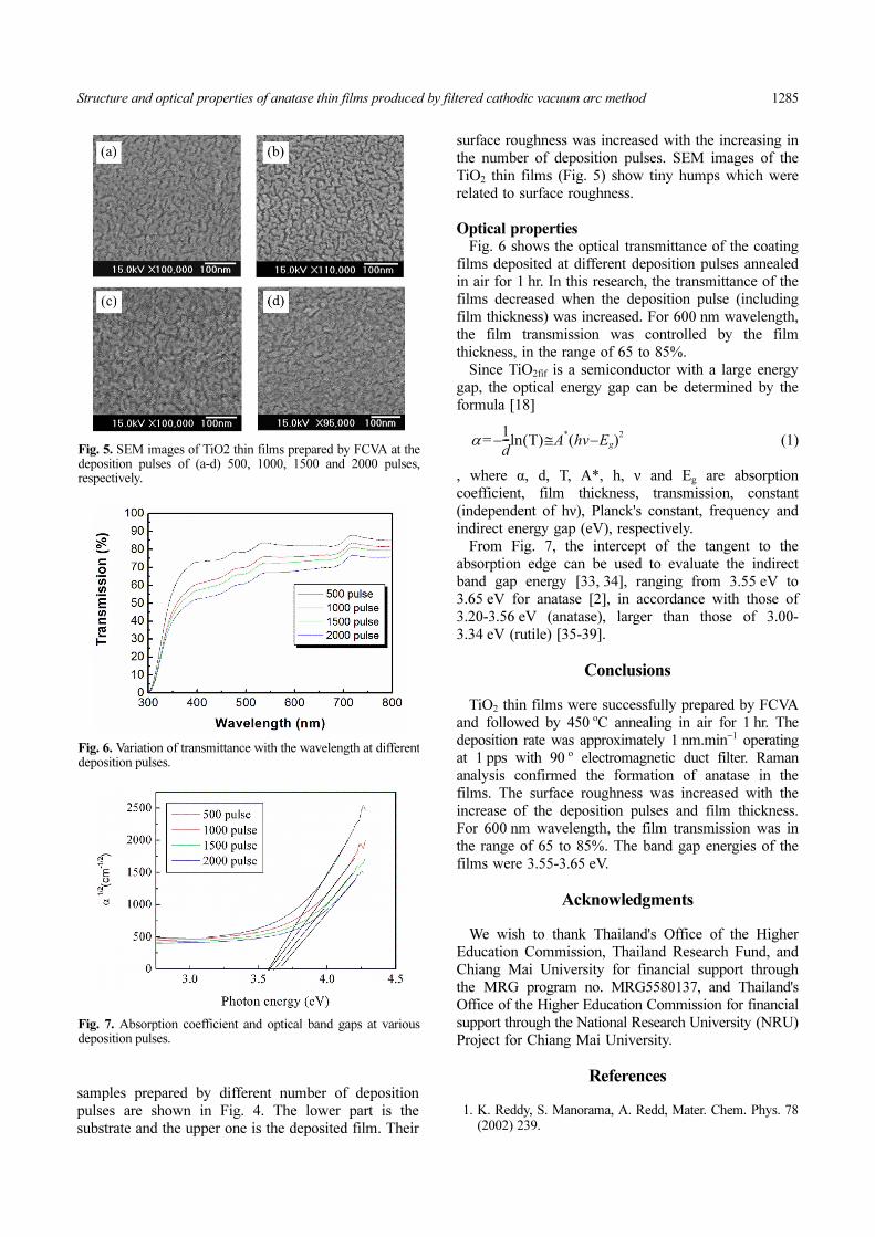
the number of deposition pulses. SEM images of the
TiO2 thin films (Fig. 5) show tiny humps which were
related to surface roughness.
Optical propertiesFig. 6 shows the optical transmittance of the coating
films deposited at different deposition pulses annealed
in air for 1 hr. In this research, the transmittance of the
films decreased when the deposition pulse (including
film thickness) was increased. For 600 nm wavelength,
the film transmission was controlled by the film
thickness, in the range of 65 to 85%.
Since TiO2fif is a semiconductor with a large energy
gap, the optical energy gap can be determined by the
formula [18]
(1)
, where α, d, T, A*, h, ν and Eg are absorption
coefficient, film thickness, transmission, constant
(independent of hν), Planck's constant, frequency and
indirect energy gap (eV), respectively.
From Fig. 7, the intercept of the tangent to the
absorption edge can be used to evaluate the indirect
band gap energy [33, 34], ranging from 3.55 eV to
3.65 eV for anatase [2], in accordance with those of
3.20-3.56 eV (anatase), larger than those of 3.00-
3.34 eV (rutile) [35-39].
Conclusions
TiO2 thin films were successfully prepared by FCVA
and followed by 450 oC annealing in air for 1 hr. The
deposition rate was approximately 1 nm.min−1 operating
at 1 pps with 90 o electromagnetic duct filter. Raman
analysis confirmed the formation of anatase in the
films. The surface roughness was increased with the
increase of the deposition pulses and film thickness.
For 600 nm wavelength, the film transmission was in
the range of 65 to 85%. The band gap energies of the
films were 3.55-3.65 eV.
Acknowledgments
We wish to thank Thailand's Office of the Higher
Education Commission, Thailand Research Fund, and
Chiang Mai University for financial support through
the MRG program no. MRG5580137, and Thailand's
Office of the Higher Education Commission for financial
support through the National Research University (NRU)
Project for Chiang Mai University.
References
1. K. Reddy, S. Manorama, A. Redd, Mater. Chem. Phys. 78(2002) 239.
α1
d--- T( ) A
*
hv Eg–( )2
≅ln–=Fig. 5. SEM images of TiO2 thin films prepared by FCVA at thedeposition pulses of (a-d) 500, 1000, 1500 and 2000 pulses,respectively.
Fig. 6. Variation of transmittance with the wavelength at differentdeposition pulses.
Fig. 7. Absorption coefficient and optical band gaps at variousdeposition pulses.

1286 Sakon Sansongsiri and Somchai Thongtem
2. G.X. Liu, F.K. Shan, W.J. Lee, G.H. Lee, I.S. Kim, B.C.Shin, S.G. Yoon, C.R. Cho, Integrated Ferroelectrics 81(2006) 239.
3. J. Niu, B. Yao, C. Peng, W. Zhang, Y. Chen, IntegratedFerroelectrics 152 (2014) 163.
4. A. Fujishima, T.N. Rao, D.A. Tryk, Journal of Photochemistryand Photobiology C: Photochemistry Reviews 1 (2000) 1.
5. R. Dholam, N. Patel, M. Adami, A. Miotello, InternationalJournal of Hydrogen Energy 33 (2008) 6896.
6. K.O. Awitor, S. Rafqah, G. Géranton, Y. Sibaud, P.R.Larson, R.S.P. Bokalawela, J.D. Jernigen, M.B. Johnson,Journal of Photochemistry and Photobiology A: Chemistry199 (2008) 250.
7. P. Chrysicopoulou, D. Davazoglou, C. Trapalis, G. Kordas,Thin Solid Films 323 (1998) 188.
8. M. Tazawa, M. Okada, K. Yoshimura, S. Ikezawa, SolarEnergy Material & Solar Cells 84 (2004) 170.
9. D.M. Giolando, Solar Energy 97 (2013) 195.10. J. Song, J. Qin, J. Qu, Z. Song, W. Zhang, X. Xue, Y. Shi,
T. Zhang, W. Ji, R. Zhang, H. Zhang, Z. Zhang, X. Wu,Solar Energy Materials & Solar Cells 130 (2014) 42.
11. G. Banfi, V. Degiorgo, D. Ricard, Advances in Physics 47(1998) 447.
12. J.C. Orlianges, A. Crunteanu, A. Pothier, T. Merle-Mejean,P. Blondy, C. Champeaux, Applied Surface Science 263(2012) 111.
13. M.C. Kao, H.Z. Chen, S.L. Young, C.Y. Kung, C.C. Lin,Thin Solid Films 517 (2009) 5096.
14. Y.H. Kim, M.S. Kim, K.S. Kim, S.H. Ahn, C.S. Lee,Current Applied Physics 11 (2011) 5122.
15. B.J. Li, L.J. Huang, N.F. Ren, M. Zhou, Applied SurfaceScience 290 (2014) 80.
16. B. Karunagaran, K. Kim, D. Mangalaraj, J. Yi, S.Velumani, Solar Energy Material & Solar Cell 88 (2005)199.
17. S. Daviðsdóttir, S. Canulescu, K. Dirscherl, J. Schou, R.Ambat, Surface & Coating Technology 216 (2013) 35.
18. A. Nakaruk, D. Ragazzon, C.C. Sorrell, Thin Solid Films518 (2010) 37353742.
19. P.S. Shinde, C.H. Bhosale, Anal J. Appl. Pyrolysis 82(2008) 83.
20. X.W. Zhang, G.R. Han, Thin solid Films 516 (2008) 6140.21. P.S. Liu, F.G. Xia, Y.M. Chen, G. Cui, Materials Letters 72
(2012) 5.22. B.K. Tay, Z.W. Zhao, D.H.C. Chua, Materials Science and
Engineering R52 (2006) 1.23. S. Ander, A. Anders, M. Rubin, Z. Wang, S. Raoux, F.
Kong, I.G. Brown, Surface and Coating Technology 76-77(1995) 167.
24. A.P. Huang, Z.F. Di, P.K. Chu, Surface & CoatingTechnology 201 (2007) 4897.
25. P.J. Martin, A. Bendavid, Thin Solid Films 518 (2010)5078.
26. A. Bendavid, P.J. Martin, H. Takikawa, Thin Solid Films360 (2000) 241.
27. C. Paternoster, I. Zhirkov, M.P. Delplancke-Ogletree,Surface & Coating Technology 227 (2013) 42.
28. A. Bendavid, P.J. Martin, E.W. Preston, Thin Solid Films517 (2008) 494.
29. A. Kleiman, A. Márquez, D.G. Lamas, Surface & CoatingTechnology 201 (2007) 6358.
30. A. Kleiman, A. Márquez, M.L. Vera, J.M. Meichtry, M.I.Litter, Applied Catalysis B: Environmental 101 (2011) 676.
31. A. Welte, C. Waldauf, C. Brabec, P. Wellmann, Thin SolidFilms 516 (2008) 7256.
32. F.D. Hardcastle, Journal of the Arkansas Academy ofScience 65 (2011) 43.
33. H.H. Huang, C.C. Huang, P.C. Huang, C.F. Yang, C.Y.Hsu, Journal of Nanoscience and Nanotechnology 8 (2008)2659.
34. C.C. Ting, S.Y. Chen, D.M. Liu, J. Appl. Phys. 88 (2000)4628.
35. L. Miao, P. Jin, K. Kaneko, A. Terai, N.N. Gabain, S.Tanemura, Applied Surface Science 212-213 (2003) 255.
36. H. Tang, K. Prasad, R. Sanijinès, P.E. Schmid, F. Lévy,Journal of Applied Physics 75 (1994) 2042.
37. H. Takikawa, T. Matsui, T. Sakakibara, A. Bendavid, P.J.Martin, Thin Solid Films 348 (1999) 145.
38. D.J. Won, C.H. Wang, H.K. Jang, D.J. Choi, AppliedPhysics A 73 (2001) 595.
39. D. Mardare, M. Tasca, M. Delibas, G.I. Rusu, AppliedSurface Science 156 (2000) 200.