july 14, 2005 10:3 wspc/175-ijn 00313 · all three ion beam techniques, fib (focused ion beam),...
TRANSCRIPT
July 14, 2005 10:3 WSPC/175-IJN 00313
International Journal of NanoscienceVol. 4, No. 3 (2005) 269–286c© World Scientific Publishing Company
ION BEAM LITHOGRAPHY AND NANOFABRICATION:A REVIEW
F. WATT∗, A. A. BETTIOL, J. A. VAN KAN, E. J. TEO and M. B. H. BREESE
Centre for Ion Beam Applications (CIBA), Physics DepartmentNational University of Singapore, Singapore 117542
Received 17 December 2004
To overcome the diffraction constraints of traditional optical lithography, the next gen-eration lithographies (NGLs) will utilize any one or more of EUV (extreme ultraviolet),X-ray, electron or ion beam technologies to produce sub-100 nm features. Perhaps themost under-developed and under-rated is the utilization of ions for lithographic pur-poses. All three ion beam techniques, FIB (Focused Ion Beam), Proton Beam Writing(p-beam writing) and Ion Projection Lithography (IPL) have now breached the techno-logically difficult 100 nm barrier, and are now capable of fabricating structures at thenanoscale. FIB, p-beam writing and IPL have the flexibility and potential to becomeleading contenders as NGLs.
The three ion beam techniques have widely different attributes, and as such havetheir own strengths, niche areas and application areas. The physical principles underlyingion beam interactions with materials are described, together with a comparison withother lithographic techniques (electron beam writing and EUV/X-ray lithography). IPLfollows the traditional lines of lithography, utilizing large area masks through which apattern is replicated in resist material which can be used to modify the near-surface
properties. In IPL, the complete absence of diffraction effects coupled with ability totailor the depth of ion penetration to suit the resist thickness or the depth of modificationare prime characteristics of this technique, as is the ability to pattern a large area in asingle brief irradiation exposure without any wet processing steps. p-beam writing andFIB are direct write (maskless) processes, which for a long time have been consideredtoo slow for mass production. However, these two techniques may have some distinctadvantages when used in combination with nanoimprinting and pattern transfer. FIBcan produce master stamps in any material, and p-beam writing is ideal for producingthree-dimensional high-aspect ratio metallic stamps of precise geometry. The transferof large scale patterns using nanoimprinting represents a technique of high potentialfor the mass production of a new generation of high area, high density, low dimensionalstructures. Finally a cross section of applications are chosen to demonstrate the potentialof these new generation ion beam nanolithographies.
Keywords: Focused ion beam; proton beam writing; ion projection lithography; ion beamlithography; nanofabrication.
∗Corresponding author.
269

July 14, 2005 10:3 WSPC/175-IJN 00313
270 F. Watt et al.
1. Introduction
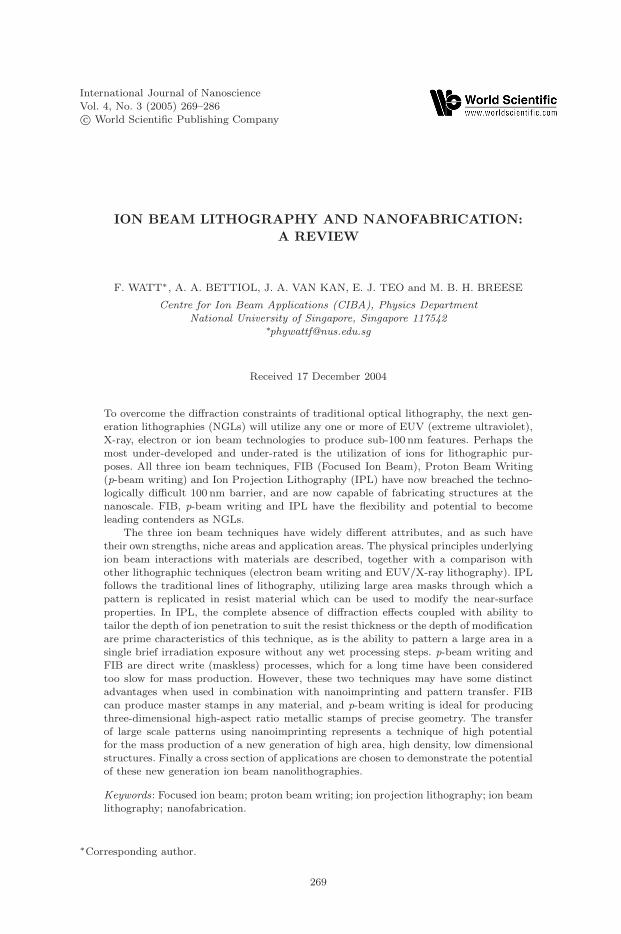
Next generation lithographies (NGLs) are being actively developed to take over fromthe highly successful optical lithography. As feature sizes shrink well below 100 nm,several key challenges for optical lithography have arisen that make it increasinglydifficult to remain in step with Moore’s Law.1 The 2002 International TechnologyRoadmap for Semiconductors2 lists optical mask fabrication, together with yield,cost and quality of calcium fluoride lenses amongst the difficult challenges thatneed to be overcome in the next few years as semiconductor manufacturers movetowards the 65 nm node. Slower than expected technical development has recentlyprompted Intel to skip the 157nm generation of lithography in favor of EUV. Otherkey challenges include the development of resist materials for 157 nm lithographyand beyond, coupled with the escalating cost of lithography tools. Each of thepotential NGLs (which include EUV, X-ray, electron and ion lithographies) arebased on fundamentally different physical principles (see Box 1) implying that eachlithographic technique will exhibit unique properties, and only in the next few yearswill we know which will be adopted as the prevailing technology of the future.Although the two front runners for the next generation lithographies are EUV andElectron Projection Lithography (EPL), increasing attention is being paid to thehigh potential of ion beam lithography as a serious alternative contender.
Box 1. The different physical interactions of fast light ions, slow heavy ions, electrons
and electromagnetic radiation (EUV and X-rays) with matter.
Fast light ions: The primary interaction is that of ion/electron collisions, and therefore
many thousands of collisions will occur before an ion comes to rest. Trajectories and
energy loss profiles can be accurately simulated by means of Monte Carlo calculations
(for example using the computer code SRIM3). As an example, for 2MeV protons, the
penetration depth in PMMA is 60.8 µm, with a 2 µm lateral broadening of the beam
at the end of range. However, the beam broadening is only 3 nm at 1 µm depth in the
PMMA and 30 nm at 5 µm so beam broadening of fast protons in a thin resist layer is
minimal.
Slow heavy ions: The primary mechanism is that of high momentum transfer between
the slow moving incident heavy ions and the atoms on the surface of the material.
The surface atoms are re-arranged, resulting in chemical and structural changes as
well as sputtering of atomic and molecular species from the surface. The sputtering
mechanism can be calculated using Monte Carlo techniques (e.g., SRIM3) to show that
the sputtering rate for a 30 keV gallium ion is around 1–10 atoms per incident ion for
a wide variety of materials.
Electrons: The primary interaction is that of electron/electron collisions, and this
results in large angle multiple scattering of the electron beam leading to the classic
“pear shaped” ionization volume around the point of entry into the material. The
(Continued)
July 14, 2005 10:3 WSPC/175-IJN 00313
Ion Beam Lithography and Nanofabrication 271
Box 1. (Continued)
trajectories can be simulated using Monte Carlo techniques such as Casino4: As an
example, 50 keV electrons penetrate up to depth of 40 µm in PMMA, with a 20 µm
spread in the beam. Sub-100 nm e-beam writing therefore can only be realized in very
thin resist layers, and high aspect ratio structures fabricated using additional steps e.g.,
reactive ion etching.
EUV and X-rays: Photons react with the atomic electrons through the photoelectric
effect, where the incident photon is completely absorbed by an atomic electron leading
to the ejection of the electron from the atom, and by Rayleigh (elastic) scattering where
the photon is scattered without an energy change. These processes can be simulated by
computer software (see for example GEANT45). A photon beam penetrating a resist
material therefore does not have a defined range, and has an exponentially decreasing
dose distribution with penetration depth.
There are currently three separate and distinct ion beam processes capable offabricating structures at the sub-100 nm level: The focused ion beam (FIB) tech-nique where a slow focused heavy ion beam (with energies typically around 30 keV)is written over a surface to create a pattern through modification, deposition orsputtering; proton beam writing, where fast (typically MeV) protons are used todirect-write deep precise 3D patterns into resist, and ion projection lithography(IPL), where medium energy ions (typically 100keV) are projected through a pat-terned mask for rapid fabrication. Schematic diagrams of the operating principlesof these three processes are shown in Fig. 1 (Focused Ion Beam), Fig. 2 (p-beamwriting) and Fig. 3 (Ion Projection Lithography). These three ion beam techniquesare not only capable of fabricating structures below the technologically important

July 14, 2005 10:3 WSPC/175-IJN 00313
272 F. Watt et al.
Liquid metal ion source
Sample
Beam scanning and
focusing
Fig. 1. A schematic diagram of a FIB system. The ion beam (usually gallium) is generated from aliquid metal source (LMIS) and the Ga+ ions are focused down a column, similar in principle tothat of a scanning electron microscope, on to the substrate. For focused ion beam chemical vapordeposition (FIBCVD), provision is usually made for a gas nozzle assembly next to the sample soas to provide a flow of gas molecules to the sample surface during irradiation.
Proton accelerator
Switcher magnet
Object aperture
Collimator aperture
Focusing systemquadrupolelensesScan coils
Micromachining chamber
Scan controller
Pixel normalization
feedback
Fig. 2. A typical set-up for a proton beam writer. MeV protons are produced in a proton accelera-tor, and a demagnified image of the beam transmitted through an object aperture is focused ontothe substrate material (resist) by means of a series of strong focusing magnetic quadrupole lenses(e.g., quadrupole triplet). Beam scanning takes place using magnetic or electrostatic deflectionbefore the focusing lenses, and is driven by a feedback signal derived from the proton interactionswith the resist. This feedback mechanism ensures a constant beam exposure per pixel as the beamis scanned across the resist, resulting in high quality structures.

July 14, 2005 10:3 WSPC/175-IJN 00313
Ion Beam Lithography and Nanofabrication 273
Ion Source
Mask Plate orStencil Mask
200 xElectrostaticReductionOptics
SubstrateStage
CondenserIlluminationSystem
Fig. 3. Schematic diagram of the Ion Projection Lithography system (PROFIB) developed at IMS(reproduced with kind permission of H. Loeschner). The multi-cusp ion source produces a He, Aror Xe ion beam which is passed through a stencil mask, and the ion-optical system with a 200xreduction projects the highly parallel transmitted ions on to the substrate.
100 nm barrier (see Fig. 4), but all three processes have highly appropriate andcomplementary application areas.
1.1. Physical properties of ion beams
Lithography using ion beams has several unique characteristics, primarily due to thephysical nature of the ion (a charged particle is at least three orders of magnitudeheavier than the electron). For slow heavy ions (e.g., 30 keV Ga+), the interactionprocess is that of altering the surface structure of a material, modifying surfacechemistry, and removing atoms from the surface through sputtering. In contrast,the primary interaction of fast lighter ions (e.g., 100keV–3 MeV protons) is that ofdeep penetration into the material, with a minimal amount of surface disruption.For both light and heavy ions, diffraction effects are not an issue (the wavelengthof a 100-keV proton is around 10−4 nm). For fast lighter ions, the interaction withmatter provides some interesting properties: (a) The ion beam travels in a straightline apart from some end of range broadening. This offers a considerable advantageover e-beam writing for fabricating high aspect ratio 3D structures since a finelyfocused electron beam spreads rapidly as it enters the resist material (see Box 1).(b) The dose exposure as the ions penetrate the material is relatively constant(apart from an increase at the end of range). This feature offers an advantage overEUV or X-ray lithography, which exhibit an exponential reduction in dose withdepth (see Box 1). (c) The penetration depth of the ion beam is well defined andcan be varied by changing the ion energy. This is a unique characteristic whichallows multi-level structures to be formed in one layer of resist. (d) Lithographywith light ions offers a virtual absence of high energy secondary electrons whichcould otherwise give rise to unwanted exposure of resist (proximity effects). Ine-beam writing for example, a small but significant fraction of secondary electrons

July 14, 2005 10:3 WSPC/175-IJN 00313
274 F. Watt et al.
(a) (b)
(c)
Fig. 4. Sub-100 nm ion beam fabricated structures: (a) 8 nm lines written into a multi layer sampleof AlF3/GaAs using FIB,6 (b) 50 nm walls fabricated in PMMA using p-beam writing with 2MeVprotons,7 and (c) 70 nm slots fabricated in 50 nm Infineon resist using IPL operating with 45 keVHe+ ions.8
are generated with energies which can contribute to the proximity effect in therange of a few tenths of microns.
2. Ion Beam Techniques
2.1. Focused ion beam (FIB)
The FIB technique, the most mature of the ion beam nanolithographies, wasdeveloped in the late 1970s with instruments becoming commercially available
July 14, 2005 10:3 WSPC/175-IJN 00313
Ion Beam Lithography and Nanofabrication 275
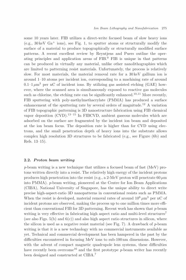
some 10 years later. FIB utilizes a direct-write focused beam of slow heavy ions(e.g., 30 keV Ga+ ions), see Fig. 1, to sputter atoms or structurally modify thesurface of a material to produce topographically or structurally modified surfacepatterns. A recent excellent review by Reyntjens and Puers outline the oper-ating principles and application areas of FIB.9 FIB is unique in that patternscan be produced in virtually any material, unlike other nanolithographies whichare limited to patterning resist materials. Unfortunately, the process is relativelyslow. For most materials, the material removal rate for a 30 keV gallium ion isaround 1–10 atoms per incident ion, corresponding to a machining rate of around0.1–1µm3 per nC of incident ions. By utilizing gas assisted etching (GAE) how-ever, where the scanned area is simultaneously exposed to reactive gas moleculessuch as chlorine, the etching rate can be significantly enhanced.10,11 More recently,FIB sputtering with poly-methylmethacrylate (PMMA) has produced a surfaceenhancement of the sputtering rate by several orders of magnitude.12 A variationof FIB topographic patterning is 3D nanostructure fabrication using FIB chemicalvapor deposition (CVD).13–15 In FIBCVD, ambient gaseous molecules which areadsorbed on the surface are fragmented by the incident ion beam and depositedat the ion beam focus. The deposition rate is higher than for CVD using elec-trons, and the small penetration depth of heavy ions into the substrate allowscomplex high resolution 3D structures to be fabricated (e.g., see Figure (6b) andRefs. 13–15).
2.2. Proton beam writing
p-beam writing is a new technique that utilizes a focused beam of fast (MeV) pro-tons written directly into a resist. The relatively high energy of the incident protonsproduces high penetration into the resist (e.g., a 2-MeV proton will penetrate 60µminto PMMA). p-beam writing, pioneered at the Centre for Ion Beam Applications(CIBA), National University of Singapore, has the unique ability to direct writeprecise high-aspect-ratio 3D nanopatterns in conventional resists such as PMMA.When the resist is developed, material removal rates of around 106 µm3 per nC ofincident protons are observed, making the process up to one million times more effi-cient than conventional FIB for 3D patterning. Recent work has shown that p-beamwriting is very effective in fabricating high aspect ratio and multi-level structures7
(see also Figs. 5(b) and 6(c)) and also high aspect ratio structures in silicon, wherethe silicon is used as a negative resist material (see Fig. 7). A drawback of p-beamwriting is that it is a new technology with no commercial instruments available asyet. Technical and commercial development has been hampered in the past by thedifficulties encountered in focusing MeV ions to sub-100nm dimensions. However,with the advent of compact magnetic quadrupole lens systems, these difficultieshave recently been overcome16 and the first prototype p-beam writer has recentlybeen designed and constructed at CIBA.7

July 14, 2005 10:3 WSPC/175-IJN 00313
276 F. Watt et al.
(a)
(b)
Fig. 5. High aspect ratio structures: (a) 20 nm trench (depth 400 nm) written in diamond usingFIB27 and (b) high-aspect-ratio test structures fabricated using p-beam writing in SU8 negativeresist, showing 60 nm wall structures 10 micron deep.
2.3. Ion Projection Lithography (IPL)
The techniques of FIB and p-beam writing have distinct advantages over otherlithographies for fabricating flexible and precise 3D nanostructures, but beingdirect-write techniques they lack the rapidity of fabrication for cost effective mass
July 14, 2005 10:3 WSPC/175-IJN 00313
Ion Beam Lithography and Nanofabrication 277
1 micron
(a) (b)
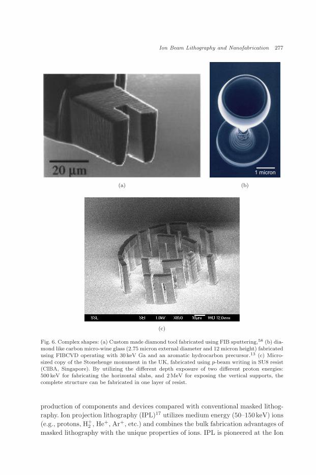
(c)
Fig. 6. Complex shapes: (a) Custom made diamond tool fabricated using FIB sputtering,58 (b) dia-mond like carbon micro-wine glass (2.75 micron external diameter and 12 micron height) fabricatedusing FIBCVD operating with 30 keV Ga and an aromatic hydrocarbon precursor.13 (c) Micro-sized copy of the Stonehenge monument in the UK, fabricated using p-beam writing in SU8 resist(CIBA, Singapore). By utilizing the different depth exposure of two different proton energies:500 keV for fabricating the horizontal slabs, and 2MeV for exposing the vertical supports, thecomplete structure can be fabricated in one layer of resist.
production of components and devices compared with conventional masked lithog-raphy. Ion projection lithography (IPL)17 utilizes medium energy (50–150keV) ions(e.g., protons, H+
2 , He+, Ar+, etc.) and combines the bulk fabrication advantages ofmasked lithography with the unique properties of ions. IPL is pioneered at the Ion
July 14, 2005 10:3 WSPC/175-IJN 00313
278 F. Watt et al.
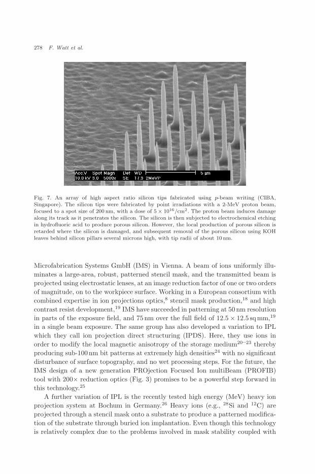
Fig. 7. An array of high aspect ratio silicon tips fabricated using p-beam writing (CIBA,Singapore). The silicon tips were fabricated by point irradiations with a 2-MeV proton beam,focused to a spot size of 200 nm, with a dose of 5 × 10¹⁶/cm2. The proton beam induces damagealong its track as it penetrates the silicon. The silicon is then subjected to electrochemical etchingin hydrofluoric acid to produce porous silicon. However, the local production of porous silicon isretarded where the silicon is damaged, and subsequent removal of the porous silicon using KOHleaves behind silicon pillars several microns high, with tip radii of about 10 nm.
Microfabrication Systems GmbH (IMS) in Vienna. A beam of ions uniformly illu-minates a large-area, robust, patterned stencil mask, and the transmitted beam isprojected using electrostatic lenses, at an image reduction factor of one or two ordersof magnitude, on to the workpiece surface. Working in a European consortium withcombined expertise in ion projections optics,8 stencil mask production,18 and highcontrast resist development,19 IMS have succeeded in patterning at 50 nm resolutionin parts of the exposure field, and 75 nm over the full field of 12.5 × 12.5 sqmm,19
in a single beam exposure. The same group has also developed a variation to IPLwhich they call ion projection direct structuring (IPDS). Here, they use ions inorder to modify the local magnetic anisotropy of the storage medium20–23 therebyproducing sub-100nm bit patterns at extremely high densities24 with no significantdisturbance of surface topography, and no wet processing steps. For the future, theIMS design of a new generation PROjection Focused Ion multiBeam (PROFIB)tool with 200× reduction optics (Fig. 3) promises to be a powerful step forward inthis technology.25
A further variation of IPL is the recently tested high energy (MeV) heavy ionprojection system at Bochum in Germany.26 Heavy ions (e.g., 28Si and 12C) areprojected through a stencil mask onto a substrate to produce a patterned modifica-tion of the substrate through buried ion implantation. Even though this technologyis relatively complex due to the problems involved in mask stability coupled with

July 14, 2005 10:3 WSPC/175-IJN 00313
Ion Beam Lithography and Nanofabrication 279
producing and projecting heavy mass ions up to MeV energies, a creditable 300 nmresolution has been reached in initial tests.
3. Applications
The three ion beam processes are complementary and potentially cover a wide vari-ety of application areas. The technical maturity and commercial availability of FIBhas meant that the majority of ion beam applications to date have been carried outin this area. The distinctive feature of FIB is that it is capable of machining anymaterial by surface erosion, and FIB has been widely applied to micro-technologyand metrology, where great success has already been achieved in semiconductorfailure analysis.9 p-beam writing is much faster, and because of its deep penetra-tion and straight trajectories into resist materials, is ideally suited for producingdimensionally accurate high aspect ratio 3D structures. However, with no commer-cial p-beam writing instruments yet available, the application areas have not beenexplored to the same extent as FIB. Both FIB and p-beam writing are eminentlysuitable for producing structures of high aspect ratio (Fig. 5) with a high degreeof geometrical flexibility (Fig. 6), and being direct-write processes are very usefulfor rapid prototyping. IPL on the other hand is a masked process, and thereforeis suitable for mass production, either for surface topographical patterning, or fornontopographic modification of the working material. Similar to p-beam writing,IPL is in its early developmental phase, and as such the application areas are mainlylimited to performance testing and prototype structuring.
3.1. Topographical patterning
Much of the recent work so far on topographical patterning has been carried out bythe well developed FIB technique, including patterning of diamond-like films,27,28
and fabrication of nanoscale titanium honeycomb arrays.29 FIB patterning coupledwith in-situ etching,30 fabrication of ordered nanochannels in alumina by growthguidance through FIB patterns,31 carbon nanopillars grown by FIB assisted chem-ical vapor deposition (FIBCVD)32 indicate the wide variety of applications in thisarea of nanotechnology. FIB has also been used in the fabrication of 3D stampsin silicon for micro-contact printing,33–35 and micromolds and intricate 3D shapesin diamond-like-carbon have also been fabricated using FIBCVD.13–15 Interestingapplications using p-beam writing and FIB fabrication of micro and nanoscale 3Dconfinement environments for cells36 and single molecule studies37 have extendedthe use of topographical patterning into the biomedical field.
3.2. Surface patterning through ion beam modification
of surface properties
In addition to surface sputtering, heavy ions such as Ga+ can also cause atomintermixing and chemical disruption of the surface or subsurface. This effect can be

July 14, 2005 10:3 WSPC/175-IJN 00313
280 F. Watt et al.
used to alter localized magnetic properties in a wide variety of magnetic materialsfor magnetic storage applications,20–24,38–43 alter surfaces for self-assembled islandnucleation through induction of defects,44 produce oriented nanocrystals in amor-phous alloys45 and create ion induced localized surface amorphization.46 Recentwork using p-beam writing on carbon substrates has indicated that a high energyproton beam can also leave a trail of magnetic ordering due to hydrogen inducedferri-magnetism.47
3.3. 3D patterning for optical and micro-photonic applications
The ability of FIB and p-beam writing to construct 3D structures of flexible geom-etry allows the rapid fabrication of micro-photonic components and systems. Bothp-beam writing and FIB have been used to fabricate multiple lens arrays,48–50 andwaveguides of precise geometry coupled with low transmission loss51 have been fab-ricated by p-beam writing using the negative resist SU8. Fabricating scaffolds ofprecise geometry for photonic band gap materials lends itself to techniques whichcan fabricate 3D structures in a precise manner, and both FIB and p-beam writinghave the capability of fabricating these types of structures.48,52–56 In particular,in an excellent demonstration of 3D micromachining (see Fig. 8), near infrared
Fig. 8. Yablonovite-like crystal obtained by ion milling.52 The milled surface corresponds to the(111) plane of the photonic crystal. The rectangular section on the sample side shows 25 periodsin width and five periods in height. The FIB etching directions are indicated by arrows A and B.Some residual glue used for sample fixing can be seen on the sample sides.

July 14, 2005 10:3 WSPC/175-IJN 00313
Ion Beam Lithography and Nanofabrication 281
three-dimensional Yablonovite-like photonic crystals have been fabricated using FIBetching of porous silicon.52 Here potential problems of sputtered material cloggingup machined channels are alleviated due to the dispersal of the sputtered material inthe porous silicon pores, thereby leading to high aspect ratios. In a further recentdevelopment, the CIBA group in Singapore have extended their work on protonbeam micromachining of semiconductors to studying patterned porous silicon.53
Proton beam writing in silicon results in damage to the irradiated regions. Dur-ing a subsequent electrochemical etch, the resulting porous silicon is formed atdifferent rates and with different porosity in the damaged regions. Since poroussilicon comprises an interconnected network of nanometer size silicon regions, theenergy band gap within porous silicon is larger than that in bulk silicon owing toquantum confinement of the electron wavefunction, enabling the emission of visiblelight. The resultant photoluminescence intensity is proportional to the irradiateddose, being more intense where the dose is greatest. Figure 9 shows an example of
Fig. 9. Proton beam irradiation induced photoluminescence.53 Photoluminescence (PL) image ofa 0.02Ohm.cm p-type silicon wafer which has been proton beam irradiated with different dosesin a grid type pattern. Ion beam irradiation results in damage to the irradiated regions of thesemiconductor, which results in porous silicon being formed at different rates and with differentporosity when electrochemically etched. The resultant PL intensity is proportional to the irradiateddose, being more intense where the dose is greatest.

July 14, 2005 10:3 WSPC/175-IJN 00313
282 F. Watt et al.
this proton-induced luminescence, where orthogonal lines have been irradiated withdifferent proton doses, in a checkerboard pattern. For optoelectronic applicationssuch as full-color display and optical interconnection, this process could providetunable controlled light emission from adjacent, micron size areas of porous siliconwith utilizable efficiency across the whole visible light range. Finally, the fabrica-tion of high resolution diffractive optics48,57–59 represents a growing interest in theapplication of ion beam fabrication techniques in the micro-photonics field.
3.4. Rapid prototyping and one-off components
As would be expected of the direct-write ion beam techniques where prefabricatedmasks are not required, the ability to rapidly fabricate prototypes is an area ofhigh potential. FIB fabricated diamond and tungsten carbide microtools have beenmade in a variety of shapes that cannot be produced using conventional grind-ing and polishing techniques, e.g., microtools exhibiting triangular, rectangular ortrapezoidal features.60 These tools, which can be fabricated with dimensions in the15–100µm range, have been shown to have a radius of curvature cutting edge downto 40 nm (see for example Fig. 6(a)). Nanoscale planar superconductor–insulator–superconductor Josephson junctions61,62 and a directly coupled superconductingquantum interference device (SQUID) magnetometer fabricated in magnesiumdiboride have been made using FIB.63 In an interesting project involving the fabri-cation of devices for direct magnetic imaging, bismuth nano-Hall probes have beenmanufactured,64 again using FIB. Other examples include the FIB fabrication ofsubmicron cantilevers,65 aperture probes for near-field optical microscopy,66 andmagnetic recording devices.67
In a new approach to producing high density storage devices, FIB has beenused to nano-engrave a 2D array of defects in highly orientated pyrolitic graphite(HOPG). These defects, which can take the form of nanoholes or nanobumps, etc,can then act as traps for gold nanoclusters which have been preformed in the gasphase, thereby creating a high density pattern of quantum dots on the HOPG68
compatible with TBit per cm2 storage. Similarly, FIB implantation of micron-widecrossed p- and n-doped stripes into a pin-diode has resulted in good quality quantumdots being produced between the stripes, resulting in a micro-led array.69
A recent and a novel technique for the development of prototype quantumcomputers is the implantation of individual 31P atoms in a solid matrix,70,71
where various information extraction techniques have been proposed to addressand manipulate the electrons and/or nuclear spins of adjacent implanted atoms.
4. Discussion and Outlook
FIB, p-beam writing and IPL can now attain sub-100nm resolutions, and thereforemust be serious contenders to play a major role in the next generation lithogra-phies. The interesting feature of all these ion-based technologies is that diffractionproblems are currently not an issue, and there is no fundamental diffraction limit

July 14, 2005 10:3 WSPC/175-IJN 00313
Ion Beam Lithography and Nanofabrication 283
to hinder further development. For cheap and competitive mass production, IPLfollows the traditional lines of lithography, utilizing large area masks through whicha pattern is replicated in resist material or which are used to locally modify thenear-surface properties. In IPL, the complete absence of diffraction effects coupledwith ability to tailor the depth of ion penetration to suit the resist thickness orthe depth of modification, are prime characteristics of this technique, as is the abil-ity to pattern a large area in a single brief irradiation exposure without any wetprocessing steps.
One of Moore’s corollaries to his now famous law suggests that the cost of man-ufacturing technology increases geometrically with time. The increased technicalcomplexities and predicted increased cost of producing smaller feature sizes maycall into question the traditional role of masked processes as the universal method ofmass production. In particular, the advent of MEMS, nanophotonics, nanomagnet-ics, molecular nanotechnology devices and lab-on-a-chip systems, may benefit fromradical new departures from established technologies. The direct-write processes,which for a long time have been considered too slow for mass production, may havesome distinct advantages when used in combination with nanoimprinting.31–34,72,73
Nanoimprinting technology (NIL) relies on the multiple transfer of a pattern into asubstrate, and has high potential as a fast and cost effective solution of producingsub-100nm features. This prime feature has been recognized in the latest Inter-national Technology Roadmap for Semiconductors 2003 Edition,74 where imprintlithography has for the first time been added to the potential list of next generationlithographies, and direct-write techniques have been mentioned as possible avenuesof high potential “Direct-write lithography has been applied to niche applicationsin development and low volume ASIC production, but its role could be expanded.Breakthroughs in direct-write technologies that achieve high throughput will be asignificant paradigm shift. It will eliminate the need for masks, offering inherentcost and cycle-time reduction”.
The success of nanoimprint lithography depends crucially on the quality ofstamps that can be fabricated, and the use of ions have distinct advantages inthis respect. FIB can produce master stamps in any material, and p-beam writingis ideal for producing high aspect ratio metallic stamps of precise geometry.75 Thetransfer of large scale patterns using nanoimprinting represents a technique of highpotential for the mass production of a new generation of high area, high density,low dimensional structures.
Finally, the unique properties of ions could also prove to be a useful adjunct toother developing lithographies. It is generally recognized that the development ofconventional lithography below 100nm requires improvements in mask technology.p-beam writing, which has the ability to construct sub-100nm high aspect ratiostructures, is ideally suited for advanced mask fabrication where relatively thick orrobust masks are required (e.g., X-ray or Ion Beam Projection lithography). There isalso an increasing interest in the use of STM/AFM tips for nanolithography, throughthe deposition and positioning of atoms or molecular clusters.76 The flexibility of
July 14, 2005 10:3 WSPC/175-IJN 00313
284 F. Watt et al.
p-beam writing for the fabrication of multiple tip assemblies in silicon for parallelwriting could prove to be a very interesting development (Fig. 7).
In conclusion, the ion beam techniques FIB, p-beam writing, and IPL, offer awide range of complementary techniques for the efficient production of sub-100nmfeatures and patterns. These techniques are in an ideal position to play a role in thenext generation lithographies; IPL as a masked technique for bulk production, andFIB and p-beam writing as direct-write techniques with high potential for rapidprototyping and in the fabrication of precision stamps for nanoimprint lithography.
Acknowledgments
The authors wish to thank John Baglin, John Melngailis, Andrei Stanishevsky andHans Loeschner, for valuable discussions and suggestions, and Jacques Gierak, HansLoeschner, Andrei Stanishevsky, David Adams, Shinji Matsui, and Kang Wang forpermission to use Figs. 4(a), 4(c), 5(a), 6(a), 6(b), and 8, respectively.
References
1. G. E. Moore, Electronics 38 (1965).2. http://public.itrs.net. International semiconductor roadmap for semiconductors
(2002).3. J. F. Ziegler, The Stopping and Range of Ions in Matter, Vol. 2–6 (Pergamon Press,
1977–1985), http://www.srim.org/.4. P. Hovington, D. Drouin, R. Gauvin, D. C. Joy and N. Evans, Scanning 19, 29 (1997)
http://www.gel.usherb.ca/casino/index.html.5. Geant4: Low energy electromagnetic physics, http://www.ge.infn.it/geant4/
lowE/index.html.6. J. Gierak, A. Septier and C. Vieu, Nucl. Instr. Meth. A 427, 91 (1999).7. J. A. van Kan, A. A. Bettiol and F. Watt, Appl. Phys. Lett. 83, 1629 (2003).8. H. Loeschner et al., JM3 — SPIE J. Microlithography, Microfabrication and Microsys-
tems 2, 34 (2003).9. S. Reyntjens and R. Puers, J. Micromech. Microeng. 11, 287 (2001).
10. R. J. Young, J. R. A. Cleaver and H. Ahmed, J. Vac. Sci. Technol. B 11, 234 (1993).11. I. Chyr and A. J. Steck, J. Vac. Sci. Technol. B 19, 2547 (2001).12. Y. Liu, D. M. Longo and R. Hull, Appl. Phys. Lett. 82, 346 (2003).13. S. Matsui, T. Kaito, J. Fujita, M. Komuro, K. Kanda and Y. Haruyama, J. Vac. Sci.
Technol. B 18, 3181 (2000).14. T. Morita et al., Jpn. J. Appl. Phys. 42, 3974 (2003).15. J. Fujita, M. Ishida, T. Ichihashi, Y. Ochiai, T. Kaito and S. Matsui, Nucl. Instr.
Meth. B 206, 472 (2003).16. F. Watt, J. A. van Kan, I. Rajta, A. A. Bettiol, T. F. Choo, M. B. H. Breese and
T. Osipowicz, Nucl. Instr. Meth. 210, 14 (2003).17. J. Melngailis, A. A. Mondelli, I. L. Berry and R. Mohondro, J. Vac. Sci. Technol. B
16, 927 (1998).18. R. Kaesmaier, A. Ehrmann and H. Loschner, Microelectron. Eng. 57–58, 145 (2001).19. S. Hirscher et al., Microelectron. Eng. 61–62, 301 (2002).20. B. D. Terris, D. Weller, L. Folks, J. E. E. Baglin and A. J. Kellock, J. Appl. Phys.
87, 7004 (2000).
July 14, 2005 10:3 WSPC/175-IJN 00313
Ion Beam Lithography and Nanofabrication 285
21. C. T. Rettner, S. Anders, J. E. E. Baglin, T. Thomson and B. D. Terris, Appl. Phys.Lett. 80, 279 (2002).
22. J. E. E. Baglin, B. D. Terris, D. K. Weller, J.-U. Thiele, A. J. Kellock, S. Anders andT. Thomson, Proc. SPIE 4468, 1 (2001).
23. S. Maat, A. J. Kellock, D. Weller, J. E. E. Baglin and E. E. Fullerton, J. Magn. Magn.Mater. 263, 1 (2003).
24. A. Dietzel et al., Adv. Mat. 15, 1152 (2003).25. H. Loeschner et al., Proc. MRS: 3D Nano-Engineered Assemblies 739, 26 (2003).26. U. Weidenmuller et al., J. Vac. Sci. Technol. 20, 246 (2002).27. A. Stanishevsky, Thin Solid Films 398–399, 560 (2001).28. A. Stanishevsky, Diamond and Related Materials 8, 1246 (1999).29. H. Hosokawa et al., Mat. Sci. Eng. A 344, 365 (2003).30. Y. Asaoka, T. Arai, N. Sano and T. Kaneko, Compound Semiconductors 2001 Inst.
Phys. Conf. Series 170, 331 (2002).31. N. W. Liu, A. Datta, C. Y. Liu and Y. L. Wang, Appl. Phys. Lett. 82, 1281 (2003).32. M. Ishida, J. Fujita and Y. Ochiai, J. Vac. Sci. Technol. B 20, 2784 (2002).33. H.-W. Li, D.-J. Kang, M. G. Blamire and W. T. S. Huck, Nanotechnology 14, 220
(2003).34. R. Hull, T. Chraska, Y. Liu and D. Longo, Mat. Sci. Eng. C 19, 383 (2002).35. Y. Fu and K. A. B. Ngoi, Optics Express 10, 436 (2002).36. S. Feng, D. Casse, J. A. van Kan, R. Ge and F. Watt, Tissue Eng. 10, 267 (2004).37. E. Leclerc, Y. Mita and T. Fujii, 2nd Joint EMBS-BMES Conf. 2002, Vols. 1–3,
Proc. Annual Int. Conf. IEEE Engineering in Medicine and Biology Society (2002),pp. 1634–1635.
38. V. Nagarajan et al., Nature Mat. 2, 43 (2003).39. S. Anders, et al., Microeoelectron. Eng. 61, 569 (2002).40. R. Hyndman, et al., J. Magnetism and Magnetic Mat. 240, 50 (2002).41. C.-M. Park and J. A. Bain, IEEE Trans Magnetics 38, 2337 (2002).42. T. Kimura, F. Wakaya and K. Gamo, J. Vac. Sci. Technol. B 20, 2814 (2002).43. M. Albrecht, C. T. Rettner, A. Moser, M. E. Best and B. D. Terris, Appl. Phys. Lett.
81, 2875 (2002).44. M. Kammler, R. Hull, M. C. Reuter and F. M. Ross, Appl. Phys. Lett. 82, 1093
(2003).45. R. Tarumi, K. Takashima and Y. Higo, Appl. Phys. Lett. 81, 4610 (2002).46. B. Basnar, et al., J. Vac. Sci. Technol. B 21, 927 (2003).47. P. Esquinazi, D. Spemann, R. Hohne, A. Setzer, K.-H. Han and T. Butz, Phys. Rev.
Lett. 91, 227201 (2003).48. A. A. Bettiol, T. C. Sum, C. H. Sow, J. A. van Kan and F. Watt, Nucl. Instr. Meth.
B 210, 250 (2003).49. M. Kitamura, E. Koike, N. Takasu and T. Nishimura, Jpn. J. Appl. Phys. — Part 1
41, 4019 (2002).50. Y. Q. Fu and N. K. Bryan, IEEE Trans. Semiconductor Manufacturing 15, 229
(2002).51. T. C. Sum, A. A. Bettiol, J. A. van Kan and F. Watt, Appl. Phys. Lett. 83, 1707
(2003).52. K. Wang, A. Chelnokov, S. Rowson, P. Garoche and J.-M. Lourtioz, J. Phys. D.
(Appl. Phys.) 33, 119 (2000).53. E. J. Teo, D. Mangaiyarkarasi, M. B. H. Breese, A. A. Bettiol and D. J. Blackwood,
Appl. Phys. Lett. 85, 4370 (2004).54. M. Nakao et al., Optical and Quantum Electronics 34, 183 (2002).

July 14, 2005 10:3 WSPC/175-IJN 00313
286 F. Watt et al.
55. K. Wang, P. Filloux, N. Paraire, P. Rocai Cabarrocas and P. Bulkin, J. Vac. Sci.Technol. B 21, 966 (2003).
56. A. Chelnokov, K. Wang, S. Rowson, P. Garoche and J.-M. Lourtioz, Appl. Phys. Lett.77, 2943 (2000).
57. J. Cheng and A. J. Steckle, IEEE J. Selected Topics in Quantum Electronics 8, 1323(2002).
58. I. Chyr and A. J. Steckle, Focused ion beam machining of GaN photonic devices.MRS Internet J. Nitride Semiconductor Res. (1999) CODEN: MIJNF7.
59. M. Khan, G. Chantal, F. T. Hartley and J. Neogi, Proc. SPIE 3997, 639 (2000).60. Y. N. Picard, D. P. Adams, M. J. Vasile and M. B. Ritchey, Precision Eng. 27, 59
(2003).61. G. Burnell, R. H. Hadfield, C. Bell, D. J. Kang and M. G. Blamire, Physica C 372,
14 (2002).62. H. W. Seo, Q. Y. Chen, C. Wang, W. K. Chu, T. M. Chuang, S. F. Lee and Y. Liou,
Int. J. Mod. Phys. B 15, 3359 (2001).63. G. Burnell, et al., Appl. Phys. Lett. 81, 102 (2002).64. A. Sandhu, H. Masuda, K. Kurosawa, A. Oral and S. J. Bending, Electron. Lett. 37,
1335 (2001).65. J. McCarthy, Z. Pei, M. Becker and D. Atteridge, Thin Solid Films 385, 146 (2000).66. C. Lehrer, L. Frey, S. Petersen, T. Sulzbach, O. Ohlsson, T. Dziomba, H. U.
Danzebrink and H. Ryssel, Microelectron. Eng. 57–58, 721 (2001).67. D. Litvinov and S. Khizroev, Nanotechnology 13, 179 (2002).68. A. Perez et al., New J. Phys. 4, article no. 76 (2002).69. M. Vitzethum et al., Physica E 13, 143 (2002).70. T. Schenkel et al., J. Vac. Sci. Technol. B (2003), in press.71. C. Yang et al., Nucl. Instr. Meth. B 210, 186 (2003).72. Y. Xia and G. M. Whitesides, Angew. Chem. Int. Ed. 37, 550 (1999).73. R. F. Pease, Nature 417, 802 (2002).74. http://public.itrs.net/Files/2003ITRS/Home2003.htm.75. K. Ansari, J. A. van Kan, A. A. Bettiol and F. Watt, Appl. Phys. Lett. 85, 476 (2004).76. R. D. Piner, J. Zhu, F. Xu, S. Hong and C. Mirkin, Science 283, 661 (1999).