k2g industrial communications engine (k2g ice)
TRANSCRIPT

1SPRUIE3–March 2017Submit Documentation Feedback
Copyright © 2017, Texas Instruments Incorporated
K2G Industrial Communications Engine (K2G ICE)
User's GuideSPRUIE3–March 2017
K2G Industrial Communications Engine (K2G ICE)
1 IntroductionThis technical user's guide describes the hardware architecture of the 66AK2G02 IndustrialCommunications Engine (K2GICE). The 66AK2G02 is a KeyStone™ II-based DSP + ARM System-on-Chip (SoC). This chapter provides an introduction to the K2G ICE, along with the key features and blockdiagram.
1.1 Key FeaturesThe K2G ICE is a high-performance, cost-efficient, standalone development platform that enables users toevaluate and develop industrial applications for the Texas Instrument’s Keystone II System-on-Chip (SoC)66AK2G02.
The K2G SoC (66AK2G02) is the new device from TI’s Keystone II architecture with:• ARM® Cortex®-A15 Microprocessor Unit (ARM A15) Subsystem at up to 600 MHz• C66x Fixed- and Floating-Point VLIW DSP Subsystem at up to 600 MHz• Two Programmable Real-Time Unit and Industrial Communication Subsystems (PRU-ICSS)• Multicore Shared Memory Controller (MSMC) with 1024KB of Shared L2 RAM• Up to 36-Bit DDR3 External Memory Interface (EMIF) with ECC (32-Bit Data + 4-Bit ECC)• PCI-Express® 2.0 Port with Integrated PHY• Three Multichannel Audio Serial Port (McASP) Peripherals• Multichannel Buffered Serial Port (McBSP)• Six Enhanced High-Resolution Pulse Width Modulation (eHRPWM) Modules• Three Inter-Integrated Circuit (I2C) Interfaces, Three UART Interfaces, and Four Serial Peripheral
Interfaces (SPI)• Seven 64-Bit Timers• Secure Device – Supports High Secure Boot Option• 21 × 21 mm2 0.8-mm pitch WBBGA

Introduction www.ti.com
2 SPRUIE3–March 2017Submit Documentation Feedback
Copyright © 2017, Texas Instruments Incorporated
K2G Industrial Communications Engine (K2G ICE)
The key features of the EVM are:• Based on the KeyStone II architecture with ARM® Cortex®-A15 @600 MHz and C66x DSP @600 MHz• 2× PRU-ICSS, supporting multi-protocol industrial Ethernet with up to 4 ports• 512 MByte of DDR3L• 256 Mbit of QSPI Flash• 32 kByte of I2C EEPROM• Micro SD-Card slot• 1× Gigabit Ethernet port supporting 10/100/1000 Mbps data rate on RJ45 connector• PCIe ×1 card edge connector• LCD display• Expansion connector with industrial interface signals for customer designs• On-board XDS100 JTAG Emulator Circuit• 20-pin JTAG header to support all types of external emulator• RoHS compliant design• Powered by DC power-wall adaptor (24 V / 2.5 A) or PCIE Edge Connector• 8-bit digital output LEDs• Industrial Ethernet LEDs• Rotary switch input• Boot media selection using DIP switches• Discrete Board Power Solution
CAUTIONOperation my result in high temperatures for some components. Be cautiouswhen handling during operation.
CAUTIONComponents installed on this product are sensitive to Electrostatic Discharge(ESD). Take precautions before handling this product.
1.2 REACH Compliance
CAUTIONIn compliance with the Article 33 provision of the EU REACH regulation, we arenotifying you that this module includes crystals (ABM3-25.000MHz-B2-T,ABM3-12.000MHz-D2Y-T) from Abracon LLC that contains two Substance ofVery High Concern (SVHC) above 0.1%. These uses from Texas Instrumentsdo not exceed 1 ton per year. The SVHC’s are Diboron trioxide CAS# 1303-86-2 and Lead Oxide CAS# 1317-36-8.
1.3 Functional Block DiagramThe functional block diagram of the K2G ICE is shown in Figure 1.

LEDs (8)LEDs (8)
20-pin JTAGconnectorJTAG Mux
USBConnectorUSB
JTAG
serialFT2232HL
LEDsDriver
I2C
TPIC2810
LEDs (8)
4bit IOI2C
PCA9536DGK
RotarySwitch
I2CLCD Display
Interface
96x16LCE display
uSDCardConnector
256Mb QSPI memory
4 bit switch + resistors
Bootmode config
Supported bootmodes1) QSPI482) QSPI963) SDCard4) Emulator
Default for all four ERRWPRGHV�XVH�WKH�µPLQ¶�ELW�
configuration
1Gb Ethernet PHY
DP83867
RJ45
10/100 Ethernet PHY
DP838222x1Stacked
RJ45 10/100 Ethernet PHY
DP83822
10/100 Ethernet PHY
DP83822
10/100 Ethernet PHY
DP83822
4Gb X16bitDDR3
MT41K256M16HA
2x1Stacked
RJ45
MU
XM
UX
24MHzxtl
PCIE (1 lane)
100MHzPCIE Edge Connector
MII
MIIPR0PRU0GP[17:0]
PR0PRU1GP[17:0]
PR1PRU0GP[17:0]
PR1PRU1GP[17:0]
RGMII
PR0 EDIO
PR0&1 Latch
PR0&1 Sync
PR0&1 ProfiBUS
Expansion Connectors
JTAG w/ EMU[0:4]
UART2
I2C1
I2C0
MMC
QSIP
DSSDATA[8:23]
SYSOSCIN
PCIECLK
PCIE PCIE (1 lane)Endpoint
DDR3
SPI0
SPI1
PWM
eCAP SYNC
eCAP PWM
3.3V
66AK2G02SoC
25MHz OSC
Clock Driver
Power Supply Circuit
GPIOx3
I2C
CAT24C256W
Board ID Memory
POR
eQEP
DCAN
3x transistor
3x transistor
3 color LED
3 colorLED
GPIOx3
TPS545315V
TLV620843.3V
DVDD33
TLV620801.35V
DVDD_DDR
TLV620801.8V
DVDD18
TPS621800.9V
CVDD/CVDD1
GPIOs
LVDSbuffer
SYSCLKP/N
SYSOSCOUT
INA226 INA226 INA226 INA226
VOLTAGESUPERVISOR
www.ti.com Introduction
3SPRUIE3–March 2017Submit Documentation Feedback
Copyright © 2017, Texas Instruments Incorporated
K2G Industrial Communications Engine (K2G ICE)
Figure 1. Functional Block Diagram
Introduction www.ti.com
4 SPRUIE3–March 2017Submit Documentation Feedback
Copyright © 2017, Texas Instruments Incorporated
K2G Industrial Communications Engine (K2G ICE)
1.4 Basic OperationThis guide provides the steps to setup and run the EtherCAT slave demo on K2G ICE. The EtherCATslave demo is delivered with the K2G ICE board on the provided micron SDcard. Refer to this link formore details on TI’s PRU-ICSS EtherCAT industrial software package.
An online version of these instructions can be found athttp://processors.wiki.ti.com/index.php/Configuring_TwinCAT_For_K2GICE_EtherCAT_Slave.
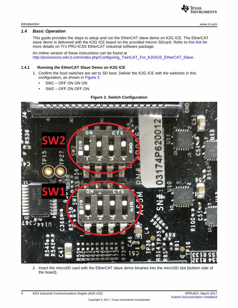
1.4.1 Running the EtherCAT Slave Demo on K2G ICE1. Confirm the boot switches are set to SD boot. Deliver the K2G ICE with the switches in this
configuration, as shown in Figure 2:• SW1 – OFF ON ON ON• SW2 – OFF ON OFF ON
Figure 2. Switch Configuration
2. Insert the microSD card with the EtherCAT slave demo binaries into the microSD slot (bottom side ofthe board).

www.ti.com Introduction
5SPRUIE3–March 2017Submit Documentation Feedback
Copyright © 2017, Texas Instruments Incorporated
K2G Industrial Communications Engine (K2G ICE)
3. Select the 24-MHz crystal as the clock source for the K2G by shorting the pins jumper J3, using theshunt provided, as shown in Figure 3. The K2G ICE should be delivered with the shunt installed.
Figure 3. Short J3 Pin
4. Connect the Ethernet cable between the K2G ICE EtherCAT IN/Port0 (J8, lower RJ-45 port) and thePC with the TwinCAT installation, as shown in Figure 4.
Figure 4. Connect Ethernet Cable
Introduction www.ti.com
6 SPRUIE3–March 2017Submit Documentation Feedback
Copyright © 2017, Texas Instruments Incorporated
K2G Industrial Communications Engine (K2G ICE)
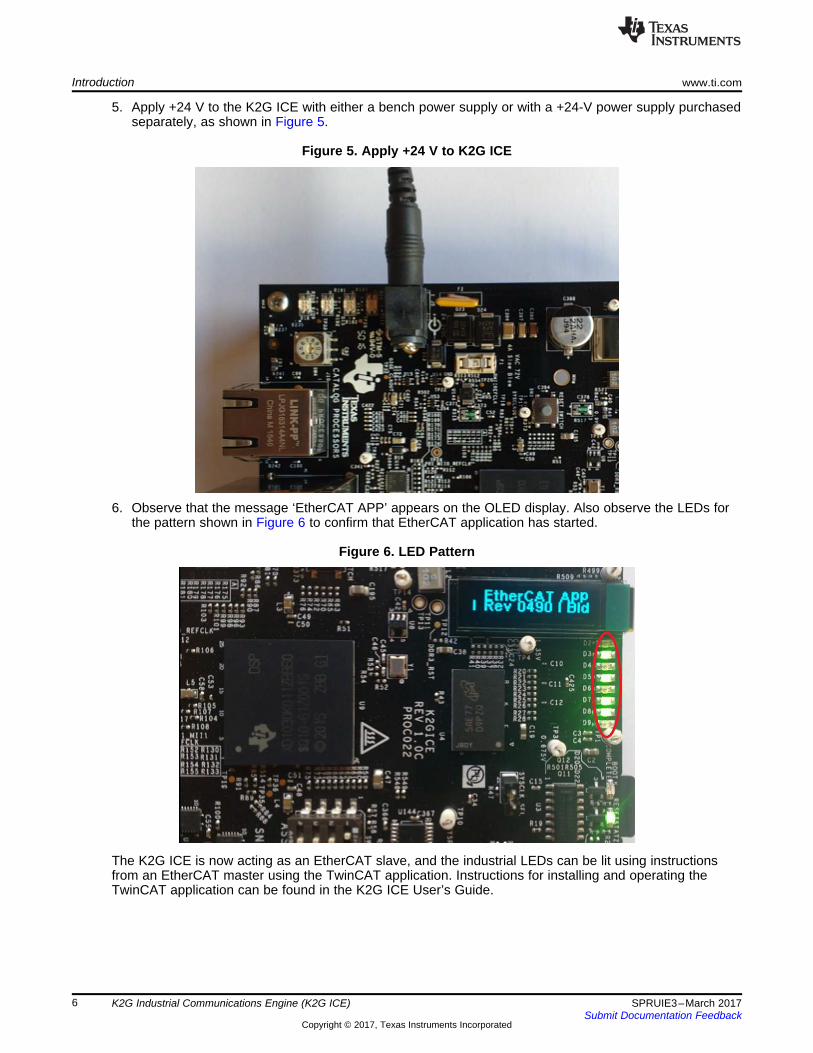
5. Apply +24 V to the K2G ICE with either a bench power supply or with a +24-V power supply purchasedseparately, as shown in Figure 5.
Figure 5. Apply +24 V to K2G ICE
6. Observe that the message ‘EtherCAT APP’ appears on the OLED display. Also observe the LEDs forthe pattern shown in Figure 6 to confirm that EtherCAT application has started.
Figure 6. LED Pattern
The K2G ICE is now acting as an EtherCAT slave, and the industrial LEDs can be lit using instructionsfrom an EtherCAT master using the TwinCAT application. Instructions for installing and operating theTwinCAT application can be found in the K2G ICE User’s Guide.

www.ti.com Introduction
7SPRUIE3–March 2017Submit Documentation Feedback
Copyright © 2017, Texas Instruments Incorporated
K2G Industrial Communications Engine (K2G ICE)
1.4.2 Setting Up the TwinCAT Application1. Download and install the PRU-ICSS EtherCAT Industrial software package from http://software-
dl.ti.com/processor-industrial-sw/esd/PRU_ICSS_EtherCAT_Slave/latest/index_FDS.html. Refer to thedocumentation under {EtherCAT_package_install_path}\docs for more details on PRU-ICSS EtherCATindustrial software package.
2. TwinCAT software setup:a. Install TwinCAT (evaluation version is available for download from
http://www.beckhoff.co.in/english.asp?download/tc3-download-xae.htm. Select PLC mode forinstallation and check the IO drivers box).
b. For EtherCAT Slave Demo application: copy{EtherCAT_package_install_path}\examples\ethercat_slave\esi\TiEtherCATLib.xml to the<Drive>:\TwinCAT\Io\EtherCAT folder. If using TwinCAT 3.1, the folder path is<Drive>:\TwinCAT\3.1\Config\Io\EtherCAT.
c. For EtherCAT Slave Full Mode application: copy{EtherCAT_package_install_path}\protocols\ethercat_slave\ecat_appl\esi\TI_ESC.xml to the<Drive>:\TwinCAT\Io\EtherCAT folder. If you are using TwinCAT 3.1, the folder path is<Drive>:\TwinCAT\3.1\Config\Io\EtherCAT.
3. Start TwinCAT XAE (VS 2010) from the Start menu. Create a new TwinCAT XAE Project (XMLformat), as shown in Figure 7 and Figure 8.
Figure 7. Create New Project

Introduction www.ti.com
8 SPRUIE3–March 2017Submit Documentation Feedback
Copyright © 2017, Texas Instruments Incorporated
K2G Industrial Communications Engine (K2G ICE)
Figure 8. New TwinCAT XAE Project
4. On first occurance, the user must set the PC's Ethernet port, which is used as the EtherCAT port. Goto TwinCAT > Show Realtime Ethernet Compatible Devices, as shown in Figure 9.
Figure 9. Show Realtime Ethernet Compatible Devices

www.ti.com Introduction
9SPRUIE3–March 2017Submit Documentation Feedback
Copyright © 2017, Texas Instruments Incorporated
K2G Industrial Communications Engine (K2G ICE)
5. Select the Ethernet port from the list of compatible devices, and press Install. This installs a BeckhoffEtherCAT driver. When installed, the Ethernet port appears in Installed and ready to use devices, asshown in Figure 10.
Figure 10. Installed and Ready to Use Devices

Introduction www.ti.com
10 SPRUIE3–March 2017Submit Documentation Feedback
Copyright © 2017, Texas Instruments Incorporated
K2G Industrial Communications Engine (K2G ICE)
6. In Solution Explorer, go to the new TwinCAT project > I/0 > right click on Devices, and select Scan asshown in Figure 11. Press OK in the next dialog to start scanning for EtherCAT devices. If Scan Boxesis grayed out, select TWINCAT > Restart TwinCAT (Config Mode).
Figure 11. Select Scan
7. When an EtherCAT compatible device has been detected on this Ethernet port, the dialog shown inFigure 12 appears. There is a tick mark next to the adapter to which the K2G ICE board is connected.Press OK and confirm to start Scan for boxes.
Figure 12. I/O Devices Found

www.ti.com Introduction
11SPRUIE3–March 2017Submit Documentation Feedback
Copyright © 2017, Texas Instruments Incorporated
K2G Industrial Communications Engine (K2G ICE)
8. The TI device is listed Box n (TIESC-003). Press Yes to activate Free Run, as shown in Figure 13.
Figure 13. Activate Free Run
9. Expand the box to see Process Data Inputs (PDI) and Outputs (PDO). Right-click Box n > RxPDO >32Bit Output and select Online Write, as shown in Figure 14.
Figure 14. Online Write

Introduction www.ti.com
12 SPRUIE3–March 2017Submit Documentation Feedback
Copyright © 2017, Texas Instruments Incorporated
K2G Industrial Communications Engine (K2G ICE)
10. Enter the value in hexadecimal format, where each bit in the LSB represents an output, as shown inFigure 15.
Figure 15. Set Value Dialog
11. Changing the LED value sets and clears the appropriate industrial LEDs on the K2G ICE board.
1.5 System OverviewThe top and the bottom pictorial views of the K2G ICE are shown in Figure 16 and Figure 17. The sideview identifies the position of the Ethernet connectors.
Figure 16. Top View
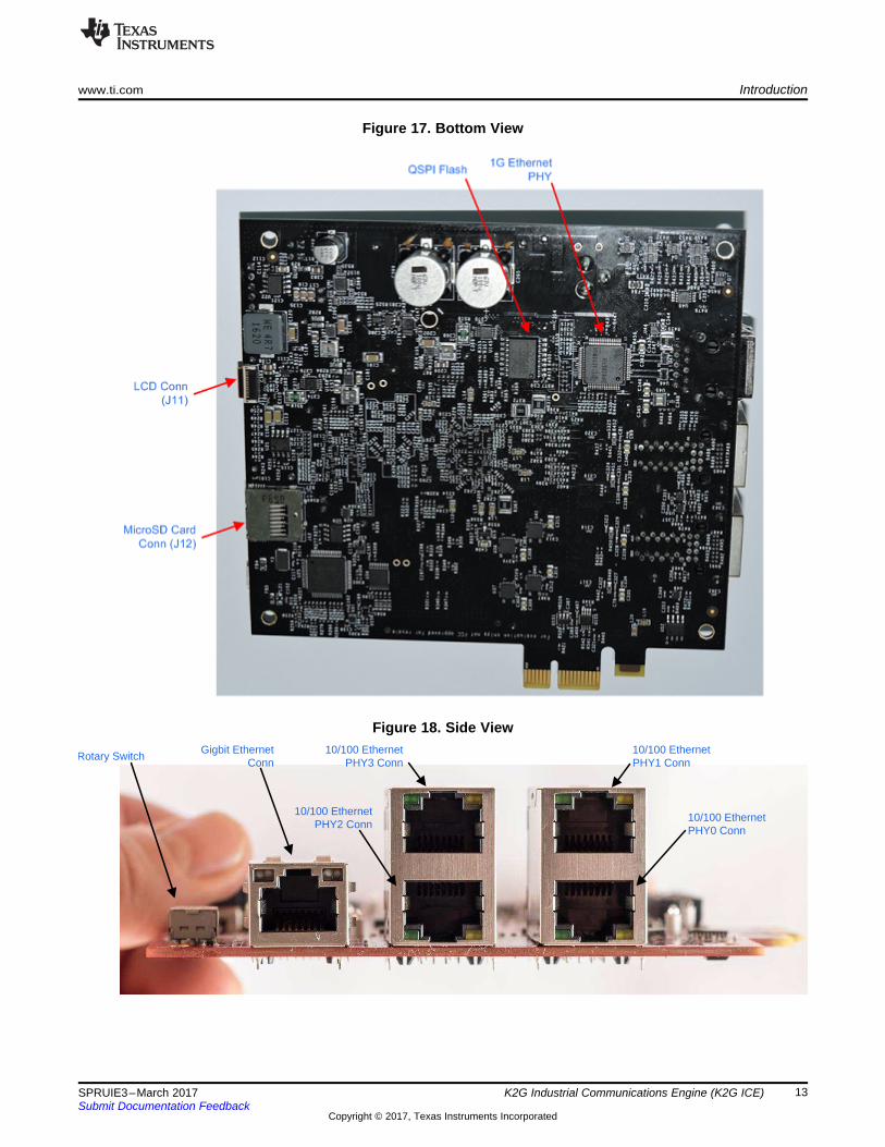
Rotary SwitchGigbit Ethernet
Conn
10/100 Ethernet PHY2 Conn
10/100 Ethernet PHY3 Conn
10/100 Ethernet PHY1 Conn
10/100 Ethernet PHY0 Conn
www.ti.com Introduction
13SPRUIE3–March 2017Submit Documentation Feedback
Copyright © 2017, Texas Instruments Incorporated
K2G Industrial Communications Engine (K2G ICE)
Figure 17. Bottom View
Figure 18. Side View

Introduction www.ti.com
14 SPRUIE3–March 2017Submit Documentation Feedback
Copyright © 2017, Texas Instruments Incorporated
K2G Industrial Communications Engine (K2G ICE)
1.6 Power SupplyThe K2G ICE can be powered from one of two sources: a single external power supply connected to theDC power jack (J6), or the 12-V supply pins on the PCIE edge connector. The power supply circuit isdesigned to allow the use of either a +24-V / 2.5-A DC (60-W) external power supply or a +12-V / 5-A DC(60-W) external power supply. A power ANDing circuit is included in the design, which prevents damage ifa +24-V external supply is connected while the board is installed in a PCIE backplane. The +24-V supplyis used to power the board in that condition.
Due to regulatory requirements, Texas Instruments cannot provide an external power supply. The K2GICE has been tested with the CUI SDI65-24-U-P5 +24-V and the CUI SDI65-12-U-P5 +12-V powersupplies, which can be purchased from distributors. Links to the supplies are shown below. A power cablecan be used with a laboratory supply.
CUI SDI65-12-U-P5
http://www.digikey.com/product-detail/en/cui-inc/SDI65-12-U-P5/102-3417-ND/5277850
CUI SDI65-24-U-P5
http://www.digikey.com/product-detail/en/cui-inc/SDI65-24-U-P5/102-3418-ND/5277851
The input voltage is converted into required voltage levels using individual DC-DC converters. These areshown in Table 1.
Table 1. Voltage Rail Power Supplies
Regulator PurposeTPS54531 5V GenerationTLV62084 3V3 GenerationTLV62084 1V8 GenerationTLV62080 1V35 GenerationLP2996A DDR3 VTT Generation
TPS62180 0V9 GenerationTPS22945 LCD Backlight
1.7 Instructions for Mechanical AssemblyThe K2G ICE can be used with or without the mechanical standoffs provided with the board. Standoffmounting is described in the K2G ICE Mechanical Accessories Mounting Instructions.

www.ti.com Overview of the K2G ICE
15SPRUIE3–March 2017Submit Documentation Feedback
Copyright © 2017, Texas Instruments Incorporated
K2G Industrial Communications Engine (K2G ICE)
2 Overview of the K2G ICEThis chapter provides an overview of the different interfaces and circuits on the K2G ICE.
2.1 Voltage Protection CircuitThe voltage protection circuit on the K2G ICE protects the board from overvoltage, undervoltage, transientvoltage, and reverse voltage input cases. The safe operation input voltage range is 11 V to 13 V. Anyvoltage not in this range is considered as fault, and the voltage protection circuit isolates the board fromthis input. A wide input voltage range is accepted to accommodate both the 24-V input and the 12-V PCIEsupply voltage. LED D25 indicates if the DC input applied to board is in a safe input range.
Figure 19. Overvoltage Protection Circuit
Figure 20. Overvoltage Fault Indicator
2.2 Voltage ANDing CircuitAlthough it is not recommended, both the 12 V from the PCIE connector and 24 V from the power inputmay be present at the same time. To protect the board from power supply conflicts, the voltage ANDingcircuit was included. If only the 12 V from the PCIE edge connector is present, D23 is forward biased,allowing current to flow. If 24 V is provided to J6, D13 is forward biased. If both 24 V on J6 and 12 V onthe PCIE edge connector are both present. D13 is forward biased and D23 is reversed biased, allowingthe 24 V to take precedence, and blocking any current flow back to the PCIE connector.
Overview of the K2G ICE www.ti.com
16 SPRUIE3–March 2017Submit Documentation Feedback
Copyright © 2017, Texas Instruments Incorporated
K2G Industrial Communications Engine (K2G ICE)
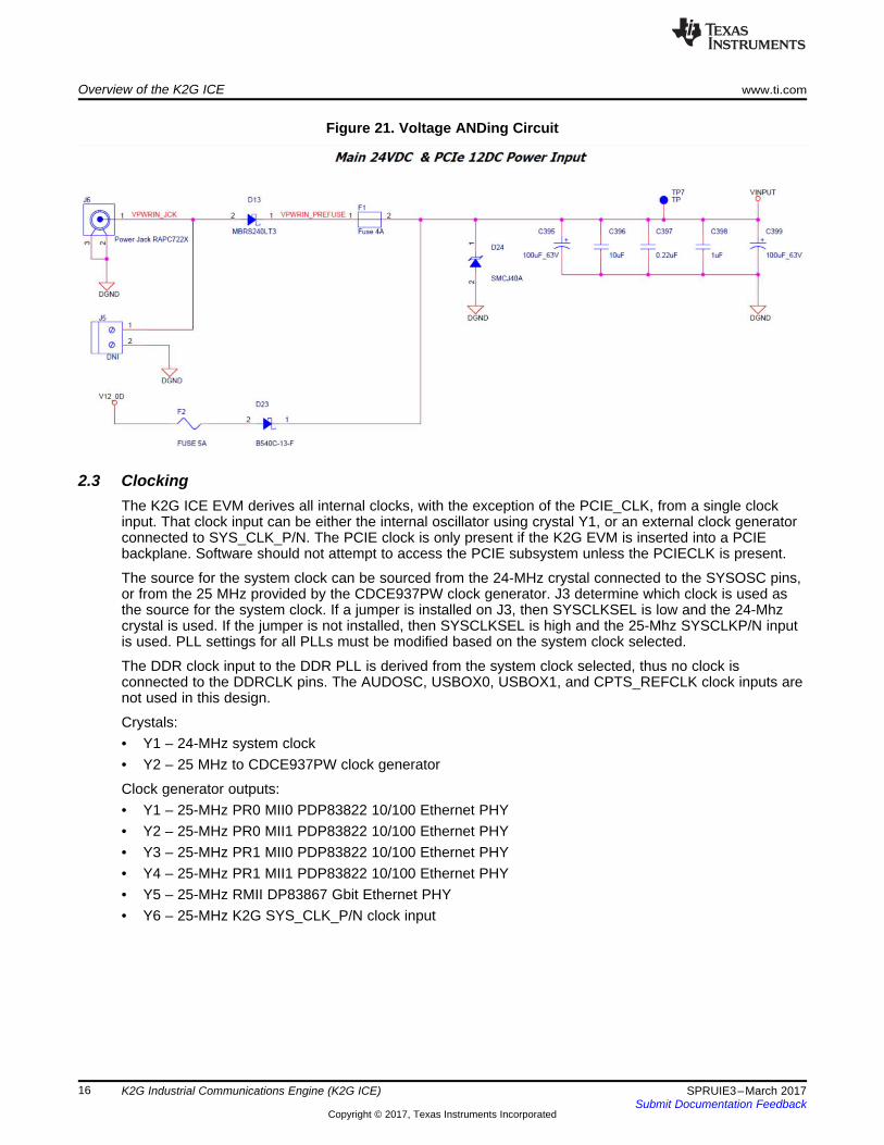
Figure 21. Voltage ANDing Circuit
2.3 ClockingThe K2G ICE EVM derives all internal clocks, with the exception of the PCIE_CLK, from a single clockinput. That clock input can be either the internal oscillator using crystal Y1, or an external clock generatorconnected to SYS_CLK_P/N. The PCIE clock is only present if the K2G EVM is inserted into a PCIEbackplane. Software should not attempt to access the PCIE subsystem unless the PCIECLK is present.
The source for the system clock can be sourced from the 24-MHz crystal connected to the SYSOSC pins,or from the 25 MHz provided by the CDCE937PW clock generator. J3 determine which clock is used asthe source for the system clock. If a jumper is installed on J3, then SYSCLKSEL is low and the 24-Mhzcrystal is used. If the jumper is not installed, then SYSCLKSEL is high and the 25-Mhz SYSCLKP/N inputis used. PLL settings for all PLLs must be modified based on the system clock selected.
The DDR clock input to the DDR PLL is derived from the system clock selected, thus no clock isconnected to the DDRCLK pins. The AUDOSC, USBOX0, USBOX1, and CPTS_REFCLK clock inputs arenot used in this design.
Crystals:• Y1 – 24-MHz system clock• Y2 – 25 MHz to CDCE937PW clock generator
Clock generator outputs:• Y1 – 25-MHz PR0 MII0 PDP83822 10/100 Ethernet PHY• Y2 – 25-MHz PR0 MII1 PDP83822 10/100 Ethernet PHY• Y3 – 25-MHz PR1 MII0 PDP83822 10/100 Ethernet PHY• Y4 – 25-MHz PR1 MII1 PDP83822 10/100 Ethernet PHY• Y5 – 25-MHz RMII DP83867 Gbit Ethernet PHY• Y6 – 25-MHz K2G SYS_CLK_P/N clock input

Y1
24MHz
Y1CDCE937PW
SYSCLOCK
DDR_CLK (unused)
25MHz
AUDOSC (unused)
SYSOSC_IN
SYSOSC_OUT
25MHz
10/100 Ethernet PHY (U19)
10/100 Ethernet PHY (U18)
10/100 Ethernet PHY (U16)
1G Ethernet PHY (U43)
10/100 Ethernet PHY (U17)
Y2
Y3
Y4
Y5
Y6
Y2
PCIe x1 Edge Conn
K2G SoC
PCIECLK100MHz
3.3V
J3
SYSCLKSEL
REFCLK
USB0XO (unused)
USB0X1 (unused)
CPTS_REFCLK (unused)
25MHz
25MHz
25MHz
25MHz
25MHz
SYSCLKOUT
TP18
www.ti.com Overview of the K2G ICE
17SPRUIE3–March 2017Submit Documentation Feedback
Copyright © 2017, Texas Instruments Incorporated
K2G Industrial Communications Engine (K2G ICE)
Figure 22. Clock Inputs
2.4 Bootmode SwitchesThe K2G ICE includes two dip switches, each with four individual switches. These are connected to eightof the sixteen bootmode signals. The K2G ICE is not designed to support all bootmodes available to theK2G, although all bootmodes may be selected with the available switches. Only the bootmodes defined inTable 2 have been tested with the K2G ICE. In addition to the bootmode bits, switches are provided forfour additional bootmode pins used to defined specific conditions for each of the bootmodes available. Formore information, see the BOOTMODE Pins Description section in the K2G TRM.

BOOTMODE0
BOOTMODE1
BOOTMODE2
BOOTMODE3
BOOTMODE4
BOOTMODE5
BOOTMODE6
BOOTMODE7
BOOTMODE8
BOOTMODE9
BOOTMODE10
BOOTMODE11
BOOTMODE12
BOOTMODE13
BOOTMODE14
BOOTMODE15
DNI DNI DNI DNI DNIDNI DNIDNI
K2G
SYSCLKSEL
VDD_3V3
VDD_3V3
VDD_3V3
Jumper J3
Dip Switch SW1
Dip Switch SW2
1234
1234
Overview of the K2G ICE www.ti.com
18 SPRUIE3–March 2017Submit Documentation Feedback
Copyright © 2017, Texas Instruments Incorporated
K2G Industrial Communications Engine (K2G ICE)
Figure 23. Bootmode Selection Switches Schematic
The dip switches are located just above the expansion connector, as shown in Figure 24. Bootmodeswitches should be set before any expansion board is installed.

www.ti.com Overview of the K2G ICE
19SPRUIE3–March 2017Submit Documentation Feedback
Copyright © 2017, Texas Instruments Incorporated
K2G Industrial Communications Engine (K2G ICE)
Figure 24. Bootmode Selection Switches
Table 2. Supported Bootmodes
Bootmode ClockSW2 SW1
J3 BOOTMODE value4 3 2 1 4 3 2 1
NoBoot/Emulation
24MHz off off on off off off off off short 0000000001000000
NoBoot/Emulation
25MHz off on off off off off off off open 0000000010000000
PCIE endpoint 24MHz off off on off off off off on short 0000000001000001
PCIE endpoint 25MHz off on off off off off off on open 0000000010000001
QSPI as 48MHz 24MHz off off on off on off off off short 0000000001001000
QSPI as 48MHz 25MHz off on off off on off off off open 0000000010001000
QSPI as 96MHz 24MHz off off on off on off off on short 0000000001001001
QSPI as 96MHz 25MHz off on off off on off off on open 0000000010001001
SDcard 24MHz on off on off on on on off short 0000001001001110
SDcard 25MHz on on off off on on on off open 0000001010001110
UART 24MHz off off on off on on on on short 0000000001001111
UART 25MHz off on off off on on on on open 0000000010001111
K2G SoC
XDS100Based on FT2232HL
EMU [00:01]
EMU [02:04]
JTAG Signals
J2 Compact TI
20-pin conn
EMUBuffer
JTAGBuffer
J1 Micro
USB conn
SerialEEPROM
UARTBuffer
TLV1117V3_3FTDI
Power supply
EMU_DETECTJTAG_OE
VBUS
DATA
Portion of circuit powered by VBUS
JTAG Signals
EMU [00:01]
EMU [02:04]
UART0_TXD
UART0_RXD
Overview of the K2G ICE www.ti.com
20 SPRUIE3–March 2017Submit Documentation Feedback
Copyright © 2017, Texas Instruments Incorporated
K2G Industrial Communications Engine (K2G ICE)
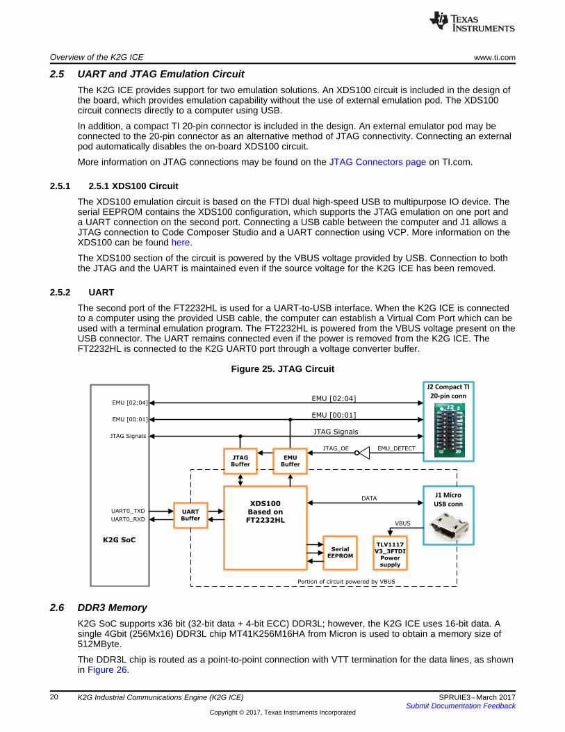
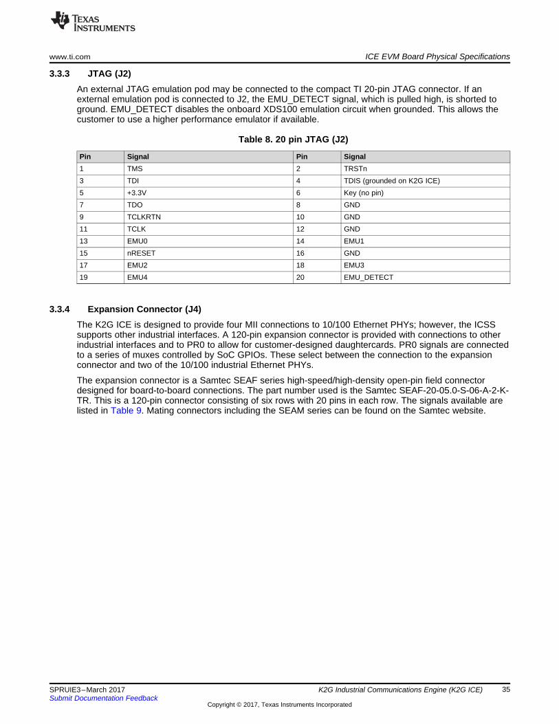
2.5 UART and JTAG Emulation CircuitThe K2G ICE provides support for two emulation solutions. An XDS100 circuit is included in the design ofthe board, which provides emulation capability without the use of external emulation pod. The XDS100circuit connects directly to a computer using USB.
In addition, a compact TI 20-pin connector is included in the design. An external emulator pod may beconnected to the 20-pin connector as an alternative method of JTAG connectivity. Connecting an externalpod automatically disables the on-board XDS100 circuit.
More information on JTAG connections may be found on the JTAG Connectors page on TI.com.
2.5.1 2.5.1 XDS100 CircuitThe XDS100 emulation circuit is based on the FTDI dual high-speed USB to multipurpose IO device. Theserial EEPROM contains the XDS100 configuration, which supports the JTAG emulation on one port anda UART connection on the second port. Connecting a USB cable between the computer and J1 allows aJTAG connection to Code Composer Studio and a UART connection using VCP. More information on theXDS100 can be found here.
The XDS100 section of the circuit is powered by the VBUS voltage provided by USB. Connection to boththe JTAG and the UART is maintained even if the source voltage for the K2G ICE has been removed.
2.5.2 UARTThe second port of the FT2232HL is used for a UART-to-USB interface. When the K2G ICE is connectedto a computer using the provided USB cable, the computer can establish a Virtual Com Port which can beused with a terminal emulation program. The FT2232HL is powered from the VBUS voltage present on theUSB connector. The UART remains connected even if the power is removed from the K2G ICE. TheFT2232HL is connected to the K2G UART0 port through a voltage converter buffer.
Figure 25. JTAG Circuit
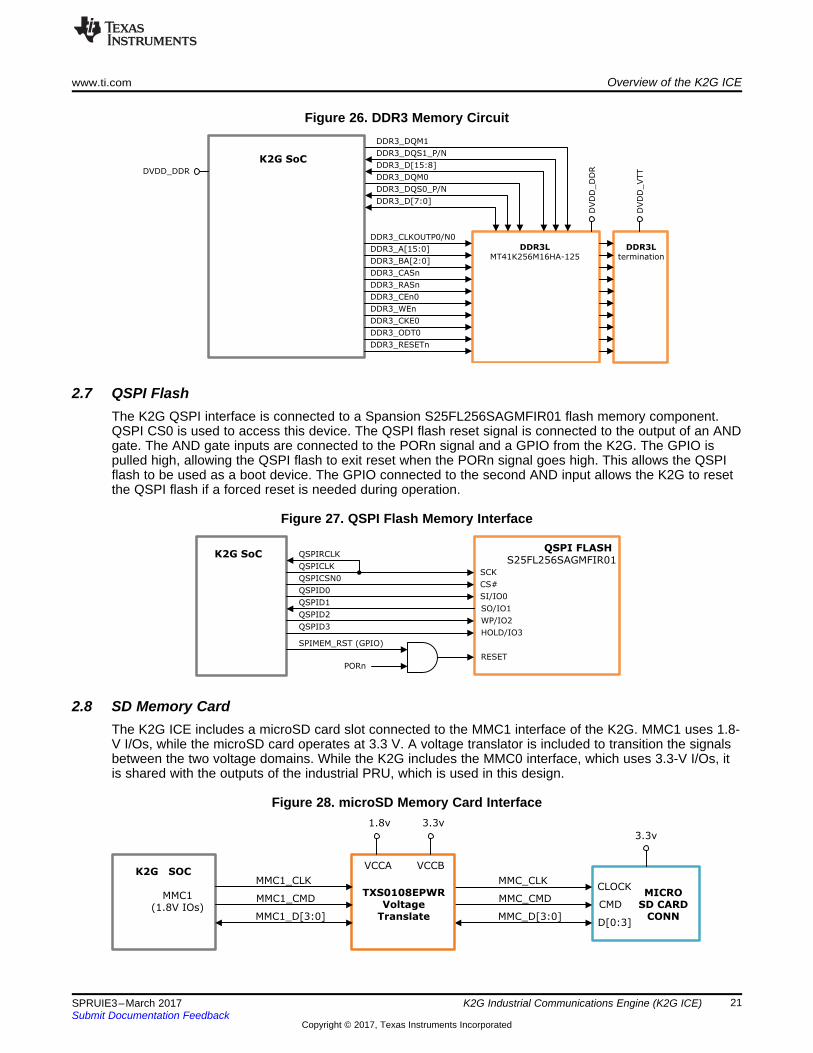
2.6 DDR3 MemoryK2G SoC supports x36 bit (32-bit data + 4-bit ECC) DDR3L; however, the K2G ICE uses 16-bit data. Asingle 4Gbit (256Mx16) DDR3L chip MT41K256M16HA from Micron is used to obtain a memory size of512MByte.
The DDR3L chip is routed as a point-to-point connection with VTT termination for the data lines, as shownin Figure 26.
MMC_CLK
MICROSD CARD
CONN
MMC_CMDCMD
CLOCK
MMC_D[3:0]D[0:3]
K2G SOC
3.3v
TXS0108EPWRVoltage
Translate
VCCA VCCB
3.3v 1.8v
MMC1_CLK
MMC1_CMD
MMC1_D[3:0]
MMC1
(1.8V IOs)
CS#
SCK
QSPI FLASH
S25FL256SAGMFIR01K2G SoC
SI/IO0
SO/IO1
WP/IO2
HOLD/IO3
RESET
QSPIRCLK
QSPICLK
QSPID3
QSPICSN0
QSPID0
QSPID1
QSPID2
SPIMEM_RST (GPIO)
PORn
K2G SoC
DDR3L
termination
DDR3L
MT41K256M16HA-125
DDR3_CLKOUTP0/N0
DDR3_A[15:0]
DDR3_BA[2:0]
DDR3_CASn
DDR3_RASn
DDR3_CEn0
DDR3_WEn
DDR3_CKE0
DDR3_ODT0
DDR3_RESETn
DDR3_D[7:0]
DDR3_DQS0_P/N
DDR3_DQM0
DDR3_D[15:8]
DDR3_DQS1_P/N
DDR3_DQM1
DVDD_DDR
DVDD_DDR
DVDD_VTT
www.ti.com Overview of the K2G ICE
21SPRUIE3–March 2017Submit Documentation Feedback
Copyright © 2017, Texas Instruments Incorporated
K2G Industrial Communications Engine (K2G ICE)
Figure 26. DDR3 Memory Circuit
2.7 QSPI FlashThe K2G QSPI interface is connected to a Spansion S25FL256SAGMFIR01 flash memory component.QSPI CS0 is used to access this device. The QSPI flash reset signal is connected to the output of an ANDgate. The AND gate inputs are connected to the PORn signal and a GPIO from the K2G. The GPIO ispulled high, allowing the QSPI flash to exit reset when the PORn signal goes high. This allows the QSPIflash to be used as a boot device. The GPIO connected to the second AND input allows the K2G to resetthe QSPI flash if a forced reset is needed during operation.
Figure 27. QSPI Flash Memory Interface
2.8 SD Memory CardThe K2G ICE includes a microSD card slot connected to the MMC1 interface of the K2G. MMC1 uses 1.8-V I/Os, while the microSD card operates at 3.3 V. A voltage translator is included to transition the signalsbetween the two voltage domains. While the K2G includes the MMC0 interface, which uses 3.3-V I/Os, itis shared with the outputs of the industrial PRU, which is used in this design.
Figure 28. microSD Memory Card Interface

RGMII0_TXCLKGTX_CLK Gigabit
Ethernet PHY
DP83867
K2G SoC
RGMII0_TXCTL
RGMII0_TXD [0:3]
RGMII0_RXCLK
RGMII0_RXCTL
RGMII0_RXD[0:3]
RJ45 Conn with
MagneticsLPJG16314A
4NL
MDIO_CLK
MDIO_DATA
TXRXPA
TXRXMA
TXRXPB
TXRXMB
TXRXPC
TXRXMC
TXRXPD
TXRXMD
TX_CTRL
TX_D[0:3]
RX_CLK
RX_CTRL
MDC
RX_D[0:3]
MDIO
Overview of the K2G ICE www.ti.com
22 SPRUIE3–March 2017Submit Documentation Feedback
Copyright © 2017, Texas Instruments Incorporated
K2G Industrial Communications Engine (K2G ICE)
2.9 Gigabit EthernetThe K2G ICE includes an RGMII connection between the DP83867 Gigabit Ethernet PHY and the networksubsystem (NSS) of the SoC using RGMII0. The default configuration of the DP83867 is determined usinga number of resistor value pull-ups and pull-downs on specific pins of the PHY.
Figure 29. Gigabit Ethernet Interface
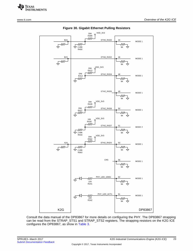
2.9.1 Gigabit Ethernet PHY Default ConfigurationThe default configuration of the DP83867 is determined using a number of resistor pull-up and pull-downvalues on specific pins of the PHY. Depending on the values installed, each of the configuration pins canbe set to one of four modes. A configuration pin or groups of configuration pins are used to set theconfiguration of the PHY after it is released from reset. Configuration settings differ depending on thepackage type selected for the PHY. The K2G ICE uses the 64-pin QFP package, designated with the PAPsuffix, which supports both the GMII and RGMII interface. A 48-pin QFN package, designated with theRGZ suffix and which only supports RGMII, is also available.
2.9.2 Gigabit Ethernet Resistor StrappingThe DP83867 PHY use a four-level configuration based on resistor strappings, which generate fourdistinct voltage ranges. These resistors are connected to the RX data and control pins, which are normallydriven by the PHY and are inputs to the K2G. When 3.3-v I/O voltages are selected, the voltage rangesare shown below.
Mode 1 – 0 V to 0.3234 V
Mode 2 – 0.4884 V to 0.5973 V
Mode 3 – 0.7491 V to 0.9141 V
Mode 4 – 2.2902 V to 3.3 V
Mid-level voltages can result in high leakage currents and are detrimental to the long-term reliability of theK2G I/O cells connected to the strapping resistor. To avoid this situation, only pull-up and pull-downresistors are used to pull the I/O cells as close as possible to either 0 V or 3.3 V. This limits the selectionof configurations to those that can be selected by using Mode 1 or Mode 4. Both the DP83867 and theK2G include internal pulling resistors. The value of the external pull resistors are selected to provide avoltage at the pins of the K2G as close to ground or 3.3 V as possible.
9K
9K
VDD_3V3
9K
VDD_3V3
9K
9K
ETH0_RXD2
ETH2_RXD4
VDD_3V3
9K2.49KR400
DNIR399
ETH0_RXD0
VDD_3V3
9K
ETH2_RXD5
ETH2_RXD6
ETH2_RXDV
VDD_3V3
9K
ETH2_RXD7
CRS
DNIR413
DNIR414
DNIR428
DNIR427
2.49KR433
10KR430
2.49KR563
DNIR562
MODE 1
MODE 1
MODE 1
MODE 1
MODE 1
MODE 2
MODE 1
MODE 1
44
46
48
49
50
51
53
56
K2G DP83867
9K
PHY_LED_1000nMODE 1
62
9K
MODE 161PHY_LED_ACTn
B24
B23
A24
220R242
220R241
www.ti.com Overview of the K2G ICE
23SPRUIE3–March 2017Submit Documentation Feedback
Copyright © 2017, Texas Instruments Incorporated
K2G Industrial Communications Engine (K2G ICE)
Figure 30. Gigabit Ethernet Pulling Resistors
Consult the data manual of the DP83867 for more details on configuring the PHY. The DP83867 strappingcan be read from the STRAP_STS1 and STRAP_STS2 registers. The strapping resistors on the K2G ICEconfigures the DP83867, as show in Table 3.

Overview of the K2G ICE www.ti.com
24 SPRUIE3–March 2017Submit Documentation Feedback
Copyright © 2017, Texas Instruments Incorporated
K2G Industrial Communications Engine (K2G ICE)
Table 3. Gigabit PHY Configuration
Bit BIT NAME Value DescriptionSTRAP_STS1.15 STRAP_MIRROR_EN 0 Port mirroring disabledSTRAP_STS1.14 STRAP_LINK_DOWNSHIFT_EN 0 Link downshift disabledSTRAP_STS1.13 STRAP_CLK_OUT_DIS 1 Clock output disabledSTRAP_STS1.12 STRAP_RGMII_DIS 0 RGMII enabledSTRAP_STS1.10 STRAP_AMDIX_DIS 0 Auto-MDIX enabledSTRAP_STS1.9 STRAP_FORCE_MDI_X 0 Force MDI (not used because auto-MDIX is
enabled)STRAP_STS1.8 STRAP_HD_EN 0 Full duplex enabled (not used because auto-MDIX is
enabled)STRAP_STS1.7 STRAP_ANEG_DIS 0 Auto-negotiation enabledSTRAP_STS1.6:5 STRAP_SPEED_SEL 00 Advertise 10/100/1000STRAP_STS1.4:0 STRAP_PHY_ADD 00000 PHY address = 0x00STRAP_STS2.10 STRAP_FLD 0 Fast link detect disabled
2.9.3 Gigabit Ethernet ConfigurationThe DP83867 PHY must be configured using the MDIO register accesses for proper operation of theinterface on the K2G ICE.
First, the value of 0x170 must be written to register 0x31 of the DP83867 for proper operation of the auto-negotiation function.
Secondly, the DP83867 includes the ability to delay the RGMII TX clock and RX clock relative to the datasignals, to compensate for delays introduced in the routing of the RGMII interface. An application noteexplaining this capability is included on the product page for the DP83867. After analyzing the layout ofthe RGMII on the K2G ICE, there is a delay of 2.25 nsec for the RX clock and 2.25 nsec for the TX clock.The TX clock delay consists of the 2 nsec of internal delay and 0.25 nsec of PCB delay. The TX clockdelay is calculated assuming that the RGMII internal TX clock delay is enabled within the K2G. In theRGMIIDCTL register (0x86), the RGMII_TX_DELAY_CTRL bit field should be set to 0b0000 and theRGMII_RX_DELAY_CTRL field should be set to 0b1000. In the RGMIICTL register (0x32), theRGMII_TX_CLK_DELAY bit should be set to 1 and the RGMII_RX_CLK_DELAY bit should be set to 1 toenable the clock shift specified in the RGMIIDCTL register.
2.10 Industrial EthernetThe K2G SoC includes two programmable real-time unit subsystems and industrial communicationssubsystems (PRU-ICSS), which can be configured to support numerous industrial protocols. Each PRU-ICSS unit can support two MII interfaces for connection to two 10/100 Ethernet PHYs. The K2G ICEincludes four DP83822I 10/100 Industrial Ethernet PHYs providing four Ethernet connections. The signalsfor PRU0 are connected to muxes, allowing this interface to be connected to the expansion connector.

www.ti.com Overview of the K2G ICE
25SPRUIE3–March 2017Submit Documentation Feedback
Copyright © 2017, Texas Instruments Incorporated
K2G Industrial Communications Engine (K2G ICE)
Figure 31. Industrial Ethernet Interface
2.10.1 Industrial Ethernet PHY Default ConfigurationThe default configuration of the DP83822 is determined using a number of resistor pull-up and pull-downvalues on specific pins of the PHY. Depending on the values installed, each of the configuration pins canbe set to one of four modes. A configuration pin or groups of configuration pins are used to set theconfiguration of the PHY after it is released from reset. Configuration settings differ depending on thepackage type selected for the PHY.

Overview of the K2G ICE www.ti.com
26 SPRUIE3–March 2017Submit Documentation Feedback
Copyright © 2017, Texas Instruments Incorporated
K2G Industrial Communications Engine (K2G ICE)
2.10.2 Industrial Ethernet Resistor StrappingThe DP83822 PHY use a four-level configuration based on resistor strappings, which generate fourdistinct voltages ranges. These resistors are connected to the RX data and control pins, which arenormally driven by the PHY and are inputs to the K2G. These voltage ranges are shown below.
Mode 1 – 0 V to 0.3234 V
Mode 2 – 0.4884 V to 0.5973 V
Mode 3 – 0.7491 V to 0.9141 V
Mode 4 – 2.2902 V to 3.3 V
Mid-level voltages can result in high leakage currents and are detrimental to the long-term reliability of theK2G I/O cells connected to the strapping resistor. To avoid this situation, only pull-up and pull-downresistors are used to pull the I/O cells as close as possible to either 0 V or 3.3 V. This limits the selectionof configurations to those that can be selected by using Mode 1 or Mode 4. Both the DP83822 and theK2G include internal pulling resistors. The value of the external pull resistors is selected to provide avoltage at the pins of the K2G as close to ground or 3.3 V as possible.

9K
9K
VDD_3V3
9K
VDD_3V3
VDD_3V3
Rlo1R154 R163 R409 R404
Rhi1R132 R141 R396 R391
PRUxMIIx_COL
VDD_3V3
9K
VDD_3V3
PHY0 - MODE 1PHY1 - MODE 4PHY2 - MODE 1PHY3 - MODE 4
PHY0 - MODE 1PHY1 - MODE 1PHY2 - MODE 4PHY3 - MODE 4
MODE 1
MODE 1
MODE 1
MODE 4
MODE 4
MODE 1
29
30
31
32
1
27
28
K2G DP83822
VDD_3V3
VDD_3V3
PRUxMIIx_RXD0
PRUxMIIx_RXD1
PRUxMIIx_RXD2
PRUxMIIx_RXD3
PRUxMIIx_CRS
PRUxMIIx_RXER
VDD_3V3
9K2.49KR157 R166 R123 R127
MODE 126PRUxMIIx_RXDV
50K VDD_3V3
50K
50K
MODE 417
PRUxMIIx_LINKLED
50K
enabled
enabled
enabled
enabled
enabled
enabled
enabled
enabled
enabled
Rhi2R131 R140 R397 R392
Rlo2R153 R162 R410 R405
DNIR130 R139 R113 R117
2.49KR152 R161 R121 R125
DNIR129 R138 R398 R393
2.49KR151 R160 R411 R406
DNIR128 R137 R112 R116
2.49KR150 R159 R120 R124
1.0KR136 R145 R394 R389
DNIR158 R167 R407 R402
1.0KR134 R143 R395 R390
DNIR156 R165 R408 R403
1.0KR133 R142 R114 R118
DNIR155 R164 R122 R126
DNIR135 R144 R115 R119
MODE 0 Rhi = 1.0K, Rlo = DNI
MODE 0 Rhi = DNI, Rlo = 1.0K
VDD_3V3
DNIR443 R442 R445 R444
www.ti.com Overview of the K2G ICE
27SPRUIE3–March 2017Submit Documentation Feedback
Copyright © 2017, Texas Instruments Incorporated
K2G Industrial Communications Engine (K2G ICE)
Figure 32. Industrial Ethernet Pulling Resistors
PETp0
K2G SoC
x1 Edge Card Edge
CONN
PERn0
PERp0
PETn0
TXN0
TXP0
RXN0
RXN0
PCIE_CLK_P 100MHz (HCSL)
PORn
REFCLK+
PERST#
PCIE_CLK_N REFCLK-
from reset circuit
Overview of the K2G ICE www.ti.com
28 SPRUIE3–March 2017Submit Documentation Feedback
Copyright © 2017, Texas Instruments Incorporated
K2G Industrial Communications Engine (K2G ICE)
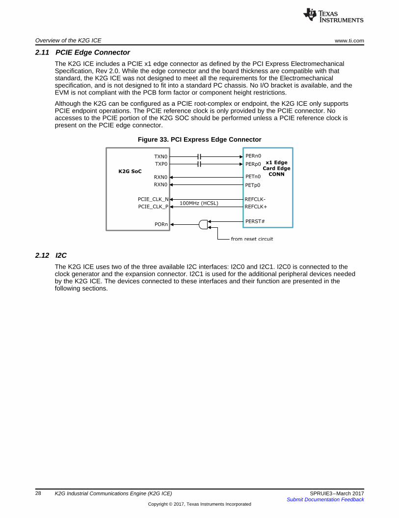
2.11 PCIE Edge ConnectorThe K2G ICE includes a PCIE x1 edge connector as defined by the PCI Express ElectromechanicalSpecification, Rev 2.0. While the edge connector and the board thickness are compatible with thatstandard, the K2G ICE was not designed to meet all the requirements for the Electromechanicalspecification, and is not designed to fit into a standard PC chassis. No I/O bracket is available, and theEVM is not compliant with the PCB form factor or component height restrictions.
Although the K2G can be configured as a PCIE root-complex or endpoint, the K2G ICE only supportsPCIE endpoint operations. The PCIE reference clock is only provided by the PCIE connector. Noaccesses to the PCIE portion of the K2G SOC should be performed unless a PCIE reference clock ispresent on the PCIE edge connector.
Figure 33. PCI Express Edge Connector
2.12 I2CThe K2G ICE uses two of the three available I2C interfaces: I2C0 and I2C1. I2C0 is connected to theclock generator and the expansion connector. I2C1 is used for the additional peripheral devices neededby the K2G ICE. The devices connected to these interfaces and their function are presented in thefollowing sections.
www.ti.com Overview of the K2G ICE
29SPRUIE3–March 2017Submit Documentation Feedback
Copyright © 2017, Texas Instruments Incorporated
K2G Industrial Communications Engine (K2G ICE)
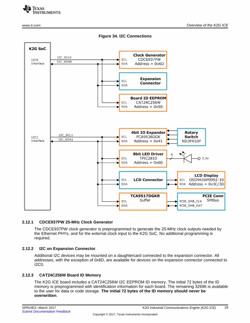
Figure 34. I2C Connections
2.12.1 CDCE937PW 25-MHz Clock GeneratorThe CDCE937PW clock generator is preprogrammed to generate the 25-MHz clock outputs needed bythe Ethernet PHYs, and for the external clock input to the K2G SoC. No additional programming isrequired.
2.12.2 I2C on Expansion ConnectorAdditional I2C devices may be mounted on a daughtercard connected to the expansion connector. Alladdresses, with the exception of 0x6D, are available for devices on the expansion connector connected toI2C0.
2.12.3 CAT24C256W Board ID MemoryThe K2G ICE board includes a CAT24C256W I2C EEPROM ID memory. The initial 72 bytes of the IDmemory is preprogrammed with identification information for each board. The remaining 32696 is availableto the user for data or code storage. The initial 72 bytes of the ID memory should never beoverwritten.

Overview of the K2G ICE www.ti.com
30 SPRUIE3–March 2017Submit Documentation Feedback
Copyright © 2017, Texas Instruments Incorporated
K2G Industrial Communications Engine (K2G ICE)
Table 4. ID Memory Header Information
Name Size(bytes)
Contents Description
Header 4 MSB 0xEE3355AA LSB Start codeBoard name 8 66AK2GIC Board name in ASCIIVersion 4 1.0B Hardware revision code in ASCII
Serial number 12 WWYY4P62nnnn
WW – Week of productionYY – Year of production4P62 – K2G ICE board codennnn – Serial number
Configuration option 32 Reserved for board configuration codes
Ethernet MAC address #0 6 MSB to LSB - MAC-ID70-FF-76-1C-xx-xx
This is the first of a block of six addresses available for theindustrial interface ports
Ethernet MAC address #5 6 MSB to LSB - MAC-ID70-FF-76-1C-xx-xx
This is the last of a block of six addresses available for theindustrial interface ports
Available 32696 Available space for user data or code
2.12.4 PCA9536DGK/ ND3FR10P Rotary SwitchThe K2G ICE board includes a PCA9536DGK I2C 4-bit IO Expander connected to a ND3FR10P 10-position rotary switch. Selecting a value on the switch presents a four-bit binary code to the PCA9536.This value can be read using the I2C interface.
2.12.5 OSD9616P0992-10 LCD DisplayThe K2G ICE board includes a OSD9616P0992-10 96×16 pixel LCD display. The display is based on theSSD1606 controller. Communications with the controller uses two slave addresses, 0x3C and 0x3D, forI2C1.
2.12.6 TPIC2810 LED DriverThe K2G ICE board includes a TPIC2810 8-bit LED driver. The driver is used to control eight green LEDsused to define the state of the industrial interfaces.
2.12.7 TCA9517DGKR I2C BufferThe K2G ICE board includes a TCA9517DGKR buffer between I2C1 and the SMBus interface on thePCIE edge connector. This buffer acts as voltage isolation between the K2G ICE card and the circuitconnected to the PCIE bus. The SMBus (System Management Bus) is used by PCIE as a control interfacewith the PCIE root complex. This interface is provided for future use and is not currently supported bysoftware.
2.13 GPIOsAlmost every I/O pin on the K2G can be configured as a GPIO. A number of GPIO pins are used in theK2G ICE for various control functions. Those GPIOs and their function are listed in Table 5.
Table 5. GPIO Functions
SOC GPIO Name Ball Net Name Dir FunctionGPIO0_00 AC21 GPIO0_00 I/O Expansion ConnectorGPIO0_01 AE20 GPIO0_01 I/O Expansion ConnectorGPIO0_02 AD22 GPIO0_02 I/O Expansion ConnectorGPIO0_03 AD20 GPIO0_03 I/O Expansion ConnectorGPIO0_04 AE21 GPIO0_04 I/O Expansion ConnectorGPIO0_05 AE22 GPIO0_05 I/O Expansion ConnectorGPIO0_06 AC20 GPIO0_06 I/O Expansion Connector

www.ti.com Overview of the K2G ICE
31SPRUIE3–March 2017Submit Documentation Feedback
Copyright © 2017, Texas Instruments Incorporated
K2G Industrial Communications Engine (K2G ICE)
Table 5. GPIO Functions (continued)SOC GPIO Name Ball Net Name Dir FunctionGPIO0_07 AD21 GPIO0_07 I/O Expansion ConnectorGPIO0_08 AE23 GPIO0_08 I/O Expansion ConnectorGPIO0_09 AB20 GPIO0_09 I/O Expansion ConnectorGPIO0_11 AD23 LED_1 Out 1 – LED D17 Red on
0 – LED D17 Red offGPIO0_12 AA21 LED_2 Out 1 – LED D17 Green on
0 – LED D17 Green offGPIO0_13 AB21 LED_3 Out 1 – LED D17 Blue on
0 – LED D17 Blue offGPIO0_14 AB22 LED_4 Out 1 – LED D18 Red on
0 – LED D18 Red offGPIO0_15 AA22 LED_5 Out 1 – LED D18 Green on
0 – LED D18 Green offGPIO0_16 AB23 LED_6 Out 1 – LED D18 Blue on
0 – LED D18 Blue offGPIO0_19 Y22 LED_7 Out 1 – LED D19 on
0 – LED D19 offGPIO0_44 R21 LED_8 Out 1 – LED D14 Red on
0 – LED D14 Red offGPIO0_43 U24 LED_9 Out 1 – LED D14 Green on
0 – LED D14 Green offGPIO0_42 V25 LED_10 Out 1 – LED D14 Blue on
0 – LED D14 Blue offGPIO0_41 T24 LED_11 Out 1 – LED D15 Red on
0 – LED D15 Red offGPIO0_101 P3 LED_12 Out 1 – LED D15 Green on
0 – LED D15 Green offGPIO0_102 P4 LED_13 Out 1 – LED D15 Blue on
0 – LED D15 Blue offGPIO0_107 U1 MUX_MII_CTL_PRU0MII0 Out 1 – PRU0 signals to expansion conn
0 – PRU0MII1 to 10/100 PHY0 (U18)GPIO0_106 T2 MUX_MII_CTL_PRU0MII1 Out 1 – PRU0 signals to expansion conn
0 – PRU0MII1 to 10/100 PHY1 (U19)GPIO0_66 H22 OE_PRU0MII0_1 Out 0 – Enable Outputs PRUMII0 Muxes (U10, U41)GPIO0_67 H21 OE_PRU0MII0_2 Out 0 – Enable Outputs PRUMII0 Muxes (U12, U36)GPIO0_57 R5 OE_PRU0MII1_1 Out 0 – Enable Outputs PRUMII1 Muxes (U11, U13)GPIO0_56 P5 OE_PRU0MII1_2 Out 0 – Enable Outputs PRUMII1 Muxes (U37, U40)GPIO0_28 W23 PR0_MII0_INTn In 0 – Interrupt from 10/100 Ethernet PHY0 (U18)GPIO0_29 Y25 PR0_MII1_INTn In 0 – Interrupt from 10/100 Ethernet PHY1 (U19)GPIO0_17 AC23 PR1_MII0_INTn In 0 – Interrupt from 10/100 Ethernet PHY2 (U16)GPIO0_22 Y24 PR1_MII1_INTn In 0 – Interrupt from 10/100 Ethernet PHY3 (U17)GPIO0_23 AA24 GPIO_PR0_MII0_RESETn Out 0 – Reset 10/100 PHY0 (U18)GPIO0_21 AB24 GPIO_PR0_MII1_RESETn Out 0 – Reset 10/100 PHY1 (U19)GPIO0_20 AC24 GPIO_PR1_MII0_RESETn Out 0 – Reset 10/100 PHY2 (U16)GPIO0_24 W25 GPIO_PR1_MII1_RESETn Out 0 – Reset 10/100 PHY3 (U17)GPIO0_10 AA20 GB_ETH_RESETn Out 0 – Resets Gigabit Ethernet PHY (U43)GPIO0_46 U22 SPIMEM_RST Out 0 – Reset QSPI MemoryGPIO0_52 E21 OLED_RESETn Out 0 – Reset the LCD DisplayGPIO0_53 D21 LCD_BST_CONV_CTL Out 0 – Disable LCD backlight
1 – Enable LCD backlightGPIO0_25 AA25 DDR_VTT_SDn Out 0 – Shutdown VTT power supply
1 – Enable VTT power supply

Overview of the K2G ICE www.ti.com
32 SPRUIE3–March 2017Submit Documentation Feedback
Copyright © 2017, Texas Instruments Incorporated
K2G Industrial Communications Engine (K2G ICE)
2.14 LEDsThe K2G ICE includes a number of LEDs used to provide indications of various conditions. Some LEDsare controlled by user software, and some provide the state of circuitry. Table 6 lists details of the LEDs.
Figure 35. Ethernet LED Positions
Table 6. LEDs
LED Color Control SoftwareControlled
Function
D1 Green +5V No Lit when +5 V is presentD2 Green U3.3 Yes user LEDD3 Green U3.4 Yes user LEDD4 Green U3.5 Yes user LEDD5 Green U3.6 Yes user LEDD6 Green U3.11 Yes user LEDD7 Green U3.12 Yes user LEDD8 Green U3.13 Yes user LEDD9 Green U3.14 Yes user LEDD10 Green JTAG No JTAG connected to USBD19 Green GPIO Yes Industrial LEDD14 Tri-color GPIOx3 Yes Industrial LEDD15 Tri-color GPIOx3 Yes Industrial LEDD17 Tri-color GPIOx3 Yes Industrial LEDD18 Tri-color GPIOx3 Yes Industrial LEDJ10 Left Green GigPHY No Gigabit Ethernet speedJ10 Right Green GigPHY No Gigabit Ethernet activityJ9 Bottom Left Green 10/100PHY No 10/100 Ethernet PHY0 linkJ9 Bottom Right Yellow 10/100PHY No 10/100 Ethernet PHY0 speedJ9 Top Left Green 10/100PHY No 10/100 Ethernet PHY1 linkJ9 Top Right Yellow 10/100PHY No 10/100 Ethernet PHY1 speedJ8 Bottom Left Green 10/100PHY No 10/100 Ethernet PHY2 link
www.ti.com Overview of the K2G ICE
33SPRUIE3–March 2017Submit Documentation Feedback
Copyright © 2017, Texas Instruments Incorporated
K2G Industrial Communications Engine (K2G ICE)
Table 6. LEDs (continued)LED Color Control Software
ControlledFunction
J8 Bottom Right Yellow 10/100PHY No 10/100 Ethernet PHY2 speedJ8 Top Left Green 10/100PHY No 10/100 Ethernet PHY3 linkJ8 Top Right Yellow 10/100PHY No 10/100 Ethernet PHY3 speed
2.15 Expansion ConnectorThe K2G ICE provides a 120-pin expansion connector to allow customers to develop customdaughtercards. The expansion connector includes a number of industrial interfaces, including the signalsfor PRU0, UART, eCAP, eQEP, SYNC, and LATCH. In addition, SPI0, SPI1, I2C0, and a number ofGPIOs are provided for customer-defined functions. The +5 V and +3.3 V are included, but are subject tothe limitations of the power supplies found on the ICE EVM. The VMAIN power supply voltage is alsoprovided. This rail is limited to the capabilities of the main power supply for the K2G ICE. A complete listof signals found on the expansion connector can be found in Section 3.3.
ICE EVM Board Physical Specifications www.ti.com
34 SPRUIE3–March 2017Submit Documentation Feedback
Copyright © 2017, Texas Instruments Incorporated
K2G Industrial Communications Engine (K2G ICE)
3 ICE EVM Board Physical SpecificationsThis section describes the physical layout of the EVMK2G board and its connectors, switches, and testpoints.
3.1 Mounting HolesThe kit includes a set of standoffs that may be used for stability. A complete description of the mountingholes use for the standoffs can be found in the K2G ICE Mechanical Accessories Mounting Instructions.
3.2 Board LayoutThe K2G ICE PCB layout was developed using Cadence Allegro 16.6. The PCB database is provided withthe documentation package for the K2G ICE. A free PCB database viewer is available from Cadence.
3.3 Connector IndexThe EVMK2G board has several connectors that provide access to various interfaces on the board, aslisted in Table 7 and shown in Figure 2 and Figure 3.
Table 7. Connectors
Conn Part Number Pins FunctionJ1 ZX62-AB-5PA(31) 5 MIcroAB USB - XDS100 JTAG and UARTJ2 FTR-110-03-G-D-06 20 SMT micro header - JTAGJ3 0022032021 2 2X1 2.54-mm header – SYSCLKSEL configurationJ4 SEAF-20-05.0-S-06-A-2-K-TR 120 120 pin – Expansion connectorJ5 OSTTC022162 2 Screw terminal (not installed)J6 RAPC722X 3 Barrel jack – power connectorJ7 Edge connector 36 PCIe x1 edge connectorJ8 ARJ21A-MBSD-A-B-EMU2 28 Stacked RJ45 – 10/100 Industrial EthernetJ9 ARJ21A-MBSD-A-B-EMU2 28 Stacked RJ45 – 10/100 Industrial EthernetJ10 LPJG16314A4NL 14 RJ45 – Gigabit EthernetJ11 10051922-1410ELF 14 FPC – LCD connectorJ12 SCHA5B0200 8 microSD Card CageJ14 0022032051 5 2X1 2.54-mm header – INA226 interfaceJ15 0022032021 2 2X1 2.54-mm header – Test Point HeaderJ16 0022032021 2 2X1 2.54-mm header – I2C_SCL2 JumperJ17 0022032021 2 2X1 2.54-mm header – I2C_SDA2 Jumper
3.3.1 DC Jack (J6) and Screw Terminal (J5)The K2G ICE is powered by inserting the DC adapter into this power jack. An input voltage between +12V and +24 V is supported. Alternatively, a screw terminal can be used to connect individual wires. Thescrew terminal is not installed on production boards.
3.3.2 MicroAB USB (J1) for XDS100 and UARTThe K2G ICE MicroAB USB connector provides two ports for communication. The first port is used tointerface with the XDS100 on-board emulation circuit. The second port is used for UART0 console port.
www.ti.com ICE EVM Board Physical Specifications
35SPRUIE3–March 2017Submit Documentation Feedback
Copyright © 2017, Texas Instruments Incorporated
K2G Industrial Communications Engine (K2G ICE)
3.3.3 JTAG (J2)An external JTAG emulation pod may be connected to the compact TI 20-pin JTAG connector. If anexternal emulation pod is connected to J2, the EMU_DETECT signal, which is pulled high, is shorted toground. EMU_DETECT disables the onboard XDS100 emulation circuit when grounded. This allows thecustomer to use a higher performance emulator if available.
Table 8. 20 pin JTAG (J2)
Pin Signal Pin Signal1 TMS 2 TRSTn3 TDI 4 TDIS (grounded on K2G ICE)5 +3.3V 6 Key (no pin)7 TDO 8 GND9 TCLKRTN 10 GND11 TCLK 12 GND13 EMU0 14 EMU115 nRESET 16 GND17 EMU2 18 EMU319 EMU4 20 EMU_DETECT
3.3.4 Expansion Connector (J4)The K2G ICE is designed to provide four MII connections to 10/100 Ethernet PHYs; however, the ICSSsupports other industrial interfaces. A 120-pin expansion connector is provided with connections to otherindustrial interfaces and to PR0 to allow for customer-designed daughtercards. PR0 signals are connectedto a series of muxes controlled by SoC GPIOs. These select between the connection to the expansionconnector and two of the 10/100 industrial Ethernet PHYs.
The expansion connector is a Samtec SEAF series high-speed/high-density open-pin field connectordesigned for board-to-board connections. The part number used is the Samtec SEAF-20-05.0-S-06-A-2-K-TR. This is a 120-pin connector consisting of six rows with 20 pins in each row. The signals available arelisted in Table 9. Mating connectors including the SEAM series can be found on the Samtec website.

ICE EVM Board Physical Specifications www.ti.com
36 SPRUIE3–March 2017Submit Documentation Feedback
Copyright © 2017, Texas Instruments Incorporated
K2G Industrial Communications Engine (K2G ICE)
Table 9. Expansion Connector (J4)
Pin Signal Pin Signal1 +3.3V 2 +3.3V5 LED1 6 VMAIN (+12V to +24V)7 +3.3V 8 +3.3V11 LED2 12 VMAIN (+12V to +24V)13 SPI0_CLK 14 PR0_UART0RXD17 PR0_PRU1_PRU_R30_OUT[0] 18 LED319 SPI0_SOMI 20 PR0_UART0TXD23 PR0_PRU1_PRU_R30_OUT[1] 24 LED425 SPI0_SIMO 26 PR0_PRU0_GPO729 PR0_PRU1_PRU_R30_OUT[2] 30 GND31 SPI0_SCS0 32 PR1_UART0RXD35 PR0_PRU1_PRU_R30_OUT[3] 36 GPIO0_0037 SPI0_SCS1 38 PR0_PRU1_PRU_R30_OUT[7]41 PR0_PRU1_PRU_R30_OUT[4] 42 GPIO0_0143 GND 44 GND47 PR0_PRU1_PRU_R30_OUT[5] 48 GPIO0_0249 SPI1_CLK 50 I2C_SCL053 PR0_PRU1_PRU_R30_OUT[6] 54 GPIO0_0355 SPI1_SOMI 56 I2C_SDA059 PR0_PRU1_PRU_R30_OUT[8] 60 GPIO0_0461 SPI1_SIMO 62 GND65 PR0_PRU1_PRU_R30_OUT[11] 66 GPIO0_0567 SPI1_SCS0 68 PR1_UART0TXD71 PR0_PRU1_PRU_R30_OUT[12] 72 GPIO0_0673 SPI1_SCS1 7477 PR0_PRU1_PRU_R30_OUT[13] 78 GPIO0_0779 GND 80 PR1_ECAP0_ECAP_SYNCIN83 PR0_PRU1_PRU_R30_OUT[14] 84 GPIO0_0885 PR0_EDC_LATCH0_IN 86 PR1_ECAP0_ECAP_SYNCOUT89 PR0_PRU1_PRU_R30_OUT[9] 90 GPIO0_0991 PR0_EDC_LATCH1_IN 92 GND95 PR0_PRU1_PRU_R30_OUT[10] 96 PR1_PRU0_GPO797 PR0_EDC_SYNC0_OUT 98 PR1_ECAP0_ECAP_CAPIN_APWM_O101 PR0_PRU1_PRU_R30_OUT[15] 102 GND103 PR0_EDC_SYNC1_OUT 104 PR0_ECAP0_ECAP_CAPIN_APWM_O107 PR0_PRU1_PRU_R30_OUT[16] 108 GND109 GND 110 GND113 GND 114 GND115 GND 116 GND119 GND 120 GND

www.ti.com ICE EVM Board Physical Specifications
37SPRUIE3–March 2017Submit Documentation Feedback
Copyright © 2017, Texas Instruments Incorporated
K2G Industrial Communications Engine (K2G ICE)
3.3.5 PCIe Edge Connector (J7)The K2G ICE includes a x1 PCI Express endpoint connector capable of insertion into a PCI Expressbackplane connector. The K2G ICE is not compliant with the PCI Express Card ElectromechanicalSpecification and is not designed to be inserted into a personal computer.
The K2G ICE does not include an onboard 100-MHz PCIe reference clock. If the PCIe interface is active,a 100-MHz clock must be present on pins A13 and A14 for proper operation. While the K2G SoC cansupport both root complex and endpoint operation, this EVM is only designed to act as an endpoint.
The PCIe backplane specification includes +12 V and +3.3 V to power cards inserted into the connector.The +12 V from the PCIe backplane can be used to power the K2G ICE. If +12 V is present on thebackplane connector, there is no need to connect a power source to the DC jack (J6). If both voltagesources are present, the power supply uses the higher of the two voltages.
Table 10. PCI Express Edge Connector (J7)
Pin Side B Side ASignal name Description Signal name Description
1 V12_0D +12 V from connector PRESENTn Backplane presencedetect
2 V12_0D +12 V from connector V12_0D +12 V from connector3 V12_0D +12 V from connector V12_0D +12 V from connector4 DGND ground DGND ground5 PCIE_SMB_CLK System management bus
clocknc no connect
6 PCIE_SMB_DATA System management busdata
nc no connect
7 DGND ground nc no connect8 V3_3_PCIE +3.3 V from connector nc no connect9 nc no connect V3_3_PCIE +3.3 V from connector10 V3_3AUX_PCIE +3.3 V auxiliary from
connectorV3_3_PCIE +3.3 V from connector
11 PCIE_WAKEn_CONN Test point PERST_CON Reset from connectorMechanical Key
12 nc no connect DGND ground13 DGND ground PCIE_REFCLKP 100-MHz ref clock in (P)14 K2G_PCIE_RXn0 Transmit pair from RC (n) PCIE_REFCLKN 100-MHz ref clock in (N)15 K2G_PCIE_RXp0 Transmit pair from RC (p) DGND ground16 DGND ground K2G_PCIE_TXp0 Receive pair from RC
(p)17 PRESENTn Backplane presence detect K2G_PCIE_TXn0 Receive pair from RC
(n)18 DGND ground DGND ground
ICE EVM Board Physical Specifications www.ti.com
38 SPRUIE3–March 2017Submit Documentation Feedback
Copyright © 2017, Texas Instruments Incorporated
K2G Industrial Communications Engine (K2G ICE)
3.3.6 RJ45 Gigabit Ethernet (J10)The K2G ICE a single RJ45 connector with magnetics for the gigabit Ethernet interface. It is connected tothe Ethernet PHY transceiver, as defined by the PHY data manual. The connector also includes twointegrated LEDs indicating the speed and the activity. The pinout of the connector is shown in Table 11.
Table 11. Gigabit Ethernet (J10)
Pin Signal Description1 DGND Ground2 No connect3 ETHER0_D3P Differential Transmit/Receive Pair 34 ETHER0_D3N5 ETHER0_D2P Differential Transmit/Receive Pair 26 ETHER0_D2N7 ETHER0_D1P Differential Transmit/Receive Pair 18 ETHER0_D1N9 ETHER0_D0P Differential Transmit/Receive Pair 010 ETHER0_D0N11 PHY_LED_ACTn Activity LED12 DGND Ground13 DGND Ground14 PHY_LED_100n Speed LED
3.3.7 Stacked RJ45 10/100 Ethernet (J8 and J9)The K2G ICE has two stacked RJ45 connectors with magnetics for the 10/100 industrial Ethernetinterfaces. It is connected to the four Ethernet PHY transceivers, as defined by the PHY data manual.Each connector also includes four integrated LEDs indicating the speed and the activity. J9 provides thetwo Ethernet interfaces provided by PRU0, and J8 provides the two Ethernet interfaces provided byPRU1. The pinout for connector J9 is shown in Table 12 and the pinout for connector J8 is shown inTable 13.
Table 12. Stacked PRU0 Ethernet (J9)
Pin Signal Description Pin SignalA1 PRU0MII0_RDP Ethernet Receive
Differential PairB1 PRU0MII1_RDP Ethernet Receive Differential
PairA2 PRU0MII0_RDN B2 PRU0MII1_RDNA3 +3.3 V B3 +3.3 VA4 B4A5 B5A6 B6A7 B7A8 PRU0MII0_TDP Ethernet Transmit
Differential PairB8 PRU0MII1_TDP Ethernet Transmit
Differential PairA9 PRU0MII0_TDN B9 PRU0MII1_TDNA10 B1015 +3.3 V 11 +3.3 V16 PRU0MII0_LINKLED Link LED 12 PRU0MII1_LINKLED Link LED17 +3.3 V 13 +3.3 V18 PRU0MII0_SPEEDLED Speed LED 14 PRU0MII1_SPEEDLED Speed LED

www.ti.com ICE EVM Board Physical Specifications
39SPRUIE3–March 2017Submit Documentation Feedback
Copyright © 2017, Texas Instruments Incorporated
K2G Industrial Communications Engine (K2G ICE)
Table 13. Stacked PRU1 Ethernet (J8)
Pin Signal Description Pin SignalA1 PRU0MII2_RDP Ethernet Receive Differential
PairB1 PRU0MII3_RDP Ethernet Receive Differential
PairA2 PRU0MII2_RDN B2 PRU0MII3_RDNA3 +3.3 V B3 +3.3 VA4 B4A5 B5A6 B6A7 B7A8 PRU0MII2_TDP Ethernet Transmit Differential
PairB8 PRU0MII3_TDP Ethernet Transmit Differential
PairA9 PRU0MII2_TDN B9 PRU0MII3_TDNA10 B1015 +3.3 V 11 +3.3 V16 PRU0MII2_LINKLED Link LED 12 PRU0MII3_LINKLED Link LED17 +3.3 V 13 +3.3 V18 PRU0MII2_SPEEDLED Speed LED 14 PRU0MII3_SPEEDLED Speed LED
3.3.8 MicroSD Card Cage (J12)The K2G ICE includes a card cage for a microSD card. The microSD is used as storage for applicationcode. The pinout for connector J12 is shown in Table 14.
Table 14. microSD Card Cage (J12)
Pin Signal Description1 MMC_D2 SD Data bit22 MMC_D3 SD Data bit33 MMC_CMD SD Command bit4 VDD_3V3 3.3V5 MMC_CLK SD Clock6 DGND ground7 MMC_D0 SD Data bit08 MMC_D1 SD Data bit19 DGND ground10 SD_DETECT SD card detect11 DGND ground12 DGND ground13 DGND ground14 DGND ground
ICE EVM Board Physical Specifications www.ti.com
40 SPRUIE3–March 2017Submit Documentation Feedback
Copyright © 2017, Texas Instruments Incorporated
K2G Industrial Communications Engine (K2G ICE)
3.3.9 LCD (J11)The K2G ICE includes a 96×16 pixel LCD display connected with a flex PCB cable. The flex PCBconnector (J11) interfaces with this cable. The pinout for connector J11 is shown in Table 15.
Table 15. Flex PCB Connector for LCD (J11)
Pin Signal Description1 VCC_LCD Supply for OEL panel generated on the display. Connect a
capacitor between this pin and ground.2 VCOMH Voltage high level for COM signal generated on the display.
Connect a capacitor between this pin and ground.3 IREF Current reference for brightness adjustment. Connect a resistor
between this pin and ground. Resistor value adjusts thebrightness. `12.5 µA maximum.
4 I2C_SDA1 I2C1 data for control5 I2C_SCL1 I2C1 clock for control6 RESn Reset to LCD7 VDD_3V3 3.3 V8 DGND Ground9 No connect10 VDDB Switched 3.3 V11 C1N Negative terminal of flying inverting capacitor12 C1P Positive terminal of flying inverting capacitor13 C2N Negative terminal of flying inverting capacitor14 C2P Positive terminal of flying inverting capacitor
3.3.10 Current Measurement (J14)The K2G ICE includes a 5-pin header designed for internal use. The connector provides an I2C interfaceto the four INA226 current/power monitor components connected to the four main power rails. The pinoutfor connector J14 is shown in Table 16.
Table 16. Current Measurement Connector (J14)
Pin Signal Description1 PMBUS_SDA I2C data2 PMBUS_SDA I2C clock3 DGND ground4 No connect5 No connect

www.ti.com ICE EVM Board Physical Specifications
41SPRUIE3–March 2017Submit Documentation Feedback
Copyright © 2017, Texas Instruments Incorporated
K2G Industrial Communications Engine (K2G ICE)
3.3.11 SOC I2C2 Header (J16 and J17)The K2G ICE includes two 2-pin headers used to short the I2C2 bus from the SOC to the PMBUS I2Cinterface for the INA226 current/power measurement components. These headers do not have shuntsinstalled by default. The pinout for header J16 is shown in Table 17, and the pinout for header J17 isshown in Table 18.
Table 17. I2C2 Clock Header (J16)
Pin Signal Description1 I2C_SCL2 shunt in – connects the PMBUS and I2C2 clocks
shunt out – isolates the PMBUS and I2C2 clocks2 PMBUS_SCL
Table 18. I2C2 Data Header (J17)
Pin Signal Description1 I2C_SDA2 shunt in – connects the PMBUS and I2C2 data
shunt out – isolates the PMBUS and I2C2 data2 PMBUS_SDA
3.3.12 SYSCLKSEL Header (J3)The K2G ICE includes two 2-pin headers used to select the source of the system clock for the K2G. If ashunt is installed on J2, the SYSCLKSEL configuration signal for the K2G is pulled low, which selects theinternal HF oscillator as the clock source for the K2G. If the shunt is not installed, the external 25-MHzclock generator connected to the SYSCLKP and SYSCLKN is used as the system clock by the K2G. Thepinout for header J3 is shown in Table 19.
Table 19. SYSCLKSEL Header (J3)
Pin Signal Description1 SYSCLKSEL shunt in – internal HF oscillator used for 24-MHz system clock
shunt out – external 25-MHz clock generator used for systemclock2 1K resistor to ground
3.3.13 VINPUT/VMAIN Testpoint Header (J15)The K2G ICE includes two 2-pin headers used as test measurement accesses for the input voltage to theboard, and the voltage after the overvoltage protection circuit. A shunt should never be installed on J15.The pinout for header J15 is shown in Table 20.
Table 20. VINPUT/VMAIN Testpoint Header (J15)
Pin Signal Description1 VINPUT +12-V to +24-V input voltage2 VMAIN +12-V to +24-V voltage after overvoltage protection
ICE EVM Board Physical Specifications www.ti.com
42 SPRUIE3–March 2017Submit Documentation Feedback
Copyright © 2017, Texas Instruments Incorporated
K2G Industrial Communications Engine (K2G ICE)
3.4 Test PointsThe EVMK2G board has several test points to signals of interest on the board, as listed in Table 21 andshown in Figure 36.
Table 21. Test Points
Test Point Signal PCB Side DescriptionTP1 DGND TOP GroundTP2 VCC_LCD TOP Backlight voltage for LCD (generated internally)TP3 VREF_DDR TOP 0.675-V DDR3L reference voltageTP4 VDDS_DDR TOP 1.375 DDR3L I/O voltageTP5 VDD_3V3 TOP 3.3-V I/O voltageTP7 VINPUT TOP +12-V to +24-V input voltageTP9 SUSPEND# TOP SUSPEND# signal from FTDI FT2232HLTP10 RESETZ TOP RESETn signal to SOCTP11 RSV3 TOP reservedTP12 DDR3_RST TOP DDR3 Reset out signalTP13 RSV4 TOP reservedTP14 VDD_0V9 TOP 0.9-V core voltageTP15 RSV9 TOP reservedTP17 VDD_1V8 TOP 1.8-V I/O VoltageTP18 SYSCLKOUT TOP SYSCLKOUT (core clock /6)TP19 RSV5 TOP reservedTP20 RMIIREFCLK TOP RMII reference clock out (not used)TP21 DGND TOP GroundTP22 DGND TOP GroundTP23 PORz TOP PORn signal to SoCTP24 RSV8 TOP reservedTP25 PCIE_WAKEn_CONN TOP PCIE_WAKEn signal on PCIE connector (J7.B11)TP26 LED_11 TOP LED_11 control signalTP27 RSV7 TOP reservedTP28 PR1_MII0_25MHzCLK TOP 10/100 PHY 25-MHz reference clock (U16)TP29 PR1_MII1_25MHzCLK 10/100 PHY 25-MHz reference clock (U17)TP30 PR0_MII0_25MHzCLK 10/100 PHY 25-MHz reference clock (U18)TP31 PR0_MII1_25MHzCLK 10/100 PHY 25-MHz reference clock (U19)TP32 CLK_OUT TOP Gig PHY reference clock outTP33 LED_4 TOP LED_4 control signalTP34 DGND TOP GroundTP35 OBSCLK_P TOP Observation clock output (positive)TP36 OBSCLK_N TOP Observation clock output (negative)

TP1TP3TP2
TP4TP5
TP23
TP14TP7
TP17
TP18
TP20
TP22
TP34
TP32
TP26
TP33
TP28
TP31
TP29
TP30
TP21
TP36TP35
TP10
www.ti.com ICE EVM Board Physical Specifications
43SPRUIE3–March 2017Submit Documentation Feedback
Copyright © 2017, Texas Instruments Incorporated
K2G Industrial Communications Engine (K2G ICE)
Figure 36. Test Point Diagram
DC IN+12V/+24V
PCIE DC IN+12V
TPS545315A max
OVP CKT
EN
TLV620842A maxEN
TLV620842A maxEN
TLV620801.2A maxEN
TPS621805A maxEN
DV
DD
33
DV
DD
18A
VD
DA
_x
DV
DD
_DD
R
CV
DD
1
CV
DD
66AK2G02
PC
IE_C
AP
LP2996A1.5A maxEN
DDR3 x1 MT41K256M16HA
QSPI Memory S25FL256S
I2C Expander PCA9536DGK
I2C EEPROM CAT24C256W
AND Gates SN74LVC1G08
Inverter SN74LVC1G04
I2C LED Driver TPIC2810
MUXs74CBTLV3257
LVDS Driver DS90LV011A
Current Monitor INA226A
Clock Gen CDCE937PW
Volt Translator XS0108EPWR
LCD Display OSD-9616
Volt Translator 74AVC2T244
Volt Translator 74AVC4T245
Volt Translator 74AVC2T245
Volt Translator 74LVC1T45
I2C Translator TCA9517
10/100 PHYsPDP83822
PS720111.5A maxEN
LMZ105011A maxEN
1G PHY DP83867I
Serial to USB FT2232HL
TLV1117800mA max
V5_0 PGOOD_3V3
VMAIN
PGOOD_1V8 PGOOD_1V35
DDR_VTT_SDn
VDD_3V3
VDD_1V8
VDDS_DDR VDD_0V9
VBUS from USB Conn J1
(+5V)
3V3FTDI
VDD_2V5
VDD_1V1
V5_0
V3_3_PCIE from PCIE Conn J7 (+3.3V)
Expansion Connector (J4)
Sdcard Conn(J12)
VMAIN
V5_0
V3_3
Multi-voltage devices
Single voltage devices
RegulatorsLegend
ICE EVM Power Requirements www.ti.com
44 SPRUIE3–March 2017Submit Documentation Feedback
Copyright © 2017, Texas Instruments Incorporated
K2G Industrial Communications Engine (K2G ICE)
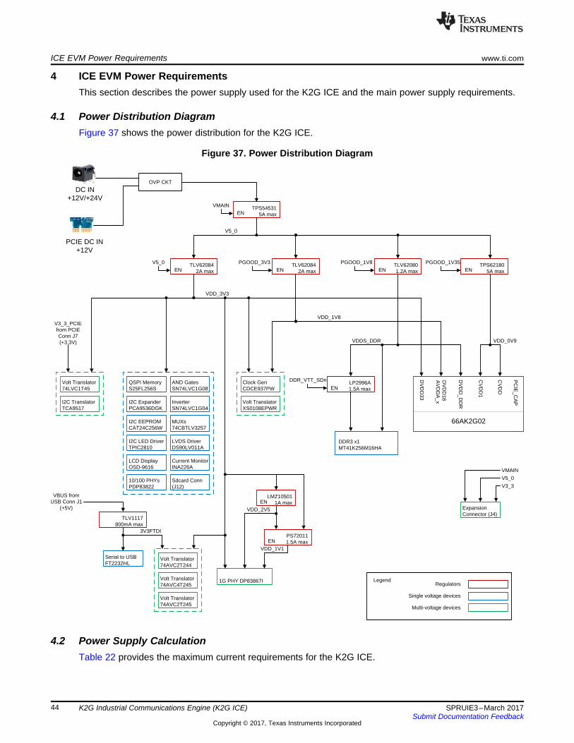
4 ICE EVM Power RequirementsThis section describes the power supply used for the K2G ICE and the main power supply requirements.
4.1 Power Distribution DiagramFigure 37 shows the power distribution for the K2G ICE.
Figure 37. Power Distribution Diagram
4.2 Power Supply CalculationTable 22 provides the maximum current requirements for the K2G ICE.

www.ti.com ICE EVM Power Requirements
45SPRUIE3–March 2017Submit Documentation Feedback
Copyright © 2017, Texas Instruments Incorporated
K2G Industrial Communications Engine (K2G ICE)
Table 22. ICE EVM Power ConsumptionQty Description Manufacturers Part Number Max Current Vmain (mA)
13 LED Green SMD 20-mA 2-V 0805 5988170107F 89.375
4 LED RedGreenBlue tricolor 20-mA 1.9/2.1-V 1210 smd SM1210RGB 82.5
1 LED ALINGAP RED CLEAR 0805 SMD 5988110107F 6.875
1 Connector RJ-45 jack with mag and LED gigabit LPJG16314A4NL 13.75
1 Connector 0.5-mm pitch, 14 Pin, FPC 10051922-1410ELF 6.875
1 Connector compact low-profile push-type microSD SCHA5B0200 13.75
1 High density 20×6 female connector 120 POS SEAF-20-05.0-S-06-A-2-K-TR 480
2 RJ45 with LED, stacked vertical ARJ21A-MBSD-A-B-EMU2 55
1 MicroSD card 31.0077
7 Dual transistor NPN 50 V 100 mA DMC564040R 0.48125
3 IC MOSFET N-CHANNEL 50-V 200-mA SOT23-3 BSS138-7-F 0.000515625
1 IC POWER MOSFET N-CHANNEL D2PAK SUM60N10-17-E3 0.0859375
1 TRANSISTOR NPN 50-V 100-mA SOT23-3 MMUN2214LT1G 0.0859375
8 4-bit 1-4 FET Mux/Demux SN74CBTLV3257RGYR 0.825
7 Single logic AND Gate SN74LVC1G08DCKR 60.15625
1 IC LOW INPUT VOLTAGE CURRENT LIMITED LOAD SWITCHSC70-5
TPS22945DCKR 0.275
1 IC TRANSLATOR BIDIRECTIONAL VOLTAGE-LEVEL 8-BITTSSOP20
TXS0108EPWR 17.1875
4 IC BI-DIRECTIONAL CURRENT MONITER MSOP10 INA226AIDGSR 1.375
1 IC µP SUPERVISOR CIRCUITS SOT23-6 TPS3808G09DBVR 0.0034375
1 IC SINGLE-BIT DUAL-SUPPLY BUS TRANSCEIVER SOT-23 SN74LVC1T45DBVR 8.25
1 IC CONTROLLER HIGH-SIDE PROTECTION VSSOP10 LM5060MM/NOPB 0.6875
2 IC DUAL-BIT DUAL SUPPLY BUS TRANSCEIVER QFN10 SN74AVC2T245RSWR 8.25
1 IC 2-CHANNEL I2C BUS REPEATER VSSOP8 TCA9517DGKR 2.0625
4 Industrial Ethernet 10/100 Mb/s PHY transceiver PDP83822RHBT 96.25
1 ESD protection array 2Chan +-15 kV TPD2E001DRLR 0
1 PROGRAMMABLE 3-PLL VCXO CLOCK SYNTHESIZER with 7outputs
CDCE937PW 10.3125
1 DDR termination regulator LP2996AMR/NOPB 0.171875
1 USBHS Dual UART/FIFO FT2232HL-REEL 24.0625
1 E2PROM 2Kbit 3-Mhz memory 93LC56B-I/SN 0.6875
1 Dual buffer with open-drain outputs SN74LVC2G07DCKR 0.171875
1 8-bit LED driver with I2C interface TPIC2810DR 0.34375
1 2-bit undirectional voltage translator SN74AVC2T244DQMR 0.006875
1 Single two-input positive NAND SN74LVC1G00DCKR 34.375
1 Bus transceiver 4-bit voltage translator SN74AVC4T245PW 34.375
1 Quad serial NOR flash memory 256Mb 3.3 V S25FL256SAGMFIR01 34.375
1 DDR3 SDRAM 4 Gb (256Mx16) 1.35 V MT41K256M16HA-125 IT:E 28.125
1 Ethernet PHY Gb/100Mb/10Mb DP83867IRPAPT 36.45833333
2 ESD protection device 2 DiffPair Chan +-15 kV TPD4E05U06DQAR 0.006875
1 I2C to I/O expander 4 bit PCA9536DGKR 55
1 EEPROM 256Kb I2C SOIC8 CAT24C256WI-G 1.03125
1 LVDS interface IC SGL HIGH SPD DIFF DRVR DS90LV011ATMF/NOPB 3.4375
1 IC SINGLE INVERTER GATE SC70-5 SN74LVC1G04DCKR 8.25
1 Cortex A15 with C66X SOC 66AK2G02 66AK2G02_ZBB 480.54
MaximumTotal maximum current consumption in mA 1726.839361
Total maximum power consumption for 12-V supply in mW 20722.0723

VMAIN
V5_0
VDD_3V3
PGOOD_3V3
VDD1V8
PGOOD_1V8
VDDS_DDR
PGOOD_1V35
VREF_DDR/ VTT_DDR
VDD_0V9
PGOOD_0V9
12V-24V6.12V
5V
3.3V
1.8V
1.35V
0.0675V
0.9V
ICE EVM Power Requirements www.ti.com
46 SPRUIE3–March 2017Submit Documentation Feedback
Copyright © 2017, Texas Instruments Incorporated
K2G Industrial Communications Engine (K2G ICE)
4.3 Power SequencingFigure 38 shows the power sequencing the K2G ICE. This diagram represents the sequencingimplemented on the K2G ICE. The power sequencing for the K2G is represented in the data manual forthe device. Refer to the data manual when designing power sequencing for this device.
Figure 38. Power Sequencing
www.ti.com Comparison to K2G General Purpose EVM
47SPRUIE3–March 2017Submit Documentation Feedback
Copyright © 2017, Texas Instruments Incorporated
K2G Industrial Communications Engine (K2G ICE)
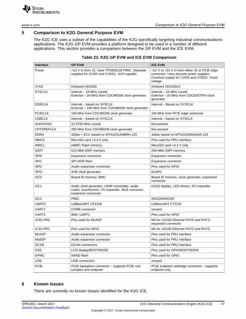
5 Comparison to K2G General Purpose EVMThe K2G ICE uses a subset of the capabilities of the K2G specifically targeting industrial communicationsapplications. The K2G GP EVM provides a platform designed to be used in a number of differentapplications. This section provides a comparison between the GP EVM and the ICE EVM.
Table 23. K2G GP EVM and ICE EVM Comparison
Interface GP EVM ICE EVMPower +12 V in from J3. Uses TPS659118 PMIC. Separate
supplies for CVDD and CVDD1. AVS capable.+12 V to +24 V in from either J6 or PCIE edgeconnector. Uses discrete power supplies.Common supply for CVDD and CVDD1. Fixedvoltage.
JTAG Onboard XDS200 Onboard XDS100v2SYSCLK Internal – 24-MHz crystal
External – 24-MHz from CDCM6208 clock generatorInternal – 24-MHz crystalExternal – 25-MHz from CDCE937PW clockgenerator
DDRCLK Internal – based on SYSCLKExternal – 100-MHz from CDCM6208 clock generator
Internal – Based on SYSCLK
PCIECLK 100 MHz from CDCM6208 clock generator 100 MHz from PCIE edge connectorUSBCLK Internal – based on SYSCLK Internal – based on SYSCLKAUDIOOSC 22.5792-MHz crystal Not presentCPTSREFCLK 250 MHz from CDCM6208 clock generator Not presentDDR3 32bits + ECC based on MT41K512M8RH-125 16bits based on MT41K256M16HA-125MMC0 MicroSD card +3.3 V only Pins used for PRU interfaceMMC1 eMMC Flash memory MicroSD card +3.3 V onlyQSPI 512-Mbit QSPI memory 256-Mbit QSPI memorySPI0 Expansion connector Expansion connectorSPI1 SPI NOR flash Expansion connectorSPI2 Audio expansion connector Pins used for GPIOSPI3 AVB clock generator eCAP0I2C0 Board ID memory, BMC, Board ID memory, clock generator, expansion
connectorI2C1 Audio clock generator, HDMI transmitter, audio
codec, touchscreen, I/O expander, MLB connector,expansion connector
OLED display, LED drivers, I/O expander
I2C2 PMIC INA226AIDGSRUART0 USBtoUART CP2105 USBtoUART FT2232UART1 COM8 connector unusedUART2 BMC UART1 Pins used for GPIOICSS PR0 Pins used for McASP MII for 10/100 Ethernet PHY0 and PHY1/
expansion connectorICSS PR1 Pins used for GPIO MII for 10/100 Ethernet PHY2 and PHY3McASP Audio expansion connector Pins used for PRU interfaceMcBSP Audio expansion connector Pins used for PRU interfaceDCAN DCAN connectors Pins used for PRU interfaceDSS LCD display/BOOTMODE Pins used for GPIO/BOOTMODEGPMC NAND flash Pins used for GPIOUSB USB connectors unusedPCIE PCIE backplane connector – supports PCIE root
complex and endpointPCIE endpoint cardedge connector – supportsendpoint only
6 Known IssuesThere are currently no known issues identified for the K2G ICE.

IMPORTANT NOTICE FOR TI DESIGN INFORMATION AND RESOURCES
Texas Instruments Incorporated (‘TI”) technical, application or other design advice, services or information, including, but not limited to,reference designs and materials relating to evaluation modules, (collectively, “TI Resources”) are intended to assist designers who aredeveloping applications that incorporate TI products; by downloading, accessing or using any particular TI Resource in any way, you(individually or, if you are acting on behalf of a company, your company) agree to use it solely for this purpose and subject to the terms ofthis Notice.TI’s provision of TI Resources does not expand or otherwise alter TI’s applicable published warranties or warranty disclaimers for TIproducts, and no additional obligations or liabilities arise from TI providing such TI Resources. TI reserves the right to make corrections,enhancements, improvements and other changes to its TI Resources.You understand and agree that you remain responsible for using your independent analysis, evaluation and judgment in designing yourapplications and that you have full and exclusive responsibility to assure the safety of your applications and compliance of your applications(and of all TI products used in or for your applications) with all applicable regulations, laws and other applicable requirements. Yourepresent that, with respect to your applications, you have all the necessary expertise to create and implement safeguards that (1)anticipate dangerous consequences of failures, (2) monitor failures and their consequences, and (3) lessen the likelihood of failures thatmight cause harm and take appropriate actions. You agree that prior to using or distributing any applications that include TI products, youwill thoroughly test such applications and the functionality of such TI products as used in such applications. TI has not conducted anytesting other than that specifically described in the published documentation for a particular TI Resource.You are authorized to use, copy and modify any individual TI Resource only in connection with the development of applications that includethe TI product(s) identified in such TI Resource. NO OTHER LICENSE, EXPRESS OR IMPLIED, BY ESTOPPEL OR OTHERWISE TOANY OTHER TI INTELLECTUAL PROPERTY RIGHT, AND NO LICENSE TO ANY TECHNOLOGY OR INTELLECTUAL PROPERTYRIGHT OF TI OR ANY THIRD PARTY IS GRANTED HEREIN, including but not limited to any patent right, copyright, mask work right, orother intellectual property right relating to any combination, machine, or process in which TI products or services are used. Informationregarding or referencing third-party products or services does not constitute a license to use such products or services, or a warranty orendorsement thereof. Use of TI Resources may require a license from a third party under the patents or other intellectual property of thethird party, or a license from TI under the patents or other intellectual property of TI.TI RESOURCES ARE PROVIDED “AS IS” AND WITH ALL FAULTS. TI DISCLAIMS ALL OTHER WARRANTIES ORREPRESENTATIONS, EXPRESS OR IMPLIED, REGARDING TI RESOURCES OR USE THEREOF, INCLUDING BUT NOT LIMITED TOACCURACY OR COMPLETENESS, TITLE, ANY EPIDEMIC FAILURE WARRANTY AND ANY IMPLIED WARRANTIES OFMERCHANTABILITY, FITNESS FOR A PARTICULAR PURPOSE, AND NON-INFRINGEMENT OF ANY THIRD PARTY INTELLECTUALPROPERTY RIGHTS.TI SHALL NOT BE LIABLE FOR AND SHALL NOT DEFEND OR INDEMNIFY YOU AGAINST ANY CLAIM, INCLUDING BUT NOTLIMITED TO ANY INFRINGEMENT CLAIM THAT RELATES TO OR IS BASED ON ANY COMBINATION OF PRODUCTS EVEN IFDESCRIBED IN TI RESOURCES OR OTHERWISE. IN NO EVENT SHALL TI BE LIABLE FOR ANY ACTUAL, DIRECT, SPECIAL,COLLATERAL, INDIRECT, PUNITIVE, INCIDENTAL, CONSEQUENTIAL OR EXEMPLARY DAMAGES IN CONNECTION WITH ORARISING OUT OF TI RESOURCES OR USE THEREOF, AND REGARDLESS OF WHETHER TI HAS BEEN ADVISED OF THEPOSSIBILITY OF SUCH DAMAGES.You agree to fully indemnify TI and its representatives against any damages, costs, losses, and/or liabilities arising out of your non-compliance with the terms and provisions of this Notice.This Notice applies to TI Resources. Additional terms apply to the use and purchase of certain types of materials, TI products and services.These include; without limitation, TI’s standard terms for semiconductor products http://www.ti.com/sc/docs/stdterms.htm), evaluationmodules, and samples (http://www.ti.com/sc/docs/sampterms.htm).
Mailing Address: Texas Instruments, Post Office Box 655303, Dallas, Texas 75265Copyright © 2018, Texas Instruments Incorporated